UNIT I Single Stage Amplifiers: Classification of ... · hybrid model, Analysis of CE amplifier...
179
UNIT – I Single Stage Amplifiers: Classification of Amplifiers – Distortion in amplifiers, Analysis of CE, CC and CB configurations with simplified hybrid model, Analysis of CE amplifier with emitter resistance and emitter follower, Miller’s theorem and its dual, Design of single stage RC coupled Amplifier using BJT. Multistage Amplifiers: Analysis of Cascaded RC coupled BJT amplifiers, Cascode Amplifier, Darlington Pair, Different Coupling Schemes used in Amplifiers – RC coupled amplifiers, Transformer Coupled Amplifier, Direct Coupled Amplifier.
Transcript of UNIT I Single Stage Amplifiers: Classification of ... · hybrid model, Analysis of CE amplifier...

UNIT – I
Single Stage Amplifiers: Classification of Amplifiers – Distortion in
amplifiers, Analysis of CE, CC and CB configurations with simplified
hybrid model, Analysis of CE amplifier with emitter resistance and emitter
follower, Miller’s theorem and its dual, Design of single stage RC coupled Amplifier using BJT.
Multistage Amplifiers: Analysis of Cascaded RC coupled BJT amplifiers,
Cascode Amplifier, Darlington Pair, Different Coupling Schemes used in
Amplifiers – RC coupled amplifiers, Transformer Coupled Amplifier,
Direct Coupled Amplifier.

Classification of Amplifiers
Type of Signal
Based on No.of
Stages Type of
Configuration
Classification based on
conduction angle
Frequency of
Operation
Small Signal
Single Stage
Common Emitter Class A Amplifier Direct Current (DC)
Large Signal
Multistage
Common Base Class B Amplifier Audio Frequencies (AF)
Common Collector Class AB Amplifier Radio Frequencies (RF)
Class C Amplifier VHF, UHF and SHF
Frequencies

Different Regions Of Operation

Transistor Voltage specifications For Various Operating
Regions
Condition for Active & Saturation Regions


Transistor Biasing

CE, CC, & CB Amplifiers

H-Parameters Representation Of An Amplifier


Small Signal Analysis Of A Junction Transistor


Design Problem

Approximate H-Model For CE Amplifier


Approximate H-Model For CC Amplifier


Approximate H-Model For CB Amplifier


Design Problem

Miller’s Theore
Millers theorem is used o simplify the analysis of a circuit
whenever there is a feedback connection in the circuit


Design Problems

Design Problems

Analysis Of CE Amplifier With Unbypassed RE
RE is added to stabilize the gain of the amplifier
RE acts as a feedback resistor
The overall gain will reduce with unbypassed RE

AC Equivalent Circuit For CE Amplifier with
Unbypassed RE

AC Equivalent Circuit For CE Amplifier with RE Splitted
usi g dual of Miller’s Theore

h-Parameter Equivalent Circuit
(Exact Analysis)

h-Parameter Equivalent Circuit
(Approximate Analysis)


Design Problems

MULTISTAGE AMPLIFIERS

Need For Cascading

Gain of 2-Stage Cascade Amplifier
Block diagram of 2-Stage Cascade Amplifier


Frequency Response of 2-Stage RC Coupled Amplifier


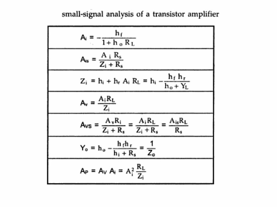
UNIT – II
BJT Amplifiers-Frequency Response: Logarithms, Decibels, General frequency considerations,
Frequency response of BJT Amplifier, Analysis at low and high frequencies, Effect of
coupling and bypass capacitors. The Hybrid pi model –Common Emitter Transistor Model,
CE Short Circuit current gain, current gain with resistive load, Single stage CE transistor
Amplifier Response, Gain –Bandwidth Product, Emitter follower at high frequencies.
MOS Amplifiers: Basic Concepts, MOS Small signal model, Common source amplifier with
resistive load


UNIT – III
Feedback Amplifiers: Concepts of feedback, Classification of feedback amplifiers,
General characteristics of negative feedback amplifiers, Effect of feedback on
amplifier characteristics, Voltage Series, Voltage Shunt, Current Series and Current
Shunt Feedback Configurations, Illustrative examples.
Oscillators: Classification of oscillators, Condition for oscillations, RC Phase shift
Oscillators, Generalized analysis of LC Oscillators-Hartley and Colpitts Oscillators,
Wien Bridge and crystal Oscillators, Stability of Oscillators

CLASSIFICATION OF AMPLIFIERS
• Amplifiers can be classified broadly as,
• I. Voltage amplifiers.
• 2. Current amplifiers.
• 3. Transconductance amplifiers.
• 4. Transresistance amplifiers.

VOLTAGE AMPLIFIER
This circuit is a 2-port network and it represents an amplifier (see in Fig 7.1).
Suppose Ri» Rs, drop across Rs is very small.
Equivalent circuit of voltage amplifiers.

CURRENT AMPLIFIER
• An ideal current amplifier is one which gives output current proportional to input current and
• the proportionality factor is independent ofRs and RL.

TRANSCONDUCTANCE AMPLIFIER
Ideal Transconductance amplifier supplies output current which is proportional
to input voltage
independently of the magnitude of Rs and RL.

TRANS RESISTANCE AMPLIFIER
It gives output voltage Vo proportional to Is, independent of Rs a. RL. For
ideal amplifiers
Rj =0, Ro=O

GENERALIZED BLOCK SCHEMATIC

Introduction To Feedback
• The process of injecting a fraction of output energy of some
device back to the input is known as feedback.
• some of the short comings(drawbacks) of the amplifier circuit
are:
1. Change in the value of the gain due to variation in
supplying voltage, temperature or due to components.
2. Distortion in wave-form due to non linearities in the
operating characters of the amplifying device.
3. The amplifier may introduce noise (undesired signals)
• The above drawbacks can be minimizing if we introduce
feedback

basic types of feedback in
amplifiers

Positive feedback
•When the feedback energy (voltage or current) is in phase with the input
signal and thus aids it, it is called positive feedback.
•Both amplifier and feedback network introduce a phase shift of 180°. The
result is a 360° phase shift around the loop, causing the feedback voltage Vf
to be in phase with the input signal Vin.
Fig. Block diagram for positive feedback

Negative feedback.
•When the feedback energy (voltage or current) is out of phase with the input
signal and thus opposes it, it is called negative feedback.
•The amplifier introduces a phase shift of 180° into the circuit while the
feedback network is so designed that it introduces no phase shift (i.e., 0°
phase shift).
•Negative feedback is also called as degenerative feedback.
Fig.negative feedback amplifier

CLASSIFACTION OF FEEDBACK
AMPLIFIERS
voltage series feedback. Voltage shunt Feedback
Current Shunt Feedback Current Series Feedback

EFFECT OF NEGATIVE FEEDBACK ON TRANSFER GAIN
REDUCTION IN GAIN

INCREASE IN BANDWIDTH
REDUCTION IN DISTORTION

FEEDBACK TO IMPROVE SENSITIVITY
FREQUENCY DISTORTION
BAND WIDTH

SENSITIVITY OF TRANSISTOR GAIN
REDUCTION OF NONLINEAR DISTORTION

REDUCTION OF NOISE
TRANSFER GAIN WITH FEEDBACK
Consider the generalized feedback amplifier

LOOP GAIN
Return Ratio
βA = Produ t of feed a k fa tor β a d a plifi atio fa tor A is alled as Return Ratio.
Return Difference (D)
The difference between unity (1) and return ratio is called as Return difference.

CLASSIFACTION OF FEEDBACK AMPLIFIERS
There are four types of feedback,
1. Voltage series feedback.
2. Voltage shunt feedback.
3. Current shunt feedback.
4. Current series feedback
Voltage shunt Feedback voltage series feedback.

Current Shunt Feedback Current Series Feedback
EFFECT OF FEEDBACK ON INPUT RESISTANCE
Current Shunt Feedback Voltage shunt Feedback

voltage series feedback. Current Series Feedback
EFFECT OF NEGATIVE FEEDBACK ON Ro
voltage series feedback. Current Shunt Feedback

ANALYSIS OF FEEDBACK AMPLIFIERS

Current shunt feedback.
Equivalent circuit.
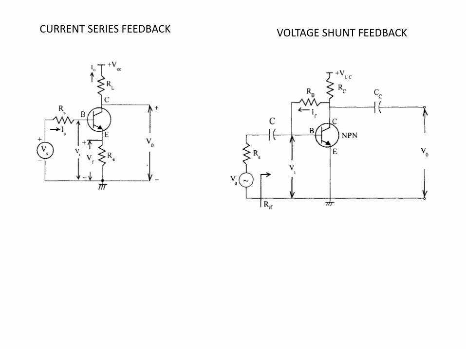
CURRENT SERIES FEEDBACK VOLTAGE SHUNT FEEDBACK

OSCILLATORS
Oscillator is a source of AC voltage or current.


There are two types of oscillators circuits:
I. Harmonic Oscillators 2. Relaxation Oscillators
PERFORMANCE MEASURES OF OSCILLATOR CIRCUITS:
Stability:
Amplitude stability:
Output Power:
Harmonics:

SINUSOIDAL OSCILLATORS
Block schematic

BARKHAUSEN CRITERION

R - C PHASE-SHIFT OSCILLATOR

A GENERAL FORM OF LC OSCILLATOR CIRCUIT

- Aβ must be positive, and at least unity in magnitude. Than XI and
X2 must have the same sign.

(a) Colpitts oscillator (b) Hartely oscillator circuit

Wien bridge oscillator circuit.


CRYSTAL OSCILLATORS

UNIT – IV
LARGE SIGNAL AMPLIFIERS: Classification, Class A Large signal
amplifiers, Transformer Coupled Class A Audio Power amplifier,
Efficiency of class A amplifier, Class B amplifier, Efficiency of class B
Amplifier, class B Push pull Amplifier, Complementary Symmetry
Class B Push Pull Amplifier, Distortion of Power Amplifiers, Thermal
Stability and Heat sinks.

Transistor Audio Power Amplifier
• A transistor amplifier which raises the power level of the signals that have audio frequency range is known as transistor audio power amplifier.
• A transistor that is suitable for power amplification is generally called a power transistor.
• The typical power output rating of a power amplifier is 1W or more.

Factors to be considered in large signal
amplifiers:
• Output power
• Distortion
• Operating region
• Thermal considerations
• Efficiency

block diagram of an audio amplifier

Difference Between Voltage and
Power Amplifiers

Performance Quantities of Power
Amplifiers
(i) Collector efficiency
The ratio of a.c. output power to the zero signal power (i.e. d.c. power) supplied by the
battery of a power amplifier is known as collector efficiency.
(ii) Distortion
The change of output wave shape from the input wave shape of an amplifier is known as
distortion.
(iii) Power dissipation capability
The ability of a power transistor to dissipate heat is known as power dissipation
capability.

Classification of Power Amplifiers
•Class A: It is one, in which the active device conducts for the full 360°.
•Class B: Conduction for 180 °.
•Class C: Conduction for < 180°.
•Class AB :Conduction angle is between 180°. and 360°.
•Class D: These are used in transmitters because their efficiency is high: 100%.
•Class S:Switching regulators are based on class'S' operation.

Class A power amplifier
•If the collector current flows at all times during the full cycle of the signal,
the power amplifier is known as class A power amplifier.
•If the Q point is placed near the centre a/the linear region a/the dynamic
curve, class A operation results. Because the transistor will conduct for
the complete 360°, distortion is low for small signals and conversion
efficiency is low.

Types of class-A power Amplifiers
1. Series fed
There is no transformer in the circuit. RL is in series with V cc. There is DC power drop across RL. Therefore efficiency = 25% (maximum).
2. Transformer coupled
• The load is coupled through a transformer. DC drop across the primary of the transformer is
negligible. There is no DC drop across RL.
Therefore efficiency = 50% maximum.

Series Fed class-A power Amplifier
Fig.(a)Series fedClass A power amplifier circuit Fig.(b)Transter curve

Transformer Coupled class-A power
Amplifier
Fig.(a)Transformer Coupled Class A power amplifier circuit Fig.(b)Transfer curve

Important Points About Class A Power
Amplifier
• A transformer coupled class A power amplifier has a maximum collector efficiency of 50%
• The power dissipated by a transistor is given by :
Pdis = Pdc − Pac
• When no signal is applied to a class A power amplifier, Pac = 0.
∴ Pdis = Pdc
• When a class A power amplifier is used in the final stage, it is called single ended class A power amplifier.

Class B power amplifier
• If the collector current flows only during the positive half-cycle of the input signal,
it is called a class B power amplifier.
Transfer curve
•For class B operation the Q point is set near cutoff. So output power will be
more and conversion efficiency is more. Conduction is only for 180

Types of class-B power Amplifiers
• Push-Pull Amplifier
The standard class B push-pull amplifier requires a centre
tapped transformer
• Complimentary Symmetry Circuits (Transformer
Less Class B Power Amplifier)
Complementary symmetry circuits need only one phase
They don't require a centre tapped transformer.

Advantages & Disadvantages of Class B
power Amplifier
Advantages
1.More output power; efficiency = 78.5%. Max.
2.Efficiency is higher. Since the transistor conducts only for 180°, when it is not conducting, it will not draw DC current.
3. Negligible power loss at no signal.
Disadvantages:
1. Supply voltage V cc should have good regulation. Since if V cc changes, the operating point changes (Since Ic changes). Therefore transistor may not be at cut off.
2. Harmonic distortion is higher. (This can be minimized by pushpull connection).

Class B Push-Pull Amplifier

Complimentary Symmetry Circuits
(Transformer Less Class B Power
Amplifier)
Fig. Complimentary Symmetry circuit

Advantages & Disadvantages of Class B
complementary power Amplifier
• Advantages
(i) This circuit does not require transformer. This saves on weight and cost.
(ii) Equal and opposite input signal voltages are not required.
• Disadvantages
(i) It is difficult to get a pair of transistors (npn and pnp) that have similar characteristics.
(ii) We require both positive and negative supply voltages.

Differences between class-A & B
power Amplifiers

Heat Sinks
•The metal sheet that serves to dissipate the additional
heat from the power transistor is known as heat sink.
•The purpose of heat sinks is to keep the operating temperature
of the transistor low, to prevent thermal breakdown.
•Almost the entire heat in a transistor is produced at the
collector-base junction. If the temperature exceeds the
permissible limit, this junction is destroyed and the transistor is
rendered useless.
• Most of power is dissipated at the collector-base junction.
This is because collector-base voltage is much greater than the
base-emitter voltage, although currents through the two
junctions are almost the same.

Mathematical Analysis Of Heat Sinks

Classification of heat Sinks 1. Low Power Transistor Type.
2. High Power Transistor Type.

Low Power Transistor Type.
• Low Power Transistors can be mounted directly on the metal chassis to increase the heat dissipation capability. The casing of the transistor must be insulated from the metal chassis to prevent shorting.
• Beryllium oxide insulating washers are used for insulating casing from the chassis. They have good thermal conductivity.
• Zinc oxide film silicon compound between washer and chassis, improves the heat transfer from the semiconductor device to case to the chassis.

High Power Transistor Type.
• re TO-3 and TO-66 types. These are diamond shaped. For
power transistors, usually, the ease itself in the collector
convention and radiation
• Finned aluminium heat sinks yield the best heat transfer per
unit cost.
Fin-type heat sink Power transistor heat sink

Alternate Methods to prevent Thermal
breakdown
• It should be realized that the use of heat sink alone
may not be sufficient to prevent thermal runaway
under all conditions. In designing a transistor circuit,
consideration should also be given to the choice of
(i) operating point
(ii) ambient temperatures which are likely to be
encountered and
(iii)the type of transistor e.g. metal case transistors are
more readily cooled by conduction than plastic ones.

UNIT – V
TUNED AMPLIFIERS Introduction, Q Factor, Small signal
Tuned Amplifiers, Effect of Cascading Single tuned Amplifiers
on bandwidth, Effect of Cascading Double Tuned Amplifiers
on Bandwidth, Stagger Tuned Amplifiers, Stability of tuned
amplifiers.

Tuned Amplifiers
•Amplifiers which amplify a specific frequency or narrow band of frequencies are
called tuned amplifiers.
•Tuned amplifiers are mostly used for the amplification of high or radio frequencies.
• It offers a very high impedance at resonant frequency and very small impedance at all
other frequencies.

Advantages of Tuned Amplifiers
1. Small power loss.
2. High selectivity
3. Smaller collector supply voltage
4. Used in RF amplifiers,
Communication receivers, Radar ,
Television ,I.F amplifiers
5. harmonic distortion is very small

Why not Tuned Circuits for Low
Frequency Amplification?
• Low frequencies are never single
• High values of L and C.

Classification

Single Tuned Amplifier
•Uses one parallel tuned circuit as the load IZI in each stage and all
these tuned circuits in different stages are tuned to the same
frequency. To get large Av or Ap, multistage amplifiers are used. But
each stage is tuned to the same frequency, one tuned circuit in one
stage.

Single Tuned Capacitive Coupled
Amplifier

Equivalent circuit of Single Tuned
Capacitive Coupled Amplifier

Equivalent circuit of Single Tuned
Capacitive Coupled Amplifier(applying
Miller's Theorem)

Simplified equivalent circuit

Simplified output circuit

Tapped Single Tuned Capacitance
Coupled Amplifier

Equivalent Circuit on the Output
Side of the I Stage

Equivalent circuit of Tapped Single
Tuned Capacitance Coupled Amplifier

Equivalent circuit after
simplification

Single Tuned Transformer Coupled
or Inductively Coupled Amplifier
Inductive coupled amplifier circuit (a) and its equivalent (b)

Single Tuned Transformer Coupled
or Inductively Coupled Amplifier
(a)Equivalent circuit (b)Simplified circuit
©Equivalent circuit

Double Tuned Amplifier
• It uses two inductively coupled tuned
circuits, for each stage of the amplifier.
Both the tuned circuits are tuned to the
same frequency, two tuned circuits in one
stage, to get sharp response.
• It provides larger 3-db band width than
the single tuned amplifier. Therefore Gain
x Bandwidth product is more.
• It provides gain - frequency curve having
steeper sides and flatter top.

Double tuned amplifier circuit

Double tuned amplifier Equivalent
circuit
(a)Equivalent circuit
(b)Modified circuit

Stagger Tuned Amplifier
•This circuit uses number of single tuned stages in cascade. The
successive tuned circuits are tuned to slightly different
frequencies.
Variation of Av with f

Stability Considerations
• Thermal Effects
• Bias Considerations: Distortion in Audio
amplifiers and other types of circuits
depends on :
(i) Input signal level (in mv)
(ii) Source Resistance
(iii) Bias Conditions
(iv) Type of output load and its
impedance
(v) Loading effect.


![RZHU :HVWFKHVWHU %ULGJH %XQGOH 'HVLJQ %XLOG ….../rzhu :hvwfkhvwhu %ulgjh %xqgoh 'hvljq‐%xlog 3urmhfw &rqwudfw ' )lqdo 5)3 4xhvwlrqv dqg $qvzhuv 'hfhpehu y µ ] } v ô î w](https://static.fdocuments.net/doc/165x107/5fa7c653c67b6249894711fe/rzhu-hvwfkhvwhu-ulgjh-xqgoh-hvljq-xlog-rzhu-hvwfkhvwhu-ulgjh-xqgoh.jpg)