UNIT 7: Micro-manufacturing Unit 7 Copyright © 2014. MDIS. All rights reserved. 1 Modern...
26
UNIT 7: Micro-manufacturing Unit 7 Copyright © 2014. MDIS. All rights reserved. 1 Modern Manufacturing
-
Upload
bennett-clinton-curtis -
Category
Documents
-
view
217 -
download
2
Transcript of UNIT 7: Micro-manufacturing Unit 7 Copyright © 2014. MDIS. All rights reserved. 1 Modern...

UNIT 7: Micro-manufacturing
Unit 7 Copyright © 2014. MDIS. All rights reserved. 1
Modern Manufacturing

2
Objectives
Unit 7 Copyright © 2014. MDIS. All rights reserved.
• Understand the various micromachining processes.• Obtain an overview of the fabrication of microelectronic devices.• Obtain an overview of the fabrication of microelectro-mechanical devices.• Obtain an overview of Nanoscale Manufacturing.

Unit 7 Copyright © 2014. MDIS. All rights reserved.
Micromanufacturing
3

Unit 7 Copyright © 2014. MDIS. All rights reserved.
Fabrication of Microelectronic Devices
• The invention of the transistor in 1947 that set the stage for what would become one of the greatest technological advancements in all of history. Microelectronics has played an increasing role in our lives ever since integrated circuit (IC) technology became the foundation for calculators, Wrist watches, controls for home appliances and automobiles, information systems, telecommunications, robotics, space travel, weaponry, and personal computers.
• The major advantages of today’s ICs are their very small size and low cost. As fabrication technology becomes more advanced, the size of devices made (such as transistors, diodes, resistors, and capacitors) continues to decrease. Consequently, more components can be put onto a chip-a small piece of semiconducting material on which the circuit is fabricated. In addition, mass production and automation have helped reduce the cost of each completed circuit.
4

Unit 7 Copyright © 2014. MDIS. All rights reserved.
Fabrication of Microelectronic Devices
5

Unit 7 Copyright © 2014. MDIS. All rights reserved.
Fabrication of Microelectronic Devices
6
http://willson.cm.utexas.edu/Research/Sub_Files/SFIL/Demonstrations/MOSFET/MOSFET1.jpg

Unit 7 Copyright © 2014. MDIS. All rights reserved.
Clean Rooms
• Clean rooms are essential for the production of most integrated circuits-a fact that can be appreciated by noting the scale of manufacturing to be performed. Integrated circuits are typically a few millimetres in length, and the smallest features in a transistor on the circuit may be as small as a few tens of nanometres. This size range is smaller than particles that we don’t normally consider harmful, such as dust, smoke, perfume, and bacteria. However, if these contaminants are present on a silicon wafer during processing, they can seriously compromise the performance of the entire device. Thus, it is essential that all of the potentially harmful particles be eliminated from the IC manufacturing environment.
7

Unit 7 Copyright © 2014. MDIS. All rights reserved.
Clean Rooms
• There are various levels of clean rooms, which are defined by the class of the room. The classification system refers to the number of 0.5-/.tm or larger particles within a cubic metre of air. Thus, a Class-0.35 clean room has 0.35x10E3 or fewer such particles per cubic metre. Clearly, the size and the number of particles are important in defining the class of a clean room. Most clean rooms for microelectronics manufacturing range from Class 0.035 to Class 0.35. In comparison, the contamination level in modern hospitals is on the order of 350,000 particles per cubic metre.
8

Unit 7 Copyright © 2014. MDIS. All rights reserved.
Clean Rooms
9
Allowable particle size counts for different clean room classes.

Unit 7 Copyright © 2014. MDIS. All rights reserved.
Semiconductors and Silicon
• Semiconductor materials have electrical properties that lie between those of conductors and insulators and that exhibit resistivities between 1x10E-2 and 1x10E8 ohms/cm. Semiconductors have become the foundation for electronic devices because their electrical properties can be altered when controlled amounts of selected impurity atoms are added to their crystal structures. These impurity atoms, also known as dopants, have either one more valence electron (n-type, or negative, dopant) or one less valence electron (p-type, or positive, dopant) than the atoms in the semiconductor lattice.
• For silicon, which is a Group IV element in the Periodic Table, typical ii-type and p-type dopants include, respectively, phosphorus (Group V) and boron (Group III).
• The electrical operation of semiconductor devices can be controlled through the creation of regions with different doping types and concentrations.
10

Unit 7 Copyright © 2014. MDIS. All rights reserved.
Semiconductors and Silicon
11

Unit 7 Copyright © 2014. MDIS. All rights reserved.
Semiconductors Manufacturing
12

Unit 7 Copyright © 2014. MDIS. All rights reserved.
Semiconductors and Silicon
• Lithography is the process by which the geometric patterns that define devices are transferred to the substrate surface. Photolithography uses a reticle, also called a photomask or mask, which is a glass or quartz plate with a pattern of the chip deposited onto it with a chromium film.
• Etching is the process by which entire films or particular sections of films are removed, and it plays an important role in the fabrication sequence. One of the key criteria in this process is selectivity-that is, the ability to etch one material without etching another.
• In the diffusion process, the movement of atoms is a result of thermal excitation. Dopants can be introduced to the substrate surface in the form of a deposited film, or the substrate can be placed in a vapour containing the dopant source.
13
Unit 7 Copyright © 2014. MDIS. All rights reserved.
Semiconductors and Silicon
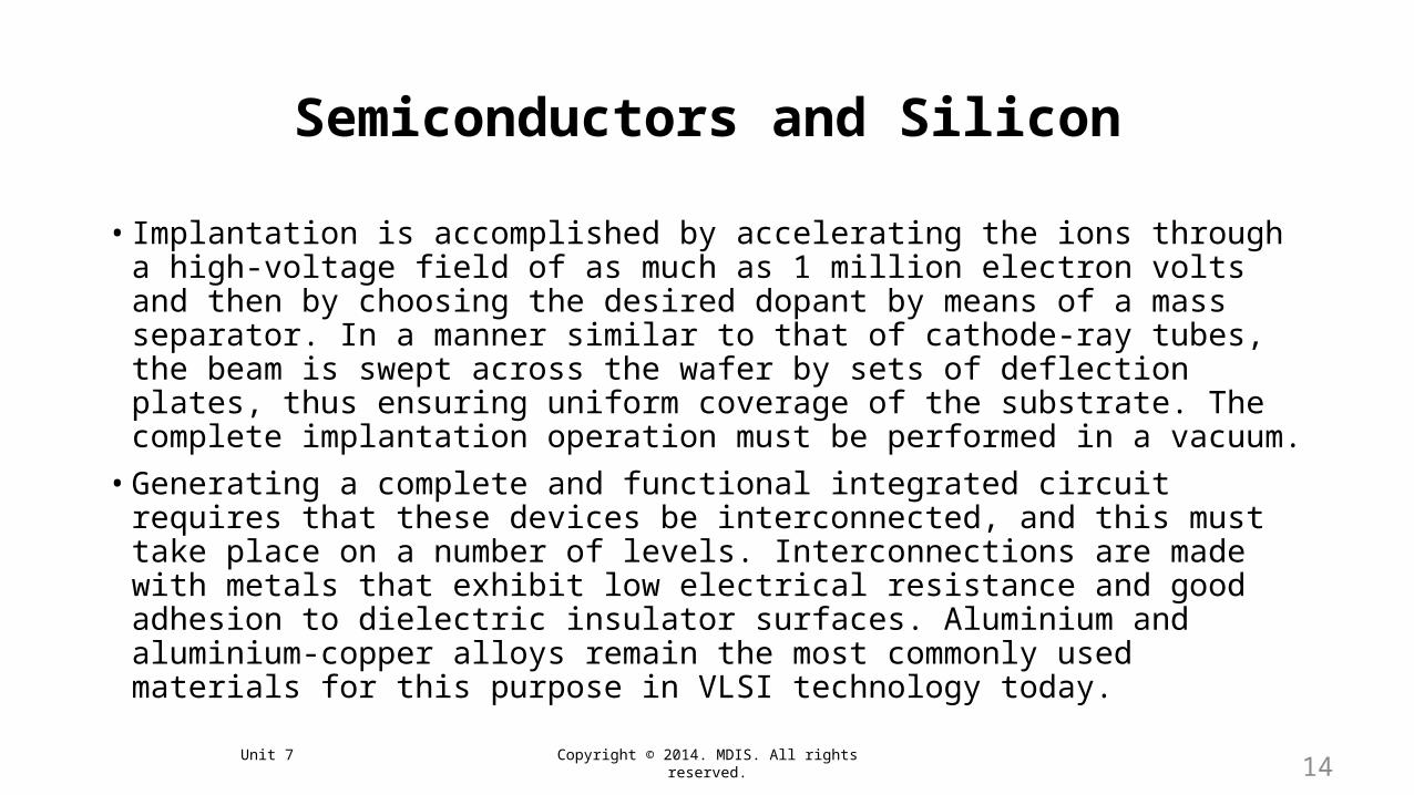
• Implantation is accomplished by accelerating the ions through a high-voltage field of as much as 1 million electron volts and then by choosing the desired dopant by means of a mass separator. In a manner similar to that of cathode-ray tubes, the beam is swept across the wafer by sets of deflection plates, thus ensuring uniform coverage of the substrate. The complete implantation operation must be performed in a vacuum.
• Generating a complete and functional integrated circuit requires that these devices be interconnected, and this must take place on a number of levels. Interconnections are made with metals that exhibit low electrical resistance and good adhesion to dielectric insulator surfaces. Aluminium and aluminium-copper alloys remain the most commonly used materials for this purpose in VLSI technology today.
14

Unit 7 Copyright © 2014. MDIS. All rights reserved.
Semiconductors and Silicon
• The Working dice must be attached to a more rugged foundation to ensure reliability. One simple method is to fasten a die to its packaging material with an epoxy cement; another method makes use of a eutectic bond made by heating metal-alloy systems.
• Once the chip has been attached to its substrate, it must be connected electrically to the package leads. This is accomplished by wire bonding very thin gold Wires from the package leads to bonding pads located around the perimeter or down the centre of the die.
15

http://blog.bcaresearch.com/wp-content/uploads/2013/10/Chart-III-8-Moores-Law-Over-199-Years-And-Going-Strong.png

Fabrication ofMicroelectromechanical
Devicesand Systems
17
Unit 7 Copyright © 2014. MDIS. All rights reserved.
Microelectro-mechanical Device
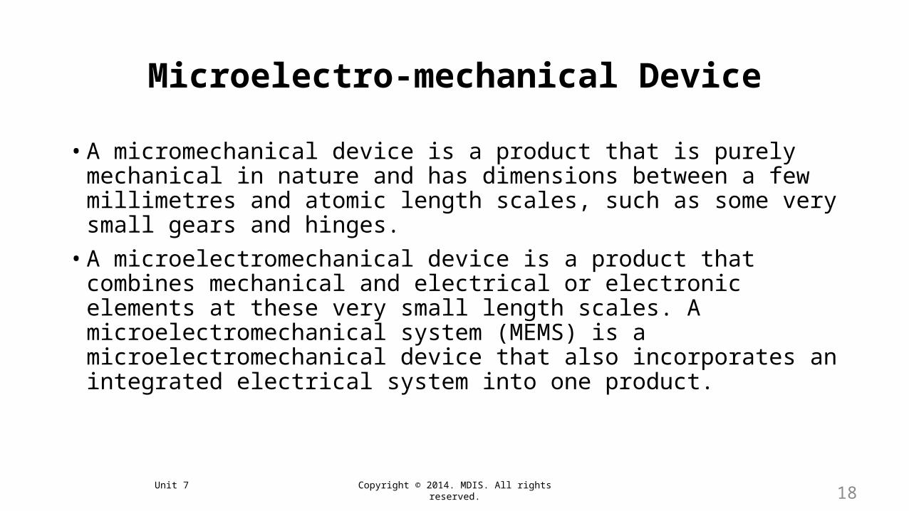
• A micromechanical device is a product that is purely mechanical in nature and has dimensions between a few millimetres and atomic length scales, such as some very small gears and hinges.
• A microelectromechanical device is a product that combines mechanical and electrical or electronic elements at these very small length scales. A microelectromechanical system (MEMS) is a microelectromechanical device that also incorporates an integrated electrical system into one product.
18

Unit 7 Copyright © 2014. MDIS. All rights reserved.
Microelectro-mechanical Systems
• Microelectromechanical devices are products that combine mechanical and electrical or electronic elements at very small length scales. Most sensors are examples of microelectromechanical devices.
• Microelectromechanical systems are microelectromechanical devices that also incorporate an integrated electrical system in one product. Microelectromechanical systems are rare compared with microelectronic, micromechanical, or microelectromechanical devices, typical examples being air-bag sensors and digital micromirror devices.
19

Unit 7 Copyright © 2014. MDIS. All rights reserved.
Bulk Micromachining
• Until the early 1980s, bulk micromachining was the most common method of machining at micrometer scales. This process uses orientation-dependent etches on single-crystal silicon, an approach that depends on etching down into a surface and stopping on certain crystal faces, doped regions, and etchable films to form a desired structure.
20

Unit 7 Copyright © 2014. MDIS. All rights reserved.
Surface Micromachining
• Bulk micromachining is useful for producing very simple shapes. It is restricted to single-crystal materials, since polycrystalline materials will not machine at different rates in different directions when wet etchants are used. Many MEMS applications require the use of other materials; hence, alternatives to bulk micromachining are needed. One such alternative is surface micromachining. A spacer or sacrificial layer is deposited onto a silicon substrate coated with a thin dielectric layer (called an isolation, or buffer, layer).
21

Unit 7 Copyright © 2014. MDIS. All rights reserved.
Example MEMS Accelerometer
22
http://www.analog.com/library/analogdialogue/archives/43-02/AD43_02_FIG-02.jpg

Nanoscale Manufacturing
23

Unit 7 Copyright © 2014. MDIS. All rights reserved.
Nanoscale Manufacturing
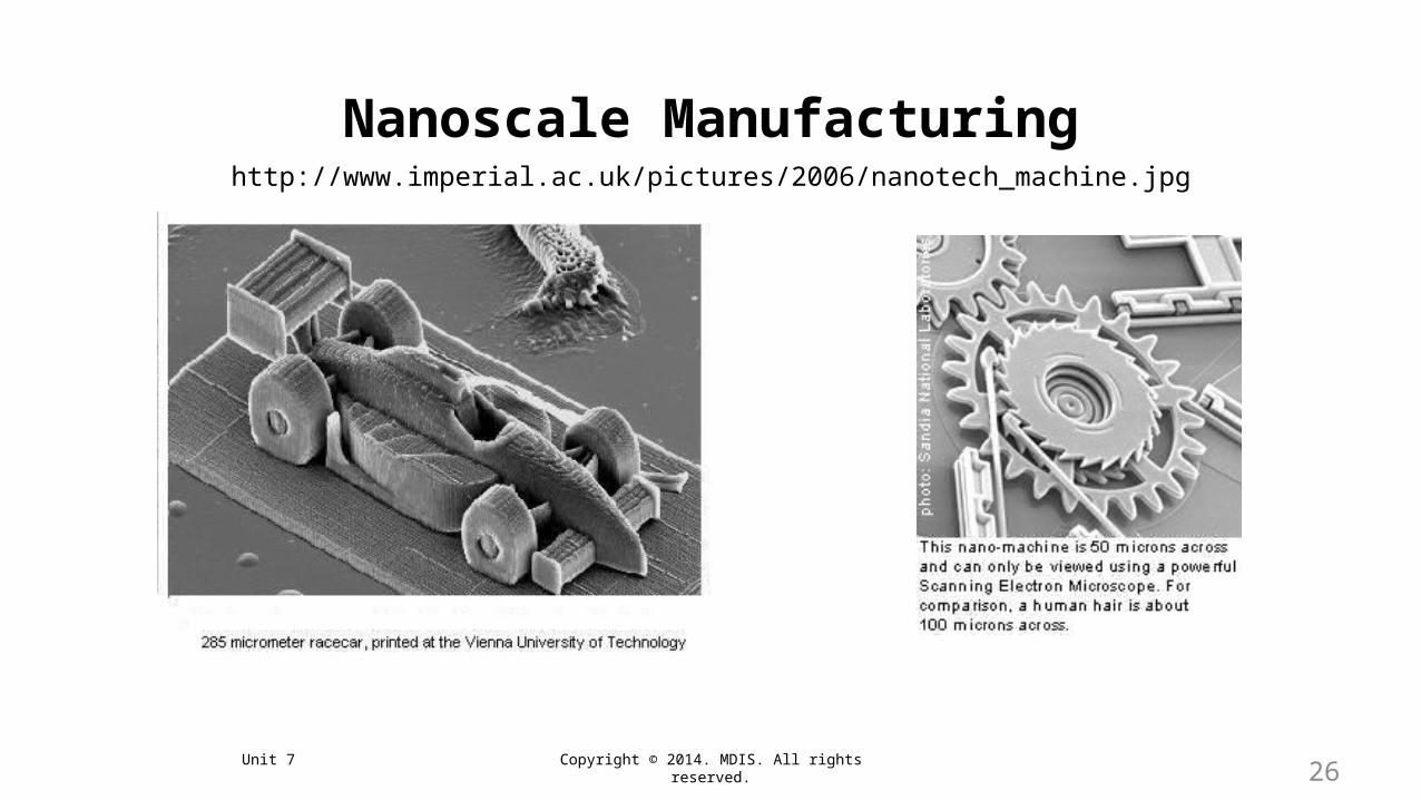
• In nanomanufacturing, parts are produced at nanometre length scales. The term usually refers to manufacturing strategies below the micrometre scale, or between 1x10E-6 and 1x10E-9 m in length. Many of the features in integrated circuits are at this length scale, but very little else with significant manufacturing relevance is. Molecularly engineered medicines and other forms of bio manufacturing are the only commercial applications at present. However, it has been recognized that many physical and biological processes act at this length scale; consequently, the approach holds much promise for future innovation.
24

Unit 7 Copyright © 2014. MDIS. All rights reserved.
Nanoscale Manufacturing
25
Unit 7 Copyright © 2014. MDIS. All rights reserved.
Nanoscale Manufacturing
26
http://www.imperial.ac.uk/pictures/2006/nanotech_machine.jpg