Unit 13 Analysis of Clocked Sequential Circuits Ku-Yaw Chang [email protected] Assistant...
30
Unit 13 Unit 13 Analysis of Analysis of Clocked Sequential Clocked Sequential Circuits Circuits Ku-Yaw Chang Ku-Yaw Chang [email protected] [email protected] Assistant Professor, Department of Assistant Professor, Department of Computer Science and Information Engineering Computer Science and Information Engineering Da-Yeh University Da-Yeh University
-
Upload
darleen-glenn -
Category
Documents
-
view
217 -
download
0
Transcript of Unit 13 Analysis of Clocked Sequential Circuits Ku-Yaw Chang [email protected] Assistant...

Unit 13Unit 13Analysis ofAnalysis of
Clocked Sequential CircuitsClocked Sequential Circuits
Ku-Yaw ChangKu-Yaw [email protected]@mail.dyu.edu.tw
Assistant Professor, Department of Assistant Professor, Department of Computer Science and Information EngineeringComputer Science and Information Engineering
Da-Yeh UniversityDa-Yeh University
222004/05/242004/05/24 Analysis of Clocked Sequential CircuitsAnalysis of Clocked Sequential Circuits
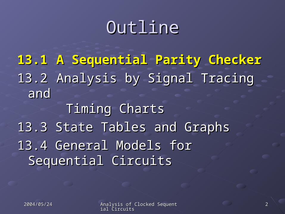
OutlineOutline
13.113.1 A Sequential Parity CheckerA Sequential Parity Checker
13.213.2 Analysis by Signal Tracing andAnalysis by Signal Tracing and Timing Charts Timing Charts
13.3 State Tables and Graphs13.3 State Tables and Graphs
13.4 General Models for Sequential Circuits13.4 General Models for Sequential Circuits

332004/05/242004/05/24 Analysis of Clocked Sequential CircuitsAnalysis of Clocked Sequential Circuits
A Sequential Parity CheckerA Sequential Parity Checker
A parity bitA parity bit An extra bitAn extra bit Being added for purposes of Being added for purposes of
error detectionerror detection
Odd parityOdd parity Total number of 1 bits is oddTotal number of 1 bits is odd
Even parityEven parity Total number of 1 bits is evenTotal number of 1 bits is even

442004/05/242004/05/24 Analysis of Clocked Sequential CircuitsAnalysis of Clocked Sequential Circuits
A Sequential Parity CheckerA Sequential Parity Checker
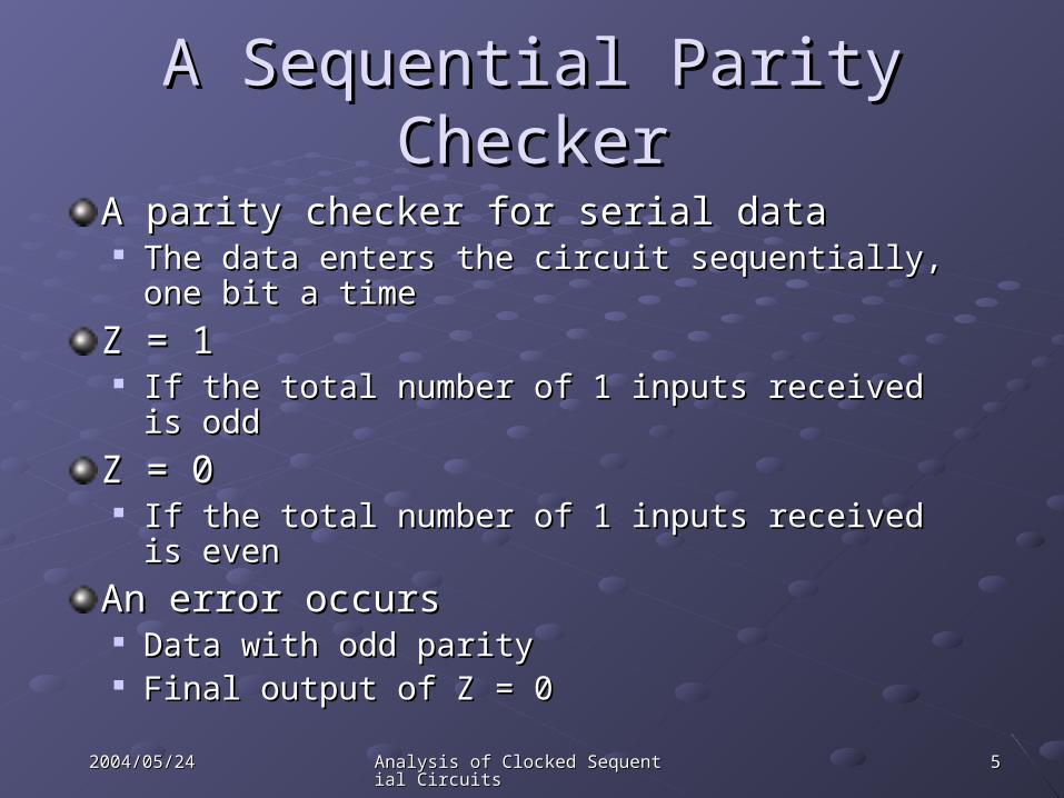
A parity checker for serial dataA parity checker for serial data The data enters the circuit sequentially,The data enters the circuit sequentially,
one bit a timeone bit a time
552004/05/242004/05/24 Analysis of Clocked Sequential CircuitsAnalysis of Clocked Sequential Circuits
A Sequential Parity CheckerA Sequential Parity Checker
A parity checker for serial dataA parity checker for serial data The data enters the circuit sequentially,The data enters the circuit sequentially,
one bit a timeone bit a time
Z = 1Z = 1 If the total number of 1 inputs received is oddIf the total number of 1 inputs received is odd
Z = 0Z = 0 If the total number of 1 inputs received is evenIf the total number of 1 inputs received is even
An error occursAn error occurs Data with odd parityData with odd parity Final output of Z = 0Final output of Z = 0
662004/05/242004/05/24 Analysis of Clocked Sequential CircuitsAnalysis of Clocked Sequential Circuits
A Sequential Parity CheckerA Sequential Parity Checker
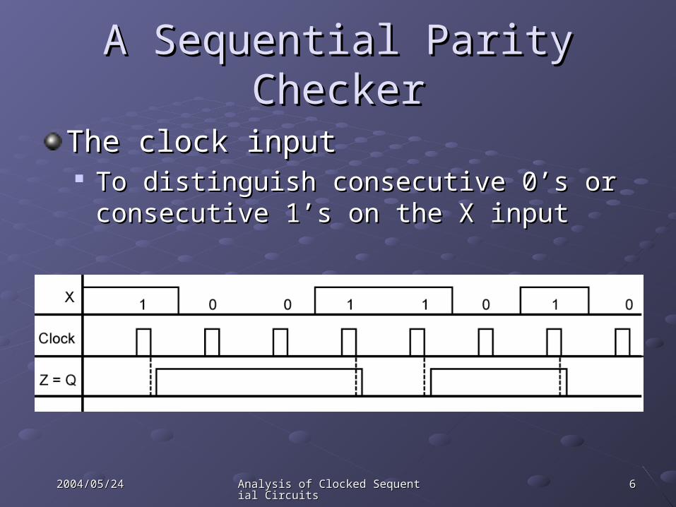
The clock inputThe clock input To distinguish consecutive 0’s or consecutive To distinguish consecutive 0’s or consecutive
1’s on the X input1’s on the X input

772004/05/242004/05/24 Analysis of Clocked Sequential CircuitsAnalysis of Clocked Sequential Circuits
State Graph for Parity CheckerState Graph for Parity Checker
Two states are requiredTwo states are required SS00
an even number of 1’s receivedan even number of 1’s received
SS11
an odd number of 1’s receivedan odd number of 1’s received

882004/05/242004/05/24 Analysis of Clocked Sequential CircuitsAnalysis of Clocked Sequential Circuits
State Table for Parity CheckerState Table for Parity Checker

992004/05/242004/05/24 Analysis of Clocked Sequential CircuitsAnalysis of Clocked Sequential Circuits
Parity CheckerParity Checker

10102004/05/242004/05/24 Analysis of Clocked Sequential CircuitsAnalysis of Clocked Sequential Circuits
OutlineOutline
13.113.1 A Sequential Parity CheckerA Sequential Parity Checker
13.213.2 Analysis by Signal Tracing andAnalysis by Signal Tracing and Timing Charts Timing Charts
13.3 State Tables and Graphs13.3 State Tables and Graphs
13.4 General Models for Sequential Circuits13.4 General Models for Sequential Circuits

11112004/05/242004/05/24 Analysis of Clocked Sequential CircuitsAnalysis of Clocked Sequential Circuits
Basic ProcedureBasic Procedure
1.1. Assume an initial state of the flip-flops (all flip-Assume an initial state of the flip-flops (all flip-flops reset to 0 unless otherwise specified).flops reset to 0 unless otherwise specified).
2.2. For the first input in the given sequence, For the first input in the given sequence, determine the circuit output(s) and flip-flop determine the circuit output(s) and flip-flop inputs.inputs.
3.3. Determine the new set of flip-flop states after Determine the new set of flip-flop states after the next active clock edge.the next active clock edge.
4.4. Determine the output(s) that corresponds to Determine the output(s) that corresponds to the new states.the new states.
5.5. Repeat 2,3, and 4 for each input in the given Repeat 2,3, and 4 for each input in the given sequence.sequence.

12122004/05/242004/05/24 Analysis of Clocked Sequential CircuitsAnalysis of Clocked Sequential Circuits
Two Types ofTwo Types ofClocked Sequential CircuitsClocked Sequential Circuits
Moore machineMoore machine the output of a sequential circuits is a function the output of a sequential circuits is a function
of the present state onlyof the present state only
Mealy machineMealy machine the output is a function of both the present the output is a function of both the present
state and the inputstate and the input

13132004/05/242004/05/24 Analysis of Clocked Sequential CircuitsAnalysis of Clocked Sequential Circuits
Moore and Mealy State GraphsMoore and Mealy State Graphs
Moore
Mealy

14142004/05/242004/05/24 Analysis of Clocked Sequential CircuitsAnalysis of Clocked Sequential Circuits
Moore Sequential CircuitMoore Sequential Circuit
Z is a function only of the present stateZ is a function only of the present state Z = A Z = A B B
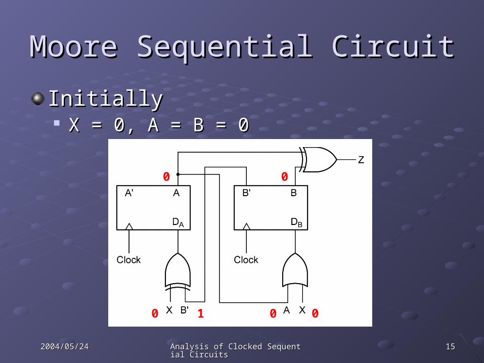
15152004/05/242004/05/24 Analysis of Clocked Sequential CircuitsAnalysis of Clocked Sequential Circuits
Moore Sequential CircuitMoore Sequential Circuit
InitiallyInitially X = 0, A = B = 0X = 0, A = B = 0
0 0
0 0
01
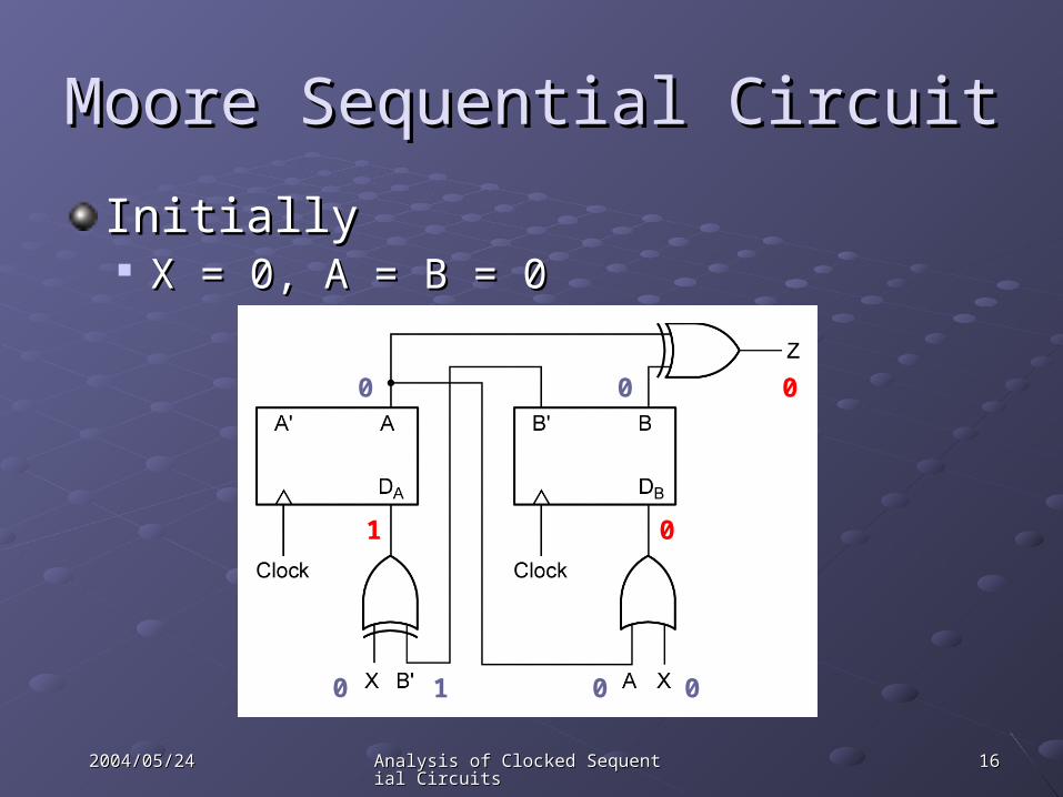
16162004/05/242004/05/24 Analysis of Clocked Sequential CircuitsAnalysis of Clocked Sequential Circuits
Moore Sequential CircuitMoore Sequential Circuit
InitiallyInitially X = 0, A = B = 0X = 0, A = B = 0
0 0
0 0
01
1 0
0

17172004/05/242004/05/24 Analysis of Clocked Sequential CircuitsAnalysis of Clocked Sequential Circuits
Moore Sequential CircuitMoore Sequential Circuit
After the first active clockAfter the first active clock A = 1, B = 0, X = 1A = 1, B = 0, X = 1
1 1
1 0
11
1 0
0

18182004/05/242004/05/24 Analysis of Clocked Sequential CircuitsAnalysis of Clocked Sequential Circuits
Moore Sequential CircuitMoore Sequential Circuit
After the first active clockAfter the first active clock Z =1, X = 1Z =1, X = 1
1 1
1 0
11
0 1
1

19192004/05/242004/05/24 Analysis of Clocked Sequential CircuitsAnalysis of Clocked Sequential Circuits
Moore Sequential CircuitMoore Sequential Circuit
After the second active clockAfter the second active clock A = 0, B = 1A = 0, B = 1
1 1
0 1
00
0 1
1

20202004/05/242004/05/24 Analysis of Clocked Sequential CircuitsAnalysis of Clocked Sequential Circuits
Moore Sequential CircuitMoore Sequential Circuit
After the second active clockAfter the second active clock Z = 1, X = 1Z = 1, X = 1
1 1
0 1
00
1 1
1

21212004/05/242004/05/24 Analysis of Clocked Sequential CircuitsAnalysis of Clocked Sequential Circuits
Timing ChartTiming Chart

22222004/05/242004/05/24 Analysis of Clocked Sequential CircuitsAnalysis of Clocked Sequential Circuits
Timing ChartTiming Chart
Initial output Z = 0 could be ignoredInitial output Z = 0 could be ignored Not in response to any X inputNot in response to any X input
The output is displaced in time with The output is displaced in time with respect to the input sequence.respect to the input sequence.
X = 0 1 1 0 1X = 0 1 1 0 1
A = 0 1 0 1 0 1A = 0 1 0 1 0 1
B = 0 0 1 1 1 1 1B = 0 0 1 1 1 1 1
Z = (0) 1 1 0 1 0Z = (0) 1 1 0 1 0

23232004/05/242004/05/24 Analysis of Clocked Sequential CircuitsAnalysis of Clocked Sequential Circuits
Mealy Sequential CircuitMealy Sequential Circuit

24242004/05/242004/05/24 Analysis of Clocked Sequential CircuitsAnalysis of Clocked Sequential Circuits
Mealy Sequential CircuitMealy Sequential Circuit
The output depends on both the input (X) The output depends on both the input (X) and the flip-flops states (A and B), so Z and the flip-flops states (A and B), so Z may change either when the input may change either when the input changes or when the flip-flops change changes or when the flip-flops change state.state.

25252004/05/242004/05/24 Analysis of Clocked Sequential CircuitsAnalysis of Clocked Sequential Circuits
Mealy Sequential CircuitMealy Sequential Circuit
InitiallyInitially0 0
11
11
1
1 10 0
11

26262004/05/242004/05/24 Analysis of Clocked Sequential CircuitsAnalysis of Clocked Sequential Circuits
Mealy Sequential CircuitMealy Sequential Circuit
InitiallyInitially0 0
11
11
1
11 10 0
0 0
11

27272004/05/242004/05/24 Analysis of Clocked Sequential CircuitsAnalysis of Clocked Sequential Circuits
Mealy Sequential CircuitMealy Sequential Circuit
First active clockFirst active clock0 1
1->01->0
0
1->0
0
11->0 1->01 0
0 0
01
11
0->1

28282004/05/242004/05/24 Analysis of Clocked Sequential CircuitsAnalysis of Clocked Sequential Circuits
Mealy Sequential CircuitMealy Sequential Circuit
First active clockFirst active clock0 1
1->01->0
0
1->0
0
0->11->0 1->01 0
0 0
01
11
0->1
00

29292004/05/242004/05/24 Analysis of Clocked Sequential CircuitsAnalysis of Clocked Sequential Circuits
Timing ChartTiming Chart

30302004/05/242004/05/24 Analysis of Clocked Sequential CircuitsAnalysis of Clocked Sequential Circuits
False OutputsFalse Outputs
False OutputsFalse Outputs After the circuit has changed state and before After the circuit has changed state and before
the input is changed, the output may the input is changed, the output may temporarily assume an incorrect value.temporarily assume an incorrect value.
Also called Also called glitchesglitches and and spikesspikes
X = 1 0 1 0 1.X = 1 0 1 0 1.A = 0 0 0 1 1 0A = 0 0 0 1 1 0B = 0 1 1 1 1 0B = 0 1 1 1 1 0Z = 1(0) 1 0(1) 0 1Z = 1(0) 1 0(1) 0 1