UNIT 1 BOOLEAN ALGEBRA AND MINIMIZATION · UNIT 1 BOOLEAN ALGEBRA AND MINIMIZATION 1.1...
102
UNIT 1 BOOLEAN ALGEBRA AND MINIMIZATION 1.1 Introduction: The English mathematician George Boole (1815-1864) sought to give symbolic form to Aristotle‘s system of logic. Boole wrote a treatise on the subject in 1854, titled An Investigation of the Laws of Thought, on Which Are Founded the Mathematical Theories of Logic and Probabilities, which codified several rules of relationship between mathematical quantities limited to one of two possible values: true or false, 1 or 0. His mathematical system became known as Boolean algebra. All arithmetic operations performed with Boolean quantities have but one of two possible Outcomes: either 1 or 0. There is no such thing as ‖2‖ or ‖ -1‖ or ‖1/2‖ in the Boolean world. It is a world in which all other possibilities are invalid by fiat. As one might guess, this is not the kind of math you want to use when balancing a checkbook or calculating current through a resistor. However, Claude Shannon of MIT fame recognized how Boolean algebra could be applied to on-and-off circuits, where all signals are characterized as either ‖high‖ (1) or ‖low‖ (0). His1938 thesis, titled A Symbolic Analysis of Relay and Switching Circuits, put Boole‘s theoretical work to use in a way Boole never could have imagined, giving us a powerful mathematical tool for designing and analyzing digital circuits. Like ‖normal‖ algebra, Boolean algebra uses alphabetical letters to denote variables. Unlike ‖normal‖ algebra, though, Boolean variables are always CAPITAL letters, never lowercase. Because they are allowed to possess only one of two possible values, either 1 or 0, each and every variable has a complement: the opposite of its value. For example, if variable ‖A‖ has a value of 0, then the complement of A has a value of 1. Boolean notation uses a bar above the variable character to denote complementation, like this:
Transcript of UNIT 1 BOOLEAN ALGEBRA AND MINIMIZATION · UNIT 1 BOOLEAN ALGEBRA AND MINIMIZATION 1.1...
UNIT 1
BOOLEAN ALGEBRA AND MINIMIZATION
1.1 Introduction:
The English mathematician George Boole (1815-1864) sought to give symbolic form to
Aristotle‘s system of logic. Boole wrote a treatise on the subject in 1854, titled An Investigation
of the Laws of Thought, on Which Are Founded the Mathematical Theories of Logic and
Probabilities, which codified several rules of relationship between mathematical quantities
limited to one of two possible values: true or false, 1 or 0. His mathematical system became
known as Boolean algebra.
All arithmetic operations performed with Boolean quantities have but one of two possible
Outcomes: either 1 or 0. There is no such thing as ‖2‖ or ‖-1‖ or ‖1/2‖ in the Boolean world. It is a
world in which all other possibilities are invalid by fiat. As one might guess, this is not the kind
of math you want to use when balancing a checkbook or calculating current through a resistor.
However, Claude Shannon of MIT fame recognized how Boolean algebra could be applied to
on-and-off circuits, where all signals are characterized as either ‖high‖ (1) or ‖low‖ (0). His1938
thesis, titled A Symbolic Analysis of Relay and Switching Circuits, put Boole‘s theoretical work
to use in a way Boole never could have imagined, giving us a powerful mathematical tool for
designing and analyzing digital circuits.
Like ‖normal‖ algebra, Boolean algebra uses alphabetical letters to denote variables.
Unlike ‖normal‖ algebra, though, Boolean variables are always CAPITAL letters, never
lowercase.
Because they are allowed to possess only one of two possible values, either 1 or 0, each and
every variable has a complement: the opposite of its value. For example, if variable ‖A‖ has a
value of 0, then the complement of A has a value of 1. Boolean notation uses a bar above the
variable character to denote complementation, like this:

In written form, the complement of ‖A‖ denoted as ‖A-not‖ or ‖A-bar‖. Sometimes a ‖prime‖
symbol is used to represent complementation. For example, A‘ would be the complement of A,
much the same as using a prime symbol to denote differentiation in calculus rather than the
fractional notation dot. Usually, though, the ‖bar‖ symbol finds more widespread use than the
‖prime‖ symbol, for reasons that will become more apparent later in this chapter.
1.2 Boolean Arithmetic:
Let us begin our exploration of Boolean algebra by adding numbers together: 0 + 0 = 0 0 + 1 = 1 1 + 0 = 1 1 + 1 = 1 The first three sums make perfect sense to anyone familiar with elementary addition. The
Last sum, though, is quite possibly responsible for more confusion than any other single
statement in digital electronics, because it seems to run contrary to the basic principles of
mathematics.
Well, it does contradict principles of addition for real numbers, but not for Boolean numbers.
Remember that in the world of Boolean algebra, there are only two possible values for any
quantity and for any arithmetic operation: 1 or 0. There is no such thing as ‖2‖ within the scope of
Boolean values. Since the sum ‖1 + 1‖ certainly isn‘t 0, it must be 1 by process of elimination.
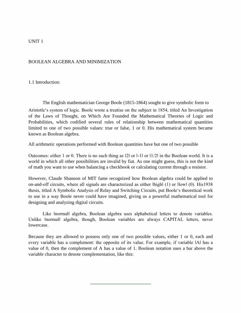
1.2.1 Addition – OR Gate Logic:
www.Vidy
Boolean addition corresponds to the logical function of an ‖OR‖ gate, as well as to parallel switch contacts:
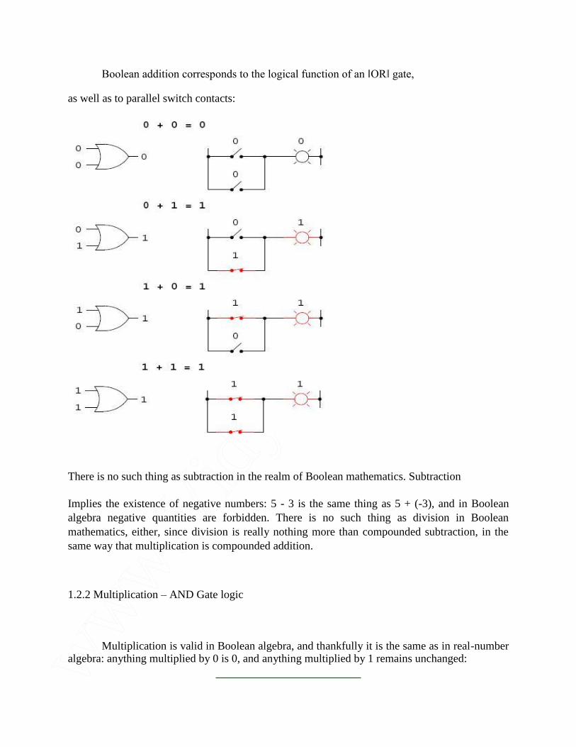
There is no such thing as subtraction in the realm of Boolean mathematics. Subtraction
Implies the existence of negative numbers: 5 - 3 is the same thing as 5 + (-3), and in Boolean
algebra negative quantities are forbidden. There is no such thing as division in Boolean
mathematics, either, since division is really nothing more than compounded subtraction, in the
same way that multiplication is compounded addition.
1.2.2 Multiplication – AND Gate logic
Multiplication is valid in Boolean algebra, and thankfully it is the same as in real-number algebra: anything multiplied by 0 is 0, and anything multiplied by 1 remains unchanged:
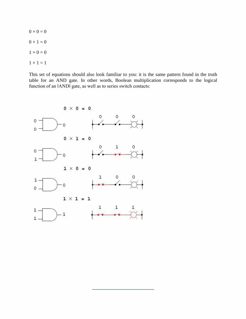
0 × 0 = 0 0 × 1 = 0 1 × 0 = 0 1 × 1 = 1
This set of equations should also look familiar to you: it is the same pattern found in the truth
table for an AND gate. In other words, Boolean multiplication corresponds to the logical
function of an ‖AND‖ gate, as well as to series switch contacts:
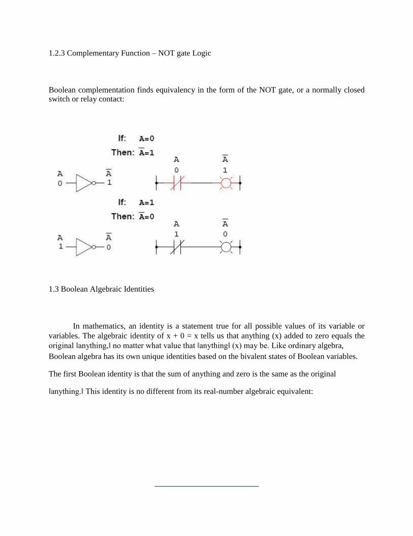
1.2.3 Complementary Function – NOT gate Logic Boolean complementation finds equivalency in the form of the NOT gate, or a normally closed switch or relay contact:
1.3 Boolean Algebraic Identities
In mathematics, an identity is a statement true for all possible values of its variable or
variables. The algebraic identity of x + 0 = x tells us that anything (x) added to zero equals the
original ‖anything,‖ no matter what value that ‖anything‖ (x) may be. Like ordinary algebra, Boolean algebra has its own unique identities based on the bivalent states of Boolean variables. The first Boolean identity is that the sum of anything and zero is the same as the original ‖anything.‖ This identity is no different from its real-number algebraic equivalent:

No matter what the value of A, the output will always be the same: when A=1, the output
will also be 1; when A=0, the output will also be 0.
The next identity is most definitely different from any seen in normal algebra. Here
we discover that the sum of anything and one is one:
No matter what the value of A, the sum of A and 1 will always be 1. In a sense, the ‖1‖
signal overrides the effect of A on the logic circuit, leaving the output fixed at a logic level of 1.
Next, we examine the effect of adding A and A together, which is the same as connecting
both inputs of an OR gate to each other and activating them with the same signal:

In real-number algebra, the sum of two identical variables is twice the original variable‘s
value (x + x = 2x), but remember that there is no concept of ‖2‖ in the world of Boolean math,
only 1 and 0, so we cannot say that A + A = 2A. Thus, when we add a Boolean quantity to itself,
the sum is equal to the original quantity: 0 + 0 = 0, and 1 + 1 = 1.
Introducing the uniquely Boolean concept of complementation into an additive identity, we find
an interesting effect. Since there must be one ‖1‖ value between any variable and its complement,
and since the sum of any Boolean quantity and 1 is 1, the sum of a variable and its complement
must be 1:
Four multiplicative identities: Ax0, Ax1, AxA, and AxA‘. Of these, the first two are no different from their equivalent expressions in regular algebra:

The third multiplicative identity expresses the result of a Boolean quantity multiplied by itself. In normal algebra, the product of a variable and itself is the square of that variable (3x 3 = 32 = 9). However, the concept of ‖square‖ implies a quantity of 2, which has no meaning in Boolean algebra, so we cannot say that A x A = A2. Instead, we find that the product of a Boolean quantity and itself is the original quantity, since 0 x 0 = 0 and 1 x 1 = 1: The fourth multiplicative identity has no equivalent in regular algebra because it uses the complement of a variable, a concept unique to Boolean mathematics. Since there must be
one ‖0‖ value between any variable and its complement, and since the product of any Boolean quantity and 0 is 0, the product of a variable and its complement must be 0:

1.4 Principle of Duality:
It states that every algebraic expression is deducible from the postulates of Boolean
algebra, and it remains valid if the operators & identity elements are interchanged. If the inputs
of a NOR gate are inverted we get a AND equivalent circuit. Similarly when the inputs of a
NAND gate are inverted, we get a OR equivalent circuit. This property is called DUALITY.
1.5 Theorems of Boolean algebra:
The theorems of Boolean algebra can be used to simplify many a complex Boolean
expression and also to transform the given expression into a more useful and meaningful
equivalent expression. The theorems are presented as pairs, with the two theorems in a given pair
being the dual of each other. These theorems can be very easily verified by the method of ‗perfect induction‘. According to this method, the validity of the expression is tested for all
possible combinations of values of the variables involved. Also, since the validity of the theorem
is based on its being true for all possible combinations of values of variables, there is no reason
why a variable cannot be replaced with its complement, or vice versa, without disturbing the
validity. Another important point is that, if a given expression is valid, its dual will also be valid
1.5.1 Theorem 1 (Operations with ‗0‘ and ‗1‘)

(a) 0.X = 0 and (b) 1+X= 1 Where X is not necessarily a single variable – it could be a term or even a large expression. Theorem 1(a) can be proved by substituting all possible values of X, that is, 0 and 1, into the given expression and checking whether the LHS equals the RHS:
• For X = 0, LHS = 0.X = 0.0 = 0 = RHS. • For X= 1, LHS = 0.1 = 0 = RHS.
Thus, 0.X =0 irrespective of the value of X, and hence the proof.
Theorem 1(b) can be proved in a similar manner. In general, according to theorem 1,
0. (Boolean expression) = 0 and 1+ (Boolean expression) =1. For example: 0. (A.B+B.C +C.D) = 0 and 1+ (A.B+B.C +C.D) = 1, where A, B and C are Boolean variables.
1.5.2 Theorem 2 (Operations with ‗0‘ and ‗1‘)
(a) 1.X = X and (b) 0+X = X
where X could be a variable, a term or even a large expression. According to this theorem, ANDing a Boolean expression to ‗1‘ or ORing ‗0‘ to it makes no difference to the expression:

• For X = 0, LHS = 1.0 = 0 = RHS. • For X = 1, LHS = 1.1 = 1 = RHS.
Also,
1. (Boolean expression) = Boolean expression and 0 + (Boolean expression) = Boolean expression.
For example,
1.(A+B.C +C.D) = 0+(A+B.C +C.D) = A+B.C +C.D
1.5.3 Theorem 3 (Idempotent or Identity Laws)
(a) X.X.X……X = X and (b) X+X+X +···+X = X
Theorems 3(a) and (b) are known by the name of idempotent laws, also known as identity laws. Theorem 3(a) is a direct outcome of an AND gate operation, whereas theorem 3(b) represents an
OR gate operation when all the inputs of the gate have been tied together. The scope of
idempotent laws can be expanded further by considering X to be a term or an expression. For
example, let us apply idempotent laws to simplify the following Boolean expression:
1.5.4 Theorem 4 (Complementation Law)
(a) X_X = 0 and (b) X+X = 1

According to this theorem, in general, any Boolean expression when ANDed to its complement
yields a ‗0‘ and when ORed to its complement yields a ‗1‘, irrespective of the complexity of the
expression: Hence, theorem 4(a) is proved. Since theorem 4(b) is the dual of theorem 4(a), its proof is implied. The example below further illustrates the application of complementation laws: 1.5.5 Theorem 5 (Commutative property)
Mathematical identity, called a ‖property‖ or a ‖law,‖ describes how differing variables relate to each other in a system of numbers. One of these properties is known as
the commutative property, and it applies equally to addition and multiplication. In essence, the
commutative property tells us we can reverse the order of variables that are either added together
or multiplied together without changing the truth of the expression:
Commutative property of addition A + B = B + A
Commutative property of multiplication AB = BA
1.5.6 Theorem 6 (Associative Property)

The Associative Property, again applying equally well to addition and multiplication.
This property tells us we can associate groups of added or multiplied variables together with
parentheses without altering the truth of the equations.
Associative property of addition A + (B + C) = (A + B) + C
Associative property of multiplication A (BC) = (AB) C
1.5.7 Theorem 7 (Distributive Property)
The Distributive Property, illustrating how to expand a Boolean expression formed by the
product of a sum, and in reverse shows us how terms may be factored out of Boolean sums-of-
products:
Distributive property
A (B + C) = AB + AC
1.5.8 Theorem 8 (Absorption Law or Redundancy Law)
(a) X+X.Y = X and (b) X.(X+Y) = X
The proof of absorption law is straightforward:

X+X.Y = X. (1+Y) = X.1 = X
Theorem 8(b) is the dual of theorem 8(a) and hence stands proved.
The crux of this simplification theorem is that, if a smaller term appears in a larger term, then the larger term is redundant. The following examples further illustrate the underlying concept:
1.5.9 Demorgan‘s Theorem
De-Morgan was a great logician and mathematician. He had contributed much to logic. Among his contribution the following two theorems are important
1.5.9.1 De-Morgan‘s First Theorem It States that ―The complement of the sum of the variables is equal to the product of the
complement of each variable‖. This theorem may be expressed by the following Boolean
expression.

1.5.9.2 De-Morgan‘s Second Theorem It states that the ―Complement of the product of variables is equal to the sum of complements of each individual variables‖. Boolean expression for this theorem is
1.6 Boolean Function

Z=AB‘+A‘C+A‘B‘C‘

1.7 Canonical Form of Boolean Expressions
An expanded form of Boolean expression, where each term contains all Boolean variables in
their true or complemented form, is also known as the canonical form of the expression. As an
illustration, is a Boolean function of three variables expressed
in canonical form. This function after simplification reduces to and loses its
canonical form.
1.7.1 MIN TERMS AND MAX TERMS Any boolean expression may be expressed in terms of either minterms or maxterms. To do this we must first define the concept of a literal. A literal is a single variable within a term which may or may not be complemented. For an expression with N variables, minterms and maxterms are defined as follows :
• A minterm is the product of N distinct literals where each literal occurs exactly once.
• A maxterm is the sum of N distinct literals where each literal occurs exactly
once. Product-of-Sums Expressions
1.7.2 Standard Forms
A product-of-sums expression contains the product of different terms, with each term
being either a single literal or a sum of more than one literal. It can be obtained from the truth
table by considering those input combinations that produce a logic ‗0‘ at the output. Each such
input combination gives a term, and the product of all such terms gives the expression. Different
terms are obtained by taking the sum of the corresponding literals. Here, ‗0‘ and ‗1‘ respectively
mean the uncomplemented and complemented variables, unlike sum-of-products expressions
where ‗0‘ and ‗1‘ respectively mean complemented and uncomplemented variables.
Since each term in the case of the product-of-sums expression is going to be the sum of literals,
this implies that it is going to be implemented using an OR operation. Now, an OR gate produces
a logic ‗0‘ only when all its inputs are in the logic ‗0‘ state, which means that the first term
corresponding to the second row of the truth table will be A+B+C. The product-of-sums Boolean
expression for this truth table is given by Transforming the given product-of-sums expression
into an equivalent sum-of-products expression is a straightforward process. Multiplying out the

given expression and carrying out the obvious simplification provides the equivalent sum-of-products expression:
A given sum-of-products expression can be transformed into an equivalent product-of-sums
expression by (a) taking the dual of the given expression, (b) multiplying out different terms to
get the sum-of products form, (c) removing redundancy and (d) taking a dual to get the
equivalent product-of-sums expression. As an illustration, let us find the equivalent product-of-
sums expression of the sum-of products expression
The dual of the given expression = 1.8 Minimization Technique
The primary objective of all simplification procedures is to obtain an expression that has
the minimum number of terms. Obtaining an expression with the minimum number of literals is
usually the secondary objective. If there is more than one possible solution with the same number
of terms, the one having the minimum number of literals is the choice.
There are several methods for simplification of Boolean logic expressions. The process is usually
called logic minimization‖ and the goal is to form a result which is efficient. Two methods we
will discuss are algebraic minimization and Karnaugh maps. For very complicated problems the
former method can be done using special software analysis programs. Karnaugh maps are also
limited to problems with up to 4 binary inputs. The Quine–McCluskey tabular method is used for
more than 4 binary inputs.
1.9 Karnaugh Map Method

Maurice Karnaugh, a telecommunications engineer, developed the Karnaugh map at Bell
Labs in 1953 while designing digital logic based telephone switching circuits. Karnaugh maps reduce logic functions more quickly and easily compared to Boolean
algebra. By reduce we mean simplify, reducing the number of gates and inputs. We like to
simplify logic to a lowest cost form to save costs by elimination of components. We define
lowest cost as being the lowest number of gates with the lowest number of inputs per gate.
A Karnaugh map is a graphical representation of the logic system. It can be drawn directly from
either minterm (sum-of-products) or maxterm (product-of-sums) Boolean expressions. Drawing
a Karnaugh map from the truth table involves an additional step of writing the minterm or
maxterm expression depending upon whether it is desired to have a minimized sum-of-products
or a minimized product of-sums expression
1.9.1 Construction of a Karnaugh Map
An n-variable Karnaugh map has 2n squares, and each possible input is allotted a square. In the case of a minterm Karnaugh map, ‗1‘ is placed in all those squares for which the output is
‗1‘, and ‗0‘ is placed in all those squares for which the output is ‗0‘. 0s are omitted for
simplicity. An ‗X‘ is placed in squares corresponding to ‗don‘t care‘ conditions. In the case of a
maxterm Karnaugh map, a ‗1‘ is placed in all those squares for which the output is ‗0‘, and a
‗0‘ is placed for input entries corresponding to a ‗1‘ output. Again, 0s are omitted for simplicity,
and an ‗X‘ is placed in squares corresponding to ‗don‘t care‘ conditions. The choice of terms
identifying different rows and columns of a Karnaugh map is not unique for a given number of
variables. The only condition to be satisfied is that the designation of adjacent rows and adjacent
columns should be the same except for one of the literals being complemented. Also, the extreme
rows and extreme columns are considered adjacent.
Some of the possible designation styles for two-, three- and four-variable minterm Karnaugh maps are shown in the figure below.
The style of row identification need not be the same as that of column identification as long as it
meets the basic requirement with respect to adjacent terms. It is, however, accepted practice to
adopt a uniform style of row and column identification. Also, the style shown in the figure below
is more commonly used. A similar discussion applies for maxterm Karnaugh maps. Having
drawn the Karnaugh map, the next step is to form groups of 1s as per the following guidelines:
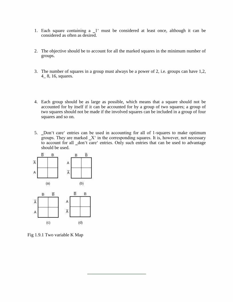
1. Each square containing a ‗1‘ must be considered at least once, although it can be
considered as often as desired.
2. The objective should be to account for all the marked squares in the minimum number of
groups.
3. The number of squares in a group must always be a power of 2, i.e. groups can have 1,2,
4_ 8, 16, squares.
4. Each group should be as large as possible, which means that a square should not be
accounted for by itself if it can be accounted for by a group of two squares; a group of two squares should not be made if the involved squares can be included in a group of four squares and so on.
5. ‗Don‘t care‘ entries can be used in accounting for all of 1-squares to make optimum groups. They are marked ‗X‘ in the corresponding squares. It is, however, not necessary to account for all ‗don‘t care‘ entries. Only such entries that can be used to advantage should be used.
Fig 1.9.1 Two variable K Map

Fig 1.9.2 Three variable K Map
Fig 1.9.3 Four variable K Map

Fig 1.9.4 Different Styles of row and column identification
Having accounted for groups with all 1s, the minimum ‗sum-of-products‘ or ‗product-of-sums‘
expressions can be written directly from the Karnaugh map. Minterm Karnaugh map and
Maxterm Karnaugh map of the Boolean function of a two-input OR gate. The Minterm and
Maxterm Boolean expressions for the two-input OR gate are as follows:

Minterm Karnaugh map and Maxterm Karnaugh map of the three variable Boolean function
The truth table, Minterm Karnaugh map and Maxterm Karnaugh map of the four
variable Boolean function

To illustrate the process of forming groups and then writing the corresponding minimized
Boolean expression, The below figures respectively show minterm and maxterm Karnaugh maps
for the Boolean functions expressed by the below equations. The minimized expressions as
deduced from Karnaugh maps in the two cases are given by Equation in the case of the minterm
Karnaugh map and Equation in the case of the maxterm Karnaugh map:


1.10 Quine–McCluskey Tabular Method
The Quine–McCluskey tabular method of simplification is based on the complementation theorem, which says that
where X represents either a variable or a term or an expression and Y is a variable. This theorem
implies that, if a Boolean expression contains two terms that differ only in one variable, then
they can be combined together and replaced with a term that is smaller by one literal. The same
procedure is applied for the other pairs of terms wherever such a reduction is possible. All these
terms reduced by one literal are further examined to see if they can be reduced further. The
process continues until the terms become irreducible. The irreducible terms are called prime
implicants. An optimum set of prime implicants that can account for all the original terms then
constitutes the minimized expression. The technique can be applied equally well for minimizing
sum-of-products and product of-
sums expressions and is particularly useful for Boolean functions having more than six variables
as it can be mechanized and run on a computer. On the other hand, the Karnaugh mapping
method, to be discussed later, is a graphical method and becomes very cumbersome when the
number of variables exceeds six. The step-by-step procedure for application of the tabular
method for minimizing Boolean expressions,both sum-of-products and product-of-sums, is
outlined as follows: 1. The Boolean expression to be simplified is expanded if it is not in expanded form.
2. Different terms in the expression are divided into groups depending upon the number of 1s they have. True and complemented variables in a sum-of-products expression mean ‗1‘ and ‗0‘ respectively. The reverse is true in the case of a product-of-sums expression. The groups are then arranged,
beginning with the group having the least number of 1s in its included terms. Terms within the
same group are arranged in ascending order of the decimal numbers represented by these terms.
As an illustration, consider the expression
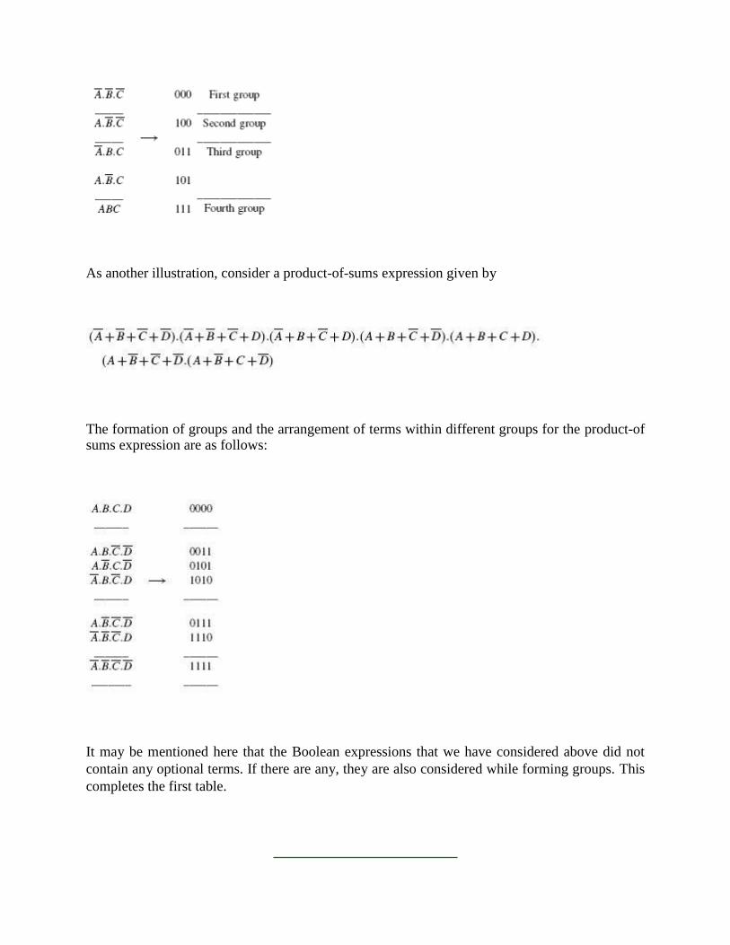
As another illustration, consider a product-of-sums expression given by
The formation of groups and the arrangement of terms within different groups for the product-of sums expression are as follows: It may be mentioned here that the Boolean expressions that we have considered above did not
contain any optional terms. If there are any, they are also considered while forming groups. This
completes the first table.

3. The terms of the first group are successively matched with those in the next adjacent higher order group to look for any possible matching and consequent reduction. The terms are considered matched when all literals except for one match. The pairs of matched terms are replaced with a single term where the position of the unmatched literals is replaced with a dash (—). These new terms formed as a result of the matching process find a place in the second table. The terms in the first table that do not find a match are called the prime implicants and are marked with an asterisk (∗). The matched terms are ticked (_).
4. Terms in the second group are compared with those in the third group to look for a possible match. Again, terms in the second group that do not find a match become the prime implicants.
5. The process continues until we reach the last group. This completes the first round of matching. The terms resulting from the matching in the first round are recorded in the second table.
6. The next step is to perform matching operations in the second table. While comparing the
terms for a match, it is important that a dash (—) is also treated like any other literal, that is, the
dash signs also need to match. The process continues on to the third table, the fourth table and so
on until the terms become irreducible any further.
7. An optimum selection of prime implicants to account for all the original terms constitutes the
terms for the minimized expression. Although optional (also called ‗don‘t care‘) terms are
considered for matching, they do not have to be accounted for once prime implicants have been
identified. Let us consider an example. Consider the following sum-of-products expression:

The second round of matching begins with the table shown on the previous page. Each term in
the first group is compared with every term in the second group. For instance, the first term in
the first group 00−1 matches with the second term in the second group 01−1 to yield 0−−1,
which is recorded in the table shown below. The process continues until all terms have been
compared for a possible match. Since this new table has only one group, the terms contained
therein are all prime implicants. In the present example, the terms in the first and second tables
have all found a match. But that is not always the case.
The next table is what is known as the prime implicant table. The prime implicant table contains
all the original terms in different columns and all the prime implicants recorded in different rows
as shown below:

Each prime implicant is identified by a letter. Each prime implicant is then examined one by one
and the terms it can account for are ticked as shown. The next step is to write a product-of-sums
expression using the prime implicants to account for all the terms. In the present illustration, it is
given as follows. Obvious simplification reduces this expression to PQRS which can be interpreted to mean that all prime implicants, that is, P, Q, R and S, are needed to account for all the original terms.
Therefore, the minimized expression =
What has been described above is the formal method of determining the optimum set of prime
implicants. In most of the cases where the prime implicant table is not too complex, the exercise
can be done even intuitively. The exercise begins with identification of those terms that can be
accounted for by only a single prime implicant. In the present example, 0011, 0110, 1001 and
1100 are such terms. As a result, P, Q, R and S become the essential prime implicants. The next
step is to find out if any terms have not been covered by the essential prime implicants. In the
present case, all terms have been covered by essential prime implicants. In fact, all prime
implicants are essential prime implicants in the present example. As another illustration, let us
consider a product-of-sums expression given by
The procedure is similar to that described for the case of simplification of sum-of-products expressions. The resulting tables leading to identification of prime implicants are as follows:

The prime implicant table is constructed after all prime implicants have been identified to look
for the optimum set of prime implicants needed to account for all the original terms. The prime
implicant table shows that both the prime implicants are the essential ones:
1.11 Universal Gates
OR, AND and NOT gates are the three basic logic gates as they together can be used to
construct the logic circuit for any given Boolean expression. NOR and NAND gates have the
property that they individually can be used to hardware-implement a logic circuit corresponding
to any given Boolean expression. That is, it is possible to use either only NAND gates or only
NOR gates to implement any Boolean expression. This is so because a combination of NAND
gates or a combination of NOR gates can be used to perform functions of any of the basic logic
gates. It is for this reason that NAND and
NOR gates are universal gates. As an illustration, Fig. 4.24 shows how two-input NAND gates
can be used to construct a NOT circuit, a two-input AND gate and a two-input OR gate. Figure
shows the same using NOR gates. Understanding the conversion of NAND to OR and NOR to AND requires the use of DeMorgan‘s theorem, which is discussed in Chapter 6 on Boolean algebra. These are gates where we need to connect an external resistor, called the pull-up resistor,
between the output and the DC power supply to make the logic gate perform the intended logic
function. Depending on the logic family used to construct the logic gate, they are referred to as
gates with open collector output (in the case of the TTL logic family) or open drain output (in the
case of the MOS logic family). Logic families are discussed in detail in Chapter 5. The
advantage of using open collector/open drain gates lies in their capability of providing an
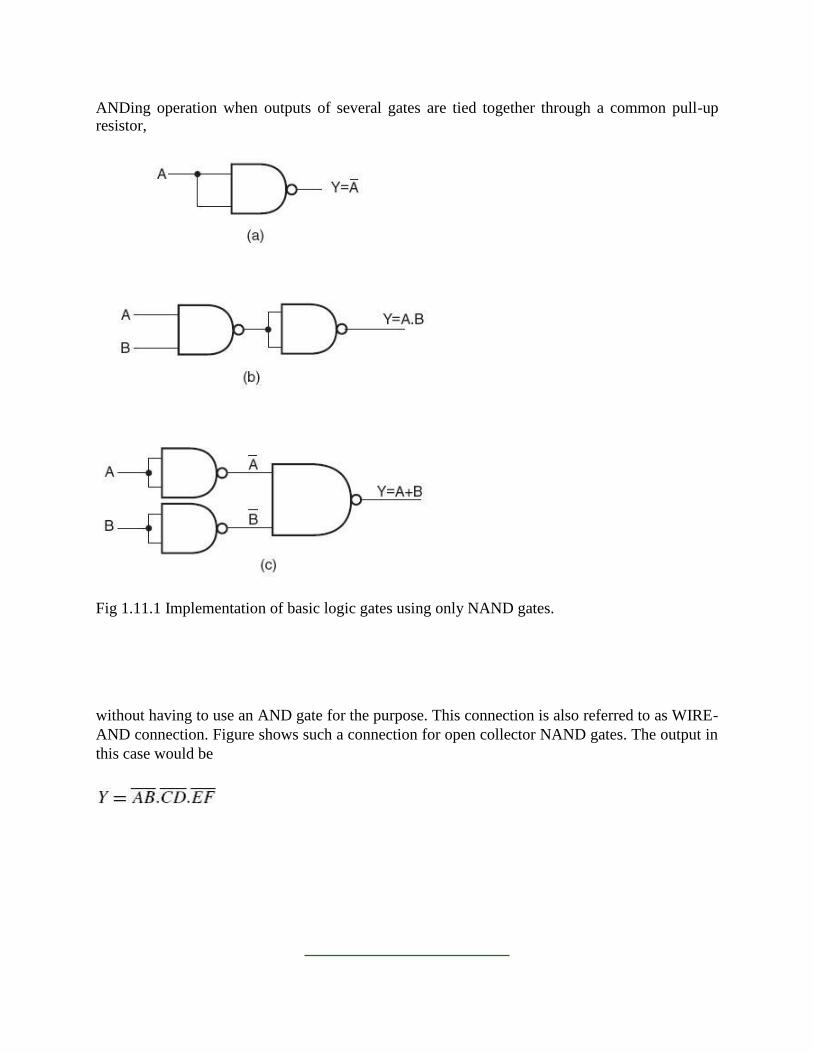
ANDing operation when outputs of several gates are tied together through a common pull-up resistor,
Fig 1.11.1 Implementation of basic logic gates using only NAND gates.
without having to use an AND gate for the purpose. This connection is also referred to as WIRE-
AND connection. Figure shows such a connection for open collector NAND gates. The output in
this case would be

WIRE-AND connection with open collector/drain devices.

The disadvantage is that they are relatively slower and noisier. Open collector/drain devices are therefore not recommended for applications where speed is an important consideration.
The Exclusive-OR function One element conspicuously missing from the set of Boolean operations is that of Exclusive-OR.
Whereas the OR function is equivalent to Boolean addition, the AND function to Boolean
multiplication, and the NOT function (inverter) to Boolean complementation, there is no direct
Boolean equivalent for Exclusive-OR. This hasn‘t stopped people from developing a symbol to
represent it, though:
This symbol is seldom used in Boolean expressions because the identities, laws, and rules
of simplification involving addition, multiplication, and complementation do not apply to it.
However, there is a way to represent the Exclusive-OR function in terms of OR and AND, as has
been shown in previous chapters: AB‘ + A‘B.

Important Questions: Unit – I
PART-A (2 Marks)
1) Define binary logic.
2) State the different classification of binary codes.
3) State the steps involved in Gray to binary conversion.
4) What is meant by bit & byte?
5) What is the use of don‘t care conditions? 6) List the different number systems 7) State the abbreviations of ASCII and EBCDIC code
8) What are the different types of number complements
9) State De Morgan's theorem.
PART-B
1.Simplify the following Boolean function by using Tabulation method (16)
F (w, x, y, z) =_ (0, 1, 2, 8, 10, 11, 14,15)
2.Simplify the following Boolean functions by using K‘Map in SOP
& POS. F (w, x, y, z) =_ (1, 3, 4, 6, 9, 11, 12, 14) (16)
3.Simplify the following Boolean functions by using K‘Map in SOP
& POS. F (w, x, y, z) =_ (1, 3, 7, 11, 15) + d (0 , 2, 5) (16)
4.Reduce the given expression. (16) [(AB)‘ + A‘ +AB‘]
5.Reduce the following function using k-map technique (16) f(A,B,C,D)= _ M(0, 3, 4, 7, 8, 10, 12, 14)+d (2, 6)

UNIT II COMBINATIONAL LOGIC
SYLLABUS :
Combinational Circuits
Analysis and Design Procedures
Circuits for Arithmetic Operations
Code Conversion
Hardware Description Language (HDL)

Unit 2
COMBINATIONAL LOGIC
3.0 Introduction
The term ‖combinational‖ comes to us from mathematics. In mathematics a
combination is an unordered set, which is a formal way to say that nobody cares
which order the items came in. Most games work this way, if you rolled dice one at
a time and get a 2 followed by a 3 it is the same as if you had rolled a 3 followed
by a 2. With combinational logic, the circuit produces
the same output regardless of the order the inputs are changed. There are circuits
which depend on the when the inputs change, these circuits are called sequential
logic. Even though you will not find the term ‖sequential logic‖ in the chapter titles,
the next several chapters will discuss sequential logic. Practical circuits will have a
mix of combinational and sequential logic, with sequential logic making sure
everything happens in order and combinational logic performing functions like
arithmetic, logic, or conversion.
3.1 Design Using Gates
A combinational circuit is one where the output at any time depends only on
the present combination of inputs at that point of time with total disregard to the
past state of the inputs. The logic gate is the most basic building block of
combinational logic. The logical function performed by a combinational circuit is
fully defined by a set of Boolean expressions. The other category of logic circuits,
called sequential logic circuits, comprises both logic gates and memory elements
such as flip-flops. Owing to the presence of memory elements, the output in a
sequential circuit depends upon not only the present but also the past state of
inputs.

The Fig 3.1 shows the block schematic representation of a generalized
combinational circuit having n input variables and m output variables or simply
outputs. Since the number of input variables is
Fig 3.1 Generalized Combinational Circuit
n, there are 2n possible combinations of bits at the input. Each output can be
expressed in terms of input variables by a Boolean expression, with the result that
the generalized system of above fig can be expressed by m Boolean expressions.
As an illustration, Boolean expressions describing the function of a four-input
OR/NOR gate are given as
….. Eq – 1
3.2 BCD Arithmetic Circuits
Addition and subtraction are the two most commonly used arithmetic
operations, as the other two, namely multiplication and division, are respectively
the processes of repeated addition and repeated subtraction, as was outlined in
Chapter 2 dealing with binary arithmetic. We will begin with the basic building
blocks that form the basis of all hardware used to perform the aforesaid arithmetic
operations on binary numbers. These include half-adder, full adder, half-subtractor,
full subtractor and controlled inverter.

3.3 Binary Adder
3.3.1 Half-Adder
A half-adder is an arithmetic circuit block that can be used to add two bits.
Such a circuit thus has two inputs that represent the two bits to be added and two
outputs, with one producing the SUM output and the other producing the CARRY.
Figure 3.2 shows the truth table of a half-adder, showing all possible input
combinations and the corresponding outputs.
The Boolean expressions for the SUM and CARRY outputs are given by the equations below
Fig 3.2 Truth Table of Half Adder
An examination of the two expressions tells that there is no scope for further
simplification. While the first one representing the SUM output is that of an EX-
OR gate, the second one representing the CARRY output is that of an AND gate.
However, these two expressions can certainly be represented in different forms
using various laws and theorems of Boolean algebra to illustrate the flexibility that
the designer has in hardware-implementing as simple a combinational function as
that of a half-adder.

Fig 3.3 Logic Implementation of Half Adder
Although the simplest way to hardware-implement a half-adder would be to use a
two-input EX-OR gate for the SUM output and a two-input AND gate for the
CARRY output, as shown in Fig. 3.3, it could also be implemented by using an
appropriate arrangement of either NAND or NOR gates.
3.3.2 Full Adder
A full adder circuit is an arithmetic circuit block that can be used to add three bits
to produce a SUM and a CARRY output. Such a building block becomes a
necessity when it comes to adding binary numbers with a large number of bits. The
full adder circuit overcomes the limitation of the half-adder, which can be used to
add two bits only. Let us recall the procedure for adding larger binary numbers.
We begin with the addition of LSBs of the two numbers. We record the sum under
the LSB column and take the carry, if any, forward to the next higher column bits.
As a result, when we add the next adjacent higher column bits, we would be
required to add three bits if there were a carry from the previous addition. We have
a similar situation for the other higher column bits. Also until we reach the MSB.
A full adder is therefore essential for the hardware implementation of an adder
circuit capable of adding larger binary numbers. A half-adder can be used for
addition of LSBs only.

Fig 3.4 Truth Table of Full Adder
Figure 3.4 shows the truth table of a full adder circuit showing all possible input
combinations and corresponding outputs. In order to arrive at the logic circuit for
hardware implementation of a full adder, we will firstly write the Boolean
expressions for the two output variables, that is, the SUM and CARRY outputs, in
terms of input variables. These expressions are then simplified by using any of the
simplification techniques described in the previous chapter. The Boolean
expressions for the two output variables are given in Equation below for the SUM
output (S) and in above Equation for the CARRY output (Cout):
The next step is to simplify the two expressions. We will do so with the help of the
Karnaugh mapping technique. Karnaugh maps for the two expressions are given in
Fig. 3.5(a) for the SUM output and Fig. 3.5(b) for the CARRY output. As is clear
from the two maps, the expression for the SUM (S) output cannot be simplified
any further, whereas the simplified Boolean expression for Cout is given by the
equation
Figure 3.6 shows the logic circuit diagram of the full adder. A full adder can also
be seen to comprise two half-adders and an OR gate. The expressions for SUM and
CARRY outputs can be rewritten as follows:

Similarly, the expression for CARRY output can be rewritten as follows:
Fig 3.5 Karnaugh Map for the sum and carry out of a full adder

Fig 3.6 Logic circuit diagram of full adder
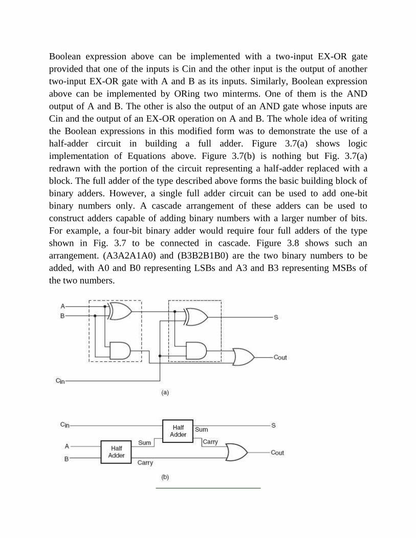
Boolean expression above can be implemented with a two-input EX-OR gate
provided that one of the inputs is Cin and the other input is the output of another
two-input EX-OR gate with A and B as its inputs. Similarly, Boolean expression
above can be implemented by ORing two minterms. One of them is the AND
output of A and B. The other is also the output of an AND gate whose inputs are
Cin and the output of an EX-OR operation on A and B. The whole idea of writing
the Boolean expressions in this modified form was to demonstrate the use of a
half-adder circuit in building a full adder. Figure 3.7(a) shows logic
implementation of Equations above. Figure 3.7(b) is nothing but Fig. 3.7(a)
redrawn with the portion of the circuit representing a half-adder replaced with a
block. The full adder of the type described above forms the basic building block of
binary adders. However, a single full adder circuit can be used to add one-bit
binary numbers only. A cascade arrangement of these adders can be used to
construct adders capable of adding binary numbers with a larger number of bits.
For example, a four-bit binary adder would require four full adders of the type
shown in Fig. 3.7 to be connected in cascade. Figure 3.8 shows such an
arrangement. (A3A2A1A0) and (B3B2B1B0) are the two binary numbers to be
added, with A0 and B0 representing LSBs and A3 and B3 representing MSBs of
the two numbers.

Fig 3.7 Logic Implementation of a full adder with Half Adders
Fig 3.8 Four Bit Binary Adder
3.4 Half-Subtractor
We will study the use of adder circuits for subtraction operations in the following
pages. Before we do that, we will briefly look at the counterparts of half-adder and
full adder circuits in the half-subtractor and full subtractor for direct
implementation of subtraction operations using logic gates.
A half-subtractor is a combinational circuit that can be used to subtract one binary digit from another to produce a DIFFERENCE output and a BORROW output.
The BORROW output here specifies whether a ‗1‘ has been borrowed to perform
the subtraction. The truth table of a half-subtractor, as shown in Fig. 3.9, explains
this further. The Boolean expressions for the two outputs are given by the
equations

Fig 3.9 Half Subtractor
Fig 3.10 Logic Diagram of a Half Subtractor
It is obvious that there is no further scope for any simplification of the Boolean expressions given by above equations. While the expression for the DIFFERENCE (D) output is that of
an EX-OR gate, the expression for the BORROW output (Bo) is that of an AND gate with input
A complemented before it is fed to the gate. Figure 3.10 shows the logic
implementation of a half-subtractor. Comparing a half-subtractor with a half-adder,
we find that the expressions for the SUM and DIFFERENCE outputs are just the
same. The expression for BORROW in the case of the half-subtractor is also
similar to what we have for CARRY in the case of the half-adder. If
the input A, that is, the minuend, is complemented, an AND gate can be used to implement the
BORROW output. Note the similarities between the logic diagrams of Fig. 3.3 (half-adder) and Fig. 3.10 (half-subtractor).
3.4.1 Full Subtractor
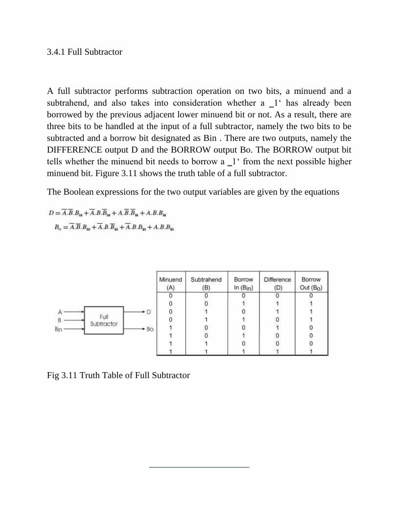
A full subtractor performs subtraction operation on two bits, a minuend and a
subtrahend, and also takes into consideration whether a ‗1‘ has already been
borrowed by the previous adjacent lower minuend bit or not. As a result, there are
three bits to be handled at the input of a full subtractor, namely the two bits to be
subtracted and a borrow bit designated as Bin . There are two outputs, namely the
DIFFERENCE output D and the BORROW output Bo. The BORROW output bit
tells whether the minuend bit needs to borrow a ‗1‘ from the next possible higher
minuend bit. Figure 3.11 shows the truth table of a full subtractor.
The Boolean expressions for the two output variables are given by the equations
Fig 3.11 Truth Table of Full Subtractor

Fig 3.12 K Maps for Difference and Borrow outputs
The Karnaugh maps for the two expressions are given in Fig. 3.12(a) for
DIFFERENCE output D and in Fig. 3.12(b) for BORROW output Bo. As is clear
from the two Karnaugh maps, no simplification is possible for the difference
output D. The simplified expression for Bo is given by the equation
If we compare these expressions with those derived earlier in the case of a full
adder, we find that the expression for DIFFERENCE output D is the same as that
for the SUM output. Also, the expression for BORROW output Bo is similar to the
expression for CARRY-OUT Co. In the case of a half-subtractor, the A input is
complemented. By a similar analysis it can be shown that a full subtractor can be
implemented with half-subtractors in the same way as a full adder was constructed
using half-adders. Relevant logic diagrams are shown in Figs 3.7(a) and (b)

corresponding to Figs 3.7(a) and (b) respectively for a full adder. Again, more than
one full subtractor can be connected in cascade to perform subtraction on two
larger binary numbers. As an illustration, Fig. 3.13 shows a four-bit subtractor.
Fig 3.13 Four Bit Subtractor
3.5 Multipliers
Multiplication of binary numbers is usually implemented in microprocessors
and microcomputers by using repeated addition and shift operations. Since the
binary adders are designed to add only two binary numbers at a time, instead of
adding all the partial products at the end, they are added two at a time and their
sum is accumulated in a register called the accumulator register. Also, when the
multiplier bit is ‗0‘, that very partial product is ignored, as an all ‗0‘ line does not
affect the final result. The basic hardware arrangement of such a binary multiplier
would comprise shift registers for the multiplicand and multiplier bits, an
accumulator register for storing partial products, a binary parallel adder and a clock
pulse generator to time various operations.

Binary multipliers are also available in IC form. Some of the popular type
numbers in the TTL family include 74261 which is a 2 × 4 bit multiplier (a four-bit
multiplicand designated as B0,B1,B2,B3 and B4, and a two-bit multiplier
designated as M0, M1 and M2. The MSBs B4 and M2 are used to represent signs.
74284 and 74285 are 4 × 4 bit multipliers. They can be used together to perform
high-speed multiplication of two four-bit numbers. Figure 3.14 shows the
arrangement. The result of multiplication is often required to be stored in a register.
The size of
this register (accumulator) depends upon the number of bits in the result, which at
the most can be equal to the sum of the number of bits in the multiplier and
multiplicand. Some multipliers ICs have an in-built register.
Fig 3.14 4 x 4 Multiplier
Many microprocessors do not have in their ALU the hardware that can perform
multiplication or other complex arithmetic operations such as division, determining
the square root, trigonometric functions, etc. These operations in these

microprocessors are executed through software. For example, a multiplication
operation may be accomplished by using a software program that does
multiplication through repeated execution of addition and shift instructions. Other
complex operations mentioned above can also be executed with similar programs.
Although the use of software reduces the hardware needed in the microprocessor,
the computation time in general is higher in the case of software-executed
operations when compared with the use of hardware to perform those operations.
HDL (HARDWARE DESCRIPTION LANGUAGE)
In electronics, a hardware description language or HDL is any language from a class of computer languages and/or programming languages for formal description of digital logic and electronic circuits. It can describe the circuit's operation, its design and organization, and tests to verify its operation by means of simulation.
HDLs are standard text-based expressions of the spatial and temporal structure and behaviour of electronic systems. In contrast to a software programming language, HDL syntax and semantics include explicit notations for expressing time and concurrency, which are the primary attributes of hardware. Languages whose only characteristic is to express circuit connectivity between hierarchies of blocks are properly classified as netlist languages used on electric computer-aided design (CAD).
HDLs are used to write executable specifications of some piece of hardware. A simulation program, designed to implement the underlying semantics of the language statements, coupled with simulating the progress of time, provides the hardware designer with the ability to model a piece of hardware before it is created physically. It is this executability that gives HDLs the illusion of being programming languages. Simulators capable of supporting discrete-event (digital) and continuous-time (analog) modeling exist, and HDLs targeted for each are available.
Design using HDL
The vast majority of modern digital circuit design revolves around an HDL description of the desired circuit, device, or subsystem.

Most designs begin as a written set of requirements or a high-level architectural diagram. The process of writing the HDL description is highly dependent on the designer's background and the circuit's nature. The HDL is merely the 'capture language'—often begin with a high-level algorithmic description such as MATLAB or a C++ mathematical model. Control and decision structures are often prototyped in flowchart applications, or entered in a state-diagram editor. Designers even use scripting languages (such as Perl) to automatically generate repetitive circuit structures in the HDL language. Advanced text editors (such as Emacs) offer editor templates for automatic indentation, syntax-dependent coloration, and macro-based expansion of entity/architecture/signal declaration.
As the design's implementation is fleshed out, the HDL code invariably must undergo code review, or auditing. In preparation for synthesis, the HDL description is subject to an array of automated checkers. The checkers enforce standardized code a guideline, identifying ambiguous code constructs before they can cause misinterpretation by downstream synthesis, and check for common logical coding errors, such as dangling ports or shorted outputs.In industry parlance, HDL design generally ends at the synthesis stage. Once the synthesis tool has mapped the HDL description into a gate netlist, this netlist is passed off to the back-end stage. Depending on the physical technology (FPGA, ASIC gate-array, ASIC standard-cell), HDLs may or may not play a significant role in the back-end flow. In general, as the design flow progresses toward a physically realizable form, the design database becomes progressively more laden with technology-specific information, which cannot be stored in a generic HDL-description. Finally, a silicon chip is manufactured in a fab.
HDL and programming languages
A HDL is analogous to a software programming language, but with major differences. Programming languages are inherently procedural (single-threaded), with limited syntactical and semantic support to handle concurrency. HDLs, on the other hand, can model multiple parallel processes (such as flipflops, adders, etc.) that automatically execute independently of one another. Any change to the process's input automatically triggers an update in the simulator's process stack. Both programming languages and HDLs are processed by a compiler (usually called a synthesizer in the HDL case), but with different goals. For HDLs, 'compiler' refers to synthesis, a process of transforming the HDL code listing into a physically realizable gate netlist. The netlist output can take any of many forms: a
"simulation" netlist with gate-delay information, a "handoff" netlist for post-synthesis place and route, or a generic industry-standard EDIF format (for subsequent conversion to a JEDEC-format file).
On the other hand, a software compiler converts the source-code listing into a microprocessor-specific object-code, for execution on the target microprocessor. As HDLs and programming languages borrow concepts and features from each other, the
boundary between them is becoming less distinct. However, pure HDLs are unsuitable for general purpose software application development, just as general-purpose programming languages are undesirable for modeling hardware. Yet as electronic systems grow increasingly complex, and reconfigurable systems become increasingly mainstream, there is growing desire in the industry for a single language that can perform some tasks of both hardware design and software programming. SystemC is an example of such—embedded system hardware can be modeled as non-detailed architectural blocks (blackboxes with modeled signal inputs and output drivers). The target application is written in C/C++, and natively compiled for the host-development system (as opposed to targeting the embedded CPU, which requires host-simulation of the embedded CPU). The high level of abstraction of SystemC models is well suited to early architecture exploration, as architectural modifications can be easily evaluated with little concern for signal-level implementation issues.
In an attempt to reduce the complexity of designing in HDLs, which have been compared to the equivalent of assembly languages, there are moves to raise the abstraction level of the design. Companies such as Cadence, Synopsys and Agility Design Solutions are promoting SystemC as a way to combine high level languages with concurrency models to allow faster design cycles for FPGAs than is possible using traditional HDLs. Approaches based on standard C or C++ (with libraries or other extensions allowing parallel programming) are found in the Catapult C tools from Mentor Graphics, and in the Impulse C tools from Impulse Accelerated Technologies. Annapolis Micro Systems, Inc.'s CoreFire Design Suite and National Instruments LabVIEW FPGA provide a graphical dataflow approach to high-level design entry. Languages such as SystemVerilog, SystemVHDL, and Handel-C seek to accomplish the same goal, but are aimed at making existing hardware engineers more productive versus making FPGAs more accessible to existing software engineers. Thus SystemVerilog is more quickly and widely adopted than SystemC. There is more information on C to HDL and Flow to HDL in their respective articles.

Unit – II PART-A (2 Marks)
1. What are Logic gates?
2. What are the basic digital logic gates?
3. What is BCD adder?
4. What is Magnitude Comparator?
5. What is code conversion?
6. Draw the logic circuit of full adder using half adder
7. What is code converter?
8. Define Combinational circuit.
9. Define sequential circuits.
10. What is Binary parallel adder?
PART-B
1. Design a combinational logic circuit to convert the Gray code into Binary code (16)
2. Draw the truth table and logic diagram for full-Adder (16)
3. Draw the truth table and logic diagram for full-Subtractor (16)
4. Explain Binary parallel adder. (16)
5. Design a combinational logic circuit to convert the BCD to Binary code (16)

UNIT III DESIGN WITH MSI DEVICES
SYLLABUS :
Decoders and Encoders
Multiplexers and Demultiplexers
Memory and Programmable Logic
HDL for Combinational Circuits

Design Using MSI devices
MULTIPLEXERS
Many tasks in communications, control, and computer systems can be
performed by combinational logic circuits. When a circuit has been designed to
perform some task in one application, it often finds use in a different application as
well. In this way, it acquires different names from its various uses. In this and the
following sections, we will describe a number of such circuits and their uses. We
will discuss their principles of operation, specifying their MSI or LSI

implementations. One common task is illustrated in Figure 12. Data generated in
one location is to be used in another location; A method is needed to transmit it
from one location to another through some communications channel. The data is
available, in parallel, on many different lines but must be transmitted over a single
communications link. A mechanism is needed to select which of the many data
lines to activate sequentially at any one time so that the data this line carries can be
transmitted at that time.This process is called multiplexing.An
example is the multiplexing of conversations on the telephone system. A number
of telephone conversations are alternately switched onto the telephone line many
times per second. Because of the nature of the human auditory system, listeners
cannot detect that what they are hearing is chopped up and that other people‘s
conversations are interspersed with their own in the transmission process.
Needed at the other end of the communications link is a device that will undo the
multiplexing: a demultiplexer. Such a device must accept the incoming serial data
and direct it in parallel to one of many output lines. The interspersed snatches of
telephone conversations, for example, must be sent to the correct listeners.
A digital multiplexer is a circuit with 2n data input lines and one output line. It
must also have a way of determining the specific data input line to be selected at
any one time. This is done with n other input lines, called the select or selector
inputs, whose function is to select one of the 2n data inputs for connection to the
output. A circuit for n = 3 is shown in Figure 13. The n selector lines have 2n = 8
combinations of values that constitute binary select numbers

Multiplexer with eight data inputs
Multiplexers as General-Purpose Logic Circuits
It is clear from Figures 13 and 14 that the structure of a multiplexer is that of
a two-level AND-OR logic circuit, with each AND gate having n + 1 inputs, where
n is the number of select inputs. It appears that the multiplexer would constitute a
canonic sum-of-products implementation of a switching function if all the data

lines together represent just one switching variable (or its complement) and each of the select inputs represents a switching variable.
Let‘s work backward from a specified function of m switching variables for which
we have written a canonic sum-of-products expression. The size of multiplexer
needed (number of select inputs) is not evident. Suppose we choose a multiplexer
that has m − 1 select inputs, leaving only one other variable to accommodate all the
data inputs.We write an output function of these select inputs and the 2m–1 data
inputs Di. Now we plan to assign m − 1 of these variables to the select inputs; but
how to make the assignment?4 There are really no restrictions, so it can be done
arbitrarily. The next step is to write the multiplexer output after replacing the select
inputs
with m − 1 of the variables of the given function. By comparing the two
expressions term by term, the Di inputs can be determined in terms of the
remaining variable.
Demultiplexers
The demultiplexer shown there is a single-input, multiple-output circuit.
However, in addition to the data input, there must be other inputs to control the
transmission of the data to the appropriate data output line at any given time. Such
a demultiplexer circuit having eight output lines is shown in Figure 16a. It is
instructive to compare this demultiplexer circuit with the multiplexer circuit in
Figure 13. For the same number of control (select) inputs, there are the same
number of AND gates. But now each AND gate output is a circuit output. Rather
than each gate having its own separate data input, the single data line now forms
one of the inputs to each AND gate, the other AND inputs being control inputs.
When the word formed by the control inputs C2C1C0 is the binary
equivalent of decimal k, then the data input x is routed to output Dk. Viewed in
another way, for a demultiplexer with n control inputs, each AND gate output
corresponds to a minterm of n variables. For a given combination of control inputs,
only one minterm can take on the value 1; the data input is routed to the AND gate

corresponding to this minterm. For example, the logical expression for the output
D3 is xC2'C1C0. Hence, when C2C1C0 = 011, then D3 = x and all other Di are 0.
The complete truth table for the eight-output demultiplexer.
A demultiplexer circuit (a) and its truth table (b).
DECODERS AND ENCODERS
The previous section began by discussing an application: Given 2n data
signals, the problem is to select, under the control of n select inputs, sequences of
these 2n data signals to send out serially on a communications link. The reverse
operation on the receiving end of the communications link is to receive data
serially on a single line and to convey it to one of 2n output lines. This again is

controlled by a set of control inputs. It is this application that needs only one input
line; other applications may require more than one.We will now investigate such a
generalized circuit.
Conceivably, there might be a combinational circuit that accepts n inputs (not
necessarily 1, but a small number) and causes data to be routed to one of many, say
up to 2n, outputs. Such circuits have the generic name decoder.
Semantically, at least, if something is to be decoded, it must have previously been
encoded, the reverse operation from decoding. Like a multiplexer, an encoding
circuit must accept data from a large number of input lines and convert it to data on
a smaller number of output lines (not
necessarily just one). This section will discuss a number of implementations of decoders and encoders.
n-to-2n-Line Decoder
In the demultiplexer circuit in Figure 16, suppose the data input line is
removed. (Draw the circuit for yourself.) Each AND gate now has only n (in this
case three) inputs, and there are 2n (in this case eight) outputs. Since there isn‘t a
data input line to control, what used to be control inputs no longer serve that
function. Instead, they are the data inputs to be decoded. This circuit is an example
of what is called an n-to-2n-line decoder. Each output represents a minterm.
Output k is 1 whenever the combination of the input variable values is the binary
equivalent of decimal k. Now suppose that the data input line from the
demultiplexer in Figure 16 is not removed but retained and viewed as an enable
input. The decoder now operates only when the enable x is 1. Viewed conversely,
an n-to-2n-line decoder with an enable input can also be used as a demultiplexer,
where the enable becomes the serial data input and the data inputs of the decoder
become the control inputs of the demultiplexer.7 Decoders of the type just
described are available as integrated circuits (MSI); n = 3 and n = 4 are quite
common. There is no theoretical reason why n can‘t be increased to higher values.
Since, however, there will always be practical limitations on the fan-in (the number
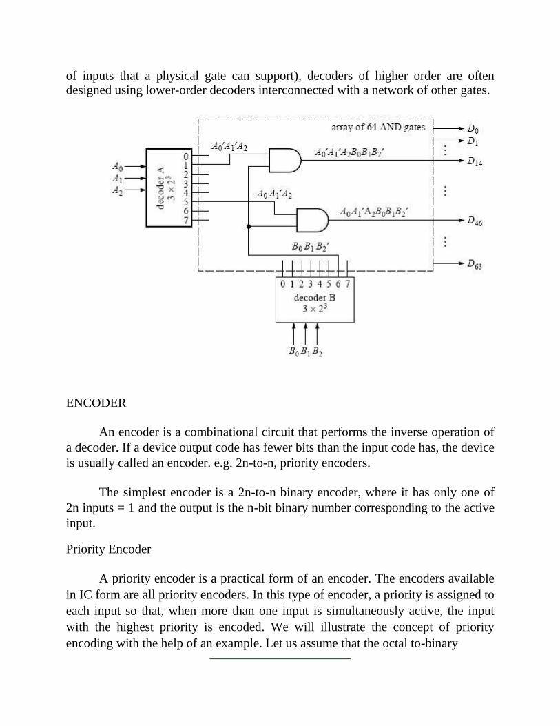
of inputs that a physical gate can support), decoders of higher order are often designed using lower-order decoders interconnected with a network of other gates.
ENCODER
An encoder is a combinational circuit that performs the inverse operation of
a decoder. If a device output code has fewer bits than the input code has, the device
is usually called an encoder. e.g. 2n-to-n, priority encoders.
The simplest encoder is a 2n-to-n binary encoder, where it has only one of
2n inputs = 1 and the output is the n-bit binary number corresponding to the active
input.
Priority Encoder
A priority encoder is a practical form of an encoder. The encoders available
in IC form are all priority encoders. In this type of encoder, a priority is assigned to
each input so that, when more than one input is simultaneously active, the input
with the highest priority is encoded. We will illustrate the concept of priority
encoding with the help of an example. Let us assume that the octal to-binary

encoder described in the previous paragraph has an input priority for higher-order
digits. Let us also assume that input lines D2, D4 and D7 are all simultaneously in
logic ‗1‘ state. In that case, only D7 will be encoded and the output will be 111.
The truth table of such a priority
Octal to binary encoder

Truth table of encoder
encoder will then be modified to what is shown above in truth table. Looking at the
last row of the table, it implies that, if D7 = 1, then, irrespective of the logic status
of other inputs, the output is 111 as D7 will only be encoded. As another example,
Fig. 8.16 shows the logic symbol and truth table of a 10-line decimal to four-line
BCD encoder providing priority encoding for higher-order digits, with digit 9
having the highest priority. In the functional table shown, the input line with
highest priority having a LOW on it is encoded irrespective of the logic status of
the other input lines.
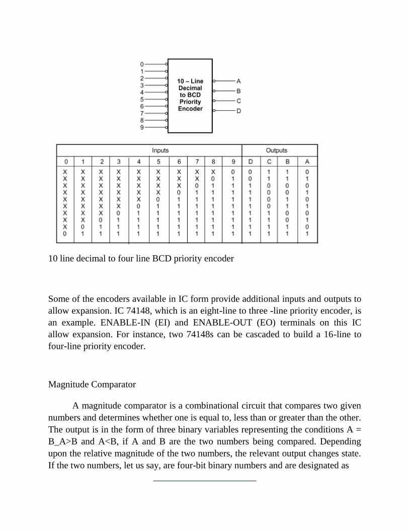
10 line decimal to four line BCD priority encoder
Some of the encoders available in IC form provide additional inputs and outputs to
allow expansion. IC 74148, which is an eight-line to three -line priority encoder, is
an example. ENABLE-IN (EI) and ENABLE-OUT (EO) terminals on this IC
allow expansion. For instance, two 74148s can be cascaded to build a 16-line to
four-line priority encoder.
Magnitude Comparator
A magnitude comparator is a combinational circuit that compares two given
numbers and determines whether one is equal to, less than or greater than the other.
The output is in the form of three binary variables representing the conditions A =
B_A>B and A<B, if A and B are the two numbers being compared. Depending
upon the relative magnitude of the two numbers, the relevant output changes state.
If the two numbers, let us say, are four-bit binary numbers and are designated as

(A3 A2 A1 A0) and (B3 B2 B1 B0), the two numbers will be equal if all pairs of
significant digits are equal, that is, A3= B3, A2 = B2, A1= B1 and A0 = B0. In
order to determine whether A is greater than or less than B we inspect the relative
magnitude of pairs of significant digits, starting from the most significant position.
The comparison is done by successively comparing the next adjacent lower pair of
digits if the digits of the pair under examination are equal. The comparison
continues until a pair of unequal digits is reached. In the pair of unequal digits, if
Ai = 1 and Bi = 0, then A > B, and if Ai = 0, Bi= 1 then A < B. If X, Y and Z are
three variables respectively representing the A = B, A > B and A < B conditions,
then the Boolean expression representing these conditions are given by the
equations
Let us examine equation (7.25). x3 will be ‗1‘ only when both A3 and B3 are equal.
Similarly, conditions for x2, x1 and x0 to be ‗1‘ respectively are equal A2 and B2,
equal A1 and B1 and equal A0 and B0. ANDing of x3, x2, x1 and x0 ensures that X
will be ‗1‘ when x3, x2, x1 and x0 are in the logic ‗1‘ state. Thus, X = 1 means that A = B. On similar lines, it can be visualized that equations (7.26)
and (7.27) respectively represent A > B and A < B conditions. Figure 7.36 shows
the logic diagram of a four-bit magnitude comparator.
Magnitude comparators are available in IC form. For example, 7485 is a four-bit
magnitude comparator of the TTL logic family. IC 4585 is a similar device in the
CMOS family. 7485 and 4585 have the same pin connection diagram and
functional table. The logic circuit inside these devices determines whether one
four-bit number, binary or BCD, is less than, equal to or greater than a second
four-bit number. It can perform comparison of straight binary and straight BCD (8-
4-2-1) codes. These devices can be cascaded together to perform operations on

larger bit numbers without the help of any external gates. This is facilitated by
three additional inputs called cascading or expansion inputs available on the IC.
These cascading inputs are also designated as A = B, A > B and A < B inputs.
Cascading of individual magnitude comparators of the type 7485 or 4585 is
discussed in the following paragraphs. IC 74AS885 is another common magnitude
comparator. The device is an eight bit magnitude comparator belonging to the
advanced Schottky TTL family. It can perform high-speed arithmetic or logic
comparisons on two eight-bit binary or 2‘s complement numbers and produces two
fully decoded decisions at the output about one number being either greater than or
less than the other. More than one of these devices can also be connected in a
cascade arrangement to perform comparison of numbers of longer lengths.

Unit III
PART-A (2 Marks) 1. Define Multiplexing?
2.What is Demultiplexer?
3.Define decoder & binary decoder
4.Define Encoder & priority Encoder
5.Give the applications of Demultiplexer.
6. Mention the uses of Demultiplexer.
7. List the types of ROM.
8. Differentiate ROM & PLD‘s
9. What are the different types of RAM?
10.What are the types of arrays in RAM?
PART-B
1. Implement the following function using PLA. (16) A (x, y, z) = _m (1, 2, 4, 6) B (x, y, z) = _m (0, 1, 6, 7) C (x, y, z) = _m (2, 6)
2. Implement the following function using PAL. (16) W (A, B, C, D) = _m (2, 12, 13) X (A, B, C, D) = _m (7, 8, 9, 10, 11, 12, 13, 14, 15) Y (A, B, C, D) = _m (0, 2, 3, 4, 5, 6, 7, 8, 10, 11, 15) Z (A, B, C, D) = _m (1, 2, 8, 12, 13)
3. Implement the given function using multiplexer (16)
4. Explain about Encoder and Decoder? (16)
5. Explain about 4 bit Magnitude comparator? (16)

UNIT IV SYNCHRONOUS SEQUENTIAL LOGIC
SYLLABUS :
Sequential Circuits
Flip flops
Analysis and Design Procedures
State Reduction and State Assignment
Shift Registers
Counters
HDL for Sequential Circuits.

UNIT IV
SEQUENTIAL LOGIC DESIGN
5.1 Flip Flops and their conversion
The flip-flop is an important element of such circuits. It has the interesting property of memory: It can be set to a state which is retained until explicitly reset.
R-S Flip-Flop
A flip-flop, as stated earlier, is a bistable circuit. Both of its output states are
stable. The circuit remains in a particular output state indefinitely until something
is done to change that output status. Referring to the bistable multivibrator circuit

discussed earlier, these two states were those of the output transistor in saturation (representing a LOW output) and in cut-off (representing a HIGH output). If the
LOW and HIGH outputs are respectively regarded as ‗0‘ and ‗1‘, then the output
can either be a ‗0‘ or a ‗1‘. Since either a ‗0‘ or a ‗1‘ can be held indefinitely until
the circuit is appropriately triggered to go to the other state, the circuit is said to
have memory. It is capable of storing one binary digit or one bit of digital
information. Also, if we recall the functioning of the bistable multivibrator circuit,
we find that, when one of the transistors was in saturation, the other was in cut-off.
This implies that, if we had taken outputs from the collectors of both transistors,
then the two outputs would be complementary.
In the flip-flops of various types that are available in IC form, we will see that all
these devices offer complementary outputs usually designated as Q and Q‘ The R-
S flip-flop is the most basic of all flip-flops. The letters ‗R‘ and ‗S‘ here stand for
RESET and SET. When the flip-flop is SET, its Q output goes to a ‗1‘ state, and
when it is RESET it goes to a ‗0‘ state. The Q‘ output is the complement of the Q
output at all times.
J-K Flip-Flop
A J-K flip-flop behaves in the same fashion as an R-S flip-flop except for
one of the entries in the function table. In the case of an R-S flip-flop, the input
combination S = R = 1 (in the case of a flip-flop with active HIGH inputs) and the
input combination S = R = 0 (in the case of a flip-flop with active LOW inputs) are
prohibited. In the case of a J-K flip-flop with active HIGH inputs, the output of the
flip-flop toggles, that is, it goes to the other state, for J = K = 1 . The output toggles
for J = K = 0 in the case of the flip-flop having active LOW inputs. Thus, a J-K
flip-flop overcomes the problem of a forbidden input combination of the R-S flip-
flop. Figures below respectively show the circuit symbol of level-triggered J-K
flip-flops with active HIGH and active LOW inputs, along with their function
tables.

The characteristic tables for a J-K flip-flop with active HIGH J and K inputs and a J-K flip-flop
with active LOW J and K inputs are respectively shown in Figs 10.28(a) and (b)_
The corresponding Karnaugh maps are shown in Fig below for the characteristics
table of Fig and in below for the characteristic table below. The characteristic
equations for the Karnaugh maps of below figure is shown next
FIG a. JK flip flop with active high inputs, b. JK flip flop with active low inputs
Toggle Flip-Flop (T Flip-Flop)
The output of a toggle flip-flop, also called a T flip-flop, changes state every time
it is triggered at its T input, called the toggle input. That is, the output becomes ‗1‘
if it was ‗0‘ and ‗0‘ if it was ‗1‘.
Positive edge-triggered and negative edge-triggered T flip-flops, along with their function tables.

w If we consider the T input as active when HIGH, the characteristic table of such a
flip-flop is shown in Fig. If the T input were active when LOW, then the
characteristic table would be as shown in Fig. The Karnaugh maps for the
characteristic tables of Figs shown respectively. The characteristic equations as
written from the Karnaugh maps are as follows:

J-K Flip-Flop as a Toggle Flip-Flop
If we recall the function table of a J-K flip-flop, we will see that, when both J and K inputs of the
flip-flop are tied to their active level (‗1‘ level if J and K are active when HIGH,
and ‗0‘ level when J and K are active when LOW), the flip-flop behaves like a
toggle flip-flop, with its clock input serving as the T input. In fact, the J-K flip-flop
can be used to construct any other flip-flop. That is why it is also sometimes
referred to as a universal flip-flop. Figure shows the use of a J-K flip-flop as a T
flip-flop.

D Flip-Flop
A D flip-flop, also called a delay flip-flop, can be used to provide temporary storage of one bit of

information. Figure shows the circuit symbol and function table of a negative edge-
triggered D flip-flop. When the clock is active, the data bit (0 or 1) present at the D
input is transferred to the output. In the D flip-flop of Fig the data transfer from D
input to Q output occurs on the negative-going (HIGH-to-LOW) transition of the
clock input. The D input can acquire new status
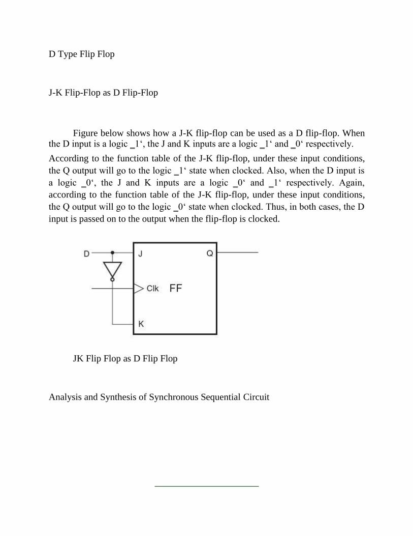
D Type Flip Flop
J-K Flip-Flop as D Flip-Flop
Figure below shows how a J-K flip-flop can be used as a D flip-flop. When the D input is a logic ‗1‘, the J and K inputs are a logic ‗1‘ and ‗0‘ respectively.
According to the function table of the J-K flip-flop, under these input conditions,
the Q output will go to the logic ‗1‘ state when clocked. Also, when the D input is
a logic ‗0‘, the J and K inputs are a logic ‗0‘ and ‗1‘ respectively. Again,
according to the function table of the J-K flip-flop, under these input conditions,
the Q output will go to the logic ‗0‘ state when clocked. Thus, in both cases, the D
input is passed on to the output when the flip-flop is clocked.
JK Flip Flop as D Flip Flop
Analysis and Synthesis of Synchronous Sequential Circuit


Design of synchronous sequential circuit


Unit IV
PART-A (2 Marks)
1. What is sequential circuit?
2. List the classifications of sequential circuit.
3. What is Synchronous sequential circuit?
4. List different types of flip-flops.
5. What do you mean by triggering of flip-flop.
6. What is an excitation table?
7. Give the excitation table of a JK flip-flop
8. Give the excitation table of a SR flip-flop
9. Give the excitation table of a T flip-flop
PART-B
1. Design a counter with the following repeated binary sequence:0, 1, 2,3, 4, 5, 6. use JK Flip-flop. (16)
2. Describe the operation of SR flip-flop (16) 3. Design a sequential circuit using JK flip-flop for the following state table [use state diagram] (16)
4. The count has a repeated sequence of six states, with flip flops B and C repeating the binary count 00, 01, 10 while flip flop A alternates between 0 and 1 every three counts. Designs with JK flip-flop (16)
5. Design a 3-bit T flip-flop counter (16)

UNIT V ASYNCHRONOUS SEQUENTIAL LOGIC
SYLLABUS :
Analysis and Design of Asynchronous Sequential Circuits
Reduction of State and Flow Tables
Race-Free State Assignment
Hazards
ASM Chart.


Optional conditional output box(es). Such an
ouput box indicates outputs that are conditionally
asserted. These outputs are called asynchrous or
Mealy outputs.
There is no rule saying that outputs are exclusively inside an a conditional output box or in a state box. An output written inside a state box is simply independent of the input, while in that state.
The idea is that flow passes from ASM block to ASM block, the decisision boxes decide the next state and conditional output. Consider the following example of an ASM diagram block. When state S0 is entered, output Z5 is always asserted. Z1_n however is asserted only if X2 is also high. Otherwise Z2 is asserted.
An ASM block
Certain Rules
The drawing of ASM charts must follow certain necessary rules:
The entrance paths to an ASM block lead to only one state box
Of 'N' possible exit paths, for each possible valid input combination, only one exit path can be followed, that is there is only one valid next state. No feedback internal to a state box is allowed. The following diagram indicates valid and invalid cases.

Incorrect Correct
Parallel vs. Serial
We can bend the rules, several internal paths can be active, provided that they lead
to a single exit path. Regardless of parallel or serial form, all tests are performed
concurrently. Usually we have a preference for the serial form. The following two examples are equivalent.
Parallel Form
Sequence Detector Example
Serial Form
The use of ASM charts is a trade-off. While the mechanics of ASM charts do reduce clutter in significant designs, its better to use an ordinary state diagrams for simple state machines. Here is an example Moore type state machine with input X and output Z. Once the flag sequence is received, the output is asserted for one clock cycle.
The corresponding ASM chart is to the right. Note that unlike the state diagram which illustrates the output value for each arc, the ASM chart indicates when the output Z only when it is asserted.
State diagram for sequence detector
ASM chart

The following timing diagram illustrates the detection of the desired sequence. Here it is assumed that the state is updated with a rising clock edge. The key concept to observe is that regardless of the input, the output can only be asserted for one entire clock cycle.
Timing diagram
Event Tables
Simply stated, timing diagrams are prone to a particular problem for the reader, in that there can be too much to see. Timing diagrams clearly expresses time relationships and delay. However, in synchonous sequential logic, all registers are updated at the rising edge of the system clock. The clock period is just set to an arbitrarily value. Provided that the input setup-and-hold requirements are satisfied, the details of the timing diagram are distracting.
The goal of an event table is that given a scenario, to neatly summarize the resultant behavior of synchronous sequential logic. In writing an event table, capitol T refers to the system clock period and nT means n times the system clock period. For asynchronous input changes, the time is given, assuming that the system output reacts instantaneously. For synchronous signals, the + symbol means a moment suitably after the given time, for the system to become settled. The - symbol however, means a moment suitably before the given time, satisfying the necessary setup time.
To reduce the clutter, be sure to fill in those signals that change state or are updated. The following event table summarizes the behavior in the above timing diagram. An empty entry will be interpreted to mean no-change to the corresponding signal during the corresponding clock cycle.
Event Table

Time Reset X State Z
0T 1 0 M0 0
0.4T 0
1T+ M1
1.3T 1
2T+ M2
2.6T 0
3T+ M3 1
3.6T 1
4T+ M2 0
4.4T 0
Asynchronous and Synchronous Output Example
The following is an example of an ASM chart with inputs X1 and X2, and outputs Z1 and Z2. In state S0 the outputs are immediately dependent on the input. In state S1, output Z1 is always asserted. In state S2, output Z1 is dependent on input X1 but Z2 is not asserted.

Example ASM chart
The following is the corresponding state diagram. The legend indicates how the input and output are associated with each arc. The 'd' symbol, which refers here to the don't-care condition helps to reduce the clutter. While the state diagram and ASM chart here are similar in complexity, state diagrams quickly become messy.
Corresponding state diagram
Clock Enable
Simply stated, a clock enable indicates when a state machine must pay attention to the system clock. The figure below has a clock signal and a clock enable, note that this clock enable is asserted for one clock period at a time. The clock enable concept is powerful as it allows a device to effectively be clocked at a rate slower than the system clock, while remaining entirely synchronous with the rest of the system. In this case the effective clock rate is one-third that of the system clock.

Clock and enable
In the spirit of reducing clutter, a clock enable can be written next to a state box. When not asserted, the device remains in its current state. The following figues are equivalent. Further, it is assumed that devices controlled by such a state, as directly or indirectly enabled by the clock enable as well.
Equivalent enables
Race condition
A race condition or race hazard is a flaw in an electronic system or process whereby the output and/or result of the process is unexpectedly and critically dependent on the sequence or timing of other events. The term originates with the idea of two signals racing each other to influence the output first.
Race conditions can occur in electronics systems, especially logic circuits, and in computer software, especially multithreaded or distributed programs.
Electronics
A typical example of a race condition may occur in a system of logic gates, where
inputs vary. If a particular output depends on the state of the inputs, it may only be
defined for steady-state signals. As the inputs change state, a small delay will occur
before the output changes, due to the physical nature of the electronic system. For a
brief period, the output may change to an unwanted state before settling back to the
designed state. Certain systems can tolerate such glitches, but if for example this
output functions as a clock signal for further systems that contain memory, the

system can rapidly depart from its designed behaviour (in effect, the temporary glitch becomes permanent).
For example, consider a two input AND gate fed with a logic signal A on one input and its negation, NOT A, on another input. In theory, the output (A AND NOT A) should never be high. However, if changes in the value of A take longer to propagate to the second input than the first when A changes from false to true, a brief period will ensue during which both inputs are true, and so the gate's output will also be true.
Proper design techniques (e.g. Karnaugh maps) encourage designers to recognize and eliminate race conditions before they cause problems.
As well as these problems, some logic elements can enter metastable states, which create further problems for circuit designers.
Critical and non-critical race conditions
A critical race occurs when the order in which internal variables are changed determines the eventual state that the state machine will end up in.
A non-critical race occurs when the order in which internal variables are changed does not alter the eventual state. In other words, a non-critical race occurs when moving to a desired state means that more than one internal state variable must be changed at once, but no matter in what order these internal state variables change, the resultant state will be the same.
Static, dynamic, and essential race conditions Static race conditions
These are caused when a signal and its complement are combined together.
Dynamic race conditions
These result in multiple transitions when only one is intended. They are due
to interaction between gates (Dynamic race conditions can be eliminated by
using not more than two levels of gating).

Essential race conditions
These are caused when an input has two transitions in less than the total
feedback propagation time. Sometimes they are cured using inductive delay-
line elements to effectively increase the time duration of an input signal
Unit V
PART-A (2 Marks)
1.What is the use of state diagram?
2. What is state table? 3. What is a state equation?
4. Differentiate ASM chart and conventional flow chart?
5. What is flow table?
6. What is primitive flow table?
7. Define race condition.
8. Define critical & non-critical race with example.
9. How can a race be avoided? 10. Define hazards.
PART-B
1. Design an Asynchronous sequential circuit using SR latch with two inputs A and B and one output y. B is the control input which, when equal to 1, transfers the input A to output y. when B is 0, the output does not change, for any change in input. (16) 2. Give hazard free relation for the following Boolean function. F (A, B, C, D) =_m (0, 2, 6, 7, 8, 10, 12) (16)
3. Explain about Hazards? (16) 4. Explain about Races? (16) 5. Design T Flip flop from Asynchronous Sequential circuit? (16)