Module 2: Defect Chemistry and Defect Equilibria Introduction ...
Upload
satwik-patnaikCategory
view
9download
0description
This article has been accepted for inclusion in a future issue of this journal. Content is final as presented, with the exception of pagination.
IEEE TRANSACTIONS ON VERY LARGE SCALE INTEGRATION (VLSI) SYSTEMS 1
Unified Capture Scheme for Small Delay DefectDetection and Aging Prediction
Song Jin, Yinhe Han, Member, IEEE, Huawei Li, Senior Member, IEEE, and Xiaowei Li, Senior Member, IEEE
Abstract— Small delay defect (SDD) and aging-induced circuitfailure are both prominent reliability concerns for nanoscale inte-grated circuits. Faster-than-at-speed testing is effective on SDDdetection in manufacturing testing, which is always implementedby designing a suite of test signal generation circuits on the chip.Meanwhile, the integration of online aging sensors is becomingattractive in monitoring aging-induced delay degradation in theruntime. These design requirements, if implemented in separateways, will increase the complexity of a reliable design andconsume more die area. In this paper, a unified capture scheme isproposed to generate programmable clock signals for the detec-tion of both SDDs and circuit aging. Our motivation arises fromthe observations that SDD detection and online aging predictionboth need to capture circuit response ahead of the functionalclock. The proposed aging-resistant design method enables theoffline test circuit to be reused in online operations. Reversedshort channel effect is also exploited to make the underlyingcircuit resilient to process variations. The proposed scheme isvalidated by intensive HSPICE simulations. Experimental resultsdemonstrate the effectiveness in terms of low area, power, andperformance overheads.
Index Terms— Faster-than-at-speed testing, online agingprediction, reversed short channel effect unified capture scheme.
I. INTRODUCTION
W ITH the relentless scaling in technology, small delaydefects (SDDs), which commonly arise from resistant
opens and shorts, gate oxide failure, via voids, etc., havebecome a serious problem in integrated circuits [1], [2]. SDDscan cause timing failure when they are activated on a longerpath during functional operation [3]. Moreover, SDDs are alsoa threat to circuit reliability because such defects may bemagnified by the subsequent aging in the field, resulting inpermanent device failure [4]. It is therefore essential to detectSDDs in the chip during the fabrication testing stage itself [5].However, traditional at-speed delay testing based on transitionfault model is always prone to sensitization of the short paths
Manuscript received September 9, 2011; revised April 3, 2012; acceptedApril 11, 2012. This work was supported in part by the National BasicResearch Program of China (973) under Grant 2011CB302503 and Grant2011CB302501, and the National Natural Science Foundation of China underGrant 61076037, Grant 60921002, and Grant 61176040, and the FundamentalResearch Funds for the Central Universities under Grant 12MS123.
S. Jin was with the State Key Laboratory of Computer Architecture, Instituteof Computing Technology, Chinese Academy of Sciences, Beijing 100190,China. He is now with the Department of Electronic and CommunicationEngineering, School of Electrical and Electronic Engineering, North ChinaElectric Power University, Baoding 071003, China.
Y. Han, H. Li, and X. Li are with the State Key Laboratory of ComputerArchitecture, Institute of Computing Technology, Chinese Academy ofSciences, Beijing 100190, China (e-mail: [email protected]).
Color versions of one or more of the figures in this paper are availableonline at http://ieeexplore.ieee.org.
Digital Object Identifier 10.1109/TVLSI.2012.2197766
in the circuit. SDDs will still be hidden because of the largetiming slack of the short paths under the functional clock,thereby escaping the test stage. One of the effective ways todetect SDDs is by exploiting faster-than-at-speed testing [6].By increasing the test clock frequency, timing slackness ofthe short paths decreases, which improves the capability ofscreening SDDs.
On the other hand, aging effects have become a prominentreliability challenge as the process advances into the nanome-ter regime [7]. Much work has been done on understandingand modeling the intrinsic mechanism of aging, such asnegative/positive bias temperature instability (NBTI/PBTI),time-dependent dielectric breakdown, hot-carrier injection,electromigration, etc. Given that circuit aging is a gradualprocess, online aging prediction [8]– [10] is an effective wayto prevent the system data or state corruption from aging-induced circuit failure. It captures the circuit response underthe normal working mode and generates a warning signal if theaging-induced delay degradation exceeds a specified threshold.Based on this warning information, some redundancy or tuningmechanisms can be enabled to ensure that the system cancontinue to work well.
The hardware circuit used in manufacturing testing isusually deactivated or abandoned when the chip works inthe field. However, for reliability, the designer still needs toinsert specific circuits for online monitoring some faults whichmay result in functional failure of the chip, such as softerror, inductive noise, and aging-induced delay degradation.If we can reutilize the hardware circuit designed for offlinemanufacturing testing to online fault detection or monitoring,the implementation complexity in defect- or aging-relatedreliability design can be significantly reduced. Meanwhile, thetotal area overhead consumed by offline and online circuitscan be saved as well.
We noticed that SDD detection and online aging predictionhave a common characteristic, i.e., both of them need tocapture the circuit response ahead of the functional clock.This motivates us to propose a unified capture scheme tosupport both faster-than-at-speed testing and online agingprediction. It reuses the offline test hardware circuit in onlinemonitoring of circuit aging and generates an on-chip program-mable clock signal to flexibly capture the circuit response atthe designated time.
However, the implementation of a unified capture scheme isconfronted with some challenges. The intrinsic aging processwill degrade the on-chip circuit. With the continuous reductionin oxide thickness and the increase in operational temperature,the NBTI effect can become a limiting factor in the device
1063–8210/$31.00 © 2012 IEEE
This article has been accepted for inclusion in a future issue of this journal. Content is final as presented, with the exception of pagination.
2 IEEE TRANSACTIONS ON VERY LARGE SCALE INTEGRATION (VLSI) SYSTEMS
lifetime [11]. The PBTI effect emerges as a dominant agingmechanism in sub-32-nm high-k processes [12], [13]. Agingeffects can cause the drift in the generated clock signal andthereby result in the interval for capturing the circuit responsein online aging prediction to deviate from its initial spangradually. This makes the traditional hardware circuit designedfor fabrication testing unfit for online operation.
Another important design concern in the proposed clockingscheme is the negative impact of process variation (PV) on theon-chip circuit. PV will cause a skew in the generated clocksignal, thus affecting the test efficiency of faster-than-at-speedtesting or the prediction accuracy of online aging prediction.
We tackled the above design concerns in the proposedunified capture scheme. Our main contributions are as follows.
1) The proposed unified capture scheme relies on thegeneration of programmable clock signals to achievedifferent test frequencies in faster-than-at-speed testingor capture intervals in online aging prediction. Moreover,the capture interval can be dynamically adjusted in theruntime to further compensate the aging-induced driftin itself.
2) The proposed aging-resistant design method signifi-cantly reduces the drift in the generated clock signalunder runtime NBTI effect. Reversed short channeleffect (RSCE) is also exploited to determine the optimaltransistor channel length for the circuit design. Thisminimizes the skew of the generated clock signal in thepresence of PV.
The rest of this paper is organized as follows. Section IIintroduces the related work. Details of the unified capturescheme are presented in Section III. PV-resilient design con-cern is discussed in Section IV. Section V presents the verifi-cation and simulation results. We conclude in Section VI.
II. RELATED WORK
To tackle NBTI-induced reliability problem, someresearchers have proposed to model, analyze, and optimizeNBTI-induced degradation in the design phase. A long-termNBTI model was formulated in [14]–[16]. NBTI-induceddegradation on random logic and SRAM with [17], [18] andwithout [19], [20] considering PV has been analyzed. SomeNBTI-resistant techniques were proposed accordingly [21],[22]. While theoretical analysis for NBTI effects is valuable,the actual NBTI-induced performance degradation stronglydepends on the practical workloads executed on the circuitand hence it is essential to be able to monitor it online.
Online aging prediction has attracted much attention inrecent years. Agarwal et al. have proposed the design ofan aging sensor in [8] and [9], wherein a warning signalwill be triggered if a delayed transition occurred within thepredetermined guardband interval. Yan et al. have proposeda unified fault detection scheme called SVFD [10] whichcan be used to detect soft error and aging-induced delaydegradation at the cost of adding extra clock signals. Thedesigns in [8]–[10] have the same problem: the guardbandbound can have a large deviation from the designated valuedue to PV, which may result in false alarms. Keane et al.have proposed an on-chip NBTI degradation sensor using a
delay-locked loop for analyzing pMOS aging under dc andac stress scenarios [11]. In [23], a circuit failure predictionmethod was proposed by measuring the delay of the logicblock. Although the circuit delay degradation can be accuratelymeasured, the hardware overhead is considerable. A voltageglitch generation and detection circuit that can be used to mon-itor the circuit aging was proposed in [24]. However, the circuititself in [24] is not aging-resistant. In [25], Vazquez et al.proposed a programmable aging sensor design that relies ona configurable pull-down nMOS network. However, the actualdetection range cannot be easily modified by resizing thenMOSs under the PV-induced uncertainty.
On the spectrum of SDD detection, timing-aware automatictest pattern generation (ATPG) and faster-than-at-speed testingare two kinds of commonly used schemes. The former tries toinvolve timing information in test generation with a transitionfault model and expects to sensitize longer paths [4], [26]–[28].However, as shown in [28], the runtime of the timing-awareATPG may be 20 times higher than that of a traditional ATPG.
For the above reasons, some authors have proposed faster-than-at-speed testing for SDDs detection. This technique triesto reduce the timing slack of the short path, while maskingthe output flip-flop (FF) of longer sensitized path to avoidunnecessary timing failure [6]. Reducing the slack of thetarget fault site can increase the possibility to detect SDDs.However, exploiting the external automatic test equipment(ATE) to provide the fast clock signal [29] will increase the testcost considerably. The fast clock signal is commonly obtainedby using the on-chip clock generation circuit. Ahmed et al.proposed to group the test pattern into some subsets anddetermine an optimal test frequency [3]. Since their schemedoes not increase the test frequency to an extent that any pathsexercised at the rated functional frequency may fail, any scanFF masking is avoided. Nakamura et al. [30] proposed to usean on-chip clock chopper and gating logic to obtain a fastertest clock at the cost of adding extra pins on the chip. In[31], McLaurin et al. proposed a clock control circuit usingthe phase-locked loop (PLL) clock to perform the faster-than-at-speed testing. Their scheme, however, is rather complex forrealistic application because the PLL has to be reset for everypattern. Pei et al. [32] proposed to generate on-chip clocksduring faster-than-at-speed testing by using two symmetricdelay lines. Tayade et al. proposed an on-chip programmablecapture generation circuit that generates a faster capture signalfor faster-than-at-speed testing [33].
The above circuit designs for faster-than-at-speed testing arenot aging-resistant, which makes them unsuitable to be reusedin online aging prediction. Moreover, PV can also result inlarge skews in the generated clock signals and thus may leadto test escape or overtesting.
III. UNIFIED CLOCKING SCHEME
A. Top View
Faster-than-at-speed testing and online aging predictionhave a common characteristic: both of them need to capturecircuit response ahead of the functional clock. As shown inFig. 1(a), in faster-than-at-speed testing, after the test vector
This article has been accepted for inclusion in a future issue of this journal. Content is final as presented, with the exception of pagination.
JIN et al.: CAPTURE SCHEME FOR SDD DETECTION AND AGING PREDICTION 3
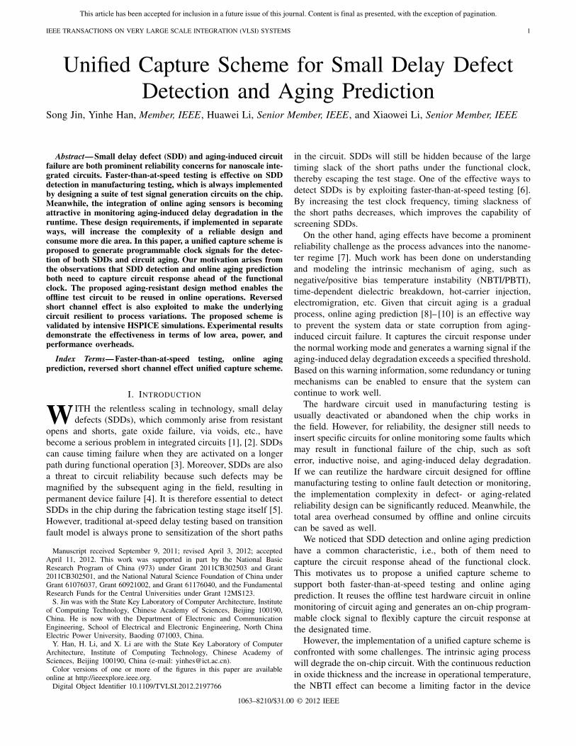
FCLKFCLK
OUTTCLKCapture IntervalLaunch Capture edge
(b)(a)
Fig. 1. (a) Faster-than-at-speed testing. (b) Online aging prediction. Bothneed to capture circuit response in advance of the functional clock.
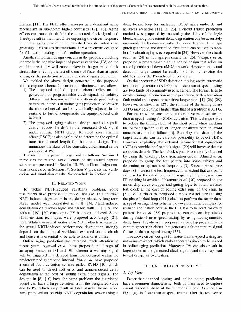
PCSGM
AS
Circuit under test/monitor
AS
FF FF
WMSM CSMFCLKGSEN
SEL
CTRL
xCLK
DD
Fig. 2. Framework of the proposed unified capture scheme.
is applied to CUT by a launch clock, a faster capture clockis used to capture the test response. This clock reduces thetiming slack of short paths, thereby improving the capabilityof SDD detection [6]. Similarly, a capture interval is formedbefore the trigger edge of the functional clock during thetime that online aging prediction is performed, as shown inFig. 1(b). It generally spans tens to hundreds of picoseconds. Ifa transition on the circuit output falls into the capture interval,it will be captured by the aging sensor and is recognized asan indication that circuit aging has exceeded the designatedthreshold.
Based on the above observations, we propose a unifiedcapture scheme that generates programmable clock signalsto support both faster-than-at-speed testing and online agingprediction. The framework of the proposed unified capturescheme, which consists of several modules, is illustrated inFig. 2. The PCSGM module generates programmable clocksignals which can be used as launch and capture clocks(together denoted as xCLK) for faster-than-at-speed testing aswell as the control signal (CTRL) to form the capture intervalfor online aging prediction. Two control signals global scanenable signal (GSEN) and SEL are applied to the workingmode selection module (WMSM) and the clock selectionmodule (CSM). They are used to switch the working modesbetween faster-than-at-speed testing and online aging predic-tion as well as to select the corresponding clock signals. TheAS unit is the aging sensor that generates the warning signalif a transition occurs within the specific capture interval.
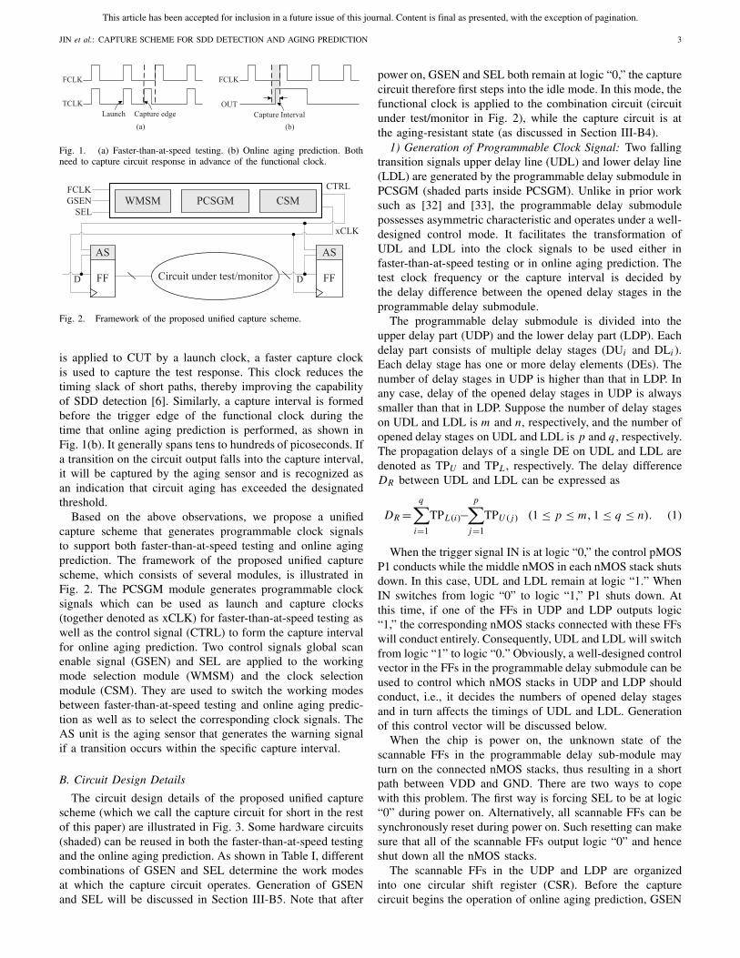
B. Circuit Design Details
The circuit design details of the proposed unified capturescheme (which we call the capture circuit for short in the restof this paper) are illustrated in Fig. 3. Some hardware circuits(shaded) can be reused in both the faster-than-at-speed testingand the online aging prediction. As shown in Table I, differentcombinations of GSEN and SEL determine the work modesat which the capture circuit operates. Generation of GSENand SEL will be discussed in Section III-B5. Note that after
power on, GSEN and SEL both remain at logic “0,” the capturecircuit therefore first steps into the idle mode. In this mode, thefunctional clock is applied to the combination circuit (circuitunder test/monitor in Fig. 2), while the capture circuit is atthe aging-resistant state (as discussed in Section III-B4).
1) Generation of Programmable Clock Signal: Two fallingtransition signals upper delay line (UDL) and lower delay line(LDL) are generated by the programmable delay submodule inPCSGM (shaded parts inside PCSGM). Unlike in prior worksuch as [32] and [33], the programmable delay submodulepossesses asymmetric characteristic and operates under a well-designed control mode. It facilitates the transformation ofUDL and LDL into the clock signals to be used either infaster-than-at-speed testing or in online aging prediction. Thetest clock frequency or the capture interval is decided bythe delay difference between the opened delay stages in theprogrammable delay submodule.
The programmable delay submodule is divided into theupper delay part (UDP) and the lower delay part (LDP). Eachdelay part consists of multiple delay stages (DUi and DLi ).Each delay stage has one or more delay elements (DEs). Thenumber of delay stages in UDP is higher than that in LDP. Inany case, delay of the opened delay stages in UDP is alwayssmaller than that in LDP. Suppose the number of delay stageson UDL and LDL is m and n, respectively, and the number ofopened delay stages on UDL and LDL is p and q , respectively.The propagation delays of a single DE on UDL and LDL aredenoted as TPU and TPL , respectively. The delay differenceDR between UDL and LDL can be expressed as
DR =q∑
i=1
TPL(i)−p∑
j=1
TPU ( j ) (1 ≤ p ≤ m, 1 ≤ q ≤ n). (1)
When the trigger signal IN is at logic “0,” the control pMOSP1 conducts while the middle nMOS in each nMOS stack shutsdown. In this case, UDL and LDL remain at logic “1.” WhenIN switches from logic “0” to logic “1,” P1 shuts down. Atthis time, if one of the FFs in UDP and LDP outputs logic“1,” the corresponding nMOS stacks connected with these FFswill conduct entirely. Consequently, UDL and LDL will switchfrom logic “1” to logic “0.” Obviously, a well-designed controlvector in the FFs in the programmable delay submodule can beused to control which nMOS stacks in UDP and LDP shouldconduct, i.e., it decides the numbers of opened delay stagesand in turn affects the timings of UDL and LDL. Generationof this control vector will be discussed below.
When the chip is power on, the unknown state of thescannable FFs in the programmable delay sub-module mayturn on the connected nMOS stacks, thus resulting in a shortpath between VDD and GND. There are two ways to copewith this problem. The first way is forcing SEL to be at logic“0” during power on. Alternatively, all scannable FFs can besynchronously reset during power on. Such resetting can makesure that all of the scannable FFs output logic “0” and henceshut down all the nMOS stacks.
The scannable FFs in the UDP and LDP are organizedinto one circular shift register (CSR). Before the capturecircuit begins the operation of online aging prediction, GSEN
This article has been accepted for inclusion in a future issue of this journal. Content is final as presented, with the exception of pagination.
4 IEEE TRANSACTIONS ON VERY LARGE SCALE INTEGRATION (VLSI) SYSTEMS
Fig. 3. Schematic diagram of capture circuit.
TABLE I
CONTROL FUNCTION OF GSEN AND SEL
Working Control signal Controlmode GSEN SEL function
faster-than- 1 1 scan in or scan outat-speed testing 0 1 launch, captureaging prediction 1 0 capture in advance
idle 0 0 functional clock
and SEL both keep remain at logic “0.” At this time, awell-designed control vector can be formed by setting or reset-ting the scannable FFs to different states (0 or 1) in the CSR.This control vector is used to control the number of openeddelay stages in UDP and LDP. For the individual segments ofthe control vector lying in UDP and LDP separately, only onebit is “1” while the other bits are all “0.” Depending on thelocations of bit “1” in the segments, the number of openeddelay stages in UDP and LDP can be equal (in faster-than-at-speed testing) or different (in online aging prediction).
Note that, although UDL and LDL are both connected tothe control pMOS P1, they do not interfere with each otherduring the operation of the capture circuit. For example, onlywhen the UDL switches to logic “0” and remains at this statefor a long enough time or constantly, LDL will be affectedand switch to logic “0” correspondingly, and vice versa.However, to generate the high clock frequency or the shortcapture interval, the time difference between switching UDLand LDL from logic “1” to logic “0” is very small. Such ashort time will not therefore lead to interference between UDLand LDL.
2) Performing Faster-Than-at-Speed Testing: During faster-than-at-speed testing, the chip under test works alternatively
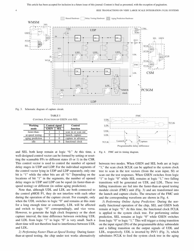
Fig. 4. FMC and its timing diagram.
between two modes. When GSEN and SEL both are at logic“1,” the scan clock SCLK can be applied to the system clocktree to scan in the test vectors (from the scan input, SI) orscan out the test responses. When GSEN switches from logic“1” to logic “0” while SEL remains at logic “1,” two fallingtransitions will be generated on UDL and LDL. These twofalling transitions are fed into the faster-than-at-speed testingmodule circuit (FMC) unit (Fig. 3) and are transformed intothe launch and capture clocks. The structure of the FMC unitand the corresponding waveform are shown in Fig. 4.
3) Performing Online Aging Prediction: During the nor-mally functional operation of the chip, SEL and GSEN bothremain at logic “0.” At this time, the functional clock FCLKis applied to the system clock tree. For performing onlineprediction, SEL remains at logic “0” while GSEN switchesfrom logic “0” to logic “1.” This will trigger a rising transitionon the input signal (IN) of the programmable delay submoduleand a falling transition on the output signals of UDL andLDL, respectively. UDL is inverted by INV1 (Fig. 3), whichsubstitutes FCLK to feed the system clock tree in the aging
This article has been accepted for inclusion in a future issue of this journal. Content is final as presented, with the exception of pagination.
JIN et al.: CAPTURE SCHEME FOR SDD DETECTION AND AGING PREDICTION 5
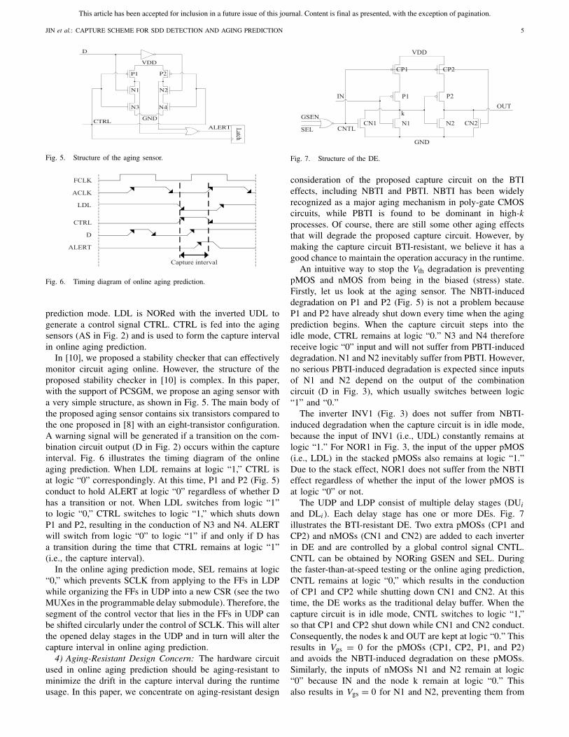
Fig. 5. Structure of the aging sensor.
Fig. 6. Timing diagram of online aging prediction.
prediction mode. LDL is NORed with the inverted UDL togenerate a control signal CTRL. CTRL is fed into the agingsensors (AS in Fig. 2) and is used to form the capture intervalin online aging prediction.
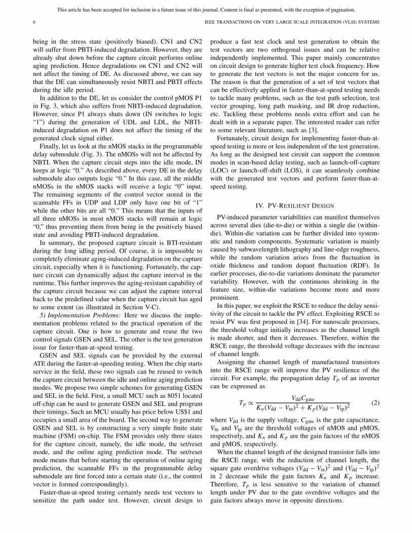
In [10], we proposed a stability checker that can effectivelymonitor circuit aging online. However, the structure of theproposed stability checker in [10] is complex. In this paper,with the support of PCSGM, we propose an aging sensor witha very simple structure, as shown in Fig. 5. The main body ofthe proposed aging sensor contains six transistors compared tothe one proposed in [8] with an eight-transistor configuration.A warning signal will be generated if a transition on the com-bination circuit output (D in Fig. 2) occurs within the captureinterval. Fig. 6 illustrates the timing diagram of the onlineaging prediction. When LDL remains at logic “1,” CTRL isat logic “0” correspondingly. At this time, P1 and P2 (Fig. 5)conduct to hold ALERT at logic “0” regardless of whether Dhas a transition or not. When LDL switches from logic “1”to logic “0,” CTRL switches to logic “1,” which shuts downP1 and P2, resulting in the conduction of N3 and N4. ALERTwill switch from logic “0” to logic “1” if and only if D hasa transition during the time that CTRL remains at logic “1”(i.e., the capture interval).
In the online aging prediction mode, SEL remains at logic“0,” which prevents SCLK from applying to the FFs in LDPwhile organizing the FFs in UDP into a new CSR (see the twoMUXes in the programmable delay submodule). Therefore, thesegment of the control vector that lies in the FFs in UDP canbe shifted circularly under the control of SCLK. This will alterthe opened delay stages in the UDP and in turn will alter thecapture interval in online aging prediction.
4) Aging-Resistant Design Concern: The hardware circuitused in online aging prediction should be aging-resistant tominimize the drift in the capture interval during the runtimeusage. In this paper, we concentrate on aging-resistant design
Fig. 7. Structure of the DE.
consideration of the proposed capture circuit on the BTIeffects, including NBTI and PBTI. NBTI has been widelyrecognized as a major aging mechanism in poly-gate CMOScircuits, while PBTI is found to be dominant in high-kprocesses. Of course, there are still some other aging effectsthat will degrade the proposed capture circuit. However, bymaking the capture circuit BTI-resistant, we believe it has agood chance to maintain the operation accuracy in the runtime.
An intuitive way to stop the Vth degradation is preventingpMOS and nMOS from being in the biased (stress) state.Firstly, let us look at the aging sensor. The NBTI-induceddegradation on P1 and P2 (Fig. 5) is not a problem becauseP1 and P2 have already shut down every time when the agingprediction begins. When the capture circuit steps into theidle mode, CTRL remains at logic “0.” N3 and N4 thereforereceive logic “0” input and will not suffer from PBTI-induceddegradation. N1 and N2 inevitably suffer from PBTI. However,no serious PBTI-induced degradation is expected since inputsof N1 and N2 depend on the output of the combinationcircuit (D in Fig. 3), which usually switches between logic“1” and “0.”
The inverter INV1 (Fig. 3) does not suffer from NBTI-induced degradation when the capture circuit is in idle mode,because the input of INV1 (i.e., UDL) constantly remains atlogic “1.” For NOR1 in Fig. 3, the input of the upper pMOS(i.e., LDL) in the stacked pMOSs also remains at logic “1.”Due to the stack effect, NOR1 does not suffer from the NBTIeffect regardless of whether the input of the lower pMOS isat logic “0” or not.
The UDP and LDP consist of multiple delay stages (DUi
and DLi ). Each delay stage has one or more DEs. Fig. 7illustrates the BTI-resistant DE. Two extra pMOSs (CP1 andCP2) and nMOSs (CN1 and CN2) are added to each inverterin DE and are controlled by a global control signal CNTL.CNTL can be obtained by NORing GSEN and SEL. Duringthe faster-than-at-speed testing or the online aging prediction,CNTL remains at logic “0,” which results in the conductionof CP1 and CP2 while shutting down CN1 and CN2. At thistime, the DE works as the traditional delay buffer. When thecapture circuit is in idle mode, CNTL switches to logic “1,”so that CP1 and CP2 shut down while CN1 and CN2 conduct.Consequently, the nodes k and OUT are kept at logic “0.” Thisresults in Vgs = 0 for the pMOSs (CP1, CP2, P1, and P2)and avoids the NBTI-induced degradation on these pMOSs.Similarly, the inputs of nMOSs N1 and N2 remain at logic“0” because IN and the node k remain at logic “0.” Thisalso results in Vgs = 0 for N1 and N2, preventing them from
This article has been accepted for inclusion in a future issue of this journal. Content is final as presented, with the exception of pagination.
6 IEEE TRANSACTIONS ON VERY LARGE SCALE INTEGRATION (VLSI) SYSTEMS
being in the stress state (positively biased). CN1 and CN2will suffer from PBTI-induced degradation. However, they arealready shut down before the capture circuit performs onlineaging prediction. Hence degradations on CN1 and CN2 willnot affect the timing of DE. As discussed above, we can saythat the DE can simultaneously resist NBTI and PBTI effectsduring the idle period.
In addition to the DE, let us consider the control pMOS P1in Fig. 3, which also suffers from NBTI-induced degradation.However, since P1 always shuts down (IN switches to logic“1”) during the generation of UDL and LDL, the NBTI-induced degradation on P1 does not affect the timing of thegenerated clock signal either.
Finally, let us look at the nMOS stacks in the programmabledelay submodule (Fig. 3). The nMOSs will not be affected byNBTI. When the capture circuit steps into the idle mode, INkeeps at logic “0.” As described above, every DE in the delaysubmodule also outputs logic “0.” In this case, all the middlenMOSs in the nMOS stacks will receive a logic “0” input.The remaining segments of the control vector stored in thescannable FFs in UDP and LDP only have one bit of “1”while the other bits are all “0.” This means that the inputs ofall three nMOSs in most nMOS stacks will remain at logic“0,” thus preventing them from being in the positively biasedstate and avoiding PBTI-induced degradation.
In summary, the proposed capture circuit is BTI-resistantduring the long idling period. Of course, it is impossible tocompletely eliminate aging-induced degradation on the capturecircuit, especially when it is functioning. Fortunately, the cap-ture circuit can dynamically adjust the capture interval in theruntime. This further improves the aging-resistant capability ofthe capture circuit because we can adjust the capture intervalback to the predefined value when the capture circuit has agedto some extent (as illustrated in Section V-C).
5) Implementation Problems: Here we discuss the imple-mentation problems related to the practical operation of thecapture circuit. One is how to generate and reuse the twocontrol signals GSEN and SEL. The other is the test generationissue for faster-than-at-speed testing.
GSEN and SEL signals can be provided by the externalATE during the faster-at-speeding testing. When the chip startsservice in the field, these two signals can be reused to switchthe capture circuit between the idle and online aging predictionmodes. We propose two simple schemes for generating GSENand SEL in the field. First, a small MCU such as 8051 locatedoff-chip can be used to generate GSEN and SEL and programtheir timings. Such an MCU usually has price below US$1 andoccupies a small area of the board. The second way to generateGSEN and SEL is by constructing a very simple finite statemachine (FSM) on-chip. The FSM provides only three statesfor the capture circuit, namely, the idle mode, the set/resetmode, and the online aging prediction mode. The set/resetmode means that before starting the operation of online agingprediction, the scannable FFs in the programmable delaysubmodule are first forced into a certain state (i.e., the controlvector is formed correspondingly).
Faster-than-at-speed testing certainly needs test vectors tosensitize the path under test. However, circuit design to
produce a fast test clock and test generation to obtain thetest vectors are two orthogonal issues and can be relativeindependently implemented. This paper mainly concentrateson circuit design to generate higher test clock frequency. Howto generate the test vectors is not the major concern for us.The reason is that the generation of a set of test vectors thatcan be effectively applied in faster-than-at-speed testing needsto tackle many problems, such as the test path selection, testvector grouping, long path masking, and IR drop reduction,etc. Tackling these problems needs extra effort and can bedealt with in a separate paper. The interested reader can referto some relevant literature, such as [3].
Fortunately, circuit design for implementing faster-than-at-speed testing is more or less independent of the test generation.As long as the designed test circuit can support the commonmodes in scan-based delay testing, such as launch-off-capture(LOC) or launch-off-shift (LOS), it can seamlessly combinewith the generated test vectors and perform faster-than-at-speed testing.
IV. PV-RESILIENT DESIGN
PV-induced parameter variabilities can manifest themselvesacross several dies (die-to-die) or within a single die (within-die). Within-die variation can be further divided into system-atic and random components. Systematic variation is mainlycaused by subwavelength lithography and line-edge roughness,while the random variation arises from the fluctuation inoxide thickness and random dopant fluctuation (RDF). Inearlier processes, die-to-die variations dominate the parametervariability. However, with the continuous shrinking in thefeature size, within-die variations become more and moreprominent.
In this paper, we exploit the RSCE to reduce the delay sensi-tivity of the circuit to tackle the PV effect. Exploiting RSCE toresist PV was first proposed in [34]. For nanoscale processes,the threshold voltage initially increases as the channel lengthis made shorter, and then it decreases. Therefore, within theRSCE range, the threshold voltage decreases with the increaseof channel length.
Assigning the channel length of manufactured transistorsinto the RSCE range will improve the PV resilience of thecircuit. For example, the propagation delay Tp of an invertercan be expressed as
Tp ∝ VddCgate
Kn(Vdd − Vtn)2 + K p(Vdd − Vtp)2 (2)
where Vdd is the supply voltage, Cgate is the gate capacitance,Vtn and Vtp are the threshold voltages of nMOS and pMOS,respectively, and Kn and K p are the gain factors of the nMOSand pMOS, respectively.
When the channel length of the designed transistor falls intothe RSCE range, with the reduction of channel length, thesquare gate overdrive voltages (Vdd − Vtn)
2 and (Vdd − Vtp)2
in 2 decrease while the gain factors Kn and K p increase.Therefore, Tp is less sensitive to the variation of channellength under PV due to the gate overdrive voltages and thegain factors always move in opposite directions.
This article has been accepted for inclusion in a future issue of this journal. Content is final as presented, with the exception of pagination.
JIN et al.: CAPTURE SCHEME FOR SDD DETECTION AND AGING PREDICTION 7
TABLE II
CONFIGURATION OF PROGRAMMABLE DELAY SUBMODULE
Delay of each stage (ps)First Second Third Fourth Fifth Sixth
UDP 30 60 90 120 150 180
TC 120 240 480 960 N/A N/A
BCI N/A N/A 990 960 930 900
CI N/A N/A 10 40 70 100
LDP 150 300 570 1080 N/A N/A
TC: test clock period. BCI: bound of the capture interval. CI: capture interval.
Fig. 8. Simulation waveform for online aging prediction.
V. VERIFICATION AND DISCUSSION
The proposed capture circuit is simulated in HSPICEunder the PTM 65-nm technology node [35] and EPFL-EKVMOSFET model (for RSCE simulation). The functional clockfrequency is assumed as 1 GHz.
Table II lists the configuration of the programmable delaysubmodule. UDP and LDP have six and four delay stages,respectively. The test clock period in faster-than-at-speed test-ing (TC) is decided by the delay difference between the firstfour stages in UDP and LDP, while the capture interval inonline aging prediction (CI) is decided by the delay differencebetween the stages 3 and 6 in UDP and the last stage in LDP.
As shown in Table II, the minimum of achievable testclock period in faster-than-at-speed testing can be set to120 ps. Actually, the minimum test clock period can be furtherreduced by decreasing the delay difference between UDP andLDP. However, faster-than-at-speed testing generally cannotbe performed at such high test clock frequencies because theinduced test power may fail the chip under test. Therefore,the achieved high test clock frequencies in the simulationare used just to demonstrate that the proposed capture circuitpotentially can provide a very high test clock frequency forSDD detection.
Under the assumption that the timing margin is 10% of thefunctional clock period (i.e., 100 ps), four kinds of captureinterval in online aging prediction can be achieved (row CI
Fig. 9. Simulated waveform for faster-than-at-speed testing.
in Table II). Note that the value of the preserved timingmargin (5%, 10%, or 15%) does not directly correlate with theoperation of the capture circuit. It just affects the identifiedcritical paths by the timing analysis procedure and hencedetermines the number of aging sensors to be inserted or thepath to be tested.
A. Verification
1) Online Aging Prediction: The proposed unified capturecircuit is first exploited to perform online aging prediction.Fig. 8 illustrates the corresponding simulation waveform. Thecapture interval is set to 70 ps (i.e., bound of this captureinterval is at 930 ps). As shown in Fig. 8, ALERT, the outputof aging sensor, remains at logic “0” even though there aretwo transitions on D occurring outside the capture interval.When the third transition occurs inside the capture interval,the aging sensor generates a rising transition (ALERT 0→1)as the warning signal.
2) Faster-Than-at-Speed Testing: In this paper, we leveragethe last transition generation (LTG) circuit proposed in [36] toperform faster-than-at-speed testing, which supports both LOCand LOS schemes [37]. The LTG circuit can be embeddedinto a scan chain to provide a fast local scan enable (LSEN)signal, which obviates the need for a timing-critical global scanenable signal (GSEN). The details of LTG circuit can be seenin [36].
Fig. 9 illustrates the HSPICE simulation waveform forfaster-than-at-speed testing using the LOS scheme. The sim-ulation waveform for the LOC scheme is not presented herebecause it is very similar to that of LOS except LSEN canbe de-asserted asynchronously. The test clock period is set to480 ps. As shown in Fig. 9, during the scan-in phase, SCLK isapplied to the clock tree to shift the test vector. GSEN is thende-asserted to enable the generation of launch and captureclocks using the programmable delay submodule. After thelaunch operation, LSEN is de-asserted fast to switch CUT fromthe scan-in mode into the functional mode. After capturing
This article has been accepted for inclusion in a future issue of this journal. Content is final as presented, with the exception of pagination.
8 IEEE TRANSACTIONS ON VERY LARGE SCALE INTEGRATION (VLSI) SYSTEMS
Fig. 10. RSCE range for 65-nm technology.
the circuit response, LSEN is asserted to logic “1” again andSCLK is applied to the clock tree to scan out the test response.
To improve the test coverage, a hybrid testing scheme(LOC + LOS) can be exploited in the faster-than-at-speedtesting. As the results in [38] show, hybrid application ofLOC and LOS schemes can provide high test coverage withreasonable hardware overhead and test vector magnitude.
B. Resilience to PV
In this subsection, we first identify the optimal transistorchannel length from the RSCE range for the proposed capturecircuit. Then we show the resilience of the capture circuit toPV in both cases that perform online aging prediction andfaster-than-at-speed testing.
1) RSCE Range Identification: We perform HSPICE simu-lation to identify the RSCE ranges for nMOS and pMOS at the65-nm technology node. Simulation is iteratively performedfor 160 runs. In the simulation, threshold voltages of nMOSand pMOS with respect to the channel length are evaluatedby varying the channel length from 1× (scale = 1) to 20×(scale = 20) the baseline length (65 nm) in steps of 0.1×.Because Vth remains stable when the scale is larger than 10,we just show the results for 1× to 16× channel lengths inFig. 10. As shown in the figure, the RSCE ranges for bothnMOS and pMOS span from 1.4× to 6× the baseline length.
To choose the optimal channel length of the transistor fromthe RSCE range, we evaluate the delay variations for differentdelay elements within the RSCE range using the HSPICEMonte Carlo simulation. Propagation delays of the three kindsof delay element are 30, 60, and 90 ps, respectively. The totalstandard variance of 10% is assumed from the variations inchannel length and oxide thickness under PV. As shown inFig. 11, the minimum delay variations of the three kinds ofdelay element in the RSCE range are at scales of 5, 1.8, and 2.However, choosing the 5× baseline channel length for the30-ps delay element will result in a large area overhead(assuming W/L = 10). Therefore, under the pessimisticassumption that the 3σ of parameter variation under PV is45%, to minimize the area overhead, 130 nm is chosen as thechannel length of the transistor (i.e., 2× the baseline lengthin Fig. 10).
The RSCE range of the transistor in a practical process maybe different from our HSPICE simulation results. However, itdoes not affect the correctness of the proposed PV-resilientmethod. The designer just needs to choose the transistor
Fig. 11. Delay variations within the RSCE range.
Fig. 12. Distribution of capture interval bound under PV.
channel length from the practical RSCE range provided bythe foundry.
2) Restricting Variation in Capture Interval: We realizetwo versions of the proposed capture circuit for online agingprediction by assigning the transistor channel length inside(130 nm) and outside (65 nm) the RSCE range, respectively.In both cases, the ratios of W/L for pMOS and nMOS are setto 10 and 5.
For clarity, we use variation in the capture interval boundto represent the variation in the capture interval. To obtainthe distribution of capture interval bound under PV, HSPICEMonte Carlo simulations are performed for 250 runs for eachof these two cases. The capture interval bound is set at 930 ps.A total standard variance of 20% is assumed from the channellength, oxide thickness, and RDF. It is divided into systematicvariance of 10% and random variance of 17%. The randomvariance is further equally divided into two components (12%for each one) corresponding to the variations from oxidethickness and RDF. Unlike the channel length and the oxidethickness, it is not easy to simulate RDF variation in HSPICE.Hence we transform the RDF effect into Vth variation inHSPICE because RDF mainly affects Vth of the transistor.
As shown in Fig. 12, the variation is significantly restrictedby choosing the channel length of transistor as 130 nm (insideRSCE range). The left histogram and the fitted Gaussiandistribution curve show that most samples of capture intervalbound locate around 930 ps closely. On the contrary, asshown in the right histogram, the samples of capture intervalbound in the 65-nm design (outside RSCE range) have a widedistribution under PV.
This article has been accepted for inclusion in a future issue of this journal. Content is final as presented, with the exception of pagination.
JIN et al.: CAPTURE SCHEME FOR SDD DETECTION AND AGING PREDICTION 9
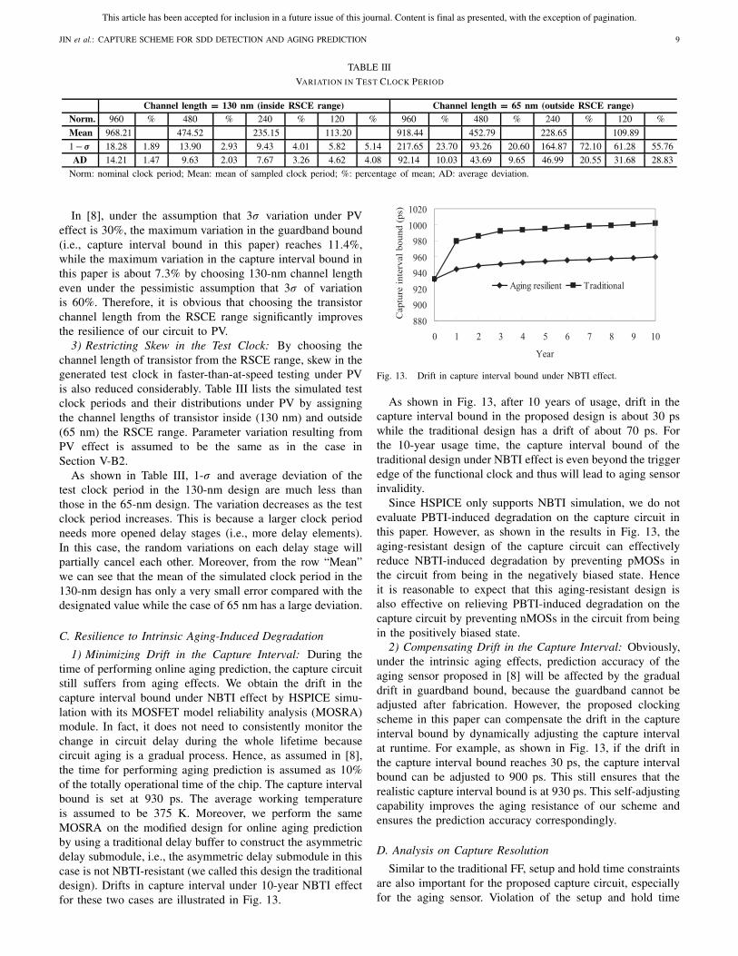
TABLE III
VARIATION IN TEST CLOCK PERIOD
Channel length = 130 nm (inside RSCE range) Channel length = 65 nm (outside RSCE range)Norm. 960 % 480 % 240 % 120 % 960 % 480 % 240 % 120 %
Mean 968.21 474.52 235.15 113.20 918.44 452.79 228.65 109.89
1 −σ 18.28 1.89 13.90 2.93 9.43 4.01 5.82 5.14 217.65 23.70 93.26 20.60 164.87 72.10 61.28 55.76
AD 14.21 1.47 9.63 2.03 7.67 3.26 4.62 4.08 92.14 10.03 43.69 9.65 46.99 20.55 31.68 28.83
Norm: nominal clock period; Mean: mean of sampled clock period; %: percentage of mean; AD: average deviation.
In [8], under the assumption that 3σ variation under PVeffect is 30%, the maximum variation in the guardband bound(i.e., capture interval bound in this paper) reaches 11.4%,while the maximum variation in the capture interval bound inthis paper is about 7.3% by choosing 130-nm channel lengtheven under the pessimistic assumption that 3σ of variationis 60%. Therefore, it is obvious that choosing the transistorchannel length from the RSCE range significantly improvesthe resilience of our circuit to PV.
3) Restricting Skew in the Test Clock: By choosing thechannel length of transistor from the RSCE range, skew in thegenerated test clock in faster-than-at-speed testing under PVis also reduced considerably. Table III lists the simulated testclock periods and their distributions under PV by assigningthe channel lengths of transistor inside (130 nm) and outside(65 nm) the RSCE range. Parameter variation resulting fromPV effect is assumed to be the same as in the case inSection V-B2.
As shown in Table III, 1-σ and average deviation of thetest clock period in the 130-nm design are much less thanthose in the 65-nm design. The variation decreases as the testclock period increases. This is because a larger clock periodneeds more opened delay stages (i.e., more delay elements).In this case, the random variations on each delay stage willpartially cancel each other. Moreover, from the row “Mean”we can see that the mean of the simulated clock period in the130-nm design has only a very small error compared with thedesignated value while the case of 65 nm has a large deviation.
C. Resilience to Intrinsic Aging-Induced Degradation
1) Minimizing Drift in the Capture Interval: During thetime of performing online aging prediction, the capture circuitstill suffers from aging effects. We obtain the drift in thecapture interval bound under NBTI effect by HSPICE simu-lation with its MOSFET model reliability analysis (MOSRA)module. In fact, it does not need to consistently monitor thechange in circuit delay during the whole lifetime becausecircuit aging is a gradual process. Hence, as assumed in [8],the time for performing aging prediction is assumed as 10%of the totally operational time of the chip. The capture intervalbound is set at 930 ps. The average working temperatureis assumed to be 375 K. Moreover, we perform the sameMOSRA on the modified design for online aging predictionby using a traditional delay buffer to construct the asymmetricdelay submodule, i.e., the asymmetric delay submodule in thiscase is not NBTI-resistant (we called this design the traditionaldesign). Drifts in capture interval under 10-year NBTI effectfor these two cases are illustrated in Fig. 13.
Fig. 13. Drift in capture interval bound under NBTI effect.
As shown in Fig. 13, after 10 years of usage, drift in thecapture interval bound in the proposed design is about 30 pswhile the traditional design has a drift of about 70 ps. Forthe 10-year usage time, the capture interval bound of thetraditional design under NBTI effect is even beyond the triggeredge of the functional clock and thus will lead to aging sensorinvalidity.
Since HSPICE only supports NBTI simulation, we do notevaluate PBTI-induced degradation on the capture circuit inthis paper. However, as shown in the results in Fig. 13, theaging-resistant design of the capture circuit can effectivelyreduce NBTI-induced degradation by preventing pMOSs inthe circuit from being in the negatively biased state. Henceit is reasonable to expect that this aging-resistant design isalso effective on relieving PBTI-induced degradation on thecapture circuit by preventing nMOSs in the circuit from beingin the positively biased state.
2) Compensating Drift in the Capture Interval: Obviously,under the intrinsic aging effects, prediction accuracy of theaging sensor proposed in [8] will be affected by the gradualdrift in guardband bound, because the guardband cannot beadjusted after fabrication. However, the proposed clockingscheme in this paper can compensate the drift in the captureinterval bound by dynamically adjusting the capture intervalat runtime. For example, as shown in Fig. 13, if the drift inthe capture interval bound reaches 30 ps, the capture intervalbound can be adjusted to 900 ps. This still ensures that therealistic capture interval bound is at 930 ps. This self-adjustingcapability improves the aging resistance of our scheme andensures the prediction accuracy correspondingly.
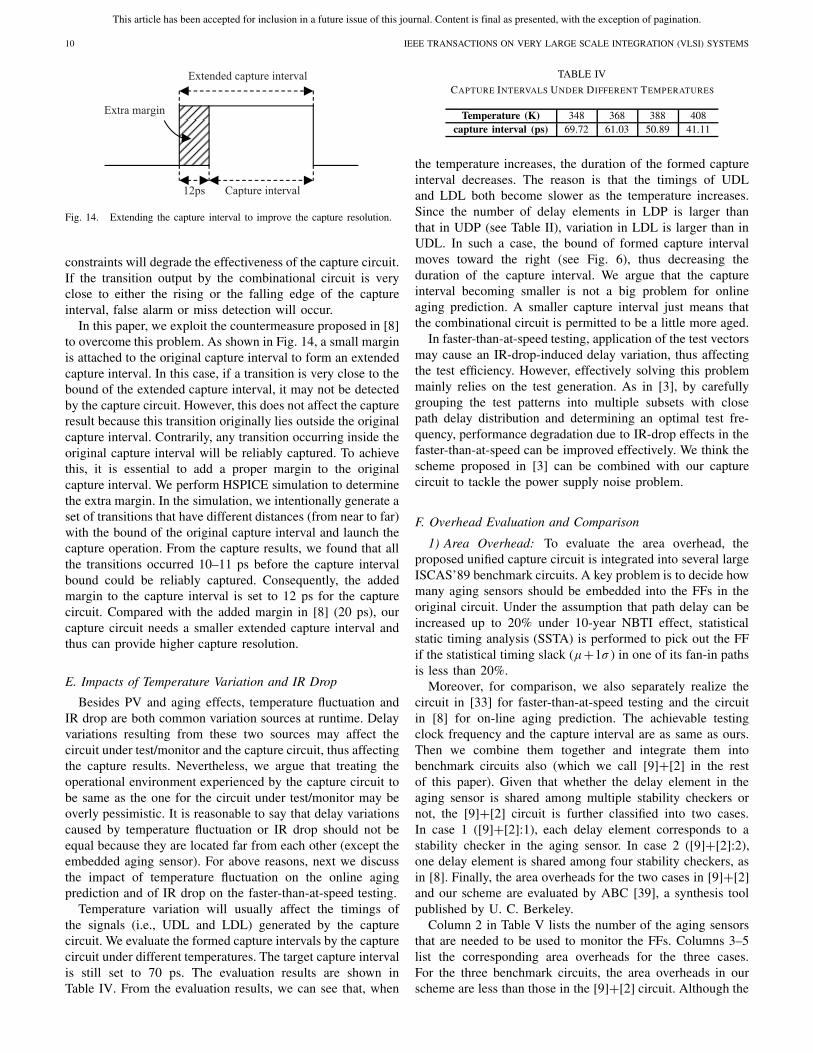
D. Analysis on Capture Resolution
Similar to the traditional FF, setup and hold time constraintsare also important for the proposed capture circuit, especiallyfor the aging sensor. Violation of the setup and hold time
This article has been accepted for inclusion in a future issue of this journal. Content is final as presented, with the exception of pagination.
10 IEEE TRANSACTIONS ON VERY LARGE SCALE INTEGRATION (VLSI) SYSTEMS
Fig. 14. Extending the capture interval to improve the capture resolution.
constraints will degrade the effectiveness of the capture circuit.If the transition output by the combinational circuit is veryclose to either the rising or the falling edge of the captureinterval, false alarm or miss detection will occur.
In this paper, we exploit the countermeasure proposed in [8]to overcome this problem. As shown in Fig. 14, a small marginis attached to the original capture interval to form an extendedcapture interval. In this case, if a transition is very close to thebound of the extended capture interval, it may not be detectedby the capture circuit. However, this does not affect the captureresult because this transition originally lies outside the originalcapture interval. Contrarily, any transition occurring inside theoriginal capture interval will be reliably captured. To achievethis, it is essential to add a proper margin to the originalcapture interval. We perform HSPICE simulation to determinethe extra margin. In the simulation, we intentionally generate aset of transitions that have different distances (from near to far)with the bound of the original capture interval and launch thecapture operation. From the capture results, we found that allthe transitions occurred 10–11 ps before the capture intervalbound could be reliably captured. Consequently, the addedmargin to the capture interval is set to 12 ps for the capturecircuit. Compared with the added margin in [8] (20 ps), ourcapture circuit needs a smaller extended capture interval andthus can provide higher capture resolution.
E. Impacts of Temperature Variation and IR Drop
Besides PV and aging effects, temperature fluctuation andIR drop are both common variation sources at runtime. Delayvariations resulting from these two sources may affect thecircuit under test/monitor and the capture circuit, thus affectingthe capture results. Nevertheless, we argue that treating theoperational environment experienced by the capture circuit tobe same as the one for the circuit under test/monitor may beoverly pessimistic. It is reasonable to say that delay variationscaused by temperature fluctuation or IR drop should not beequal because they are located far from each other (except theembedded aging sensor). For above reasons, next we discussthe impact of temperature fluctuation on the online agingprediction and of IR drop on the faster-than-at-speed testing.
Temperature variation will usually affect the timings ofthe signals (i.e., UDL and LDL) generated by the capturecircuit. We evaluate the formed capture intervals by the capturecircuit under different temperatures. The target capture intervalis still set to 70 ps. The evaluation results are shown inTable IV. From the evaluation results, we can see that, when
TABLE IV
CAPTURE INTERVALS UNDER DIFFERENT TEMPERATURES
Temperature (K) 348 368 388 408capture interval (ps) 69.72 61.03 50.89 41.11
the temperature increases, the duration of the formed captureinterval decreases. The reason is that the timings of UDLand LDL both become slower as the temperature increases.Since the number of delay elements in LDP is larger thanthat in UDP (see Table II), variation in LDL is larger than inUDL. In such a case, the bound of formed capture intervalmoves toward the right (see Fig. 6), thus decreasing theduration of the capture interval. We argue that the captureinterval becoming smaller is not a big problem for onlineaging prediction. A smaller capture interval just means thatthe combinational circuit is permitted to be a little more aged.
In faster-than-at-speed testing, application of the test vectorsmay cause an IR-drop-induced delay variation, thus affectingthe test efficiency. However, effectively solving this problemmainly relies on the test generation. As in [3], by carefullygrouping the test patterns into multiple subsets with closepath delay distribution and determining an optimal test fre-quency, performance degradation due to IR-drop effects in thefaster-than-at-speed can be improved effectively. We think thescheme proposed in [3] can be combined with our capturecircuit to tackle the power supply noise problem.
F. Overhead Evaluation and Comparison
1) Area Overhead: To evaluate the area overhead, theproposed unified capture circuit is integrated into several largeISCAS’89 benchmark circuits. A key problem is to decide howmany aging sensors should be embedded into the FFs in theoriginal circuit. Under the assumption that path delay can beincreased up to 20% under 10-year NBTI effect, statisticalstatic timing analysis (SSTA) is performed to pick out the FFif the statistical timing slack (μ+1σ ) in one of its fan-in pathsis less than 20%.
Moreover, for comparison, we also separately realize thecircuit in [33] for faster-than-at-speed testing and the circuitin [8] for on-line aging prediction. The achievable testingclock frequency and the capture interval are as same as ours.Then we combine them together and integrate them intobenchmark circuits also (which we call [9]+[2] in the restof this paper). Given that whether the delay element in theaging sensor is shared among multiple stability checkers ornot, the [9]+[2] circuit is further classified into two cases.In case 1 ([9]+[2]:1), each delay element corresponds to astability checker in the aging sensor. In case 2 ([9]+[2]:2),one delay element is shared among four stability checkers, asin [8]. Finally, the area overheads for the two cases in [9]+[2]and our scheme are evaluated by ABC [39], a synthesis toolpublished by U. C. Berkeley.
Column 2 in Table V lists the number of the aging sensorsthat are needed to be used to monitor the FFs. Columns 3–5list the corresponding area overheads for the three cases.For the three benchmark circuits, the area overheads in ourscheme are less than those in the [9]+[2] circuit. Although the
This article has been accepted for inclusion in a future issue of this journal. Content is final as presented, with the exception of pagination.
JIN et al.: CAPTURE SCHEME FOR SDD DETECTION AND AGING PREDICTION 11
TABLE V
AREA OVERHEAD AND POWER CONSUMPTION
Area (%) Power (%)circuit AS ours [9]+[2]:1 [9]+[2]:2 ours [9]+[2]:1 [9]+[2]:2s38584 294 1.16 6.83 3.29 1.1 0.8 0.6s38417 302 2.41 8.91 4.66 1.3 1.1 0.7s35932 327 2.23 8.65 4.21 1.5 1.3 1
area overhead in [9]+[2]:2 is smaller than that in [9]+[2]:1by sharing the delay element, it is still larger than ours.This demonstrates that by reusing the offline testing hardwarecircuit in online operation, the total area overhead is saved.
2) Power Consumption: We evaluate the increase in averagepower consumption during the online aging prediction byHSPICE simulation. The evaluation is performed by assumingthat all the embedded aging sensors work simultaneously. Thetime for performing aging prediction is assumed as 10% of thetotal operational time of the chip (10 years). The evaluationresults are listed in columns 6–8 of Table V.
The power is mainly induced by the transitions in the delaysubmodule. From the evaluation results we can see that thepower consumption in our scheme is a little larger than that inthe [9]+[2] circuit. This because the number of delay stagesthat the transition propagated in our capture circuit is largerthan that in the [9]+[2] circuit. However, the total powerincrease during online aging prediction is still negligible.
3) Performance Loss: Performance loss is induced by theembedded aging sensor, which adds extra load on the pathoutput. Similar as in [8], we evaluate the performance losstargeting a single path in HSPICE simulation by comparingthe path delay variation before and after inserting the agingsensor. The reported performance loss is only about 0.5%.
G. Discussion
1) Applicability of the Unified Capture Scheme: Delayvariation continuously exacerbates with the technology scal-ing and has a significant impact on the reliability of theshipped chip. Hence it is essential to detect SDDs duringthe fabrication testing stage as well as to monitor runtimedelay variations online. The proposed unified capture schemesupports both these goals with one suite of the hardwarecircuit. The implementation complexity in defect- or aging-related reliability design is significantly reduced. Meanwhile,the total area overhead consumed by offline and online circuitsis also saved. With the above stated merits, we believe that theproposed unified capture scheme will be quite promising.
The proposed capture scheme is mainly applicable to chipsthat rely on edge-triggered FF designs. Although the underly-ing capture circuit operates for the positive-edge- triggered FFdesign, it also can be applied to the negative-edge-triggered FFdesign by making a few of modifications. For example, if wereplace the NAND gate in the FMC unit (Fig. 4) with an AND
gate, launch and capture signals will be the falling transitionsaccording to UDL and LDL signals. Similarly, for online agingprediction, we just need to move the falling transition onLDL ahead of the falling edge of ACLK by adjusting theprogrammable delay difference (Fig. 6), the aging sensor canstill work as usual. FF-based design is common in the practical
ASIC or microprocessor, such as in [31]. So, we think theproposed capture scheme is practical and appropriate for manyindustry designs.
On the other hand, from the experimental evaluation, wecan see that implementation of the proposed capture circuitdoes not result in large overheads either on the silicon areaor on the power consumption. The data in Table V show thatthe power dissipated by the capture circuit is negligible, whilethe area overhead is only a little more than 2% for the circuitwith the tens of thousands of gates. For larger scale circuits,only the number of aging sensors will increase. Therefore, it isreasonable to say that the capture circuit is applicable for large-scale circuit in terms of the low area and power overheads.
The actual production environment is certainly differentfrom HSPICE simulation. We make the following suggestionson implementation of the proposed unified capture schemein a real IC. First, the RSCE ranges of pMOS and nMOSin a particular process can be obtained from the foundry.Second, the achieved delay difference of the programmabledelay submodule may need to be adjusted according to theresults in the first silicon debugging. This will facilitatethe proposed capture circuit to operate under the practicalparameter variability. Moreover, identification of critical pathshould also be performed at this phase. This can improve theaccuracy of the timing analysis and help identify the FFs thatare embedded with the aging sensor. Finally, test compressiontechniques [40], [41] can be combined with our scheme forreducing the test patterns in SDD detection.
2) Implementation in Traditional Design Flow: Implemen-tation of the proposed capture scheme needs a little modifica-tion on the traditional IC design flow. We propose a solution asfollows. First, besides the usual standard cells, some specificcells used to construct the capture circuit should be addedto the technology library. These specific cells include theaging-resistant delay element, FMC unit, nMOS stacks, andthe hybrid cell consisting of the aging sensor and the FF.Then, the netlists of the circuit under test/monitor and thecapture circuit can be mapped to the technology library byusing appropriate cells. Note that, in the mapping process, allthe FFs are still the traditional ones (i.e., without the embeddedaging sensor). After the timing analysis, paths under monitor(PUM) are identified according to the timing constraint. Atthis time, the FFs that are fed by the PUMs are replaced withthe hybrid cell (aging sensor + FF). The subsequent steps inIC design flow can remain unchanged. We think that such asolution will have minimal perturbation on the traditional ICdesign flow and hence is feasible.
VI. CONCLUSION
In this paper, we proposed a unified capture scheme tosupport both the faster-than-at-speed testing and online agingprediction. Unlike previous work, the underlying capture cir-cuit in this paper possesses asymmetric characteristic andoperates under a well-designed control mode. It can generateprogrammable clock signals that facilitate the achievement ofdifferent test clock frequencies in faster-than-at-speed testingas well as capture intervals in online aging prediction. Com-ponents in the underlying capture circuit are aging-resistant,
This article has been accepted for inclusion in a future issue of this journal. Content is final as presented, with the exception of pagination.
12 IEEE TRANSACTIONS ON VERY LARGE SCALE INTEGRATION (VLSI) SYSTEMS
which significantly reduces the drift in the capture intervalcaused by aging effects. By choosing the channel length of thetransistor from the RSCE range, the proposed capture circuitis resilient to PV. The proposed unified capture scheme can beeasily incorporated into the original clock distribution systemin the chip. It just adds multiplexers in clock distributionnodes to select the corresponding clock signals giving differentworking modes without changing the closed form of theoriginal clock distribution system.
One of our future objectives is to implement the proposedunified capture scheme in a test chip to validate the effective-ness in an actual production environment.
REFERENCES
[1] S. Menon, A. D. Sigh, and V. Agrawal, “Output hazard-free transitiondelay fault test generation,” in Proc. IEEE VLSI Test Symp., May 2009,pp. 97–102.
[2] T. Mak, A. Krstic, K. T. Cheng, and L.-C. Wang, “New challenges indelay testing of nanometer, multigigahertz designs,” IEEE Design TestComput., vol. 21, no. 3, pp. 241–248, May–Jun. 2004.
[3] N. Ahmed and M. Tehranipoor, “A novel faster-than-at-speed transition-delay test method considering IR-drop effects,” IEEE Trans. Comput.-Aided Design Integr. Circuits Syst., vol. 28, no. 10, pp. 1573–1582, Oct.2009.
[4] N. Ahmed, M. Tehranipoor, and V. Jayaram, “Timing-based delay testfor screening small delay defects,” in Proc. 43rd Ann. Design Autom.Conf., 2006, pp. 320–325.
[5] R. Tayade, S. Sundereswaran, and J. Abraham, “Small-delay defectdetection in the presence of process variations,” in Proc. 8th IEEE Int.Symp. Qual. Electron Design, Mar. 2007, pp. 711–716.
[6] M. Amodeo and B. Cory, Beyond At-Speed. Springfield, MO: TestMeasurement World, 2005.
[7] International Technology Roadmap for Semiconductors. (2005) [Online].Available: http://www.itrs.net/
[8] M. Agarwal, B. C. Paul, Z. Ming, and S. Mitra, “Circuit failureprediction and its application to transistor aging,” in Proc. 25th IEEEVLSI Test Symp., May 2007, pp. 277–286.
[9] M. Agarwal, V. Balakrishnan, A. Bhuyan, K. Kyunglok, B. C. Paul,W. Wenping, Y. Bo, C. Yu, and S. Mitra, “Optimized circuit failureprediction for aging: Practicality and promise,” in Proc. IEEE Int. TestConf., Oct. 2008, pp. 1–10.
[10] G. Yan, Y. Han, and X. Li, “A unified online fault detection scheme viachecking of stability violation,” in Proc. Conf. Design Autom. Test Eur.,2009, pp. 20–24.
[11] J. Keane, T. H. Kim, and C. H. Kim, “An on-chip NBTI sensor formeasuring PMOS threshold voltage degradation,” IEEE Trans. VeryLarge Scale Integr. (VLSI) Syst., vol. 18, no. 6, pp. 947–956, Jun. 2010.
[12] K. Zhao, J. H. Stathis, B. P. Linder, E. Cartier, and A. Kerber, “PBTIunder dynamic stress: From a single defect point of view,” in Proc. IEEEInt. Rel. Phys. Symp., Apr. 2011, pp. 4A.3.1–4A.3.9.
[13] E. Cartier, B. P. Linder, V. Narayanan, and V. K. Paruchuri, “Fundamen-tal understanding and optimization of PBTI in nFETs with SiO2/HfO2gate-stack,” in Proc. IEEE IEDM, Dec. 2006, pp. 1–4.
[14] B. C. Paul, K. Kang, H. Kufluoglu, M. A. Alam, and K. Roy, “Tem-poral performance degradation under NBTI: Estimation and design forimproved reliability of nanoscale circuits,” in Proc. Design Autom. TestEur., 2006, pp. 1–6.
[15] Y. Wang, H. Luo, K. He, R. Luo, H. Yang, and Y. Xie, “Temperature-aware NBTI modeling and the impact of input vector control onperformance degradation,” in Proc. IEEE Design Autom. Test Eur., Apr.2007, pp. 1–6.
[16] W. Wang, Z. Wei, S. Yang, and Y. Cao, “An efficient method to identifycritical gates under circuit aging,” in Proc. IEEE Int. Conf. Comut.-AidedDesign, Nov. 2007, pp. 735–740.
[17] W. Wang, V. Reddy, Y. Bo, V. Balakrishnan, S. Krishnan, and C. Yu,“Statistical prediction of circuit aging under process variations,” in Proc.IEEE Custom Integr. Circuits Conf., Sep. 2008, pp. 13–16.
[18] L. Yinghai, S. Li, Z. Hai, Z. Hengliang, Y. Fan, and Z. Xuan, “Statisticalreliability analysis under process variation and aging effects,” in Proc.Design Autom. Conf., Aug. 2009, pp. 514–519.
[19] W. Wang, S. Yang, S. Bhardwaj, R. Vattikonda, S. Vrudhula, F. Liu,and Y. Cao, “The impact of NBTI on the performance of combinationaland sequential circuits,” in Proc. 44th IEEE Design Autom. Conf., Jun.2007, pp. 364–369.
[20] S. V. Kumar, K. H. Kim, and S. S. Sapatnekar, “Impact of NBTI onSRAM read stability and design for reliability,” in Proc. 7th Int. Symp.Qual. Electron. Design, Mar. 2006, pp. 213–218.
[21] S. V. Kumar, C. H. Kim, and S. S. Sapatnekar, “NBTI-aware synthesis ofdigital circuits,” in Proc. Design Autom. Conf., Jun. 2007, pp. 370–375.
[22] R. Vattikonda, W. Wang, and Y. Cao, “Modeling and minimization ofPMOS NBTI effect for robust nanometer design,” in Proc. 43rd IEEEDesign Autom. Conf., Jul. 2006, pp. 1047–1052.
[23] S. Mitra, “Globally optimized robust systems to overcome scaled CMOSchallenges,” in Proc. IEEE Design Autom. Test Eur., Mar. 2008, pp. 941–946.
[24] H. Dadgour and K. Banerjee, “Aging-resilient design of pipelinedarchitectures using novel detection and correction circuits,” in Proc.Design Autom. Test Eur. Conf. Exhibit., Mar. 2010, pp. 244–249.
[25] J. C. Vazquez, V. Champac, I. C. Teixeira, M. B. Santos, and J. P.Teixeira, “Programmable aging sensor for automotive safety-criticalapplications,” in Proc. IEEE Design Autom. Test Eur. Conf. Exhibit.,Mar. 2010, pp. 618–621.
[26] W. Qiu, W. Jing, D. M. H. Walker, D. Reddy, L. Xiang, L. Zhuo, S.Weiping, and H. Balachandran, “K longest paths per-gate (KLPG) testgeneration for scan-based sequential circuits,” in Proc. IEEE Int. TestConf., Oct. 2004, pp. 223–231.
[27] Y. Sato, S. Hamada, and T. Maeda, “Invisible delay quality–SDQLmodel lights up what could not be seen,” in Proc. IEEE Int. Test Conf.,Nov. 2005, no. 47.1, pp. 1–9.
[28] M. Yilmaz, K. Chakrabarty, and M. Tehranipoor, “Test-pattern gradingand pattern selection for small-delay defects,” in Proc. 26th IEEE VLSITest Symp., May 2008, pp. 233–239.
[29] H. Yan and A. D. Singh, “Experiments in detecting delay faults usingmultiple higher frequency clocks and results from neighboring die,” inProc. IEEE Int. Test Conf., Oct. 2003, pp. 105–111.
[30] H. Nakamura, A. Shirokane, Y. Nishizaki, A. Uzzaman, V. Chickermane,B. Keller, T. Ube, and Y. Terauchi, “Low cost testing of nanometer SoCsusing on-chip clocking and test compression,” in Proc. 14th IEEE AsianTest Symp., Dec. 2005, pp. 156–161.
[31] T. McLaurin and F. Fredrick, “The testability features of the MCF5407containing the 4th generation coldfire microprocessor core,” in Proc. Int.Test Conf., 2000, pp. 151–159.
[32] S. Pei, H. Li, and X. Li, “An on-chip clock generation scheme for faster-than-at-speed delay testing,” in Proc. IEEE Design Autom. Test Eur.Conf. Exhibit., Mar. 2010, pp. 1353–1356.
[33] R. Tayade and J. A. Abraham, “On-chip programmable capture foraccurate path delay test and characterization,” in Proc. IEEE Int. TestConf., Oct. 2008, pp. 1–10.
[34] A. Torkel and S. Roland, “Time delay line with low sensitivity to processvariations,” U.S. Patent 0 079 487, Mar. 26, 2009.
[35] W. Zhao and Y. Cao, “New generation of predictive technology modelfor sub-45 nm early design explorations,” IEEE Trans. Electron Devices,vol. 53, no. 11, pp. 2816–2823, Nov. 2006.
[36] N. Ahmed, C. P. Ravikumar, M. Tehranipoor, and J. Plusquellic, “At-speed transition fault testing with low speed scan enable,” in Proc. 23rdIEEE VLSI Test Symp., May 2005, pp. 42–47.
[37] S. Wang, X. Liu, and S. T. Chakradhar, “Hybrid delay scan: A low hard-ware overhead scan-based delay test technique for high fault coverageand compact test sets,” in Proc. IEEE Design Autom. Test Eur. Conf.Exhibit., Feb. 2004, pp. 1296–1301.
[38] G. Xu and A. D. Singh, “Achieving high transition delay fault coveragewith partial DTSFF scan chains,” in Proc. IEEE Int. Test Conf., Oct.2007, pp. 1–9.
[39] ABC: A System for Sequential Synthesis and Verification. Berkeley LogicSynthesis and Verification Group, Berkeley, CA [Online]. Available:http://www.eecs.berkeley.edu/∼alanmi/abc/
[40] Y. Han, Y. Hu, X. Li, H. Li, and A. Chandra, “Embedded test decom-pressor to reduce the required channels and vector memory of tester forcomplex processor circuit,” IEEE Trans. Very Large Scale Integr. (VLSI)Syst., vol. 15, no. 5, pp. 531–540, May 2007.
[41] Y. Han, X. Li, H. Li, and A. Chandra, “Test resource partitioningbased on efficient response compaction for test timer and tester channelsreduction,” J. Comput. Sci. Technol., vol. 20, no. 2, pp. 201–209, Mar.2005.
This article has been accepted for inclusion in a future issue of this journal. Content is final as presented, with the exception of pagination.
JIN et al.: CAPTURE SCHEME FOR SDD DETECTION AND AGING PREDICTION 13
Song Jin received the Ph.D. degree in computer science from the Instituteof Computing Technology, Chinese Academy of Sciences, Beijing, China, in2011.
He is currently an Assistant Professor with the Department of Electronicand Communication Engineering, School of Electrical and Electronic Engi-neering, North China Electric Power University, Baoding, China. His currentresearch interests include VLSI design and testing and computer architecture,with emphasis on design for reliability and variation tolerance.
Yinhe Han (M’06) received the B.Eng. degree from the Nanjing Universityof Aeronautics and Astronautics, Nanjing, China, in 2001, and the M.Eng.and Ph.D. degrees in computer science from the Institute of ComputingTechnology (ICT), Chinese Academy of Sciences, Beijing, China, in 2003and 2006, respectively.
He is currently an Associate Professor at ICT. His current research interestsinclude VLSI design and testing, reliable system, and architecture.
Dr. Han was a recipient of the Test Technology Technical Council BestPaper Award from the Asian Test Symposium in 2003. He is a member ofthe Association for Computing Machinery and the Institute of Electronics,Information and Communication Engineers.
Huawei Li (M’00–SM’09) received the B.S. degree in computer sciencefrom Xiangtan University, Xiangtan, China, in 1996, and the M.S. and Ph.D.degrees from the Institute of Computing Technology (ICT), Chinese Academyof Sciences, Beijing, China, in 1999 and 2001, respectively.
She is currently a Professor at ICT. Her current research interests includeVLSI and SoC design verification and test generation, delay testing, anddependable computing.
Prof. Li has been serving as Secretary General of the China ComputerFederation Technical Committee on Fault Tolerant Computing since 2008.She also served as Program Chair of the IEEE Asian Test Symposium in2007 and the IEEE Workshop on RTL and High Level Testing in 2003.
Xiaowei Li (SM’04) received the B.Eng. and M.Eng. degrees in computerscience from the Hefei University of Technology, Hefei, China, in 1985 and1988, respectively, and the Ph.D. degree in computer science from the Instituteof Computing Technology (ICT), Chinese Academy of Sciences, Beijing,China, in 1991.
He was with the Department of Computer Science, Peking University,Beijing, as an Assistant Professor from 1991 to 2000 and an AssociateProfessor since 1993. He joined at ICT as a Professor in 2000. He is currentlythe Deputy (Executive) Director of the State Key Laboratory of ComputerArchitecture, ICT. He has co-authored over 200 papers in published academicjournals and international conference proceedings and holds 34 patents and35 software copyrights. His current research interests include VLSI testing,design verification, and dependable computing.
Prof. Li has been serving as Chair of the China Computer FederationTechnical Committee on Fault Tolerant Computing since 2008, the IEEE AsianPacific Regional Test Technology Technical Council Vice Chair since 2004,and the Steering Committee Chair of the IEEE Asian Test Symposium since2011. In addition, he serves on the Technical Program Committees of severalIEEE and Association for Computing Machinery conferences, including VTS,DATE, ASP-DAC, and PRDC. He also serves as an Editorial Board Memberof JCST, JETTA, and JOLPE.