Understanding the Impact of the Doping Profiles on Selective Emitter Solar Cell by Two-Dimensional...
9
IEEE JOURNAL OF PHOTOVOLTAICS, VOL. 3, NO. 1, JANUARY 2013 159 Understanding the Impact of the Doping Profiles on Selective Emitter Solar Cell by Two-Dimensional Numerical Simulation Raffaele De Rose, Mauro Zanuccoli, Paolo Magnone, M. Frei, Enrico Sangiorgi, Fellow, IEEE, and Claudio Fiegna Abstract—The selective emitter (SE) design, featuring lower doped areas between the front contact fingers and higher doped areas underneath the front metallization, is crucial to improve the performance at the front side of a monocrystalline (c-Si) sili- con solar cell. One of the most interesting and promising low-cost SE process consists of the screen printing of a phosphorus-doped paste, allowing a separate optimization of the doping profiles in the metallized and nonmetallized front-side areas. By referring to this kind of process, this paper presents a simulation study with a decoupled analysis on the effect of the lowly doped and highly doped profiles on the performance of an SE solar cell, by means of 2-D electro-optical numerical device simulations. Moreover, by exploiting the 2-D modeling, the effect of the alignment tolerance used in the SE diffusion process for the subsequent metallization process has been also investigated. Numerical results show that the adoption of an optimized design for the SE cell can lead to an ef- ficiency improvement above 0.4% abs compared with the 75 Ω/sq homogeneous emitter reference cell. Index Terms—Doping profile, numerical simulation, selective emitter (SE), solar cell. I. INTRODUCTION T HE improvement in the front-side emitter is currently an important issue for the optimization of the silicon (Si) so- lar cell technological process. The emitter requires high lateral conductance to achieve a low series resistance contribution at the front side. Nevertheless, emitter recombination losses limit cell performance and become increasingly dominant with the improvement of the rear side due to the forthcoming adoption Manuscript received January 31, 2012; revised August 2, 2012; accepted August 3, 2012. Date of publication September 28, 2012; date of current ver- sion December 19, 2012. This work was supported in part by Nanofunction Network of Excellence Project funded by the European Commission under the Seventh Framework Program and the ERG Project funded by the European Na- noelectronics Initiative Advisory Council Joint Undertaking under Grant 2010/ 270722-2. R. De Rose is with the Advanced Research Center on Electronic Systems, Department of Electrical, Electronics and Information Engineering, University of Bologna, I-47521 Cesena, Italy, and also with the Department of Electronics, Computer Science and Systems, University of Calabria, 87036 Rende, Italy (e-mail: [email protected]). M. Zanuccoli, P. Magnone, E. Sangiorgi, and C. Fiegna are with the Advanced Research Center on Electronic Systems, Department of Electri- cal, Electronic, and Information Engineering, University of Bologna, I-47521 Cesena, Italy (e-mail: [email protected]; [email protected]; [email protected]; cfi[email protected]). M. Frei is with Applied Materials, Inc., Santa Clara, CA 95054-3299 USA (e-mail: [email protected]). Color versions of one or more of the figures in this paper are available online at http://ieeexplore.ieee.org. Digital Object Identifier 10.1109/JPHOTOV.2012.2214376 Fig. 1. Two-dimensional cross section of the SE solar cell. W sub and D sub denote the front contact pitch and the substrate thickness, respectively. W m is the width of the front contact finger, while W se represents the lateral width of the HDOP region. It is worth mentioning that the lateral size of the 2-D simulated device has been limited to half of the depicted structure. of a rear point contact design with passivated rear surfaces in most of the industrial Si solar cells [1]. Since transport and recombination mechanisms are strongly coupled in the semi- conductor equations, the emitter design results in a strategic tradeoff between these physical phenomena for the performance of a solar cell. The development of technological solutions to contact emitters with a high sheet resistance (>80 Ω/sq), such as the optimization of the silver (Ag) pastes [2]–[4] and/or the so-called seed-and-plate approach [5]–[7], is a challenging task in photovoltaic industry for further optimization of the emitter, but it could be limited by a narrower firing window or by the application of an additional (plating) step [8]. However, such technological solutions to contact high sheet resistance emitter are not industrially available yet. An alternative and promising approach to improve the emit- ter performance is the realization of a selective emitter (SE) design. SE solar cells, in contrast with standard screen-printed industrial c-Si cells based on an homogeneously diffused emit- ter (HE), feature different doping profiles in the metallized and nonmetallized front-side areas (see Fig. 1): While a highly doped (HDOP) profile under the metal-contacted regions en- sures a good ohmic metal–semiconductor contact (achieving a low contact resistance) and an adequate lateral conductivity, a lowly doped (LDOP) profile in the illuminated passivated re- gions between the front contact fingers leads to a reduction of Auger and surface recombination losses and, consequently, in an enhanced spectral response in the blue region of the spec- trum [8]–[10]. However, an efficiency tradeoff exists between 2156-3381/$31.00 © 2012 IEEE
-
Upload
chikirin-gronlund -
Category
Documents
-
view
42 -
download
0
description
Paper explaining the understanding the Impact of the Doping Profiles on Selective Emitter Solar Cell by Two-Dimensional Numerical Simulation
Transcript of Understanding the Impact of the Doping Profiles on Selective Emitter Solar Cell by Two-Dimensional...
IEEE JOURNAL OF PHOTOVOLTAICS, VOL. 3, NO. 1, JANUARY 2013 159
Understanding the Impact of the Doping Profiles onSelective Emitter Solar Cell by Two-Dimensional
Numerical SimulationRaffaele De Rose, Mauro Zanuccoli, Paolo Magnone, M. Frei, Enrico Sangiorgi, Fellow, IEEE, and Claudio Fiegna
Abstract—The selective emitter (SE) design, featuring lowerdoped areas between the front contact fingers and higher dopedareas underneath the front metallization, is crucial to improvethe performance at the front side of a monocrystalline (c-Si) sili-con solar cell. One of the most interesting and promising low-costSE process consists of the screen printing of a phosphorus-dopedpaste, allowing a separate optimization of the doping profiles inthe metallized and nonmetallized front-side areas. By referring tothis kind of process, this paper presents a simulation study witha decoupled analysis on the effect of the lowly doped and highlydoped profiles on the performance of an SE solar cell, by meansof 2-D electro-optical numerical device simulations. Moreover, byexploiting the 2-D modeling, the effect of the alignment toleranceused in the SE diffusion process for the subsequent metallizationprocess has been also investigated. Numerical results show that theadoption of an optimized design for the SE cell can lead to an ef-ficiency improvement above 0.4%abs compared with the 75 Ω/sqhomogeneous emitter reference cell.
Index Terms—Doping profile, numerical simulation, selectiveemitter (SE), solar cell.
I. INTRODUCTION
THE improvement in the front-side emitter is currently animportant issue for the optimization of the silicon (Si) so-
lar cell technological process. The emitter requires high lateralconductance to achieve a low series resistance contribution atthe front side. Nevertheless, emitter recombination losses limitcell performance and become increasingly dominant with theimprovement of the rear side due to the forthcoming adoption
Manuscript received January 31, 2012; revised August 2, 2012; acceptedAugust 3, 2012. Date of publication September 28, 2012; date of current ver-sion December 19, 2012. This work was supported in part by NanofunctionNetwork of Excellence Project funded by the European Commission under theSeventh Framework Program and the ERG Project funded by the European Na-noelectronics Initiative Advisory Council Joint Undertaking under Grant 2010/270722-2.
R. De Rose is with the Advanced Research Center on Electronic Systems,Department of Electrical, Electronics and Information Engineering, Universityof Bologna, I-47521 Cesena, Italy, and also with the Department of Electronics,Computer Science and Systems, University of Calabria, 87036 Rende, Italy(e-mail: [email protected]).
M. Zanuccoli, P. Magnone, E. Sangiorgi, and C. Fiegna are with theAdvanced Research Center on Electronic Systems, Department of Electri-cal, Electronic, and Information Engineering, University of Bologna, I-47521Cesena, Italy (e-mail: [email protected]; [email protected];[email protected]; [email protected]).
M. Frei is with Applied Materials, Inc., Santa Clara, CA 95054-3299 USA(e-mail: [email protected]).
Color versions of one or more of the figures in this paper are available onlineat http://ieeexplore.ieee.org.
Digital Object Identifier 10.1109/JPHOTOV.2012.2214376
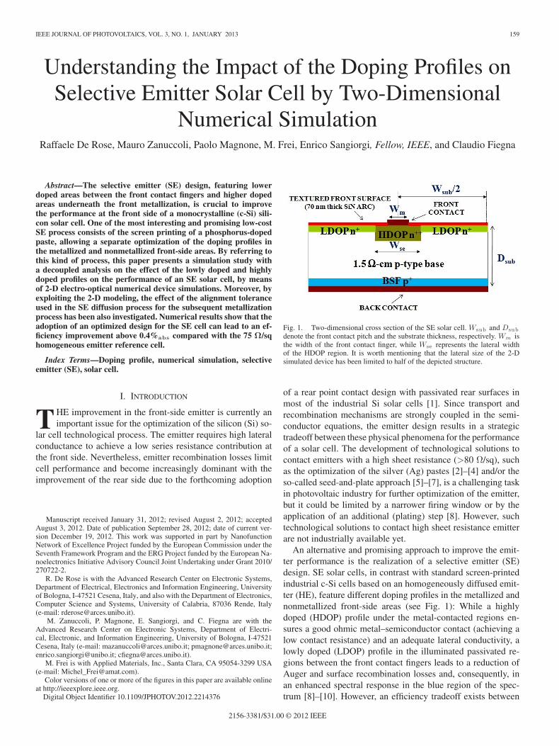
Fig. 1. Two-dimensional cross section of the SE solar cell. Wsub and Dsubdenote the front contact pitch and the substrate thickness, respectively. Wm isthe width of the front contact finger, while Wse represents the lateral widthof the HDOP region. It is worth mentioning that the lateral size of the 2-Dsimulated device has been limited to half of the depicted structure.
of a rear point contact design with passivated rear surfaces inmost of the industrial Si solar cells [1]. Since transport andrecombination mechanisms are strongly coupled in the semi-conductor equations, the emitter design results in a strategictradeoff between these physical phenomena for the performanceof a solar cell. The development of technological solutions tocontact emitters with a high sheet resistance (>80 Ω/sq), suchas the optimization of the silver (Ag) pastes [2]–[4] and/or theso-called seed-and-plate approach [5]–[7], is a challenging taskin photovoltaic industry for further optimization of the emitter,but it could be limited by a narrower firing window or by theapplication of an additional (plating) step [8]. However, suchtechnological solutions to contact high sheet resistance emitterare not industrially available yet.
An alternative and promising approach to improve the emit-ter performance is the realization of a selective emitter (SE)design. SE solar cells, in contrast with standard screen-printedindustrial c-Si cells based on an homogeneously diffused emit-ter (HE), feature different doping profiles in the metallized andnonmetallized front-side areas (see Fig. 1): While a highlydoped (HDOP) profile under the metal-contacted regions en-sures a good ohmic metal–semiconductor contact (achieving alow contact resistance) and an adequate lateral conductivity, alowly doped (LDOP) profile in the illuminated passivated re-gions between the front contact fingers leads to a reduction ofAuger and surface recombination losses and, consequently, inan enhanced spectral response in the blue region of the spec-trum [8]–[10]. However, an efficiency tradeoff exists between
2156-3381/$31.00 © 2012 IEEE
160 IEEE JOURNAL OF PHOTOVOLTAICS, VOL. 3, NO. 1, JANUARY 2013
these advantages and the increased emitter resistance that af-fects the SE solar cells due to the lower doping concentration inthe nonmetallized areas.
The use of SE has become one of the most interesting low-cost concepts to boost efficiency of Si solar cells. Indeed, ithas already been demonstrated that a wide variety of processschemes, which are ready for industrial implementation, canbe adopted to form an SE and, then, to enhance the perfor-mance of a c-Si solar cell without a relevant increase in pro-duction costs [8]. Among these methods, it is worth mentioningthe selective laser doping from phosphorus silicate glass [9],the etch-back process [11], the diffusion masking [12], etc.One of the most interesting and promising low-cost SE pro-cess is based on the use of a screen-printable phosphorus-dopedpaste [13], [14]. An important advantage of using this tech-nique is its ability to selectively form HDOP regions withoutthe need for laser patterning, diffusion mask, or etch-back pro-cess. Indeed, this process consists of the screen printing of adopant paste with the same pattern as the metallization, the fir-ing of the paste, and, then, the subsequent printing of the frontmetallization over the HDOP regions (requiring a good align-ment). Moreover, as demonstrated in [14], this SE process pro-vides additional degrees of freedom to optimize the LDOP andHDOP emitters independently, achieving an efficiency improve-ment in the range of 0.3–0.7%abs compared with the baselineprocess.
By considering this kind of SE process, the aim of this paperis to perform a simulation study with a decoupled analysis of theinfluence of the LDOP and HDOP profiles on the performanceof a c-Si SE solar cell. In this paper, we expand the analysisdone in [15] by discussing the impact of LDOP profile on SEsolar cell performance, by extending the comparison betweenthe SE and HE solar cells also in terms of spectral response andby investigating in more detail the impact of the dominant re-combination mechanisms in the emitter region through a carefuldark loss analysis. Unlike some previous works [10], [16], [17],where the impact of the emitter doping profile was analyzedby using a 1-D analytical or numerical modeling, we perform2-D numerical simulations using a state-of-the-art numericalTCAD simulator [18] coupled to an in-house optical simulatorthat provides the 2-D map of the optical generation rate insidethe solar cell. The 2-D approach is mandatory to account forthe shadowing losses underneath the front metallization, to dis-tinguish the front-side passivated and metallized areas, and, incase of SE design, to differentiate the local front-side dopingproperties. This allows us to better model the physical mech-anisms occurring inside the device (and, in particular, in theemitter region), mainly in terms of doping-dependent bulk andsurface recombination and of 2-D lateral carrier transport. Thecomparison with a reference 75-Ω/sq HE solar cell allows usto quantitatively evaluate the expected performance improve-ments. Moreover, thanks to the 2-D modeling, we are able toconsider the effect on the SE cell performance of the alignmenttolerance used in the SE diffusion process for the subsequentmetallization process, leading to broad HDOP dopant lines. Inthis regard, we estimate the benefit achievable by reducing theHDOP lateral width in the SE cell.
The remainder of this paper is organized as follows. Thegeometrical and physical details of the simulated solar cells andthe simulation methodology are first discussed in Section II.In Section III, the effect of the doping profile in the passivatedLDOP regions at different front contact pitch values is analyzed.Then, the impact of the doping profile in the metal-contactedHDOP areas is investigated in Section IV. After that, SectionV reports a quantitative analysis of the effect of the alignmenttolerances used in SE diffusion. Finally, the main results of thework are summarized in Section VI.
II. SIMULATION METHODOLOGY
A two-busbar 12.5 cm × 12.5 cm monocrystalline solarcell has been simulated with the following characteristics (seeFig. 1): a 1.5-Ω·cm (Nbase = 1016 cm−3), 180-μm-thick boron-doped p-type base with a full-area metallized aluminum-alloyedback surface field (Al-p+ BSF) modeled with a typical 10-μm-deep profile reported in [19]; a front surface covered with a70-nm-thick silicon nitride (SiNx ) antireflective coating layer;and a silver front finger with a width Wm of 100 μm. The frontside of the SE solar cell is also characterized by the lateralwidth of the HDOP region (Wse) and by the front contact pitch(Wsub). By exploiting the symmetry of the device, the lateralsize of the 2-D simulation domain has been limited to half ofthe front contact pitch.
In order to achieve realistic predictions on c-Si cell perfor-mance, an ad-hoc calibration of the physical models and pa-rameters implemented in the TCAD simulator has been per-formed [20]. These fine-tuned models include the bandgap nar-rowing (BGN) model by Schenk to account for the effectiveintrinsic carrier density [21], the Auger recombination modelwith the parameterization adopted by Altermatt in [22], the mo-bility model proposed by Klaassen [18], [23], [24], and the bulkShockley–Read–Hall (SRH) lifetime model in boron-doped Cz-Si according to Glunz’s parameterization [25] and in Al-p+
Cz-Si according to Altermatt’s parameterization [19]. UsingAltermatt’s parameterization for the SRH lifetime in the Al-BSF, we obtain a BSF saturation current density of J0,BSF ≈590 fA/cm2 , similar to the typically measured values [19]. Thebandgap model parameters are adjusted to achieve an intrinsiccarrier density of 9.65 × 109 cm−3 at 300 K and low dopingdensity [26]. According to the adopted SRH lifetime model inthe substrate [25], we obtain a bulk minority carrier lifetime ofabout 206 μs for the considered substrate doping. Fermi–Diracstatistics has been implemented to adequately model the HDOPregions, such as the emitter and the BSF. According to the ap-plied model for BGN and to Fermi–Dirac statistics, we adoptthe parameterization proposed by Kimmerle et al. in [27] forthe surface recombination velocity (SRV) at SiNx -passivatedfront surface, assuming an Auger-limited lifetime in the emitterbulk and a chemical phosphorus surface concentration depen-dence for the SRV. The SRV at the metallized surfaces is setto 106 cm/s.
In addition to the electrical simulation, optical generationrate profiles have been calculated with a monodimensional sim-ulation of plane waves propagation in silicon, assuming direct
DE ROSE et al.: UNDERSTANDING THE IMPACT OF THE DOPING PROFILES ON SELECTIVE EMITTER SOLAR CELL 161
illumination with a standard AM1.5G spectrum (1000 W/m2)and ideal shadowing under front metal fingers and accountingfor a random pyramids textured SiNx front surface. It is worthnoting that the electrical simulation does not account for the sur-face texturing. Moreover, some of the adopted models, like theSRV model, are extracted for planar surfaces. Therefore, it is ex-pected that the implementation of the texturing in the electricalsimulations and the update of the physical models to representtextured surfaces may lead to a decrease of the performance ofthe simulated devices, mainly due to an increase of the surfacerecombination losses and to an increased emitter resistance.
The calculated electrical cell parameters include the short-circuit current density Jsc , the open-circuit voltage Voc , the fillfactor (FF), and the efficiency η. A postprocessing analysis hasbeen performed on the simulated I−V curves to account forthe losses due to the parasitic series resistance R of the frontcontact according to the following expressions [28], [29]:
Rc =12
ρc
Lm · LTcoth
(Wm /2
LT
)(1)
Rm =13· ρm · Lm
Hm · Wm(2)
R = Rc + Rm (3)
PM = PM 0 − I2MP · R (4)
where Rc is the metal–semiconductor contact resistance, ρc
is the specific front contact resistivity, LT =√
(ρc/Rsq) is thetransport length that is a function of both ρc and the emitter sheetresistance Rsq [30], Rm is the metal finger resistance, ρm = 6 ×10⁻⁶ Ω·cm is the front metal resistivity, Lm = 3 cm is the fingerlength, Hm = 12 μm is the finger thickness, IMP is the current atthe maximum power point, PM0 is the maximum output powerwithout the resistance losses, and PM is the effective maximumoutput power. The effect of the full-area back contact is notaccounted because it is a “vertical” contact (i.e., in which thecurrent flows vertically) and, then, its entire area is active [30].In (1), the contact resistance is calculated by considering themetal finger composed of two parallel metals featuring a widthof Wm /2, which account for the current coming from the twosides of the finger. Since the parallel of two identical resistancesis considered, we introduce a factor 1/2 in (1).
Concerning the specific front contact resistivity, it is worthconsidering that it depends on the surface concentration, accord-ing to Schroder and Meier [30]. However, it has been demon-strated in [31] and [32] that the contact resistivity of screen-printed silver contacts depends not only on the surface dopingconcentration, but also on several other process-dependent fac-tors related to the contact formation. In particular, ρc is mainlylimited by the number and the size of the silver crystals growninto the emitter, i.e., by the silver crystal covered surface areaand by the current paths from the silver crystals to the bulk ofthe finger [31]. In addition, it has been reported that the sur-face texture, leading to a pyramidal shape of the silver crystal,influences the contact resistance on emitters with high sheetresistance [32].
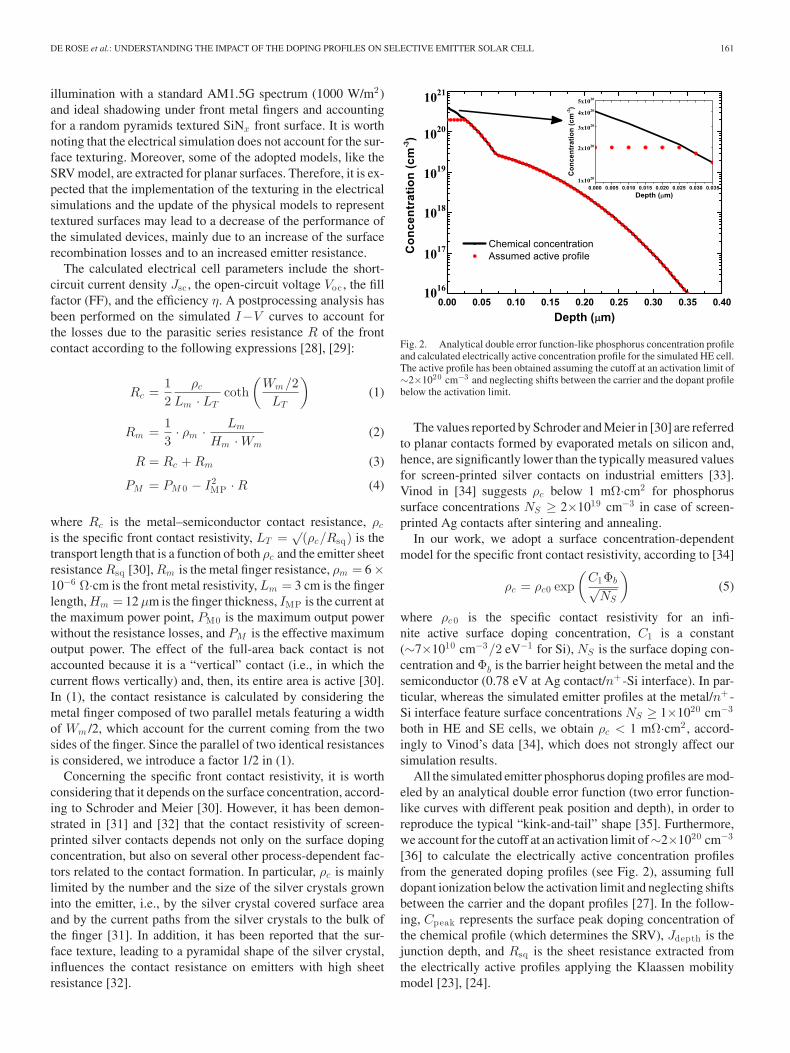
Fig. 2. Analytical double error function-like phosphorus concentration profileand calculated electrically active concentration profile for the simulated HE cell.The active profile has been obtained assuming the cutoff at an activation limit of∼2×1020 cm−3 and neglecting shifts between the carrier and the dopant profilebelow the activation limit.
The values reported by Schroder and Meier in [30] are referredto planar contacts formed by evaporated metals on silicon and,hence, are significantly lower than the typically measured valuesfor screen-printed silver contacts on industrial emitters [33].Vinod in [34] suggests ρc below 1 mΩ·cm2 for phosphorussurface concentrations NS ≥ 2×1019 cm−3 in case of screen-printed Ag contacts after sintering and annealing.
In our work, we adopt a surface concentration-dependentmodel for the specific front contact resistivity, according to [34]
ρc = ρc0 exp(
C1Φb√NS
)(5)
where ρc0 is the specific contact resistivity for an infi-nite active surface doping concentration, C1 is a constant(∼7×1010 cm−3/2 eV−1 for Si), NS is the surface doping con-centration and Φb is the barrier height between the metal and thesemiconductor (0.78 eV at Ag contact/n+ -Si interface). In par-ticular, whereas the simulated emitter profiles at the metal/n+ -Si interface feature surface concentrations NS ≥ 1×1020 cm−3
both in HE and SE cells, we obtain ρc < 1 mΩ·cm2 , accord-ingly to Vinod’s data [34], which does not strongly affect oursimulation results.
All the simulated emitter phosphorus doping profiles are mod-eled by an analytical double error function (two error function-like curves with different peak position and depth), in order toreproduce the typical “kink-and-tail” shape [35]. Furthermore,we account for the cutoff at an activation limit of∼2×1020 cm−3
[36] to calculate the electrically active concentration profilesfrom the generated doping profiles (see Fig. 2), assuming fulldopant ionization below the activation limit and neglecting shiftsbetween the carrier and the dopant profiles [27]. In the follow-ing, Cpeak represents the surface peak doping concentration ofthe chemical profile (which determines the SRV), Jdepth is thejunction depth, and Rsq is the sheet resistance extracted fromthe electrically active profiles applying the Klaassen mobilitymodel [23], [24].
162 IEEE JOURNAL OF PHOTOVOLTAICS, VOL. 3, NO. 1, JANUARY 2013
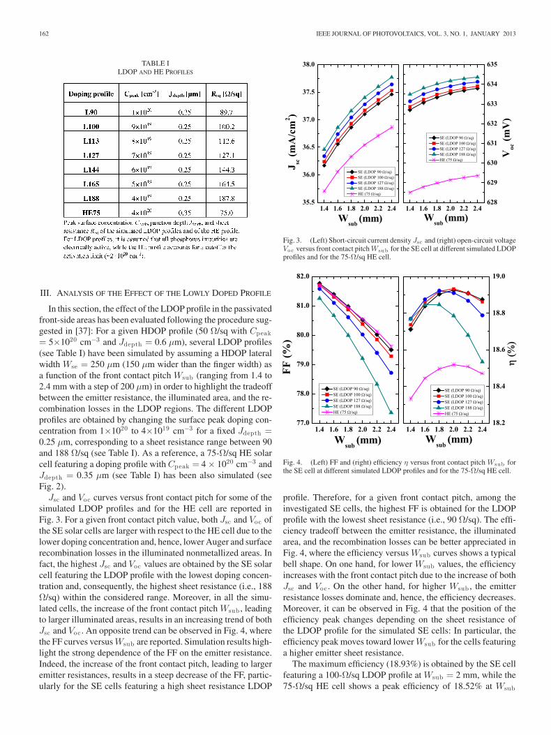
TABLE ILDOP AND HE PROFILES
III. ANALYSIS OF THE EFFECT OF THE LOWLY DOPED PROFILE
In this section, the effect of the LDOP profile in the passivatedfront-side areas has been evaluated following the procedure sug-gested in [37]: For a given HDOP profile (50 Ω/sq with Cpeak= 5×1020 cm−3 and Jdepth = 0.6 μm), several LDOP profiles(see Table I) have been simulated by assuming a HDOP lateralwidth Wse = 250 μm (150 μm wider than the finger width) asa function of the front contact pitch Wsub (ranging from 1.4 to2.4 mm with a step of 200 μm) in order to highlight the tradeoffbetween the emitter resistance, the illuminated area, and the re-combination losses in the LDOP regions. The different LDOPprofiles are obtained by changing the surface peak doping con-centration from 1×10²⁰ to 4×1019 cm−3 for a fixed Jdepth =0.25 μm, corresponding to a sheet resistance range between 90and 188 Ω/sq (see Table I). As a reference, a 75-Ω/sq HE solarcell featuring a doping profile with Cpeak = 4 × 1020 cm−3 andJdepth = 0.35 μm (see Table I) has been also simulated (seeFig. 2).
Jsc and Voc curves versus front contact pitch for some of thesimulated LDOP profiles and for the HE cell are reported inFig. 3. For a given front contact pitch value, both Jsc and Voc ofthe SE solar cells are larger with respect to the HE cell due to thelower doping concentration and, hence, lower Auger and surfacerecombination losses in the illuminated nonmetallized areas. Infact, the highest Jsc and Voc values are obtained by the SE solarcell featuring the LDOP profile with the lowest doping concen-tration and, consequently, the highest sheet resistance (i.e., 188Ω/sq) within the considered range. Moreover, in all the simu-lated cells, the increase of the front contact pitch Wsub , leadingto larger illuminated areas, results in an increasing trend of bothJsc and Voc . An opposite trend can be observed in Fig. 4, wherethe FF curves versus Wsub are reported. Simulation results high-light the strong dependence of the FF on the emitter resistance.Indeed, the increase of the front contact pitch, leading to largeremitter resistances, results in a steep decrease of the FF, partic-ularly for the SE cells featuring a high sheet resistance LDOP
Fig. 3. (Left) Short-circuit current density Jsc and (right) open-circuit voltageVo c versus front contact pitch Wsub for the SE cell at different simulated LDOPprofiles and for the 75-Ω/sq HE cell.
Fig. 4. (Left) FF and (right) efficiency η versus front contact pitch Wsub forthe SE cell at different simulated LDOP profiles and for the 75-Ω/sq HE cell.
profile. Therefore, for a given front contact pitch, among theinvestigated SE cells, the highest FF is obtained for the LDOPprofile with the lowest sheet resistance (i.e., 90 Ω/sq). The effi-ciency tradeoff between the emitter resistance, the illuminatedarea, and the recombination losses can be better appreciated inFig. 4, where the efficiency versus Wsub curves shows a typicalbell shape. On one hand, for lower Wsub values, the efficiencyincreases with the front contact pitch due to the increase of bothJsc and Voc . On the other hand, for higher Wsub , the emitterresistance losses dominate and, hence, the efficiency decreases.Moreover, it can be observed in Fig. 4 that the position of theefficiency peak changes depending on the sheet resistance ofthe LDOP profile for the simulated SE cells: In particular, theefficiency peak moves toward lower Wsub for the cells featuringa higher emitter sheet resistance.
The maximum efficiency (18.93%) is obtained by the SE cellfeaturing a 100-Ω/sq LDOP profile at Wsub = 2 mm, while the75-Ω/sq HE cell shows a peak efficiency of 18.52% at Wsub

DE ROSE et al.: UNDERSTANDING THE IMPACT OF THE DOPING PROFILES ON SELECTIVE EMITTER SOLAR CELL 163
TABLE IISIMULATION RESULTS
= 2 mm. In Table II, we report the comparison between theHE and SE cells featuring the maximum efficiency. The SE cellshows an increase in terms of Jsc and Voc of 0.63 mA/cm2 and4.6 mV, respectively, an FF decrease of 0.17%abs , and an ef-ficiency gain of 0.41%abs . In terms of dark saturation currentdensity J0,tot , the SE cell shows a lower value (∼860 fA/cm2)with respect to the HE cell (∼1010 fA/cm2), according to thehigher performance. The decrease of J0,tot shown by SE cell is aconsequence of the reduction of the recombination losses in theemitter: As a matter of fact, the emitter saturation current densityJ0 , e decreases from ∼284 fA/cm2 for HE to ∼135 fA/cm2 forSE (see Table II). Through a careful analysis of the loss mecha-nisms in the emitter region, we can ascribe the J0,e decrease to amoderate reduction of Auger recombination losses (J0,e(Auger)decreases from ∼63 fA/cm2 for HE to ∼36 fA/cm2 for SE)and to a strong reduction of the surface recombination losses(J0,e(Surf ) decreases from ∼197 fA/cm2 for HE to ∼81 fA/cm2
for SE).
IV. ANALYSIS OF THE EFFECT OF THE HIGHLY DOPED PROFILE
In this section, the impact of the HDOP profile in the met-allized front-side areas on SE cell performance has been in-vestigated according to [15]. Various HDOP profiles have beenexamined at three different phosphorus dose concentrations (D)(6 × 10¹⁵ , 3 × 10¹⁵ , and 1.5 × 1015 cm−2), by varying theCpeak from 5 × 10²⁰ to 1×1020 cm−3 and, consequently, thejunction depth of the doping profile (see Table III). Accordingly,the sheet resistance of the simulated HDOP profiles ranges from∼12 to ∼64 Ω/sq. It is worth noting that only the HDOP pro-files whose junction is deeper than that of the previous LDOPprofiles have been considered in Table III. The effect of thedifferent HDOP profiles in the SE cell has been evaluated byusing the optimal 100 Ω/sq LDOP profile at Wsub = 2.0 mm,derived from the analysis reported in the previous section andby assuming the same HDOP lateral width (Wse = 250 μm).
The trend of Voc versus Cpeak for the three different doses isreported in Fig. 5. We observe that, for a given dose, a lowerCpeak and, hence, a deeper junction is slightly beneficial for theVoc because of the following combined effects: 1) a lower peakdoping leads to a lower SRV in the illuminated HDOP area out-side the front metal finger and 2) a deeper junction is beneficialfor the reduction of the emitter saturation current density in themetallized regions J0,e(met) , as already demonstrated in [10],due to the shielding effect of the minority carriers in the emitter,
TABLE IIIHDOP PROFILES
Fig. 5. (Left) Open-circuit voltage Vo c and (right) short-circuit current densityJsc versus peak doping concentration Cp eak at three different dose concentra-tions (6 × 10¹⁵ , 3 × 10¹⁵ , and 1.5 × 1015 cm−2 ) for the simulated HDOPprofiles, by assuming a HDOP lateral width Wse of 250 μm.
i.e., the holes, from the metal–semiconductor interface. As amatter of fact, for a dose of 3×1015 cm−2 , ranging the Cpeakfrom 5×10²⁰ to 1×1020 cm−3 , the J0,e(Surf ) decreases from∼80 to ∼70 fA/cm2due to the lower SRV in the exposed HDOPregion, while the J0,e(met) , weighted on the metallized area, de-creases from ∼333 to ∼157 fA/cm2due to the better shieldingeffect of the deeper junction. In order to further highlight thiseffect, we performed a simulation of a cell with Wse = 0 (i.e.,no HDOP region) featuring the 100-Ω/sq emitter profile (L100in Table I) with a shallow junction of 0.25 μm. As expected,this cell exhibits a low value of emitter dark saturation current(J0,e≈132 fA/cm2) because of reduced Auger and surface re-combination losses. However, the same cell shows a higher valueof J0,e(met) = 588 fA/cm2 due to the shallower junction thatcauses an increased recombination at the metal/semiconductorinterface, according to [10]. Nevertheless, simulation results re-ported in Fig. 5 only reveals a weak dependence of the Voc onthe HDOP profile: the maximum variation of the Voc is limitedto ∼0.7 mV (∼0.11%). On the contrary, a stronger impact ofthe HDOP profile on the Jsc is highlighted in Fig. 5, where a
164 IEEE JOURNAL OF PHOTOVOLTAICS, VOL. 3, NO. 1, JANUARY 2013
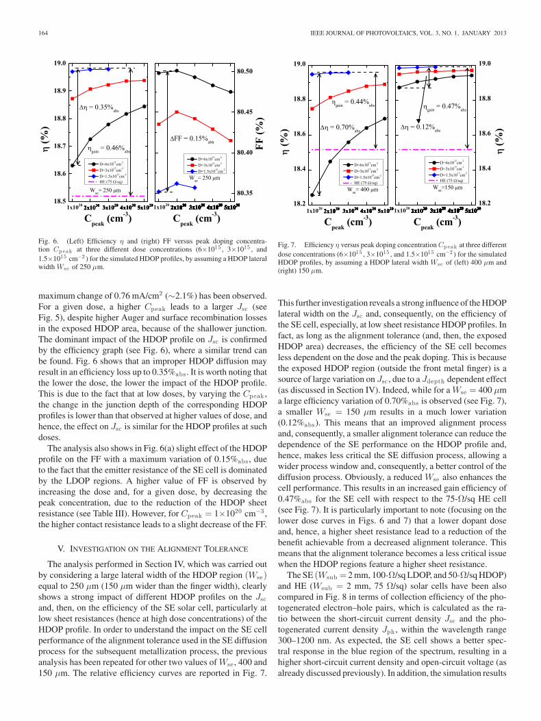
Fig. 6. (Left) Efficiency η and (right) FF versus peak doping concentra-tion Cp eak at three different dose concentrations (6×10¹⁵ , 3×10¹⁵ , and1.5×1015 cm−2 ) for the simulated HDOP profiles, by assuming a HDOP lateralwidth Wse of 250 μm.
maximum change of 0.76 mA/cm2 (∼2.1%) has been observed.For a given dose, a higher Cpeak leads to a larger Jsc (seeFig. 5), despite higher Auger and surface recombination lossesin the exposed HDOP area, because of the shallower junction.The dominant impact of the HDOP profile on Jsc is confirmedby the efficiency graph (see Fig. 6), where a similar trend canbe found. Fig. 6 shows that an improper HDOP diffusion mayresult in an efficiency loss up to 0.35%abs . It is worth noting thatthe lower the dose, the lower the impact of the HDOP profile.This is due to the fact that at low doses, by varying the Cpeak ,the change in the junction depth of the corresponding HDOPprofiles is lower than that observed at higher values of dose, andhence, the effect on Jsc is similar for the HDOP profiles at suchdoses.
The analysis also shows in Fig. 6(a) slight effect of the HDOPprofile on the FF with a maximum variation of 0.15%abs , dueto the fact that the emitter resistance of the SE cell is dominatedby the LDOP regions. A higher value of FF is observed byincreasing the dose and, for a given dose, by decreasing thepeak concentration, due to the reduction of the HDOP sheetresistance (see Table III). However, for Cpeak = 1×1020 cm−3 ,the higher contact resistance leads to a slight decrease of the FF.
V. INVESTIGATION ON THE ALIGNMENT TOLERANCE
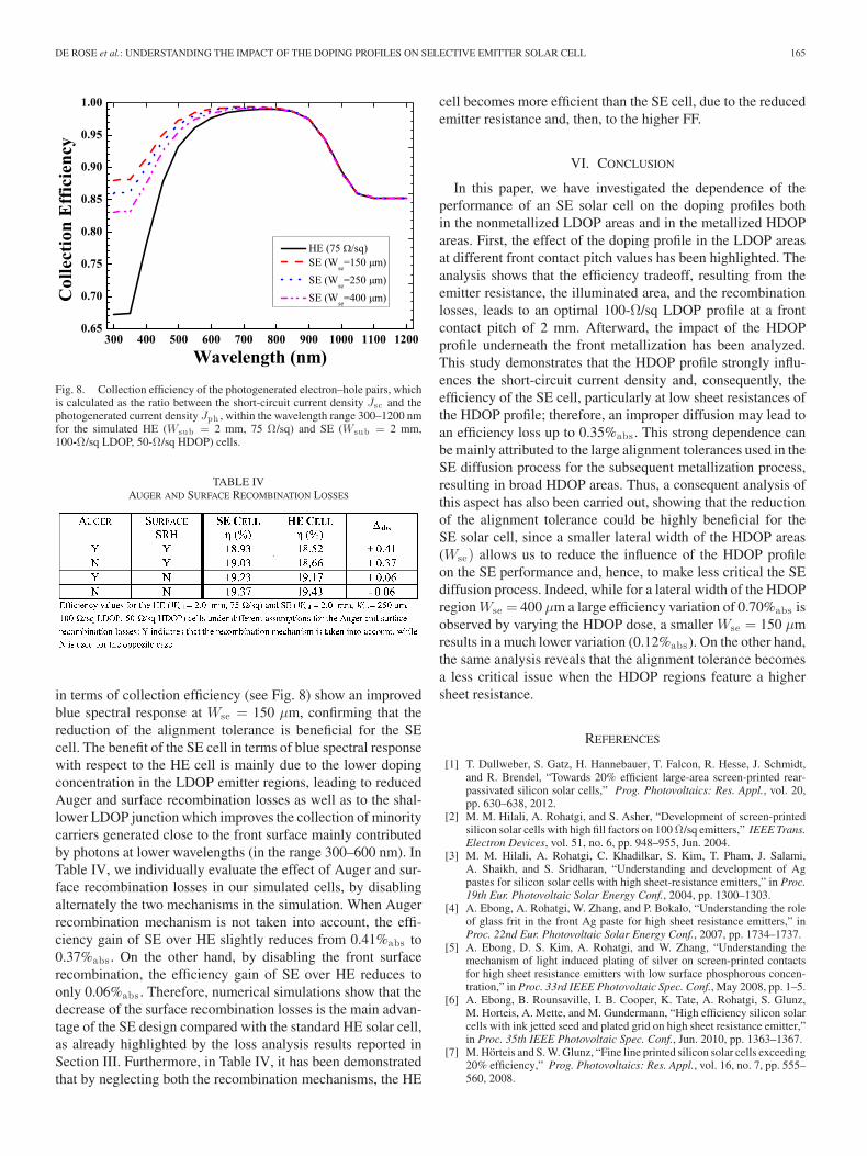
The analysis performed in Section IV, which was carried outby considering a large lateral width of the HDOP region (Wse)equal to 250 μm (150 μm wider than the finger width), clearlyshows a strong impact of different HDOP profiles on the Jscand, then, on the efficiency of the SE solar cell, particularly atlow sheet resistances (hence at high dose concentrations) of theHDOP profile. In order to understand the impact on the SE cellperformance of the alignment tolerance used in the SE diffusionprocess for the subsequent metallization process, the previousanalysis has been repeated for other two values of Wse , 400 and150 μm. The relative efficiency curves are reported in Fig. 7.
Fig. 7. Efficiency η versus peak doping concentration Cp eak at three differentdose concentrations (6×10¹⁵ , 3×10¹⁵ , and 1.5×1015 cm−2 ) for the simulatedHDOP profiles, by assuming a HDOP lateral width Wse of (left) 400 μm and(right) 150 μm.
This further investigation reveals a strong influence of the HDOPlateral width on the Jsc and, consequently, on the efficiency ofthe SE cell, especially, at low sheet resistance HDOP profiles. Infact, as long as the alignment tolerance (and, then, the exposedHDOP area) decreases, the efficiency of the SE cell becomesless dependent on the dose and the peak doping. This is becausethe exposed HDOP region (outside the front metal finger) is asource of large variation on Jsc , due to a Jdepth dependent effect(as discussed in Section IV). Indeed, while for a Wse = 400 μma large efficiency variation of 0.70%abs is observed (see Fig. 7),a smaller Wse = 150 μm results in a much lower variation(0.12%abs). This means that an improved alignment processand, consequently, a smaller alignment tolerance can reduce thedependence of the SE performance on the HDOP profile and,hence, makes less critical the SE diffusion process, allowing awider process window and, consequently, a better control of thediffusion process. Obviously, a reduced Wse also enhances thecell performance. This results in an increased gain efficiency of0.47%abs for the SE cell with respect to the 75-Ω/sq HE cell(see Fig. 7). It is particularly important to note (focusing on thelower dose curves in Figs. 6 and 7) that a lower dopant doseand, hence, a higher sheet resistance lead to a reduction of thebenefit achievable from a decreased alignment tolerance. Thismeans that the alignment tolerance becomes a less critical issuewhen the HDOP regions feature a higher sheet resistance.
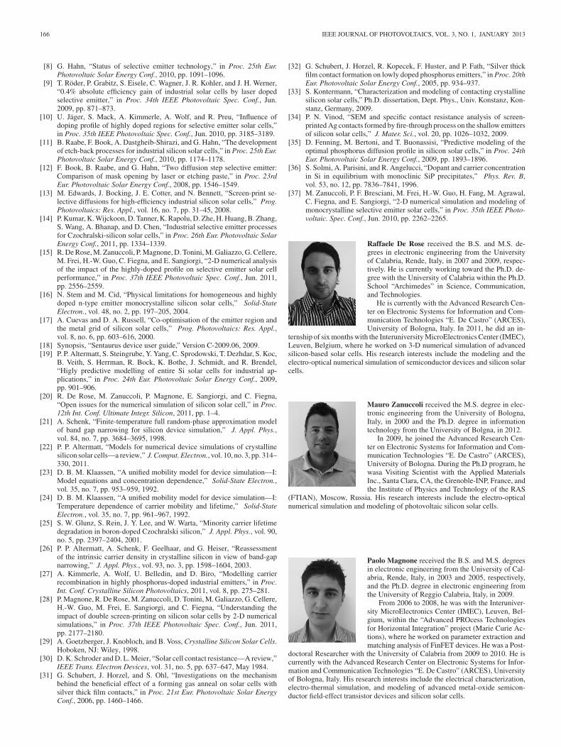
The SE (Wsub = 2 mm, 100-Ω/sq LDOP, and 50-Ω/sq HDOP)and HE (Wsub = 2 mm, 75 Ω/sq) solar cells have been alsocompared in Fig. 8 in terms of collection efficiency of the pho-togenerated electron–hole pairs, which is calculated as the ra-tio between the short-circuit current density Jsc and the pho-togenerated current density Jph , within the wavelength range300–1200 nm. As expected, the SE cell shows a better spec-tral response in the blue region of the spectrum, resulting in ahigher short-circuit current density and open-circuit voltage (asalready discussed previously). In addition, the simulation results
DE ROSE et al.: UNDERSTANDING THE IMPACT OF THE DOPING PROFILES ON SELECTIVE EMITTER SOLAR CELL 165
Fig. 8. Collection efficiency of the photogenerated electron–hole pairs, whichis calculated as the ratio between the short-circuit current density Jsc and thephotogenerated current density Jph , within the wavelength range 300–1200 nmfor the simulated HE (Wsub = 2 mm, 75 Ω/sq) and SE (Wsub = 2 mm,100-Ω/sq LDOP, 50-Ω/sq HDOP) cells.
TABLE IVAUGER AND SURFACE RECOMBINATION LOSSES
in terms of collection efficiency (see Fig. 8) show an improvedblue spectral response at Wse = 150 μm, confirming that thereduction of the alignment tolerance is beneficial for the SEcell. The benefit of the SE cell in terms of blue spectral responsewith respect to the HE cell is mainly due to the lower dopingconcentration in the LDOP emitter regions, leading to reducedAuger and surface recombination losses as well as to the shal-lower LDOP junction which improves the collection of minoritycarriers generated close to the front surface mainly contributedby photons at lower wavelengths (in the range 300–600 nm). InTable IV, we individually evaluate the effect of Auger and sur-face recombination losses in our simulated cells, by disablingalternately the two mechanisms in the simulation. When Augerrecombination mechanism is not taken into account, the effi-ciency gain of SE over HE slightly reduces from 0.41%abs to0.37%abs . On the other hand, by disabling the front surfacerecombination, the efficiency gain of SE over HE reduces toonly 0.06%abs . Therefore, numerical simulations show that thedecrease of the surface recombination losses is the main advan-tage of the SE design compared with the standard HE solar cell,as already highlighted by the loss analysis results reported inSection III. Furthermore, in Table IV, it has been demonstratedthat by neglecting both the recombination mechanisms, the HE
cell becomes more efficient than the SE cell, due to the reducedemitter resistance and, then, to the higher FF.
VI. CONCLUSION
In this paper, we have investigated the dependence of theperformance of an SE solar cell on the doping profiles bothin the nonmetallized LDOP areas and in the metallized HDOPareas. First, the effect of the doping profile in the LDOP areasat different front contact pitch values has been highlighted. Theanalysis shows that the efficiency tradeoff, resulting from theemitter resistance, the illuminated area, and the recombinationlosses, leads to an optimal 100-Ω/sq LDOP profile at a frontcontact pitch of 2 mm. Afterward, the impact of the HDOPprofile underneath the front metallization has been analyzed.This study demonstrates that the HDOP profile strongly influ-ences the short-circuit current density and, consequently, theefficiency of the SE cell, particularly at low sheet resistances ofthe HDOP profile; therefore, an improper diffusion may lead toan efficiency loss up to 0.35%abs . This strong dependence canbe mainly attributed to the large alignment tolerances used in theSE diffusion process for the subsequent metallization process,resulting in broad HDOP areas. Thus, a consequent analysis ofthis aspect has also been carried out, showing that the reductionof the alignment tolerance could be highly beneficial for theSE solar cell, since a smaller lateral width of the HDOP areas(Wse) allows us to reduce the influence of the HDOP profileon the SE performance and, hence, to make less critical the SEdiffusion process. Indeed, while for a lateral width of the HDOPregion Wse = 400 μm a large efficiency variation of 0.70%abs isobserved by varying the HDOP dose, a smaller Wse = 150 μmresults in a much lower variation (0.12%abs). On the other hand,the same analysis reveals that the alignment tolerance becomesa less critical issue when the HDOP regions feature a highersheet resistance.
REFERENCES
[1] T. Dullweber, S. Gatz, H. Hannebauer, T. Falcon, R. Hesse, J. Schmidt,and R. Brendel, “Towards 20% efficient large-area screen-printed rear-passivated silicon solar cells,” Prog. Photovoltaics: Res. Appl., vol. 20,pp. 630–638, 2012.
[2] M. M. Hilali, A. Rohatgi, and S. Asher, “Development of screen-printedsilicon solar cells with high fill factors on 100 Ω/sq emitters,” IEEE Trans.Electron Devices, vol. 51, no. 6, pp. 948–955, Jun. 2004.
[3] M. M. Hilali, A. Rohatgi, C. Khadilkar, S. Kim, T. Pham, J. Salami,A. Shaikh, and S. Sridharan, “Understanding and development of Agpastes for silicon solar cells with high sheet-resistance emitters,” in Proc.19th Eur. Photovoltaic Solar Energy Conf., 2004, pp. 1300–1303.
[4] A. Ebong, A. Rohatgi, W. Zhang, and P. Bokalo, “Understanding the roleof glass frit in the front Ag paste for high sheet resistance emitters,” inProc. 22nd Eur. Photovoltaic Solar Energy Conf., 2007, pp. 1734–1737.
[5] A. Ebong, D. S. Kim, A. Rohatgi, and W. Zhang, “Understanding themechanism of light induced plating of silver on screen-printed contactsfor high sheet resistance emitters with low surface phosphorous concen-tration,” in Proc. 33rd IEEE Photovoltaic Spec. Conf., May 2008, pp. 1–5.
[6] A. Ebong, B. Rounsaville, I. B. Cooper, K. Tate, A. Rohatgi, S. Glunz,M. Horteis, A. Mette, and M. Gundermann, “High efficiency silicon solarcells with ink jetted seed and plated grid on high sheet resistance emitter,”in Proc. 35th IEEE Photovoltaic Spec. Conf., Jun. 2010, pp. 1363–1367.
[7] M. Horteis and S. W. Glunz, “Fine line printed silicon solar cells exceeding20% efficiency,” Prog. Photovoltaics: Res. Appl., vol. 16, no. 7, pp. 555–560, 2008.
166 IEEE JOURNAL OF PHOTOVOLTAICS, VOL. 3, NO. 1, JANUARY 2013
[8] G. Hahn, “Status of selective emitter technology,” in Proc. 25th Eur.Photovoltaic Solar Energy Conf., 2010, pp. 1091–1096.
[9] T. Roder, P. Grabitz, S. Eisele, C. Wagner, J. R. Kohler, and J. H. Werner,“0.4% absolute efficiency gain of industrial solar cells by laser dopedselective emitter,” in Proc. 34th IEEE Photovoltaic Spec. Conf., Jun.2009, pp. 871–873.
[10] U. Jager, S. Mack, A. Kimmerle, A. Wolf, and R. Preu, “Influence ofdoping profile of highly doped regions for selective emitter solar cells,”in Proc. 35th IEEE Photovoltaic Spec. Conf., Jun. 2010, pp. 3185–3189.
[11] B. Raabe, F. Book, A. Dastgheib-Shirazi, and G. Hahn, “The developmentof etch-back processes for industrial silicon solar cells,” in Proc. 25th Eur.Photovoltaic Solar Energy Conf., 2010, pp. 1174–1178.
[12] F. Book, B. Raabe, and G. Hahn, “Two diffusion step selective emitter:Comparison of mask opening by laser or etching paste,” in Proc. 23rdEur. Photovoltaic Solar Energy Conf., 2008, pp. 1546–1549.
[13] M. Edwards, J. Bocking, J. E. Cotter, and N. Bennett, “Screen-print se-lective diffusions for high-efficiency industrial silicon solar cells,” Prog.Photovoltaics: Res. Appl., vol. 16, no. 7, pp. 31–45, 2008.
[14] P. Kumar, K. Wijckoon, D. Tanner, K. Rapolu, D. Zhe, H. Huang, B. Zhang,S. Wang, A. Bhanap, and D. Chen, “Industrial selective emitter processesfor Czochralski-silicon solar cells,” in Proc. 26th Eur. Photovoltaic SolarEnergy Conf., 2011, pp. 1334–1339.
[15] R. De Rose, M. Zanuccoli, P. Magnone, D. Tonini, M. Galiazzo, G. Cellere,M. Frei, H.-W. Guo, C. Fiegna, and E. Sangiorgi, “2-D numerical analysisof the impact of the highly-doped profile on selective emitter solar cellperformance,” in Proc. 37th IEEE Photovoltaic Spec. Conf., Jun. 2011,pp. 2556–2559.
[16] N. Stem and M. Cid, “Physical limitations for homogeneous and highlydoped n-type emitter monocrystalline silicon solar cells,” Solid-StateElectron., vol. 48, no. 2, pp. 197–205, 2004.
[17] A. Cuevas and D. A. Russell, “Co-optimisation of the emitter region andthe metal grid of silicon solar cells,” Prog. Photovoltaics: Res. Appl.,vol. 8, no. 6, pp. 603–616, 2000.
[18] Synopsis, “Sentaurus device user guide,” Version C-2009.06, 2009.[19] P. P. Altermatt, S. Steingrube, Y. Yang, C. Sprodowski, T. Dezhdar, S. Koc,
B. Veith, S. Herrman, R. Bock, K. Bothe, J. Schmidt, and R. Brendel,“Higly predictive modelling of entire Si solar cells for industrial ap-plications,” in Proc. 24th Eur. Photovoltaic Solar Energy Conf., 2009,pp. 901–906.
[20] R. De Rose, M. Zanuccoli, P. Magnone, E. Sangiorgi, and C. Fiegna,“Open issues for the numerical simulation of silicon solar cell,” in Proc.12th Int. Conf. Ultimate Integr. Silicon, 2011, pp. 1–4.
[21] A. Schenk, “Finite-temperature full random-phase approximation modelof band gap narrowing for silicon device simulation,” J. Appl. Phys.,vol. 84, no. 7, pp. 3684–3695, 1998.
[22] P. P. Altermatt, “Models for numerical device simulations of crystallinesilicon solar cells—a review,” J. Comput. Electron., vol. 10, no. 3, pp. 314–330, 2011.
[23] D. B. M. Klaassen, “A unified mobility model for device simulation—I:Model equations and concentration dependence,” Solid-State Electron.,vol. 35, no. 7, pp. 953–959, 1992.
[24] D. B. M. Klaassen, “A unified mobility model for device simulation—I:Temperature dependence of carrier mobility and lifetime,” Solid-StateElectron., vol. 35, no. 7, pp. 961–967, 1992.
[25] S. W. Glunz, S. Rein, J. Y. Lee, and W. Warta, “Minority carrier lifetimedegradation in boron-doped Czochralski silicon,” J. Appl. Phys., vol. 90,no. 5, pp. 2397–2404, 2001.
[26] P. P. Altermatt, A. Schenk, F. Geelhaar, and G. Heiser, “Reassessmentof the intrinsic carrier density in crystalline silicon in view of band-gapnarrowing,” J. Appl. Phys., vol. 93, no. 3, pp. 1598–1604, 2003.
[27] A. Kimmerle, A. Wolf, U. Belledin, and D. Biro, “Modelling carrierrecombination in highly phosphorus-doped industrial emitters,” in Proc.Int. Conf. Crystalline Silicon Photovoltaics, 2011, vol. 8, pp. 275–281.
[28] P. Magnone, R. De Rose, M. Zanuccoli, D. Tonini, M. Galiazzo, G. Cellere,H.-W. Guo, M. Frei, E. Sangiorgi, and C. Fiegna, “Understanding theimpact of double screen-printing on silicon solar cells by 2-D numericalsimulations,” in Proc. 37th IEEE Photovoltaic Spec. Conf., Jun. 2011,pp. 2177–2180.
[29] A. Goetzberger, J. Knobloch, and B. Voss, Crystalline Silicon Solar Cells.Hoboken, NJ: Wiley, 1998.
[30] D. K. Schroder and D. L. Meier, “Solar cell contact resistance—A review,”IEEE Trans. Electron Devices, vol. 31, no. 5, pp. 637–647, May 1984.
[31] G. Schubert, J. Horzel, and S. Ohl, “Investigations on the mechanismbehind the beneficial effect of a forming gas anneal on solar cells withsilver thick film contacts,” in Proc. 21st Eur. Photovoltaic Solar EnergyConf., 2006, pp. 1460–1466.
[32] G. Schubert, J. Horzel, R. Kopecek, F. Huster, and P. Fath, “Silver thickfilm contact formation on lowly doped phosphorus emitters,” in Proc. 20thEur. Photovoltaic Solar Energy Conf., 2005, pp. 934–937.
[33] S. Kontermann, “Characterization and modeling of contacting crystallinesilicon solar cells,” Ph.D. dissertation, Dept. Phys., Univ. Konstanz, Kon-stanz, Germany, 2009.
[34] P. N. Vinod, “SEM and specific contact resistance analysis of screen-printed Ag contacts formed by fire-through process on the shallow emittersof silicon solar cells,” J. Mater. Sci., vol. 20, pp. 1026–1032, 2009.
[35] D. Fenning, M. Bertoni, and T. Buonassisi, “Predictive modeling of theoptimal phosphorus diffusion profile in silicon solar cells,” in Proc. 24thEur. Photovoltaic Solar Energy Conf., 2009, pp. 1893–1896.
[36] S. Solmi, A. Parisini, and R. Angelucci, “Dopant and carrier concentrationin Si in equilibrium with monoclinic SiP precipitates,” Phys. Rev. B,vol. 53, no. 12, pp. 7836–7841, 1996.
[37] M. Zanuccoli, P. F. Bresciani, M. Frei, H.-W. Guo, H. Fang, M. Agrawal,C. Fiegna, and E. Sangiorgi, “2-D numerical simulation and modeling ofmonocrystalline selective emitter solar cells,” in Proc. 35th IEEE Photo-voltaic. Spec. Conf., Jun. 2010, pp. 2262–2265.
Raffaele De Rose received the B.S. and M.S. de-grees in electronic engineering from the Universityof Calabria, Rende, Italy, in 2007 and 2009, respec-tively. He is currently working toward the Ph.D. de-gree with the University of Calabria within the Ph.D.School “Archimedes” in Science, Communication,and Technologies.
He is currently with the Advanced Research Cen-ter on Electronic Systems for Information and Com-munication Technologies “E. De Castro” (ARCES),University of Bologna, Italy. In 2011, he did an in-
ternship of six months with the Interuniversity MicroElectronics Center (IMEC),Leuven, Belgium, where he worked on 3-D numerical simulation of advancedsilicon-based solar cells. His research interests include the modeling and theelectro-optical numerical simulation of semiconductor devices and silicon solarcells.
Mauro Zanuccoli received the M.S. degree in elec-tronic engineering from the University of Bologna,Italy, in 2000 and the Ph.D. degree in informationtechnology from the University of Bolgna, in 2012.
In 2009, he joined the Advanced Research Cen-ter on Electronic Systems for Information and Com-munication Technologies “E. De Castro” (ARCES),University of Bologna. During the Ph.D program, hewasa Visiting Scientist with the Applied MaterialsInc., Santa Clara, CA, the Grenoble-INP, France, andthe Institute of Physics and Technology of the RAS
(FTIAN), Moscow, Russia. His research interests include the electro-opticalnumerical simulation and modeling of photovoltaic silicon solar cells.
Paolo Magnone received the B.S. and M.S. degreesin electronic engineering from the University of Cal-abria, Rende, Italy, in 2003 and 2005, respectively,and the Ph.D. degree in electronic engineering fromthe University of Reggio Calabria, Italy, in 2009.
From 2006 to 2008, he was with the Interuniver-sity MicroElectronics Center (IMEC), Leuven, Bel-gium, within the “Advanced PROcess Technologiesfor Horizontal Integration” project (Marie Curie Ac-tions), where he worked on parameter extraction andmatching analysis of FinFET devices. He was a Post-
doctoral Researcher with the University of Calabria from 2009 to 2010. He iscurrently with the Advanced Research Center on Electronic Systems for Infor-mation and Communication Technologies “E. De Castro” (ARCES), Universityof Bologna, Italy. His research interests include the electrical characterization,electro-thermal simulation, and modeling of advanced metal-oxide semicon-ductor field-effect transistor devices and silicon solar cells.
DE ROSE et al.: UNDERSTANDING THE IMPACT OF THE DOPING PROFILES ON SELECTIVE EMITTER SOLAR CELL 167
M. Frei, photograph and biography not available at the time of publication.
Enrico Sangiorgi (F’05) received the Laurea degreefrom the University of Bologna, Italy, in 1979.
He has been a Visiting Scientist with Stanford Uni-versity, Stanford, CA, and Bell Laboratories, MurrayHill, NJ. In 1993, he was appointed Full Professorof Electronics with the University of Udine, Italy.In 2002, he joined the University of Bologna, wherehe is now Director of the Electrical Engineering De-partment “Guglielmo Marconi.” His research coversdevice modeling.
Dr. Sangiorgi is a Distinguished Lecturer of theIEEE; he has been Chairman of the Electron Devices Society (EDS) andthe TRANSACTIONS ON COMPUTER-AIDED DESIGN Technical Committee anda member of the Cledo Brunetti Award and Education Award Committees ofthe EDS. He has been Editor of the IEEE ELECTRON DEVICE LETTERS and onthe editorial boards of the IEEE TRANSACTIONS ON ELECTRON DEVICES, andthe IEEE JOURNAL OF PHOTOVOLTAICS.
Claudio Fiegna received the Laurea and Ph.D. de-grees in electronics engineering from the Universityof Bologna, Italy.
He is currently a Full Professor of electronicswith the University of Bologna, where he is also theDirector of the Advanced Research Center on Elec-tronic Systems for Information and CommunicationTechnologies “E. De Castro” (ARCES). His researchinterests include numerical device simulation and itsapplication to the analysis of advanced metal-oxidesemiconductor device structures, and silicon-based
solar cells.Dr. Fiegna serves on the committee for the Educational Award of the IEEE
Electron Devices Society.