Understanding the Design and Control of VSC-Based HVDC ... · VSC-Based HVDC System with Shunt...
9
International Journal of Applied Engineering Research ISSN 0973-4562 Volume 13, Number 7 (2018) pp. 5048-5056 © Research India Publications. http://www.ripublication.com 5048 Understanding the Design and Control of VSC-Based HVDC System with Shunt Passive Filters Banishree Misra 1 , Byamakesh Nayak 2 1,2 School of Electrical Engineering, KIIT University, Bhubaneswar, India. Abstract A detail description of the operating scheme of a 12-pulse voltage source converter (VSC) used in high voltage DC (HVDC) system is presented here. The system used here for HVDC transmission schemes comprises only one terminals with a 12-pulse converter and a DC load of 1000MW. Then the design of the control structure for the triggering circuit and the technique of pulse generation for the thyristor based converter is explained and analysed using MATLAB/SIMULINK. The effect of changing the firing pulse on the active and reactive power generation and the total harmonic distortion of the source current is investigated. The simulation results confirms the capability of HVDC converter operating with a wide range of firing angles. The parameters of different passive harmonic filters are calculated. The harmonic study of the VSC based HVDC system with shunt passive filters confirms the effectiveness of the filters. All the results are validated in MATLAB/SIMULINK environment. Keywords: VSC based HVDC system; 12-pulse converter; phase locked loop; passive filter; reactive power; total harmonic distortion. INTRODUCTION The concept on which an HVDC system operates is the conversion of generating current from AC to DC (rectification) at the transmitting end, and from DC to AC (inversion) at the receiving end. Using the following converters the target can be achieved [1]-[4]: 1. Thyristor based line-commutated current-source converters (CSCs). (Fig. 1, CSC-HVDC). These converters are well applied for high power applications, usually in the order of 1000MW. 2. Fully controllable switch based forced-commutated voltage- source converters (VSCs). These converters uses mostly gate-turn-off thyristors (GTOs) or for industrial application insulated gate bipolar transistors (IGBTs) (Fig. 2, VSC- HVDC). This technology is mostly used for medium power level in the range of 350MW. The main difference between CSCs and VSCs is that the VSCs are able to control the active and reactive power injections independent from each other as well as from the system state whereas CSC can control the active power only. With the CSC the DC current polarity will remain the same and hence the power flow direction through the converter is decided by the polarity of the DC voltage. Semi-controllable thyristors are the building blocks for the current source converters. The triggering pulse of the thyristors will decide the instant at which the current starts conduction. However the the device commutation instant is calculated by the natural zero crossing of the AC voltage. A large smoothing reactors is connected in series at the DC terminal of a CSC to keep the current smooth and continuous [5]-[7]. The total harmonic distortion of the voltage and current is calculated on the AC side. To eliminate the harmonic content large passive and active filters are designed. On the contrary, the voltage source converter VSC do not change the polarity of the DC voltage, so the power flow direction is determined by the polarity of the DC current. These converters are equipped with fully controllable semiconductor switches such as IGBTs. Here the conduction and commutation of the current at any instant is decided by a gate pulse. Like a voltage source, the DC terminal of a VSC is joined in parallel with a comparatively large capacitor. Both these converter technologies have their own advantages hence used in different power system applications. One of the common application is being the compensation. Here compensation will be made by a power-electronic compensator which will increase the power transfer capability of the line, will increase the efficiency of the power transfer, will improve voltage and angle stability and ultimately will improve the power quality. A HVDC converter controls power on the DC link and at the same time execute certain other tasks. For example it makes a balance between the frequency, voltage magnitude or power factor, of the system. Fig. 1. provides a structural difference of the two converter technologies. CSC (a) C VSC L (b) Figure 1. Comparision of (a) CSC and (b) VSC configuration
Transcript of Understanding the Design and Control of VSC-Based HVDC ... · VSC-Based HVDC System with Shunt...

International Journal of Applied Engineering Research ISSN 0973-4562 Volume 13, Number 7 (2018) pp. 5048-5056
© Research India Publications. http://www.ripublication.com
5048
Understanding the Design and Control of VSC-Based HVDC System with Shunt
Passive Filters
Banishree Misra1, Byamakesh Nayak2 1,2 School of Electrical Engineering, KIIT University, Bhubaneswar, India.
Abstract
A detail description of the operating scheme of a 12-pulse
voltage source converter (VSC) used in high voltage DC
(HVDC) system is presented here. The system used here for
HVDC transmission schemes comprises only one terminals
with a 12-pulse converter and a DC load of 1000MW. Then
the design of the control structure for the triggering circuit and
the technique of pulse generation for the thyristor based
converter is explained and analysed using
MATLAB/SIMULINK. The effect of changing the firing
pulse on the active and reactive power generation and the total
harmonic distortion of the source current is investigated. The
simulation results confirms the capability of HVDC converter
operating with a wide range of firing angles. The parameters
of different passive harmonic filters are calculated. The
harmonic study of the VSC based HVDC system with shunt
passive filters confirms the effectiveness of the filters. All the
results are validated in MATLAB/SIMULINK environment.
Keywords: VSC based HVDC system; 12-pulse converter;
phase locked loop; passive filter; reactive power; total
harmonic distortion.
INTRODUCTION
The concept on which an HVDC system operates is the
conversion of generating current from AC to DC (rectification)
at the transmitting end, and from DC to AC (inversion) at the
receiving end. Using the following converters the target can be
achieved [1]-[4]:
1. Thyristor based line-commutated current-source converters
(CSCs). (Fig. 1, CSC-HVDC). These converters are well
applied for high power applications, usually in the order of
1000MW.
2. Fully controllable switch based forced-commutated voltage-
source converters (VSCs). These converters uses mostly
gate-turn-off thyristors (GTOs) or for industrial application
insulated gate bipolar transistors (IGBTs) (Fig. 2, VSC-
HVDC). This technology is mostly used for medium power
level in the range of 350MW.
The main difference between CSCs and VSCs is that the VSCs
are able to control the active and reactive power injections
independent from each other as well as from the system state
whereas CSC can control the active power only. With the CSC
the DC current polarity will remain the same and hence the
power flow direction through the converter is decided by the
polarity of the DC voltage. Semi-controllable thyristors are the
building blocks for the current source converters. The
triggering pulse of the thyristors will decide the instant at
which the current starts conduction. However the the device
commutation instant is calculated by the natural zero crossing
of the AC voltage. A large smoothing reactors is connected in
series at the DC terminal of a CSC to keep the current smooth
and continuous [5]-[7]. The total harmonic distortion of the
voltage and current is calculated on the AC side. To eliminate
the harmonic content large passive and active filters are
designed. On the contrary, the voltage source converter VSC
do not change the polarity of the DC voltage, so the power
flow direction is determined by the polarity of the DC current.
These converters are equipped with fully controllable
semiconductor switches such as IGBTs. Here the conduction
and commutation of the current at any instant is decided by a
gate pulse. Like a voltage source, the DC terminal of a VSC is
joined in parallel with a comparatively large capacitor.
Both these converter technologies have their own advantages
hence used in different power system applications. One of the
common application is being the compensation. Here
compensation will be made by a power-electronic
compensator which will increase the power transfer capability
of the line, will increase the efficiency of the power transfer,
will improve voltage and angle stability and ultimately will
improve the power quality. A HVDC converter controls
power on the DC link and at the same time execute certain
other tasks. For example it makes a balance between the
frequency, voltage magnitude or power factor, of the system.
Fig. 1. provides a structural difference of the two converter
technologies.
CSC
(a)
C VSC L
(b)
Figure 1. Comparision of (a) CSC and (b) VSC configuration

International Journal of Applied Engineering Research ISSN 0973-4562 Volume 13, Number 7 (2018) pp. 5048-5056
© Research India Publications. http://www.ripublication.com
5049
COMPONENTS OF VSC-BASED HVDC SYSTEM WITH
12-PULSE AC-DC CONVERTER
A. Three Phase Source
In the proposed HVDC system the source is balanced three-
voltage source with an internal R-L impedance. The three
phase voltage sources are connected in Y with the neutral
internally grounded. The internal resistance is considered zero
while the inductance is taken as 98.03 ohm. The design has
been considered for a 60 Hz supply system. The AC supply
systems is demonstrated by damped L-R equivalents with an
angle of 80 degrees at fundamental frequency 60 Hz.
B. Thyristor Controlled Rectifier
The schematic diagram of 12-pulse converter based HVDC
system with a 1000 MW (500kV and 2 kA) load is shown in
Fig. 1. The 12-pulse converter consist of two series connected
thyristor bridges connected with a three-phase converter
transformer. The thyristor bridges is a universal three-phase
power converter which consists of six power switches
connected in a bridge configuration. The universal Bridge
block is the basic block for designing two-level voltage-
sourced converters (VSC). Observing from the AC side, an
HVDC converter acts as a source of harmonic currents. The
harmonic order is decided on the basis of the number of pulses
p generated by the converter section. For the AC side the
current harmonics will have a order of n = kp ± 1, where k
can be any integer. So for a 6-pulse converter considering p =
6, the injected current harmonics on the AC side will have the
order of 5,7,11,13.
C. Three Phase Three Winding Transformer
The required phase shift between the two set of voltages is 30⁰ (360⁰/ Total number of pulses) can be generated if the
converter is connected to a Y-Δ connected secondary of a
transformer. The primary of the transformer is a Y-connection
with grounded neutral(winding-1) and on the secondary the
winding-2 is Y connected and winding-3 is Δ(D1) connected.
so the winding-3(D1) is lagging winding-2 (Y) by an angle of
30 degrees.
CONTROL SCHEME FOR VSC BASED HVDC SYSTEM
Y
Δ
Yg
a2
b2
c2
a3
b3
c3
Vabc
a
b
c
A
B
C
G
A
B
C
A
B
C
G
A
B
C
Alpha PY
Wt PD
Block
10
Vabc Freq
Wt
Pulse Generator
Thyristor
PLL-(3ph)
3-ph V-I
Measurement
Converter
Transformer
Power
System
+
_
+
_
1000
MW
Figure 2. Block diagram showing pulse generator block
connected to a twelve-pulse thyristor converter.
The firing pulses for the two series connected three-phase
thyristor bridge will be generated by the pulse generator. The
set of pulses for each converter contains six equally placed
square pulses with 60⁰ phase displacement between them. The
Py set of pulses will be applied to the first converter bridge
connected to the Y-connected secondary winding of the three-
phase three winding converter transformer. The Pd set of
pulses will go to the Δ-connected secondary winding of the
three winding transformer.
The Pulse Generator of the 12-pulse thyristor converter can be
controlled by the reference signal (alpha angle) and by the
synchronization parameter ωt. It is an angle varying between 0
and 360⁰. The ωt signal is synchronized with the zero crossing
of the fundamental voltage of phase A (positive sequence) of
the primary side of the three phase three winding transformer.
The information about ωt signal can be obtained from the
phase locked loop (PLL) system.
Pulse 1
Pulse 3
Pulse 2
Pulse 4
Pulse 5
Pulse 6
Vac Commutating
voltage
Internal wt
ramp of Vac
Alpha delay angle
Figure 3. PY and PD pulse train generation technique
An internal ωt ramp signal is generated by the pulse generator
block which will control the instant of pulse generation. The
angle alpha in electrical degrees is the delay by which the
pulse is delayed with respect to the angle zero of its
fundamental commutating voltage. The generation technique
of pulse train Py can be explained corresponding to Fig. 4. In
this the thyristor pulse generator is configured to generates two
pulse trains simultaneously. At an delay angle of alpha the first
pulse is generated and exactly after 60⁰ the second pulse will
reach the second converter bridge.
International Journal of Applied Engineering Research ISSN 0973-4562 Volume 13, Number 7 (2018) pp. 5048-5056
© Research India Publications. http://www.ripublication.com
5050
abc wt PID
Controller
er
Controlled
Oscillator
abc
wt
Freq
Automatic Gain
Control
Low Pass Filter
(Rate Limited)
abc to dq0
Variable
Frequency
mean value
Phase Detector
Freq
q-axis
axis
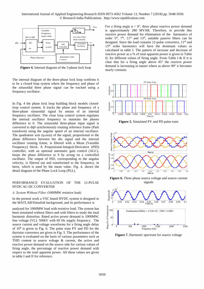
Figure 4. Internal diagram of the 3-phase lock loop
The internal diagram of the three-phase lock loop confirms it
to be a closed loop system where the frequency and phase of
the sinusoidal three phase signal can be tracked using a
frequency oscillator.
In Fig. 4 the phase lock loop building block models closed-
loop control system. It tracks the phase and frequency of a
three-phase sinusoidal signal by means of an internal
frequency oscillator. The close loop control system regulates
the internal oscillator frequency to maintain the phases
difference to 0. The sinusoidal three-phase input signal is
converted to dq0 synchronously rotating reference frame (Park
transform) using the angular speed of an internal oscillator.
The quadrature axis (q-axis) of the signal, proportional to the
phase difference between the abc signal and the internal
oscillator rotating frame, is filtered with a Mean (Variable
Frequency) block. A Proportional-Integral-Derivative (PID)
controller, with an optional automatic gain control (AGC),
keeps the phase difference to 0 by acting on a controlled
oscillator. The output of PID, corresponding to the angular
velocity, is filtered out and transformed to the frequency, in
hertz, which is used by the mean value. Fig. 4. shows the
detail diagram of the Phase Lock Loop (PLL).
PERFORMANCE EVALUATION OF THE 12-PULSE
HVDC AC-DC CONVERTER
A. System Without Filter (1000MW resistive load)
In the present work a VSC based HVDC system is designed in
the MATLAB/Simulink background, and its performance is
analysed for 1000MW load with resistive load. The system has
been simulated without filters and with filters to study the total
harmonic distortion. Rated active power demand is 1000MW,
line voltage (VL): 500kV with 60 Hz supply frequency. The
source current and voltage waveforms for a firing angle delay
of 10⁰ is given in Fig. 6. The pulse train PY and PD for the
thyristor converters are given in Fig. 5. The performance of the
system is evaluated on the basis of various parameters such as
THD content in source voltage & current, the active and
reactive power demand on the source side for various values of
firing angle, the percentage of reactive power demand with
respect to the total apparent power. All these values are given
in table I and II for reference.
For a firing angle α = 0°, three phase reactive power demand
is approximately 280 MVAR. Therefore, to provide this
reactive power demand for elimination of the harmonics of
order 5th, 7th, 11th and 13th, suitable passive filters can be
designed. Since the load contains 12-pulse converters, 11th and
13th order harmonics will have the dominant values as
calculated in table I. The pattern of increase and decrease of
reactive power as a % of total apparent power is given in Table
II. for different values of firing angle. From Table I & II it is
clear that for a firing angle above 45° the reactive power
demand is increasing in nature where as above 90° it becomes
nearly constant.
Figure 5. Simulated PY and PD pulse train
Figure 6. Three phase source voltage and source current
signals
Figure 7. Harmonic spectrum for source voltage
0
0.5
1
Am
pli
tud
e
PY Pulse Train
0 0.002 0.004 0.006 0.008 0.01 0.012 0.014 0.016 0.018 0.020
0.5
1
Time (s)
Am
pli
tud
e
PD Pulse Train
-6
-4
-2
0
2
4
6x 10
5
Time (s)
So
urce V
olt
ag
e (
Vo
lt)
0 0.005 0.01 0.015 0.02 0.025 0.03 0.035 0.04 0.045 0.05
-2000
-1000
0
1000
2000
Time (s)
So
urce C
urren
t (A
)
0 0.01 0.02 0.03 0.04 0.05 0.06 0.07 0.08 0.09 0.1
-202
x 105
Time (s)
Mag
nit
ud
e
0 500 1000 1500 2000 25000
50
100
Frequency (Hz)
Fundamental (60Hz) = 3.519e+05 , THD= 13.68%
Mag
(%
of
Fu
nd
am
en
tal)

International Journal of Applied Engineering Research ISSN 0973-4562 Volume 13, Number 7 (2018) pp. 5048-5056
© Research India Publications. http://www.ripublication.com
5051
Figure 8. Harmonic spectrum for source current
Figure 9. Output DC power without Passive Filter
Table I: Harmonic profile of source current for different
values of firing angle of thyristor converter
Thyristor
Firing
Angle (α0)
MVAR
(Q)
MW
(P)
Harmonics in source current
h5
(%)
h7
(%)
h11
(%)
h13
(%)
THD
(%)
00 280.2 983.6 0.05 0.03 2.47 1.31 2.91
100 369.3 901.8 0.04 0.01 4.25 2.59 5.20
200 695.9 769.8 0.07 0.05 6.17 4.30 7.63
300 637.9 716.3 0.06 0.09 7.9 5.66 7.39
400 353.1 562.4 0.11 0.06 9.32 6.7 9.78
500 309.7 331.9 0.14 0.17 10.51 7.51 11.64
700 387.6 124.8 0.65 0.25 13.83 8.15 17.57
900 -3.425 2.521 2.07 1.58 78.6 5.49 87.57
1200 -4.515 3.524 1.53 1.47 98.52 93.57 158.58
Table II: Total Reactive Power Demand as a Percentage of
Total Apparent Power
Thyristor
Firing Angle
(α0 )
MVAR ( Q)
MW (P)
MVA
% of MVAR
00 280.2 983.6 1022.73 27.39
100 369.3 901.8 974.48 37.89
200 695.9 769.8 1037.72 67.02
300 637.9 716.3 959.16 66.50
400 353.1 562.4 664.05 53.17
500 309.7 331.9 453.95 68.22
700 377.6 124.8 397.68 94.95
900 -3.425 2.521 4.2527 80.53
1200 -4.515 3.524 5.7274 78.83
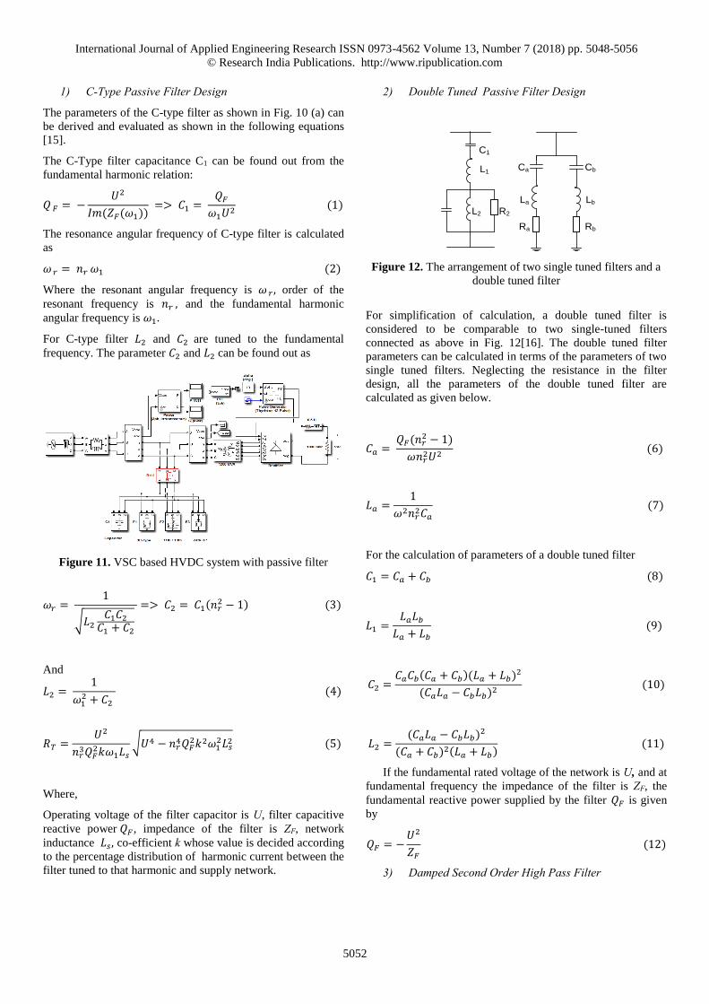
PASSIVE HARMONIC FILTER DESIGN FOR VSC
BASED HVDC SYSTEM
Conventional Passive Filters with (1000MW resistive load)
The conventional passive filters used for harmonic elimination
consist of inductors, capacitors and resistors. They are
categorized as high-pass or band-pass filters and tuned filters.
In a shunt configuration of VSC based HVDC system these
filters are connected in parallel with nonlinear loads such as
uncontrolled/controlled rectifiers, fluorescent lamps, or
electric arc furnaces. Taking the VSC based HVDC system
with the same DC load into consideration here three passive
filters are designed of total reactive power rating of 600 Mvar
[11]. First one is a C-type filter tuned to the 3rd harmonic
frequency, second one is a double-tuned filter tuned to 11th and
13th harmonic frequency and last one is a second order high-
pass filter tuned to the 24th harmonic frequency[12]. The filter
configurations are given in Fig 10. All the filter parameters are
calculated and provided in Table III [13]-[14]. The complete
configuration of VSC based HVDC system is provided in Fig.
11.
C
L
R
C1 C1
L1
C2 L2 R2
C
R L
(a) (b) (c)
Figure 10. Passive filters (a) C-type filter, (b) double tuned
filter, and (c) second order high pass filter
0 0.01 0.02 0.03 0.04 0.05 0.06 0.07 0.08 0.09 0.1
-10000
1000
Time (s)
Mag
nit
ud
e
0 500 1000 1500 2000 25000
50
100
Frequency (Hz)Mag
(%
of
Fu
nd
am
en
tal)
Fundamental (60Hz) = 1833 , THD= 5.29%
0 0.01 0.02 0.03 0.04 0.05 0.06 0.07 0.08 0.09 0.1
-10000
1000
Time (s)
Mag
nit
ud
e
0 500 1000 1500 2000 25000
50
100
Frequency (Hz)Mag
(%
of
Fu
nd
am
en
tal)
Fundamental (60Hz) = 1833 , THD= 5.29%
0 0.01 0.02 0.03 0.04 0.05 0.06 0.07 0.08 0.09 0.10
2
4
6
8
10
12x 10
8
Time (s)
Mag
nit
ud
e
International Journal of Applied Engineering Research ISSN 0973-4562 Volume 13, Number 7 (2018) pp. 5048-5056
© Research India Publications. http://www.ripublication.com
5052
1) C-Type Passive Filter Design
The parameters of the C-type filter as shown in Fig. 10 (a) can
be derived and evaluated as shown in the following equations
[15].
The C-Type filter capacitance C1 can be found out from the
fundamental harmonic relation:
𝑄 𝐹 = −𝑈2
𝐼𝑚(𝑍𝐹(𝜔1)) => 𝐶1 =
𝑄𝐹
𝜔1𝑈2 (1)
The resonance angular frequency of C-type filter is calculated
as
𝜔 𝑟 = 𝑛𝑟 𝜔1 (2)
Where the resonant angular frequency is 𝜔 𝑟 , order of the
resonant frequency is 𝑛𝑟 , and the fundamental harmonic
angular frequency is 𝜔1.
For C-type filter 𝐿2 and 𝐶2 are tuned to the fundamental
frequency. The parameter 𝐶2 and 𝐿2 can be found out as
Figure 11. VSC based HVDC system with passive filter
𝜔𝑟 = 1
√𝐿2𝐶1𝐶2
𝐶1 + 𝐶2
=> 𝐶2 = 𝐶1(𝑛𝑟2 − 1) (3)
And
𝐿2 = 1
𝜔12 + 𝐶2
(4)
𝑅𝑇 =𝑈2
𝑛𝑟3𝑄𝐹
2𝑘𝜔1𝐿𝑠
√𝑈4 − 𝑛𝑟4𝑄𝐹
2𝑘2𝜔12𝐿𝑠
2 (5)
Where,
Operating voltage of the filter capacitor is U, filter capacitive
reactive power 𝑄𝐹 , impedance of the filter is ZF, network
inductance 𝐿𝑠, co-efficient k whose value is decided according
to the percentage distribution of harmonic current between the
filter tuned to that harmonic and supply network.
2) Double Tuned Passive Filter Design
C1
L1
L2 R2
Ra
CbCa
Rb
La Lb
Figure 12. The arrangement of two single tuned filters and a
double tuned filter
For simplification of calculation, a double tuned filter is
considered to be comparable to two single-tuned filters
connected as above in Fig. 12[16]. The double tuned filter
parameters can be calculated in terms of the parameters of two
single tuned filters. Neglecting the resistance in the filter
design, all the parameters of the double tuned filter are
calculated as given below.
𝐶𝑎 = 𝑄𝐹(𝑛𝑟
2 − 1)
𝜔𝑛𝑟2𝑈2
(6)
𝐿𝑎 =1
𝜔2𝑛𝑟2𝐶𝑎
(7)
For the calculation of parameters of a double tuned filter
𝐶1 = 𝐶𝑎 + 𝐶𝑏 (8)
𝐿1 =𝐿𝑎𝐿𝑏
𝐿𝑎 + 𝐿𝑏
(9)
𝐶2 =𝐶𝑎𝐶𝑏(𝐶𝑎 + 𝐶𝑏)(𝐿𝑎 + 𝐿𝑏)2
(𝐶𝑎𝐿𝑎 − 𝐶𝑏𝐿𝑏)2 (10)
𝐿2 =(𝐶𝑎𝐿𝑎 − 𝐶𝑏𝐿𝑏)2
(𝐶𝑎 + 𝐶𝑏)2(𝐿𝑎 + 𝐿𝑏) (11)
If the fundamental rated voltage of the network is U, and at
fundamental frequency the impedance of the filter is ZF, the
fundamental reactive power supplied by the filter 𝑄𝐹 is given
by
𝑄𝐹 = −𝑈2
𝑍𝐹
(12)
3) Damped Second Order High Pass Filter

International Journal of Applied Engineering Research ISSN 0973-4562 Volume 13, Number 7 (2018) pp. 5048-5056
© Research India Publications. http://www.ripublication.com
5053
The typical arrangement of a damped high-pass filter is shown
in Fig. 10 (c). The capacitive and reactive reactance and the
resistance can be determined from the following equations
[17].
𝑋𝐶 =𝑈2
𝑄𝐹
(13)
Reactor reactance to trap the 𝑛𝑟 th harmonic will have the
value of
𝑋𝐿 =𝑋𝐶
𝑛𝑟2
(14)
𝑅 = 𝑋𝑛 𝑄, 𝑅 = 𝑋𝐿𝑛𝑟 𝑄 (15)
The filter size can be found out in terms of the reactive power
generated at fundamental-frequency
𝑄𝐹 = 𝑈2
𝑋𝐶 − 𝑋𝐿
(16)
Table III: Parameters of the Passive Filter Configuration
Operating voltage of the AC network (kV) 500
Frequency (Hz) 60
Each Branch Size (MVar) 150
Branch
Type
Tuning
Harmonic
Quality
Factor
L (mH) C (µF) R (Ω)
C-Type
High Pass
3 2 550 C1 = 1.59
C = 12.7
1111.11
Double
Tuned
11, 13 20 L1 = 15.2
L2 = 0.46
C1 = 3.15
C2 = 107
2740
High Pass 24 7 7.67 1.59 486
4) Simulation Results
Figure 13. AC source voltage, source current & load current
waveforms with passive filter.
Figure 14. Harmonic spectrum of load current with passive
filter.
Figure 15. Harmonic spectrum of source voltage with passive
filter.
Figure 16. Harmonic spectrum of source current with passive
filter.
-5
0
5x 10
5
So
urc
e V
olta
ge
(V
)
-2000
-1000
0
1000
2000
Sourc
e C
urr
ent
(A)
Iabc_B1
0 0.005 0.01 0.015 0.02 0.025 0.03 0.035 0.04 0.045 0.05
-2000
0
2000
Time (s)
Load C
urr
ent
(A)
0 0.01 0.02 0.03 0.04 0.05 0.06 0.07 0.08 0.09 0.1
-1000
0
1000
Time (s)
Am
pli
tude
0 5 10 15 20 250
20
40
60
80
100
Harmonic order
Fundamental (60Hz) = 1966 , THD= 9.10%
Mag (
% o
f F
undam
enta
l)
0 0.01 0.02 0.03 0.04 0.05 0.06 0.07 0.08 0.09 0.1
-1000
0
1000
Time (s)
Am
pli
tud
e
0 5 10 15 20 250
20
40
60
80
100
Harmonic order
Fundamental (60Hz) = 1966 , THD= 9.10%
Mag
(%
of
Fu
nd
am
en
tal)
0 0.02 0.04 0.06 0.08 0.1
-2
0
2
4x 10
5
Time (s)
Am
pli
tude
0 5 10 15 20 250
20
40
60
80
100
Harmonic order
Fundamental (60Hz) = 3.866e+05 , THD= 2.92%
Mag (
% o
f F
undam
enta
l)
0 0.02 0.04 0.06 0.08 0.1
-2
0
2
4x 10
5
Time (s)
Am
pli
tude
0 5 10 15 20 250
20
40
60
80
100
Harmonic order
Fundamental (60Hz) = 3.866e+05 , THD= 2.92%
Mag (
% o
f F
undam
enta
l)
0 0.01 0.02 0.03 0.04 0.05 0.06 0.07 0.08 0.09 0.1
-1000
0
1000
Time (s)
Am
pli
tude
0 5 10 15 20 250
20
40
60
80
100
Harmonic order
Fundamental (60Hz) = 1766 , THD= 3.18%
Mag (
% o
f F
undam
enta
l)
0 0.01 0.02 0.03 0.04 0.05 0.06 0.07 0.08 0.09 0.1
-1000
0
1000
Time (s)
Am
pli
tud
e
0 5 10 15 20 250
20
40
60
80
100
Harmonic order
Fundamental (60Hz) = 1766 , THD= 3.18%
Mag
(%
of
Fu
nd
am
en
tal)
International Journal of Applied Engineering Research ISSN 0973-4562 Volume 13, Number 7 (2018) pp. 5048-5056
© Research India Publications. http://www.ripublication.com
5054
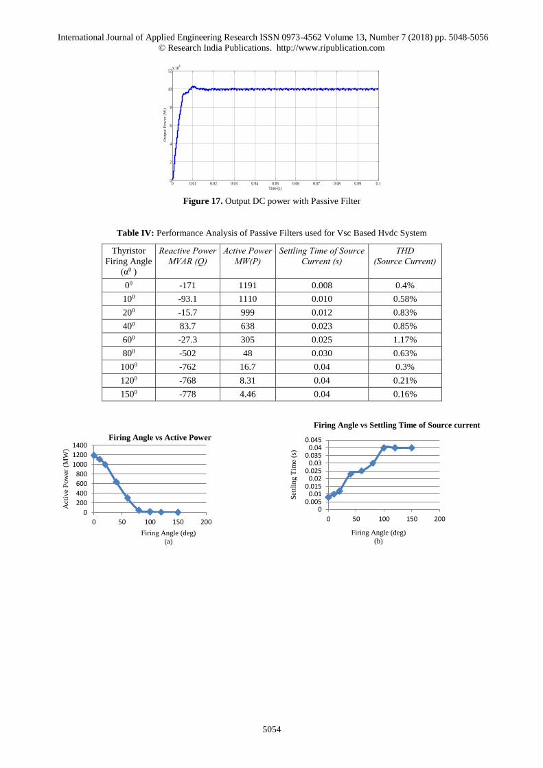
Figure 17. Output DC power with Passive Filter
Table IV: Performance Analysis of Passive Filters used for Vsc Based Hvdc System
Thyristor
Firing Angle
(α0 )
Reactive Power MVAR (Q)
Active Power MW(P)
Settling Time of Source Current (s)
THD (Source Current)
00 -171 1191 0.008 0.4%
100 -93.1 1110 0.010 0.58%
200 -15.7 999 0.012 0.83%
400 83.7 638 0.023 0.85%
600 -27.3 305 0.025 1.17%
800 -502 48 0.030 0.63%
1000 -762 16.7 0.04 0.3%
1200 -768 8.31 0.04 0.21%
1500 -778 4.46 0.04 0.16%
0 0.01 0.02 0.03 0.04 0.05 0.06 0.07 0.08 0.09 0.10
2
4
6
8
10
12x 10
8
Time (s)
Outp
ut
Pow
er
(W)
0
200
400
600
800
1000
1200
1400
0 50 100 150 200
Act
ive
Pow
er (
MW
)
Firing Angle (deg)
(a)
Firing Angle vs Active Power
00.005
0.010.015
0.020.025
0.030.035
0.040.045
0 50 100 150 200
Set
tlin
g T
ime
(s)
Firing Angle (deg)
(b)
Firing Angle vs Settling Time of Source current
International Journal of Applied Engineering Research ISSN 0973-4562 Volume 13, Number 7 (2018) pp. 5048-5056
© Research India Publications. http://www.ripublication.com
5055
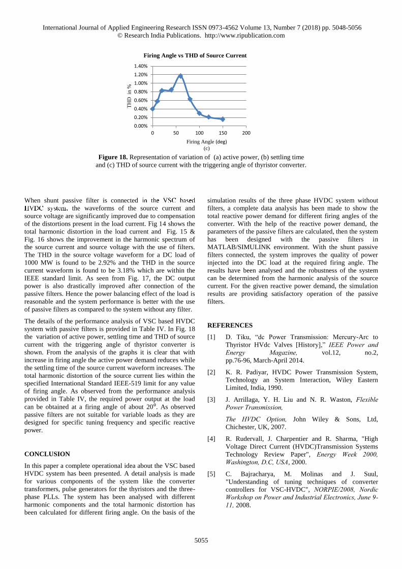
Figure 18. Representation of variation of (a) active power, (b) settling time
and (c) THD of source current with the triggering angle of thyristor converter.
When shunt passive filter is connected
the waveforms of the source current and
source voltage are significantly improved due to compensation
of the distortions present in the load current. Fig 14 shows the
total harmonic distortion in the load current and Fig. 15 &
Fig. 16 shows the improvement in the harmonic spectrum of
the source current and source voltage with the use of filters.
The THD in the source voltage waveform for a DC load of
1000 MW is found to be 2.92% and the THD in the source
current waveform is found to be 3.18% which are within the
IEEE standard limit. As seen from Fig. 17, the DC output
power is also drastically improved after connection of the
passive filters. Hence the power balancing effect of the load is
reasonable and the system performance is better with the use
of passive filters as compared to the system without any filter.
The details of the performance analysis of VSC based HVDC
system with passive filters is provided in Table IV. In Fig. 18
the variation of active power, settling time and THD of source
current with the triggering angle of thyristor converter is
shown. From the analysis of the graphs it is clear that with
increase in firing angle the active power demand reduces while
the settling time of the source current waveform increases. The
total harmonic distortion of the source current lies within the
specified International Standard IEEE-519 limit for any value
of firing angle. As observed from the performance analysis
provided in Table IV, the required power output at the load
can be obtained at a firing angle of about 20⁰. As observed
passive filters are not suitable for variable loads as they are
designed for specific tuning frequency and specific reactive
power.
CONCLUSION
In this paper a complete operational idea about the VSC based
HVDC system has been presented. A detail analysis is made
for various components of the system like the converter
transformers, pulse generators for the thyristors and the three-
phase PLLs. The system has been analysed with different
harmonic components and the total harmonic distortion has
been calculated for different firing angle. On the basis of the
simulation results of the three phase HVDC system without
filters, a complete data analysis has been made to show the
total reactive power demand for different firing angles of the
converter. With the help of the reactive power demand, the
parameters of the passive filters are calculated, then the system
has been designed with the passive filters in
MATLAB/SIMULINK environment. With the shunt passive
filters connected, the system improves the quality of power
injected into the DC load at the required firing angle. The
results have been analysed and the robustness of the system
can be determined from the harmonic analysis of the source
current. For the given reactive power demand, the simulation
results are providing satisfactory operation of the passive
filters.
REFERENCES
[1] D. Tiku, “dc Power Transmission: Mercury-Arc to
Thyristor HVdc Valves [History],” IEEE Power and Energy Magazine, vol.12, no.2,
pp.76-96, March-April 2014.
[2] K. R. Padiyar, HVDC Power Transmission System,
Technology an System Interaction, Wiley Eastern
Limited, India, 1990.
[3] J. Arrillaga, Y. H. Liu and N. R. Waston, Flexible Power Transmission,
The HVDC Option, John Wiley & Sons, Ltd,
Chichester, UK, 2007.
[4] R. Rudervall, J. Charpentier and R. Sharma, "High
Voltage Direct Current (HVDC)Transmission Systems
Technology Review Paper", Energy Week 2000, Washington, D.C, USA, 2000.
[5] C. Bajracharya, M. Molinas and J. Suul,
"Understanding of tuning techniques of converter
controllers for VSC-HVDC", NORPIE/2008, Nordic Workshop on Power and Industrial Electronics, June 9-11, 2008.
0.00%
0.20%
0.40%
0.60%
0.80%
1.00%
1.20%
1.40%
0 50 100 150 200T
HD
in
%
Firing Angle (deg)(c)
Firing Angle vs THD of Source Current
International Journal of Applied Engineering Research ISSN 0973-4562 Volume 13, Number 7 (2018) pp. 5048-5056
© Research India Publications. http://www.ripublication.com
5056
[6] B. Singh, S. Gairola, B.N. Singh, A. Chandra, K. Al-
Haddad, “Multipulse AC–DC Converters for Improving
Power Quality: A Review,” IEEE Trans Power Electron, vol.23, no.1, pp.260-281, Jan. 2008.
[7] R. Agarwal and S. Singh, "Harmonic Mitigation in
Voltage Source Converters based HVDC system Using
12-Pulse AC-DC Converters", in Annual IEEE India Conference (INDICON), 2014.
[8] D. Madhan Mohan, B. Singh, B.K. Panigrahi,
“Harmonic optimised 24- pulse voltage source
converter for high voltage DC systems,” IET Power
Electronics, vol.2, no.5, pp.563-573, Sept. 2009.
[9] S. Singh, B. Singh, “Passive filter design for a 12-pulse
converter fedLCI-synchronous motor drive,” in Proc. IEEE PEDES, 2010, pp.1-8.
[10] D. M. Mohan, B. Singh, K. B. Panigrahi, “Analysis and
design of threelevel, 24-pulse double bridge Voltage
Source Converter based HVDC system for active and
reactive power control,” in Proc. IEEE PEDES, pp.1-7,
2010.
[11] A. A. Rockhill, M. Liserre, R. Teodorescu, and P.
Rodriguez, “Grid-filter design for a multimegawatt
medium-voltage voltage-source inverter,” IEEE Trans. Ind. Electron., vol. 58, no. 4, pp. 1205–1217, Apr.
2011.
[12] P. Channegowda and V. John, “Filter optimization for
grid interactive voltage source inverters,” IEEE Trans. Ind. Electron., vol. 57, no. 12, pp. 4106–4114, Dec.
2010.
[13] B. Misra, B. K. Nayak, "Performance Analysis of
Hybrid Filters in High Power Applications", 2nd International Conference on Contemporary Computing and Informatics (ic3i), pp. 330-335, 2016.
[14] R. Beres, X. Wang, F. Blaabjerg, C. Bak, M. Liserre,
"A review of passive filters for grid-connected voltage
source converters". In: Applied Power Electronics Conference and Exposition (APEC), 2014 Twenty-Ninth Annual IEEE, pp. 2208–2215, 2014.
[15] Klempka R., A New Method for the C-Type Passive Filter Design. Electrical Review 7a, pp. 277-281.
[16] P. Li and Q. Hao, "The algorithm for the parameters of
AC filters in HVDC transmission system", in 2008 IEEE/PES Transmission and Distribution Conference and Exposition, Chicago, IL, 2008, pp. 1 - 6.
[17] B. Badrzadeh, K. Smith and R. Wilson, "Designing
Passive Harmonic Filters for an Aluminum Smelting
Plant", IEEE Transactions on Industry Applications,
vol. 47, no. 2, pp. 973-983, 2011.