UMW UMW 6312...
12
UMW 6312 GENERAL DESCRIPTION is a high-performance current mode PWM control IC designed for AC/DC convertor, which built-in high-voltage power switch tube and supplies continuous output power of 10W within the range of wide-voltage between 85V and 300V, the output power of peak value can be up to 12W.The combination of optimized reasonable circuit design and bipolar facture technology with high performance and price ratio economizes the whole cost ultimately. The power controller can be applied to the typical flyback circuit topology so as to form a simple AC/DC transformer. IC circuit can use the power switch tube itself within a larger version of startup, greatly reduces the power loss of starting resistance .IC built-in PFM function that when the output power increases then the working frequency increases, thus reducing switching loss and achieving high efficiency when the power output decreases. The PFM function combination of patent drive circuit that can easily meet "of energy Star 2.0" strict requirements. When VCC reaches 12V, the chip internal over voltage protection activates and limits the output voltage rising. That can prevent the too high output voltage because the light coupling or the feedback circuit damaged. The circuit built-in the input voltage compensation function, which realizes the constant output power limiting in the whole power grid conditions. In the IC internal that provides the overload and the perfect saturation function. It can real time control van overload, transformer saturation, output short circuit in abnormal condition, so improving the reliability of power supply. IC has integrated the internal temperature protection function, when the system is overheating, the output power will be lower, or shuts down the output. We can provide meeting ROHS and green environmental protection requirements of DIP-8 standard. FEATURES ■ Meeting AC85-300V input voltage range of the design requirements ■ Low starting current and working current ■ The standby power consumption can be as low as 0.15W ■ Improve driving circuit efficiency 2-3% ■ Meeting the requirements of energy efficiency energy star 2.0 ■ With temperature compensation function accurate current control ■ Wide voltage continuous output power can be up to 10W, the peak output power can be up to 12W ■ AC line compensation ■ With functions of thermal protection (OTP) ■ With functions of over voltage protection (OVP) ■ Can be realized without Y capacitor system design ■ Less peripheral components, and the overall scheme of low cost APPLICATIONS ■ The charger ■ DVD/DVB power ■ Small appliances (such as: induction cooker) ■ PC&LCD TV standby power supply ■ The power adapter (such as communications terminal products) UMW 6312 UMW R UMW 6312 UMW 6312 1 www.umw-ic.com 友台半导体有限公司
Transcript of UMW UMW 6312...

UMW 6312
GENERAL DESCRIPTIONis a high-performance current mode PWM
control IC designed for AC/DC convertor, which built-inhigh-voltage power switch tube and suppliescontinuous output power of 10W within the range ofwide-voltage between 85V and 300V, the output powerof peak value can be up to 12W.The combination ofoptimized reasonable circuit design and bipolar facturetechnology with high performance and price ratioeconomizes the whole cost ultimately. The powercontroller can be applied to the typical flyback circuittopology so as to form a simple AC/DC transformer. ICcircuit can use the power switch tube itself within alarger version of startup, greatly reduces the powerloss of starting resistance .IC built-in PFM function thatwhen the output power increases then the workingfrequency increases, thus reducing switching loss andachieving high efficiency when the power outputdecreases. The PFM function combination of patentdrive circuit that can easily meet "of energy Star 2.0"strict requirements. When VCC reaches 12V, the chipinternal over voltage protection activates and limits theoutput voltage rising. That can prevent the too highoutput voltage because the light coupling or thefeedback circuit damaged. The circuit built-in the inputvoltage compensation function, which realizes theconstant output power limiting in the whole power gridconditions. In the IC internal that provides the overloadand the perfect saturation function. It can real timecontrol van overload, transformer saturation, outputshort circuit in abnormal condition, so improving thereliability of power supply. IC has integrated theinternal temperature protection function, when thesystem is overheating, the output power will be lower,or shuts down the output. We can provide meetingROHS and green environmental protectionrequirements of DIP-8 standard.
FEATURES Meeting AC85-300V input voltage range ofthe design requirements
Low starting current and working current The standby power consumption can beas low as 0.15W
Improve driving circuit efficiency 2-3% Meeting the requirements of energyefficiency energy star 2.0
With temperature compensationfunction accurate current control
Wide voltage continuous output power can beup to 10W, the peak output power can be upto 12W
AC line compensation With functions of thermal protection (OTP) With functions of over voltage protection (OVP) Can be realized without Y capacitorsystem design
Less peripheral components, and the
overall scheme of low cost
APPLICATIONS The charger DVD/DVB power Small appliances (such as: induction cooker) PC&LCD TV standby power supply The power adapter (such as
communications terminal products)
UMW 6312UMW
R
UMW 6312UMW 6312
1www.umw-ic.com 友台半导体有限公司
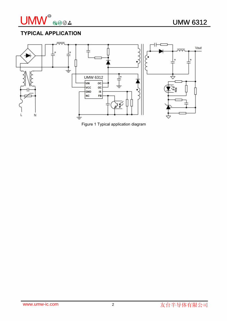
TYPICAL APPLICATION
Figure 1 Typical application diagram
UMW 6312UMW
R
UMW 6312UMW 6312
UMW 6312
2www.umw-ic.com 友台半导体有限公司

GENERALINFORMATIONPin Configuration Absolute Maximum RatingsThe pin map is shown as below for DIP-8 Power supply voltage VCC 18V
Pins input voltage VCC+0.3V
VIN OC Endurance voltage of OC collector -0.3-750V
VCC OCSwitching current of peak value 1000mA
Total dissipation power 1500mW
GND IS Operating temperature range -20 to +125
NC FBDeposit temperature range -55 to +150
Welding temperature +260,10S
TERMINAL ASSIGNMENTSPin Num. Pin Name I/O Description
1 VIN ICircuit input compensation and high voltage current source to triggerfeet, external compensation resistance
2 VCC P Power Supply3 GND P Ground4 NC No Connection5 FB I Feedback pins
6 IS ISwitching current sampling and limit enactment, sampling resistanceof external current
7/8 OC O Output pins, meet switching transformer
Recommended operating conditions
PARAMETER MIN TYP MAX UNITPower supply voltage VCC 5 10 V
Pins input voltage -0.3 - Vcc VPeak inverse voltage - - 650 V
Switching current of peak value - 800 mAOperating temperature -10 100
UMW 6312UMW
R
UMW 6312UMW 6312
UMW 6312
3www.umw-ic.com 友台半导体有限公司
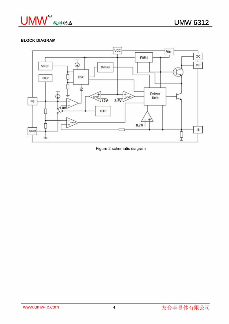
BLOCK DIAGRAM
Figure 2 schematic diagram
UMW 6312UMW
R
UMW 6312UMW 6312
4www.umw-ic.com 友台半导体有限公司
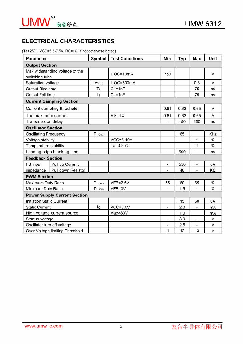
ELECTRICAL CHARACTERISTICS(Ta=25, VCC=5.5-7.5V, RS=1Ω, if not otherwise noted)
Parameter Symbol Test Conditions Min Typ Max UnitOutput SectionMax withstanding voltage of the
I_OC=10mA 750 Vswitching tubeSaturation voltage Vsat I_OC=500mA 0.8 VOutput Rise time TR CL=1nF 75 nsOutput Fall time TF CL=1nF 75 nsCurrent Sampling SectionCurrent sampling threshold 0.61 0.63 0.65 V
The maximum current RS=1Ω 0.61 0.63 0.65 ATransmission delay - 150 250 nsOscillator SectionOscillating Frequency F_OSC 65 KHzVoltage stability VCC=5-10V 1 %Temperature stability Ta=0-85 1 %Leading edge blanking time - 500 - nsFeedback SectionFB Input Pull up Current - 550 - uAimpedance Pull down Resistor - 40 - KΩPWM SectionMaximum Duty Ratio D_max VFB=2.5V 55 60 65 %Minimum Duty Ratio D_min VFB=0V - 1.5 - %Power Supply Current SectionInitiation Static Current 15 50 uAStatic Current IQ VCC=8.0V - 2.0 - mAHigh voltage current source Vac>80V 1.0 mAStartup voltage - 8.9 - VOscillator turn off voltage - 2.5 - VOver Voltage limiting Threshold 11 12 13 V
UMW 6312UMW
R
UMW 6312UMW 6312
5www.umw-ic.com 友台半导体有限公司
OPERATION DESCRIPTIONStart control: During start-up phase, the internalbenchmark, oscillators, driving circuit andprotection circuit is stopped working, the smallcurrent of 50uA on the starting resistance is inputfrom VIN to the base of the Power Transistor, theamplifying current from Emitter through currentlimiting circuit outflows to VCC, more than 50uAcurrent part charge to parallel capacitor of VCC,when VCC voltage rises to 8.9 V, entering a stateof PWM control chip.PWM control: The voltage of FB pins through thepartial pressure resistance exports to the PWMcomparator as the peak switching currentreference, the FB signal determines the size ofthe switch tube peak current, through the FB torealize the control of the PWM control. At thesame time the Output pulse duty ratio is limited bymaximum duty cycle, the FB is controlled byinternal and external feedback circuit.External feedback circuit: After amplification thesystem output error adjusting signal is convertedinto current signal that can adjust the voltage ofFB by isolation transmission of the optocoupler.The heavier load, the smaller optocoupler current,the higher FB voltage, the greater duty ratio ofPWM signal, the output power increases, and viceversa, the load is light, the feedback current isadded, the FB voltage decreases, the duty ratiodecreases, and the output decreases, so as torealize the adjustment of the output voltage.VCC overvoltage protection circuit: if the peripheralfeedback makes the VCC increasing that is morethan 12V, then the internal feedback circuit makesthe FB voltage reducing and reducing the outputpower, it makes the VCC voltage keeping in 12V, thisfeature can prevent the output voltage increasingbecause the optocoupler or feedback is damaged.Thus the secondary circuit and its output load will notdamage.
Standby frequency reduction control circuit:In standby mode, when the output voltageincreases, then the FB voltages lower. If the FBvoltage is less than 1.8V (about between 1.2-1.8V)then the oscillator cycle will increase, the smallerFB, the wider oscillator cycle. This feature is toreduce the standby power consumption andprevent the occurrence of audio interference atthe same time.Efficient driving circuit: The efficient driving circuitmakes the switch tube in critical saturation drivingstate, improving the frequency of the triode,effectively reducing the triode switch loss, improvingthe work efficiency of the whole system, greatlyreducing the fever of the chip at the same time. Thatmakes the system more reliable.AC line compensation: The chip from VINdetects the voltage size and real-timecompensate the maximum output power; thismakes the maximum limiting power constant.When high and low ac is input.Thermal protection function: When the internaltemperature is higher than 140, then makingthe internal FB voltage reducing and the oscillatorcycle widening, reducing or closing the poweroutput, so the temperature does notexceed 150 in order to achieve protection.
UMW 6312UMW
R
UMW 6312UMW 6312
6www.umw-ic.com 友台半导体有限公司
UMW 6312

Electric Parameter DefinitionsStart-up static current: The minimum currentsourcing current which can enable VCC surgingwhen VCC is connected to a filter capacitor andan adjustable current sourcing.Start-up voltage: The maximum of VCC above.Restart-up voltage: The minimum of VCCabove.Oscillator shut-down voltage: The Negativeedge of VCC above; the value of VCC whichcan stop the oscillator.Static current: The VCC power supply current innormal period when FB is connected to theground by a 1.0KΩ resistance.FB pull up current: which occurs in normalperiod, when FB=2.5V, and IS=0A.FB upper current protection: The pull downcurrent of FB when FB=2.0V and IS=0.3A innormal period.The VCC voltage limit: The value of VCC whenthere is no feedback circuit of in normalperiod.OC upper limit current: If FB=2.0V, theminimum OC current when there is pull downcurrent in FB.
Application information FB feedback and controlIn normal working state, the FB voltage willdetermine the maximum switching current value,the higher the voltage, the bigger switch current(only limited to peak current limit). The FB pininternal pull-up 550uA current source, pull-downabout 40KΩ resistor (approximate equivalent),An external resistor reduces the depth of thefeedback, the size of the external resistance willnot affect the maximum peak current, it isrecommended to use 7.5K to 10K resistor, anexternal resistor can improve reaction speed ofthe system with overload and the input voltagejumping. It is advantageous to the short circuitprotection. Moreover the FB voltage below 1.8V,will make the period of oscillation widening, theswitch frequency falling, It is lower than 1.8V,the frequency will be lower. FB convertercapacitance will affect feedback bandwidth, thusinfluence some external parameters, such astransient characteristics.
Figure 3. FB feedback and control
UMW 6312UMW
R
UMW 6312UMW 6312
7www.umw-ic.com 友台半导体有限公司
UMW 6312

Typical applications for CFB capacitance value, canbe between 10-100nF selection based on thefrequency characteristics of the feedback loop,General application can use the 100nF.Over temperature protectionIC has built-in precision over temperature protectionfunction. In the chip internal when the temperaturereaches 140 , the thermal protection circuit pullsdown the clock signal, and the switch frequency isreduced in order to reduce the power consumption.The Switching frequency decreases with the rise ofthe temperature, and until the oscillation shuts down.As shown in the figure below
Figure 4.Over temperature protectionPower tube driving characteristics and highpressure offset technology
In the IC internal, it has an unique offset technology,at the time of power tube shutting off, the base outputof Power Transistor drops down to the groundinstantly, at the same time the offset output voltage ofemitter is greater than the base. Launching E junction
reverse, it accelerates the IC current rate of descentand expands the effective security work area, The CBof the switch tube is in the reverse voltage thatachieves greater than 750V voltage. About moredetails of the switch tube please refer to the relevanttechnical data compression characteristics.
Figure5 The collector emitter clamping voltage
Offset waveform as shown in the figure below:
Figure 6 Vbe driving voltage waveformOver voltage and under-voltage protectionIC has with hysteresis under voltage protectionfunction. When the VCC voltage achieves to 8.9V the IC will start, the initial voltage is providedby a driving resistor, the input of high voltagethrough the driving resistor enters to B injectionof the switch tube, the amplifying IC currentthrough current limiting circuit outflows to VCCcapacitor Thus forming the driving voltage. TheVCC voltage should be maintained in between5-10V (including full load) in the normal working,if the VCC voltage pulls down to 2.5V theoscillator will enter closed state.
V1.2
UMW 6312UMW
R
UMW 6312UMW 6312
8www.umw-ic.com 友台半导体有限公司
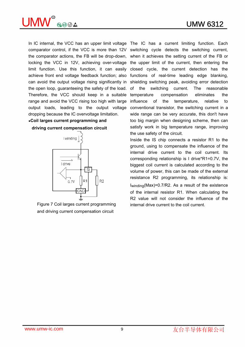
In IC internal, the VCC has an upper limit voltagecomparator control, if the VCC is more than 12Vthe comparator actions, the FB will be drop-down,locking the VCC in 12V, achieving over-voltagelimit function. Use this function, it can easilyachieve front end voltage feedback function; alsocan avoid the output voltage rising significantly inthe open loop, guaranteeing the safety of the load.Therefore, the VCC should keep in a suitablerange and avoid the VCC rising too high with largeoutput loads, leading to the output voltagedropping because the IC overvoltage limitation.Coil larges current programming anddriving current compensation circuit
Figure 7 Coil larges current programming
and driving current compensation circuit
The IC has a current limiting function. Eachswitching cycle detects the switching current,when it achieves the setting current of the FB orthe upper limit of the current, then entering theclosed cycle, the current detection has thefunctions of real-time leading edge blanking,shielding switching peak, avoiding error detectionof the switching current. The reasonabletemperature compensation eliminates theinfluence of the temperature, relative toconventional transistor, the switching current in awide range can be very accurate, this don't havetoo big margin when designing scheme, then cansatisfy work in big temperature range, improvingthe use safety of the circuit.Inside the IS chip connects a resistor R1 to theground, using to compensate the influence of theinternal drive current to the coil current. Itscorresponding relationship is I drive*R1=0.7V, thebiggest coil current is calculated according to thevolume of power, this can be made of the externalresistance R2 programming, its relationship is:
Iwinding(Max)=0.7/R2. As a result of the existenceof the internal resistor R1. When calculating theR2 value will not consider the influence of theinternal drive current to the coil current.
UMW 6312UMW
R
UMW 6312UMW 6312
9www.umw-ic.com 友台半导体有限公司

The heat dissipation requirementsAs a result of the drive technology breakthrough, thechip internal loss (fever) 40% less than the PIN TOPIN the other products, but for a typical power switch,should use the necessary cooling measures, in orderto avoid high temperature lead to thermal protection.In the IC internal, this main heating is the generatedby the switching loss, so the appropriate coolingposition is the IC Pin7-8 feet, an easy to use methodis laid a certain area of PCB copper foil in Pin7-8 feet,especially it will increase thermal capacity on copperfoil tinning, For a 85-265V input, typical application of10W output, 200mm ² is the size of copper foil isnecessary.
VCC design pointsWhen the VCC voltage rises to 8.9V, the IC willstart, the VCC capacitor will store enoughpower for IC before entering normal workinguntil establishing normal output voltage; So theVCC capacitor is not too small, and thereasonable VCC capacitor is 22uF.
Figure 8 Heat dissipation map
UMW 6312UMW
R
UMW 6312UMW 6312
10www.umw-ic.com 友台半导体有限公司

Package size
Dimensions In Dimensions In InchesSymbol Millimeters
Min Max Min Max
A 3.710 4.310 0.146 0.170
A1 0.510 0.020 -
A2 3.200 3.600 0.126 0.142
B 0.380 0.570 0.015 0.020
B1 1.524(BSC) 0.060(BSC)
C 0.204 0.360 0.008 0.014
D 9.000 9.400 0.354 0.370
E 6.200 6.600 0.244 0.260
E1 7.320 7.920 0.288 0.312
e 2.540(BSC) 0.100(BSC)
L 3.00 3.60 0.118 0.142
E2 8.400 9.000 0.331 0.354
UMW 6312UMW
R
UMW 6312UMW 6312
11www.umw-ic.com 友台半导体有限公司
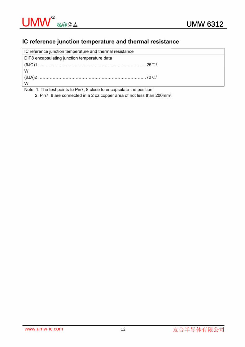
IC reference junction temperature and thermal resistanceIC reference junction temperature and thermal resistanceDIP8 encapsulating junction temperature data(θJC)1 …………………………………………………………………25/W(θJA)2 …………………………………………………………………70/WNote: 1. The test points to Pin7, 8 close to encapsulate the position.
2. Pin7, 8 are connected in a 2 oz copper area of not less than 200mm².
UMW 6312UMW
R
UMW 6312UMW 6312
12www.umw-ic.com 友台半导体有限公司