Ultrashort Pulsed Lasers – Efficient Tools for Materials
30
14 Ultrashort Pulsed Lasers – Efficient Tools for Materials Micro-Processing Marian Zamfirescu 1,2 , Magdalena Ulmeanu 1 , Alina Bunea 2 , Gheorghe Sajin 2 and Razvan Dabu 1 1 National Institute for Laser, Plasma and Radiation Physics, 2 National Institute for Microtechnology, Romania 1. Introduction Fabrication technologies on the micro and nanometer scale are becoming more and more important from the viewpoint of industrial applications, for example: high-resolution lithography for manufacturing high-density recording media, high-resolution displays, and high sensitivity biomolecule sensor arrays. Electron-beam lithography, interferometric lithography, electron-beam evaporation of constituent materials and lift-off procedures were used to fabricate negative refractive-index metamaterials at the near-infrared (NIR) wavelengths (Zhang et al., 2005; Dolling et al., 2006; Dolling et al., 2007). Due to its capability for large-area fabrication, conventional photo-lithography is a wide-spread fabrication technology. Because the minimum feature size is limited by optical diffraction, sub-micrometer structures can be created by deep ultra-violet (DUV) at hundred-nanometer wavelengths or extreme ultra-violet (EUV) at ten-nanometer wavelengths lithography techniques (Gwyn et al., 1998). Because these technologies require complex vacuum optics, their cost remains prohibitive. Ultrashort pulsed lasers, particularly femtosecond lasers, could offer an alternative to currently used micro and nanostructuring methods (Nishiyama et al., 2008; Qi et al., 2009; Allsop et al., 2010; Sugioka et al., 2010). High peak power can be reached for femtosecond pulses at relatively low energy per pulse. Due to the high radiation intensity, nonlinear effects dominate the interaction of tightly focused femtosecond laser beams with materials. Pulsed laser micromachining involves the removal of material through the ablation process which consists in some consecutive physical processes: laser energy absorption, material heating, material expelling, and material cooling (Liu et al., 1997; Stuart et al., 1996). The first step in laser ablation is the absorption of laser energy by the target material. The absorption mechanism depends on laser intensity (laser fluence and pulsewidth) and can be accomplished by linear and nonlinear processes. For opaque materials at laser radiation wavelength, linear absorption is the main mechanism at long pulsewidths with low intensity, whereas the nonlinear absorption becomes dominant at ultrashort pulsewidths with high intensity. For transparent materials, absorption comes from nonlinear processes through laser-induced optical breakdown. It is a process where a normally transparent material is first transformed in absorbing plasma by avalanche ionization and multiphoton www.intechopen.com
Transcript of Ultrashort Pulsed Lasers – Efficient Tools for Materials

14
Ultrashort Pulsed Lasers – Efficient Tools for Materials Micro-Processing
Marian Zamfirescu1,2, Magdalena Ulmeanu1, Alina Bunea2, Gheorghe Sajin2 and Razvan Dabu1
1National Institute for Laser, Plasma and Radiation Physics, 2National Institute for Microtechnology,
Romania
1. Introduction
Fabrication technologies on the micro and nanometer scale are becoming more and more important from the viewpoint of industrial applications, for example: high-resolution lithography for manufacturing high-density recording media, high-resolution displays, and high sensitivity biomolecule sensor arrays. Electron-beam lithography, interferometric lithography, electron-beam evaporation of constituent materials and lift-off procedures were used to fabricate negative refractive-index metamaterials at the near-infrared (NIR) wavelengths (Zhang et al., 2005; Dolling et al., 2006; Dolling et al., 2007). Due to its capability for large-area fabrication, conventional photo-lithography is a wide-spread fabrication technology. Because the minimum feature size is limited by optical diffraction, sub-micrometer structures can be created by deep ultra-violet (DUV) at hundred-nanometer wavelengths or extreme ultra-violet (EUV) at ten-nanometer wavelengths lithography techniques (Gwyn et al., 1998). Because these technologies require complex vacuum optics, their cost remains prohibitive. Ultrashort pulsed lasers, particularly femtosecond lasers, could offer an alternative to currently used micro and nanostructuring methods (Nishiyama et al., 2008; Qi et al., 2009; Allsop et al., 2010; Sugioka et al., 2010). High peak power can be reached for femtosecond pulses at relatively low energy per pulse. Due to the high radiation intensity, nonlinear effects dominate the interaction of tightly focused femtosecond laser beams with materials. Pulsed laser micromachining involves the removal of material through the ablation process which consists in some consecutive physical processes: laser energy absorption, material heating, material expelling, and material cooling (Liu et al., 1997; Stuart et al., 1996). The first step in laser ablation is the absorption of laser energy by the target material. The absorption mechanism depends on laser intensity (laser fluence and pulsewidth) and can be accomplished by linear and nonlinear processes. For opaque materials at laser radiation wavelength, linear absorption is the main mechanism at long pulsewidths with low intensity, whereas the nonlinear absorption becomes dominant at ultrashort pulsewidths with high intensity. For transparent materials, absorption comes from nonlinear processes through laser-induced optical breakdown. It is a process where a normally transparent material is first transformed in absorbing plasma by avalanche ionization and multiphoton
www.intechopen.com

Recent Advances in Nanofabrication Techniques and Applications
262
ionization. At relatively low laser intensity, the avalanche ionization process in a transparent dielectric material is seeded by free electrons coming from material impurities, thermal or linear optical ionization of shallow energy levels of inclusions. Free electrons can absorb laser energy through the inverse Bremsstrahlung process, when they collide with the bound electrons and the material lattice. Seed electrons can be accelerated at energy exceeding the ionization potential of the bound electrons. The collisions of seed electrons with bound electrons give rise to an avalanche ionization process growing exponentially from the initial very low seed electrons density. When plasma with a critical density is created, the transparent material is broken down and becomes absorbing at laser radiation wavelength. If the laser field strength is very high, as in the case of femtosecond-pulse laser-matter interaction, bound electrons can be directly ionized through multiphoton absorption. For longer laser pulses (microsecond-nanosecond pulsewidths) where the field strength is lower, the multiphoton ionization contribution is negligible and laser-induced breakdown is dominated by avalanche ionization. For ultrashort pulses, multiphoton ionization determines the breakdown threshold behavior: only when the laser intensity exceeds a certain threshold the plasma density grows to the critical value where irreversible breakdown takes place. The avalanche ionization fluence breakdown threshold exhibits large fluctuations due to statistical variations of the number of seed electrons already present in the material. Multiphoton ionization can directly generate free electrons, it is not related to the impurity seed electrons. Consequently, the laser induced breakdown threshold at ultrashort pulsewidths becomes more precise. The material is heated up by the electrons energy transfer to the ions and the lattice. The amount of laser energy transfer during the laser pulse depends on the laser pulse duration and the energy coupling coefficient. Due to the thermal gradient, the absorbed energy can leave the laser focal volume by heat conduction and a larger volume is heated. For absorbing materials, such as metals and semiconductors, the laser pulse energy is absorbed in a surface layer whose thickness is given by the skin penetration depth, 1 sl , where is the absorption coefficient. The heat penetration depth due to the thermal conduction is given by the diffusion length, ld Dl , where D is the heat diffusion coefficient and l is the laser pulsewidth. For microsecond and nanosecond laser pulses, sd ll , and the volume of the heated material, hence the temperature, is determined by the heat diffusion length. Therefore, for long pulses, the fluence breakdown threshold varies with the laser pulsewidth as lthF . If the laser pulsewidth decreases, the diffusion length decreases too. For laser pulses in the femtoseconds range, sd ll , the skin penetration depth determines the heated volume during the laser pulse. As a result, the breakdown threshold becomes independent of the pulsewidth. For long pulses, a larger volume of material is heated and melted, but only a small layer of material reaches the vaporization temperature. Material removal is accomplished through melt expulsion driven by the vapor pressure and the recoil of the light pressure. This physical process involving fluid dynamics and vapor conditions is an instable one. For micro-processing applications, the resolidification of the melt after the ablation can lead to very irregular shapes of the holes or cuts. On the other hand, for ultrashort pulses, the laser energy is deposited in a thin layer with a thickness limited by the skin penetration depth. The localized energy heats the material very quickly at high temperatures to the vapor phase with high kinetic energy. The material removal takes place mainly by direct vaporization. Because most of the heated material reaches the vaporization temperature, the
www.intechopen.com
Ultrashort Pulsed Lasers – Efficient Tools for Materials Micro-Processing
263
resulting melt layer thickness is much smaller than in case of long pulses. After the laser pulse irradiation is finished, there is a rapid cooling due to the steep temperature gradient. Because little liquid is involved, the ablation process becomes highly precise in comparison to the long pulse case. By precision micromachining with femtosecond laser pulses, feature sizes with submicrometer resolution can be obtained (Chimmalgi et al., 2003). Micro- and nanostructures can be created also through some nonlinear optical processes that occur when the interaction of high intensity femtosecond laser radiation with materials is performed under the ablation threshold. By tightly focusing the femtosecond laser pulses into the bulk of transparent materials, 3D micro-structures can be produced by a permanent refractive-index modification inside a small focal volume (Will et al., 2002; Osellame et al., 2003; Vega et al., 2005). Laser energy is deposited in this volume by multi-photon absorption and avalanche ionization. The photogenerated hot electron plasma rapidly transfers its energy to the lattice giving rise to high temperatures and pressures. The nonelastic thermo-mechanical stress created in the focal region produces a local densification with an increase of refractive index over a micrometer-sized volume of the material. This index gradient allows one to fabricate complicated photonic structures in many transparent materials like fused silica (Will et al., 2002; Shah et al., 2005), silicate and phosphate glasses (Homoelle et al., 1999; Ams et al., 2005), chalcogenide thin films (Zoubir et al., 2004), sapphire (Wortmann et al., 2008), poly(methyl methacrylate) (Sowa et al., 2006). Various microstructures contributing to developments in integrated optics, optical communications, and optical data storage have been obtained by refractive-index patterning: optical waveguides (Will et al., 2002; Osellame et al., 2003; Zoubir et al., 2004; Ams et al., 2005; Sowa et al., 2006; Allsop et al., 2010), beam splitters (Homoelle et al., 1999), micro-channels (Wortmann et al., 2008), directional couplers (Streltsov & Borelli, 2001), three-dimensional data storage (Glezer et al., 1996), diffraction gratings (Takeshima et al., 2004), photonic crystals (Takeshima et al., 2005). In case of irradiation of UV-photopolymerizable materials with high-intensity tightly focused NIR femtosecond laser pulses, a nonlinear optical process of multi-photon absorption can take place. In such photopolymers, the two-photon absorption of NIR femtosecond laser pulses induces photochemical reactions and then photopolymerization, just like in the case of a single UV photon absorption (Maruo et al., 1997; Witzgall et al., 1998). Unlike the UV-radiation photo-polymerization by single photon absorption, a high-probability of two-photon absorption occurs only in a very tiny volume of material near the center of the focused laser spot, leaving behind photo-polymerized patterns with micrometer or sub-micrometer dimensions. Direct laser writing by multiphoton polymerization of photoresists has emerged as a technique for the rapid, cheap and flexible fabrication of 3D structures with a resolution beyond the diffraction limit, leading to advanced applications in telecommunication, photonics, metamaterials and biomedicine (Deubel et al., 2004; Rill et al., 2008; Ovsianikov et al., 2009; Farsari & Chichkov, 2009). In this chapter, we present some experimental results in the field of femtosecond laser micromachining and micro/nanostructuring of both opaque and transparent materials. Three-dimensional (3D) micro-structuring of negative photo-resists by two-photon photo-polymerization (TPP) using low energy high repetition rate NIR femtosecond lasers is described in the Section 2 of the paper. Fabrication of GHz range composite right/left handed (CRLH) devices by a technology that combines classical photo-lithography and femtosecond laser processing is described in the Section 3. Near-field laser lithography reaching a resolution beyond the diffraction limit through the interaction of ultra-short
www.intechopen.com

Recent Advances in Nanofabrication Techniques and Applications
264
pulsed laser beams with small size particles is presented in Section 4. In the Section 5, a micro-printing method based on femtosecond laser induced forward transfer (LIFT) of various materials deposited in thin films is demonstrated.
2. 3D structuring by two-photon photo-polymerization (TPP)
Building a 3D micro-structure was always a challenge, since micrometer and submicrometer resolutions are hardly obtained on complex arrangements using various materials. Applications such as microfluidics, micro- and nanoelectronics, integrated optics, motivated the development of manufacturing techniques. Among these, micro-milling, micro-moulding, electro-discharge machining, imprinting lithography, X-ray and UV lithography, electron and ion-beam lithography, chemical and plasma etching, laser rapid-prototyping, direct laser writing (DLW), are the most used microfabrication technologies (Frassila, 2010). However, none of these techniques satisfies simultaneously all the requirements in terms of spatial resolution, high-aspect-ratio of the structures, or ability of processing a large variety of materials and complex designs. Combinations of different techniques are sometimes the way for overcoming some technological bottlenecks. For example, X-ray lithography combined with electroforming and/or moulding allows microfabrication on metals or plastics with resolution below 100 nm and aspect-ratio up to 100 or even higher (Becker et al., 1986). However, the resulting structures are not fully 3D designs. These are more 2D structures with a finite dimension in Z direction, the so called 2½D structures. Despite of good resolution of the method in XY directions, such structures have limited complexity. 3D-stacking approach was recently used in combination with thin film deposition, lithographic and selective etching techniques for fabrication of 3D integrated circuits such as microprocessors and memories (Pavlidis et al., 2009). It requires complex and very expensive machineries justified only by very high mass production. From commercial point of view, for custom applications or limited series, these technologies are not the most competitive ones. The laser processing of materials always offered a cheap and reliable solution for microfabrication. The lasers become an omnipresent tool, from thin film deposition, to laser processing by ablation, or laser spectroscopy characterization. Concerning the fabrication of full 3D structures, the laser rapid prototyping or stereolithography have been developed by C.W. Hull in 1986. A 3D model can be created inside an UV-curable material. The UV-laser irradiates a photosensitive material layer by layer following a certain path. The size of the 3D model is typically of the order of few-mm to hundreds of mm in each direction, with resolution of tens of micrometers. Since the femtosecond lasers were developed, the approach of rapid prototyping inspired the development of micro-stereolithography (Maruo et al., 1997). The nonlinear effect such as two-photon absorption of NIR radiation is easily achieved in photoresists which usually absorb the UV radiation. When the material is transparent to NIR photons, the laser can be focused deeply in the volume of the material. At the tightly focused spot of a femtosecond nJ laser pulse, the laser intensity is high enough to exceed the threshold of the nonlinear absorption. Permanent physical and chemical modifications of the material take place in a small volume, deep inside of the transparent material. If the laser fluence is kept low enough, small features can be created with resolution down to tens of nm's (Farsari et al., 2005; Tan et al., 2007). By following the rapid-prototyping algorithms, a 3D model can be created layer by layer inside the material.
www.intechopen.com

Ultrashort Pulsed Lasers – Efficient Tools for Materials Micro-Processing
265
A large series of negative photoresists, among them SU-8, organically modified ceramics (Ormocer), or organically modified silicate (Ormosil), have the maximum of the absorption band in the UV-blue spectral range. In such photopolymers, the two-photon absorption of NIR Ti:sapphire femtosecond laser radiation induces photochemical reactions and then photo-polymerization, just like in the case of a single UV photon absorption. In contrast with the single photon processing, the two-photon absorption occurs in a very tiny volume of material, near the centre of the focused spot, allowing creation of features with resolution below 1 micrometer.
2.1 Experimental set-up The laser workstation for material processing consists in the following main parts: the femtosecond laser, the beam delivery and focusing optics, and the scanning mechanics. In our experiments we use a set-up compatible with different type of laser structuring methods, by laser ablation as well as by TPP. The set-up consists in a modular microscope for laser writing built to be coupled with laser beams at different radiation wavelengths, depending on the experimental requirements. For applications such as laser ablation, requiring high pulse energy from tens nano-Joules up to micro-Joules, a laser amplifier CPA2101 system (Clark-MXR) was employed. This laser emits femtosecond pulses of as much as 0.6 mJ energy, 200 fs pulse duration at 775 nm wavelength and 2 KHz repetition rate. In experiments requiring high repetition rate, such as TPP, a 75 MHz repetition rate femtosecond laser oscillator Synergy Pro (Femtolasers) was coupled with the processing microscope. The oscillator delivers laser pulses of 5 nJ pulse energy, 10 fs duration at 790 nm central wavelength, with spectral bandwidth of 100 nm. The beam delivery optics is interchangeable and can be easily replaced with optics adapted for other working wavelengths, such as harmonics of fundamental wavelength.
Fig. 1. Experimental set-up for laser processing. A – Attenuator with half waveplate and Glan Polarizer; DC – Dichroic mirror; L1 – Focusing lens; S – Sample; XYZ –Translation stage; CCD – Video camera.
DC
XYZ
CCD
L1
A
S
www.intechopen.com
Recent Advances in Nanofabrication Techniques and Applications
266
The laser workstation has a modular configuration as shown in figure 1. The main modules are: the attenuation module, the focusing optics, the XYZ sample translation stages, and the visualisation system with video camera. The laser energy can be continuously attenuated by a motorised half waveplate placed in front of a Glan polarizer providing a 300:1 extinction rate. In the case of extremely short femtosecond pulses, a reflective polarizer is used for avoiding the temporal stretching laser pulses due to the dispersion introduced by bulk material. A dielectric mirror reflects the laser beam at 800 nm to the focusing optics and transmits the visible radiation to the visualization system. For beam focusing, different microscope objectives or lenses with a wide range of numerical aperture, adapted to a specific application, are used. The same focusing objective is used for visualization. The focusing optics is chosen depending on the desired resolution of the processed sample or the depth of the structure to be obtained. Submicrometer resolutions were obtained with a 100x Mitutoyo microscope objective with 0.5 numerical aperture and long working distance of 12 mm, allowing the processing deeply in the volume of a transparent material. With such objective, the focused laser spot has a minimal diameter of about 1 m, and a confocal parameter of about 2 m. In case of 100-nm bandwidth pulses, the positive group delay dispersion (GDD) introduced by the beam delivery optics was partially compensated by an optical temporal compressor formed by a pair of SF11 prisms. By changing the distance between the two prisms, the negative dispersion in the compressor is adjusted and laser pulses with less than 40-fs duration were delivered to the processed materials. For processing the sample according to a computed design, a XYZ translation (Nanocube - Thorlabs) with motorized stages and piezo drivers is used. The stage has a total travel range of 4x4x4 mm3 with hundreds of nm accuracy. The embedded piezo stage has 20 m travel range per each axis and accuracy down to 5 nm. For longer travels, linear stages with 50 mm maximum travel are used. The maximum translation speed is 2 mm/s. The sample focusing is done by the visualization system with CCD and a 200 mm tube lens. The resolution of the visualization system is better than 1 m when a 100x microscope objective is mounted. Dedicated software was realized for controlling the laser processing of samples. Common structures such as parallel lines, grids for 2D geometries, alphanumerical characters are included in a predefined library. Also, 3D predefined periodical structures such as vertical pillars in rectangular, hexagonal, or woodpile symmetries can be fabricated.
2.2 Laser processing protocol of photosensitive materials For a reproducible fabrication of a required design a good control of processing protocol is necessary. The main processing steps are: the substrate preparation; deposition of the photosensitive material; laser irradiation; development and final curing of the polymerized structures.
2.2.1 Substrate preparation for photoresist deposition A critical step is the initial treatment of the substrate in order to provide a good adhesion of the polymerized structure. The frequently used treatments are cleaning by reactive plasma etching, chemical corrosion, or a simple ultrasonic bath in solvents followed by thermal dehumidification, depending on the substrate nature (silicon wafer, glass, fused silica). A
www.intechopen.com

Ultrashort Pulsed Lasers – Efficient Tools for Materials Micro-Processing
267
promoter film deposition is sometime a good solution to increase adhesion, especially in the case of glass substrate with reduced adherence. Producing photoresists with enhanced adhesion is also desirable, since the treatment of the substrate is simplified. All the following processing steps are preferable to deploy in a controlled environment since the dust can easily stick to the photoresist film, compromising the final geometry.
2.2.2 Photoresist films deposition and treatment The commonly used technique to deposit films of non-polymerised resin on the substrate is the spin-coating. The thickness of the resulting photoresist film can be controlled by the viscosity of the initial monomer and the spinning speed. It can vary from tens of micrometers down to few micrometers for spinning speeds varying typically from 500 rot/min up to 6000 rot/min. If structures with height of the order of hundreds of micrometer are required, the sample has to be prepared differently. A drop of resin is placed between two transparent slides separated by spacers with fixed width of hundreds of micrometers up to 1-2 mm. Thicknesses below 1 m are also possible for specific applications. In such case, resins with low viscosity are spin-coated at speed up to 10.000-12.000 rot/min. However, the uniformity of the film thickness is difficult to be controlled on the entire surface. After deposition, the processing protocol is followed by a specific treatment for each type of photoresists. Since the viscosity of the material is controlled by concentration of the solvent present in the liquid resin, the solvent has to be removed prior to laser treatment of the material. An insufficient removal of solvent will result in soft and deformed final microstructure, with low adherence to the substrate. For example, in the case of SU-8, the deposited film resist has to be baked for 15-30 minutes at 950C. This is the so called Hard Backing step. The baking time depends on the photoresist thickness. The increase of the Hard Backing temperature should in principle accelerate the removal of the solvent. However, a fraction of solvent always remains in the volume of the material, and increasing the Hard Backing temperature causes a gradient of the solvent concentration and distortion of the microstructure. Low bake temperature for longer time can provide a constant evaporation rate, and finally low and uniform concentration of the remaining solvent in the resulting solid film resin (Liu et al., 2005). Other materials such as Ormocers and Ormosil can be directly processed without any intermediate thermal treatment. Such photoresists remains liquid till are laser irradiated, then the cross-linking process transforms the resin into a solid. However, the removal of solvent before laser processing will significantly improve the fabrication of the microstructures, especially in terms of aspect ratio, adhesion to the substrate and smoothness of the surfaces.
2.2.3 Laser irradiation of the photoresists Laser exposure conditions, such as laser fluence and scanning speed should be established prior to fabrication of complex structures. The map of processing parameters for a commercial Ormocore, a derivate of Ormocer photoresist, is shown in figure 2. Different scanning speeds and laser fluences are tested. The scanning speed were varied from 0.1 to 0.8 mm/s, and the laser fluence from Fo to 2Fo, with Fo = 0.28 J/cm2. The structures from figure 2 were obtained by focusing the laser beam at 2 KHz repetition rate by a 75 mm lens with a 25 m beam diameter at the beam waist. In order to determine the optimal laser
www.intechopen.com

Recent Advances in Nanofabrication Techniques and Applications
268
irradiation dose, structures of XY parallel lines, with 50-m period on each direction, were produced under different exposure conditions. For low speed and high laser fluence, the polymer is over exposed and damaged. For example, in case of scanning speed of 0.1 mm/s, the laser fluence of 1.5-2 Fo was over the damage threshold. With a laser spot diameter of 25 m and a laser repetition rate of 2 KHz, we can estimate about 520 laser pulses per each spot contributing to the polymerization process. Under these conditions, the irradiation dose is high enough to damage the material by producing bubbles in the photoresist. The structure optical quality is compromised.
Fig. 2. Processing map for the determination of optimal laser irradiation parameters.
At 1.5 Fo laser fluence, but much higher scanning speed of 0.8 mm/s, only 65 laser pulses contribute to the photopolymerization process. Such irradiation parameters produce smooth structures with good optical quality, transparent to the visible light. Similar structures were obtained for Fo fluence and 0.1 mm/s processing speed. Decreasing the laser fluence to Fo, thinner structures can be obtained. From practical point of view, higher scanning speed is preferred because of shorter processing times. However, the accuracy of the fabricated structures is better at lower scanning speeds. The optimum parameters have to be a compromise between the total processing time and the processing quality.
2.2.4 Development After laser exposure, the non irradiated material is removed by rinsing the sample in a specific solvent, depending on the nature of the photoresist. In the case of SU-8 photopolymer, an intermediate step of post-exposure bake is needed, before rinsing, for accelerating the process of cross-linking of molecules and then polymerization. For other materials such as Ormocers, Ormosil, or chalcogenic glasses, this step is not required, and the processing protocol is simplified. In the case 3D microstructuring of liquid resist, the UV curing of the structures after development is preferred for strengthening the processed microstructure.
0.1 mm/s 0.4 mm/s 0.8 mm/s
2 F0
1.5 F0
F0
500 m
www.intechopen.com

Ultrashort Pulsed Lasers – Efficient Tools for Materials Micro-Processing
269
2.3 Micro-rapid-prototyping for 3D microstructuring in photoresists The classical photolithography techniques are usually limited to the fabrication of 2D structures. Also, several technological steps are required in order to complete a final design: mask fabrication, exposure, selective corrosion, etc. The laser direct-writing method provides a more simplified protocol for fabrication of different devices. Moreover, it can be successfully applied to the fabrication of 3D structures, using the rapid prototyping approach (Kawata et al., 2001). As in the case of macroscale fabrication, the micro-rapid-prototyping supposes the reconstruction of a 3D structure, using the laser imprinting in bulk material, from a computer generated solid by CAD software. In our laser processing workstation, for 3D structuring of transparent materials, the software allows the import of complex designs as standard format STL files, commonly used in rapid prototyping. The solid is numerically divided in series of sections as in the figure 3b. Each layer is laser imprinted inside the photosensitive material by translating the focused femtosecond laser beam relative to the sample, accordingly to a calculated path. The two-photon or multiphoton absorption of the femtosecond radiation will induce photochemical modification and densification of the material at the focused spot, as described in the previous section. By incrementing the position in Z direction, a solid shape will result. The irradiated material is transparent to the laser wavelength and allows deep focusing of the beam inside the volume of the material. The formation of high aspect ratio 3D microstructures is possible. A high-aspect-ratio structure produced by TPP in Ormoclad photoresist is shown in figure 3c. The 3D structure is a miniaturised "Endless Column", a sculpture created by the Romanian artist Constantin Brâncuşi (1876-1957). The microstructure is 600 m in height, and is formed by 4 octahedron-shaped modules ended by a half module. Each module is constructed by squared layers with maximum size of 100x100 m2. In order to obtain a good overlap between layers the increment in Z direction was 2 m, while the vortex size in Z direction was about 7 m.
Fig. 3. Description of 3D stereolithography algorithm: a) The design in STL format; b) Computed slices of the 3D design; c) High aspect ratio 3D structure fabricated in Ormoclad. Scale bar: 100 m. The solid structure is formed by TPP in layer by layer approach.
c) ba)
www.intechopen.com
Recent Advances in Nanofabrication Techniques and Applications
270
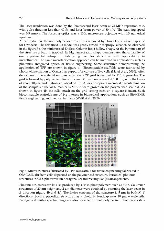
The laser irradiation was done by the femtosecond laser beam at 75 MHz repetition rate, with pulse duration less than 40 fs, and laser beam power of 60 mW. The scanning speed was 0.5 mm/s. The focusing optics was a 100x microscope objective with 0.5 numerical aperture. After irradiation, the non-polymerised resin was removed by OrmoDev, a solvent specific for Ormocers. The remained 3D model was gently rinsed in isopropyl alcohol. As observed in the figure 3c, the miniaturised Endless Column has a hollow shape. At the bottom part of the structure a bead is trapped. Its high-aspect-ratio shape demonstrates the capability of our experimental set-up for fabricating complex structures with applicability in microfluidics. The same microfabrication approach can be involved in applications such as photonics, integrated optics, or tissue engineering. Some structures demonstrating the application of TPP are shown in figure 4. Biocompatible scaffolds were fabricated by photopolymerisation of Ormosil as support for culture of live cells (Matei et al., 2010). After deposition of the material on glass substrate, a 2D grid is realized by TPP (figure 4a). The grid is formed by polymerised lines in X and Y direction, spaced at 100 m, with thickness of about 10 m, and highness of about 50 m. After appropriate microbial decontamination of the sample, epithelial human cells MRC-5 were grown on the polymerised scaffold. As shown in figure 4b, the cells attach on the grid setting each on a square element. Such biocompatible scaffolds are of big interest in biomedical applications such as BioMEMS, tissue engineering, and medical implants (Weiß et al., 2009).
Fig. 4. Microstructures fabricated by TPP: (a) Scaffold for tissue engineering fabricated in ORMOSIL. (b) Stem cells deposited on the polymerised structure. Periodical photonic structures in SU-8 photoresist in hexagonal (c) and rectangular (d) arrangements.
Photonic structures can be also produced by TPP in photopolymers such as SU-8. Columnar structures of 20 µm height and 2 µm diameter were obtained by scanning the laser beam in
Z direction (figure 4b and 4c). The lattice constant of the structure is 5 m in both X, Y directions. Such a periodical structure has a photonic bandgap near 10 µm wavelength. Bandgaps at visible spectral range are also possible for photopolymerised photonic crystals
www.intechopen.com

Ultrashort Pulsed Lasers – Efficient Tools for Materials Micro-Processing
271
with submicrometre lattice constant and different arrangements, such as woodpile structures (Deubel et al., 2004).
2.4 The limits of TPP microstructuring method The quality of a 3D structure is characterized by some parameters, such as adhesion to the substrate, shrinkage of the obtained geometry compared to the desired design, limited aspect ratio, and limited minimal feature size. The limitations of the TPP technique are mainly given by intrinsic physical and chemical properties of the photoresist and the laser focusing capability. For overcoming them, new polymers have to be developed with better performances such as low shrinkage and good adhesion on commons substrates such as glass or silica. Also, the behaviour of the photoresist and its solvent strongly affect the aspect-ratio of the structure. Some materials become very soft during development, and the structure falls down to the substrate after removing the sample from the solvent. Beside these, the limitations due to the processing equipments are mainly related to the processing resolution. Limited smoothness of the structures is given by the non uniform movement of the translation stages. Another limitation of the rapid prototyping method is the total processing time required to fabricate a structure. Since the rapid prototyping is a laser scanning technique, this is a time consuming method requiring tens of minutes up to few hours in order to complete a complex 3D structure. The solution to overcome this disadvantage is to use lasers with very high repetition rate and also fast scanning mechanics such as galvano-scanners. However, a compromise between writing speed and accuracy has to be done, the piezoelectric stages remaining the most accurate positioning systems used in 3D DLW.
3. Femtosecond laser microprocessing of composite right/left handed (CRLH) metamaterials for millimeter wave devices
3.1 Metamaterial CRLH millimeter wave devices Metamaterials (MTM) are propagation media presenting simultaneously both negative permittivities ( < 0) and negative permeabilities ( < 0). These media, with unusual properties not readily available in nature, are called Left Handed Materials (LHM). For a LHM, the triade formed by the electric field, magnetic field and Poynting vector of an electromagnetic field propagating through this media has a “left hand” orientation, different from common materials where this orientation is a “right hand” one. As a result, LHM support propagation of an electromagnetic wave where the group velocity is anti-parallel to the phase velocity. This phenomenon associates with a negative refraction index. Although presented as a theoretical curiosity since 1968 (Veselago, 1968), practical applications of “left handed” media appeared 30 years later when the first experimental investigations were made (Pendry, 1999; Shelby et al., 2001). Since that time, a great variety of media with metamaterial characteristics and subsequent applications from microwave to the visible domain were developed. In the microwave and millimeter wave frequency domain, the main conventional propagation media are the transmission lines (microstrips, coplanar waveguides). The right handed form of these transmission line structures may be assimilated to a large enough number of cascaded cells, each cell being made of series inductor – parallel capacitor. For this
www.intechopen.com

Recent Advances in Nanofabrication Techniques and Applications
272
type of line, called Right Handed Transmission Line (RH-TL), the group velocity and the phase velocity have positive values. The left handed transmission lines are made by cascading a large enough number of cells, each cell composed of series capacitor – parallel inductor. For this type of line, called Left Handed Transmission Line (LH-TL), the group velocity has positive values while the phase velocity has, in some conditions, negative values. In practice LH-TLs are made as artificial lines using lumped or distributed circuit elements. Due to the parasitic inductances and capacitances associated with series capacitors and parallel inductors respectively, the line configuration will present, actually, cells of type series LC – parallel LC, the result being a composite kind of line named Composite Right / Left Handed Transmission Line (CRLH-TL). CRLH structures act as LH-TLs at frequencies where the guided wavelength is larger than the cell size and as RH-TLs at high frequencies, where the guided wavelength is smaller than the cell size. Between these frequency domains there is a forbidden frequency band where the propagation is cut. These are so called unbalanced CRLH structures. If this forbidden band is reduced to a single point, a balanced CRLH structure is obtained and this is one of the conditions for designing some CRLH devices for microwaves and millimeter waves. Based on the CRLH structures, a large class of microwave and millimeter wave devices (MMW) has been developed (Caloz & Itoh, 2006). Among such devices, made on the basis of metamaterial approach, various types of directional couplers (Caloz et al., 2004; Wang et al., 2006), filter configurations (Li et al., 2007; Liu et al., 2009), antennas (Sajin et al., 2007; Seongmin et al., 2008; Ziolkowski et al., 2009; Basharin & Balabukha, 2009; Eggermont et al., 2009) were reported. The metamaterial CRLH-TL approach allows substantial space reduction compared to the standard devices. Moreover, combined with other metamaterial devices and circuits, it offers the possibility to develop a new and different kind of microwave and mm-wave circuitry. Complex monolithically integrated circuits can be fabricated using coplanar waveguide (CPW) configurations on semiconductor substrates. The design of the MTM microwave and millimeter wave devices is based on CRLH-TL elementary cells. A CPW CRLH elementary cell with distributed parameters is usually composed of series interdigital capacitors and parallel inductive stubs to the ground. The schematic layout of an elementary CPW CRLH cell is shown in figure 5a, while the equivalent circuit is given in figure 5b.
(a) (b)
Fig. 5. Layout of an elementary CRLH cell (a) and the equivalent circuit (b).
www.intechopen.com

Ultrashort Pulsed Lasers – Efficient Tools for Materials Micro-Processing
273
CCs are the series connected interdigital capacitors and LLp is the ground connected inductor. At high frequencies, LCs (parasitic inductance of the interdigital capacitor), CCp (parasitic capacitance to the ground of the interdigital capacitor), and CLp (parasitic capacitance of the inductive stub) become significant circuit elements. The CRLH-TL elementary cell configuration is determined by the working frequency and the materials used. The values of capacitances and inductances forming the CRLH cell (see figure 5b) were obtained with appropriate computer software (Microwave Office, HFSS). These programs also give the geometrical dimensions of the CRLH cell, as they are presented in figure 5a, where: wC, lC, and sC are the width, length and distance between two digits of the interdigital capacitor, respectively; wL and sL are the width and distance to the ground of the inductive CPW stub, respectively; gC is the distance to the ground planes of the CPW line. At high frequencies (ten-hundred GHz), the cell geometrical details reach the limits of classical photolithography and the laser ablation becomes a valuable technique to process such MMW devices.
3.2 Zeroth-order resonant CRLH antenna on silicon substrate This antenna consists of an array of CRLH cells. Each cell is made of two series connected CPW interdigital capacitors and two parallel conected short-ended CPW inductive transmission lines. The layout of an elementary CRLH cell and its equivalent circuit are presented in figure 5. The designed antenna is a zeroth-order resonance device configuration consisting of an open-ended array of CRLH cells. Using CPW transmission lines, the circuit area of the CRLH antenna could be much smaller compared to the microstrip antenna where microstrip lines are used. For an open-ended CRLH antenna, the zeroth-order resonance is at the frequency fsh = 1/[2(LLpCLp)1/2] which is the parallel resonance due to the two CPW short-ended inductive transmission lines. Also, there are resonance frequencies corresponding to the right-hand (RH) and the left-hand (LH) CRLH behaviour (Caloz & Itoh, 2006). For the operating frequency of the zeroth-order antenna, fsh , = 0 where is the equivalent phase constant of the CRLH cell, this frequency being the highest one for the LH frequency range. A zeroth-order resonance CPW CRLH antenna working at 28 GHz frequency was designed. It consists of three resonant T – shaped CRLH cells processed on a high resistivity silicon wafer substrate. The conditions and mathematical relations for the CRLH cells design are presented in literature (Caloz & Itoh, 2006; Sajin et al., 2007). For future integration in a more complex circuit, the CRLH cell was designed on silicon substrate, using CPW transmission lines. The substrate was a 500 ┤m thick silicon wafer (εr,Si = 11.9) of 5 kcm resistivity, covered with 1 ┤m SiO2 layer (εr,SiO2 = 4.7) grown by thermal oxidation. The Si wafer was plated by a sputtering process with a metallic layer of 3000 Å Au / 500 Å Cr. The backside of the silicon wafer was not metalized. The calculated dimensions of the interdigital capacitors and inductive stubs for these CRLH cells are the following: sC = 5 ┤m, lC = 250 ┤m, wC = 10 ┤m, wL = 42 ┤m, sL = 10 ┤m, lL = 212 ┤m, gC = 65 ┤m. Each capacitor has 10 digits. The antenna access line has 3400 ┤m length with a geometry computed to match the 50 Ω characteristic impedance of the measuring system. The processing technology applied to obtain the antenna structure consists of two steps by combining two technologies: photolithography and direct laser writing. In the first step, the Au/Cr metallization was removed from the large areas of the structure by standard wet photolithography. Since the laser structures writing by ablation is a time consuming scanning method, the lithography was preferred for large size area processing in order to
www.intechopen.com

Recent Advances in Nanofabrication Techniques and Applications
274
obtain the main layout of the future device. Also, the removal of the metallic film by laser ablation from large area could result in a high quantity of ablated material re-deposited on the sample surface, contaminating the active area of the device. In the second step, for the fine details of the interdigital capacitor, the precise laser ablation was used. The samples were laser ablated by tightly focusing the femtosecond laser pulses with 200 fs duration, 775 nm wavelength, tens of nJ pulse energy, and 2-kHz repetition rate. A 20x microscope objective, 0.4 NA, was used for the Au/Cr layer ablation, obtaining interdigital spaces of 5 m, as designed. The 2D structures were generated according to a computer controlled algorithm by precisely translating the sample with a resolution below 1 µm. An optical microscopy image of the active part of the antenna structure is presented in figure 6a, where the grounded lines forming the inductive stubs and the interdigital capacitors, processed by laser ablation, can be observed. A Scanning Electron Microscopy (SEM) image showing details of the antenna interdigital capacitors is presented in figure 6b.
(a) (b)
Fig. 6. (a) Optical microscopy image of the active part of the CRLH antenna. (b) SEM image showing a detail of the interdigital capacitor made by femtosecond laser processing.
Many electrical properties such as gain, return loss, voltage standing wave ratio, reflection coefficient, and amplifier stability of microwave and mm-wave networks may be expressed using S-parameters (Kurokawa, 1965). In the context of S-parameters, scattering refers to which way the traveling currents and voltages in a transmission line are affected when a discontinuity is inserted. These losses appear when the incident wave meets an impedance which differs from the line's characteristic impedance. The input return loss (RL) parameter of the CRLH antenna is presented in figure 7. It represents a scalar measure of how close the actual input impedance of the device is to the nominal system impedance value and, expressed in decibels, is given by RLin (dB) = |20×log10|S11|| where, by definition, |S11|, is equivalent to the reflected voltage magnitude divided by the incident voltage magnitude. For a frequency domain between 28.01 GHz and 29.66 GHz, an input return loss having values RL < -15 dB can be observed. The minimum value of RL = -27.05 dB was obtained at 28.78 GHz. It represents a very good matching of the antenna structure to the 50 characteristic impedance of the millimeter wave measurement system and to the most usual microwave and millimeter devices.
www.intechopen.com

Ultrashort Pulsed Lasers – Efficient Tools for Materials Micro-Processing
275
In order to measure the radiation characteristic, antenna chips were mounted on specialized test fixtures. The radiation characteristic was measured at 28.7 GHz frequency where the antenna return losses have a minimum. The measuring setup allows the rotation of the CRLH emitting antenna both in transversal and longitudinal planes.
25 30 35Frequency (GHz)
11_1
-30
-25
-20
-15
-10
-5
0
S11
(dB
)
29.65 GHz-15 dB
28.01 GHz-15 dB
28.78 GHz-27.05 dB
DB(|S(1,1)|)11
Fig. 7. Return loss of the CRLH antenna for a frequency sweep between 25-35 GHz
The radiation characteristic rated to the maximum power in the transversal plane of the CRLH antenna structure is shown in figure 8a, while the characteristic in the longitudinal plane is presented in figure 8b. The -3 dB beam-width of the radiation characteristic is about 37 degrees in the transversal plane and 25 degrees in the longitudinal plane. The longitudinal radiation characteristic has the maximum at the angle of ~ 24 degrees.
(a) (b)
Fig. 8. Radiation characteristic in the transversal plane (a) and in the longitudinal plane (b) for the measured CRLH antenna
www.intechopen.com

Recent Advances in Nanofabrication Techniques and Applications
276
The antenna gain, which relates the intensity of an antenna radiation in a given direction to the intensity that could be produced by a hypothetical ideal antenna that radiates isotropically (equally in all directions), was computed using the De Friis formula (Balanis, 1997). The gain was nearly constant in the 28 ÷ 29 GHz frequency band, with a maximum value of 2.99 dB at 28.6 GHz. The area occupied by the antenna is 2.15 0.6 mm2. There is a considerable size reduction compared to a standard ┣/2 patch antenna.
3.3 Millimeter wave CRLH band-pass filter and dir ectional coupler The band-pass filter was made by cascading a number of identical CRLH cells. The directional coupler consists of two coupled CRLH artificial lines, each composed of two identical cascaded CRLH cells. Both band-pass filter and directional coupler (figure 9a,b) were microprocessed by the two-steps technology described in section 3.2. The geometrical dimensions of the interdigital capacitor and inductive CPW stub of the CRLH band-pass filter at 50 GHz working frequency were calculated: sC = 5 ┤m, lC = 250 ┤m, wC = 10 ┤m, gC = 65 ┤m, the number of capacitor digits = 10, wL = 42 ┤m, sL = 10 ┤m, and lL = 212 ┤m (see figure 5a). Unlike the antenna CRLH cell, the filter CRLH cell has only one inductive CPW stub. A silicon substrate plated with 2000 Å Au/500 Å Cr was used. The working parameters of the band-pass filter structure were measured in the 40-60 GHz frequency range. The S11 parameter evaluation show return loss values < -15 dB in a frequency range of 46.32 GHz ÷ 55.4 GHz, whereas losses in the same frequency range, given by S21 parameter, are around 6 ÷ 7 dB (Sajin et al., 2010a).
(a) (b)
Fig. 9. SEM images of CRLH band pass filter (a) and directional coupler (b) structures microprocessed by laser ablation.
For the CRLH directional coupler the port 1 is the input port, while the ports 2, 3 and 4 are the transmission, coupled, and isolated ports, respectively (figure 9b). Measured return losses (S11) were better than -20 dB for a frequency domain between 24.01 GHz ÷ 38.11 GHz, whereas the isolation (S41) is greater than 30 dB in a large frequency range, exceeding the domain 20-40 GHz (Sajin et al., 2010b).
4. Enhanced near-field laser lithography
The current trend towards sub-micrometer structures requires new methods and technologies of surface structuring. The traditional masking approach in optical lithography
www.intechopen.com
Ultrashort Pulsed Lasers – Efficient Tools for Materials Micro-Processing
277
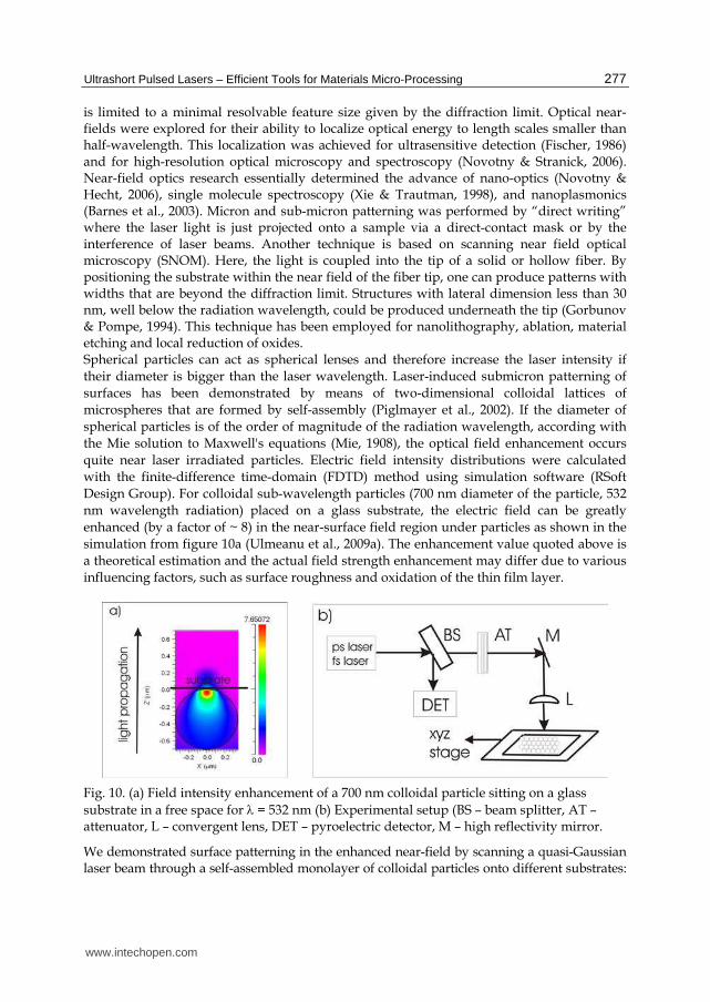
is limited to a minimal resolvable feature size given by the diffraction limit. Optical near-fields were explored for their ability to localize optical energy to length scales smaller than half-wavelength. This localization was achieved for ultrasensitive detection (Fischer, 1986) and for high-resolution optical microscopy and spectroscopy (Novotny & Stranick, 2006). Near-field optics research essentially determined the advance of nano-optics (Novotny & Hecht, 2006), single molecule spectroscopy (Xie & Trautman, 1998), and nanoplasmonics (Barnes et al., 2003). Micron and sub-micron patterning was performed by “direct writing” where the laser light is just projected onto a sample via a direct-contact mask or by the interference of laser beams. Another technique is based on scanning near field optical microscopy (SNOM). Here, the light is coupled into the tip of a solid or hollow fiber. By positioning the substrate within the near field of the fiber tip, one can produce patterns with widths that are beyond the diffraction limit. Structures with lateral dimension less than 30 nm, well below the radiation wavelength, could be produced underneath the tip (Gorbunov & Pompe, 1994). This technique has been employed for nanolithography, ablation, material etching and local reduction of oxides. Spherical particles can act as spherical lenses and therefore increase the laser intensity if their diameter is bigger than the laser wavelength. Laser-induced submicron patterning of surfaces has been demonstrated by means of two-dimensional colloidal lattices of microspheres that are formed by self-assembly (Piglmayer et al., 2002). If the diameter of spherical particles is of the order of magnitude of the radiation wavelength, according with the Mie solution to Maxwell's equations (Mie, 1908), the optical field enhancement occurs quite near laser irradiated particles. Electric field intensity distributions were calculated with the finite-difference time-domain (FDTD) method using simulation software (RSoft Design Group). For colloidal sub-wavelength particles (700 nm diameter of the particle, 532 nm wavelength radiation) placed on a glass substrate, the electric field can be greatly enhanced (by a factor of ~ 8) in the near-surface field region under particles as shown in the simulation from figure 10a (Ulmeanu et al., 2009a). The enhancement value quoted above is a theoretical estimation and the actual field strength enhancement may differ due to various influencing factors, such as surface roughness and oxidation of the thin film layer.
Fig. 10. (a) Field intensity enhancement of a 700 nm colloidal particle sitting on a glass substrate in a free space for = 532 nm (b) Experimental setup (BS – beam splitter, AT – attenuator, L – convergent lens, DET – pyroelectric detector, M – high reflectivity mirror.
We demonstrated surface patterning in the enhanced near-field by scanning a quasi-Gaussian laser beam through a self-assembled monolayer of colloidal particles onto different substrates:
www.intechopen.com

Recent Advances in Nanofabrication Techniques and Applications
278
glass and metallic thin films of nanometers thickness like Ag, Au, Co, Cu thin films as well as Co/Cu/Co multilayer structures (Ulmeanu et al., 2009b). Single pulse laser ablation of monolayer thin films and multilayer structures was performed by irradiating with a Nd:YAG picosecond laser (400-ps pulsewidth at =532 nm) and a Ti:sapphire femtosecond laser system (200-fs pulsewidth at = 775 nm). The experimental setup is shown in figure 10b. The laser beam was focused on the colloidal particles using a 75 mm convex lens corrected for reduced spherical aberrations. The irradiating energy was adjusted through neutral attenuators. For the control of the irradiation process, a certain fraction of the incident laser energy is split off by a glass splitter and measured with a pyroelectric detector. The sample was mounted on a precision three-axis xyz stage and was aligned for normal incidence of the laser beam. The ablation spots were produced with single pulse shots at different laser energies. All experiments were performed under ambient conditions. The irradiated area of the sample was imaged using Scanning Electron Microscpy (SEM) and Atomic Force Microscopy (AFM) to obtain the surface maps and crater profiles. From our investigations, it is obvious that, using 2D colloidal masks, arrays with regularly arranged holes can be created through a parallel process on the whole surface (Ulmeanu et al., 2009a). The shape of the holes depends on the laser fluence and thermophysical properties of the surfaces involved in the experiments (figure 11).
Fig. 11. SEM images for the near-field experiments at fluences above the threshold level: (a) glass substrate (Fpeak= 7.3 J/cm2), (b) Co thin film (Fpeak = 0.82 J/cm2), (c) Ag thin film (Fpeak = 0.18 J/cm2) and (d) Au thin film (Fpeak = 0.17 J/cm2). Scale bar: 10 m.
For the case of glass near-field processing, we have obtained regular nano-holes, with a uniform distribution of depths and heights at the same fluence value (figure 11a). The smallest diameter of the holes, according to the SEM images, was 100 nm. For the case of Ag thin film (figure 11c), bumps and nanoholes were visible away from the peak fluence location, but not in a regular structure like in the case of the Au thin film (figure 11d) and Co thin film (figure 11b). Despite of similar ablation thresholds of Ag and Au thin films, due to a high thermal diffusivity coefficient and low adherence of the thin film on glass substrate,
www.intechopen.com

Ultrashort Pulsed Lasers – Efficient Tools for Materials Micro-Processing
279
the near-field experiments gave a non-uniform pattern in the case of the Ag thin film surface. The discrepancy between Ag and Au thin film may potentially be due also to appreciable surface roughness of the thermally evaporated Ag thin film, that has a great impact on the optical near-field distribution. The near-field processing in the case of Au thin film indicated different patterns produced by a single shot laser: from bowl type structure to bumps depending on the fluence, as in AFM investigations presented in the figure 12a,b. For the Co thin film near-field ablation, we were able to determine the dependence of the holes diameter versus the depth at different fluences, the holes having shapes from bowl type to an almost rectangular shape with flat bottom. By comparing near-field processing on Co and Au thin films (figure 12c), we put into evidence holes with different diameters (d) and heights (z) at fluences nearby the thresholds: dAu = 145 nm, zAu = 14 nm (Au thin film), dCo = 250 nm, zCo = 60 nm (Co thin film). For a multilayer Co(3 nm)/Cu(6 nm)/Co(20 nm) material, we investigated a method of preferential laser processing of a specific layer by changing the laser fluence instead of selecting different laser wavelengths. Figure 13a represents a schematic multilayer structure. The heterostructure composition determined by Sputtered Neutral Mass Spectroscopy (SNMS) measurements is shown in figure 13b. We demonstrated the formation of ordered areas of nano-holes in a multilayer structure using single femtosecond laser pulse irradiation (200 fs, = 775 nm) on 700 nm diameter colloidal particles (Ulmeanu et al., 2010). The ablation threshold for the multilayer structure in the enhanced near-field regime was measured to be 2.8 x 10⁻² J/cm2.
Fig. 12. (a) 3D AFM image; (b) scan lines for the structures produced by a single shot laser in the case of the near-field experiments for Au thin film; (c) depth profiles of the holes for Au and Co thin films.
Fig. 13. (a) Schematic representation of the multilayer structure; (b) heterostructure composition determined by the SNMS measurements; (c) holes depths and widths distribution for the Co(3nm)/Cu(6nm)/Co(20 nm) multilayer structure (peak laser fluence, Flas = 0.04 J/cm2).
www.intechopen.com

Recent Advances in Nanofabrication Techniques and Applications
280
The dependence of the holes diameter versus the depth at different fluences, obtained by AFM measurements, is showed in the figure 13c. As expected, with the decrease of the laser energy from the central zone to the edges of the irradiated area, the depth of the holes is decreasing. In the case of multilayer structures, the hole depth decrease depending on the laser fluence corresponds to the ablation of the first, second or third layer. This type of planar metal/dielectric interfaces with a selective distribution of layers can open new perspective in the excitation of propagating surface plasmons and, consequently, in creating transducers for sensing of biomolecular recognition reactions.
5. Femtosecond laser induced forward transfer
Laser Induced Forward Transfer (LIFT) represents a challenging technique to the conventional etching microfabrication techniques. It becomes particularly interesting when a very small quantity of material has to be deposited on a substrate. Many kinds of materials such as metallic films, semiconductors, polymers, or even biological material can be transferred (Thomas et al, 2007; Sanz et al, 2010; Colina et al, 2005). The material to be transferred is initially deposited in thin films on a transparent substrate named donor substrate, or "ribbon" (transparent at laser radiation used for LIFT process). Usually, but not necessarily, a very thin metallic layer is deposited as buffer between the donor substrate and the film to be transferred. The donor sample, is placed at a short distance, parallel to another acceptor substrate (virtually any material). The donor film is backward irradiated with a pulsed laser, like in figure 14.
Fig. 14. The schematic of LIFT principle.
The laser is focused on the donor thin film at the interface with the donor substrate. Then, a small amount of buffer material is ablated and transformed in gaseous faze. This gas expands pushing forward the rest of the material which is projected to the acceptor substrate. If the parameters are correctly chosen, the ejected material is deposited on the acceptor's surface. The role of the buffer layer is only to protect the material to be transferred and is used especially in the case of organic materials susceptible to be affected by a direct exposure to the laser beam. Otherwise, in absence of a buffer layer, the material itself can be vaporized at the interface with the donor substrate, the pressure of the created gas transferring a small quantity of material from a substrate to another.
www.intechopen.com

Ultrashort Pulsed Lasers – Efficient Tools for Materials Micro-Processing
281
In LIFT experiments some parameters, like distance d between the donor film and acceptor substrate, or laser fluency, have to be investigated in order to find the optimal processing conditions for the deposition of a certain material. In our LIFT experiments, we demonstrated the transfer of a polymer material, an Ormocer photoresist, using our laser processing workstation. The polymer layer was directly deposited by spin coating on a glass substrate, without any buffer layer. The distance between donor and acceptor was fixed at 15 m. Series of 5x5 pixels were created by single pulses, shot by shot. The laser source was the Clark MXR CPA-2101 laser, with 200 fs pulse duration and 775 nm wavelength, externally triggered for single shot experiments. The sample was translated from a pixel to another by a computer controlled translation stage. The distance between pixels was 50 m. The laser was focused to the donor layer by a 75 mm focusing lens with about 25 m focus spot diameter. The energy per pulse was varied from 2.5 to 7.5 J. Optical images of the structures, as transferred to the acceptor substrate at different pulse energies, are shown in figure 15. The quality of the obtained structures strongly depends on the pulse energy. At the highest pulse energy used, non uniform droplets results, sparse on the donor surface. Decreasing the pulse energy the transferred droplets remain well defined.
Fig. 15. LIFT generated microstructures at different laser energy. Scale bar: 100 m.
The smallest size of the droplets obtained in these experimental conditions was about 2 m. Smaller structures, such as nanodroplets, can be also transferred (Banks et al., 2006) and even an entire microstructure or a microdevice could be deposited by LIFT (Piqué et al., 2006). This technique can be efficiently used as a microprinting method.
6. Conclusions
Various experimental techniques for materials micro-processing based on ultra-short pulsed lasers are presented. Direct femtosecond laser writing technique by two-photon photo-polymerization was used to produce microstructures in the volume of transparent materials. By this technique, photonic devices such as photonic crystals, optical couplers, diffractive elements, 3D structures for microfluidics, scaffolds for tissue engineering, and other MEMS can be fabricated. Femtosecond laser ablation was used to produce 2D microstructures on different materials surface. Electronic devices, based on CRLH transmission lines having metamaterials characteristics in the tens-GHz frequency range, such as band-pass filters, antennas, and directional couplers were manufactured by combined photo-lithography and femtosecond laser ablation techniques. A microprinting method, based on laser induced forward transfer
www.intechopen.com

Recent Advances in Nanofabrication Techniques and Applications
282
of a small quantity of ablated material from a donor substrate to an acceptor substrate, was demonstrated. Using self-assembled monolayers of colloidal micro-spheres on glass and metallic thin film substrates, nano-patterning was obtained by ultrashort pulse laser ablation in the near-surface enhanced laser field irradiation regime. Formation of ordered areas of nano-holes in a multilayer structure was demonstrated by selective near-field laser ablation. Ultrashort pulsed laser micro/nanostructures writing technique could be considered as an alternative to the classical techniques based on photo-lithography. New micro/nano-processing technologies can be developed by combining femtosecond laser writing techniques with already proved lithography techniques.
7. Acknowledgment
M. Zamfirescu acknowledges the support of the Sectoral Operational Programme Human Resources Development (SOP HRD), financed from European Social Fund and by Romanian Government under the contract number POSDRU/89/1.5/S/63700. M. Ulmeanu acknowledges the financial support of the European Social Fund POSDRU 2007-2013 through the contract POSDRU/89/1.5/S/60746.
8. References
Allsop, T.; Dubov, M.; Mezentzev, V. & Bennion, I. (2010). Inscription and characterization of waveguides written into borosilicate glass by a high-repetition-rate femtosecond laser at 800 nm, Applied Optics, Vol. 49, No. 10, (1 April 2010), pp. 1938-1950, ISSN 0003-6935
Ams, M.; Marshall, G. D.; Spence, D. J. & Withford, M. J. (2005). Slit beam method for femtosecond laser direct-write fabrication of symmetric waveguides in bulk glasses, Optics Express, Vol. 13, No. 15, (July 2005), pp. 5676-5681, eISSN 1094-4087
Balanis, C.A. (1997). Antenna Theory. Analysis and design, John Wiley & Sons, Inc., ISBN: 0-471-59268-4, New York, Chichester, Brisbane, Toronto, Singapore
Banks, D. P.; Grivas, C.; Mills, J. D.; Eason, R. W. and Zergioti, I. (2006). Nanodroplets deposited in microarrays by femtosecond Ti:sapphire laser-induced forward transfer, Appl. Phys. Lett., Vol. 89, No. 19, (November 2006) pp. 193107, ISSN 1077-3118
Barnes, W. L.; Dereux, A. & Ebbesen, T. W. (2003), Surface plasmon subwavelength optics. Nature, Vol. 424, (August 2003), pp. 824-830, ISSN 0028-0836
Basharin, A.; & Balabukha, N. (2009). The Radiation of Antennas Based on Metamaterial Waveguides, Proceedings of 3rd International Congress on Advanced Electromagnetic
Materials in Microwaves and Optics, Metamaterials 2009, pp.224 – 226, ISBN 978-0-9551179-6-1, 30th Aug. – 04th Sept. 2009, London, UK
Becker, EW.; Ehrfeld W.; Hagmann, P.; Maner, A & Munchmeyer, D. (1986). Fabrication of microstructures with high aspect ratio and great structural heights by synchrotron radiation lithography, galvanoformung and plastic moulding
www.intechopen.com

Ultrashort Pulsed Lasers – Efficient Tools for Materials Micro-Processing
283
(LIGA process). Microelectronic Eng., Vol. 4, No.1, (May 1986), pp. 35–36, ISSN 0167-931
Caloz, C. & Itoh, T. (2006). Electromagnetic metamaterials: Transmission line theory and
microwave applications, John Wiley & Sons, Inc., ISBN-10: 0-471-66985-7. ISBN-13: 978-0-47166985-2, Hoboken, New Jersey
Caloz, C.; Sanada, A. & Itoh, T. (2004). A novel composite right-/left-handed coupled-line directional coupler with arbitrary coupling level and broad bandwidth, IEEE Trans.
on Microwave Theory and Techniques, Vol. 52, March 2004, pp. 980-992, ISSN 0018-9480
Chimmalgi, A.; Choi, T. Y.; Grigoropoulos, C. P. & Komvopoulos, K. (2003). Femtosecond laser aperturless near-field nanomachining of metals assisted by scanning probe microscopy, Applied Physics Letters, Vol. 82, No. 8, (24 Febraury 2003), pp. 1146-1148, ISSN 0003-6951
Colina, M.; Serra, P.; Fernández-Pradas, J.M.; Sevilla, L. & Morenza, J.L. (2005). Biosensors
and Bioelectronics, Vol. 20, No. 8, (February 2005), pp. 1638–1642, ISSN 0956-5663 Deubel, M.; Von Freymann, G.; Wegener, M.; Pereira, S.; Busch, K. & Soukoulis, C. M.
(2004). Nature Materials, Vol. 3, No. 7, (July 2004), pp. 444-447, ISSN 1476-1122 Dolling, G.; Enkrich, C.; Wegener, M.; Soukoulis, C. M. & Linden, S. (2006). Low-loss
negative-index metamaterial at telecommunication wavelengths, Optics Letters, Vol. 31, No. 12, (June 15, 2006), pp. 1800-1802, ISSN 0146-9592
Dolling, G.; Wegener, M.; Soukoulis, C. M. & Linden, S. (2007). Negative-index metamaterial at 780 nm wavelengths, Optics Letters, Vol. 32, No. 1, (January 1, 2007), pp. 53-55, ISSN 0146-9592
Eggermont, S.; Platteborze, R. & Huynen, I. (2009). Analysis of Radiation in a Metamaterial Leaky Wave Antenna Based on Complementary Split Ring Resonator, Proceedings of
3rd International Congress on Advanced Electromagnetic Materials in Microwaves and
Optics, Metamaterials 2009, pp.102 – 104, ISBN 978-0-9551179-6-1, 30th Aug. – 04th Sept. 2009, London, UK
Farsari, M.; Filippidis, G. & Fotakis, C. (2005). Fabrication of three-dimensional structures by three-photon polymerization, Optics Letters , Vol. 30, No. 23, (luna N, 2005) pp. 3180-3182, ISSN 0146-9592
Farsari, M. & Chichkov, B. N. (2009). Two-photon fabrication, Nature Photonics, Vol. 3, No. 8, (August 2008), pp. 450-452, ISSN 1749-4885
Fischer, U. Ch. (1986). Submicrometer aperture in a thin metal film as a probe of its microenvironment through enhanced light scattering and fluorescence. Journal of
the Optical Society of America B, Vol. 3, No. 10, (October, 1986), pp. 1239-1224, ISSN 0740-3224
Frassila, Sami. (2010). Introduction to Microfabrication. Second Edition, John Wiley & Sons Ltd., ISBN 978-0-470-74983-8
Glezer, E. N.; Milosavljevic, M.; Huang, L.; Finlay, R. J.; Her, T. H.; Callan, J. P. & Mazur, E. (1996). Three-dimensional optical storage inside transparent materials, Optics Letters, Vol. 21, No. 24, (December 15, 1996), pp. 2023-2025, ISSN 0146-9592
www.intechopen.com

Recent Advances in Nanofabrication Techniques and Applications
284
Gorbunov, A. A. & Pompe, W. (1994). Thin film nanoprocessing by laser/STM combination. Physica Status Solidi A, Vol. 145, No. 2, (October 2004), pp. 333-338, ISSN 0031-8965
Gwyn, C. W.; Stulen, R.; Sweeney, D. & Attttwood, D. (1998). Extreme ultraviolet lithography, Journal of Vacuum Science & Technology B, Vol. 16, No. 6, (November 1998), pp. 3142-3149, ISSN 0734-211X
Homoelle, D.; Wielandy, S.; Gaeta, A. L.; Borelli, N. F. & Smith, C. (1999). Infrared photosensitivity in silica glasses exposed to femtosecond laser pulses, Optics Letters, Vol. 24, No. 18, (September 15, 1999), pp. 1311-1313, ISSN 0146-9592
Kawata S., Sun H.-B., Tanaka T., and Takada K. (2001). Finer features for functional microdevices, Nature , Vol. 412, No. 6848, (August 16, 2001) pp. 697-698, ISSN: 0028-0836
Kurokawa, K. (1965). Power Waves and the Scattering Matrix, IEEE Trans. on MTT, Vol.13, March 1965, pp194 – 202, ISSN: 0018-9480
Li, C.; Liu, K.-Y. & Li, F. (2007). Composite right/left-handed coplanar waveguide band-pass filter using capacitively-coupled zeroth-order resonators, Appl. Phys. Lett. Vol. A 87, pp. 317–319, ISSN 0003-6951
Liu, X.; Du, D. & Mourou, G. (1997). Laser Ablation and Micromachining with Ultrashort Laser Pulses, IEEE Journal of Quantum Electronics, Vol. 33, No. 10, (October 1997), pp. 1706-1716, ISSN 0018-9197
Liu, C. & Menzel, W. (2009), On the Relation between Composite Right-/Left-Handed Transmission Lines and Chebyshev Filters, International Journal of Microwave Science
and Technology, Volume 2009, Article ID 184895, DOI:10.1155/2009/184895 Liu, G.; Tian, Y. and Kan., Y. (2005). Fabrication of high-aspect-ratio microstructures using
SU8 photoresist, Microsystem Technologies, Vol. 11, No. 3-4, (November 6, 2003), pp.343–346, ISSN: 1432-1858
Maruo, S.; Nakamura, O. & Kawata, S. (1997). Three-dimensional microfabrication with two-photon-absorbed photoplymerization, Optics Letters, Vol. 22, No. 2, (January 15, 1997), pp. 132-134, ISSN 0146-9592
Matei, A.; Zamfirescu, M.; Jipa, F.; Luculescu, C.;Dinescu, M.; Buruiana, EC.; Buruiana, T.;Sima, L.E. & Petrescu, S.M. (2010). Two Photon Polymerization of Ormosils, AIP
Conference Proceedings, International Symposium on High Power Laser Ablation 2010, Vol. 1278, No. 1, (October 2010), pp. 843-851, ISSN 0094-243X
Menzel, W. (1979). A new traveling-wave antenna in microstrip, Arch. Electron. Uebertrag.
Tech., Vol. 33, 1979, pp. 137 – 140. Mie, G. (1908). Beitrage zur Optik trueber Medien, speziell kolloidaler Metallosungen.
Annalen der Physik, Vol. 330, No. 3, pp. 377-445, ISSN 1521-3889 Nishiyama, H.; Mizoshiri, M.; Kawahara, T.; Nishii, J. & Hirata, Y. (2008). SiO2- based
nonplanar structures fabricated using femtosecond laser lithography, Optics
Express, Vol. 16, No. 22, (27 October 2009), pp. 17288-17294, eISSN 1094-4087 Novotny, L. & Stranick, S. J. (2006). Near-field optical microscopy and spectroscopy with
pointed probes. Annual Review of Physical Chemistry, Vol. 57, (May 2006), pp. 303-
331, ISSN 0066-426X
www.intechopen.com

Ultrashort Pulsed Lasers – Efficient Tools for Materials Micro-Processing
285
Novotny, L. & Hecht, B. (2006). Principles of Nano-Optics, Cambridge University Press, ISBN 978-0-521-83224-3, New York
Osellame, R.; Taccheo, S.; Marangoni, M.; Ramponi, R.; Laporta P.; Polli, D.; De Silvestri, S. & Cerullo, G. (2003). Femtosecond writing of active optical waveguides with astigmatically shaped beams, Journal of the Optical Society of America B, Vol. 20, No. 7, (July 2003), pp. 1559-1567, ISSN 0740-3224
Ovsianikov, A.; Xiao, S. Z.; Farsari, M.; Vamvakaki, M.; Fotakis, C. & Chichkov, B. N. (2009). Shrinkage of microstructures produced by two-photon polymerization of Zr-based hybrid photosensitive materials, Optics Express, Vol. 17, No. 4, (February 16, 2009), pp. 2143-2148, eISSN 1094-4087
Pavlidis, V. F. and Friedman, E. G. (2009). Three-Dimensional Integrated Circuit Design, Morgan Kaufmann, Elsevier Inc., ISBN 978-0-12-374343-5.
Pendry, J.B. (1999). Magnetism from conductors and enhanced nonlinear phenomena. IEEE
Trans. on MTT, Vol.47, nr.11, Nov. 1999, pp. 2075-2084, ISSN: 0018-9480 Piglmayer, K.; Denk, R. & Bauerle, D. (2002). Laser-induced surface patterning by means of
microspheres. Applied Physics Letters, Vol. 80, No. 25, (June 2005), pp. 4693-4695, ISSN 0003-6951
Piqué, A.; Mathews, S.A.; Pratap, B.; Auyeung, R.C.Y.; Karns, B.J. & Lakeou, S. (2006) Embedding electronic circuits by laser direct-write, Microelectronic
Engineering, Vol. 83, No. 11-12, (November-December 2006) pp. 2527–2533, ISSN 0167-9317
Qi, L.; Nishii, K. & Nambai, Y. (2009). Regular subwavelength surface structures induced by femtosecond laser pulses on stainless steel, Optics Letters, Vol. 34, No. 12, (June 15, 2009), pp. 1846-1848, ISSN 0146-9592
Rill, M. S.; Plet, C.; Thiel,, M.; Staude, I.; Von Freymenn, G.; Linden, S. & Wegener, M. (2008). Photonic metamaterials by direct laser writing and silver chemical vapour deposition, Nature Materials, Vol. 7, No. 7, (July 2008), pp. 543-546, ISSN 1476-1122
Sajin G.; Simion S.; Craciunoiu, F. & Marcelli, R. (2007). Silicon supported microwave zeroth-order resonance antenna on metamaterial approach, Proceedings of Asia-
Pacific Microwave Conference, APMC 2007, pp. 221 – 224, ISBN 1-4244-0748-6, Bangkok, Thailanda, December 2007
Sajin G.; Simion S.; Craciunoiu Fl.; Bunea, A. C.; Dinescu, A.; Zamfirescu, M.; Neagu, L. & Dabu, R. (2010a). Millimeter Wave Metamaterial Band-Pass Filter by Femtosecond Laser Ablation, Proceedings of European Microwave Conference, EuMC, ISBN 978-2-87487-015-6, pp. 1393–1396, Paris, France, September 26 – October 01, 2010.
Sajin, G.; Simion, S.; Craciunoiu, Fl.; Bunea, A. C.; Muller A.A. & Dinescu, A. (2010b). Metamaterial Millimeter Wave Directional Coupler on silicon substrate, Proc. of 33rd
International Semiconductor Conference, CAS, pp. 269–272, ISBN 978-14244-5781-6; ISSN 1545-827X, Sinaia, Romania, October 11 – 13, 2010.
Sanz, M.; Walczak. M.; Oujja, M.; Domingo, C.; Klini, A.; Papadopoulou, E.L.; Fotakis, C. & Castillejo, M. (2010), Femtosecond laser deposition of TiO2 by laser induced
www.intechopen.com

Recent Advances in Nanofabrication Techniques and Applications
286
forward transfer, Thin Solid Films, Vol. 518, No. 19, (July 2010) pp. 5525–5529, ISSN 0040-6090
Seongmin, P.; Baik, J. W.; Cho, S. H. & Kim, Y. S. (2008). A metamaterial-based symmetrical periodic antenna with efficiency enhancement, Proceedings of Asia-Pacific Microwave
Conference, Paper A3-49, ISBN 978-1-4244-2642-3, Hong Kong, China, December 2008.
Shelby R.A.; Smith D.R. & Schultz S. (2001). Experimental verification of a negative index of refraction, Science, vol. 292, (April 2001), pp. 77–79, ISSN: 0036-8075
Sowa, S.; Watanabe, W.; Tamaki, T.; Nishii, J. & Itoh, K. (2005). Symmetric waveguides in poly(methyl methacrylate) fabricated by femtosecond laser pulses, Optics Express, Vol. 14, No. 1, (9 January 2006), pp. 291-297, eISSN 1094-4087
Streltsov, A. M. & Borrelli, N. F. (2001). Fabrication and analysis of a directional coupler written in glass by nanojoule femtosecond laser pulses, Optics Letters, Vol. 21, No. 1, (January 1, 2001), pp. 2023-2025, ISSN 0146-9592
Stuart, B. C.; Feit, M. D.; Herman, S.; Rubenchick, A. M.; Shore, B. W. & Perry, M. D. (1996). Optical ablation by high-power short-pulse lasers, Journal of the
Optical Society of America B, Vol. 13, No. 2, (February 1996), pp. 459-468, ISSN 0740-3224
Sugioka, K.; Meunier, M. & Pique, A. (2010). Laser Precision Microfabrication, Springer Series in Materials Science, Vol. 135, Springer_Verlag Berlin Heidelberg, ISBN 978-3-642-10523-4
Takeshima, N.; Kuroiwa, Y.; Narita, Y.; Tanaka, S. & Hirao, K. (2004). Fabrication of a periodic structure with a high refractive-index difference by femtosecond laser pulses, Optics Express, Vol.12, No. 17, (23 August 2004), pp. 4019-4024, eISSN 1094-4087
Takeshima, N.; Nartita, Y.; Nagata, T. & Tanaka, S. (2005). Fabrication of photonic crystals in ZnS-doped glass, Optics Letters, Vol. 30, No. 5, (March 1, 2005), ISSN 0146-9592
Tan, D.; Li ,Y.; Qi, F.; Yang, H.; Gong Q.; Dong, X. & Duan X. (2007). Reduction in feature size of two-photon polymerization using SCR500, Appl. Phys. Lett. Vol. 90, (January 13, 2007) pp. 071106 1-3 , ISSN 1077-3118
Thomas, B.; Alloncle, A. P.; Delaporte, P.; Sentis, M.; Sanaur, S.; Barret, M. & Collot, P. (2007). Experimental investigations of laser-induced forward transfer process of organic thin films, App. Surf. Sci., Vol. 254, No. 4, (December 2007) pp. 1206-1210, ISSN 0169-4332
Ulmeanu, M.; Zamfirescu, M.; Rusen, L.; Luculescu, C.; Moldovan, A. ; Stratan, A. & Dabu, R. (2009a). Structuring by field enhancement of glass, Ag, Au, and Co thin films using short pulse laser ablation. Journal of Applied Physics, Vol. 106, No.11, (December 2009) pp.114908 - 114908-8, ISSN 0021-8979
Ulmeanu, M.; Zamfirescu, M. & Medianu, R., (2009b). Self-assembly of colloidal particles on different surfaces. Colloids and Surfaces A: Physicochemical and Engineering Aspects, Vol. 338, No. 1-3, (April 2009), pp. 87-92, ISSN 0927-7757
Ulmeanu, M.; Filipescu, M.; Scarisoreanu, N.D.; Georgescu, G.; Rusen, L. & Zamfirescu, M. (2010). Selective removal and patterning of a Co/Cu/Co trilayer created by
www.intechopen.com

Ultrashort Pulsed Lasers – Efficient Tools for Materials Micro-Processing
287
femtosecond laser processing. Applied Physics A, DOI:10.1007/s00339-010-6119-9, ISSN 1432-0630
Vega, F.; Armengol, J.; Diez-Blanco, V.; Siegel, J.; Solis, J.; Barcones, B.; Perez-Rodriguez, A. & Loza-Alvarez, P. (2005). Mechanisms of refractive index modification during femtosecond laser writing of waveguides in alkaline lead-oxide silicate glass, Applied Physics Letters, Vol. 87, 021109 (2005), ISSN 0003-6951
Veselago, V. G. (1968). The electrodynamics of substances with simultaneously negative values of ε and ┤, Sov. Physics – Usp., vol.47, January-February 1968, pp. 509-514
Wang, Y. Z.; Zhang, Y. W.; He, L.; Liu, F.-Q.; Li, H. Q. & Chen, H. (2006). Discussion on coupling mechanism of asymmetric CRLH/RH TL coupler, Journal of Zhejiang
University - Science A, Vol. 7, January 2006, pp. 95-98, ISSN 1673-565X Weiß, T.; Hildebrand. G.; Schade, R. & Liefeith K. (2009). Two-Photon polymerization for
microfabrication of three-dimensional scaffolds for tissue engineering application, Engineering in Life Sciences Vol. 9, No. 5, (October 2009), pp. 384–390, ISSN 1618-2863
Will, M.; Nolte, S.; Chichkov, B. & Tunnermann, A. (2002). Optical properties of waveguides fabricated in fused silica by femtosecond laser pulses, Applied Optics, Vol. 41, No. 21, (July 2002), pp. 4360-4364, ISSN 1559-128X
Witzgall, G.; Vrijen, R.; Yablonovitch, E.; Doan, V. & Schwartz, B. J. (1998). Single-shot two-photon exposure of commercial photoiresisit for the production of three-dimensional structures, Optics Letters, Vol. 23, No. 22, (November 15, 1998), ISSN 0146-9592
Wortmann, D.; Gottmann, J.; Brandt, N. & Horn-Solle, H. (2008). Micro- and nanostructures inside sapphire by fs-laser irradiation and selective etching, Optics Express, Vol. 16, No. 3, (4 February 2008), pp. 1517-1522, eISSN 1094-4087
Xie, X. S. & Trautman, J. K. (1998). Optical studies of single molecules at room temperature. Annual Review of Physical Chemistry, Vol. 49, (October 1998), pp. 441–480, ISSN 0066-426X
Yuanyuan, S.; Yewen, Z.; Fuqiang, L.; Li, H.; Hongqiang, L. & Hong, C. (2007). A novel filter based on zeroth-order resonance by means of CRLH transmission line, Microwave and Optical Technology Letters, Vol. 49, Issue 5, pp. 1015 – 1018, ISSN: 0895-2477
Yu, C. C.; Huang, M. H.; Lin, L. K. & Chang, Y. T. (2008). A compact antenna based on metamaterial for WiMAX, Proceedings of Asia-Pacific Microwave
Conference,APMC 2008, Paper J2-05, ISBN 978-1-4244-2642-3, Hong Kong, China, December 2008
Zhang, S.; Fan, W.; Panoiu, N. C.; Malloy, K. J.; Osgood, R. M. & Brueck, S. R. J. (2005). Experimental Demonstration of Near-Infrared Negative-Index Metamaterials, Physical Review Letters, Vol. 95, 137404 (23 September 2005), ISSN 0031-9007
Ziolkowski, R.W.; Peng, J. & Lin, C. C. (2009). Electrically Small Metamaterial-Inspired Antennas: The Next Generation, Proceedings of 3rd International Congress
on Advanced Electromagnetic Materials in Microwaves and Optics, Metamaterials
www.intechopen.com

Recent Advances in Nanofabrication Techniques and Applications
288
2009, pp.44 – 46, ISBN 978-0-9551179-6-1, 30th Aug. – 04th Sept. 2009, London, UK
Zoubir, A.; Richardson, M.; Rivero, C.; Schulte, A.; Lopez, C.; Richardson, K; Ho, N & Vallee, R. (2004). Direct femtosecond laser writing of waveguides in As2S3 thin films, Optics Letters, Vol. 29, No. 7, (April 1, 2004), pp. 748-750, ISSN 0146-9592
www.intechopen.com

Recent Advances in Nanofabrication Techniques and ApplicationsEdited by Prof. Bo Cui
ISBN 978-953-307-602-7Hard cover, 614 pagesPublisher InTechPublished online 02, December, 2011Published in print edition December, 2011
InTech EuropeUniversity Campus STeP Ri Slavka Krautzeka 83/A 51000 Rijeka, Croatia Phone: +385 (51) 770 447 Fax: +385 (51) 686 166www.intechopen.com
InTech ChinaUnit 405, Office Block, Hotel Equatorial Shanghai No.65, Yan An Road (West), Shanghai, 200040, China
Phone: +86-21-62489820 Fax: +86-21-62489821
Nanotechnology has experienced a rapid growth in the past decade, largely owing to the rapid advances innanofabrication techniques employed to fabricate nano-devices. Nanofabrication can be divided into twocategories: "bottom up" approach using chemical synthesis or self assembly, and "top down" approach usingnanolithography, thin film deposition and etching techniques. Both topics are covered, though with a focus onthe second category. This book contains twenty nine chapters and aims to provide the fundamentals andrecent advances of nanofabrication techniques, as well as its device applications. Most chapters focus on in-depth studies of a particular research field, and are thus targeted for researchers, though some chapters focuson the basics of lithographic techniques accessible for upper year undergraduate students. Divided into fiveparts, this book covers electron beam, focused ion beam, nanoimprint, deep and extreme UV, X-ray, scanningprobe, interference, two-photon, and nanosphere lithography.
How to referenceIn order to correctly reference this scholarly work, feel free to copy and paste the following:
Marian Zamfirescu, Magdalena Ulmeanu, Alina Bunea, Gheorghe Sajin and Razvan Dabu (2011). UltrashortPulsed Lasers – Efficient Tools for Materials Micro-Processing, Recent Advances in NanofabricationTechniques and Applications, Prof. Bo Cui (Ed.), ISBN: 978-953-307-602-7, InTech, Available from:http://www.intechopen.com/books/recent-advances-in-nanofabrication-techniques-and-applications/ultrashort-pulsed-lasers-efficient-tools-for-materials-micro-processing

© 2011 The Author(s). Licensee IntechOpen. This is an open access articledistributed under the terms of the Creative Commons Attribution 3.0License, which permits unrestricted use, distribution, and reproduction inany medium, provided the original work is properly cited.