
UltraScale アーキテクチャ コンフィギャラブル ロ …...UltraScale アーキテクチャ コンフィギャラブル ロジック ブロック ユーザー ガイド

UltraScale ArchitectureLibraries Guide
UG974 (v2014.1) April 2, 2014

Chapter 1
Introduction
OverviewThis HDL guide is part of the Vivado™ Design Suite documentation collection.
This guide contains the following:
• Introduction
• Descriptions of each available macro
• A list of design elements supported in this architecture, organized by functional categories
• Descriptions of each available primitive
About Design ElementsThis version of the Libraries Guide describes the valid design elements for 7 series architecturesincluding Zynq®UltraScale™ architecture-based devices, and includes examples of instantiationcode for each element. Instantiation templates are also supplied in a separate ZIP file, whichyou can find on www.xilinx.com linked to this file or within the Language Templates in theVivado Design Suite.
Design elements are divided into the following main categories:
• Retargeted Elements: These elements are automatically changed by the softwaretools when they are used in 7 series FPGAs and Zynq®-7000 All Programmable SoCdevicesUltraScale™ architecture-based devices. Retargeting ensures that your design takesadvantage of the latest circuit design advances.
• Macros : These elements are in the UniMacro library in the tool, and are used to instantiateprimitives that are complex to instantiate by just using the primitives. The synthesis toolswill automatically expand the unimacros to their underlying primitives.
• Primitives: Xilinx components that are native to the architecture you are targeting.
UltraScale Architecture Libraries Guide www.xilinx.com 2UG974 (v2014.1) April 2, 2014
Send Feedback

Chapter 1: Introduction
Design Entry MethodsFor each design element in this guide, Xilinx evaluates four options for using the designelement, and recommends what we believe is the best solution for you. The four options are:
• Instantiation: This component can be instantiated directly into the design. This method isuseful if you want to control the exact use, implementation, or placement of the individualblocks.
• Inference: This component can be inferred by most supported synthesis tools. You shoulduse this method if you want to have complete flexibility and portability of the code tomultiple architectures. Inference also gives the tools the ability to optimize for performance,area, or power, as specified by the user to the synthesis tool.
• IP Catalog: This component can be instantiated from the IP Catalog. The IP Catalogmaintains a library of IP Cores assembled from multiple primitives to form more complexfunctions, as well as interfaces to help in instantiation of the more complex primitives.References here to the IP Catalog generally refer to the latter, where you use the IP catalogto assist in the use and integration of certain primitives into your design.
• Macro Support: This component has a UniMacro that can be used. These components arein the UniMacro library in the Xilinx tool, and are used to instantiate primitives that are toocomplex to instantiate by just using the primitives. The synthesis tools will automaticallyexpand UniMacros to their underlying primitives.
UltraScale Architecture Libraries Guide www.xilinx.com 3UG974 (v2014.1) April 2, 2014
Send Feedback

Chapter 2
Primitive GroupsThe following Primitive Groups correlate to the PRIMTIVE_GROUP cell property in the Vivadosoftware. Similarly, the listed Primitive Subgroup correlates to the PRIMTIVE_SUBGROUPproperty on the cells in the software. These can be used in filters in order to specify a class ofcells for constraint processing and other tasks within Vivado.
ADVANCED CLB I/O
ARITHMETIC CLOCK REGISTER
BLOCKRAM CONFIGURATION
ADVANCED
Design Element Description Primitive Subgroup
CMAC Primitive: 100G MAC Block MAC
GTHE3_CHANNEL Primitive: Gigabit Transceiver for UltraScale devices GT
GTHE3_COMMON Primitive: Gigabit Transceiver for UltraScale devices GT
GTYE3_CHANNEL Primitive: Gigabit Transceiver for UltraScale devices GT
GTYE3_COMMON Primitive: Gigabit Transceiver for UltraScale devices GT
IBUFDS_GTE3 Primitive: Gigabit Transceiver Buffer GT
ILKN Primitive: Interlaken MAC INTERLAKEN
OBUFDS_GTE3 Primitive: Gigabit Transceiver Buffer GT
OBUFDS_GTE3_ADV Primitive: Gigabit Transceiver Buffer GT
PCIE_3_1 Primitive: Integrated Block for PCI Express PCIE
SYSMONE1 Primitive: Xilinx Analog-to-Digital Converter and SystemMonitor
SYSMON
ARITHMETIC
Design Element Description Primitive Subgroup
DSP48E2 Primitive: 48-bit Multi-Functional Arithmetic Block DSP
UltraScale Architecture Libraries Guide www.xilinx.com 4UG974 (v2014.1) April 2, 2014
Send Feedback

Chapter 2: Primitive Groups
BLOCKRAM
Design Element Description Primitive Subgroup
FIFO18E2 Primitive: 18Kb FIFO (First-In-First-Out) Block RAMMemory
FIFO
FIFO36E2 Primitive: 36Kb FIFO (First-In-First-Out) Block RAMMemory
FIFO
RAMB18E2 Primitive: 18K-bit Configurable Synchronous Block RAM BRAM
RAMB36E2 Primitive: 36K-bit Configurable Synchronous Block RAM BRAM
CLB
Design Element Description Primitive Subgroup
AND2B1L Primitive: Two input AND gate implemented in place ofa CLB Latch
LATCH
CARRY8 Primitive: Fast Carry Logic with Look Ahead CARRY
CFGLUT5 Primitive: 5-input Dynamically Reconfigurable Look-UpTable (LUT)
LUT
LUT1 Primitive: 1-Bit Look-Up Table LUT
LUT2 Primitive: 2-Bit Look-Up Table LUT
LUT3 Primitive: 3-Bit Look-Up Table LUT
LUT4 Primitive: 4-Bit Look-Up Table LUT
LUT5 Primitive: 5-Bit Look-Up Table LUT
LUT6 Primitive: 6-Bit Look-Up Table LUT
LUT6_2 Primitive: Six-input, 2-output, Look-Up Table LUT
MUXF7 Primitive: CLB MUX to connect two LUT6’s Together MUXF
MUXF8 Primitive: CLB MUX to connect two MUXF7’s Together MUXF
MUXF9 Primitive: CLB MUX to connect two MUXF8’s Together MUXF
OR2L Primitive: Two input OR gate implemented in place ofa CLB Latch
LATCH
RAM128X1D Primitive: 128-Deep by 1-Wide Dual Port Random AccessMemory (Select RAM)
LUTRAM
RAM128X1S Primitive: 128-Deep by 1-Wide Random Access Memory(Select RAM)
LUTRAM
RAM256X1D Primitive: 256-Deep by 1-Wide Dual Port Random AccessMemory (Select RAM)
LUTRAM
RAM256X1S Primitive: 256-Deep by 1-Wide Random Access Memory(Select RAM)
LUTRAM
RAM32M Primitive: 32-Deep by 8-bit Wide Multi Port RandomAccess Memory (Select RAM)
LUTRAM
RAM32M16 Primitive: 32-Deep by 16-bit Wide Multi Port RandomAccess Memory (Select RAM)
LUTRAM
RAM32X1D Primitive: 32-Deep by 1-Wide Static Dual PortSynchronous RAM
LUTRAM
UltraScale Architecture Libraries Guide www.xilinx.com 5UG974 (v2014.1) April 2, 2014
Send Feedback

Chapter 2: Primitive Groups
Design Element Description Primitive Subgroup
RAM32X1S Primitive: 32-Deep by 1-Wide Static Synchronous RAM LUTRAM
RAM512X1S Primitive: 512-Deep by 1-Wide Random Access Memory(Select RAM)
LUTRAM
RAM64M Primitive: 64-Deep by 4-bit Wide Multi Port RandomAccess Memory (Select RAM)
LUTRAM
RAM64M8 Primitive: 64-Deep by 8-bit Wide Multi Port RandomAccess Memory (Select RAM)
LUTRAM
RAM64X1D Primitive: 64-Deep by 1-Wide Dual Port StaticSynchronous RAM
LUTRAM
RAM64X1S Primitive: 64-Deep by 1-Wide Static Synchronous RAM LUTRAM
SRL16E Primitive: 16-Bit Shift Register Look-Up Table (LUT) SRL
SRLC32E Primitive: 32-Bit Shift Register Look-Up Table (LUT) SRL
CLOCK
Design Element Description Primitive Subgroup
BUFG Primitive: General Clock Buffer BUFFER
BUFG_GT Primitive: Clock Buffer Driven by Gigabit Transceiver BUFFER
BUFG_GT_SYNC Primitive: Synchronizer for BUFG_GT Control Signals BUFFER
BUFGCE Primitive: General Clock Buffer with Clock Enable BUFFER
BUFGCE_1 Primitive: General Clock Buffer with Clock Enable andOutput State 1
BUFFER
BUFGCE_DIV Primitive: General Clock Buffer with Divide Function BUFFER
BUFGCTRL Primitive: General Clock Control Buffer MUX
BUFGMUX Primitive: General Clock Mux Buffer MUX
BUFGMUX_1 Primitive: General Clock Mux Buffer with Output State 1 MUX
BUFGMUX_CTRL Primitive: 2-to-1 General Clock MUX Buffer MUX
MMCME3_ADV Primitive: Advanced Mixed Mode Clock Manager(MMCM)
PLL
MMCME3_BASE Primitive: Base Mixed Mode Clock Manager (MMCM) PLL
PLLE3_ADV Primitive: Advanced Phase-Locked Loop (PLL) PLL
PLLE3_BASE Primitive: Base Phase-Locked Loop (PLL) PLL
UltraScale Architecture Libraries Guide www.xilinx.com 6UG974 (v2014.1) April 2, 2014
Send Feedback

Chapter 2: Primitive Groups
CONFIGURATION
Design Element Description Primitive Subgroup
BSCANE2 Primitive: Boundary-Scan User Instruction BSCAN
DNA_PORTE2 Primitive: Device DNA Access Port DNA
EFUSE_USR Primitive: 32-bit non-volatile design ID EFUSE
FRAME_ECCE3 Primitive: Configuration Frame Error Correction ECC
ICAPE3 Primitive: Internal Configuration Access Port ICAP
MASTER_JTAG Primitive: JTAG Port Access MASTER_JTAG
STARTUPE3 Primitive: STARTUP Block STARTUP
I/O
Design Element Description Primitive Subgroup
BITSLICE_CONTROL Primitive: BITSLICE_CONTROL for control using NativeMode
BITSLICE
DCIRESET Primitive: Digitally Controlled Impedance ResetComponent
DCI_RESET
HPIO_VREF Primitive: VREF Scan INPUT_BUFFER
IBUF Primitive: Input Buffer INPUT_BUFFER
IBUF_ANALOG Primitive: Analog Auxiliary SYSMON Input Buffer INPUT_BUFFER
IBUF_IBUFDISABLE Primitive: Input Buffer With Input Buffer Disable INPUT_BUFFER
IBUF_INTERMDISABLE Primitive: Input Buffer With Input Buffer Disable andOn-die Input Termination Disable
INPUT_BUFFER
IBUFDS Primitive: Differential Input Buffer INPUT_BUFFER
IBUFDS_DIFF_OUT Primitive: Differential Input Buffer With ComplementaryOutputs
INPUT_BUFFER
IBUFDS_DIFF_OUT_IBUFDISABLE
Primitive: Differential Input Buffer With ComplementaryOutputs and Input Buffer Disable
INPUT_BUFFER
IBUFDS_DIFF_OUT_INTERMDISABLE
Primitive: Differential Input Buffer with ComplementaryOutputs, Input Path Disable and On-die Input TerminationDisable
INPUT_BUFFER
IBUFDS_IBUFDISABLE Primitive: Differential Input Buffer With Input BufferDisable
INPUT_BUFFER
IBUFDS_INTERMDISABLE Primitive: Differential Input Buffer With Input BufferDisable and On-die Input Termination Disable
INPUT_BUFFER
IBUFDSE3 Primitive: Differential Input Buffer with Offset Calibration INPUT_BUFFER
IBUFE3 Primitive: Input Buffer with Offset Calibration and VREFTuning
INPUT_BUFFER
IDELAYCTRL Primitive: IDELAYE3/ODELAYE3 Tap Delay Value Control DELAY
IDELAYE3 Primitive: Input Fixed or Variable Delay Element DELAY
IOBUF Primitive: Input/Output Buffer BIDIR_BUFFER
IOBUF_DCIEN Primitive: Input/Output Buffer DCI Enable BIDIR_BUFFER
UltraScale Architecture Libraries Guide www.xilinx.com 7UG974 (v2014.1) April 2, 2014
Send Feedback

Chapter 2: Primitive Groups
Design Element Description Primitive Subgroup
IOBUF_INTERMDISABLE Primitive: Bidirectional Buffer with Input Path Disable andOn-die Input Termination Disable
BIDIR_BUFFER
IOBUFDS Primitive: Differential Input/Output Buffer BIDIR_BUFFER
IOBUFDS_DCIEN Primitive: Differential Bidirectional Buffer With InputBuffer Disable and On-die Input Termination Disable
BIDIR_BUFFER
IOBUFDS_DIFF_OUT Primitive: Differential Input/Output Buffer Primitive WithComplementary Outputs for the Input Buffer
BIDIR_BUFFER
IOBUFDS_DIFF_OUT_DCIEN
Primitive: Differential Bidirectional Buffer withComplementary Outputs, Input Path Disable, and On-dieInput Termination Disable
BIDIR_BUFFER
IOBUFDS_DIFF_OUT_INTERMDISABLE
Primitive: Differential Bidirectional Buffer withComplementary Outputs, Input Buffer Disable and On-dieInput Termination Disable
BIDIR_BUFFER
IOBUFDS_INTERMDISABLE Primitive: Differential Bidirectional Buffer With InputBuffer Disable and On-die Input
BIDIR_BUFFER
IOBUFDSE3 Primitive: Differential Bidirectional I/O Buffer with OffsetCalibration
BIDIR_BUFFER
IOBUFE3 Primitive: Bidirectional I/O Buffer with Offset Calibrationand VREF Tuning
BIDIR_BUFFER
ISERDESE3 Primitive: Input SERial/DESerializer SERDES
KEEPER Primitive: I/O Weak Keeper WEAK_DRIVER
OBUF Primitive: Output Buffer OUTPUT_BUFFER
OBUFDS Primitive: Differential Output Buffer OUTPUT_BUFFER
OBUFT Primitive: 3-State Output Buffer OUTPUT_BUFFER
OBUFTDS Primitive: Differential 3-state Output Buffer OUTPUT_BUFFER
ODELAYE3 Primitive: Output Fixed or Variable Delay Element DELAY
OSERDESE3 Primitive: Output SERial/DESerializer SERDES
PULLDOWN Primitive: I/O Pulldown WEAK_DRIVER
PULLUP Primitive: I/O Pullup WEAK_DRIVER
RIU_OR Primitive: Register Interface Unit Selection Block BITSLICE
RX_BITSLICE Primitive: RX_BITSLICE for input using Native Mode BITSLICE
RXTX_BITSLICE Primitive: RXTX_BITSLICE for bidirectional I/O usingNative Mode
BITSLICE
TX_BITSLICE Primitive: TX_BITSLICE for output using Native Mode BITSLICE
TX_BITSLICE_TRI Primitive: TX_BITSLICE_TRI for tristate using Native Mode BITSLICE
UltraScale Architecture Libraries Guide www.xilinx.com 8UG974 (v2014.1) April 2, 2014
Send Feedback

Chapter 2: Primitive Groups
REGISTER
Design Element Description Primitive Subgroup
FDCE Primitive: D Flip-Flop with Clock Enable andAsynchronous Clear
SDR
FDPE Primitive: D Flip-Flop with Clock Enable andAsynchronous Preset
SDR
FDRE Primitive: D Flip-Flop with Clock Enable and SynchronousReset
SDR
FDSE Primitive: D Flip-Flop with Clock Enable and SynchronousSet
SDR
HARD_SYNC Primitive: Metastability Hardened Registers METASTABILITY
IDDRE1 Primitive: Dedicated Dual Data Rate (DDR) Input Register DDR
LDCE Primitive: Transparent Latch with Clock Enable andAsynchronous Clear
LATCH
LDPE Primitive: Transparent Latch with Clock Enable andAsynchronous Preset
LATCH
ODDRE1 Primitive: Dedicated Dual Data Rate (DDR) OutputRegister
DDR
UltraScale Architecture Libraries Guide www.xilinx.com 9UG974 (v2014.1) April 2, 2014
Send Feedback

Chapter 3
Design Elements
OverviewThis section describes the design elements that can be used with 7 series FPGAs andZynq®-7000 All Programmable SoC devicesUltraScale™ architecture-based devices. The designelements are organized alphabetically.
The following information is provided for each design element, where applicable:
• Name of element
• Brief description
• Schematic symbol (if any)
• Logic table (if any)
• Port descriptions
• Design Entry Method
• Available attributes (if any)
• Example instantiation code
• For more information
UltraScale Architecture Libraries Guide www.xilinx.com 10UG974 (v2014.1) April 2, 2014
Send Feedback

Chapter 3: Design Elements
AND2B1LPrimitive: Two input AND gate implemented in place of a CLB LatchPRIMITIVE_GROUP: CLBPRIMITIVE_SUBGROUP: LATCH
IntroductionThis element allows the specification of a configurable CLB latch to take the function of a twoinput AND gate. The use of this element can reduce logic levels and increase logic density ofthe part by trading off register/latch resources for logic. Xilinx suggests caution when using thiscomponent as it can affect register packing and density within a CLB.
Logic TableInputs OutputsDI SRI O
0 0 0
0 1 0
1 0 1
1 1 0
Port DescriptionsPort Direction Width Function
DI Input 1 Active-High input that is generally connected to sourcing LUT located in thesame CLB.
O Output 1 Output of the AND gate.
SRI Input 1 Input that is generally source from outside of the CLB. The attributeIS_SRI_INVERTED determines the active polarity of this signal.
NOTE: To allow more than one AND2B1L or OR2L to be packed into a halfCLB, a common signal must be connected to this input.
UltraScale Architecture Libraries Guide www.xilinx.com 11UG974 (v2014.1) April 2, 2014
Send Feedback

Chapter 3: Design Elements
Design Entry MethodInstantiation Yes
Inference No
IP and IP Integrator Catalog No
Macro support No
Available AttributesAttribute Type Allowed Values Default Description
IS_SRI_INVERTED
BINARY 1’b0 to 1’b1 1’b0 Indicates whether the optional inversion is used ornot for the SRI pin of this component. When set tohigh, the AND2B1L acts as a true AND gate.
VHDL Instantiation TemplateUnless they already exist, copy the following two statements and paste them before the entitydeclaration.Library UNISIM;use UNISIM.vcomponents.all;
-- AND2B1L: Two input AND gate implemented in place of a CLB Latch-- UltraScale-- Xilinx HDL Libraries Guide, version 2014.1
AND2B1L_inst : AND2B1Lgeneric map (
IS_SRI_INVERTED => ’0’ -- Optional inversion for SRI)port map (
O => O, -- 1-bit output: AND gate outputDI => DI, -- 1-bit input: Data input connected to LUT logicSRI => SRI -- 1-bit input: External CLB data
);
-- End of AND2B1L_inst instantiation
Verilog Instantiation Template
// AND2B1L: Two input AND gate implemented in place of a CLB Latch// UltraScale// Xilinx HDL Libraries Guide, version 2014.1
AND2B1L #(.IS_SRI_INVERTED(1’b0) // Optional inversion for SRI
)AND2B1L_inst (
.O(O), // 1-bit output: AND gate output
.DI(DI), // 1-bit input: Data input connected to LUT logic
.SRI(SRI) // 1-bit input: External CLB data);
// End of AND2B1L_inst instantiation
UltraScale Architecture Libraries Guide www.xilinx.com 12UG974 (v2014.1) April 2, 2014
Send Feedback

Chapter 3: Design Elements
For More Information• See the 7 series FPGA User Documentation (User Guides and Data Sheets).
• See the UltraScale User Documentation.
UltraScale Architecture Libraries Guide www.xilinx.com 13UG974 (v2014.1) April 2, 2014
Send Feedback

Chapter 3: Design Elements
BITSLICE_CONTROLPrimitive: BITSLICE_CONTROL for control using Native ModePRIMITIVE_GROUP: I/OPRIMITIVE_SUBGROUP: BITSLICE
UltraScale Architecture Libraries Guide www.xilinx.com 14UG974 (v2014.1) April 2, 2014
Send Feedback

Chapter 3: Design Elements
IntroductionIn native mode, the BITSLICE_CONTROL controls the clocking and characteristics of the sixor seven bitslices within a nibble.
Port DescriptionsPort Direction Width Function
CLK_FROM_EXT Input 1 Inter-byte clock coming from north or southBITSLICE_CONTROL
CLK_TO_EXT_NORTH Output 1 Inter-byte clock going to north BITSLICE_CONTROL
CLK_TO_EXT_SOUTH Output 1 Inter-byte clock going to south BITSLICE_CONTROL
DLY_RDY Output 1 Fixed delay calibration complete
DYN_DCI<6:0> Output 7 Direct control of IOB DCI when using a memory interface
EN_VTC Input 1 Enables voltage and temperature compensation whenHigh
NCLK_NIBBLE_IN Input 1 Intra-byte DQS strobes from other/clock control block
NCLK_NIBBLE_OUT Output 1 Intra-byte DQS strobes/clock to other control block
PCLK_NIBBLE_IN Input 1 Intra-byte DQS strobes/clock from other control block
PCLK_NIBBLE_OUT Output 1 Intra-byte DQS strobes/clock to other control block
PHY_RDCS0<3:0> Input 4 Rank select. Selects one of four ranks when using amemory interface.
PHY_RDCS1<3:0> Input 4 Rank select. Selects one of four ranks when using amemory interface.
PHY_RDEN<3:0> Input 4 Read burst enable when using a memory interface
PHY_WRCS0<3:0> Input 4 Rank select. Selects one of four ranks when using amemory interface.
PHY_WRCS1<3:0> Input 4 Rank select. Selects one of four ranks when using amemory interface.
PLL_CLK Input 1 PLL clock input
REFCLK Input 1 Frequency reference clock for delay control
RIU_ADDR<5:0> Input 6 Address input for RIU
RIU_CLK Input 1 System clock from fabric for RIU access
RIU_NIBBLE_SEL Input 1 Nibble select to enable RIU read/write
RIU_RD_DATA<15:0> Output 16 RIU Output Read data to the controller
RIU_VALID Output 1 Indicates that last data written has been accepted whenHigh
RIU_WR_DATA<15:0> Input 16 RIU Input Write data from the controller
RIU_WR_EN Input 1 Enables write to RIU when High
RST Input 1 Asynchronous global reset
RX_BIT_CTRL_IN0<39:0> Input 40 Input control and data bus from Bitslice 0
RX_BIT_CTRL_IN1<39:0> Input 40 Input control and data bus from Bitslice 1
UltraScale Architecture Libraries Guide www.xilinx.com 15UG974 (v2014.1) April 2, 2014
Send Feedback

Chapter 3: Design Elements
Port Direction Width Function
RX_BIT_CTRL_IN2<39:0> Input 40 Input control and data bus from Bitslice 2
RX_BIT_CTRL_IN3<39:0> Input 40 Input control and data bus from Bitslice 3
RX_BIT_CTRL_IN4<39:0> Input 40 Input control and data bus from Bitslice 4
RX_BIT_CTRL_IN5<39:0> Input 40 Input control and data bus from Bitslice 5
RX_BIT_CTRL_IN6<39:0> Input 40 Input control and data bus from Bitslice 6
RX_BIT_CTRL_OUT0<39:0> Output 40 Output control and data bus to Bitslice 0
RX_BIT_CTRL_OUT1<39:0> Output 40 Output control and data bus to Bitslice 1
RX_BIT_CTRL_OUT2<39:0> Output 40 Output control and data bus to Bitslice 2
RX_BIT_CTRL_OUT3<39:0> Output 40 Output control and data bus to Bitslice 3
RX_BIT_CTRL_OUT4<39:0> Output 40 Output control and data bus to Bitslice 4
RX_BIT_CTRL_OUT5<39:0> Output 40 Output control and data bus to Bitslice 5
RX_BIT_CTRL_OUT6<39:0> Output 40 Output control and data bus to Bitslice 6
TBYTE_IN<3:0> Input 4 Output enable for 3-state control and WClkgen whenusing a memory interface
TX_BIT_CTRL_IN_TRI<39:0> Input 40 Input control and data bus from 3-state TX_BITSLICE_TRI
TX_BIT_CTRL_IN0<39:0> Input 40 Input control and data bus from Bitslice 0
TX_BIT_CTRL_IN1<39:0> Input 40 Input control and data bus from Bitslice 1
TX_BIT_CTRL_IN2<39:0> Input 40 Input control and data bus from Bitslice 2
TX_BIT_CTRL_IN3<39:0> Input 40 Input control and data bus from Bitslice 3
TX_BIT_CTRL_IN4<39:0> Input 40 Input control and data bus from Bitslice 4
TX_BIT_CTRL_IN5<39:0> Input 40 Input control and data bus from Bitslice 5
TX_BIT_CTRL_IN6<39:0> Input 40 Input control and data bus from Bitslice 6
TX_BIT_CTRL_OUT_TRI<39:0> Output 40 Output control and data bus to 3-state TX_BITSLICE_TRI
TX_BIT_CTRL_OUT0<39:0> Output 40 Output control and data bus to Bitslice 0
TX_BIT_CTRL_OUT1<39:0> Output 40 Output control and data bus to Bitslice 1
TX_BIT_CTRL_OUT2<39:0> Output 40 Output control and data bus to Bitslice 2
TX_BIT_CTRL_OUT3<39:0> Output 40 Output control and data bus to Bitslice 3
TX_BIT_CTRL_OUT4<39:0> Output 40 Output control and data bus to Bitslice 4
TX_BIT_CTRL_OUT5<39:0> Output 40 Output control and data bus to Bitslice 5
TX_BIT_CTRL_OUT6<39:0> Output 40 Output control and data bus to Bitslice 6
VTC_RDY Output 1 PHY calibration is complete, VTC is enabled after EN_VTCis enabled
UltraScale Architecture Libraries Guide www.xilinx.com 16UG974 (v2014.1) April 2, 2014
Send Feedback

Chapter 3: Design Elements
Design Entry MethodInstantiation Yes
Inference No
IP and IP Integrator Catalog Yes
Macro support No
Available AttributesAttribute Type Allowed Values Default Description
CTRL_CLK STRING "EXTERNAL","INTERNAL"
"EXTERNAL" Select between the EXTERNAL RIU_CLKor INTERNAL locally divided PLL clockfor the delay control
DIV_MODE STRING "DIV2", "DIV4" "DIV2" Select between controller DIV2 or DIV4mode
EN_CLK_TO_EXT_NORTH
STRING "DISABLE","ENABLE"
"DISABLE" Enable clock forwarding to north forinter-byte clocking
EN_CLK_TO_EXT_SOUTH
STRING "DISABLE","ENABLE"
"DISABLE" Enable clock forwarding to south forinter-byte clocking
EN_DYN_ODLY_MODE
STRING "FALSE", "TRUE" "FALSE" Enable dynamic output delay modewhen TRUE
EN_OTHER_NCLK STRING "FALSE", "TRUE" "FALSE" • "TRUE": Select the NCLK from theother BITSLICE_CONTROL in thenibble
• "FALSE": Other BITSLICE_CONTROLNCLK is not used
EN_OTHER_PCLK STRING "FALSE", "TRUE" "FALSE" • "TRUE": Select the PCLK from theother BITSLICE_CONTROL in thenibble
• "FALSE": Other BITSLICE_CONTROLPCLK is not used
IDLY_VT_TRACK STRING "TRUE", "FALSE" "TRUE" Globally enable VT tracking forinput delays associated with theBITSLICE_CONTROL
INV_RXCLK STRING "FALSE", "TRUE" "FALSE" Invert clock path from IOB to upper RXbitslice
ODLY_VT_TRACK STRING "TRUE", "FALSE" "TRUE" Globally enable VT tracking foroutput delays associated with theBITSLICE_CONTROL
QDLY_VT_TRACK STRING "TRUE", "FALSE" "TRUE" Globally enable VT tracking forclock delays associated with theBITSLICE_CONTROL
READ_IDLE _COUNT HEX 6’h00 to 6’h3f 6’h00 Gap count between read bursts for ODTcontrol counter
REFCLK_SRC STRING "PLLCLK","REFCLK"
"PLLCLK" Selects either the PLLCLK or REFCLK asthe input clock for the delay control
UltraScale Architecture Libraries Guide www.xilinx.com 17UG974 (v2014.1) April 2, 2014
Send Feedback

Chapter 3: Design Elements
Attribute Type Allowed Values Default Description
ROUNDING_FACTOR
DECIMAL 16, 2, 4, 8, 32, 64,128
16 Rounding factor in BISC spec
RX_CLK_PHASE_N STRING "SHIFT_0","SHIFT_90"
"SHIFT_0" • "SHIFT_0": No Shift
• "SHIFT_90": Shift Read CLK by90 relative to read DQ duringcalibration
RX_CLK_PHASE_P STRING "SHIFT_0","SHIFT_90"
"SHIFT_0" • "SHIFT_0": No Shift
• "SHIFT_90": Shift Read CLK by90 relative to read DQ duringcalibration
RX_GATING STRING "DISABLE","ENABLE"
"DISABLE" ENABLE/DISABLE read DQS gating
RXGATE _EXTEND STRING "FALSE", "TRUE" "FALSE" Reserved for use by MIG MemoryController. Do Not Change.
SELF _CALIBRATE STRING "ENABLE","DISABLE"
"ENABLE" Enable or Disable Built in Self Calibrationof the nibble group controlled by theBITSLICE_CONTROL
SERIAL_MODE STRING "FALSE", "TRUE" "FALSE" Put BITSLICE read paths into serialmode. The input clock from the datareceiver comes from an external sourcevia a PLLE3. One example use is forSGMII.
TX_GATING STRING "DISABLE","ENABLE"
"DISABLE" ENABLE/DISABLE clock gating inWClkgen
VHDL Instantiation TemplateUnless they already exist, copy the following two statements and paste them before the entitydeclaration.Library UNISIM;use UNISIM.vcomponents.all;
-- BITSLICE_CONTROL: BITSLICE_CONTROL for control using Native Mode-- UltraScale-- Xilinx HDL Libraries Guide, version 2014.1
BITSLICE_CONTROL_inst : BITSLICE_CONTROLgeneric map (
CTRL_CLK => "EXTERNAL", -- EXTERNALRIU_CLK or INTERNAL locally divided PLL clock for delay-- control (EXTERNAL, INTERNAL)
DIV_MODE=> "DIV2", -- Controller DIV2/DIV4 mode (DIV2, DIV4)EN_CLK_TO_EXT_NORTH=> "DISABLE", -- Enable clock forwarding to northEN_CLK_TO_EXT_SOUTH=> "DISABLE", -- Enable clock forwarding to southEN_DYN_ODLY_MODE=> "FALSE", -- Enable dynamic output delay modeEN_OTHER_NCLK=> "FALSE", -- Select the NCLK from the other BITSLICE_CONTROL in the nibble
-- (FALSE, TRUE)EN_OTHER_PCLK=> "FALSE", -- Select the PCLK from the other BITSLICE_CONTROL in the nibble
-- (FALSE, TRUE)INV_RXCLK => "FALSE", -- Invert clock path from IOB to upper RX bitsliceREAD_IDLE_COUNT=> X"00", -- Gap count between read bursts for ODT control counter (VALUES)REFCLK_SRC=> "PLLCLK", -- Select the input clock for the delay control (PLLCLK, REFCLK)ROUNDING_FACTOR=> 16, -- Rounding factor in BISC spec (16-128)RX_CLK_PHASE_N=> "SHIFT_0", -- Shift the Read CLK relative to read DQ during calibration (SHIFT_0,
-- SHIFT_90)
UltraScale Architecture Libraries Guide www.xilinx.com 18UG974 (v2014.1) April 2, 2014
Send Feedback

Chapter 3: Design Elements
RX_CLK_PHASE_P=> "SHIFT_0", -- Shift the Read CLK relative to read DQ during calibration (SHIFT_0,-- SHIFT_90)
RX_GATING => "DISABLE", -- ENABLE/DISABLE read DQS gatingSERIAL_MODE=> "FALSE", -- Put BITSLICE read paths into serial mode (FALSE, TRUE)TX_GATING => "DISABLE" -- ENABLE/DISABLE clock gating in WClkgen
)port map (
CLK_TO_EXT_NORTH=> CLK_TO_EXT_NORTH, -- 1-bit output: Inter-byte clock going to north-- BITSLICE_CONTROL
CLK_TO_EXT_SOUTH=> CLK_TO_EXT_SOUTH, -- 1-bit output: Inter-byte clock going to south-- BITSLICE_CONTROL
DLY_RDY=> DLY_RDY, -- 1-bit output: Fixed delay calibration completeDYN_DCI => DYN_DCI, -- 7-bit output: Direct control of IOB DCI when using a
-- memory interface
NCLK_NIBBLE_OUT=> NCLK_NIBBLE_OUT, -- 1-bit output: Intra-byte DQS strobes/clock to other-- control block
PCLK_NIBBLE_OUT => PCLK_NIBBLE_OUT, -- 1-bit output: Intra-byte DQS strobes/clock to other-- control block
RIU_RD_DATA => RIU_RD_DATA, -- 16-bit output: RIU Output Read data to the controllerRIU_VALID => RIU_VALID, -- 1-bit output: RIU Read data is valid when HighRX_BIT_CTRL_OUT0 => RX_BIT_CTRL_OUT0, -- 40-bit output: Output bus to RX Bitslice 0RX_BIT_CTRL_OUT1 => RX_BIT_CTRL_OUT1, -- 40-bit output: Output bus to RX Bitslice 1RX_BIT_CTRL_OUT2 => RX_BIT_CTRL_OUT2, -- 40-bit output: Output bus to RX Bitslice 2RX_BIT_CTRL_OUT3 => RX_BIT_CTRL_OUT3, -- 40-bit output: Output bus to RX Bitslice 3RX_BIT_CTRL_OUT4 => RX_BIT_CTRL_OUT4, -- 40-bit output: Output bus to RX Bitslice 4RX_BIT_CTRL_OUT5 => RX_BIT_CTRL_OUT5, -- 40-bit output: Output bus to RX Bitslice 5RX_BIT_CTRL_OUT6 => RX_BIT_CTRL_OUT6, -- 40-bit output: Output bus to RX Bitslice 6TX_BIT_CTRL_OUT0 => TX_BIT_CTRL_OUT0, -- 40-bit output: Output bus to TX Bitslice 0TX_BIT_CTRL_OUT1 => TX_BIT_CTRL_OUT1, -- 40-bit output: Output bus to TX Bitslice 1TX_BIT_CTRL_OUT2 => TX_BIT_CTRL_OUT2, -- 40-bit output: Output bus to TX Bitslice 2TX_BIT_CTRL_OUT3 => TX_BIT_CTRL_OUT3, -- 40-bit output: Output bus to TX Bitslice 3TX_BIT_CTRL_OUT4 => TX_BIT_CTRL_OUT4, -- 40-bit output: Output bus to TX Bitslice 4TX_BIT_CTRL_OUT5 => TX_BIT_CTRL_OUT5, -- 40-bit output: Output bus to TX Bitslice 5TX_BIT_CTRL_OUT6 => TX_BIT_CTRL_OUT6, -- 40-bit output: Output bus to TX Bitslice 6TX_BIT_CTRL_OUT_TRI => TX_BIT_CTRL_OUT_TRI, -- 40-bit output: Output bus to 3-state TX_BITSLICE_TRIVTC_RDY=> VTC_RDY, -- 1-bit output: PHY calibration is completeCLK_FROM_EXT=> CLK_FROM_EXT, -- 1-bit input: Inter-byte clock coming from north or south
-- BITSLICE_CONTROL
EN_VTC => EN_VTC, -- 1-bit input: Enables voltage and temperature compensation-- when High
NCLK_NIBBLE_IN => NCLK_NIBBLE_IN, -- 1-bit input: Intra-byte DQS strobes from other/clock-- control block
PCLK_NIBBLE_IN => PCLK_NIBBLE_IN, -- 1-bit input: Intra-byte DQS strobes/clock from other-- control block
PHY_RDCS0=> PHY_RDCS0, -- 4-bit input: Rank selectPHY_RDCS1=> PHY_RDCS1, -- 4-bit input: Rank selectPHY_RDEN=> PHY_RDEN, -- 4-bit input: Read burst enable when using a memory
-- interface
PHY_WRCS0=> PHY_WRCS0, -- 4-bit input: Rank selectPHY_WRCS1=> PHY_WRCS1, -- 4-bit input: Rank selectPLL_CLK => PLL_CLK, -- 1-bit input: PLL clock inputREFCLK => REFCLK, -- 1-bit input: Frequency reference clock for delay controlRIU_ADDR => RIU_ADDR, -- 6-bit input: Address input for RIURIU_CLK => RIU_CLK, -- 1-bit input: System clock from fabric for RIU accessRIU_NIBBLE_SEL => RIU_NIBBLE_SEL, -- 1-bit input: Nibble select to enable RIU read/writeRIU_WR_DATA=> RIU_WR_DATA, -- 16-bit input: RIU Input Write data from the controllerRIU_WR_EN=> RIU_WR_EN, -- 1-bit input: Enables write to RIU when HighRST => RST, -- 1-bit input: Asynchronous global resetRX_BIT_CTRL_IN0 => RX_BIT_CTRL_IN0, -- 40-bit input: Input bus from RX Bitslice 0RX_BIT_CTRL_IN1 => RX_BIT_CTRL_IN1, -- 40-bit input: Input bus from RX Bitslice 1RX_BIT_CTRL_IN2 => RX_BIT_CTRL_IN2, -- 40-bit input: Input bus from RX Bitslice 2RX_BIT_CTRL_IN3 => RX_BIT_CTRL_IN3, -- 40-bit input: Input bus from RX Bitslice 3
UltraScale Architecture Libraries Guide www.xilinx.com 19UG974 (v2014.1) April 2, 2014
Send Feedback

Chapter 3: Design Elements
RX_BIT_CTRL_IN4 => RX_BIT_CTRL_IN4, -- 40-bit input: Input bus from RX Bitslice 4RX_BIT_CTRL_IN5 => RX_BIT_CTRL_IN5, -- 40-bit input: Input bus from RX Bitslice 5RX_BIT_CTRL_IN6 => RX_BIT_CTRL_IN6, -- 40-bit input: Input bus from RX Bitslice 6TBYTE_IN => TBYTE_IN, -- 4-bit input: Output enable for 3-state controlTX_BIT_CTRL_IN0 => TX_BIT_CTRL_IN0, -- 40-bit input: Input bus from TX Bitslice 0TX_BIT_CTRL_IN1 => TX_BIT_CTRL_IN1, -- 40-bit input: Input bus from TX Bitslice 1TX_BIT_CTRL_IN2 => TX_BIT_CTRL_IN2, -- 40-bit input: Input bus from TX Bitslice 2TX_BIT_CTRL_IN3 => TX_BIT_CTRL_IN3, -- 40-bit input: Input bus from TX Bitslice 3TX_BIT_CTRL_IN4 => TX_BIT_CTRL_IN4, -- 40-bit input: Input bus from TX Bitslice 4TX_BIT_CTRL_IN5 => TX_BIT_CTRL_IN5, -- 40-bit input: Input bus from TX Bitslice 5TX_BIT_CTRL_IN6 => TX_BIT_CTRL_IN6, -- 40-bit input: Input bus from TX Bitslice 6TX_BIT_CTRL_IN_TRI => TX_BIT_CTRL_IN_TRI -- 40-bit input: Input bus from 3-state TX_BITSLICE_TRI
);
-- End of BITSLICE_CONTROL_inst instantiation
Verilog Instantiation Template
// BITSLICE_CONTROL: BITSLICE_CONTROL for control using Native Mode// UltraScale// Xilinx HDL Libraries Guide, version 2014.1
BITSLICE_CONTROL #(.CTRL_CLK("EXTERNAL"), // EXTERNALRIU_CLK or INTERNAL locally divided PLL clock for delay
// control (EXTERNAL, INTERNAL).DIV_MODE("DIV2"), // Controller DIV2/DIV4 mode (DIV2, DIV4).EN_CLK_TO_EXT_NORTH("DISABLE"), // Enable clock forwarding to north.EN_CLK_TO_EXT_SOUTH("DISABLE"), // Enable clock forwarding to south.EN_DYN_ODLY_MODE("FALSE"), // Enable dynamic output delay mode.EN_OTHER_NCLK("FALSE"), // Select the NCLK from the other BITSLICE_CONTROL in the nibble (FALSE,
// TRUE).EN_OTHER_PCLK("FALSE"), // Select the PCLK from the other BITSLICE_CONTROL in the nibble (FALSE,
// TRUE).INV_RXCLK("FALSE"), // Invert clock path from IOB to upper RX bitslice.READ_IDLE_COUNT(6’h00), // Gap count between read bursts for ODT control counter (VALUES).REFCLK_SRC("PLLCLK"), // Select the input clock for the delay control (PLLCLK, REFCLK).ROUNDING_FACTOR(16), // Rounding factor in BISC spec (16-128).RX_CLK_PHASE_N("SHIFT_0"), // Shift the Read CLK relative to read DQ during calibration (SHIFT_0,
// SHIFT_90).RX_CLK_PHASE_P("SHIFT_0"), // Shift the Read CLK relative to read DQ during calibration (SHIFT_0,
// SHIFT_90).RX_GATING("DISABLE"), // ENABLE/DISABLE read DQS gating.SERIAL_MODE("FALSE"), // Put BITSLICE read paths into serial mode (FALSE, TRUE).TX_GATING("DISABLE") // ENABLE/DISABLE clock gating in WClkgen
)BITSLICE_CONTROL_inst (
.CLK_TO_EXT_NORTH(CLK_TO_EXT_NORTH), // 1-bit output: Inter-byte clock going to north// BITSLICE_CONTROL
.CLK_TO_EXT_SOUTH(CLK_TO_EXT_SOUTH), // 1-bit output: Inter-byte clock going to south// BITSLICE_CONTROL
.DLY_RDY(DLY_RDY), // 1-bit output: Fixed delay calibration complete.DYN_DCI(DYN_DCI), // 7-bit output: Direct control of IOB DCI when using a memory
// interface
.NCLK_NIBBLE_OUT(NCLK_NIBBLE_OUT), // 1-bit output: Intra-byte DQS strobes/clock to other control// block
.PCLK_NIBBLE_OUT(PCLK_NIBBLE_OUT), // 1-bit output: Intra-byte DQS strobes/clock to other control// block
.RIU_RD_DATA(RIU_RD_DATA), // 16-bit output: RIU Output Read data to the controller
.RIU_VALID(RIU_VALID), // 1-bit output: RIU Read data is valid when High
.RX_BIT_CTRL_OUT0(RX_BIT_CTRL_OUT0), // 40-bit output: Output bus to RX Bitslice 0
.RX_BIT_CTRL_OUT1(RX_BIT_CTRL_OUT1), // 40-bit output: Output bus to RX Bitslice 1
.RX_BIT_CTRL_OUT2(RX_BIT_CTRL_OUT2), // 40-bit output: Output bus to RX Bitslice 2
.RX_BIT_CTRL_OUT3(RX_BIT_CTRL_OUT3), // 40-bit output: Output bus to RX Bitslice 3
.RX_BIT_CTRL_OUT4(RX_BIT_CTRL_OUT4), // 40-bit output: Output bus to RX Bitslice 4
.RX_BIT_CTRL_OUT5(RX_BIT_CTRL_OUT5), // 40-bit output: Output bus to RX Bitslice 5
UltraScale Architecture Libraries Guide www.xilinx.com 20UG974 (v2014.1) April 2, 2014
Send Feedback

Chapter 3: Design Elements
.RX_BIT_CTRL_OUT6(RX_BIT_CTRL_OUT6), // 40-bit output: Output bus to RX Bitslice 6
.TX_BIT_CTRL_OUT0(TX_BIT_CTRL_OUT0), // 40-bit output: Output bus to TX Bitslice 0
.TX_BIT_CTRL_OUT1(TX_BIT_CTRL_OUT1), // 40-bit output: Output bus to TX Bitslice 1
.TX_BIT_CTRL_OUT2(TX_BIT_CTRL_OUT2), // 40-bit output: Output bus to TX Bitslice 2
.TX_BIT_CTRL_OUT3(TX_BIT_CTRL_OUT3), // 40-bit output: Output bus to TX Bitslice 3
.TX_BIT_CTRL_OUT4(TX_BIT_CTRL_OUT4), // 40-bit output: Output bus to TX Bitslice 4
.TX_BIT_CTRL_OUT5(TX_BIT_CTRL_OUT5), // 40-bit output: Output bus to TX Bitslice 5
.TX_BIT_CTRL_OUT6(TX_BIT_CTRL_OUT6), // 40-bit output: Output bus to TX Bitslice 6
.TX_BIT_CTRL_OUT_TRI(TX_BIT_CTRL_OUT_TRI), // 40-bit output: Output bus to 3-state TX_BITSLICE_TRI
.VTC_RDY(VTC_RDY), // 1-bit output: PHY calibration is complete
.CLK_FROM_EXT(CLK_FROM_EXT), // 1-bit input: Inter-byte clock coming from north or south// BITSLICE_CONTROL
.EN_VTC(EN_VTC), // 1-bit input: Enables voltage and temperature compensation// when High
.NCLK_NIBBLE_IN(NCLK_NIBBLE_IN), // 1-bit input: Intra-byte DQS strobes from other/clock// control block
.PCLK_NIBBLE_IN(PCLK_NIBBLE_IN), // 1-bit input: Intra-byte DQS strobes/clock from other// control block
.PHY_RDCS0(PHY_RDCS0), // 4-bit input: Rank select
.PHY_RDCS1(PHY_RDCS1), // 4-bit input: Rank select.PHY_RDEN(PHY_RDEN), // 4-bit input: Read burst enable when using a memory interface.PHY_WRCS0(PHY_WRCS0), // 4-bit input: Rank select.PHY_WRCS1(PHY_WRCS1), // 4-bit input: Rank select.PLL_CLK(PLL_CLK), // 1-bit input: PLL clock input.REFCLK(REFCLK), // 1-bit input: Frequency reference clock for delay control.RIU_ADDR(RIU_ADDR), // 6-bit input: Address input for RIU.RIU_CLK(RIU_CLK), // 1-bit input: System clock from fabric for RIU access.RIU_NIBBLE_SEL(RIU_NIBBLE_SEL), // 1-bit input: Nibble select to enable RIU read/write.RIU_WR_DATA(RIU_WR_DATA), // 16-bit input: RIU Input Write data from the controller.RIU_WR_EN(RIU_WR_EN), // 1-bit input: Enables write to RIU when High.RST(RST), // 1-bit input: Asynchronous global reset.RX_BIT_CTRL_IN0(RX_BIT_CTRL_IN0), // 40-bit input: Input bus from RX Bitslice 0.RX_BIT_CTRL_IN1(RX_BIT_CTRL_IN1), // 40-bit input: Input bus from RX Bitslice 1.RX_BIT_CTRL_IN2(RX_BIT_CTRL_IN2), // 40-bit input: Input bus from RX Bitslice 2.RX_BIT_CTRL_IN3(RX_BIT_CTRL_IN3), // 40-bit input: Input bus from RX Bitslice 3.RX_BIT_CTRL_IN4(RX_BIT_CTRL_IN4), // 40-bit input: Input bus from RX Bitslice 4.RX_BIT_CTRL_IN5(RX_BIT_CTRL_IN5), // 40-bit input: Input bus from RX Bitslice 5.RX_BIT_CTRL_IN6(RX_BIT_CTRL_IN6), // 40-bit input: Input bus from RX Bitslice 6.TBYTE_IN(TBYTE_IN), // 4-bit input: Output enable for 3-state control.TX_BIT_CTRL_IN0(TX_BIT_CTRL_IN0), // 40-bit input: Input bus from TX Bitslice 0.TX_BIT_CTRL_IN1(TX_BIT_CTRL_IN1), // 40-bit input: Input bus from TX Bitslice 1.TX_BIT_CTRL_IN2(TX_BIT_CTRL_IN2), // 40-bit input: Input bus from TX Bitslice 2.TX_BIT_CTRL_IN3(TX_BIT_CTRL_IN3), // 40-bit input: Input bus from TX Bitslice 3.TX_BIT_CTRL_IN4(TX_BIT_CTRL_IN4), // 40-bit input: Input bus from TX Bitslice 4.TX_BIT_CTRL_IN5(TX_BIT_CTRL_IN5), // 40-bit input: Input bus from TX Bitslice 5.TX_BIT_CTRL_IN6(TX_BIT_CTRL_IN6), // 40-bit input: Input bus from TX Bitslice 6.TX_BIT_CTRL_IN_TRI(TX_BIT_CTRL_IN_TRI) // 40-bit input: Input bus from 3-state TX_BITSLICE_TRI
);
// End of BITSLICE_CONTROL_inst instantiation
For More Information• See the 7 series FPGA User Documentation (User Guides and Data Sheets).
• See the UltraScale User Documentation.
UltraScale Architecture Libraries Guide www.xilinx.com 21UG974 (v2014.1) April 2, 2014
Send Feedback

Chapter 3: Design Elements
BSCANE2Primitive: Boundary-Scan User Instruction
PRIMITIVE_GROUP: CONFIGURATIONPRIMITIVE_SUBGROUP: BSCAN
IntroductionThis design element allows access to and from internal logic by the JTAG Boundary Scanlogic controller. This allows for communication between the internal running design and thededicated JTAG pins of the FPGA. Each instance of this design element will handle one JTAGUSER instruction (USER1 through USER4) as set with the JTAG_CHAIN attribute.To handle all four USER instuctions, instantiate four of these elements and set the JTAG_CHAINattribute appropriately.For specific information on boundary scan for an architecture, see the Configuration UserGuide for the specific device.
Port DescriptionsPort Direction Width Function
CAPTURE Output 1 CAPTURE output from TAP controller.
DRCK Output 1 Gated TCK output. When SEL is asserted, DRCK toggles whenCAPTURE or SHIFT are asserted.
RESET Output 1 Reset output for TAP controller.
RUNTEST Output 1 Output asserted when TAP controller is in Run Test/Idle state.
SEL Output 1 USER instruction active output.
SHIFT Output 1 SHIFT output from TAP controller.
TCK Output 1 Test Clock output. Fabric connection to TAP Clock pin.
TDI Output 1 Test Data Input (TDI) output from TAP controller.
UltraScale Architecture Libraries Guide www.xilinx.com 22UG974 (v2014.1) April 2, 2014
Send Feedback

Chapter 3: Design Elements
Port Direction Width Function
TDO Input 1 Test Data Output (TDO) input for USER function.
TMS Output 1 Test Mode Select output. Fabric connection to TAP.
UPDATE Output 1 UPDATE output from TAP controller
Design Entry MethodInstantiation Recommended
Inference No
IP and IP Integrator Catalog No
Macro support No
Available AttributesAttribute Type Allowed Values Default Description
JTAG_CHAIN DECIMAL 1, 2, 3, 4 1 Value for USER command
VHDL Instantiation TemplateUnless they already exist, copy the following two statements and paste them before the entitydeclaration.Library UNISIM;use UNISIM.vcomponents.all;
-- BSCANE2: Boundary-Scan User Instruction-- UltraScale-- Xilinx HDL Libraries Guide, version 2014.1
BSCANE2_inst : BSCANE2generic map (
JTAG_CHAIN => 1 -- Value for USER command)port map (
CAPTURE=> CAPTURE, -- 1-bit output: CAPTUREoutput from TAP controller.DRCK=> DRCK, -- 1-bit output: Gated TCK output. When SEL is asserted, DRCK toggles when CAPTUREor
-- SHIFT are asserted.
RESET => RESET, -- 1-bit output: Reset output for TAP controller.RUNTEST=> RUNTEST, -- 1-bit output: Output asserted when TAP controller is in Run Test/Idle state.SEL => SEL, -- 1-bit output: USER instruction active output.SHIFT => SHIFT, -- 1-bit output: SHIFT output from TAP controller.TCK => TCK, -- 1-bit output: Test Clock output. Fabric connection to TAP Clock pin.TDI => TDI, -- 1-bit output: Test Data Input (TDI) output from TAP controller.TMS => TMS, -- 1-bit output: Test Mode Select output. Fabric connection to TAP.UPDATE=> UPDATE, -- 1-bit output: UPDATEoutput from TAP controllerTDO => TDO -- 1-bit input: Test Data Output (TDO) input for USER function.
);
-- End of BSCANE2_inst instantiation
UltraScale Architecture Libraries Guide www.xilinx.com 23UG974 (v2014.1) April 2, 2014
Send Feedback

Chapter 3: Design Elements
Verilog Instantiation Template
// BSCANE2: Boundary-Scan User Instruction// UltraScale// Xilinx HDL Libraries Guide, version 2014.1
BSCANE2#(.JTAG_CHAIN(1) // Value for USER command
)BSCANE2_inst (
.CAPTURE(CAPTURE), // 1-bit output: CAPTUREoutput from TAP controller..DRCK(DRCK), // 1-bit output: Gated TCK output. When SEL is asserted, DRCK toggles when CAPTUREor
// SHIFT are asserted.
.RESET(RESET), // 1-bit output: Reset output for TAP controller.
.RUNTEST(RUNTEST), // 1-bit output: Output asserted when TAP controller is in Run Test/Idle state.
.SEL(SEL), // 1-bit output: USER instruction active output.
.SHIFT(SHIFT), // 1-bit output: SHIFT output from TAP controller.
.TCK(TCK), // 1-bit output: Test Clock output. Fabric connection to TAP Clock pin.
.TDI(TDI), // 1-bit output: Test Data Input (TDI) output from TAP controller.
.TMS(TMS), // 1-bit output: Test Mode Select output. Fabric connection to TAP.
.UPDATE(UPDATE), // 1-bit output: UPDATEoutput from TAP controller
.TDO(TDO) // 1-bit input: Test Data Output (TDO) input for USER function.);
// End of BSCANE2_inst instantiation
For More Information• See the 7 series FPGA User Documentation (User Guides and Data Sheets).
• See the UltraScale User Documentation.
UltraScale Architecture Libraries Guide www.xilinx.com 24UG974 (v2014.1) April 2, 2014
Send Feedback

Chapter 3: Design Elements
BUFGPrimitive: General Clock BufferPRIMITIVE_GROUP: CLOCKPRIMITIVE_SUBGROUP: BUFFER
IntroductionThis design element is a high-fanout buffer that connects signals to the global routingresources for low skew distribution of the signal. BUFGs are typically used on clock nets aswell other high fanout nets like sets/resets and clock enables.
Port DescriptionsPort Direction Width Function
I Input 1 Clock input
O Output 1 Clock output
Design Entry MethodInstantiation Yes
Inference Recommended
IP and IP Integrator Catalog No
Macro support No
VHDL Instantiation TemplateUnless they already exist, copy the following two statements and paste them before the entitydeclaration.Library UNISIM;use UNISIM.vcomponents.all;
-- BUFG: General Clock Buffer-- UltraScale-- Xilinx HDL Libraries Guide, version 2014.1
BUFG_inst : BUFGport map (
O => O, -- 1-bit output: BufferI => I -- 1-bit input: Buffer
UltraScale Architecture Libraries Guide www.xilinx.com 25UG974 (v2014.1) April 2, 2014
Send Feedback

Chapter 3: Design Elements
);
-- End of BUFG_inst instantiation
Verilog Instantiation Template
// BUFG: General Clock Buffer// UltraScale// Xilinx HDL Libraries Guide, version 2014.1
BUFG BUFG_inst (.O(O), // 1-bit output: Buffer.I(I) // 1-bit input: Buffer
);
// End of BUFG_inst instantiation
For More Information• See the 7 series FPGA User Documentation (User Guides and Data Sheets).
• See the UltraScale User Documentation.
UltraScale Architecture Libraries Guide www.xilinx.com 26UG974 (v2014.1) April 2, 2014
Send Feedback

Chapter 3: Design Elements
BUFG_GTPrimitive: Clock Buffer Driven by Gigabit TransceiverPRIMITIVE_GROUP: CLOCKPRIMITIVE_SUBGROUP: BUFFER
IntroductionClock buffer driven by the Gigabit transceiver for the purpose of clock distribution to otherportions of the FPGA.
Port DescriptionsPort Direction Width Function
CE Input 1 Buffer enable
CEMASK Input 1 CE Mask
CLR Input 1 Asynchronous clear forcing the output to zero.
CLRMASK Input 1 CLR Mask.
DIV<2:0> Input 3 Specifies the value to divide the clock. Divide value is valueprovided plus 1. For instance, setting 3’b000 will provide a dividevalue of 1 and 3’b111 will be a divide value of 8.
I Input 1 Buffer input.
O Output 1 Buffer output
UltraScale Architecture Libraries Guide www.xilinx.com 27UG974 (v2014.1) April 2, 2014
Send Feedback

Chapter 3: Design Elements
Design Entry MethodInstantiation Yes
Inference No
IP and IP Integrator Catalog Recommended
Macro support No
VHDL Instantiation TemplateUnless they already exist, copy the following two statements and paste them before the entitydeclaration.Library UNISIM;use UNISIM.vcomponents.all;
-- BUFG_GT: Clock Buffer Driven by Gigabit Transceiver-- UltraScale-- Xilinx HDL Libraries Guide, version 2014.1
BUFG_GT_inst : BUFG_GTport map (
O => O, -- 1-bit output: BufferCE => CE, -- 1-bit input: Buffer enableCEMASK=> CEMASK, -- 1-bit input: CE MaskCLR => CLR, -- 1-bit input: Asynchronous clearCLRMASK=> CLRMASK, -- 1-bit input: CLR MaskDIV => DIV, -- 3-bit input: Dymanic divide ValueI => I -- 1-bit input: Buffer
);
-- End of BUFG_GT_inst instantiation
Verilog Instantiation Template
// BUFG_GT: Clock Buffer Driven by Gigabit Transceiver// UltraScale// Xilinx HDL Libraries Guide, version 2014.1
BUFG_GTBUFG_GT_inst (.O(O), // 1-bit output: Buffer.CE(CE), // 1-bit input: Buffer enable.CEMASK(CEMASK), // 1-bit input: CE Mask.CLR(CLR), // 1-bit input: Asynchronous clear.CLRMASK(CLRMASK), // 1-bit input: CLR Mask.DIV(DIV), // 3-bit input: Dymanic divide Value.I(I) // 1-bit input: Buffer
);
// End of BUFG_GT_inst instantiation
For More Information• See the 7 series FPGA User Documentation (User Guides and Data Sheets).
• See the UltraScale User Documentation.
UltraScale Architecture Libraries Guide www.xilinx.com 28UG974 (v2014.1) April 2, 2014
Send Feedback

Chapter 3: Design Elements
BUFG_GT_SYNCPrimitive: Synchronizer for BUFG_GT Control SignalsPRIMITIVE_GROUP: CLOCKPRIMITIVE_SUBGROUP: BUFFER
IntroductionSynchronizer for the BUFG_GT CE and CLR functions. Please refer to the UltraScale GTTransceivers User Guide for details on this component.
Port DescriptionsPort Direction Width Function
CE Input 1 Asynchronous enable
CESYNC Output 1 CE signal synchronized to CLK
CLK Input 1 Clock
CLR Input 1 Asynchronous clear
CLRSYNC Output 1 CLR signal synchronized to CLK
Design Entry MethodInstantiation Yes
Inference No
IP and IP Integrator Catalog Recommended
Macro support No
UltraScale Architecture Libraries Guide www.xilinx.com 29UG974 (v2014.1) April 2, 2014
Send Feedback

Chapter 3: Design Elements
VHDL Instantiation TemplateUnless they already exist, copy the following two statements and paste them before the entitydeclaration.Library UNISIM;use UNISIM.vcomponents.all;
-- BUFG_GT_SYNC:Synchronizer for BUFG_GTControl Signals-- UltraScale-- Xilinx HDL Libraries Guide, version 2014.1
BUFG_GT_SYNC_inst : BUFG_GT_SYNCport map (
CESYNC=> CESYNC, -- 1-bit output: Synchronized CECLRSYNC=> CLRSYNC, -- 1-bit output: Synchronized CLRCE => CE, -- 1-bit input: Asynchronous enableCLK => CLK, -- 1-bit input: ClockCLR => CLR -- 1-bit input: Asynchronous clear
);
-- End of BUFG_GT_SYNC_inst instantiation
Verilog Instantiation Template
// BUFG_GT_SYNC:Synchronizer for BUFG_GTControl Signals// UltraScale// Xilinx HDL Libraries Guide, version 2014.1
BUFG_GT_SYNCBUFG_GT_SYNC_inst (.CESYNC(CESYNC), // 1-bit output: Synchronized CE.CLRSYNC(CLRSYNC), // 1-bit output: Synchronized CLR.CE(CE), // 1-bit input: Asynchronous enable.CLK(CLK), // 1-bit input: Clock.CLR(CLR) // 1-bit input: Asynchronous clear
);
// End of BUFG_GT_SYNC_inst instantiation
For More Information• See the 7 series FPGA User Documentation (User Guides and Data Sheets).
• See the UltraScale User Documentation.
UltraScale Architecture Libraries Guide www.xilinx.com 30UG974 (v2014.1) April 2, 2014
Send Feedback

Chapter 3: Design Elements
BUFGCEPrimitive: General Clock Buffer with Clock EnablePRIMITIVE_GROUP: CLOCKPRIMITIVE_SUBGROUP: BUFFER
IntroductionThis design element is a general clock buffer with a single gated input. Its O output is 0 whenclock enable (CE) is Low (inactive). When clock enable (CE) is High, the I input is transferred tothe O output.
Logic TableInputs OutputsI CE O
X 0 0
I 1 I
Design Entry MethodInstantiation Recommended
Inference Yes
IP and IP Integrator Catalog No
Macro support No
Available AttributesAttribute Type AllowedValues Default Description
CE_TYPE STRING "SYNC","ASYNC"
"SYNC" Specifies whether the enable should be synchronous(glitch-free) or asynchronous (no input clock switchingnecessary).
IS_CE_INVERTED
BINARY 1’b0 to 1’b1 1’b0 Specifies use of the programmable inversion on theCE pin.
IS_I_INVERTED BINARY 1’b0 to 1’b1 1’b0 Specifies use of the programmable inversion on theI pin.
UltraScale Architecture Libraries Guide www.xilinx.com 31UG974 (v2014.1) April 2, 2014
Send Feedback

Chapter 3: Design Elements
VHDL Instantiation TemplateUnless they already exist, copy the following two statements and paste them before the entitydeclaration.Library UNISIM;use UNISIM.vcomponents.all;
-- BUFGCE: General Clock Buffer with Clock Enable-- UltraScale-- Xilinx HDL Libraries Guide, version 2014.1
BUFGCE_inst : BUFGCEgeneric map (
CE_TYPE => "SYNC", -- SYNC, ASYNCIS_CE_INVERTED => ’0’, -- Programmable inversion on CEIS_I_INVERTED => ’0’ -- Programmable inversion on I
)port map (
O => O, -- 1-bit output: BufferCE => CE, -- 1-bit input: Buffer enableI => I -- 1-bit input: Buffer
);
-- End of BUFGCE_inst instantiation
Verilog Instantiation Template
// BUFGCE: General Clock Buffer with Clock Enable// UltraScale// Xilinx HDL Libraries Guide, version 2014.1
BUFGCE#(.CE_TYPE("SYNC"), // SYNC, ASYNC.IS_CE_INVERTED(1’b0), // Programmable inversion on CE.IS_I_INVERTED(1’b0) // Programmable inversion on I
)BUFGCE_inst (
.O(O), // 1-bit output: Buffer
.CE(CE), // 1-bit input: Buffer enable
.I(I) // 1-bit input: Buffer);
// End of BUFGCE_inst instantiation
For More Information• See the 7 series FPGA User Documentation (User Guides and Data Sheets).
• See the UltraScale User Documentation.
UltraScale Architecture Libraries Guide www.xilinx.com 32UG974 (v2014.1) April 2, 2014
Send Feedback

Chapter 3: Design Elements
BUFGCE_1Primitive: General Clock Buffer with Clock Enable and Output State 1PRIMITIVE_GROUP: CLOCKPRIMITIVE_SUBGROUP: BUFFER
IntroductionThis design element is a general clock buffer with a single gated input. Its O output is 1 whenclock enable (CE) is Low (inactive). When clock enable (CE) is High, the I input is transferred tothe O output.
Logic TableInputs OutputsI CE O
X 0 1
I 1 I
Port DescriptionsPort Direction Width Function
CE Input 1 Clock buffer active-High enable
I Input 1 Clock input
O Output 1 Clock output
Design Entry MethodInstantiation Yes
Inference No
IP and IP Integrator Catalog No
Macro support No
UltraScale Architecture Libraries Guide www.xilinx.com 33UG974 (v2014.1) April 2, 2014
Send Feedback
Chapter 3: Design Elements
VHDL Instantiation TemplateUnless they already exist, copy the following two statements and paste them before the entitydeclaration.Library UNISIM;use UNISIM.vcomponents.all;
-- BUFGCE_1: General Clock Buffer with Clock Enable and Output State 1-- UltraScale-- Xilinx HDL Libraries Guide, version 2014.1
BUFGCE_1_inst : BUFGCE_1port map (
O => O, -- 1-bit output: Clock outputCE => CE, -- 1-bit input: Clock enable input for I0I => I -- 1-bit input: Primary clock
);
-- End of BUFGCE_1_inst instantiation
Verilog Instantiation Template
// BUFGCE_1: General Clock Buffer with Clock Enable and Output State 1// UltraScale// Xilinx HDL Libraries Guide, version 2014.1
BUFGCE_1BUFGCE_1_inst (.O(O), // 1-bit output: Clock output.CE(CE), // 1-bit input: Clock enable input for I0.I(I) // 1-bit input: Primary clock
);
// End of BUFGCE_1_inst instantiation
For More Information• See the 7 series FPGA User Documentation (User Guides and Data Sheets).
• See the UltraScale User Documentation.
UltraScale Architecture Libraries Guide www.xilinx.com 34UG974 (v2014.1) April 2, 2014
Send Feedback

Chapter 3: Design Elements
BUFGCE_DIVPrimitive: General Clock Buffer with Divide FunctionPRIMITIVE_GROUP: CLOCKPRIMITIVE_SUBGROUP: BUFFER
IntroductionBUFGCE_DIV is a general clock buffer with an enable and divide function.
Port DescriptionsPort Direction Width Function
CE Input 1 Buffer enable input.
CLR Input 1 Asynchronous clear function forcing the output value to zero.
I Input 1 Buffer input
O Output 1 Buffer output
Design Entry MethodInstantiation Yes
Inference No
IP and IP Integrator Catalog No
Macro support No
UltraScale Architecture Libraries Guide www.xilinx.com 35UG974 (v2014.1) April 2, 2014
Send Feedback

Chapter 3: Design Elements
Available AttributesAttribute Type AllowedValues Default Description
BUFGCE_DIVIDE
DECIMAL 1, 2, 3, 4, 5, 6,7, 8
1 Divide value.
IS_CE_INVERTED
BINARY 1’b0 to 1’b1 1’b0 Indicates whether to use the optional inversion onthe CE pin of this component.
IS_CLR_INVERTED
BINARY 1’b0 to 1’b1 1’b0 Indicates whether to use the optional inversion onthe CLR pin of this component.
IS_I_INVERTED BINARY 1’b0 to 1’b1 1’b0 Indicates whether to use the optional inversion onthe I pin of this component.
VHDL Instantiation TemplateUnless they already exist, copy the following two statements and paste them before the entitydeclaration.Library UNISIM;use UNISIM.vcomponents.all;
-- BUFGCE_DIV: General Clock Buffer with Divide Function-- UltraScale-- Xilinx HDL Libraries Guide, version 2014.1
BUFGCE_DIV_inst : BUFGCE_DIVgeneric map (
BUFGCE_DIVIDE => 1, -- 1-8-- Programmable Inversion Attributes: Specifies built-in programmable inversion on specific pinsIS_CE_INVERTED => ’0’, -- Optional inversion for CEIS_CLR_INVERTED => ’0’, -- Optional inversion for CLRIS_I_INVERTED => ’0’ -- Optional inversion for I
)port map (
O => O, -- 1-bit output: BufferCE => CE, -- 1-bit input: Buffer enableCLR => CLR, -- 1-bit input: Asynchronous clearI => I -- 1-bit input: Buffer
);
-- End of BUFGCE_DIV_inst instantiation
Verilog Instantiation Template
// BUFGCE_DIV: General Clock Buffer with Divide Function// UltraScale// Xilinx HDL Libraries Guide, version 2014.1
BUFGCE_DIV #(.BUFGCE_DIVIDE(1), // 1-8// Programmable Inversion Attributes: Specifies built-in programmable inversion on specific pins.IS_CE_INVERTED(1’b0), // Optional inversion for CE.IS_CLR_INVERTED(1’b0), // Optional inversion for CLR.IS_I_INVERTED(1’b0) // Optional inversion for I
)BUFGCE_DIV_inst (
.O(O), // 1-bit output: Buffer
.CE(CE), // 1-bit input: Buffer enable
.CLR(CLR), // 1-bit input: Asynchronous clear
.I(I) // 1-bit input: Buffer);
UltraScale Architecture Libraries Guide www.xilinx.com 36UG974 (v2014.1) April 2, 2014
Send Feedback

Chapter 3: Design Elements
// End of BUFGCE_DIV_inst instantiation
For More Information• See the 7 series FPGA User Documentation (User Guides and Data Sheets).
• See the UltraScale User Documentation.
UltraScale Architecture Libraries Guide www.xilinx.com 37UG974 (v2014.1) April 2, 2014
Send Feedback

Chapter 3: Design Elements
BUFGCTRLPrimitive: General Clock Control BufferPRIMITIVE_GROUP: CLOCKPRIMITIVE_SUBGROUP: MUX
IntroductionBUFGCTRL primitive is a general clock buffer that is designed as a synchronous/asynchronous"glitch free" 2:1 multiplexer with two clock inputs. If clock MUXing is not necessary, it issuggested to use a BUFG or BUFGCE component.
Port DescriptionsPort Direction Width Function
CE0 Input 1 Clock enable input for the I0 clock input. A setup/hold time mustbe guarenteed when you are using the CE0 pin to enable this input.Failure to meet this requirement could result in a clock glitch.
CE1 Input 1 Clock enable input for the I1 clock input. A setup/hold time mustbe guarenteed when you are using the CE1 pin to enable this input.Failure to meet this requirement could result in a clock glitch.
IGNORE0 Input 1 Clock ignore input for I0 input. Asserting the IGNORE pin preventsthe BUFGCTRL from detecting the conditions for switching betweentwo clock inputs. In other words, asserting IGNORE causes the MUXto switch the inputs at the instant the select pin changes. IGNORE0causes the output to switch away from the I0 input immediately whenthe select pin changes, while IGNORE1 causes the output to switchaway from the I1 input immediately when the select pin changes.
IGNORE1 Input 1 Clock ignore input for I1 input. Asserting the IGNORE pin preventsthe BUFGCTRL from detecting the conditions for switching betweentwo clock inputs. In other words, asserting IGNORE causes the MUXto switch the inputs at the instant the select pin changes. IGNORE0causes the output to switch away from the I0 input immediately whenthe select pin changes, while IGNORE1 causes the output to switchaway from the I1 input immediately when the select pin changes.
UltraScale Architecture Libraries Guide www.xilinx.com 38UG974 (v2014.1) April 2, 2014
Send Feedback

Chapter 3: Design Elements
Port Direction Width Function
I0 Input 1 Primary clock input into the BUFGCTRL enabled by the CE0 input andselected by the S0 input.
I1 Input 1 Secondary clock input into the BUFGCTRL enabled by the CE1 inputand selected by the S1 input.
O Output 1 Clock output
S0 Input 1 Clock select input for I0. The S pins represent the clock select pinfor each clock input. When using the S pin as input select, there isa setup/hold time requirement. Unlike CE pins, failure to meet thisrequirement will not result in a clock glitch. However, it can cause theoutput clock to appear one clock cycle later.
S1 Input 1 Clock select input for I1. The S pins represent the clock select pinfor each clock input. When using the S pin as input select, there isa setup/hold time requirement. Unlike CE pins, failure to meet thisrequirement will not result in a clock glitch. However, it can cause theoutput clock to appear one clock cycle later.
Design Entry MethodInstantiation Yes
Inference No
IP and IP Integrator Catalog No
Macro support No
Available AttributesAttribute Type Allowed Values Default Description
INIT_OUT DECIMAL 0, 1 0 Initializes the BUFGCTRL output to thespecified value after configuration.
IS_CE0_INVERTED
BINARY 1’b0 to 1’b1 1’b0 Indicates whether to use the optional inversionon the CE0 pin of this component.
IS_CE1_INVERTED
BINARY 1’b0 to 1’b1 1’b0 Indicates whether to use the optional inversionon the CE1 pin of this component.
IS_IGNORE0_INVERTED
BINARY 1’b0 to 1’b1 1’b0 Indicates whether to use the optional inversionon the IGNORE0 pin of this component.
IS_IGNORE1_INVERTED
BINARY 1’b0 to 1’b1 1’b0 Indicates whether to use the optional inversionon the IGNORE1 pin of this component.
IS_I0 _INVERTED BINARY 1’b0 to 1’b1 1’b0 Indicates whether to use the optional inversionon the I0 pin of this component.
IS_I1 _INVERTED BINARY 1’b0 to 1’b1 1’b0 Indicates whether to use the optional inversionon the I1 pin of this component.
IS_S0_INVERTED
BINARY 1’b0 to 1’b1 1’b0 Indicates whether to use the optional inversionon the S0 pin of this component.
IS_S1_INVERTED
BINARY 1’b0 to 1’b1 1’b0 Indicates whether to use the optional inversionon the S1 pin of this component.
UltraScale Architecture Libraries Guide www.xilinx.com 39UG974 (v2014.1) April 2, 2014
Send Feedback

Chapter 3: Design Elements
Attribute Type Allowed Values Default Description
PRESELECT_I0 BOOLEAN FALSE, TRUE FALSE If TRUE, BUFGCTRL output uses I0 input afterconfiguration.
PRESELECT_I1 BOOLEAN FALSE, TRUE FALSE If TRUE, BUFGCTRL output uses I1 input afterconfiguration.
NOTE: Both PRESELECT attributes might not be TRUE at the same time.
VHDL Instantiation TemplateUnless they already exist, copy the following two statements and paste them before the entitydeclaration.Library UNISIM;use UNISIM.vcomponents.all;
-- BUFGCTRL: General Clock Control Buffer-- UltraScale-- Xilinx HDL Libraries Guide, version 2014.1
BUFGCTRL_inst : BUFGCTRLgeneric map (
INIT_OUT => 0, -- Initial value of BUFGCTRLoutput, 0-1PRESELECT_I0 => FALSE, -- BUFGCTRLoutput uses I0 input, FALSE, TRUEPRESELECT_I1 => FALSE, -- BUFGCTRLoutput uses I1 input, FALSE, TRUE-- Programmable Inversion Attributes: Specifies built-in programmable inversion on specific pinsIS_CE0_INVERTED => ’0’, -- Optional inversion for CE0IS_CE1_INVERTED => ’0’, -- Optional inversion for CE1IS_I0_INVERTED => ’0’, -- Optional inversion for I0IS_I1_INVERTED => ’0’, -- Optional inversion for I1IS_IGNORE0_INVERTED => ’0’, -- Optional inversion for IGNORE0IS_IGNORE1_INVERTED => ’0’, -- Optional inversion for IGNORE1IS_S0_INVERTED => ’0’, -- Optional inversion for S0IS_S1_INVERTED => ’0’ -- Optional inversion for S1
)port map (
O => O, -- 1-bit output: Clock outputCE0 => CE0, -- 1-bit input: Clock enable input for I0CE1 => CE1, -- 1-bit input: Clock enable input for I1I0 => I0, -- 1-bit input: Primary clockI1 => I1, -- 1-bit input: Secondary clockIGNORE0 => IGNORE0, -- 1-bit input: Clock ignore input for I0IGNORE1 => IGNORE1, -- 1-bit input: Clock ignore input for I1S0 => S0, -- 1-bit input: Clock select for I0S1 => S1 -- 1-bit input: Clock select for I1
);
-- End of BUFGCTRL_inst instantiation
Verilog Instantiation Template
// BUFGCTRL: General Clock Control Buffer// UltraScale// Xilinx HDL Libraries Guide, version 2014.1
BUFGCTRL#(.INIT_OUT(0), // Initial value of BUFGCTRLoutput, 0-1.PRESELECT_I0("FALSE"), // BUFGCTRLoutput uses I0 input, FALSE, TRUE.PRESELECT_I1("FALSE"), // BUFGCTRLoutput uses I1 input, FALSE, TRUE// Programmable Inversion Attributes: Specifies built-in programmable inversion on specific pins.IS_CE0_INVERTED(1’b0), // Optional inversion for CE0.IS_CE1_INVERTED(1’b0), // Optional inversion for CE1.IS_I0_INVERTED(1’b0), // Optional inversion for I0
UltraScale Architecture Libraries Guide www.xilinx.com 40UG974 (v2014.1) April 2, 2014
Send Feedback
Chapter 3: Design Elements
.IS_I1_INVERTED(1’b0), // Optional inversion for I1
.IS_IGNORE0_INVERTED(1’b0), // Optional inversion for IGNORE0
.IS_IGNORE1_INVERTED(1’b0), // Optional inversion for IGNORE1
.IS_S0_INVERTED(1’b0), // Optional inversion for S0
.IS_S1_INVERTED(1’b0) // Optional inversion for S1)BUFGCTRL_inst (
.O(O), // 1-bit output: Clock output
.CE0(CE0), // 1-bit input: Clock enable input for I0
.CE1(CE1), // 1-bit input: Clock enable input for I1
.I0(I0), // 1-bit input: Primary clock
.I1(I1), // 1-bit input: Secondary clock
.IGNORE0(IGNORE0), // 1-bit input: Clock ignore input for I0
.IGNORE1(IGNORE1), // 1-bit input: Clock ignore input for I1
.S0(S0), // 1-bit input: Clock select for I0
.S1(S1) // 1-bit input: Clock select for I1);
// End of BUFGCTRL_inst instantiation
For More Information• See the 7 series FPGA User Documentation (User Guides and Data Sheets).
• See the UltraScale User Documentation.
UltraScale Architecture Libraries Guide www.xilinx.com 41UG974 (v2014.1) April 2, 2014
Send Feedback

Chapter 3: Design Elements
BUFGMUXPrimitive: General Clock Mux BufferPRIMITIVE_GROUP: CLOCKPRIMITIVE_SUBGROUP: MUX
IntroductionThis design element is a general clock buffer, based off of the BUFGCTRL, that can selectbetweeen two input clocks: I0 and I1. When the select input (S) is Low, the signal on I0 isselected for output (O). When the select input (S) is High, the signal on I1 is selected for output.BUFGMUX BUFGMUX_1 are distinguished by the state the output assumes when that outputswitches between clocks in response to a change in its select input. BUFGMUX assumes outputstate 0 and BUFGMUX_1 assumes output state 1.
Logic TableInputs OutputsI0 I1 S O
I0 X 0 I0
X I1 1 I1
X X ↑ 0
X X ↓ 0
Port DescriptionsPort Direction Width Function
I0 Input 1 Clock buffer input. This input is reflected on the output O when the Sinput is zero.
I1 Input 1 Clock buffer input. This input is reflected on the output O when the Sinput is one.
O Output 1 Clock buffer output.
S Input 1 Clock buffer select input. When Low, selects I0 input and when High, the I1input is selected
UltraScale Architecture Libraries Guide www.xilinx.com 42UG974 (v2014.1) April 2, 2014
Send Feedback

Chapter 3: Design Elements
Design Entry MethodInstantiation Yes
Inference No
IP and IP Integrator Catalog No
Macro support No
Available AttributesAttribute Type Allowed Values Default Description
CLK_SEL_TYPE STRING "SYNC","ASYNC"
"SYNC" Specifies synchronous (glitch-free) or asynchronousclock switching.
VHDL Instantiation TemplateUnless they already exist, copy the following two statements and paste them before the entitydeclaration.Library UNISIM;use UNISIM.vcomponents.all;
-- BUFGMUX:General Clock Mux Buffer-- UltraScale-- Xilinx HDL Libraries Guide, version 2014.1
BUFGMUX_inst : BUFGMUXgeneric map (
CLK_SEL_TYPE => "SYNC" -- SYNC, ASYNC)port map (
O => O, -- 1-bit output: Clock outputI0 => I0, -- 1-bit input: Clock input (S=0)I1 => I1, -- 1-bit input: Clock input (S=1)S => S -- 1-bit input: Clock select
);
-- End of BUFGMUX_inst instantiation
Verilog Instantiation Template
// BUFGMUX:General Clock Mux Buffer// UltraScale// Xilinx HDL Libraries Guide, version 2014.1
BUFGMUX#(.CLK_SEL_TYPE("SYNC") // SYNC, ASYNC
)BUFGMUX_inst (
.O(O), // 1-bit output: Clock output
.I0(I0), // 1-bit input: Clock input (S=0)
.I1(I1), // 1-bit input: Clock input (S=1)
.S(S) // 1-bit input: Clock select);
// End of BUFGMUX_inst instantiation
UltraScale Architecture Libraries Guide www.xilinx.com 43UG974 (v2014.1) April 2, 2014
Send Feedback

Chapter 3: Design Elements
For More Information• See the 7 series FPGA User Documentation (User Guides and Data Sheets).
• See the UltraScale User Documentation.
UltraScale Architecture Libraries Guide www.xilinx.com 44UG974 (v2014.1) April 2, 2014
Send Feedback

Chapter 3: Design Elements
BUFGMUX_1Primitive: General Clock Mux Buffer with Output State 1PRIMITIVE_GROUP: CLOCKPRIMITIVE_SUBGROUP: MUX
IntroductionThis design element is a general clock buffer, based off of the BUFGCTRL, that can selectbetweeen two input clocks: I0 and I1. When the select input (S) is Low, the signal on I0 isselected for output (O). When the select input (S) is High, the signal on I1 is selected for output.BUFGMUX BUFGMUX_1 are distinguished by the state the output assumes when that outputswitches between clocks in response to a change in its select input. BUFGMUX assumes outputstate0 and BUFGMUX_1 assumes output state 1.
Logic TableInputs OutputsI0 I1 S O
I0 X 0 I0
X I1 1 I1
X X ↑ 1
X X ↓ 1
Design Entry MethodInstantiation Yes
Inference No
IP and IP Integrator Catalog No
Macro support No
UltraScale Architecture Libraries Guide www.xilinx.com 45UG974 (v2014.1) April 2, 2014
Send Feedback

Chapter 3: Design Elements
Available AttributesAttribute Type Allowed Values Default Description
CLK_SEL_TYPE STRING "SYNC","ASYNC"
"SYNC" Specifies synchronous (glitch-free) or asynchronousclock switching.
VHDL Instantiation TemplateUnless they already exist, copy the following two statements and paste them before the entitydeclaration.Library UNISIM;use UNISIM.vcomponents.all;
-- BUFGMUX_1: General Clock Mux Buffer with Output State 1-- UltraScale-- Xilinx HDL Libraries Guide, version 2014.1
BUFGMUX_1_inst : BUFGMUX_1generic map (
CLK_SEL_TYPE => "SYNC" -- SYNC, ASYNC)port map (
O => O, -- 1-bit output: Clock outputI0 => I0, -- 1-bit input: Clock input (S=0)I1 => I1, -- 1-bit input: Clock input (S=1)S => S -- 1-bit input: Clock select
);
-- End of BUFGMUX_1_inst instantiation
Verilog Instantiation Template
// BUFGMUX_1: General Clock Mux Buffer with Output State 1// UltraScale// Xilinx HDL Libraries Guide, version 2014.1
BUFGMUX_1#(.CLK_SEL_TYPE("SYNC") // SYNC, ASYNC
)BUFGMUX_1_inst (
.O(O), // 1-bit output: Clock output
.I0(I0), // 1-bit input: Clock input (S=0)
.I1(I1), // 1-bit input: Clock input (S=1)
.S(S) // 1-bit input: Clock select);
// End of BUFGMUX_1_inst instantiation
For More Information• See the 7 series FPGA User Documentation (User Guides and Data Sheets).
• See the UltraScale User Documentation.
UltraScale Architecture Libraries Guide www.xilinx.com 46UG974 (v2014.1) April 2, 2014
Send Feedback

Chapter 3: Design Elements
BUFGMUX_CTRLPrimitive: 2-to-1 General Clock MUX BufferPRIMITIVE_GROUP: CLOCKPRIMITIVE_SUBGROUP: MUX
IntroductionThis design element is a general clock buffer with two clock inputs, one clock output, and aselect line used to cleanly select between one of two clocks driving the clocking resources.This component is based on BUFGCTRL, with some pins connected to logic High or Low. Thiselement uses the S pin as the select pin for the 2-to-1 MUX. S can switch anytime withoutcausing a glitch on the output clock of the buffer.
Port DescriptionsPort Direction Width Function
I0 Input 1 Clock buffer input. This input is reflected on the output O when the S input iszero.
I1 Input 1 Clock buffer input. This input is reflected on the output O when the S input isone.
O Output 1 Clock buffer output.
S Input 1 Clock buffer select input. When Low, selects the I0 input and when High,selects the I1 input.
Design Entry MethodInstantiation Yes
Inference No
IP and IP Integrator Catalog No
Macro support No
UltraScale Architecture Libraries Guide www.xilinx.com 47UG974 (v2014.1) April 2, 2014
Send Feedback

Chapter 3: Design Elements
VHDL Instantiation TemplateUnless they already exist, copy the following two statements and paste them before the entitydeclaration.Library UNISIM;use UNISIM.vcomponents.all;
-- BUFGMUX_CTRL:2-to-1 General Clock MUXBuffer-- UltraScale-- Xilinx HDL Libraries Guide, version 2014.1
BUFGMUX_CTRL_inst : BUFGMUX_CTRLport map (
O => O, -- 1-bit output: Clock outputI0 => I0, -- 1-bit input: Clock input (S=0)I1 => I1, -- 1-bit input: Clock input (S=1)S => S -- 1-bit input: Clock select
);
-- End of BUFGMUX_CTRL_inst instantiation
Verilog Instantiation Template
// BUFGMUX_CTRL:2-to-1 General Clock MUXBuffer// UltraScale// Xilinx HDL Libraries Guide, version 2014.1
BUFGMUX_CTRLBUFGMUX_CTRL_inst (.O(O), // 1-bit output: Clock output.I0(I0), // 1-bit input: Clock input (S=0).I1(I1), // 1-bit input: Clock input (S=1).S(S) // 1-bit input: Clock select
);
// End of BUFGMUX_CTRL_inst instantiation
For More Information• See the 7 series FPGA User Documentation (User Guides and Data Sheets).
• See the UltraScale User Documentation.
UltraScale Architecture Libraries Guide www.xilinx.com 48UG974 (v2014.1) April 2, 2014
Send Feedback

Chapter 3: Design Elements
CARRY8Primitive: Fast Carry Logic with Look AheadPRIMITIVE_GROUP: CLBPRIMITIVE_SUBGROUP: CARRY
IntroductionThis circuit represents the fast carry logic for a CLB. The carry chain consists of a series of eightMUXes and eight XORs that connect to the other logic (LUTs) in the CLB via dedicated routes toform more complex functions. The fast carry logic is useful for building arithmetic functionslike adders, counters, subtractors and add/subs, as well as such other logic functions as widecomparators, address decoders, and some logic gates. This component can be configured tooperate as a single 8-bit carry or two independent 4-bit carry logic.
Port DescriptionsPort Direction Width Function
CI Input 1 Carry input for 8-bit carry or lower portion of 4-bit carry.
CI_TOP Input 1 Upper carry input when CARRY_TYPE=DUAL_CY4. Tie to ground ifCARRY_TYPE=SINGLE_CY8.
CO<7:0> Output 8 Carry-out of each stage of the carry chain
DI<7:0> Input 8 Carry-MUX data input
O<7:0> Output 8 Carry chain XOR general data out
S<7:0> Input 8 Carry-MUX select line
Design Entry MethodInstantiation Yes
Inference Recommended
IP and IP Integrator Catalog Yes
Macro support No
UltraScale Architecture Libraries Guide www.xilinx.com 49UG974 (v2014.1) April 2, 2014
Send Feedback

Chapter 3: Design Elements
Available AttributesAttribute Type Allowed Values Default Description
CARRY_TYPE STRING "SINGLE_CY8","DUAL_CY4"
"SINGLE_CY8" Specifies whether the CLB carry logic isto function as a single 8-bit carry-chainor two independent 4-bit carry chains.
VHDL Instantiation TemplateUnless they already exist, copy the following two statements and paste them before the entitydeclaration.Library UNISIM;use UNISIM.vcomponents.all;
-- CARRY8: Fast Carry Logic with Look Ahead-- UltraScale-- Xilinx HDL Libraries Guide, version 2014.1
CARRY8_inst : CARRY8generic map (
CARRY_TYPE=> "SINGLE_CY8" -- 8-bit or dual 4-bit carry (SINGLE_CY8, DUAL_CY4))port map (
CO => CO, -- 8-bit output: Carry-outO => O, -- 8-bit output: Carry chain XOR data outCI => CI, -- 1-bit input: Lower Carry-InCI_TOP => CI_TOP, -- 1-bit input: Upper Carry-InDI => DI, -- 8-bit input: Carry-MUX data inS => S -- 8-bit input: Carry-mux select
);
-- End of CARRY8_inst instantiation
Verilog Instantiation Template
// CARRY8: Fast Carry Logic with Look Ahead// UltraScale// Xilinx HDL Libraries Guide, version 2014.1
CARRY8#(.CARRY_TYPE("SINGLE_CY8") // 8-bit or dual 4-bit carry (SINGLE_CY8, DUAL_CY4)
)CARRY8_inst (
.CO(CO), // 8-bit output: Carry-out
.O(O), // 8-bit output: Carry chain XOR data out
.CI(CI), // 1-bit input: Lower Carry-In
.CI_TOP(CI_TOP), // 1-bit input: Upper Carry-In
.DI(DI), // 8-bit input: Carry-MUX data in
.S(S) // 8-bit input: Carry-mux select);
// End of CARRY8_inst instantiation
For More Information• See the 7 series FPGA User Documentation (User Guides and Data Sheets).
• See the UltraScale User Documentation.
UltraScale Architecture Libraries Guide www.xilinx.com 50UG974 (v2014.1) April 2, 2014
Send Feedback

Chapter 3: Design Elements
CFGLUT5Primitive: 5-input Dynamically Reconfigurable Look-Up Table (LUT)PRIMITIVE_GROUP: CLBPRIMITIVE_SUBGROUP: LUT
IntroductionThis element is a runtime, dynamically reconfigurable, 5-input look-up table (LUT) that enablesthe changing of the logical function of the LUT during circuit operation. Using the CDI pin, anew INIT value can be synchronously shifted in serially to change the logical function. The O6output pin produces the logical output function, based on the current INIT value loaded intothe LUT and the currently selected I0-I4 input pins. Optionally, you can use the O5 output incombination with the O6 output to create two individual 4-input functions sharing the sameinputs or a 5-input function and a 4-input function that uses a subset of the 5-input logic (seetables below). This component occupies one of the eight LUT6 components within a CLBM.To cascade this element, connect the CDO pin from each element to the CDI input of thenext element. This will allow a single serial chain of data (32-bits per LUT) to reconfiguremultiple LUTs.
Port DescriptionsPort Direction Width Function
CDI Input 1 Reconfiguration data serial input
CDO Output 1 Reconfiguration data cascaded output (optionally connect to theCDI input of a subsequent LUT)
CE Input 1 Active-High reconfiguration clock enable
CLK Input 1 Reconfiguration clock
LUT Inputs Input 1 Logic inputs to the programmable lookup table
O5 Output 1 4-LUT output
O6 Output 1 5-LUT output
UltraScale Architecture Libraries Guide www.xilinx.com 51UG974 (v2014.1) April 2, 2014
Send Feedback

Chapter 3: Design Elements
Design Entry MethodInstantiation Yes
Inference No
IP and IP Integrator Catalog No
Macro support No
Available AttributesAttribute Type Allowed Values Default Description
INIT HEX 32’h00000000 to32’hffffffff
32’h00000000 Specifies the initial logical expressionof this element
IS_CLK_INVERTED
BINARY 1’b0 to 1’b1 1’b0 Indicates whether the CLK is active-highor active-low
VHDL Instantiation TemplateUnless they already exist, copy the following two statements and paste them before the entitydeclaration.Library UNISIM;use UNISIM.vcomponents.all;
-- CFGLUT5: 5-input Dynamically Reconfigurable Look-Up Table (LUT)-- UltraScale-- Xilinx HDL Libraries Guide, version 2014.1
CFGLUT5_inst : CFGLUT5generic map (
INIT => X"00000000", -- Initial logic functionIS_CLK_INVERTED => ’0’ -- Optional inversion for CLK
)port map (
CDO=> CDO, -- 1-bit output: Reconfiguration cascadeO5 => O5, -- 1-bit output: 4-LUTO6 => O6, -- 1-bit output: 5-LUTCDI => CDI, -- 1-bit input: Reconfiguration dataCE => CE, -- 1-bit input: Reconfiguration enableCLK => CLK, -- 1-bit input: Clock-- LUT Inputs: 1-bit (each) input: Logic inputsI0 => I0,I1 => I1,I2 => I2,I3 => I3,I4 => I4
);
-- End of CFGLUT5_inst instantiation
UltraScale Architecture Libraries Guide www.xilinx.com 52UG974 (v2014.1) April 2, 2014
Send Feedback

Chapter 3: Design Elements
Verilog Instantiation Template
// CFGLUT5: 5-input Dynamically Reconfigurable Look-Up Table (LUT)// UltraScale// Xilinx HDL Libraries Guide, version 2014.1
CFGLUT5 #(.INIT(32’h00000000), // Initial logic function.IS_CLK_INVERTED(1’b0) // Optional inversion for CLK
)CFGLUT5_inst (
.CDO(CDO), // 1-bit output: Reconfiguration cascade
.O5(O5), // 1-bit output: 4-LUT
.O6(O6), // 1-bit output: 5-LUT
.CDI(CDI), // 1-bit input: Reconfiguration data
.CE(CE), // 1-bit input: Reconfiguration enable
.CLK(CLK), // 1-bit input: Clock// LUT Inputs: 1-bit (each) input: Logic inputs.I0(I0),.I1(I1),.I2(I2),.I3(I3),.I4(I4)
);
// End of CFGLUT5_inst instantiation
For More Information• See the 7 series FPGA User Documentation (User Guides and Data Sheets).
• See the UltraScale User Documentation.
UltraScale Architecture Libraries Guide www.xilinx.com 53UG974 (v2014.1) April 2, 2014
Send Feedback

Chapter 3: Design Elements
CMACPrimitive: 100G MAC BlockPRIMITIVE_GROUP: ADVANCEDPRIMITIVE_SUBGROUP: MAC
IntroductionThe CMAC integrated block provides a high-performance, low latency 100G Ethernet port thatallows for a wide range of user customization and statistics gathering. It supports 1588 timestamping for one step and two step. This element is not intended to be instantiated, used,or modified outside of Xilinx generated IP. The block is designed to be integrated with GTsand FPGA clocking resources using fabric interconnect. Please refer to the Integrated Blockfor CMAC User Guide for further details on this component.
Design Entry MethodInstantiation No
Inference No
IP and IP Integrator Catalog Recommended
Macro support No
For More Information• See the 7 series FPGA User Documentation (User Guides and Data Sheets).
• See the UltraScale User Documentation.
UltraScale Architecture Libraries Guide www.xilinx.com 54UG974 (v2014.1) April 2, 2014
Send Feedback

Chapter 3: Design Elements
DCIRESETPrimitive: Digitally Controlled Impedance Reset ComponentPRIMITIVE_GROUP: I/OPRIMITIVE_SUBGROUP: DCI_RESET
IntroductionThis design element is used to reset the Digitally Controlled Impedance (DCI) state machineafter configuration has been completed. By toggling the RST input to the DCIRESET primitivewhile the device is operating, the DCI state-machine is reset and both phases of impedanceadjustment proceed in succession. All I/Os using DCI will be unavailable until the LOCKEDoutput from the DCIRESET block is asserted.
Port DescriptionsPort Direction Width Function
LOCKED Output 1 DCI state-machine LOCK status output. When Low, DCI I/Oimpedance is being calibrated and DCI I/Os are unavailable. Upon aLow-to-High assertion, DCI I/Os are available for use.
RST Input 1 Active-High asynchronous reset input to DCI state-machine. AfterRST is asserted, I/Os utilizing DCI will be unavailable until LOCKEDis asserted.
Design Entry MethodInstantiation Recommended
Inference No
IP and IP Integrator Catalog No
Macro support No
UltraScale Architecture Libraries Guide www.xilinx.com 55UG974 (v2014.1) April 2, 2014
Send Feedback

Chapter 3: Design Elements
VHDL Instantiation TemplateUnless they already exist, copy the following two statements and paste them before the entitydeclaration.Library UNISIM;use UNISIM.vcomponents.all;
-- DCIRESET: Digitally Controlled Impedance Reset Component-- UltraScale-- Xilinx HDL Libraries Guide, version 2014.1
DCIRESET_inst : DCIRESETport map (
LOCKED=> LOCKED, -- 1-bit output: LOCK status outputRST => RST -- 1-bit input: Active-High asynchronous reset input
);
-- End of DCIRESET_inst instantiation
Verilog Instantiation Template
// DCIRESET: Digitally Controlled Impedance Reset Component// UltraScale// Xilinx HDL Libraries Guide, version 2014.1
DCIRESET DCIRESET_inst (.LOCKED(LOCKED), // 1-bit output: LOCK status output.RST(RST) // 1-bit input: Active-High asynchronous reset input
);
// End of DCIRESET_inst instantiation
For More Information• See the 7 series FPGA User Documentation (User Guides and Data Sheets).
• See the UltraScale User Documentation.
UltraScale Architecture Libraries Guide www.xilinx.com 56UG974 (v2014.1) April 2, 2014
Send Feedback

Chapter 3: Design Elements
DNA_PORTE2Primitive: Device DNA Access PortPRIMITIVE_GROUP: CONFIGURATIONPRIMITIVE_SUBGROUP: DNA
IntroductionThe DNA_PORT allows access to a dedicated shift register that can be loaded with theDevice DNA data bits (factory-programmed, read-only unique ID) for a given 7 series device.In addition to shifting out the DNA data bits, this component allows for the inclusion ofsupplemental bits of your data, or allows for the DNA data to rollover (repeat DNA data afterinitial data has been shifted out). This component is primarily used in conjunction with othercircuitry to build added copy protection for the FPGA bitstream from possible theft. Connect allinputs and outputs to the design to ensure proper operation. To access the Device DNA data,you must first load the shift register by setting the active-High READ signal for one clock cycle.After the shift register is loaded, the data can be synchronously shifted out by enabling theactive-High SHIFT input and capturing the data out the DOUT output port. Additional datacan be appended to the end of the 96-bit shift register by connecting the appropriate logicto the DIN port. If DNA data rollover is desired, connect the DOUT port directly to the DINport to allow for the same data to be shifted out after completing the 96-bit shift operation.If no additional data is necessary, the DIN port can be tied to a logic zero. The attributeSIM_DNA_VALUE can be optionally set to allow for simulation of a possible DNA data sequence.By default, the Device DNA data bits are all zeros in the simulation model.
Port DescriptionsPort Direction Width Function
CLK Input 1 Clock input
DIN Input 1 User data input pin
DOUT Output 1 DNA output data
READ Input 1 Active-High load DNA, active-Low read input
SHIFT Input 1 Active-High shift enable input
UltraScale Architecture Libraries Guide www.xilinx.com 57UG974 (v2014.1) April 2, 2014
Send Feedback

Chapter 3: Design Elements
Design Entry MethodInstantiation Recommended
Inference No
IP and IP Integrator Catalog No
Macro support No
Available AttributesAttribute Type Allowed Values Default Description
SIM_DNA_VALUE HEX 96’h000000000000000000000000 to96’hffffffffffff fffffffffffd
96’h000000000000000000000000
Specifies a sample 96-bitDNA value for simulation
VHDL Instantiation TemplateUnless they already exist, copy the following two statements and paste them before the entitydeclaration.Library UNISIM;use UNISIM.vcomponents.all;
-- DNA_PORTE2: Device DNA Access Port-- UltraScale-- Xilinx HDL Libraries Guide, version 2014.1
DNA_PORTE2_inst : DNA_PORTE2generic map (
SIM_DNA_VALUE=> X"000000000000000000000000" -- Specifies a sample 96-bit DNA value for simulation)port map (
DOUT=> DOUT, -- 1-bit output: DNA output dataCLK => CLK, -- 1-bit input: Clock inputDIN => DIN, -- 1-bit input: User data input pinREAD => READ, -- 1-bit input: Active-High load DNA, active-Low read inputSHIFT => SHIFT -- 1-bit input: Active-High shift enable input
);
-- End of DNA_PORTE2_inst instantiation
Verilog Instantiation Template// DNA_PORTE2: Device DNA Access Port// UltraScale// Xilinx HDL Libraries Guide, version 2014.1
DNA_PORTE2#(.SIM_DNA_VALUE(96’h000000000000000000000000) // Specifies a sample 96-bit DNA value for simulation
)DNA_PORTE2_inst (
.DOUT(DOUT), // 1-bit output: DNA output data
.CLK(CLK), // 1-bit input: Clock input
.DIN(DIN), // 1-bit input: User data input pin
.READ(READ), // 1-bit input: Active-High load DNA, active-Low read input
.SHIFT(SHIFT) // 1-bit input: Active-High shift enable input);
// End of DNA_PORTE2_inst instantiation
UltraScale Architecture Libraries Guide www.xilinx.com 58UG974 (v2014.1) April 2, 2014
Send Feedback

Chapter 3: Design Elements
For More Information• See the 7 series FPGA User Documentation (User Guides and Data Sheets).
• See the UltraScale User Documentation.
UltraScale Architecture Libraries Guide www.xilinx.com 59UG974 (v2014.1) April 2, 2014
Send Feedback

Chapter 3: Design Elements
DSP48E2Primitive: 48-bit Multi-Functional Arithmetic BlockPRIMITIVE_GROUP: ARITHMETICPRIMITIVE_SUBGROUP: DSP
UltraScale Architecture Libraries Guide www.xilinx.com 60UG974 (v2014.1) April 2, 2014
Send Feedback
Chapter 3: Design Elements
IntroductionThis design element is a versatile, scalable, integrated block that allows for the creation ofcompact, high-speed, arithmetic-intensive operations, such as those seen for many DSPalgorithms. Some of the functions capable within the block include multiplication, addition,subtraction, accumulation, shifting, logical operations and pattern detection.
Port DescriptionsPort Direction Width Function
A<29:0> Input 30 Data input for preadder, multiplier,adder/subtractor/accumulator, ALU or concatenationoperations. When used with the multiplier or preadder, 27bits of data (A[26:0]) is used and upper bits (A[29:27]) areunused and should be tied High. When using the internaladder/subtractor/accumulator or ALU circuit, all 30 bits areused (A[29:0]). When used in concatenation mode, all 30bits are used and this constitutes the MSB (upper) bits of theconcatenated vector. If this port is not used, tie all bits High.
ACIN<29:0> Input 30 Cascaded data input from ACOUT of previous DSP48E2(muxed with A). If not used, tie port to all zeros.
ACOUT<29:0> Output 30 Cascaded data output to ACIN of next DSP48E2. If not used,leave unconnected.
ALUMODE<3:0> Input 4 Controls the selection of the logic function in the DSP48E2.
B<17:0> Input 18 The B input of the multiplier. B[17:0] are the least significantbits (LSBs) of the A:B concatenated input to the second-stageadder/subtracter or logic function. If this port is not used,tie all bits High.
BCIN<17:0> Input 18 Cascaded data input from BCOUT of previous DSP48E2(muxed with B). If not used, tie port to all zeros.
BCOUT<17:0> Output 18 Cascaded data output to BCIN of next DSP48E2. If not used,leave unconnected.
C<47:0> Input 48 Data input to the second-stage adder/subtracter, patterndetector, or logic function. If this port is not used, tie allbits High.
CARRYCASCIN Input 1 Cascaded carry input from CARRYCASCOUT of previousDSP48E2.
CARRYCASCOUT Output 1 Cascaded carry output to CARRYCASCIN of next DSP48E2.This signal is internally fed back into the CARRYINSELmultiplexer input of the same DSP48E2.
CARRYIN Input 1 Carry input from the FPGA logic.
CARRYINSEL<2:0> Input 3 Selects the carry source:0 1 1 - PCIN[47] - Rounding PCIN (round towards zero)1 0 0 - CARRYCASCOUT - For larger add/sub/acc (sequentialoperation via internal feedback). Must select with PREG=11 0 1 - ~P[47] - Rounding P (round towards infinity). Mustselect with PREG=11 1 0 - A[24] - XNOR B[17] Rounding A x B1 1 1 - P[47] - For rounding P (round towards zero). Mustselect with PREG=1.
UltraScale Architecture Libraries Guide www.xilinx.com 61UG974 (v2014.1) April 2, 2014
Send Feedback

Chapter 3: Design Elements
Port Direction Width Function
CARRYOUT<3:0> Output 4 4-bit carry output from each 12-bit field of theaccumulate/adder/logic unit. Normal 48-bit operation usesonly CARRYOUT3. SIMD operation can use four carry outbits (CARRYOUT[3:0]).
CEAD Input 1 Active-High, clock enable for the pre-adder output ADpipeline register. Tie to logic one if not used and ADREG=1.Tie to logic zero if ADREG=0.
CEALUMODE Input 1 Active-High, clock enable for ALUMODE (control inputs)registers (ALUMODEREG=1). Tie to logic one if not used.
CEA1 Input 1 Active-High, clock enable for the first A (input) register.This port is only used if AREG=2 or INMODE0 = 1. Whentwo registers are used, this is the first sequentially. WhenDynamic AB Access is used, this clock enable is applied forINMODE[0]=1. If the A port is not used, tie Low.
CEA2 Input 1 Active-High, clock enable for the second A (input) register.When two registers are used, this is the second sequentially.When one register is used (AREG=1), CEA2 is the clockenable. If the A port is not used, tie Low.
CEB1 Input 1 Active-High, clock enable for the first B (input) register.When two registers are used, this is the first sequentially.When Dynamic AB Access is used, this clock enable isapplied for INMODE[4]=1. If the B port is not used, tie Low.
CEB2 Input 1 Active-High, clock enable for the second B (input) register.This port is only used if BREG=1 or 2. Tie to logic one if notused and BREG=1 or 2. Tie to logic zero if BREG=0. Whentwo registers are used, this is the second sequentially. Whenone register isused (BREG=1), CEB2 is the clock enable.
CEC Input 1 Active-High, clock enable for the C (input) register (CREG=1).If the C port is not used, tie Low.
CECARRYIN Input 1 Active-High, clock enable for the CARRYIN (input fromfabric) register (CARRYINREG=1). Tie to logic one if not used.
CECTRL Input 1 Active-High, clock enable for the OPMODE andCARRYINSEL (control inputs) registers (OPMODEREG=1 orCARRYINSELREG=1). Tie to logic one if not used.
CED Input 1 Active-High, clock enable for the D (input) registers(DREG=1). If the D port is not used, tie Low.
CEINMODE Input 1 Active-High, clock enable for the INMODE control inputregisters (INMODEREG=1). Tie to logic one if not used.
CEM Input 1 Active-High, Clock enable for the post-multiply M (pipeline)register and the internal multiply round CARRYIN register(MREG=1). Tie to logic one if not used.
CEP Input 1 Active-High, clock enable for the P (output) register(PREG=1). Tie to logic one if not used.
CLK Input 1 This port is the DSP48E2 input clock, common to all internalregisters and flip-flops.
D<26:0> Input 27 27-bit data input to the pre-adder or alternative input to themultiplier. The pre-adder implements D + A as determinedby the INMODE3 signal. If this port is not used, tie all bitsHigh.
UltraScale Architecture Libraries Guide www.xilinx.com 62UG974 (v2014.1) April 2, 2014
Send Feedback

Chapter 3: Design Elements
Port Direction Width Function
INMODE<4:0> Input 5 These five control bits select the functionality of thepre-adder, the A, B, and D inputs, and the input registers.These bits should be tied to all zeroes if not used.
MULTSIGNIN Input 1 Sign of the multiplied result from the previous DSP48E2 forMACC extension. Either connect to the MULTSIGNOUT ofanother DSP block or tie to ground if not used.
MULTSIGNOUT Output 1 Sign of the multiplied result cascaded to the next DSP48E2for MACC extension. Either connect to the MULTSIGNIN ofanother DSP block or tie to ground if not used.
OPMODE<8:0> Input 9 Controls the input to the W, X, Y, and Z multiplexers inthe DSP48E2 dictating the operation or function of thecomponent.
OVERFLOW Output 1 Active-High overflow indicator when used with theappropriate setting of the pattern detector and PREG=1.
P<47:0> Output 48 Data output from second stage adder/subtracter or logicfunction.
PATTERNBDETECT Output 1 Active-High match indicator between P[47:0] and the patternbar.
PATTERNDETECT Output 1 Active-High match indicator between P[47:0] and the patterngated by the MASK. Result arrives on the same cycle as P.
PCIN<47:0> Input 48 Cascaded data input from PCOUT of previous DSP48E2 toadder. If used, connect to PCOUT of upstream cascadedDSP48E2. If not used, tie port to all zeros.
PCOUT<47:0> Output 48 Cascaded data output to PCIN of next DSP48E2. If used,connect to PCIN of downstream cascaded DSP48E2. If notused, leave unconnected.
RSTA Input 1 Synchronous reset for both A (input) registers (AREG=1or 2). Polarity is determined by the IS_RSTA_INVERTEDattribute. Tie to logic zero if A port is not used.
RSTALLCARRYIN Input 1 Synchronous reset for the Carry (internal path) and theCARRYIN registers (CARRYINREG=1). Polarity is determinedby the IS_RSTALLCARRYIN_INVERTED attribute. Tie to logiczero if not used.
RSTALUMODE Input 1 Synchronous Reset for ALUMODE (control inputs)registers (ALUMODEREG=1). Polarity is determined by theIS_RSTALUMODE_INVERTED attribute. Tie to logic zero ifnot used.
RSTB Input 1 Synchronous Reset for both B (input) registers (BREG=1or 2). Polarity is determined by the IS_RSTB_INVERTEDattribute. Tie to logic zero if B port is not used.
RSTC Input 1 Synchronous reset for the C (input) registers (CREG=1).Polarity is determined by the IS_RSTC_INVERTED attribute.Tie to logic zero if C port is not used.
RSTCTRL Input 1 Synchronous reset for OPMODE and CARRYINSEL(control inputs) registers (OPMODEREG=1 and/orCARRYINSELREG=1). Polarity is determined by theIS_RSTCTRL_INVERTED attribute. Tie to logic zero if not used.
UltraScale Architecture Libraries Guide www.xilinx.com 63UG974 (v2014.1) April 2, 2014
Send Feedback

Chapter 3: Design Elements
Port Direction Width Function
RSTD Input 1 Synchronous reset for the D (input) register and for thepre-adder (output) AD pipeline register (DREG=1 and/orADREG=1). Polarity is determined by the IS_RSTD_INVERTEDattribute. Tie to logic zero if B port is not used.
RSTINMODE Input 1 Synchronous reset for the INMODE (control input)registers (INMODEREG=1). Polarity is determined by theIS_RSTINMODE_INVERTED attribute. Tie to logic zero if notused.
RSTM Input 1 Synchronous reset for the M (pipeline) registers (MREG=1).Polarity is determined by the IS_RSTM_INVERTED attribute.Tie to logic zero if not used.
RSTP Input 1 Synchronous reset for the P (output) registers (PREG=1).Polarity is determined by the IS_RSTP_INVERTED attribute.Tie to logic zero if not used.
UNDERFLOW Output 1 Active-High underflow indicator when used with theappropriate setting of the pattern detector and PREG=1.
XOROUT<7:0> Output 8 Data output from Wide XOR logic function
Design Entry MethodInstantiation Yes
Inference Recommended
IP and IP Integrator Catalog Yes
Macro support Yes
Available AttributesAttribute Type Allowed Values Default Description
A_INPUT STRING "DIRECT", "CASCADE" "DIRECT" Selects the input to the Aport between parallel input("DIRECT") or the cascadedinput from the previousDSP48E2 ("CASCADE").
ACASCREG DECIMAL 1, 0, 2 1 In conjunction with AREG,selects the number of A inputregisters on the A cascade path,ACOUT. This attribute must beequal to or one less than theAREG value:
• AREG=0: ACASCREG mustbe 0
• AREG=1: ACASCREG mustbe 1
• AREG=2: ACASCREG can be1 or 2
ADREG DECIMAL 1, 0 1 Selects the number of pre-adderpipeline registers.
UltraScale Architecture Libraries Guide www.xilinx.com 64UG974 (v2014.1) April 2, 2014
Send Feedback
Chapter 3: Design Elements
Attribute Type Allowed Values Default Description
ALUMODEREG DECIMAL 1, 0 1 Selects the number ofALUMODE input registers.
AMULTSEL STRING "A", "AD" "A" Selects the input to the 27-bitA input of the multiplier
AREG DECIMAL 1, 0, 2 1 Selects the number of A inputpipeline registers. If A port isnot in use, set to 1.
AUTORESET_PATDET
STRING "NO_RESET","RESET_MATCH","RESET_NOT_MATCH"
"NO_RESET" Automatically resets the PRegister (accumulated valueor counter value) on the nextclock cycle, if a pattern detectevent has occurred on this clockcycle. The "RESET_MATCH" and"RESET_NOT_MATCH" settingsdistinguish between whetherthe DSP48E2 should cause anauto reset of the P Register onthe next cycle:
• if the pattern is matched, or
• whenever the pattern is notmatched on the currentcycle but was matched onthe previous clock cycle
AUTORESET_PRIORITY
STRING "RESET", "CEP" "RESET" When using theAUTORESET_PATDET feature,defines priority of AUTORESETvs. clock enable (CEP).
B_INPUT STRING "DIRECT", "CASCADE" "DIRECT" Selects the input to the Bport between parallel input("DIRECT") or the cascadedinput from the previousDSP48E2 ("CASCADE").
BCASCREG DECIMAL 1, 0, 2 1 In conjunction with BREG,selects the number of B inputregisters on the B cascade path,BCOUT. This attribute must beequal to or one less than theBREG value:
• BREG=0: BCASCREG mustbe 0
• BREG=1: BCASCREG mustbe 1
• BREG=2: BCASCREG can be1 or 2
BMULTSEL STRING "B", "AD" "B" Selects the input to the 18-bit Binput of the multiplier.
BREG DECIMAL 1, 0, 2 1 Selects the number of B inputregisters If B port is not in use,set to 1.
UltraScale Architecture Libraries Guide www.xilinx.com 65UG974 (v2014.1) April 2, 2014
Send Feedback

Chapter 3: Design Elements
Attribute Type Allowed Values Default Description
CARRYINREG DECIMAL 1, 0 1 Selects the number of CARRYINinput registers.
CARRYINSELREG DECIMAL 1, 0 1 Selects the number ofCARRYINSEL input registers.
CREG DECIMAL 1, 0 1 Selects the number of C inputregisters. If C port is not in use,set to 1.
DREG DECIMAL 1, 0 1 Selects the number of D inputregisters. If D port is not in use,set to 1.
INMODEREG DECIMAL 1, 0 1 Selects the number of INMODEinput registers.
IS_ALUMODE_INVERTED
BINARY 4’b0000 to 4’b1111 4’b0000 Indicates whether the optionalinversions are used or not onthe individual ALUMODE pinsof this component
IS_CARRYIN_INVERTED
BINARY 1’b0 to 1’b1 1’b0 Indicates whether the optionalinversion is used or not on theCARRYIN pin of this component
IS_CLK_INVERTED
BINARY 1’b0 to 1’b1 1’b0 Indicates whether the optionalinversion is used or not on theCLK pin of this component
IS_INMODE_INVERTED
BINARY 5’b00000 to 5’b11111 5’b00000 Indicates whether the optionalinversions are used or not onthe individual INMODE pins ofthis component
IS_OPMODE_INVERTED
BINARY 9’b000000000 to9’b111111111
9’b000000000 Indicates whether the optionalinversions are used or not onthe individual OPMODE pins ofthis component
IS_RSTA_INVERTED
BINARY 1’b0 to 1’b1 1’b0 Indicates whether the optionalinversion is used or not on theRSTA pin of this component
IS_RSTALLCARRYIN_INVERTED
BINARY 1’b0 to 1’b1 1’b0 Indicates whether the optionalinversion is used or not onthe RSTALLCARRYIN pin of thiscomponent
IS_RSTALUMODE_INVERTED
BINARY 1’b0 to 1’b1 1’b0 Indicates whether the optionalinversion is used or not onthe RSTALUMODE pin of thiscomponent
IS_RSTB_INVERTED
BINARY 1’b0 to 1’b1 1’b0 Indicates whether the optionalinversion is used or not on theRSTB pin of this component
IS_RSTC_INVERTED
BINARY 1’b0 to 1’b1 1’b0 Indicates whether the optionalinversion is used or not on theRSTC pin of this component
UltraScale Architecture Libraries Guide www.xilinx.com 66UG974 (v2014.1) April 2, 2014
Send Feedback
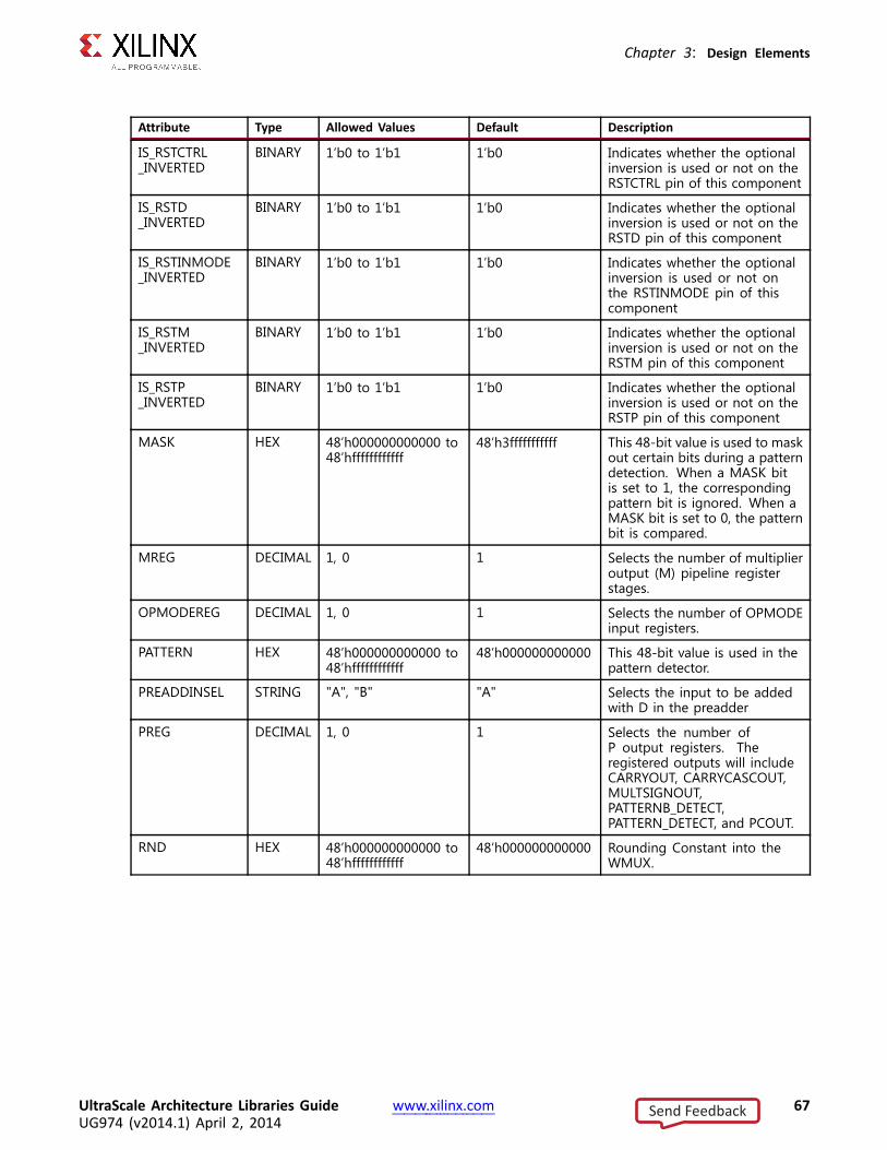
Chapter 3: Design Elements
Attribute Type Allowed Values Default Description
IS_RSTCTRL_INVERTED
BINARY 1’b0 to 1’b1 1’b0 Indicates whether the optionalinversion is used or not on theRSTCTRL pin of this component
IS_RSTD_INVERTED
BINARY 1’b0 to 1’b1 1’b0 Indicates whether the optionalinversion is used or not on theRSTD pin of this component
IS_RSTINMODE_INVERTED
BINARY 1’b0 to 1’b1 1’b0 Indicates whether the optionalinversion is used or not onthe RSTINMODE pin of thiscomponent
IS_RSTM_INVERTED
BINARY 1’b0 to 1’b1 1’b0 Indicates whether the optionalinversion is used or not on theRSTM pin of this component
IS_RSTP_INVERTED
BINARY 1’b0 to 1’b1 1’b0 Indicates whether the optionalinversion is used or not on theRSTP pin of this component
MASK HEX 48’h000000000000 to48’hffffffffffff
48’h3fffffffffff This 48-bit value is used to maskout certain bits during a patterndetection. When a MASK bitis set to 1, the correspondingpattern bit is ignored. When aMASK bit is set to 0, the patternbit is compared.
MREG DECIMAL 1, 0 1 Selects the number of multiplieroutput (M) pipeline registerstages.
OPMODEREG DECIMAL 1, 0 1 Selects the number of OPMODEinput registers.
PATTERN HEX 48’h000000000000 to48’hffffffffffff
48’h000000000000 This 48-bit value is used in thepattern detector.
PREADDINSEL STRING "A", "B" "A" Selects the input to be addedwith D in the preadder
PREG DECIMAL 1, 0 1 Selects the number ofP output registers. Theregistered outputs will includeCARRYOUT, CARRYCASCOUT,MULTSIGNOUT,PATTERNB_DETECT,PATTERN_DETECT, and PCOUT.
RND HEX 48’h000000000000 to48’hffffffffffff
48’h000000000000 Rounding Constant into theWMUX.
UltraScale Architecture Libraries Guide www.xilinx.com 67UG974 (v2014.1) April 2, 2014
Send Feedback

Chapter 3: Design Elements
Attribute Type Allowed Values Default Description
SEL_MASK STRING "MASK", "C","ROUNDING_MODE1","ROUNDING_MODE2"
"MASK" Selects the mask to be used forthe pattern detector. The C andMASK settings are for standarduses of the pattern detector(counter, overflow detection,etc.). ROUNDING_MODE1(Cbar left shifted by 1) andROUNDING_MODE2 (C-barleft shifted by 2) selectspecial masks based off of theoptionally registered C port.These rounding modes can beused to implement convergentrounding in the DSP48E2 usingthe pattern detector.
SEL_PATTERN STRING "PATTERN", "C" "PATTERN" Selects the input source forthe pattern field. The inputsource can either be a 48-bitdynamic C input or a 48-bitstatic PATTERN attribute field.
USE_MULT STRING "MULTIPLY","DYNAMIC", "NONE"
"MULTIPLY" Selects usage of the multiplier.
• "MULTIPLY" - Multiplier isbeing used.
• "NONE" - Saves powerwhen using only theAdder/Logic Unit.
• "DYNAMIC" - Indicates thatthe switching between A*Band A:B operations on thefly and therefore needs toget the worst-case timingof the two paths.
USE_PATTERN_DETECT
STRING "NO_PATDET","PATDET"
"NO_PATDET" Selects whether the patterndetector and related featuresare used ("PATDET") or not used("NO_PATDET"). This attributeis used for speed specificationand Simulation Model purposesonly.
USE_SIMD STRING "ONE48", "FOUR12","TWO24"
"ONE48" Selects the mode of operationfor the adder/subtracter. Theattribute setting can be one48-bit adder mode ("ONE48"),two 24- bit adder mode("TWO24"), or four 12-bit addermode ("FOUR12"). TypicalMultiply-Add operations aresupported when the mode isset to "ONE48". When either"TWO24" or "FOUR12" modeis selected, the multiplier mustnot be used, and USE_MULTmust be set to "NONE".
UltraScale Architecture Libraries Guide www.xilinx.com 68UG974 (v2014.1) April 2, 2014
Send Feedback

Chapter 3: Design Elements
Attribute Type Allowed Values Default Description
USE_WIDEXOR STRING "FALSE", "TRUE" "FALSE" Determines whether the WideXOR is used or not
XORSIMD STRING "XOR24_48_96","XOR12"
"XOR24_48_96" Selects the mode of operationfor the Wide XOR. The attributesetting can be one 96-bit, two48-bit four 24-bit XOR modes(XOR24_48_96), or eight 12-bitXOR mode (XOR12).
VHDL Instantiation TemplateUnless they already exist, copy the following two statements and paste them before the entitydeclaration.Library UNISIM;use UNISIM.vcomponents.all;
-- DSP48E2: 48-bit Multi-Functional Arithmetic Block-- UltraScale-- Xilinx HDL Libraries Guide, version 2014.1
DSP48E2_inst : DSP48E2generic map (
-- Feature Control Attributes: Data Path SelectionAMULTSEL=> "A", -- Selects A input to multiplier (A, AD)A_INPUT => "DIRECT", -- Selects A input source, "DIRECT" (A port) or "CASCADE" (ACIN port)BMULTSEL=> "B", -- Selects B input to multiplier (B, AD)B_INPUT => "DIRECT", -- Selects B input source, "DIRECT" (B port) or "CASCADE" (BCIN port)PREADDINSEL=> "A", -- Selects input to preadder (A, B)RND => X"000000000000", -- Rounding ConstantUSE_MULT=> "MULTIPLY", -- Select multiplier usage (MULTIPLY, DYNAMIC, NONE)USE_SIMD => "ONE48", -- SIMD selection (ONE48, FOUR12, TWO24)USE_WIDEXOR=> "FALSE", -- Use the Wide XOR function (FALSE, TRUE)XORSIMD=> "XOR24_48_96", -- Mode of operation for the Wide XOR (XOR24_48_96, XOR12)-- Pattern Detector Attributes: Pattern Detection ConfigurationAUTORESET_PATDET=> "NO_RESET", -- NO_RESET, RESET_MATCH,RESET_NOT_MATCHAUTORESET_PRIORITY=> "RESET", -- Priority of AUTORESETvs.CEP (RESET, CEP).MASK=> X"3fffffffffff", -- 48-bit mask value for pattern detect (1=ignore)PATTERN=> X"000000000000", -- 48-bit pattern match for pattern detectSEL_MASK=> "MASK", -- MASK, C, ROUNDING_MODE1,ROUNDING_MODE2SEL_PATTERN=> "PATTERN", -- Select pattern value (PATTERN, C)USE_PATTERN_DETECT=> "NO_PATDET", -- Enable pattern detect (NO_PATDET, PATDET)-- Programmable Inversion Attributes: Specifies built-in programmable inversion on specific pinsIS_ALUMODE_INVERTED=> ’0000’, -- Optional inversion for ALUMODEIS_CARRYIN_INVERTED => ’0’, -- Optional inversion for CARRYINIS_CLK_INVERTED => ’0’, -- Optional inversion for CLKIS_INMODE_INVERTED => ’00000’, -- Optional inversion for INMODEIS_OPMODE_INVERTED=> ’000000000’, -- Optional inversion for OPMODEIS_RSTALLCARRYIN_INVERTED => ’0’, -- Optional inversion for RSTALLCARRYINIS_RSTALUMODE_INVERTED=> ’0’, -- Optional inversion for RSTALUMODEIS_RSTA_INVERTED => ’0’, -- Optional inversion for RSTAIS_RSTB_INVERTED => ’0’, -- Optional inversion for RSTBIS_RSTCTRL_INVERTED => ’0’, -- Optional inversion for RSTCTRLIS_RSTC_INVERTED => ’0’, -- Optional inversion for RSTCIS_RSTD_INVERTED => ’0’, -- Optional inversion for RSTDIS_RSTINMODE_INVERTED=> ’0’, -- Optional inversion for RSTINMODEIS_RSTM_INVERTED => ’0’, -- Optional inversion for RSTMIS_RSTP_INVERTED => ’0’, -- Optional inversion for RSTP-- Register Control Attributes: Pipeline Register ConfigurationACASCREG=> 1, -- Number of pipeline stages between A/ACIN and ACOUT(1-2)ADREG=> 1, -- Pipeline stages for pre-adder (1-0)ALUMODEREG=> 1, -- Pipeline stages for ALUMODE(1-0)AREG=> 1, -- Pipeline stages for A (1-2)BCASCREG=> 1, -- Number of pipeline stages between B/BCIN and BCOUT(1-2)
UltraScale Architecture Libraries Guide www.xilinx.com 69UG974 (v2014.1) April 2, 2014
Send Feedback

Chapter 3: Design Elements
BREG=> 1, -- Pipeline stages for B (1-2)CARRYINREG=> 1, -- Pipeline stages for CARRYIN (1-0)CARRYINSELREG=> 1, -- Pipeline stages for CARRYINSEL (1-0)CREG=> 1, -- Pipeline stages for C (1-0)DREG=> 1, -- Pipeline stages for D (1-0)INMODEREG=> 1, -- Pipeline stages for INMODE (1-0)MREG=> 1, -- Multiplier pipeline stages (1-0)OPMODEREG=> 1, -- Pipeline stages for OPMODE(1-0)PREG=> 1 -- Number of pipeline stages for P (1-0)
)port map (
-- Cascade: 30-bit (each) output: Cascade PortsACOUT=> ACOUT, -- 30-bit output: A port cascadeBCOUT=> BCOUT, -- 18-bit output: B cascadeCARRYCASCOUT=> CARRYCASCOUT, -- 1-bit output: Cascade carryMULTSIGNOUT=> MULTSIGNOUT, -- 1-bit output: Multiplier sign cascadePCOUT=> PCOUT, -- 48-bit output: Cascade output-- Control: 1-bit (each) output: Control Inputs/Status BitsOVERFLOW=> OVERFLOW, -- 1-bit output: Overflow in add/accPATTERNBDETECT=> PATTERNBDETECT,-- 1-bit output: Pattern bar detectPATTERNDETECT=> PATTERNDETECT, -- 1-bit output: Pattern detectUNDERFLOW=> UNDERFLOW, -- 1-bit output: Underflow in add/acc-- Data: 4-bit (each) output: Data PortsCARRYOUT=> CARRYOUT, -- 4-bit output: CarryP => P, -- 48-bit output: Primary dataXOROUT=> XOROUT, -- 8-bit output: XOR data-- Cascade: 30-bit (each) input: Cascade PortsACIN => ACIN, -- 30-bit input: A cascade dataBCIN => BCIN, -- 18-bit input: B cascadeCARRYCASCIN=> CARRYCASCIN, -- 1-bit input: Cascade carryMULTSIGNIN => MULTSIGNIN, -- 1-bit input: Multiplier sign cascadePCIN => PCIN, -- 48-bit input: P cascade-- Control: 4-bit (each) input: Control Inputs/Status BitsALUMODE=> ALUMODE, -- 4-bit input: ALU controlCARRYINSEL => CARRYINSEL, -- 3-bit input: Carry selectCLK => CLK, -- 1-bit input: ClockINMODE => INMODE, -- 5-bit input: INMODE controlOPMODE=> OPMODE, -- 9-bit input: Operation modeRSTINMODE=> RSTINMODE, -- 1-bit input: Reset for INMODEREG-- Data: 30-bit (each) input: Data PortsA => A, -- 30-bit input: A dataB => B, -- 18-bit input: B dataC => C, -- 48-bit input: C dataCARRYIN => CARRYIN, -- 1-bit input: Carry-inD => D, -- 27-bit input: D data-- Reset/Clock Enable: 1-bit (each) input: Reset/Clock Enable InputsCEA1 => CEA1, -- 1-bit input: Clock enable for 1st stage AREGCEA2 => CEA2, -- 1-bit input: Clock enable for 2nd stage AREGCEAD => CEAD, -- 1-bit input: Clock enable for ADREGCEALUMODE=> CEALUMODE, -- 1-bit input: Clock enable for ALUMODECEB1 => CEB1, -- 1-bit input: Clock enable for 1st stage BREGCEB2 => CEB2, -- 1-bit input: Clock enable for 2nd stage BREGCEC => CEC, -- 1-bit input: Clock enable for CREGCECARRYIN=> CECARRYIN, -- 1-bit input: Clock enable for CARRYINREGCECTRL => CECTRL, -- 1-bit input: Clock enable for OPMODEREGand CARRYINSELREGCED => CED, -- 1-bit input: Clock enable for DREGCEINMODE=> CEINMODE, -- 1-bit input: Clock enable for INMODEREGCEM=> CEM, -- 1-bit input: Clock enable for MREGCEP => CEP, -- 1-bit input: Clock enable for PREGRSTA => RSTA, -- 1-bit input: Reset for AREGRSTALLCARRYIN=> RSTALLCARRYIN, -- 1-bit input: Reset for CARRYINREGRSTALUMODE=> RSTALUMODE, -- 1-bit input: Reset for ALUMODEREGRSTB => RSTB, -- 1-bit input: Reset for BREGRSTC => RSTC, -- 1-bit input: Reset for CREGRSTCTRL => RSTCTRL, -- 1-bit input: Reset for OPMODEREGand CARRYINSELREGRSTD => RSTD, -- 1-bit input: Reset for DREGand ADREGRSTM=> RSTM, -- 1-bit input: Reset for MREGRSTP => RSTP -- 1-bit input: Reset for PREG
);
-- End of DSP48E2_inst instantiation
UltraScale Architecture Libraries Guide www.xilinx.com 70UG974 (v2014.1) April 2, 2014
Send Feedback

Chapter 3: Design Elements
Verilog Instantiation Template
// DSP48E2: 48-bit Multi-Functional Arithmetic Block// UltraScale// Xilinx HDL Libraries Guide, version 2014.1
DSP48E2 #(// Feature Control Attributes: Data Path Selection.AMULTSEL("A"), // Selects A input to multiplier (A, AD).A_INPUT("DIRECT"), // Selects A input source, "DIRECT" (A port) or "CASCADE" (ACIN port).BMULTSEL("B"), // Selects B input to multiplier (B, AD).B_INPUT("DIRECT"), // Selects B input source, "DIRECT" (B port) or "CASCADE" (BCIN port).PREADDINSEL("A"), // Selects input to preadder (A, B).RND(48’h000000000000), // Rounding Constant.USE_MULT("MULTIPLY"), // Select multiplier usage (MULTIPLY, DYNAMIC, NONE).USE_SIMD("ONE48"), // SIMD selection (ONE48, FOUR12, TWO24).USE_WIDEXOR("FALSE"), // Use the Wide XOR function (FALSE, TRUE).XORSIMD("XOR24_48_96"), // Mode of operation for the Wide XOR (XOR24_48_96, XOR12)// Pattern Detector Attributes: Pattern Detection Configuration.AUTORESET_PATDET("NO_RESET"), // NO_RESET, RESET_MATCH,RESET_NOT_MATCH.AUTORESET_PRIORITY("RESET"), // Priority of AUTORESETvs.CEP (RESET, CEP)..MASK(48’h3fffffffffff), // 48-bit mask value for pattern detect (1=ignore).PATTERN(48’h000000000000), // 48-bit pattern match for pattern detect.SEL_MASK("MASK"), // MASK, C, ROUNDING_MODE1,ROUNDING_MODE2.SEL_PATTERN("PATTERN"), // Select pattern value (PATTERN, C).USE_PATTERN_DETECT("NO_PATDET"), // Enable pattern detect (NO_PATDET, PATDET)// Programmable Inversion Attributes: Specifies built-in programmable inversion on specific pins.IS_ALUMODE_INVERTED(4’b0000), // Optional inversion for ALUMODE.IS_CARRYIN_INVERTED(1’b0), // Optional inversion for CARRYIN.IS_CLK_INVERTED(1’b0), // Optional inversion for CLK.IS_INMODE_INVERTED(5’b00000), // Optional inversion for INMODE.IS_OPMODE_INVERTED(9’b000000000), // Optional inversion for OPMODE.IS_RSTALLCARRYIN_INVERTED(1’b0), // Optional inversion for RSTALLCARRYIN.IS_RSTALUMODE_INVERTED(1’b0), // Optional inversion for RSTALUMODE.IS_RSTA_INVERTED(1’b0), // Optional inversion for RSTA.IS_RSTB_INVERTED(1’b0), // Optional inversion for RSTB.IS_RSTCTRL_INVERTED(1’b0), // Optional inversion for RSTCTRL.IS_RSTC_INVERTED(1’b0), // Optional inversion for RSTC.IS_RSTD_INVERTED(1’b0), // Optional inversion for RSTD.IS_RSTINMODE_INVERTED(1’b0), // Optional inversion for RSTINMODE.IS_RSTM_INVERTED(1’b0), // Optional inversion for RSTM.IS_RSTP_INVERTED(1’b0), // Optional inversion for RSTP// Register Control Attributes: Pipeline Register Configuration.ACASCREG(1), // Number of pipeline stages between A/ACIN and ACOUT(1-2).ADREG(1), // Pipeline stages for pre-adder (1-0).ALUMODEREG(1), // Pipeline stages for ALUMODE(1-0).AREG(1), // Pipeline stages for A (1-2).BCASCREG(1), // Number of pipeline stages between B/BCIN and BCOUT(1-2).BREG(1), // Pipeline stages for B (1-2).CARRYINREG(1), // Pipeline stages for CARRYIN (1-0).CARRYINSELREG(1), // Pipeline stages for CARRYINSEL (1-0).CREG(1), // Pipeline stages for C (1-0).DREG(1), // Pipeline stages for D (1-0).INMODEREG(1), // Pipeline stages for INMODE (1-0).MREG(1), // Multiplier pipeline stages (1-0).OPMODEREG(1), // Pipeline stages for OPMODE(1-0).PREG(1) // Number of pipeline stages for P (1-0)
)DSP48E2_inst (
// Cascade: 30-bit (each) output: Cascade Ports.ACOUT(ACOUT), // 30-bit output: A port cascade.BCOUT(BCOUT), // 18-bit output: B cascade.CARRYCASCOUT(CARRYCASCOUT), // 1-bit output: Cascade carry.MULTSIGNOUT(MULTSIGNOUT), // 1-bit output: Multiplier sign cascade.PCOUT(PCOUT), // 48-bit output: Cascade output// Control: 1-bit (each) output: Control Inputs/Status Bits.OVERFLOW(OVERFLOW), // 1-bit output: Overflow in add/acc.PATTERNBDETECT(PATTERNBDETECT),// 1-bit output: Pattern bar detect.PATTERNDETECT(PATTERNDETECT), // 1-bit output: Pattern detect.UNDERFLOW(UNDERFLOW), // 1-bit output: Underflow in add/acc// Data: 4-bit (each) output: Data Ports
UltraScale Architecture Libraries Guide www.xilinx.com 71UG974 (v2014.1) April 2, 2014
Send Feedback

Chapter 3: Design Elements
.CARRYOUT(CARRYOUT), // 4-bit output: Carry
.P(P), // 48-bit output: Primary data
.XOROUT(XOROUT), // 8-bit output: XOR data// Cascade: 30-bit (each) input: Cascade Ports.ACIN(ACIN), // 30-bit input: A cascade data.BCIN(BCIN), // 18-bit input: B cascade.CARRYCASCIN(CARRYCASCIN), // 1-bit input: Cascade carry.MULTSIGNIN(MULTSIGNIN), // 1-bit input: Multiplier sign cascade.PCIN(PCIN), // 48-bit input: P cascade// Control: 4-bit (each) input: Control Inputs/Status Bits.ALUMODE(ALUMODE), // 4-bit input: ALU control.CARRYINSEL(CARRYINSEL), // 3-bit input: Carry select.CLK(CLK), // 1-bit input: Clock.INMODE(INMODE), // 5-bit input: INMODE control.OPMODE(OPMODE), // 9-bit input: Operation mode.RSTINMODE(RSTINMODE), // 1-bit input: Reset for INMODEREG// Data: 30-bit (each) input: Data Ports.A(A), // 30-bit input: A data.B(B), // 18-bit input: B data.C(C), // 48-bit input: C data.CARRYIN(CARRYIN), // 1-bit input: Carry-in.D(D), // 27-bit input: D data// Reset/Clock Enable: 1-bit (each) input: Reset/Clock Enable Inputs.CEA1(CEA1), // 1-bit input: Clock enable for 1st stage AREG.CEA2(CEA2), // 1-bit input: Clock enable for 2nd stage AREG.CEAD(CEAD), // 1-bit input: Clock enable for ADREG.CEALUMODE(CEALUMODE), // 1-bit input: Clock enable for ALUMODE.CEB1(CEB1), // 1-bit input: Clock enable for 1st stage BREG.CEB2(CEB2), // 1-bit input: Clock enable for 2nd stage BREG.CEC(CEC), // 1-bit input: Clock enable for CREG.CECARRYIN(CECARRYIN), // 1-bit input: Clock enable for CARRYINREG.CECTRL(CECTRL), // 1-bit input: Clock enable for OPMODEREGand CARRYINSELREG.CED(CED), // 1-bit input: Clock enable for DREG.CEINMODE(CEINMODE), // 1-bit input: Clock enable for INMODEREG.CEM(CEM), // 1-bit input: Clock enable for MREG.CEP(CEP), // 1-bit input: Clock enable for PREG.RSTA(RSTA), // 1-bit input: Reset for AREG.RSTALLCARRYIN(RSTALLCARRYIN), // 1-bit input: Reset for CARRYINREG.RSTALUMODE(RSTALUMODE), // 1-bit input: Reset for ALUMODEREG.RSTB(RSTB), // 1-bit input: Reset for BREG.RSTC(RSTC), // 1-bit input: Reset for CREG.RSTCTRL(RSTCTRL), // 1-bit input: Reset for OPMODEREGand CARRYINSELREG.RSTD(RSTD), // 1-bit input: Reset for DREGand ADREG.RSTM(RSTM), // 1-bit input: Reset for MREG.RSTP(RSTP) // 1-bit input: Reset for PREG
);
// End of DSP48E2_inst instantiation
For More Information• See the 7 series FPGA User Documentation (User Guides and Data Sheets).
• See the UltraScale User Documentation.
UltraScale Architecture Libraries Guide www.xilinx.com 72UG974 (v2014.1) April 2, 2014
Send Feedback

Chapter 3: Design Elements
EFUSE_USRPrimitive: 32-bit non-volatile design IDPRIMITIVE_GROUP: CONFIGURATIONPRIMITIVE_SUBGROUP: EFUSE
IntroductionProvides internal access to the 32 non-volatile, user-programmable eFUSE bits
Port DescriptionsPort Direction Width Function
EFUSEUSR<31:0> Output 32 User eFUSE register value output
Design Entry MethodInstantiation Recommended
Inference No
IP and IP Integrator Catalog No
Macro support No
Available AttributesAttribute Type Allowed Values Default Description
SIM_EFUSE _VALUE HEX 32’h00000000to 32’hffffffff
32’h00000000 Value of the 32-bit non-volatilevalue used in simulation
UltraScale Architecture Libraries Guide www.xilinx.com 73UG974 (v2014.1) April 2, 2014
Send Feedback

Chapter 3: Design Elements
VHDL Instantiation TemplateUnless they already exist, copy the following two statements and paste them before the entitydeclaration.Library UNISIM;use UNISIM.vcomponents.all;
-- EFUSE_USR: 32-bit non-volatile design ID-- UltraScale-- Xilinx HDL Libraries Guide, version 2014.1
EFUSE_USR_inst : EFUSE_USRgeneric map (
SIM_EFUSE_VALUE=> X"00000000" -- Value of the 32-bit non-volatile value used in simulation)port map (
EFUSEUSR=> EFUSEUSR -- 32-bit output: User eFUSE register value output);
-- End of EFUSE_USR_inst instantiation
Verilog Instantiation Template
// EFUSE_USR: 32-bit non-volatile design ID// UltraScale// Xilinx HDL Libraries Guide, version 2014.1
EFUSE_USR#(.SIM_EFUSE_VALUE(32’h00000000) // Value of the 32-bit non-volatile value used in simulation
)EFUSE_USR_inst (
.EFUSEUSR(EFUSEUSR) // 32-bit output: User eFUSE register value output);
// End of EFUSE_USR_inst instantiation
For More Information• See the 7 series FPGA User Documentation (User Guides and Data Sheets).
• See the UltraScale User Documentation.
UltraScale Architecture Libraries Guide www.xilinx.com 74UG974 (v2014.1) April 2, 2014
Send Feedback

Chapter 3: Design Elements
FDCEPrimitive: D Flip-Flop with Clock Enable and Asynchronous ClearPRIMITIVE_GROUP: REGISTERPRIMITIVE_SUBGROUP: SDR
IntroductionThis design element is a single D-type flip-flop with clock enable and asynchronous clear. Whenclock enable (CE) is High and asynchronous clear (CLR) is not asserted, the data on the datainput (D) of this design element is transferred to the corresponding data output (Q) during theclock (C) transition. When CLR is active, it overrides all other inputs and resets the data output(Q) Low. When CE is Low, clock transitions are ignored.This flip-flop is asynchronously initialized when power is applied. When global set/reset (GSR) isactive either upon power-up or when asserted via the STARTUP block, the value of the INITattribute is placed on the register’s output.
Logic TableInputs OutputsCLR CE D C Q
1 X X X 0
0 0 X X No Change
0 1 D ↑ D
Port DescriptionsPort Direction Width Function
C Input 1 Clock input. Polarity is determined by the IS_C_INVERTED attribute.
CE Input 1 Active-High register clock enable
CLR Input 1 Asynchronous clear. Polarity is determined by the IS_CLR_INVERTED attribute.
D Input 1 Data input
Q Output 1 Data output
UltraScale Architecture Libraries Guide www.xilinx.com 75UG974 (v2014.1) April 2, 2014
Send Feedback

Chapter 3: Design Elements
Design Entry MethodInstantiation Yes
Inference Recommended
IP and IP Integrator Catalog No
Macro support No
Available AttributesAttribute Type Allowed Values Default Description
INIT BINARY 1’b0, 1’b1 1’b0 Sets the initial value of Q output afterconfiguration or when GSR is asserted via theSTARTUP block
IS_C_INVERTED BINARY 1’b0 to 1’b1 1’b0 Indicates whether the optional inversion is usedor not for the C pin of this component
IS_CLR _INVERTED BINARY 1’b0 to 1’b1 1’b0 Indicates whether the optional inversion is usedor not for the CLR pin of this component
IS_D_INVERTED BINARY 1’b0 to 1’b1 1’b0 Indicates whether the optional inversion is usedor not for the D pin of this component. Mustbe set to 0 unless used as an I/O register.
VHDL Instantiation TemplateUnless they already exist, copy the following two statements and paste them before the entitydeclaration.Library UNISIM;use UNISIM.vcomponents.all;
-- FDCE: D Flip-Flop with Clock Enable and Asynchronous Clear-- UltraScale-- Xilinx HDL Libraries Guide, version 2014.1
FDCE_inst : FDCEgeneric map (
INIT => 0, -- Initial value of register, 1’b0, 1’b1-- Programmable Inversion Attributes: Specifies the use of the built-in programmable inversionIS_CLR_INVERTED => ’0’, -- Optional inversion for CLRIS_C_INVERTED => ’0’, -- Optional inversion for CIS_D_INVERTED => ’0’ -- Optional inversion for D
)port map (
Q => Q, -- 1-bit output: DataC => C, -- 1-bit input: ClockCE => CE, -- 1-bit input: Clock enableCLR => CLR, -- 1-bit input: Asynchronous clearD => D -- 1-bit input: Data
);
-- End of FDCE_inst instantiation
UltraScale Architecture Libraries Guide www.xilinx.com 76UG974 (v2014.1) April 2, 2014
Send Feedback

Chapter 3: Design Elements
Verilog Instantiation Template
// FDCE: D Flip-Flop with Clock Enable and Asynchronous Clear// UltraScale// Xilinx HDL Libraries Guide, version 2014.1
FDCE #(.INIT(0), // Initial value of register, 1’b0, 1’b1// Programmable Inversion Attributes: Specifies the use of the built-in programmable inversion.IS_CLR_INVERTED(1’b0), // Optional inversion for CLR.IS_C_INVERTED(1’b0), // Optional inversion for C.IS_D_INVERTED(1’b0) // Optional inversion for D
)FDCE_inst (
.Q(Q), // 1-bit output: Data
.C(C), // 1-bit input: Clock
.CE(CE), // 1-bit input: Clock enable
.CLR(CLR), // 1-bit input: Asynchronous clear
.D(D) // 1-bit input: Data);
// End of FDCE_inst instantiation
For More Information• See the 7 series FPGA User Documentation (User Guides and Data Sheets).
• See the UltraScale User Documentation.
UltraScale Architecture Libraries Guide www.xilinx.com 77UG974 (v2014.1) April 2, 2014
Send Feedback

Chapter 3: Design Elements
FDPEPrimitive: D Flip-Flop with Clock Enable and Asynchronous PresetPRIMITIVE_GROUP: REGISTERPRIMITIVE_SUBGROUP: SDR
IntroductionThis design element is a single D-type flip-flop with clock enable and asynchronous preset.When clock enable (CE) is High and asynchronous preset (PRE) is not asserted, the data on thedata input (D) of this design element is transferred to the corresponding data output (Q) duringthe clock (C) transition. When PRE is asserted, it overrides all other inputs and presets the dataoutput (Q) High. When CE is Low, clock transitions are ignored.This flip-flop is asynchronously initialized when power is applied. When global set/reset (GSR) isactive either upon power-up or when asserted via the STARTUP block, the value of the INITattribute is placed on the register’s output.
Logic TableInputs OutputsPRE CE D C Q
1 X X X 1
0 0 X X No Change
0 1 D ↑ D
Port DescriptionsPort Direction Width Function
C Input 1 Clock input. Polarity is determined by the IS_C_INVERTED attribute.
CE Input 1 Active-High register clock enable
D Input 1 Data input
PRE Input 1 Asynchronous preset. Polarity is determined by the IS_PRE_INVERTEDattribute.
Q Output 1 Data output
UltraScale Architecture Libraries Guide www.xilinx.com 78UG974 (v2014.1) April 2, 2014
Send Feedback

Chapter 3: Design Elements
Design Entry MethodInstantiation Yes
Inference Recommended
IP and IP Integrator Catalog No
Macro support No
Available AttributesAttribute Type Allowed Values Default Description
INIT BINARY 1’b1, 1’b0 1’b1 Sets the initial value of Q output afterconfiguration or when GSR is asserted via theSTARTUP block
IS_C_INVERTED BINARY 1’b0 to 1’b1 1’b0 Indicates whether the optional inversion is usedor not for the C pin of this component
IS_D_INVERTED BINARY 1’b0 to 1’b1 1’b0 Indicates whether the optional inversion is usedor not for the D pin of this component. Mustbe set to 0 unless used as an I/O register.
IS_PRE _INVERTED BINARY 1’b0 to 1’b1 1’b0 Indicates whether the optional inversion is usedor not for the PRE pin of this component
VHDL Instantiation TemplateUnless they already exist, copy the following two statements and paste them before the entitydeclaration.Library UNISIM;use UNISIM.vcomponents.all;
-- FDPE: D Flip-Flop with Clock Enable and Asynchronous Preset-- UltraScale-- Xilinx HDL Libraries Guide, version 2014.1
FDPE_inst : FDPEgeneric map (
INIT => 1, -- Initial value of register, 1’b1, 1’b0-- Programmable Inversion Attributes: Specifies the use of the built-in programmable inversionIS_C_INVERTED => ’0’, -- Optional inversion for CIS_D_INVERTED => ’0’, -- Optional inversion for DIS_PRE_INVERTED => ’0’ -- Optional inversion for PRE
)port map (
Q => Q, -- 1-bit output: DataC => C, -- 1-bit input: ClockCE => CE, -- 1-bit input: Clock enableD => D, -- 1-bit input: DataPRE => PRE -- 1-bit input: Asynchronous preset
);
-- End of FDPE_inst instantiation
UltraScale Architecture Libraries Guide www.xilinx.com 79UG974 (v2014.1) April 2, 2014
Send Feedback

Chapter 3: Design Elements
Verilog Instantiation Template
// FDPE: D Flip-Flop with Clock Enable and Asynchronous Preset// UltraScale// Xilinx HDL Libraries Guide, version 2014.1
FDPE #(.INIT(1), // Initial value of register, 1’b1, 1’b0// Programmable Inversion Attributes: Specifies the use of the built-in programmable inversion.IS_C_INVERTED(1’b0), // Optional inversion for C.IS_D_INVERTED(1’b0), // Optional inversion for D.IS_PRE_INVERTED(1’b0) // Optional inversion for PRE
)FDPE_inst (
.Q(Q), // 1-bit output: Data
.C(C), // 1-bit input: Clock
.CE(CE), // 1-bit input: Clock enable
.D(D), // 1-bit input: Data
.PRE(PRE) // 1-bit input: Asynchronous preset);
// End of FDPE_inst instantiation
For More Information• See the 7 series FPGA User Documentation (User Guides and Data Sheets).
• See the UltraScale User Documentation.
UltraScale Architecture Libraries Guide www.xilinx.com 80UG974 (v2014.1) April 2, 2014
Send Feedback

Chapter 3: Design Elements
FDREPrimitive: D Flip-Flop with Clock Enable and Synchronous ResetPRIMITIVE_GROUP: REGISTERPRIMITIVE_SUBGROUP: SDR
IntroductionThis design element is a single D-type flip-flop with clock enable and synchronous reset. Whenclock enable (CE) is High and synchronous reset (R) is not asserted, the data on the data input(D) of this design element is transferred to the corresponding data output (Q) during the clock(C) transition. When R is active, it overrides all other inputs and resets the data output (Q) Lowupon the next clock transition. When CE is Low, clock transitions are ignored.This flip-flop is asynchronously initialized when power is applied. When global set/reset (GSR) isactive either upon power-up or when asserted via the STARTUP block, the value of the INITattribute is placed on the register’s output.
Logic TableInputs OutputsR CE D C Q
1 X X ↑ 0
0 0 X X No Change
0 1 D ↑ D
Port DescriptionsPort Direction Width Function
C Input 1 Clock input. Polarity is determined by the IS_C_INVERTED attribute.
CE Input 1 Active-High register clock enable
D Input 1 Data input
Q Output 1 Data output
R Input 1 Synchronous reset. Polarity is determined by the IS_R_INVERTED attribute.
UltraScale Architecture Libraries Guide www.xilinx.com 81UG974 (v2014.1) April 2, 2014
Send Feedback

Chapter 3: Design Elements
Design Entry MethodInstantiation Yes
Inference Recommended
IP and IP Integrator Catalog No
Macro support No
Available AttributesAttribute Type Allowed Values Default Description
INIT BINARY 1’b0, 1’b1 1’b0 Sets the initial value of Q output afterconfiguration or when GSR is asserted via theSTARTUP block.
IS_C_INVERTED BINARY 1’b0 to 1’b1 1’b0 Indicates whether the optional inversion is usedor not for the C pin of this component
IS_D_INVERTED BINARY 1’b0 to 1’b1 1’b0 Indicates whether the optional inversion is usedor not for the C pin of this component. Mustbe set to 0 unless used as an I/O register.
IS_R_INVERTED BINARY 1’b0 to 1’b1 1’b0 Indicates whether the optional inversion is usedor not for the R pin of this component
VHDL Instantiation TemplateUnless they already exist, copy the following two statements and paste them before the entitydeclaration.Library UNISIM;use UNISIM.vcomponents.all;
-- FDRE: D Flip-Flop with Clock Enable and Synchronous Reset-- UltraScale-- Xilinx HDL Libraries Guide, version 2014.1
FDRE_inst : FDREgeneric map (
INIT => 0, -- Initial value of register, 1’b0, 1’b1-- Programmable Inversion Attributes: Specifies the use of the built-in programmable inversionIS_C_INVERTED => ’0’, -- Optional inversion for CIS_D_INVERTED => ’0’, -- Optional inversion for DIS_R_INVERTED => ’0’ -- Optional inversion for R
)port map (
Q => Q, -- 1-bit output: DataC => C, -- 1-bit input: ClockCE => CE, -- 1-bit input: Clock enableD => D, -- 1-bit input: DataR => R -- 1-bit input: Synchronous reset
);
-- End of FDRE_inst instantiation
UltraScale Architecture Libraries Guide www.xilinx.com 82UG974 (v2014.1) April 2, 2014
Send Feedback

Chapter 3: Design Elements
Verilog Instantiation Template
// FDRE: D Flip-Flop with Clock Enable and Synchronous Reset// UltraScale// Xilinx HDL Libraries Guide, version 2014.1
FDRE #(.INIT(0), // Initial value of register, 1’b0, 1’b1// Programmable Inversion Attributes: Specifies the use of the built-in programmable inversion.IS_C_INVERTED(1’b0), // Optional inversion for C.IS_D_INVERTED(1’b0), // Optional inversion for D.IS_R_INVERTED(1’b0) // Optional inversion for R
)FDRE_inst (
.Q(Q), // 1-bit output: Data
.C(C), // 1-bit input: Clock
.CE(CE), // 1-bit input: Clock enable
.D(D), // 1-bit input: Data
.R(R) // 1-bit input: Synchronous reset);
// End of FDRE_inst instantiation
For More Information• See the 7 series FPGA User Documentation (User Guides and Data Sheets).
• See the UltraScale User Documentation.
UltraScale Architecture Libraries Guide www.xilinx.com 83UG974 (v2014.1) April 2, 2014
Send Feedback

Chapter 3: Design Elements
FDSEPrimitive: D Flip-Flop with Clock Enable and Synchronous SetPRIMITIVE_GROUP: REGISTERPRIMITIVE_SUBGROUP: SDR
IntroductionThis design element is a single D-type flip-flop with clock enable and synchronous set. Whenclock enable (CE) is High and synchronous set (S) is not asserted, the data on the data input (D)of this design element is transferred to the corresponding data output (Q) during the clock (C)transition. When S is active, it overrides all other inputs and sets the data output (Q) High uponthe next clock transition. When CE is Low, clock transitions are ignored.This flip-flop is asynchronously initialized when power is applied. When global set/reset (GSR) isactive either upon power-up or when asserted via the STARTUP block, the value of the INITattribute is placed on the register’s output.
Logic TableInputs OutputsS CE D C Q
1 X X ↑ 1
0 0 X X No Change
0 1 D ↑ D
Port DescriptionsPort Direction Width Function
C Input 1 Clock input. Polarity is determined by the IS_C_INVERTED attribute.
CE Input 1 Active-High register clock enable
D Input 1 Data input
Q Output 1 Data output
S Input 1 Synchronous set. Polarity is determined by the IS_S_INVERTED attribute.
UltraScale Architecture Libraries Guide www.xilinx.com 84UG974 (v2014.1) April 2, 2014
Send Feedback

Chapter 3: Design Elements
Design Entry MethodInstantiation Yes
Inference Recommended
IP and IP Integrator Catalog No
Macro support No
Available AttributesAttribute Type Allowed Values Default Description
INIT BINARY 1’b1, 1’b0 1’b1 Sets the initial value of Q output afterconfiguration or when GSR is asserted via theSTARTUP block.
IS_C_INVERTED BINARY 1’b0 to 1’b1 1’b0 Indicates whether the optional inversion is usedor not for the C pin of this component
IS_D_INVERTED BINARY 1’b0 to 1’b1 1’b0 Indicates whether the optional inversion is usedor not for the C pin of this component. Mustbe set to 0 unless used as an I/O register.
IS_S_INVERTED BINARY 1’b0 to 1’b1 1’b0 Indicates whether the optional inversion is usedor not for the S pin of this component
VHDL Instantiation TemplateUnless they already exist, copy the following two statements and paste them before the entitydeclaration.Library UNISIM;use UNISIM.vcomponents.all;
-- FDSE: D Flip-Flop with Clock Enable and Synchronous Set-- UltraScale-- Xilinx HDL Libraries Guide, version 2014.1
FDSE_inst : FDSEgeneric map (
INIT => 1, -- Initial value of register, 1’b1, 1’b0-- Programmable Inversion Attributes: Specifies the use of the built-in programmable inversionIS_C_INVERTED => ’0’, -- Optional inversion for CIS_D_INVERTED => ’0’, -- Optional inversion for DIS_S_INVERTED => ’0’ -- Optional inversion for S
)port map (
Q => Q, -- 1-bit output: DataC => C, -- 1-bit input: ClockCE => CE, -- 1-bit input: Clock enableD => D, -- 1-bit input: DataS => S -- 1-bit input: Synchronous set
);
-- End of FDSE_inst instantiation
UltraScale Architecture Libraries Guide www.xilinx.com 85UG974 (v2014.1) April 2, 2014
Send Feedback

Chapter 3: Design Elements
Verilog Instantiation Template
// FDSE: D Flip-Flop with Clock Enable and Synchronous Set// UltraScale// Xilinx HDL Libraries Guide, version 2014.1
FDSE #(.INIT(1), // Initial value of register, 1’b1, 1’b0// Programmable Inversion Attributes: Specifies the use of the built-in programmable inversion.IS_C_INVERTED(1’b0), // Optional inversion for C.IS_D_INVERTED(1’b0), // Optional inversion for D.IS_S_INVERTED(1’b0) // Optional inversion for S
)FDSE_inst (
.Q(Q), // 1-bit output: Data
.C(C), // 1-bit input: Clock
.CE(CE), // 1-bit input: Clock enable
.D(D), // 1-bit input: Data
.S(S) // 1-bit input: Synchronous set);
// End of FDSE_inst instantiation
For More Information• See the 7 series FPGA User Documentation (User Guides and Data Sheets).
• See the UltraScale User Documentation.
UltraScale Architecture Libraries Guide www.xilinx.com 86UG974 (v2014.1) April 2, 2014
Send Feedback

Chapter 3: Design Elements
FIFO18E2Primitive: 18Kb FIFO (First-In-First-Out) Block RAM MemoryPRIMITIVE_GROUP: BLOCKRAMPRIMITIVE_SUBGROUP: FIFO
IntroductionThe FIFO18E2 uses dedicated control logic and the 18Kb Block RAM to deliver a configurableFirst-In-First-Out (FIFO) capability. This primitive can be used in a 4-bit wide by 4K deep,9-bit wide by 2K deep, 18-bit wide by 1K deep, or a 36-bit wide by 512 deep configuration.The primitive can be configured in either synchronous or dual-clock (asynchronous) mode,with all associated FIFO flags and status signals. This FIFO also features a cascade capabilitywhich allows multiple FIFO18E2 components to be chained together to form deeper FIFOconfiguration if desired.When using the dual-clock mode with independent clocks, depending on the offset betweenread and write clock edges, the Empty, Almost Empty, Full and Almost Full flags can deassertone cycle later. Due to the asynchronous nature of the clocks the simulation model only reflectsthe deassertion latency cycles listed in the User Guide.
UltraScale Architecture Libraries Guide www.xilinx.com 87UG974 (v2014.1) April 2, 2014
Send Feedback

Chapter 3: Design Elements
Port DescriptionsPort Direction Width Function
CASDIN<31:0> Input 32 FIFO Data Input Bus from previous FIFO CASDOUT ouputwhen cascading FIFOs serially or in parallel to extend depth.Only used when CASCADE_ORDER="MIDDLE", "LAST", or"PARALLEL".
CASDINP<3:0> Input 4 FIFO parity data input bus from previous FIFO CASDOUTPwhen cascading FIFOs serially or in parallel to extend depth.Only used when CASCADE_ORDER="MIDDLE", "LAST", or"PARALLEL".
CASDOMUX Input 1 D input to flop that drives the select line to thecascade mux on the BRAM outputs. Only used whenCASCADE_ORDER="PARALLEL".
CASDOMUXEN Input 1 EN input to flop that drives the select line to thecascade mux on the BRAM outputs. Only used whenCASCADE_ORDER="PARALLEL".
CASDOUT<31:0> Output 32 FIFO data output bus to next FIFO CASDIN input whencascading FIFOs serially or in parallel to extend depth.Only used when CASCADE_ORDER="FIRST", "MIDDLE", or"PARALLEL".
CASDOUTP<3:0> Output 4 FIFO Parity data output bus to next FIFO CASDINP inputwhen cascading FIFOs serially or in parallel to extend depth.Only used when CASCADE_ORDER="FIRST", "MIDDLE", or"PARALLEL".
CASNXTEMPTY Output 1 EMPTY input from previous FIFO, used for cascadingFIFOs serially to extend depth. Connects to theCASNXTEMPTY of the previous FIFO. Only used whenCASCADE_ORDER="MIDDLE" or "LAST".
CASNXTRDEN Input 1 RDEN input from next FIFO, used for cascading FIFOsserially to extend depth. Connects to CASPRVRDEN ofthe next FIFO. Only used when CASCADE_ORDER="FIRST"or "MIDDLE".
CASOREGIMUX Input 1 D input to flop that drives the select line to thecascade mux before the output registers. Onlyused when CASCADE_ORDER="PARALLEL" andREGISTER_MODE="DO_PIPELINED".
CASOREGIMUXEN Input 1 EN input to flop that drives the select line to thecascade mux before the output registers. Onlyused when CASCADE_ORDER="PARALLEL" andREGISTER_MODE="DO_PIPELINED".
CASPRVEMPTY Input 1 EMPTY input from previous FIFO, used for cascading FIFOsserially to extend depth. Connects to the CASNXTEMPTYof the previous FIFO. Only used when CASCADE_ORDER is"MIDDLE" or "LAST".
CASPRVRDEN Output 1 Control output driving the RDEN input of the previous(PRV) FIFO, used for cascading FIFOs serially to extenddepth. Connects to CASNXTRDEN of the previous FIFO.Only used when CASCADE_ORDER is "MIDDLE" or "LAST".
DIN<31:0> Input 32 FIFO data input bus. Synchronous to WRCLK.
DINP<3:0> Input 4 FIFO parity input bus. Synchronous to WRCLK.
UltraScale Architecture Libraries Guide www.xilinx.com 88UG974 (v2014.1) April 2, 2014
Send Feedback
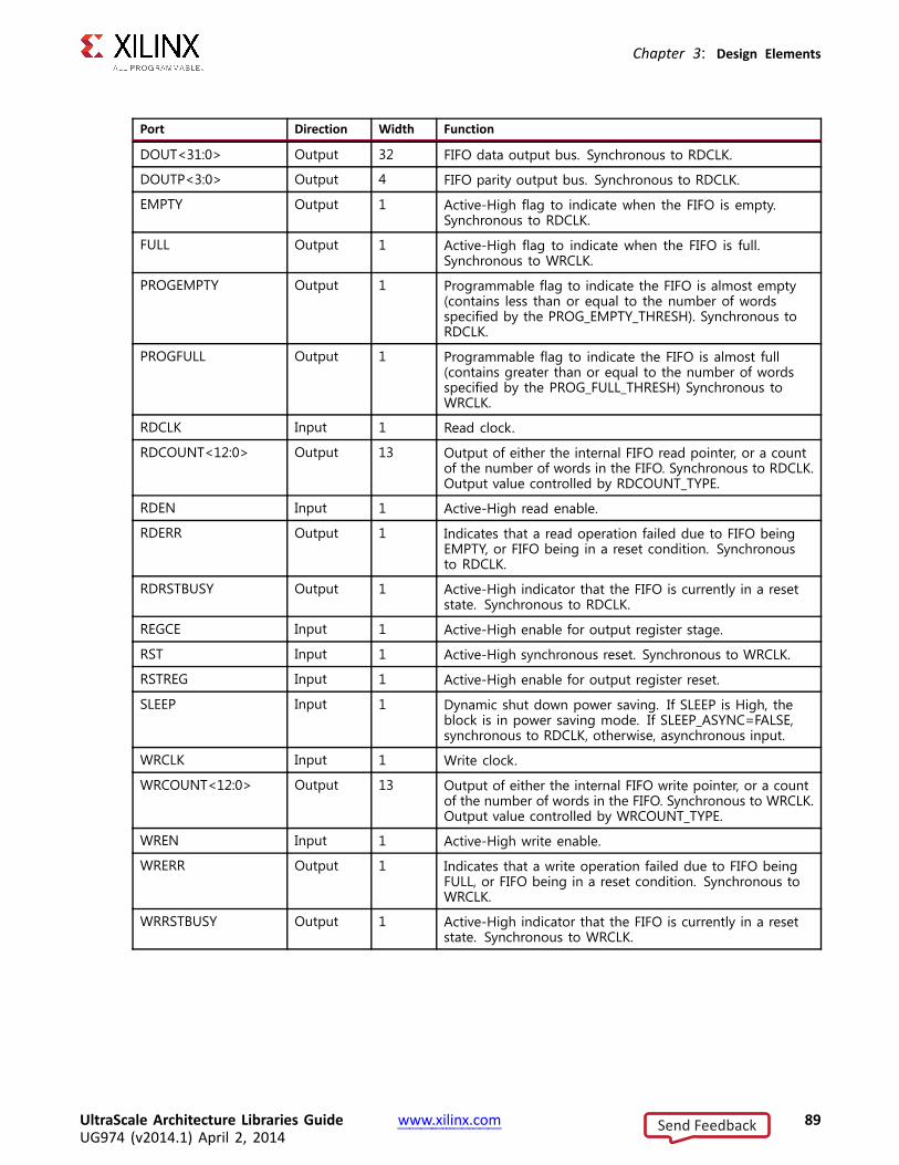
Chapter 3: Design Elements
Port Direction Width Function
DOUT<31:0> Output 32 FIFO data output bus. Synchronous to RDCLK.
DOUTP<3:0> Output 4 FIFO parity output bus. Synchronous to RDCLK.
EMPTY Output 1 Active-High flag to indicate when the FIFO is empty.Synchronous to RDCLK.
FULL Output 1 Active-High flag to indicate when the FIFO is full.Synchronous to WRCLK.
PROGEMPTY Output 1 Programmable flag to indicate the FIFO is almost empty(contains less than or equal to the number of wordsspecified by the PROG_EMPTY_THRESH). Synchronous toRDCLK.
PROGFULL Output 1 Programmable flag to indicate the FIFO is almost full(contains greater than or equal to the number of wordsspecified by the PROG_FULL_THRESH) Synchronous toWRCLK.
RDCLK Input 1 Read clock.
RDCOUNT<12:0> Output 13 Output of either the internal FIFO read pointer, or a countof the number of words in the FIFO. Synchronous to RDCLK.Output value controlled by RDCOUNT_TYPE.
RDEN Input 1 Active-High read enable.
RDERR Output 1 Indicates that a read operation failed due to FIFO beingEMPTY, or FIFO being in a reset condition. Synchronousto RDCLK.
RDRSTBUSY Output 1 Active-High indicator that the FIFO is currently in a resetstate. Synchronous to RDCLK.
REGCE Input 1 Active-High enable for output register stage.
RST Input 1 Active-High synchronous reset. Synchronous to WRCLK.
RSTREG Input 1 Active-High enable for output register reset.
SLEEP Input 1 Dynamic shut down power saving. If SLEEP is High, theblock is in power saving mode. If SLEEP_ASYNC=FALSE,synchronous to RDCLK, otherwise, asynchronous input.
WRCLK Input 1 Write clock.
WRCOUNT<12:0> Output 13 Output of either the internal FIFO write pointer, or a countof the number of words in the FIFO. Synchronous to WRCLK.Output value controlled by WRCOUNT_TYPE.
WREN Input 1 Active-High write enable.
WRERR Output 1 Indicates that a write operation failed due to FIFO beingFULL, or FIFO being in a reset condition. Synchronous toWRCLK.
WRRSTBUSY Output 1 Active-High indicator that the FIFO is currently in a resetstate. Synchronous to WRCLK.
UltraScale Architecture Libraries Guide www.xilinx.com 89UG974 (v2014.1) April 2, 2014
Send Feedback

Chapter 3: Design Elements
Design Entry MethodInstantiation Yes
Inference No
IP and IP Integrator Catalog Recommended
Macro support No
Available AttributesAttribute Type Allowed Values Default Description
CASCADE_ORDER
STRING "NONE", "FIRST", "LAST","MIDDLE", "PARALLEL"
"NONE" Specifies use, configurationand position of the cascadefeature to bind more than oneFIFO18E2 together to formdeeper FIFO depths.
CLOCK_DOMAINS
STRING "INDEPENDENT","COMMON"
"INDEPENDENT" Specifies whether to usea Common (synchronousoperation) or Indepedent(asynchronous or different)clocks
FIRST_WORD_FALL_THROUGH
STRING "FALSE", "TRUE" "FALSE" If TRUE, the first write to theFIFO will appear on DO withouta first RDEN assertion.
INIT HEX 36’h000000000 to36’hfffffffff
36’h000000000 Specifies the initial value on theDO output after configuration.
IS_RDCLK_INVERTED
BINARY 1’b0 to 1’b1 1’b0 Indicates whether the optionalinversion is used or not on theRDCLK pin of this component
IS_RDEN_INVERTED
BINARY 1’b0 to 1’b1 1’b0 Indicates whether the optionalinversion is used or not on theRDEN pin of this component
IS_RST_INVERTED
BINARY 1’b0 to 1’b1 1’b0 Indicates whether the optionalinversion is used or not on theRST pin of this component
IS_RSTREG_INVERTED
BINARY 1’b0 to 1’b1 1’b0 Indicates whether the optionalinversion is used or not on theRSTREG pin of this component
IS_WRCLK_INVERTED
BINARY 1’b0 to 1’b1 1’b0 Indicates whether the optionalinversion is used or not on theWRCLK pin of this component
IS_WREN_INVERTED
BINARY 1’b0 to 1’b1 1’b0 Indicates whether the optionalinversion is used or not on theWREN pin of this component
PROG_EMPTY_THRESH
DECIMAL 1 to 8191 256 Specifies the different betweenthe write pointer (WRCOUNT)and read pointer (RDCOUNT).to trigger the PROGEMPTYoutput.
UltraScale Architecture Libraries Guide www.xilinx.com 90UG974 (v2014.1) April 2, 2014
Send Feedback

Chapter 3: Design Elements
Attribute Type Allowed Values Default Description
PROG_FULL_THRESH
DECIMAL 1 to 8191 256 Specifies the different betweenthe write pointer (WRCOUNT)and read pointer (RDCOUNT).to trigger the PROGFULLoutput.
RDCOUNT_TYPE STRING "RAW_PNTR","EXTENDED_DATACOUNT","SIMPLE_DATACOUNT","SYNC_PNTR"
"RAW_PNTR" Specifies type and format forthe RDCOUNT data.
READ_WIDTH DECIMAL 4, 9, 18, 36 4 Specifies the data width for theread-side of the FIFO.
REGISTER_MODE
STRING "UNREGISTERED","DO_PIPELINED","REGISTERED"
"UNREGISTERED" Specifies output regsiter mode.
RSTREG_PRIORITY
STRING "RSTREG", "REGCE" "RSTREG" Specifies whether reset orenable has priority.
SLEEP_ASYNC STRING "FALSE", "TRUE" "FALSE" Specifies asynchronous orsynchronous operation of theBRAM sleep mode.
SRVAL HEX 36’h000000000 to36’hfffffffff
36’h000000000 Specifies per-bit the polarityof the FIFO output afterRST/RSTREG is asserted
WRCOUNT_TYPE STRING "RAW_PNTR","EXTENDED_DATACOUNT","SIMPLE_DATACOUNT","SYNC_PNTR"
"RAW_PNTR" Specifies type and format forthe WRCOUNT data.
WRITE_WIDTH DECIMAL 4, 9, 18, 36 4 Specifies the data width for thewrite-side of the FIFO.
VHDL Instantiation TemplateUnless they already exist, copy the following two statements and paste them before the entitydeclaration.Library UNISIM;use UNISIM.vcomponents.all;
-- FIFO18E2: 18Kb FIFO (First-In-First-Out) Block RAMMemory-- UltraScale-- Xilinx HDL Libraries Guide, version 2014.1
FIFO18E2_inst : FIFO18E2generic map (
CASCADE_ORDER=> "NONE", -- NONE, FIRST, LAST, MIDDLE, PARALLELCLOCK_DOMAINS=> "INDEPENDENT", -- INDEPENDENT, COMMONFIRST_WORD_FALL_THROUGH=> "FALSE", -- FALSE, TRUEINIT => X"000000000", -- Initial values on output portPROG_EMPTY_THRESH=> 256, -- Programmable Empty ThresholdPROG_FULL_THRESH=> 256, -- Programmable Full Threshold-- Programmable Inversion Attributes: Specifies the use of the built-in programmable inversionIS_RDCLK_INVERTED => ’0’, -- Optional inversion for RDCLKIS_RDEN_INVERTED => ’0’, -- Optional inversion for RDENIS_RSTREG_INVERTED=> ’0’, -- Optional inversion for RSTREGIS_RST_INVERTED => ’0’, -- Optional inversion for RSTIS_WRCLK_INVERTED=> ’0’, -- Optional inversion for WRCLK
UltraScale Architecture Libraries Guide www.xilinx.com 91UG974 (v2014.1) April 2, 2014
Send Feedback

Chapter 3: Design Elements
IS_WREN_INVERTED=> ’0’, -- Optional inversion for WRENRDCOUNT_TYPE=> "RAW_PNTR", -- RAW_PNTR,EXTENDED_DATACOUNT,SIMPLE_DATACOUNT,SYNC_PNTRREAD_WIDTH=> 4, -- 4-36REGISTER_MODE=> "UNREGISTERED", -- UNREGISTERED,DO_PIPELINED, REGISTEREDRSTREG_PRIORITY=> "RSTREG", -- RSTREG, REGCESLEEP_ASYNC=> "FALSE", -- FALSE, TRUESRVAL => X"000000000", -- SET/reset value of the FIFO outputsWRCOUNT_TYPE=> "RAW_PNTR", -- RAW_PNTR,EXTENDED_DATACOUNT,SIMPLE_DATACOUNT,SYNC_PNTRWRITE_WIDTH=> 4 -- 4-36
)port map (
-- Cascade Signals: 32-bit (each) output: Multi-FIFO cascade signalsCASDOUT=> CASDOUT, -- 32-bit output: Data cascade output busCASDOUTP=> CASDOUTP, -- 4-bit output: Parity data cascade output busCASNXTEMPTY=> CASNXTEMPTY, -- 1-bit output: Cascade next emptyCASPRVRDEN=> CASPRVRDEN, -- 1-bit output: Cascade previous read enable-- Read Data: 32-bit (each) output: Read output dataDOUT=> DOUT, -- 32-bit output: FIFO data output busDOUTP=> DOUTP, -- 4-bit output: FIFO parity output bus.-- Status: 1-bit (each) output: Flags and other FIFO status outputsEMPTY=> EMPTY, -- 1-bit output: EmptyFULL => FULL, -- 1-bit output: FullPROGEMPTY=> PROGEMPTY, -- 1-bit output: Programmable emptyPROGFULL=> PROGFULL, -- 1-bit output: Programmable fullRDCOUNT=> RDCOUNT, -- 13-bit output: Read countRDERR=> RDERR, -- 1-bit output: Read errorRDRSTBUSY=> RDRSTBUSY, -- 1-bit output: Reset busy (sync to RDCLK)WRCOUNT=> WRCOUNT, -- 13-bit output: Write countWRERR=> WRERR, -- 1-bit output: Write ErrorWRRSTBUSY=> WRRSTBUSY, -- 1-bit output: Reset busy (sync to WRCLK)-- Cascade Signals: 32-bit (each) input: Multi-FIFO cascade signalsCASDIN => CASDIN, -- 32-bit input: Data cascade input busCASDINP => CASDINP, -- 4-bit input: Parity data cascade input busCASDOMUX=> CASDOMUX, -- 1-bit input: Cascade MUXselectCASDOMUXEN=> CASDOMUXEN, -- 1-bit input: Enable for cascade MUXselectCASNXTRDEN=> CASNXTRDEN, -- 1-bit input: Cascade next read enableCASOREGIMUX=> CASOREGIMUX, -- 1-bit input: Cascade output MUX selectCASOREGIMUXEN=> CASOREGIMUXEN,-- 1-bit input: Cascade output MUX seelct enableCASPRVEMPTY=> CASPRVEMPTY, -- 1-bit input: Cascade previous empty-- Read Control Signals: 1-bit (each) input: Read clock, enable and reset input signalsRDCLK => RDCLK, -- 1-bit input: Read clockRDEN=> RDEN, -- 1-bit input: Read enableREGCE=> REGCE, -- 1-bit input: Output register clock enableRSTREG=> RSTREG, -- 1-bit input: Output register resetSLEEP => SLEEP, -- 1-bit input: Sleep Mode-- Write Control Signals: 1-bit (each) input: Write clock and enable input signalsRST => RST, -- 1-bit input: ResetWRCLK=> WRCLK, -- 1-bit input: Write clockWREN=> WREN, -- 1-bit input: Write enable-- Write Data: 32-bit (each) input: Write input dataDIN => DIN, -- 32-bit input: FIFO data input busDINP => DINP -- 4-bit input: FIFO parity input bus
);
-- End of FIFO18E2_inst instantiation
Verilog Instantiation Template
// FIFO18E2: 18Kb FIFO (First-In-First-Out) Block RAMMemory// UltraScale// Xilinx HDL Libraries Guide, version 2014.1
FIFO18E2 #(.CASCADE_ORDER("NONE"), // NONE, FIRST, LAST, MIDDLE, PARALLEL.CLOCK_DOMAINS("INDEPENDENT"), // INDEPENDENT, COMMON.FIRST_WORD_FALL_THROUGH("FALSE"), // FALSE, TRUE.INIT(36’h000000000), // Initial values on output port.PROG_EMPTY_THRESH(256), // Programmable Empty Threshold.PROG_FULL_THRESH(256), // Programmable Full Threshold// Programmable Inversion Attributes: Specifies the use of the built-in programmable inversion
UltraScale Architecture Libraries Guide www.xilinx.com 92UG974 (v2014.1) April 2, 2014
Send Feedback
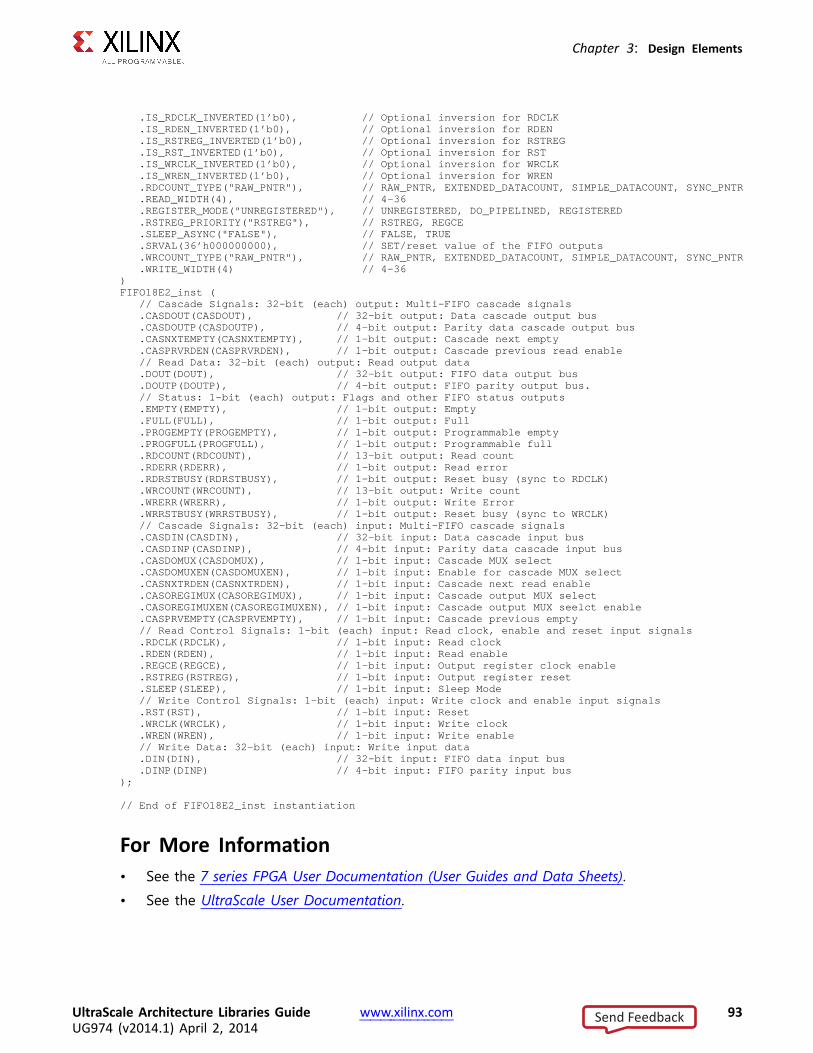
Chapter 3: Design Elements
.IS_RDCLK_INVERTED(1’b0), // Optional inversion for RDCLK
.IS_RDEN_INVERTED(1’b0), // Optional inversion for RDEN
.IS_RSTREG_INVERTED(1’b0), // Optional inversion for RSTREG
.IS_RST_INVERTED(1’b0), // Optional inversion for RST
.IS_WRCLK_INVERTED(1’b0), // Optional inversion for WRCLK
.IS_WREN_INVERTED(1’b0), // Optional inversion for WREN
.RDCOUNT_TYPE("RAW_PNTR"), // RAW_PNTR,EXTENDED_DATACOUNT,SIMPLE_DATACOUNT,SYNC_PNTR
.READ_WIDTH(4), // 4-36
.REGISTER_MODE("UNREGISTERED"), // UNREGISTERED,DO_PIPELINED, REGISTERED
.RSTREG_PRIORITY("RSTREG"), // RSTREG, REGCE
.SLEEP_ASYNC("FALSE"), // FALSE, TRUE
.SRVAL(36’h000000000), // SET/reset value of the FIFO outputs
.WRCOUNT_TYPE("RAW_PNTR"), // RAW_PNTR,EXTENDED_DATACOUNT,SIMPLE_DATACOUNT,SYNC_PNTR
.WRITE_WIDTH(4) // 4-36)FIFO18E2_inst (
// Cascade Signals: 32-bit (each) output: Multi-FIFO cascade signals.CASDOUT(CASDOUT), // 32-bit output: Data cascade output bus.CASDOUTP(CASDOUTP), // 4-bit output: Parity data cascade output bus.CASNXTEMPTY(CASNXTEMPTY), // 1-bit output: Cascade next empty.CASPRVRDEN(CASPRVRDEN), // 1-bit output: Cascade previous read enable// Read Data: 32-bit (each) output: Read output data.DOUT(DOUT), // 32-bit output: FIFO data output bus.DOUTP(DOUTP), // 4-bit output: FIFO parity output bus.// Status: 1-bit (each) output: Flags and other FIFO status outputs.EMPTY(EMPTY), // 1-bit output: Empty.FULL(FULL), // 1-bit output: Full.PROGEMPTY(PROGEMPTY), // 1-bit output: Programmable empty.PROGFULL(PROGFULL), // 1-bit output: Programmable full.RDCOUNT(RDCOUNT), // 13-bit output: Read count.RDERR(RDERR), // 1-bit output: Read error.RDRSTBUSY(RDRSTBUSY), // 1-bit output: Reset busy (sync to RDCLK).WRCOUNT(WRCOUNT), // 13-bit output: Write count.WRERR(WRERR), // 1-bit output: Write Error.WRRSTBUSY(WRRSTBUSY), // 1-bit output: Reset busy (sync to WRCLK)// Cascade Signals: 32-bit (each) input: Multi-FIFO cascade signals.CASDIN(CASDIN), // 32-bit input: Data cascade input bus.CASDINP(CASDINP), // 4-bit input: Parity data cascade input bus.CASDOMUX(CASDOMUX), // 1-bit input: Cascade MUXselect.CASDOMUXEN(CASDOMUXEN), // 1-bit input: Enable for cascade MUXselect.CASNXTRDEN(CASNXTRDEN), // 1-bit input: Cascade next read enable.CASOREGIMUX(CASOREGIMUX), // 1-bit input: Cascade output MUX select.CASOREGIMUXEN(CASOREGIMUXEN),// 1-bit input: Cascade output MUX seelct enable.CASPRVEMPTY(CASPRVEMPTY), // 1-bit input: Cascade previous empty// Read Control Signals: 1-bit (each) input: Read clock, enable and reset input signals.RDCLK(RDCLK), // 1-bit input: Read clock.RDEN(RDEN), // 1-bit input: Read enable.REGCE(REGCE), // 1-bit input: Output register clock enable.RSTREG(RSTREG), // 1-bit input: Output register reset.SLEEP(SLEEP), // 1-bit input: Sleep Mode// Write Control Signals: 1-bit (each) input: Write clock and enable input signals.RST(RST), // 1-bit input: Reset.WRCLK(WRCLK), // 1-bit input: Write clock.WREN(WREN), // 1-bit input: Write enable// Write Data: 32-bit (each) input: Write input data.DIN(DIN), // 32-bit input: FIFO data input bus.DINP(DINP) // 4-bit input: FIFO parity input bus
);
// End of FIFO18E2_inst instantiation
For More Information• See the 7 series FPGA User Documentation (User Guides and Data Sheets).
• See the UltraScale User Documentation.
UltraScale Architecture Libraries Guide www.xilinx.com 93UG974 (v2014.1) April 2, 2014
Send Feedback

Chapter 3: Design Elements
FIFO36E2Primitive: 36Kb FIFO (First-In-First-Out) Block RAM MemoryPRIMITIVE_GROUP: BLOCKRAMPRIMITIVE_SUBGROUP: FIFO
IntroductionThe FIFO36E2 uses dedicated control logic and the 36Kb Block RAM to deliver a configurableFirst-In-First-Out (FIFO) capability. This primitive can be used in a 4-bit wide by 8K deep,9-bit wide by 4K deep, 18-bit wide by 2K deep, 36-bit by 1K deep or a 72-bit wide by 512deep configuration. The primitive can be configured in either synchronous or dual-clock(asynchronous) mode, with all associated FIFO flags and status signals. This FIFO also features acascade capability which allows multiple FIFO36E2 components to be chained together to formdeeper FIFO configuration if desired.When using the dual-clock mode with independent clocks, depending on the offset betweenread and write clock edges, the Empty, Almost Empty, Full and Almost Full flags can deassertone cycle later. Due to the asynchronous nature of the clocks the simulation model only reflectsthe deassertion latency cycles listed in the User Guide.
UltraScale Architecture Libraries Guide www.xilinx.com 94UG974 (v2014.1) April 2, 2014
Send Feedback

Chapter 3: Design Elements
Port DescriptionsPort Direction Width Function
CASDIN<63:0> Input 64 FIFO Data Input Bus from previous FIFO CASDOUT ouputwhen cascading FIFOs serially or in parallel to extend depth.Only used when CASCADE_ORDER="MIDDLE", "LAST", or"PARALLEL".
CASDINP<7:0> Input 8 FIFO parity data input bus from previous FIFO CASDOUTPwhen cascading FIFOs serially or in parallel to extend depth.Only used when CASCADE_ORDER="MIDDLE", "LAST", or"PARALLEL".
CASDOMUX Input 1 D input to flop that drives the select line to the cascademux on the Block RAM outputs. Only used whenCASCADE_ORDER="PARALLEL".
CASDOMUXEN Input 1 EN input to flop that drives the select line to the cascademux on the Block RAM outputs. Only used whenCASCADE_ORDER="PARALLEL".
CASDOUT<63:0> Output 64 FIFO data output bus to next FIFO CASDIN input whencascading FIFOs serially or in parallel to extend depth.Only used when CASCADE_ORDER="FIRST", "MIDDLE", or"PARALLEL".
CASDOUTP<7:0> Output 8 FIFO Parity data output bus to next FIFO CASDINP inputwhen cascading FIFOs serially or in parallel to extend depth.Only used when CASCADE_ORDER="FIRST", "MIDDLE", or"PARALLEL".
CASNXTEMPTY Output 1 EMPTY input from previous FIFO, used for cascadingFIFOs serially to extend depth. Connects to theCASNXTEMPTY of the previous FIFO. Only used whenCASCADE_ORDER="MIDDLE" or "LAST".
CASNXTRDEN Input 1 RDEN input from next FIFO, used for cascading FIFOs seriallyto extend depth. Connects to CASPRVRDEN of the next FIFO.Only used when CASCADE_ORDER="FIRST" or "MIDDLE".
CASOREGIMUX Input 1 D input to flop that drives the select line to thecascade mux before the output registers. Onlyused when CASCADE_ORDER="PARALLEL" andREGISTER_MODE="DO_PIPELINED".
CASOREGIMUXEN Input 1 EN input to flop that drives the select line to thecascade mux before the output registers. Onlyused when CASCADE_ORDER="PARALLEL" andREGISTER_MODE="DO_PIPELINED".
CASPRVEMPTY Input 1 EMPTY input from previous FIFO, used for cascadingFIFOs serially to extend depth. Connects to theCASNXTEMPTY of the previous FIFO. Only used whenCASCADE_ORDER="MIDDLE" or "LAST".
CASPRVRDEN Output 1 Control output driving the RDEN input of the previous (PRV)FIFO, used for cascading FIFOs serially to extend depth.Connects to CASNXTRDEN of the previous FIFO. Only usedwhen CASCADE_ORDER="MIDDLE" or "LAST".
DBITERR Output 1 Status output from ECC function to indicate a double biterror was detected during a read operation. EN_ECC_READneeds to be TRUE in order to use this functionality.Synchronous to RDCLK.
UltraScale Architecture Libraries Guide www.xilinx.com 95UG974 (v2014.1) April 2, 2014
Send Feedback

Chapter 3: Design Elements
Port Direction Width Function
DIN<63:0> Input 64 FIFO data input bus. Synchronous to WRCLK.
DINP<7:0> Input 8 FIFO parity input bus. Synchronous to WRCLK.
DOUT<63:0> Output 64 FIFO data output bus. Synchronous to RDCLK.
DOUTP<7:0> Output 8 FIFO parity output bus. Synchronous to RDCLK.
ECCPARITY<7:0> Output 8 8-bit data generated by the ECC encoder used by theECC decoder for memory error detection and correction.Applicable when EN_ECC_WRITE=1. Synchronous to WRCLK.
EMPTY Output 1 Active-High flag to indicate when the FIFO is empty.Synchronous to RDCLK.
FULL Output 1 Active-High flag to indicate when the FIFO is full.Synchronous to WRCLK.
INJECTDBITERR Input 1 Applicable when EN_ECC_WRITE=1. Causes a double-biterror to be inserted on bits 30 and 62 of DI during a writeoperation. Synchronous to WRCLK.
INJECTSBITERR Input 1 Applicable when EN_ECC_WRITE=1. Causes a single-bit errorto be inserted on bit 30 of DI during a write operation.
PROGEMPTY Output 1 Programmable flag to indicate the FIFO is almost empty(contains less than or equal to the number of words specifiedby the PROG_EMPTY_THRESH). Synchronous to RDCLK.
PROGFULL Output 1 Programmable flag to indicate the FIFO is almost full(contains greater than or equal to the number of wordsspecified by the PROG_FULL_THRESH) Synchronous toWRCLK.
RDCLK Input 1 Read clock.
RDCOUNT<13:0> Output 14 Output of either the internal FIFO read pointer, or a count ofthe number of words in the FIFO. Synchronous to RDCLK.Output value controlled by RDCOUNT_TYPE.
RDEN Input 1 Active-High read enable.
RDERR Output 1 Indicates that a read operation failed due to FIFO beingEMPTY, or FIFO being in a reset condition. Synchronousto RDCLK.
RDRSTBUSY Output 1 Active-High indicator that the FIFO is currently in a resetstate. Synchronous to RDCLK.
REGCE Input 1 Active-High enable for output register stage.
RST Input 1 Active-High synchronous reset. Synchronous to WRCLK.
RSTREG Input 1 Active-High enable for output register reset.
SBITERR Output 1 ECC output indicating that a single-bit error was detectedduring the read operation. Synchronous to RDCLK.
SLEEP Input 1 Dynamic shut down power saving. If SLEEP is High, theblock is in power saving mode. If SLEEP_ASYNC=FALSE,synchronous to RDCLK, otherwise, asynchronous input.
WRCLK Input 1 Write clock.
WRCOUNT<13:0> Output 14 Output of either the internal FIFO write pointer, or a countof the number of words in the FIFO. Synchronous to WRCLK.Output value controlled by WRCOUNT_TYPE.
UltraScale Architecture Libraries Guide www.xilinx.com 96UG974 (v2014.1) April 2, 2014
Send Feedback

Chapter 3: Design Elements
Port Direction Width Function
WREN Input 1 Active-High write enable.
WRERR Output 1 Indicates that a write operation failed due to FIFO beingFULL, or FIFO being in a reset condition. Synchronous toWRCLK.
WRRSTBUSY Output 1 Active-High indicator that the FIFO is currently in a resetstate. Synchronous to WRCLK.
Design Entry MethodInstantiation Yes
Inference No
IP and IP Integrator Catalog Yes
Macro support No
Available AttributesAttribute Type Allowed Values Default Description
CASCADE_ORDER
STRING "NONE", "FIRST", "LAST","MIDDLE", "PARALLEL"
"NONE" Specifies use,configuration andposition of the cascadefeature to bind morethan one FIFO36E2together to formdeeper FIFO depths.
CLOCK_DOMAINS
STRING "INDEPENDENT","COMMON"
"INDEPENDENT" Specifies whetherto use a Common(synchronousoperation) orIndepedent(asynchronous ordifferent) clocks
EN_ECC_PIPE STRING "FALSE", "TRUE" "FALSE" Enable ECC pipelineoutput register stage
EN_ECC_READ STRING "FALSE", "TRUE" "FALSE" Enable the ECC readdecoder circuitry.Only valid whenREAD_WIDTH is setto 72.
EN_ECC_WRITE STRING "FALSE", "TRUE" "FALSE" Enable the ECC writeencoder circuitry.Only valid whenWRITE_WIDTH is setto 72.
FIRST_WORD_FALL_THROUGH
STRING "FALSE", "TRUE" "FALSE" If TRUE, the first writeto the FIFO will appearon DO without a firstRDEN assertion.
UltraScale Architecture Libraries Guide www.xilinx.com 97UG974 (v2014.1) April 2, 2014
Send Feedback

Chapter 3: Design Elements
Attribute Type Allowed Values Default Description
INIT HEX 72’h000000000000000000 to 72’hffffffffffffffffff
72’h000000000000000000
Specifies the initialvalue on the DO outputafter configuration.
IS_RDCLK_INVERTED
BINARY 1’b0 to 1’b1 1’b0 Indicates whether theoptional inversion isused or not on theRDCLK pin of thiscomponent
IS_RDEN_INVERTED
BINARY 1’b0 to 1’b1 1’b0 Indicates whether theoptional inversionis used or not onthe RDEN pin of thiscomponent
IS_RST_INVERTED
BINARY 1’b0 to 1’b1 1’b0 Indicates whether theoptional inversion isused or not on the RSTpin of this component
IS_RSTREG_INVERTED
BINARY 1’b0 to 1’b1 1’b0 Indicates whether theoptional inversion isused or not on theRSTREG pin of thiscomponent
IS_WRCLK_INVERTED
BINARY 1’b0 to 1’b1 1’b0 Indicates whether theoptional inversion isused or not on theWRCLK pin of thiscomponent
IS_WREN_INVERTED
BINARY 1’b0 to 1’b1 1’b0 Indicates whether theoptional inversion isused or not on theWREN pin of thiscomponent
PROG_EMPTY_THRESH
DECIMAL 1 to 8191 256 Specifies the differentbetween the writepointer (WRCOUNT)and read pointer(RDCOUNT). to triggerthe PROGEMPTYoutput.
PROG_FULL_THRESH
DECIMAL 1 to 8191 256 Specifies the differentbetween the writepointer (WRCOUNT)and read pointer(RDCOUNT). to triggerthe PROGFULL output.
RDCOUNT_TYPE STRING "RAW_PNTR","EXTENDED_DATACOUNT","SIMPLE_DATACOUNT","SYNC_PNTR"
"RAW_PNTR" Specifies type andformat for theRDCOUNT data.
READ_WIDTH DECIMAL 4, 9, 18, 36, 72 4 Specifies the data widthfor the read-side of theFIFO.
UltraScale Architecture Libraries Guide www.xilinx.com 98UG974 (v2014.1) April 2, 2014
Send Feedback

Chapter 3: Design Elements
Attribute Type Allowed Values Default Description
REGISTER _MODE STRING "UNREGISTERED","DO_PIPELINED","REGISTERED"
"UNREGISTERED" Specifies outputregsiter mode.
RSTREG_PRIORITY
STRING "RSTREG", "REGCE" "RSTREG" Specifies whether resetor enable has priority.
SLEEP_ASYNC STRING "FALSE", "TRUE" "FALSE" Specifies asynchronousor synchronousoperation of the BRAMsleep mode.
SRVAL HEX 72’h000000000000000000 to 72’hffffffffffffffffff
72’h000000000000000000
Specifies per-bitthe polarity of theFIFO output afterRST/RSTREG is asserted
WRCOUNT_TYPE STRING "RAW_PNTR","EXTENDED_DATACOUNT","SIMPLE_DATACOUNT","SYNC_PNTR"
"RAW_PNTR" Specifies type andformat for theWRCOUNT data.
WRITE_WIDTH DECIMAL 4, 9, 18, 36, 72 4 Specifies the data widthfor the write-side of theFIFO.
VHDL Instantiation TemplateUnless they already exist, copy the following two statements and paste them before the entitydeclaration.Library UNISIM;use UNISIM.vcomponents.all;
-- FIFO36E2: 36Kb FIFO (First-In-First-Out) Block RAMMemory-- UltraScale-- Xilinx HDL Libraries Guide, version 2014.1
FIFO36E2_inst : FIFO36E2generic map (
CASCADE_ORDER=> "NONE", -- NONE, FIRST, LAST, MIDDLE, PARALLELCLOCK_DOMAINS=> "INDEPENDENT", -- INDEPENDENT, COMMONEN_ECC_PIPE => "FALSE", -- ECC pipeline register, (FALSE, TRUE)EN_ECC_READ=> "FALSE", -- Enable ECC decoder, (FALSE, TRUE)EN_ECC_WRITE=> "FALSE", -- Enable ECC encoder, (FALSE, TRUE)FIRST_WORD_FALL_THROUGH=> "FALSE", -- FALSE, TRUEINIT => X"000000000000000000", -- Initial values on output portPROG_EMPTY_THRESH=> 256, -- Programmable Empty ThresholdPROG_FULL_THRESH=> 256, -- Programmable Full Threshold-- Programmable Inversion Attributes: Specifies the use of the built-in programmable inversionIS_RDCLK_INVERTED => ’0’, -- Optional inversion for RDCLKIS_RDEN_INVERTED => ’0’, -- Optional inversion for RDENIS_RSTREG_INVERTED=> ’0’, -- Optional inversion for RSTREGIS_RST_INVERTED => ’0’, -- Optional inversion for RSTIS_WRCLK_INVERTED=> ’0’, -- Optional inversion for WRCLKIS_WREN_INVERTED=> ’0’, -- Optional inversion for WRENRDCOUNT_TYPE=> "RAW_PNTR", -- RAW_PNTR,EXTENDED_DATACOUNT,SIMPLE_DATACOUNT,SYNC_PNTRREAD_WIDTH=> 4, -- 4-72REGISTER_MODE=> "UNREGISTERED", -- UNREGISTERED,DO_PIPELINED, REGISTEREDRSTREG_PRIORITY=> "RSTREG", -- RSTREG, REGCESLEEP_ASYNC=> "FALSE", -- FALSE, TRUESRVAL => X"000000000000000000", -- SET/reset value of the FIFO outputsWRCOUNT_TYPE=> "RAW_PNTR", -- RAW_PNTR,EXTENDED_DATACOUNT,SIMPLE_DATACOUNT,SYNC_PNTRWRITE_WIDTH=> 4 -- 4-72
UltraScale Architecture Libraries Guide www.xilinx.com 99UG974 (v2014.1) April 2, 2014
Send Feedback

Chapter 3: Design Elements
)port map (
-- Cascade Signals: 64-bit (each) output: Multi-FIFO cascade signalsCASDOUT=> CASDOUT, -- 64-bit output: Data cascade output busCASDOUTP=> CASDOUTP, -- 8-bit output: Parity data cascade output busCASNXTEMPTY=> CASNXTEMPTY, -- 1-bit output: Cascade next emptyCASPRVRDEN=> CASPRVRDEN, -- 1-bit output: Cascade previous read enable-- ECC Signals: 1-bit (each) output: Error Correction Circuitry portsDBITERR => DBITERR, -- 1-bit output: Double bit error statusECCPARITY => ECCPARITY, -- 8-bit output: Generated error correction paritySBITERR => SBITERR, -- 1-bit output: Single bit error status-- Read Data: 64-bit (each) output: Read output dataDOUT=> DOUT, -- 64-bit output: FIFO data output busDOUTP=> DOUTP, -- 8-bit output: FIFO parity output bus.-- Status: 1-bit (each) output: Flags and other FIFO status outputsEMPTY=> EMPTY, -- 1-bit output: EmptyFULL => FULL, -- 1-bit output: FullPROGEMPTY=> PROGEMPTY, -- 1-bit output: Programmable emptyPROGFULL=> PROGFULL, -- 1-bit output: Programmable fullRDCOUNT=> RDCOUNT, -- 14-bit output: Read countRDERR=> RDERR, -- 1-bit output: Read errorRDRSTBUSY=> RDRSTBUSY, -- 1-bit output: Reset busy (sync to RDCLK)WRCOUNT=> WRCOUNT, -- 14-bit output: Write countWRERR=> WRERR, -- 1-bit output: Write ErrorWRRSTBUSY=> WRRSTBUSY, -- 1-bit output: Reset busy (sync to WRCLK)-- Cascade Signals: 64-bit (each) input: Multi-FIFO cascade signalsCASDIN => CASDIN, -- 64-bit input: Data cascade input busCASDINP => CASDINP, -- 8-bit input: Parity data cascade input busCASDOMUX=> CASDOMUX, -- 1-bit input: Cascade MUXselect inputCASDOMUXEN=> CASDOMUXEN, -- 1-bit input: Enable for cascade MUXselectCASNXTRDEN=> CASNXTRDEN, -- 1-bit input: Cascade next read enableCASOREGIMUX=> CASOREGIMUX, -- 1-bit input: Cascade output MUX selectCASOREGIMUXEN=> CASOREGIMUXEN,-- 1-bit input: Cascade output MUX seelct enableCASPRVEMPTY=> CASPRVEMPTY, -- 1-bit input: Cascade previous empty-- ECC Signals: 1-bit (each) input: Error Correction Circuitry portsINJECTDBITERR => INJECTDBITERR, -- 1-bit input: Inject a double bit errorINJECTSBITERR => INJECTSBITERR, -- 1-bit input: Inject a single bit error-- Read Control Signals: 1-bit (each) input: Read clock, enable and reset input signalsRDCLK => RDCLK, -- 1-bit input: Read clockRDEN=> RDEN, -- 1-bit input: Read enableREGCE=> REGCE, -- 1-bit input: Output register clock enableRSTREG=> RSTREG, -- 1-bit input: Output register resetSLEEP => SLEEP, -- 1-bit input: Sleep Mode-- Write Control Signals: 1-bit (each) input: Write clock and enable input signalsRST => RST, -- 1-bit input: ResetWRCLK=> WRCLK, -- 1-bit input: Write clockWREN=> WREN, -- 1-bit input: Write enable-- Write Data: 64-bit (each) input: Write input dataDIN => DIN, -- 64-bit input: FIFO data input busDINP => DINP -- 8-bit input: FIFO parity input bus
);
-- End of FIFO36E2_inst instantiation
Verilog Instantiation Template
// FIFO36E2: 36Kb FIFO (First-In-First-Out) Block RAMMemory// UltraScale// Xilinx HDL Libraries Guide, version 2014.1
FIFO36E2 #(.CASCADE_ORDER("NONE"), // NONE, FIRST, LAST, MIDDLE, PARALLEL.CLOCK_DOMAINS("INDEPENDENT"), // INDEPENDENT, COMMON.EN_ECC_PIPE("FALSE"), // ECC pipeline register, (FALSE, TRUE).EN_ECC_READ("FALSE"), // Enable ECC decoder, (FALSE, TRUE).EN_ECC_WRITE("FALSE"), // Enable ECC encoder, (FALSE, TRUE).FIRST_WORD_FALL_THROUGH("FALSE"), // FALSE, TRUE.INIT(72’h000000000000000000), // Initial values on output port.PROG_EMPTY_THRESH(256), // Programmable Empty Threshold.PROG_FULL_THRESH(256), // Programmable Full Threshold
UltraScale Architecture Libraries Guide www.xilinx.com 100UG974 (v2014.1) April 2, 2014
Send Feedback

Chapter 3: Design Elements
// Programmable Inversion Attributes: Specifies the use of the built-in programmable inversion.IS_RDCLK_INVERTED(1’b0), // Optional inversion for RDCLK.IS_RDEN_INVERTED(1’b0), // Optional inversion for RDEN.IS_RSTREG_INVERTED(1’b0), // Optional inversion for RSTREG.IS_RST_INVERTED(1’b0), // Optional inversion for RST.IS_WRCLK_INVERTED(1’b0), // Optional inversion for WRCLK.IS_WREN_INVERTED(1’b0), // Optional inversion for WREN.RDCOUNT_TYPE("RAW_PNTR"), // RAW_PNTR,EXTENDED_DATACOUNT,SIMPLE_DATACOUNT,SYNC_PNTR.READ_WIDTH(4), // 4-72.REGISTER_MODE("UNREGISTERED"), // UNREGISTERED,DO_PIPELINED, REGISTERED.RSTREG_PRIORITY("RSTREG"), // RSTREG, REGCE.SLEEP_ASYNC("FALSE"), // FALSE, TRUE.SRVAL(72’h000000000000000000), // SET/reset value of the FIFO outputs.WRCOUNT_TYPE("RAW_PNTR"), // RAW_PNTR,EXTENDED_DATACOUNT,SIMPLE_DATACOUNT,SYNC_PNTR.WRITE_WIDTH(4) // 4-72
)FIFO36E2_inst (
// Cascade Signals: 64-bit (each) output: Multi-FIFO cascade signals.CASDOUT(CASDOUT), // 64-bit output: Data cascade output bus.CASDOUTP(CASDOUTP), // 8-bit output: Parity data cascade output bus.CASNXTEMPTY(CASNXTEMPTY), // 1-bit output: Cascade next empty.CASPRVRDEN(CASPRVRDEN), // 1-bit output: Cascade previous read enable// ECC Signals: 1-bit (each) output: Error Correction Circuitry ports.DBITERR(DBITERR), // 1-bit output: Double bit error status.ECCPARITY(ECCPARITY), // 8-bit output: Generated error correction parity.SBITERR(SBITERR), // 1-bit output: Single bit error status// Read Data: 64-bit (each) output: Read output data.DOUT(DOUT), // 64-bit output: FIFO data output bus.DOUTP(DOUTP), // 8-bit output: FIFO parity output bus.// Status: 1-bit (each) output: Flags and other FIFO status outputs.EMPTY(EMPTY), // 1-bit output: Empty.FULL(FULL), // 1-bit output: Full.PROGEMPTY(PROGEMPTY), // 1-bit output: Programmable empty.PROGFULL(PROGFULL), // 1-bit output: Programmable full.RDCOUNT(RDCOUNT), // 14-bit output: Read count.RDERR(RDERR), // 1-bit output: Read error.RDRSTBUSY(RDRSTBUSY), // 1-bit output: Reset busy (sync to RDCLK).WRCOUNT(WRCOUNT), // 14-bit output: Write count.WRERR(WRERR), // 1-bit output: Write Error.WRRSTBUSY(WRRSTBUSY), // 1-bit output: Reset busy (sync to WRCLK)// Cascade Signals: 64-bit (each) input: Multi-FIFO cascade signals.CASDIN(CASDIN), // 64-bit input: Data cascade input bus.CASDINP(CASDINP), // 8-bit input: Parity data cascade input bus.CASDOMUX(CASDOMUX), // 1-bit input: Cascade MUXselect input.CASDOMUXEN(CASDOMUXEN), // 1-bit input: Enable for cascade MUXselect.CASNXTRDEN(CASNXTRDEN), // 1-bit input: Cascade next read enable.CASOREGIMUX(CASOREGIMUX), // 1-bit input: Cascade output MUX select.CASOREGIMUXEN(CASOREGIMUXEN),// 1-bit input: Cascade output MUX seelct enable.CASPRVEMPTY(CASPRVEMPTY), // 1-bit input: Cascade previous empty// ECC Signals: 1-bit (each) input: Error Correction Circuitry ports.INJECTDBITERR(INJECTDBITERR), // 1-bit input: Inject a double bit error.INJECTSBITERR(INJECTSBITERR), // 1-bit input: Inject a single bit error// Read Control Signals: 1-bit (each) input: Read clock, enable and reset input signals.RDCLK(RDCLK), // 1-bit input: Read clock.RDEN(RDEN), // 1-bit input: Read enable.REGCE(REGCE), // 1-bit input: Output register clock enable.RSTREG(RSTREG), // 1-bit input: Output register reset.SLEEP(SLEEP), // 1-bit input: Sleep Mode// Write Control Signals: 1-bit (each) input: Write clock and enable input signals.RST(RST), // 1-bit input: Reset.WRCLK(WRCLK), // 1-bit input: Write clock.WREN(WREN), // 1-bit input: Write enable// Write Data: 64-bit (each) input: Write input data.DIN(DIN), // 64-bit input: FIFO data input bus.DINP(DINP) // 8-bit input: FIFO parity input bus
);
// End of FIFO36E2_inst instantiation
UltraScale Architecture Libraries Guide www.xilinx.com 101UG974 (v2014.1) April 2, 2014
Send Feedback

Chapter 3: Design Elements
For More Information• See the 7 series FPGA User Documentation (User Guides and Data Sheets).
• See the UltraScale User Documentation.
UltraScale Architecture Libraries Guide www.xilinx.com 102UG974 (v2014.1) April 2, 2014
Send Feedback

Chapter 3: Design Elements
FRAME_ECCE3Primitive: Configuration Frame Error CorrectionPRIMITIVE_GROUP: CONFIGURATIONPRIMITIVE_SUBGROUP: ECC
IntroductionThis design element enables the dedicated, built-in Error Correction Code (ECC) for theconfiguration memory of the FPGA. This element contains outputs that allow monitoring of thestatus of the ECC circuitry and the status of the readback CRC circuitry.
Port DescriptionsPort Direction Width Function
CRCERROR Output 1 Output indicating a CRC error.
ECCERRORNOTSINGLE Output 1 Indicates multiple bits error in a frame
ECCERRORSINGLE Output 1 Output indicating single-bit Frame ECC error detected
ENDOFFRAME Output 1 Output indicating end of frame readback
ENDOFSCAN Output 1 Output indicating end of one round of scan
FAR<25:0> Output 26 Frame Address Register value output
FARSEL<1:0> Input 2 Indicates Frame Address
ICAPBOTCLK Input 1 Connect to CLK pin of Bottom ICAP
ICAPTOPCLK Input 1 Connect to CLK pin of Top ICAP
UltraScale Architecture Libraries Guide www.xilinx.com 103UG974 (v2014.1) April 2, 2014
Send Feedback

Chapter 3: Design Elements
Design Entry MethodInstantiation Recommended
Inference No
IP and IP Integrator Catalog No
Macro support No
VHDL Instantiation TemplateUnless they already exist, copy the following two statements and paste them before the entitydeclaration.Library UNISIM;use UNISIM.vcomponents.all;
-- FRAME_ECCE3:Configuration Frame Error Correction-- UltraScale-- Xilinx HDL Libraries Guide, version 2014.1
FRAME_ECCE3_inst : FRAME_ECCE3port map (
CRCERROR=> CRCERROR, -- 1-bit output: Output indicating a CRC error.ECCERRORNOTSINGLE=> ECCERRORNOTSINGLE,-- 1-bit output: Indicates multiple bits error in a frameECCERRORSINGLE=> ECCERRORSINGLE, -- 1-bit output: Output indicating single-bit Frame ECC error
-- detected
ENDOFFRAME=> ENDOFFRAME, -- 1-bit output: Output indicating end of frame readbackENDOFSCAN=> ENDOFSCAN, -- 1-bit output: Output indicating end of one round of scanFAR => FAR, -- 26-bit output: Frame Address Register value outputFARSEL => FARSEL, -- 2-bit input: Indicates Frame AddressICAPBOTCLK => ICAPBOTCLK, -- 1-bit input: Connect to CLK pin of Bottom ICAPICAPTOPCLK => ICAPTOPCLK -- 1-bit input: Connect to CLK pin of Top ICAP
);
-- End of FRAME_ECCE3_inst instantiation
Verilog Instantiation Template
// FRAME_ECCE3:Configuration Frame Error Correction// UltraScale// Xilinx HDL Libraries Guide, version 2014.1
FRAME_ECCE3FRAME_ECCE3_inst (.CRCERROR(CRCERROR), // 1-bit output: Output indicating a CRC error..ECCERRORNOTSINGLE(ECCERRORNOTSINGLE),// 1-bit output: Indicates multiple bits error in a frame.ECCERRORSINGLE(ECCERRORSINGLE), // 1-bit output: Output indicating single-bit Frame ECC error
// detected
.ENDOFFRAME(ENDOFFRAME), // 1-bit output: Output indicating end of frame readback
.ENDOFSCAN(ENDOFSCAN), // 1-bit output: Output indicating end of one round of scan
.FAR(FAR), // 26-bit output: Frame Address Register value output
.FARSEL(FARSEL), // 2-bit input: Indicates Frame Address
.ICAPBOTCLK(ICAPBOTCLK), // 1-bit input: Connect to CLK pin of Bottom ICAP
.ICAPTOPCLK(ICAPTOPCLK) // 1-bit input: Connect to CLK pin of Top ICAP);
// End of FRAME_ECCE3_inst instantiation
UltraScale Architecture Libraries Guide www.xilinx.com 104UG974 (v2014.1) April 2, 2014
Send Feedback

Chapter 3: Design Elements
For More Information• See the 7 series FPGA User Documentation (User Guides and Data Sheets).
• See the UltraScale User Documentation.
UltraScale Architecture Libraries Guide www.xilinx.com 105UG974 (v2014.1) April 2, 2014
Send Feedback
Chapter 3: Design Elements
GTHE3_CHANNELPrimitive: Gigabit Transceiver for UltraScale devicesPRIMITIVE_GROUP: ADVANCEDPRIMITIVE_SUBGROUP: GT
IntroductionGTHE3 is a gigabit transceiver component for UltraScale devices. This element is not intendedto be instantiated, used, or modified outside of Xilinx generated IP. Please refer to theTransceivers User Guide for details on this component.
Design Entry MethodInstantiation No
Inference No
IP and IP Integrator Catalog Recommended
Macro support No
For More Information• See the 7 series FPGA User Documentation (User Guides and Data Sheets).
• See the UltraScale User Documentation.
UltraScale Architecture Libraries Guide www.xilinx.com 106UG974 (v2014.1) April 2, 2014
Send Feedback

Chapter 3: Design Elements
GTHE3_COMMONPrimitive: Gigabit Transceiver for UltraScale devicesPRIMITIVE_GROUP: ADVANCEDPRIMITIVE_SUBGROUP: GT
IntroductionGTHE3 is a gigabit transceiver component for UltraScale devices. This element is not intendedto be instantiated, used, or modified outside of Xilinx generated IP. Please refer to theTransceivers User Guide for details on this component.
Design Entry MethodInstantiation No
Inference No
IP and IP Integrator Catalog Recommended
Macro support No
For More Information• See the 7 series FPGA User Documentation (User Guides and Data Sheets).
• See the UltraScale User Documentation.
UltraScale Architecture Libraries Guide www.xilinx.com 107UG974 (v2014.1) April 2, 2014
Send Feedback

Chapter 3: Design Elements
GTYE3_CHANNELPrimitive: Gigabit Transceiver for UltraScale devicesPRIMITIVE_GROUP: ADVANCEDPRIMITIVE_SUBGROUP: GT
IntroductionGTYE3 is a gigabit transceiver component for UltraScale devices. This element is not intended tobe instantiated, used, or modified outside of Xilinx generated IP. Please refer to the TransceiversUser Guide for details on this component.
Design Entry MethodInstantiation No
Inference No
IP and IP Integrator Catalog Recommended
Macro support No
For More Information• See the 7 series FPGA User Documentation (User Guides and Data Sheets).
• See the UltraScale User Documentation.
UltraScale Architecture Libraries Guide www.xilinx.com 108UG974 (v2014.1) April 2, 2014
Send Feedback

Chapter 3: Design Elements
GTYE3_COMMONPrimitive: Gigabit Transceiver for UltraScale devicesPRIMITIVE_GROUP: ADVANCEDPRIMITIVE_SUBGROUP: GT
IntroductionGTYE3 is a gigabit transceiver component for UltraScale devices. This element is not intended tobe instantiated, used, or modified outside of Xilinx generated IP. Please refer to the TransceiversUser Guide for details on this component.
Design Entry MethodInstantiation No
Inference No
IP and IP Integrator Catalog Recommended
Macro support No
For More Information• See the 7 series FPGA User Documentation (User Guides and Data Sheets).
• See the UltraScale User Documentation.
UltraScale Architecture Libraries Guide www.xilinx.com 109UG974 (v2014.1) April 2, 2014
Send Feedback
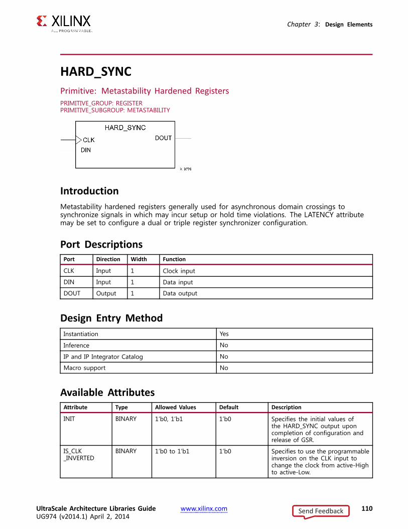
Chapter 3: Design Elements
HARD_SYNCPrimitive: Metastability Hardened RegistersPRIMITIVE_GROUP: REGISTERPRIMITIVE_SUBGROUP: METASTABILITY
IntroductionMetastability hardened registers generally used for asynchronous domain crossings tosynchronize signals in which may incur setup or hold time violations. The LATENCY attributemay be set to configure a dual or triple register synchronizer configuration.
Port DescriptionsPort Direction Width Function
CLK Input 1 Clock input
DIN Input 1 Data input
DOUT Output 1 Data output
Design Entry MethodInstantiation Yes
Inference No
IP and IP Integrator Catalog No
Macro support No
Available AttributesAttribute Type Allowed Values Default Description
INIT BINARY 1’b0, 1’b1 1’b0 Specifies the initial values ofthe HARD_SYNC output uponcompletion of configuration andrelease of GSR.
IS_CLK_INVERTED
BINARY 1’b0 to 1’b1 1’b0 Specifies to use the programmableinversion on the CLK input tochange the clock from active-Highto active-Low.
UltraScale Architecture Libraries Guide www.xilinx.com 110UG974 (v2014.1) April 2, 2014
Send Feedback
Chapter 3: Design Elements
Attribute Type Allowed Values Default Description
LATENCY DECIMAL 2, 3 2 Specifies whether to use a twostage or three stage synchronizer.Three stage will exhibit betterMTBF characteristics however havean additional clock cycle of latency.
VHDL Instantiation TemplateUnless they already exist, copy the following two statements and paste them before the entitydeclaration.Library UNISIM;use UNISIM.vcomponents.all;
-- HARD_SYNC:Metastability Hardened Registers-- UltraScale-- Xilinx HDL Libraries Guide, version 2014.1
HARD_SYNC_inst : HARD_SYNCgeneric map (
INIT => 0, -- Initial values, 1’b0, 1’b1IS_CLK_INVERTED => ’0’, -- Programmable inversion on CLK inputLATENCY=> 2 -- 2-3
)port map (
DOUT=> DOUT, -- 1-bit output: DataCLK => CLK, -- 1-bit input: ClockDIN => DIN -- 1-bit input: Data
);
-- End of HARD_SYNC_inst instantiation
Verilog Instantiation Template
// HARD_SYNC:Metastability Hardened Registers// UltraScale// Xilinx HDL Libraries Guide, version 2014.1
HARD_SYNC#(.INIT(0), // Initial values, 1’b0, 1’b1.IS_CLK_INVERTED(1’b0), // Programmable inversion on CLK input.LATENCY(2) // 2-3
)HARD_SYNC_inst (
.DOUT(DOUT), // 1-bit output: Data
.CLK(CLK), // 1-bit input: Clock
.DIN(DIN) // 1-bit input: Data);
// End of HARD_SYNC_inst instantiation
For More Information• See the 7 series FPGA User Documentation (User Guides and Data Sheets).
• See the UltraScale User Documentation.
UltraScale Architecture Libraries Guide www.xilinx.com 111UG974 (v2014.1) April 2, 2014
Send Feedback

Chapter 3: Design Elements
HPIO_VREFPrimitive: VREF ScanPRIMITIVE_GROUP: I/OPRIMITIVE_SUBGROUP: INPUT_BUFFER
IntroductionThe VREF_HPIO component in conjuction with either the IBUFE3 or IOBUFE3 buffers providesaccess to the VREF scan capability in the HPIO banks.
Port DescriptionsPort Direction Width Function
FABRIC_VREF_TUNE<6:0> Input 7 VREF tuning input value to allow Vref adjustment.
VREF Output 1 Tuned output that connects to all associated IBUFE3 orIOBUFE3 components within an HPIO bank.
Design Entry MethodInstantiation Yes
Inference No
IP and IP Integrator Catalog No
Macro support No
Available AttributesAttribute Type Allowed Values Default Description
VREF_CNTR STRING "OFF","FABRIC_RANGE1","FABRIC_RANGE2"
"OFF" Specifies VREF counter range.
UltraScale Architecture Libraries Guide www.xilinx.com 112UG974 (v2014.1) April 2, 2014
Send Feedback

Chapter 3: Design Elements
VHDL Instantiation TemplateUnless they already exist, copy the following two statements and paste them before the entitydeclaration.Library UNISIM;use UNISIM.vcomponents.all;
-- HPIO_VREF: VREF Scan-- UltraScale-- Xilinx HDL Libraries Guide, version 2014.1
HPIO_VREF_inst : HPIO_VREFgeneric map (
VREF_CNTR=> "OFF" -- OFF, FABRIC_RANGE1, FABRIC_RANGE2)port map (
VREF => VREF, -- 1-bit output: Tuned output (connect to associated IBUFE3-- component)
FABRIC_VREF_TUNE=> FABRIC_VREF_TUNE -- 7-bit input: VREF tuning value);
-- End of HPIO_VREF_inst instantiation
Verilog Instantiation Template
// HPIO_VREF: VREF Scan// UltraScale// Xilinx HDL Libraries Guide, version 2014.1
HPIO_VREF #(.VREF_CNTR("OFF") // OFF, FABRIC_RANGE1, FABRIC_RANGE2
)HPIO_VREF_inst (
.VREF(VREF), // 1-bit output: Tuned output (connect to associated IBUFE3// component)
.FABRIC_VREF_TUNE(FABRIC_VREF_TUNE) // 7-bit input: VREF tuning value);
// End of HPIO_VREF_inst instantiation
For More Information• See the 7 series FPGA User Documentation (User Guides and Data Sheets).
• See the UltraScale User Documentation.
UltraScale Architecture Libraries Guide www.xilinx.com 113UG974 (v2014.1) April 2, 2014
Send Feedback

Chapter 3: Design Elements
IBUFPrimitive: Input BufferPRIMITIVE_GROUP: I/OPRIMITIVE_SUBGROUP: INPUT_BUFFER
IntroductionSingle-ended ignals used as simple inputs must use an input buffer (IBUF).I/O attributes that do not impact the logic function of the component such as IOSTANDARDand IBUF_LOW_POWER should be supplied to the top-level port via an appropriate property.Please consult the Vivado Properties Guide for details on applying such properties to theassociated port.
Port DescriptionsPort Direction Width Function
I Input 1 Buffer Input connected to a top-level input port.
O Output 1 Buffer output connected to internal FPGA circuitry.
Design Entry MethodInstantiation Yes
Inference Recommended
IP and IP Integrator Catalog No
Macro support No
VHDL Instantiation TemplateUnless they already exist, copy the following two statements and paste them before the entitydeclaration.Library UNISIM;use UNISIM.vcomponents.all;
-- IBUF: Simple Single-ended Input Buffer-- UltraScale-- Xilinx HDL Libraries Guide, version 2014.1
IBUF_inst : IBUF
UltraScale Architecture Libraries Guide www.xilinx.com 114UG974 (v2014.1) April 2, 2014
Send Feedback

Chapter 3: Design Elements
port map (O => O, -- 1-bit output: Buffer outputI => I -- 1-bit input: Buffer input
);
-- End of IBUF_inst instantiation
Verilog Instantiation Template
// IBUF: Simple Single-ended Input Buffer// UltraScale// Xilinx HDL Libraries Guide, version 2014.1
IBUF #()IBUF_inst (
.O(O), // 1-bit output: Buffer output
.I(I) // 1-bit input: Buffer input);
// End of IBUF_inst instantiation
For More Information• See the 7 series FPGA User Documentation (User Guides and Data Sheets).
• See the UltraScale User Documentation.
UltraScale Architecture Libraries Guide www.xilinx.com 115UG974 (v2014.1) April 2, 2014
Send Feedback

Chapter 3: Design Elements
IBUF_ANALOGPrimitive: Analog Auxiliary SYSMON Input BufferPRIMITIVE_GROUP: I/OPRIMITIVE_SUBGROUP: INPUT_BUFFER
IntroductionThis design element is an input buffer used to connect the auxiliary analog inputs to theSYSMONE1 component. When using the VAUXP/VAUXN pins of the SYSMONE1 component,this buffer allows for a proper connection to the top-level port in the design.
Port DescriptionsPort Direction Width Function
I Input 1 Connect this pin to a top-level port in the design.
O Output 1 Connect this pin to either the VAUXP or VAUXN port of a SYSMONE1component.
Design Entry MethodInstantiation Yes
Inference Yes
IP and IP Integrator Catalog Recommended
Macro support No
VHDL Instantiation TemplateUnless they already exist, copy the following two statements and paste them before the entitydeclaration.Library UNISIM;use UNISIM.vcomponents.all;
-- IBUF_ANALOG: Analog Auxiliary SYSMONInput Buffer-- UltraScale-- Xilinx HDL Libraries Guide, version 2014.1
IBUF_ANALOG_inst : IBUF_ANALOGport map (
O => O, -- 1-bit output: Connect to a VAUXP/VAUXNport of the SYSMONE1
UltraScale Architecture Libraries Guide www.xilinx.com 116UG974 (v2014.1) April 2, 2014
Send Feedback

Chapter 3: Design Elements
I => I -- 1-bit input: Connect to a top-level design port);
-- End of IBUF_ANALOG_inst instantiation
Verilog Instantiation Template
// IBUF_ANALOG: Analog Auxiliary SYSMONInput Buffer// UltraScale// Xilinx HDL Libraries Guide, version 2014.1
IBUF_ANALOG IBUF_ANALOG_inst (.O(O), // 1-bit output: Connect to a VAUXP/VAUXNport of the SYSMONE1.I(I) // 1-bit input: Connect to a top-level design port
);
// End of IBUF_ANALOG_inst instantiation
For More Information• See the 7 series FPGA User Documentation (User Guides and Data Sheets).
• See the UltraScale User Documentation.
UltraScale Architecture Libraries Guide www.xilinx.com 117UG974 (v2014.1) April 2, 2014
Send Feedback

Chapter 3: Design Elements
IBUF_IBUFDISABLEPrimitive: Input Buffer With Input Buffer DisablePRIMITIVE_GROUP: I/OPRIMITIVE_SUBGROUP: INPUT_BUFFER
IntroductionThe IBUF_IBUFDISABLE primitive is an input buffer with a disable port that can be used as anadditional power saving feature for periods when the input is not used.The IBUF_IBUFDISABLE primitive can disable the input buffer and force the O output tothe internal logic to a logic-Low when the IBUFDISABLE signal is asserted High. TheUSE_IBUFDISABLE attribute must be set to TRUE and SIM_DEVICE to ULTRASCALE for thisprimitive to have the expected behavior specific to the UltraScale architecture. This featurecan be used to reduce power at times when the I/O is idle. Input buffers that use the VREFpower rail (such as SSTL and HSTL) benefit the most from the IBUFDISABLE being set to TRUEbecause they tend to have higher static power consumption than the non-VREF standards suchas LVCMOS and LVTTL.I/O attributes that do not impact the logic function of the component such as IOSTANDARD,DIFF_TERM and IBUF_LOW_POWER should be supplied to the top-level port via an appropriateproperty. Please consult the Vivado Properties Guide for details on applying such properties tothe associated port.
Port DescriptionsPort Direction Width Function
I Input 1 Input port connection. Connect directly to top-level port in thedesign.
IBUFDISABLE Input 1 Disables input path through the buffer and forces to a logic low.This feature is generally used to reduce power at times when theI/O is idle for a period of time.
O Output 1 Buffer output representing the input path to the device.
UltraScale Architecture Libraries Guide www.xilinx.com 118UG974 (v2014.1) April 2, 2014
Send Feedback

Chapter 3: Design Elements
Design Entry MethodInstantiation Yes
Inference No
IP and IP Integrator Catalog No
Macro support No
Available AttributesAttribute Type Allowed Values Default Description
SIM_DEVICE STRING "ULTRASCALE","7SERIES"
"ULTRASCALE" This attribute must be set to"ULTRASCALE" in order to exhibitthe proper simulation behavior.
USE_IBUFDISABLE
STRING "TRUE", "FALSE" "TRUE" This attribute must be unspecifiedor set to "TRUE" if specified.
VHDL Instantiation TemplateUnless they already exist, copy the following two statements and paste them before the entitydeclaration.Library UNISIM;use UNISIM.vcomponents.all;
-- IBUF_IBUFDISABLE: Single-ended Input Buffer w/ Disable-- UltraScale-- Xilinx HDL Libraries Guide, version 2014.1
IBUF_IBUFDISABLE_inst : IBUF_IBUFDISABLEgeneric map (
SIM_DEVICE => "ULTRASCALE" -- Must be set to "ULTRASCALE")port map (
O => O, -- 1-bit output: Buffer outputI => I, -- 1-bit input: Buffer input (connect directly to top-level port)IBUFDISABLE => IBUFDISABLE -- 1-bit input: Buffer disable input, low=disable
);
-- End of IBUF_IBUFDISABLE_inst instantiation
Verilog Instantiation Template
// IBUF_IBUFDISABLE: Single-ended Input Buffer w/ Disable// UltraScale// Xilinx HDL Libraries Guide, version 2014.1
IBUF_IBUFDISABLE #(.SIM_DEVICE("ULTRASCALE") // Must be set to "ULTRASCALE"
)IBUF_IBUFDISABLE_inst (
.O(O), // 1-bit output: Buffer output
.I(I), // 1-bit input: Buffer input (connect directly to top-level port)
.IBUFDISABLE(IBUFDISABLE) // 1-bit input: Buffer disable input, low=disable);
// End of IBUF_IBUFDISABLE_inst instantiation
UltraScale Architecture Libraries Guide www.xilinx.com 119UG974 (v2014.1) April 2, 2014
Send Feedback

Chapter 3: Design Elements
For More Information• See the 7 series FPGA User Documentation (User Guides and Data Sheets).
• See the UltraScale User Documentation.
UltraScale Architecture Libraries Guide www.xilinx.com 120UG974 (v2014.1) April 2, 2014
Send Feedback

Chapter 3: Design Elements
IBUF_INTERMDISABLEPrimitive: Input Buffer With Input Buffer Disable and On-die Input TerminationDisablePRIMITIVE_GROUP: I/OPRIMITIVE_SUBGROUP: INPUT_BUFFER
IntroductionThe IBUF_INTERMDISABLE primitive is available in the HR I/O banks and is similar to theIBUF_IBUFDISABLE primitive in that it has a IBUFDISABLE port that can be used to disable theinput buffer during periods that the buffer is not being used. The USE_IBUFDISABLE attributemust be set to TRUE and SIM_DEVICE to ULTRASCALE for this primitive to have the expectedbehavior specific to the UltraScale architecture. The IBUF_INTERMDISABLE primitive also hasan INTERMDISABLE port that can be used to disable the optional on-die receiver terminationfeature. See UG571: UltraScale Architecture SelectIO Resources, "Uncalibrated Input Terminationin I/O Banks" for more details.The IBUF_INTERMDISABLE primitive can disable the input buffer and force the O outputto the internal logic to a logic-Low when the IBUFDISABLE signal is asserted High. TheIBUF_INTERMDISABLE primitive further allows the termination legs to be disabled wheneverthe INTERMDISABLE signal is asserted High. These features can be combined to reduce powerwhenever the input is idle. Input buffers that use the VREF power rail (such as SSTL and HSTL)benefit the most from the IBUFDISABLE signal being set to TRUE because they tend to havehigher static power consumption than the non-VREF standards such as LVCMOS and LVTTL.I/O attributes that do not impact the logic function of the component such as IOSTANDARDand IBUF_LOW_POWER should be supplied to the top-level port via an appropriate property.Please consult the Vivado Properties Guide for details on applying such properties to theassociated port.
UltraScale Architecture Libraries Guide www.xilinx.com 121UG974 (v2014.1) April 2, 2014
Send Feedback

Chapter 3: Design Elements
Port DescriptionsPort Direction Width Function
I Input 1 Input port connection. Connect directly to top-level port in thedesign.
IBUFDISABLE Input 1 Disables input path through the buffer and forces to a logic low.This feature is generally used to reduce power at times when theI/O is idle for a period of time.
INTERMDISABLE Input 1 Control to enable/disable of on-chip input termination. This isgenerally used to reduce power in long periods of an idle state.
O Output 1 Buffer output representing the input path to the device.
Design Entry MethodInstantiation Yes
Inference No
IP and IP Integrator Catalog No
Macro support No
Available AttributesAttribute Type Allowed Values Default Description
SIM_DEVICE STRING "ULTRASCALE","7SERIES"
"ULTRASCALE" This attribute must be set to"ULTRASCALE" in order to exhibitthe proper simulation behavior.
USE_IBUFDISABLE
STRING "TRUE", "FALSE" "TRUE" This attribute must be unspecifiedor set to "TRUE" if specified.
VHDL Instantiation TemplateUnless they already exist, copy the following two statements and paste them before the entitydeclaration.Library UNISIM;use UNISIM.vcomponents.all;
-- IBUF_INTERMDISABLE: Single-ended Input Buffer w/ Input Termination Disable-- UltraScale-- Xilinx HDL Libraries Guide, version 2014.1
IBUF_INTERMDISABLE_inst : IBUF_INTERMDISABLEgeneric map (
SIM_DEVICE => "ULTRASCALE" -- Must be set to "ULTRASCALE")port map (
O => O, -- 1-bit output: Buffer outputI => I, -- 1-bit input: Buffer input (connect directly to top-level port)IBUFDISABLE => IBUFDISABLE, -- 1-bit input: Buffer disable input, low=disableINTERMDISABLE => INTERMDISABLE -- 1-bit input: Input Termination Disable
);
-- End of IBUF_INTERMDISABLE_inst instantiation
UltraScale Architecture Libraries Guide www.xilinx.com 122UG974 (v2014.1) April 2, 2014
Send Feedback

Chapter 3: Design Elements
Verilog Instantiation Template
// IBUF_INTERMDISABLE: Single-ended Input Buffer w/ Input Termination Disable// UltraScale// Xilinx HDL Libraries Guide, version 2014.1
IBUF_INTERMDISABLE #(.SIM_DEVICE("ULTRASCALE") // Must be set to "ULTRASCALE"
)IBUF_INTERMDISABLE_inst (
.O(O), // 1-bit output: Buffer output
.I(I), // 1-bit input: Buffer input (connect directly to top-level port)
.IBUFDISABLE(IBUFDISABLE), // 1-bit input: Buffer disable input, low=disable
.INTERMDISABLE(INTERMDISABLE) // 1-bit input: Input Termination Disable);
// End of IBUF_INTERMDISABLE_inst instantiation
For More Information• See the 7 series FPGA User Documentation (User Guides and Data Sheets).
• See the UltraScale User Documentation.
UltraScale Architecture Libraries Guide www.xilinx.com 123UG974 (v2014.1) April 2, 2014
Send Feedback

Chapter 3: Design Elements
IBUFDSPrimitive: Differential Input BufferPRIMITIVE_GROUP: I/OPRIMITIVE_SUBGROUP: INPUT_BUFFER
IntroductionThe usage and rules corresponding to the differential primitives are similar to the single-endedSelectIO primitives. Differential SelectIO primitives have two pins to and from the device padsto show the P and N channel pins in a differential pair. N channel pins have a B suffix.I/O attributes that do not impact the logic function of the component such as IOSTANDARD,DIFF_TERM and IBUF_LOW_POWER should be supplied to the top-level port via an appropriateproperty. Please consult the Vivado Properties Guide for details on applying such propertiesto the associated port. Attributes that do impact the functionality such as DQS_BIAS mustbe supplied to the component via a generic_map (VHDL) or parameter (Verilog) in order tohave the correct simulation behavior.
Logic TableInputs OutputsI IB O
0 0 No Change
0 1 0
1 0 1
1 1 No Change
Port DescriptionsPort Direction Width Function
I Input 1 Diff_p Buffer Input. Connect to top-level p-side input port.
IB Input 1 Diff_n Buffer Input. Connect to top-level n-side input port.
O Output 1 Buffer output
UltraScale Architecture Libraries Guide www.xilinx.com 124UG974 (v2014.1) April 2, 2014
Send Feedback

Chapter 3: Design Elements
Design Entry MethodInstantiation Recommended
Inference No
IP and IP Integrator Catalog No
Macro support No
Available AttributesAttribute Type Allowed Values Default Description
DQS_BIAS STRING "FALSE", "TRUE" "FALSE" Provides pull-up/pull-down feature required forsome DQS memory interface pins or provides DCbias for certain LVDS applications.
VHDL Instantiation TemplateUnless they already exist, copy the following two statements and paste them before the entitydeclaration.Library UNISIM;use UNISIM.vcomponents.all;
-- IBUFDS: Differential Input Buffer-- UltraScale-- Xilinx HDL Libraries Guide, version 2014.1
IBUFDS_inst : IBUFDSgeneric map (
DQS_BIAS => "FALSE" -- (FALSE, TRUE))port map (
O => O, -- 1-bit output: Buffer outputI => I, -- 1-bit input: Diff_p buffer input (connect directly to top-level port)IB => IB -- 1-bit input: Diff_n buffer input (connect directly to top-level port)
);
-- End of IBUFDS_inst instantiation
Verilog Instantiation Template
// IBUFDS: Differential Input Buffer// UltraScale// Xilinx HDL Libraries Guide, version 2014.1
IBUFDS #(.DQS_BIAS("FALSE") // (FALSE, TRUE)
)IBUFDS_inst (
.O(O), // 1-bit output: Buffer output
.I(I), // 1-bit input: Diff_p buffer input (connect directly to top-level port)
.IB(IB) // 1-bit input: Diff_n buffer input (connect directly to top-level port));
// End of IBUFDS_inst instantiation
UltraScale Architecture Libraries Guide www.xilinx.com 125UG974 (v2014.1) April 2, 2014
Send Feedback

Chapter 3: Design Elements
For More Information• See the 7 series FPGA User Documentation (User Guides and Data Sheets).
• See the UltraScale User Documentation.
UltraScale Architecture Libraries Guide www.xilinx.com 126UG974 (v2014.1) April 2, 2014
Send Feedback

Chapter 3: Design Elements
IBUFDS_DIFF_OUTPrimitive: Differential Input Buffer With Complementary OutputsPRIMITIVE_GROUP: I/OPRIMITIVE_SUBGROUP: INPUT_BUFFER
IntroductionThe IBUFDS_DIFF_OUT is a differential input buffer primitive with complementary outputs (Oand OB).I/O attributes that do not impact the logic function of the component such as IOSTANDARD,DIFF_TERM and IBUF_LOW_POWER should be supplied to the top-level port via an appropriateproperty. Please consult the Vivado Properties Guide for details on applying such propertiesto the associated port. Attributes that do impact the functionality such as DQS_BIAS mustbe supplied to the component via a generic_map (VHDL) or parameter (Verilog) in order tohave the correct simulation behavior.
Logic TableInputs OutputsI IB O OB
0 0 No Change No Change
0 1 0 1
1 0 1 0
1 1 No Change No Change
Port DescriptionsPort Direction Width Function
I Input 1 Diff_p Buffer Input. Connect to top-level p-side input port.
IB Input 1 Diff_n Buffer Input. Connect to top-level n-side input port.
O Output 1 Buffer diff_p output
OB Output 1 Buffer diff_n output
UltraScale Architecture Libraries Guide www.xilinx.com 127UG974 (v2014.1) April 2, 2014
Send Feedback

Chapter 3: Design Elements
Design Entry MethodInstantiation Yes
Inference No
IP and IP Integrator Catalog No
Macro support No
Available AttributesAttribute Type Allowed Values Default Description
DQS_BIAS STRING "FALSE", "TRUE" "FALSE" Provides pull-up/pull-down feature required forsome DQS memory interface pins or provides DCbias for certain LVDS applications.
VHDL Instantiation TemplateUnless they already exist, copy the following two statements and paste them before the entitydeclaration.Library UNISIM;use UNISIM.vcomponents.all;
-- IBUFDS_DIFF_OUT: Differential Input Buffer w/ Differential Output-- UltraScale-- Xilinx HDL Libraries Guide, version 2014.1
IBUFDS_DIFF_OUT_inst : IBUFDS_DIFF_OUTgeneric map (
DQS_BIAS => "FALSE" -- (FALSE, TRUE))port map (
O => O, -- 1-bit output: Buffer diff_p outputOB => OB, -- 1-bit output: Buffer diff_n outputI => I, -- 1-bit input: Diff_p buffer input (connect directly to top-level port)IB => IB -- 1-bit input: Diff_n buffer input (connect directly to top-level port)
);
-- End of IBUFDS_DIFF_OUT_inst instantiation
Verilog Instantiation Template
// IBUFDS_DIFF_OUT: Differential Input Buffer w/ Differential Output// UltraScale// Xilinx HDL Libraries Guide, version 2014.1
IBUFDS_DIFF_OUT #(.DQS_BIAS("FALSE") // (FALSE, TRUE)
)IBUFDS_DIFF_OUT_inst (
.O(O), // 1-bit output: Buffer diff_p output
.OB(OB), // 1-bit output: Buffer diff_n output
.I(I), // 1-bit input: Diff_p buffer input (connect directly to top-level port)
.IB(IB) // 1-bit input: Diff_n buffer input (connect directly to top-level port));
// End of IBUFDS_DIFF_OUT_inst instantiation
UltraScale Architecture Libraries Guide www.xilinx.com 128UG974 (v2014.1) April 2, 2014
Send Feedback

Chapter 3: Design Elements
For More Information• See the 7 series FPGA User Documentation (User Guides and Data Sheets).
• See the UltraScale User Documentation.
UltraScale Architecture Libraries Guide www.xilinx.com 129UG974 (v2014.1) April 2, 2014
Send Feedback

Chapter 3: Design Elements
IBUFDS_DIFF_OUT_IBUFDISABLEPrimitive: Differential Input Buffer With Complementary Outputs and InputBuffer DisablePRIMITIVE_GROUP: I/OPRIMITIVE_SUBGROUP: INPUT_BUFFER
IntroductionThe IBUFDS_DIFF_OUT_IBUFDISABLE primitive shown is a differential input buffer withcomplementary differential outputs. The USE_IBUFDISABLE attribute must be set to TRUE andthe SIM_DEVICE to ULTRASCALE for this primitive to have the expected behavior that is specificto the UltraScale architecture.I/O attributes that do not impact the logic function of the component such as IOSTANDARD,DIFF_TERM and IBUF_LOW_POWER should be supplied to the top-level port via an appropriateproperty. Please consult the Vivado Properties Guide for details on applying such propertiesto the associated port. Attributes that do impact the functionality such as DQS_BIAS mustbe supplied to the component via a generic_map (VHDL) or parameter (Verilog) in order tohave the correct simulation behavior.
Port DescriptionsPort Direction Width Function
I Input 1 Diff_p Buffer Input. Connect to top-level p-side input port.
IB Input 1 Diff_n Buffer Input. Connect to top-level n-side input port.
IBUFDISABLE Input 1 The IBUFDISABLE feature is not supported with this primitive in theUltraScale architecture. This port must be tied to a logic ’0’.
O Output 1 Buffer diff_p output
OB Output 1 Buffer diff_n output
UltraScale Architecture Libraries Guide www.xilinx.com 130UG974 (v2014.1) April 2, 2014
Send Feedback

Chapter 3: Design Elements
Design Entry MethodInstantiation Yes
Inference No
IP and IP Integrator Catalog No
Macro support No
Available AttributesAttribute Type Allowed Values Default Description
DQS_BIAS STRING "FALSE","TRUE"
"FALSE" Provides pull-up/pull-down feature requiredfor some DQS memory interface pins orprovides DC bias for certain LVDS applications.
SIM_DEVICE STRING "ULTRASCALE","7SERIES"
"ULTRASCALE" This attribute must be set to "ULTRASCALE" inorder to exhibit the proper simulation behavior.
USE_IBUFDISABLE
STRING "TRUE","FALSE"
"TRUE" This attribute must be unspecified or set to"TRUE" if specified.
VHDL Instantiation TemplateUnless they already exist, copy the following two statements and paste them before the entitydeclaration.Library UNISIM;use UNISIM.vcomponents.all;
-- IBUFDS_DIFF_OUT_IBUFDISABLE: Differential Input Buffer w/ Differential Output and Input disable-- UltraScale-- Xilinx HDL Libraries Guide, version 2014.1
IBUFDS_DIFF_OUT_IBUFDISABLE_inst : IBUFDS_DIFF_OUT_IBUFDISABLEgeneric map (
DQS_BIAS => "FALSE", -- (FALSE, TRUE)SIM_DEVICE => "ULTRASCALE" -- Must be set to "ULTRASCALE"
)port map (
O => O, -- 1-bit output: Buffer diff_p outputOB => OB, -- 1-bit output: Buffer diff_n outputI => I, -- 1-bit input: Diff_p buffer input (connect directly to top-level port)IB => IB, -- 1-bit input: Diff_n buffer input (connect directly to top-level port)IBUFDISABLE => IBUFDISABLE -- 1-bit input: Buffer disable input, low=disable
);
-- End of IBUFDS_DIFF_OUT_IBUFDISABLE_inst instantiation
UltraScale Architecture Libraries Guide www.xilinx.com 131UG974 (v2014.1) April 2, 2014
Send Feedback

Chapter 3: Design Elements
Verilog Instantiation Template
// IBUFDS_DIFF_OUT_IBUFDISABLE: Differential Input Buffer w/ Differential Output and Input disable// UltraScale// Xilinx HDL Libraries Guide, version 2014.1
IBUFDS_DIFF_OUT_IBUFDISABLE #(.DQS_BIAS("FALSE"), // (FALSE, TRUE).SIM_DEVICE("ULTRASCALE") // Must be set to "ULTRASCALE"
)IBUFDS_DIFF_OUT_IBUFDISABLE_inst (
.O(O), // 1-bit output: Buffer diff_p output
.OB(OB), // 1-bit output: Buffer diff_n output
.I(I), // 1-bit input: Diff_p buffer input (connect directly to top-level port)
.IB(IB), // 1-bit input: Diff_n buffer input (connect directly to top-level port)
.IBUFDISABLE(IBUFDISABLE) // 1-bit input: Buffer disable input, low=disable);
// End of IBUFDS_DIFF_OUT_IBUFDISABLE_inst instantiation
For More Information• See the 7 series FPGA User Documentation (User Guides and Data Sheets).
• See the UltraScale User Documentation.
UltraScale Architecture Libraries Guide www.xilinx.com 132UG974 (v2014.1) April 2, 2014
Send Feedback

Chapter 3: Design Elements
IBUFDS_DIFF_OUT_INTERMDISABLEPrimitive: Differential Input Buffer with Complementary Outputs, Input PathDisable and On-die Input Termination DisablePRIMITIVE_GROUP: I/OPRIMITIVE_SUBGROUP: INPUT_BUFFER
IntroductionThe IBUFDS_DIFF_OUT_INTERMDISABLE primitive is available in the HR I/O banks. It hascomplementary differential outputs and a INTERMDISABLE port that can be used to manuallydisable the optional on-die receiver termination features (uncalibrated). See UG571: UltraScaleArchitecture SelectIO Resources, "Uncalibrated Input Termination in I/O Banks" for more details.The USE_IBUFDISABLE attribute must be set to TRUE and SIM_DEVICE to ULTRASCALE for thisprimitive to have the expected behavior that is specific to the UltraScale architecture.If the I/O is using any on-die receiver termination features (uncalibrated), this primitive disablesthe termination legs whenever the INTERMDISABLE signal is asserted High.I/O attributes that do not impact the logic function of the component such as IOSTANDARD,DIFF_TERM and IBUF_LOW_POWER should be supplied to the top-level port via an appropriateproperty. Please consult the Vivado Properties Guide for details on applying such propertiesto the associated port. Attributes that do impact the functionality such as DQS_BIAS mustbe supplied to the component via a generic_map (VHDL) or parameter (Verilog) in order tohave the correct simulation behavior.
Port DescriptionsPort Direction Width Function
I Input 1 Diff_p Buffer Input. Connect to top-level p-side input port.
IB Input 1 Diff_n Buffer Input. Connect to top-level n-side input port.
IBUFDISABLE Input 1 The IBUFDISABLE feature is not supported with this primitive inthe UltraScale architecture. This port must be tied to a logic ’0’.
INTERMDISABLE Input 1 Disables input termination reducing current dissipation withinthe buffer. This feature is generally used to reduce power attimes when the I/O is idle for a period of time.
O Output 1 Buffer diff_p output
OB Output 1 Buffer diff_n output
UltraScale Architecture Libraries Guide www.xilinx.com 133UG974 (v2014.1) April 2, 2014
Send Feedback

Chapter 3: Design Elements
Design Entry MethodInstantiation Yes
Inference No
IP and IP Integrator Catalog No
Macro support No
Available AttributesAttribute Type Allowed Values Default Description
DQS_BIAS STRING "FALSE", "TRUE" "FALSE" Provides pull-up/pull-down feature requiredfor some DQS memory interface pinsor provides DC bias for certain LVDSapplications.
SIM_DEVICE STRING "ULTRASCALE","7SERIES"
"ULTRASCALE" This attribute must be set to "ULTRASCALE"in order to exhibit the proper simulationbehavior.
USE_IBUFDISABLE
STRING "TRUE", "FALSE" "TRUE" This attribute must be unspecified or set to"TRUE" if specified.
VHDL Instantiation TemplateUnless they already exist, copy the following two statements and paste them before the entitydeclaration.Library UNISIM;use UNISIM.vcomponents.all;
-- IBUFDS_DIFF_OUT_INTERMDISABLE: Differential Input Buffer w/ Differential Output, Input disable and Termination Disable
-- UltraScale-- Xilinx HDL Libraries Guide, version 2014.1
IBUFDS_DIFF_OUT_INTERMDISABLE_inst : IBUFDS_DIFF_OUT_INTERMDISABLEgeneric map (
DQS_BIAS => "FALSE", -- (FALSE, TRUE)SIM_DEVICE => "ULTRASCALE" -- Must be set to "ULTRASCALE"
)port map (
O => O, -- 1-bit output: Buffer diff_p outputOB => OB, -- 1-bit output: Buffer diff_n outputI => I, -- 1-bit input: Diff_p buffer input (connect directly to top-level port)IB => IB, -- 1-bit input: Diff_n buffer input (connect directly to top-level port)IBUFDISABLE => IBUFDISABLE, -- 1-bit input: Buffer input disable, low=disableINTERMDISABLE => INTERMDISABLE -- 1-bit input: Buffer termination disable, low=disable
);
-- End of IBUFDS_DIFF_OUT_INTERMDISABLE_inst instantiation
UltraScale Architecture Libraries Guide www.xilinx.com 134UG974 (v2014.1) April 2, 2014
Send Feedback

Chapter 3: Design Elements
Verilog Instantiation Template
// IBUFDS_DIFF_OUT_INTERMDISABLE: Differential Input Buffer w/ Differential Output, Input disable and Termination Disable
// UltraScale// Xilinx HDL Libraries Guide, version 2014.1
IBUFDS_DIFF_OUT_INTERMDISABLE #(.DQS_BIAS("FALSE"), // (FALSE, TRUE).SIM_DEVICE("ULTRASCALE") // Must be set to "ULTRASCALE"
)IBUFDS_DIFF_OUT_INTERMDISABLE_inst (
.O(O), // 1-bit output: Buffer diff_p output
.OB(OB), // 1-bit output: Buffer diff_n output.I(I), // 1-bit input: Diff_p buffer input (connect directly to top-level port).IB(IB), // 1-bit input: Diff_n buffer input (connect directly to top-level port).IBUFDISABLE(IBUFDISABLE), // 1-bit input: Buffer input disable, low=disable.INTERMDISABLE(INTERMDISABLE) // 1-bit input: Buffer termination disable, low=disable
);
// End of IBUFDS_DIFF_OUT_INTERMDISABLE_inst instantiation
For More Information• See the 7 series FPGA User Documentation (User Guides and Data Sheets).
• See the UltraScale User Documentation.
UltraScale Architecture Libraries Guide www.xilinx.com 135UG974 (v2014.1) April 2, 2014
Send Feedback

Chapter 3: Design Elements
IBUFDS_GTE3Primitive: Gigabit Transceiver BufferPRIMITIVE_GROUP: ADVANCEDPRIMITIVE_SUBGROUP: GT
IntroductionIBUFDS_GTE3 is the gigabit transceiver input pad buffer component. The REFCLK signalshould be routed to the dedicated reference clock input pins on the serial transceiver, andthe user design should instantiate the IBUFDS_GTE3 primitive in the user design. See theTransceivers User Guide for more information on PCB layout requirements, including referenceclock requirements.
Design Entry MethodInstantiation Yes
Inference No
IP and IP Integrator Catalog Recommended
Macro support No
For More Information• See the 7 series FPGA User Documentation (User Guides and Data Sheets).
• See the UltraScale User Documentation.
UltraScale Architecture Libraries Guide www.xilinx.com 136UG974 (v2014.1) April 2, 2014
Send Feedback

Chapter 3: Design Elements
IBUFDS_IBUFDISABLEPrimitive: Differential Input Buffer With Input Buffer DisablePRIMITIVE_GROUP: I/OPRIMITIVE_SUBGROUP: INPUT_BUFFER
IntroductionThe IBUFDS_DIFF_OUT_IBUFDISABLE primitive is a differential input buffer with complementarydifferential outputs. The USE_IBUFDISABLE attribute must be set to TRUE and the SIM_DEVICEto ULTRASCALE for this primitive to have the expected behavior that is specific to the UltraScalearchitecture.I/O attributes that do not impact the logic function of the component such as IOSTANDARD,DIFF_TERM and IBUF_LOW_POWER should be supplied to the top-level port via an appropriateproperty. Please consult the Vivado Properties Guide for details on applying such propertiesto the associated port. Attributes that do impact the functionality such as DQS_BIAS mustbe supplied to the component via a generic_map (VHDL) or parameter (Verilog) in order tohave the correct simulation behavior.
Port DescriptionsPort Direction Width Function
I Input 1 Diff_p Buffer Input. Connect to top-level p-side input port.
IB Input 1 Diff_n Buffer Input. Connect to top-level n-side input port.
IBUFDISABLE Input 1 The IBUFDISABLE feature is not supported with this primitive in theUltraScale architecture. This port must be tied to a logic ’0’.
O Output 1 Buffer output
Design Entry MethodInstantiation Recommended
Inference No
IP and IP Integrator Catalog No
Macro support No
UltraScale Architecture Libraries Guide www.xilinx.com 137UG974 (v2014.1) April 2, 2014
Send Feedback

Chapter 3: Design Elements
Available AttributesAttribute Type Allowed Values Default Description
DQS_BIAS STRING "FALSE", "TRUE" "FALSE" Provides pull-up/pull-down feature required forsome DQS memory interface pins or provides DCbias for certain LVDS applications.
SIM_DEVICE STRING "ULTRASCALE","7SERIES"
"ULTRASCALE"This attribute must be set to "ULTRASCALE" in orderto exhibit the proper simulation behavior.
USE_IBUFDISABLE
STRING "TRUE", "FALSE" "TRUE" This attribute must be unspecified or set to "TRUE"if specified.
VHDL Instantiation TemplateUnless they already exist, copy the following two statements and paste them before the entitydeclaration.Library UNISIM;use UNISIM.vcomponents.all;
-- IBUFDS_IBUFDISABLE: Differential Input Buffer with IBUF Disable-- UltraScale-- Xilinx HDL Libraries Guide, version 2014.1
IBUFDS_IBUFDISABLE_inst : IBUFDS_IBUFDISABLEgeneric map (
DQS_BIAS => "FALSE", -- (FALSE, TRUE)SIM_DEVICE => "ULTRASCALE" -- Must be set to "ULTRASCALE"
)port map (
O => O, -- 1-bit output: Buffer outputI => I, -- 1-bit input: Diff_p buffer input (connect directly to top-level port)IB => IB, -- 1-bit input: Diff_n buffer input (connect directly to top-level port)IBUFDISABLE => IBUFDISABLE -- 1-bit input: Buffer disable input, low=disable
);
-- End of IBUFDS_IBUFDISABLE_inst instantiation
Verilog Instantiation Template
// IBUFDS_IBUFDISABLE: Differential Input Buffer with IBUF Disable// UltraScale// Xilinx HDL Libraries Guide, version 2014.1
IBUFDS_IBUFDISABLE #(.DQS_BIAS("FALSE"), // (FALSE, TRUE).SIM_DEVICE("ULTRASCALE") // Must be set to "ULTRASCALE"
)IBUFDS_IBUFDISABLE_inst (
.O(O), // 1-bit output: Buffer output
.I(I), // 1-bit input: Diff_p buffer input (connect directly to top-level port)
.IB(IB), // 1-bit input: Diff_n buffer input (connect directly to top-level port)
.IBUFDISABLE(IBUFDISABLE) // 1-bit input: Buffer disable input, low=disable);
// End of IBUFDS_IBUFDISABLE_inst instantiation
UltraScale Architecture Libraries Guide www.xilinx.com 138UG974 (v2014.1) April 2, 2014
Send Feedback

Chapter 3: Design Elements
For More Information• See the 7 series FPGA User Documentation (User Guides and Data Sheets).
• See the UltraScale User Documentation.
UltraScale Architecture Libraries Guide www.xilinx.com 139UG974 (v2014.1) April 2, 2014
Send Feedback
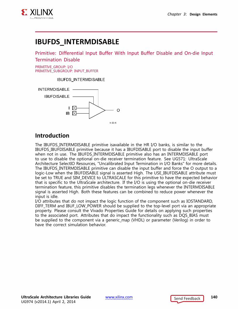
Chapter 3: Design Elements
IBUFDS_INTERMDISABLEPrimitive: Differential Input Buffer With Input Buffer Disable and On-die InputTermination DisablePRIMITIVE_GROUP: I/OPRIMITIVE_SUBGROUP: INPUT_BUFFER
IntroductionThe IBUFDS_INTERMDISABLE primitive isavailable in the HR I/O banks, is similar to theIBUFDS_IBUFDISABLE primitive because it has a IBUFDISABLE port to disable the input bufferwhen not in use. The IBUFDS_INTERMDISABLE primitive also has an INTERMDISABLE portto use to disable the optional on-die receiver termination feature. See UG571: UltraScaleArchitecture SelectIO Resources, "Uncalibrated Input Termination in I/O Banks" for more details.The IBUFDS_INTERMDISABLE primitive can disable the input buffer and force the O output to alogic-Low when the IBUFDISABLE signal is asserted High. The USE_IBUFDISABLE attribute mustbe set to TRUE and SIM_DEVICE to ULTRASCALE for this primitive to have the expected behaviorthat is specific to the UltraScale architecture. If the I/O is using the optional on-die receivertermination feature, this primitive disables the termination legs whenever the INTERMDISABLEsignal is asserted High. Both these features can be combined to reduce power whenever theinput is idle.I/O attributes that do not impact the logic function of the component such as IOSTANDARD,DIFF_TERM and IBUF_LOW_POWER should be supplied to the top-level port via an appropriateproperty. Please consult the Vivado Properties Guide for details on applying such propertiesto the associated port. Attributes that do impact the functionality such as DQS_BIAS mustbe supplied to the component via a generic_map (VHDL) or parameter (Verilog) in order tohave the correct simulation behavior.
UltraScale Architecture Libraries Guide www.xilinx.com 140UG974 (v2014.1) April 2, 2014
Send Feedback

Chapter 3: Design Elements
Port DescriptionsPort Direction Width Function
I Input 1 Diff_p Buffer Input. Connect to top-level p-side input port.
IB Input 1 Diff_n Buffer Input. Connect to top-level n-side input port.
IBUFDISABLE Input 1 Disables input path through the buffer and forces to a logic low.This feature is generally used to reduce power at times when theI/O is idle for a period of time.
INTERMDISABLE Input 1 Disables input termination reducing current dissipation within thebuffer. This feature is generally used to reduce power at timeswhen the I/O is idle for a period of time.
O Output 1 Buffer output
Design Entry MethodInstantiation Yes
Inference No
IP and IP Integrator Catalog No
Macro support No
Available AttributesAttribute Type Allowed Values Default Description
DQS_BIAS STRING "FALSE", "TRUE" "FALSE" Provides pull-up/pull-down feature required forsome DQS memory interface pins or providesDC bias for certain LVDS applications.
SIM_DEVICE STRING "ULTRASCALE","7SERIES"
"ULTRASCALE" This attribute must be set to "ULTRASCALE" inorder to exhibit the proper simulation behavior.
USE_IBUFDISABLE
STRING "TRUE", "FALSE" "TRUE" This attribute must be unspecified or set to"TRUE" if specified.
VHDL Instantiation TemplateUnless they already exist, copy the following two statements and paste them before the entitydeclaration.Library UNISIM;use UNISIM.vcomponents.all;
-- IBUFDS_INTERMDISABLE: Differential Input Buffer w/ Input disable and Termination Disable-- UltraScale-- Xilinx HDL Libraries Guide, version 2014.1
IBUFDS_INTERMDISABLE_inst : IBUFDS_INTERMDISABLEgeneric map (
DQS_BIAS => "FALSE", -- (FALSE, TRUE)SIM_DEVICE => "ULTRASCALE" -- Must be set to "ULTRASCALE"
)port map (
O => O, -- 1-bit output: Buffer outputI => I, -- 1-bit input: Diff_p buffer input (connect directly to top-level port)
UltraScale Architecture Libraries Guide www.xilinx.com 141UG974 (v2014.1) April 2, 2014
Send Feedback

Chapter 3: Design Elements
IB => IB, -- 1-bit input: Diff_n buffer input (connect directly to top-level port)IBUFDISABLE => IBUFDISABLE, -- 1-bit input: Buffer input disable, low=disableINTERMDISABLE => INTERMDISABLE -- 1-bit input: Buffer termination disable, low=disable
);
-- End of IBUFDS_INTERMDISABLE_inst instantiation
Verilog Instantiation Template
// IBUFDS_INTERMDISABLE: Differential Input Buffer w/ Input disable and Termination Disable// UltraScale// Xilinx HDL Libraries Guide, version 2014.1
IBUFDS_INTERMDISABLE #(.DQS_BIAS("FALSE"), // (FALSE, TRUE).SIM_DEVICE("ULTRASCALE") // Must be set to "ULTRASCALE"
)IBUFDS_INTERMDISABLE_inst (
.O(O), // 1-bit output: Buffer output.I(I), // 1-bit input: Diff_p buffer input (connect directly to top-level port).IB(IB), // 1-bit input: Diff_n buffer input (connect directly to top-level port).IBUFDISABLE(IBUFDISABLE), // 1-bit input: Buffer input disable, low=disable.INTERMDISABLE(INTERMDISABLE) // 1-bit input: Buffer termination disable, low=disable
);
// End of IBUFDS_INTERMDISABLE_inst instantiation
For More Information• See the 7 series FPGA User Documentation (User Guides and Data Sheets).
• See the UltraScale User Documentation.
UltraScale Architecture Libraries Guide www.xilinx.com 142UG974 (v2014.1) April 2, 2014
Send Feedback

Chapter 3: Design Elements
IBUFDSE3Primitive: Differential Input Buffer with Offset CalibrationPRIMITIVE_GROUP: I/OPRIMITIVE_SUBGROUP: INPUT_BUFFER
IntroductionThe differential input buffer (IBUFDSE3) primitive is only supported in HP I/O banks. ThisUltraScale architecture specific primitive has functions similar to the IBUFDS along with controlsfor offset calibration with input buffer disable (IBUFDISABLE). The offset calibration feature isaccessed using the OSC_EN and OSC[3:0] ports. The VREF scan feature is not supported withthis primitive.I/O attributes that do not impact the logic function of the component such as IOSTANDARD,DIFF_TERM and IBUF_LOW_POWER should be supplied to the top-level port via an appropriateproperty. Please consult the Vivado Properties Guide for details on applying such propertiesto the associated port. Attributes that do impact the functionality such as DQS_BIAS mustbe supplied to the component via a generic_map (VHDL) or parameter (Verilog) in order tohave the correct simulation behavior.
Port DescriptionsPort Direction Width Function
I Input 1 Diff_p Buffer Input. Connect to top-level p-side input port.
IB Input 1 Diff_n Buffer Input. Connect to top-level n-side input port.
IBUFDISABLE Input 1 Disables input path through the buffer and forces to a logiclow. This feature is generally used to reduce power at timeswhen the I/O is idle for a period of time.
O Output 1 Buffer output
OSC<3:0> Input 4 Offset cancellation value
OSC_EN<1:0> Input 2 Offset cancellation enable
VREF Input 1 Not applicable for this buffer.
UltraScale Architecture Libraries Guide www.xilinx.com 143UG974 (v2014.1) April 2, 2014
Send Feedback

Chapter 3: Design Elements
Design Entry MethodInstantiation Recommended
Inference No
IP and IP Integrator Catalog No
Macro support No
Available AttributesAttribute Type Allowed Values Default Description
DQS_BIAS STRING "FALSE", "TRUE" "FALSE" Provides pull-up/pull-down featurerequired for some DQS memoryinterface pins or provides DC biasfor certain LVDS applications.
SIM_INPUT_BUFFER_OFFSET
DECIMAL -50 to 50 0 Offset value for simulationpurposes.
USE_IBUFDISABLE
STRING "FALSE", "TRUE" "FALSE" This attribute must be unspecifiedor set to "TRUE" if specified.
VHDL Instantiation TemplateUnless they already exist, copy the following two statements and paste them before the entitydeclaration.Library UNISIM;use UNISIM.vcomponents.all;
-- IBUFDSE3: Differential Input Buffer with VREF and OFFSET Control-- UltraScale-- Xilinx HDL Libraries Guide, version 2014.1
IBUFDSE3_inst : IBUFDSE3generic map (
DQS_BIAS => "FALSE", -- (FALSE, TRUE)SIM_INPUT_BUFFER_OFFSET=> 0 -- Offset value for simulation (-50-50)
)port map (
O => O, -- 1-bit output: Buffer outputI => I, -- 1-bit input: Diff_p buffer input (connect directly to top-level port)IB => IB, -- 1-bit input: Diff_n buffer input (connect directly to top-level port)IBUFDISABLE => IBUFDISABLE, -- 1-bit input: Buffer disable input, low=disableOSC => OSC, -- 4-bit input: Offset cancellation valueOSC_EN=> OSC_EN, -- 2-bit input: Offset cancelatin enableVREF => VREF -- 1-bit input: Vref input from HPIO_VREF
);
-- End of IBUFDSE3_inst instantiation
UltraScale Architecture Libraries Guide www.xilinx.com 144UG974 (v2014.1) April 2, 2014
Send Feedback

Chapter 3: Design Elements
Verilog Instantiation Template
// IBUFDSE3: Differential Input Buffer with VREF and OFFSET Control// UltraScale// Xilinx HDL Libraries Guide, version 2014.1
IBUFDSE3 #(.DQS_BIAS("FALSE"), // (FALSE, TRUE).SIM_INPUT_BUFFER_OFFSET(0) // Offset value for simulation (-50-50)
)IBUFDSE3_inst (
.O(O), // 1-bit output: Buffer output
.I(I), // 1-bit input: Diff_p buffer input (connect directly to top-level port)
.IB(IB), // 1-bit input: Diff_n buffer input (connect directly to top-level port)
.IBUFDISABLE(IBUFDISABLE), // 1-bit input: Buffer disable input, low=disable
.OSC(OSC), // 4-bit input: Offset cancellation value
.OSC_EN(OSC_EN), // 2-bit input: Offset cancelatin enable
.VREF(VREF) // 1-bit input: Vref input from HPIO_VREF);
// End of IBUFDSE3_inst instantiation
For More Information• See the 7 series FPGA User Documentation (User Guides and Data Sheets).
• See the UltraScale User Documentation.
UltraScale Architecture Libraries Guide www.xilinx.com 145UG974 (v2014.1) April 2, 2014
Send Feedback

Chapter 3: Design Elements
IBUFE3Primitive: Input Buffer with Offset Calibration and VREF TuningPRIMITIVE_GROUP: I/OPRIMITIVE_SUBGROUP: INPUT_BUFFER
IntroductionThe input buffer (IBUFE3) primitive is only supported in HP I/O banks. This UltraScalearchitecture specific primitive has functions similar to the IBUF with added controls foroffset calibration and VREF tuning, along with input buffer disable (IBUFDISABLE). The offsetcalibration feature is accessed using the OSC_EN and OSC[3:0] ports. The VREF scan feature isaccessed using the HPIO_VREF primitive in conjunction with IBUFE3.I/O attributes that do not impact the logic function of the component such as IOSTANDARD,DIFF_TERM and IBUF_LOW_POWER should be supplied to the top-level port via anappropriate property. Please consult the Vivado Properties Guide for details on applyingsuch properties to the associated port. Attributes that do impact the functionality such asSIM_INPUT_BUFFER_OFFSET must be supplied to the component via a generic_map (VHDL) orparameter (Verilog) in order to have the correct simulation behavior.
Port DescriptionsPort Direction Width Function
I Input 1 Diff_p Buffer Input. Connect to top-level p-side inputport.
IBUFDISABLE Input 1 Disables input path through the buffer and forces to alogic low. This feature is generally used to reduce powerat times when the I/O is idle for a period of time.
O Output 1 Buffer output
OSC<3:0> Input 4 Offset cancellation value
OSC_EN Input 1 Offset cancellation enable
VREF Input 1 Vref input from HPIO_VREF
UltraScale Architecture Libraries Guide www.xilinx.com 146UG974 (v2014.1) April 2, 2014
Send Feedback

Chapter 3: Design Elements
Design Entry MethodInstantiation Yes
Inference No
IP and IP Integrator Catalog No
Macro support No
Available AttributesAttribute Type Allowed Values Default Description
SIM_INPUT_BUFFER_OFFSET
DECIMAL -50 to 50 0 Offset value for simulationpurposes.
USE_IBUFDISABLE
STRING "FALSE", "TRUE" "FALSE" This attribute must be unspecifiedor set to "TRUE" if specified.
VHDL Instantiation TemplateUnless they already exist, copy the following two statements and paste them before the entitydeclaration.Library UNISIM;use UNISIM.vcomponents.all;
-- IBUFE3: Input Buffer with VREF and OFFSET Control-- UltraScale-- Xilinx HDL Libraries Guide, version 2014.1
IBUFE3_inst : IBUFE3generic map (
SIM_INPUT_BUFFER_OFFSET=> 0 -- Offset value for simulation (-50-50))port map (
O => O, -- 1-bit output: Buffer outputI => I, -- 1-bit input: Buffer input (connect directly to top-level port)IBUFDISABLE => IBUFDISABLE, -- 1-bit input: Buffer disable input, low=disableOSC => OSC, -- 4-bit input: Offset cancellation valueOSC_EN=> OSC_EN, -- 1-bit input: Offset cancelatin enableVREF => VREF -- 1-bit input: Vref input from HPIO_VREF
);
-- End of IBUFE3_inst instantiation
Verilog Instantiation Template
// IBUFE3: Input Buffer with VREF and OFFSET Control// UltraScale// Xilinx HDL Libraries Guide, version 2014.1
IBUFE3 #(.SIM_INPUT_BUFFER_OFFSET(0) // Offset value for simulation (-50-50)
)IBUFE3_inst (
.O(O), // 1-bit output: Buffer output
.I(I), // 1-bit input: Buffer input (connect directly to top-level port)
.IBUFDISABLE(IBUFDISABLE), // 1-bit input: Buffer disable input, low=disable
.OSC(OSC), // 4-bit input: Offset cancellation value
UltraScale Architecture Libraries Guide www.xilinx.com 147UG974 (v2014.1) April 2, 2014
Send Feedback

Chapter 3: Design Elements
.OSC_EN(OSC_EN), // 1-bit input: Offset cancelatin enable
.VREF(VREF) // 1-bit input: Vref input from HPIO_VREF);
// End of IBUFE3_inst instantiation
For More Information• See the 7 series FPGA User Documentation (User Guides and Data Sheets).
• See the UltraScale User Documentation.
UltraScale Architecture Libraries Guide www.xilinx.com 148UG974 (v2014.1) April 2, 2014
Send Feedback

Chapter 3: Design Elements
ICAPE3Primitive: Internal Configuration Access PortPRIMITIVE_GROUP: CONFIGURATIONPRIMITIVE_SUBGROUP: ICAP
IntroductionThis design element gives you access to the configuration functions of the FPGA from theFPGA fabric. Using this component, commands and data can be written to and read from theconfiguration logic of the FPGA array. Since the improper use of this function can have anegative effect on the functionality and reliability of the FPGA, you should not use this elementunless you are very familiar with its capabilities.
Port DescriptionsPort Direction Width Function
AVAIL Output 1 Availability status of ICAP
CLK Input 1 Clock input
CSIB Input 1 Active-Low ICAP enable
I<31:0> Input 32 Configuration data input bus
O<31:0> Output 32 Configuration data output bus
PRDONE Output 1 Indicates completion of Partial Reconfiguration
PRERROR Output 1 Indicates Error during Partial Reconfiguration
RDWRB Input 1 Read/Write Select input
Design Entry MethodInstantiation Recommended
Inference No
IP and IP Integrator Catalog No
Macro support No
UltraScale Architecture Libraries Guide www.xilinx.com 149UG974 (v2014.1) April 2, 2014
Send Feedback

Chapter 3: Design Elements
Available AttributesAttribute Type Allowed Values Default Description
DEVICE_ID HEX 32’h03628093,32’h03627093
32’h03628093 Specifies the pre-programmedDevice ID value to be used forsimulation purposes.
ICAP_AUTO_SWITCH
STRING "DISABLE","ENABLE"
"DISABLE" Enable switch ICAP using syncword
SIM_CFG_FILE_NAME
STRING String "NONE" Specifies the Raw Bitstream (RBT)file to be parsed by the simulationmodel
VHDL Instantiation TemplateUnless they already exist, copy the following two statements and paste them before the entitydeclaration.Library UNISIM;use UNISIM.vcomponents.all;
-- ICAPE3: Internal Configuration Access Port-- UltraScale-- Xilinx HDL Libraries Guide, version 2014.1
ICAPE3_inst : ICAPE3generic map (
DEVICE_ID => X"03628093", -- Specifies the pre-programmed Device ID value to be used for simulation-- purposes.
ICAP_AUTO_SWITCH=> "DISABLE", -- Enable switch ICAP using sync wordSIM_CFG_FILE_NAME => "NONE" -- Specifies the Raw Bitstream (RBT) file to be parsed by the simulation
-- model)port map (
AVAIL => AVAIL, -- 1-bit output: Availability status of ICAPO => O, -- 32-bit output: Configuration data output busPRDONE=> PRDONE, -- 1-bit output: Indicates completion of Partial ReconfigurationPRERROR=> PRERROR,-- 1-bit output: Indicates Error during Partial ReconfigurationCLK => CLK, -- 1-bit input: Clock inputCSIB => CSIB, -- 1-bit input: Active-Low ICAP enableI => I, -- 32-bit input: Configuration data input busRDWRB=> RDWRB -- 1-bit input: Read/Write Select input
);
-- End of ICAPE3_inst instantiation
Verilog Instantiation Template// ICAPE3: Internal Configuration Access Port// UltraScale// Xilinx HDL Libraries Guide, version 2014.1
ICAPE3 #(.DEVICE_ID(32’h03628093), // Specifies the pre-programmed Device ID value to be used for simulation
// purposes..ICAP_AUTO_SWITCH("DISABLE"), // Enable switch ICAP using sync word.SIM_CFG_FILE_NAME("NONE") // Specifies the Raw Bitstream (RBT) file to be parsed by the simulation
// model)ICAPE3_inst (
.AVAIL(AVAIL), // 1-bit output: Availability status of ICAP
.O(O), // 32-bit output: Configuration data output bus
.PRDONE(PRDONE), // 1-bit output: Indicates completion of Partial Reconfiguration
UltraScale Architecture Libraries Guide www.xilinx.com 150UG974 (v2014.1) April 2, 2014
Send Feedback

Chapter 3: Design Elements
.PRERROR(PRERROR), // 1-bit output: Indicates Error during Partial Reconfiguration
.CLK(CLK), // 1-bit input: Clock input
.CSIB(CSIB), // 1-bit input: Active-Low ICAP enable
.I(I), // 32-bit input: Configuration data input bus
.RDWRB(RDWRB) // 1-bit input: Read/Write Select input);
// End of ICAPE3_inst instantiation
For More Information• See the 7 series FPGA User Documentation (User Guides and Data Sheets).
• See the UltraScale User Documentation.
UltraScale Architecture Libraries Guide www.xilinx.com 151UG974 (v2014.1) April 2, 2014
Send Feedback

Chapter 3: Design Elements
IDDRE1Primitive: Dedicated Dual Data Rate (DDR) Input RegisterPRIMITIVE_GROUP: REGISTERPRIMITIVE_SUBGROUP: DDR
IntroductionIn component mode, the IDDRE1 in UltraScale FPGAs is a dedicated input register designed toreceive external dual data rate (DDR) signals into Xilinx FPGAs. The IDDRE1 is available withmodes that present the data to the FPGA fabric at the time and clock edge they are captured,or on the same clock edge. This feature allows you to avoid additional timing complexitiesand resource usage.
Port DescriptionsPort Direction Width Function
C Input 1 The high-speed clock input (C) is used to clock in the input serial datastream
CB Input 1 The inverted high-speed clock input
D Input 1 The serial input data port (D) is the serial (high-speed) data input port ofthe ISERDESE3. This port accepts data from the IOB or FPGA Fabric.
Q1 Output 1 Registered parallel output 1
Q2 Output 1 Registered parallel output 2
R Input 1 Active High Asynchronous Reset
Design Entry MethodInstantiation Yes
Inference No
IP and IP Integrator Catalog Yes
Macro support No
UltraScale Architecture Libraries Guide www.xilinx.com 152UG974 (v2014.1) April 2, 2014
Send Feedback

Chapter 3: Design Elements
Available AttributesAttribute Type Allowed Values Default Description
DDR_CLK_EDGE STRING "OPPOSITE_EDGE","SAME_EDGE","SAME_EDGE_PIPELINED"
"OPPOSITE_EDGE" Sets the IDDRE1 mode ofoperation with respect to clockedge.
• "OPPOSITE_EDGE":Traditional input DDRsolution. Data presented toQ1 on the rising edge andQ2 on the falling edge.
• "SAME_EDGE": Data ispresented to the device logicon the same clock edge. Hasseperated effect.
• "SAME_EDGE_PIPELINED":Data is presented to thedevice logic on the sameclock edge. Removes theseperated effect but incursclock latency.
IS_C_INVERTED BINARY 1’b0 to 1’b1 1’b0 Indicates whether the clock C isactive-high or active-low
VHDL Instantiation TemplateUnless they already exist, copy the following two statements and paste them before the entitydeclaration.Library UNISIM;use UNISIM.vcomponents.all;
-- IDDRE1: Dedicated Dual Data Rate (DDR) Input Register-- UltraScale-- Xilinx HDL Libraries Guide, version 2014.1
IDDRE1_inst : IDDRE1generic map (
DDR_CLK_EDGE=> "OPPOSITE_EDGE", -- IDDRE1 mode (OPPOSITE_EDGE, SAME_EDGE,SAME_EDGE_PIPELINED)IS_C_INVERTED => ’0’ -- Optional inversion for C
)port map (
Q1 => Q1, -- 1-bit output: Registered parallel output 1Q2 => Q2, -- 1-bit output: Registered parallel output 2C => C, -- 1-bit input: High-speed clockCB => CB, -- 1-bit input: Inversion of High-speed clock CD => D, -- 1-bit input: Serial Data InputR => R -- 1-bit input: Active High Async Reset
);
-- End of IDDRE1_inst instantiation
UltraScale Architecture Libraries Guide www.xilinx.com 153UG974 (v2014.1) April 2, 2014
Send Feedback

Chapter 3: Design Elements
Verilog Instantiation Template
// IDDRE1: Dedicated Dual Data Rate (DDR) Input Register// UltraScale// Xilinx HDL Libraries Guide, version 2014.1
IDDRE1 #(.DDR_CLK_EDGE("OPPOSITE_EDGE"), // IDDRE1 mode (OPPOSITE_EDGE, SAME_EDGE,SAME_EDGE_PIPELINED).IS_C_INVERTED(1’b0) // Optional inversion for C
)IDDRE1_inst (
.Q1(Q1), // 1-bit output: Registered parallel output 1
.Q2(Q2), // 1-bit output: Registered parallel output 2
.C(C), // 1-bit input: High-speed clock
.CB(CB), // 1-bit input: Inversion of High-speed clock C
.D(D), // 1-bit input: Serial Data Input
.R(R) // 1-bit input: Active High Async Reset);
// End of IDDRE1_inst instantiation
For More Information• See the 7 series FPGA User Documentation (User Guides and Data Sheets).
• See the UltraScale User Documentation.
UltraScale Architecture Libraries Guide www.xilinx.com 154UG974 (v2014.1) April 2, 2014
Send Feedback

Chapter 3: Design Elements
IDELAYCTRLPrimitive: IDELAYE3/ODELAYE3 Tap Delay Value ControlPRIMITIVE_GROUP: I/OPRIMITIVE_SUBGROUP: DELAY
IntroductionAt least one of these design elements must be instantiated when using IDELAYE3 or ODELAYE3.The IDELAYCTRL module provides a reference clock input that allows internal circuitry todefine precise delay tap values independent of PVT (process, voltage, and temperature) forthe IDELAYE3 and ODELAYE3 components.
Port DescriptionsPort Direction Width Function
RDY Output 1 The ready (RDY) signal indicates when IDELAYE3 andODELAYE3 modules in the specific region are calibrated.The RDY signal is deasserted if REFCLK is held High orLow for one clock more. If RDY is deasserted Low, theIDELAYCTRL module must be reset. If not needed, RDYto be unconnected/ignored.
REFCLK Input 1 Time reference to IDELAYCTRL to calibrate all IDELAYE3and ODELAYE3 modules in the same region. REFCLK canbe supplied directly from a user-supplied source or theMMCME3/PLLE3 and must be routed on a global clockbuffer.
RST Input 1 Active-High asynchronous reset. To ensure properIDELAYE3 and ODELAYE3 operation, IDELAYCTRL must bereset after configuation and the REFCLK signal is stable.
Design Entry MethodInstantiation Yes
Inference No
IP and IP Integrator Catalog Yes
Macro support No
UltraScale Architecture Libraries Guide www.xilinx.com 155UG974 (v2014.1) April 2, 2014
Send Feedback

Chapter 3: Design Elements
VHDL Instantiation TemplateUnless they already exist, copy the following two statements and paste them before the entitydeclaration.Library UNISIM;use UNISIM.vcomponents.all;
-- IDELAYCTRL: IDELAYE3/ODELAYE3 Tap Delay Value Control-- UltraScale-- Xilinx HDL Libraries Guide, version 2014.1
IDELAYCTRL_inst : IDELAYCTRLport map (
RDY => RDY, -- 1-bit output: Ready outputREFCLK => REFCLK, -- 1-bit input: Reference clock inputRST => RST -- 1-bit input: Active high reset input
);
-- End of IDELAYCTRL_inst instantiation
Verilog Instantiation Template
// IDELAYCTRL: IDELAYE3/ODELAYE3 Tap Delay Value Control// UltraScale// Xilinx HDL Libraries Guide, version 2014.1
(* IODELAY_GROUP= (MISSING VALUE) *) // (MISSING DESCRIPTION)
IDELAYCTRL IDELAYCTRL_inst (.RDY(RDY), // 1-bit output: Ready output.REFCLK(REFCLK), // 1-bit input: Reference clock input.RST(RST) // 1-bit input: Active high reset input
);
// End of IDELAYCTRL_inst instantiation
For More Information• See the 7 series FPGA User Documentation (User Guides and Data Sheets).
• See the UltraScale User Documentation.
UltraScale Architecture Libraries Guide www.xilinx.com 156UG974 (v2014.1) April 2, 2014
Send Feedback

Chapter 3: Design Elements
IDELAYE3Primitive: Input Fixed or Variable Delay ElementPRIMITIVE_GROUP: I/OPRIMITIVE_SUBGROUP: DELAY
IntroductionIn component mode, I/O blocks contain a programmable delay element called IDELAYE3.The IDELAYE3 can be connected to an input register/ISERDESE3 or driven directly into FPGAlogic. The IDELAYE3 is a 512-tap delay element with a calibrated tap resolution. Refer to theFPGA Data Sheet for delay values. The IDELAYE3 allows incoming signals to be delayed onan individual basis.
Port DescriptionsPort Direction Width Function
CASC_IN Input 1 Cascade delay input from slave ODELAY CASCADE_OUT
CASC_OUT Output 1 Cascade delay output to ODELAY input cascade
CASC_RETURN Input 1 Cascade delay returning from slave ODELAY DATAOUT
CE Input 1 Active high enable increment/decrement function
CLK Input 1 Clock Input
CNTVALUEIN<8:0> Input 9 Counter value from FPGA logic for dynamically loadable tapvalue input
CNTVALUEOUT<8:0> Output 9 The CNTVALUEOUT pins are used for reporting the dynamicallyswitching value of the delay element. CNTVALUEOUT is onlyavailable when IDELAYE3 is in "VARIABLE" or "VAR_LOAD" mode.
UltraScale Architecture Libraries Guide www.xilinx.com 157UG974 (v2014.1) April 2, 2014
Send Feedback
Chapter 3: Design Elements
Port Direction Width Function
DATAIN Input 1 The DATAIN input is directly driven by the FPGA logic providinga logic accessible delay line. The data is driven back into theFPGA logic through the DATAOUT port with a delay set by theDELAY_VALUE.
DATAOUT Output 1 Delayed data output from one of two data input ports (IDATAINor DATAIN).
EN_VTC Input 1 Keep delay constant over VT
IDATAIN Input 1 Data input for IDELAY from the IBUF
INC Input 1 Increment / Decrement tap delay input
LOAD Input 1 Loads the IDELAYE3 primitive to the pre-programmed valuein VARIABLE mode. In VAR_LOAD mode, it load the value ofCNTVALUEIN.
RST Input 1 Asynchronous Reset to the DELAY_VALUE, active level based onIS_RST_INVERTED
Design Entry MethodInstantiation Yes
Inference No
IP and IP Integrator Catalog Yes
Macro support No
Available AttributesAttribute Type Allowed Values Default Description
CASCADE STRING "NONE", "MASTER","SLAVE_END","SLAVE_MIDDLE"
"NONE" Sets the location of the IDELAYE3when it is used in a cascadedconfiguration
• "NONE" : Delay line is notcascaded
• "MASTER" : Delay line iscascaded with another delayline
• "SLAVE_MIDDLE" : Delay lineis cascaded from adjacentdelay line and also cascadesto another delay line
• "SLAVE_END" : Delay line isthe last cascaded delay line
UltraScale Architecture Libraries Guide www.xilinx.com 158UG974 (v2014.1) April 2, 2014
Send Feedback

Chapter 3: Design Elements
Attribute Type Allowed Values Default Description
DELAY_FORMAT STRING "TIME", "COUNT" "TIME" Sets the units of DELAY_VALUEof the IDELAYE3. Use TIME whenDELAY_TYPE is FIXED. Use COUNTwhen DELAY_TYPE is VARIABLE orVAR_LOAD.
• "TIME" : IDELAYE3DELAY_VALUE is specifiedin ps
• "COUNT" : IDELAYE3DELAY_VALUE is specifiedin taps
DELAY_SRC STRING "IDATAIN","DATAIN"
"IDATAIN" Select the delay source input tothe IDELAYE3
• "DATAIN" : IDELAYE3 chaininput is DATAIN
• "IDATAIN": IDELAYE3 chaininput is IDATAIN
DELAY_TYPE STRING "FIXED","VAR_LOAD","VARIABLE"
"FIXED" Sets the type of tap delay line.
• "FIXED" - Sets a static delayvalue
• "VARIABLE" - Dynamicallyadjust (increment/decrement)delay value
• "VAR_LOAD" - Dynamicallyloads tap values
DELAY_VALUE DECIMAL 0 to 1250 0 Specifies the fixed delay in ps inFIXED mode or the initial startingnumber of taps in "VARIABLE"mode or "VAR_LOAD" mode(input path).
IS_CLK _INVERTED BINARY 1’b0 to 1’b1 1’b0 Indicates whether the CLK isactive-high or active-low
IS_RST _INVERTED BINARY 1’b0 to 1’b1 1’b0 Indicates whether the RST isactive-high or active-low
REFCLK_FREQUENCY
1 significantdigit FLOAT
200.0 to 2400.0 300.0 Sets the tap value (in MHz)used by the timing analyzerfor static timing analysis andfunctional/timing simulation. Thefrequency of REFCLK must bewithin the given datasheet rangeto guarantee performance.
UltraScale Architecture Libraries Guide www.xilinx.com 159UG974 (v2014.1) April 2, 2014
Send Feedback

Chapter 3: Design Elements
Attribute Type Allowed Values Default Description
UPDATE_MODE STRING "ASYNC","MANUAL", "SYNC"
"ASYNC" Determines when updates to thedelay will take effect
• "ASYNC": Updates areincrements or decrements tothe delay value independentof the data being received
• "SYNC": Updates requirethat DATAIN (or IDATAIN)transitions to synchronouslyupdate the delay with theDATAIN edges
• "MANUAL": Updates takeeffect when both LD and CEare asserted after the LD andCNTVALUEIN signals are usedto load the new CNTVALUE
VHDL Instantiation TemplateUnless they already exist, copy the following two statements and paste them before the entitydeclaration.Library UNISIM;use UNISIM.vcomponents.all;
-- IDELAYE3: Input Fixed or Variable Delay Element-- UltraScale-- Xilinx HDL Libraries Guide, version 2014.1
IDELAYE3_inst : IDELAYE3generic map (
CASCADE=> "NONE", -- Cascade setting (NONE, MASTER, SLAVE_END, SLAVE_MIDDLE)DELAY_FORMAT=> "TIME", -- Units of the DELAY_VALUE(TIME, COUNT)DELAY_SRC=> "IDATAIN", -- Delay input (IDATAIN, DATAIN)DELAY_TYPE=> "FIXED", -- Set the type of tap delay line (FIXED, VAR_LOAD, VARIABLE)DELAY_VALUE=> 0, -- Input delay value settingIS_CLK_INVERTED => ’0’, -- Optional inversion for CLKIS_RST_INVERTED => ’0’, -- Optional inversion for RSTREFCLK_FREQUENCY=> 300.0, -- IDELAYCTRL clock input frequency in MHz (VALUES)UPDATE_MODE=> "ASYNC" -- Determines when updates to the delay will take effect (ASYNC, MANUAL, SYNC)
)port map (
CASC_OUT=> CASC_OUT, -- 1-bit output: Cascade delay output to ODELAY input cascadeCNTVALUEOUT=> CNTVALUEOUT,-- 9-bit output: Counter value outputDATAOUT=> DATAOUT, -- 1-bit output: Delayed data outputCASC_IN => CASC_IN, -- 1-bit input: Cascade delay input from slave ODELAYCASCADE_OUTCASC_RETURN=> CASC_RETURN,-- 1-bit input: Cascade delay returning from slave ODELAYDATAOUTCE => CE, -- 1-bit input: Active high enable increment/decrement inputCLK => CLK, -- 1-bit input: Clock inputCNTVALUEIN => CNTVALUEIN, -- 9-bit input: Counter value inputDATAIN => DATAIN, -- 1-bit input: Data input from the IOBUFEN_VTC => EN_VTC, -- 1-bit input: Keep delay constant over VTIDATAIN => IDATAIN, -- 1-bit input: Data input from the logicINC => INC, -- 1-bit input: Increment / Decrement tap delay inputLOAD => LOAD, -- 1-bit input: Load DELAY_VALUEinputRST => RST -- 1-bit input: Asynchronous Reset to the DELAY_VALUE
);
-- End of IDELAYE3_inst instantiation
UltraScale Architecture Libraries Guide www.xilinx.com 160UG974 (v2014.1) April 2, 2014
Send Feedback

Chapter 3: Design Elements
Verilog Instantiation Template
// IDELAYE3: Input Fixed or Variable Delay Element// UltraScale// Xilinx HDL Libraries Guide, version 2014.1
IDELAYE3 #(.CASCADE("NONE"), // Cascade setting (NONE, MASTER, SLAVE_END, SLAVE_MIDDLE).DELAY_FORMAT("TIME"), // Units of the DELAY_VALUE(TIME, COUNT).DELAY_SRC("IDATAIN"), // Delay input (IDATAIN, DATAIN).DELAY_TYPE("FIXED"), // Set the type of tap delay line (FIXED, VAR_LOAD, VARIABLE).DELAY_VALUE(0), // Input delay value setting.IS_CLK_INVERTED(1’b0), // Optional inversion for CLK.IS_RST_INVERTED(1’b0), // Optional inversion for RST.REFCLK_FREQUENCY(300.0), // IDELAYCTRL clock input frequency in MHz (VALUES).UPDATE_MODE("ASYNC") // Determines when updates to the delay will take effect (ASYNC, MANUAL, SYNC)
)IDELAYE3_inst (
.CASC_OUT(CASC_OUT), // 1-bit output: Cascade delay output to ODELAY input cascade
.CNTVALUEOUT(CNTVALUEOUT),// 9-bit output: Counter value output
.DATAOUT(DATAOUT), // 1-bit output: Delayed data output
.CASC_IN(CASC_IN), // 1-bit input: Cascade delay input from slave ODELAYCASCADE_OUT
.CASC_RETURN(CASC_RETURN),// 1-bit input: Cascade delay returning from slave ODELAYDATAOUT
.CE(CE), // 1-bit input: Active high enable increment/decrement input
.CLK(CLK), // 1-bit input: Clock input
.CNTVALUEIN(CNTVALUEIN), // 9-bit input: Counter value input
.DATAIN(DATAIN), // 1-bit input: Data input from the IOBUF
.EN_VTC(EN_VTC), // 1-bit input: Keep delay constant over VT
.IDATAIN(IDATAIN), // 1-bit input: Data input from the logic
.INC(INC), // 1-bit input: Increment / Decrement tap delay input
.LOAD(LOAD), // 1-bit input: Load DELAY_VALUEinput
.RST(RST) // 1-bit input: Asynchronous Reset to the DELAY_VALUE);
// End of IDELAYE3_inst instantiation
For More Information• See the 7 series FPGA User Documentation (User Guides and Data Sheets).
• See the UltraScale User Documentation.
UltraScale Architecture Libraries Guide www.xilinx.com 161UG974 (v2014.1) April 2, 2014
Send Feedback

Chapter 3: Design Elements
ILKNPrimitive: Interlaken MACPRIMITIVE_GROUP: ADVANCEDPRIMITIVE_SUBGROUP: INTERLAKEN
IntroductionThe Interlaken protocol block provides a high-performance, low power implementation of theInterlaken protocol that provides a low risk, quick path for adopting Interlaken as a chip-to-chipinterconnect protocol. This block is designed to be integrated with GTs and FPGA clockingresources using fabric interconnect. Please refer to the Integrated Block for ILKN User Guide forfurther details on this component
Design Entry MethodInstantiation No
Inference No
IP and IP Integrator Catalog Recommended
Macro support No
For More Information• See the 7 series FPGA User Documentation (User Guides and Data Sheets).
• See the UltraScale User Documentation.
UltraScale Architecture Libraries Guide www.xilinx.com 162UG974 (v2014.1) April 2, 2014
Send Feedback

Chapter 3: Design Elements
IOBUFPrimitive: Input/Output BufferPRIMITIVE_GROUP: I/OPRIMITIVE_SUBGROUP: BIDIR_BUFFER
IntroductionThe IOBUF primitive is needed when bidirectional signals require both an input buffer and a3-state output buffer with an active-High 3-state T pin. The IOBUF is a generic IOBUF. Alogic-High on the T pin disables the output buffer. When the output buffer is 3-stated (T =High), the input buffer and any on-die receiver termination (uncalibrated or DCI) are ON. Whenthe output buffer is not 3-stated (T = Low), any on-die receiver termination (uncalibrated orDCI) is disabled.I/O attributes that do not impact the logic function of the component such as IOSTANDARD,DRIVE and SLEW should be supplied to the top-level port via an appropriate property. Pleaseconsult the Vivado Properties Guide for details on applying such properties to the associatedport.
Logic TableInputs Bidirectional OutputsT I IO O
1 X Z IO
0 1 1 1
0 0 0 0
UltraScale Architecture Libraries Guide www.xilinx.com 163UG974 (v2014.1) April 2, 2014
Send Feedback

Chapter 3: Design Elements
Port DescriptionsPort Direction Width Function
I Input 1 Input of OBUF. Connect to the logic drivingthe output port.
IO Inout 1 Bidirectional port to be connected directly totop-level inout port.
O Output 1 Output path of the buffer.
T Input 1 3-state enable input signifying whether thebuffer acts as an input or output.
Design Entry MethodInstantiation Yes
Inference Recommended
IP and IP Integrator Catalog No
Macro support No
VHDL Instantiation TemplateUnless they already exist, copy the following two statements and paste them before the entitydeclaration.Library UNISIM;use UNISIM.vcomponents.all;
-- IOBUF: Simple Bi-directional Buffer-- UltraScale-- Xilinx HDL Libraries Guide, version 2014.1
IOBUF_inst : IOBUFport map (
O => O, -- 1-bit output: Buffer outputI => I, -- 1-bit input: Buffer inputIO => IO, -- 1-bit inout: Buffer inout (connect directly to top-level port)T => T -- 1-bit input: 3-state enable input
);
-- End of IOBUF_inst instantiation
Verilog Instantiation Template// IOBUF: Simple Bi-directional Buffer// UltraScale// Xilinx HDL Libraries Guide, version 2014.1
IOBUF #()IOBUF_inst (
.O(O), // 1-bit output: Buffer output
.I(I), // 1-bit input: Buffer input
.IO(IO), // 1-bit inout: Buffer inout (connect directly to top-level port)
.T(T) // 1-bit input: 3-state enable input);
// End of IOBUF_inst instantiation
UltraScale Architecture Libraries Guide www.xilinx.com 164UG974 (v2014.1) April 2, 2014
Send Feedback

Chapter 3: Design Elements
For More Information• See the 7 series FPGA User Documentation (User Guides and Data Sheets).
• See the UltraScale User Documentation.
UltraScale Architecture Libraries Guide www.xilinx.com 165UG974 (v2014.1) April 2, 2014
Send Feedback

Chapter 3: Design Elements
IOBUF_DCIENPrimitive: Input/Output Buffer DCI EnablePRIMITIVE_GROUP: I/OPRIMITIVE_SUBGROUP: BIDIR_BUFFER
IntroductionThe IOBUF_DCIEN primitive is available in the HP I/O banks. It has an IBUFDISABLE port thatcan be used to disable the input buffer during periods that the buffer is not being used. TheIOBUF_DCIEN primitive also has a DCITERMDISABLE port that can be used to manually disablethe optional on-die receiver termination features (uncalibrated and DCI). See UG571: UltraScaleArchitecture SelectIO Resources, "DCI Only available in the HP I/O Banks" and "UncalibratedInput Termination in I/O Banks" sections for more details.The IOBUF_DCIEN primitive can disable the input buffer and force the O output to the internallogic to a logic-Low when the IBUFDISABLE signal is asserted High and output buffer is 3-stated(T = High). If the I/O is using any on-die receiver termination features (uncalibrated and DCI),this primitive disables the termination legs whenever the DCITERMDISABLE signal is assertedHigh and the output buffer is 3-stated (T = High). When the output buffer is 3-stated (T =High), the input buffer and any on-die receiver termination (uncalibrated or DCI) are controlledby IBUFDISABLE and DCITERMDISABLE, respectively. The USE_IBUFDISABLE attribute must beset to TRUE and SIM_DEVICE to ULTRASCALE for this primitive to have the expected behaviorthat is specific to the UltraScale architecture. When the output buffer is not 3-stated (T = Low),the input buffer and any on-die receiver termination (uncalibrated or DCI) are disabled and theO output (to the internal logic) is forced to a logic-Low. These features can be combined toreduce power whenever the input is idle for a period of time.I/O attributes that do not impact the logic function of the component such as IOSTANDARD,DRIVE and SLEW should be supplied to the top-level port via an appropriate property. Pleaseconsult the Vivado Properties Guide for details on applying such properties to the associatedport.
UltraScale Architecture Libraries Guide www.xilinx.com 166UG974 (v2014.1) April 2, 2014
Send Feedback

Chapter 3: Design Elements
Port DescriptionsPort Direction Width Function
DCITERMDISABLE Input 1 Control to enable/disable DCI termination. This is generally usedto reduce power in long periods of an idle state.
I Input 1 Input of OBUF. Connect to the logic driving the output port.
IBUFDISABLE Input 1 Disables input path through the buffer and forces to a logic low.This feature is generally used to reduce power at times when theI/O is idle for a period of time.
IO Inout 1 Bidirectional port to be connected directly to top-level inout port.
O Output 1 Output path of the buffer.
T Input 1 3-state enable input signifying whether the buffer acts as an inputor output.
Design Entry MethodInstantiation Yes
Inference No
IP and IP Integrator Catalog No
Macro support No
Available AttributesAttribute Type Allowed Values Default Description
SIM_DEVICE STRING "ULTRASCALE","7SERIES"
"ULTRASCALE" This attribute must be set to "ULTRASCALE"in order to exhibit the proper simulationbehavior.
USE_IBUFDISABLE
STRING "TRUE", "FALSE" "TRUE" This attribute must be unspecified or setto "TRUE" if specified.
VHDL Instantiation TemplateUnless they already exist, copy the following two statements and paste them before the entitydeclaration.Library UNISIM;use UNISIM.vcomponents.all;
-- IOBUF_DCIEN: Bi-directional Buffer w/ Input and DCI Enable-- UltraScale-- Xilinx HDL Libraries Guide, version 2014.1
IOBUF_DCIEN_inst : IOBUF_DCIENgeneric map (
SIM_DEVICE => "ULTRASCALE" -- Must be set to "ULTRASCALE")port map (
O => O, -- 1-bit output: Buffer outputDCITERMDISABLE => DCITERMDISABLE, -- 1-bit input: DCI Termination DisableI => I, -- 1-bit input: Buffer inputIBUFDISABLE => IBUFDISABLE, -- 1-bit input: Buffer disable input, low=disable
UltraScale Architecture Libraries Guide www.xilinx.com 167UG974 (v2014.1) April 2, 2014
Send Feedback

Chapter 3: Design Elements
IO => IO, -- 1-bit inout: Buffer inout (connect directly to top-level port)T => T -- 1-bit input: 3-state enable input
);
-- End of IOBUF_DCIEN_inst instantiation
Verilog Instantiation Template
// IOBUF_DCIEN: Bi-directional Buffer w/ Input and DCI Enable// UltraScale// Xilinx HDL Libraries Guide, version 2014.1
IOBUF_DCIEN #(.SIM_DEVICE("ULTRASCALE") // Must be set to "ULTRASCALE"
)IOBUF_DCIEN_inst (
.O(O), // 1-bit output: Buffer output
.DCITERMDISABLE(DCITERMDISABLE), // 1-bit input: DCI Termination Disable
.I(I), // 1-bit input: Buffer input
.IBUFDISABLE(IBUFDISABLE), // 1-bit input: Buffer disable input, low=disable
.IO(IO), // 1-bit inout: Buffer inout (connect directly to top-level port)
.T(T) // 1-bit input: 3-state enable input);
// End of IOBUF_DCIEN_inst instantiation
For More Information• See the 7 series FPGA User Documentation (User Guides and Data Sheets).
• See the UltraScale User Documentation.
UltraScale Architecture Libraries Guide www.xilinx.com 168UG974 (v2014.1) April 2, 2014
Send Feedback

Chapter 3: Design Elements
IOBUF_INTERMDISABLEPrimitive: Bidirectional Buffer with Input Path Disable and On-die InputTermination DisablePRIMITIVE_GROUP: I/OPRIMITIVE_SUBGROUP: BIDIR_BUFFER
IntroductionThe IOBUF_INTERMDISABLE primitive is available in the HR I/O banks. It has an IBUFDISABLEport that can be used to disable the input buffer during periods that the buffer is not beingused. The IOBUF_INTERMDISABLE primitive also has an INTERMDISABLE port that can be usedto manually disable the optional on-die receiver termination feature. See UG571: UltraScaleArchitecture SelectIO Resources, "Uncalibrated Input Termination in I/O Banks" for more details.The IOBUF_INTERMDISABLE primitive can disable the input buffer and force the O outputto the internal logic to a logic-Low when the IBUFDISABLE signal is asserted High and theoutput buffer is 3-stated (T = High). If the I/O is using the on-die receiver termination feature(uncalibrated), this primitive disables the termination legs whenever the INTERMDISABLE signalis asserted High and the output buffer is 3-stated (T = High). When the output buffer is3-stated (T = High), the input buffer and any on-die receiver termination are controlled byIBUFDISABLE and INTERMDISABLE, respectively. The USE_IBUFDISABLE attribute must be set toTRUE and the SIM_DEVICE set to ULTRASCALE for this primitive to have the expected behaviorthat is specific to the UltraScale architecture. When the output buffer is not 3-stated (T = Low),the input buffer and any on-die receiver termination are disabled and the O output (to theinternal logic) is forced to a logic-Low. These features can be combined to reduce powerwhenever the input is idle for a period of time.I/O attributes that do not impact the logic function of the component such as IOSTANDARDand IBUF_LOW_POWER should be supplied to the top-level port via an appropriate property.Please consult the Vivado Properties Guide for details on applying such properties to theassociated port.
UltraScale Architecture Libraries Guide www.xilinx.com 169UG974 (v2014.1) April 2, 2014
Send Feedback
Chapter 3: Design Elements
Port DescriptionsPort Direction Width Function
I Input 1 Buffer input representing the output path from the device.
IBUFDISABLE Input 1 Disables input path through the buffer and forces to a logic low.This feature is generally used to reduce power at times when theI/O is idle for a period of time.
INTERMDISABLE Input 1 Control to enable/disable on-chip input termination. This isgenerally used to reduce power in long periods of an idle state.
IO Inout 1 Bidirectional I/O port connection. Connect directly to top-levelport in the design.
O Output 1 Buffer output representing the input path to the device.
T Input 1 3-state enable input signifying whether the buffer acts as aninput or output.
Design Entry MethodInstantiation Yes
Inference No
IP and IP Integrator Catalog No
Macro support No
Available AttributesAttribute Type Allowed Values Default Description
SIM_DEVICE STRING "ULTRASCALE","7SERIES"
"ULTRASCALE" This attribute must be set to "ULTRASCALE"in order to exhibit the proper simulationbehavior.
USE_IBUFDISABLE
STRING "TRUE","FALSE"
"TRUE" This attribute must be unspecified or set to"TRUE" if specified.
VHDL Instantiation TemplateUnless they already exist, copy the following two statements and paste them before the entitydeclaration.Library UNISIM;use UNISIM.vcomponents.all;
-- IOBUF_INTERMDISABLE: Single-ended Bidirectional Buffer w/ Input Termination Disable-- UltraScale-- Xilinx HDL Libraries Guide, version 2014.1
IOBUF_INTERMDISABLE_inst : IOBUF_INTERMDISABLEgeneric map (
SIM_DEVICE => "ULTRASCALE" -- Must be set to "ULTRASCALE")port map (
O => O, -- 1-bit output: Buffer outputI => I, -- 1-bit input: Buffer inputIBUFDISABLE => IBUFDISABLE, -- 1-bit input: Buffer disable input, low=disable
UltraScale Architecture Libraries Guide www.xilinx.com 170UG974 (v2014.1) April 2, 2014
Send Feedback

Chapter 3: Design Elements
INTERMDISABLE => INTERMDISABLE, -- 1-bit input: Input Termination DisableIO => IO, -- 1-bit inout: Buffer inout (connect directly to top-level port)T => T -- 1-bit input: 3-state enable input
);
-- End of IOBUF_INTERMDISABLE_inst instantiation
Verilog Instantiation Template
// IOBUF_INTERMDISABLE: Single-ended Bidirectional Buffer w/ Input Termination Disable// UltraScale// Xilinx HDL Libraries Guide, version 2014.1
IOBUF_INTERMDISABLE #(.SIM_DEVICE("ULTRASCALE") // Must be set to "ULTRASCALE"
)IOBUF_INTERMDISABLE_inst (
.O(O), // 1-bit output: Buffer output
.I(I), // 1-bit input: Buffer input
.IBUFDISABLE(IBUFDISABLE), // 1-bit input: Buffer disable input, low=disable
.INTERMDISABLE(INTERMDISABLE), // 1-bit input: Input Termination Disable
.IO(IO), // 1-bit inout: Buffer inout (connect directly to top-level port)
.T(T) // 1-bit input: 3-state enable input);
// End of IOBUF_INTERMDISABLE_inst instantiation
For More Information• See the 7 series FPGA User Documentation (User Guides and Data Sheets).
• See the UltraScale User Documentation.
UltraScale Architecture Libraries Guide www.xilinx.com 171UG974 (v2014.1) April 2, 2014
Send Feedback

Chapter 3: Design Elements
IOBUFDSPrimitive: Differential Input/Output BufferPRIMITIVE_GROUP: I/OPRIMITIVE_SUBGROUP: BIDIR_BUFFER
IntroductionThe IOBUFDS is a differential input/output buffer primitive. A logic-High on the T pin disablesthe output buffer. When the output buffer is 3-stated (T = High), the input buffer and anyon-die receiver termination (uncalibrated or DCI) are ON. When the output buffer is not3-stated (T = Low), any on-die receiver termination (uncalibrated or DCI) is disabled.I/O attributes that do not impact the logic function of the component such as IOSTANDARD,DRIVE and SLEW should be supplied to the top-level port via an appropriate property. Pleaseconsult the Vivado Properties Guide for details on applying such properties to the associatedport.
Logic TableInputs Bidirectional OutputsI T IO IOB O
X 1 Z Z No Change
0 0 0 1 0
I 0 1 0 1
UltraScale Architecture Libraries Guide www.xilinx.com 172UG974 (v2014.1) April 2, 2014
Send Feedback

Chapter 3: Design Elements
Port DescriptionsPort Direction Width Function
I Input 1 Input of OBUF. Connect to the logic driving the output port.
IO Inout 1 Bidirectional diff_p port to be connected directly to top-level inout port.
IOB Inout 1 Bidirectional diff_n port to be connected directly to top-level inout port.
O Output 1 Output path of the buffer.
T Input 1 3-state enable input signifying whether the buffer acts as an input oroutput.
Design Entry MethodInstantiation Recommended
Inference No
IP and IP Integrator Catalog No
Macro support No
Available AttributesAttribute Type Allowed Values Default Description
DQS_BIAS STRING "FALSE","TRUE"
"FALSE" Provides pull-up/pull-down feature required for someDQS memory interface pins.
VHDL Instantiation TemplateUnless they already exist, copy the following two statements and paste them before the entitydeclaration.Library UNISIM;use UNISIM.vcomponents.all;
-- IOBUFDS: Differential Bi-directional Buffer-- UltraScale-- Xilinx HDL Libraries Guide, version 2014.1
IOBUFDS_inst : IOBUFDSgeneric map (
DQS_BIAS => "FALSE" -- (FALSE, TRUE))port map (
O => O, -- 1-bit output: Buffer outputI => I, -- 1-bit input: Buffer inputIO => IO, -- 1-bit inout: Diff_p inout (connect directly to top-level port)IOB => IOB, -- 1-bit inout: Diff_n inout (connect directly to top-level port)T => T -- 1-bit input: 3-state enable input
);
-- End of IOBUFDS_inst instantiation
UltraScale Architecture Libraries Guide www.xilinx.com 173UG974 (v2014.1) April 2, 2014
Send Feedback
Chapter 3: Design Elements
Verilog Instantiation Template
// IOBUFDS: Differential Bi-directional Buffer// UltraScale// Xilinx HDL Libraries Guide, version 2014.1
IOBUFDS #(.DQS_BIAS("FALSE") // (FALSE, TRUE)
)IOBUFDS_inst (
.O(O), // 1-bit output: Buffer output
.I(I), // 1-bit input: Buffer input
.IO(IO), // 1-bit inout: Diff_p inout (connect directly to top-level port)
.IOB(IOB), // 1-bit inout: Diff_n inout (connect directly to top-level port)
.T(T) // 1-bit input: 3-state enable input);
// End of IOBUFDS_inst instantiation
For More Information• See the 7 series FPGA User Documentation (User Guides and Data Sheets).
• See the UltraScale User Documentation.
UltraScale Architecture Libraries Guide www.xilinx.com 174UG974 (v2014.1) April 2, 2014
Send Feedback

Chapter 3: Design Elements
IOBUFDS_DCIENPrimitive: Differential Bidirectional Buffer With Input Buffer Disable and On-dieInput Termination DisablePRIMITIVE_GROUP: I/OPRIMITIVE_SUBGROUP: BIDIR_BUFFER
IntroductionThe IOBUFDS_DCIEN primitive is available in the HP I/O banks. It has an IBUFDISABLE portthat can be used to disable the input buffer during periods that the buffer is not being used.The USE_IBUFDISABLE attribute must be set to TRUE and SIM_DEVICE to ULTRASCALE for thisprimitive to have the expected behavior that is specific to the UltraScale architecture. TheIOBUFDS_DCIEN primitive also has a DCITERMDISABLE port that can be used to manuallydisable the optional on-die receiver termination features (uncalibrated or DCI). See UG571:UltraScale Architecture SelectIO Resources, "DCI Only available in the HP I/O Banks" and"Uncalibrated Input Termination in I/O Banks" sections for more details.The IOBUFDS_DCIEN primitive can disable the input buffer and force the O output to theinternal logic to a logic-Low when the IBUFDISABLE signal is asserted High and the output bufferis 3-stated (T = High). If the I/O is using an on-die receiver termination feature (uncalibratedor DCI), this primitive disables the termination legs whenever the DCITERMDISABLE signal isasserted High and the output buffer is 3-stated (T = High).When the output buffer is 3-stated (T = High), the input buffer and any on-die receivertermination (uncalibrated or DCI) are controlled by IBUFDISABLE and DCITERMDISABLE,respectively. When the output buffer is not 3-stated (T = Low), the input buffer and any on-diereceiver termination (uncalibrated or DCI) are disabled and force the O output (to the internallogic) to a logic-Low. These features can be combined to reduce power whenever the input isidle for a period of time.I/O attributes that do not impact the logic function of the component such as IOSTANDARD,DRIVE and SLEW should be supplied to the top-level port via an appropriate property.Attributes that do impact the functionality such as DQS_BIAS must be supplied to thecomponent via a generic_map (VHDL) or parameter (Verilog) in order to have the correctsimulation behavior. Please consult the Vivado Properties Guide for details on applying suchproperties to the associated port.
UltraScale Architecture Libraries Guide www.xilinx.com 175UG974 (v2014.1) April 2, 2014
Send Feedback

Chapter 3: Design Elements
Port DescriptionsPort Direction Width Function
DCITERMDISABLE Input 1 Control to enable/disable DCI termination. This is generally usedto reduce power in long periods of an idle state.
I Input 1 Input of OBUF. Connect to the logic driving the output port.
IBUFDISABLE Input 1 Disables input path through the buffer and forces to a logic low.This feature is generally used to reduce power at times when theI/O is idle for a period of time.
IO Inout 1 Bidirectional diff_p port to be connected directly to top-levelinout port.
IOB Inout 1 Bidirectional diff_n port to be connected directly to top-levelinout port.
O Output 1 Output path of the buffer.
T Input 1 3-state enable input signifying whether the buffer acts as aninput or output.
Design Entry MethodInstantiation Recommended
Inference No
IP and IP Integrator Catalog No
Macro support No
Available AttributesAttribute Type Allowed Values Default Description
DQS_BIAS STRING "FALSE", "TRUE" "FALSE" Provides pull-up/pull-down feature required forsome DQS memory interface pins.
SIM_DEVICE STRING "ULTRASCALE","7SERIES"
"ULTRASCALE" This attribute must be set to "ULTRASCALE" inorder to exhibit the proper simulation behavior.
USE_IBUFDISABLE
STRING "TRUE", "FALSE" "TRUE" This attribute must be unspecified or set to"TRUE" if specified.
VHDL Instantiation TemplateUnless they already exist, copy the following two statements and paste them before the entitydeclaration.Library UNISIM;use UNISIM.vcomponents.all;
-- IOBUFDS_DCIEN: Advanced Differential Bi-directional Buffer with Input and Termination Disable-- UltraScale-- Xilinx HDL Libraries Guide, version 2014.1
IOBUFDS_DCIEN_inst : IOBUFDS_DCIENgeneric map (
DQS_BIAS => "FALSE", -- (FALSE, TRUE)
UltraScale Architecture Libraries Guide www.xilinx.com 176UG974 (v2014.1) April 2, 2014
Send Feedback

Chapter 3: Design Elements
SIM_DEVICE => "ULTRASCALE" -- Must be set to "ULTRASCALE")port map (
O => O, -- 1-bit output: Buffer outputDCITERMDISABLE => DCITERMDISABLE, -- 1-bit input: DCI Termination DisableI => I, -- 1-bit input: Buffer inputIBUFDISABLE => IBUFDISABLE, -- 1-bit input: Buffer disable input, low=disableIO => IO, -- 1-bit inout: Diff_p inout (connect directly to top-level port)IOB => IOB, -- 1-bit inout: Diff_n inout (connect directly to top-level port)T => T -- 1-bit input: 3-state enable input
);
-- End of IOBUFDS_DCIEN_inst instantiation
Verilog Instantiation Template
// IOBUFDS_DCIEN: Advanced Differential Bi-directional Buffer with Input and Termination Disable// UltraScale// Xilinx HDL Libraries Guide, version 2014.1
IOBUFDS_DCIEN #(.DQS_BIAS("FALSE"), // (FALSE, TRUE).SIM_DEVICE("ULTRASCALE") // Must be set to "ULTRASCALE"
)IOBUFDS_DCIEN_inst (
.O(O), // 1-bit output: Buffer output
.DCITERMDISABLE(DCITERMDISABLE), // 1-bit input: DCI Termination Disable
.I(I), // 1-bit input: Buffer input
.IBUFDISABLE(IBUFDISABLE), // 1-bit input: Buffer disable input, low=disable
.IO(IO), // 1-bit inout: Diff_p inout (connect directly to top-level port)
.IOB(IOB), // 1-bit inout: Diff_n inout (connect directly to top-level port)
.T(T) // 1-bit input: 3-state enable input);
// End of IOBUFDS_DCIEN_inst instantiation
For More Information• See the 7 series FPGA User Documentation (User Guides and Data Sheets).
• See the UltraScale User Documentation.
UltraScale Architecture Libraries Guide www.xilinx.com 177UG974 (v2014.1) April 2, 2014
Send Feedback

Chapter 3: Design Elements
IOBUFDS_DIFF_OUTPrimitive: Differential Input/Output Buffer Primitive With ComplementaryOutputs for the Input BufferPRIMITIVE_GROUP: I/OPRIMITIVE_SUBGROUP: BIDIR_BUFFER
IntroductionThe IOBUFDS_DIFF_OUT is a differential input/output buffer primitive with complementaryoutputs (O and OB). A logic-High on the T pin disables the output buffer. When the outputbuffer is 3-stated (T = High), the input buffer and any on-die receiver termination (uncalibratedor DCI) are ON. When the output buffer is not 3-stated (T = Low), any on-die receivertermination (uncalibrated or DCI) is disabled. TM and TS must be connected to the same inputfrom the interconnect logic for this primitive to have the expected behavior that is specific tothe UltraScale architecture.I/O attributes that do not impact the logic function of the component such as IOSTANDARD,DIFF_TERM and IBUF_LOW_POWER should be supplied to the top-level port via an appropriateproperty. Please consult the Vivado Properties Guide for details on applying such propertiesto the associated port. Attributes that do impact the functionality such as DQS_BIAS mustbe supplied to the component via a generic_map (VHDL) or parameter (Verilog) in order tohave the correct simulation behavior.
UltraScale Architecture Libraries Guide www.xilinx.com 178UG974 (v2014.1) April 2, 2014
Send Feedback

Chapter 3: Design Elements
Port DescriptionsPort Direction Width Function
I Input 1 Input of OBUF. Connect to the logic driving the output port.
IO Inout 1 Bidirectional diff_p port to be connected directly to top-level inoutport.
IOB Inout 1 Bidirectional diff_n port to be connected directly to top-level inoutport.
O Output 1 Output path of the buffer.
OB Output 1 Output path of the buffer.
TM Input 1 3-state enable input for the p-side or master side signifyingwhether the buffer acts as an input or output. This pin must beconnected to the same signal as the TS input.
TS Input 1 3-state enable input for the n-side or slave side signifying whetherthe buffer acts as an input or output. This pin must be connectedto the same signal as the TM input.
Design Entry MethodInstantiation Yes
Inference No
IP and IP Integrator Catalog No
Macro support No
Available AttributesAttribute Type Allowed Values Default Description
DQS_BIAS STRING "FALSE","TRUE"
"FALSE" Provides pull-up/pull-down feature required for someDQS memory interface pins.
VHDL Instantiation TemplateUnless they already exist, copy the following two statements and paste them before the entitydeclaration.Library UNISIM;use UNISIM.vcomponents.all;
-- IOBUFDS_DIFF_OUT: Differential Bi-directional Buffer w/ Differential Output-- UltraScale-- Xilinx HDL Libraries Guide, version 2014.1
IOBUFDS_DIFF_OUT_inst : IOBUFDS_DIFF_OUTgeneric map (
DQS_BIAS => "FALSE" -- (FALSE, TRUE))port map (
O => O, -- 1-bit output: Buffer diff_p outputOB => OB, -- 1-bit output: Buffer diff_n outputI => I, -- 1-bit input: Buffer inputIO => IO, -- 1-bit inout: Diff_p inout (connect directly to top-level port)
UltraScale Architecture Libraries Guide www.xilinx.com 179UG974 (v2014.1) April 2, 2014
Send Feedback

Chapter 3: Design Elements
IOB => IOB, -- 1-bit inout: Diff_n inout (connect directly to top-level port)TM => TM, -- 1-bit input: 3-state master enable inputTS => TS -- 1-bit input: 3-state slave enable input
);
-- End of IOBUFDS_DIFF_OUT_inst instantiation
Verilog Instantiation Template
// IOBUFDS_DIFF_OUT: Differential Bi-directional Buffer w/ Differential Output// UltraScale// Xilinx HDL Libraries Guide, version 2014.1
IOBUFDS_DIFF_OUT #(.DQS_BIAS("FALSE") // (FALSE, TRUE)
)IOBUFDS_DIFF_OUT_inst (
.O(O), // 1-bit output: Buffer diff_p output
.OB(OB), // 1-bit output: Buffer diff_n output
.I(I), // 1-bit input: Buffer input
.IO(IO), // 1-bit inout: Diff_p inout (connect directly to top-level port)
.IOB(IOB), // 1-bit inout: Diff_n inout (connect directly to top-level port)
.TM(TM), // 1-bit input: 3-state master enable input
.TS(TS) // 1-bit input: 3-state slave enable input);
// End of IOBUFDS_DIFF_OUT_inst instantiation
For More Information• See the 7 series FPGA User Documentation (User Guides and Data Sheets).
• See the UltraScale User Documentation.
UltraScale Architecture Libraries Guide www.xilinx.com 180UG974 (v2014.1) April 2, 2014
Send Feedback
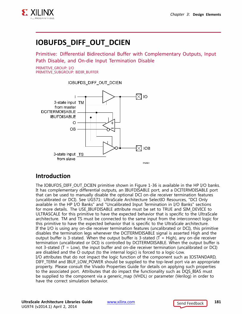
Chapter 3: Design Elements
IOBUFDS_DIFF_OUT_DCIENPrimitive: Differential Bidirectional Buffer with Complementary Outputs, InputPath Disable, and On-die Input Termination DisablePRIMITIVE_GROUP: I/OPRIMITIVE_SUBGROUP: BIDIR_BUFFER
IntroductionThe IOBUFDS_DIFF_OUT_DCIEN primitive shown in Figure 1-36 is available in the HP I/O banks.It has complementary differential outputs, an IBUFDISABLE port, and a DCITERMDISABLE portthat can be used to manually disable the optional DCI on-die receiver termination features(uncalibrated or DCI). See UG571: UltraScale Architecture SelectIO Resources, "DCI Onlyavailable in the HP I/O Banks" and "Uncalibrated Input Termination in I/O Banks" sectionsfor more details. The USE_IBUFDISABLE attribute must be set to TRUE and SIM_DEVICE toULTRASCALE for this primitive to have the expected behavior that is specific to the UltraScalearchitecture. TM and TS must be connected to the same input from the interconnect logic forthis primitive to have the expected behavior that is specific to the UltraScale architecture.If the I/O is using any on-die receiver termination features (uncalibrated or DCI), this primitivedisables the termination legs whenever the DCITERMDISABLE signal is asserted High and theoutput buffer is 3-stated. When the output buffer is 3-stated (T = High), any on-die receivertermination (uncalibrated or DCI) is controlled by DCITERMDISABLE. When the output buffer isnot 3-stated (T = Low), the input buffer and on-die receiver termination (uncalibrated or DCI)are disabled and the O output (to the internal logic) is forced to a logic-Low.I/O attributes that do not impact the logic function of the component such as IOSTANDARD,DIFF_TERM and IBUF_LOW_POWER should be supplied to the top-level port via an appropriateproperty. Please consult the Vivado Properties Guide for details on applying such propertiesto the associated port. Attributes that do impact the functionality such as DQS_BIAS mustbe supplied to the component via a generic_map (VHDL) or parameter (Verilog) in order tohave the correct simulation behavior.
UltraScale Architecture Libraries Guide www.xilinx.com 181UG974 (v2014.1) April 2, 2014
Send Feedback

Chapter 3: Design Elements
Port DescriptionsPort Direction Width Function
DCITERMDISABLE Input 1 Control to enable/disable DCI termination. This is generally usedto reduce power in long periods of an idle state.
I Input 1 Input of OBUF. Connect to the logic driving the output port.
IBUFDISABLE Input 1 The IBUFDISABLE feature is not supported with this primitive inthe UltraScale architecture. This port must be tied to a logic ’0’.
IO Inout 1 Bidirectional diff_p port to be connected directly to top-levelinout port.
IOB Inout 1 Bidirectional diff_n port to be connected directly to top-levelinout port.
O Output 1 Output path of the buffer.
OB Output 1 Output path of the buffer.
TM Input 1 3-state enable input for the p-side or master side signifyingwhether the buffer acts as an input or output. This pin must beconnected to the same signal as the TS input.
TS Input 1 3-state enable input for the n-side or slave side signifyingwhether the buffer acts as an input or output. This pin must beconnected to the same signal as the TM input.
Design Entry MethodInstantiation Yes
Inference No
IP and IP Integrator Catalog No
Macro support No
Available AttributesAttribute Type Allowed Values Default Description
DQS_BIAS STRING "FALSE", "TRUE" "FALSE" Provides pull-up/pull-down feature requiredfor some DQS memory interface pins.
SIM_DEVICE STRING "ULTRASCALE","7SERIES"
"ULTRASCALE" This attribute must be set to "ULTRASCALE"in order to exhibit the proper simulationbehavior.
USE_IBUFDISABLE
STRING "TRUE", "FALSE" "TRUE" This attribute must be unspecified or set to"TRUE" if specified.
UltraScale Architecture Libraries Guide www.xilinx.com 182UG974 (v2014.1) April 2, 2014
Send Feedback

Chapter 3: Design Elements
VHDL Instantiation TemplateUnless they already exist, copy the following two statements and paste them before the entitydeclaration.Library UNISIM;use UNISIM.vcomponents.all;
-- IOBUFDS_DIFF_OUT_DCIEN: Differential Bi-directional Buffer w/ Differential Output, Input disable and DCI Disable-- UltraScale-- Xilinx HDL Libraries Guide, version 2014.1
IOBUFDS_DIFF_OUT_DCIEN_inst : IOBUFDS_DIFF_OUT_DCIENgeneric map (
DQS_BIAS => "FALSE", -- (FALSE, TRUE)SIM_DEVICE => "ULTRASCALE" -- Must be set to "ULTRASCALE"
)port map (
O => O, -- 1-bit output: Buffer diff_p outputOB => OB, -- 1-bit output: Buffer diff_n outputDCITERMDISABLE => DCITERMDISABLE, -- 1-bit input: DCI Termination DisableI => I, -- 1-bit input: Buffer inputIBUFDISABLE => IBUFDISABLE, -- 1-bit input: Buffer disable input, low=disableIO => IO, -- 1-bit inout: Diff_p inout (connect directly to top-level port)IOB => IOB, -- 1-bit inout: Diff_n inout (connect directly to top-level port)TM => TM, -- 1-bit input: 3-state master enable inputTS => TS -- 1-bit input: 3-state slave enable input
);
-- End of IOBUFDS_DIFF_OUT_DCIEN_inst instantiation
Verilog Instantiation Template
// IOBUFDS_DIFF_OUT_DCIEN: Differential Bi-directional Buffer w/ Differential Output, Input disable and DCI Disable// UltraScale// Xilinx HDL Libraries Guide, version 2014.1
IOBUFDS_DIFF_OUT_DCIEN #(.DQS_BIAS("FALSE"), // (FALSE, TRUE).SIM_DEVICE("ULTRASCALE") // Must be set to "ULTRASCALE"
)IOBUFDS_DIFF_OUT_DCIEN_inst (
.O(O), // 1-bit output: Buffer diff_p output
.OB(OB), // 1-bit output: Buffer diff_n output
.DCITERMDISABLE(DCITERMDISABLE), // 1-bit input: DCI Termination Disable
.I(I), // 1-bit input: Buffer input
.IBUFDISABLE(IBUFDISABLE), // 1-bit input: Buffer disable input, low=disable
.IO(IO), // 1-bit inout: Diff_p inout (connect directly to top-level port)
.IOB(IOB), // 1-bit inout: Diff_n inout (connect directly to top-level port)
.TM(TM), // 1-bit input: 3-state master enable input
.TS(TS) // 1-bit input: 3-state slave enable input);
// End of IOBUFDS_DIFF_OUT_DCIEN_inst instantiation
For More Information• See the 7 series FPGA User Documentation (User Guides and Data Sheets).
• See the UltraScale User Documentation.
UltraScale Architecture Libraries Guide www.xilinx.com 183UG974 (v2014.1) April 2, 2014
Send Feedback

Chapter 3: Design Elements
IOBUFDS_DIFF_OUT_INTERMDISABLEPrimitive: Differential Bidirectional Buffer with Complementary Outputs, InputBuffer Disable and On-die Input Termination DisablePRIMITIVE_GROUP: I/OPRIMITIVE_SUBGROUP: BIDIR_BUFFER
IntroductionThe IOBUFDS_DIFF_OUT_INTERMDISABLE primitive is available in the HR I/O banks. TheIOBUFDS_DIFF_OUT_INTERMDISABLE primitive has an INTERMDISABLE port that can be used todisable the optional on-die receiver termination feature. See UG571: UltraScale ArchitectureSelectIO Resources, "Uncalibrated Input Termination in I/O Banks" for more details on thisfeature. TM and TS must be connected to the same input (T) from the interconnect logic forthis primitive to have the expected behavior that is specific to the UltraScale architecture.The USE_IBUFDISABLE attribute must be set to TRUE and SIM_DEVICE to ULTRASCALE for theIOBUFDS_DIFF_OUT_INTERMDISABLE primitive to have the expected behavior that is specificto the UltraScale architecture. If the I/O is using the on-die receiver termination features, thisprimitive disables the termination legs whenever the INTERMDISABLE signal is asserted Highand the output buffer is 3-stated. When the output buffer is 3-stated (T = High), any on-diereceiver termination is controlled by INTERMDISABLE. When the output buffer is not 3-stated (T= Low), the input buffer and on-die receiver termination are disabled and the O output (to theinternal logic) is forced to a logic-Low.I/O attributes that do not impact the logic function of the component such as IOSTANDARD,DIFF_TERM and IBUF_LOW_POWER should be supplied to the top-level port via an appropriateproperty. Please consult the Vivado Properties Guide for details on applying such propertiesto the associated port. Attributes that do impact the functionality such as DQS_BIAS mustbe supplied to the component via a generic_map (VHDL) or parameter (Verilog) in order tohave the correct simulation behavior.
UltraScale Architecture Libraries Guide www.xilinx.com 184UG974 (v2014.1) April 2, 2014
Send Feedback

Chapter 3: Design Elements
Port DescriptionsPort Direction Width Function
I Input 1 Input of OBUF. Connect to the logic driving the output port.
IBUFDISABLE Input 1 The IBUFDISABLE feature is not supported with this primitive inthe UltraScale architecture. This port must be tied to a logic ’0’.
INTERMDISABLE Input 1 Control to enable/disable on-chip input termination. This isgenerally used to reduce power in long periods of an idle state.
IO Inout 1 Bidirectional diff_p port to be connected directly to top-levelinout port.
IOB Inout 1 Bidirectional diff_n port to be connected directly to top-levelinout port.
O Output 1 Output path of the buffer.
OB Output 1 Output path of the buffer.
TM Input 1 3-state enable input for the p-side or master side signifyingwhether the buffer acts as an input or output. This pin must beconnected to the same signal as the TS input.
TS Input 1 3-state enable input for the n-side or slave side signifyingwhether the buffer acts as an input or output. This pin must beconnected to the same signal as the TM input.
Design Entry MethodInstantiation Recommended
Inference No
IP and IP Integrator Catalog No
Macro support No
Available AttributesAttribute Type Allowed Values Default Description
DQS_BIAS STRING "FALSE", "TRUE" "FALSE" Provides pull-up/pull-down feature requiredfor some DQS memory interface pins.
SIM_DEVICE STRING "ULTRASCALE","7SERIES"
"ULTRASCALE" This attribute must be set to "ULTRASCALE" inorder to exhibit the proper simulation behavior.
USE_IBUFDISABLE
STRING "TRUE", "FALSE" "TRUE" This attribute must be unspecified or set to"TRUE" if specified.
UltraScale Architecture Libraries Guide www.xilinx.com 185UG974 (v2014.1) April 2, 2014
Send Feedback

Chapter 3: Design Elements
VHDL Instantiation TemplateUnless they already exist, copy the following two statements and paste them before the entitydeclaration.Library UNISIM;use UNISIM.vcomponents.all;
-- IOBUFDS_DIFF_OUT_INTERMDISABLE: Differential Bi-directional Buffer w/ Differential Output, Input disable and Input Termination Disable
-- UltraScale-- Xilinx HDL Libraries Guide, version 2014.1
IOBUFDS_DIFF_OUT_INTERMDISABLE_inst : IOBUFDS_DIFF_OUT_INTERMDISABLEgeneric map (
DQS_BIAS => "FALSE", -- (FALSE, TRUE)SIM_DEVICE => "ULTRASCALE" -- Must be set to "ULTRASCALE"
)port map (
O => O, -- 1-bit output: Buffer diff_p outputOB => OB, -- 1-bit output: Buffer diff_n outputI => I, -- 1-bit input: Buffer inputIBUFDISABLE => IBUFDISABLE, -- 1-bit input: Buffer disable input, low=disableINTERMDISABLE => INTERMDISABLE, -- 1-bit input: Input Termination DisableIO => IO, -- 1-bit inout: Diff_p inout (connect directly to top-level port)IOB => IOB, -- 1-bit inout: Diff_n inout (connect directly to top-level port)TM => TM, -- 1-bit input: 3-state master enable inputTS => TS -- 1-bit input: 3-state slave enable input
);
-- End of IOBUFDS_DIFF_OUT_INTERMDISABLE_inst instantiation
Verilog Instantiation Template
// IOBUFDS_DIFF_OUT_INTERMDISABLE: Differential Bi-directional Buffer w/ Differential Output, Input disable and Input Termination Disable
// UltraScale// Xilinx HDL Libraries Guide, version 2014.1
IOBUFDS_DIFF_OUT_INTERMDISABLE#(.DQS_BIAS("FALSE"), // (FALSE, TRUE).SIM_DEVICE("ULTRASCALE") // Must be set to "ULTRASCALE"
)IOBUFDS_DIFF_OUT_INTERMDISABLE_inst (
.O(O), // 1-bit output: Buffer diff_p output
.OB(OB), // 1-bit output: Buffer diff_n output
.I(I), // 1-bit input: Buffer input
.IBUFDISABLE(IBUFDISABLE), // 1-bit input: Buffer disable input, low=disable
.INTERMDISABLE(INTERMDISABLE), // 1-bit input: Input Termination Disable
.IO(IO), // 1-bit inout: Diff_p inout (connect directly to top-level port)
.IOB(IOB), // 1-bit inout: Diff_n inout (connect directly to top-level port)
.TM(TM), // 1-bit input: 3-state master enable input
.TS(TS) // 1-bit input: 3-state slave enable input);
// End of IOBUFDS_DIFF_OUT_INTERMDISABLE_inst instantiation
For More Information• See the 7 series FPGA User Documentation (User Guides and Data Sheets).
• See the UltraScale User Documentation.
UltraScale Architecture Libraries Guide www.xilinx.com 186UG974 (v2014.1) April 2, 2014
Send Feedback

Chapter 3: Design Elements
IOBUFDS_INTERMDISABLEPrimitive: Differential Bidirectional Buffer With Input Buffer Disable and On-dieInputPRIMITIVE_GROUP: I/OPRIMITIVE_SUBGROUP: BIDIR_BUFFER
IntroductionThe IOBUFDS_INTERMDISABLE primitive is available in the HR I/O banks. It has an IBUFDISABLEport that can be used to disable the input buffer during periods when the buffer is not beingused. The IOBUFDS_INTERMDISABLE primitive also has an INTERMDISABLE port that canbe used to disable the optional on-die receiver termination feature. See UG571: UltraScaleArchitecture SelectIO Resources, "Uncalibrated Input Termination in I/O Banks" for more detailson this feature.The IOBUFDS_INTERMDISABLE primitive can disable the input buffer and force the O outputto the internal logic to a logic-Low when the IBUFDISABLE signal is asserted High and theoutput buffer is 3-stated (T = High). The USE_IBUFDISABLE attribute must be set to TRUEand SIM_DEVICE to ULTRASCALE for this primitive to have the expected behavior that isspecific to the UltraScale architecture. If the I/O is using the on-die receiver terminationfeature, this primitive disables the termination legs whenever the INTERMDISABLE signal isasserted High and the output buffer is 3-stated. When the output buffer is 3-stated (T =High), the input buffer and any on-die receiver termination are controlled by IBUFDISABLE andINTERMFIDISABLE, respectively. When the output buffer is not 3-stated (T = Low), the inputbuffer and on-die receiver termination are disabled and the O output (to the internal logic) isforced to a logic-Low. These features can be combined to reduce power whenever the input isidle for a period of time.I/O attributes that do not impact the logic function of the component such as IOSTANDARD,DIFF_TERM and IBUF_LOW_POWER should be supplied to the top-level port via an appropriateproperty. Please consult the Vivado Properties Guide for details on applying such propertiesto the associated port. Attributes that do impact the functionality such as DQS_BIAS mustbe supplied to the component via a generic_map (VHDL) or parameter (Verilog) in order tohave the correct simulation behavior.
UltraScale Architecture Libraries Guide www.xilinx.com 187UG974 (v2014.1) April 2, 2014
Send Feedback

Chapter 3: Design Elements
Port DescriptionsPort Direction Width Function
I Input 1 Input of OBUF. Connect to the logic driving the output port.
IBUFDISABLE Input 1 Disables input path through the buffer and forces to a logic low.This feature is generally used to reduce power at times when theI/O is idle for a period of time.
INTERMDISABLE Input 1 Control to enable/disable on-chip input termination. This isgenerally used to reduce power in long periods of an idle state.
IO Inout 1 Bidirectional diff_p port to be connected directly to top-levelinout port.
IOB Inout 1 Bidirectional diff_n port to be connected directly to top-levelinout port.
O Output 1 Output path of the buffer.
T Input 1 3-state enable input signifying whether the buffer acts as an inputor output.
Design Entry MethodInstantiation Yes
Inference No
IP and IP Integrator Catalog No
Macro support No
Available AttributesAttribute Type Allowed Values Default Description
DQS_BIAS STRING "FALSE","TRUE"
"FALSE" Provides pull-up/pull-down feature requiredfor some DQS memory interface pins.
SIM_DEVICE STRING "ULTRASCALE","7SERIES"
"ULTRASCALE" This attribute must be set to "ULTRASCALE"in order to exhibit the proper simulationbehavior.
USE _IBUFDISABLE STRING "TRUE","FALSE"
"TRUE" This attribute must be unspecified or set to"TRUE" if specified.
VHDL Instantiation TemplateUnless they already exist, copy the following two statements and paste them before the entitydeclaration.Library UNISIM;use UNISIM.vcomponents.all;
-- IOBUFDS_INTERMDISABLE: Differential Bi-directional Buffer w/ Input disable and Input Termination Disable-- UltraScale-- Xilinx HDL Libraries Guide, version 2014.1
IOBUFDS_INTERMDISABLE_inst : IOBUFDS_INTERMDISABLEgeneric map (
UltraScale Architecture Libraries Guide www.xilinx.com 188UG974 (v2014.1) April 2, 2014
Send Feedback

Chapter 3: Design Elements
DQS_BIAS => "FALSE", -- (FALSE, TRUE)SIM_DEVICE => "ULTRASCALE" -- Must be set to "ULTRASCALE"
)port map (
O => O, -- 1-bit output: Buffer outputI => I, -- 1-bit input: Buffer inputIBUFDISABLE => IBUFDISABLE, -- 1-bit input: Buffer disable input, low=disableINTERMDISABLE => INTERMDISABLE, -- 1-bit input: Input Termination DisableIO => IO, -- 1-bit inout: Diff_p inout (connect directly to top-level port)IOB => IOB, -- 1-bit inout: Diff_n inout (connect directly to top-level port)T => T -- 1-bit input: 3-state enable input
);
-- End of IOBUFDS_INTERMDISABLE_inst instantiation
Verilog Instantiation Template
// IOBUFDS_INTERMDISABLE: Differential Bi-directional Buffer w/ Input disable and Input Termination Disable// UltraScale// Xilinx HDL Libraries Guide, version 2014.1
IOBUFDS_INTERMDISABLE#(.DQS_BIAS("FALSE"), // (FALSE, TRUE).SIM_DEVICE("ULTRASCALE") // Must be set to "ULTRASCALE"
)IOBUFDS_INTERMDISABLE_inst (
.O(O), // 1-bit output: Buffer output
.I(I), // 1-bit input: Buffer input
.IBUFDISABLE(IBUFDISABLE), // 1-bit input: Buffer disable input, low=disable
.INTERMDISABLE(INTERMDISABLE), // 1-bit input: Input Termination Disable
.IO(IO), // 1-bit inout: Diff_p inout (connect directly to top-level port)
.IOB(IOB), // 1-bit inout: Diff_n inout (connect directly to top-level port)
.T(T) // 1-bit input: 3-state enable input);
// End of IOBUFDS_INTERMDISABLE_inst instantiation
For More Information• See the 7 series FPGA User Documentation (User Guides and Data Sheets).
• See the UltraScale User Documentation.
UltraScale Architecture Libraries Guide www.xilinx.com 189UG974 (v2014.1) April 2, 2014
Send Feedback
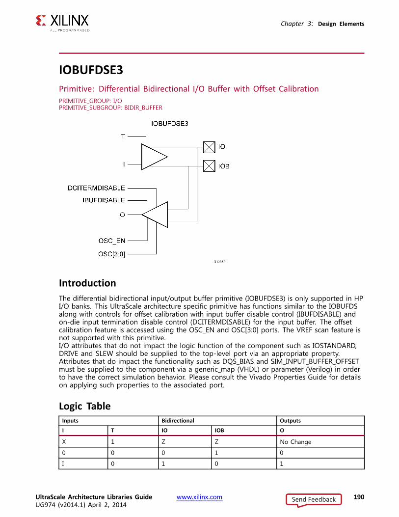
Chapter 3: Design Elements
IOBUFDSE3Primitive: Differential Bidirectional I/O Buffer with Offset CalibrationPRIMITIVE_GROUP: I/OPRIMITIVE_SUBGROUP: BIDIR_BUFFER
IntroductionThe differential bidirectional input/output buffer primitive (IOBUFDSE3) is only supported in HPI/O banks. This UltraScale architecture specific primitive has functions similar to the IOBUFDSalong with controls for offset calibration with input buffer disable control (IBUFDISABLE) andon-die input termination disable control (DCITERMDISABLE) for the input buffer. The offsetcalibration feature is accessed using the OSC_EN and OSC[3:0] ports. The VREF scan feature isnot supported with this primitive.I/O attributes that do not impact the logic function of the component such as IOSTANDARD,DRIVE and SLEW should be supplied to the top-level port via an appropriate property.Attributes that do impact the functionality such as DQS_BIAS and SIM_INPUT_BUFFER_OFFSETmust be supplied to the component via a generic_map (VHDL) or parameter (Verilog) in orderto have the correct simulation behavior. Please consult the Vivado Properties Guide for detailson applying such properties to the associated port.
Logic TableInputs Bidirectional OutputsI T IO IOB O
X 1 Z Z No Change
0 0 0 1 0
I 0 1 0 1
UltraScale Architecture Libraries Guide www.xilinx.com 190UG974 (v2014.1) April 2, 2014
Send Feedback
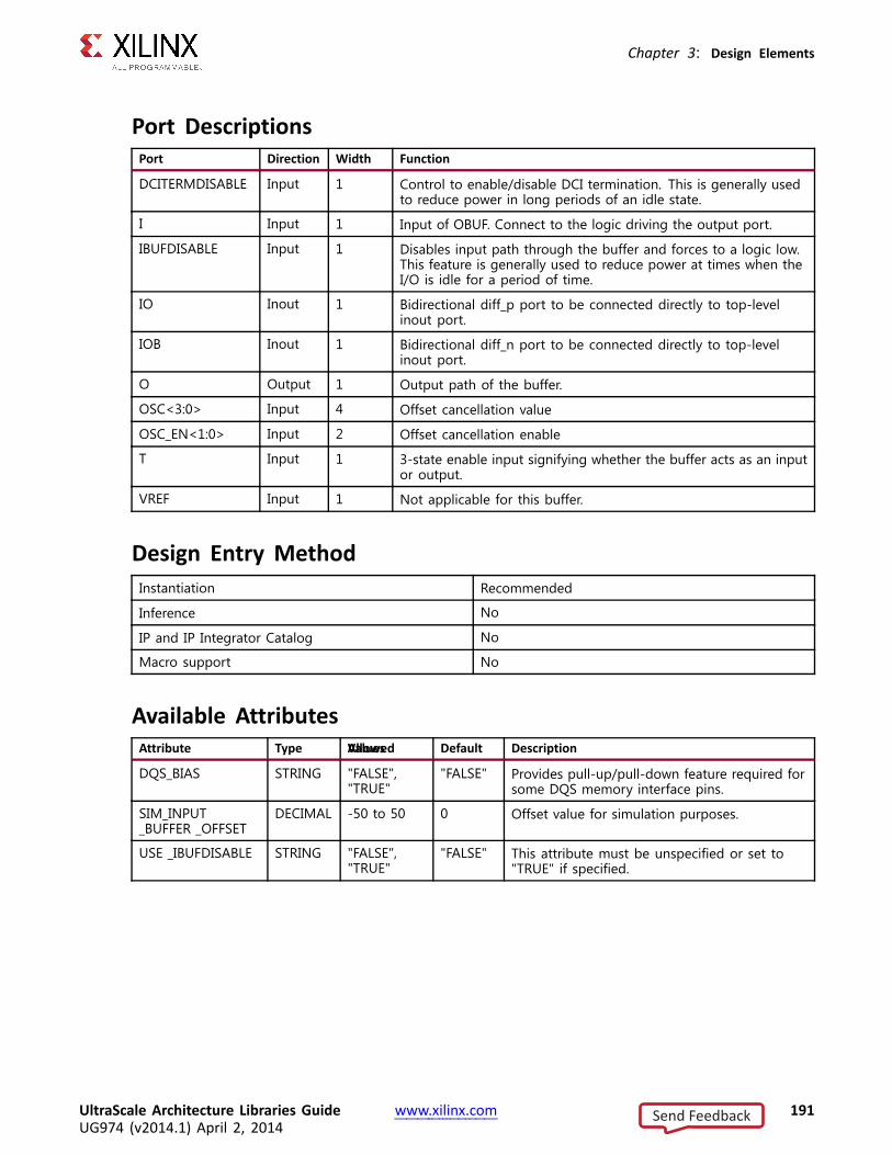
Chapter 3: Design Elements
Port DescriptionsPort Direction Width Function
DCITERMDISABLE Input 1 Control to enable/disable DCI termination. This is generally usedto reduce power in long periods of an idle state.
I Input 1 Input of OBUF. Connect to the logic driving the output port.
IBUFDISABLE Input 1 Disables input path through the buffer and forces to a logic low.This feature is generally used to reduce power at times when theI/O is idle for a period of time.
IO Inout 1 Bidirectional diff_p port to be connected directly to top-levelinout port.
IOB Inout 1 Bidirectional diff_n port to be connected directly to top-levelinout port.
O Output 1 Output path of the buffer.
OSC<3:0> Input 4 Offset cancellation value
OSC_EN<1:0> Input 2 Offset cancellation enable
T Input 1 3-state enable input signifying whether the buffer acts as an inputor output.
VREF Input 1 Not applicable for this buffer.
Design Entry MethodInstantiation Recommended
Inference No
IP and IP Integrator Catalog No
Macro support No
Available AttributesAttribute Type AllowedValues Default Description
DQS_BIAS STRING "FALSE","TRUE"
"FALSE" Provides pull-up/pull-down feature required forsome DQS memory interface pins.
SIM_INPUT_BUFFER _OFFSET
DECIMAL -50 to 50 0 Offset value for simulation purposes.
USE _IBUFDISABLE STRING "FALSE","TRUE"
"FALSE" This attribute must be unspecified or set to"TRUE" if specified.
UltraScale Architecture Libraries Guide www.xilinx.com 191UG974 (v2014.1) April 2, 2014
Send Feedback

Chapter 3: Design Elements
VHDL Instantiation TemplateUnless they already exist, copy the following two statements and paste them before the entitydeclaration.Library UNISIM;use UNISIM.vcomponents.all;
-- IOBUFDSE3: Advanced Differential Bi-directional Buffer-- UltraScale-- Xilinx HDL Libraries Guide, version 2014.1
IOBUFDSE3_inst : IOBUFDSE3generic map (
DQS_BIAS => "FALSE", -- (FALSE, TRUE)SIM_INPUT_BUFFER_OFFSET=> 0 -- Offset value for simulation (-50-50)
)port map (
O => O, -- 1-bit output: Buffer outputDCITERMDISABLE => DCITERMDISABLE, -- 1-bit input: DCI Termination DisableI => I, -- 1-bit input: Buffer inputIBUFDISABLE => IBUFDISABLE, -- 1-bit input: Buffer disable input, low=disableIO => IO, -- 1-bit inout: Diff_p inout (connect directly to top-level port)IOB => IOB, -- 1-bit inout: Diff_n inout (connect directly to top-level port)OSC => OSC, -- 4-bit input: Offset cancellation valueOSC_EN=> OSC_EN, -- 2-bit input: Offset cancelatin enableT => T, -- 1-bit input: 3-state enable inputVREF => VREF -- 1-bit input: Vref input from HPIO_VREF
);
-- End of IOBUFDSE3_inst instantiation
Verilog Instantiation Template
// IOBUFDSE3: Advanced Differential Bi-directional Buffer// UltraScale// Xilinx HDL Libraries Guide, version 2014.1
IOBUFDSE3 #(.DQS_BIAS("FALSE"), // (FALSE, TRUE).SIM_INPUT_BUFFER_OFFSET(0) // Offset value for simulation (-50-50)
)IOBUFDSE3_inst (
.O(O), // 1-bit output: Buffer output
.DCITERMDISABLE(DCITERMDISABLE), // 1-bit input: DCI Termination Disable
.I(I), // 1-bit input: Buffer input
.IBUFDISABLE(IBUFDISABLE), // 1-bit input: Buffer disable input, low=disable
.IO(IO), // 1-bit inout: Diff_p inout (connect directly to top-level port)
.IOB(IOB), // 1-bit inout: Diff_n inout (connect directly to top-level port)
.OSC(OSC), // 4-bit input: Offset cancellation value
.OSC_EN(OSC_EN), // 2-bit input: Offset cancelatin enable
.T(T), // 1-bit input: 3-state enable input
.VREF(VREF) // 1-bit input: Vref input from HPIO_VREF);
// End of IOBUFDSE3_inst instantiation
For More Information• See the 7 series FPGA User Documentation (User Guides and Data Sheets).
• See the UltraScale User Documentation.
UltraScale Architecture Libraries Guide www.xilinx.com 192UG974 (v2014.1) April 2, 2014
Send Feedback

Chapter 3: Design Elements
IOBUFE3Primitive: Bidirectional I/O Buffer with Offset Calibration and VREF TuningPRIMITIVE_GROUP: I/OPRIMITIVE_SUBGROUP: BIDIR_BUFFER
IntroductionThe bidirectional input/output buffer primitive (IOBUFE3) is only supported in HP I/O banks.This UltraScale architecture specific primitive has functions similar to the IOBUF along withcontrols for offset calibration and VREF tuning with input buffer disable (IBUFDISABLE) andon-die input termination control (DCITERMDISABLE) for the input buffer. The offset calibrationfeature is accessed using the OSC_EN and OSC[3:0] ports. The VREF scan feature is accessedusing the HPIO_VREF primitive in conjunction with IOBUFE3.I/O attributes that do not impact the logic function of the component such as IOSTANDARD,DRIVE and SLEW should be supplied to the top-level port via an appropriate property. Pleaseconsult the Vivado Properties Guide for details on applying such properties to the associatedport.
UltraScale Architecture Libraries Guide www.xilinx.com 193UG974 (v2014.1) April 2, 2014
Send Feedback
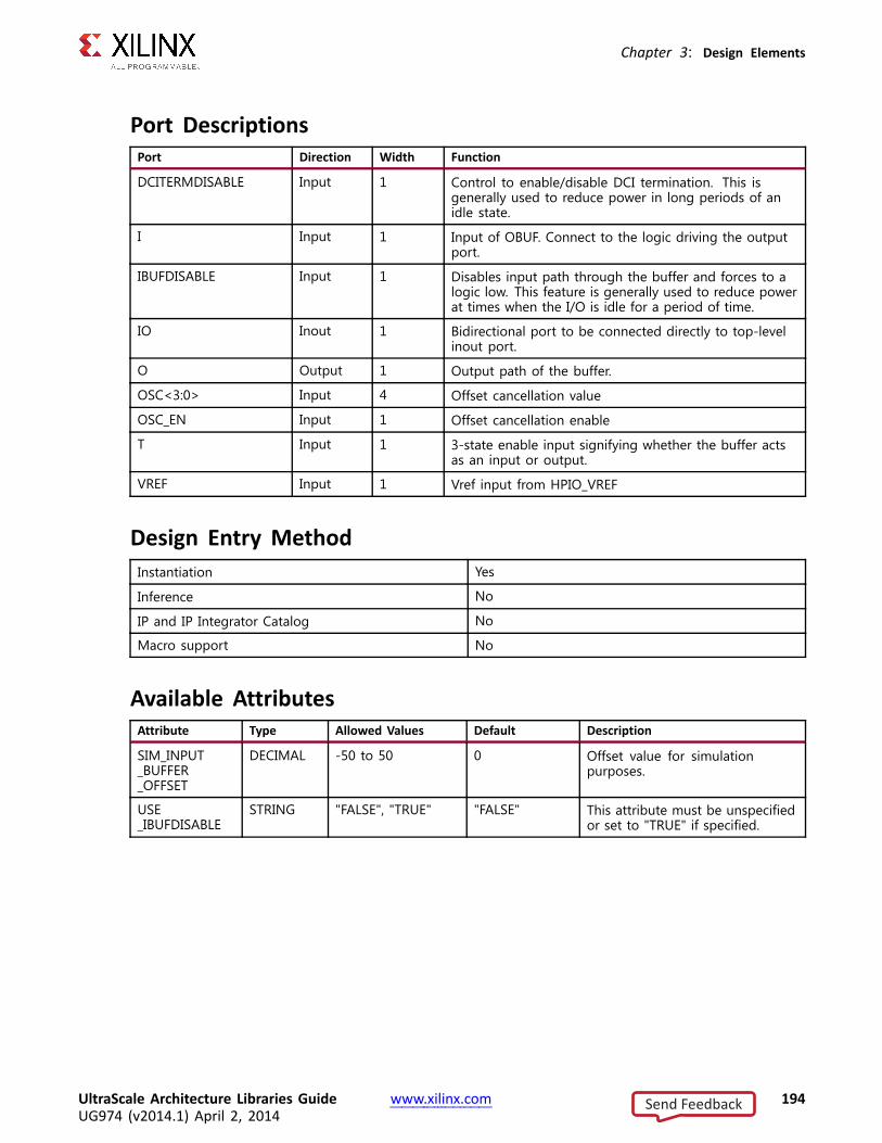
Chapter 3: Design Elements
Port DescriptionsPort Direction Width Function
DCITERMDISABLE Input 1 Control to enable/disable DCI termination. This isgenerally used to reduce power in long periods of anidle state.
I Input 1 Input of OBUF. Connect to the logic driving the outputport.
IBUFDISABLE Input 1 Disables input path through the buffer and forces to alogic low. This feature is generally used to reduce powerat times when the I/O is idle for a period of time.
IO Inout 1 Bidirectional port to be connected directly to top-levelinout port.
O Output 1 Output path of the buffer.
OSC<3:0> Input 4 Offset cancellation value
OSC_EN Input 1 Offset cancellation enable
T Input 1 3-state enable input signifying whether the buffer actsas an input or output.
VREF Input 1 Vref input from HPIO_VREF
Design Entry MethodInstantiation Yes
Inference No
IP and IP Integrator Catalog No
Macro support No
Available AttributesAttribute Type Allowed Values Default Description
SIM_INPUT_BUFFER_OFFSET
DECIMAL -50 to 50 0 Offset value for simulationpurposes.
USE_IBUFDISABLE
STRING "FALSE", "TRUE" "FALSE" This attribute must be unspecifiedor set to "TRUE" if specified.
UltraScale Architecture Libraries Guide www.xilinx.com 194UG974 (v2014.1) April 2, 2014
Send Feedback

Chapter 3: Design Elements
VHDL Instantiation TemplateUnless they already exist, copy the following two statements and paste them before the entitydeclaration.Library UNISIM;use UNISIM.vcomponents.all;
-- IOBUFE3: Advanced Bi-directional Buffer-- UltraScale-- Xilinx HDL Libraries Guide, version 2014.1
IOBUFE3_inst : IOBUFE3generic map (
SIM_INPUT_BUFFER_OFFSET=> 0 -- Offset value for simulation (-50-50))port map (
O => O, -- 1-bit output: Buffer outputDCITERMDISABLE => DCITERMDISABLE, -- 1-bit input: DCI Termination DisableI => I, -- 1-bit input: Buffer inputIBUFDISABLE => IBUFDISABLE, -- 1-bit input: Buffer disable input, low=disableIO => IO, -- 1-bit inout: Buffer inout (connect directly to top-level port)OSC => OSC, -- 4-bit input: Offset cancellation valueOSC_EN=> OSC_EN, -- 1-bit input: Offset cancelatin enableT => T, -- 1-bit input: 3-state enable inputVREF => VREF -- 1-bit input: Vref input from HPIO_VREF
);
-- End of IOBUFE3_inst instantiation
Verilog Instantiation Template
// IOBUFE3: Advanced Bi-directional Buffer// UltraScale// Xilinx HDL Libraries Guide, version 2014.1
IOBUFE3 #(.SIM_INPUT_BUFFER_OFFSET(0) // Offset value for simulation (-50-50)
)IOBUFE3_inst (
.O(O), // 1-bit output: Buffer output
.DCITERMDISABLE(DCITERMDISABLE), // 1-bit input: DCI Termination Disable
.I(I), // 1-bit input: Buffer input
.IBUFDISABLE(IBUFDISABLE), // 1-bit input: Buffer disable input, low=disable
.IO(IO), // 1-bit inout: Buffer inout (connect directly to top-level port)
.OSC(OSC), // 4-bit input: Offset cancellation value
.OSC_EN(OSC_EN), // 1-bit input: Offset cancelatin enable
.T(T), // 1-bit input: 3-state enable input
.VREF(VREF) // 1-bit input: Vref input from HPIO_VREF);
// End of IOBUFE3_inst instantiation
For More Information• See the 7 series FPGA User Documentation (User Guides and Data Sheets).
• See the UltraScale User Documentation.
UltraScale Architecture Libraries Guide www.xilinx.com 195UG974 (v2014.1) April 2, 2014
Send Feedback

Chapter 3: Design Elements
ISERDESE3Primitive: Input SERial/DESerializer
PRIMITIVE_GROUP: I/OPRIMITIVE_SUBGROUP: SERDES
IntroductionIn component mode, the ISERDESE3 in UltraScale FPGAs is a dedicated serial-to-parallelconverter with specific clocking and logic features designed to facilitate the implementationof high-speed source-synchronous applications. The ISERDESE3 avoids the additional timingcomplexities encountered when designing deserializers in the FPGA fabric. ISERDESE3 featuresinclude: Dedicated Deserializer/Serial-to-Parallel Converter, which enables high-speed datatransfer without requiring the FPGA fabric to match the input data frequency. This convertersupports both single data rate (SDR) and double data rate (DDR) modes. In SDR mode, theserial-to-parallel converter creates a 4- bit wide parallel word by retrieving data from everyother Q pin. In DDR mode, the serial-to-parallel converter creates an 8-bit-wide parallel word.
Port DescriptionsPort Direction Width Function
CLK Input 1 The high-speed clock input (CLK) is used to clock in the inputserial data stream.
CLK_B Input 1 The inverted high-speed clock input
CLKDIV Input 1 The divided clock input (CLKDIV) is typically a divided version ofCLK (depending on the width of the implemented deserialization).It drives the output of the serial-to-parallel converter and theCE module.
D Input 1 The serial input data port (D) is the serial (high-speed) datainput port of the ISERDESE3. This port accepts data from theIOB or FPGA Fabric.
FIFO_EMPTY Output 1 FIFO empty flag
FIFO_RD_CLK Input 1 FIFO read clock
UltraScale Architecture Libraries Guide www.xilinx.com 196UG974 (v2014.1) April 2, 2014
Send Feedback

Chapter 3: Design Elements
Port Direction Width Function
FIFO_RD_EN Input 1 Enables reading the FIFO when asserted
INTERNAL_DIVCLK Output 1 Internally divided down clock used to launch data from ISERDESto fabric when FIFO is disabled (do not connect)
Q<7:0> Output 8 8-bit registered output
RST Input 1 Asynchronous Reset, active level based on IS_RST_INVERTED
Design Entry MethodInstantiation Yes
Inference No
IP and IP Integrator Catalog Yes
Macro support No
Available AttributesAttribute Type Allowed Values Default Description
DATA_WIDTH DECIMAL 8, 4 8 Defines the width of theserial-to-parallel converter.Running in SDR mode is done byretrieving data from every other Qpin.
FIFO_ENABLE STRING "FALSE", "TRUE" "FALSE" Setting FIFO_ENABLE to TRUE usesthe FIFO and setting FIFO_ENABLEto FALSE bypasses the FIFO
FIFO_SYNC_MODE
STRING "FALSE", "TRUE" "FALSE" Set FIFO_SYNC_MODE to TRUEwhen the internal write clock andthe FIFO_RD_CLK are coming froma common source and all clocktiming from write to read mustbe met. Set FIFO_SYNC_MODEto FALSE will cause the internal2-stage flop synchonizers to beused and will add latency to whenFIFO_EMPTY will deassert afterdata is first written to the FIFO.
IS_CLK_B_INVERTED
BINARY 1’b0 to 1’b1 1’b0 Indicates whether the CLK_B isactive-low or active-high
IS_CLK_INVERTED
BINARY 1’b0 to 1’b1 1’b0 Indicates whether the CLK isactive-high or active-low
IS_RST_INVERTED
BINARY 1’b0 to 1’b1 1’b0 Indicates whether the RST isactive-high or active-low
UltraScale Architecture Libraries Guide www.xilinx.com 197UG974 (v2014.1) April 2, 2014
Send Feedback

Chapter 3: Design Elements
VHDL Instantiation TemplateUnless they already exist, copy the following two statements and paste them before the entitydeclaration.Library UNISIM;use UNISIM.vcomponents.all;
-- ISERDESE3: Input SERial/DESerializer-- UltraScale-- Xilinx HDL Libraries Guide, version 2014.1
ISERDESE3_inst : ISERDESE3generic map (
DATA_WIDTH=> 8, -- Parallel data width (4,8)FIFO_ENABLE => "FALSE", -- Enables the use of the FIFOFIFO_SYNC_MODE=> "FALSE", -- Enables the use of internal 2-stage synchronizers on the FIFOIS_CLK_B_INVERTED => ’0’, -- Optional inversion for CLK_BIS_CLK_INVERTED => ’0’, -- Optional inversion for CLKIS_RST_INVERTED => ’0’ -- Optional inversion for RST
)port map (
FIFO_EMPTY => FIFO_EMPTY, -- 1-bit output: FIFO empty flagINTERNAL_DIVCLK => INTERNAL_DIVCLK, -- 1-bit output: Internally divided down clock used when FIFO is
-- disabled
Q => Q, -- 8-bit registered outputCLK => CLK, -- 1-bit input: High-speed clockCLKDIV => CLKDIV, -- 1-bit input: Divided ClockCLK_B => CLK_B, -- 1-bit input: Inversion of High-speed clock CLKD => D, -- 1-bit input: Serial Data InputFIFO_RD_CLK => FIFO_RD_CLK, -- 1-bit input: FIFO read clockFIFO_RD_EN => FIFO_RD_EN, -- 1-bit input: Enables reading the FIFO when assertedRST => RST -- 1-bit input: Asynchronous Reset
);
-- End of ISERDESE3_inst instantiation
UltraScale Architecture Libraries Guide www.xilinx.com 198UG974 (v2014.1) April 2, 2014
Send Feedback

Chapter 3: Design Elements
Verilog Instantiation Template
// ISERDESE3: Input SERial/DESerializer// UltraScale// Xilinx HDL Libraries Guide, version 2014.1
ISERDESE3 #(.DATA_WIDTH(8), // Parallel data width (4,8).FIFO_ENABLE("FALSE"), // Enables the use of the FIFO.FIFO_SYNC_MODE("FALSE"), // Enables the use of internal 2-stage synchronizers on the FIFO.IS_CLK_B_INVERTED(1’b0), // Optional inversion for CLK_B.IS_CLK_INVERTED(1’b0), // Optional inversion for CLK.IS_RST_INVERTED(1’b0) // Optional inversion for RST
)ISERDESE3_inst (
.FIFO_EMPTY(FIFO_EMPTY), // 1-bit output: FIFO empty flag
.INTERNAL_DIVCLK(INTERNAL_DIVCLK), // 1-bit output: Internally divided down clock used when FIFO is// disabled
.Q(Q), // 8-bit registered output
.CLK(CLK), // 1-bit input: High-speed clock
.CLKDIV(CLKDIV), // 1-bit input: Divided Clock
.CLK_B(CLK_B), // 1-bit input: Inversion of High-speed clock CLK
.D(D), // 1-bit input: Serial Data Input
.FIFO_RD_CLK(FIFO_RD_CLK), // 1-bit input: FIFO read clock
.FIFO_RD_EN(FIFO_RD_EN), // 1-bit input: Enables reading the FIFO when asserted
.RST(RST) // 1-bit input: Asynchronous Reset);
// End of ISERDESE3_inst instantiation
For More Information• See the UltraScale Architecture SelectIO Resources User Guide (UG471).
• See the UltraScale User Documentation.
UltraScale Architecture Libraries Guide www.xilinx.com 199UG974 (v2014.1) April 2, 2014
Send Feedback

Chapter 3: Design Elements
KEEPERPrimitive: I/O Weak KeeperPRIMITIVE_GROUP: I/OPRIMITIVE_SUBGROUP: WEAK_DRIVER
IntroductionThe design element is a weak keeper element that retains the value of the I/O when not beingdriven. For example, if a logic 1 is being driven onto the I/O, KEEPER drives a weak/resistive 1onto the pin/port. If the net driver is then 3-stated, KEEPER continues to drive a weak/resistive1 onto the pin/port.
Port DescriptionsPort Direction Width Function
O Inout 1 Keeper output. Connect directly to a top_level port.
Design Entry MethodInstantiation Yes
Inference Yes, via property
IP and IP Integrator Catalog No
Macro support No
UltraScale Architecture Libraries Guide www.xilinx.com 200UG974 (v2014.1) April 2, 2014
Send Feedback

Chapter 3: Design Elements
VHDL Instantiation TemplateUnless they already exist, copy the following two statements and paste them before the entitydeclaration.Library UNISIM;use UNISIM.vcomponents.all;
-- KEEPER: I/O Weak Keeper-- UltraScale-- Xilinx HDL Libraries Guide, version 2014.1
KEEPER_inst : KEEPERport map (
O => O -- 1-bit inout: Keeper output (connect directly to top-level port));
-- End of KEEPER_inst instantiation
Verilog Instantiation Template
// KEEPER: I/O Weak Keeper// UltraScale// Xilinx HDL Libraries Guide, version 2014.1
KEEPERKEEPER_inst (.O(O) // 1-bit inout: Keeper output (connect directly to top-level port)
);
// End of KEEPER_inst instantiation
For More Information• See the 7 series FPGA User Documentation (User Guides and Data Sheets).
• See the UltraScale User Documentation.
UltraScale Architecture Libraries Guide www.xilinx.com 201UG974 (v2014.1) April 2, 2014
Send Feedback

Chapter 3: Design Elements
LDCEPrimitive: Transparent Latch with Clock Enable and Asynchronous ClearPRIMITIVE_GROUP: REGISTERPRIMITIVE_SUBGROUP: LATCH
IntroductionThis design element is a transparent data latch with asynchronous clear and gate enable. Whenthe asynchronous clear input (CLR) is active, it overrides the other inputs and resets the data(Q) output Low. Q reflects the data (D) input while the gate (G) input and gate enable (GE) areactive and CLR is not active. If (GE) is Low, data on (D) cannot be latched. The data on the(D) input during the gate transition is stored in the latch. The data on the (Q) output remainsunchanged as long as (G) or (GE) remains Low.This latch is asynchronously initialized when power is applied. When global set/reset (GSR)is active either upon power-up or when asserted via the STARTUP block, the value of theINIT attribute is placed on the latch’s output.
Logic TableInputs OutputsCLR GE G D Q
1 X X X 0
0 0 X X No Change
0 1 1 D D
0 1 0 X No Change
0 1 ↓ D D
UltraScale Architecture Libraries Guide www.xilinx.com 202UG974 (v2014.1) April 2, 2014
Send Feedback

Chapter 3: Design Elements
Port DescriptionsPort Direction Width Function
CLR Input 1 Asynchronous clear. Polarity is determined by the IS_CLR_INVERTEDattribute.
D Input 1 Data input
G Input 1 Gate input. Polarity is determined by the IS_G_INVERTED attribute.
GE Input 1 Active-High latech gate enable
Q Output 1 Data output
Design Entry MethodInstantiation Yes
Inference Yes
IP and IP Integrator Catalog No
Macro support No
Available AttributesAttribute Type Allowed Values Default Description
INIT BINARY 1’b0, 1’b1 1’b0 Sets the initial value of Q output afterconfiguration or when GSR is asserted via theSTARTUP block.
IS_CLR_INVERTED
BINARY 1’b0 to 1’b1 1’b0 Indicates whether the optional inversion isused or not for the CLR pin of this component
IS_G_INVERTED BINARY 1’b0 to 1’b1 1’b0 Indicates whether the optional inversion isused or not for the G pin of this component
VHDL Instantiation TemplateUnless they already exist, copy the following two statements and paste them before the entitydeclaration.Library UNISIM;use UNISIM.vcomponents.all;
-- LDCE: Transparent Latch with Clock Enable and Asynchronous Clear-- UltraScale-- Xilinx HDL Libraries Guide, version 2014.1
LDCE_inst : LDCEgeneric map (
INIT => 0, -- Initial value of latch, 1’b0, 1’b1-- Programmable Inversion Attributes: Specifies the use of the built-in programmable inversionIS_CLR_INVERTED => ’0’, -- Optional inversion for CLRIS_G_INVERTED => ’0’ -- Optional inversion for G
)port map (
Q => Q, -- 1-bit output: DataCLR => CLR, -- 1-bit input: Asynchronous clearD => D, -- 1-bit input: Data
UltraScale Architecture Libraries Guide www.xilinx.com 203UG974 (v2014.1) April 2, 2014
Send Feedback

Chapter 3: Design Elements
G => G, -- 1-bit input: GateGE => GE -- 1-bit input: Gate enable
);
-- End of LDCE_inst instantiation
Verilog Instantiation Template
// LDCE: Transparent Latch with Clock Enable and Asynchronous Clear// UltraScale// Xilinx HDL Libraries Guide, version 2014.1
LDCE #(.INIT(0), // Initial value of latch, 1’b0, 1’b1// Programmable Inversion Attributes: Specifies the use of the built-in programmable inversion.IS_CLR_INVERTED(1’b0), // Optional inversion for CLR.IS_G_INVERTED(1’b0) // Optional inversion for G
)LDCE_inst (
.Q(Q), // 1-bit output: Data
.CLR(CLR), // 1-bit input: Asynchronous clear
.D(D), // 1-bit input: Data
.G(G), // 1-bit input: Gate
.GE(GE) // 1-bit input: Gate enable);
// End of LDCE_inst instantiation
For More Information• See the 7 series FPGA User Documentation (User Guides and Data Sheets).
• See the UltraScale User Documentation.
UltraScale Architecture Libraries Guide www.xilinx.com 204UG974 (v2014.1) April 2, 2014
Send Feedback

Chapter 3: Design Elements
LDPEPrimitive: Transparent Latch with Clock Enable and Asynchronous PresetPRIMITIVE_GROUP: REGISTERPRIMITIVE_SUBGROUP: LATCH
IntroductionThis design element is a transparent data latch with asynchronous preset and gate enable.When the asynchronous preset input (PRE) is active, it overrides the other inputs and presetsthe data (Q) output High. Q reflects the data (D) input while the gate (G) input and gate enable(GE) are active and PRE is not active. If (GE) is Low, data on (D) cannot be latched. The dataon the (D) input during the gate transition is stored in the latch. The data on the (Q) outputremains unchanged as long as (G) or (GE) remains Low.This latch is asynchronously initialized when power is applied. When global set/reset (GSR)is active either upon power-up or when asserted via the STARTUP block, the value of theINIT attribute is placed on the latch’s output.
Logic TableInputs OutputsPRE GE G D Q
1 X X X 1
0 0 X X No Change
0 1 1 D D
0 1 0 X No Change
0 1 ↓ D D
UltraScale Architecture Libraries Guide www.xilinx.com 205UG974 (v2014.1) April 2, 2014
Send Feedback

Chapter 3: Design Elements
Port DescriptionsPort Direction Width Function
D Input 1 Data input
G Input 1 Gate input. Polarity is determined by the IS_G_INVERTED attribute.
GE Input 1 Active-High latech gate enable
PRE Input 1 Asynchronous preset. Polarity is determined by the IS_PRE_INVERTEDattribute.
Q Output 1 Data output
Design Entry MethodInstantiation Yes
Inference Yes
IP and IP Integrator Catalog No
Macro support No
Available AttributesAttribute Type Allowed Values Default Description
INIT BINARY 1’b1, 1’b0 1’b1 Sets the initial value of Q output afterconfiguration or when GSR is asserted via theSTARTUP block.
IS_G_INVERTED BINARY 1’b0 to 1’b1 1’b0 Indicates whether the optional inversion is usedor not for the G pin of this component
IS_PRE_INVERTED
BINARY 1’b0 to 1’b1 1’b0 Indicates whether the optional inversion is usedor not for the PRE pin of this component
VHDL Instantiation TemplateUnless they already exist, copy the following two statements and paste them before the entitydeclaration.Library UNISIM;use UNISIM.vcomponents.all;
-- LDPE: Transparent Latch with Clock Enable and Asynchronous Preset-- UltraScale-- Xilinx HDL Libraries Guide, version 2014.1
LDPE_inst : LDPEgeneric map (
INIT => 1, -- Initial value of latch, 1’b1, 1’b0-- Programmable Inversion Attributes: Specifies the use of the built-in programmable inversionIS_G_INVERTED => ’0’, -- Optional inversion for GIS_PRE_INVERTED => ’0’ -- Optional inversion for PRE
)port map (
Q => Q, -- 1-bit output: DataD => D, -- 1-bit input: DataG => G, -- 1-bit input: Gate
UltraScale Architecture Libraries Guide www.xilinx.com 206UG974 (v2014.1) April 2, 2014
Send Feedback
Chapter 3: Design Elements
GE => GE, -- 1-bit input: Gate enablePRE => PRE -- 1-bit input: Asynchronous preset
);
-- End of LDPE_inst instantiation
Verilog Instantiation Template
// LDPE: Transparent Latch with Clock Enable and Asynchronous Preset// UltraScale// Xilinx HDL Libraries Guide, version 2014.1
LDPE #(.INIT(1), // Initial value of latch, 1’b1, 1’b0// Programmable Inversion Attributes: Specifies the use of the built-in programmable inversion.IS_G_INVERTED(1’b0), // Optional inversion for G.IS_PRE_INVERTED(1’b0) // Optional inversion for PRE
)LDPE_inst (
.Q(Q), // 1-bit output: Data
.D(D), // 1-bit input: Data
.G(G), // 1-bit input: Gate
.GE(GE), // 1-bit input: Gate enable
.PRE(PRE) // 1-bit input: Asynchronous preset);
// End of LDPE_inst instantiation
For More Information• See the 7 series FPGA User Documentation (User Guides and Data Sheets).
• See the UltraScale User Documentation.
UltraScale Architecture Libraries Guide www.xilinx.com 207UG974 (v2014.1) April 2, 2014
Send Feedback

Chapter 3: Design Elements
LUT1Primitive: 1-Bit Look-Up TablePRIMITIVE_GROUP: CLBPRIMITIVE_SUBGROUP: LUT
IntroductionThis design element is a 1-bit look-up table (LUT). This element provides a look-up table versionof a buffer or inverter.The INIT parameter for the LUT primitive is what gives the LUT its logical value. By default,this value is zero, thus driving the output to a zero regardless of the input values (acting as aground). However, in most cases a new INIT value must be determined in order to specify thelogic function for the LUT primitive. There are at least two methods by which the LUT value canbe determined:The Logic Table Method: A common method to determine the desired INIT value for a LUT isusing a logic table. To do so, simply create a binary logic table of all possible inputs, specify thedesired logic value of the output and then create the INIT string from those output values.The Equation Method: Another method to determine the LUT value is to define parameters orgenerics for each input to the LUT that correspond to their listed truth value and use thoseto build the logic equation you are after. This method is easier to understand once you havegrasped the concept and is more self-documenting than the above method. However, thismethod does require the code to first specify the appropriate parameters or generics.A LUT1 may be grouped with another LUT1, LUT2, LUT3 or LUT4 and placed into a single LUT6resource. It may also be placed with a LUT5 however it must share a common input signal. TheVivado software will automatically combine LUTs when necessary or advantageous. However,this can be manually controlled by specifying a LUTNM or HLUTNM on the associated LUTcomponents to specify specific grouping within a single LUT resource.
Logic TableInputs OutputsI0 O
0 INIT[0]
1 INIT[1]
INIT = Binary number assigned to the INIT attribute
UltraScale Architecture Libraries Guide www.xilinx.com 208UG974 (v2014.1) April 2, 2014
Send Feedback

Chapter 3: Design Elements
Design Entry MethodInstantiation Yes
Inference Recommended
IP and IP Integrator Catalog No
Macro support No
Available AttributesAttribute Type Allowed Values Default Description
INIT HEX 2’h0 to 2’h3 2’h0 Specifies the logical expression ofthis element
VHDL Instantiation TemplateUnless they already exist, copy the following two statements and paste them before the entitydeclaration.Library UNISIM;use UNISIM.vcomponents.all;
-- LUT1: 1-Bit Look-Up Table-- UltraScale-- Xilinx HDL Libraries Guide, version 2014.1
LUT1_inst : LUT1generic map (
INIT => X"0" -- Logic function)port map (
O => O, -- 1-bit output: LUTI0 => I0 -- 1-bit input: LUT
);
-- End of LUT1_inst instantiation
Verilog Instantiation Template// LUT1: 1-Bit Look-Up Table// UltraScale// Xilinx HDL Libraries Guide, version 2014.1
LUT1 #(.INIT(2’h0) // Logic function
)LUT1_inst (
.O(O), // 1-bit output: LUT
.I0(I0) // 1-bit input: LUT);
// End of LUT1_inst instantiation
For More Information• See the 7 series FPGA User Documentation (User Guides and Data Sheets).• See the UltraScale User Documentation.
UltraScale Architecture Libraries Guide www.xilinx.com 209UG974 (v2014.1) April 2, 2014
Send Feedback

Chapter 3: Design Elements
LUT2Primitive: 2-Bit Look-Up TablePRIMITIVE_GROUP: CLBPRIMITIVE_SUBGROUP: LUT
IntroductionThis design element is a 2-bit look-up table (LUT). This element allows the creation of anylogical function with two inputs.The INIT parameter for the LUT primitive is what gives the LUT its logical value. By default,this value is zero, thus driving the output to a zero regardless of the input values (acting as aground). However, in most cases a new INIT value must be determined in order to specify thelogic function for the LUT primitive. There are at least two methods by which the LUT value canbe determined:The Logic Table Method: A common method to determine the desired INIT value for a LUT isusing a logic table. To do so, simply create a binary logic table of all possible inputs, specify thedesired logic value of the output and then create the INIT string from those output values.The Equation Method: Another method to determine the LUT value is to define parameters orgenerics for each input to the LUT that correspond to their listed truth value and use thoseto build the logic equation you are after. This method is easier to understand once you havegrasped the concept and is more self-documenting than the above method. However, thismethod does require the code to first specify the appropriate parameters or generics.A LUT2 may be grouped with a LUT1, LUT2, LUT3, LUT4 or LUT5 and placed into a singleLUT6 resource as long as the combined input signals do not exceed 5 unique inputs. TheVivado software will automatically combine LUTs when necessary or adventageous. Howeverthis can be manually controlled buy specifying a LUTNM or HLUTNM on the associated LUTcomponents to specify specific grouping within a single LUT resource.
Logic TableInputs OutputsI1 I0 O
0 0 INIT[0]
0 1 INIT[1]
1 0 INIT[2]
1 1 INIT[3]
INIT = Binary equivalent of the hexadecimal number assigned to the INIT attribute
UltraScale Architecture Libraries Guide www.xilinx.com 210UG974 (v2014.1) April 2, 2014
Send Feedback

Chapter 3: Design Elements
Design Entry MethodInstantiation Yes
Inference Recommended
IP and IP Integrator Catalog No
Macro support No
Available AttributesAttribute Type Allowed Values Default Description
INIT HEX 4’h0 to 4’hf 4’h0 Specifies the logicalexpression of thiselement
VHDL Instantiation TemplateUnless they already exist, copy the following two statements and paste them before the entitydeclaration.Library UNISIM;use UNISIM.vcomponents.all;
-- LUT2: 2-Bit Look-Up Table-- UltraScale-- Xilinx HDL Libraries Guide, version 2014.1
LUT2_inst : LUT2generic map (
INIT => X"0" -- Logic function)port map (
O => O, -- 1-bit output: LUTI0 => I0, -- 1-bit input: LUTI1 => I1 -- 1-bit input: LUT
);
-- End of LUT2_inst instantiation
Verilog Instantiation Template
// LUT2: 2-Bit Look-Up Table// UltraScale// Xilinx HDL Libraries Guide, version 2014.1
LUT2 #(.INIT(4’h0) // Logic function
)LUT2_inst (
.O(O), // 1-bit output: LUT
.I0(I0), // 1-bit input: LUT
.I1(I1) // 1-bit input: LUT);
// End of LUT2_inst instantiation
UltraScale Architecture Libraries Guide www.xilinx.com 211UG974 (v2014.1) April 2, 2014
Send Feedback

Chapter 3: Design Elements
For More Information• See the 7 series FPGA User Documentation (User Guides and Data Sheets).
• See the UltraScale User Documentation.
UltraScale Architecture Libraries Guide www.xilinx.com 212UG974 (v2014.1) April 2, 2014
Send Feedback

Chapter 3: Design Elements
LUT3Primitive: 3-Bit Look-Up Table
PRIMITIVE_GROUP: CLBPRIMITIVE_SUBGROUP: LUT
IntroductionThis design element is a 3-bit look-up table (LUT). This element allows the creation of anylogical function with three inputs.The INIT parameter for the LUT primitive is what gives the LUT its logical value. By default,this value is zero, thus driving the output to a zero regardless of the input values (acting as aground). However, in most cases a new INIT value must be determined in order to specify thelogic function for the LUT primitive. There are at least two methods by which the LUT value canbe determined:The Logic Table Method: A common method to determine the desired INIT value for a LUT isusing a logic table. To do so, simply create a binary logic table of all possible inputs, specify thedesired logic value of the output and then create the INIT string from those output values.The Equation Method: Another method to determine the LUT value is to define parameters orgenerics for each input to the LUT that correspond to their listed truth value and use thoseto build the logic equation you are after. This method is easier to understand once you havegrasped the concept and is more self-documenting than the above method. However, thismethod does require the code to first specify the appropriate parameters or generics.A LUT3 may be grouped with a LUT1, LUT2, LUT3, LUT4 or LUT5 and placed into a singleLUT6 resource as long as the combined input signals do not exceed 5 unique inputs. TheVivado software will automatically combine LUTs when necessary or adventageous. Howeverthis can be manually controlled buy specifying a LUTNM or HLUTNM on the associated LUTcomponents to specify specific grouping within a single LUT resource.
Logic TableInputs OutputsI2 I1 I0 O
0 0 0 INIT[0]
0 0 1 INIT[1]
0 1 0 INIT[2]
0 1 1 INIT[3]
UltraScale Architecture Libraries Guide www.xilinx.com 213UG974 (v2014.1) April 2, 2014
Send Feedback

Chapter 3: Design Elements
Inputs OutputsI2 I1 I0 O
1 0 0 INIT[4]
1 0 1 INIT[5]
1 1 0 INIT[6]
1 1 1 INIT[7]
INIT = Binary equivalent of the hexadecimal number assigned to the INIT attribute
Design Entry MethodInstantiation Yes
Inference Recommended
IP and IP Integrator Catalog No
Macro support No
Available AttributesAttribute Type Allowed Values Default Description
INIT HEX 8’h00 to 8’hff 8’h00 Specifies the logicalexpression of this element
VHDL Instantiation TemplateUnless they already exist, copy the following two statements and paste them before the entitydeclaration.Library UNISIM;use UNISIM.vcomponents.all;
-- LUT3: 3-Bit Look-Up Table-- UltraScale-- Xilinx HDL Libraries Guide, version 2014.1
LUT3_inst : LUT3generic map (
INIT => X"00" -- Logic function)port map (
O => O, -- 1-bit output: LUTI0 => I0, -- 1-bit input: LUTI1 => I1, -- 1-bit input: LUTI2 => I2 -- 1-bit input: LUT
);
-- End of LUT3_inst instantiation
UltraScale Architecture Libraries Guide www.xilinx.com 214UG974 (v2014.1) April 2, 2014
Send Feedback

Chapter 3: Design Elements
Verilog Instantiation Template
// LUT3: 3-Bit Look-Up Table// UltraScale// Xilinx HDL Libraries Guide, version 2014.1
LUT3 #(.INIT(8’h00) // Logic function
)LUT3_inst (
.O(O), // 1-bit output: LUT
.I0(I0), // 1-bit input: LUT
.I1(I1), // 1-bit input: LUT
.I2(I2) // 1-bit input: LUT);
// End of LUT3_inst instantiation
For More Information• See the 7 series FPGA User Documentation (User Guides and Data Sheets).
• See the UltraScale User Documentation.
UltraScale Architecture Libraries Guide www.xilinx.com 215UG974 (v2014.1) April 2, 2014
Send Feedback

Chapter 3: Design Elements
LUT4Primitive: 4-Bit Look-Up TablePRIMITIVE_GROUP: CLBPRIMITIVE_SUBGROUP: LUT
IntroductionThis design element is a 4-bit look-up table (LUT). This element allows the creation of anylogical function with four inputs.The INIT parameter for the LUT primitive is what gives the LUT its logical value. By default,this value is zero, thus driving the output to a zero regardless of the input values (acting as aground). However, in most cases a new INIT value must be determined in order to specify thelogic function for the LUT primitive. There are at least two methods by which the LUT value canbe determined:The Logic Table Method: A common method to determine the desired INIT value for a LUT isusing a logic table. To do so, simply create a binary logic table of all possible inputs, specify thedesired logic value of the output and then create the INIT string from those output values.The Equation Method: Another method to determine the LUT value is to define parameters orgenerics for each input to the LUT that correspond to their listed truth value and use thoseto build the logic equation you are after. This method is easier to understand once you havegrasped the concept and is more self-documenting than the above method. However, thismethod does require the code to first specify the appropriate parameters or generics.A LUT4 may be grouped with a LUT1, LUT2, LUT3, LUT4 or LUT5 and placed into a singleLUT6 resource as long as the combined input signals do not exceed 5 unique inputs. TheVivado software will automatically combine LUTs when necessary or adventageous. Howeverthis can be manually controlled buy specifying a LUTNM or HLUTNM on the associated LUTcomponents to specify specific grouping within a single LUT resource.
UltraScale Architecture Libraries Guide www.xilinx.com 216UG974 (v2014.1) April 2, 2014
Send Feedback

Chapter 3: Design Elements
Logic TableInputs OutputsI3 I2 I1 I0 O
0 0 0 0 INIT[0]
0 0 0 1 INIT[1]
0 0 1 0 INIT[2]
0 0 1 1 INIT[3]
0 1 0 0 INIT[4]
0 1 0 1 INIT[5]
0 1 1 0 INIT[6]
0 1 1 1 INIT[7]
1 0 0 0 INIT[8]
1 0 0 1 INIT[9]
1 0 1 0 INIT[10]
1 0 1 1 INIT[11]
1 1 0 0 INIT[12]
1 1 0 1 INIT[13]
1 1 1 0 INIT[14]
1 1 1 1 INIT[15]
INIT = Binary equivalent of the hexadecimal number assigned to the INIT attribute
Design Entry MethodInstantiation Yes
Inference Recommended
IP and IP Integrator Catalog No
Macro support No
Available AttributesAttribute Type Allowed Values Default Description
INIT HEX 16’h0000 to 16’hffff 16’h0000 Specifies the logicalexpression of thiselement
UltraScale Architecture Libraries Guide www.xilinx.com 217UG974 (v2014.1) April 2, 2014
Send Feedback

Chapter 3: Design Elements
VHDL Instantiation TemplateUnless they already exist, copy the following two statements and paste them before the entitydeclaration.Library UNISIM;use UNISIM.vcomponents.all;
-- LUT4: 4-Bit Look-Up Table-- UltraScale-- Xilinx HDL Libraries Guide, version 2014.1
LUT4_inst : LUT4generic map (
INIT => X"0000" -- Logic function)port map (
O => O, -- 1-bit output: LUTI0 => I0, -- 1-bit input: LUTI1 => I1, -- 1-bit input: LUTI2 => I2, -- 1-bit input: LUTI3 => I3 -- 1-bit input: LUT
);
-- End of LUT4_inst instantiation
Verilog Instantiation Template
// LUT4: 4-Bit Look-Up Table// UltraScale// Xilinx HDL Libraries Guide, version 2014.1
LUT4 #(.INIT(16’h0000) // Logic function
)LUT4_inst (
.O(O), // 1-bit output: LUT
.I0(I0), // 1-bit input: LUT
.I1(I1), // 1-bit input: LUT
.I2(I2), // 1-bit input: LUT
.I3(I3) // 1-bit input: LUT);
// End of LUT4_inst instantiation
For More Information• See the 7 series FPGA User Documentation (User Guides and Data Sheets).
• See the UltraScale User Documentation.
UltraScale Architecture Libraries Guide www.xilinx.com 218UG974 (v2014.1) April 2, 2014
Send Feedback

Chapter 3: Design Elements
LUT5Primitive: 5-Bit Look-Up TablePRIMITIVE_GROUP: CLBPRIMITIVE_SUBGROUP: LUT
IntroductionThis design element is a 5-bit look-up table (LUT). This element allows the creation of anylogical function with five inputs.The INIT parameter for the LUT primitive is what gives the LUT its logical value. By default,this value is zero, thus driving the output to a zero regardless of the input values (acting as aground). However, in most cases a new INIT value must be determined in order to specify thelogic function for the LUT primitive. There are at least two methods by which the LUT value canbe determined:The Logic Table Method: A common method to determine the desired INIT value for a LUT isusing a logic table. To do so, simply create a binary logic table of all possible inputs, specify thedesired logic value of the output and then create the INIT string from those output values.The Equation Method: Another method to determine the LUT value is to define parameters orgenerics for each input to the LUT that correspond to their listed truth value and use thoseto build the logic equation you are after. This method is easier to understand once you havegrasped the concept and is more self-documenting than the above method. However, thismethod does require the code to first specify the appropriate parameters or generics.A LUT5 may be grouped with a LUT1, LUT2, LUT3, LUT4 or LUT5 and placed into a singleLUT6 resource as long as the combined input signals do not exceed 5 unique inputs. TheVivado software will automatically combine LUTs when necessary or adventageous. Howeverthis can be manually controlled buy specifying a LUTNM or HLUTNM on the associated LUTcomponents to specify specific grouping within a single LUT resource.
UltraScale Architecture Libraries Guide www.xilinx.com 219UG974 (v2014.1) April 2, 2014
Send Feedback
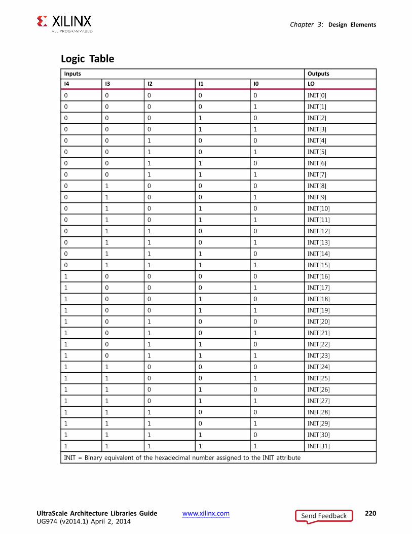
Chapter 3: Design Elements
Logic TableInputs OutputsI4 I3 I2 I1 I0 LO
0 0 0 0 0 INIT[0]
0 0 0 0 1 INIT[1]
0 0 0 1 0 INIT[2]
0 0 0 1 1 INIT[3]
0 0 1 0 0 INIT[4]
0 0 1 0 1 INIT[5]
0 0 1 1 0 INIT[6]
0 0 1 1 1 INIT[7]
0 1 0 0 0 INIT[8]
0 1 0 0 1 INIT[9]
0 1 0 1 0 INIT[10]
0 1 0 1 1 INIT[11]
0 1 1 0 0 INIT[12]
0 1 1 0 1 INIT[13]
0 1 1 1 0 INIT[14]
0 1 1 1 1 INIT[15]
1 0 0 0 0 INIT[16]
1 0 0 0 1 INIT[17]
1 0 0 1 0 INIT[18]
1 0 0 1 1 INIT[19]
1 0 1 0 0 INIT[20]
1 0 1 0 1 INIT[21]
1 0 1 1 0 INIT[22]
1 0 1 1 1 INIT[23]
1 1 0 0 0 INIT[24]
1 1 0 0 1 INIT[25]
1 1 0 1 0 INIT[26]
1 1 0 1 1 INIT[27]
1 1 1 0 0 INIT[28]
1 1 1 0 1 INIT[29]
1 1 1 1 0 INIT[30]
1 1 1 1 1 INIT[31]
INIT = Binary equivalent of the hexadecimal number assigned to the INIT attribute
UltraScale Architecture Libraries Guide www.xilinx.com 220UG974 (v2014.1) April 2, 2014
Send Feedback

Chapter 3: Design Elements
Port DescriptionPort Direction Width Function
I0 Input 1 LUT input
I1 Input 1 LUT input
I2 Input 1 LUT input
I3 Input 1 LUT input
I4 Input 1 LUT input
O Output 1 LUT output
Design Entry MethodInstantiation Yes
Inference Recommended
IP and IP Integrator Catalog No
Macro support No
Available AttributesAttribute Type Allowed Values Default Description
INIT HEX 32’h00000000 to32’hffffffff
32’h00000000 Specifies the logical expression of this element
VHDL Instantiation TemplateUnless they already exist, copy the following two statements and paste them before the entitydeclaration.Library UNISIM;use UNISIM.vcomponents.all;
-- LUT5: 5-Bit Look-Up Table-- UltraScale-- Xilinx HDL Libraries Guide, version 2014.1
LUT5_inst : LUT5generic map (
INIT => X"00000000" -- Logic function)port map (
O => O, -- 1-bit output: LUTI0 => I0, -- 1-bit input: LUTI1 => I1, -- 1-bit input: LUTI2 => I2, -- 1-bit input: LUTI3 => I3, -- 1-bit input: LUTI4 => I4 -- 1-bit input: LUT
);
-- End of LUT5_inst instantiation
UltraScale Architecture Libraries Guide www.xilinx.com 221UG974 (v2014.1) April 2, 2014
Send Feedback

Chapter 3: Design Elements
Verilog Instantiation Template
// LUT5: 5-Bit Look-Up Table// UltraScale// Xilinx HDL Libraries Guide, version 2014.1
LUT5 #(.INIT(32’h00000000) // Logic function
)LUT5_inst (
.O(O), // 1-bit output: LUT
.I0(I0), // 1-bit input: LUT
.I1(I1), // 1-bit input: LUT
.I2(I2), // 1-bit input: LUT
.I3(I3), // 1-bit input: LUT
.I4(I4) // 1-bit input: LUT);
// End of LUT5_inst instantiation
For More Information• See the 7 series FPGA User Documentation (User Guides and Data Sheets).
• See the UltraScale User Documentation.
UltraScale Architecture Libraries Guide www.xilinx.com 222UG974 (v2014.1) April 2, 2014
Send Feedback

Chapter 3: Design Elements
LUT6Primitive: 6-Bit Look-Up TablePRIMITIVE_GROUP: CLBPRIMITIVE_SUBGROUP: LUT
IntroductionThis design element is a 6-bit look-up table (LUT). This element allows the creation of anylogical function with six inputs.The INIT parameter for the LUT primitive is what gives the LUT its logical value. By default,this value is zero, thus driving the output to a zero regardless of the input values (acting as aground). However, in most cases a new INIT value must be determined in order to specify thelogic function for the LUT primitive. There are at least two methods by which the LUT value canbe determined:The Logic Table Method: A common method to determine the desired INIT value for a LUT isusing a logic table. To do so, simply create a binary logic table of all possible inputs, specify thedesired logic value of the output and then create the INIT string from those output values.The Equation Method: Another method to determine the LUT value is to define parameters orgenerics for each input to the LUT that correspond to their listed truth value and use thoseto build the logic equation you are after. This method is easier to understand once you havegrasped the concept and is more self-documenting than the above method. However, thismethod does require the code to first specify the appropriate parameters or generics.
Logic TableInputs OutputsI5 I4 I3 I2 I1 I0 O
0 0 0 0 0 0 INIT[0]
0 0 0 0 0 1 INIT[1]
0 0 0 0 1 0 INIT[2]
UltraScale Architecture Libraries Guide www.xilinx.com 223UG974 (v2014.1) April 2, 2014
Send Feedback

Chapter 3: Design Elements
Inputs OutputsI5 I4 I3 I2 I1 I0 O
0 0 0 0 1 1 INIT[3]
0 0 0 1 0 0 INIT[4]
0 0 0 1 0 1 INIT[5]
0 0 0 1 1 0 INIT[6]
0 0 0 1 1 1 INIT[7]
0 0 1 0 0 0 INIT[8]
0 0 1 0 0 1 INIT[9]
0 0 1 0 1 0 INIT[10]
0 0 1 0 1 1 INIT[11]
0 0 1 1 0 0 INIT[12]
0 0 1 1 0 1 INIT[13]
0 0 1 1 1 0 INIT[14]
0 0 1 1 1 1 INIT[15]
0 1 0 0 0 0 INIT[16]
0 1 0 0 0 1 INIT[17]
0 1 0 0 1 0 INIT[18]
0 1 0 0 1 1 INIT[19]
0 1 0 1 0 0 INIT[20]
0 1 0 1 0 1 INIT[21]
0 1 0 1 1 0 INIT[22]
0 1 0 1 1 1 INIT[23]
0 1 1 0 0 0 INIT[24]
0 1 1 0 0 1 INIT[25]
0 1 1 0 1 0 INIT[26]
0 1 1 0 1 1 INIT[27]
0 1 1 1 0 0 INIT[28]
0 1 1 1 0 1 INIT[29]
0 1 1 1 1 0 INIT[30]
0 1 1 1 1 1 INIT[31]
1 0 0 0 0 0 INIT[32]
1 0 0 0 0 1 INIT[33]
1 0 0 0 1 0 INIT[34]
1 0 0 0 1 1 INIT[35]
1 0 0 1 0 0 INIT[36]
1 0 0 1 0 1 INIT[37]
1 0 0 1 1 0 INIT[38]
UltraScale Architecture Libraries Guide www.xilinx.com 224UG974 (v2014.1) April 2, 2014
Send Feedback

Chapter 3: Design Elements
Inputs OutputsI5 I4 I3 I2 I1 I0 O
1 0 0 1 1 1 INIT[39]
1 0 1 0 0 0 INIT[40]
1 0 1 0 0 1 INIT[41]
1 0 1 0 1 0 INIT[42]
1 0 1 0 1 1 INIT[43]
1 0 1 1 0 0 INIT[44]
1 0 1 1 0 1 INIT[45]
1 0 1 1 1 0 INIT[46]
1 0 1 1 1 1 INIT[47]
1 1 0 0 0 0 INIT[48]
1 1 0 0 0 1 INIT[49]
1 1 0 0 1 0 INIT[50]
1 1 0 0 1 1 INIT[51]
1 1 0 1 0 0 INIT[52]
1 1 0 1 0 1 INIT[53]
1 1 0 1 1 0 INIT[54]
1 1 0 1 1 1 INIT[55]
1 1 1 0 0 0 INIT[56]
1 1 1 0 0 1 INIT[57]
1 1 1 0 1 0 INIT[58]
1 1 1 0 1 1 INIT[59]
1 1 1 1 0 0 INIT[60]
1 1 1 1 0 1 INIT[61]
1 1 1 1 1 0 INIT[62]
1 1 1 1 1 1 INIT[63]
INIT = Binary equivalent of the hexadecimal number assigned to the INIT attribute
Port DescriptionPort Direction Width Function
I0 Input 1 LUT input
I1 Input 1 LUT input
I2 Input 1 LUT input
I3 Input 1 LUT input
I4 Input 1 LUT input
I5 Input 1 LUT input
O Output 1 LUT output
UltraScale Architecture Libraries Guide www.xilinx.com 225UG974 (v2014.1) April 2, 2014
Send Feedback

Chapter 3: Design Elements
Design Entry MethodInstantiation Yes
Inference Recommended
IP and IP Integrator Catalog No
Macro support No
Available AttributesAttribute Type Allowed Values Default Description
INIT HEX 64’h000000000000 0000to 64’hffffffffffff ffff
64’h0000000000000000
Specifies the logical expression of thiselement
VHDL Instantiation TemplateUnless they already exist, copy the following two statements and paste them before the entitydeclaration.Library UNISIM;use UNISIM.vcomponents.all;
-- LUT6: 6-Bit Look-Up Table-- UltraScale-- Xilinx HDL Libraries Guide, version 2014.1
LUT6_inst : LUT6generic map (
INIT => X"0000000000000000" -- Logic function)port map (
O => O, -- 1-bit output: LUTI0 => I0, -- 1-bit input: LUTI1 => I1, -- 1-bit input: LUTI2 => I2, -- 1-bit input: LUTI3 => I3, -- 1-bit input: LUTI4 => I4, -- 1-bit input: LUTI5 => I5 -- 1-bit input: LUT
);
-- End of LUT6_inst instantiation
Verilog Instantiation Template// LUT6: 6-Bit Look-Up Table// UltraScale// Xilinx HDL Libraries Guide, version 2014.1
LUT6 #(.INIT(64’h0000000000000000) // Logic function
)LUT6_inst (
.O(O), // 1-bit output: LUT
.I0(I0), // 1-bit input: LUT
.I1(I1), // 1-bit input: LUT
.I2(I2), // 1-bit input: LUT
.I3(I3), // 1-bit input: LUT
.I4(I4), // 1-bit input: LUT
.I5(I5) // 1-bit input: LUT);
UltraScale Architecture Libraries Guide www.xilinx.com 226UG974 (v2014.1) April 2, 2014
Send Feedback

Chapter 3: Design Elements
// End of LUT6_inst instantiation
For More Information• See the 7 series FPGA User Documentation (User Guides and Data Sheets).
• See the UltraScale User Documentation.
UltraScale Architecture Libraries Guide www.xilinx.com 227UG974 (v2014.1) April 2, 2014
Send Feedback

Chapter 3: Design Elements
LUT6_2Primitive: Six-input, 2-output, Look-Up TablePRIMITIVE_GROUP: CLBPRIMITIVE_SUBGROUP: LUT
IntroductionThis design element is a 6-input, 2-output look-up table (LUT) that can either act as a dualasynchronous 32-bit ROM (with 5-bit addressing), implement any two 5-input logic functionswith shared inputs, or implement a 6-input logic function and a 5-input logic function withshared inputs and shared logic values. LUTs are the basic logic building blocks and are used toimplement most logic functions of the design. A LUT6_2 will be mapped to one of the eightlook-up tables in the CLB.
An INIT attribute consisting of a 64-bit hexadecimal value must be specified to indicate the LUTslogical function. The INIT value is calculated by assigning a 1 to corresponding INIT bit valuewhen the associated inputs are applied. For instance, a Verilog INIT value of 64’hfffffffffffffffe(X"FFFFFFFFFFFFFFFE" for VHDL) makes the O6 output 1 unless all zeros are on the inputs andthe O5 output a 1, or unless I[4:0] are all zeroes (a 5-input and 6-input OR gate). The lower half(bits 31:0) of the INIT values apply to the logic function of the O5 output.
The INIT parameter for the FPGA LUT primitive is what gives the LUT its logical value. Bydefault, this value is zero, thus driving the output to a zero regardless of the input values (actingas a ground). However, in most cases a new INIT value must be determined in order to specifythe logic function for the LUT primitive. There are at least two methods by which the LUT valuecan be determined:The Logic Table Method: A common method to determine the desired INIT value for a LUT isusing a logic table. To do so, simply create a binary logic table of all possible inputs, specify thedesired logic value of the output and then create the INIT string from those output values.The Equation Method: Another method to determine the LUT value is to define parametersfor each input to the LUT that correspond to their listed truth value and use those to build thelogic equation you are after. This method is easier to understand once you have grasped theconcept and is more self-documenting than the above method. However, this method doesrequire the code to first specify the appropriate parameters.
UltraScale Architecture Libraries Guide www.xilinx.com 228UG974 (v2014.1) April 2, 2014
Send Feedback

Chapter 3: Design Elements
Logic TableInputs OutputsI5 I4 I3 I2 I1 I0 O5 O6
0 0 0 0 0 0 INIT[0] INIT[0]
0 0 0 0 0 1 INIT[1] INIT[1]
0 0 0 0 1 0 INIT[2] INIT[2]
0 0 0 0 1 1 INIT[3] INIT[3]
0 0 0 1 0 0 INIT[4] INIT[4]
0 0 0 1 0 1 INIT[5] INIT[5]
0 0 0 1 1 0 INIT[6] INIT[6]
0 0 0 1 1 1 INIT[7] INIT[7]
0 0 1 0 0 0 INIT[8] INIT[8]
0 0 1 0 0 1 INIT[9] INIT[9]
0 0 1 0 1 0 INIT[10] INIT[10]
0 0 1 0 1 1 INIT[11] INIT[11]
0 0 1 1 0 0 INIT[12] INIT[12]
0 0 1 1 0 1 INIT[13] INIT[13]
0 0 1 1 1 0 INIT[14] INIT[14]
0 0 1 1 1 1 INIT[15] INIT[15]
0 1 0 0 0 0 INIT[16] INIT[16]
0 1 0 0 0 1 INIT[17] INIT[17]
0 1 0 0 1 0 INIT[18] INIT[18]
0 1 0 0 1 1 INIT[19] INIT[19]
0 1 0 1 0 0 INIT[20] INIT[20]
0 1 0 1 0 1 INIT[21] INIT[21]
0 1 0 1 1 0 INIT[22] INIT[22]
0 1 0 1 1 1 INIT[23] INIT[23]
0 1 1 0 0 0 INIT[24] INIT[24]
0 1 1 0 0 1 INIT[25] INIT[25]
0 1 1 0 1 0 INIT[26] INIT[26]
0 1 1 0 1 1 INIT[27] INIT[27]
0 1 1 1 0 0 INIT[28] INIT[28]
0 1 1 1 0 1 INIT[29] INIT[29]
0 1 1 1 1 0 INIT[30] INIT[30]
0 1 1 1 1 1 INIT[31] INIT[31]
1 0 0 0 0 0 INIT[0] INIT[32]
1 0 0 0 0 1 INIT[1] INIT[33]
1 0 0 0 1 0 INIT[2] INIT[34]
UltraScale Architecture Libraries Guide www.xilinx.com 229UG974 (v2014.1) April 2, 2014
Send Feedback

Chapter 3: Design Elements
Inputs OutputsI5 I4 I3 I2 I1 I0 O5 O6
1 0 0 0 1 1 INIT[3] INIT[35]
1 0 0 1 0 0 INIT[4] INIT[36]
1 0 0 1 0 1 INIT[5] INIT[37]
1 0 0 1 1 0 INIT[6] INIT[38]
1 0 0 1 1 1 INIT[7] INIT[39]
1 0 1 0 0 0 INIT[8] INIT[40]
1 0 1 0 0 1 INIT[9] INIT[41]
1 0 1 0 1 0 INIT[10] INIT[42]
1 0 1 0 1 1 INIT[11] INIT[43]
1 0 1 1 0 0 INIT[12] INIT[44]
1 0 1 1 0 1 INIT[13] INIT[45]
1 0 1 1 1 0 INIT[14] INIT[46]
1 0 1 1 1 1 INIT[15] INIT[47]
1 1 0 0 0 0 INIT[16] INIT[48]
1 1 0 0 0 1 INIT[17] INIT[49]
1 1 0 0 1 0 INIT[18] INIT[50]
1 1 0 0 1 1 INIT[19] INIT[51]
1 1 0 1 0 0 INIT[20] INIT[52]
1 1 0 1 0 1 INIT[21] INIT[53]
1 1 0 1 1 0 INIT[22] INIT[54]
1 1 0 1 1 1 INIT[23] INIT[55]
1 1 1 0 0 0 INIT[24] INIT[56]
1 1 1 0 0 1 INIT[25] INIT[57]
1 1 1 0 1 0 INIT[26] INIT[58]
1 1 1 0 1 1 INIT[27] INIT[59]
1 1 1 1 0 0 INIT[28] INIT[60]
1 1 1 1 0 1 INIT[29] INIT[61]
1 1 1 1 1 0 INIT[30] INIT[62]
1 1 1 1 1 1 INIT[31] INIT[63]
INIT = Binary equivalent of the hexadecimal number assigned to the INIT attribute
UltraScale Architecture Libraries Guide www.xilinx.com 230UG974 (v2014.1) April 2, 2014
Send Feedback

Chapter 3: Design Elements
Port DescriptionPort Direction Width Function
I0 Input 1 LUT input
I1 Input 1 LUT input
I2 Input 1 LUT input
I3 Input 1 LUT input
I4 Input 1 LUT input
I5 Input 1 LUT input
O5 Output 1 6/5–LUT output
O6 Output 1 5–LUT output
Design Entry MethodInstantiation Yes
Inference Recommended
IP and IP Integrator Catalog No
Macro support No
Available AttributesAttribute Type Allowed Values Default Description
INIT HEX Any 64–bit value All Zeros Specifies the LUT5/6 output function.
VHDL Instantiation TemplateUnless they already exist, copy the following two statements and paste them before the entitydeclaration.Library UNISIM;use UNISIM.vcomponents.all;
-- LUT6_2: 6-input 2 output Look-Up Table-- UltraScale-- Xilinx HDL Libraries Guide, version 2014.1
LUT6_2_inst : LUT6_2generic map (
INIT => X"0000000000000000") -- Specify LUT Contentsport map (
O6 => O6, -- 6/5-LUT output (1-bit)O5 => O5, -- 5-LUT output (1-bit)I0 => I0, -- LUT input (1-bit)I1 => I1, -- LUT input (1-bit)I2 => I2, -- LUT input (1-bit)I3 => I3, -- LUT input (1-bit)I4 => I4, -- LUT input (1-bit)I5 => I5 -- LUT input (1-bit)
);
-- End of LUT6_2_inst instantiation
UltraScale Architecture Libraries Guide www.xilinx.com 231UG974 (v2014.1) April 2, 2014
Send Feedback

Chapter 3: Design Elements
Verilog Instantiation Template
// LUT6_2: 6-input, 2 output Look-Up Table// UltraScale// Xilinx HDL Libraries Guide, version 2014.1
LUT6_2 #(.INIT(64’h0000000000000000) // Specify LUT Contents
) LUT6_2_inst (.O6(O6), // 1-bit LUT6 output.O5(O5), // 1-bit lower LUT5 output.I0(I0), // 1-bit LUT input.I1(I1), // 1-bit LUT input.I2(I2), // 1-bit LUT input.I3(I3), // 1-bit LUT input.I4(I4), // 1-bit LUT input.I5(I5) // 1-bit LUT input (fast MUX select only available to O6 output)
);
// End of LUT6_2_inst instantiation
For More Information• See the 7 series FPGA User Documentation (User Guides and Data Sheets).
• See the UltraScale User Documentation.
UltraScale Architecture Libraries Guide www.xilinx.com 232UG974 (v2014.1) April 2, 2014
Send Feedback

Chapter 3: Design Elements
MASTER_JTAGPrimitive: JTAG Port AccessPRIMITIVE_GROUP: CONFIGURATIONPRIMITIVE_SUBGROUP: MASTER_JTAG
IntroductionThis component can be used to override the external JTAG pins of the FPGA allowing fullaccess to the JTAG port from within the device.
Port DescriptionsPort Direction Width Function
TCK Input 1 JTAG TCK input pin
TDI Input 1 JTAG TDI input pin
TDO Output 1 JTAG TDO output pin
TMS Input 1 JTAG TMS input pin
Design Entry MethodInstantiation Recommended
Inference No
IP and IP Integrator Catalog No
Macro support No
VHDL Instantiation TemplateUnless they already exist, copy the following two statements and paste them before the entitydeclaration.Library UNISIM;use UNISIM.vcomponents.all;
-- MASTER_JTAG: JTAG Port Access-- UltraScale-- Xilinx HDL Libraries Guide, version 2014.1
MASTER_JTAG_inst : MASTER_JTAG
UltraScale Architecture Libraries Guide www.xilinx.com 233UG974 (v2014.1) April 2, 2014
Send Feedback

Chapter 3: Design Elements
port map (TDO => TDO, -- 1-bit output: JTAG TDO output pinTCK => TCK, -- 1-bit input: JTAG TCK input pinTDI => TDI, -- 1-bit input: JTAG TDI input pinTMS => TMS -- 1-bit input: JTAG TMS input pin
);
-- End of MASTER_JTAG_inst instantiation
Verilog Instantiation Template
// MASTER_JTAG: JTAG Port Access// UltraScale// Xilinx HDL Libraries Guide, version 2014.1
MASTER_JTAGMASTER_JTAG_inst (.TDO(TDO), // 1-bit output: JTAG TDO output pin.TCK(TCK), // 1-bit input: JTAG TCK input pin.TDI(TDI), // 1-bit input: JTAG TDI input pin.TMS(TMS) // 1-bit input: JTAG TMS input pin
);
// End of MASTER_JTAG_inst instantiation
For More Information• See the 7 series FPGA User Documentation (User Guides and Data Sheets).
• See the UltraScale User Documentation.
UltraScale Architecture Libraries Guide www.xilinx.com 234UG974 (v2014.1) April 2, 2014
Send Feedback

Chapter 3: Design Elements
MMCME3_ADVPrimitive: Advanced Mixed Mode Clock Manager (MMCM)PRIMITIVE_GROUP: CLOCKPRIMITIVE_SUBGROUP: PLL
IntroductionThe MMCME3 is a mixed signal block designed to support frequency synthesis, clock networkdeskew, and jitter reduction. The clock outputs can each have an individual divide, phaseshift and duty cycle based on the same VCO frequency. Additionally, the MMCME3 supportsdynamic phase shifting and fractional divides.
UltraScale Architecture Libraries Guide www.xilinx.com 235UG974 (v2014.1) April 2, 2014
Send Feedback

Chapter 3: Design Elements
Port DescriptionsPort Direction Width Function
CDDCDONE Output 1 Acknowledge signal that output clock dynmiac divide is done andthe output is valid.
CDDCREQ Input 1 Active high request signal for dynamically changing output clockdivide.
CLKFBIN Input 1 Feedback clock pin to the MMCM
CLKFBOUT Output 1 Dedicated MMCM Feedback clock output
CLKFBOUTB Output 1 Inverted CLKFBOUT
CLKFBSTOPPED Output 1 Status pin indicating that the feedback clock has stopped.
CLKINSEL Input 1 Signal controls the state of the input MUX, High = CLKIN1, Low= CLKIN2.
CLKINSTOPPED Output 1 Status pin indicating that the input clock has stopped.
CLKIN1 Input 1 Primary clock input.
CLKIN2 Input 1 Secondary clock input to dynamically switch the MMCM referenceclock.
CLKOUT0 Output 1 CLKOUT0 output
CLKOUT0B Output 1 User configurable clock outputs that can be divided versions of theVCO phase outputs (user controllable) from 1 (bypassed) to 128.The output clocks are phase aligned to each other (unless phaseshifted) and aligned to the input clock with a proper feedbackconfiguration. The CLKOUT#B outputs are 180 degrees out ofphase with the non-B outputs.
CLKOUT1 Output 1 CLKOUT1 output
CLKOUT1B Output 1 Inverted CLKOUT2 output
CLKOUT2 Output 1 User configurable clock outputs that can be divided versions of theVCO phase outputs (user controllable) from 1 (bypassed) to 128.The output clocks are phase aligned to each other (unless phaseshifted) and aligned to the input clock with a proper feedbackconfiguration. The CLKOUT#B outputs are 180 degrees out ofphase with the non-B outputs.
CLKOUT2B Output 1 Inverted CLKOUT2 output
CLKOUT3 Output 1 CLKOUT3 output
CLKOUT3B Output 1 Inverted CLKOUT3 output
CLKOUT4 Output 1 CLKOUT4 output
CLKOUT5 Output 1 CLKOUT5 output
CLKOUT6 Output 1 CLKOUT6 output
DADDR<6:0> Input 7 The dynamic reconfiguration address (DADDR) input bus providesa reconfiguration address for the dynamic reconfiguration. Whennot used, all bits must be assigned zeros.
DCLK Input 1 The DCLK signal is the reference clock for the dynamicreconfiguration port.
UltraScale Architecture Libraries Guide www.xilinx.com 236UG974 (v2014.1) April 2, 2014
Send Feedback

Chapter 3: Design Elements
Port Direction Width Function
DEN Input 1 The dynamic reconfiguration enable (DEN) provides the enablecontrol signal to access the dynamic reconfiguration feature. Whenthe dynamic reconfiguration feature is not used, DEN must be tiedLow.
DI<15:0> Input 16 The dynamic reconfiguration data input (DI) bus providesreconfiguration data. When not used, all bits must be set to zero.
DO<15:0> Output 16 The dynamic reconfiguration output bus provides MMCM dataoutput when using dynamic reconfiguration.
DRDY Output 1 The dynamic reconfiguration ready output (DRDY) providesthe response to the DEN signal for the MMCMs dynamicreconfiguration feature.
DWE Input 1 The dynamic reconfiguration write enable (DWE) input pin providesthe write enable control signal to write the DI data into the DADDRaddress. When not used, it must be tied Low.
LOCKED Output 1 An output from the MMCM that indicates when the MMCMhas achieved phase alignment within a predefined window andfrequency matching within a predefined PPM range. The MMCMautomatically locks after power on, no extra reset is required.LOCKED will be deasserted if the input clock stops or the phasealignment is violated (e.g., input clock phase shift). The MMCMautomatically reacquires lock after LOCKED is deasserted.
PSCLK Input 1 Phase shift clock.
PSDONE Output 1 Phase shift done.
PSEN Input 1 Phase shift enable
PSINCDEC Input 1 Phase shift increment/decrement control.
PWRDWN Input 1 Powers down MMCM components, thus reducing powerconsumption when derived clocks are not in use for sustainedperiods of time. Upon release of PWRDWN, the MMCM mustregain LOCK prior to use.
RST Input 1 Asynchronous reset signal. The MMCM will synchronously re-enableitself when this signal is released (i.e., MMCM re-enabled). A reset isrequired when the input clock conditions change (e.g., frequency).
Design Entry MethodInstantiation Yes
Inference No
IP and IP Integrator Catalog Recommended
Macro support No
UltraScale Architecture Libraries Guide www.xilinx.com 237UG974 (v2014.1) April 2, 2014
Send Feedback

Chapter 3: Design Elements
Available AttributesAttribute Type AllowedValues Default Description
BANDWIDTH STRING "OPTIMIZED","HIGH","LOW"
"OPTIMIZED" Specifies the MMCM programmingalgorithm affecting the jitter, phasemargin and other characteristics of theMMCM.
CLKFBOUT_MULT_F
3 significantdigit FLOAT
2.000 to64.000
5.000 Specifies the amount to multiplyall CLKOUT clock outputs if adifferent frequency is desired. Thisnumber, in combination with theassociated CLKOUT#_DIVIDE value andDIVCLK_DIVIDE value, will determine theoutput frequency.
CLKFBOUT _PHASE 3 significantdigit FLOAT
-360.000 to360.000
0.000 Specifies the phase offset in degreesof the clock feedback output. Shiftingthe feedback clock results in a negativephase shift of all output clocks to theMMCM.
CLKIN1 _PERIOD,CLKIN2 _PERIOD
FLOAT(nS) 0.000 to100.000
0.000 Specifies the input period in ns to theMMCM CLKIN inputs. Resolution is downto the ps. For example a value of 33.333would indicate a 30 MHz input clock.This information is mandatory and mustbe supplied. CLKIN1_PERIOD relates tothe input period on the CLKIN1 inputwhile CLKIN2_PERIOD relates to theinput clock period on the CLKIN2 input.
CLKOUT0_DIVIDE_F
3 significantdigit FLOAT
1.000 to128.000
1.000 Specifies the amount to fractional dividethe associated CLKOUT clock outputif a different frequency is desired.This number in combination with theCLKFBOUT_MULT_F and DIVCLK_DIVIDEvalues will determine the outputfrequency.
CLKOUT0_DUTY_CYCLE,CLKOUT1_DUTY_CYCLE,CLKOUT2_DUTY_CYCLE,CLKOUT3_DUTY_CYCLE,CLKOUT4_DUTY_CYCLE,CLKOUT5_DUTY_CYCLE,CLKOUT6_DUTY_CYCLE
3 significantdigit FLOAT
0.001 to 0.999 0.500 Specifies the Duty Cycle of the associatedCLKOUT clock output in percentage (i.e.,0.50 will generate a 50% duty cycle).
CLKOUT0 _PHASE 3 significantdigit FLOAT
-360.000 to360.000
0.000 Specifies the phase offset in degreesof the clock feedback output. Shiftingthe feedback clock results in a negativephase shift of all output clocks to theMMCM.
UltraScale Architecture Libraries Guide www.xilinx.com 238UG974 (v2014.1) April 2, 2014
Send Feedback

Chapter 3: Design Elements
Attribute Type AllowedValues Default Description
CLKOUT1 _DIVIDE,CLKOUT2 _DIVIDE,CLKOUT3 _DIVIDE,CLKOUT4 _DIVIDE,CLKOUT5 _DIVIDE,CLKOUT6 _DIVIDE
DECIMAL 1 to 128 1 Specifies the amount to divide theassociated CLKOUT clock output if adifferent frequency is desired. Thisnumber in combination with theCLKFBOUT_MULT_F and DIVCLK_DIVIDEvalues will determine the outputfrequency.
CLKOUT1 _PHASE 3 significantdigit FLOAT
-360.000 to360.000
0.000 Specifies the phase offset in degreesof the clock feedback output. Shiftingthe feedback clock results in a negativephase shift of all output clocks to theMMCM.
CLKOUT2 _PHASE 3 significantdigit FLOAT
-360.000 to360.000
0.000 Specifies the phase offset in degreesof the clock feedback output. Shiftingthe feedback clock results in a negativephase shift of all output clocks to theMMCM.
CLKOUT3 _PHASE 3 significantdigit FLOAT
-360.000 to360.000
0.000 Specifies the phase offset in degreesof the clock feedback output. Shiftingthe feedback clock results in a negativephase shift of all output clocks to theMMCM.
CLKOUT4_CASCADE
STRING "FALSE","TRUE"
"FALSE" Specifies the phase offset in degreesof the clock feedback output. Shiftingthe feedback clock results in a negativephase shift of all output clocks to theMMCM.
CLKOUT4 _PHASE 3 significantdigit FLOAT
-360.000 to360.000
0.000 Specifies the phase offset in degreesof the clock feedback output. Shiftingthe feedback clock results in a negativephase shift of all output clocks to theMMCM.
CLKOUT5 _PHASE 3 significantdigit FLOAT
-360.000 to360.000
0.000 Specifies the phase offset in degreesof the clock feedback output. Shiftingthe feedback clock results in a negativephase shift of all output clocks to theMMCM.
CLKOUT6 _PHASE 3 significantdigit FLOAT
-360.000 to360.000
0.000 Specifies the phase offset in degreesof the clock feedback output. Shiftingthe feedback clock results in a negativephase shift of all output clocks to theMMCM.
UltraScale Architecture Libraries Guide www.xilinx.com 239UG974 (v2014.1) April 2, 2014
Send Feedback

Chapter 3: Design Elements
Attribute Type AllowedValues Default Description
COMPENSATION STRING "AUTO","BUF_IN","EXTERNAL","INTERNAL","ZHOLD"
"AUTO" Clock input compensation. Should beset to ZHOLD. Defines how the MMCMfeedback is configured.
• "ZHOLD" - Indicates the MMCM isconfigured to provide a negativehold time at the I/O registers.
• "INTERNAL" - Indicates the MMCM isusing its own internal feedback pathso no delay is being compensated.
• "EXTERNAL" - Indicates a networkexternal to the FPGA is beingcompensated.
• "BUF_IN" - Indicates that theconfiguration does not match withthe other compensation modes andno delay will be compensated. Thisis the case if a clock input is drivenby a BUFG for instance.
DIVCLK _DIVIDE DECIMAL 1 to 106 1 Specifies the division ratio for all outputclocks with respect to the input clock.Effectively divides the CLKIN going intothe PFD.
IS_CLKFBIN_INVERTED
BINARY 1’b0 to 1’b1 1’b0 Indicates whether the optional inversionis used or not on the CLKFBIN pin of thiscomponent
IS_CLKINSEL_INVERTED
BINARY 1’b0 to 1’b1 1’b0 Indicates whether the optional inversionis used or not on the CLKINSEL pin ofthis component
IS_CLKIN1_INVERTED
BINARY 1’b0 to 1’b1 1’b0 Indicates whether the optional inversionis used or not on the CLKIN1 pin of thiscomponent
IS_CLKIN2_INVERTED
BINARY 1’b0 to 1’b1 1’b0 Indicates whether the optional inversionis used or not on the CLKIN2 pin of thiscomponent
IS_PSEN _INVERTED BINARY 1’b0 to 1’b1 1’b0 Indicates whether the optional inversionis used or not on the PSEN pin of thiscomponent
IS_PSINCDEC_INVERTED
BINARY 1’b0 to 1’b1 1’b0 Indicates whether the optional inversionis used or not on the PSINCDEC pin ofthis component
IS_PWRDWN_INVERTED
BINARY 1’b0 to 1’b1 1’b0 Indicates whether the optional inversionis used or not on the PWRDWN pin ofthis component
IS_RST _INVERTED BINARY 1’b0 to 1’b1 1’b0 Indicates whether the optional inversionis used or not on the RST pin of thiscomponent
UltraScale Architecture Libraries Guide www.xilinx.com 240UG974 (v2014.1) April 2, 2014
Send Feedback

Chapter 3: Design Elements
Attribute Type AllowedValues Default Description
REF_JITTER1,REF_JITTER2
3 significantdigit FLOAT
0.000 to 0.999 0.010 Allows specification of the expectedjitter on the CLKIN inputs in order tobetter optimize MMCM performance.A bandwidth setting of OPTIMIZED willattempt to choose the best parameter forinput clocking when unknown. If known,then the value provided should bespecified in terms of the UI percentage(the maximum peak to peak value) ofthe expected jitter on the input clock.REF_JITTER1 relates to the input jitter onCLKIN1 while REF_JITTER2 relates to theinput jitter on CLKIN2.
SS_EN STRING "FALSE","TRUE"
"FALSE" Enables the spread spectrum featurefor the MMCM. Used in conjunctionwith SS_MODE and SS_MOD_PERIODattributes.
SS_MOD_PERIOD DECIMAL(nS) 4000 to 40000 10000 Specifies the spread spectrummodulation period (ns).
SS_MODE STRING "CENTER_HIGH","CENTER_LOW","DOWN_HIGH","DOWN_LOW"
"CENTER_HIGH"Controls the spread spectrum frequencydeviation and the spread type.
STARTUP_WAIT STRING "FALSE","TRUE"
"FALSE" Delays configuration DONE signal fromasserting until MMCM is locked.
CLKFBOUT_USE_FINE_PS,CLKOUT0_USE_FINE_PS,CLKOUT1_USE_FINE_PS,CLKOUT2_USE_FINE_PS,CLKOUT3_USE_FINE_PS,CLKOUT4_USE_FINE_PS,CLKOUT5_USE_FINE_PS,CLKOUT6_USE_FINE_PS
STRING "FALSE","TRUE"
"FALSE" Counter variable fine phase shift enable.
VHDL Instantiation TemplateUnless they already exist, copy the following two statements and paste them before the entitydeclaration.Library UNISIM;use UNISIM.vcomponents.all;
-- MMCME3_ADV:Advanced Mixed Mode Clock Manager (MMCM)-- UltraScale-- Xilinx HDL Libraries Guide, version 2014.1
MMCME3_ADV_inst : MMCME3_ADV
UltraScale Architecture Libraries Guide www.xilinx.com 241UG974 (v2014.1) April 2, 2014
Send Feedback

Chapter 3: Design Elements
generic map (BANDWIDTH=> "OPTIMIZED", -- Jitter programming (OPTIMIZED, HIGH, LOW)CLKFBOUT_MULT_F=> 5.0, -- Multiply value for all CLKOUT(2.000-64.000).CLKFBOUT_PHASE=> 0.0, -- Phase offset in degrees of CLKFB (-360.000-360.000).-- CLKIN_PERIOD: Input clock period in ns units, ps resolution (i.e. 33.333 is 30 MHz).CLKIN1_PERIOD => 0.0,CLKIN2_PERIOD => 0.0,CLKOUT0_DIVIDE_F => 1.0, -- Divide amount for CLKOUT0 (1.000-128.000).-- CLKOUT0_DUTY_CYCLE- CLKOUT6_DUTY_CYCLE:Duty cycle for CLKOUToutputs (0.001-0.999).CLKOUT0_DUTY_CYCLE=> 0.5,CLKOUT1_DUTY_CYCLE=> 0.5,CLKOUT2_DUTY_CYCLE=> 0.5,CLKOUT3_DUTY_CYCLE=> 0.5,CLKOUT4_DUTY_CYCLE=> 0.5,CLKOUT5_DUTY_CYCLE=> 0.5,CLKOUT6_DUTY_CYCLE=> 0.5,-- CLKOUT0_PHASE- CLKOUT6_PHASE:Phase offset for CLKOUToutputs (-360.000-360.000).CLKOUT0_PHASE=> 0.0,CLKOUT1_PHASE=> 0.0,CLKOUT2_PHASE=> 0.0,CLKOUT3_PHASE=> 0.0,CLKOUT4_CASCADE=> "FALSE",CLKOUT4_PHASE=> 0.0,CLKOUT5_PHASE=> 0.0,CLKOUT6_PHASE=> 0.0,-- CLKOUT1_DIVIDE - CLKOUT6_DIVIDE: Divide amount for CLKOUT(1-128)CLKOUT1_DIVIDE => 1,CLKOUT2_DIVIDE => 1,CLKOUT3_DIVIDE => 1,CLKOUT4_DIVIDE => 1,CLKOUT5_DIVIDE => 1,CLKOUT6_DIVIDE => 1,COMPENSATION=> "AUTO", -- AUTO, BUF_IN, EXTERNAL, INTERNAL, ZHOLDDIVCLK_DIVIDE => 1, -- Master division value (1-106)-- Programmable Inversion Attributes: Specifies built-in programmable inversion on specific pinsIS_CLKFBIN_INVERTED => ’0’, -- Optional inversion for CLKFBINIS_CLKIN1_INVERTED => ’0’, -- Optional inversion for CLKIN1IS_CLKIN2_INVERTED => ’0’, -- Optional inversion for CLKIN2IS_CLKINSEL_INVERTED => ’0’, -- Optional inversion for CLKINSELIS_PSEN_INVERTED => ’0’, -- Optional inversion for PSENIS_PSINCDEC_INVERTED => ’0’, -- Optional inversion for PSINCDECIS_PWRDWN_INVERTED=> ’0’, -- Optional inversion for PWRDWNIS_RST_INVERTED => ’0’, -- Optional inversion for RST-- REF_JITTER: Reference input jitter in UI (0.000-0.999).REF_JITTER1 => 0.0,REF_JITTER2 => 0.0,STARTUP_WAIT=> "FALSE", -- Delays DONEuntil MMCMis locked (FALSE, TRUE)-- Spread Spectrum: Spread Spectrum AttributesSS_EN => "FALSE", -- Enables spread spectrum (FALSE, TRUE)SS_MODE=> "CENTER_HIGH", -- CENTER_HIGH, CENTER_LOW,DOWN_HIGH,DOWN_LOWSS_MOD_PERIOD=> 10000, -- Spread spectrum modulation period (ns) (4000-40000)-- USE_FINE_PS: Fine phase shift enable (TRUE/FALSE)CLKFBOUT_USE_FINE_PS=> "FALSE",CLKOUT0_USE_FINE_PS=> "FALSE",CLKOUT1_USE_FINE_PS=> "FALSE",CLKOUT2_USE_FINE_PS=> "FALSE",CLKOUT3_USE_FINE_PS=> "FALSE",CLKOUT4_USE_FINE_PS=> "FALSE",CLKOUT5_USE_FINE_PS=> "FALSE",CLKOUT6_USE_FINE_PS=> "FALSE"
)port map (
-- Clock Outputs: 1-bit (each) output: User configurable clock outputsCLKOUT0 => CLKOUT0, -- 1-bit output: CLKOUT0CLKOUT0B=> CLKOUT0B, -- 1-bit output: Inverted CLKOUT0CLKOUT1 => CLKOUT1, -- 1-bit output: Primary clockCLKOUT1B=> CLKOUT1B, -- 1-bit output: Inverted CLKOUT1CLKOUT2 => CLKOUT2, -- 1-bit output: CLKOUT2CLKOUT2B=> CLKOUT2B, -- 1-bit output: Inverted CLKOUT2CLKOUT3 => CLKOUT3, -- 1-bit output: CLKOUT3CLKOUT3B=> CLKOUT3B, -- 1-bit output: Inverted CLKOUT3CLKOUT4 => CLKOUT4, -- 1-bit output: CLKOUT4
UltraScale Architecture Libraries Guide www.xilinx.com 242UG974 (v2014.1) April 2, 2014
Send Feedback

Chapter 3: Design Elements
CLKOUT5 => CLKOUT5, -- 1-bit output: CLKOUT5CLKOUT6 => CLKOUT6, -- 1-bit output: CLKOUT6-- DRP Ports: 16-bit (each) output: Dynamic reconfiguration portsDO => DO, -- 16-bit output: DRP dataDRDY=> DRDY, -- 1-bit output: DRP ready-- Dynamic Phase Shift Ports: 1-bit (each) output: Ports used for dynamic phase shifting of the outputsPSDONE=> PSDONE, -- 1-bit output: Phase shift done-- Feedback: 1-bit (each) output: Clock feedback portsCLKFBOUT=> CLKFBOUT, -- 1-bit output: Feedback clockCLKFBOUTB=> CLKFBOUTB, -- 1-bit output: Inverted CLKFBOUT-- Status Ports: 1-bit (each) output: MMCMstatus portsCDDCDONE=> CDDCDONE, -- 1-bit output: Clock dynamic divide doneCLKFBSTOPPED=> CLKFBSTOPPED,-- 1-bit output: Feedback clock stoppedCLKINSTOPPED=> CLKINSTOPPED, -- 1-bit output: Input clock stoppedLOCKED=> LOCKED, -- 1-bit output: LOCKCDDCREQ=> CDDCREQ, -- 1-bit input: Request to dymanic divide clock-- Clock Inputs: 1-bit (each) input: Clock inputsCLKIN1 => CLKIN1, -- 1-bit input: Primary clockCLKIN2 => CLKIN2, -- 1-bit input: Secondary clock-- Control Ports: 1-bit (each) input: MMCMcontrol portsCLKINSEL => CLKINSEL, -- 1-bit input: Clock select, High=CLKIN1 Low=CLKIN2PWRDWN=> PWRDWN, -- 1-bit input: Power-downRST => RST, -- 1-bit input: Reset-- DRP Ports: 7-bit (each) input: Dynamic reconfiguration portsDADDR=> DADDR, -- 7-bit input: DRP addressDCLK => DCLK, -- 1-bit input: DRP clockDEN => DEN, -- 1-bit input: DRP enableDI => DI, -- 16-bit input: DRP dataDWE=> DWE, -- 1-bit input: DRP write enable-- Dynamic Phase Shift Ports: 1-bit (each) input: Ports used for dynamic phase shifting of the outputsPSCLK => PSCLK, -- 1-bit input: Phase shift clockPSEN => PSEN, -- 1-bit input: Phase shift enablePSINCDEC => PSINCDEC, -- 1-bit input: Phase shift increment/decrement-- Feedback: 1-bit (each) input: Clock feedback portsCLKFBIN => CLKFBIN -- 1-bit input: Feedback clock
);
-- End of MMCME3_ADV_inst instantiation
Verilog Instantiation Template
// MMCME3_ADV:Advanced Mixed Mode Clock Manager (MMCM)// UltraScale// Xilinx HDL Libraries Guide, version 2014.1
MMCME3_ADV#(.BANDWIDTH("OPTIMIZED"), // Jitter programming (OPTIMIZED, HIGH, LOW).CLKFBOUT_MULT_F(5.0), // Multiply value for all CLKOUT(2.000-64.000)..CLKFBOUT_PHASE(0.0), // Phase offset in degrees of CLKFB (-360.000-360.000).// CLKIN_PERIOD: Input clock period in ns units, ps resolution (i.e. 33.333 is 30 MHz)..CLKIN1_PERIOD(0.0),.CLKIN2_PERIOD(0.0),.CLKOUT0_DIVIDE_F(1.0), // Divide amount for CLKOUT0 (1.000-128.000).// CLKOUT0_DUTY_CYCLE- CLKOUT6_DUTY_CYCLE:Duty cycle for CLKOUToutputs (0.001-0.999)..CLKOUT0_DUTY_CYCLE(0.5),.CLKOUT1_DUTY_CYCLE(0.5),.CLKOUT2_DUTY_CYCLE(0.5),.CLKOUT3_DUTY_CYCLE(0.5),.CLKOUT4_DUTY_CYCLE(0.5),.CLKOUT5_DUTY_CYCLE(0.5),.CLKOUT6_DUTY_CYCLE(0.5),// CLKOUT0_PHASE- CLKOUT6_PHASE:Phase offset for CLKOUToutputs (-360.000-360.000)..CLKOUT0_PHASE(0.0),.CLKOUT1_PHASE(0.0),.CLKOUT2_PHASE(0.0),.CLKOUT3_PHASE(0.0),.CLKOUT4_CASCADE("FALSE"),.CLKOUT4_PHASE(0.0),.CLKOUT5_PHASE(0.0),.CLKOUT6_PHASE(0.0),
UltraScale Architecture Libraries Guide www.xilinx.com 243UG974 (v2014.1) April 2, 2014
Send Feedback
Chapter 3: Design Elements
// CLKOUT1_DIVIDE - CLKOUT6_DIVIDE: Divide amount for CLKOUT(1-128).CLKOUT1_DIVIDE(1),.CLKOUT2_DIVIDE(1),.CLKOUT3_DIVIDE(1),.CLKOUT4_DIVIDE(1),.CLKOUT5_DIVIDE(1),.CLKOUT6_DIVIDE(1),.COMPENSATION("AUTO"), // AUTO, BUF_IN, EXTERNAL, INTERNAL, ZHOLD.DIVCLK_DIVIDE(1), // Master division value (1-106)// Programmable Inversion Attributes: Specifies built-in programmable inversion on specific pins.IS_CLKFBIN_INVERTED(1’b0), // Optional inversion for CLKFBIN.IS_CLKIN1_INVERTED(1’b0), // Optional inversion for CLKIN1.IS_CLKIN2_INVERTED(1’b0), // Optional inversion for CLKIN2.IS_CLKINSEL_INVERTED(1’b0), // Optional inversion for CLKINSEL.IS_PSEN_INVERTED(1’b0), // Optional inversion for PSEN.IS_PSINCDEC_INVERTED(1’b0), // Optional inversion for PSINCDEC.IS_PWRDWN_INVERTED(1’b0), // Optional inversion for PWRDWN.IS_RST_INVERTED(1’b0), // Optional inversion for RST// REF_JITTER: Reference input jitter in UI (0.000-0.999)..REF_JITTER1(0.0),.REF_JITTER2(0.0),.STARTUP_WAIT("FALSE"), // Delays DONEuntil MMCMis locked (FALSE, TRUE)// Spread Spectrum: Spread Spectrum Attributes.SS_EN("FALSE"), // Enables spread spectrum (FALSE, TRUE).SS_MODE("CENTER_HIGH"), // CENTER_HIGH, CENTER_LOW,DOWN_HIGH,DOWN_LOW.SS_MOD_PERIOD(10000), // Spread spectrum modulation period (ns) (4000-40000)// USE_FINE_PS: Fine phase shift enable (TRUE/FALSE).CLKFBOUT_USE_FINE_PS("FALSE"),.CLKOUT0_USE_FINE_PS("FALSE"),.CLKOUT1_USE_FINE_PS("FALSE"),.CLKOUT2_USE_FINE_PS("FALSE"),.CLKOUT3_USE_FINE_PS("FALSE"),.CLKOUT4_USE_FINE_PS("FALSE"),.CLKOUT5_USE_FINE_PS("FALSE"),.CLKOUT6_USE_FINE_PS("FALSE")
)MMCME3_ADV_inst (
// Clock Outputs: 1-bit (each) output: User configurable clock outputs.CLKOUT0(CLKOUT0), // 1-bit output: CLKOUT0.CLKOUT0B(CLKOUT0B), // 1-bit output: Inverted CLKOUT0.CLKOUT1(CLKOUT1), // 1-bit output: Primary clock.CLKOUT1B(CLKOUT1B), // 1-bit output: Inverted CLKOUT1.CLKOUT2(CLKOUT2), // 1-bit output: CLKOUT2.CLKOUT2B(CLKOUT2B), // 1-bit output: Inverted CLKOUT2.CLKOUT3(CLKOUT3), // 1-bit output: CLKOUT3.CLKOUT3B(CLKOUT3B), // 1-bit output: Inverted CLKOUT3.CLKOUT4(CLKOUT4), // 1-bit output: CLKOUT4.CLKOUT5(CLKOUT5), // 1-bit output: CLKOUT5.CLKOUT6(CLKOUT6), // 1-bit output: CLKOUT6// DRP Ports: 16-bit (each) output: Dynamic reconfiguration ports.DO(DO), // 16-bit output: DRP data.DRDY(DRDY), // 1-bit output: DRP ready// Dynamic Phase Shift Ports: 1-bit (each) output: Ports used for dynamic phase shifting of the outputs.PSDONE(PSDONE), // 1-bit output: Phase shift done// Feedback: 1-bit (each) output: Clock feedback ports.CLKFBOUT(CLKFBOUT), // 1-bit output: Feedback clock.CLKFBOUTB(CLKFBOUTB), // 1-bit output: Inverted CLKFBOUT// Status Ports: 1-bit (each) output: MMCMstatus ports.CDDCDONE(CDDCDONE), // 1-bit output: Clock dynamic divide done.CLKFBSTOPPED(CLKFBSTOPPED), // 1-bit output: Feedback clock stopped.CLKINSTOPPED(CLKINSTOPPED), // 1-bit output: Input clock stopped.LOCKED(LOCKED), // 1-bit output: LOCK.CDDCREQ(CDDCREQ), // 1-bit input: Request to dymanic divide clock// Clock Inputs: 1-bit (each) input: Clock inputs.CLKIN1(CLKIN1), // 1-bit input: Primary clock.CLKIN2(CLKIN2), // 1-bit input: Secondary clock// Control Ports: 1-bit (each) input: MMCMcontrol ports.CLKINSEL(CLKINSEL), // 1-bit input: Clock select, High=CLKIN1 Low=CLKIN2.PWRDWN(PWRDWN), // 1-bit input: Power-down.RST(RST), // 1-bit input: Reset// DRP Ports: 7-bit (each) input: Dynamic reconfiguration ports.DADDR(DADDR), // 7-bit input: DRP address
UltraScale Architecture Libraries Guide www.xilinx.com 244UG974 (v2014.1) April 2, 2014
Send Feedback

Chapter 3: Design Elements
.DCLK(DCLK), // 1-bit input: DRP clock
.DEN(DEN), // 1-bit input: DRP enable
.DI(DI), // 16-bit input: DRP data
.DWE(DWE), // 1-bit input: DRP write enable// Dynamic Phase Shift Ports: 1-bit (each) input: Ports used for dynamic phase shifting of the outputs.PSCLK(PSCLK), // 1-bit input: Phase shift clock.PSEN(PSEN), // 1-bit input: Phase shift enable.PSINCDEC(PSINCDEC), // 1-bit input: Phase shift increment/decrement// Feedback: 1-bit (each) input: Clock feedback ports.CLKFBIN(CLKFBIN) // 1-bit input: Feedback clock
);
// End of MMCME3_ADV_inst instantiation
For More Information• See the 7 series FPGA User Documentation (User Guides and Data Sheets).
• See the UltraScale User Documentation.
UltraScale Architecture Libraries Guide www.xilinx.com 245UG974 (v2014.1) April 2, 2014
Send Feedback

Chapter 3: Design Elements
MMCME3_BASEPrimitive: Base Mixed Mode Clock Manager (MMCM)
PRIMITIVE_GROUP: CLOCKPRIMITIVE_SUBGROUP: PLL
IntroductionThe MMCME3 is a mixed signal block designed to support frequency synthesis, clock networkdeskew, phase adjustment and jitter reduction. The MMCME3_BASE supports a subset of themore common features and thus is easier to instantiate and use compared to the full featuresMMCME3_ADV.
Port DescriptionsPort Direction Width Function
CLKFBIN Input 1 Feedback clock pin to the MMCM
CLKFBOUT Output 1 Dedicated MMCM Feedback clock output
CLKFBOUTB Output 1 Inverted CLKFBOUT output
CLKIN1 Input 1 General clock input.
UltraScale Architecture Libraries Guide www.xilinx.com 246UG974 (v2014.1) April 2, 2014
Send Feedback

Chapter 3: Design Elements
Port Direction Width Function
CLKOUT0 Output 1 CLKOUT0 output
CLKOUT0B Output 1 Inverted CLKOUT0 output
CLKOUT1 Output 1 CLKOUT1 output
CLKOUT1B Output 1 Inverted CLKOUT1 output
CLKOUT2 Output 1 CLKOUT2 output
CLKOUT2B Output 1 Inverted CLKOUT2 output
CLKOUT3 Output 1 CLKOUT3 output
CLKOUT3B Output 1 Inverted CLKOUT3 output
CLKOUT4 Output 1 CLKOUT4 output
CLKOUT5 Output 1 CLKOUT5 output
CLKOUT6 Output 1 CLKOUT6 output
LOCKED Output 1 An output from the MMCM that indicates when theMMCM has achieved phase alignment within a predefinedwindow and frequency matching within a predefined PPMrange. The MMCM automatically locks after power on,no extra reset is required. LOCKED will be deasserted ifthe input clock stops or the phase alignment is violated(e.g., input clock phase shift). The MMCM automaticallyreacquires lock after LOCKED is deasserted.
PWRDWN Input 1 Powers down instantiated but unused MMCMs.
RST Input 1 Asynchronous reset signal. The MMCM will synchronouslyre-enable itself when this signal is released (i.e., MMCMre-enabled). A reset is required when the input clockconditions change (e.g., frequency).
Design Entry MethodInstantiation Yes
Inference No
IP and IP Integrator Catalog Recommended
Macro support No
Available AttributesAttribute Type Allowed Values Default Description
BANDWIDTH STRING "OPTIMIZED","HIGH", "LOW"
"OPTIMIZED" Specifies the MMCM programmingalgorithm affecting the jitter, phasemargin and other characteristics of theMMCM.
UltraScale Architecture Libraries Guide www.xilinx.com 247UG974 (v2014.1) April 2, 2014
Send Feedback

Chapter 3: Design Elements
Attribute Type Allowed Values Default Description
CLKFBOUT _MULT_F 3significantdigitFLOAT
2.000 to 64.000 5.000 Specifies the amount to multiplyall CLKOUT clock outputs if adifferent frequency is desired. Thisnumber, in combination with theassociated CLKOUT#_DIVIDE value andDIVCLK_DIVIDE value, will determinethe output frequency.
CLKFBOUT _PHASE 3significantdigitFLOAT
-360.000 to360.000
0.000 Specifies the phase offset in degreesof the clock feedback output. Shiftingthe feedback clock results in a negativephase shift of all output clocks to theMMCM.
CLKIN1 _PERIOD FLOAT(nS) 0.000 to100.000
0.000 Specifies the input period in ns to theMMCM CLKIN1 input. Resolution isdown to the ps (3 decimal places).For example, a value of 33.333 wouldindicate a 30 MHz input clock. Thisinformation is mandatory and must besupplied.
CLKOUT0 _DIVIDE_F 3significantdigitFLOAT
1.000 to128.000
1.000 Specifies the amount to dividethe associated CLKOUT clockoutput if a different frequency isdesired. This number in combinationwith the CLKFBOUT_MULT_F andDIVCLK_DIVIDE values will determinethe output frequency.
CLKOUT1 _DIVIDE,CLKOUT2 _DIVIDE,CLKOUT3 _DIVIDE,CLKOUT4 _DIVIDE,CLKOUT5 _DIVIDE,CLKOUT6 _DIVIDE
DECIMAL 1 to 128 1 Specifies the amount to dividethe associated CLKOUT clockoutput if a different frequency isdesired. This number in combinationwith the CLKFBOUT_MULT_F andDIVCLK_DIVIDE values will determinethe output frequency.
CLKOUT0_DUTY_CYCLE,CLKOUT1_DUTY_CYCLE,CLKOUT2_DUTY_CYCLE,CLKOUT3_DUTY_CYCLE,CLKOUT4_DUTY_CYCLE,CLKOUT5_DUTY_CYCLE,CLKOUT6_DUTY_CYCLE
3significantdigitFLOAT
0.001 to 0.999 0.500 Specifies the Duty Cycle of theassociated CLKOUT clock output inpercentage (i.e., 0.50 will generate a50% duty cycle).
CLKOUT0 _PHASE,CLKOUT1 _PHASE,CLKOUT2 _PHASE,CLKOUT3 _PHASE,CLKOUT4 _PHASE,CLKOUT5 _PHASE,CLKOUT6 _PHASE
3significantdigitFLOAT
-360.000 to360.000
0.000 Specifies the phase offset in degreesof the clock feedback output. Shiftingthe feedback clock results in a negativephase shift of all output clocks to theMMCM.
UltraScale Architecture Libraries Guide www.xilinx.com 248UG974 (v2014.1) April 2, 2014
Send Feedback

Chapter 3: Design Elements
Attribute Type Allowed Values Default Description
CLKOUT4 _CASCADE STRING "FALSE","TRUE"
"FALSE" Cascades the output divider (counter)CLKOUT6 into the input of theCLKOUT4 divider for an output clockdivider that is greater than 128.
DIVCLK _DIVIDE DECIMAL 1 to 106 1 Specifies the division ratio for alloutput clocks with respect to the inputclock. Effectively divides the CLKINgoing into the PFD.
IS_CLKFBIN_INVERTED
BINARY 1’b0 to 1’b1 1’b0 Indicates whether the optionalinversion is used or not on theCLKFBIN pin of this component.
IS_CLKIN1 _INVERTED BINARY 1’b0 to 1’b1 1’b0 Indicates whether the optionalinversion is used or not on the CLKIN1pin of this component.
IS_PWRDWN_INVERTED
BINARY 1’b0 to 1’b1 1’b0 Indicates whether the optionalinversion is used or not on thePWRDWN pin of this component.
IS_RST _INVERTED BINARY 1’b0 to 1’b1 1’b0 Indicates whether the optionalinversion is used or not on the RST pinof this component.
REF_JITTER1 3significantdigitFLOAT
0.000 to 0.999 0.010 Allows specification of the expectedjitter on CLKIN1 in order to betteroptimize MMCM performance. Abandwidth setting of OPTIMIZED willattempt to choose the best parameterfor input clocking when unknown.If known, then the value providedshould be specified in terms of theUI percentage (the maximum peak topeak value) of the expected jitter onthe input clock.
STARTUP_WAIT STRING "FALSE","TRUE"
"FALSE" Delays configuration DONE signal fromasserting until MMCM is locked.
VHDL Instantiation TemplateUnless they already exist, copy the following two statements and paste them before the entitydeclaration.Library UNISIM;use UNISIM.vcomponents.all;
-- MMCME3_BASE:Base Mixed Mode Clock Manager (MMCM)-- UltraScale-- Xilinx HDL Libraries Guide, version 2014.1
MMCME3_BASE_inst : MMCME3_BASEgeneric map (
BANDWIDTH=> "OPTIMIZED", -- Jitter programming (OPTIMIZED, HIGH, LOW)CLKFBOUT_MULT_F=> 5.0, -- Multiply value for all CLKOUT(2.000-64.000).CLKFBOUT_PHASE=> 0.0, -- Phase offset in degrees of CLKFB (-360.000-360.000).CLKIN1_PERIOD => 0.0, -- Input clock period in ns units, ps resolution (i.e. 33.333 is 30 MHz).-- CLKOUT0_DIVIDE - CLKOUT6_DIVIDE: Divide amount for each CLKOUT(1-128)CLKOUT1_DIVIDE => 1,CLKOUT2_DIVIDE => 1,
UltraScale Architecture Libraries Guide www.xilinx.com 249UG974 (v2014.1) April 2, 2014
Send Feedback

Chapter 3: Design Elements
CLKOUT3_DIVIDE => 1,CLKOUT4_DIVIDE => 1,CLKOUT5_DIVIDE => 1,CLKOUT6_DIVIDE => 1,CLKOUT0_DIVIDE_F => 1.0, -- Divide amount for CLKOUT0 (1.000-128.000).-- CLKOUT0_DUTY_CYCLE- CLKOUT6_DUTY_CYCLE:Duty cycle for each CLKOUT(0.001-0.999).CLKOUT0_DUTY_CYCLE=> 0.5,CLKOUT1_DUTY_CYCLE=> 0.5,CLKOUT2_DUTY_CYCLE=> 0.5,CLKOUT3_DUTY_CYCLE=> 0.5,CLKOUT4_DUTY_CYCLE=> 0.5,CLKOUT5_DUTY_CYCLE=> 0.5,CLKOUT6_DUTY_CYCLE=> 0.5,-- CLKOUT0_PHASE- CLKOUT6_PHASE:Phase offset for each CLKOUT(-360.000-360.000).CLKOUT0_PHASE=> 0.0,CLKOUT1_PHASE=> 0.0,CLKOUT2_PHASE=> 0.0,CLKOUT3_PHASE=> 0.0,CLKOUT4_PHASE=> 0.0,CLKOUT5_PHASE=> 0.0,CLKOUT6_PHASE=> 0.0,CLKOUT4_CASCADE=> "FALSE", -- Cascade CLKOUT4 counter with CLKOUT6 (FALSE, TRUE)DIVCLK_DIVIDE => 1, -- Master division value (1-106)-- Programmable Inversion Attributes: Specifies built-in programmable inversion on specific pinsIS_CLKFBIN_INVERTED => ’0’, -- Optional inversion for CLKFBINIS_CLKIN1_INVERTED => ’0’, -- Optional inversion for CLKIN1IS_PWRDWN_INVERTED=> ’0’, -- Optional inversion for PWRDWNIS_RST_INVERTED => ’0’, -- Optional inversion for RSTREF_JITTER1 => 0.0, -- Reference input jitter in UI (0.000-0.999).STARTUP_WAIT=> "FALSE" -- Delays DONEuntil MMCMis locked (FALSE, TRUE)
)port map (
-- Clock Outputs: 1-bit (each) output: User configurable clock outputsCLKOUT0 => CLKOUT0, -- 1-bit output: CLKOUT0CLKOUT0B=> CLKOUT0B, -- 1-bit output: Inverted CLKOUT0CLKOUT1 => CLKOUT1, -- 1-bit output: CLKOUT1CLKOUT1B=> CLKOUT1B, -- 1-bit output: Inverted CLKOUT1CLKOUT2 => CLKOUT2, -- 1-bit output: CLKOUT2CLKOUT2B=> CLKOUT2B, -- 1-bit output: Inverted CLKOUT2CLKOUT3 => CLKOUT3, -- 1-bit output: CLKOUT3CLKOUT3B=> CLKOUT3B, -- 1-bit output: Inverted CLKOUT3CLKOUT4 => CLKOUT4, -- 1-bit output: CLKOUT4CLKOUT5 => CLKOUT5, -- 1-bit output: CLKOUT5CLKOUT6 => CLKOUT6, -- 1-bit output: CLKOUT6-- Feedback: 1-bit (each) output: Clock feedback portsCLKFBOUT=> CLKFBOUT, -- 1-bit output: Feedback clockCLKFBOUTB=> CLKFBOUTB, -- 1-bit output: Inverted CLKFBOUT-- Status Ports: 1-bit (each) output: MMCMstatus portsLOCKED=> LOCKED, -- 1-bit output: LOCK-- Clock Inputs: 1-bit (each) input: Clock inputCLKIN1 => CLKIN1, -- 1-bit input: Clock-- Control Ports: 1-bit (each) input: MMCMcontrol portsPWRDWN=> PWRDWN, -- 1-bit input: Power-downRST => RST, -- 1-bit input: Reset-- Feedback: 1-bit (each) input: Clock feedback portsCLKFBIN => CLKFBIN -- 1-bit input: Feedback clock
);
-- End of MMCME3_BASE_inst instantiation
Verilog Instantiation Template
// MMCME3_BASE:Base Mixed Mode Clock Manager (MMCM)// UltraScale// Xilinx HDL Libraries Guide, version 2014.1
MMCME3_BASE#(.BANDWIDTH("OPTIMIZED"), // Jitter programming (OPTIMIZED, HIGH, LOW).CLKFBOUT_MULT_F(5.0), // Multiply value for all CLKOUT(2.000-64.000)..CLKFBOUT_PHASE(0.0), // Phase offset in degrees of CLKFB (-360.000-360.000).
UltraScale Architecture Libraries Guide www.xilinx.com 250UG974 (v2014.1) April 2, 2014
Send Feedback

Chapter 3: Design Elements
.CLKIN1_PERIOD(0.0), // Input clock period in ns units, ps resolution (i.e. 33.333 is 30 MHz).// CLKOUT0_DIVIDE - CLKOUT6_DIVIDE: Divide amount for each CLKOUT(1-128).CLKOUT1_DIVIDE(1),.CLKOUT2_DIVIDE(1),.CLKOUT3_DIVIDE(1),.CLKOUT4_DIVIDE(1),.CLKOUT5_DIVIDE(1),.CLKOUT6_DIVIDE(1),.CLKOUT0_DIVIDE_F(1.0), // Divide amount for CLKOUT0 (1.000-128.000).// CLKOUT0_DUTY_CYCLE- CLKOUT6_DUTY_CYCLE:Duty cycle for each CLKOUT(0.001-0.999)..CLKOUT0_DUTY_CYCLE(0.5),.CLKOUT1_DUTY_CYCLE(0.5),.CLKOUT2_DUTY_CYCLE(0.5),.CLKOUT3_DUTY_CYCLE(0.5),.CLKOUT4_DUTY_CYCLE(0.5),.CLKOUT5_DUTY_CYCLE(0.5),.CLKOUT6_DUTY_CYCLE(0.5),// CLKOUT0_PHASE- CLKOUT6_PHASE:Phase offset for each CLKOUT(-360.000-360.000)..CLKOUT0_PHASE(0.0),.CLKOUT1_PHASE(0.0),.CLKOUT2_PHASE(0.0),.CLKOUT3_PHASE(0.0),.CLKOUT4_PHASE(0.0),.CLKOUT5_PHASE(0.0),.CLKOUT6_PHASE(0.0),.CLKOUT4_CASCADE("FALSE"), // Cascade CLKOUT4 counter with CLKOUT6 (FALSE, TRUE).DIVCLK_DIVIDE(1), // Master division value (1-106)// Programmable Inversion Attributes: Specifies built-in programmable inversion on specific pins.IS_CLKFBIN_INVERTED(1’b0), // Optional inversion for CLKFBIN.IS_CLKIN1_INVERTED(1’b0), // Optional inversion for CLKIN1.IS_PWRDWN_INVERTED(1’b0), // Optional inversion for PWRDWN.IS_RST_INVERTED(1’b0), // Optional inversion for RST.REF_JITTER1(0.0), // Reference input jitter in UI (0.000-0.999)..STARTUP_WAIT("FALSE") // Delays DONEuntil MMCMis locked (FALSE, TRUE)
)MMCME3_BASE_inst (
// Clock Outputs: 1-bit (each) output: User configurable clock outputs.CLKOUT0(CLKOUT0), // 1-bit output: CLKOUT0.CLKOUT0B(CLKOUT0B), // 1-bit output: Inverted CLKOUT0.CLKOUT1(CLKOUT1), // 1-bit output: CLKOUT1.CLKOUT1B(CLKOUT1B), // 1-bit output: Inverted CLKOUT1.CLKOUT2(CLKOUT2), // 1-bit output: CLKOUT2.CLKOUT2B(CLKOUT2B), // 1-bit output: Inverted CLKOUT2.CLKOUT3(CLKOUT3), // 1-bit output: CLKOUT3.CLKOUT3B(CLKOUT3B), // 1-bit output: Inverted CLKOUT3.CLKOUT4(CLKOUT4), // 1-bit output: CLKOUT4.CLKOUT5(CLKOUT5), // 1-bit output: CLKOUT5.CLKOUT6(CLKOUT6), // 1-bit output: CLKOUT6// Feedback: 1-bit (each) output: Clock feedback ports.CLKFBOUT(CLKFBOUT), // 1-bit output: Feedback clock.CLKFBOUTB(CLKFBOUTB), // 1-bit output: Inverted CLKFBOUT// Status Ports: 1-bit (each) output: MMCMstatus ports.LOCKED(LOCKED), // 1-bit output: LOCK// Clock Inputs: 1-bit (each) input: Clock input.CLKIN1(CLKIN1), // 1-bit input: Clock// Control Ports: 1-bit (each) input: MMCMcontrol ports.PWRDWN(PWRDWN), // 1-bit input: Power-down.RST(RST), // 1-bit input: Reset// Feedback: 1-bit (each) input: Clock feedback ports.CLKFBIN(CLKFBIN) // 1-bit input: Feedback clock
);
// End of MMCME3_BASE_inst instantiation
For More Information• See the 7 series FPGA User Documentation (User Guides and Data Sheets).
• See the UltraScale User Documentation.
UltraScale Architecture Libraries Guide www.xilinx.com 251UG974 (v2014.1) April 2, 2014
Send Feedback
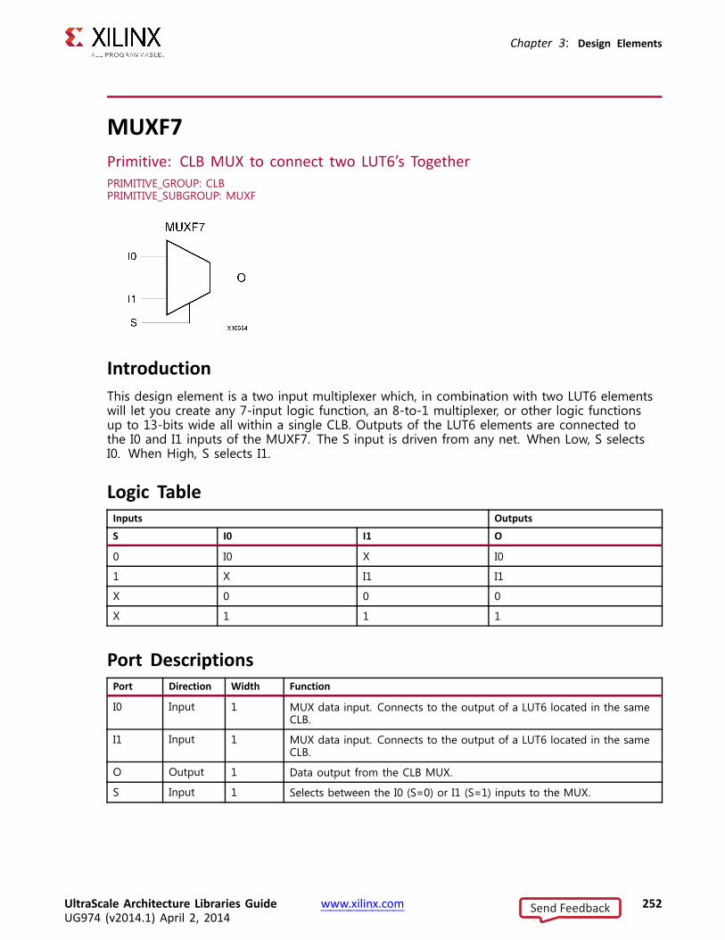
Chapter 3: Design Elements
MUXF7Primitive: CLB MUX to connect two LUT6’s TogetherPRIMITIVE_GROUP: CLBPRIMITIVE_SUBGROUP: MUXF
IntroductionThis design element is a two input multiplexer which, in combination with two LUT6 elementswill let you create any 7-input logic function, an 8-to-1 multiplexer, or other logic functionsup to 13-bits wide all within a single CLB. Outputs of the LUT6 elements are connected tothe I0 and I1 inputs of the MUXF7. The S input is driven from any net. When Low, S selectsI0. When High, S selects I1.
Logic TableInputs OutputsS I0 I1 O
0 I0 X I0
1 X I1 I1
X 0 0 0
X 1 1 1
Port DescriptionsPort Direction Width Function
I0 Input 1 MUX data input. Connects to the output of a LUT6 located in the sameCLB.
I1 Input 1 MUX data input. Connects to the output of a LUT6 located in the sameCLB.
O Output 1 Data output from the CLB MUX.
S Input 1 Selects between the I0 (S=0) or I1 (S=1) inputs to the MUX.
UltraScale Architecture Libraries Guide www.xilinx.com 252UG974 (v2014.1) April 2, 2014
Send Feedback

Chapter 3: Design Elements
Design Entry MethodInstantiation Yes
Inference Recommended
IP and IP Integrator Catalog No
Macro support No
VHDL Instantiation TemplateUnless they already exist, copy the following two statements and paste them before the entitydeclaration.Library UNISIM;use UNISIM.vcomponents.all;
-- MUXF7: CLB MUX to connect two LUT6’s Together-- UltraScale-- Xilinx HDL Libraries Guide, version 2014.1
MUXF7_inst : MUXF7port map (
O => O, -- 1-bit output: Output of MUXI0 => I0, -- 1-bit input: Connect to LUT6 outputI1 => I1, -- 1-bit input: Connect to LUT6 outputS => S -- 1-bit input: Input select to MUX
);
-- End of MUXF7_inst instantiation
Verilog Instantiation Template
// MUXF7: CLB MUX to connect two LUT6’s Together// UltraScale// Xilinx HDL Libraries Guide, version 2014.1
MUXF7MUXF7_inst (.O(O), // 1-bit output: Output of MUX.I0(I0), // 1-bit input: Connect to LUT6 output.I1(I1), // 1-bit input: Connect to LUT6 output.S(S) // 1-bit input: Input select to MUX
);
// End of MUXF7_inst instantiation
For More Information• See the 7 series FPGA User Documentation (User Guides and Data Sheets).
• See the UltraScale User Documentation.
UltraScale Architecture Libraries Guide www.xilinx.com 253UG974 (v2014.1) April 2, 2014
Send Feedback

Chapter 3: Design Elements
MUXF8Primitive: CLB MUX to connect two MUXF7’s TogetherPRIMITIVE_GROUP: CLBPRIMITIVE_SUBGROUP: MUXF
IntroductionThis design element is a two input multiplexer which, in combination with two MUXF7 and fourLUT6 elements will let you create any 8-input logic function, an 16-to-1 multiplexer, or otherlogic functions up to 27-bits wide all within a single CLB. Outputs of the MUXF7 elements areconnected to the I0 and I1 inputs of the MUXF8. The S input is driven from any net. WhenLow, S selects I0. When High, S selects I1.
Logic TableInputs OutputsS I0 I1 O
0 I0 X I0
1 X I1 I1
X 0 0 0
X 1 1 1
Port DescriptionsPort Direction Width Function
I0 Input 1 MUX data input. Connects to the output of a MUXF7 located in thesame CLB.
I1 Input 1 MUX data input. Connects to the output of a MUXF7 located in thesame CLB.
O Output 1 Data output from the CLB MUX.
S Input 1 Selects between the I0 (S=0) or I1 (S=1) inputs to the MUX.
UltraScale Architecture Libraries Guide www.xilinx.com 254UG974 (v2014.1) April 2, 2014
Send Feedback

Chapter 3: Design Elements
Design Entry MethodInstantiation Yes
Inference Recommended
IP and IP Integrator Catalog No
Macro support No
VHDL Instantiation TemplateUnless they already exist, copy the following two statements and paste them before the entitydeclaration.Library UNISIM;use UNISIM.vcomponents.all;
-- MUXF8: CLB MUX to connect two MUXF7’s Together-- UltraScale-- Xilinx HDL Libraries Guide, version 2014.1
MUXF8_inst : MUXF8port map (
O => O, -- 1-bit output: Output of MUXI0 => I0, -- 1-bit input: Connect to MUXF7 outputI1 => I1, -- 1-bit input: Connect to MUXF7 outputS => S -- 1-bit input: Input select to MUX
);
-- End of MUXF8_inst instantiation
Verilog Instantiation Template
// MUXF8: CLB MUX to connect two MUXF7’s Together// UltraScale// Xilinx HDL Libraries Guide, version 2014.1
MUXF8MUXF8_inst (.O(O), // 1-bit output: Output of MUX.I0(I0), // 1-bit input: Connect to MUXF7 output.I1(I1), // 1-bit input: Connect to MUXF7 output.S(S) // 1-bit input: Input select to MUX
);
// End of MUXF8_inst instantiation
For More Information• See the 7 series FPGA User Documentation (User Guides and Data Sheets).
• See the UltraScale User Documentation.
UltraScale Architecture Libraries Guide www.xilinx.com 255UG974 (v2014.1) April 2, 2014
Send Feedback

Chapter 3: Design Elements
MUXF9Primitive: CLB MUX to connect two MUXF8’s TogetherPRIMITIVE_GROUP: CLBPRIMITIVE_SUBGROUP: MUXF
IntroductionThis design element is a two input multiplexer which, in combination with two MUXF8s, fourMUXF7s and eight LUT6 elements will let you create any 9-input logic function, a 32-to-1multiplexer, or other logic functions up to 55-bits wide all within a single CLB. Outputs of theMUXF8 elements are connected to the I0 and I1 inputs of the MUXF9. The S input is drivenfrom any net. When Low, S selects I0. When High, S selects I1.
Logic TableInputs OutputsS I0 I1 O
0 I0 X I0
1 X I1 I1
X 0 0 0
X 1 1 1
Port DescriptionsPort Direction Width Function
I0 Input 1 MUX data input. Connects to the output of a MUXF8 located in the sameCLB.
I1 Input 1 MUX data input. Connects to the output of a MUXF8 located in the sameCLB.
O Output 1 Data output from the CLB MUX.
S Input 1 Selects between the I0 (S=0) or I1 (S=1) inputs to the MUX.
UltraScale Architecture Libraries Guide www.xilinx.com 256UG974 (v2014.1) April 2, 2014
Send Feedback
Chapter 3: Design Elements
Design Entry MethodInstantiation Yes
Inference Recommended
IP and IP Integrator Catalog No
Macro support No
VHDL Instantiation TemplateUnless they already exist, copy the following two statements and paste them before the entitydeclaration.Library UNISIM;use UNISIM.vcomponents.all;
-- MUXF9: CLB MUX to connect two MUXF8’s Together-- UltraScale-- Xilinx HDL Libraries Guide, version 2014.1
MUXF9_inst : MUXF9port map (
O => O, -- 1-bit output: Output of MUXI0 => I0, -- 1-bit input: Connect to MUXF8 outputI1 => I1, -- 1-bit input: Connect to MUXF8 outputS => S -- 1-bit input: Input select to MUX
);
-- End of MUXF9_inst instantiation
Verilog Instantiation Template
// MUXF9: CLB MUX to connect two MUXF8’s Together// UltraScale// Xilinx HDL Libraries Guide, version 2014.1
MUXF9MUXF9_inst (.O(O), // 1-bit output: Output of MUX.I0(I0), // 1-bit input: Connect to MUXF8 output.I1(I1), // 1-bit input: Connect to MUXF8 output.S(S) // 1-bit input: Input select to MUX
);
// End of MUXF9_inst instantiation
For More Information• See the 7 series FPGA User Documentation (User Guides and Data Sheets).
• See the UltraScale User Documentation.
UltraScale Architecture Libraries Guide www.xilinx.com 257UG974 (v2014.1) April 2, 2014
Send Feedback

Chapter 3: Design Elements
OBUFPrimitive: Output BufferPRIMITIVE_GROUP: I/OPRIMITIVE_SUBGROUP: OUTPUT_BUFFER
IntroductionAn output buffer (OBUF) must be used to drive signals from the device to external output pads.I/O attributes that do not impact the logic function of the component such as IOSTANDARD,DRIVE and SLEW should be supplied to the top-level port via an appropriate property. Pleaseconsult the Vivado Properties Guide for details on applying such properties to the associatedport.
Port DescriptionsPort Direction Width Function
I Input 1 Input of OBUF. Connect to the logic driving the output port.
O Output 1 Output of OBUF to be connected directly to top-level output port.
Design Entry MethodInstantiation Yes
Inference Recommended
IP and IP Integrator Catalog No
Macro support No
VHDL Instantiation TemplateUnless they already exist, copy the following two statements and paste them before the entitydeclaration.Library UNISIM;use UNISIM.vcomponents.all;
-- OBUF: Simple Output Buffer-- UltraScale-- Xilinx HDL Libraries Guide, version 2014.1
OBUF_inst : OBUFport map (
UltraScale Architecture Libraries Guide www.xilinx.com 258UG974 (v2014.1) April 2, 2014
Send Feedback

Chapter 3: Design Elements
O => O, -- 1-bit output: Buffer output (connect directly to top-level port)I => I -- 1-bit input: Buffer input
);
-- End of OBUF_inst instantiation
Verilog Instantiation Template
// OBUF: Simple Output Buffer// UltraScale// Xilinx HDL Libraries Guide, version 2014.1
OBUF #()OBUF_inst (
.O(O), // 1-bit output: Buffer output (connect directly to top-level port)
.I(I) // 1-bit input: Buffer input);
// End of OBUF_inst instantiation
For More Information• See the 7 series FPGA User Documentation (User Guides and Data Sheets).
• See the UltraScale User Documentation.
UltraScale Architecture Libraries Guide www.xilinx.com 259UG974 (v2014.1) April 2, 2014
Send Feedback
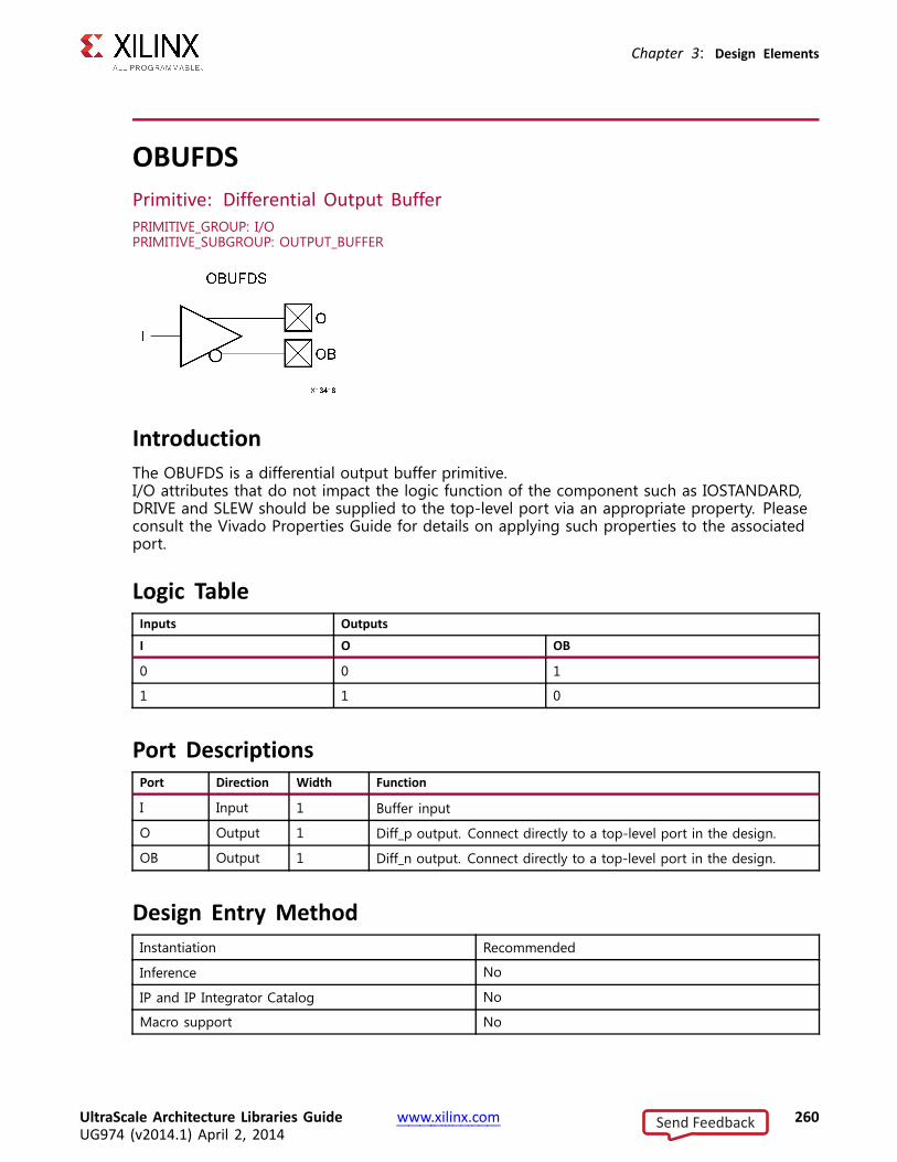
Chapter 3: Design Elements
OBUFDSPrimitive: Differential Output BufferPRIMITIVE_GROUP: I/OPRIMITIVE_SUBGROUP: OUTPUT_BUFFER
IntroductionThe OBUFDS is a differential output buffer primitive.I/O attributes that do not impact the logic function of the component such as IOSTANDARD,DRIVE and SLEW should be supplied to the top-level port via an appropriate property. Pleaseconsult the Vivado Properties Guide for details on applying such properties to the associatedport.
Logic TableInputs OutputsI O OB
0 0 1
1 1 0
Port DescriptionsPort Direction Width Function
I Input 1 Buffer input
O Output 1 Diff_p output. Connect directly to a top-level port in the design.
OB Output 1 Diff_n output. Connect directly to a top-level port in the design.
Design Entry MethodInstantiation Recommended
Inference No
IP and IP Integrator Catalog No
Macro support No
UltraScale Architecture Libraries Guide www.xilinx.com 260UG974 (v2014.1) April 2, 2014
Send Feedback

Chapter 3: Design Elements
VHDL Instantiation TemplateUnless they already exist, copy the following two statements and paste them before the entitydeclaration.Library UNISIM;use UNISIM.vcomponents.all;
-- OBUFDS: Differential Output Buffer-- UltraScale-- Xilinx HDL Libraries Guide, version 2014.1
OBUFDS_inst : OBUFDSport map (
O => O, -- 1-bit output: Diff_p output (connect directly to top-level port)OB => OB, -- 1-bit output: Diff_n output (connect directly to top-level port)I => I -- 1-bit input: Buffer input
);
-- End of OBUFDS_inst instantiation
Verilog Instantiation Template
// OBUFDS: Differential Output Buffer// UltraScale// Xilinx HDL Libraries Guide, version 2014.1
OBUFDS#()OBUFDS_inst (
.O(O), // 1-bit output: Diff_p output (connect directly to top-level port)
.OB(OB), // 1-bit output: Diff_n output (connect directly to top-level port)
.I(I) // 1-bit input: Buffer input);
// End of OBUFDS_inst instantiation
For More Information• See the 7 series FPGA User Documentation (User Guides and Data Sheets).
• See the UltraScale User Documentation.
UltraScale Architecture Libraries Guide www.xilinx.com 261UG974 (v2014.1) April 2, 2014
Send Feedback

Chapter 3: Design Elements
OBUFDS_GTE3Primitive: Gigabit Transceiver BufferPRIMITIVE_GROUP: ADVANCEDPRIMITIVE_SUBGROUP: GT
IntroductionOBUFDS_GTE3 is the gigabit transceiver output pad buffer component in UltraScale devices.The REFCLK signal should be routed to the dedicated reference clock output pins on the serialtransceiver, and the user design should instantiate the OBUFDS_GTE3 primitive in the userdesign. See the Transceivers User Guide for more information on PCB layout requirements,including reference clock requirements.
Design Entry MethodInstantiation Yes
Inference No
IP and IP Integrator Catalog Recommended
Macro support No
For More Information• See the 7 series FPGA User Documentation (User Guides and Data Sheets).
• See the UltraScale User Documentation.
UltraScale Architecture Libraries Guide www.xilinx.com 262UG974 (v2014.1) April 2, 2014
Send Feedback

Chapter 3: Design Elements
OBUFDS_GTE3_ADVPrimitive: Gigabit Transceiver BufferPRIMITIVE_GROUP: ADVANCEDPRIMITIVE_SUBGROUP: GT
IntroductionOBUFDS_GTE3_ADV is the gigabit transceiver output pad buffer component in UltraScaledevices. The REFCLK signal should be routed to the dedicated reference clock output pins onthe serial transceiver, and the user design should instantiate the OBUFDS_GTE3 primitive in theuser design. See the Transceivers User Guide for more information on PCB layout requirements,including reference clock requirements.
Port DescriptionsPort Direction Width Function
CEB Input 1 Refer to Transceiver User Guide
I<3:0> Input 4 Refer to Transceiver User Guide
O Output 1 Refer to Transceiver User Guide
OB Output 1 Refer to Transceiver User Guide
RXRECCLK_SEL<1:0> Input 2 Refer to Transceiver User Guide
Design Entry MethodInstantiation Yes
Inference No
IP and IP Integrator Catalog Recommended
Macro support No
Available AttributesAttribute Type Allowed Values Default Description
REFCLK_EN_TX_PATH
BINARY 1’b0 to 1’b1 1’b0 Refer to Transceiver User Guide
REFCLK_ICNTL_TX
BINARY 5’b00000 to5’b11111
5’b00000 Refer to Transceiver User Guide
UltraScale Architecture Libraries Guide www.xilinx.com 263UG974 (v2014.1) April 2, 2014
Send Feedback

Chapter 3: Design Elements
VHDL Instantiation TemplateUnless they already exist, copy the following two statements and paste them before the entitydeclaration.Library UNISIM;use UNISIM.vcomponents.all;
-- OBUFDS_GTE3_ADV:Gigabit Transceiver Buffer-- UltraScale-- Xilinx HDL Libraries Guide, version 2014.1
OBUFDS_GTE3_ADV_inst : OBUFDS_GTE3_ADVgeneric map (
REFCLK_EN_TX_PATH=> ’0’, -- Refer to Transceiver User GuideREFCLK_ICNTL_TX => ’00000’ -- Refer to Transceiver User Guide
)port map (
O => O, -- 1-bit output: Refer to Transceiver User GuideOB => OB, -- 1-bit output: Refer to Transceiver User GuideCEB => CEB, -- 1-bit input: Refer to Transceiver User GuideI => I, -- 4-bit input: Refer to Transceiver User GuideRXRECCLK_SEL=> RXRECCLK_SEL -- 2-bit input: Refer to Transceiver User Guide
);
-- End of OBUFDS_GTE3_ADV_inst instantiation
Verilog Instantiation Template
// OBUFDS_GTE3_ADV:Gigabit Transceiver Buffer// UltraScale// Xilinx HDL Libraries Guide, version 2014.1
OBUFDS_GTE3_ADV#(.REFCLK_EN_TX_PATH(1’b0), // Refer to Transceiver User Guide.REFCLK_ICNTL_TX(5’b00000) // Refer to Transceiver User Guide
)OBUFDS_GTE3_ADV_inst (
.O(O), // 1-bit output: Refer to Transceiver User Guide
.OB(OB), // 1-bit output: Refer to Transceiver User Guide
.CEB(CEB), // 1-bit input: Refer to Transceiver User Guide
.I(I), // 4-bit input: Refer to Transceiver User Guide
.RXRECCLK_SEL(RXRECCLK_SEL) // 2-bit input: Refer to Transceiver User Guide);
// End of OBUFDS_GTE3_ADV_inst instantiation
For More Information• See the 7 series FPGA User Documentation (User Guides and Data Sheets).
• See the UltraScale User Documentation.
UltraScale Architecture Libraries Guide www.xilinx.com 264UG974 (v2014.1) April 2, 2014
Send Feedback

Chapter 3: Design Elements
OBUFTPrimitive: 3-State Output BufferPRIMITIVE_GROUP: I/OPRIMITIVE_SUBGROUP: OUTPUT_BUFFER
IntroductionThe generic 3-state output buffer OBUFT typically implements 3-state outputs or bidirectionalI/O.I/O attributes that do not impact the logic function of the component such as IOSTANDARD,DRIVE and SLEW should be supplied to the top-level port via an appropriate property. Pleaseconsult the Vivado Properties Guide for details on applying such properties to the associatedport.
Logic TableInputs OutputsT I O
1 X Z
0 1 1
0 0 0
Port DescriptionsPort Direction Width Function
I Input 1 Input of OBUF. Connect to the logic driving the output port.
O Output 1 Output of OBUF to be connected directly to top-level output port.
T Input 1 3-state enable input
UltraScale Architecture Libraries Guide www.xilinx.com 265UG974 (v2014.1) April 2, 2014
Send Feedback

Chapter 3: Design Elements
Design Entry MethodInstantiation Yes
Inference Recommended
IP and IP Integrator Catalog No
Macro support No
VHDL Instantiation TemplateUnless they already exist, copy the following two statements and paste them before the entitydeclaration.Library UNISIM;use UNISIM.vcomponents.all;
-- OBUFT: Simple 3-state Output Buffer-- UltraScale-- Xilinx HDL Libraries Guide, version 2014.1
OBUFT_inst : OBUFTport map (
O => O, -- 1-bit output: Buffer output (connect directly to top-level port)I => I, -- 1-bit input: Buffer inputT => T -- 1-bit input: 3-state enable input
);
-- End of OBUFT_inst instantiation
Verilog Instantiation Template
// OBUFT: Simple 3-state Output Buffer// UltraScale// Xilinx HDL Libraries Guide, version 2014.1
OBUFT #()OBUFT_inst (
.O(O), // 1-bit output: Buffer output (connect directly to top-level port)
.I(I), // 1-bit input: Buffer input
.T(T) // 1-bit input: 3-state enable input);
// End of OBUFT_inst instantiation
For More Information• See the 7 series FPGA User Documentation (User Guides and Data Sheets).
• See the UltraScale User Documentation.
UltraScale Architecture Libraries Guide www.xilinx.com 266UG974 (v2014.1) April 2, 2014
Send Feedback

Chapter 3: Design Elements
OBUFTDSPrimitive: Differential 3-state Output BufferPRIMITIVE_GROUP: I/OPRIMITIVE_SUBGROUP: OUTPUT_BUFFER
IntroductionThe OBUFTDS is a differential 3-state output buffer primitive.I/O attributes that do not impact the logic function of the component such as IOSTANDARDand SLEW should be supplied to the top-level port via an appropriate property. Please consultthe Vivado Properties Guide for details on applying such properties to the associated port.
Logic TableInputs OutputsI T O OB
X 1 Z Z
0 0 0 1
1 0 1 0
Port DescriptionsPort Direction Width Function
I Input 1 Buffer input
O Output 1 Diff_p output. Connect directly to a top-level port in the design.
OB Output 1 Diff_n output. Connect directly to a top-level port in the design.
T Input 1 3-state enable input
UltraScale Architecture Libraries Guide www.xilinx.com 267UG974 (v2014.1) April 2, 2014
Send Feedback

Chapter 3: Design Elements
Design Entry MethodInstantiation Yes
Inference No
IP and IP Integrator Catalog No
Macro support No
VHDL Instantiation TemplateUnless they already exist, copy the following two statements and paste them before the entitydeclaration.Library UNISIM;use UNISIM.vcomponents.all;
-- OBUFTDS: Differential 3-state Output Buffer-- UltraScale-- Xilinx HDL Libraries Guide, version 2014.1
OBUFTDS_inst : OBUFTDSport map (
O => O, -- 1-bit output: Diff_p output (connect directly to top-level port)OB => OB, -- 1-bit output: Diff_n output (connect directly to top-level port)I => I, -- 1-bit input: Buffer inputT => T -- 1-bit input: 3-state enable input
);
-- End of OBUFTDS_inst instantiation
Verilog Instantiation Template
// OBUFTDS: Differential 3-state Output Buffer// UltraScale// Xilinx HDL Libraries Guide, version 2014.1
OBUFTDS#()OBUFTDS_inst (
.O(O), // 1-bit output: Diff_p output (connect directly to top-level port)
.OB(OB), // 1-bit output: Diff_n output (connect directly to top-level port)
.I(I), // 1-bit input: Buffer input
.T(T) // 1-bit input: 3-state enable input);
// End of OBUFTDS_inst instantiation
For More Information• See the 7 series FPGA User Documentation (User Guides and Data Sheets).
• See the UltraScale User Documentation.
UltraScale Architecture Libraries Guide www.xilinx.com 268UG974 (v2014.1) April 2, 2014
Send Feedback

Chapter 3: Design Elements
ODDRE1Primitive: Dedicated Dual Data Rate (DDR) Output RegisterPRIMITIVE_GROUP: REGISTERPRIMITIVE_SUBGROUP: DDR
IntroductionIn component mode, the ODDRE1 in UltraScale FPGAs is a dedicated output register for usein transmitting dual data rate (DDR) signals from FPGA devices. The ODDRE1 interface withthe FPGA fabric is limited to the same clock edges. This feature allows designers to avoidadditional timing complexities and CLB usage.
Port DescriptionsPort Direction Width Function
C Input 1 High-speed clock input
D1 Input 1 Parallel data input 1
D2 Input 1 Parallel data input 2
Q Output 1 Data output to IOB
SR Input 1 Active High Asynchronous Reset
Design Entry MethodInstantiation Yes
Inference No
IP and IP Integrator Catalog Yes
Macro support No
UltraScale Architecture Libraries Guide www.xilinx.com 269UG974 (v2014.1) April 2, 2014
Send Feedback

Chapter 3: Design Elements
Available AttributesAttribute Type Allowed Values Default Description
IS_C_INVERTED BINARY 1’b0 to 1’b1 1’b0 Indicates whether the clock C isactive-high or active-low
IS_D1_INVERTED
BINARY 1’b0 to 1’b1 1’b0 Optional inversion for D1
IS_D2_INVERTED
BINARY 1’b0 to 1’b1 1’b0 Optional inversion for D2
SRVAL BINARY 1’b0, 1’b1 1’b0 Initializes the ODDRE1 Flip-Flopsto the specified value
VHDL Instantiation TemplateUnless they already exist, copy the following two statements and paste them before the entitydeclaration.Library UNISIM;use UNISIM.vcomponents.all;
-- ODDRE1: Dedicated Dual Data Rate (DDR) Output Register-- UltraScale-- Xilinx HDL Libraries Guide, version 2014.1
ODDRE1_inst : ODDRE1generic map (
IS_C_INVERTED => ’0’, -- Optional inversion for CIS_D1_INVERTED => ’0’, -- Optional inversion for D1IS_D2_INVERTED => ’0’, -- Optional inversion for D2SRVAL => 0 -- Initializes the ODDRE1Flip-Flops to the specified value (1’b0, 1’b1)
)port map (
Q => Q, -- 1-bit output: Data output to IOBC => C, -- 1-bit input: High-speed clock inputD1 => D1, -- 1-bit input: Parallel data input 1D2 => D2, -- 1-bit input: Parallel data input 2SR => SR -- 1-bit input: Active High Async Reset
);
-- End of ODDRE1_inst instantiation
Verilog Instantiation Template
// ODDRE1: Dedicated Dual Data Rate (DDR) Output Register// UltraScale// Xilinx HDL Libraries Guide, version 2014.1
ODDRE1#(.IS_C_INVERTED(1’b0), // Optional inversion for C.IS_D1_INVERTED(1’b0), // Optional inversion for D1.IS_D2_INVERTED(1’b0), // Optional inversion for D2.SRVAL(0) // Initializes the ODDRE1Flip-Flops to the specified value (1’b0, 1’b1)
)ODDRE1_inst (
.Q(Q), // 1-bit output: Data output to IOB
.C(C), // 1-bit input: High-speed clock input
.D1(D1), // 1-bit input: Parallel data input 1
.D2(D2), // 1-bit input: Parallel data input 2
.SR(SR) // 1-bit input: Active High Async Reset);
UltraScale Architecture Libraries Guide www.xilinx.com 270UG974 (v2014.1) April 2, 2014
Send Feedback

Chapter 3: Design Elements
// End of ODDRE1_inst instantiation
For More Information• See the 7 series FPGA User Documentation (User Guides and Data Sheets).
• See the UltraScale User Documentation.
UltraScale Architecture Libraries Guide www.xilinx.com 271UG974 (v2014.1) April 2, 2014
Send Feedback

Chapter 3: Design Elements
ODELAYE3Primitive: Output Fixed or Variable Delay ElementPRIMITIVE_GROUP: I/OPRIMITIVE_SUBGROUP: DELAY
IntroductionIn component mode, I/O blocks contain a programmable delay element called ODELAYE3. TheODELAYE3 can be connected to an output register/OSERDESE3 or driven directly by FPGA logic.The ODELAYE3 is a 512-tap delay element with a calibrated delay. The ODELAYE3 allowssignals to be delayed on an individual basis.
Port DescriptionsPort Direction Width Function
CASC_IN Input 1 Cascade delay input from slave IDELAY CASCADE_OUT
CASC_OUT Output 1 Cascade delay output to IDELAY input cascade
CASC_RETURN Input 1 Cascade delay returning from slave IDELAY DATAOUT
CE Input 1 Active high enable increment/decrement function
CLK Input 1 Clock input
CNTVALUEIN<8:0> Input 9 Counter value from FPGA logic for dynamically loadable tapvalue input
CNTVALUEOUT<8:0> Output 9 The CNTVALUEOUT pins are used for reporting the dynamicallyswitching value of the delay element. CNTVALUEOUT is onlyavailable when ODELAYE3 is in "VARIABLE" or "VAR_LOAD" mode.
DATAOUT Output 1 Delayed data from ODATAIN input port
EN_VTC Input 1 Keep delay constant over VT
UltraScale Architecture Libraries Guide www.xilinx.com 272UG974 (v2014.1) April 2, 2014
Send Feedback

Chapter 3: Design Elements
Port Direction Width Function
INC Input 1 Increment / Decrement tap delay input
LOAD Input 1 Loads the ODELAY primitive to the pre-programmed value inVARIABLE mode. In VAR_LOAD mode, it loads the value ofCNTVALUEIN.
ODATAIN Input 1 Data input for ODELAYE3 from OSERDES or programmable logic
RST Input 1 Asynchronous Reset to the DELAY_VALUE, active level based onIS_RST_INVERTED
Design Entry MethodInstantiation Yes
Inference No
IP and IP Integrator Catalog Yes
Macro support No
Available AttributesAttribute Type Allowed Values Default Description
CASCADE STRING "NONE", "MASTER","SLAVE_END","SLAVE_MIDDLE"
"NONE" Set the location of the ODELAYE3when it is used in a cascadedconfiguration
• "NONE" : Delay line is notcascaded
• "MASTER" : Delay line iscascaded with another delayline
• "SLAVE_MIDDLE" : Delay lineis cascaded from adjacentdelay line and also cascades toanother delay line
• "SLAVE_END" : Delay line isthe last cascaded delay line
DELAY_FORMAT STRING "TIME", "COUNT" "TIME" Sets the units of DELAY_VALUE ofthe ODELAYE3. Use TIME whenDELAY_TYPE is FIXED. Use COUNTwhen DELAY_TYPE is VARIABLE orVAR_LOAD.
• "TIME" : ODELAYE3DELAY_VALUE is specifiedin ps
• "COUNT" : ODELAYE3DELAY_VALUE is specifiedin taps
UltraScale Architecture Libraries Guide www.xilinx.com 273UG974 (v2014.1) April 2, 2014
Send Feedback

Chapter 3: Design Elements
Attribute Type Allowed Values Default Description
DELAY_TYPE STRING "FIXED","VAR_LOAD","VARIABLE"
"FIXED" Sets the type of tap delay line.
• "FIXED" - Sets a static delayvalue
• "VARIABLE" - Dynamicallyadjust (increment/decrement)delay value
• "VAR_LOAD" - Dynamicallyloads tap values
DELAY_VALUE DECIMAL 0 to 1250 0 Specifies the fixed delay in ps inFIXED mode or the initial startingnumber of taps in "VARIABLE"mode or "VAR_LOAD" mode (inputpath).
IS_CLK_INVERTED
BINARY 1’b0 to 1’b1 1’b0 Indicates whether the CLK isactive-high or active-low
IS_RST_INVERTED
BINARY 1’b0 to 1’b1 1’b0 Indicates whether the RST isactive-high or active-low
REFCLK_FREQUENCY
1significantdigit FLOAT
200.0 to 2400.0 300.0 Sets the tap value (in MHz)used by the timing analyzerfor static timing analysis andfunctional/timing simulation. Thefrequency of REFCLK must bewithin the given datasheet rangeto guarantee performance.
UPDATE_MODE STRING "ASYNC","MANUAL", "SYNC"
"ASYNC" Determines when updates to thedelay will take effect
• "ASYNC": Updates areincrements or decrements tothe delay value independentof the data being received
• "SYNC": Updates requirethat ODATAIN transitions tosynchronously update thedelay with the ODATAIN edges
• "MANUAL": Updates takeeffect when both LD and CEare asserted after the LD andCNTVALUEIN signals are usedto load the new CNTVALUE
UltraScale Architecture Libraries Guide www.xilinx.com 274UG974 (v2014.1) April 2, 2014
Send Feedback

Chapter 3: Design Elements
VHDL Instantiation TemplateUnless they already exist, copy the following two statements and paste them before the entitydeclaration.Library UNISIM;use UNISIM.vcomponents.all;
-- ODELAYE3: Output Fixed or Variable Delay Element-- UltraScale-- Xilinx HDL Libraries Guide, version 2014.1
ODELAYE3_inst : ODELAYE3generic map (
CASCADE=> "NONE", -- Cascade setting (NONE, MASTER, SLAVE_END, SLAVE_MIDDLE)DELAY_FORMAT=> "TIME", -- (TIME, COUNT)DELAY_TYPE=> "FIXED", -- Set the type of tap delay line (FIXED, VAR_LOAD, VARIABLE)DELAY_VALUE=> 0, -- Output delay tap settingIS_CLK_INVERTED => ’0’, -- Optional inversion for CLKIS_RST_INVERTED => ’0’, -- Optional inversion for RSTREFCLK_FREQUENCY=> 300.0, -- IDELAYCTRL clock input frequency in MHz (VALUES).UPDATE_MODE=> "ASYNC" -- Determines when updates to the delay will take effect (ASYNC, MANUAL, SYNC)
)port map (
CASC_OUT=> CASC_OUT, -- 1-bit output: Cascade delay output to IDELAY input cascadeCNTVALUEOUT=> CNTVALUEOUT,-- 9-bit output: Counter value outputDATAOUT=> DATAOUT, -- 1-bit output: Delayed data from ODATAIN input portCASC_IN => CASC_IN, -- 1-bit input: Cascade delay input from slave IDELAY CASCADE_OUTCASC_RETURN=> CASC_RETURN,-- 1-bit input: Cascade delay returning from slave IDELAY DATAOUTCE => CE, -- 1-bit input: Active high enable increment/decrement inputCLK => CLK, -- 1-bit input: Clock inputCNTVALUEIN => CNTVALUEIN, -- 9-bit input: Counter value inputEN_VTC => EN_VTC, -- 1-bit input: Keep delay constant over VTINC => INC, -- 1-bit input: Increment / Decrement tap delay inputLOAD => LOAD, -- 1-bit input: Load DELAY_VALUEinputODATAIN => ODATAIN, -- 1-bit input: Data inputRST => RST -- 1-bit input: Asynchronous Reset to the DELAY_VALUE
);
-- End of ODELAYE3_inst instantiation
UltraScale Architecture Libraries Guide www.xilinx.com 275UG974 (v2014.1) April 2, 2014
Send Feedback

Chapter 3: Design Elements
Verilog Instantiation Template
// ODELAYE3: Output Fixed or Variable Delay Element// UltraScale// Xilinx HDL Libraries Guide, version 2014.1
ODELAYE3#(.CASCADE("NONE"), // Cascade setting (NONE, MASTER, SLAVE_END, SLAVE_MIDDLE).DELAY_FORMAT("TIME"), // (TIME, COUNT).DELAY_TYPE("FIXED"), // Set the type of tap delay line (FIXED, VAR_LOAD, VARIABLE).DELAY_VALUE(0), // Output delay tap setting.IS_CLK_INVERTED(1’b0), // Optional inversion for CLK.IS_RST_INVERTED(1’b0), // Optional inversion for RST.REFCLK_FREQUENCY(300.0), // IDELAYCTRL clock input frequency in MHz (VALUES)..UPDATE_MODE("ASYNC") // Determines when updates to the delay will take effect (ASYNC, MANUAL, SYNC)
)ODELAYE3_inst (
.CASC_OUT(CASC_OUT), // 1-bit output: Cascade delay output to IDELAY input cascade
.CNTVALUEOUT(CNTVALUEOUT),// 9-bit output: Counter value output
.DATAOUT(DATAOUT), // 1-bit output: Delayed data from ODATAIN input port
.CASC_IN(CASC_IN), // 1-bit input: Cascade delay input from slave IDELAY CASCADE_OUT
.CASC_RETURN(CASC_RETURN),// 1-bit input: Cascade delay returning from slave IDELAY DATAOUT
.CE(CE), // 1-bit input: Active high enable increment/decrement input
.CLK(CLK), // 1-bit input: Clock input
.CNTVALUEIN(CNTVALUEIN), // 9-bit input: Counter value input
.EN_VTC(EN_VTC), // 1-bit input: Keep delay constant over VT
.INC(INC), // 1-bit input: Increment / Decrement tap delay input
.LOAD(LOAD), // 1-bit input: Load DELAY_VALUEinput
.ODATAIN(ODATAIN), // 1-bit input: Data input
.RST(RST) // 1-bit input: Asynchronous Reset to the DELAY_VALUE);
// End of ODELAYE3_inst instantiation
For More Information• See the UltraScale Architecture SelectIO Resources User Guide (UG471).
• See the UltraScale User Documentation.
UltraScale Architecture Libraries Guide www.xilinx.com 276UG974 (v2014.1) April 2, 2014
Send Feedback

Chapter 3: Design Elements
OR2LPrimitive: Two input OR gate implemented in place of a CLB LatchPRIMITIVE_GROUP: CLBPRIMITIVE_SUBGROUP: LATCH
IntroductionThis element allows the specification of a configurable CLB latch to take the function of a twoinput OR gate. The use of this element can reduce logic levels and increase logic density of thepart by trading off register/latch resources for logic. Xilinx suggests caution when using thiscomponent as it can affect register packing and density within a CLB.
Logic TableInputs OutputsDI SRI O
0 0 0
0 1 1
1 0 1
1 1 1
Port DescriptionsPort Direction Width Function
DI Input 1 Active-High input that is generally connected to sourcing LUT located in thesame CLB.
O Output 1 Output of the AND gate.
SRI Input 1 Input that is generally source from outside of the CLB. The attributeIS_SRI_INVERTED determines the active polarity of this signal.
NOTE: To allow more than one AND2B1L or OR2L to be packed into a halfCLB, a common signal must be connected to this input.
UltraScale Architecture Libraries Guide www.xilinx.com 277UG974 (v2014.1) April 2, 2014
Send Feedback

Chapter 3: Design Elements
Design Entry MethodInstantiation Yes
Inference No
IP and IP Integrator Catalog No
Macro support No
Available AttributesAttribute Type Allowed Values Default Description
IS_SRI_INVERTED
BINARY 1’b0 to 1’b1 1’b0 Indicates whether the optionalinversion is used or not for the SRIpin of this component.
VHDL Instantiation TemplateUnless they already exist, copy the following two statements and paste them before the entitydeclaration.Library UNISIM;use UNISIM.vcomponents.all;
-- OR2L: Two input OR gate implemented in place of a CLB Latch-- UltraScale-- Xilinx HDL Libraries Guide, version 2014.1
OR2L_inst : OR2Lgeneric map (
IS_SRI_INVERTED => ’0’ -- Optional inversion for SRI)port map (
O => O, -- 1-bit output: AND gate outputDI => DI, -- 1-bit input: Data input connected to LUT logicSRI => SRI -- 1-bit input: External CLB data
);
-- End of OR2L_inst instantiation
Verilog Instantiation Template
// OR2L: Two input OR gate implemented in place of a CLB Latch// UltraScale// Xilinx HDL Libraries Guide, version 2014.1
OR2L #(.IS_SRI_INVERTED(1’b0) // Optional inversion for SRI
)OR2L_inst (
.O(O), // 1-bit output: AND gate output
.DI(DI), // 1-bit input: Data input connected to LUT logic
.SRI(SRI) // 1-bit input: External CLB data);
// End of OR2L_inst instantiation
UltraScale Architecture Libraries Guide www.xilinx.com 278UG974 (v2014.1) April 2, 2014
Send Feedback

Chapter 3: Design Elements
For More Information• See the UltraScale Architecture SelectIO Resources User Guide (UG471).
• See the UltraScale User Documentation.
UltraScale Architecture Libraries Guide www.xilinx.com 279UG974 (v2014.1) April 2, 2014
Send Feedback

Chapter 3: Design Elements
OSERDESE3Primitive: Output SERial/DESerializerPRIMITIVE_GROUP: I/OPRIMITIVE_SUBGROUP: SERDES
IntroductionIn component mode, the OSERDESE3 in UltraScale FPGAs is a dedicated parallel-to-serialconverter with specific clocking and logic features designed to facilitate the implementationof high-speed source-synchronous applications. The OSERDESE3 avoids the additionaltiming complexities encountered when designing serializers in the internal device logic. TheOSERDESE3 can serialize an outgoing signal by either 4 in SDR mode, or by 4 and 8 in DDRmode.
Port DescriptionsPort Direction Width Function
CLK Input 1 The high-speed clock input (CLK) is used to clock out theoutput serial data stream.
CLKDIV Input 1 The divided clock input (CLKDIV) is typically a divided version ofCLK (depending on the width of the implemented serialization).It drives the input of the parallel-to-serial converter and theCE module.
D<7:0> Input 8 The parallel input data port (D) is the parallel data input portof the OSERDESE3.
OQ Output 1 Serial Output Data to the IOB
RST Input 1 Asynchronous Reset, active level based on IS_RST_INVERTED
T Input 1 Tristate input from fabric
T_OUT Output 1 3-state control output to IOB
UltraScale Architecture Libraries Guide www.xilinx.com 280UG974 (v2014.1) April 2, 2014
Send Feedback

Chapter 3: Design Elements
Design Entry MethodInstantiation Yes
Inference No
IP and IP Integrator Catalog Yes
Macro support No
Available AttributesAttribute Type Allowed Values Default Description
DATA_WIDTH DECIMAL 8, 4 8 Defines the width of the parallel-to-serialconverter. When used with SDR clocking,the DATA_WIDTH is set to be twice thedesired width.
INIT BINARY 1’b0, 1’b1 1’b0 Initializes the OSERDES flip-flops to thevalue specified
IS_CLK_INVERTED
BINARY 1’b0 to 1’b1 1’b0 Indicates whether the CLK is active-highor active-low
IS_CLKDIV_INVERTED
BINARY 1’b0 to 1’b1 1’b0 Indicates whether the CLKDIV isactive-high or active-low
IS_RST_INVERTED
BINARY 1’b0 to 1’b1 1’b0 Indicates whether the RST is active-highor active-low
VHDL Instantiation TemplateUnless they already exist, copy the following two statements and paste them before the entitydeclaration.Library UNISIM;use UNISIM.vcomponents.all;
-- OSERDESE3: Output SERial/DESerializer-- UltraScale-- Xilinx HDL Libraries Guide, version 2014.1
OSERDESE3_inst : OSERDESE3generic map (
DATA_WIDTH=> 8, -- Parallel Data Width (8-4)INIT => 0, -- Initialization value of the OSERDESflip-flopsIS_CLKDIV_INVERTED => ’0’, -- Optional inversion for CLKDIVIS_CLK_INVERTED => ’0’, -- Optional inversion for CLKIS_RST_INVERTED => ’0’ -- Optional inversion for RST
)port map (
OQ => OQ, -- 1-bit output: Serial Output DataT_OUT => T_OUT, -- 1-bit output: 3-state control output to IOBCLK => CLK, -- 1-bit input: High-speed clockCLKDIV => CLKDIV, -- 1-bit input: Divided ClockD => D, -- 8-bit input: Parallel Data InputRST => RST, -- 1-bit input: Asynchronous ResetT => T -- 1-bit input: Tristate input from fabric
);
-- End of OSERDESE3_inst instantiation
UltraScale Architecture Libraries Guide www.xilinx.com 281UG974 (v2014.1) April 2, 2014
Send Feedback

Chapter 3: Design Elements
Verilog Instantiation Template
// OSERDESE3: Output SERial/DESerializer// UltraScale// Xilinx HDL Libraries Guide, version 2014.1
OSERDESE3#(.DATA_WIDTH(8), // Parallel Data Width (8-4).INIT(0), // Initialization value of the OSERDESflip-flops.IS_CLKDIV_INVERTED(1’b0), // Optional inversion for CLKDIV.IS_CLK_INVERTED(1’b0), // Optional inversion for CLK.IS_RST_INVERTED(1’b0) // Optional inversion for RST
)OSERDESE3_inst (
.OQ(OQ), // 1-bit output: Serial Output Data
.T_OUT(T_OUT), // 1-bit output: 3-state control output to IOB
.CLK(CLK), // 1-bit input: High-speed clock
.CLKDIV(CLKDIV), // 1-bit input: Divided Clock
.D(D), // 8-bit input: Parallel Data Input
.RST(RST), // 1-bit input: Asynchronous Reset
.T(T) // 1-bit input: Tristate input from fabric);
// End of OSERDESE3_inst instantiation
For More Information• See the UltraScale Architecture SelectIO Resources User Guide (UG471).
• See the UltraScale User Documentation.
UltraScale Architecture Libraries Guide www.xilinx.com 282UG974 (v2014.1) April 2, 2014
Send Feedback

Chapter 3: Design Elements
PCIE_3_1Primitive: Integrated Block for PCI ExpressPRIMITIVE_GROUP: ADVANCEDPRIMITIVE_SUBGROUP: PCIE
IntroductionThe Integrated block for PCI Express is a hard macro primitive compliant with the PCIespecification. This block is designed to be integrated with GTs and FPGA clocking resourcesusing fabric interconnect. Please refer to the Integrated Block for PCI Express User Guide forfurther details on this component.
Design Entry MethodInstantiation No
Inference No
IP and IP Integrator Catalog Recommended
Macro support No
For More Information• See the 7 series FPGA User Documentation (User Guides and Data Sheets).
• See the UltraScale User Documentation.
UltraScale Architecture Libraries Guide www.xilinx.com 283UG974 (v2014.1) April 2, 2014
Send Feedback

Chapter 3: Design Elements
PLLE3_ADVPrimitive: Advanced Phase-Locked Loop (PLL)PRIMITIVE_GROUP: CLOCKPRIMITIVE_SUBGROUP: PLL
IntroductionThe PLLE3 is used for high-speed I/O clocking using Bitslice components as well as generalclocking requirements. In general, the PLLE3 has less jitter and reduced power characteristicscompared to the MMCME3 which makes it preferable for clocking behaviors that do not requirefeatures only available to the MMCME3.
Port DescriptionsPort Direction Width Function
CLKFBIN Input 1 Feedback clock pin to the PLL
CLKFBOUT Output 1 Dedicated PLL Feedback clock output
CLKIN Input 1 Clock input.
CLKOUTPHY Output 1 General clock output connected to I/O Bitslice components.
CLKOUTPHYEN Input 1 Enable signal for CLKOUTPHY.
CLKOUT0 Output 1 General clock output CLKOUT0. Generally connected to aglobal buffer.
CLKOUT0B Output 1 Inverted CLKOUT0. Generally connected to a global buffer.
CLKOUT1 Output 1 General clock output CLKOUT1. Generally connected to aglobal buffer.
CLKOUT1B Output 1 Inverted CLKOUT1. Generally connected to a global buffer.
UltraScale Architecture Libraries Guide www.xilinx.com 284UG974 (v2014.1) April 2, 2014
Send Feedback

Chapter 3: Design Elements
Port Direction Width Function
DADDR<6:0> Input 7 The dynamic reconfiguration address (DADDR) inputbus provides a reconfiguration address for the dynamicreconfiguration. When not used, all bits must be assigned zeros.
DCLK Input 1 The DCLK signal is the reference clock for the dynamicreconfiguration port.
DEN Input 1 The dynamic reconfiguration enable (DEN) provides the enablecontrol signal to access the dynamic reconfiguration feature.When the dynamic reconfiguration feature is not used, DENmust be tied Low.
DI<15:0> Input 16 The dynamic reconfiguration output bus provides PLL dataoutput when using dynamic reconfiguration.
DO<15:0> Output 16 The dynamic reconfiguration output bus provides PLL dataoutput when using dynamic reconfiguration.
DRDY Output 1 The dynamic reconfiguration ready output (DRDY) providesthe response to the DEN signal for the PLLs dynamicreconfiguration feature.
DWE Input 1 The dynamic reconfiguration write enable (DWE) input pinprovides the write enable control signal to write the DI datainto the DADDR address. When not used, it must be tied Low.
LOCKED Output 1 An output from the PLL that indicates when the PLL hasachieved phase alignment within a predefined window andfrequency matching within a predefined PPM range. The PLLautomatically locks after power on, no extra reset is required.LOCKED will be deasserted if the input clock stops or the phasealignment is violated (e.g., input clock phase shift). The PLLmust be reset after LOCKED is deasserted.
PWRDWN Input 1 Powers down instantiated but unused PLLs.
RST Input 1 The RST signal is an asynchronous reset for the PLL. The PLLwill synchronously re-enable itself when this signal is releasedand go through a new phase alignment and lock cycle. Areset is required when the input clock conditions change (e.g.,frequency).
Design Entry MethodInstantiation Yes
Inference No
IP and IP Integrator Catalog Recommended
Macro support No
UltraScale Architecture Libraries Guide www.xilinx.com 285UG974 (v2014.1) April 2, 2014
Send Feedback

Chapter 3: Design Elements
Available AttributesAttribute Type Allowed Values Default Description
CLKFBOUT_MULT
DECIMAL 1 to 19 5 Specifies the amount to multiplyall CLKOUT clock outputs if adifferent frequency is desired. Thisnumber, in combination with theassociated CLKOUT#_DIVIDE valueand DIVCLK_DIVIDE value, willdetermine the output frequency.
CLKFBOUT_PHASE
3significantdigit FLOAT
-360.000 to 360.000 0.000 Specifies the phase offset indegrees of the clock feedbackoutput. Shifting the feedbackclock results in a negative phaseshift of all output clocks to thePLL.
CLKIN_PERIOD FLOAT(nS) 0.000 to 14.286 0.000 Specifies the input period in ns tothe PLL CLKIN input. Resolutionis down to the ps (3 decimalplaces). For example a value of33.333 would indicate a 30 MHzinput clock. This information ismandatory and must be supplied.
CLKOUTPHY_MODE
STRING "VCO_2X", "VCO","VCO_HALF"
"VCO_2X" Specifies the frequency of theCLKOUTPHY clock output.
CLKOUT0_DIVIDE
DECIMAL 1 to 128 1 Specifies the amount to dividethe CLKOUT0 output. Thisnumber in combination withthe CLKFBOUT_MULT andDIVCLK_DIVIDE values willdetermine the output frequency.
CLKOUT0_DUTY_CYCLE
3significantdigit FLOAT
0.001 to 0.999 0.500 Specifies the Duty Cycle ofCLKOUT0 clock output inpercentage (i.e., 0.500 willgenerate a 50% duty cycle).
CLKOUT0 _PHASE 3significantdigit FLOAT
-360.000 to 360.000 0.000 Specifies the phase offset indegrees of the CLKOUT0 output.
CLKOUT1_DIVIDE
DECIMAL 1 to 128 1 Specifies the amount to dividethe CLKOUT1 output. Thisnumber in combination withthe CLKFBOUT_MULT andDIVCLK_DIVIDE values willdetermine the output frequency.
CLKOUT1_DUTY_CYCLE
3significantdigit FLOAT
0.001 to 0.999 0.500 Specifies the Duty Cycle ofCLKOUT1 clock output inpercentage (i.e., 0.500 willgenerate a 50% duty cycle).
CLKOUT1 _PHASE 3significantdigit FLOAT
-360.000 to 360.000 0.000 Specifies the phase offset indegrees of the CLKOUT1 output.
UltraScale Architecture Libraries Guide www.xilinx.com 286UG974 (v2014.1) April 2, 2014
Send Feedback

Chapter 3: Design Elements
Attribute Type Allowed Values Default Description
COMPENSATION STRING "AUTO", "BUF_IN","INTERNAL"
"AUTO" Clock input compensation. Ingeeneral, should be set to AUTO.Defines how the PLL feedbackcompensation is configured.
• "AUTO" - Tools automaticallydetermine propercompensation settings basedon how the PLL feedback pathis connected.
• "INTERNAL" - Indicates thePLL is using its own internalfeedback path so no delay isbeing compensated.
• "BUF_IN" - Indicates that theconfiguration does not matchwith the other compensationmodes and no delay will becompensated. This is the caseif a clock input is driven by aBUFG for instance.
DIVCLK _DIVIDE DECIMAL 1 to 15 1 Specifies the division ratio for alloutput clocks with respect to theinput clock. Effectively divides theCLKIN going into the PFD.
IS_CLKFBIN_INVERTED
BINARY 1’b0 to 1’b1 1’b0 Indicates whether the optionalinversion is used or not on theCLKFBIN pin of this component.
IS_CLKIN_INVERTED
BINARY 1’b0 to 1’b1 1’b0 Indicates whether the optionalinversion is used or not on theCLKIN pin of this component.
IS_PWRDWN_INVERTED
BINARY 1’b0 to 1’b1 1’b0 Indicates whether the optionalinversion is used or not on thePWRDWN pin of this component.
IS_RST_INVERTED
BINARY 1’b0 to 1’b1 1’b0 Indicates whether the optionalinversion is used or not on theRST pin of this component.
REF_JITTER 3significantdigit FLOAT
0.000 to 0.999 0.010 Allows specification of theexpected jitter on CLKIN inorder to better optimize PLLperformance. A bandwidth settingof OPTIMIZED will attempt tochoose the best parameter forinput clocking when unknown. Ifknown, then the value providedshould be specified in terms of theUI percentage (the maximum peakto peak value) of the expectedjitter on the input clock.
STARTUP_WAIT STRING "FALSE", "TRUE" "FALSE" Delays configuration DONE signalfrom asserting until PLL is locked.
UltraScale Architecture Libraries Guide www.xilinx.com 287UG974 (v2014.1) April 2, 2014
Send Feedback

Chapter 3: Design Elements
VHDL Instantiation TemplateUnless they already exist, copy the following two statements and paste them before the entitydeclaration.Library UNISIM;use UNISIM.vcomponents.all;
-- PLLE3_ADV: Advanced Phase-Locked Loop (PLL)-- UltraScale-- Xilinx HDL Libraries Guide, version 2014.1
PLLE3_ADV_inst : PLLE3_ADVgeneric map (
CLKFBOUT_MULT=> 5, -- Multiply value for all CLKOUT, (1-19)CLKFBOUT_PHASE=> 0.0, -- Phase offset in degrees of CLKFB, (-360.000-360.000).CLKIN_PERIOD => 0.0, -- Input clock period in ns to ps resolution (i.e. 33.333 is 30 MHz).-- CLKOUT0Attributes: Divide, Phase and Duty Cycle for the CLKOUT0 outputCLKOUT0_DIVIDE => 1, -- Divide amount for CLKOUT0 (1-256)CLKOUT0_DUTY_CYCLE=> 0.5, -- Duty cycle for CLKOUT0 (0.001-0.999).CLKOUT0_PHASE=> 0.0, -- Phase offset for CLKOUT0 (-360.000-360.000).-- CLKOUT1Attributes: Divide, Phase and Duty Cycle for the CLKOUT1 outputCLKOUT1_DIVIDE => 1, -- Divide amount for CLKOUT1 (1-256)CLKOUT1_DUTY_CYCLE=> 0.5, -- Duty cycle for CLKOUT1 (0.001-0.999).CLKOUT1_PHASE=> 0.0, -- Phase offset for CLKOUT1 (-360.000-360.000).CLKOUTPHY_MODE=> "VCO_2X", -- Frequency of the CLKOUTPHY(VCO_2X, VCO, VCO_HALF)COMPENSATION=> "AUTO", -- AUTO, BUF_IN, INTERNALDIVCLK_DIVIDE => 1, -- Master division value, (1-11)-- Programmable Inversion Attributes: Specifies built-in programmable inversion on specific pinsIS_CLKFBIN_INVERTED => ’0’, -- Optional inversion for CLKFBINIS_CLKIN_INVERTED => ’0’, -- Optional inversion for CLKINIS_PWRDWN_INVERTED=> ’0’, -- Optional inversion for PWRDWNIS_RST_INVERTED => ’0’, -- Optional inversion for RSTREF_JITTER => 0.0, -- Reference input jitter in UI (0.000-0.999).STARTUP_WAIT=> "FALSE" -- Delays DONEuntil PLL is locked (FALSE, TRUE)
)port map (
-- Clock Outputs: 1-bit (each) output: User configurable clock outputsCLKOUT0 => CLKOUT0, -- 1-bit output: General Clock outputCLKOUT0B=> CLKOUT0B, -- 1-bit output: Inverted CLKOUT0CLKOUT1 => CLKOUT1, -- 1-bit output: General Clock outputCLKOUT1B=> CLKOUT1B, -- 1-bit output: Inverted CLKOUT1CLKOUTPHY=> CLKOUTPHY, -- 1-bit output: Bitslice clock-- DRP Ports: 16-bit (each) output: Dynamic reconfiguration portsDO => DO, -- 16-bit output: DRP dataDRDY=> DRDY, -- 1-bit output: DRP ready-- Feedback Clocks: 1-bit (each) output: Clock feedback portsCLKFBOUT=> CLKFBOUT, -- 1-bit output: Feedback clockLOCKED=> LOCKED, -- 1-bit output: LOCKCLKIN => CLKIN, -- 1-bit input: Input clock-- Control Ports: 1-bit (each) input: PLL control portsCLKOUTPHYEN=> CLKOUTPHYEN,-- 1-bit input: CLKOUTPHYenablePWRDWN=> PWRDWN, -- 1-bit input: Power-downRST => RST, -- 1-bit input: Reset-- DRP Ports: 7-bit (each) input: Dynamic reconfiguration portsDADDR=> DADDR, -- 7-bit input: DRP addressDCLK => DCLK, -- 1-bit input: DRP clockDEN => DEN, -- 1-bit input: DRP enableDI => DI, -- 16-bit input: DRP dataDWE=> DWE, -- 1-bit input: DRP write enable-- Feedback Clocks: 1-bit (each) input: Clock feedback portsCLKFBIN => CLKFBIN -- 1-bit input: Feedback clock
);
-- End of PLLE3_ADV_inst instantiation
UltraScale Architecture Libraries Guide www.xilinx.com 288UG974 (v2014.1) April 2, 2014
Send Feedback

Chapter 3: Design Elements
Verilog Instantiation Template
// PLLE3_ADV: Advanced Phase-Locked Loop (PLL)// UltraScale// Xilinx HDL Libraries Guide, version 2014.1
PLLE3_ADV #(.CLKFBOUT_MULT(5), // Multiply value for all CLKOUT, (1-19).CLKFBOUT_PHASE(0.0), // Phase offset in degrees of CLKFB, (-360.000-360.000)..CLKIN_PERIOD(0.0), // Input clock period in ns to ps resolution (i.e. 33.333 is 30 MHz).// CLKOUT0Attributes: Divide, Phase and Duty Cycle for the CLKOUT0 output.CLKOUT0_DIVIDE(1), // Divide amount for CLKOUT0 (1-256).CLKOUT0_DUTY_CYCLE(0.5), // Duty cycle for CLKOUT0 (0.001-0.999)..CLKOUT0_PHASE(0.0), // Phase offset for CLKOUT0 (-360.000-360.000).// CLKOUT1Attributes: Divide, Phase and Duty Cycle for the CLKOUT1 output.CLKOUT1_DIVIDE(1), // Divide amount for CLKOUT1 (1-256).CLKOUT1_DUTY_CYCLE(0.5), // Duty cycle for CLKOUT1 (0.001-0.999)..CLKOUT1_PHASE(0.0), // Phase offset for CLKOUT1 (-360.000-360.000)..CLKOUTPHY_MODE("VCO_2X"), // Frequency of the CLKOUTPHY(VCO_2X, VCO, VCO_HALF).COMPENSATION("AUTO"), // AUTO, BUF_IN, INTERNAL.DIVCLK_DIVIDE(1), // Master division value, (1-11)// Programmable Inversion Attributes: Specifies built-in programmable inversion on specific pins.IS_CLKFBIN_INVERTED(1’b0), // Optional inversion for CLKFBIN.IS_CLKIN_INVERTED(1’b0), // Optional inversion for CLKIN.IS_PWRDWN_INVERTED(1’b0), // Optional inversion for PWRDWN.IS_RST_INVERTED(1’b0), // Optional inversion for RST.REF_JITTER(0.0), // Reference input jitter in UI (0.000-0.999)..STARTUP_WAIT("FALSE") // Delays DONEuntil PLL is locked (FALSE, TRUE)
)PLLE3_ADV_inst (
// Clock Outputs: 1-bit (each) output: User configurable clock outputs.CLKOUT0(CLKOUT0), // 1-bit output: General Clock output.CLKOUT0B(CLKOUT0B), // 1-bit output: Inverted CLKOUT0.CLKOUT1(CLKOUT1), // 1-bit output: General Clock output.CLKOUT1B(CLKOUT1B), // 1-bit output: Inverted CLKOUT1.CLKOUTPHY(CLKOUTPHY), // 1-bit output: Bitslice clock// DRP Ports: 16-bit (each) output: Dynamic reconfiguration ports.DO(DO), // 16-bit output: DRP data.DRDY(DRDY), // 1-bit output: DRP ready// Feedback Clocks: 1-bit (each) output: Clock feedback ports.CLKFBOUT(CLKFBOUT), // 1-bit output: Feedback clock.LOCKED(LOCKED), // 1-bit output: LOCK.CLKIN(CLKIN), // 1-bit input: Input clock// Control Ports: 1-bit (each) input: PLL control ports.CLKOUTPHYEN(CLKOUTPHYEN),// 1-bit input: CLKOUTPHYenable.PWRDWN(PWRDWN), // 1-bit input: Power-down.RST(RST), // 1-bit input: Reset// DRP Ports: 7-bit (each) input: Dynamic reconfiguration ports.DADDR(DADDR), // 7-bit input: DRP address.DCLK(DCLK), // 1-bit input: DRP clock.DEN(DEN), // 1-bit input: DRP enable.DI(DI), // 16-bit input: DRP data.DWE(DWE), // 1-bit input: DRP write enable// Feedback Clocks: 1-bit (each) input: Clock feedback ports.CLKFBIN(CLKFBIN) // 1-bit input: Feedback clock
);
// End of PLLE3_ADV_inst instantiation
For More InformationSee the UltraScale User Documentation.
UltraScale Architecture Libraries Guide www.xilinx.com 289UG974 (v2014.1) April 2, 2014
Send Feedback

Chapter 3: Design Elements
PLLE3_BASEPrimitive: Base Phase-Locked Loop (PLL)PRIMITIVE_GROUP: CLOCKPRIMITIVE_SUBGROUP: PLL
IntroductionThe PLLE3 is used for high-speed I/O clocking using Bitslice components as well as generalclocking requirements. In general, the PLLE3 has less jitter and reduced power characteristicscompared to the MMCME3 which makes it preferable for clocking behaviors that do not requirefeatures only available to the MMCME3.
Port DescriptionsPort Direction Width Function
CLKFBIN Input 1 Feedback clock pin to the PLL
CLKFBOUT Output 1 Dedicated PLL Feedback clock output
CLKIN Input 1 Clock input.
CLKOUTPHY Output 1 General clock output connected to I/O Bitslice components.
CLKOUTPHYEN Input 1 Enable signal for CLKOUTPHY.
CLKOUT0 Output 1 General clock output CLKOUT0. Generally connected to a globalbuffer.
CLKOUT0B Output 1 Inverted CLKOUT0. Generally connected to a global buffer.
CLKOUT1 Output 1 General clock output CLKOUT1. Generally connected to a globalbuffer.
CLKOUT1B Output 1 Inverted CLKOUT1. Generally connected to a global buffer.
UltraScale Architecture Libraries Guide www.xilinx.com 290UG974 (v2014.1) April 2, 2014
Send Feedback

Chapter 3: Design Elements
Port Direction Width Function
LOCKED Output 1 An output from the PLL that indicates when the PLL has achievedphase alignment within a predefined window and frequencymatching within a predefined PPM range. The PLL automaticallylocks after power on, no extra reset is required. LOCKED willbe deasserted if the input clock stops or the phase alignmentis violated (e.g., input clock phase shift). The PLL must be resetafter LOCKED is deasserted.
PWRDWN Input 1 Powers down instantiated but unused PLLs.
RST Input 1 The RST signal is an asynchronous reset for the PLL. The PLL willsynchronously re-enable itself when this signal is released and gothrough a new phase alignment and lock cycle. A reset is requiredwhen the input clock conditions change (e.g., frequency).
Design Entry MethodInstantiation Yes
Inference No
IP and IP Integrator Catalog Recommended
Macro support No
Available AttributesAttribute Type Allowed Values Default Description
CLKFBOUT _MULT DECIMAL 1 to 19 5 Specifies the amount to multiplyall CLKOUT clock outputs if adifferent frequency is desired. Thisnumber, in combination with theassociated CLKOUT#_DIVIDE value andDIVCLK_DIVIDE value, will determinethe output frequency.
CLKFBOUT _PHASE 3significantdigit FLOAT
-360.000 to360.000
0.000 Specifies the phase offset in degreesof the clock feedback output. Shiftingthe feedback clock results in a negativephase shift of all output clocks to thePLL.
CLKIN_PERIOD FLOAT(nS) 0.000 to 14.286 0.000 Specifies the input period in ns to thePLL CLKIN input. Resolution is down tothe ps (3 decimal places). For examplea value of 33.333 would indicate a 30MHz input clock. This information ismandatory and must be supplied.
CLKOUTPHY _MODE STRING "VCO_2X","VCO","VCO_HALF"
"VCO_2X" Specifies the frequency of theCLKOUTPHY clock output.
CLKOUT0 _DIVIDE DECIMAL 1 to 128 1 Specifies the amount to divide theCLKOUT0 output. This number incombination with the CLKFBOUT_MULTand DIVCLK_DIVIDE values willdetermine the output frequency.
UltraScale Architecture Libraries Guide www.xilinx.com 291UG974 (v2014.1) April 2, 2014
Send Feedback

Chapter 3: Design Elements
Attribute Type Allowed Values Default Description
CLKOUT0_DUTY_CYCLE
3significantdigit FLOAT
0.001 to 0.999 0.500 Specifies the Duty Cycle of CLKOUT0clock output in percentage (i.e., 0.500will generate a 50% duty cycle).
CLKOUT0 _PHASE 3significantdigit FLOAT
-360.000 to360.000
0.000 Specifies the phase offset in degreesof the CLKOUT0 output.
CLKOUT1 _DIVIDE DECIMAL 1 to 128 1 Specifies the amount to divide theCLKOUT1 output. This number incombination with the CLKFBOUT_MULTand DIVCLK_DIVIDE values willdetermine the output frequency.
CLKOUT1_DUTY_CYCLE
3significantdigit FLOAT
0.001 to 0.999 0.500 Specifies the Duty Cycle of CLKOUT1clock output in percentage (i.e., 0.500will generate a 50% duty cycle).
CLKOUT1 _PHASE 3significantdigit FLOAT
-360.000 to360.000
0.000 Specifies the phase offset in degreesof the CLKOUT1 output.
DIVCLK _DIVIDE DECIMAL 1 to 15 1 Specifies the division ratio for alloutput clocks with respect to the inputclock. Effectively divides the CLKINgoing into the PFD.
IS_CLKFBIN_INVERTED
BINARY 1’b0 to 1’b1 1’b0 Indicates whether the optionalinversion is used or not on theCLKFBIN pin of this component.
IS_CLKIN _INVERTED BINARY 1’b0 to 1’b1 1’b0 Indicates whether the optionalinversion is used or not on the CLKINpin of this component.
IS_PWRDWN_INVERTED
BINARY 1’b0 to 1’b1 1’b0 Indicates whether the optionalinversion is used or not on thePWRDWN pin of this component.
IS_RST _INVERTED BINARY 1’b0 to 1’b1 1’b0 Indicates whether the optionalinversion is used or not on the RSTpin of this component.
REF_JITTER 3significantdigit FLOAT
0.000 to 0.999 0.010 Allows specification of the expectedjitter on CLKIN in order to betteroptimize PLL performance. Abandwidth setting of OPTIMIZED willattempt to choose the best parameterfor input clocking when unknown.If known, then the value providedshould be specified in terms of theUI percentage (the maximum peak topeak value) of the expected jitter onthe input clock.
STARTUP_WAIT STRING "FALSE","TRUE"
"FALSE" Delays configuration DONE signalfrom asserting until PLL is locked.
UltraScale Architecture Libraries Guide www.xilinx.com 292UG974 (v2014.1) April 2, 2014
Send Feedback

Chapter 3: Design Elements
VHDL Instantiation TemplateUnless they already exist, copy the following two statements and paste them before the entitydeclaration.Library UNISIM;use UNISIM.vcomponents.all;
-- PLLE3_BASE: Base Phase-Locked Loop (PLL)-- UltraScale-- Xilinx HDL Libraries Guide, version 2014.1
PLLE3_BASE_inst : PLLE3_BASEgeneric map (
CLKFBOUT_MULT=> 5, -- Multiply value for all CLKOUT, (1-19)CLKFBOUT_PHASE=> 0.0, -- Phase offset in degrees of CLKFB, (-360.000-360.000).CLKIN_PERIOD => 0.0, -- Input clock period in ns to ps resolution (i.e. 33.333 is 30 MHz).-- CLKOUT0Attributes: Divide, Phase and Duty Cycle for the CLKOUT0 outputCLKOUT0_DIVIDE => 1, -- Divide amount for CLKOUT0 (1-256)CLKOUT0_DUTY_CYCLE=> 0.5, -- Duty cycle for CLKOUT0 (0.001-0.999).CLKOUT0_PHASE=> 0.0, -- Phase offset for CLKOUT0 (-360.000-360.000).-- CLKOUT1Attributes: Divide, Phase and Duty Cycle for the CLKOUT1 outputCLKOUT1_DIVIDE => 1, -- Divide amount for CLKOUT1 (1-256)CLKOUT1_DUTY_CYCLE=> 0.5, -- Duty cycle for CLKOUT1 (0.001-0.999).CLKOUT1_PHASE=> 0.0, -- Phase offset for CLKOUT1 (-360.000-360.000).CLKOUTPHY_MODE=> "VCO_2X", -- Frequency of the CLKOUTPHY(VCO_2X, VCO, VCO_HALF)DIVCLK_DIVIDE => 1, -- Master division value, (1-11)-- Programmable Inversion Attributes: Specifies built-in programmable inversion on specific pinsIS_CLKFBIN_INVERTED => ’0’, -- Optional inversion for CLKFBINIS_CLKIN_INVERTED => ’0’, -- Optional inversion for CLKINIS_PWRDWN_INVERTED=> ’0’, -- Optional inversion for PWRDWNIS_RST_INVERTED => ’0’, -- Optional inversion for RSTREF_JITTER => 0.0, -- Reference input jitter in UI (0.000-0.999).STARTUP_WAIT=> "FALSE" -- Delays DONEuntil PLL is locked (FALSE, TRUE)
)port map (
-- Clock Outputs: 1-bit (each) output: User configurable clock outputsCLKOUT0 => CLKOUT0, -- 1-bit output: General Clock outputCLKOUT0B=> CLKOUT0B, -- 1-bit output: Inverted CLKOUT0CLKOUT1 => CLKOUT1, -- 1-bit output: General Clock outputCLKOUT1B=> CLKOUT1B, -- 1-bit output: Inverted CLKOUT1CLKOUTPHY=> CLKOUTPHY, -- 1-bit output: Bitslice clock-- Feedback Clocks: 1-bit (each) output: Clock feedback portsCLKFBOUT=> CLKFBOUT, -- 1-bit output: Feedback clockLOCKED=> LOCKED, -- 1-bit output: LOCKCLKIN => CLKIN, -- 1-bit input: Input clock-- Control Ports: 1-bit (each) input: PLL control portsCLKOUTPHYEN=> CLKOUTPHYEN,-- 1-bit input: CLKOUTPHYenablePWRDWN=> PWRDWN, -- 1-bit input: Power-downRST => RST, -- 1-bit input: Reset-- Feedback Clocks: 1-bit (each) input: Clock feedback portsCLKFBIN => CLKFBIN -- 1-bit input: Feedback clock
);
-- End of PLLE3_BASE_inst instantiation
UltraScale Architecture Libraries Guide www.xilinx.com 293UG974 (v2014.1) April 2, 2014
Send Feedback

Chapter 3: Design Elements
Verilog Instantiation Template
// PLLE3_BASE: Base Phase-Locked Loop (PLL)// UltraScale// Xilinx HDL Libraries Guide, version 2014.1
PLLE3_BASE #(.CLKFBOUT_MULT(5), // Multiply value for all CLKOUT, (1-19).CLKFBOUT_PHASE(0.0), // Phase offset in degrees of CLKFB, (-360.000-360.000)..CLKIN_PERIOD(0.0), // Input clock period in ns to ps resolution (i.e. 33.333 is 30 MHz).// CLKOUT0Attributes: Divide, Phase and Duty Cycle for the CLKOUT0 output.CLKOUT0_DIVIDE(1), // Divide amount for CLKOUT0 (1-256).CLKOUT0_DUTY_CYCLE(0.5), // Duty cycle for CLKOUT0 (0.001-0.999)..CLKOUT0_PHASE(0.0), // Phase offset for CLKOUT0 (-360.000-360.000).// CLKOUT1Attributes: Divide, Phase and Duty Cycle for the CLKOUT1 output.CLKOUT1_DIVIDE(1), // Divide amount for CLKOUT1 (1-256).CLKOUT1_DUTY_CYCLE(0.5), // Duty cycle for CLKOUT1 (0.001-0.999)..CLKOUT1_PHASE(0.0), // Phase offset for CLKOUT1 (-360.000-360.000)..CLKOUTPHY_MODE("VCO_2X"), // Frequency of the CLKOUTPHY(VCO_2X, VCO, VCO_HALF).DIVCLK_DIVIDE(1), // Master division value, (1-11)// Programmable Inversion Attributes: Specifies built-in programmable inversion on specific pins.IS_CLKFBIN_INVERTED(1’b0), // Optional inversion for CLKFBIN.IS_CLKIN_INVERTED(1’b0), // Optional inversion for CLKIN.IS_PWRDWN_INVERTED(1’b0), // Optional inversion for PWRDWN.IS_RST_INVERTED(1’b0), // Optional inversion for RST.REF_JITTER(0.0), // Reference input jitter in UI (0.000-0.999)..STARTUP_WAIT("FALSE") // Delays DONEuntil PLL is locked (FALSE, TRUE)
)PLLE3_BASE_inst (
// Clock Outputs: 1-bit (each) output: User configurable clock outputs.CLKOUT0(CLKOUT0), // 1-bit output: General Clock output.CLKOUT0B(CLKOUT0B), // 1-bit output: Inverted CLKOUT0.CLKOUT1(CLKOUT1), // 1-bit output: General Clock output.CLKOUT1B(CLKOUT1B), // 1-bit output: Inverted CLKOUT1.CLKOUTPHY(CLKOUTPHY), // 1-bit output: Bitslice clock// Feedback Clocks: 1-bit (each) output: Clock feedback ports.CLKFBOUT(CLKFBOUT), // 1-bit output: Feedback clock.LOCKED(LOCKED), // 1-bit output: LOCK.CLKIN(CLKIN), // 1-bit input: Input clock// Control Ports: 1-bit (each) input: PLL control ports.CLKOUTPHYEN(CLKOUTPHYEN),// 1-bit input: CLKOUTPHYenable.PWRDWN(PWRDWN), // 1-bit input: Power-down.RST(RST), // 1-bit input: Reset// Feedback Clocks: 1-bit (each) input: Clock feedback ports.CLKFBIN(CLKFBIN) // 1-bit input: Feedback clock
);
// End of PLLE3_BASE_inst instantiation
For More Information• See the 7 series FPGA User Documentation (User Guides and Data Sheets).
• See the UltraScale User Documentation.
UltraScale Architecture Libraries Guide www.xilinx.com 294UG974 (v2014.1) April 2, 2014
Send Feedback

Chapter 3: Design Elements
PULLDOWNPrimitive: I/O PulldownPRIMITIVE_GROUP: I/OPRIMITIVE_SUBGROUP: WEAK_DRIVER
IntroductionThe design element is a weak pulldown element that pulls an undriven I/O to a logic zerostate. For example, if the I/O is 3-stated and not driven by any other element, a logic 0 willexist on the I/O.
Port DescriptionsPort Direction Width Function
O Output 1 Pulldown output. Connect directly to a top-level port in the design.
Design Entry MethodInstantiation Yes
Inference Yes, via property
IP and IP Integrator Catalog No
Macro support No
UltraScale Architecture Libraries Guide www.xilinx.com 295UG974 (v2014.1) April 2, 2014
Send Feedback

Chapter 3: Design Elements
VHDL Instantiation TemplateUnless they already exist, copy the following two statements and paste them before the entitydeclaration.Library UNISIM;use UNISIM.vcomponents.all;
-- PULLDOWN:I/O Pulldown-- UltraScale-- Xilinx HDL Libraries Guide, version 2014.1
PULLDOWN_inst : PULLDOWNport map (
O => O -- 1-bit output: Pulldown output (connect directly to top-level port));
-- End of PULLDOWN_inst instantiation
Verilog Instantiation Template
// PULLDOWN:I/O Pulldown// UltraScale// Xilinx HDL Libraries Guide, version 2014.1
PULLDOWNPULLDOWN_inst (.O(O) // 1-bit output: Pulldown output (connect directly to top-level port)
);
// End of PULLDOWN_inst instantiation
For More Information• See the 7 series FPGA User Documentation (User Guides and Data Sheets).
• See the UltraScale User Documentation.
UltraScale Architecture Libraries Guide www.xilinx.com 296UG974 (v2014.1) April 2, 2014
Send Feedback

Chapter 3: Design Elements
PULLUPPrimitive: I/O PullupPRIMITIVE_GROUP: I/OPRIMITIVE_SUBGROUP: WEAK_DRIVER
IntroductionThe design element is a weak pullup element that pulls an undriven I/O to a logic one state. Forexample, if the I/O is 3-stated and not driven by any other element, a logic 1 will exist on the I/O.
Port DescriptionsPort Direction Width Function
O Output 1 Pullup output. Connect directly to a top-level port in the design.
Design Entry MethodInstantiation Yes
Inference Yes, via property
IP and IP Integrator Catalog No
Macro support No
VHDL Instantiation TemplateUnless they already exist, copy the following two statements and paste them before the entitydeclaration.Library UNISIM;use UNISIM.vcomponents.all;
-- PULLUP: I/O Pullup-- UltraScale-- Xilinx HDL Libraries Guide, version 2014.1
PULLUP_inst : PULLUPport map (
O => O -- 1-bit output: Pullup output (connect directly to top-level port)
UltraScale Architecture Libraries Guide www.xilinx.com 297UG974 (v2014.1) April 2, 2014
Send Feedback
Chapter 3: Design Elements
);
-- End of PULLUP_inst instantiation
Verilog Instantiation Template
// PULLUP: I/O Pullup// UltraScale// Xilinx HDL Libraries Guide, version 2014.1
PULLUP PULLUP_inst (.O(O) // 1-bit output: Pullup output (connect directly to top-level port)
);
// End of PULLUP_inst instantiation
For More Information• See the 7 series FPGA User Documentation (User Guides and Data Sheets).
• See the UltraScale User Documentation.
UltraScale Architecture Libraries Guide www.xilinx.com 298UG974 (v2014.1) April 2, 2014
Send Feedback

Chapter 3: Design Elements
RAM128X1DPrimitive: 128-Deep by 1-Wide Dual Port Random Access Memory (Select RAM)PRIMITIVE_GROUP: CLBPRIMITIVE_SUBGROUP: LUTRAM
IntroductionThis design element is a 128-bit deep by 1-bit wide random access memory and has aread/write port that writes the value on the D input data pin when the write enable (WE)is high to the memory cell specified by the A address bus. This happens shortly after therising edge of the WCLK and that same value is reflected in the data output SPO. When WE islow, an asynchronous read is initiated in which the contents of the memory cell specified bythe A address bus is output asynchronously to the SPO output. The read port can performasynchronous read access of the memory by changing the value of the address bus DPRA, andby outputting that value to the DPO data output.
Port DescriptionsPort Direction Width Function
SPO Output 1 Read/Write port data output addressed by A
DPO Output 1 Read port data output addressed by DPRA
D Input 1 Write data input addressed by A
A Input 7 Read/Write port address bus
DPRA Input 7 Read port address bus
WE Input 1 Write Enable
WCLK Input 1 Write clock (reads are asynchronous)
If instantiated, the following connections should be made to this component:• Tie the WCLK input to the desired clock source, the D input to the data source to be stored
and the DPO output to an FDCE D input or other appropriate data destination.• Optionally, the SPO output can also be connected to the appropriate data destination
or else left unconnected.• Connect the WE clock enable pin to the proper write enable source in the design.• Connect the 7-bit A bus to the source for the read/write addressing and the 7-bit DPRA
bus to the appropriate read address connections.
UltraScale Architecture Libraries Guide www.xilinx.com 299UG974 (v2014.1) April 2, 2014
Send Feedback

Chapter 3: Design Elements
You can use the INIT attribute to specify the initial contents of the RAM. If left unspecified, theinitial contents default to all zeros.
Design Entry MethodInstantiation Yes
Inference Recommended
IP Catalog No
Macro support No
Available AttributesAttribute Type Allowed Values Default Description
INIT Hexadecimal Any 128-bit value All zeros Specifies the initial contents of theRAM.
IS_WCLK_INVERTED Binary 1’b0 to 1’b1 1’b0 Indicates whether the optionalinversion is used or not for the WCLKpin of this component
VHDL Instantiation TemplateUnless they already exist, copy the following two statements and paste them before the entitydeclaration.Library UNISIM;use UNISIM.vcomponents.all;
-- RAM128X1D: 128-deep by 1-wide positive edge write, asynchronous read-- dual-port distributed LUT RAM-- UltraScale-- Xilinx HDL Libraries Guide, version 2014.1
RAM128X1D_inst : RAM128X1Dgeneric map (
INIT => X"00000000000000000000000000000000", -- Initial contents of RAMIS_WCLK_INVERTED => ’0’) -- Specifies active high/low WCLK
port map (DPO => DPO, -- Read/Write port 1-bit ouputSPO => SPO, -- Read port 1-bit outputA => A, -- Read/Write port 7-bit address inputD => D, -- RAMdata inputDPRA => DPRA, -- Read port 7-bit address inputWCLK=> WCLK, -- Write clock inputWE => WE -- RAMdata input
);
-- End of RAM128X1D_inst instantiation
UltraScale Architecture Libraries Guide www.xilinx.com 300UG974 (v2014.1) April 2, 2014
Send Feedback

Chapter 3: Design Elements
Verilog Instantiation Template
// RAM128X1D: 128-deep by 1-wide positive edge write, asynchronous read// dual-port distributed LUT RAM// UltraScale// Xilinx HDL Libraries Guide, version 2014.1
RAM128X1D#(.INIT(128’h00000000000000000000000000000000),.IS_WCLK_INVERTED(1’b0) // Specifies active high/low WCLK
) RAM128X1D_inst (.DPO(DPO), // Read port 1-bit output.SPO(SPO), // Read/write port 1-bit output.A(A), // Read/write port 7-bit address input.D(D), // RAMdata input.DPRA(DPRA), // Read port 7-bit address input.WCLK(WCLK), // Write clock input.WE(WE) // Write enable input
);
// End of RAM128X1D_inst instantiation
For More Information• See the 7 series FPGA User Documentation (User Guides and Data Sheets).
• See the UltraScale User Documentation.
UltraScale Architecture Libraries Guide www.xilinx.com 301UG974 (v2014.1) April 2, 2014
Send Feedback

Chapter 3: Design Elements
RAM128X1SPrimitive: 128-Deep by 1-Wide Random Access Memory (Select RAM)PRIMITIVE_GROUP: CLBPRIMITIVE_SUBGROUP: LUTRAM
IntroductionThis design element is a 128-bit deep by 1-bit wide random access memory with synchronouswrite and asynchronous read capability. This RAM is implemented using the LUT resources ofthe device (also known as Select RAM), and does not consume any of the block RAM resourcesof the device. If a synchronous read capability is preferred, a register can be attached to theoutput and placed in the same CLB.
The RAM128X1S has an active-High write enable (WE) so that when that signal is High, anda rising edge occurs on the WCLK pin, a write is performed recording the value of the Dinput data pin into the memory array. The output O displays the contents of the memory celladdressed by A, regardless of the WE value. When a write is performed, the output is updatedto the new value shortly after the write completes.
Port DescriptionsPort Direction Width Function
O Output 1 Read/Write port data output addressedby A
D Input 1 Write data input addressed by A
A Input 7 Read/Write port address bus
WE Input 1 Write Enable
WCLK Input 1 Write clock (reads are asynchronous)
UltraScale Architecture Libraries Guide www.xilinx.com 302UG974 (v2014.1) April 2, 2014
Send Feedback
Chapter 3: Design Elements
Design Entry MethodInstantiation Yes
Inference Recommended
IP Catalog No
Macro support No
If instantiated, the following connections should be made to this component:• Tie the WCLK input to the desired clock source, the D input to the data source to be stored,
and the O output to an FDCE D input or other appropriate data destination.• Connect the WE clock enable pin to the proper write enable source in the design.• Connect the 7-bit A bus to the source for the read/write.
You can use the INIT attribute to specify the initial contents of the RAM. If left unspecified, theinitial contents default to all zeros.
Available AttributesAttribute Type Allowed Values Default Description
INIT Hexadecimal Any 128-bit value All zeros Specifies the initial contents of theRAM.
IS_WCLK_INVERTED Binary 1’b0 to 1’b1 1’b0 Indicates whether the optionalinversion is used or not for the WCLKpin of this component
VHDL Instantiation TemplateUnless they already exist, copy the following two statements and paste them before the entitydeclaration.Library UNISIM;use UNISIM.vcomponents.all;
-- RAM128X1S: 128-deep x 1 positive edge write, asynchronous read-- single-port distributed RAM-- UltraScale-- Xilinx HDL Libraries Guide, version 2014.1
RAM128X1S_inst : RAM128X1Sgeneric map (
INIT => X"00000000000000000000000000000000", -- Initial contents of RAMIS_WCLK_INVERTED => ’0’) -- Specifies active high/low WCLK
port map (O => O, -- 1-bit data outputA0 => A0, -- Address[0] input bitA1 => A1, -- Address[1] input bitA2 => A2, -- Address[2] input bitA3 => A3, -- Address[3] input bitA4 => A4, -- Address[4] input bitA5 => A5, -- Address[5] input bitA6 => A6, -- Address[6] input bitD => D, -- 1-bit data inputWCLK=> WCLK, -- Write clock inputWE => WE -- RAMdata input
);
-- End of RAM128X1S_inst instantiation
UltraScale Architecture Libraries Guide www.xilinx.com 303UG974 (v2014.1) April 2, 2014
Send Feedback

Chapter 3: Design Elements
Verilog Instantiation Template
// RAM128X1S: 128 x 1 positive edge write, asynchronous read single-port distributed RAM (Mapped to two LUT6s)// UltraScale// Xilinx HDL Libraries Guide, version 2014.1
RAM128X1S #(.INIT(128’h00000000000000000000000000000000), // Initial contents of RAM.IS_WCLK_INVERTED(1’b0) // Specifies active high/low WCLK
) RAM128X1S_inst (.O(O), // 1-bit data output.A0(A0), // Address[0] input bit.A1(A1), // Address[1] input bit.A2(A2), // Address[2] input bit.A3(A3), // Address[3] input bit.A4(A4), // Address[4] input bit.A5(A5), // Address[5] input bit.A6(A6), // Address[6] input bit.D(D), // 1-bit data input.WCLK(WCLK), // Write clock input.WE(WE) // Write enable input
);
// End of RAM128X1S_inst instantiation
For More Information• See the 7 series FPGA User Documentation (User Guides and Data Sheets).
• See the UltraScale User Documentation.
UltraScale Architecture Libraries Guide www.xilinx.com 304UG974 (v2014.1) April 2, 2014
Send Feedback

Chapter 3: Design Elements
RAM256X1DPrimitive: 256-Deep by 1-Wide Dual Port Random Access Memory (Select RAM)PRIMITIVE_GROUP: CLBPRIMITIVE_SUBGROUP: LUTRAM
IntroductionThis design element is a 256-bit deep by 1-bit wide random access memory and has aread/write port that writes the value on the D input data pin when the write enable (WE)is high to the memory cell specified by the A address bus. This happens shortly after therising edge of the WCLK and that same value is reflected in the data output SPO. When WE islow, an asynchronous read is initiated in which the contents of the memory cell specified bythe A address bus is output asynchronously to the SPO output. The read port can performasynchronous read access of the memory by changing the value of the address bus DPRA, andby outputting that value to the DPO data output.
Port DescriptionsPort Direction Width Function
SPO Output 1 Read/Write port data output addressed by A
DPO Output 1 Read port data output addressed by DPRA
D Input 1 Write data input addressed by A
A Input 8 Read/Write port address bus
DPRA Input 8 Read port address bus
WE Input 1 Write Enable
WCLK Input 1 Write clock (reads are asynchronous)
If instantiated, the following connections should be made to this component:• Tie the WCLK input to the desired clock source, the D input to the data source to be stored
and the DPO output to an FDCE D input or other appropriate data destination.• Optionally, the SPO output can also be connected to the appropriate data destination
or else left unconnected.• Connect the WE clock enable pin to the proper write enable source in the design.• Connect the 7-bit A bus to the source for the read/write addressing and the 7-bit DPRA
bus to the appropriate read address connections.
UltraScale Architecture Libraries Guide www.xilinx.com 305UG974 (v2014.1) April 2, 2014
Send Feedback

Chapter 3: Design Elements
You can use the INIT attribute to specify the initial contents of the RAM. If left unspecified, theinitial contents default to all zeros.
Design Entry MethodInstantiation Yes
Inference Recommended
IP Catalog No
Macro support No
Available AttributesAttribute Type Allowed Values Default Description
INIT Hexadecimal Any 256-bit value All zeros Specifies the initial contents of theRAM.
IS_WCLK_INVERTED Binary 1’b0 to 1’b1 1’b0 Indicates whether the optionalinversion is used or not for the WCLKpin of this component
VHDL Instantiation TemplateUnless they already exist, copy the following two statements and paste them before the entitydeclaration.Library UNISIM;use UNISIM.vcomponents.all;
-- RAM256X1D: 256-deep by 1-wide positive edge write, asynchronous read-- dual-port distributed LUT RAM-- UltraScale-- Xilinx HDL Libraries Guide, version 2014.1
RAM256X1D_inst : RAM256X1Dgeneric map (
INIT => X"0000000000000000000000000000000000000000000000000000000000000000", -- Initial contents of RAMIS_WCLK_INVERTED => ’0’) -- Specifies active high/low WCLK
port map (DPO => DPO, -- Read/Write port 1-bit ouputSPO => SPO, -- Read port 1-bit outputA => A, -- Read/Write port 8-bit address inputD => D, -- RAMdata inputDPRA => DPRA, -- Read port 8-bit address inputWCLK=> WCLK, -- Write clock inputWE => WE -- RAMdata input
);
-- End of RAM256X1D_inst instantiation
UltraScale Architecture Libraries Guide www.xilinx.com 306UG974 (v2014.1) April 2, 2014
Send Feedback
Chapter 3: Design Elements
Verilog Instantiation Template
// RAM256X1D: 256-deep by 1-wide positive edge write, asynchronous read// dual-port distributed LUT RAM// UltraScale// Xilinx HDL Libraries Guide, version 2014.1
RAM256X1D#(.INIT(256’h0000000000000000000000000000000000000000000000000000000000000000),.IS_WCLK_INVERTED(1’b0) // Specifies active high/low WCLK
) RAM256X1D_inst (.DPO(DPO), // Read port 1-bit output.SPO(SPO), // Read/write port 1-bit output.A(A), // Read/write port 8-bit address input.D(D), // RAMdata input.DPRA(DPRA), // Read port 8-bit address input.WCLK(WCLK), // Write clock input.WE(WE) // Write enable input
);
// End of RAM256X1D_inst instantiation
For More Information• See the 7 series FPGA User Documentation (User Guides and Data Sheets).
• See the UltraScale User Documentation.
UltraScale Architecture Libraries Guide www.xilinx.com 307UG974 (v2014.1) April 2, 2014
Send Feedback

Chapter 3: Design Elements
RAM256X1SPrimitive: 256-Deep by 1-Wide Random Access Memory (Select RAM)PRIMITIVE_GROUP: CLBPRIMITIVE_SUBGROUP: LUTRAM
IntroductionThis design element is a 256-bit deep by 1-bit wide random access memory with synchronouswrite and asynchronous read capability. This RAM is implemented using the LUT resources ofthe device (also known as Select RAM), and does not consume any of the block RAM resourcesof the device. If a synchronous read capability is preferred, a register can be attached to theoutput and placed in the same CLB.
The RAM256X1S has an active-High write enable (WE) so that when that signal is High, anda rising edge occurs on the WCLK pin, a write is performed recording the value of the Dinput data pin into the memory array. The output O displays the contents of the memory celladdressed by A, regardless of the WE value. When a write is performed, the output is updatedto the new value shortly after the write completes.
Port DescriptionsPort Direction Width Function
O Output 1 Read/Write port data output addressedby A
D Input 1 Write data input addressed by A
A Input 8 Read/Write port address bus
WE Input 1 Write Enable
WCLK Input 1 Write clock (reads are asynchronous)
UltraScale Architecture Libraries Guide www.xilinx.com 308UG974 (v2014.1) April 2, 2014
Send Feedback

Chapter 3: Design Elements
Design Entry MethodInstantiation Yes
Inference Recommended
IP Catalog No
Macro support No
If instantiated, the following connections should be made to this component:
• Tie the WCLK input to the desired clock source, the D input to the data source to be stored,and the O output to an FDCE D input or other appropriate data destination.
• Connect the WE clock enable pin to the proper write enable source in the design.
• Connect the 8-bit A bus to the source for the read/write.
You can use the INIT attribute to specify the initial contents of the RAM. If left unspecified, theinitial contents default to all zeros.
Available AttributesAttribute Type Allowed Values Default Description
INIT Hexadecimal Any 256-bit value All zeros Specifies the initial contents of theRAM.
IS_WCLK_INVERTED Binary 1’b0 to 1’b1 1’b0 Indicates whether the optionalinversion is used or not for the WCLKpin of this component
VHDL Instantiation TemplateUnless they already exist, copy the following two statements and paste them before the entitydeclaration.Library UNISIM;use UNISIM.vcomponents.all;
-- RAM256X1S: 256-deep by 1-wide positive edge write, asynchronous read-- single-port distributed LUT RAM-- UltraScale-- Xilinx HDL Libraries Guide, version 2014.1
RAM256X1S_inst : RAM256X1Sgeneric map (
INIT => X"0000000000000000000000000000000000000000000000000000000000000000", -- Initial contents of RAMIS_WCLK_INVERTED => ’0’) -- Specifies active high/low WCLK
port map (O => O, -- Read/Write port 1-bit ouputA => A, -- Read/Write port 8-bit address inputD => D, -- RAMdata inputWCLK=> WCLK, -- Write clock inputWE => WE -- Write enable input
);
-- End of RAM256X1S_inst instantiation
UltraScale Architecture Libraries Guide www.xilinx.com 309UG974 (v2014.1) April 2, 2014
Send Feedback

Chapter 3: Design Elements
Verilog Instantiation Template
// RAM256X1S: 256-deep by 1-wide positive edge write, asynchronous read (Mapped to four LUT6s)// single-port distributed LUT RAM// UltraScale// Xilinx HDL Libraries Guide, version 2014.1
RAM256X1S #(.INIT(256’h0000000000000000000000000000000000000000000000000000000000000000),.IS_WCLK_INVERTED(1’b0) // Specifies active high/low WCLK
) RAM256X1S_inst (.O(O), // Read/write port 1-bit output.A(A), // Read/write port 8-bit address input.WE(WE), // Write enable input.WCLK(WCLK), // Write clock input.D(D) // RAMdata input
);
// End of RAM256X1S_inst instantiation
For More Information• See the 7 series FPGA User Documentation (User Guides and Data Sheets).
• See the UltraScale User Documentation.
UltraScale Architecture Libraries Guide www.xilinx.com 310UG974 (v2014.1) April 2, 2014
Send Feedback

Chapter 3: Design Elements
RAM32MPrimitive: 32-Deep by 8-bit Wide Multi Port Random Access Memory (SelectRAM)PRIMITIVE_GROUP: CLBPRIMITIVE_SUBGROUP: LUTRAM
IntroductionThis design element is a 32-bit deep by 8-bit wide, multi-port, random access memory withsynchronous write and asynchronous independent, 2-bit, wide-read capability. This RAM isimplemented using the LUT resources of the device known as SelectRAM™, and does notconsume any of the Block RAM resources of the device. The RAM32M is implemented in a singleslice and consists of one 8-bit write, 2-bit read port and three separate 2-bit read ports fromthe same memory, which allows for byte-wide write and independent 2-bit read access RAM.
• If the DIA, DIB, DIC, and DID inputs are all tied to the same data inputs, the RAM canbecome a 1 read/write port, 3 independent read port, 32x2 quad port memory.
• If DID is grounded, DOD is not used.
• If ADDRA, ADDRB, and ADDRC are tied to the same address, the RAM becomes a 32x6simple dual port RAM.
• If ADDRD is tied to ADDRA, ADDRB, and ADDRC, then the RAM is a 32x8 single port RAM.
There are several other possible configurations for this RAM.
UltraScale Architecture Libraries Guide www.xilinx.com 311UG974 (v2014.1) April 2, 2014
Send Feedback
Chapter 3: Design Elements
Port DescriptionsPort Direction Width Function
DOA Output 2 Read port data outputs addressed by ADDRA
DOB Output 2 Read port data outputs addressed by ADDRB
DOC Output 2 Read port data outputs addressed by ADDRC
DOD Output 2 Read/Write port data outputs addressed by ADDRD
DIA Input 2 Write data inputs addressed by ADDRD (read outputis addressed by ADDRA)
DIB Input 2 Write data inputs addressed by ADDRD (read outputis addressed by ADDRB)
DIC Input 2 Write data inputs addressed by ADDRD (read outputis addressed by ADDRC)
DID Input 2 Write data inputs addressed by ADDRD
ADDRA Input 5 Read address bus A
ADDRB Input 5 Read address bus B
ADDRC Input 5 Read address bus C
ADDRD Input 5 8-bit data write port, 2-bit data read port addressbus D
WE Input 1 Write Enable
WCLK Input 1 Write clock (reads are asynchronous)
Design Entry MethodInstantiation Yes
Inference Recommended
IP Catalog No
Macro support No
This element can be inferred by some synthesis tools by describing a RAM with a synchronouswrite and asynchronous read capability. Consult your synthesis tool documentation for detailson RAM inference capabilities and coding examples. You should instantiate this component ifyou have a need to implicitly specify the RAM function, or if you need to manually place orrelationally place the component.
If synchronous read capability is desired, the outputs can be connected to an FDRE/FDSE(FDCE/FDPE if asynchronous reset is needed) in order to improve the output timing of thefunction. However, this is not necessary for the proper operation of the RAM. If you wantto have the data clocked on the negative edge of a clock, an inverter can be described onthe clock input to this component. This inverter will be absorbed into the block duringimplementation and set as the IS_WCLK_INVERTED attribute giving the ability to write to theRAM on falling clock edges.
UltraScale Architecture Libraries Guide www.xilinx.com 312UG974 (v2014.1) April 2, 2014
Send Feedback

Chapter 3: Design Elements
If instantiated, the following connections should be made to this component:• Connect the WCLK input to the desired clock source• Connect the DIA, DIB, DIC, and DID inputs to the data source to be stored• Connect the DOA, DOB, DOC, and DOD outputs to an FDCE D input or other appropriate
data destination, or leave unconnected if not used• Connect the WE clock enable pin to the proper write enable source in the design• Connect the ADDRD bus to the source for the read/write addressing• Connect the ADDRA, ADDRB, and ADDRC buses to the appropriate read address
connections
The optional INIT_A, INIT_B, INIT_C and INIT_D attributes let you specify the initial memorycontents of each port using a 64-bit hexadecimal value. The INIT value correlates to the RAMaddressing by the following equation: ADDRy[z] = INIT_y[2*z+1:2*z]. For instance, if the RAMADDRC port is addressed to 00001, then the INIT_C[3:2] values would be the initial valuesshown on the DOC port before the first write occurs at that address. If left unspecified, theinitial contents will be all zeros.
Available AttributesAttribute Type Allowed Values Default Description
INIT_A Hexadecimal Any 64-bit value All zeros Specifies the initial contents of the RAMon port A.
INIT_B Hexadecimal Any 64-bit value All zeros Specifies the initial contents of the RAMon port B.
INIT_C Hexadecimal Any 64-bit value All zeros Specifies the initial contents of the RAMon port C.
INIT_D Hexadecimal Any 64-bit value All zeros Specifies the initial contents of the RAMon port D.
IS_WCLK_INVERTED Binary 1’b0 to 1’b1 1’b0 Indicates whether the optional inversionis used or not for the WCLK pin of thiscomponent
VHDL Instantiation TemplateUnless they already exist, copy the following two statements and paste them before the entitydeclaration.Library UNISIM;use UNISIM.vcomponents.all;
-- RAM32M: 32-deep by 8-wide Multi Port LUT RAM-- UltraScale-- Xilinx HDL Libraries Guide, version 2014.1
RAM32M_inst : RAM32Mgeneric map (
INIT_A => X"0000000000000000", -- Initial contents of A portINIT_B => X"0000000000000000", -- Initial contents of B portINIT_C => X"0000000000000000", -- Initial contents of C portINIT_D => X"0000000000000000", -- Initial contents of D portIS_WCLK_INVERTED => ’0’) -- Specifies active high/low WCLK
port map (DOA => DOA, -- Read port A 2-bit output
UltraScale Architecture Libraries Guide www.xilinx.com 313UG974 (v2014.1) April 2, 2014
Send Feedback

Chapter 3: Design Elements
DOB => DOB, -- Read port B 2-bit outputDOC=> DOC, -- Read port C 2-bit outputDOD=> DOD, -- Read/Write port D 2-bit outputADDRA=> ADDRA, -- Read port A 5-bit address inputADDRB=> ADDRB, -- Read port B 5-bit address inputADDRC=> ADDRC, -- Read port C 5-bit address inputADDRD=> ADDRD, -- Read/Write port D 5-bit address inputDIA => DIA, -- RAM2-bit data write input addressed by ADDRD,
-- read addressed by ADDRADIB => DIB, -- RAM2-bit data write input addressed by ADDRD,
-- read addressed by ADDRBDIC => DIC, -- RAM2-bit data write input addressed by ADDRD,
-- read addressed by ADDRCDID => DID, -- RAM2-bit data write input addressed by ADDRD,
-- read addressed by ADDRDWCLK=> WCLK, -- Write clock inputWE => WE -- Write enable input
);-- End of RAM32M_inst instantiation
Verilog Instantiation Template
// RAM32M: 32-deep by 8-wide Multi Port LUT RAM (Mapped to four LUT6s)// UltraScale// Xilinx HDL Libraries Guide, version 2014.1
RAM32M#(.INIT_A(64’h0000000000000000), // Initial contents of A Port.INIT_B(64’h0000000000000000), // Initial contents of B Port.INIT_C(64’h0000000000000000), // Initial contents of C Port.INIT_D(64’h0000000000000000), // Initial contents of D Port.IS_WCLK_INVERTED(1’b0) // Specifies active high/low WCLK
) RAM32M_inst (.DOA(DOA), // Read port A 2-bit output.DOB(DOB), // Read port B 2-bit output.DOC(DOC), // Read port C 2-bit output.DOD(DOD), // Read/write port D 2-bit output.ADDRA(ADDRA), // Read port A 5-bit address input.ADDRB(ADDRB), // Read port B 5-bit address input.ADDRC(ADDRC), // Read port C 5-bit address input.ADDRD(ADDRD), // Read/write port D 5-bit address input.DIA(DIA), // RAM2-bit data write input addressed by ADDRD,
// read addressed by ADDRA.DIB(DIB), // RAM2-bit data write input addressed by ADDRD,
// read addressed by ADDRB.DIC(DIC), // RAM2-bit data write input addressed by ADDRD,
// read addressed by ADDRC.DID(DID), // RAM2-bit data write input addressed by ADDRD,
// read addressed by ADDRD.WCLK(WCLK), // Write clock input.WE(WE) // Write enable input
);
// End of RAM32M_inst instantiation
For More Information• See the 7 series FPGA User Documentation (User Guides and Data Sheets).
• See the UltraScale User Documentation.
UltraScale Architecture Libraries Guide www.xilinx.com 314UG974 (v2014.1) April 2, 2014
Send Feedback

Chapter 3: Design Elements
RAM32M16Primitive: 32-Deep by 16-bit Wide Multi Port Random Access Memory (SelectRAM)PRIMITIVE_GROUP: CLBPRIMITIVE_SUBGROUP: LUTRAM
IntroductionThis design element is a 32-bit deep by 16-bit wide, multi-port, random access memory withsynchronous write and asynchronous independent, 2-bit, wide-read capability. This RAM isimplemented using the LUT resources of the device known as SelectRAM™, and does notconsume any of the Block RAM resources of the device. This component is implemented ina single CLB and consists of one 16-bit write, 2-bit read port and seven separate 2-bit readports from the same memory, which allows for dual byte-wide write and independent 2-bitread access RAM.• If the DIA through DIH inputs are all tied to the same data inputs, the RAM can become a 1
read/write port, 7 independent read port, 32x2 eight port memory.• If DIH is grounded, DOH is not used.• If ADDRA through ADDRG are tied to the same address, the RAM becomes a 32x14 simple
dual port RAM.• If ADDRA through ADDRH are tied together, the RAM becomes a 32x16 single port RAM.There are several other possible configurations for this RAM.
UltraScale Architecture Libraries Guide www.xilinx.com 315UG974 (v2014.1) April 2, 2014
Send Feedback

Chapter 3: Design Elements
Port DescriptionsPort Direction Width Function
DOA Output 2 Read port data outputs addressed by ADDRA
DOB Output 2 Read port data outputs addressed by ADDRB
DOC Output 2 Read port data outputs addressed by ADDRC
DOD Output 2 Read port data outputs addressed by ADDRD
DOE Output 2 Read port data outputs addressed by ADDRE
DOF Output 2 Read port data outputs addressed by ADDRF
DOG Output 2 Read port data outputs addressed by ADDRG
DOH Output 2 Read/Write port data outputs addressed by ADDRH
DIA Input 2 Data write input addressed by ADDRH (read outputis addressed by ADDRA)
DIB Input 2 Data write input addressed by ADDRH (read outputis addressed by ADDRB)
DIC Input 2 Data write input addressed by ADDRH (read outputis addressed by ADDRC)
DID Input 2 Data write input addressed by ADDRH (read outputis addressed by ADDRD)
DIE Input 2 Data write input addressed by ADDRH (read outputis addressed by ADDRE)
DIF Input 2 Data write input addressed by ADDRH (read outputis addressed by ADDRF)
DIG Input 2 Data write input addressed by ADDRH (read outputis addressed by ADDRG)
DIH Input 2 RAM 2-bit data write input addressed by ADDRH(read output is addressed by ADDRH)
ADDRA Input 5 Read port A address input
ADDRB Input 5 Read port B address input
ADDRC Input 5 Read port C address input
ADDRD Input 5 Read port D address input
ADDRE Input 5 Read port E address input
ADDRF Input 5 Read port F address input
ADDRG Input 5 Read port G address input
ADDRH Input 5 Read/write port H address input
WE Input 1 Write Enable
WCLK Input 1 Write clock (reads are asynchronous)
UltraScale Architecture Libraries Guide www.xilinx.com 316UG974 (v2014.1) April 2, 2014
Send Feedback

Chapter 3: Design Elements
Design Entry MethodInstantiation Yes
Inference Recommended
IP Catalog No
Macro support No
This element can be inferred by some synthesis tools by describing a RAM with a synchronouswrite and asynchronous read capability. Consult your synthesis tool documentation for detailson RAM inference capabilities and coding examples. You should instantiate this component ifyou have a need to implicitly specify the RAM function, or if you need to manually place orrelationally place the component.
If synchronous read capability is desired, the outputs can be connected to an FDRE/FDSE(FDCE/FDPE if asynchronous reset is needed) in order to improve the output timing of thefunction. However, this is not necessary for the proper operation of the RAM. If you wantto have the data clocked on the negative edge of a clock, an inverter can be described onthe clock input to this component. This inverter will be absorbed into the block duringimplementation and set as the IS_WCLK_INVERTED attribute giving the ability to write to theRAM on falling clock edges.
If instantiated, the following connections should be made to this component:
• Connect the WCLK input to the desired clock source
• Connect the DIA–DIH inputs to the data source to be stored
• Connect the DOA–DOH outputs to an FD* D input or other appropriate data destination,or leave unconnected if not used
• Connect the WE clock enable pin to the proper write enable source in the design
• Connect the ADDRD bus to the source for the read/write addressing
• Connect the ADDRA–ADDRG buses to the appropriate read address connections
The optional INIT_A–INIT_H attributes let you specify the initial memory contents of eachport using a 64-bit hexadecimal value. The INIT value correlates to the RAM addressing bythe following equation: ADDRy[z] = INIT_y[2*z+1:2*z]. For instance, if the RAM ADDRC portis addressed to 00001, then the INIT_C[3:2] values would be the initial values shown on theDOC port before the first write occurs at that address. If left unspecified, the initial contentswill be all zeros.
Available AttributesAttribute Type Allowed Values Default Description
INIT_A Hexadecimal Any 128-bitvalue
All zeros Specifies the initial contents of the RAMon port A.
INIT_B Hexadecimal Any 128-bitvalue
All zeros Specifies the initial contents of the RAMon port B.
INIT_C Hexadecimal Any 128-bitvalue
All zeros Specifies the initial contents of the RAMon port C.
INIT_D Hexadecimal Any 128-bitvalue
All zeros Specifies the initial contents of the RAMon port D.
UltraScale Architecture Libraries Guide www.xilinx.com 317UG974 (v2014.1) April 2, 2014
Send Feedback

Chapter 3: Design Elements
Attribute Type Allowed Values Default Description
INIT_E Hexadecimal Any 128-bitvalue
All zeros Specifies the initial contents of the RAMon port E.
INIT_F Hexadecimal Any 128-bitvalue
All zeros Specifies the initial contents of the RAMon port F.
INIT_G Hexadecimal Any 128-bitvalue
All zeros Specifies the initial contents of the RAMon port G.
INIT_H Hexadecimal Any 128-bitvalue
All zeros Specifies the initial contents of the RAMon port H.
IS_WCLK_INVERTED Binary 1’b0 to 1’b1 1’b0 Indicates whether the optional inversionis used or not for the WCLK pin of thiscomponent
VHDL Instantiation TemplateUnless they already exist, copy the following two statements and paste them before the entitydeclaration.Library UNISIM;use UNISIM.vcomponents.all;
-- RAM32M16: 32-deep by 16-wide Multi Port LUT RAM-- UltraScale-- Xilinx HDL Libraries Guide, version 2014.1RAM32M16_inst : RAM32M16generic map (
INIT_A => X"0000000000000000", -- Initial contents of A portINIT_B => X"0000000000000000", -- Initial contents of B portINIT_C => X"0000000000000000", -- Initial contents of C portINIT_D => X"0000000000000000", -- Initial contents of D portINIT_E => X"0000000000000000", -- Initial contents of E portINIT_F => X"0000000000000000", -- Initial contents of F portINIT_G => X"0000000000000000", -- Initial contents of G portINIT_H => X"0000000000000000", -- Initial contents of H portIS_WCLK_INVERTED => ’0’) -- Specifies active high/low WCLK
port map (DOA => DOA, -- Read port A 2-bit outputDOB => DOB, -- Read port B 2-bit outputDOC=> DOC, -- Read port C 2-bit outputDOD=> DOD, -- Read port D 2-bit outputDOE => DOE, -- Read port E 2-bit outputDOF => DOF, -- Read port F 2-bit outputDOG=> DOG, -- Read port G 2-bit outputDOH=> DOH, -- Read/write port H 2-bit outputADDRA=> ADDRA, -- Read port A 5-bit address inputADDRB=> ADDRB, -- Read port B 5-bit address inputADDRC=> ADDRC, -- Read port C 5-bit address inputADDRD=> ADDRD, -- Read port D 5-bit address inputADDRE=> ADDRE, -- Read port E 5-bit address inputADDRF=> ADDRF, -- Read port F 5-bit address inputADDRG=> ADDRG, -- Read port G 5-bit address inputADDRH=> ADDRH, -- Read/write port H 5-bit address inputDIA => DIA, -- RAM2-bit data write input addressed by ADDRD,
-- read addressed by ADDRADIB => DIB, -- RAM2-bit data write input addressed by ADDRD,
-- read addressed by ADDRBDIC => DIC, -- RAM2-bit data write input addressed by ADDRD,
-- read addressed by ADDRCDID => DID, -- RAM2-bit data write input addressed by ADDRD,
-- read addressed by ADDRDDIE => DIE, -- RAM2-bit data write input addressed by ADDRE,
-- read addressed by ADDRE
UltraScale Architecture Libraries Guide www.xilinx.com 318UG974 (v2014.1) April 2, 2014
Send Feedback

Chapter 3: Design Elements
DIF => DIF, -- RAM2-bit data write input addressed by ADDRF,-- read addressed by ADDRF
DIG => DIG, -- RAM2-bit data write input addressed by ADDRG,-- read addressed by ADDRG
DIH => DIH, -- RAM2-bit data write input addressed by ADDRH,-- read addressed by ADDRH
WCLK=> WCLK, -- Write clock inputWE => WE -- Write enable input
);-- End of RAM32M16_inst instantiation
Verilog Instantiation Template
// RAM32M16: 32-deep by 16-wide Multi Port LUT RAM (Mapped to eight LUT6s)// UltraScale// Xilinx HDL Libraries Guide, version 2014.1
RAM32M16#(.INIT_A(64’h0000000000000000), // Initial contents of A Port.INIT_B(64’h0000000000000000), // Initial contents of B Port.INIT_C(64’h0000000000000000), // Initial contents of C Port.INIT_D(64’h0000000000000000), // Initial contents of D Port.INIT_E(64’h0000000000000000), // Initial contents of E Port.INIT_F(64’h0000000000000000), // Initial contents of F Port.INIT_G(64’h0000000000000000), // Initial contents of G Port.INIT_H(64’h0000000000000000), // Initial contents of H Port.IS_WCLK_INVERTED(1’b0) // Specifies active high/low WCLK
) RAM32M16_inst (.DOA(DOA), // Read port A 2-bit output.DOB(DOB), // Read port B 2-bit output.DOC(DOC), // Read port C 2-bit output.DOD(DOD), // Read port D 2-bit output.DOE(DOE), // Read port E 2-bit output.DOF(DOF), // Read port F 2-bit output.DOG(DOG), // Read port G 2-bit output.DOH(DOH), // Read/write port H 2-bit output.ADDRA(ADDRA), // Read port A 5-bit address input.ADDRB(ADDRB), // Read port B 5-bit address input.ADDRC(ADDRC), // Read port C 5-bit address input.ADDRD(ADDRD), // Read port D 5-bit address input.ADDRE(ADDRE), // Read port E 5-bit address input.ADDRF(ADDRF), // Read port F 5-bit address input.ADDRG(ADDRG), // Read port G 5-bit address input.ADDRH(ADDRH), // Read/write port H 5-bit address input.DIA(DIA), // RAM2-bit data write input addressed by ADDRD,
// read addressed by ADDRA.DIB(DIB), // RAM2-bit data write input addressed by ADDRD,
// read addressed by ADDRB.DIC(DIC), // RAM2-bit data write input addressed by ADDRD,
// read addressed by ADDRC.DID(DID), // RAM2-bit data write input addressed by ADDRD,
// read addressed by ADDRD.DIE(DIE), // RAM2-bit data write input addressed by ADDRD,
// read addressed by ADDRE.DIF(DIF), // RAM2-bit data write input addressed by ADDRD,
// read addressed by ADDRF.DIG(DIG), // RAM2-bit data write input addressed by ADDRD,
// read addressed by ADDRG.DIH(DIH), // RAM2-bit data write input addressed by ADDRD,
// read addressed by ADDRH.WCLK(WCLK), // Write clock input.WE(WE) // Write enable input
);
// End of RAM32M16_inst instantiation
UltraScale Architecture Libraries Guide www.xilinx.com 319UG974 (v2014.1) April 2, 2014
Send Feedback

Chapter 3: Design Elements
For More Information• See the 7 series FPGA User Documentation (User Guides and Data Sheets).
• See the UltraScale User Documentation.
UltraScale Architecture Libraries Guide www.xilinx.com 320UG974 (v2014.1) April 2, 2014
Send Feedback

Chapter 3: Design Elements
RAM32X1DPrimitive: 32-Deep by 1-Wide Static Dual Port Synchronous RAMPRIMITIVE_GROUP: CLBPRIMITIVE_SUBGROUP: LUTRAM
IntroductionThis design element is a 32-bit deep by 1-bit wide static dual port random access memorywith synchronous write capability. The device has two separate address ports: the read address(DPRA4:DPRA0) and the write address (A4:A0). These two address ports are completelyasynchronous. The read address controls the location of the data driven out of the output pin(DPO), and the write address controls the destination of a valid write transaction. When thewrite enable (WE) is Low, transitions on the write clock (WCLK) are ignored and data storedin the RAM is not affected. When WE is High, any positive transition on WCLK loads thedata on the data input (D) into the memory cell selected by the 5-bit write address. Forpredictable performance, write address and data inputs must be stable before a Low-to-HighWCLK transition. This RAM block assumes an active-High WCLK. WCLK can be active-High oractive-Low. Any inverter placed on the WCLK input net is absorbed into the block. You caninitialize RAM32X1D during configuration using the INIT attribute. Mode selection is shown inthe following logic table.
The SPO output reflects the data in the memory cell addressed by A4:A0. The DPO outputreflects the data in the memory cell addressed by DPRA4:DPRA0. The write process is notaffected by the address on the read address port.
You can use the INIT attribute to specify the initial contents of the RAM. If left unspecified, theinitial contents default to all zeros.
Logic TableInputs OutputsWE (Mode) WCLK D SPO DPO
0 (read) X X data_a data_d
1 (read) 0 X data_a data_d
1 (read) 1 X data_a data_d
1 (write) ↑ D D data_d
1 (read) ↓ X data_a data_d
UltraScale Architecture Libraries Guide www.xilinx.com 321UG974 (v2014.1) April 2, 2014
Send Feedback

Chapter 3: Design Elements
Design Entry MethodInstantiation Yes
Inference Recommended
IP Catalog No
Macro support No
This design element can be used in schematics.
Available AttributesAttribute Type Allowed Values Default Description
INIT Hexadecimal Any 32-bit value All zeros Specifies the initial contents of theRAM.
IS_WCLK_INVERTED Binary 1’b0 to 1’b1 1’b0 Indicates whether the optionalinversion is used or not for the WCLKpin of this component
VHDL Instantiation TemplateUnless they already exist, copy the following two statements and paste them before the entitydeclaration.Library UNISIM;use UNISIM.vcomponents.all;
-- RAM32X1D: 32 x 1 positive edge write, asynchronous read-- dual-port distributed RAM-- UltraScale-- Xilinx HDL Libraries Guide, version 2014.1
RAM32X1D_inst : RAM32X1Dgeneric map (
INIT => X"00000000", -- Initial contents of RAMIS_WCLK_INVERTED => ’0’) -- Specifies active high/low WCLK
port map (DPO => DPO, -- Read-only 1-bit data outputSPO => SPO, -- R/W 1-bit data outputA0 => A0, -- R/W address[0] input bitA1 => A1, -- R/W address[1] input bitA2 => A2, -- R/W address[2] input bitA3 => A3, -- R/W address[3] input bitA4 => A4, -- R/W address[4] input bitD => D, -- Write 1-bit data inputDPRA0 => DPRA0, -- Read-only address[0] input bitDPRA1 => DPRA1, -- Read-only address[1] input bitDPRA2 => DPRA2, -- Read-only address[2] input bitDPRA3 => DPRA3, -- Read-only address[3] input bitDPRA4 => DPRA4, -- Read-only address[4] input bitWCLK=> WCLK, -- Write clock inputWE => WE -- Write enable input
);
-- End of RAM32X1D_inst instantiation
UltraScale Architecture Libraries Guide www.xilinx.com 322UG974 (v2014.1) April 2, 2014
Send Feedback

Chapter 3: Design Elements
Verilog Instantiation Template
// RAM32X1D: 32 x 1 positive edge write, asynchronous read dual-port distributed RAM (Mapped to two LUT6s)// UltraScale// Xilinx HDL Libraries Guide, version 2014.1
RAM32X1D#(.INIT(32’h00000000), // Initial contents of RAM.IS_WCLK_INVERTED(1’b0) // Specifies active high/low WCLK
) RAM32X1D_inst (.DPO(DPO), // Read-only 1-bit data output.SPO(SPO), // Rw/ 1-bit data output.A0(A0), // Rw/ address[0] input bit.A1(A1), // Rw/ address[1] input bit.A2(A2), // Rw/ address[2] input bit.A3(A3), // Rw/ address[3] input bit.A4(A4), // Rw/ address[4] input bit.D(D), // Write 1-bit data input.DPRA0(DPRA0), // Read-only address[0] input bit.DPRA1(DPRA1), // Read-only address[1] input bit.DPRA2(DPRA2), // Read-only address[2] input bit.DPRA3(DPRA3), // Read-only address[3] input bit.DPRA4(DPRA4), // Read-only address[4] input bit.WCLK(WCLK), // Write clock input.WE(WE) // Write enable input
);
// End of RAM32X1D_inst instantiation
For More Information• See the 7 series FPGA User Documentation (User Guides and Data Sheets).
• See the UltraScale User Documentation.
UltraScale Architecture Libraries Guide www.xilinx.com 323UG974 (v2014.1) April 2, 2014
Send Feedback

Chapter 3: Design Elements
RAM32X1SPrimitive: 32-Deep by 1-Wide Static Synchronous RAMPRIMITIVE_GROUP: CLBPRIMITIVE_SUBGROUP: LUTRAM
IntroductionThis design element is a 32-bit deep by 1-bit wide static random access memory withsynchronous write capability. When the write enable is Low, transitions on the write clock(WCLK) are ignored and data stored in the RAM is not affected. When (WE) is High, anypositive transition on (WCLK) loads the data on the data input (D) into the memory cell selectedby the 5-bit address (A4-A0). For predictable performance, address and data inputs mustbe stable before a Low-to-High (WCLK) transition. This RAM block assumes an active-High(WCLK). However, (WCLK) can be active-High or active-Low. Any inverter placed on the (WCLK)input net is absorbed into the block.
The signal output on the data output pin (O) is the data that is stored in the RAM at thelocation defined by the values on the address pins.
You can use the INIT attribute to specify the initial contents of the RAM. If left unspecified, theinitial contents default to all zeros.
Logic TableInputs OutputsWE (Mode) WCLK D O
0 (read) X X Data
1 (read) 0 X Data
1 (read) 1 X Data
1 (write) ↑ D D
1 (read) ↓ X Data
UltraScale Architecture Libraries Guide www.xilinx.com 324UG974 (v2014.1) April 2, 2014
Send Feedback

Chapter 3: Design Elements
Design Entry MethodInstantiation Yes
Inference Recommended
IP Catalog No
Macro support No
Available AttributesAttribute Type Allowed Values Default Description
INIT Hexadecimal Any 32-bit value All zeros Specifies the initial contents of theRAM.
IS_WCLK_INVERTED Binary 1’b0 to 1’b1 1’b0 Indicates whether the optionalinversion is used or not for the WCLKpin of this component
VHDL Instantiation TemplateUnless they already exist, copy the following two statements and paste them before the entitydeclaration.Library UNISIM;use UNISIM.vcomponents.all;
-- RAM32X1S: 32 x 1 posedge write distributed (LUT) RAM-- UltraScale-- Xilinx HDL Libraries Guide, version 2014.1
RAM32X1S_inst : RAM32X1Sgeneric map (
INIT => X"00000000", -- Initial contents of RAMIS_WCLK_INVERTED => ’0’) -- Specifies active high/low WCLK
port map (O => O, -- RAMoutputA0 => A0, -- RAMaddress[0] inputA1 => A1, -- RAMaddress[1] inputA2 => A2, -- RAMaddress[2] inputA3 => A3, -- RAMaddress[3] inputA4 => A4, -- RAMaddress[4] inputD => D, -- RAMdata inputWCLK=> WCLK, -- Write clock inputWE => WE -- Write enable input
);
-- End of RAM32X1S_inst instantiation
UltraScale Architecture Libraries Guide www.xilinx.com 325UG974 (v2014.1) April 2, 2014
Send Feedback
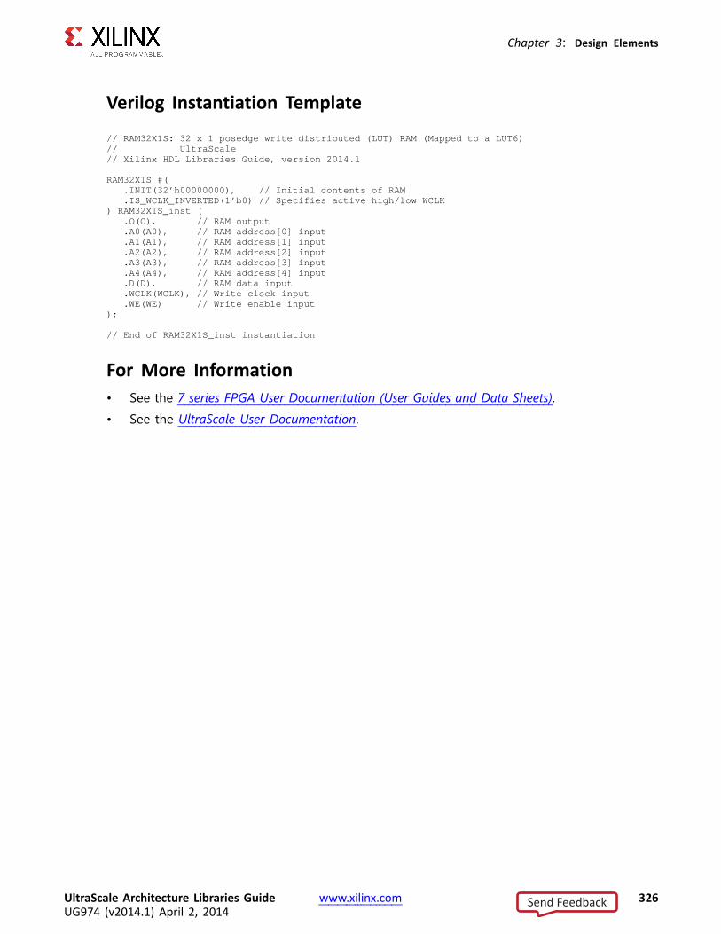
Chapter 3: Design Elements
Verilog Instantiation Template
// RAM32X1S: 32 x 1 posedge write distributed (LUT) RAM (Mapped to a LUT6)// UltraScale// Xilinx HDL Libraries Guide, version 2014.1
RAM32X1S#(.INIT(32’h00000000), // Initial contents of RAM.IS_WCLK_INVERTED(1’b0) // Specifies active high/low WCLK
) RAM32X1S_inst (.O(O), // RAMoutput.A0(A0), // RAMaddress[0] input.A1(A1), // RAMaddress[1] input.A2(A2), // RAMaddress[2] input.A3(A3), // RAMaddress[3] input.A4(A4), // RAMaddress[4] input.D(D), // RAMdata input.WCLK(WCLK), // Write clock input.WE(WE) // Write enable input
);
// End of RAM32X1S_inst instantiation
For More Information• See the 7 series FPGA User Documentation (User Guides and Data Sheets).
• See the UltraScale User Documentation.
UltraScale Architecture Libraries Guide www.xilinx.com 326UG974 (v2014.1) April 2, 2014
Send Feedback

Chapter 3: Design Elements
RAM512X1SPrimitive: 512-Deep by 1-Wide Random Access Memory (Select RAM)PRIMITIVE_GROUP: CLBPRIMITIVE_SUBGROUP: LUTRAM
IntroductionThis design element is a 512-bit deep by 1-bit wide random access memory with synchronouswrite and asynchronous read capability. This RAM is implemented using the LUT resources ofthe device (also known as Select RAM), and does not consume any of the block RAM resourcesof the device. If a synchronous read capability is preferred, a register can be attached to theoutput and placed in the same slice as long as the same clock is used for both the RAM andthe register. The RAM512X1S has an active-High write enable, WE, so that when that signal isHigh, and a rising edge occurs on the WCLK pin, a write is performed recording the value ofthe D input data pin into the memory array. The output O displays the contents of the memorycell addressed by A, regardless of the WE value. When a write is performed, the output isupdated to the new value shortly after the write completes.
Port DescriptionsPort Direction Width Function
O Output 1 Read/Write port data output addressedby A
D Input 1 Write data input addressed by A
A Input 9 Read/Write port address bus
WE Input 1 Write Enable
WCLK Input 1 Write clock (reads are asynchronous)
Design Entry MethodInstantiation Yes
Inference Recommended
IP Catalog No
Macro support No
UltraScale Architecture Libraries Guide www.xilinx.com 327UG974 (v2014.1) April 2, 2014
Send Feedback

Chapter 3: Design Elements
If instantiated, the following connections should be made to this component:
• Tie the WCLK input to the desired clock source, the D input to the data source to be stored,and the O output to an FDCE D input or other appropriate data destination.
• Connect the WE clock enable pin to the proper write enable source in the design.
• Connect the 8-bit A bus to the source for the read/write.
You can use the INIT attribute to specify the initial contents of the RAM. If left unspecified, theinitial contents default to all zeros.
Available AttributesAttribute Type Allowed Values Default Description
INIT Hexadecimal Any 512-bit value All zeros Specifies the initial contents of theRAM.
IS_WCLK_INVERTED Binary 1’b0 to 1’b1 1’b0 Indicates whether the optionalinversion is used or not for the WCLKpin of this component
VHDL Instantiation TemplateUnless they already exist, copy the following two statements and paste them before the entitydeclaration.Library UNISIM;use UNISIM.vcomponents.all;
-- RAM512X1S: 512-deep by 1-wide positive edge write, asynchronous read-- single-port distributed LUT RAM-- UltraScale-- Xilinx HDL Libraries Guide, version 2014.1
RAM512X1S_inst : RAM512X1Sgeneric map (
INIT => X"00000000000000000000000000000000000000000000000000000000000000000000000000000000000000000000000000000000000000000000000000000000", -- Initial contents of RAM
IS_WCLK_INVERTED => ’0’) -- Specifies active high/low WCLKport map (
O => O, -- Read/Write port 1-bit ouputA => A, -- Read/Write port 9-bit address inputD => D, -- RAMdata inputWCLK=> WCLK, -- Write clock inputWE => WE -- Write enable input
);
-- End of RAM512X1S_inst instantiation
UltraScale Architecture Libraries Guide www.xilinx.com 328UG974 (v2014.1) April 2, 2014
Send Feedback

Chapter 3: Design Elements
Verilog Instantiation Template
// RAM512X1S: 512-deep by 1-wide positive edge write, asynchronous read (Mapped to eight LUT6s)// single-port distributed LUT RAM// UltraScale// Xilinx HDL Libraries Guide, version 2014.1
RAM512X1S #(.INIT(512’h00000000000000000000000000000000000000000000000000000000000000000000000000000000000000000000000000000000000000000000000000000000),
.IS_WCLK_INVERTED(1’b0) // Specifies active high/low WCLK) RAM512X1S_inst (
.O(O), // Read/write port 1-bit output
.A(A), // Read/write port 9-bit address input
.WE(WE), // Write enable input
.WCLK(WCLK), // Write clock input
.D(D) // RAMdata input);
// End of RAM512X1S_inst instantiation
For More Information• See the 7 series FPGA User Documentation (User Guides and Data Sheets).
• See the UltraScale User Documentation.
UltraScale Architecture Libraries Guide www.xilinx.com 329UG974 (v2014.1) April 2, 2014
Send Feedback

Chapter 3: Design Elements
RAM64MPrimitive: 64-Deep by 4-bit Wide Multi Port Random Access Memory (SelectRAM)PRIMITIVE_GROUP: CLBPRIMITIVE_SUBGROUP: LUTRAM
IntroductionThis design element is a 64-bit deep by 4-bit wide, multi-port, random access memory withsynchronous write and asynchronous independent bit wide read capability. This RAM isimplemented using the LUT resources of the device (also known as SelectRAM™) and doesnot consume any of the block RAM resources of the device. The RAM64M component isimplemented in a single slice, and consists of one 4-bit write, 1-bit read port, and threeseparate 1-bit read ports from the same memory allowing for 4-bit write and independentbit read access RAM.
• If the DIA, DIB, DIC, and DID inputs are all tied to the same data inputs, the RAM canbecome a 1 read/write port, 3 independent read port 64x1 quad port memory.
• If DID is grounded, DOD is not used.
• If ADDRA, ADDRB, and ADDRC are tied to the same address, the RAM becomes a 64x3simple dual port RAM.
• If ADDRD is tied to ADDRA, ADDRB, and ADDRC, the RAM is a 64x4 single port RAM.
There are several other possible configurations for this RAM.
UltraScale Architecture Libraries Guide www.xilinx.com 330UG974 (v2014.1) April 2, 2014
Send Feedback

Chapter 3: Design Elements
Port DescriptionsPort Direction Width Function
DOA Output 1 Read port data outputs addressed by ADDRA
DOB Output 1 Read port data outputs addressed by ADDRB
DOC Output 1 Read port data outputs addressed by ADDRC
DOD Output 1 Read/Write port data outputs addressed by ADDRD
DIA Input 1 Write data inputs addressed by ADDRD (read output isaddressed by ADDRA)
DIB Input 1 Write data inputs addressed by ADDRD (read output isaddressed by ADDRB)
DIC Input 1 Write data inputs addressed by ADDRD (read output isaddressed by ADDRC)
DID Input 1 Write data inputs addressed by ADDRD
ADDRA Input 6 Read address bus A
ADDRB Input 6 Read address bus B
ADDRC Input 6 Read address bus C
ADDRD Input 6 4-bit data write port, 1-bit data read port address bus D
WE Input 1 Write Enable
WCLK Input 1 Write clock (reads are asynchronous)
Design Entry MethodInstantiation Yes
Inference Recommended
IP Catalog No
Macro support No
This element can be inferred by some synthesis tools by describing a RAM with a synchronouswrite and asynchronous read capability. Consult your synthesis tool documentation for detailson RAM inference capabilities and coding examples. Xilinx suggests that you instantiate thiscomponent if you have a need to implicitly specify the RAM function, or if you need tomanually place or relationally place the component.
If synchronous read capability is desired, the outputs can be connected to an FDRE/FDSE(FDCE/FDPE if asynchronous reset is needed) in order to improve the output timing of thefunction. However, this is not necessary for the proper operation of the RAM. If you wantto have the data clocked on the negative edge of a clock, an inverter can be described onthe clock input to this component. This inverter will be absorbed into the block duringimplementation and set as the IS_WCLK_INVERTED attribute giving the ability to write to theRAM on falling clock edges.
UltraScale Architecture Libraries Guide www.xilinx.com 331UG974 (v2014.1) April 2, 2014
Send Feedback

Chapter 3: Design Elements
If instantiated, the following connections should be made to this component:• Connect the WCLK input to the desired clock source, the DIA, DIB, DIC• Connect the DIA, DIB, DIC, and DID inputs to the data source to be stored• Connect the DOA, DOB, DOC, and DOD outputs to an FDCE D input or other appropriate
data destination, or leave unconnected if not used• Connect the WE clock enable pin to the proper write enable source in the design• Connect the ADDRD bus to the source for the read/write addressing• Connect the ADDRA, ADDRB, and ADDRC buses to the appropriate read address
connections
The optional INIT_A, INIT_B, INIT_C and INIT_D attributes let you specify the initial memorycontents of each port using a 64-bit hexadecimal value. The INIT value correlates to the RAMaddressing by the following equation: ADDRy[z] = INIT_y[z]. For instance, if the RAM ADDRCport is addressed to 00001, then the INIT_C[1] values would be the initial values shown on theDOC port before the first write occurs at that address. If left unspecified, the initial contents willdefault to all zeros.
Available AttributesAttribute Type Allowed Values Default Description
INIT_A Hexadecimal Any 64-bit value All zeros Specifies the initial contents of the RAMon port A.
INIT_B Hexadecimal Any 64-bit value All zeros Specifies the initial contents of the RAMon port B.
INIT_C Hexadecimal Any 64-bit value All zeros Specifies the initial contents of the RAMon port C.
INIT_D Hexadecimal Any 64-bit value All zeros Specifies the initial contents of the RAMon port D.
IS_WCLK_INVERTED Binary 1’b0 to 1’b1 1’b0 Indicates whether the optional inversionis used or not for the WCLK pin of thiscomponent
VHDL Instantiation TemplateUnless they already exist, copy the following two statements and paste them before the entitydeclaration.Library UNISIM;use UNISIM.vcomponents.all;
-- RAM64M: 64-deep by 4-wide Multi Port LUT RAM-- UltraScale-- Xilinx HDL Libraries Guide, version 2014.1
RAM64M_inst : RAM64Mgeneric map (
INIT_A => X"0000000000000000", -- Initial contents of A portINIT_B => X"0000000000000000", -- Initial contents of B portINIT_C => X"0000000000000000", -- Initial contents of C portINIT_D => X"0000000000000000", -- Initial contents of D portIS_WCLK_INVERTED => ’0’) -- Specifies active high/low WCLK
UltraScale Architecture Libraries Guide www.xilinx.com 332UG974 (v2014.1) April 2, 2014
Send Feedback
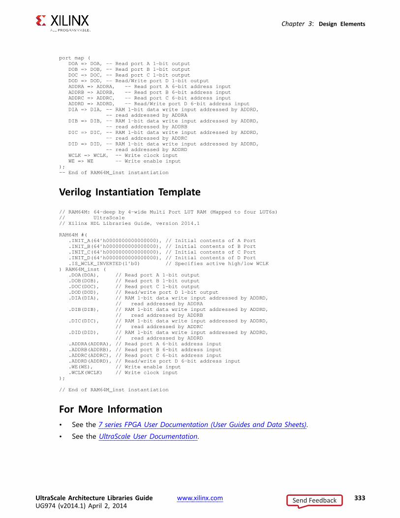
Chapter 3: Design Elements
port map (DOA => DOA, -- Read port A 1-bit outputDOB => DOB, -- Read port B 1-bit outputDOC=> DOC, -- Read port C 1-bit outputDOD=> DOD, -- Read/Write port D 1-bit outputADDRA=> ADDRA, -- Read port A 6-bit address inputADDRB=> ADDRB, -- Read port B 6-bit address inputADDRC=> ADDRC, -- Read port C 6-bit address inputADDRD=> ADDRD, -- Read/Write port D 6-bit address inputDIA => DIA, -- RAM1-bit data write input addressed by ADDRD,
-- read addressed by ADDRADIB => DIB, -- RAM1-bit data write input addressed by ADDRD,
-- read addressed by ADDRBDIC => DIC, -- RAM1-bit data write input addressed by ADDRD,
-- read addressed by ADDRCDID => DID, -- RAM1-bit data write input addressed by ADDRD,
-- read addressed by ADDRDWCLK=> WCLK, -- Write clock inputWE => WE -- Write enable input
);-- End of RAM64M_inst instantiation
Verilog Instantiation Template
// RAM64M: 64-deep by 4-wide Multi Port LUT RAM (Mapped to four LUT6s)// UltraScale// Xilinx HDL Libraries Guide, version 2014.1
RAM64M#(.INIT_A(64’h0000000000000000), // Initial contents of A Port.INIT_B(64’h0000000000000000), // Initial contents of B Port.INIT_C(64’h0000000000000000), // Initial contents of C Port.INIT_D(64’h0000000000000000), // Initial contents of D Port.IS_WCLK_INVERTED(1’b0) // Specifies active high/low WCLK
) RAM64M_inst (.DOA(DOA), // Read port A 1-bit output.DOB(DOB), // Read port B 1-bit output.DOC(DOC), // Read port C 1-bit output.DOD(DOD), // Read/write port D 1-bit output.DIA(DIA), // RAM1-bit data write input addressed by ADDRD,
// read addressed by ADDRA.DIB(DIB), // RAM1-bit data write input addressed by ADDRD,
// read addressed by ADDRB.DIC(DIC), // RAM1-bit data write input addressed by ADDRD,
// read addressed by ADDRC.DID(DID), // RAM1-bit data write input addressed by ADDRD,
// read addressed by ADDRD.ADDRA(ADDRA), // Read port A 6-bit address input.ADDRB(ADDRB), // Read port B 6-bit address input.ADDRC(ADDRC), // Read port C 6-bit address input.ADDRD(ADDRD), // Read/write port D 6-bit address input.WE(WE), // Write enable input.WCLK(WCLK) // Write clock input
);
// End of RAM64M_inst instantiation
For More Information• See the 7 series FPGA User Documentation (User Guides and Data Sheets).
• See the UltraScale User Documentation.
UltraScale Architecture Libraries Guide www.xilinx.com 333UG974 (v2014.1) April 2, 2014
Send Feedback

Chapter 3: Design Elements
RAM64M8Primitive: 64-Deep by 8-bit Wide Multi Port Random Access Memory (SelectRAM)PRIMITIVE_GROUP: CLBPRIMITIVE_SUBGROUP: LUTRAM
IntroductionThis design element is a 64-bit deep by 8-bit wide, multi-port, random access memory withsynchronous write and asynchronous independent bit wide read capability. This RAM isimplemented using the LUT resources of the device (also known as SelectRAM™) and does notconsume any of the block RAM resources of the device. This component is implemented in asingle CLB and consists of one 8-bit write, 1-bit read port, and seven separate 1-bit read portsfrom the same memory allowing for byte-wide write and independent bit read access RAM.• If the 7 inputs are all tied to the same data inputs, the RAM can become a 1 read/write
port, 7 independent read port 64x1 octal port memory.• If DIH is grounded, DOH is not used.• If ADDRA through ADDRG are tied to the same address, the RAM becomes a 64x14 simple
dual port RAM.• If ADDRA through ADDRH are tied together, the RAM becomes a 64x16 single port RAM.There are several other possible configurations for this RAM.
UltraScale Architecture Libraries Guide www.xilinx.com 334UG974 (v2014.1) April 2, 2014
Send Feedback

Chapter 3: Design Elements
Port DescriptionsPort Direction Width Function
DOA Output 1 Read port data outputs addressed by ADDRA
DOB Output 1 Read port data outputs addressed by ADDRB
DOC Output 1 Read port data outputs addressed by ADDRC
DOD Output 1 Read port data outputs addressed by ADDRD
DOE Output 1 Read port data outputs addressed by ADDRE
DOF Output 1 Read port data outputs addressed by ADDRF
DOG Output 1 Read port data outputs addressed by ADDRG
DOH Output 1 Read/Write port data outputs addressed by ADDRH
DIA Input 1 Data write input addressed by ADDRH (read output isaddressed by ADDRA)
DIB Input 1 Data write input addressed by ADDRH (read output isaddressed by ADDRB)
DIC Input 1 Data write input addressed by ADDRH (read output isaddressed by ADDRC)
DID Input 1 Data write input addressed by ADDRH (read output isaddressed by ADDRD)
DIE Input 1 Data write input addressed by ADDRH (read output isaddressed by ADDRE)
DIF Input 1 Data write input addressed by ADDRH (read output isaddressed by ADDRF)
DIG Input 1 Data write input addressed by ADDRH (read output isaddressed by ADDRG)
DIH Input 1 RAM 2-bit data write input addressed by ADDRH (readoutput is addressed by ADDRH)
ADDRA Input 6 Read port A address input
ADDRB Input 6 Read port B address input
ADDRC Input 6 Read port C address input
ADDRD Input 6 Read port D address input
ADDRE Input 6 Read port E address input
ADDRF Input 6 Read port F address input
ADDRG Input 6 Read port G address input
ADDRH Input 6 Read/write port H address input
WE Input 1 Write Enable
WCLK Input 1 Write clock (reads are asynchronous)
UltraScale Architecture Libraries Guide www.xilinx.com 335UG974 (v2014.1) April 2, 2014
Send Feedback

Chapter 3: Design Elements
Design Entry MethodInstantiation Yes
Inference Recommended
IP Catalog No
Macro support No
This element can be inferred by some synthesis tools by describing a RAM with a synchronouswrite and asynchronous read capability. Consult your synthesis tool documentation for detailson RAM inference capabilities and coding examples. Xilinx suggests that you instantiate thiscomponent if you have a need to implicitly specify the RAM function, or if you need tomanually place or relationally place the component.
If synchronous read capability is desired, the outputs can be connected to an FDRE/FDSE(FDCE/FDPE if asynchronous reset is needed) in order to improve the output timing of thefunction. However, this is not necessary for the proper operation of the RAM. If you wantto have the data clocked on the negative edge of a clock, an inverter can be described onthe clock input to this component. This inverter will be absorbed into the block duringimplementation and set as the IS_WCLK_INVERTED attribute giving the ability to write to theRAM on falling clock edges.
If instantiated, the following connections should be made to this component:
• Connect the WCLK input to the desired clock source
• Connect the DIA–DIH inputs to the data source to be stored
• Connect the DOA–DOH outputs to an FD* D input or other appropriate data destination,or leave unconnected if not used
• Connect the WE clock enable pin to the proper write enable source in the design
• Connect the ADDRH bus to the source for the read/write addressing
• Connect the ADDRA–ADDRG buses to the appropriate read address connections
The optional INIT_A–INIT_H attributes let you specify the initial memory contents of each portusing a 64-bit hexadecimal value. The INIT value correlates to the RAM addressing by thefollowing equation: ADDRy[z] = INIT_y[z]. For instance, if the RAM ADDRC port is addressed to00001, then the INIT_C[1] values would be the initial values shown on the DOC port before thefirst write occurs at that address. If left unspecified, the initial contents will default to all zeros.
Available AttributesAttribute Type Allowed Values Default Description
INIT_A Hexadecimal Any 128-bitvalue
All zeros Specifies the initial contents of the RAMon port A.
INIT_B Hexadecimal Any 128-bitvalue
All zeros Specifies the initial contents of the RAMon port B.
INIT_C Hexadecimal Any 128-bitvalue
All zeros Specifies the initial contents of the RAMon port C.
INIT_D Hexadecimal Any 128-bitvalue
All zeros Specifies the initial contents of the RAMon port D.
UltraScale Architecture Libraries Guide www.xilinx.com 336UG974 (v2014.1) April 2, 2014
Send Feedback

Chapter 3: Design Elements
Attribute Type Allowed Values Default Description
INIT_E Hexadecimal Any 128-bitvalue
All zeros Specifies the initial contents of the RAMon port E.
INIT_F Hexadecimal Any 128-bitvalue
All zeros Specifies the initial contents of the RAMon port F.
INIT_G Hexadecimal Any 128-bitvalue
All zeros Specifies the initial contents of the RAMon port G.
INIT_H Hexadecimal Any 128-bitvalue
All zeros Specifies the initial contents of the RAMon port H.
IS_WCLK_INVERTED Binary 1’b0 to 1’b1 1’b0 Indicates whether the optional inversionis used or not for the WCLK pin of thiscomponent
VHDL Instantiation TemplateUnless they already exist, copy the following two statements and paste them before the entitydeclaration.Library UNISIM;use UNISIM.vcomponents.all;
-- RAM64M8: 64-deep by 8-wide Multi Port LUT RAM-- UltraScale-- Xilinx HDL Libraries Guide, version 2014.1RAM64M8_inst : RAM64M8generic map (
INIT_A => X"0000000000000000", -- Initial contents of A portINIT_B => X"0000000000000000", -- Initial contents of B portINIT_C => X"0000000000000000", -- Initial contents of C portINIT_D => X"0000000000000000", -- Initial contents of D portINIT_E => X"0000000000000000", -- Initial contents of E portINIT_F => X"0000000000000000", -- Initial contents of F portINIT_G => X"0000000000000000", -- Initial contents of G portINIT_H => X"0000000000000000", -- Initial contents of H portIS_WCLK_INVERTED => ’0’) -- Specifies active high/low WCLK
port map (DOA => DOA, -- Read port A 1-bit outputDOB => DOB, -- Read port B 1-bit outputDOC=> DOC, -- Read port C 1-bit outputDOD=> DOD, -- Read port D 1-bit outputDOE => DOE, -- Read port E 1-bit outputDOF => DOF, -- Read port F 1-bit outputDOG=> DOG, -- Read port G 1-bit outputDOH=> DOH, -- Read/write port H 1-bit outputADDRA=> ADDRA, -- Read port A 6-bit address inputADDRB=> ADDRB, -- Read port B 6-bit address inputADDRC=> ADDRC, -- Read port C 6-bit address inputADDRD=> ADDRD, -- Read port D 6-bit address inputADDRE=> ADDRE, -- Read port E 6-bit address inputADDRF=> ADDRF, -- Read port F 6-bit address inputADDRG=> ADDRG, -- Read port G 6-bit address inputADDRH=> ADDRH, -- Read/write port H 6-bit address inputDIA => DIA, -- RAM1-bit data write input addressed by ADDRD,
-- read addressed by ADDRADIB => DIB, -- RAM1-bit data write input addressed by ADDRD,
-- read addressed by ADDRBDIC => DIC, -- RAM1-bit data write input addressed by ADDRD,
-- read addressed by ADDRCDID => DID, -- RAM1-bit data write input addressed by ADDRD,
-- read addressed by ADDRDDIE => DIE, -- RAM1-bit data write input addressed by ADDRE,
-- read addressed by ADDRE
UltraScale Architecture Libraries Guide www.xilinx.com 337UG974 (v2014.1) April 2, 2014
Send Feedback
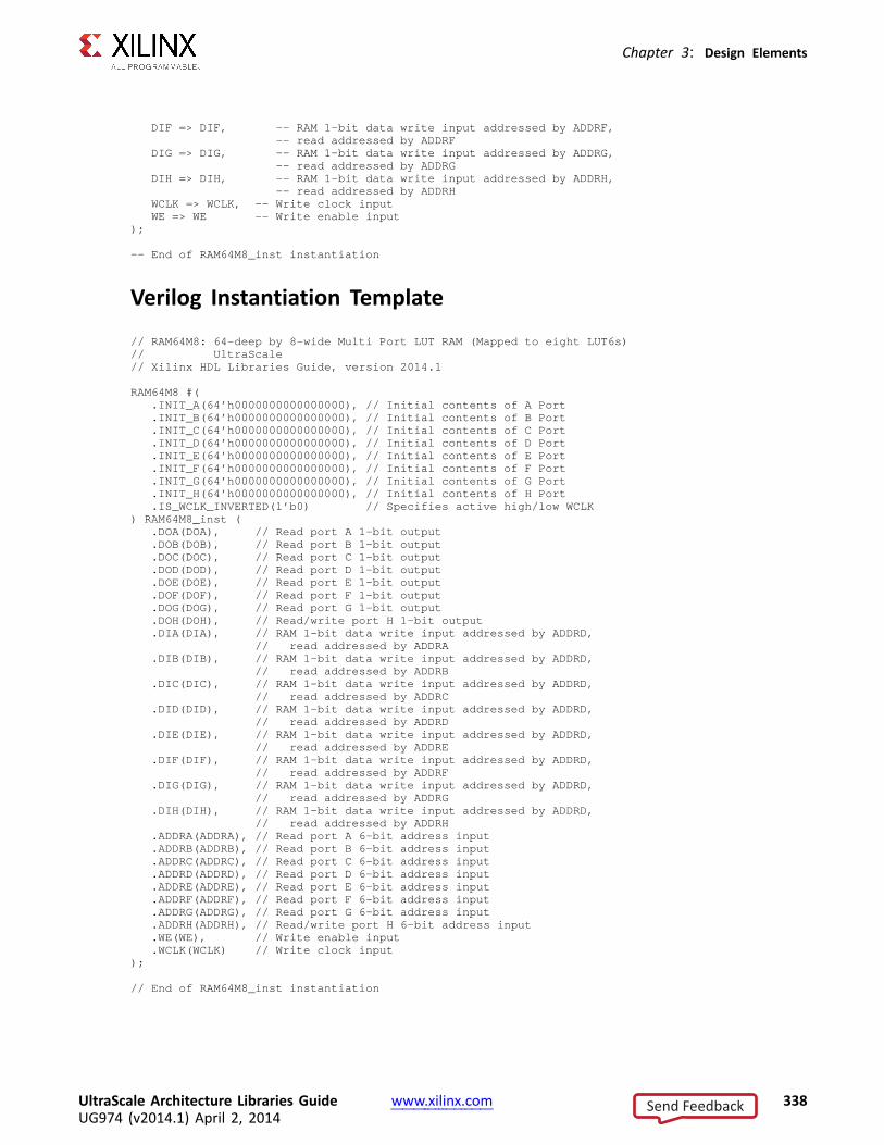
Chapter 3: Design Elements
DIF => DIF, -- RAM1-bit data write input addressed by ADDRF,-- read addressed by ADDRF
DIG => DIG, -- RAM1-bit data write input addressed by ADDRG,-- read addressed by ADDRG
DIH => DIH, -- RAM1-bit data write input addressed by ADDRH,-- read addressed by ADDRH
WCLK=> WCLK, -- Write clock inputWE => WE -- Write enable input
);
-- End of RAM64M8_inst instantiation
Verilog Instantiation Template
// RAM64M8: 64-deep by 8-wide Multi Port LUT RAM (Mapped to eight LUT6s)// UltraScale// Xilinx HDL Libraries Guide, version 2014.1
RAM64M8#(.INIT_A(64’h0000000000000000), // Initial contents of A Port.INIT_B(64’h0000000000000000), // Initial contents of B Port.INIT_C(64’h0000000000000000), // Initial contents of C Port.INIT_D(64’h0000000000000000), // Initial contents of D Port.INIT_E(64’h0000000000000000), // Initial contents of E Port.INIT_F(64’h0000000000000000), // Initial contents of F Port.INIT_G(64’h0000000000000000), // Initial contents of G Port.INIT_H(64’h0000000000000000), // Initial contents of H Port.IS_WCLK_INVERTED(1’b0) // Specifies active high/low WCLK
) RAM64M8_inst (.DOA(DOA), // Read port A 1-bit output.DOB(DOB), // Read port B 1-bit output.DOC(DOC), // Read port C 1-bit output.DOD(DOD), // Read port D 1-bit output.DOE(DOE), // Read port E 1-bit output.DOF(DOF), // Read port F 1-bit output.DOG(DOG), // Read port G 1-bit output.DOH(DOH), // Read/write port H 1-bit output.DIA(DIA), // RAM1-bit data write input addressed by ADDRD,
// read addressed by ADDRA.DIB(DIB), // RAM1-bit data write input addressed by ADDRD,
// read addressed by ADDRB.DIC(DIC), // RAM1-bit data write input addressed by ADDRD,
// read addressed by ADDRC.DID(DID), // RAM1-bit data write input addressed by ADDRD,
// read addressed by ADDRD.DIE(DIE), // RAM1-bit data write input addressed by ADDRD,
// read addressed by ADDRE.DIF(DIF), // RAM1-bit data write input addressed by ADDRD,
// read addressed by ADDRF.DIG(DIG), // RAM1-bit data write input addressed by ADDRD,
// read addressed by ADDRG.DIH(DIH), // RAM1-bit data write input addressed by ADDRD,
// read addressed by ADDRH.ADDRA(ADDRA), // Read port A 6-bit address input.ADDRB(ADDRB), // Read port B 6-bit address input.ADDRC(ADDRC), // Read port C 6-bit address input.ADDRD(ADDRD), // Read port D 6-bit address input.ADDRE(ADDRE), // Read port E 6-bit address input.ADDRF(ADDRF), // Read port F 6-bit address input.ADDRG(ADDRG), // Read port G 6-bit address input.ADDRH(ADDRH), // Read/write port H 6-bit address input.WE(WE), // Write enable input.WCLK(WCLK) // Write clock input
);
// End of RAM64M8_inst instantiation
UltraScale Architecture Libraries Guide www.xilinx.com 338UG974 (v2014.1) April 2, 2014
Send Feedback

Chapter 3: Design Elements
For More Information• See the 7 series FPGA User Documentation (User Guides and Data Sheets).
• See the UltraScale User Documentation.
UltraScale Architecture Libraries Guide www.xilinx.com 339UG974 (v2014.1) April 2, 2014
Send Feedback

Chapter 3: Design Elements
RAM64X1DPrimitive: 64-Deep by 1-Wide Dual Port Static Synchronous RAMPRIMITIVE_GROUP: CLBPRIMITIVE_SUBGROUP: LUTRAM
IntroductionThis design element is a 64-bit deep by 1-bit wide static dual port random access memorywith synchronous write capability. The device has two separate address ports: the read address(DPRA5:DPRA0) and the write address (A5:A0). These two address ports are completelyasynchronous. The read address controls the location of the data driven out of the output pin(DPO), and the write address controls the destination of a valid write transaction. When thewrite enable (WE) is Low, transitions on the write clock (WCLK) are ignored and data stored inthe RAM is not affected.
When WE is High, any positive transition on WCLK loads the data on the data input (D) into thememory cell selected by the 6-bit (A0:A5) write address. For predictable performance, writeaddress and data inputs must be stable before a Low-to-High WCLK transition. This RAM blockassumes an active-High WCLK. WCLK can be active-High or active-Low. Any inverter placed onthe WCLK input net is absorbed into the block.
The SPO output reflects the data in the memory cell addressed by A5:A0. The DPO outputreflects the data in the memory cell addressed by DPRA5:DPRA0. The write process is notaffected by the address on the read address port.
You can use the INIT attribute to specify the initial contents of the RAM. If left unspecified, theinitial contents default to all zeros.
Logic TableInputs OutputsWE (mode) WCLK D SPO DPO
0 (read) X X data_a data_d
1 (read) 0 X data_a data_d
1 (read) 1 X data_a data_d
1 (write) ↑ D D data_d
UltraScale Architecture Libraries Guide www.xilinx.com 340UG974 (v2014.1) April 2, 2014
Send Feedback

Chapter 3: Design Elements
Inputs OutputsWE (mode) WCLK D SPO DPO
1 (read) ↓ X data_a data_d
data_a = memory cell addressed by bits A5:A0
data_d = memory cell addressed by bits DPRA5:DPRA0
Design Entry MethodInstantiation Yes
Inference Recommended
IP Catalog No
Macro support No
Available AttributesAttribute Type Allowed Values Default Description
INIT Hexadecimal Any 64-bit value All zeros Specifies the initial contents of theRAM.
IS_WCLK_INVERTED Binary 1’b0 to 1’b1 1’b0 Indicates whether the optionalinversion is used or not for the WCLKpin of this component
VHDL Instantiation TemplateUnless they already exist, copy the following two statements and paste them before the entitydeclaration.Library UNISIM;use UNISIM.vcomponents.all;
-- RAM64X1D: 64 x 1 positive edge write, asynchronous read-- dual-port distributed RAM-- UltraScale-- Xilinx HDL Libraries Guide, version 2014.1
RAM64X1D_inst : RAM64X1Dgeneric map (
INIT => X"0000000000000000", -- Initial contents of RAMIS_WCLK_INVERTED => ’0’) -- Specifies active high/low WCLK
port map (DPO => DPO, -- Read-only 1-bit data outputSPO => SPO, -- R/W 1-bit data outputA0 => A0, -- R/W address[0] input bitA1 => A1, -- R/W address[1] input bitA2 => A2, -- R/W address[2] input bitA3 => A3, -- R/W address[3] input bitA4 => A4, -- R/W address[4] input bitA5 => A5, -- R/W address[5] input bitD => D, -- Write 1-bit data inputDPRA0 => DPRA0, -- Read-only address[0] input bitDPRA1 => DPRA1, -- Read-only address[1] input bitDPRA2 => DPRA2, -- Read-only address[2] input bitDPRA3 => DPRA3, -- Read-only address[3] input bitDPRA4 => DPRA4, -- Read-only address[4] input bit
UltraScale Architecture Libraries Guide www.xilinx.com 341UG974 (v2014.1) April 2, 2014
Send Feedback

Chapter 3: Design Elements
DPRA5 => DPRA5, -- Read-only address[5] input bitWCLK=> WCLK, -- Write clock inputWE => WE -- Write enable input
);
-- End of RAM64X1D_inst instantiation
Verilog Instantiation Template
// RAM64X1D: 64 x 1 positive edge write, asynchronous read dual-port distributed RAM (Mapped to two LUT6s)// UltraScale// Xilinx HDL Libraries Guide, version 2014.1
RAM64X1D#(.INIT(64’h0000000000000000), // Initial contents of RAM.IS_WCLK_INVERTED(1’b0) // Specifies active high/low WCLK
) RAM64X1D_inst (.DPO(DPO), // Read-only 1-bit data output.SPO(SPO), // Rw/ 1-bit data output.A0(A0), // Rw/ address[0] input bit.A1(A1), // Rw/ address[1] input bit.A2(A2), // Rw/ address[2] input bit.A3(A3), // Rw/ address[3] input bit.A4(A4), // Rw/ address[4] input bit.A5(A5), // Rw/ address[5] input bit.D(D), // Write 1-bit data input.DPRA0(DPRA0), // Read-only address[0] input bit.DPRA1(DPRA1), // Read-only address[1] input bit.DPRA2(DPRA2), // Read-only address[2] input bit.DPRA3(DPRA3), // Read-only address[3] input bit.DPRA4(DPRA4), // Read-only address[4] input bit.DPRA5(DPRA5), // Read-only address[5] input bit.WCLK(WCLK), // Write clock input.WE(WE) // Write enable input
);
// End of RAM64X1D_inst instantiation
For More Information• See the 7 series FPGA User Documentation (User Guides and Data Sheets).
• See the UltraScale User Documentation.
UltraScale Architecture Libraries Guide www.xilinx.com 342UG974 (v2014.1) April 2, 2014
Send Feedback

Chapter 3: Design Elements
RAM64X1SPrimitive: 64-Deep by 1-Wide Static Synchronous RAMPRIMITIVE_GROUP: CLBPRIMITIVE_SUBGROUP: LUTRAM
IntroductionThis design element is a 64-bit deep by 1-bit wide static random access memory (RAM) withsynchronous write capability. When the write enable is set Low, transitions on the write clock(WCLK) are ignored and data stored in the RAM is not affected. When WE is set High, anypositive transition on WCLK loads the data on the data input (D) into the memory cell selectedby the 6-bit address (A5:A0). This RAM block assumes an active-High WCLK. However, WCLKcan be active-High or active-Low. Any inverter placed on the WCLK input net is absorbedinto the block.
The signal output on the data output pin (O) is the data that is stored in the memory celldefined by the values on the address pins.
You can use the INIT attribute to specify the initial contents of the RAM. If left unspecified, theinitial contents default to all zeros.
Logic TableMode selection is shown in the following logic tableInputs OutputsWE (mode) WCLK D O
0 (read) X X Data
1 (read) 0 X Data
1 (read) 1 X Data
1 (write) ↑ D D
1 (read) ↓ X Data
Data = memory cell addressed by bits A5:A0
UltraScale Architecture Libraries Guide www.xilinx.com 343UG974 (v2014.1) April 2, 2014
Send Feedback

Chapter 3: Design Elements
Design Entry MethodInstantiation Yes
Inference Recommended
IP Catalog No
Macro support No
Available AttributesAttribute Type Allowed Values Default Description
INIT Hexadecimal Any 64-bit value All zeros Specifies the initial contents of theRAM.
IS_WCLK_INVERTED Binary 1’b0 to 1’b1 1’b0 Indicates whether the optionalinversion is used or not for the WCLKpin of this component
VHDL Instantiation TemplateUnless they already exist, copy the following two statements and paste them before the entitydeclaration.Library UNISIM;use UNISIM.vcomponents.all;
-- RAM64X1S: 64 x 1 positive edge write, asynchronous read single-port distributed RAM-- UltraScale-- Xilinx HDL Libraries Guide, version 2014.1
RAM64X1S_inst : RAM64X1Sgeneric map (
INIT => X"0000000000000000", -- Initial contents of RAMIS_WCLK_INVERTED => ’0’) -- Specifies active high/low WCLK
port map (O => O, -- 1-bit data outputA0 => A0, -- Address[0] input bitA1 => A1, -- Address[1] input bitA2 => A2, -- Address[2] input bitA3 => A3, -- Address[3] input bitA4 => A4, -- Address[4] input bitA5 => A5, -- Address[5] input bitD => D, -- 1-bit data inputWCLK=> WCLK, -- Write clock inputWE => WE -- Write enable input
);
-- End of RAM64X1S_inst instantiation
UltraScale Architecture Libraries Guide www.xilinx.com 344UG974 (v2014.1) April 2, 2014
Send Feedback

Chapter 3: Design Elements
Verilog Instantiation Template
// RAM64X1S: 64 x 1 positive edge write, asynchronous read single-port distributed RAM (Mapped to a LUT6)// UltraScale// Xilinx HDL Libraries Guide, version 2014.1
RAM64X1S#(.INIT(64’h0000000000000000), // Initial contents of RAM.IS_WCLK_INVERTED(1’b0) // Specifies active high/low WCLK
) RAM64X1S_inst (.O(O), // 1-bit data output.A0(A0), // Address[0] input bit.A1(A1), // Address[1] input bit.A2(A2), // Address[2] input bit.A3(A3), // Address[3] input bit.A4(A4), // Address[4] input bit.A5(A5), // Address[5] input bit.D(D), // 1-bit data input.WCLK(WCLK), // Write clock input.WE(WE) // Write enable input
);
// End of RAM64X1S_inst instantiation
For More Information• See the 7 series FPGA User Documentation (User Guides and Data Sheets).
• See the UltraScale User Documentation.
UltraScale Architecture Libraries Guide www.xilinx.com 345UG974 (v2014.1) April 2, 2014
Send Feedback

Chapter 3: Design Elements
RAMB18E2Primitive: 18K-bit Configurable Synchronous Block RAMPRIMITIVE_GROUP: BLOCKRAMPRIMITIVE_SUBGROUP: BRAM
UltraScale Architecture Libraries Guide www.xilinx.com 346UG974 (v2014.1) April 2, 2014
Send Feedback

Chapter 3: Design Elements
IntroductionThe RAMB18E2 allows access to the block RAM memory in the 18Kb configuration. Thiselement can be configured and used as a 1-bit wide by 16K deep to an 18-bit wide by 1024-bitdeep true dual port RAM. This element can also be configured as a 36-bit wide by 512 deepsimple dual port RAM. Both read and write operations are fully synchronous to the suppliedclock(s) to the component. However, the READ and WRITE ports can operate fully independentand asynchronous to each other, accessing the same memory array. When configured in thewider data width modes, byte-enable write operations are possible, and an optional outputregister can be used to reduce the clock-to-out times of the RAM. This RAM also features acascade capability which allows multiple RAMB18E2 components to be chained together toform deeper and more power efficient memory configuration if desired.
Port DescriptionsPort Direction Width Function
ADDRARDADDR<13:0> Input 14 Port A address input bus/Read address input bus.
ADDRBWRADDR<13:0> Input 14 Port B address input bus/Write address input bus.
ADDRENA Input 1 Active-High port A address input bus/Read address inputbus.
ADDRENB Input 1 Active-High port B address input bus/Write address inputbus.
CASDIMUXA Input 1 Port A mux control input to select between normal datainput (DINA) when Low or CASCADE data input (CASDINA)when High.
CASDIMUXB Input 1 Port B mux control input to select between normal datainput (DINB) when Low or CASCADE data input (CASDINB)when High.
CASDINA<15:0> Input 16 Port A cascade input data
CASDINB<15:0> Input 16 Port B cascade input data
CASDINPA<1:0> Input 2 Port A cascade input parity data
CASDINPB<1:0> Input 2 Port B cascade input parity data
CASDOMUXA Input 1 Port A mux control input to select between unregisteredoutput data from BRAM or CASCADE data input(CASDINA).
CASDOMUXB Input 1 Port B mux control input to select between unregisteredoutput data from BRAM or CASCADE data input(CASDINB).
CASDOMUXEN_A Input 1 Port A unregistered output data register enable.
CASDOMUXEN_B Input 1 Port B unregistered output data register enable.
CASDOUTA<15:0> Output 16 Port A cascade output data
CASDOUTB<15:0> Output 16 Port B cascade output data
CASDOUTPA<1:0> Output 2 Port A cascade output parity data
CASDOUTPB<1:0> Output 2 Port B cascade output parity data
UltraScale Architecture Libraries Guide www.xilinx.com 347UG974 (v2014.1) April 2, 2014
Send Feedback

Chapter 3: Design Elements
Port Direction Width Function
CASOREGIMUXA Input 1 Port A mux control input to select between registeredoutput data from BRAM or CASCADE data input(CASDINA).
CASOREGIMUXB Input 1 Port B mux control input to select between registeredoutput data from BRAM or CASCADE data input(CASDINB).
CASOREGIMUXEN_A Input 1 Port A registered output data register enable.
CASOREGIMUXEN_B Input 1 Port B registered output data register enable.
CLKARDCLK Input 1 Port A clock input/Read clock input.
CLKBWRCLK Input 1 Port B clock input/Write clock input.
DINADIN<15:0> Input 16 Port A data input bus. When WRITE_WIDTH=36, DINADINis the logical DI<15:0>.
DINBDIN<15:0> Input 16 Port B data input bus. When WRITE_WIDTH=36, DINBDINis the logical DI<31:16>.
DINPADINP<1:0> Input 2 Port A parity data input bus/Data parity input busaddressed by WRADDR. When WRITE_WIDTH=36,DINPADINP is the logical DIP<1:0>.
DINPBDINP<1:0> Input 2 Port B parity data input bus/Data parity input busaddressed by WRADDR. When WRITE_WIDTH=36,DINPBDINP is the logical DIP<3:2>.
DOUTADOUT<15:0> Output 16 Port A data output bus. When READ_WIDTH=36,DOUTADOUT is the logical DO<15:0>.
DOUTBDOUT<15:0> Output 16 Port B data output bus. When READ_WIDTH=36,DOUTBDOUT is the logical DO<31:16>.
DOUTPADOUTP<1:0> Output 2 Port A parity data output bus. When READ_WIDTH=36,DOUTPADOUT is the logical DOP<1:0>.
DOUTPBDOUTP<1:0> Output 2 Port B parity data output bus. When READ_WIDTH=36,DOUTPBDOUTP is the logical DOP<3:2>.
ENARDEN Input 1 Port A RAM enable/Read enable.
ENBWREN Input 1 Port B RAM enable/Write enable.
REGCEAREGCE Input 1 Port A output register clock enable input/Output registerclock enable input (valid only when DOA_REG=1).
REGCEB Input 1 Port B output register clock enable (valid only whenDOB_REG=1 and READ_WIDTH<=18).
RSTRAMARSTRAM Input 1 Synchronous data latch set/reset to value indicated bySRVAL_A. RSTRAMARSTRAM sets/resets the BRAM dataoutput latch when DO_REG=0 or 1. If DO_REG=1 there isa cycle of latency between the internal data latch nodethat is reset by RSTRAMARSTRAM and the DO output ofthe BRAM. This signal resets port A RAM output whenREAD_WIDTH<=18 and the entire RAM output whenREAD_WIDTH=36.
UltraScale Architecture Libraries Guide www.xilinx.com 348UG974 (v2014.1) April 2, 2014
Send Feedback

Chapter 3: Design Elements
Port Direction Width Function
RSTRAMB Input 1 Synchronous data latch set/reset to value indicated bySRVAL_B. RSTRAMB sets/resets the BRAM data outputlatch when DO_REG=0 or 1. If DO_REG=1 there is a cycleof latency between the internal data latch node that isreset by RSTRAMB and the DO output of the BRAM. Notused when READ_WIDTH=36.
RSTREGARSTREG Input 1 Synchronous output register set/reset to value indicated bySRVAL_A. RSTREGARSTREG sets/resets the output registerwhen DO_REG=1. RSTREG_PRIORITY_A determines if thissignal gets priority over REGCEAREGCE. This signal resetsport A output when READ_WIDTH<=18 and the entireRAM output when READ_WIDTH=36.
RSTREGB Input 1 Synchronous output register set/reset to value indicatedby SRVAL_B. RSTREGB sets/resets the output registerwhen DO_REG=1. RSTREG_PRIORITY_B determines ifthis signal gets priority over REGCEB. Not used whenREAD_WIDTH=36.
SLEEP Input 1 Dynamic shut down power saving. If SLEEP is High, theblock is in power saving mode. If SLEEP_ASYNC=FALSE,synchronous to RDCLK, otherwise, asynchronous input.
WEA<1:0> Input 2 Port A byte-wide write enable. Not used whenRAM_MODE="SDP". See User Guide for WEA mapping fordifferent port widths.
WEBWE<3:0> Input 4 Port B byte-wide write enable/Write enable. See UserGuide for WEBWE mapping for different port widths.
Design Entry MethodInstantiation Yes
Inference Recommended
IP and IP Integrator Catalog Yes
Macro support Yes
Available AttributesAttribute Type Allowed Values Default Description
CASCADE_ORDER_A,CASCADE_ORDER_B
STRING "NONE", "FIRST","LAST", "MIDDLE"
"NONE" Specifies the order of thecascaded BRAM. FIRSTBRAM is the bottom incascade, LAST one is onthe top of the cascade, andMIDDLE is the BRAM inbetween bottom and top.
UltraScale Architecture Libraries Guide www.xilinx.com 349UG974 (v2014.1) April 2, 2014
Send Feedback

Chapter 3: Design Elements
Attribute Type Allowed Values Default Description
CLOCK _DOMAINS STRING "INDEPENDENT","COMMON"
"INDEPENDENT" Used for Simulation purposeto model the addressscollision case as wellas enable lower poweroperation in common clockmode.
• "COMMON"=CommonClock/Single Clock
• "INDEPENDENT"=IndependentClock/Dual Clock
DOA_REG,DOB_REG
DECIMAL 1, 0 1 A value of 1 enables theoutput registers to the RAMenabling higher perfromanceclock-to-out from the RAMat the expense of an addedclock cycle of read latency.A value of 0 allows a readin one clock cycle but willresult in slower clock-to-outtiming.
ENADDRENA,ENADDRENB
STRING "FALSE", "TRUE" "FALSE" Specifies if Address Enablepin is enabled
INIT_A, INIT_B HEX 18’h00000 to18’h3ffff
18’h00000 Specifies the initial valueon the port output afterconfiguration.
INIT_FILE STRING String "NONE" File name of file used tospecify initial RAM contents.
INIT_00 to INIT_3F HEX 256’h0000000000000000000000000000000000000000000000000000000000000000 to256’hfffffffffffffffffffffffffffffffffffffffffffffffffffffffffff fffff
256’h0000000000000000000000000000000000000000000000000000000000000000
Allows specification of theinitial contents of the 16Kbdata memory array.
INITP_00,INITP_01,INITP_02,INITP_03,INITP_04,INITP_05,INITP_06, INITP_07
HEX 256’h0000000000000000000000000000000000000000000000000000000000000000 to256’hfffffffffffffffffffffffffffffffffffffffffffffffffffffffffff fffff
256’h0000000000000000000000000000000000000000000000000000000000000000
Allows specification of theinitial contents of the 2Kbparity data memory array.
UltraScale Architecture Libraries Guide www.xilinx.com 350UG974 (v2014.1) April 2, 2014
Send Feedback

Chapter 3: Design Elements
Attribute Type Allowed Values Default Description
IS_CLKARDCLK_INVERTED,IS_CLKBWRCLK_INVERTED,IS_ENARDEN_INVERTED,IS_ENBWREN_INVERTED, IS_RSTRAMARSTRAM_INVERTED,IS_RSTRAMB_INVERTED, IS_RSTREGARSTREG_INVERTED,IS_RSTREGB_INVERTED
BINARY 1’b0 to 1’b1 1’b0 Indicates whether theoptional inversions are tobe used or not on specificpins for this component thuschanging the active polarityof that pin’s function. Whenset to 1 on a clock pin(WRCLK or RDCLK), thiscomponents clocks onthe negative edge. Whenset to 1 on other pins, itchanges the function tobehave active-Low ratherthan active-High. Forpins that are buses, thebit-width of this attributeshould match that of thebit-width of the associatedpins and a binary valueindicates which inverters touse and which to bypass.If an external inverter isspecified on one of theseasscoaited pins, the Vivadosoftware will automaticallyset this attribute duringthe opt_design stage sothat additional logic is notnecessary for changing theinput polarity.
RDADDRCHANGEA,RDADDRCHANGEB
STRING "FALSE", "TRUE" "FALSE" Read Address Change is afeature which will preventmemory access when theoutput value does notchange thus saving power.Setting this attribute to TRUEenables this power-savingfeature. Setting it to falseimproves setup time to theRAM possibly improvingBRAM performance.
READ_WIDTH_A,READ_WIDTH_B,WRITE_WIDTH_A,WRITE_WIDTH_B
DECIMAL 0, 1, 2, 4, 9, 18, 36 0 Specifies the desired datawidth for a read/write onport A/B, including paritybits. This value must be0 if the port is not used.Otherwise, it should be setto the desired port width.
RSTREG_PRIORITY_A,RSTREG_PRIORITY_B
STRING "RSTREG", "REGCE" "RSTREG" Selects register priority forRSTREG or REGCE
UltraScale Architecture Libraries Guide www.xilinx.com 351UG974 (v2014.1) April 2, 2014
Send Feedback

Chapter 3: Design Elements
Attribute Type Allowed Values Default Description
SIM _COLLISION_CHECK
STRING "ALL","GENERATE_X_ONLY","NONE","WARNING_ONLY"
"ALL" Allows modification of thesimulation behavior so thatif a memory collision occurs
• "ALL" = warningproduced and affectedoutputs/memory gounknown (X)
• "WARNING_ONLY" =warning producedand affectedoutputs/memory retainlast value
• "GENERATE_X_ONLY" =no warning and affectedoutputs/memory gounknown (X)
• "NONE" = nowarning and affectedoutputs/memory retainlast value
NOTE: Use this settingcarefully. Setting it to a valueother than "ALL" can maskdesign problems duringsimulation.
SLEEP_ASYNC STRING "FALSE", "TRUE" "FALSE" Specifies whether the SLEEPpin is synchronous to theCLKARDCLK pin ("FALSE") ortreated as an asynchronouspin.
SRVAL_A, SRVAL_B HEX 18’h00000 to18’h3ffff
18’h00000 Specifies the output valueof the RAM upon assertionof the synchronous reset(RST/RSTREG) signal.
UltraScale Architecture Libraries Guide www.xilinx.com 352UG974 (v2014.1) April 2, 2014
Send Feedback
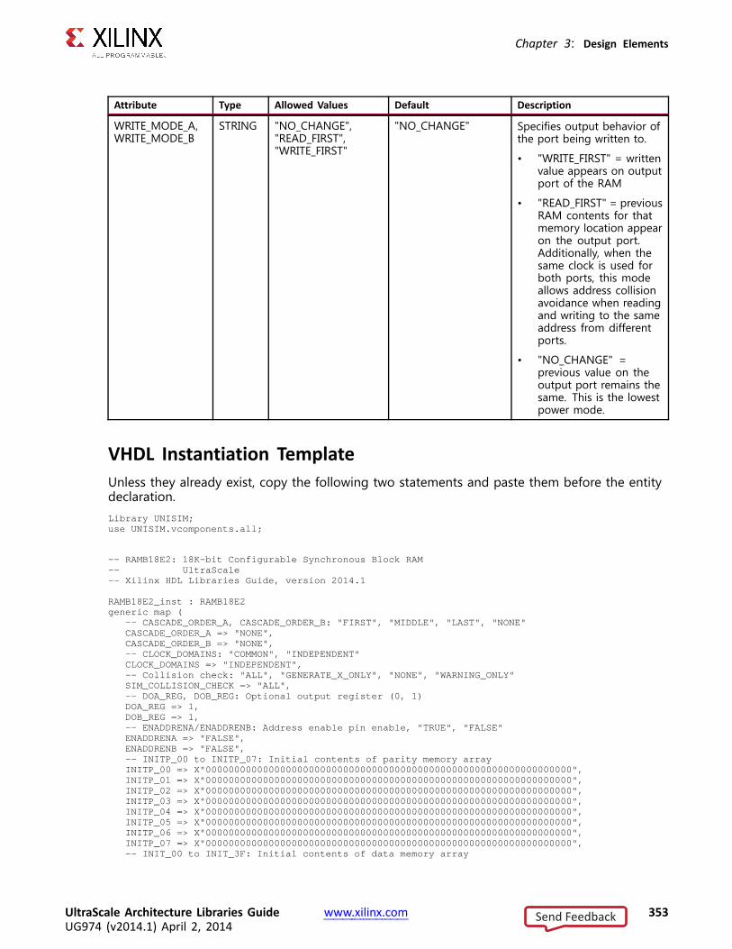
Chapter 3: Design Elements
Attribute Type Allowed Values Default Description
WRITE_MODE_A,WRITE_MODE_B
STRING "NO_CHANGE","READ_FIRST","WRITE_FIRST"
"NO_CHANGE" Specifies output behavior ofthe port being written to.
• "WRITE_FIRST" = writtenvalue appears on outputport of the RAM
• "READ_FIRST" = previousRAM contents for thatmemory location appearon the output port.Additionally, when thesame clock is used forboth ports, this modeallows address collisionavoidance when readingand writing to the sameaddress from differentports.
• "NO_CHANGE" =previous value on theoutput port remains thesame. This is the lowestpower mode.
VHDL Instantiation TemplateUnless they already exist, copy the following two statements and paste them before the entitydeclaration.Library UNISIM;use UNISIM.vcomponents.all;
-- RAMB18E2: 18K-bit Configurable Synchronous Block RAM-- UltraScale-- Xilinx HDL Libraries Guide, version 2014.1
RAMB18E2_inst : RAMB18E2generic map (
-- CASCADE_ORDER_A,CASCADE_ORDER_B:"FIRST", "MIDDLE", "LAST", "NONE"CASCADE_ORDER_A=> "NONE",CASCADE_ORDER_B=> "NONE",-- CLOCK_DOMAINS:"COMMON", "INDEPENDENT"CLOCK_DOMAINS=> "INDEPENDENT",-- Collision check: "ALL", "GENERATE_X_ONLY", "NONE", "WARNING_ONLY"SIM_COLLISION_CHECK => "ALL",-- DOA_REG, DOB_REG: Optional output register (0, 1)DOA_REG=> 1,DOB_REG=> 1,-- ENADDRENA/ENADDRENB:Address enable pin enable, "TRUE", "FALSE"ENADDRENA=> "FALSE",ENADDRENB=> "FALSE",-- INITP_00 to INITP_07: Initial contents of parity memory arrayINITP_00 => X"0000000000000000000000000000000000000000000000000000000000000000",INITP_01 => X"0000000000000000000000000000000000000000000000000000000000000000",INITP_02 => X"0000000000000000000000000000000000000000000000000000000000000000",INITP_03 => X"0000000000000000000000000000000000000000000000000000000000000000",INITP_04 => X"0000000000000000000000000000000000000000000000000000000000000000",INITP_05 => X"0000000000000000000000000000000000000000000000000000000000000000",INITP_06 => X"0000000000000000000000000000000000000000000000000000000000000000",INITP_07 => X"0000000000000000000000000000000000000000000000000000000000000000",-- INIT_00 to INIT_3F: Initial contents of data memory array
UltraScale Architecture Libraries Guide www.xilinx.com 353UG974 (v2014.1) April 2, 2014
Send Feedback

Chapter 3: Design Elements
INIT_00 => X"0000000000000000000000000000000000000000000000000000000000000000",INIT_01 => X"0000000000000000000000000000000000000000000000000000000000000000",INIT_02 => X"0000000000000000000000000000000000000000000000000000000000000000",INIT_03 => X"0000000000000000000000000000000000000000000000000000000000000000",INIT_04 => X"0000000000000000000000000000000000000000000000000000000000000000",INIT_05 => X"0000000000000000000000000000000000000000000000000000000000000000",INIT_06 => X"0000000000000000000000000000000000000000000000000000000000000000",INIT_07 => X"0000000000000000000000000000000000000000000000000000000000000000",INIT_08 => X"0000000000000000000000000000000000000000000000000000000000000000",INIT_09 => X"0000000000000000000000000000000000000000000000000000000000000000",INIT_0A => X"0000000000000000000000000000000000000000000000000000000000000000",INIT_0B => X"0000000000000000000000000000000000000000000000000000000000000000",INIT_0C => X"0000000000000000000000000000000000000000000000000000000000000000",INIT_0D => X"0000000000000000000000000000000000000000000000000000000000000000",INIT_0E => X"0000000000000000000000000000000000000000000000000000000000000000",INIT_0F => X"0000000000000000000000000000000000000000000000000000000000000000",INIT_10 => X"0000000000000000000000000000000000000000000000000000000000000000",INIT_11 => X"0000000000000000000000000000000000000000000000000000000000000000",INIT_12 => X"0000000000000000000000000000000000000000000000000000000000000000",INIT_13 => X"0000000000000000000000000000000000000000000000000000000000000000",INIT_14 => X"0000000000000000000000000000000000000000000000000000000000000000",INIT_15 => X"0000000000000000000000000000000000000000000000000000000000000000",INIT_16 => X"0000000000000000000000000000000000000000000000000000000000000000",INIT_17 => X"0000000000000000000000000000000000000000000000000000000000000000",INIT_18 => X"0000000000000000000000000000000000000000000000000000000000000000",INIT_19 => X"0000000000000000000000000000000000000000000000000000000000000000",INIT_1A => X"0000000000000000000000000000000000000000000000000000000000000000",INIT_1B => X"0000000000000000000000000000000000000000000000000000000000000000",INIT_1C => X"0000000000000000000000000000000000000000000000000000000000000000",INIT_1D => X"0000000000000000000000000000000000000000000000000000000000000000",INIT_1E => X"0000000000000000000000000000000000000000000000000000000000000000",INIT_1F => X"0000000000000000000000000000000000000000000000000000000000000000",INIT_20 => X"0000000000000000000000000000000000000000000000000000000000000000",INIT_21 => X"0000000000000000000000000000000000000000000000000000000000000000",INIT_22 => X"0000000000000000000000000000000000000000000000000000000000000000",INIT_23 => X"0000000000000000000000000000000000000000000000000000000000000000",INIT_24 => X"0000000000000000000000000000000000000000000000000000000000000000",INIT_25 => X"0000000000000000000000000000000000000000000000000000000000000000",INIT_26 => X"0000000000000000000000000000000000000000000000000000000000000000",INIT_27 => X"0000000000000000000000000000000000000000000000000000000000000000",INIT_28 => X"0000000000000000000000000000000000000000000000000000000000000000",INIT_29 => X"0000000000000000000000000000000000000000000000000000000000000000",INIT_2A => X"0000000000000000000000000000000000000000000000000000000000000000",INIT_2B => X"0000000000000000000000000000000000000000000000000000000000000000",INIT_2C => X"0000000000000000000000000000000000000000000000000000000000000000",INIT_2D => X"0000000000000000000000000000000000000000000000000000000000000000",INIT_2E => X"0000000000000000000000000000000000000000000000000000000000000000",INIT_2F => X"0000000000000000000000000000000000000000000000000000000000000000",INIT_30 => X"0000000000000000000000000000000000000000000000000000000000000000",INIT_31 => X"0000000000000000000000000000000000000000000000000000000000000000",INIT_32 => X"0000000000000000000000000000000000000000000000000000000000000000",INIT_33 => X"0000000000000000000000000000000000000000000000000000000000000000",INIT_34 => X"0000000000000000000000000000000000000000000000000000000000000000",INIT_35 => X"0000000000000000000000000000000000000000000000000000000000000000",INIT_36 => X"0000000000000000000000000000000000000000000000000000000000000000",INIT_37 => X"0000000000000000000000000000000000000000000000000000000000000000",INIT_38 => X"0000000000000000000000000000000000000000000000000000000000000000",INIT_39 => X"0000000000000000000000000000000000000000000000000000000000000000",INIT_3A => X"0000000000000000000000000000000000000000000000000000000000000000",INIT_3B => X"0000000000000000000000000000000000000000000000000000000000000000",INIT_3C => X"0000000000000000000000000000000000000000000000000000000000000000",INIT_3D => X"0000000000000000000000000000000000000000000000000000000000000000",INIT_3E => X"0000000000000000000000000000000000000000000000000000000000000000",INIT_3F => X"0000000000000000000000000000000000000000000000000000000000000000",-- INIT_A, INIT_B: Initial values on output portsINIT_A => X"00000",INIT_B => X"00000",-- Initialization File: RAM initialization fileINIT_FILE => "NONE",-- Programmable Inversion Attributes: Specifies the use of the built-in programmable inversionIS_CLKARDCLK_INVERTED=> ’0’,IS_CLKBWRCLK_INVERTED=> ’0’,
UltraScale Architecture Libraries Guide www.xilinx.com 354UG974 (v2014.1) April 2, 2014
Send Feedback

Chapter 3: Design Elements
IS_ENARDEN_INVERTED=> ’0’,IS_ENBWREN_INVERTED=> ’0’,IS_RSTRAMARSTRAM_INVERTED=> ’0’,IS_RSTRAMB_INVERTED=> ’0’,IS_RSTREGARSTREG_INVERTED=> ’0’,IS_RSTREGB_INVERTED=> ’0’,-- RDADDRCHANGE:Disable memory access when output value does not change ("TRUE", "FALSE")RDADDRCHANGEA=> "FALSE",RDADDRCHANGEB=> "FALSE",-- READ_WIDTH_A/B, WRITE_WIDTH_A/B: Read/write width per portREAD_WIDTH_A=> 0, -- 0-36READ_WIDTH_B=> 0, -- 0-18WRITE_WIDTH_A=> 0, -- 0-18WRITE_WIDTH_B=> 0, -- 0-36-- RSTREG_PRIORITY_A, RSTREG_PRIORITY_B: Reset or enable priority ("RSTREG", "REGCE")RSTREG_PRIORITY_A=> "RSTREG",RSTREG_PRIORITY_B=> "RSTREG",-- SRVAL_A, SRVAL_B: Set/reset value for outputSRVAL_A => X"00000",SRVAL_B => X"00000",-- Sleep Async: Sleep function asynchronous or synchronous ("TRUE", "FALSE")SLEEP_ASYNC=> "FALSE",-- WriteMode: "WRITE_FIRST", "NO_CHANGE", "READ_FIRST"WRITE_MODE_A=> "NO_CHANGE",WRITE_MODE_B=> "NO_CHANGE"
)port map (
-- Cascade Signals: 16-bit (each) output: Multi-BRAM cascade signalsCASDOUTA=> CASDOUTA, -- 16-bit output: Port A cascade output dataCASDOUTB=> CASDOUTB, -- 16-bit output: Port B cascade output dataCASDOUTPA=> CASDOUTPA, -- 2-bit output: Port A cascade output parity dataCASDOUTPB=> CASDOUTPB, -- 2-bit output: Port B cascade output parity data-- Port A Data: 16-bit (each) output: Port A dataDOUTADOUT=> DOUTADOUT, -- 16-bit output: A port data/LSB dataDOUTPADOUTP=> DOUTPADOUTP, -- 2-bit output: A port parity/LSB parity-- Port B Data: 16-bit (each) output: Port B dataDOUTBDOUT=> DOUTBDOUT, -- 16-bit output: B port data/MSB dataDOUTPBDOUTP=> DOUTPBDOUTP, -- 2-bit output: B port parity/MSB parity-- Cascade Signals: 1-bit (each) input: Multi-BRAM cascade signalsCASDIMUXA=> CASDIMUXA, -- 1-bit input: Port A input data (0=DINA, 1=CASDINA)CASDIMUXB=> CASDIMUXB, -- 1-bit input: Port B input data (0=DINB, 1=CASDINB)CASDINA => CASDINA, -- 16-bit input: Port A cascade input dataCASDINB => CASDINB, -- 16-bit input: Port B cascade input dataCASDINPA => CASDINPA, -- 2-bit input: Port A cascade input parity dataCASDINPB => CASDINPB, -- 2-bit input: Port B cascade input parity dataCASDOMUXA=> CASDOMUXA, -- 1-bit input: Port A unregistered data (0=BRAM data, 1=CASDINA)CASDOMUXB=> CASDOMUXB, -- 1-bit input: Port B unregistered data (0=BRAM data, 1=CASDINB)CASDOMUXEN_A=> CASDOMUXEN_A, -- 1-bit input: Port A unregistered output data enableCASDOMUXEN_B=> CASDOMUXEN_B, -- 1-bit input: Port B unregistered output data enableCASOREGIMUXA=> CASOREGIMUXA, -- 1-bit input: Port A registered data (0=BRAM data, 1=CASDINA)CASOREGIMUXB=> CASOREGIMUXB, -- 1-bit input: Port B registered data (0=BRAM data, 1=CASDINB)CASOREGIMUXEN_A=> CASOREGIMUXEN_A,-- 1-bit input: Port A registered output data enableCASOREGIMUXEN_B=> CASOREGIMUXEN_B,-- 1-bit input: Port B registered output data enable-- Port A Address/Control Signals: 14-bit (each) input: Port A address and control signalsADDRARDADDR=> ADDRARDADDR, -- 14-bit input: A/Read port addressADDRENA=> ADDRENA, -- 1-bit input: Active-High A/Read port address enableCLKARDCLK=> CLKARDCLK, -- 1-bit input: A/Read port clockENARDEN=> ENARDEN, -- 1-bit input: A port enable/Read enableREGCEAREGCE=> REGCEAREGCE, -- 1-bit input: A port register enable/Register enableRSTRAMARSTRAM=> RSTRAMARSTRAM, -- 1-bit input: A port set/resetRSTREGARSTREG=> RSTREGARSTREG, -- 1-bit input: A port register set/resetWEA=> WEA, -- 2-bit input: A port write enable-- Port A Data: 16-bit (each) input: Port A dataDINADIN => DINADIN, -- 16-bit input: A port data/LSB dataDINPADINP => DINPADINP, -- 2-bit input: A port parity/LSB parity-- Port B Address/Control Signals: 14-bit (each) input: Port B address and control signalsADDRBWRADDR=> ADDRBWRADDR, -- 14-bit input: B/Write port addressADDRENB=> ADDRENB, -- 1-bit input: Active-High B/Write port address enableCLKBWRCLK=> CLKBWRCLK, -- 1-bit input: B/Write port clockENBWREN=> ENBWREN, -- 1-bit input: B port enable/Write enableREGCEB=> REGCEB, -- 1-bit input: B port register enableRSTRAMB=> RSTRAMB, -- 1-bit input: B port set/reset
UltraScale Architecture Libraries Guide www.xilinx.com 355UG974 (v2014.1) April 2, 2014
Send Feedback
Chapter 3: Design Elements
RSTREGB=> RSTREGB, -- 1-bit input: B port register set/resetSLEEP => SLEEP, -- 1-bit input: Sleep ModeWEBWE=> WEBWE, -- 4-bit input: B port write enable/Write enable-- Port B Data: 16-bit (each) input: Port B dataDINBDIN => DINBDIN, -- 16-bit input: B port data/MSB dataDINPBDINP => DINPBDINP -- 2-bit input: B port parity/MSB parity
);
-- End of RAMB18E2_inst instantiation
Verilog Instantiation Template
// RAMB18E2: 18K-bit Configurable Synchronous Block RAM// UltraScale// Xilinx HDL Libraries Guide, version 2014.1
RAMB18E2 #(// CASCADE_ORDER_A,CASCADE_ORDER_B:"FIRST", "MIDDLE", "LAST", "NONE".CASCADE_ORDER_A("NONE"),.CASCADE_ORDER_B("NONE"),// CLOCK_DOMAINS:"COMMON", "INDEPENDENT".CLOCK_DOMAINS("INDEPENDENT"),// Collision check: "ALL", "GENERATE_X_ONLY", "NONE", "WARNING_ONLY".SIM_COLLISION_CHECK("ALL"),// DOA_REG, DOB_REG: Optional output register (0, 1).DOA_REG(1),.DOB_REG(1),// ENADDRENA/ENADDRENB:Address enable pin enable, "TRUE", "FALSE".ENADDRENA("FALSE"),.ENADDRENB("FALSE"),// INITP_00 to INITP_07: Initial contents of parity memory array.INITP_00(256’h0000000000000000000000000000000000000000000000000000000000000000),.INITP_01(256’h0000000000000000000000000000000000000000000000000000000000000000),.INITP_02(256’h0000000000000000000000000000000000000000000000000000000000000000),.INITP_03(256’h0000000000000000000000000000000000000000000000000000000000000000),.INITP_04(256’h0000000000000000000000000000000000000000000000000000000000000000),.INITP_05(256’h0000000000000000000000000000000000000000000000000000000000000000),.INITP_06(256’h0000000000000000000000000000000000000000000000000000000000000000),.INITP_07(256’h0000000000000000000000000000000000000000000000000000000000000000),// INIT_00 to INIT_3F: Initial contents of data memory array.INIT_00(256’h0000000000000000000000000000000000000000000000000000000000000000),.INIT_01(256’h0000000000000000000000000000000000000000000000000000000000000000),.INIT_02(256’h0000000000000000000000000000000000000000000000000000000000000000),.INIT_03(256’h0000000000000000000000000000000000000000000000000000000000000000),.INIT_04(256’h0000000000000000000000000000000000000000000000000000000000000000),.INIT_05(256’h0000000000000000000000000000000000000000000000000000000000000000),.INIT_06(256’h0000000000000000000000000000000000000000000000000000000000000000),.INIT_07(256’h0000000000000000000000000000000000000000000000000000000000000000),.INIT_08(256’h0000000000000000000000000000000000000000000000000000000000000000),.INIT_09(256’h0000000000000000000000000000000000000000000000000000000000000000),.INIT_0A(256’h0000000000000000000000000000000000000000000000000000000000000000),.INIT_0B(256’h0000000000000000000000000000000000000000000000000000000000000000),.INIT_0C(256’h0000000000000000000000000000000000000000000000000000000000000000),.INIT_0D(256’h0000000000000000000000000000000000000000000000000000000000000000),.INIT_0E(256’h0000000000000000000000000000000000000000000000000000000000000000),.INIT_0F(256’h0000000000000000000000000000000000000000000000000000000000000000),.INIT_10(256’h0000000000000000000000000000000000000000000000000000000000000000),.INIT_11(256’h0000000000000000000000000000000000000000000000000000000000000000),.INIT_12(256’h0000000000000000000000000000000000000000000000000000000000000000),.INIT_13(256’h0000000000000000000000000000000000000000000000000000000000000000),.INIT_14(256’h0000000000000000000000000000000000000000000000000000000000000000),.INIT_15(256’h0000000000000000000000000000000000000000000000000000000000000000),.INIT_16(256’h0000000000000000000000000000000000000000000000000000000000000000),.INIT_17(256’h0000000000000000000000000000000000000000000000000000000000000000),.INIT_18(256’h0000000000000000000000000000000000000000000000000000000000000000),.INIT_19(256’h0000000000000000000000000000000000000000000000000000000000000000),.INIT_1A(256’h0000000000000000000000000000000000000000000000000000000000000000),.INIT_1B(256’h0000000000000000000000000000000000000000000000000000000000000000),.INIT_1C(256’h0000000000000000000000000000000000000000000000000000000000000000),.INIT_1D(256’h0000000000000000000000000000000000000000000000000000000000000000),
UltraScale Architecture Libraries Guide www.xilinx.com 356UG974 (v2014.1) April 2, 2014
Send Feedback

Chapter 3: Design Elements
.INIT_1E(256’h0000000000000000000000000000000000000000000000000000000000000000),
.INIT_1F(256’h0000000000000000000000000000000000000000000000000000000000000000),
.INIT_20(256’h0000000000000000000000000000000000000000000000000000000000000000),
.INIT_21(256’h0000000000000000000000000000000000000000000000000000000000000000),
.INIT_22(256’h0000000000000000000000000000000000000000000000000000000000000000),
.INIT_23(256’h0000000000000000000000000000000000000000000000000000000000000000),
.INIT_24(256’h0000000000000000000000000000000000000000000000000000000000000000),
.INIT_25(256’h0000000000000000000000000000000000000000000000000000000000000000),
.INIT_26(256’h0000000000000000000000000000000000000000000000000000000000000000),
.INIT_27(256’h0000000000000000000000000000000000000000000000000000000000000000),
.INIT_28(256’h0000000000000000000000000000000000000000000000000000000000000000),
.INIT_29(256’h0000000000000000000000000000000000000000000000000000000000000000),
.INIT_2A(256’h0000000000000000000000000000000000000000000000000000000000000000),
.INIT_2B(256’h0000000000000000000000000000000000000000000000000000000000000000),
.INIT_2C(256’h0000000000000000000000000000000000000000000000000000000000000000),
.INIT_2D(256’h0000000000000000000000000000000000000000000000000000000000000000),
.INIT_2E(256’h0000000000000000000000000000000000000000000000000000000000000000),
.INIT_2F(256’h0000000000000000000000000000000000000000000000000000000000000000),
.INIT_30(256’h0000000000000000000000000000000000000000000000000000000000000000),
.INIT_31(256’h0000000000000000000000000000000000000000000000000000000000000000),
.INIT_32(256’h0000000000000000000000000000000000000000000000000000000000000000),
.INIT_33(256’h0000000000000000000000000000000000000000000000000000000000000000),
.INIT_34(256’h0000000000000000000000000000000000000000000000000000000000000000),
.INIT_35(256’h0000000000000000000000000000000000000000000000000000000000000000),
.INIT_36(256’h0000000000000000000000000000000000000000000000000000000000000000),
.INIT_37(256’h0000000000000000000000000000000000000000000000000000000000000000),
.INIT_38(256’h0000000000000000000000000000000000000000000000000000000000000000),
.INIT_39(256’h0000000000000000000000000000000000000000000000000000000000000000),
.INIT_3A(256’h0000000000000000000000000000000000000000000000000000000000000000),
.INIT_3B(256’h0000000000000000000000000000000000000000000000000000000000000000),
.INIT_3C(256’h0000000000000000000000000000000000000000000000000000000000000000),
.INIT_3D(256’h0000000000000000000000000000000000000000000000000000000000000000),
.INIT_3E(256’h0000000000000000000000000000000000000000000000000000000000000000),
.INIT_3F(256’h0000000000000000000000000000000000000000000000000000000000000000),// INIT_A, INIT_B: Initial values on output ports.INIT_A(18’h00000),.INIT_B(18’h00000),// Initialization File: RAM initialization file.INIT_FILE("NONE"),// Programmable Inversion Attributes: Specifies the use of the built-in programmable inversion.IS_CLKARDCLK_INVERTED(1’b0),.IS_CLKBWRCLK_INVERTED(1’b0),.IS_ENARDEN_INVERTED(1’b0),.IS_ENBWREN_INVERTED(1’b0),.IS_RSTRAMARSTRAM_INVERTED(1’b0),.IS_RSTRAMB_INVERTED(1’b0),.IS_RSTREGARSTREG_INVERTED(1’b0),.IS_RSTREGB_INVERTED(1’b0),// RDADDRCHANGE:Disable memory access when output value does not change ("TRUE", "FALSE").RDADDRCHANGEA("FALSE"),.RDADDRCHANGEB("FALSE"),// READ_WIDTH_A/B, WRITE_WIDTH_A/B: Read/write width per port.READ_WIDTH_A(0), // 0-36.READ_WIDTH_B(0), // 0-18.WRITE_WIDTH_A(0), // 0-18.WRITE_WIDTH_B(0), // 0-36// RSTREG_PRIORITY_A, RSTREG_PRIORITY_B: Reset or enable priority ("RSTREG", "REGCE").RSTREG_PRIORITY_A("RSTREG"),.RSTREG_PRIORITY_B("RSTREG"),// SRVAL_A, SRVAL_B: Set/reset value for output.SRVAL_A(18’h00000),.SRVAL_B(18’h00000),// Sleep Async: Sleep function asynchronous or synchronous ("TRUE", "FALSE").SLEEP_ASYNC("FALSE"),// WriteMode: "WRITE_FIRST", "NO_CHANGE", "READ_FIRST".WRITE_MODE_A("NO_CHANGE"),.WRITE_MODE_B("NO_CHANGE")
)RAMB18E2_inst (
// Cascade Signals: 16-bit (each) output: Multi-BRAM cascade signals.CASDOUTA(CASDOUTA), // 16-bit output: Port A cascade output data.CASDOUTB(CASDOUTB), // 16-bit output: Port B cascade output data
UltraScale Architecture Libraries Guide www.xilinx.com 357UG974 (v2014.1) April 2, 2014
Send Feedback

Chapter 3: Design Elements
.CASDOUTPA(CASDOUTPA), // 2-bit output: Port A cascade output parity data
.CASDOUTPB(CASDOUTPB), // 2-bit output: Port B cascade output parity data// Port A Data: 16-bit (each) output: Port A data.DOUTADOUT(DOUTADOUT), // 16-bit output: A port data/LSB data.DOUTPADOUTP(DOUTPADOUTP), // 2-bit output: A port parity/LSB parity// Port B Data: 16-bit (each) output: Port B data.DOUTBDOUT(DOUTBDOUT), // 16-bit output: B port data/MSB data.DOUTPBDOUTP(DOUTPBDOUTP), // 2-bit output: B port parity/MSB parity// Cascade Signals: 1-bit (each) input: Multi-BRAM cascade signals.CASDIMUXA(CASDIMUXA), // 1-bit input: Port A input data (0=DINA, 1=CASDINA).CASDIMUXB(CASDIMUXB), // 1-bit input: Port B input data (0=DINB, 1=CASDINB).CASDINA(CASDINA), // 16-bit input: Port A cascade input data.CASDINB(CASDINB), // 16-bit input: Port B cascade input data.CASDINPA(CASDINPA), // 2-bit input: Port A cascade input parity data.CASDINPB(CASDINPB), // 2-bit input: Port B cascade input parity data.CASDOMUXA(CASDOMUXA), // 1-bit input: Port A unregistered data (0=BRAM data, 1=CASDINA).CASDOMUXB(CASDOMUXB), // 1-bit input: Port B unregistered data (0=BRAM data, 1=CASDINB).CASDOMUXEN_A(CASDOMUXEN_A), // 1-bit input: Port A unregistered output data enable.CASDOMUXEN_B(CASDOMUXEN_B), // 1-bit input: Port B unregistered output data enable.CASOREGIMUXA(CASOREGIMUXA), // 1-bit input: Port A registered data (0=BRAM data, 1=CASDINA).CASOREGIMUXB(CASOREGIMUXB), // 1-bit input: Port B registered data (0=BRAM data, 1=CASDINB).CASOREGIMUXEN_A(CASOREGIMUXEN_A),// 1-bit input: Port A registered output data enable.CASOREGIMUXEN_B(CASOREGIMUXEN_B),// 1-bit input: Port B registered output data enable// Port A Address/Control Signals: 14-bit (each) input: Port A address and control signals.ADDRARDADDR(ADDRARDADDR), // 14-bit input: A/Read port address.ADDRENA(ADDRENA), // 1-bit input: Active-High A/Read port address enable.CLKARDCLK(CLKARDCLK), // 1-bit input: A/Read port clock.ENARDEN(ENARDEN), // 1-bit input: A port enable/Read enable.REGCEAREGCE(REGCEAREGCE), // 1-bit input: A port register enable/Register enable.RSTRAMARSTRAM(RSTRAMARSTRAM), // 1-bit input: A port set/reset.RSTREGARSTREG(RSTREGARSTREG), // 1-bit input: A port register set/reset.WEA(WEA), // 2-bit input: A port write enable// Port A Data: 16-bit (each) input: Port A data.DINADIN(DINADIN), // 16-bit input: A port data/LSB data.DINPADINP(DINPADINP), // 2-bit input: A port parity/LSB parity// Port B Address/Control Signals: 14-bit (each) input: Port B address and control signals.ADDRBWRADDR(ADDRBWRADDR), // 14-bit input: B/Write port address.ADDRENB(ADDRENB), // 1-bit input: Active-High B/Write port address enable.CLKBWRCLK(CLKBWRCLK), // 1-bit input: B/Write port clock.ENBWREN(ENBWREN), // 1-bit input: B port enable/Write enable.REGCEB(REGCEB), // 1-bit input: B port register enable.RSTRAMB(RSTRAMB), // 1-bit input: B port set/reset.RSTREGB(RSTREGB), // 1-bit input: B port register set/reset.SLEEP(SLEEP), // 1-bit input: Sleep Mode.WEBWE(WEBWE), // 4-bit input: B port write enable/Write enable// Port B Data: 16-bit (each) input: Port B data.DINBDIN(DINBDIN), // 16-bit input: B port data/MSB data.DINPBDINP(DINPBDINP) // 2-bit input: B port parity/MSB parity
);
// End of RAMB18E2_inst instantiation
For More Information• See the 7 series FPGA User Documentation (User Guides and Data Sheets).
• See the UltraScale User Documentation.
UltraScale Architecture Libraries Guide www.xilinx.com 358UG974 (v2014.1) April 2, 2014
Send Feedback
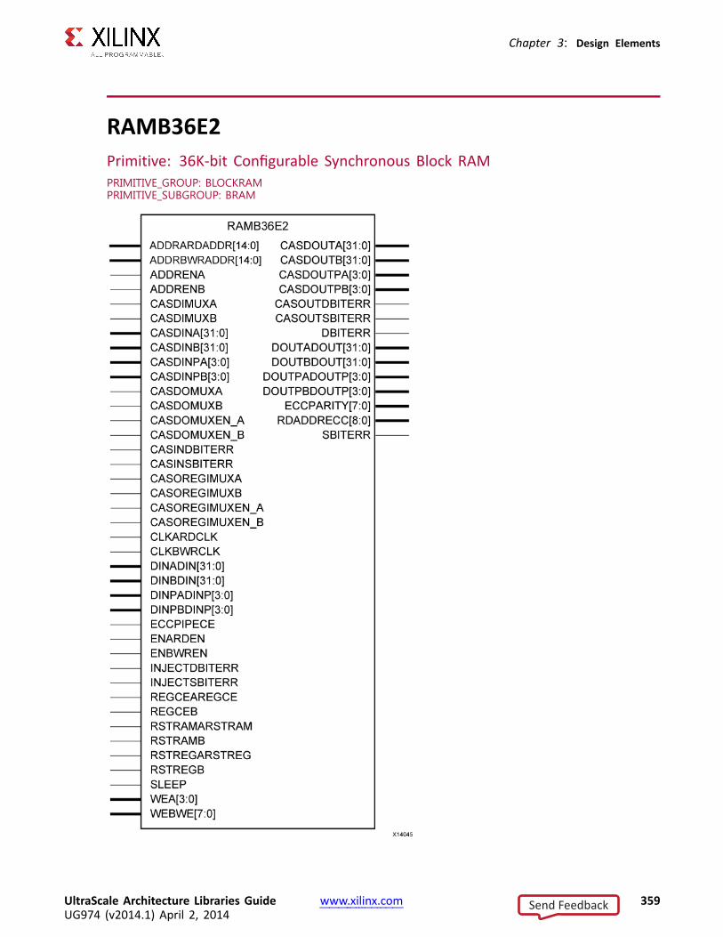
Chapter 3: Design Elements
RAMB36E2Primitive: 36K-bit Configurable Synchronous Block RAMPRIMITIVE_GROUP: BLOCKRAMPRIMITIVE_SUBGROUP: BRAM
UltraScale Architecture Libraries Guide www.xilinx.com 359UG974 (v2014.1) April 2, 2014
Send Feedback

Chapter 3: Design Elements
IntroductionThe RAMB36E2 allows access to the block RAM memory in the 36Kb configuration. Thiselement can be configured and used as a 1-bit wide by 32K deep to an 36-bit wide by 1024-bitdeep true dual port RAM. This element can also be configured as a 72-bit wide by 512 deepsimple dual port RAM. Both read and write operations are fully synchronous to the suppliedclock(s) to the component. However, the READ and WRITE ports can operate fully independentand asynchronous to each other, accessing the same memory array. When configured in thewider data width modes, byte-enable write operations are possible, and an optional outputregister can be used to reduce the clock-to-out times of the RAM. This RAM also features acascade capability which allows multiple RAMB36E2 components to be chained together toform deeper and more power efficient memory configuration if desired.
Port DescriptionsPort Direction Width Function
ADDRARDADDR<14:0> Input 15 Port A address input bus/Read address input bus.
ADDRBWRADDR<14:0> Input 15 Port B address input bus/Write address input bus.
ADDRENA Input 1 Active-High port A address input bus/Read address input bus.
ADDRENB Input 1 Active-High port B address input bus/Write address input bus.
CASDIMUXA Input 1 Port A mux control input to select between normal datainput (DINA) when Low or CASCADE data input (CASDINA)when High.
CASDIMUXB Input 1 Port B mux control input to select between normal data input(DINB) when Low or CASCADE data input (CASDINB) whenHigh.
CASDINA<31:0> Input 32 Port A cascade input data
CASDINB<31:0> Input 32 Port B cascade input data
CASDINPA<3:0> Input 4 Port A cascade input parity data
CASDINPB<3:0> Input 4 Port B cascade input parity data
CASDOMUXA Input 1 Port A mux control input to select between unregisteredoutput data from BRAM or CASCADE data input (CASDINA).
CASDOMUXB Input 1 Port B mux control input to select between unregisteredoutput data from BRAM or CASCADE data input (CASDINB).
CASDOMUXEN_A Input 1 Port A unregistered output data register enable.
CASDOMUXEN_B Input 1 Port B unregistered output data register enable.
CASDOUTA<31:0> Output 32 Port A cascade output data
CASDOUTB<31:0> Output 32 Port B cascade output data
CASDOUTPA<3:0> Output 4 Port A cascade output parity data
CASDOUTPB<3:0> Output 4 Port B cascade output parity data
CASINDBITERR Input 1 Cascaded double bit error (DBITERR) signal from priorBlockRAM in the cascade chain.
CASINSBITERR Input 1 Cascaded single bit error (SBITERR) signal from priorBlockRAM in the cascade chain.
UltraScale Architecture Libraries Guide www.xilinx.com 360UG974 (v2014.1) April 2, 2014
Send Feedback

Chapter 3: Design Elements
Port Direction Width Function
CASOREGIMUXA Input 1 Port A mux control input to select between registered outputdata from BRAM or CASCADE data input (CASDINA).
CASOREGIMUXB Input 1 Port B mux control input to select between registered outputdata from BRAM or CASCADE data input (CASDINB).
CASOREGIMUXEN_A Input 1 Port A registered output data register enable.
CASOREGIMUXEN_B Input 1 Port B registered output data register enable.
CASOUTDBITERR Output 1 Cascaded double bit error (DBITERR) signal to next BlockRAMin the cascade chain.
CASOUTSBITERR Output 1 Cascaded single bit error (SBITERR) signal to next BlockRAMin the cascade chain.
CLKARDCLK Input 1 Port A clock input/Read clock input.
CLKBWRCLK Input 1 Port B clock input/Write clock input.
DBITERR Output 1 Status output from ECC function to indicate a double bit errorwas detected during a read operation. EN_ECC_READ needsto be TRUE in order to use this functionality. Synchronousto RDCLK.
DINADIN<31:0> Input 32 Port A data input bus. When WRITE_WIDTH=72, DINADIN isthe logical DI<31:0>.
DINBDIN<31:0> Input 32 Port B data input bus. When WRITE_WIDTH=72, DINBDIN isthe logical DI<63:32>.
DINPADINP<3:0> Input 4 Port A parity data input bus/Data parity input bus addressedby WRADDR. When WRITE_WIDTH=72, DINPADINP is thelogical DIP<3:0>.
DINPBDINP<3:0> Input 4 Port B parity data input bus/Data parity input bus addressedby WRADDR. When WRITE_WIDTH=72, DINPBDINP is thelogical DIP<7:4>.
DOUTADOUT<31:0> Output 32 Port A data output bus. When READ_WIDTH=72,DOUTADOUT is the logical DO<31:0>.
DOUTBDOUT<31:0> Output 32 Port B data output bus. When READ_WIDTH=72,DOUTBDOUT is the logical DO<63:32>.
DOUTPADOUTP<3:0> Output 4 Port A parity data output bus. When READ_WIDTH=72,DOUTPADOUT is the logical DOP<3:0>.
DOUTPBDOUTP<3:0> Output 4 Port B parity data output bus. When READ_WIDTH=72,DOUTPBDOUTP is the logical DOP<7:4>.
ECCPARITY<7:0> Output 8 8-bit data generated by the ECC encoder used by theECC decoder for memory error detection and correction.Applicable when EN_ECC_WRITE=1. Synchronous to WRCLK.
ECCPIPECE Input 1 Clock enable for the ECC pipeline register.
ENARDEN Input 1 Port A RAM enable/Read enable.
ENBWREN Input 1 Port B RAM enable/Write enable.
INJECTDBITERR Input 1 Applicable when EN_ECC_WRITE=1. Causes a double-biterror to be inserted on bits 30 and 62 of DI during a writeoperation. Synchronous to WRCLK.
INJECTSBITERR Input 1 Applicable when EN_ECC_WRITE=1. Causes a single-bit errorto be inserted on bit 30 of DI during a write operation.
UltraScale Architecture Libraries Guide www.xilinx.com 361UG974 (v2014.1) April 2, 2014
Send Feedback

Chapter 3: Design Elements
Port Direction Width Function
RDADDRECC<8:0> Output 9 Read address for ECC function.
REGCEAREGCE Input 1 Port A output register clock enable input/Output registerclock enable input (valid only when DOA_REG=1).
REGCEB Input 1 Port B output register clock enable (valid only whenDOB_REG=1 and READ_WIDTH<=18).
RSTRAMARSTRAM Input 1 Synchronous data latch set/reset to value indicated bySRVAL_A. RSTRAMARSTRAM sets/resets the BRAM dataoutput latch when DO_REG=0 or 1. If DO_REG=1 there is acycle of latency between the internal data latch node that isreset by RSTRAMARSTRAM and the DO output of the BRAM.This signal resets port A RAM output when READ_WIDTH<=36and the entire RAM output when READ_WIDTH=72.
RSTRAMB Input 1 Synchronous data latch set/reset to value indicated bySRVAL_B. RSTRAMB sets/resets the BRAM data output latchwhen DO_REG=0 or 1. If DO_REG=1 there is a cycle oflatency between the internal data latch node that is reset byRSTRAMB and the DO output of the BRAM. Not used whenREAD_WIDTH=72.
RSTREGARSTREG Input 1 Synchronous output register set/reset to value indicated bySRVAL_A. RSTREGARSTREG sets/resets the output registerwhen DO_REG=1. RSTREG_PRIORITY_A determines if thissignal gets priority over REGCEAREGCE. This signal resetsport A output when READ_WIDTH<=36 and the entire RAMoutput when READ_WIDTH=72.
RSTREGB Input 1 Synchronous output register set/reset to value indicatedby SRVAL_B. RSTREGB sets/resets the output register whenDO_REG=1. RSTREG_PRIORITY_B determines if this signalgets priority over REGCEB. Not used when READ_WIDTH=36.
SBITERR Output 1 ECC output indicating that a single-bit error was detectedduring the read operation. Synchronous to RDCLK.
SLEEP Input 1 Dynamic shut down power saving. If SLEEP is High, theblock is in power saving mode. If SLEEP_ASYNC=FALSE,synchronous to RDCLK, otherwise, asynchronous input.
WEA<3:0> Input 4 Port A byte-wide write enable. Not used whenRAM_MODE="SDP". See User Guide for WEA mapping fordifferent port widths.
WEBWE<7:0> Input 8 Port B byte-wide write enable/Write enable. See User Guidefor WEBWE mapping for different port widths.
Design Entry MethodInstantiation Yes
Inference Recommended
IP and IP Integrator Catalog Yes
Macro support Yes
UltraScale Architecture Libraries Guide www.xilinx.com 362UG974 (v2014.1) April 2, 2014
Send Feedback

Chapter 3: Design Elements
Available AttributesAttribute Type Allowed Values Default Description
CASCADE_ORDER_A,CASCADE_ORDER_B
STRING "NONE", "FIRST","LAST", "MIDDLE"
"NONE" Specifies the order of thecascaded BRAM. FIRSTBRAM is the bottom incascade, LAST one is onthe top of the cascade, andMIDDLE is the BRAM inbetween bottom and top.
CLOCK _DOMAINS STRING "INDEPENDENT","COMMON"
"INDEPENDENT" Used for Simulation purposeto model the addressscollision case as wellas enable lower poweroperation in common clockmode.
• "COMMON"=CommonClock/Single Clock
• "INDEPENDENT"=IndependentClock/Dual Clock
DOA_REG DECIMAL 1, 0 1 A value of 1 enables theoutput registers to theRAM enabling higherperfromance clock-to-outfrom the RAM at the expenseof an added clock cycle ofread latency. A value of 0allows a read in one clockcycle but will result in slowerclock-to-out timing.
DOB_REG DECIMAL 1, 0 1 Used for Simulation purposeto model the addressscollision case as wellas enable lower poweroperation in common clockmode.
• "COMMON"=CommonClock/Single Clock
• "INDEPENDENT"=IndependentClock/Dual Clock
EN_ECC_PIPE STRING "FALSE", "TRUE" "FALSE" Enable ECC pipeline outputregister stage.
EN_ECC_READ STRING "FALSE", "TRUE" "FALSE" Enable the ECC read decodercircuitry. Only valid whenREAD_WIDTH is set to 72.
EN_ECC_WRITE STRING "FALSE", "TRUE" "FALSE" Enable the ECC writeencoder circuitry. Only validwhen WRITE_WIDTH is setto 72.
ENADDRENA,ENADDRENB
STRING "FALSE", "TRUE" "FALSE" Specifies if Address Enablepin is enabled
UltraScale Architecture Libraries Guide www.xilinx.com 363UG974 (v2014.1) April 2, 2014
Send Feedback

Chapter 3: Design Elements
Attribute Type Allowed Values Default Description
INIT_A, INIT_B HEX 36’h000000000 to36’hfffffffff
36’h000000000 Specifies the initial valueon the port output afterconfiguration.
INIT_FILE STRING String "NONE" File name of file used tospecify initial RAM contents.
INIT_00 to INIT_7F HEX 256’h0000000000000000000000000000000000000000000000000000000000000000 to256’hfffffffffffffffffffffffffffffffffffffffffffffffffffffffffff fffff
256’h0000000000000000000000000000000000000000000000000000000000000000
Allows specification of theinitial contents of the 32Kbdata memory array.
INITP_00 toINITP_0F
HEX 256’h0000000000000000000000000000000000000000000000000000000000000000 to256’hfffffffffffffffffffffffffffffffffffffffffffffffffffffffffff fffff
256’h0000000000000000000000000000000000000000000000000000000000000000
Allows specification of theinitial contents of the 4Kbparity data memory array.
IS_CLKARDCLK_INVERTED,IS_CLKBWRCLK_INVERTED,IS_ENARDEN_INVERTED,IS_ENBWREN_INVERTED, IS_RSTRAMARSTRAM_INVERTED,IS_RSTRAMB_INVERTED, IS_RSTREGARSTREG_INVERTED,IS_RSTREGB_INVERTED
BINARY 1’b0 to 1’b1 1’b0 Indicates whether theoptional inversions are to beused or not on specific pinsfor this component thuschanging the active polarityof that pin’s function. Whenset to 1 on a clock pin(WRCLK or RDCLK), thiscomponents clocks onthe negative edge. Whenset to 1 on other pins, itchanges the function tobehave active-Low ratherthan active-High. Forpins that are buses, thebit-width of this attributeshould match that of thebit-width of the associatedpins and a binary valueindicates which inverters touse and which to bypass.If an external inverter isspecified on one of theseasscoaited pins, the Vivadosoftware will automaticallyset this attribute duringthe opt_design stage sothat additional logic is notnecessary for changing theinput polarity.
UltraScale Architecture Libraries Guide www.xilinx.com 364UG974 (v2014.1) April 2, 2014
Send Feedback

Chapter 3: Design Elements
Attribute Type Allowed Values Default Description
RDADDRCHANGEA,RDADDRCHANGEB
STRING "FALSE", "TRUE" "FALSE" Read Address Change is afeature which will preventmemory access when theoutput value does notchange thus saving power.Setting this attribute to TRUEenables this power-savingfeature. Setting it to falseimproves setup time to theRAM possibly improvingBRAM performance.
READ_WIDTH_A,READ_WIDTH_B,WRITE_WIDTH_A,WRITE_WIDTH_B
DECIMAL 0, 1, 2, 4, 9, 18, 36, 72 0 Specifies the desired datawidth for a read/write onport A/B, including paritybits. This value must be0 if the port is not used.Otherwise, it should be setto the desired port width.
RSTREG_PRIORITY_A,RSTREG_PRIORITY_B
STRING "RSTREG", "REGCE" "RSTREG" Selects register priority forRSTREG or REGCE
SIM _COLLISION_CHECK
STRING "ALL","GENERATE_X_ONLY","NONE","WARNING_ONLY"
"ALL" Allows modification of thesimulation behavior so thatif a memory collision occurs
• "ALL" = warningproduced and affectedoutputs/memory gounknown (X)
• "WARNING_ONLY" =warning producedand affectedoutputs/memory retainlast value
• "GENERATE_X_ONLY" =no warning and affectedoutputs/memory gounknown (X)
• "NONE" = nowarning and affectedoutputs/memory retainlast value
NOTE: Use this settingcarefully. Setting it to avalue other than "ALL"can mask design problemsduring simulation.
SLEEP_ASYNC STRING "FALSE", "TRUE" "FALSE" Specifies whether the SLEEPpin is synchronous to theCLKARDCLK pin ("FALSE") ortreated as an asynchronouspin.
UltraScale Architecture Libraries Guide www.xilinx.com 365UG974 (v2014.1) April 2, 2014
Send Feedback

Chapter 3: Design Elements
Attribute Type Allowed Values Default Description
SRVAL_A, SRVAL_B HEX 36’h000000000 to36’hfffffffff
36’h000000000 Specifies the output valueof the RAM upon assertionof the synchronous reset(RST/RSTREG) signal.
WRITE_MODE_A,WRITE_MODE_B
STRING "NO_CHANGE","READ_FIRST","WRITE_FIRST"
"NO_CHANGE" Specifies output behavior ofthe port being written to.
• "WRITE_FIRST" = writtenvalue appears on outputport of the RAM
• "READ_FIRST" =previous RAM contentsfor that memory locationappear on the outputport. Additionally, whenthe same clock is usedfor both ports, this modeallows address collisionavoidance when readingand writing to the sameaddress from differentports.
• "NO_CHANGE" =previous value on theoutput port remains thesame. This is the lowestpower mode.
VHDL Instantiation TemplateUnless they already exist, copy the following two statements and paste them before the entitydeclaration.Library UNISIM;use UNISIM.vcomponents.all;
-- RAMB36E2: 36K-bit Configurable Synchronous Block RAM-- UltraScale-- Xilinx HDL Libraries Guide, version 2014.1
RAMB36E2_inst : RAMB36E2generic map (
-- CASCADE_ORDER_A,CASCADE_ORDER_B:"FIRST", "MIDDLE", "LAST", "NONE"CASCADE_ORDER_A=> "NONE",CASCADE_ORDER_B=> "NONE",-- CLOCK_DOMAINS:"COMMON", "INDEPENDENT"CLOCK_DOMAINS=> "INDEPENDENT",DOB_REG=> 1,-- Collision check: "ALL", "GENERATE_X_ONLY", "NONE", "WARNING_ONLY"SIM_COLLISION_CHECK => "ALL",-- DOA_REG, DOB_REG: Optional output register (0, 1)DOA_REG=> 1,-- ENADDRENA/ENADDRENB:Address enable pin enable, "TRUE", "FALSE"ENADDRENA=> "FALSE",ENADDRENB=> "FALSE",-- EN_ECC_PIPE: ECC pipeline register, "TRUE"/"FALSE"EN_ECC_PIPE => "FALSE",-- EN_ECC_READ:Enable ECC decoder, "TRUE"/"FALSE"EN_ECC_READ=> "FALSE",-- EN_ECC_WRITE: Enable ECC encoder, "TRUE"/"FALSE"
UltraScale Architecture Libraries Guide www.xilinx.com 366UG974 (v2014.1) April 2, 2014
Send Feedback

Chapter 3: Design Elements
EN_ECC_WRITE=> "FALSE",-- INITP_00 to INITP_0F: Initial contents of parity memory arrayINITP_00 => X"0000000000000000000000000000000000000000000000000000000000000000",INITP_01 => X"0000000000000000000000000000000000000000000000000000000000000000",INITP_02 => X"0000000000000000000000000000000000000000000000000000000000000000",INITP_03 => X"0000000000000000000000000000000000000000000000000000000000000000",INITP_04 => X"0000000000000000000000000000000000000000000000000000000000000000",INITP_05 => X"0000000000000000000000000000000000000000000000000000000000000000",INITP_06 => X"0000000000000000000000000000000000000000000000000000000000000000",INITP_07 => X"0000000000000000000000000000000000000000000000000000000000000000",INITP_08 => X"0000000000000000000000000000000000000000000000000000000000000000",INITP_09 => X"0000000000000000000000000000000000000000000000000000000000000000",INITP_0A => X"0000000000000000000000000000000000000000000000000000000000000000",INITP_0B => X"0000000000000000000000000000000000000000000000000000000000000000",INITP_0C => X"0000000000000000000000000000000000000000000000000000000000000000",INITP_0D => X"0000000000000000000000000000000000000000000000000000000000000000",INITP_0E => X"0000000000000000000000000000000000000000000000000000000000000000",INITP_0F => X"0000000000000000000000000000000000000000000000000000000000000000",-- INIT_00 to INIT_7F: Initial contents of data memory arrayINIT_00 => X"0000000000000000000000000000000000000000000000000000000000000000",INIT_01 => X"0000000000000000000000000000000000000000000000000000000000000000",INIT_02 => X"0000000000000000000000000000000000000000000000000000000000000000",INIT_03 => X"0000000000000000000000000000000000000000000000000000000000000000",INIT_04 => X"0000000000000000000000000000000000000000000000000000000000000000",INIT_05 => X"0000000000000000000000000000000000000000000000000000000000000000",INIT_06 => X"0000000000000000000000000000000000000000000000000000000000000000",INIT_07 => X"0000000000000000000000000000000000000000000000000000000000000000",INIT_08 => X"0000000000000000000000000000000000000000000000000000000000000000",INIT_09 => X"0000000000000000000000000000000000000000000000000000000000000000",INIT_0A => X"0000000000000000000000000000000000000000000000000000000000000000",INIT_0B => X"0000000000000000000000000000000000000000000000000000000000000000",INIT_0C => X"0000000000000000000000000000000000000000000000000000000000000000",INIT_0D => X"0000000000000000000000000000000000000000000000000000000000000000",INIT_0E => X"0000000000000000000000000000000000000000000000000000000000000000",INIT_0F => X"0000000000000000000000000000000000000000000000000000000000000000",INIT_10 => X"0000000000000000000000000000000000000000000000000000000000000000",INIT_11 => X"0000000000000000000000000000000000000000000000000000000000000000",INIT_12 => X"0000000000000000000000000000000000000000000000000000000000000000",INIT_13 => X"0000000000000000000000000000000000000000000000000000000000000000",INIT_14 => X"0000000000000000000000000000000000000000000000000000000000000000",INIT_15 => X"0000000000000000000000000000000000000000000000000000000000000000",INIT_16 => X"0000000000000000000000000000000000000000000000000000000000000000",INIT_17 => X"0000000000000000000000000000000000000000000000000000000000000000",INIT_18 => X"0000000000000000000000000000000000000000000000000000000000000000",INIT_19 => X"0000000000000000000000000000000000000000000000000000000000000000",INIT_1A => X"0000000000000000000000000000000000000000000000000000000000000000",INIT_1B => X"0000000000000000000000000000000000000000000000000000000000000000",INIT_1C => X"0000000000000000000000000000000000000000000000000000000000000000",INIT_1D => X"0000000000000000000000000000000000000000000000000000000000000000",INIT_1E => X"0000000000000000000000000000000000000000000000000000000000000000",INIT_1F => X"0000000000000000000000000000000000000000000000000000000000000000",INIT_20 => X"0000000000000000000000000000000000000000000000000000000000000000",INIT_21 => X"0000000000000000000000000000000000000000000000000000000000000000",INIT_22 => X"0000000000000000000000000000000000000000000000000000000000000000",INIT_23 => X"0000000000000000000000000000000000000000000000000000000000000000",INIT_24 => X"0000000000000000000000000000000000000000000000000000000000000000",INIT_25 => X"0000000000000000000000000000000000000000000000000000000000000000",INIT_26 => X"0000000000000000000000000000000000000000000000000000000000000000",INIT_27 => X"0000000000000000000000000000000000000000000000000000000000000000",INIT_28 => X"0000000000000000000000000000000000000000000000000000000000000000",INIT_29 => X"0000000000000000000000000000000000000000000000000000000000000000",INIT_2A => X"0000000000000000000000000000000000000000000000000000000000000000",INIT_2B => X"0000000000000000000000000000000000000000000000000000000000000000",INIT_2C => X"0000000000000000000000000000000000000000000000000000000000000000",INIT_2D => X"0000000000000000000000000000000000000000000000000000000000000000",INIT_2E => X"0000000000000000000000000000000000000000000000000000000000000000",INIT_2F => X"0000000000000000000000000000000000000000000000000000000000000000",INIT_30 => X"0000000000000000000000000000000000000000000000000000000000000000",INIT_31 => X"0000000000000000000000000000000000000000000000000000000000000000",INIT_32 => X"0000000000000000000000000000000000000000000000000000000000000000",INIT_33 => X"0000000000000000000000000000000000000000000000000000000000000000",INIT_34 => X"0000000000000000000000000000000000000000000000000000000000000000",
UltraScale Architecture Libraries Guide www.xilinx.com 367UG974 (v2014.1) April 2, 2014
Send Feedback

Chapter 3: Design Elements
INIT_35 => X"0000000000000000000000000000000000000000000000000000000000000000",INIT_36 => X"0000000000000000000000000000000000000000000000000000000000000000",INIT_37 => X"0000000000000000000000000000000000000000000000000000000000000000",INIT_38 => X"0000000000000000000000000000000000000000000000000000000000000000",INIT_39 => X"0000000000000000000000000000000000000000000000000000000000000000",INIT_3A => X"0000000000000000000000000000000000000000000000000000000000000000",INIT_3B => X"0000000000000000000000000000000000000000000000000000000000000000",INIT_3C => X"0000000000000000000000000000000000000000000000000000000000000000",INIT_3D => X"0000000000000000000000000000000000000000000000000000000000000000",INIT_3E => X"0000000000000000000000000000000000000000000000000000000000000000",INIT_3F => X"0000000000000000000000000000000000000000000000000000000000000000",INIT_40 => X"0000000000000000000000000000000000000000000000000000000000000000",INIT_41 => X"0000000000000000000000000000000000000000000000000000000000000000",INIT_42 => X"0000000000000000000000000000000000000000000000000000000000000000",INIT_43 => X"0000000000000000000000000000000000000000000000000000000000000000",INIT_44 => X"0000000000000000000000000000000000000000000000000000000000000000",INIT_45 => X"0000000000000000000000000000000000000000000000000000000000000000",INIT_46 => X"0000000000000000000000000000000000000000000000000000000000000000",INIT_47 => X"0000000000000000000000000000000000000000000000000000000000000000",INIT_48 => X"0000000000000000000000000000000000000000000000000000000000000000",INIT_49 => X"0000000000000000000000000000000000000000000000000000000000000000",INIT_4A => X"0000000000000000000000000000000000000000000000000000000000000000",INIT_4B => X"0000000000000000000000000000000000000000000000000000000000000000",INIT_4C => X"0000000000000000000000000000000000000000000000000000000000000000",INIT_4D => X"0000000000000000000000000000000000000000000000000000000000000000",INIT_4E => X"0000000000000000000000000000000000000000000000000000000000000000",INIT_4F => X"0000000000000000000000000000000000000000000000000000000000000000",INIT_50 => X"0000000000000000000000000000000000000000000000000000000000000000",INIT_51 => X"0000000000000000000000000000000000000000000000000000000000000000",INIT_52 => X"0000000000000000000000000000000000000000000000000000000000000000",INIT_53 => X"0000000000000000000000000000000000000000000000000000000000000000",INIT_54 => X"0000000000000000000000000000000000000000000000000000000000000000",INIT_55 => X"0000000000000000000000000000000000000000000000000000000000000000",INIT_56 => X"0000000000000000000000000000000000000000000000000000000000000000",INIT_57 => X"0000000000000000000000000000000000000000000000000000000000000000",INIT_58 => X"0000000000000000000000000000000000000000000000000000000000000000",INIT_59 => X"0000000000000000000000000000000000000000000000000000000000000000",INIT_5A => X"0000000000000000000000000000000000000000000000000000000000000000",INIT_5B => X"0000000000000000000000000000000000000000000000000000000000000000",INIT_5C => X"0000000000000000000000000000000000000000000000000000000000000000",INIT_5D => X"0000000000000000000000000000000000000000000000000000000000000000",INIT_5E => X"0000000000000000000000000000000000000000000000000000000000000000",INIT_5F => X"0000000000000000000000000000000000000000000000000000000000000000",INIT_60 => X"0000000000000000000000000000000000000000000000000000000000000000",INIT_61 => X"0000000000000000000000000000000000000000000000000000000000000000",INIT_62 => X"0000000000000000000000000000000000000000000000000000000000000000",INIT_63 => X"0000000000000000000000000000000000000000000000000000000000000000",INIT_64 => X"0000000000000000000000000000000000000000000000000000000000000000",INIT_65 => X"0000000000000000000000000000000000000000000000000000000000000000",INIT_66 => X"0000000000000000000000000000000000000000000000000000000000000000",INIT_67 => X"0000000000000000000000000000000000000000000000000000000000000000",INIT_68 => X"0000000000000000000000000000000000000000000000000000000000000000",INIT_69 => X"0000000000000000000000000000000000000000000000000000000000000000",INIT_6A => X"0000000000000000000000000000000000000000000000000000000000000000",INIT_6B => X"0000000000000000000000000000000000000000000000000000000000000000",INIT_6C => X"0000000000000000000000000000000000000000000000000000000000000000",INIT_6D => X"0000000000000000000000000000000000000000000000000000000000000000",INIT_6E => X"0000000000000000000000000000000000000000000000000000000000000000",INIT_6F => X"0000000000000000000000000000000000000000000000000000000000000000",INIT_70 => X"0000000000000000000000000000000000000000000000000000000000000000",INIT_71 => X"0000000000000000000000000000000000000000000000000000000000000000",INIT_72 => X"0000000000000000000000000000000000000000000000000000000000000000",INIT_73 => X"0000000000000000000000000000000000000000000000000000000000000000",INIT_74 => X"0000000000000000000000000000000000000000000000000000000000000000",INIT_75 => X"0000000000000000000000000000000000000000000000000000000000000000",INIT_76 => X"0000000000000000000000000000000000000000000000000000000000000000",INIT_77 => X"0000000000000000000000000000000000000000000000000000000000000000",INIT_78 => X"0000000000000000000000000000000000000000000000000000000000000000",INIT_79 => X"0000000000000000000000000000000000000000000000000000000000000000",INIT_7A => X"0000000000000000000000000000000000000000000000000000000000000000",INIT_7B => X"0000000000000000000000000000000000000000000000000000000000000000",INIT_7C => X"0000000000000000000000000000000000000000000000000000000000000000",
UltraScale Architecture Libraries Guide www.xilinx.com 368UG974 (v2014.1) April 2, 2014
Send Feedback

Chapter 3: Design Elements
INIT_7D => X"0000000000000000000000000000000000000000000000000000000000000000",INIT_7E => X"0000000000000000000000000000000000000000000000000000000000000000",INIT_7F => X"0000000000000000000000000000000000000000000000000000000000000000",-- INIT_A, INIT_B: Initial values on output portsINIT_A => X"000000000",INIT_B => X"000000000",-- Initialization File: RAM initialization fileINIT_FILE => "NONE",-- Programmable Inversion Attributes: Specifies the use of the built-in programmable inversion on-- specific pinsIS_CLKARDCLK_INVERTED=> ’0’,IS_CLKBWRCLK_INVERTED=> ’0’,IS_ENARDEN_INVERTED=> ’0’,IS_ENBWREN_INVERTED=> ’0’,IS_RSTRAMARSTRAM_INVERTED=> ’0’,IS_RSTRAMB_INVERTED=> ’0’,IS_RSTREGARSTREG_INVERTED=> ’0’,IS_RSTREGB_INVERTED=> ’0’,-- RDADDRCHANGE:Disable memory access when output value does not change ("TRUE", "FALSE")RDADDRCHANGEA=> "FALSE",RDADDRCHANGEB=> "FALSE",-- READ_WIDTH_A/B, WRITE_WIDTH_A/B: Read/write width per portREAD_WIDTH_A=> 0, -- 0-72READ_WIDTH_B=> 0, -- 0-36WRITE_WIDTH_A=> 0, -- 0-36WRITE_WIDTH_B=> 0, -- 0-72-- RSTREG_PRIORITY_A, RSTREG_PRIORITY_B: Reset or enable priority ("RSTREG", "REGCE")RSTREG_PRIORITY_A=> "RSTREG",RSTREG_PRIORITY_B=> "RSTREG",-- SRVAL_A, SRVAL_B: Set/reset value for outputSRVAL_A => X"000000000",SRVAL_B => X"000000000",-- Sleep Async: Sleep function asynchronous or synchronous ("TRUE", "FALSE")SLEEP_ASYNC=> "FALSE",-- WriteMode: "WRITE_FIRST", "NO_CHANGE", "READ_FIRST"WRITE_MODE_A=> "NO_CHANGE",WRITE_MODE_B=> "NO_CHANGE"
)port map (
-- Cascade Signals: 32-bit (each) output: Multi-BRAM cascade signalsCASDOUTA=> CASDOUTA, -- 32-bit output: Port A cascade output dataCASDOUTB=> CASDOUTB, -- 32-bit output: Port B cascade output dataCASDOUTPA=> CASDOUTPA, -- 4-bit output: Port A cascade output parity dataCASDOUTPB=> CASDOUTPB, -- 4-bit output: Port B cascade output parity dataCASOUTDBITERR=> CASOUTDBITERR, -- 1-bit output: DBITERR cascade outputCASOUTSBITERR=> CASOUTSBITERR, -- 1-bit output: SBITERR cascade output-- ECC Signals: 1-bit (each) output: Error Correction Circuitry portsDBITERR => DBITERR, -- 1-bit output: Double bit error statusECCPARITY => ECCPARITY, -- 8-bit output: Generated error correction parityRDADDRECC=> RDADDRECC, -- 9-bit output: ECC Read AddressSBITERR => SBITERR, -- 1-bit output: Single bit error status-- Port A Data: 32-bit (each) output: Port A dataDOUTADOUT=> DOUTADOUT, -- 32-bit output: A port data/LSB dataDOUTPADOUTP=> DOUTPADOUTP, -- 4-bit output: A port parity/LSB parity-- Port B Data: 32-bit (each) output: Port B dataDOUTBDOUT=> DOUTBDOUT, -- 32-bit output: B port data/MSB dataDOUTPBDOUTP=> DOUTPBDOUTP, -- 4-bit output: B port parity/MSB parity-- Cascade Signals: 1-bit (each) input: Multi-BRAM cascade signalsCASDIMUXA=> CASDIMUXA, -- 1-bit input: Port A input data (0=DINA, 1=CASDINA)CASDIMUXB=> CASDIMUXB, -- 1-bit input: Port B input data (0=DINB, 1=CASDINB)CASDINA => CASDINA, -- 32-bit input: Port A cascade input dataCASDINB => CASDINB, -- 32-bit input: Port B cascade input dataCASDINPA => CASDINPA, -- 4-bit input: Port A cascade input parity dataCASDINPB => CASDINPB, -- 4-bit input: Port B cascade input parity dataCASDOMUXA=> CASDOMUXA, -- 1-bit input: Port A unregistered data (0=BRAM data, 1=CASDINA)CASDOMUXB=> CASDOMUXB, -- 1-bit input: Port B unregistered data (0=BRAM data, 1=CASDINB)CASDOMUXEN_A=> CASDOMUXEN_A, -- 1-bit input: Port A unregistered output data enableCASDOMUXEN_B=> CASDOMUXEN_B, -- 1-bit input: Port B unregistered output data enableCASINDBITERR => CASINDBITERR, -- 1-bit input: DBITERR cascade inputCASINSBITERR => CASINSBITERR, -- 1-bit input: SBITERR cascade inputCASOREGIMUXA=> CASOREGIMUXA, -- 1-bit input: Port A registered data (0=BRAM data, 1=CASDINA)CASOREGIMUXB=> CASOREGIMUXB, -- 1-bit input: Port B registered data (0=BRAM data, 1=CASDINB)
UltraScale Architecture Libraries Guide www.xilinx.com 369UG974 (v2014.1) April 2, 2014
Send Feedback

Chapter 3: Design Elements
CASOREGIMUXEN_A=> CASOREGIMUXEN_A,-- 1-bit input: Port A registered output data enableCASOREGIMUXEN_B=> CASOREGIMUXEN_B,-- 1-bit input: Port B registered output data enable-- ECC Signals: 1-bit (each) input: Error Correction Circuitry portsECCPIPECE => ECCPIPECE, -- 1-bit input: ECC Pipeline Register EnableINJECTDBITERR => INJECTDBITERR, -- 1-bit input: Inject a double bit errorINJECTSBITERR => INJECTSBITERR,-- Port A Address/Control Signals: 15-bit (each) input: Port A address and control signalsADDRARDADDR=> ADDRARDADDR, -- 15-bit input: A/Read port addressADDRENA=> ADDRENA, -- 1-bit input: Active-High A/Read port address enableCLKARDCLK=> CLKARDCLK, -- 1-bit input: A/Read port clockENARDEN=> ENARDEN, -- 1-bit input: A port enable/Read enableREGCEAREGCE=> REGCEAREGCE, -- 1-bit input: A port register enable/Register enableRSTRAMARSTRAM=> RSTRAMARSTRAM, -- 1-bit input: A port set/resetRSTREGARSTREG=> RSTREGARSTREG, -- 1-bit input: A port register set/resetSLEEP => SLEEP, -- 1-bit input: Sleep ModeWEA=> WEA, -- 4-bit input: A port write enable-- Port A Data: 32-bit (each) input: Port A dataDINADIN => DINADIN, -- 32-bit input: A port data/LSB dataDINPADINP => DINPADINP, -- 4-bit input: A port parity/LSB parity-- Port B Address/Control Signals: 15-bit (each) input: Port B address and control signalsADDRBWRADDR=> ADDRBWRADDR, -- 15-bit input: B/Write port addressADDRENB=> ADDRENB, -- 1-bit input: Active-High B/Write port address enableCLKBWRCLK=> CLKBWRCLK, -- 1-bit input: B/Write port clockENBWREN=> ENBWREN, -- 1-bit input: B port enable/Write enableREGCEB=> REGCEB, -- 1-bit input: B port register enableRSTRAMB=> RSTRAMB, -- 1-bit input: B port set/resetRSTREGB=> RSTREGB, -- 1-bit input: B port register set/resetWEBWE=> WEBWE, -- 8-bit input: B port write enable/Write enable-- Port B Data: 32-bit (each) input: Port B dataDINBDIN => DINBDIN, -- 32-bit input: B port data/MSB dataDINPBDINP => DINPBDINP -- 4-bit input: B port parity/MSB parity
);
-- End of RAMB36E2_inst instantiation
Verilog Instantiation Template
// RAMB36E2: 36K-bit Configurable Synchronous Block RAM// UltraScale// Xilinx HDL Libraries Guide, version 2014.1
RAMB36E2 #(// CASCADE_ORDER_A,CASCADE_ORDER_B:"FIRST", "MIDDLE", "LAST", "NONE".CASCADE_ORDER_A("NONE"),.CASCADE_ORDER_B("NONE"),// CLOCK_DOMAINS:"COMMON", "INDEPENDENT".CLOCK_DOMAINS("INDEPENDENT"),.DOB_REG(1),// Collision check: "ALL", "GENERATE_X_ONLY", "NONE", "WARNING_ONLY".SIM_COLLISION_CHECK("ALL"),// DOA_REG, DOB_REG: Optional output register (0, 1).DOA_REG(1),// ENADDRENA/ENADDRENB:Address enable pin enable, "TRUE", "FALSE".ENADDRENA("FALSE"),.ENADDRENB("FALSE"),// EN_ECC_PIPE: ECC pipeline register, "TRUE"/"FALSE".EN_ECC_PIPE("FALSE"),// EN_ECC_READ:Enable ECC decoder, "TRUE"/"FALSE".EN_ECC_READ("FALSE"),// EN_ECC_WRITE: Enable ECC encoder, "TRUE"/"FALSE".EN_ECC_WRITE("FALSE"),// INITP_00 to INITP_0F: Initial contents of parity memory array.INITP_00(256’h0000000000000000000000000000000000000000000000000000000000000000),.INITP_01(256’h0000000000000000000000000000000000000000000000000000000000000000),.INITP_02(256’h0000000000000000000000000000000000000000000000000000000000000000),.INITP_03(256’h0000000000000000000000000000000000000000000000000000000000000000),.INITP_04(256’h0000000000000000000000000000000000000000000000000000000000000000),.INITP_05(256’h0000000000000000000000000000000000000000000000000000000000000000),.INITP_06(256’h0000000000000000000000000000000000000000000000000000000000000000),.INITP_07(256’h0000000000000000000000000000000000000000000000000000000000000000),
UltraScale Architecture Libraries Guide www.xilinx.com 370UG974 (v2014.1) April 2, 2014
Send Feedback

Chapter 3: Design Elements
.INITP_08(256’h0000000000000000000000000000000000000000000000000000000000000000),
.INITP_09(256’h0000000000000000000000000000000000000000000000000000000000000000),
.INITP_0A(256’h0000000000000000000000000000000000000000000000000000000000000000),
.INITP_0B(256’h0000000000000000000000000000000000000000000000000000000000000000),
.INITP_0C(256’h0000000000000000000000000000000000000000000000000000000000000000),
.INITP_0D(256’h0000000000000000000000000000000000000000000000000000000000000000),
.INITP_0E(256’h0000000000000000000000000000000000000000000000000000000000000000),
.INITP_0F(256’h0000000000000000000000000000000000000000000000000000000000000000),// INIT_00 to INIT_7F: Initial contents of data memory array.INIT_00(256’h0000000000000000000000000000000000000000000000000000000000000000),.INIT_01(256’h0000000000000000000000000000000000000000000000000000000000000000),.INIT_02(256’h0000000000000000000000000000000000000000000000000000000000000000),.INIT_03(256’h0000000000000000000000000000000000000000000000000000000000000000),.INIT_04(256’h0000000000000000000000000000000000000000000000000000000000000000),.INIT_05(256’h0000000000000000000000000000000000000000000000000000000000000000),.INIT_06(256’h0000000000000000000000000000000000000000000000000000000000000000),.INIT_07(256’h0000000000000000000000000000000000000000000000000000000000000000),.INIT_08(256’h0000000000000000000000000000000000000000000000000000000000000000),.INIT_09(256’h0000000000000000000000000000000000000000000000000000000000000000),.INIT_0A(256’h0000000000000000000000000000000000000000000000000000000000000000),.INIT_0B(256’h0000000000000000000000000000000000000000000000000000000000000000),.INIT_0C(256’h0000000000000000000000000000000000000000000000000000000000000000),.INIT_0D(256’h0000000000000000000000000000000000000000000000000000000000000000),.INIT_0E(256’h0000000000000000000000000000000000000000000000000000000000000000),.INIT_0F(256’h0000000000000000000000000000000000000000000000000000000000000000),.INIT_10(256’h0000000000000000000000000000000000000000000000000000000000000000),.INIT_11(256’h0000000000000000000000000000000000000000000000000000000000000000),.INIT_12(256’h0000000000000000000000000000000000000000000000000000000000000000),.INIT_13(256’h0000000000000000000000000000000000000000000000000000000000000000),.INIT_14(256’h0000000000000000000000000000000000000000000000000000000000000000),.INIT_15(256’h0000000000000000000000000000000000000000000000000000000000000000),.INIT_16(256’h0000000000000000000000000000000000000000000000000000000000000000),.INIT_17(256’h0000000000000000000000000000000000000000000000000000000000000000),.INIT_18(256’h0000000000000000000000000000000000000000000000000000000000000000),.INIT_19(256’h0000000000000000000000000000000000000000000000000000000000000000),.INIT_1A(256’h0000000000000000000000000000000000000000000000000000000000000000),.INIT_1B(256’h0000000000000000000000000000000000000000000000000000000000000000),.INIT_1C(256’h0000000000000000000000000000000000000000000000000000000000000000),.INIT_1D(256’h0000000000000000000000000000000000000000000000000000000000000000),.INIT_1E(256’h0000000000000000000000000000000000000000000000000000000000000000),.INIT_1F(256’h0000000000000000000000000000000000000000000000000000000000000000),.INIT_20(256’h0000000000000000000000000000000000000000000000000000000000000000),.INIT_21(256’h0000000000000000000000000000000000000000000000000000000000000000),.INIT_22(256’h0000000000000000000000000000000000000000000000000000000000000000),.INIT_23(256’h0000000000000000000000000000000000000000000000000000000000000000),.INIT_24(256’h0000000000000000000000000000000000000000000000000000000000000000),.INIT_25(256’h0000000000000000000000000000000000000000000000000000000000000000),.INIT_26(256’h0000000000000000000000000000000000000000000000000000000000000000),.INIT_27(256’h0000000000000000000000000000000000000000000000000000000000000000),.INIT_28(256’h0000000000000000000000000000000000000000000000000000000000000000),.INIT_29(256’h0000000000000000000000000000000000000000000000000000000000000000),.INIT_2A(256’h0000000000000000000000000000000000000000000000000000000000000000),.INIT_2B(256’h0000000000000000000000000000000000000000000000000000000000000000),.INIT_2C(256’h0000000000000000000000000000000000000000000000000000000000000000),.INIT_2D(256’h0000000000000000000000000000000000000000000000000000000000000000),.INIT_2E(256’h0000000000000000000000000000000000000000000000000000000000000000),.INIT_2F(256’h0000000000000000000000000000000000000000000000000000000000000000),.INIT_30(256’h0000000000000000000000000000000000000000000000000000000000000000),.INIT_31(256’h0000000000000000000000000000000000000000000000000000000000000000),.INIT_32(256’h0000000000000000000000000000000000000000000000000000000000000000),.INIT_33(256’h0000000000000000000000000000000000000000000000000000000000000000),.INIT_34(256’h0000000000000000000000000000000000000000000000000000000000000000),.INIT_35(256’h0000000000000000000000000000000000000000000000000000000000000000),.INIT_36(256’h0000000000000000000000000000000000000000000000000000000000000000),.INIT_37(256’h0000000000000000000000000000000000000000000000000000000000000000),.INIT_38(256’h0000000000000000000000000000000000000000000000000000000000000000),.INIT_39(256’h0000000000000000000000000000000000000000000000000000000000000000),.INIT_3A(256’h0000000000000000000000000000000000000000000000000000000000000000),.INIT_3B(256’h0000000000000000000000000000000000000000000000000000000000000000),.INIT_3C(256’h0000000000000000000000000000000000000000000000000000000000000000),.INIT_3D(256’h0000000000000000000000000000000000000000000000000000000000000000),.INIT_3E(256’h0000000000000000000000000000000000000000000000000000000000000000),
UltraScale Architecture Libraries Guide www.xilinx.com 371UG974 (v2014.1) April 2, 2014
Send Feedback

Chapter 3: Design Elements
.INIT_3F(256’h0000000000000000000000000000000000000000000000000000000000000000),
.INIT_40(256’h0000000000000000000000000000000000000000000000000000000000000000),
.INIT_41(256’h0000000000000000000000000000000000000000000000000000000000000000),
.INIT_42(256’h0000000000000000000000000000000000000000000000000000000000000000),
.INIT_43(256’h0000000000000000000000000000000000000000000000000000000000000000),
.INIT_44(256’h0000000000000000000000000000000000000000000000000000000000000000),
.INIT_45(256’h0000000000000000000000000000000000000000000000000000000000000000),
.INIT_46(256’h0000000000000000000000000000000000000000000000000000000000000000),
.INIT_47(256’h0000000000000000000000000000000000000000000000000000000000000000),
.INIT_48(256’h0000000000000000000000000000000000000000000000000000000000000000),
.INIT_49(256’h0000000000000000000000000000000000000000000000000000000000000000),
.INIT_4A(256’h0000000000000000000000000000000000000000000000000000000000000000),
.INIT_4B(256’h0000000000000000000000000000000000000000000000000000000000000000),
.INIT_4C(256’h0000000000000000000000000000000000000000000000000000000000000000),
.INIT_4D(256’h0000000000000000000000000000000000000000000000000000000000000000),
.INIT_4E(256’h0000000000000000000000000000000000000000000000000000000000000000),
.INIT_4F(256’h0000000000000000000000000000000000000000000000000000000000000000),
.INIT_50(256’h0000000000000000000000000000000000000000000000000000000000000000),
.INIT_51(256’h0000000000000000000000000000000000000000000000000000000000000000),
.INIT_52(256’h0000000000000000000000000000000000000000000000000000000000000000),
.INIT_53(256’h0000000000000000000000000000000000000000000000000000000000000000),
.INIT_54(256’h0000000000000000000000000000000000000000000000000000000000000000),
.INIT_55(256’h0000000000000000000000000000000000000000000000000000000000000000),
.INIT_56(256’h0000000000000000000000000000000000000000000000000000000000000000),
.INIT_57(256’h0000000000000000000000000000000000000000000000000000000000000000),
.INIT_58(256’h0000000000000000000000000000000000000000000000000000000000000000),
.INIT_59(256’h0000000000000000000000000000000000000000000000000000000000000000),
.INIT_5A(256’h0000000000000000000000000000000000000000000000000000000000000000),
.INIT_5B(256’h0000000000000000000000000000000000000000000000000000000000000000),
.INIT_5C(256’h0000000000000000000000000000000000000000000000000000000000000000),
.INIT_5D(256’h0000000000000000000000000000000000000000000000000000000000000000),
.INIT_5E(256’h0000000000000000000000000000000000000000000000000000000000000000),
.INIT_5F(256’h0000000000000000000000000000000000000000000000000000000000000000),
.INIT_60(256’h0000000000000000000000000000000000000000000000000000000000000000),
.INIT_61(256’h0000000000000000000000000000000000000000000000000000000000000000),
.INIT_62(256’h0000000000000000000000000000000000000000000000000000000000000000),
.INIT_63(256’h0000000000000000000000000000000000000000000000000000000000000000),
.INIT_64(256’h0000000000000000000000000000000000000000000000000000000000000000),
.INIT_65(256’h0000000000000000000000000000000000000000000000000000000000000000),
.INIT_66(256’h0000000000000000000000000000000000000000000000000000000000000000),
.INIT_67(256’h0000000000000000000000000000000000000000000000000000000000000000),
.INIT_68(256’h0000000000000000000000000000000000000000000000000000000000000000),
.INIT_69(256’h0000000000000000000000000000000000000000000000000000000000000000),
.INIT_6A(256’h0000000000000000000000000000000000000000000000000000000000000000),
.INIT_6B(256’h0000000000000000000000000000000000000000000000000000000000000000),
.INIT_6C(256’h0000000000000000000000000000000000000000000000000000000000000000),
.INIT_6D(256’h0000000000000000000000000000000000000000000000000000000000000000),
.INIT_6E(256’h0000000000000000000000000000000000000000000000000000000000000000),
.INIT_6F(256’h0000000000000000000000000000000000000000000000000000000000000000),
.INIT_70(256’h0000000000000000000000000000000000000000000000000000000000000000),
.INIT_71(256’h0000000000000000000000000000000000000000000000000000000000000000),
.INIT_72(256’h0000000000000000000000000000000000000000000000000000000000000000),
.INIT_73(256’h0000000000000000000000000000000000000000000000000000000000000000),
.INIT_74(256’h0000000000000000000000000000000000000000000000000000000000000000),
.INIT_75(256’h0000000000000000000000000000000000000000000000000000000000000000),
.INIT_76(256’h0000000000000000000000000000000000000000000000000000000000000000),
.INIT_77(256’h0000000000000000000000000000000000000000000000000000000000000000),
.INIT_78(256’h0000000000000000000000000000000000000000000000000000000000000000),
.INIT_79(256’h0000000000000000000000000000000000000000000000000000000000000000),
.INIT_7A(256’h0000000000000000000000000000000000000000000000000000000000000000),
.INIT_7B(256’h0000000000000000000000000000000000000000000000000000000000000000),
.INIT_7C(256’h0000000000000000000000000000000000000000000000000000000000000000),
.INIT_7D(256’h0000000000000000000000000000000000000000000000000000000000000000),
.INIT_7E(256’h0000000000000000000000000000000000000000000000000000000000000000),
.INIT_7F(256’h0000000000000000000000000000000000000000000000000000000000000000),// INIT_A, INIT_B: Initial values on output ports.INIT_A(36’h000000000),.INIT_B(36’h000000000),// Initialization File: RAM initialization file.INIT_FILE("NONE"),// Programmable Inversion Attributes: Specifies the use of the built-in programmable inversion on// specific pins
UltraScale Architecture Libraries Guide www.xilinx.com 372UG974 (v2014.1) April 2, 2014
Send Feedback

Chapter 3: Design Elements
.IS_CLKARDCLK_INVERTED(1’b0),
.IS_CLKBWRCLK_INVERTED(1’b0),
.IS_ENARDEN_INVERTED(1’b0),
.IS_ENBWREN_INVERTED(1’b0),
.IS_RSTRAMARSTRAM_INVERTED(1’b0),
.IS_RSTRAMB_INVERTED(1’b0),
.IS_RSTREGARSTREG_INVERTED(1’b0),
.IS_RSTREGB_INVERTED(1’b0),// RDADDRCHANGE:Disable memory access when output value does not change ("TRUE", "FALSE").RDADDRCHANGEA("FALSE"),.RDADDRCHANGEB("FALSE"),// READ_WIDTH_A/B, WRITE_WIDTH_A/B: Read/write width per port.READ_WIDTH_A(0), // 0-72.READ_WIDTH_B(0), // 0-36.WRITE_WIDTH_A(0), // 0-36.WRITE_WIDTH_B(0), // 0-72// RSTREG_PRIORITY_A, RSTREG_PRIORITY_B: Reset or enable priority ("RSTREG", "REGCE").RSTREG_PRIORITY_A("RSTREG"),.RSTREG_PRIORITY_B("RSTREG"),// SRVAL_A, SRVAL_B: Set/reset value for output.SRVAL_A(36’h000000000),.SRVAL_B(36’h000000000),// Sleep Async: Sleep function asynchronous or synchronous ("TRUE", "FALSE").SLEEP_ASYNC("FALSE"),// WriteMode: "WRITE_FIRST", "NO_CHANGE", "READ_FIRST".WRITE_MODE_A("NO_CHANGE"),.WRITE_MODE_B("NO_CHANGE")
)RAMB36E2_inst (
// Cascade Signals: 32-bit (each) output: Multi-BRAM cascade signals.CASDOUTA(CASDOUTA), // 32-bit output: Port A cascade output data.CASDOUTB(CASDOUTB), // 32-bit output: Port B cascade output data.CASDOUTPA(CASDOUTPA), // 4-bit output: Port A cascade output parity data.CASDOUTPB(CASDOUTPB), // 4-bit output: Port B cascade output parity data.CASOUTDBITERR(CASOUTDBITERR), // 1-bit output: DBITERR cascade output.CASOUTSBITERR(CASOUTSBITERR), // 1-bit output: SBITERR cascade output// ECC Signals: 1-bit (each) output: Error Correction Circuitry ports.DBITERR(DBITERR), // 1-bit output: Double bit error status.ECCPARITY(ECCPARITY), // 8-bit output: Generated error correction parity.RDADDRECC(RDADDRECC), // 9-bit output: ECC Read Address.SBITERR(SBITERR), // 1-bit output: Single bit error status// Port A Data: 32-bit (each) output: Port A data.DOUTADOUT(DOUTADOUT), // 32-bit output: A port data/LSB data.DOUTPADOUTP(DOUTPADOUTP), // 4-bit output: A port parity/LSB parity// Port B Data: 32-bit (each) output: Port B data.DOUTBDOUT(DOUTBDOUT), // 32-bit output: B port data/MSB data.DOUTPBDOUTP(DOUTPBDOUTP), // 4-bit output: B port parity/MSB parity// Cascade Signals: 1-bit (each) input: Multi-BRAM cascade signals.CASDIMUXA(CASDIMUXA), // 1-bit input: Port A input data (0=DINA, 1=CASDINA).CASDIMUXB(CASDIMUXB), // 1-bit input: Port B input data (0=DINB, 1=CASDINB).CASDINA(CASDINA), // 32-bit input: Port A cascade input data.CASDINB(CASDINB), // 32-bit input: Port B cascade input data.CASDINPA(CASDINPA), // 4-bit input: Port A cascade input parity data.CASDINPB(CASDINPB), // 4-bit input: Port B cascade input parity data.CASDOMUXA(CASDOMUXA), // 1-bit input: Port A unregistered data (0=BRAM data, 1=CASDINA).CASDOMUXB(CASDOMUXB), // 1-bit input: Port B unregistered data (0=BRAM data, 1=CASDINB).CASDOMUXEN_A(CASDOMUXEN_A), // 1-bit input: Port A unregistered output data enable.CASDOMUXEN_B(CASDOMUXEN_B), // 1-bit input: Port B unregistered output data enable.CASINDBITERR(CASINDBITERR), // 1-bit input: DBITERR cascade input.CASINSBITERR(CASINSBITERR), // 1-bit input: SBITERR cascade input.CASOREGIMUXA(CASOREGIMUXA), // 1-bit input: Port A registered data (0=BRAM data, 1=CASDINA).CASOREGIMUXB(CASOREGIMUXB), // 1-bit input: Port B registered data (0=BRAM data, 1=CASDINB).CASOREGIMUXEN_A(CASOREGIMUXEN_A),// 1-bit input: Port A registered output data enable.CASOREGIMUXEN_B(CASOREGIMUXEN_B),// 1-bit input: Port B registered output data enable// ECC Signals: 1-bit (each) input: Error Correction Circuitry ports.ECCPIPECE(ECCPIPECE), // 1-bit input: ECC Pipeline Register Enable.INJECTDBITERR(INJECTDBITERR), // 1-bit input: Inject a double bit error.INJECTSBITERR(INJECTSBITERR),// Port A Address/Control Signals: 15-bit (each) input: Port A address and control signals.ADDRARDADDR(ADDRARDADDR), // 15-bit input: A/Read port address.ADDRENA(ADDRENA), // 1-bit input: Active-High A/Read port address enable.CLKARDCLK(CLKARDCLK), // 1-bit input: A/Read port clock
UltraScale Architecture Libraries Guide www.xilinx.com 373UG974 (v2014.1) April 2, 2014
Send Feedback

Chapter 3: Design Elements
.ENARDEN(ENARDEN), // 1-bit input: A port enable/Read enable
.REGCEAREGCE(REGCEAREGCE), // 1-bit input: A port register enable/Register enable
.RSTRAMARSTRAM(RSTRAMARSTRAM), // 1-bit input: A port set/reset
.RSTREGARSTREG(RSTREGARSTREG), // 1-bit input: A port register set/reset
.SLEEP(SLEEP), // 1-bit input: Sleep Mode
.WEA(WEA), // 4-bit input: A port write enable// Port A Data: 32-bit (each) input: Port A data.DINADIN(DINADIN), // 32-bit input: A port data/LSB data.DINPADINP(DINPADINP), // 4-bit input: A port parity/LSB parity// Port B Address/Control Signals: 15-bit (each) input: Port B address and control signals.ADDRBWRADDR(ADDRBWRADDR), // 15-bit input: B/Write port address.ADDRENB(ADDRENB), // 1-bit input: Active-High B/Write port address enable.CLKBWRCLK(CLKBWRCLK), // 1-bit input: B/Write port clock.ENBWREN(ENBWREN), // 1-bit input: B port enable/Write enable.REGCEB(REGCEB), // 1-bit input: B port register enable.RSTRAMB(RSTRAMB), // 1-bit input: B port set/reset.RSTREGB(RSTREGB), // 1-bit input: B port register set/reset.WEBWE(WEBWE), // 8-bit input: B port write enable/Write enable// Port B Data: 32-bit (each) input: Port B data.DINBDIN(DINBDIN), // 32-bit input: B port data/MSB data.DINPBDINP(DINPBDINP) // 4-bit input: B port parity/MSB parity
);
// End of RAMB36E2_inst instantiation
For More Information• See the 7 series FPGA User Documentation (User Guides and Data Sheets).
• See the UltraScale User Documentation.
UltraScale Architecture Libraries Guide www.xilinx.com 374UG974 (v2014.1) April 2, 2014
Send Feedback

Chapter 3: Design Elements
RIU_ORPrimitive: Register Interface Unit Selection BlockPRIMITIVE_GROUP: I/OPRIMITIVE_SUBGROUP: BITSLICE
IntroductionThe RIU_OR controls the Register Interface Unit selection between the lower and upper nibbleBITSLICE_CONTROL within a BYTE.
Port DescriptionsPort Direction Width Function
RIU_RD_DATA<15:0> Output 16 RIU data bus to the controller
RIU_RD_DATA_LOW<15:0> Input 16 RIU data bus from the controller to the lower nibbleBITSLICE_CONTROL
RIU_RD_DATA_UPP<15:0> Input 16 RIU data bus from the controller to the upper nibbleBITSLICE_CONTROL
RIU_RD_VALID Output 1 Combined RIU read valid signal to the controller
RIU_RD_VALID_LOW Input 1 RIU_VALID of the lower nibble BITSLICE_CONTROL
RIU_RD_VALID_UPP Input 1 RIU_VALID of the upper nibble BITSLICE_CONTROL
Design Entry MethodInstantiation Yes
Inference No
IP and IP Integrator Catalog Yes
Macro support No
UltraScale Architecture Libraries Guide www.xilinx.com 375UG974 (v2014.1) April 2, 2014
Send Feedback

Chapter 3: Design Elements
VHDL Instantiation TemplateUnless they already exist, copy the following two statements and paste them before the entitydeclaration.Library UNISIM;use UNISIM.vcomponents.all;
-- RIU_OR: Register Interface Unit Selection Block-- UltraScale-- Xilinx HDL Libraries Guide, version 2014.1
RIU_OR_inst : RIU_ORport map (
RIU_RD_DATA => RIU_RD_DATA, -- 16-bit output: RIU data bus to the controllerRIU_RD_VALID => RIU_RD_VALID, -- 1-bit output: Combined RIU read valid signal to the controllerRIU_RD_DATA_LOW=> RIU_RD_DATA_LOW, -- 16-bit input: RIU data bus from the controller to the lower
-- nibble BITSLICE_CONTROL
RIU_RD_DATA_UPP=> RIU_RD_DATA_UPP, -- 16-bit input: RIU data bus from the controller to the upper-- nibble BITSLICE_CONTROL
RIU_RD_VALID_LOW=> RIU_RD_VALID_LOW, -- 1-bit input: RIU_VALID of the lower nibble BITSLICE_CONTROLRIU_RD_VALID_UPP => RIU_RD_VALID_UPP -- 1-bit input: RIU_VALID of the upper nibble BITSLICE_CONTROL
);
-- End of RIU_OR_inst instantiation
Verilog Instantiation Template
// RIU_OR: Register Interface Unit Selection Block// UltraScale// Xilinx HDL Libraries Guide, version 2014.1
RIU_OR #()RIU_OR_inst (
.RIU_RD_DATA(RIU_RD_DATA), // 16-bit output: RIU data bus to the controller
.RIU_RD_VALID(RIU_RD_VALID), // 1-bit output: Combined RIU read valid signal to the controller
.RIU_RD_DATA_LOW(RIU_RD_DATA_LOW), // 16-bit input: RIU data bus from the controller to the lower// nibble BITSLICE_CONTROL
.RIU_RD_DATA_UPP(RIU_RD_DATA_UPP), // 16-bit input: RIU data bus from the controller to the upper// nibble BITSLICE_CONTROL
.RIU_RD_VALID_LOW(RIU_RD_VALID_LOW), // 1-bit input: RIU_VALID of the lower nibble BITSLICE_CONTROL
.RIU_RD_VALID_UPP(RIU_RD_VALID_UPP) // 1-bit input: RIU_VALID of the upper nibble BITSLICE_CONTROL);
// End of RIU_OR_inst instantiation
For More Information• See the 7 series FPGA User Documentation (User Guides and Data Sheets).
• See the UltraScale User Documentation.
UltraScale Architecture Libraries Guide www.xilinx.com 376UG974 (v2014.1) April 2, 2014
Send Feedback

Chapter 3: Design Elements
RX_BITSLICEPrimitive: RX_BITSLICE for input using Native ModePRIMITIVE_GROUP: I/OPRIMITIVE_SUBGROUP: BITSLICE
IntroductionIn native mode, the RX_BITSLICE contains deserialization logic and 512-tap input delay (IDELAY)that can be continuously adjusted for VT variation. The RX_BITSLICE contains deserializationlogic for either 1:4 or 1:8 deserialization and a shallow FIFO to allow connection to anotherclock domain.
UltraScale Architecture Libraries Guide www.xilinx.com 377UG974 (v2014.1) April 2, 2014
Send Feedback

Chapter 3: Design Elements
Port DescriptionsPort Direction Width Function
CE Input 1 Clock enable for RX_BITSLICE IDELAY register clock
CE_EXT Input 1 Optional extended (cascaded delay) clock enable forIDELAY register clock
CLK Input 1 Clock used to sample LOAD, CE, INC
CLK_EXT Input 1 Optional extended (cascaded delay) delay clock used tosample LOAD, CE, and INC
CNTVALUEIN<8:0> Input 9 Counter value from internal device logic for tap valueto be loaded dynamically
CNTVALUEIN_EXT<8:0> Input 9 Optional extended (cascaded delay) counter valuefrom internal device logic for tap value to be loadeddynamically
CNTVALUEOUT<8:0> Output 9 Counter value to going the internal device logic formonitoring tap value
CNTVALUEOUT_EXT<8:0> Output 9 Optional extended (cascaded delay) counter value goingto the internal device logic for monitoring tap value
DATAIN Input 1 Input signal from IBUF
EN_VTC Input 1 Enables IDELAYCTRL to keep stable delay over VT whenset to HIGH. VT compensation disabled when set to LOW.
EN_VTC_EXT Input 1 Enables IDELAYCTRL to keep stable delay over VT of thecascaded delay when set to HIGH. VT compensationdisabled when set to LOW.
FIFO_EMPTY Output 1 FIFO empty flag for the FIFO of this bit
FIFO_RD_CLK Input 1 FIFO read clock for the FIFO of this bit
FIFO_RD_EN Input 1 FIFO read enable for the FIFO of this bit
FIFO_WRCLK_OUT Output 1 FIFO source synchronous write clock out to the devicelogic. Only valid for RX_BITSLICE 0. Currently notsupported, do not connect.
INC Input 1 Increment the current delay tap setting
INC_EXT Input 1 Optional extended (cascaded delay) increments thecurrent delay tap setting
LOAD Input 1 Load the CNTVALUEIN tap setting
LOAD_EXT Input 1 Optional extended (cascaded delay) load theCNTVALUEIN_EXT tap setting
Q<7:0> Output 8 Registered output data from FIFO
RST Input 1 Asynchronous assert, synchronous deassert forRX_BITSLICE ISERDES
RST_DLY Input 1 Reset the internal DELAY value to DELAY_VALUE
RST_DLY_EXT Input 1 Optional extended (cascaded delay) reset delay toDELAY_VALUE_EXT
RX_BIT_CTRL_IN<39:0> Input 40 Input bus from BITSLICE_CONTROL
RX_BIT_CTRL_OUT<39:0> Output 40 Output bus to BITSLICE_CONTROL
UltraScale Architecture Libraries Guide www.xilinx.com 378UG974 (v2014.1) April 2, 2014
Send Feedback
Chapter 3: Design Elements
Port Direction Width Function
TX_BIT_CTRL_IN<39:0> Input 40 Input bus from BITSLICE_CONTROL
TX_BIT_CTRL_OUT<39:0> Output 40 Output bus to BITSLICE_CONTROL
Design Entry MethodInstantiation Yes
Inference No
IP and IP Integrator Catalog Yes
Macro support No
Available AttributesAttribute Type Allowed Values Default Description
CASCADE STRING "FALSE", "TRUE" "FALSE" • "TRUE": Enables cascadingof IDELAY and ODELAY linesto get a total of 2.5ns delay.Extended delay controlled bythe _EXT pins.
• "FALSE": Only use IDELAYdelay line with a maximum of1.25ns delay.
DATA_TYPE STRING "NONE","CLOCK", "DATA","DATA_AND_CLOCK"
"NONE" Defines whether the input pin iscarrying a clock signal, a datasignal, or clock signal that is alsoused as data.
DATA_WIDTH DECIMAL 8, 4 8 Defines the width of theserial-to-parallel converter.Legal data widths are 4 and 8.
DELAY_FORMAT STRING "TIME", "COUNT" "TIME" Sets the units of DELAY_VALUEof the RX_BITSLICE IDELAY. UseTIME when DELAY_TYPE is FIXED.Use COUNT when DELAY_TYPE isVARIABLE or VAR_LOAD.
• "TIME" : RX_BITSLICE IDELAYDELAY_VALUE is specified in ps
• "COUNT" : RX_BITSLICE IDELAYDELAY_VALUE is specified intaps
DELAY_TYPE STRING "FIXED","VAR_LOAD","VARIABLE"
"FIXED" Sets the type of tap delay line.
• "FIXED" - Sets a static delayvalue
• "VARIABLE" - Dynamicallyadjust (increment/decrement)delay value
• "VAR_LOAD" - Dynamicallyloads tap values
UltraScale Architecture Libraries Guide www.xilinx.com 379UG974 (v2014.1) April 2, 2014
Send Feedback

Chapter 3: Design Elements
Attribute Type Allowed Values Default Description
DELAY_VALUE DECIMAL 0 to 1250 0 Specifies the fixed delay in pswhen using FIXED DELAY_TYPE.Specifies value upon reset whenusing VARIABLE or VAR_LOAD.
DELAY_VALUE_EXT
DECIMAL 0 to 1250 0 Value of the extended input delayvalue in ps
FIFO_SYNC_MODE
STRING "FALSE", "TRUE" "FALSE" Internal write clock andFIFO_RD_CLK are coming from thesame source
• "TRUE" - Internal write clockand the FIFO_RD_CLK arecoming from a commonsource.
• "FALSE" - FIFO write clock andthe FIFO read clock are not ona common clock domain
IS_CLK_EXT_INVERTED
BINARY 1’b0 to 1’b1 1’b0 Indicates whether the clockCLK_EXT is active-high oractive-low
IS_CLK_INVERTED
BINARY 1’b0 to 1’b1 1’b0 Indicates whether the clock CLK isactive-high or active-low
IS_RST_DLY_EXT_INVERTED
BINARY 1’b0 to 1’b1 1’b0 Indicates whether the resetRST_DLY_EXT is active-high oractive-low
IS_RST_DLY_INVERTED
BINARY 1’b0 to 1’b1 1’b0 Indicates whether the resetRST_DLY is active-high oractive-low
IS_RST_INVERTED
BINARY 1’b0 to 1’b1 1’b0 Indicates whether the reset RST isactive-high or active-low
REFCLK_FREQUENCY
1significantdigit FLOAT
200.0 to 2400.0 300.0 Specification of the reference clockfrequency in MHz
UPDATE_MODE STRING "ASYNC","MANUAL", "SYNC"
"ASYNC" • "ASYNC": Updates areincrements or decrements tothe delay value independentof the data being received
• "SYNC": Updates requirethat data input transitionsto synchronously update thedelay with the data inputedges
• "MANUAL": Updates takeeffect when both LOAD andCE are asserted after the LOADand CNTVALUEIN signalsare used to load the newCNTVALUE
UltraScale Architecture Libraries Guide www.xilinx.com 380UG974 (v2014.1) April 2, 2014
Send Feedback

Chapter 3: Design Elements
Attribute Type Allowed Values Default Description
UPDATE_MODE_EXT
STRING "ASYNC","MANUAL", "SYNC"
"ASYNC" • "ASYNC": Updates areincrements or decrements tothe delay value independentof the data being received
• "SYNC": Updates requirethat data input transitionsto synchronously update thedelay with the data inputedges
• "MANUAL": Updates takeeffect when both LOAD andCE are asserted after the LOADand CNTVALUEIN signalsare used to load the newCNTVALUE
VHDL Instantiation TemplateUnless they already exist, copy the following two statements and paste them before the entitydeclaration.Library UNISIM;use UNISIM.vcomponents.all;
-- RX_BITSLICE: RX_BITSLICE for input using Native Mode-- UltraScale-- Xilinx HDL Libraries Guide, version 2014.1
RX_BITSLICE_inst : RX_BITSLICEgeneric map (
CASCADE=> "FALSE", -- Enables cascading of IDELAY and ODELAY linesDATA_TYPE=> "NONE", -- Defines what the input pin is carrying (NONE, CLOCK, DATA,
-- DATA_AND_CLOCK)DATA_WIDTH=> 8, -- Defines the width of the serial-to-parallel converter (8-4)DELAY_FORMAT=> "TIME", -- Units of the DELAY_VALUE(TIME, COUNT)DELAY_TYPE=> "FIXED", -- Set the type of tap delay line (FIXED, VAR_LOAD, VARIABLE)DELAY_VALUE=> 0, -- Input delay value setting in psDELAY_VALUE_EXT=> 0, -- Value of the extended input delay value in psFIFO_SYNC_MODE=> "FALSE", -- Internal write clock and FIFO_RD_CLK are coming from a common sourceIS_CLK_EXT_INVERTED => ’0’, -- Optional inversion for CLK_EXTIS_CLK_INVERTED => ’0’, -- Optional inversion for CLKIS_RST_DLY_EXT_INVERTED => ’0’, -- Optional inversion for RST_DLY_EXTIS_RST_DLY_INVERTED => ’0’, -- Optional inversion for RST_DLYIS_RST_INVERTED => ’0’, -- Optional inversion for RSTREFCLK_FREQUENCY=> 300.0, -- Specification of the reference clock frequency in MHz (VALUES)UPDATE_MODE=> "ASYNC", -- Determines when updates to the delay will take effect (ASYNC, MANUAL,
-- SYNC)UPDATE_MODE_EXT=> "ASYNC" -- Determines when updates to the extended input delay will take effect
-- (ASYNC, MANUAL, SYNC))port map (
CNTVALUEOUT=> CNTVALUEOUT, -- 9-bit output: Counter value to device logicCNTVALUEOUT_EXT=> CNTVALUEOUT_EXT,-- 9-bit output: Optional extended (cascaded delay) counter value
-- going to the device logic
FIFO_EMPTY => FIFO_EMPTY, -- 1-bit output: FIFO empty flagFIFO_WRCLK_OUT=> FIFO_WRCLK_OUT, -- 1-bit output: FIFO source synchronous write clock out to the
-- device logic (currently unsupported, do not connect)
Q => Q, -- 8-bit output: Registered output data from FIFORX_BIT_CTRL_OUT => RX_BIT_CTRL_OUT, -- 40-bit output: Output bus to BITSLICE_CONTROLTX_BIT_CTRL_OUT => TX_BIT_CTRL_OUT, -- 40-bit output: Output bus to BITSLICE_CONTROL
UltraScale Architecture Libraries Guide www.xilinx.com 381UG974 (v2014.1) April 2, 2014
Send Feedback

Chapter 3: Design Elements
CE => CE, -- 1-bit input: Clock enable for IDELAYCE_EXT => CE_EXT, -- 1-bit input: Optional extended (cascaded delay) clock enableCLK => CLK, -- 1-bit input: Clock used to sample LOAD, CE, INCCLK_EXT => CLK_EXT, -- 1-bit input: Optional extended (cascaded delay) clockCNTVALUEIN => CNTVALUEIN, -- 9-bit input: Counter value from device logicCNTVALUEIN_EXT=> CNTVALUEIN_EXT, -- 9-bit input: Optional extended (cascaded delay) counter value from
-- device logic
DATAIN => DATAIN, -- 1-bit input: Input signal from IBUFEN_VTC => EN_VTC, -- 1-bit input: Enable IDELAYCTRL to keep stable delay over VTEN_VTC_EXT=> EN_VTC_EXT, -- 1-bit input: Optional extended (cascaded delay) to keep stable
-- delay over VT
FIFO_RD_CLK => FIFO_RD_CLK, -- 1-bit input: FIFO read clockFIFO_RD_EN => FIFO_RD_EN, -- 1-bit input: FIFO read enableINC => INC, -- 1-bit input: Increment the current delay tap settingINC_EXT => INC_EXT, -- 1-bit input: Optional extended (cascaded delay) increments the
-- current delay tap setting
LOAD => LOAD, -- 1-bit input: Load the CNTVALUEIN tap settingLOAD_EXT=> LOAD_EXT, -- 1-bit input: Optional extended (cascaded delay) load the
-- CNTVALUEIN_EXT tap setting
RST => RST, -- 1-bit input: Asynchronous assert, synchronous deassert for-- RX_BITSLICE ISERDES
RST_DLY => RST_DLY, -- 1-bit input: Reset the internal DELAY value to DELAY_VALUERST_DLY_EXT => RST_DLY_EXT, -- 1-bit input: Optional extended (cascaded delay) reset delay to
-- DELAY_VALUE_EXT
RX_BIT_CTRL_IN => RX_BIT_CTRL_IN, -- 40-bit input: Input bus from BITSLICE_CONTROLTX_BIT_CTRL_IN => TX_BIT_CTRL_IN -- 40-bit input: Input bus from BITSLICE_CONTROL
);
-- End of RX_BITSLICE_inst instantiation
Verilog Instantiation Template
// RX_BITSLICE: RX_BITSLICE for input using Native Mode// UltraScale// Xilinx HDL Libraries Guide, version 2014.1
RX_BITSLICE #(.CASCADE("FALSE"), // Enables cascading of IDELAY and ODELAY lines.DATA_TYPE("NONE"), // Defines what the input pin is carrying (NONE, CLOCK, DATA,
// DATA_AND_CLOCK).DATA_WIDTH(8), // Defines the width of the serial-to-parallel converter (8-4).DELAY_FORMAT("TIME"), // Units of the DELAY_VALUE(TIME, COUNT).DELAY_TYPE("FIXED"), // Set the type of tap delay line (FIXED, VAR_LOAD, VARIABLE).DELAY_VALUE(0), // Input delay value setting in ps.DELAY_VALUE_EXT(0), // Value of the extended input delay value in ps.FIFO_SYNC_MODE("FALSE"), // Internal write clock and FIFO_RD_CLK are coming from a common source.IS_CLK_EXT_INVERTED(1’b0), // Optional inversion for CLK_EXT.IS_CLK_INVERTED(1’b0), // Optional inversion for CLK.IS_RST_DLY_EXT_INVERTED(1’b0), // Optional inversion for RST_DLY_EXT.IS_RST_DLY_INVERTED(1’b0), // Optional inversion for RST_DLY.IS_RST_INVERTED(1’b0), // Optional inversion for RST.REFCLK_FREQUENCY(300.0), // Specification of the reference clock frequency in MHz (VALUES).UPDATE_MODE("ASYNC"), // Determines when updates to the delay will take effect (ASYNC, MANUAL,
// SYNC).UPDATE_MODE_EXT("ASYNC") // Determines when updates to the extended input delay will take effect
// (ASYNC, MANUAL, SYNC))RX_BITSLICE_inst (
.CNTVALUEOUT(CNTVALUEOUT), // 9-bit output: Counter value to device logic
.CNTVALUEOUT_EXT(CNTVALUEOUT_EXT),// 9-bit output: Optional extended (cascaded delay) counter value// going to the device logic
.FIFO_EMPTY(FIFO_EMPTY), // 1-bit output: FIFO empty flag.FIFO_WRCLK_OUT(FIFO_WRCLK_OUT), // 1-bit output: FIFO source synchronous write clock out to the device
UltraScale Architecture Libraries Guide www.xilinx.com 382UG974 (v2014.1) April 2, 2014
Send Feedback

Chapter 3: Design Elements
// logic (currently unsupported, do not connect)
.Q(Q), // 8-bit output: Registered output data from FIFO
.RX_BIT_CTRL_OUT(RX_BIT_CTRL_OUT), // 40-bit output: Output bus to BITSLICE_CONTROL
.TX_BIT_CTRL_OUT(TX_BIT_CTRL_OUT), // 40-bit output: Output bus to BITSLICE_CONTROL
.CE(CE), // 1-bit input: Clock enable for IDELAY
.CE_EXT(CE_EXT), // 1-bit input: Optional extended (cascaded delay) clock enable
.CLK(CLK), // 1-bit input: Clock used to sample LOAD, CE, INC
.CLK_EXT(CLK_EXT), // 1-bit input: Optional extended (cascaded delay) clock
.CNTVALUEIN(CNTVALUEIN), // 9-bit input: Counter value from device logic.CNTVALUEIN_EXT(CNTVALUEIN_EXT), // 9-bit input: Optional extended (cascaded delay) counter value from
// device logic
.DATAIN(DATAIN), // 1-bit input: Input signal from IBUF
.EN_VTC(EN_VTC), // 1-bit input: Enable IDELAYCTRL to keep stable delay over VT
.EN_VTC_EXT(EN_VTC_EXT), // 1-bit input: Optional extended (cascaded delay) to keep stable// delay over VT
.FIFO_RD_CLK(FIFO_RD_CLK), // 1-bit input: FIFO read clock
.FIFO_RD_EN(FIFO_RD_EN), // 1-bit input: FIFO read enable
.INC(INC), // 1-bit input: Increment the current delay tap setting
.INC_EXT(INC_EXT), // 1-bit input: Optional extended (cascaded delay) increments the// current delay tap setting
.LOAD(LOAD), // 1-bit input: Load the CNTVALUEIN tap setting
.LOAD_EXT(LOAD_EXT), // 1-bit input: Optional extended (cascaded delay) load the// CNTVALUEIN_EXT tap setting
.RST(RST), // 1-bit input: Asynchronous assert, synchronous deassert for// RX_BITSLICE ISERDES
.RST_DLY(RST_DLY), // 1-bit input: Reset the internal DELAY value to DELAY_VALUE
.RST_DLY_EXT(RST_DLY_EXT), // 1-bit input: Optional extended (cascaded delay) reset delay to// DELAY_VALUE_EXT
.RX_BIT_CTRL_IN(RX_BIT_CTRL_IN), // 40-bit input: Input bus from BITSLICE_CONTROL
.TX_BIT_CTRL_IN(TX_BIT_CTRL_IN) // 40-bit input: Input bus from BITSLICE_CONTROL);
// End of RX_BITSLICE_inst instantiation
For More Information• See the 7 series FPGA User Documentation (User Guides and Data Sheets).
• See the UltraScale User Documentation.
UltraScale Architecture Libraries Guide www.xilinx.com 383UG974 (v2014.1) April 2, 2014
Send Feedback

Chapter 3: Design Elements
RXTX_BITSLICEPrimitive: RXTX_BITSLICE for bidirectional I/O using Native ModePRIMITIVE_GROUP: I/OPRIMITIVE_SUBGROUP: BITSLICE
UltraScale Architecture Libraries Guide www.xilinx.com 384UG974 (v2014.1) April 2, 2014
Send Feedback

Chapter 3: Design Elements
IntroductionIn native mode, the RXTX_BITSLICE performs both functions of an RX_BITSLICE and TX_BITSLICEfor bidirectional I/O.
Port DescriptionsPort Direction Width Function
D<7:0> Input 8 Data from device logic
DATAIN Input 1 Input signal from IOBUF
FIFO_EMPTY Output 1 FIFO empty flag for the FIFO of this bit
FIFO_RD_CLK Input 1 FIFO read clock for the FIFO of this bit
FIFO_RD_EN Input 1 FIFO read enable for the FIFO of this bit
FIFO_WRCLK_OUT Output 1 FIFO source synchronous write clock out to the devicelogic. Only valid for RX_BITSLICE 0. Currently notsupported, do not connect.
O Output 1 Serialized output going to output buffer
Q<7:0> Output 8 Registered output data from FIFO
RX_BIT_CTRL_IN<39:0> Input 40 RX Input bus from BITSLICE_CONTROL
RX_BIT_CTRL_OUT<39:0> Output 40 RX Output bus to BITSLICE_CONTROL
RX_CE Input 1 Clock enable for RXTX_BITSLICE IDELAY register clock
RX_CLK Input 1 RX Clock used to sample LOAD, CE, INC
RX_CNTVALUEIN<8:0> Input 9 RX Counter value from internal device logic for tap valueto be loaded dynamically
RX_CNTVALUEOUT<8:0> Output 9 RX Counter value from internal device logic for tap valueto be loaded dynamically
RX_EN_VTC Input 1 RX Enable to keep stable delay over VT when set toHIGH. VT compensation disabled when set to LOW.
RX_INC Input 1 RX Increment the current delay tap setting
RX_LOAD Input 1 RX Load the CNTVALUEIN tap setting
RX_RST Input 1 RX Asynchronous assert, synchronous deassert forRXTX_BITSLICE ISERDES
RX_RST_DLY Input 1 RX Reset the internal DELAY value to DELAY_VALUE
T Input 1 Legacy T byte input from device logic
T_OUT Output 1 Byte group 3-state output
TBYTE_IN Input 1 Byte group 3-state input from TX_BITSLICE_TRI
TX_BIT_CTRL_IN<39:0> Input 40 TX Input bus from BITSLICE_CONTROL
TX_BIT_CTRL_OUT<39:0> Output 40 Output bus to BITSLICE_CONTROL for TX
TX_CE Input 1 Clock enable for RXTX_BITSLICE ODELAY register clock
TX_CLK Input 1 TX Clock used to sample LOAD, CE, INC
TX_CNTVALUEIN<8:0> Input 9 TX Counter value from internal device logic for tap valueto be loaded dynamically
UltraScale Architecture Libraries Guide www.xilinx.com 385UG974 (v2014.1) April 2, 2014
Send Feedback

Chapter 3: Design Elements
Port Direction Width Function
TX_CNTVALUEOUT<8:0> Output 9 TX Counter value to going the internal device logic formonitoring tap value
TX_EN_VTC Input 1 TX Enable to keep stable delay over VT when set to HIGH.VT compensation disabled when set to LOW.
TX_INC Input 1 TX Increment the current delay tap setting
TX_LOAD Input 1 TX Load the CNTVALUEIN tap setting
TX_RST Input 1 TX Asynchronous assert, synchronous deassert forRXTX_BITSLICE OSERDES
TX_RST_DLY Input 1 TX Reset the internal DELAY value to DELAY_VALUE
Design Entry MethodInstantiation Yes
Inference No
IP and IP Integrator Catalog Yes
Macro support No
Available AttributesAttribute Type Allowed Values Default Description
FIFO_SYNC_MODE
STRING "FALSE", "TRUE" "FALSE" Internal write clock andFIFO_RD_CLK are coming from thesame source
• "TRUE" - Internal write clockand the FIFO_RD_CLK arecoming from a commonsource.
• "FALSE" - FIFO write clock andthe FIFO read clock are not ona common clock domain
INIT BINARY 1’b1, 1’b0 1’b1 Defines initial O value
IS_RX_CLK_INVERTED
BINARY 1’b0 to 1’b1 1’b0 Indicates whether the clock RX_CLKis active-high or active-low
IS_RX_RST_DLY_INVERTED
BINARY 1’b0 to 1’b1 1’b0 Indicates whether the resetRX_RST_DLY is active-high oractive-low
IS_RX_RST_INVERTED
BINARY 1’b0 to 1’b1 1’b0 Indicates whether the reset RX_RSTis active-high or active-low
IS_TX_CLK_INVERTED
BINARY 1’b0 to 1’b1 1’b0 Indicates whether the clock TX_CLKis active-high or active-low
IS_TX_RST_DLY_INVERTED
BINARY 1’b0 to 1’b1 1’b0 Indicates whether the resetTX_RST_DLY is active-high oractive-low
UltraScale Architecture Libraries Guide www.xilinx.com 386UG974 (v2014.1) April 2, 2014
Send Feedback
Chapter 3: Design Elements
Attribute Type Allowed Values Default Description
IS_TX_RST_INVERTED
BINARY 1’b0 to 1’b1 1’b0 Indicates whether the reset TX_RSTis active-high or active-low
PRE_EMPHASIS STRING "OFF", "ON" "OFF" Used in conjunction with IOB toEnable/Disable the pre-emphasis.
RX_DATA_TYPE STRING "NONE","CLOCK", "DATA","DATA_AND_CLOCK"
"NONE" Defines whether the RX input pinis carrying a clock signal, a datasignal, or clock signal that is alsoused as data.
RX_DATA_WIDTH DECIMAL 8, 4 8 Defines the width of theserial-to-parallel converter.Legal data widths are 4 and 8.
RX_DELAY_FORMAT
STRING "TIME", "COUNT" "TIME" Sets the units of DELAY_VALUE ofthe RXTX_BITSLICE IDELAY. UseTIME when DELAY_TYPE is FIXED.Use COUNT when DELAY_TYPE isVARIABLE or VAR_LOAD.
• "TIME" : RXTX_BITSLICE IDELAYDELAY_VALUE is specified in ps
• "COUNT" : RXTX_BITSLICEIDELAY DELAY_VALUE isspecified in taps
RX_DELAY_TYPE STRING "FIXED","VAR_LOAD","VARIABLE"
"FIXED" Sets the type of RX tap delay line.
• "FIXED" - Sets a static delayvalue
• "VARIABLE" - Dynamicallyadjust (increment/decrement)delay value
• "VAR_LOAD" - Dynamicallyloads tap values
RX_DELAY_VALUE
DECIMAL 0 to 1250 0 Specifies the RX fixed delay in pswhen using FIXED DELAY_TYPE.Specifies RX value upon reset whenusing VARIABLE or VAR_LOAD.
RX_REFCLK_FREQUENCY
1significantdigit FLOAT
200.0 to 2400.0 300.0 Specification of the RX referenceclock frequency in MHz
UltraScale Architecture Libraries Guide www.xilinx.com 387UG974 (v2014.1) April 2, 2014
Send Feedback

Chapter 3: Design Elements
Attribute Type Allowed Values Default Description
RX_UPDATE_MODE
STRING "ASYNC","MANUAL", "SYNC"
"ASYNC" • "ASYNC": Updates areincrements or decrements tothe delay value independentof the data being received
• "SYNC": Updates requirethat data input transitionsto synchronously update thedelay with the data inputedges
• "MANUAL": Updates takeeffect when both LOAD andCE are asserted after the LOADand CNTVALUEIN signalsare used to load the newCNTVALUE
TBYTE_CTL STRING "TBYTE_IN", "T" "TBYTE_IN" Select between T and TBYTE_INinputs in OSERDES mode only
TX_DATA_WIDTH DECIMAL 8, 4 8 Defines the parallel data inputwidth. Legal values are 4 and 8.
TX_DELAY_FORMAT
STRING "TIME", "COUNT" "TIME" Sets the units of DELAY_VALUE ofthe RXTX_BITSLICE ODELAY. UseTIME when DELAY_TYPE is FIXED.Use COUNT when DELAY_TYPE isVARIABLE or VAR_LOAD.
• "TIME" : RXTX_BITSLICEODELAY DELAY_VALUE isspecified in ps
• "COUNT" : RXTX_BITSLICEODELAY DELAY_VALUE isspecified in taps
TX_DELAY_TYPE STRING "FIXED","VAR_LOAD","VARIABLE"
"FIXED" Sets the type of TX tap delay line.
• "FIXED" - Sets a static delayvalue
• "VARIABLE" - Dynamicallyadjust (increment/decrement)delay value
• "VAR_LOAD" - Dynamicallyloads tap values
TX_DELAY_VALUE
DECIMAL 0 to 1250 0 Specifies the TX fixed delay in pswhen using FIXED DELAY_TYPE.Specifies TX value upon reset whenusing VARIABLE or VAR_LOAD.
TX_OUTPUT_PHASE_90
STRING "FALSE", "TRUE" "FALSE" Delays the output phase by90-degrees
UltraScale Architecture Libraries Guide www.xilinx.com 388UG974 (v2014.1) April 2, 2014
Send Feedback

Chapter 3: Design Elements
Attribute Type Allowed Values Default Description
TX_REFCLK_FREQUENCY
1significantdigit FLOAT
200.0 to 2400.0 300.0 Specification of the TX referenceclock frequency in MHz
TX_UPDATE_MODE
STRING "ASYNC","MANUAL", "SYNC"
"ASYNC" • "ASYNC": Updates areincrements or decrements tothe delay value independentof the data being received
• "SYNC": Updates requirethat input data transitionsto synchronously update thedelay with the data inputedges
• "MANUAL": Updates takeeffect when both LOAD andCE are asserted after the LOADand CNTVALUEIN signalsare used to load the newCNTVALUE
VHDL Instantiation TemplateUnless they already exist, copy the following two statements and paste them before the entitydeclaration.Library UNISIM;use UNISIM.vcomponents.all;
-- RXTX_BITSLICE: RXTX_BITSLICE for bidirectional I/O using Native Mode-- UltraScale-- Xilinx HDL Libraries Guide, version 2014.1
RXTX_BITSLICE_inst : RXTX_BITSLICEgeneric map (
FIFO_SYNC_MODE=> "FALSE", -- Internal write clock and FIFO_RD_CLK are coming from a common sourceINIT => 1, -- Defines initial O valueIS_RX_CLK_INVERTED => ’0’, -- Optional inversion for RX_CLKIS_RX_RST_DLY_INVERTED => ’0’, -- Optional inversion for RX_RST_DLYIS_RX_RST_INVERTED => ’0’, -- Optional inversion for RX_RSTIS_TX_CLK_INVERTED => ’0’, -- Optional inversion for TX_CLKIS_TX_RST_DLY_INVERTED => ’0’, -- Optional inversion for TX_RST_DLYIS_TX_RST_INVERTED => ’0’, -- Optional inversion for TX_RSTPRE_EMPHASIS=> "OFF", -- Enable/Disable the pre-emphasisRX_DATA_TYPE=> "NONE", -- Defines what the RX input pin is carrying (NONE, CLOCK, DATA,
-- DATA_AND_CLOCK)RX_DATA_WIDTH=> 8, -- Defines the width of the serial-to-parallel converter (8-4)RX_DELAY_FORMAT=> "TIME", -- Units of the RX DELAY_VALUE(TIME, COUNT)RX_DELAY_TYPE=> "FIXED", -- Set the type of RX tap delay line (FIXED, VAR_LOAD, VARIABLE)RX_DELAY_VALUE=> 0, -- RX Input delay value setting in psRX_REFCLK_FREQUENCY=> 300.0, -- Specification of the RX reference clock frequency in MHz (VALUES)RX_UPDATE_MODE=> "ASYNC", -- Determines when updates to the RX delay will take effect (ASYNC,
-- MANUAL, SYNC)TBYTE_CTL => "TBYTE_IN", -- Select between T and TBYTE_IN inputsTX_DATA_WIDTH=> 8, -- Parallel data input width (8-4)TX_DELAY_FORMAT=> "TIME", -- Units of the TX DELAY_VALUE(TIME, COUNT)TX_DELAY_TYPE=> "FIXED", -- Set the type of TX tap delay line (FIXED, VAR_LOAD, VARIABLE)TX_DELAY_VALUE=> 0, -- TX Input delay value setting in psTX_OUTPUT_PHASE_90=> "FALSE", -- Delays the output phase by 90-degreesTX_REFCLK_FREQUENCY=> 300.0, -- Specification of the TX reference clock frequency in MHz (VALUES)TX_UPDATE_MODE=> "ASYNC" -- Determines when updates to the delay will take effect (ASYNC, MANUAL,
-- SYNC))
UltraScale Architecture Libraries Guide www.xilinx.com 389UG974 (v2014.1) April 2, 2014
Send Feedback

Chapter 3: Design Elements
port map (FIFO_EMPTY => FIFO_EMPTY, -- 1-bit output: FIFO empty flagFIFO_WRCLK_OUT=> FIFO_WRCLK_OUT, -- 1-bit output: FIFO source synchronous write clock out to the
-- device logic (currently unsupported, do not connect)
O => O, -- 1-bit output: Serialized output going to output bufferQ => Q, -- 8-bit output: Registered output data from FIFORX_BIT_CTRL_OUT => RX_BIT_CTRL_OUT, -- 40-bit output: RX Output bus to BITSLICE_CONTROLRX_CNTVALUEOUT=> RX_CNTVALUEOUT, -- 9-bit output: RX Counter value from device logicTX_BIT_CTRL_OUT => TX_BIT_CTRL_OUT, -- 40-bit output: Output bus to BITSLICE_CONTROL for TXTX_CNTVALUEOUT=> TX_CNTVALUEOUT, -- 9-bit output: TX Counter value to device logicT_OUT => T_OUT, -- 1-bit output: Byte group 3-state outputD => D, -- 8-bit input: Data from device logicDATAIN => DATAIN, -- 1-bit input: Input signal from IOBUFFIFO_RD_CLK => FIFO_RD_CLK, -- 1-bit input: FIFO read clockFIFO_RD_EN => FIFO_RD_EN, -- 1-bit input: FIFO read enableRX_BIT_CTRL_IN => RX_BIT_CTRL_IN, -- 40-bit input: RX Input bus from BITSLICE_CONTROLRX_CE => RX_CE, -- 1-bit input: Clock enable for IDELAYRX_CLK => RX_CLK, -- 1-bit input: RX Clock used to sample LOAD, CE, INCRX_CNTVALUEIN=> RX_CNTVALUEIN, -- 9-bit input: RX Counter value from device logicRX_EN_VTC=> RX_EN_VTC, -- 1-bit input: RX Enable to keep stable delay over VTRX_INC => RX_INC, -- 1-bit input: RX Increment the current delay tap settingRX_LOAD=> RX_LOAD, -- 1-bit input: RX Load the CNTVALUEIN tap settingRX_RST => RX_RST, -- 1-bit input: RX Asynchronous assert, synchronous deassert for
-- RXTX_BITSLICE ISERDES
RX_RST_DLY=> RX_RST_DLY, -- 1-bit input: RX Reset the internal DELAY value to DELAY_VALUET => T, -- 1-bit input: Legacy T byte input from device logicTBYTE_IN => TBYTE_IN, -- 1-bit input: Byte group 3-state input from TX_BITSLICE_TRITX_BIT_CTRL_IN => TX_BIT_CTRL_IN, -- 40-bit input: TX Input bus from BITSLICE_CONTROLTX_CE => TX_CE, -- 1-bit input: Clock enable for ODELAYTX_CLK => TX_CLK, -- 1-bit input: TX Clock used to sample LOAD, CE, INCTX_CNTVALUEIN => TX_CNTVALUEIN, -- 9-bit input: TX Counter value from device logicTX_EN_VTC => TX_EN_VTC, -- 1-bit input: TX Enable to keep stable delay over VTTX_INC => TX_INC, -- 1-bit input: TX Increment the current delay tap settingTX_LOAD => TX_LOAD, -- 1-bit input: TX Load the CNTVALUEIN tap settingTX_RST => TX_RST, -- 1-bit input: TX Asynchronous assert, synchronous deassert for
-- RXTX_BITSLICE OSERDES
TX_RST_DLY => TX_RST_DLY -- 1-bit input: TX Reset the internal DELAY value to DELAY_VALUE);
-- End of RXTX_BITSLICE_inst instantiation
Verilog Instantiation Template
// RXTX_BITSLICE: RXTX_BITSLICE for bidirectional I/O using Native Mode// UltraScale// Xilinx HDL Libraries Guide, version 2014.1
RXTX_BITSLICE #(.FIFO_SYNC_MODE("FALSE"), // Internal write clock and FIFO_RD_CLK are coming from a common source.INIT(1), // Defines initial O value.IS_RX_CLK_INVERTED(1’b0), // Optional inversion for RX_CLK.IS_RX_RST_DLY_INVERTED(1’b0), // Optional inversion for RX_RST_DLY.IS_RX_RST_INVERTED(1’b0), // Optional inversion for RX_RST.IS_TX_CLK_INVERTED(1’b0), // Optional inversion for TX_CLK.IS_TX_RST_DLY_INVERTED(1’b0), // Optional inversion for TX_RST_DLY.IS_TX_RST_INVERTED(1’b0), // Optional inversion for TX_RST.PRE_EMPHASIS("OFF"), // Enable/Disable the pre-emphasis.RX_DATA_TYPE("NONE"), // Defines what the RX input pin is carrying (NONE, CLOCK, DATA,
// DATA_AND_CLOCK).RX_DATA_WIDTH(8), // Defines the width of the serial-to-parallel converter (8-4).RX_DELAY_FORMAT("TIME"), // Units of the RX DELAY_VALUE(TIME, COUNT).RX_DELAY_TYPE("FIXED"), // Set the type of RX tap delay line (FIXED, VAR_LOAD, VARIABLE).RX_DELAY_VALUE(0), // RX Input delay value setting in ps.RX_REFCLK_FREQUENCY(300.0), // Specification of the RX reference clock frequency in MHz (VALUES).RX_UPDATE_MODE("ASYNC"), // Determines when updates to the RX delay will take effect (ASYNC,
// MANUAL, SYNC).TBYTE_CTL("TBYTE_IN"), // Select between T and TBYTE_IN inputs
UltraScale Architecture Libraries Guide www.xilinx.com 390UG974 (v2014.1) April 2, 2014
Send Feedback

Chapter 3: Design Elements
.TX_DATA_WIDTH(8), // Parallel data input width (8-4)
.TX_DELAY_FORMAT("TIME"), // Units of the TX DELAY_VALUE(TIME, COUNT)
.TX_DELAY_TYPE("FIXED"), // Set the type of TX tap delay line (FIXED, VAR_LOAD, VARIABLE)
.TX_DELAY_VALUE(0), // TX Input delay value setting in ps
.TX_OUTPUT_PHASE_90("FALSE"), // Delays the output phase by 90-degrees
.TX_REFCLK_FREQUENCY(300.0), // Specification of the TX reference clock frequency in MHz (VALUES).TX_UPDATE_MODE("ASYNC") // Determines when updates to the delay will take effect (ASYNC, MANUAL,
// SYNC))RXTX_BITSLICE_inst (
.FIFO_EMPTY(FIFO_EMPTY), // 1-bit output: FIFO empty flag.FIFO_WRCLK_OUT(FIFO_WRCLK_OUT), // 1-bit output: FIFO source synchronous write clock out to the device
// logic (currently unsupported, do not connect)
.O(O), // 1-bit output: Serialized output going to output buffer
.Q(Q), // 8-bit output: Registered output data from FIFO
.RX_BIT_CTRL_OUT(RX_BIT_CTRL_OUT), // 40-bit output: RX Output bus to BITSLICE_CONTROL
.RX_CNTVALUEOUT(RX_CNTVALUEOUT), // 9-bit output: RX Counter value from device logic
.TX_BIT_CTRL_OUT(TX_BIT_CTRL_OUT), // 40-bit output: Output bus to BITSLICE_CONTROL for TX
.TX_CNTVALUEOUT(TX_CNTVALUEOUT), // 9-bit output: TX Counter value to device logic
.T_OUT(T_OUT), // 1-bit output: Byte group 3-state output
.D(D), // 8-bit input: Data from device logic
.DATAIN(DATAIN), // 1-bit input: Input signal from IOBUF
.FIFO_RD_CLK(FIFO_RD_CLK), // 1-bit input: FIFO read clock
.FIFO_RD_EN(FIFO_RD_EN), // 1-bit input: FIFO read enable
.RX_BIT_CTRL_IN(RX_BIT_CTRL_IN), // 40-bit input: RX Input bus from BITSLICE_CONTROL
.RX_CE(RX_CE), // 1-bit input: Clock enable for IDELAY
.RX_CLK(RX_CLK), // 1-bit input: RX Clock used to sample LOAD, CE, INC
.RX_CNTVALUEIN(RX_CNTVALUEIN), // 9-bit input: RX Counter value from device logic
.RX_EN_VTC(RX_EN_VTC), // 1-bit input: RX Enable to keep stable delay over VT
.RX_INC(RX_INC), // 1-bit input: RX Increment the current delay tap setting
.RX_LOAD(RX_LOAD), // 1-bit input: RX Load the CNTVALUEIN tap setting
.RX_RST(RX_RST), // 1-bit input: RX Asynchronous assert, synchronous deassert for// RXTX_BITSLICE ISERDES
.RX_RST_DLY(RX_RST_DLY), // 1-bit input: RX Reset the internal DELAY value to DELAY_VALUE
.T(T), // 1-bit input: Legacy T byte input from device logic
.TBYTE_IN(TBYTE_IN), // 1-bit input: Byte group 3-state input from TX_BITSLICE_TRI
.TX_BIT_CTRL_IN(TX_BIT_CTRL_IN), // 40-bit input: TX Input bus from BITSLICE_CONTROL
.TX_CE(TX_CE), // 1-bit input: Clock enable for ODELAY
.TX_CLK(TX_CLK), // 1-bit input: TX Clock used to sample LOAD, CE, INC
.TX_CNTVALUEIN(TX_CNTVALUEIN), // 9-bit input: TX Counter value from device logic
.TX_EN_VTC(TX_EN_VTC), // 1-bit input: TX Enable to keep stable delay over VT
.TX_INC(TX_INC), // 1-bit input: TX Increment the current delay tap setting
.TX_LOAD(TX_LOAD), // 1-bit input: TX Load the CNTVALUEIN tap setting
.TX_RST(TX_RST), // 1-bit input: TX Asynchronous assert, synchronous deassert for// RXTX_BITSLICE OSERDES
.TX_RST_DLY(TX_RST_DLY) // 1-bit input: TX Reset the internal DELAY value to DELAY_VALUE);
// End of RXTX_BITSLICE_inst instantiation
For More Information• See the 7 series FPGA User Documentation (User Guides and Data Sheets).
• See the UltraScale User Documentation.
UltraScale Architecture Libraries Guide www.xilinx.com 391UG974 (v2014.1) April 2, 2014
Send Feedback

Chapter 3: Design Elements
SRL16EPrimitive: 16-Bit Shift Register Look-Up Table (LUT)PRIMITIVE_GROUP: CLBPRIMITIVE_SUBGROUP: SRL
IntroductionThis design element is a shift register look-up table (LUT). The inputs A3, A2, A1, and A0 selectthe depth of the shift register.The shift register can be of a fixed, static depth or it can be dynamically adjusted.To create a fixed-depth shift register: Drive the A3 through A0 inputs with static values. Thedepth of the shift register can vary from 1 bit to 16 bits, as determined by the following formula:Depth = (8 x A3) + (4 x A2) + (2 x A1) + A0 + 1If A3, A2, A1, and A0 are all zeros (0000), the shift register is one bit deep. If they are all ones(1111), it is 16 bits deep.To change the depth of the shift register dynamically: Change the values driving the A3 throughA0 inputs. For example, if A2, A1, and A0 are all ones (111) and A3 toggles between a one (1)and a zero (0), the depth of the shift register changes from 16 bits to 8 bits. Internally, thedepth of the shift register is always 16 bits and the input lines A3 through A0 select whichof the 16 bits reach the output. The shift register LUT contents are initialized by assigning afour-digit hexadecimal number to an INIT attribute. The first, or the left-most, hexadecimal digitis the most significant bit. If an INIT value is not specified, it defaults to a value of four zeros(0000) so that the shift register LUT is cleared during configuration.When CE is High, the data (D) is loaded into the first bit of the shift register during the clock(CLK) transition. During subsequent clock transitions, when CE is High, data shifts to the nexthighest bit position as new data is loaded. The data appears on the Q output when the shiftregister length determined by the address inputs is reached. When CE is Low, the registerignores clock transitions and retains current data within the shift register.Two SLR16E components may be placed within the same LUT within a CLBM as long as theyhave the same clock, clock enable and depth selection address signals as well as the sameIS_CLK_INVERTED attribute value. This allows up to 16 SRL16E components to be placed into asingle CLB. Optionally, LUTNM or HLUTNMs may be placed on two SRL16E components tospecify specific grouping within a LUT.
UltraScale Architecture Libraries Guide www.xilinx.com 392UG974 (v2014.1) April 2, 2014
Send Feedback

Chapter 3: Design Elements
Logic TableInputs OutputAm CE CLK D Q
Am 0 X X Q(Am)
Am 1 ↑ D Q(Am - 1)
m= 0, 1, 2, 3
Port DescriptionsPort Direction Width Function
CE Input 1 Active-High clock enable
CLK Input 1 Shift register clock. Polarity is determined by the IS_CLK_INVERTEDattribute.
D Input 1 SRL data input
DepthSelection
Input 1 The value placed on the A0 - A3 inputs specifies the shift register depth.Depth = (8 x A3) + (4 x A2) + (2 x A1) + A0 + 1.
Q Output 1 SRL data output
Design Entry MethodInstantiation Yes
Inference Recommended
IP and IP Integrator Catalog No
Macro support No
Available AttributesAttribute Type Allowed Values Default Description
INIT HEX 16’h0000 to16’hffff
16’h0000 Specifies the initial contents in the shiftregister upon completion of configuration.
IS_CLK_INVERTED
BINARY 1’b0 to 1’b1 1’b0 Indicates whether the optional inversion isused or not on the clock pin (CLK). When setto 1 the active edge of the clock is the fallingedge. If an external inverter is connected tothis pin, the Vivado software will automaticallyset this attribute during the opt_design stageso that additional logic is not necessary forchanging the clock polarity.
UltraScale Architecture Libraries Guide www.xilinx.com 393UG974 (v2014.1) April 2, 2014
Send Feedback

Chapter 3: Design Elements
VHDL Instantiation TemplateUnless they already exist, copy the following two statements and paste them before the entitydeclaration.Library UNISIM;use UNISIM.vcomponents.all;
-- SRL16E: 16-Bit Shift Register Look-Up Table (LUT)-- UltraScale-- Xilinx HDL Libraries Guide, version 2014.1
SRL16E_inst : SRL16Egeneric map (
INIT => X"0000", -- Initial contents of shift registerIS_CLK_INVERTED => ’0’ -- Optional inversion for CLK
)port map (
Q => Q, -- 1-bit output: SRL DataCE => CE, -- 1-bit input: Clock enableCLK => CLK, -- 1-bit input: ClockD => D, -- 1-bit input: SRL Data-- Depth Selection: 1-bit (each) input: A0-A3 select SRL depthA0 => A0,A1 => A1,A2 => A2,A3 => A3
);
-- End of SRL16E_inst instantiation
Verilog Instantiation Template
// SRL16E: 16-Bit Shift Register Look-Up Table (LUT)// UltraScale// Xilinx HDL Libraries Guide, version 2014.1
SRL16E #(.INIT(16’h0000), // Initial contents of shift register.IS_CLK_INVERTED(1’b0) // Optional inversion for CLK
)SRL16E_inst (
.Q(Q), // 1-bit output: SRL Data
.CE(CE), // 1-bit input: Clock enable
.CLK(CLK), // 1-bit input: Clock
.D(D), // 1-bit input: SRL Data// Depth Selection: 1-bit (each) input: A0-A3 select SRL depth.A0(A0),.A1(A1),.A2(A2),.A3(A3)
);
// End of SRL16E_inst instantiation
For More Information• See the 7 series FPGA User Documentation (User Guides and Data Sheets).
• See the UltraScale User Documentation.
UltraScale Architecture Libraries Guide www.xilinx.com 394UG974 (v2014.1) April 2, 2014
Send Feedback

Chapter 3: Design Elements
SRLC32EPrimitive: 32-Bit Shift Register Look-Up Table (LUT)PRIMITIVE_GROUP: CLBPRIMITIVE_SUBGROUP: SRL
IntroductionThis design element is a shift register look-up table (LUT). The inputs A4, A3, A2, A1, and A0select the depth of the shift register.The shift register can be of a fixed, static depth or it can be dynamically adjusted.To create a fixed-depth shift register: Drive the A4 through A0 inputs with static values. Thedepth of the shift register can vary from 1 bit to 32 bits, as determined by the following formula:Depth = (16 x A4) + (8 x A3) + (4 x A2) + (2 x A1) + A0 + 1If A4, A3, A2, A1, and A0 are all zeros (00000), the shift register is one bit deep. If they are allones (11111), it is 32 bits deep.To change the depth of the shift register dynamically: Change the values driving the A4 through
UltraScale Architecture Libraries Guide www.xilinx.com 395UG974 (v2014.1) April 2, 2014
Send Feedback

Chapter 3: Design Elements
A0 inputs. For example, if A3, A2, A1, and A0 are all ones (1111) and A4 toggles between a one(1) and a zero (0), the depth of the shift register changes from 32 bits to 16 bits. Internally, thedepth of the shift register is always 32 bits and the input lines A4 through A0 select whichof the 32 bits reach the output. The shift register LUT contents are initialized by assigning aeight-digit hexadecimal number to an INIT attribute. The first, or the left-most, hexadecimaldigit is the most significant bit. If an INIT value is not specified, it defaults to a value of eightzeros (00000000) so that the shift register LUT is cleared during configuration.When CE is High, the data (D) is loaded into the first bit of the shift register during the clock(CLK) transition. During subsequent clock transitions, when CE is High, data shifts to the nexthighest bit position as new data is loaded. The data appears on the Q output when the shiftregister length determined by the address inputs is reached. When CE is Low, the registerignores clock transitions and retains current data within the shift register.Two or more SLRC32E components may be cascaded to create deeper than 32-bit shift registers.To do so, connect the Q31 output of one SRLC32E component to the D input of another.
Port DescriptionsPort Direction Width Function
A<4:0> Input 5 The value placed on the A0 - A3 inputs specifies the shift register depth.Depth = (16 x A4) + (8 x A3) + (4 x A2) + (2 x A1) + A0 + 1.
CE Input 1 Active-High clock enable
CLK Input 1 Shift register clock. Polarity is determined by the IS_CLK_INVERTEDattribute.
D Input 1 SRL data input
Q Output 1 SRL data output
Q31 Output 1 SRL data output used to connect more than one SRLC32E component toform deeper than 32-bit shift registers.
Design Entry MethodInstantiation Yes
Inference Recommended
IP and IP Integrator Catalog No
Macro support No
Available AttributesAttribute Type Allowed Values Default Description
INIT HEX 32’h00000000 to32’hffffffff
32’h00000000 Specifies the initial contents in the shiftregister upon completion of configuration.
UltraScale Architecture Libraries Guide www.xilinx.com 396UG974 (v2014.1) April 2, 2014
Send Feedback

Chapter 3: Design Elements
Attribute Type Allowed Values Default Description
IS_CLK_INVERTED
BINARY 1’b0 to 1’b1 1’b0 Indicates whether the optional inversion isused or not on the clock pin (CLK). Whenset to 1 the active edge of the clock isthe falling edge. If an external inverter isconnected to this pin, the Vivado softwarewill automatically set this attribute duringthe opt_design stage so that additionallogic is not necessary for changing theclock polarity.
VHDL Instantiation TemplateUnless they already exist, copy the following two statements and paste them before the entitydeclaration.Library UNISIM;use UNISIM.vcomponents.all;
-- SRLC32E: 32-Bit Shift Register Look-Up Table (LUT)-- UltraScale-- Xilinx HDL Libraries Guide, version 2014.1
SRLC32E_inst : SRLC32Egeneric map (
INIT => X"00000000", -- Initial contents of shift registerIS_CLK_INVERTED => ’0’ -- Optional inversion for CLK
)port map (
Q => Q, -- 1-bit output: SRL DataQ31 => Q31, -- 1-bit output: SRL Cascade DataA => A, -- 5-bit input: Selects SRL depthCE => CE, -- 1-bit input: Clock enableCLK => CLK, -- 1-bit input: ClockD => D -- 1-bit input: SRL Data
);
-- End of SRLC32E_inst instantiation
Verilog Instantiation Template
// SRLC32E: 32-Bit Shift Register Look-Up Table (LUT)// UltraScale// Xilinx HDL Libraries Guide, version 2014.1
SRLC32E #(.INIT(32’h00000000), // Initial contents of shift register.IS_CLK_INVERTED(1’b0) // Optional inversion for CLK
)SRLC32E_inst (
.Q(Q), // 1-bit output: SRL Data
.Q31(Q31), // 1-bit output: SRL Cascade Data
.A(A), // 5-bit input: Selects SRL depth
.CE(CE), // 1-bit input: Clock enable
.CLK(CLK), // 1-bit input: Clock
.D(D) // 1-bit input: SRL Data);
// End of SRLC32E_inst instantiation
UltraScale Architecture Libraries Guide www.xilinx.com 397UG974 (v2014.1) April 2, 2014
Send Feedback

Chapter 3: Design Elements
For More Information• See the 7 series FPGA User Documentation (User Guides and Data Sheets).
• See the UltraScale User Documentation.
UltraScale Architecture Libraries Guide www.xilinx.com 398UG974 (v2014.1) April 2, 2014
Send Feedback
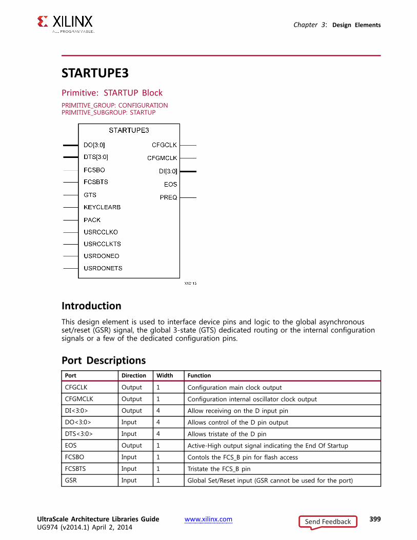
Chapter 3: Design Elements
STARTUPE3Primitive: STARTUP BlockPRIMITIVE_GROUP: CONFIGURATIONPRIMITIVE_SUBGROUP: STARTUP
IntroductionThis design element is used to interface device pins and logic to the global asynchronousset/reset (GSR) signal, the global 3-state (GTS) dedicated routing or the internal configurationsignals or a few of the dedicated configuration pins.
Port DescriptionsPort Direction Width Function
CFGCLK Output 1 Configuration main clock output
CFGMCLK Output 1 Configuration internal oscillator clock output
DI<3:0> Output 4 Allow receiving on the D input pin
DO<3:0> Input 4 Allows control of the D pin output
DTS<3:0> Input 4 Allows tristate of the D pin
EOS Output 1 Active-High output signal indicating the End Of Startup
FCSBO Input 1 Contols the FCS_B pin for flash access
FCSBTS Input 1 Tristate the FCS_B pin
GSR Input 1 Global Set/Reset input (GSR cannot be used for the port)
UltraScale Architecture Libraries Guide www.xilinx.com 399UG974 (v2014.1) April 2, 2014
Send Feedback

Chapter 3: Design Elements
Port Direction Width Function
GTS Input 1 Global 3-state input (GTS cannot be used for the port name)
KEYCLEARB Input 1 Clear AES Decrypter Key input from Battery-Backed RAM (BBRAM)
PACK Input 1 PROGRAM acknowledge input
PREQ Output 1 PROGRAM request to fabric output
USRCCLKO Input 1 User CCLK input
USRCCLKTS Input 1 User CCLK 3-state enable input
USRDONEO Input 1 User DONE pin output control
USRDONETS Input 1 User DONE 3-state enable output
Design Entry MethodInstantiation Recommended
Inference No
IP and IP Integrator Catalog No
Macro support No
Available AttributesAttribute Type Allowed Values Default Description
PROG_USR STRING "FALSE", "TRUE" "FALSE" Activate program event securityfeature. Requires encryptedbitstreams.
SIM_CCLK_FREQ FLOAT(nS) 0.0 to 10.0 0.0 Set the Configuration ClockFrequency(ns) for simulation
VHDL Instantiation TemplateUnless they already exist, copy the following two statements and paste them before the entitydeclaration.Library UNISIM;use UNISIM.vcomponents.all;
-- STARTUPE3: STARTUPBlock-- UltraScale-- Xilinx HDL Libraries Guide, version 2014.1
STARTUPE3_inst : STARTUPE3generic map (
PROG_USR=> "FALSE", -- Activate program event security feature. Requires encrypted bitstreams.SIM_CCLK_FREQ=> 0.0 -- Set the Configuration Clock Frequency(ns) for simulation
)port map (
CFGCLK=> CFGCLK, -- 1-bit output: Configuration main clock outputCFGMCLK=> CFGMCLK, -- 1-bit output: Configuration internal oscillator clock outputDI => DI, -- 4-bit output: Allow receiving on the D input pinEOS => EOS, -- 1-bit output: Active-High output signal indicating the End Of StartupPREQ=> PREQ, -- 1-bit output: PROGRAMrequest to fabric outputDO => DO, -- 4-bit input: Allows control of the D pin output
UltraScale Architecture Libraries Guide www.xilinx.com 400UG974 (v2014.1) April 2, 2014
Send Feedback

Chapter 3: Design Elements
DTS => DTS, -- 4-bit input: Allows tristate of the D pinFCSBO=> FCSBO, -- 1-bit input: Contols the FCS_B pin for flash accessFCSBTS => FCSBTS, -- 1-bit input: Tristate the FCS_B pinGSR => GSR, -- 1-bit input: Global Set/Reset input (GSR cannot be used for the port)GTS => GTS, -- 1-bit input: Global 3-state input (GTS cannot be used for the port name)KEYCLEARB=> KEYCLEARB, -- 1-bit input: Clear AES Decrypter Key input from Battery-Backed RAM (BBRAM)PACK => PACK, -- 1-bit input: PROGRAMacknowledge inputUSRCCLKO=> USRCCLKO, -- 1-bit input: User CCLK inputUSRCCLKTS=> USRCCLKTS, -- 1-bit input: User CCLK 3-state enable inputUSRDONEO=> USRDONEO, -- 1-bit input: User DONEpin output controlUSRDONETS=> USRDONETS -- 1-bit input: User DONE3-state enable output
);
-- End of STARTUPE3_inst instantiation
Verilog Instantiation Template
// STARTUPE3: STARTUPBlock// UltraScale// Xilinx HDL Libraries Guide, version 2014.1
STARTUPE3#(.PROG_USR("FALSE"), // Activate program event security feature. Requires encrypted bitstreams..SIM_CCLK_FREQ(0.0) // Set the Configuration Clock Frequency(ns) for simulation
)STARTUPE3_inst (
.CFGCLK(CFGCLK), // 1-bit output: Configuration main clock output
.CFGMCLK(CFGMCLK), // 1-bit output: Configuration internal oscillator clock output
.DI(DI), // 4-bit output: Allow receiving on the D input pin
.EOS(EOS), // 1-bit output: Active-High output signal indicating the End Of Startup
.PREQ(PREQ), // 1-bit output: PROGRAMrequest to fabric output
.DO(DO), // 4-bit input: Allows control of the D pin output
.DTS(DTS), // 4-bit input: Allows tristate of the D pin
.FCSBO(FCSBO), // 1-bit input: Contols the FCS_B pin for flash access
.FCSBTS(FCSBTS), // 1-bit input: Tristate the FCS_B pin
.GSR(GSR), // 1-bit input: Global Set/Reset input (GSR cannot be used for the port)
.GTS(GTS), // 1-bit input: Global 3-state input (GTS cannot be used for the port name)
.KEYCLEARB(KEYCLEARB), // 1-bit input: Clear AES Decrypter Key input from Battery-Backed RAM (BBRAM)
.PACK(PACK), // 1-bit input: PROGRAMacknowledge input
.USRCCLKO(USRCCLKO), // 1-bit input: User CCLK input
.USRCCLKTS(USRCCLKTS), // 1-bit input: User CCLK 3-state enable input
.USRDONEO(USRDONEO), // 1-bit input: User DONEpin output control
.USRDONETS(USRDONETS) // 1-bit input: User DONE3-state enable output);
// End of STARTUPE3_inst instantiation
For More Information• See the 7 series FPGA User Documentation (User Guides and Data Sheets).
• See the UltraScale User Documentation.
UltraScale Architecture Libraries Guide www.xilinx.com 401UG974 (v2014.1) April 2, 2014
Send Feedback

Chapter 3: Design Elements
SYSMONE1Primitive: Xilinx Analog-to-Digital Converter and System MonitorPRIMITIVE_GROUP: ADVANCEDPRIMITIVE_SUBGROUP: SYSMON
IntroductionThe SYSMON provides an analog-to-digital conversion and associated monitoring capability.The core ADC comprises a 10-bit, 0.2 MSPS (Mega-sample-per-second) ADC, providing ageneral purpose analog interface for a range of applications. The ADC supports a range ofoperating modes and various analog input signal types e.g., unipolar, differential etc. TheSystem Monitor also includes a number of on-chip sensors that support measurement of theon-chip power supply voltages and die temperature.
UltraScale Architecture Libraries Guide www.xilinx.com 402UG974 (v2014.1) April 2, 2014
Send Feedback

Chapter 3: Design Elements
Port DescriptionsPort Direction Width Function
ALM<15:0> Output 16 Output alarm for temperature, Vccint, Vccaux and Vccbram.ALM[0] - System Monitor temperature sensor alarm output.ALM[1] - System Monitor Vccint sensor alarm output.ALM[2] - System Monitor Vccaux sensor alarm output.ALM[3] - System Monitor Vccbram sensor alarm output.ALM[6:4] - Not defined.ALM[7] - Logic OR of bus ALM[6:0]. Can be used to flagoccurrence of any alarm.ALM[11:8] - Alarms for the User Supplies 1-4.ALM[14:12] - Not definedALM[15] - Logical OR of bus ALM[14:8] which can be used toflag any alarm in this group.
BUSY Output 1 SYSMON busy signal. This signal transitions High during an ADCconversion. This signal also transitions High for an extendedperiod during an ADC or sensor calibration.
CHANNEL<5:0> Output 6 Channel selection outputs. The SYSMON input MUX channelselection for the current ADC conversion is placed on theseoutputs at the end of an ADC conversion.
CONVST Input 1 Convert start input. This input controls the sampling instant onthe SYSMON(s) input and is only used in event mode timing.This input comes from the general-purpose interconnect in theFPGA logic.
CONVSTCLK Input 1 Convert start clock input. This input is connected to a clocknet. Like CONVST, this input controls the sampling instant onthe SYSMON(s) inputs and is only used in event mode timing.This input comes from the local clock distribution network inthe FPGA logic. Thus, for the best control over the samplinginstant (delay and jitter), a global clock input can be used asthe CONVST source.
DADDR<7:0> Input 8 Address bus for the dynamic reconfiguration port.
DCLK Input 1 Clock input for the dynamic reconfiguration port.
DEN Input 1 Enable signal for the dynamic reconfiguration port.
DI<15:0> Input 16 Input data bus for the dynamic reconfiguration port.
DO<15:0> Output 16 Output data bus for dynamic reconfiguration port.
DRDY Output 1 Data ready signal for the dynamic reconfiguration port.
DWE Input 1 Write enable for the dynamic reconfiguration port.
EOC Output 1 End of Conversion signal. This signal transitions to an active-Highat the end of an ADC conversion when the measurement iswritten to the status registers.
EOS Output 1 End of Sequence. This signal transitions to active-High when themeasurement data from the last channel in an automatic channelsequence is written to the status registers.
I2C_SCLK Input 1 Input for the I2C_SCLK. Required for DRP I2C interface. TheI2C_SCLK_IN and the I2C_SCLK_TS ports must be connected tothe dedicated I2C_SCLK package pin as described in the SystemMonitor User Guide.
UltraScale Architecture Libraries Guide www.xilinx.com 403UG974 (v2014.1) April 2, 2014
Send Feedback

Chapter 3: Design Elements
Port Direction Width Function
I2C_SCLK_TS Output 1 Output for the I2C_SCLK. Required for DRP I2C interface. TheI2C_SCLK_IN and the I2C_SCLK_TS ports must be connected tothe dedicated I2C_SCLK package pin as described in the SystemMonitor User Guide.
I2C_SDA Input 1 Input for the I2C_SDA. Required for DRP I2C interface. TheI2C_SDA_IN and the I2C_SDA_TS ports must be connected tothe dedicated I2C_SDA package pin as described in the SystemMonitor User Guide.
I2C_SDA_TS Output 1 Output for the I2C_SDA. Required for DRP I2C interface. TheI2C_SDA_IN and the I2C_SDA_TS ports must be connected tothe dedicated I2C_SDA package pin as described in the SystemMonitor User Guide.
JTAGBUSY Output 1 Used to indicate that a JTAG DRP transaction is in progress.
JTAGLOCKED Output 1 Indicates that a DRP port lock request has been made by theJTAG interface. This signal is also used to indicate that the DRP isready for access (when Low).
JTAGMODIFIED Output 1 Used to indicate that a JTAG Write to the DRP has occurred.
MUXADDR<4:0> Output 5 These outputs are used in external multiplexer mode. Theyindicate the address of the next channel in a sequence to beconverted. They provide the channel address for an externalmultiplexer.
OT Output 1 Over-Temperature alarm
RESET Input 1 Reset signal for the SYSMON control logic.
VAUXN<15:0> Input 16 N-side auxiliary analog input
VAUXP<15:0> Input 16 P-side auxiliary analog input
VN Input 1 N-side analog input
VP Input 1 P-side analog input
Design Entry MethodInstantiation Yes
Inference No
IP and IP Integrator Catalog Recommended
Macro support No
Available AttributesAttribute Type Allowed Values Default Description
INIT_4A HEX 16’h0000 to16’hffff
16’h0000 Sequence register 4
INIT_4B HEX 16’h0000 to16’hffff
16’h0000 Sequence register 5
INIT_4C HEX 16’h0000 to16’hffff
16’h0000 Sequence register 6
UltraScale Architecture Libraries Guide www.xilinx.com 404UG974 (v2014.1) April 2, 2014
Send Feedback

Chapter 3: Design Elements
Attribute Type Allowed Values Default Description
INIT_4D HEX 16’h0000 to16’hffff
16’h0000 Sequence register 7
INIT_4E HEX 16’h0000 to16’hffff
16’h0000 Sequence register 8
INIT_4F HEX 16’h0000 to16’hffff
16’h0000 Sequence register 9
INIT_5A HEX 16’h0000 to16’hffff
16’h0000 Alarm limit register 10
INIT_5B HEX 16’h0000 to16’hffff
16’h0000 Alarm limit register 11
INIT_5C HEX 16’h0000 to16’hffff
16’h0000 Alarm limit register 12
INIT_5D HEX 16’h0000 to16’hffff
16’h0000 Alarm limit register 13
INIT_5E HEX 16’h0000 to16’hffff
16’h0000 Alarm limit register 14
INIT_5F HEX 16’h0000 to16’hffff
16’h0000 Alarm limit register 15
INIT_6A HEX 16’h0000 to16’hffff
16’h0000 User supply alarm register 10
INIT_6B HEX 16’h0000 to16’hffff
16’h0000 User supply alarm register 11
INIT_6C HEX 16’h0000 to16’hffff
16’h0000 User supply alarm register 12
INIT_6D HEX 16’h0000 to16’hffff
16’h0000 User supply alarm register 13
INIT_6E HEX 16’h0000 to16’hffff
16’h0000 User supply alarm register 14
INIT_6F HEX 16’h0000 to16’hffff
16’h0000 User supply alarm register 15
INIT_40 HEX 16’h0000 to16’hffff
16’h0000 Configuration register 0
INIT_41 HEX 16’h0000 to16’hffff
16’h0000 Configuration register 1
INIT_42 HEX 16’h0000 to16’hffff
16’h0000 Configuration register 2
INIT_43 HEX 16’h0000 to16’hffff
16’h0000 Configuration register 3
INIT_44 HEX 16’h0000 to16’hffff
16’h0000 Configuration register 4
INIT_45 HEX 16’h0000 to16’hffff
16’h0000 Analog Bus Register
INIT_46 HEX 16’h0000 to16’hffff
16’h0000 Sequence register 0
UltraScale Architecture Libraries Guide www.xilinx.com 405UG974 (v2014.1) April 2, 2014
Send Feedback

Chapter 3: Design Elements
Attribute Type Allowed Values Default Description
INIT_47 HEX 16’h0000 to16’hffff
16’h0000 Sequence register 1
INIT_48 HEX 16’h0000 to16’hffff
16’h0000 Sequence register 2
INIT_49 HEX 16’h0000 to16’hffff
16’h0000 Sequence register 3
INIT_50 HEX 16’h0000 to16’hffff
16’h0000 Alarm limit register 0
INIT_51 HEX 16’h0000 to16’hffff
16’h0000 Alarm limit register 1
INIT_52 HEX 16’h0000 to16’hffff
16’h0000 Alarm limit register 2
INIT_53 HEX 16’h0000 to16’hffff
16’h0000 Alarm limit register 3
INIT_54 HEX 16’h0000 to16’hffff
16’h0000 Alarm limit register 4
INIT_55 HEX 16’h0000 to16’hffff
16’h0000 Alarm limit register 5
INIT_56 HEX 16’h0000 to16’hffff
16’h0000 Alarm limit register 6
INIT_57 HEX 16’h0000 to16’hffff
16’h0000 Alarm limit register 7
INIT_58 HEX 16’h0000 to16’hffff
16’h0000 Alarm limit register 8
INIT_59 HEX 16’h0000 to16’hffff
16’h0000 Alarm limit register 9
INIT_60 HEX 16’h0000 to16’hffff
16’h0000 User supply alarm register 0
INIT_61 HEX 16’h0000 to16’hffff
16’h0000 User supply alarm register 1
INIT_62 HEX 16’h0000 to16’hffff
16’h0000 User supply alarm register 2
INIT_63 HEX 16’h0000 to16’hffff
16’h0000 User supply alarm register 3
INIT_64 HEX 16’h0000 to16’hffff
16’h0000 User supply alarm register 4
INIT_65 HEX 16’h0000 to16’hffff
16’h0000 User supply alarm register 5
INIT_66 HEX 16’h0000 to16’hffff
16’h0000 User supply alarm register 6
INIT_67 HEX 16’h0000 to16’hffff
16’h0000 User supply alarm register 7
INIT_68 HEX 16’h0000 to16’hffff
16’h0000 User supply alarm register 8
UltraScale Architecture Libraries Guide www.xilinx.com 406UG974 (v2014.1) April 2, 2014
Send Feedback
Chapter 3: Design Elements
Attribute Type Allowed Values Default Description
INIT_69 HEX 16’h0000 to16’hffff
16’h0000 User supply alarm register 9
INIT_73, INIT_74,INIT_75, INIT_76,INIT_77
HEX 16’h0000 to16’hffff
16’h0000 System Monitor Test registers not forcustomer usage
IS_CONVSTCLK_INVERTED
BINARY 1’b0 to 1’b1 1’b0 Indicates whether or not to use theoptional inversion on the CONVSTCLK pinof this component.
IS_DCLK_INVERTED
BINARY 1’b0 to 1’b1 1’b0 Indicates whether or not to use theoptional inversion on the DCLK pin of thiscomponent.
INIT_70 toINIT_7F
HEX 16’h0000 to16’hffff
16’h0000 Reserved for future use
SIM_MONITOR_FILE
STRING String "design.txt" Specify the file name (and directoryif different from simulation directory)of file containing analog voltage andtemperature data for SYSMON simulationbehavior.
SYSMON_VUSER0_BANK
DECIMAL 0 to 999 0 Specify the IO Bank number to be usedwith User0 for monitoring
SYSMON_VUSER0_MONITOR
STRING String "NONE" Specify the voltage to monitor for User0
SYSMON_VUSER1_BANK
DECIMAL 0 to 999 0 Specify the IO Bank number to be usedwith User1 for monitoring
SYSMON_VUSER1_MONITOR
STRING String "NONE" Specify the voltage to monitor for User1
SYSMON_VUSER2_BANK
DECIMAL 0 to 999 0 Specify the IO Bank number to be usedwith User2 for monitoring
SYSMON_VUSER2_MONITOR
STRING String "NONE" Specify the voltage to monitor for User2
SYSMON_VUSER3_BANK
DECIMAL 0 to 999 0 Specify the IO Bank number to be usedwith User3 for monitoring
SYSMON_VUSER3_MONITOR
STRING String "NONE" Specify the voltage to monitor for User3
VHDL Instantiation TemplateUnless they already exist, copy the following two statements and paste them before the entitydeclaration.Library UNISIM;use UNISIM.vcomponents.all;
-- SYSMONE1:Xilinx Analog-to-Digital Converter and System Monitor-- UltraScale-- Xilinx HDL Libraries Guide, version 2014.1
UltraScale Architecture Libraries Guide www.xilinx.com 407UG974 (v2014.1) April 2, 2014
Send Feedback

Chapter 3: Design Elements
SYSMONE1_inst : SYSMONE1generic map (
-- INIT_40 - INIT_44: SYSMONconfiguration registersINIT_40 => X"0000",INIT_41 => X"0000",INIT_42 => X"0000",INIT_43 => X"0000",INIT_44 => X"0000",INIT_45 => X"0000", -- Analog Bus Register-- INIT_46 - INIT_4F: Sequence RegistersINIT_46 => X"0000",INIT_47 => X"0000",INIT_48 => X"0000",INIT_49 => X"0000",INIT_4A => X"0000",INIT_4B => X"0000",INIT_4C => X"0000",INIT_4D => X"0000",INIT_4E => X"0000",INIT_4F => X"0000",-- INIT_50 - INIT_5F: Alarm Limit RegistersINIT_50 => X"0000",INIT_51 => X"0000",INIT_52 => X"0000",INIT_53 => X"0000",INIT_54 => X"0000",INIT_55 => X"0000",INIT_56 => X"0000",INIT_57 => X"0000",INIT_58 => X"0000",INIT_59 => X"0000",INIT_5A => X"0000",INIT_5B => X"0000",INIT_5C => X"0000",INIT_5D => X"0000",INIT_5E => X"0000",INIT_5F => X"0000",-- INIT_60 - INIT_6F: User Supply AlarmsINIT_60 => X"0000",INIT_61 => X"0000",INIT_62 => X"0000",INIT_63 => X"0000",INIT_64 => X"0000",INIT_65 => X"0000",INIT_66 => X"0000",INIT_67 => X"0000",INIT_68 => X"0000",INIT_69 => X"0000",INIT_6A => X"0000",INIT_6B => X"0000",INIT_6C => X"0000",INIT_6D => X"0000",INIT_6E => X"0000",INIT_6F => X"0000",-- Programmable Inversion Attributes: Specifies the use of the built-in programmable inversion on-- specific pinsIS_CONVSTCLK_INVERTED=> ’0’, -- Optional inversion for CONVSTCLK, VALUESIS_DCLK_INVERTED => ’0’, -- Optional inversion for DCLK, VALUES-- Simulation attributes: Set for proper simulation behaviorSIM_MONITOR_FILE => "design.txt", -- Analog simulation data file name-- User Voltage Monitor: SYSMONUser voltage monitorSYSMON_VUSER0_BANK=> 0, -- Specify IO Bank for User0SYSMON_VUSER0_MONITOR=> "NONE", -- Specify Voltage for User0SYSMON_VUSER1_BANK=> 0, -- Specify IO Bank for User1SYSMON_VUSER1_MONITOR=> "NONE", -- Specify Voltage for User1SYSMON_VUSER2_BANK=> 0, -- Specify IO Bank for User2SYSMON_VUSER2_MONITOR=> "NONE", -- Specify Voltage for User2SYSMON_VUSER3_MONITOR=> "NONE" -- Specify Voltage for User3
)port map (
-- ALARMS: 16-bit (each) output: ALM, OT
UltraScale Architecture Libraries Guide www.xilinx.com 408UG974 (v2014.1) April 2, 2014
Send Feedback

Chapter 3: Design Elements
ALM => ALM, -- 16-bit output: Output alarm for temp, Vccint, Vccaux and VccbramOT => OT, -- 1-bit output: Over-Temperature alarm-- Dynamic Reconfiguration Port (DRP): 16-bit (each) output: Dynamic Reconfiguration PortsDO => DO, -- 16-bit output: DRP output data busDRDY=> DRDY, -- 1-bit output: DRP data ready-- STATUS: 1-bit (each) output: SYSMONstatus portsBUSY => BUSY, -- 1-bit output: System Monitor busy outputCHANNEL=> CHANNEL, -- 6-bit output: Channel selection outputsEOC => EOC, -- 1-bit output: End of ConversionEOS => EOS, -- 1-bit output: End of SequenceJTAGBUSY=> JTAGBUSY, -- 1-bit output: JTAG DRP transaction in progress outputJTAGLOCKED=> JTAGLOCKED, -- 1-bit output: JTAG requested DRP port lockJTAGMODIFIED => JTAGMODIFIED, -- 1-bit output: JTAG Write to the DRP has occurredMUXADDR=> MUXADDR, -- 5-bit output: External MUX channel decode-- Auxiliary Analog-Input Pairs: 16-bit (each) input: VAUXP[15:0], VAUXN[15:0]VAUXN=> VAUXN, -- 16-bit input: N-side auxiliary analog inputVAUXP => VAUXP, -- 16-bit input: P-side auxiliary analog input-- CONTROLand CLOCK: 1-bit (each) input: Reset, conversion start and clock inputsCONVST=> CONVST, -- 1-bit input: Convert start inputCONVSTCLK=> CONVSTCLK, -- 1-bit input: Convert start inputRESET => RESET, -- 1-bit input: Active-High reset-- Dedicated Analog Input Pair: 1-bit (each) input: VP/VNVN => VN, -- 1-bit input: N-side analog inputVP => VP, -- 1-bit input: P-side analog input-- Dynamic Reconfiguration Port (DRP): 8-bit (each) input: Dynamic Reconfiguration PortsDADDR=> DADDR, -- 8-bit input: DRP address busDCLK => DCLK, -- 1-bit input: DRP clockDEN => DEN, -- 1-bit input: DRP enable signalDI => DI, -- 16-bit input: DRP input data busDWE=> DWE, -- 1-bit input: DRP write enable-- I2C Interface: 1-bit (each) input: Ports used with the I2C DRP interfaceI2C_SCLK => I2C_SCLK, -- 1-bit input: I2C_SCLK input portI2C_SDA => I2C_SDA -- 1-bit input: I2C_SDA input port
);
-- End of SYSMONE1_inst instantiation
Verilog Instantiation Template
// SYSMONE1:Xilinx Analog-to-Digital Converter and System Monitor// UltraScale// Xilinx HDL Libraries Guide, version 2014.1
SYSMONE1#(// INIT_40 - INIT_44: SYSMONconfiguration registers.INIT_40(16’h0000),.INIT_41(16’h0000),.INIT_42(16’h0000),.INIT_43(16’h0000),.INIT_44(16’h0000),.INIT_45(16’h0000), // Analog Bus Register// INIT_46 - INIT_4F: Sequence Registers.INIT_46(16’h0000),.INIT_47(16’h0000),.INIT_48(16’h0000),.INIT_49(16’h0000),.INIT_4A(16’h0000),.INIT_4B(16’h0000),.INIT_4C(16’h0000),.INIT_4D(16’h0000),.INIT_4E(16’h0000),.INIT_4F(16’h0000),// INIT_50 - INIT_5F: Alarm Limit Registers.INIT_50(16’h0000),.INIT_51(16’h0000),.INIT_52(16’h0000),.INIT_53(16’h0000),.INIT_54(16’h0000),.INIT_55(16’h0000),.INIT_56(16’h0000),
UltraScale Architecture Libraries Guide www.xilinx.com 409UG974 (v2014.1) April 2, 2014
Send Feedback

Chapter 3: Design Elements
.INIT_57(16’h0000),
.INIT_58(16’h0000),
.INIT_59(16’h0000),
.INIT_5A(16’h0000),
.INIT_5B(16’h0000),
.INIT_5C(16’h0000),
.INIT_5D(16’h0000),
.INIT_5E(16’h0000),
.INIT_5F(16’h0000),// INIT_60 - INIT_6F: User Supply Alarms.INIT_60(16’h0000),.INIT_61(16’h0000),.INIT_62(16’h0000),.INIT_63(16’h0000),.INIT_64(16’h0000),.INIT_65(16’h0000),.INIT_66(16’h0000),.INIT_67(16’h0000),.INIT_68(16’h0000),.INIT_69(16’h0000),.INIT_6A(16’h0000),.INIT_6B(16’h0000),.INIT_6C(16’h0000),.INIT_6D(16’h0000),.INIT_6E(16’h0000),.INIT_6F(16’h0000),// Programmable Inversion Attributes: Specifies the use of the built-in programmable inversion on// specific pins.IS_CONVSTCLK_INVERTED(1’b0), // Optional inversion for CONVSTCLK, VALUES.IS_DCLK_INVERTED(1’b0), // Optional inversion for DCLK, VALUES// Simulation attributes: Set for proper simulation behavior.SIM_MONITOR_FILE("design.txt"), // Analog simulation data file name// User Voltage Monitor: SYSMONUser voltage monitor.SYSMON_VUSER0_BANK(0), // Specify IO Bank for User0.SYSMON_VUSER0_MONITOR("NONE"), // Specify Voltage for User0.SYSMON_VUSER1_BANK(0), // Specify IO Bank for User1.SYSMON_VUSER1_MONITOR("NONE"), // Specify Voltage for User1.SYSMON_VUSER2_BANK(0), // Specify IO Bank for User2.SYSMON_VUSER2_MONITOR("NONE"), // Specify Voltage for User2.SYSMON_VUSER3_MONITOR("NONE") // Specify Voltage for User3
)SYSMONE1_inst (
// ALARMS: 16-bit (each) output: ALM, OT.ALM(ALM), // 16-bit output: Output alarm for temp, Vccint, Vccaux and Vccbram.OT(OT), // 1-bit output: Over-Temperature alarm// Dynamic Reconfiguration Port (DRP): 16-bit (each) output: Dynamic Reconfiguration Ports.DO(DO), // 16-bit output: DRP output data bus.DRDY(DRDY), // 1-bit output: DRP data ready// STATUS: 1-bit (each) output: SYSMONstatus ports.BUSY(BUSY), // 1-bit output: System Monitor busy output.CHANNEL(CHANNEL), // 6-bit output: Channel selection outputs.EOC(EOC), // 1-bit output: End of Conversion.EOS(EOS), // 1-bit output: End of Sequence.JTAGBUSY(JTAGBUSY), // 1-bit output: JTAG DRP transaction in progress output.JTAGLOCKED(JTAGLOCKED), // 1-bit output: JTAG requested DRP port lock.JTAGMODIFIED(JTAGMODIFIED), // 1-bit output: JTAG Write to the DRP has occurred.MUXADDR(MUXADDR), // 5-bit output: External MUX channel decode// Auxiliary Analog-Input Pairs: 16-bit (each) input: VAUXP[15:0], VAUXN[15:0].VAUXN(VAUXN), // 16-bit input: N-side auxiliary analog input.VAUXP(VAUXP), // 16-bit input: P-side auxiliary analog input// CONTROLand CLOCK: 1-bit (each) input: Reset, conversion start and clock inputs.CONVST(CONVST), // 1-bit input: Convert start input.CONVSTCLK(CONVSTCLK), // 1-bit input: Convert start input.RESET(RESET), // 1-bit input: Active-High reset// Dedicated Analog Input Pair: 1-bit (each) input: VP/VN.VN(VN), // 1-bit input: N-side analog input.VP(VP), // 1-bit input: P-side analog input// Dynamic Reconfiguration Port (DRP): 8-bit (each) input: Dynamic Reconfiguration Ports.DADDR(DADDR), // 8-bit input: DRP address bus.DCLK(DCLK), // 1-bit input: DRP clock.DEN(DEN), // 1-bit input: DRP enable signal.DI(DI), // 16-bit input: DRP input data bus
UltraScale Architecture Libraries Guide www.xilinx.com 410UG974 (v2014.1) April 2, 2014
Send Feedback

Chapter 3: Design Elements
.DWE(DWE), // 1-bit input: DRP write enable// I2C Interface: 1-bit (each) input: Ports used with the I2C DRP interface.I2C_SCLK(I2C_SCLK), // 1-bit input: I2C_SCLK input port.I2C_SDA(I2C_SDA) // 1-bit input: I2C_SDA input port
);
// End of SYSMONE1_inst instantiation
For More Information• See the 7 series FPGA User Documentation (User Guides and Data Sheets).
• See the UltraScale User Documentation.
UltraScale Architecture Libraries Guide www.xilinx.com 411UG974 (v2014.1) April 2, 2014
Send Feedback

Chapter 3: Design Elements
TX_BITSLICEPrimitive: TX_BITSLICE for output using Native ModePRIMITIVE_GROUP: I/OPRIMITIVE_SUBGROUP: BITSLICE
IntroductionIn native mode, the TX_BITSLICE contains serialization logic and a 512-tap output delay(ODELAY) that can be continously adjusted for VT variation. The TX_BITSLICE containsserialization logic for either 4:1 or 8:1 serialization.
Port DescriptionsPort Direction Width Function
CE Input 1 Clock enable for TX_BITSLICE ODELAY register clock
CLK Input 1 Clock used to sample LOAD, CE, INC
CNTVALUEIN<8:0> Input 9 Counter value from internal device logic for tap valueto be loaded dynamically
CNTVALUEOUT<8:0> Output 9 Counter value to going the internal device logic formonitoring tap value
D<7:0> Input 8 Data from device logic
UltraScale Architecture Libraries Guide www.xilinx.com 412UG974 (v2014.1) April 2, 2014
Send Feedback

Chapter 3: Design Elements
Port Direction Width Function
EN_VTC Input 1 Enable to keep stable delay over VT when set to HIGH.VT compensation disabled when set to LOW.
INC Input 1 Increment the current delay tap setting
LOAD Input 1 Load the CNTVALUEIN tap setting
O Output 1 Serialized output going to output buffer
RST Input 1 Asynchronous assert, synchronous deassert forTX_BITSLICE OSERDES
RST_DLY Input 1 Reset the internal DELAY value to DELAY_VALUE
RX_BIT_CTRL_IN<39:0> Input 40 Input bus from BITSLICE_CONTROL
RX_BIT_CTRL_OUT<39:0> Output 40 Output bus to BITSLICE_CONTROL
T Input 1 Legacy T byte input from device logic
T_OUT Output 1 Byte group 3-state output
TBYTE_IN Input 1 Byte group 3-state input from TX_BITSLICE_TRI
TX_BIT_CTRL_IN<39:0> Input 40 Input bus from BITSLICE_CONTROL
TX_BIT_CTRL_OUT<39:0> Output 40 Output bus to BITSLICE_CONTROL
Design Entry MethodInstantiation Yes
Inference No
IP and IP Integrator Catalog Yes
Macro support No
Available AttributesAttribute Type Allowed Values Default Description
DATA_WIDTH DECIMAL 8, 4 8 Defines the parallel data inputwidth. Legal values are 4 and 8.
DELAY_FORMAT STRING "TIME", "COUNT" "TIME" Sets the units of DELAY_VALUEof the TX_BITSLICE ODELAY. UseTIME when DELAY_TYPE is FIXED.Use COUNT when DELAY_TYPE isVARIABLE or VAR_LOAD.
• "TIME" : TX_BITSLICE ODELAYDELAY_VALUE is specified in ps
• "COUNT" : TX_BITSLICEODELAY DELAY_VALUE isspecified in taps
UltraScale Architecture Libraries Guide www.xilinx.com 413UG974 (v2014.1) April 2, 2014
Send Feedback
Chapter 3: Design Elements
Attribute Type Allowed Values Default Description
DELAY_TYPE STRING "FIXED","VAR_LOAD","VARIABLE"
"FIXED" Sets the type of tap delay line.
• "FIXED" - Sets a static delayvalue
• "VARIABLE" - Dynamicallyadjust (increment/decrement)delay value
• "VAR_LOAD" - Dynamicallyloads tap values
DELAY_VALUE DECIMAL 0 to 1250 0 Specifies the fixed delay in pswhen using FIXED DELAY_TYPE.Specifies value upon reset whenusing VARIABLE or VAR_LOAD.
INIT BINARY 1’b1, 1’b0 1’b1 Defines initial O value
IS_CLK_INVERTED
BINARY 1’b0 to 1’b1 1’b0 Indicates whether the clock CLK isactive-high or active-low
IS_RST_DLY_INVERTED
BINARY 1’b0 to 1’b1 1’b0 Indicates whether the resetRST_DLY is active-high oractive-low
IS_RST_INVERTED
BINARY 1’b0 to 1’b1 1’b0 Indicates whether the reset RST isactive-high or active-low
OUTPUT_PHASE_90
STRING "FALSE", "TRUE" "FALSE" Delays the output phase by90-degrees
PRE_EMPHASIS STRING "OFF", "ON" "OFF" Used in conjunction with IOB toEnable/Disable the pre-emphasis.
REFCLK_FREQUENCY
1significantdigit FLOAT
200.0 to 2400.0 300.0 Specification of the reference clockfrequency in MHz
TBYTE_CTL STRING "TBYTE_IN", "T" "TBYTE_IN" Select between T and TBYTE_INinputs in OSERDES mode only
UPDATE_MODE STRING "ASYNC","MANUAL", "SYNC"
"ASYNC" • "ASYNC": Updates areincrements or decrements tothe delay value independentof the data being received
• "SYNC": Updates requirethat input data transitionsto synchronously update thedelay with the data inputedges
• "MANUAL": Updates takeeffect when both LOAD andCE are asserted after the LOADand CNTVALUEIN signalsare used to load the newCNTVALUE
UltraScale Architecture Libraries Guide www.xilinx.com 414UG974 (v2014.1) April 2, 2014
Send Feedback

Chapter 3: Design Elements
VHDL Instantiation TemplateUnless they already exist, copy the following two statements and paste them before the entitydeclaration.Library UNISIM;use UNISIM.vcomponents.all;
-- TX_BITSLICE: TX_BITSLICE for output using Native Mode-- UltraScale-- Xilinx HDL Libraries Guide, version 2014.1
TX_BITSLICE_inst : TX_BITSLICEgeneric map (
DATA_WIDTH=> 8, -- Parallel data input width (8-4)DELAY_FORMAT=> "TIME", -- Units of the DELAY_VALUE(TIME, COUNT)DELAY_TYPE=> "FIXED", -- Set the type of tap delay line (FIXED, VAR_LOAD, VARIABLE)DELAY_VALUE=> 0, -- Output delay value settingINIT => 1, -- Defines initial O valueIS_CLK_INVERTED => ’0’, -- Optional inversion for CLKIS_RST_DLY_INVERTED => ’0’, -- Optional inversion for RST_DLYIS_RST_INVERTED => ’0’, -- Optional inversion for RSTOUTPUT_PHASE_90=> "FALSE", -- Delays the output phase by 90-degreesREFCLK_FREQUENCY=> 300.0, -- Specification of the reference clock frequency in MHz (VALUES)TBYTE_CTL => "TBYTE_IN", -- Select between T and TBYTE_IN inputsUPDATE_MODE=> "ASYNC" -- Determines when updates to the delay will take effect (ASYNC, MANUAL,
-- SYNC))port map (
CNTVALUEOUT=> CNTVALUEOUT, -- 9-bit output: Counter value to device logicO => O, -- 1-bit output: Serialized output going to output bufferRX_BIT_CTRL_OUT => RX_BIT_CTRL_OUT, -- 40-bit output: Output bus to BITSLICE_CONTROLTX_BIT_CTRL_OUT => TX_BIT_CTRL_OUT, -- 40-bit output: Output bus to BITSLICE_CONTROLT_OUT => T_OUT, -- 1-bit output: Byte group 3-state outputCE => CE, -- 1-bit input: Clock enable for ODELAYCLK => CLK, -- 1-bit input: Clock used to sample LOAD, CE, INCCNTVALUEIN => CNTVALUEIN, -- 9-bit input: Counter value from device logicD => D, -- 8-bit input: Data from device logicEN_VTC => EN_VTC, -- 1-bit input: Enable to keep stable delay over VTINC => INC, -- 1-bit input: Increment the current delay tap settingLOAD => LOAD, -- 1-bit input: Load the CNTVALUEIN tap settingRST => RST, -- 1-bit input: Asynchronous assert, synchronous deassert for
-- TX_BITSLICE OSERDES
RST_DLY => RST_DLY, -- 1-bit input: Reset the internal DELAY value to DELAY_VALUERX_BIT_CTRL_IN => RX_BIT_CTRL_IN, -- 40-bit input: Input bus from BITSLICE_CONTROLT => T, -- 1-bit input: Legacy T byte input from device logicTBYTE_IN => TBYTE_IN, -- 1-bit input: Byte group 3-state input from TX_BITSLICE_TRITX_BIT_CTRL_IN => TX_BIT_CTRL_IN -- 40-bit input: Input bus from BITSLICE_CONTROL
);
-- End of TX_BITSLICE_inst instantiation
UltraScale Architecture Libraries Guide www.xilinx.com 415UG974 (v2014.1) April 2, 2014
Send Feedback

Chapter 3: Design Elements
Verilog Instantiation Template
// TX_BITSLICE: TX_BITSLICE for output using Native Mode// UltraScale// Xilinx HDL Libraries Guide, version 2014.1
TX_BITSLICE #(.DATA_WIDTH(8), // Parallel data input width (8-4).DELAY_FORMAT("TIME"), // Units of the DELAY_VALUE(TIME, COUNT).DELAY_TYPE("FIXED"), // Set the type of tap delay line (FIXED, VAR_LOAD, VARIABLE).DELAY_VALUE(0), // Output delay value setting.INIT(1), // Defines initial O value.IS_CLK_INVERTED(1’b0), // Optional inversion for CLK.IS_RST_DLY_INVERTED(1’b0), // Optional inversion for RST_DLY.IS_RST_INVERTED(1’b0), // Optional inversion for RST.OUTPUT_PHASE_90("FALSE"), // Delays the output phase by 90-degrees.REFCLK_FREQUENCY(300.0), // Specification of the reference clock frequency in MHz (VALUES).TBYTE_CTL("TBYTE_IN"), // Select between T and TBYTE_IN inputs.UPDATE_MODE("ASYNC") // Determines when updates to the delay will take effect (ASYNC, MANUAL,
// SYNC))TX_BITSLICE_inst (
.CNTVALUEOUT(CNTVALUEOUT), // 9-bit output: Counter value to device logic
.O(O), // 1-bit output: Serialized output going to output buffer
.RX_BIT_CTRL_OUT(RX_BIT_CTRL_OUT), // 40-bit output: Output bus to BITSLICE_CONTROL
.TX_BIT_CTRL_OUT(TX_BIT_CTRL_OUT), // 40-bit output: Output bus to BITSLICE_CONTROL
.T_OUT(T_OUT), // 1-bit output: Byte group 3-state output
.CE(CE), // 1-bit input: Clock enable for ODELAY
.CLK(CLK), // 1-bit input: Clock used to sample LOAD, CE, INC
.CNTVALUEIN(CNTVALUEIN), // 9-bit input: Counter value from device logic
.D(D), // 8-bit input: Data from device logic
.EN_VTC(EN_VTC), // 1-bit input: Enable to keep stable delay over VT
.INC(INC), // 1-bit input: Increment the current delay tap setting
.LOAD(LOAD), // 1-bit input: Load the CNTVALUEIN tap setting
.RST(RST), // 1-bit input: Asynchronous assert, synchronous deassert for// TX_BITSLICE OSERDES
.RST_DLY(RST_DLY), // 1-bit input: Reset the internal DELAY value to DELAY_VALUE
.RX_BIT_CTRL_IN(RX_BIT_CTRL_IN), // 40-bit input: Input bus from BITSLICE_CONTROL
.T(T), // 1-bit input: Legacy T byte input from device logic
.TBYTE_IN(TBYTE_IN), // 1-bit input: Byte group 3-state input from TX_BITSLICE_TRI
.TX_BIT_CTRL_IN(TX_BIT_CTRL_IN) // 40-bit input: Input bus from BITSLICE_CONTROL);
// End of TX_BITSLICE_inst instantiation
For More Information• See the 7 series FPGA User Documentation (User Guides and Data Sheets).
• See the UltraScale User Documentation.
UltraScale Architecture Libraries Guide www.xilinx.com 416UG974 (v2014.1) April 2, 2014
Send Feedback

Chapter 3: Design Elements
TX_BITSLICE_TRIPrimitive: TX_BITSLICE_TRI for tristate using Native Mode
PRIMITIVE_GROUP: I/OPRIMITIVE_SUBGROUP: BITSLICE
IntroductionIn native mode, the TX_BITSLICE_TRI provides the ability to tristate bitslices within a nibble.The TX_BITSLICE_TRI also contains a 512-tap output delay element (ODELAY) with a calibratedtap resolution.
Port DescriptionsPort Direction Width Function
BIT_CTRL_IN<39:0> Input 40 Input bus from BITSLICE_CONTROL
BIT_CTRL_OUT<39:0> Output 40 Output bus to BITSLICE_CONTROL
CE Input 1 Active high enable increment/decrement input
CLK Input 1 Clock input
CNTVALUEIN<8:0> Input 9 Counter value from FPGA logic for dynamically loadabletap value input
CNTVALUEOUT<8:0> Output 9 Counter value to going the internal device logic formonitoring tap value
EN_VTC Input 1 Enable to keep stable delay over VT when set to HIGH.VT compensation disabled when set to LOW.
INC Input 1 Increment the current delay tap setting
UltraScale Architecture Libraries Guide www.xilinx.com 417UG974 (v2014.1) April 2, 2014
Send Feedback

Chapter 3: Design Elements
Port Direction Width Function
LOAD Input 1 Load the CNTVALUEIN tap setting
RST Input 1 Asynchronous assert, synchronous deassert
RST_DLY Input 1 Reset the internal DELAY value to DELAY_VALUE
TRI_OUT Output 1 Output to the TBYTE_IN pins of the bitslices
Design Entry MethodInstantiation Yes
Inference No
IP and IP Integrator Catalog Yes
Macro support No
Available AttributesAttribute Type Allowed Values Default Description
DATA_WIDTH DECIMAL 8, 4 8 Defines the parallel data inputwidth. Legal values are 4 and 8.
DELAY_FORMAT STRING "TIME", "COUNT" "TIME" Sets the units of DELAY_VALUE ofthe TX_BITSLICE_TRI ODELAY. UseTIME when DELAY_TYPE is FIXED.Use COUNT when DELAY_TYPE isVARIABLE or VAR_LOAD.
• "TIME" : TX_BITSLICE_TRIODELAY DELAY_VALUE isspecified in ps
• "COUNT" : TX_BITSLICE_TRIODELAY DELAY_VALUE isspecified in taps
DELAY_TYPE STRING "FIXED","VAR_LOAD","VARIABLE"
"FIXED" Sets the type of tap delay line.
• "FIXED" - Sets a static delayvalue
• "VARIABLE" - Dynamicallyadjust (increment/decrement)delay value
• "VAR_LOAD" - Dynamicallyloads tap values
DELAY_VALUE DECIMAL 0 to 1250 0 Specifies the fixed delay in pswhen using FIXED DELAY_TYPE.Specifies value upon reset whenusing VARIABLE or VAR_LOAD.
INIT BINARY 1’b1, 1’b0 1’b1 Defines initial O value
IS_CLK_INVERTED
BINARY 1’b0 to 1’b1 1’b0 Indicates whether the clock CLK isactive-high or active-low
UltraScale Architecture Libraries Guide www.xilinx.com 418UG974 (v2014.1) April 2, 2014
Send Feedback

Chapter 3: Design Elements
Attribute Type Allowed Values Default Description
IS_RST_DLY_INVERTED
BINARY 1’b0 to 1’b1 1’b0 Indicates whether the resetRST_DLY is active-high oractive-low
IS_RST_INVERTED
BINARY 1’b0 to 1’b1 1’b0 Indicates whether the reset RST isactive-high or active-low
OUTPUT_PHASE_90
STRING "FALSE", "TRUE" "FALSE" Delays the output phase by90-degrees
REFCLK_FREQUENCY
1significantdigit FLOAT
200.0 to 2400.0 300.0 Specification of the reference clockfrequency in MHz
UPDATE_MODE STRING "ASYNC","MANUAL", "SYNC"
"ASYNC" • "ASYNC": Updates areincrements or decrements tothe delay value independentof the data being received
• "SYNC": Updates requirethat input data transitionsto synchronously update thedelay with the data inputedges
• "MANUAL": Updates takeeffect when both LOAD andCE are asserted after the LOADand CNTVALUEIN signalsare used to load the newCNTVALUE
VHDL Instantiation TemplateUnless they already exist, copy the following two statements and paste them before the entitydeclaration.Library UNISIM;use UNISIM.vcomponents.all;
-- TX_BITSLICE_TRI: TX_BITSLICE_TRI for tristate using Native Mode-- UltraScale-- Xilinx HDL Libraries Guide, version 2014.1
TX_BITSLICE_TRI_inst : TX_BITSLICE_TRIgeneric map (
DATA_WIDTH=> 8, -- Parallel data input width (8-4)DELAY_FORMAT=> "TIME", -- Units of the DELAY_VALUE(TIME, COUNT)DELAY_TYPE=> "FIXED", -- Set the type of tap delay line (FIXED, VAR_LOAD, VARIABLE)DELAY_VALUE=> 0, -- Output delay value settingINIT => 1, -- Defines initial O valueIS_CLK_INVERTED => ’0’, -- Optional inversion for CLKIS_RST_DLY_INVERTED => ’0’, -- Optional inversion for RST_DLYIS_RST_INVERTED => ’0’, -- Optional inversion for RSTOUTPUT_PHASE_90=> "FALSE", -- Delays the output phase by 90-degreesREFCLK_FREQUENCY=> 300.0, -- Specification of the reference clock frequency in MHz (VALUES)UPDATE_MODE=> "ASYNC" -- Determines when updates to the delay will take effect (ASYNC, MANUAL,
-- SYNC))port map (
BIT_CTRL_OUT => BIT_CTRL_OUT, -- 40-bit output: Output bus to BITSLICE_CONTROLCNTVALUEOUT=> CNTVALUEOUT, -- 9-bit output: Counter value to device logicTRI_OUT => TRI_OUT, -- 1-bit output: Output to the TBYTE_IN pins of the bitslices
UltraScale Architecture Libraries Guide www.xilinx.com 419UG974 (v2014.1) April 2, 2014
Send Feedback

Chapter 3: Design Elements
BIT_CTRL_IN => BIT_CTRL_IN, -- 40-bit input: Input bus from BITSLICE_CONTROLCE => CE, -- 1-bit input: Active high enable increment/decrement inputCLK => CLK, -- 1-bit input: Clock inputCNTVALUEIN => CNTVALUEIN, -- 9-bit input: Counter value inputEN_VTC => EN_VTC, -- 1-bit input: Enable to keep stable delay over VTINC => INC, -- 1-bit input: Increment the current delay tap settingLOAD => LOAD, -- 1-bit input: Load the CNTVALUEIN tap settingRST => RST, -- 1-bit input: Asynchronous assert, synchronous deassertRST_DLY => RST_DLY -- 1-bit input: Reset the internal DELAY value to DELAY_VALUE
);
-- End of TX_BITSLICE_TRI_inst instantiation
Verilog Instantiation Template
// TX_BITSLICE_TRI: TX_BITSLICE_TRI for tristate using Native Mode// UltraScale// Xilinx HDL Libraries Guide, version 2014.1
TX_BITSLICE_TRI #(.DATA_WIDTH(8), // Parallel data input width (8-4).DELAY_FORMAT("TIME"), // Units of the DELAY_VALUE(TIME, COUNT).DELAY_TYPE("FIXED"), // Set the type of tap delay line (FIXED, VAR_LOAD, VARIABLE).DELAY_VALUE(0), // Output delay value setting.INIT(1), // Defines initial O value.IS_CLK_INVERTED(1’b0), // Optional inversion for CLK.IS_RST_DLY_INVERTED(1’b0), // Optional inversion for RST_DLY.IS_RST_INVERTED(1’b0), // Optional inversion for RST.OUTPUT_PHASE_90("FALSE"), // Delays the output phase by 90-degrees.REFCLK_FREQUENCY(300.0), // Specification of the reference clock frequency in MHz (VALUES).UPDATE_MODE("ASYNC") // Determines when updates to the delay will take effect (ASYNC, MANUAL,
// SYNC))TX_BITSLICE_TRI_inst (
.BIT_CTRL_OUT(BIT_CTRL_OUT), // 40-bit output: Output bus to BITSLICE_CONTROL
.CNTVALUEOUT(CNTVALUEOUT), // 9-bit output: Counter value to device logic
.TRI_OUT(TRI_OUT), // 1-bit output: Output to the TBYTE_IN pins of the bitslices
.BIT_CTRL_IN(BIT_CTRL_IN), // 40-bit input: Input bus from BITSLICE_CONTROL
.CE(CE), // 1-bit input: Active high enable increment/decrement input
.CLK(CLK), // 1-bit input: Clock input
.CNTVALUEIN(CNTVALUEIN), // 9-bit input: Counter value input
.EN_VTC(EN_VTC), // 1-bit input: Enable to keep stable delay over VT
.INC(INC), // 1-bit input: Increment the current delay tap setting
.LOAD(LOAD), // 1-bit input: Load the CNTVALUEIN tap setting
.RST(RST), // 1-bit input: Asynchronous assert, synchronous deassert
.RST_DLY(RST_DLY) // 1-bit input: Reset the internal DELAY value to DELAY_VALUE);
// End of TX_BITSLICE_TRI_inst instantiation
For More Information• See the 7 series FPGA User Documentation (User Guides and Data Sheets).
• See the UltraScale User Documentation.
UltraScale Architecture Libraries Guide www.xilinx.com 420UG974 (v2014.1) April 2, 2014
Send Feedback

Appendix A
Additional Resources and Legal Notices
Xilinx ResourcesFor support resources such as Answers, Documentation, Downloads, and Forums, see XilinxSupport.
For a glossary of technical terms used in Xilinx documentation, see the Xilinx Glossary.
Solution CentersSee the Xilinx Solution Centers for support on devices, software tools, and intellectualproperty at all stages of the design cycle. Topics include design assistance, advisories, andtroubleshooting tips.
ReferencesThese documents provide supplemental material useful with this guide:
UltraScale Architecture Libraries Guide www.xilinx.com 421UG974 (v2014.1) April 2, 2014
Send Feedback

Appendix A: Additional Resources and Legal Notices
Please Read: Important Legal NoticesThe information disclosed to you hereunder (the "Materials") is provided solely for the selectionand use of Xilinx products. To the maximum extent permitted by applicable law: (1) Materialsare made available "AS IS" and with all faults, Xilinx hereby DISCLAIMS ALL WARRANTIESAND CONDITIONS, EXPRESS, IMPLIED, OR STATUTORY, INCLUDING BUT NOT LIMITED TOWARRANTIES OF MERCHANTABILITY, NON-INFRINGEMENT, OR FITNESS FOR ANY PARTICULARPURPOSE; and (2) Xilinx shall not be liable (whether in contract or tort, including negligence,or under any other theory of liability) for any loss or damage of any kind or nature relatedto, arising under, or in connection with, the Materials (including your use of the Materials),including for any direct, indirect, special, incidental, or consequential loss or damage (includingloss of data, profits, goodwill, or any type of loss or damage suffered as a result of any actionbrought by a third party) even if such damage or loss was reasonably foreseeable or Xilinxhad been advised of the possibility of the same. Xilinx assumes no obligation to correct anyerrors contained in the Materials or to notify you of updates to the Materials or to productspecifications. You may not reproduce, modify, distribute, or publicly display the Materialswithout prior written consent. Certain products are subject to the terms and conditionsof Xilinx’s limited warranty, please refer to Xilinx’s Terms of Sale which can be viewed athttp://www.xilinx.com/legal.htm#tos; IP cores may be subject to warranty and support termscontained in a license issued to you by Xilinx. Xilinx products are not designed or intended tobe fail-safe or for use in any application requiring fail-safe performance; you assume sole riskand liability for use of Xilinx products in such critical applications, please refer to Xilinx’s Termsof Sale which can be viewed at http://www.xilinx.com/legal.htm#tos.
© Copyright 2012–2014 Xilinx, Inc. Xilinx, the Xilinx logo, Artix, ISE, Kintex, Spartan, Virtex,Vivado, Zynq, and other designated brands included herein are trademarks of Xilinx in the UnitedStates and other countries. All other trademarks are the property of their respective owners.
UltraScale Architecture Libraries Guide www.xilinx.com 422UG974 (v2014.1) April 2, 2014
Send Feedback


![Developing Tamper-Resistant Designs with Zynq UltraScale+ ... · Developing Tamper Resistant Designs with UltraScale and UltraScale+ FPGAs (XAPP1098) [Ref6] provide a useful background](https://static.fdocuments.net/doc/165x107/5f0b3f187e708231d42f9162/developing-tamper-resistant-designs-with-zynq-ultrascale-developing-tamper.jpg)