UltraScale Architecture GTH Transceivers -...
387
UltraScale Architecture GTH Transceivers User Guide UG576 (v1.2) August 12, 2015
Transcript of UltraScale Architecture GTH Transceivers -...

UltraScale Architecture GTH Transceivers
User Guide
UG576 (v1.2) August 12, 2015

Revision HistoryThe following table shows the revision history for this document.
Date Version Revision
08/12/2015 1.2 Removed “Advance Specification” from document title.Chapter 1: Updated pattern generator connection in Figure 1-2. Added Ports and Attributes, page 15.Chapter 2: Added Single External Reference Clock Use Model and Multiple External Reference Clocks Use Model. Removed internal CPLL reset signal from Figure 2-10. Removed Table 2-8: GTHE3_CHANNEL Clocking Attribute and Table 2-10: GTHE3_COMMON Clocking Attributes. In Table 2-10, updated CPLLPD and CPLLRESET descriptions, and added table note. Removed SIM_CPLLREFCLK_SEL from Table 2-11. Updated QPLL0_FBDIV/QPLL1_FBDIV valid settings in Table 2-13 and Table 2-15. Removed SIM_QPLL0REFCLK_SEL/SIM_QPLL1REFCLK_SEL from Table 2-15. Added Resetting Multiple Lanes and Quads. In CPLL Reset, replaced CPLLRESET with CPLLPD. In Table 2-18, added CPLLPD and table note. Removed Table 2-21: CPLL Reset Attributes. In GTH Transceiver TX Reset in Response to Completion of Configuration, updated third step under reset mode being defaulted to single mode. Replaced CPLLRESET with CPLLPD in Figure 2-18. Updated near-end loopback, near-end PCS loopback, and far-end PMA loopback bullets after Figure 2-20. Replaced CPLLRESET with CPLLPD in Table 2-24. Added description of TXRATEMODE to f irst paragraph of TX Rate Change. In GTH Transceiver RX Reset in Response to Completion of Configuration, updated third step under reset mode being defaulted to single mode. Replaced CPLLRESET with CPLLPD in Figure 2-23. Replaced CPLLRESET with CPLLPD in Table 2-29. Added description of RXRATEMODE to f irst paragraph of RX Rate Change. Added Powering Up/Down Multiple Lanes and Quads, page 71. Updated second paragraph in PLL Power Down. Updated near-end and far-end PCS loopback bullets after Figure 2-25. Updated description of PCSRSVDIN[2] in Table 2-35. Added Digital Monitor.Chapter 3: Added BUFG_GT_SYNC to notes after Figure 3-2 to Figure 3-5 and Figure 3-28. Updated pattern generator connection in Figure 3-1, Figure 3-14, and Figure 3-17. In Table 3-4, changed TXDATAEXTENDRSVD clock domain to Async. Added description of multi-lane configuration before Figure 3-3. Changed GEARBOX_MODE[0] setting from 1’b0 to 1’b1 in Enabling the TX Asynchronous Gearbox. Added Reading Datapath Latency. Added TXUSRCLK jitter sensitivity to Table 3-17. Updated Functional Description, page 118. In Table 3-20, updated descriptions of TXPHDLYRESET, TXDLYSRESET, TXSYNCMODE, TXSYNCALLIN, and TXSYNCIN, and changed TXDLYHOLD and TXDLYUPDOWN clock domains to Async. Updated note in Table 3-22. Updated description of master bullet in Using TX Buffer Bypass in Multi-Lane Manual Mode. Added Using TX Pattern Generator. Updated valid settings for TX_PROGDIV_CFG in Table 3-30. Updated TXRATEMODE description in Table 3-31. Added description of internal 25 MHz clock before Table 3-32. In Table 3-33, changed TXPIPPMEN, TXPIPPMOVRDEN, TXPIPPMSEL, and TXPIPPMSTEPSIZE[4:0] clock domain to Async. Updated TX Phase Interpolator PPM Controller Use Mode and added Figure 3-29. In Table 3-35, changed TXBUFDIFFCTRL[2:0], TXDEEMPH, and TXDIFFCTRL[3:0] clock domain to Async, updated driver swing control values in description of TXDIFFCTRL[3:0], and removed TXPOSTCURSORINV and TXPRECURSORINV. Updated description of TX_EIDLE_ASSERT_DELAY in Table 3-36. Changed TXPDELECIDLEMODE clock domain to Async in Table 3-39.
UltraScale Architecture GTH Transceivers www.xilinx.com 2UG576 (v1.2) August 12, 2015
Send Feedback

08/12/2015 1.2(Cont’d)
Updated description of SATA_BURST_SEQ_LEN[3:0] in Table 3-40.Chapter 4: Updated capacitor values from 10 to 100 nF in Figure 4-2 and Figure 4-3. Updated description of RXQPIEN in Table 4-1. Updated description of RX_CM_TRIM [3:0] in Table 4-2. Added note after Table 4-3. Added note to Table 4-5 and Table 4-6. Updated description of RXSYSCLKSEL in Table 4-7. Reversed KH and KL in Figure 4-8. In Table 4-9, changed clock domain for all ports to Async, removed RXDFEXYDEN port, and added attribute lengths to descriptions of ports throughout. In Table 4-10, added sentence about attribute being shared between DFE and LPM modes to description of RX_DFE_KL_LPM_KH_CFG1[2:0], RX_DFE_KL_LPM_KL_CFG1[2:0], and RX_DFE_AGC_CFG1[2:0]. Updated GTH Use Modes and GTH Transceivers: Switching Between LPM and DFE Modes at Run Time. Added BUFG_GT_SYNC to note 6 after Figure 4-12. In Parallel Clock Divider and Selector, replaced TXOUTCLK with RXOUTCLK. Updated valid settings for RX_PROGDIV_CFG in Table 4-15. Updated RXRATEMODE description in Table 4-16. Added description of internal 25 MHz clock before Table 4-17. Updated description of USE_PCS_CLK_PHASE_SEL in Table 4-19. Updated RX_DATA_WIDTH description in Table 4-27. Updated RX_DATA_WIDTH settings in Enabling and Disabling 8B/10B Decoding. In Table 4-28, updated description of RXPHDLYPD, and removed RXDDIEN, RXPHMONITOR, and RXPHSLIPMONITOR. Replaced RXREC with RXDES in description of RX_XCLK_SEL in Table 4-29. Removed duplicate “Using RX Buffer Bypass in Single-Lane Auto Mode” section. Removed RXDDIEN setting from Using RX Buffer Bypass in Single-Lane Auto Mode. Updated master bullet in Using RX Buffer Bypass in Multi-Lane Manual Mode. Removed M_RXDDIEN and S_RXDDIEN from Figure 4-32. Added RXUSRCLK jitter sensitivity to Table 4-31. Updated RX8B10BEN description in Table 4-35. Changed GEARBOX_MODE[0] setting from 1’b0 to 1’b1 in Enabling the RX Asynchronous Gearbox. Added Reading Datapath Latency.Chapter 5: Updated direction and description columns for MGTREFCLK0P/N and MGTREFCLK1P/N in Table 5-1. Updated first two paragraphs of Termination Resistor Calibration Circuit. Added Table 5-2 and Table 5-3 to Analog Power Supply Pins. Added Reference Clock Output Buffer and Power Up/Down and Reset on Multiple Lanes. Updated recommendations for MGTREFCLK0P/N, MGTREFCLK1P/N, and MGTHRXP/N[3:0] in Table 5-5.Chapter 6: Added new chapter.Appendix B: In Table B-2, updated DRP encoding for 003Eh and 00C6h, and added 0150h to 015Fh.
Date Version Revision
UltraScale Architecture GTH Transceivers www.xilinx.com 3UG576 (v1.2) August 12, 2015
Send Feedback

09/17/2014 1.1 Chapter 2: Updated Functional Description, page 23. Added description of PLL CLKOUT to paragraph before Equation 2-2 and Equation 2-4. Added RESETEXCEPTION and GTPOWERGOOD to Table 2-21 and Table 2-25. Added TX_PMA_POWER_SAVE to Table 2-22 and Table 2-26. Removed description of reset mode being defaulted to sequential mode from GTH Transceiver TX Reset in Response to Completion of Configuration and GTH Transceiver RX Reset in Response to Completion of Configuration. Updated Figure 2-18. Updated Table 2-24. Updated Figure 2-23. Updated Table 2-29. Updated f irst paragraph in RX Rate Change. Corrected RX_CLKMUX_EN and TX_CLKMUX_EN attributes in Table 2-31. In Table 2-35, updated descriptions of DRPEN and DRPRDY, and added PCSRSVDIN[2]. Updated descriptions of DRPEN and DRPRDY in Table 2-36.Chapter 3: Added Equation 3-2. Updated f irst bullet after Table 3-3. Added TXDATAEXTENDRSVD to Table 3-4. Added TX_FABINT_USRCLK_FLOP to Table 3-5. Updated Figure 3-6. Added Table 3-14. Updated title of Figure 3-14 and paragraphs immediately preceding and following. Updated description of TX_SAMPLE_PERIOD in Table 3-16. Replaced PMA with PISO and TXUSRCLK with TX XCLK in Functional Description, page 118. Added TXPHDLY_CFG0/TXPHDLY_CFG1 to Table 3-21. Updated GTH Transceivers column and added note to Table 3-22. Updated note 2 after Figure 3-18. In Using the TX Phase Alignment to Minimize the TX Lane-to-Lane Skew, replaced BUFG with BUFG_GT. Added 3'b101 to third GTH transceiver setting after Figure 3-21. Updated TXOUTCLKSEL setting in Using TX Buffer Bypass in Single-Lane Auto Mode and Using TX Buffer Bypass in Single-Lane Manual Mode. Updated note 9 after Figure 3-22. Added Using TX Buffer Bypass in Multi-Lane Auto Mode. Removed TX_USERPATTERN_DATA attributes from Table 3-25. Added TX_DIVRESET_TIME to Table 3-30. Added TXRATEMODE to Table 3-31. Added TX_CLK25_DIV to Table 3-32. Replaced TXPPMOVRD_VALUE[6:0] with TXPI_PPM_CFG[6:0] in description of TXPIPPMOVRDEN in Table 3-33. Added TX Phase Interpolator PPM Controller Use Mode. Added TXDRVBIAS_P, TXDRVBIAS_N, TX_DCD_CFG, and TX_DCD_EN to Table 3-36. Replaced TXPOWERDOWN with TXPD in description of TXPDELECIDLEMODE in Table 3-39. Added TX_IDLE_DATA_ZERO to Table 3-40.Chapter 4: Updated capacitor values in Figure 4-2 and Figure 4-3 from 100 nF to 10 nF. Added RX_CM_BUF_CFG and RX_CM_BUF_PD to Table 4-2. Updated Table 4-3 to Table 4-6. Swapped Figure 4-3 and Figure 4-5. Swapped Figure 4-4 and Figure 4-6. In Table 4-9, updated description of {RXOSHOLD, RXOSOVRDEN}, removed “GTH transceiver” from several ports, and added RXOSINTSTARTED, RXOSINTSTROBEDONE, {RXLPMOSHOLD, RXLPMOSOVRDEN}, and {RXLPMGCHOLD, RXLPMGCOVRDEN} ports. In Table 4-10, removed “GTH transceiver” from some attributes and added several new attributes. Removed LPM mode from third paragraph in Choosing Between LPM and DFE Modes. In Table 4-11, updated descriptions of RXCDRFREQRESET and RXCDRRESET, and added RXCDRPHDONE. Added RX_WIDEMODE_CDR and CDR_SWAP_MODE_EN to Table 4-12. Added RX_DIVRESET_TIME to Table 4-15. Added RXRATEMODE to Table 4-16. Added RXPMACLK_SEL and RX_CLK25_DIV to Table 4-17. Added EYE_SCAN_SWAP_EN to Table 4-19. Updated width of RXPRBSSEL[3:0] in Table 4-22. Updated first paragraph in Alignment Status Signals.
Date Version Revision
UltraScale Architecture GTH Transceivers www.xilinx.com 4UG576 (v1.2) August 12, 2015
Send Feedback

09/17/2014 1.1(Cont’d)
Updated number of RXUSRCLK2 cycles from one to two in Manual Alignment. Updated description of RXSLIDE in Table 4-24. Updated Figure 4-26. Removed out of table character with disparity error (D) from Figure 4-27. Replaced PMA with SIPO and RXUSRCLK with RX XCLK in Functional Description, page 220. In Table 4-28, added RXSLIPOUTCLK, RXSLIPPMA, and RXPHALIGNERR, and updated description of RXDDIEN. Added RX_CLK_SLIP_OVRD to Table 4-29. Added note to Table 4-30. Updated RXOUTCLKSEL and removed RXDDIEN from list of transceiver settings in Using RX Buffer Bypass in Single-Lane Auto Mode, Using RX Buffer Bypass in Multi-Lane Manual Mode, and Using RX Buffer Bypass in Multi-Lane Auto Mode. Removed RXDLYSRESET reset from note 2 after Figure 4-29, note 2 after Figure 4-30, and note 4 after Figure 4-35. Relabeled BUFG to BUFG_GT in Figure 4-33. Updated description of RXBUFSTATUS[2:0] in Table 4-32. Updated Figure 4-36 and Figure 4-55. Added Table 4-42. Updated title of Figure 4-55 and paragraphs immediately preceding and following. Updated description of RX_SAMPLE_PERIOD in Table 4-44. Added widths to RXCTRL1 and RXCTRL0 ports in Table 4-46. Added Equation 4-2. Added RXDATAEXTENDRSVD to Table 4-48. Added RX_FABINT_USRCLK_FLOP to Table 4-49.Chapter 5: Removed Figure 5-2: “GTH Transceivers Internal Power Supply Connections.” In Termination Resistor Calibration Circuit, added sentence about RCAL circuit being driven by configuration clock to f irst paragraph and recommendation to limit DC trace resistance to last paragraph. In Table 5-5, added recommendation to limit DC trace resistance in recommendations column of MGTAVTTRCAL and MGTRREF pins and updated Quad power supply group recommendation for MGTAVCC[N], MGTAVTT[N], and MGTVCCAUX[N]. Removed nominal range and nominal value from second bullet in GTH Transceiver Reference Clock Checklist. Updated capacitor values in Figure 5-7 and Figure 5-8 from 0.1 µF to 0.01 µF.Appendix C: Added new appendix.
12/10/2013 1.0 Initial Xilinx release.
Date Version Revision
UltraScale Architecture GTH Transceivers www.xilinx.com 5UG576 (v1.2) August 12, 2015
Send Feedback

Table of ContentsRevision History . . . . . . . . . . . . . . . . . . . . . . . . . . . . . . . . . . . . . . . . . . . . . . . . . . . . . . . . . . . . . . . . . . . . 2
Chapter 1: Transceiver and Tool OverviewIntroduction to UltraScale Architecture . . . . . . . . . . . . . . . . . . . . . . . . . . . . . . . . . . . . . . . . . . . . . . . . 9Features . . . . . . . . . . . . . . . . . . . . . . . . . . . . . . . . . . . . . . . . . . . . . . . . . . . . . . . . . . . . . . . . . . . . . . . . . 9UltraScale FPGAs Transceivers Wizard . . . . . . . . . . . . . . . . . . . . . . . . . . . . . . . . . . . . . . . . . . . . . . . . 14Simulation . . . . . . . . . . . . . . . . . . . . . . . . . . . . . . . . . . . . . . . . . . . . . . . . . . . . . . . . . . . . . . . . . . . . . . 14Implementation . . . . . . . . . . . . . . . . . . . . . . . . . . . . . . . . . . . . . . . . . . . . . . . . . . . . . . . . . . . . . . . . . . 16
Chapter 2: Shared FeaturesReference Clock Input/Output Structure . . . . . . . . . . . . . . . . . . . . . . . . . . . . . . . . . . . . . . . . . . . . . . 18Reference Clock Selection and Distribution . . . . . . . . . . . . . . . . . . . . . . . . . . . . . . . . . . . . . . . . . . . . 23Channel PLL . . . . . . . . . . . . . . . . . . . . . . . . . . . . . . . . . . . . . . . . . . . . . . . . . . . . . . . . . . . . . . . . . . . . . 36Quad PLL . . . . . . . . . . . . . . . . . . . . . . . . . . . . . . . . . . . . . . . . . . . . . . . . . . . . . . . . . . . . . . . . . . . . . . . . 41Reset and Initialization . . . . . . . . . . . . . . . . . . . . . . . . . . . . . . . . . . . . . . . . . . . . . . . . . . . . . . . . . . . . 46Power Down. . . . . . . . . . . . . . . . . . . . . . . . . . . . . . . . . . . . . . . . . . . . . . . . . . . . . . . . . . . . . . . . . . . . . 69Loopback. . . . . . . . . . . . . . . . . . . . . . . . . . . . . . . . . . . . . . . . . . . . . . . . . . . . . . . . . . . . . . . . . . . . . . . . 72Dynamic Reconfiguration Port . . . . . . . . . . . . . . . . . . . . . . . . . . . . . . . . . . . . . . . . . . . . . . . . . . . . . . 74Digital Monitor. . . . . . . . . . . . . . . . . . . . . . . . . . . . . . . . . . . . . . . . . . . . . . . . . . . . . . . . . . . . . . . . . . . 78
Chapter 3: TransmitterTX Overview . . . . . . . . . . . . . . . . . . . . . . . . . . . . . . . . . . . . . . . . . . . . . . . . . . . . . . . . . . . . . . . . . . . . . 86TX Interface . . . . . . . . . . . . . . . . . . . . . . . . . . . . . . . . . . . . . . . . . . . . . . . . . . . . . . . . . . . . . . . . . . . . . 87TX 8B/10B Encoder . . . . . . . . . . . . . . . . . . . . . . . . . . . . . . . . . . . . . . . . . . . . . . . . . . . . . . . . . . . . . . . 96TX Synchronous Gearbox. . . . . . . . . . . . . . . . . . . . . . . . . . . . . . . . . . . . . . . . . . . . . . . . . . . . . . . . . . 100TX Asynchronous Gearbox . . . . . . . . . . . . . . . . . . . . . . . . . . . . . . . . . . . . . . . . . . . . . . . . . . . . . . . . 110TX Buffer . . . . . . . . . . . . . . . . . . . . . . . . . . . . . . . . . . . . . . . . . . . . . . . . . . . . . . . . . . . . . . . . . . . . . . . 116TX Buffer Bypass . . . . . . . . . . . . . . . . . . . . . . . . . . . . . . . . . . . . . . . . . . . . . . . . . . . . . . . . . . . . . . . . 118TX Pattern Generator. . . . . . . . . . . . . . . . . . . . . . . . . . . . . . . . . . . . . . . . . . . . . . . . . . . . . . . . . . . . . 132TX Polarity Control . . . . . . . . . . . . . . . . . . . . . . . . . . . . . . . . . . . . . . . . . . . . . . . . . . . . . . . . . . . . . . . 135TX Fabric Clock Output Control . . . . . . . . . . . . . . . . . . . . . . . . . . . . . . . . . . . . . . . . . . . . . . . . . . . . . 136TX Phase Interpolator PPM Controller . . . . . . . . . . . . . . . . . . . . . . . . . . . . . . . . . . . . . . . . . . . . . . . 143TX Configurable Driver. . . . . . . . . . . . . . . . . . . . . . . . . . . . . . . . . . . . . . . . . . . . . . . . . . . . . . . . . . . . 145
UltraScale Architecture GTH Transceivers www.xilinx.com 6UG576 (v1.2) August 12, 2015
Send Feedback

TX Receiver Detect Support for PCI Express Designs. . . . . . . . . . . . . . . . . . . . . . . . . . . . . . . . . . . . 153TX Out-of-Band Signaling. . . . . . . . . . . . . . . . . . . . . . . . . . . . . . . . . . . . . . . . . . . . . . . . . . . . . . . . . . 155
Chapter 4: ReceiverRX Overview . . . . . . . . . . . . . . . . . . . . . . . . . . . . . . . . . . . . . . . . . . . . . . . . . . . . . . . . . . . . . . . . . . . . 157RX Analog Front End . . . . . . . . . . . . . . . . . . . . . . . . . . . . . . . . . . . . . . . . . . . . . . . . . . . . . . . . . . . . . 158RX Out-of-Band Signaling . . . . . . . . . . . . . . . . . . . . . . . . . . . . . . . . . . . . . . . . . . . . . . . . . . . . . . . . . 165RX Equalizer (DFE and LPM) . . . . . . . . . . . . . . . . . . . . . . . . . . . . . . . . . . . . . . . . . . . . . . . . . . . . . . . 168RX CDR . . . . . . . . . . . . . . . . . . . . . . . . . . . . . . . . . . . . . . . . . . . . . . . . . . . . . . . . . . . . . . . . . . . . . . . . 180RX Fabric Clock Output Control. . . . . . . . . . . . . . . . . . . . . . . . . . . . . . . . . . . . . . . . . . . . . . . . . . . . . 184RX Margin Analysis . . . . . . . . . . . . . . . . . . . . . . . . . . . . . . . . . . . . . . . . . . . . . . . . . . . . . . . . . . . . . . 190RX Polarity Control. . . . . . . . . . . . . . . . . . . . . . . . . . . . . . . . . . . . . . . . . . . . . . . . . . . . . . . . . . . . . . . 200RX Pattern Checker . . . . . . . . . . . . . . . . . . . . . . . . . . . . . . . . . . . . . . . . . . . . . . . . . . . . . . . . . . . . . . 201RX Byte and Word Alignment . . . . . . . . . . . . . . . . . . . . . . . . . . . . . . . . . . . . . . . . . . . . . . . . . . . . . . 203RX 8B/10B Decoder . . . . . . . . . . . . . . . . . . . . . . . . . . . . . . . . . . . . . . . . . . . . . . . . . . . . . . . . . . . . . . 215RX Buffer Bypass . . . . . . . . . . . . . . . . . . . . . . . . . . . . . . . . . . . . . . . . . . . . . . . . . . . . . . . . . . . . . . . . 220RX Elastic Buffer . . . . . . . . . . . . . . . . . . . . . . . . . . . . . . . . . . . . . . . . . . . . . . . . . . . . . . . . . . . . . . . . . 233RX Clock Correction . . . . . . . . . . . . . . . . . . . . . . . . . . . . . . . . . . . . . . . . . . . . . . . . . . . . . . . . . . . . . . 238RX Channel Bonding. . . . . . . . . . . . . . . . . . . . . . . . . . . . . . . . . . . . . . . . . . . . . . . . . . . . . . . . . . . . . . 246RX Synchronous Gearbox . . . . . . . . . . . . . . . . . . . . . . . . . . . . . . . . . . . . . . . . . . . . . . . . . . . . . . . . . 257RX Asynchronous Gearbox . . . . . . . . . . . . . . . . . . . . . . . . . . . . . . . . . . . . . . . . . . . . . . . . . . . . . . . . 268RX Interface . . . . . . . . . . . . . . . . . . . . . . . . . . . . . . . . . . . . . . . . . . . . . . . . . . . . . . . . . . . . . . . . . . . . 275
Chapter 5: Board Design GuidelinesOverview . . . . . . . . . . . . . . . . . . . . . . . . . . . . . . . . . . . . . . . . . . . . . . . . . . . . . . . . . . . . . . . . . . . . . . 280Pin Description and Design Guidelines. . . . . . . . . . . . . . . . . . . . . . . . . . . . . . . . . . . . . . . . . . . . . . . 280Reference Clock . . . . . . . . . . . . . . . . . . . . . . . . . . . . . . . . . . . . . . . . . . . . . . . . . . . . . . . . . . . . . . . . . 286GTH Transceiver Reference Clock Checklist . . . . . . . . . . . . . . . . . . . . . . . . . . . . . . . . . . . . . . . . . . . 287Reference Clock Interface . . . . . . . . . . . . . . . . . . . . . . . . . . . . . . . . . . . . . . . . . . . . . . . . . . . . . . . . . 288Power Supply and Filtering . . . . . . . . . . . . . . . . . . . . . . . . . . . . . . . . . . . . . . . . . . . . . . . . . . . . . . . . 290Power Supply Distribution Network. . . . . . . . . . . . . . . . . . . . . . . . . . . . . . . . . . . . . . . . . . . . . . . . . 293PCB Design Checklist . . . . . . . . . . . . . . . . . . . . . . . . . . . . . . . . . . . . . . . . . . . . . . . . . . . . . . . . . . . . . 295
Chapter 6: Use ModelPCI Express Architecture . . . . . . . . . . . . . . . . . . . . . . . . . . . . . . . . . . . . . . . . . . . . . . . . . . . . . . . . . . 298
Appendix A: 8B/10B Valid Characters
Appendix B: DRP Address Map of the GTH TransceiverGTHE3_COMMON Primitive DRP Address Map. . . . . . . . . . . . . . . . . . . . . . . . . . . . . . . . . . . . . . . . 310
UltraScale Architecture GTH Transceivers www.xilinx.com 7UG576 (v1.2) August 12, 2015
Send Feedback

GTHE3_CHANNEL Primitive DRP Address Map . . . . . . . . . . . . . . . . . . . . . . . . . . . . . . . . . . . . . . . . 330
Appendix C: Placement Information by Package and Device
Appendix D: Additional Resources and Legal NoticesXilinx Resources . . . . . . . . . . . . . . . . . . . . . . . . . . . . . . . . . . . . . . . . . . . . . . . . . . . . . . . . . . . . . . . . . 386Solution Centers. . . . . . . . . . . . . . . . . . . . . . . . . . . . . . . . . . . . . . . . . . . . . . . . . . . . . . . . . . . . . . . . . 386References . . . . . . . . . . . . . . . . . . . . . . . . . . . . . . . . . . . . . . . . . . . . . . . . . . . . . . . . . . . . . . . . . . . . . 386Please Read: Important Legal Notices . . . . . . . . . . . . . . . . . . . . . . . . . . . . . . . . . . . . . . . . . . . . . . . 387
UltraScale Architecture GTH Transceivers www.xilinx.com 8UG576 (v1.2) August 12, 2015
Send Feedback

Chapter 1
Transceiver and Tool Overview
Introduction to UltraScale ArchitectureXilinx® UltraScale™ architecture is a revolutionary approach to creating programmable devices capable of addressing the massive I/O and memory bandwidth requirements of next-generation applications while eff iciently routing and processing the data brought on chip. UltraScale architecture-based devices address a vast spectrum of high-bandwidth, high-utilization system requirements through industry-leading technical innovations. The devices share many building blocks to provide optimized scalability across the product range, as well as numerous new power reduction features for low total power consumption.
Kintex® UltraScale FPGAs provide high performance with a focus on optimized performance per watt for applications including wireless, wired, and signal or image processing. High DSP and block RAM-to-logic ratios, and next generation transceivers are combined with low-cost packaging to enable an optimum blend of capability for these applications.
Virtex® UltraScale FPGAs provide the highest system capacity, bandwidth, and performance. Delivering unprecedented logic capacity, serial I/O bandwidth, and on-chip memory, the Virtex UltraScale family pushes the performance envelope ever higher.
This user guide describes the UltraScale architecture SelectIO™ resources and is part of the UltraScale architecture documentation suite available at: www.xilinx.com/ultrascale.
FeaturesThe GTH transceivers in the UltraScale architecture are power-efficient transceivers, supporting line rates from 500 Mb/s to 16.375 Gb/s. The GTH transceiver is highly configurable and tightly integrated with the programmable logic resources of the UltraScale architecture. Table 1-1 summarizes the features by functional group that support a wide variety of applications.
UltraScale Architecture GTH Transceivers www.xilinx.com 9UG576 (v1.2) August 12, 2015
Send Feedback

Chapter 1: Transceiver and Tool Overview
The GTH transceiver supports these use modes:
• PCI Express, Revision 1.1/2.0/3.0
• SFF-8431 (SFP+)
• 10GBASE-R/KR
• Interlaken
• 10 Gb attachment unit interface (XAUI), reduced pin extended attachment unit interface (RXAUI), 100 Gb attachment unit interface (CAUI), 40 Gb attachment unit interface (XLAUI)
• Common packet radio interface (CPRI™), open base station architecture initiative (OBSAI)
Table 1-1: GTH Transceiver Features
Group Feature
PCS 2-byte and 4-byte internal datapath to support different line rate requirements
8B/10B encoding and decoding
64B/66B and 64B/67B support
128B/130B encoding and decoding for PCI Express® Gen3
Comma detection and byte and word alignment
PRBS generator and checker
TX phase FIFO
RX elastic FIFO for clock correction and channel bonding
Buffer bypass support for f ixed latency
Programmable logic interface
100 Gb attachment unit interface (CAUI) support
Native multi-lane support for buffer bypass
TX phase interpolator PPM controller for external voltage-controlled crystal oscillator (VCXO) replacement
PMA Two shared LC tank phase-locked loops (PLLs) per Quad for best jitter performance
One ring PLL per channel for best clocking flexibility
Power-efficient adaptive linear equalizer mode called the low-power mode (LPM) with auto adapt
11-tap Decision Feedback Equalizer (DFE) with Auto Adapt
TX pre-emphasis
Programmable TX output
Beacon signaling for PCI Express designs
Out-of-band (OOB) signaling including COM signal support for Serial ATA (SATA) designs
Line rate support up to 16.375 Gb/s
UltraScale Architecture GTH Transceivers www.xilinx.com 10UG576 (v1.2) August 12, 2015
Send Feedback

Chapter 1: Transceiver and Tool Overview
• OC-48/192
• Optical channel transport unit (OTU): OTU-1, OTU-2, OTU-3, OTU-4
• Serial RapidIO (SRIO)
• Serial advanced technology attachment (SATA), serial attached SCSI (SAS)
• Serial digital interface (SDI)
Key Differences from Previous FPGA Generations• Increased line rate support up to 16.375 Gb/s
• Enhanced 64B/66B and 64B/67B gearbox support
• Improved PRBS generator and checker
• Additional datapath to support PCIe Gen3
• Enhanced clocking to provide additional flexibility in supporting 64B/66B type protocols in the interconnect logic
Additional information on the functional blocks of UltraScale architecture-based devices:
• UltraScale Architecture Configuration User Guide (UG570) [Ref 1], provides more information on device configuration.
• UltraScale Architecture SelectIO Resources User Guide (UG571) [Ref 2], provides more information on the I/O resources.
• UltraScale Architecture Clocking Resources User Guide (UG572) [Ref 3], provides more information on the mixed mode clock manager (MMCM) and clocking.
UltraScale Architecture GTH Transceivers www.xilinx.com 11UG576 (v1.2) August 12, 2015
Send Feedback

Chapter 1: Transceiver and Tool Overview
Figure 1-1 illustrates the clustering of four GTHE3_CHANNEL primitives and one GTHE3_COMMON primitive to form a Quad.
Four GTHE3_CHANNEL primitives clustered together with one GTHE3_COMMON primitive are called a Quad or Q.
X-Ref Target - Figure 1-1
Figure 1-1: GTH Transceiver Quad Configuration
TX
RXRecoveredclock routeddirectly fromthe PMA
CPLL
QPLL1
TX
RX
CPLL
TX
RX
CPLL
TX
RX
CPLL
REFCLKDistribution
GTHE3_CHANNEL
GTHE3_CHANNEL
GTHE3_CHANNEL
GTHE3_CHANNEL
GTHE3_COMMONIBUFDS_GTE3 /OBUFDS_GTE3
UG576_c1_01_102513
QPLL0
IBUFDS_GTE3 /OBUFDS_GTE3
UltraScale Architecture GTH Transceivers www.xilinx.com 12UG576 (v1.2) August 12, 2015
Send Feedback

Chapter 1: Transceiver and Tool Overview
The GTHE3_COMMON primitive contains two LC-tank PLLs (QPLL0 and QPLL1). The GTHE3_COMMON only needs to be instantiated when a LC-tank PLL is used in the application.
Each GTHE3_CHANNEL primitive consists of a channel PLL, a transmitter, and a receiver.
Figure 1-2 illustrates the topology of a GTHE3_CHANNEL primitive.
Refer to Figure 2-11, page 36 for the description of the channel clocking architecture, which provides clocks to the RX and TX clock dividers.
X-Ref Target - Figure 1-2
Figure 1-2: GTHE3_CHANNEL Primitive Topology
From ChannelClocking
Architecture
To RX Parallel Data(Near-End PCSLoopback)
From RX ParallelData (Far-End PMA
Loopback)
From RX ParallelData (Far-End PCS
Loopback)
TXOOBandPCIe
TXDriver
TXClock
Dividers
TX PhaseInterpolator
TX PhaseInterpolatorController
TXPre/PostEmp
PISO
TX PMA TX PCS
Polarity
TX Sync Gearbox
TX PIPEControlSATA
OOB
PhaseAdjustFIFO
TX AsyncGearbox
8B/10BEncoder
128B/130BEncoder
TXInterface
PCIeBeacon
PatternGenerator
From ChannelClocking
Architecture
RXEQ
RXClock
Dividers
DFE
SIPO
RX OOB
Polarity
PRBSChecker
CommaDetect
andAlign
RX SyncGearbox
RXInterface
RXElasticBuffer
RX AsyncGearbox
RX PIPEControl
RX StatusControl
UG576_c1_02_022315
PCIe RXBuffer
BlockDetectAlign
128B/130BDecoder
8B/10BDecoder
UltraScale Architecture GTH Transceivers www.xilinx.com 13UG576 (v1.2) August 12, 2015
Send Feedback

Chapter 1: Transceiver and Tool Overview
UltraScale FPGAs Transceivers WizardThe UltraScale FPGAs Transceivers Wizard (hereinafter called the Wizard) is the preferred tool to generate a wrapper to instantiate GTH transceiver primitives called GTHE3_COMMON and GTHE3_CHANNEL. The Wizard is located in the IP catalog under the IO Interfaces category.
RECOMMENDED: Download the most up-to-date IP update before using the Wizard. Details on how to use this Wizard can be found in the UltraScale FPGAs Transceivers Wizard: Product Guide for Vivado Design Suite (PG182) [Ref 4].
Simulation
Functional DescriptionSimulations using the GTHE3 channel and common primitives have specif ic prerequisites that the simulation environment and the test bench must fulf ill. For instructions on how to set up the simulation environment for supported simulators depending on the used hardware description language (HDL), see the latest version of the Vivado Design Suite User Guide: Logic Simulation (UG900) [Ref 5].
The prerequisites for simulating a design with the GTHE3 channel and common primitives are listed:
• A simulator with support for SecureIP models.
SecureIP models are encrypted versions of the Verilog HDL used for implementation of the modeled block. SecureIP is an IP encryption methodology. To support SecureIP models, a Verilog LRM—IEEE Std 1364-2005 encryption compliant simulator is required.
• A mixed-language simulator for VHDL simulation.
SecureIP models use a Verilog standard. To use them in a VHDL design, a mixed-language simulator is required. The simulator must be able to simulate VHDL and Verilog simultaneously.
• An installed GTH transceiver SecureIP model.
• The correct setup of the simulator for SecureIP use (initialization file, environment variables).
• The correct simulator resolution (Verilog).
UltraScale Architecture GTH Transceivers www.xilinx.com 14UG576 (v1.2) August 12, 2015
Send Feedback

Chapter 1: Transceiver and Tool Overview
Ports and AttributesThere are no simulation-only ports on the GTHE3_COMMON and GTHE3_CHANNEL primitives.
GTHE3_COMMON Attributes
The GTHE3_COMMON primitive has attributes intended only for simulation. Table 1-2 lists the simulation-only attributes of the GTHE3_COMMON primitive. The names of these attributes start with SIM_.
GTHE3_CHANNEL Attributes
The GTHE3_CHANNEL primitive has attributes intended only for simulation. Table 1-3 lists the simulation-only attributes of the GTHE3_CHANNEL primitive. The names of these attributes start with SIM_.
Table 1-2: GTHE3_COMMON Simulation-Only Attributes
Attribute Type Description
SIM_MODE String This attribute selects the simulation mode. The default for this attribute is FAST.
SIM_RESET_SPEEDUP String If the SIM_RESET_SPEEDUP attribute is set to TRUE (default), an approximated reset sequence is used to speed up the reset time for simulations, where faster reset times and faster simulation times are desirable. If the SIM_RESET_SPEEDUP attribute is set to FALSE, the model emulates hardware reset behavior in detail. SIM_RESET_SPEEDUP can be set to FAST_ALIGN to speed up the simulation time when the TX or RX buffer bypass features are used.
SIM_VERSION Integer This attribute selects the simulation version to match different revisions of silicon. The default for this attribute is 2.
Table 1-3: GTHE3_CHANNEL Simulation-Only Attributes
Attribute Type Description
SIM_MODE String This attribute selects the simulation mode. The default for this attribute is FAST.
SIM_RESET_SPEEDUP String If the SIM_RESET_SPEEDUP attribute is set to TRUE (default), an approximated reset sequence is used to speed up the reset time for simulations, where faster reset times and faster simulation times are desirable. If the SIM_RESET_SPEEDUP attribute is set to FALSE, the model emulates hardware reset behavior in detail. SIM_RESET_SPEEDUP can be set to FAST_ALIGN to speed up the simulation time when the TX or RX buffer bypass features are used.
UltraScale Architecture GTH Transceivers www.xilinx.com 15UG576 (v1.2) August 12, 2015
Send Feedback

Chapter 1: Transceiver and Tool Overview
Implementation
Functional DescriptionIt is a common practice to define the location of GTH transceiver Quads early in the design process to ensure correct usage of clock resources and to facilitate signal integrity analysis during board design. The implementation flow facilitates this practice through the use of location constraints in the XDC file.
The position of each GTH transceiver channel and common primitive is specified by an XY coordinate system that describes the column number and the relative position within that column. For a given device/package combination, the transceiver with the coordinates X0Y0 is located at the lowest position of the lowest available bank.
There are two ways to create a XDC file for designs that utilize the GTH transceiver. The preferred method is to use the UltraScale FPGAs Transceivers Wizard. The Wizard automatically generates XDC file templates that configure the transceivers and contain placeholders for GTH transceiver placement information. The XDC files generated by the Wizard can then be edited to customize operating parameters and placement information for the application.
The second approach is to create the XDC file manually. When using this approach, the designer must enter both configuration attributes that control transceiver operation as well as tile location parameters. Care must be taken to ensure that all of the parameters needed to configure the GTH transceiver are correctly entered.
SIM_RECEIVER_DETECT_PASS Boolean SIM_RECEIVER_DETECT_PASS is a string TRUE/FALSE attribute to determine if a receiver detect operation should indicate a pass or fail in simulation.
SIM_TX_EIDLE_DRIVE_LEVEL String SIM_TX_EIDLE_DRIVE_LEVEL can be set to 0, 1, X, or Z to allow for simulation of electrical idle and receiver detect operations using an external pull-up resistor. The default for this attribute is 0.
SIM_VERSION Integer This attribute selects the simulation version to match different revisions of silicon. The default for this attribute is 2.
Table 1-3: GTHE3_CHANNEL Simulation-Only Attributes (Cont’d)
Attribute Type Description
UltraScale Architecture GTH Transceivers www.xilinx.com 16UG576 (v1.2) August 12, 2015
Send Feedback

Chapter 1: Transceiver and Tool Overview
When an application requires an LC-tank PLL, a GTHE3_COMMON primitive must be instantiated as shown in Figure 1-3.
Each channel contains a channel PLL (CPLL). Therefore, a reference clock can be connected directly to a GTHE3_CHANNEL primitive without the necessity to instantiate a GTHE3_COMMON primitive.
X-Ref Target - Figure 1-3
Figure 1-3: Four Channel Configuration (Reference Clock from the QPLL of GTHE3_COMMON)
GTHE3_COMMON
IBUFDS_GTE3
2
GTHE3_CHANNEL
QPLL0
QPLL1
CPLL
TX
RX
GTHE3_CHANNEL
CPLL
TX
RX
GTHE3_CHANNEL
CPLL
TX
RX
GTHE3_CHANNEL
CPLL
TX
RX
UG576_c1_03_110912
UltraScale Architecture GTH Transceivers www.xilinx.com 17UG576 (v1.2) August 12, 2015
Send Feedback

Chapter 2
Shared Features
Reference Clock Input/Output Structure
Functional DescriptionThe reference clock structure in the GTH transceiver supports two modes of operation: input mode and output mode. In the input mode of operation, your design provides a clock on the dedicated reference clock I/O pins that is used to drive the Quad or channel PLLs. In the output mode of operation, the recovered clock (RXRECCLKOUT) from any of the four channels within the same Quad can be routed to the dedicated reference clock I/O pins. This output clock can then be used as the reference clock input at a different location. The mode of operation cannot be changed during run-time.
Input ModeThe reference clock input mode structure is illustrated in Figure 2-1. The input is terminated internally with 50Ω on each leg to 4/5 MGTAVCC. The reference clock is instantiated in software with the IBUFDS_GTE3 software primitive. The ports and attributes controlling the reference clock input are tied to the IBUFDS_GTE3 software primitive.
Figure 2-1 shows the internal structure of the reference clock input buffer.
X-Ref Target - Figure 2-1
Figure 2-1: Reference Clock Input Structure
UG576_c2_01_112513
Nominal50Ω
Nominal50Ω
4/5MGTAVCC
IBUFDS_GTE3
GTREFCLKP0/1
GTREFCLKN0/1
MGTAVCC
I
IB
CEB/2
1'b0
Reserved
O
ODIV2
REFCLK_HROW_CK_SEL
To GTREFCLK0/1 ofGTHE3_CHANNEL orGTHE3_COMMON
ToHROW
2'b00
2'b01
2'b10
2'b11
UltraScale Architecture GTH Transceivers www.xilinx.com 18UG576 (v1.2) August 12, 2015
Send Feedback

Chapter 2: Shared Features
Ports and Attributes
Table 2-1 defines the reference clock input ports in the IBUFDS_GTE3 software primitive.
Table 2-2 defines the attributes in the IBUFDS_GTE3 software primitive that configure the reference clock input.
The reference clock output mode is accessed through one of the two software primitives: OBUFDS_GTE3 and OBUFDS_GTE3_ADV. The choice of the primitive depends on your application. Use OBUFDS_GTE3 when the RXRECCLKOUT is always derived from the same channel. Use OBUFDS_GTE3_ADV if the channel providing RXRECCLKOUT can change during runtime. When using the OBUFDS_GTE3_ADV primitive, the GTHE3_COMMON primitive must also be instantiated. GTHE3_COMMON is not required to be instantiated when using the OBUFDS_GTE3 primitive.
Table 2-1: Reference Clock Input Ports (IBUFDS_GTE3)
Port Dir Clock Domain Description
CEB In N/A This is the active-Low asynchronous clock enable signal for the clock buffer. Setting this signal High powers down the clock buffer.
I In (pad) N/A These are the reference clock input ports that get mapped to GTREFCLK0P and GTREFCLK1P.
IB In (pad) N/A These are the reference clock input ports that get mapped to GTREFCLK0N and GTREFCLK1N.
O Out N/A This output drives the GTREFCLK[0/1] signals in the GTHE3_COMMON or GTHE3_CHANNEL software primitives. Refer to Reference Clock Selection and Distribution, page 23 for more details.
ODIV2 Out N/A This output can be configured to output either the O signal or a divide-by-2 version of the O signal. It can drive the BUFG_GT via the HROW routing. Refer to Reference Clock Selection and Distribution, page 23 for more details.
Table 2-2: Reference Clock Input Attributes (IBUFDS_GTE3)
Attribute Type Description
REFCLK_EN_TX_PATH 1-bit Binary Reserved. This attribute must always be set to 1'b0.
REFCLK_HROW_CK_SEL 2-bit Binary Configures ODIV2 output:2'b00: ODIV2 = O2'b01: ODIV2 = Divide-by-2 version of O2'b10: ODIV2 = 1'b02'b11: Reserved
REFCLK_ICNTL_RX 2-bit Binary Reserved. Use the recommended value from the Wizard.
UltraScale Architecture GTH Transceivers www.xilinx.com 19UG576 (v1.2) August 12, 2015
Send Feedback

Chapter 2: Shared Features
Output Mode - OBUFDS_GTE3The reference clock output mode structure with the OBUFDS_GTE3 primitive is shown in Figure 2-2. The ports and attributes controlling the reference clock output are tied to the OBUFDS_GTE3 software primitive.
Ports and Attributes
Table 2-3 defines the ports in the OBUFDS_GTE3 software primitive.
Table 2-4 defines the attributes in the OBUFDS_GTE3 software primitive that configure the reference clock output.
X-Ref Target - Figure 2-2
Figure 2-2: Reference Clock Output Use Model with OBUFDS_GTE3
Table 2-3: Reference Clock Output Ports (OBUFDS_GTE3)
Port Dir Clock Domain Description
CEB In N/A This is the active-Low asynchronous clock enable signal for the clock buffer. Setting this signal High powers down the clock buffer.
I In N/A Recovered clock input. Connect to the output port RXRECCLKOUT of one of the four GTHE3_CHANNEL in the same Quad.
O Out N/A Reference clock output ports that get mapped to GTREFCLK0P and GTREFCLK1P.
OB Out N/A Reference clock output ports that get mapped to GTREFCLK0N and GTREFCLK1N.
Table 2-4: Reference Clock Output Attributes (OBUFDS_GTE3)
Attribute Type Description
REFCLK_EN_TX_PATH 1-bit Binary Reserved. This attribute must always be set to 1'b1.
REFCLK_ICNTL_TX 5-bit Binary Reserved. Use the recommended value from the Wizard.
OBUFDS_GTE3
O
OB
MGTAVCC
CEB
I
FromRXRECCLKOUT ofGTHE3_CHANNEL
GTREFCLKP0/1
GTREFCLKN0/1
UG576_c2_02_112513
UltraScale Architecture GTH Transceivers www.xilinx.com 20UG576 (v1.2) August 12, 2015
Send Feedback

Chapter 2: Shared Features
Output Mode - OBUFDS_GTE3_ADVThe reference clock output mode structure with the OBUFDS_GTE3_ADV primitive is shown in Figure 2-3. The ports and attributes controlling the reference clock output are tied to the OBUFDS_GTE3_ADV and GTHE3_COMMON software primitives. The ports RXRECCLK0_SEL and RXRECCLK1_SEL on GTHE3_COMMON control the multiplexer that selects between the RXRECCLKOUT from the four different channels in a Quad.
X-Ref Target - Figure 2-3
Figure 2-3: Reference Clock Output Use Model with OBUFDS_GTE3_ADV
RXRECCLKOUT
GTHE3_CHANNEL 0
RXRECCLKOUT
GTHE3_CHANNEL 1
RXRECCLKOUT
GTHE3_CHANNEL 2
RXRECCLKOUT
GTHE3_CHANNEL 3OBUFDS_GTE3_ADV
O
OB
MGTAVCC
GTREFCLKP1
GTREFCLKN1
OBUFDS_GTE3_ADV
O
OB
MGTAVCC
CEB
I[0]
GTREFCLKP0
GTREFCLKN0
2'b00
2'b01
2'b10
2'b11
I[1]
I[2]
I[3]I
GTHE3_COMMON
RXRECCLK0_SEL
RXRECCLK1_SEL
RXRECCLK_SEL
I[0]2'b00
2'b01
2'b10
2'b11
I[1]
I[2]
I[3]
RXRECCLK_SEL
CEBUG576_c2_03_112513
UltraScale Architecture GTH Transceivers www.xilinx.com 21UG576 (v1.2) August 12, 2015
Send Feedback

Chapter 2: Shared Features
Ports and Attributes
Table 2-5 defines the ports in the OBUFDS_GTE3_ADV software primitive.
Table 2-6 defines the attributes in the OBUFDS_GTE3_ADV software primitive that configure the reference clock output.
Table 2-5: Reference Clock Output Ports (OBUFDS_GTE3_ADV)
Port Dir Clock Domain Description
CEB In N/A This is the active-Low asynchronous clock enable signal for the clock buffer. Setting this signal High powers down the clock buffer.
I[3:0] In N/A Recovered clock input bus.Connect I[0] to RXRECCLKOUT of GTHE3_CHANNEL mapping to channel 0.Connect I[1] to RXRECCLKOUT of GTHE3_CHANNEL mapping to channel 1.Connect I[2] to RXRECCLKOUT of GTHE3_CHANNEL mapping to channel 2.Connect I[3] to RXRECCLKOUT of GTHE3_CHANNEL mapping to channel 3.
O Out N/A Reference clock output ports that get mapped to GTREFCLK0P and GTREFCLK1P.
OB Out N/A Reference clock output ports that get mapped to GTREFCLK0N and GTREFCLK1N.
RXRECCLK_SEL[1:0] In Async Recovered clock input selection control. Connect to either RXRECCLK0_SEL[1:0] or RXRECCLK1_SEL[1:0] output from the GTHE3_COMMON.Use RXRECCLK0_SEL if O, OB map to GTREFCLK0P/N.Use RXRECCLK1_SEL if O, OB map to GTREFCLK1P/N.
Table 2-6: Reference Clock Output Attributes (OBUFDS_GTE3_ADV)
Attribute Type Description
REFCLK_EN_TX_PATH 1-bit Binary Reserved. This attribute must always be set to 1'b1.
REFCLK_ICNTL_TX 5-bit Binary Reserved. Use the recommended value from the Wizard.
UltraScale Architecture GTH Transceivers www.xilinx.com 22UG576 (v1.2) August 12, 2015
Send Feedback

Chapter 2: Shared Features
Reference Clock Selection and Distribution
Functional DescriptionThe GTH transceivers in UltraScale devices provide different reference clock input options. Clock selection and availability is similar to the 7 series FPGAs GTX/GTH transceivers, but the reference clock selection architecture supports two LC tanks (or QPLL) and one ring oscillator (or CPLL) based PLLs.
Architecturally, the concept of a Quad (or Q), contains a grouping of four GTHE3_CHANNEL primitives, one GTHE3_COMMON primitive, two dedicated external reference clock pin pairs, and dedicated reference clock routing. The GTHE3_CHANNEL primitive must be instantiated for each transceiver. If the high-performance QPLL is needed, the GTHE3_COMMON primitive must also be instantiated. In general, the reference clock for a Quad (Q(n)) can also be sourced from up to two Quads below (Q(n–1) or Q(n-2)) via GTNORTHREFCLK or from up to two Quads above (Q(n+1) or Q(n+2)) via GTSOUTHREFCLK. For devices that support stacked silicon interconnect (SSI) technology, the reference clock sharing via GTNORTHREFCLK and GTSOUTREFCLK ports is limited within its own super logic region (SLR). See the data sheets for more information about SSI technology.
Reference clock features include:
• Clock routing for north and south bound clocks.
• Flexible clock inputs available for the QPLL or CPLL.
• Static or dynamic selection of the reference clock for the QPLL or CPLL.
The Quad architecture has four GTH transceivers, two dedicated reference clock pin pairs, and dedicated north or south reference clock routing. Each GTH transceiver channel in a Quad has six clock inputs available:
• Two local reference clock pin pairs, GTREFCLK0 or GTREFCLK1
• Two reference clock pin pairs from the Quads above, GTSOUTHREFCLK0 or GTSOUTHREFCLK1
• Two reference clocks pin pairs from the Quads below, GTNORTHREFCLK0 or GTNORTHREFCLK1
Because there are only two south clock inputs and four potential clock sources from the two Quads above (Q(n+1)) and Q(n+2)), only a maximum of two of the four potential reference clock pin pairs from above can be physically connected up to Q(n) at any given moment. The four potential reference clock pin pairs from above are reduced to two or three if the Quad above (Q(n+1)) is itself sourcing reference clock pin pairs from two above (Q(n+3)). This is because there are a total of two south reference clock routing tracks connecting the Quads. Similar rules apply when sourcing a reference clock from Quads below. Because
UltraScale Architecture GTH Transceivers www.xilinx.com 23UG576 (v1.2) August 12, 2015
Send Feedback

Chapter 2: Shared Features
there are two north clock inputs and four potential clock sources from the two Quads below (Q(n-1) and Q(n-2)), only a maximum of two of the four potential reference clock pin pairs from below can be physically connected up to Q(n) at any given moment. The four potential reference clock pin pairs from below is reduced to two or three if the Quad below (Q(n-1)) is itself sourcing reference clock pin pairs from two below Q(n-3). Again, this is because there are a total of two north reference clock routing tracks connecting the Quads. For example, Q(n-1) is sourcing both reference clocks from Q(n-3). In this example, Q(n) would only be able to source reference clock pins below from Q(n-1). Q(n) would not be able to access the reference clock pins in Q(n-2) because the two routing tracks have already been used to bring the two reference clocks from Q(n-3) to Q(n-1).
Figure 2-4 shows the detailed view of the reference clock multiplexer structure within a single GTHE3_COMMON primitive. The QPLL0REFCLKSEL and QPLL1REFCLKSEL ports are required when multiple reference clock sources are connected to this multiplexer. A single reference clock is most commonly used. In the case of a single reference clock, connect the reference clock to the GTREFCLK00 and GTREFCLK01 ports, and tie the QPLL0REFCLKSEL and QPLL1REFCLKSEL ports to 3'b001. The Xilinx software tools will handle the complexity of the multiplexers and associated routing.
X-Ref Target - Figure 2-4
Figure 2-4: QPLL Reference Clock Selection Multiplexer
GTREFCLK00GTREFCLK10
GTNORTHREFCLK00GTNORTHREFCLK10GTSOUTHREFCLK00GTSOUTHREFCLK10
GTGREFCLK0
GTREFCLK01GTREFCLK11
GTNORTHREFCLK01GTNORTHREFCLK11GTSOUTHREFCLK01GTSOUTHREFCLK11
GTGREFCLK1
QPLL0REFCLKSEL[2:0]
0
1
2
3
4
5
6
7
QPLL0 QPLL0OUTCLK
QPLL0OUTREFCLK
GTHE3_COMMON
UG576_c2_04_112513
QPLL1REFCLKSEL[2:0]
0
1
2
3
4
5
6
7
QPLL1 QPLL1OUTCLK
QPLL1OUTREFCLK
UltraScale Architecture GTH Transceivers www.xilinx.com 24UG576 (v1.2) August 12, 2015
Send Feedback
Chapter 2: Shared Features
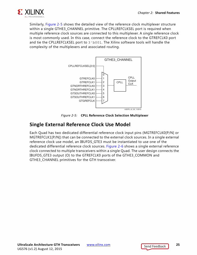
Similarly, Figure 2-5 shows the detailed view of the reference clock multiplexer structure within a single GTHE3_CHANNEL primitive. The CPLLREFCLKSEL port is required when multiple reference clock sources are connected to this multiplexer. A single reference clock is most commonly used. In this case, connect the reference clock to the GTREFCLK0 port and tie the CPLLREFCLKSEL port to 3'b001. The Xilinx software tools will handle the complexity of the multiplexers and associated routing.
Single External Reference Clock Use ModelEach Quad has two dedicated differential reference clock input pins (MGTREFCLK0[P/N] or MGTREFCLK1[P/N]) that can be connected to the external clock sources. In a single external reference clock use model, an IBUFDS_GTE3 must be instantiated to use one of the dedicated differential reference clock sources. Figure 2-6 shows a single external reference clock connected to multiple transceivers within a single Quad. The user design connects the IBUFDS_GTE3 output (O) to the GTREFCLK0 ports of the GTHE3_COMMON and GTHE3_CHANNEL primitives for the GTH transceiver.
X-Ref Target - Figure 2-5
Figure 2-5: CPLL Reference Clock Selection Multiplexer
GTREFCLK0GTREFCLK1
GTNORTHREFCLK0GTNORTHREFCLK1GTSOUTHREFCLK0GTSOUTHREFCLK1
GTGREFCLK
CPLLREFCLKSEL[2:0]
0
1
2
3
4
5
6
7
CPLL
GTHE3_CHANNEL
CPLLOutputCLK
UG576_c2_05_112513
UltraScale Architecture GTH Transceivers www.xilinx.com 25UG576 (v1.2) August 12, 2015
Send Feedback

Chapter 2: Shared Features
Note: The IBUFDS_GTE3 diagram in Figure 2-6 is a simplif ication. The output port ODIV2 is left floating, and the input port CEB is set to logic 0.
Figure 2-7 shows a single external reference clock with multiple transceivers connected to multiple Quads. The user design connects the IBUDFS_GTE3 output (O) to the GTREFCLK0 ports of the GTHE3_COMMON and GTHE3_CHANNEL primitives for the GTH transceiver. In this case, the Xilinx implementation tools make the necessary adjustments to the north/south routing as well as pin swapping necessary to route the reference clocks from one Quad to another when required.
X-Ref Target - Figure 2-6
Figure 2-6: Single External Reference Clock with Multiple Transceivers in a Single Quad
Q(n)
IBUFDS_GTE3
I
UG576_c2_23_020415
IBO
MGTREFCLKP
MGTREFCLKN
GTHE3_CHANNEL
GTREFCLK0GTREFCLK1
GTHE3_CHANNEL
GTREFCLK0GTREFCLK1
GTHE3_CHANNEL
GTREFCLK0GTREFCLK1
GTHE3_COMMON
GTREFCLK00GTREFCLK10
GTHE3_CHANNEL
GTREFCLK0GTREFCLK1
GTREFCLK01GTREFCLK11
UltraScale Architecture GTH Transceivers www.xilinx.com 26UG576 (v1.2) August 12, 2015
Send Feedback

Chapter 2: Shared Features
X-Ref Target - Figure 2-7
Figure 2-7: Single External Reference Clock with Multiple Transceivers in Multiple Quads
Q(n)
IBUFDS_GTE3
I
UG576_c2_24_020415
IBO
MGTREFCLKP
MGTREFCLKN
GTHE3_CHANNEL
GTREFCLK0GTREFCLK1
GTHE3_CHANNEL
GTREFCLK0GTREFCLK1
GTHE3_CHANNEL
GTREFCLK0GTREFCLK1
GTHE3_COMMON
GTREFCLK00GTREFCLK10
GTHE3_CHANNEL
GTREFCLK0GTREFCLK1
Q(n-2)
GTHE3_CHANNEL
GTREFCLK0GTREFCLK1
GTHE3_CHANNEL
GTREFCLK0GTREFCLK1
GTHE3_CHANNEL
GTREFCLK0GTREFCLK1
GTHE3_COMMON
GTREFCLK00GTREFCLK10
GTHE3_CHANNEL
GTREFCLK0GTREFCLK1
Q(n+2)
GTHE3_CHANNEL
GTREFCLK0GTREFCLK1
GTHE3_CHANNEL
GTREFCLK0GTREFCLK1
GTHE3_CHANNEL
GTREFCLK0GTREFCLK1
GTHE3_COMMON
GTREFCLK00GTREFCLK10
GTHE3_CHANNEL
GTREFCLK0GTREFCLK1
GTREFCLK01GTREFCLK11
GTREFCLK01GTREFCLK11
GTREFCLK01GTREFCLK11
UltraScale Architecture GTH Transceivers www.xilinx.com 27UG576 (v1.2) August 12, 2015
Send Feedback

Chapter 2: Shared Features
Note: The IBUFDS_GTE3 diagram in Figure 2-7 is a simplif ication. The output port ODIV2 is left floating, and the input port CEB is set to logic 0.
These rules must be observed when sharing a reference clock to ensure that jitter margins for high-speed designs are met:
• The number of Quads above the sourcing Quad must not exceed two.
• The number of Quads below the sourcing Quad must not exceed two.
• The total number of Quads sourced by an external clock pin pair (MGTREFCLKN/MGTREFCLKP) must not exceed f ive Quads (or 20 transceivers).
The maximum number of transceivers that can be sourced by a single clock pin pair is 20. Designs with more than 20 transceivers require the use of multiple external clock pins to ensure that the rules for controlling jitter are followed. When multiple clock pins are used, an external buffer can be used to drive them from the same oscillator.
Multiple External Reference Clocks Use ModelEach Quad has two dedicated differential reference clock input pins (MGTREFCLK0[P/N] or MGTREFCLK1[P/N]) that can be connected to external clock sources. In the multiple external reference clocks use model, each dedicated reference clock pin pair must instantiate its corresponding IBUDFS_GTE3 primitive to use these dedicated reference clock resources.
For the f irst external reference clock (MGTREFCLK0[P/N]), the user design connects the IBUFDS_GTE3 output (O) to the GTREFCLK0 ports of the GTHE3_COMMON and GTHE3_CHANNEL primitives for the GTH transceiver. Similarly, for the second external reference clock (MGTREFCLK1[P/N]), the user design connects the IBUFDS_GTE3 output (O) to the GTREFCLK1 ports of the GTHE3_COMMON and GTHE3_CHANNEL primitives for the GTH transceiver.
Figure 2-8 shows the QPLLs of each Quad, and the CPLL of each transceiver can be sourced by either MGTREFCLK0[P/N] or MGTRECLK1[P/N] within a single Quad. Users can set QPLL0/1REFCLKSEL[2:0] and CPLLREFCLKSEL[2:0] to the corresponding values to select the source of the reference clock.
UltraScale Architecture GTH Transceivers www.xilinx.com 28UG576 (v1.2) August 12, 2015
Send Feedback

Chapter 2: Shared Features
Note: The IBUFDS_GTE3 diagram in Figure 2-8 is a simplif ication. The output port ODIV2 is left floating, and the input port CEB is set to logic 0.
The flexibility of the reference clock selection architecture allows each transceiver within a Quad to have access to the dedicated reference clocks from the two Quads immediately above and below. Figure 2-9 and Figure 2-10 show examples of how one of the transceivers belonging to one Quad can access the dedicated reference clocks from another Quad by using the GTNORTHREFCLK and GTSOUTHREFCLK ports. In a situation where there are more than one reference clock options per GTH transceiver PLL, the user design is required to set the QPLL0/1REFCLKSEL[2:0] and CPLLREFCLKSEL[2:0] based on the design requirements.
X-Ref Target - Figure 2-8
Figure 2-8: Multiple GTH Transceivers with Multiple Reference Clocks in a Single Quad
Q(n)
IBUFDS_GTE3
I
IBO
MGTREFCLK0P
UG576_c2_25_060515
MGTREFCLK0N
GTHE3_CHANNEL
GTREFCLK0GTREFCLK1
GTHE3_CHANNEL
GTREFCLK0GTREFCLK1
GTHE3_CHANNEL
GTREFCLK0GTREFCLK1
GTHE3_COMMON
GTREFCLK00GTREFCLK10
GTHE3_CHANNEL
GTREFCLK0GTREFCLK1
IBUFDS_GTE3
I
IBO
MGTREFCLK1P
MGTREFCLK1N
GTREFCLK01GTREFCLK11
UltraScale Architecture GTH Transceivers www.xilinx.com 29UG576 (v1.2) August 12, 2015
Send Feedback

Chapter 2: Shared Features
Notes relevant to Figure 2-9:
1. CPLLREFCLKSEL[2:0] is used to select between GTREFCLK0/1, GTNORTHREFCLK0/1, and GTSOUTHREFCLK0/1.
2. The IBUFDS_GTE3 diagram is a simplif ication. The output port ODIV2 is left floating and the input port CEB is set to logic 0.
X-Ref Target - Figure 2-9
Figure 2-9: Multiple GTH Transceivers Using CPLLs with Multiple Reference Clocks in Different Quads
Q(n)
IBUFDS_GTE3
I
IBO
MGTREFCLK0P
UG576_c2_26_060515
MGTREFCLK0N
IBUFDS_GTE3
I
IBO
MGTREFCLK1P
MGTREFCLK1N
Q(n-1)
IBUFDS_GTE3
I
IBO
MGTREFCLK0P
MGTREFCLK0N
IBUFDS_GTE3
I
IBO
MGTREFCLK1P
MGTREFCLK1N
GTREFCLK0GTREFCLK1
GTSOUTHREFCLK0GTSOUTHREFCLK1
GTHE3_CHANNEL
GTNORTHREFCLK0GTNORTHREFCLK1
GTREFCLK0GTREFCLK1
GTSOUTHREFCLK0GTSOUTHREFCLK1
GTHE3_CHANNEL
GTNORTHREFCLK0GTNORTHREFCLK1
UltraScale Architecture GTH Transceivers www.xilinx.com 30UG576 (v1.2) August 12, 2015
Send Feedback

Chapter 2: Shared Features
Notes relevant to Figure 2-10:
1. QPLL0REFCLKSEL[2:0] is used to select between GTREFCLK00/10, GTNORTHREFCLK00/10, and GTSOUTHREFCLK00/10. QPLL1REFCLKSEL[2:0] is used to select between GTREFCLK01/11, GTNORTHREFCLK01/11, and GTSOUTHREFCLK01/11.
2. The IBUFDS_GTE3 diagram is a simplif ication. The output port ODIV2 is left floating and the input port CEB is set to logic 0.
X-Ref Target - Figure 2-10
Figure 2-10: Multiple GTH Transceivers Using QPLLs with Multiple Reference Clocks in Different Quads
Q(n)
IBUFDS_GTE3
I
IBO
MGTREFCLK0P
UG576_c2_27_060515
MGTREFCLK0N
IBUFDS_GTE3
I
IBO
MGTREFCLK1P
MGTREFCLK1N
Q(n-1)
IBUFDS_GTE3
I
IBO
MGTREFCLK0P
MGTREFCLK0N
IBUFDS_GTE3
I
IBO
MGTREFCLK1P
MGTREFCLK1N
GTREFCLK10GTREFCLK01
GTSOUTHREFCLK00GTSOUTHREFCLK10
GTHE3_COMMON
GTNORTHREFCLK00GTNORTHREFCLK10
GTREFCLK01GTREFCLK11
GTSOUTHREFCLK01GTSOUTHREFCLK11
GTNORTHREFCLK10GTNORTHREFCLK01
GTHE3_COMMON
GTSOUTHREFCLK01GTSOUTHREFCLK11
GTREFCLK00
GTREFCLK11
GTNORTHREFCLK01GTNORTHREFCLK11
GTSOUTHREFCLK00GTSOUTHREFCLK10
GTREFCLK00GTREFCLK10
GTNORTHREFCLK00
GTNORTHREFCLK11
UltraScale Architecture GTH Transceivers www.xilinx.com 31UG576 (v1.2) August 12, 2015
Send Feedback

Chapter 2: Shared Features
These rules must be observed when sharing a reference clock to ensure that jitter margins for high-speed designs are met:
• The number of Quads above the sourcing Quad must not exceed two.
• The number of Quads below the sourcing Quad must not exceed two.
• The total number of Quads sourced by an external clock pin pair (MGTREFCLKN/MGTREFCLKP) must not exceed five Quads (or 20 transceivers).
The maximum number of transceivers that can be sourced by a single clock pin pair is 20. Designs with more than 20 transceivers require the use of multiple external clock pins to ensure that the rules for controlling jitter are followed. When multiple clock pins are used, an external buffer can be used to drive them from the same oscillator.
For multi-rate designs that require the reference clock source to be changed dynamically, the QPLL0/1REFCLKSEL and CPLLREFCLKSEL ports are used dynamically to select the reference clock source. After the selection has been made, the user design is responsible for resetting the CPLL and QPLLs via the active-High CPLLPD and QPLL0/1RESET ports, and the subsequent initialization process described in Reset and Initialization, page 46.
UltraScale Architecture GTH Transceivers www.xilinx.com 32UG576 (v1.2) August 12, 2015
Send Feedback

Chapter 2: Shared Features
Ports and AttributesTable 2-7 and Table 2-8 define the clocking ports for GTHE3_CHANNEL and GTHE3_COMMON primitives.
Table 2-7: GTHE3_CHANNEL Clocking Ports
Port Direction Clock Domain Description
CPLLREFCLKSEL[2:0] In Async Input to dynamically select the input reference clock to the Channel PLL. Set this input to 3'b001 when only one clock source is connected to the Channel PLL reference clock selection multiplexer. Reset must be applied to the Channel PLL after changing the reference clock input.000: Reserved001: GTREFCLK0 selected010: GTREFCLK1 selected011: GTNORTHREFCLK0 selected100: GTNORTHREFCLK1 selected101: GTSOUTHREFCLK0 selected110: GTSOUTHREFCLK1 selected111: GTGREFCLK selected
GTGREFCLK In Clock Reference clock generated by the internal interconnect logic. This input is reserved for internal testing purposes only.
GTNORTHREFCLK0 In Clock North-bound clock from the Quad below.
GTNORTHREFCLK1 In Clock North-bound clock from the Quad below.
GTREFCLK0 In Clock External clock driven by IBUFDS_GTE3 for the Channel PLL. For more information, refer to GTH Transceiver Reference Clock Checklist, page 287.
GTREFCLK1 In Clock External clock driven by IBUFDS_GTE3 for the Channel PLL. For more information, refer to GTH Transceiver Reference Clock Checklist, page 287.
GTSOUTHREFCLK0 In Clock South-bound clock from the Quad above.
GTSOUTHREFCLK1 In Clock South-bound clock from the Quad above.
QPLL0CLK In Clock Clock input from the high-performance Quad PLL. Connect QPLL0OUTCLK from the GTHE3_COMMON primitive to this port when the high-performance Quad PLL is used to drive the TX and/or RX channel(s).
QPLL1CLK In Clock Clock input from the high-performance Quad PLL. Connect QPLL1OUTCLK from the GTHE3_COMMON primitive to this port when the high-performance Quad PLL is used to drive the TX and/or RX channel(s).
QPLL0REFCLK In Clock Connect this port to the QPLL0OUTREFCLK port of the GTH3_COMMON.
UltraScale Architecture GTH Transceivers www.xilinx.com 33UG576 (v1.2) August 12, 2015
Send Feedback

Chapter 2: Shared Features
QPLL1REFCLK In Clock Connect this port to the QPLL1OUTREFCLK port of the GTH3_COMMON.
RXSYSCLKSEL[1:0] In Async Selects the PLL reference clock source to drive the RXOUTCLK:00 = CPLL10 = QPLL011 = QPLL1
TXSYSCLKSEL[1:0] In Async Selects the PLL reference clock source to drive the TXOUTCLK00 = CPLL10 = QPLL011 = QPLL1
TXPLLCLKSEL[1:0] In Async Selects the PLL to drive the TX datapath:00 = CPLL10 = QPLL111 = QPLL0
RXPLLCLKSEL[1:0] In Async Selects the PLL to drive the RX datapath:00 = CPLL10 = QPLL111 = QPLL0
GTREFCLKMONITOR Out Clock CPLL reference clock selection multiplexer output.
Table 2-7: GTHE3_CHANNEL Clocking Ports (Cont’d)
Port Direction Clock Domain Description
UltraScale Architecture GTH Transceivers www.xilinx.com 34UG576 (v1.2) August 12, 2015
Send Feedback

Chapter 2: Shared Features
Table 2-8: GTHE3_COMMON Clocking Ports
Port Dir Clock Domain Description
QPLL0REFCLKSEL[2:0] In Async Input to dynamically select the input reference clock to the Quad PLL0. Set to 3'b001 when only one clock source is connected to the Quad PLL reference clock selection multiplexer.Reset must be applied to the Quad PLL after changing the reference clock input.000: Reserved001: GTREFCLK00 selected010: GTREFCLK10 selected011: GTNORTHREFCLK00 selected100: GTNORTHREFCLK10 selected101: GTSOUTHREFCLK00 selected110: GTSOUTHREFCLK10 selected111: GTGREFCLK0 selected
QPLL1REFCLKSEL[2:0] In Async Input to dynamically select the input reference clock to the Quad PLL1. Set to 3'b001 when only one clock source is connected to the Quad PLL reference clock selection multiplexer.Reset must be applied to the Quad PLL after changing the reference clock input.000: Reserved001: GTREFCLK01 selected010: GTREFCLK11 selected011: GTNORTHREFCLK01 selected100: GTNORTHREFCLK11 selected101: GTSOUTHREFCLK01 selected110: GTSOUTHREFCLK11 selected111: GTGREFCLK1 selected
GTNORTHREFCLK00GTNORTHREFCLK10
In Clock North-bound clocks from the Quad PLL0 below.
GTNORTHREFCLK01GTNORTHREFCLK11
In Clock North-bound clocks from the Quad PLL1 below.
GTREFCLK00GTREFCLK10
In Clock External jitter stable clock driven by IBUFDS_GTE3 for the Quad PLL0.
GTREFCLK01GTREFCLK11
In Clock External jitter stable clock driven by IBUFDS_GTE3 for the Quad PLL1.
GTSOUTHREFCLK00GTSOUTHREFCLK10
In Clock South-bound clocks from the Quad PLL0 above.
GTSOUTHREFCLK01GTSOUTHREFCLK11
In Clock South-bound clocks from the Quad PLL1 above.
UltraScale Architecture GTH Transceivers www.xilinx.com 35UG576 (v1.2) August 12, 2015
Send Feedback
Chapter 2: Shared Features
Channel PLL
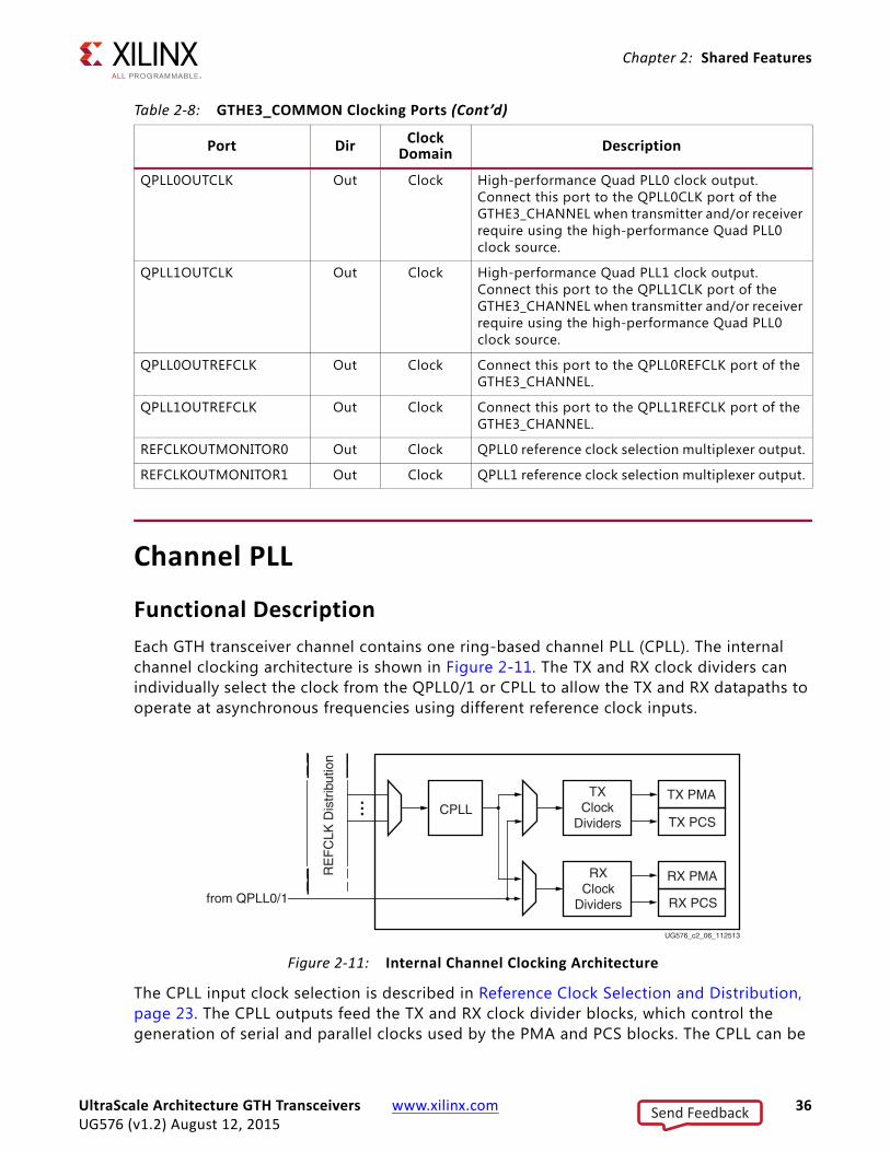
Functional DescriptionEach GTH transceiver channel contains one ring-based channel PLL (CPLL). The internal channel clocking architecture is shown in Figure 2-11. The TX and RX clock dividers can individually select the clock from the QPLL0/1 or CPLL to allow the TX and RX datapaths to operate at asynchronous frequencies using different reference clock inputs.
The CPLL input clock selection is described in Reference Clock Selection and Distribution, page 23. The CPLL outputs feed the TX and RX clock divider blocks, which control the generation of serial and parallel clocks used by the PMA and PCS blocks. The CPLL can be
QPLL0OUTCLK Out Clock High-performance Quad PLL0 clock output. Connect this port to the QPLL0CLK port of the GTHE3_CHANNEL when transmitter and/or receiver require using the high-performance Quad PLL0 clock source.
QPLL1OUTCLK Out Clock High-performance Quad PLL1 clock output. Connect this port to the QPLL1CLK port of the GTHE3_CHANNEL when transmitter and/or receiver require using the high-performance Quad PLL0 clock source.
QPLL0OUTREFCLK Out Clock Connect this port to the QPLL0REFCLK port of the GTHE3_CHANNEL.
QPLL1OUTREFCLK Out Clock Connect this port to the QPLL1REFCLK port of the GTHE3_CHANNEL.
REFCLKOUTMONITOR0 Out Clock QPLL0 reference clock selection multiplexer output.
REFCLKOUTMONITOR1 Out Clock QPLL1 reference clock selection multiplexer output.
X-Ref Target - Figure 2-11
Figure 2-11: Internal Channel Clocking Architecture
Table 2-8: GTHE3_COMMON Clocking Ports (Cont’d)
Port Dir Clock Domain Description
RE
FC
LK D
istr
ibut
ion
CPLLTX
ClockDividers
RXClock
Dividers
TX PMA
TX PCS
RX PMA
RX PCS
UG576_c2_06_112513
from QPLL0/1
UltraScale Architecture GTH Transceivers www.xilinx.com 36UG576 (v1.2) August 12, 2015
Send Feedback

Chapter 2: Shared Features
shared between the TX and RX datapaths if they operate at line rates that are integral multiples of the same VCO frequency.
Figure 2-12 illustrates a conceptual view of the CPLL architecture. The input clock can be divided by a factor of M before feeding into the phase frequency detector. The feedback dividers, N1 and N2, determine the VCO multiplication ratio and the CPLL output frequency. A lock indicator block compares the frequencies of the reference clock and the VCO feedback clock to determine if a frequency lock has been achieved.
The CPLL in the GTH transceiver has a nominal operating range between 2.0 GHz to 6.25 GHz. The UltraScale FPGAs Transceivers Wizard chooses the appropriate CPLL settings based on application requirements.
Equation 2-1 shows how to determine the CPLL output frequency (GHz).
Equation 2-1
X-Ref Target - Figure 2-12
Figure 2-12: CPLL Block Diagram
PLLCLKIN
/ M
LockIndicator
PhaseFrequencyDetector
ChargePump
LoopFilter VCO
PLLLOCKED
PLLCLKOUT
/ N1/ N2
UG576_c2_07_112513
fPLLClkout fPLLClkinN1 N2×
M------------------×=
UltraScale Architecture GTH Transceivers www.xilinx.com 37UG576 (v1.2) August 12, 2015
Send Feedback

Chapter 2: Shared Features
Equation 2-2 shows how to determine the line rate (Gb/s). D represents the value of the TX or RX clock divider block in the channel. Both rising and falling edges of the PLL CLKOUT are used to generate the required line rate defined in Equation 2-2.
Equation 2-2
Table 2-9 lists the allowable divider settings.
Ports and AttributesTable 2-10 and Table 2-11 defines the pins and attributes for the CPLL.
Table 2-9: CPLL Divider Settings
Factor Attribute Valid Settings
M CPLL_REFCLK_DIV 1, 2
N2 CPLL_FBDIV 1, 2, 3, 4, 5
N1 CPLL_FBDIV_45 4, 5
DRXOUT_DIVTXOUT_DIV
1, 2, 4, 8, 16(1)
1. TX/RXOUT_DIV = 16 is not supported when using CPLL.
Table 2-10: CPLL Ports
Port Direction Clock Domain Description
CPLLLOCKDETCLK In Clock Stable reference clock for the detection of the feedback and reference clock signals to the CPLL. The input reference clock to the CPLL or any output clock generated from the CPLL (e.g., TXOUTCLK) must not be used to drive this clock. This clock is required only when using the CPLLFBCLKLOST and CPLLREFCLKLOST ports. It does not affect the CPLL lock detection, reset and power-down functions.
CPLLLOCKEN In Async This port enables the CPLL lock detector. It must always be tied High.
CPLLPD In Async Active-High signal that powers down and resets the CPLL for power savings.
fLineRatefPLLClkout 2×
D-----------------------------=
UltraScale Architecture GTH Transceivers www.xilinx.com 38UG576 (v1.2) August 12, 2015
Send Feedback

Chapter 2: Shared Features
CPLLREFCLKSEL In Async Input to dynamically select the input reference clock to the CPLL. Set this input to 3'b001 when only one clock source is connected to the CPLL reference clock selection multiplexer. Reset must be applied to the CPLL after changing the reference clock input.000: Reserved001: GTREFCLK0 selected010: GTREFCLK1 selected011: GTNORTHREFCLK0 selected100: GTNORTHREFCLK1 selected101: GTSOUTHREFCLK0 selected110: GTSOUTHREFCLK1 selected111: GTGREFCLK selected
CPLLRESET In Async Reserved. Use CPLLPD to reset the CPLL.
CPLLFBCLKLOST Out CPLLLOCKDETCLK A High on this signal indicates the feedback clock from the CPLL feedback divider to the phase frequency detector of the CPLL is lost.
CPLLLOCK Out Async This active-High PLL frequency lock signal indicates that the PLL frequency is within predetermined tolerance. The transceiver and its clock outputs are not reliable until this condition is met.
CPLLREFCLKLOST Out CPLLLOCKDETCLK A High on this signal indicates the reference clock to the phase frequency detector of the CPLL is lost.
Notes: 1. When the GTH transceiver is configured to PCIe® mode, tie CPLLRESET and CPLLPD together.
Table 2-11: CPLL Attributes
Attribute Type Description
CPLL_CFG0 16-bit Hex Reserved. Configuration setting for the CPLL. Use the recommended value from the Wizard.
CPLL_CFG1 16-bit Hex Reserved. Configuration setting for the CPLL.Use the recommended value from the Wizard.
CPLL_CFG2 16-bit Hex Reserved. Configuration setting for the CPLL.Use the recommended value from the Wizard.
CPLL_CFG3 6-bit Hex Reserved. Configuration setting for the CPLL.Use the recommended value from the Wizard.
CPLL_FBDIV Integer CPLL feedback divider N2 settings as shown in Figure 2-11, page 36. Valid settings are 1, 2, 3, 4, and 5.
Table 2-10: CPLL Ports (Cont’d)
Port Direction Clock Domain Description
UltraScale Architecture GTH Transceivers www.xilinx.com 39UG576 (v1.2) August 12, 2015
Send Feedback

Chapter 2: Shared Features
Use Modes
Dynamically Changing CPLL settings
The following describes the sequence of events to dynamically change CPLL settings. It pertains only to changes for the CPLL:
1. When ready (all valid data is transmitted or received), provide changes via port CPLLREFCLKSEL and/or DRP to the attributes listed in Table 2-11.
2. Follow the reset guidelines as detailed in CPLL Reset, page 49.
3. When the CPLL has locked, assert GTTXRESET and/or GTRXRESET and follow the guidelines as detailed in GTH Transceiver TX Reset in Response to GTTXRESET Pulse, page 54 and GTH Transceiver RX Reset in Response to GTRXRESET Pulse, page 63.
4. Continue with transceiver operation.
CPLL_FBDIV_45 Integer CPLL reference clock divider N1 settings as shown in Figure 2-11, page 36. Valid settings are 4 and 5.
CPLL_INIT_CFG0 16-bit Hex Reserved. Use the recommended value from the Wizard.
CPLL_INIT_CFG1 8-bit Hex Reserved. Use the recommended value from the Wizard.
CPLL_LOCK_CFG 16-bit Hex Reserved. Use the recommended value from the Wizard.
CPLL_REFCLK_DIV Integer CPLL reference clock divider M settings as shown in Figure 2-11, page 36. Valid settings are 1 and 2.
RXOUT_DIV(1) Integer CPLL/QPLL output clock divider D for the RX datapath as shown in Figure 2-11, page 36. Valid settings are 1, 2, 4, 8, and 16.
TXOUT_DIV(1) Integer CPLL/QPLL output clock divider D for the TX datapath as shown in Figure 2-11, page 36. Valid settings are 1, 2, 4, 8, and 16.
SATA_CPLL_CFG String Reserved. SATA application specific setting. Use the recommended value from the Wizard.
Notes: 1. TXOUT_DIV/RXOUT_DIV = 16 is not supported when using the CPLL.
Table 2-11: CPLL Attributes (Cont’d)
Attribute Type Description
UltraScale Architecture GTH Transceivers www.xilinx.com 40UG576 (v1.2) August 12, 2015
Send Feedback

Chapter 2: Shared Features
Quad PLL
Functional DescriptionEach Quad contains two LC-based PLLs, referred to as the Quad PLLs (QPLL0 and QPLL1). Either QPLL can be shared by the serial transceiver channels within the same Quad, but cannot be shared by channels in other Quads. Use of QPLL0/1 is required when operating the channels at line rates above the CPLL operating range. The GTHE3_COMMON primitive encapsulates both the GTH QPLL0/1 and must be instantiated when either QPLL is used.
The QPLL0/1 input reference clock selection is described in Reference Clock Selection and Distribution, page 23. The QPLL0/1 outputs feed the TX and RX clock divider blocks of each serial transceiver channel within the same Quad, which control the generation of serial and parallel clocks used by the PMA and PCS blocks. Figure 2-11, page 36 shows the internal channel clocking architecture.
Figure 2-13 illustrates a conceptual view of the QPLL0/1 architecture. The input clock can be divided by a factor of M before it is fed into the phase frequency detector. The feedback divider N determines the VCO multiplication ratio. The QPLL0/1 output frequency is half of the VCO frequency. A lock indicator block compares the frequencies of the reference clock and the VCO feedback clock to determine if a frequency lock has been achieved.
The QPLL0/1 VCO operates within two different frequency bands. Table 2-12 describes the nominal operating range for these bands. For more information, see the specific device data sheet.
X-Ref Target - Figure 2-13
Figure 2-13: QPLL0/1 Detail
Table 2-12: QPLL0/1 Nominal Operating Range
QPLL Frequency (GHz)
QPLL0 9.8–16.3
QPLL1 8.0–13.0
PLLCLKIN
/ M
LockIndicator
PhaseFrequencyDetector
ChargePump
LoopFilter
PLLLOCKED
PLLCLKOUT
/ N
UG576_c2_08_112513
/ 2Lower Band
VCO
Upper BandVCO
UltraScale Architecture GTH Transceivers www.xilinx.com 41UG576 (v1.2) August 12, 2015
Send Feedback

Chapter 2: Shared Features
When the lower band VCO is selected, the upper band VCO is automatically powered down and vice versa. The Wizard chooses the appropriate band and QPLL settings based on application requirements.
Equation 2-3 shows how to determine the PLL output frequency (GHz).
Equation 2-3
Equation 2-4 shows how to determine the line rate (Gb/s). D represents the value of the TX or RX clock divider block in the channel. Both rising and falling edges of the PLL CLKOUT are used to generate the required line rate defined in Equation 2-4. See Table 2-9, page 38 for the valid settings for D.
Equation 2-4
Table 2-13 lists the allowable divider values.
Ports and AttributesTable 2-14 and Table 2-15, page 44 define the pins and attributes for the QPLL.
Table 2-13: QPLL0/1 Divider Settings
Factor Attribute Valid Settings
M QPLL0_REFCLK_DIVQPLL1_REFCLK_DIV 1, 2, 3, 4
N QPLL0_FBDIVQPLL1_FBDIV
16, 20, 32, 40, 60, 64, 66, 75, 80, 84, 90, 96, 100, 112, 120, 125, 150
D RXOUT_DIVTXOUT_DIV 1, 2, 4, 8, 16
fPLLClkout fPLLClkinN
M 2×------------×=
fLineRatefPLLClkout 2×
D-----------------------------=
Table 2-14: QPLL0/1 Ports
Port Direction Clock Domain Description
QPLLDMONITOR0[7:0]/QPLLDMONITOR1[7:0]
Out Async Reserved.
QPLL0CLKRSVD0/QPLL1CLKRSVD0
In – Reserved. Tie to 1'b0.
QPLL0CLKRSVD1/QPLL1CLKRSVD1
In – Reserved. Tie to 1'b0.
QPLL0FBCLKLOST/QPLL1FBCLKLOST
Out QPLL0LOCKDETCLK/QPLL1LOCKDETCLK
A High on this signal indicates the feedback clock from the QPLL0/1 feedback divider to the phase frequency detector of the QPLL0/1 is lost.
QPLL0LOCK/QPLL1LOCK Out Async This active-High QPLL0/1 frequency lock signal indicates that the QPLL0/1 frequency is within the predetermined tolerance. The transceiver and its clock outputs are not reliable until this condition is met.
UltraScale Architecture GTH Transceivers www.xilinx.com 42UG576 (v1.2) August 12, 2015
Send Feedback

Chapter 2: Shared Features
QPLL0LOCKDETCLK/QPLL1LOCKDETCLK
In Clock Stable reference clock for the detection of the feedback and reference clock signals to the QPLL0/1. The input reference clock to the QPLL0/1 or any output clock generated from the QPLL0/1 (e.g., TXOUTCLK) must not be used to drive this clock.This clock is required only when using the QPLL0FBCLKLOST/QPLL1FBCLKLOST and QPLL0REFCLKLOST/QPLL1REFCLKLOST ports. It does not affect the QPLL0/1 lock detection, reset, and power-down functions.The same clock can be used to drive both QPLL0LOCKDETCLK and QPLL1LOCKDETCLK.
QPLL0LOCKEN/QPLL1LOCKEN
In Async This port enables the QPLL0/1 lock detection circuitry. It must always be tied High.
QPLL0OUTCLK/QPLL1OUTCLK
Out N/A QPLL0/1 output clock. Connect QPLL0OUTCLK to QPLL0CLK and QPLL1OUTCLK to QPLL1CLK in the GTHE3_CHANNEL primitive.
QPLL0OUTREFCLK/QPLL1OUTREFCLK
Out N/A QPLL0/1 reference output clock. Connect QPLL0OUTREFCLK to QPLL0REFCLK and QPLL1OUTREFCLK to QPLL1REFCLK in the GTHE3_CHANNEL primitive.
QPLL0PD/QPLL1PD In Async Active-High signal that powers down the QPLL0/1 for power savings.
QPLL0REFCLKLOST/QPLL1REFCLKLOST
Out QPLL0LOCKDETCLK/QPLL1LOCKDETCLK
A High on this signal indicates the reference clock to the phase frequency detector of the QPLL0/1 is lost.
QPLL0REFCLKSEL[2:0]/QPLL1REFCLKSEL[2:0]
In Async Input to dynamically select the input reference clock to the QPLL0/1. Set this input to 3'b001 when only one clock source is connected to the QPLL0/1 reference clock selection multiplexer.Reset must be applied to the QPLL0/1 after changing the reference clock input.000: Reserved001: GTREFCLK0 selected010: GTREFCLK1 selected011: GTNORTHREFCLK0 selected100: GTNORTHREFCLK1 selected101: GTSOUTHREFCLK0 selected110: GTSOUTHREFCLK1 selected111: GTGREFCLK selected
QPLL0RESET/QPLL1RESET In Async This active-High port resets the dividers inside the QPLL0/1 as well as the QPLL0/1 lock indicator and status block.
Table 2-14: QPLL0/1 Ports (Cont’d)
Port Direction Clock Domain Description
UltraScale Architecture GTH Transceivers www.xilinx.com 43UG576 (v1.2) August 12, 2015
Send Feedback

Chapter 2: Shared Features
QPLLRSVD1[7:0] In – Reserved. Use the recommended value from the Wizard.
QPLLRSVD2[4:0] In – Reserved. Use the recommended value from the Wizard.
QPLLRSVD3[4:0] In – Reserved. Use the recommended value from the Wizard.
QPLLRSVD4[7:0] In – Reserved. Use the recommended value from the Wizard.
REFCLKOUTMONITOR0/REFCLKOUTMONITOR1
Out N/A QPLL0/1 reference clock selection multiplexer output.
BGBYPASSB In Async Reserved. This port must be set to 1'b1. Do not modify this value.
BGMONITORENB In Async Reserved. This port must be set to 1'b1. Do not modify this value.
BGPDB In Async Reserved. This port must be set to 1'b1. Do not modify this value.
BGRCALOVRD[4:0] In Async Reserved. This port must be set to 5'b11111. Do not modify this value.
BGRCALOVRDENB In Async Reserved. This port must be set to 1'b1. Do not modify this value.
RCALENB In Async Reserved. This port must be set to 1'b1. Do not modify this value.
PMARSVD0[7:0] In Async Reserved.
PMARSVD1[7:0] In Async Reserved.
Table 2-14: QPLL0/1 Ports (Cont’d)
Port Direction Clock Domain Description
Table 2-15: QPLL0/1 Attributes
Attribute Type Description
BIAS_CFG0 16-bit Hex Reserved. Use the recommended value from the Wizard.
BIAS_CFG1 16-bit Hex Reserved. Use the recommended value from the Wizard.
BIAS_CFG2 16-bit Hex Reserved. Use the recommended value from the Wizard.
BIAS_CFG3 16-bit Hex Reserved. Use the recommended value from the Wizard.
BIAS_CFG4 16-bit Hex Reserved. Use the recommended value from the Wizard.
BIAS_CFG_RSVD 10-bit Binary Reserved. Use the recommended value from the Wizard.
COMMON_CFG0 16-bit Hex Reserved. Use the recommended value from the Wizard.
COMMON_CFG1 16-bit Hex Reserved. Use the recommended value from the Wizard.
POR_CFG 16-bit Hex Reserved. Use the recommended value from the Wizard.
QPLL0_CFG0/QPLL1_CFG0
16-bit Hex Reserved. Use the recommended value from the Wizard.
UltraScale Architecture GTH Transceivers www.xilinx.com 44UG576 (v1.2) August 12, 2015
Send Feedback

Chapter 2: Shared Features
QPLL0_CFG1/QPLL1_CFG1
16-bit Hex Reserved. Use the recommended value from the Wizard.
QPLL0_CFG1_G3/QPLL1_CFG1_G3
16-bit Hex Reserved. Use the recommended value from the Wizard.
QPLL0_CFG2/QPLL1_CFG2
16-bit Hex Reserved. Use the recommended value from the Wizard.
QPLL0_CFG2_G3/QPLL1_CFG2_G3
16-bit Hex Reserved. Use the recommended value from the Wizard.
QPLL0_CFG3/QPLL1_CFG3
16-bit Hex Reserved. Use the recommended value from the Wizard.
QPLL0_CFG4/QPLL1_CFG4
16-bit Hex Reserved. Use the recommended value from the Wizard.
QPLL0_CP/QPLL1_CP
10-bit Binary Reserved. Use the recommended value from the Wizard.
QPLL0_CP_G3/QPLL1_CP_G3
10-bit Binary Reserved. Use the recommended value from the Wizard.
QPLL0_FBDIV/QPLL1_FBDIV
Integer QPLL0/1 feedback divider N settings as shown in Figure 2-13, page 41. Valid divider settings are 16, 20, 32, 40, 60, 64, 66, 75, 80, 84, 90, 96, 100, 112, 120, 125, 150.
QPLL0_FBDIV_G3/QPLL1_FBDIV_G3
Integer Reserved. Use the recommended value from the Wizard.
QPLL0_INIT_CFG0/QPLL1_INIT_CFG0
16-bit Hex Reserved. Use the recommended value from the Wizard.
QPLL0_INIT_CFG1/QPLL1_INIT_CFG1
8-bit Hex Reserved. Use the recommended value from the Wizard.
QPLL0_LOCK_CFG/QPLL1_LOCK_CFG
16-bit Hex Reserved. Use the recommended value from the Wizard.
QPLL0_LOCK_CFG_G3/QPLL1_LOCK_CFG_G3
16-bit Hex Reserved. Use the recommended value from the Wizard.
QPLL0_LPF/QPLL1_LPF
10-bit Binary Reserved. Use the recommended value from the Wizard.
QPLL0_LPF_G3/QPLL1_LPF_G3
10-bit Binary Reserved. Use the recommended value from the Wizard.
QPLL0_REFCLK_DIV/QPLL1_REFCLK_DIV
Integer QPLL0/1 reference clock divider M settings as shown in Figure 2-13, page 41. Valid settings are 1, 2, 3, and 4.
QPLL0_SDM_CFG0/QPLL1_SDM_CFG0
16-bit Binary Reserved. Use the recommended value from the Wizard.
QPLL0_SDM_CFG1/QPLL1_SDM_CFG1
16-bit Binary Reserved. Use the recommended value from the Wizard.
QPLL0_SDM_CFG2/QPLL1_SDM_CFG2
16-bit Binary Reserved. Use the recommended value from the Wizard.
RSVD_ATTR0 16-bit Hex Reserved. Use the recommended value from the Wizard.
Table 2-15: QPLL0/1 Attributes (Cont’d)
Attribute Type Description
UltraScale Architecture GTH Transceivers www.xilinx.com 45UG576 (v1.2) August 12, 2015
Send Feedback

Chapter 2: Shared Features
Reset and InitializationThe GTH transceiver must be initialized after device power-up and configuration before it can be used. The GTH transmitter (TX) and receiver (RX) can be initialized independently and in parallel as shown in Figure 2-14. The GTH transceiver TX and RX initialization comprises two steps:
1. Initializing the associated PLL driving TX/RX
2. Initializing the TX and RX datapaths (PMA + PCS)
The GTH transceiver TX and RX can receive a clock from either the QPLL or the CPLL. The associated PLL (QPLL/CPLL) used by the TX and RX must be initialized f irst before TX and RX initialization. Any PLL used by the TX and RX is reset individually and its reset operation is completely independent from all TX and RX resets. The TX and RX datapaths must be initialized only after the associated PLL is locked.
RSVD_ATTR1 16-bit Hex Reserved. Use the recommended value from the Wizard.
RSVD_ATTR2 16-bit Hex Reserved. Use the recommended value from the Wizard.
RSVD_ATTR3 16-bit Hex Reserved. Use the recommended value from the Wizard.
SDM0DATA1_0/SDM1DATA1_0
16-bit Binary Reserved. Use the recommended value from the Wizard.
SDM0DATA1_1/SDM1DATA1_1
9-bit Binary Reserved. Use the recommended value from the Wizard.
SDM0INITSEED0_0/SDM1INITSEED0_0
16-bit Binary Reserved. Use the recommended value from the Wizard.
SDM0INITSEED0_1/SDM1INITSEED0_1
9-bit Binary Reserved. Use the recommended value from the Wizard.
SDM0_DATA_PIN_SEL/SDM1_DATA_PIN_SEL
1-bit Binary Reserved. Use the recommended value from the Wizard.
SDM0_WIDTH_PIN_SEL/SDM1_WIDTH_PIN_SEL
1-bit Binary Reserved. Use the recommended value from the Wizard.
RXOUT_DIV Integer QPLL0/QPLL1/CPLL output clock divider D for the RX datapath as shown in Figure 2-11, page 36. Valid settings are 1, 2, 4, 8, and 16.
TXOUT_DIV Integer QPLL0/QPLL1/CPLL output clock divider D for the TX datapath as shown in Figure 2-11, page 36. Valid settings are 1, 2, 4, 8, and 16.
Table 2-15: QPLL0/1 Attributes (Cont’d)
Attribute Type Description
UltraScale Architecture GTH Transceivers www.xilinx.com 46UG576 (v1.2) August 12, 2015
Send Feedback

Chapter 2: Shared Features
The GTH transceiver TX and RX use a state machine to control initialization process. They are partitioned into a few reset regions. The partition allows the reset state machine to control the reset process in a sequence that the PMA can be reset f irst and the PCS can be reset after the assertion of the TXUSERRDY or RXUSERRDY. It also allows the PMA, the PCS, and functional blocks inside them to be reset individually when needed during normal operation.
The GTH transceiver offers two types of reset: initialization and component.
• Initialization Reset: This reset is used for complete GTH transceiver initialization. It must be used after device power-up and configuration. During normal operation, when necessary, GTTXRESET and GTRXRESET can also reinitialize the GTH transceiver TX and RX. GTTXRESET is the initialization reset port for the GTH transceiver TX. GTRXRESET is the initialization reset port for the GTH transceiver RX.
• Component Reset: This reset is used for special cases and specific subsection resets while the GTH transceiver is in normal operation. TX component reset ports include TXPMARESET and TXPCSRESET. RX component reset ports include RXPMARESET, RXDFELPMRESET, EYESCANRESET, RXPCSRESET, RXBUFRESET, and RXOOBRESET.
X-Ref Target - Figure 2-14
Figure 2-14: GTH Transceiver Initialization Overview
AfterConfiguration
Associated PLL(QPLL/CPLL)used by TXInitialization
TX Initialization ByGTTXRESET
TXRESETDONE RXRESETDONE
RX Initialization ByGTRXRESET
Associated PLL(QPLL/CPLL)used by RXInitialization
UG576_c2_09_062614
UltraScale Architecture GTH Transceivers www.xilinx.com 47UG576 (v1.2) August 12, 2015
Send Feedback

Chapter 2: Shared Features
For major coverage differences between initialization and component resets, refer to Table 2-23 for the GTH transceiver TX and Table 2-27 and Table 2-28 for the GTH transceiver RX.
All reset ports described in this section initiate the internal reset state machine when driven High. The internal reset state machines are held in the reset state until these same reset ports are driven Low. These resets are all asynchronous. The guideline for the pulse width of these asynchronous resets is one period of the reference clock, unless otherwise noted.
TIP: Reset ports should not be used for the purpose of power down. For details on proper power down usage, refer to Power Down, page 69.
Resetting Multiple Lanes and QuadsResetting multiple lanes in a Quad or multiple Quads affects the power supply regulation circuit (see Power Up/Down and Reset on Multiple Lanes, page 291).
Reset ModesThe GTH transceiver RX resets can operate in two different modes: sequential mode and single mode. The GTH transceiver TX resets only operate in sequential mode.
• Sequential mode: The reset state machine starts with an initialization or component reset input driven High and proceeds through all states after the requested reset states in the reset state machine, as shown in Figure 2-17 for the GTH transceiver TX or Figure 2-22 for the GTH transceiver RX until completion. The completion of sequential mode reset flow is signaled when (TX/RX)RESETDONE transitions from Low to High.
• Single mode: The reset state machine only executes the requested component reset independently for a predetermined time set by its attribute. It does not process any state after the requested state, as shown in Figure 2-22 for the GTH transceiver RX. The requested reset can be any component reset to reset the PMA, the PCS, or functional blocks inside them. The completion of a single mode reset is signaled when RXRESETDONE transitions from Low to High.
The GTH transceiver initialization reset must use sequential mode. All component resets can be operated in either sequential mode or single mode, except for TX resets, which can only operate in sequential mode.
The GTH transceiver uses GTRESETSEL to select between sequential reset mode and single reset mode. Table 2-16 provides configuration details that apply to both the GTH transceiver TX and GTH transceiver RX. Reset modes have no impact on CPLL and QPLL resets. During normal operation, the GTH transceiver TX or GTH transceiver RX can be reset by applications in either sequential mode or single mode (GTH transceiver RX only), which provides flexibility to reset a portion of the GTH transceiver. When using either sequential mode or single mode, RESETOVRD must be driven Low, as shown in Table 2-16. RESETOVRD
UltraScale Architecture GTH Transceivers www.xilinx.com 48UG576 (v1.2) August 12, 2015
Send Feedback

Chapter 2: Shared Features
and GTRESETSEL must be set to the desired value 300–500 ns before the assertions of any reset.
CPLL ResetThe CPLL must be reset before use. As shown in Figure 2-15, CPLLPD is an input that resets the CPLL. CPLLLOCK is an output that indicates the reset process is done. The requirement for this asynchronous CPLLPD pulse width must be at least 2 µs. The time required for the CPLL to lock is affected by a few factors, such as bandwidth setting and clock frequency.
Table 2-16: GTH Transceiver Reset Modes Operation
Operation Mode RESETOVRD GTRESETSEL
Sequential Mode 0 0
Single Mode 0 1
Table 2-17: GTH Transceiver Reset Mode Ports
Port Dir Clock Domain Description
GTRESETSEL In Async Reset mode enable port.Low: Sequential mode (recommended).High: Single mode.
RESETOVRD In Async Reserved. Must be tied to ground.
X-Ref Target - Figure 2-15
Figure 2-15: CPLL Reset Timing Diagram
Table 2-18: CPLL Reset Ports
Port Dir Clock Domain Description
CPLLPD In Async This port is driven High and then deasserted to start CPLL reset.
CPLLRESET In Async Reserved. Use CPLLPD to reset the CPLL.
CPLLLOCK Out Async This active-High CPLL frequency lock signal indicates that the CPLL frequency is within a predetermined tolerance. The GTH transceiver and its clock outputs are not reliable until this condition is met.
CPLLLOCKEN In Async This active-High signal enables the CPLL lock detector.
Notes: 1. When the GTH transceiver is configured to PCIe mode, tie CPLLRESET and CPLLPD together.
CPLLPD
CPLLLOCK
CPLL Lock TimeUG576_c2_10_062615
2 µs
UltraScale Architecture GTH Transceivers www.xilinx.com 49UG576 (v1.2) August 12, 2015
Send Feedback

Chapter 2: Shared Features
QPLL0/1 ResetQPLL0/1 must be reset before it can be used. Each GTH transceiver Quad has three dedicated ports for its respective QPLL reset. As shown in Figure 2-16, QPLL0/1RESET is an input that resets QPLL0/1. QPLL0/1LOCK is an output that indicates the reset process is done. The guideline for this asynchronous QPLL0/1RESET pulse width is one period of the reference clock. The real QPLL0/1 reset generated by the internal GTH transceiver circuit is much longer than the QPLL0/1RESET High pulse duration. The time required for QPLL0/1 to lock is affected by a few factors, such as bandwidth setting and clock frequency.
TX Initialization and ResetThe GTH transceiver TX uses a reset state machine to control the reset process. The GTH transceiver TX is partitioned into two reset regions, TX PMA and TX PCS. The partition allows TX initialization and reset to be operated only in sequential mode, as shown in Figure 2-17.
X-Ref Target - Figure 2-16
Figure 2-16: QPLL0/1 Reset Timing Diagram
Table 2-19: QPLL0/1 Reset Ports
Port Dir Clock Domain Description
QPLL0RESET/QPLL1RESET
In Async This port is driven High and then deasserted to start the QPLL0/1 reset.
QPLL0LOCK/QPLL1LOCK
Out Async This active-High QPLL0/1 frequency lock signal indicates that the QPLL0/1 frequency is within a predetermined tolerance. The GTH transceiver and its clock outputs are not reliable until this condition is met.
QPLL0LOCKEN/QPLL1LOCKEN
In Async This active-High signal enables the QPLL0/1 lock detector.
Table 2-20: QPLL Reset Attributes
Attribute Type Description
QPLL0RESET_TIME/QPLL1RESET_TIME(QPLL0_INIT_CFG[9:0]/QPLL1_INIT_CFG[9:0])
10-bit BinaryReserved. Represents the time duration to apply internal QPLL0/1 reset. Must be a non-zero value. Use the recommended value from the Wizard.
QPLL0/1RESET
QPLL0/1LOCK
QPLL0/1 Lock Time
QPLL0/1RESET_TIME
Internal QPLL0/1Reset Signal
UG576_c2_11_112513
UltraScale Architecture GTH Transceivers www.xilinx.com 50UG576 (v1.2) August 12, 2015
Send Feedback

Chapter 2: Shared Features
The initializing TX must use GTTXRESET in sequential mode. Activating GTTXRESET input can automatically trigger a full asynchronous TX reset. The reset state machine executes the reset sequence, as shown in Figure 2-17, covering the whole TX PMA and TX PCS. During normal operation, when needed, sequential mode allows you to reset TX from activating TXPMARESET and continue the reset state machine until TXRESETDONE transitions from Low to High.
The TX reset state machine does not reset the PCS until TXUSERRDY is detected High. Drive TXUSERRDY High after these conditions are met:
1. All clocks used by the application including TXUSRCLK/TXUSRCLK2 are shown as stable.
2. The user interface is ready to transmit data to the GTH transceiver.X-Ref Target - Figure 2-17
Figure 2-17: GTH Transceiver TX Reset State Machine Sequence
WAIT UntilGTTXRESET From
High to Low
TXPMARESETProcess
GTTXRESETHigh
TXPMARESETHigh
TXPCSRESETProcess
TXPCSRESETHigh
Sequence Mode and TXUSERRDY
TXRESETDONEHigh
WAIT UntilTXPMARESET
From High to Low
WAIT UntilTXPCSRESET
From High to Low
UG576_c2_12_062614
UltraScale Architecture GTH Transceivers www.xilinx.com 51UG576 (v1.2) August 12, 2015
Send Feedback

Chapter 2: Shared Features
Ports and Attributes
Table 2-21 lists ports required by TX initialization process.
Table 2-22 lists attributes required by GTH transceiver TX initialization. In general cases, the reset time required by the TX PMA or the TX PCS varies depending on line rate. The factors affecting PMA reset time and PCS reset time are user-configurable attributes TXPMARESET_TIME and TXPCSRESET_TIME.
Table 2-21: TX Initialization and Reset Ports
Port Dir Clock Domain Description
GTTXRESET In Async This port is driven High and then deasserted to start the full TX reset sequence. The time required for the reset sequence is to be determined.
TXPMARESET In Async This port is used to reset the TX PMA. It is driven High and then deasserted to start the TX PMA reset process. In sequential mode, activating this port resets both the TX PMA and the TX PCS.
TXPCSRESET In Async This port is used to reset the TX PCS. It is driven High and then deasserted to start the PCS reset process. In sequential mode, activating this port only resets the TX PCS.
TXUSERRDY In Async This port is driven High from your application when TXUSRCLK and TXUSRCLK2 are stable.
TXRESETDONE Out TXUSRCLK2 This active-High signal indicates the GTH transceiver TX has f inished reset and is ready for use. This port is driven Low when GTTXRESET goes High and is not driven High until the GTH transceiver TX detects TXUSERRDY High.
CFGRESET In Async Reserved. Use the recommended value from the Wizard.
TXPMARESETDONE Out Async This active-high signal indicates TX PMA reset is complete. This port is driven Low when GTTXRESET or TXPMARESET is asserted.
PCSRSVDOUT Out Async Reserved.
RESETEXCEPTION Out Async Reserved.
GTPOWERGOOD Out Async Power good indicator.
Table 2-22: TX Initialization and Reset Attributes
Attribute Type Description
TXPMARESET_TIME 5-bit Binary
Reserved. Represents the time duration to apply a TX PMA reset. Use the recommended value from the Wizard. Must be a non-zero value when using GTTXRESET or TXPMARESET to initiate the reset process.
UltraScale Architecture GTH Transceivers www.xilinx.com 52UG576 (v1.2) August 12, 2015
Send Feedback

Chapter 2: Shared Features
GTH Transceiver TX Reset in Response to Completion of ConfigurationThe TX reset sequence shown in Figure 2-17 is not automatically started to follow global GSR. It must meet these conditions:
1. GTRESETSEL must be Low to use sequential mode.
2. GTTXRESET must be used.
3. TXPMARESET and TXPCSRESET must be constantly driven Low during the entire reset process before TXRESETDONE is detected High.
4. GTTXRESET cannot be driven Low until the associated PLL is locked.
5. Ensure that GTPOWERGOOD is High before releasing C/QPLLRESET and GTTXRESET.
If the reset mode is defaulted to single mode, then you must:
1. Change reset mode to Sequential mode.
2. Wait another 300-500 ns.
3. Assert QPLLRESET, CPLLPD, and GTTXRESET.
RECOMMENDED: Use the associated PLLLOCK from either CPLL or QPLL to release GTTXRESET from High to Low as shown in Figure 2-18. The TX reset state machine waits when GTTXRESET is detected High and starts the reset sequence until GTTXRESET is released Low.
TXPCSRESET_TIME 5-bit Binary
Reserved. Represents the time duration to apply a TX PCS reset. Use the recommended value from the Wizard. Must be a non-zero value when using TXPCSRESET to initiate the reset process.
TX_PMA_POWER_SAVE 1-bit Binary
Reserved. Use the recommended value from the Wizard.
Table 2-22: TX Initialization and Reset Attributes (Cont’d)
Attribute Type Description
UltraScale Architecture GTH Transceivers www.xilinx.com 53UG576 (v1.2) August 12, 2015
Send Feedback

Chapter 2: Shared Features
GTH Transceiver TX Reset in Response to GTTXRESET PulseThe GTH transceiver allows you to reset the entire TX completely at any time by sending GTTXRESET an active-High pulse. TXPMARESET_TIME and TXPCSRESET_TIME can be set statically or reprogrammed through DRP ports to adjust the required reset time before applying GTTXRESET. These conditions must be met when using GTTXRESET:
1. GTRESETSEL must be driven Low to use sequential mode.
2. TXPMARESET and TXPCSRESET must be driven constantly Low during the entire reset process before TXRESETDONE is detected High.
3. The associated PLL must indicate locked.
4. The guideline for this asynchronous GTTXRESET pulse width is one period of the reference clock.
X-Ref Target - Figure 2-18
Figure 2-18: GTH Transmitter Initialization after Configuration
X-Ref Target - Figure 2-19
Figure 2-19: GTH Transmitter Reset after GTTXRESET Pulse
CPLLPD/QPLL0/1RESET
CPLLLOCK/QPLL0/1LOCK
GTTXRESET
TXUSERRDY
TXRESETDONE
TX RESET FSM IDLEWAIT TXPMARESET TXPCSRESET
TXPMARESET_TIME TXPCSRESET_TIME
UG576_c2_13_062615
GTPOWERGOOD
GTTXRESET
TXUSERRDY
TXRESETDONE
TX RESET FSM IDLE IDLEWAIT TXPMARESET TXPCSRESET
TXPMARESET_TIME TXPCSRESET_TIME
UG576_c2_14_112513
UltraScale Architecture GTH Transceivers www.xilinx.com 54UG576 (v1.2) August 12, 2015
Send Feedback
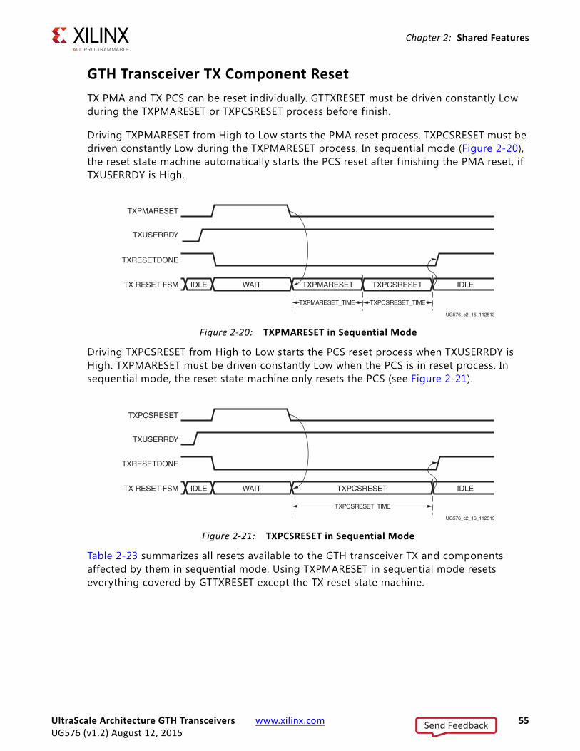
Chapter 2: Shared Features
GTH Transceiver TX Component Reset TX PMA and TX PCS can be reset individually. GTTXRESET must be driven constantly Low during the TXPMARESET or TXPCSRESET process before f inish.
Driving TXPMARESET from High to Low starts the PMA reset process. TXPCSRESET must be driven constantly Low during the TXPMARESET process. In sequential mode (Figure 2-20), the reset state machine automatically starts the PCS reset after f inishing the PMA reset, if TXUSERRDY is High.
Driving TXPCSRESET from High to Low starts the PCS reset process when TXUSERRDY is High. TXPMARESET must be driven constantly Low when the PCS is in reset process. In sequential mode, the reset state machine only resets the PCS (see Figure 2-21).
Table 2-23 summarizes all resets available to the GTH transceiver TX and components affected by them in sequential mode. Using TXPMARESET in sequential mode resets everything covered by GTTXRESET except the TX reset state machine.
X-Ref Target - Figure 2-20
Figure 2-20: TXPMARESET in Sequential Mode
X-Ref Target - Figure 2-21
Figure 2-21: TXPCSRESET in Sequential Mode
TXPMARESET
TXUSERRDY
TXRESETDONE
TX RESET FSM IDLE IDLEWAIT TXPMARESET TXPCSRESET
TXPMARESET_TIME TXPCSRESET_TIME
UG576_c2_15_112513
TXPCSRESET
TXUSERRDY
TXRESETDONE
TX RESET FSM IDLE IDLEWAIT TXPCSRESET
TXPCSRESET_TIME
UG576_c2_16_112513
UltraScale Architecture GTH Transceivers www.xilinx.com 55UG576 (v1.2) August 12, 2015
Send Feedback

Chapter 2: Shared Features
Table 2-24 lists the recommended resets for various situations.
Table 2-23: TX Initialization Reset and Component Reset Coveragein Sequential Mode
Functional Blocks GTTXRESET TXPMARESET TXPCSRESET
TX PCS
TX Interconnect Logic Interface
✓ ✓ ✓
TX 8B/10B Encoder ✓ ✓ ✓
TX Gearbox ✓ ✓ ✓
TX Buffer ✓ ✓ ✓
TX Pattern Generator ✓ ✓ ✓
TX Polarity Control ✓ ✓ ✓
TX Out-of-Band Signaling ✓ ✓ ✓
TX Reset FSM ✓
TX PMA
TX Configuration Driver ✓ ✓
TX Receiver Detect for PCI Express Designs
✓ ✓
TX PISO ✓ ✓
Table 2-24: Recommended Resets for Common Situations
Situation Components to be Reset Recommended Reset(1)
After power up and configuration CPLL/QPLL being usedEntire TX
CPLLPD, QPLL0/1RESET,GTTXRESET
After turning on a reference clock to the CPLL/QPLL being used
CPLL/QPLL being usedEntire TX
CPLLPD, QPLL0/1RESET,GTTXRESET
After changing the reference clock to the CPLL/QPLL being used
CPLL/QPLL being usedEntire TX
CPLLPD, QPLL0/1RESET,GTTXRESET
After assertion/deassertion of CPLLPD or QPLLPD for the PLL being used
CPLL/QPLL being usedEntire TX
CPLLPD, QPLL0/1RESET,GTTXRESET
After assertion/deassertion of TXPD[1:0] Entire TX GTTXRESET
TX rate change Entire TX Reset performed automatically
TX parallel clock source reset TX PCS TXPCSRESET
After entering or exiting Far-End PMA loopback
Entire TX GTTXRESET
After entering or exiting Near-End PMA loopback
Entire RX GTRXRESET
Notes: 1. The recommended reset has the smallest impact on the other components of the GTH transceiver.
UltraScale Architecture GTH Transceivers www.xilinx.com 56UG576 (v1.2) August 12, 2015
Send Feedback

Chapter 2: Shared Features
After Power-up and Configuration
The PLL being used and the entire GTH TX requires a reset after configuration. See GTH Transceiver TX Reset in Response to Completion of Configuration, page 53.
After Turning on a Reference Clock to the CPLL/QPLL Being Used
If the reference clock(s) changes or the GTH transceiver(s) are powered up after configuration, toggle GTTXRESET after the PLL fully completes its reset procedure.
After Changing the Reference Clock to the CPLL/QPLL being used
Whenever the reference clock input to the PLL is changed, the PLL must be reset afterwards to ensure that it locks to the new frequency. Toggle GTTXRESET after the PLL fully completes its reset procedure.
After Assertion/Deassertion of C/QPLLPD, for the PLL being used
When the CPLL or QPLL being used goes back to normal operation after power down, the PLL must be reset. Toggle GTTXRESET after the PLL fully completes its reset procedure.
After Assertion/Deassertion of TXPD[1:0]
After the TXPD signal is deasserted, GTTXRESET must be toggled.
TX Rate Change
When a rate change is performed using the TXRATE port and TXRATEMODE is set to 1'b0, the required reset sequence is performed automatically. When TXRATEDONE is asserted, it indicates that both a rate change and the necessary reset sequence have been applied and completed.
If the TX buffer is enabled, set the TXBUF_RESET_ON_RATE_CHANGE attribute to TRUE to allow the TX buffer to reset automatically after a rate change. If TX buffer bypass mode is used, alignment must be repeated after TXRATEDONE is asserted.
TX Parallel Clock Source Reset
The clocks driving TXUSRCLK and TXUSRCLK2 must be stable for correct operation. Toggle TXPCSRESET after the clock source re-locks.
If TX buffer bypass mode is used, alignment must be repeated after the completion of the reset procedure.
UltraScale Architecture GTH Transceivers www.xilinx.com 57UG576 (v1.2) August 12, 2015
Send Feedback

Chapter 2: Shared Features
RX Initialization and ResetThe GTH transceiver RX uses a reset state machine to control the reset process. Due to its complexity, the GTH transceiver RX is partitioned into more reset regions than the GTH transceiver TX. The partition allows RX initialization and reset to be operated in either sequential mode or single mode as shown in Figure 2-22:
1. RX in Sequential Mode
To initialize the GTH transceiver RX, GTRXRESET must be used in sequential mode. Activating the GTRXRESET input can automatically trigger a full asynchronous RX reset. The reset state machine executes the reset sequence as shown in Figure 2-22, covering the entire RX PMA and RX PCS. During normal operation, sequential mode also allows you to initiate a reset by activating any of these resets including RXPMARESET, RXDFELPMRESET, EYESCANRESET, RXPCSRESET, and RXBUFRESET, and continue the reset state machine until RXRESETDONE transitions from Low to High.
2. RX in Single Mode
When the GTH transceiver RX is in single mode, RXPMARESET, RXDFELPMRESET, EYESCANRESET, RXPCSRESET, and RXBUFRESET in the reset sequence can be executed individually and independently without triggering a reset on other reset regions.
In either sequential mode or single mode, the RX reset state machine does not reset the PCS until RXUSERRDY goes High. Drive RXUSERRDY High after these conditions are met:
1. All clocks used by the application, including RXUSRCLK and RXUSRCLK2, are shown to be stable.
2. The user interface is ready to receive data from the GTH transceiver.
UltraScale Architecture GTH Transceivers www.xilinx.com 58UG576 (v1.2) August 12, 2015
Send Feedback

Chapter 2: Shared Features
Ports and AttributesTable 2-25 lists the ports required by the GTH transceiver RX initialization process.
X-Ref Target - Figure 2-22
Figure 2-22: GTH Transceiver RX Reset State Machine Sequence
WAIT untilRXPMARESET
from High to Low
RXPMARESETProcess
WAIT untilGTRXRESET
from High to Low
RXPMARESET Donewhen
RXRESETDONE High
RXPMARESETHigh
GTRXRESETHigh
SingleMode
WAIT untilRXDFELPMRESET
from High to Low
RXDFELPMRESETProcess
RXDFELPMRESET Done when
RXRESETDONE High
RXDFELPMRESETHigh
SingleMode
WAIT untilEYESCANRESETfrom High to Low
EYESCANRESETProcess
EYESCANRESETDone when
RXRESETDONE High
EYESCANRESETHigh
SingleMode
WAIT untilRXPCSRESET
from High to Low
RXPCSRESETProcess
RXPCSRESET Donewhen
RXRESETDONE High
RXPCSRESETHigh
SingleMode
WAIT untilRXBUFRESET
from High to Low
RXBUFRESETProcess
RXRESETDONEHigh
RXBUFRESET Donewhen
RXRESETDONE High
RXBUFRESETHigh
SingleMode
Sequence Mode and RXUSERRDY
UG576_c2_17_062614
Table 2-25: RX Initialization and Reset Ports
Port Dir Clock Domain Description
GTRXRESET In Async This port is driven High and then deasserted to start the full channel RX reset sequence.
RXOSCALRESET In Async Reserved. Use the recommended value from the Wizard.
RSOSINTDONE Out Async Reserved. Use the recommended value from the Wizard.
UltraScale Architecture GTH Transceivers www.xilinx.com 59UG576 (v1.2) August 12, 2015
Send Feedback
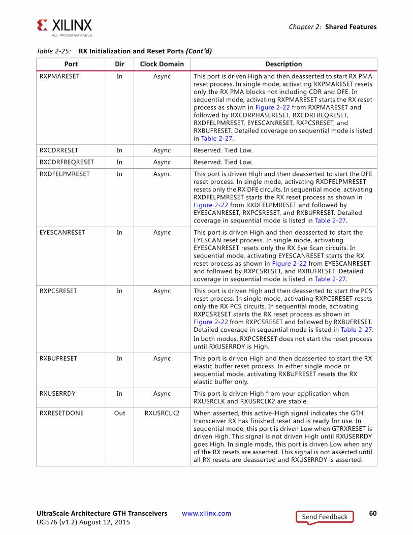
Chapter 2: Shared Features
RXPMARESET In Async This port is driven High and then deasserted to start RX PMA reset process. In single mode, activating RXPMARESET resets only the RX PMA blocks not including CDR and DFE. In sequential mode, activating RXPMARESET starts the RX reset process as shown in Figure 2-22 from RXPMARESET and followed by RXCDRPHASERESET, RXCDRFREQRESET, RXDFELPMRESET, EYESCANRESET, RXPCSRESET, and RXBUFRESET. Detailed coverage on sequential mode is listed in Table 2-27.
RXCDRRESET In Async Reserved. Tied Low.
RXCDRFREQRESET In Async Reserved. Tied Low.
RXDFELPMRESET In Async This port is driven High and then deasserted to start the DFE reset process. In single mode, activating RXDFELPMRESET resets only the RX DFE circuits. In sequential mode, activating RXDFELPMRESET starts the RX reset process as shown in Figure 2-22 from RXDFELPMRESET and followed by EYESCANRESET, RXPCSRESET, and RXBUFRESET. Detailed coverage in sequential mode is listed in Table 2-27.
EYESCANRESET In Async This port is driven High and then deasserted to start the EYESCAN reset process. In single mode, activating EYESCANRESET resets only the RX Eye Scan circuits. In sequential mode, activating EYESCANRESET starts the RX reset process as shown in Figure 2-22 from EYESCANRESET and followed by RXPCSRESET, and RXBUFRESET. Detailed coverage in sequential mode is listed in Table 2-27.
RXPCSRESET In Async This port is driven High and then deasserted to start the PCS reset process. In single mode, activating RXPCSRESET resets only the RX PCS circuits. In sequential mode, activating RXPCSRESET starts the RX reset process as shown in Figure 2-22 from RXPCSRESET and followed by RXBUFRESET. Detailed coverage in sequential mode is listed in Table 2-27.In both modes, RXPCSRESET does not start the reset process until RXUSERRDY is High.
RXBUFRESET In Async This port is driven High and then deasserted to start the RX elastic buffer reset process. In either single mode or sequential mode, activating RXBUFRESET resets the RX elastic buffer only.
RXUSERRDY In Async This port is driven High from your application when RXUSRCLK and RXUSRCLK2 are stable.
RXRESETDONE Out RXUSRCLK2 When asserted, this active-High signal indicates the GTH transceiver RX has f inished reset and is ready for use. In sequential mode, this port is driven Low when GTRXRESET is driven High. This signal is not driven High until RXUSERRDY goes High. In single mode, this port is driven Low when any of the RX resets are asserted. This signal is not asserted until all RX resets are deasserted and RXUSERRDY is asserted.
Table 2-25: RX Initialization and Reset Ports (Cont’d)
Port Dir Clock Domain Description
UltraScale Architecture GTH Transceivers www.xilinx.com 60UG576 (v1.2) August 12, 2015
Send Feedback

Chapter 2: Shared Features
Table 2-26 lists the attributes required by GTH transceiver RX initialization. In general cases, the reset time required by each reset on the RX datapath varies depending on line rate and function. The factors affecting each reset time are user-configurable attributes listed in Table 2-26.
RXPMARESETDONE Out Async This active-High signal indicates RX PMA reset is complete. This port is driven Low when GTRXRESET or RXPMARESET is asserted.
RXOOBRESET In Async This port can be used to reset the OOB individually. Tie this port Low if the OOB function is not used or the OOB single reset is not required.RXOOBRESET is independent from the GTH transceiver RX reset state machine sequence as shown in Figure 2-22. Sequential mode and single mode do not apply to RXOOBRESET.Activating RXOOBRESET does not cause RXRESETDONE to transition from Low to High or High to Low.
RESETEXCEPTION Out Async Reserved.
GTPOWERGOOD Out Async Power good indicator.
Table 2-25: RX Initialization and Reset Ports (Cont’d)
Port Dir Clock Domain Description
Table 2-26: RX Initialization and Reset Attributes
Attribute Type Description
RXOSCALRESET_TIME 5-bit Binary Reserved. Use the recommended value from the Wizard. Must be a non-zero value when GTRXRESET is used to initiate the reset process.
RXOSCALRESET_TIMEOUT 5-bit Binary Reserved. Use the recommended value from the Wizard. Set to zero for normal operation.
RXPMARESET_TIME 5-bit Binary Reserved. Represents the time duration to apply the RX PMA reset. Use the recommended value from the Wizard. Must be a non-zero value when using GTRXRESET or RXPMARESET to initiate reset process.
RXCDRPHRESET_TIME 5-bit Binary Reserved. Represents the time duration to apply RX CDR phase reset. Must be a non-zero value when using RXCDRRESET to initialize the reset process.
RXCDRFREQRESET_TIME 5-bit Binary Reserved. Represents the time duration to apply the RX CDRFREQ reset. Use the recommended value from the Wizard. Must be a non-zero value when using RXCDRFREQRESET to initiate the reset process.
RXDFELPMRESET_TIME 7-bit Binary Reserved. Represents the time duration to apply the RX DFE reset. Use the recommended value from the Wizard. Must be a non-zero value when using RXDFELPMRESET to initiate the reset process.
UltraScale Architecture GTH Transceivers www.xilinx.com 61UG576 (v1.2) August 12, 2015
Send Feedback

Chapter 2: Shared Features
GTH Transceiver RX Reset in Response to Completion of ConfigurationThe RX reset sequence shown in Figure 2-22 is not automatically started to follow the global GSR.
These conditions must be met:
1. GTRESETSEL must be driven Low to use the sequential mode.
2. GTRXRESET must be used.
3. All single reset inputs including RXPMARESET, RXCDRRESET, RXCDRFREQRESET, RXDFELPMRESET, EYESCANRESET, RXPCSRESET, and RXBUFRESET must be constantly held Low during the entire reset process before RXRESETDONE goes High.
4. GTRXRESET cannot be driven Low until the associated PLL is locked.
5. Ensure that GTPOWERGOOD is High before releasing C/QPLLRESET and GTRXRESET.
If the reset mode is defaulted to single mode, then you must:
1. Change reset mode to Sequential mode.
2. Wait another 300-500 ns.
3. Assert CPLLPD or QPLL0/1RESET and GTRXRESET.
RECOMMENDED: Use the associated PLLLOCK from either the CPLL or QPLL to release GTRXRESET from High to Low as shown in Figure 2-23. The RX reset state machine waits when GTRXRESET is High and starts the reset sequence until GTRXRESET is released Low.
RXISCANRESET_TIME 5-bit Binary Reserved. Represents the time duration to apply the RX EYESCAN reset. Use the recommended value from the Wizard. Must be a non-zero value when using RXISCANRESET_TIME to initiate the reset process.
RXPCSRESET_TIME 5-bit Binary Reserved. Represents the time duration to apply the RX PCS reset. Use the recommended value from the Wizard. Must be a non-zero value when using RXPCSRESET to initiate the reset process.
RXBUFRESET_TIME 5-bit Binary Reserved. Represents the time duration to apply the RX BUFFER reset. Use the recommended value from the Wizard. Must be a non-zero value when using RXBUFRESET to initiate the reset process.
RX_PMA_POWER_SAVE 1-bit Binary Reserved. Use the recommended value from the Wizard.
Table 2-26: RX Initialization and Reset Attributes (Cont’d)
Attribute Type Description
UltraScale Architecture GTH Transceivers www.xilinx.com 62UG576 (v1.2) August 12, 2015
Send Feedback

Chapter 2: Shared Features
GTH Transceiver RX Reset in Response to GTRXRESET PulseThe GTH transceiver allows you to completely reset the entire GTH transceiver RX at any time when needed by sending GTRXRESET an active High pulse. All RX reset attributes listed in Table 2-25 can be set statically or reprogrammed through DRP ports to adjust the required reset time before applying GTRXRESET. These conditions must be met to use GTRXRESET:
1. GTRESETSEL must be driven Low to use sequential mode.
2. All reset inputs shown on the left of Figure 2-24 including RXPMARESET, RXCDRRESET, RXCDRFREQRESET, RXDFELPMRESET, EYESCANRESET, RXPCSRESET, and RXBUFRESET must be constantly driven Low during the entire reset process before RXRESETDONE is detected High.
3. The associated PLL must indicate locked.
TIP: The guideline for this asynchronous GTRXRESET pulse width is one period of the reference clock.
X-Ref Target - Figure 2-23
Figure 2-23: GTH Receiver after Configuration
CPLLPD/QPLL0/1RESET
CPLLLOCK/QPLL0/1LOCK
GTRXRESET
RXUSERRDY
RXRESETDONE
RX RESET FSM WAIT RXOSCALRESET RXPMARESET RXCDRRESET RXDFERESET RXEYESCANRESET RXPCSRESET RXBUFRESET
RXBUFRESET_TIMETXPCSRESET_TIME RXCDRFREQRESET_TIME RXISCANRESET_TIMERXCDRPHRESET_TIME RXDFELPMRESET_TIME RXPCSRESET_TIME
IDLERXCDRFREQRESET
UG576_c2_18_062615
GTPOWERGOOD
TXPMARESET_TIME
UltraScale Architecture GTH Transceivers www.xilinx.com 63UG576 (v1.2) August 12, 2015
Send Feedback

Chapter 2: Shared Features
GTH Transceiver RX Component ResetsGTH transceiver RX component resets can operate in either sequential mode or single mode. They are primarily used for special cases. These resets are needed when only a specific subsection needs to be reset. Table 2-27 and Table 2-28 summarize all resets available to the GTH transceiver RX and components affected by them in both sequential mode and single mode. These resets are all asynchronous.
X-Ref Target - Figure 2-24
Figure 2-24: GTH Receiver Reset after GTRXRESET Pulse
GTRXRESET
RXUSERRDY
RXRESETDONE
RX RESET FSM IDLE WAIT RXPMARESET RXCDRRESET RXDFELPMRESET RXISCANRESET RXPCSRESET RXBUFRESET
RXBUFRESET_TIMERXPMARESET_TIME RXCDRFREQRESET_TIME RXISCANRESET_TIMERXCDRPHRESET_TIME RXDFELPMRESET_TIME RXPCSRESET_TIME
IDLERXCDRFREQRESET
UG576_c2_19_112513
Table 2-27: RX Component Reset Coverage in Sequential Mode
Functional Blocks GTRXRESET
RXPMARESET
RXDFERESET
EYESCANRESET
RXPCSRESET
RXBUFRESET
RX PCS
RX Interconnect Logic Interface ✓ ✓ ✓ ✓ ✓
RX Gearbox ✓ ✓ ✓ ✓ ✓
RX Status Control ✓ ✓ ✓ ✓ ✓
RX Elastic Buffer Delay Aligner ✓ ✓ ✓ ✓ ✓
RX 8B/10B Encoder ✓ ✓ ✓ ✓ ✓
RX Comma Detect and Alignment ✓ ✓ ✓ ✓ ✓
RX Polarity ✓ ✓ ✓ ✓ ✓
PRBS Checker ✓ ✓ ✓ ✓ ✓
RX Elastic Buffer ✓ ✓ ✓ ✓ ✓ ✓
RX Reset FSM ✓
UltraScale Architecture GTH Transceivers www.xilinx.com 64UG576 (v1.2) August 12, 2015
Send Feedback

Chapter 2: Shared Features
Table 2-29 lists the recommended resets for various situations.
RX PMA
RX Analog Front End ✓ ✓
RX Out-of-Band Signaling ✓ ✓
RX SIPO ✓ ✓
RX CDR Phase Path ✓ ✓
RX CDR Frequency Path ✓ ✓
RX DFE ✓ ✓ ✓
RX EYESCAN ✓ ✓ ✓ ✓
Table 2-28: RX Component Reset Coverage in Single Mode
Functional Blocks GTRXRESET
RXPMARESET
RXDFERESET
EYESCANRESET
RXPCSRESET
RXBUFRESET
RXOOBRESET
RX PCS
RX Interconnect Logic Interface ✓
RX Gearbox ✓
RX Status Control ✓
RX Delay Aligner ✓
RX 8B/10B Encoder ✓
RX Comma Detect and Alignment ✓
RX Polarity ✓
PRBS Checker ✓
RX Elastic Buffer ✓
RX Reset FSM
RX PMA
RX Analog Front End ✓
RX Out-of-Band Signaling ✓ ✓
RX SIPO ✓
RX CDR Phase Path
RX CDR Frequency Path
RX DFE ✓
RX EYESCAN ✓
Table 2-27: RX Component Reset Coverage in Sequential Mode (Cont’d)
Functional Blocks GTRXRESET
RXPMARESET
RXDFERESET
EYESCANRESET
RXPCSRESET
RXBUFRESET
UltraScale Architecture GTH Transceivers www.xilinx.com 65UG576 (v1.2) August 12, 2015
Send Feedback

Chapter 2: Shared Features
Table 2-29: Recommended Resets for Common Situations
Situation Components to be Reset Recommended Reset(1)
After power up and configuration CPLL/QPLL being usedEntire RX
CPLLPD, QPLL0/1RESET, GTRXRESET
After turning on a reference clock to the CPLL/QPLL being used
CPLL/QPLL being usedEntire RX
CPLLPD, QPLL0/1RESET, GTRXRESET
After changing the reference clock to the CPLL/QPLL being used
CPLL/QPLL being usedEntire RX
CPLLPD, QPLL0/1RESET, GTRXRESET
After assertion/deassertion of CPLLPD or QPLLPD for the PLL being used
CPLL/QPLL being usedEntire RX
CPLLPD, QPLL0/1RESET, GTRXRESET
After assertion/deassertion of RXPD[1:0] Entire RX GTRXRESET
RX rate change Entire RX GTRXRESET or reset sequence is performed automatically due to RXRATE. See RX Rate Change, page 67 for more information.
RX parallel clock source reset RX PCS RXPCSRESET
After remote power up Entire RX GTRXRESET
Electrical idle Entire RX Handled automatically with appropriate attribute settings
After connecting RXN/RXP(2) Entire RX GTRXRESET
After recovered clock becomes stable RX Elastic Buffer
RXBUFRESET
After an RXBUFFER error RX Elastic Buffer
RXBUFRESET
After changing channel bonding mode in real time
RX Elastic Buffer
RX elastic buffer is reset automatically after change in channel bonding mode by setting RXBUF_RESET_ON_CB_CHANGE to TRUE
After PRBS error PRBS Error Counter
PRBSCNTRESET
After comma realignment RX Elastic Buffer
(optional)
RX elastic buffer is reset automatically after comma realignment by setting RXBUF_RESET_ON_COMMAALIGN to TRUE
Notes: 1. The recommended reset has the smallest impact on the other components of the GTH transceiver.2. It is assumed that RXN/RXP are connected simultaneously.
UltraScale Architecture GTH Transceivers www.xilinx.com 66UG576 (v1.2) August 12, 2015
Send Feedback

Chapter 2: Shared Features
After Power-up and Configuration
The PLL being used and the entire GTH RX requires a reset after configuration. See GTH Transceiver RX Reset in Response to Completion of Configuration, page 62.
After Turning on a Reference Clock to the CPLL/QPLL0/1 Being Used
If the reference clock(s) changes or GTH transceiver(s) are powered up after configuration, toggle GTRXRESET after the PLL fully completes its reset procedure.
After Changing the Reference Clock to the CPLL/QPLL0/1 Being Used
Whenever the reference clock input to the PLL is changed, the PLL must be reset afterwards to ensure that it locks to the new frequency. Toggle GTRXRESET after the PLL fully completes its reset procedure.
After Assertion/Deassertion of CPLLPD or QPLL0/1PD for the PLL Being Used
When the CPLL or QPLL being used goes back to normal operation after power down, the PLL must be reset. Toggle GTRXRESET after the PLL fully completes its reset procedure.
After Assertion/Deassertion of RXPD[1:0]
After the RXPD signal is deasserted, GTRXRESET must be toggled.
RX Rate Change
In most cases, in addition to changing the output divider, an RX rate change requires changing the RX CDR loop f ilter settings via DRP. After writing in the proper RX CDR loop f ilter setting and updating the RX_OUTDIV attribute via DRP, the RX must be reset by toggling the GTRXRESET port. In cases where the CDR loop f ilter does not need to be updated via DRP, rate change can be performed using the RXRATE port with RXRATEMODE set to 1'b0. As a result, the required reset sequence is performed automatically. RXRATEDONE being asserted in response to RXRATE indicates that both rate change and the necessary reset sequence have been applied and completed.
If the RX buffer is enabled, set the RXBUF_RESET_ON_RATE_CHANGE attribute to TRUE to allow the RX buffer to reset automatically after a rate change. If RX buffer bypass mode is used, alignment must be repeated after RXRATEDONE is asserted.
RX Parallel Clock Source Reset
The clocks driving RXUSRCLK and RXUSRCLK2 must be stable for correct operation. Toggle RXPCSRESET after the clock source re-locks. If RX buffer bypass mode is used, alignment must be repeated after the completion of the reset procedure.
UltraScale Architecture GTH Transceivers www.xilinx.com 67UG576 (v1.2) August 12, 2015
Send Feedback

Chapter 2: Shared Features
After Remote Power-Up
If the source of incoming data is powered up after the GTH transceiver that is receiving its data has begun operating, the RX side must be reset to ensure a clean lock to the incoming data.
Electrical Idle Reset
For protocols that support OOB and electrical idle, when the differential voltage of the RX input to the transceiver drops to OOB or electrical idle levels, the RX CDR is managed automatically when the attributes associated with electrical idle are set to appropriate values. Use the recommended values from the Wizard.
After Connecting RXN/RXP
When the RX data to the GTH transceiver comes from a connector that can be plugged in and unplugged, the RX side must be reset when the data source is plugged in to ensure that it can lock to incoming data.
After Recovered Clock Becomes Stable
Depending on the design of the clocking scheme, it is possible for the RX reset sequence to be completed before the CDR is locked to the incoming data. In this case, the recovered clock might not be stable when RXRESETDONE is asserted.
When the RX buffer is used, RXBUFRESET should be triggered after the recovered clock becomes stable. When RX buffer bypass is used, the alignment procedure should not start until the recovered clock becomes stable.
Refer to the UltraScale device data sheets [Ref 6] for successful CDR lock-to-data criteria.
After an RX Elastic Buffer Error
After an RX elastic buffer overflow or underflow, the RX elastic buffer must be reset using RXBUFRESET to ensure correct behavior.
After Changing Channel Bonding Mode During Run Time
When set to TRUE, RXBUF_RESET_ON_CB_CHANGE enables automatic reset of the RX elastic buffer when RXCHANBONDMASTER, RXCHANBONDSLAVE, or RXCHANBONDLEVEL change.
After a PRBS Error
PRBSCNTRESET is asserted to reset the PRBS error counter.
UltraScale Architecture GTH Transceivers www.xilinx.com 68UG576 (v1.2) August 12, 2015
Send Feedback

Chapter 2: Shared Features
After Comma Realignment
When set to TRUE, RXBUF_RESET_ON_COMMAALIGN enables automatic reset of the RX elastic buffer during comma realignment.
Power Down
Functional DescriptionThe GTH transceiver supports a range of power-down modes. These modes support both generic power management capabilities as well as those defined in the PCI Express and SATA standards.
The GTH transceiver offers different levels of power control. Each channel in each direction can be powered down separately using TXPD and RXPD. The CPLLPD port directly affects the Channel PLL while the QPLL0/1PD port directly affects the Quad PLL0/1.
Ports and AttributesTable 2-30 defines the power-down ports.
Table 2-30: Power-Down Ports
Port Dir Clock Domain Description
CPLLPD In Async This active-High signal powers down the Channel PLL.
QPLL0PD/QPLL1PD In Async This active-High signal powers down the Quad PLL0/1.
RXPD[1:0] In Async Powers down the RX lane according to the PCI Express PIPE protocol encoding.00: P0 (normal operation)01: P0s (low recovery time power down)10: P1 (longer recovery time) 11: P2 (lowest power state)
TXPD[1:0] In TXUSRCLK2 (TXPDELECIDLEMODE
makes this port asynchronous)
Powers down the TX lane according to the PCI Express PIPE protocol encoding. 00: P0 (normal operation)01: P0s (low recovery time power down)10: P1 (longer recovery time; Receiver Detection still on) 11: P2 (lowest power state)
Attributes can control the transition times between these power-down states.
UltraScale Architecture GTH Transceivers www.xilinx.com 69UG576 (v1.2) August 12, 2015
Send Feedback

Chapter 2: Shared Features
Table 2-31 defines the power-down attributes.
TXPDELECIDLEMODE In Async Determines if TXELECIDLE and TXPD should be treated as synchronous or asynchronous signals.
TXPHDLYPD In Async TX phase and delay alignment circuit power down. It is set to 1'b0 in TX buffer bypass mode.
0: Power up the TX phase and delay alignment circuit.1: Power down the TX phase and delay alignment circuit.
RXPHDLYPD In Async RX phase and delay alignment circuit power down. It is set to 1'b0 in RX buffer bypass mode.
0: Power up the RX phase and delay alignment circuit.1: Power down the RX phase and delay alignment circuit.
Table 2-31: Power-Down Attributes
Attribute Type Description
PD_TRANS_TIME_FROM_P2 12-bit Hex Counter settings for programmable transition time from P2 state for PCIe. Use the recommended value from the Wizard.
PD_TRANS_TIME_NONE_P2 8-bit Hex Counter settings for programmable transition time to/from all states except P2 for PCIe. Use the recommended value from the Wizard.
PD_TRANS_TIME_TO_P2 8-bit Hex Counter settings for programmable transition time to P2 state for PCIe. Use the recommended value from the Wizard.
TRANS_TIME_RATE 8-bit Hex Counter settings for programmable transition time when the rate is changed using the [TX/RX]RATE pins for all protocols including the PCIe protocol (Gen2/Gen1 data rates). Use the recommended value from the Wizard.
RX_CLKMUX_EN 1-bit Binary Use the recommended value from the Wizard.
TX_CLKMUX_EN 1-bit Binary Use the recommended value from the Wizard.
Table 2-30: Power-Down Ports (Cont’d)
Port Dir Clock Domain Description
UltraScale Architecture GTH Transceivers www.xilinx.com 70UG576 (v1.2) August 12, 2015
Send Feedback
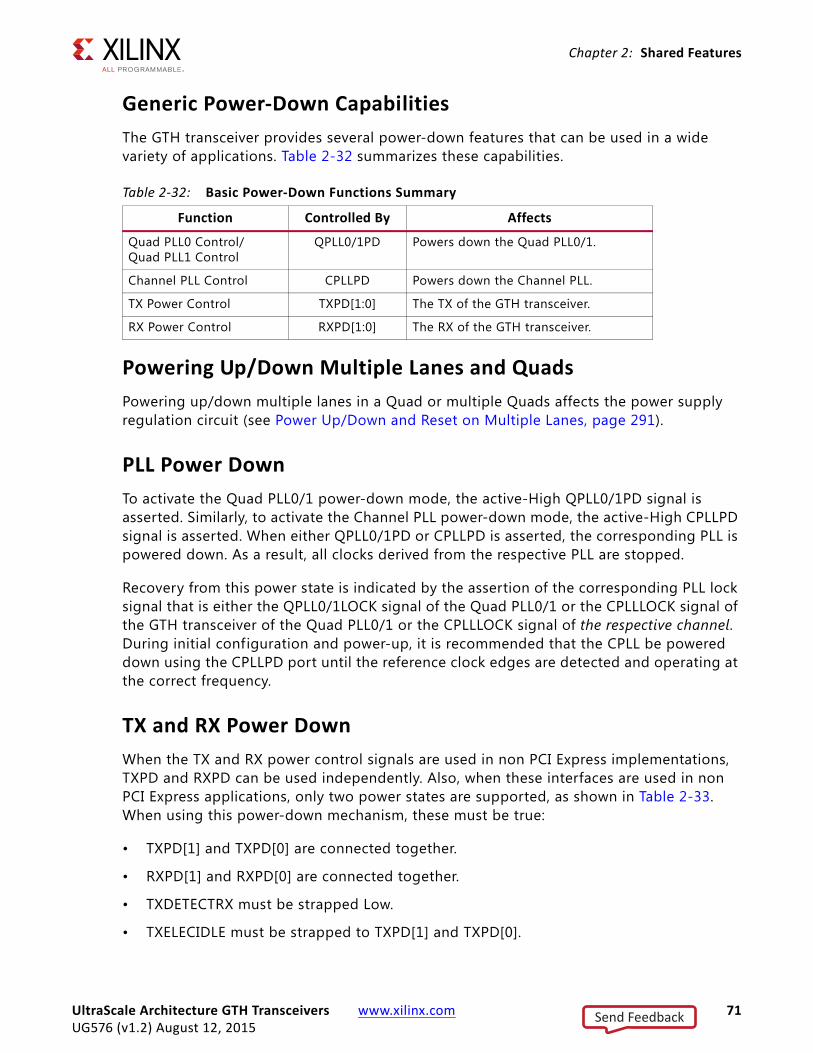
Chapter 2: Shared Features
Generic Power-Down CapabilitiesThe GTH transceiver provides several power-down features that can be used in a wide variety of applications. Table 2-32 summarizes these capabilities.
Powering Up/Down Multiple Lanes and QuadsPowering up/down multiple lanes in a Quad or multiple Quads affects the power supply regulation circuit (see Power Up/Down and Reset on Multiple Lanes, page 291).
PLL Power DownTo activate the Quad PLL0/1 power-down mode, the active-High QPLL0/1PD signal is asserted. Similarly, to activate the Channel PLL power-down mode, the active-High CPLLPD signal is asserted. When either QPLL0/1PD or CPLLPD is asserted, the corresponding PLL is powered down. As a result, all clocks derived from the respective PLL are stopped.
Recovery from this power state is indicated by the assertion of the corresponding PLL lock signal that is either the QPLL0/1LOCK signal of the Quad PLL0/1 or the CPLLLOCK signal of the GTH transceiver of the Quad PLL0/1 or the CPLLLOCK signal of the respective channel. During initial configuration and power-up, it is recommended that the CPLL be powered down using the CPLLPD port until the reference clock edges are detected and operating at the correct frequency.
TX and RX Power DownWhen the TX and RX power control signals are used in non PCI Express implementations, TXPD and RXPD can be used independently. Also, when these interfaces are used in non PCI Express applications, only two power states are supported, as shown in Table 2-33. When using this power-down mechanism, these must be true:
• TXPD[1] and TXPD[0] are connected together.
• RXPD[1] and RXPD[0] are connected together.
• TXDETECTRX must be strapped Low.
• TXELECIDLE must be strapped to TXPD[1] and TXPD[0].
Table 2-32: Basic Power-Down Functions Summary
Function Controlled By Affects
Quad PLL0 Control/Quad PLL1 Control
QPLL0/1PD Powers down the Quad PLL0/1.
Channel PLL Control CPLLPD Powers down the Channel PLL.
TX Power Control TXPD[1:0] The TX of the GTH transceiver.
RX Power Control RXPD[1:0] The RX of the GTH transceiver.
UltraScale Architecture GTH Transceivers www.xilinx.com 71UG576 (v1.2) August 12, 2015
Send Feedback

Chapter 2: Shared Features
Loopback
Functional DescriptionLoopback modes are specialized configurations of the transceiver datapath where the traffic stream is folded back to the source. Typically, a specif ic traff ic pattern is transmitted and then compared to check for errors. Figure 2-25 illustrates a loopback test configuration with four different loopback modes.
Loopback test modes fall into two broad categories:
• Near-end loopback modes loop transmit data back in the transceiver closest to the traffic generator. A GTRXRESET is required after entering and exiting near-end PMA loopback.
• Far-end loopback modes loop received data back in the transceiver at the far end of the link.
Loopback testing can be used either during development or in deployed equipment for fault isolation. The traffic patterns used can be either application traffic patterns or specialized pseudo-random bit sequences. Each GTH transceiver has a built-in PRBS generator and checker.
Table 2-33: TX and RX Power States for Operation that are not for PCI Express Designs
TXPD[1:0] or RXPD[1:0] Description
00 Normal mode. Transceiver TX or RX is active sending or receiving data.
11 Power-down mode. Transceiver TX or RX is idle.
X-Ref Target - Figure 2-25
Figure 2-25: Loopback Testing Overview
Test Logic Near-End GTH
1 2 3 4
Far-End GTH
Link Near-End Test Structures Link Far-End Test Structures
TrafficChecker
TrafficGenerator
RX-PCS
RX-PCS
TX-PCS
TX-PCS
TX-PMA
TX-PMA
RX-PMA
RX-PMA
UG576_c2_20_112513
UltraScale Architecture GTH Transceivers www.xilinx.com 72UG576 (v1.2) August 12, 2015
Send Feedback

Chapter 2: Shared Features
Each GTH transceiver features several loopback modes to facilitate testing:
• Near-end PCS Loopback (path 1 in Figure 2-25)
The RX elastic buffer must be enabled and RX_XCLK_SEL must be set to RXDES for near-end PCS loopback to function properly. While in near-end PCS loopback, the RX XCLK domain is clocked by the TX PMA parallel clock (TX XCLK). If the RXOUTCLK is used to clock interconnect logic and RXOUTCLKSEL is set to RXOUTCLKPMA during normal operation, one of these two items must be changed when placing the GTH transceiver into near-end PCS loopback:
° Set RXOUTCLKSEL to select RXOUTCLKPCS, or
° Set RXCDRHOLD = 1'b1
• Near-end PMA Loopback (path 2 in Figure 2-25)
A GTRXRESET is required after entering or exiting near-end PMA loopback.
• Far-end PMA Loopback (path 3 in Figure 2-25)
The TX buffer must be enabled and TX_XCLK_SEL must be set to TXOUT for far-end PMA loopback to function properly. While in far-end PMA loopback, the write side of the TX buffer is clocked by the RX PMA parallel clock (RX XCLK). The TX phase interpolator PPM controller must be disabled by setting the TXPIPPMEN port to 1'b0 and TXPIPPMSEL port to 1'b0. A GTTXRESET is required after entering or exiting far-end PMA loopback.
• Far-end PCS Loopback (path 4 in Figure 2-25)
If clock correction is not used, a transceiver in far-end PCS loopback must use the same reference clock used by the transceiver that is the source of the loopback data. Regardless of whether or not clock correction is used, the TXUSRCLK and RXUSRCLK ports must be driven by the same clocking resource (BUFG_GT). Far-end PCS loopback is not supported when both or either gearboxes in the channel are enabled.
Ports and AttributesTable 2-34 defines the loopback ports.
Table 2-34: Loopback Ports
Port Dir Clock Domain Description
LOOPBACK[2:0] In Async 000: Normal operation001: Near-end PCS Loopback010: Near-end PMA Loopback011: Reserved100: Far-end PMA Loopback101: Reserved110: Far-end PCS Loopback
UltraScale Architecture GTH Transceivers www.xilinx.com 73UG576 (v1.2) August 12, 2015
Send Feedback

Chapter 2: Shared Features
There are no loopback attributes.
Dynamic Reconfiguration Port
Functional DescriptionThe dynamic reconfiguration port (DRP) allows the dynamic change of parameters of the GTHE3_CHANNEL and GTHE3_COMMON primitives. The DRP interface is a processor-friendly synchronous interface with an address bus (DRPADDR) and separated data buses for reading (DRPDO) and writing (DRPDI) configuration data to the primitives. An enable signal (DRPEN), a read/write signal (DRPWE), and a ready/valid signal (DRPRDY) are the control signals that implement read and write operations, indicate operation completion, or indicate the availability of data.
Ports and AttributesTable 2-35 shows the DRP related ports for GTHE3_CHANNEL.
Table 2-35: DRP Ports of GTHE3_CHANNEL
Port Dir Clock Domain Description
DRPADDR[8:0] In DRPCLK DRP address bus.
DRPCLK In N/A DRP interface clock.
DRPEN In DRPCLK DRP enable signal.0: No read or write operation performed.1: Enables a read or write operation.For write operations, DRPWE and DRPEN should be driven High for one DRPCLK cycle only. See Figure 2-26 for correct operation.For read operations, DRPEN should be driven High for one DRPCLK cycle only. See Figure 2-27 for correct operation.
DRPDI[15:0] In DRPCLK Data bus for writing configuration data from the interconnect logic resources to the transceiver.
DRPRDY Out DRPCLK Indicates operation is complete for write operations and data is valid for read operations.If writing or reading a R/W register, DRPRDY asserts six DRPCLK cycles after initiating a DRP transaction. For read-only registers, the number of DRPCLK cycles for DRPRDY assertion depends on the relationship between the DRPCLK frequency and USRCLK frequency. For read-only registers, if a DRPRDY is not seen within 500 DRPCLK cycles after initiating a DRP transaction, reset the DRP interface using the port PCSRSVDIN[2].
UltraScale Architecture GTH Transceivers www.xilinx.com 74UG576 (v1.2) August 12, 2015
Send Feedback

Chapter 2: Shared Features
Table 2-36 shows the DRP related ports for GTHE3_COMMON.
DRPDO[15:0] Out DRPCLK Data bus for reading configuration data from the GTH transceiver to the interconnect logic resources.
DRPWE In DRPCLK DRP write enable.0: Read operation when DRPEN is 1.1: Write operation when DRPEN is 1.For write operations, DRPWE and DRPEN should be driven High for one DRPCLK cycle only. See Figure 2-26 for correct operation.
PCSRSVDIN[2] In Async DRP reset. Reading read-only registers while the XCLK is not toggling (e.g., during reset or change of reference clocks) causes the DRP to not return a DRPRDY signal and prevent further DRP transactions. In such an event, PCSRSVDIN[2] must be pulsed to reset the DRP interface before initiating further DRP transactions.
Table 2-36: DRP Ports of GTHE3_COMMON
Port Dir Clock Domain Description
DRPADDR[8:0] In DRPCLK DRP address bus.
DRPCLK In N/A DRP interface clock.
DRPEN In DRPCLK DRP enable signal.0: No read or write operation performed.1: Enables a read or write operation.
For write operations, DRPWE and DRPEN should be driven High for one DRPCLK cycle only. See Figure 2-26 for correct operation.For read operations, DRPEN should be driven High for one DRPCLK cycle only. See Figure 2-27 for correct operation.
DRPDI[15:0] In DRPCLK Data bus for writing configuration data from the interconnect logic resources to the transceiver.
DRPRDY Out DRPCLK Indicates operation is complete for write operations and data is valid for read operations.If writing or reading a read/write register, DRPRDY asserts six to seven DRPCLK cycles after initiating a DRP transaction.
Table 2-35: DRP Ports of GTHE3_CHANNEL (Cont’d)
Port Dir Clock Domain Description
UltraScale Architecture GTH Transceivers www.xilinx.com 75UG576 (v1.2) August 12, 2015
Send Feedback

Chapter 2: Shared Features
Usage Model
Write Operation
Figure 2-26 shows the DRP write operation timing. New DRP operation can be initiated when DRPRDY is asserted.
DRPDO[15:0] Out DRPCLK Data bus for reading configuration data from the GTH transceiver to the interconnect logic resources.
DRPWE In DRPCLK DRP write enable.0: Read operation when DRPEN is 1.1: Write operation when DRPEN is 1.
For write operations, DRPWE and DRPEN should be driven High for one DRPCLK cycle only. See Figure 2-26 for correct operation.
X-Ref Target - Figure 2-26
Figure 2-26: DRP Write Timing
Table 2-36: DRP Ports of GTHE3_COMMON (Cont’d)
Port Dir Clock Domain Description
UG576_c2_21_110613
DRPCLK
DRPEN
DRPRDY
DRPWE
DRPADDR
DRPDI
DRPDO
ADR
DAT
UltraScale Architecture GTH Transceivers www.xilinx.com 76UG576 (v1.2) August 12, 2015
Send Feedback
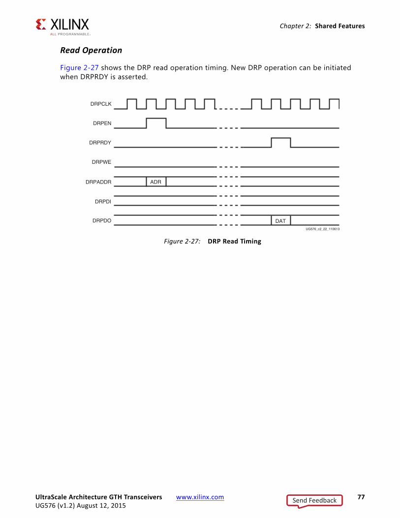
Chapter 2: Shared Features
Read Operation
Figure 2-27 shows the DRP read operation timing. New DRP operation can be initiated when DRPRDY is asserted.
X-Ref Target - Figure 2-27
Figure 2-27: DRP Read Timing
UG576_c2_22_110613
DRPCLK
DRPEN
DRPRDY
DRPWE
DRPADDR
DRPDI
DRPDO
ADR
DAT
UltraScale Architecture GTH Transceivers www.xilinx.com 77UG576 (v1.2) August 12, 2015
Send Feedback

Chapter 2: Shared Features
Digital Monitor
Functional DescriptionThe two receiver modes (LPM and DFE) use an adaptive algorithm in optimizing a link. The digital monitor provides visibility into the current state of these adaptation loops. Digital monitor requires a clock; DRPCLK or RXUSRCLK2 can be used for this. The attributes RXDFE_CFG1 or RXLPM_CFG select the adaptation loops monitored on the DMONITOROUT port. The output port DMONITOROUT contains the current code(s) for a selected loop. A loop has three steady-states: min, max, or dithering.
Ports and AttributesTable 2-37 shows the GTH digital monitor ports.
Table 2-37: Digital Monitor Ports
Port Dir Clock Domain Description
DMONITOROUT[16:0] Out Async/local clock
Digital monitor output bus:[16]: Internal clock adaptation loops:
[6:0]: RXDFEOS, RXDFEVP, RXDFEUT, RXLPMOS[6:2]: RXDFEKL, RXLPMKH, RXLPMKL[5:0]: RXDFETAP2, RXDFETAP3[4:0]: RXDFEAGC, RXDFETAP4, RXDFETAP5, RXDFETAP6, RXDFETAP7, RXDFETAP8, RXDFETAP9, RXDFETAPA, RXDFETAPB, RXLPMAGC
DMONITORCLK In Async Digital monitor clock.
DMONFIFORESET In Async Reserved. Tie to GND.
UltraScale Architecture GTH Transceivers www.xilinx.com 78UG576 (v1.2) August 12, 2015
Send Feedback

Chapter 2: Shared Features
Table 2-38 shows the GTH digital monitor attributes.
Table 2-38: Digital Monitor Attributes
Attribute Type Description
ADAPT_CFG1[15:0] Hex [15:13]: Reserved.[12:8]: Select DFE or LPM adaptation:5'b00010: DFE5'b00000: LPM
[7:0]: Reserved.
RXDFE_CFG1[15:0] Hex [15:6]: Reserved[5]: Set to 1'b1 when monitoring DFE adaptation loops, otherwise set to 1'b0.[4:0]: Select DFE adaptation loop:
RXDFE_CFG1[4:0] Select line for DFE adaptation
Code Mapping Range
5'b00000 RXDFEOS: Base line wander cancellation7 bits signed with double neutral
7'd0: min (neg)7'd63: neutral7'd64: neutral7'd127: max (pos)
5'b00001 RXDFEKL: DFE low-frequency gain
5'd0: min5'd31: max
5'b00010 RXDFEVP: DFE voltage peak 7'd0: min7'd127: max
5'b00011 RXDFEUT: DFE tap 1 7'd0: min7'd127: max
5'b00100 RXDFEAGC: DFE AGC frequency gain
5'd0: min5'd31: max
5'b00101 RXDFETAP2: DFE tap 2 6'd0: min6'd63: max
5'b00110 RXDFETAP3: DFE tap 36-bit signed with double neutral
6'd0: min (neg)6'd31: neutral6'd32: neutral6'd63: max (pos)
5'b00111 RXDFETAP4: DFE tap 45-bit signed with double neutral
5'd0: min (neg)5'd15: neutral5'd16: neutral5'd31: max (pos)
5'b01000 RXDFETAP5: DFE tap 55-bit signed with double neutral
5'd0: min (neg)5'd15: neutral5'd16: neutral5'd31: max (pos)
UltraScale Architecture GTH Transceivers www.xilinx.com 79UG576 (v1.2) August 12, 2015
Send Feedback

Chapter 2: Shared Features
RXDFE_CFG1[15:0] (Cont’d)
Hex [4:0]: Select DFE adaptation loop:
Table 2-38: Digital Monitor Attributes (Cont’d)
Attribute Type Description
RXDFE_CFG1[4:0] Select line for DFE adaptation
Code Mapping Range
5'b01001 RXDFETAP6: DFE tap 65-bit signed with double neutral
5'd0: min (neg)5'd15: neutral5'd16: neutral5'd31: max (pos)
5'b01010 RXDFETAP7: DFE tap 75-bit signed with double neutral
5'd0: min (neg)5'd15: neutral5'd16: neutral5'd31: max (pos)
5'b01011 RXDFETAP8: DFE tap 85-bit signed with double neutral
5'd0: min (neg)5'd15: neutral5'd16: neutral5'd31: max (pos)
5'b01100 RXDFETAP9: DFE tap 95-bit signed with double neutral
5'd0: min (neg)5'd15: neutral5'd16: neutral5'd31: max (pos)
5'b01101 RXDFETAPA: DFE tap A5-bit signed with double neutral
5'd0: min (neg)5'd15: neutral5'd16: neutral5'd31: max (pos)
5'b01110 RXDFETAPB: DFE tap B5-bit signed with double neutral
5'd0: min (neg)5'd15: neutral5'd16: neutral5'd31: max (pos)
UltraScale Architecture GTH Transceivers www.xilinx.com 80UG576 (v1.2) August 12, 2015
Send Feedback

Chapter 2: Shared Features
Use ModeReading loop values out of DMONITOR requires a clock on input port DMONITORCLK, change adaptation loop select through the DRP, and monitor output DMONITOROUT. Set attributes DMONITOR_CFG1, RXLPM_CFG, RXDFE_CFG1, and ADAPT_CFG1 via the DRP port to enable the digital monitor and select the appropriate loop for monitoring. The DRP locations of the attributes are:
0x003A[15:8] = DMONITOR_CFG1[7:0]
0x0032[15:0] = RXLPM_CFG[15:0]
0x0054[15:0] = RXDFE_CFG1[15:0]
0x0092[15:0] = ADAPT_CFG1[15:0]
The output of the digital monitor can be observed on port DMONITOROUT. The signals from the digital monitor are LSB aligned and asynchronous.
RXLPM_CFG[15:0] Hex [15:6]: Reserved.[5]: Set to 1'b1 when monitoring LPM adaptation loops, otherwise set to 1'b0.[4:3]: Select LPM adaptation loop:
[2:0]: Reserved.
DMONITOR_CFG1[7:0] Hex [7:1]: Reserved.[0]: Enable digital monitor.
Table 2-38: Digital Monitor Attributes (Cont’d)
Attribute Type Description
RXLPM_CFG[4:3] Select line for LPM adaptation
Code Mapping Range
2'b00 RXLPMKH: LPM high-frequency gain
5'd0: min 5'd31: max
2'b01 RXLPMKL: LPM low-frequency gain
5'd0: min 5'd31: max
2'b10 RXLPMOS: Base line wander cancellation7 bits signed with double neutral
7'd0: min (neg)7'd63: neutral7'd64: neutral7'd127: max (pos)
2'b11 RXLPMAGC: LPM automatic gain control (AGC) frequency gain
5'd0: min 5'd31: max
UltraScale Architecture GTH Transceivers www.xilinx.com 81UG576 (v1.2) August 12, 2015
Send Feedback

Chapter 2: Shared Features
Capturing the Digital Monitor Output
The DMONITOROUT signals change slowly in comparison to RXUSRCLK2. One way to capture the DMONIOTROUT output is described here.
reg [7:0] compare1, compare2, dmonitorout_sync;
always@ (posedge RXUSRCLK2) begin if (reset) begin compare1 <= 8'd0; compare2 <= 8'd0; dmonitorout_sync <= 8'd0; end else begin compare1 <= DMONITOROUT[7:0]; compare2 <= compare1;
if (compare1 == compare2) dmonitorout_sync <= compare2; else dmonitorout_sync <= dmonitorout_sync; end //elseend //always
Any method that captures the information successfully is valid.
Capturing the Digital Monitor Output through Software
The dmonitorout_sync described in the Verilog code in the section above can be mapped into host processor memory to capture digital monitor output. The channel DRP port can be mapped into host processor memory to select the adaptation loop to be monitored. Example C code is provided below as an illustration. The drpread and drpwrite functions are DRP operations described in Usage Model, page 76. The captureDMON function reads the dmonitorout_sync register described in the Verilog code in the section above.
//////////////////////////////////////////// Function Prototype//////////////////////////////////////////
void drpwrite(unsigned int drpaddress, unsigned int drpvalue);
usigned int drpread(unsigned int drpaddress);
unsigned int captureDMON(unsigned int msb, unsigned int lsb);
/////////////////////////////////////////////////// Initialize Digital Monitor /////////////////////////////////////////////////
// Enable Digital Monitor// Read/Modify/Write DMONITOR_CFG1[0]temp = drpread(0x003A);
UltraScale Architecture GTH Transceivers www.xilinx.com 82UG576 (v1.2) August 12, 2015
Send Feedback

Chapter 2: Shared Features
drpwrite(0x003A, (temp & 0xFEFF) | 0x0100);
/////////////////////////////////////////////////// Read Digital Monitor as often as required/////////////////////////////////////////////////
while(!done) {
/////////////////////////////////////////////////// LPM Mode Only/////////////////////////////////////////////////
// DFE monitor disabledrpwrite(0x0054, 0x0000);
// Read/Modify/Write ADAPT_CFG1[12:8]temp = drpread(0x0092);drpwrite(0x0092, (temp & 0xE0FF) | 0x0000);
// LPM Mode Only: RXLPMHFdrpwrite(0x0032, 0x0010);captureDMON(6, 2);
// LPM Mode Only: RXLPMLFdrpwrite(0x0032, 0x0014);captureDMON(6, 2);
// LPM Mode Only: RXLPMOSdrpwrite(0x0032, 0x0018);captureDMON(6, 0);
// LPM Mode Only: RXLPMAGCdrpwrite(0x0032, 0x001C);captureDMON(4, 0);
/////////////////////////////////////////////////// DFE Mode Only/////////////////////////////////////////////////
//LPM monitor disabledrpwrite(0x0032, 0x0000);
// Read/Modify/Write ADAPT_CFG1[12:8]temp = drpread(0x0092);drpwrite(0x0092, (temp & 0xE0FF) | 0x0200);
// DFE Mode Only: RXDFEOSdrpwrite(0x0054, 0x0020);captureDMON(6, 0);
// DFE Mode Only: RXDFEKLdrpwrite(0x0054, 0x0021);captureDMON(6, 2);
// DFE Mode Only: RXDFEVPdrpwrite(0x0054, 0x0022);captureDMON(6, 0);
// DFE Mode Only: RXDFEUT
UltraScale Architecture GTH Transceivers www.xilinx.com 83UG576 (v1.2) August 12, 2015
Send Feedback

Chapter 2: Shared Features
drpwrite(0x0054, 0x0023);captureDMON(6, 0);
// DFE Mode Only: RXDFEAGCdrpwrite(0x0054, 0x0024);captureDMON(4, 0);
// DFE Mode Only: RXDFETAP2drpwrite(0x0054, 0x0025);captureDMON(5, 0);
// DFE Mode Only: RXDFETAP3drpwrite(0x0054, 0x0026);captureDMON(4, 0);
// DFE Mode Only: RXDFETAP4drpwrite(0x0054, 0x0027);captureDMON(4, 0);
// DFE Mode Only: RXDFETAP5drpwrite(0x0054, 0x0028);captureDMON(4, 0);
// DFE Mode Only: RXDFETAP6drpwrite(0x0054, 0x0029);captureDMON(4, 0);
// DFE Mode Only: RXDFETAP7drpwrite(0x0054, 0x002A);captureDMON(4, 0);
// DFE Mode Only: RXDFETAP8drpwrite(0x0054, 0x002B);captureDMON(4, 0);
// DFE Mode Only: RXDFETAP9drpwrite(0x0054, 0x002C);captureDMON(4, 0);
// DFE Mode Only: RXDFETAPAdrpwrite(0x0054, 0x002D);captureDMON(4, 0);
// DFE Mode Only: RXDFETAPBdrpwrite(0x0054, 0x002E);captureDMON(4, 0);}
UltraScale Architecture GTH Transceivers www.xilinx.com 84UG576 (v1.2) August 12, 2015
Send Feedback

Chapter 2: Shared Features
Interpreting the Digital Monitor Output
RXDFEOS[6:0] = DMONITOROUT[6:0]7'd0 = - Full Scale7'd63,7'd64 = 07'd127 = + Full Scale
RXDFEKL[4:0] = DMONITOROUT[6:2]5'd0 = 05'd31 = Full Scale
RXDFEVP[6:0] = RXDFEUT[6:0] = DMONITOROUT[6:0]7'd0 = 07'd127 = Full Scale
RXDFEAGC[4:0] = DMONITOROUT[4:0]5'd0 = 05'd31 = Full Scale
RXDFETAP2[5:0] = DMONITOROUT[5:0]6'd0 = 06'd63 = Full Scale
RXDFETAP3[5:0] = DMONITOROUT[5:0]7'd0 = - Full Scale7'd31,7'd32 = 07'd63 = + Full Scale
RXDFETAP4[4:0] = RXDFETAP5[4:0] = RXDFETAP6[4:0] = RXDFETAP7[4:0] = RXDFETAP8[4:0] = RXDFETAP9[4:0] = RXDFETAPA[4:0] = RXDFETAPB[4:0] = DMONITOROUT[4:0]7'd0 = - Full Scale7'd15,7'd16 = 07'd31 = + Full Scale
RXLPMKH [4:0] = RXLPMKL [4:0] = DMONITOROUT[6:2]5'd0 = 05'd31 = Full Scale
RXLPMOS[6:0] = DMONITOROUT[6:0]7'd0 = - Full Scale7'd63,7'd64 = 07'd127 = + Full Scale
RXLPMAGC[4:0] = DMONITOROUT[4:0]5'd0 = 05'd31 = Full Scale
UltraScale Architecture GTH Transceivers www.xilinx.com 85UG576 (v1.2) August 12, 2015
Send Feedback

Chapter 3
Transmitter
TX Overview
Functional DescriptionThis chapter shows how to configure and use each of the functional blocks inside the transmitter (TX). Each transceiver includes an independent transmitter, which consists of a PCS and a PMA. Figure 3-1 shows the functional blocks of the transmitter. Parallel data flows from the device logic into the TX interface, through the PCS and PMA, and then out the TX driver as high-speed serial data.
The key elements within the GTH transceiver TX are:
1. TX Interface, page 87
2. TX 8B/10B Encoder, page 96
3. TX Synchronous Gearbox, page 100
X-Ref Target - Figure 3-1
Figure 3-1: GTH Transceiver TX Block Diagram
From ChannelClocking Architecture
To RX Parallel Data(Near-End PCS Loopback)
From RX Parallel Data (Far-End PMA Loopback)
From RX Parallel Data(Far-End PCS Loopback)
TXOOBandPCIe
TXDriver
TXClock
Dividers
TXPre/PostEmp
PISO
TX PMA TX PCS
Polarity
TX SyncGearbox
TX PIPEControl
SATAOOB
PhaseAdjustFIFO
TX AsyncGearbox
8B/10BEncoder
128B/130BEncoder
TXInterface
PCIeBeacon
PatternGenerator
UG576_c3_01_022315
TX PhaseInterpolator
TX PhaseInterpolatorController
UltraScale Architecture GTH Transceivers www.xilinx.com 86UG576 (v1.2) August 12, 2015
Send Feedback

Chapter 3: Transmitter
4. TX Buffer, page 116
5. TX Buffer Bypass, page 118
6. TX Pattern Generator, page 132
7. TX Polarity Control, page 135
8. TX Fabric Clock Output Control, page 136
9. TX Phase Interpolator PPM Controller, page 143
10. TX Configurable Driver, page 145
11. TX Receiver Detect Support for PCI Express Designs, page 153
12. TX Out-of-Band Signaling, page 155
TX Interface
Functional DescriptionThe TX interface is the gateway to the TX datapath of the GTH transceiver. Applications transmit data through the GTH transceiver by writing data to the TXDATA port on the positive edge of TXUSRCLK2. The width of the port can be configured to be two, four, or eight bytes wide. The actual width of the port depends on the TX_DATA_WIDTH and TX_INT_DATAWIDTH attributes and TX8B10BEN port setting. Port widths can be 16, 20, 32, 40, 64, and 80 bits. The rate of the parallel clock (TXUSRCLK2) at the interface is determined by the TX line rate, the width of the TXDATA port, and whether or not 8B/10B encoding is enabled. A second parallel clock (TXUSRCLK) must be provided for the internal PCS logic in the transmitter. This section shows how to drive the parallel clocks and explains the constraints on those clocks for correct operation. The highest transmitter data rates require an 8-byte interface to achieve a TXUSRCLK2 rate in the specif ied operating range.
Interface Width Configuration
The GTH transceiver contains 2-byte and 4-byte internal datapaths and is configurable by setting the TX_INT_DATAWIDTH attribute. The interface width is configurable by setting the TX_DATA_WIDTH attribute. When the 8B/10B encoder is enabled, the TX_DATA_WIDTH attribute must be configured to 20 bits, 40 bits, or 80 bits, and in this case, the TX interface only uses the TXDATA ports. For example, TXDATA[15:0] is used when the interface width is 16. When the 8B/10B encoder is bypassed, the TX_DATA_WIDTH attribute can be configured to any of the available widths: 16, 20, 32, 40, 64 or 80 bits.
UltraScale Architecture GTH Transceivers www.xilinx.com 87UG576 (v1.2) August 12, 2015
Send Feedback

Chapter 3: Transmitter
Table 3-1 shows how the interface width for the TX datapath is selected. 8B/10B encoding is described in more detail in TX 8B/10B Encoder, page 96.
When the 8B/10B encoder is bypassed and the TX_DATA_WIDTH is 20, 40, or 80, the TXCTRL1 and TXCTRL0 ports are used to extend the TXDATA port from 16 to 20 bits, 32 to 40 bits, or 64 to 80 bits. Table 3-2 shows the data transmitted when the 8B/10B encoder is disabled. When the TX gearbox is used, refer to TX Synchronous Gearbox, page 100 for data transmission order.
Table 3-1: TX Interface Datapath Configuration
TX8B10BEN TX_DATA_WIDTH TX_INT_DATAWIDTH Interface Width Internal Data Width
1
20 0 16 20
40 0 32 20
40 1 32 40
80 1 64 40
0
16 0 16 16
20 0 20 20
32 0 32 16
32 1 32 32
40 0 40 20
40 1 40 40
64 1 64 32
80 1 80 40
Table 3-2: TX Data Transmitted when 8B/10B Encoder Bypassed< < < Data Transmission Order is Right to Left (LSB to MSB) < < <
39 38 37 36 35 34 33 32 31 30 29 28 27 26 25 24 23 22 21 20 19 18 17 16 15 14 13 12 11 10 9 8 7 6 5 4 3 2 1 0
Data Transmitted
TXC
TRL1
[3]
TXC
TRL0
[3]
TXD
ATA
[31:
24]
TXC
TRL1
[2]
TXC
TRL0
[2]
TXD
ATA
[23:
16]
TXC
TRL1
[1]
TXC
TRL0
[1]
TXD
ATA
[15:
8]
TXC
TRL1
[0]
TXC
TRL0
[0]
TXD
ATA
[7:0
]
< < < Data Transmission Order is Right to Left (LSB to MSB) < < <
79 78 77 76 75 74 73 72 71 70 69 68 67 66 65 64 63 62 61 60 59 58 57 56 55 54 53 52 51 50 49 48 47 46 45 44 43 42 41 40
Data Transmitted
TXCT
RL1[
7]
TXCT
RL0[
7]
TXD
ATA
[63:
56]
TXCT
RL1[
6]
TXCT
RL0[
6]
TXD
ATA
[55:
48]
TXCT
RL1[
5]
TXCT
RL0[
5]
TXD
ATA
[47:
40]
TXCT
RL1[
4]
TXCT
RL0[
4]
TXD
ATA
[39:
30]
UltraScale Architecture GTH Transceivers www.xilinx.com 88UG576 (v1.2) August 12, 2015
Send Feedback
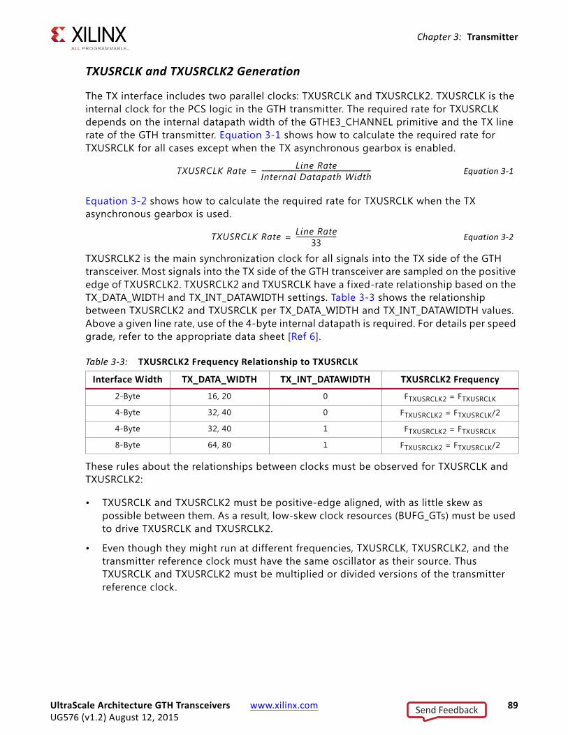
Chapter 3: Transmitter
TXUSRCLK and TXUSRCLK2 Generation
The TX interface includes two parallel clocks: TXUSRCLK and TXUSRCLK2. TXUSRCLK is the internal clock for the PCS logic in the GTH transmitter. The required rate for TXUSRCLK depends on the internal datapath width of the GTHE3_CHANNEL primitive and the TX line rate of the GTH transmitter. Equation 3-1 shows how to calculate the required rate for TXUSRCLK for all cases except when the TX asynchronous gearbox is enabled.
Equation 3-1
Equation 3-2 shows how to calculate the required rate for TXUSRCLK when the TX asynchronous gearbox is used.
Equation 3-2
TXUSRCLK2 is the main synchronization clock for all signals into the TX side of the GTH transceiver. Most signals into the TX side of the GTH transceiver are sampled on the positive edge of TXUSRCLK2. TXUSRCLK2 and TXUSRCLK have a fixed-rate relationship based on the TX_DATA_WIDTH and TX_INT_DATAWIDTH settings. Table 3-3 shows the relationship between TXUSRCLK2 and TXUSRCLK per TX_DATA_WIDTH and TX_INT_DATAWIDTH values. Above a given line rate, use of the 4-byte internal datapath is required. For details per speed grade, refer to the appropriate data sheet [Ref 6].
These rules about the relationships between clocks must be observed for TXUSRCLK and TXUSRCLK2:
• TXUSRCLK and TXUSRCLK2 must be positive-edge aligned, with as little skew as possible between them. As a result, low-skew clock resources (BUFG_GTs) must be used to drive TXUSRCLK and TXUSRCLK2.
• Even though they might run at different frequencies, TXUSRCLK, TXUSRCLK2, and the transmitter reference clock must have the same oscillator as their source. Thus TXUSRCLK and TXUSRCLK2 must be multiplied or divided versions of the transmitter reference clock.
Table 3-3: TXUSRCLK2 Frequency Relationship to TXUSRCLK
Interface Width TX_DATA_WIDTH TX_INT_DATAWIDTH TXUSRCLK2 Frequency
2-Byte 16, 20 0 FTXUSRCLK2 = FTXUSRCLK
4-Byte 32, 40 0 FTXUSRCLK2 = FTXUSRCLK/2
4-Byte 32, 40 1 FTXUSRCLK2 = FTXUSRCLK
8-Byte 64, 80 1 FTXUSRCLK2 = FTXUSRCLK/2
TXUSRCLK Rate Line RateInternal Datapath Width-----------------------------------------------------------=
TXUSRCLK Rate Line Rate33
----------------------=
UltraScale Architecture GTH Transceivers www.xilinx.com 89UG576 (v1.2) August 12, 2015
Send Feedback

Chapter 3: Transmitter
Ports and AttributesTable 3-4 defines the TX Interface ports.
Table 3-5 defines the TX interface attributes.
Table 3-4: TX Interface Ports
Port Dir Clock Domain Description
TXCTRL0[15:0]/TXCTRL1[15:0]
In TXUSRCLK2 When 8B/10B encoding is disabled, TXCTRL0/1 is used to extend the data bus for 20-, 40- and 80-bit TX interfaces. Bits [15:8] are unused.
TXDATA[127:0] In TXUSRCLK2 The bus for transmitting data. The width of this port depends on TX_DATA_WIDTH:
TX_DATA_WIDTH = 16, 20: TXDATA[15:0] = 16 bits wideTX_DATA_WIDTH = 32, 40: TXDATA[31:0] = 32 bits wideTX_DATA_WIDTH = 64, 80: TXDATA[63:0] = 64 bits wide
When a 20-bit, 40-bit, or 80-bit bus is required, the TXCTRL0 and TXCTRL1 ports from the 8B/10B encoder is concatenated with the TXDATA port. Bits [127:64] are unused. See Table 3-2, page 88.
TXDATAEXTENDRSVD In Async Reserved.
TXUSRCLK In Clock This port is used to provide a clock for the internal TX PCS datapath.
TXUSRCLK2 In Clock This port is used to synchronize the interconnect logic with the TX interface. This clock must be positive-edge aligned to TXUSRCLK.
Table 3-5: TX Interface Attributes
Attribute Type Description
TX_DATA_WIDTH Integer Sets the bit width of the TXDATA port. When 8B/10B encoding is enabled, TX_DATA_WIDTH must be set to 20, 40, or 80. Valid settings are 16, 20, 32, 40, 64, and 80. See Interface Width Configuration, page 87 for more information.
TX_INT_DATAWIDTH Integer Controls the width of the internal datapath. 0: 2-byte internal datapath1: 4-byte internal datapath. Set to 1 if a line rate is greater than 8.1875 Gb/s.
UltraScale Architecture GTH Transceivers www.xilinx.com 90UG576 (v1.2) August 12, 2015
Send Feedback

Chapter 3: Transmitter
Using TXOUTCLK to Drive the TX InterfaceDepending on the TXUSRCLK and TXUSRCLK2 frequencies, there are different ways UltraScale architecture clock resources can be used to drive the parallel clock for the TX interface. Figure 3-2 through Figure 3-5 show different ways clock resources can be used to drive the parallel clocks for the TX interface. In these examples, the TXOUTCLK is from the PMA and the TXOUTCLKSEL = 3'b010 to select the TXOUTCLKPMA path as indicated in Figure 3-28, page 136.
• Depending on the input reference clock frequency and the required line rate, a BUFG_GT with a properly configured divide setting and the appropriate TXOUTCLKSEL port setting is required. The UltraScale FPGAs Transceivers Wizard creates a sample design based on different design requirements for most cases.
• In use models where TX buffer is bypassed, there are additional restrictions on the clocking resources. Refer to TX Buffer Bypass, page 118 for more information.
TX_FABINT_USRCLK_FLOP 1-Bit Binary
Determines if port signals are registered again in the TXUSRCLK domain after being registered in the TXUSRCLK2 domain. This attribute only applies if the TX internal datapath width is the same as the TX interface width, otherwise this attribute is ignored. Use the recommended value from the Wizard.
0: Bypass TXUSRCLK flip-flops1: Enable TXUSRCLK flip-flops
Table 3-5: TX Interface Attributes (Cont’d)
Attribute Type Description
UltraScale Architecture GTH Transceivers www.xilinx.com 91UG576 (v1.2) August 12, 2015
Send Feedback

Chapter 3: Transmitter
TXOUTCLK Driving GTH Transceiver TX in 2-Byte or 4-Byte Mode
In Figure 3-2, TXOUTCLK is used to drive TXUSRCLK and TXUSRCLK2 for 2-byte mode (TX_DATA_WIDTH = 16 or 20 and TX_INT_DATAWIDTH = 0) or 4-byte mode (TX_DATA_WIDTH = 32 or 40 and TX_INT_DATAWIDTH = 1) in a single-lane configuration. In both cases, the frequency of TXUSRCLK2 is equal to TXUSRCLK.
Notes relevant to Figure 3-2:
1. For details about placement constraints and restrictions on clocking resources (BUFG_GT, BUFG_GT_SYNC, etc.), refer to the UltraScale Architecture Clocking Resources User Guide (UG572) [Ref 3].
2. FTXUSRCLK2 = FTXUSRCLK.
X-Ref Target - Figure 3-2
Figure 3-2: Single Lane—TXOUTCLK Drives TXUSRCLK and TXUSRCLK2 (2-Byte or 4-Byte Mode)
UG576_c3_02_062614
BUFG_GT 1
2
UltraScale Devices
GTH Transceiver
TXOUTCLK
TXUSRCLK2
2TXUSRCLK
TXDATA (TX_DATA_WIDTH = 16 / 20 / 32 / 40 bits)
Design inUltraScale
Architecture
UltraScale Architecture GTH Transceivers www.xilinx.com 92UG576 (v1.2) August 12, 2015
Send Feedback

Chapter 3: Transmitter
Similarly, Figure 3-3 shows the shows the same settings in multiple lanes configuration. In a multi-lane configuration, the middle-most GTH transceiver should be selected to be the source of TXOUTCLK. For example, in a multi-lane configuration of 12 GTH transceivers consisting of three contiguous Quads, one of the middle GTH transceivers in the middle Quad should be selected as the source of TXOUTCLK.
Notes relevant to Figure 3-3:
1. For details about placement constraints and restrictions on clocking resources (BUFG_GT, BUFG_GT_SYNC, etc.), refer to the UltraScale Architecture Clocking Resources User Guide (UG572) [Ref 3].
2. FTXUSRCLK2 = FTXUSRCLK.
X-Ref Target - Figure 3-3
Figure 3-3: Multiple Lanes—TXOUTCLK Drives TXUSRCLK2 (2-Byte or 4-Byte Mode)
UG576_c3_03_062614
BUFG_GT 1
2
UltraScaleDevices
GTHTransceiver
TXOUTCLK
TXUSRCLK2
2TXUSRCLK
TXDATA (TX_DATA_WIDTH = 16 / 20 / 32 / 40 bits)
Design inUltraScale
Architecture
2UltraScaleDevices
GTHTransceiver
TXUSRCLK2
2TXUSRCLK
TXDATA (TX_DATA_WIDTH = 16 / 20 / 32 / 40 bits)
UltraScale Architecture GTH Transceivers www.xilinx.com 93UG576 (v1.2) August 12, 2015
Send Feedback

Chapter 3: Transmitter
TXOUTCLK Driving GTH Transceiver TX in 4-Byte or 8-Byte Mode
In Figure 3-4, TXOUTCLK is used to drive TXUSRCLK2 for 4-byte mode (TX_DATA_WIDTH = 32 or 40 and TX_INT_DATAWIDTH = 0) or 8-byte mode (TX_DATA_WIDTH = 64 or 80 and TX_INT_DATAWIDTH = 1). In both cases, the frequency of TXUSRCLK2 is equal to half of the frequency of TXUSRCLK.
Notes relevant to Figure 3-4:
1. FTXUSRCLK2 = FTXUSRCLK/2
2. For details about placement constraints and restrictions on clocking resources (BUFG_GT, BUFG_GT_SYNC, etc.), refer to the UltraScale Architecture Clocking Resources User Guide (UG572) [Ref 3].
X-Ref Target - Figure 3-4
Figure 3-4: Single Lane—TXOUTCLK Drives TXUSRCLK2 (4-Byte or 8-Byte Mode)
UG576_c3_04_062614
UltraScale DevicesGTH Transceiver
TXOUTCLK
TXUSRCLK1
TXUSRCLK21
TXDATA (32 / 40 / 64 / 80 bits) Design inUltraScale
Architecture
BUFG_GT
BUFG_GT
÷2
÷1
UltraScale Architecture GTH Transceivers www.xilinx.com 94UG576 (v1.2) August 12, 2015
Send Feedback

Chapter 3: Transmitter
Similarly, Figure 3-5 shows the shows the same settings in multiple lanes configuration.
Notes relevant to Figure 3-5:
1. FTXUSRCLK2 = FTXUSRCLK/2
2. For details about placement constraints and restrictions on clocking resources (BUFG_GT, BUFG_GT_SYNC, etc.), refer to the UltraScale Architecture Clocking Resources User Guide (UG572) [Ref 3].
X-Ref Target - Figure 3-5
Figure 3-5: Multiple Lanes—TXOUTCLK Drives TXUSRCLK2 (4-Byte or 8-Byte Mode)
UG576_c3_05_062614
TXOUTCLK
TXUSRCLK21
TXUSRCLK1
TXUSRCLK21
TXUSRCLK1
TXDATA (TX_DATA_WIDTH = 32 / 40 / 64 / 80 bits)
Design inUltraScale
Architecture
TXDATA (TX_DATA_WIDTH = 32 / 40 / 64 / 80 bits)
BUFG_GT
BUFG_GT
UltraScale DevicesGTH Transceiver
UltraScale DevicesGTH Transceiver
÷2
÷1
UltraScale Architecture GTH Transceivers www.xilinx.com 95UG576 (v1.2) August 12, 2015
Send Feedback

Chapter 3: Transmitter
TX 8B/10B Encoder
Functional DescriptionMany protocols use 8B/10B encoding on outgoing data. 8B/10B is an industry standard encoding scheme that trades two bits overhead per byte for achieved DC-balance and bounded disparity to allow reasonable clock recovery. The GTH transceiver has a built-in 8B/10B TX path to encode TX data without consuming device resources. Enabling the 8B/10B encoder increases latency through the TX path. The 8B/10B encoder can be disabled or bypassed to minimize latency, if not needed.
8B/10B Bit and Byte Ordering
The order of the bits after the 8B/10B encoder is the opposite of the order shown in Appendix A, 8B/10B Valid Characters, because 8B/10B encoding requires bit a0 to be transmitted f irst, and the GTH transceiver always transmits the right-most bit f irst. To match with 8B/10B, the 8B/10B encoder in the GTH transceiver automatically reverses the bit order. Figure 3-6 shows data transmitted by the GTH transceiver when TX_DATA_WIDTH = 20, 40, and 80. The number of bits used by TXDATA and corresponding byte orders are determined by TX_DATA_WIDTH.
• Only use TXDATA[15:0] if TX_DATA_WIDTH = 20
• Only use TXDATA[31:0] if TX_DATA_WIDTH = 40
• Use full TXDATA[63:0] if TX_DATA_WIDTH = 80
When the 8B/10B encoder is bypassed and TX_DATA_WIDTH is set to a multiple of 10, 10-bit characters are passed to TX data interface with this format:
• The corresponding TXCTRL1 represents the 9th bit
• The corresponding TXCTRL0 represents the 8th bit
• The corresponding TXDATA byte represents [7:0] bits
K Characters
The 8B/10B table includes special characters (K characters) that are often used for control functions. TXCTRL2 ports are used to indicate if data on TXDATA are K characters or regular data. The 8B/10B encoder checks received TXDATA byte to match any K character if corresponding TXCTRL2 bit is driven High.
UltraScale Architecture GTH Transceivers www.xilinx.com 96UG576 (v1.2) August 12, 2015
Send Feedback

Chapter 3: Transmitter
Running Disparity
8B/10B coding is DC-balanced, meaning that the long-term ratio of 1s and 0s transmitted should be exactly 50%. To achieve this, the encoder always calculates the difference between the number of 1s transmitted and the number of 0s transmitted, and at the end of
X-Ref Target - Figure 3-6
Figure 3-6: 8B/10B Bit and Byte Ordering
15 14 13 12 11 10 9 8 7 6 5 4 3 2 1 0
31 30 29 28 27 26 25 24 23 22 21 20 19 18 17 16 15 14 13 12 11 10 9 8 7 6 5 4 3 2 1 0
31 30 29 28 27 26 25 24 23 22 21 20 19 18 17 16 15 14 13 12 11 10 9 8 7 6 5 4 3 2 1 0
H1 G1 F1 E1 D1 C1 B1 A1 H0 G0 F0 E0 D0 C0 B0 A0
H3 G3 F3 E3 D3 C3 B3 A3 H2 G2 F2 E2 D2 C2 B2 A2 H1 G1 F1 E1 D1 C1 B1 A1 H0 G0 F0 E0 D0 C0 B0 A0
H3 G3 F3 E3 D3 C3 B3 A3 H2 G2 F2 E2 D2 C2 B2 A2 H1 G1 F1 E1 D1 C1 B1 A1 H0 G0 F0 E0 D0 C0 B0 A0
63 62 61 60 59 58 57 56 55 54 53 52 51 50 49 48 47 46 45 44 43 42 41 40 39 38 37 36 35 34 33 32
H7 G7 F7 E7 D7 C7 B7 A7 H6 G6 F6 E6 D6 C6 B6 A6 H5 G5 F5 E5 D5 C5 B5 A5 H4 G4 F4 E4 D4 C4 B4 A4
j1 h1 g1 f1 i1 e1 d1 c1 b1 a1 j0 h0 g0 f0 i0 e0 d0 c0 b0 a0
j3 h3 g3 f3 i3 e3 d3 c3 b3 a3 j2 h2 g2 f2 i2 e2 d2 c2 b2 a2 j1 h1 g1 f1 i1 e1 d1 c1 b1 a1 j0 h0 g0 f0 i0 e0 d0 c0 b0 a0
TX_DATA_WIDTH = 20
TX_DATA_WIDTH = 40
TX_DATA_WIDTH = 80
TXDATA
TXDATA
8B/10B
8B/10B
8B/10B
TXDATA
TXDATA
MSB
MSB LSB
MSB LSB
LSB
TransmittedLast
TransmittedFirst
TransmittedLast
j3 h3 g3 f3 i3 e3 d3 c3 b3 a3 j2 h2 g2 f2 i2 e2 d2 c2 b2 a2 j1 h1 g1 f1 i1 e1 d1 c1 b1 a1 j0 h0 g0 f0 i0 e0 d0 c0 b0 a0
j7 h7 g7 f7 i7 e7 d7 c7 b7 a7 j6 h6 g6 f6 i6 e6 d6 c6 b6 a6 j5 h5 g5 f5 i5 e5 d5 c5 b5 a5 j4 h4 g4 f4 i4 e4 d4 c4 b4 a4
TransmittedLast
TransmittedFirst
TransmittedFirst
UG576_c3_06_041014
UltraScale Architecture GTH Transceivers www.xilinx.com 97UG576 (v1.2) August 12, 2015
Send Feedback

Chapter 3: Transmitter
each character transmitted, makes the difference either +1 or –1. This difference is known as the running disparity.
To accommodate protocols that use disparity to send control information, the running disparity not only can be generated by the 8B/10B encoder but is also controllable through TXCTRL1 and TXCTRL0 as shown in Table 3-6. For example, an Idle character sent with reversed disparity might be used to trigger clock correction.
Ports and AttributesTable 3-7 lists the ports required by the TX 8B/10B encoder.
Note: There are no TX encoder attributes.
Table 3-6: TXCTRL1 and TXCTRL0 versus Outgoing Disparity
TXCTRL1 TXCTRL0 Outgoing Disparity
0 0 Calculated by the 8B/10B encoder.
0 1 Inverts running disparity when encoding TXDATA.
1 0 Forces running disparity negative when encoding TXDATA.
1 1 Forces running disparity positive when encoding TXDATA.
Table 3-7: TX 8B/10B Encoder Ports
Port Dir Clock Domain Description
TX8B10BBYPASS[7:0] In TXUSRCLK2 This active-High port allows byte-interleaved data to bypass 8B/10B on a per-byte basis. TX8B10BEN must be High to use this per-byte bypass mode.
TX8B10BBYPASS [7] corresponds to TXDATA[63:56]TX8B10BBYPASS [6] corresponds to TXDATA[55:48]TX8B10BBYPASS [5] corresponds to TXDATA[47:40]TX8B10BBYPASS [4] corresponds to TXDATA[39:32]TX8B10BBYPASS [3] corresponds to TXDATA[31:24]TX8B10BBYPASS [2] corresponds to TXDATA[23:16]TX8B10BBYPASS [1] corresponds to TXDATA[15:8]TX8B10BBYPASS [0] corresponds to TXDATA[7:0]
TXBYPASS8B10B[x] = 1, encoder for byte x is bypassed.TXBYPASS8B10B[x] = 0, encoder for byte x is used.
TX8B10BEN In TXUSRCLK2 TX8B10BEN is set High to enable the 8B/10B encoder. TX_DATA_WIDTH must be set to 20, 40, or 80 when the 8B/10B encoder is enabled.
0: 8B/10B encoder bypassed. This option reduces latency.1: 8B/10B encoder enabled.
UltraScale Architecture GTH Transceivers www.xilinx.com 98UG576 (v1.2) August 12, 2015
Send Feedback

Chapter 3: Transmitter
Enabling and Disabling 8B/10B Encoding
To enable the 8B/10B encoder, TX8B10BEN must be driven High. The TX 8B/10B encoder allows byte interleaved data to bypass the encoder on a per-byte basis. When TX8B10BEN is driven Low, all encoders are turned off and no data from TXDATA can be encoded. When TX8B10BEN is High, driving a bit from TX8B10BBYPASS High can make the corresponding byte channel from TXDATA bypass 8B/10B encoding. When the encoder is turned off, the operation of the TXDATA port is as described in the TX interface.
TXCTRL1[15:0] In TXUSRCLK2 Set High to work with TXCTRL0 to force running disparity negative or positive when encoding TXDATA. Set Low to use normal running disparity. Refer to Table 3-6 for a detailed definition.
TXCTRL1[7] corresponds to TXDATA[63:56]TXCTRL1[6] corresponds to TXDATA[55:48]TXCTRL1[5] corresponds to TXDATA[47:40]TXCTRL1[4] corresponds to TXDATA[39:32]TXCTRL1[3] corresponds to TXDATA[31:24]TXCTRL1[2] corresponds to TXDATA[23:16]TXCTRL1[1] corresponds to TXDATA[15:8]TXCTRL1[0] corresponds to TXDATA[7:0]
TXCTRL0[15:0] In TXUSRCLK2 Work with TXCTRL1 to provide running disparity control. Refer to Table 3-6 for detailed information.
TXCTRL0[7] corresponds to TXDATA[63:56]TXCTRL0[6] corresponds to TXDATA[55:48]TXCTRL0[5] corresponds to TXDATA[47:40]TXCTRL0[4] corresponds to TXDATA[39:32]TXCTRL0[3] corresponds to TXDATA[31:24]TXCTRL0[2] corresponds to TXDATA[23:16]TXCTRL0[1] corresponds to TXDATA[15:8]TXCTRL0[0] corresponds to TXDATA[7:0]
TXCTRL2[7:0] In TXUSRCLK2 When High, indicates the corresponding data byte on TXDATA is a valid K character.
TXCTRL2[7] corresponds to TXDATA[63:56]TXCTRL2[6] corresponds to TXDATA[55:48]TXCTRL2[5] corresponds to TXDATA[47:40]TXCTRL2[4] corresponds to TXDATA[39:32]TXCTRL2[3] corresponds to TXDATA[31:24]TXCTRL2[2] corresponds to TXDATA[23:16]TXCTRL2[1] corresponds to TXDATA[15:8]TXCTRL2[0] corresponds to TXDATA[7:0]A TXCTRL2 bit should be driven Low when the corresponding data byte from TXDATA is set to bypass the 8B/10B encoder.
Table 3-7: TX 8B/10B Encoder Ports (Cont’d)
Port Dir Clock Domain Description
UltraScale Architecture GTH Transceivers www.xilinx.com 99UG576 (v1.2) August 12, 2015
Send Feedback

Chapter 3: Transmitter
TX Synchronous Gearbox
Functional DescriptionSome high-speed data rate protocols use 64B/66B encoding to reduce the overhead of 8B/10B encoding while retaining the benefits of an encoding scheme. The TX synchronous gearbox provides support for 64B/66B and 64B/67B header and payload combining. The Interlaken interface protocol specif ication uses the 64B/67B encoding scheme. Refer to the Interlaken specif ication for further information.
The TX synchronous gearbox supports 2-byte, 4-byte and 8-byte interfaces. Scrambling of the data is done in the interconnect logic. A CAUI interface mode is also supported in addition to the normal synchronous gearbox mode.
Ports and AttributesTable 3-8 defines the TX synchronous gearbox ports.
Table 3-8: TX Synchronous Gearbox Ports
Port Name Dir Clock Domain Description
TXHEADER[5:0] In TXUSRCLK2 Input port to provide header.TXHEADER[1:0] is used for the 64B/66B gearbox and TXHEADER[2:0] is used for the 64B/67B gearbox.In CAUI interface mode, TXHEADER[2:0] is used for datastream A and TXHEADER[5:3] is used for datastream B.
TXSEQUENCE[6:0] In TXUSRCLK2 This input port is used for the interconnect logic sequence counter when the TX gearbox is used. Bits [5:0] are used for the 64B/66 B gearbox, and bits [6:0] are used for the 64B/67B gearbox. This port is shared by both PCS lanes (PCSLs) in CAUI interface mode.
UltraScale Architecture GTH Transceivers www.xilinx.com 100UG576 (v1.2) August 12, 2015
Send Feedback

Chapter 3: Transmitter
Table 3-9 defines the TX synchronous gearbox attributes.
Enabling the TX Synchronous GearboxTo enable the TX synchronous gearbox, TXGEARBOX_EN must be set to TRUE.
Bit 4 of the GEARBOX_MODE attribute must be set to 0. Bit 3 and 1 are unused and must be set to 0. Bit 2 determines if the normal interface or CAUI interface is used. Bit 0 determines if the 64B/67B gearbox or the 64B/66B gearbox is used. The GTH transceiver’s TX gearbox and RX gearbox use the same mode.
TX Synchronous Gearbox Bit and Byte OrderingFigure 3-7 shows an example of the f irst four cycles of data entering and exiting the TX gearbox for 64B/66B encoding when using a 4-byte logic interface (TX_DATA_WIDTH = 32 (4-byte), TX_INT_DATAWIDTH = 1 (4-byte)) in normal mode (GEARBOX_MODE[2] = 1'b0). The input consists of a 2-bit header and 32 bits of data. On the f irst cycle, the header and 30 bits of data exit the TX gearbox. On the second cycle, the remaining two data bits from the previous cycle’s TXDATA input along with 30 data bits from the current TXDATA input exit the TX gearbox. On the third cycle, the output of the TX gearbox contains two remaining data bits from the first 66-bit block, the header of the second 66-bit block, and 28 data bits from the second 66-bit block.
Table 3-9: TX Synchronous Gearbox Attributes
Attribute Type Description
GEARBOX_MODE 5-bit Binary This attribute indicates the TX and RX gearbox modes:• Bit 4:
0: Select synchronous gearbox.1: Select asynchronous gearbox.
• Bit 3:Unused. Set to 0.
• Bit 2:0: Normal mode.1: CAUI interface mode.
• Bit 1:Unused. Set to 0.
• Bit 0:0: 64B/67B gearbox mode for Interlaken (Only valid for synchronous gearbox).1: 64B/66B gearbox.
TXGEARBOX_EN String When TRUE, this attribute enables either the TX synchronous or asynchronous gearbox. Which TX gearbox is enabled depends on the GEARBOX_MODE attribute.
UltraScale Architecture GTH Transceivers www.xilinx.com 101UG576 (v1.2) August 12, 2015
Send Feedback
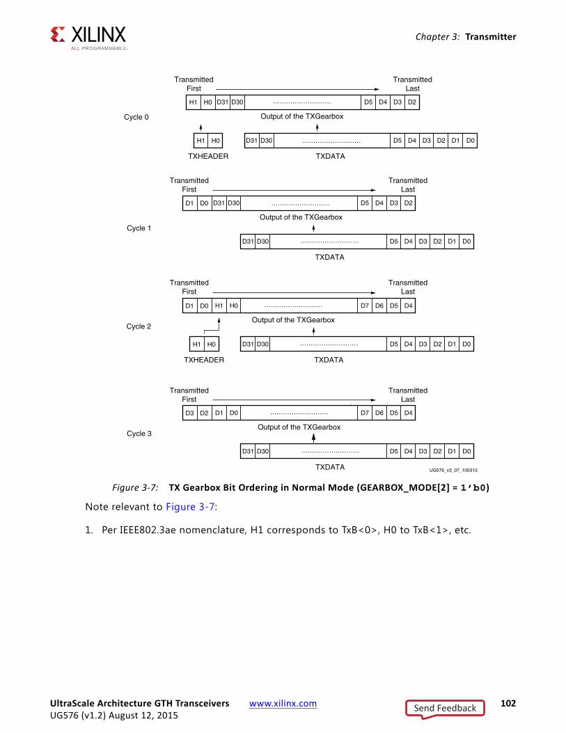
Chapter 3: Transmitter
Note relevant to Figure 3-7:
1. Per IEEE802.3ae nomenclature, H1 corresponds to TxB<0>, H0 to TxB<1>, etc.
X-Ref Target - Figure 3-7
Figure 3-7: TX Gearbox Bit Ordering in Normal Mode (GEARBOX_MODE[2] = 1’b0)
UG576_c3_07_100313
H1 H0 D31 D30 D5 D4 D3 D2………………………
TransmittedFirst
TransmittedLast
TransmittedFirst
TransmittedLast
TransmittedFirst
TransmittedLast
TransmittedFirst
TransmittedLast
H1 H0 D31 D30 D5 D4 D3 D2……………………… D1 D0
TXDATATXHEADER
Output of the TXGearboxCycle 0
D1 D0 D31 D30 D5 D4 D3 D2………………………
D31 D30 D5 D4 D3 D2……………………… D1 D0
TXDATA
Output of the TXGearbox
Cycle 1
D1 D0 H1 H0 D7 D6 D5 D4………………………
H1 H0 D31 D30 D5 D4 D3 D2……………………… D1 D0
TXDATATXHEADER
Output of the TXGearboxCycle 2
D3 D2 D1 D0 D7 D6 D5 D4………………………
D31 D30 D5 D4 D3 D2……………………… D1 D0
TXDATA
Output of the TXGearboxCycle 3
UltraScale Architecture GTH Transceivers www.xilinx.com 102UG576 (v1.2) August 12, 2015
Send Feedback

Chapter 3: Transmitter
Using the TX Synchronous GearboxThe TX synchronous gearbox requires the use of an external sequence counter that must be implemented in interconnect logic. The TX gearbox supports 2-byte, 4-byte, and 8-byte interfaces to the interconnect logic.
As shown in Figure 3-8, the external sequence counter operating mode uses the TXSEQUENCE [6:0], TXDATA[63:0], and TXHEADER[2:0] inputs when in normal mode (GEARBOX_MODE[2] = 1'b0). TXHEADER[5:3] is also used when the CAUI interface is used (GEARBOX_MODE[2] = 1'b1). A binary counter must exist in the interconnect logic to drive the TXSEQUENCE port. For 64B/66B encoding, the counter increments from 0 to 32 and repeats from 0. For 64B/67B encoding, the counter increments from 0 to 66 and repeats from 0. When using 64B/66B encoding, tie TXSQUENCE [6] to logic 0 and tie the unused TXHEADER [2] to logic 0. TXHEADER[5] must be tied to logic 0 when the CAUI interface is used and 64B/66B encoding is selected (GEARBOX_MODE[2] = 1'b1, GEARBOX_MODE[0] = 1'b0). The sequence counter increment ranges ({0 to 32}, {0 to 66}) are identical for 2-byte, 4-byte and 8-byte interfaces. However, the counter must increment once every two TXUSRCLK2 cycles when using a mode where TX_DATA_WIDTH is the same as TX_INT_DATAWIDTH (e.g., a 4-byte interconnect logic interface (TX_DATA_WIDTH = 32) and a 4-byte internal data width (TX_INT_DATAWIDTH= 1)).
X-Ref Target - Figure 3-8
Figure 3-8: TX Synchronous Gearbox in External Sequence Counter Operating Mode in Normal Mode (GEARBOX_MODE[2] = 1'b0)
TX Gearbox(in GTH Transceiver)
Data Source
Sequence Counter(0–32 or 0–66)
Design in Interconnect Logic
Pause
TXHEADER[2:0]
TXDATA[15:0] or TXDATA[31:0] orTXDATA[63:0]
TXSEQUENCE[6:0]
UG576_c3_08_062614
UltraScale Architecture GTH Transceivers www.xilinx.com 103UG576 (v1.2) August 12, 2015
Send Feedback

Chapter 3: Transmitter
Due to the nature of the 64B/66B and 64B/67B encoding schemes and the TX synchronous gearbox, user data is held (paused) during various sequence counter values. Data is paused for two TXUSRCLK2 cycles in modes with the same TX_DATA_WIDTH and TX_INT_DATAWIDTH, and for one TXUSRCLK2 cycle in modes where TX_DATA_WIDTH is twice the TX_INT_DATAWIDTH. Valid data transfer is resumed on the next TXUSRCLK2 cycle. The data pause only applies to TXDATA and not to TXHEADER. The TXSEQUENCE pause locations for various modes are described in Table 3-10 and Table 3-11.
Table 3-10: 64B/66B Encoding Frequency of TXSEQUENCE and Pause Locations in Normal Mode (GEARBOX_MODE[2] = 1'b0)
TX_DATA_WIDTH TX_INT_DATAWIDTH Frequency of TXSEQUENCE TXSEQUENCE PAUSE
64(8-byte)
1(4-byte)
1 XTXUSRCLK2
32
32(4-byte)
1(4-byte)
2 XTXUSRCLK2
32
32(4-byte)
0(2-byte)
1 XTXUSRCLK2
31
16(2-byte)
0(2-byte)
2 XTXUSRCLK2
31
Table 3-11: 64B/67B Encoding Frequency of TXSEQUENCE and Pause Locations in Normal Mode (GEARBOX_MODE[2] = 1'b0)
TX_DATA_WIDTH TX_INT_DATAWIDTH Frequency of TXSEQUENCE TXSEQUENCE PAUSE
64(8-byte)
1(4-byte)
1 XTXUSRCLK2
22, 44, 66
32(4-byte)
1(4-byte)
2 XTXUSRCLK2
22, 44, 66
32(4-byte)
0(2-byte)
1 XTXUSRCLK2
21, 44, 65
16(2-byte)
0(2-byte)
2 XTXUSRCLK2
21, 44, 65
UltraScale Architecture GTH Transceivers www.xilinx.com 104UG576 (v1.2) August 12, 2015
Send Feedback

Chapter 3: Transmitter
Figure 3-9 shows how a pause occurs at counter value 32 when using an 8-byte interconnect logic interface and a 4-byte internal datapath in external sequence counter mode with 64B/66B encoding in normal mode (GEARBOX_MODE[2] = 1'b0).
Figure 3-10 shows how a pause occurs at counter value 44 when using a 2-byte interconnect logic interface with a 2-byte internal datapath in external sequence counter mode with 64B/67B encoding in normal mode (GEARBOX_MODE[2] = 1'b0).
The sequence of transmitting 64/67 data for the external sequence counter mode using a 2-byte internal datapath (TX_INT_DATAWIDTH = 0) in normal mode (GEARBOX_MODE[2] = 1'b0) is:
1. Apply GTTXRESET and wait until the reset cycle is completed.
2. During reset, apply 7'h00 to TXSEQUENCE, header information to TXHEADER, and initial data to TXDATA. This state can be held indefinitely until data transmission is ready.
X-Ref Target - Figure 3-9
Figure 3-9: Pause at Sequence Counter Value 32 in Normal Mode (GEARBOX_MODE[2] = 1'b0)
UG576_c3_09_100313
1
29 30 31 32 0 1 2 3 4 5 6 7 8
Da Db Dc Dd De Df Dg Dh Di Dj Dk Dl
1
Pause for 1 TXUSRCLK2 cycle.Data is ignored.
2
TXUSRCLK2
TXHEADER[1:0]
TXSEQUENCE[5:0]
TXDATA[63:0]
X-Ref Target - Figure 3-10
Figure 3-10: Pause at Sequence Counter Value 44 in Normal Mode (GEARBOX_MODE[2] = 1'b0)
UG576_c3_10_100313
1
42 43 44 45 46
Da Db Dc Dd De Df Dg
2
TXUSRCLK2
TXHEADER[2:0]
TXSEQUENCE[6:0]
TXDATA[15:0]
Pause for 2 TXUSRCLK2 cycle.Data is ignored.
UltraScale Architecture GTH Transceivers www.xilinx.com 105UG576 (v1.2) August 12, 2015
Send Feedback

Chapter 3: Transmitter
3. On count 0, apply data to TXDATA and header information to TXHEADER. For a 2-byte interface (TX_DATA_WIDTH = 16), drive the second 2 bytes to TXDATA while still on count 0.
4. The sequence counter increments to 1 while data is driven on TXDATA.
5. After applying 4 bytes of data, the counter increments to 2. Apply data on TXDATA and header information on TXHEADER.
6. On count 21, stop data pipeline.
7. On count 22, drive data on TXDATA.
8. On count 44, stop data pipeline.
9. On count 45, drive data on TXDATA.
10. On count 65, stop data pipeline.
11. On count 66, drive data on TXDATA.
The sequence of transmitting 64/67 data for the external sequence counter mode using the 4-byte internal datapath (TX_INT_DATAWIDTH = 1) in normal mode (GEARBOX_MODE[2] = 1'b0) is as follows:
1. Apply GTTXRESET and wait until the reset cycle is completed.
2. During reset, apply 7'h00 to TXSEQUENCE, header information to TXHEADER, and initial data to TXDATA. This state can be held indefinitely until data transmission is ready.
3. On count 0, apply data to TXDATA and header information to TXHEADER. For a 4-byte interface (TX_DATA_WIDTH = 32), drive the second 4 bytes to TXDATA while still on count 0.
4. Sequence counter increments to 1 while data is driven on TXDATA.
5. After applying 8 bytes of data, the counter increments to 2. Drive data on TXDATA and header information on TXHEADER.
6. On count 22, stop data pipeline.
7. On count 23, drive data on TXDATA.
8. On count 44, stop data pipeline.
9. On count 45, drive data on TXDATA.
10. On count 66, stop data pipeline.
The sequence of transmitting 64/66 data for the external sequence counter mode using the 2-byte internal datapath (TX_INT_DATAWIDTH = 0) in normal mode (GEARBOX_MODE[2] = 1'b0) is as follows:
1. Apply GTTXRESET and wait until the reset cycle is completed.
UltraScale Architecture GTH Transceivers www.xilinx.com 106UG576 (v1.2) August 12, 2015
Send Feedback

Chapter 3: Transmitter
2. During reset, apply 6'h00 to TXSEQUENCE, the appropriate header data to TXHEADER, and initial data to TXDATA. This state can be held indefinitely until data transmission is ready.
3. On count 0, apply data to TXDATA and header information to TXHEADER. For a 2-byte interface (TX_DATA_WIDTH = 16), drive the second 2 bytes to TXDATA while still on count 0.
4. The sequence counter increments to 1 while data is driven on TXDATA.
5. After applying 4 bytes of data, the counter increments to 2. Drive data on TXDATA and header information on TXHEADER.
6. On count 31, stop data pipeline.
7. On count 32, drive data on TXDATA.
The sequence of transmitting 64/66 data for the external sequence counter mode using a 4-byte internal datapath (TX_INT_DATAWIDTH = 1) in normal mode (GEARBOX_MODE[2] = 1'b0) is as follows:
1. Apply GTTXRESET and waits until the reset cycle is completed.
2. During reset, apply 6'h00 to TXSEQUENCE, the appropriate header data to TXHEADER, and initial data to TXDATA. This state can be held indefinitely until data transmission is ready.
3. On count 0, drive data to TXDATA and header information to TXHEADER. For a 4-byte interface (TX_DATA_WIDTH = 32), drive the second 4 bytes to TXDATA while still on count 0.
4. The sequence counter increments to 1 while data is driven on TXDATA.
5. After applying 8 bytes of data, the counter increments to 2. Drive data on TXDATA and header information on TXHEADER.
6. On count 32, stop data pipeline.
UltraScale Architecture GTH Transceivers www.xilinx.com 107UG576 (v1.2) August 12, 2015
Send Feedback
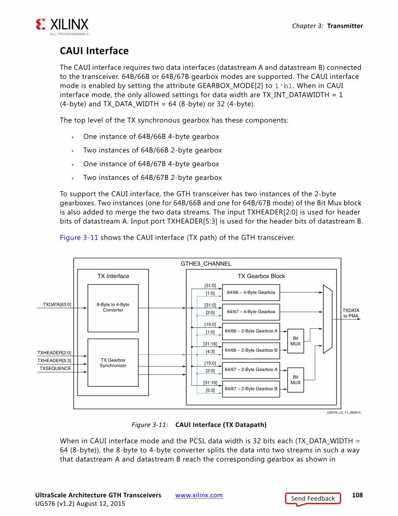
Chapter 3: Transmitter
CAUI InterfaceThe CAUI interface requires two data interfaces (datastream A and datastream B) connected to the transceiver. 64B/66B or 64B/67B gearbox modes are supported. The CAUI interface mode is enabled by setting the attribute GEARBOX_MODE[2] to 1'b1. When in CAUI interface mode, the only allowed settings for data width are TX_INT_DATAWIDTH = 1 (4-byte) and TX_DATA_WIDTH = 64 (8-byte) or 32 (4-byte).
The top level of the TX synchronous gearbox has these components:
° One instance of 64B/66B 4-byte gearbox
° Two instances of 64B/66B 2-byte gearbox
° One instance of 64B/67B 4-byte gearbox
° Two instances of 64B/67B 2-byte gearbox
To support the CAUI interface, the GTH transceiver has two instances of the 2-byte gearboxes. Two instances (one for 64B/66B and one for 64B/67B mode) of the Bit Mux block is also added to merge the two data streams. The input TXHEADER[2:0] is used for header bits of datastream A. Input port TXHEADER[5:3] is used for the header bits of datastream B.
Figure 3-11 shows the CAUI interface (TX path) of the GTH transceiver.
When in CAUI interface mode and the PCSL data width is 32 bits each (TX_DATA_WIDTH = 64 (8-byte)), the 8-byte to 4-byte converter splits the data into two streams in such a way that datastream A and datastream B reach the corresponding gearbox as shown in
X-Ref Target - Figure 3-11
Figure 3-11: CAUI Interface (TX Datapath)
TX Gearbox BlockTX Interface
64/66 – 4-Byte Gearbox
BitMUX
BitMUX
TXDATAto PMA
UG576_c3_11_062614
8-Byte to 4-ByteConverter
TXDATA[63:0]
TXHEADER[2:0]
TXHEADER[5:3]
TXSEQUENCE
TX GearboxSynchronizer
[31:0]
[1:0]
[31:0]
[2:0]
[15:0]
[1:0]
[15:0]
[2:0]
[31:16]
[4:3]
[31:16]
[5:3]
64/67 – 4-Byte Gearbox
64/66 – 2-Byte Gearbox A
64/66 – 2-Byte Gearbox B
64/67 – 2-Byte Gearbox A
64/67 – 2-Byte Gearbox B
GTHE3_CHANNEL
UltraScale Architecture GTH Transceivers www.xilinx.com 108UG576 (v1.2) August 12, 2015
Send Feedback

Chapter 3: Transmitter
Figure 3-12 and Figure 3-13.
The Bit Mux block interleaves two bitstreams (two 16-bit inputs) to form one merged bitstream that is twice the width. The Bit Mux function is as described in clause 83.5.2 of IEEE Std 802.3ba-2010.
Although TX_INT_DATAWIDTH = 1 (4-byte) is used in CAUI interface mode, two 2-byte gearboxes are used to realize the functionality, as shown in Figure 3-11. The functionality of these 2-byte gearboxes is the same as described in Using the TX Synchronous Gearbox, page 103, for the case when TX_INT_DATAWIDTH = 0 (2-byte). TXSEQUENCE pause locations for various modes are described in Table 3-12 and Table 3-13.
X-Ref Target - Figure 3-12
Figure 3-12: Input to the 8-Byte to 4-Byte Converter (TX_DATA_WIDTH = 64 (8-Byte), TX_INT_DATAWIDTH =1 (4-Byte), GEARBOX_MODE[2] = 1'b1)
X-Ref Target - Figure 3-13
Figure 3-13: Output of the 8-Byte to 4-Byte Converter (TX_DATA_WIDTH = 64 (8-Byte), TX_INT_DATAWIDTH = 1 (4-Byte), GEARBOX_MODE[2] = 1'b1)
TXUSRCLK2
TXDATA[63:56]
TXDATA[55:48]
TXDATA[47:40]
TXDATA[39:32]
TXDATA[31:24]
TXDATA[23:16]
TXDATA[15:8]
TXDATA[7:0]
D0 D8 D16
D1 D9 D17
D2 D10 D18
D3 D11 D19
D4 D12 D20
D5 D13 D21
D6 D14 D22
D7 D15 D23UG576_c3_12_100313
TXUSRCLK
TXDATA[31:24]
TXDATA[23:16]
TXDATA[15:8]
TXDATA[7:0]
D0 D2 D8
D1 D3 D9
D4 D6 D12
D5 D7 D13
D10 D16 D18
D11 D17 D19
D14 D20 D22
D15 D21 D23
UG576_c3_13_100313
UltraScale Architecture GTH Transceivers www.xilinx.com 109UG576 (v1.2) August 12, 2015
Send Feedback
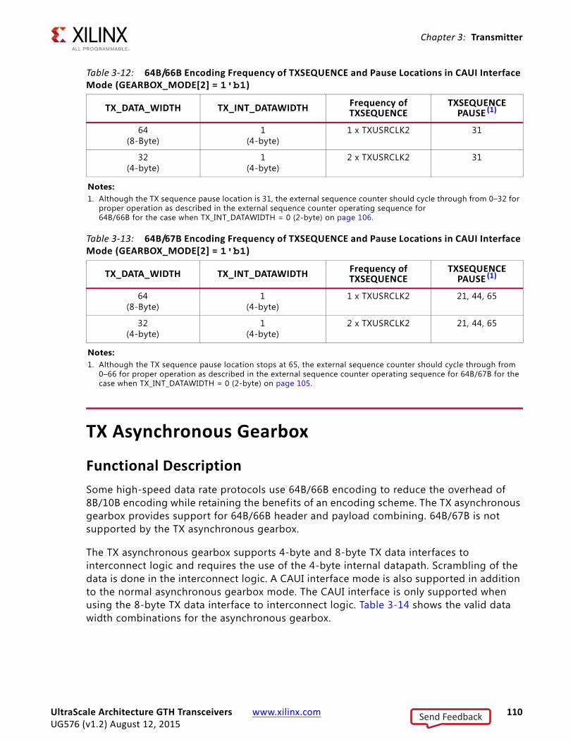
Chapter 3: Transmitter
TX Asynchronous Gearbox
Functional DescriptionSome high-speed data rate protocols use 64B/66B encoding to reduce the overhead of 8B/10B encoding while retaining the benefits of an encoding scheme. The TX asynchronous gearbox provides support for 64B/66B header and payload combining. 64B/67B is not supported by the TX asynchronous gearbox.
The TX asynchronous gearbox supports 4-byte and 8-byte TX data interfaces to interconnect logic and requires the use of the 4-byte internal datapath. Scrambling of the data is done in the interconnect logic. A CAUI interface mode is also supported in addition to the normal asynchronous gearbox mode. The CAUI interface is only supported when using the 8-byte TX data interface to interconnect logic. Table 3-14 shows the valid data width combinations for the asynchronous gearbox.
Table 3-12: 64B/66B Encoding Frequency of TXSEQUENCE and Pause Locations in CAUI Interface Mode (GEARBOX_MODE[2] = 1'b1)
TX_DATA_WIDTH TX_INT_DATAWIDTH Frequency of TXSEQUENCE
TXSEQUENCE PAUSE (1)
64(8-Byte)
1(4-byte)
1 x TXUSRCLK2 31
32(4-byte)
1(4-byte)
2 x TXUSRCLK2 31
Notes: 1. Although the TX sequence pause location is 31, the external sequence counter should cycle through from 0–32 for
proper operation as described in the external sequence counter operating sequence for 64B/66B for the case when TX_INT_DATAWIDTH = 0 (2-byte) on page 106.
Table 3-13: 64B/67B Encoding Frequency of TXSEQUENCE and Pause Locations in CAUI Interface Mode (GEARBOX_MODE[2] = 1'b1)
TX_DATA_WIDTH TX_INT_DATAWIDTH Frequency of TXSEQUENCE
TXSEQUENCE PAUSE (1)
64(8-Byte)
1(4-byte)
1 x TXUSRCLK2 21, 44, 65
32(4-byte)
1(4-byte)
2 x TXUSRCLK2 21, 44, 65
Notes: 1. Although the TX sequence pause location stops at 65, the external sequence counter should cycle through from
0–66 for proper operation as described in the external sequence counter operating sequence for 64B/67B for the case when TX_INT_DATAWIDTH = 0 (2-byte) on page 105.
UltraScale Architecture GTH Transceivers www.xilinx.com 110UG576 (v1.2) August 12, 2015
Send Feedback
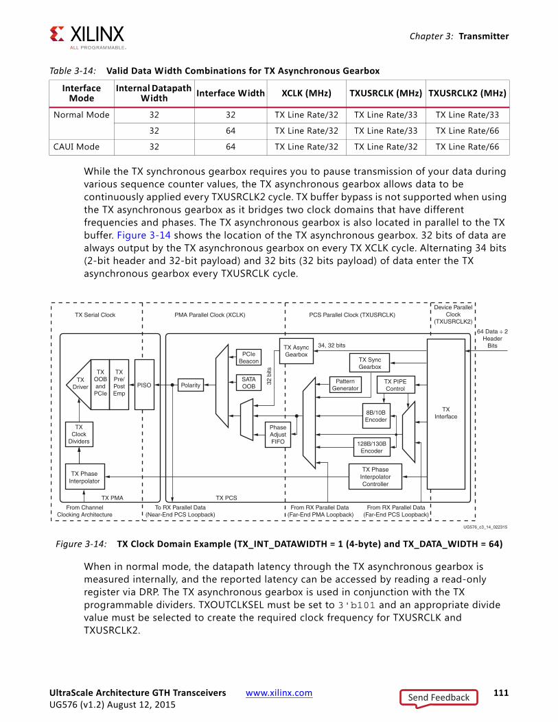
Chapter 3: Transmitter
While the TX synchronous gearbox requires you to pause transmission of your data during various sequence counter values, the TX asynchronous gearbox allows data to be continuously applied every TXUSRCLK2 cycle. TX buffer bypass is not supported when using the TX asynchronous gearbox as it bridges two clock domains that have different frequencies and phases. The TX asynchronous gearbox is also located in parallel to the TX buffer. Figure 3-14 shows the location of the TX asynchronous gearbox. 32 bits of data are always output by the TX asynchronous gearbox on every TX XCLK cycle. Alternating 34 bits (2-bit header and 32-bit payload) and 32 bits (32 bits payload) of data enter the TX asynchronous gearbox every TXUSRCLK cycle.
When in normal mode, the datapath latency through the TX asynchronous gearbox is measured internally, and the reported latency can be accessed by reading a read-only register via DRP. The TX asynchronous gearbox is used in conjunction with the TX programmable dividers. TXOUTCLKSEL must be set to 3'b101 and an appropriate divide value must be selected to create the required clock frequency for TXUSRCLK and TXUSRCLK2.
Table 3-14: Valid Data Width Combinations for TX Asynchronous Gearbox
Interface Mode
Internal Datapath Width Interface Width XCLK (MHz) TXUSRCLK (MHz) TXUSRCLK2 (MHz)
Normal Mode 32 32 TX Line Rate/32 TX Line Rate/33 TX Line Rate/33
32 64 TX Line Rate/32 TX Line Rate/33 TX Line Rate/66
CAUI Mode 32 64 TX Line Rate/32 TX Line Rate/32 TX Line Rate/66
X-Ref Target - Figure 3-14
Figure 3-14: TX Clock Domain Example (TX_INT_DATAWIDTH = 1 (4-byte) and TX_DATA_WIDTH = 64)
From ChannelClocking Architecture
To RX Parallel Data(Near-End PCS Loopback)
From RX Parallel Data (Far-End PMA Loopback)
From RX Parallel Data(Far-End PCS Loopback)
TXOOBandPCIe
TXDriver
TXClock
Dividers
TXPre/PostEmp
PISO
TX PMA TX PCS
Polarity
TX SyncGearbox
TX PIPEControl
SATAOOB
PhaseAdjustFIFO
TX AsyncGearbox
8B/10BEncoder
128B/130BEncoder
TXInterface
PCIeBeacon
PatternGenerator
UG576_c3_14_022315
TX PhaseInterpolator
TX PhaseInterpolatorController
TX Serial Clock PMA Parallel Clock (XCLK) PCS Parallel Clock (TXUSRCLK)Device Parallel
Clock(TXUSRCLK2)
64 Data ÷ 2Header
Bits
34, 32 bits
32 b
its
UltraScale Architecture GTH Transceivers www.xilinx.com 111UG576 (v1.2) August 12, 2015
Send Feedback

Chapter 3: Transmitter
Ports and AttributesTable 3-15 defines the TX asynchronous gearbox ports.
Table 3-16 defines the TX asynchronous gearbox ports.
Table 3-15: TX Asynchronous Gearbox Ports
Port Name Dir Clock Domain Description
TXHEADER[5:0] In TXUSRCLK2 Input port to provide header. TXHEADER[1:0] is used in the normal mode and is used to provide the header for datastream A in CAUI interface mode. When in CAUI interface mode, TXHEADER[4:3] is used to provide the header for datastream B.
TXSEQUENCE[0] In TXUSRCLK2 TXSEQUNCE[0] is used to indicate on which TXUSRCLK2 cycle a header is provided onto the interface. On cycles where TXSEQUENCE[0] = 1'b0, the header is present on TXHEADER.When using a 64-bit (8-byte) TXDATA interface to interconnect logic, tie TXSEQUENCE[0] to 1'b0.When using a 32-bit (4-byte) TXDATA interface to interconnect logic, toggle TXSEQUENCE[0] every TXUSRCLK2 cycle.
TXBUFSTATUS[1:0] Out TXUSRCLK2 TXBUFSTATUS provides status for the TX Buffer or the TX asynchronous gearbox. When using the TX asynchronous gearbox, the port status is as follows.Bit 1:
0: No TX asynchronous gearbox FIFO overflow.1: TX asynchronous gearbox FIFO overflow.
Bit 0:0: No TX asynchronous gearbox FIFO underflow.1: TX asynchronous gearbox FIFO underflow.
After the port is set High, it remains High until the TX asynchronous gearbox is reset.
TXLATCLK In Clock Input port used to provide a clock for the TX asynchronous gearbox latency calculation.
UltraScale Architecture GTH Transceivers www.xilinx.com 112UG576 (v1.2) August 12, 2015
Send Feedback

Chapter 3: Transmitter
Table 3-16: TX Asynchronous Gearbox Ports
Attribute Type Description
GEARBOX_MODE 5-bit Binary Selects the TX and RX gearbox operating modes.Bit 4:
0: Select synchronous gearbox.1: Select asynchronous gearbox.
Bit3: Unused. Set to 0.
Bit 2:0: Normal mode.1: CAUI interface mode.
Bit 1:Unused. Set to 0.
Bit 0: 0: 64B/67B gearbox mode (Only valid for synchronous gearbox).1: 64B/66B gearbox.
TXGEARBOX_EN String When TRUE, this attribute enables either the TX synchronous or asynchronous gearbox. Which TX gearbox is enabled depends on the GEARBOX_MODE attribute. When FALSE, this attribute disables the TX synchronous and asynchronous gearbox.
TXGBOX_FIFO_INIT_RD_ADDR Integer Initialization read address. Reserved. The recommended value from the UltraScale FPGAs Transceivers Wizard must be used.
TX_SAMPLE_PERIOD 3-bit Binary Number of TXLATCLK cycles over which averaging takes place for latency calculation:• 3'b000: 256• 3'b001: 512• 3'b010: 1024• 3'b011: 2048• 3'b100: 4096• 3'b101: 8192• 3'b110: 16384• 3'b111: 32768
TXGBOX_FIFO_LATENCY 16-bit Binary Measured latency in UI through the TX asynchronous gearbox averaged over TX_SAMPLE_PERIOD cycles. The reported latency is in units of 1/8 UI.The TXGBOX_FIFO_LATENCY read-only register is accessed via DRP. The address of this register is 0x163.
UltraScale Architecture GTH Transceivers www.xilinx.com 113UG576 (v1.2) August 12, 2015
Send Feedback

Chapter 3: Transmitter
Enabling the TX Asynchronous GearboxTo enable the TX asynchronous gearbox, TXGEARBOX_EN must be set to TRUE. GEARBOX_MODE[4] must be set to 1'b1 to select the asynchronous gearbox. GEARBOX_MODE[1] and GEARBOX_MODE[3] are unused and must be set to 1'b0. GEARBOX_MODE[2] determines if the normal interface or CAUI interface is used. As the TX asynchronous gearbox only supports 64B/66B, GEARBOX_MODE[0] must be set to 1'b1.
Using the TX Asynchronous GearboxAs shown in Figure 3-15, the TX asynchronous gearbox uses TXSEQUENCE[0], TXDATA[63:0], and TXHEADER[1:0] inputs when in normal mode (GEARBOX_MODE[2] = 1'b0).
When using an 8-byte TXDATA interface (TX_DATA_WIDTH = 64), 2 bits of header and 64 bits of payload are placed onto TXHEADER and TXDATA every TXUSRCLK2 cycle. TXSEQUENCE[0] is tied Low when using a 64-bit (8-byte) TXDATA interface because a 2-bit header is provided every TXUSRCLK2 cycle.
When using a 4-byte TXDATA interface (TX_DATA_WIDTH = 32), a 2-bit header is placed onto TXHEADER[1:0] every other cycle, and half of the 64-bit payload is placed on TXDATA[31:0] every TXUSRCLK2. On the same TXUSRCLK2 cycles that TXHEADER[1:0] is used, TXSEQUENCE[0] must be asserted Low.
Reading Datapath LatencyThe datapath latency through the TX asynchronous gearbox FIFO is calculated statistically using TXLATCLK, which is asynchronous to TX_XCLK. TX_SAMPLE_PERIOD determines the number of TXLATCLK cycles over which averaging takes place. The measured latency value
X-Ref Target - Figure 3-15
Figure 3-15: TX Asynchronous Gearbox in Normal Mode (GEARBOX_MODE[2] = 1'b0)
TX Asynchronous Gearbox(in GTH Transceiver)
Data Source
Tied Low if Using 8-byte TXDATAInterface
Toggle Every TXUSRCLK2 Cycle ifUsing 4-byte TXDATA Interface
Design in Interconnect Logic
TXHEADER[1:0]
TXDATA[31:0] or TXDATA[63:0]
TXSEQUENCE[0]
UG576_c3_15_062614
UltraScale Architecture GTH Transceivers www.xilinx.com 114UG576 (v1.2) August 12, 2015
Send Feedback

Chapter 3: Transmitter
in TXGBOX_FIFO_LATENCY is updated once per sampling period, which is defined in TX_SAMPLE_PERIOD. The latency measurement is not supported in CAUI mode.
These settings are used to read the latency:
• Enable TX asynchronous gearbox under normal mode.
• Set TX_SAMPLE_PERIOD:
° Higher averaging period gives more accurate latency value.
• Read TXGBOX_FIFO_LATENCY:
° The value is in units of 1/8 UI.
CAUI InterfaceThe CAUI interface requires two data interfaces (datastream A and datastream B) connected to the transceiver. The CAUI interface mode is enabled by setting the GEARBOX_MODE[2] to 1'b1. When in CAUI interface mode and the TX asynchronous gearbox is selected, the only allowed settings for data width are TX_INT_DATAWIDTH = 1 (4-byte) and TX_DATA_WIDTH = 64 (8-byte).
As shown in Figure 3-16, the TX asynchronous gearbox uses TXSEQUENCE[0], TXDATA[63:0], and TXHEADER[4:0] inputs when in CAUI mode (GEARBOX_MODE[2] = 1'b1). Usage of the CAUI interface for each datastream is the same as described for normal mode when TX_DATA_WIDTH = 32 (4-byte).
X-Ref Target - Figure 3-16
Figure 3-16: TX Asynchronous Gearbox in CAUI Mode (GEARBOX_MODE[2] = 1'b1)
TX Asynchronous Gearbox(in GTH Transceiver)
Data SourcePCSL – Datastream A
Toggle every TXUSRCLK2 cycle
Design in Interconnect Logic
TXHEADER[1:0]
TXDATA[31:0]
Data SourcePCSL – Datastream B
TXHEADER[4:3]
TXDATA[63:32]
TXSEQUENCE[0]
UG576_c3_16_062614
UltraScale Architecture GTH Transceivers www.xilinx.com 115UG576 (v1.2) August 12, 2015
Send Feedback

Chapter 3: Transmitter
TX Buffer
Functional DescriptionThe GTH transceiver TX datapath has two internal parallel clock domains used in the PCS: the PMA parallel clock domain (XCLK) and the TXUSRCLK domain. To transmit data, the XCLK rate must match the TXUSRCLK rate, and all phase differences between the two domains must be resolved. Figure 3-17 shows the XCLK and TXUSRCLK domains.
The GTH transmitter includes a TX buffer and a TX phase alignment circuit to resolve phase differences between the XCLK and TXUSRCLK domains. The TX phase alignment circuit is used when TX buffer is bypassed (see TX Buffer Bypass, page 118). All TX datapaths must use either the TX buffer or the TX phase alignment circuit. Table 3-17 shows trade-offs between buffering and phase alignment.
X-Ref Target - Figure 3-17
Figure 3-17: TX Clock Domains
From ChannelClocking Architecture
To RX Parallel Data(Near-End PCS Loopback)
From RX Parallel Data (Far-End PMA Loopback)
From RX Parallel Data(Far-End PCS Loopback)
TXOOBandPCIe
TXDriver
TXClock
Dividers
TXPre/PostEmp
PISO
TX PMA TX PCS
Polarity
TX SyncGearbox
TX PIPEControl
SATAOOB
PhaseAdjustFIFO
TX AsyncGearbox
8B/10BEncoder
128B/130BEncoder
TXInterface
PCIeBeacon
PatternGenerator
UG576_c3_17_022315
TX PhaseInterpolator
TX PhaseInterpolatorController
TX Serial Clock PMA Parallel Clock (XCLK) PCS Parallel Clock (TXUSRCLK)Device Parallel
Clock(TXUSCLK2)
UltraScale Architecture GTH Transceivers www.xilinx.com 116UG576 (v1.2) August 12, 2015
Send Feedback

Chapter 3: Transmitter
Ports and AttributesTable 3-18 defines the TX buffer ports.
Table 3-19 defines the TX buffer attributes.
Table 3-17: TX Buffering versus Phase Alignment
TX Buffer TX Phase Alignment
Ease of Use The TX buffer is the recommended default to use when possible. It is robust and easier to operate.
Phase alignment is an advanced feature that requires extra logic and additional constraints on clock sources. TXOUTCLKSEL must select the GTH transceiver reference clock as the source of TXOUTCLK to drive TXUSRCLK.
Latency If low latency is critical, the TX buffer must be bypassed.
Phase alignment uses fewer registers in the TX datapath to achieve lower and deterministic latency.
TX Lane-to-Lane Deskew The TX phase alignment circuit can be used to reduce the lane skew between separate GTH transceivers. All GTH transceivers involved must use the same line rate.
TXUSRCLK jitter sensitivity No sensitivity to TXUSRCLK jitter.
Sensitive to TXUSRCLK jitter. Refer to the device data sheet [Ref 6].
Table 3-18: TX Buffer Ports
Port Dir Clock Domain Description
TXBUFSTATUS[1:0] Out TXUSRCLK2 TX buffer status.TXBUFSTATUS[1]: TX buffer overflow or underflow status. When TXBUFSTATUS[1] is set High, it remains High until the TX buffer is reset.
1: TX FIFO has overflow or underflow.0: No TX FIFO overflow or underflow error.
TXBUFSTATUS[0]: TX buffer fullness.1: TX FIFO is at least half full.0: TX FIFO is less than half full.
Table 3-19: TX Buffer Attributes
Attribute Type Description
TXBUF_EN Boolean Use or bypass the TX buffer.TRUE: Uses the TX buffer (default).FALSE: Bypasses the TX buffer (advanced feature).
UltraScale Architecture GTH Transceivers www.xilinx.com 117UG576 (v1.2) August 12, 2015
Send Feedback

Chapter 3: Transmitter
Using the TX Buffer
Reset the TX buffer whenever TXBUFSTATUS indicates an overflow or underflow condition. The TX buffer can be reset by using GTTXRESET, TXPCSRESET, or the GTH transceiver internally generated TX buffer reset on rate change when TXBUF_RESET_ON_RATE_CHANGE = TRUE (see TX Initialization and Reset, page 50). Assertion of GTTXRESET triggers a sequence that resets the entire transmitter of the GTH transceiver. These settings are use to enable the TX buffer to resolve phase differences between the XCLK and TXUSRCLK domains:
• TXBUF_EN = TRUE
• TX_XCLK_SEL = TXOUT
TX Buffer Bypass
Functional DescriptionThe TX phase alignment circuit is used to adjust the phase difference between the PISO parallel clock domain and the TX XCLK domain in order to transfer data from the PCS into the PISO. It also performs the TX delay alignment by continuously adjusting the TXUSRCLK to compensate for the temperature and voltage variations. The combined TX phase and delay alignments can be automatically performed by the GTH transceiver or manually controlled. Refer to Figure 3-17, page 116 for the XCLK and TXUSRCLK domains and Table 3-17, page 117 for trade-offs between buffering and phase alignment.
TX_XCLK_SEL String Selects the clock source used to drive the PMA parallel clock domain (XCLK).
TXOUT: Selects TXOUTCLK as source of XCLK. Use when using the TX buffer. TXUSR: Selects TXUSRCLK as source of XCLK. Used when bypassing the TX buffer.
TXBUF_RESET_ON_RATE_CHANGE Boolean GTH transceiver internally generated TX buffer reset on rate change.
TRUE: Enables auto TX buffer reset on rate change.FALSE: Disables auto TX buffer reset on rate change.
TXFIFO_ADDR_CFG String Low: Normal latency mode (Default).High: Increased phase margin mode.
Table 3-19: TX Buffer Attributes (Cont’d)
Attribute Type Description
UltraScale Architecture GTH Transceivers www.xilinx.com 118UG576 (v1.2) August 12, 2015
Send Feedback
Chapter 3: Transmitter
Buffer bypass is an advanced feature that requires extra logic and additional constraints on clock sources. Contact your local FAE for solutions to improve interface margin if TXUSRCLK rate (Equation 3-1) is greater than 325 MHz.
Ports and AttributesTable 3-20 defines the TX buffer bypass ports.
Table 3-20: TX Buffer Bypass Ports
Port Dir Clock Domain Description
TXPHDLYRESET In Async TX phase alignment hard reset to force TXOUTCLK to the center of the delay alignment tap. The delay alignment tap has a full range of ±4 ns and a half range of ±2 ns. This hard reset can be used to initiate the GTH transceiver to perform the TX phase and delay alignment automatically when all other TX buffer bypass input ports are set Low. Xilinx recommends using TXDLYSRESET only for phase and delay alignment.
TXPHALIGN In Async Sets the TX phase alignment. Tied Low when using the auto alignment mode.
TXPHALIGNEN In Async Enables the TX phase alignment in manual mode. Tied Low when using the auto mode.
TXPHDLYPD In Async TX phase and delay alignment circuit power down. Tied High when a) TX buffer bypass is not in use; b) TXPD is asserted, or c) TXOUTCLKSEL is set to 3'b011 or 3'b100 but the reference clock is not connected. Tied Low during TX buffer bypass mode normal operation.
0: Power-up the TX phase and delay alignment circuit.1: Power-down the TX phase and delay alignment circuit.
TXPHINIT In Async TX phase alignment initialization. Reserved. Tied Low when using the auto alignment mode.
TXPHOVRDEN In Async TX phase alignment counter override enable. Tied Low when not in use.
0: Normal operation.1: Enables TX phase alignment counter override with the value from TXPH_CFG[10:0].
UltraScale Architecture GTH Transceivers www.xilinx.com 119UG576 (v1.2) August 12, 2015
Send Feedback

Chapter 3: Transmitter
TXDLYSRESET In Async TX delay alignment soft reset to gradually shift TXOUTCLK to the center of the delay alignment tap. The delay alignment tap has a full range of ±4 ns and a half range of ±2 ns. This soft reset can be used to initiate the GTH transceiver to perform the TX phase and delay alignment automatically when all other TX buffer bypass input ports are set Low. TXPHDLYRESET and GTTXRESET force TXOUTCLK to the center of the delay alignment tap, which might cause a sudden phase shift within one clock cycle. TXPMARESET followed by TXDLYSRESET should be used to reset the transmitter and restart phase alignment without sudden phase shifts on TXOUTCLK.
TXDLYBYPASS In Async TX delay alignment bypass.0: Uses the TX delay alignment circuit.1: Bypasses the TX delay alignment circuit.
TXDLYEN In Async Enables the TX delay alignment in manual mode. Tied Low when using the auto mode.
TXDLYOVRDEN In Async TX delay alignment counter override enable. Tied Low when not in use.
0: Normal operation.1: Enables TX delay alignment counter override with the value from TXDLY_CFG[14:6].
TXPHDLYTSTCLK In Async TX phase and delay alignment test clock. Used with TXDLYHOLD and TXDLYUPDOWN.
TXDLYHOLD In Async TX delay alignment hold. Used as a hold override when TXPHDLY_CFG[1] = 1 to bypass the TX phase and delay alignment voter. Tied Low when not in use.
TXDLYUPDOWN In Async TX delay alignment up or down. Used as an up or down override when TXPHDLY_CFG[1] = 1 to bypass the TX phase and delay alignment voter. Tied Low when not in use.
TXPHALIGNDONE Out Async TX phase alignment done. When the auto TX phase and delay alignment is used, the second rising edge of TXPHALIGNDONE detected after TXDLYSRESETDONE assertion indicates TX phase and delay alignment are done.
TXPHINITDONE Out Async Indicates that TX phase alignment initialization is done.
TXDLYSRESETDONE Out Async Indicates that TX delay alignment soft reset is done.
TXSYNCMODE In Async Reserved. Don't care.
TXSYNCALLIN In Async Reserved. Don't care.
TXSYNCIN In Async Reserved. Don't care.
Table 3-20: TX Buffer Bypass Ports (Cont’d)
Port Dir Clock Domain Description
UltraScale Architecture GTH Transceivers www.xilinx.com 120UG576 (v1.2) August 12, 2015
Send Feedback

Chapter 3: Transmitter
TX Buffer Bypass Use ModesTX phase alignment can be performed on one channel (single lane) or a group of channels sharing a single TXOUTCLK (multi-lane). See Table 3-22 for use modes.
TXSYNCOUT Out Async Reserved.
TXSYNCDONE Out Async Reserved.
Table 3-21: TX Buffer Bypass Attributes
Attribute Type Description
TXBUF_EN Boolean Use or bypass the TX buffer.TRUE: Uses the TX buffer (default).FALSE: Bypasses the TX buffer (advanced feature).
TX_XCLK_SEL String Selects the clock source used to drive the PMA parallel clock domain (XCLK).
TXOUT: Selects TXOUTCLK as the source of XCLK. Used when using the TX buffer. TXUSR: Selects TXUSRCLK as the source of XCLK. Used when bypassing the TX buffer.
TXPH_CFG 16-bit Binary Reserved. Use the recommended value from the Wizard.
TXPH_MONITOR_SEL 5-bit Binary Reserved. Use the recommended value from the Wizard.
TXPHDLY_CFG0/TXPHDLY_CFG1
16-bit Binary TX phase and delay alignment configuration.Reserved. Use the recommended value from the Wizard.
TXDLY_CFG 16-bit Binary Reserved. Use the recommended value from the Wizard.
TXDLY_LCFG 9-bit Binary Reserved. Use the recommended value from the Wizard.
TXDLY_TAP_CFG 16-bit Binary Reserved. Use the recommended value from the Wizard.
TXSYNC_MULTILANE 1-bit Binary Reserved. Tie to 1'b0.
TXSYNC_SKIP_DA 1-bit Binary Reserved. Tie to 1'b0.
TXSYNC_OVRD 1-bit Binary Reserved. Tie to 1'b1.
LOOPBACK_CFG 1-bit Binary Reserved. Use the recommended value from the Wizard.
Table 3-22: TX Buffer Bypass Use Modes
TX Buffer Bypass GTH Transceivers
Single Lane Auto or Manual
Multi-lane Auto or Manual
Notes: 1. In stacked silicon interconnect (SSI) technology devices, systems that require multi-lane TX buffer bypass crossing
the SLR boundaries need custom-made clocking topology and characterization. This use case is not supported.
Table 3-20: TX Buffer Bypass Ports (Cont’d)
Port Dir Clock Domain Description
UltraScale Architecture GTH Transceivers www.xilinx.com 121UG576 (v1.2) August 12, 2015
Send Feedback

Chapter 3: Transmitter
Using TX Buffer Bypass in Single-Lane Auto ModeUse these GTH transceiver settings to bypass the TX buffer:
• TXBUF_EN = FALSE.
• TX_XCLK_SEL = TXUSR.
• TXOUTCLKSEL = 3'b011 or 3'b100 or 3'b101 to select the GTH transceiver reference clock as the source of TXOUTCLK.
With the GTH transceiver reference clock selected, TXOUTCLK is used as the source of the TXUSRCLK. You must ensure that TXOUTCLK and the selected GTH transceiver reference clock are operating at the desired frequency. When the TX buffer is bypassed, the TX phase alignment procedure must be performed after these conditions:
• Resetting or powering up the GTH transceiver TX.
• Resetting or powering up the CPLL and/or QPLL.
• Change of the GTH transceiver reference clock source or frequency.
• Change of the TX line rate.
Figure 3-18 shows the required steps to perform the auto TX phase alignment and use the TX delay alignment to adjust TXUSRCLK to compensate for temperature and voltage variations.
Notes relevant to Figure 3-18:
1. The sequence of events in Figure 3-18 is not drawn to scale.
2. After conditions such as a GTH transmitter reset or TX rate change, TX phase alignment must be performed to align XCLK and TXUSRCLK. The TX phase and delay alignments are initiated by asserting TXDLYSRESET.
3. Wait until TXDLYSRESETDONE is High. TXDLYSRESETDONE will remain asserted for a minimum of 100 ns.
4. TX phase alignment is done when the second rising edge of TXPHALIGNDONE is detected. The f irst assertion of TXPHALIGNDONE will have a minimum pulse width of
X-Ref Target - Figure 3-18
Figure 3-18: TX Buffer Bypass—Single-Lane Auto Mode
UG576_c3_18_100413
TXDLYSRESET
TXDLYSRESETDONE
TXPHALIGNDONE
UltraScale Architecture GTH Transceivers www.xilinx.com 122UG576 (v1.2) August 12, 2015
Send Feedback

Chapter 3: Transmitter
100 ns. Upon the second rising edge of TXPHALIGNDONE, this signal should remain asserted until another alignment procedure is initiated.
5. An assertion/deassertion of GTTXRESET is required if TXPHALIGNDONE does not follow the sequence shown in Figure 3-18.
6. TX delay alignment continues to adjust TXUSRCLK to compensate for temperature and voltage variations.
Using TX Buffer Bypass in Single-Lane Manual ModeUse these GTH transceiver settings to bypass the TX buffer:
• TXBUF_EN = FALSE.
• TX_XCLK_SEL = TXUSR.
• TXOUTCLKSEL = 3'b011 or 3'b100 or 3'b101 to select the GTH transceiver reference clock as the source of TXOUTCLK.
With the GTH transceiver reference clock selected, TXOUTCLK is used as the source of the TXUSRCLK. You must ensure that TXOUTCLK and the selected GTH transceiver reference clock are operating at the desired frequency. When the TX buffer is bypassed, the TX phase alignment procedure must be performed after these conditions:
• Resetting or powering up the GTH transceiver TX.
• Resetting or powering up the CPLL and/or QPLL.
• Change of the GTH transceiver reference clock source or frequency.
• Change of the TX line rate.
Figure 3-19 shows the required steps to perform the manual TX phase alignment and use the TX delay alignment to adjust TXUSRCLK to compensate for temperature and voltage variations.
UltraScale Architecture GTH Transceivers www.xilinx.com 123UG576 (v1.2) August 12, 2015
Send Feedback
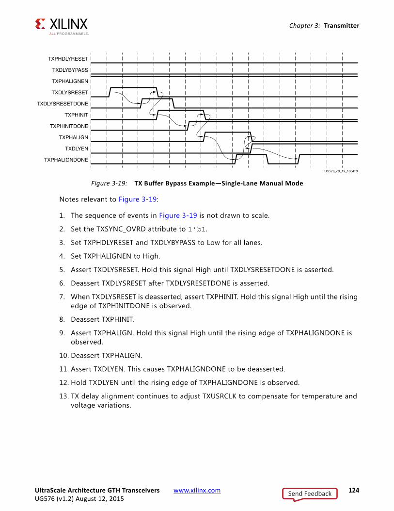
Chapter 3: Transmitter
Notes relevant to Figure 3-19:
1. The sequence of events in Figure 3-19 is not drawn to scale.
2. Set the TXSYNC_OVRD attribute to 1'b1.
3. Set TXPHDLYRESET and TXDLYBYPASS to Low for all lanes.
4. Set TXPHALIGNEN to High.
5. Assert TXDLYSRESET. Hold this signal High until TXDLYSRESETDONE is asserted.
6. Deassert TXDLYSRESET after TXDLYSRESETDONE is asserted.
7. When TXDLYSRESET is deasserted, assert TXPHINIT. Hold this signal High until the rising edge of TXPHINITDONE is observed.
8. Deassert TXPHINIT.
9. Assert TXPHALIGN. Hold this signal High until the rising edge of TXPHALIGNDONE is observed.
10. Deassert TXPHALIGN.
11. Assert TXDLYEN. This causes TXPHALIGNDONE to be deasserted.
12. Hold TXDLYEN until the rising edge of TXPHALIGNDONE is observed.
13. TX delay alignment continues to adjust TXUSRCLK to compensate for temperature and voltage variations.
X-Ref Target - Figure 3-19
Figure 3-19: TX Buffer Bypass Example—Single-Lane Manual Mode
TXPHDLYRESET
TXDLYBYPASS
TXPHALIGNEN
TXDLYSRESET
TXDLYSRESETDONE
TXPHINIT
TXPHINITDONE
TXPHALIGN
TXDLYEN
TXPHALIGNDONE
UG576_c3_19_100413
UltraScale Architecture GTH Transceivers www.xilinx.com 124UG576 (v1.2) August 12, 2015
Send Feedback

Chapter 3: Transmitter
Using the TX Phase Alignment to Minimize the TX Lane-to-Lane SkewThe TX phase alignment circuit can also be used to minimize skew between GTH transceivers. Figure 3-20 shows how the TX phase alignment circuit can reduce lane skew by aligning the XCLK domains of multiple GTH transceivers to a common clock source. Figure 3-20 shows multiple GTH transceiver lanes running before and after TX phase is aligned to a common clock. Before the TX phase alignment, all XCLKs have an arbitrary phase difference. After TX phase alignment, the only phase difference is the skew from the common clock, and all lanes transmit data simultaneously as long as the datapath latency is matched. TXUSRCLK and TXUSRCLK2 for all GTH transceivers must come from the same source and must be routed through a low skew clocking resource such as a BUFG_GT for the TX phase alignment circuit to be effective.
Using TX Buffer Bypass in Multi-Lane Manual ModeWhen a multi-lane application requires TX buffer bypass, phase alignment needs to be performed manually. This section describes the steps required to perform the multi-lane TX buffer bypass alignment procedure manually.
• Master: In a multi-lane application, the buffer bypass master is the lane that is the source of TXOUTCLK. In a multi-lane application, the middle-most GTH transceiver should be selected to be the source of TXOUTCLK. For example, in a multi-lane application of 12 GTH transceivers consisting of 3 contiguous Quads, one of the middle GTH transceivers in the middle Quad should be selected as the source of TXOUTCLK.
• Slave: All the lanes that share the same TXUSRCLK/TXUSRCLK2, which is generated from the TXOUTCLK of the buffer bypass master.
X-Ref Target - Figure 3-20
Figure 3-20: TX Phase Alignment to Minimize TX Lane-to-Lane Skew
GTH TXLane 0
Skew
Before TX Phase Alignment After TX Phase Alignment
Reduced SkewParallel clocksare independent
Parallel clocks are phase aligned to thesame clock edge
GTH TXLane 0
GTH TXLane 1
GTH TXLane 1
UG576_c3_20_100413
UltraScale Architecture GTH Transceivers www.xilinx.com 125UG576 (v1.2) August 12, 2015
Send Feedback
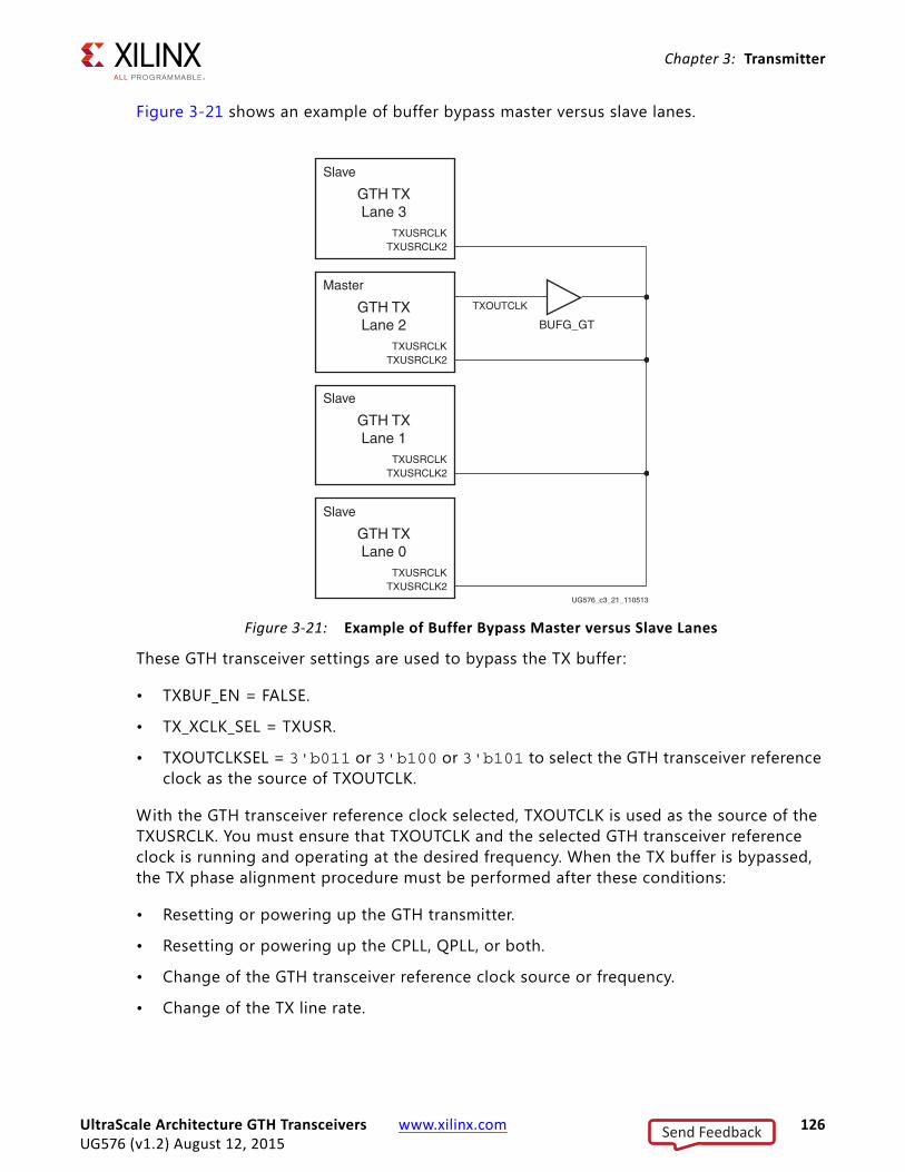
Chapter 3: Transmitter
Figure 3-21 shows an example of buffer bypass master versus slave lanes.
These GTH transceiver settings are used to bypass the TX buffer:
• TXBUF_EN = FALSE.
• TX_XCLK_SEL = TXUSR.
• TXOUTCLKSEL = 3'b011 or 3'b100 or 3'b101 to select the GTH transceiver reference clock as the source of TXOUTCLK.
With the GTH transceiver reference clock selected, TXOUTCLK is used as the source of the TXUSRCLK. You must ensure that TXOUTCLK and the selected GTH transceiver reference clock is running and operating at the desired frequency. When the TX buffer is bypassed, the TX phase alignment procedure must be performed after these conditions:
• Resetting or powering up the GTH transmitter.
• Resetting or powering up the CPLL, QPLL, or both.
• Change of the GTH transceiver reference clock source or frequency.
• Change of the TX line rate.
X-Ref Target - Figure 3-21
Figure 3-21: Example of Buffer Bypass Master versus Slave Lanes
UG576_c3_21_110513
BUFG_GT
GTH TXLane 3
Slave
TXUSRCLKTXUSRCLK2
GTH TXLane 2
Master
TXUSRCLK
TXOUTCLK
TXUSRCLK2
GTH TXLane 1
Slave
TXUSRCLKTXUSRCLK2
GTH TXLane 0
Slave
TXUSRCLKTXUSRCLK2
UltraScale Architecture GTH Transceivers www.xilinx.com 126UG576 (v1.2) August 12, 2015
Send Feedback

Chapter 3: Transmitter
Figure 3-22 shows the required steps to perform manual TX phase and delay alignment.
Notes relevant to Figure 3-22:
1. The sequence of events shown in Figure 3-22 is not drawn to scale.
2. M_* denotes ports related to the master lane.
3. S_* denotes ports related to the slave lane(s).
4. Set the TXSYNC_OVRD attribute to 1'b1.
5. Set TXPHDLYRESET and TXDLYBYPASS to Low for all lanes.
6. Set TXPHALIGNEN to High for all lanes.
7. Assert TXDLYSRESET for all lanes. Hold this signal High until TXDLYSRESETDONE of the respective lane is asserted.
8. Deassert TXDLYSRESET for the lane in which the TXDLYSRESETDONE is asserted.
9. When TXDLYSRESET of all lanes are deasserted, assert TXPHINIT for the master lane. Hold this signal High until the rising edge of TXPHINITDONE of the master lane is observed. If TXPHINITDONE is High due to the sequence having completed once before already, assertion of TXPHINIT causes TXPHINITDONE to deassert. TXPHINITDONE stays Low for a minimum of one TXUSRCLK cycle.
X-Ref Target - Figure 3-22
Figure 3-22: TX Phase and Delay Alignment in Manual Mode
M_TXPHDLYRESET
M_TXDLYBYPASS
M_TXPHALIGNEN
M_TXDLYSRESET
M_TXDLYSRESETDONE
M_TXPHINIT
M_TXPHINITDONE
M_TXPHALIGN
M_TXDLYEN
M_TXPHALIGNDONE
S_TXPHDLYRESET
S_TXDLYBYPASS
S_TXPHALIGNEN
S_TXDLYSRESET
S_TXDLYSRESETDONE
S_TXPHINIT
S_TXPHINITDONE
S_TXPHALIGN
S_TXDLYEN
S_TXPHALIGNDONE
UG576_c3_22_100413
UltraScale Architecture GTH Transceivers www.xilinx.com 127UG576 (v1.2) August 12, 2015
Send Feedback

Chapter 3: Transmitter
10. Deassert TXPHINIT for the master lane.
11. Assert TXPHALIGN for the master lane. Hold this signal High until the rising edge of TXPHALIGNDONE of the master lane is observed.
12. Deassert TXPHALIGN for the master lane.
13. Assert TXDLYEN for the master lane. This causes TXPHALIGNDONE to be deasserted.
14. Hold TXDLYEN for the master lane High until the rising edge of TXPHALIGNDONE of the master lane is observed.
15. Deassert TXDLYEN for the master lane.
16. Assert TXPHINIT for all slave lane(s). Hold this signal High until the rising edge of TXPHINITDONE of the respective slave lane is observed.
17. Deassert TXPHINIT for the slave lane in which the TXPHINITDONE is asserted.
18. When TXPHINIT for all slave lane(s) are deasserted, assert TXPHALIGN for all slave lane(s). Hold this signal High until the rising edge of TXPHALIGNDONE of the respective slave lane is observed.
19. Deassert TXPHALIGN for the slave lane in which the TXPHALIGNDONE is asserted.
20. When TXPHALIGN for all slave lane(s) are deasserted, assert TXDLYEN for the master lane. This causes TXPHALIGNDONE of the master lane to be deasserted.
21. Wait until TXPHALIGNDONE of the master lane reasserts. Phase and delay alignment for the multi-lane interface is complete. Continue to hold TXDLYEN for the master lane High to adjust TXUSRCLK to compensate for temperature and voltage variations.
Using TX Buffer Bypass in Multi-Lane Auto ModeFor GTH transceivers, when a multi-lane application requires TX buffer bypass, phase alignment can be performed manually or automatically. This section describes the steps required to perform the multi-lane TX buffer bypass alignment procedure automatically.
• Master: In a multi-lane application, the buffer bypass master is the lane that is the source of TXOUTCLK.
• Slave: These are all the lanes that share the same TXUSRCLK/TXUSRCLK2, which is generated from the TXOUTCLK of the buffer bypass master.
UltraScale Architecture GTH Transceivers www.xilinx.com 128UG576 (v1.2) August 12, 2015
Send Feedback
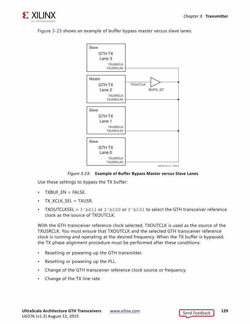
Chapter 3: Transmitter
Figure 3-23 shows an example of buffer bypass master versus slave lanes.
Use these settings to bypass the TX buffer:
• TXBUF_EN = FALSE.
• TX_XCLK_SEL = TXUSR.
• TXOUTCLKSEL = 3'b011 or 3'b100 or 3'b101 to select the GTH transceiver reference clock as the source of TXOUTCLK.
With the GTH transceiver reference clock selected, TXOUTCLK is used as the source of the TXUSRCLK. You must ensure that TXOUTCLK and the selected GTH transceiver reference clock is running and operating at the desired frequency. When the TX buffer is bypassed, the TX phase alignment procedure must be performed after these conditions:
• Resetting or powering up the GTH transmitter.
• Resetting or powering up the PLL.
• Change of the GTH transceiver reference clock source or frequency.
• Change of the TX line rate.
X-Ref Target - Figure 3-23
Figure 3-23: Example of Buffer Bypass Master versus Slave Lanes
UG576_c3_21_110513
BUFG_GT
GTH TXLane 3
Slave
TXUSRCLKTXUSRCLK2
GTH TXLane 2
Master
TXUSRCLK
TXOUTCLK
TXUSRCLK2
GTH TXLane 1
Slave
TXUSRCLKTXUSRCLK2
GTH TXLane 0
Slave
TXUSRCLKTXUSRCLK2
UltraScale Architecture GTH Transceivers www.xilinx.com 129UG576 (v1.2) August 12, 2015
Send Feedback

Chapter 3: Transmitter
To set up TX buffer bypass in multilane, auto mode, set these attributes:
• TXSYNC_MULTILANE = 1
• TXSYNC_OVRD = 0
Set the ports as shown in Figure 3-24.
X-Ref Target - Figure 3-24
Figure 3-24: TX Buffer Bypass, Multilane, Auto Mode Port Connection
Master
TXSYNCMODE
TXSYNCALLIN
TXSYNCIN TXSYNCOUT
TXSYNCDONE
TXPHALIGNDONE
1’b1
1’b0
TXDLYSRESET
Slave
TXSYNCMODE
TXSYNCALLIN
TXSYNCIN TXSYNCOUT
TXSYNCDONE
TXPHALIGNDONE
TXDLYSRESET
UG576_c3_29_041414
UltraScale Architecture GTH Transceivers www.xilinx.com 130UG576 (v1.2) August 12, 2015
Send Feedback

Chapter 3: Transmitter
Figure 3-25 shows the required steps to perform manual TX phase and delay alignment.
Notes relevant to Figure 3-25:
1. The sequence of events shown in Figure 3-25 is not drawn to scale.
2. M_* denotes ports related to the master lane.
3. S_* denotes ports related to the slave lane(s).
4. After conditions such as a GTH transmitter reset or TX rate change, TX phase alignment must be performed to align XCLK and TXUSRCLK. The TX phase and delay alignments are initiated by asserting TXDLYSRESET.
5. Wait until TXDLYSRESETDONE is High. TXDLYSRESETDONE stays asserted for a minimum of 100 ns.
6. When TXSYNCDONE of the master lane is asserted, the alignment procedure is completed. This signal remains asserted until the alignment procedure is re-initiated.
7. Upon the assertion of TXSYNCDONE of the master lane, TXPHALIGNDONE of the master lane indicates whether alignment is achieved and maintained.
8. TX delay alignment continues to adjust TXUSRCLK to compensate for temperature and voltage variations.
X-Ref Target - Figure 3-25
Figure 3-25: TX Buffer Bypass Example, Multi-Lane Auto Mode
M_TXDLYSRESET
M_TXDLYSRESETDONE
M_TXPHALIGNDONE
M_TXSYNCOUT
M_TXSYNCDONE
S_TXDLYSRESET
S_TXDLYSRESETDONE
S_TXPHALIGNDONE
S_TXSYNCOUT
S_TXSYNCDONE
UG576_c3_30_041414
UltraScale Architecture GTH Transceivers www.xilinx.com 131UG576 (v1.2) August 12, 2015
Send Feedback

Chapter 3: Transmitter
TX Pattern Generator
Functional DescriptionPseudo-random bit sequences (PRBS) are commonly used to test the signal integrity of high-speed links. These sequences appear random but have specif ic properties that can be used to measure the quality of a link. The GTH transceiver pattern generator block can generate several industry-standard PRBS patterns listed in Table 3-23.
In addition to PRBS patterns, the GTH transceiver supports 16 UI, 20 UI, 32 UI, or 40 UI square wave test patterns, depending on internal data width as well as a 2-UI square wave test pattern and PCI Express® compliance pattern generation. Clocking patterns are usually used to check PLL random jitter often done with a spectrum analyzer.
Table 3-23: Supported PRBS Patterns
Name Polynomial Length of Sequence Description
PRBS-7 1 + X6 + X7 27 - 1 bits Used to test channels with 8B/10B.
PRBS-9 1 + X5 + X9 29 - 1 bits ITU-T Recommendation O.150, Section 5.1. PRBS-9 is one of the recommended test patterns for SFP+.
PRBS-15 1 + X14 + X15 215 - 1 bits ITU-T Recommendation O.150, Section 5.3. PRBS-15 is often used for jitter measurement because it is the longest pattern the Agilent DCA-J sampling scope can handle.
PRBS-23 1 + X18 + X23 223 - 1 bits ITU-T Recommendation O.150, Section 5.6. PRBS-23 is often used for non-8B/10B encoding schemes. It is one of the recommended test patterns in the SONET specification.
PRBS-31 1 + X28 + X31 231 - 1 bits ITU-T Recommendation O.150, Section 5.8. PRBS-31 is often used for non-8B/10B encoding schemes. It is a recommended PRBS test pattern for 10 Gigabit Ethernet. See IEEE 802.3ae-2002.
Table 3-24: PCI Express Compliance Pattern
Symbol K28.5 D21.5 K28.5 D10.2
Disparity 0 1 1 0
Pattern 0011111010 1010101010 1100000101 0101010101
UltraScale Architecture GTH Transceivers www.xilinx.com 132UG576 (v1.2) August 12, 2015
Send Feedback

Chapter 3: Transmitter
The error insertion function is supported to verify link connection and also for jitter tolerance tests. When an inverted PRBS pattern is necessary, TXPOLARITY signal is used to control polarity.
X-Ref Target - Figure 3-26
Figure 3-26: 20-UI Square Wave
X-Ref Target - Figure 3-27
Figure 3-27: TX Pattern Generator Block
UG576_c3_23_100713
20 UI
PRBS-7
ErrorInsertions Polarity
Inversion
PRBS-9
PRBS-15
PRBS-23
PRBS-31
PCI Express Compliance Pattern
Square Wave with 2 UI period
Square Wave with 16 UI, 20 UI,32 UI or 40 UI period
TXDATA UG576_c3_24_100713
UltraScale Architecture GTH Transceivers www.xilinx.com 133UG576 (v1.2) August 12, 2015
Send Feedback

Chapter 3: Transmitter
Ports and AttributesTable 3-25 defines the pattern generator ports.
Table 3-26 defines the pattern generator attribute.
Using TX Pattern Generator
In all but one use mode, the TX pattern generator can simply be enabled by changing the value of the TXPRBSSEL port to select the desired pattern. When the TX asynchronous gearbox is enabled, these additional steps must be taken to enable the TX pattern generator:
1. Put the PCS into reset by asserting TXPCSRESET.
2. Set attribute TXGEARBOX_EN to 1'b0 and TXBUF_EN to 1'b1 via the DRP.
3. Set port TXOUTCLKSEL to 3'b010 (TXOUTCLKPMA).
Table 3-25: Pattern Generator Ports
Port Name Dir Clock Domain Description
TXPRBSSEL[3:0] In TXUSRCLK2 Transmitter PRBS generator test pattern control.4'b0000: Standard operation mode (test pattern generation is off)4'b0001: PRBS-74'b0010: PRBS-94'b0011: PRBS-154'b0100: PRBS-234'b0101: PRBS-314'b1000: PCI Express compliance pattern. Only works with internal data width 20 bit and 40 bit modes4'b1001: Square wave with 2 UI (alternating 0s/1s)4'b1010: Square wave with 16 UI, 20 UI, 32 UI, or 40 UI period (based on internal data width)
TXPRBSFORCEERR In TXUSRCLK2 When this port is driven High, errors are forced in the PRBS transmitter. While this port is asserted, the output data pattern contains errors. When TXPRBSSEL is set to 4'b0000, this port does not affect TXDATA.
Table 3-26: Pattern Generator Attribute
Attribute Type Description
RXPRBS_ERR_LOOPBACK 1-bit Binary When set to 1, causes RXPRBSERR bit to be internally looped back to TXPRBSFORCEERR of the same GTH transceiver. This allows synchronous and asynchronous jitter tolerance testing without worrying about data clock domain crossing.When set to 0, TXPRBSFORCEERR forces onto the TX PRBS.
UltraScale Architecture GTH Transceivers www.xilinx.com 134UG576 (v1.2) August 12, 2015
Send Feedback

Chapter 3: Transmitter
4. Set port TXPRBSSEL to the desired pattern.
5. Release the PCS from reset by deasserting TXPCSRESET and wait for TXRESETDONE to assert.
To return to TX asynchronous gearbox mode, the above changes must be reversed as described below:
1. Put the PCS into reset by asserting TXPCSRESET.
2. Set the attribute TXGEARBOX_EN to 1'b1 and TXBUF_EN to 1'b0 via the DRP.
3. Set port TXOUTCLKSEL to 3'b101 (TXPROGDIVCLK).
4. Set port TXPRBSSEL to 4'b0000.
5. Release the PCS from reset by deasserting TXPCSRESET and wait for TXRESETDONE to assert.
TX Polarity Control
Functional DescriptionIf TXP and TXN differential traces are accidentally swapped on the PCB, the differential data transmitted by the GTH transceiver TX is reversed. One solution is to invert the parallel data before serialization and transmission to offset the reversed polarity on the differential pair. The TX polarity control can be accessed through the TXPOLARITY input from the interconnect logic interface. It is driven High to invert the polarity of outgoing data.
Ports and AttributesTable 3-27 defines the ports required for TX polarity control.
Using TX Polarity Control
TXPOLARITY can be tied High if the polarity of TXP and TXN needs to be reversed.
Table 3-27: TX Polarity Control Ports
Port Dir Clock Domain Description
TXPOLARITY In TXUSRCLK2 The TXPOLARITY port is used to invert the polarity of outgoing data.
0: Not inverted. TXP is positive, and TXN is negative.1: Inverted. TXP is negative, and TXN is positive.
UltraScale Architecture GTH Transceivers www.xilinx.com 135UG576 (v1.2) August 12, 2015
Send Feedback

Chapter 3: Transmitter
TX Fabric Clock Output Control
Functional DescriptionThe TX Clock Divider Control block has two main components: serial clock divider control and parallel clock divider and selector control. The clock divider and selector details are illustrated in Figure 3-28.
Notes relevant to Figure 3-28:
1. TXOUTCLKPCS and TXOUTCLKFABRIC are redundant outputs. Use TXOUTCLK for new designs.
2. TXOUTCLK is used as the source of the interconnect logic clock via BUFG_GT.
X-Ref Target - Figure 3-28
Figure 3-28: TX Serial and Parallel Clock Divider
UG576_c3_25_020514
TX DATA
TXOUTCLKPCS
TXOUTCLK
TXOUTCLKPCS
TXOUTCLKPMA
‘1’
TXPLLREFCLK_DIV1
TXPLLREFCLK_DIV2
TXPROGDIVCLK
TXOUTCLKSELTXOUTCLKFABRIC
000
001
010
011
101
100
PISO
CPLL
REFCLK Sel
REFCLK Distribution
PhaseInterp
DelayAligner
TX PolarityControl
÷D{1,2,4,8,16}
TX PMA
GTHE3_CHANNEL (GTH Transceiver Primitive)
0
10
00
01
10
11 00
11QPLL1REFCLK
10
00 1
TXP/N
QPLL1CLK
QPLL0REFCLK
MGTREFCLK[0/1]N
TXSYSCLKSEL
TX_PROGCLK_SEL
REFCLK_HROW_CK_SEL
QPLL0CLK
TXDLYBYPASS
TX PROG.DIV
÷2
TX DATA FromUpstream PCS Blocks
TX PCS
Output toGTHE3_COMMON andGTHE3_CHANNEL
Output Clock to BUFG_GT
O
ODIV2
IBUFDS_GTE3MGTREFCLK[0/1]P
TXPLLCLKSEL
÷{4,5}
÷{2,4}
UltraScale Architecture GTH Transceivers www.xilinx.com 136UG576 (v1.2) August 12, 2015
Send Feedback

Chapter 3: Transmitter
3. There is only one CPLL in the GTHE3_CHANNEL. The QPLL from the GTHE3_COMMON can also be used, when applicable.
4. The selection of the /2 or /4 divider block is controlled by the TX_INT_DATAWIDTH attribute from the GTHE3_CHANNEL primitive. /2 is selected when TX_INT_DATAWIDTH = 0 (2-byte internal datapath) and /4 is selected when TX_INT_DATAWIDTH = 1 (4-byte internal datapath).
5. The selection of the /4 or /5 divider block is controlled by the TX_DATA_WIDTH attribute from the GTHE3_CHANNEL primitive. /4 is selected when TX_DATA_WIDTH = 16, 32, or 64. /5 is selected when TX_DATA_WIDTH = 20, 40, or 80.
6. For details about placement constraints and restrictions on clocking resources (IBUFDS_GTE3, BUFG_GT, BUFG_GT_SYNC, etc.), refer to the UltraScale Architecture Clocking Resources User Guide (UG572) [Ref 3].
Serial Clock Divider
Each transmitter PMA module has a D divider that divides down the clock from the PLL for lower line rate support. This serial clock divider, D, can be set statically for applications with a fixed line rate or it can be changed dynamically for protocols with multiple line rates.
To use the D divider in fixed line rate applications, the TXOUT_DIV attribute must be set to the appropriate value, and the TXRATE port needs to be tied to 3'b000. Refer to the Static Setting via Attribute column in Table 3-28 for details.
To use the D divider in multiple line rate applications, the TXRATE port is used to dynamically select the D divider value. The TXOUT_DIV attribute and the TXRATE port must select the same D divider value upon device configuration. After device configuration, the TXRATE is used to dynamically change the D divider value. Refer to the Dynamic Control via Ports column in Table 3-28 for details.
The control for the serial divider is shown in Table 3-28. For details about the line rate range per speed grade, refer to the data sheets [Ref 6].
Table 3-28: TX PLL Output Divider Setting
D Divider Value Static Setting via Attribute Dynamic Control via Ports
1TXOUT_DIV = 1
TXRATE = 3'b000TXOUT_DIV = Ignored
TXRATE = 3'b001
2TXOUT_DIV = 2
TXRATE = 3'b000TXOUT_DIV = Ignored
TXRATE = 3'b010
4TXOUT_DIV = 4
TXRATE = 3'b000TXOUT_DIV = Ignored
TXRATE = 3'b011
8TXOUT_DIV = 8
TXRATE = 3'b000TXOUT_DIV = Ignored
TXRATE = 3'b100
16TXOUT_DIV = 16
TXRATE = 3'b000TXOUT_DIV = Ignored
TXRATE = 3'b101
UltraScale Architecture GTH Transceivers www.xilinx.com 137UG576 (v1.2) August 12, 2015
Send Feedback

Chapter 3: Transmitter
Parallel Clock Divider and Selector
The parallel clock outputs from the TX clock divider control block can be used as an interconnect logic clock, depending on the line rate requirement.
The recommended clock for the interconnect logic is the TXOUTCLK from one of the GTH transceivers. It is also possible to bring the MGTREFCLK directly to the interconnect logic and use as the interconnect logic clock. TXOUTCLK is preferred for general applications as it has an output delay control used for applications that bypass the TX buffer for output lane deskewing or constant datapath delay. Refer to TX Buffer Bypass, page 118 for more details.
The TXOUTCLKSEL port controls the input selector and allows these clocks to be output via the TXOUTCLK port:
• TXOUTCLKSEL = 3'b001: The TXOUTCLKPCS path is not recommended for use because it incurs extra delay from the PCS block.
• TXOUTCLKSEL = 3'b010: TXOUTCLKPMA is the divided down PLL clock after the TX phase interpolator and is used by the TX PCS block. This clock is interrupted when the PLL is reset by one of the related reset signals.
• TXOUTCLKSEL = 3'b011 or 3'b100: TXPLLREFCLK_DIV1 or TXPLLREFCLK_DIV2 is the input reference clock to the CPLL or QPLL, depending on the TXSYSCLKSEL setting. TXPLLREFCLK is the recommended clock for general usage and is required for the TX buffer bypass mode.
• TXOUTCLKSEL = 3'b0101: TXPRODIVCLK is the divided down PLL clock after the TX Programmable Divider. See TX Programmable Divider for more details.
TX Programmable Divider
The TX programmable divider shown in Figure 3-28 uses one of the PLL output clocks to generate a parallel output clock. By using the transceiver PLL, TX programmable divider, and BUFG_GT, TXOUTCLK (TXOUTCLKSEL = 101) can be used as a clock source for the interconnect logic. The supported divider values are 4, 5, 8, 10, 16, 16.5, 20, 32, 33, 40, 64, 66, and 80.
The high-speed clock multiplexer controlled by TX_PROGCLK_SEL is set based on the application requirements:
• 00: The post TX phase interpolator (PI) clock path can be used to generate a parallel clock with a certain ppm offset created by the TX PI. In this use case, one transceiver PLL is shared for the datapath and clock generation path. The clock signal is interrupted if the channel or the source PLL is being reset. To use this path, set the attribute to POSTPI.
• 01: The pre TX PI clock path can be used to generate a system clock to support applications where minimal or f ixed latency is needed. In this use case, one transceiver
UltraScale Architecture GTH Transceivers www.xilinx.com 138UG576 (v1.2) August 12, 2015
Send Feedback

Chapter 3: Transmitter
PLL is shared for the datapath and clock generation path. The clock signal is interrupted only if the source PLL is being reset. To use this path, set the attribute to PREPI.
• 10: In applications where the QPLL clock might be interrupted during reconfiguration, the bypass clock path provides the flexibility to use the CPLL to generate a stable parallel clock for the interconnect logic.
Table 3-29 and Table 3-30 show the programmable divider ports and attribute, respectively.
Ports and AttributesTable 3-31 defines the ports required for TX fabric clock output control.
Table 3-29: TX Programmable Divider Port
Port Dir Clock Domain Description
TXPROGDIVRESET In Async This active-High port resets the dividers as well as the TXPRGDIVRESETDONE indicator. A reset must be performed whenever the input clock source is interrupted.
TXPRGDIVRESETDONE Out Async When the input clock is stable and reset is performed, this active-High signal indicates the rest is completed and the output clock is stable.
Table 3-30: TX Programmable Divider Attribute
Attribute Type Description
TX_PROGDIV_CFG Real TX programmable divider ratio. Valid settings are 0.0, 4.0, 5.0, 8.0, 10.0, 16.0, 16.5, 20.0, 32.0, 33.0, 40.0, 64.0, 66.0, 80.0, and 100.0.
TX_DIVRESET_TIME 5-Bit Binary
Reserved. Represents the time duration to apply the TX programmable divider reset. Use the recommended value from the Wizard. This must be a non-zero value when using TXPROGDIVRESET to initiate the reset process.
Table 3-31: TX Fabric Clock Output Control Ports
Port Dir Clock Domain Description
TXOUTCLKSEL[2:0] In Async This port controls the multiplexer select signal in Figure 3-28.3'b000: Static 13'b001: TXOUTCLKPCS path3'b010: TXOUTCLKPMA path3'b011: TXPLLREFCLK_DIV1 path3'b100: TXPLLREFCLK_DIV2 path3'b101: TXPROGDIVCLKOthers: Reserved.
UltraScale Architecture GTH Transceivers www.xilinx.com 139UG576 (v1.2) August 12, 2015
Send Feedback

Chapter 3: Transmitter
TXRATE[2:0] In TXUSRCLK2 This port dynamically controls the setting for the TX serial clock divider D (see Table 3-28), and it is used with the TXOUT_DIV attribute. 3'b000: Use the TXOUT_DIV divider value3'b001: Set the D divider to 13'b010: Set the D divider to 23'b011: Set the D divider to 43'b100: Set the D divider to 83'b101: Set the D divider to 16
TXOUTCLKFABRIC Out Clock TXOUTCLKFABRIC is a redundant output reserved for testing. Use TXOUTCLK with TXOUTCLKSEL = 3'b011 instead.
TXOUTCLK Out Clock TXOUTCLK is the recommended clock output to the interconnect logic. The TXOUTCLKSEL port is the input selector for TXOUTCLK and allows the PLL input reference clock to the interconnect logic.
TXOUTCLKPCS Out Clock TXOUTCLKPCS is a redundant output. Use TXOUTCLK with TXOUTCLKSEL = 3'b001 instead.
TXRATEDONE Out TXUSRCLK2 The TXRATEDONE port is asserted High for one TXUSRCLK2 cycle in response to a change on the TXRATE port. The TRANS_TIME_RATE attribute defines the period of time between a change on the TXRATE port and the assertion of TXRATEDONE.
TXDLYBYPASS In Async TX delay alignment bypass:0: Uses the TX delay alignment circuit. Set to 1'b0 when the TX buffer is bypassed.1: Bypasses the TX delay alignment circuit. Set to 1'b1 when the TX buffer is used.
TXRATEMODE In Async Determines if TXRATE asynchronously controls the D output divider in the TX PMA.
0: Synchronous. When set to 1'b0, an automatic reset sequence occurs in response to a change on the TXRATE port. 1: Asynchronous
Table 3-31: TX Fabric Clock Output Control Ports (Cont’d)
Port Dir Clock Domain Description
UltraScale Architecture GTH Transceivers www.xilinx.com 140UG576 (v1.2) August 12, 2015
Send Feedback

Chapter 3: Transmitter
The transceiver has an internal 25 MHz clock derived from the reference clock from the [TX/RX]_CLK25_DIV setting. The 25 MHz clock is used as a synchronizer and timer for various transceiver operations such as reset, power management, rate change, OOB, and beaconing. Set [TX/RX]_CLK25_DIV to achieve 25 MHz or as close as possible. For SATA OOB, this internal clock must be 25 MHz. Table 3-32 defines the attributes required for TX fabric clock output control.
Table 3-32: TX Fabric Clock Output Control Attributes
Attribute Type Description
TRANS_TIME_RATE 8-bit Hex Reserved. Use the recommended value from the Wizard. This attribute determines when PHYSTATUS and TXRATEDONE are asserted after a rate change.
TXBUF_RESET_ON_RATE_CHANGE Boolean When set to TRUE, this attribute enables an automatic TX buffer reset during a rate change event initiated by a change in TXRATE.
TXOUT_DIV Integer This attribute controls the setting for the TX serial clock divider. This attribute is only valid when TXRATE = 3'b000. Otherwise the D divider value is controlled by TXRATE. Valid settings are 1, 2, 4, 8, and 16.
TX_PROGCLK_SEL String 00: Set to POSTPI to select the clock path after the TX phase interpolator.01: Set to PREPI to select the clock path before the TX phase interpolator.10: Set to PLL to select the clock path from the CPLL.
UltraScale Architecture GTH Transceivers www.xilinx.com 141UG576 (v1.2) August 12, 2015
Send Feedback

Chapter 3: Transmitter
TX_CLK25_DIV Integer This attribute sets a divider that divides down TXPLLREFCLK_DIV1 to generate an internal clock that is used for some of the logic inside the TX portion of the transceiver.
1: TXPLLREFCLK_DIV1 ≤ 25 MHz2: 25 MHz ≤ TXPLLREFCLK_DIV1 ≤ 50 MHz3: 50 MHz ≤ TXPLLREFCLK_DIV1 ≤ 75 MHz4: 75 MHz ≤ TXPLLREFCLK_DIV1 ≤ 100 MHz5: 100 MHz ≤ TXPLLREFCLK_DIV1 ≤ 125 MHz6: 125 MHz ≤ TXPLLREFCLK_DIV1 ≤ 150 MHz7: 150 MHz ≤ TXPLLREFCLK_DIV1 ≤ 175 MHz8: 175 MHz ≤ TXPLLREFCLK_DIV1 ≤ 200 MHz9: 200 MHz ≤ TXPLLREFCLK_DIV1 ≤ 225 MHz10: 225 MHz ≤ TXPLLREFCLK_DIV1 ≤ 250 MHz11: 250 MHz ≤ TXPLLREFCLK_DIV1 ≤ 275 MHz12: 275 MHz ≤ TXPLLREFCLK_DIV1 ≤ 300 MHz13: 300 MHz ≤ TXPLLREFCLK_DIV1 ≤ 325 MHz14: 325 MHz ≤ TXPLLREFCLK_DIV1 ≤ 350 MHz15: 350 MHz ≤ TXPLLREFCLK_DIV1 ≤ 375 MHz16: 375 MHz ≤ TXPLLREFCLK_DIV1 ≤ 400 MHz17: 400 MHz ≤ TXPLLREFCLK_DIV1 ≤ 425 MHz18: 425 MHz ≤ TXPLLREFCLK_DIV1 ≤ 450 MHz19: 450 MHz ≤ TXPLLREFCLK_DIV1 ≤ 475 MHz20: 475 MHz ≤ TXPLLREFCLK_DIV1 ≤ 500 MHz21: 500 MHz ≤ TXPLLREFCLK_DIV1 ≤ 525 MHz22: 525 MHz ≤ TXPLLREFCLK_DIV1 ≤ 550 MHz23: 550 MHz ≤ TXPLLREFCLK_DIV1 ≤ 575 MHz24: 575 MHz ≤ TXPLLREFCLK_DIV1 ≤ 600 MHz25: 600 MHz ≤ TXPLLREFCLK_DIV1 ≤ 625 MHz26: 625 MHz ≤ TXPLLREFCLK_DIV1 ≤ 650 MHz27: 650 MHz ≤ TXPLLREFCLK_DIV1 ≤ 675 MHz28: 675 MHz ≤ TXPLLREFCLK_DIV1 ≤ 700 MHz29: 700 MHz ≤ TXPLLREFCLK_DIV1 ≤ 725 MHz30: 725 MHz ≤ TXPLLREFCLK_DIV1 ≤ 750 MHz31: 750 MHz ≤ TXPLLREFCLK_DIV1 ≤ 775 MHz32: 775 MHz ≤ TXPLLREFCLK_DIV1 ≤ 820 MHz
Table 3-32: TX Fabric Clock Output Control Attributes (Cont’d)
Attribute Type Description
UltraScale Architecture GTH Transceivers www.xilinx.com 142UG576 (v1.2) August 12, 2015
Send Feedback

Chapter 3: Transmitter
TX Phase Interpolator PPM Controller
Functional DescriptionThe TX Phase Interpolator Parts Per Million (TXPIPPM) Controller module provides support for dynamically controlling the TX phase interpolator (TX PI). Located in the TX PCS, its inputs come from the TX interface and it outputs to the TX PMA. Applications exist that require f ine-tune control of the data in the TX PMA. Control of the output clock from the PLL is achieved through a TX PI, which in turn can be controlled by the TX phase interpolator PPM controller module. The interconnect logic can control the TX PI in the TX PMA through the use of the TX Phase Interpolator PPM Controller module in the PCS.
Ports and AttributesTable 3-33 defines the ports required for the TX Phase Interpolator PPM Controller.
Table 3-33: TX Phase Interpolator PPM Controller Ports
Port Dir Clock Domain Description
TXPIPPMEN In Async 1'b0: Disables the TX Phase Interpolator PPM Controller block. The TX PI is not updated with a PI code and retains the previous PI code.1'b1: Enables the TX Phase Interpolator PPM Controller block. The TX PI is updated with a PI code every TXPI_SYNFREQ_PPM[2:0] cycles.
TXPIPPMOVRDEN In Async 1'b0: Normal operation1'b1: Enables direct control of the PI Code output to the TX PI in the TX PMA. Use with TXPI_PPM_CFG[6:0] to program the value of PI code.
TXPIPPMSEL In Async Set to 1'b1 when using the TX PI PPM controller, otherwise set to 1'b0.
TXPIPPMPD In Async 1'b0: Does not power down the TX Phase Interpolator PPM Controller module.1'b1: Powers down the TX Phase Interpolator PPM Controller module.
TXPIPPMSTEPSIZE[4:0] In Async TXPIPPMSTEPSIZE[4]:1'b1: Increments PI code.1'b0: Decrements PI code.
TXPIPPMSTEPSIZE[3:0] is the amount to increment or decrement PI code. Its values range from 0 to 15.
UltraScale Architecture GTH Transceivers www.xilinx.com 143UG576 (v1.2) August 12, 2015
Send Feedback

Chapter 3: Transmitter
Table 3-34 defines the TX Phase Interpolator PPM Controller attributes.
TX Phase Interpolator PPM Controller Use Mode
Continuous PI Code Update Mode
The continuous PI code update mode can be used when there is a f ixed lead/lag relationship between the two clocks of interest. This use mode allows for the TX output of the GTH transceiver to be running at a f ixed ppm offset from the reference clock. An example use case would be a frequency re-synthesizer as shown in Figure 3-29. Data might be received at one frequency and retransmitted at a different frequency without requiring additional external clock sources.
Table 3-34: TX Phase Interpolator PPM Controller Attributes
Attribute Type Description
TXPI_SYNFREQ_PPM[2:0] 3-bit Binary This attribute specif ies how often PI Code to the TX PI is updated. It is updated every (TXPI_SYNFREQ_PPM[2:0] + 1) cycles. All values are valid except for 3'b000. Use the Wizard’s default value for this attribute.
TXPI_PPM_CFG[7:0] 8-bit Binary When TXPIPPMOVRDEN = 1'b1, program the lower 7 bits of this attribute to one of the 128 values output to the TX PI. The most signif icant bit needs to be pulsed (asserted High and then Low) for the TX PI to register the new 7-bit value of TXPI_PPM_CFG[6:0].
TXPI_CFG0 2-bit Binary Reserved. Issue the recommended value from the Wizard.
TXPI_CFG1 2-bit Binary Reserved. Issue the recommended value from the Wizard.
TXPI_CFG2 2-bit Binary Reserved. Issue the recommended value from the Wizard.
TXPI_CFG3 1-bit Binary Reserved. Issue the recommended value from the Wizard.
TXPI_CFG4 1-bit Binary Reserved. Issue the recommended value from the Wizard.
TXPI_CFG5 3-bit Binary Reserved. Issue the recommended value from the Wizard.
TXPI_INVSTROBE_SEL 1-bit Binary Reserved. Tied to 1'b0.
TXPI_GRAY_SEL 1-bit Binary 1'b0: TXPIPPMSTEPSIZE[3:0] is binary encoded.1'b1: TXPIPPMSTEPSIZE[3:0] is gray encoded.
TXPI_PPMCLK_SEL String Reserved.
UltraScale Architecture GTH Transceivers www.xilinx.com 144UG576 (v1.2) August 12, 2015
Send Feedback
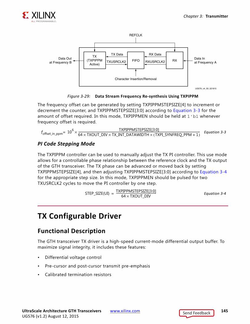
Chapter 3: Transmitter
The frequency offset can be generated by setting TXPIPPMSTEPSIZE[4] to increment or decrement the counter, and TXPIPPMSTEPSIZE[3:0] according to Equation 3-3 for the amount of offset required. In this mode, TXPIPPMEN should be held at 1'b1 whenever frequency offset is required.
Equation 3-3
PI Code Stepping Mode
The TXPIPPM controller can be used to manually adjust the TX PI controller. This use mode allows for a controllable phase relationship between the reference clock and the TX output of the GTH transceiver. The TX phase can be advanced or moved back by setting TXPIPPMSTEPSIZE[4], and then adjusting TXPIPPMSTEPSIZE[3:0] according to Equation 3-4 for the appropriate step size. In this mode, TXPIPPMEN should be pulsed for two TXUSRCLK2 cycles to move the PI controller by one step.
Equation 3-4
TX Configurable Driver
Functional DescriptionThe GTH transceiver TX driver is a high-speed current-mode differential output buffer. To maximize signal integrity, it includes these features:
• Differential voltage control
• Pre-cursor and post-cursor transmit pre-emphasis
• Calibrated termination resistors
X-Ref Target - Figure 3-29
Figure 3-29: Data Stream Frequency Re-synthesis Using TXPIPPM
UG576_c4_59_021815
TX(TXPIPPM
Active)RXFIFO
TX Data RX Data
TXUSRCLK2 RXUSRCLK2Data In at Frequency A
Data Outat Frequency B
Character Insertion/Removal
REFCLK
foffset_in_ppm 106 TXPIPPMSTEPSIZE[3:0]64 TXOUT_DIV TX_INT_DATAWIDTH TXPI_SYNFREQ_PPM 1+( )×××-----------------------------------------------------------------------------------------------------------------------------------------------------×=
STEP_SIZE(UI) TXPIPPMSTEPSIZE[3:0]64 TXOUT_DIV×
-------------------------------------------------=
UltraScale Architecture GTH Transceivers www.xilinx.com 145UG576 (v1.2) August 12, 2015
Send Feedback
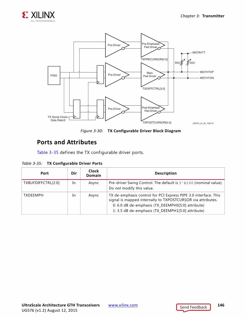
Chapter 3: Transmitter
Ports and AttributesTable 3-35 defines the TX configurable driver ports.
X-Ref Target - Figure 3-30
Figure 3-30: TX Configurable Driver Block Diagram
Pre-Driver
PISO
TX Serial Clock=Data Rate/2
TXDIFFCTRL[3:0]
TXPRECURSOR[4:0]
MGTAVTT
MGTHTXP
MGTHTXN
TXPOSTCURSOR[4:0]
Pre-EmphasisPad Driver
MainPad Driver
Post-EmphasisPad Driver
Pre-Driver
Pre-Driver
UG576_c3_26_102413
5050
Table 3-35: TX Configurable Driver Ports
Port Dir Clock Domain Description
TXBUFDIFFCTRL[2:0] In Async Pre-driver Swing Control. The default is 3’b100 (nominal value).Do not modify this value.
TXDEEMPH In Async TX de-emphasis control for PCI Express PIPE 3.0 interface. This signal is mapped internally to TXPOSTCURSOR via attributes.
0: 6.0 dB de-emphasis (TX_DEEMPH0[5:0] attribute)1: 3.5 dB de-emphasis (TX_DEEMPH1[5:0] attribute)
UltraScale Architecture GTH Transceivers www.xilinx.com 146UG576 (v1.2) August 12, 2015
Send Feedback

Chapter 3: Transmitter
TXDIFFCTRL[3:0] In Async Driver Swing Control. The default is user specif ied. All listed values are in mVPPD.
Note: The peak-to-peak differential voltage is defined when TXPOSTCURSOR = 5'b00000 and TXPRECURSOR = 5'b00000.
TXELECIDLE In TXUSRCLK2 When High, this signal forces MGTHTXP and MGTHTXN both to Common mode, creating an electrical idle signal.
TXINHIBIT In TXUSRCLK2 When High, this signal blocks transmission of TXDATA and forces MGTHTXP to 0 and MGTHTXN to 1.
TXMAINCURSOR[6:0] In Async Allows the main cursor coeff icients to be directly set if the TX_MAINCURSOR_SEL attribute is set to 1'b1. 51 – TXPOSTCURSOR coefficient units – TXPRECURSOR coeff icient units < TXMAINCURSOR coefficient units < 80 –TXPOSTCURSOR coefficient units – TXPRECURSOR coeff icient units.
Table 3-35: TX Configurable Driver Ports (Cont’d)
Port Dir Clock Domain Description
[3:0] mVPPD
0000 170
0001 250
0010 320
0011 390
0100 460
0101 530
0110 600
0111 660
1000 730
1001 780
1010 840
1011 900
1100 950
1101 1000
1110 1040
1111 1080
UltraScale Architecture GTH Transceivers www.xilinx.com 147UG576 (v1.2) August 12, 2015
Send Feedback

Chapter 3: Transmitter
TXMARGIN[2:0] In Async TX Margin control for PCI Express PIPE 3.0 Interface. These signals are mapped internally to TXDIFFCTRL/TXBUFDIFFCTRL via attributes.
TXQPIBIASEN In Async Enables the GND bias on the TX output as required by the QPI specification.
TXQPISENN Out Async Sense output that registers a 1 or 0 on the MGTHTXN pin.
TXQPISENP Out Async Sense output that registers a 1 or 0 on the MGTHTXP pin.
TXQPISTRONGPDOWN In Async Pulls the TX output strongly to GND to enable handshaking as required by the QPI protocol.
TXQPIWEAKPUP In Async Pulls the TX output weakly to MGTAVTT to enable handshaking as required by the QPI protocol.
Table 3-35: TX Configurable Driver Ports (Cont’d)
Port Dir Clock Domain Description
[2:0] Full Range Half Range Full Range Attribute Half Range Attribute
000 800-1200 400-1200 TX_MARGIN_FULL_0 TX_MARGIN_LOW_0
001 800-1200 400-700 TX_MARGIN_FULL_1 TX_MARGIN_LOW_1
010 800-1200 400-700 TX_MARGIN_FULL_2 TX_MARGIN_LOW_2
011 200-400 100-200 TX_MARGIN_FULL_3 TX_MARGIN_LOW_3
100 100-200 100-200 TX_MARGIN_FULL_4 TX_MARGIN_LOW_4
101
default to “DIRECT” mode110
111
UltraScale Architecture GTH Transceivers www.xilinx.com 148UG576 (v1.2) August 12, 2015
Send Feedback

Chapter 3: Transmitter
TXPOSTCURSOR[4:0] In Async Transmitter post-cursor TX pre-emphasis control. The default is user specif ied. All listed values (dB) are typical.
Note: The TXPOSTCURSOR values are defined when the TXPRECURSOR =5'b00000Emphasis = 20log10(Vhigh/Vlow) = |20log10 (Vlow/Vhigh)|
Table 3-35: TX Configurable Driver Ports (Cont’d)
Port Dir Clock Domain Description
[4:0] Emphasis (dB) |Coefficient Units|
5'b00000 0.00 0
5'b00001 0.22 15'b00010 0.45 2
5'b00011 0.68 3
5'b00100 0.92 45'b00101 1.16 5
5'b00110 1.41 6
5'b00111 1.67 75'b01000 1.94 8
5'b01001 2.21 9
5'b01010 2.50 10
5'b01011 2.79 115'b01100 3.10 12
5'b01101 3.41 13
5'b01110 3.74 145'b01111 4.08 15
5'b10000 4.44 16
5'b10001 4.81 175'b10010 5.19 18
5'b10011 5.60 19
5'b10100 6.02 205'b10101 6.47 21
5'b10110 6.94 22
5'b10111 7.43 235'b11000 7.96 24
5'b11001 8.52 25
5'b11010 9.12 265'b11011 9.76 27
5'b11100 10.46 28
5'b11101 11.21 295'b11110 12.04 30
5'b11111 12.96 31
UltraScale Architecture GTH Transceivers www.xilinx.com 149UG576 (v1.2) August 12, 2015
Send Feedback

Chapter 3: Transmitter
TXPRECURSOR[4:0] In Async Transmitter pre-cursor TX pre-emphasis control. The default is user specif ied. All listed values (dB) are typical.
Note: The TXPRECURSOR values are defined when the TXPOSTCURSOR =5'b00000Emphasis = 20log10(Vhigh/Vlow) = |20log10 (Vlow/Vhigh)|
MGTHTXPMGTHTXN
Out (Pad)
TX Serial Clock
Differential complements of one another forming a differential transmit output pair. These ports represent the pads. The locations of these ports must be constrained (see Implementation, page 16) and brought to the top level of the design.
Table 3-35: TX Configurable Driver Ports (Cont’d)
Port Dir Clock Domain Description
[4:0] Emphasis (dB) |Coefficient Units|
5'b00000 0.00 05'b00001 0.22 1
5'b00010 0.45 2
5'b00011 0.68 35'b00100 0.92 4
5'b00101 1.16 5
5'b00110 1.41 65'b00111 1.67 7
5'b01000 1.94 8
5'b01001 2.21 95'b01010 2.50 10
5'b01011 2.79 11
5'b01100 3.10 125'b01101 3.41 13
5'b01110 3.74 14
5'b01111 4.08 155'b10000 4.44 16
5'b10001 4.81 17
5'b10010 5.19 185'b10011 5.60 19
5'b10100 6.02 20
5'b10101 6.02 20
5'b10110 6.02 205'b10111 6.02 20
5'b11000 6.02 20
5'b11001 6.02 205'b11010 6.02 20
5'b11011 6.02 20
5'b11100 6.02 205'b11101 6.02 20
5'b11110 6.02 20
5'b11111 6.02 20
UltraScale Architecture GTH Transceivers www.xilinx.com 150UG576 (v1.2) August 12, 2015
Send Feedback
Chapter 3: Transmitter
Table 3-36 defines the TX configurable driver attributes.
TXSWING In Async TX swing control for PCI Express PIPE 3.0 Interface. This signal is mapped internally to TXDIFFCTRL/TXBUFDIFFCTRL.
0: Full swing1: Low swing
TXDIFFPD In Async Reserved.
TXPISOPD In Async Reserved.
Table 3-35: TX Configurable Driver Ports (Cont’d)
Port Dir Clock Domain Description
Table 3-36: TX Configurable Driver Attributes
Attribute Type Description
TX_DEEMPH0[5:0] 6-bit Binary This attribute has the value of TXPOSTCURSOR[4:0] that has to be mapped when TXDEEMPH = 0. TX_DEEMPH0[4:0] = TXPOSTCURSOR[4:0].Do not modify this value.
TX_DEEMPH1[5:0] 6-bit Binary This attribute has the value of TXPOSTCURSOR[4:0] that has to be mapped when TXDEEMPH = 1. TX_DEEMPH1[4:0] = TXPOSTCURSOR[4:0].Do not modify this value.
TX_DRIVE_MODE String This attribute selects whether PCI Express PIPE 3.0 pins or TX Drive Control pins control the TX driver. The default is “DIRECT.”
DIRECT: TXBUFDIFFCRL, TXDIFFCTRL, TXPOSTCURSOR, TXPRECURSOR and TXMAINCURSOR (If TX_MAINCURSOR_SEL = 1'b1) control the TX driver settings.PIPE: TXDEEMPH, TXMARGIN, TXSWING, TXPRECURSOR and TXMAINCURSOR (If TX_MAINCURSOR_SEL = 1'b1) control the TX driver settings.PIPEGEN3: TXMARGIN, TXSWING, TXPOSTCURSOR, TXPRECURSOR and TXMAINCURSOR (If TX_MAINCURSOR_SEL = 1'b1) control the TX driver settings.
TX_MAINCURSOR_SEL 1-bit Binary Allows independent control of the main cursor. 1'b0: The TXMAINCURSOR coeff icient is automatically determined by the equation: 80 – TXPOSTCURSOR coeff icient – TXPRECURSOR coeff icient1'b1: TXMAINCURSOR coeff icient can be independently set by the TXMAINCURSOR pins within the range specified in the pin description.
TX_MARGIN_FULL_0[6:0] 7-bit Binary This attribute has the value of TXBUFDIFFCTRL[2:0] and TXDIFFCTRL[3:0] that has to be mapped when TXMARGIN = 000 and TXSWING = 0. TX_MARGIN_FULL_0 = TXBUFDIFFCTRL[2:0], TXDIFFCTRL[3:0].
UltraScale Architecture GTH Transceivers www.xilinx.com 151UG576 (v1.2) August 12, 2015
Send Feedback

Chapter 3: Transmitter
TX_MARGIN_FULL_1[6:0] 7-bit Binary This attribute has the value of TXBUFDIFFCTRL[2:0] and TXDIFFCTRL[3:0] that has to be mapped when TXMARGIN = 001 and TXSWING = 0. TX_MARGIN_FULL_1 = TXBUFDIFFCTRL[2:0], TXDIFFCTRL[3:0].
TX_MARGIN_FULL_2[6:0] 7-bit Binary This attribute has the value of TXBUFDIFFCTRL[2:0] and TXDIFFCTRL[3:0] that has to be mapped when TXMARGIN = 010 and TXSWING = 0. TX_MARGIN_FULL_2 = TXBUFDIFFCTRL[2:0], TXDIFFCTRL[3:0].
TX_MARGIN_FULL_3[6:0] 7-bit Binary This attribute has the value of TXBUFDIFFCTRL[2:0] and TXDIFFCTRL[3:0] that has to be mapped when TXMARGIN = 011 and TXSWING = 0. TX_MARGIN_FULL_3 = TXBUFDIFFCTRL[2:0], TXDIFFCTRL[3:0].
TX_MARGIN_FULL_4[6:0] 7-bit Binary This attribute has the value of TXBUFDIFFCTRL[2:0] and TXDIFFCTRL[3:0] that has to be mapped when TXMARGIN = 100 and TXSWING = 0. TX_MARGIN_FULL_4 = TXBUFDIFFCTRL[2:0], TXDIFFCTRL[3:0].
TX_MARGIN_LOW_0[6:0] 7-bit Binary This attribute has the value of TXBUFDIFFCTRL[2:0] and TXDIFFCTRL[3:0] that has to be mapped when TXMARGIN = 000 and TXSWING = 1. TX_MARGIN_LOW_0 = TXBUFDIFFCTRL[2:0], TXDIFFCTRL[3:0].
TX_MARGIN_LOW_1[6:0] 7-bit Binary This attribute has the value of TXBUFDIFFCTRL[2:0] and TXDIFFCTRL[3:0] that has to be mapped when TXMARGIN = 001 and TXSWING = 1. TX_MARGIN_LOW_1 = TXBUFDIFFCTRL[2:0], TXDIFFCTRL[3:0].
TX_MARGIN_LOW_2[6:0] 7-bit Binary This attribute has the value of TXBUFDIFFCTRL[2:0] and TXDIFFCTRL[3:0] that has to be mapped when TXMARGIN = 010 and TXSWING = 1. TX_MARGIN_LOW_2 = TXBUFDIFFCTRL[2:0], TXDIFFCTRL[3:0].
TX_MARGIN_LOW_3[6:0] 7-bit Binary This attribute has the value of TXBUFDIFFCTRL[2:0] and TXDIFFCTRL[3:0] that has to be mapped when TXMARGIN = 011 and TXSWING = 1. TX_MARGIN_LOW_3 = TXBUFDIFFCTRL[2:0], TXDIFFCTRL[3:0].
TX_MARGIN_LOW_4[6:0] 7-bit Binary This attribute has the value of TXBUFDIFFCTRL[2:0] and TXDIFFCTRL[3:0] that has to be mapped when TXMARGIN = 100 and TXSWING = 1. TX_MARGIN_LOW_4 = TXBUFDIFFCTRL[2:0], TXDIFFCTRL[3:0].
TX_QPI_STATUS_EN 1-bit Binary Enables the QPI signals to be passed into the interconnect logic.
TX_EIDLE_ASSERT_DELAY 3-bit Binary Programmable delay between TXELECIDLE assertion to TXP/N entering electrical idle. Use the recommended value from the Wizard.
TX_EIDLE_DEASSERT_DELAY 3-bit Binary Programmable delay between TXELECIDLE de-assertion to TXP/N exiting electrical idle. Use the recommended value from the Wizard.
TX_LOOPBACK_DRIVE_HIZ 1-bit Binary Reserved. Use the recommended value from the Wizard.
Table 3-36: TX Configurable Driver Attributes (Cont’d)
Attribute Type Description
UltraScale Architecture GTH Transceivers www.xilinx.com 152UG576 (v1.2) August 12, 2015
Send Feedback

Chapter 3: Transmitter
TX Receiver Detect Support for PCI Express Designs
Functional DescriptionThe PCI Express specif ication includes a feature that allows the transmitter on a given link to detect if a receiver is present. The decision if a receiver is present is based on the rise time of TXP/TXN. Figure 3-31 shows the circuit model used for receive detection. The GTH transceiver must be in the P1 power down state to perform receiver detection. Receiver detection requires an external coupling capacitor between the transmitter and receiver, and the receiver must be terminated. Refer to the PCI Express Base Specification for the actual value of the external coupling capacitor in Gen1, Gen2, or Gen3 applications. The receiver detection sequence starts with the assertion of TXDETECTRX. In response, the receiver detection logic drives TXN and TXP to (VDD - VSWING/2) and then releases them. After a programmable interval, the levels of TXN and TXP are compared with a threshold voltage. At the end of the sequence, the receiver detection status is presented on RXSTATUS when PHYSTATUS is asserted High for one cycle.
Note: Refer to the PCI Express Base Specification for the actual value of the external coupling capacitor in Gen1, Gen2, or Gen3 applications.
TXDRVBIAS_P 3-bit Binary Reserved. Use the recommended value from the Wizard.
TXDRVBIAS_N 3-bit Binary Reserved. Use the recommended value from the Wizard.
TX_DCD_CFG 6-bit Binary Reserved. Use the recommended value from the Wizard.
TX_DCD_EN 1-bit Binary Reserved. Use the recommended value from the Wizard.
Table 3-36: TX Configurable Driver Attributes (Cont’d)
Attribute Type Description
X-Ref Target - Figure 3-31
Figure 3-31: Receiver Detection Circuit Model
CCH: < 3 nF
UG576_c3_27_110513
CAC RTERMR: 40Ω - 60Ω
VTERMR
RTERMT: 40Ω - 60Ω
VDD
TXDETECTRX
GTH TransceiverComponents
ChannelComponents
Far-End ReceiverComponents
TXP
UltraScale Architecture GTH Transceivers www.xilinx.com 153UG576 (v1.2) August 12, 2015
Send Feedback

Chapter 3: Transmitter
Ports and AttributesTable 3-37 describes the TX receiver detection ports.
Using the TX Receiver Detection for PCI Express
While in the P1 power state, the GTH transceiver can be instructed to perform a receiver detection operation to determine if there is a receiver at the other end of the link. Figure 3-32 shows an example use mode on how to perform receiver detection in PCI Express mode.
Table 3-37: TX Receiver Detection Ports
Port Dir Clock Domain Description
TXDETECTRX In TXUSRCLK2 Used to tell the GTH transceiver to begin a receiver detection operation.
0: Normal operation.1: Receiver detection.
TXPD[1:0] In TXUSRCLK2 Power up or down the TX and RX of the GTH transceiver. In PCI Express mode, tie TXPD and RXPD to the same source. To perform receiver detection, set these signals to the P1 power saving state.00: P0 power state for normal operation.01: P0s power saving state with low recovery time latency.10: P1 power saving state with longer recovery time latency.11: P2 power saving state with lowest power.
RXPD[1:0] In Async
PHYSTATUS Out RXUSRCLK2 In PCI Express mode, this signal is used to communicate completion of several GTH transceiver functions, including power management state transitions, rate change, and receiver detection. During receiver detection, this signal is asserted High to indicate receiver detection completion.
RXSTATUS[2:0] Out RXUSRCLK2 During receiver detection, this signal is read when PHYSTATUS is asserted High. Only these encodings are valid during receiver detection:000: Receiver not present.011: Receiver present.
Table 3-38: TX Receiver Detection Attributes
Attribute Type Description
TX_RXDETECT_CFG 14-bit Binary Reserved. Use the recommended value from the Wizard.
TX_RXDETECT_REF 3-bit Binary Reserved. Use the recommended value from the Wizard.
UltraScale Architecture GTH Transceivers www.xilinx.com 154UG576 (v1.2) August 12, 2015
Send Feedback
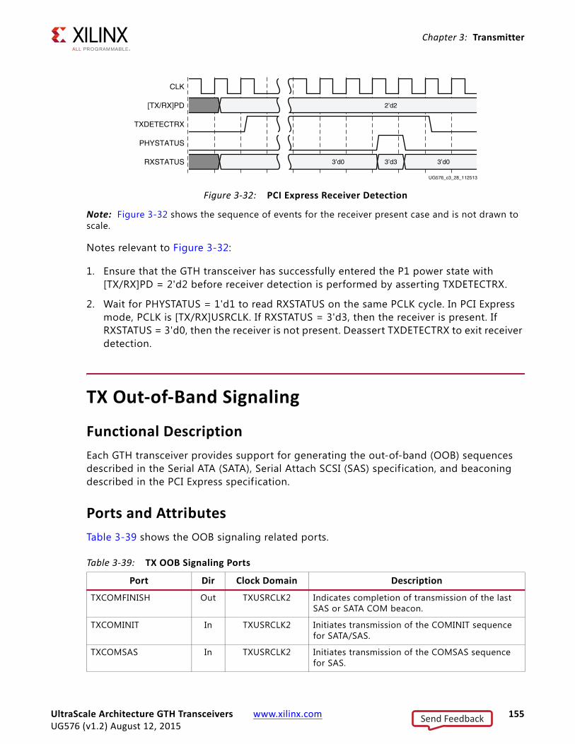
Chapter 3: Transmitter
Note: Figure 3-32 shows the sequence of events for the receiver present case and is not drawn to scale.
Notes relevant to Figure 3-32:
1. Ensure that the GTH transceiver has successfully entered the P1 power state with [TX/RX]PD = 2'd2 before receiver detection is performed by asserting TXDETECTRX.
2. Wait for PHYSTATUS = 1'd1 to read RXSTATUS on the same PCLK cycle. In PCI Express mode, PCLK is [TX/RX]USRCLK. If RXSTATUS = 3'd3, then the receiver is present. If RXSTATUS = 3'd0, then the receiver is not present. Deassert TXDETECTRX to exit receiver detection.
TX Out-of-Band Signaling
Functional DescriptionEach GTH transceiver provides support for generating the out-of-band (OOB) sequences described in the Serial ATA (SATA), Serial Attach SCSI (SAS) specification, and beaconing described in the PCI Express specif ication.
Ports and AttributesTable 3-39 shows the OOB signaling related ports.
X-Ref Target - Figure 3-32
Figure 3-32: PCI Express Receiver Detection
Table 3-39: TX OOB Signaling Ports
Port Dir Clock Domain Description
TXCOMFINISH Out TXUSRCLK2 Indicates completion of transmission of the last SAS or SATA COM beacon.
TXCOMINIT In TXUSRCLK2 Initiates transmission of the COMINIT sequence for SATA/SAS.
TXCOMSAS In TXUSRCLK2 Initiates transmission of the COMSAS sequence for SAS.
CLK
[TX/RX]PD
TXDETECTRX
PHYSTATUS
RXSTATUS
2’d2
3’d0 3’d3 3’d0
UG576_c3_28_112513
UltraScale Architecture GTH Transceivers www.xilinx.com 155UG576 (v1.2) August 12, 2015
Send Feedback

Chapter 3: Transmitter
Table 3-40 shows the OOB signaling attributes.
TXCOMWAKE In TXUSRCLK2 Initiates transmission of the COMWAKE sequence for SATA/SAS.
TXPDELECIDLEMODE In Async Determines if TXELECIDLE and TXPD should be treated as synchronous or asynchronous signals.
1: Asynchronous0: Synchronous
TXPD[1:0] In TXUSRCLK2 Powers down the TX lane according to the PCI Express encoding. 00: P0 normal operation01: P0s low recovery time power down10: P1 longer recovery time, RecDet still on11: P2 lowest power state.
Attributes can control the transition times between these power down mode (PD_TRANS_TIME_FROM_P2, PD_TRANS_TIME_NONE_P2, PD_TRANS_TIME_TO_P2).
Table 3-40: TX OOB Signaling Attributes
Attribute Type Description
SATA_CPLL_CFG String Configuration bits for the CPLL setting related to SAS/SATA.
VCO_3000MHZ = Full rate modeVCO_1500MHZ = ½ rate modeVCO_750MHZ = ¼ rate mode
SATA_BURST_SEQ_LEN[3:0] 4-bit Binary N+1 number of bursts in a COM sequence for SAS/SATA where N is the SATA_BURST_SEQ_LEN value.
TX_IDLE_DATA_ZERO 1-bit Binary When enabled, data sent to the PMA is all zeros during electrical idle. Use the recommended value from the Wizard.
Table 3-39: TX OOB Signaling Ports (Cont’d)
Port Dir Clock Domain Description
UltraScale Architecture GTH Transceivers www.xilinx.com 156UG576 (v1.2) August 12, 2015
Send Feedback

Chapter 4
Receiver
RX Overview
Functional DescriptionThis section shows how to configure and use each of the functional blocks inside the receiver (RX). Each GTH transceiver includes an independent receiver, made up of a PCS and a PMA. Figure 4-1 shows the blocks of the GTH transceiver RX. High-speed serial data flows from traces on the board into the PMA of the GTH transceiver RX, into the PCS, and f inally into the interconnect logic. Refer to Figure 2-11, page 36 for the description of the channel clocking architecture, which provides clocks to the RX and TX clock dividers.
The key elements within the GTH transceiver RX are:
1. RX Analog Front End, page 158
2. RX Out-of-Band Signaling, page 165
3. RX Equalizer (DFE and LPM), page 168
X-Ref Target - Figure 4-1
Figure 4-1: GTH Transceiver RX Block Diagram
From ChannelClocking
Architecture
From TX ParallelData (Near-EndPCS Loopback)
To TX ParallelData (Far-End
PMA Loopback)
To TX Parallel Data (Far-End PCS
Loopback)
RXEQ
RXClock
Dividers
DFE
SIPO
RX OOB
Polarity
PRBSChecker
CommaDetect
andAlign
RX SyncGearbox
RXInterface
8B/10BDecoder RX
ElasticBuffer
RX PIPEControl
RX StatusControl
UG576_c4_01_063014
RX AsyncGearbox
PCIe RXBuffer
BlockDetectAlign
128B/130BDecoder
UltraScale Architecture GTH Transceivers www.xilinx.com 157UG576 (v1.2) August 12, 2015
Send Feedback

Chapter 4: Receiver
4. RX CDR, page 180
5. RX Fabric Clock Output Control, page 184
6. RX Margin Analysis, page 190
7. RX Polarity Control, page 200
8. RX Pattern Checker, page 201
9. RX Byte and Word Alignment, page 203
10. RX 8B/10B Decoder, page 215
11. RX Buffer Bypass, page 220
12. RX Elastic Buffer, page 233
13. RX Clock Correction, page 238
14. RX Channel Bonding, page 246
15. RX Synchronous Gearbox, page 257
16. RX Interface, page 275
RX Analog Front End
Functional DescriptionThe RX analog front end (AFE) is a high-speed current-mode input differential buffer (see Figure 4-1). It has these features:
• Configurable RX termination voltage
• Calibrated termination resistors
UltraScale Architecture GTH Transceivers www.xilinx.com 158UG576 (v1.2) August 12, 2015
Send Feedback

Chapter 4: Receiver
Ports and AttributesTable 4-1 defines the RX AFE ports.
X-Ref Target - Figure 4-2
Figure 4-2: RX Analog Front End
+–
+–
DeviceBoard ACJTAG RX
ACJTAG RX
50Ω
50Ω MGTAVTT Programmable
GNDFLOAT
MGTAVTT
MGTAVTT
~100 nF
~100 nF
RX_CM_SEL[1:0]
UG576_c4_02_020514
GTH Transceivers: RX_CM_TRIM[3:0]
Table 4-1: RX AFE Ports
Port Dir Clock Domain Description
GTHRXN, GTHRXP In (Pad) RX Serial Clock Differential complements of one another forming a differential receiver input pair. These ports represent pads. The location of these ports must be constrained (see Implementation, page 16) and brought to the top level of the design.
RXQPISENN Out Async Sense output that registers a 1 or 0 on the GTHRXN pin.
RXQPISENP Out Async Sense output that registers a 1 or 0 on the GTHRXP pin.
RXQPIEN In Async Enables and disables buffers that drive the sense output ports RXQPISENP and RXQPISENN:1’b0: Disables buffers1’b1: Enables buffers
UltraScale Architecture GTH Transceivers www.xilinx.com 159UG576 (v1.2) August 12, 2015
Send Feedback

Chapter 4: Receiver
Table 4-2 defines the RX AFE attributes.
Table 4-2: RX AFE Attributes
Attribute Type Description
RX_CM_SEL [1:0] 2-bit Binary Controls the mode for the RX termination voltage.2'b00 - AVTT2'b01 - GND2'b10 - Floating2'b11 - Programmable
RX_CM_TRIM [3:0] 4-bit Binary Controls the Common mode in Programmable mode.4’b0000 – 260 mV4’b0001 – 260 mV4’b0010 – 306 mV4’b0011 – 345 mV4’b0100 – 388 mV4’b0101 – 430 mV4’b0110 – 520 mV4’b0111 – 563 mV4’b1000 – 610 mV4’b1001 – 700 mV4’b1010 – 800 mV4’b1011 – 830 mV4’b1100 – 875 mV4’b1101 – 915 mV4’b1110 – 960 mV4’b1111 – 1030 mV
TERM_RCAL_CFG 15-bit Binary Bits [14:0]Controls the internal termination calibration circuit. Reserved. Use the recommended value from the Wizard.
TERM_RCAL_OVRD 3-bit Binary Bits [2:0]:Selects whether the external 100Ω precision resistor is connected to the MGTRREF pin or a value defined by TERM_RCAL_CFG [14:0]. Reserved. Use the recommended value from the Wizard.
RX_CM_BUF_CFG 4-bit Binary Reserved. Use the recommended value from the Wizard.
RX_CM_BUF_PD 1-bit Binary Reserved. Use the recommended value from the Wizard.
UltraScale Architecture GTH Transceivers www.xilinx.com 160UG576 (v1.2) August 12, 2015
Send Feedback

Chapter 4: Receiver
GTH Use Modes—RX Termination
Note: For PCIe® applications, refer to Chapter 6, Use Model.
Table 4-3: Use Mode 1—RX Termination
Use Mode
External AC Coupling
Term Voltage (mV) Usage Notes
1 On 800Attribute settings:• RX_CM_SEL[1:0] = 2'b11• RX_CM_TRIM[3:0] = 4'b1010
X-Ref Target - Figure 4-3
Figure 4-3: Use Mode 1
+–
~100 nF
50Ω
50Ω
Programmable
~100 nF
DEVICEBOARD
ACJTAG RX
ACJTAG RX
MGTAVTT
MGTAVTT
UG576_c4_05_020514
GTH: RX_CM_SEL = 2'b11
GTH: RX_CM_TRIM[3:0]varies from 4'b000 - 4'b1111800 mV = 4’b1010
UltraScale Architecture GTH Transceivers www.xilinx.com 161UG576 (v1.2) August 12, 2015
Send Feedback

Chapter 4: Receiver
Table 4-4: Use Mode 2—RX Termination
Use Mode
External AC Coupling
Term Voltage Usage Notes
2 Off FloatAttribute Settings:• RX_CM_SEL[1:0] = 2'b10
X-Ref Target - Figure 4-4
Figure 4-4: Use Mode 2
50Ω FLOAT
50Ω
DEVICEBOARD
ACJTAG RX
ACJTAG RX
MGTAVTT
MGTAVTT
UG576_c4_06_063014
GTH: RX_CM_SEL = 2'b10
UltraScale Architecture GTH Transceivers www.xilinx.com 162UG576 (v1.2) August 12, 2015
Send Feedback
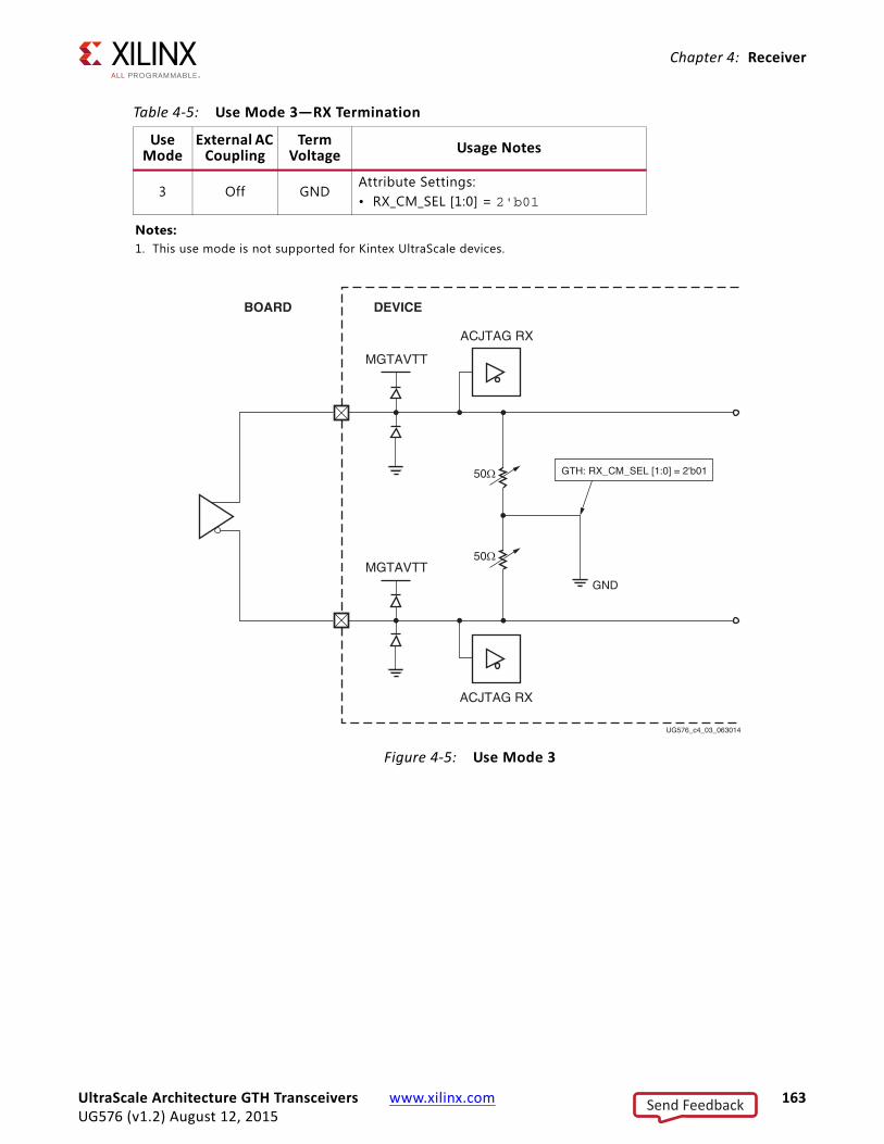
Chapter 4: Receiver
Table 4-5: Use Mode 3—RX Termination
Use Mode
External AC Coupling
Term Voltage Usage Notes
3 Off GNDAttribute Settings:• RX_CM_SEL [1:0] = 2'b01
Notes: 1. This use mode is not supported for Kintex UltraScale devices.
X-Ref Target - Figure 4-5
Figure 4-5: Use Mode 3
50Ω
50Ω
DEVICEBOARD
ACJTAG RX
ACJTAG RX
MGTAVTT
MGTAVTTGND
GTH: RX_CM_SEL [1:0] = 2'b01
UG576_c4_03_063014
UltraScale Architecture GTH Transceivers www.xilinx.com 163UG576 (v1.2) August 12, 2015
Send Feedback

Chapter 4: Receiver
Table 4-6: Use Mode 4—RX Termination
Use Mode
External AC Coupling
Term Voltage Usage Notes
4 Off MGTAVTTAttribute Settings:• RX_CM_SEL[1:0] = 2'b00Note: This only works in LPM mode.
Notes: 1. This use mode is not supported for Kintex UltraScale devices.
X-Ref Target - Figure 4-6
Figure 4-6: Use Mode 4
+–50Ω
50Ω
DEVICEBOARD
ACJTAG RX
ACJTAG RX
MGTAVTT
MGTAVTT
MGTAVTT
GTH: RX_CM_SEL [1:0] = 2'b00
UG576_c4_04_063014
UltraScale Architecture GTH Transceivers www.xilinx.com 164UG576 (v1.2) August 12, 2015
Send Feedback

Chapter 4: Receiver
RX Out-of-Band Signaling
Functional DescriptionThe GTH receiver provides support for decoding the out-of-band (OOB) sequences described in the Serial ATA (SATA) and Serial Attach SCSI (SAS) specif ications and supports beaconing described in the PCI Express specif ication. GTH receiver support for SATA/SAS OOB signaling consists of the analog circuitry required to decode the OOB signal state and state machines to decode bursts of OOB signals for SATA/SAS COM sequences.
The GTH receiver also supports beacons that are PCI Express compliant by using interface signals defined in the PHY Interface for the PCI Express (PIPE) Specification. The interconnect logic decodes the beacon sequence.
Ports and AttributesTable 4-7 defines the OOB signaling related ports.
Table 4-7: RX OOB Signaling Ports
Port Dir Clock Domain Description
RXOOBRESET In Async Reserved. Tie to GND.
RXELECIDLEMODE[1:0] In Async Input signal to control the behavior of RXELECIDLE.2'b00 = RXELECIDLE indicates the status of the OOB signal detection circuit. Use this setting for PCIe, SATA/SAS, and protocols/applications using OOB. In these cases, the OOB circuit must be powered on.2'b11 = RXELECIDLE outputs a static 1'b0. Use this setting for non-OOB protocols.
RXELECIDLE Out Async This output indicates the status of OOB signal detection and is only valid for PCIe, SATA/SAS, and protocols/applications using OOB. In these cases, the OOB circuit must be powered on.0 = Activity is seen on the receiver1 = No activity is seen
For non-OOB protocols, RXELECIDLEMODE[1:0] must be set to 2’b11. RXELECIDLE outputs a static 1’b0 and in this case does not indicate signal detection status.
RXCOMINITDET Out RXUSRCLK2 Indicates reception of the COMINIT sequence for SATA/SAS.
RXCOMSASDET Out RXUSRCLK2 Indicates reception of the COMSAS sequence for SAS.
UltraScale Architecture GTH Transceivers www.xilinx.com 165UG576 (v1.2) August 12, 2015
Send Feedback

Chapter 4: Receiver
Table 4-8 defines the OOB signaling attributes.
RXCOMWAKEDET Out RXUSRCLK2 Indicates reception of the COMWAKE sequence for SATA/SAS.
RXSYSCLKSEL In Async Selects the reference clock source for the RX:2'b00 selects CPLLREFCLK2'b10 selects QPLLREFCLK02'b11 selects QPLLREFCLK1
Table 4-7: RX OOB Signaling Ports (Cont’d)
Port Dir Clock Domain Description
Table 4-8: RX OOB Signaling Attributes
Attribute Type Description
OOB_PWRUP 1-bit Binary OOB power up. The OOB circuit can be optionally powered down when not being used.1'b0 = Circuit powered down1'b1 = Circuit powered up (PCIe, SATA/SAS, protocols/applications using OOB)
OOBDIVCTL[1:0] 2-bit Binary Controls the division of the OOB clk:11 = 810 = 401 = 200 = 1 (no change)
RXELECIDLE_CFG[2:0] 3-bit Binary Reserved. Use the default value from the Wizard.
RXOOB_CLK_CFG 1-bit Binary 1'b0 = Selects sysclk.1'b1 = Selects port sigvalidclk.
RXOOB_CFG[8:0] 9-bit Binary OOB block configuration. Use the default value specif ied by the Wizard.
SATA_BURST_VAL[2:0] 3-bit Binary Number of bursts to declare a COM match for SAS/SATA. The default value is 3'b100.
SATA_EIDLE_VAL[2:0] 3-bit Binary Number of idles to declare a COM match for SAS/SATA. The default value is 3'b100.
SAS_MIN_COM Integer 1-63. Lower bound on activity burst for COM FSM for SAS/SATA. The default value is 36.
SATA_MIN_INIT Integer 1-63. Lower bound on idle count during COMSAS for SAS. The default value is 12.
SATA_MIN_WAKE Integer 1-63. Lower bound on idle count during COMINIT/COMRESET for SAS/SATA. The default value is 4.
SATA_MAX_BURST Integer 1-63. Upper bound on activity burst for COM FSM for SAS/SATA. The default value is 8.
SATA_MIN_BURST Integer 1-61. Lower bound on activity burst for COM FSM for SAS/SATA. The default value is 8.
SAS_MAX_COM Integer 1-127. Upper bound on idle count during COMSAS for SAS. The default value is 64.
UltraScale Architecture GTH Transceivers www.xilinx.com 166UG576 (v1.2) August 12, 2015
Send Feedback
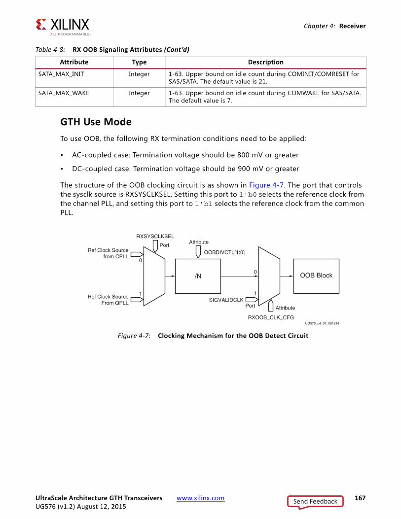
Chapter 4: Receiver
GTH Use ModeTo use OOB, the following RX termination conditions need to be applied:
• AC-coupled case: Termination voltage should be 800 mV or greater
• DC-coupled case: Termination voltage should be 900 mV or greater
The structure of the OOB clocking circuit is as shown in Figure 4-7. The port that controls the sysclk source is RXSYSCLKSEL. Setting this port to 1'b0 selects the reference clock from the channel PLL, and setting this port to 1'b1 selects the reference clock from the common PLL.
SATA_MAX_INIT Integer 1-63. Upper bound on idle count during COMINIT/COMRESET for SAS/SATA. The default value is 21.
SATA_MAX_WAKE Integer 1-63. Upper bound on idle count during COMWAKE for SAS/SATA. The default value is 7.
Table 4-8: RX OOB Signaling Attributes (Cont’d)
Attribute Type Description
X-Ref Target - Figure 4-7
Figure 4-7: Clocking Mechanism for the OOB Detect Circuit
/N OOB Block
Ref Clock Sourcefrom CPLL
Ref Clock SourceFrom QPLL
RXSYSCLKSEL
OOBDIVCTL[1:0]
SIGVALIDCLK
RXOOB_CLK_CFG
Attribute
Attribute
0
1
0
1
Port
Port
UG576_c4_07_061214
UltraScale Architecture GTH Transceivers www.xilinx.com 167UG576 (v1.2) August 12, 2015
Send Feedback

Chapter 4: Receiver
RX Equalizer (DFE and LPM)
Functional DescriptionA serial link bit error rate (BER) performance is a function of the transmitter, the transmission media, and the receiver. The transmission media or channel is bandwidth-limited and the signal traveling through it is subjected to attenuation and distortion.
There are two types of adaptive f iltering available to the GTH receiver depending on system level trade-offs between power and performance. Optimized for power with lower channel loss, the GTH receiver has a power-efficient adaptive mode named the low-power mode (LPM), see Figure 4-8. For equalizing lossier channels, the DFE mode is available. See Figure 4-9 for the GTH transceiver.
The DFE allows better compensation of transmission channel losses by providing a closer adjustment of f ilter parameters than when using a linear equalizer. However, a DFE cannot remove the pre-cursor of a transmitted bit; it only compensates for the post cursors. A linear equalizer allows pre-cursor and post-cursor gain. The GTH RX DFE mode is a discrete-time adaptive high-pass filter. The TAP values of the DFE are the coefficients of this f ilter that are set by the adaptive algorithm.
X-Ref Target - Figure 4-8
Figure 4-8: LPM Mode
FixedGainAGC
KH SIPO
UG576_c4_08_020514
Data to PCS
KL,KH
RX Data Path: LPM Mode
LPMAdaptationController
Ter
min
atio
n
p
n
LinearEQ
KL
UltraScale Architecture GTH Transceivers www.xilinx.com 168UG576 (v1.2) August 12, 2015
Send Feedback

Chapter 4: Receiver
X-Ref Target - Figure 4-9
Figure 4-9: GTH DFE Mode
H2
+ UTDFEKL
H3
H4
H5
+
SIPOData to PCS
RX Data Path: GTH DFE Mode
MMSEAdaptionController
Ter
min
atio
np
n
DFEKL, AGC, UT, H2-HB
VP
LinearEQ
H6
H7
UG576_c4_09_112513
H8
H9
HA
HB
AGC
UltraScale Architecture GTH Transceivers www.xilinx.com 169UG576 (v1.2) August 12, 2015
Send Feedback

Chapter 4: Receiver
Ports and AttributesTable 4-9 defines the RX equalizer ports.
Table 4-9: RX Equalizer Ports
Port Dir Clock Domain Description
RXLPMEN In Async RX datapath0: DFE1: LPM
RXDFELPMRESET In Async Reset for LPM and DFE datapath. Must be toggled after switching between modes to initialize adaptation.
{RXOSHOLD, RXOSOVRDEN} In Async {HOLD,OVRDEN} DFE2'b00: OS Offset cancelation loop adapt2'b10: Freeze current adapt value2'bx1: Override OS value according to attribute RXDFE_OS_CFG0[15:9]
Use the recommended value from the Wizard.
{RXLPMLFHOLD, RXLPMLFKLOVRDEN} In Async {HOLD,OVRDEN} RX LPM2'b00: KL Low frequency loop adapt2'b10: Freeze current adapt value2'bx1: Override KL value according to attribute RXDFELPM_KL_CFG0[15:9]
Use the recommended value from the Wizard.
{RXLPMHFHOLD, RXLPMHFOVRDEN} In Async {HOLD,OVRDEN} RX LPM 2'b00: KH High frequency loop adapt2'b10: Freeze current adapt value2'bx1: Override KH value according to attribute RXDFELPM_KH_CFG0[15:9]
Use the recommended value from the Wizard.
{RXDFEAGCHOLD, RXDFEAGCOVRDEN} In Async {HOLD,OVRDEN} RX DFE2'b00: Automatic gain control (AGC) loop adapt2'b10: Freeze current AGC adapt value2'bx1: Override AGC value according to attribute RXDFE_GC_CFG2[6:2]
Use the recommended value from the Wizard.
{RXDFELFHOLD, RXDFELFOVRDEN} In Async {HOLD,OVRDEN} RX DFE2'b00: KL Low frequency loop adapt2'b10: Freeze current KL adapt value2'bx1: Override KL value according to attribute RXDFELPM_KL_CFG0[15:9]
Use the recommended value from the Wizard.
UltraScale Architecture GTH Transceivers www.xilinx.com 170UG576 (v1.2) August 12, 2015
Send Feedback

Chapter 4: Receiver
{RXDFEUTHOLD, RXDFEUTOVRDEN} In Async {HOLD,OVRDEN} RX DFE2'b00: UT Unrolled threshold loop adapt2'b10: Freeze current UT adapt value2'bx1: Override UT value according to attribute RXDFE_UT_CFG0[15:9]
Use the recommended value from the Wizard.
{RXDFEVPHOLD, RXDFEVPOVRDEN} In Async {HOLD,OVRDEN} RX DFE2'b00: VP Voltage peak loop adapt2'b10: Freeze current VP adapt value2'bx1: Override VP value according to attribute RXDFE_VP_CFG0[15:9]
Use the recommended value from the Wizard.
{RXDFETAP2HOLD, RXDFETAP2OVRDEN} In Async {HOLD,OVRDEN} RX DFE2'b00: TAP2 loop adapt2'b10: Freeze current TAP2 adapt value2'bx1: Override TAP2 value according to attribute RXDFE_H2_CFG0[14:9]
Use the recommended value from the Wizard.
{RXDFETAP3HOLD, RXDFETAP3OVRDEN} In Async {HOLD,OVRDEN} RX DFE2'b00: TAP3 loop adapt2'b10: Freeze current TAP3 adapt value2'bx1: Override TAP3 value according to attribute RXDFE_H3_CFG0[14:9]
Use the recommended value from the Wizard.
{RXDFETAP4HOLD, RXDFETAP4OVRDEN} In Async {HOLD,OVRDEN} RX DFE2'b00: TAP4 loop adapt2'b10: Freeze current TAP4 adapt value2'bx1: Override TAP4 value according to attribute RXDFE_H4_CFG0[13:9]
Use the recommended value from the Wizard.
{RXDFETAP5HOLD, RXDFETAP5OVRDEN} In Async {HOLD,OVRDEN} RX DFE2'b00: TAP5 loop adapt2'b10: Freeze current TAP5 adapt value2'bx1: Override TAP5 value according to attribute RXDFE_H5_CFG0[13:9]
Use the recommended value from the Wizard.
RXMONITORSEL[1:0] In Async Reserved. Use the recommended value from the Wizard.
RXMONITOROUT[6:0] Out Async Reserved. Use the recommended value from the Wizard.
Table 4-9: RX Equalizer Ports (Cont’d)
Port Dir Clock Domain Description
UltraScale Architecture GTH Transceivers www.xilinx.com 171UG576 (v1.2) August 12, 2015
Send Feedback

Chapter 4: Receiver
{RXDFETAP6HOLD, RXDFETAP6OVRDEN} In Async {HOLD,OVRDEN} RX DFE2'b00: TAP6 loop adapt2'b10: Freeze current TAP6 adapt value2'bx1: Override TAP6 value according to attribute RXDFE_H6_CFG0[13:9]
Use the recommended value from the Wizard.
{RXDFETAP7HOLD, RXDFETAP7OVRDEN} In Async {HOLD,OVRDEN} RX DFE2'b00: TAP7 loop adapt2'b10: Freeze current 2'bx1: Override TAP7 value according to attribute RXDFE_H7_CFG0[13:9]
Use the recommended value from the Wizard.
{RXDFETAP8HOLD, RXDFETAP8OVRDEN} In Async {HOLD,OVRDEN} RX DFE2'b00: TAP8 loop adapt2'b10: Freeze current2'bx1: Override TAP8 value according to attribute RXDFE_H8_CFG0[13:9]
Use the recommended value from the Wizard.
{RXDFETAP9HOLD, RXDFETAP9OVRDEN} In Async {HOLD,OVRDEN} RX DFE2'b00: TAP9 loop adapt2'b10: Freeze current2'bx1: Override TAP9 value according to attribute RXDFE_H9_CFG0[13:9]
Use the recommended value from the Wizard.
{RXDFETAP10HOLD, RXDFETAP10OVRDEN} In Async {HOLD,OVRDEN} RX DFE2'b00: TAP10 loop adapt2'b10: Freeze current2'bx1: Override TAP10 value according to attribute RXDFE_HA_CFG0[13:9]
Use the recommended value from the Wizard.
{RXDFETAP11HOLD, RXDFETAP11OVRDEN} In Async {HOLD,OVRDEN} RX DFE2'b00: TAP11 loop adapt2'b10: Freeze current2'bx1: Override TAP11 value according to attribute RXDFE_HB_CFG0[13:9]
Use the recommended value from the Wizard.
Table 4-9: RX Equalizer Ports (Cont’d)
Port Dir Clock Domain Description
UltraScale Architecture GTH Transceivers www.xilinx.com 172UG576 (v1.2) August 12, 2015
Send Feedback

Chapter 4: Receiver
{RXDFETAP12HOLD, RXDFETAP12OVRDEN} In Async {HOLD,OVRDEN} RX DFE2'b00: TAP12 loop adapt2'b10: Freeze current2'bx1: Override TAP12 value according to the reserved attribute TAP12 adapt value
Use the recommended value from the Wizard.
{RXDFETAP13HOLD, RXDFETAP13OVRDEN} In Async {HOLD,OVRDEN} RX DFE2'b00: TAP13 loop adapt2'b10: Freeze current2'bx1: Override TAP13 value according to the reserved attribute TAP13 adapt value
Use the recommended value from the Wizard.
{RXDFETAP14HOLD, RXDFETAP14OVRDEN} In Async {HOLD,OVRDEN} RX DFE2'b00: TAP14 loop adapt2'b10: Freeze current2'bx1: Override TAP14 value according to the reserved attribute TAP14 adapt value
Use the recommended value from the Wizard.
{RXDFETAP15HOLD, RXDFETAP15OVRDEN} In Async {HOLD,OVRDEN} RX DFE2'b00: TAP15 loop adapt2'b10: Freeze current2'bx1: Override TAP15 value according to the reserved attribute TAP15 adapt value
Use the recommended value from the Wizard.
RXDFEAGCCTRL[1:0] In Async RX DFE: Reserved. Use the recommended value from the Wizard.
RXOSINTEN In Async RX LPM & DFE: Reserved. Use the recommended value from the Wizard.
RXOSINTCFG[3:0] In Async RX LPM & DFE: Reserved. Use the recommended value from the Wizard.
RXOSINTOVRDEN In Async RX LPM & DFE: Reserved. Use the recommended value from the Wizard.
RXOSINTSTROBE In Async RX LPM & DFE: Reserved. Use the recommended value from the Wizard.
RXOSINTSTROBESTARTED In Async RX LPM & DFE: Reserved. Use the recommended value from the Wizard.
Table 4-9: RX Equalizer Ports (Cont’d)
Port Dir Clock Domain Description
UltraScale Architecture GTH Transceivers www.xilinx.com 173UG576 (v1.2) August 12, 2015
Send Feedback

Chapter 4: Receiver
Table 4-10 defines the RX equalizer attributes.
{RXOSINTHOLD,RXOSINTTESTOVRDEN} In Async {HOLD,OVRDEN}2'b00: Reserved. Use the recommended value from the Wizard.2'b10: Reserved. Use the recommended value from the Wizard.2'bx1: Reserved. Use the recommended value from the Wizard.
RXDFEVSEN In Async Reserved. Use the recommended value from the Wizard.
RXDFEXYDEN In Async Reserved. Use the recommended value from the Wizard.
RXOSINTDONE Out Async Reserved. Use the recommended value from the Wizard.
RXOSINTSTARTED Out Async Reserved.
RXOSINTSTROBEDONE Out Async Reserved.
{RXLPMOSHOLD, RXLPMOSOVRDEN} In Async {HOLD, OVRDEN} RX LPM2'b00: OS Offset cancelation loop adapt2'b10: Freeze current adapt value2'bx1: Override OS value according to attribute RXLPM_OS_CFG0[15:9]. Use the recommended value from the Wizard.
{RXLPMGCHOLD, RXLPMGCOVRDEN} In Async {HOLD, OVRDEN} RX LPM2'b00: Gain control loop adapt2'b10: Freeze current adapt value2'bx1: Override GC value according to attribute RXLPM_GC_CFG[12:8]. Use the recommended value from the Wizard.
Table 4-9: RX Equalizer Ports (Cont’d)
Port Dir Clock Domain Description
Table 4-10: RX Equalizer Attributes
Attribute Type Description
RX_AFE_CM_EN 1-bit Binary Reserved. Use the recommended value from the Wizard.
RX_BIAS_CFG0 16-bit Binary Reserved. Use the recommended value from the Wizard.
RX_CTLE3_LPF 8-bit Binary Reserved. Use the recommended value from the Wizard.
RX_EN_HI_LR 1-bit Binary Reserved. Use the recommended value from the Wizard.
UltraScale Architecture GTH Transceivers www.xilinx.com 174UG576 (v1.2) August 12, 2015
Send Feedback

Chapter 4: Receiver
RX_SUM_DFETAPREP_EN 1-bit Binary Reserved. Use the recommended value from the Wizard.
RX_SUM_IREF_TUNE 4-bit Binary Reserved. Use the recommended value from the Wizard.
RX_SUM_RES_CTRL 2-bit Binary Reserved. Use the recommended value from the Wizard.
RX_SUM_VCMTUNE 4-bit Binary Reserved. Use the recommended value from the Wizard.
RX_SUM_VCM_OVWR 1-bit Binary Reserved. Use the recommended value from the Wizard.
RX_SUM_VREF_TUNE 3-bit Binary Reserved. Use the recommended value from the Wizard.
RX_TUNE_AFE_OS 2-bit Binary Reserved. Use the recommended value from the Wizard.
RXLPM_OS_CFG0[15:0] 16-bit Binary Reserved. Use the recommended value from the Wizard.
RXLPM_OS_CFG1[15:0] 16-bit Binary Reserved. Use the recommended value from the Wizard.
RXDFE_OS_CFG0[15:0] 16-bit Binary Reserved. Issue the recommended value from the Wizard.
RXDFE_OS_CFG1[15:0] 16-bit Binary Reserved. Issue the recommended value from the Wizard.
RXDFELPM_KL_CFG0[15:0] 16-bit Binary Reserved. Use the recommended value from the Wizard.
RXDFELPM_KL_CFG1[15:0] 16-bit Binary Reserved. Use the recommended value from the Wizard.
RXDFELPM_KL_CFG2[15:0] 16-bit Binary Reserved. Use the recommended value from the Wizard.
RXLPM_KH_CFG0[15:0] 16-bit Binary Reserved. Use the recommended value from the Wizard.
RXLPM_KH_CFG01[15:0] 16-bit Binary Reserved. Use the recommended value from the Wizard.
RXDFE_H2_CFG0[15:0] 16-bit Binary Reserved. Use the recommended value from the Wizard.
RXDFE_H2_CFG1[15:0] 16-bit Binary Reserved. Use the recommended value from the Wizard.
RXDFE_H3_CFG0[15:0] 16-bit Binary Reserved. Use the recommended value from the Wizard.
RXDFE_H3_CFG1[15:0] 16-bit Binary Reserved. Use the recommended value from the Wizard.
RXDFE_H4_CFG0[15:0] 16-bit Binary Reserved. Use the recommended value from the Wizard.
Table 4-10: RX Equalizer Attributes (Cont’d)
Attribute Type Description
UltraScale Architecture GTH Transceivers www.xilinx.com 175UG576 (v1.2) August 12, 2015
Send Feedback
Chapter 4: Receiver
RXDFE_H4_CFG1[15:0] 16-bit Binary Reserved. Use the recommended value from the Wizard.
RXDFE_H5_CFG0[15:0] 16-bit Binary Reserved. Use the recommended value from the Wizard.
RXDFE_H5_CFG1[15:0] 16-bit Binary Reserved. Use the recommended value from the Wizard.
RXDFE_H6_CFG0[15:0] 16-bit Binary Reserved. Use the recommended value from the Wizard.
RXDFE_H6_CFG1[15:0] 16-bit Binary Reserved. Use the recommended value from the Wizard.
RXDFE_H7_CFG0[15:0] 16-bit Binary Reserved. Use the recommended value from the Wizard.
RXDFE_H7_CFG1[15:0] 16-bit Binary Reserved. Use the recommended value from the Wizard.
RXDFE_H8_CFG0[15:0] 16-bit Binary Reserved. Use the recommended value from the Wizard.
RXDFE_H8_CFG1[15:0] 16-bit Binary Reserved. Use the recommended value from the Wizard.
RXDFE_H9_CFG0[15:0] 16-bit Binary Reserved. Use the recommended value from the Wizard.
RXDFE_H9_CFG1[15:0] 16-bit Binary Reserved. Use the recommended value from the Wizard.
RXDFE_HA_CFG0[15:0] 16-bit Binary Reserved. Use the recommended value from the Wizard.
RXDFE_HA_CFG1[15:0] 16-bit Binary Reserved. Use the recommended value from the Wizard.
RXDFE_HB_CFG0[15:0] 16-bit Binary Reserved. Use the recommended value from the Wizard.
RXDFE_HB_CFG1[15:0] 16-bit Binary Reserved. Use the recommended value from the Wizard.
RXDFE_HC_CFG0[15:0] 16-bit Binary Reserved. Use the recommended value from the Wizard.
RXDFE_HC_CFG1[15:0] 16-bit Binary Reserved. Use the recommended value from the Wizard.
RXDFE_HD_CFG0[15:0] 16-bit Binary Reserved. Use the recommended value from the Wizard.
RXDFE_HD_CFG1[15:0] 16-bit Binary Reserved. Use the recommended value from the Wizard.
RXDFE_HE_CFG0[15:0] 16-bit Binary Reserved. Use the recommended value from the Wizard.
RXDFE_HE_CFG1[15:0] 16-bit Binary Reserved. Use the recommended value from the Wizard.
Table 4-10: RX Equalizer Attributes (Cont’d)
Attribute Type Description
UltraScale Architecture GTH Transceivers www.xilinx.com 176UG576 (v1.2) August 12, 2015
Send Feedback

Chapter 4: Receiver
RXDFE_HF_CFG0[15:0] 16-bit Binary Reserved. Use the recommended value from the Wizard.
RXDFE_HF_CFG1[15:0] 16-bit Binary Reserved. Use the recommended value from the Wizard.
RXDFE_UT_CFG0[15:0] 16-bit Binary Reserved. Use the recommended value from the Wizard.
RXDFE_UT_CFG1[15:0] 16-bit Binary Reserved. Use the recommended value from the Wizard.
RXDFE_VP_CFG0[15:0] 16-bit Binary Reserved. Use the recommended value from the Wizard.
RXDFE_VP_CFG1[15:0] 16-bit Binary Reserved. Use the recommended value from the Wizard.
RX_DFE_LPM_HOLD_DURING_EIDLE 1-bit Binary 1'b0: Default setting.1'b1: Restores the DFE contents from internal registers after termination of an electrical idle state for PCI Express operation. Holds the DFE circuit in reset when an electrical idle condition is detected.
Note: For channels with large attenuation (lossy channels typically exceeding 15 dB at Nyquist), Xilinx recommends setting RX_DFE_LPM_HOLD_DURING_EIDLE to 1'b0 because fast transitioning data patterns like the 101010 sequence in CJPAT/CJTPAT can accidentally trigger an electrical idle.
RX_DFELPM_KLKH_AGC_STUP_EN 1-bit Binary Reserved. Use the recommended value from the Wizard.
RX_DFELPM_CFG0[3:0] 4-bit Binary Reserved. Use the recommended value from the Wizard.
RX_DFELPM_CFG1 1-bit Binary Reserved. Use the recommended value from the Wizard.
RX_DFE_KL_LPM_KH_CFG0[1:0] 2-bit Binary Reserved. Use the recommended value from the Wizard.
RX_DFE_KL_LPM_KH_CFG1[2:0] 3-bit Binary Reserved. This attribute is shared between DFE and LPM modes. Use the recommended value from the Wizard.
RX_DFE_KL_LPM_KH_CFG2[3:0] 4-bit Binary Reserved. Use the recommended value from the Wizard.
RX_DFE_KL_LPM_KL_CFG0[1:0] 2-bit Binary Reserved. Use the recommended value from the Wizard.
RX_DFE_KL_LPM_KL_CFG1[2:0] 3-bit Binary Reserved. This attribute is shared between DFE and LPM modes. Use the recommended value from the Wizard.
RX_DFE_AGC_CFG0[1:0] 2-bit Binary Reserved. Use the recommended value from the Wizard.
Table 4-10: RX Equalizer Attributes (Cont’d)
Attribute Type Description
UltraScale Architecture GTH Transceivers www.xilinx.com 177UG576 (v1.2) August 12, 2015
Send Feedback

Chapter 4: Receiver
GTH Use Modes
Choosing Between LPM and DFE Modes
LPM Use Mode
LPM mode is recommended for short reach and low reflection channel applications with channel losses of 14 dB or less at the Nyquist frequency. LPM is preferred for applications where non-random data patterns are used. As Figure 4-8 indicates, in LPM mode the AGC is f ixed. Generally for low loss channels (less than 14 dB at Nyquist), it is advised to not use any TX emphasis and let the RX adaptation handle all the equalization of the link.
RX_DFE_AGC_CFG1[2:0] 3-bit Binary Reserved. This attribute is shared between DFE and LPM modes. Use the recommended value from the Wizard.
ADAPT_CFG0[15:0] 16-bit Binary Reserved. Use the recommended value from the Wizard.
ADAPT_CFG1[15:0] 16-bit Binary Reserved. Use the recommended value from the Wizard.
RX_BIAS_CFG[15:0] 16-bit Binary Reserved. Use the recommended value from the Wizard.
DFE_D_X_REL_POS 1-bit Binary Reserved. Use the recommended value from the Wizard.
DFE_VCM_COMP_EN 1-bit Binary Reserved. Use the recommended value from the Wizard.
RXCFOK_CFG0 16-bit Binary Reserved. Use the recommended value from the Wizard.
RXCFOK_CFG1 16-bit Binary Reserved. Use the recommended value from the Wizard.
RXCFOK_CFG2 16-bit Binary Reserved. Use the recommended value from the Wizard.
RXDFE_CFG0 16-bit Binary Reserved. Use the recommended value from the Wizard.
RXDFE_CFG1 16-bit Binary Reserved. Use the recommended value from the Wizard.
RXDFE_GC_CFG0 16-bit Binary Reserved. Use the recommended value from the Wizard.
RXDFE_GC_CFG1 16-bit Binary Reserved. Use the recommended value from the Wizard.
RXDFE_GC_CFG2 16-bit Binary Reserved. Use the recommended value from the Wizard.
Table 4-10: RX Equalizer Attributes (Cont’d)
Attribute Type Description
UltraScale Architecture GTH Transceivers www.xilinx.com 178UG576 (v1.2) August 12, 2015
Send Feedback

Chapter 4: Receiver
LPM mode does not require data scrambling for proper adaptation. For 8B/10B applications in LPM mode, repeated patterns (idle patterns) with or without scrambling can be used during adaptation.
DFE Use Mode
DFE mode is recommended for high reflection channels, and medium- to long-reach applications with high channel losses of 8 dB and above at the Nyquist frequency. DFE mode has the advantage of equalizing a channel without amplifying noise and crosstalk. Therefore, it is the best choice when crosstalk is a concern or when reflections are identif ied in a single-bit response analysis. In certain low loss applications that require the use of DFE, the AGC is f ixed. Use the default Wizard settings.
DFE mode must be carefully considered in 8B/10B applications or where data scrambling is not employed. To properly adapt to data, the auto adaptation in DFE mode requires incoming data to be random. For example, in a XAUI application, the user payload data is non-scrambled and 8B/10B encoded. While the user payload is generally random, the frequency content of the data is inherently limited by the encoding, and there is nothing defined in the protocol to prevent repeated patterns from occurring. These repeated patterns can cause the auto adapting algorithms to drift away from the ideal equalization setting. Patterns with characteristics similar to PRBS7 (or higher polynomials) are suff iciently random for auto adaptation to properly choose the correct equalization setting.
GTH Transceivers: Switching Between LPM and DFE Modes at Run TimeIn multi-rate applications, it may be required to switch between LPM to DFE. Follow these steps to switch between LPM and DFE modes:
1. To switch from DFE to LPM mode, set RXLPMEN = 1.
2. Several attributes change with data rates and insertion loss. Therefore, it is recommended to generate DFE and LPM wrappers for the same data rate and compare all attributes for differences, then write the corresponding values when switching between the two modes.
3. Reset the receiver’s PMA by pulsing RXPMARESET.
See RX Initialization and Reset, page 58 for more information regarding RXPMARESET.
UltraScale Architecture GTH Transceivers www.xilinx.com 179UG576 (v1.2) August 12, 2015
Send Feedback

Chapter 4: Receiver
RX CDR
Functional DescriptionThe RX clock data recovery (CDR) circuit in each GTHE3_CHANNEL transceiver extracts the recovered clock and data from an incoming data stream. Figure 4-10 illustrates the architecture of the CDR block. Clock paths are shown with dotted lines for clarity.
The GTHE3_CHANNEL transceiver employs phase rotator CDR architecture. Incoming data f irst goes through receiver equalization stages. The equalized data is captured by an edge and a data sampler. The data captured by the data sampler is fed to the CDR state machine and the downstream transceiver blocks.
The CDR state machine uses the data from both the edge and data samplers to determine the phase of the incoming data stream and to control the phase interpolators (PIs). The phase for the edge sampler is locked to the transition region of the data stream while the phase of the data sampler is positioned in the middle of the data eye.
X-Ref Target - Figure 4-10
Figure 4-10: CDR Detail
Linear EQ DFE CDR FSMDEMUX
DEMUX
EdgeSampler
DataSampler
PI(X)
PI(D)
RX DATA
Recovered Clock
RXP/N
UG576_c4_10_112513
PLL
X-Ref Target - Figure 4-11
Figure 4-11: CDR Sampler Positions
E0 E1
UG576_c4_11_112513
E2
D0 D1
UltraScale Architecture GTH Transceivers www.xilinx.com 180UG576 (v1.2) August 12, 2015
Send Feedback

Chapter 4: Receiver
The CPLL or QPLL provides a base clock to the phase interpolator. The phase interpolator in turn produces f ine, evenly spaced sampling phases to allow the CDR state machine to have f ine phase control. The CDR state machine can track incoming data streams that can have a frequency offset from the local PLL reference clock.
Ports and AttributesTable 4-11 defines the CDR ports.
Table 4-12 defines the CDR related attributes.
Table 4-11: CDR Ports
Port Dir Clock Domain Description
RXCDRFREQRESET In Async CDR frequency detector reset. Reserved. Tied Low.
RXCDRHOLD In Async Hold the CDR control loop frozen.
RXCDROVRDEN In Async Reserved.
RXCDRRESET In Async CDR phase detector reset. Reserved. Tied Low.
RXCDRRESETRSV In Async Reserved.
RXRATE[2:0] In RXUSRCLK2 Dynamic pins to automatically change effective PLL dividers in the GTH transceiver RX. These ports are used for PCI Express and other standards. 000: Use RXOUT_DIV attributes 001: Divide by 1010: Divide by 2011: Divide by 4100: Divide by 8 101: Divide by 16110: Divide by 1111: Divide by 1
RXBUF_RESET_ON_RATE_CHANGE attribute enables optional automatic reset.
RXCDRLOCK Out Async Reserved.
RXCDRPHDONE Out Async Reserved.
Table 4-12: CDR Attributes
Attribute Type Description
RXCDR_CFG0_GEN3 16-bit Hex CDR configuration. Use the recommended value from the Wizard.
RXCDR_CFG1_GEN3 16-bit Hex CDR configuration. Use the recommended value from the Wizard.
RXCDR_CFG2_GEN3 16-bit Hex CDR configuration. Use the recommended value from the Wizard.
RXCDR_CFG3_GEN3 16-bit Hex CDR configuration. Use the recommended value from the Wizard.
UltraScale Architecture GTH Transceivers www.xilinx.com 181UG576 (v1.2) August 12, 2015
Send Feedback

Chapter 4: Receiver
RXCDR_CFG4_GEN3 16-bit Hex CDR configuration. Use the recommended value from the Wizard.
RXCDR_CFG5_GEN3 16-bit Hex CDR configuration. Use the recommended value from the Wizard.
RXCDR_CFG0 16-bit Hex CDR configuration. Use the recommended value from the Wizard.
RXCDR_CFG1 16-bit Hex CDR configuration. Use the recommended value from the Wizard.
RXCDR_CFG2 16-bit Hex CDR configuration. Use the recommended value from the Wizard.
RXCDR_CFG3 16-bit Hex CDR configuration. Use the recommended value from the Wizard.
RXCDR_CFG4 16-bit Hex CDR configuration. Use the recommended value from the Wizard.
RXCDR_CFG5 16-bit Hex CDR configuration. Use the recommended value from the Wizard.
RXCDR_LOCK_CFG0 16-bit Hex CDR configuration. Use the recommended value from the Wizard.
RXCDR_LOCK_CFG1 16-bit Hex CDR configuration. Use the recommended value from the Wizard.
RXCDR_LOCK_CFG2 16-bit Hex CDR configuration. Use the recommended value from the Wizard.
RXCDR_HOLD_DURING_EIDLE Binary 1'b0: Default setting.1'b1: Enables the CDR to hold its internal states during an optional reset sequence of an electrical idle state as used in PCI Express operation.
Note: For channels with large attenuation (lossy channels typically exceeding 15 dB at Nyquist), Xilinx recommends setting RXCDR_HOLD_DURING_EIDLE to 1'b0 because fast transitioning data patterns like the 101010 sequence in CJPAT/CJTPAT can accidentally trigger an electrical idle.
RXCDR_FR_RESET_ON_EIDLE Binary 1'b0: Default setting.1'b1: Enables automatic reset of CDR frequency during an optional reset sequence of an electrical idle state as used in PCI Express operation.
Note: For channels with large attenuation (lossy channels typically exceeding 15 dB at Nyquist), Xilinx recommends setting RXCDR_FR_RESET_ON_EIDLE to 1'b0 because fast transitioning data patterns like the 101010 sequence in CJPAT/CJTPAT can accidentally trigger an electrical idle.
Table 4-12: CDR Attributes (Cont’d)
Attribute Type Description
UltraScale Architecture GTH Transceivers www.xilinx.com 182UG576 (v1.2) August 12, 2015
Send Feedback

Chapter 4: Receiver
RXCDR_PH_RESET_ON_EIDLE Binary 1'b0: Default setting.1'b1: Enables automatic reset of CDR phase during an optional reset sequence of an electrical idle state as used in PCI Express operation.
Note: For channels with large attenuation (lossy channels typically exceeding 15 dB at Nyquist), Xilinx recommends setting RXCDR_PH_RESET_ON_EIDLE to 1'b0 because fast transitioning data patterns like the 101010 sequence in CJPAT/CJTPAT can accidentally trigger an electrical idle.
RXPI_CFG0 2-bit Binary Reserved. Issue the recommended value from the Wizard.
RXPI_CFG1 2-bit Binary Reserved. Issue the recommended value from the Wizard.
RXPI_CFG2 2-bit Binary Reserved. Issue the recommended value from the Wizard.
RXPI_CFG3 2-bit Binary Reserved. Issue the recommended value from the Wizard.
RXPI_CFG4 Binary Reserved. Issue the recommended value from the Wizard.
RXPI_CFG5 Binary Reserved. Issue the recommended value from the Wizard.
RXPI_CFG6 3-bit Binary Reserved. Issue the recommended value from the Wizard.
RX_WIDEMODE_CDR 1-bit Binary Reserved. Issue the recommended value from the Wizard.
CDR_SWAP_MODE_EN 1-bit Binary Reserved. Issue the recommended value from the Wizard.
Table 4-12: CDR Attributes (Cont’d)
Attribute Type Description
UltraScale Architecture GTH Transceivers www.xilinx.com 183UG576 (v1.2) August 12, 2015
Send Feedback

Chapter 4: Receiver
RX Fabric Clock Output Control
Functional DescriptionThe RX clock divider control block has two main components: serial clock divider control and parallel clock divider and selector control. The clock divider and selector details are illustrated in Figure 4-12.
Note relevant to Figure 4-12:
1. RXOUTCLKPCS and RXOUTCLKFABRIC are redundant outputs. Use RXOUTCLK for new designs.
X-Ref Target - Figure 4-12
Figure 4-12: RX Serial and Parallel Clock Divider
UG576_c4_12_120613
RX DATA
RXOUTCLKPCS
RXOUTCLK
RXOUTCLKPCS
RXOUTCLKPMA
‘1’
RXPLLREFCLK_DIV1
RXPLLREFCLK_DIV2
RXPROGDIVCLK
RXOUTCLKSELRXOUTCLKFABRIC
000
001
010
011
101
100
SIPO
CPLL
REFCLK Sel
REFCLK Distribution
PhaseInterp.
CDR
DelayAligner
RX PolarityControl
÷D{1,2,4,8,16}
RX PMA
GTHE3_CHANNEL (GTH Transceiver Primitive)
0
10 11 00
11QPLL1REFCLK
10
00 1
RXP/N
QPLL1CLK
QPLL0REFCLK
MGT REFCLK[0/1]N
RXSYSCLKSEL
RXRECCLKOUT
REFCLK_HROW_CK_SEL
QPLL0CLK
RXDLYBYPASS
RX PROG.DIV
÷2
RX DATA toDownstream PCS Blocks
RX PCS
Output toGTHE3_COMMON andGTHE3_CHANNEL
Output Clock to BUFG_GT
O
ODIV2
IBUFDS_GTE3MGT REFCLK[0/1]P
RXPLLCLKSEL
÷{4,5}
÷{2,4}
UltraScale Architecture GTH Transceivers www.xilinx.com 184UG576 (v1.2) August 12, 2015
Send Feedback

Chapter 4: Receiver
2. RXOUTCLK is used as the source of the interconnect logic clock via BUFG_GT.
3. There is only one CPLL in the GTHE3_CHANNEL. QPLLs from the GTHE3_COMMON can also be used when applicable.
4. The selection of the /4 or /5 divider block is controlled by the RX_DATA_WIDTH attribute from the GTHE3_CHANNEL primitive. /4 is selected when RX_DATA_WIDTH = 16, 32, or 64. /5 is selected when RX_DATA_WIDTH = 20, 40, or 80.
5. The selection of the /2 or /4 divider block is controlled by the RX_INT_DATAWIDTH attribute from the GTHE3_CHANNEL primitive. /2 is selected when RX_INT_DATAWIDTH = 0 (2-byte internal datapath) and /4 is selected when RX_INT_DATAWIDTH = 1 (4-byte internal datapath).
6. For details about placement constraints and restrictions on clocking resources (IBUFDS_GTE3, BUFG_GT, BUFG_GT_SYNC, etc.), refer to the UltraScale Architecture Clocking Resources User Guide (UG572) [Ref 3].
Serial Clock Divider
Each transmitter PMA module has a D divider that divides down the clock from the PLL for lower line rate support. This serial clock divider, D, can be set statically for applications with a fixed line rate or it can be changed dynamically for protocols with multiple line rates. The control for the serial divider is described in Table 4-13. For details about the line rate range per speed grade, refer to the data sheet [Ref 6].
To use the D divider in fixed line rate applications, the RXOUT_DIV attribute must be set to the appropriate value, and the RXRATE port needs to be tied to 3'b000. Refer to the Static Setting via Attribute column in Table 4-13 for details.
To use the D divider in multiple line rate applications, the RXRATE port is used to dynamically select the D divider value. The RXOUT_DIV attribute and the RXRATE port must select the same D divider value upon device configuration. After device configuration, the RXRATE is used to dynamically change the D divider value. Refer to the Dynamic Control via Ports column in Table 4-13 for details.
Table 4-13: RX PLL Output Divider Setting
D Divider Value Static Setting via Attribute Dynamic Control via Ports
1RXOUT_DIV = 1
RXRATE = 3'b000RXOUT_DIV = Ignored
RXRATE = 3'b001
2RXOUT_DIV = 2
RXRATE = 3'b000RXOUT_DIV = Ignored
RXRATE = 3'b010
4RXOUT_DIV = 4
RXRATE = 3'b000RXOUT_DIV = Ignored
RXRATE = 3'b011
8RXOUT_DIV = 8
RXRATE = 3'b000RXOUT_DIV = Ignored
RXRATE = 3'b100
UltraScale Architecture GTH Transceivers www.xilinx.com 185UG576 (v1.2) August 12, 2015
Send Feedback

Chapter 4: Receiver
Parallel Clock Divider and Selector
The parallel clock outputs from the RX clock divider control block can be used as an interconnect logic clock depending on the line rate and protocol requirements.
The recommended clock for the interconnect logic is the RXOUTCLK from one of the GTH transceivers. It is also possible to bring the MGTREFCLK directly to the interconnect logic and use as the interconnect logic clock. RXOUTCLK is preferred for general applications because it has an output delay control used for applications that bypass the RX buffer for constant datapath delay. Refer to RX Buffer Bypass, page 220 for more details.
The RXOUTCLKSEL port controls the input selector and allows these clocks to be output via RXOUTCLK port:
• RXOUTCLKSEL = 3'b001: RXOUTCLKPCS path is not recommended to be used as it incurs extra delay from the PCS block.
• RXOUTCLKSEL = 3'b010: RXOUTCLKPMA is the recovered clock that can be brought out to the interconnect logic. The recovered clock is used by protocols that do not have a clock compensation mechanism and require to use a clock synchronous to the data (the recovered clock), to clock the downstream interconnect logic. It is also used by the RX PCS block. This clock is interrupted when the PLL or CDR is reset by one of the related reset signals.
• RXOUTCLKSEL = 3'b011 or 3'b100: RXPLLREFCLK_DIV1 or RXPLLREFCLK_DIV2 is the input reference clock to the CPLL or QPLL depending on the RXSYSCLKSEL setting. For usages that do not require outputting a recovered clock to the interconnect logic, RXPLLREFCLK_DIV1 or RXPLLREFCLK_DIV2 can be used as the system clock. However, RXOUTCLK is usually used as system clock.
RX Programmable Divider
The RX programmable divider shown in Figure 4-12 uses the recovered clock from the CDR to generate a parallel output clock. By using the recovered clock, RX programmable divider, and BUFG_GT, RXOUTCLK (RXOUTCLKSEL = 101) can be used as a clock source for the interconnect logic instead of consuming the interconnect logic PLL or MMCM. The output clock of the programmable divider can also be bought out to the transceiver reference clock pin configured as an output. The supported divider values are 4, 5, 8, 10, 16, 16.5, 20, 32, 33, 40, 64, and 66. Table 4-14 and Table 4-15 show the programmable divider ports and attribute, respectively.
16RXOUT_DIV = 16
RXRATE = 3'b000RXOUT_DIV = Ignored
RXRATE = 3'b101
Table 4-13: RX PLL Output Divider Setting (Cont’d)
D Divider Value Static Setting via Attribute Dynamic Control via Ports
UltraScale Architecture GTH Transceivers www.xilinx.com 186UG576 (v1.2) August 12, 2015
Send Feedback

Chapter 4: Receiver
Ports and AttributesTable 4-16 defines the ports required for RX fabric clock output control.
Table 4-14: Programmable Divider Ports
Port Dir Clock Domain Description
RXPROGDIVRESET In Async This active-High port resets the dividers as well as the RXPRGDIVRESETDONE indicator. Perform a reset whenever the input clock source is interrupted.
RXPRGDIVRESETDONE Out Async When the input clock is stable and reset is performed, this active-High signal indicates the rest is completed and the output clock is stable.
Table 4-15: Programmable Divider Attribute
Attribute Type Description
RX_PROGDIV_CFG Real TX programmable divider ratio. Valid settings are 0.0, 4.0, 5.0, 8.0, 10.0, 16.0, 16.5, 20.0, 32.0, 33.0, 40.0, 64.0, 66.0, 80.0, and 100.0.
RX_DIVRESET_TIME 5-bit Binary Reserved. Represents the time duration to apply the RX programmable divider reset. Use the recommended value from the Wizard. RX_DIVRESET_TIME must be a non-zero value when using RXPROGDIVRESET to initiate the reset process.
Table 4-16: RX Fabric Clock Output Control Ports
Port Dir Clock Domain Description
RXOUTCLKSEL[2:0] In Async This port controls the multiplexer select signal in Figure 4-12.3'b000: Static 13'b001: RXOUTCLKPCS path3'b010: RXOUTCLKPMA path3'b011: RXPLLREFCLK_DIV1 path3'b100: RXPLLREFCLK_DIV2 path3'b101: RXPROGDIVCLK pathOthers: Reserved.
RXRATE[2:0] In RXUSRCLK2 This port dynamically controls the setting for the RX serial clock divider D (see Table 4-13) and it is used with RXOUT_DIV attribute. 3'b000: Use RXOUT_DIV divider value3'b001: Set D divider to 13'b010: Set D divider to 23'b011: Set D divider to 43'b100: Set D divider to 83'b101: Set D divider to 16
UltraScale Architecture GTH Transceivers www.xilinx.com 187UG576 (v1.2) August 12, 2015
Send Feedback

Chapter 4: Receiver
The transceiver has an internal 25 MHz clock derived from the reference clock from the [TX/RX]_CLK25_DIV setting. The 25 MHz clock is used as a synchronizer and timer for various transceiver operations such as reset, power management, rate change, OOB, and beaconing. Set [TX/RX]_CLK25_DIV to achieve 25 MHz or as close as possible. For SATA OOB, this internal clock must be 25 MHz. Table 4-17 defines the attributes required for RX fabric clock output control.
RXOUTCLKFABRIC Out Clock RXOUTCLKFABRIC is a redundant output reserved for testing. Use RXOUTCLK with RXOUTCLKSEL = 3'b011 instead.
RXOUTCLK Out Clock RXOUTCLK is the recommended clock output to the interconnect logic. The RXOUTCLKSEL port is the input selector for RXOUTCLK and allows the PLL input reference clock to the interconnect logic.
RXOUTCLKPCS Out Clock RXOUTCLKPCS is a redundant output. Use RXOUTCLK with RXOUTCLKSEL = 3'b001 instead.
RXRATEDONE Out RXUSRCLK2 The RXRATEDONE port is asserted High for one RXUSRCLK2 cycle in response to a change on the RXRATE port. The TRANS_TIME_RATE attribute defines the period of time between a change on the RXRATE port and the assertion of RXRATEDONE.
RXDLYBYPASS In Async RX delay alignment bypass:0: Uses the RX delay alignment circuit. Set to 1'b0 when the RX buffer is bypassed.1: Bypasses the RX delay alignment circuit. Set to 1’b1 when the RX buffer is used.
RXRATEMODE In Async Determines if RXRATE asynchronously controls the D Output Divider in the RX PMA.
0: Synchronous. When set to 1'b0, an automatic reset sequence occurs in response to a change on the RXRATE port.1: Asynchronous
Table 4-16: RX Fabric Clock Output Control Ports (Cont’d)
Port Dir Clock Domain Description
Table 4-17: RX Fabric Clock Output Control Attributes
Attribute Type Description
TRANS_TIME_RATE 8-bit Hex Reserved. Use the recommended value from the Wizard. This attribute determines when PHYSTATUS and RXRATEDONE are asserted after a rate change.
RXBUF_RESET_ON_RATE_CHANGE Boolean When set to TRUE, this attribute enables automatic RX buffer reset during a rate change event initiated by a change in RXRATE.
RXOUT_DIV Integer This attribute controls the setting for the RX serial clock divider. This attribute is only valid when RXRATE = 3'b000. Otherwise the D divider value is controlled by RXRATE. Valid settings are 1, 2, 4, 8, and 16.
UltraScale Architecture GTH Transceivers www.xilinx.com 188UG576 (v1.2) August 12, 2015
Send Feedback

Chapter 4: Receiver
RXPMACLK_SEL String Reserved. Use the recommended value from the Wizard.
RX_CLK25_DIV Integer This attribute sets a divider that divides down RXPLLREFCLK_DIV1 to generate an internal clock that is used for some of the logic inside the RX portion of the transceiver.
1: RXPLLREFCLK_DIV1 ≤ 25 MHz2: 25 MHz ≤ RXPLLREFCLK_DIV1 ≤ 50 MHz3: 50 MHz ≤ RXPLLREFCLK_DIV1 ≤ 75 MHz4: 75 MHz ≤ RXPLLREFCLK_DIV1 ≤ 100 MHz5: 100 MHz ≤ RXPLLREFCLK_DIV1 ≤ 125 MHz6: 125 MHz ≤ RXPLLREFCLK_DIV1 ≤ 150 MHz7: 150 MHz ≤ RXPLLREFCLK_DIV1 ≤ 175 MHz8: 175 MHz ≤ RXPLLREFCLK_DIV1 ≤ 200 MHz9: 200 MHz ≤ RXPLLREFCLK_DIV1 ≤ 225 MHz10: 225 MHz ≤ RXPLLREFCLK_DIV1 ≤ 250 MHz11: 250 MHz ≤ RXPLLREFCLK_DIV1 ≤ 275 MHz12: 275 MHz ≤ RXPLLREFCLK_DIV1 ≤ 300 MHz13: 300 MHz ≤ RXPLLREFCLK_DIV1 ≤ 325 MHz14: 325 MHz ≤ RXPLLREFCLK_DIV1 ≤ 350 MHz15: 350 MHz ≤ RXPLLREFCLK_DIV1 ≤ 375 MHz16: 375 MHz ≤ RXPLLREFCLK_DIV1 ≤ 400 MHz17: 400 MHz ≤ RXPLLREFCLK_DIV1 ≤ 425 MHz18: 425 MHz ≤ RXPLLREFCLK_DIV1 ≤ 450 MHz19: 450 MHz ≤ RXPLLREFCLK_DIV1 ≤ 475 MHz20: 475 MHz ≤ RXPLLREFCLK_DIV1 ≤ 500 MHz21: 500 MHz ≤ RXPLLREFCLK_DIV1 ≤ 525 MHz22: 525 MHz ≤ RXPLLREFCLK_DIV1 ≤ 550 MHz23: 550 MHz ≤ RXPLLREFCLK_DIV1 ≤ 575 MHz24: 575 MHz ≤ RXPLLREFCLK_DIV1 ≤ 600 MHz25: 600 MHz ≤ RXPLLREFCLK_DIV1 ≤ 625 MHz26: 625 MHz ≤ RXPLLREFCLK_DIV1 ≤ 650 MHz27: 650 MHz ≤ RXPLLREFCLK_DIV1 ≤ 675 MHz28: 675 MHz ≤ RXPLLREFCLK_DIV1 ≤ 700 MHz29: 700 MHz ≤ RXPLLREFCLK_DIV1 ≤ 725 MHz30: 725 MHz ≤ RXPLLREFCLK_DIV1 ≤ 750 MHz31: 750 MHz ≤ RXPLLREFCLK_DIV1 ≤ 775 MHz32: 775 MHz ≤ RXPLLREFCLK_DIV1 ≤ 820 MHz
Table 4-17: RX Fabric Clock Output Control Attributes (Cont’d)
Attribute Type Description
UltraScale Architecture GTH Transceivers www.xilinx.com 189UG576 (v1.2) August 12, 2015
Send Feedback

Chapter 4: Receiver
RX Margin Analysis
Functional DescriptionAs line rates and channel attenuation increase, the receiver equalizers are more often enabled to overcome channel attenuation. This poses a challenge to system bring-up because the quality of the link cannot be determined by measuring the far-end eye opening at the receiver pins. At high line rates, the received eye measured on the printed circuit board can appear to be completely closed even though the internal eye after the receiver equalizer is open.
The GTH transceivers RX eye scan provides a mechanism to measure and visualize the receiver eye margin after the equalizer. Additional use modes enable several other methods to determine and diagnose the effects of equalization settings.
Eye Scan TheoryRXDATA is recovered from the equalized differential waveform by sampling after the RX equalizer. The horizontal sampling position is determined by the CDR function and the vertical position is differential zero. This is indicated as data sample in Figure 4-13.
To enable eye scan functionality, an additional sampler is provided with programmable (horizontal and vertical) offsets from the data sample point. This is indicated as offset sample in Figure 4-13.
X-Ref Target - Figure 4-13
Figure 4-13: Offset Sample and Data Sample to Calculate BER as a Function of Offset—the Statistical Eye
UG576_c4_13_112513
UltraScale Architecture GTH Transceivers www.xilinx.com 190UG576 (v1.2) August 12, 2015
Send Feedback
Chapter 4: Receiver
A single eye scan measurement consists of accumulating the number of data samples (sample count) and the number of times that the offset sample disagreed with the data sample (error count). The bit error ratio (BER) at the programmed vertical and horizontal offset is the ratio of the error count to the sample count. The sample count can range from tens of thousands to greater than 1014.
Repeating such BER measurements for the full array of horizontal and vertical offsets (or a subsampled set of offsets) produces a BER map as shown in Figure 4-13, commonly referred to as a statistical eye, where the color map represents log10(BER). In this view, the eye is apparently smaller than a traditional oscilloscope view (as in Figure 4-13) because it has been closed by very low probability jitter and noise that does not show up in the much lower number of samples of an oscilloscope.
Because this functionality puts no restrictions on the data patterns being received nor requires any changes in the RX settings, it can be performed while application data is being received without error. Furthermore, no interconnect logic is required—only the ability to read and write attributes.
Eye Scan ArchitectureThe blocks with shaded gray in Figure 4-14 describe the portion of the PMA architecture that supports eye scan. The horizontal offset (HORZ_OFFSET) advances or delays the sampling time of the offset samples relative to the data samples. The vertical offset (VERT_OFFSET) raises or lowers the differential voltage threshold to which the equalized waveform is compared. The data samples are deserialized into the Rdata bus, and the offset samples are deserialized into the Sdata bus.
When in DFE mode (RXLPMEN=0), due to the unrolled f irst DFE tap, two separate eye scan measurements are needed, one at +UT and one at –UT, to measure the TOTAL BER at a given vertical and horizontal offset.
UltraScale Architecture GTH Transceivers www.xilinx.com 191UG576 (v1.2) August 12, 2015
Send Feedback

Chapter 4: Receiver
X-Ref Target - Figure 4-14
Figure 4-14: PMA Architecture to Support Eye Scan
UG576_c4_14_112513
DAC
Capture FFRX Input
Unrolled Tap
Equalization
Error-detection,Screening
De-serialization
PCSInterface
Capture FF
Capture FF
+
+
-
DAC PI PI
UT_SIGN (±1)
VERT_OFFSET Rec Clock HORZ_OFFSET
Rdata
Sdata
UltraScale Architecture GTH Transceivers www.xilinx.com 192UG576 (v1.2) August 12, 2015
Send Feedback
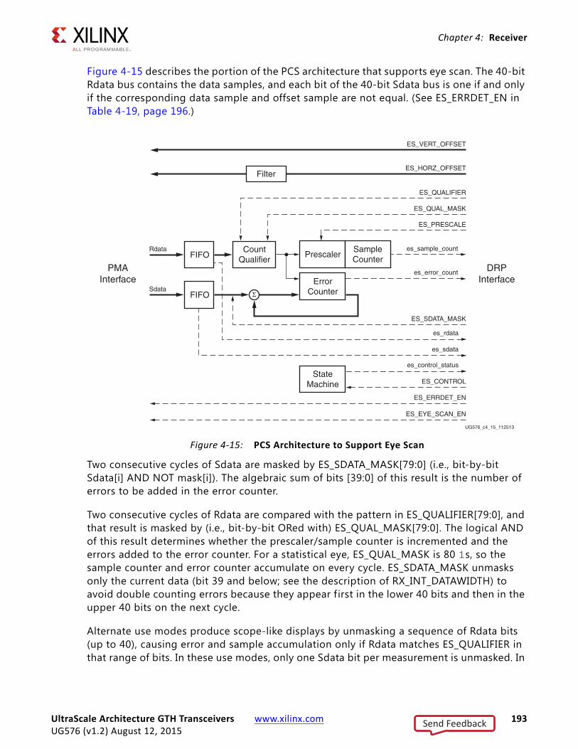
Chapter 4: Receiver
Figure 4-15 describes the portion of the PCS architecture that supports eye scan. The 40-bit Rdata bus contains the data samples, and each bit of the 40-bit Sdata bus is one if and only if the corresponding data sample and offset sample are not equal. (See ES_ERRDET_EN in Table 4-19, page 196.)
Two consecutive cycles of Sdata are masked by ES_SDATA_MASK[79:0] (i.e., bit-by-bit Sdata[i] AND NOT mask[i]). The algebraic sum of bits [39:0] of this result is the number of errors to be added in the error counter.
Two consecutive cycles of Rdata are compared with the pattern in ES_QUALIFIER[79:0], and that result is masked by (i.e., bit-by-bit ORed with) ES_QUAL_MASK[79:0]. The logical AND of this result determines whether the prescaler/sample counter is incremented and the errors added to the error counter. For a statistical eye, ES_QUAL_MASK is 80 1s, so the sample counter and error counter accumulate on every cycle. ES_SDATA_MASK unmasks only the current data (bit 39 and below; see the description of RX_INT_DATAWIDTH) to avoid double counting errors because they appear first in the lower 40 bits and then in the upper 40 bits on the next cycle.
Alternate use modes produce scope-like displays by unmasking a sequence of Rdata bits (up to 40), causing error and sample accumulation only if Rdata matches ES_QUALIFIER in that range of bits. In these use modes, only one Sdata bit per measurement is unmasked. In
X-Ref Target - Figure 4-15
Figure 4-15: PCS Architecture to Support Eye Scan
UG576_c4_15_112513
Rdata
ES_VERT_OFFSET
ES_QUALIFIER
ES_QUAL_MASK
ES_PRESCALE
es_sample_count
es_error_count
es_rdata
es_sdata
es_control_status
ES_CONTROL
ES_ERRDET_EN
ES_EYE_SCAN_EN
ES_SDATA_MASK
ES_HORZ_OFFSETFilter
CountQualifierFIFO
SdataFIFO
Prescaler
DRPInterface
PMAInterface Error
Counter
StateMachine
SampleCounter
UltraScale Architecture GTH Transceivers www.xilinx.com 193UG576 (v1.2) August 12, 2015
Send Feedback
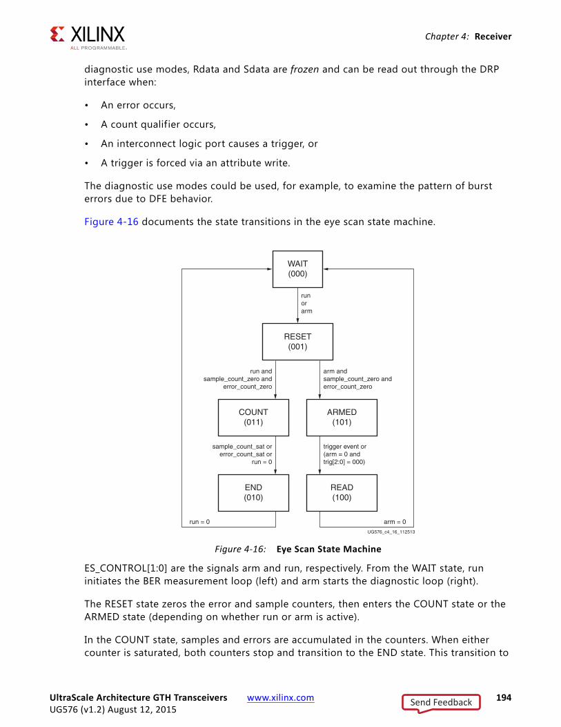
Chapter 4: Receiver
diagnostic use modes, Rdata and Sdata are frozen and can be read out through the DRP interface when:
• An error occurs,
• A count qualif ier occurs,
• An interconnect logic port causes a trigger, or
• A trigger is forced via an attribute write.
The diagnostic use modes could be used, for example, to examine the pattern of burst errors due to DFE behavior.
Figure 4-16 documents the state transitions in the eye scan state machine.
ES_CONTROL[1:0] are the signals arm and run, respectively. From the WAIT state, run initiates the BER measurement loop (left) and arm starts the diagnostic loop (right).
The RESET state zeros the error and sample counters, then enters the COUNT state or the ARMED state (depending on whether run or arm is active).
In the COUNT state, samples and errors are accumulated in the counters. When either counter is saturated, both counters stop and transition to the END state. This transition to
X-Ref Target - Figure 4-16
Figure 4-16: Eye Scan State Machine
UG576_c4_16_112513
runorarm
arm andsample_count_zero anderror_count_zero
run andsample_count_zero and
error_count_zero
WAIT(000)
RESET(001)
COUNT(011)
ARMED(101)
trigger event or(arm = 0 andtrig[2:0] = 000)
arm = 0run = 0
sample_count_sat orerror_count_sat or
run = 0
END(010)
READ(100)
UltraScale Architecture GTH Transceivers www.xilinx.com 194UG576 (v1.2) August 12, 2015
Send Feedback
Chapter 4: Receiver
the END state is detected by polling es_control_status[3:0]. Bit 0 (done) is set active only in the END, READ, and WAIT states. Bits [3:1] display the current state of the state machine.
The END state transitions to the WAIT state when run is set back to zero. The es_sample_count[15:0] and es_error_count[15:0] can be read either in the END or WAIT state.
In the ARMED state, the FIFOs (successive cycles of Rdata and of Sdata) are stopped when a trigger event occurs. The trigger event is either the count qualif ier pulse, the logical OR of all bits into the error counter, or a manual trigger provided from a DRP data input or from a port. One of these four options is selected by trig[3:0] = ES_CONTROL[5:2].
In the READ state, the last two cycles of Rdata can be read from the COE status register, es_rdata[79:0], and the last two cycles of Sdata can be read from the COE status register, es_sdata[79:0].
Ports and AttributesTable 4-18 defines ports related to the RX eye scan function.
Table 4-18: RX Margin Analysis Ports
Port Dir Domain Description
EYESCANDATAERROR Out Async Asserts high for one REC_CLK cycle when an (unmasked) error occurs while in the COUNT or ARMED state.
EYESCANTRIGGER In RXUSRCLK2 Causes a trigger event. See ES_CONTROL[4] below.
RXRATE In RXUSRCLK2 Dynamic pins to automatically change effective PLL dividers in the GTH transceiver RX. These ports are used for PCI Express and other standards. 000: Use RXOUT_DIV attributes 001: Divide by 1010: Divide by 2011: Divide by 4100: Divide by 8 101: Divide by 16110: Divide by 1111: Divide by 1
RXBUF_RESET_ON_RATE_CHANGE attribute enables optional automatic reset.
RXLPMEN In Async When set to 1'b1, the LPM mode with the adaptive linear equalizer is enabled. When set to 1'b0, the high-performance DFE mode is enabled.
EYESCANMODE In Async Reserved.
UltraScale Architecture GTH Transceivers www.xilinx.com 195UG576 (v1.2) August 12, 2015
Send Feedback

Chapter 4: Receiver
Table 4-19 defines RX eye scan attributes. Lower case attribute names indicate R/O.
Table 4-19: RX Margin Analysis Attributes
Attribute Type Description
ES_HORZ_OFFSET 12-bit Hex
Controls the horizontal (phase) offset of the scan sample. [10:0]: Phase offset (two's complement). The center of data eye (0 UI) corresponds to a count of 11'd0 for all data rates. The table below lists the minimum count (representing -0.5 UI) and maximum count (representing +0.5 UI) for each data rate.
Rate min count [dec(bin)] eye center [dec(bin)] max count [dec(bin)]Full -32 (11'b11111100000) +0(11'b00000000000) +32(11'b00000100000)Half -64 (11'b11111000000) +0(11'b00000000000) +64(11'b00001000000)Qrtr -128 (11'b11110000000) +0(11'b00000000000) +128(11'b00010000000)Octal -256 (11'b11100000000) +0(11'b00000000000) +256(11'b00100000000)Hex -512 (11'b11000000000) +0(11'b00000000000) +512(11'b01000000000)
[11]: Phase unification. Must be set to 0 for all positive counts (including zero) and to 1 for all negative counts.
ES_PRESCALE 5-bit Binary
Controls the pre-scaling of the sample count to keep both sample count and error count in reasonable precision within the 16-bit register range. Prescale = 2(1 + register value), so minimum prescale is 2(1+0) = 2 and maximum prescale is 2(1+31) = 4,284,967,296.
ES_SDATA_MASK4, ES_SDATA_MASK3, ES_SDATA_MASK2, ES_SDATA_MASK1, ES_SDATA_MASK0
16-bit Hex
These five 16-bit quantities comprise the 80-bit ES_SDATA_MASK. (ES_SDATA_MASK4[15:0] holds bits [79:64], etc.) This attribute masks up to two cycles of the 40-bit Sdata bus. Binary 1 causes the corresponding bus bit to be masked and binary 0 leaves it unmasked. To support the statistical eye view, the error counter accumulates the total number of unmasked 1s on the most recent cycle of the Sdata bus (masked by ES_SDATA_MASK[39:0]). To support the scope and waveform views, the error counter increments by only one for any non-zero number of unmasked 1s on the previous cycle of the Sdata bus (masked by ES_SDATA_MASK[79:40]). This attribute and ES_QUAL_MASK must also mask out unused bits for bus widths narrower than 40 bits. For the statistical eye view, this attribute would assume the following values as a function of bus width:
40-bit width: ES_SDATA_MASK = ({40{1'b1}}, {40{1'b0}})32-bit width: ES_SDATA_MASK = ({40{1'b1}}, {32{1'b0}}, {8{1'b1}})20-bit width: ES_SDATA_MASK = ({40{1'b1}}, {20{1'b0}}, {20{1'b1}})16-bit width: ES_SDATA_MASK = ({40{1'b1}}, {16{1'b0}}, {24{1'b1}})
Scope and waveform views require a sequence of measurements, unmasking only a single bit per measurement.
UltraScale Architecture GTH Transceivers www.xilinx.com 196UG576 (v1.2) August 12, 2015
Send Feedback

Chapter 4: Receiver
ES_QUALIFIER4, ES_QUALIFIER3, ES_QUALIFIER2, ES_QUALIFIER1, ES_QUALIFIER0
16-bit Hex
These five 16-bit quantities comprise the 80-bit ES_QUALIFIER. (ES_QUALIFIER4[15:0] holds bits [79:64], etc.) Eye scan can qualify BER measurements based on patterns up to 40 contiguous bits long in any position in the input data. Because the data, and therefore the qualif ier pattern, is not aligned, the position of the pattern must be discovered by a barrel-shifting search. For example, looking for the pattern 10'b0011111010 (K28.5 in 8B/10B code) with a 20-bit data width would require a sequence of measurements such as the following, searching for a non-zero sample count at the correct alignment:
ES_QUALIFIER = ({50{1'b?}}, 10'b0011111010, {20{1’b?}})ES_QUALIFIER = ({49{1'b?}}, 10'b0011111010, {21{1'b?}})ES_QUALIFIER = ({48{1'b?}}, 10'b0011111010, {22{1'b?}})…etc… (where ? represents a DON'T CARE bit that will be masked)
The qualif ier pattern is shifted only over the valid bits for the bus width (40, 32, 20, or 16). See the description of RX_INT_DATAWIDTH.
ES_QUAL_MASK4, ES_QUAL_MASK3, ES_QUAL_MASK2, ES_QUAL_MASK1, ES_QUAL_MASK0
16-bit Hex
These five 16-bit quantities comprise the 80-bit ES_QUAL_MASK. (ES_QUAL_MASK4[15:0] holds bits [79:64], etc.) This attribute masks those bits not included in the qualif ier pattern. For example, the corresponding values for the K28.5 example above would be:
ES_QUAL_MASK = ({50{1'b1}}, {10{1'b0}}, {20{1'b1}})ES_QUAL_MASK = ({49{1'b1}}, {10{1'b0}}, {21{1'b1}})ES_QUAL_MASK = ({48{1'b1}}, {10{1'b0}}, {22{1'b1}})…etc…
ES_EYE_SCAN_EN 1-bit Binary
This bit should always be 1 when using Eye Scan. Setting this bit to 0 powers down the Eye Scan circuitry in the PMA and forces the Eye Scan state to WAIT. Re-enabling Eye Scan functionality requires reasserting this bit and asserting/deasserting PMA reset.
ES_ERRDET_EN 1-bit Binary
1: Each bit of the Sdata bus is 1 if and only if the corresponding offset data sample does not agree with the recovered data sample. This is used for the statistical eye view.0: Each bit of the Sdata bus is the recovered data sample. Therefore, if no errors occurred, the Sdata bus would be identical to the Rdata bus. This is used for the scope and waveform views.
Table 4-19: RX Margin Analysis Attributes (Cont’d)
Attribute Type Description
UltraScale Architecture GTH Transceivers www.xilinx.com 197UG576 (v1.2) August 12, 2015
Send Feedback

Chapter 4: Receiver
ES_CONTROL 6-bit Binary
[0]: RUN.Asserting this bit causes a state transition from the WAIT state to the RESET state, initiating a BER measurement sequence.
[1]: ARMAsserting this bit causes a state transition from the WAIT state to the RESET state, initiating a diagnostic sequence. In the ARMED state, deasserting this bit causes a state transition to the READ state if one of the states of bits [5:2] below is not met.
[5:2]: 0001 In the ARMED state, causes a trigger event (transition to the READ state) when an error is detected (i.e., an unmasked 1 on the Sdata bus).0010 In the ARMED state, causes a trigger event (transition to the READ state) when the qualif ier pattern is detected in Rdata.0100 In the ARMED state, causes a trigger event (transition to the READ state) when the eye_scan_trigger port asserts High.1000 In the ARMED state, causes a trigger event (transition to the READ state) immediately.
es_control_status 4-bit Binary
[0]: DONE. Asserted High only in the WAIT, END, or READ states.[3:1]: Current state of the state machine:WAIT 000
RESET 001
COUN 011
END 010
ARMED 101
READ 100
es_rdata_byte4, es_rdata_byte3, es_rdata_byte2, es_rdata_byte1, es_rdata_byte0
16-bit Binary
These five 16-bit quantities comprise the 80-bit es_rdata. (es_rdata_byte4[15:0] holds bits [79:64], etc.) When a trigger event occurs in the ARMED state, es_rdata[39:0] is the present state of the Rdata bus and es_rdata[79:40] is the previous state of the Rdata bus.
es_sdata_byte4, es_sdata_byte3, es_sdata_byte2, es_sdata_byte1, es_sdata_byte0
16-bit Binary
These five 16-bit quantities comprise the 80-bit es_sdata. (es_sdata_byte4[15:0] holds bits [79:64], etc.) When a trigger event occurs in the ARMED state, es_sdata[39:0] is the present state of the Sdata bus and es_sdata[79:40] is the previous state of the Sdata bus.
es_error_count 16-bit Hex
In END and WAIT states, contains the f inal error count for the preceding BER measurement.
es_sample_count 16-bit Hex
In END and WAIT states, contains the f inal sample count for the preceding BER measurement.
RX_DATA_WIDTH Integer Sets the bit width of the RXDATA port. When 8B/10B encoding is enabled, RX_DATA_WIDTH must be set to 20, 40, or 80. Valid settings are 16, 20, 32, 40, 64, and 80.See Interface Width Configuration, page 275 for more details.
Table 4-19: RX Margin Analysis Attributes (Cont’d)
Attribute Type Description
UltraScale Architecture GTH Transceivers www.xilinx.com 198UG576 (v1.2) August 12, 2015
Send Feedback

Chapter 4: Receiver
USE_PCS_CLK_PHASE_SEL 1-bit Binary
If set to 1, the Eye Scan 4T clock phase is determined by ES_CLK_PHASE_SEL.If set to 0, the deserializer phase detector determines the phase of the Eye Scan 4T clock.Under some conditions, the deserializer phase detector might switch within the ±0.5 UI bounds of an eye scan, resulting in incorrect BER measurements at the left and/or right edges of the scan. If this is observed, it can be remedied by asserting USE_PCS_CLK_PHASE_SEL (deasserted by default) and then determining which value of ES_CLK_PHASE SEL provides an eye.
ES_CLK_PHASE_SEL 1-bit Binary
If USE_PCS_CLK_PHASE_SEL is asserted, setting this bit to 1 selects one phase of the Eye Scan 4T clock. Setting it to 0 selects the other phase.
RX_INT_DATAWIDTH Integer 1: 32- or 40-bit interface0: 16- or 20-bit interface(See description of RX_INT_DATAWIDTH in Table 4-49.)Width of valid data on Rdata and Sdata buses is RX interconnect logic data width (see RX_DATA_WIDTH) divided by 2(1–RX_INT_DATAWIDTH).For the different possible bus widths, the previous and current valid Rdata and Sdata bits correspond to the following indices in ES_SDATA_MASK, ES_QUALIFIER, ES_QUAL_MASK, es_rdata, and es_sdata:
valid data width previous data current data 16 [79:64] [39:24] 20 [79:60] [39:20] 32 [79:48] [39: 8] 40 [79:40] [39: 0]
RXOUT_DIV Integer QPLL/CPLL output clock divider D for the RX datapath as shown in Figure 2-11, page 36. See Table 2-11 and Table 2-15.Valid settings are 1, 2, 4, 8, and 16.This attribute sets the divider only if the RXRATE port is set to 3'b000.
ES_PMA_CFG 1-bit Binary
Reserved.
RX_EYESCAN_VS_UT_SIGN 1-bit Binary
1-bit binary UT sign:0: positive unwrapped threshold1: negative unwrapped threshold
Equivalent to ES_VERT_OFFSET[8] in 7 series devices.
RX_EYESCAN_VS_NEG_DIR 1-bit Binary
1-bit binary offset sign:1: negative0: positive
Equivalent to ES_VERT_OFFSET[7] in 7 series devices.
RX_EYESCAN_VS_CODE 7-bit Binary
7-bit binary offset magnitude (centered on ±UT, the unwrapped threshold). Equivalent to ES_VERT_OFFSET[6:0] in 7 series devices.
Table 4-19: RX Margin Analysis Attributes (Cont’d)
Attribute Type Description
UltraScale Architecture GTH Transceivers www.xilinx.com 199UG576 (v1.2) August 12, 2015
Send Feedback

Chapter 4: Receiver
RX Polarity Control
Functional DescriptionIf RXP and RXN differential traces are accidentally swapped on the PCB, the differential data received by the GTH transceiver RX are reversed. The GTH transceiver RX allows inversion to be done on parallel bytes in the PCS after the SIPO to offset reversed polarity on differential pair. Polarity control function uses the RXPOLARITY input, which is driven High from the interconnect logic interface to invert the polarity.
Ports and AttributesTable 4-21 defines the ports required by the RX polarity control function.
RX_EYESCAN_VS_RANGE 2-bit Binary
Sets scale factor for eye scan as follows:00: 1.5 mV/count (default)01: 1.8 mV/count10: 2.2 mV/count11: 2.8 mV/count
EYE_SCAN_SWAP_EN 1-bit Binary
Reserved. Use the recommended value from the Wizard.
Table 4-19: RX Margin Analysis Attributes (Cont’d)
Attribute Type Description
Table 4-20: DRP Address Map for Eye Scan Read-Only (R) Registers
DRP Address Hex (GTH Transceiver) DRP Bits R/W Name Attribute Bit
151 15:0 R es_error_count 15:0
152 15:0 R es_sample_count 15:0
153 3:0 R es_control_status 3:0
154 15:0 R es_rdata_byte4 79:64
155 15:0 R es_rdata_byte3 63:48
156 15:0 R es_rdata_byte2 47:32
157 15:0 R es_rdata_byte1 31:16
158 15:0 R es_rdata_byte0 15:0
159 15:0 R es_sdata_byte4 79:64
15A 15:0 R es_sdata_byte3 63:48
15B 15:0 R es_sdata_byte2 47:32
15C 15:0 R es_sdata_byte1 31:16
15D 15:0 R es_sdata_byte0 15:0
UltraScale Architecture GTH Transceivers www.xilinx.com 200UG576 (v1.2) August 12, 2015
Send Feedback

Chapter 4: Receiver
Using RX Polarity ControlRXPOLARITY can be tied High if the polarity of RXP and RXN needs to be reversed.
RX Pattern Checker
Functional DescriptionThe GTH receiver includes a built-in PRBS checker (see Figure 4-17). This checker can be set to check for one of f ive industry-standard PRBS patterns. The checker is self-synchronizing and works on the incoming data before comma alignment or decoding. This function can be used to test the signal integrity of the channel.
Table 4-21: RX Polarity Control Ports
Port Dir Clock Domain Description
RXPOLARITY In RXUSRCLK2 The RXPOLARITY port can invert the polarity of incoming data:
0: Not inverted. RXP is positive and RXN is negative.1: Inverted. RXP is negative and RXN is positive.
X-Ref Target - Figure 4-17
Figure 4-17: RX Pattern Checker Block
SIPO
PRBS-7 Pattern Checker
PRBS-15 Pattern Checker
PRBS-23 Pattern Checker
PRBS-31 Pattern Checker
ErrorCounter(32 bits)
RX_PRBS_ERR_CNT
RXPRBSERR
RXDATA
RXPRBSSELPolarity
Inversion
Error
UG576_c4_17_112513
PRBS-9 Pattern Checker
UltraScale Architecture GTH Transceivers www.xilinx.com 201UG576 (v1.2) August 12, 2015
Send Feedback
Chapter 4: Receiver
Ports and AttributesTable 4-22 defines the pattern checker ports.
Table 4-22: Pattern Checker Ports
Port Dir Clock Domain Description
RXPRBSCNTRESET In RXUSRCLK2 Resets the PRBS error counter.
RXPRBSSEL[3:0] In RXUSRCLK2 Receiver PRBS checker test pattern control. Only these settings are valid:4’b000: Standard operation mode. (PRBS check is off)4’b0001: PRBS-74’b0010: PRBS-94’b0011: PRBS-154’b0100: PRBS-234’b0101: PRBS-31
After changing patterns, perform a reset of the RX (GTRXRESET, RXPMARESET, or RXPCSRESET) or a reset of the PRBS error counter (RXPRBSCNTRESET) such that the RX pattern checker can attempt to reestablish the link acquired. No checking is done for non-PRBS patterns.
RXPRBSERR Out RXUSRCLK2 This non-sticky status output indicates that PRBS errors have occurred.
RXPRBSLOCKED Out RXUSRCLK2 Output to indicate that the RX PRBS checker has been error free for RXPRBS_LINKACQ_CNT XCLK cycles after reset. Once asserted High, RXPRBSLOCKED does not deassert until reset of the RX pattern checker via a reset of the RX (GTRXRESET, RXPMARESET, or RXPCSRESET in sequential mode) or a reset of the PRBS error counter (RXPRBSCNTRESET).
UltraScale Architecture GTH Transceivers www.xilinx.com 202UG576 (v1.2) August 12, 2015
Send Feedback

Chapter 4: Receiver
Table 4-23 defines the pattern checker attributes.
RX Byte and Word Alignment
Functional DescriptionSerial data must be aligned to symbol boundaries before it can be used as parallel data. To make alignment possible, transmitters send a recognizable sequence, usually called a comma. The receiver searches for the comma in the incoming data. When it f inds a comma, it moves the comma to a byte boundary so the received parallel words match the transmitted parallel words.
Figure 4-18 shows the alignment to a 10-bit comma. The RX receiving unaligned bits are on the right side. The serial data with the comma is highlighted in the middle. Byte aligned RX parallel data is on the left.
Table 4-23: Pattern Checker Attributes
Attribute Type Description
RX_PRBS_ERR_CNT 32-bit Binary PRBS error counter. This counter can be reset by asserting RXPRBSCNTRESET. When a single bit error in incoming data occurs, this counter increments by 1. Single bit errors are counted thus when multiple bit errors occur in incoming data. The counter increments by the actual number of bit errors. Counting begins after RXPRBSLOCKED is asserted High. The counter saturates at 32'hFFFFFFFF. This error counter can only be accessed via the DRP interface. Because the DRP only outputs 16 bits of data per operation, two DRP transactions must be completed to read out the complete 32-bit value. To properly read out the error counter, read out the lower 16 bits at address 0x15E f irst, followed by the upper 16 bits at address 0x15F.
RXPRBS_ERR_LOOPBACK 1-bit Binary When this attribute is set to 1, the RXPRBSERR bit is internally looped back to TXPRBSFORCEERR of the same GTH transceiver. This allows synchronous and asynchronous jitter tolerance testing without worrying about data clock domain crossing. When this attribute is set to 0, TXPRBSFORCEERR is forced onto the TX PRBS.
RXPRBS_LINKACQ_CNT Integer RX pattern checker link acquire count. Used in conjunction with output port RXPRBSLOCKED. After the RX PRBS checker has seen RXPRBS_LINKACQ_CNT XCLK cycles of error-free PRBS data, RXPRBSLOCKED is asserted High. Valid range is 15–255.
UltraScale Architecture GTH Transceivers www.xilinx.com 203UG576 (v1.2) August 12, 2015
Send Feedback

Chapter 4: Receiver
Figure 4-19 shows TX parallel data on the left side, and RX receiving recognizable parallel data after comma alignment on the right side.
Enabling Comma Alignment
To enable the comma alignment block, the RXCOMMADETEN port is driven High. RXCOMMADETEN is driven Low to bypass the block completely for minimum latency.
Configuring Comma Patterns
To set the comma pattern that the block searches for in the incoming data stream, the ALIGN_MCOMMA_VALUE, ALIGN_PCOMMA_VALUE, and ALIGN_COMMA_ENABLE attributes are used. The comma lengths depend on RX_DATA_WIDTH (see Table 4-49, page 278). Figure 4-20 shows how the ALIGN_COMMA_ENABLE masks each of the comma values to allow partial pattern matching.
X-Ref Target - Figure 4-18
Figure 4-18: Conceptual View of Comma Alignment (Aligning to a 10-Bit Comma)
X-Ref Target - Figure 4-19
Figure 4-19: Parallel Data View of Comma Alignment
1001011000010010011010111001100111001011111001011011001010100100010101010101100110
All Subsequent DataAligned to Correct
Byte Boundary
Alignment BlockFinds Comma
Transmitted First
UG576_c4_18_112513
Stream of Serial Data
TX Parallel Data RX Parallel Data
Data0
Comma
Data1
Data2
Non-alignedData
Comma
Data1
Data2
Time
UG576_c4_19_112513
UltraScale Architecture GTH Transceivers www.xilinx.com 204UG576 (v1.2) August 12, 2015
Send Feedback

Chapter 4: Receiver
Figure 4-21 shows how the commas are combined when ALIGN_COMMA_DOUBLE is TRUE.
Figure 4-22 shows how a comma is combined with ALIGN_COMMA_ENABLE to make a wild-carded comma for a 20-bit internal comma. If ALIGN_COMMA_DOUBLE is TRUE, the MCOMMA and PCOMMA patterns are combined so that the block searches for two commas in a row. The number of bits in the comma depends on RX_DATA_WIDTH. Either a 16-bit or a 20-bit comma alignment mode is possible. A double comma is only detected when the received data has a PCOMMA defined by ALIGN_PCOMMA_VALUE followed by an MCOMMA defined by ALIGN_MCOMMA_VALUE with no extra bits in between.
Activating Comma Alignment
Commas are aligned to the closest boundary providing they are found while comma alignment is active. RXMCOMMAALIGNEN is driven High to align on the MCOMMA pattern.
X-Ref Target - Figure 4-20
Figure 4-20: Comma Pattern Masking
X-Ref Target - Figure 4-21
Figure 4-21: Extended Comma Pattern Definition
X-Ref Target - Figure 4-22
Figure 4-22: Extended Comma Pattern Masking
0101111100
xxx1111100
0001111111
ALIGN_MCOMMA_VALUEor
ALIGN_PCOMMA_VALUEPattern Required forComma Detection(x = don’t care)
ALIGN_COMMA_ENABLE UG576_c4_20_112513
ALIGN_MCOMMA_VALUE ALIGN_PCOMMA_VALUE
UG576_c4_21_112513
0010100010
xx10100001
0011111111
0010100001
0011111111
xx10100010
0011111111
ALIGN_MCOMMA_VALUEand
ALIGN_PCOMMA_VALUE(ALIGN_COMMA_DOUBLE = TRUE) Pattern Required for
Comma Detection(x = don’t care)
ALIGN_COMMA_ENABLE UG576_c4_22_112513
UltraScale Architecture GTH Transceivers www.xilinx.com 205UG576 (v1.2) August 12, 2015
Send Feedback

Chapter 4: Receiver
RXPCOMMAALIGNEN is driven High to activate alignment on the PCOMMA pattern. Both enable ports are driven to align to either pattern. When ALIGN_COMMA_DOUBLE is TRUE, both enable ports must always be driven to the same value.
Alignment Status Signals
While MCOMMA or PCOMMA alignment is active, any matching comma pattern causes the block to realign to the closest boundary. After successful alignment, the block holds RXBYTEISALIGNED High. At this time, RXMCOMMAALIGNEN and RXPCOMMAALIGNEN can be driven Low to turn off alignment and keep the current alignment position. RXPCOMMAALIGNEN must be TRUE for PCOMMAs to cause RXBYTEISALIGNED to go High. Similarly, RXMCOMMAALIGNEN must be TRUE for MCOMMAs to cause RXBYTEISALIGNED to go High. Commas can arrive while RXBYTEISALIGNED is High. If the commas arrive aligned to boundaries, there is no change. If the commas arrive out of position while comma alignment is inactive, the block deasserts RXBYTEISALIGNED until the commas are aligned again. If alignment is still activated for the comma that arrives, the block automatically aligns the new comma to the closest boundary and drives RXBYTEREALIGN High for one RXUSRCLK2 cycle.
In applications that operate at a line rate greater than 5 Gb/s and have excessive noise in the system, the byte align block might falsely align to a wrong byte boundary and falsely assert the RXBYTEISALIGNED signal when no valid data is present. In such applications, a system-level check should be in place for checking the validity of the RXBYTEISALIGNED indicator and data.
In systems that use the RX OOB block, such as PCIe and SATA, after locking to a valid byte boundary and asserting the RXBYTEISALIGNED signal, the byte align block might occasionally deassert the RXBYTEISALIGNED signal even when there is no change in the byte boundary. In such applications, RXBYTEISALIGNED should not be used as a valid indicator of the change in byte boundary after the f irst assertion.
Alignment Boundaries
The allowed boundaries for alignment are defined by ALIGN_COMMA_WORD and RX_INT_DATAWIDTH. The spacing of the possible boundaries is determined by RX_DATA_WIDTH, and the number of boundary positions is determined by the number of bytes in the RXDATA interface (refer to Table 4-45, page 275 for RX_DATA_WIDTH and RX_INT_DATAWIDTH settings). Figure 4-23 shows the boundaries that can be selected.
UltraScale Architecture GTH Transceivers www.xilinx.com 206UG576 (v1.2) August 12, 2015
Send Feedback
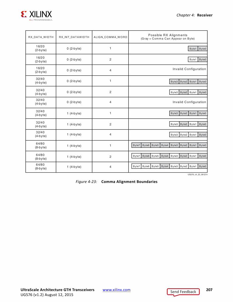
Chapter 4: Receiver
X-Ref Target - Figure 4-23
Figure 4-23: Comma Alignment Boundaries
ALIG N_CO M M A_W O RD
16/20 (2-byte)
Possible RX A lignm ents(Gray = Com m a Can Appear on Byte)
16/20 (2-byte)
16/20 (2-byte)
0 (2-byte)
0 (2-byte)
0 (2-byte)
1
2
4 Invalid Configuration
32/40 (4-byte)
32/40 (4-byte)
32/40 (4-byte)
0 (2-byte)
0 (2-byte)
0 (2-byte)
1
2
4 Invalid Configuration
Byte0Byte1
Byte0Byte1
32/40 (4-byte)
32/40 (4-byte)
32/40 (4-byte)
1 (4-byte)
1 (4-byte)
1 (4-byte)
1
2
4
64/80 (8-byte)
64/80 (8-byte)
64/80 (8-byte)
1 (4-byte)
1 (4-byte)
1 (4-byte)
1
2
4 Byte4Byte5Byte6Byte7
Byte0Byte1Byte2Byte3
Byte0Byte1Byte2Byte3
Byte0Byte1Byte2Byte3
Byte0Byte1Byte2Byte3
Byte0Byte1Byte2Byte3
Byte0Byte1Byte2Byte3
Byte0Byte1Byte2Byte3
Byte0
UG576_c4_23_061214
Byte1Byte2Byte3
Byte4Byte5Byte6Byte7
Byte4Byte5Byte6Byte7
RX_DATA_W IDTH RX_INT_DATAW IDTH
UltraScale Architecture GTH Transceivers www.xilinx.com 207UG576 (v1.2) August 12, 2015
Send Feedback

Chapter 4: Receiver
Manual Alignment
RXSLIDE can be used to override the automatic comma alignment and to shift the parallel data. RXSLIDE is driven High for two RXUSRCLK2 cycles to shift the parallel data by one bit. RXSLIDE must be Low for at least 32 RXUSRCLK2 cycles before it can be used again.
Figure 4-24 shows the waveforms for manual alignment using RXSLIDE in RXSLIDE_MODE = PCS, before and after the data shift. When RXSLIDE_MODE = PCS is used, the number of bit shift positions when consecutive RXSLIDE pulses are issued is also determined by the comma alignment boundary set by ALIGN_COMMA_WORD, RX_DATA_WIDTH, and RX_INT_DATAWIDTH. For example, if the RX_DATA_WIDTH is 20 bits and ALIGN_COMMA_WORD is 1, after the 9th slide operation, the slide position returns back to 0. For the same RX_DATA_WIDTH setting, for an ALIGN_COMMA_WORD setting of 2, the slide position returns to 0 after the 19th slide operation. Thus in RXSLIDE_MODE = PCS, a maximum of 40 bits of sliding is possible when RX_INT_DATAWIDTH= 1 (4-byte) and ALIGN_COMMA_WORD = 4.
Note relevant to Figure 4-24:
1. Latency between the slide and the slide result at RXDATA depends on the number of active RX PCS blocks in the datapath.
X-Ref Target - Figure 4-24
Figure 4-24: Manual Data Alignment Using RXSLIDE for RX_DATA_WIDTH = 20 Bits and RXSLIDE_MODE = PCS
UG576_c4_24_112513
RXUSRCLK2
RXSLIDE
RXDATA
TXDATA 00000000001001111100
00000000000010011111 0000000000100111110000000000000100111110
Slide results on RXDATAafter several cycles of latency
through the PCS path
A minimum of 32 RXUSRCLK2cycles are required between two
RXSLIDE pulses
UltraScale Architecture GTH Transceivers www.xilinx.com 208UG576 (v1.2) August 12, 2015
Send Feedback

Chapter 4: Receiver
Figure 4-25 shows the waveforms for manual alignment using RXSLIDE in RXSLIDE_MODE = PMA before and after the data shift. In this mode, the data is shifted right by one bit for every RXSLIDE pulse issued, but there is some intermediate data with the bits shifted left before the final data appears on the bus. When RXSLIDE_MODE = PMA is used, the RX recovered clock phase is shifted by 2 UI for every alternate RXSLIDE pulse.
Note relevant to Figure 4-25:
1. Latency between the slide and the slide result at RXDATA depends on the number of active RX PCS blocks in the datapath.
X-Ref Target - Figure 4-25
Figure 4-25: Manual Data Alignment Using RXSLIDE for RX_DATA_WIDTH = 20 Bits and RXSLIDE_MODE = PMA
UG576_c4_25_112513
RXUSRCLK2
RXSLIDE
RXDATA
TXDATA 00000000001001111100
00000000000010011111 10000000000001001111 1100000000000010011100000000000100111110
Intermediate Data
Slide results on RXDATAafter several cycles of latency
through the PCS path
A minimum of 32 RXUSRCLK2cycles are required between two
RXSLIDE pulses
UltraScale Architecture GTH Transceivers www.xilinx.com 209UG576 (v1.2) August 12, 2015
Send Feedback

Chapter 4: Receiver
Ports and AttributesTable 4-24 defines the RX byte and word alignment ports.
Table 4-24: RX Byte and Word Alignment Ports
Port Name Dir Clock Domain Description
RXBYTEISALIGNED Out RXUSRCLK2 This signal from the comma detection and realignment circuit is High to indicate that the parallel data stream is properly aligned on byte boundaries according to comma detection.0: Parallel data stream not aligned to byte boundaries1: Parallel data stream aligned to byte boundaries
There are several cycles after RXBYTEISALIGNED is asserted before aligned data is available at the RX interface.RXBYTEISALIGNED responds to plus comma alignment when RXPCOMMAALIGNEN is TRUE. RXBYTEISALIGNED responds to minus comma alignment when RXMCOMMAALIGNEN is TRUE.Alignment Status Signals, page 206 describes some conditions when this signal could deviate from the expected behavior.
RXBYTEREALIGN Out RXUSRCLK2 This signal from the comma detection and realignment circuit indicates that the byte alignment within the serial data stream has changed due to comma detection.0: Byte alignment has not changed1: Byte alignment has changed
Data can be lost or repeated when alignment occurs, which can cause data errors (and disparity errors when the 8B/10B decoder is used).
RXCOMMADET Out RXUSRCLK2 This signal is asserted when the comma alignment block detects a comma. The assertion occurs several cycles before the comma is available at the RX interface.0: Comma not detected1: Comma detected
RXCOMMADETEN In RXUSRCLK2 RXCOMMADETEN activates the comma detection and alignment circuit.0: Bypass the circuit1: Use the comma detection and alignment circuit
Bypassing the comma and alignment circuit reduces RX datapath latency.
UltraScale Architecture GTH Transceivers www.xilinx.com 210UG576 (v1.2) August 12, 2015
Send Feedback

Chapter 4: Receiver
RXPCOMMAALIGNEN In RXUSRCLK2 Aligns the byte boundary when comma plus is detected.0: Disabled1: Enabled.
RXMCOMMAALIGNEN In RXUSRCLK2 Aligns the byte boundary when comma minus is detected.0: Disabled1: Enabled.
RXSLIDE In RXUSRCLK2 RXSLIDE implements a comma alignment bump control. When RXSLIDE is asserted, the byte alignment is adjusted by one bit, which permits determination and control of byte alignment by the interconnect logic. Each assertion of RXSLIDE causes just one adjustment. RXSLIDE must be asserted for a minimum pulse width of two RXUSRCLK2 cycles.RXSLIDE must be deasserted for more than 32 RXUSRCLK2 cycles before it can be reasserted to cause another adjustment.When asserted, RXSLIDE takes precedence over normal comma alignment.For proper operation, set these values:
RXPCOMMAALIGNEN = 0;RXMCOMMAALIGNEN = 0;RXCOMMADETEN = 1;SHOW_REALIGN_COMMA = FALSE
Table 4-24: RX Byte and Word Alignment Ports (Cont’d)
Port Name Dir Clock Domain Description
UltraScale Architecture GTH Transceivers www.xilinx.com 211UG576 (v1.2) August 12, 2015
Send Feedback

Chapter 4: Receiver
Table 4-25 defines the RX byte and word alignment attributes.
Table 4-25: RX Byte and Word Alignment Attributes
Attribute Type Description
ALIGN_COMMA_WORD Integer This attribute controls the alignment of detected commas within a multi-byte datapath.
1: Align comma to either of the 2 bytes for a 2-byte interface, any of the 4 bytes for a 4-byte interface, any of the 8 bytes for an 8-byte interface. The comma can be aligned to either the even bytes or the odd bytes of RXDATA output.2: Align comma to the even bytes only. The aligned comma is guaranteed to be aligned to even bytes RXDATA[9:0] for a 2-byte interface, RXDATA[9:0]/RXDATA[29:20] for a 4-byte interface, RXDATA[9:0]/ RXDATA[29:20]/RX[49:40]/RX[69:60] for an 8-byte interface4: Align comma to a 4-byte boundary. This setting is not allowed for RX_INT_DATAWIDTH = 0. The aligned comma is guaranteed to be aligned to RXDATA[9:0] for a 4-byte interface, and RXDATA[9:0]/RXDATA[49:40] for an 8-byte interface Refer to Figure 4-23, page 207 for comma alignment boundaries allowed for the different ALIGN_COMMA_WORD, RX_DATA_WIDTH and RX_INT_DATAWIDTH settings.
Protocols that send commas in even and odd positions must set ALIGN_COMMA_WORD to 1.
ALIGN_COMMA_ENABLE 10-bit Binary
Sets which bits in MCOMMA/PCOMMA must be matched to incoming data and which bits can be of any value.This attribute is a 10-bit mask with a default value of 1111111111. Any bit in the mask that is reset to 0 effectively turns the corresponding bit in MCOMMA or PCOMMA to a don't care bit.
ALIGN_COMMA_DOUBLE Boolean Specifies whether a comma match consists of either a comma plus or a comma minus alone, or if both are required in the sequence.
FALSE: The plus comma (PCOMMA) and minus comma (MCOMMA) are handled separately. An individual match for either can lead to comma detection and alignment.TRUE: A comma match consists of a comma plus followed immediately by a comma minus. The match pattern is 20 or 16 bits (as determined by RX_DATA_WIDTH).When ALIGN_COMMA_DOUBLE is TRUE, ALIGN_PCOMMA_DET must be the same as ALIGN_MCOMMA_DET, and RXPCOMMAALIGNEN must be the same as RXMCOMMAALIGNEN.
UltraScale Architecture GTH Transceivers www.xilinx.com 212UG576 (v1.2) August 12, 2015
Send Feedback

Chapter 4: Receiver
ALIGN_MCOMMA_VALUE 10-bit Binary
Defines comma minus to raise RXCOMMADET and align the parallel data. The reception order is right to left. (ALIGN_MCOMMA_VALUE [0] is received f irst.) The default value is 10'b1010000011 (K28.5). This definition does not affect 8B/10B encoding or decoding.
ALIGN_MCOMMA_DET Boolean Controls the raising of RXCOMMADET on comma minus.FALSE: Do not raise RXCOMMADET when comma minus is detected.TRUE: Raise RXCOMMADET when comma minus is detected. (This setting does not affect comma alignment.)
ALIGN_PCOMMA_VALUE 10-bit Binary
Defines comma plus to raise RXCOMMADET and align parallel data. The reception order is right to left. (ALIGN_PCOMMA_VALUE [0] is received first.) The default value is 10'b0101111100 (K28.5). This definition does not affect 8B/10B encoding or decoding.
ALIGN_PCOMMA_DET Boolean Controls the raising of RXCOMMADET on comma plus.FALSE: Do not raise RXCOMMADET when comma plus is detected.TRUE: Raise RXCOMMADET when comma plus is detected. (This setting does not affect comma alignment.)
SHOW_REALIGN_COMMA Boolean Defines if a comma that caused realignment is brought out to the RX.
FALSE: Do not bring the comma that causes realignment to the RX. This setting reduces RX datapath latencyTRUE: Bring the realignment comma to the RX.SHOW_REALIGN_COMMA = TRUE should not be used when ALIGN_COMMA_DOUBLE = TRUE or when manual alignment is used.
Table 4-25: RX Byte and Word Alignment Attributes (Cont’d)
Attribute Type Description
UltraScale Architecture GTH Transceivers www.xilinx.com 213UG576 (v1.2) August 12, 2015
Send Feedback

Chapter 4: Receiver
RXSLIDE_MODE String Defines the RXSLIDE mode.OFF: Default setting. The RXSLIDE feature is not used.PCS: PCS is used to perform the bit-slipping function. RXSLIDE is driven High for one RXUSRCLK2 cycle to shift the parallel data (RXDATA) to the left by one bit within the comma alignment boundary determined by the ALIGN_COMMA_WORD, RX_DATA_WIDTH, and RX_INT_DATAWIDTH settings. In this mode, even if RXOUTCLK is sourcing from the RX PMA, the clock phase remains the same. This option requires SHOW_REALIGN_COMMA to be FALSE. PMA: PMA is used to perform the bit-slipping function. RXSLIDE is driven High for one RXUSRCLK2 cycle to shift the parallel data (RXDATA) to the right by one bit. If RXOUTCLK is sourcing from the RX PMA, its phase might be changed. This mode provides minimum variation of latency compared to PCS mode. This option requires SHOW_REALIGN_COMMA to be FALSE. AUTO: This is an automated PMA mode without using the interconnect logic to monitor the RXDATA and issue RXSLIDE pulses. In this mode, RXSLIDE is ignored. In PCIe applications, this setting is used for FTS lane deskew. This option requires SHOW_ALIGN_COMMA to be FALSE. When RX buffer bypass is used, RXSLIDE_MODE cannot be set to AUTO or PMA.
RXSLIDE_AUTO_WAIT Integer Defines how long the PCS (in terms of RXUSRCLK clock cycle) waits for the PMA to auto slide before checking the alignment again. Valid settings are from 0 to 15. The default value is 7. Use the recommended value from the Wizard.
RX_SIG_VALID_DLY Integer Reserved. Use the recommended value from the Wizard.
COMMA_ALIGN_LATENCY 7-bit Binary Current alignment that is used by the byte align block to align the incoming data based on the comma location locked. This register is only accessible via the DRP.
Table 4-25: RX Byte and Word Alignment Attributes (Cont’d)
Attribute Type Description
UltraScale Architecture GTH Transceivers www.xilinx.com 214UG576 (v1.2) August 12, 2015
Send Feedback

Chapter 4: Receiver
RX 8B/10B Decoder
Functional DescriptionIf RX received data is 8B/10B encoded, it must be decoded. The GTH transceiver has a built-in 8B/10B encoder in the GTH transceiver TX and an 8B/10B decoder in the GTH transceiver RX, which includes four one-byte 8B/10B decoder modules on the datapath to decode data without consuming device resources. The RX 8B/10B decoder has these features:
1. Supports 2-byte, 4-byte, and 8-byte datapath operation
2. Provides daisy-chained hookup of running disparity for proper disparity
3. Generates K characters and status outputs
4. Can be bypassed if incoming data is not 8B/10B encoded
5. Pipes out 10-bit literal encoded values when encountering a not-in-table error
8B/10B Bit and Byte Ordering
The order of the bits into the 8B/10B decoder is the opposite of the order shown in Appendix A, 8B/10B Valid Characters. 8B/10B decoding requires bit a0 to be received f irst, but the GTH transceiver always receives the right-most bit f irst. Consequently, the 8B/10B decoder automatically reverses the bit order of received data before decoding it. Decoded data is available on RXDATA ports. Figure 4-26 shows data received by the GTH transceiver RX when RX_DATA_WIDTH = 20, 40, or 80. Data is reconstructed into bytes and sent to the RXDATA interface after the 8B/10B decoder. The number of bits used by RXDATA and corresponding byte orders are determined by RX_DATA_WIDTH.
• Only use RXDATA[15:0] if RX_DATA_WIDTH = 20
• Only use RXDATA[31:0] if RX_DATA_WIDTH = 40
• Use full RXDATA[63:0] if RX_DATA_WIDTH = 80
When the 8B/10B decoder is bypassed but RX_DATA_WIDTH is set to multiple of 10, 10-bit characters are passed to the RX data interface with this format:
• The corresponding RXDISPERR represents the 9th bit
• The corresponding RXCHARISK represents the 8th bit
• The corresponding RXDATA byte represents the [7:0] bits
UltraScale Architecture GTH Transceivers www.xilinx.com 215UG576 (v1.2) August 12, 2015
Send Feedback

Chapter 4: Receiver
RX Running Disparity
Disparity check is performed and the decoder drives the corresponding RXCTRL1 High when the data byte on RXDATA arrives with the wrong disparity. In addition to disparity errors, the 8B/10B decoder detects 20-bit out-of-table error codes. The decoder drives the RXCTRL3 port High when decoder is enabled but a received 10-bit character cannot be mapped into a valid 8B/10B character listed in Appendix A, 8B/10B Valid Characters. The
X-Ref Target - Figure 4-26
Figure 4-26: 8B/10B Decoder Bit and Byte Order
15 14 13 12 11 10 9 8 7 6 5 4 3 2 1 0
31 30 29 28 27 26 25 24 23 22 21 20 19 18 17 16 15 14 13 12 11 10 9 8 7 6 5 4 3 2 1 0
31 30 29 28 27 26 25 24 23 22 21 20 19 18 17 16 15 14 13 12 11 10 9 8 7 6 5 4 3 2 1 0
H1 G1 F1 E1 D1 C1 B1 A1 H0 G0 F0 E0 D0 C0 B0 A0
H3 G3 F3 E3 D3 C3 B3 A3 H2 G2 F2 E2 D2 C2 B2 A2 H1 G1 F1 E1 D1 C1 B1 A1 H0 G0 F0 E0 D0 C0 B0 A0
H3 G3 F3 E3 D3 C3 B3 A3 H2 G2 F2 E2 D2 C2 B2 A2 H1 G1 F1 E1 D1 C1 B1 A1 H0 G0 F0 E0 D0 C0 B0 A0
63 62 61 60 59 58 57 56 55 54 53 52 51 50 49 48 47 46 45 44 43 42 41 40 39 38 37 36 35 34 33 32
H7 G7 F7 E7 D7 C7 B7 A7 H6 G6 F6 E6 D6 C6 B6 A6 H5 G5 F5 E5 D5 C5 B5 A5 H4 G4 F4 E4 D4 C4 B4 A4
j1 h1 g1 f1 i1 e1 d1 c1 b1 a1 j0 h0 g0 f0 i0 e0 d0 c0 b0 a0
j3 h3 g3 f3 i3 e3 d3 c3 b3 a3 j2 h2 g2 f2 i2 e2 d2 c2 b2 a2 j1 h1 g1 f1 i1 e1 d1 c1 b1 a1 j0 h0 g0 f0 i0 e0 d0 c0 b0 a0
RX_DATA_WIDTH = 20
RX_DATA_WIDTH = 40
RX_DATA_WIDTH = 80
RXDATA
RXDATA
8B/10B
8B/10B
8B/10B
RXDATA
RXDATA
MSB
MSB LSB
MSB LSB
LSB
ReceivedLast
ReceivedFirst
ReceivedLast
j3 h3 g3 f3 i3 e3 d3 c3 b3 a3 j2 h2 g2 f2 i2 e2 d2 c2 b2 a2 j1 h1 g1 f1 i1 e1 d1 c1 b1 a1 j0 h0 g0 f0 i0 e0 d0 c0 b0 a0
j7 h7 g7 f7 i7 e7 d7 c7 b7 a7 j6 h6 g6 f6 i6 e6 d6 c6 b6 a6 j5 h5 g5 f5 i5 e5 d5 c5 b5 a5 j4 h4 g4 f4 i4 e4 d4 c4 b4 a4
ReceivedLast
ReceivedFirst
ReceivedFirst
UG576_c4_26_041414
UltraScale Architecture GTH Transceivers www.xilinx.com 216UG576 (v1.2) August 12, 2015
Send Feedback

Chapter 4: Receiver
non-decoded 10-bit character is piped out of the decoder through the RX data interface with this format:
• The corresponding RXCTRL1 represents the 9th bit
• The corresponding RXCTRL0 represents the 8th bit
• The corresponding RXDATA byte represents the [7:0] bits
Figure 4-27 shows a waveform at the RX data interface when the decoder receives good data (A), data with disparity error (B) and an out-of-table character (C).
Special Characters
8B/10B decoding includes special characters (K characters) that are often used for control functions. When RXDATA is a K character, the decoder drives RXCTRL0 High.
If DEC_PCOMMA_DETECT is set to TRUE, the decoder drives the corresponding RXCTRL2 High whenever RXDATA is a positive 8B/10B comma. If DEC_MCOMMA_DETECT is TRUE, the decoder drives the corresponding RXCTRL2 bit High whenever RXDATA is a negative 8B/10B comma.
X-Ref Target - Figure 4-27
Figure 4-27: RX Data with 8B/10B Errors
UG576_c4_27_073114
RXUSRCLK2
RXDATA GoodData
Out ofTable
DispError
GoodData
RXCTRL1
RXCTRL3
A B C
UltraScale Architecture GTH Transceivers www.xilinx.com 217UG576 (v1.2) August 12, 2015
Send Feedback

Chapter 4: Receiver
Ports and AttributesTable 4-26 defines the ports required by RX 8B/10B decoder.
Table 4-26: RX 8B/10B Decoder Ports
Port Dir Clock Domain Description
RX8B10BEN In RXUSRCLK2 RX8B10BEN selects the use of the 8B/10B decoder in the RX datapath, just after the comma detection/realignment block. If this input is Low, the literal 10-bit data comes out as {RXCTRL1, RXCTRL0, RXDATA<8 bits>}.
1: 8B/10B decoder enabled0: 8B/10B decoder bypassed (reduces latency)
RXCTRL2[7:0] Out RXUSRCLK2 Active High indicates the corresponding byte shown on RXDATA is a comma character.
RXCTRL2[7] corresponds to RXDATA[63:56]RXCTRL2[6] corresponds to RXDATA[55:48]RXCTRL2[5] corresponds to RXDATA[47:40]RXCTRL2[4] corresponds to RXDATA[39:32]RXCTRL2[3] corresponds to RXDATA[31:24]RXCTRL2[2] corresponds to RXDATA[23:16]RXCTRL2[1] corresponds to RXDATA[15:8]RXCTRL2[0] corresponds to RXDATA[7:0]
RXCTRL0[15:0] In RXUSRCLK2 Active High indicates the corresponding byte shown on RXDATA is a K character when 8B/10B decoding is enabled. RXCTRL0[15:8] are unused.
RXCTRL0[7] corresponds to RXDATA[63:56]RXCTRL0[6] corresponds to RXDATA[55:48]RXCTRL0[5] corresponds to RXDATA[47:40]RXCTRL0[4] corresponds to RXDATA[39:32]RXCTRL0[3] corresponds to RXDATA[31:24]RXCTRL0[2] corresponds to RXDATA[23:16]RXCTRL0[1] corresponds to RXDATA[15:8]RXCTRL0[0] corresponds to RXDATA[7:0]This is bit 8 of non-decoded data if the 8B/10B decoder is bypassed or the corresponding bit of RXCTRL3 is High. Refer to RX Interface, page 275.
UltraScale Architecture GTH Transceivers www.xilinx.com 218UG576 (v1.2) August 12, 2015
Send Feedback

Chapter 4: Receiver
RXCTRL1[15:0] Out RXUSRCLK2 Active High indicates the corresponding byte shown on RXDATA has a disparity error. RXCTRL1[15:8] are unused.
RXCTRL1[7] corresponds to RXDATA[63:56]RXCTRL1[6] corresponds to RXDATA[55:48]RXCTRL1[5] corresponds to RXDATA[47:40]RXCTRL1[4] corresponds to RXDATA[39:32]RXCTRL1[3] corresponds to RXDATA[31:24]RXCTRL1[2] corresponds to RXDATA[23:16]RXCTRL1[1] corresponds to RXDATA[15:8]RXCTRL1[0] corresponds to RXDATA[7:0]This is bit 9 of non-decoded data if the 8B/10B decoder is bypassed or the corresponding bit of RXCTRL3 is High. Refer to RX Interface, page 275.
RXCTRL3[7:0] Out RXUSRCLK2 Active High indicates the corresponding byte shown on RXDATA was not a valid character in the 8B/10B table.
RXCTRL3[7] corresponds to RXDATA[63:56]RXCTRL3[6] corresponds to RXDATA[55:48]RXCTRL3[5] corresponds to RXDATA[47:40]RXCTRL3[4] corresponds to RXDATA[39:32]RXCTRL3[3] corresponds to RXDATA[31:24]RXCTRL3[2] corresponds to RXDATA[23:16]RXCTRL3[1] corresponds to RXDATA[15:8]RXCTRL3[0] corresponds to RXDATA[7:0]
Table 4-27: RX 8B/10B Decoder Attributes
Attribute Type Description
RX_DISPERR_SEQ_MATCH String Specifies whether the disparity error status of a decoded byte must match the indicator in the channel bonding and clock correction sequence.When TRUE, indicates the disparity error status must be matched.When FALSE, ignores the disparity error status.
DEC_MCOMMA_DETECT String When set to TRUE, drives the per byte flag RXCTRL2 High when an MCOMMA is detected.When set to FALSE, RXCTRL2 is Low when a negative comma is detected.
DEC_PCOMMA_DETECT String When set to TRUE, drives the per byte flag RXCTRL2 High when a PCOMMA is detected.When set to FALSE, RXCTRL2 is Low when a positive comma is detected.
Table 4-26: RX 8B/10B Decoder Ports (Cont’d)
Port Dir Clock Domain Description
UltraScale Architecture GTH Transceivers www.xilinx.com 219UG576 (v1.2) August 12, 2015
Send Feedback

Chapter 4: Receiver
Enabling and Disabling 8B/10B DecodingTo enable the 8B/10B decoder, RX8B10BEN must be driven High. RX_DATA_WIDTH must be set to a multiple of 10 (20, 40, 80) with the 8B/10B decoder enabled.
To disable the 8B/10B decoder on the GTH receiver path, RX8B10BEN must be driven Low. When the encoder is disabled, RX_DATA_WIDTH can be set to a multiple of 8 or 10 (16, 20, 32, 40, 64, 80). The operation of the RXDATA port with 8B/10B decoding bypassed is described in RX Interface, page 275.
RX Buffer Bypass
Functional DescriptionBypassing the RX elastic buffer is an advanced feature of the GTH transceiver. The RX phase alignment circuit is used to adjust the phase difference between the SIPO parallel clock domain and the RX XCLK domain in order to effect reliable data transfer from the SIPO into the PCS. It also performs the RX delay alignment by adjusting the RXUSRCLK to compensate for the temperature and voltage variations. The combined RX phase and delay alignments can be automatically performed by the GTH transceiver or manually controlled. Figure 4-36 shows the XCLK and RXUSRCLK domains, and Table 4-31 shows trade-offs between buffering and phase alignment.
The RX elastic buffer can be bypassed to reduce latency when the RX recovered clock is used to source RXUSRCLK and RXUSRCLK2. When the RX elastic buffer is bypassed, latency through the RX datapath is low and deterministic, but clock correction and channel bonding are not available.
Figure 4-28 shows how RX phase alignment allows the RX elastic buffer to be bypassed. Before RX phase alignment, there is no guaranteed phase relationship between the SIPO parallel clock domain and the RX XCLK domain. RX XCLK is configured to use RXUSRCLK
DEC_VALID_COMMA_ONLY String When set to TRUE, drives the per byte flag RXCTRL2 High when only IEEE 802.3 valid commas K28.1, K28.5, and K28.7 are detected.When set to FALSE, RXCTRL2 is for positive or negative 8B/10B commas, depending how you set DEC_PCOMMA_DETECT and DEC_MCOMMA_DETECT.
RX_DATA_WIDTH 3-bit Binary The PCS data width is set at the interconnect logic interface with values of 16, 20, 32, 40, 64, or 80 (if 8B/10B decoding is not used) or 20, 40, 80 (if 8B/10B decoding is used).
Table 4-27: RX 8B/10B Decoder Attributes (Cont’d)
Attribute Type Description
UltraScale Architecture GTH Transceivers www.xilinx.com 220UG576 (v1.2) August 12, 2015
Send Feedback

Chapter 4: Receiver
when using RX phase alignment. RX phase alignment selects a phase shifted version of the RX recovered clock from the CDR (XCLK) so that there is no significant phase difference between SIPO parallel clock and RX XCLK.
When RX buffer bypass is used, RXSLIDE_MODE cannot be set to AUTO or PMA.
Ports and AttributesTable 4-28 defines the RX buffer bypass ports.
X-Ref Target - Figure 4-28
Figure 4-28: Using RX Phase Alignment
From ChannelClocking
Architecture
From TX ParallelData (Near-EndPCS Loopback)
To TX ParallelData (Far-End
PMA Loopback)
To TX ParallelData (Far-End PCS
Loopback)
Device ParallelClock
(RXUSRCLK2)
PCS ParallelClock
(RXUSRCLK)
PMA ParallelClock
(XCLK)
RX SerialClock
RXEQ
RXClock
Dividers
DFE
SIPO
RX OOB
Polarity
PRBSChecker
CommaDetect
andAlign
RXGear-box
RXInterface8B/10B
Decoder
Bypass RX Elastic Buffer
After RX phase alignment:- SIPO parallel clock phase matches RXUSRCLK phase.- No phase difference between XCLK and RXUSRCLK.
RXElasticBuffer
RX PIPEControl
RX StatusControl
UG576_c4_28_063014
RX CDR
Table 4-28: RX Buffer Bypass Ports
Port Dir Clock Domain Description
RXPHDLYRESET In Async RX phase alignment hard reset to force RXUSRCLK to the center of the delay alignment tap. The delay alignment tap has a full range of ±4 ns and a half range of ±2 ns. This hard reset can be used to initiate the GTH transceiver to perform the RX phase and delay alignment automatically when all other RX buffer bypass input ports are set Low. Xilinx recommends using RXDLYSRESET only for phase and delay alignment.
RXPHALIGN In Async Sets the RX phase alignment. Tied Low when using the auto alignment mode.
RXPHALIGNEN In Async RX phase alignment enable. Tied Low when using the auto alignment mode.
UltraScale Architecture GTH Transceivers www.xilinx.com 221UG576 (v1.2) August 12, 2015
Send Feedback

Chapter 4: Receiver
RXPHDLYPD In Async RX phase and delay alignment circuit power down. Tied High when a) RXPD is asserted orb) RXOUTCLKSEL is set to 3'b010 but the recovered clock is not available. Tied Low during RX buffer bypass mode normal operation.
0: Power-up the RX phase and delay alignment circuit.1: Power-down the RX phase and delay alignment circuit.
RXPHOVRDEN In Async RX phase alignment counter override enable. Tied Low when not in use.
0: Normal operation.1: Enables the RX phase alignment counter override with the RXPH_CFG[10:6] value.
RXDLYSRESET In Async RX delay alignment soft reset to gradually shift RXUSRCLK to the center of the delay alignment tap. The delay alignment tap has a full range of ±4 ns and a half range of ±2 ns. This soft reset can be used to initiate the GTH transceiver to perform the RX phase and delay alignment automatically when all other RX bypass buffer input ports are Low.
RXDLYBYPASS In Async RX delay alignment bypass.0: Uses the RX delay alignment circuit.1: Bypasses the RX delay alignment circuit.
RXDLYEN In Async RX delay alignment enable. Tied Low when not in use.
RXDLYOVRDEN In Async RX delay alignment counter override enable. Tied Low when not in use.
0: Normal operation.1: Enables the RX delay alignment counter override with the RXDLY_CFG[14:6] value.
RXPHALIGNDONE Out Async RX phase alignment done. When the auto RX phase and delay alignment are used, the second rising edge of RXPHALIGNDONE detected after RXDLYSRESETDONE assertion indicates RX phase and delay alignment are done.The alignment of data in RXDATA can change after the second rising edge of RXPHALIGNDONE.
RXDLYSRESETDONE Out Async RX delay alignment soft reset done.
RXSYNCMODE In Async 0: RX Buffer Bypass Slave lane1: RX Buffer Bypass Master laneThis input is not used in multi-lane manual mode.
Table 4-28: RX Buffer Bypass Ports (Cont’d)
Port Dir Clock Domain Description
UltraScale Architecture GTH Transceivers www.xilinx.com 222UG576 (v1.2) August 12, 2015
Send Feedback

Chapter 4: Receiver
Table 4-29 defines the RX buffer attributes.
RXSYNCALLIN In Async Single-lane auto mode: Connect this input to its own RXPHALIGNDONE.Multi-lane auto mode: Connect this input to the ANDed signal of RXPHALIGNDONE of the master and all slave lanes.Multi-lane manual mode: This input is not used in multi-lane manual mode.
RXSYNCIN In Async Only valid in multi-lane auto mode applications. Connect this input to RXSYNCOUT from RX buffer bypass master lane.
RXSYNCOUT Out Async Only valid for RX buffer bypass master lane in multi-lane auto mode applications. Connect this signal to the RXSYNCIN of each lane within the multi-lane application.
RXSYNCDONE Out Async Indicates RX Buffer Bypass alignment procedure completion. Only valid for RX buffer bypass master lane in auto mode operation.
RXSLIPOUTCLK In RXUSRCLK2 Reserved. Use the recommended value from the Wizard.
RXSLIPPMA In RXUSRCLK2 Reserved. Use the recommended value from the Wizard.
RXPHALIGNERR Out Async RX phase align error.
Table 4-29: RX Buffer Bypass Attributes
Attribute Type Description
RXBUF_EN Boolean Use or bypass the RX elastic buffer.TRUE: Uses the RX elastic buffer (default).FALSE: Bypasses the RX elastic buffer (advanced feature).
RX_XCLK_SEL String Selects the clock source used to drive the RX parallel clock domain (XCLK).
RXDES: Selects the RX recovered clock as source of XCLK. Used when using the RX elastic buffer.RXUSR: Selects RXUSRCLK as the source of XCLK. Used when bypassing the RX elastic buffer.
RXPH_CFG 24-bit Binary Reserved. Use the recommended value from the Wizard.
RXPH_MONITOR_SEL 5-bit Binary Reserved. Use the recommended value from the Wizard.
RXPHDLY_CFG 24-bit Binary RX phase and delay alignment configuration. RXPHDLY_CFG[19] = 1 is used to set the RX delay alignment tap to the full range of ±4 ns. RXPHDLY_CFG[19] = 0 is used to set the RX delay alignment tap to the half range of ±2 ns.Reserved. Use the recommended value from the Wizard.
RXDLY_CFG 16-bit Binary Reserved. Use the recommended value from the Wizard.
Table 4-28: RX Buffer Bypass Ports (Cont’d)
Port Dir Clock Domain Description
UltraScale Architecture GTH Transceivers www.xilinx.com 223UG576 (v1.2) August 12, 2015
Send Feedback

Chapter 4: Receiver
RX Buffer Bypass Use ModesRX phase alignment can be performed on one channel (single lane) or a group of channels sharing a single RXOUTCLK (multi-lane). RX buffer bypass supports single-lane auto mode, and multi-lane applications in manual and auto mode (Table 4-30).
RXDLY_LCFG 9-bit Binary Reserved. Use the recommended value from the Wizard.
RXDLY_TAP_CFG 16-bit Binary Reserved. Use the recommended value from the Wizard.
RX_DDI_SEL 6-bit Binary RX data delay insertion select.Reserved. Use the recommended value from the Wizard.
RXSYNC_MULTILANE 1-bit Binary Indicates whether the lane is used as part of a multi-lane interface. Only valid on RX buffer bypass master lane in auto mode.
0: This lane is used in single-lane mode.1: This lane is used in multi-lane mode.
RXSYNC_SKIP_DA 1-bit Binary Control to skip delay alignment procedure. Only valid on RX buffer bypass master lane in auto mode.
0: RX delay alignment procedure occurs.1: RX delay alignment procedure is skipped.
RXSYNC_OVRD 1-bit Binary Manual mode override.0: RX Buffer bypass auto mode is enabled.1: RX Buffer bypass manual mode is used. RX Buffer bypass control is implemented in interconnect logic.
TST_RSV[0] 1-bit Binary 0: Normal.1: Override data delay insertion (DDI) delay setting with RX_DDI_SEL attribute.
RX_CLK_SLIP_OVRD 5-bit Binary Reserved. Use the recommended value from the Wizard.
Table 4-30: RX Buffer Bypass Use Modes
RX Buffer Bypass GTH Transceiver
Single-Lane Auto
Multi-Lane Manual or Auto
Notes: 1. In stacked silicon interconnect (SSI) technology devices, systems that require multi-lane RX buffer bypass crossing
the SLR boundaries need custom-made clocking topology and characterization. This use case is generally not supported or guaranteed.
Table 4-29: RX Buffer Bypass Attributes (Cont’d)
Attribute Type Description
UltraScale Architecture GTH Transceivers www.xilinx.com 224UG576 (v1.2) August 12, 2015
Send Feedback
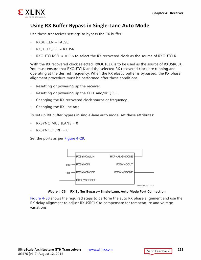
Chapter 4: Receiver
Using RX Buffer Bypass in Single-Lane Auto ModeUse these transceiver settings to bypass the RX buffer:
• RXBUF_EN = FALSE.
• RX_XCLK_SEL = RXUSR.
• RXOUTCLKSEL = 010b to select the RX recovered clock as the source of RXOUTCLK.
With the RX recovered clock selected, RXOUTCLK is to be used as the source of RXUSRCLK. You must ensure that RXOUTCLK and the selected RX recovered clock are running and operating at the desired frequency. When the RX elastic buffer is bypassed, the RX phase alignment procedure must be performed after these conditions:
• Resetting or powering up the receiver.
• Resetting or powering up the CPLL and/or QPLL.
• Changing the RX recovered clock source or frequency.
• Changing the RX line rate.
To set up RX buffer bypass in single-lane auto mode, set these attributes:
• RXSYNC_MULTILANE = 0
• RXSYNC_OVRD = 0
Set the ports as per Figure 4-29.
Figure 4-30 shows the required steps to perform the auto RX phase alignment and use the RX delay alignment to adjust RXUSRCLK to compensate for temperature and voltage variations.
X-Ref Target - Figure 4-29
Figure 4-29: RX Buffer Bypass—Single-Lane, Auto Mode Port Connection
RXSYNCMODE
RXSYNCALLIN
RXSYNCIN RXSYNCOUT
UG576_c4_30_112513
RXSYNCDONE
RXPHALIGNDONE
1'b1
1'b0
RXDLYSRESET
UltraScale Architecture GTH Transceivers www.xilinx.com 225UG576 (v1.2) August 12, 2015
Send Feedback

Chapter 4: Receiver
Notes relevant to Figure 4-30:
1. The sequence of events in Figure 4-30 is not drawn to scale.
2. After conditions such as a receiver reset or RX rate change, RX phase alignment must be performed to align XCLK and RXUSRCLK. Wait until exiting RXELECIDLE and RX CDR is locked before asserting RXDLYSRESET to start the RX phase and delay alignments.
3. Wait until RXDLYSRESETDONE is High. RXDLYSRESETDONE will stay asserted for a minimum of 100 ns.
4. When RXSYNCDONE is asserted, the alignment procedure is completed. This signal will remain asserted until the alignment procedure is re-initiated.
5. Upon the assertion of RXSYNCDONE, RXPHALIGNDONE indicates whether alignment is achieved and maintained.
6. RX delay alignment continues to adjust RXUSRCLK to compensate for temperature and voltage variations.
It is necessary to start the RX phase alignment after RX CDR is locked to ensure that the RX recovered clock and RXUSRCLK are stable and ready to be used for alignment. When the RX elastic buffer is bypassed, data received from the PMA can be distorted due to phase differences after conditions such as a transceiver reset or rate change. If the received data evaluated at the interconnect logic interface is invalid, the RX phase alignment needs to be repeated while the RX CDR is locked.
Using RX Buffer Bypass in Multi-Lane Manual ModeWhen a multi-lane application requires RX buffer bypass, phase alignment can be performed manually or automatically.
This section describes the steps required to perform the multi-lane RX buffer bypass alignment procedure manually:
• Master: In a multi-lane application, the buffer bypass master is the lane that is the source of RXOUTCLK. In a multi-lane application, the middle-most GTH transceiver
X-Ref Target - Figure 4-30
Figure 4-30: RX Buffer Bypass Example—Single-Lane Auto Mode
RXDLYSRESET
RXDLYSRESETDONE
RXPHALIGNDONE
RXSYNCDONE
UG576_c4_31_112513
UltraScale Architecture GTH Transceivers www.xilinx.com 226UG576 (v1.2) August 12, 2015
Send Feedback

Chapter 4: Receiver
should be selected to be the source of RXOUTCLK. For example, in a multi-lane application of 12 GTH transceivers made up of three contiguous Quads, one of the middle GTH transceivers in the middle Quad should be selected as the source for RXUSRCLK and RXUSRCLK.
• Slave: All the lanes that share the same RXUSRCLK/RXUSRCLK2, which is generated from the RXOUTCLK of the buffer bypass master.
Figure 4-31 shows an example of buffer bypass master versus slave lanes.
Use these transceiver settings to bypass the RX elastic buffer:
• RXBUF_EN = FALSE
• RX_XCLK_SEL = RXUSR
• RXOUTCLKSEL = 3'b010 or 3'b101 to select the RX recovered clock as the source of RXOUTCLK
With the RX recovered clock selected, RXOUTCLK is to be used as the source of RXUSRCLK. You must ensure that RXOUTCLK and the selected RX recovered clock are operating at the desired frequency. When the RX elastic buffer is bypassed, the RX phase alignment procedure must be performed after these conditions:
X-Ref Target - Figure 4-31
Figure 4-31: Example of RX Buffer Bypass Master versus Slave Lanes
UG576_c4_32_112513
BUFG_GT
GTH RXLane 3
Slave
RXUSRCLKRXUSRCLK2
GTH RXLane 2
Master
RXUSRCLK
RXOUTCLK
RXUSRCLK2
GTH RXLane 1
Slave
RXUSRCLKRXUSRCLK2
GTH RXLane 0
Slave
RXUSRCLKRXUSRCLK2
UltraScale Architecture GTH Transceivers www.xilinx.com 227UG576 (v1.2) August 12, 2015
Send Feedback

Chapter 4: Receiver
• Resetting or powering up the receiver
• Resetting or powering up the CPLL and/or QPLL
• Changing the RX recovered clock source or frequency
• Changing the transceiver RX line rate
Figure 4-32 shows the required steps to perform manual RX phase and delay alignment.
Notes relevant to Figure 4-32:
1. The sequence of events shown in Figure 4-32 is not drawn to scale.
2. M_* denotes ports related to the master lane.
3. S_* denotes ports related to the slave lane(s).
4. Set the RXSYNC_OVRD attribute to 1'b1.
5. Set RXPHDLYRESET and RXDLYBYPASS to Low for all lanes.
6. Set RXPHALIGNEN and RXDDIEN to High for all lanes.
7. Assert RXDLYSRESET for all lanes. Hold this signal High until RXDLYSRESETDONE of the respective lane is asserted.
8. Deassert RXDLYSRESET for the lane in which the RXDLYSRESETDONE is asserted.
9. When RXDLYSRESET of all lanes are deasserted, assert RXPHALIGN for the master lane. Hold this signal High until the rising edge of RXPHALIGNDONE of the master lane is observed.
X-Ref Target - Figure 4-32
Figure 4-32: RX Phase and Delay Alignment in Manual Mode
M_RXPHDLYRESET
M_RXDLYBYPASS
M_RXPHALIGNEN
M_RXDLYSRESET
M_RXDLYSRESETDONE
M_RXPHALIGN
M_RXDLYEN
M_RXPHALIGNDONE
S_RXPHDLYRESET
S_RXDLYBYPASS
S_RXPHALIGNEN
S_RXDLYSRESET
S_RXDLYSRESETDONE
S_RXPHALIGN
S_RXDLYEN
S_RXPHALIGNDONE
UG576_c4_33_050715
UltraScale Architecture GTH Transceivers www.xilinx.com 228UG576 (v1.2) August 12, 2015
Send Feedback

Chapter 4: Receiver
10. Deassert RXPHALIGN for the master lane.
11. Assert RXDLYEN for the master lane. This causes RXPHALIGNDONE to be deasserted.
12. Hold RXDLYEN for the master lane High until the rising edge of RXPHALIGNDONE of the master lane is observed.
13. Deassert RXDLYEN for the master lane.
14. Assert RXPHALIGN for all slave lane(s). Hold this signal High until the rising edge of RXPHALIGNDONE of the respective slave lane is observed.
15. Deassert RXPHALIGN for the slave lane in which the RXPHALIGNDONE is asserted.
16. When RXPHALIGN for all slave lane(s) are deasserted, assert RXDLYEN for the master lane. This causes RXPHALIGNDONE of the master lane to be deasserted.
17. Wait until RXPHALIGNDONE of the master lane reasserts. Phase and delay alignment for the multi-lane interface is complete. Continue to hold RXDLYEN for the master lane High to adjust RXUSRCLK to compensate for temperature and voltage variations.
In a multi-lane application, it is necessary to start the RX alignment procedure on the interface after RXELECIDLE is deasserted on any lane. Lock the RX CDR of all lanes before starting the RX alignment procedure. This requirement is to ensure that the RX recovered clocks and RXUSRCLK are stable and ready before alignment.
When the RX elastic buffer is bypassed, data received from the PMA might be distorted due to phase differences after conditions such as a GTH transceiver reset or rate change. If the received data evaluated at the interconnect logic interface is invalid on any lane, repeat the RX alignment procedure for the interface after the RX CDR is locked on all lanes.
Using RX Buffer Bypass in Multi-Lane Auto ModeWhen a multi-lane application requires RX buffer bypass, phase alignment can be performed manually or automatically. This section describes the steps required to perform the multi-lane RX buffer bypass alignment procedure automatically:
• Master: In a multi-lane application, the buffer bypass master is the lane that is the source of RXOUTCLK.
• Slave: These are all the lanes that share the same RXUSRCLK/RXUSRCLK2, which is generated from the RXOUTCLK of the buffer bypass master.
Figure 4-33 shows an example of buffer bypass master versus slave lanes.
UltraScale Architecture GTH Transceivers www.xilinx.com 229UG576 (v1.2) August 12, 2015
Send Feedback

Chapter 4: Receiver
Use these GTH transceiver settings to bypass the RX buffer:
• RXBUF_EN = FALSE.
• RX_XCLK_SEL = RXUSR.
• RXOUTCLKSEL = 3'b010 or 3'b101 to select the RX recovered clock as the source of RXOUTCLK.
With the RX recovered clock selected, RXOUTCLK is to be used as the source of RXUSRCLK. You must ensure that RXOUTCLK and the selected RX recovered clock are running and operating at the desire frequency. When the RX elastic buffer is bypassed, the RX phase alignment procedure must be performed after these conditions:
• Resetting or powering up the GTH receiver.
• Resetting or powering up the CPLL and/or QPLL.
• Changing the RX recovered clock source or frequency.
• Changing the GTH RX line rate.
To set up RX buffer bypass in multi-lane auto mode, set these attributes:
X-Ref Target - Figure 4-33
Figure 4-33: Example of Buffer Bypass Master versus Slave Lanes
GTH RXLane 0
GTH RXLane 1
GTH RXLane 2
GTH RXLane 3
BUFG_GT
RXUSRCLKRXUSRCLK2
RXUSRCLKRXUSRCLK2
RXUSRCLKRXUSRCLK2
RXUSRCLKRXUSRCLK2
RXOUTCLKMaster
Slave
Slave
Slave
UG576_c4_34_061214
UltraScale Architecture GTH Transceivers www.xilinx.com 230UG576 (v1.2) August 12, 2015
Send Feedback

Chapter 4: Receiver
• RXSYNC_MULTILANE = 1
• RXSYNC_OVRD = 0
Set the ports as shown in Figure 4-34.
X-Ref Target - Figure 4-34
Figure 4-34: RX Buffer Bypass—Multi-Lane Auto Mode Port Connection
Master
RXSYNCMODE
RXSYNCALLIN
RXSYNCIN RXSYNCOUT
RXSYNCDONE
RXPHALIGNDONE
1'b1
RXDLYSRESET
Slave
RXSYNCMODE
RXSYNCALLIN
RXSYNCIN RXSYNCOUT
RXSYNCDONE
RXPHALIGNDONE
UG576_c4_35_112513
1'b0
RXDLYSRESET
UltraScale Architecture GTH Transceivers www.xilinx.com 231UG576 (v1.2) August 12, 2015
Send Feedback

Chapter 4: Receiver
Figure 4-35 shows the required steps to perform auto RX phase and delay alignment.
Notes relevant to Figure 4-35:
1. The sequence of events shown in Figure 4-35 is not drawn to scale.
2. M_* denotes ports related to the master lane.
3. S_* denotes ports related to the slave lane(s).
4. After conditions such as a GTH receiver reset or RX rate change, RX phase alignment must be performed to align XCLK and RXUSRCLK. Wait until exiting RXELECIDLE and RX CDR is locked before asserting RXDLYSRESET to start the RX phase and delay alignments.
5. Wait until RXDLYSRESETDONE is High. RXDLYSRESETDONE will stay asserted for a minimum of 100 ns.
6. When RXSYNCDONE of the master lane is asserted, the alignment procedure is completed. This signal will remain asserted until alignment procedure is re-initiated.
7. Upon the assertion of RXSYNCDONE of the master lane, RXPHALIGNDONE of the master lane indicates whether alignment is achieved and maintained.
X-Ref Target - Figure 4-35
Figure 4-35: RX Buffer Bypass Example—Multi-Lane Auto Mode
M_RXDLYSRESET
M_RXDLYSRESETDONE
M_RXPHALIGNDONE
M_RXSYNCOUT
M_RXSYNCDONE
S_RXDLYSRESET
S_RXDLYSRESETDONE
S_RXPHALIGNDONE
S_RXSYNCOUT
S_RXSYNCDONE
UG576_c4_36_112513
UltraScale Architecture GTH Transceivers www.xilinx.com 232UG576 (v1.2) August 12, 2015
Send Feedback

Chapter 4: Receiver
8. RX delay alignment continues to adjust RXUSRCLK to compensate for temperature and voltage variations.
In a multi-lane application, it is necessary to start the RX alignment procedure on the interface after RXELECIDLE is deasserted on any lane. RX CDR of all lanes needs to be locked before starting the RX alignment procedure. This requirement is to make sure the RX recovered clocks and RXUSRCLK are stable and ready before alignment.
When the RX elastic buffer is bypassed, data received from the PMA can be distorted due to phase differences after conditions such as a GTH transceiver reset or rate change. If the received data evaluated at the interconnect logic interface is invalid on any lane, the RX alignment procedure needs to be repeated for the interface after RX CDR is locked on all lanes.
RX Elastic Buffer
Functional DescriptionThe GTH transceiver RX datapath has two internal parallel clock domains used in the PCS: The PMA parallel clock domain (XCLK) and the RXUSRCLK domain. To receive data, the PMA parallel rate must be suff iciently close to the RXUSRCLK rate, and all phase differences between the two domains must be resolved. Figure 4-36 shows the two parallel clock domains: XCLK and RXUSRCLK.
X-Ref Target - Figure 4-36
Figure 4-36: RX Clock Domains
From ChannelClocking
Architecture
From TX ParallelData (Near-EndPCS Loopback)
To TX ParallelData (Far-End
PMA Loopback)
To TX ParallelData (Far-End PCS
Loopback)
PCS Parallel Clock(RXUSRCLK)
Device ParallelClock
(RXUSRCLK2)
PMA Parallel Clock(XCLK)
RX Serial Clock
RXEQ
RXClock
Dividers
DFE
SIPO
RX OOB
Polarity
PRBSChecker
CommaDetect
andAlign
RX SyncGearbox
RXInterface
8B/10BDecoder RX
ElasticBuffer
RX PIPEControl
RX StatusControl
UG576_c4_37_063014
RX AsyncGearbox
BlockDetectAlign
128B/130BDecoder
PCIe RXBuffer
UltraScale Architecture GTH Transceivers www.xilinx.com 233UG576 (v1.2) August 12, 2015
Send Feedback

Chapter 4: Receiver
The GTH transceiver includes an RX elastic buffer to resolve differences between the XCLK and RXUSRCLK domains. The phase of the two domains can also be matched by using the RX recovered clock from the transceiver to drive RXUSRCLK and adjusting its phase to match XCLK when the RX buffer is bypassed (see RX Buffer Bypass, page 220). All RX datapaths must use one of these approaches. The costs and benefits of each approach are shown in Table 4-31.
Table 4-31: RX Buffering versus Phase Alignment
RX Elastic Buffer RX Phase Alignment
Ease of Use The RX buffer is the recommended default to use when possible. It is robust and easier to operate.
Phase alignment is an advanced feature that requires extra logic and additional constraints on clock sources. RXOUTCLKSEL must select the RX recovered clock as the source of RXOUTCLK to drive RXUSRCLK.
Clocking Options
Can use RX recovered clock or local clock (with clock correction).
Must use the RX recovered clock.
Initialization Works immediately. Must wait for all clocks to stabilize before performing the RX phase and delay alignment procedure.
Latency Buffer latency depends on features use, such as clock correction and channel bonding.
Lower deterministic latency.
Clock Correction and Channel Bonding
Required for clock correction and channel bonding.
Not performed inside the transceiver. Required to be implemented in interconnect logic.
RXUSRCLK jitter sensitivity
No sensitivity to RXUSRCLK jitter. Sensitive to RXUSRCLK jitter. Refer to the device data sheets [Ref 6].
UltraScale Architecture GTH Transceivers www.xilinx.com 234UG576 (v1.2) August 12, 2015
Send Feedback

Chapter 4: Receiver
Ports and AttributesTable 4-32 defines the RX buffer ports.
Table 4-33 defines the RX buffer attributes.
Table 4-32: RX Buffer Ports
Port Dir Clock Domain Description
RXBUFRESET In Async Resets and reinitializes the RX elastic buffer.
RXBUFSTATUS[2:0] Out RXUSRCLK2 RX buffer status. The RX elastic buffer underflow or overflow error status are not sticky bits and return to normal condition (000b) if the error clears. When an error condition is detected, an RX elastic buffer reset is recommended. When clock correction is disabled, RXBUFSTATUS codes 001b and 010b can be used by setting RXBUF_ADDR_MODE to FULL.000b: Nominal condition.001b: Number of bytes in the buffer are less than CLK_COR_MIN_LAT010b: Number of bytes in the buffer are greater than CLK_COR_MAX_LAT101b: RX elastic buffer underflow110b: RX elastic buffer overflow
Table 4-33: RX Buffer Attributes
Attribute Type Description
RXBUF_EN String Use or bypass the RX elastic buffer.TRUE: Uses the RX elastic buffer (default).FALSE: Bypasses the RX elastic buffer (advanced feature).
RX_XCLK_SEL String Selects the clock source used to drive the RX parallel clock domain (XCLK).
RXDES: Selects the RX recovered clock as the source of XCLK. Used when using the RX elastic buffer.RXUSR: Selects RXUSRCLK as the source of XCLK. Used when bypassing the RX elastic buffer.
RX_BUFFER_CFG 6-bit Binary RX elastic buffer configuration.Reserved. Use the recommended value from the Wizard.
RX_DEFER_RESET_BUF_EN String Defer RX elastic buffer reset on comma realignment. The time deferred is controlled by RXBUF_EIDLE_HI_CNT.
TRUE: Enables deferral of RX elastic buffer reset on comma realignment.FALSE: Disables deferral of RX elastic buffer reset on comma realignment.
UltraScale Architecture GTH Transceivers www.xilinx.com 235UG576 (v1.2) August 12, 2015
Send Feedback

Chapter 4: Receiver
RXBUF_ADDR_MODE String RX elastic buffer address mode.FULL: Enables the RX elastic buffer for clock correction and channel bonding support.FAST: Enables the RX elastic buffer for phase compensation without clock correction and channel bonding support. This mode is recommended for high line rates.
RXBUF_EIDLE_HI_CNT 4-bit Binary Controls the timing of asserting the GTH transceiver internally generated RX elastic buffer reset on electrical idle when valid data is not present on the RXP/RXN serial lines. Reserved. Use the recommended value from the Wizard.
RXBUF_EIDLE_LO_CNT 4-bit Binary Controls the timing of deasserting the GTH transceiver internally generated RX elastic buffer reset on electrical idle when valid data is present on the RXP/RXN serial lines.Reserved. Use the recommended value from the Wizard.
RXBUF_RESET_ON_CB_CHANGE String GTH transceiver internally generated RX elastic buffer reset on channel bonding change.
TRUE: Enables auto RX elastic buffer reset on channel bonding change.FALSE: Disables auto RX elastic buffer reset on channel bonding change.
RXBUF_RESET_ON_COMMAALIGN String GTH transceiver internally generated RX elastic buffer reset on comma realignment.
TRUE: Enables auto RX elastic buffer reset on comma alignment.FALSE: Disables auto RX elastic buffer reset on comma alignment.
RXBUF_RESET_ON_EIDLE String GTH transceiver internally generated RX elastic buffer reset on electrical idle.
TRUE: Enables auto reset of RX elastic buffer during an optional reset sequence of an electrical idle state as used in PCI Express operation.FALSE: Disables auto RX elastic buffer reset on electrical idle. This should be the default setting.
Note: For channels with large attenuation (lossy channels typically exceeding 15 dB at Nyquist), Xilinx recommends setting RXBUF_RESET_ON_EIDLE to FALSE because fast transitioning data patterns like the 101010 sequence in CJPAT/CJTPAT can accidentally trigger an electrical idle.
RXBUF_RESET_ON_RATE_CHANGE String GTH transceiver internally generated RX elastic buffer reset on rate change.
TRUE: Enables auto RX elastic buffer reset on rate change.FALSE: Disables auto RX elastic buffer reset on rate change.
Table 4-33: RX Buffer Attributes (Cont’d)
Attribute Type Description
UltraScale Architecture GTH Transceivers www.xilinx.com 236UG576 (v1.2) August 12, 2015
Send Feedback

Chapter 4: Receiver
Using the RX Elastic BufferThese settings are used to enable the RX elastic buffer to resolve phase differences between the XCLK and RXUSRCLK domains:
• RXBUF_EN = TRUE
• RX_XCLK_SEL = RXDES
The content of the RX elastic buffer becomes invalid if an RX elastic buffer overflow or underflow condition occurs. When any of these conditions occur, reset and reinitialize the RX elastic buffer by using GTRXRESET, RXPCSRESET, RXBUFRESET, or the GTH transceiver internally generated RX elastic buffer reset (see RX Initialization and Reset, page 58). The internally generated RX elastic buffer reset can occur on channel bonding change, comma realignment, electrical idle, or rate change conditions.
The RX elastic buffer is also used for clock correction (see RX Clock Correction) and channel bonding (see RX Channel Bonding, page 246). Clock correction is used in cases where XCLK and RXUSRCLK are not frequency matched. Table 4-34 lists common clock configurations and shows whether they require clock correction.
RXBUF_THRESH_OVRD String RX elastic buffer threshold override.TRUE: Use the RXBUF_THRESH_OVFLW and RXBUF_THRESH_UNDFLW attributes to set the RX elastic buffer overflow and underflow thresholds, respectively.FALSE: Automatically calculates the RX elastic buffer overflow and underflow thresholds. This is the recommended default setting.
RXBUF_THRESH_OVFLW Integer RX elastic buffer overflow threshold specif ied as the number of bytes. If the data latency through the RX elastic buffer is at or above this threshold, the buffer is considered to be in an overflow condition. Used when RXBUF_THRESH_OVRD = TRUE.Reserved. Use the recommended value from the Wizard.
RXBUF_THRESH_UNDFLW Integer RX elastic buffer underflow threshold specif ied as number of bytes. If the data latency through the RX elastic buffer is at or below this threshold, the buffer is consider to be in underflow condition. Used when RXBUF_THRESH_OVRD = TRUE.Reserved. Use the recommended value from the Wizard.
RXBUFRESET_TIME 5-bit Binary RX elastic buffer reset time.Reserved. Use the recommended value from the Wizard.
Table 4-33: RX Buffer Attributes (Cont’d)
Attribute Type Description
UltraScale Architecture GTH Transceivers www.xilinx.com 237UG576 (v1.2) August 12, 2015
Send Feedback

Chapter 4: Receiver
When the RX elastic buffer is used, the setting of CLK_COR_MIN_LAT affects the latency through the buffer, regardless of whether clock correction is used.
RX Clock Correction
Functional DescriptionThe RX elastic buffer is designed to bridge between two different clock domains, RXUSRCLK and XCLK, which is the recovered clock from CDR. Even if RXUSRCLK and XCLK are running at same clock frequency, there is always a small frequency difference. Because XCLK and RXUSRCLK are not exactly the same, the difference can be accumulated to cause the RX elastic buffer to eventually overflow or underflow unless it is corrected. To allow correction, each GTH transceiver TX periodically transmits one or more special characters that the GTH transceiver RX is allowed to remove or replicate in the RX elastic buffer as necessary. By removing characters when the RX elastic buffer is too full and replicating characters when the RX elastic buffer is too empty, the receiver can prevent overflow or underflow.
Table 4-34: Common Clock Configurations
Types of Clocking Require Clock Correction?
Synchronous system where both sides uses the reference clock from the same physical oscillator. No
Asynchronous system when separate reference clocks are used and the GTH receiver uses an RX recovered clock. No
Asynchronous system when separate reference clocks are used and the GTH receiver uses a local clock. Yes
UltraScale Architecture GTH Transceivers www.xilinx.com 238UG576 (v1.2) August 12, 2015
Send Feedback

Chapter 4: Receiver
X-Ref Target - Figure 4-37
Figure 4-37: Clock Correction Conceptual View
Write OperationDriven by
XCLK
Read OperationDriven by
RXUSRCLK
Normal Condition If RXUSRCLK and XCLK Are Exactly the Same Frequency
Pointer Difference is Always Same BetweenREAD Address and WRITE Address While
They Are Moving
Write OperationDriven by
XCLK
Insert Special Character toRealign Pointer Difference
to Normal Condition
UG576_c4_38_112513
Read OperationDriven by
RXUSRCLK
Elastic Buffer Can Underflow When Read Clock Faster Than Write Clock
Pointer Difference is Getting SmallerWhen READ Clock is Faster
Write OperationDriven by
XCLK
Remove Special Character toRealign Pointer Differenceto Normal Condition
Read OperationDriven by
RXUSRCLK
Elastic Buffer Can Overflow When Read Clock Slower Than Write Clock
Pointer Difference is Getting BiggerWhen WRITE Clock is Faster
UltraScale Architecture GTH Transceivers www.xilinx.com 239UG576 (v1.2) August 12, 2015
Send Feedback

Chapter 4: Receiver
Ports and AttributesTable 4-35 defines the ports required by RX clock correction functions.
Table 4-36 defines the attributes required by RX channel bonding.
Table 4-35: RX Clock Correction Ports
Port Dir Clock Domain Description
RXBUFRESET In Async Resets the RX elastic buffer and related logic.
RXBUFSTATUS[2:0] Out RXUSRCLK2 Indicates the status of the RX elastic buffer:000: In nominal operating range where the buffer occupancy is within the CLK_COR_MIN_LAT and CLK_COR_MAX_LAT range001: RX elastic buffer occupancy is less than CLK_COR_MIN_LAT010: RX elastic buffer occupancy is greater than CLK_COR_MAX_LAT101: RX elastic buffer underflow110: RX elastic buffer overflow
RXCLKCORCNT[1:0] Out RXUSRCLK2 Reports the clock correction status of the RX elastic buffer when the first byte of a clock correction sequence is shown in RXDATA. 00: No clock correction 01: One sequence skipped 10: Two sequences skipped 11: One sequence added
RX8B10BEN In RXUSRCLK2 Active High to enable the 8B/10B decoder in the GTH transceiver RX. If 8B/10B decoding is enabled, RX_DATA_WIDTH must be a multiple of 10 (20, 40, 80). If 8B/10B decoding is not enabled, RX_DATA_WIDTH must be a multiple of 8 or 10 (16, 20, 32, 40, 64, 80).
Table 4-36: RX Clock Correction Attributes
Attribute Type Description
CBCC_DATA_SOURCE_SEL String This attribute is used together with RX8B10BEN to select the data source for clock correction and channel bonding.When RX8B10BEN is High, CBCC_DATA_SOURCE_SEL = DECODED, the clock correction sequence matches the data decoded after the 8B/10B decoder. CBCC_DATA_SOURCE_SEL = ENCODED, the clock correction sequence matches the raw data from the comma detection and realignment block before the 8B/10B decoder.When RX8B10BEN is Low, CBCC_DATA_SOURCE_SEL = DECODED is not supported. CBCC_DATA_SOURCE_SEL = ENCODED, the clock correction sequence matches the raw data from the comma detection and realignment block.
UltraScale Architecture GTH Transceivers www.xilinx.com 240UG576 (v1.2) August 12, 2015
Send Feedback

Chapter 4: Receiver
CLK_CORRECT_USE String Set TRUE to enable the clock correction function. Set FALSE to disable the clock correction function.These attributes need to be set while clock correction disabled:
CLK_COR_SEQ_1_1 = 10'b0100000000CLK_COR_SEQ_2_1 = 10'b0100000000CLK_COR_SEQ_1_ENABLE = 4'b1111CLK_COR_SEQ_2_ENABLE = 4'b1111
CLK_COR_KEEP_IDLE String Set TRUE to keep at least one clock correction sequence in the data stream for every continuous stream of clock correction sequences received.Set FALSE to remove all clock correction sequences from the byte stream if needed to recenter the RX elastic buffer range.
CLK_COR_MAX_LAT Integer Specif ies the maximum RX elastic buffer latency. If the RX elastic buffer exceeds CLK_COR_MAX_LAT, the clock correction circuit removes incoming clock correction sequences to prevent overflow.The Wizard chooses an optimal CLK_COR_MAX_LAT value based on application requirements. The value selected by the Wizard must be followed to maintain optimal performance and must not be overridden.
CLK_COR_MIN_LAT Integer Specif ies the minimum RX elastic buffer latency. If the RX elastic buffer drops below CLK_COR_MIN_LAT, the clock correction circuit replicates incoming clock correction sequences to prevent underflow.The Wizard chooses a CLK_COR_MIN_LAT value based on application requirements. The value selected by the Wizard must be followed to maintain optimal performance and must not be overriden.
CLK_COR_PRECEDENCE String Determines whether clock correction or channel bonding takes precedence when both operations are triggered at the same time.
TRUE: Clock correction takes precedence over channel bonding if there is opportunity for bothFALSE: Channel bonding takes precedence over clock correction if there is opportunity for both
CLK_COR_REPEAT_WAIT Integer This attribute specif ies the minimum number of RXUSRCLK cycles between two successive clock corrections being placed. If this attribute is 0, no limit is placed on how frequently the clock correction character can be placed.Valid values for this attribute range from 0 to 31.
CLK_COR_SEQ_LEN Integer Defines the length of the sequence in bytes that has to match to detect opportunities for clock correction. This attribute also defines the size of the adjustment (number of bytes repeated or skipped) in a clock correction.Valid lengths are 1, 2, and 4 bytes.
Table 4-36: RX Clock Correction Attributes (Cont’d)
Attribute Type Description
UltraScale Architecture GTH Transceivers www.xilinx.com 241UG576 (v1.2) August 12, 2015
Send Feedback

Chapter 4: Receiver
CLK_COR_SEQ_1_ENABLE 4-bit Binary Mask enable bit for the f irst clock correction sequence.CLK_FOR_SEQ_1_ENABLE[0] is the mask bit for CLK_COR_SEQ_1_1.CLK_FOR_SEQ_1_ENABLE[1] is the mask bit for CLK_COR_SEQ_1_2.CLK_FOR_SEQ_1_ENABLE[2] is the mask bit for CLK_COR_SEQ_1_3.CLK_FOR_SEQ_1_ENABLE[3] is the mask bit for CLK_COR_SEQ_1_4.When CLK_FOR_SEQ_1_ENABLE[*] is 0, the corresponding CLK_COR_SEQ_1_* is either considered as a don't care or is matched automatically without a comparison.When CLK_FOR_SEQ_1_ENABLE[*] is 1, the corresponding CLK_COR_SEQ_1_* is compared for a match.
CLK_COR_SEQ_1_1 10-bit Binary
First clock correction sequence 1 to be compared when CLK_FOR_SEQ_1_ENABLE[0] = 1.
CLK_COR_SEQ_1_2 10-bit Binary
First clock correction sequence 2 to be compared when CLK_FOR_SEQ_1_ENABLE[1] = 1.
CLK_COR_SEQ_1_3 10-bit Binary
First clock correction sequence 3 to be compared when CLK_FOR_SEQ_1_ENABLE[2] = 1.
CLK_COR_SEQ_1_4 10-bit Binary
First clock correction sequence 4 to be compared when CLK_FOR_SEQ_1_ENABLE[3] = 1.
CLK_COR_SEQ_2_USE String Set to TRUE if the second clock correction sequence (CLK_COR_SEQ_2_*) is used in addition to the CLK_COR_SEQ_1_* that is always used.
CLK_COR_SEQ_2_ENABLE 4-bit Binary Mask enable bit for the second clock correction sequence.CLK_FOR_SEQ_2_ENABLE[0] is the mask bit for CLK_COR_SEQ_2_1.CLK_FOR_SEQ_2_ENABLE[1] is the mask bit for CLK_COR_SEQ_2_2.CLK_FOR_SEQ_2_ENABLE[2] is the mask bit for CLK_COR_SEQ_2_3.CLK_FOR_SEQ_2_ENABLE[3] is the mask bit for CLK_COR_SEQ_2_4.When CLK_FOR_SEQ_2_ENABLE[*] is 0, the corresponding CLK_COR_SEQ_2_* is either considered as a don't care or is matched automatically without a comparison.When CLK_FOR_SEQ_2_ENABLE[*] is 1, the corresponding CLK_COR_SEQ_2_* is compared for a match.
CLK_COR_SEQ_2_1 10-bit Binary
Second clock correction sequence 1 to be compared when CLK_FOR_SEQ_2_ENABLE[0] = 1
CLK_COR_SEQ_2_2 10-bit Binary
Second clock correction sequence 2 to be compared when CLK_FOR_SEQ_2_ENABLE[1] = 1
CLK_COR_SEQ_2_3 10-bit Binary
Second clock correction sequence 3 to be compared when CLK_FOR_SEQ_2_ENABLE[2] = 1
Table 4-36: RX Clock Correction Attributes (Cont’d)
Attribute Type Description
UltraScale Architecture GTH Transceivers www.xilinx.com 242UG576 (v1.2) August 12, 2015
Send Feedback

Chapter 4: Receiver
CLK_COR_SEQ_2_4 10-bit Binary
Second clock correction sequence 4 to be compared when CLK_FOR_SEQ_2_ENABLE[3] = 1
RX_DATA_WIDTH Integer Sets the bit width of the RXDATA port. When 8B/10B encoding is enabled, RX_DATA_WIDTH must be set to 20, 40, or 80. Valid settings are 16, 20, 32, 40, 64, and 80.See Interface Width Configuration, page 275 for more details.
RX_DISPERR_SEQ_MATCH String Specif ies whether the disparity error status of a decoded byte must match the indicator in the channel bonding and clock correction sequence.
TRUE: The disparity error status must be matched. FALSE: The disparity error status is ignored.
RX_INT_DATAWIDTH Integer Controls the width of the internal datapath. 0: 2-Byte internal datapath1: 4-Byte internal datapath
ALIGN_COMMA_WORD Integer This attribute controls the alignment of detected commas within a multi-byte datapath.
1: Align the comma to either of the 2 bytes for a 2-byte interface, any of the 4 bytes for a 4-byte interface, and any of the 8 bytes for an 8-byte interface. The comma can be aligned to either the even bytes or the odd bytes of the RXDATA output.2: Align the comma to the even bytes only. The aligned comma is guaranteed to be aligned to even bytes RXDATA[9:0] for a 2-byte interface, RXDATA[9:0]/RXDATA[29:20] for a 4-byte interface, and RXDATA[9:0]/RXDATA[29:20]/RX[49:40/RX[69:60] for an 8-byte interface4: Align the comma to a 4-byte boundary. This setting is not allowed for RX_INT_DATAWIDTH = 0. The aligned comma is guaranteed to be aligned to RXDATA[9:0] for a 4-byte interface and RXDATA[9:0]/RXDATA[49:40] for an 8-byte interface.
Refer to Figure 4-23 for comma alignment boundaries that are allowed for the different ALIGN_COMMA_WORD, RX_DATA_WIDTH, and RX_INT_DATAWIDTH settings.Protocols that send commas in even and odd positions must set ALIGN_COMMA_WORD to 1.
Table 4-36: RX Clock Correction Attributes (Cont’d)
Attribute Type Description
UltraScale Architecture GTH Transceivers www.xilinx.com 243UG576 (v1.2) August 12, 2015
Send Feedback

Chapter 4: Receiver
Using RX Clock CorrectionFollow the steps described in this section to use the receiver’s clock correction feature.
Enabling Clock Correction
Each GTH transceiver includes a clock correction circuit that performs clock correction by controlling the pointers of the RX elastic buffer. To use clock correction, RXBUF_EN is set to TRUE to turn on the RX elastic buffer, and CLK_CORRECT_USE is set to TRUE to turn on the clock correction circuit.
Clock correction is triggered when the RX elastic buffer latency is too high or too low, and the clock correction circuit detects a match sequence. To use clock correction, the clock correction circuit must be configured to set these items:
• RX elastic buffer limits
• Clock correction sequence
Setting RX Elastic Buffer Limits
The RX elastic buffer limits are set using CLK_COR_MIN_LAT (minimum latency) and CLK_COR_MAX_LAT (maximum latency). When the number of bytes in the RX elastic buffer drops below CLK_COR_MIN_LAT, the clock correction circuit writes an additional CLK_COR_SEQ_LEN byte from the f irst clock correction sequence it matches to prevent buffer underflow. Similarly, when the number of bytes in the RX elastic buffer exceeds CLK_COR_MAX_LAT, the clock correction circuit deletes CLK_COR_SEQ_LEN bytes from the f irst clock correction sequence it matches, starting with the first byte of the sequence. The Wizard chooses an optimal setting for CLK_COR_MIN_LAT and CLK_COR_MAX_LAT based on application requirements. The value selected by the Wizard must be followed to maintain optimal performance and must not be overridden.
Setting Clock Correction Sequences
The clock correction sequences are programmed using the CLK_COR_SEQ_1_* attributes and CLK_COR_SEQ_LEN. Each CLK_COR_SEQ_1_* attribute corresponds to one subsequence in clock correction sequence 1. CLK_COR_SEQ_LEN is used to set the number of subsequences to be matched. If the 40-bit or 20-bit internal datapaths are used, the clock correction circuit matches all 10 bits of each subsequence. If the 16-bit or 32-bit internal datapaths are used, only the right-most eight bits of each subsequence are used.
A second, alternate clock correction sequence can be activated by setting CLK_COR_SEQ_2_USE to TRUE. The f irst and second sequences share length settings, but use different subsequence values for matching. Set the CLK_COR_SEQ_2_* attributes to define the subsequence values for the second sequence.
UltraScale Architecture GTH Transceivers www.xilinx.com 244UG576 (v1.2) August 12, 2015
Send Feedback

Chapter 4: Receiver
When using 8B/10B decoding (RX8B10BEN is High), CBCC_DATA_SOURCE_SEL is set to DECODED to search the output of the 8B/10B decoder for sequence matches instead of non-decoded data. This allows the circuit to look for 8-bit values with either positive or negative disparity, and to distinguish K characters from regular characters (see TX 8B/10B Encoder, page 96 and RX 8B/10B Decoder, page 215 for details). Figure 4-38 shows how to set a clock correction sequence byte when RX8B10BEN is High and CBCC_DATA_SOURCE_SEL is set to DECODED.
When CBCC_DATA_SOURCE_SEL is set to ENCODED, the sequence must exactly match incoming raw data. When RX_DISPERR_SEQ_MATCH is set to FALSE, CLK_COR_SEQ_x_y[9] is not used for matching.
Some protocols use clock correction sequences with don’t care subsequences. The clock correction circuit can be programmed to recognize these sequences using CLK_COR_SEQ_1_ENABLE and CLK_COR_SEQ_2_ENABLE. When the enable bit for a sequence is Low, that byte is considered matched no matter what the value is. Figure 4-39 shows the mapping between the clock correction sequences and the clock correction sequence enable bits.
X-Ref Target - Figure 4-38
Figure 4-38: Clock Correction Subsequence Settings with CBCC_DATA_SOURCE_SEL = DECODED
X-Ref Target - Figure 4-39
Figure 4-39: Clock Correction Sequence Mapping
UG576_c4_39_112513
CLK_COR_SEQ_x_y 9 8 7:0
8-bit Clock Correction Sequence
1 = Sequence is a K Character0 = Sequence is a Regular Character
1 = Sequence Uses Inverted Disparity0 = Sequence Uses Regular Disparity
UG576_c4_40_112513
4
CLK_COR_SEQ_x_4 CLK_COR_SEQ_x_3 CLK_COR_SEQ_x_2
CLK_COR_SEQ_x_ENABLE
CLK_COR_SEQ_x_1
3 2 1
UltraScale Architecture GTH Transceivers www.xilinx.com 245UG576 (v1.2) August 12, 2015
Send Feedback

Chapter 4: Receiver
To preserve comma alignment through the elastic buffer, CLK_COR_SEQ_LEN and ALIGN_COMMA_WORD must be selected such that they comply with Table 4-37.
Clock Correction Options
CLK_COR_REPEAT_WAIT is used to control the clock correction frequency. This value is set to the minimum number of RXUSRCLK cycles required between clock correction events. This attribute is set to 0 to allow clock correction to at occur any time. Some protocols allow clock correction to occur at any time, but require that if the clock correction circuit removes sequences, at least one sequence stays in the stream. For protocols with this requirement, CLK_COR_KEEP_IDLE is set to TRUE.
Monitoring Clock Correction
The clock correction circuit can be monitored using the RXCLKCORCNT and RXBUFSTATUS ports. The RXCLKCORCNT entry in Table 4-35 shows how to decode the values of RXCLKCORCNT to determine the status of the clock correction circuit. The RXBUFSTATUS entry in Table 4-35 shows how to decode the values of RXBUFSTATUS to determine how full the RX elastic buffer is.
RX Channel Bonding
Functional DescriptionProtocols such as XAUI and PCI Express combine multiple serial transceiver connections to create a single higher throughput channel. Each serial transceiver connection is called one lane. Unless each of the serial connections is exactly the same length, skew between the lanes can cause data to be transmitted at the same time but arrive at different times. Channel bonding cancels out the skew between GTH transceiver lanes by using the RX elastic buffer as a variable latency block. Channel bonding is also called channel deskew or lane-to-lane deskew. GTH transmitters used for a bonded channel all transmit a channel bonding character (or a sequence of characters) simultaneously. When the sequence is received, the GTH receiver can determine the skew between each lane and adjust the latency of RX elastic buffers, so that data is presented without skew at the RX interconnect logic interface.
Table 4-37: Valid ALIGN_COMMA_WORD/CLK_COR_SEQ_LEN Combinations
ALIGN_COMMA_WORD CLK_COR_SEQ_LEN
1 1, 2, 4
2 2, 4
4 4
UltraScale Architecture GTH Transceivers www.xilinx.com 246UG576 (v1.2) August 12, 2015
Send Feedback

Chapter 4: Receiver
RX channel bonding supports 8B/10B encoded data but does not support these encoded data types:
• 64B/66B
• 64B/67B
• 128B/130B
• Scrambled data
X-Ref Target - Figure 4-40
Figure 4-40: Channel Bonding Conceptual View
Elastic Buffer GTH0 (Master)
GTH1 (Slave)
UG576_c4_41_112513
DeskewedData
RX Data in Two Clock CyclesAhead of GTH1 Data
Set to 4 Cycles of Latency byChannel Bonding Controller
data dataSEQ4
SEQ3
SEQ2
SEQ1
Elastic BufferRX Data in Two Clock CyclesBehind GTH0 Data
Set to 2 Cycles of Latency byChannel Bonding Controller
data dataSEQ4
SEQ3
SEQ2
SEQ1
data dataSEQ4
SEQ3
SEQ2
SEQ1
DeskewedData
data dataSEQ4
SEQ3
SEQ2
SEQ1
UltraScale Architecture GTH Transceivers www.xilinx.com 247UG576 (v1.2) August 12, 2015
Send Feedback

Chapter 4: Receiver
Ports and AttributesTable 4-38 defines the ports required by RX channel bonding functions.
Table 4-38: RX Channel Bonding Ports
Port Dir Clock Domain Description
RXCHANBONDSEQ Out RXUSRCLK2 This port goes High when RXDATA contains the start of a channel bonding sequence.
RXCHANISALIGNED Out RXUSRCLK2 This signal from the RX elastic buffer goes High to indicate that the channel is properly aligned with the master transceiver according to observed channel bonding sequences in the data stream. This signal goes Low if an unaligned channel bonding sequence is detected, indicating that channel alignment was lost.
RXCHANREALIGN Out RXUSRCLK2 This signal from the RX elastic buffer is held High for at least one cycle when the receiver has changed the alignment between this transceiver and the master.
RXCHBONDI[4:0] In RXUSRCLK Channel bonding control ports used by slaves only. These ports are used to receive channel bonding and clock correction control information from master GTH transceiver RXCHBONDO ports or from daisy-chained slave GTH transceiver RXCHBONDO ports, which are concatenated from the master GTH transceiver.
RXCHBONDO[4:0] Out RXUSRCLK Channel bonding control ports used to propagate channel bonding and clock correction information to the slave GTH transceiver from the master or a daisy-chained slave concatenated from the master. The master RXCHBONDO can be tied to one or multiple slave RXCHBONDI ports. Tie the slave RXCHBONDO to the next level slave RXCHBONDI to form a daisy chain and pass information from the master to each slave.
RXCHBONDLEVEL[2:0] In RXUSRCLK2 Indicates the amount of internal pipelining used for the RX elastic buffer control signals. A higher value permits more daisy chaining of RXCHBONDO and RXCHBONDI to ease placement and routing constraints. To minimize required latency through the RX elastic buffer, CHAN_BOND_LEVEL in the master is set to the smallest value possible for the required amount of daisy-chaining. When using a 4-byte internal datapath (RX_INT_DATAWIDTH = 1), the master should not exceed RXCHANBONDLEVEL = 3.
UltraScale Architecture GTH Transceivers www.xilinx.com 248UG576 (v1.2) August 12, 2015
Send Feedback

Chapter 4: Receiver
Table 4-39 defines the attributes required by RX channel bonding.
RXCHBONDMASTER In RXUSRCLK2 Indicates that the transceiver is the master for channel bonding. Its RXCHBONDO port directly drives the RXCHBONDI ports on one or more slave transceivers.This port cannot be driven High at the same time as RXCHBONDSLAVE.
RXCHBONDSLAVE In RXUSRCLK2 Indicates that this transceiver is a slave for channel bonding. Its RXCHBONDI port is directly driven by the RXCHBONDO port of another slave or master transceiver. If its RXCHBONDLEVEL[2:0] setting is greater than 0, its RXCHBONDO port can directly drive the RXCHBONDI ports on one or more other slave transceivers.This port cannot be driven High at the same time as RXCHBONDMASTER.
RXCHBONDEN In RXUSRCLK2 This port enables channel bonding (from the interconnect logic to both the master and slaves).
Table 4-39: RX Channel Bonding Attributes
Attribute Type Description
CHAN_BOND_MAX_SKEW Integer This attribute controls the number of USRCLK cycles that the master waits before ordering the slaves to execute channel bonding. This attribute determines the maximum skew that can be handled by channel bonding. It must always be less than one-half the minimum distance (in bytes or 10-bit codes) between channel bonding sequences. Valid values range from 1 to 14.
CHAN_BOND_KEEP_ALIGN String Allows preservation of ALIGN characters during channel bonding for PCI Express.
CHAN_BOND_SEQ_1_1CHAN_BOND_SEQ_1_2CHAN_BOND_SEQ_1_3CHAN_BOND_SEQ_1_4
10-bit Binary The CHAN_BOND_SEQ_1 attributes are used in conjunction with CHAN_BOND_SEQ_1_ENABLE to define channel bonding sequence 1. Each subsequence is 10 bits long. The rules for setting the subsequences depend on RX_DATA_WIDTH and CBCC_DATA_SOURCE_SEL. Not all subsequences need to be used. CHAN_BOND_SEQ_LEN determines how much of the sequence is used for a match. If CHAN_BOND_SEQ_LEN = 1, only CHAN_BOND_SEQ_1_1 is used.CHAN_BOND_SEQ_1_ENABLE can be used to make parts of the sequence don't care. If CHAN_BOND_SEQ_1_ENABLE[k] is 0, CHAN_BOND_SEQ_1_k is a don't-care subsequence and is always considered to be a match.
CHAN_BOND_SEQ_1_ENABLE 4-bit Binary
Table 4-38: RX Channel Bonding Ports (Cont’d)
Port Dir Clock Domain Description
UltraScale Architecture GTH Transceivers www.xilinx.com 249UG576 (v1.2) August 12, 2015
Send Feedback

Chapter 4: Receiver
CHAN_BOND_SEQ_2_1CHAN_BOND_SEQ_2_2CHAN_BOND_SEQ_2_3CHAN_BOND_SEQ_2_4
10-bit Binary The CHAN_BOND_SEQ_2 attributes are used in conjunction with CHAN_BOND_SEQ_2_ENABLE to define the second channel bonding sequence. When CHAN_BOND_SEQ_2_USE is TRUE, the second sequence is used as an alternate sequence to trigger channel bonding.Each subsequence is 10 bits long. The rules for setting the subsequence depend on RX_DATA_WIDTH and CBCC_DATA_SOURCE_SEL. Not all subsequences need to be used. CHAN_BOND_SEQ_LEN determines how many of the subsequences are used for a match. If CHAN_BOND_SEQ_LEN = 1, only CHAN_BOND_SEQ_2_1 is used.CHAN_BOND_SEQ_2_ENABLE can be used to make parts of the sequence don't care. If CHAN_BOND_SEQ_2_ENABLE[k] is 0, CHAN_BOND_SEQ_2_k is a don't-care subsequence and is always considered to be a match.
CHAN_BOND_SEQ_2_ENABLE 4-bit Binary
CHAN_BOND_SEQ_2_USE String Determines if the two-channel bonding sequence is to be used.
TRUE: Channel bonding can be triggered by channel bonding sequence 1 or 2.FALSE: Channel bonding is only triggered by sequence 1.
CHAN_BOND_SEQ_LEN Integer Defines the length in bytes of the channel bonding sequence that the GTH transceiver has to match to f ind skew. Valid lengths are 1, 2, and 4 bytes.
CBCC_DATA_SOURCE_SEL String This attribute is used to select the data source for clock correction and channel bonding.When set to DECODED, selects data from the 8B/10B decoder when RX8B10BEN is High.When set to ENCODED, selects data from the comma detection and realignment block.
FTS_DESKEW_SEQ_ENABLE 4-bit Binary Enable mask for FTS_LANE_DESKEW_CFG.FTS_DESKEW_SEQ_ENABLE[0] is for FTS_LANE_DESKEW_CFG[0]FTS_DESKEW_SEQ_ENABLE[1] is for FTS_LANE_DESKEW_CFG[1]FTS_DESKEW_SEQ_ENABLE[2] is for FTS_LANE_DESKEW_CFG[2]FTS_DESKEW_SEQ_ENABLE[3] is for FTS_LANE_DESKEW_CFG[3]The default value is 1111.
Table 4-39: RX Channel Bonding Attributes (Cont’d)
Attribute Type Description
UltraScale Architecture GTH Transceivers www.xilinx.com 250UG576 (v1.2) August 12, 2015
Send Feedback

Chapter 4: Receiver
FTS_LANE_DESKEW_CFG 4-bit Binary Bit 3: This bit is set to 1'b1 on a slave to freeze the alignment to prevent spurious misalignments or modified alignments that can occur following slip-4, snap-4, or clock correction when good channel alignment is still maintained. This bit is set to 1'b0 on a slave to unfreeze the alignment.Bit 2: Specifies whether a “master” channel doing FTS lane deskew that just reached the end of an FTS OS in its lookahead control logic inhibits its own generation of clock correction commands for a brief time. The purpose is to prevent clock correction commands from interfering with operation of the slave's slip-4 and snap-4 logic. The logic guarantees that clock correction can still occur if a full SKP OS is present.Bit 1: Specif ies whether a “slave” channel doing FTS lane deskew is permitted (1'b1) or inhibited (1'b0) from performing an immediate backward alignment adjustment by four bytes (slip-4) if the slave is found to have reached the SKP OS following FTS before the master.Bit 0: Specif ies whether a “slave” channel doing FTS lane deskew is permitted (1'b1) or inhibited (1'b0) from performing an immediate forward alignment adjustment by four bytes (snap-4) if the master is found to have reached the SKP OS following FTS before the slave.
FTS_LANE_DESKEW_EN String This attribute is set to TRUE to enable channel bonding logic for FTS lane deskew. FTS lane deskew is separate from the standard algorithm using channel bonding sequences 1 and 2, and it operates in parallel with the standard algorithm. FTS lane deskew operates only in two-byte mode.
PCS_PCIE_EN Boolean This attribute is set to TRUE when the GTH transceiver is used for PCI Express and set to FALSE for all other protocols. The channel bonding function requires this attribute together with TXCHARDISPMODE and TXCHARDISPVAL to support PIPE encode and FTS lane deskew. It also works together with TXELECIDLE to match a shorter sequence from reusing prior channel bonding information after the GTH transceiver returns from electrical idle.
Table 4-39: RX Channel Bonding Attributes (Cont’d)
Attribute Type Description
UltraScale Architecture GTH Transceivers www.xilinx.com 251UG576 (v1.2) August 12, 2015
Send Feedback

Chapter 4: Receiver
Using RX Channel BondingFollow the steps described below to use the receiver’s channel bonding feature.
Enabling Channel Bonding
Each GTH transceiver includes a circuit that performs channel bonding by controlling the pointers of the RX elastic buffer. Because channel bonding requires the use of the RX buffer, the RXBUF_EN attribute must be set to TRUE.
Each GTH transceiver has a channel bonding circuit. Configuring a GTH transceiver for channel bonding requires these steps:
1. Set the channel bonding mode for each GTH transceiver.
2. Tie the RXCHBONDMASTER of the master transceiver High.
3. Tie the RXCHBONDSLAVE of the slave transceiver(s) High.
4. Connect the channel bonding port from the master to each slave, either directly or by daisy chaining.
5. Set the channel bonding sequence and detection parameters.
Channel Bonding Mode
The channel bonding mode for each GTH transceiver determines whether channel bonding is active and whether the GTH transceiver is the master or a slave. Each set of channel bonded GTH transceivers must have one master and any number of slaves. To turn on channel bonding for a group of GTH transceivers, one transceiver is set to master. The remaining GTH transceivers in the group are set to slaves.
RX_DATA_WIDTH Integer Sets the bit width of the RXDATA port. When 8B/10B encoding is enabled, RX_DATA_WIDTH must be set to 20, 40, or 80. Valid settings are 16, 20, 32, 40, 64, and 80.See Interface Width Configuration, page 275 for more details.
RX_DISPERR_SEQ_MATCH Boolean Specif ies whether the disparity error status of a decoded byte must match the indicator in the channel bonding and clock correction sequence.TRUE: The disparity error must be matched.FALSE: The disparity error status is ignored.
Table 4-39: RX Channel Bonding Attributes (Cont’d)
Attribute Type Description
UltraScale Architecture GTH Transceivers www.xilinx.com 252UG576 (v1.2) August 12, 2015
Send Feedback

Chapter 4: Receiver
Connecting Channel Bonding Ports
The channel bonding operation requires connecting the master GTH transceiver RXCHBONDO port to the RXCHBONDI port of all slaves in the group. Only GTH transceivers belonging to the same column can be channel bonded together. A direct connection is required for adjacent GTH transceivers. To directly connect a master to a slave:
1. Connect the RXCHBONDO port of the master to the RXCHBONDI port of the slave.
2. Tie the RXCHBONDMASTER of the master transceiver High.
3. Tie the RXCHBONDSLAVE of each slave transceiver High.
When GTH transceivers are directly connected, meeting the timing constraints becomes diff icult as the transceivers get further apart. The solution to this problem is to connect the transceivers in a daisy chain. Daisy chaining is performed using the RXCHBONDLEVEL[2:0] ports to allow additional pipeline stages between the master and the slave. The RXCHBONDO port of each slave is used as a pipeline stage in the RXCHBONDO path from the master. Figure 4-41 and Figure 4-42 show two daisy-chain examples.
X-Ref Target - Figure 4-41
Figure 4-41: Channel Bonding Daisy Chain Example 1
RXCHBONDI
RXCHBONDO
RXCHBONDI
RXCHBONDO
RXCHBONDI
RXCHBONDO
RXCHBONDI
RXCHBONDO
RXCHANBONDMASTER = 0RXCHANBONDSLAVE = 1RXCHANBONDLEVEL[2:0] = 0
RXCHANBONDMASTER = 0RXCHANBONDSLAVE = 1RXCHANBONDLEVEL[2:0] = 1
RXCHANBONDMASTER = 0RXCHANBONDSLAVE = 1RXCHANBONDLEVEL[2:0] = 2
RXCHANBONDMASTER = 1RXCHANBONDSLAVE = 0RXCHANBONDLEVEL[2:0] = 3
UG576_c4_42_112513
UltraScale Architecture GTH Transceivers www.xilinx.com 253UG576 (v1.2) August 12, 2015
Send Feedback
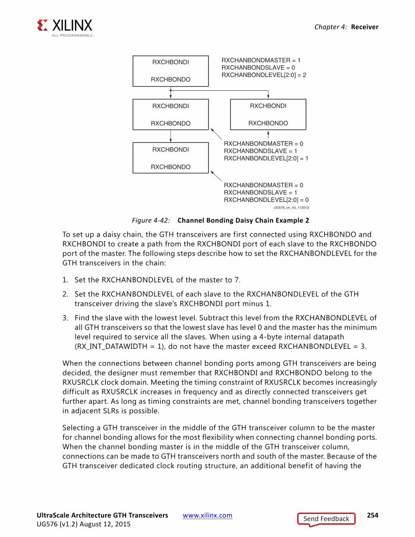
Chapter 4: Receiver
To set up a daisy chain, the GTH transceivers are f irst connected using RXCHBONDO and RXCHBONDI to create a path from the RXCHBONDI port of each slave to the RXCHBONDO port of the master. The following steps describe how to set the RXCHANBONDLEVEL for the GTH transceivers in the chain:
1. Set the RXCHANBONDLEVEL of the master to 7.
2. Set the RXCHANBONDLEVEL of each slave to the RXCHANBONDLEVEL of the GTH transceiver driving the slave’s RXCHBONDI port minus 1.
3. Find the slave with the lowest level. Subtract this level from the RXCHANBONDLEVEL of all GTH transceivers so that the lowest slave has level 0 and the master has the minimum level required to service all the slaves. When using a 4-byte internal datapath (RX_INT_DATAWIDTH = 1), do not have the master exceed RXCHANBONDLEVEL = 3.
When the connections between channel bonding ports among GTH transceivers are being decided, the designer must remember that RXCHBONDI and RXCHBONDO belong to the RXUSRCLK clock domain. Meeting the timing constraint of RXUSRCLK becomes increasingly diff icult as RXUSRCLK increases in frequency and as directly connected transceivers get further apart. As long as timing constraints are met, channel bonding transceivers together in adjacent SLRs is possible.
Selecting a GTH transceiver in the middle of the GTH transceiver column to be the master for channel bonding allows for the most flexibility when connecting channel bonding ports. When the channel bonding master is in the middle of the GTH transceiver column, connections can be made to GTH transceivers north and south of the master. Because of the GTH transceiver dedicated clock routing structure, an additional benefit of having the
X-Ref Target - Figure 4-42
Figure 4-42: Channel Bonding Daisy Chain Example 2
RXCHBONDI
RXCHBONDO
RXCHANBONDMASTER = 1RXCHANBONDSLAVE = 0RXCHANBONDLEVEL[2:0] = 2
RXCHBONDI
RXCHBONDO
RXCHBONDI
RXCHBONDO
RXCHBONDI
RXCHBONDO
RXCHANBONDMASTER = 0RXCHANBONDSLAVE = 1RXCHANBONDLEVEL[2:0] = 1
RXCHANBONDMASTER = 0RXCHANBONDSLAVE = 1RXCHANBONDLEVEL[2:0] = 0
UG576_c4_43_112513
UltraScale Architecture GTH Transceivers www.xilinx.com 254UG576 (v1.2) August 12, 2015
Send Feedback

Chapter 4: Receiver
channel bonding master at the center of the GTH transceiver column is that up to 20 GTH transceivers can be channel bonded together using a single clock pin pair.
As long as timing constraints are met, there is no limit to the number of GTH transceivers that can be on a particular RXCHANBONDLEVEL.
Setting Channel Bonding Sequences
The channel bonding sequence is programmed in the same way as the clock correction sequence. CHAN_BOND_SEQ_LEN sets the length of the sequence, and CHAN_BOND_SEQ_1_* sets the values of the sequence. If CHAN_BOND_SEQ_2_USE is TRUE, CHAN_BOND_SEQ_2_* sets the values for the alternate second sequence. The number of active bits in each subsequence depends on RX_DATA_WIDTH and CBCC_DATA_SOURCE_SEL (see RX Clock Correction, page 238). When RX_DISPERR_SEQ_MATCH is set to FALSE, CHAN_BOND_SEQ_x_y[9] is not used for matching.
Figure 4-43 shows how the subsequence bits are mapped.
As with clock correction sequences, channel bonding sequences can have don’t care subsequences. CHAN_BOND_SEQ_1_ENABLE and CHAN_BOND_SEQ_2_ENABLE set these bytes. Figure 4-44 shows the mapping of the enable attributes for the channel bonding subsequences.
X-Ref Target - Figure 4-43
Figure 4-43: Channel Bonding Sequence Settings
X-Ref Target - Figure 4-44
Figure 4-44: Channel Bonding Sequence Mapping
CHAN BOND_SEQ_x_y
8-Bit Channel Bonding Sequence
1 = Sequence Uses Inverted Disparity0 = Sequence Uses Regular Disparity
7:089
1 = Sequence is a K Character0 = Sequence is a Regular Character
UG576_c4_44_112513
CHAN_BOND_SEQ_x_4 CHAN_BOND_SEQ_x_3 CHAN_BOND_SEQ_x_2 CHAN_BOND_SEQ_x_1
CHAN_BOND_SEQ_x_ENABLE 4 3 2 1UG576_c4_45_112513
UltraScale Architecture GTH Transceivers www.xilinx.com 255UG576 (v1.2) August 12, 2015
Send Feedback

Chapter 4: Receiver
Setting the Maximum Skew
When the master receives a channel bonding sequence, it does not trigger channel bonding immediately. Several more bytes must arrive if the slaves have more latency. This wait time effectively becomes the maximum skew that the RX elastic buffer can handle. If the skew is greater than this wait time, the slaves might not receive the sequence by the time the master triggers channel bonding.
Figure 4-45 shows two FIFOs, one for the master and one for the slave. If the slave is behind the master, the master must wait several cycles before triggering channel bonding, otherwise the slow slave does not have the channel bonding sequence in its buffer.
CHAN_BOND_MAX_SKEW is used to set the maximum skew allowed for channel bonding sequences 1 and 2. The maximum skew range is 1 to 14. This range must always be less than one-half the minimum distance (in bytes or 10-bit codes) between channel bonding sequences. This minimum distance is determined by the protocol being used.
Precedence between Channel Bonding and Clock Correction
The clock correction (see RX Clock Correction, page 238) and channel bonding circuits both perform operations on the pointers of the RX elastic buffer. Normally, the two circuits work together without conflict, except when clock correction events and channel bonding events
X-Ref Target - Figure 4-45
Figure 4-45: Channel Bonding Example (CHAN_BOND_MAX_SKEW = 2 andMaster RXCHANBONDLEVEL[2:0] = 1)
D1D2D3D4D5D6D7SEQ1
D1D2D3D4D5D6D7 D0
D4D5D6D7SEQ1D8D9D10
D4D5D6D7SEQ1D8D9 D3
D5D6D7SEQ1D8D9D10D11
D5D6D7SEQ1D8D9D10 D4SlaveElasticBuffer
MasterElasticBuffer
Slave’s New ElasticBuffer Read Pointer
Master receives CB Sequence
The master waits CHAN_BOND_MAX_SKEWcycles before triggering channel bonding, givingthe slave time to receive the sequence. The message to perform channel bonding is sentusing the RXCHBONDO port.
The RXCHANBONDLEVEL setting of the masterdetermines how many cycles later the bondingoperation is executed. At this time, the slave’selastic buffer pointers are moved so that the output is deskewed.
SlaveElasticBuffer
MasterElasticBuffer
SlaveElasticBuffer
MasterElasticBuffer
UG576_c4_46_112513
UltraScale Architecture GTH Transceivers www.xilinx.com 256UG576 (v1.2) August 12, 2015
Send Feedback

Chapter 4: Receiver
occur simultaneously. In this case, one of the two circuits must take precedence. To make clock correction a higher priority than channel bonding, CLK_COR_PRECEDENCE must be set to TRUE. To make channel bonding a higher priority, CLK_COR_PRECEDENCE must be set to FALSE.
RX Synchronous Gearbox
Functional DescriptionThe RX synchronous gearbox provides support for 64B/66B and 64B/67B header and payload separation. The gearbox uses output pins RXDATA[63:0] and RXHEADER[2:0] for the payload and header of the received data in normal mode. Similar to TX Synchronous Gearbox, page 100, the RX synchronous gearbox operates with the PMA using a single clock. Because of this, occasionally, the output data is invalid. Output pins RXHEADERVALID and RXDATAVALID determine if the appropriate header and data are valid. The RX synchronous gearbox supports 2-byte, 4-byte, and 8-byte interfaces.
The data out of the RX synchronous gearbox is not necessarily aligned. Alignment is done in the interconnect logic. The RXGEARBOXSLIP port can be used to slip the data from the gearbox cycle-by-cycle until correct alignment is reached. It takes a specif ic number of cycles before the bitslip operation is processed and the output data is stable. Descrambling of the data and block synchronization is done in the interconnect logic. A CAUI interface mode is also supported besides the normal gearbox mode.
UltraScale Architecture GTH Transceivers www.xilinx.com 257UG576 (v1.2) August 12, 2015
Send Feedback

Chapter 4: Receiver
Ports and AttributesTable 4-40 defines the RX gearbox ports.
Table 4-40: RX Gearbox Ports
Port Name Dir Clock Domain Description
RXDATAVALID[1:0] Out RXUSRCLK2 Status output when Gearbox 64B/66B or 64B/67B is used, which indicates that the data appearing on RXDATA is valid. For example, during 64B/66B encoding, this signal is deasserted every 32 cycles for the 8-byte interface (and 4-byte interface with RX_INT_DATAWIDTH= 0) and every 64 cycles for the 2-byte interface (and 4-byte interface with RX_INT_DATAWIDTH = 1).RXDATAVALID[0] indicates that the data appearing on RXDATA is valid in normal mode. The current RXDATA for datastream A is valid in CAUI interface mode.RXDATAVALID[1] indicates that the current RXDATA is valid for datastream B in CAUI interface mode.
RXGEARBOXSLIP In RXUSRCLK2 When High, this port causes the gearbox contents to slip to the next possible alignment. This port is used to achieve alignment with the interconnect logic. Asserting this port for one RXUSRCLK2 cycle changes the data alignment coming out of the gearbox. RXGEARBOXSLIP must be deasserted for at least one cycle and then reasserted to cause a new realignment of the data. If multiple realignments occur in rapid succession, it is possible to pass the proper alignment point without recognizing the correct alignment point in the interconnect logic.RXGEARBOXSLIP for datastream A in CAUI interface mode.
RXHEADER[5:0] Out RXUSRCLK2 RXHEADER[2:0]: Header output in normal mode and for datastream A in CAUI interface mode.RXHEADER[5:3]: Header output for datastream B in CAUI interface mode.
RXHEADERVALID[1:0] Out RXUSRCLK2 Indicates that the RXHEADER is valid when using the gearbox.GTH transceiver:RXHEADERVALID[0]: Indicates that RXHEADER is valid for the current data in normal mode and for datastream A in CAUI interface mode.RXHEADERVALID[1]: Indicates that RXHEADER is valid for datastream B in CAUI interface mode.
UltraScale Architecture GTH Transceivers www.xilinx.com 258UG576 (v1.2) August 12, 2015
Send Feedback

Chapter 4: Receiver
Table 4-41 defines the RX synchronous gearbox attributes.
Enabling the RX Synchronous GearboxTo enable the RX synchronous gearbox for the GTH transceiver, set the attribute RXGEARBOX_EN to TRUE. Bit 4 of the GEARBOX_MODE attribute must be set to 0. Bit 3 and 1 are unused and must be set to 0. Bit 2 determines if the normal interface or CAUI interface is used. Bit 0 determines if the 64B/67B gearbox or the 64B/66B gearbox is used.
RXSLIDE In RXUSRCLK2 Used as RXGEARBOXSLIP for datastream B in CAUI interface mode.
RXSTARTOFSEQ[1:0] Out RXUSRCLK2 When the gearbox 64B/66B or 64B/67B is enabled, this output indicates when the sequence counter is 0 for the present RXDATA outputs.RXSTARTOFSEQ[0]: This output indicates when the sequence counter is 0 for the present RXDATA in normal mode, and for datastream A in CAUI interface mode.RXSTARTOFSEQ[1]: This output indicates when the sequence counter is 0 for datastream B in CAUI interface mode.
Table 4-41: RX Synchronous Gearbox Attributes
Attribute Type Description
GEARBOX_MODE 5-bit Binary This attribute indicates the TX and RX gearbox modes:• Bit 4:
° 0: Select synchronous gearbox.
° 1: Select asynchronous gearbox.• Bit 3:
Unused. Set to 0.• Bit 2:
0: Normal mode.1: CAUI interface mode.
• Bit 1:Unused. Set to 0.
• Bit 0:0: 64B/67B gearbox mode for Interlaken (only valid for synchronous gearbox).1: 64B/66B gearbox
RXGEARBOX_EN String When TRUE, this attribute enables either the RX synchronous or asynchronous gearbox. Which RX gearbox is enabled depends on the GEARBOX_MODE attribute.
Table 4-40: RX Gearbox Ports (Cont’d)
Port Name Dir Clock Domain Description
UltraScale Architecture GTH Transceivers www.xilinx.com 259UG576 (v1.2) August 12, 2015
Send Feedback

Chapter 4: Receiver
RX Gearbox Operating ModesThe RX gearbox only supports 2-byte, 4-byte and 8-byte logic interfaces to the interconnect logic.
As shown in Figure 4-46, output ports RXDATA, RXHEADER, RXDATAOUTVALID, and RXHEADEROUTVALID in addition to the RXGEARBOXSLIP input port are used in normal mode (GEARBOX_MODE[2] = 1’b0).
X-Ref Target - Figure 4-46
Figure 4-46: Gearbox Usage in Normal Mode (GEARBOX_MODE[2] = 1'b0)
Design in Interconnect LogicRX Synchronous Gearbox
(in GTH Transceiver)
RXHEADER[2:0]
RXDATA[15:0] or RXDATA[31:0] orRXDATA[63:0]
RXDATAVALID
RXGEARBOXSLIP
RXHEADERVALID
RXSTARTOFSEQ
UG576_c4_47_070114
UltraScale Architecture GTH Transceivers www.xilinx.com 260UG576 (v1.2) August 12, 2015
Send Feedback

Chapter 4: Receiver
Figure 4-47 shows an example of four cycles of data entering and exiting the RX gearbox for 64B/66B encoding when using a 4-byte logic interface (RX_DATA_WIDTH = 32 (4-byte), RX_INT_DATAWIDTH = 1 (4-byte)) in normal mode (GEARBOX_MODE[2] = 1'b0).
Note relevant to Figure 4-47:
1. As per IEEE Std 802.3ae-2002 nomenclature, H1 corresponds to RxB<0>, H0 to RxB<1>, etc.
X-Ref Target - Figure 4-47
Figure 4-47: RX Gearbox Operation in Normal Mode (GEARBOX_MODE[2] = 1'b0)
D31 D30 D5 D4 D3 D2……………
D31 D30 D5 D4………………………
D0 …………D31
D1 D0
D1 D0 D31 D30 D7 D6 D5 D4………………
D1 D0 D31 D30 D5 D4………………………
D0 ………
D3 D2
D31 D30 D7 D6 D5 D4………………
D3 D2 D1 D0 D7………………………
D0 …………D31
D6
D1 D0 D31 D30 D9 D8 D7 D6………………
D5 D4 D3 D2 D7………………
D0 …………
D1 D0 D6D31 D30
D31
H1 H0
H1 H0
H1
H1 H0
H1 H0
H1
Input to the RXGearbox
Cycle N
Cycle N+3
RXHEADEROUTVALID = 1'b1RXDATAOUTVALID = 1'b1
RXHEADER RXDATA
Input to the RXGearbox
Cycle N+1
RXHEADEROUTVALID = 1'b0RXDATAOUTVALID = 1'b1
RXHEADER RXDATA
Input to the RXGearbox
Cycle N+2
RXHEADEROUTVALID = 1'b1RXDATAOUTVALID = 1'b1
RXHEADER RXDATA
Input to the RXGearbox
RXHEADEROUTVALID = 1'b0RXDATAOUTVALID = 1'b1
RXHEADER RXDATA
Output of theRXGearbox
Output of theRXGearbox
Output of theRXGearbox
Output of theRXGearbox
UG576_c4_48_112513
UltraScale Architecture GTH Transceivers www.xilinx.com 261UG576 (v1.2) August 12, 2015
Send Feedback

Chapter 4: Receiver
The RX gearbox internally manages all sequencing, which differs from the TX gearbox option of either internal or external sequencing. Depending on whether a 2-byte, 4-byte, or 8-byte interface is used, RXDATAOUTVALID and RXHEADEROUTVALID assert and deassert for different periods of length. The RX gearbox encounters similar data and header pauses found in the TX gearbox. Figure 4-48 shows such a pause in addition to RXHEADERVALID and RXDATAVALID being deasserted for one cycle. Figure 4-49 shows the operation for 64B/67B encoding when RX_DATA_WIDTH = 16 (2-byte) and RX_INT_DATAWIDTH = 0 (2-byte) in normal mode (GEARBOX_MODE[2] = 1'b0).
X-Ref Target - Figure 4-48
Figure 4-48: RX Gearbox When Using 64B/66B Encoding and RX_DATA_WIDTH = 64 (8-Byte) and RX_INT_DATAWIDTH= 1 (4-Byte) in Normal Mode (GEARBOX_MODE[2] = 1'b0)
UG576_c4_49_112513
1
Da Db Dc Dd De XXX Df Dg Dh Di Dj Dk Dl Dm Dn
12
RXUSRCLK2
RXGEARBOXSLIP
RXHEADERVALID
RXHEADER[1:0]
RXDATAVALID
RXDATA[63:0]
Data pauses for 1 cycle.
X-Ref Target - Figure 4-49
Figure 4-49: RX Gearbox When Using 64B/67B Encoding and RX_DATA_WIDTH = 16 (2-Byte) and RX_INT_DATAWIDTH = 0 (2-Byte)
UG576_c4_50_112513
1 1 110 06 6 62
Da Db Dc Dd De XXXDf Dg Dh Di Dj Dk Dl Dm
50
RXUSRCLK2
RXGEARBOXSLIP
RXHEADERVALID
RXHEADER[2:0]
RXDATAVALID
RXDATA[15:0]
Data pauses for 1 cycle. Data pauses for 2 cycles.
UltraScale Architecture GTH Transceivers www.xilinx.com 262UG576 (v1.2) August 12, 2015
Send Feedback

Chapter 4: Receiver
RX Gearbox Block SynchronizationThe 64B/66B and 64B/67B protocols depend on block synchronization to determine their block boundaries. Block synchronization is required because all incoming data is unaligned before block lock is achieved. The goal is to search for the valid synchronization header by changing the data alignment. The RXGEARBOXSLIP input port is used to change the gearbox data alignment so that all possible alignments can be checked in normal mode (GEARBOX_MODE[2] = 1'b0). (RXSLIDE is used as RXGEARBOXSLIP for the second datastream in the CAUI interface mode (GEARBOX_MODE[2] = 1'b1).) The RXGEARBOXSLIP signal feeds back from the block synchronization state machine to the RX gearbox and tells it to slip the data alignment. This process of slipping and testing the synchronization header repeats until block lock is achieved. When using the RX gearbox, a block synchronization state machine is required in the interconnect logic. Figure 4-50 shows the operation of a block synchronization state machine.
UltraScale Architecture GTH Transceivers www.xilinx.com 263UG576 (v1.2) August 12, 2015
Send Feedback

Chapter 4: Receiver
The state machine works by keeping track of valid and invalid synchronization headers. Upon reset, block lock is deasserted, and the state is LOCK_INIT. The next state is RESET_CNT where all counters are zeroed out. The synchronization header is analyzed in the
X-Ref Target - Figure 4-50
Figure 4-50: Block Synchronization State Machine
LOCK_INIT
block_lock <= falsetest_sh <= false
RESET_CNT
sh_cnt <= 0sh_invalid_cnt <= 0slip_done <= false
TEST_SH
test_sh <= false
VALID_SH
sh_cnt <= sh_cnt + 1
64_GOOD
block_lock <= true
SLIP
block_lock <= falseSLIP <= true
INVALID_SH
sh_cnt <= sh_cnt + 1sh_invalid_cnt <= sh_invalid_cnt + 1
sh_cnt = 64 AND sh_invalid_cnt = 0
sh_cnt = 64 AND sh_invalid_cnt > 0
sh_cnt = 64 AND sh_invalid_cnt < 16 AND block_lock = true
sh_invalid_cnt = 16 OR block_lock = false
slip_done = true
sh_valid = 0
Unconditional Transition
sh_valid = 1
test_sh = true AND sh_cnt < 64
test_sh = 1
Unconditional Transition
test_sh = true AND sh_cnt < 64 AND sh_invalid_cnt < 16 AND block_lock = true
UG576_c4_51_112513
UltraScale Architecture GTH Transceivers www.xilinx.com 264UG576 (v1.2) August 12, 2015
Send Feedback

Chapter 4: Receiver
TEST_SH state. If the header is valid, sh_cnt is incremented in the VALID_SH state, otherwise sh_count and sh_invalid_count are incremented in the INVALID_SH state.
For the block synchronization state machine shown in Figure 4-50, sh_cnt_max and sh_invalid_cnt_max are both constants that are set to 64 and 16, respectively. From the VALID_SH state, if sh_cnt is less than the value sh_cnt_max and test_sh is High, the next state is TEST_SH. If sh_cnt is equal to sh_cnt_max and sh_invalid_cnt equals 0, the next state is GOOD_64 and from there block_lock is asserted. Then the process repeats again and the counters are cleared to zeros. To achieve block lock, the state machine must receive sh_cnt_max number of valid synchronization headers in a row without getting an invalid synchronization header. However, when block lock is achieved sh_invalid_cnt_max – 1, the number of invalid synchronization headers can be received within sh_cnt_max number of valid synchronization headers. Thus, once locked, it is harder to break lock.
Figure 4-51 shows a waveform of the block synchronization state machine asserting RXGEARBOXSLIP numerous times because of invalid synchronization headers before achieving data alignment. After the RXGEARBOXSLIP is issued, the state machine waits 32 RXUSRCLK2 cycles before checking for valid synchronization headers.
X-Ref Target - Figure 4-51
Figure 4-51: RX Gearbox with Block Synchronization in Normal Mode (GEARBOX_MODE[2] = 1'b0)
UG576_c4_52_112513
Data alignmentachieved
Data check onunscrambled data
block_sync_i
unscrambled_data_i
begin_r
track_data_r
start_of_packet_detected_r
RXDATA
RXDATAVALID
RXGEARBOXSLIP
RXHEADER
RXHEADERVALID
RXSTARTOFSEQ
0
Slip dataalignment
Closely spaced slip pulses. State machineasserts slip as soon as it sees bad header.
0000000000000000
0000000000000000
UltraScale Architecture GTH Transceivers www.xilinx.com 265UG576 (v1.2) August 12, 2015
Send Feedback

Chapter 4: Receiver
CAUI Interface
The CAUI interface requires two data interfaces on the transceiver. This section describes the design of the CAUI interface block on the RX that is implemented in the GTH transceiver. This supports a dual data interface in 64/66 and 64/67 modes (datastream A and datastream B). The CAUI interface mode can be selected by setting the attribute GEARBOX_MODE[2] to 1'b1. When in CAUI interface mode, the only allowed settings are RX_INT_DATAWIDTH = 1 (4-byte) and RX_DATA_WIDTH = 64 (8-byte) or 32 (4-byte).
The top-level RX synchronous gearbox has the following components:
1. One instance of 64/66 4-byte gearbox
2. Two instances of 64/66 2-byte gearbox
3. One instance of 64/67 4-byte gearbox
4. Two instances of 64/67 2-byte gearbox
5. Sequence detector
To support the CAUI interface, the GTH transceiver has two instances of each of the 2-byte gearboxes. One instance of the bit demux block is also added. The RXGEARBOXSLIP input signal is used for datastream A, while the RXSLIDE input signal is used as a gearbox slip input for datastream B.
UltraScale Architecture GTH Transceivers www.xilinx.com 266UG576 (v1.2) August 12, 2015
Send Feedback

Chapter 4: Receiver
Figure 4-52 shows the CAUI interface (RX path) of the GTH transceiver.
In CAUI interface mode, the bit demux block splits the incoming data stream from the PMA into A and B streams. The block receives 32 bits of encoded data every cycle. All even bits are assigned to datastream A and all odd bits are assigned to datastream B.
Though RX_INT_DATAWIDTH = 1 (4-byte) is used in this mode, two 2-byte gearboxes are used to realize the functionality shown in Figure 4-52. The functionality of these 2-byte gearboxes are the same as described in the previous sections for the case when RX_INT_DATAWIDTH = 0 (2-byte).
If the PCSL data width is 32 bits each (RX_DATA_WIDTH = 64 (8-byte)), the 4-byte to 8-byte converter combines the data streams in such a way that datastreams A and B reach the corresponding PCSLs as shown in Figure 4-53 and Figure 4-54.
X-Ref Target - Figure 4-52
Figure 4-52: CAUI Interface (RX Datapath)
RX Gearbox BlockInterconnect LogicInterface Block
GTHE3_CHANNEL
64/66 – 4 ByteGearbox
Data OutData ValidHeader OutHeader Valid
Data OutData ValidHeader OutHeader Valid
Data OutData ValidHeader OutHeader Valid
Data OutData ValidHeader OutHeader Valid
Data OutData ValidHeader OutHeader Valid
Data OutData ValidHeader OutHeader Valid
BitDemux0
B
A IN
RXDATAfrom PMA
UG576_c4_53_072215
4-Byte to 8-ByteConverter
RXDATA[63:0]
RXDATAVALID[1:0]
RXHEADER[5:0]
RXHEADERVALID[1:0]
RXSTARTOFSEQ[1:0]
RX GearboxSynchronizer
64/67 – 4 ByteGearbox
64/66 – 2 ByteGearbox A
64/66 – 2 ByteGearbox B
{B ,
A}
{B ,
A}
{B ,
A}
64/67 – 2 ByteGearbox A
64/67 – 2 ByteGearbox B
64/66 4B Gbx Sequence64/67 4B Gbx Sequence64/66 2B Gbx A Sequence64/67 2B Gbx A Sequence
Startseq
Startseq
0064/66 2B Gbx B Sequence64/67 2B Gbx B Sequence
SequenceDetector A
SequenceDetector B
UltraScale Architecture GTH Transceivers www.xilinx.com 267UG576 (v1.2) August 12, 2015
Send Feedback

Chapter 4: Receiver
RX Asynchronous Gearbox
Functional DescriptionThe RX asynchronous gearbox only provides support for 64B/66B header and payload separation. The gearbox uses the output pins RXDATA[63:0] and RXHEADER[1:0] for the payload and header in normal mode. 64B/67B is not supported by the RX asynchronous gearbox.
The RX asynchronous gearbox supports 4-byte and 8-byte RX data interface to interconnect logic and requires the use of the 4-byte internal datapath. Scrambling of the data is done in the interconnect logic. A CAUI interface mode is also supported in addition to the normal asynchronous gearbox mode. The CAUI interface is only supported when using the 8-byte RX data interface to interconnect logic. Table 4-42 shows the valid data width combinations for the asynchronous gearbox.
X-Ref Target - Figure 4-53
Figure 4-53: Input to the 4-Byte to 8-Byte Converter (RX_DATA_WIDTH = 64 (8-Byte), RX_INT_DATAWIDTH = 1 (4-Byte), GEARBOX_MODE[2] = 1'b1)
X-Ref Target - Figure 4-54
Figure 4-54: Output of the 4-Byte to 8-Byte Converter (RX_DATA_WIDTH = 64 (8-Byte), RX_INT_DATAWIDTH = 1 (4-Byte), GEARBOX_MODE[2] = 1'b1)
RXUSRCLK
RXDATA[31:24]
RXDATA[23:16]
RXDATA[15:8]
RXDATA[7:0]
D0 D4 D8
D1 D5 D9
D2 D6 D10
D3 D7 D11
D12 D16 D20
D13 D17 D21
D14 D18 D22
D15 D19 D23
UG576_c4_54_112513
RXUSRCLK2
RXDATA[63:56]
RXDATA[55:48]
RXDATA[47:40]
RXDATA[39:32]
RXDATA[31:24]
RXDATA[23:16]
RXDATA[15:8]
RXDATA[7:0]
D0 D8 D16
D1 D9 D17
D4 D12 D20
D5 D13 D21
D2 D10 D18
D3 D11 D19
D6 D14 D22
D7 D15 D23UG576_c4_55_112513
UltraScale Architecture GTH Transceivers www.xilinx.com 268UG576 (v1.2) August 12, 2015
Send Feedback

Chapter 4: Receiver
While the RX synchronous gearbox requires you to monitor the RXDATAVALID port because of invalid data appearing periodically, the RX asynchronous gearbox allows valid data to be continuously received every RXUSRCLK2 cycle. RX buffer bypass is not supported when using the RX asynchronous gearbox because it bridges two clock domains that have different frequencies and phases. The RX asynchronous gearbox is also located in parallel to the RX buffer. Figure 4-55 shows the location of the TX asynchronous gearbox. 32 bits of data always enter the RX asynchronous gearbox on every RX XCLK cycle. Alternating 34 bits (2-bit header and 32-bit payload) and 32 bits (32-bit payload) of data exit the RX asynchronous gearbox every RXUSRCLK cycle.
When in normal mode, the data path latency through the RX asynchronous gearbox is measured internally and the reported latency can be accessed by reading a read-only register via DRP. The RX asynchronous gearbox is used in conjunction with the RX programmable dividers. RXOUTCLKSEL must be set to 3'b101 and an appropriate divide value must be selected to create the required clock frequencies for TXUSRCLK and TXUSRCLK2.
Table 4-42: Valid Data Width Combinations for RX Asynchronous Gearbox
Interface Mode
Internal Datapath Width Interface Width XCLK (MHz) RXUSRCLK (MHz) RXUSRCLK2 (MHz)
Normal Mode 32 32 RX Line Rate/32 RX Line Rate/33 RX Line Rate/33
32 64 RX Line Rate/32 RX Line Rate/33 RX Line Rate/66
CAUI Mode 32 64 RX Line Rate/32 RX Line Rate/32 RX Line Rate/66
X-Ref Target - Figure 4-55
Figure 4-55: RX Clock Domain Example (RX_INT_DATAWIDTH = 1 (4-byte) and RX_DATA_WIDTH = 64)
RX OOB
DFERXEQ
SIPO
RXClock
Dividers
Polarity
RXInterface
64 Data +2 Header
bits
CommaDetect
andAlign
128B/130B
Decoder
RXElasticBuffer RX Sync
GearboxPRBSChecker
RX StatusControl
RX PIPEControl
From ChannelClocking
Architecture
From TX ParallelData (Near-EndPCS Loopback)
To TX Parallel Data(Far-End PCS
Loopback)
To TX Parallel Data(Far-End PMA
Loopback)
RX Serial Clock PMA Parallel Clock (XCLK) PCS Parallel Clock (RXUSRCLK)Device Parallel
Clock(RXUSRCLK2)
RX AsyncGearbox
34, 32 bits32 bits
8B/10BDecoder
PCIeRX Buffer
BlockDetectAlign
UG576_c4_56_063014
UltraScale Architecture GTH Transceivers www.xilinx.com 269UG576 (v1.2) August 12, 2015
Send Feedback

Chapter 4: Receiver
Ports and AttributesTable 4-43 defines the RX asynchronous gearbox ports.
Table 4-43: RX Asynchronous Gearbox Ports
Port Name Dir Clock Domain Description
RXGEARBOXSLIP In RXUSRCLK2 When High, this port causes the gearbox contents to slip to the next possible alignment. This port is used to achieve alignment with the interconnect logic.Asserting this port for one RXUSRCLK2 cycle changes the data alignment coming out of the gearbox.RXGEARBOXSLIP must be deasserted for at least one cycle and then reasserted to cause a new realignment of the data. If multiple realignments occur in rapid succession, it is possible to pass the proper alignment point without recognizing the correct alignment point in the interconnect logic.When in CAUI interface mode, RXGEARBOXSLIP is used for slip datastream A.
RXHEADER[5:0] Out RXUSRCLK2 RXHEADER[1:0]: Header output in normal mode and for datastream A in CAUI interface mode.RXHEADER[4:3]: Header output for datastream B in CAUI interface mode.
RXHEADERVALID[1:0] Out RXUSRCLK2 Indicates if RXHEADER is valid.RXHEADERVALID[0]: 1'b1 indicates that RXHEADER is valid for current data in normal mode and for datastream A in CAUI interface mode. When using an 8-byte RX data interface (RX_DATA_WIDTH = 64), RXHEADERVALID[0] always outputs 1'b1 indicating RXHEADER is valid for every RXUSRCLK2 cycle. RXHEADERVALID[0] toggles every RXUSRCLK2 cycle when using a 4-byte RX data interface in either normal mode or CAUI interface mode.RXHEADERVALID[1]: 1'b1 indicates that RXHEADER is valid for datastream B in CAUI interface mode. RXHEADERVALID[1] toggles every RXUSRCLK2 cycle when using a 4-byte RX data interface in either normal mode or CAUI interface mode.
UltraScale Architecture GTH Transceivers www.xilinx.com 270UG576 (v1.2) August 12, 2015
Send Feedback

Chapter 4: Receiver
Table 4-44 defines the RX asynchronous gearbox ports.
RXBUFSTATUS[1:0] Out RXUSRCLK2 RXBUFSTATUS provides status for the RX buffer or the RX asynchronous gearbox. When using the RX asynchronous gearbox, the port status is as follows:• Bit 1:
0: No RX asynchronous gearbox FIFO overflow.1: RX asynchronous gearbox FIFO overflow.
• Bit 0:0: No RX asynchronous gearbox FIFO underflow1: RX asynchronous gearbox FIFO underflow.
After the port is set High, it remains High until the TX asynchronous gearbox is reset.
RXLATCLK In Clock Input port used to provide a clock for the RX asynchronous gearbox latency calculation.
RXSLIDE In RXUSRCLK2 Used as RXGEARBOXSLIP for datastream B in CAUI interface mode.
Table 4-44: RX Asynchronous Gearbox Ports
Attribute Type Description
GEARBOX_MODE 5-bit Binary Selects the TX and RX gearbox operating modes.• Bit 4:
0: Select synchronous gearbox.1: Select asynchronous gearbox.
• Bit3:Unused. Set to 0.
• Bit 2:0: Normal mode1: CAUI interface mode.
• Bit 1:Unused. Set to 0.
• Bit 0:0: 64B/67B gearbox mode (Only valid for synchronous gearbox).1: 64B/66B gearbox.
RXGEARBOX_EN String When TRUE, this attribute enables either the RX synchronous or asynchronous gearbox. Which RX gearbox is enabled depends on the GEARBOX_MODE attribute. When FALSE, this attribute disables the RX synchronous and asynchronous gearbox.
Table 4-43: RX Asynchronous Gearbox Ports (Cont’d)
Port Name Dir Clock Domain Description
UltraScale Architecture GTH Transceivers www.xilinx.com 271UG576 (v1.2) August 12, 2015
Send Feedback

Chapter 4: Receiver
Enabling the RX Asynchronous GearboxTo enable the RX asynchronous gearbox, RXGEARBOX_EN must be set to TRUE.
GEARBOX_MODE[4] must be set to 1'b1 to select the asynchronous gearbox. Bit GEARBOX_MODE[1] and GEARBOX_MODE[3] are unused and must be set to 1'b0. GEARBOX_MODE[2] determines if the normal interface or CAUI interface is used. As the RX asynchronous gearbox only supports 64B/66B, GEARBOX_MODE[0] must be set to 1'b1.
Using the RX Asynchronous GearboxAs shown in Figure 4-56, the RX asynchronous gearbox uses output ports RXHEADERVALID[0], RXDATA[63:0], and RXHEADER[1:0], and uses the input port RXGEARBOXSLIP when in normal mode (GEARBOX_MODE[2] = 1'b0).
When using an 8-byte RXDATA interface (RX_DATA_WIDTH = 64), 2 bits of header and 64 bits of payload are output by the GTH transceiver every RXUSRCLK2 cycle. RXHEADERVALID[0] is High (1'b1) every RXUSRCLK2 cycle as RXHEADER[1:0] is valid every RXUSRCLK2 cycle.
When using a 4-byte RXDATA interface (RX_DATA_WIDTH = 32), RXHEADER[1:0] is valid every other RXUSRCLK2 cycle, thus RXHEADERVALID[0] will toggle, and 32 bits of data is output on RXDATA[31:0] every RXUSRCLK2 cycle.
RXGBOX_FIFO_INIT_RD_ADDR Integer Initialization read address. Reserved. The recommended value from the UltraScale FPGAs Transceiver Wizard must be used.
RX_SAMPLE_PERIOD 3-bit Binary Number of RXLATCLK cycles of over which averaging takes place for latency calculation.3'b000: 2563'b001: 5123'b010: 10243'b011: 20483'b100: 40963'b101: 81923'b110: 163843'b111: 32768
RXGBOX_FIFO_LATENCY 16-bit Binary Measured latency in UI through the RX asynchronous gearbox averaged over RX_SAMPLE_PERIOD cycles. The reported latency is in units of 1/8 UI.The RXGBOX_FIFO_LATENCY read-only register is accessed via DRP. The address of this register is 0x169.
Table 4-44: RX Asynchronous Gearbox Ports (Cont’d)
Attribute Type Description
UltraScale Architecture GTH Transceivers www.xilinx.com 272UG576 (v1.2) August 12, 2015
Send Feedback

Chapter 4: Receiver
The RXGEARBOXSLIP input port is used in the block synchronization process. The block synchronization process to determine block boundaries is the same as documented in RX Synchronous Gearbox, page 257. Refer to RX Gearbox Block Synchronization, page 263 for block synchronization details.
Reading Datapath LatencyThe datapath latency through the RX async gearbox FIFO is calculated statistically using RXLATCLK, which is asynchronous to RX_XCLK. RX_SAMPLE_PERIOD determines the number of RXLATCLK cycles over which averaging takes place. The measured latency value in RXGBOX_FIFO_LATENCY is updated once per sampling period that is defined in RX_SAMPLE_PERIOD.
For the read side of the RX async gearbox FIFO, there is an additional offset that is determined by the gearbox slip count value for the data alignment. Thus, the RXGEARBOXSLIP must be performed to achieve sync status prior to reading out the latency value. The latency measurement is not supported in CAUI mode.
These settings are used to read the latency:
• Enable RX asynchronous gearbox under normal mode
• Set RX_SAMPLE_PERIOD
° Higher averaging period gives more accurate latency value
• Achieve datapath sync status by RXGEARBOXSLIP
• Read RXGBOX_FIFO_LATENCY
° The value is in units of 1/8 UI
X-Ref Target - Figure 4-56
Figure 4-56: RX Asynchronous Gearbox in Normal Mode (GEARBOX_MODE[2] = 1'b0)
Design in Interconnect Logic
RX Asynchronous Gearbox(in GTH Transceiver)
RXHEADER[1:0]
RXDATA[31:0] orRXDATA[63:0]
RXHEADERVALID[0]
RXGEARBOXSLIP
UG576_c4_57_063014
UltraScale Architecture GTH Transceivers www.xilinx.com 273UG576 (v1.2) August 12, 2015
Send Feedback

Chapter 4: Receiver
CAUI InterfaceThe CAUI interface requires two data interfaces (datastream A and datastream B) connected to the transceiver. The CAUI interface mode is enabled by setting the GEARBOX_MODE[2] to 1'b1. When in CAUI interface mode and the RX asynchronous gearbox is selected, the only allowed settings for data width are TX_INT_DATAWIDTH = 1 (4-byte) and TX_DATA_WIDTH = 64 (8-byte).
As shown in Figure 4-57, the RX asynchronous gearbox uses RXHEADERVALID[1:0], RXDATA[63:0], and RXHEADER[4:0], and uses the input ports RXGEARBOXSLIP and RXSLIDE when in CAUI interface mode (GEARBOX_MODE[2] = 1'b1). Usage of the CAUI interface for each datastream is the same as described for normal mode when RX_DATA_WIDTH = 32 (4-byte). RXDATA[31:0], RXHEADER[1:0], and RXHEADERVALID[0] are dedicated for datastream A while RXDATA[63:32], RXHEADER[4:3], and RXHEADERVALID[1] are dedicated for datastream B. For datastream B, RXSLIDE serves the same purpose as RXGEARBOXSLIP does for datastream A.
Just as in normal mode, the block synchronization process to determine block boundaries is the same as documented in RX Synchronous Gearbox, page 257. Refer to RX Gearbox Block Synchronization, page 263 for block synchronization details.
X-Ref Target - Figure 4-57
Figure 4-57: RX Asynchronous Gearbox in CAUI Mode (GEARBOX_MODE[2] = 1'b1)
UG576_c4_58_063014
Design in Interconnect Logic
RX Asynchronous Gearbox(in GTH Transceiver)
RXHEADER[1:0]
RXDATA[31:0]
RXGEARBOXSLIP
RXHEADERVALID[0]
RXHEADER[4:3]
RXDATA[63:32]
RXSLIDE
RXHEADERVALID[1]
PCSL – Datastream A
PCSL – Datastream B
UltraScale Architecture GTH Transceivers www.xilinx.com 274UG576 (v1.2) August 12, 2015
Send Feedback
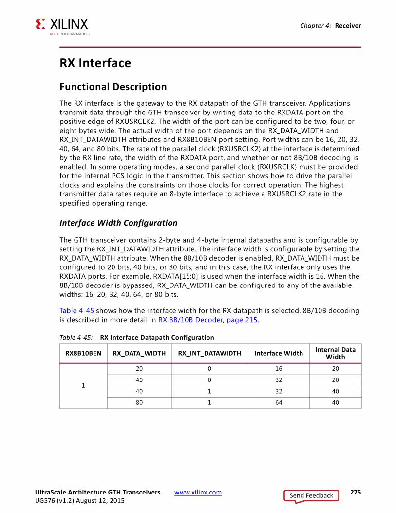
Chapter 4: Receiver
RX Interface
Functional DescriptionThe RX interface is the gateway to the RX datapath of the GTH transceiver. Applications transmit data through the GTH transceiver by writing data to the RXDATA port on the positive edge of RXUSRCLK2. The width of the port can be configured to be two, four, or eight bytes wide. The actual width of the port depends on the RX_DATA_WIDTH and RX_INT_DATAWIDTH attributes and RX8B10BEN port setting. Port widths can be 16, 20, 32, 40, 64, and 80 bits. The rate of the parallel clock (RXUSRCLK2) at the interface is determined by the RX line rate, the width of the RXDATA port, and whether or not 8B/10B decoding is enabled. In some operating modes, a second parallel clock (RXUSRCLK) must be provided for the internal PCS logic in the transmitter. This section shows how to drive the parallel clocks and explains the constraints on those clocks for correct operation. The highest transmitter data rates require an 8-byte interface to achieve a RXUSRCLK2 rate in the specified operating range.
Interface Width Configuration
The GTH transceiver contains 2-byte and 4-byte internal datapaths and is configurable by setting the RX_INT_DATAWIDTH attribute. The interface width is configurable by setting the RX_DATA_WIDTH attribute. When the 8B/10B decoder is enabled, RX_DATA_WIDTH must be configured to 20 bits, 40 bits, or 80 bits, and in this case, the RX interface only uses the RXDATA ports. For example, RXDATA[15:0] is used when the interface width is 16. When the 8B/10B decoder is bypassed, RX_DATA_WIDTH can be configured to any of the available widths: 16, 20, 32, 40, 64, or 80 bits.
Table 4-45 shows how the interface width for the RX datapath is selected. 8B/10B decoding is described in more detail in RX 8B/10B Decoder, page 215.
Table 4-45: RX Interface Datapath Configuration
RX8B10BEN RX_DATA_WIDTH RX_INT_DATAWIDTH Interface Width Internal Data Width
1
20 0 16 20
40 0 32 20
40 1 32 40
80 1 64 40
UltraScale Architecture GTH Transceivers www.xilinx.com 275UG576 (v1.2) August 12, 2015
Send Feedback

Chapter 4: Receiver
When the 8B/10B decoder is bypassed and RX_DATA_WIDTH is 20, 40, or 80, the RXCTRL0 and RXCTRL1 ports are used to extend the RXDATA port from 16 to 20 bits, 32 to 40 bits, or 64 to 80 bits. Table 4-46 shows the data received when the 8B/10B decoder is disabled. When the RX gearbox is used, refer to RX Synchronous Gearbox, page 257 for data transmission order.
RXUSRCLK and RXUSRCLK2 Generation
The RX interface includes two parallel clocks: RXUSRCLK and RXUSRCLK2. RXUSRCLK is the internal clock for the PCS logic in the GTH transmitter. The required rate for RXUSRCLK depends on the internal datapath width of the GTHE3_CHANNEL primitive and the RX line rate of the GTH transmitter. Equation 4-1 shows how to calculate the required rate for RXUSRCLK for all cases except when the RX asynchronous gearbox is used.
Equation 4-1
0
16 0 16 16
20 0 20 20
32 0 32 16
32 1 32 32
40 0 40 20
40 1 40 40
64 1 64 32
80 1 80 40
Table 4-45: RX Interface Datapath Configuration (Cont’d)
RX8B10BEN RX_DATA_WIDTH RX_INT_DATAWIDTH Interface Width Internal Data Width
Table 4-46: RX Data Received When the 8B/10B Decoder is Bypassed
< < < Data Reception is Right to Left (LSB to MSB) < < < 39 38 37 36 35 34 33 32 31 30 29 28 27 26 25 24 23 22 21 20 19 18 17 16 15 14 13 12 11 10 9 8 7 6 5 4 3 2 1 0
Data Received
RXC
TRL1
[3]
RXC
TRL0
[3]
RXD
ATA
[31:
24]
RXC
TRL1
[2]
RXC
TRL0
[2]
RXD
ATA
[23:
16]
RXC
TRL1
[1]
RXC
TRL0
[1]
RXD
ATA
[15:
8]
RXC
TRL1
[0]
RXC
TRL0
[0]
RXD
ATA
[7:0
]
< < < Data Reception is Right to Left (LSB to MSB) < < <
79 78 77 76 75 74 73 72 71 70 69 68 67 66 65 64 63 62 61 60 59 58 57 56 55 54 53 52 51 50 49 48 47 46 45 44 43 42 41 40
Data Received
RXC
TRL1
[7]
RXC
TRL0
[7]
RXD
ATA
[56:
63]
RXC
TRL1
[6]
RXC
TRL0
[6]
RXD
ATA
[48:
55]
RXC
TRL1
[5]
RXC
TRL0
[5]
RXD
ATA
[40:
47]
RXC
TRL1
[4]
RXC
TRL0
[4]
RXD
ATA
[32:
39]
RXUSRCLK Rate Line RateInternal Datapath Width-----------------------------------------------------------=
UltraScale Architecture GTH Transceivers www.xilinx.com 276UG576 (v1.2) August 12, 2015
Send Feedback

Chapter 4: Receiver
Equation 4-2 shows how to calculate the required rate for RXUSRCLK when the asynchronous gearbox is used.
Equation 4-2
RXUSRCLK2 is the main synchronization clock for all signals into the RX side of the GTH transceiver. Most signals into the RX side of the GTH transceiver are sampled on the positive edge of RXUSRCLK2. RXUSRCLK2 and RXUSRCLK have a fixed-rate relationship based on the RX_DATA_WIDTH and RX_INT_DATAWIDTH settings. Table 4-47 shows the relationship between RXUSRCLK2 and RXUSRCLK per RX_DATA_WIDTH and RX_INT_DATAWIDTH values. Above a given line rate, use of the 4-byte internal datapath is required. For details per speed grade, refer to the appropriate data sheet [Ref 6].
These rules about the relationships between clocks must be observed for RXUSRCLK and RXUSRCLK2:
• RXUSRCLK and RXUSRCLK2 must be positive-edge aligned, with as little skew as possible between them.
• If the channel is configured so the same oscillator drives the reference clock for the transmitter and the receiver, TXOUTCLK can be used to drive RXUSRCLK and RXUSRCLK2 in the same way that they are used to drive TXUSRCLK and TXUSRCLK2. When clock correction is turned off or the RX buffer is bypassed, RX phase alignment must be used to align the serial clock and the parallel clocks.
• If separate oscillators are driving the reference clocks for the transmitter and receiver on the channel, and clock correction is not used, RXUSRCLK and RXUSRCLK2 must be driven by RXOUTCLK (RXOUTCLKSEL = 3'b010 for RXOUTCLKPMA), and the phase-alignment circuit must be used.
• If clock correction is used, RXUSRCLK and RXUSRCLK2 can be sourced by RXOUTCLK or TXOUTCLK.
Table 4-47: RXUSRCLK2 Frequency Relationship to RXUSRCLK
Interface Width RX_DATA_WIDTH RX_INT_DATAWIDTH RXUSRCLK2 Frequency
2-Byte 16, 20 0 FRXUSRCLK2 = FRXUSRCLK
4-Byte 32, 40 0 FRXUSRCLK2 = FRXUSRCLK / 2
4-Byte 32, 40 1 FRXUSRCLK2 = FRXUSRCLK
8-Byte 64, 80 1 FRXUSRCLK2 = FRXUSRCLK / 2
RXUSRCLK Rate Line Rate33
----------------------=
UltraScale Architecture GTH Transceivers www.xilinx.com 277UG576 (v1.2) August 12, 2015
Send Feedback

Chapter 4: Receiver
Ports and AttributesTable 4-48 defines the RX interface ports.
Table 4-49 defines the RX interface attributes.
Table 4-48: RX Interface Ports
Port Dir Clock Domain Description
RXCTRL1[15:0] Out RXUSRCLK2 When 8B/10B decoding is disabled, RXCTRL1 is used to extend the data bus for 20-bit, 40-bit and 80-bit RX interfaces.
RXCTRL0[15:0] Out RXUSRCLK2 When 8B/10B decoding is disabled, RXCTRL0 is used to extend the data bus for 20-bit, 40-bit and 80-bit RX interfaces.
RXDATA[127:0] Out RXUSRCLK2 The bus for receiving data. The width of this port depends on RX_DATA_WIDTH:
RX_DATA_WIDTH = 16, 20: RXDATA[15:0] = 16 bits wideRX_DATA_WIDTH = 32, 40: RXDATA[31:0] = 32 bits wideRX_DATA_WIDTH = 64, 80: RXDATA[63:0] = 64 bits wide
When a 20-bit, 40-bit, or 80-bit bus is required, the RXCTRL0 and RXCTRL1 ports from the 8B/10B encoder are concatenated with the RXDATA port. Bits [127:64] are unused. See Table 4-46, page 276.
RXUSRCLK In Clock This port is used to provide a clock for the internal RX PCS datapath.
RXUSRCLK2 In Clock This port is used to synchronize the interconnect logic with the RX interface. This clock must be positive-edge aligned to RXUSRCLK when RXUSRCLK is provided by the user.
RXDATAEXTENDRSVD Out RXUSRCLK2 Reserved.
Table 4-49: RX Interface Attributes
Attribute Type Description
RX_DATA_WIDTH Integer Sets the bit width of the RXDATA port. When 8B/10B encoding is enabled, RX_DATA_WIDTH must be set to 20, 40, or 80. Valid settings are 16, 20, 32, 40, 64, and 80.See Interface Width Configuration, page 275 for more details.
UltraScale Architecture GTH Transceivers www.xilinx.com 278UG576 (v1.2) August 12, 2015
Send Feedback

Chapter 4: Receiver
RX_INT_DATAWIDTH Integer Controls the width of the internal datapath. 0: 2-byte internal datapath1: 4-byte internal datapath.
Above a given line rate, use of the 4-byte internal datapath is required. For details per speed grade, refer to the appropriate data sheet [Ref 6].
RX_FABINT_USRCLK_FLOP 1-bit Binary Determines if port signals are registered once in RXUSRCLK domain before RXUSRCLK2 domain. This attribute only applies if the RX internal datapath width is the same as the RX interface width, otherwise this attribute is ignored. Use the recommended value from the Wizard.
0: Bypass RXUSRCLK flip-flops1: Enable RXUSRCLK flip-flops
Table 4-49: RX Interface Attributes (Cont’d)
Attribute Type Description
UltraScale Architecture GTH Transceivers www.xilinx.com 279UG576 (v1.2) August 12, 2015
Send Feedback

Chapter 5
Board Design Guidelines
OverviewTopics related to implementing a design on a printed circuit board that uses the GTH transceivers are presented in this chapter. The GTH transceivers are analog circuits that require special consideration and attention when designing and implementing them on a printed circuit board. Besides an understanding of the functionality of the device pins, a design that performs optimally requires attention to issues such as device interfacing, transmission line impedance and routing, power supply design filtering and distribution, component selection, and PCB layout and stackup design.
Pin Description and Design Guidelines
GTH Transceiver Pin DescriptionsTable 5-1 defines the GTH transceiver Quad pins.
Table 5-1: GTH Transceiver Quad Pin Descriptions
Pins Dir Description
MGTREFCLK0PMGTREFCLK0N
In/Out (Pad)
Configured as either reference clock input pins or as RX recovered clock output pins for the Quad.
MGTREFCLK1PMGTREFCLK1N
In/Out (Pad)
Configured as either reference clock input pins or as RX recovered clock output pins for the Quad.
MGTHRXP[3:0]/MGTHRXN[3:0] In (Pad) RXP and RXN are the differential input pairs for each of the receivers in the GTH transceiver Quad.
MGTHTXP[3:0]/MGTHTXN[3:0] Out (Pad) TXP and TXN are the differential output pairs for each of the transmitters in the GTH transceiver Quad.
MGTAVTTRCAL In (Pad) Bias current supply for the termination resistor calibration circuit. See Termination Resistor Calibration Circuit.
MGTRREF In (Pad) Calibration resistor input pin for the termination resistor calibration circuit. See Termination Resistor Calibration Circuit.
UltraScale Architecture GTH Transceivers www.xilinx.com 280UG576 (v1.2) August 12, 2015
Send Feedback

Chapter 5: Board Design Guidelines
Figure 5-1 shows the external power supply connections with the GTH transceivers.
Note relevant to Figure 5-1:
1. The voltage values are nominal. See the device data sheets [Ref 6] for values and tolerances.
MGTAVCC In (Pad) MGTAVCC is the analog supply for the internal analog circuits of the GTH transceiver Quad tile. This includes the analog circuits for the PLLs, transmitters, and receivers. Most packages have multiple groups of power supply connections in the package for MGTAVCC. Refer to the package pin definitions to identify in which power supply group a specific GTH transceiver Quad is located. The nominal voltage is 1.0 VDC.
MGTAVTT In (Pad) MGTAVTT is the analog supply for the Transmitter and Receiver termination circuits of the GTH transceiver Quad tile. Most packages have multiple groups of power supply connections in the package for MGTAVTT. Refer to the package pin definitions to identify in which power supply group a specif ic GTH transceiver Quad is located. The nominal voltage is 1.2 VDC.
MGTVCCAUX In (Pad) MGTVCCAUX is the auxiliary analog QPLL voltage supply for the transceivers. Most packages have multiple groups of power supply connections in the package for MGTVCCAUX. Refer to the package pin definitions to identify in which power supply group a specif ic GTH transceiver Quad is located. The nominal voltage is 1.8 VDC.
Table 5-1: GTH Transceiver Quad Pin Descriptions (Cont’d)
Pins Dir Description
X-Ref Target - Figure 5-1
Figure 5-1: GTH Transceivers External Power Supply Connections
GTH Transceiver Quad
MGTVCCAUX
MGTAVCC
MGTAVTT
MGTAVTTRCAL
MGTRREF
1.2V
1.0V
1.8V
100Ω1%
UG576_c5_01_100913
UltraScale Architecture GTH Transceivers www.xilinx.com 281UG576 (v1.2) August 12, 2015
Send Feedback

Chapter 5: Board Design Guidelines
Termination Resistor Calibration CircuitThere is one resistor calibration circuit (RCAL) shared between all GTH transceiver Quad primitives in a GTH transceiver Quad column. The MGTAVTTRCAL and MGTRREF pins connect the bias circuit power and the external calibration resistor to the RCAL circuit. The RCAL circuit performs the resistor calibration only during configuration of the UltraScale device. Prior to configuration, all analog supply voltages must be present and within the proper tolerance as specif ied in the device data sheets [Ref 6]. If an entire GTH column is not used, MGTAVTTRCAL and MGTRREF should be tied to ground.
The RCAL circuit is associated with the GTH transceiver Quad that is the RCAL master. The RCAL master performs the termination resistor calibration during configuration of the UltraScale device and then distributes the calibrated values to all of the GTH transceiver Quads in the column. The RCAL circuit is driven by the internally generated configuration system clock, CFGMCLK. The Quad in which the RCAL circuit is located must be powered on. For Stacked Silicon Interconnect (SSI) technology devices, each slice to be used (that contains multiple Quads) must be powered on.
Connect the MGTAVTTRCAL pin to the MGTAVTT supply and to a pin on the 100Ω precision external resistor. The other pin of the resistor is connected to the MGTRREF pin. The resistor calibration circuit provides a controlled current load to the resistor connected to the MGTRREF pin. It then senses the voltage drop across the external calibration resistor and uses that value to adjust the internal resistor calibration setting. The quality of the resistor calibration is dependent on the accuracy of the voltage measurement at the MGTAVTTRCAL and MGTRREF pins. To eliminate errors due to the voltage drop across the traces that lead from the resistor and to the UltraScale device pins, the trace from the MGTAVTTRCAL pin to the resistor should have the same length and geometry as the trace that connects the other pin of the resistor to the MGTRREF pin. Also, limit the DC resistance of each trace to less than 0.5Ω. (See the suggested layout in Figure 5-2.)
X-Ref Target - Figure 5-2
Figure 5-2: PCB Layout for the RCAL Resistor
UG576_c5_03_063014
100Ω
Trace length from the resistor pins to theUltraScale device pins MGTRREF and MGTAVTTRCALmust be equal in length.Connection
to AVTT
MGTAVTTRCAL MGTRREF
UltraScale Architecture GTH Transceivers www.xilinx.com 282UG576 (v1.2) August 12, 2015
Send Feedback

Chapter 5: Board Design Guidelines
Analog Power Supply PinsThe GTH transceiver Quad analog power supplies (MGTAVCC, MGTAVTT, and MGTVCCAUX) have planes inside the package. For some of the packages, there are multiple planes for each analog power supply. It there is more than one power supply group in the package, the power supply pin names have a _G# suff ix that identif ies which pins are associated with which power supply group. If all of the Quads in a power supply group are not used, the associated power pins can be left unconnected or tied to GND (unless the RCAL circuit is in that Quad).
For each GTH transceiver analog power supply group there are three power supplies (MGTAVCC, MGTAVTT, and MGTVCCAUX). For example, if there are two power supply groups in a package, then there are a total of six power supply planes in the package for these groups, with three planes in the package for each power supply group. Table 5-2 shows the power supply groups for Kintex UltraScale devices.
Table 5-2: Kintex UltraScale Device Transceiver Power Supply Groups and RCAL Master by Package
Device PackageGTH Transceiver GTY Transceiver
126 127 128 131 132 133 224 225 226 227 228 229 230 231 232 233 124 125 126 127 128 129 130 131
XCKU035
FBVA676 – –RCL
– –
FBVA900 – –RCL
– –
FFVA1156 R R RCL
R R
SFVA784 – –RCL
XCKU040
FBVA676 – –RCL
– –
FBVA900 – –RCL
– –
FFVA1156 R RRCL
R R R
SFVA784 – –RCL
XCKU060FFVA1156 L L
RCLR R R
RCLR R
FFVA1517 L L LRCL
RS RS RSRCL
RS RS
XCKU085
FLVA1517 L L LRCL
RS RS RSRCL
RS RS RN RN RNRCL
RN
FLVB1760 LRCL
L L RS RS RSRCL
RS RS RN RNRCL
RN
FLVF1924 LS LS LSRCL
LN LN RS RS RSRCL
RS RS RN RN RNRCL
RN
XCKU095
FFVB1760 RS RSRCL
RS RS RS RN RN RN L LRCL
L L
FFVB2104 RS RSRCL
RS RS RS RN RN RN LS LS LS LS LN LNRCL
LN LN
FFVC1517 R RRCL
R R R L L L L LRCL
UltraScale Architecture GTH Transceivers www.xilinx.com 283UG576 (v1.2) August 12, 2015
Send Feedback

Chapter 5: Board Design Guidelines
Table 5-3 shows the power supply groups for the Virtex UltraScale devices.
XCKU115
FLVA1517 L L LRCL
RS RS RSRCL
RS RS RN RN RNRCL
RN
FLVA2104 LS LS LSRCL
LN LN LNRCL
RS RS RSRCL
RS RNRCL
RN RN
FLVB1760 LRCL
L L LRCL
RS RS RSRCL
RS RS RN RNRCL
RN RN
FLVB2104 LS LS LSRCL
LN LN LNRCL
RS RS RSRCL
RS RS RN RN RNRCL
RN RN
FLVD1517 LS LS LSRCL
LN LN LNRCL
RS RS RSRCL
RS RS RN RN RNRCL
RN RN
FLVD1924 LS LS LSRCL
LN LN LNRCL
RS RS RSRCL
RS RNRCL
RN RN
FLVF1924 LS LS LSRCL
LN LN LNRCL
RS RS RSRCL
RS RS RN RN RNRCL
RN RN
Notes: 1. In each cell, the top row is the power supply group designator. If the second row contains RCL, that Quad is an RCAL master.
Table 5-2: Kintex UltraScale Device Transceiver Power Supply Groups and RCAL Master by Package (Cont’d)
Device PackageGTH Transceiver GTY Transceiver
126 127 128 131 132 133 224 225 226 227 228 229 230 231 232 233 124 125 126 127 128 129 130 131
Table 5-3: Virtex UltraScale Device Transceiver Power Supply Groups and RCAL Master by Package
Device PackageGTH Transceiver GTY Transceiver
219 220 221 222 223 224 225 226 227 228 229 230 231 232 233 119 120 121 122 123 124 125 126 127 128 129 130 131 132 133
XCVU065 FFVC1517 R R RRCL
R R L L RCL
L L L
XCVU080
FFVC1517 R RRCL
R R R L L L L L RCL
FFVD1517 RS RS RCL
RS RS RS RN RN RN LS LS LS LS LN LN RCL
LN LN
FFVB1760 RS RS RCL
RS RS RS RN RN RN L L RCL
L L
FFVA2104 RS RS RCL
RS RS RN RN RN LS LS LS LN LN RCL
LN
FFVB2104 RS RS RCL
RS RS RS RN RN RN LS LS LS LS LN LN RCL
LN LN
XCVU095
FFVC1517 R R RCL
R R R L L L L L RCL
FFVD1517 RS RS RCL
RS RS RS RN RN RN LS LS LS LS LN LN RCL
LN LN
FFVB1760 RS RS RCL
RS RS RS RN RN RN L L RCL
L L
FFVA2104 RS RS RCL
RS RS RN RN RN LS LS LS LN LN RCL
LN
FFVB2104 RS RS RCL
RS RS RS RN RN RN LS LS LS LS LN LN RCL
LN LN
FFVC2104 RC RC RCL
RC RC RC RN RN RN LC LC LC LC LC LN RCL
LN LN
UltraScale Architecture GTH Transceivers www.xilinx.com 284UG576 (v1.2) August 12, 2015
Send Feedback

Chapter 5: Board Design Guidelines
XCVU125
FLVD1517 RS RS RS RCL
RS RS RN RN RN RCL
RN RN LS LS RCL
LS LS LN LN RCL
LN LN
FLVB1760 RS RS RS RCL
RS RS RN RN RCL
RN RN L L RCL
L L
FLVA2104 RS RS RS RCL
RS RN RCL
RN RN LS RCL
LS LS LN RCL
LN LN
FLVB2104 RS RS RS RCL
RS RS RN RN RN RCL
RN RN LS RCL
LS LS LS LN LN RCL
LN LN LN
FLVC2104 RC RC RC RCL
RC RC RN RN RN RCL
RN RN LC LC RCL
LC LC LC LN LN RCL
LN LN LN
XCVU160FLGB2104 RS RS RS
RCLRS RS RN RN RN
RCLRN RN LS
RCLLS LS LS LN LN
RCLLN LN LN
FLGC2104 RS RS RCL
RS RC RC RC RCL
RC RC RN RN RN RCL
RN RN LS RCL
LS LS LC LC RCL
LC LC LC LN LN RCL
LN LN LN
XCVU190
FLGB2104 RS RS RS RCL
RS RS RN RN RN RCL
RN RN LS RCL
LS LS LS LN LN RCL
LN LN LN
FLGC2104 RS RS RCL
RS RC RC RC RCL
RC RC RN RN RN RCL
RN RN LS RCL
LS LS LC LC RCL
LC LC LC LN LN RCL
LN LN LN
FLGA2577 RS RS RS RCL
RS RLC RLC RLC RLC RCL
RUC RUC RUC RUC RN RCL
RN RN LS LS RCL
LS LS LLC LLC LLC RCL
LLC LUC LUC LUC LUC RCL
LN LN LN
XCVU440FLGB2377 RS
RCLRS RS RC RC RC
RCLRN RCL
RN RN
FLGA2892 RS RS RS RCL
RS RC RC RC RCL
RC RN RN RN RCL
RN
Notes: 1. In each cell, the top row is the power supply group designator. If the second row contains RCL, that Quad is an RCAL master.
Table 5-3: Virtex UltraScale Device Transceiver Power Supply Groups and RCAL Master by Package (Cont’d)
Device PackageGTH Transceiver GTY Transceiver
219 220 221 222 223 224 225 226 227 228 229 230 231 232 233 119 120 121 122 123 124 125 126 127 128 129 130 131 132 133
UltraScale Architecture GTH Transceivers www.xilinx.com 285UG576 (v1.2) August 12, 2015
Send Feedback

Chapter 5: Board Design Guidelines
Reference Clock
OverviewThis section focuses on the selection of the reference clock source or oscillator. An oscillator is characterized by:
• Frequency range
• Output voltage swing
• Jitter (deterministic, random, peak-to-peak)
• Rise and fall times
• Supply voltage and current
• Noise specif ication
• Duty cycle and duty-cycle tolerance
• Frequency stability
These characteristics are selection criteria when choosing an oscillator for a GTH transceiver design. Figure 5-3 illustrates the convention for the single-ended clock input voltage swing, peak-to-peak as used in the GTH transceiver portion of the device data sheets [Ref 6]. This f igure is provided to show the contrast to the differential clock input voltage swing calculation shown in Figure 5-4.
Figure 5-4 illustrates the differential clock input voltage swing, peak-to-peak, which is defined as MGTREFCLKP – MGTREFCLKN.
X-Ref Target - Figure 5-3
Figure 5-3: Single-Ended Clock Input Voltage Swing, Peak-to-Peak
X-Ref Target - Figure 5-4
Figure 5-4: Differential Clock Input Voltage Swing, Peak-to-Peak
+V
Single-Ended Voltage
0
MGTREFCLKP
MGTREFCLKN
UG576_c5_04_100913
+V
–V
0
MGTREFCLKP – MGTREFCLKN
VIDIFF
UG576_c5_05_100913
UltraScale Architecture GTH Transceivers www.xilinx.com 286UG576 (v1.2) August 12, 2015
Send Feedback

Chapter 5: Board Design Guidelines
Figure 5-5 shows the rise and fall time convention of the reference clock.
Figure 5-6 illustrates the internal details of the IBUFDS. The dedicated differential reference clock input pair MGTREFCLKP/MGTREFCLKN is internally terminated with 100Ω differential impedance. The common mode voltage of this differential reference clock input pair is 4/5 of MGTAVCC, or nominal 0.8V. See the device data sheets [Ref 6] for exact specif ications.
Note relevant to Figure 5-6:
1. The resistor values are nominal. See the device data sheets [Ref 6] for exact specifications.
GTH Transceiver Reference Clock ChecklistThis criteria must be met when choosing an oscillator for a design with GTH transceivers:
• Provide AC coupling between the oscillator output pins and the dedicated GTH transceiver Quad clock input pins.
X-Ref Target - Figure 5-5
Figure 5-5: Rise and Fall Times
X-Ref Target - Figure 5-6
Figure 5-6: MGTREFCLK Input Buffer Details
80%
20%
TRCLK
TFCLK
UG576_c5_06_100913
MGTREFCLKP 50Ω
50Ω
4/5 MGTAVCC
MGTREFCLKN
REFCLK
to GTHDedicated
ClockRouting
UG576_c5_07_100913
UltraScale Architecture GTH Transceivers www.xilinx.com 287UG576 (v1.2) August 12, 2015
Send Feedback

Chapter 5: Board Design Guidelines
• Ensure that the differential voltage swing of the reference clock is the range as specified in the device data sheets [Ref 6].
• Meet or exceed the reference clock characteristics as specif ied in the device data sheets [Ref 6].
• Meet or exceed the reference clock characteristics as specif ied in the standard for which the GTH transceiver provides physical layer support.
• Fulf ill the oscillator vendor's requirement regarding power supply, board layout, and noise specification.
• Provide a dedicated point-to-point connection between the oscillator and GTH transceiver Quad clock input pins.
• Keep impedance discontinuities on the differential transmission lines to a minimum (impedance discontinuities generate jitter).
Reference Clock Interface
LVDSFigure 5-7 shows how an LVDS oscillator is connected to a reference clock input of a GTH transceiver.
X-Ref Target - Figure 5-7
Figure 5-7: Interfacing an LVDS Oscillator to the GTH Transceiver Reference Clock Input
LVDS Oscillator
0.01 μF
0.01 μFGTH TransceiverReference Clock
Input Buffer
Internal to UltraScale Device
UG576_c5_08_050114
UltraScale Architecture GTH Transceivers www.xilinx.com 288UG576 (v1.2) August 12, 2015
Send Feedback

Chapter 5: Board Design Guidelines
LVPECLFigure 5-8 shows how an LVPECL oscillator is connected to a reference clock input of a GTH transceiver.
Note relevant to Figure 5-8:
1. The resistor values are nominal. Refer to the oscillator data sheet for actual bias resistor requirement.
AC Coupled Reference ClockAC coupling of the oscillator reference clock output to the GTH transceiver Quad reference clock inputs serves multiple purposes:
• Blocking a DC current between the oscillator and the GTH transceiver Quad dedicated clock input pins (which reduces the power consumption of both parts as well)
• Common mode voltage independence
• The AC coupling capacitor forms a high-pass f ilter with the on-chip termination that attenuates a wander of the reference clock
To minimize noise and power consumption, external AC coupling capacitors between the sourcing oscillator and the GTH transceiver Quad dedicated reference clock input pins are required.
Unused Reference ClocksIf the reference clock input is not used, leave the reference clock input pins unconnected (both MGTREFCLKP and MGTREFCLKN).
X-Ref Target - Figure 5-8
Figure 5-8: Interfacing an LVPECL Oscillator to the GTH Transceiver Reference Clock Input
LVPECL Oscillator
240 Ω
240 Ω
0.01 μF
0.01 μFGTH TransceiverReference Clock
Input Buffer
UG576_c5_09_050114
Internal to UltraScale Device
UltraScale Architecture GTH Transceivers www.xilinx.com 289UG576 (v1.2) August 12, 2015
Send Feedback

Chapter 5: Board Design Guidelines
Reference Clock Output BufferThe reference clock pins can be configured to be output pins that drive an RX recovered clock from one of the transceivers in the Quad. Operation and configuration of this buffer is discussed in Chapter 2, Shared Features. This output is designed to supply a signal through the DC blocking capacitors on the PCB (Figure 5-9). The signal levels are comparable to those of LVDS after the DC blocking capacitors. See the device data sheets [Ref 6] for output levels.
Reference Clock PowerThe GTH transceiver reference clock input circuit is powered by MGTAVCC. Excessive noise on this supply has a negative impact on the performance of any GTH transceiver Quad that uses the reference clock from this circuit.
Power Supply and Filtering
OverviewThe GTH transceiver Quad requires three analog power supplies: MGTAVCC at a nominal voltage level of 1.0 VDC, MGTVCCAUX at a nominal voltage level of 1.8 VDC, and MGTAVTT at a nominal voltage level of 1.2 VDC. The pins for each of these analog power supplies are tied to a plane in the package. In some packages, there are two planes (a north plane and a south plane) for each of the analog power supplies. See Overview, page 280 for a discussion of the internal power planes in the GTH transceiver packages.
Noise on the GTH transceiver analog power supplies can cause degradation in the performance of the transceivers. The most likely form of degradation is an increase in jitter
X-Ref Target - Figure 5-9
Figure 5-9: UltraScale Architecture GTH Transceiver Reference Clock Output Connection
LVDS (or Equivalent)Receiver
0.01 μF
0.01 μFGTH TransceiverReference Clock
Output Buffer
Internal to UltraScale Device
UG576_c5_10_021015
UltraScale Architecture GTH Transceivers www.xilinx.com 290UG576 (v1.2) August 12, 2015
Send Feedback

Chapter 5: Board Design Guidelines
at the output of the GTH transmitter and reduced jitter tolerance in the receiver. Sources of power supply noise are:
• Power supply regulator noise
• Power distribution network
• Coupling from other circuits
Each of these noise sources must be considered in the design and implementation of the GTH transceiver analog power supplies. The total peak-to-peak noise as measured at the input pin of the UltraScale device should not exceed 10 mVpk-pk.
Power Up/Down and Reset on Multiple LanesThe operating state of the GTH transceiver can be controlled through the assertion and deassertion of the power down and reset controls (see Reset and Initialization, page 46 and Power Down, page 69).
When the GTH transceiver’s operating state is changed by either changing the power down state or the reset state, the load current as seen by the onboard power distribution network (PDN) and the power supply regulator is also changed. When the load current changes, the power supply regulator must sense the change in the load current and compensate for this change to maintain the design supply voltage. The effect of a delay in the change of the load current can result in a temporary spike or dip in the power supply voltage. When the operating state of the GTH transceiver goes from power down to power up, the load current transient is positive and the voltage from the regulator might dip while the regulator circuit adapts to the new load conditions. Conversely, when the operating state of the GTH transceiver goes from power up to power down, the load current transient is negative and the voltage from the regulator might spike while the regulator circuit adapts to the new load current conditions.
The magnitude and duration of the voltage transient from the power supply regulator depend upon the design of the power supply regulator circuit. In some cases, the voltage might oscillate as the voltage regulator circuit converges to the design voltage setting.
In all of these cases, the important consideration is that the voltage at the input pin of the device must remain within the operating limits as specif ied in the device data sheets [Ref 6]. Use the Xilinx Power Estimator (XPE) tool to calculate the amount of power required for the transceivers in your application.
Power Supply RegulatorsNormally, the GTH transceiver analog voltage supplies have local power supply regulators that provide a f inal stage of voltage regulation. Preferably these regulators are placed as close as is feasible to the GTH transceiver power supply pins. Minimizing the distance between the analog voltage regulators and the GTH transceiver power supply pins reduces
UltraScale Architecture GTH Transceivers www.xilinx.com 291UG576 (v1.2) August 12, 2015
Send Feedback

Chapter 5: Board Design Guidelines
the opportunity for noise coupling into the supply after the regulator and for noise generated by current transients caused by load dynamics.
Linear versus Switching RegulatorsThe type of power supply regulator can have a signif icant impact on the complexity, cost, and performance of the power supply circuit. A power supply regulator must provide adequate power to the GTH transceiver with a minimum amount of noise while meeting the overall system thermal and efficiency requirements. There are two major types of power supply voltage regulators available for regulating the GTH transceiver analog voltage rails, linear regulators, and switching regulators. Each of these types of regulators has advantages and disadvantages. The optimal choice of regulator type depends on system requirements such as:
• Physical size
• Thermal budget
• Power eff iciency
• Cost
Linear RegulatorA linear regulator is usually the simplest means to provide voltage regulation for the GTH transceiver analog supply rails. Inherently, a linear regulator does not inject signif icant noise into the regulated output voltage. In fact, some, not all, linear regulators provide noise rejection at the output from noise present on the voltage input. Another advantage of the linear regulator is that it usually requires a minimal number of external components to realize a circuit on the printed circuit board.
There are potentially two major disadvantages to linear regulators, minimum dropout voltage, and limited efficiency. Linear regulators require an input voltage that is higher than the output voltage. This minimum dropout voltage often is dependent on the load current. Even low dropout linear regulators require a minimum difference between the input voltage and the output voltage of the regulator. The system power supply design must consider the minimum dropout voltage requirements of the linear regulators.
The efficiency of a linear regulator is dependent on the voltage difference between the input and output of the linear regulator. For instance, if the input voltage of the regulator is 2.5 VDC and the output voltage of the regulator is 1.2 VDC, the voltage difference is 1.3 VDC. Assuming that the current into the regulator is essentially equal to the current out of the regulator, the maximum eff iciency of the regulator is 48%. This means that for every watt delivered to the load, the system must consume an additional watt for regulation. This power consumed by the regulator generates heat that must be dissipated by the system. Providing a means to dissipate the heat generated by the linear regulator can drive up the system cost. So even though from a simple component count and complexity cost, the linear regulator appears to have an advantage over the switching regulator, if the overall
UltraScale Architecture GTH Transceivers www.xilinx.com 292UG576 (v1.2) August 12, 2015
Send Feedback

Chapter 5: Board Design Guidelines
system cost is considered, including power consumption and heat dissipation, in high current applications, the linear regulator can actually be at a disadvantage.
Switching RegulatorA switching regulator can provide an eff icient means to deliver a well-regulated voltage for the GTH transceiver analog power supply. Unlike the linear regulator, the switching regulator does not depend on the voltage drop between the input voltage of the regulator and the output voltage to provide regulation. Therefore the switching regulator can supply large amounts of current to the load while maintaining high power eff iciency. It is not uncommon for a switching regulator to maintain eff iciencies of 95% or greater. This eff iciency is not severely impacted by the voltage drop between the input of the regulator and the output. It is impacted by the load current in a much lesser degree than that of the linear regulator. Because of the eff iciency of the switching regulator, the system does not need to supply as much power to the circuit, and it does not need to provide a means to dissipate power consumed by the regulator.
The disadvantages to the switching regulator are complexity of the circuit and noise generated by the regulator switching function. Switching regulator circuits are usually more complex than linear regulator circuits. This shortcoming in switching regulators has recently been addressed by several switching regulator component vendors. Normally, a switching power supply regulation circuit requires a switching transistor element, an inductor, and a capacitor. Depending on the required eff iciency and load requirements, a switching regulator circuit might require external switching transistors and inductors. Besides the component count, these switching regulators require very careful placement and routing on the printed circuit board to be effective.
Switching regulators generate signif icant noise and therefore usually require additional f iltering before the voltage is delivered to the GTH transceiver analog power supply input of the GTH transceiver. As the amplitude of the noise should be limited to less than 10 mVpp, the power supply f ilter should be designed to attenuate the noise from the switching regulator to meet this requirement.
Power Supply Distribution Network
Staged Decoupling
Die
The decoupling capacitance on the die f ilters the highest frequency noise components on the power supplies. The source for this very high frequency noise is the internal on-die circuits.
UltraScale Architecture GTH Transceivers www.xilinx.com 293UG576 (v1.2) August 12, 2015
Send Feedback

Chapter 5: Board Design Guidelines
Package
The UltraScale architecture package has additional decoupling. Decoupling capacitors in the package provide attenuation for noise in the package power plane, thereby reducing the interaction between GTH transceiver Quads. These capacitors in the package also aid in maintaining a low-impedance, high-frequency path between the power supply, MGTAVCC MGTVCCAUX, or MGTAVTT, and GND.
Printed Circuit Board
Because the impedance between the power planes and GND has been kept low on the die and in the package, the board design has a much more relaxed requirement for decoupling on the printed circuit board. The primary purpose of the PCB decoupling capacitors is to provide noise isolation between the transceiver power supply pins and the external noise sources. Some examples of external noise sources are:
• Power supply regulator circuits
• On board digital switching circuits
• SelectIO signals from the UltraScale device
Decoupling capacitors should be provided on the PCB near the GTH transceiver power pins. These capacitors reduce the impedance of the PCB power distribution network. The reduced impedance of the PDN provides a means to attenuate noise from external sources before it can get into the device package power planes. The noise at the power pins should be less than 10 mVpp over the band from 10 kHz to 80 MHz.
The decoupling capacitor guidelines for the GTH transceivers are shown in Table 5-4. The GTH transceiver Quads are organized into power supply groups in the package. See Analog Power Supply Pins for the package being used.
Table 5-4: GTH Transceiver PCB Capacitor Recommendations
Quantity Per Group Capacitance(µF) Tolerance Type
MGTAVCC MGTAVTT MGTVCCAUX
1 1 1 4.70 10% Ceramic
UltraScale Architecture GTH Transceivers www.xilinx.com 294UG576 (v1.2) August 12, 2015
Send Feedback

Chapter 5: Board Design Guidelines
PCB Design ChecklistTable 5-5 is a checklist of items that can be used to design and review any GTH transceiver PCB schematic and layout.
Table 5-5: GTH Transceiver PCB Design Checklist
Pins Recommendations
MGTREFCLK0PMGTREFCLK0NMGTREFCLK1PMGTREFCLK1N
When configured as an input:• Use AC coupling capacitors for connection to oscillator• For AC coupling capacitors, see Reference Clock Interface, page 288.• Reference clock oscillator output must comply with the minimum and
maximum input amplitude requirements for these input pins. See the device data sheets [Ref 6].
When configured as an output:• Use AC coupling capacitors for connection to receiving device.• For AC coupling capacitors use 0.01 µF.• For output signal characteristics, See Kintex UltraScale Architecture Data
Sheet: DC and AC Switching Characteristics (DS892) [Ref 6].If reference pins are not used, leave the associated pin pair unconnected.
MGTHRXP[3:0]/MGTHRXN[3:0] • Use AC coupling capacitors for connection to transmitter. The recommended value for AC coupling capacitors is 100 nF.
• Receiver data traces should be provided enough clearance to eliminate crosstalk from adjacent signals.
• If a receiver will never be used under any conditions, connect the associated pin pair to GND.
• If a receiver is not used and not connected to anything under some conditions but might be connected to something and used under other conditions, then for the conditions when the receiver is unused, either do not instance the GTH transceiver in the FPGA design or if the GTH transceiver is instanced, set RXPD[1:0] to 2'b11.
• See RX Analog Front End, page 158.
MGTHTXP[3:0]/MGTHTXN[3:0] • Transmitter should be AC coupled to the receiver. The recommended value for the AC coupling capacitors is 100 nF.
• Transmitter data traces should be provided enough clearance to eliminate crosstalk from adjacent signals.
• If a transmitter is not used, leave the associated pin pair unconnected.
MGTAVTTRCAL • Connect to MGTAVTT and to a 100Ω resistor that is also connected to MGTRREF. Use identical trace geometry for the connection between the resistor and this pin and for the connection from the other pin of the resistor to MGTRREF. Also, limit the DC resistance of each trace to less than 0.5Ω.
• See Termination Resistor Calibration Circuit, page 282.
MGTRREF • Connect to a 100Ω resistor that is also connected to MGTAVTTRCAL. Use identical trace geometry for the connection between the resistor to this pin and for the connection from the other pin of the resistor to MGTAVTTRCAL. Also, limit the DC resistance of each trace to less than 0.5Ω.
• See Termination Resistor Calibration Circuit, page 282.
UltraScale Architecture GTH Transceivers www.xilinx.com 295UG576 (v1.2) August 12, 2015
Send Feedback

Chapter 5: Board Design Guidelines
MGTAVCC[N] • The nominal voltage is 1.0 VDC.• See the device data sheets [Ref 6] for power supply voltage tolerances.• The power supply regulator for this voltage should not be shared with
non-transceiver loads.• Many packages have multiple groups of power supply connections in the
package for MGTAVCC. Information on pin locations for each package can be found in the UltraScale Architecture Packaging and Pinout User Guide (UG575) [Ref 7].
• The following f ilter capacitor is recommended:
° 1 of 4.7 µF 10%• For optimal performance, power supply noise must be less than 10 mVpp.• If all of the Quads in a power supply group are not used, the associated
power pins can be left unconnected or tied to GND (unless the RCAL circuit is in that Quad).
• For power consumption, refer to XPE at www.xilinx.com/power.
MGTAVTT[N] • The nominal voltage is 1.2 VDC.• See the device data sheets [Ref 6] for power supply voltage tolerances.• The power supply regulator for this voltage should not be shared with
non-MGT loads.• Many packages have multiple groups of power supply connections in the
package for MGTAVTT. Information on pin locations for each package can be found in the UltraScale Architecture Packaging and Pinout User Guide (UG575) [Ref 7].
• The following ceramic filter capacitor is recommended:
° 1 of 4.7 µF 10%• For optimal performance, power supply noise must be less than 10 mVpp.• If all of the Quads in a power supply group are not used, the associated
power pins can be left unconnected or tied to GND (unless the RCAL circuit is in that Quad).
• For power consumption, refer to XPE at www.xilinx.com/power.
MGTVCCAUX[N] • The nominal voltage is 1.8 VDC.• See the device data sheets [Ref 6] for power supply voltage tolerances.• The power supply regulator for this voltage should not be shared with
non-MGT loads.• Many packages have multiple groups of power supply connections in the
package for MGTAVTT. For information on pin locations for each package, see the UltraScale Architecture Packaging and Pinout User Guide (UG575) [Ref 7].
• The following f ilter capacitor is recommended:
° 1 of 4.7 µF 10%• For optimal performance, power supply noise must be less than 10 mVpp.• If all of the QPLLs in this power supply group are not used but the Quads
are used, the filter capacitors are not necessary and these pins can be connected to VCCAUX.
• If all of the Quads in a power supply group are not used, the associated pins can be left unconnected or tied to GND (unless the RCAL circuit is in that Quad).
Table 5-5: GTH Transceiver PCB Design Checklist (Cont’d)
Pins Recommendations
UltraScale Architecture GTH Transceivers www.xilinx.com 296UG576 (v1.2) August 12, 2015
Send Feedback

Chapter 5: Board Design Guidelines
UltraScale Architecture GTH Transceivers www.xilinx.com 297UG576 (v1.2) August 12, 2015
Send Feedback

Chapter 6
Use Model
PCI Express Architecture
Functional DescriptionDedicated PCS and PMA features support the PHY Interface for the PCI Express® architecture (PIPE) when the GTH transceiver is configured to PCIe mode. Several PCIe ports and attributes of the GTH transceiver are controlled by the LogiCORE PCIe IP. A PHY wrapper reference design of the LogiCORE PCIe IP demonstrates how these PCIe ports are driven. This reference design is available through the Vivado tools PCIe IP catalog. Refer to UltraScale Architecture Gen3 Integrated Block for PCI Express LogiCORE IP Product Guide (PG156) [Ref 8].
Ports and AttributesTable 6-1 shows the dedicated PCIe architecture ports.
Table 6-1: Dedicated PCIe Architecture Ports
Port Direction Clock Domain Description
PCIERSTIDLE In Async Set this port to 1'b0 to request the transceiver to reset in PCIe mode. Set this port to 1'b1 when transceiver reset, including TX buffer bypass clock alignment, is complete.
PCIERSTTXSYNCSTART In Async Set this port to 1’b1 for at least four TXUSERCLK cycles to request the transceiver to start TX buffer bypass clock alignment during PCIe reset. After setting this port back to 1’b0, wait for PCIESYNCTXSYNCDONE to transition from 1’b0 to 1’b1 to indicate that TX buffer bypass clock alignment is done.
PCIEEQRXEQADAPTDONE In Async Reserved. Tie to GND.
PCIEUSERRATEDONE In Async Reserved. Tie to GND.
PCIEUSERPHYSTATUSRST Out Async A value of 1'b1 indicates the transceiver is in reset.
UltraScale Architecture GTH Transceivers www.xilinx.com 298UG576 (v1.2) August 12, 2015
Send Feedback

Chapter 6: Use Model
Table 6-2 shows the PCIe configuration attributes.
The primary RX elastic buffer through the 8B/10B decoder datapath is selected when the transceiver is operating in Gen1 and Gen2 line rates, and the Gen3 RX elastic buffer through the 128B/130B decoder datapath is selected when the transceiver is operating in Gen3 line rate. The configuration for the Gen3 RX elastic buffer is an advanced feature and should not be modif ied. Table 6-3 shows the PCIe Gen3 RX elastic buffer attributes.
PCIERATEQPLLPD Out Async This CHANNEL output can be used to control the QPLLPD of the COMMON for PCIe applications.
PCIERATEQPLLRESET Out Async This CHANNEL output can be used to control the QPLLRESET of the COMMON for PCIe applications.
PCIERATEIDLE Out Async A value of 1'b0 indicates the transceiver is busy performing a PCIe rate change.
PCIESYNCTXSYNCDONE Out Async A value of 1'b1 indicates the transceiver is done performing TX buffer bypass clock alignment for PCIe applications.
PCIERATEGEN3 Out Async A value of 1'b1 indicates the transceiver is entering PCIe Gen3 line rate.
PCIEUSERGEN3RDY Out Async A value of 1'b1 indicates the transceiver is operating in PCIe Gen3 line rate.
PCIEUSERRATESTART Out Async Reserved.
Table 6-1: Dedicated PCIe Architecture Ports (Cont’d)
Port Direction Clock Domain Description
Table 6-2: PCIe Configuration Attributes
Port Direction Description
PCS_PCIE_EN Boolean Enables the transceiver to PCIe mode.TRUE: PCIe modeFALSE: All other protocols
PLL_SEL_MODE_GEN12 2-bit binary Selects the PLL for PCIe Gen1 and Gen2 line rates.00b: CPLL11b: QPLL1
PLL_SEL_MODE_GEN3 2-bit binary Set to 2’b11 to select QPLL1 for PCIe Gen3 line rate.
PCIE_BUFG_DIV_CTRL 16-bit binary Reserved. Use the recommended value from the Wizard.
PCIE_RXPCS_CFG_GEN3 16-bit binary Reserved. Use the recommended value from the Wizard.
PCIE_RXPMA_CFG 16-bit binary Reserved. Use the recommended value from the Wizard.
PCIE_TXPCS_CFG_GEN3 16-bit binary Reserved. Use the recommended value from the Wizard.
PCIE_TXPMA_CFG 16-bit binary Reserved. Use the recommended value from the Wizard.
UltraScale Architecture GTH Transceivers www.xilinx.com 299UG576 (v1.2) August 12, 2015
Send Feedback

Chapter 6: Use Model
RX Termination for Receiver DetectionDynamic switching of the receiver termination mode is required when the remote transmitter is using the falling edge for the receiver detection or in a situation where the implementation of the remote transmitter is unknown. The steps to perform dynamic switching of the receiver termination mode are:
1. When the receiver detection is performed by the remote transmitter, set the receiver termination mode to MGTAVTT (RX_CM_SEL[1:0] = 2’b00) via a DRP operation.
2. After receiver detection is completed, set the receiver termination mode to programmable mode (RX_CM_SEL [1:0] = 2’b11) via a DRP operation.
The dynamic switching of the termination mode is not required when the transmitter is using the rising edge for the receiver detection. In this case, set the receiver termination mode to programmable (RX_CM_SEL[1:0] = 2’b11). The PCIe IP core can be customized to select different receiver termination schemes.
Table 6-3: PCIe Gen3 RX Elastic Buffer Attributes
Port Type Description
PCI3_AUTO_REALIGN String Reserved. Use the recommended value from the Wizard.
PCI3_PIPE_RX_ELECIDLE 1-bit binary Reserved. Use the recommended value from the Wizard.
PCI3_RX_ASYNC_EBUF_BYPASS 2-bit binary Reserved. Use the recommended value from the Wizard.
PCI3_RX_ELECIDLE_EI2_ENABLE 1-bit binary Reserved. Use the recommended value from the Wizard.
PCI3_RX_ELECIDLE_H2L_COUNT 6-bit binary Reserved. Use the recommended value from the Wizard.
PCI3_RX_ELECIDLE_H2L_DISABLE 3-bit binary Reserved. Use the recommended value from the Wizard.
PCI3_RX_ELECIDLE_HI_COUNT 6-bit binary Reserved. Use the recommended value from the Wizard.
PCI3_RX_ELECIDLE_LP4_DISABLE 1-bit binary Reserved. Use the recommended value from the Wizard.
PCI3_RX_FIFO_DISABLE 1-bit binary Reserved. Use the recommended value from the Wizard.
UltraScale Architecture GTH Transceivers www.xilinx.com 300UG576 (v1.2) August 12, 2015
Send Feedback

Appendix A
8B/10B Valid Characters8B/10B encoding includes a set of Data characters and K characters. Eight-bit values are coded into 10-bit values, keeping the serial line DC balanced. K characters are special Data characters designated with a CHARISK. K characters are used for specif ic informative designations. Table A-1 shows the valid Data characters. Table A-2, page 309 shows the valid K characters.
Table A-1: Valid Data Characters
Data Byte Name
Bits HGF EDCBA
Current RD –abcdei fghj
Current RD + abcdei fghj
D0.0 000 00000 100111 0100 011000 1011
D1.0 000 00001 011101 0100 100010 1011
D2.0 000 00010 101101 0100 010010 1011
D3.0 000 00011 110001 1011 110001 0100
D4.0 000 00100 110101 0100 001010 1011
D5.0 000 00101 101001 1011 101001 0100
D6.0 000 00110 011001 1011 011001 0100
D7.0 000 00111 111000 1011 000111 0100
D8.0 000 01000 111001 0100 000110 1011
D9.0 000 01001 100101 1011 100101 0100
D10.0 000 01010 010101 1011 010101 0100
D11.0 000 01011 110100 1011 110100 0100
D12.0 000 01100 001101 1011 001101 0100
D13.0 000 01101 101100 1011 101100 0100
D14.0 000 01110 011100 1011 011100 0100
D15.0 000 01111 010111 0100 101000 1011
D16.0 000 10000 011011 0100 100100 1011
D17.0 000 10001 100011 1011 100011 0100
D18.0 000 10010 010011 1011 010011 0100
D19.0 000 10011 110010 1011 110010 0100
D20.0 000 10100 001011 1011 001011 0100
D21.0 000 10101 101010 1011 101010 0100
UltraScale Architecture GTH Transceivers www.xilinx.com 301UG576 (v1.2) August 12, 2015
Send Feedback

Appendix A: 8B/10B Valid Characters
D22.0 000 10110 011010 1011 011010 0100
D23.0 000 10111 111010 0100 000101 1011
D24.0 000 11000 110011 0100 001100 1011
D25.0 000 11001 100110 1011 100110 0100
D26.0 000 11010 010110 1011 010110 0100
D27.0 000 11011 110110 0100 001001 1011
D28.0 000 11100 001110 1011 001110 0100
D29.0 000 11101 101110 0100 010001 1011
D30.0 000 11110 011110 0100 100001 1011
D31.0 000 11111 101011 0100 010100 1011
D0.1 001 00000 100111 1001 011000 1001
D1.1 001 00001 011101 1001 100010 1001
D2.1 001 00010 101101 1001 010010 1001
D3.1 001 00011 110001 1001 110001 1001
D4.1 001 00100 110101 1001 001010 1001
D5.1 001 00101 101001 1001 101001 1001
D6.1 001 00110 011001 1001 011001 1001
D7.1 001 00111 111000 1001 000111 1001
D8.1 001 01000 111001 1001 000110 1001
D9.1 001 01001 100101 1001 100101 1001
D10.1 001 01010 010101 1001 010101 1001
D11.1 001 01011 110100 1001 110100 1001
D12.1 001 01100 001101 1001 001101 1001
D13.1 001 01101 101100 1001 101100 1001
D14.1 001 01110 011100 1001 011100 1001
D15.1 001 01111 010111 1001 101000 1001
D16.1 001 10000 011011 1001 100100 1001
D17.1 001 10001 100011 1001 100011 1001
D18.1 001 10010 010011 1001 010011 1001
D19.1 001 10011 110010 1001 110010 1001
D20.1 001 10100 001011 1001 001011 1001
D21.1 001 10101 101010 1001 101010 1001
D22.1 001 10110 011010 1001 011010 1001
D23.1 001 10111 111010 1001 000101 1001
Table A-1: Valid Data Characters (Cont’d)
Data Byte Name
Bits HGF EDCBA
Current RD –abcdei fghj
Current RD + abcdei fghj
UltraScale Architecture GTH Transceivers www.xilinx.com 302UG576 (v1.2) August 12, 2015
Send Feedback

Appendix A: 8B/10B Valid Characters
D24.1 001 11000 110011 1001 001100 1001
D25.1 001 11001 100110 1001 100110 1001
D26.1 001 11010 010110 1001 010110 1001
D27.1 001 11011 110110 1001 001001 1001
D28.1 001 11100 001110 1001 001110 1001
D29.1 001 11101 101110 1001 010001 1001
D30.1 001 11110 011110 1001 100001 1001
D31.1 001 11111 101011 1001 010100 1001
D0.2 010 00000 100111 0101 011000 0101
D1.2 010 00001 011101 0101 100010 0101
D2.2 010 00010 101101 0101 010010 0101
D3.2 010 00011 110001 0101 110001 0101
D4.2 010 00100 110101 0101 001010 0101
D5.2 010 00101 101001 0101 101001 0101
D6.2 010 00110 011001 0101 011001 0101
D7.2 010 00111 111000 0101 000111 0101
D8.2 010 01000 111001 0101 000110 0101
D9.2 010 01001 100101 0101 100101 0101
D10.2 010 01010 010101 0101 010101 0101
D11.2 010 01011 110100 0101 110100 0101
D12.2 010 01100 001101 0101 001101 0101
D13.2 010 01101 101100 0101 101100 0101
D14.2 010 01110 011100 0101 011100 0101
D15.2 010 01111 010111 0101 101000 0101
D16.2 010 10000 011011 0101 100100 0101
D17.2 010 10001 100011 0101 100011 0101
D18.2 010 10010 010011 0101 010011 0101
D19.2 010 10011 110010 0101 110010 0101
D20.2 010 10100 001011 0101 001011 0101
D21.2 010 10101 101010 0101 101010 0101
D22.2 010 10110 011010 0101 011010 0101
D23.2 010 10111 111010 0101 000101 0101
D24.2 010 11000 110011 0101 001100 0101
D25.2 010 11001 100110 0101 100110 0101
Table A-1: Valid Data Characters (Cont’d)
Data Byte Name
Bits HGF EDCBA
Current RD –abcdei fghj
Current RD + abcdei fghj
UltraScale Architecture GTH Transceivers www.xilinx.com 303UG576 (v1.2) August 12, 2015
Send Feedback

Appendix A: 8B/10B Valid Characters
D26.2 010 11010 010110 0101 010110 0101
D27.2 010 11011 110110 0101 001001 0101
D28.2 010 11100 001110 0101 001110 0101
D29.2 010 11101 101110 0101 010001 0101
D30.2 010 11110 011110 0101 100001 0101
D31.2 010 11111 101011 0101 010100 0101
D0.3 011 00000 100111 0011 011000 1100
D1.3 011 00001 011101 0011 100010 1100
D2.3 011 00010 101101 0011 010010 1100
D3.3 011 00011 110001 1100 110001 0011
D4.3 011 00100 110101 0011 001010 1100
D5.3 011 00101 101001 1100 101001 0011
D6.3 011 00110 011001 1100 011001 0011
D7.3 011 00111 111000 1100 000111 0011
D8.3 011 01000 111001 0011 000110 1100
D9.3 011 01001 100101 1100 100101 0011
D10.3 011 01010 010101 1100 010101 0011
D11.3 011 01011 110100 1100 110100 0011
D12.3 011 01100 001101 1100 001101 0011
D13.3 011 01101 101100 1100 101100 0011
D14.3 011 01110 011100 1100 011100 0011
D15.3 011 01111 010111 0011 101000 1100
D16.3 011 10000 011011 0011 100100 1100
D17.3 011 10001 100011 1100 100011 0011
D18.3 011 10010 010011 1100 010011 0011
D19.3 011 10011 110010 1100 110010 0011
D20.3 011 10100 001011 1100 001011 0011
D21.3 011 10101 101010 1100 101010 0011
D22.3 011 10110 011010 1100 011010 0011
D23.3 011 10111 111010 0011 000101 1100
D24.3 011 11000 110011 0011 001100 1100
D25.3 011 11001 100110 1100 100110 0011
D26.3 011 11010 010110 1100 010110 0011
D27.3 011 11011 110110 0011 001001 1100
Table A-1: Valid Data Characters (Cont’d)
Data Byte Name
Bits HGF EDCBA
Current RD –abcdei fghj
Current RD + abcdei fghj
UltraScale Architecture GTH Transceivers www.xilinx.com 304UG576 (v1.2) August 12, 2015
Send Feedback

Appendix A: 8B/10B Valid Characters
D28.3 011 11100 001110 1100 001110 0011
D29.3 011 11101 101110 0011 010001 1100
D30.3 011 11110 011110 0011 100001 1100
D31.3 011 11111 101011 0011 010100 1100
D0.4 100 00000 100111 0010 011000 1101
D1.4 100 00001 011101 0010 100010 1101
D2.4 100 00010 101101 0010 010010 1101
D3.4 100 00011 110001 1101 110001 0010
D4.4 100 00100 110101 0010 001010 1101
D5.4 100 00101 101001 1101 101001 0010
D6.4 100 00110 011001 1101 011001 0010
D7.4 100 00111 111000 1101 000111 0010
D8.4 100 01000 111001 0010 000110 1101
D9.4 100 01001 100101 1101 100101 0010
D10.4 100 01010 010101 1101 010101 0010
D11.4 100 01011 110100 1101 110100 0010
D12.4 100 01100 001101 1101 001101 0010
D13.4 100 01101 101100 1101 101100 0010
D14.4 100 01110 011100 1101 011100 0010
D15.4 100 01111 010111 0010 101000 1101
D16.4 100 10000 011011 0010 100100 1101
D17.4 100 10001 100011 1101 100011 0010
D18.4 100 10010 010011 1101 010011 0010
D19.4 100 10011 110010 1101 110010 0010
D20.4 100 10100 001011 1101 001011 0010
D21.4 100 10101 101010 1101 101010 0010
D22.4 100 10110 011010 1101 011010 0010
D23.4 100 10111 111010 0010 000101 1101
D24.4 100 11000 110011 0010 001100 1101
D25.4 100 11001 100110 1101 100110 0010
D26.4 100 11010 010110 1101 010110 0010
D27.4 100 11011 110110 0010 001001 1101
D28.4 100 11100 001110 1101 001110 0010
D29.4 100 11101 101110 0010 010001 1101
Table A-1: Valid Data Characters (Cont’d)
Data Byte Name
Bits HGF EDCBA
Current RD –abcdei fghj
Current RD + abcdei fghj
UltraScale Architecture GTH Transceivers www.xilinx.com 305UG576 (v1.2) August 12, 2015
Send Feedback

Appendix A: 8B/10B Valid Characters
D30.4 100 11110 011110 0010 100001 1101
D31.4 100 11111 101011 0010 010100 1101
D0.5 101 00000 100111 1010 011000 1010
D1.5 101 00001 011101 1010 100010 1010
D2.5 101 00010 101101 1010 010010 1010
D3.5 101 00011 110001 1010 110001 1010
D4.5 101 00100 110101 1010 001010 1010
D5.5 101 00101 101001 1010 101001 1010
D6.5 101 00110 011001 1010 011001 1010
D7.5 101 00111 111000 1010 000111 1010
D8.5 101 01000 111001 1010 000110 1010
D9.5 101 01001 100101 1010 100101 1010
D10.5 101 01010 010101 1010 010101 1010
D11.5 101 01011 110100 1010 110100 1010
D12.5 101 01100 001101 1010 001101 1010
D13.5 101 01101 101100 1010 101100 1010
D14.5 101 01110 011100 1010 011100 1010
D15.5 101 01111 010111 1010 101000 1010
D16.5 101 10000 011011 1010 100100 1010
D17.5 101 10001 100011 1010 100011 1010
D18.5 101 10010 010011 1010 010011 1010
D19.5 101 10011 110010 1010 110010 1010
D20.5 101 10100 001011 1010 001011 1010
D21.5 101 10101 101010 1010 101010 1010
D22.5 101 10110 011010 1010 011010 1010
D23.5 101 10111 111010 1010 000101 1010
D24.5 101 11000 110011 1010 001100 1010
D25.5 101 11001 100110 1010 100110 1010
D26.5 101 11010 010110 1010 010110 1010
D27.5 101 11011 110110 1010 001001 1010
D28.5 101 11100 001110 1010 001110 1010
D29.5 101 11101 101110 1010 010001 1010
D30.5 101 11110 011110 1010 100001 1010
D31.5 101 11111 101011 1010 010100 1010
Table A-1: Valid Data Characters (Cont’d)
Data Byte Name
Bits HGF EDCBA
Current RD –abcdei fghj
Current RD + abcdei fghj
UltraScale Architecture GTH Transceivers www.xilinx.com 306UG576 (v1.2) August 12, 2015
Send Feedback

Appendix A: 8B/10B Valid Characters
D0.6 110 00000 100111 0110 011000 0110
D1.6 110 00001 011101 0110 100010 0110
D2.6 110 00010 101101 0110 010010 0110
D3.6 110 00011 110001 0110 110001 0110
D4.6 110 00100 110101 0110 001010 0110
D5.6 110 00101 101001 0110 101001 0110
D6.6 110 00110 011001 0110 011001 0110
D7.6 110 00111 111000 0110 000111 0110
D8.6 110 01000 111001 0110 000110 0110
D9.6 110 01001 100101 0110 100101 0110
D10.6 110 01010 010101 0110 010101 0110
D11.6 110 01011 110100 0110 110100 0110
D12.6 110 01100 001101 0110 001101 0110
D13.6 110 01101 101100 0110 101100 0110
D14.6 110 01110 011100 0110 011100 0110
D15.6 110 01111 010111 0110 101000 0110
D16.6 110 10000 011011 0110 100100 0110
D17.6 110 10001 100011 0110 100011 0110
D18.6 110 10010 010011 0110 010011 0110
D19.6 110 10011 110010 0110 110010 0110
D20.6 110 10100 001011 0110 001011 0110
D21.6 110 10101 101010 0110 101010 0110
D22.6 110 10110 011010 0110 011010 0110
D23.6 110 10111 111010 0110 000101 0110
D24.6 110 11000 110011 0110 001100 0110
D25.6 110 11001 100110 0110 100110 0110
D26.6 110 11010 010110 0110 010110 0110
D27.6 110 11011 110110 0110 001001 0110
D28.6 110 11100 001110 0110 001110 0110
D29.6 110 11101 101110 0110 010001 0110
D30.6 110 11110 011110 0110 100001 0110
D31.6 110 11111 101011 0110 010100 0110
D0.7 111 00000 100111 0001 011000 1110
D1.7 111 00001 011101 0001 100010 1110
Table A-1: Valid Data Characters (Cont’d)
Data Byte Name
Bits HGF EDCBA
Current RD –abcdei fghj
Current RD + abcdei fghj
UltraScale Architecture GTH Transceivers www.xilinx.com 307UG576 (v1.2) August 12, 2015
Send Feedback

Appendix A: 8B/10B Valid Characters
D2.7 111 00010 101101 0001 010010 1110
D3.7 111 00011 110001 1110 110001 0001
D4.7 111 00100 110101 0001 001010 1110
D5.7 111 00101 101001 1110 101001 0001
D6.7 111 00110 011001 1110 011001 0001
D7.7 111 00111 111000 1110 000111 0001
D8.7 111 01000 111001 0001 000110 1110
D9.7 111 01001 100101 1110 100101 0001
D10.7 111 01010 010101 1110 010101 0001
D11.7 111 01011 110100 1110 110100 1000
D12.7 111 01100 001101 1110 001101 0001
D13.7 111 01101 101100 1110 101100 1000
D14.7 111 01110 011100 1110 011100 1000
D15.7 111 01111 010111 0001 101000 1110
D16.7 111 10000 011011 0001 100100 1110
D17.7 111 10001 100011 0111 100011 0001
D18.7 111 10010 010011 0111 010011 0001
D19.7 111 10011 110010 1110 110010 0001
D20.7 111 10100 001011 0111 001011 0001
D21.7 111 10101 101010 1110 101010 0001
D22.7 111 10110 011010 1110 011010 0001
D23.7 111 10111 111010 0001 000101 1110
D24.7 111 11000 110011 0001 001100 1110
D25.7 111 11001 100110 1110 100110 0001
D26.7 111 11010 010110 1110 010110 0001
D27.7 111 11011 110110 0001 001001 1110
D28.7 111 11100 001110 1110 001110 0001
D29.7 111 11101 101110 0001 010001 1110
D30.7 111 11110 011110 0001 100001 1110
D31.7 111 11111 101011 0001 010100 1110
Table A-1: Valid Data Characters (Cont’d)
Data Byte Name
Bits HGF EDCBA
Current RD –abcdei fghj
Current RD + abcdei fghj
UltraScale Architecture GTH Transceivers www.xilinx.com 308UG576 (v1.2) August 12, 2015
Send Feedback

Appendix A: 8B/10B Valid Characters
Table A-2: Valid Control K Characters
Special Code Name
Bits HGF EDCBA
Current RD –abcdei fghj
Current RD +abcdei fghj
K28.0 000 11100 001111 0100 110000 1011
K28.1 001 11100 001111 1001 110000 0110
K28.2 010 11100 001111 0101 110000 1010
K28.3 011 11100 001111 0011 110000 1100
K28.4 100 11100 001111 0010 110000 1101
K28.5 101 11100 001111 1010 110000 0101
K28.6 110 11100 001111 0110 110000 1001
K28.7 (1) 111 11100 001111 1000 110000 0111
K23.7 111 10111 111010 1000 000101 0111
K27.7 111 11011 110110 1000 001001 0111
K29.7 111 11101 101110 1000 010001 0111
K30.7 111 11110 011110 1000 100001 0111
Notes: 1. Used for testing and characterization only.
UltraScale Architecture GTH Transceivers www.xilinx.com 309UG576 (v1.2) August 12, 2015
Send Feedback

Appendix B
DRP Address Map of the GTH Transceiver
GTHE3_COMMON Primitive DRP Address MapTable B-1 lists the DRP map of the GTHE3_COMMON primitive sorted by address.
Note: The reserved bits should NOT be modified. Attributes that are not described explicitly are set automatically by the UltraScale FPGAs Transceivers Wizard. These attributes must be left at their defaults, except for use cases that explicitly request different values.
Table B-1: DRP Map of GTHE3_COMMON Primitive
DRP Address (Hex) DRP Bits R/W Attribute Name Attribute Bits Attribute
EncodingDRP
Encoding
0008h [15:0] R/W QPLL0_CFG0 [15:0] 0-65535 0-65535
0009h [15:0] R/W COMMON_CFG0 [15:0] 0-65535 0-65535
000Bh [15:0] R/W RSVD_ATTR0 [15:0] 0-65535 0-65535
0010h [15:0] R/W QPLL0_CFG1 [15:0] 0-65535 0-65535
0011h [15:0] R/W QPLL0_CFG2 [15:0] 0-65535 0-65535
0012h [15:0] R/W QPLL0_LOCK_CFG [15:0] 0-65535 0-65535
0013h [15:0] R/W QPLL0_INIT_CFG0 [15:0] 0-65535 0-65535
0014h [15:8] R/W QPLL0_INIT_CFG1 [7:0] 0-255 0-255
0014h [7:0] R/W QPLL0_FBDIV [7:0]
16 14
17 15
18 16
19 17
20 18
21 19
22 20
23 21
24 22
25 23
26 24
27 25
UltraScale Architecture GTH Transceivers www.xilinx.com 310UG576 (v1.2) August 12, 2015
Send Feedback

Appendix B: DRP Address Map of the GTH Transceiver
0014h [7:0] R/W QPLL0_FBDIV [7:0]
28 26
29 27
30 28
31 29
32 30
33 31
34 32
35 33
36 34
37 35
38 36
39 37
40 38
41 39
42 40
43 41
44 42
45 43
46 44
47 45
48 46
49 47
50 48
51 49
52 50
53 51
54 52
55 53
56 54
57 55
58 56
59 57
60 58
61 59
Table B-1: DRP Map of GTHE3_COMMON Primitive (Cont’d)
DRP Address (Hex) DRP Bits R/W Attribute Name Attribute Bits Attribute
EncodingDRP
Encoding
UltraScale Architecture GTH Transceivers www.xilinx.com 311UG576 (v1.2) August 12, 2015
Send Feedback

Appendix B: DRP Address Map of the GTH Transceiver
0014h [7:0] R/W QPLL0_FBDIV [7:0]
62 60
63 61
64 62
65 63
66 64
67 65
68 66
69 67
70 68
71 69
72 70
73 71
74 72
75 73
76 74
77 75
78 76
79 77
80 78
81 79
82 80
83 81
84 82
85 83
86 84
87 85
88 86
89 87
90 88
91 89
92 90
93 91
94 92
95 93
Table B-1: DRP Map of GTHE3_COMMON Primitive (Cont’d)
DRP Address (Hex) DRP Bits R/W Attribute Name Attribute Bits Attribute
EncodingDRP
Encoding
UltraScale Architecture GTH Transceivers www.xilinx.com 312UG576 (v1.2) August 12, 2015
Send Feedback

Appendix B: DRP Address Map of the GTH Transceiver
0014h [7:0] R/W QPLL0_FBDIV [7:0]
96 94
97 95
98 96
99 97
100 98
101 99
102 100
103 101
104 102
105 103
106 104
107 105
108 106
109 107
110 108
111 109
112 110
113 111
114 112
115 113
116 114
117 115
118 116
119 117
120 118
121 119
122 120
123 121
124 122
125 123
126 124
127 125
128 126
129 127
Table B-1: DRP Map of GTHE3_COMMON Primitive (Cont’d)
DRP Address (Hex) DRP Bits R/W Attribute Name Attribute Bits Attribute
EncodingDRP
Encoding
UltraScale Architecture GTH Transceivers www.xilinx.com 313UG576 (v1.2) August 12, 2015
Send Feedback

Appendix B: DRP Address Map of the GTH Transceiver
0014h [7:0] R/W QPLL0_FBDIV [7:0]
130 128
131 129
132 130
133 131
134 132
135 133
136 134
137 135
138 136
139 137
140 138
141 139
142 140
143 141
144 142
145 143
146 144
147 145
148 146
149 147
150 148
151 149
152 150
153 151
154 152
155 153
156 154
157 155
158 156
159 157
160 158
0015h [15:0] R/W QPLL0_CFG3 [15:0] 0-65535 0-65535
0016h [9:0] R/W QPLL0_CP [9:0] 0-1023 0-1023
Table B-1: DRP Map of GTHE3_COMMON Primitive (Cont’d)
DRP Address (Hex) DRP Bits R/W Attribute Name Attribute Bits Attribute
EncodingDRP
Encoding
UltraScale Architecture GTH Transceivers www.xilinx.com 314UG576 (v1.2) August 12, 2015
Send Feedback

Appendix B: DRP Address Map of the GTH Transceiver
0018h [11:7] R/W QPLL0_REFCLK_DIV [4:0]
2 0
3 1
4 2
5 3
6 5
8 6
10 7
12 13
16 14
20 15
1 16
0019h [9:0] R/W QPLL0_LPF [9:0] 0-1023 0-1023
001Ah [15:0] R/W QPLL0_CFG1_G3 [15:0] 0-65535 0-65535
001Bh [15:0] R/W QPLL0_CFG2_G3 [15:0] 0-65535 0-65535
001Ch [9:0] R/W QPLL0_LPF_G3 [9:0] 0-1023 0-1023
001Dh [15:0] R/W QPLL0_LOCK_CFG_G3 [15:0] 0-65535 0-65535
001Eh [15:0] R/W RSVD_ATTR1 [15:0] 0-65535 0-65535
001Fh [15:8] R/W QPLL0_FBDIV_G3 [7:0]
16 14
17 15
18 16
19 17
20 18
21 19
22 20
23 21
24 22
25 23
26 24
27 25
28 26
29 27
30 28
31 29
32 30
Table B-1: DRP Map of GTHE3_COMMON Primitive (Cont’d)
DRP Address (Hex) DRP Bits R/W Attribute Name Attribute Bits Attribute
EncodingDRP
Encoding
UltraScale Architecture GTH Transceivers www.xilinx.com 315UG576 (v1.2) August 12, 2015
Send Feedback

Appendix B: DRP Address Map of the GTH Transceiver
001Fh [15:8] R/W QPLL0_FBDIV_G3 [7:0]
33 31
34 32
35 33
36 34
37 35
38 36
39 37
40 38
41 39
42 40
43 41
44 42
45 43
46 44
47 45
48 46
49 47
50 48
51 49
52 50
53 51
54 52
55 53
56 54
57 55
58 56
59 57
60 58
61 59
62 60
63 61
64 62
65 63
66 64
Table B-1: DRP Map of GTHE3_COMMON Primitive (Cont’d)
DRP Address (Hex) DRP Bits R/W Attribute Name Attribute Bits Attribute
EncodingDRP
Encoding
UltraScale Architecture GTH Transceivers www.xilinx.com 316UG576 (v1.2) August 12, 2015
Send Feedback

Appendix B: DRP Address Map of the GTH Transceiver
001Fh [15:8] R/W QPLL0_FBDIV_G3 [7:0]
67 65
68 66
69 67
70 68
71 69
72 70
73 71
74 72
75 73
76 74
77 75
78 76
79 77
80 78
81 79
82 80
83 81
84 82
85 83
86 84
87 85
88 86
89 87
90 88
91 89
92 90
93 91
94 92
95 93
96 94
97 95
98 96
99 97
100 98
Table B-1: DRP Map of GTHE3_COMMON Primitive (Cont’d)
DRP Address (Hex) DRP Bits R/W Attribute Name Attribute Bits Attribute
EncodingDRP
Encoding
UltraScale Architecture GTH Transceivers www.xilinx.com 317UG576 (v1.2) August 12, 2015
Send Feedback

Appendix B: DRP Address Map of the GTH Transceiver
001Fh [15:8] R/W QPLL0_FBDIV_G3 [7:0]
101 99
102 100
103 101
104 102
105 103
106 104
107 105
108 106
109 107
110 108
111 109
112 110
113 111
114 112
115 113
116 114
117 115
118 116
119 117
120 118
121 119
122 120
123 121
124 122
125 123
126 124
127 125
128 126
129 127
130 128
131 129
132 130
133 131
134 132
Table B-1: DRP Map of GTHE3_COMMON Primitive (Cont’d)
DRP Address (Hex) DRP Bits R/W Attribute Name Attribute Bits Attribute
EncodingDRP
Encoding
UltraScale Architecture GTH Transceivers www.xilinx.com 318UG576 (v1.2) August 12, 2015
Send Feedback

Appendix B: DRP Address Map of the GTH Transceiver
001Fh [15:8] R/W QPLL0_FBDIV_G3 [7:0]
135 133
136 134
137 135
138 136
139 137
140 138
141 139
142 140
143 141
144 142
145 143
146 144
147 145
148 146
149 147
150 148
151 149
152 150
153 151
154 152
155 153
156 154
157 155
158 156
159 157
160 158
001Fh [1:0] R/W RXRECCLKOUT0_SEL [1:0] 0-3 0-3
0020h [15:0] R/W QPLL0_SDM_CFG0 [15:0] 0-65535 0-65535
0021h [15:0] R/W QPLL0_SDM_CFG1 [15:0] 0-65535 0-65535
0022h [15:0] R/W SDM0INITSEED0_0 [15:0] 0-65535 0-65535
0023h [8:0] R/W SDM0INITSEED0_1 [8:0] 0-511 0-511
0024h [15:0] R/W QPLL0_SDM_CFG2 [15:0] 0-65535 0-65535
0025h [9:0] R/W QPLL0_CP_G3 [9:0] 0-1023 0-1023
0028h [15:0] R/W SDM0DATA1_0 [15:0] 0-65535 0-65535
Table B-1: DRP Map of GTHE3_COMMON Primitive (Cont’d)
DRP Address (Hex) DRP Bits R/W Attribute Name Attribute Bits Attribute
EncodingDRP
Encoding
UltraScale Architecture GTH Transceivers www.xilinx.com 319UG576 (v1.2) August 12, 2015
Send Feedback

Appendix B: DRP Address Map of the GTH Transceiver
0029h [10] R/W SDM0_WIDTH_PIN_SEL [0] 0-1 0-1
0029h [9] R/W SDM0_DATA_PIN_SEL [0] 0-1 0-1
0029h [8:0] R/W SDM0DATA1_1 [8:0] 0-511 0-511
0030h [15:0] R/W QPLL0_CFG4 [15:0] 0-65535 0-65535
0081h [15:0] R/W BIAS_CFG0 [15:0] 0-65535 0-65535
0082h [15:0] R/W BIAS_CFG1 [15:0] 0-65535 0-65535
0083h [15:0] R/W BIAS_CFG2 [15:0] 0-65535 0-65535
0084h [15:0] R/W BIAS_CFG3 [15:0] 0-65535 0-65535
0085h [9:0] R/W BIAS_CFG_RSVD [9:0] 0-1023 0-1023
0086h [15:0] R/W BIAS_CFG4 [15:0] 0-65535 0-65535
0088h [15:0] R/W QPLL1_CFG0 [15:0] 0-65535 0-65535
0089h [15:0] R/W COMMON_CFG1 [15:0] 0-65535 0-65535
008Bh [15:0] R/W POR_CFG [15:0] 0-65535 0-65535
0090h [15:0] R/W QPLL1_CFG1 [15:0] 0-65535 0-65535
0091h [15:0] R/W QPLL1_CFG2 [15:0] 0-65535 0-65535
0092h [15:0] R/W QPLL1_LOCK_CFG [15:0] 0-65535 0-65535
0093h [15:0] R/W QPLL1_INIT_CFG0 [15:0] 0-65535 0-65535
0094h [15:8] R/W QPLL1_INIT_CFG1 [7:0] 0-255 0-255
0094h [7:0] R/W QPLL1_FBDIV [7:0]
16 14
17 15
18 16
19 17
20 18
21 19
22 20
23 21
24 22
25 23
26 24
27 25
28 26
29 27
30 28
31 29
Table B-1: DRP Map of GTHE3_COMMON Primitive (Cont’d)
DRP Address (Hex) DRP Bits R/W Attribute Name Attribute Bits Attribute
EncodingDRP
Encoding
UltraScale Architecture GTH Transceivers www.xilinx.com 320UG576 (v1.2) August 12, 2015
Send Feedback

Appendix B: DRP Address Map of the GTH Transceiver
0094h [7:0] R/W QPLL1_FBDIV [7:0]
32 30
33 31
34 32
35 33
36 34
37 35
38 36
39 37
40 38
41 39
42 40
43 41
44 42
45 43
46 44
47 45
48 46
49 47
50 48
51 49
52 50
53 51
54 52
55 53
56 54
57 55
58 56
59 57
60 58
61 59
62 60
63 61
64 62
65 63
Table B-1: DRP Map of GTHE3_COMMON Primitive (Cont’d)
DRP Address (Hex) DRP Bits R/W Attribute Name Attribute Bits Attribute
EncodingDRP
Encoding
UltraScale Architecture GTH Transceivers www.xilinx.com 321UG576 (v1.2) August 12, 2015
Send Feedback

Appendix B: DRP Address Map of the GTH Transceiver
001Fh [15:8] R/W QPLL0_FBDIV_G3 [7:0]
66 64
67 65
68 66
69 67
70 68
71 69
72 70
73 71
74 72
75 73
76 74
77 75
78 76
79 77
80 78
81 79
82 80
83 81
84 82
85 83
86 84
87 85
88 86
89 87
90 88
91 89
92 90
93 91
94 92
95 93
96 94
97 95
98 96
99 97
Table B-1: DRP Map of GTHE3_COMMON Primitive (Cont’d)
DRP Address (Hex) DRP Bits R/W Attribute Name Attribute Bits Attribute
EncodingDRP
Encoding
UltraScale Architecture GTH Transceivers www.xilinx.com 322UG576 (v1.2) August 12, 2015
Send Feedback

Appendix B: DRP Address Map of the GTH Transceiver
001Fh [15:8] R/W QPLL0_FBDIV_G3 [7:0]
100 98
101 99
102 100
103 101
104 102
105 103
106 104
107 105
108 106
109 107
110 108
111 109
112 110
113 111
114 112
115 113
116 114
117 115
118 116
119 117
120 118
121 119
122 120
123 121
124 122
125 123
126 124
127 125
128 126
129 127
130 128
131 129
132 130
133 131
Table B-1: DRP Map of GTHE3_COMMON Primitive (Cont’d)
DRP Address (Hex) DRP Bits R/W Attribute Name Attribute Bits Attribute
EncodingDRP
Encoding
UltraScale Architecture GTH Transceivers www.xilinx.com 323UG576 (v1.2) August 12, 2015
Send Feedback

Appendix B: DRP Address Map of the GTH Transceiver
0094h [7:0] R/W QPLL1_FBDIV [7:0]
134 132
135 133
136 134
137 135
138 136
139 137
140 138
141 139
142 140
143 141
144 142
145 143
146 144
147 145
148 146
149 147
150 148
151 149
152 150
153 151
154 152
155 153
156 154
157 155
158 156
159 157
160 158
0095h [15:0] R/W QPLL1_CFG3 [15:0] 0-65535 0-65535
0096h [9:0] R/W QPLL1_CP [9:0] 0-1023 0-1023
0098h [13] R/W SARC_SEL [0] 0-1 0-1
0098h [12] R/W SARC_EN [0] 0-1 0-1
Table B-1: DRP Map of GTHE3_COMMON Primitive (Cont’d)
DRP Address (Hex) DRP Bits R/W Attribute Name Attribute Bits Attribute
EncodingDRP
Encoding
UltraScale Architecture GTH Transceivers www.xilinx.com 324UG576 (v1.2) August 12, 2015
Send Feedback

Appendix B: DRP Address Map of the GTH Transceiver
0098h [11:7] R/W QPLL1_REFCLK_DIV [4:0]
2 0
3 1
4 2
5 3
6 5
8 6
10 7
12 13
16 14
20 15
1 16
0099h [9:0] R/W QPLL1_LPF [9:0] 0-1023 0-1023
009Ah [15:0] R/W QPLL1_CFG1_G3 [15:0] 0-65535 0-65535
009Bh [15:0] R/W QPLL1_CFG2_G3 [15:0] 0-65535 0-65535
009Ch [9:0] R/W QPLL1_LPF_G3 [9:0] 0-1023 0-1023
009Dh [15:0] R/W QPLL1_LOCK_CFG_G3 [15:0] 0-65535 0-65535
009Eh [15:0] R/W RSVD_ATTR2 [15:0] 0-65535 0-65535
009Fh [15:8] R/W QPLL1_FBDIV_G3 [7:0]
16 14
17 15
18 16
19 17
20 18
21 19
22 20
23 21
24 22
25 23
26 24
27 25
28 26
29 27
30 28
31 29
32 30
Table B-1: DRP Map of GTHE3_COMMON Primitive (Cont’d)
DRP Address (Hex) DRP Bits R/W Attribute Name Attribute Bits Attribute
EncodingDRP
Encoding
UltraScale Architecture GTH Transceivers www.xilinx.com 325UG576 (v1.2) August 12, 2015
Send Feedback
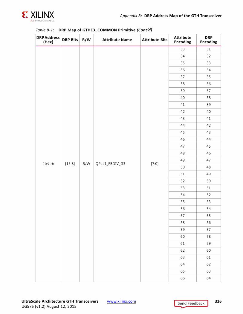
Appendix B: DRP Address Map of the GTH Transceiver
009Fh [15:8] R/W QPLL1_FBDIV_G3 [7:0]
33 31
34 32
35 33
36 34
37 35
38 36
39 37
40 38
41 39
42 40
43 41
44 42
45 43
46 44
47 45
48 46
49 47
50 48
51 49
52 50
53 51
54 52
55 53
56 54
57 55
58 56
59 57
60 58
61 59
62 60
63 61
64 62
65 63
66 64
Table B-1: DRP Map of GTHE3_COMMON Primitive (Cont’d)
DRP Address (Hex) DRP Bits R/W Attribute Name Attribute Bits Attribute
EncodingDRP
Encoding
UltraScale Architecture GTH Transceivers www.xilinx.com 326UG576 (v1.2) August 12, 2015
Send Feedback

Appendix B: DRP Address Map of the GTH Transceiver
009Fh [15:8] R/W QPLL1_FBDIV_G3 [7:0]
67 65
68 66
69 67
70 68
71 69
72 70
73 71
74 72
75 73
76 74
77 75
78 76
79 77
80 78
81 79
82 80
83 81
84 82
85 83
86 84
87 85
88 86
89 87
90 88
91 89
92 90
93 91
94 92
95 93
96 94
97 95
98 96
99 97
100 98
Table B-1: DRP Map of GTHE3_COMMON Primitive (Cont’d)
DRP Address (Hex) DRP Bits R/W Attribute Name Attribute Bits Attribute
EncodingDRP
Encoding
UltraScale Architecture GTH Transceivers www.xilinx.com 327UG576 (v1.2) August 12, 2015
Send Feedback

Appendix B: DRP Address Map of the GTH Transceiver
009Fh [15:8] R/W QPLL1_FBDIV_G3 [7:0]
101 99
102 100
103 101
104 102
105 103
106 104
107 105
108 106
109 107
110 108
111 109
112 110
113 111
114 112
115 113
116 114
117 115
118 116
119 117
120 118
121 119
122 120
123 121
124 122
125 123
126 124
127 125
128 126
129 127
130 128
131 129
132 130
133 131
134 132
Table B-1: DRP Map of GTHE3_COMMON Primitive (Cont’d)
DRP Address (Hex) DRP Bits R/W Attribute Name Attribute Bits Attribute
EncodingDRP
Encoding
UltraScale Architecture GTH Transceivers www.xilinx.com 328UG576 (v1.2) August 12, 2015
Send Feedback

Appendix B: DRP Address Map of the GTH Transceiver
009Fh [15:8] R/W QPLL1_FBDIV_G3 [7:0]
135 133
136 134
137 135
138 136
139 137
140 138
141 139
142 140
143 141
144 142
145 143
146 144
147 145
148 146
149 147
150 148
151 149
152 150
153 151
154 152
155 153
156 154
157 155
158 156
159 157
160 158
009Fh [1:0] R/W RXRECCLKOUT1_SEL [1:0] 0-3 0-3
00A0h [15:0] R/W QPLL1_SDM_CFG0 [15:0] 0-65535 0-65535
00A1h [15:0] R/W QPLL1_SDM_CFG1 [15:0] 0-65535 0-65535
00A2h [15:0] R/W SDM1INITSEED0_0 [15:0] 0-65535 0-65535
00A3h [8:0] R/W SDM1INITSEED0_1 [8:0] 0-511 0-511
00A4h [15:0] R/W QPLL1_SDM_CFG2 [15:0] 0-65535 0-65535
00A5h [9:0] R/W QPLL1_CP_G3 [9:0] 0-1023 0-1023
00A8h [15:0] R/W SDM1DATA1_0 [15:0] 0-65535 0-65535
Table B-1: DRP Map of GTHE3_COMMON Primitive (Cont’d)
DRP Address (Hex) DRP Bits R/W Attribute Name Attribute Bits Attribute
EncodingDRP
Encoding
UltraScale Architecture GTH Transceivers www.xilinx.com 329UG576 (v1.2) August 12, 2015
Send Feedback

Appendix B: DRP Address Map of the GTH Transceiver
GTHE3_CHANNEL Primitive DRP Address MapTable B-2 lists the DRP map of the GTHE3_CHANNEL primitive sorted by address.
Note: The reserved bits should NOT be modified. Attributes that are not described explicitly are set automatically by the UltraScale FPGAs Transceivers Wizard. These attributes must be left at their defaults, except for use cases that explicitly request different values.
00A9h [10] R/W SDM1_WIDTH_PIN_SEL [0] 0-1 0-1
00A9h [9] R/W SDM1_DATA_PIN_SEL [0] 0-1 0-1
00A9h [8:0] R/W SDM1DATA1_1 [8:0] 0-511 0-511
00ADh [15:0] R/W RSVD_ATTR3 [15:0] 0-65535 0-65535
00B0h [15:0] R/W QPLL1_CFG4 [15:0] 0-65535 0-65535
Table B-1: DRP Map of GTHE3_COMMON Primitive (Cont’d)
DRP Address (Hex) DRP Bits R/W Attribute Name Attribute Bits Attribute
EncodingDRP
Encoding
Table B-2: DRP Map of GTHE3_CHANNEL Primitive
DRP Address (Hex) DRP Bits R/W Attribute Name Attribute
BitsAttribute Encoding
DRP Encoding
0002h [0] R/W CDR_SWAP_MODE_EN [0] 0-1 0-1
0003h [15:11] R/W RXBUFRESET_TIME [4:0] 0-31 0-31
0003h [9] R/W EYE_SCAN_SWAP_EN [0] 0-1 0-1
0003h [8:5] R/W RX_DATA_WIDTH [3:0]
16 2
20 3
32 4
40 5
64 6
80 7
128 8
160 9
0003h [4:0] R/W RXCDRFREQRESET_TIME [4:0] 0-31 0-31
0004h [15:11] R/W RXCDRPHRESET_TIME [4:0] 0-31 0-31
0004h [10:8] R/W PCI3_RX_ELECIDLE_H2L_DISABLE [2:0] 0-7 0-7
0004h [7:1] R/W RXDFELPMRESET_TIME [6:0] 0-127 0-127
0004h [0] R/W RX_FABINT_USRCLK_FLOP [0] 0-1 0-1
0005h [15:11] R/W RXPMARESET_TIME [4:0] 0-31 0-31
0005h [10] R/W PCI3_RX_ELECIDLE_LP4_DISABLE [0] 0-1 0-1
UltraScale Architecture GTH Transceivers www.xilinx.com 330UG576 (v1.2) August 12, 2015
Send Feedback
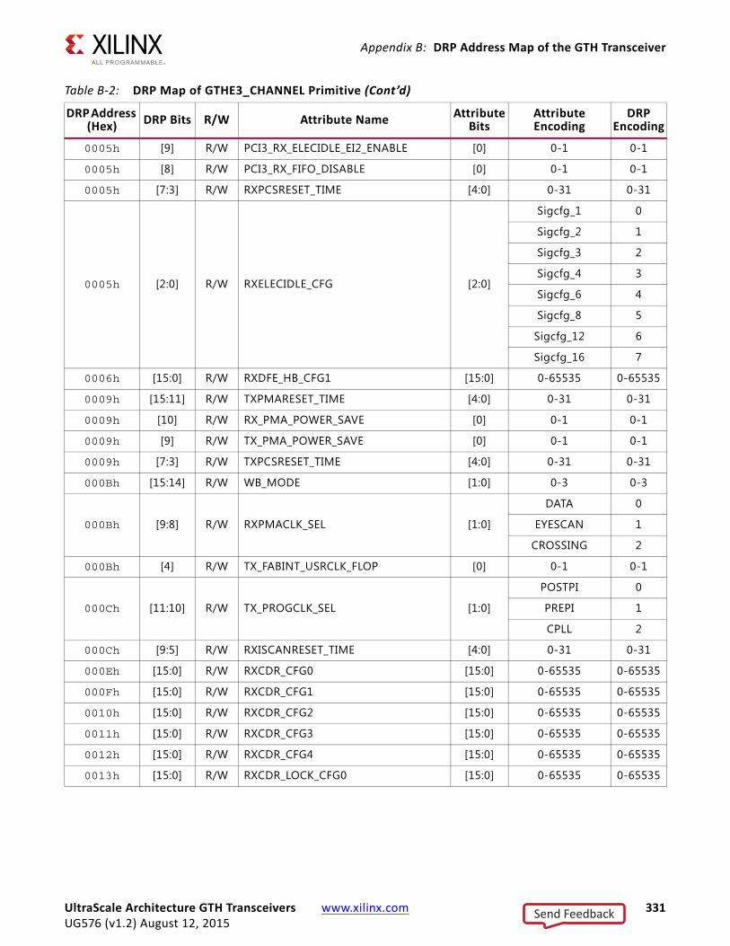
Appendix B: DRP Address Map of the GTH Transceiver
0005h [9] R/W PCI3_RX_ELECIDLE_EI2_ENABLE [0] 0-1 0-1
0005h [8] R/W PCI3_RX_FIFO_DISABLE [0] 0-1 0-1
0005h [7:3] R/W RXPCSRESET_TIME [4:0] 0-31 0-31
0005h [2:0] R/W RXELECIDLE_CFG [2:0]
Sigcfg_1 0
Sigcfg_2 1
Sigcfg_3 2
Sigcfg_4 3
Sigcfg_6 4
Sigcfg_8 5
Sigcfg_12 6
Sigcfg_16 7
0006h [15:0] R/W RXDFE_HB_CFG1 [15:0] 0-65535 0-65535
0009h [15:11] R/W TXPMARESET_TIME [4:0] 0-31 0-31
0009h [10] R/W RX_PMA_POWER_SAVE [0] 0-1 0-1
0009h [9] R/W TX_PMA_POWER_SAVE [0] 0-1 0-1
0009h [7:3] R/W TXPCSRESET_TIME [4:0] 0-31 0-31
000Bh [15:14] R/W WB_MODE [1:0] 0-3 0-3
000Bh [9:8] R/W RXPMACLK_SEL [1:0]
DATA 0
EYESCAN 1
CROSSING 2
000Bh [4] R/W TX_FABINT_USRCLK_FLOP [0] 0-1 0-1
000Ch [11:10] R/W TX_PROGCLK_SEL [1:0]
POSTPI 0
PREPI 1
CPLL 2
000Ch [9:5] R/W RXISCANRESET_TIME [4:0] 0-31 0-31
000Eh [15:0] R/W RXCDR_CFG0 [15:0] 0-65535 0-65535
000Fh [15:0] R/W RXCDR_CFG1 [15:0] 0-65535 0-65535
0010h [15:0] R/W RXCDR_CFG2 [15:0] 0-65535 0-65535
0011h [15:0] R/W RXCDR_CFG3 [15:0] 0-65535 0-65535
0012h [15:0] R/W RXCDR_CFG4 [15:0] 0-65535 0-65535
0013h [15:0] R/W RXCDR_LOCK_CFG0 [15:0] 0-65535 0-65535
Table B-2: DRP Map of GTHE3_CHANNEL Primitive (Cont’d)
DRP Address (Hex) DRP Bits R/W Attribute Name Attribute
BitsAttribute Encoding
DRP Encoding
UltraScale Architecture GTH Transceivers www.xilinx.com 331UG576 (v1.2) August 12, 2015
Send Feedback

Appendix B: DRP Address Map of the GTH Transceiver
0014h [15:12] R/W CHAN_BOND_MAX_SKEW [3:0]
1 1
2 2
3 3
4 4
5 5
6 6
7 7
8 8
9 9
10 10
11 11
12 12
13 13
14 14
0014h [11:10] R/W CHAN_BOND_SEQ_LEN [1:0]
1 0
2 1
3 2
4 3
0014h [9:0] R/W CHAN_BOND_SEQ_1_1 [9:0] 0-1023 0-1023
0015h [15:10] R/W PCI3_RX_ELECIDLE_HI_COUNT [5:0] 0-63 0-63
0015h [9:0] R/W CHAN_BOND_SEQ_1_3 [9:0] 0-1023 0-1023
0016h [15:10] R/W PCI3_RX_ELECIDLE_H2L_COUNT [5:0] 0-63 0-63
0016h [9:0] R/W CHAN_BOND_SEQ_1_4 [9:0] 0-1023 0-1023
0017h [15:10] R/W RX_BUFFER_CFG [5:0] 0-63 0-63
0017h [9] R/W RX_DEFER_RESET_BUF_EN[0] FALSE 0
TRUE 1
0017h [8:7] R/W OOBDIVCTL [1:0] 0-3 0-3
0017h [6:5] R/W PCI3_AUTO_REALIGN [1:0]
FRST_SMPL 0
OVR_8_BLK 1
OVR_64_BLK 2
OVR_1K_BLK 3
0017h [4] R/W PCI3_PIPE_RX_ELECIDLE [0] 0-1 0-1
0018h [15:12] R/W CHAN_BOND_SEQ_1_ENABLE [3:0] 0-15 0-15
0018h [11:10] R/W PCI3_RX_ASYNC_EBUF_BYPASS [1:0] 0-3 0-3
Table B-2: DRP Map of GTHE3_CHANNEL Primitive (Cont’d)
DRP Address (Hex) DRP Bits R/W Attribute Name Attribute
BitsAttribute Encoding
DRP Encoding
UltraScale Architecture GTH Transceivers www.xilinx.com 332UG576 (v1.2) August 12, 2015
Send Feedback

Appendix B: DRP Address Map of the GTH Transceiver
0018h [9:0] R/W CHAN_BOND_SEQ_2_1 [9:0] 0-1023 0-1023
0019h [9:0] R/W CHAN_BOND_SEQ_2_2 [9:0] 0-1023 0-1023
001Ah [9:0] R/W CHAN_BOND_SEQ_2_3 [9:0] 0-1023 0-1023
001Bh [9:0] R/W CHAN_BOND_SEQ_2_4 [9:0] 0-1023 0-1023
001Ch [15:12] R/W CHAN_BOND_SEQ_2_ENABLE [3:0] 0-15 0-15
001Ch [11] R/W CHAN_BOND_SEQ_2_USE [0]FALSE 0
TRUE 1
001Ch [6] R/W CLK_COR_KEEP_IDLE [0]FALSE 0
TRUE 1
001Ch [5:0] R/W CLK_COR_MIN_LAT [5:0]
3 3
4 4
5 5
6 6
7 7
8 8
9 9
10 10
11 11
12 12
13 13
14 14
15 15
16 16
17 17
18 18
19 19
20 20
21 21
22 22
23 23
24 24
25 25
26 26
27 27
Table B-2: DRP Map of GTHE3_CHANNEL Primitive (Cont’d)
DRP Address (Hex) DRP Bits R/W Attribute Name Attribute
BitsAttribute Encoding
DRP Encoding
UltraScale Architecture GTH Transceivers www.xilinx.com 333UG576 (v1.2) August 12, 2015
Send Feedback

Appendix B: DRP Address Map of the GTH Transceiver
001Ch [5:0] R/W CLK_COR_MIN_LAT
[5:0] 28 28
29 29
30 30
31 31
32 32
33 33
34 34
35 35
36 36
37 37
38 38
39 39
40 40
41 41
42 42
43 43
44 44
45 45
46 46
47 47
48 48
49 49
50 50
51 51
52 52
53 53
54 54
55 55
56 56
57 57
58 58
59 59
60 60
61 61
Table B-2: DRP Map of GTHE3_CHANNEL Primitive (Cont’d)
DRP Address (Hex) DRP Bits R/W Attribute Name Attribute
BitsAttribute Encoding
DRP Encoding
UltraScale Architecture GTH Transceivers www.xilinx.com 334UG576 (v1.2) August 12, 2015
Send Feedback

Appendix B: DRP Address Map of the GTH Transceiver
001Ch [5:0] R/W CLK_COR_MIN_LAT [5:0]62 62
63 63
001Dh [15:10] R/W CLK_COR_MAX_LAT [5:0]
3 3
4 4
5 5
6 6
7 7
8 8
9 9
10 10
11 11
12 12
13 13
14 14
15 15
16 16
17 17
18 18
19 19
20 20
21 21
22 22
23 23
24 24
25 25
26 26
27 27
28 28
29 29
30 30
31 31
32 32
33 33
34 34
Table B-2: DRP Map of GTHE3_CHANNEL Primitive (Cont’d)
DRP Address (Hex) DRP Bits R/W Attribute Name Attribute
BitsAttribute Encoding
DRP Encoding
UltraScale Architecture GTH Transceivers www.xilinx.com 335UG576 (v1.2) August 12, 2015
Send Feedback

Appendix B: DRP Address Map of the GTH Transceiver
001Dh [15:10] R/W CLK_COR_MAX_LAT [5:0]
35 35
36 36
37 37
38 38
39 39
40 40
41 41
42 42
43 43
44 44
45 45
46 46
47 47
48 48
49 49
50 50
51 51
52 52
53 53
54 54
55 55
56 56
57 57
58 58
59 59
60 60
001Dh [9] R/W CLK_COR_PRECEDENCE [0]FALSE 0
TRUE 1
Table B-2: DRP Map of GTHE3_CHANNEL Primitive (Cont’d)
DRP Address (Hex) DRP Bits R/W Attribute Name Attribute
BitsAttribute Encoding
DRP Encoding
UltraScale Architecture GTH Transceivers www.xilinx.com 336UG576 (v1.2) August 12, 2015
Send Feedback

Appendix B: DRP Address Map of the GTH Transceiver
001Dh [8:4] R/W CLK_COR_REPEAT_WAIT [4:0]
0 0
1 1
2 2
3 3
4 4
5 5
6 6
7 7
8 8
9 9
10 10
11 11
12 12
13 13
14 14
15 15
16 16
17 17
18 18
19 19
20 20
21 21
22 22
23 23
24 24
25 25
26 26
27 27
28 28
29 29
30 30
31 31
Table B-2: DRP Map of GTHE3_CHANNEL Primitive (Cont’d)
DRP Address (Hex) DRP Bits R/W Attribute Name Attribute
BitsAttribute Encoding
DRP Encoding
UltraScale Architecture GTH Transceivers www.xilinx.com 337UG576 (v1.2) August 12, 2015
Send Feedback

Appendix B: DRP Address Map of the GTH Transceiver
001Dh [3:2] R/W CLK_COR_SEQ_LEN [1:0]
1 0
2 1
3 2
4 3
001Dh [0] R/W CHAN_BOND_KEEP_ALIGN [0]FALSE 0
TRUE 1
001Eh [9:0] R/W CLK_COR_SEQ_1_1 [9:0] 0-1023 0-1023
001Fh [9:0] R/W CLK_COR_SEQ_1_2 [9:0] 0-1023 0-1023
0020h [9:0] R/W CLK_COR_SEQ_1_3 [9:0] 0-1023 0-1023
0021h [9:0] R/W CLK_COR_SEQ_1_4 [9:0] 0-1023 0-1023
0022h [15:12] R/W CLK_COR_SEQ_1_ENABLE [3:0] 0-15 0-15
0022h [9:0] R/W CLK_COR_SEQ_2_1 [9:0] 0-1023 0-1023
0023h [9:0] R/W CLK_COR_SEQ_2_2 [9:0] 0-1023 0-1023
0024h [15:12] R/W CLK_COR_SEQ_2_ENABLE [3:0] 0-15 0-15
0024h [11] R/W CLK_COR_SEQ_2_USE [0]FALSE 0
TRUE 1
0024h [10] R/W CLK_CORRECT_USE [0]FALSE 0
TRUE 1
0024h [9:0] R/W CLK_COR_SEQ_2_3 [9:0] 0-1023 0-1023
0025h [9:0] R/W CLK_COR_SEQ_2_4 [9:0] 0-1023 0-1023
0026h [15:0] R/W RXDFE_HE_CFG0 [15:0] 0-65535 0-65535
0027h [15:13] R/W ALIGN_COMMA_WORD [2:0]
1 1
2 2
4 4
0027h [12] R/W ALIGN_COMMA_DOUBLE [0]FALSE 0
TRUE 1
0027h [11] R/W SHOW_REALIGN_COMMA [0]FALSE 0
TRUE 1
0027h [9:0] R/W ALIGN_COMMA_ENABLE [9:0] 0-1023 0-1023
Table B-2: DRP Map of GTHE3_CHANNEL Primitive (Cont’d)
DRP Address (Hex) DRP Bits R/W Attribute Name Attribute
BitsAttribute Encoding
DRP Encoding
UltraScale Architecture GTH Transceivers www.xilinx.com 338UG576 (v1.2) August 12, 2015
Send Feedback

Appendix B: DRP Address Map of the GTH Transceiver
0028h [15:8] R/W CPLL_FBDIV [7:0]
2 0
3 1
4 2
5 3
6 5
8 6
10 7
12 13
16 14
20 15
1 16
0028h [7] R/W CPLL_FBDIV_45 [0]4 0
5 1
0028h [3:0] R/W TXDRVBIAS_N [3:0] 0-15 0-15
0029h [15:0] R/W CPLL_LOCK_CFG [15:0] 0-65535 0-65535
002Ah [15:11] R/W CPLL_REFCLK_DIV [4:0]
2 0
3 1
4 2
5 3
6 5
8 6
10 7
12 13
16 14
20 15
1 16
002Ah [6:5] R/W SATA_CPLL_CFG [1:0]
VCO_3000MHZ 0
VCO_1500MHZ 1
VCO_750MHZ 2
002Ah [3:0] R/W TXDRVBIAS_P [3:0] 0-15 0-15
002Bh [15:0] R/W CPLL_INIT_CFG0 [15:0] 0-65535 0-65535
002Ch [15] R/W DEC_PCOMMA_DETECT [0]FALSE 0
TRUE 1
002Ch [11:7] R/W TX_DIVRESET_TIME [4:0] 0-31 0-31
Table B-2: DRP Map of GTHE3_CHANNEL Primitive (Cont’d)
DRP Address (Hex) DRP Bits R/W Attribute Name Attribute
BitsAttribute Encoding
DRP Encoding
UltraScale Architecture GTH Transceivers www.xilinx.com 339UG576 (v1.2) August 12, 2015
Send Feedback

Appendix B: DRP Address Map of the GTH Transceiver
002Ch [6:2] R/W RX_DIVRESET_TIME [4:0] 0-31 0-31
002Ch [1] R/W A_TXPROGDIVRESET [0] 0-1 0-1
002Ch [0] R/W A_RXPROGDIVRESET [0] 0-1 0-1
002Dh [15:0] R/W RXCDR_LOCK_CFG1 [15:0] 0-65535 0-65535
002Eh [15:0] R/W RXCFOK_CFG1 [15:0] 0-65535 0-65535
002Fh [15:0] R/W RXDFE_H2_CFG0 [15:0] 0-65535 0-65535
0030h [15:0] R/W RXDFE_H2_CFG1 [15:0] 0-65535 0-65535
0031h [15:0] R/W RXCFOK_CFG2 [15:0] 0-65535 0-65535
0032h [15:0] R/W RXLPM_CFG [15:0] 0-65535 0-65535
0033h [15:0] R/W RXLPM_KH_CFG0 [15:0] 0-65535 0-65535
0034h [15:0] R/W RXLPM_KH_CFG1 [15:0] 0-65535 0-65535
0035h [15:0] R/W RXDFELPM_KL_CFG0 [15:0] 0-65535 0-65535
0036h [15:0] R/W RXDFELPM_KL_CFG1 [15:0] 0-65535 0-65535
0037h [15:0] R/W RXLPM_OS_CFG0 [15:0] 0-65535 0-65535
0038h [15:0] R/W RXLPM_OS_CFG1 [15:0] 0-65535 0-65535
0039h [15:0] R/W RXLPM_GC_CFG [15:0] 0-65535 0-65535
003Ah [15:8] R/W DMONITOR_CFG1 [7:0] 0-255 0-255
003Ch [15:10] R/W ES_CONTROL [5:0] 0-63 0-63
003Ch [9] R/W ES_ERRDET_EN [0]FALSE 0
TRUE 1
003Ch [8] R/W ES_EYE_SCAN_EN [0]FALSE 0
TRUE 1
003Ch [4:0] R/W ES_PRESCALE [4:0] 0-31 0-31
003Dh [15:0] R/W RXDFE_HC_CFG0 [15:0] 0-65535 0-65535
Table B-2: DRP Map of GTHE3_CHANNEL Primitive (Cont’d)
DRP Address (Hex) DRP Bits R/W Attribute Name Attribute
BitsAttribute Encoding
DRP Encoding
UltraScale Architecture GTH Transceivers www.xilinx.com 340UG576 (v1.2) August 12, 2015
Send Feedback

Appendix B: DRP Address Map of the GTH Transceiver
003Eh [15:0] R/W TX_PROGDIV_CFG [15:0]
0.0 32768
4.0 57744
5.0 49648
8.0 57728
10.0 57760
16.0 57730
16.5 49672
20.0 57762
32.0 57734
33.0 49800
40.0 57766
64.0 57742
66.0 50056
80.0 57743
100.0 57775
003Fh [15:0] R/W ES_QUALIFIER0 [15:0] 0-65535 0-65535
0040h [15:0] R/W ES_QUALIFIER1 [15:0] 0-65535 0-65535
0041h [15:0] R/W ES_QUALIFIER2 [15:0] 0-65535 0-65535
0042h [15:0] R/W ES_QUALIFIER3 [15:0] 0-65535 0-65535
0043h [15:0] R/W ES_QUALIFIER4 [15:0] 0-65535 0-65535
0044h [15:0] R/W ES_QUAL_MASK0 [15:0] 0-65535 0-65535
0045h [15:0] R/W ES_QUAL_MASK1 [15:0] 0-65535 0-65535
0046h [15:0] R/W ES_QUAL_MASK2 [15:0] 0-65535 0-65535
0047h [15:0] R/W ES_QUAL_MASK3 [15:0] 0-65535 0-65535
0048h [15:0] R/W ES_QUAL_MASK4 [15:0] 0-65535 0-65535
0049h [15:0] R/W ES_SDATA_MASK0 [15:0] 0-65535 0-65535
004Ah [15:0] R/W ES_SDATA_MASK1 [15:0] 0-65535 0-65535
004Bh [15:0] R/W ES_SDATA_MASK2 [15:0] 0-65535 0-65535
004Ch [15:0] R/W ES_SDATA_MASK3 [15:0] 0-65535 0-65535
004Dh [15:0] R/W ES_SDATA_MASK4 [15:0] 0-65535 0-65535
004Eh [4] R/W FTS_LANE_DESKEW_EN [0]FALSE 0
TRUE 1
004Eh [3:0] R/W FTS_DESKEW_SEQ_ENABLE [3:0] 0-15 0-15
004Fh [15:4] R/W ES_HORZ_OFFSET [11:0] 0-4095 0-4095
Table B-2: DRP Map of GTHE3_CHANNEL Primitive (Cont’d)
DRP Address (Hex) DRP Bits R/W Attribute Name Attribute
BitsAttribute Encoding
DRP Encoding
UltraScale Architecture GTH Transceivers www.xilinx.com 341UG576 (v1.2) August 12, 2015
Send Feedback

Appendix B: DRP Address Map of the GTH Transceiver
004Fh [3:0] R/W FTS_LANE_DESKEW_CFG [3:0] 0-15 0-15
0050h [15:0] R/W RXDFE_HC_CFG1 [15:0] 0-65535 0-65535
0051h [9:0] R/W ES_PMA_CFG [9:0] 0-1023 0-1023
0052h [10] R/W RX_EN_HI_LR [0] 0-1 0-1
0052h [4:2] R/W RX_DFE_AGC_CFG1 [2:0] 0-7 0-7
0052h [1:0] R/W RX_DFE_AGC_CFG0 [1:0] 0-3 0-3
0053h [15:0] R/W RXDFE_CFG0 [15:0] 0-65535 0-65535
0054h [15:0] R/W RXDFE_CFG1 [15:0] 0-65535 0-65535
0055h [13] R/W LOCAL_MASTER [0] 0-1 0-1
0055h [12] R/W PCS_PCIE_EN [0]FALSE 0
TRUE 1
0055h [10] R/W ALIGN_MCOMMA_DET [0]FALSE 0
TRUE 1
0055h [9:0] R/W ALIGN_MCOMMA_VALUE [9:0] 0-1023 0-1023
0056h [10] R/W ALIGN_PCOMMA_DET [0]FALSE 0
TRUE 1
0056h [9:0] R/W ALIGN_PCOMMA_VALUE [9:0] 0-1023 0-1023
0057h [15:0] R/W TXDLY_LCFG [15:0] 0-65535 0-65535
0058h [15:0] R/W RXDFE_OS_CFG0 [15:0] 0-65535 0-65535
0059h [15:0] R/W RXPHDLY_CFG [15:0] 0-65535 0-65535
005Ah [15:0] R/W RXDFE_OS_CFG1 [15:0] 0-65535 0-65535
005Bh [15:0] R/W RXDLY_CFG [15:0] 0-65535 0-65535
005Ch [15:0] R/W RXDLY_LCFG [15:0] 0-65535 0-65535
005Dh [15:0] R/W RXDFE_HF_CFG0 [15:0] 0-65535 0-65535
005Eh [15:0] R/W RXDFE_HD_CFG0 [15:0] 0-65535 0-65535
005Fh [15:0] R/W RX_BIAS_CFG0 [15:0] 0-65535 0-65535
0060h [15:0] R/W PCS_RSVD0 [15:0] 0-65535 0-65535
0061h [15:11] R/W RXPH_MONITOR_SEL [4:0] 0-31 0-31
0061h [10] R/W RX_CM_BUF_PD [0] 0-1 0-1
0061h [9:6] R/W RX_CM_BUF_CFG [3:0] 0-15 0-15
0061h [5:2] R/W RX_CM_TRIM [3:0] 0-15 0-15
0061h [1:0] R/W RX_CM_SEL [1:0] 0-3 0-3
0062h [14] R/W RX_SUM_DFETAPREP_EN [0] 0 0
0062h [14] R/W RX_SUM_DFETAPREP_EN [0] 1 1
Table B-2: DRP Map of GTHE3_CHANNEL Primitive (Cont’d)
DRP Address (Hex) DRP Bits R/W Attribute Name Attribute
BitsAttribute Encoding
DRP Encoding
UltraScale Architecture GTH Transceivers www.xilinx.com 342UG576 (v1.2) August 12, 2015
Send Feedback

Appendix B: DRP Address Map of the GTH Transceiver
0062h [13] R/W RX_SUM_VCM_OVWR [0] 0 0
0062h [13] R/W RX_SUM_VCM_OVWR [0] 1 1
0062h [12:9] R/W RX_SUM_IREF_TUNE [3:0] 0-15 0-15
0062h [8:7] R/W RX_SUM_RES_CTRL [1:0] 0-3 0-3
0062h [6:3] R/W RX_SUM_VCMTUNE [3:0] 0-15 0-15
0062h [2:0] R/W RX_SUM_VREF_TUNE [2:0] 0-7 0-7
0063h [15] R/W CBCC_DATA_SOURCE_SEL [0] ENCODED 0
0063h [15] R/W CBCC_DATA_SOURCE_SEL [0] DECODED 1
0063h [14] R/W OOB_PWRUP [0] 0-1 0-1
0063h [13:5] R/W RXOOB_CFG [8:0] 0-511 0-511
0063h [2:0] R/W RXOUT_DIV [2:0]
1 0
2 1
4 2
8 3
16 4
Table B-2: DRP Map of GTHE3_CHANNEL Primitive (Cont’d)
DRP Address (Hex) DRP Bits R/W Attribute Name Attribute
BitsAttribute Encoding
DRP Encoding
UltraScale Architecture GTH Transceivers www.xilinx.com 343UG576 (v1.2) August 12, 2015
Send Feedback

Appendix B: DRP Address Map of the GTH Transceiver
0064h [15:11] R/W RX_SIG_VALID_DLY [4:0]
1 0
2 1
3 2
4 3
5 4
6 5
7 6
8 7
9 8
10 9
11 10
12 11
13 12
14 13
15 14
16 15
17 16
18 17
19 18
20 19
21 20
22 21
0064h [15:11] R/W RX_SIG_VALID_DLY [4:0]
23 22
24 23
25 24
26 25
27 26
28 27
29 28
30 29
31 30
32 31
Table B-2: DRP Map of GTHE3_CHANNEL Primitive (Cont’d)
DRP Address (Hex) DRP Bits R/W Attribute Name Attribute
BitsAttribute Encoding
DRP Encoding
UltraScale Architecture GTH Transceivers www.xilinx.com 344UG576 (v1.2) August 12, 2015
Send Feedback

Appendix B: DRP Address Map of the GTH Transceiver
0064h [10:9] R/W RXSLIDE_MODE [1:0]
OFF 0
AUTO 1
PCS 2
PMA 3
0064h [8] R/W RXPRBS_ERR_LOOPBACK [0] 0-1 0-1
0064h [7:4] R/W RXSLIDE_AUTO_WAIT [3:0]
1 1
2 2
3 3
4 4
5 5
6 6
7 7
8 8
9 9
10 10
11 11
12 12
13 13
14 14
15 15
0064h [3] R/W RXBUF_EN [0]FALSE 0
TRUE 1
0064h [2:1] R/W RX_XCLK_SEL [1:0]
RXDES 0
RXUSR 1
RXPMA 2
0064h [0] R/W RXGEARBOX_EN [0]FALSE 0
TRUE 1
Table B-2: DRP Map of GTHE3_CHANNEL Primitive (Cont’d)
DRP Address (Hex) DRP Bits R/W Attribute Name Attribute
BitsAttribute Encoding
DRP Encoding
UltraScale Architecture GTH Transceivers www.xilinx.com 345UG576 (v1.2) August 12, 2015
Send Feedback

Appendix B: DRP Address Map of the GTH Transceiver
0065h [15:10] R/W RXBUF_THRESH_OVFLW [5:0]
0 0
1 1
2 2
3 3
4 4
5 5
6 6
7 7
8 8
9 9
10 10
11 11
12 12
13 13
14 14
15 15
16 16
17 17
18 18
19 19
20 20
21 21
22 22
23 23
24 24
25 25
26 26
27 27
28 28
Table B-2: DRP Map of GTHE3_CHANNEL Primitive (Cont’d)
DRP Address (Hex) DRP Bits R/W Attribute Name Attribute
BitsAttribute Encoding
DRP Encoding
UltraScale Architecture GTH Transceivers www.xilinx.com 346UG576 (v1.2) August 12, 2015
Send Feedback

Appendix B: DRP Address Map of the GTH Transceiver
0065h [15:10] R/W RXBUF_THRESH_OVFLW [5:0]
29 29
30 30
31 31
32 32
33 33
34 34
35 35
36 36
37 37
38 38
39 39
40 40
41 41
42 42
43 43
44 44
45 45
46 46
47 47
48 48
49 49
50 50
51 51
52 52
53 53
54 54
55 55
56 56
57 57
58 58
59 59
60 60
61 61
62 62
Table B-2: DRP Map of GTHE3_CHANNEL Primitive (Cont’d)
DRP Address (Hex) DRP Bits R/W Attribute Name Attribute
BitsAttribute Encoding
DRP Encoding
UltraScale Architecture GTH Transceivers www.xilinx.com 347UG576 (v1.2) August 12, 2015
Send Feedback

Appendix B: DRP Address Map of the GTH Transceiver
0065h [15:10] R/W RXBUF_THRESH_OVFLW [5:0] 63 63
0065h [9:0] R/W DMONITOR_CFG0 [9:0] 0-1023 0-1023
0066h [15] R/W RXBUF_THRESH_OVRD [0]FALSE 0
TRUE 1
0066h [14] R/W RXBUF_RESET_ON_COMMAALIGN [0]FALSE 0
TRUE 1
0066h [13] R/W RXBUF_RESET_ON_RATE_CHANGE [0]FALSE 0
TRUE 1
0066h [12] R/W RXBUF_RESET_ON_CB_CHANGE [0]FALSE 0
TRUE 1
0066h [11:6] R/W RXBUF_THRESH_UNDFLW [5:0]
0 0
1 1
2 2
3 3
4 4
5 5
6 6
7 7
8 8
9 9
10 10
11 11
12 12
13 13
14 14
15 15
16 16
17 17
18 18
19 19
20 20
21 21
22 22
23 23
Table B-2: DRP Map of GTHE3_CHANNEL Primitive (Cont’d)
DRP Address (Hex) DRP Bits R/W Attribute Name Attribute
BitsAttribute Encoding
DRP Encoding
UltraScale Architecture GTH Transceivers www.xilinx.com 348UG576 (v1.2) August 12, 2015
Send Feedback

Appendix B: DRP Address Map of the GTH Transceiver
0066h [11:6] R/W RXBUF_THRESH_UNDFLW [5:0]
24 24
25 25
26 26
27 27
28 28
29 29
30 30
31 31
32 32
33 33
34 34
35 35
36 36
37 37
38 38
39 39
40 40
41 41
42 42
43 43
44 44
45 45
46 46
47 47
48 48
49 49
50 50
51 51
52 52
53 53
54 54
55 55
56 56
57 57
Table B-2: DRP Map of GTHE3_CHANNEL Primitive (Cont’d)
DRP Address (Hex) DRP Bits R/W Attribute Name Attribute
BitsAttribute Encoding
DRP Encoding
UltraScale Architecture GTH Transceivers www.xilinx.com 349UG576 (v1.2) August 12, 2015
Send Feedback

Appendix B: DRP Address Map of the GTH Transceiver
0066h [11:6] R/W RXBUF_THRESH_UNDFLW [5:0]
58 58
59 59
60 60
61 61
62 62
63 63
0066h [5] R/W RX_CLKMUX_EN [0] 0-1 0-1
0066h [4] R/W RX_DISPERR_SEQ_MATCH [0]FALSE 0
TRUE 1
0066h [3] R/W RXBUF_ADDR_MODE [0]FULL 0
FAST 1
0066h [2] R/W RX_WIDEMODE_CDR [0] 0-1 0-1
0066h [1:0] R/W RX_INT_DATAWIDTH [1:0]
0 0
1 1
2 2
0067h [15:12] R/W RXBUF_EIDLE_HI_CNT [3:0] 0-15 0-15
0067h [11] R/W RXCDR_HOLD_DURING_EIDLE [0] 0-1 0-1
0067h [10] R/W RX_DFE_LPM_HOLD_DURING_EIDLE [0] 0-1 0-1
0067h [7:4] R/W RXBUF_EIDLE_LO_CNT [3:0] 0-15 0-15
0067h [3] R/W RXBUF_RESET_ON_EIDLE [0]FALSE 0
TRUE 1
0067h [2] R/W RXCDR_FR_RESET_ON_EIDLE [0] 0-1 0-1
0067h [1] R/W RXCDR_PH_RESET_ON_EIDLE [0] 0-1 0-1
0068h [15:13] R/W SATA_BURST_VAL [2:0] 0-7 0-7
0068h [7:4] R/W SATA_BURST_SEQ_LEN [3:0] 0-15 0-15
0068h [2:0] R/W SATA_EIDLE_VAL [2:0] 0-7 0-7
0069h [15:10] R/W SATA_MIN_BURST [5:0]
1 1
2 2
3 3
4 4
5 5
6 6
7 7
8 8
Table B-2: DRP Map of GTHE3_CHANNEL Primitive (Cont’d)
DRP Address (Hex) DRP Bits R/W Attribute Name Attribute
BitsAttribute Encoding
DRP Encoding
UltraScale Architecture GTH Transceivers www.xilinx.com 350UG576 (v1.2) August 12, 2015
Send Feedback

Appendix B: DRP Address Map of the GTH Transceiver
0069h [15:10] R/W SATA_MIN_BURST [5:0]
9 9
10 10
11 11
12 12
13 13
14 14
15 15
16 16
17 17
18 18
19 19
20 20
21 21
22 22
23 23
24 24
25 25
26 26
27 27
28 28
29 29
30 30
31 31
32 32
33 33
34 34
35 35
36 36
37 37
38 38
39 39
40 40
41 41
42 42
Table B-2: DRP Map of GTHE3_CHANNEL Primitive (Cont’d)
DRP Address (Hex) DRP Bits R/W Attribute Name Attribute
BitsAttribute Encoding
DRP Encoding
UltraScale Architecture GTH Transceivers www.xilinx.com 351UG576 (v1.2) August 12, 2015
Send Feedback
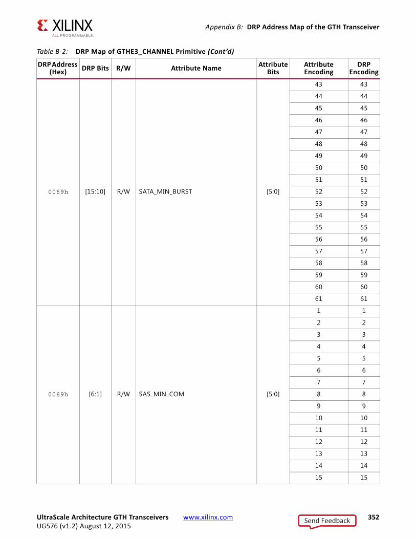
Appendix B: DRP Address Map of the GTH Transceiver
0069h [15:10] R/W SATA_MIN_BURST [5:0]
43 43
44 44
45 45
46 46
47 47
48 48
49 49
50 50
51 51
52 52
53 53
54 54
55 55
56 56
57 57
58 58
59 59
60 60
61 61
0069h [6:1] R/W SAS_MIN_COM [5:0]
1 1
2 2
3 3
4 4
5 5
6 6
7 7
8 8
9 9
10 10
11 11
12 12
13 13
14 14
15 15
Table B-2: DRP Map of GTHE3_CHANNEL Primitive (Cont’d)
DRP Address (Hex) DRP Bits R/W Attribute Name Attribute
BitsAttribute Encoding
DRP Encoding
UltraScale Architecture GTH Transceivers www.xilinx.com 352UG576 (v1.2) August 12, 2015
Send Feedback

Appendix B: DRP Address Map of the GTH Transceiver
0069h [6:1] R/W SAS_MIN_COM [5:0]
16 16
17 17
18 18
19 19
20 20
21 21
22 22
23 23
24 24
25 25
26 26
27 27
28 28
29 29
30 30
31 31
32 32
33 33
34 34
35 35
36 36
37 37
38 38
39 39
40 40
41 41
42 42
43 43
44 44
45 45
46 46
47 47
48 48
49 49
Table B-2: DRP Map of GTHE3_CHANNEL Primitive (Cont’d)
DRP Address (Hex) DRP Bits R/W Attribute Name Attribute
BitsAttribute Encoding
DRP Encoding
UltraScale Architecture GTH Transceivers www.xilinx.com 353UG576 (v1.2) August 12, 2015
Send Feedback

Appendix B: DRP Address Map of the GTH Transceiver
0069h [6:1] R/W SAS_MIN_COM [5:0]
50 50
51 51
52 52
53 53
54 54
55 55
56 56
57 57
58 58
59 59
60 60
61 61
62 62
63 63
006Ah [15:10] R/W SATA_MIN_INIT [5:0]
1 1
2 2
3 3
4 4
5 5
6 6
7 7
8 8
9 9
10 10
11 11
12 12
13 13
14 14
15 15
16 16
17 17
18 18
19 19
20 20
Table B-2: DRP Map of GTHE3_CHANNEL Primitive (Cont’d)
DRP Address (Hex) DRP Bits R/W Attribute Name Attribute
BitsAttribute Encoding
DRP Encoding
UltraScale Architecture GTH Transceivers www.xilinx.com 354UG576 (v1.2) August 12, 2015
Send Feedback

Appendix B: DRP Address Map of the GTH Transceiver
006Ah [15:10] R/W SATA_MIN_INIT [5:0]
21 21
22 22
23 23
24 24
25 25
26 26
27 27
28 28
29 29
30 30
31 31
32 32
33 33
34 34
35 35
36 36
37 37
38 38
39 39
40 40
41 41
42 42
43 43
44 44
45 45
46 46
47 47
48 48
49 49
50 50
51 51
52 52
53 53
54 54
Table B-2: DRP Map of GTHE3_CHANNEL Primitive (Cont’d)
DRP Address (Hex) DRP Bits R/W Attribute Name Attribute
BitsAttribute Encoding
DRP Encoding
UltraScale Architecture GTH Transceivers www.xilinx.com 355UG576 (v1.2) August 12, 2015
Send Feedback

Appendix B: DRP Address Map of the GTH Transceiver
006Ah [15:10] R/W SATA_MIN_INIT [5:0]
55 55
56 56
57 57
58 58
59 59
60 60
61 61
62 62
63 63
006Ah [6:1] R/W SATA_MIN_WAKE [5:0]
1 1
2 2
3 3
4 4
5 5
6 6
7 7
8 8
9 9
10 10
11 11
12 12
13 13
14 14
15 15
16 16
17 17
18 18
19 19
20 20
21 21
22 22
23 23
24 24
25 25
Table B-2: DRP Map of GTHE3_CHANNEL Primitive (Cont’d)
DRP Address (Hex) DRP Bits R/W Attribute Name Attribute
BitsAttribute Encoding
DRP Encoding
UltraScale Architecture GTH Transceivers www.xilinx.com 356UG576 (v1.2) August 12, 2015
Send Feedback

Appendix B: DRP Address Map of the GTH Transceiver
006Ah [6:1] R/W SATA_MIN_WAKE [5:0]
26 26
27 27
28 28
29 29
30 30
31 31
32 32
33 33
34 34
35 35
36 36
37 37
38 38
39 39
40 40
41 41
42 42
43 43
44 44
45 45
46 46
47 47
48 48
49 49
50 50
51 51
52 52
53 53
54 54
55 55
56 56
57 57
58 58
59 59
Table B-2: DRP Map of GTHE3_CHANNEL Primitive (Cont’d)
DRP Address (Hex) DRP Bits R/W Attribute Name Attribute
BitsAttribute Encoding
DRP Encoding
UltraScale Architecture GTH Transceivers www.xilinx.com 357UG576 (v1.2) August 12, 2015
Send Feedback
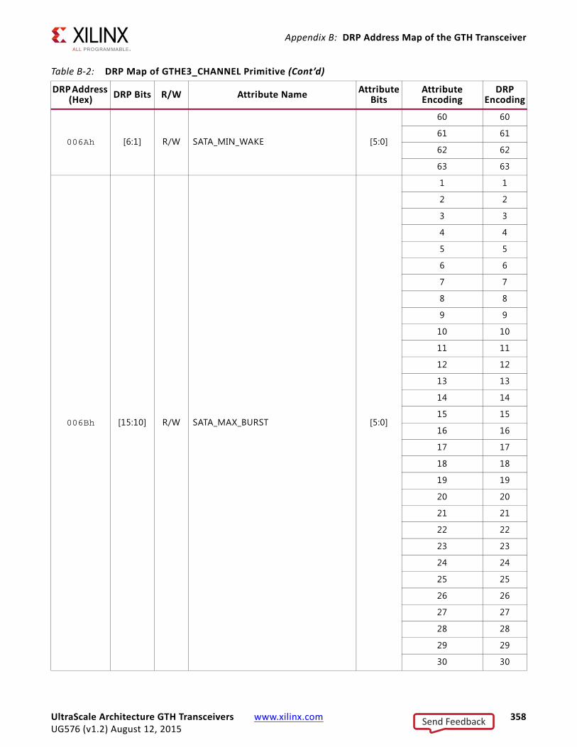
Appendix B: DRP Address Map of the GTH Transceiver
006Ah [6:1] R/W SATA_MIN_WAKE [5:0]
60 60
61 61
62 62
63 63
006Bh [15:10] R/W SATA_MAX_BURST [5:0]
1 1
2 2
3 3
4 4
5 5
6 6
7 7
8 8
9 9
10 10
11 11
12 12
13 13
14 14
15 15
16 16
17 17
18 18
19 19
20 20
21 21
22 22
23 23
24 24
25 25
26 26
27 27
28 28
29 29
30 30
Table B-2: DRP Map of GTHE3_CHANNEL Primitive (Cont’d)
DRP Address (Hex) DRP Bits R/W Attribute Name Attribute
BitsAttribute Encoding
DRP Encoding
UltraScale Architecture GTH Transceivers www.xilinx.com 358UG576 (v1.2) August 12, 2015
Send Feedback

Appendix B: DRP Address Map of the GTH Transceiver
006Bh [15:10] R/W SATA_MAX_BURST [5:0]
31 31
32 32
33 33
34 34
35 35
36 36
37 37
38 38
39 39
40 40
41 41
42 42
43 43
44 44
45 45
46 46
47 47
48 48
49 49
50 50
51 51
52 52
53 53
54 54
55 55
56 56
57 57
58 58
59 59
60 60
61 61
62 62
63 63
Table B-2: DRP Map of GTHE3_CHANNEL Primitive (Cont’d)
DRP Address (Hex) DRP Bits R/W Attribute Name Attribute
BitsAttribute Encoding
DRP Encoding
UltraScale Architecture GTH Transceivers www.xilinx.com 359UG576 (v1.2) August 12, 2015
Send Feedback
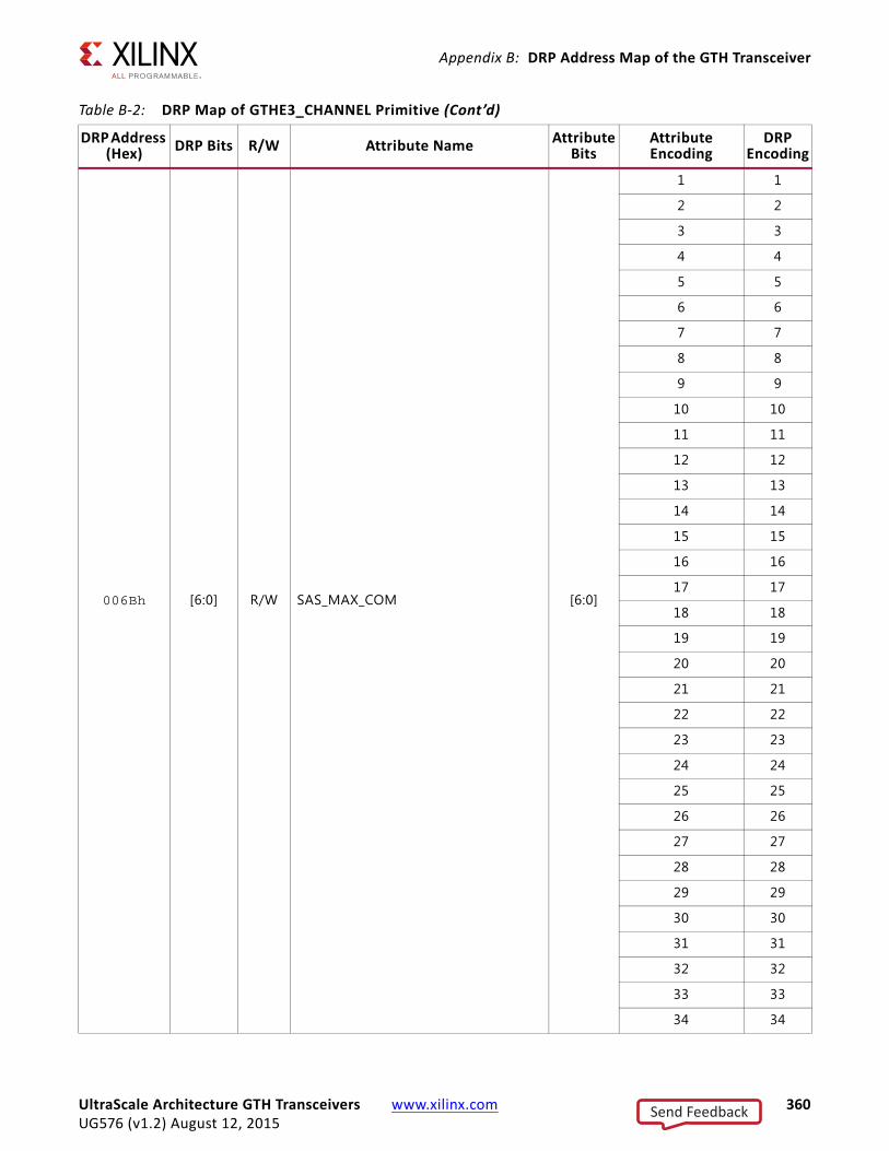
Appendix B: DRP Address Map of the GTH Transceiver
006Bh [6:0] R/W SAS_MAX_COM [6:0]
1 1
2 2
3 3
4 4
5 5
6 6
7 7
8 8
9 9
10 10
11 11
12 12
13 13
14 14
15 15
16 16
17 17
18 18
19 19
20 20
21 21
22 22
23 23
24 24
25 25
26 26
27 27
28 28
29 29
30 30
31 31
32 32
33 33
34 34
Table B-2: DRP Map of GTHE3_CHANNEL Primitive (Cont’d)
DRP Address (Hex) DRP Bits R/W Attribute Name Attribute
BitsAttribute Encoding
DRP Encoding
UltraScale Architecture GTH Transceivers www.xilinx.com 360UG576 (v1.2) August 12, 2015
Send Feedback

Appendix B: DRP Address Map of the GTH Transceiver
006Bh [6:0] R/W SAS_MAX_COM [6:0]
35 35
36 36
37 37
38 38
39 39
40 40
41 41
42 42
43 43
44 44
45 45
46 46
47 47
48 48
49 49
50 50
51 51
52 52
53 53
54 54
55 55
56 56
57 57
58 58
59 59
60 60
61 61
62 62
63 63
64 64
65 65
66 66
67 67
68 68
Table B-2: DRP Map of GTHE3_CHANNEL Primitive (Cont’d)
DRP Address (Hex) DRP Bits R/W Attribute Name Attribute
BitsAttribute Encoding
DRP Encoding
UltraScale Architecture GTH Transceivers www.xilinx.com 361UG576 (v1.2) August 12, 2015
Send Feedback

Appendix B: DRP Address Map of the GTH Transceiver
006Bh [6:0] R/W SAS_MAX_COM [6:0]
69 69
70 70
71 71
72 72
73 73
74 74
75 75
76 76
77 77
78 78
79 79
80 80
81 81
82 82
83 83
84 84
85 85
86 86
87 87
88 88
89 89
90 90
91 91
92 92
93 93
94 94
95 95
96 96
97 97
98 98
99 99
100 100
101 101
102 102
Table B-2: DRP Map of GTHE3_CHANNEL Primitive (Cont’d)
DRP Address (Hex) DRP Bits R/W Attribute Name Attribute
BitsAttribute Encoding
DRP Encoding
UltraScale Architecture GTH Transceivers www.xilinx.com 362UG576 (v1.2) August 12, 2015
Send Feedback

Appendix B: DRP Address Map of the GTH Transceiver
006Bh [6:0] R/W SAS_MAX_COM [6:0]
103 103
104 104
105 105
106 106
107 107
108 108
109 109
110 110
111 111
112 112
113 113
114 114
115 115
116 116
117 117
118 118
119 119
120 120
121 121
122 122
123 123
124 124
125 125
126 126
127 127
006Ch [15:10] R/W SATA_MAX_INIT [5:0]
1 1
2 2
3 3
4 4
5 5
6 6
7 7
8 8
9 9
Table B-2: DRP Map of GTHE3_CHANNEL Primitive (Cont’d)
DRP Address (Hex) DRP Bits R/W Attribute Name Attribute
BitsAttribute Encoding
DRP Encoding
UltraScale Architecture GTH Transceivers www.xilinx.com 363UG576 (v1.2) August 12, 2015
Send Feedback

Appendix B: DRP Address Map of the GTH Transceiver
006Ch [15:10] R/W SATA_MAX_INIT [5:0]
10 10
11 11
12 12
13 13
14 14
15 15
16 16
17 17
18 18
19 19
20 20
21 21
22 22
23 23
24 24
25 25
26 26
27 27
28 28
29 29
30 30
31 31
32 32
33 33
34 34
35 35
36 36
37 37
38 38
39 39
40 40
41 41
42 42
43 43
Table B-2: DRP Map of GTHE3_CHANNEL Primitive (Cont’d)
DRP Address (Hex) DRP Bits R/W Attribute Name Attribute
BitsAttribute Encoding
DRP Encoding
UltraScale Architecture GTH Transceivers www.xilinx.com 364UG576 (v1.2) August 12, 2015
Send Feedback

Appendix B: DRP Address Map of the GTH Transceiver
006Ch [15:10] R/W SATA_MAX_INIT [5:0]
44 44
45 45
46 46
47 47
48 48
49 49
50 50
51 51
52 52
53 53
54 54
55 55
56 56
57 57
58 58
59 59
60 60
61 61
62 62
63 63
006Ch [6:1] R/W SATA_MAX_WAKE [5:0]
1 1
2 2
3 3
4 4
5 5
6 6
7 7
8 8
9 9
10 10
11 11
12 12
13 13
14 14
Table B-2: DRP Map of GTHE3_CHANNEL Primitive (Cont’d)
DRP Address (Hex) DRP Bits R/W Attribute Name Attribute
BitsAttribute Encoding
DRP Encoding
UltraScale Architecture GTH Transceivers www.xilinx.com 365UG576 (v1.2) August 12, 2015
Send Feedback

Appendix B: DRP Address Map of the GTH Transceiver
006Ch [6:1] R/W SATA_MAX_WAKE [5:0]
15 15
16 16
17 17
18 18
19 19
20 20
21 21
22 22
23 23
24 24
25 25
26 26
27 27
28 28
29 29
30 30
31 31
32 32
33 33
34 34
35 35
36 36
37 37
38 38
39 39
40 40
41 41
42 42
43 43
44 44
45 45
46 46
47 47
48 48
Table B-2: DRP Map of GTHE3_CHANNEL Primitive (Cont’d)
DRP Address (Hex) DRP Bits R/W Attribute Name Attribute
BitsAttribute Encoding
DRP Encoding
UltraScale Architecture GTH Transceivers www.xilinx.com 366UG576 (v1.2) August 12, 2015
Send Feedback

Appendix B: DRP Address Map of the GTH Transceiver
006Ch [6:1] R/W SATA_MAX_WAKE [5:0]
49 49
50 50
51 51
52 52
53 53
54 54
55 55
56 56
57 57
58 58
59 59
60 60
61 61
62 62
63 63
006Dh [7:3] R/W RX_CLK25_DIV [4:0]
1 0
2 1
3 2
4 3
5 4
6 5
7 6
8 7
9 8
10 9
11 10
12 11
13 12
14 13
15 14
16 15
17 16
18 17
19 18
Table B-2: DRP Map of GTHE3_CHANNEL Primitive (Cont’d)
DRP Address (Hex) DRP Bits R/W Attribute Name Attribute
BitsAttribute Encoding
DRP Encoding
UltraScale Architecture GTH Transceivers www.xilinx.com 367UG576 (v1.2) August 12, 2015
Send Feedback

Appendix B: DRP Address Map of the GTH Transceiver
006Dh [7:3] R/W RX_CLK25_DIV [4:0]
20 19
21 20
22 21
23 22
24 23
25 24
26 25
27 26
28 27
29 28
30 29
31 30
32 31
006Eh [15:0] R/W TXPHDLY_CFG0 [15:0] 0-65535 0-65535
006Fh [15:0] R/W TXPHDLY_CFG1 [15:0] 0-65535 0-65535
0070h [15:0] R/W TXDLY_CFG [15:0] 0-65535 0-65535
0071h [6:2] R/W TXPH_MONITOR_SEL [4:0] 0-31 0-31
0071h [1:0] R/W TAPDLY_SET_TX [1:0] 0-3 0-3
0072h [15:0] R/W RXCDR_LOCK_CFG2 [15:0] 0-65535 0-65535
0073h [15:0] R/W TXPH_CFG [15:0] 0-65535 0-65535
0074h [14:0] R/W TERM_RCAL_CFG [14:0] 0-32767 0-32767
0075h [15:0] R/W RXDFE_HF_CFG1 [15:0] 0-65535 0-65535
0076h [15:4] R/W PD_TRANS_TIME_FROM_P2 [11:0] 0-4095 0-4095
0076h [3:1] R/W TERM_RCAL_OVRD [2:0] 0-7 0-7
0077h [15:8] R/W PD_TRANS_TIME_NONE_P2 [7:0] 0-255 0-255
0077h [7:0] R/W PD_TRANS_TIME_TO_P2 [7:0] 0-255 0-255
0078h [15:8] R/W TRANS_TIME_RATE [7:0] 0-255 0-255
0079h [15:8] R/W TST_RSV0 [7:0] 0-255 0-255
0079h [7:0] R/W TST_RSV1 [7:0] 0-255 0-255
007Ah [15:11] R/W TX_CLK25_DIV [4:0]
1 0
2 1
3 2
4 3
5 4
Table B-2: DRP Map of GTHE3_CHANNEL Primitive (Cont’d)
DRP Address (Hex) DRP Bits R/W Attribute Name Attribute
BitsAttribute Encoding
DRP Encoding
UltraScale Architecture GTH Transceivers www.xilinx.com 368UG576 (v1.2) August 12, 2015
Send Feedback

Appendix B: DRP Address Map of the GTH Transceiver
007Ah [15:11] R/W TX_CLK25_DIV [4:0]
6 5
7 6
8 7
9 8
10 9
11 10
12 11
13 12
14 13
15 14
16 15
17 16
18 17
19 18
20 19
21 20
22 21
23 22
24 23
25 24
26 25
27 26
28 27
29 28
30 29
31 30
32 31
007Ah [10] R/W TX_XCLK_SEL [0]TXOUT 0
TXUSR 1
007Ah [3:0] R/W TX_DATA_WIDTH [3:0]
16 2
20 3
32 4
40 5
64 6
Table B-2: DRP Map of GTHE3_CHANNEL Primitive (Cont’d)
DRP Address (Hex) DRP Bits R/W Attribute Name Attribute
BitsAttribute Encoding
DRP Encoding
UltraScale Architecture GTH Transceivers www.xilinx.com 369UG576 (v1.2) August 12, 2015
Send Feedback
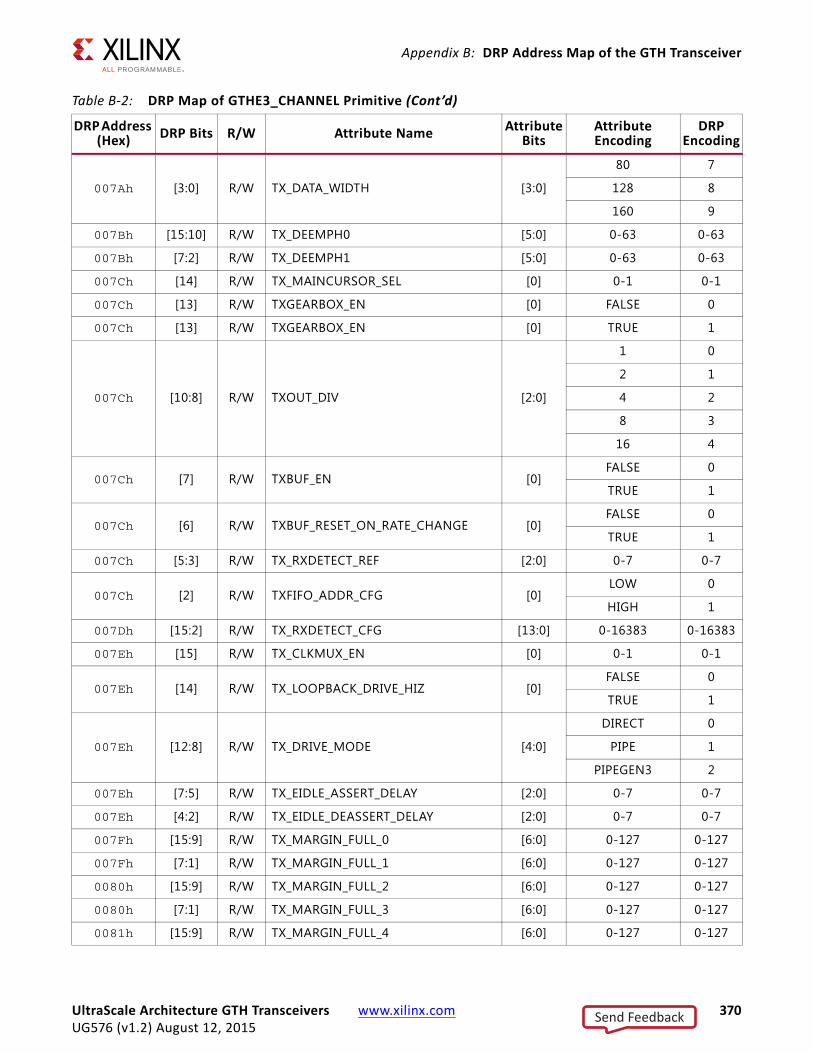
Appendix B: DRP Address Map of the GTH Transceiver
007Ah [3:0] R/W TX_DATA_WIDTH [3:0]
80 7
128 8
160 9
007Bh [15:10] R/W TX_DEEMPH0 [5:0] 0-63 0-63
007Bh [7:2] R/W TX_DEEMPH1 [5:0] 0-63 0-63
007Ch [14] R/W TX_MAINCURSOR_SEL [0] 0-1 0-1
007Ch [13] R/W TXGEARBOX_EN [0] FALSE 0
007Ch [13] R/W TXGEARBOX_EN [0] TRUE 1
007Ch [10:8] R/W TXOUT_DIV [2:0]
1 0
2 1
4 2
8 3
16 4
007Ch [7] R/W TXBUF_EN [0]FALSE 0
TRUE 1
007Ch [6] R/W TXBUF_RESET_ON_RATE_CHANGE [0]FALSE 0
TRUE 1
007Ch [5:3] R/W TX_RXDETECT_REF [2:0] 0-7 0-7
007Ch [2] R/W TXFIFO_ADDR_CFG [0]LOW 0
HIGH 1
007Dh [15:2] R/W TX_RXDETECT_CFG [13:0] 0-16383 0-16383
007Eh [15] R/W TX_CLKMUX_EN [0] 0-1 0-1
007Eh [14] R/W TX_LOOPBACK_DRIVE_HIZ [0]FALSE 0
TRUE 1
007Eh [12:8] R/W TX_DRIVE_MODE [4:0]
DIRECT 0
PIPE 1
PIPEGEN3 2
007Eh [7:5] R/W TX_EIDLE_ASSERT_DELAY [2:0] 0-7 0-7
007Eh [4:2] R/W TX_EIDLE_DEASSERT_DELAY [2:0] 0-7 0-7
007Fh [15:9] R/W TX_MARGIN_FULL_0 [6:0] 0-127 0-127
007Fh [7:1] R/W TX_MARGIN_FULL_1 [6:0] 0-127 0-127
0080h [15:9] R/W TX_MARGIN_FULL_2 [6:0] 0-127 0-127
0080h [7:1] R/W TX_MARGIN_FULL_3 [6:0] 0-127 0-127
0081h [15:9] R/W TX_MARGIN_FULL_4 [6:0] 0-127 0-127
Table B-2: DRP Map of GTHE3_CHANNEL Primitive (Cont’d)
DRP Address (Hex) DRP Bits R/W Attribute Name Attribute
BitsAttribute Encoding
DRP Encoding
UltraScale Architecture GTH Transceivers www.xilinx.com 370UG576 (v1.2) August 12, 2015
Send Feedback

Appendix B: DRP Address Map of the GTH Transceiver
0081h [7:1] R/W TX_MARGIN_LOW_0 [6:0] 0-127 0-127
0082h [15:9] R/W TX_MARGIN_LOW_1 [6:0] 0-127 0-127
0082h [7:1] R/W TX_MARGIN_LOW_2 [6:0] 0-127 0-127
0083h [15:9] R/W TX_MARGIN_LOW_3 [6:0] 0-127 0-127
0083h [7:1] R/W TX_MARGIN_LOW_4 [6:0] 0-127 0-127
0084h [15:0] R/W RXDFE_HD_CFG1 [15:0] 0-65535 0-65535
0085h [13] R/W TX_QPI_STATUS_EN [0] 0-1 0-1
0085h [11:10] R/W TX_INT_DATAWIDTH [1:0] 0 0
0085h [11:10] R/W TX_INT_DATAWIDTH [1:0] 1 1
0085h [11:10] R/W TX_INT_DATAWIDTH [1:0] 2 2
0089h [7:0] R/W RXPRBS_LINKACQ_CNT [7:0]
15 15
16 16
17 17
18 18
19 19
20 20
21 21
22 22
23 23
24 24
25 25
26 26
27 27
28 28
29 29
30 30
31 31
32 32
33 33
34 34
35 35
36 36
37 37
38 38
Table B-2: DRP Map of GTHE3_CHANNEL Primitive (Cont’d)
DRP Address (Hex) DRP Bits R/W Attribute Name Attribute
BitsAttribute Encoding
DRP Encoding
UltraScale Architecture GTH Transceivers www.xilinx.com 371UG576 (v1.2) August 12, 2015
Send Feedback

Appendix B: DRP Address Map of the GTH Transceiver
0089h [7:0] R/W RXPRBS_LINKACQ_CNT [7:0]
39 39
40 40
41 41
42 42
43 43
44 44
45 45
46 46
47 47
48 48
49 49
50 50
51 51
52 52
53 53
54 54
55 55
56 56
57 57
58 58
59 59
60 60
61 61
62 62
63 63
64 64
65 65
66 66
67 67
68 68
69 69
70 70
71 71
72 72
Table B-2: DRP Map of GTHE3_CHANNEL Primitive (Cont’d)
DRP Address (Hex) DRP Bits R/W Attribute Name Attribute
BitsAttribute Encoding
DRP Encoding
UltraScale Architecture GTH Transceivers www.xilinx.com 372UG576 (v1.2) August 12, 2015
Send Feedback

Appendix B: DRP Address Map of the GTH Transceiver
0089h [7:0] R/W RXPRBS_LINKACQ_CNT [7:0]
73 73
74 74
75 75
76 76
77 77
78 78
79 79
80 80
81 81
82 82
83 83
84 84
85 85
86 86
87 87
88 88
89 89
90 90
91 91
92 92
93 93
94 94
95 95
96 96
97 97
98 98
99 99
100 100
101 101
102 102
103 103
104 104
105 105
106 106
Table B-2: DRP Map of GTHE3_CHANNEL Primitive (Cont’d)
DRP Address (Hex) DRP Bits R/W Attribute Name Attribute
BitsAttribute Encoding
DRP Encoding
UltraScale Architecture GTH Transceivers www.xilinx.com 373UG576 (v1.2) August 12, 2015
Send Feedback

Appendix B: DRP Address Map of the GTH Transceiver
0089h [7:0] R/W RXPRBS_LINKACQ_CNT [7:0]
107 107
108 108
109 109
110 110
111 111
112 112
113 113
114 114
115 115
116 116
117 117
118 118
119 119
120 120
121 121
122 122
123 123
124 124
125 125
126 126
127 127
128 128
129 129
130 130
131 131
132 132
133 133
134 134
135 135
136 136
137 137
138 138
139 139
140 140
Table B-2: DRP Map of GTHE3_CHANNEL Primitive (Cont’d)
DRP Address (Hex) DRP Bits R/W Attribute Name Attribute
BitsAttribute Encoding
DRP Encoding
UltraScale Architecture GTH Transceivers www.xilinx.com 374UG576 (v1.2) August 12, 2015
Send Feedback

Appendix B: DRP Address Map of the GTH Transceiver
0089h [7:0] R/W RXPRBS_LINKACQ_CNT [7:0]
141 141
142 142
143 143
144 144
145 145
146 146
147 147
148 148
149 149
150 150
151 151
152 152
153 153
154 154
155 155
156 156
157 157
158 158
159 159
160 160
161 161
162 162
163 163
164 164
165 165
166 166
167 167
168 168
169 169
170 170
171 171
172 172
173 173
174 174
Table B-2: DRP Map of GTHE3_CHANNEL Primitive (Cont’d)
DRP Address (Hex) DRP Bits R/W Attribute Name Attribute
BitsAttribute Encoding
DRP Encoding
UltraScale Architecture GTH Transceivers www.xilinx.com 375UG576 (v1.2) August 12, 2015
Send Feedback

Appendix B: DRP Address Map of the GTH Transceiver
0089h [7:0] R/W RXPRBS_LINKACQ_CNT [7:0]
175 175
176 176
177 177
178 178
179 179
180 180
181 181
182 182
183 183
184 184
185 185
186 186
187 187
188 188
189 189
190 190
191 191
192 192
193 193
194 194
195 195
196 196
197 197
198 198
199 199
200 200
201 201
202 202
203 203
204 204
205 205
206 206
207 207
208 208
Table B-2: DRP Map of GTHE3_CHANNEL Primitive (Cont’d)
DRP Address (Hex) DRP Bits R/W Attribute Name Attribute
BitsAttribute Encoding
DRP Encoding
UltraScale Architecture GTH Transceivers www.xilinx.com 376UG576 (v1.2) August 12, 2015
Send Feedback

Appendix B: DRP Address Map of the GTH Transceiver
0089h [7:0] R/W RXPRBS_LINKACQ_CNT [7:0]
209 209
210 210
211 211
212 212
213 213
214 214
215 215
216 216
217 217
218 218
219 219
220 220
221 221
222 222
223 223
224 224
225 225
226 226
227 227
228 228
229 229
230 230
231 231
232 232
233 233
234 234
235 235
236 236
237 237
238 238
239 239
240 240
241 241
242 242
Table B-2: DRP Map of GTHE3_CHANNEL Primitive (Cont’d)
DRP Address (Hex) DRP Bits R/W Attribute Name Attribute
BitsAttribute Encoding
DRP Encoding
UltraScale Architecture GTH Transceivers www.xilinx.com 377UG576 (v1.2) August 12, 2015
Send Feedback

Appendix B: DRP Address Map of the GTH Transceiver
0089h [7:0] R/W RXPRBS_LINKACQ_CNT [7:0]
243 243
244 244
245 245
246 246
247 247
248 248
249 249
250 250
251 251
252 252
253 253
254 254
255 255
008Ah [15] R/W TX_PMADATA_OPT [0] 0-1 0-1
008Ah [14] R/W RXSYNC_OVRD [0] 0-1 0-1
008Ah [13] R/W TXSYNC_OVRD [0] 0-1 0-1
008Ah [12] R/W TX_IDLE_DATA_ZERO [0] 0-1 0-1
008Ah [11] R/W A_RXOSCALRESET [0] 0-1 0-1
008Ah [10] R/W RXOOB_CLK_CFG [0] PMA 0
008Ah [10] R/W RXOOB_CLK_CFG [0] FABRIC 1
008Ah [9] R/W TXSYNC_SKIP_DA [0] 0-1 0-1
008Ah [8] R/W RXSYNC_SKIP_DA [0] 0-1 0-1
008Ah [4:0] R/W RXOSCALRESET_TIME [4:0] 0-31 0-31
008Bh [10] R/W TXSYNC_MULTILANE [0] 0-1 0-1
008Bh [9] R/W RXSYNC_MULTILANE [0] 0-1 0-1
008Bh [7:0] R/W RX_CTLE3_LPF [7:0] 0-255 0-255
008Ch [15] R/W ACJTAG_MODE [0] 0-1 0-1
008Ch [14] R/W ACJTAG_DEBUG_MODE [0] 0-1 0-1
008Ch [13] R/W ACJTAG_RESET [0] 0-1 0-1
008Ch [12] R/W RESET_POWERSAVE_DISABLE [0] 0-1 0-1
008Ch [11:10] R/W RX_TUNE_AFE_OS [1:0] 0-3 0-3
008Ch [9:8] R/W RX_DFE_KL_LPM_KL_CFG0 [1:0] 0-3 0-3
008Ch [7:5] R/W RX_DFE_KL_LPM_KL_CFG1 [2:0] 0-7 0-7
008Dh [15:0] R/W RXDFELPM_KL_CFG2 [15:0] 0-65535 0-65535
Table B-2: DRP Map of GTHE3_CHANNEL Primitive (Cont’d)
DRP Address (Hex) DRP Bits R/W Attribute Name Attribute
BitsAttribute Encoding
DRP Encoding
UltraScale Architecture GTH Transceivers www.xilinx.com 378UG576 (v1.2) August 12, 2015
Send Feedback

Appendix B: DRP Address Map of the GTH Transceiver
008Eh [15:0] R/W RXDFE_VP_CFG0 [15:0] 0-65535 0-65535
008Fh [15:0] R/W RXDFE_VP_CFG1 [15:0] 0-65535 0-65535
0090h [15:0] R/W RXDFE_UT_CFG1 [15:0] 0-65535 0-65535
0091h [15:0] R/W ADAPT_CFG0 [15:0] 0-65535 0-65535
0092h [15:0] R/W ADAPT_CFG1 [15:0] 0-65535 0-65535
0093h [15:0] R/W RXCFOK_CFG0 [15:0] 0-65535 0-65535
0094h [11] R/W ES_CLK_PHASE_SEL [0] 0-1 0-1
0094h [10] R/W USE_PCS_CLK_PHASE_SEL [0] 0-1 0-1
0095h [15:0] R/W PMA_RSV1 [15:0] 0-65535 0-65535
0097h [12] R/W RX_AFE_CM_EN [0] 0-1 0-1
0097h [11] R/W RX_CAPFF_SARC_ENB [0] 0-1 0-1
0097h [10] R/W RX_EYESCAN_VS_NEG_DIR [0] 0-1 0-1
0097h [9] R/W RX_EYESCAN_VS_UT_SIGN [0] 0-1 0-1
0097h [8:2] R/W RX_EYESCAN_VS_CODE [6:0] 0-127 0-127
0097h [1:0] R/W RX_EYESCAN_VS_RANGE [1:0] 0-3 0-3
0098h [15:0] R/W RXDFE_HE_CFG1 [15:0] 0-65535 0-65535
0099h [15:11] R/W GEARBOX_MODE [4:0] 0-31 0-31
0099h [10:8] R/W TXPI_SYNFREQ_PPM [2:0] 0-7 0-7
0099h [7] R/W TXPI_PPMCLK_SEL [0] TXUSRCLK 0
0099h [7] R/W TXPI_PPMCLK_SEL [0] TXUSRCLK2 1
0099h [6] R/W TXPI_INVSTROBE_SEL [0] 0-1 0-1
0099h [5] R/W TXPI_GRAY_SEL [0] 0-1 0-1
0099h [3] R/W TXPI_LPM [0] 0-1 0-1
0099h [2] R/W TXPI_VREFSEL [0] 0-1 0-1
009Ah [7:0] R/W TXPI_PPM_CFG [7:0] 0-255 0-255
009Bh [15] R/W RX_DFELPM_KLKH_AGC_STUP_EN [0] 0-1 0-1
009Bh [14:11] R/W RX_DFELPM_CFG0 [3:0] 0-15 0-15
009Bh [10] R/W RX_DFELPM_CFG1 [0] 0-1 0-1
009Bh [9:8] R/W RX_DFE_KL_LPM_KH_CFG0 [1:0] 0-3 0-3
009Bh [7:5] R/W RX_DFE_KL_LPM_KH_CFG1 [2:0] 0-7 0-7
009Ch [12:11] R/W TXPI_CFG0 [1:0] 0-3 0-3
009Ch [10:9] R/W TXPI_CFG1 [1:0] 0-3 0-3
009Ch [8:7] R/W TXPI_CFG2 [1:0] 0-3 0-3
009Ch [6] R/W TXPI_CFG3 [0] 0-1 0-1
Table B-2: DRP Map of GTHE3_CHANNEL Primitive (Cont’d)
DRP Address (Hex) DRP Bits R/W Attribute Name Attribute
BitsAttribute Encoding
DRP Encoding
UltraScale Architecture GTH Transceivers www.xilinx.com 379UG576 (v1.2) August 12, 2015
Send Feedback

Appendix B: DRP Address Map of the GTH Transceiver
009Ch [5] R/W TXPI_CFG4 [0] 0-1 0-1
009Ch [4:2] R/W TXPI_CFG5 [2:0] 0-7 0-7
009Dh [15:14] R/W RXPI_CFG1 [1:0] 0-3 0-3
009Dh [13:12] R/W RXPI_CFG2 [1:0] 0-3 0-3
009Dh [11:10] R/W RXPI_CFG3 [1:0] 0-3 0-3
009Dh [9] R/W RXPI_CFG4 [0] 0-1 0-1
009Dh [8] R/W RXPI_CFG5 [0] 0-1 0-1
009Dh [7:5] R/W RXPI_CFG6 [2:0] 0-7 0-7
009Dh [4:3] R/W RXPI_CFG0 [1:0] 0-3 0-3
009Eh [15:0] R/W RXDFE_UT_CFG0 [15:0] 0-65535 0-65535
009Fh [15:0] R/W RXDFE_GC_CFG0 [15:0] 0-65535 0-65535
00A0h [15:0] R/W RXDFE_GC_CFG1 [15:0] 0-65535 0-65535
00A1h [15:0] R/W RXDFE_GC_CFG2 [15:0] 0-65535 0-65535
00A2h [15:0] R/W RXCDR_CFG0_GEN3 [15:0] 0-65535 0-65535
00A3h [15:0] R/W RXCDR_CFG1_GEN3 [15:0] 0-65535 0-65535
00A4h [15:0] R/W RXCDR_CFG2_GEN3 [15:0] 0-65535 0-65535
00A5h [15:0] R/W RXCDR_CFG3_GEN3 [15:0] 0-65535 0-65535
00A6h [15:0] R/W RXCDR_CFG4_GEN3 [15:0] 0-65535 0-65535
00A7h [15:0] R/W RXCDR_CFG5_GEN3 [15:0] 0-65535 0-65535
00A8h [15:0] R/W RXCDR_CFG5 [15:0] 0-65535 0-65535
00A9h [15:0] R/W PCIE_RXPMA_CFG [15:0] 0-65535 0-65535
00AAh [15:0] R/W PCIE_TXPCS_CFG_GEN3 [15:0] 0-65535 0-65535
00ABh [15:0] R/W PCIE_TXPMA_CFG [15:0] 0-65535 0-65535
00ACh [7:3] R/W RX_CLK_SLIP_OVRD [4:0] 0-31 0-31
00ACh [2:0] R/W PCS_RSVD1 [2:0] 0-7 0-7
00ADh [12:11] R/W PLL_SEL_MODE_GEN3 [1:0] 0-3 0-3
00ADh [10:9] R/W PLL_SEL_MODE_GEN12 [1:0] 0-3 0-3
00ADh [8] R/W RATE_SW_USE_DRP [0] 0-1 0-1
00ADh [3] R/W RXPI_LPM [0] 0-1 0-1
00ADh [2] R/W RXPI_VREFSEL [0] 0-1 0-1
00AEh [15:0] R/W RXDFE_H3_CFG0 [15:0] 0-65535 0-65535
00AFh [15] R/W DFE_D_X_REL_POS [0] 0-1 0-1
00AFh [14] R/W DFE_VCM_COMP_EN [0] 0-1 0-1
00AFh [13] R/W GM_BIAS_SELECT [0] 0-1 0-1
Table B-2: DRP Map of GTHE3_CHANNEL Primitive (Cont’d)
DRP Address (Hex) DRP Bits R/W Attribute Name Attribute
BitsAttribute Encoding
DRP Encoding
UltraScale Architecture GTH Transceivers www.xilinx.com 380UG576 (v1.2) August 12, 2015
Send Feedback

Appendix B: DRP Address Map of the GTH Transceiver
00AFh [10:0] R/W EVODD_PHI_CFG [10:0] 0-2047 0-2047
00B0h [15:0] R/W RXDFE_H3_CFG1 [15:0] 0-65535 0-65535
00B1h [15:0] R/W RXDFE_H4_CFG0 [15:0] 0-65535 0-65535
00B2h [15:0] R/W RXDFE_H4_CFG1 [15:0] 0-65535 0-65535
00B3h [15:0] R/W RXDFE_H5_CFG0 [15:0] 0-65535 0-65535
00B4h [15:13] R/W PROCESS_PAR [2:0] 0-7 0-7
00B4h [11:8] R/W TEMPERATUR_PAR [3:0] 0-15 0-15
00B4h [7:5] R/W TX_MODE_SEL [2:0] 0-7 0-7
00B4h [4] R/W TX_SARC_LPBK_ENB [0] 0-1 0-1
00B5h [15:0] R/W RXDFE_H5_CFG1 [15:0] 0-65535 0-65535
00B6h [15:10] R/W TX_DCD_CFG [5:0] 0-63 0-63
00B6h [9] R/W TX_DCD_EN [0] 0-1 0-1
00B6h [8] R/W TX_EML_PHI_TUNE [0] 0-1 0-1
00B6h [5:0] R/W CPLL_CFG3 [5:0] 0-63 0-63
00B7h [15:0] R/W RXDFE_H6_CFG0 [15:0] 0-65535 0-65535
00B8h [15:0] R/W RXDFE_H6_CFG1 [15:0] 0-65535 0-65535
00B9h [15:0] R/W RXDFE_H7_CFG0 [15:0] 0-65535 0-65535
00BAh [6:2] R/W DDI_REALIGN_WAIT [4:0]
0 0
1 1
2 2
3 3
4 4
5 5
6 6
7 7
8 8
9 9
10 10
11 11
12 12
13 13
14 14
15 15
16 16
Table B-2: DRP Map of GTHE3_CHANNEL Primitive (Cont’d)
DRP Address (Hex) DRP Bits R/W Attribute Name Attribute
BitsAttribute Encoding
DRP Encoding
UltraScale Architecture GTH Transceivers www.xilinx.com 381UG576 (v1.2) August 12, 2015
Send Feedback

Appendix B: DRP Address Map of the GTH Transceiver
00BAh [6:2] R/W DDI_REALIGN_WAIT [4:0]
17 17
18 18
19 19
20 20
21 21
22 22
23 23
24 24
25 25
26 26
27 27
28 28
29 29
30 30
31 31
00BAh [1:0] R/W DDI_CTRL [1:0] 0-3 0-3
00BBh [11:9] R/W TXGBOX_FIFO_INIT_RD_ADDR [2:0]
2 2
3 3
4 4
5 5
6 6
00BBh [8:6] R/W TX_SAMPLE_PERIOD [2:0] 0-7 0-7
00BBh [5:3] R/W RXGBOX_FIFO_INIT_RD_ADDR [2:0]
2 2
3 3
4 4
5 5
00BBh [2:0] R/W RX_SAMPLE_PERIOD [2:0] 0-7 0-7
00BCh [15:0] R/W CPLL_CFG2 [15:0] 0-65535 0-65535
00BDh [15:0] R/W RXPHSAMP_CFG [15:0] 0-65535 0-65535
00BEh [15:0] R/W RXPHSLIP_CFG [15:0] 0-65535 0-65535
00BFh [15:0] R/W RXPHBEACON_CFG [15:0] 0-65535 0-65535
00C0h [15:0] R/W RXDFE_H7_CFG1 [15:0] 0-65535 0-65535
00C1h [15:0] R/W RXDFE_H8_CFG0 [15:0] 0-65535 0-65535
00C2h [15:0] R/W RXDFE_H8_CFG1 [15:0] 0-65535 0-65535
Table B-2: DRP Map of GTHE3_CHANNEL Primitive (Cont’d)
DRP Address (Hex) DRP Bits R/W Attribute Name Attribute
BitsAttribute Encoding
DRP Encoding
UltraScale Architecture GTH Transceivers www.xilinx.com 382UG576 (v1.2) August 12, 2015
Send Feedback

Appendix B: DRP Address Map of the GTH Transceiver
00C3h [15:0] R/W PCIE_BUFG_DIV_CTRL [15:0] 0-65535 0-65535
00C4h [15:0] R/W PCIE_RXPCS_CFG_GEN3 [15:0] 0-65535 0-65535
00C5h [15:0] R/W RXDFE_H9_CFG0 [15:0] 0-65535 0-65535
00C6h [15:0] R/W RX_PROGDIV_CFG [15:0]
0.0 32768
4.0 57744
5.0 49648
8.0 57728
10.0 57760
16.0 57730
16.5 49672
20.0 57762
32.0 57734
33.0 49800
40.0 57766
64.0 57742
66.0 50056
80.0 57743
100.0 57775
00C7h [15:0] R/W RXDFE_H9_CFG1 [15:0] 0-65535 0-65535
00C8h [15:0] R/W RXDFE_HA_CFG0 [15:0] 0-65535 0-65535
00CAh [9:0] R/W CHAN_BOND_SEQ_1_2 [9:0] 0-1023 0-1023
00CBh [15:0] R/W CPLL_CFG0 [15:0] 0-65535 0-65535
00CCh [15:0] R/W CPLL_CFG1 [15:0] 0-65535 0-65535
00CDh [15:8] R/W CPLL_INIT_CFG1 [7:0] 0-255 0-255
00CDh [7:2] R/W RX_DDI_SEL [5:0] 0-63 0-63
00CDh [1] R/W DEC_VALID_COMMA_ONLY [0]FALSE 0
TRUE 1
00CDh [0] R/W DEC_MCOMMA_DETECT [0]FALSE 0
TRUE 1
00CEh [15:0] R/W RXDFE_HA_CFG1 [15:0] 0-65535 0-65535
00CFh [15:0] R/W RXDFE_HB_CFG0 [15:0] 0-65535 0-65535
0150h [6:0] R COMMA_ALIGN_LATENCY [6:0] 0-127 0-127
0151h [15:0] R es_error_count [15:0] 0-65535 0-65535
0152h [15:0] R es_sample_count [15:0] 0-65535 0-65535
Table B-2: DRP Map of GTHE3_CHANNEL Primitive (Cont’d)
DRP Address (Hex) DRP Bits R/W Attribute Name Attribute
BitsAttribute Encoding
DRP Encoding
UltraScale Architecture GTH Transceivers www.xilinx.com 383UG576 (v1.2) August 12, 2015
Send Feedback

Appendix B: DRP Address Map of the GTH Transceiver
0153h [3:0] R es_control_status [3:0] 0-15 0-15
0154h [15:0] R es_rdata_byte4 [79:64] 0-65535 0-65535
0155h [15:0] R es_rdata_byte3 [63:48] 0-65535 0-65535
0156h [15:0] R es_rdata_byte2 [47:32] 0-65535 0-65535
0157h [15:0] R es_rdata_byte1 [31:16] 0-65535 0-65535
0158h [15:0] R es_rdata_byte0 [15:0] 0-65535 0-65535
0159h [15:0] R es_sdata_byte4 [79:64] 0-65535 0-65535
015Ah [15:0] R es_sdata_byte3 [63:48] 0-65535 0-65535
015Bh [15:0] R es_sdata_byte2 [47:32] 0-65535 0-65535
015Ch [15:0] R es_sdata_byte1 [31:16] 0-65535 0-65535
015Dh [15:0] R es_sdata_byte0 [15:0] 0-65535 0-65535
015Eh [15:0] R RX_PRBS_ERR_CNT [15:0] 0-65535 0-65535
015Fh [15:0] R RX_PRBS_ERR_CNT [31:16] 0-65535 0-65535
Table B-2: DRP Map of GTHE3_CHANNEL Primitive (Cont’d)
DRP Address (Hex) DRP Bits R/W Attribute Name Attribute
BitsAttribute Encoding
DRP Encoding
UltraScale Architecture GTH Transceivers www.xilinx.com 384UG576 (v1.2) August 12, 2015
Send Feedback

UltraScale Architecture GTH Transceivers www.xilinx.com 385UG576 (v1.2) August 12, 2015
Appendix C
Placement Information by Package and Device
For transceiver placement information, refer to the UltraScale Architecture Packaging and Pinout User Guide (UG575) [Ref 7].
Send Feedback

Appendix D
Additional Resources and Legal Notices
Xilinx ResourcesFor support resources such as Answers, Documentation, Downloads, and Forums, see Xilinx Support.
For a glossary of technical terms used in Xilinx documentation, see the Xilinx Glossary.
Solution CentersSee the Xilinx Solution Centers for support on devices, software tools, and intellectual property at all stages of the design cycle. Topics include design assistance, advisories, and troubleshooting tips.
References1. UltraScale Architecture Configuration User Guide (UG570)
2. UltraScale Architecture SelectIO Resources User Guide (UG571)
3. UltraScale Architecture Clocking Resources User Guide (UG572)
4. UltraScale FPGAs Transceivers Wizard: Product Guide for Vivado Design Suite (PG182)
5. Vivado Design Suite User Guide: Logic Simulation (UG900)
6. UltraScale device data sheets:
UltraScale Architecture and Product Overview (DS890)
Kintex UltraScale Architecture Data Sheet: DC and AC Switching Characteristics (DS892)
7. UltraScale Architecture Packaging and Pinout User Guide (UG575)
8. UltraScale Architecture Gen3 Integrated Block for PCI Express LogiCORE IP Product Guide (PG156)
UltraScale Architecture GTH Transceivers www.xilinx.com 386UG576 (v1.2) August 12, 2015
Send Feedback

Appendix D: Additional Resources and Legal Notices
Please Read: Important Legal NoticesThe information disclosed to you hereunder (the “Materials”) is provided solely for the selection and use of Xilinx products. To the maximum extent permitted by applicable law: (1) Materials are made available "AS IS" and with all faults, Xilinx hereby DISCLAIMS ALL WARRANTIES AND CONDITIONS, EXPRESS, IMPLIED, OR STATUTORY, INCLUDING BUT NOT LIMITED TO WARRANTIES OF MERCHANTABILITY, NON-INFRINGEMENT, OR FITNESS FOR ANY PARTICULAR PURPOSE; and (2) Xilinx shall not be liable (whether in contract or tort, including negligence, or under any other theory of liability) for any loss or damage of any kind or nature related to, arising under, or in connection with, the Materials (including your use of the Materials), including for any direct, indirect, special, incidental, or consequential loss or damage (including loss of data, profits, goodwill, or any type of loss or damage suffered as a result of any action brought by a third party) even if such damage or loss was reasonably foreseeable or Xilinx had been advised of the possibility of the same. Xilinx assumes no obligation to correct any errors contained in the Materials or to notify you of updates to the Materials or to product specifications. You may not reproduce, modify, distribute, or publicly display the Materials without prior written consent. Certain products are subject to the terms and conditions of Xilinx’s limited warranty, please refer to Xilinx’s Terms of Sale which can be viewed at http://www.xilinx.com/legal.htm#tos; IP cores may be subject to warranty and support terms contained in a license issued to you by Xilinx. Xilinx products are not designed or intended to be fail-safe or for use in any application requiring fail-safe performance; you assume sole risk and liability for use of Xilinx products in such critical applications, please refer to Xilinx’s Terms of Sale which can be viewed at http://www.xilinx.com/legal.htm#tos.Automotive Applications DisclaimerXILINX PRODUCTS ARE NOT DESIGNED OR INTENDED TO BE FAIL-SAFE, OR FOR USE IN ANY APPLICATION REQUIRING FAIL-SAFE PERFORMANCE, SUCH AS APPLICATIONS RELATED TO: (I) THE DEPLOYMENT OF AIRBAGS, (II) CONTROL OF A VEHICLE, UNLESS THERE IS A FAIL-SAFE OR REDUNDANCY FEATURE (WHICH DOES NOT INCLUDE USE OF SOFTWARE IN THE XILINX DEVICE TO IMPLEMENT THE REDUNDANCY) AND A WARNING SIGNAL UPON FAILURE TO THE OPERATOR, OR (III) USES THAT COULD LEAD TO DEATH OR PERSONAL INJURY. CUSTOMER ASSUMES THE SOLE RISK AND LIABILITY OF ANY USE OF XILINX PRODUCTS IN SUCH APPLICATIONS.© Copyright 2013–2015 Xilinx, Inc. Xilinx, the Xilinx logo, Artix, ISE, Kintex, Spartan, Virtex, Vivado, Zynq, and other designated brands included herein are trademarks of Xilinx in the United States and other countries. PCI, PCI Express, PCIe, and PCI-X are trademarks of PCI-SIG. All other trademarks are the property of their respective owners.
UltraScale Architecture GTH Transceivers www.xilinx.com 387UG576 (v1.2) August 12, 2015
Send Feedback