

UltrafastSurfaceDynamics June8-12,2019 QiandaoLake,China
120
USD 11 Ultrafast Surface Dynamics June 8-12, 2019 Qiandao Lake, China
Transcript of UltrafastSurfaceDynamics June8-12,2019 QiandaoLake,China

USD 11Ultrafast Surface Dynamics
June 8-12, 2019Qiandao Lake, China

1
Supported by

2
Organization and Contact
Organizing Committee Jin ZhaoDepartment of PhysicsUniversity of Science and Technology of [email protected]
Haiming ZhuDepartment of ChemistryZhejiang [email protected]
Hrvoje PetekDepartment of Physics and AstronomyUniversity of [email protected]
Shijing TanHefei National Research Center for Physical Sciences atthe MicroscaleUniversity of Science and Technology of [email protected]
Qijing ZhengDepartment of PhysicsUniversity of Science and Technology of [email protected]
Qing ChenInternational Center for Quantum Design of FunctionalMaterialsUniversity of Science and Technology of [email protected]
Further Information https://usd11.github.io/orhttp://staff.ustc.edu.cn/~zqj/
Email [email protected]
Location New Century Resort, Qiandao LakeNo.888 Yangguang Road (Qilin Bandao) Chunan DistrictQiandaohu Chinahttp://www.qiandaokaiyuanresort.cn/en

3
WELCOME
To the 11th International Symposium on Ultrafast Surface Dynamics. We wish you a pleasantstay at the Qiandao Lake and hope that you enjoy the scientific program of the USD 11. Weare looking forward to stimulating talks and discussions.
Jin Zhao, Haiming Zhu and Hrvoje Petek
HISTORY
The Ultrafast Surface Dynamics (USD) is an international symposium, which started in 1997 inAscona Switzerland, and has since been held every 2-3 years alternating in various locations inEurope, the USA, and Japan.
2017 : USD10 in Inzell, Germany 2015 : USD9 in Lake Biwa, Japan 2013 : USD8 in Estes Park, U.S.A. 2010 : USD7 in Brijuni Islands, Croatia 2008 : USD6 in Kloster Banz, Germany 2006 : USD5 in Abashiri, Japan 2003 : USD4 in Telluride, U.S.A. 2001 : USD3 in San Sebastian, Spain 1999 : USD2 in Ringberg, Germany 1997 : USD1 in Ascona, Switzerland
SCOPE
The conference focuses on the fundamental electronic excitations in solids, solid surfaces, andinterfaces, which may ultimately couple to other degrees of freedom such atomic, molecular,spin, and other excitations, which evolve on time scales from attoseconds to picoseconds. Theprogram of USD11 will encompass, but is not limited to, experiments on dynamics ofinterfacial electron transfer, the spin-dependent dynamics in topological materials,femtosecond relaxation during the photoemission of electrons, dynamical screening,collective excitations in solids, correlated electron phenomena, etc. A further focus will be thedevelopment and application of theoretical models that describe electronically excited statesand their dynamics. New impulses are to be expected from the work on spin liquids and newdevelopments in the field of time-resolved density function theory. The main objectives of themeeting are to exchange ideas on the current scientific results, the initiation and deepening ofbilateral and multilateral cooperation among research groups, the discussion anddevelopment of visions on future research, and stimulation of ultrafast science research inChina.
COVERED TOPICS
Fundamental Light-Matter interactions Electron Dynamics and Electronic Energy Transfer at Surfaces and Interfaces Electron Correlation Light Energy Conversion Surface and Interface Magnetisation Dynamics Ultrafast Plasmonics and Nanooptics Dynamics in Low-dimensional materials

4
Novel Phenomena / Materials Ultrafast Surface Science
INTERNATIONAL STEERING COMMITTEE
Uwe Bovensiepen (University of Duisburg-Essen, Germany) Pedro Echenique (University of the Basque Country, Spain) Tony Heinz (Stanford University, USA) Ulrich Höfer (University of Marburg, Germany) Hrvoje Petek (University of Pittsburgh, USA) Martin Weinelt (Freie Universität Berlin, Germany) Martin Wolf (Fritz-Haber Institute, Germany) Xiaoyang Zhu (Columbia University, USA) Jin Zhao (University of Science & Technology of China, China)

5
PROGRAM
Friday, June 7
Session Chair: Hrvoje Petek
19:30 - 19:40 Welcoming Remarks
19:40 - 20:20V. Ara
ApkarianSpectromicroscopy with Atomically Confined Light
20:20 - 21:00 Xiaohui QiuCross-plane Thermal Conductance of Au/graphene/Au
Heterojunctions
Saturday, June 8
Session Chair: Ulrich Höfer
09:00 - 09:40 Shiwei WuNonlinear Optical Response of Massless Dirac Fermions in
Graphene Materials
09:40 - 10:20Martin
Aeschlimann
Mixing the Light-Spin with Plasmon-Orbit by Non-Linear Light Matter
Interaction
10:20 - 10:40 Coffee Break
10:40 - 11:20 Robin HuangRevealing an Optical Spin Skyrmion in the Core of a Surface
Plasmon Vortex
11:20 - 12:00Markus B.
Raschke
Ultrafast and Nonlinear Nanoscopy: Watching Quantum Dynamics in
Time and Space
12:00 - 12:20Zeno
Schumacher
Ultrafast Nonlinear Optical Response Probed by Atomic Force
Microscopy
12:20 - 14:40 Lunch
Session Chair: Haiming Zhu
14:40 - 15:20 Jigang WangQuantum Beats by Terahertz Symmetry Breaking: From Excitons,
Polarons to Cooper Pairs (THz)
15:20 - 15:40Oliver B.
Wright
Imaging GHz Surface Phonons on Phononic Crystals, Acoustic
Metamaterials and Microstructures
15:40 - 16:00 Timm Rohwer Defect-mediated Control of Charge Density Waves
16:00 - 16:20 Coffee Break
16:20 - 17:00Cheng-Tien
ChiangPhotoemission with High-order Harmonics at MHz
17:00 - 17:20 Henry Kapteyn The Y-Fi VUVTM : A One-Box MHz rep-rate VUV Source for Surface

6
and Chemical Dynamics Studies
17:20 - 19:00 Dinner
19:00 - 21:00 Poster Session
Sunday, June 9
Session Chair: Karl Martin Wolf
09:00 - 09:40 Xiaoyang ZhuExcitons, phonons and Electrons in Two-dimensional
Semiconductors and Heterojunctions
09:40 - 10:20Uwe
Bovensiepen
Local and Non-local Electron Dynamics in Layered Material Systems
Analyzed by Time-resolved Photoelectron Spectroscopy
10:20 - 10:40 Coffee Break
10:40 - 11:20 Michael Bauer Ultrafast Dynamics in 2D- and 3D-Dirac Materials
11:20 - 12:00Javier García
de AbajoPlasmonics in Atomically Thin Materials
12:00 - 12:20 Tzu-Yu ChenSecond Harmonic Generation in a Fully Centro-Symmetric
Plasmonic Nanocircuit
12:20 - 14:40 Lunch
Session Chair: Raschke Markus
14:40 - 15:20 Yihua Wang Ultrafast Electronic and Magnetic Dynamics in Topological Materials
15:20 - 16:00 Kazuki SumidaSurface Dirac Fermion Dynamics of Non-magnetic and Magnetic
Topological Insulators
16:00 - 16:20 Coffee Break
16:20 - 17:00 Kaihui Liu Ultrafast Optical Spectroscopy of Individual Nanomaterials
17:00 - 17:40 Haiming Zhu Charge and Energy Transfer Dynamics at 2D Ultimate Proximity
17:40 - 18:00 Nan PanMagnetically-Sensitive Valley Polarization Reversal and Revival of
Defect-Bound Excitons in WSe2-WS2Heterostructure
18:00 - 19:00 Dinner
19:00 - 21:00 Poster Session
Monday, June 10
Session Chair: Ryuichi Arafune
09:00 - 09:40 Christian Heide Ultrafast Control of Electron Inside of Graphene and Across

7
Solid-state Interfaces
09:40 - 10:00 Walter PfeifferFinal State Effective Mass Affects Attosecond Photoemission Delays
in BiTeCl
10:00 - 10:20Andreas Geba
uer
Equivalence of RABBITT and Streaking Delays in
Attosecond-Time-Resolved Photoemission Spectroscopy at Solid
Surfaces
10:20 - 10:40 Coffee Break
10:40 - 11:20 Sheng MengUltrafast Carrier Relaxation and Pauli Drag Effect in Photoexcited
Solids
11:20 - 12:00 Jin ZhaoMolecular Dynamics Investigations on the Excited Carriers in
Condensed Matter Systems
12:00 - 14:00 Lunch
14:00 - 18:00 Conference Break
18:00 - 21:00 Conference Dinner
Tuesday, June 11
Session Chair: Uwe Bovensiepen
09:00 - 09:40 Martin WolfUltrafast Excited State Dynamics of Solids Probed by Time-resolved
ARPES
09:40 - 10:20 Shijing TanAnisotropic Optical Response of Black Phosphorus Studied by
Multiphoton Photoemission Spectroscopy
10:20 - 10:40 Coffee Break
10:40 - 11:20 Fengqiu WangExcited-states Lifetime Control in Emerging Low-dimensional
Materials
11:20 - 11:40 Takeshi SuzukiUltrafast Carrier Dynamics in a Twisted Bilayer Graphene
Quasicrystal
11:40 - 14:40 Lunch
Session Chair: Xiaoyang Zhu
14:40 - 15:20 Xuefeng Guo Ultrafast Single Molecule Electrical Detection
15:20 - 15:40 Lisa GradElectron Dynamics on Cu2O(111) Probed with Time-Resolved
Two-Photon Photoemission
15:40 - 16:00Helmut
ZachariasExciton-induced Chemical Reactions on Surfaces
16:00 - 16:20 Coffee Break

8
16:20 - 16:40 Kiyoshi MiyataUnique Dielectric Responses in Lead-halide Perovskites: Proposal of
Ferroelectric Polaron
16:40 - 17:00Sebastian F.
Maehrlein
Dialing into Dynamically Disordered Lattice Potentials in CsPbBr3 via
2D Coherent Phonon Spectroscopy
17:00 - 17:20 Kunie IshiokaCharge Separation Dynamics at Lead Halide Perovskite Interfaces
Monitored by Differential Transient Transmission Spectroscopy
17:20 - 17:40 Daniel Niesner Coupled Spin and Lattice Dynamics in Lead Halide Perovskites
17:40 - 18:00 Ti Wang Visualizing Carrier Transport in Perovskites
18:00 - 19:40 Conference Banquet & After-dinner Colloquium
Session Chair: Shijing Tan
19:40 - 20:20 Hrvoje Petek How to Dress a Metal
20:20 - 21:00 Ulrich HöferSubcycle Time-resolved ARPES of THz-driven Dirac Currents in a
Topological Surface Band
21:00 - 21:20 Poster Award
Wednesday, June 12
Session Chair: Kazuki Sumida
09:00 - 09:40 Martin WeineltSpin Mixing and Spin-wave Excitations in 3d and 4fFerromagnetic
Metals
09:40 - 10:20Ryuichi
ArafuneSpectroscopic Investigation of Opto-spincurrent Control
10:20 - 10:40 Coffee Break
10:40 - 11:20Zhensheng
Tao
Critical Behaviors in 20fs Govern the Non-equilibrium Laser-induced
Magnetic Phase Transition in Ni
11:20 - 11:40 Stefan Mathias Coherent Ultrafast Spin Transfer in Ferromagnetic Alloys

9
ORALCONTRIBUTIONS
10
Spectromicroscopy with Atomically Confined Light
V. Ara ApkarianDepartment of Chemistry, University of California, Irvine
e-mail: [email protected]
Plasmonic nanojunctions can be used to effectively confine light on the Å scale, surpassing thediffraction limit of light by four orders of magnitude, and opening the atomistic near-field inoptical microscopy. Seeing an atom, a single chemical bond, imaging the vibrational normalmodes inside one molecule, and seeing sound and atomically resolved phonons are amongthe recent observations made in our laboratory under the rubric of tip-enhanced Ramanspectro-microscopy (TERS). I will use these examples to expand on the unusual propertiesand multiple facets of atomistically confined plasmons and their applications. As light, themomentum uncertainty associated with spatial confinement gives visible photons thewavelength of x-rays, which allows the simultaneous energy and momentum matchingconditions required to see dispersive acoustic phonons – to see sound. As fields, the dramaticenhancement through confinement accesses the strong-field limit and allows detection of thefeeble Raman effect from individual atoms and molecules. This gives access to theelectro-mechanical machinery of individual molecules for sensing and device applications,such as the recently demonstrated single molecule scanning electrometer and single moleculeoptoelectronics. As picocavity photons, superpositions of only two Fock states can beprepared and maintained. And in the quantum tunneling limit required for atomisticresolution, phototunneling current of confined electrons provides a more natural descriptionof the local, time harmonic electro-magnetic fields and associated observables, such as thephase in Raman lines. There is much to be seen at the Å-scale opened up through atomicallyconfined light.

11
Cross-plane Thermal Conductance of Au/graphene/AuHeterojunctions
Junbo Zhou1,2, Rui Wang1, Xiaohui Qiu1,2
1 Chinese Academy of Sciences Key Laboratory of Standardization and Measurement forNanotechnology, Chinese Academy of Sciences Center for Excellence in Nanoscience, National
Center for Nanoscience and Technology, Beijing 100190, China2 University of Chinese Academy of Sciences, Beijing 100049, China
e-mail: [email protected]
2D materials provide an appealing platform for studying heat transport through atomicallyabrupt interface, allowing to reveal interesting phenomena such as thickness dependentthermal conductivity at the nanometer scale. Here, we employ the Frequency DomainThermoreflectance (FDTR) technique to investigate the heat conduction across theheterojunction composed of few-layer graphene embedded in gold thin film. We measure thethermal conductance across this Au/graphene/Au sandwich structure as a function ofgraphene layer number at varying temperatures. It is found that electron transmissiondominates the thermal conductance for monolayer graphene, and two-orders of magnitudedecrease through bilayer graphene. For multilayer graphene sheets, phonon thermalconductivity is suggested to account for the heat transmission through the interfacialboundaries.
Fig. 1 Schematics of the Au/graphene/Au structure, and an optic image of graphene on Au with mono-and bi-layer graphene (scalebar 20um). The measured phase lags in FDTR and their fittings to a heattransfer model, through which the thermal conductivity of Au/graphene/Au heterostructures werederived.

12
Nonlinear optical response of massless Dirac fermions ingraphene
Shiwei Wu1
1Department of Physics, Fudan University, Chinae-mail: [email protected]
Graphene exhibits extraordinarily strong coupling to light owing to its unique linear andgapless two-dimensional band structure that hosts massless Dirac fermions. In this talk, I willfocus on its nonlinear optical response. For centrosymmetric monolayer graphene, thesecond-order optical nonlinearity is forbidden under the electric-dipole approximation. Yet, itpossesses exceptionally strong third-order optical nonlinearity. Recently we show that thethird-order nonlinearity including THG and FWM could be electrically tuned by orders ofmagnitude [1]. Furthermore, the electric-quadrupole response is also gate tunable, leading tostrong doping-induced second harmonic generation (SHG) beyond the electric-dipoleapproximation [2]. In contrast to the electric dipole allowed THG, the electric quadrupole SHGstrictly vanishes at zero doping, manifesting the electron-hole symmetry of massless Diracfermions. We believe the findings in graphene are readily applicable to other related Diracmaterials such as topological insulators, Dirac and Weyl semimetals. And the giantnonlinearity in graphene can be utilized to develop nonlinear optoelectronic devices.
[1] Tao Jiang,† Di Huang,† Jinluo Cheng, Xiaodong Fan, Zhihong Zhang, Yuwei Shan, Yangfan Yi, YunyunDai, Lei Shi, Kaihui Liu, Changgan Zeng, Jian Zi, J.E. Sipe, Yuen-Ron Shen, Wei-Tao Liu,* Shiwei Wu*, Gatetunable third-order nonlinear optical response of massless Dirac fermions in graphene. NaturePhotonics 12, 430-436 (2018).[2] Yu Zhang,† Di Huang,† Yuwei Shan, Tao Jiang, Zhihong Zhang, Kaihui Liu, Lei Shi, Jinluo Cheng, John E.Sipe, Wei-Tao Liu,* Shiwei Wu*, Doping induced second harmonic generation in centrosymmetricgraphene from quadrupole response. Physical Review Letters 122, 047401 (2019).

13
Mixing the Light-Spin with Plasmon-Orbit by Non-LinearLight Matter Interaction
Martin AeschlimannDepartment of Physics and Research Center OPTIMAS
University of Kaiserslautern, Germanye-mail: [email protected]
Transformation of light carrying spin angular momentum (SAM) to optical field vorticescarrying orbital angular momentum (OAM) has been of wide interest in recent years. Theinteractions between two optical fields, each carrying one of those degrees of freedom, andfurthermore, the transfer of the resulting angular momentum product to matter is seldomdiscussed. Here we measure the interaction between light carrying axial SAM andplasmon-polariton vortices carrying high order transverse OAM. The interaction is mediatedby two-photon absorption within a gold surface, imprinting the resulting angular momentummixing into matter by excitation of electrons that are photo-emitted into vacuum.
We demonstrate that, counter-intuitively, the spatial distribution of the emittedelectrons carries the signature of a subtraction of the spin from the orbit angular momenta.We show experimentally and theoretically that the absorptive nature of this interaction leadsto both single and double photon-plasmon angular momentum mixing processes by one- andtwo- photon interactions. The dynamics of two-photon absorption can be described by athree-level model system and its corresponding density matrix. The transition from theground to the third excited state may occur through a population of an intermediate state, orthrough coherences only without passing through the diagonal elements. In this way one candiscriminate between pathways consisting of a single angular momentum mixing in oneabsorption, with the two steps of the other absorption performed by pure photon or plasmonfields. Double mixing pathways occur when both transitions are performed by identicaltwo-step sequences of mixing plasmon and light.

14
Revealing an optical spin skyrmion in the core of asurface plasmon vortex
Yanan Dai1, Zhikang Zhou1, Atsushi Kubo2, Chen-Bin Huang3, and Hrvoje Petek11 Department of Physics and Astronomy, University of Pittsburgh, USA
2Department of Physics, University of Tsukuba, Japan3Institute of Photonics Technologies, National Tsing Hua University, Taiwan
e-mail: [email protected], [email protected]
We report the first experimental evidence for an electric field spin angular momentumskyrmion at a plasmonic silver surface. Skyrmions are stable quasiparticles in magneticmaterials with distinct topological spin textures that have been investigated for several yearsby electron microscopy and scan tunneling microscopy techniques. Our skyrmion represents atrue topological spin texture, which is engendered by an Archimedean plasmonic couplingstructure.
We employ interferometric time-resolved photoemission electron microscopy to record amovie of the plasmonic fields with <10 nm spatial resolution and <100 as pump-probe pulsedelay/frame. Archimedean plasmonic coupling structures have been employed before togenerate vortices, but they have never been explored from perspective of skyrmions. Unlikeprevious research, we employ linearly polarized light to generate the vortex, with theoutcome that the skyrmion is generated by the geometrical charge of the coupling structure,rather than more complicated process involving the photon spin. We model the nanoscalefields, their polarization properties and plasmonic flow, which enable us to conclude that theskyrmion is a stable quasiparticle on the time scale of the pulse duration.
Fig. 1 The plasmonic Néel spin angular momentum (SAM) skyrmion. The colored arrows show theSAM pseudovectors that define the skyrmion texture created within a plasmonic vortex core; they areoverlaid on the map of L-line singularities of SPP fields that define the skyrmion density.

15
Ultrafast and Nonlinear Nanoscopy:Watching Quantum Dynamics in Time and Space
Raschke Markus (雷默)Department of Physics, Department of Chemistry, and JILA
University of Colorado, Boulder, USAe-mail: [email protected]
We will present a new regime in nonlinear nano-optics and spatio-temporal nano-imaging forthe study of fundamental coherent optical, plasmonic, and quantum dynamic phenomenawith nanometer spatial and few-femtosecond temporal resolution. To gain the desirednanometer spatial resolution with spectroscopic specificity and femtosecond temporalresolution we combine plasmonic nano-focusing and optical antenna concepts with ultrafastand shaped laser pulses to precisely control optical excitation on fs-time and nm-length scales.
Fig. 1. a) Nonlinear four-wave mixing nano-focused imaging of coherent electrondynamics with few-fs time and few-nm spatial resolution [1]. b-c) New mechanism forenhanced nonlinear frequency conversation on the nanoscale by gradient field andevanescent wave phase matching [2]. d-f) Nonlinear nano-optics of graphene with layerdependent, enhanced edge contrast, and quantum Doppler nonlocal response exploring theunique electronic bandstructure and symmetries of graphene [3].Examples include anultrafast movie of the real time and real space coherent dynamics of coupled plasmonicnanostructures (Fig 1a) [1]. The underlying mechanism of four-wave mixing reveals a newregime of nonlinear frequency generation on the nanoscale based on a plasmonicgradient-field effect that provides for an efficient, conventionally dipole-forbidden nonlinearresponse (b,c) [2]. Similarly, in graphene, we discover new spatial, spectral, and temporalphenomena based on a bandstructure and tip nano-cavity enhanced nonlinear response (d-f)[3]. These results provide for localized and -enhanced nonlinear optical interactions with newpossibilities for applications from nano-photonic circuits to quantum nano-optics, and-imaging.
1. V. Kravtsov, R. Ulbricht, R., J. M. Atkin, and M. B. Raschke, Plasmonic nanofocused four-wave mixingfor femtosecond near-field imaging. Nature Nanotechnol. 11, 459-464 (2016).

16
2. V. Kravtsov, S. AlMutairi, R. Ulbricht, A. Ryan Kutayiah, A. Belyanin, and M. B. Raschke, Enhancedthird-order optical nonlinearity driven by surface-plasmon field gradients. Phys. Rev. Lett. 120, 203903(2018).3. T. Jiang, V. Kravtsov, S. AlMutairi, A. Belyaning, and M. B. Raschke, Nonlinear nano-optics ofgraphene: symmetry, nonlocality, and coherent dynamics (submitted).
17
Ultrafast nonlinear optical response probed by atomicforce microscopy
Zeno Schumacher*, Rasa Rejali, Andreas Spielhofer, Yoichi Miyahara andPeter Grutter
Department of Physics, McGill University, Montreal, Canada*current address: Physics Department, ETH Zurich, 8093 Zurich, Switzerland,
e-mail: [email protected]
Scanning probe technique such as non-contact Atomic Force Microscopy (nc-AFM) offer theability to spatially resolve surfaces with sub-nanometer resolution. Recent technical advances,such as photo-induced force microscopy (PiFM) [1] and pump-probe style time-resolvednc-AFM [2,3], have shown the potential of light induced force measurements, resolvingdynamics in the ps range. The high force sensitivity of AFM allows to resolve small variationsin local optical induced forces and to decouple the probe volume from the focal size of theillumination.
Here, we present nanometer spatially resolved measurements of the ultrafast opticalnonlinear response on a surface to a fs-pulsed laser. The induced polarization is detected asan additional force component in the nc-AFM measurement. Local variations on thenanometer scale of the induced polarization on a periodically poled lithium niobate surfacecan be resolved. The variation can be attributed to surface adsorbates and correlated totopographical nc-AFM measurements. Due to the high force sensitivity of this method, evenmonolayer samples can be detected. We will present recent results on a MoSe2 monolayerdetecting the utrafast nanometer local nonlinear optical response. With this, nc-AFM adds tothe toolbox of ultrafast surface science, whereas the force detection of ultrafast opticalnonlinear processes is combined with nanometer spatial resolution.
[1] Rajapaksa, I., Uenal, K., & Wickramasinghe, H. K. (2010). Image force microscopy of molecularresonance: A microscope principle. Applied Physics Letters, 97(7), 073121.[2] Jahng, J., et al. (2015). Ultrafast pump-probe force microscopy with nanoscale resolution. AppliedPhysics Letters, 106(8), 083113.[3] Schumacher, Z., Spielhofer, A., Miyahara, Y., & Grutter, P. (2017). The limit of time resolution infrequency modulation atomic force microscopy by a pump-probe approach. Applied Physics Letters,110(5).
18
Quantum Beats by Terahertz Symmetry Breaking: FromExitons, Polarons to Cooper Pairs
Jigang WangDepartment of Physics and Astronomy, Iowa State University & Ames Laboratory - USDOE,
Ames, Iowa 50011, USAe-mail: [email protected]
Harnessing quantum coherence and quantum quench prethermalization has emerged as across-cutting theme for discovering and controlling emergent phases and collective modes,even thermodynamically forbidden. In this talk, I will discuss our recent progress towardsapplying these new tuning knobs using single- and few-cycle THz pulses to reveal quantumbeats and ultrafast control in several systems of current focus including perovskitesemiconductors and superconductors. Particularly, our results show that THz light-drivencoherence and subcycle symmetry breaking allows the observation of forbidden collectivemodes and hidden many-body quantum phases that are difficult to be accessed by othertuning methods. Finally I will discuss far-reaching consequences of THz coherent andnano-optics methods on quantum matter discovery.
19
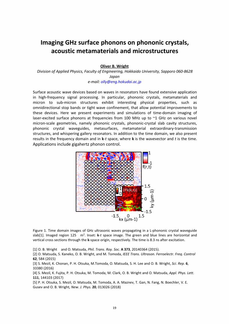
Imaging GHz surface phonons on phononic crystals,acoustic metamaterials and microstructures
Oliver B. WrightDivision of Applied Physics, Faculty of Engineering, Hokkaido University, Sapporo 060-8628
Japane-mail: [email protected]
Surface acoustic wave devices based on waves in resonators have found extensive applicationin high-frequency signal processing. In particular, phononic crystals, metamaterials andmicron to sub-micron structures exhibit interesting physical properties, such asomnidirectional stop bands or tight wave confinement, that allow potential improvements tothese devices. Here we present experiments and simulations of time-domain imaging oflaser-excited surface phonons at frequencies from 100 MHz up to ~1 GHz on various novelmicron-scale geometries, namely phononic crystals, phononic-crystal slab cavity structures,phononic crystal waveguides, metasurfaces, metamaterial extraordinary-transmissionstructures, and whispering gallery resonators. In addition to the time domain, we also presentresults in the frequency domain and in k-t space, where k is the wavevector and t is the time.Applications include gigahertz phonon control.
Figure 1. Time domain images of GHz ultrasonic waves propagating in a L-phononic crystal waveguideslab[1]. Imaged region 125 m2. Inset: k-t space image. The green and blue lines are horizontal andvertical cross sections through the k-space origin, respectively. The time is 8.3 ns after excitation.
[1] O. B. Wright and O. Matsuda, Phil. Trans. Roy. Soc. A 373, 20140364 (2015).[2] O. Matsuda, S. Kaneko, O. B. Wright, and M. Tomoda, IEEE Trans. Ultrason. Ferroelectr. Freq. Control62, 584 (2015)[3] S. Mezil, K. Chonan, P. H. Otsuka, M.Tomoda, O. Matsuda, S. H. Lee and O. B. Wright, Sci. Rep. 6,33380 (2016)[4] S. Mezil, K. Fujita, P. H. Otsuka, M. Tomoda, M. Clark, O. B. Wright and O. Matsuda, Appl. Phys. Lett.111, 144103 (2017)[5] P. H. Otsuka, S. Mezil, O. Matsuda, M. Tomoda, A. A. Maznev, T. Gan, N. Fang, N. Boechler, V. E.Gusev and O. B. Wright, New. J. Phys. 20, 013026 (2018)

20
Defect-mediated Control of Charge Density Waves
Timm Rohwer1,2, Alfred Zong1, Anshul Kogar1, Ya-Qing Bie1 , Changmin Lee1,Edoardo Baldini1, Emre Ergeen1, Mehmet B. Yilmaz1, Byron Freelon1,3, Edbert J. Sie 1,4,
Pablo Jarillo-Herrero 1 and Nuh Gedik11Massachusetts Institute of Technology, Cambridge, Massachusetts 02139, MA, USA
2Center for Free-Electron Laser Science, Deutsches Elektronen-Synchrotron DESY, LuruperChaussee 149, 22761 Hamburg, Germany
3Department of Physics and Astronomy, University of Louisville, Louisville, KY, USA4Geballe Laboratory for Advanced Materials, Stanford University, Stanford, CA, USA
e-mail: [email protected]
We investigated the light-induced melting of a unidirectional charge density wave (CDW) inLaTe3 by a combination of time-resolved Angle Resolved Photo-Electron Spectroscopy(trARPES), Ultrafast Electron Diffraction (UED) and Transient Optical Spectroscopy (TOS) [1].This enabled us to record and compare the correlated dynamics in both, the electronic andlattice subsystem, leading to an independent tracking of the CDW amplitude and phasedynamics. We find that a fast (approximately 1 picosecond) recovery of the CDW amplitude isfollowed by a slower re-establishment of phase coherence. This longer timescale is dictatedby the presence of topological defects: long-range order is inhibited and is only restored whenthe defects annihilate.
On a different CDW compound a fully reversible on-off switching of domain-walls isdemonstrated by means of UED. Both, the creation and annihilation can be realized by asingle pulse of light [2]. Both studies provide a framework to understand and control thegeometry of the ultrafast restored CDW’s by utilizing defects and boundaries as a governingmechanism.
Fig. 1 Three time-resolved probes for combined detection of the transient electronic and latticestructure.
[1] Nature Physics 15, 27 (2019)[2] Science Advances 4, eaau5501 (2018)

21
Photoemission with high-order harmonics at MHz
Cheng-Tien Chiang1,2, Andreas Trützschler1,2, Michael Huth2, Robin Kamrla1,2, Frank O.Schumann2, Wolf Widdra1,2
1Institute of Physics, Martin-Luther-University Halle-Wittenberg, Halle (Saale), Germany2Max Planck Institute of Microstructure Physics, Halle (Saale), Germany
e-mail: [email protected] ; [email protected]
With the recent progress of high-power femtosecond lasers, high-order harmonic generation(HHG) has evolved into a routine technique to convert the infrared laser light into a muchhigher photon energy ranging from vacuum-ultraviolet to x-ray. Due to the widely tunablephoton energy range as well as the ultimate pulse duration below few femtoseconds, theapplication of HHG-based light source to photoelectron spectroscopy (PES) and microscopyhave been pursued since decades [1]. However, these developments have been limited by thespace-charge effects at low laser repetition rates of several kilohertz as well as the complexityof the HHG setups. By combining femtosecond lasers operating at megahertz repetition rateswith a compact design of the HHG chamber, we have demonstrated efficient photoelectronspectroscopy experiments [2,3]. In this talk, the application of MHz-HHG light sources totime-resolved PES and the advanced double photoemission (DPE) spectroscopy will bepresented.
In DPE experiments, a pair of photoelectrons are emitted due to the absorption of onesingle photon. Therefore DPE could provide a unique opportunity to analyze the interactionbetween electrons in solids. By using a pair of time-of-flight spectrometers in combinationwith the MHz-HHG light source [4,5], we analyze the two-dimensional energy distribution ofcorrelated sp-d and d-d electron pairs from Ag(001) and Cu(111) [6]. These results will becompared with DPE on correlated materials such as NiO and discussed in terms of electroncorrelation.
[1] Angle-resolved photoelectron spectroscopy at surfaces with high-order harmonic generation C.-T.Chiang, in “Reference module in chemistry, molecular sciences and chemical engineering”, edited by K.Wandelt, ISBN:978-0-12-409547-2, Elsevier (2018).https://www.sciencedirect.com/science/article/pii/B9780124095472132573[2] Boosting laboratory photoelectron spectroscopy by megahertz high-order harmonics, C.-T. Chiang,M. Huth, A. Trützschler, M. Kiel, F. O. Schumann, J. Kirschner, and W. Widdra, New J. Phys. 17, 013035(2015).[3] Efficient and tunable high-order harmonic light sources for photoelectron spectroscopy at surfaces,C.-T. Chiang, M. Huth, A. Trützschler, F. O. Schumann, J. Kirschner, and W. Widdra, J. Electron Spectrosc.Relat. Phenomena 200, 15 (2015).[4] Extended energy range analysis for angle-resolved time-of-flight photoelectron spectroscopy, M.Huth, A. Trützschler, C.-T. Chiang, R. Kamrla, F. O. Schumann, and W. Widdra, J. Appl. Phys. 124, 164504(2018).[5] Electron pair emission detected by time-of-flight spectrometers: recent progress, M. Huth, C.-T.Chiang, A. Trützschler, F. O. Schumann, J. Kirschner, and W. Widdra, App. Phys. Lett. 104, 061602(2014).[6] Band-resolved double photoemission spectroscopy on correlated valence electron pairs in metals, A.Trützschler, M. Huth, C.-T. Chiang, R. Kamrla, F. O. Schumann, J. Kirschner, and W. Widdra, Phys. Rev.Lett. 118, 136401 (2017).

22
The Y-Fi VUVTM: A One-Box MHz rep-rate VUV Source forSurface and Chemical Dynamics Studies
Daniel D. Hickstein1, David E. Couch2, Matt Kirchner1, Jessica Ramirez1,Xiaoyu Ji4, Margaret Murnane1,2, Henry Kapteyn1,2, and Sterling Backus1,3*
1KMLabs Inc., 4775 Walnut St #102, Boulder, CO 80301, USA2University of Colorado at Boulder, Dept of Physics and JILA, Boulder, CO 80309, USA3Colorado State University, ECE, 1373 Campus Delivery, Ft. Collins, CO 80523, USA
4Laser Resolution, 1040 Caoyang Rd., Putuo District, Shanghai 200063 Chinae-mail: [email protected]
Ultrashort-pulse light in the deep-UV-vacuum-UV spectral region, covering ~6-15 eV, isuniquely capable of probing physical and chemical processes, for example for Angle-ResolvedPhotoelectron Spectroscopy (ARPES) and Photoionization Mass Spectrometry PIMS. However,the ideal VUV light source for these applications—compact, with MHz repetition-rates andfemtosecond-domain pulse duration—has not as-yet existed. High-order harmonic generationhas proven useful for generating multiple harmonic orders in the VUV and EUV spectralregions; however, when attempting to scale to higher repetition rate, the much lower pulseenergy from tabletop-scale MHz lasers requires a tight-focusing geometry with rapidlydiminishing conversion efficiency.
Recently, we demonstrated a new architecture for VUV generation using cascadedfour-wave mixing in a small-diameter, low-loss negative curvature (NC) fiber. We employω+2ω cascaded four-wave-mixing driven by an ultrafast fiber laser running at up to 5 MHz, togenerate 1.2-eV-spaced harmonics extending to ~11 eV, with flux approaching synchrotronlevels—all in a tabletop setup. This work is based on well-established four-wave mixing ingasses.[1-2] By using tight confinement of the driving laser mode over a long propagationlength, we enable multi-step cascaded upconversion in a simple geometry.[3]
In this project, we started with a commercial (KMLabs YFi UltraTM) ultrafast fiber laserproducing ~10 J, 160 fs pulses @ 1040 nm with 1-10 MHz repetition rate. The output wasfrequency doubled with ~50-70% efficiency, recombined with 1040 nm light and retimed, thenfocused into a ~30 m diameter NC fiber backed with xenon gas. The first four-wave-mixing(FWM) step generates >200 mW at 345 nm, which then cascades to produce 4ω, 5ω, 6ω, 7ω,8ω, and 9ω (Figure 1). The narrow ~20 meV spectral bandwidth of the laser broadens onlymodestly, by ~2-3x for the 10.8 eV emission and less for lower orders.
KMLabs is currently constructing a commercial version of this laser, the Y-Fi VUVTM (figure2), which incorporates the fiber laser, the upconversion setup, and a monochromator into asingle 0.75m x 1.5 m enclosure designed to replace conventional synchrotron and lamp-basedlight sources for a wide variety of VUV light applications. The monochromator is designed toaccommodate applications both in high-resolution and in time-resolved studies, making itpossible to either select a single harmonic order with minimal time-dispersion, or to spectrallynarrow the output to ~1 meV. Further results characterizing the Y-Fi VUVTM will be presented,along with on-going experimental application results.

23
Figure 1. Using cascaded four-wave mixing to generate VUV harmonics of a 1 MHz 1040 nm fiber laser.a) Photon flux and spectrum for 6 harmonics. Flux corresponds to intensity emitted by the source,measured by separating harmonic orders with a prism, using a power meter (up to 6 eV), current from aNIST-calibrated Al2O3 photodiode (for 10.8 eV), and estimates for 7.2-9.6 eV based on relativefluorescence intensity.
Figure 2. Y-Fi VUV design layout. Entire optical system including monochromator for energy selectionoccupies a footprint of 0.75 m x1.5 m.
1. C. G. Durfee III, A. Rundquist, H. C. Kapteyn, and M. M. Murnane, "Guided wave methods andapparatus for nonlinear frequency generation," US Patent 6,151,155.2. C. G. Durfee III, S. Backus, M. M. Murnane, and H. C. Kapteyn, "Ultrabroadband phase-matchedoptical parametric generation in the ultraviolet by use of guided waves," Optics Letters, vol. 22, no. 20,pp. 1565-1567, 1997.3. S. Backus, H. C. Kapteyn, and D. Winters, Two-Color Wave-Mixing Upconversion in StructuredWaveguides, PCT application US1865862 (2018).

24
Excitons, phonons, and electrons in two-dimensionalsemiconductors and heterojunctions
Xiaoyang ZhuColumbia University, New York, NY 10027, USA
e-mail: [email protected]
Two-dimensional (2D) semiconductors, such as transition metal dichalcogenides (TMDCs), areemerging platforms for exploring a broad range of electronic, optoelectronic, and quantumphenomena. These materials feature strong Coulombic interactions, making them ideal forstudying highly correlated phenomena as a function of charge-carrier density. In this talk, I willdiscuss our recent effort in understanding dynamics at the 2D limit. Using a range of modelsystems, including TMDC hetero-bilayers, 2D superatomic semiconductors, and 2D magneticmaterials, I will discuss how the strong Coulomb interaction is manifested in manybodydynamics, including spin-valley specific scattering, Mott transitions, and electron-phononcoupling. I will also discuss the prospects of quantum fluid phases, such as excitoncondensates and 2D superconductivity.
25
Local and non-local electron dynamics in layeredmaterial systems analyzed by time-resolved
photoelectron spectroscopy
Yasin Beyazit1, Jan Beckord1, Jan Meyburg2, Detlef Diesing2, Manuel Ligges1,Uwe Bovensiepen1
1Faculty of Physics and Center for Nanointegration Duisburg-Essen,University of Duisburg-Essen, 47048 Duisburg, Germany
2Faculty of Chemistry, University of Duisburg-Essen, 45117 Essen, Germanye-mail: [email protected]
An excited electron in condensed matter propagates with its momentum k at an energy E(k)and experiences elastic and inelastic scattering processes, which lead to relaxation.Experiments employing femto-second time-resolved photoelectron spectroscopy exploited sofar very successfully the surface sensitivity of photoelectron spectroscopy and probed suchscattering processes locally at the surface or the surface near region in the time domain [1].Here, we report on first experimental results which analyze the non-local dynamics of excitedelectrons in two-photon photoemission (2PPE). In these experiments one photon excites in aAu/Fe/MgO(001) heterostructure electrons in Fe. Electron propagation through the layerstack to the Au surface is detected in 2PPE in back-pump front-probe experiments, similar topioneering femtosecond pump-probe experiments in condensed matter, which revealedtime-dependent changes in the linear optical reflectivity of free standing Au films[2].
Electrons which propagate through the layer stack in the intermediate state are detected,similar to a time-of-flight analysis. We observe pronounced differences between front- andback-pumping the hetero-structure which are attributed to electron transport contributionsthrough the layer stack. Given the investigated Au film thickness 5 nm ≤ dAu ≤30 nm, the Fermivelocity of Au of vF=1.4 nm/fs, and the 2PPE cross correlation width on the Au surface of 70 fswe are setup to distinguish ballistic and superdiffusive transport contributions. We identifyelastically and inelastically scattered electrons which propagate in a superdiffusive regime [3].Furthermore, absence of ballistic contributions at electron energies of 1-2 eV above the Fermilevel for the thicker Au films are attributed to enhanced scattering at the Fe-Au interface.
[1] U. Bovensiepen, H. Petek, M. Wolf, Dynamics at Solid State Surface and Interfaces, Vol. 1, Wiley-VCH,2010.
[2] S. D. Brorson, J. G. Fujimoto, and E. P. Ippen, Phys. Rev. Lett. 59, 1962 (1987).[3] M. Battiato, K. Carva, and P. M. Oppeneer, Phys. Rev. B 86, 024404 (2012).
26
Ultrafast Carrier Dynamics in 2D- and 3D-Dirac Materials
Michael Bauer11Institute of Experimental and Applied Physics, University of Kiel, Germany,
e-mail: [email protected]
In this contribution I will report on recent trARPES results on the relaxation of hot carriers in2D- and 3D-Dirac cones. In HOPG we were able to follow different stages in the formation of aFermi-Dirac distribution in a 2D-Dirac cone within the first 50 fs after excitation with 7 fs pumppulses [1]. The data allow discerning processes associated with electron-electron andelectron-phonon interaction, which act differently on the energy and momentum relaxationof the nascent carrier distribution [2].
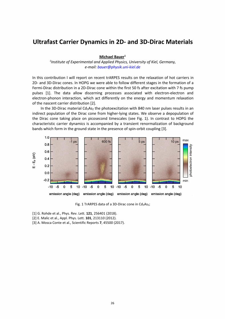
In the 3D-Dirac material Cd3As2 the photoexcitation with 840 nm laser pulses results in anindirect population of the Dirac cone from higher-lying states. We observe a depopulation ofthe Dirac cone taking place on picosecond timescales (see Fig. 1). In contrast to HOPG thecharacteristic carrier dynamics is accompanied by a transient renormalization of backgroundbands which form in the ground state in the presence of spin-orbit coupling [3].
Fig. 1 TrARPES data of a 3D-Dirac cone in Cd3As2;
[1] G. Rohde et al., Phys. Rev. Lett. 121, 256401 (2018).[2] E. Malic et al., Appl. Phys. Lett. 101, 213110 (2012).[3] A. Mosca Conte et al., Scientific Reports 7, 45500 (2017).
27
Plasmonics in atomically thin materials
Javier García de Abajo1,2
1ICFO-The Institute of Photonic Sciences, The Barcelona Institute of Science and Technology,08860 Castelldefels (Barcelona), Spain
2 ICREA-Institució Catalana de Reserca i Estudis Avançats, Passeig Lluís Companys 23, 08810Barcelona, Spain
e-mail: [email protected]
Two-dimensional polaritons have emerged as powerful tools to manipulate light at atomicscales in materials such as graphene, transition metal dichalcogenides, and atomically-thinmetal films. In this talk, we will review recent experimental advances in the fabrication andperformance of atomically-thin metallic films, as well as fundamental properties of theseexcitations, including their in/out-coupling to light and their potential for applications insensing, nonlinear optics, and quantum physics.

28
Second Harmonic Generation in a FullyCentro-Symmetric Plasmonic Nanocircuit
T.-Y. Chen1, J. Obermeier2, F.-C. Lin3, J.-S. Huang4, M. Lippitz2,*,and C.-B. Huang1,*
1Institute of Photonics Technologies, National Tsing Hua University, Hsinchu, Taiwan2Department of Physics, University of Bayreuth, Bayreuth, Germany
3Department of Chemistry, National Tsing Hua University, Hsinchu, Taiwan4Leibnitz Institute of Photonic Technology, Jena, Germany
e-mail: [email protected], [email protected]
In recent years, scientists have shown growing interest in surface plasma. Due to their distinctcharacteristics, surface plasma can demonstrate novel properties of the electromagneticwaves and thus provide the electric field enhancements with extremely high intensity. Inprevious works, it has been demonstrated that surface plasma can significantly enhance theoptical signal which is highly dependent on the intensity of the electric field, especially in thecase of nonlinear optical signals such as high order harmonic generations, Ramanspectroscopy and two-photon fluorescence. Second harmonic generation (SHG) is one of theimportant project among them. Recent research has shown that the SHG signal generate byusing surface plasma has many interesting features. However, almost all of the work onsurface plasma generated second harmonic signal are study with localize surface plasmon(LSP), which although has very strong localized electric fields, the efficiency will be limited bythe geometry of the structure due to the limitation of the SHG on symmetric environment.However, there has another type of surface plasma, which is called surface plasmon polariton(SPP). The primary aim of this paper is to analyze the effect of using SPP on a two-wiretransmission line, which is a plasmonic waveguide to generate SHG signal and demonstratedthat an optical mode of correct symmetry is sufficient to allow SHG even in centro-symmetricstructure made of centro-symmetric material.
Fig 1. Schematic representation of using SPP to generate SHG signal on a two-wire transmission-line byboth symmetric mode and anti-symmetric mode
29
Ultrafast electronic and magnetic dynamics intopological materials
Yihua WangFudan University
e-mail: [email protected]
Topological materials, for example topological insulators, Weyl semimetals and magneticWeyl semimetals, have exotic bulk and boundary electronic states that are promisingplatforms for future spintronics and quantum computation. These states exhibit uniquedynamics and even transform into new topological orders under femtosecond opticalexcitations. In this talk, I will present our recent work on probing the ultrafast electronic andmagnetic dynamics of topological insulators, Weyl semimetals and magnetic Weyl semimetalsusing time-and-angle resolved photoemission spectroscopy (Tr-ARPES) and time-resolvedmagneto-optical Kerr effect (Tr-MOKE). I will discuss the interesting behavior of theirelectronic and magnetic order that are only accessible through optical excitations.

30
Surface Dirac Fermion Dynamics of Non-magnetic andMagnetic Topological Insulators
Kazuki Sumida1,21Department of Physics, Tokyo Institute of Technology, Tokyo, Japan2Graduate School of Science, Hiroshima University, Hiroshima, Japan
e-mail: [email protected]
A three-dimensional (3D) topological insulator (TI) hosts spin-polarized massless Dirac statesalong its two-dimensional (2D) topological surface state (TSS) due to the topology of the bulkband structure. The Dirac-cone-like TSS exists as long as time-reversal symmetry is preservedand exhibits novel phenomena not found in conventional 2D metals. Thus, 3D TIs haveattracted much attention as key materials to revolutionize electronic, spintronic andoptoelectronic devices. Furthermore, magnetically doped TIs, possessing an energy gapcreated at the Dirac node through time-reversal symmetry breaking, are predicted to exhibitthe quantized anomalous Hall effect (QAHE). Although several candidates of magnetic TIswere demonstrated to show long-range magnetic order, the realization of the QAHE is so farrestricted to V- and Cr-doped (Sb,Bi)2Te3 systems at extremely low temperature [1,2]. It is,therefore, very important to understand the interaction between the host and the magneticdopants to raise the critical temperature of the QAHE. Nevertheless, the influence of themagnetic impurities to the TSSs remains unexplored.
Here, first, we investigate the ultrafast surface dynamics of bulk-carrier-tunable TIs(Sb1-xBix)2Te3 by using time- and angle-resolved photoemission spectroscopy (TARPES). OurTARPES studies have disclosed several functions, such as >400-ps prolonged duration,population inversion, and surface photovoltage effect, on the nonequilibrated surface of TIs[3,4].
The second part of my talk will be focused on magnetic TIs. We systematically investigatethe magnetic dopants induced modifications to electronic structures from the viewpoints ofmagnetic, structural and electronic properties and the ultrafast carrier dynamics in a series ofSb2-xVxTe3 (x = 0, 0.015, 0.03) by a combination of x-ray magnetic circular dichroism (XMCD),scanning tunneling microscopy/spectroscopy (STM/STS) and TARPES. The XMCD experimenthas revealed that the host Te 5p and Sb 5p electrons carry magnetic moments that mediatethe localized V 3d spins. Furthermore, the STM and its differential conductance spectroscopyresolved two independent V-induced impurities, which are energetically overlapped with theTSS. More importantly, when the doping amount of V was increased, the electronic recoverytime for the nonequilibrated state was drastically shortened to <500 fs. The observedshortened duration indicates an increased impurity scattering paths between the host and themagnetic dopants [5].
[1] C.-Z. Chang et al., Science 340, 167 (2013).[2] C.-Z. Chang et al., Nat. Mater. 14, 473 (2015).[3] K. Sumida et al., Sci. Rep. 7, 14080 (2017).[4] K. Sumida et al., Phys. Rev. B 99, 085302 (2019).[5] K. Sumida et al., submitted.
31
Ultrafast Optical Spectroscopy of IndividualNano-materials with Defined Atomic Structure
Kaihui LiuSchool of Physics, Peking University, Beijing 100871, China
email: [email protected]
When the characteristic length of a material shrink to 1 nm scale, many distinct physicalphenomena, such as quantum confinement, enhanced many-body interactions, strong vander Waals inter-material couplings and ultrafast charge separation, will appear. To investigatethe related fascinating low-dimensional physics, we need a tool to quantitatively link theatomic structures to the physical properties of these very small nano-materials. In this talk, Iwill introduce our recently developed in-situ TEM + high-sensitive ultrafast nanoopticstechnique, which combines capability of structural characterization in TEM and propertycharacterization in nanooptics on the same individual nano-materials. Several examples ofusing this technique to study the interlayer quantum coupling and ultrafast dynamics in 1Dcarbon nanotube system and 2D atomic layered systems will be demonstrated.
(1) Kaihui Liu, Enge Wang, Feng Wang* and et al., “Van der Waals-Coupled Electronic States inIncommensurate Double-walled Carbon Nanotubes”, Nature Physics 2014, 10, 737(2) Xu Zhou, Jingxin Cheng, Yubing Zhou, Shiwei Wu*, Hailin Peng*, Kaihui Liu* and et al., “StrongSecond-Harmonic Generation in Atomic Layered GaSe”, JACS 2015, 137, 7994.(3) Ziheng Ji, Chuanhong Jin*, Kebin Shi*, Sheng Meng, Kaihui Liu* and et al., "RobustStacking-Independent Ultrafast Charge Transfer in MoS2/WS2 Bilayers", ACS Nano 2017, 11, 12020(4) ing Liang, Zhipei Sun*, Sheng Meng*, Kaihui Liu* and et al. "Monitoring Local Strain Vector inAtomic-Layered MoSe2 by Second-Harmonic Generation", Nano Letters 2017, 17, 7539(5) Fengrui Yao, Kaihui Liu* and et al. "Measurement of complex optical susceptibility for individualcarbon nanotubes by elliptically polarized light excitation", Nature Communications 2018, 9, 3387(6) Hao Hong, Sheng Meng*, Hailin Peng*, and Kaihui Liu* and et al. "Ultrafast Broadband ChargeCollection from Clean Graphene/CH3NH3PbI3 Interface", JACS 2018, 140, 14952
32
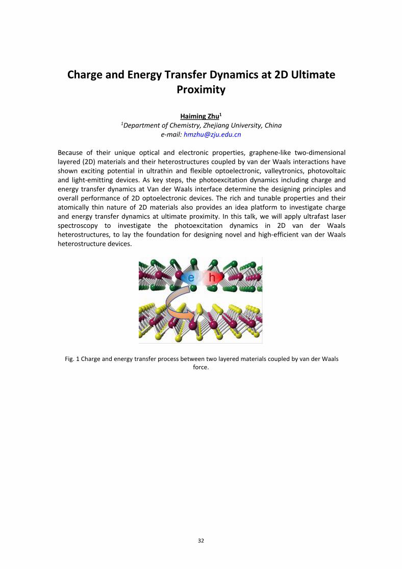
Charge and Energy Transfer Dynamics at 2D UltimateProximity
Haiming Zhu1
1Department of Chemistry, Zhejiang University, Chinae-mail: [email protected]
Because of their unique optical and electronic properties, graphene-like two-dimensionallayered (2D) materials and their heterostructures coupled by van der Waals interactions haveshown exciting potential in ultrathin and flexible optoelectronic, valleytronics, photovoltaicand light-emitting devices. As key steps, the photoexcitation dynamics including charge andenergy transfer dynamics at Van der Waals interface determine the designing principles andoverall performance of 2D optoelectronic devices. The rich and tunable properties and theiratomically thin nature of 2D materials also provides an idea platform to investigate chargeand energy transfer dynamics at ultimate proximity. In this talk, we will apply ultrafast laserspectroscopy to investigate the photoexcitation dynamics in 2D van der Waalsheterostructures, to lay the foundation for designing novel and high-efficient van der Waalsheterostructure devices.
Fig. 1 Charge and energy transfer process between two layered materials coupled by van der Waalsforce.

33
Magnetically-Sensitive Valley Polarization Reversal andRevival of Defect-Bound Excitons in WSe2-WS2
Heterostructure
Taishen Li1, Xuefeng Cui1, Nan Pan1,2, Xiaoping Wang1,21Hefei National Laboratory for Physical Sciences at the Microscale, University of Science and
Technology of China, China2Key Laboratory of Strongly-Coupled Quantum Matter Physics, Chinese Academy of Sciences,
School of Physical Sciences, University of Science and Technology of China, Chinae-mail: [email protected]
A tunable, large valley polarization with a long valley lifetime is necessary to variousvalleytronic applications of the transition metal dichalcogenides (TMDs). However, the valleylifetime of free exciton(s) in monolayer TMDs is limited to a few picoseconds, and the valleyproperties can hardly be modulated by a magnetic field with moderate intensities. Therefore,constructing advanced architectures which possess low-field- tunable higher valleypolarization and longer valley lifetime is exceptionally desirable. Very recently, it was foundthat certain defect-bound exciton could extend the valley lifetime to few microsecond inmonolayer WSe2, which is exciting to the community. However, it remains challenging to tunethe valley properties of defect-bound excitons. We find that the defect-bound interlayer (IXdef)and intralayer (Xdef) excitons in an AB- stacked WSe2-WS2 heterobilayer possess at least themicrosecond valley lifetimes, and exhibit unprecedented magnetically-tunable valleyproperties: The valley polarization of IXdef keeps reversed and can be surprisingly enhancedfrom -10% to -60% by a small out-of-plane magnetic field (<±0.4 T), showing an anomalousand exceptionally-sharp Λ-shape as a function of the field. In contrast, the valley polarizationof Xdef can revive after a fast decay and can be readily tuned under a moderate magnetic field(>±1 T), following the direction of the field and showing an X-shape. Our results demonstratethat the valley pseudospin of defect-bound excitons can be efficiently manipulated by a smallmagnetic field and the interlayer interactions, which will shed new light on both theunderstanding and the manipulating methods of the valley dynamics in TMDs and theirheterostructures.
Fig. 1 Magnetically-sensitive valley properties of defect-bound excitons in WSe2-WS2 heterobilayer.
34
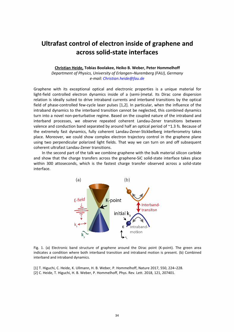
Ultrafast control of electron inside of graphene andacross solid-state interfaces
Christian Heide, Tobias Boolakee, Heiko B. Weber, Peter HommelhoffDepartment of Physics, University of Erlangen–Nuremberg (FAU), Germany
e-mail: [email protected]
Graphene with its exceptional optical and electronic properties is a unique material forlight-field controlled electron dynamics inside of a (semi-)metal. Its Dirac cone dispersionrelation is ideally suited to drive intraband currents and interband transitions by the opticalfield of phase-controlled few-cycle laser pulses [1,2]. In particular, when the influence of theintraband dynamics to the interband transition cannot be neglected, this combined dynamicsturn into a novel non-perturbative regime. Based on the coupled nature of the intraband andinterband processes, we observe repeated coherent Landau-Zener transitions betweenvalence and conduction band separated by around half an optical period of ~1.3 fs. Because ofthe extremely fast dynamics, fully coherent Landau-Zener-Stckbelberg interferometry takesplace. Moreover, we could show complex electron trajectory control in the graphene planeusing two perpendicular polarized light fields. That way we can turn on and off subsequentcoherent ultrafast Landau-Zener transitions.
In the second part of the talk we combine graphene with the bulk material silicon carbideand show that the charge transfers across the graphene-SiC solid-state interface takes placewithin 300 attoseconds, which is the fastest charge transfer observed across a solid-stateinterface.
Fig. 1. (a) Electronic band structure of graphene around the Dirac point (K-point). The green areaindicates a condition where both interband transition and intraband motion is present. (b) Combinedinterband and intraband dynamics.
[1] T. Higuchi, C. Heide, K. Ullmann, H. B. Weber, P. Hommelhoff, Nature 2017, 550, 224–228.[2] C. Heide, T. Higuchi, H. B. Weber, P. Hommelhoff, Phys. Rev. Lett. 2018, 121, 207401.

35
Final state effective mass affects attosecondphotoemission delays in BiTeCl
S. Neb1,2, A. Gebauer1,3, W. Enns1, N. Müller1, J.H. Dil4,5, E.V. Chulkov6,7,8,V. M. Silkin6,7,9, N.M. Kabachnik6,10,11, A.K. Kazansky6,7,9,P.M. Echenique6,7,12,
U. Heinzmann1, and W. Pfeiffer11Bielefeld University, 33615 Bielefeld, Germany
2Department of Physics, ETH Zurich, 8093 Zurich, Switzerland3Department of Physics and Research Center OPTIMAS, University of Kaiserslautern, 67663
Kaiserslautern, Germany4Paul-Scherrer-Institut (PSI), 5232 Villigen, Switzerland
5École Polytechnique Fédérale de Lausanne (EPFL), 1015 Lausanne, Switzerland6University of the Basque Country, 20080 San Sebastián, Spain
7Donostia International Physics Center (DIPC), 20018 San Sebastián, Spain8Tomsk State University, 634050 Tomsk, Russia
9IKERBASQUE, Basque Foundation for Science, 48013 Bilbao, Spain10Skobeltsyn Institute of Nuclear Physics, 119991 Moscow, Russia
11European XFEL GmbH, 22869 Schenefeld, Germany12Centro de Física de Materiales (CSIC-UPV/EHU), 20018 San Sebastián, Spain
e-mail: [email protected]
Attosecond time-resolved photoemission based on the photoelectron streaking in atime-correlated strong IR field allows investigating temporal delays in the photoemission fromdifferent initial states. Discrepancies between experimental observations and existingtheoretical models advance our understanding of mechanisms that determine thephotoemission kinematics and, for example, allowed recently the identification of anintra-atomic delay as significant contribution to the total photoemission delay [1].
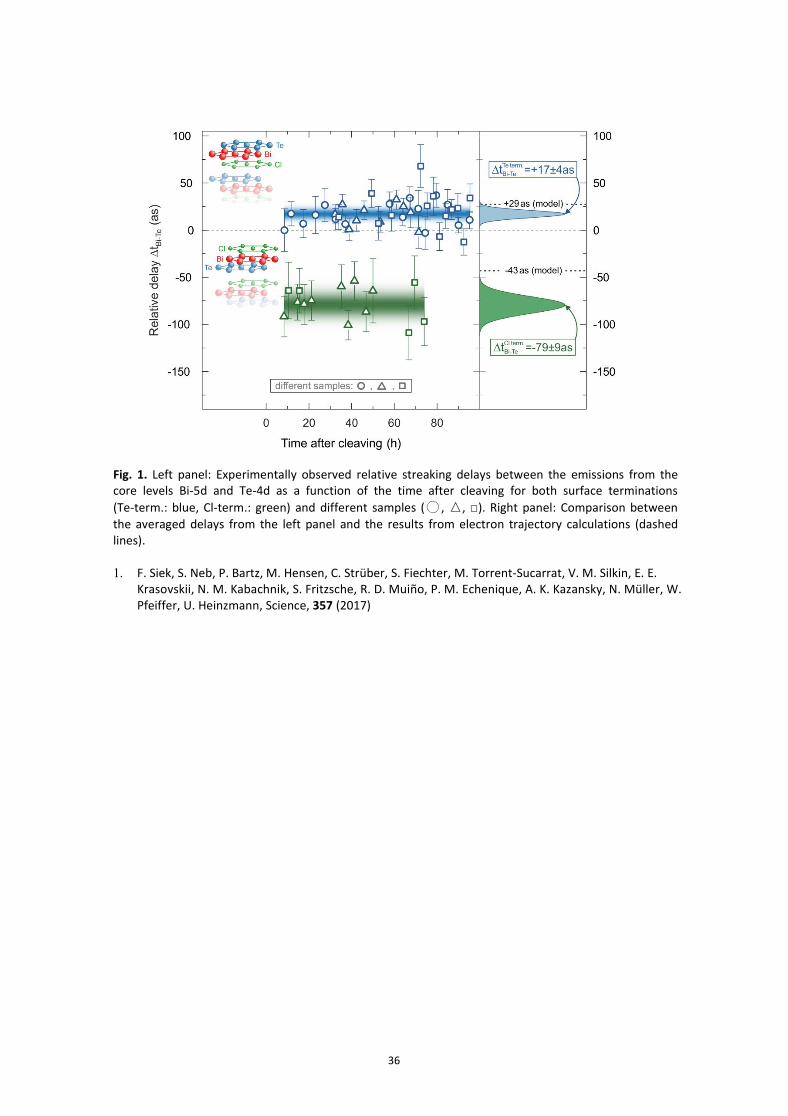
Here we report on attosecond time-resolved photoemission from the layered andnon-centrosymmetric crystal BiTeCl. The lack of inversion symmetry allows studying relativephotoemission delays for differently terminated but well-defined and inert surfaces withidentical bulk properties. Furthermore, the different layer stacking enables the experimentaldetermination of the inelastic mean free path (MFP). This reduces the ambiguities for electrontrajectory calculations performed to model the observed relative photoemission delays andthus allows drawing qualitative conclusions from the experimental results.
The comparison with results from classical and quantum mechanical electron trajectorycalculations results in a significant discrepancy for both terminated surfaces (Fig. 1). Themodeling includes the experimentally observed MFP (≈ 3.5 Å), the screened electron-holeinteraction using a Yukawa potential, intra-atomic corrections within theEisenbud-Wigner-Smith theory, and the dynamic atomic-scale screening of the IR-field forboth surface terminations. The discrepancy between model and experiment is robust againstthe variation of model parameters within reasonable limits. This indicates that the onlymissing contribution in the model, i.e. the effective electron mass in the final states, isresponsible for the observed discrepancies.
36
Fig. 1. Left panel: Experimentally observed relative streaking delays between the emissions from thecore levels Bi-5d and Te-4d as a function of the time after cleaving for both surface terminations(Te-term.: blue, Cl-term.: green) and different samples (〇 , △, □). Right panel: Comparison betweenthe averaged delays from the left panel and the results from electron trajectory calculations (dashedlines).
1. F. Siek, S. Neb, P. Bartz, M. Hensen, C. Strüber, S. Fiechter, M. Torrent-Sucarrat, V. M. Silkin, E. E.Krasovskii, N. M. Kabachnik, S. Fritzsche, R. D. Muiño, P. M. Echenique, A. K. Kazansky, N. Müller, W.Pfeiffer, U. Heinzmann, Science, 357 (2017)
37
Equivalence of RABBITT and Streaking Delays inAttosecond-Time-Resolved Photoemission Spectroscopy
at Solid Surfaces
A. Gebauer1,2, S. Neb1,3, W. Enns1, B. Stadtmüller2, M. Aeschlimann2, W. Pfeiffer11Faculty of Physics, Bielefeld University, 33615 Bielefeld, Germany
2Department of Physics and Research Center OPTIMAS, University of Kaiserslautern,67663 Kaiserslautern, Germany
3Department of Physics, ETH Zurich, 8093 Zurich, Switzerlande-mail: [email protected]
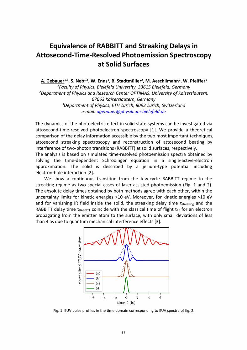
The dynamics of the photoelectric effect in solid-state systems can be investigated viaattosecond-time-resolved photoelectron spectroscopy [1]. We provide a theoreticalcomparison of the delay information accessible by the two most important techniques,attosecond streaking spectroscopy and reconstruction of attosecond beating byinterference of two-photon transitions (RABBITT) at solid surfaces, respectively.The analysis is based on simulated time-resolved photoemission spectra obtained bysolving the time-dependent Schrödinger equation in a single-active-electronapproximation. The solid is described by a jellium-type potential includingelectron-hole interaction [2].
We show a continuous transition from the few-cycle RABBITT regime to thestreaking regime as two special cases of laser-assisted photoemission (Fig. 1 and 2).The absolute delay times obtained by both methods agree with each other, within theuncertainty limits for kinetic energies >10 eV. Moreover, for kinetic energies >10 eVand for vanishing IR field inside the solid, the streaking delay time τstreaking and theRABBITT delay time τRABBITT coincide with the classical time of flight tPE for an electronpropagating from the emitter atom to the surface, with only small deviations of lessthan 4 as due to quantum mechanical interference effects [3].
Fig. 1: EUV pulse profiles in the time domain corresponding to EUV spectra of fig. 2.

38
Fig. 2: Simulated photoelectron spectrograms (color plots) corresponding to four different EUV spectra(black lines). Each corresponding EUV excitation pulse (train) is given by the Fourier transform of theEUV spectra (Fig. 1). All spectra were normalized individually. IR pulses were treated independentlywith center wavelength at 800 nm, 5 fs pulse duration and 1 V/nm electric field peak amplitude.
[1] A. Cavalieri et al., Nature 449, 1029 (2007)[2] A. K. Kazansky, P. M. Echenique, Phys. Rev. Lett. 102, 177401 (2009)[3] A. Gebauer et al., Appl. Sci. 9, 592 (2019)

39
Ultrafast carrier relaxation and Pauli drag effect inphotoexcited solids
Sheng MengInstitute of Physics, Chinese Academy of Sciences, Beijing, 100190, P. R. China
e-mail: [email protected]
Ultrafast light-matter interaction is a powerful tool for the study of solids. Upon laserexcitation, carrier multiplication and lattice acceleration beyond thermal velocity can occur, asa result of far-from-equilibrium carrier relaxation. The roles of electron-electron andelectron-phonon scatterings are identified by first-principles electron dynamic simulations,from which a unified phase diagram emerges (Fig. 1). It not only explains theexperimentally-observed “inertial” melting, but also predicts an abnormal damping by PauliExclusion Principle with a new perspective on ultrahigh-intensity laser applications.
Fig. 1 Schematic phase diagrams for ultrafast laser melting under (a,c) adiabatic potential energysurfaces (PES) and (b, d) dynamic PES, respectively.
40
Ab initio Nonadiabatic Molecular DynamicsInvestigations on the Excited Carriers in Condensed
Matter Systems
Qijing Zheng1, Weibin Chu1, Chuanyu Zhao1, Lili Zhang1, Hongli Guo1, 2, Yanan Wang1, XiangJiang1, and Jin Zhao∗1, 3, 4
1ICQD/Hefei National Laboratory for Physical Sciences at Microscale, and Key Laboratory ofStrongly-Coupled Quantum Matter Physics, Chinese Academy of Sciences, and Department of
Physics, University of Science and Technology of China, Hefei, Anhui 230026, China2School of Physics and Technology, Center for Nanoscience and Nanotechnology, and Key
Laboratory of Artificial Micro- and Nano-structures of Ministry of Education, Wuhan University,Wuhan 430072, China
3Department of Physics and Astronomy, University of Pittsburgh, Pittsburgh PA 15260, UnitedStates
4 Synergetic Innovation Center of Quantum Information & Quantum Physics, University ofScience and Technology of China, Hefei, Anhui 230026, China
e-mail: [email protected]
The ultrafast dynamics of photo-excited charge carriers in condensed matter systems play animportant role in optoelectronics and solar energy conversion. Yet it is challenging tounderstand such multi-dimensional dynamics at the atomic scale. Combining the real-timetime-dependent density functional theory (RT-TDDFT) with fewest-switches surface hoppingscheme, we develop time-dependent ab initio nonadiabatic molecular dynamics (NAMD) codeHefei-NAMD to simulate the excited carrier dynamics in condensed matter systems. Using thismethod, we have investigated the interfacial charge transfer dynamics, the electron-holerecombination dynamics and the excited spin-polarized hole dynamics in different condensedmatter systems. The time-dependent dynamics of excited carriers are studied in energy, realand momentum spaces. In addition, the coupling of the excited carriers with phonons, defectsand molecular adsorptions are investigated. The state-of-art NAMD studies provide uniqueinsights to understand the ultrafast dynamics of the excited carriers in different condensedmatter systems at the atomic scale.

41
Ultrafast Excited State Dynamics of SolidsProbed by Time-resolved ARPES
Martin WolfFritz Haber Institute of the Max Planck Society, Berlin, Germany
Email: [email protected]
Electronic excitations in solids may induce ultrafast dynamical processes at the atomic scale,including chemical surface reactions, coherent lattice excitations or ultrafast structural phasetransitions. These processes are accompanied by pronounced changes of the electronicstructure and occupation of electronic states. Recent advances in ultrafast spectroscopy allowdirect probing of the underlying fundamental steps and provide a mechanistic understandingof transfer of energy from the electronic system into nuclear motions.
In my talk, I will discuss recent advances to probe such transient changes by a 500 kHzHHG based laser source enabling excited state band mapping throughout the completeBrillouin zone by time-resolved photoemission spectroscopy (trARPES) [1]. Such trARPESexperiments provide detailed insights into excited states of black phosphorous, excitondynamics in quasi-2D transition metal dichalcogenides (TMDCs) and photo-induced phasetransitions in quasi-1D metal nanowires on In/Si(111). For the latter case we lay out a detailedreaction pathway including temporally separated transitions of electronic and atomicstructure and demonstrate that the excited state population dynamics of the transient bandstructure is described by a thermalized electron distribution function [2].
Acknowledgements: This work was performed in collaboration with C.W. Nicholson,M. Puppin, S. Dong, R. Xiang, S. Beaulieu, M. Dendzik, L. Rettig and R. Ernstorfer (FHI Berlin)and A. Lücke, W.G. Schmidt (University of Paderborn).
[1] M. Puppin et al., Rev. Sci. Instr. 90, 023104 (2019)[2] C.W. Nicholson et al., Science 362, 821 (2018) and arXiv:1812.11385
42
Anisotropic Optical Response of Black PhosphorusStudied by Multiphoton Photoemission Spectroscopy
Shijing Tan,1 Hongli Guo,2Min Feng,2 Limin Cao,2 Jin Zhao,1 and Hrvoje Petek3*1Hefei National Research Center for Physical Science at the Microscale, University of Science
and Technology of China, Hefei 230026, China2School of Physics and Technology, Wuhan University, Wuhan 430072, China
3Department of Physics and Astronomy and Pittsburgh Quantum Institute, University ofPittsburgh, Pittsburgh, Pennsylvania 15260, USA
e-mail: [email protected]
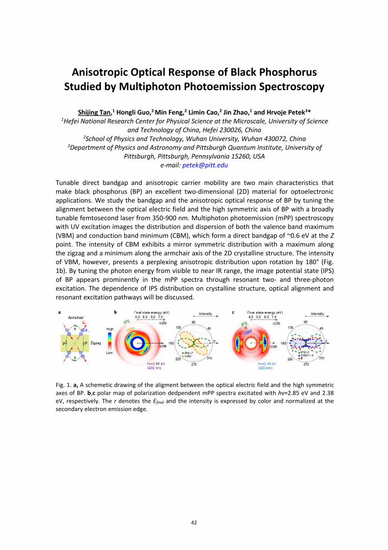
Tunable direct bandgap and anisotropic carrier mobility are two main characteristics thatmake black phosphorus (BP) an excellent two-dimensional (2D) material for optoelectronicapplications. We study the bandgap and the anisotropic optical response of BP by tuning thealignment between the optical electric field and the high symmetric axis of BP with a broadlytunable femtosecond laser from 350-900 nm. Multiphoton photoemission (mPP) spectroscopywith UV excitation images the distribution and dispersion of both the valence band maximum(VBM) and conduction band minimum (CBM), which form a direct bandgap of ~0.6 eV at the Zpoint. The intensity of CBM exhibits a mirror symmetric distribution with a maximum alongthe zigzag and a minimum along the armchair axis of the 2D crystalline structure. The intensityof VBM, however, presents a perplexing anisotropic distribution upon rotation by 180° (Fig.1b). By tuning the photon energy from visible to near IR range, the image potential state (IPS)of BP appears prominently in the mPP spectra through resonant two- and three-photonexcitation. The dependence of IPS distribution on crystalline structure, optical alignment andresonant excitation pathways will be discussed.
Fig. 1. a, A schemetic drawing of the aligment between the optical electric field and the high symmetricaxes of BP. b,c polar map of polarization dedpendent mPP spectra excitated with hv=2.85 eV and 2.38eV, respectively. The r denotes the Efinal and the intensity is expressed by color and normalized at thesecondary electron emission edge.

43
Excited-States Lifetime Control inEmerging Low-Dimensional Materials
Fengqiu WangNanjing University, 210023 China
e-mail: [email protected]
Low-dimensional materials enabled photonics and optoelectronics are rapidly becoming apreferred avenue for next-generation information devices, promising both significantperformance improvement and the potential for disruptive, novel-concept devices.Understanding the photocarrier dynamics, which is fundamentally linked to many of thefigures of merits of photonic devices, is the key to develop high-performance devices and alsoone of the most fundamental tasks of ‘light-matter interaction’ research.
While it is highly desirable to be able to customize the photocarrier dynamics to adapt tovarious device applications, approaches developed for conventional materials are not directlyapplicable and such a task remains a significant experimental challenge. In this talk, recentprogress in controlling the photocarrier lifetimes in three representative material classes(including graphene-like Dirac materials, Monolayer transition-metal dichalcogenides, as wellas 2D semiconductor heterostructures) will be presented. Photonic applications of theseemerging materials in ultrafast optical switches, high speed photodetectors will also betouched upon.
[1] Nature Communications 8, 14111 (2017)[2] Nature Communications 6, 8589 (2015)[3] Nature Nanotechnology 3, 738 (2008)[4] Nanoscale 8, 12883 (2016)[5] Nano Research 10, 1880 (2017)[6] 2D Materials 4, 035022 (2017)[7] Appl. Phys. Lett.112, 031108 (2018)[8] Appl. Phys. Lett. 112, 171112 (2018)[9] Appl. Phys. Lett. 113, 061104 (2018)[10] Appl. Phys. Lett. 111, 091101 (2017)

44
Ultrafast Carrier Dynamics in a Twisted BilayerGraphene Quasicrystal
T. Suzuki1, T. Iimori1, S. J. Ahn2, Z. Yuhao1, M. Watanabe1, J. Xu1, M. Fujisawa1,T. Kanai1, N. Ishii1, J. Itatani1, K. Suwa3, H. Fukidome3, S. Tanaka4, J. R. Ahn2,5,
K. Okazaki1, S. Shin1, F. Komori1, and I. Matsuda11The Institute for Solid State Physics, The University of Tokyo, Japan
2Department of Physics and SAINT, Sungkyunkwan University, Republic of Korea3Research Institute of Electronical Communication, Tohoku University, Japan
4Department of Applied Quantum Physics and Nuclear Engineering, Kyushu University, Japan5Samsung-SKKU Graphene Center, Sungkyunkwan University, Republic of Korea
e-mail: [email protected]
A twisted bilayer graphene has attracted broad attention owing to its exotic phases includingsuperconductivity and Mott insulating controlled by tuning the twisting angle [1].Furthermore, it has been demonstrated that a 2D quasicrystal was observed at twisting angleof 30 degrees, which offered new opportunities to investigate many properties characteristicto quasi-periodicities [2]. Here, we have studied non-equilibrium carrier dynamics in a twistedbilayer graphene quasicrystal by time- and angle-resolved photoemission spectroscopy(TARPES) using extreme ultraviolet (XUV) pulses obtained from high-harmonic generations(Fig. 1a). Figures 1b and 1e show the ARPES images for the upper- and lower-layer Dirac bandsin equilibrium, respectively. After infrared (IR) photo-excitation (800 nm, 0.7 mJ/cm2), bothbands exhibits immediate carrier transfer from occupied to unoccupied bands at the delaytime (Dt) of 0.05 ps (Figs. 1c and 1f), and excited carriers quickly relax to the original states atDt = 0.16 ps (Figs. 1d and 1g). In the presentation, I will show the further results withcomparing replica bands and a non-twisted bilayer graphene.
Fig. 1 a. Schematics of time- and angle-resolved photoemission spectroscopy (TARPES) for a twistedbilayer graphene quasicrystal. ARPES and difference TARPES images at the indicated delay times for theupper- (b-d) and lower-layer (e-g) Dirac bands.
[1] Y. Cao, et al., Nature 556, 43 (2018).[2] S. J. Ahn, et al., Science 361, 782 (2018).
45
Ultrafast Single-Molecule Electrical Detection
Xuefeng GuoCollege of Chemistry and Molecular Engineering, Peking University, Beijing 100871, China
e-mail : [email protected]
A universal lithographic methodology for creating single-molecule devices based on carbonnanomaterials as point contacts has been developed. In this talk, I will detail our rational assaytechniques by using bridge molecules with functional side groups capable of subsequentchemical/biocompatible assembly. We have tested this approach in chemical/biologicalsystems, including DNA hybridization, aptamer-protein interaction, photocyclization,host-guest interaction, hydrogen-bond interaction, nucleophilic substitution (SN1) andnucleophilic addition. Because it is constructed from a single molecule, each device canmonitor individual binding events in real time. This methodology demonstrates a connectionbetween electrical conduction and reaction dynamics that offers a glimpse into the future ofintegrated multifunctional sensors and devices.
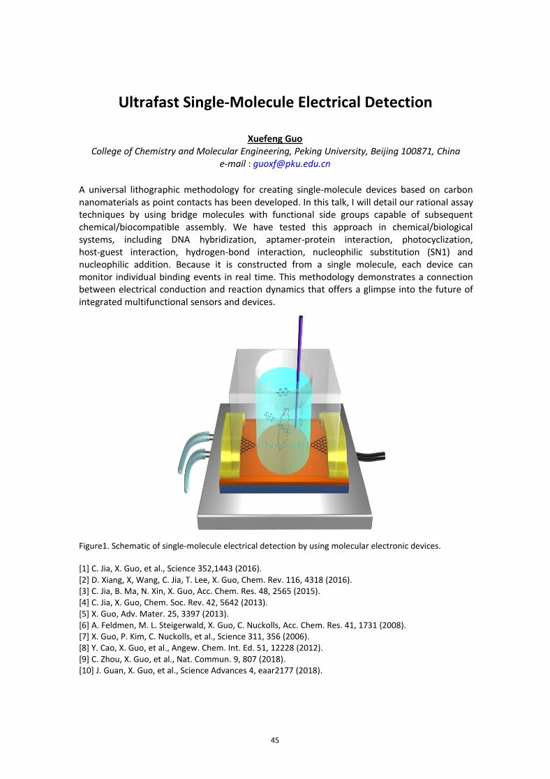
Figure1. Schematic of single-molecule electrical detection by using molecular electronic devices.
[1] C. Jia, X. Guo, et al., Science 352,1443 (2016).[2] D. Xiang, X, Wang, C. Jia, T. Lee, X. Guo, Chem. Rev. 116, 4318 (2016).[3] C. Jia, B. Ma, N. Xin, X. Guo, Acc. Chem. Res. 48, 2565 (2015).[4] C. Jia, X. Guo, Chem. Soc. Rev. 42, 5642 (2013).[5] X. Guo, Adv. Mater. 25, 3397 (2013).[6] A. Feldmen, M. L. Steigerwald, X. Guo, C. Nuckolls, Acc. Chem. Res. 41, 1731 (2008).[7] X. Guo, P. Kim, C. Nuckolls, et al., Science 311, 356 (2006).[8] Y. Cao, X. Guo, et al., Angew. Chem. Int. Ed. 51, 12228 (2012).[9] C. Zhou, X. Guo, et al., Nat. Commun. 9, 807 (2018).[10] J. Guan, X. Guo, et al., Science Advances 4, eaar2177 (2018).

46
Electron Dynamics on Cu2O(111) Probed withTime-Resolved Two-Photon Photoemission
Lisa Grad1, Adrian Schuler1, Zbynek Novotny2, Matthias Hengsberger1, Jrg Osterwalder11Department of Physics, University of Zurich, Switzerland
2 Paul-Scherrer Institute, Villigen, Switzerlande-mail: [email protected]
Photocatalytic water splitting represents a sustainable way to store solar energy in the form ofchemical bonds. For large-scale use, the combination of molecular catalysts supported onlight-absorbing substrates is a viable approach. One material often used in such devices iscuprous oxide.
Due to its small direct band gap [1] it is an efficient absorber for solar light. Furthermoreit is a p-type semiconductor with downward band bending towards the surface [2]. Therelated electric field leads to charge separation by accelerating photo-excited electronstowards the surface and holes into the bulk. Therefore the lifetime of free charge carriers isassumed to be long.
By means of time-resolved two-photon photoemission we have investigated theelectronic structure and the electron dynamics of cuprous oxide on the (111) surface. On thisparticular surface two different reconstructions can be observed, a (1x1) and a (√3x√3)R30.For the (1x1) structure two electronic states of the conduction band could be observed at theΓ-point in good agreement with DFT calculations [3]. The lifetimes of photo-excited electronsin these two states is very different. A fast relaxation into the conduction band minimum(CBM) due to intraband and interband scattering takes place followed by a slow depopulationof the CBM. Moreover, a defect state located in the band gap was observed.
For the (√3x√3)R30 surface reconstruction, which is driven by defects in the surface layer,the properties change drastically. It seems that the band gap is completely filled withelectronic states, probably with additional defect states. Therefore the electron dynamics iscompletely different in this case. Our current effort centres in understanding this change.

47
Fig. 1 Electronic structure of Cu2O(111) at the Γ-point dependent on the delay between excitation pulse(hν=3eV, p-polarized) and probe pulse (hν=6eV, p-polarized). Two conduction band states and a defectstate located in the band gap are observable with very different lifetimes.
[1] B. K. Meyer et al., Phys. Status Solidi B 249, No. 8, 14871509 (2012)[2] D. Leuenberger et al., Nano Lett. 17, 6620 (2017)[3] M. Heinemann et al., Phys. Rev. B 87, 115111 (2013)
48
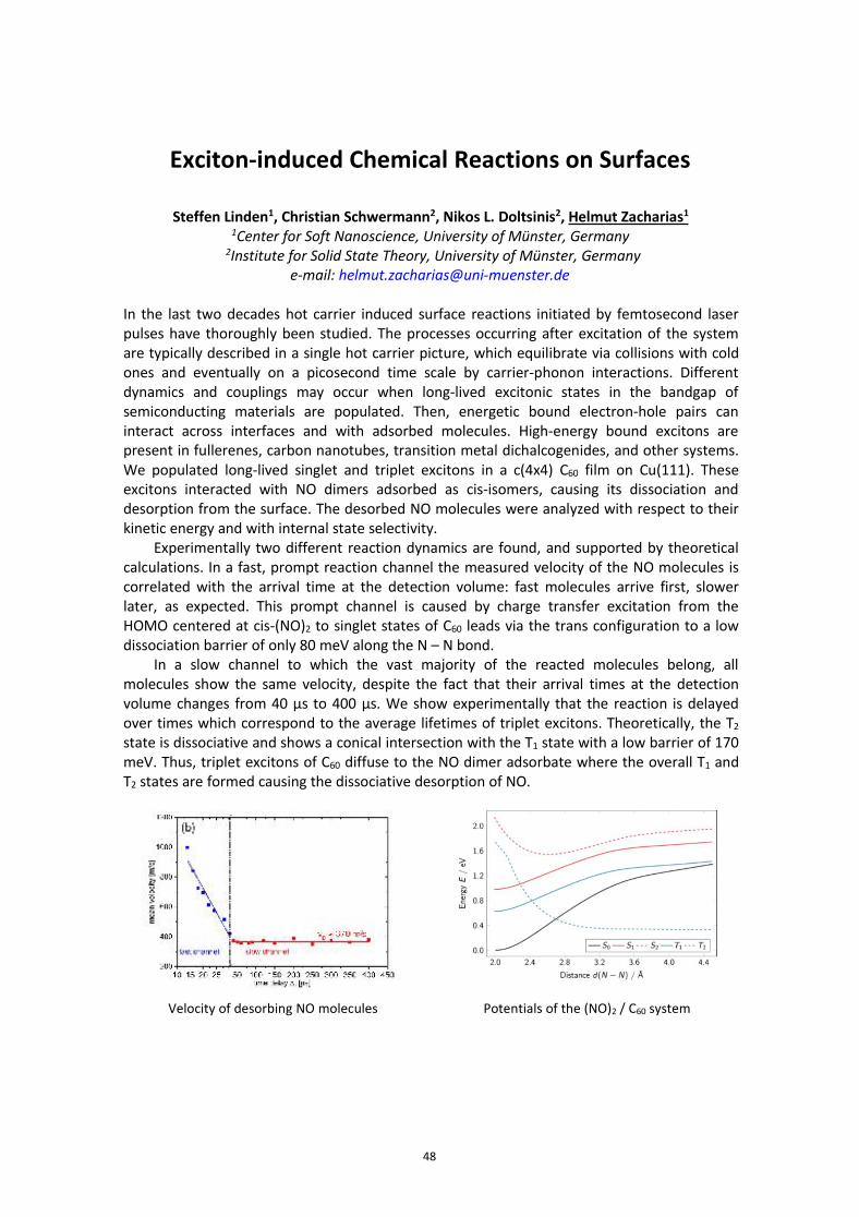
Exciton-induced Chemical Reactions on Surfaces
Steffen Linden1, Christian Schwermann2, Nikos L. Doltsinis2, Helmut Zacharias11Center for Soft Nanoscience, University of Münster, Germany
2Institute for Solid State Theory, University of Münster, Germanye-mail: [email protected]
In the last two decades hot carrier induced surface reactions initiated by femtosecond laserpulses have thoroughly been studied. The processes occurring after excitation of the systemare typically described in a single hot carrier picture, which equilibrate via collisions with coldones and eventually on a picosecond time scale by carrier-phonon interactions. Differentdynamics and couplings may occur when long-lived excitonic states in the bandgap ofsemiconducting materials are populated. Then, energetic bound electron-hole pairs caninteract across interfaces and with adsorbed molecules. High-energy bound excitons arepresent in fullerenes, carbon nanotubes, transition metal dichalcogenides, and other systems.We populated long-lived singlet and triplet excitons in a c(4x4) C60 film on Cu(111). Theseexcitons interacted with NO dimers adsorbed as cis-isomers, causing its dissociation anddesorption from the surface. The desorbed NO molecules were analyzed with respect to theirkinetic energy and with internal state selectivity.
Experimentally two different reaction dynamics are found, and supported by theoreticalcalculations. In a fast, prompt reaction channel the measured velocity of the NO molecules iscorrelated with the arrival time at the detection volume: fast molecules arrive first, slowerlater, as expected. This prompt channel is caused by charge transfer excitation from theHOMO centered at cis-(NO)2 to singlet states of C60 leads via the trans configuration to a lowdissociation barrier of only 80 meV along the N – N bond.
In a slow channel to which the vast majority of the reacted molecules belong, allmolecules show the same velocity, despite the fact that their arrival times at the detectionvolume changes from 40 µs to 400 µs. We show experimentally that the reaction is delayedover times which correspond to the average lifetimes of triplet excitons. Theoretically, the T2state is dissociative and shows a conical intersection with the T1 state with a low barrier of 170meV. Thus, triplet excitons of C60 diffuse to the NO dimer adsorbate where the overall T1 andT2 states are formed causing the dissociative desorption of NO.
Velocity of desorbing NO molecules Potentials of the (NO)2 / C60 system
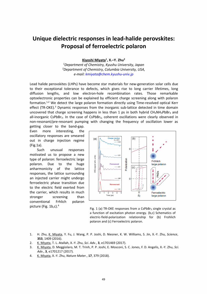
49
Unique dielectric responses in lead-halide perovskites:Proposal of ferroelectric polaron
Kiyoshi Miyata1, X.–Y. Zhu2
1Department of Chemistry, Kyushu University, Japan2Department of Chemistry, Columbia University, USA,
e-mail: [email protected]
Lead halide perovskites (LHPs) have become star materials for new-generation solar cells dueto their exceptional tolerance to defects, which gives rise to long carrier lifetimes, longdiffusion lengths, and low electron-hole recombination rates. Those remarkableoptoelectronic properties can be explained by efficient charge screening along with polaronformation.1,2 We detect the large polaron formation directly using Time-resolved optical Kerreffect (TR-OKE).3 Dynamic responses from the inorganic sub-lattice detected in time domainuncovered that charge screening happens in less than 1 ps in both hybrid CH3NH3PbBr3 andall-inorganic CsPbBr3. In the case of CsPbBr3, coherent oscillations were clearly observed innon-resonant/pre-resonant pumping with changing the frequency of oscillation lower asgetting closer to the band-gap.Even more interesting, theoscillatory responses are smearedout in charge injection regime(Fig.1a).
Such unusual responsesmotivated us to propose a newtype of polaron: ferroelectric largepolaron. Due to the hugeanharmonicity of the latticeresponses, the lattice surroundingan injected carrier might undergoferroelectric phase transition dueto the electric field exerted fromthe carrier, which results in muchstronger screening thanconventional Frhlich polaronpicture (Fig. 1b,c).4
1. H. Zhu, K. Miyata, Y. Fu, J. Wang, P. P. Joshi, D. Niesner, K. W. Williams, S. Jin, X.-Y. Zhu, Science,353, 1409 (2016).
2. K. Miyata, T. L. Atallah, X.-Y. Zhu, Sci. Adv., 3, e1701469 (2017).3. K. Miyata, D. Meggiolaro, M. T. Trinh, P. P. Joshi, E. Mosconi, S. C. Jones, F. D. Angelis, X.-Y. Zhu, Sci.
Adv., 3, e1701217 (2017).4. K. Miyata, X.-Y. Zhu, Nature Mater., 17, 379 (2018).
Fig. 1 (a) TR-OKE responses from a CsPbBr3 single crystal asa function of excitation photon energy. (b,c) Schematics ofelectric-field-polarization relationship for (b) Frohlichpolaron and (c) Ferroelectric polaron.
50
Dialing into dynamically disordered lattice potentials inCsPbBr3 via 2D coherent phonon spectroscopy
Sebastian F. Maehrlein1, Prakriti P. Joshi1, Dominik M. Juraschek2, Daniele Meggiolaro3,4,Kiyoshi Miyata1,5, Filippo De Angelis3,4, X.-Y. Zhu1
1Department of Chemistry, Columbia University, USA2Materials Theory, ETH Zürich, Switzerland
3Computational Laboratory for Hybrid/Organic Photovoltaics, National ResearchCouncil–Institute of Molecular Science and Technologies, Perugia, Italy.
4D3-CompuNet, Istituto Italiano di Tecnologia, Genova, Italy.5Department of Chemistry, Kyushu University, Japan
e-mail: [email protected]
Lead halide perovskites (LHPs) have emerged as new darlings of materials science with broadpotential for high performance solar cells and light emitting devices. The dynamicallydisordered and soft perovskite lattice is found to be a key component for their extraordinaryoptoelectronic properties1–5. The lattice potential is strongly anharmonic and fluctuatesspatially and temporally, leading to a multitude of exciting phenomena such as (dynamic)Rashba effect6–8, ferroelectricity9,10, large polarons11,12, and ferroelectric polarons2,13. Theunifying goal of these studies is finding the fundamental mechanism of charge carrierprotection in LHPs, but so far, specific electronic state coupled lattice potentials have eludedexperimental probes.
Here, we extend our time-resolved optical Kerr effect (TR-OKE) studies2 of theall-inorganic CsPbBr3 perovskite to two-dimensions (2D-OKE), which allows us to establishthe phonon response with high excitation energy resolution. We use this time-resolvedspectroscopy to investigate the coherent lattice response in the highly dilute chargeinjection regime, i.e. in the weak absorption tail below the electronic band gap. Additionaldiscrimination against incoherent signals leads to purely coherent phonon sensitivedetection of the charge induced polarization anisotropy.
We find a very effective displacive excitation of coherent phonons over a wide spectralrange. Surprisingly, we witness an extreme pump energy-dependent shift in phononfrequency compared to the equilibrium normal mode analysis through ab-initio calculations.These results unveil the energy-dependent mapping of strongly modified non-equilibriumlattice potentials, which are likely coupled to localized electronic states. Such phononresponse may form the basis for the design principle of defect tolerant semiconductors fromefficient dynamic screening.
1. Zhu, H. et al. Organic Cations Might Not Be Essential to the Remarkable Properties of Band EdgeCarriers in Lead Halide Perovskites. Adv. Mater. 29, 1603072–n/a (2017).
2. Miyata, K. & Zhu, X.-Y. Ferroelectric large polarons. Nature Materials 17, 379–381 (2018).3. Beecher, A. N. et al. Direct Observation of Dynamic Symmetry Breaking above Room
Temperature in Methylammonium Lead Iodide Perovskite. ACS Energy Lett. 1, 880–887 (2016).4. Katan, C., Mohite, A. D. & Even, J. Entropy in halide perovskites. Nature Materials 17, 377–379
(2018).5. Whalley, L. D., Frost, J. M., Jung, Y.-K. & Walsh, A. Perspective: Theory and simulation of hybrid
halide perovskites. J. Chem. Phys. 146, 220901 (2019).6. Etienne, T., Mosconi, E. & De Angelis, F. Dynamical Origin of the Rashba Effect in Organohalide
51
Lead Perovskites: A Key to Suppressed Carrier Recombination in Perovskite Solar Cells? J. Phys.Chem. Lett. 7, 1638–1645 (2016).
7. Niesner, D. et al. Giant Rashba Splitting in mathrmCH_3mathrmNH_3mathrmPbBr_3Organic-Inorganic Perovskite. PRL 117, 126401 (2016).
8. Wu, B. et al. Indirect tail states formation by thermal-induced polar fluctuations in halideperovskites. Nature Communications 10, 484 (2019).
9. Garten, L. M. et al. The existence and impact of persistent ferroelectric domains inMAPbI<sub>3</sub> Sci Adv 5, eaas9311 (2019).
10. Pecchia, A., Gentilini, D., Rossi, D., Maur, M. Auf der & Di Carlo, A. Role of FerroelectricNanodomains in the Transport Properties of Perovskite Solar Cells. Nano Lett. 16, 988–992(2016).
11. Miyata, K. et al. Large polarons in lead halide perovskites. Sci Adv 3, e1701217 (2017).12. Evans, T. J. S. et al. Competition Between Hot-Electron Cooling and Large Polaron Screening in
CsPbBr3 Perovskite Single Crystals. Journal of Physical Chemistry C(2018).doi:10.1021/acs.jpcc.8b00476
13. Joshi, P. P., Maehrlein, S. F. & Zhu, X. Dynamic Screening and Slow Cooling of Hot Carriers in LeadHalide Perovskites. Adv. Mater. 0, 1803054 (2019).

52
Charge Separation Dynamics at Lead Halide PerovskiteInterfaces Monitored by Differential Transient
Transmission Spectroscopy
Kunie Ishioka1*, Bobby G. Barker Jr.2, Masatoshi Yanagida3, Yasuhiro Shirai3and Kenjiro Miyano3
1RCAMC, National Institute for Materials Science, Japan2Department of Chemistry and Biochemistry, University of South Carolina, USA
3GREEN, National Institute for Materials Science, Japane-mail: [email protected]
Lead halide perovskite solar cells have been developing rapidly in the past few years, withtheir power conversion efficiency exceeding 22%. The perovskite solar cells typically consistof a perovskite film sandwiched between thin layers of electron- and hole-transport materials,which allow ultrafast separation of the charges photoexcited in the perovskite. Wesystematically investigate the charge separation dynamics at the interfaces of CH3NH3PbI3(MAPbI3) with three typical organic and inorganic hole transport materials (HTMs), PTAA,PEDOT:PSS and NiOx, by means of pump-probe transmission measurements [1]. Wephotoexcite only near the MAPbI3/HTM interface or near the back surface of the 250-nm thickperovskite film, and measure the differential transient transmission between thephotoexcitation on the two sides to extract the carrier dynamics directly related to the holeinjection (Fig. 1a). The differential transmission signals directly monitor the hole injectionfrom MAPbI3 to PTAA and PEDOT:PSS within 1 and 2 ps, respectively, whereas that to NiOx
comprises two steps and takes 40 ps to be completed (Fig. 1b). The obtained injectiondynamics are in contrast with the previous reports on the hole injection dynamics to PTAA andNiOx, whose time scales were sub-nanosecond and sub-picosecond, respectively. We discussthe hole injection dynamics in comparison with the device performance of the solar cellscontaining the same MAPbI3/HTM interfaces based on their current-voltage curves andquantum efficiencies.
Fig. 1. (a) Schematics of the two configurations in the transient transmission measurements. (b)Differential transient transmission signals of MAPbI3 with different HTMs.
[1] K. Ishioka, B. G. Barker Jr., M. Yanagida, Y. Shirai and K. Miyano, J. Phys. Chem. Lett. 8, 3902 (2017).

53
Coupled spin and lattice dynamics inlead halide perovskites
Daniel Niesner1, Janek Rieger1, Oskar Schuster1, Thomas Fauster11Department of Physics, Friedrich-Alexander-Universität Erlangen-Nürnberg, Erlangen,
Germanye-mail: [email protected]
Lead halide perovskites (LHPs) of the form APbHa3 (A = organic CH3NH3 or inorganic Cs; Ha =Br, I) exhibit long carrier lifetimes, despite being defect-rich direct-bandgap semiconductors,and high carrier mobilities despite their strongly ionic character. These properties make LHPsinto promising novel materials for applications in thin-film solar cells and optoelectronics. Thecomplex and unusual carrier dynamics in LHPs are supposedly related to the contained heavyelements and the associated strong spin-orbit coupling and low-frequency anharmonicphonon modes.
In spectroscopic [3] and transport [1] experiments using circularly polarized light, wedemonstrated the occurrence of spin-polarized optical transitions below the direct band gapin the prototypical organic-inorganic LHP (CH3NH3)PbI3. Namely, the spin-polarized states giverise to a temperature-dependent circular photogalvanic effect at sufficiently high sampletemperatures [1], i. e. above an order-disorder phase transition at 165 K. Our results imply alocal and dynamical Rashba effect [2]. The symmetry-breaking field causing the dynamicalRashba effect arises from structural fluctuations, while the average bulk inversion symmetry ispreserved.
To access the femtosecond spin and lattice dynamics at the surfaces of LHPs, epitaxialthin films are grown. We focus on purely inorganic CsPbHa3 as model systems, complementingearlier studies on organic-inorganic LHPs [3, 4]. Static angle-resolved photoelectronspectroscopy is used to investigate the surface band structure of the films. The results arecompared to the ones obtained from cleaved single crystals. Femtosecond dynamics areexplored using time-resolved two-photon photoemission.
Fig. 1 (a) Dynamical Rashba effect in the conduction band of a semiconductor with strong spin-orbitcoupling in the presence of thermal fluctuations [2]. (b) Experimental setup for identifying a circularphotogalvanic effect, (c, d) illustrate the mechanism behind the effect [1].
[1] D. Niesner et al., Proc. Natl. Acad. Sci. 115 (2018) 9509.[2] B. Monserrat and D. Vanderbilt, arXiv:1711.06274 (2017).[3] D. Niesner et al., Phys. Rev. Lett. 117 (2016) 126401.[4] D. Niesner et al., J. Am. Chem. Soc. 138 (2016) 15717.
54
Visualizing carrier transport in perovskites
Ti WangSchool of Physics and Technology, Wuhan University
e-mail: [email protected]
Slow cooling of hot polarons resulting from phonon bottleneck has been observed in hybridorganic-inorganic lead halide perovskites, pointing toward the potential for harvesting hotcarriers to overcome the Shockley-Queisser limit. Open questions remain on whether the highoptical phonon density from the bottleneck impedes the transport of these hot polarons. Here,we present a direct visualization of hot polaron transport in both single crystal nanoplate andpolycrystalline lead halide perovskites utilizing ultrafast transient absorption microscopy with300 femtosecond temporal resolution and 50 nanometer spatial precision. Remarkably, hotpolaron diffusion does not suffer from but rather is enhanced by the presence of phononbottleneck, opposite from what is observed in GaAs. Moreover, surface functionalizationwith phenethylammonium iodide increases the carrier diffusion coefficient of the near-surfacecarriers. We attribute the improved near-surface carrier diffusion to a more defect-tolerantcharacter of the PEAI-terminated surface. Our work represents a leap forward in theunderstanding of surface chemistry and the underlying carrier transport properties in hybridperovskites.

55
How to Dress a Metal
Hrvoje PetekDepartment of Physics & Astronomy, University of Pittsburgh, USA,
e-mail: [email protected]
We rely on metals to perform veracious reflection of light. But what if light changes theelectronic properties of a metal during the optical interaction? In fact, the electronicproperties of solid state materials are not indelibly defined by the space-periodic interactionpotentials of lattice ions as understood from the by Bloch theory, but can also be modifiedand manipulated by time-periodic potentials of strong optical fields, according to theFloquet-Bloch theory. Optical fields introduce a new degree-of-freedom to coherentlymanipulate, and turn-on transiently novel band properties of solids that do not exist undernear-equilibrium conditions. Here we apply the coherent multidimensional photoelectronspectroscopy1 to demonstrate the optical fields can manipulate the electronic structures ofeven the highest density optical materials, noble metals. We manipulate the surface bands ofCu(111) as a paradigm for how optical fields can tailor electronic band structures of solids. Theoptical field causes Autler-Townes splitting, deforming the surface electronic bands with aquasiparticle momentum-dependent resonance condition, such that modulating the effectiveband mass can transform electrons into holes on <10 fs time scale. More broadly, ourresearch shows the interaction of electrons in a metal with optical fields. This is particularlypoorly understood at epsilon near zero (ENZ) condition. We also examine the field-collectiveelectronic response at ENZ. This research was performed by Marcel Reutzel and Andi Li.
[1] M. Reutzel, A. Li, H. Petek, Coherent Two-Dimensional Multiphoton Photoelectron Spectroscopy ofMetal Surfaces. Phys. Rev. X 9, (2019) 011044.
56
Subcycle time-resolved ARPES of THz-driven Diraccurrents in a topological surface band
J. Reimann1, S. Schlauderer2, C. P. Schmid2, F. Langer2, S. Baierl2, K. A. Kokh3,O. E. Tereshchenko3, A. Kimura4, C. Lange2, J. Güdde1, R. Huber2, and U. Höfer1
1Department of Physics, Philipps-Universität Marburg, Germany2Department of Physics, University of Regensburg, Germany
3Russian Academy of Sciences, Novosibirsk, Russian Federation4Graduate School of Science, Hiroshima University, Japan
e-mail: [email protected]
Lightwave electronics builds upon the idea that the electric field of intense light pulses can beused to accelerate electrons at terahertz to petahertz clock rates. Yet, in conventionalsemiconductors and dielectrics the finite band mass and ultrafast scattering limit theelectron’s ballistic excursion and velocity. Recently, we have shown that the unique bandstructure of topological insulators lifts these constraints [1]. In the first subcycle time-resolvedARPES experiment, we observe how the carrier wave of a THz pulse accelerates Dirac fermionsin the topological surface state of Bi2Te3. While terahertz streaking of photo-emitted electronstraces the electromagnetic field at the surface, the acceleration of Dirac states leads to astrong redistribution of electrons in momentum space.
The experiments reveal that the electrons carrying the current react inertia-less on theaccelerating field and travel with the Fermi velocity of 4.1 Å/fs or 410 nm/ps. The resultingsurface currents reach peak densities as large as 2 A cm-1. Analysis with a semiclassicalBoltzmann model shows that the relevant electron scattering times amount to at least 1 ps.This unique transport dynamics opens a realistic parameter space for lightwave electronics.Due to the large Fermi velocity, the low scattering rates, and the linear band structure,lightwave-driven Dirac fermions in TSSs may ballistically propagate in dispersion-freewavepackets over distances as large as several 100 nm. This distance easily exceeds the gatewidth of latest electronic transistors by orders of magnitude. Owing to spin-momentumlocking, the ballistic Dirac currents also carry a spin current, which could enable spintronics upto optical clock rates.
As an experimental approach, we believe that our novel concept of subcycle THz-ARPESprovides the most direct way of studying carrier transport in non-trivial band structures withhigh time resolution. We will briefly discuss perspectives as well as experimental difficulties ofthe technique.
[1] J. Reimann, et al., “Subcycle observation of lightwave-driven Dirac currents in a topological surfaceband”, Nature 562, 396 (2018).
57
Spin mixing and spin-wave excitations in 3d and 4fferromagnetic metals
Martin WeineltFachbereich Physik, Freie Universität Berlin, Arnimallee 14, 14195 Berlin, Germany
e-mail: [email protected]
Today’s commonly accepted models of ultrafast magnetization dynamics are based onElliot-Yafet spin relaxation [1] and spin transport [2]. In addition, recent works give evidencethat magnons can drive ultrafast magnetization dynamics within 100 fs [3]. However, thenature of spin interactions and their dynamics in ferromagnetic metals is not well understoodand only few studies could capture the coupling strength of electron-magnon interaction,which turned out to be surprisingly weak (λ ~ 0.2) [4].
In this contribution we discuss various aspects of spin mixing and electron-magnoncoupling in the 3d and 4f ferromagnetic metals, Fe, Gd and Tb. We utilized spin- andangle-resolved photoelectron spectroscopy to study the transient electronic structure, thetemperature-dependent linewidths and the binding-energy renormalization of surface statesinteracting with magnons.
Ultrafast demagnetization in Gd depends on spin mixing of the valence bands. At lowtemperature and high spin polarization, we observe within the first 100 fs after 0.95 eVexcitation an increase of the 5d exchange splitting in the bulk but its decrease at the surface.This is explained by optically-induced spin transfer [5] between the localized surface anddelocalized bulk bands of Gd. For higher temperature spin mixing diminishes this ultrafast spintransfer consistent with an earlier onset of demagnetization. Comparing the subsequentmagnetization dynamics in Gd and Tb we find clear evidence that sub-ps demagnetization inTb is driven by coupling of 4f spins (S=3, L=3) to lattice excitations, i.e. spin-wave generation[6]. This channel of angular momentum transfer is missing in Gd (S=7/2, but L=0). In acomplementary spin-resolved photoemission study we investigated the magnetic phasetransition following the 5d surface-state linewidth [7]. Surprisingly, contributions ofelectron-phonon and electron- magnon scattering to the linewidth are comparable for Gd andTb.
For a thin iron film we studied the spin polarization and magnetic linear dichroism of arenormalized surface resonance. We find extraordinary strong electron-magnon coupling (λ ~4), which separates dressed and undressed dispersion branches and manifests as magneticdichroism rearranging the spectral weight between the two branches.
[1] B. Koopmans et al., Nat. Mater. 9, 259 (2010).[2] M. Battiato, K. Carva, and P. M. Oppeneer, Phys. Rev. Lett. 105, 1 (2010).[3] E. Carpene, H. Hedayat, F. Boschini, and C. Dallera, Phys. Rev. B 91, 174414 (2015); S. Eich et al.,
Science Advances 3 (2017); P. Tengdin et al., Science Advances 4, (2018).[4] J. Schäfer et al., Phys. Rev. Lett. 92, 097205 (2004).[5] Dewhurst et al., Nano Lett. 2018, 18, 1842−1848.[6] A. Melnikov, A. Povolotskiy, and U. Bovensiepen, Phys. Rev. Lett. 100, 247401 (2008).[7] Fedorov et al., Phys. Rev. B 65, 212409 (2002).

58
Spectroscopic investigation of Opto-spincurrent control
Ryuichi Arafune11International Center for Materials Nanoarchitectonics (MANA), National Instituite for
Materials Sciecne (NIMS), Japane-mail: [email protected]
Spincurrent plays one of the most substantial roles in spintronics. Both two classes ofspincurrent, pure- spincurrent and spin-polarized current, are important. The former is a non-equilibrium distribution where electrons with spin up propagate in one direction whereasthose with spin down propagate in the opposite direction and not accompanied by a netcharge transfer. The latter is the charge transfer with the co-oriented spins. By using angleresolved high resolution one- and two- photon photoemission spectroscopy[1,2,3], we haveinvestigated the opto-spin-current generated at surfaces via spin orbit interaction. In this talk,we have demonstrated that changing light polarization enable us to switch theopto-spin-current characteristics; opto-pure-spincurrent and spin-polarized photocurrent. Thesample is Ir(111) covered by graphene. The Rashba-type band splitting has been found in theimage potential states as well as the spin-split surface resonances in the occupied region. Theoptical direct transition between the spin-polarized states excited by the linear polarized lightresults in the opto-pure-spin-current, and the circularly polarized light excitation causes thespin-polarized photocurrent.
[1] T. Nakazawa et al., Surf. Int. Anal., 48, 1194-1198 (2016).[2] T. Nakazawa et al., Phys. Rev. B 94, 115412-115419 (2016).[3] R. Arafune et al., Prog. Surf. Sci., 93, 177 (2018).

59
Critical behaviors in 20 fs govern the non-equilibriumlaser-induced magnetic phase transition in Ni
Wenjing You1, Pheobe Tengdin1, Cong Chen1, Xun Shi1, Dmitriy Zusin1, Yingchao Zhang1,Christian Gentry1, Adam Blonsky1, Peter M. Oppeneer2, Henry C. Kapteyn1, Zhensheng Tao3,
Margaret M. Murnane11Department of Physics and JILA, University of Colorado and National Institute of
Standards and Technology (NIST), Boulder, CO 80309, USA2Department of Physics and Astronomy, Uppsala University,
Box 516, 75120 Uppsala, Sweden3 State Key Laboratory of Surface Physics and Department of Physics,
Fudan University, Shanghai, Chinae-mail:[email protected]
Manipulating material states with femtosecond laser illumination is a promising routine tocreate new states that are not accessible in equilibrium. To harness the power of possibility toengineer materials with light, it is key to understand how the energy transfers from photonsto different degrees of freedom and how the hierarchy of the energy transfer shapes thebehaviors of a material. In this talk, I will take the laser-induced ultrafast demagnetization inferromagnetic metals as an example and show how the laser illumination leads to the loss ofmagnetic order in femtoseconds [1,2]. Here, by combining time- and angle-resolvedphotoelectron spectroscopy and ultrafast magneto-optical spectroscopy, we showed that thelaser-induced ultrafast demagnetization in transition metal Ni is essentially of a phasetransition of the coupled electron and spin system. In our results, we not only explained thefluence-dependent time constants, but also revealed that the critical phenomena, occurring in~20 fs, play an important role in the phase transition, which includes the observation of thecritical fluence to induce the phase transition and the divergence of the heat capacity at thecritical point. To our knowledge, this is the first time such observations become available andset a new record for how fast the light and spin can be coupled in experiment. Surprisingly,our results indicate a strong connection between the non-equilibrium laser-induced dynamicsand the material properties under thermal equilibrium, implying potential universality of ourfindings. By comparing with the ultrafast magneto-optical spectroscopy, we found possiblecoexistence of the transient ferro- and paramagnetic states at the critical point of the phasetransition. This can be studied by the next-generation space-time-resolved spectroscopictechnique.

60
Fig. 1 a) Schematic of the critical behavior of ultrafast demagnetization in Ni. b) Peak electrontemperature extracted ~24 fs after excitation as a function of pump fluence, indicating a divergence ofthe heat capacity during the phase transition. c) Change of exchange splitting at 2 ps as a function oflaser fluence at different sample temperatures. The agreement of the critical fluence (Fc) in b) and c)indicates the connection of the electron dynamics to the magnetic properties of Ni.
[1] P. Tengdin, W. You, C. Chen, X. Shi, D. Zusin, Y. Zhang, C. Gentry, A. Blonsky, M. Keller, P. M.Oppeneer, H. Kapteyn, Z. Tao, and M. Murnane, Sci. Adv. 4, eaap9744 (2018).[2] W. You, P. Tengdin, C. Chen, X. Shi, D. Zusin, Y. Zhang, C. Gentry, A. Blonsky, M. Keller, P. M.Oppeneer, H. Kapteyn, Z. Tao, and M. Murnane, Phys. Rev. Lett. 121, 77204 (2018).

61
Coherent ultrafast spin transfer in ferromagnetic alloys
M. Hofherr1,2, S. H쳌user1, P. Tengdin3, S. Sakshath1, H. T. Nembach3,4, S. T. Weber1, J. M.Shaw4, T. J. Silva4, H. C. Kapteyn3, M. Cinchetti5, B. Rethfeld1, M. M. Murnane3, D.
Steil6, B. Stadtmüller1,2, S. Sharma7, M. Aeschlimann1,S. Mathias6,*
1University of Kaiserslautern und Research Center OPTIMAS, 67663 Kaiserslautern, Germany2Graduate School Materials Science in Mainz, 55128 Mainz, Germany
3 Department of Physics and JILA, University of Colorado and NIST, Boulder, CO 80309, USA4 Quantum Electromagnetics Division, NIST, Boulder, CO 80305, USA5 Experimentelle Physik VI, TU Dortmund, 44221 Dortmund, Germany
6 Georg-August-Universität G��ngen, I. Physikalisches Ins�tut, 37077 G��ngen, Germany7 Max-Born-Institute for Nonlinear Optics, Max-Born-Strasse 2A, 12489 Berlin, Germany
e-mail: [email protected]
The vision of using light to manipulate electronic and spin excitations in materials on theirfundamental time and length scales requires new approaches in experiment and theory, toobserve and understand these excitations. The ultimate speed limit for all-opticalmanipulation requires control schemes for which the electronic or magnetic sub-systems ofthe materials are directly manipulated on the timescale of the laser excitation pulse. In ourwork, we provide experimental evidence of such a direct, ultrafast and coherent spin transferbetween two magnetic subsystems of an alloy of Fe and Ni. Our experimental findings arefully supported by time dependent density functional theory simulations and, hence, suggeststhe possibility of coherently controlling spin dynamics on sub-femtosecond timescales.
Fig. 1. a) Schematic overview of theoptically-induced spin transfer (OISTR)experiment in FeNi. An EUV probe pulseinvestigates the element-specificmagnetization dynamics in FeNi triggered byan IR pump. b) Projected density of states(pDOS) calculation for FeNi for Fe (green) andNi (blue) demonstrating a favorable spintransfer from Ni to Fe in the minority channel.c) In the respective energy regions accordingto the calculations shown in b), the spindynamics show a clear fingerprint of OISTR,on ≈50 fs time scales. d) In contrast, otherspectral regions display only the conventionaldemagnetization.

62
POSTERCONTRIBUTIONS
63
Directional sub-femtosecond charge transfer dynamicsand the dimensionality of 1T-TaS2
D. Kühn1,2, M. Müller3,4, F. Sorgenfrei1,2, E. Giangrisostomi2, R. M. Jay,1 R. Ovsyannikov2, N.Mårtensson5, D. Sánchez-Portal3 & A. Föhlisch 1,2
1Ins�tut für Physik und Astronomie, Universität Potsdam, Germany.2Helmholtz-Zentrum Berlin für Materialien und Energie GmbH, Berlin, Germany.
3Centro de Física de Materiales CSIC-UPV/EHU and DIPC,Donostia – San Sebastián, Spain.
4CIC-nanoGUNE, Av. de Tolosa 76, E-20018, Donostia-San Sebastián, Spain. 5Uppsala-Berlinjoint Lab on Next Generation Electron Spectroscopy, Department of Physics and Astronomy,
Uppsala University, Sweden.e-mail: [email protected]
For the layered transition metal dichalcogenide 1T-TaS2, we establish through a uniqueexperimental approach and density functional theory, how ultrafast charge transfer in 1T-TaS2takes on isotropic three-dimensional character or anisotropic two-dimensional character,depending on the commensurability of the charge density wave phases of 1T-TaS2. [1] TheX-ray spectroscopic core-hole-clock method prepares selectively in- and out-of-planepolarized sulfur 3p orbital occupation with respect to the 1T-TaS2 planes and monitorssub-femtosecond wave packet delocalization. [2] Despite being a prototypicaltwo-dimensional material, isotropic three-dimensional charge transfer is found in thecommensurate charge density wave phase (CCDW), indicating strong coupling between layers.In contrast, anisotropic two-dimensional charge transfer occurs for the nearly commensuratephase (NCDW). In direct comparison, theory shows that interlayer interaction in the CCDWphase – not layer stacking variations – causes isotropic three-dimensional charge transfer. Thisis presumably a general mechanism for phase transitions and tailored properties ofdichalcogenides with charge density waves.
[1] Directional sub-femtosecond charge transfer dynamics and the dimensionality of 1T-TaS2, D. Kühn, M.Müller, F. Sorgenfrei, E. Giangrisostomi, R. M. Jay, R. Ovsyannikov, N. Mårtensson, D. Sánchez-Portal &A. Föhlisch, Scientific Reports, 9:488 (2019).[2] Direct observation of electron dynamics in the attosecond domain, A. Föhlisch, P. Feulner, F. Hennies,A. Fink, D. Menzel, D. Sanchez-Portal, P. M. Echenique & W. Wurth, Nature, 436:373–376 (2005).

64
The Coherent Response of Ag/Cu(111) Surfaces toOptical Excitation
Marcel Reutzel1, Andi Li1, Hrvoje Petek11Department of Physics and Astronomy, University of Pittsburgh, USA,
e-mail: [email protected]
Metal surfaces serve as nearly-perfect systems to study coherent light-matter interactions.Here, we apply the energy-resolved (ER) and interferometric time-resolved (ITR) multi-photonphotoemission (mPP) technique to study the coherent nonlinear dynamics of Ag/Cu(111)surfaces excited by optical fields in the perturbative regime. We focus on the Shockley surface(SS) state of Ag/Cu(111) as a benchmark for spectroscopy.
By measuring the non-resonant 3- and 4-photon photoemission of the SS state, as well asits replica structures in the above-threshold photoemission (ATP), we correlate coherentpolarizations and populations excited in the sample with final photoelectron distributions,where the interaction terminates. We also interpret the experimental results using an opticalBloch equation (OBE) model, which shows that the spectroscopic features of the 2Dphotoelectron spectra obeys a relation between the nonlinear orders of the coherentphotoemission processm and the induced coherence n.By measuring the resonant 4-photon photoemission between SS and image potential (IP)states, we observe the signature of optical dressing of surface band structures. By formingnew eigenstates that are defined by the optical resonance condition and the external fieldstrength, the AC Stark effect shifts the surface electronic band energies with quasiparticlemomentum-dependent resonance condition and time-dependent optical field strength: theoptical field distorts solid-state bands and can transform electrons into holes by modulatingthe effective band mass on <10 fs time scale.

65
Electronic structure and ultrafast dynamics ofα-Fe2O3 (012)
Angelika Demling1, Sarah B. King2, Julia Sthler11Department of Physical Chemistry, Fritz-Haber Institute of the Max Planck Society, Germany
2Department of Chemistry and James Franck Institute of The University of Chicago USAe-mail: [email protected]
α-Fe2O3 (or hematite) is the most stable iron oxide under standard conditions. Due to its vastabundance in earth’s crust it plays a key role in geochemistry and corrosion processes.Moreover, as it catalyzes the water splitting reaction and has a favorable band gap of roughly2.1 eV, it is considered as electrode material in photoelectrochemical cells. However, theprobability of the photocatalytic reaction relies on the energy level alignment betweenexcited states of hematite and water. In our study we investigate the (012) surface using staticand time-resolved two-photon photoelectron spectroscopy. We discuss surface photovoltageeffects and give first insights into electron dynamics of the clean hematite surface on anabsolut energy scale.

66
Dynamics of Excited Hole at Au/TiO2
Rutile(110) Interface
Aolei Wang, Qijing Zheng, Chuanyu Zhao, Jin Zhao*
Department of Physics, University of Science and Technology of China, Chinae-mail: [email protected]
Photoinduced hot carriers transfer between gold nanoparticles (NPs) and semiconductorunder plasmon excitation is an important phenomenon in photocatalysis. Electron-holerecombination velocity is the key factor of the photocatalytic device to drive redox reaction. Inthis study, we carried out nonadiabatic molecular dynamics calculations combined withreal-time time-dependent density functional theory to investigate the effects of the numberof Au atoms on hole transfer at Au/TiO2 rutile(100) interface. It was found that Au3 cluster wasmuch better than single Au atom and one Au chain in hole trapping ability and electron-holeseparation ability. This work provides insight into the rational design of plasmon-enhancedcatalysts.

67
Strong modification of the transport level alignment inmolecular thin films after optical excitation
B. Stadtmller1, S. Emmerich1,2, S. Hedwig1, D. Jungkenn1, N. Haag1, C. Schott1, M. Cinchetti3, S.Mathias4, M. Aeschlimann1
1 Department of Physics and Research Center OPTIMAS, University of Kaiserslautern,Erwin-Schrdinger-Str 46, 67663 Kaiserslautern, Germany
2 Graduate School of Excellence Materials Science in Mainz, Erwin Schroedinger Strae 46,67663 Kaiserslautern, Germany
3 Experimentelle Physik VI, Technische Universitt Dortmund, 44221 Dortmund, Germany4 Georg-August-Universitt Gttingen, I. Physikalisches Institut, Friedrich-Hund-Platz 1, D-37077
Gttingen, Germanye-mail: [email protected]
Organic photovoltaic devices operate by absorbing light and generating current. These twoprocesses are governed by the optical and transport properties of the organic semiconductor.Despite their common origin – the electronic band structure, their interplay between inorganic materials is far from being understood.
In this work, we present new insights into the transient evolution of the valence bandstates of fullerene complexes on Ag(111) after optical excitation. This is achieved by time- andmomentum- resolved photoemission (tr-ARPES) with a fs-XUV light source which allows us tosimultaneously follow the transient evolution of the excited and occupied band structure afterfs-optical excitation with visible light. Optical excitation of the fullerene C60 leads to transientchanges of the linewidth of all molecular valence states which can be directly linked to thecharacteristic timescales of the exciton decay in C60. Using model simulations, wedemonstrate that the transient broadening of all molecular levels is mediated by the dielectricscreening of the molecular film due to the formation of non-interacting excitons with differentlocal charge distributions, i.e. to excitons with charge transfer (CT) character. These transientmodifications of the energy level alignment are not limited to C60, but can also occur for otherendohedral fullerenes such as Sc3N@C80 and reveal characteristic changes for different sampletemperatures. In this way, our study shows that excitons of dominant CT character act ascharge defects in organic thin films that severely influence the transient energy positions ofthe transport levels of the entire molecular film.
Fig. 1. The left side shows aschematic sketch of theexperiment. A C60 multilayerfilm is optically excited by afs-light pulse and thetransient changes of the bandstructure are monitored bytr-ARPES. Typical tr-ARPESmaps of the transient bandstructure of a C60 film areshown on the right side.
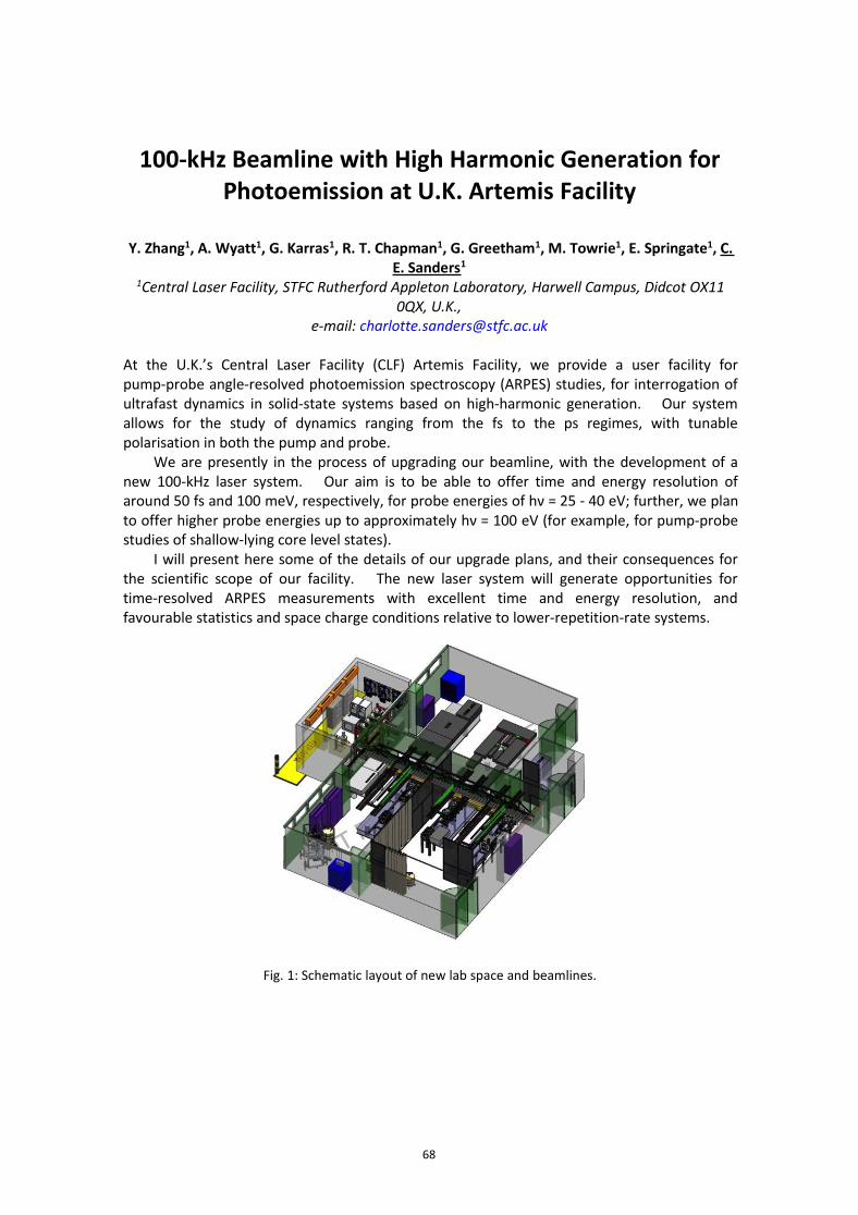
68
100-kHz Beamline with High Harmonic Generation forPhotoemission at U.K. Artemis Facility
Y. Zhang1, A. Wyatt1, G. Karras1, R. T. Chapman1, G. Greetham1, M. Towrie1, E. Springate1, C.E. Sanders1
1Central Laser Facility, STFC Rutherford Appleton Laboratory, Harwell Campus, Didcot OX110QX, U.K.,
e-mail: [email protected]
At the U.K.’s Central Laser Facility (CLF) Artemis Facility, we provide a user facility forpump-probe angle-resolved photoemission spectroscopy (ARPES) studies, for interrogation ofultrafast dynamics in solid-state systems based on high-harmonic generation. Our systemallows for the study of dynamics ranging from the fs to the ps regimes, with tunablepolarisation in both the pump and probe.
We are presently in the process of upgrading our beamline, with the development of anew 100-kHz laser system. Our aim is to be able to offer time and energy resolution ofaround 50 fs and 100 meV, respectively, for probe energies of hν = 25 - 40 eV; further, we planto offer higher probe energies up to approximately hν = 100 eV (for example, for pump-probestudies of shallow-lying core level states).
I will present here some of the details of our upgrade plans, and their consequences forthe scientific scope of our facility. The new laser system will generate opportunities fortime-resolved ARPES measurements with excellent time and energy resolution, andfavourable statistics and space charge conditions relative to lower-repetition-rate systems.
Fig. 1: Schematic layout of new lab space and beamlines.

69
Femtosecond EUV Beamline for Ultrafast MaterialsResearch and Development
Zhonghui Nie1, Ion Cristian Edmond Turcu1,2, Yao Li1, Xiaoqian Zhang1, Liang He1, Jian Tu1,Zhiqiang Ni1, Huangfeng Xu1, Yequan Chen1, Xuezhong Ruan1, Fabio Frassetto3, Paolo Miotti3,Nicola Fabris3, Luca Poletto3, Jing Wu4, Qiangsheng Lu5, Chang Liu5, Thorsten Kampen6, YaZhai7, Wenqing Liu8, Cephise Cacho9, Xuefeng Wang1, Fengqiu Wang1, Yi Shi1, Rong Zhang1
and Yongbing Xu1,10
1School of Electronic Science and Engineering, Nanjing University, Nanjing 210023, China2STFC Rutherford Appleton Laboratory, Central Laser Facility, Oxfordshire OX11 0QX, UK
3National Research Council Institute of Photonics and Nanotechnologies, 35131 Padova, Italy4Department of Physics, York University, York YO10 5DD, UK
5Shenzhen Institute for Quantum Science and Engineering, and Department of Physics,Southern University of Science and Technology, Shenzhen 518055, China
6Department of Solid State Physics, Technische Universität Berlin, 10623 Berlin, Germany7Department of Physics, Southeast University, Nanjing 210009, China
8Department of Electronic Engineering, Royal Holloway University of London, Egham TW200EX, UK
9Diamond Light Source Ltd., Harwell Campus, Oxfordshire OX11 0QX, UK10York-Nanjing Joint Center in Spintronics, Department of Electronic Engineering, The
University of York, York YO10 5DD, UKe-mail: [email protected]
A new femtosecond, Extreme Ultraviolet, time resolved Spin-ARPES beamline was developedfor ultrafast materials research and development. The 50fs laser-driven, table-top beamline isan integral part of the “Ultrafast Spintronic Materials Facility”, dedicated to engineering newultrafast materials. This facility will provide a fast in-situ analysis and development of newmaterials. The high harmonic generation EUV source emits a flux of 2.3x10¹¹ photons/second(2.3x108 photons/pulse) at H23 (35.7 eV). The photon energy ranges from 10 eV to 70 eVenabling surface sensitive studies of the electronic structure. Ultrafast surface photovoltaiceffect with ~650 fs rise-time was measured in p-GaAs (100) from time-resolved ARPES spectra.The data acquisition time could be reduced by over two orders of magnitude by scaling thelaser driver from 1kHz, 4W to 1 MHz, kW repetition rate and average power respectively.

70
Valley-polarized excitation in singly-oriented monolayerWS2/Au(111)
Gerald Rohde1, Hauke Beyer1, Antonija Grubišić-Čabo2, Ankatrin Stange1, LucaBignardi3, Daniel Lizzit3, Paolo Lacovig3, Silvano Lizzit3, Kai Rossnagel1, Philip
Hofmann2, and Michael Bauer11Institute of Experimental and Applied Physics, University of Kiel, Germany
2Department of Physics and Astronomy, Aarhus University, Denmark3Elettra Sincrotrone Trieste, Italye-mail: [email protected]
Time- and angle-resolved photoelectron spectroscopy (trARPES) is employed to studythe valley-selective excitation and near-surface dynamics of carriers in singly-orientedmonolayer WS2/Au(111). Upon photoexcitation with circularly polarized light (λ ≈590 nm), we observe a selective population of both valence and conduction band at Kand K′, respectively, cp. Fig. 1. The quantitative analysis of the data indicates a valleypolarization in the valence band of ≈ 90 % which is consistent with the fraction ofdomains with mirror orientation as determined in diffraction experiments [1]. On thecontrary, the valley polarization in the conduction band only reaches values of ≈ 70 %.We explain the difference in the polarization by the spin-orbit splitting of theconduction band being much smaller in comparison to the splitting of the valenceband and promoting intervalley scattering processes from K to K’. Different carrierdynamics of valence and conduction band population further hint to intervalleyscattering being of relevance for the depolarization of the conduction band.
Fig. 1: TrARPES data of WS2/Au(111) at the K point at Δt = 50 fs. (a) Difference intensity map generated
from trARPES datasets recorded at excitation with left (σ-) and right (σ+) circularly polarized light,respectively, as set by a quarter wave plate. (b) Conduction band (CB) and upper valence band (UVB)intensities as a function of the quarter wave plate angle.
[1] L. Bignardi et al., Phys. Rev. Mat. 3, 014003 (2019)
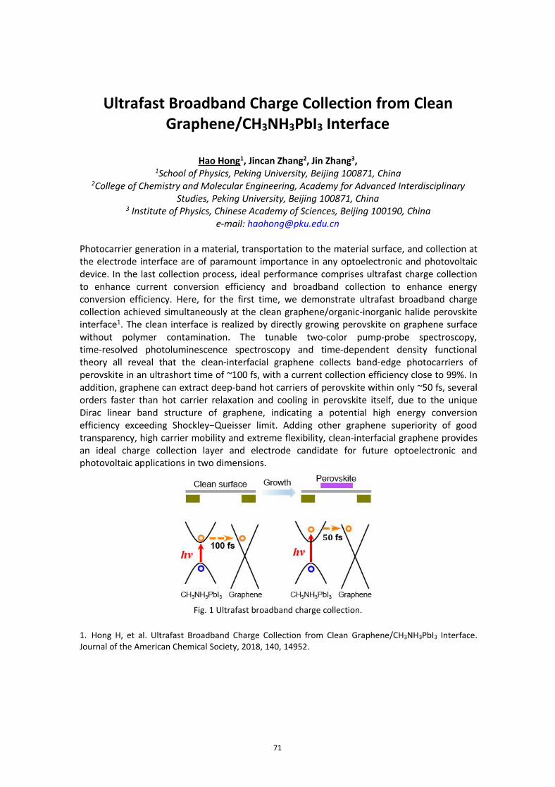
71
Ultrafast Broadband Charge Collection from CleanGraphene/CH3NH3PbI3 Interface
Hao Hong1, Jincan Zhang2, Jin Zhang3,1School of Physics, Peking University, Beijing 100871, China
2College of Chemistry and Molecular Engineering, Academy for Advanced InterdisciplinaryStudies, Peking University, Beijing 100871, China
3 Institute of Physics, Chinese Academy of Sciences, Beijing 100190, Chinae-mail: [email protected]
Photocarrier generation in a material, transportation to the material surface, and collection atthe electrode interface are of paramount importance in any optoelectronic and photovoltaicdevice. In the last collection process, ideal performance comprises ultrafast charge collectionto enhance current conversion efficiency and broadband collection to enhance energyconversion efficiency. Here, for the first time, we demonstrate ultrafast broadband chargecollection achieved simultaneously at the clean graphene/organic-inorganic halide perovskiteinterface1. The clean interface is realized by directly growing perovskite on graphene surfacewithout polymer contamination. The tunable two-color pump-probe spectroscopy,time-resolved photoluminescence spectroscopy and time-dependent density functionaltheory all reveal that the clean-interfacial graphene collects band-edge photocarriers ofperovskite in an ultrashort time of ~100 fs, with a current collection efficiency close to 99%. Inaddition, graphene can extract deep-band hot carriers of perovskite within only ~50 fs, severalorders faster than hot carrier relaxation and cooling in perovskite itself, due to the uniqueDirac linear band structure of graphene, indicating a potential high energy conversionefficiency exceeding Shockley−Queisser limit. Adding other graphene superiority of goodtransparency, high carrier mobility and extreme flexibility, clean-interfacial graphene providesan ideal charge collection layer and electrode candidate for future optoelectronic andphotovoltaic applications in two dimensions.
Fig. 1 Ultrafast broadband charge collection.
1. Hong H, et al. Ultrafast Broadband Charge Collection from Clean Graphene/CH3NH3PbI3 Interface.Journal of the American Chemical Society, 2018, 140, 14952.

72
Lattice Disorder-engineered Energy Splitting betweenBright and Dark Excitons in CsPbBr3 QuantumWires
Huaiyi Ding1,2, Mei Liu1, Nan Pan1,2,3, Yiyun Dong1, Yue Lin1, Taishen Li1,2, Jiangtao Zhao4,Zhenlin Luo4, Yi Luo1,2,3 and Xiaoping Wang1,2,3
1Hefei National Laboratory for Physical Sciences at the Microscale, University of Science andTechnology of China, Hefei, Anhui 230026, P. R. China
2Synergetic Innovation Center of Quantum Information & Quantum Physics, University ofScience and Technology of China, Hefei, Anhui 230026, P. R. China
3Key Laboratory of Strongly-Coupled Quantum Matter Physics, Chinese Academy of Sciences,School of Physical Sciences, University of Science and Technology of China, Hefei, Anhui
4National Synchrotron Radiation Laboratory and CAS Key Laboratory of Materials for EnergyConversion, University of Science and Technology of China, Hefei, Anhui, 230026, China.
e-mail: [email protected]
Excitons in nanostructured semiconductors often undergo strong electron-hole exchangeinteraction, resulting in bright-dark exciton splitting with the dark exciton usually being thelower energy state. This unfavorable state arrangement has become the major bottleneck forachieving high photoluminescence quantum yield (PLQY). However, the arrangement of darkand bright exciton states in lead halide perovskites is under intense debate due to theinvolvement of many complicated factors, We present here the first experimental evidence todemonstrate that the strain is a crucial factor in tuning the energy splitting of the bright anddark excitons, resulting in different PL properties.
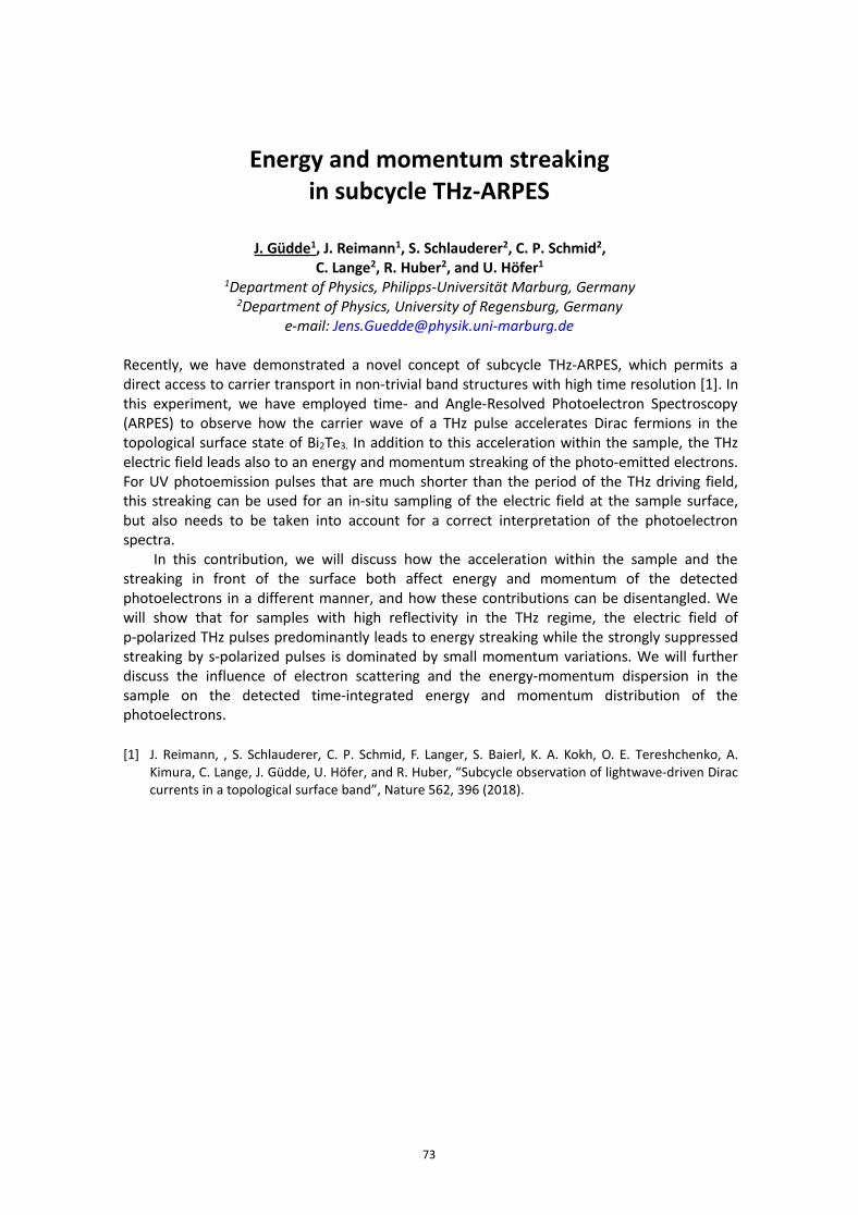
73
Energy and momentum streakingin subcycle THz-ARPES
J. Güdde1, J. Reimann1, S. Schlauderer2, C. P. Schmid2,C. Lange2, R. Huber2, and U. Höfer1
1Department of Physics, Philipps-Universität Marburg, Germany2Department of Physics, University of Regensburg, Germany
e-mail: [email protected]
Recently, we have demonstrated a novel concept of subcycle THz-ARPES, which permits adirect access to carrier transport in non-trivial band structures with high time resolution [1]. Inthis experiment, we have employed time- and Angle-Resolved Photoelectron Spectroscopy(ARPES) to observe how the carrier wave of a THz pulse accelerates Dirac fermions in thetopological surface state of Bi2Te3. In addition to this acceleration within the sample, the THzelectric field leads also to an energy and momentum streaking of the photo-emitted electrons.For UV photoemission pulses that are much shorter than the period of the THz driving field,this streaking can be used for an in-situ sampling of the electric field at the sample surface,but also needs to be taken into account for a correct interpretation of the photoelectronspectra.
In this contribution, we will discuss how the acceleration within the sample and thestreaking in front of the surface both affect energy and momentum of the detectedphotoelectrons in a different manner, and how these contributions can be disentangled. Wewill show that for samples with high reflectivity in the THz regime, the electric field ofp-polarized THz pulses predominantly leads to energy streaking while the strongly suppressedstreaking by s-polarized pulses is dominated by small momentum variations. We will furtherdiscuss the influence of electron scattering and the energy-momentum dispersion in thesample on the detected time-integrated energy and momentum distribution of thephotoelectrons.
[1] J. Reimann, , S. Schlauderer, C. P. Schmid, F. Langer, S. Baierl, K. A. Kokh, O. E. Tereshchenko, A.Kimura, C. Lange, J. Güdde, U. Höfer, and R. Huber, “Subcycle observation of lightwave-driven Diraccurrents in a topological surface band”, Nature 562, 396 (2018).

74
Anomalous photoluminescence enhancement inantimony telluride-molybdenum disulfide (Sb2Te3/MoS2)
heterostructure
Jianfei Li1,2, Huawei Liu3, Zhonghui Nie1,2, Yuhan Wang1,2, Anlian Pan3, Fengqiu Wang1,21School of Electronic Science and Engineering and Collaborative Innovation Center of Advanced
Microstructures, Nanjing University, Nanjing 210093, China2Key Laboratory of Intelligent Optical Sensing and Manipulation, Ministry of Education, Nanjing
University, Nanjing 210093, China3Key Laboratory for Micro-Nano Physics and Technology of Hunan Province, College of Materials
Science and Engineering, Hunan University, Changsha 410082, Chinae-mail: [email protected]
Antimony telluride (Sb2Te3) is known as a typical topological insulator (TI) with energy gap inbulk and gapless topological states at surface. Besides the novel TI-related properties, Sb2Te3also has van der Waals (vdW) layered structures, and its surface states can be relatively robustat interfaces between Sb2Te3 and other semiconductors. Molybdenum disulfide (MoS2), as amost widely studied vdW layered TMDs material in recent years, is an excellent candidate tocombine with Sb2Te3 to explore interfacial interaction between 2D material and TI and itspotential applications for optoelectronic devices.
In this study, we report the observation of an anomalous photoluminescence (PL)enhancement in CVD-grown heterostructures composed of multilayer Sb2Te3 and monolayerMoS2. Interestingly, the PL intensity of MoS2 excitons in the heterostructure area is enhanced(by 30-40%) compared with that of the bare monolayer MoS2 under the excitation of 532 nmlaser source. To identify the origin of this PL enhancement, PL spectra and transientdifferential reflection are measured under different temperatures. It is found that theenhanced MoS2 excitonic radiation in the heterostructures is contributed by the hotphotocarriers generated within the Sb2Te3 by optical excitation, which then transfer to theMoS2 layer facilitated by their excess energy. Our findings provide important complementaryinsights into the charge transfer processes in vdW heterostructures, especially under thesituation of non-resonant excitation.
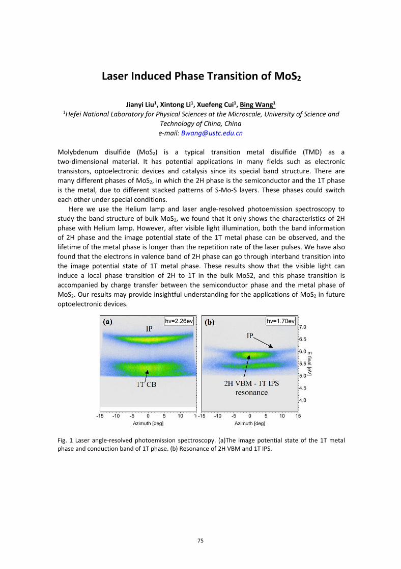
75
Laser Induced Phase Transition of MoS2
Jianyi Liu1, Xintong Li1, Xuefeng Cui1, Bing Wang11Hefei National Laboratory for Physical Sciences at the Microscale, University of Science and
Technology of China, Chinae-mail: [email protected]
Molybdenum disulfide (MoS2) is a typical transition metal disulfide (TMD) as atwo-dimensional material. It has potential applications in many fields such as electronictransistors, optoelectronic devices and catalysis since its special band structure. There aremany different phases of MoS2, in which the 2H phase is the semiconductor and the 1T phaseis the metal, due to different stacked patterns of S-Mo-S layers. These phases could switcheach other under special conditions.
Here we use the Helium lamp and laser angle-resolved photoemission spectroscopy tostudy the band structure of bulk MoS2, we found that it only shows the characteristics of 2Hphase with Helium lamp. However, after visible light illumination, both the band informationof 2H phase and the image potential state of the 1T metal phase can be observed, and thelifetime of the metal phase is longer than the repetition rate of the laser pulses. We have alsofound that the electrons in valence band of 2H phase can go through interband transition intothe image potential state of 1T metal phase. These results show that the visible light caninduce a local phase transition of 2H to 1T in the bulk MoS2, and this phase transition isaccompanied by charge transfer between the semiconductor phase and the metal phase ofMoS2. Our results may provide insightful understanding for the applications of MoS2 in futureoptoelectronic devices.
Fig. 1 Laser angle-resolved photoemission spectroscopy. (a)The image potential state of the 1T metalphase and conduction band of 1T phase. (b) Resonance of 2H VBM and 1T IPS.
76
Non-Adiabatic Molecular Dynamics ofSpin-Resolved Exciton
Xiang Jiang1,2, Jin Zhao1,2
1Hefei National Laboratory for Physical Sciences at the Microscale, University of Science andTechnology of China, Hefei, Anhui 230026, China
2Department of Physics, University of Science and Technology of China,Hefei, Anhui 230026, China
e-mail: [email protected] [email protected]
Quantum dynamics simulation is crucial but still a challenge especially in condensed matterphysics and other many-body systems. From the single particle (electron or hole) tomulti-particle (exciton, trion, etc.) dynamics, the calculation will show more accurate resultsand reveal more essential physics. Here we introduce a method to calculate the dynamics of aspin-resolved exciton, in which the spin of bound electron and hole could be involved. In ourapproach, the Bethe-Salpeter equation (BSE) describes the binding of an exciton[1] and thespin-orbit coupling gives the channel for the spin flip. On the other hand, based on J.C. Tully’sfewest switches surface hopping[2] (FSSH) and O.V. Prezhdo’s classical path approximation[3]
(CPA), an algorithm is developed to describe a (quasi-)particle’s movement. By considering theexcited state dynamics, the electron-phonon interaction, the excitonic effect and the spindegree of freedom, our approach gives us a powerful instrument to study plenty oftime-dependent problems, and it could provide us with a more comprehensive physicspicture.
[1] Rohlfing, M.; Louie, S. G., Physical Review B 2000, 62 (8), 4927-4944.[2] Tully, J. C., J. Chem. Phys. 1990, 93 (2), 1061-1071.[3] Akimov, A. V.; Prezhdo, O. V., J Chem Theory Comput 2013, 9 (11), 4959-72.
77
Suppression of Electron-Hole Recombination by IntrinsicDefects in 2D Mono-Element Material
Lili Zhang 1, Jin Zhao1
1Department of Physics, University of Science and Technology of China, Chinae-mail: [email protected]
Nonradiative electron-hole (e-h) recombination through the intrinsic defects in semiconductorhas been known as one of the elemental problems in the solar energy conversion. The simpleShockley-Read-Hall (SRH) model, in which the deep trap defect states in the band gap areproposed as nonradiative e-h recombination centers, has been widely used for decades. Inthis report, by using time-dependent DFT based ab initio nonadiabatic molecular dynamics(NAMD) method, we find that the SRH model fails to describe the e-h recombination behaviorfor defects in two-dimensional (2D) mono-elemental material such as monolayer blackphosphorous (BP). Through the investigation of three intrinsic defects with shallow and deepdefect states in monolayer BP, it is found surprisingly that none of these defects acceleratethe e-h recombination significantly despite of their distinct electronic structures. The deeptrap defect state can even suppress the e-h recombination. Further analysis shows thatbecause monolayer BP is a mono-elemental material, the distinct impurity phonon, whichoften induces fast e-h recombination, is not formed. Moreover, due to the flexibility of 2Dmaterial, the defects scatter the phonons present in pristine BP, generating multiple modeswith lower frequencies. Through electron-phonon coupling with these low-frequency phonons,the nonadiabatic coupling and the coherence time between the electronic states are reduced,which suppresses the e-h recombination. We propose that the conclusion can be extended toother mono-elemental 2D materials, which can be an important guidance for the futuredesign of functional semiconductors. In addition, the NAMD method, in which theelectron-phonon coupling is included at ab initio level, paves a new way to understand thenonradiative e-h recombination in semiconductors.
78
Time-resolved momentum microscopy with a 1 MHzhigh-harmonic generation lightsource
M. Keunecke, C. Nolte, D. Schmitt, M. Gutberlet, G. Halasi, D. Steil, S. Steil, S. MathiasGeorg-August-Universität G��ngen, I. Physikalisches Ins�tut, 37077 G��ngen, Germany
e-mail: [email protected]
Recent developments in laser technology and electron spectrometers allow for the build-up ofa new generation of time-resolved photoelectron emission experiments. With regard tolightsource development, coherent extreme-ultraviolet femtosecond pulses can todayroutinely be produced via high-harmonic generation (HHG) at repetition rates up to 1 MHz,which is essential in time-resolved photoemission spectroscopy/ microscopy to avoid spacecharge effects. In addition, new and highly-efficient electron spectrometers are available thatmap the full parallel momentum space of the electronic structure (ARPES), or can be used asphotoemission electron microscopes (PEEM) with several tenths of nanometers spatialresolution. On our poster, we will present first time-resolved measurements with such ahigh-repetition rate HHG photoemission setup. We will discuss detection efficiency, spacecharge effects and energy-, time-, momentum- and spatial resolution that can be achieved.
Fig. 1. Momentum maps recorded with the momentum microscope from an Au(111) crystal with a 1MHz HHG lightsource running at 26.6 eV.
79
Structural relaxation along with S1-T1 conversion incarbazol-benzonitrile derivatives
Masaki Saigo1, Kiyoshi Miyata1, Hajime Nakanotani2, Chihaya Adachi2,Ken Onda1
1Department of Chemistry, Faculty of science, Kyushu University, Japan2Center for Organic Photonics and Electronics Research (OPERA)
Japan Science and Technology Agency (JST), The Exploratory Research for AdvancedTechnology (ERATO), Kyushu University, Japane-mail: [email protected]
Thermally activated delayed fluorescence(TADF) molecules are gathering attentiondue to their potential to boost the efficiencyof organic light emitting devices withoutpresious metals.1 The key is to optimize thebalance between efficient emission andreverse intersystem crossing (RISC) whichconverts dark triplet excited states to brightsinglet excited states, but microscopicunderstanding of the process is limited.Here, we focus on fourcarbazol-benzonitrile derivatives thatpossess identical energy gap between S1and T1 but show distinct TADF activities.2We systematically studied the excited-statestructures of typical TADF molecules usingtime-resolved infrared vibrational (TR-IR)spectroscopy in conjunction with quantumchemical calculations.
Fig. 1 shows TR-IR spectra in the regionof 1250-1450 cm-1. TADF active moleculessuch as 4CzBN remains similar TR-IR spectraalong with intersystem crossing (Fig.1a),implying the similarity in the moleculargeometry between S1 and T1. In contrast,TADF inactive molecules such as p-3CzBN show significant changes in TR-IR spectra alongintersystem crossing (Fig.1b), suggesting drastic change in the geometry. This implies thatrestricting structural relaxation is important to keep the activation energy barrier for reverseintersystem crossing minimum to design efficient TADF molecules. The structural dynamics insolid environments will also be discussed.
[1] Uoyama, Adachi, et al., Nature, 492, 234-238 (2012). [2] Hosokai, Adachi, et al., Sci. Adv., 3,e1603282 (2017).
Fig. 1. Temporal evolutions of TR-IR spectra of (a)4CzBN and (b) p-3CzBN in THF solution afterphotoexcitation. (inset) Molecular structures ofeach molecule.
S1
T1
S1
T1

80
Spin Excitation and Magnetic Anisotropy of Mn Clusterson Graphene Moiré Patterns
Mengxi Liu1, Xin li,1,2 Xia Qiu,1,2 Xiaohui Qiu1,2
1 Chinese Academy of Sciences Key Laboratory of Standardization and Measurement forNanotechnology, Chinese Academy of Sciences Center for Excellence in Nanoscience, National
Center for Nanoscience and Technology, Beijing 100190, China2 University of Chinese Academy of Sciences, Beijing 100049, China
e-mail: [email protected]
The magnetic structures comprising few-atom clusters could be exploited as bits in ultrahighdensity data storage or spin-valves in nanoelectronics devices. Robust control andmanipulation of the magnetization dynamics of these nanoclusters is a vital issue becausetheir magnetic properties are highly susceptible to the environment. Here, we employ lowtemperature scanning tunneling microscopy and spectroscopy (STM/STS) to study the spinexcitation of Mn clusters formed on single-layer graphene grown on Ru(0001) surface. Thespatially resolved STS reveals spin states are highly confined within the nanoclusters. However,the site-dependent lineshapes and excitation energies indicate spin anisotropic distributionsthat might be modulated by the underlying graphene moiré patterns. Using noncontactatomic force microscopy (nc-AFM) and kelvin probe force microscopy (KPFM), we determinethe configuration of Mn clusters and their adsorbed sites, as well as charge transfer fromunderlying graphene. Furthermore, we find that the spin properties of these Mn clusters canbe markedly influenced by bonding with molecular ligands.
Fig. 1 a, STM image of a Mn cluster formed on graphene moiré patterns/Ru(0001), and a spin excitationspectroscopy acquired over the Mn cluster is shown in b.

81
Cooperative evolution of intraband and interbandexcitations for high harmonic generation in strained
MoS2
Meng-Xue Guan,1,2 Chao Lian,1 Shi-Qi Hu,1,2 Sheng-Jie Zhang1,2, Jin Zhang,1,2 and ShengMeng1,2,*
1 Beijing National Laboratory for Condensed Matter Physics and Institute of Physics, ChineseAcademy of Sciences, Beijing 100190, China
2 School of Physical Sciences, University of Chinese Academy of Sciences, Beijing 100190, Chinae-mail: [email protected]
Modulating electronic structure of two-dimensional (2D) materials represents an excitingavenue for tailoring their optoelectronic properties. Here, we identify a strain-induced,cooperative effect of intraband and interband excitations contributing to high harmonicgeneration (HHG) in prototype dichalcogenide MoS2 monolayer. We find that besides thedominant intraband contributions, interband current is also indispensable in modulating HHG.The HHG yields increase linearly with the compressive strain since flatter band dispersion andBerry curvature enhance both interband and intraband dynamics. Band structure can beretrieved with high reliability by monitoring the strain-induced evolution of HHG spectra,suggesting that strain not only provides an additional knob to control HHG in solids, but alsomarks a way towards a complete understanding of underlying microscopic mechanisms.
FIG. False color representation of the momentum space resolved distribution of the excited electronsunder different strain conditions.

82
Visualization of surface plasmon polaritons propagatingat dielectric/metal interfaces by 2P-PEEM
Masahiro Shibuta1,2,3, Kana Yamagiwa2, Atsushi Nakajima1,21 Keio Institute of Pure and Applied Sciences (KiPAS), Keio University, Japan
2 Department of Chemistry Faculty of Science and Technology, Keio University, Japan3 Fachbereich Physik und Zentrum fr Materialwissenschaften, Philipps-Universitt Marburg,
Germanye-mail: [email protected]
Visualization of surface plasmon polaritons (SPPs) propagating at dielectric/metalinterfaces is indispensable in opening up opportunities for a new photonics utilizingthe plasmonic phenomena. Two-photon photoelectron emission microscopy(2P-PEEM) is one powerful method to directly observe the SPP propagation inducedby a pump photon. With this model, a beating of surface polarization between SPPsand pump photon itself is probed as a lateral distribution of photoemission (Figure 1)[1].
Here, we demonstrate the visualization of SPPs propagating at the dielectric/metalinterfaces of fullerene (C60)/Au(111) and alkanethiolate self-assembled monolayers(SAMs)/Au(111), through a dual-color 2P-PEEM using near-infrared (NIR) pump andultraviolet (UV) probe photons.
In both systems, SPPs propagating in sub-mm scale are clearly imaged.Furthermore, the beating patterns quantitatively reflect the physical properties ofSPPs at the interfaces (e.g. SPP dispersion, phase and group velocities). In the case ofC60/Au(111), the SPP properties are modulated sensitively depending on the C60
coverage, where the analytical results nicely fit to a simple Drude model. On the otherhand, the SPP dispersion for SAM/Au(111) obviously deviates from the modelassuming simply n-alkane layers on Au(111). The results imply that a strong chemicalinteraction at the gold-sulfur interface largely affects the SPP properties [2]. Preciseevaluation of SPP properties for nanoscale functional films will be of high importancefor a fine control of future plasmonic nanodevices.
Figure 1. Schematic of SPP visualization at C60/Au(111) interface by dual-color 2P-PEEM.
[1] M. Shibuta, T. Eguchi, and A. Nakajima, Plasmonics 8, 1411 (2013).[2] K. Yamagiwa, M. Shibuta, and A. Nakajima, Phys. Chem. Chem. Phys. 19, 13455 (2017).

83
Quantum Dynamics of Photo-induced Water Splitting onGraphitic Carbon Nitride
Peiwei You1,3, Chao Lian1, Jiyu Xu1,3, Jin Zhang1,3, Xiaobing Chen1,3, Cui Zhang1* and ShengMeng1,2,3*
1Beijing National Laboratory for Condensed Matter Physics and Institute of Physics, ChineseAcademy of Sciences, Beijing 100190, China
2Collaborative Innovation Centre of QuantumMatter, Beijing 100184, China3University of Chinese Academy of Sciences, Beijing 100049, People’s Republic of China
e-mail: [email protected]; [email protected]
Hydrogen production from photocatalytic water splitting provides an ideal way to harvestsolar energy. One of the most promising photocatalyst is graphitic carbon nitride (g-C3N4)thanks to its outstanding thermal and chemical stability, low cost and nontoxic nature. Despitemany experimental studies, the microscopic quantum motion of photocatalysis remainselusive. Here we use newly-developed time-dependent density functional theory (TDDFT)molecular dynamics to explore the nonadiabatic process of photo-induced water splitting ongraphitic carbon nitride. Different from traditional scheme, hole transfer plays a key role inwater photosplitting, as described by a three-step model. First, the g-C3N4 is photoexcitedwith electron transfer from nitrogen to carbon atoms. Then, water is attracted to nitrogenatom with a hole transfer from g-C3N4 to water molecule, leading to a weaker O-H bond. Last,the O-H bond is activated and breaks with a proton transferred from water to g-C3N4. Thiswork presents a first real time quantum simulation of photo-induced water splitting by firstprinciples, which helps designing more effective photocatalysts.
Figure 1. The dynamics of the photocatalytic water splitting process on g-C3N4 upon photoexcitation

84
Laser induced demagnetization in two dimensionmaterial NiCl2
Sheng-jie Zhang,1,2 and Sheng Meng1,21 Beijing National Laboratory for Condensed Matter Physics and Institute of Physics, Chinese
Academy of Sciences, Beijing 100190, China2 School of Physical Sciences, University of Chinese Academy of Sciences, Beijing
100190, Chinae-mail: [email protected]
The overarching goal of the field of femtomagnetism is to control the magnetic structure ofmatter on a femtosecond time scale. The temporal limits to the light-magnetism interactionare governed by the fact that the electron spin interacts indirectly with light, with currentstudies showing a laser induced global loss in the magnetic moment on a time scale of theorder of a few 100 s of femtoseconds. In this work, we report ab initio simulations of thequantum dynamics of electronic charge and spins when subjected to intense laser pulses.Performing these purely electron-dynamics calculations for two dimension NiCl2 causes asignificant change in the moments on the order of 30 fs. We show that the underlying physicsof demagnetization for NiCl2 is dominated by a combination of the flow of spin-currents andspin-flips.
Fig. 1 Left: The shape of laser field. Right: Change of magnetic moment as a function of time.
(1) Huang, B. et al., Nature 546, 270–273 (2017)(2) H. Liu et al., J. Phys. Chem. Lett. 2018, 9, 6709−6715(3) P. Tengdin et al., Sci. Adv. 2018;4: eaap9744(4) W. You et al., Phys. Rev. Lett. 121, 077204 (2018)

85
Tracking energy transfer dynamicsin luminescent Eu3+ complex
Shiori Miyazaki1, Kiyoshi Miyata1, Yuichi Kitagawa2, Yasuchika Hasegawa2,Ken Onda1
1Department of Chemistry, Kyushu University, Japan2Faculty of Engineering, Hokkaido University, Japan
e-mail: [email protected]
Trivalent europium (Eu3+) complexes are attractivematerials for luminescence applications because of theirnarrow line-width emission due to the transitionbetween shielded 4f-4f transitions. To overcome a smallextinction coefficient (ε<10 M-1cm-1) of Eu3+ itself, theluminescent Eu3+ complex needs to contain organicligands with a large extinction coefficient. However,design strategiy for efficient energy transfer from theligands to the metal center is not yet established. Here,we have studied energy transfer dynamics inluminescent Eu(hfa)3(DPPTO)2 (Fig.1a) usingtime-resolved photoluminescence as a function ofsample temperature.
The complex was pumped at the - * transition ofthe ligands (267 nm). Time-resolved emission wasrecorded using either a streak camera or photomultipliertube coupled with a monochromator. The solid samplewas supported on a He cryostat to tune its temperaturein the range of 20-300 K.
Fig. 1b shows the emission spectra at different delaytime at room temperature. We observed three distinctemissions from Eu(hfa)3(DPPTO)2: (1) Broad emission in300-450 nm which decays in a few ns (fluorescence fromtriphenylene ligands), (2) Narrow emission at 586 nmdecaying in 1.5 s (4f-4f transition from the 5D1 state ofEu3+), and (3) Narrow emission bands at 595 and 620 nmthat shows rise in 1.5 s and decays in >100 s (4f-4ftransition from the 5D0 state). The rise and decay timescales correspond to the energy cascade from initiallyexcited ligands to Eu3+ metal center excited states (Fig.1c). Interestingly, the emission dynamics from the 5D1
state showed additional emission rising in 0.5 s at 20 K(Fig. 1d), which might indicate additional energy transferchannel activated at low temperature due to suppressionof non-radiative decay.
Fig.1. (a) Structure ofEu(hfa)3(DPPTO)2. (b) Emissionspectra at different delay times. (c)The energy diagram of theEu(hfa)3(DPPTO)2. (d) Temporalprofiles of emission from 5D1 state(580-590 nm) at 300 K (red) and at20 K (blue).

86
Enhanced two photon photoemission at the interface ofmetal phthalocyanines and HOPG
Shitan Wang1, Dongmei Niu1, Yongli Gao2
1Hunan Key Laboratory for Super-microstructure and Ultrafast Process, School of Physics andElectronics, Central South University, Changsha, Hunan, 410012, P. R. China
2Department of Physics and Astronomy, University of Rochester, Rochester, NY14627, USAe-mail: [email protected]
Metal phthalocyanines(MPcs) are widely used in organic semiconductor industry because oftheir outstanding photoelectric properties and thermal stability. We investigate theinteractions of MPcs and HOPG surfaces using photoemission spectroscopy (PES) andrelaxation process of the excited states with two-photon photoemission spectroscopy (2PPE).We observed greatly enhanced photoemission process at the interfaces of MPcs/inorganicsubstrates(HOPG, BP) compared to the pristine substrates and this enhancement is ascribedto the selection rules as well as the increased density of states introduced by MPcs which canbe excited by the ~400nm light. The lifetime of the excited states are measured to be around60 fs with time-resolved 2PPE. Our results provide valuable reference to the photoelectric andphotovoltaic research fields.
Fig. 1 (a) 2PPE spectra for 1 ML PbPc on BP as a function of delay time. (b) The enhanced 2PPE of PbPc/BP compared to the pristine BP. (c) The two-photon correlation signals for different energy levels.

87
Temperature Dependent Ultrafast Dynamics ofHeterogeneous Oadsorbed + Oadsorbed = O2,gas Reaction on
Single Crystal Pd(100) Surface
Sourav Banerjee1, and Atanu Bhattacharya*11Department of Inorganic and Physical Chemistry, Indian Institute of Science, India
e-mail: [email protected]
The interaction of atomic oxygen with transition-metal is of pivotal importance for a variety ofindustrially and environmentally relevant processes, including CO oxidation in automobileexhaust catalytic converters. As the recombination of two atoms forming a molecule, whichthen leaves the surface, represents one of the simplest surface chemical reactions, therecombinative desorption of molecular Oxygen from Pd single crystal surface attracted earlyattention of femtosecond surface chemistry community. Misewich and coworkers1 followedthe desorption of oxygen molecules from a molecular oxygen-covered Pd(111) surface. Thismolecular oxygen-covered Pd(111) surface can be prepared only at temperatures lower than200 K (for an example, Misewich’s work was performed at 140 K). At the low temperature(below 200 K), molecular oxygen can be molecularly adsorbed on the palladium surface. Attemperatures above 300 K, molecular oxygen completely dissociates to oxygen atoms on thepalladium surfaces, rendering atomic oxygen adlayer surface. So far, no recombinativedesorption of (O+O=O2) was observed from the experiments performed with adsorbed atomicoxygen on the Pd(111) surface and it was concluded by Heinz and coworkers thatfemtosecond laser excitation in the range of 2 to 5 mJ/cm2 does not initiate recombinativedesorption of oxygen.2 On the contrary, our work3 is the first report on femtosecondlaser-induced recombinative surface chemistry of adsorbed oxygen atoms on the Pd singlecrystal surface. The process of recombinative desorption of molecular oxygen (Oadsorbed +Oadsorbed = O2,gas) from Pd(100) single crystal surface, under femtosecond laser irradiation, hasbeen investigated with the help of pre- and post-radiation temperature programmeddesorption (TPD) measurements. This surface photochemistry is found to depend strongly oninitial surface temperature. 400 K temperature was found to be threshold temperature abovewhich this reaction is active for absorbed fluence of 2.86 mJ/cm2. The desorption-yield isfound to be linear with respect to the absorbed fluence. Furthermore, the dynamics for therecombinative O+O=O2 desorption has been explored with the help of two pulse correlationspectroscopy(2PC). The dynamics is found to be strongly dependent on the initial temperature,which leads to form different adsorbate coverage and surface structures.

88
Figure 1: Summary for femtosecond laser-induced recombinative O+O=O2 reaction on Pd(100) andtemperature dependent dynamics
1. Misewich, A. et al J. Chern. Phys., 1994, 100, 736.2. Heinz, T.F. et al Proc. SPIE, 1994, 276, 2125.3. Banerjee, S. et al J. Phys. Chem. C, 2018, 122, 26039.
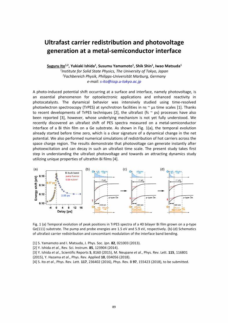
89
Ultrafast carrier redistribution and photovoltagegeneration at a metal-semiconductor interface
Suguru Ito1,2, Yukiaki Ishida1, Susumu Yamamoto1, Shik Shin1, Iwao Matsuda11Institute for Solid State Physics, The University of Tokyo, Japan2Fachbereich Physik, Philipps-Universität Marburg, Germany
e-mail: [email protected]
A photo-induced potential shift occurring at a surface and interface, namely photovoltage, isan essential phenomenon for optoelectronic applications and enhanced reactivity inphotocatalysts. The dynamical behavior was intensively studied using time-resolvedphotoelectron spectroscopy (TrPES) at synchrotron facilities in ns ~ μs time scales [1]. Thanksto recent developments of TrPES techniques [2], the ultrafast (fs ~ ps) processes have alsobeen reported [3], however, whose underlying mechanism is not yet fully understood. Werecently discovered an ultrafast shift of PES spectra measured on a metal-semiconductorinterface of a Bi thin film on a Ge substrate. As shown in Fig. 1(a), the temporal evolutionalready started before time zero, which is a clear signature of a dynamical change in the netpotential. We also performed numerical simulations of redistribution of hot carriers across thespace charge region. The results demonstrate that photovoltage can generate instantly afterphotoexcitation and can decay in such an ultrafast time scale. The present study takes firststep in understanding the ultrafast photovoltage and towards an attracting dynamics studyutilizing unique properties of ultrathin Bi films [4].
Fig. 1 (a) Temporal evolution of peak positions in TrPES spectra of a 40 bilayer Bi film grown on a p-typeGe(111) substrate. The pump and probe energies are 1.5 eV and 5.9 eV, respectively. (b)-(d) Schematicsof ultrafast carrier redistribution and concomitant modulation of the interface band bending.
[1] S. Yamamoto and I. Matsuda, J. Phys. Soc. Jpn. 82, 021003 (2013).[2] Y. Ishida et al., Rev. Sci. Instrum. 85, 123904 (2014).[3] Y. Ishida et al., Scientific Reports 5, 8160 (2015), M. Neupane et al., Phys. Rev. Lett. 115, 116801(2015), Y. Hazama et al., Phys. Rev. Applied 10, 034056 (2018).[4] S. Ito et al., Phys. Rev. Lett. 117, 236402 (2016), Phys. Rev. B 97, 155423 (2018), to be submitted.
90
Momentum dependent quasi-particle lifetime in metalsinvestigated by time-resolved momentum microscopy
Tobias Eul1, Eva S. Walther1, Eva Prinz1,2, Michael Hartelt1,Benjamin Frisch1, Martin Feidt1,Mirko Cinchetti3, Martin Aeschlimann1, Benjamin Stadtmller1,2
1Department of Physics and Research Center Optimas, University of Kaiserslautern, Germany2Graduate School MAINZ, 67663 Kaiserslautern, Germany
3Experimentelle Physik VI, TU Dortmund University, Germanye-mail: [email protected]
Electron dynamics in solid state systems and at interfaces play a crucial role for theperformance of nanoscale electronic and spintronic devices. Therefore, it is essential toinvestigate the electron dynamics and the corresponding energy and momentum dissipationmechanisms in prototypical materials used for such devices.
So far, most investigations focused on the inelastic lifetimes of hot electrons, which canbe directly obtained with time-resolved two-photon photoemission (tr-2PPE), using apump-probe setup. Here we will go beyond this conventional approach and investigate themomentum dependent lifetime of electrons and the corresponding (quasi-)elastic scatteringphenomena. This is achieved by combining the well-established tr-2PPE technique withmomentum spectroscopy in a ToF-PEEM operated in k-space mode. This enables us to analyzeauto- and cross-correlation traces for different intermediate state energies at each point ofthe accessible momentum space, which can be directly translated into momentum dependentlifetime map representations (see Fig1b).
As first model systems, we focused on bulk states of simple noble metal surfaces such asAg(110) and Ag(111) using different angles of incidence of laser light. Here we already observelifetime differences of several femtoseconds, which can be correlated to the occupied as wellas the unoccupied part of the band structure. Our first results already point to a complexmomentum dependent lifetime of electrons even for simple material systems.
Figure 1. a) Time of flight data obtained in our momentum microscope from illuminating a Ag(110)crystal under normal incidence with a photon energy of 3.1eV. b) By introducing a delay between twoidentical pulses, we perform cross-correlation measurements and can directly translate thephotoemission yield into electron lifetimes.
a) b)

91
New long-lived metastable state mediated bymode-selective electron-phonon coupling in 1T-TaSe2
Wenjing You1, Xun Shi1, Yingchao Zhang1, Zhensheng Tao1, Peter M. Oppeneer2, Xianxin Wu3,Ronny Thomale3, Kai Rossnagel4, Michael Bauer4, Henry Kapteyn1, Margaret Murnane11Department of Physics and JILA, University of Colorado and NIST, Boulder, CO 80309, USA
2Department of Physics and Astronomy, Uppsala University, Box 516, 75120 Uppsala, Sweden3Institut fur Theoretische Physik und Astrophysik, Julius-Maximilians-Universität Würzburg,
97074 Würzburg, Germany4Institute of Experimental and Applied Physics, Kiel University, D-24098 Kiel, Germany
e-mail: [email protected]
Quantum materials represent one of the most promising frontiers in the quest for faster,lightweight, energy efficient technologies. However, their inherent complexity and rich phaselandscape make them challenging to understand or manipulate in useful ways. Ultrafastexcitation with a strong laser pulse enables the controllability over strongly correlatedelectronic states through non-equilibrium pathway. Here we use time- and angle-resolvedphotoemission spectroscopy, combined with femtosecond lasers, to measure the dynamicelectron temperature, band structure and heat capacity of strongly correlated materials [1].We then show that this is a very sensitive probe of phase changes in materials, becauseelectrons react very quickly, and moreover generally are the smallest component of the totalheat capacity. This allows us to uncover a new long-lived metastable state in the chargedensity wave material 1T-TaSe2, that is distinct from all of the known equilibrium phases (Fig.1): it is characterized by a significantly reduced effective heat capacity that is only 30% of thenormal value, due to selective electron-phonon coupling to a subset of phonon modes. As aresult, significantly less energy is required to melt the charge order and transform the state ofthe material than under thermal equilibrium conditions. This metastable CDW phase, with acontinuously tunable order parameter depending on the laser fluence, is stable up tohundreds of picoseconds, thus markedly enriching the landscape of metastable orderedphases of TaSe2. Moreover, this charge ordered metastable phase can be verified bymeasuring the band structure and breathing mode to reveal its nature and microscopicinteractions [2]. The creation and optical manipulation of the long lived metastable phase withultrashort lasers pave the way for future studies to inform new theories, as well as to map thefull functional phase space of quantum materials for application.
92
Fig. 1 New long-lived metastable state mediated by mode-selective electron-phonon coupling. Theupper left panel shows the top view of the Ta plane in 1T-TaSe2. In the CDW state, displacement of theTa atoms leads to a √13×√13 superstructure consisting of 13-atom star-of-David clusters. After laserexcitation, the evolution of the sample is determined first by the electron temperature and then byelectron-phonon coupling, which depend on the fluence. For strong laser excitation, theelectron-phonon coupling switches from nearly homogeneous to mode-selective. The resultinginhomogeneity within the phonon bath drives the material into a new long-lived metastable CDW state.The blue shading represents the electron density in the real-space, the grey circles represent Ta atoms,both amplitudes are exaggerated for better visualization. Te, Tp and Tl refer to the temperatures of theelectron, strongly-coupled phonons, and the rest of the phonon bath, respectively
[1] X. Shi, W. You, Y. Zhang, Z. Tao, P. M. Oppeneer, X. Wu, R. Thomale, K. Rossnagel, M. Bauer, H.Kapteyn, M. Murnane, Science Advances 5, eaav4449 (2019).[2] In preparation.
93
Electron-phonon interactions in transient states afterultrafast excitation
Xinbao Liu,1,2 and Sheng Meng1,2,*1 Beijing National Laboratory for Condensed Matter Physics and Institute of Physics, Chinese
Academy of Sciences, Beijing 100190, China2 School of Physical Sciences, University of Chinese Academy of Sciences, Beijing 100190, China
e-mail: [email protected]
Electron-phonon interactions are ubiquitous in condensed matter physics and play animportant role in superconductivity, charge density waves in transition metal diselenides,relaxation of hot electrons, the carrier mobility in semiconductors. We investigate thelinewidth and electron phonon coupling in several 2D materials under different Fermi-Diracdistribution with density functional perturbation theory and Wannier interpolation method.Our results provide information about electron-phonon coupling of the relaxation process oftransient states after ultrafast excitation.

94
Oscillating kinetic energy of the photoemitted electronsin tr-PES
Xinwei Zheng1, Kamil Bobowski1, Dominic Lawrenz1, Robert Carley2, Beatrice Andres1,Cephise Cacho3, Richard Chapman3, Emma Springate3, Serguei Molodtsov2, and Martin
Weinelt11Freie Universität Berlin, Fachbereich Physik, Arnimalle 14, 14195 Berlin, Germany
2European XFEL GmbH, Holzkoppel 4, 22869 Schenefeld, Germany3Rutherford Appleton Laboratory, Didcot, OX11 0QX, UK
e-mail: [email protected]
We measured ultrafast time-resolved photoemission spectra on Gd (0001) and W (110) withan IR pump, XUV probe set up at the Artemis facility at CLF. We observed an oscillating kineticenergy of the photoemitted electrons before time zero. Such oscillations have been observedon the surface state of Gd by Bovensiepen et al. [1]. They described the oscillations with aponderomotive acceleration of the emitted photoelectrons in a transient grating formed bythe interference between the incident and reflected parts of the pump pulse. We performed afurther investigation on these oscillations by varying the wavelengths of the pump pulse andfound that the amplitude and the phase of the oscillations are pump wavelength-dependent.They show different behavior than predicted by the ponderomotive acceleration model. Bycomparing the amplitude of the oscillations on different bands, we discovered that theoscillating kinetic energy depends on the initial state of photoemission.
[1] Bovensiepen et al., Phys. Rev. B, 79, 045415 (2009)

95
Back-pump/front-probe non-linear photoemission onAu/Fe/MgO(001) thin films
Y. Beyazit1, J. Beckord1, J. Thomas1, P. Zhou1, D. Diesing2, M. Ligges1, U. Bovensiepen1
1Faculty of Physics, University Duisburg-Essen, Germany2Faculty of Chemistry, University Duisburg-Essen, Germany,
e-mail: [email protected]
The understanding of energy transport and relaxation dynamics of photo-excited electrons inmulti-layer thin films is of interest in the area of ultrafast hot-carrier dynamics. Femtosecondtime-resolved non-linear photoemission enables us to explore the difference between localand non-local relaxation processes. Here we report on first experiments employingback-pump/front-probe photoelectron spectroscopy on epitaxial Au/Fe/MgO(001) thin films,where Fe acts as an injection and Au as a propagation layer. In these experiments, weinvestigate the hot-electron transport and relaxation energy-resolved in the time domain (seeFig. 1). We demonstrate in our work the energy-resolved hot electron propagation in theballistic and superdiffusive regime. Up 30 fs hot electrons propagate ballistically, after 50 fswe identify scattered electrons and conclude a superdiffusive propagation. The extend ofscattering increases for larger Au film thickness and lower hot electron energy. Previoustheoretical works support our experimental observations by presenting the samecharacteristic transition from ballistic behaviour at short times to a (super)diffusive behaviourat longer delay times [1,2].
We acknowledge the funding of this work by the Deutsche Forschungsgemeinschaftthrough SFB 1242.
Fig. 1: Tr-2PPE intensity as a function of pump-probe delay for different intermediate stateenergies E - EF in Au/Fe/MgO(001) thin films with Fe-thickness dFe= 7 nm and Au-thicknessdAu= 30 nm.
[1]: D.M. Nenno et al. Particle-in-cell simulation of ultrafast hot-carrier transport in Fe/Auheterostructure, PRB 98, 224416 (2018)[2]: M. Battiato et al. Theory of laser-induced ultrafast superdiffusive spin transport in layeredheterostructures, PRB 86, 024404 (2012)
96
Photogenerated Carrier Dynamics at Anatase/RutileTiO2 Interface
Yanan Wang, Yongliang Shi, Chuanyu Zhao, Qijing Zheng* and Jin Zhao*
Department of Physics, University of Science and Technology of China, Chinae-mail: [email protected]
TiO2 is an intensively studied photocatalytic material owing to its low cost and high activity.The anatase/rutile (A/R) mixed-phase TiO2 is recognized as an effective strategy to achievehigh photocatalytic efficiency by the type-II band alignment favorable to spatial chargeseparation. However, the atomic structure, as well as the exact band alignment of the A/Rmixed-phase TiO2, is very difficult to identify either in experimental measurements ortheoretical simulations. Moreover, the time-dependent photogenerated carrier dynamics,which can determine the photocatalytic efficiency, has not been studied at the atomic scale.In this report, we use adaptive genetic algorithm to search the stable interface structures. Wefind that the band alignment is determined by the interfacial atomic structures. Especially,with oxygen vacancy (OV) at the interface, band alignment can be reversed as compared tothat of the stoichiometric interface. Then, we select one stoichiometric and one defectivestructure to study the photogenerated carrier dynamics using the time-dependent ab initiononadiabatic molecule dynamics. We find that in the stoichiometric system, for both theelectron and the hole, the charge transfer happens within 400 fs, which is much shorter thanthe electron-hole recombination timescale at ns to μs magnitude, which suggests that thecharge transfer can occur efficiently at the interface before they recombine. For the defectiveA/R system with OV, we find that the electron will be trapped by the defect state within 1 ps,while the hole dynamics is not affected. Our study provides atomic insights into theunderstanding of the band alignment and photogenerated carrier dynamics at the mixed A/RTiO2 interface, which provides valuable guidance for functional material design for solarenergy conversion.

97
Electrically driven single-photon superradiancefrom molecular chains in a plasmonic nanocavity
Yang Luo1, Gong Chen1,2, Yang Zhang1*, Li Zhang1, Yunjie Yu1, Fanfang Kong1, Xiaojun Tian1,Yao Zhang1, Chongxin Shan2, Yi Luo1, Jinlong Yang1, Vahid Sandoghdar3, Zhenchao Dong1*
and J. G. Hou1*
1Hefei National Laboratory for Physical Sciences at the Microscale, University of Science andTechnology of China, China.
2School of Physics and Engineering, Zhengzhou University, China3Max Planck Institute for the Science of Light, Germany
e-mail: [email protected]; [email protected]; [email protected].
When N two-level emitters undergo dipole-dipole coupling, new collective states areformed as a result of quantum superposition of product states with well-defined phases. Suchcoherent intermolecular dipole-dipole interactions can lead to various phenomena such ascoherent energy transfer, photosynthesis, and new quantum engineered systems [1,2]. One ofthe interesting features of quantum coherent collective states is single-photon superradiance(SPS), namely the generation of a singly excited collective state through symmetric quantumsuperposition of all possible states [3,4]. However, quantitative studies of SPS in molecularsystems confront challenges concerning the precise control and characterization ofintermolecular dipole-dipole coupling, including the number of coupled monomers (N),intermolecular distances, dipole arrangements and orientations as well as their phaserelations. Furthermore, it would be highly desirable to have optical access to each individualconstituent of a molecular system such as a chain.
By exploiting scanning tunneling microscope induced luminescence technique [5], herewe demonstrate electrically driven SPS from artificially constructed molecular chains of up to12 molecules. Sub-nanometer resolved spectroscopic imaging for molecular chains reveals thelocal optical response of superradiant states and the associated quantum coherence nature.Second-order photon correlation measurements for these superradiant peaks show evidentphoton antibunching effects with single-photon purities g(2)(0)<0.5, indicating the occurrenceof SPS and the formation of single-exciton superradiant state. The combination of spatiallyresolved spectral measurements with theoretical considerations reveals that nanocavityplasmons dramatically modify the linewidth and intensity of emission from the molecularchains, but they do not dictate the intrinsic coherence of the superradiant states. Our resultsopen up new routes to study energy transfer and quantum many-body physics at individualmolecule level.
[1] Scholes, G. D. et al., Nature, 2017, 543, 647[2] Hestand, N. J. and Spano, F. C., Chem. Rev., 2018, 118, 7069.[3] Dicke, R. H. , Phys. Rev., 1954, 93, 99.[4] Scully, M. O. and Svidzinsky, A. A. Science, 2009, 325, 1510.[5] Kuhnke, K., Große, C., Merino, P. and Kern, K., Chem. Rev., 2017, 117, 5174

98
Ultrafast photoinduced phase transition of MoTe2
Yuhan Wang1,2, Zhonghui Nie1,2, , Ziling Li3, Jianfei Li1,2, Kaleem Ullah1,2, Yu Ye3, FengqiuWang1,2
1School of Electronic Science and Engineering and Collaborative Innovation Center ofAdvanced Microstructures, Nanjing University, Nanjing 210093, China
2Key Laboratory of Intelligent Optical Sensing and Manipulation, Ministry of Education,Nanjing University, Nanjing 210093, China
3Department of Physics, Peking University, Beijing 100871, Chinae-mail: [email protected]
Among transition metal dichalcogenides (TMDs), MoTe2 is of particular interest in the field ofphase engineering, due to the small free energy difference between its semiconducting 2Hphase and metallic 1T’ phase, as well as the novel quantum phenomena such as topologicalstates and Weyl states discovered in its 1T’ and Td phases. In this study, we performtime-resolved reflection spectroscopy with varying pump fluences on a CVD-grown MoTe2 film,composed of single crystalline grains of 2H phase and polycrystalline 1T’ phase.[1] Underexcitation fluences above ~ 10 mJ/cm2, the 2H-MoTe2 grains demonstrate transient featuresvery distinct from those under the lower excitation but similar to the photoresponse of themetallic 1T’-MoTe2 area, suggesting photoinduced (partial) phase transformation.Temperature-dependence of transition characteristics in the transient differential reflectionsignals are also examined to obtain a comprehensive understanding on this optically inducedphase transition. Our findings open up new opportunities for ultrafast phase control of thenovel TMDs materials by optical methods, and also provide enlightening insights into thephysics underlying their polymorphism.
Fig. 1 Transient differential reflection of 2H-MoTe2 measured under different pump fluences. The pumpand probe wavelengths are 800 nm and 1050 nm, respectively.
[1] X. Xu, S. Chen, et al., J. Am. Chem. Soc. 141, 2128 (2019).

99
State resolved transient charge transfer onh-TiO2(110) by fs time-resolved photoemission
Yu Zhang1,2,3, Daniel Payne1,2, Chi L. Pang1,2, Helen H. Fielding1, Cephise Cacho3, Richard T.Chapman3, Emma Springate3, Geoff Thornton1,2
1 Department of Chemistry, University College London, London WC1H 0AJ, United Kingdom2 London Centre for Nanotechnology, University College London, London WC1H 0AH, United
Kingdom3Central Laser Facility, STFC Rutherford Appleton Laboratory, Harwell, Oxford OX11 0QX,
United Kingdome-mail: [email protected]
Time-resolved pump-probe photoemission spectroscopy has been used to study the dynamicsof charge carrier recombination and trapping on hydroxylated rutile TiO2(110). An XUV (20 -30 eV) probe was used to monitor the population of electrons and holes in the conductionand valence bands. Two types of pump excitation were employed, one in the infrared (0.95 eV)and the other in the UV (3.5 eV) region. With IR excitation, electrons associated with defectsare excited into the bottom of the conduction band from the polaronic states within the bandgap, which are retrapped within 45±10 fs. Under UV excitation, the electrons in these bandgap states as well as valence band electrons are excited into the conduction band. In additionto the fast polaron trapping observed with IR excitation, we also observe a long lifetime(about 1 ps) component to both the depletion of hot electrons at the bottom of theconduction band and the refilling of the band gap states. This points to a band gap statemediated recombination process with a ps lifetime.
Fig. 1 Time-resolved pump-probe photoemission spectroscopy has been used to study the dynamics ofcharge carrier recombination and trapping on hydroxylated rutile TiO2(110). Two types of pumpexcitation were employed, one in the infrared (0.95 eV) and the other in the UV (3.5 eV) region

100
Ultrafast Photocarrier Dynamics of Atomically ThinBismuth Oxyselenide Crystals
Zhonghui Nie1,2, Tong Tong1, Yuhan Wang1,2, Jianfei Li1,2, Edmond Turcu1, Yongbing Xu1,Fengqiu Wang1,2
1School of Electronic Science and Engineering and Collaborative Innovation Center ofAdvanced Microstructures, Nanjing University, Nanjing 210093, China
2Key Laboratory of Intelligent Optical Sensing and Manipulation, Ministry of Education,Nanjing University, Nanjing 210093, China
e-mail: [email protected]
Identifying novel two-dimensional (2D) materials with high mobility and suitable bandgap is akey issue of modern electronics. Besides the recently investigated 2D materials such asgraphene, transition metal dichalcogenides (TMDs) and black phosphorus, the air-stablebismuth oxyselenide crystals (Bi2O2Se) has also attracted tremendous attention as a newlyemerging candidate for optoelectronic devices, due to its high mobility and large electronicbandgap. However, the fundamental photocarrier behaviors of Bi2O2Se, determining theperformance of related optoelectronic applications, still remain elusive. In this study, weresearch the ultrafast photocarrier dynamics in CVD-grown single crystalline Bi2O2Senanoflakes through two-color pump-probe technique. Our experimental results reveal a ~nsphotocarrier lifetime in Bi2O2Se samples, much longer than those of other 2D materials.Photocarrier dynamics under high photocarrier density is dominated by bimolecularrecombination, and a bimolecular recombination constant of 3.310-6 cm-2s-1 is extracted. Suchlow value of the bimolecular recombination constant is much smaller than those of bulkBi2O2Se and TMDs, and also indicates that the 2D Bi2O2Se should be a promising material foroptoelectronic devices. Meanwhile the photocarrier diffusion has been also measured, wherethe diffusion coefficient is ~ 31 cm2/s. Our findings could promote the understanding ofphoto-physics in Bi2O2Se, and provide valuable guidelines for device design based on Bi2O2Se.
Fig. 1 (a) Dynamical signals of Bi2O2Se under different pump fluences; (b) the fitting of bimolecularrecombination constant g and the blue dots are extracted from (a).

101
Spin Dynamics of Ultrafast Demagnetization in Ni
Zhenfa Zheng1, Qijing Zheng2, Chuanyu Zhao2, Jin Zhao*
1Department of Physics, University of Science and Technology of China, Chinae-mail: [email protected]
We employ time-dependent ab initio non-adiabatic molecular dynamics (NAMD) to study theultrafast demagnetization in Ni. Under the interaction of spin-orbital coupling, the spin flip oflaser-excited electrons occurs in a time scale of hundreds of seconds. However, the spinminority electrons trend to conserve their spin because nonadiabatic coupling is stronger thanspin-orbital coupling. This is a key factor of the demagnetization in Ni.

102
List of Participants
Abajo, Javier García deICFO-The Institute of Photonic Sciences, The Barcelona Institute of Science and [email protected]
Aeschlimann, MartinTechnische Universität [email protected]
Apkarian, Vartkess AraDepartment of Chemistry, University of California, [email protected]
Arafune, RyuichiNational institute for Materials Science, [email protected]
Banerjee, SouravIndian Institute of [email protected] / [email protected]
Bauer, MichaelInstitute of Experimental and Applied Physics, University of [email protected]
Bovensiepen, UweUniversity of [email protected]
Chen, LanInstitute of Physics, Chinese Academy of [email protected]
Chen, Tzu-YuNational Tsing Hua University, [email protected]
Chen, YuzhongZhejiang [email protected]
Chiang, Cheng-TienMartin-Luther-Lniversity [email protected]
Cui, XuefengUniversity of Science and Technology of China
103
Demling, Angelika VerenaFritz-Haber-Institut der [email protected]
Ding, HuaiyiUniversity of Science and Technology of [email protected]
Eul, TobiasTechnische Universität [email protected]
Gebauer, AndreasBielefeld [email protected]
Grad, LisaDepartment of Physics, University of [email protected]
Gu, LehuaFudan [email protected]
Guan, MengxueInstitute of Physics, Chinese Academy of [email protected]
Guo, HongliUniversity of Science and Technology of [email protected]
Guo, XuefengCollege of Chemistry and Molecular Engineering, Peking [email protected]
Güdde, Jens PaulDepartment of Physics, Philipps-Universität [email protected]
Heide, Christian Peter WernerLehrstuhl fuer Laserphysik, Friedrich-Alexander-Universitaet [email protected]
Hong, HaoSchool of Physics, Peking University

104
Huang, Chen-BinNational Tsing Hua University, [email protected]
Höfer, UlrichDepartment of Physics, Philipps-Universität [email protected]
Ishioka, KunieNational Institute for Materials [email protected]
Ito, SuguruFachbereich Physik, Philipps-Universität [email protected]
Jiang, XiangUniversity of Science and Technology of [email protected]
Kapteyn, Henry CorneliusKapteyn-Murnane Laboratories Inc and JILA, University of [email protected]
Keunecke, MariusFriedrich-Hund-Platz 1, 37077 Göttingen, [email protected]
Lai, RunchenDalian Institute of Chemical Physics, China Academy of [email protected]
Li, AndiDepartment of Physics and Astronomy, University of [email protected]
Li, JianfeiNanjing [email protected]
Li, XintongUniversity of Science and Technology of [email protected]
Li, XufengZhejiang University
105
Liu, JianyiUniversity of Science and Technology of [email protected]
Liu, KaihuiSchool of Physics, Peking [email protected]
Liu, LimingUniversity of Science and Technology of [email protected]
Liu, MengxiNational Center for Nanoscience and [email protected]
Liu, XinbaoInstitute of Physics, Chinese Academy of [email protected]
Maehrlein, Sebastian F.Department of Chemistry, Columbia University, NY, [email protected]
Mathias, StefanGeorg-August-Universität Göttingen, I. Physikalisches [email protected]
Meng, ShengInstitute of Physics, Chinese Academy of [email protected]
Miyata, [email protected]
Miyata, KiyoshiKyushu [email protected]
Miyazaki, ShioriKyushu [email protected]
Nie, ZhonghuiSchool of Electronic science and engineering, Nanjing [email protected]
106
Niesner, DanielUniversität Erlangen-Nürnberg, Lehrstuhl für Festkö[email protected]
Pan, NanUniversity of Science and Technology of [email protected]
Petek, HrvojeDepartment of Physics and Astronomy, University of [email protected]
Pfeiffer, WalterBielefeld [email protected]
Qiu, XiaohuiNational Center for Nanoscience and [email protected]
Raschke, Markus B.Department of Physics, University of [email protected]
Rohde, GeraldInstitute of Experimental and Applied Physics, University of [email protected]
Rohwer, TimmCenter for Free-Electron Laser Science (CFEL), Deutsches Elektronen-Synchrotron [email protected]
Saigo, MasakiKyushu [email protected]
Sanders, Charlotte EstelleArtemis Facility, U.K. Central Laser Facility, STFC Rutherford Appleton [email protected]
Schumacher, ZenoDepartment of Physics, McGill [email protected]
Shi, YongliangUniversity of Science and Technology of [email protected]

107
Stadtmüller, BenjaminUniversity of [email protected]
Su, JianfengLuoyang Institute of Science and [email protected]
Sumida, KazukiTokyo Institute of [email protected]
Sun, ZeyuanFudan [email protected]
Suzuki, TakeshiThe institute for solid state physics (ISSP), the University of [email protected]
Tan, ShijingUniversity of Science and Technology of [email protected]
Tang, WenxinChongqing [email protected]
Tao, WeijianZhejiang [email protected]
Tao, ZhenshengDepartment of Physics, Fudan [email protected]
Tian, YunzheUniversity of Science and Technology of [email protected]
Turcu, Ion Cristian EdmondSchool of Electronic science and engineering, Nanjing [email protected]
Wang, AoleiUniversity of Science and Technology of [email protected]

108
Wang, FengqiuNanjing [email protected]
Wang, HuiminInstitute of Physics, Chinese Academy of [email protected]
Wang, JigangIowa State University & Ames Laboratory, [email protected]
Wang, ShitanCentral South [email protected]
Wang, TiWuhan [email protected]
Wang, YananUniversity of Science and Technology of [email protected]
Wang, YihuaFudan [email protected]
Wang, YuhanNanjing [email protected]
Weinelt, MartinFreie Universitaet [email protected]
Wolf, Karl MartinFritz Haber Institut of the Max Planck [email protected]
Wright, Oliver BernardFaculty of Engineering, Hokkaido [email protected]
Wu, ChunChunSchool of Physics, Peking [email protected]

109
Wu, ShiweiFudan [email protected]
Wu, XiaojunUniversity of Science and Technology of [email protected]
Xu, JunliInstitute of Physics, Chinese Academy of Sciences
Yi, YangfanFudan [email protected]
You, PeiweiInstitute of Physics, Chinese Academy of [email protected]
You, WenjingJILA and Physics Department, University of Colorado, [email protected]
Yu, XinxinAnhui [email protected]
Zacharias, HelmutCenter for Soft Nanoscience, University of Mü[email protected]
Zhang, LiliUniversity of Science and Technology of [email protected]
Zhang, ShengjieInstitute of Physics, Chinese Academy of [email protected]
Zhang, YangUniversity of Science and Technology of [email protected]
Zhang, YaoUniversity of Science and Technology of [email protected]

110
Zhang, YuCentral Laser Facility, STFC Rutherford Appleton [email protected]
Zhao, ChuanyuUniversity of Science and Technology of [email protected]
Zhao, HuiInstitute of Physics, Chinese Academy of [email protected]
Zhao, JinUniversity of Science and Technology of [email protected]
Zhao, Ye
Zheng, QijingUniversity of Science and Technology of [email protected]
Zheng, XinweiFreie Universität [email protected]
Zheng, ZhenfaUniversity of Science and Technology of [email protected]
Zhou, DongmingZhejiang [email protected]
Zhou, GuanqingDepartment of Physics, Shanghai Jiao Tong [email protected]
Zhou, HongzhiZhejiang [email protected]
Zhu, HaimingDepartment of Chemistry, Zhejiang [email protected]
Zhu, Xiaoyang