
Wideband Amplifiers Cascading Amplifier Stages, Selection of Poles

Abstract— This paper presents a new ultra wideband, high
efficiency RF power amplifier based on a GaNThis amplifier provides more than 50W o20MHz to 1400MHz (almost two decades) and exhibits a drain efficiency of up to 50%. The gain of the power stage of the amplifier is GP = 17dB in saturation conditions and reachin small signal operation, gain flatness is ±1frequency band. The topology of the amplifier is a balanced Class-AB one and its input and load networks are made of coaxial transmission line transformers loaded with ferrite cores that provide both impedance transformation and balancing functions.
I. INTRODUCTION.
F power amplifiers with the capability frequency bands could be used in communications systems that require
services with reduced number of components and size. kinds of amplifiers also have applications for instrumentation purposes. There are three main parameters that have to designing this type of amplifier: broadband operation, good linearity and medium level of power efficiency. The class AB push-pull [1] provides good linearity with an efficiency at maximum output power transistors with a phase shift of 180º gives the additional advantage of canceling the even harmonics in the output RF signal
II. DESIGN AND SIMULATIO
The selected device for this design is the CREE HEMT GaN transistor CGH40090PP. This device consist ofunmatched transistors placed in the same package (Fig. 1), which makes it ideal for a push-pull amplifier design because the two transistors present the same characteristics were manufactured with the same process.
D Madueno (Indra Sistemas SA) Telecomunicación), J Pardo (UPM, Gómez (UPM, Grupo de Ingeniería de Radio (GIRA)
Radio (GIRA) EUIT Telecomunicación
<<<<<<<<<<<<<<<<<<<<<<<<<<<<<<<<<<<<<<<<<<<<<<<<<<< <<<<<<<<<<<<<<<<<<<<<<<<<<<<<<<<<<<<<<<<<<<<<<<<<<<<<<<<<<<<< <<<<<<<<<<<<<<<<<<<<<<<<<<<<<<<<<<<<<<<<<<<<<<<<<<<<<
Ultra Wideband, High Efficiency RF Power Amplifier based on GaN HEMTs
R
a new ultra wideband, high efficiency RF power amplifier based on a GaN HEMT transistor
W of output power from MHz (almost two decades) and exhibits a drain
up to 50%. The gain of the power stage of the dB in saturation conditions and reaches 22dB
in small signal operation, gain flatness is ±1dB all over its . The topology of the amplifier is a balanced
AB one and its input and load networks are made of coaxial transmission line transformers loaded with ferrite cores
at provide both impedance transformation and balancing
capability of covering several used in civil and military
communications systems that require integrating several number of components and size. These
have applications for instrumentation
main parameters that have to be considered for broadband operation, good
power efficiency. The class AB [1] provides good linearity with an acceptable
efficiency at maximum output power [2,3]. Using two º gives the additional
the even harmonics in the output RF
IMULATIO N
The selected device for this design is the CREE HEMT GaN consist of two identical
unmatched transistors placed in the same package (Fig. 1), pull amplifier design because
the same characteristics since they manufactured with the same process.
This transistor can work from DC to output power of 100W, 28V of drain voltage supply and a drain efficiency of 55%. As initial goal for the design, the amplifier should provide a minimum output power of 50W broadband operation, the input and output matching networks have been implemented using tA feedback network was used tofrequencies in order to have a flat gain and over the overall frequency range. Figure 2 shows the schematic used for the design.
.
(a)
Fig. 1. Picture (a) and scheme of transistor (b) selected for the amplifier design.
Feedback
Power supply network
Guanella 4:1
transformer
Fig. 2. Schematic
) , F. Ortega-Gonzalez (UPM, Grupo de Ingeniería de Radio (GIRA)
UPM, Grupo de Ingeniería de Radio (GIRA) EUIT TelecomunicaciónGrupo de Ingeniería de Radio (GIRA) EUIT Telecomunicación), D Tena (UPM,
EUIT Telecomunicación) <<<<<<<<<<<<<<<<<<<<<<<<<<<<<<<<<<<<<<<<<<<<<<<<<<< <<<<<<<<<<<<<<<<<<<<<<<<<<<<<<<<<<<<<<<<<<<<<<<<<<<<<<<<<<<<< <<<<<<<<<<<<<<<<<<<<<<<<<<<<<<<<<<<<<<<<<<<<<<<<<<<<< <<<<<<<<<<<<
Ultra Wideband, High Efficiency RF Power Amplifier based on GaN HEMTs
1
can work from DC to 2.5GHz with a saturated W, 28V of drain voltage supply and a
As initial goal for the design, the amplifier should provide a minimum output power of 50W from 50MHz to 2GHz. For
operation, the input and output matching networks have been implemented using transmission line transformers.
was used to reduce the gain at lower to have a flat gain and flat output power
cy range. Figure 2 shows the used for the design.
(b)
Picture (a) and scheme of transistor (b) selected for the amplifier
Feedback
network
Power supply network
Guanella 1:4
transformer
of broadband amplifier.
Grupo de Ingeniería de Radio (GIRA) EUIT
EUIT Telecomunicación), M Patino-UPM, Grupo de Ingeniería de
<<<<<<<<<<<<<<<<<<<<<<<<<<<<<<<<<<<<<<<<<<<<<<<<<<< <<<<<<<<<<<<<<<<<<<<<<<<<<<<<<<<<<<<<<<<<<<<<<<<<<<<<<<<<<<<< <<<<<<<<<<
<<<<<<<<<<<<
Ultra Wideband, High Efficiency RF Power Amplifier based on GaN HEMTs
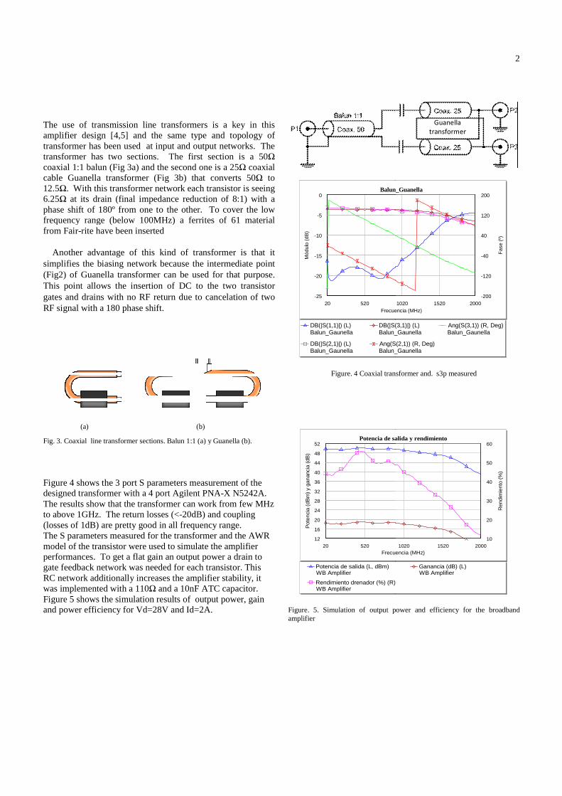
The use of transmission line transformers is a key in this amplifier design [4,5] and the same type and topology of transformer has been used at input and output networks. transformer has two sections. The first section iscoaxial 1:1 balun (Fig 3a) and the second one is acable Guanella transformer (Fig 3b) that 12.5Ω. With this transformer network each transistor is seeing 6.25Ω at its drain (final impedance reduction of 8:1phase shift of 180º from one to the other. frequency range (below 100MHz) a ferrites of 61 material from Fair-rite have been inserted
Another advantage of this kind of transformer is that it
simplifies the biasing network because the intermediate point (Fig2) of Guanella transformer can be used for that purposeThis point allows the insertion of DC to the two transistor gates and drains with no RF return due to RF signal with a 180 phase shift.
(a) (b)
Fig. 3. Coaxial line transformer sections. Balun 1:1 (a) y Guanella (b).
Figure 4 shows the 3 port S parameters measurement ofdesigned transformer with a 4 port Agilent PNAThe results show that the transformer can work from few MHz to above 1GHz. The return losses (<-20dB) and coupling (losses of 1dB) are pretty good in all frequency range. The S parameters measured for the transformer model of the transistor were used to simulate the amplifier performances. To get a flat gain an output power a drain to gate feedback network was needed for each transistor. This RC network additionally increases the amplifier stability, it was implemented with a 110Ω and a 10nF Figure 5 shows the simulation results of ouand power efficiency for Vd=28V and Id=2A.
The use of transmission line transformers is a key in this the same type and topology of
transformer has been used at input and output networks. The The first section is a 50Ω
and the second one is a 25Ω coaxial cable Guanella transformer (Fig 3b) that converts 50Ω to
each transistor is seeing drain (final impedance reduction of 8:1) with a
the other. To cover the low frequency range (below 100MHz) a ferrites of 61 material
Another advantage of this kind of transformer is that it because the intermediate point can be used for that purpose.
to the two transistor gates and drains with no RF return due to cancelation of two
(b)
alun 1:1 (a) y Guanella (b).
Figure 4 shows the 3 port S parameters measurement of the 4 port Agilent PNA-X N5242A.
ormer can work from few MHz 20dB) and coupling
in all frequency range. The S parameters measured for the transformer and the AWR model of the transistor were used to simulate the amplifier
To get a flat gain an output power a drain to for each transistor. This
increases the amplifier stability, it and a 10nF ATC capacitor.
Figure 5 shows the simulation results of output power, gain and power efficiency for Vd=28V and Id=2A.
Figure. 4 Coaxial transformer and
Figure. 5. Simulation of output power and efficiency amplifier
20 520Frecuencia (MHz)
Balun_Guanella
-25
-20
-15
-10
-5
0
Mód
ulo
(dB
)
DB(|S(1,1)|) (L)Balun_Gaunella
DB(|S(2,1)|) (L)Balun_Gaunella
DB(|S(3,1)|) (L)Balun_Gaunella
Ang(S(2,1)) (R, Deg)Balun_Gaunella
20 520Frecuencia (MHz)
Potencia de salida y rendimiento
12
16
20
24
28
32
36
40
44
48
52
Pot
enci
a (
dBm
) y
gana
ncia
(dB
)
Potencia de salida (L, dBm)WB Amplifier
Rendimiento drenador (%) (R)WB Amplifier
2
Guanella
transformer
Coaxial transformer and. s3p measured
Simulation of output power and efficiency for the broadband
1020 1520 2000Frecuencia (MHz)
Balun_Guanella
-200
-120
-40
40
120
200
Fas
e (º
)
DB(|S(3,1)|) (L)Balun_Gaunella
Ang(S(2,1)) (R, Deg)Balun_Gaunella
Ang(S(3,1)) (R, Deg)Balun_Gaunella
1020 1520 2000Frecuencia (MHz)
Potencia de salida y rendimiento
10
20
30
40
50
60
Ren
dim
ient
o (%
)
Ganancia (dB) (L)WB Amplifier
3
Figure 6 shows simulation results of output power and efficiency versus input power at two different frequencies
Figure. 6. Simulated output power and efficiency versus Pin.
The stability of the amplifier was also verified by AWR simulation. Figure 7 shows that the amplifier is unconditionally stable in all the frequency range, with a stability measurement (B1)>0 and a stability factor (K)>1
Figure. 7. Simulated stability measurement (B1) and Rollet stability factor (K)
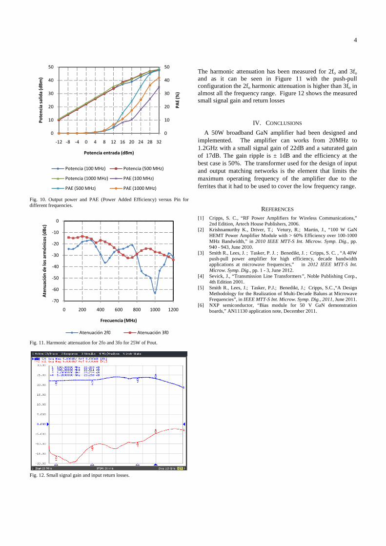
III. EXPERIMENTAL RESULTS
Figure 8 shows the implemented amplifier, it can be seen that the transformer configuration used at the input and output matching networks are identical with the only difference that at the input port a flexible coaxial cable is used instead of semi rigid cable used at the output. The NXP circuit proposal [6] was used for biasing the transistors. This circuit generates the negative voltage for the gate and provides the gate-drain voltage sequencing necessary in this kind of transistors
Figure. 8. Implemented broadband amplifier.
Figure 9 shows the measured saturated output power and the drain efficiency. Figure 10 shows the curves of output power versus input power for different frequencies. The measurements was performed with a Vd=28V and a Id=2A
Figure. 9. Measured of saturated output power and efficiency from 20MHz to 1.2GHz .
-10 -5 0 5 10 15 20 25 30 32Potencia de entrada (dBm)
10
15
20
25
30
35
40
45
50
55
Pot
enci
a de
sal
ida
(W)
0
6.67
13.3
20
26.7
33.3
40
46.7
53.3
60
Ren
dim
ient
o (%
)Freq = 500MHz (L, dBm)WB Amplifier
Freq = 100MHz (L, dBm)WB Amplifier
Freq = 1000MHz (L, dBm)WB Amplifier
Freq = 100MHz (R)WB Amplifier
Freq = 500 MHz (R)WB Amplifier
Freq = 1000 MHz (R)WB Amplifier
20 520 1020 1520 2000Frecuencia (MHz)
Factor y medida de estabilidad
0
1
2
3
4
5
K()WB Amplifier
B1()WB Amplifier
20
25
30
35
40
45
50
55
60
65
70
30
32
34
36
38
40
42
44
46
48
50
0 200 400 600 800 1000 1200
Re
nd
ime
into
(%
)
Po
ten
cia
(d
Bm
)
Frecuencia (MHz)
Pot. Salida (dBm) Rendimiento (%)
4
Fig. 10. Output power and PAE (Power Added Efficiency) versus Pin for different frequencies.
Fig. 11. Harmonic attenuation for 2fo and 3fo for 25W of Pout.
Fig. 12. Small signal gain and input return losses.
The harmonic attenuation has been measured for 2fo and 3fo and as it can be seen in Figure 11 with the push-pull configuration the 2fo harmonic attenuation is higher than 3fo in almost all the frequency range. Figure 12 shows the measured small signal gain and return losses
IV. CONCLUSIONS
A 50W broadband GaN amplifier had been designed and implemented. The amplifier can works from 20MHz to 1.2GHz with a small signal gain of 22dB and a saturated gain of 17dB. The gain ripple is ± 1dB and the efficiency at the best case is 50%. The transformer used for the design of input and output matching networks is the element that limits the maximum operating frequency of the amplifier due to the ferrites that it had to be used to cover the low frequency range.
REFERENCES [1] Cripps, S. C., “RF Power Amplifiers for Wireless Communications,”
2nd Edition, Artech House Publishers, 2006. [2] Krishnamurthy K., Driver, T.; Vetury, R.; Martin, J., “100 W GaN
HEMT Power Amplifier Module with > 60% Efficiency over 100-1000 MHz Bandwidth,” in 2010 IEEE MTT-S Int. Microw. Symp. Dig., pp. 940 - 943, June 2010.
[3] Smith R., Lees, J. ; Tasker, P. J. ; Benedikt, J. ; Cripps, S. C. , “A 40W push-pull power amplifier for high efficiency, decade bandwidth applications at microwave frequencies,” in 2012 IEEE MTT-S Int. Microw. Symp. Dig., pp. 1 - 3, June 2012.
[4] Sevick, J., “Transmission Line Transformers” , Noble Publishing Corp., 4th Edition 2001.
[5] Smith R., Lees, J.; Tasker, P.J.; Benedikt, J.; Cripps, S.C.,“A Design Methodology for the Realization of Multi-Decade Baluns at Microwave Frequencies”, in IEEE MTT-S Int. Microw. Symp. Dig., 2011, June 2011.
[6] NXP semiconductor, “Bias module for 50 V GaN demonstration boards,” AN11130 application note, December 2011.
0
10
20
30
40
50
0
10
20
30
40
50
-12 -8 -4 0 4 8 12 16 20 24 28 32
PA
E (
%)
Po
ten
cia
sa
lid
a (
dB
m)
Potencia entrada (dBm)
Potencia (100 MHz) Potencia (500 MHz)
Potencia (1000 MHz) PAE (100 MHz)
PAE (500 MHz) PAE (1000 MHz)
-70
-60
-50
-40
-30
-20
-10
0
0 200 400 600 800 1000 1200
Ate
nu
aci
ón
de
lo
s a
rmó
nic
os
(dB
c)
Frecuencia (MHz)
Atenuación 2f0 Atenuación 3f0


