Ultra-Wide Bandgap AlGaN Channel MISFET with Graded ... · MISFET with Graded Heterostructure Ohmic...
30
IWN2016 Sanyam Bajaj: [email protected] Prof. Siddharth Rajan: [email protected] 1 Ultra-Wide Bandgap AlGaN Channel MISFET with Graded Heterostructure Ohmic Contacts Sanyam Bajaj 1 , F. Akyol 1 , S. Krishnamoorthy 1 , Y. Zhang 1 , S. Rajan 1 1 Department of Electrical and Computer Engineering The Ohio State University, Columbus, OH USA A. Armstrong 2 , A. Allerman 2 2 Sandia National Laboratories, Albuquerque, NM USA Acknowledgment: ONR (Dr. Paul Maki), NSF (ECCS-1408416), Raytheon IDS Microelectronics
Transcript of Ultra-Wide Bandgap AlGaN Channel MISFET with Graded ... · MISFET with Graded Heterostructure Ohmic...

IWN2016 Sanyam Bajaj: [email protected] Prof. Siddharth Rajan: [email protected]
Ultra-Wide Bandgap AlGaN Channel MISFET with Graded Heterostructure
Ohmic Contacts
Sanyam Bajaj1, F. Akyol1, S. Krishnamoorthy1, Y. Zhang1, S. Rajan1
1Department of Electrical and Computer EngineeringThe Ohio State University, Columbus, OH USA
A. Armstrong2, A. Allerman2
2Sandia National Laboratories, Albuquerque, NM USA
Acknowledgment:ONR (Dr. Paul Maki), NSF (ECCS-1408416), Raytheon IDS Microelectronics

IWN2016 Sanyam Bajaj: [email protected] Prof. Siddharth Rajan: [email protected]
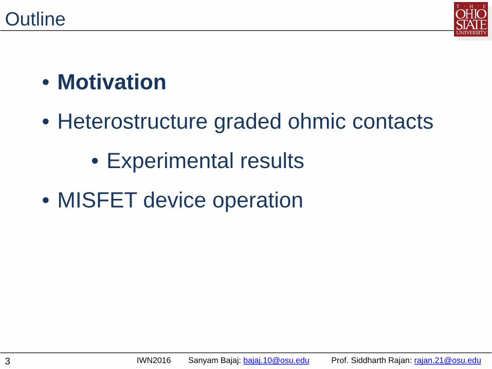
Outline
2
• Motivation
• Heterostructure graded ohmic contacts
• Experimental results
• MISFET device operation
IWN2016 Sanyam Bajaj: [email protected] Prof. Siddharth Rajan: [email protected]
Outline
3
• Motivation
• Heterostructure graded ohmic contacts
• Experimental results
• MISFET device operation

IWN2016 Sanyam Bajaj: [email protected] Prof. Siddharth Rajan: [email protected]
Ultra-wide bandgap material systems
4
3 4 5 62468
10121416
AlN
Diamondβ-Ga2O3
GaN
Fitting:V
br ~ 0.15*(E
g)2.5 MV/cm
Brea
kdow
n Fi
eld
(MV/
cm)
Energy Bandgap (eV)
4H-SiC
• GaN – wide bandgap (3.4 eV)• Ultrawide bandgap (UWBG) material systems with bandgap exceeding
4 eV• AlN with extremely high (theoretical) breakdown field ~ 5X of GaN• Results in high composition AlGaN with superior device figures of
merits – next-generation rf amplifiers? Power switches?
Hudgins et al. IEEE TED 18.3 (2003)

IWN2016 Sanyam Bajaj: [email protected] Prof. Siddharth Rajan: [email protected]
ns=1013 cm-2
Switching figure of merit
5
ns=1013 cm-2
2DEG mobility:• Limited by Alloy Scattering +Optical Phonon Scattering
Al mole fraction in AlGaN
Bajaj et al., APL 105.26 (2014)

IWN2016 Sanyam Bajaj: [email protected] Prof. Siddharth Rajan: [email protected]
ns=1013 cm-2
Switching figure of merit
6
ns=1013 cm-2
ns=1013 cm-2
2DEG mobility:• Limited by Alloy Scattering + Optical Phonon Scattering
Baliga figure of merit (εμEC3):
• Superior for larger Al compositions in channel than GaN
Bajaj et al., APL 105.26 (2014)
Al mole fraction in AlGaN
Al mole fraction in AlGaN

IWN2016 Sanyam Bajaj: [email protected] Prof. Siddharth Rajan: [email protected]
AlGaN for rf electronics
7
3 4 5 62468
10121416
John
son'
s FO
M ( x
107 M
V/s)AlN
Diamondβ-Ga2O3
GaN
Br
eakd
own
Fiel
d (M
V/cm
)
Energy Bandgap (eV)
4H-SiC1
2
3
4
5
• AlGaN channels with predicted electron velocities comparable to GaN
– superior Johnson’s figure of merit (theoretical)
Farahmand et al. IEEE TED 48.3 (2001) Anwar et al. IEEE TED 48.3 (2001)

IWN2016 Sanyam Bajaj: [email protected] Prof. Siddharth Rajan: [email protected]
AlGaN for rf electronics / optoelectronics
8
3 4 5 62468
10121416
John
son'
s FO
M ( x
107 M
V/s)AlN
Diamondβ-Ga2O3
GaN
Br
eakd
own
Fiel
d (M
V/cm
)
Energy Bandgap (eV)
4H-SiC1
2
3
4
5
• AlGaN channels with predicted electron velocities comparable to GaN
– superior Johnson’s figure of merit (theoretical)
• Also enables deep-UV emitters and detectors
Fig. by Crystal IS (http://www.cisuvc.com/)
Farahmand et al. IEEE TED 48.3 (2001) Anwar et al. IEEE TED 48.3 (2001)

IWN2016 Sanyam Bajaj: [email protected] Prof. Siddharth Rajan: [email protected]
Key Challenges
9
Material Challenges: Defects, Mobility
Device Challenges: High contact resistances to AlGaNChannels
Li et al., IEEE EDL 20.7 (1999)
Yue et al., IEEE EDL 33.7 (2012)
0.0 0.1 0.2 0.3 0.4 0.5 0.6 0.7 0.8 0.91E-7
1E-6
1E-5
1E-4
1E-3
0.01
0.1
France et al.APL (2007)
Wang et al.El. Mat. (2004)
Srivastava et al.El. Mat. (2009)
Yun et al.EDL (2006)
Baca et al.APL (2016)
Yafune et al.El.Lett. (2014)
Yafune et al.JJAP (2011)
Nanjo et al.APL (2008)
Yafune et al.JJAP (2011)
ρ C
(Ω.c
m2 )
Al composition in AlGaN channel
GaN HEMTs [ref]

IWN2016 Sanyam Bajaj: [email protected] Prof. Siddharth Rajan: [email protected]
Outline
10
• Motivation
• Heterostructure graded ohmic contacts
• Experimental results
• MISFET device operation

IWN2016 Sanyam Bajaj: [email protected] Prof. Siddharth Rajan: [email protected]
EF
EC
EVACχS
Metal Semiconductor
ΦM
e-
W
ND+ Charge
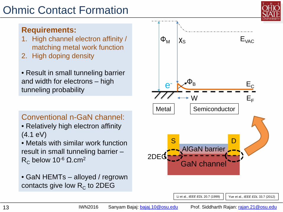
Requirements:1. High channel electron affinity /
matching metal work function2. High doping density
• Result in small tunneling barrier and width for electrons – high tunneling probability
eWm B
eT 3*24 2/1φ−
=
QM
ΦB
Ohmic Contact Formation

IWN2016 Sanyam Bajaj: [email protected] Prof. Siddharth Rajan: [email protected]
EF
EC
EVACχS
Metal Semiconductor
ΦM
e-
W
Requirements:1. High channel electron affinity /
matching metal work function2. High doping density
• Result in small tunneling barrier and width for electrons – high tunneling probability
Conventional n-GaN channel:• Relatively high electron affinity (4.1 eV)• Metals with similar work function result in small tunneling barrier –RC below 10-6 Ω.cm2
ΦB
Ohmic Contact Formation
IWN2016 Sanyam Bajaj: [email protected] Prof. Siddharth Rajan: [email protected]
Li et al., IEEE EDL 20.7 (1999) Yue et al., IEEE EDL 33.7 (2012)
GaN channel
AlGaN barrierS D
2DEG
Requirements:1. High channel electron affinity /
matching metal work function2. High doping density
• Result in small tunneling barrier and width for electrons – high tunneling probability
Conventional n-GaN channel:• Relatively high electron affinity (4.1 eV)• Metals with similar work function result in small tunneling barrier –RC below 10-6 Ω.cm2
• GaN HEMTs – alloyed / regrown contacts give low RC to 2DEG
EF
EC
EVACχS
Metal Semiconductor
ΦM
e-
W
ΦB
Ohmic Contact Formation

IWN2016 Sanyam Bajaj: [email protected] Prof. Siddharth Rajan: [email protected]
Ohmic Contacts to UWBG AlGaN
14
Challenges:1. Low electron affinity of AlN
(0.6 eV) – high Schottkybarrier
2. Low doping efficiency
• Result in low tunneling probability, high RC EF
ECΦB
EVAC
ΦM χS
Metal Semiconductor
e-
W

IWN2016 Sanyam Bajaj: [email protected] Prof. Siddharth Rajan: [email protected]
Heterostructure-engineered ohmic contacts
15
UWBGn-AlGaNchannel
S DA
A’ EF
EC
EV
ΦB
• Conventional ohmic contact to n-type UWBG AlGaN channel –large Schottky barrier
χS
EVAC
ND+
ChargeQM
AlGa
N

IWN2016 Sanyam Bajaj: [email protected] Prof. Siddharth Rajan: [email protected]
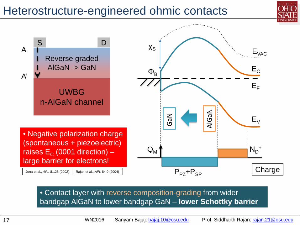
UWBGn-AlGaN channel
Reverse gradedAlGaN -> GaN
S D
A’
A
• Contact layer with reverse composition-grading from wider bandgap AlGaN to lower bandgap GaN – lower Schottky barrier
EF
EC
EV
EVAC
ND+
Charge
QM
χS
PPZ+PSP
ΦB
GaN
AlGa
N
Heterostructure-engineered ohmic contacts
IWN2016 Sanyam Bajaj: [email protected] Prof. Siddharth Rajan: [email protected]
UWBGn-AlGaN channel
Reverse gradedAlGaN -> GaN
S D
A’
A
• Contact layer with reverse composition-grading from wider bandgap AlGaN to lower bandgap GaN – lower Schottky barrier
EF
EC
EV
EVAC
ND+
Charge
QM
χS
PPZ+PSP
ΦB
GaN
AlGa
N
• Negative polarization charge (spontaneous + piezoelectric) raises EC (0001 direction) –large barrier for electrons!
Jena et al., APL 81.23 (2002) Rajan et al., APL 84.9 (2004)
Heterostructure-engineered ohmic contacts

IWN2016 Sanyam Bajaj: [email protected] Prof. Siddharth Rajan: [email protected]
UWBGn-AlGaN channel
Reverse gradedn++ AlGaN -> GaN
S D
A’
A
• Contact layer with reverse composition-grading from wider bandgap AlGaN to lower bandgap GaN – lower Schottky barrier
EF
EC
EV
EVAC
ND+
ChargeQM
χS
PPZ+PSP
ΦB
Electron slab
n++ gradedAlGaN
• High donor concentration compensates negative polarization charge – flat ECprofile, low RSH
Jena et al., APL 81.23 (2002) Rajan et al., APL 84.9 (2004)
Park et al., IEEE EDL 36.3 (2015)
Heterostructure-engineered ohmic contacts

IWN2016 Sanyam Bajaj: [email protected] Prof. Siddharth Rajan: [email protected]
Outline
19
• Motivation
• Heterostructure graded ohmic contacts
• Experimental results
• MISFET device operation

IWN2016 Sanyam Bajaj: [email protected] Prof. Siddharth Rajan: [email protected]
Experiment – n-type Al0.75Ga0.25N Channel
20
30nm Al0.75Ga0.25N (UID)
AlN on Sapphire
100nm Al0.75Ga0.25NSi = 3x1019 cm-3
75%
6%50nm Gradedn++ AlGaN
Si = 1020 cm-3
- 100 nm 75% n-AlGaN channel with EG = 5.35 eV (MBE growth on AlN/Sapphire template)- Si donor concentration = 3x1019 cm-3
- 50 nm n++ reverse polarization-graded contact layer
- Conduction band profile under ohmic region (as-grown)
A’
A
A A’
0 50 100 150 200-6
-4
-2
0
2
4
6UIDAlGaN
AlNn-Al0.75Ga0.25N
Graded AlGaN
EF
EV
Ener
gy (e
V)Distance (nm)
AS GROWN:Contact region EC

IWN2016 Sanyam Bajaj: [email protected] Prof. Siddharth Rajan: [email protected]
30nm Al0.75Ga0.25N (UID)
AlN on Sapphire
90nm Al0.75Ga0.25NSi = 3x1019 cm-3
75%
6%
- 100 nm 75% n-AlGaN channel with EG = 5.35 eV (MBE growth on AlN/Sapphire template)- Si donor concentration = 3x1019 cm-3
- 50 nm n++ reverse polarization-graded contact layer
- Conduction band profile under gate region (recessed)
A
A’
100 150 200-6
-4
-2
0
2
4
6
UIDAlGaN
Ener
gy (e
V)Distance (nm)
RECESSED:Intrinsic region
n-Al0.75Ga0.25N AlN
EC
EF
EV
A A’
Experiment – n-type Al0.75Ga0.25N Channel

IWN2016 Sanyam Bajaj: [email protected] Prof. Siddharth Rajan: [email protected]
Non-Alloyed Ohmics Contacts
22
Graded AlGaNcontact layer
30nm Al0.75Ga0.25N (UID)
AlN on Sapphire
AlGaN channel
Non-alloyed ohmic contacts – Ti/Al/Ni/Au = 20/120/30/50 nm
S D

IWN2016 Sanyam Bajaj: [email protected] Prof. Siddharth Rajan: [email protected]
Contact Resistance using TLM
23
30nm Al0.75Ga0.25N (UID)
AlN on Sapphire
AlGaN channel
S DRC1 RC1
RSH
spacing
0 1 2 3 4 5 6 7
4
6
8
10
12
14
ρSP = 1.4x10⁻⁶ Ω.cm2
RC1 = 0.15 Ω.mmRSH = 158 Ω/sq
Resis
tanc
e (o
hm)
Spacing (µm)
Non-alloyed ohmic contacts – Ti/Al/Ni/Au = 20/120/30/50 nm
As-grown structure:• RC1 (Metal-
semiconductor interface resistance) = 0.15 Ω.mm
• ρSP = 1.4x10⁻⁶
Ω.cm2
Recessed structure:• Net RC to 75% AlGaN
channel = 0.32 Ω.mm
• ρSP = 1.9x10⁻⁶
Ω.cm2

IWN2016 Sanyam Bajaj: [email protected] Prof. Siddharth Rajan: [email protected]
Contact Resistance using TLM
24
30nm Al0.75Ga0.25N (UID)
AlN on Sapphire
AlGaN channel
S DRC1 RC1
RSH
spacing
0 1 2 3 4 5 6 7
4
6
8
10
12
14
ρSP = 1.4x10⁻⁶ Ω.cm2
RC1 = 0.15 Ω.mmRSH = 158 Ω/sq
Resis
tanc
e (o
hm)
Spacing (µm)
As-grown structure:• RC1 (Metal-
semiconductor interface resistance) = 0.15 Ω.mm
• ρSP = 1.4x10⁻⁶
Ω.cm2
Recessed structure:• Net RC to 75% AlGaN
channel = 0.32 Ω.mm
• ρSP = 1.9x10⁻⁶
Ω.cm2
30nm Al0.75Ga0.25N (UID)
AlN on Sapphire
90nm channel
S DRC1 RC1
RSH1 RSH2RSH1
spacing
2 4 6 8 10 12 142030405060708090
100110
ρSP = 1.9x10⁻⁶ Ω.cm2
RC1+RSH1 = 0.32 Ω.mmRSH2 = 725 Ω/sq
Resis
tanc
e (o
hm)
Spacing (µm)
Cl2-based ICP-RIE etch to test contact to AlGaN channel

IWN2016 Sanyam Bajaj: [email protected] Prof. Siddharth Rajan: [email protected]
Contact Resistance using TLM
25
30nm Al0.75Ga0.25N (UID)
AlN on Sapphire
AlGaN channel
S DRC1 RC1
RSH
spacing
0 1 2 3 4 5 6 7
4
6
8
10
12
14
ρSP = 1.4x10⁻⁶ Ω.cm2
RC1 = 0.15 Ω.mmRSH = 158 Ω/sq
Resis
tanc
e (o
hm)
Spacing (µm)
• ρSP = 1.9x10⁻⁶
Ω.cm2
30nm Al0.75Ga0.25N (UID)
AlN on Sapphire
90nm channel
S DRC1 RC1
RSH1 RSH2RSH1
spacing
2 4 6 8 10 12 142030405060708090
100110
ρSP = 1.9x10⁻⁶ Ω.cm2
RC1+RSH1 = 0.32 Ω.mmRSH2 = 725 Ω/sq
Resis
tanc
e (o
hm)
Spacing (µm)
Low ρSP to UWBG AlGaN ~ 5.3 eV (Non-alloyed)
0.0 0.1 0.2 0.3 0.4 0.5 0.6 0.7 0.8 0.91E-7
1E-6
1E-5
1E-4
1E-3
0.01
0.1
France et al.APL (2007)
Wang et al.El. Mat. (2004)
Srivastava et al.El. Mat. (2009)
Yun et al.EDL (2006)
This work
Baca et al.APL (2016)
Yafune et al.El.Lett. (2014)
Yafune et al.JJAP (2011)
Nanjo et al.APL (2008)
Yafune et al.JJAP (2011)
ρ C (Ω
.cm
2 )
Al composition in AlGaN channel
GaN HEMTs [ref]

IWN2016 Sanyam Bajaj: [email protected] Prof. Siddharth Rajan: [email protected]
Outline
26
• Motivation
• Heterostructure graded ohmic contacts
• Experimental results
• MISFET device operation
IWN2016 Sanyam Bajaj: [email protected] Prof. Siddharth Rajan: [email protected]
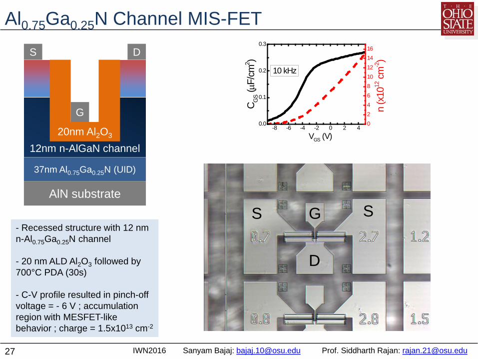
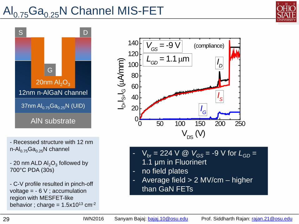
Al0.75Ga0.25N Channel MIS-FET
27
37nm Al0.75Ga0.25N (UID)
AlN substrate
12nm n-AlGaN channel
S D
20nm Al2O3
G
GS S
D
- Recessed structure with 12 nm n-Al0.75Ga0.25N channel
- 20 nm ALD Al2O3 followed by 700°C PDA (30s)
- C-V profile resulted in pinch-off voltage = - 6 V ; accumulation region with MESFET-like behavior ; charge = 1.5x1013 cm-2
-8 -6 -4 -2 0 2 40.0
0.1
0.2
0.3
VGS (V)
C GS (µF
/cm
2 )
0246810121416
n (x
1012
cm
-2)
10 kHz

IWN2016 Sanyam Bajaj: [email protected] Prof. Siddharth Rajan: [email protected]
- Recessed structure with 12 nm n-Al0.75Ga0.25N channel
- 20 nm ALD Al2O3 followed by 700°C PDA (30s)
- C-V profile resulted in pinch-off voltage = - 6 V ; accumulation region with MESFET-like behavior ; charge = 1.5x1013 cm-2
37nm Al0.75Ga0.25N (UID)
AlN substrate
12nm n-AlGaN channel
S D
20nm Al2O3
G
- IDS_MAX ~ 60 mA/mm ; gm_MAX = 14 mS/mm- fT_PEAK of 0.6 GHz ; fMAX_PEAK of 1.4 GHz- Limited by low channel mobility of 16 cm2/Vs- Defect related compensation
0 5 10 15 200
10
20
30
40
50
60
∆VG = -2 V
I D (m
A/m
m)
VDS (V)
VG = 2 V
-8 -6 -4 -2 0 20
10
20
30
40
50
60
VGS (V)
I D (m
A/m
m)
02468101214
gm (m
S/mm
)
VDS = 20 V
0.01 0.1 1 100
10
20
30
40
fT = 0.6 GHz
VDS = 25 VVGS = 4 V
rf ga
in (d
B)
Frequency (Hz)
|h21| U MSG
Al0.75Ga0.25N Channel MIS-FET
IWN2016 Sanyam Bajaj: [email protected] Prof. Siddharth Rajan: [email protected]
- Recessed structure with 12 nm n-Al0.75Ga0.25N channel
- 20 nm ALD Al2O3 followed by 700°C PDA (30s)
- C-V profile resulted in pinch-off voltage = - 6 V ; accumulation region with MESFET-like behavior ; charge = 1.5x1013 cm-2
37nm Al0.75Ga0.25N (UID)
AlN substrate
12nm n-AlGaN channel
S D
20nm Al2O3
G
- Vbr = 224 V @ VGS = -9 V for LGD = 1.1 μm in Fluorinert
- no field plates- Average field > 2 MV/cm – higher
than GaN FETs
0 50 100 150 200 2500
20406080
100120140 VGS = -9 V
ISIG
ID
I D,I S,
I G (µ
A/m
m)
VDS (V)
LGD = 1.1 µm(compliance)
Al0.75Ga0.25N Channel MIS-FET

IWN2016 Sanyam Bajaj: [email protected] Prof. Siddharth Rajan: [email protected]
SUMMARY
30
- Heterostructure graded ohmic contacts to UWBG AlGaN –compositional grading + high doping
- Achieved low specific contact resistance to Al0.75Ga0.25N channels (NON-ALLOYED)
- Demonstrated the 1st UWBG Al0.75Ga0.25N channel MISFET with low-resistance ohmics (MBE)
- This work removes one of the principle challenges for UWBG AlGaN devices; applications in large range of electronic and photonic devices
30nm Al0.75Ga0.25N (UID)
AlN on Sapphire
90nm channel
S DRC1 RC1
RSH1 RSH2RSH1
spacing
2 4 6 8 10 12 142030405060708090
100110
ρSP = 1.9x10⁻⁶ Ω.cm2
RC1+RSH1 = 0.32 Ω.mmRSH2 = 725 Ω/sq
Resis
tanc
e (o
hm)
Spacing (µm)
0 5 10 15 200
10
20
30
40
50
60
∆VG = -2 V
I D (m
A/m
m)
VDS (V)
VG = 2 V
0.0 0.1 0.2 0.3 0.4 0.5 0.6 0.7 0.8 0.91E-7
1E-6
1E-5
1E-4
1E-3
0.01
0.1
France et al.APL (2007)
Wang et al.El. Mat. (2004)
Srivastava et al.El. Mat. (2009)
Yun et al.EDL (2006)
This work
Baca et al.APL (2016)
Yafune et al.El.Lett. (2014)
Yafune et al.JJAP (2011)
Nanjo et al.APL (2008)
Yafune et al.JJAP (2011)
ρ C (Ω
.cm
2 )
Al composition in AlGaN channel
GaN HEMTs [ref]