Ultra-Low Quiescent Current HCOT Buck ConverterRT5707A/DS5707A... · Richtek Technology Corporation...
16
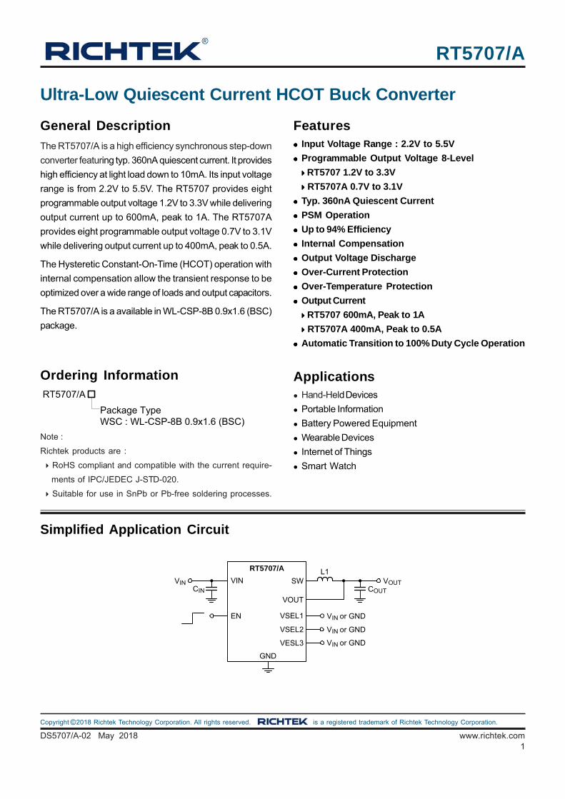
RT5707/A ® DS5707/A-02 May 2018 www.richtek.com 1 © Copyright 2018 Richtek Technology Corporation. All rights reserved. is a registered trademark of Richtek Technology Corporation. Simplified Application Circuit Ultra-Low Quiescent Current HCOT Buck Converter General Description The RT5707/A is a high efficiency synchronous step-down converter featuring typ. 360nA quiescent current. It provides high efficiency at light load down to 10mA. Its input voltage range is from 2.2V to 5.5V. The RT5707 provides eight programmable output voltage 1.2V to 3.3V while delivering output current up to 600mA, peak to 1A. The RT5707A provides eight programmable output voltage 0.7V to 3.1V while delivering output current up to 400mA, peak to 0.5A. The Hysteretic Constant-On-Time (HCOT) operation with internal compensation allow the transient response to be optimized over a wide range of loads and output capacitors. The RT5707/A is a available in WL-CSP-8B 0.9x1.6 (BSC) package. Features Input Voltage Range : 2.2V to 5.5V Programmable Output Voltage 8-Level RT5707 1.2V to 3.3V RT5707A 0.7V to 3.1V Typ. 360nA Quiescent Current PSM Operation Up to 94% Efficiency Internal Compensation Output Voltage Discharge Over-Current Protection Over-Temperature Protection Output Current RT5707 600mA, Peak to 1A RT5707A 400mA, Peak to 0.5A Automatic Transition to 100% Duty Cycle Operation Applications Hand-Held Devices Portable Information Battery Powered Equipment Wearable Devices Internet of Things Smart Watch Ordering Information Note : Richtek products are : RoHS compliant and compatible with the current require- ments of IPC/JEDEC J-STD-020. Suitable for use in SnPb or Pb-free soldering processes. RT5707/A Package Type WSC : WL-CSP-8B 0.9x1.6 (BSC) GND VIN RT5707/A SW EN VOUT VESL3 VSEL2 VSEL1 V IN C IN L1 C OUT V OUT V IN or GND V IN or GND V IN or GND
Transcript of Ultra-Low Quiescent Current HCOT Buck ConverterRT5707A/DS5707A... · Richtek Technology Corporation...
RT5707/A®
DS5707/A-02 May 2018 www.richtek.com1
©Copyright 2018 Richtek Technology Corporation. All rights reserved. is a registered trademark of Richtek Technology Corporation.
Simplified Application Circuit
Ultra-Low Quiescent Current HCOT Buck Converter
General Description
The RT5707/A is a high efficiency synchronous step-down
converter featuring typ. 360nA quiescent current. It provides
high efficiency at light load down to 10mA. Its input voltage
range is from 2.2V to 5.5V. The RT5707 provides eight
programmable output voltage 1.2V to 3.3V while delivering
output current up to 600mA, peak to 1A. The RT5707A
provides eight programmable output voltage 0.7V to 3.1V
while delivering output current up to 400mA, peak to 0.5A.
The Hysteretic Constant-On-Time (HCOT) operation with
internal compensation allow the transient response to be
optimized over a wide range of loads and output capacitors.
The RT5707/A is a available in WL-CSP-8B 0.9x1.6 (BSC)
package.
Features Input Voltage Range : 2.2V to 5.5V
Programmable Output Voltage 8-Level
RT5707 1.2V to 3.3V
RT5707A 0.7V to 3.1V
Typ. 360nA Quiescent Current
PSM Operation
Up to 94% Efficiency
Internal Compensation
Output Voltage Discharge
Over-Current Protection
Over-Temperature Protection
Output Current
RT5707 600mA, Peak to 1A
RT5707A 400mA, Peak to 0.5A
Automatic Transition to 100% Duty Cycle Operation
Applications Hand-Held Devices
Portable Information
Battery Powered Equipment
Wearable Devices
Internet of Things
Smart Watch
Ordering Information
Note :
Richtek products are :
RoHS compliant and compatible with the current require-
ments of IPC/JEDEC J-STD-020.
Suitable for use in SnPb or Pb-free soldering processes.
RT5707/A
Package TypeWSC : WL-CSP-8B 0.9x1.6 (BSC)
GND
VIN
RT5707/A
SW
EN
VOUT
VESL3
VSEL2
VSEL1
VINCIN
L1
COUT
VOUT
VIN or GND
VIN or GND
VIN or GND

RT5707/A
2
DS5707/A-02 May 2018www.richtek.com
©Copyright 2018 Richtek Technology Corporation. All rights reserved. is a registered trademark of Richtek Technology Corporation.
Functional Pin Description
Pin No. Pin Name Pin Function
A1 SW This pin is the connection between two build-in switches in the chip, which should be connected to the external inductor. The inductor should be connected to this pin with the shortest path.
A2 VIN Supply input. A minimum of 10F (RT5707) and 4.7F (RT5707A) ceramic capacitor should be connected to this pin with the shortest path
B1 EN Chip enable input pin. High level voltage enables the device while low level voltage turns the device off. This pin must be terminated.
B2 GND Device ground pin. This pin should be connected to input and output capacitors with the shortest path.
C1 VSEL1 Output voltage selection pin. This pin must be terminated.
C2 VOUT Output voltage feedback pin. This pin should be connected close to the output capacitor terminal for better voltage regulation. A minimum of 10F ceramic capacitor should be connected to this pin with the shortest path.
D1 VSEL2 Output voltage selection pin. This pin must be terminated.
D2 VSEL3 Output voltage selection pin. This pin must be terminated.
Pin Configuration(TOP VIEW)
WL-CSP-8B 0.9x1.6 (BSC)
EN
VSEL2
GND
VOUT
VSEL3
VSEL1
SW VIN
D1 D2
C2C1
B1 B2
A1 A2
Marking Information
6E : Product Code
W : Date Code6EW
RT5707WSC
6Z : Product Code
W : Date Code
RT5707AWSC
6ZW

RT5707/A
3
DS5707/A-02 May 2018 www.richtek.com
©Copyright 2018 Richtek Technology Corporation. All rights reserved. is a registered trademark of Richtek Technology Corporation.
Functional Block Diagram
Operation
The RT5707/A is a hysteretic constant on time (HCOT)
switching buck converter. The RT5707/A provides Over-
Temperature Protection (OTP) and Over-Current Protection
(OCP) mechanisms to prevent the device from damage
with abnormal operations. When the EN voltage is logic
low, the IC will be shut down with low input supply current
less than 1μA.
UVLO Protection
To protect the chip from operating at insufficient supply
voltage, the UVLO is needed. When the input voltage is
lower than the UVLO falling threshold voltage, the device
will be lockout.
100% Duty Cycle Operation
The converter enters 100% duty cycle operation once the
input voltage decrease and the difference voltage between
input and output is lower than VTH_100-. The output voltage
follows the input voltage minus the voltage drop across
the internal P_MOSFET and the inductor. Once the input
Figure 1. Automatic Transition into 100% Duty Cycle
VIN
VOUT
VTH_100+
VTH_100-
VUVLO+VUVLO-
VIN
VOUT
100% duty cycle 100% duty cycle
Soft-start
Step Down OperationVO tracks VIN
VO tracks VIN
VOUT_target
voltage increases and trips the 100% mode exit threshold,
VTH_100+, the converter backs to normal switching again.
See Figure 1.
GateDrive
PSM/PWMControl
VREF
DigitalControl
SW
GND
OSC OTP
UVLO
OCPVSEL1
R1
R2
VIN
EN
FB
Soft-start
VSEL2
VSEL3
AMP
VREF
FastDischarge
VOUT
+
-
EN
VOUT

RT5707/A
4
DS5707/A-02 May 2018www.richtek.com
©Copyright 2018 Richtek Technology Corporation. All rights reserved. is a registered trademark of Richtek Technology Corporation.
Over-Temperature Protection
When the junction temperature exceeds the OTP
threshold value, the IC will shut down the switching
operation. Once the junction temperature cools down and
is lower than the OTP lower threshold, the converter will
automatically resume switching.
Over-Current Protection
The OCP function is implemented by UGATE and LGATE.
When the inductor current reaches the UGATE current
limit threshold, the high-side MOSFET will be turned-off.
The low-side MOSFET turns on to discharge the inductor
current until the inductor current trips below the LGATE
current limit threshold. After UGATE current limit triggered,
the max inductor current is decided by the inductor current
rising rate and the response delay time of the internal
network.
During OCP period, the output voltage drops below the
setting threshold (typ. 0.4V) and the current limit value is
reduced for lowering the devices loss, reducing the heat
and preventing further damage of the chip.
Output Voltage Selection
The RT5707/A provides 8 level output voltages which can
be programmed via the volatage select pin VSEL1 to
VSEL3. Table 1 indicates the setting to indivdual output
voltage.
Table 1. Output Voltage Setting
Device VOUT (V) VSEL3 VSEL2 VSEL1
RT5707
1.2 0 0 0
1.5 0 0 1
1.8 0 1 0
2.1 0 1 1
2.5 1 0 0
2.8 1 0 1
3 1 1 0
3.3 1 1 1
RT5707A
0.7 0 0 0
1 0 0 1
1.3 0 1 0
1.6 0 1 1
1.9 1 0 0
2 1 0 1
2.9 1 1 0
3.1 1 1 1

RT5707/A
5
DS5707/A-02 May 2018 www.richtek.com
©Copyright 2018 Richtek Technology Corporation. All rights reserved. is a registered trademark of Richtek Technology Corporation.
Recommended Operating Conditions (Note 4)
Supply Input Voltage------------------------------------------------------------------------------------------------------ 2.2V to 5.5V
RT5707 Output Current (5.5V ≥ VIN ≥ (VOUT_NOM + 0.7V) ≥ 3V) ---------------------------------------------- 0mA to 600mA
RT5707A Output Current (5.5V ≥ VIN ≥ (VOUT_NOM + 0.7V) ≥ 3V) -------------------------------------------- 0mA to 400mA
Junction Temperature Range-------------------------------------------------------------------------------------------- −40°C to 125°C Ambient Temperature Range-------------------------------------------------------------------------------------------- −40°C to 85°C
Electrical Characteristics
Parameter Symbol Test Conditions Min Typ Max Unit
BUCK Regulator
Under-Voltage Lockout Rising Threshold
VUVLOR VIN rising -- 2 2.15 V
Under-Voltage Lockout Hysteresis
VUVLO_HYS -- 0.1 0.4 V
VOUT Voltage Accuracy VOUT_ACC10 VOUT = 1.8V, IOUT = 10mA 2.5 -- 2.5
% VOUT_ACC100 VOUT = 1.8V, IOUT = 100mA 2 -- 2
Input Quiescent Current
IQ_Non-SW VOUT = 1.8V, IOUT = 0A, EN = VIN, non-switching
-- 360 800
nA
IQSW VOUT = 1.8V, IOUT = 0A, EN = VIN, switching
-- 460 1200
Shutdown Current ISHDN EN = GND -- 0.2 1 A
Switching Frequency fSW VOUT = 1.8V, CCM mode -- 1.2 -- MHz
UGATE Current Limit ICL_UG 3V VIN 5.5V RT5707 1 1.2 1.4
A RT5707A 0.68 0.78 0.88
LGATE Current Limit ICL_LG 3V VIN 5.5V RT5707 1 1.2 1.4
A RT5707A 0.55 0.68 0.8
UGATE RON RON_UG IOUT = 50mA -- 350 -- m
LGATE RON RON_LG IOUT = 50mA -- 250 -- m
(VIN = 3.6V, CIN
= COUT = 10μF, L1 = 2.2μH, TA
= 25°C, unless otherwise specified)
Absolute Maximum Ratings (Note 1)
VIN, SW, EN, VSEL1, VSEL2, VSEL3, VOUT -------------------------------------------------------------------- −0.3V to 6V
Power Dissipation, PD @ TA = 25°C
WL-CSP-8B 0.9x1.6 (BSC) --------------------------------------------------------------------------------------------- 0.84W
Package Thermal Resistance (Note 2)
WL-CSP-8B 0.9x1.6 (BSC), θJA --------------------------------------------------------------------------------------- 118.5°C/W
Lead Temperature (Soldering, 10 sec.) ------------------------------------------------------------------------------- 260°C Junction Temperature Range-------------------------------------------------------------------------------------------- 150°C Storage Temperature Range -------------------------------------------------------------------------------------------- −65°C to 150°C ESD Susceptibility (Note 3)
HBM (Human Body Model) ---------------------------------------------------------------------------------------------- 2kV

RT5707/A
6
DS5707/A-02 May 2018www.richtek.com
©Copyright 2018 Richtek Technology Corporation. All rights reserved. is a registered trademark of Richtek Technology Corporation.
Note 1. Stresses beyond those listed “Absolute Maximum Ratings” may cause permanent damage to the device. These are
stress ratings only, and functional operation of the device at these or any other conditions beyond those indicated in
the operational sections of the specifications is not implied. Exposure to absolute maximum rating conditions may
affect device reliability.
Note 2. θJA is measured under natural convection (still air) at TA = 25°C with the component mounted on a high effective-
thermal-conductivity four-layer test board on a JEDEC 51-7 thermal measurement standard.
Note 3. Devices are ESD sensitive. Handling precaution is recommended.
Note 4. The device is not guaranteed to function outside its operating conditions.
Parameter Symbol Test Conditions Min Typ Max Unit
Output Discharge Resistor RDIS EN = GND, IOUT = 10mA -- 10 --
VOUT Pin Input Leakage IVOUT VOUT = 2V, EN = VIN -- 100 -- nA
VOUT Minimum Off Time tOFF_MIN -- 80 -- ns
VOUT Minimum On Time tON_MIN VOUT = 1.8V, VIN = 3.6V -- 420 -- ns
Line Regulation VOUT_LineReg VOUT = 1.8V, IOUT = 100mA, VIN = 2.2V to 5.5V
-- 0.1 -- %/V
Load Regulation VOUT_LoadReg1
VOUT = 1.8V, including PFM operation
-- 0.001 -- %/mA
VOUT_LoadReg2 VOUT = 1.8V, only CCM operation -- 0.0005 --
Over-Temperature Protection
TOTP -- 150 -- °C
Over-Temperature Protection Hysteresis
TOTP_HYS -- 20 -- °C
Auto 100% Duty Cycle Leave Detection Threshold
VTH_100+ Rising VIN, 100% mode is left with VIN = VOUT + VTH_100+
150 250 350 mV
Auto 100% Duty Cycle Enter Detection Threshold
VTH_100- Falling VIN, 100% mode is entered with VIN = VOUT + VTH_100-
85 200 290 mV
Timing
Regulator Start Up Delay Time
tSS_EN IOUT = 0mA, EN = GND to VIN, VOUT starts rising
-- 0.1 -- ms
Regulator Soft Start Time tSS VOUT = 1.8V, IOUT = 10mA, EN = VIN
-- 0.7 -- ms
Logic Input (EN, VSEL1, VSEL2 and VSEL3)
Input High Threshold VIH VIN = 2.2V to 5.5V 1.2 -- -- V
Input Low Threshold VIL VIN = 2.2V to 5.5V -- -- 0.4 V
Input Pin Bias Current IIN -- 10 -- nA

RT5707/A
7
DS5707/A-02 May 2018 www.richtek.com
©Copyright 2018 Richtek Technology Corporation. All rights reserved. is a registered trademark of Richtek Technology Corporation.
Typical Application Circuit
Reference Part Number Description Package Manufacturer
CIN, COUT GRM155R60J106ME15 10F/6.3V/X5R 0402 Murata
L1 1239AS-H-2R2M 2.2H 2520 Murata
2.2V to 5.5V VIN
RT5707
SW
EN
VOUT MainSystem
VIN
CIN10µF
2.2µHL1
COUT10µF
C2
B1
A2A1
GND
VSEL1C1
B2
VIN or GND
VSEL2D1
VSEL3D2
VIN or GND
VIN or GND
2.2V to 5.5V VINSW
EN
VOUT MainSystem
VIN
CIN4.7µF
2.2µHL1
COUT10µF
C2
B1
A2A1
GND
VSEL1C1
B2
VIN or GND
VSEL2D1
VSEL3D2
VIN or GND
VIN or GND
RT5707A
For the RT5707
For the RT5707A
Recommended components information for the RT5707 as below table :
Reference Part Number Description Package Manufacturer
CIN GRM155R60J475ME47 4.7F/6.3V/X5R 0402 Murata
COUT GRM155R60J106ME15 10F/6.3V/X5R 0402 Murata
L1 DFE201610E-2R2M=P2 2.2H 2016 Murata
Recommended components information for the RT5707A as below table :

RT5707/A
8
DS5707/A-02 May 2018www.richtek.com
©Copyright 2018 Richtek Technology Corporation. All rights reserved. is a registered trademark of Richtek Technology Corporation.
Efficiency vs. Load Current
30
40
50
60
70
80
90
100
0.001 0.01 0.1 1 10 100 1000
Load Current (mA)
Effi
cie
ncy
(%
)
Output Voltage Ripple
7.5
10.0
12.5
15.0
17.5
20.0
22.5
0.001 0.01 0.1 1 10 100 1000
Load Current (mA)
Ou
tpu
t Vo
ltag
e R
ipp
le (
mV
pp
)
Quiescent Current
0.3
0.4
0.5
0.6
0.7
0.8
0.9
1.0
3.5 3.7 3.9 4.1 4.3 4.5 4.7 4.9 5.1 5.3 5.5
Input Voltage (V)
Qu
iesc
en
t Cu
rre
nt (μ
A)
Output Voltage Ripple
0
10
20
30
40
50
60
70
0.001 0.01 0.1 1 10 100 1000
Load Current (mA)
Ou
tpu
t Vo
ltag
e R
ipp
le (
mV
pp
)
Efficiency vs. Load Current
65
70
75
80
85
90
95
100
0.001 0.01 0.1 1 10 100 1000
Load Current (mA)
Effi
cie
ncy
(%
)
Switching Frequency vs. Load Current
0.0
0.2
0.4
0.6
0.8
1.0
1.2
1.4
1.6
1.8
2.0
0 100 200 300 400 500 600
Load Current (mA)
Sw
itch
ing
Fre
qu
en
cy (
MH
z) 1
Typical Operating Characteristics
Switching
VOUT = 3.3V
VOUT = 3.3V
VOUT = 3.3V
VIN = 3.6VVIN = 4.2VVIN = 5V
VIN = 5VVIN = 4.2VVIN = 3.8V
VIN = 5.5VVIN = 5VVIN = 4.2V
VOUT = 3.3V
Non-switching
VOUT = 0.7V
VIN = 2.5VVIN = 3VVIN = 3.6V
VOUT = 0.7V
VIN = 2.5VVIN = 3VVIN = 3.6V
RT5707/A
9
DS5707/A-02 May 2018 www.richtek.com
©Copyright 2018 Richtek Technology Corporation. All rights reserved. is a registered trademark of Richtek Technology Corporation.
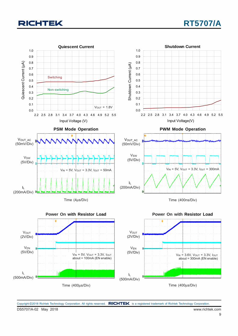
Quiescent Current
0.0
0.1
0.2
0.3
0.4
0.5
0.6
0.7
0.8
0.9
1.0
2.2 2.5 2.8 3.1 3.4 3.7 4.0 4.3 4.6 4.9 5.2 5.5
Input Voltage (V)
Qu
iesc
en
t Cu
rre
nt (μ
A)
PWM Mode Operation
Time (400ns/Div)
Power On with Resistor Load
Time (400μs/Div)
Power On with Resistor Load
Time (400μs/Div)
VOUT
(2V/Div)
IL(500mA/Div)
VEN
(5V/Div)
VIN = 5V, VOUT = 3.3V, IOUT = 300mA
VOUT_AC
(50mV/Div)
VSW
(5V/Div)
IL(200mA/Div)
VIN = 5V, VOUT = 3.3V, IOUT
about = 100mA (EN enable)VIN = 3.6V, VOUT = 3.3V, IOUT
about = 300mA (EN enable)
VOUT
(2V/Div)
IL(500mA/Div)
VEN
(5V/Div)
PSM Mode Operation
Time (4μs/Div)
VOUT_AC
(50mV/Div)
VSW
(5V/Div)
IL(200mA/Div)
VIN = 5V, VOUT = 3.3V, IOUT = 50mA
Shutdown Current
0.0
0.1
0.2
0.3
0.4
0.5
0.6
0.7
0.8
0.9
1.0
2.2 2.5 2.8 3.1 3.4 3.7 4.0 4.3 4.6 4.9 5.2 5.5
Input Voltage(V)
Sh
utd
ow
n C
urr
en
t (μ
A) 1
Switching
VOUT = 1.8V
Non-switching

RT5707/A
10
DS5707/A-02 May 2018www.richtek.com
©Copyright 2018 Richtek Technology Corporation. All rights reserved. is a registered trademark of Richtek Technology Corporation.
100% Duty Cycle Entry and Leave Operation
Time (20ms/Div)
VOUT
(500mV/Div)
IL(200mA/Div)
VIN = 2.2V to 5.5V (Ramp rise),VOUT = 3.3V, IOUT = 30mA
VIN
(2V/Div)
Load Transient Response
Time (200μs/Div)
VOUT_AC
(50mV/Div)
IL(200mA/Div)
VIN = 5V, VOUT = 3.3V,IOUT 50mA to 450mA,
TR = TF = 1μs
Load Transient Response
Time (200μs/Div)
VOUT_AC
(50mV/Div)
IL(200mA/Div)
VIN = 5V, VOUT = 3.3V,IOUT 50mA to 500mA,
TR = TF = 1.6μs
Load Transient Response
Time (200μs/Div)
VOUT_AC
(50mV/Div)
IL(100mA/Div)
VIN = 5V, VOUT = 3.3V,IOUT 5mA to 290mA,
TR = TF = 1μs
Load Transient Response
Time (200μs/Div)
VOUT_AC
(50mV/Div)
IL(100mA/Div)
VIN = 5V, VOUT = 3.3V,IOUT 100mA to 290mA,
TR = TF = 1μs

RT5707/A
11
DS5707/A-02 May 2018 www.richtek.com
©Copyright 2018 Richtek Technology Corporation. All rights reserved. is a registered trademark of Richtek Technology Corporation.
Thermal Considerations
The junction temperature should never exceed the
absolute maximum junction temperature TJ(MAX), listed
under Absolute Maximum Ratings, to avoid permanent
damage to the device. The maximum allowable power
dissipation depends on the thermal resistance of the IC
package, the PCB layout, the rate of surrounding airflow,
and the difference between the junction and ambient
temperatures. The maximum power dissipation can be
calculated using the following formula :
PD(MAX) = (TJ(MAX) − TA) / θJA
where TJ(MAX) is the maximum junction temperature, TA is
the ambient temperature, and θJA is the junction-to-ambient
thermal resistance.
For continuous operation, the maximum operating junction
temperature indicated under Recommended Operating
Conditions is 125°C. The junction-to-ambient thermal
resistance, θJA, is highly package dependent. For a WL-
CSP-8B 0.9x1.6 (BSC) package, the thermal resistance,
θJA, is 118.5°C/W on a standard JEDEC 51-7 high effective-
thermal-conductivity four-layer test board. The maximum
power dissipation at TA = 25°C can be calculated as below
PD(MAX) = (125°C − 25°C) / (118.5°C/W) = 0.84W for a
WL-CSP-8B 0.9x1.6 (BSC) package.
The maximum power dissipation depends on the operating
ambient temperature for the fixed TJ(MAX) and the thermal
resistance, θJA. The derating curves in Figure 2 allows
the designer to see the effect of rising ambient temperature
on the maximum power dissipation.
Application Information
The RT5707/A is a synchronous low voltage step-down
converter that can support the input voltage range from
2.2V to 5.5V and the output current can be up to 600mA,
peak to 1A (RT5707) / 400mA, peak to 0.5A (RT5707A).
Internal compensation are integrated to minimize external
component count. Protection features include over-current
protection, under-voltage protection and over-temperature
protection.
Inductor Selection
The recommended power inductor is 2.2μH and inductor
saturation current rating choose follow over current
protection design consideration. In applications, it needs
to select an inductor with the low DCR to provide good
performance and efficiency.
CIN and COUT Selection
The input capacitance, CIN, is needed to filter the
trapezoidal current at the source of the top MOSFET. To
prevent large ripple voltage, a low ESR input capacitor
sized for the maximum RMS current should be used. RMS
current is given by :
OUT INRMS OUT(MAX)
IN OUT
V VI = I 1V V
This formula has a maximum at VIN = 2VOUT, where IRMS =
IOUT / 2. This simple worst-case condition is commonly
used for design because even significant deviations do
not offer much relief. To choose a capacitor rated at a
higher temperature than required.
Several capacitors may also be paralleled to meet size or
height requirements in the design.
The selection of COUT is determined by the Effective Series
Resistance (ESR) that is required to minimize voltage ripple
and load step transients, as well as the amount of bulk
capacitance that is necessary to ensure that the control
loop is stable. Loop stability can be checked by viewing
the load transient response as described in a later section.
The output ripple, ΔVOUT, is determined by :
OUT LSW OUT
1V I ESR + 8 f C

RT5707/A
12
DS5707/A-02 May 2018www.richtek.com
©Copyright 2018 Richtek Technology Corporation. All rights reserved. is a registered trademark of Richtek Technology Corporation.
Layout Considerations
For high frequency switching power supplies, the PCB
layout is important to get good regulation, high efficiency
and stability. The following descriptions are the guidelines
for better PCB layout.
For good regulation, place the power components as
close as possible. The traces should be wide and short
enough especially for the high-current loop.
Shorten the SW node trace length and make it wide.
0.0
0.1
0.2
0.3
0.4
0.5
0.6
0.7
0.8
0.9
1.0
0 25 50 75 100 125
Ambient Temperature (°C)
Ma
xim
um
Po
we
r D
issi
pa
tion
(W
) 1 Four-Layer PCB
Figure 2. Derating Curve of Maximum Power Dissipation
Table 2. Protection Trigger Condition and Behavior
Protection Type Threshold Refer to
Electrical Spec. Protection Method Reset Method
RT5707 UGATE Current Limit ILX > 1.2A (Typ.) Turn off high-side MOS ILX < 1.2A (Typ.)
LGATE Current Limit ILX > 1.2A (Typ.) Turn on low-side MOS ILX < 1.2A (Typ.)
RT5707A UGATE Current Limit ILX > 0.78A (Typ.) Turn off high-side MOS ILX < 0.78A (Typ.)
LGATE Current Limit ILX > 0.68A (Typ.) Turn on low-side MOS ILX < 0.68A (Typ.)
UVLO VUVLOF < 1.9V (Typ.) Shutdown VUVLOR > 2V (Typ.)
OTP Temperature > 150°C (Typ.) Shutdown Temperature < 130°C (Typ.)

RT5707/A
13
DS5707/A-02 May 2018 www.richtek.com
©Copyright 2018 Richtek Technology Corporation. All rights reserved. is a registered trademark of Richtek Technology Corporation.
Figure 3. RT5707 PCB Layout Guide
The VSEL1, VSEL2, VSEL3 and EN pin should be connected to MCU or GND. Do not floating these pins.
TOP View
VIN
CIN
COUT
L1
SW
VOUT
GNDEN
VSEL1
VSEL2 VSEL3
VIN
The input capacitor Cin connected tothis pin should be grounded with theshortest path
The output capacitor Cin connected tothis pin should be grounded with theshortest path
The inductor should be connected to this pin with the shortest path.
VOUT
VIN

RT5707/A
14
DS5707/A-02 May 2018www.richtek.com
©Copyright 2018 Richtek Technology Corporation. All rights reserved. is a registered trademark of Richtek Technology Corporation.
Figure 4. RT5707A PCB Layout Guide
The VSEL1, VSEL2, VSEL3 and EN pin should be connected to MCU or GND. Do not floating these pins.
TOP View
VIN
CIN
COUT
L1
SW
VOUT
GNDEN
VSEL1
VSEL2 VSEL3
VIN
The input capacitor Cin connected tothis pin should be grounded with theshortest path
The output capacitor Cin connected tothis pin should be grounded with theshortest path
The inductor should be connected to this pin with the shortest path.
VOUT
VIN
RT5707/A
15
DS5707/A-02 May 2018 www.richtek.com
©Copyright 2018 Richtek Technology Corporation. All rights reserved. is a registered trademark of Richtek Technology Corporation.
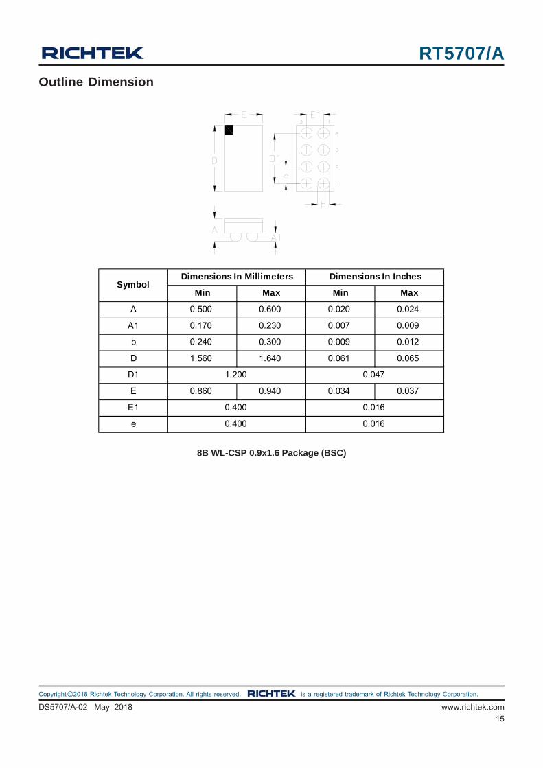
Outline Dimension
Min Max Min Max
A 0.500 0.600 0.020 0.024
A1 0.170 0.230 0.007 0.009
b 0.240 0.300 0.009 0.012
D 1.560 1.640 0.061 0.065
D1
E 0.860 0.940 0.034 0.037
E1
e 0.400 0.016
SymbolDimensions In Millimeters Dimensions In Inches
1.200 0.047
0.400 0.016
8B WL-CSP 0.9x1.6 Package (BSC)

RT5707/A
16
DS5707/A-02 May 2018www.richtek.com
Richtek Technology Corporation14F, No. 8, Tai Yuen 1st Street, Chupei City
Hsinchu, Taiwan, R.O.C.
Tel: (8863)5526789
Richtek products are sold by description only. Richtek reserves the right to change the circuitry and/or specifications without notice at any time. Customers should
obtain the latest relevant information and data sheets before placing orders and should verify that such information is current and complete. Richtek cannot
assume responsibility for use of any circuitry other than circuitry entirely embodied in a Richtek product. Information furnished by Richtek is believed to be
accurate and reliable. However, no responsibility is assumed by Richtek or its subsidiaries for its use; nor for any infringements of patents or other rights of third
parties which may result from its use. No license is granted by implication or otherwise under any patent or patent rights of Richtek or its subsidiaries.
Footprint Information
e A B
NSMD 0.240 0.340
SMD 0.270 0.240
ToleranceFootprint Dimension (mm)
PackageNumber of
PinType
±0.0250.400WL-CSP0.9x1.6-8(BSC) 8