Ultra Low Power Wake-Up Receiver with Unique Node ...
56
Ultra Low Power Wake-Up Receiver with Unique Node Addressing for Wireless Sensor Nodes Travis Lee Cochran Thesis submitted to the faculty of the Virginia Polytechnic Institute and State University in partial fulfillment of the requirements for the degree of Master of Science In Electrical Engineering Dong S. Ha, Chair Patrick Robert Schaumont Yaling Yang December 6 th , 2011 Blacksburg, VA Keywords: wake-up receiver, ultra-low power, wireless sensor network, serial code detector Copyright © 2011 by Travis Lee Cochran
Transcript of Ultra Low Power Wake-Up Receiver with Unique Node ...

Ultra Low Power Wake-Up Receiver with Unique Node Addressing
for Wireless Sensor Nodes
Travis Lee Cochran
Thesis submitted to the faculty of the Virginia Polytechnic Institute and State University in
partial fulfillment of the requirements for the degree of
Master of Science
In
Electrical Engineering
Dong S. Ha, Chair
Patrick Robert Schaumont
Yaling Yang
December 6th, 2011
Blacksburg, VA
Keywords: wake-up receiver, ultra-low power, wireless sensor network, serial code detector
Copyright © 2011 by Travis Lee Cochran

Ultra Low Power Wake-Up Receiver with Unique Node
Addressing for Wireless Sensor Nodes
Travis Lee Cochran
(ABSTRACT)
Power consumption and battery life are of critical importance for medical implant devices. For this
reason, devices for Wireless Body Area Network (WBAN) applications must consume very little power.
To save power, it is desirable to turn off or put to sleep a device when not in use. However, a
transceiver, which is the most power hungry block of a wireless sensor node, needs to listen for the
incoming signal continuously. An alternative scheme, is to listen for the incoming signal at a
predetermined internal, which saves power at the cost of increased latency. Another and more
sophisticated scheme is to provide a wake-up receiver, which listens for the incoming signal
continuously, and upon detection of an incoming signal, it wakes the primary transceiver up. A wake-up
receiver is typically simple and dissipates little power to make the scheme useful.
This thesis proposes a low-power wake-up receiver, which listens for a wake-up signal, identifies the
target node, and wakes up the primary receiver only when that specific node is called upon. When a
wake up signal is transmitted to all of the nodes on a network, our wake-up receiver allows all the nodes
on a network except the targeted node to remain asleep to save power. Several wake-up receiver
topologies have been proposed. This work uses a passive Cockcroft-Walton multiplier circuit as an RF
envelope detector followed by a simple detector circuit. A novel serial code detector is then used to
decode the pulse width modulated input signal to wake-up the designated node. A passive RF front end
and simple decoding circuit reduce power consumption substantially at the cost of low sensitivity. The

sensitivity of the wake-up receiver can be improved though the addition of an RF amplifier, but at the
cost of increased power consumption.
iii

Acknowledgements
I would like to thank all those who helped me get to where I am today. First I would like to thank
my parents for all their love and support and always pushing me to excel in all my endeavors. I also
want to thank to my sister for always setting a great example.
I thank Dr. Ha for his guidance and mentorship as my advisor. I have grown as an engineer and a
person under his tutelage and through my research, projects and writings. My time as a member of the
Virginia Tech VLSI for Telecommunications Lab will be the foundation of the rest of my career.
I would like to thank my committee members Dr. Patrick Schaumont and Dr. Yaling Yang for
their time and their interest in my research. I would also like to thank all of the members of the VTVT lab
who I’ve worked with other the past two year. Namely, Justin Cartwright, Na Kong, Jeongki Kim, Jihoon
Jeong, Jinsik, Yun, John Turner, Shaver Deyerle, Carlos Qeumada, and Jebreel Salem.
iv

Contents
1. Introduction .......................................................................................................................................... 1
2. Background ........................................................................................................................................... 5
2.1 Wake-Up Receivers ............................................................................................................................. 5
2.1.1 About Wake-Up Receivers ........................................................................................................... 5
2.1.2 Key Technical Problems ............................................................................................................... 6
2.2 Wake-Up Receiver Topologies ............................................................................................................ 6
2.2.1 FSK Wake-up Receivers ................................................................................................................ 7
2.2.2 Envelop Detection Wake-up Receivers ........................................................................................ 8
2.3 Identification of Nodes to Wake up .................................................................................................. 13
3. Architecture and Operation of the Proposed Wake-Up Receiver ...................................................... 16
3.1 Matching Circuit and Multiplier ........................................................................................................ 16
3.2 Signal Decoding Block ....................................................................................................................... 18
3.2.1 Operation ................................................................................................................................... 18
3.2.2 Communications Protocol .......................................................................................................... 21
3.2.3 Wake-Up ID Packet Structure ............................................................................................. 22
3.2.4 System Level Design Constraints ............................................................................................... 23
4. Design of Proposed System ................................................................................................................ 24
4.1 Discussion of Technology .................................................................................................................. 24
4.2Matching Network ............................................................................................................................. 25
4.3 Cockcroft-Walton Multiplier ............................................................................................................. 29
4.4 Over Voltage protection. .................................................................................................................. 31
4.5 DC Detector Circuit ........................................................................................................................... 33
4.6 Serial Code Detector ......................................................................................................................... 34
4.6.1 Delay Buffer Design .................................................................................................................... 35
4.6.2 Pass-Gate Flip-Flop Design ......................................................................................................... 36
4.6.3 Combinational Logic and Node ID storage ................................................................................. 37
5. Circuit Simulations .............................................................................................................................. 38
5.1 Transient Analysis ............................................................................................................................. 38
5.2 Power Analysis .................................................................................................................................. 40
6. Future Work ....................................................................................................................................... 45
v

7. Conclusion ............................................................................................................................................... 46
Works Cited ................................................................................................................................................. 47
vi

List of Figures
Figure 1: Wireless Boady Area Network ....................................................................................................... 1
Figure 2: Super Hederodyne Wake-Up Receiver .......................................................................................... 8
Figure 3: IF Envelope Detection .................................................................................................................. 10
Figure 4: Three BAW's connected to a Die ................................................................................................. 11
Figure 5: Cockcroft-Walton Wake-Up Circuit.............................................................................................. 12
Figure 6: Diagram of Wake-Up Receiver with Microprocessor .................................................................. 14
Figure 7: RF Envelope Detector with base band amplification ................................................................... 15
Figure 8: Proposed Signal Chain .................................................................................................................. 16
Figure 9: Cockcroft-Walton Multiplier Operation ....................................................................................... 17
Figure 10: Passive RF front end ................................................................................................................... 18
Figure 11: Low Power Serial Code Detector Circuit .................................................................................... 19
Figure 12: Long and Short Pulses Detected ................................................................................................ 20
Figure 13: Clock Signal Generation ............................................................................................................. 20
Figure 14: Restricted Node ID's................................................................................................................... 22
Figure 15: Sample Wake-Up Packet ............................................................................................................ 23
Figure 16: System Schematic in Cadence.................................................................................................... 24
Figure 17: Multiplier Circuit S-Parameters ................................................................................................. 25
Figure 18: Pi Match Schematic .................................................................................................................... 27
Figure 19: S11 of Multiplier circuit with Matching Network ...................................................................... 27
Figure 20: Matching Network with and without inductor resistance......................................................... 28
Figure 21: S21 of Impedance Matching Network ....................................................................................... 29
Figure 22: Cockcroft-Walton Multiplier Schematic .................................................................................... 30
Figure 23: Over Voltage Protection Circuit ................................................................................................. 32
Figure 24: Over-Voltage Protection Kicking in at 1.6V ................................................................................ 33
Figure 25: DC Detector Schematic .............................................................................................................. 34
Figure 26: Serial Code Detector Schematic ................................................................................................. 35
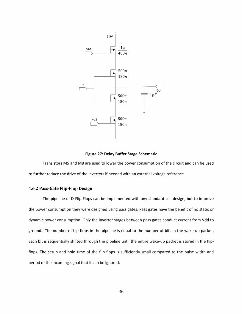
Figure 27: Delay Buffer Stage Schematic .................................................................................................... 36
Figure 28: Pass Gate Flip Flop Schematic .................................................................................................... 37
Figure 29: Transient Simulation .................................................................................................................. 39
Figure 30: Pulse Width Modulated Signal and Delayed Copy ..................................................................... 40
Figure 31: Flip Flop Output ......................................................................................................................... 40
Figure 32: Transient Power Consumption when receiving a message…………………………………………………….41
Figure 33: Comparison of Wake-Up Receivers Performance ..................................................................... 44
vii

List of Tables
Table 1: Power Consumption of Decoding Blocks ...................................................................................... 41
Table 2: Comparison with other Designs .................................................................................................... 43
viii

1
1. Introduction
Wireless body area networks (WBANs) are expected to make sweeping changes in the medical field
as well as many other applications [5]. The Wireless Body Area Network (WBAN) draft standard, IEEE
Draft 802.15, is being developed for the communication of wireless devices about your person for
medical, athletic, and multimedia applications. The network consists of a central hub, which
communicates with wireless devices within a 2 meter range. These devices can include medically
implanted sensors/devices such as pacemakers, blood glucose sensors, and blood pressure sensors,
wearable sensors such as pedometers, and enhanced reality or multimedia devices. The network
protocol is also design to communicate with external wireless interfaces, which can be added to the
network or relayed to through an external hub. These devices can include an electronic doctor’s chart to
read your medical sensor data, a wireless smart home system, and many other applications.
Figure 1: Wireless Boady Area Network [1]
Used under fair use guidelines, 2011.
2
The wireless sensors on the network should have as long a battery life as possible to reduce
frequency batteries need to be replaced. This can be achieved through low power design and energy
scavenging. Surgically implanted medical sensors are especially critical since replacing the battery may
require additional surgery. It may be possible to recharge some of these sensors inductively but
extending the battery life through low power design allows for less interaction by the user.
WBAN devices should be able to run off of small batteries or energy scavenged from the ambient
environment, allowing them to be implantable or wearable for medical applications. The power
consumption of a WBAN device is of critical importance and poses significant design challenges.
Frequent battery recharging or replacement of implanted sensors entails surgical operations and
possible exposure to harmful infections. Therefore, an advanced power management scheme is
required to prolong the battery life and increase the lifespan of WBAN devices.
The RF front-end of a wireless device is responsible for major power dissipation in the system, and it
is particularly true for small wireless devices in WBANs, where data communication occurs for a short
period of time. Reducing power consumption of the RF front-end while the node is idle is very important.
Duty cycling is a popular wake-up scheme [6]. WBAN nodes sleep in an idle state most of the time, while
waking up at the predefined time to communicate with the host. This approach can reduce the amount
of energy used by exploiting the inherent low frequency changes characteristic of biomedical
information. However, the low duty cycle results in increased latency in communication. Moreover,
WBAN devices still wake up even if there is no data to transmit or receive, which results in redundant
energy dissipation.
This thesis presents a wake-up receiver, which targets for the 2.4 GHz ISM band although the main
transceiver is likely to operate in the 402-405 MHz medical implant communication service (MICS) band.
The wake-up receiver can operate in whichever band is allocated for the target application with little

3
modification. The proposed wake-up receiver consists of a carrier sensing circuit and a serial code
detector. The carrier sensing circuit is implemented with passive elements and is triggered by radio
energy to minimize power dissipation. Meanwhile, the code detector decodes the received signal and
generates an asynchronous interrupt signal to the main processor and transceiver when the node is
called upon, thus enabling the main transceiver to react quickly. We propose a simple protocol to
support the proposed asynchronous wake-up receiver.
The main contribution of this thesis is combining a low power wake-up receiver front end with a
serial code detection circuit which can decode the pulse width modulated information from the carrier.
This decoded node ID is compared to each node’s assigned ID and an interrupt is generated at the target
node to wake the processor and main RF transceiver. For other proposed wake-up receivers the
processor has to wake on every node to decode the incoming packets, wasting power and lowering the
wireless nodes battery life.
This thesis is organized as follows:
Chapter 2 provides the background for wake-up receivers with special consideration for
WBAN’s and different power saving techniques for wireless sensor networks. This includes
both MAC layer power savings as well as different wake-up receiver designs. Several general
types of wake-up receivers are discussed with specific examples given and analyzed.
Chapter 3 covers the architecture of the proposed wake-up receiver with system level
design constraints and concerns. Several possible design tradeoffs are discussed which
would allow the performance of the proposed design to be tailored for a specific application.
Chapter 4 goes into the details of this wake-up receiver design. The design of each block in
the signal chain is discussed and analyzed, starting with the input at the antenna, through a
matching network, the Cockcroft-Walton multiplier, and the DC detector. Followed by the

4
serial code detector and the design of its components, e.g. the pass gate flip flops and delay
buffer.
In Chapter 5, the simulation results of the proposed wake-up receiver are analyzed. These
results are compared to other recently published wake-up receiver designs to illustrate the
tradeoffs between the design primarily with regards to power consumption, sensitivity, and
bit rate.
In Chapter 6, the future plans for this work are discussed to see this design fabricated and
tested to verify the simulations as well as possible improvements.
In Chapter 7, we conclude this thesis by summarizing the benefits and unique features of
the proposed wake-up receiver.

5
2. Background
This chapter provides the background for wake-up receivers with special consideration for
WBAN’s and different power saving techniques for wireless sensor networks. This includes both MAC
layer power savings as well as different wake-up receiver designs. Several general types of wake-up
receivers and their topologies are discussed with specific examples given and analyzed.
2.1 Wake-Up Receivers
The primary purpose of a wake-up receiver is to lower the power consumption of the primary
transceiver for wireless sensor networks. A wake-up receiver should dissipate low power, typically less
than 100µW. The required data rate of a wake-up receiver is much lower than that for the primary
transceiver. The RF sensitivity is also around 30dB less than that of primary receivers [1].
2.1.1 About Wake-Up Receivers
A wake-up receiver enables a wireless sensor network to save power by turning off the main
transceiver unless it is needed. There are two main power saving options provided in the draft standard
for Wireless Body Area Networks (WBANs), IEEE Draft 802.15 [2]. The first technique is the use of
Beacon Periods, in which the hub assigns each network node a specific time slot to communicate with
the hub. The node also has the option to sleep for a number of beacon periods before waking up to
transmit the data or to simply synchronize with the hub and return to sleep [3]. This MAC layer power
saving option allows for the node to sleep, turning off its transceiver and other system components until
the next scheduled beacon period. A major shortcoming of this option is latency. If the nodes are
sleeping through many beacon periods before communicating, the latency can be large. The long latency
is undesirable for medical applications such as the ones for WBANs. To set the time to wake up and
communicate with a beacon period, the wireless node must have an accurate clock running. Also the

6
accuracy of the timer determines how long a node can sleep through beacon periods and correctly
wakes up within its predetermined time slot to avoid overlap the communications with following nodes.
The second power saving option comes from the physical layer through the adoption of a wake-
up receiver. If a node on the network indicates that it has a wake-up receiver, the hub requests the
specific node via the wake-up receiver and then communicates with the node once the main transceiver
is powered up. This option incurs low latency compared with sleeping through many beacon periods.
The wake-up receiver latency is only limited by the bit rate (which is usually low) of the wake-up receiver
and the wake-up time of the RF transceiver and the processor. This option does not need a digital clock
and a timer, although the addition of the wake-up receiver will consume more power than the main
transceiver alone.
2.1.2 Key Technical Problems
Minimizing the power consumption is a major concern for any wake-up receiver design.
However, lowering the power consumption usually results in decrease of the input sensitivity, which
decreases the range and increases the BER (bit error rate). Also since a wake-up receiver is supplemental
to the main RF transceiver, its footprint should be minimized, so its cost does not outweigh the power
savings.
2.2 Wake-Up Receiver Topologies
There are two major communication schemes used for wake-up receivers, which are discussed
below with their respective topologies. First there are FSK wake-up receivers which encode the packet
data in frequency variation. These are usually more complex but higher performing than other designs.
Typically super-heterodyne or super-regenerative receiver topologies are used. The other main
communication scheme uses simple on-off keying and envelope detection in the receiver. These
receivers can use a mixer to bring the incoming signal down to baseband or do the envelope detection

7
at high frequency. The Cockcroft-Walton multiplier is a commonly used circuit for high frequency
envelope detection.
There are many proposed topologies for wake-up receivers. Two primary modulation schemes,
on-off keying (OOK) and frequency-shift keying (FSK), are commonly used due to their simplicity for
demodulation, and the simplicity allows for low power consumption [4]. However, these modulation
schemes provides low data rates compared with more sophisticated coding schemes, but a high data is
not required for a wake-up receiver.
2.2.1 FSK Wake-up Receivers
An FSK receiver is less sensitive to path loss than an envelope detector and is inherently more
linear. The RF carrier of a super-heterodyne FSK receiver is down-converted to an intermediate
frequency (IF), which mitigates adverse effects of parasitics. Further, an IF amplifier consumes less
power than an RF amplifier due to a lower operating frequency. Figure 2 shows a super-heterodyne
receiver which mixes in incident signal with two signals 90 degrees out of phase with each other,
yielding an I and Q signal at low frequency, which are then amplified. A super-heterodyne FSK wake-up
receiver can achieve a reasonably high data rate using both the I and Q channel, and high sensitivity but
at the cost of high power consumption. The local oscillator (LO) of a super-heterodyne FSK wake-up
receiver consumes a lot of power in this topology. For example, the FSK wake-up receiver in [2] achieves
50 kbps and -65 dBm, but consumes 126 , which is quite high.

8
Figure 2: Super Hederodyne Wake-Up Receiver [5]
Used under fair use guidelines, 2011.
Super regenerative receivers, first proposed by Armstrong back in 1922, are also applied for FSK
wake-up receivers. Super regenerative receivers achieve high gain and low power consumption, as they
operate near the threshold of instability. Negative feedback in the form of a quenching circuit is often
used to keep the amplifier stable. A super regenerative receiver can also be used for envelope detection
[5].
2.2.2 Envelop Detection Wake-up Receivers
Envelope detection is popular for wake-up receivers due to its simplicity. A simple envelope
detector receiver is composed of a diode rectifier followed by a low pass filter. Such a simple receiver
has very low sensitivity. Two approaches have been used to boost the sensitivity, down-mixing with low
frequency amplification and voltage multipliers, both illustrated below.
2.2.2.1 Intermediate Frequency Envelope Detection

9
There are several proposed wake-up receiver designs which mix the RF signal down to an
intermediate frequency before the envelop detector. Figure 3 uses a local oscillator (LO) and a mixer to
convert the incoming RF signal down to IF. The lower frequency signal is then amplified before passing
through an envelope detector generating a baseband signal. The baseband packet data is decoded by
the processor to determine if the node is going to wake up. The benefit of this design is that to achieve
the same receiver sensitivity, the IF amplifier dissipates less power than an RF amplifier [4]. However,
the LO required for the super-heterodyne topology is power hungry. One unique approach is to use a
ring oscillator with an unknown exact frequency [6] instead of a traditional LC oscillator. A ring oscillator
dissipates less power than an LC oscillator, but its frequency is dependent on process and temperature
variation which causes the IF to vary. This would be a problem for a fixed IF architecture, but the exact
frequency of the IF is irrelevant for the envelop detector. This architecture achieves a sensitivity of -72
dBm at 100 kbps with a power consumption of 52 µW [6]. A similar design achieves -87 dBm at 250kbps
for 83µW of power consumption [7]. One caveat of this design is that the input filter has to have a high
Q to reject adjacent channels due to the wideband amplification which would amplify other nearby
signals which were mixed down near the IF.

10
Figure 3: IF Envelope Detection [7]
Used under fair use guidelines, 2011.
Another approach which has been proposed is to duty cycle the operation of the wake-up
receiver such that it effectively samples the channel every bit period for the wake-up signal [8]. By duty
cycling the operation of the wake-up receiver the effective power consumption can be reduced and the
latency will not be increased significantly as long as the duty cycle period is short. Once an initial wake-
up preamble (1kbps) is detected the wake-up receiver can stay active to decode the incoming packet at
a higher data rate of 200kbps before returning to the duty cycling operation. In [9] a down sampling
clock is used to convert the signal to an IF before amplifying and digitizing the signal.
A Clock Harvesting GSM circuit is used as a wake-up receiver in [10] uses both an LNA before a
mixer as well as several IF amplifier stages after the mixer to achieve a sensitivity of -87dBm although
the number of amplifiers yields a high power consumption of 126µW. This design like several other
envelope detectors uses a Surface Acoustic Wave (SAW) resonator to achieve high selectivity on the

11
input [11]. This allows for out of band signals to be filtered out before the mixer and envelope detector.
Both SAW’s and thin-film bulk acoustic resonators (FBAR or BAW) are useful for high Q RF filters and
have a smaller form factor than crystal filters or off chip LC filters. Because of their small size, a BAW can
be implemented in the same package as the IC die and connected through wire bonds [12].
Figure 4: Three BAW's connected to a Die [13]
Used under fair use guidelines, 2011.
2.2.2.2 High Frequency Envelope Detection
An amplification of an RF signal is often needed for the envelope detection. Instead of using an
RF amplifier (which dissipates power), it can be accomplished with a voltage multiplier like a Cockcroft-

12
Walton circuit [13]. The Cockcroft-Walton Multiplier was first developed for generating large DC
voltages for particle physics experiments in 1922 by John Cockcroft and Ernest Walton. Although
designed for high power applications this circuit is also useful for low power circuits as well. Functionally
the Cockcroft-Walton multiplier works on the same principle as a voltage doubler, just with some
number of stages stacked in series. The modeling of this multiplier circuit at UHF [14] shows the
maximum sensitivity of the receiver with the multiplier circuit to be -32dBm [14]. Figure 5 shows a
circuit diagram of their work. From the antenna in they have a power matching network to ensure
maximum power transfer of the received RF signal. Next they have an N stage Cockcroft-Walton voltage
multiplier. The DC output voltage of this circuit is ideally 2N times larger than the peak to peak input RF
voltage. However, there are losses in the diodes which prevent this. Their work intends to generate a 1
V output. If the output voltage can be detected as a smaller voltage, then the sensitivity could be
improved. The circuit has also been applied for supplying the operating power for very low power
applications such as RFID [15].
Figure 5: Cockcroft-Walton Wake-Up Circuit [17]
Used under fair use guidelines, 2011.

13
2.3 Identification of Nodes to Wake up
Existing wake-up receiver designs based on the Cockcroft-Walton Multiplier have a similar signal
chain from the antenna through the multiplier, and into some sort of detector with a digital output.
However, the output of the detector is used in different ways. Most commonly a microprocessor is used
to read the output of the detector. This output has been used directly as an interrupt [16], but this
requires every wake-up receiver on the network to wake the processor when the carrier is detected on a
predetermined channel. It also requires each processor to stay active for the decoding of the entire of
the wake-up packet to decode the incoming OOK message [17]. Simply using the wake-up receiver as a
carrier detection circuit also requires that a channel is dedicated to wake-up communication only,
limiting the channels available for the active nodes to use for communication.
Another approach proposed has been to use multiple multiplier circuits in parallel; each
input filtered to receiver a different frequency [18]. Using this method the presence or absence of the
carrier at each frequency can be used identify the specific node the hub is trying to wake-up. This has
the benefit or only waking a single node on the network and not all, saving power. The unused wake-up
channels can possibly be used for data communications with possibility of accidentally waking up other
nodes.
However, this system requires a larger footprint on the die. As the number of nodes on the
network grows the number of multiplier circuits needed increases as n where:
The use multiple channels in the band to wake a single node on the network is also a very inefficient use
of the available RF spectrum.
14
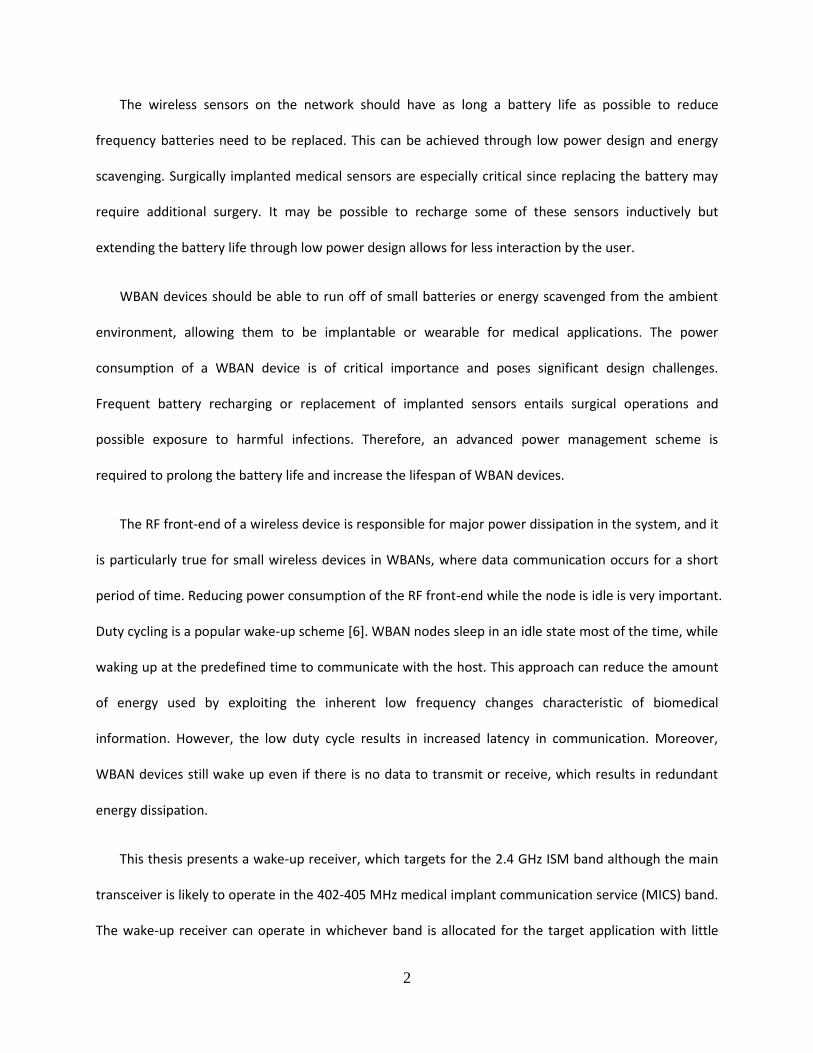
Using the processor on the node to decode the incoming signal for node addressing removes the
need for a dedicated wake-up channel and/or having multiple multipliers. The processor input is still
used as an interrupt but after the processor is active, it can decode the incoming signal either using on-
off keying (OOK) or pulse width modulation (PWM). The main drawback of this system is that the
processor for every node in the network has to wake up and decode each wake-up signal on the
network as well as false wake ups when the carrier for a normal packet is detected in the same channel.
Since it will only stay awake and perform the requested function if it correctly reads the ID for that
specific node this does not hurt the operation of the system. Instead the constant use of the processor
wastes power unnecessarily. In several papers discrete microcontrollers have been used to this end. For
a TI MSP430 which is a low power processor, the power consumption changes from 440nW to around
1mW when switching to active operation [19].
The wake-up receiver proposed in this thesis attempts to address these problems. The proposed
receiver has a simple and dedicated decoder for identification of nodes, which decodes the wake-up
packet received and wakes up only the designated node.
Figure 6: Diagram of Wake-Up Receiver with Microprocessor
Another issue with the multiplier circuit is that it has wideband operation. This requires the Q of
the initial filter to be sufficiently high such that the adjacent channels not being used to wake-up signals
are filtered out. Due to the limitations for the Q of on chip inductors, it has been proposed to use a BAW

15
[6] to achieve a high Q input filter for RFIC designs. A BAW can have a Q from several thousand to
several million, allowing for a very narrow band filter to be created.
Figure 7: RF Envelope Detector with base band amplification [12]
Used under fair use guidelines, 2011.

16
3. Architecture and Operation of the Proposed Wake-Up Receiver
The proposed architecture for this wake up receiver combines the use of a carrier detection circuit
and the proposed Serial Code Detector to read data from the carrier. Following the signal path from the
antenna, there is a matching network and filter for maximum power transfer and to filter out adjacent
channels. Next in the signal path is a Cockcroft-Walton multiplier which works like a charge pump to
create a DC voltage from the received RF signal [20] [21] [22]. After the multiplier, there is an over-
voltage circuit to prevent the DC voltage on the output of the multiplier from rising to levels where it
could damage the system. A DC detector circuit generates a digital output from the carrier pulses
received and converted to DC pulses. The serial code detector allows for pulse width modulated data to
be read from the carrier without any form of synchronization. The serial code detector then generates
an interrupt to wake the node’s processor and main RF block to respond to the wake-up signal as
needed.
Figure 8: Proposed Signal Chain
3.1 Matching Circuit and Multiplier
The matching circuit connecting the antenna to the rest of the circuit serves two functions. First
it matches the input impedance of the multiplier to the antenna. This provides maximum power transfer
of the received signal. Secondly the matching circuit filters out other frequency bands so only the carrier
in the channel designated for wake up signals will be detected. For adjacent channels to be filtered out

17
the Q of the matching circuit must be sufficiently high. For wide channel spacing the LC network used is
adequate but if the application requires the channels to be closely spaced a better filter will be required.
Next in the signal chain a Cockcroft-Walton multiplier, constructed of N stages where each stage
doubles the output voltage of the circuit. However, for large numbers of stages, losses from the
capacitors in each stage, especially near the input cause the output voltage to ‘sag’. A single stage of the
multiplier is shown in Figure 2.a. When the polarity of the input voltage is negative, a current is
conducted through D2, charging up the capacitor C2. Then when the polarity of the input changes the
charge on C2 conducts through D1 to charge C1. The voltage on the input plus the voltage across C2
yields twice in input voltage on C1 for 10 V in this case, as a voltage doubler should operate. The
operation of this multiplier is the same as additional stages are added, allowing for the input to be
multiplied to a large voltage.
C1AC
C2
AC
C2
C1AC
C2
-
+
+
-
+-
+
+-
-5V
5V
10V
5V
Figure 9: Cockcroft-Walton Multiplier Operation
Up till this part in the circuit all of the circuit elements are passive [4]. This means that there is no
active current or leakage current for the RF front end of the receiver. Among several DC sensing circuits
proposed so far [1] [6][7][8][10], the most basic design is a series of inverters, which yields a digital
output. The inverter in [2] has a sensitivity of around -30 dBm and a static current consumption of 2.6 µA.
The power consumption sensitivity level of -72 dBm with 52 µW power consumption has been achieved
I I

18
on chip at the cost of increased complexity [10]. A discrete comparator was used for -65 dBm with 2.8 µW
[6]. An integrated solution in [7] has a sensitivity of -31 dBm with a current of only 900 nA.
Figure 10: Passive RF Front End
3.2 Signal Decoding Block
To determine if the received wake-up packet is addressed for the wireless node the packet must be
decoded and the node ID compared to the nodes unique ID on the network. All of the wake-up receivers
previously analyzed, the packet data is simply sent to a processor to be checked against the node ID. This
requires a processor in every sensor node on the network to wake to check the ID before returning to
sleep. By comparing the received ID to the node’s ID, only the processor on the requested node is woken
up.
3.2.1 Operation
The main contribution of this paper is the combination of the carrier detection circuit and a node
identification circuit as described in the following. The digital data from the DC detector circuit is applied
into a pipeline of nf D flops as shown in Figure 4, where nf is the number of bits needed to uniquely
identify each node on a WBAN. Because there is no clock signal, the input from the DC detector is delayed
through a series of buffers before its rising edge can trigger the flip flops. The delay of these buffers is
significant and will be discussed later in more detail. Once the data in the flip-flops matches a preset

19
identifier in a register, or some other memory device, an interrupt is sent to the node processor, which
resets the pipelined flip-flops, and turns on the primary transmitter and receiver. It can then respond to
the hubs wake up request, and handle any necessary tasks before disabling the primary receiver and
returning to sleep.
Figure 11: Low Power Serial Code Detector Circuit
A typical scheme for timing is established through an alternating sequence such as 101010… at the
preamble of the message, which is used to synchronize the receiver. The scheme is widely used, but
requires a level of sophistication beyond what is needed for a simple wake-up receiver. Other methods
such as pulse interval encoding have been proposed [1], but require a constant clock to determine the
length of these intervals. Instead, we propose adoption of pulse width encoding to differentiate
between logical one and zero. The different widths are used such that the delay is longer than the
short pulse (logical 0), but shorter than the long pulse (logical 1). This means that when the flip-flop
reads the input after time delay, a long pulse keeps the input high, but the short pulse has gone low
already. This scheme allows for a binary message to be received by the receiver without synchronization
or using a timer.

20
The timing diagram in Figure 5 shows the carrier pulses charging up the RF front end and the
resultant output of the DC detector. Note that the setup and hold time of the flip-flops is short
compared to the pulse widths and time delay. Figure 6 shows clock signal generation, where the input
signal is delayed through a buffer chain to create the clock signal.
Figure 12: Long and Short Pulses Detected
Figure 13: Clock Signal Generation

21
3.2.2 Communications Protocol
One difficulty with the proposed system is that the strength of the carrier signal decreases with
as
the receiver moves away from the transmitter. Although the distance in a WBAN should not exceed two
meters [5], this still affects the received power. A wake-up receiver closer to the transmitter charges its
voltage multiplier more rapidly, yielding longer pulse widths for both the short and long pulses. Likewise a
receiver far from the transmitter has shorter pulses. To solve this problem, we propose that the initial
wake up signal sent from the hub uses the minimum power and carrier pulse width. If the hub receives no
response from the node, then it successively increases the transmission power or pulse width until a
response is received from the node. Initially all of the pulses should be relatively short causing the circuit
in Figure 3 to read all zeros. As the pulse width increases in steps less than , the correct node reaches
the threshold, where the long and short pulses are read correctly as ones and zeros regardless of its
proximity to the transmitter. If the increase in the pulse width is larger than , there is a possibility of
reading all zeros and then all ones in two successive messages and not correctly receiving the actual
signal.
If the range of the network is extended further, this problem becomes more pronounced, and the
latency of the system increases as the system takes longer to sweep the entire pulse widths. Two
solutions are possible to this problem. First, the hub can remember the required pulse width of the target
node at the last transmission and starts from only a slightly smaller width than the required one.
Assuming that the path to that node does not change dramatically between two successive wake-ups it
should only take several tries to wake the node starting from minus one or two pulse widths from the
previous message. Secondly, two or more serial code detectors are implemented in parallel receiving
data from the same DC detector, effectively dividing up the search space. Each detector should have a
different buffer delay, and , which allows for the correct pulse width to be found more rapidly,
reducing the latency

22
3.2.3 Wake-Up ID Packet Structure
The wake-up ID packet should be as simple as possible to keep the length of the packet small. At
a minimum, the packet must consist of a header, and the ID of the node which is being requested by the
hub. The header is to ensure that the full packet has been decoded by the serial code detector and not
half a packet being shifted in or out. The contents of the header must be reserved, and not duplicated in
the rest of the packet. Otherwise when a new packet was being received, it would shift to the head of
the packet, and cause an unnecessary wake-up. As seen in Figure 14, for the header 1001, the node ID
for every node on the network cannot start with 001, or end with 100.
1001xxxxx
1001001x-forbidden, header repeats in packet
Xxxxxx100 – 1001xxxxx – forbidden previous packet causes header to repeat
Figure 14: Restricted Node ID's
The heart of the packet is the node ID. The length of the node ID is determined by the maximum
numbers of nodes on the network where ( ) ( ) is the maximum number of nodes on
the network for n bits in the ID. The ( ) term removes all of the restricted ID’s starting with 001 or
ending with 100 for the header value of 1001 to prevent unnecessary wake-ups. To remove any ID’s
which contain the header within itself the ( ) term is added. Figure 15 illustrates the packet
structure with the preamble, node ID, and potentially a parity bit for error checking.

23
Node ID01011….
Parity Bit
Preamble100
Figure 15: Sample Wake-Up Packet
3.2.4 System Level Design Constraints
There are several design constrains on a wake-up receiver for it to be practical for use in a real
application. First the sensitivity of the receiver must be high enough that the signal can be recovered
with the given source transmit power and maximum path loss. This may also include path losses through
body tissue in the case of medical implant devices which will attenuate the signal more than free space.
Another constraint pertains to the channel used for the wake-up signals and the data packets on
the same channel and/or adjoining channels. The wake-up packet is usually sent at a slower rate, 1kbps-
100kbps, than the data packets which can be transmitted at 10Mbps [23]. If the frequency selectivity on
the input of the wake-up receiver is low, then the data packets from the adjoining channel may cause
enough noise to corrupt the wake-up packet. If there is error checking in the wake-up packets such as a
parity bit this will help prevent unnecessary wake-ups but it will increase the latency of the wake-up
packets have to be send repeatedly.
The latency of the system must also be low enough for the wake-up receiver to outperform
duty-cycling of the main processor for the same power savings. For the power savings to be equal
between duty-cycled operation and an ultra-low power wake-up receiver, the duty cycle period will
have to be longer than the latency of the wake-up receiver. The system can wake quickly once the wake-
up packet is decoded, on the order of several microseconds [24]. The latency of the system may be
constrained for the given application but this can be traded for power consumption by using a different
wake-up receiver topology.
24
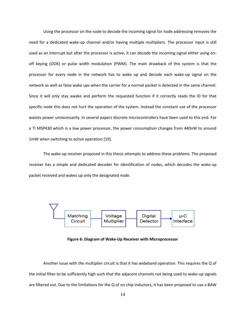
4. Design of Proposed System
The design of the proposed wake up receiver will be discussed starting from the receiving antenna
and matching network and then follow the signal path through the multiplier circuit, DC detector, and
serial code detector.
Cockcroft-Walton Multiplier
DC Detector Serial Code Detector
RF Antenna
Interrupt to Processor
Node ID
Figure 16: System Schematic
4.1 Discussion of Technology
For this design the National Semiconductor 180nm process has been used although this process
lacks Schottky diodes which are preferable for this design. Instead diode connected NMOS FET
transistors are used for the Cockcroft-Walton multiplier. The design was simulated with an off chip
inductor for a higher Q although an on chip inductor could be used.
25
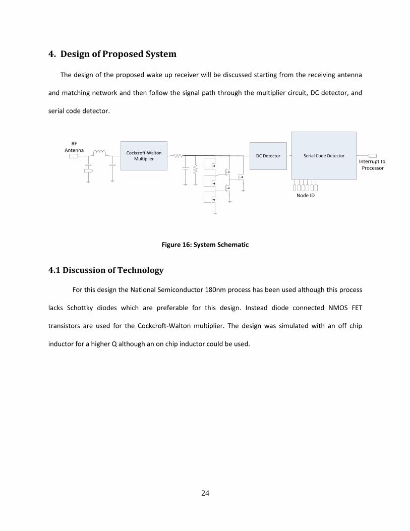
4.2Matching Network
The antenna’s 50 Ohm impedance needs to be matched to the input impedance of the
Cockcroft-Walton Multiplier for maximum power transfer. For this to be done the input impedance of
the multiplier must first be found by measuring the S-Parameters.
Figure 17: Multiplier Circuit S-Parameters
These measurements are then used to calculate the input reflection coefficient.

26
√
| |
Where
| | | |
| |
With the input reflection coefficient the input impedance can easily be found using the normalized
impedance of 50 Ohms.
For this application a relatively high Q is desired for the matching network to filter out any adjacent
channels so only the target carrier frequency will charge the multiplier circuit. A π match is used to allow
for control of the Q. The value of each component can be found from the following equations where X3
is an inductor and the rest are capacitors.
| | | |
| |
[ ]

27
Figure 18: Pi Match Schematic
Figure 19: S11 of Multiplier circuit with Matching Network

28
This provides a good match at the target frequency with an s11 of -46dB at 2.4GHz. However, this is for
an ideal inductor. Assuming the Q of the inductor is 100, which is more practical of an off chip inductor,
we get an s11 of -10dB.
This is still a reasonable match and can be seen in Figure 20 compared to the lossless inductor.
Figure 20: Matching Network with and without inductor resistance
The addition of the inductor resistance also turns this matching network into a lossy network as seen
by the s21 in Figure 21. The network was simulated to have a loss of 2.5dB at 2.4 GHz. If the inductor
was implemented with a low Q on chip spiral inductor this loss would be higher. If available a high Q

29
filter could be implemented with an acoustic resonator. This could be implemented in the same package
and connected by bond wires as in [6].
Figure 21: S21 of Impedance Matching Network
4.3 Cockcroft-Walton Multiplier
Envelope detectors are a well-known circuit for receiving AM signals. The simplicity of such
circuits makes them desirable for low power wireless applications. A Cockcroft-Walton multiplier circuit,
shown in Figure 22, enables a carrier to be detected by charging up a DC voltage when receiving an AC
signal. This works like an envelope detector if the information in the carriers transitions slowly

30
compared to the charge time of the multiplier circuit with the benefit of not needing active
amplification.
1 pF 1 pF 1 pF 1 pF
1 pF 1 pF 1 pF 1 pF 1 pF 1 pF
1 pF 1 pFInput
Output
Figure 22: Cockcroft-Walton Multiplier Schematic
The output voltage of the multiplier circuit is a function of the number of stages and the voltage
drop of each stage. This can be estimated by following equation neglecting losses.
The voltage drop is also dependent on the load current and can be calculated as.
[
] ( )
Where C is the stage capacitance, f is the AC frequency, and is current through the load.
The DC output will also have an AC ripple which is fed through from the input. This ripple can be
calculated as
[
] ( )
For an input of 0.2 volts peak to peak and 6 stages the output voltage of our multiplier should
be.
[
] ( )

31
This matches closely to the simulation results shown in the next section. A more accurate model
for a Cockcroft-Walton Multiplier shown below is given in [20]. This model takes into account the diode
characteristics and uses Bessel and the Lambert W functions if a precise analytical solution is needed but
for design purposes it is more efficient to use the simple model above and then tune the design using a
CAD simulation package.
( (
)
)
More stages can be added to the multiplier to increase the gain for better sensitivity. However,
the losses from the diodes increase with the number of staged with a cubed and a squared term for
diminishing returns. Also increasing the number of stages increases the design cost as the size of the
receiver on the die will increase.
4.4 Over Voltage protection.
The DC output of the multiplier is dependent on the number of stages in the multiplier, but also
the RF power level. The sensitivity of the receiver is low compared to active receiver designs, and an
input of -10dBm is required to generate a DC voltage of several hundred millivolts where it can be
detected by the rest of the circuit. However, if the RF power is large the DC output could easily reach a
voltage where it could damage components. This is not surprising, since the original application for the
Cockcroft-Walton Multiplier was to generate kilovolt DC levels for particle physics experiments.
To prevent high voltages from damaging the circuit, over voltage protection is included to bleed
off current when the voltage surpasses a set threshold. The simplest design is a diode to ground. When

32
the voltage reaches the threshold voltage for the diode it will begin to conduct current, keeping the
voltage at safe levels. However, the turn on voltage of a single diode is low (~0.7V), so several diodes can
be connected in series to raise the voltage at which all of the diodes begin to conduct. In addition to
bleed off current faster the nodes between those diodes can be used to turn on NMOS FETS connected
to ground.
20 kΩ
20 kΩ
1 pF
Input
Output
Figure 23: Over Voltage Protection Circuit
𝑛
𝑛
𝑛
𝑛
𝑛
𝑛
𝑢
𝑛
𝑢
𝑛
𝑢
𝑛

33
Figure 24: Over-Voltage Protection Kicking in at 1.6V
4.5 DC Detector Circuit
The DC Detector circuit is needed to detect when the output voltage of the multiplier
circuit reaches a certain threshold. Because the RF power received by the antenna is unknown, it is
difficult to predict what the voltage on the output of the multiplier circuit will charge too. To improve
the sensitivity of the receiver the DC detector’s threshold is set to 0.1 V. The figure below shows the
schematic for the DC detector with an inverter following for an active high output. The section of the
circuit inside the box is a beta multiplier which is used to generate the bias voltages for the PMOS loads
for the two inverter stages. In a fully integrated design these bias voltages may available from a global
voltage bias to reduce power consumption.

34
Figure 25: DC Detector Schematic
4.6 Serial Code Detector
The serial code detector decodes the wake up ID for the wireless sensor node from the pulse
width modulated signal. This detector consists of three components. A buffer chain to delay the input
signal, a series of D-flip flops to store each bit in the packet, and the combinational logic to compare the
contents of the flip flop to the node’s ID.
Beta Multiplier Bias Circuit
Current Source
𝑛
𝑛
𝑛
𝑛
𝑛
𝑛
𝑛
𝑛
𝑛
𝑛
𝑛
𝑛
𝑛
𝑛
𝑛
𝑛
𝑛
𝑛
𝑛
𝑛
𝑛
𝑛
𝑛
𝑛
𝑛
𝑛 𝑛
Ω

35
Figure 26: Serial Code Detector Schematic
4.6.1 Delay Buffer Design
The delay of the buffer chain must be larger than the short pulse, , while shorter than the long
pulse, . To achieve this long delay the capacitance is increased between the two inverters of each
buffer stage. This is accomplished adding a capacitor after each inverter, increasing the parasitic delay.
Lowering the drive of the first inverter also increases the delay of the buffer by making the buffer take
longer to charge up the capacitance between the inverters.
36
Out
In
vb2
Vb1
1.5V
Figure 27: Delay Buffer Stage Schematic
Transistors M5 and M8 are used to lower the power consumption of the circuit and can be used
to further reduce the drive of the inverters if needed with an external voltage reference.
4.6.2 Pass-Gate Flip-Flop Design
The pipeline of D-Flip Flops can be implemented with any standard cell design, but to improve
the power consumption they were designed using pass gates. Pass gates have the benefit of no static or
dynamic power consumption. Only the inverter stages between pass gates conduct current from Vdd to
ground. The number of flip-flops in the pipeline is equal to the number of bits in the wake-up packet.
Each bit is sequentially shifted through the pipeline until the entire wake-up packet is stored in the flip-
flops. The setup and hold time of the flip flops is sufficiently small compared to the pulse width and
period of the incoming signal that it can be ignored.
𝑛
𝑛
𝑛
𝑛
𝑛
𝑛
𝑛
𝑝𝐹

37
D
Qn
Q
nClk
nClk
Clk
Clk
Clk
Clk
nClk
nClk
Figure 28: Pass Gate Flip Flop Schematic
4.6.3 Combinational Logic and Node ID storage
The contents of the flip flop are compared to a present value via combinational logic. The
present value, which is the nodes unique ID, may be the contents of a memory address, register, or
other memory type accessible on the IC. It should not be hardwired because this would not allow for
different nodes to be programed with their own unique address. The output of each flip-flop is XNOR’ed
with the preset value. When the received packet matches the preset node ID all of the XOR gates yield a
low input which are AND’ed together. However, to prevent an AND gate with a large number of inputs,
it is broken up into two layers of logic with NOR gates feeding into NAND gates.

38
5. Circuit Simulations
The main performance parameters of wake-up receivers are the power consumption, sensitivity, and
the latency of its response to the hub. The two parameters are often traded as for the case of duty cycled
wake-ups. The more often it wakes up, the shorter the latency is, but the larger the power consumption.
The sensitivity of the receiver determines how powerful the hub transmitter must be. If a hub has a larger
power budget, a design with a lower sensitivity and hence more power efficient, can be used.
The proposed serial code detector circuit was designed and simulated using National
Semiconductor 180nm CMOS technology. To reduce the leakage current, the flip-flops use pass gates,
and the buffers and digital logic operate with a raised threshold voltage. The increased delay from the
raised threshold voltage is acceptable due to the low bit rate of the message. In fact, it is beneficial for
the delay buffer due to a longer delay for each stage.
5.1 Transient Analysis
The transient response of both a long and short pulse can be seen in Figure . The incoming RF
pulses are at 2.4GHZ, with a short pulse width of 100ns and a long pulse width of 1µs. The Cockcroft-
Walton multiplier output is labeled and reaches 0.5 volts to be detected by the DC detector circuit. The
DC detector output pulses are longer than the incoming RF pulse because the Cockcroft-Walton
multiplier charges up to the DC detectors turn on voltage quickly but because of the high impedance
load the charge on the output takes longer to dissipate, causing a longer pulse. The output of the delay
buffer can be seen delayed 500ns after the output of the DC detector.

39
Figure 29: Transient Simulation
Figure shows the DC detector output again with the delayed copy of it self while receiving six
bits. Below it in Figure the output of the first flip flop is shown on the same time scale for comparison.
Notice that the time between pulses can vary and not have any effect on the output. After receiving
these six bits the contents of the first six flip flops reads 010101.
CW Multiplier
DC Detector Output
Delay Buffer Output

40
Figure 30: Pulse Width Modulated Signal and Delayed Copy
Figure 31: Flip Flop Output
5.2 Power Analysis
The simulation results indicate that the leakage current of the entire serial code detector is about 1
nA with a 0.9 V supply. When the code detector receives a message with a bit rate of 200 Kbps, the
average current is 1.65 µA and power consumption of 1.489 µW. Figure shows the current profile while
receiving the data. Each current spike correlates to a carrier pulse being received and trigging the clock
for all of the flip-flops.
41
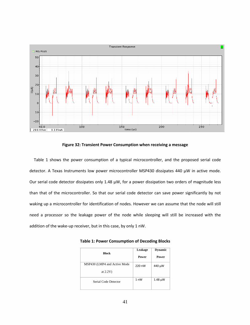
Figure 32: Transient Power Consumption when receiving a message
Table 1 shows the power consumption of a typical microcontroller, and the proposed serial code
detector. A Texas Instruments low power microcontroller MSP430 dissipates 440 µW in active mode.
Our serial code detector dissipates only 1.48 µW, for a power dissipation two orders of magnitude less
than that of the microcontroller. So that our serial code detector can save power significantly by not
waking up a microcontroller for identification of nodes. However we can assume that the node will still
need a processor so the leakage power of the node while sleeping will still be increased with the
addition of the wake-up receiver, but in this case, by only 1 nW.
Table 1: Power Consumption of Decoding Blocks
Block
Leakage
Power
Dynamic
Power
MSP430 (LMP4 and Active Mode
at 2.2V)
220 nW 440 µW
Serial Code Detector 1 nW 1.48 µW

42
We illustrate a wireless network with 20 nodes to compare our wake-up receiver to an existing system
based on processors for node identifications. Let’s suppose that the wake up signal takes 1 ms to process
for the existing system and for our wake-up receiver, and the target node is further processed for 30 ms
for our system. An existing system with the above microcontroller consumes 440 uW for 1ms for each
node for the node identification, and the total power consumption for 20 nodes is 8.8 mW. The proposed
serial code detector consumes 1.48 uW for 1 ms and 29.6 µW for 20 nodes. After all the nodes on the
network have decoded the wake up signal for our system, only the target node wakes for 30 ms to
consume 440 µw for 30 ms. The proposed wake-up receiver scheme saves energy by about 300 times
compared with an existing system.
Existing systems using a microprocessor to decode a received wake up signal consume more power
than the proposed serial detector, but incur less latency. Pulse interval encoding [1] or other encoding
schemes are able to wake up nodes and respond quickly regardless of its distance to the hub because as
long as the SNR of the received signal is high enough, the signal can be decoded. In contrast, the
proposed serial code detector and the associated protocol rely on successive transmissions until the
node can wake up to respond. Theoretically the target node can respond after one request from the
hub, but is likely that multiple tries will be needed. The number of tries needed is determined by the link
budget of connection, the time delay of the buffer chain, and the difference in pulse widths between the
large and small pulses. Further, the latency of our system increases as the wake up time of the node
increases. However, the increase can be as little as 3 µs [3], which can be acceptable for a WBAN
system.
The results of this work as well as other recent publications on wake-up receivers are listed in Table 2.
Also the power consumption is plotted versus the RF sensitivity in Figure . The power consumption of
our system includes the serial code detector which only consumes an additional 1.48 µW while receiving
a packet, for all of the other receivers in the comparison a processor on the node has to be used.

43
Although the node will have some low power processor its power consumption will be much closer to
the 440 µW of the Texas Instruments MSP430 than the serial code detector. The sensitivity is not the
only metric by which to judge the receivers performance but it correlates highly with the power
consumption. When including the fact that the proposed design decodes the incoming packet
independent of any processor on top of the low power consumption this work exhibits ultra-low power
consumption with a modest data rate of 200kbps. The only caveat is the low sensitivity compared to
other designs.
Table 2: Comparison with other Designs
Power Consumption
Sensitivity Data Rate Architecture
This Work
1.0 µW -28dBm 200kbps Serial Code Detector/envelope
detector
[17] 1.35 µW -28dBm 33kbps Cockcroft-Walton
Multiplier
[11] 2.4 µW -71dBm 9kbps Direct Down Conversion
[18] 2.6 µW -29.3dBm n/a Cockcroft-Walton
Multiplier [6] 52 µW -72dBm 100kbps Uncertain IF
[5] 56 µW -75dBm 100kbps Super-Regenerative
Receiver
[9] 123 µW -86dBm 10kbps Double Sampling RF
Power Detector
[4] 126 µW -65dBm 50kbps Passive Quadrature Mixer [25] 230 µW -60dBm 1Gbps Duty Cycled Operation
[7] 415 µW -82dBm 500kbps Duty Cycled PLL
[12] 26 mW -90dBm 50kbps BAW Resonator Based

44
Figure 33: Comparison of Wake-Up Receivers Performance
This Work
[5] [4]
[6]
[3]
[10]
[8]
[15]
[16]
[19]
[11]
-100
-90
-80
-70
-60
-50
-40
-30
-20
-10
0
0.1 1 10 100 1000 10000 100000
Sen
siti
vity
(d
Bm
)
Power Consumption (µW)
Wake-up Receivers' RF Sensitivity vs Power Consumption
45
6. Future Work Due to foundry issues this circuit has not been fabricated. Therefor to fully prove this design it
should be fabricated and measured to ensure that the circuit matches the simulations for performance.
By testing the functionality and measuring the power consumption, latency, and sensitivity the accuracy
of the simulated values can be found. Also this work was not targeting a specific application so there
were no target specifications for overall performance. Instead the design focused on lowering the power
consumption as much as possible.
Also this work is centered on the serial code detector and the pulse width modulation
communication scheme. To achieve a higher performance wake-up receiver while still saving power
decoding the signal the serial code detector can be applied to other envelope detector topologies to
replace decoding the signal with each nodes processor.

46
7. Conclusion A wake-up receiver can be used to improve the battery life of a wireless sensor node. By putting
the main RF transceiver to sleep and listening for wake-up signals the node can use less power and have
less latency than with duty cycling the operation of the main transceiver. There are several available
topologies for wake-up receivers. Primarily OOK envelope detectors and FSK super regenerative
receivers. Envelope detectors can offer very low power consumption but tend to have poor sensitivity
while a super regenerative receiver has better sensitivity but with higher power consumption.
A novel wake-up receiver has been proposed which combines an envelope detection Cockcroft-
Walton circuit with a serial code detector and pulse width modulated OOK communication protocol to
function as a very low power wake-up receiver, without the need for a local oscillator or processor to
decode the incoming packet. The serial code detector has an idle power consumption of only 1nW and
1.48µW when receiving a packet. Combined with the power consumption in the front end this wake-up
receiver only consumes 0.8 µW between wake-up packet transmissions. The latency of the receiver
depends on how many tries the hub has to make to find the correct transmit power level or pulse width
for the distance of the wireless node but on a body area network only 2 or 3 tries should be needed. A
single wake-up transmission takes 18 µs so we can approximate the latency to be 45µs. The data rate of
500kbps for long pulse widths of 1µs, but as the pulse width is increased to communicate with more
distant nodes the effective bitrate will decrease.
This design achieves very low power consumption through its use of a passive RF front end but
has lower performance than other higher power designs as would be expected. This design which
targets applications where battery life is critical can also have its performance improved by adding an
amplifier before the envelope detector trading off power consumption for better performance.

47
Works Cited
[1] R. Su, T. Watteyne and K. Pister, "Comparison between Preamble Sampling and Wake-Up Receivers
in Wireless Sensor Networks," in IEEE Global Telecommunications Conference, 2010.
[2] Draft Standard for Body Area Network, IEEE, 2010.
[3] W. L. Tan, W. C. Lau and O. Yue, "An Energy Efficient and Receiver-Driven MAC Protocol for Wireless
Sensor Networks," in IEEE Vehicular Technology Conference, 2007.
[4] M. Lont, D. Milosevic, G. Dolmans and A. van Roermund, "Ultra-Low Power FSK Wake-up Receiver
Front-End for Body Area Networks," Baltimore, MD, 2011.
[5] X. Yu, J.-S. Lee, C. Shu and S.-G. Lee, "A 53uW super-regenerative receiver for 2.4GHz wake-up
application," in Asia-Pacific Microwave Conference, 2008.
[6] N. Pletcher, S. Gambini and J. Rabaey, "A 52uW wake-up receiver with -72dB Sensitivity using an
uncertain-IF architecture," IEEE Journal of Solid State Circuits, pp. Vol. 44 No. 1 pp. 269-280, Jan.
2009.
[7] S. Drago, D. Leenaerts, F. Sebastiano, L. Breems, K. Makinwa and B. Nauta, "A 2.4 GHz 830pJ/bit
Duty-Cycled Wake-Up Receiver with -82dBm Sensitivity for Crystal-Less Wireless Sensor Nodes,"
2010.
[8] D.-Y. Yoon, C.-J. Jeong, J. Cartwright, H.-Y. Kang and S.-K. Han, "A new approach to low-power and
low-latency wake-up receiver system for wireless sensor nodes," Wireless Communication
Magazine, 2011.
[9] X. Huang, P. Harpe, G. Dolmans and H. d. Groot, "A 915MHz Ultra-Low Power Wake-Up Receiver
with Scalable Performance and Power Consumption," in ESSCIRC, 2011.
[10] J. Brown and D. Wentzloff, "A 1900 MHz-Band GSM-Based Clock Harvesting Receiver with -87dBm
Sensitivity," in IEEE Radios Frequency Intergrated Circuits Symposium, 2011.
[11] C. Hambeck, S. Mahlknecht and T. Herndl, "A 2.4uW Wake-Up Receiver for Wireless Sensor Nodes
with -71dBm Sensitivity," in International Symposium on Circuits and Systems, 2011.
[12] M. Dielacher, J. Prainsack, M. Flatscher, R. Matischek and T. Herndl, "A BAW based Transceiver used
as Wake-Up Receiver," in International Conference on Architechture of Computing Systems, 2010.
[13] H. Cho, H. Kim, Y. Xi, M. Kim, S. Kwon and T. Park, "High sensitivity CMOS passive wake-up circuit,"
48
in Asia-Pacific Microwave Conference, 2008.
[14] J. Wang, Y. Fu and L. Dong, "Modeling of UHF voltage-multipliers for radio triggered wake-up
circuit," in Wireless and Microwave Technology Conference, Clearwater, FL., 2009.
[15] W. Che, D. Meng, X. Chang, W. Chen and L. Wang, "A Semi-Passive UHF RFID Tag with On-Chip
Temperature Sensor," in IEEE Custom Integratred Circuits Conference (CICC), 2010.
[16] T. Hakkinen and J. Vanhala, "Ultra-Low Power Wake-Up Circuit for Short Range Wireless
Communication," in IET International Conference on Intelligent Enviroments, 2008.
[17] J. Lim, H. Cho, K. Cho and T. Park, "High sensitive RF-DC rectifier and ultra low power DC sensing
circuit for waking up wireless system," in Asia-Pacific Microwave Conference, Singapore, 2009.
[18] H. Kim, H. Cho, Y. Xin, M. Kim , S. Kwon, J. Lim and Y. Yang, "Cmos Passive Wake-Up Circuit for
Sensor Network Applications," Microwave and Optical Technology Letters, vol. 52, pp. 597-600,
March 2010.
[19] J. Ansari, D. Pankin and P. Mahonen, "Radio-triggered wake-ups with addressing capabilities for
extremely low power sensor network applications," in PMIRC, Cannes, 2008.
[20] F. Bo, D. Yukie, Z. Xiaoxing and L. Yingjie, "Modeling and anaylsis of pwer extraction circuits for
passive UHF RFID applications," vol. 30, no. 1, 2009.
[21] M. Arasu, K. Ong, Y. Choi and W. Yeoh, "A 2.4-GHz CMOS RF front-end for Wireless Sensor Network
Applications," in Radio and Wireless Symposium, Phoenix,AZ, 2011.
[22] L. Gu and J. Stankovic, "Radio-triggered wake-up capabilities for wireless sensor networks," in RTAS,
2004.
[23] L. Huang, P. Harpe, C. Zhou, S. Rampu, M. Vidojkovic, G. Dolmans and H. de Groot, "Performance
Evaluation of an Ultra-Low Power Receiver for Body Area Networks (BAN)," in IEEE 21st
International Symposium on Personal, Indoor and Mobile Radio Communications Workshops, 2010.
[24] H. Chen and W. Yen, "A low power and fast wake-up circuit," in ISCAS, 2004.
[25] X. Li, P. Baltus, D. Milosevic, P. v. Zeijl and A. v. Roermund, "A 60 GHz Ultra Low-Power Wake-up
Radio," in IEEE Radio and Wireless Symposium, 2011.
[26] T. Cochran, J. Kim and D. Ha, "Low Power Wake-Up Receiver with Unique Node Addressing," in
Midwestern IEEE International Symposium on Circuits and Systems , 2011.