Ultra Fast Elemental Depth Profiling - Horiba · Ultra Fast Elemental Depth Profiling Pulsed RF...
7
Ultra Fast Elemental Depth Profiling Pulsed RF Glow Discharge Optical Emission Spectrometry GD-OES
Transcript of Ultra Fast Elemental Depth Profiling - Horiba · Ultra Fast Elemental Depth Profiling Pulsed RF...
Ultra Fast Elemental Depth Profiling
Pulsed RF Glow Discharge Optical Emission Spectrometry
GD-OES
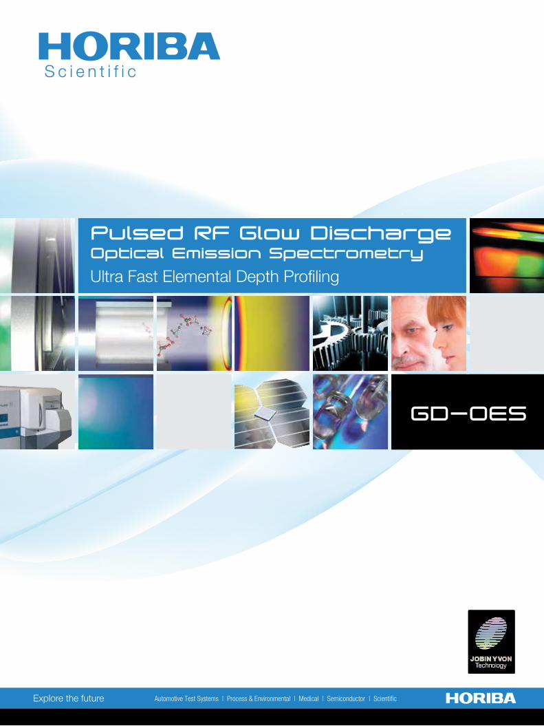
Surface sensitive techniques (XPS or SIMS) are slow and fail to measure layers of more than 1 micrometer. For thicker layers, SEM EDX on cross sections can be used, but require tedious preparation and cannot measure light elements. Pulsed RF GD-OES on the other hand, rapidly sputters tens of micrometers, measures all elements and is therefore ideal both for thin and thick layers.
The unique characteristics of the Pulsed RF source and the use of Emission Spectrometry allow for quasi-absence of matrix effects resulting in easy calibrations to obtain quantitative depth profiles (concentrations vs. depth) from the measured qualitative ones (intensities vs. time)
Pulsed RF Glow Discharge Optical Emission Spectrometry
Quantitative Elemental Depth Profile Analysis from the first
nanometer down to more than 150 microns
Protective coatingsNative oxide (few nm)Corrosion protectionTribological improvement1-
100
nm
Complex coatingsStructure: Multilayer, Gradient,Elemental compositionInterface detailsLayer intermixingCompound formation
10-1
000
nm
Intermediate layersAdhesion improvementElement inter-diffusionSubstrate protection
100 n
m -
100 µ
m
SubstrateBulk composition1
mm
Analysis time - 2 min, crater diameter - 4 mm.
Mo
Se
InCu
Ga
0.0 1.0 2.0 3.0Sample depth (µm)
Con
cent
ratio
n (a
t%)
0
40
80
Depth Profile of the absorber layer of a CIGS thin film PV cell by pulsed RF GD-OES.
Sub nm depth resolutionMirror for X-ray, thin multilayer material. Ref: Thin Solid Films 540 (2013) 96–105
Substrate
60 periods of 7 nm thick
Mo 3.2 nmB4C 0.3 nmSi 3.5 nm
Depth Profile Analysis of a PVD coating (left qualitative, right quantitative)
Quantitative depth profile of thin and thick films
2 3
Most materials today are either
multilayered (thin films PV, LED,
hard disks, electrodes for Li
batteries, coated glasses, etc.)
or feature surface treatments
and advanced coatings for
enhanced performance or
corrosion resistance.
Pulsed RF GD-OES is the ideal
analytical companion tool
for coated material studies,
process elaboration and control
as it offers ultra fast elemental
depth profile analysis of thin
and thick layers, conductive or
isolating, with high sensitivity
to all elements.
As the name suggests, the
technique combines a Glow
Discharge Source powered by
Pulsed Radio Frequency with
the ability to sputter “layer by
layer” a representative area
of the material investigated
together with a high resolution
and high sensitivity emission
spectrometer that will measure
in real time all elements of
interest.
The GD-Profiler series of
Pulsed RF GD-OES offers two
models, each with a variety
of options to suit the most
comprehensive range of
applications:
GD Profiler 2 & GD Profiler HR.
A firmly established techniqueThe ISO Technical Committee TC 201 for Surface Analysis has already issued three international standards for GD. Five reference books are available, and an annual rate of over 60 scientific papers published with GD data show the vitality of the technique in all domains of material science.
High sensitivity and Ultra Fast Optical detection allows simultaneous measurement of all elements of interest in the depth profile - with emission lines ranging from the VUV (120 nm for H and its isotope D, 130 nm for O, etc.), to the IR for Li (670 nm) and K (766 nm).
Emission spectrum
With a typical erosion rate of µm/min (2-10 nm/s), researchers are encouraged to run multiple samples. The immediate feedback allows them to optimize and control each stage of their evaporation, deposition or annealing processes and to quickly react to any observed variation.
Pulsed RF GD-OES offers superb depth resolution down to the nanometer scale or below, made possible by the unique characteristics of the advanced pulsed RF GD source and the Ultra Fast Detection capability of the optical system.
Speed & depth resolution
All elements
Pulsed RF GD-OES also measures solar cells, corroded surfaces, Ag-TiCN bioactive coatings, materials for H storage, laser surface treatments, alloys and compounds, oxides and nitrides, thin and thick films etc.
Refer to our application notes, published papers and the presentations from GD-Days.
A multidimensional platform for material analysisA
t. %
µm
State Of Charge 100 %
O
Li Ni
0 10 20 30 40 50 600
20
40
60
F
Al
Mn
C
Co
Ru
Fe
Cr
Ta
0 0.4 0.8 1.2 1.6 sec0
40
80
110
NiInte
nsity
(a. u
.)
Zn Fe
Interface 3.02 µm
100 2 4 6 8 12 14 16 18 µm102
0
20
40
60
80
100
%
Li
B
Al
Si
Na
O
0 20 40 60 80 100 120 140 µm
0
0.06
0.12
0.18
0.24
0.30
0.36
0.42
0.48
Inte
nsity
(a. u
.)
And much more
Ga
Al
In
N
Mg
0 4 8 12 s0
1
2
3
4
Inte
nsity
(a.u
.)
Time
InGaN/GaNP-GaN
n-GaN
Sapphire substrate0
1
2
3
4
3 5 7 9 s
H D
Ta
Ti
Ni
Depth (nm)
0 100 200 300 4000
10
20
30
40
Emis
sion
Inte
nsity
(a.u
.)
The excellent optical resolution of the instrument even allows simultaneous measurements of H, and its isotope Deuterium, which is of great interest for nuclear research.
Ref: Fusion Engineering and Design 87 (2012) 1091– 1094
C
H
o
Al Zn
Inte
nsity
(a.u
.)
Etching time (min)0 20 40
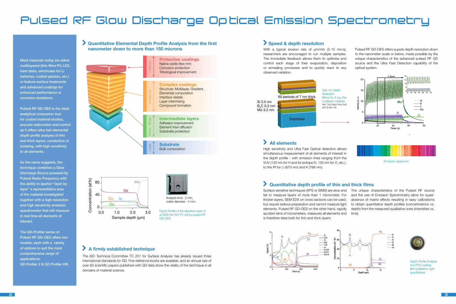
The patented UFS allows for Ultra Fast Sputtering of polymeric layers offering enhanced signal/noise ratios and the ability to measure embedded layers below thick polymeric ones with excellent depth resolution. The example here shows a DVD featuring 6 layers in 100 nm below a 70 µm thick polymeric layer.
70 µm
100 nm20 ~30 µm
100 nm20 ~30 µm
180 nm
EBSD measurement of WC. Sample preparation is crucial for EBSD observation. Right: mirror-like mechanical polishing; Center: standard chemical polishing procedure (5 hours); Left: GD preparation (3 seconds!).
Ref: M. Penoy, Ceratizit, 6th International GD day.
GD: 10W - 3 sec CP: 5 hours Mechanical polishing
4 5
At.
%
µm
State Of Charge 0 %
O
Li
Ni
0 10 20 30 40 50 600
20
40
60
C
F
Al
Mn
FeN
O
At %
µm
C
0 2 4 6 8 10 12 14 16 180
20
40
60
80
Li Batteries: Positive & Negative ElectrodesThick layers, fragile samples, handling strategies
Electrodes of Li ion batteries are readily measured with the Pulsed RF GD-OES. Strategies for sample handling (including the Li bell for air sensitive materials) have been developed. The patented UFS assures that the sputtering is equally fast on positive and negative electrodes.
Ref: HORIBA Scientific Application note n°18
Hard DisksDepth resolution, uniformity check
Hard disks feature up to 18 layers in 100 nm. The Pulsed RF GD-OES is notably used for assessment of the repeatability of the thickness of each deposited layer over the surface area.
Ref: S. Liang, Seagate, 6th International GD day.
NitrurationGD results correlate with mechanical testing
Pulsed RF GD-OES data allow following N and C profiles in depth, together with all other elements to control nitruration processes and are correlated to hardness testings.
Ref: G. Mancuso, Colmegna, 4th GD Day
Zn CoatingsCompliant with ISO 16962
The first applicative ISO standard for Glow Discharge. Control of composition, thickness, coatings weights and determination of contaminants are keys for the production follow up.
Glass Cationic ExchangeDeep crater in glass
140 µm deep crater in glass without thermal effect thanks to pulsed operation.
LEDDeposition process control
Pulsed RF GD-OES is ideal for fast control of the active layers of the LED offering the chance for immediate reaction in case of process drift.
Ref: HORIBA Scientific Application note n°19
Polymers, patented "UFS"Ultra Fast Sputtering of polymers
HydrogenGD is one of the rare surface techniques capable of measuring H
GD SEM/EBSDPulsed RF GD plasma reveals the structure of the material
Pulsed operation enables users to provide higher instantaneous power to the sample while preventing any thermal effect.
The patented auto-matching in Pulsed RF mode allows automatic tuning of the source in real time as it sputters through multiple layers and coatings that vary in impedance.
Plasma Cleaning (only possible in Pulsed RF mode) minimizes contaminants, allowing extreme surface measurements.
Ref: J. Anal. At. Spectrom., 2009, 24, 734–741
The selection of calibration materials is easy with Pulsed RF as bulk and coated specimens - conductive, isolating or hybrid- can be used within the same analytical method.
Why the source makes the difference
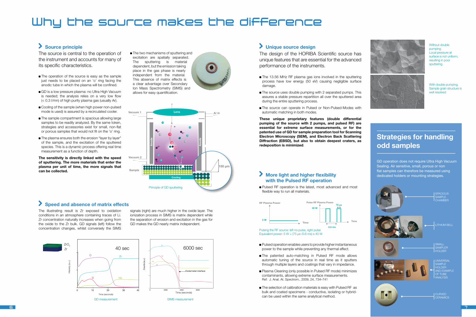
The source is central to the operation of the instrument and accounts for many of its specific characteristics.
The operation of the source is easy as the sample just needs to be placed on an 'o’ ring facing the anodic tube in which the plasma will be confined.
GD is a low pressure plasma: no Ultra High Vacuum is needed; the analysis relies on a very low flow (< 0.3 l/mn) of high purity plasma gas (usually Ar).
Cooling of the sample (when high power non-pulsed mode is used) is assured by a recirculated cooler.
The sample compartment is spacious allowing large samples to be readily analyzed. By the same token, strategies and accessories exist for small, non-flat or porous samples that would not fit on the 'o’ ring.
The plasma ensures both the erosion “layer by layer” of the sample, and the excitation of the sputtered species. This is a dynamic process offering real time measurement as a function of depth.
The sensitivity is directly linked with the speed of sputtering. The more materials that enter the plasma per unit of time, the more signals that can be collected.
The two mechanisms of sputtering and excitation are spatially separated. The sputtering is material dependent, but the emission taking place in the gas phase is nearly independent from the material. This absence of matrix effects is a clear advantage over Secondary Ion Mass Spectrometry (SIMS) and allows for easy quantification.
The design of the HORIBA Scientific source has unique features that are essential for the advanced performance of the instruments.
The 13.56 MHz RF plasma gas ions involved in the sputtering process have low energy (50 eV) causing negligible surface damage.
The source uses double pumping with 2 separated pumps. This assures a stable pressure repartition all over the sputtered area during the entire sputtering process.
The source can operate in Pulsed or Non-Pulsed-Modes with automatic matching in both modes.
These unique proprietary features (double differential pumping of the source with 2 pumps, and pulsed RF) are essential for extreme surface measurements, or for the patented use of GD for sample preparation tool for Scanning Electron Microscopy (SEM), and Electron Back Scattering Diffraction (EBSD), but also to obtain deepest craters, as redeposition is minimized.
Pulsed RF operation is the latest, most advanced and most flexible way to run all materials.
The illustrating result is Zr exposed to oxidation conditions in an atmosphere containing traces of Li. Zr concentration naturally increases when going from the oxide to the Zr bulk. GD signals (left) follow the concentration changes, whilst conversely the SIMS
signals (right) are much higher in the oxide layer. The ionization process in SIMS is matrix dependent while the separation of erosion and excitation in the gas for GD makes the GD nearly matrix independent.
λ
Sample
Vacuum 2
Ar in
Ano
de
Ano
de
Cooling
Vacuum 1 Lens
150 µm
Principle of GD sputtering
λ
Sample
Vacuum 2
Ar in
Ano
de
Ano
de
Cooling
Vacuum 1 Lens
150 µm
O Zr
NbLi
0 10 20 30 40
Time (seconds)
Inte
nsity
(a.u
.)
O
Nb
Li
Zr
0 2000 4000 6000
Cou
nts
(a.u
.)
Time (seconds)
Oxide/metal interface
ZrO2
Zr
GD measurement SIMS measurement
40 sec 6000 sec
GD operation does not require Ultra High Vacuum Sealing. Air sensitive, small, porous or non flat samples can therefore be measured using dedicated holders or mounting strategies.
Strategies for handling odd samples
Without double pumping. Local pressure at surface is not uniform, resulting in poor sputtering.
With double pumping. Sample grain structure is well resolved
Time
Pulse RF Plasma Power
40 W
0.6 ms
75 µs
Pulsing the RF source: left no pulse, right pulseEquivalent power: 5 W = (75 µs /0.6 ms) x 40 W
Time
RF Plasma Power
5 W
SPACIOUS SAMPLE CHAMBER
LITHIUM BELL
SMALL SAMPLER HOLDER
UNIVERSAL SAMPLE HOLDER AND EXAMPLE OF TUBE ANALySIS
CURVED CERAMICS
6 7
Source principle
Speed and absence of matrix effects
Unique source design
More light and higher flexibility with the Pulsed RF operation
3
Detection
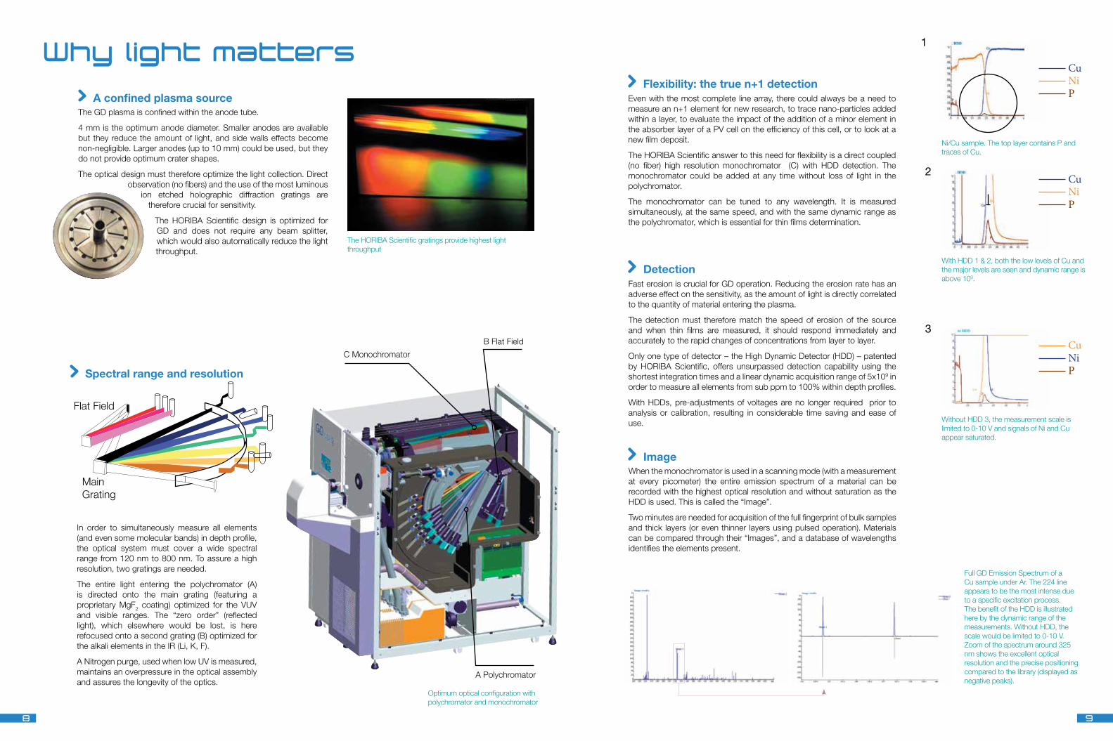
The GD plasma is confined within the anode tube.
4 mm is the optimum anode diameter. Smaller anodes are available but they reduce the amount of light, and side walls effects become non-negligible. Larger anodes (up to 10 mm) could be used, but they do not provide optimum crater shapes.
The optical design must therefore optimize the light collection. Direct observation (no fibers) and the use of the most luminous
ion etched holographic diffraction gratings are therefore crucial for sensitivity.
The HORIBA Scientific design is optimized for GD and does not require any beam splitter, which would also automatically reduce the light throughput.
Why light matters
In order to simultaneously measure all elements (and even some molecular bands) in depth profile, the optical system must cover a wide spectral range from 120 nm to 800 nm. To assure a high resolution, two gratings are needed.
The entire light entering the polychromator (A) is directed onto the main grating (featuring a proprietary MgF2 coating) optimized for the VUV and visible ranges. The “zero order” (reflected light), which elsewhere would be lost, is here refocused onto a second grating (B) optimized for the alkali elements in the IR (Li, K, F).
A Nitrogen purge, used when low UV is measured, maintains an overpressure in the optical assembly and assures the longevity of the optics.
MainGrating
Flat Field
The HORIBA Scientific gratings provide highest light throughput
B Flat Field
A Polychromator
C Monochromator
Optimum optical configuration with polychromator and monochromator
Even with the most complete line array, there could always be a need to measure an n+1 element for new research, to trace nano-particles added within a layer, to evaluate the impact of the addition of a minor element in the absorber layer of a PV cell on the efficiency of this cell, or to look at a new film deposit.
The HORIBA Scientific answer to this need for flexibility is a direct coupled (no fiber) high resolution monochromator (C) with HDD detection. The monochromator could be added at any time without loss of light in the polychromator.
The monochromator can be tuned to any wavelength. It is measured simultaneously, at the same speed, and with the same dynamic range as the polychromator, which is essential for thin films determination.
With HDD 1 & 2, both the low levels of Cu and the major levels are seen and dynamic range is above 109.
Without HDD 3, the measurement scale is limited to 0-10 V and signals of Ni and Cu appear saturated.
Ni/Cu sample. The top layer contains P and traces of Cu.
Fast erosion is crucial for GD operation. Reducing the erosion rate has an adverse effect on the sensitivity, as the amount of light is directly correlated to the quantity of material entering the plasma.
The detection must therefore match the speed of erosion of the source and when thin films are measured, it should respond immediately and accurately to the rapid changes of concentrations from layer to layer.
Only one type of detector – the High Dynamic Detector (HDD) – patented by HORIBA Scientific, offers unsurpassed detection capability using the shortest integration times and a linear dynamic acquisition range of 5x10⁹ in order to measure all elements from sub ppm to 100% within depth profiles.
With HDDs, pre-adjustments of voltages are no longer required prior to analysis or calibration, resulting in considerable time saving and ease of use.
When the monochromator is used in a scanning mode (with a measurement at every picometer) the entire emission spectrum of a material can be recorded with the highest optical resolution and without saturation as the HDD is used. This is called the “Image”.
Two minutes are needed for acquisition of the full fingerprint of bulk samples and thick layers (or even thinner layers using pulsed operation). Materials can be compared through their “Images”, and a database of wavelengths identifies the elements present.
Full GD Emission Spectrum of a Cu sample under Ar. The 224 line appears to be the most intense due to a specific excitation process. The benefit of the HDD is illustrated here by the dynamic range of the measurements. Without HDD, the scale would be limited to 0-10 V.Zoom of the spectrum around 325 nm shows the excellent optical resolution and the precise positioning compared to the library (displayed as negative peaks).
CuNiP
CuNiP
CuNiP
8 9
1
2
Flexibility: the true n+1 detection A confined plasma source
Spectral range and resolution
Image

Multitasking and multilingual, Quantum software offers easy access to all the functionalities of the instrument (control of poly and mono operation, management of the patented PolyscanTM pulsed operation, etc.). Quantum can be used for data treatment on other computers in emulation mode while the instrument is making measurements.
A multidimensional platform for material analysis
Powerful and flexible data handling with the unique functionalities of Time Plus (to increase analysis time during measurement), UFS (Ultra Fast Sputtering) to enhance the erosion of polymers and measurement with multiple acquisition frequencies. Real time display of acquisition, ultra fast treatment options (including multiple smoothing), automatic determination of interfaces, calculation of trends and export of results as images, ascii or xls files for flexible reports generation.
Creation and use of analytical tasks to apply similar treatments on multiple results for overlay and comparison of multiple results.
Record of all raw data allowing flexible reprocessing, ability to display the entire depth profile measurement from a bulk result, to use layered samples in any program or to apply bulk programs for surface measurements and depth profile programs for bulk.
Intelligent Quantification models including the Sputtering Rate mode that follows the ISO standard and the new Layer Mode for advanced materials. Measurement of concentrations (in At%, M% vs depth, coating weights, layer thicknesses). 2D/3D associated crater profiles.
B3
B3
B2
B2
B1Si1 Si2 Si3
Si1Si2Si3
C1
C1
C3
C3
C2
C2
B1
0 1 2 3 µm
22
20
18
16
14
12
10
8
6
4
2
0
V
sample 1150 (600 °C)
sample 1216-2 (300 °C)
sample 1216-4 (500 °C)
Overlay of measurements to study a varying process
Analysis times are typically 1000 times shorter than classical surface techniques that operate in UHV environment.
Non conductors are readily analyzed without surface charging effects.
All elements are simultaneously measured including H, C, N, O , F, Li, etc.
Nanometer depth resolution
GD is complementary to other techniques that provide imaging, lateral resolution or molecular information.
Pulsed RF GD pointsIQ
Setting up of the layer mode
Coupling of techniques with variable lateral resolution
Multimatrix Linear Calibration of N with statistical information built in
Control of plasma parameters in pulsed and non-pulsed mode;
Patented RF coupler;
Plasma Cleaning;
Use of multiple gases (Ar, Ne, when F or He are also needed, UFS gas mixing);
Integrated libraries of reference materials, optical wavelengths and sputtering rates;
On line Statistical Process Control (SPC) to follow up surface and bulk results as well as operating parameters;
Built-in diagnostic functions allowing remote obser-vation.
Instrument control
On line SPC
The GD plasma sputtering, though Ultra Fast, is delicate. Incident particles have a low energy (50eV) and do not induce structural changes in the material. Coupling GD with other techniques offering different lateral resolution is therefore of great interest. XPS, Ellipsometry and micro Raman measurements have been performed within GD craters, providing multiple and complementary information on the same materials.
Coupling to SEM, XPS or other surface techniques
Surface and cross section observations with SEM are also made easier and better after GD sputtering. Using the patented "UFS", fine details can be observed even on samples with thick organic layers.
Ref: New Horizons of Applied Scanning Electron Microscopy, K. Shimizu, Springer
Cross section measurement accessory
10 11
Software
Thi
s d
ocu
men
t is
no
t co
ntra
ctua
lly b
ind
ing
und
er a
ny c
ircum
stan
ces
- P
rint
ed in
Fra
nce
- ©
HO
RIB
A J
ob
in Y
von
03/2
014
France: HORIBA Jobin Yvon S.A.S., 16-18 rue du Canal, 91165 Longjumeau cedex - Tel: +33 (0)1 69 74 72 00 - Fax: +33 (0)1 69 09 07 21 - Email: [email protected]: HORIBA Instruments Inc., 3880 Park Avenue, Edison, NJ 08820-3012 - Toll-free: +1-866-562-4698 - Tel: +1 732 494 8660 - Fax: +1 732 549 5125 - Email: [email protected]: HORIBA Ltd., Tokyo Branch Office, 2-6, KandaAwaji-cho, Chiyoda-ku, Tokyo 101-0063, Japan - Tel: +81-(0)3 6206 4721 - Fax: +81 (0)3 6206 4730 - Email: [email protected]: HORIBA Jobin Yvon GmbH, Hauptstrasse 1, 82008 Unterhaching - Tel: +49 (0)89 4623 17-0 - Fax: +49 (0)89 4623 17-99 - Email: [email protected]: HORIBA Jobin Yvon Srl., Via Cesare Pavese 21, 20090 Opera (Milano) - Tel: +39 2 5760 3050 - Fax: +39 2 5760 0876 - Email: [email protected]: HORIBA UK Ltd., 2 Dalston Gardens, Stanmore, Middlesex HA7 1BQ - Tel: +44 (0)20 8204 8142 - Fax: +44 (0)20 8204 6142 - Email: [email protected]: HORIBA (China) Trading Co. Ltd., Unit D 1F, Bldg A, Srynnex International Park, No. 1068 West Tianshan Road, Shanghai 200335 - Tel: +86 (0)21 6289 6060 - Fax: +86 (0)21 6289 5553 Email: [email protected]: HORIBA Instruments Brasil Ltda., Rua Presbítero Plínio Alves de Souza, 645, Loteamento Polo Multivias, Bairro Medeiros, Jundiaí / SP, CEP 13.212-181 - Tel: +55 (0)11 2923 5400 Fax: +55 (0)11 2923 5490 - Email: [email protected]: Tel: +33 (0)1 69 74 72 00 - Email: [email protected]
www.horiba.com/[email protected]
Look at the Surface and Beyond...
HORIBA Scientific's New R&D centre in Paris Saclay with the world's largest scientific gratings facility
GD Day The International GD Day, held every 2 years, gathers practitioners and researchers interested in all aspects of analytical GD for surface and depth profile analysis of materials. Presentations made by the users cover a wide variety of application topics. The GD Day also gives attendees the opportunity to see the latest instrument developments and offers the occasion to create valuable relationships and collaboration to set up projects or exchange samples.
www.gd-day.com
We know GD and its multiple application possibilities! For 15 years, HORIBA Scientific has been the reference leader in GD for surface and depth profile analysis, with an installed base of over 300 units. Our staff of application scientists provide dedicated solutions and full support.
4 GD Labsat your service
PARIS - NEw YORk - TOkYO - SHANGHAï