


Ultimate Design Review - Relativistic Nuclear Collisions...
40
Ultimate Design Review G. Bertolone, C. Colledani, A. Dorokhov, W. Dulinski, G. Dozière , A. Himmi, Ch. Hu-Guo, F. Morel, H. Pham, I. Valin, J. Wang, G. Claus, M. Gelin, M. Goffe, K. Jaaskelainen, M. Specht, M. Winter J.Baudot
-
Upload
trinhthien -
Category
Documents
-
view
213 -
download
0
Transcript of Ultimate Design Review - Relativistic Nuclear Collisions...

Ultimate Design Review
G. Bertolone, C. Colledani, A. Dorokhov, W. Dulinski, G. Dozière, A. Himmi, Ch. Hu-Guo, F. Morel, H. Pham, I. Valin, J. Wang,
G. Claus, M. Gelin, M. Goffe, K. Jaaskelainen, M. Specht, M. WinterJ.Baudot
Ultimate1 [email protected] 229/11/2010
iPHC
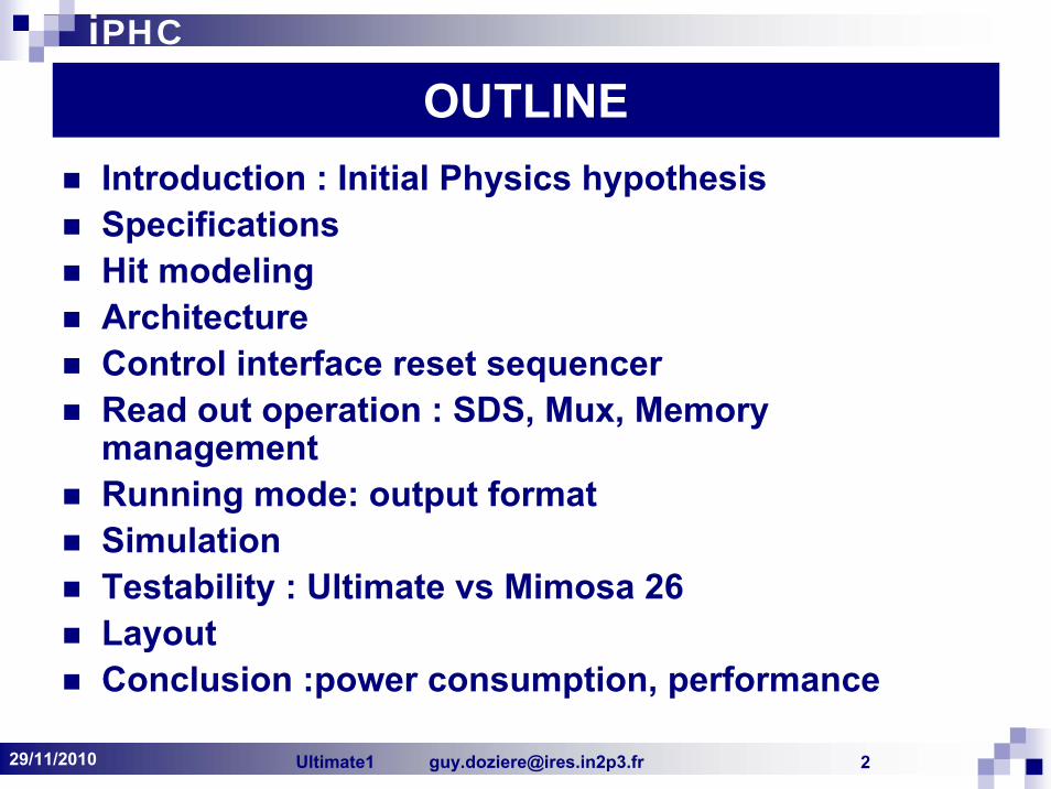
OUTLINEIntroduction : Initial Physics hypothesisSpecificationsHit modelingArchitecture Control interface reset sequencerRead out operation : SDS, Mux, Memory managementRunning mode: output formatSimulationTestability : Ultimate vs Mimosa 26LayoutConclusion :power consumption, performance
Ultimate1 [email protected] 329/11/2010
iPHC
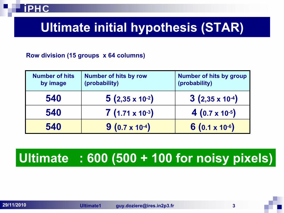
Number of hits by image
Number of hits by row (probability)
Number of hits by group (probability)
540 5 (2,35 x 10⁻²) 3 (2,35 x 10⁻⁴)540 7 (1.71 x 10⁻³) 4 (0.7 x 10⁻⁵)540 9 (0.7 x 10⁻⁴) 6 (0.1 x 10⁻⁶)
Row division (15 groups x 64 columns)
Ultimate initial hypothesis (STAR)
Ultimate : 600 (500 + 100 for noisy pixels)

Ultimate1 [email protected] 429/11/2010
iPHC
Ultimate specifications
Design based on Mimosa26 architectureReticle size (~ 3.8 cm²)
M26 1152 x 575 pixels Ultimate 960 x 928 pixels
Reduced power dissipationVdd: 3V simulate on digital partShorter integration time
Integration time = 185.6 µs
Higher hit density larger memories3.5 times larger than Mimosa26 (600 2048 words)
Higher transmission bit rate: 80 160 Mb/s per lineEnhanced testability
Ultimate1 [email protected] 729/11/2010
iPHC
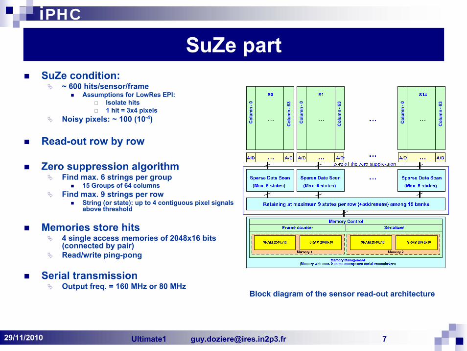
SuZe partSuZe condition:
~ 600 hits/sensor/frameAssumptions for LowRes EPI:
Isolate hits1 hit = 3x4 pixels
Noisy pixels: ~ 100 (10-4)
Read-out row by row
Zero suppression algorithmFind max. 6 strings per group
15 Groups of 64 columnsFind max. 9 strings per row
String (or state): up to 4 contiguous pixel signals above threshold
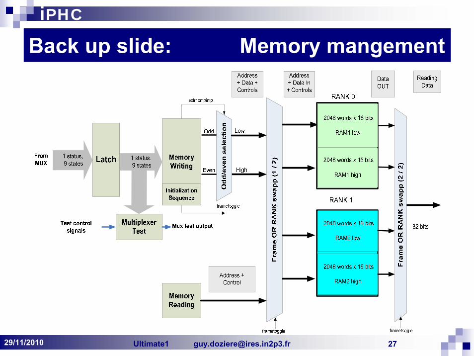
Memories store hits4 single access memories of 2048x16 bits (connected by pair)Read/write ping-pong
Serial transmissionOutput freq. = 160 MHz or 80 MHz
Block diagram of the sensor read-out architecture
Col
umn
-0
Col
umn
-63
Col
umn
-0
Col
umn
-63
Col
umn
-63
Col
umn
-0
Col
umn
-0
Col
umn
-63
Col
umn
-0
Col
umn
-63
Col
umn
-63
Col
umn
-0
Ultimate1 [email protected] 829/11/2010
iPHC
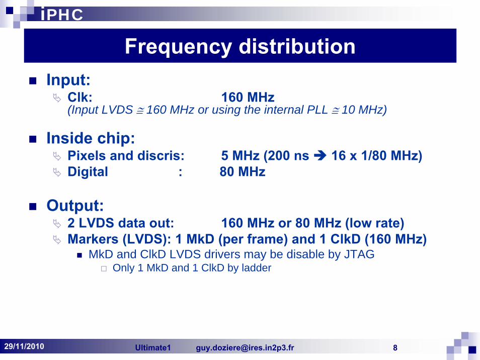
Frequency distributionInput:
Clk: 160 MHz (Input LVDS ≅ 160 MHz or using the internal PLL ≅ 10 MHz)
Inside chip: Pixels and discris: 5 MHz (200 ns 16 x 1/80 MHz)Digital : 80 MHz
Output:2 LVDS data out: 160 MHz or 80 MHz (low rate)Markers (LVDS): 1 MkD (per frame) and 1 ClkD (160 MHz)
MkD and ClkD LVDS drivers may be disable by JTAGOnly 1 MkD and 1 ClkD by ladder
Ultimate1 [email protected] 929/11/2010
iPHC
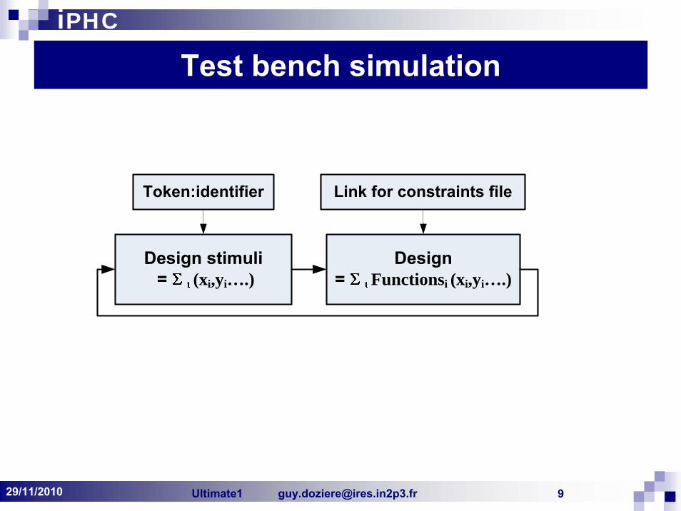
Test bench simulation
(xi,yi….) Functionsi (xi,yi….)
Token:identifier Link for constraints file

Ultimate1 [email protected] 1129/11/2010
iPHC
Testing functionalityAnalog part1a) Analog pixel scan:
The matrix is divided in stripes of 8 columns swapped with the next block of 8 columns at right and so on until all the columns are analyzed. 8 output pads. Max. Freq. = 20 MHz2a) Nominal speed: 8 pre-selected columns connected directly to the 8 output pads and read at 80 MHz3a) An external signal synchronized with the matrix read-out allows activating a line pattern during one or several selected rows (1d)4a)A test mode injects a test voltage to emulate pixels outputsA test mode reads one selected row register; pixels and discriminators are in working mode, tint = 185 µs, Read-out freq. = 10 MHz via 2 LVDS output pads
The row automatic scanning mode of whole matrix is implementedAll voltages of the discriminators are adjustable.
Digital partA test mode receives 2 rows by JTAG to emulate a matrix of (2 JTAG rows) x 464 = 928 rows.
In SuZe, 2 functionalities are tested: 1d )the Sparse Data Scan (SDS) and,2d) the Multiplexing Logic (Mux) giving up to 9 states.3d) On pad, we can select 3 modes: working mode ( analog readout + suze)test mode : discriminators, SDS, Mux.Synchronizations signals coming from main sequencer moduleAll the shape and durations of the synchronizations signals are configurable.

Ultimate1 [email protected] 1229/11/2010
iPHC
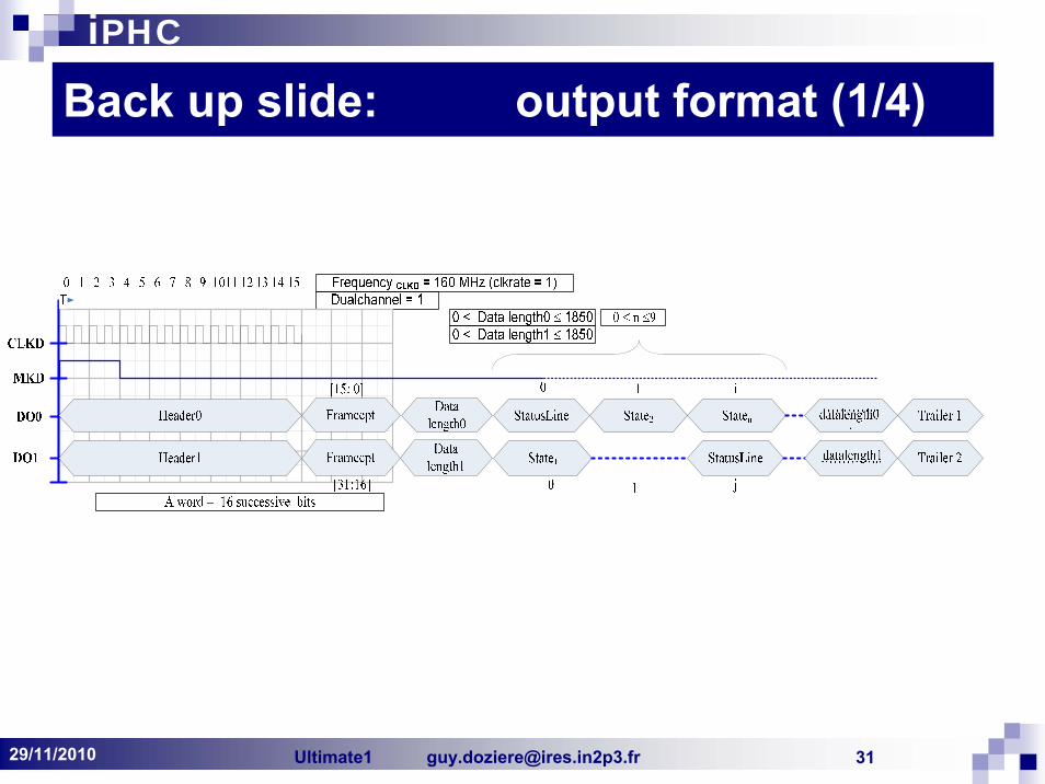
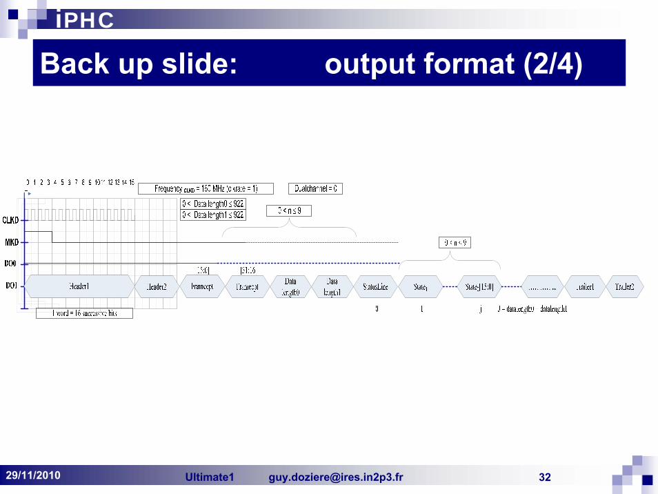
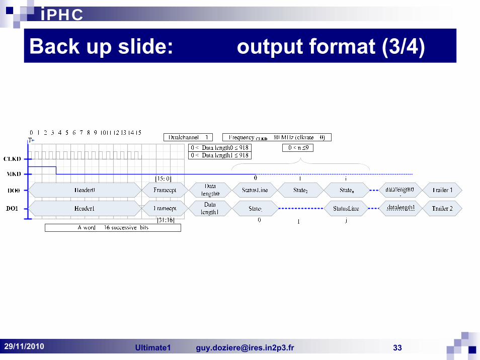
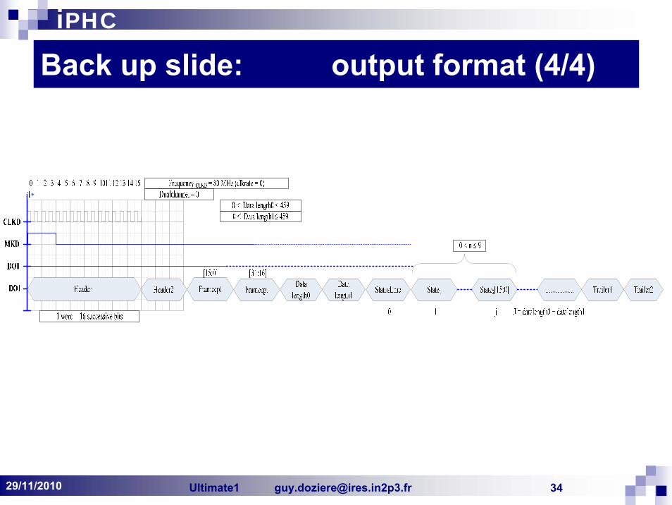
Data formatThe data format is the same as Mimosa26 but read-out frequency is doubled
Mode test «pixels+discris»: read 1 row register, data split to 2 outputs at 10 MHz
Main mode: data split to 2 outputs at 160 MHz with LSB first
For each line with hit : one Status/line followed by up to 9 States. The following data stream is generated:
Status/Line word: Address of line, Number of States ( 9 Max., overflow flag if > 9 )
States list – One state = consecutive pixels at 1 in the line:
Column address of the first pixel at 1, Number of pixels at 1
numberof
hit pixels
Bit(0-
not usedThe address of the column
Bit(0-1) Bit (0-9)0 1 2 …. 12 13 ... 15
State
Ultimate1 [email protected] 1329/11/2010
iPHC
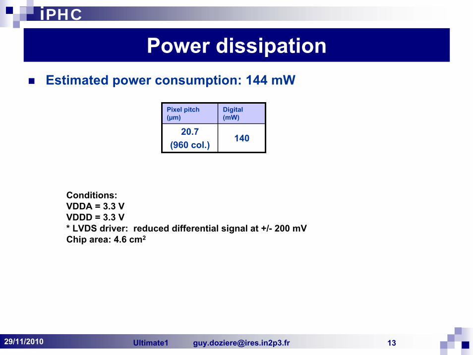
Power dissipation
Pixel pitch (µm)
Digital (mW)
20.7(960 col.)
140
Conditions:VDDA = 3.3 VVDDD = 3.3 V* LVDS driver: reduced differential signal at +/- 200 mVChip area: 4.6 cm2
Estimated power consumption: 144 mW

Ultimate1 [email protected] 1429/11/2010
iPHC
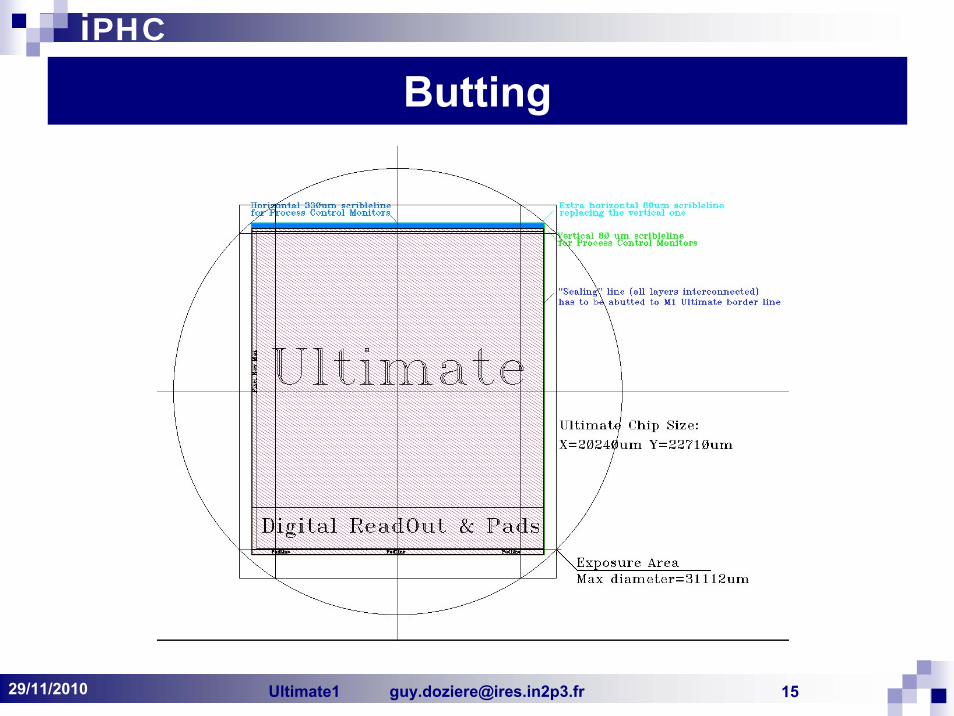
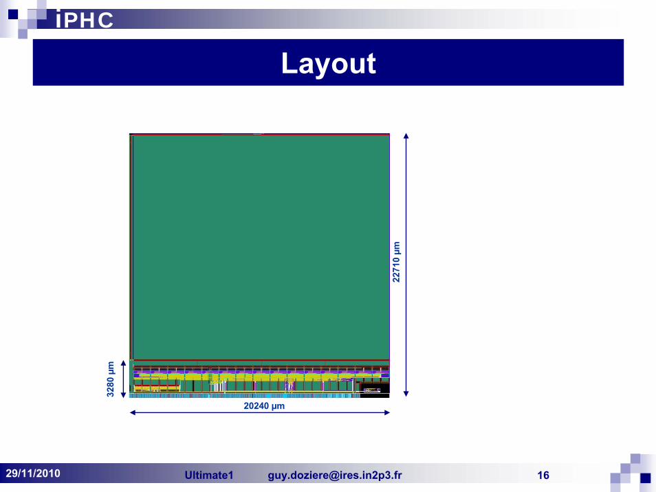
Ultimate floor plan
Pixel Array: 928 rows x 960 columns
Pitch: 20.7 µmActive area: ~ 3.8 cm²
X = 19872 µm Y = 19209.6 µm
Chip size: ~ 4.6 cm²X = 20240 µmY = 22710 µm
AMS 0.35 high-res process400 Ω.cm p- EPI layer Column-level Discriminators
Selectable analog outputs ~ 220 µm for Pads + Electronics
Zero Suppression
Pad Ring 3280 µm
365 µm
JTAG Bias-DACSeq. CtrlPLLMem. 1 Mem. 2
Sequ
ence
r
20240 µm
2271
0 µm
Pixel Array
Ultimate1 [email protected] 1729/11/2010
iPHC
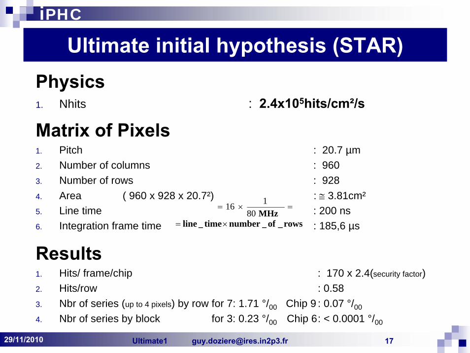
Matrix of Pixels1. Pitch : 20.7 µm2. Number of columns : 9603. Number of rows : 9284. Area ( 960 x 928 x 20.7²) : ≅ 3.81cm²5. Line time : 200 ns6. Integration frame time : 185,6 µs
=×=MHz80116
Ultimate initial hypothesis (STAR)Physics1. Nhits : 2.4x10⁵hits/cm²/s
Results1. Hits/ frame/chip : 170 x 2.4(security factor)2. Hits/row : 0.583. Nbr of series (up to 4 pixels) by row for 7: 1.71 °/00 Chip 9 : 0.07 °/00
4. Nbr of series by block for 3: 0.23 °/00 Chip 6: < 0.0001 °/00
rows_of_numbertime_line ×=
Ultimate1 [email protected] 2329/11/2010
iPHC
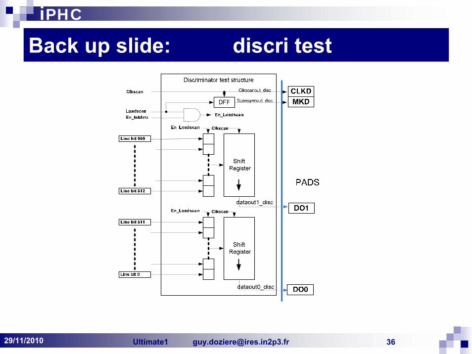
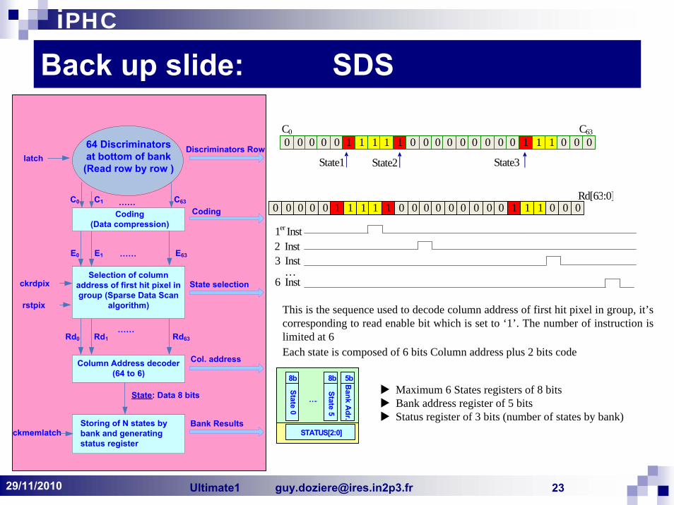
Back up slide: SDS
State1 State2 State3
0 0 0 0 0 1 1 1 1 1 0 0 0 0 0 0 0 0 0 1 1 1 0 0 0C0 C63
Rd[63:0]0 0 0 0 0 1 1 1 1 1 0 0 0 0 0 0 0 0 0 1 1 1 0 0 0
……
……
……
latch
ckrdpix
rstpix
ckmemlatch
State selection
Coding
Col. address
64 Discriminators at bottom of bank
(Read row by row )
Coding(Data compression)
C0 C1 C63
Bank Results
E0 E1 E63
Rd0 Rd1 Rd63
State: Data 8 bits
Column Address decoder(64 to 6)
Selection of column address of first hit pixel in group (Sparse Data Scan
algorithm)
Storing of N states by bank and generating status register
Discriminators Row
1er Inst
…
2 Inst3 Inst
6 Inst
This is the sequence used to decode column address of first hit pixel in group, it’scorresponding to read enable bit which is set to ‘1’. The number of instruction islimited at 6Each state is composed of 6 bits Column address plus 2 bits code
HIT0
8b
OvfSTATUS[2:0]
HIT5
8b ADR
Sm
4b
….
8b
STATUS[2:0]
8b A5b
….
Bank A
dr.
State 0
State 5
Maximum 6 States registers of 8 bitsBank address register of 5 bitsStatus register of 3 bits (number of states by bank)
Ultimate1 [email protected] 2429/11/2010
iPHC
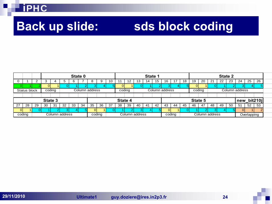
Back up slide: sds block coding
0 1 2 3 4 5 6 7 8 9 10 11 12 13 14 15 16 17 18 19 20 21 22 23 24 25 260 1 2 0 1 0 1 2 3 4 5 0 1 0 1 2 3 4 5 0 1 0 1 2 3 4 5
27 28 29 30 31 32 33 34 35 36 37 38 39 40 41 42 43 44 45 46 47 48 49 50 51 52 530 1 0 1 2 3 4 5 0 1 0 1 2 3 4 5 0 1 0 1 2 3 4 5 0 1 2
coding Column address Overlappingcoding Column address coding Column address
Status block
State 0 State 1 State 2
coding Column address coding Column address coding Column address
State 3 State 4 State 5 new_bit210j
Ultimate1 [email protected] 2529/11/2010
iPHC
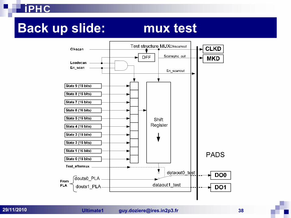
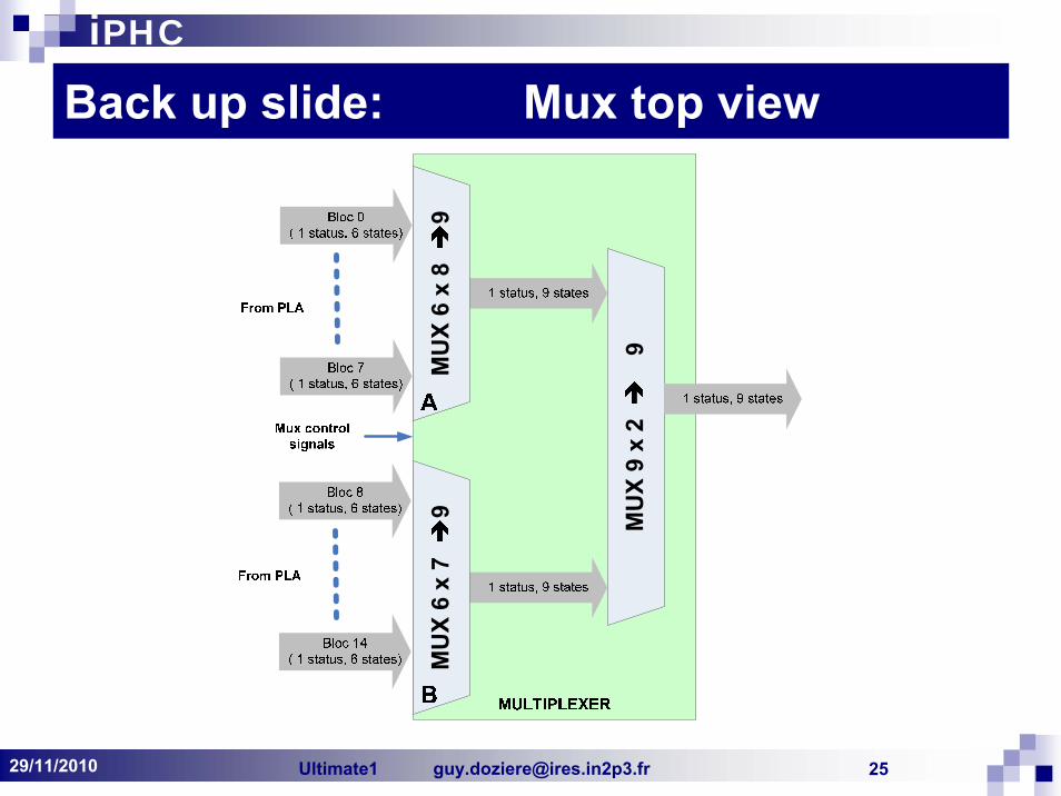
Back up slide: Mux top view
MU
X 9
x 2
9
MU
X 6
x 8
9
MU
X 6
x 7
9
Ultimate1 [email protected] 2829/11/2010
iPHC
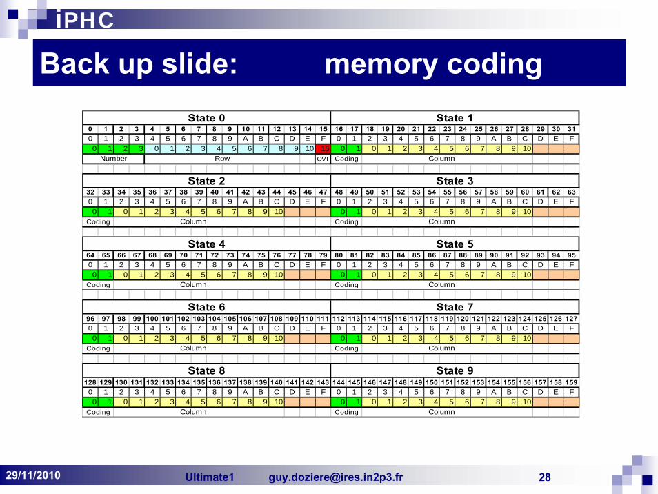
Back up slide: memory coding
0 1 2 3 4 5 6 7 8 9 10 11 12 13 14 15 16 17 18 19 20 21 22 23 24 25 26 27 28 29 30 310 1 2 3 4 5 6 7 8 9 A B C D E F 0 1 2 3 4 5 6 7 8 9 A B C D E F0 1 2 3 0 1 2 3 4 5 6 7 8 9 10 15 0 1 0 1 2 3 4 5 6 7 8 9 10
OVF
32 33 34 35 36 37 38 39 40 41 42 43 44 45 46 47 48 49 50 51 52 53 54 55 56 57 58 59 60 61 62 630 1 2 3 4 5 6 7 8 9 A B C D E F 0 1 2 3 4 5 6 7 8 9 A B C D E F0 1 0 1 2 3 4 5 6 7 8 9 10 0 1 0 1 2 3 4 5 6 7 8 9 10
64 65 66 67 68 69 70 71 72 73 74 75 76 77 78 79 80 81 82 83 84 85 86 87 88 89 90 91 92 93 94 950 1 2 3 4 5 6 7 8 9 A B C D E F 0 1 2 3 4 5 6 7 8 9 A B C D E F0 1 0 1 2 3 4 5 6 7 8 9 10 0 1 0 1 2 3 4 5 6 7 8 9 10
96 97 98 99 100 101 102 103 104 105 106 107 108 109 110 111 112 113 114 115 116 117 118 119 120 121 122 123 124 125 126 1270 1 2 3 4 5 6 7 8 9 A B C D E F 0 1 2 3 4 5 6 7 8 9 A B C D E F0 1 0 1 2 3 4 5 6 7 8 9 10 0 1 0 1 2 3 4 5 6 7 8 9 10
128 129 130 131 132 133 134 135 136 137 138 139 140 141 142 143 144 145 146 147 148 149 150 151 152 153 154 155 156 157 158 1590 1 2 3 4 5 6 7 8 9 A B C D E F 0 1 2 3 4 5 6 7 8 9 A B C D E F0 1 0 1 2 3 4 5 6 7 8 9 10 0 1 0 1 2 3 4 5 6 7 8 9 10
State 8 State 9
Coding Column Coding Column
State 6 State 7
Coding Column Coding Column
State 4 State 5
Coding Column Coding Column
State 2 State 3
Coding Column Coding Column
State 0 State 1
Number Row Coding Column
Ultimate1 [email protected] 2929/11/2010
iPHC
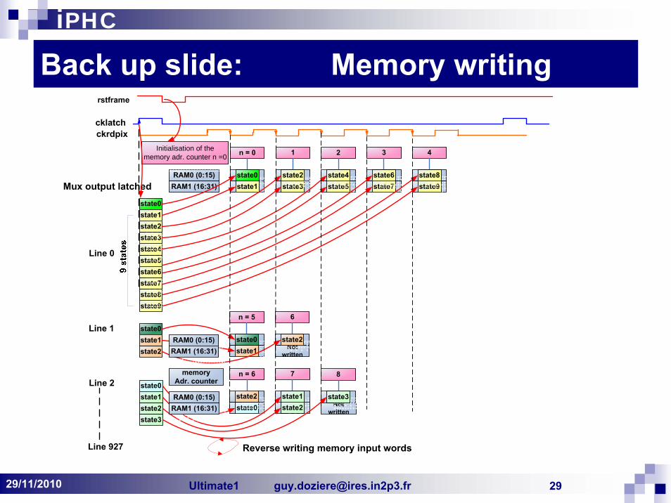
Back up slide: Memory writing
RAM0 (0:15)Mux output latched
cklatch
rstframe
ckrdpix
state0
state5state4state3
state1state2
state9state8state7state6
RAM1 (16:31)
Initialisation of the memory adr. counter n =0 n = 0 1 2 3 4
state0state1 state3
state2state5state4
state9state8
state7state6
state0state1state2
n = 5
Not written
6
state0state1
state2
state0state1state2
memory Adr. counter
n = 6 7
state0state1state2
state3
Not written
8
state3state2
Reverse writing memory input words
Line 0
Line 1
Line 2
Line 927
RAM0 (0:15)RAM1 (16:31)
RAM0 (0:15)RAM1 (16:31)
Ultimate1 [email protected] 3029/11/2010
iPHC
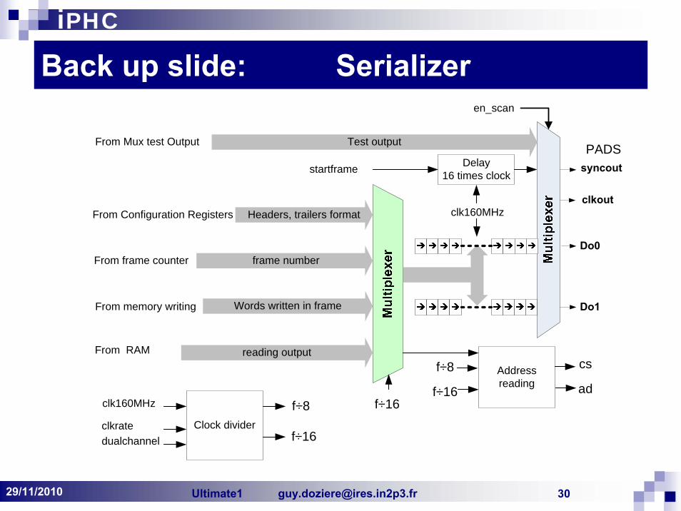
Back up slide: Serializer
Delay16 times clock
dualchannelclkrate
reading output
Headers, trailers format
frame number
Test output
en_scan
Do0
Do1
PADS
clkout
syncout
From Mux test Output
From RAM
From Configuration Registers
From frame counter
Words written in frameFrom memory writing
startframe
Address reading
Clock divider
clk160MHz f÷8
f÷16
f÷16
f÷8
f÷16
cs
ad
clk160MHz
Ultimate1 [email protected] 3529/11/2010
iPHC
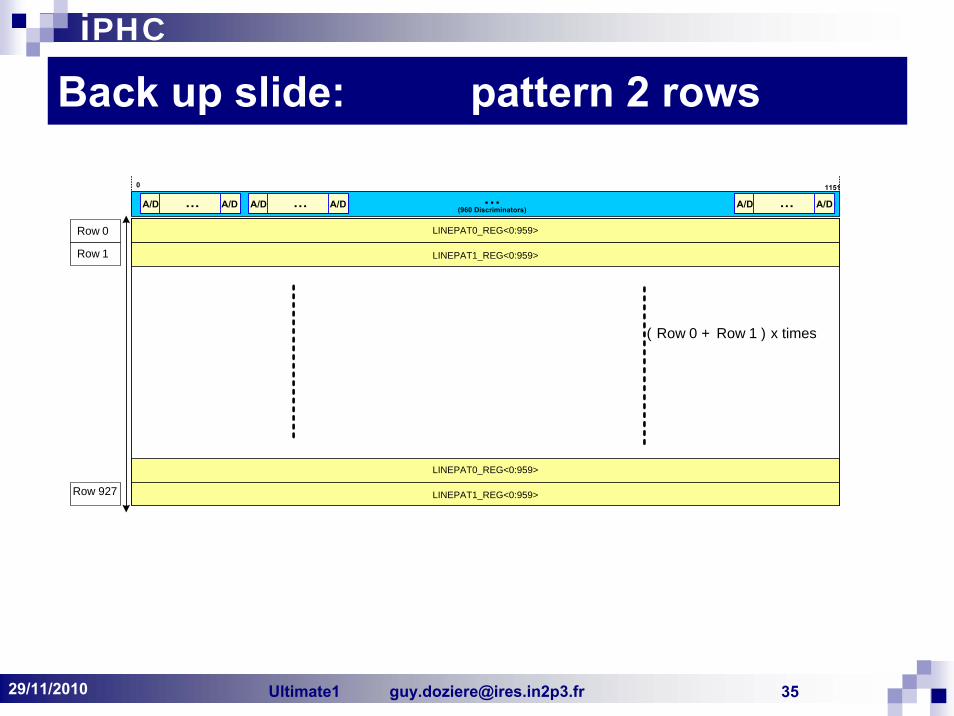
Back up slide: pattern 2 rows
Row 0
Row 1
927
( Row 0 + Row 1 ) x times
Row
A/D A/D… A/D A/D A/D A/D… …A/D A/D… A/D A/D A/D A/D…… …(960 Discriminators)
LINEPAT0_REG<0:959>
LINEPAT1_REG<0:959>
LINEPAT0_REG<0:959>
LINEPAT1_REG<0:959>
0 1151
Ultimate1 [email protected] 3729/11/2010
iPHC
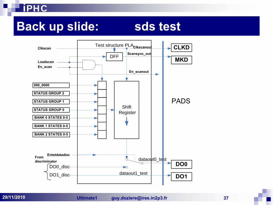
Back up slide: sds testTest structure PLA
STATUS GROUP 2
STATUS GROUP 1
STATUS GROUP 0
BANK 0 STATES 0-5
BANK 1 STATES 0-5
BANK 2 STATES 0-5
000_0000
Loadscan
Shift Register
En_scan
Clkscan
DO0_disc
DO1_disc
Clkscanout
En_scanout
Entstdatadisc
DFFScansync_out
From discriminator
dataout1_test
dataout0_testDO0
DO1
CLKD
MKD