UG733 Xilinx Power Tools Tutorial - china.xilinx.com file03/15/10 1.0 Initial Xilinx release....
26
Xilinx Power Tools Tutorial Spartan-6 and Virtex-6 FPGAs UG733 (v14.1) April 24, 2012
Transcript of UG733 Xilinx Power Tools Tutorial - china.xilinx.com file03/15/10 1.0 Initial Xilinx release....

Spartan-6 and Virtex-6 FPGAs [optional]
UG733 (v14.1) April 24, 2012 [optional]
Xilinx Power Tools Tutorial
Spartan-6 and Virtex-6 FPGAs
UG733 (v14.1) April 24, 2012

Xilinx Power Tools Tutorial www.xilinx.com UG733 (v14.1) April 24, 2012
Xilinx is disclosing this user guide, manual, release note, and/or specification (the “Documentation”) to you solely for use in the development of designs to operate with Xilinx hardware devices. You may not reproduce, distribute, republish, download, display, post, or transmit the Documentation in any form or by any means including, but not limited to, electronic, mechanical, photocopying, recording, or otherwise, without the prior written consent of Xilinx. Xilinx expressly disclaims any liability arising out of your use of the Documentation. Xilinx reserves the right, at its sole discretion, to change the Documentation without notice at any time. Xilinx assumes no obligation to correct any errors contained in the Documentation, or to advise you of any corrections or updates. Xilinx expressly disclaims any liability in connection with technical support or assistance that may be provided to you in connection with the Information.
THE DOCUMENTATION IS DISCLOSED TO YOU “AS-IS” WITH NO WARRANTY OF ANY KIND. XILINX MAKES NO OTHER WARRANTIES, WHETHER EXPRESS, IMPLIED, OR STATUTORY, REGARDING THE DOCUMENTATION, INCLUDING ANY WARRANTIES OF MERCHANTABILITY, FITNESS FOR A PARTICULAR PURPOSE, OR NONINFRINGEMENT OF THIRD-PARTY RIGHTS. IN NO EVENT WILL XILINX BE LIABLE FOR ANY CONSEQUENTIAL, INDIRECT, EXEMPLARY, SPECIAL, OR INCIDENTAL DAMAGES, INCLUDING ANY LOSS OF DATA OR LOST PROFITS, ARISING FROM YOUR USE OF THE DOCUMENTATION.
CRITICAL APPLICATIONS DISCLAIMERXILINX PRODUCTS (INCLUDING HARDWARE, SOFTWARE AND/OR IP CORES) ARE NOT DESIGNED OR INTENDED TO BE FAIL-SAFE, OR FOR USE IN ANY APPLICATION REQUIRING FAIL-SAFE PERFORMANCE, SUCH AS IN LIFE-SUPPORT OR SAFETY DEVICES OR SYSTEMS, CLASS III MEDICAL DEVICES, NUCLEAR FACILITIES, APPLICATIONS RELATED TO THE DEPLOYMENT OF AIRBAGS, OR ANY OTHER APPLICATIONS THAT COULD LEAD TO DEATH, PERSONAL INJURY OR SEVERE PROPERTY OR ENVIRONMENTAL DAMAGE (INDIVIDUALLY AND COLLECTIVELY, “CRITICAL APPLICATIONS”). FURTHERMORE, XILINX PRODUCTS ARE NOT DESIGNED OR INTENDED FOR USE IN ANY APPLICATIONS THAT AFFECT CONTROL OF A VEHICLE OR AIRCRAFT, UNLESS THERE IS A FAIL-SAFE OR REDUNDANCY FEATURE (WHICH DOES NOT INCLUDE USE OF SOFTWARE IN THE XILINX DEVICE TO IMPLEMENT THE REDUNDANCY) AND A WARNING SIGNAL UPON FAILURE TO THE OPERATOR. CUSTOMER AGREES, PRIOR TO USING OR DISTRIBUTING ANY SYSTEMS THAT INCORPORATE XILINX PRODUCTS, TO THOROUGHLY TEST THE SAME FOR SAFETY PURPOSES. TO THE MAXIMUM EXTENT PERMITTED BY APPLICABLE LAW, CUSTOMER ASSUMES THE SOLE RISK AND LIABILITY OF ANY USE OF XILINX PRODUCTS IN CRITICAL APPLICATIONS.
AUTOMOTIVE APPLICATIONS DISCLAIMERXILINX PRODUCTS ARE NOT DESIGNED OR INTENDED TO BE FAIL-SAFE, OR FOR USE IN ANY APPLICATION REQUIRING FAIL-SAFE PERFORMANCE, SUCH AS APPLICATIONS RELATED TO: (I) THE DEPLOYMENT OF AIRBAGS, (II) CONTROL OF A VEHICLE, UNLESS THERE IS A FAIL-SAFE OR REDUNDANCY FEATURE (WHICH DOES NOT INCLUDE USE OF SOFTWARE IN THE XILINX DEVICE TO IMPLEMENT THE REDUNDANCY) AND A WARNING SIGNAL UPON FAILURE TO THE OPERATOR, OR (III) USES THAT COULD LEAD TO DEATH OR PERSONAL INJURY. CUSTOMER ASSUMES THE SOLE RISK AND LIABILITY OF ANY USE OF XILINX PRODUCTS IN SUCH APPLICATIONS.
© Copyright 2012 Xilinx, Inc. XILINX, the Xilinx logo, Virtex, Spartan, ISE, and other designated brands included herein are trademarks of Xilinx in the United States and other countries. All other trademarks are the property of their respective owners.

UG733 (v14.1) April 24, 2012 www.xilinx.com Xilinx Power Tools Tutorial
Revision HistoryThe following table shows the revision history for this document.
Date Version Revision
03/15/10 1.0 Initial Xilinx release.
03/01/11 13.1 Updated with information to describe the Power Tools for the 13.1 release of ISE.
10/19/11 13.3 Revisions to manual for ISE 13.3 release:
• Updated all XPower Estimator and XPower Analyzer figures after running 13.3 design files through the Power Tools.
• Added Strip Path information to Step 2 of “Power Analysis Using XPower Analyzer (XPA)”.
• Updated names for buttons within XPower Estimator (renamed for 13.3). See “Import File Button” and “Set Default Rates Button” figures.
01/18/11 13.4 Revisions to manual for ISE 13.4 release.
• Updated figures for Spartan-6 XPower Estimator design flow, since design files have been changed to target a different Spartan-6 device.
• Added Simulation file and Strip Path information to Step 2 of “Power Analysis Using XPower Analyzer (XPA)” for Spartan-6 deesign flow.
04/24/12 14.1 Revalidated for the 14.1 release. Editorial updates only; no technical content updates.

Xilinx Power Tools Tutorial www.xilinx.com 5UG733 (v14.1) April 24, 2012
Revision History . . . . . . . . . . . . . . . . . . . . . . . . . . . . . . . . . . . . . . . . . . . . . . . . . . . . . . . . . . . . . 3
Virtex-6 and Spartan-6 Power Tools TutorialIntroduction . . . . . . . . . . . . . . . . . . . . . . . . . . . . . . . . . . . . . . . . . . . . . . . . . . . . . . . . . . . . . . . . . 7
Power in FPGAs . . . . . . . . . . . . . . . . . . . . . . . . . . . . . . . . . . . . . . . . . . . . . . . . . . . . . . . . . . . 7Tutorial Design Information. . . . . . . . . . . . . . . . . . . . . . . . . . . . . . . . . . . . . . . . . . . . . . . . . 8
Power Estimation Using XPE (XPower Estimator) . . . . . . . . . . . . . . . . . . . . . . . . . . . . . 8Step 1: Download XPE Spreadsheet . . . . . . . . . . . . . . . . . . . . . . . . . . . . . . . . . . . . . . . . . . 9Step 2: Import Design Information (If Applicable) . . . . . . . . . . . . . . . . . . . . . . . . . . . . . . 9Step 3: Enter Environment Data . . . . . . . . . . . . . . . . . . . . . . . . . . . . . . . . . . . . . . . . . . . . . 9Step 4: Set Activity Rates . . . . . . . . . . . . . . . . . . . . . . . . . . . . . . . . . . . . . . . . . . . . . . . . . . . 11Step 5: Set Clock Net Frequency . . . . . . . . . . . . . . . . . . . . . . . . . . . . . . . . . . . . . . . . . . . . 11Step 6: Enter Design Information. . . . . . . . . . . . . . . . . . . . . . . . . . . . . . . . . . . . . . . . . . . . 11Step 7: Adjust Design Data . . . . . . . . . . . . . . . . . . . . . . . . . . . . . . . . . . . . . . . . . . . . . . . . . 13
Power Reduction Options in ISE . . . . . . . . . . . . . . . . . . . . . . . . . . . . . . . . . . . . . . . . . . . . 16Synthesis Power Reduction . . . . . . . . . . . . . . . . . . . . . . . . . . . . . . . . . . . . . . . . . . . . . . . . 16Map Power Reduction . . . . . . . . . . . . . . . . . . . . . . . . . . . . . . . . . . . . . . . . . . . . . . . . . . . . . 17
Power Analysis Using XPower Analyzer (XPA) . . . . . . . . . . . . . . . . . . . . . . . . . . . . . . 17Step 1: Open XPower Analyzer (XPA) . . . . . . . . . . . . . . . . . . . . . . . . . . . . . . . . . . . . . . . 18Step 2: Specify Input Files . . . . . . . . . . . . . . . . . . . . . . . . . . . . . . . . . . . . . . . . . . . . . . . . . . 19Step 3: Enter Environment Settings . . . . . . . . . . . . . . . . . . . . . . . . . . . . . . . . . . . . . . . . . . 20Step 4: Set Default Activity Rates . . . . . . . . . . . . . . . . . . . . . . . . . . . . . . . . . . . . . . . . . . . 21Step 5: Adjust Design Data . . . . . . . . . . . . . . . . . . . . . . . . . . . . . . . . . . . . . . . . . . . . . . . . . 21
Conclusion. . . . . . . . . . . . . . . . . . . . . . . . . . . . . . . . . . . . . . . . . . . . . . . . . . . . . . . . . . . . . . . . . . 23
Appendix A: Additional Resources
Table of Contents

Xilinx Power Tools Tutorial www.xilinx.com 7UG733 (v14.1) April 24, 2012
Virtex-6 and Spartan-6 Power Tools Tutorial
IntroductionThis tutorial provides advice on how to use the Xilinx® Power Tools for accurate power consumption estimation. The tutorial focuses on a simple Virtex®-6 and Spartan®-6 design for use in both an XPower Estimator (XPE) spreadsheet and XPower Analyzer (XPA) to illustrate how you may use the power tools in your design flow. This tutorial also describes the power optimization options in the ISE implementation tools.
The Xilinx Power Tools cover different stages of the design flow. The tools can supply power estimates from the pre-design phase to the point at which the design is fully implemented. Because the Power Tools supply information throughout the design flow, they can be used for:
• Part selection
• Board design
• System reliability
• Power consumption estimation, analysis, and optimization
Power in FPGAsXilinx constantly innovates to make sure the power challenges associated with shrinking technologies can be overcome. Xilinx understands that FPGA power consumption is one of the biggest concerns of FPGA users. Xilinx Power Tools help perform power estimation and analysis for a given design. Power estimation and analysis become even more important as FPGAs increase in logic capacity and performance by migrating to smaller process geometries.
Total power in an FPGA is the sum of two components:
• Static power - Static power results primarily from transistor leakage current in the device. Leakage current is either from source-to-drain or through the gate oxide, and exists even when the transistor is logically “OFF”.
• Dynamic power - Dynamic power is associated with design activity and switching events in the core or I/O of the device. Dynamic power is determined by node capacitance, supply voltage, and switching frequency.
The accuracy of the Xilinx Power Tools depends on two primary components:
• Device data models and device characterization integrated into the tools
• Inputs accurately entered by the user into the tools.
8 www.xilinx.com Xilinx Power Tools TutorialUG733 (v14.1) April 24, 2012
Power Estimation Using XPE (XPower Estimator)
For accurate estimates of your application, enter realistic information which is as complete as possible. Modeling a certain aspect of the design in a manner that is overly conservative or that lacks sufficient knowledge of the design can result in unrealistic estimates.
Tutorial Design InformationThe design used in this tutorial is not a functional design; it is only used to illustrate power tool capabilities and recommended usage. Synthesis and implementation have been performed on the design in ISE without any power optimization options.
The SAIF (simulation activity) file that is used as an input file for XPA was generated in the ISE Simulator (ISim). The SAIF file is a stimulus file from design simulation. For more details about SAIF generation using ISim, refer to the ISim User Guide (UG660).
Power Estimation Using XPE (XPower Estimator)The XPower Estimator (XPE) spreadsheet is a power estimation tool typically used in the pre-design and pre-implementation phases of a project. XPE helps with architecture evaluation and device selection and helps you select the appropriate power supply and the thermal management components which may be required for your application.
As a pre-implementation tool, XPE can be used in the early stages of a design cycle when the RTL description of the design is incomplete. After implementation, the XPower Analyzer (XPA) tool (available in the ISE Design Suite software) can be used for more accurate estimates and power analysis.
XPE is a spreadsheet, so all Microsoft Excel functionality is fully retained in the writable (unprotected) sections of the spreadsheet.
The goal of this tutorial is not to give an exhaustive overview of XPE, but to provide an example of basic XPE features, allowing you to perform a quick power estimation for your design. For a complete description of XPE, see the XPower Estimator User Guide (UG440).
For an accurate XPE estimation, you will have to estimate the amount of device resources your design will use. If you are not sure how to make this estimate it might be best to run through an example design in ISE and take a look at the Map Report file, which contains resource usage information.
XPE displays tabs for each type of component in a device architecture (for example, I/Os, BRAMs, and DCMs). The number of tabs displayed in XPE will vary depending on your device architecture. For example, in this tutorial, the device selected does not have any MGT circuitry and so the MGT tab is not included.
The 14.1 version of XPA is used in this tutorial. Below are the steps that will allow you to perform accurate power analysis using XPE. You can use either the Spartan-6 or Virtex-6 design with this tutorial.

Xilinx Power Tools Tutorial www.xilinx.com 9UG733 (v14.1) April 24, 2012
Power Estimation Using XPE (XPower Estimator)
Step 1: Download XPE SpreadsheetDownload the latest available spreadsheet for your targeted device, and the tutorial design files.
The XPE spreadsheets are available at the Power Advantage web page here:
http://www.xilinx.com/power
This tutorial uses this 14.1 version of the spreadsheet:
• Virtex-6: Virtex5_Virtex6_XPE_14_1.xls
OR
• Spartan-6: Spartan3a_Spartan6_XPE_14_1.xls
The tutorial design files are available from the Tutorials page on the Xilinx website here:
http://www.xilinx.com/support/documentation/sw_manuals/dt_ise14-1_tutorials.htm
Step 2: Import Design Information (If Applicable)Import the MRP (MAP Report) file from the working directory of either the Virtex-6 or Spartan-6 tutorial design (available from the Tutorials page on the Xilinx website). To do so, click the Import File button in the XPE spreadsheet, then select Map Report (*.mrp) in the Files of type field of the dialog box that opens. When you select the .mrp file to import, this will automatically load the spreadsheet with the design resources.
Note: In many cases, you will be entering information into XPE before your design has been implemented in ISE, and there will not be an MRP file to import into XPE. For this tutorial, however, you imported an MRP file to give the XPE spreadsheet some initial information.
File name of tutorial Map Report:
• Virtex-6: V6_tutorial_top_16bit_map.mrp (MAP Report to be imported in XPE)
• Spartan-6: S6_tutorial_top_16bit_map.mrp (MAP Report to be imported in XPE)
Note: For cases in which you have already used XPE for a given design and you want to upgrade the XPE version, you can click the Import button, then select XPE Workbook (*.xls*) in the Files of type field of the dialog box that opens. When you select the .xls* file to import, the information from the earlier XPE spreadsheet will be loaded into the updated XPE spreadsheet.
Step 3: Enter Environment DataIn the Summary tab, check the Device information and enter Environment data as follows:
• Ambient Temp = 25°C
• Heat Sink = None
• Airflow = 0
Note: FPGA quiescent power is highly affected by environment settings, so it is important to match your board’s environment with the board data as precisely as possible. The Xilinx Power Tools can be very useful to perform What If? analysis and define the best thermal strategy for the board.
Figure 1: Import File Button

10 www.xilinx.com Xilinx Power Tools TutorialUG733 (v14.1) April 24, 2012
Power Estimation Using XPE (XPower Estimator)
Figure 2: Device and Environment Settings for Virtex-6 Design
Figure 3: Device and Environment Settings for Spartan-6 Design

Xilinx Power Tools Tutorial www.xilinx.com 11UG733 (v14.1) April 24, 2012
Power Estimation Using XPE (XPower Estimator)
Step 4: Set Activity RatesYou can set the overall Toggle Rate for each of the different tabs (i.e Logic, IO, BRAM, DSP) in the spreadsheet. To do so, from the Summary tab, click the Set Default Rates button. By default the toggle rate will be set to 12.5, which should be displayed for Logic, DSP and I/O.
Typically, logic-intensive designs work at around 12.5% of the synchronizing clock (12.5% is the default value used in XPE). For a worst- case estimate, a toggle rate of 20% can be used. Average toggle rates greater than 20% are not very common. Arithmetic-intensive modules of a design seem to take toggle rates of up to 50%, which is representative of the absolute worst case. An example of this would be a Multiply-Accumulate operation. It is also common to model toggle rate for random input data at 50%. To appreciate what 100% toggle rate means, think of a constantly enabled toggle flip-flop (TFF) whose data input is tied High. The T-output of this flip-flop toggles every clock edge. Very few designs could have an average toggle rate that high (100%).
Step 5: Set Clock Net FrequencySet the overall clock frequency of the spreadsheet. To do this, from the Summary tab, click the Set Default Rates button and set the rate to 200 MHz (the default) for All Clock Nets.
Note: If no clock nets are defined for the design, changing the frequency will not affect anything.
Using this toolbar button sets the clock frequency for all relevant design elements, such as Clocks, Logic, I/Os, BRAMs, and DSP elements. Having a single clock frequency for all these elements is not realistic; however, individual elements can be adjusted in other tabs of the spreadsheet later on.
Step 6: Enter Design InformationIf you are working in the Virtex-6 design, set the clock frequency, multiply counter, and Clock0 Divide values in the MMCM tab for the two MMCM components in the design.
Set the first MMCM (MMCM_1) as follows:
• Clock (MHz) = 200 MHz
• Multiply Counter = 10
• Clock 0 Divide = 5
• Leave default value for other fields.
Set the second MMCM (MMCM_2) as follows:
• Clock (MHz) = 33 MHz
• Multiply Counter = 25
• Clock 0 Divide = 25
• Leave default value for other fields.
Figure 4: Set Default Rates Button
12 www.xilinx.com Xilinx Power Tools TutorialUG733 (v14.1) April 24, 2012
Power Estimation Using XPE (XPower Estimator)
At this point, the power numbers reported in the Summary tab will look like this for the Virtex-6 design:
If you are working in the Spartan-6 design, set the clock frequency, multiply counter, and Clock0 Divide values in the PLL tab for the PLL component in the design.
Set the PLL (PLL_1) to the following attributes:
• Clock (MHz) = 33 MHz
• Multiply Counter = 25
• Clock 0 Divide = 25
• Leave default values for the rest of the field
At this point, the Summary tab of the spreadsheet should look like the following figure for the Spartan-6 design:
Figure 5: Power and Thermal Distribution - XPE for Virtex-6 FPGAs

Xilinx Power Tools Tutorial www.xilinx.com 13UG733 (v14.1) April 24, 2012
Power Estimation Using XPE (XPower Estimator)
Step 7: Adjust Design DataThe Import feature that imported data from a Map Report (MRP) file entered approximate values for design elements in the CLOCK, LOGIC, IO, BRAM, and DSP tabs. This can be improved if you have a good understanding of how these elements are used in your design. Extracting additional data from the MRP file and adjusting the values in the XPE spreadsheet helps to get a more accurate power estimation.
Note: Using the -detail option in MAP will generate a verbose Map report that can help you to gather more detailed information on the design. This will help to adjust XPE design elements after data has been imported from the MRP file (MAP report). More information about this option is found in the Command Line Tools User Guide (UG628).
Note: Using the command line xpwr -xpe in ISE will generate an .xpe (interoperability) file containing specific design information which can be imported into XPE. For more information about importing design information from XPower Analyzer (XPA) into XPE, see the XPower Estimator User Guide (UG440).
Figure 6: Power and Thermal Distribution - XPE for Spartan-6 FPGAs

14 www.xilinx.com Xilinx Power Tools TutorialUG733 (v14.1) April 24, 2012
Power Estimation Using XPE (XPower Estimator)
If you are working in the Virtex-6 design, modify the entries for the following elements:
• In the CLOCK tab, you can simplify the clock usage to two clocks.
♦ The first clock (GCLK_1) should be set as follows:
- Frequency (MHz) = 200 MHz
- Fanout = 68
♦ The second clock (GCLK_2) should be set as follows:
- Frequency (MHz) = 33 MHz
- Fanout = 63
• In the LOGIC tab, change the Toggle Rate to 19%, which is the average estimated value for this design.
• In the IO tab, change the Clock (MHz) (clock frequency) for the LVCMOS I/Os to 33 MHz and the Toggle Rate to 14% for both I/O types, which is the average estimated value for all I/Os of this design.
• For the DSP tab, change the Toggle Rate for all DSP components to 1.5%, which is the average estimated value.
After all the relevant settings have been entered or updated, power results are available in the Summary tab of the spreadsheet. The following figure shows the new result from modifications for the Virtex-6 design.
Figure 7: Updated Power and Thermal Distribution in XPE for Virtex-6 FPGA
Xilinx Power Tools Tutorial www.xilinx.com 15UG733 (v14.1) April 24, 2012
Power Estimation Using XPE (XPower Estimator)
If you are working in the Spartan-6 design, change the entries for the following elements:
• In the CLOCK tab, modify the clock usage to two clocks
♦ The first clock (GCLK_1) should be set as follows:
- Frequency (MHz) = 200 MHz
♦ The second clock (GCLK_2) should be set as follows:
- Frequency (MHz) = 33 MHz
• In the LOGIC tab, change the Toggle Rate to 19%, which is the average estimated value.
• In the IO tab, change the Clock (MHz) (clock frequency) for the LVCMOS I/Os to 33 MHz and the Toggle Rate to 14% for both I/O types, which is the average estimated value for all I/Os of this design.
• In the BRAM (Block RAM) tab, change the Clock (MHz) (clock frequency) on both Port A and Port B to 200 MHz.
After all the relevant settings have been entered or updated, the power results are available in the Summary tab of the spreadsheet. The following figure shows the new results from the recent modification for the Spartan-6 design.
After the data is entered and the part is operating within the thermal limits of the selected grade, the power reported by XPE can be used to determine the voltage rails for the design. If your confidence in the data entered is not very high, you may add additional padding to
Figure 8: Updated Power and Thermal Distribution in XPE for Spartan-6 FPGA

16 www.xilinx.com Xilinx Power Tools TutorialUG733 (v14.1) April 24, 2012
Power Reduction Options in ISE
the numbers to circumvent the possibility of under-designing the power system for the FPGA. If, however, you are fairly certain of the data entered, no additional padding above the data reported by XPE is necessary.
Although XPE is primarily intended to be used early in design conception to scale the power budget it can be used later on in the design stages to get accurate power estimation (as described in Step 7: Adjust Design Data) or to perform worst case power analysis. For further details about this analysis and XPE, refer to the XPower Estimator User Guide (UG440), the Power Methodology Guide (UG786), and the White Paper Seven Steps to an Accurate Worst-Case Power Analysis Using Xilinx Power Estimator (XPE) (WP353).
Key Points for Interpreting Power Results
• XPE reports the total supply power across all voltage sources (Power Supply section on the Summary tab). The table includes all power required from the on-board power supplies.
• XPE reports the power dissipated on-chip across all power rails (On-Chip Power table). This table displays a breakdown of power consumption from all the different FPGA resources. This table also displays the total percentage used for each of the different FPGA resource. This view can help determine the amount of power being consumed and dissipated by the device. It also helps identify potential areas in the design where power optimization techniques could be used to meet the targeted power budget.
• XPE also reports Thermal data (Summary table), giving the estimated Junction Temperature of the FPGA related to the package characteristics and the thermal power (on-chip power).
Power Reduction Options in ISEDepending on the design itself, power optimization options used in the ISE design flow can be more or less efficient. When –power switches are used in synthesis and implementation, an average power reduction of approximately 10% is expected, with a small runtime penalty (approximately 15%) and a potentially small percentage of performance degradation. Because the design used in this tutorial is rather small, the dynamic power is much lower than the static power. Under these conditions, using power optimization options available in synthesis and implementation aren’t relevant and won’t help much.
In ISE there are a few process properties available to help reduce power in your design. You can set these properties in Synthesis and Map processes.
Note: Instead of changing properties for each tool you could also use the predefined implementation strategies specific for optimizing power.
Synthesis Power ReductionYou can reduce power with the –power switch in synthesis. The Power Reduction property in ISE instructs XST to optimize the design to consume as little power as possible. Macro processing decisions are made to implement functions in a manner that uses minimal power.
To access synthesis properties in ISE:
1. In the Processes tab, right-click Synthesize and select Process Properties.
2. In the Synthesis Options dialog box, verify or change the Power Reduction setting.

Xilinx Power Tools Tutorial www.xilinx.com 17UG733 (v14.1) April 24, 2012
Power Analysis Using XPower Analyzer (XPA)
Map Power ReductionOne option in Map for power reduction is to use the -power high switch (Power Reduction property in ISE). This enables extraction of gating logic to minimize design activity by disabling logic that is not contributing to the output for each clock cycle.
You can also specify a switching activity file to guide power optimization. The switching activity file is specified with the -activityfile switch (Power Activity File property in ISE).
Another option in Map for power reduction is to use the –global_opt switch (Global Optimization property in ISE). This switch will specify that placement is optimized to reduce the power consumed by a design during timing-driven packing and placement. Global optimization includes logic remapping and trimming, logic and register replication, optimization, and logic replacement of tri-states. Depending on the design, this switch can help reduce power. These routines will extend the runtime of Map because of the extra processing that occurs. By default, this option is off. For further information on this option, see the Command Line Tools User Guide (UG628).
Power Analysis Using XPower Analyzer (XPA)XPower Analyzer (XPA) does an analysis on real design data. Use XPA after design implementation in ISE, using the NCD file output from Place & Route (PAR). XPA now features a vectorless estimation algorithm; a way of assigning activity rates to nodes even if these activity rates are not defined in the design file or specified in any other way. However, we recommend using simulation activity files (SAIF or VCD) from simulation for accurate power analysis. We recommend always using the latest version of ISE to get the latest version of XPA, which contains the latest characterization data for power analysis.
XPA is used for design power analysis. At the point in your design phase when XPA is used, your ISE project should have successfully completed Place & Route (PAR) and generated an NCD output file. It is important to understand which design files are used by the XPA tool for power estimation. In this tutorial, either a Spartan-6 design on the SP601 board or a Virtex-6 design is used for power estimation and both are included for reference. These design files are available from the Tutorials page on the Xilinx website.
XPA can be started as a standalone graphical user interface (xpa shell command) from within a project in ISE Project Navigator, or as a batch command line (xpwr) or from PlanAhead. The XPA GUI can be opened standalone by entering xpa at the command line. To generate a text-based power report, enter xpwr. Note that you can type just xpwr in a command shell and all the switch options will be displayed.
In ISE, XPower Analyzer can be found in the Processes tab, under Place & Route.
To invoke XPower Analyzer through PlanAhead, in the Flow Navigator, open the Implemented Design. Then select the Launch XPower Analyzer command from the Implemented Design task list.

18 www.xilinx.com Xilinx Power Tools TutorialUG733 (v14.1) April 24, 2012
Power Analysis Using XPower Analyzer (XPA)
To improve the accuracy of XPA you can also read in optional design files. For example, from Project Navigator you can do the following:
1. In the Processes tab, under Place & Route, right-click Analyze Power Distribution (XPower Analyzer) and select Process Properties.
2. In the XPower Analyzer Properties dialog box, specify the files.
Alternatively, in the standalone tool you will have the option to include these files when you load the design. Specify the files to include in the Open Design dialog box.
The input files are:
• NCD - Output file from PAR that is required by XPA for power analysis.
• Settings file - Optional file. The Settings file contains application settings and node activity rates saved from an XPower Analyzer session. Any manual changes (edits) you have made in the XPA window can be saved to a settings file. The settings file (XML format) can then be used to load any relevant design information from a previous XPA session into a later session.
• PCF - Optional file. The PCF (Physical Constraints File) contains constraint information to help determine clock frequencies. All clock information from the UCF (User Constraints File) are reported in the PCF, so if the design is well constrained, loading the PCF is important for accurate power results.
• VCD or SAIF file - Optional file. These simulation activity files include specific switching information (toggle rates, signal rates, and frequency information) that will give the most accurate power estimation. Note that XPA might not always be able to match all of your design nets with nets in the simulation file so you may have to enter some switching information manually. It is important to make sure you look at what design information was extracted and what (if any) design information was not extracted. In the Console window take note of any warning messages, since they may indicate that design information was not pulled into XPA.
The 14.1 version of XPA is used in this tutorial. Below are the key steps that will allow you to perform a power analysis using XPA. You can use either the Virtex-6 or Spartan-6 design for this tutorial.
Step 1: Open XPower Analyzer (XPA)Open XPA in one of these ways:
• Open XPA through ISE - In the Processes tab of Project Navigator, double-click the Analyze Power Distribution (XPower Analyzer) process, located under Place & Route.
When you open XPA from ISE, you are analyzing a design that has already been fully placed and routed.
OR
• Open XPA standalone - To open XPA standalone:
a. Select Start > Run.
b. At the command prompt, type xpa and press Enter.

Xilinx Power Tools Tutorial www.xilinx.com 19UG733 (v14.1) April 24, 2012
Power Analysis Using XPower Analyzer (XPA)
Step 2: Specify Input FilesIf you opened XPA standalone, you will need to specify your input files in this way:
1. In the XPA window, select File > Open Design.
2. In the Open Design dialog box, select the files and set options to use for either the Virtex-6 or Spartan-6 tutorial design.
Note: This tutorial will focus on the Virtex-6 design.
♦ Virtex-6:
- V6_tutorial_top_16bit.ncd (Post-Place and Route NCD file)
- V6_tutorial_top_16bit.pcf (Physical Constraints File)
- simulation_XPA_stimulus_file.saif (Stimulus file from Simulation)
- Enter uut for the Strip Path. This will strip off the testbench name within the SAIF file, to improve XPA’s ability to match names in the stimulus (SAIF) file with names in the design (NCD) file.
♦ Spartan-6:
- S6_tutorial_top_16bit.ncd (Post-Place and Route NCD file)
- S6_tutorial_top_16bit.pcf (Physical Constraints File)
- simulation_XPA_stimulus_file.saif (Stimulus file from Simulation)
- Enter uut for the Strip Path. This will strip off the testbench name within the SAIF file, to improve XPA’s ability to match names in the stimulus (SAIF) file with names in the design (NCD) file.
Figure 9: Open Design Dialog Box (XPA)
XML File
PCF File
VCD/SAIF File
NCD File
Path in VCD/SAIF File

20 www.xilinx.com Xilinx Power Tools TutorialUG733 (v14.1) April 24, 2012
Power Analysis Using XPower Analyzer (XPA)
Step 3: Enter Environment SettingsOnce XPA is completely opened and has analyzed the design using the specified input files, these report views are displayed:
• The Summary view displays all the important voltage rail information.
• The Environment and Thermal Property tables in the Summary view show thermal information to be used in the device power calculation, and allow you to set the relevant thermal settings to match your hardware and environment (see Figure 10). Ambient temperature is 50°C by default, but you can change this value. Also, you can enter a custom junction temperature, a custom Theta JA (if using a heatsink), and airflow information. This thermal information directly affects your power estimation.
• The Summary view displays the power drawn from each voltage supply (Supply Summary table) along with both quiescent (Iccq) and dynamic current (Icc) (Supply Power (W) table). In this report view, you can adjust each supply voltage within the recommended operating condition range given in the device data sheet.
• The Default Activity Rates view allows you to change certain settings globally; you can enter output load information, toggle rate, and enable rate information.
When XPA has completed its design analysis after you open the specified input files, go to the Summary view Environment table and change the relevant thermal settings as follows:
• Ambient Temp = 25°C
• Airflow = 250 LFM
• Heat Sink = None
You will need to update the power analysis after you enter data into XPA. To do this, select Tools > Update Power Analysis.
Figure 10: Environment Table (Summary View) - XPower Analyzer (XPA)
Xilinx Power Tools Tutorial www.xilinx.com 21UG733 (v14.1) April 24, 2012
Power Analysis Using XPower Analyzer (XPA)
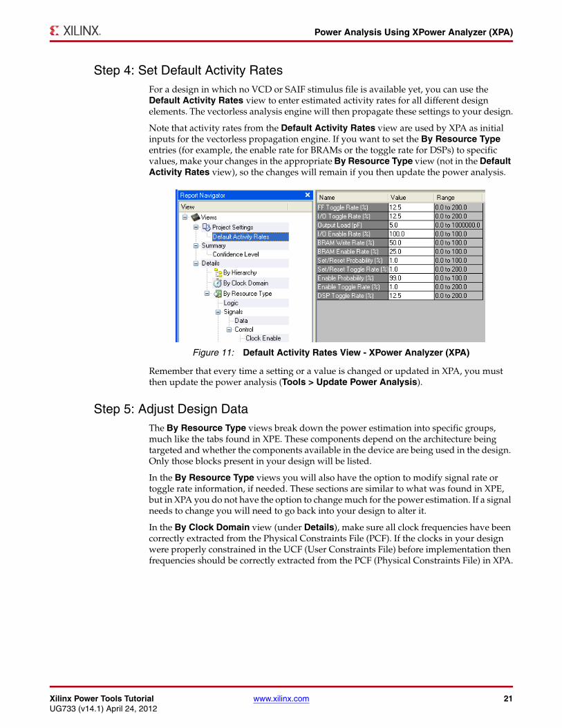
Step 4: Set Default Activity RatesFor a design in which no VCD or SAIF stimulus file is available yet, you can use the Default Activity Rates view to enter estimated activity rates for all different design elements. The vectorless analysis engine will then propagate these settings to your design.
Note that activity rates from the Default Activity Rates view are used by XPA as initial inputs for the vectorless propagation engine. If you want to set the By Resource Type entries (for example, the enable rate for BRAMs or the toggle rate for DSPs) to specific values, make your changes in the appropriate By Resource Type view (not in the Default Activity Rates view), so the changes will remain if you then update the power analysis.
Remember that every time a setting or a value is changed or updated in XPA, you must then update the power analysis (Tools > Update Power Analysis).
Step 5: Adjust Design DataThe By Resource Type views break down the power estimation into specific groups, much like the tabs found in XPE. These components depend on the architecture being targeted and whether the components available in the device are being used in the design. Only those blocks present in your design will be listed.
In the By Resource Type views you will also have the option to modify signal rate or toggle rate information, if needed. These sections are similar to what was found in XPE, but in XPA you do not have the option to change much for the power estimation. If a signal needs to change you will need to go back into your design to alter it.
In the By Clock Domain view (under Details), make sure all clock frequencies have been correctly extracted from the Physical Constraints File (PCF). If the clocks in your design were properly constrained in the UCF (User Constraints File) before implementation then frequencies should be correctly extracted from the PCF (Physical Constraints File) in XPA.
Figure 11: Default Activity Rates View - XPower Analyzer (XPA)

22 www.xilinx.com Xilinx Power Tools TutorialUG733 (v14.1) April 24, 2012
Power Analysis Using XPower Analyzer (XPA)
If you made any changes make sure to rerun the power estimation analysis (Tools > Update Power Analysis).
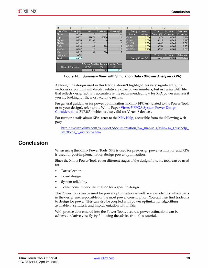
Once all settings are properly set, the Summary lists all relevant power figures for the design analyzed.
The two figures below compare results when XPA is loaded with the same NCD and settings but different stimulus analysis from simulation. In Figure 13, information was estimated by the vectorless estimation algorithm. In Figure 14, information was supplied by an SAIF file extracted from simulation.
Figure 12: By Clock Domain View - XPower Analyzer (XPA)
Figure 13: Summary View Using Vectorless Estimation Algorithm - XPower Analyzer (XPA)
Xilinx Power Tools Tutorial www.xilinx.com 23UG733 (v14.1) April 24, 2012
Conclusion
Although the design used in this tutorial doesn’t highlight this very significantly, the vectorless algorithm will display relatively close power numbers, but using an SAIF file that reflects design activity accurately is the recommended flow for XPA power analysis if you are looking for the most accurate results.
For general guidelines for power optimization in Xilinx FPGAs (related to the Power Tools or to your design), refer to the White Paper Virtex-5 FPGA System Power Design Considerations (WP285), which is also valid for Virtex-6 devices.
For further details about XPA, refer to the XPA Help, accessible from the following web page:
http://www.xilinx.com/support/documentation/sw_manuals/xilinx14_1/isehelp_start#xpa_c_overview.htm
ConclusionWhen using the Xilinx Power Tools, XPE is used for pre-design power estimation and XPA is used for post-implementation design power optimization.
Since the Xilinx Power Tools cover different stages of the design flow, the tools can be used for:
• Part selection
• Board design
• System reliability
• Power consumption estimation for a specific design
The Power Tools can be used for power optimization as well. You can identify which parts in the design are responsible for the most power consumption. You can then find tradeoffs to design for power. This can also be coupled with power optimization algorithms available in synthesis and implementation within ISE.
With precise data entered into the Power Tools, accurate power estimations can be achieved relatively easily by following the advice from this tutorial.
Figure 14: Summary View with Simulation Data - XPower Analyzer (XPA)

24 www.xilinx.com Xilinx Power Tools TutorialUG733 (v14.1) April 24, 2012
Conclusion

Xilinx Power Tools Tutorial www.xilinx.com 25UG733 (v14.1) April 24, 2012
Appendix A
Additional Resources
• ISE Design Suite: Installation and Licensing Guide (UG798): http://www.xilinx.com/support/documentation/sw_manuals/xilinx14_1/iil.pdf
• ISE Design Suite 14: Release Notes Guide (UG631): http://www.xilinx.com/support/documentation/sw_manuals/xilinx14_1/irn.pdf
• Xilinx® Documentation: http://www.xilinx.com/support/documentation
• Xilinx Global Glossary: http://www.xilinx.com/support/documentation/sw_manuals/glossary.pdf
• Xilinx Support: http://www.xilinx.com/support.htm
• To download the XPower Estimator (XPE) spreadsheets, see the Power Advantage webpage on the Xilinx website at:
http://www.xilinx.com/power
• The design files used in this tutorial are available from the Tutorials page on the Xilinx Website here:
http://www.xilinx.com/support/documentation/dt_ise14-1_tutorials.htm
• To search the Answer Database of silicon, software, and IP questions and answers, or to create a technical support WebCase, see the Xilinx website at:
http://www.xilinx.com/support
• The following are especially pertinent to the subject of this User Guide.
• Power Methodology Guide (UG786)
• XPower Estimator User Guide (UG440)
• Seven Steps to an Accurate Worst-Case Power Analysis Using Xilinx Power Estimator (XPE) (WP353)
• XPower Analyzer (XPA) Online Help
• Test Boards for Area Array Surface Mount Package Thermal Measurements
• Descriptions of the resources available in an FPGA can be found under FPGA Device Families at http://www.xilinx.com/documentation.

26 www.xilinx.com Xilinx Power Tools TutorialUG733 (v14.1) April 24, 2012
Appendix A: Additional Resources


![Xilinx ISE Design Suite 13: Installation and Licensing Guide · ISE Design Suite 13: Installation and Licensing [Guide Subtitle] [optional] UG798 (v 13.1) [optional] ISE Design Suite](https://static.fdocuments.net/doc/165x107/5ae50f2c7f8b9a495c8f67cb/xilinx-ise-design-suite-13-installation-and-licensing-design-suite-13-installation.jpg)