UCC256303 LLC Resonant Controller Enabling Ultra-Low ... · Copyright © 2017, ... JEDEC document...
67
FB LO HO HS BLK VIN BW Vout Cr Lr Lm ISNS VCR 10 HV LO GND LL/SS HO VCC VCR FB BLK 7 UCC256303 LLC Controller HB HS RVCC 9 BW ISNS 8 BLK FB ISNS VCR BW HO HS LO CSS External Bias CBOOT Copyright © 2017, Texas Instruments Incorporated 4 6 5 3 1 11 14 15 16 12 Product Folder Order Now Technical Documents Tools & Software Support & Community An IMPORTANT NOTICE at the end of this data sheet addresses availability, warranty, changes, use in safety-critical applications, intellectual property matters and other important disclaimers. PRODUCTION DATA. UCC256303 SLUSD49 – SEPTEMBER 2017 UCC256303 LLC Resonant Controller Enabling Ultra-Low Standby Power 1 1 Features 1• Hybrid Hysteretic Control (HHC) – Best-in-Class Transient Response – Easy Compensation Design • Optimized Low Power Features Enable 75 mW Standby Power Design with PFC on – Advanced Burst Mode Opto-Coupler Low Power Operation – Helps Enable Compliance to CoC Tier II Standard • Fast Exit from Burst Mode • Improved Capacitive Region Avoidance Scheme • Adaptive Dead-Time • Internal High-Side Gate Drivers (0.6-A and 1.2-A Capability) • Robust Soft Start with No Hard Switching • Over Temperature, Output Over Voltage, Input Over and Under Voltage Protection with Three Levels of Over Current Protections • Wide Operating Frequency Range (35 kHz to 1 MHz) • LLC Resonant Controller in SOIC16 with High Voltage Clearance • External Bias Required • Create a Custom Design Using the UCC256303 With the WEBENCH ® Power Designer 2 Applications • Digital TV SMPS • AC-DC Adapter • Gaming • Desktop PC 3 Description The UCC256303 is a fully featured LLC controller with integrated high-voltage gate driver. It has been designed to pair with a PFC stage to provide a complete power system using a minimum of external components. The resulting power system is designed to meet the most stringent requirements for standby power without the need for a separate standby power converter, and with PFC stage running all the time. UCC256303 includes a range of features designed to make LLC converter operation well controlled and robust. This device aims to unburden the LLC designer and allow mainstream applications to benefit from efficiency advantages of the LLC topology. UCC256303 uses hybrid hysteretic control to provide best in class line and load transient response. The control effort is approximately linearly proportional to average input current in one cycle. The control makes the open loop transfer function a first order system so that it’s very easy to compensate. The system is always stable with proper frequency compensation. UCC256303 provides a high efficient burst mode with consistent burst power level during each burst on cycle. The burst power level is programmable and adaptively changes with input voltage, making the optimization of efficiency very easy. Device Information (1) PART NUMBER PACKAGE BODY SIZE (NOM) UCC256303 SOIC (14) 9.9 mm x 3.9 mm (1) For all available packages, see the orderable addendum at the end of the data sheet. Simplified Schematic
Transcript of UCC256303 LLC Resonant Controller Enabling Ultra-Low ... · Copyright © 2017, ... JEDEC document...

FB
LO
HO
HS
BLKVIN
BW
Vout
CrLr
Lm
ISN
S
VC
R
10
HV
LO
GND
LL/SS
HO
VCC
VCR
FB
BLK
7
UCC256303LLC
Controller
HB
HS
RVCC
9BW
ISNS
8
BLK
FB
ISNS
VCR
BW
HO
HS
LO
CSS
External Bias
CBOOT
Copyright © 2017, Texas Instruments Incorporated
4
6
5
3
1
11
14
15
16
12
Product
Folder
Order
Now
Technical
Documents
Tools &
Software
Support &Community
An IMPORTANT NOTICE at the end of this data sheet addresses availability, warranty, changes, use in safety-critical applications,intellectual property matters and other important disclaimers. PRODUCTION DATA.
UCC256303SLUSD49 –SEPTEMBER 2017
UCC256303 LLC Resonant ControllerEnabling Ultra-Low Standby Power
1
1 Features1• Hybrid Hysteretic Control (HHC)
– Best-in-Class Transient Response– Easy Compensation Design
• Optimized Low Power Features Enable 75 mWStandby Power Design with PFC on– Advanced Burst Mode
Opto-Coupler Low Power Operation– Helps Enable Compliance to CoC Tier II
Standard• Fast Exit from Burst Mode• Improved Capacitive Region Avoidance Scheme• Adaptive Dead-Time• Internal High-Side Gate Drivers
(0.6-A and 1.2-A Capability)• Robust Soft Start with No Hard Switching• Over Temperature, Output Over Voltage, Input
Over and Under Voltage Protection withThree Levels of Over Current Protections
• Wide Operating Frequency Range(35 kHz to 1 MHz)
• LLC Resonant Controller in SOIC16with High Voltage Clearance
• External Bias Required• Create a Custom Design Using the UCC256303
With the WEBENCH® Power Designer
2 Applications• Digital TV SMPS• AC-DC Adapter• Gaming• Desktop PC
3 DescriptionThe UCC256303 is a fully featured LLC controllerwith integrated high-voltage gate driver. It has beendesigned to pair with a PFC stage to provide acomplete power system using a minimum of externalcomponents. The resulting power system is designedto meet the most stringent requirements for standbypower without the need for a separate standby powerconverter, and with PFC stage running all the time.UCC256303 includes a range of features designed tomake LLC converter operation well controlled androbust. This device aims to unburden the LLCdesigner and allow mainstream applications to benefitfrom efficiency advantages of the LLC topology.
UCC256303 uses hybrid hysteretic control to providebest in class line and load transient response. Thecontrol effort is approximately linearly proportional toaverage input current in one cycle. The control makesthe open loop transfer function a first order system sothat it’s very easy to compensate. The system isalways stable with proper frequency compensation.
UCC256303 provides a high efficient burst mode withconsistent burst power level during each burst oncycle. The burst power level is programmable andadaptively changes with input voltage, making theoptimization of efficiency very easy.
Device Information(1)
PART NUMBER PACKAGE BODY SIZE (NOM)UCC256303 SOIC (14) 9.9 mm x 3.9 mm
(1) For all available packages, see the orderable addendum atthe end of the data sheet.
Simplified Schematic

2
UCC256303SLUSD49 –SEPTEMBER 2017 www.ti.com
Product Folder Links: UCC256303
Submit Documentation Feedback Copyright © 2017, Texas Instruments Incorporated
Table of Contents1 Features .................................................................. 12 Applications ........................................................... 13 Description ............................................................. 14 Revision History..................................................... 25 Pin Configuration and Functions ......................... 36 Specifications......................................................... 4
6.1 Absolute Maximum Ratings ...................................... 46.2 ESD Ratings.............................................................. 46.3 Recommended Operating Conditions....................... 56.4 Thermal Information .................................................. 56.5 Electrical Characteristics........................................... 66.6 Switching Characteristics .......................................... 86.7 Typical Characteristics .............................................. 9
7 Detailed Description ............................................ 137.1 Overview ................................................................. 137.2 Functional Block Diagram ....................................... 157.3 Feature Description................................................. 167.4 Device Functional Modes........................................ 30
8 Application and Implementation ........................ 42
8.1 Application Information............................................ 428.2 Typical Application ................................................. 42
9 Power Supply Recommendations ...................... 579.1 VCC Pin Capacitor.................................................. 579.2 Boot Capacitor ........................................................ 579.3 RVCC Pin Capacitor ............................................... 58
10 Layout................................................................... 5910.1 Layout Guidelines ................................................. 5910.2 Layout Example .................................................... 59
11 Device and Documentation Support ................. 6011.1 Device Support...................................................... 6011.2 Documentation Support (if applicable).................. 6011.3 Receiving Notification of Documentation Updates 6011.4 Community Resources.......................................... 6011.5 Trademarks ........................................................... 6011.6 Electrostatic Discharge Caution............................ 6011.7 Glossary ................................................................ 61
12 Mechanical, Packaging, and OrderableInformation ........................................................... 61
4 Revision HistoryNOTE: Page numbers for previous revisions may differ from page numbers in the current version.
DATE REVISION NOTESSeptember 2017 * Initial release.

4
6
5
3
1
10
11
14
15
16HV
LO
GND
LL/SS
HO
VCC
VCR
FB
BLK
7
UCC256303LLC
Controller
HB
HS
12RVCC
9BW
ISNS
8
3
UCC256303www.ti.com SLUSD49 –SEPTEMBER 2017
Product Folder Links: UCC256303
Submit Documentation FeedbackCopyright © 2017, Texas Instruments Incorporated
5 Pin Configuration and Functions
DDB Package16-Pin SOIC
Top View
Pin FunctionsPIN
I/O DESCRIPTIONNAME NO.
BLK 4 I
This pin is used to sense the PFC output voltage level. A resistive divider should be used toattenuate the signal before it is applied to this pin. The voltage level on this pin will determinewhen the LLC converter start/stops switching. The sensed BLK voltage is also used to adjustthe burst mode threshold to improve efficiency over the input voltage range.
BW 8 I This pin is used to sense the output voltage through the bias winding. The sensed voltage isused for output over voltage protection.
FB 5 I LLC stage control feedback input. The amount of current sourced from this pin will determinethe LLC input power level.
GND 11 G Ground reference for all signals.
HB 14 I
High-side gate-drive floating supply voltage. The bootstrap capacitor is connected betweenthis pin and pin HS. A high voltage, high speed diode should be connected from RVCC tothis pin to supply power to the upper MOSFET driver during the period when the lowerMOSFET is conducting.
HO 15 O High-side floating gate-drive output.HS 16 I High-side gate-drive floating ground. Current return for the high-side gate-drive current.HV 1 I Connect to GND
ISNS 6 I Resonant current sense. The resonant capacitor voltage is differentiated with a first orderfilter to measure the resonant current
LL/SS 9 I
The capacitance value connected from this pin to ground will define the duration of the soft-start period. This pin is also used to program the burst mode threshold; the resistor divideron this pin programs the burst mode threshold and the threshold scaling factor with BLK pinvoltage.
LO 10 O Low-side gate-drive output.Missing 2 N/A Functional creepage and clearanceMissing 13 N/A Functional creepage and clearanceRVCC 12 P Regulated 12-V supply. This pin is used to supply the gate driver and PFC controller.VCC 3 P Supply input.VCR 7 I Resonant capacitor voltage sense

4
UCC256303SLUSD49 –SEPTEMBER 2017 www.ti.com
Product Folder Links: UCC256303
Submit Documentation Feedback Copyright © 2017, Texas Instruments Incorporated
(1) Stresses beyond those listed under Absolute Maximum Ratings may cause permanent damage to the device. These are stress ratingsonly, which do not imply functional operation of the device at these or any other conditions beyond those indicated under RecommendedOperating Conditions. Exposure to absolute-maximum-rated conditions for extended periods may affect device reliability.
6 Specifications
6.1 Absolute Maximum RatingsOver operating free-air temperature range (unless otherwise noted), all voltageages are with respect to GND, currents arepositive into and negative out of the specified terminal. (1)
MIN MAX UNITInput voltage HB –0.3 640 V
BLK, FB, LL/SS –0.3 7 VVCR –0.3 7 VHB - HS –0.3 17 VVCC –0.3 30 VBW, ISNS -5 7 V
RVCC outputvoltage
DC -0.3 17 V
HO output voltageDC HS – 0.3 HB + 0.3
VTransient, less than 100 ns HS - 2 HB + 0.3
LO output voltageDC –0.3 RVCC + 0.3
VTransient, less than 100 ns –2 RVCC + 0.3
Floating ground slew rate, dVHS/dt –50 50 V/nsHO, LO pulsed current, IOUT_PULSED –0.6 1.2 AJunction temperature range, TJ –40 150
°CStorage temperature range, Tstg –5 150
Lead temperatureSoldering, 10 second 300Reflow 260
(1) JEDEC document JEP155 states that 500-V HBM allows safe manufacturing with a standard ESD control process.(2) JEDEC document JEP157 states that 250-V CDM allows safe manufacturing with a standard ESD control process.
6.2 ESD RatingsVALUE UNIT
V(ESD) Electrostatic discharge
Human body model (HBM), perANSI/ESDA/JEDEC JS-001, highvoltage pins (1)
±1000
VHuman body model (HBM), perANSI/ESDA/JEDEC JS-001, all otherpins (1)
±2000
Charged device model (CDM), perJEDEC specification JESD22-C101, allpins (2)
±500

5
UCC256303www.ti.com SLUSD49 –SEPTEMBER 2017
Product Folder Links: UCC256303
Submit Documentation FeedbackCopyright © 2017, Texas Instruments Incorporated
(1) Not tested in production. Specified by characterization.
6.3 Recommended Operating ConditionsAll voltages are with respect to GND, –40°C< TJ =TA < 125°C, currents are positive into and negative out of the specifiedterminal, unless otherwise noted.
MIN NOM MAX UNITHS Input voltage 600 VVCC Supply voltage 11.25 15 26 VHB - HS Driver bootstrap voltage 10 12 16 VCB Ceramic bypass capacitor from HB to HS 0.1 5 µFCRVCC RVCC pin decoupling capacitor 4.7 µFIRVCCMAX Maximum output current of RVCC (1) 100 mATA Operating ambient temperature –40 125 °C
(1) For more information about traditional and new thermal metrics, see the Semiconductor and IC Package Thermal Metrics applicationreport, SPRA953.
6.4 Thermal Information
THERMAL METRIC (1)UCC25630
UNITD (SOIC)14 PINS
RθJA Junction-to-ambient thermal resistance 74.7 °C/WRθJC(top) Junction-to-case (top) thermal resistance 30.7 °C/WRθJB Junction-to-board thermal resistance 31.8 °C/WΨJT Junction-to-top characterization parameter 4.4 °C/WΨJB Junction-to-board characterization parameter 31.4 °C/W

6
UCC256303SLUSD49 –SEPTEMBER 2017 www.ti.com
Product Folder Links: UCC256303
Submit Documentation Feedback Copyright © 2017, Texas Instruments Incorporated
(1) Not tested in production. Specified by characterization(2) Not tested in production. Specified by design
6.5 Electrical CharacteristicsAll voltages are with respect to GND, –40°C< TJ =TA < 125°C, VCC = 15 V, currents are positive into and negative out of thespecified terminal, unless otherwise noted.
PARAMETER TEST CONDITIONS MIN TYP MAX UNITSUPPLY VOLTAGE
VCCStartExtIn external bias mode, gate startsswitching above this level 10.5 V
SUPPLY CURRENTICCSleep Current drawn from VCC rail during
burst off periodVCC = 15V 600 645 750 µA
ICCRun Current drawn from VCC Pin whilegate is switching. Excluding GateCurrent
VCC = 15V, maximum dead time 1.70 2.2 2.80 mA
REGULATED SUPPLYVRVCC Regulated supply voltage VCC = 15V 11.60 12 12.40 VVRVCC VCC = 11.25V, ICC = 30mA 10.7 VVRVCCUVLO RVCC under voltage lock out voltage
(1)7 V
BULK VOLTAGE SENSE
VBLKStartInput voltage that allows LLC to startswitching Voltage rising 2.99 3.05 3.095 V
VBLKStop Input voltage that forces LLCoperation to stop
Voltage falling 2.13 2.17 2.23 V
VBLKOVRiseInput voltage that causes switching tostop Voltage rising 3.94 4.03 4.11 V
VBLKOVFallInput voltage that causes switching tore-start Voltage falling 3.64 3.76 3.86 V
FEEDBACK PINRFBInternal Internal pull down resistor value 81.5 100.4 119.5 kΩIFB FB internal current source 139.7 163.6 184.7 µAf-3dB Feedback chain -3dB cut off frequency
(2)1 MHz
RESONANT CURRENT SENSEVISNS_OCP1 OCP1 threshold 3.97 4.03 4.07 VVISNS_OCP1_SS
OCP1 threshold during soft start (1) 5 V
VISNS_OCP2 OCP2 threshold 0.68 0.84 0.99 VVISNS_OCP3 OCP3 threshold 0.49 0.64 0.79 V
TISNS_OCP2
The time the average input currentneeds to stay above OCP2 thresholdbefore OCP2 is triggered (1)
2 ms
TISNS_OCP3
The time the average input currentneeds to stay above OCP3 thresholdbefore OCP3 is triggered (1)
50 ms
VIpolarityHystResonant current polarity detectionhysteresis 16.9 30.7 44.7 mV
nOCP1 Number of OCP1 cycles before OCP1fault is tripped (1)
4

7
UCC256303www.ti.com SLUSD49 –SEPTEMBER 2017
Product Folder Links: UCC256303
Submit Documentation FeedbackCopyright © 2017, Texas Instruments Incorporated
Electrical Characteristics (continued)All voltages are with respect to GND, –40°C< TJ =TA < 125°C, VCC = 15 V, currents are positive into and negative out of thespecified terminal, unless otherwise noted.
PARAMETER TEST CONDITIONS MIN TYP MAX UNIT
(3) IMismatch calculated as average of (IPD-(IPD+IPU)/(IPD+IPU)/2)) and (IPU-(IPD+IPU)/((IPD+IPU)/2)
RESONANT CAPACITOR VOLTAGE SENSEVCM Internal common mode voltage 2.91 3.02 3.14 V
IRAMPFrequency compensation ramp currentsource value 1.63 1.84 2.10 mA
IMismatch Pull up and pull down ramp currentsource mismatch (3)
–1.25% 1.25%
SOFT START
ISSUpCurrent output from SS pin to chargeup the soft start capacitor 21.8 25.8 29.8 µA
RSSDown SS pin pull down resistance ZCS or OCP1 222 401 580 ΩGATE DRIVERVLOL LO output low voltage Isink = 20mA 0.027 0.052 0.087 VVRVCC - VLOH LO output high voltage Isource = 20mA 0.113 0.178 0.263 VVHOL - VHS HO output low voltage Isink = 20mA 0.027 0.053 0.087 VVHB - VHOH HO output high voltage Isource = 20mA 0.113 0.173 0.263 VVHB-HSUVLORise
High side gate driver UVLO risethreshold
7.35 7.94 8.70 V
VHB-HSUVLOFall
High side gate driver UVLO fallthreshold
6.65 7.25 7.76 V
Isource_pk HO, LO peak source current (2) -0.6 AIsink_pk HO, LO peak sink current (2) 1.2 ABOOTSTRAPIBOOT_QUIESCENT
(HB - HS) quiescent current HB - HS = 12V 51.10 74.40 97.70 µA
IBOOT_LEAK HB to GND leakage current 0.02 0.40 5.40 µAtChargeBoot Length of charge boot state 234 267 296 µsBIAS WINDINGVBWOVRise Output voltage OVP –4.1 -3.97 -3.86 VBURST MODERLL LL voltage scaling resistor value 240 250 258 kΩADAPTIVE DEADTIMEdVHS/dt Detectable PSN slew rate (1) ±1 ±50 V/nsFAULT RECOVERYtPauseTimeOut Paused timer (1) 1 sTHERMAL SHUTDOWNTJ_r Thermal shutdown temperature (1) Temperature rising 125 145 °CTJ_H Thermal shutdown hsyterisis (1) 20 °C

8
UCC256303SLUSD49 –SEPTEMBER 2017 www.ti.com
Product Folder Links: UCC256303
Submit Documentation Feedback Copyright © 2017, Texas Instruments Incorporated
(1) Not tested in production. Ensured by design
6.6 Switching CharacteristicsAll voltages are with respect to GND, –40°C < TJ =TA < 125°C, VCC = 12 V, currents are positive into and negative out of thespecified terminal, unless otherwise noted.
PARAMETER TEST CONDITIONS MIN TYP MAX UNITtr(LO) Rise time 10% to 90%, 1-nF load 18 35 50 nstf(LO) Fall time 10% to 90%, 1-nF load 15 25 50 nstr(HO) Rise time 10% to 90%, 1-nF load 18 35 50 nstf(HO) Fall time 10% to 90%, 1-nF load 15 25 50 nstDT(min) Minimum dead time (1) 100 ns
tDT(max)Maximum dead time (dead time fault)(1) 150 µs
tON(min) Minimum gate on time (1) 250 nstON(max) Maximum gate on time (1) 14.5 µs

Temperature (°C)
RLL
(k:
)
-60 -40 -20 0 20 40 60 80 100 120 140247
247.5
248
248.5
249
249.5
250
250.5
251
251.5
252
D005
VCC=11.25 VVCC=15 VVCC=25 V
Temperature (°C)
VR
VC
C (
V)
-60 -40 -20 0 20 40 60 80 100 120 1409
9.5
10
10.5
11
11.5
12
12.5
D006
VCC=11.25 VVCC=15 VVCC=25 V
Temperature (°C)
I Ram
p (m
A)
-60 -40 -20 0 20 40 60 80 100 120 1401.78
1.8
1.82
1.84
1.86
1.88
D003
VCC=11.25 VVCC=15 VVCC=25 V
Temperature (°C)
I mis
mat
ch(%
)
-60 -40 -20 0 20 40 60 80 100 120 140-0.8
-0.6
-0.4
-0.2
0
0.2
0.4
0.6
0.8
D004
VCC=11.25 VVCC=15 VVCC=25 V
Temperature (°C)
I Boo
t_Q
uies
cent
(P
A)
-60 -40 -20 0 20 40 60 80 100 120 14058
60
62
64
66
68
70
72
D001
VCC=11.25 VVCC=15 VVCC=25 V
Temperature (°C)
I Boo
t_Le
ak (
µA
)
-60 -40 -20 0 20 40 60 80 100 120 1400
0.3
0.6
0.9
1.2
1.5
1.8
2.1
2.4
D002
VCC=11.25 VVCC=15 VVCC=25 V
9
UCC256303www.ti.com SLUSD49 –SEPTEMBER 2017
Product Folder Links: UCC256303
Submit Documentation FeedbackCopyright © 2017, Texas Instruments Incorporated
6.7 Typical Characteristics
Figure 1. IBOOT_QUIESCENT vs Temperature Figure 2. IBOOT_LEAK vs Temperature
Figure 3. IRAMP vs Temperature Figure 4. IMISMATCH vs Temperature
Figure 5. RLL vs Temperature Figure 6. VRVCC vs Temperature, ICC = 100 mA

Temperature (°C)
RF
B (
k:)
-10 0 10 20 30 40 50 60 70 80 9098.5
99
99.5
100
100.5
101
101.5
102
102.5
D011
VCC=11.25 VVCC=15 VVCC=25 V
Temperature (°C)
I FB (P
A)
-60 -40 -20 0 20 40 60 80 100 120 140159
160
161
162
163
164
165
166
167
D012
VCC=11.25 VVCC=15 VVCC=25 V
Temperature (°C)
I CC
Run
(m
A)
-60 -40 -20 0 20 40 60 80 100 120 1402.15
2.2
2.25
2.3
2.35
2.4
2.45
2.5
2.55
2.6
D009
VCC=11.25 VVCC=15 VVCC=25 V
Temperature (°C)
VC
M (
V)
-60 -40 -20 0 20 40 60 80 100 120 1402.995
3
3.005
3.01
3.015
3.02
3.025
3.03
3.035
D010
VCC=11.25 VVCC=15 VVCC=25 V
Temperature (°C)
VR
VC
C (
V)
-60 -40 -20 0 20 40 60 80 100 120 14011.2
11.3
11.4
11.5
11.6
11.7
11.8
11.9
12
12.1
D007
VCC=11.25 VVCC=15 VVCC=25 V
Temperature (°C)
I CC
Sle
ep (P
A)
-60 -40 -20 0 20 40 60 80 100 120 1400.55
0.6
0.65
0.7
0.75
0.8
0.85
0.9
0.95
D008
VCC=11.25 VVCC=15 VVCC=25 V
10
UCC256303SLUSD49 –SEPTEMBER 2017 www.ti.com
Product Folder Links: UCC256303
Submit Documentation Feedback Copyright © 2017, Texas Instruments Incorporated
Typical Characteristics (continued)
Figure 7. VRVCC vs Temperature, ICC = 0 mA Figure 8. iCCSleep vs Temperature
Figure 9. ICCRun vs Temperature Figure 10. VCM vs Temperature
Figure 11. RFB vs Temperature Figure 12. IFB vs Temperature

Temperature (°C)
VO
L (m
V)
-60 -40 -20 0 20 40 60 80 100 120 14035
40
45
50
55
60
65
70
75
D017
VCC=11.25 VVCC=15 VVCC=25 V
Temperature (°C)
VR
VC
C-V
LOH (
mV
)
-60 -40 -20 0 20 40 60 80 100 120 140120
140
160
180
200
220
240
260
D018
VCC=11.25 VVCC=15 VVCC=25 V
Temperature (°C)
VH
B-H
SU
VLO
Ris
e (V
)
-60 -40 -20 0 20 40 60 80 100 120 1407.75
7.8
7.85
7.9
7.95
8
8.05
8.1
D015
VCC=11.25 VVCC=15 VVCC=25 V
Temperature (°C)
VH
B-H
SU
VLO
Fal
l (V
)
-60 -40 -20 0 20 40 60 80 100 120 1407.235
7.24
7.245
7.25
7.255
7.26
7.265
7.27
7.275
7.28
7.285
D016
VCC=11.25 VVCC=15 VVCC=25 V
Temperature (°C)
I SS
Up
(PA
)
-60 -40 -20 0 20 40 60 80 100 120 14025
25.2
25.4
25.6
25.8
26
26.2
26.4
D013
VCC=11.25 VVCC=15 VVCC=25 V
Temperature (°C)
RS
SD
own
(:)
-60 -40 -20 0 20 40 60 80 100 120 140360
380
400
420
440
460
D014
VCC=11.25 VVCC=15 VVCC=25 V
11
UCC256303www.ti.com SLUSD49 –SEPTEMBER 2017
Product Folder Links: UCC256303
Submit Documentation FeedbackCopyright © 2017, Texas Instruments Incorporated
Typical Characteristics (continued)
Figure 13. ISSUp vs Temperature Figure 14. RSSDown vs Temperature
Figure 15. IHB-HSUVLORise vs Temperature Figure 16. IHB-HSUVLOFall vs Temperature
Figure 17. VLOL vs Temperature Figure 18. VRVCC-VLOH vs Temperature

Temperature (°C)
VH
OL
- V
HS (
mV
)
-60 -40 -20 0 20 40 60 80 100 120 14035
40
45
50
55
60
65
70
75
D019
VCC=11.25 VVCC=15 VVCC=25 V
Temperature (°C)
VH
B -
VH
OH (
mV
)
-60 -40 -20 0 20 40 60 80 100 120 140120
140
160
180
200
220
240
260
D020
VCC=11.25 VVCC=15 VVCC=25 V
12
UCC256303SLUSD49 –SEPTEMBER 2017 www.ti.com
Product Folder Links: UCC256303
Submit Documentation Feedback Copyright © 2017, Texas Instruments Incorporated
Typical Characteristics (continued)
Figure 19. VHOL- VHS vs Temperature Figure 20. VHB - VHOH vs Temperature

13
UCC256303www.ti.com SLUSD49 –SEPTEMBER 2017
Product Folder Links: UCC256303
Submit Documentation FeedbackCopyright © 2017, Texas Instruments Incorporated
7 Detailed Description
7.1 OverviewThe high level of integration of UCC256303 enables significant reduction in the list of materials and solution sizewithout compromising functionality. UCC256303 achieves extremely low standby power using burst mode. Thedevice's novel control scheme offers excellent transient performance and simplified compensation.
Many consumer applications with mid-high power consumption, including large screen televisions, AC-DCadapters, server power supplies, and LED drivers, employ PFC + LLC power supplies because they offerimproved efficiency, and small size, compared with a PFC + Flyback topology. A disadvantage of the PFC + LLCpower supply system is that it naturally offers poor light load efficiency and high no-load power because the LLCstage requires a minimum amount of circulating current to maintain regulation. UCC256303 LLC controller isdesigned to make a LLC power supply system with advanced control algorithm and high efficient burst mode.UCC256303 contains a number of novel features that enable it to offer excellent light load efficiency and no loadpower.
UCC256303 uses a novel control algorithm, Hybrid Hysteretic Control (HHC), to achieve regulation. In thiscontrol algorithm, the switching frequency is defined by the resonant capacitor voltage, which carries accurateinput current information. Therefore, the control effort controls the input current directly. This enables excellentload and line transient response, and high efficient burst mode. In addition, comparing with traditional DirectFrequency Control (DFC), HHC changes the system to a first order system. Therefore, the compensation designis much easier and can achieve higher loop bandwidth.
UCC256303 includes robust algorithms for avoiding ZCS operation region. When near ZCS operation isdetected, UCC256303 over-rides the feedback signal and ramps up the switching frequency until operation isrestored. After which the switching frequency is ramped back down at a rate determined by the soft-startcapacitor until control has been handed back to the voltage control loop.
UCC256303 monitors the half-bridge switched node to determine the required dead-time in the gate signals forthe outgoing and incoming power switches. In this way the dead-time is automatically adjusted to provideoptimum efficiency and security of operation. UCC256303 includes an algorithm for adaptive dead-time thatmakes its operation inherently robust compared with alternative parts.

14
UCC256303SLUSD49 –SEPTEMBER 2017 www.ti.com
Product Folder Links: UCC256303
Submit Documentation Feedback Copyright © 2017, Texas Instruments Incorporated
Overview (continued)UCC256303 includes high and low-side drivers that can directly drive LLC power stage delivering up to 1-kWpeak/500-W continuous power. This allows complete and fully featured power systems to be realized withminimum component count.
At low output power levels UCC256303 automatically transitions into light-load burst mode. The LLC equivalentload current level during the burst on period is a programmable value. The space period between bursts isterminated by the secondary voltage regulator loop based on the FB pin voltage. During burst mode, theresonant capacitor voltage is monitored so that the first and last burst pulse widths are fully optimized for bestefficiency. This method allows UCC256303 to achieve higher light-load efficiency and reduced no-load powercompared with alternative parts.
In addition, UCC256303 enables the opto-coupler to operate at a low power mode, which can save up to 20 mWat standby mode comparing with conventional solution.
Additional protection features of UCC256303 include three-level over current protection, output over voltageprotection, input voltage OVP and UVP, gate driver UVLO protection, and over temperature protection.
The key features of UCC256303 can be summarized as follows:• Integrated high voltage gate driver• Hybrid Hysteretic Control helps achieve best in class load and line transient response• Optimized light load burst mode enables 150-mW standby power design• Improved capacitive region operation prevention scheme• Adaptive dead time• Wide operating frequency range (35 kHz ~ 1 MHz)

VCCVCC
monitor
HV
VCCShort
VCCStartSwitching
external
supply
HO
LO
HSON
LSON
WaveGenEn
HB
HSLevel
Shift
Adaptive
Dead Time
High Voltage Isolation
Wake Up
Control
Active/Low
Power
To RVCC
SlewDone_H
BLKOVFallTh
BLKStartTh
BLK
BLKStart-
+
-
+
-
+
BLKStopThBLKStop
BLKSns
BLKOV
BW
Bias
winding
sense
OVP
ISNS
IPolarity
OCP1ThOCP2
OCP2Th
OCP3Th
OCP3
VCM
OCP1
-
+
-
+
-
+
-
+AverageMUX
HSON
RISNS
VCR
HSRampOn
LSRampOn
AVDD
FBReplica
Feedback
Opto-
coupler
RFB
GND
FB
VCC
ZCS
ChargeSS
SS
Pick
lower
value
Rdischarge
LL/SS
-
+
AVDD
Pick
higher
value
BLKSns
-
+Vcm
+
-
-
+
VCR
-
+
VCM
Waveform generator
SlewDone_L
IPolarity
SlewDone_H
SlewDone_L
WaveGenEn
ZCS
HSON
LSON
System states and
faults
OVP
OCP1
OCP2
OCP3BLKStart
BLKStop
BLKOV
LDO
RVCC
RVCC
To RVCC
Burst
Threshold
Gen
CISNSTo resonant
capacitor
-
+VCM
Vbus
AVDD
MUX
AVDD
SSEndMUX
SSEnd
SS CtrlSSEn
FBLessThanSS
ZCS
ChargeSS
SSEndFBLessThanBMT
BMT
RVCCEn
RVCCUVLO
RVCCUVLOVCCStartSwitching
ACZeroCrossing
HSRampOn
LSRampOn
Temperature
sensorOTP
OTP
BLKOVRiseThMUX
SSEn
RVCCEn
FBLessThanBMT
Copyright © 2017, Texas Instruments Incorporated
15
UCC256303www.ti.com SLUSD49 –SEPTEMBER 2017
Product Folder Links: UCC256303
Submit Documentation FeedbackCopyright © 2017, Texas Instruments Incorporated
7.2 Functional Block Diagram

VTH
VCR
Gate_H
Gate_L
AVDD
-
+
-
+VCM
+
-
-
+
Compensator
SQ
Q R
Gate_L
Gate_H
Dead
time
control
Gate_L
Gate_H
VIN
VOUT
Lr
Lm
Cr
+
-
VTL
VCR
VCOMPC1
C2
IIN
VCOMP = VTH - VTL
(VTH + VTL)/2 = VCMVCR = +
SQ
Q R
Turn high side off when VCR > VTH;
Turn low side off when VCR < VTL;
High side and low side are turned on
by dead time control circuits
Icomp
Icomp
16
UCC256303SLUSD49 –SEPTEMBER 2017 www.ti.com
Product Folder Links: UCC256303
Submit Documentation Feedback Copyright © 2017, Texas Instruments Incorporated
7.3 Feature Description
7.3.1 Hybrid Hysteretic ControlUCC256303 uses a novel control scheme – Hybrid Hysteretic Control (HHC) - to achieve best in class line andload transient performance. The control method makes the compensator very easy to design. The controlmethod also makes light load management easier and more efficient. Improved line transient enables lower bulkcapacitor/output capacitor value and saves system cost.
HHC is a control method which combines traditional frequency control and charge control – It is charge controlwith added frequency compensation ramp. Comparing with traditional frequency control, it changes the powerstage transfer function from a 2nd order system to a 1st order system, so that it is very easy to compensate. Thecontrol effort is directly related to input current, so the line and load transients are best in class. Comparing withcharge control, the hybrid hysteretic control avoids unstable condition by adding in a frequency compensationramp. The frequency compensation makes the system always stable, and makes the output impedance lower aswell. Lower output impedance makes the transient performance better than charge control.
In summary, the problems solved by HHC are:• Help LLC converters achieve best in class load transient and line transient• Changes the small-signal transfer function to a 1st order system which is very easy to compensate, and can
achieve very high bandwidth• Inherently stable via frequency compensation• Makes burst mode control high efficiency optimization much easier
Figure 21 shows the HHC implementation in UCC256303: a capacitor divider (C1 and C2) and two well matchedcontrolled current source.
Figure 21. UCC256303 HHC Implementation

VcompVthh VCM
2
VcompVthh VCM
2
High-Side Gate
t1
T/2
Low-Side Gate
t2 t3 t4
VTH
VTL
ûVCR
û9&5¶
17
UCC256303www.ti.com SLUSD49 –SEPTEMBER 2017
Product Folder Links: UCC256303
Submit Documentation FeedbackCopyright © 2017, Texas Instruments Incorporated
Feature Description (continued)The resonant capacitor voltage is divided down by the capacitor divider formed by C1 and C2. The currentsources are controlled by the gate drive signals. When high side switch is on, turn on the upper current source toinject a constant current into the capacitor divider; when low side switch is on, turn on the lower current source topull the same amount of constant current outside of the capacitor divider. The two current sources add atriangular compensation ramp to the VCR node. The current sources are supplied by a reference voltage Vref. Thisvoltage needs to be equal to or larger than twice of the common mode voltage VCM. The divided resonantcapacitor voltage and the compensation ramp voltage are then added together to get VCR node voltage. If thefrequency compensation ramp dominates, the VCR node voltage will look like a triangular waveform, and thecontrol will be similar to direct frequency control. If the resonant capacitor voltage dominates, the shape of theVCR node voltage will look like the actual resonant capacitor voltage, and the control will be similar to chargecontrol. This is why the control method is called “hybrid” and the compensation ramp is called frequencycompensation.
This set up has an inherent negative feedback to keep the high side and low side on time balanced, and alsokeep the common mode voltage at VCR node at VCM.
There are two input signals needed for the new control scheme: VCR and VCOMP. VCR is the sum of the scaleddown version of the resonant capacitor voltage and the frequency compensation ramp. VCOMP is the voltage loopcompensator output. The waveform below shows how the high-side and low-side switches are controlled basedon VCR and VCOMP. The common mode voltage of VCR is VCM.
Figure 22. HHC Gate On/Off Control Principle
Based on VCOMP and VCM (3 V), two thresholds: Vthh and Vthl are created.
(1)
(2)
The VCR voltage is compared with the two thresholds. When VCR > Vthh, turn off high side switch; when VCR <Vthl, turn off low side switch. HO and LO turn on edges are controlled by adaptive dead time circuit.

FBreplica
Feedback
Opto-
coupler
RFB
FB
VCC
SS
Pick
lower
value -
+Pick
higher
value
-
+Vcm
+
-
-
+
VCR
-
+
VCM
AVDD
MUX
AVDD
SSEndMUX
SSEnd
SS CtrlSSEn
FBLessThanSS
ZCS
ChargeSS
SSEnd
FBLessThanBMT
BMT
VcrHigherThanVthh
VcrLowerThanVthl
VcrHigherThanVcm
IFB
SSreplicaBMTreplica
18
UCC256303SLUSD49 –SEPTEMBER 2017 www.ti.com
Product Folder Links: UCC256303
Submit Documentation Feedback Copyright © 2017, Texas Instruments Incorporated
Feature Description (continued)7.3.2 Regulated 12-V SupplyRVCC pin is the regulated 12-V supply which can supply up to 100-mA current. The regulated rail is used tosupply the PFC, and LLC gate driver. RVCC has under voltage lock out (UVLO) function. If during normaloperation, RVCC voltage is less than RVCCUVLO threshold. It is treated as a fault and the system will enterFAULT state. Details about the FAULT handling will be discussed in the section.
7.3.3 Feedback ChainControl of output voltage is provided by a voltage regulator circuit located on the secondary side of the isolationbarrier. The demand signal from the secondary regulator circuit is transferred across the isolation barrier usingan opto-coupler and is fed into the FB pin on UCC256303. This section discusses about the whole feedbackchain.
The feedback chain has the following functions:• Optocoupler feedback signal input and bias• System external shut down• Soft start function selection by a pick lower block• Burst mode selection by a pick higher block• Convert single ended feedback demand to two thresholds Vthh and Vthl; and VCR comparison with the
thresholds and the common mode voltage VCM
Figure 23. Feedback Chain Block Diagram

FB opto RFBI I I
FBreplica
SSreplica
SSEn
ZCS
FBLessThanSS
SSEnd
ChargeSS
Vthh
Vthl
FBLessThanBMT
BMTreplica
Vcm
19
UCC256303www.ti.com SLUSD49 –SEPTEMBER 2017
Product Folder Links: UCC256303
Submit Documentation FeedbackCopyright © 2017, Texas Instruments Incorporated
Feature Description (continued)The timing diagram below shows the FB chain waveforms. The sequence is normal soft start followed by a ZCSevent, and load step into burst mode, and then come out of burst mode.
Figure 24. Feedback Chain Timing Diagram
7.3.4 Optocoupler Feedback Signal Input and BiasThe secondary regulator circuit and optocoupler feedback circuit all add directly to the no load power consumedby the system. To achieve very low no load power it is necessary to drive the optocoupler in a low current mode.
As shown in Figure 24, a constant current source IFB is generated out of VCC voltage and connected to FB pin.A resistor RFB is also connected to this current source with a PMOS in series. During normal operation, thePMOS is always on. The PMOS limits the maximum voltage on the FBreplica.
(3)
From this equation, when Iopto increases, IRFB will decrease, making FBreplica decrease. In this way, the controleffort is inverted. This circuit can also limit the optocoupler maximum current to be IFB. A conventional way tobias the optocoupler is using a pull up resistor on the collector of the optocoupler output. To reduce the powerconsumption, the pull up resistor needs to be big, which will limit the loop bandwidth. For the bias current methodused in UCC256303, the optocoupler current is limited and there is no loop bandwidth issue.
20
UCC256303SLUSD49 –SEPTEMBER 2017 www.ti.com
Product Folder Links: UCC256303
Submit Documentation Feedback Copyright © 2017, Texas Instruments Incorporated
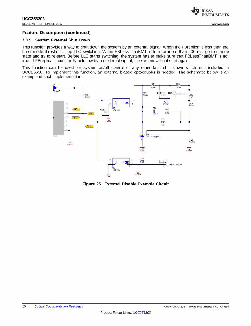
Feature Description (continued)7.3.5 System External Shut DownThis function provides a way to shut down the system by an external signal. When the FBreplica is less than theburst mode threshold, stop LLC switching. When FBLessThanBMT is true for more than 200 ms, go to startupstate and try to re-start. Before LLC starts switching, the system has to make sure that FBLessThanBMT is nottrue. If FBreplica is constantly held low by an external signal, the system will not start again.
This function can be used for system on/off control or any other fault shut down which isn’t included inUCC25630. To implement this function, an external biased optocoupler is needed. The schematic below is anexample of such implementation.
Figure 25. External Disable Example Circuit

ChargeSS SSEn & !SSEnd & !ZCS
SSEnd SSEn & !ZCS & (!FBLessThanSS)
21
UCC256303www.ti.com SLUSD49 –SEPTEMBER 2017
Product Folder Links: UCC256303
Submit Documentation FeedbackCopyright © 2017, Texas Instruments Incorporated
Feature Description (continued)7.3.6 Pick Lower Block and Soft Start MultiplexerThis part of the circuit consists of 3 elements:• A pick lower block• A MUX which selects AVDD or SS signal as the second input to the pick lower block• A SS control block which handles the charge and discharge of the SS capacitor in cause of a ZCS fault
The pick lower block has two inputs. The first input is FBreplica. The second input is selected between AVDDand SS pin voltage. The other output of the block is the lower of the two inputs.
The MUX selects between SS and AVDD. The selection is based on SSEnd (soft start end) signal, which is anoutput of the SS Ctrl block. SSEnd is high when SS is higher than FBreplica, and soft start process has beeninitiated by the state machine, and there is no ZCS condition. Switching to AVDD after soft start has ended helpsmake sure that during non-soft start or non-ZCS fault condition, FBreplica signal is always sent through the picklower block. It also releases the SS pin to do the other function – light load threshold programming.
The SS control block handles the charge and discharge of the SS capacitor in cause of a ZCS fault. It reset theSSEnd signal when ZCS happens, so the effect of pulling down on SS pin to increase the switching frequencycan pass through the pick lower block. The relationship of the SS control block inputs and outputs is thefollowing:
(4)
(5)
7.3.7 Pick Higher Block and Burst Mode MultiplexerThe output of the pick lower block goes into a pick higher block, which selects the higher of the pick lower blockoutput and the burst mode threshold setting.
The burst mode multiplexer selects between BMT and ground. During soft start, the multiplexer selects ground.The startup process is open loop and controlled by the soft start ramp. Burst mode is not enabled during softstart phase.
After soft start, the higher of the two inputs are sent to the differential amplifier. The other output is a comparatoroutput FBLessThanBMT. It is sent to the waveform generator state machine to control burst mode and systemexternal shut down.
7.3.8 VCR ComparatorsThe output of the pick higher block is sent to a differential amplifier to convert the signal to two thresholdssymmetrical to Vcm. The difference between the two thresholds Vthh and Vthl equals the input amplitude. TheVCR pin voltage is then compared with Vthh, Vthl, and Vcm. The results are sent to the waveform generator.
LSON
HSON
Compensation ramp current
2 mA
0
-2 mA
HSRampOn
LSRampOn
AVDD
VCR7VCR
22
UCC256303SLUSD49 –SEPTEMBER 2017 www.ti.com
Product Folder Links: UCC256303
Submit Documentation Feedback Copyright © 2017, Texas Instruments Incorporated
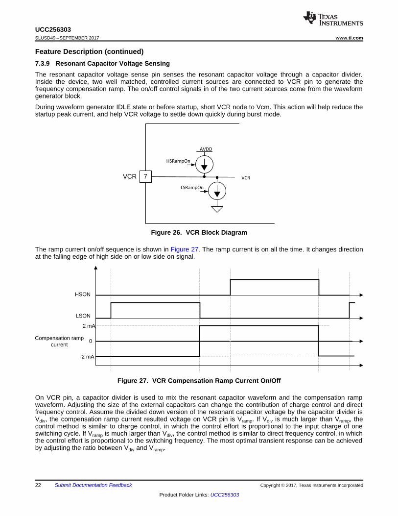
Feature Description (continued)7.3.9 Resonant Capacitor Voltage SensingThe resonant capacitor voltage sense pin senses the resonant capacitor voltage through a capacitor divider.Inside the device, two well matched, controlled current sources are connected to VCR pin to generate thefrequency compensation ramp. The on/off control signals in of the two current sources come from the waveformgenerator block.
During waveform generator IDLE state or before startup, short VCR node to Vcm. This action will help reduce thestartup peak current, and help VCR voltage to settle down quickly during burst mode.
Figure 26. VCR Block Diagram
The ramp current on/off sequence is shown in Figure 27. The ramp current is on all the time. It changes directionat the falling edge of high side on or low side on signal.
Figure 27. VCR Compensation Ramp Current On/Off
On VCR pin, a capacitor divider is used to mix the resonant capacitor waveform and the compensation rampwaveform. Adjusting the size of the external capacitors can change the contribution of charge control and directfrequency control. Assume the divided down version of the resonant capacitor voltage by the capacitor divider isVdiv, the compensation ramp current resulted voltage on VCR pin is Vramp. If Vdiv is much larger than Vramp, thecontrol method is similar to charge control, in which the control effort is proportional to the input charge of oneswitching cycle. If Vramp is much larger than Vdiv, the control method is similar to direct frequency control, in whichthe control effort is proportional to the switching frequency. The most optimal transient response can be achievedby adjusting the ratio between Vdiv and Vramp.

IPolarity
OCP1Th OCP2
OCP2Th
OCP3Th
OCP3
VCM
OCP1
-+
-+
-+
-+AverageMUX
HSON
RISNS
CISNS
To
Resonant
Capacitor
-+
VCM
6
ISNS
23
UCC256303www.ti.com SLUSD49 –SEPTEMBER 2017
Product Folder Links: UCC256303
Submit Documentation FeedbackCopyright © 2017, Texas Instruments Incorporated
Feature Description (continued)7.3.10 Resonant Current SensingThe ISNS pin is connected to the resonant capacitor using a high voltage capacitor. The capacitor CISNS andthe resistor RISNS form a differentiator. The resonant capacitor voltage is differentiated to get the resonantcurrent. The differentiated signal is AC and goes both positive and negative. In order to sense the zero crossing,the signal is level shifted using an op amp adder. IPolarity comparator detects the direction of the resonantcurrent. The digital state machine implements a blanking time on IPolarity – IPolarity edges during the first 400nsof dead time are ignored.
OCP2 and OCP3 thresholds are based on average input current. To get the average input current, thedifferentiator output is multiplexed with the high side switch on signal HSON: when HS is on, the MUX output isthe differentiator output; when HS is off, the MUX output is 0. The MUX output is then averaged using a low passfilter. The output of the filter is the sensed average input current. Note that the MUX needs to pass through bothpositive and negative voltages. OCP2 and OCP3 faults have a 2ms and 50ms timer respectively. Only when theOCP2/OCP3 comparators output high for continuous 2ms or 50ms, the faults will be activated.
OCP1 threshold is set on the peak resonant current. The voltage on the ISNS pin gets compared to OCP1threshold OCP1Th directly. The peak resonant current is checked once per cycle on the positive half cycle.OCP1 fault is only activated when there are 4 consecutive cycles of OCP1 event detected. During start up, theOCP1 comparator output of the first 15 cycles are ignored.
Figure 28. ISNS Block Diagram

PFC output voltage
LLC gate drive waveforms
RVCC
1s FAULT timer
BLKOVRiseThBLKOVFallTh
AC plug in
BLKStartTh
PFC start switching
BLKOVFallTh
BLKStartThBLKStart
-
+
-
+
-
+
BLKStopThBLKStop
BLKSns
BLKOVBLKOVRiseThMUX
4
BLK
24
UCC256303SLUSD49 –SEPTEMBER 2017 www.ti.com
Product Folder Links: UCC256303
Submit Documentation Feedback Copyright © 2017, Texas Instruments Incorporated
Feature Description (continued)7.3.11 Bulk Voltage SensingThe BLK pin is used to sense the LLC DC input voltage (bulk voltage) level. The comparators on BLK pin set thefollowing thresholds:• Bulk voltage level when LLC starts switching – BLKStartTh• Bulk voltage level when LLC stops switching – BLKStopTh• Bulk voltage level when bulk over voltage fault is generated – BLKOVRiseTh• Bulk voltage level when bulk over voltage fault is cleared – BLKOVFallTh
BLKOV signal is generated by one comparator with two thresholds selected by a MUX. This is to createnecessary hysteresis for the BLKOV fault. The BLKSns signal is buffered and sent to burst mode thresholdgeneration block to implement the adaptive burst mode threshold.
Figure 29 shows the block diagram of the BLK pin.
Figure 29. VCR Compensation Ramp Current On/Off
Figure 30. Timing Diagram of BLK Operations

BW pin
Inverting Op-Amp
Output
LSON
Sample Position
Peak Detector Output
OVPOVPTh -
+-
+
Peak
detectS/H
8
BW
25
UCC256303www.ti.com SLUSD49 –SEPTEMBER 2017
Product Folder Links: UCC256303
Submit Documentation FeedbackCopyright © 2017, Texas Instruments Incorporated
Feature Description (continued)7.3.12 Output Voltage SensingThe output voltage is sensed through the bias winding (BW) voltage sense pin. The sensed output voltage iscompared with a fixed threshold to generate output OVP fault. The block diagram of the bias winding voltagesense block is shown below.
Figure 31. Bias Winding Sensing Block Diagram
The bias winding sense block consists of an inverting op amp to flip the BW signal. The flipped BW signal is thenpeak detected and sampled at low side turn off edge. The sampled voltage represents the output voltage duringthis cycle. The S/H output is them compared with OVP comparator. Shown below is the timing diagram of theBW sense block.
Figure 32. Timing Diagram of BW Sense Block

HSON
LSON
WaveGenEn
Level
Shift
Adaptive
Dead Time
High Voltage
Isolation
Wake Up
Control
Active/Low
Power
To RVCC
SlewDone_H
SlewDone_L
Vbus
10
LO
HS
HO
HB
16
15
14
26
UCC256303SLUSD49 –SEPTEMBER 2017 www.ti.com
Product Folder Links: UCC256303
Submit Documentation Feedback Copyright © 2017, Texas Instruments Incorporated
Feature Description (continued)7.3.13 High Voltage Gate DriverThe low-side gate driver output is LO. The gate driver is supplied by the 12-V RVCC rail.
The high-side driver module consists of three physical device pins. HB and HS form the positive and negativerails, respectively, of the high-side driver, and HO connects to the gate of the upper half-bridge MOSFET.
During periods when the lower half-bridge MOSFET is conducting, HS is shorted to GND via the conductinglower MOSFET. At this time power for the high side driver is obtained from RVCC via high voltage diodeDBOOT, and capacitor CBOOT is charged to RVCC minis the forward drop on the diode.
During periods when the upper half-bridge MOSFET is conducting, HS is connected the LLC input voltage rail. Atthis time the HV diode is reverse biased and the high side driver is powered by charge stored in CBOOT.
The slew on HS pin is detected for adaptive dead time adjustment. The next gate is only turned on when theslew on HS pin is finished.
Both the high-side and low side gate drivers have under voltage lock out (UVLO) protection. The low side gatedriver UVLO is implemented on RVCC; the high side gate driver UVLO is implemented on (HB - HS) voltage.
When operating at light load, UCC256303 enters burst mode. During the burst off period, the gate driver enterslow power mode to reduce power consumption.
The block diagram of the gate driver is shown in Figure 33.
Figure 33. Gate Driver Block Diagram

27
UCC256303www.ti.com SLUSD49 –SEPTEMBER 2017
Product Folder Links: UCC256303
Submit Documentation FeedbackCopyright © 2017, Texas Instruments Incorporated
Feature Description (continued)7.3.14 Protections
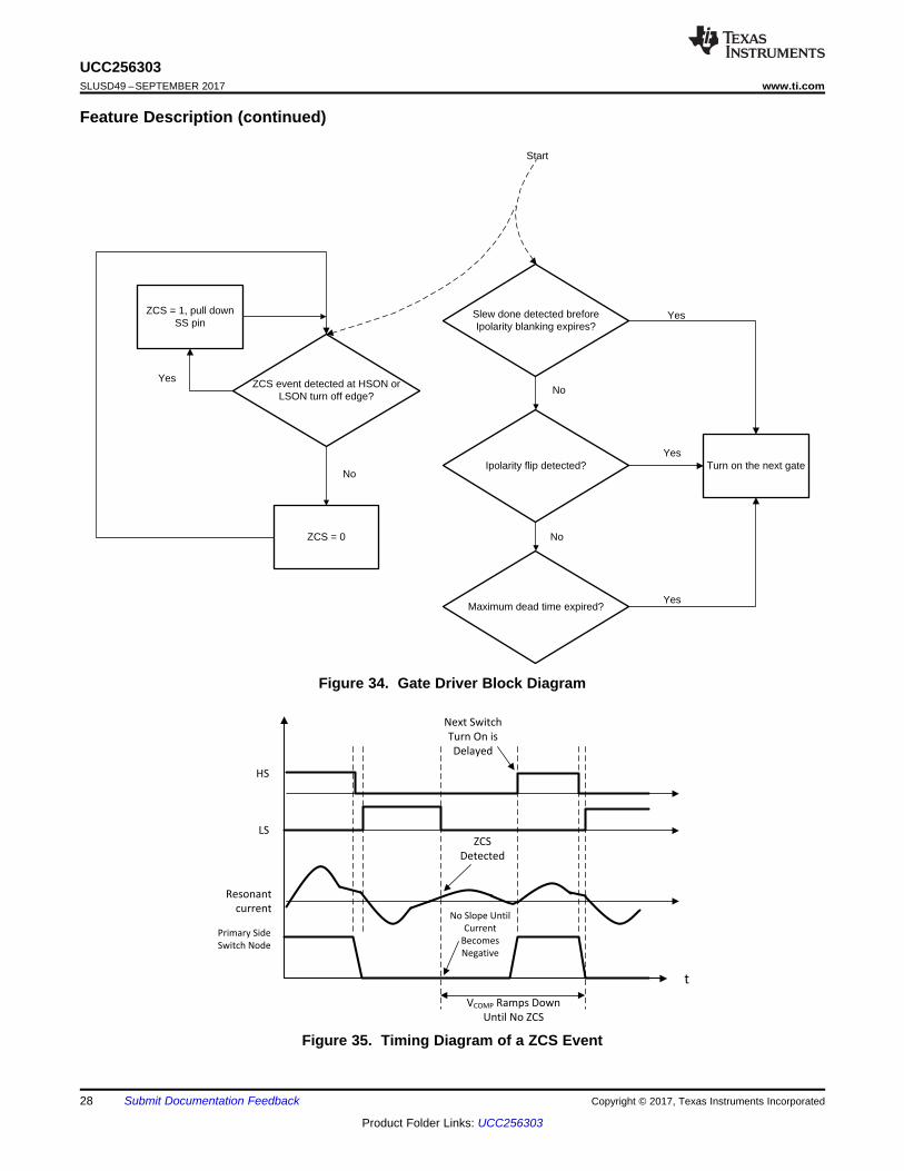
7.3.14.1 ZCS Region PreventionCapacitive region is an LLC operation region in which the voltage gain increases when the switching frequencyincreases. It is also called ZCS region. Capacitive mode operation should be avoided for two reasons:• The feedback loop becomes positive feedback in capacitive region• The MOSFET may be damaged because of body diode reverse recovery
To make sure that capacitive region operation does not happen, we need to first rely on the slew done signal. Ifthere is a slew done signal detected, it suggests that the opposite body diode must not be conducting and to turnon the next FET. If there is no slew detected, IPolarity signal is used. The next gate will be turned on at the nextIPolarity flip event. The IPolarity flip indicates that the capacitive operation cycle has already passed. Theresonant current reverses the direction and begins to discharge the switch node. When the capacitive operationcycle has passed, the system enters a high frequency oscillation stage, where the oscillation frequency isdetermined by the parasitic elements in the circuit. In this stage, the body diode is no longer conducting and it isallowed to turn on the next gate.
However, in the high frequency oscillation stage, the resonant current may be so small that the IPolarity detectionis missed. In this case, the next gate will be turned on by maximum dead time timer expiration.
In addition to preventing the next gate from turning on when the opposite body diode is conducting, the switchingfrequency is forced to ramp up until there is a cycle with no capacitive region operation detected
The capacitive region detection is done by checking the resonant current polarity at HSON or LSON falling edge.If the resonant current is positive at LSON falling edge, or negative at HSON falling edge, the ZCS signal in thewaveform generator is turned high. The ZCS signal keeps high until there is a half cycle without capacitive regionoperation happens.
The force ramping up of the switching frequency is done by pull the SS pin down by a resistor to ground. Detailswill be discussed in SS pin section.
Below is the flow chart of capacitive region prevention algorithm:
HS
LS
Primary Side
Switch Node
Resonant
current
t
ZCS
Detected
Next Switch
Turn On is
Delayed
VCOMP Ramps Down
Until No ZCS
No Slope Until
Current
Becomes
Negative
Yes
Start
Slew done detected brefore Ipolarity blanking expires?
Ipolarity flip detected?
Maximum dead time expired?
Turn on the next gateYes
Yes
No
No
ZCS event detected at HSON or LSON turn off edge?
ZCS = 1, pull down SS pin
ZCS = 0
No
Yes
28
UCC256303SLUSD49 –SEPTEMBER 2017 www.ti.com
Product Folder Links: UCC256303
Submit Documentation Feedback Copyright © 2017, Texas Instruments Incorporated
Feature Description (continued)
Figure 34. Gate Driver Block Diagram
Figure 35. Timing Diagram of a ZCS Event

29
UCC256303www.ti.com SLUSD49 –SEPTEMBER 2017
Product Folder Links: UCC256303
Submit Documentation FeedbackCopyright © 2017, Texas Instruments Incorporated
Feature Description (continued)7.3.14.2 Over Current Protection (OCP)There are three levels of OCP:1. OCP1: peak current protection (highest threshold)
1. Fault action: count OCP1 cycles and shut down power stage if counter exceeds preset value2. OCP2: average input current protection (high threshold)
1. Fault action: if above threshold for 2 ms, shut down3. OCP3: average input current protection (low threshold)
1. Fault action: if above threshold for 50 ms, shut down
The circuit block diagram has been discussed in the Resonant Current Sensing section.
7.3.14.3 Over Output Voltage Protection (VOUTOVP)This is the output over voltage protection. VOUTOVP threshold is set on the bias winding voltage sense. TheVOUTOVP trip point can be set by configuring the voltage divider on BW pin.
7.3.14.4 Over Input Voltage Protection (VINOVP)This is the input over voltage protection. The fault actions have been discussed in the BLK section. The trip pointcan be set by configuring the voltage divider on BLK pin.
7.3.14.5 Under Input Voltage Protection (VINUVP)This is the input under voltage protection. The fault actions have been discussed in the BLK section. The trippoint can be set by configuring the voltage divider on BLK pin.
7.3.14.6 Boot UVLOThis is the high side gate driver UVLO. When (HB – HS) voltage is less than the threshold, the high side gateoutput will be shut down.
7.3.14.7 RVCC UVLOThis is the regulated 12-V UVLO. When RVCC voltage is less than the threshold, both the high side gate outputand the low-side gate output will be turned off.
7.3.14.8 Over Temperature Protection (OTP)This is the device over temperature protection. When OTP fault is tripped, if the device is switching, the switchingwill stop. If the device is in HV start up stage and JFET is on, the JFET will be turned off. Details of the OTP faulthandling will be discussed in the Device Functional Modes section.
There are two digital state machines in the system:• System States and Faults State Machine• Waveform Generator Stage Machine
The system states control state machine controls system operation states and faults. The waveform generatorstate machine controls the gate driver behavior.

Pick
higher
value
MUXSSEnd
Burst mode
threshold
COMPCOMP_new
FB less than burst mode threshold
30
UCC256303SLUSD49 –SEPTEMBER 2017 www.ti.com
Product Folder Links: UCC256303
Submit Documentation Feedback Copyright © 2017, Texas Instruments Incorporated
7.4 Device Functional Modes
7.4.1 Burst Mode ControlThe efficiency of an LLC converter power stage drops rapidly with falling output power. To maintain reasonablelight load efficiency it is necessary to operate the LLC converter in burst mode. In this mode the LLC converteroperates at relatively high power for a short burst period and then all switching is stopped for a space period.During the Burst period excess charge is transferred to and stored in the output capacitor. During the Spaceperiod this stored charge is used to supply the load current. Providing an effective light-load scheme is aparticular problem for an LLC controller that is located on the primary side of the isolation barrier. This is becausethe feedback demand signal (VCOMP) is mainly a function of input/output voltage ratio and only loosely related toload current. The normal method of placing a couple of thresholds in the VCOMP voltage window to switch OFFand ON the LLC converter does not work effectively. Another issue with the conventional method is that whenburst on, the switching pulses are determined by VCOMP, which is usually at initial burst on, and decays as theoutput voltage rises. The resulting inductor current will be big at first and then decays. This is not optimalbecause the big current at first may create mechanical vibration. The high switching frequency afterwards maycause two much switching loss.
For an advanced burst mode, the following features are desired:• The power delivered by each burst should be relatively constant for a certain load.• The Burst power is set high enough to provide reasonable LLC converter efficiency and low enough to avoid
acoustic noise and excessive output voltage ripple.• When burst on, the average capacitor voltage should settle to VIN/2 as fast as possible for best efficiency.• The switching frequency or burst power level of each burst pulse should be optimized for efficient operation.• The burst pattern of each burst should be relatively constant.• There should be no audible noise.• Burst mode performance should be consistent across input voltage range.
The HHC method makes the control of the burst mode very straight forward. The block diagram is a functionallyaccurate description of the burst mode control method in UCC256303.
Figure 36. Burst Mode Control Block Diagram
The control effort is selected between the higher of the two signals: 1) the voltage loop compensator output(VCOMP) or 2) the Burst Mode Threshold level (BMT). When VCOMP goes below BMT, continue switching for afixed number of switching cycles, then stop. Always switch while COMP is higher than BMT. If soft start isn’tdone yet, send the COMP (controlled by soft start ramp). BMT is programmable and adaptively changed withinput voltage. The last pulse of each burst on period is turned off when the resonant capacitor voltage equalsVIN/2. In HHC method, this is approximately equivalent to VCR node voltage equals the common mode voltageVCM. This operation keeps the resonant capacitor voltage to about VIN/2 for each burst off period, thus enablingthe burst pattern to settle as soon as possible during burst on period.

ZCS
ChargeSS
SS
Rdischarge
AVDD
BLKSns
To RVCC
Burst
Threshold
Gen
BMT
9
LL/SS
31
UCC256303www.ti.com SLUSD49 –SEPTEMBER 2017
Product Folder Links: UCC256303
Submit Documentation FeedbackCopyright © 2017, Texas Instruments Incorporated
Device Functional Modes (continued)7.4.2 Soft-Start and Burst-Mode ThresholdThe soft-start programming and burst mode threshold programming are multiplexed on one pin – LL/SS. Inaddition, when ZCS region operation happens, this pin is pulled down to ground through a resistor to increasethe switching frequency.
An internal constant current source charges the soft start capacitor to generate the soft-start command. Soft startperiod starts right after charge boot stage is done, and ends when FBreplica becomes lower than SS pin voltage.
After soft start is done, the SS voltage is replaced by AVDD to send to the FB chain. The LL/SS pin is then usedto generate the burst mode threshold. In UCC256303 we try to maintain the same burst mode power level overthe input voltage range. This is done by adaptively changing the burst mode threshold with sensed BLK voltage.
The programming resistors output provide two degrees of freedom, to set the burst mode threshold, as well ashow the threshold changes with BLK voltage. When programmed correctly, the power stage will always enterburst mode at a certain output current level, making the system much easier to optimize.
Figure 37. LL/SS Block Diagram

System states and
faults
OVP
OCP1
OCP2
OCP3BLKStart
BLKStop
BLKOV
RVCCUVLO
VCCStartExt
VCCStartSwitching
ACZeroCrossing
OTP
SSEn
RVCCEn
FBLessThanBMT
WaveGenEn
32
UCC256303SLUSD49 –SEPTEMBER 2017 www.ti.com
Product Folder Links: UCC256303
Submit Documentation Feedback Copyright © 2017, Texas Instruments Incorporated
Device Functional Modes (continued)7.4.3 System States and Faults State MachineBelow is an overview of the system states sequence:
The state transition diagram starts from the un-powered condition of UCC256303. When PFC output voltagereaches a certain level, LLC is turned on. Before LLC starts running, the LO pin is kept high to pull the HS nodeof the LLC bridge low, thus allowing the capacitor between HB and HS pins to be charged from VCC via thebootstrap diode. UCC256303 will remain in the CHARGE_BOOT state for a certain time to ensure the bootcapacitor is fully charged. When the load drops to below a certain level, LLC operates in burst mode
Fault conditions encountered by UCC256303 will cause operation to stop, or paused for a certain period of timefollowed by an automatic re-start. It is to ensure that while a persistent fault condition is present, it is not possiblefor UCC256303 or the power converter temperature to continue to rise as a result of the repeated re-startattempts.
Figure 38. Block Diagram of System States and Faults State Machine
33
UCC256303www.ti.com SLUSD49 –SEPTEMBER 2017
Product Folder Links: UCC256303
Submit Documentation FeedbackCopyright © 2017, Texas Instruments Incorporated
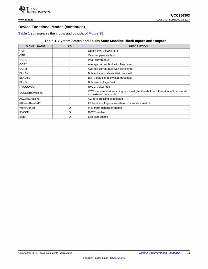
Device Functional Modes (continued)Table 1 summarizes the inputs and outputs of Figure 38
Table 1. System States and Faults State Machine Block Inputs and OutputsSIGNAL NAME I/O DESCRIPTION
OVP I Output over voltage faultOTP I Over temperature faultOCP1 I Peak current faultOCP2 I Average current fault with 2ms timerOCP3 I Average current fault with 50ms timerBLKStart I Bulk voltage is above start thresholdBLKStop I Bulk voltage is below stop thresholdBLKOV I Bulk over voltage faultRVCCUVLO I RVCC UVLO fault
VCCStartSwitching I VCC is above start switching threshold (the threshold is different in self bias modeand external bias mode)
ACZeroCrossing I AC zero crossing is detectedFBLessThanBMT I FBReplica voltage is less than burst mode thresholdWaveGenEn O Waveform generator enableRVCCEn O RVCC enableSSEn O Soft start enable

STARTUP
WAKEUP
CHARGE_ BOOT
STEADY_ STATE_RUN
LIGHT_ LOAD_RUN
FAULT
1
2
3
4 5
6
7
8
10
11
12
13
14
15
AC plug in
9
34
UCC256303SLUSD49 –SEPTEMBER 2017 www.ti.com
Product Folder Links: UCC256303
Submit Documentation Feedback Copyright © 2017, Texas Instruments Incorporated
The state machine is shown in Figure 39 and the description of the states and state transition conditions are inthe tables below.
Figure 39. System States and Faults State Machine

35
UCC256303www.ti.com SLUSD49 –SEPTEMBER 2017
Product Folder Links: UCC256303
Submit Documentation FeedbackCopyright © 2017, Texas Instruments Incorporated
Table 2. States in System States and Faults State MachineSTATE OUTPUT STATUS DESCRIPTION
STARTUPWaveGenEn = 0RVCCEn = 1SSEn = 0
This is the first state after power on reset (POR).When VCC becomes higher thanVCCstartswitching threshold, regulated RVCC is turned on to allow internal circuitsto load trim settings and start up.
WAKEUPWaveGenEn = 0RVCCEn = 1SSEn = 0
When BLK voltage reaches BLKStart level, the system enters WAKEUP state andstay in WAKEUP state for 150us for the analog circuits to wake up.
CHARGE_BOOTWaveGenEn = 0RVCCEn = 1SSEn = 0
In this state, the BOOT capacitor is charged by turning on the low side switch for acertain period of time.
STEADY_STATE_RUNWaveGenEn = 1RVCCEn = 1V SSEn = 1
In this state, the waveform generator is enabled. Soft start module is enabled. LLCstarts to soft start. When soft start is done, the system enters normal operation.
LIGHT_LOAD_RUNWaveGenEn = 1RVCCEn = 1SSEn = 1
If FBReplica is less than burst mode threshold during normal operation, the systementers LIGHT_LOAD_RUN mode. The FBLessThanBMT time is counted. If thetime is longer than 200ms, it is treated as a fault, restart the system.
FAULTWaveGenEn = 0RVCCEn = 0SSEn = 0
After any fault condition, the system enters FAULT state and waits for 1s before re-start. The 1s timer allows system to cool down and prevents frequent repetitivestart up in case of a persistent fault.

36
UCC256303SLUSD49 –SEPTEMBER 2017 www.ti.com
Product Folder Links: UCC256303
Submit Documentation Feedback Copyright © 2017, Texas Instruments Incorporated
Table 3. System States and Faults State Machine State Transition ConditionsSTATE TRANSITION
CONDITION DESCRIPTION
1
System ready (trim load done)VCCStartSwitching = 1BLKStart = 1BLKStop = 0BLKOV = 0RVCCUVLO = 0
2
BLKStart = 1BLKStop = 0BLKOV = 0RVCCUVLO = 0FBLessThanBMT = 0
3 Charge boot done4 FBLessThanBMT = 15 FBLessThanBMT = 06 VCCStartSwitching = 0 or FBLessThanBMT time out7 VCCStartSwitching = 08 VCCStartSwitching = 0 or BLKOV = 19 VCCStartSwitching = 0 or BLKOV = 1
10OTP = 1 or BLKOV = 1 orBLKStop = 1 or OVP or OCP1 or OCP2 time out orOCP3 time out or RVCCUVLO = 1
11OTP = 1 or BLKOV = 1 orBLKStop = 1 or OVP or OCP1 or OCP2 time out orOCP3 time out or RVCCUVLO = 1
12 OTP = 113 OTP = 114 OTP = 115 1s pause time out

PFC output voltage
LLC output voltage
LLC gate drive waveforms
VCC
RVCC
System state
AC plug in
STARTUP
WAKEUP CHARGE_BOOT
STEADY_STATE_RUN FAULT STEADY_STATE_RUN
WAKEUP CHARGE_BOOT
VCCStartSwitching
STARTUP
37
UCC256303www.ti.com SLUSD49 –SEPTEMBER 2017
Product Folder Links: UCC256303
Submit Documentation FeedbackCopyright © 2017, Texas Instruments Incorporated
Figure 40 only shows the most commonly used state transition (assuming no faults during start up states so allthe states are captured in the timing diagram). Many different ways of state transitions may happen according tothe state machine, but are not captured in this section.
In Figure 40, a normal start up procedure is shown. The system enters normal operation and then a fault (OCP,OVP, or OTP) happens.
NOTEOCP1 and OVP are fast faults and are first processed in the waveform generator statemachine.
The system is configured to be restart after 1s pause time.
Figure 40. Timing Diagram of System States and Faults

Waveform generator
IPolarity
SlewDone_H
SlewDone_L
WaveGenEn
ZCS
HSON
LSON
HSRampOn
LSRampOn
VcrHigherThanVthh
VcrLowerThanVthl
VcrHighThanVcm
38
UCC256303SLUSD49 –SEPTEMBER 2017 www.ti.com
Product Folder Links: UCC256303
Submit Documentation Feedback Copyright © 2017, Texas Instruments Incorporated
7.4.4 Waveform Generator State MachineThe waveform generator module consists of a state machine that implements hybrid hysteretic control, adaptivedead time, and ZCS protection. Each cycle of LLC operation is broken down into 4 separate periods: HSON,DTHL, LSON, and DTLH. In addition, there is an IDLE state and a WAKEUP state.
The initial state of this state machine is IDLE. In IDLE state, the system is operating in a low power mode. WhenWaveGenEn command is received, the state machine enters WAKEUP state to turn on various circuit blocks.Once the WAKEUP timer is expired, the system enters LSON (low side on) state. LSON state is followed byDTLH (dead time high to low) state, which is the dead time state. After DTLH state, the high side turns on andsystem enters HSON. HSON state is followed by DTHL (dead time low to high) state. After DTHL, the systemgoes back to LSON state again.
There are minimum and maximum timers in each of the states. The state transition conditions and descriptionsare discussed in detail below.
Figure 41. Waveform Generator State Machine Block Diagram
Table 4 summarizes the inputs and outputs of the Waveform Generator State Machine Block Diagram
NOTEOVP and OCP1 faults are not listed here. But they are processed in the wave gen statemachine before handled to system states and faults state machine.
Table 4. Waveform Generator State Machine Inputs and OutputsSIGNAL NAME I/O DESCRIPTION
IPolarity I Polarity of the resonant current (Note: this signal has a 1us blanking time duringdead time. IPolarity signal listed here is after blanking. See ISNS section fordetails.)
SlewDone_H I Primary side switch node completes slewing from low to highSlewDone_L I Primary side switch node completes slewing from high to lowVcrHigherThanVthh I VCR voltage is higher than the high threshold VthhVcrLowerThanVthl I VCR voltage is lower than the low threshold VthlVcrHighThanVcm I VCR voltage is high than the common mode voltage VcmWaveGenEn I Waveform generator enableZCS O Zero current switching is detectedHSON O High side gate driver onLSON O Low side gate driver onHSRampOn O High side compensation current ramp onLSRampOn O Low side compensation current ramp on

HSON
LSON
DTLH
DTHL
IDLE
WakeUp
Power on reset
1
2 3
4
5
6
7
8
9
10
11
39
UCC256303www.ti.com SLUSD49 –SEPTEMBER 2017
Product Folder Links: UCC256303
Submit Documentation FeedbackCopyright © 2017, Texas Instruments Incorporated
The state machine is shown in Figure 42 and the description of the states and state transition conditions are inTable 5.
Figure 42. Waveform Generator State Machine

40
UCC256303SLUSD49 –SEPTEMBER 2017 www.ti.com
Product Folder Links: UCC256303
Submit Documentation Feedback Copyright © 2017, Texas Instruments Incorporated
Table 5. States in Waveform Generator State MachineSTATE OUTPUT STATUS DESCRIPTION
IDLE
HSON = 0LSON = 0HSRampOn = 0LSRampOn = 0ZCS = 0
Both high side and low side are off in this state. Various circuits are operating inlow power mode. This is the first state after POR. During burst off period, thesystem is in IDLE state as well. Upon entering IDLE state, load burst cycle counter,switching cycle counter, OCP1 counter, and OVP counter. Load startup cyclecounter if WaveGenEn_Rising = 1
WakeUp HSON = 0LSON = 0HSRampOn = 0LSRampOn = 0ZCS = 0
In this state, internal circuits wake up from low power mode.
LSON HSON = 0LSON = 1HSRampOn = 0LSRampOn = 1ZCS = 0 or 1
In this state, the low side gate turns on; the low side ramp current source turns on.ZCS may be 0 or 1 depends on the detected result. More details will be describedin ZCS section. Enable low side on timer.
DTLH HSON = 0LSON = 0HSRampOn = 1LSRampOn = 0ZCS = 0 or 1
Dead time from low side on to high side on. Low side ramp current source turnsoff. High side ramp current source turns on. Enable dead time timer.
HSON HSON = 1LSON = 0HSRampOn = 1LSRampOn = 0ZCS = 0 or 1
In this state, the high side gate turns on; the high side ramp current source turnson. ZCS may be 0 or 1 depends on the detected result. More details will bedescribed in ZCS section. Enable high side on timer.
DTHL HSON = 0LSON = 0HSRampOn = 0LSRampOn = 1ZCS = 0 or 1
Dead time from high side on to low side on. High side ramp current source turnsoff. Low side ramp current source turns on. Enable dead time timer.

41
UCC256303www.ti.com SLUSD49 –SEPTEMBER 2017
Product Folder Links: UCC256303
Submit Documentation FeedbackCopyright © 2017, Texas Instruments Incorporated
Table 6. Waveform Generator State Machine State Transition ConditionsSTATE TRANSITION
CONDITION DESCRIPTION
1 WaveGenEn = 1 and FBLessThanBMT = 0 and minimum IDLE time expired2 Wake up time expired3 (VcrLowerThanVthl = 1 or LSON max timer expired) and LSON min timer expired4 StartUpCounterExpired = 0 and DTStartUpTimerExpired = 1
DTMaxTimerExpired = 1SlewDone_H = 1SlewDone_H = 1 and MeasuredDTExpired = 1; (Note: this condition and the condition above isselectable using a trim bit, depending on whether dead time measure and match feature is wanted)IPolarityFallingEdgeDetected = 1
5 (VcrHigherThanVthh = 1 or HSON max timer expired) and HSON min timer expired6 StartUpCounterExpired = 0 and DTStartUpTimerExpired = 1
DTMaxTimerExpired = 1SlewDone_L = 1IPolarityFallingEdgeDetected = 1
7 WaveGenEn = 08 WaveGenEn = 0
(VcrLowerThanVthl = 1 or LSON max timer expired) and LSON min timer expired and (OCP1 counterexpire or OVP counter expire)
9 WaveGenEn = 010 WaveGenEn = 0
BurstModeCountExpire = 1 and VcrHigherThanVcm = 1 and FBLessThanBMT = 1 and HSON min timeexpired
11 WaveGenEn = 0
Table 7. Waveform Generator State Machine Internal Counters and TimersINTERNAL VARIABLE DESCRIPTION
Switching cycle counter This counter counts the switching cycleOVP counter Bias Winding Overvoltage counter. The counter decrements every time a Bias Winding Overvoltage
occursStartup counter Startup Counter. Counter gets set to 15 when wave generator enable toggles from low to high, and then
decrements every switching cycle. When the count hits 0, the dead time state is no longer permitted tobe exited via the startup dead time expiration.
Burst cycle counter Burst counter. Counter gets set to 15 and then decrements every switching cycle until it hits ‘0’. IfFBLessThanBMT = 1 when the counter is ‘0’, the switcher will stop until FBLessThanBMT = 0.
OCP1 counter OCP1 counter. Counter gets set to 4 and then decrements every switching cycle when OCP1 occurs,until it hits ‘0’
Wakeup timer Wakeup state timerDT max timer Maximum dead time timerStartup dead time max timer Dead time max clamp for the first few start up cycles before the startup counter expiresGate on min timer Minimum gate on time timerGate on max timer Maximum gate on time timer

FB
LO
HO
HS
BLKVIN
BW
Vout
CrLr
Lm
ISN
S
VC
R
10
HV
LO
GND
LL/SS
HO
VCC
VCR
FB
BLK
7
UCC256303LLC
Controller
HB
HS
RVCC
9BW
ISNS
8
BLK
FB
ISNS
VCR
BW
HO
HS
LO
CSS
External Bias
CBOOT
Copyright © 2017, Texas Instruments Incorporated
4
6
5
3
1
11
14
15
16
12
42
UCC256303SLUSD49 –SEPTEMBER 2017 www.ti.com
Product Folder Links: UCC256303
Submit Documentation Feedback Copyright © 2017, Texas Instruments Incorporated
8 Application and Implementation
NOTEInformation in the following applications sections is not part of the TI componentspecification, and TI does not warrant its accuracy or completeness. TI’s customers areresponsible for determining suitability of components for their purposes. Customers shouldvalidate and test their design implementation to confirm system functionality.
8.1 Application InformationUCC256303 can be used in a wide range of applications in which LLC topology is implemented. In order to makethe part easier to use, TI has prepared a list of materials to demonstrate the features of the device:• Full featured EVM hardware• An excel design calculator• Simulation models• Application notes on Hybrid Hysteretic Control theory
In the following sections, a typical design example is presented.
8.2 Typical ApplicationShown below is a typical half bridge LLC application using UCC256303 as the controller.

43
UCC256303www.ti.com SLUSD49 –SEPTEMBER 2017
Product Folder Links: UCC256303
Submit Documentation FeedbackCopyright © 2017, Texas Instruments Incorporated
Typical Application (continued)8.2.1 Design RequirementsThe design specifications are summarized in Table 8.
Table 8. System Design SpecificationsPARAMETER TEST CONDITIONS MIN TYP MAX UNITS
INPUT CHARACTERISTICSDC Voltage range 340 390 410 VDCAC Voltage range 85 264 VACAC Voltage frequency 47 63 HzInput DC UVLO On 320 VDCInput DC UVLO Off 140 VDCInput DC current Input = 340 VDC, full load = 10 A 0.383 AInput DC current Input = 390 VDC, full load = 10 A 0.331 AInput DC current Input = 410 VDC, full load = 10 A 0.315 A
OUTPUT CHARACTERISTICSOutput voltage, VOUT No load to full load 12 VDCOutput load current, IOUT 340 VDC to 410 VDC 10 AOutput voltage ripple 390 VDC and full load = 10 A 130 mVpp
SYSTEMS CHARACTERISTICSSwitching frequency 53 160 kHzPeak efficiency 390 VDC, load = ??A 92.9Operating temperature Natural convection 25 ºC

los
max
s 12 0.5 0.516 1.224
/ 2 340 / 2
fOUT maxg
IN min
V V VM n
V
min
12 0.516 0.976
/ 2 410 / 2
fOUT ming
IN max
V VM n
V
/ 2 390 / 216.25 16
12
IN nom
OUT nom
Vn
V
44
UCC256303SLUSD49 –SEPTEMBER 2017 www.ti.com
Product Folder Links: UCC256303
Submit Documentation Feedback Copyright © 2017, Texas Instruments Incorporated
8.2.2 Detailed Design Procedure
8.2.2.1 LLC Power Stage RequirementsStart the design by deciding the LLC power stage component values. The LLC power stage design procedureoutlined here follows the one given in the TI application note “Designing an LLC Resonant Half-Bridge PowerConverters”. The application note contains a full explanation of the origin of each of the equations used. Theequations given below are based on the First Harmonic Approximation (FHA) method commonly used to analyzethe LLC topology. This method gives a good starting point for any design, but a final design requires an iterativeapproach combining the FHA results, circuit simulation, and hardware testing. An alternative design approach isgiven in TI application note SLUA733, LLC Design for UCC29950.
8.2.2.2 LLC Gain RangeFirst, determine the transformer turns ratio by the nominal input and output voltages.
(6)
Then determine the LLC gain range Mg(min) and Mg(max). Assume there is a 0.5-V drop in the rectifier diodes (Vf)and a further 0.5-V drop due to other losses (Vloss).
(7)
(8)

0.15 eQ
13.5 nL
/
r re
e
L CQ
R
m
nr
LL
L
45
UCC256303www.ti.com SLUSD49 –SEPTEMBER 2017
Product Folder Links: UCC256303
Submit Documentation FeedbackCopyright © 2017, Texas Instruments Incorporated
8.2.2.3 Select Ln and Qe
Ln is the ratio between the magnetizing inductance and the resonant inductance.
(9)
Qe is the quality factor of the resonant tank.
(10)
In this equation, Re is the equivalent load resistance.
Selecting Ln and Qe values should result in an LLC gain curve, as shown below, that intersects with Mg(min) andMg(max) traces. The peak gain of the resulting curve should be larger than Mg(max). Details of how to select Ln andQe are not discussed here. They are available in the Application Note, UCC25630x Practical Design Guidelinesand UCC256303 Design Calculator.
In this case, the selected Ln and Qe values are:(11)
(12)
111.3 SW Mgminf kHz
50.3 SW Mgmaxf kHz
1.15 n Mgminf
0.52 n Mgmaxf
01 1
96.82 2 44 61.5
u Pr r
f kHz / & Q) +
830 PmL H
61.5 PrL H
44 rC nF
13.5 59.5 803 u u P Pm n rL L L H H
2 2
0
1 159.5
2 2 100 42.6 P
u u ur
r
L H I & N+] Q)
0
1 142.6
2 2 0.15 100 249
u u u u u u :r
e eC
4 I 5 N+]
0 100 f kHz
2 2
2 2
8 8 16 12249
10u u
u u :OUT nom
eOUT nom
VnR
I
46
UCC256303SLUSD49 –SEPTEMBER 2017 www.ti.com
Product Folder Links: UCC256303
Submit Documentation Feedback Copyright © 2017, Texas Instruments Incorporated
8.2.2.4 Determine Equivalent Load ResistanceDetermine the equivalent load resistance by Equation 13.
(13)
8.2.2.5 Determine Component Parameters for LLC Resonant CircuitBefore determining the resonant tank component parameters, a nominal switching frequency (resonantfrequency) should be selected. In this design, 100 kHz is selected as the resonant frequency.
(14)
The resonant tank parameters can be calculated as the following:
(15)
(16)
(17)
After the preliminary parameters are selected, find the closest actual component value that is available, re-checkthe gain curve with the selected parameters, and then run time domain simulation to verify the circuit operation.
The following resonant tank parameters are:
(18)
(19)
(20)
Based on the final resonant tank parameters, the resonant frequency can be calculated:
(21)
Based on the new LLC gain curve, the normalized switching frequency at maximum and minimum gain are givenby:
(22)
(23)
The maximum and minimum switching frequencies are:
(24)
(25)

2 2 12.2185.503
2u u
oes
savI A
I A
2 2 12.2188.639
2 2u u
oes
wsI A
I A
16 0.764 12.218 u u oes oeI n I A A
2 22 2 0.764 0.659 1.009 r m oeI I I A A A
2 2 2 2 16 120.659
2 50.3 830u
u u u u P
OUTm
m
nVI A
&/ N+] +
1.1 100.764
162 2 2 2
u u u
ooe
I $I A
n
47
UCC256303www.ti.com SLUSD49 –SEPTEMBER 2017
Product Folder Links: UCC256303
Submit Documentation FeedbackCopyright © 2017, Texas Instruments Incorporated
8.2.2.6 LLC Primary-Side CurrentsThe primary-side currents are calculated for component selection purpose. The currents are calculated based ona 110% overload condition.
The primary side RMS load current is given by:
(26)
The RMS magnetizing current at minimum switching frequency is given by:
(27)
The total current in resonant tank is given by:
(28)
8.2.2.7 LLC Secondary-Side CurrentsThe total secondary side RMS load current is the current referred from the primary side current (Ioe) to thesecondary side.
(29)
In this design, the transformer’s secondary side has a center-tapped configuration. The current of eachsecondary transformer winding is calculated by:
(30)
The corresponding half-wave average current is:
(31)
8.2.2.8 LLC TransformerA bias winding is needed in order to utilize the over-voltage protection function.
The transformer can be built or purchased according to these specifications:• Turns ratio: Primary : Secondary : Bias = 32 : 2 : 3• Primary terminal voltage: 450Vac• Primary magnetizing inductance: LM = 830 µH• Primary side winding rated current: Ir = 1.009 A• Secondary terminal voltage: 36Vac• Secondary winding rated current: Iws = 8.639 A• Minimum switching frequency: 50.3 kHz• Maximum switching frequency: 111.3 kHz• Insulation between primary and secondary sides: IEC60950 reinforced insulation
The minimum operating frequency during normal operation is that calculated above but during shutdown the LLCcan operate at right above ZCS boundary condition, which is a lower frequency. The magnetic components in theresonant circuit, the transformer and resonant inductor, should be rated to operate at this lower frequency.

1.1 1.109 u QLLC rI I A
1.5 615 u QLLC peak IN maxV V V
1.009 rI A
410
2 2 72.5 102.52 2
u IN max
CRCR valley
VV V V
410
2 2 72.5 307.52 2
u IN max
CRCR peak
VV V V
2 22 2410
72.5 217.42 2
§ · § ·¨ ¸ ¨ ¸¨ ¸ © ¹© ¹
IN maxCRCR rms
VV V V
3 9
1.00972.5
2 50.3 10 44 10
u u u u
rCR
r
IV V
&&
3 62 50.3 10 61.5 10 1.009 19.607 u u u u u
RL R RV &/ , 9
48
UCC256303SLUSD49 –SEPTEMBER 2017 www.ti.com
Product Folder Links: UCC256303
Submit Documentation Feedback Copyright © 2017, Texas Instruments Incorporated
8.2.2.9 LLC Resonant InductorThe AC voltage across the resonant inductor is given by its impedance times the current:
(32)
The inductor can be built or purchased according to the following specifications:• Inductance: Lr = 61.5 µH• Rated current: Ir = 1.009 A• Terminal AC voltage:• Frequency range: 50.3 kHz to 111.3 kHz
The minimum operating frequency during normal operation is that calculated above but during shutdown the LLCcan operate at right above ZCS boundary condition, which is a lower frequency. The magnetic components in theresonant circuit, the transformer and resonant inductor, should be rated to operate at this lower frequency.
8.2.2.10 LLC Resonant CapacitorThis capacitor carries the full-primary current at a high frequency. A low dissipation factor part is needed toprevent overheating in the part.
The AC voltage across the resonant capacitor is given by its impedance times the current.
(33)
(34)
Peak voltage:
(35)
Valley voltage:
(36)
Rated current:(37)
8.2.2.11 LLC Primary-Side MOSFETsEach MOSFET sees the input voltage as its maximum applied voltage. Choose the MOSFET voltage rating to be1.5 times of the maximum bulk voltage:
(38)
Choose the MOSFET current rating to be 1.1 times of the maximum primary side RMS current:
(39)

2 2 12.2185.5
u u
oesSAV
II A
4101.2 1.2 30.75
16 u u
IN maxDB
VV V
n
0.82 /
400
MIN
switchnode
I AV ns
C pF
Load Current (A)
Rem
aini
ng I r
es a
t Gat
e T
urn
Off
(A)
0 2 4 6 8 10 120.75
1
1.25
1.5
1.75
2
D001
Input Voltage (V)350360370380390400
49
UCC256303www.ti.com SLUSD49 –SEPTEMBER 2017
Product Folder Links: UCC256303
Submit Documentation FeedbackCopyright © 2017, Texas Instruments Incorporated
8.2.2.12 Design Considerations for Adaptive Dead-TimeAfter the resonant tank is designed and the primary side MOSFET is selected, the ZVS operation of theconverter needs to be double checked. ZVS can only be achieved when there is enough current left in theresonant inductor at the gate turn off edge to discharge the switch node. UCC256303 implements adaptive dead-time based on the slewing of the switch node. The slew detection circuit has a detection range of 1V/ns to 50V/ns.
To check the ZVS operation, a series of time domain simulations are conducted, and the resonant current at thegate turn off edges are captured. An example plot is shown below:
Figure 43. Adaptive Dead-Time
The figure above assumes the maximum switching frequency occurs at 5% load, and system starts to burst at5% load.
From this plot, the minimum resonant current left in the tank is Imin = 0.8 A in the interested operation range. Inorder to calculate the slew rate, the primary side switch node parasitic capacitance must be known. This valuecan be estimated from the MOSFET datasheet. In this case, Cswitchnode = 400 pF. The minimum slew rate is givenby:
(40)
This is larger than 1 V/ns minimum detectable slew rate.
8.2.2.13 LLC Rectifier DiodesThe voltage rating of the output diodes is given by:
(41)
The current rating of the output diodes is given by:
(42)

0.319
2 104
:
u
OUT pk pkmax
RECT pk
V VESR m
I A
2 22 210 10 4.84
2 2 2 2
§ · § · u ¨ ¸ ¨ ¸
© ¹ © ¹OUT OUTC out
I I I A
20 LLCcapV V
10 11.112 2 2 2
u RECT OUT
I I A
50
UCC256303SLUSD49 –SEPTEMBER 2017 www.ti.com
Product Folder Links: UCC256303
Submit Documentation Feedback Copyright © 2017, Texas Instruments Incorporated
8.2.2.14 LLC Output CapacitorsThe LLC converter topology does not require an output filter although a small second stage filter inductor may beuseful in reducing peak-to-peak output noise. Assuming that the output capacitors carry the rectifier’s full waveoutput current then the capacitor ripple current rating is:
(43)
Use 20 V rating for 12-V output voltage:
(44)
The capacitor’s RMS current rating is:
(45)
Solid Aluminum capacitors with conductive polymer technology have high ripple-current ratings and are a goodchoice here. The ripple-current rating for a single capacitor may not be sufficient so multiple capacitors are oftenconnected in parallel.
The ripple voltage at the output of the LLC stage is a function of the amount of AC current that flows in thecapacitors. To estimate this voltage, assume that all the current, including the DC current in the load, flows in thefilter capacitors.
(46)
The capacitor specifications are:• Voltage Rating: 20 V• Ripple Current Rating: 4.84 A• ESR: < 19 mΩ

18 3.4810 41.75
3.48
§ · § · u :u :¨ ¸ ¨ ¸
© ¹© ¹
BiasWindingNom BWnomBWupper BWlower
BWnom
V VR R k k
V
10 :BWlowerR k
43.48
115 BWnom
VV V
%
312 18
2 u BiasWindingNomV V V
3.75340 425
3 u BulkOVFallV V V
4340 453
3 u BulkOVRiseV V V
340 BulkStartV V
15.08 :BLKupper BLKsns BLKlowerR R R M
15.21134
113.33:
:BLKsns
BLKlowerBLK
R MR k
k
2 2390
15.210.01
:IN nom
BLKsnsBLKsns
VR M
P
340113.33
3 BLK
Vk
V
51
UCC256303www.ti.com SLUSD49 –SEPTEMBER 2017
Product Folder Links: UCC256303
Submit Documentation FeedbackCopyright © 2017, Texas Instruments Incorporated
8.2.2.15 BLK Pin Voltage DividerBLK pin senses the LLC input voltage and determines when to turn on and off the LLC converter. Differentversions of UCC256303 have different BLK thresholds.
Choose bulk startup voltage at 340 V, then the BLK resistor divider ratio can be calculated as below:
(47)
The desired power consumption of the BLK pin resistor divider is PBLKsns = 10 mW. The BLK sense resistor totalvalue is given by:
(48)
The lower BLK divider resistor value is given by:
(49)
The higher BLK divider resistor value is given by:
(50)
The actual bulk voltage thresholds can be calculated:(51)
(52)
(53)
(54)
8.2.2.16 BW Pin Voltage DividerBW pin senses the output voltage through the bias winding and protects the power stage from over voltage. Thenominal output voltage is 12 V. The bias winding has 3 turns, and the secondary side winding has 2 turns. So thenominal voltage of the bias winding is given by:
(55)
The desired OVP threshold in this design is 115% of the nominal value. The OVP threshold level in UCC256303device is 4 V, so the nominal BW pin voltage is given by:
(56)
Choose the lower resistor of the BW resistor divider to be 10 kΩ.(57)
The upper resistor can be calculated by:
(58)

1 2
1 11 2 1 2
12 1
1 12 12
u u
u u u u u
COMP
VCRRampIN avg
COMPIN avgr r COMP
TI
C Ck
C IT CI T IC C C C C C I
1
1 2 1 2
1 12
' | u u u u
COMPIN avgr
C TVCOMP VCR I T I
C C C C C
1 132
3.27 52.372
u pri
secpeakOCP respeakOCPsec
NI I A A
N
14
3.271.222
:
respeakOCPV
I A
2 2 1.009 1.222 1.74 u u u : ISNSpeak r ISNSV I k A V
1.222 44358.45
150:u
:ISNS r
ISNSISNS
k C nR
C p
150 ISNSC pF
0.41.222
120 110.94 390
:§ · § ·
uu¨ ¸ ¨ ¸© ¹© ¹
ISNSfullloadISNS
OUT
bulknom
V Vk
WPV 9
0.60.4
150 ISNSfullload
VV V
%
52
UCC256303SLUSD49 –SEPTEMBER 2017 www.ti.com
Product Folder Links: UCC256303
Submit Documentation Feedback Copyright © 2017, Texas Instruments Incorporated
8.2.2.17 ISNS Pin DifferentiatorISNS pin sets the over current protection level. OCP1 is peak current protection level; OCP2 and OCP3 areaverage current protection levels. The threshold voltages are 0.6 V, 0.8 V, and 4 V, respectively.
Set OCP3 level at 150% of full load. Thus, the sensed average input current level at full load is given by:
(59)
The current sense ratio can then be calculated:
(60)
Select a current sense capacitor first, since there are less high voltage capacitor choices than resistors:
(61)
Then calculate the required ISNS resistor value:
(62)
After the current sense ratio is determined, the peak ISNS pin voltage at full load can be calculated:
(63)
The peak resonant current at OCP1 level is given by:
(64)
The peak secondary-side current at OCP1 level is given by:
(65)
8.2.2.18 VCR Pin Capacitor DividerThe capacitor divider on the VCR pin sets two parameters: (1) the divider ratio of the resonant capacitor voltage;(2) the amount of frequency compensation to be added. The first criteria the capacitor divider needs to meet isthat under over load condition, the peak-to-peak voltage on VCR pin is with in 6 V.
As derived earlier, the following relationship between VCOMP voltage, ΔVCR, switching period, input averagecurrent, and the VCR capacitor divider is shown in Equation 66
(66)
In this equation, C1 is the upper capacitor on the capacitor divider; C2 is the lower capacitor on the capacitordivider. VCOMP is contributed by two parts – the divided resonant capacitor voltage, and the voltage generatedby the VCR pin internal current sources. Define the contribution of the internal current source to be KVCRRamp.
(67)
Select C1 and C2 so that KVCRRamp is within 0.1 ~ 0.6 range, and at over load condition, VCOMP is less than 6 V.In this example C1 = 150 pF and C2 = 15 nF is select.

10 100 10
:§ · u¨ ¸¨ ¸© ¹
kFB
VVLL I k
k
u u
LLUpper LLLower LL LL
LLUpper LLLower LLUpper
R R R RVLL VBLK VRVCC
R R R
LLUpper LLLower LL
VRVCC VBLK VBLK VLLR R R
AVDD
9
LL/SS
R1
R2
RVCC
-
+
VBLK-
+
AGND
VLL
u VLL a VBLK b
53
UCC256303www.ti.com SLUSD49 –SEPTEMBER 2017
Product Folder Links: UCC256303
Submit Documentation FeedbackCopyright © 2017, Texas Instruments Incorporated
8.2.2.19 Burst Mode ProgrammingThe burst mode programming interface enables user to program a burst mode threshold voltage (VLL) whichadaptively changes with input voltage. This way, consistent burst threshold can be achieved across VIN range,thus making the efficiency curve more consistent across VIN range.
The following relationship exists between VLL voltage and BLK pin voltage:(68)
In this equation, VLL is the burst mode threshold voltage; VBLK is BLK pin voltage; two parameters a and b canbe programmed by two external resistors.
After soft start is done, the sensed BLK pin voltage is applied to LL/SS pin from inside the IC through a buffer. Asshown in the figure below, this creates a difference between the current flowing through the programming resistorRLLUpper and RLLLower. The difference between the current flows into the LL/SS pin, mirrored and then applied to a250-kΩ resistor RLL. The voltage on RLL is used as VLL.
Figure 44. Burst Mode Programming
The relationship between VLL and VBLK can then be derived:
(69)
Equation 69 rearranged produces Equation 70
(70)
To determine RLLUpper and RLLLower, two sets of (VLL, VBLK) values are required. VBLK can be measured directlyfrom BLK pin. VLL level can be measured by inserting a 10-kΩ resistor between the feedback optocoupleremitter and ground. Assume the voltage measured on the 10-kΩ resistor is V10k. Then VLL voltage can becalculated as:
(71)
Remove the RLLUpper. In this way, the VLL voltage is at its minimal value 0.7 V, which is determined by theinternal circuit design. Then adjust the load current to the desired burst mode threshold load level, and makesure the power stage does not burst in this condition. For example, 10% load is the desired burst mode thresholdlevel. With 10 A as the full-load condition, set the load current to 1 A. After the load current is set, change theinput voltage to two different voltages and record two different readings (V10k, VBLK). Then based onEquation 70 and Equation 71, RLLUpper and RLLLower can be solved.
In this example select the lower resistor to be 402 kΩ and the upper resistor to be 732 kΩ.

725u
SS
SSV C
T$
54
UCC256303SLUSD49 –SEPTEMBER 2017 www.ti.com
Product Folder Links: UCC256303
Submit Documentation Feedback Copyright © 2017, Texas Instruments Incorporated
8.2.2.20 Soft-Start CapacitorThe soft-start capacitor sets the speed of the soft-start ramp. The soft start time varies with load condition. At fullload or over load condition, the soft start time is the longest. It is not easy to calculate the exact soft start timevalue. However, it can be estimated that under full load condition, the longest possible soft start time is given by:
(72)
Using a 150-nF soft-start capacitor, gives the longest possible soft-start time as 42 ms according to Equation 72.
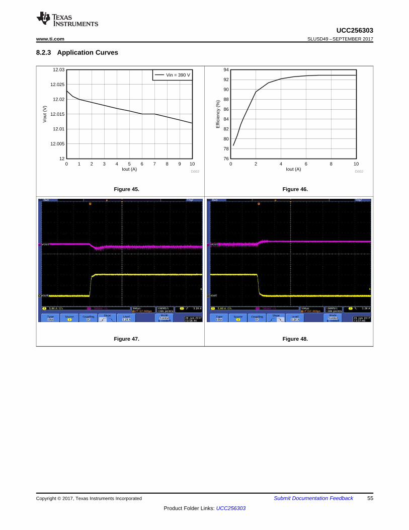
Iout (A)
Vou
t (V
)
0 1 2 3 4 5 6 7 8 9 1012
12.005
12.01
12.015
12.02
12.025
12.03
D002
Vin = 390 V
Iout (A)
Effi
cien
cy (
%)
0 2 4 6 8 1076
78
80
82
84
86
88
90
92
94
D002
55
UCC256303www.ti.com SLUSD49 –SEPTEMBER 2017
Product Folder Links: UCC256303
Submit Documentation FeedbackCopyright © 2017, Texas Instruments Incorporated
8.2.3 Application Curves
Figure 45. Figure 46.
Figure 47. Figure 48.

56
UCC256303SLUSD49 –SEPTEMBER 2017 www.ti.com
Product Folder Links: UCC256303
Submit Documentation Feedback Copyright © 2017, Texas Instruments Incorporated
Figure 49.

Maximum Burst Off Period (ms)
Min
imum
Req
uire
d B
oot C
apac
itanc
e (n
F)
0 3 6 9 12 15 18 21 24 27 300
200
400
600
800
1000
1200
D002
85 10284
3u
bootleak maxoff
bootbootmaxdrop
I t $ PVC nF
V V
8 12 1 8 3 bootmaxdrop RVCC bootforwarddropV V V V V V V V
1 bootforwarddropV V
10 maxofft ms
103 tot
VCCccdropmax
QC )
V
26 10.5 15.5 ccdropmaxV V V V
1.6 totQ mC
57
UCC256303www.ti.com SLUSD49 –SEPTEMBER 2017
Product Folder Links: UCC256303
Submit Documentation FeedbackCopyright © 2017, Texas Instruments Incorporated
9 Power Supply Recommendations
9.1 VCC Pin CapacitorThe VCC capacitor should be sized based on the total start-up charge required by the system. The start-upcharge will mostly be consumed by the gate driver circuit. Thus the total start-up charge can be estimated by thestart-up switching frequency, MOSFET gate charge, and the soft-start time.
Assume the total start-up charge required by the system is shown in Equation 73
(73)
During PFC and LLC startup phase, the maximum VCC voltage drop allowed is
(74)
The minimum VCC capacitor needed:
(75)
Choose 110-µF capacitor.
9.2 Boot CapacitorDuring burst off period, power consumed by the high side gate driver from the HB pin must be drawn from CBOOTand will cause its voltage to decay. At the start of the next burst period there must be sufficient voltage remainingon CBOOT to power the high side gate driver until the conduction period of LO allows it to be replenished fromCRVCC. The power consumed by the high side driver during this burst off period will therefore have a direct impacton the size and cost of capacitors that must be connected to CBOOT and RVCC.
Assume the system has a maximum burst off period of 10 ms.(76)
Assume the bootstrap diode has a forward voltage drop of 1 V:
(77)
Assume the boot voltage to be always above 8 V to avoid UVLO fault. Then the maximum allowed voltage dropon boot capacitor is:
(78)
Boot capacitor can then be sized:
(79)
Figure 50. Minimum Required Boot Capacitance vs. Maximum Burst Off Period

RVCC Capacitance (PF)
Pha
se M
argi
n (D
egre
es)
1 2 3 4 5 6 7 8 9 100
10
20
30
40
50
60
D003
DC Load Current (mA)110255075
58
UCC256303SLUSD49 –SEPTEMBER 2017 www.ti.com
Product Folder Links: UCC256303
Submit Documentation Feedback Copyright © 2017, Texas Instruments Incorporated
9.3 RVCC Pin CapacitorRVCC capacitor needs to be at least 5 times of boot capacitor. In addition, sizing of the RVCC capacitor dependson the stability of RVCC LDO. If load is light on RVCC, smaller capacitors can be used. The larger the load, thelarger the capacitor is needed. In a typical system, the RVCC LDO powers the PFC and LLC gate drivers. Theplot below shows the worst case RVCC LDO phase margin versus RVCC capacitor for various load currents.RVCC capacitor should be sized based on the figure below.
Figure 51. RVCC Pin Capacitor

59
UCC256303www.ti.com SLUSD49 –SEPTEMBER 2017
Product Folder Links: UCC256303
Submit Documentation FeedbackCopyright © 2017, Texas Instruments Incorporated
10 Layout
10.1 Layout Guidelines• Put a 2.2-µF ceramic capacitor on VCC pin in addition to the energy storage electrolytic capacitor. The 2.2-µF
ceramic capacitor should be put as close as possible to the VCC pin.• RVCC pin should have a bypass capacitor of 4.7 µF or more. It is recommended to add a 0.1-µF ceramic
capacitor in addition to the 4.7 µF. The capacitors should be put as close as possible to the RVCC pin. RVCCcap needs to be at least 5 times of boot capacitor.
• Minimum recommended boot capacitor is 0.1 µF. The minimum value of the boot capacitor needs to bedetermined by the minimum burst frequency. The boot capacitor should be large enough to hold the bootstrapvoltage during the lowest burst frequency. Please refer to the boot leakage current in the electrical table.
• Use large copper pour around GND pin• The filtering capacitor on BW, ISNS, BLK should be put as close as possible to the pin• FB trace should be as short as possible• Soft-start capacitor should be put as close as possible to LL/SS pin• Use film capacitor or C0G, NP0 ceramic capacitor on VCR divider and ISNS capacitor for low distortion• It is recommended that ISNS resistor is less than 500 Ω to keep the node impedance low• Add necessary filtering capacitors on BW pin to filter out the high spikes on the bias winding waveform. It is
critical to filter out the high spikes because internally the signal is peak detected and then sampled at the lowside turn off edge.
• Keep necessary high voltage clearance
10.2 Layout Example

60
UCC256303SLUSD49 –SEPTEMBER 2017 www.ti.com
Product Folder Links: UCC256303
Submit Documentation Feedback Copyright © 2017, Texas Instruments Incorporated
11 Device and Documentation Support
11.1 Device Support
11.1.1 Development Support
11.1.1.1 Custom Design With WEBENCH® ToolsClick here to create a custom design using the UCC256303 device with the WEBENCH® Power Designer.1. Start by entering the input voltage (VIN), output voltage (VOUT), and output current (IOUT) requirements.2. Optimize the design for key parameters such as efficiency, footprint, and cost using the optimizer dial.3. Compare the generated design with other possible solutions from Texas Instruments.
The WEBENCH Power Designer provides a customized schematic along with a list of materials with real-timepricing and component availability.
In most cases, these actions are available:• Run electrical simulations to see important waveforms and circuit performance• Run thermal simulations to understand board thermal performance• Export customized schematic and layout into popular CAD formats• Print PDF reports for the design, and share the design with colleagues
Get more information about WEBENCH tools at www.ti.com/WEBENCH.
11.2 Documentation Support (if applicable)
11.2.1 Related DocumentationFor related documentation see the following:• Design Spreadsheet, UCC25630 Design Calculator, UCC634• User Guide, Using UCC25630-1EVM-291,
11.3 Receiving Notification of Documentation UpdatesTo receive notification of documentation updates, navigate to the device product folder on ti.com. In the upperright corner, click on Alert me to register and receive a weekly digest of any product information that haschanged. For change details, review the revision history included in any revised document.
11.4 Community ResourcesThe following links connect to TI community resources. Linked contents are provided "AS IS" by the respectivecontributors. They do not constitute TI specifications and do not necessarily reflect TI's views; see TI's Terms ofUse.
TI E2E™ Online Community TI's Engineer-to-Engineer (E2E) Community. Created to foster collaborationamong engineers. At e2e.ti.com, you can ask questions, share knowledge, explore ideas and helpsolve problems with fellow engineers.
Design Support TI's Design Support Quickly find helpful E2E forums along with design support tools andcontact information for technical support.
11.5 TrademarksE2E is a trademark of Texas Instruments.WEBENCH is a registered trademark of Texas Instruments.
11.6 Electrostatic Discharge CautionThis integrated circuit can be damaged by ESD. Texas Instruments recommends that all integrated circuits be handled withappropriate precautions. Failure to observe proper handling and installation procedures can cause damage.
ESD damage can range from subtle performance degradation to complete device failure. Precision integrated circuits may be moresusceptible to damage because very small parametric changes could cause the device not to meet its published specifications.

61
UCC256303www.ti.com SLUSD49 –SEPTEMBER 2017
Product Folder Links: UCC256303
Submit Documentation FeedbackCopyright © 2017, Texas Instruments Incorporated
11.7 GlossarySLYZ022 — TI Glossary.
This glossary lists and explains terms, acronyms, and definitions.
12 Mechanical, Packaging, and Orderable InformationThe following pages include mechanical, packaging, and orderable information. This information is the mostcurrent data available for the designated devices. This data is subject to change without notice and revision ofthis document. For browser-based versions of this data sheet, refer to the left-hand navigation.

PACKAGE OPTION ADDENDUM
www.ti.com 30-Sep-2017
Addendum-Page 1
PACKAGING INFORMATION
Orderable Device Status(1)
Package Type PackageDrawing
Pins PackageQty
Eco Plan(2)
Lead/Ball Finish(6)
MSL Peak Temp(3)
Op Temp (°C) Device Marking(4/5)
Samples
UCC25630-3DDBR ACTIVE SOIC DDB 14 2500 Green (RoHS& no Sb/Br)
CU NIPDAU Level-2-260C-1 YEAR -40 to 125 UCC256303
UCC25630-3DDBT ACTIVE SOIC DDB 14 250 Green (RoHS& no Sb/Br)
CU NIPDAU Level-2-260C-1 YEAR -40 to 125 UCC256303
(1) The marketing status values are defined as follows:ACTIVE: Product device recommended for new designs.LIFEBUY: TI has announced that the device will be discontinued, and a lifetime-buy period is in effect.NRND: Not recommended for new designs. Device is in production to support existing customers, but TI does not recommend using this part in a new design.PREVIEW: Device has been announced but is not in production. Samples may or may not be available.OBSOLETE: TI has discontinued the production of the device.
(2) RoHS: TI defines "RoHS" to mean semiconductor products that are compliant with the current EU RoHS requirements for all 10 RoHS substances, including the requirement that RoHS substancedo not exceed 0.1% by weight in homogeneous materials. Where designed to be soldered at high temperatures, "RoHS" products are suitable for use in specified lead-free processes. TI mayreference these types of products as "Pb-Free".RoHS Exempt: TI defines "RoHS Exempt" to mean products that contain lead but are compliant with EU RoHS pursuant to a specific EU RoHS exemption.Green: TI defines "Green" to mean the content of Chlorine (Cl) and Bromine (Br) based flame retardants meet JS709B low halogen requirements of <=1000ppm threshold. Antimony trioxide basedflame retardants must also meet the <=1000ppm threshold requirement.
(3) MSL, Peak Temp. - The Moisture Sensitivity Level rating according to the JEDEC industry standard classifications, and peak solder temperature.
(4) There may be additional marking, which relates to the logo, the lot trace code information, or the environmental category on the device.
(5) Multiple Device Markings will be inside parentheses. Only one Device Marking contained in parentheses and separated by a "~" will appear on a device. If a line is indented then it is a continuationof the previous line and the two combined represent the entire Device Marking for that device.
(6) Lead/Ball Finish - Orderable Devices may have multiple material finish options. Finish options are separated by a vertical ruled line. Lead/Ball Finish values may wrap to two lines if the finishvalue exceeds the maximum column width.
Important Information and Disclaimer:The information provided on this page represents TI's knowledge and belief as of the date that it is provided. TI bases its knowledge and belief on informationprovided by third parties, and makes no representation or warranty as to the accuracy of such information. Efforts are underway to better integrate information from third parties. TI has taken andcontinues to take reasonable steps to provide representative and accurate information but may not have conducted destructive testing or chemical analysis on incoming materials and chemicals.TI and TI suppliers consider certain information to be proprietary, and thus CAS numbers and other limited information may not be available for release.
In no event shall TI's liability arising out of such information exceed the total purchase price of the TI part(s) at issue in this document sold by TI to Customer on an annual basis.
PACKAGE OPTION ADDENDUM
www.ti.com 30-Sep-2017
Addendum-Page 2

www.ti.com
PACKAGE OUTLINE
C
TYP6.25.8
1.75 MAX
10X 1.27
14X 0.510.31
2X8.89
TYP0.250.13
0 - 80.250.10
0.25GAGE PLANE
1.270.40
A
NOTE 3
10.09.8
B 4.03.8
4222925/A 04/2016
SOIC - 1.75 mm max heightDDB0014ASOIC
NOTES: 1. All linear dimensions are in millimeters. Dimensions in parenthesis are for reference only. Dimensioning and tolerancing per ASME Y14.5M. 2. This drawing is subject to change without notice. 3. This dimension does not include mold flash, protrusions, or gate burrs. Mold flash, protrusions, or gate burrs shall not exceed 0.15 mm per side. 4. This dimension does not include interlead flash. Interlead flash shall not exceed 0.43 mm per side.5. Reference JEDEC registration MS-012, variation AC.
116
0.25 C A B
98
PIN 1 IDAREA
NOTE 4
SEATING PLANE
0.1 C
SEE DETAIL A
DETAIL ATYPICAL
SCALE 1.800

www.ti.com
EXAMPLE BOARD LAYOUT
(5.4)
0.07 MAXALL AROUND
0.07 MINALL AROUND
14X (1.55)
14X (0.6)
10X (1.27)
(R )TYP
0.05
(4.445)TYP
4222925/A 04/2016
SOIC - 1.75 mm max heightDDB0014ASOIC
SYMM
SYMM
LAND PATTERN EXAMPLESCALE:8X
1
8 9
16
NOTES: (continued) 6. Publication IPC-7351 may have alternate designs. 7. Solder mask tolerances between and around signal pads can vary based on board fabrication site.
METALSOLDER MASKOPENING
NON SOLDER MASKDEFINED
SOLDER MASK DETAILS
SOLDER MASKOPENING
METAL UNDERSOLDER MASK
SOLDER MASKDEFINED

www.ti.com
EXAMPLE STENCIL DESIGN
(5.4)
14X (1.27)
14X (0.6)
14X (1.55)
(4.445)TYP
4222925/A 04/2016
SOIC - 1.75 mm max heightDDB0014ASOIC
NOTES: (continued) 8. Laser cutting apertures with trapezoidal walls and rounded corners may offer better paste release. IPC-7525 may have alternate design recommendations. 9. Board assembly site may have different recommendations for stencil design.
SYMM
SYMM
1
8 9
16
SOLDER PASTE EXAMPLEBASED ON 0.125 mm THICK STENCIL
SCALE:8X

IMPORTANT NOTICE
Texas Instruments Incorporated (TI) reserves the right to make corrections, enhancements, improvements and other changes to itssemiconductor products and services per JESD46, latest issue, and to discontinue any product or service per JESD48, latest issue. Buyersshould obtain the latest relevant information before placing orders and should verify that such information is current and complete.TI’s published terms of sale for semiconductor products (http://www.ti.com/sc/docs/stdterms.htm) apply to the sale of packaged integratedcircuit products that TI has qualified and released to market. Additional terms may apply to the use or sale of other types of TI products andservices.Reproduction of significant portions of TI information in TI data sheets is permissible only if reproduction is without alteration and isaccompanied by all associated warranties, conditions, limitations, and notices. TI is not responsible or liable for such reproduceddocumentation. Information of third parties may be subject to additional restrictions. Resale of TI products or services with statementsdifferent from or beyond the parameters stated by TI for that product or service voids all express and any implied warranties for theassociated TI product or service and is an unfair and deceptive business practice. TI is not responsible or liable for any such statements.Buyers and others who are developing systems that incorporate TI products (collectively, “Designers”) understand and agree that Designersremain responsible for using their independent analysis, evaluation and judgment in designing their applications and that Designers havefull and exclusive responsibility to assure the safety of Designers' applications and compliance of their applications (and of all TI productsused in or for Designers’ applications) with all applicable regulations, laws and other applicable requirements. Designer represents that, withrespect to their applications, Designer has all the necessary expertise to create and implement safeguards that (1) anticipate dangerousconsequences of failures, (2) monitor failures and their consequences, and (3) lessen the likelihood of failures that might cause harm andtake appropriate actions. Designer agrees that prior to using or distributing any applications that include TI products, Designer willthoroughly test such applications and the functionality of such TI products as used in such applications.TI’s provision of technical, application or other design advice, quality characterization, reliability data or other services or information,including, but not limited to, reference designs and materials relating to evaluation modules, (collectively, “TI Resources”) are intended toassist designers who are developing applications that incorporate TI products; by downloading, accessing or using TI Resources in anyway, Designer (individually or, if Designer is acting on behalf of a company, Designer’s company) agrees to use any particular TI Resourcesolely for this purpose and subject to the terms of this Notice.TI’s provision of TI Resources does not expand or otherwise alter TI’s applicable published warranties or warranty disclaimers for TIproducts, and no additional obligations or liabilities arise from TI providing such TI Resources. TI reserves the right to make corrections,enhancements, improvements and other changes to its TI Resources. TI has not conducted any testing other than that specificallydescribed in the published documentation for a particular TI Resource.Designer is authorized to use, copy and modify any individual TI Resource only in connection with the development of applications thatinclude the TI product(s) identified in such TI Resource. NO OTHER LICENSE, EXPRESS OR IMPLIED, BY ESTOPPEL OR OTHERWISETO ANY OTHER TI INTELLECTUAL PROPERTY RIGHT, AND NO LICENSE TO ANY TECHNOLOGY OR INTELLECTUAL PROPERTYRIGHT OF TI OR ANY THIRD PARTY IS GRANTED HEREIN, including but not limited to any patent right, copyright, mask work right, orother intellectual property right relating to any combination, machine, or process in which TI products or services are used. Informationregarding or referencing third-party products or services does not constitute a license to use such products or services, or a warranty orendorsement thereof. Use of TI Resources may require a license from a third party under the patents or other intellectual property of thethird party, or a license from TI under the patents or other intellectual property of TI.TI RESOURCES ARE PROVIDED “AS IS” AND WITH ALL FAULTS. TI DISCLAIMS ALL OTHER WARRANTIES ORREPRESENTATIONS, EXPRESS OR IMPLIED, REGARDING RESOURCES OR USE THEREOF, INCLUDING BUT NOT LIMITED TOACCURACY OR COMPLETENESS, TITLE, ANY EPIDEMIC FAILURE WARRANTY AND ANY IMPLIED WARRANTIES OFMERCHANTABILITY, FITNESS FOR A PARTICULAR PURPOSE, AND NON-INFRINGEMENT OF ANY THIRD PARTY INTELLECTUALPROPERTY RIGHTS. TI SHALL NOT BE LIABLE FOR AND SHALL NOT DEFEND OR INDEMNIFY DESIGNER AGAINST ANY CLAIM,INCLUDING BUT NOT LIMITED TO ANY INFRINGEMENT CLAIM THAT RELATES TO OR IS BASED ON ANY COMBINATION OFPRODUCTS EVEN IF DESCRIBED IN TI RESOURCES OR OTHERWISE. IN NO EVENT SHALL TI BE LIABLE FOR ANY ACTUAL,DIRECT, SPECIAL, COLLATERAL, INDIRECT, PUNITIVE, INCIDENTAL, CONSEQUENTIAL OR EXEMPLARY DAMAGES INCONNECTION WITH OR ARISING OUT OF TI RESOURCES OR USE THEREOF, AND REGARDLESS OF WHETHER TI HAS BEENADVISED OF THE POSSIBILITY OF SUCH DAMAGES.Unless TI has explicitly designated an individual product as meeting the requirements of a particular industry standard (e.g., ISO/TS 16949and ISO 26262), TI is not responsible for any failure to meet such industry standard requirements.Where TI specifically promotes products as facilitating functional safety or as compliant with industry functional safety standards, suchproducts are intended to help enable customers to design and create their own applications that meet applicable functional safety standardsand requirements. Using products in an application does not by itself establish any safety features in the application. Designers mustensure compliance with safety-related requirements and standards applicable to their applications. Designer may not use any TI products inlife-critical medical equipment unless authorized officers of the parties have executed a special contract specifically governing such use.Life-critical medical equipment is medical equipment where failure of such equipment would cause serious bodily injury or death (e.g., lifesupport, pacemakers, defibrillators, heart pumps, neurostimulators, and implantables). Such equipment includes, without limitation, allmedical devices identified by the U.S. Food and Drug Administration as Class III devices and equivalent classifications outside the U.S.TI may expressly designate certain products as completing a particular qualification (e.g., Q100, Military Grade, or Enhanced Product).Designers agree that it has the necessary expertise to select the product with the appropriate qualification designation for their applicationsand that proper product selection is at Designers’ own risk. Designers are solely responsible for compliance with all legal and regulatoryrequirements in connection with such selection.Designer will fully indemnify TI and its representatives against any damages, costs, losses, and/or liabilities arising out of Designer’s non-compliance with the terms and provisions of this Notice.
Mailing Address: Texas Instruments, Post Office Box 655303, Dallas, Texas 75265Copyright © 2017, Texas Instruments Incorporated