Typical Applications Functional Diagram - Farnell … On-line at 13 - 1 DC POWER MANAGEMENT - SMT 13...
27
For price, delivery, and to place orders, please contact Hittite Microwave Corporation: 20 Alpha Road, Chelmsford, MA 01824 Phone: 978-250-3343 Fax: 978-250-3373 Order On-line at www.hittite.com 13 - 1 DC POWER MANAGEMENT - SMT 13 HMC920LP5E v07.1013 ACTIVE BIAS CONTROLLER HMC920LP5E ACTIVE BIAS CONTROLLER Functional Diagram Features • Single Positive Voltage Supply (5V to 16.5V) • Adjustable Drain Voltage 3V to 15V • Adjustable Drain Current up to 500mA • Internal Negative Voltage Generator • Active Bias Current Regulation • Stable Bias Current Over Temperature and Process Variation and Aging • Short Circuit Protection (Power Foldback) • Adjustable Over/Under-Current Alarm • Adjustable Low Vdd Voltage Alarm • Automated Power-up Sequencing • Enable Input for Active Bias Control • Trigger-out Output for Daisy Chain Power-Up and Power-Down Sequencing Typical Applications • Cellular Base Station • Wireless Infrastructure Equipment • Microwave Radio & VSAT • Military & Space • Test Instrumentation Information furnished by Analog Devices is believed to be accurate and reliable. However, no responsibility is assumed by Analog Devices for its use, nor for any infringements of patents or other rights of third parties that may result from its use. Specifications subject to change without notice. No license is granted by implication or otherwise under any patent or patent rights of Analog Devices. Trademarks and registered trademarks are the property of their respective owners. For price, delivery, and to place orders: Analog Devices, Inc., One Technology Way, P.O. Box 9106, Norwood, MA 02062-9106 Phone: 781-329-4700 • Order online at www.analog.com Application Support: Phone: 1-800-ANALOG-D
Transcript of Typical Applications Functional Diagram - Farnell … On-line at 13 - 1 DC POWER MANAGEMENT - SMT 13...

For price, delivery, and to place orders, please contact Hittite Microwave Corporation:20 Alpha Road, Chelmsford, MA 01824 Phone: 978-250-3343 Fax: 978-250-3373
Order On-line at www.hittite.com13 - 1
DC
PO
WE
R M
AN
AG
EM
EN
T -
SM
T
13
HMC920LP5Ev07.1013
ACTIVE BIAS CONTROLLER
HMC920LP5EACTIVE BIAS CONTROLLER
Functional Diagram
Features• Single Positive Voltage Supply (5V to 16.5V)
• Adjustable Drain Voltage 3V to 15V
• Adjustable Drain Current up to 500mA
• Internal Negative Voltage Generator
• Active Bias Current Regulation
• Stable Bias Current Over Temperature and Process Variation and Aging
• Short Circuit Protection (Power Foldback)
• Adjustable Over/Under-Current Alarm
• Adjustable Low Vdd Voltage Alarm
• Automated Power-up Sequencing
• Enable Input for Active Bias Control
• Trigger-out Output for Daisy Chain Power-Up and Power-Down Sequencing
Typical Applications
• Cellular Base Station
• Wireless Infrastructure Equipment
• Microwave Radio & VSAT
• Military & Space
• Test Instrumentation
Information furnished by Analog Devices is believed to be accurate and reliable. However, no responsibility is assumed by Analog Devices for its use, nor for any infringements of patents or other rights of third parties that may result from its use. Specifications subject to change without notice. No license is granted by implication or otherwise under any patent or patent rights of Analog Devices. Trademarks and registered trademarks are the property of their respective owners.
For price, delivery, and to place orders: Analog Devices, Inc., One Technology Way, P.O. Box 9106, Norwood, MA 02062-9106 Phone: 781-329-4700 • Order online at www.analog.com Application Support: Phone: 1-800-ANALOG-D

HMC920* PRODUCT PAGE QUICK LINKSLast Content Update: 02/23/2017
COMPARABLE PARTSView a parametric search of comparable parts.
EVALUATION KITS• HMC920LP5E Evaluation Board
DOCUMENTATIONApplication Notes
• AN-1363: Meeting Biasing Requirements of Externally Biased RF/Microwave Amplifiers with Active Bias Controllers
Data Sheet
• HMC920 Data Sheet
REFERENCE MATERIALSQuality Documentation
• Package/Assembly Qualification Test Report: 32L 5x5mm QFN Package (QTR: 10009 REV: 05)
• Package/Assembly Qualification Test Report: LP5 & LP5G (QTR: 2014-00150 REV: 02)
• Semiconductor Qualification Test Report: CMOS-B (QTR: 2013-00262)
DESIGN RESOURCES• HMC920 Material Declaration
• PCN-PDN Information
• Quality And Reliability
• Symbols and Footprints
DISCUSSIONSView all HMC920 EngineerZone Discussions.
SAMPLE AND BUYVisit the product page to see pricing options.
TECHNICAL SUPPORTSubmit a technical question or find your regional support number.
DOCUMENT FEEDBACKSubmit feedback for this data sheet.
This page is dynamically generated by Analog Devices, Inc., and inserted into this data sheet. A dynamic change to the content on this page will not trigger a change to either the revision number or the content of the product data sheet. This dynamic page may be frequently modified.
For price, delivery, and to place orders, please contact Hittite Microwave Corporation:20 Alpha Road, Chelmsford, MA 01824 Phone: 978-250-3343 Fax: 978-250-3373
Order On-line at www.hittite.com13 - 2
DC
PO
WE
R M
AN
AG
EM
EN
T -
SM
T
13
HMC920LP5Ev07.1013
ACTIVE BIAS CONTROLLER
HMC920LP5E is an active bias controller which generates a regulated Drain voltage and actively adjusts the gate voltage of an external amplifier to achieve constant bias current. It can be used to bias any enhancement and depletion type amplifiers operating in Class-A regime with Drain voltages (VDRAIN) from 3V to 15V and drain currents (IDRAIN) up to 500mA, offering a complete biasing solution.
HMC920LP5E achieves excellent bias stability over supply, temperature and process variations, and eliminates the required calibration procedures used to prevent RF performance degradation due to such variations.
The HMC920LP5E is housed in an RoHS compliant 5x5 mm QFN leadless package with an exposed backside pad to improve thermal characteristics.
General Description
Electrical Specifications, TA = +25°C, Vdd = Vdd1 = Vdd2 = 15V
Parameter Symbol Conditions Min. Typ. Max. Units
Supply Voltage Vdd 5 16.5 V
Quiescent Current IDD
Vdd = 5VEN = Vdig 35 mA
EN = GND 20 mA
Vdd = 15VEN = Vdig 35 mA
EN = GND 20 mA
Negative Voltage Output VNEG -2.5 V
Oscillator Frequency FOSC 250 kHz
Bandgap Reference VBGC 2 V
VDIG Feedback VDIGFB 2.5 V
LDOCC Feedback LDOFB 2 V
Enable Input Threshold ENTHRSVinlow 1 V
Vinhigh 1.4 V
ALMTRIG Input Threshold ALMTRIGVinlow 1 V
Vinhigh 1.4 V
Low Vdd Alarm Threshold VddCHK 3.8 V
VDRAIN Characteristics
DRAIN Current Adjustment Range IDRAIN 0 500 mA
DRAIN Current Change Over Supply VoltageΔIDRAINV
VDRAIN set to 6V, IDRAIN set to 100mA,
0.05 %/V
DRAIN Current Change Over Temperature 0.03 %/C
DRAIN Adjustment Range VDRAIN 3 15 V
VDRAIN Change Over Supply VoltageΔVDRAIN
VDRAIN set to 6V, IDRAIN set to 100mA,
0.05 %/V
VDRAIN Change Over Temperature 0.008 %/C
VNEG Characteristics
Negative Voltage Output VNEG -2.5 V
VNEG Current Sink INEG 0 60 mA
VGATE Characteristics
GATE Current Supply IG -4 4 mA
VGATE Low Level VG_MIN VNEG V
VGATE High Level VG_MAX VNEG+4.5 V
VDIG Characteristics
Adjustment Range VDIG 3.5 5 V
VDIG Current Source IDIG 30 mA
Information furnished by Analog Devices is believed to be accurate and reliable. However, no responsibility is assumed by Analog Devices for its use, nor for any infringements of patents or other rights of third parties that may result from its use. Specifications subject to change without notice. No license is granted by implication or otherwise under any patent or patent rights of Analog Devices. Trademarks and registered trademarks are the property of their respective owners.
For price, delivery, and to place orders: Analog Devices, Inc., One Technology Way, P.O. Box 9106, Norwood, MA 02062-9106 Phone: 781-329-4700 • Order online at www.analog.com Application Support: Phone: 1-800-ANALOG-D

For price, delivery, and to place orders, please contact Hittite Microwave Corporation:20 Alpha Road, Chelmsford, MA 01824 Phone: 978-250-3343 Fax: 978-250-3373
Order On-line at www.hittite.com13 - 3
DC
PO
WE
R M
AN
AG
EM
EN
T -
SM
T
13
HMC920LP5Ev07.1013
ACTIVE BIAS CONTROLLER
VDRAIN Line Regulation Over IDRAIN
VDRAIN Line Regulation Over Temperature
IDRAIN Regulation Accuracy vs. Vdd [1][2]
100
102
104
106
108
110
7 8 9 10 11 12 13 14 15
+25C+85C -40C
SUPPLY VOLTAGE (V)
CU
RR
EN
T (
mA
)
5.7
5.8
5.9
6
6.1
6.2
6.5 7.5 8.5 9.5 10.5 11.5 12.5 13.5 14.5 15.5 16.5
Idrain=0mAIdrain=100mAIdrain=200mA
SUPPLY VOLTAGE (V)
DR
AIN
VO
LTA
GE
VD
RA
IN (
V)
5.9
5.94
5.98
6.02
6.06
6.1
6.5 7.5 8.5 9.5 10.5 11.5 12.5 13.5 14.5 15.5 16.5
+25C+85C -40C
SUPPLY VOLTAGE (V)
DR
AIN
VO
LTA
GE
VD
RA
IN (
V) No load condition
[1] IDRAIN is set to 110mA [2] HMC594LC3B is used as external amplifier
VNEG Line Regulation Over Temperature
VDIG Line Regulation Over Temperature
3.4
3.42
3.44
3.46
3.48
3.5
5 6 7 8 9 10 11 12 13 14 15 16
+25C+85C -40C
SUPPLY VOLTAGE (V)
DIG
ITA
L V
OLT
AG
E V
DIG
(V
)
No load condition
-2.5
-2.48
-2.46
-2.44
-2.42
-2.4
5 6 7 8 9 10 11 12 13 14 15 16
+25C+85C -40C
SUPPLY VOLTAGE (V)
NE
GA
TIV
E V
OLT
AG
E V
NE
G (
V)
No load condition
VDRAIN Load Regulation Over Vdd
5.7
5.8
5.9
6
6.1
6.2
0 20 40 60 80 100 120 140 160 180 200 220
Vdd=+7.5VVdd=+10.0VVdd=+16.5V
DRAIN LOAD CURRENT (mA)
DR
AIN
VO
LTA
GE
VD
RA
IN (
V)
Information furnished by Analog Devices is believed to be accurate and reliable. However, no responsibility is assumed by Analog Devices for its use, nor for any infringements of patents or other rights of third parties that may result from its use. Specifications subject to change without notice. No license is granted by implication or otherwise under any patent or patent rights of Analog Devices. Trademarks and registered trademarks are the property of their respective owners.
For price, delivery, and to place orders: Analog Devices, Inc., One Technology Way, P.O. Box 9106, Norwood, MA 02062-9106 Phone: 781-329-4700 • Order online at www.analog.com Application Support: Phone: 1-800-ANALOG-D
For price, delivery, and to place orders, please contact Hittite Microwave Corporation:20 Alpha Road, Chelmsford, MA 01824 Phone: 978-250-3343 Fax: 978-250-3373
Order On-line at www.hittite.com13 - 4
DC
PO
WE
R M
AN
AG
EM
EN
T -
SM
T
13
HMC920LP5Ev07.1013
ACTIVE BIAS CONTROLLER
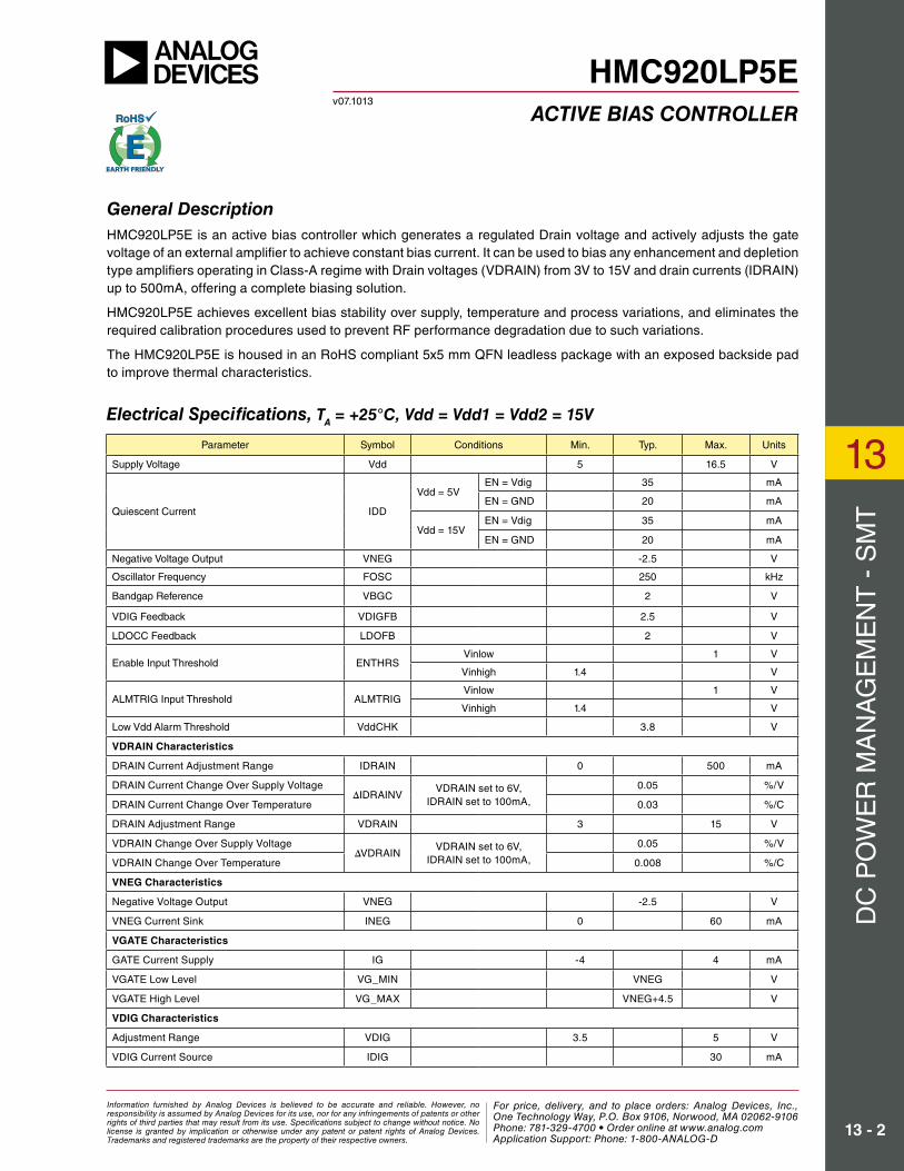
VDIG Load Regulation Over Temperature
VNEG Load Regulation Over Temperature [2] VNEG Load Regulation Over Temperature [3]
VDRAIN Load Regulation Over Temperature [1]
3.4
3.42
3.44
3.46
3.48
3.5
0 5 10 15 20 25 30 35
+25C+85C -40C
DIGITAL LOAD CURRENT (mA)
DIG
ITA
L V
OLT
AG
E V
DIG
(V
)
5.7
5.8
5.9
6
6.1
6.2
0 40 80 120 160 200 240 280 320 360 400
+25C+85C -40C
DRAIN LOAD CURRENT (mA)
DR
AIN
VO
LTA
GE
VD
RA
IN (
V)
-2.7
-2.6
-2.5
-2.4
-2.3
0 5 10 15 20 25
+25C+85C -40C
NEGATIVE SINK CURRENT (mA)
NE
GA
TIV
E V
OLT
AG
E V
NE
G (
V)
-2.7
-2.6
-2.5
-2.4
-2.3
0 15 30 45 60 75
+25C+85C -40C
NEGATIVE SINK CURRENT (mA)
NE
GA
TIV
E V
OLT
AG
E V
NE
G (
V)
[1] Vdd = 7.5V [2] Vdd = 5V [3] Vdd - 16.5V
Enable Waveform Disable Waveform
0V
0V0V
0V
0V
C C
0V
A A
B B
A Enable Pin, 5 V/div C VGATE, 1 V/div
B VDRAIN, 2 V/div
A Enable Pin, 5 V/div C VGATE, 1 V/div
B VDRAIN, 2 V/div
200 µs/div 200 µs/div
Information furnished by Analog Devices is believed to be accurate and reliable. However, no responsibility is assumed by Analog Devices for its use, nor for any infringements of patents or other rights of third parties that may result from its use. Specifications subject to change without notice. No license is granted by implication or otherwise under any patent or patent rights of Analog Devices. Trademarks and registered trademarks are the property of their respective owners.
For price, delivery, and to place orders: Analog Devices, Inc., One Technology Way, P.O. Box 9106, Norwood, MA 02062-9106 Phone: 781-329-4700 • Order online at www.analog.com Application Support: Phone: 1-800-ANALOG-D

For price, delivery, and to place orders, please contact Hittite Microwave Corporation:20 Alpha Road, Chelmsford, MA 01824 Phone: 978-250-3343 Fax: 978-250-3373
Order On-line at www.hittite.com13 - 5
DC
PO
WE
R M
AN
AG
EM
EN
T -
SM
T
13
HMC920LP5Ev07.1013
ACTIVE BIAS CONTROLLER
Power Up Waveform
VDIG Load Transient VNEG Load Transient
Power Down Waveform
VDRAIN Load Transient VDOCC Load Transient
6V 6V
3.5V
A
B
0V
-2.5V
0mA 0mA
0mA
C
0V
D
0V
0mA
B B
B
0V
0VCD
B
A A
A
0V
A
B
A
A VDRAIN, 500 mV/div
B IDRAIN, 100 mA/div
A LDOCC, 200 mV/div
B IDRAIN, 100 mA/div
A VDIG, 50 mV/div
B IDIG, 20 mA/div
A Vdd, 5V/div C VGATE, 1V/div
B VDRAIN, 5V/div D VNEG, 1V/div
A Vdd, 5V/div C VGATE, 1V/div
B VDRAIN, 5V/div D VNEG, 1V/div
A VNEG, 50 mV/div
B INEG, 5 mA/div
20 us/div
500 us/div
5 ms/div
20 us/div
1 ms/div
10 ms/div
Information furnished by Analog Devices is believed to be accurate and reliable. However, no responsibility is assumed by Analog Devices for its use, nor for any infringements of patents or other rights of third parties that may result from its use. Specifications subject to change without notice. No license is granted by implication or otherwise under any patent or patent rights of Analog Devices. Trademarks and registered trademarks are the property of their respective owners.
For price, delivery, and to place orders: Analog Devices, Inc., One Technology Way, P.O. Box 9106, Norwood, MA 02062-9106 Phone: 781-329-4700 • Order online at www.analog.com Application Support: Phone: 1-800-ANALOG-D

For price, delivery, and to place orders, please contact Hittite Microwave Corporation:20 Alpha Road, Chelmsford, MA 01824 Phone: 978-250-3343 Fax: 978-250-3373
Order On-line at www.hittite.com13 - 6
DC
PO
WE
R M
AN
AG
EM
EN
T -
SM
T
13
HMC920LP5Ev07.1013
ACTIVE BIAS CONTROLLER
Outline Drawing
NOTES:1. LEADFRAME MATERIAL: COPPER ALLOY2. DIMENSIONS ARE IN INCHES [MILLIMETERS]3. LEAD SPACING TOLERANCE IS NON-CUMULATIVE.4. PAD BURR LENGTH SHALL BE 0.15mm MAXIMUM. PAD BURR HEIGHT SHALL BE 0.05mm MAXIMUM.5. PACKAGE WARP SHALL NOT EXCEED 0.05mm.6. ALL GROUND LEADS AND GROUND PADDLE MUST BE SOLDERED TO PCB RF GROUND.7. REFER TO HITTITE APPLICATION NOTE FOR SUGGESTED LAND PATTERN.
Part Number Package Body Material Lead Finish MSL Rating Package Marking [1]
HMC920LP5E RoHS-compliant Low Stress Injection Molded Plastic 100% matte Sn MSL1 [2] H920XXXX
[1] 4-Digit lot number XXXX[2] Max peak reflow temperature of 260 °C
Package Information
Absolute Maximum Ratings [1]
Vdd1, Vdd2 to GND -0.3V to +16.5V
VDIG to GND -0.3V to +5.5V
VDIGFB, PORCAP, BGCAP, EN, CURALM, ALMTRIG to GND
-0.3V to (VDIG + 0.3V)
ALMSET, ALMC1, ALMC2, REF to GND
-0.3V to (Vdd + 0.3V)
VNEGFB, VGATE, VDRAIN, ISENSE to GND
-0.3V to (Vdd + 0.3V)
VNEGIN to GND -4V to (Vdd + 0.3V)
ALML, ALMM, ALMH, LDOCC, LDOFB to GND
-0.3V to (Vdd + 0.3V)
VGATEFB, TRGOUT, VddALM, VddCHK to GND
-0.3V to (VDIG + 0.3V)
ELECTROSTATIC SENSITIVE DEVICEOBSERVE HANDLING PRECAUTIONS
CPGND to GND -0.3V to +0.3V
Vdd1 to Vdd2 -0.3V to +0.3V
Junction Temperature 125 °C
Continuous Pdiss (T = 85 °C)(Derate 256.67 mW/°C above 85 °C)
10.27 Watts
Thermal Resistance (RTH)(Junction to package bottom)
3.9 °C/W
Storage Temperature -65 to +150 °C
Operating Temperature -40 to +85 °C
ESD Sensitivity (HBM) Class 1C
Note that there are two different voltage domains on HMC920LP5E; a high voltage domain Vdd, and a low voltage domain VDIG. Take necessary precautions not to violate ABS MAX ratings of each subdomains.
Information furnished by Analog Devices is believed to be accurate and reliable. However, no responsibility is assumed by Analog Devices for its use, nor for any infringements of patents or other rights of third parties that may result from its use. Specifications subject to change without notice. No license is granted by implication or otherwise under any patent or patent rights of Analog Devices. Trademarks and registered trademarks are the property of their respective owners.
For price, delivery, and to place orders: Analog Devices, Inc., One Technology Way, P.O. Box 9106, Norwood, MA 02062-9106 Phone: 781-329-4700 • Order online at www.analog.com Application Support: Phone: 1-800-ANALOG-D

For price, delivery, and to place orders, please contact Hittite Microwave Corporation:20 Alpha Road, Chelmsford, MA 01824 Phone: 978-250-3343 Fax: 978-250-3373
Order On-line at www.hittite.com13 - 7
DC
PO
WE
R M
AN
AG
EM
EN
T -
SM
T
13
HMC920LP5Ev07.1013
ACTIVE BIAS CONTROLLER
Pin DescriptionsPin Number Function Description Interface Schematic
1, 2 Vdd1Bias supply Pins. Connect supply voltage
to all these pins with appropriate filtering. Vdd1 supply voltage should be same as Vdd2.
3 VDIG3.5V LDO output for internal use. Output capability <30mA.
Is not recommended for external use.
4 VDIGFBFeedback node for VDIG LDO. Should be left floating for
regular operation.
5 PORCAPExternal capacitor for power-on-reset signal. 47pF to
GND is needed. If longer POR duration is needed, can be increased.
10 ALMSETA resistor to ground is needed. The value of the resistor determines the alarm delay duration. The value of the
resistor can be chosen between 10K and 10M.
12 FIXBIASA high precision (e.g. 0.5%, ±25 ppm TCR) 10K resistor
to ground is needed. Variance in the resistance will cause deviation in the bias current.
6 BGCAPExternal capacitor of bandgap output. Connect a
0.1uF or greater low ESR ceramic capacitor to GND.
7 ENEnable pin. System is enabled when Ven is HIGH (3.5V). IF
left floating, Ven defaults to HIGH (enabled).
9 ALMTRGDummy alarm trigger signal to create test alarm when taken HIGH (3.5V). Defaults to LOW (GND) when left
floating.
8 CURALMOver/under current alarm
(Generates an active HIGH signal).
24 TRGOUT
Trigger out signal. Generates a HIGH (3.5V) signal when the active bias system stabilizes. This signal can be
used to trigger next device (ENABLE) if more than one HMC920LP5E is used in a daisy chain.
31 VddALM Generates an active LOW signal if Vdd1 drops below 3.5V.
Information furnished by Analog Devices is believed to be accurate and reliable. However, no responsibility is assumed by Analog Devices for its use, nor for any infringements of patents or other rights of third parties that may result from its use. Specifications subject to change without notice. No license is granted by implication or otherwise under any patent or patent rights of Analog Devices. Trademarks and registered trademarks are the property of their respective owners.
For price, delivery, and to place orders: Analog Devices, Inc., One Technology Way, P.O. Box 9106, Norwood, MA 02062-9106 Phone: 781-329-4700 • Order online at www.analog.com Application Support: Phone: 1-800-ANALOG-D

For price, delivery, and to place orders, please contact Hittite Microwave Corporation:20 Alpha Road, Chelmsford, MA 01824 Phone: 978-250-3343 Fax: 978-250-3373
Order On-line at www.hittite.com13 - 8
DC
PO
WE
R M
AN
AG
EM
EN
T -
SM
T
13
HMC920LP5Ev07.1013
ACTIVE BIAS CONTROLLER
Pin Number Function Description Interface Schematic
13 VREF1.5V reference voltage. 0.1uF or greater capacitor to GND
is needed for noise filtering.
14 Vdd2Bias supply for negative voltage generator. Connect supply
voltage with appropriate filtering. Vdd2 supply voltage should be same as Vdd1.
15 CPOUT
Negative voltage generator charge pump output. Negative voltage generator needs a flying capacitor, a reservoir
capacitor and two diodes to operate. Please refer to the application schematic for more info.
16 DGND Digital ground domain (DGND).
11, 17 AGND Analog ground domain (GND).
18 VNEGFB
Feedback (Control) pin for Negative Voltage Genera-tor Charge Pump. Float to activate the negative voltage generator / Sort to GND to disable the negative voltage
generator.
19 VNEGIN
Negative input to the chip. Should be supplied with CPOUT when negative voltage generator is enabled, or connect to external VSS when negative voltage generator is enabled. For detailed usage please refer to the “Negative Voltage
Generator” section.
20 VGATEFB
Control pin for VGATEFB. Float VGATEFB when a depletion mode transistor is biased. Selects the mode of
operation along with VNEGFB pin. For detailed usage please refer to the Table 1. Mode Selection.
Pin Descriptions (Continued)
Information furnished by Analog Devices is believed to be accurate and reliable. However, no responsibility is assumed by Analog Devices for its use, nor for any infringements of patents or other rights of third parties that may result from its use. Specifications subject to change without notice. No license is granted by implication or otherwise under any patent or patent rights of Analog Devices. Trademarks and registered trademarks are the property of their respective owners.
For price, delivery, and to place orders: Analog Devices, Inc., One Technology Way, P.O. Box 9106, Norwood, MA 02062-9106 Phone: 781-329-4700 • Order online at www.analog.com Application Support: Phone: 1-800-ANALOG-D

For price, delivery, and to place orders, please contact Hittite Microwave Corporation:20 Alpha Road, Chelmsford, MA 01824 Phone: 978-250-3343 Fax: 978-250-3373
Order On-line at www.hittite.com13 - 9
DC
PO
WE
R M
AN
AG
EM
EN
T -
SM
T
13
HMC920LP5Ev07.1013
ACTIVE BIAS CONTROLLER
Pin Number Function Description Interface Schematic
21 VGATE
Gate Control pin for external amplifier. Connect to the gate (base) of the external amplifier. In order to guarantee stabil-
ity, a 10µF capacitor should be connected between the gate (base) terminal of the external amplifier and GND as
close to the amplifier as possible.
22, 23 VDRAIN
Drain voltage. Should be connected to the supply terminal of the external amplifier. A minimum 100 nF
capacitor has to be placed close to the external amplifier to improve load regulation.
25 ISENSETo adjust the bias current of the external amplifier connect a resistor (Rsense) from ISENSE pin to GND. Use Eqn.4 to
determine the required Rsense value.
26 ALML
A high precision resistor (e.g. 0.5%, ±25 ppm TCR) to GND is needed. The value of the resistor sets the threshold
value for under current alarm. Please refer to the “Over/Under Current Alarm” section for a detailed explanation.
27 ALMM
A high precision resistor (e.g. 0.5%, ±25 ppm TCR) between ALML and ALMM is needed. The total external
resistance from ALMM pin to GND should always be equal to 5 kΩ. Please refer to the “Over/Under Current Alarm”
section for a detailed explanation.
28 ALMH
A high precision resistor (e.g. 0.5%, ±25 ppm TCR) to ALMM pin is needed. The value of the resistor sets the threshold value for over current alarm. Please refer to the “Over/Under Current Alarm” section for a detailed
explanation.
Pin Descriptions (Continued)
Information furnished by Analog Devices is believed to be accurate and reliable. However, no responsibility is assumed by Analog Devices for its use, nor for any infringements of patents or other rights of third parties that may result from its use. Specifications subject to change without notice. No license is granted by implication or otherwise under any patent or patent rights of Analog Devices. Trademarks and registered trademarks are the property of their respective owners.
For price, delivery, and to place orders: Analog Devices, Inc., One Technology Way, P.O. Box 9106, Norwood, MA 02062-9106 Phone: 781-329-4700 • Order online at www.analog.com Application Support: Phone: 1-800-ANALOG-D

For price, delivery, and to place orders, please contact Hittite Microwave Corporation:20 Alpha Road, Chelmsford, MA 01824 Phone: 978-250-3343 Fax: 978-250-3373
Order On-line at www.hittite.com13 - 10
DC
PO
WE
R M
AN
AG
EM
EN
T -
SM
T
13
HMC920LP5Ev07.1013
ACTIVE BIAS CONTROLLER
Pin Descriptions (Continued)
Pin Number Function Description Interface Schematic
29 LDOCC
High voltage LDO output pin. To ensure stability, connect a 10 µF capacitor with ESR>200 mΩ from
LDOCC to GND. A tantalum capacitor is recommended to meet the ESR requirement.
30 LDOFBFeedback pin of the VDRAIN LDO. VDRAIN voltage
is set by two resistors calculated with Eqn. 2.
32 VddCHK Should be left floating for regular operation.
Paddle GND PAD Analog ground (AGND).
Information furnished by Analog Devices is believed to be accurate and reliable. However, no responsibility is assumed by Analog Devices for its use, nor for any infringements of patents or other rights of third parties that may result from its use. Specifications subject to change without notice. No license is granted by implication or otherwise under any patent or patent rights of Analog Devices. Trademarks and registered trademarks are the property of their respective owners.
For price, delivery, and to place orders: Analog Devices, Inc., One Technology Way, P.O. Box 9106, Norwood, MA 02062-9106 Phone: 781-329-4700 • Order online at www.analog.com Application Support: Phone: 1-800-ANALOG-D

For price, delivery, and to place orders, please contact Hittite Microwave Corporation:20 Alpha Road, Chelmsford, MA 01824 Phone: 978-250-3343 Fax: 978-250-3373
Order On-line at www.hittite.com13 - 11
DC
PO
WE
R M
AN
AG
EM
EN
T -
SM
T
13
HMC920LP5Ev07.1013
ACTIVE BIAS CONTROLLER
Simplified Application Circuit
Notes:
[1] A variable resistor is assembled on R4 slot to adjust bias current for evaluating various different amplifiers without soldering.
[2] A variable resistor is assembled on R1 slot to adjust VDRAIN voltage for evaluating various different amplifiers without soldering.
Information furnished by Analog Devices is believed to be accurate and reliable. However, no responsibility is assumed by Analog Devices for its use, nor for any infringements of patents or other rights of third parties that may result from its use. Specifications subject to change without notice. No license is granted by implication or otherwise under any patent or patent rights of Analog Devices. Trademarks and registered trademarks are the property of their respective owners.
For price, delivery, and to place orders: Analog Devices, Inc., One Technology Way, P.O. Box 9106, Norwood, MA 02062-9106 Phone: 781-329-4700 • Order online at www.analog.com Application Support: Phone: 1-800-ANALOG-D

For price, delivery, and to place orders, please contact Hittite Microwave Corporation:20 Alpha Road, Chelmsford, MA 01824 Phone: 978-250-3343 Fax: 978-250-3373
Order On-line at www.hittite.com13 - 12
DC
PO
WE
R M
AN
AG
EM
EN
T -
SM
T
13
HMC920LP5Ev07.1013
ACTIVE BIAS CONTROLLER
Simplified Evaluation PCB
List of Materials for Simplified Evaluation PCB EVAL01-HMC920LP5E [1]
Item Description
TP1-TP6 DC Test Point
C1 100 nF Capacitor, 0402 Pkg.
C2, C7 10 µF Capacitor, Case B Tantalum
C3 22 µF Capacitor, Tantalum.
C4 100 pF Capacitor, 0402 Pkg.
C5, C10 4.7 µF Capacitor, 0603 Pkg.
C6, C11 10 µF Capacitor, 0603 Pkg.
C9 330 nF Capacitor, 0603 Pkg.
D1Dual Schottky Diode (Digi-Key part number: BAT54SLT1)
R1 50k Ohm Trim Potentiometer
R4 5k Ohm Trim Potentiometer
R2, R13 10k Ohm Resistor, 0402 Pkg.
R6 4.99k Ohm, 0402 Pkg.
R7 270 Ohm, 0402 Pkg.
U1 HMC920LP5E Active Bias Controller
PCB [2] EVAL01-HMC920LP5E Evaluation PCB
[1] Reference this number when ordering complete evaluation PCB
[2] Circuit Board Material: FR4
Information furnished by Analog Devices is believed to be accurate and reliable. However, no responsibility is assumed by Analog Devices for its use, nor for any infringements of patents or other rights of third parties that may result from its use. Specifications subject to change without notice. No license is granted by implication or otherwise under any patent or patent rights of Analog Devices. Trademarks and registered trademarks are the property of their respective owners.
For price, delivery, and to place orders: Analog Devices, Inc., One Technology Way, P.O. Box 9106, Norwood, MA 02062-9106 Phone: 781-329-4700 • Order online at www.analog.com Application Support: Phone: 1-800-ANALOG-D
For price, delivery, and to place orders, please contact Hittite Microwave Corporation:20 Alpha Road, Chelmsford, MA 01824 Phone: 978-250-3343 Fax: 978-250-3373
Order On-line at www.hittite.com13 - 13
DC
PO
WE
R M
AN
AG
EM
EN
T -
SM
T
13
HMC920LP5Ev07.1013
ACTIVE BIAS CONTROLLER
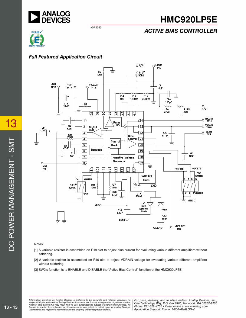
Full Featured Application Circuit
Notes:
[1] A variable resistor is assembled on R19 slot to adjust bias current for evaluating various different amplifiers without soldering.
[2] A variable resistor is assembled on R10 slot to adjust VDRAIN voltage for evaluating various different amplifiers without soldering.
[3] SW2’s function is to ENABLE and DISABLE the “Active Bias Control” function of the HMC920LP5E.
Information furnished by Analog Devices is believed to be accurate and reliable. However, no responsibility is assumed by Analog Devices for its use, nor for any infringements of patents or other rights of third parties that may result from its use. Specifications subject to change without notice. No license is granted by implication or otherwise under any patent or patent rights of Analog Devices. Trademarks and registered trademarks are the property of their respective owners.
For price, delivery, and to place orders: Analog Devices, Inc., One Technology Way, P.O. Box 9106, Norwood, MA 02062-9106 Phone: 781-329-4700 • Order online at www.analog.com Application Support: Phone: 1-800-ANALOG-D

For price, delivery, and to place orders, please contact Hittite Microwave Corporation:20 Alpha Road, Chelmsford, MA 01824 Phone: 978-250-3343 Fax: 978-250-3373
Order On-line at www.hittite.com13 - 14
DC
PO
WE
R M
AN
AG
EM
EN
T -
SM
T
13
HMC920LP5Ev07.1013
ACTIVE BIAS CONTROLLER
Full Featured Evaluation PCB
Careful PCB layout is critical to achieve stable and low noise operation. The negative voltage genera-tor charge pump stage requires particular attention. To isolate the charge pump switching noise from the analog circuit blocks, create two separate ground planes dedicated to AGND and DGND connections. Connect AGND (pin#17) and DGND (pin#16) pins to the paddle at a single point under the package. Con-nect all the components connected to the charge pump (D1, C12 and C14 in the application circuit) to DGND plane, and connect rest of the external compo-nents to a low noise AGND.
List of Materials for Full Featured Evaluation PCB 130511 [1]
Item Description
TP2, TP8 - TP11, TP14, TP15, TP17
DC Test Point
C2 47 pF Capacitor, 0402 Pkg.
C5, C9 10 µF Capacitor, Case B Tantalum
C6, C14 4.7 µF Capacitor, 0805 Pkg.
C12, C21 10 µF Capacitor, 0805 Pkg.
C13 0.33 µF Capacitor, 0603 Pkg.
C19 22 µF Capacitor, Tantalum
C20 0.1 µF Capacitor, 0402 Pkg.
C22 0.1 µF Capacitor, 0805 Pkg.
C24 100 pF Capacitor, 0603 Pkg.
R2, R29 0 Ohm Resistor, 0805 Pkg.
R4 270 Ohm Resistor, 0402 Pkg.
R5, R26 10 kOhm Resistor, 0603 Pkg.
R10 50 kOhm Potentiometer
R14 1 kOhm Resistor, 0603 Pkg.
R15 3.32 kOhm Resistor, 0603 Pkg.
R16 1.69 kOhm Resistor, 0603 Pkg.
R19 5 kOhm Potentiometer
R20, R22 1.8M Ohm Resistor, 0603 Pkg.
R2710 kOhm 0.5% ±25ppm/°C Resistor, 0402 Pkg.
R28 0 Ohm Resistor, 0402 Pkg.
Item Description
D1Dual Schottky Diode (Digi-Key part number: BAT54SLT1GOSCT-ND)
SW1 DIP 4 Position Half-Pitch Switch
SW2 DIP 2 Position Half-Pitch Switch
U1 HMC920LP5E Active Bias Controller
PCB [2] 128399 Evaluation PCB
[1] Reference this number when ordering complete evaluation PCB
[2] Circuit Board Material: FR4
Information furnished by Analog Devices is believed to be accurate and reliable. However, no responsibility is assumed by Analog Devices for its use, nor for any infringements of patents or other rights of third parties that may result from its use. Specifications subject to change without notice. No license is granted by implication or otherwise under any patent or patent rights of Analog Devices. Trademarks and registered trademarks are the property of their respective owners.
For price, delivery, and to place orders: Analog Devices, Inc., One Technology Way, P.O. Box 9106, Norwood, MA 02062-9106 Phone: 781-329-4700 • Order online at www.analog.com Application Support: Phone: 1-800-ANALOG-D
For price, delivery, and to place orders, please contact Hittite Microwave Corporation:20 Alpha Road, Chelmsford, MA 01824 Phone: 978-250-3343 Fax: 978-250-3373
Order On-line at www.hittite.com13 - 15
DC
PO
WE
R M
AN
AG
EM
EN
T -
SM
T
13
HMC920LP5Ev07.1013
ACTIVE BIAS CONTROLLER
Application Notes
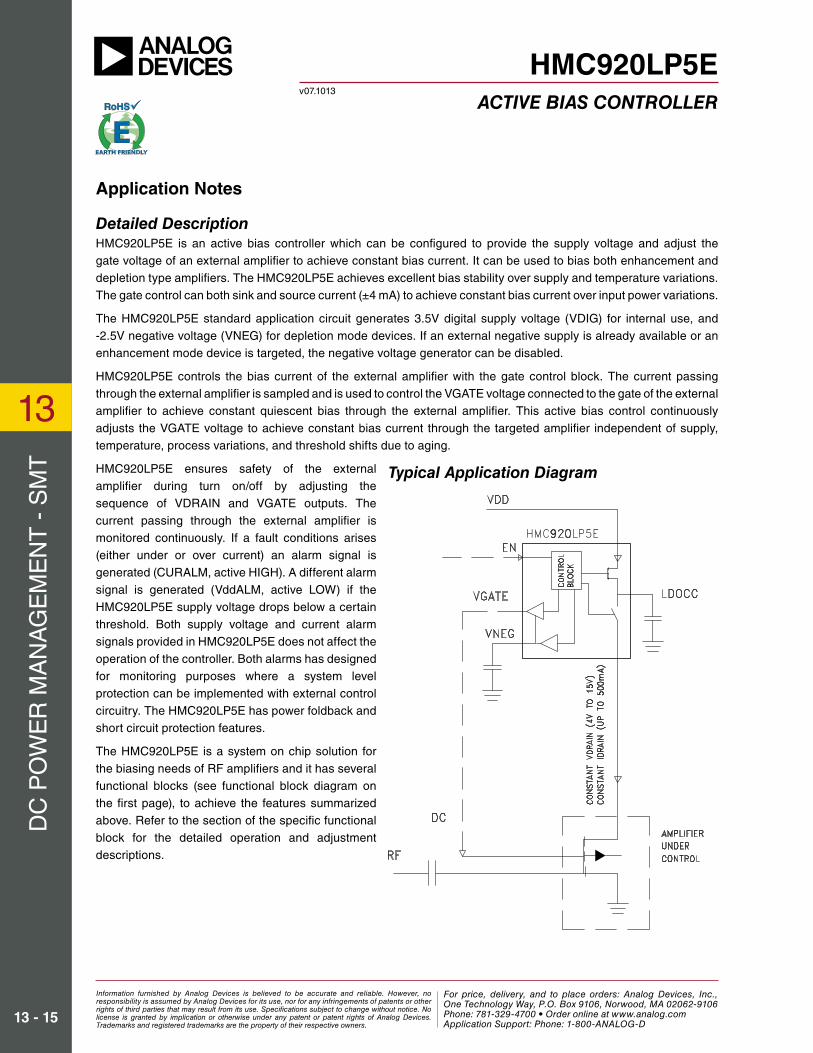
Detailed DescriptionHMC920LP5E is an active bias controller which can be configured to provide the supply voltage and adjust the gate voltage of an external amplifier to achieve constant bias current. It can be used to bias both enhancement and depletion type amplifiers. The HMC920LP5E achieves excellent bias stability over supply and temperature variations. The gate control can both sink and source current (±4 mA) to achieve constant bias current over input power variations.
The HMC920LP5E standard application circuit generates 3.5V digital supply voltage (VDIG) for internal use, and -2.5V negative voltage (VNEG) for depletion mode devices. If an external negative supply is already available or an enhancement mode device is targeted, the negative voltage generator can be disabled.
HMC920LP5E controls the bias current of the external amplifier with the gate control block. The current passing through the external amplifier is sampled and is used to control the VGATE voltage connected to the gate of the external amplifier to achieve constant quiescent bias through the external amplifier. This active bias control continuously adjusts the VGATE voltage to achieve constant bias current through the targeted amplifier independent of supply, temperature, process variations, and threshold shifts due to aging.
HMC920LP5E ensures safety of the external amplifier during turn on/off by adjusting the sequence of VDRAIN and VGATE outputs. The current passing through the external amplifier is monitored continuously. If a fault conditions arises (either under or over current) an alarm signal is generated (CURALM, active HIGH). A different alarm signal is generated (VddALM, active LOW) if the HMC920LP5E supply voltage drops below a certain threshold. Both supply voltage and current alarm signals provided in HMC920LP5E does not affect the operation of the controller. Both alarms has designed for monitoring purposes where a system level protection can be implemented with external control circuitry. The HMC920LP5E has power foldback and short circuit protection features.
The HMC920LP5E is a system on chip solution for the biasing needs of RF amplifiers and it has several functional blocks (see functional block diagram on the first page), to achieve the features summarized above. Refer to the section of the specific functional block for the detailed operation and adjustment descriptions.
Typical Application Diagram
Information furnished by Analog Devices is believed to be accurate and reliable. However, no responsibility is assumed by Analog Devices for its use, nor for any infringements of patents or other rights of third parties that may result from its use. Specifications subject to change without notice. No license is granted by implication or otherwise under any patent or patent rights of Analog Devices. Trademarks and registered trademarks are the property of their respective owners.
For price, delivery, and to place orders: Analog Devices, Inc., One Technology Way, P.O. Box 9106, Norwood, MA 02062-9106 Phone: 781-329-4700 • Order online at www.analog.com Application Support: Phone: 1-800-ANALOG-D

For price, delivery, and to place orders, please contact Hittite Microwave Corporation:20 Alpha Road, Chelmsford, MA 01824 Phone: 978-250-3343 Fax: 978-250-3373
Order On-line at www.hittite.com13 - 16
DC
PO
WE
R M
AN
AG
EM
EN
T -
SM
T
13
HMC920LP5Ev07.1013
ACTIVE BIAS CONTROLLER
Low Voltage Linear Regulator (VDIG)
Place the R1 and R3 resistor as close as possible to the VDIG FB pin.
To ensure stable operation of VDIG, bypass VDIG to AGND with a 10µF tantalum capacitor (with RESR > 200mΩ) under full-load conditions.
The HMC920LP5E requires a low voltage bias rail (3.3V to 5V) for internal circuitry. An internal linear regulator produces a preset 3.5V low-current VDIG output. VDIG powers the internal logic circuitry, oscillator and the control of the negative charge pump. VDIG supplies a maximum of 30mA current and therefore it is recommended for external use only for light loading.
If needed the VDIG output can be adjusted externally through R1 and R3, to a maximum of 5V. To adjust the VDIG value, set R1 to 10kΩ and determine the value of R3 using the equation (1):
If a 3.3V/5V supply is already available externally, internal low-voltage regulator can be disabled to increase the overall system efficiency. To deactivate the internal low-voltage regulator, connect a 0Ohm resistor on R3 (depopulate R1), and connect the external supply to VDIG pin. The typical current consumption from VDIG pin is less than 5mA. The correct power up sequence is GND, VDD, VDIG, VNEG, and signal pins.
Reference (BGCAP)The HMC920LP5E employs two reference voltage generators. The first reference voltage generates 2.5V accurate to ±5% over temperature, supply, and load variations.. This reference voltage generator is used to bias VDIG LDO. A second reference generator generates a stable 2V reference accurate to ±2% over temperature, supply, and load variations. In order to decrease noise, it is recommended to bypass BGCAP to AGND with a 0.1μF or greater ceramic capacitor, as close as possible to the BGCAP pin as possible.
R3 = x (VDIG - 2.5) (1)R12.5
Figure 1. Low Voltage Linear Regulator (VDIG) Block Diagram
Information furnished by Analog Devices is believed to be accurate and reliable. However, no responsibility is assumed by Analog Devices for its use, nor for any infringements of patents or other rights of third parties that may result from its use. Specifications subject to change without notice. No license is granted by implication or otherwise under any patent or patent rights of Analog Devices. Trademarks and registered trademarks are the property of their respective owners.
For price, delivery, and to place orders: Analog Devices, Inc., One Technology Way, P.O. Box 9106, Norwood, MA 02062-9106 Phone: 781-329-4700 • Order online at www.analog.com Application Support: Phone: 1-800-ANALOG-D

For price, delivery, and to place orders, please contact Hittite Microwave Corporation:20 Alpha Road, Chelmsford, MA 01824 Phone: 978-250-3343 Fax: 978-250-3373
Order On-line at www.hittite.com13 - 17
DC
PO
WE
R M
AN
AG
EM
EN
T -
SM
T
13
HMC920LP5Ev07.1013
ACTIVE BIAS CONTROLLER
Negative Voltage Generator (VNEGOUT)The HMC920LP5E has an internal regulated charge pump block to generate negative voltage (VNEGOUT) required for depletion mode devices. The HMC920LP5E generates -2.5V at the VNEGOUT output in default configuration. Contact factory if a voltage rail different than -2.5V is required.
The HMC920LP5E is designed to reject the ripple on the VNEGOUT by isolating VNEGOUT from the VGATE.
The negative voltage is required only for depletion mode devices, and it can be disabled through the VGATEFB and VNEGFB pins. See Table-1 how to set the operation mode.
Enable/Disable (EN)The active bias control loop is enabled when EN is pulled up to VDIG, and it is disabled when it is pulled down to GND. If EN is left floating HMC920LP5E is enabled through the internal weak pull-up. Note that LDOCC, VDIG and VNEG operation is independent of EN condition. EN signal controls the operation of only VGATE and VDRAIN outputs. When EN pulled down to GND, HMC920LP5E discharges VDRAIN down to GND and it pulls the VGATE down to VNEG. Please see the “Active Bias Control Loop” section for detailed explanation.
Where VDRAIN is the supply voltage of the external amplifier and IDRAIN is the desired constant bias current through the external amplifier.
To ensure stable operation of the LDOCC output, bypass LDOCC to AGND with a 10µF tantalum capacitor (with RESR > 200mΩ).
The HMC920LP5E has power foldback and short circuit protection, refer to the respective section for detailed description of these features.
VLDOCC = VDRAIN + IDRAIN x 0.5 (3)
Place the R8 and R5 as close as possible to the LDOFB.
High Voltage Linear Regulator (LDOCC/VDRAIN)The HMC920LP5E has an adjustable high-voltage, high-current linear regulator (LDOCC) to provide the drain supply rail of the external RF amplifier. The LDOCC output can source up to 500mA loads. The LDOCC output can be adjusted to regulate any voltage level from 3V to 15V through external resistors R8 and R5.
To adjust the LDOCC, set R5 to 10kΩ and determine the value of R8 using the equation (2):
R8 = x (VDOCC - 2) (2)R52
The LDOCC output is connected to the VDRAIN output through an internal MOSFET (RDS-ON = 0.5Ω) switch.
This internal MOSFET is controlled through power-up sequencing which ensures that no voltage is applied to drain of the external amplifier until the gate voltage is pulled down to VNEG(ensuring external amplifier disabled). Connect the external amplifier to the VDRAIN output to use power-up sequencing feature.
Note that there will be a voltage drop from LDOCC to VDRAIN due to finite RDS_ON resistance of the internal switch. To compensate for this voltage drop choose the LDOCC value as shown in equation (3).
Information furnished by Analog Devices is believed to be accurate and reliable. However, no responsibility is assumed by Analog Devices for its use, nor for any infringements of patents or other rights of third parties that may result from its use. Specifications subject to change without notice. No license is granted by implication or otherwise under any patent or patent rights of Analog Devices. Trademarks and registered trademarks are the property of their respective owners.
For price, delivery, and to place orders: Analog Devices, Inc., One Technology Way, P.O. Box 9106, Norwood, MA 02062-9106 Phone: 781-329-4700 • Order online at www.analog.com Application Support: Phone: 1-800-ANALOG-D

For price, delivery, and to place orders, please contact Hittite Microwave Corporation:20 Alpha Road, Chelmsford, MA 01824 Phone: 978-250-3343 Fax: 978-250-3373
Order On-line at www.hittite.com13 - 18
DC
PO
WE
R M
AN
AG
EM
EN
T -
SM
T
13
HMC920LP5Ev07.1013
ACTIVE BIAS CONTROLLER
Active Bias Control LoopThe HMC920LP5E regulates the bias current (IDRAIN) of the external amplifier through VGATE output connected to the gate of the external amplifier. In this closed loop operation the current passing through the external amplifier is sampled and is used to adjust VGATE to achieve constant quiescent bias through the external amplifier.
The HMC920LP5E continuously compensates for any supply, temperature, process variations and threshold drifts due to aging, without any calibration.
The gate control of the HMC920LP5E can both sink and source current (at least ±4 mA) to achieve constant bias current over input power variations.
The bias current passing through the external amplifier can be adjusted with RSENSE, where RSENSE is the total resistor (R4 + R19) connected from ISENSE to GND. Use the relation given in equation (4) to set the desired bias current through the external amplifier.
Power FoldbackThe HMC920LP5E employs a power foldback protection feature to limit the power consumption on the HMC920LP5E package under excessive loading such as a short circuit from VDRAIN to GND.
HMC920LP5E senses the instantaneous power consumption over the VDRAIN LDO (PSENSE = (Vdd-VDRAIN) x IDRAIN), and limits the instantaneous power consumption less than 4.5W. This is achieved by decreasing VDRAIN voltage and IDRAIN current simultaneously.
The advantage of the power foldback protection feature over a hard current limit is safe operation with higher user flexibility.
The following plots present the power foldback characteristic over Vdd.
RSENSE adjustment is referenced to the total resistance seen from ALMM (PIN#27) to GND. Connect 5 kΩ resistor from ALMM to GND (R16 + R15) to ensure equation (4) holds.
IDRAIN = A (4) 165 RSENSE
Power Foldback VDRAIN vs. IDRAIN over Vdd
Power Foldback Delivered Power vs. IDRAIN Over Vdd
0
1
2
3
4
0 100 200 300 400 500 600 700 800
Vdd = 6VVdd = 9VVdd = 12VVdd = 15V
IDRAIN (mA)
VD
RA
IN (
V)
0
0.5
1
1.5
2
2.5
0 100 200 300 400 500 600 700 800
Vdd = 6VVdd = 9VVdd = 12VVdd = 15V
IDRAIN (mA)
PO
WE
R D
ELI
VE
RE
D F
RO
M V
DR
AIN
(W
)
Information furnished by Analog Devices is believed to be accurate and reliable. However, no responsibility is assumed by Analog Devices for its use, nor for any infringements of patents or other rights of third parties that may result from its use. Specifications subject to change without notice. No license is granted by implication or otherwise under any patent or patent rights of Analog Devices. Trademarks and registered trademarks are the property of their respective owners.
For price, delivery, and to place orders: Analog Devices, Inc., One Technology Way, P.O. Box 9106, Norwood, MA 02062-9106 Phone: 781-329-4700 • Order online at www.analog.com Application Support: Phone: 1-800-ANALOG-D

For price, delivery, and to place orders, please contact Hittite Microwave Corporation:20 Alpha Road, Chelmsford, MA 01824 Phone: 978-250-3343 Fax: 978-250-3373
Order On-line at www.hittite.com13 - 19
DC
PO
WE
R M
AN
AG
EM
EN
T -
SM
T
13
HMC920LP5Ev07.1013
ACTIVE BIAS CONTROLLER
Over/Under Current AlarmThe HMC920LP5E provides over and under current alarm indicator CURALM (pin#8) signal. The CURALM is pulled up to VDIG when the IDRAIN current exceeds ± 25% of IDRAIN regulation target value.
The condition of CURALM signal does not effect the operation of HMC920LP5E, it is provided only for monitoring purposes.
The CURALM signal is activated if the low and high current duration is longer than a certain threshold. This duration can be adjusted through the external resistor R26 with equation 5. Figure-2 presents a behavioral sketch how the CURALM indicator signal acts under various IDRAIN conditions.
Twait = R26x5.1x10-4+3
where Twait is in micro seconds. Changing R26 from 10 kOhms to 10 Megohms, Twait can be adjusted from 8.1 usec to 51 msec.
Power Dissipated on HMC920LP5E vs. IDRAIN Over Vdd
Short Circuit ProtectionThe pass transistor in every LDO is in series with the load, and a large amount of current will flow through the regulator during a short condition when no precaution circuitry is included in the system. The HMC920LP5E limits the current through the pass transistor to less than 900 mA, and this current limit acts as the secondary short circuit protection to the power foldback feature. During a VDRAIN-GND short circuit HMC920LP5E also pulls down the VGATE to the lowest voltage supply VNEG, and disables the external amplifier completely for safety.
HMC920LP5E continuously checks the following pins for short conditions and disables the system when a short to ground is detected.
-LDOCC-VDRAIN-VNEGIN (in depletion mode)-FIXBIAS
0
1
2
3
4
5
0 100 200 300 400 500 600 700 800
Vdd = 6VVdd = 9VVdd = 12VVdd = 15V
IDRAIN (mA)
PO
WE
R D
ISS
IPA
TE
D (
W)
Information furnished by Analog Devices is believed to be accurate and reliable. However, no responsibility is assumed by Analog Devices for its use, nor for any infringements of patents or other rights of third parties that may result from its use. Specifications subject to change without notice. No license is granted by implication or otherwise under any patent or patent rights of Analog Devices. Trademarks and registered trademarks are the property of their respective owners.
For price, delivery, and to place orders: Analog Devices, Inc., One Technology Way, P.O. Box 9106, Norwood, MA 02062-9106 Phone: 781-329-4700 • Order online at www.analog.com Application Support: Phone: 1-800-ANALOG-D

For price, delivery, and to place orders, please contact Hittite Microwave Corporation:20 Alpha Road, Chelmsford, MA 01824 Phone: 978-250-3343 Fax: 978-250-3373
Order On-line at www.hittite.com13 - 20
DC
PO
WE
R M
AN
AG
EM
EN
T -
SM
T
13
HMC920LP5Ev07.1013
ACTIVE BIAS CONTROLLER
Vdd Under-Voltage AlarmThe HMC920LP5E provides a low Vdd indicator signal (VddALM pin#31) when the Vdd supply voltage is lower than an user adjustable threshold value. VddALM pin pulled down to GND when the Vdd voltage is lower than the adjusted VddTHR value. To adjust the Vdd under-voltage alarm threshold set R6 (the resistance from VddCHK to AGND) according to the relation provided in (6).
Power-up and Enable SequencingTo ensure the safety of the external amplifier the HMC920LP5E provides a certain power-up sequence for enabling active bias control loop. During start-up VDRAIN is kept at GND while VGATE is taken to the most negative supply available (VGATE=VNEG). This ensures that external amplifier is completely turned-off before VDRAIN is applied. When EN signal is received VDRAIN is applied and the active bias loop is enabled. The final phase of the power-up sequence is completed by increasing the VGATE linearly until the set IDRAIN value is achieved.
For power-down and disabling the same sequencing is applied in the reverse order.
(6)
Figure 2. Current Alarm Behavior
Daisy-Chain OperationHMC920LP5E produces a trigger out signal (TRGOUT pin#24) when the external amplifier achieves a stable bias current (IDRAIN). This trigger signal can be used to enable additional HMC920LP5E chips in a chain of amplifiers. The triggering sequence can be routed in anyway, from input to output, or from output to input depending on the use. Figure-3 presents a sample use of three HMC920LP5Es in an amplifier chain. Please note that, only one of the HMC920LP5E is used to generate the negative voltage and the remaining HMC920LP5E is set to receive external negative voltages (which is provided from the master HMC920LP5E). Generating negative voltage only with single HMC920LP5E reduces the number of the components in the system, and decreases the over all current consumption slightly, compared to each bias controller generating its own negative voltage.
To ensure proper start-up, the system enable signal should ne applied to the chip that has the negative voltage generator.
1388.0
3
1506VddTHR
kR
Information furnished by Analog Devices is believed to be accurate and reliable. However, no responsibility is assumed by Analog Devices for its use, nor for any infringements of patents or other rights of third parties that may result from its use. Specifications subject to change without notice. No license is granted by implication or otherwise under any patent or patent rights of Analog Devices. Trademarks and registered trademarks are the property of their respective owners.
For price, delivery, and to place orders: Analog Devices, Inc., One Technology Way, P.O. Box 9106, Norwood, MA 02062-9106 Phone: 781-329-4700 • Order online at www.analog.com Application Support: Phone: 1-800-ANALOG-D
For price, delivery, and to place orders, please contact Hittite Microwave Corporation:20 Alpha Road, Chelmsford, MA 01824 Phone: 978-250-3343 Fax: 978-250-3373
Order On-line at www.hittite.com13 - 21
DC
PO
WE
R M
AN
AG
EM
EN
T -
SM
T
13
HMC920LP5Ev07.1013
ACTIVE BIAS CONTROLLER
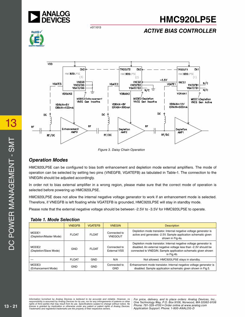
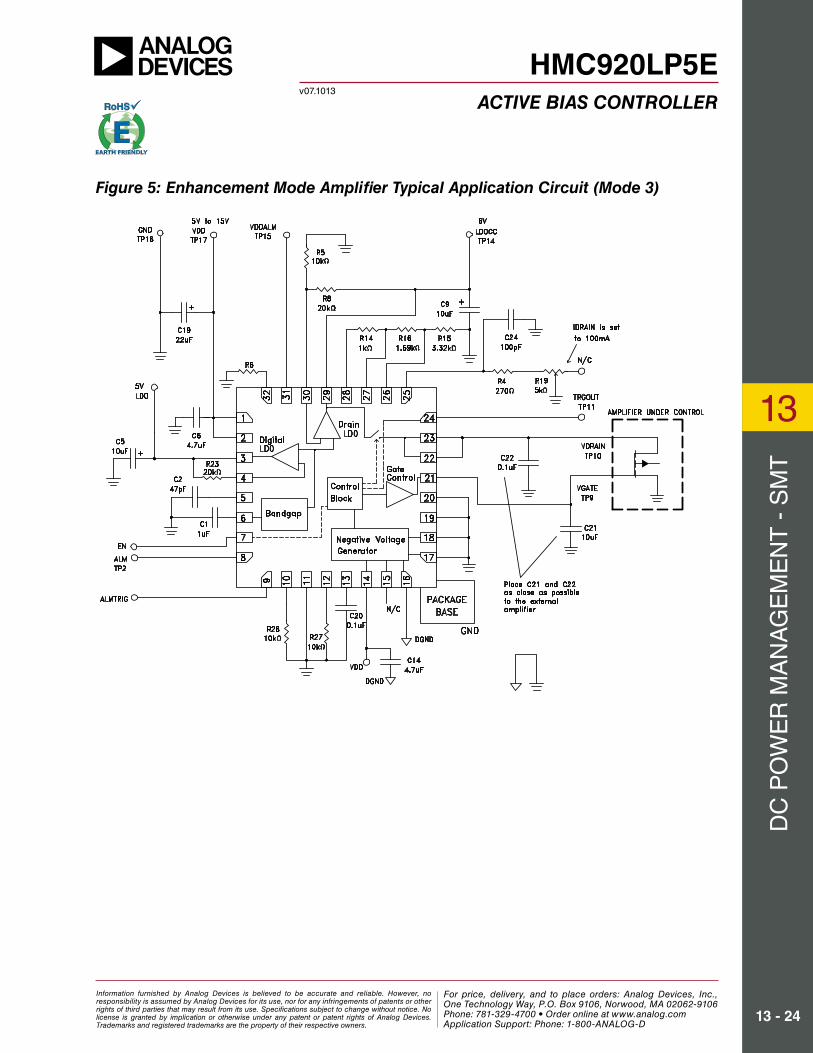
Operation ModesHMC920LP5E can be configured to bias both enhancement and depletion mode external amplifiers. The mode of operation can be selected by setting two pins (VNEGFB, VGATEFB) as tabulated in Table-1. The connection to the VNEGIN should be adjusted accordingly.
In order not to bias external amplifier in a wrong region, please make sure that the correct mode of operation is selected before powering up HMC920LP5E.
HMC920LP5E does not allow the internal negative voltage generator to work if an enhancement mode is selected. Therefore, if VNEGFB is left floating while VGATEFB is grounded, HMC920LP5E will stay in standby mode.
Please note that the external negative voltage should be between -2.5V to -3.5V for HMC920LP5E to operate.
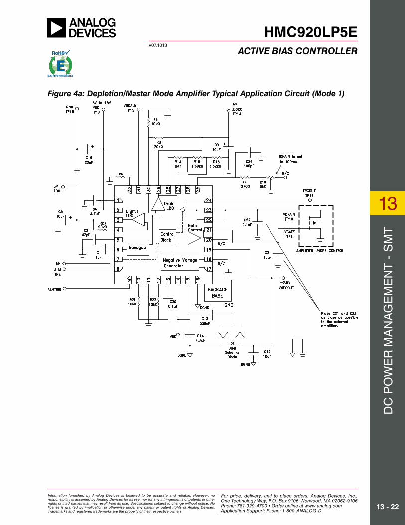
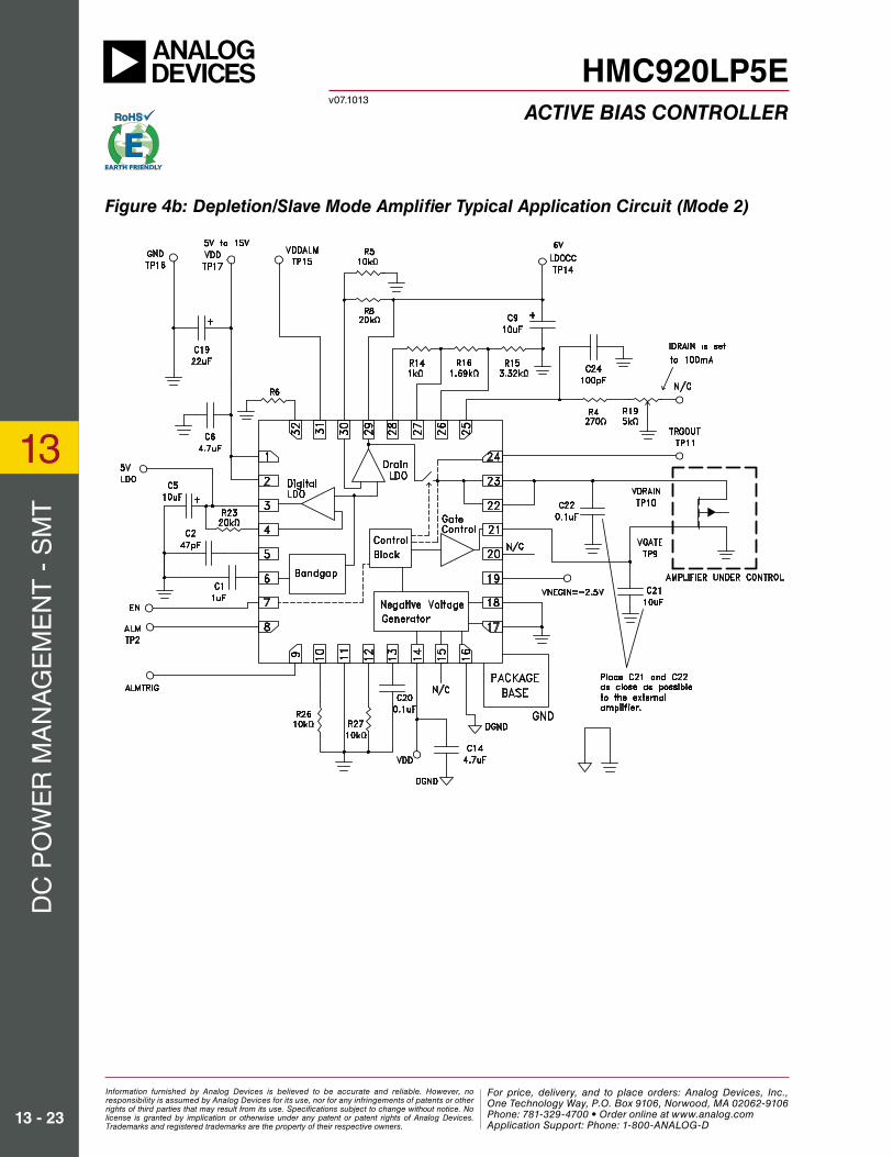
Table 1. Mode SelectionVNEGFB VGATEFB VNEGIN Description
MODE1(Depletion/Master Mode)
FLOAT FLOATConnected to VNEGOUT
Depletion mode transistor. Internal negative voltage generator is active and generates -2.5V. Sample application schematic given
shown in Fig.4a.
MODE2(Depletion/Slave Mode)
GND FLOATConnected to External VSS
Depletion mode transistor. Internal negative voltage generator is disabled. An external negative voltage less than -2.3V should be
connected to VNEGIN. Sample application schematic given shown in Fig.4b.
--- FLOAT GND N/A Not allowed. HMC920LP5E stays in standby.
MODE3(Enhancement Mode)
GND GNDConnected to
GNDEnhancement mode transistor. Internal negative voltage generator is
disabled. Sample application schematic given shown in Fig.5.
Figure 3. Daisy Chain Operation
Information furnished by Analog Devices is believed to be accurate and reliable. However, no responsibility is assumed by Analog Devices for its use, nor for any infringements of patents or other rights of third parties that may result from its use. Specifications subject to change without notice. No license is granted by implication or otherwise under any patent or patent rights of Analog Devices. Trademarks and registered trademarks are the property of their respective owners.
For price, delivery, and to place orders: Analog Devices, Inc., One Technology Way, P.O. Box 9106, Norwood, MA 02062-9106 Phone: 781-329-4700 • Order online at www.analog.com Application Support: Phone: 1-800-ANALOG-D
For price, delivery, and to place orders, please contact Hittite Microwave Corporation:20 Alpha Road, Chelmsford, MA 01824 Phone: 978-250-3343 Fax: 978-250-3373
Order On-line at www.hittite.com13 - 22
DC
PO
WE
R M
AN
AG
EM
EN
T -
SM
T
13
HMC920LP5Ev07.1013
ACTIVE BIAS CONTROLLER
Figure 4a: Depletion/Master Mode Amplifier Typical Application Circuit (Mode 1)
Information furnished by Analog Devices is believed to be accurate and reliable. However, no responsibility is assumed by Analog Devices for its use, nor for any infringements of patents or other rights of third parties that may result from its use. Specifications subject to change without notice. No license is granted by implication or otherwise under any patent or patent rights of Analog Devices. Trademarks and registered trademarks are the property of their respective owners.
For price, delivery, and to place orders: Analog Devices, Inc., One Technology Way, P.O. Box 9106, Norwood, MA 02062-9106 Phone: 781-329-4700 • Order online at www.analog.com Application Support: Phone: 1-800-ANALOG-D
For price, delivery, and to place orders, please contact Hittite Microwave Corporation:20 Alpha Road, Chelmsford, MA 01824 Phone: 978-250-3343 Fax: 978-250-3373
Order On-line at www.hittite.com13 - 23
DC
PO
WE
R M
AN
AG
EM
EN
T -
SM
T
13
HMC920LP5Ev07.1013
ACTIVE BIAS CONTROLLER
Figure 4b: Depletion/Slave Mode Amplifier Typical Application Circuit (Mode 2)
Information furnished by Analog Devices is believed to be accurate and reliable. However, no responsibility is assumed by Analog Devices for its use, nor for any infringements of patents or other rights of third parties that may result from its use. Specifications subject to change without notice. No license is granted by implication or otherwise under any patent or patent rights of Analog Devices. Trademarks and registered trademarks are the property of their respective owners.
For price, delivery, and to place orders: Analog Devices, Inc., One Technology Way, P.O. Box 9106, Norwood, MA 02062-9106 Phone: 781-329-4700 • Order online at www.analog.com Application Support: Phone: 1-800-ANALOG-D
For price, delivery, and to place orders, please contact Hittite Microwave Corporation:20 Alpha Road, Chelmsford, MA 01824 Phone: 978-250-3343 Fax: 978-250-3373
Order On-line at www.hittite.com13 - 24
DC
PO
WE
R M
AN
AG
EM
EN
T -
SM
T
13
HMC920LP5Ev07.1013
ACTIVE BIAS CONTROLLER
Figure 5: Enhancement Mode Amplifier Typical Application Circuit (Mode 3)
Information furnished by Analog Devices is believed to be accurate and reliable. However, no responsibility is assumed by Analog Devices for its use, nor for any infringements of patents or other rights of third parties that may result from its use. Specifications subject to change without notice. No license is granted by implication or otherwise under any patent or patent rights of Analog Devices. Trademarks and registered trademarks are the property of their respective owners.
For price, delivery, and to place orders: Analog Devices, Inc., One Technology Way, P.O. Box 9106, Norwood, MA 02062-9106 Phone: 781-329-4700 • Order online at www.analog.com Application Support: Phone: 1-800-ANALOG-D

For price, delivery, and to place orders, please contact Hittite Microwave Corporation:20 Alpha Road, Chelmsford, MA 01824 Phone: 978-250-3343 Fax: 978-250-3373
Order On-line at www.hittite.com13 - 25
DC
PO
WE
R M
AN
AG
EM
EN
T -
SM
T
13
HMC920LP5Ev07.1013
ACTIVE BIAS CONTROLLER
Table 2 - List of Bias Settings for Various Hittite AmplifiersHittite Part Number VDRAIN (V) IDRAIN (mA) LDOCC (V) RSENSE (kΩ) R8 (kΩ)
LNAs
HMC609LC4 6 170 6.09 1.0 20.4
HMC594LC3B 6 100 6.05 1.7 20.3
HMC753LP4 5 55 5.03 3.0 15.1
HMC490LP5 5 200 5.10 0.8 15.5
HMC504LC4B 4 90 4.05 1.8 10.2
HMC-ALH140 4 60 4.03 2.8 10.2
HMC-ALH244 4 45 4.02 3.7 10.1
HMC772LC4 4 45 4.02 3.7 10.1
HMC752LC4 3 70 3.04 2.4 5.2
Gain Blocks & Drivers
HMC635LC4 5 280 5.14 0.6 15.7
HMC-AUH256 5 295 5.15 0.6 15.7
Linear & Power
HMC757 7 395 7.20 0.4 26.0
HMC441LM1 5 90 5.05 1.8 15.2
HMC442LM1 / HMC442LC3B
5 85 5.04 1.9 15.2
HMC-ABH209 5 80 5.04 2.1 15.2
HMC-APH403 5 475 5.24 0.3 16.2
HMC-APH596 5 400 5.20 0.4 16.0
HMC608LC4 5 310 5.16 0.5 15.8
HMC498LC4 5 250 5.13 0.7 15.6
HMC-ABH241 5 220 5.11 0.8 15.6
HMC499LC4 5 200 5.10 0.8 15.5
HMC-APH196 4.5 400 4.70 0.4 13.5
HMC-APH633 4 240 4.12 0.7 10.6
HMC-AUH317 4 160 4.08 1.0 10.4
HMC-AUH318 4 160 4.08 1.0 10.4
HMC-AUH320 4 130 4.07 1.3 10.3
HMC863 6 375 6.19 0.4 20.9
Wideband (Distributed)
HMC637LP5 12 400 12.20 0.4 51.0
HMC619LP5 12 300 12.15 0.55 50.8
HMC559 10 400 10.20 0.4 41.0
HMC562 8 80 8.04 2.1 30.2
HMC460LC5 8 75 8.04 2.2 30.2
HMC659LC5 8 300 8.15 0.6 30.8
HMC464LP5 8 290 8.15 0.6 30.7
HMC459 8 290 8.15 0.6 30.7
HMC465LP5 8 160 8.08 1.0 30.4
HMC462LP5 5 66 5.03 2.5 15.2
Information furnished by Analog Devices is believed to be accurate and reliable. However, no responsibility is assumed by Analog Devices for its use, nor for any infringements of patents or other rights of third parties that may result from its use. Specifications subject to change without notice. No license is granted by implication or otherwise under any patent or patent rights of Analog Devices. Trademarks and registered trademarks are the property of their respective owners.
For price, delivery, and to place orders: Analog Devices, Inc., One Technology Way, P.O. Box 9106, Norwood, MA 02062-9106 Phone: 781-329-4700 • Order online at www.analog.com Application Support: Phone: 1-800-ANALOG-D
For price, delivery, and to place orders, please contact Hittite Microwave Corporation:20 Alpha Road, Chelmsford, MA 01824 Phone: 978-250-3343 Fax: 978-250-3373
Order On-line at www.hittite.com13 - 26
DC
PO
WE
R M
AN
AG
EM
EN
T -
SM
T
13
HMC920LP5Ev07.1013
ACTIVE BIAS CONTROLLER
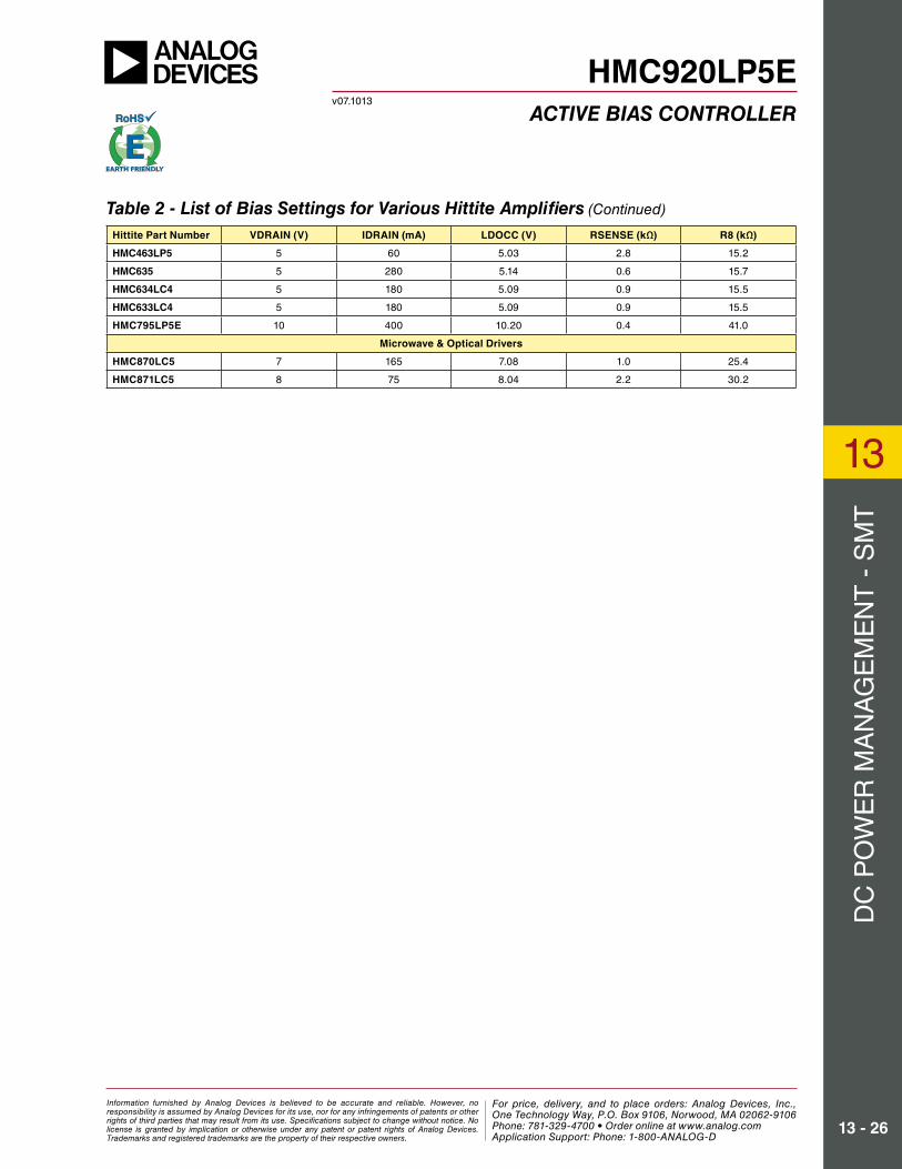
Table 2 - List of Bias Settings for Various Hittite Amplifiers (Continued)
Hittite Part Number VDRAIN (V) IDRAIN (mA) LDOCC (V) RSENSE (kΩ) R8 (kΩ)
HMC463LP5 5 60 5.03 2.8 15.2
HMC635 5 280 5.14 0.6 15.7
HMC634LC4 5 180 5.09 0.9 15.5
HMC633LC4 5 180 5.09 0.9 15.5
HMC795LP5E 10 400 10.20 0.4 41.0
Microwave & Optical Drivers
HMC870LC5 7 165 7.08 1.0 25.4
HMC871LC5 8 75 8.04 2.2 30.2
Information furnished by Analog Devices is believed to be accurate and reliable. However, no responsibility is assumed by Analog Devices for its use, nor for any infringements of patents or other rights of third parties that may result from its use. Specifications subject to change without notice. No license is granted by implication or otherwise under any patent or patent rights of Analog Devices. Trademarks and registered trademarks are the property of their respective owners.
For price, delivery, and to place orders: Analog Devices, Inc., One Technology Way, P.O. Box 9106, Norwood, MA 02062-9106 Phone: 781-329-4700 • Order online at www.analog.com Application Support: Phone: 1-800-ANALOG-D


