Tuning Parameters for Accurate MOSFET … Parameters for Accurate MOSFET Simulation For LDD &...
32
Tuning Parameters for Accurate MOSFET Simulation
Transcript of Tuning Parameters for Accurate MOSFET … Parameters for Accurate MOSFET Simulation For LDD &...

Tuning Parameters for Accurate
MOSFET Simulation

Tuning Parameters for Accurate MOSFET Simulation
Basic Simulation Guidelines
For accurate simulation of MOSFETs, 90% of the effort should be invested in achieving an accurate PROCESS simulation while only 10% of the time should be spent fine tuning Device simulation
Device physics better characterized than new process physics (90%/10% rule)
Device physics doesn’t change but new processes continue to evolve
- 2 -
Tuning Parameters for Accurate MOSFET Simulation
Basic Guidelines (con’t)
If the device simulation is way off from the measured data, most probably you’ve done something wrong in the PROCESS simulation
Exception: Inappropriate gridding
Golden Rule: DO NOT CHANGE WELL KNOWN COEFFICIENTS!
eg. DIX.0, DIP.0 & DIM.0
- 3 -

Tuning Parameters for Accurate MOSFET Simulation
What Measured Data are Needed to Correctly
Calibrate the Models?
Two types of required measured data:- Essential data for Process Modeling
Verification data (I-V curves etc)
(this is data NOT used in process models to check the predictive nature of the simulation)
- 4 -
Tuning Parameters for Accurate MOSFET Simulation
Process Modeling Data
THE PROCESS FLOW !
Vt versus Gate Length (Minimum Geometry up to 20 m Gate length)
Accurate gate oxide thickness (Care! quantum C-V effects and/or poly depletion)
Accurate spacer width/profile (preferably SEM micrographs)
SIMS profiles
- 5 -
Tuning Parameters for Accurate MOSFET Simulation
Why do I need Data for 20 m Gate Lengths ?
Interstitials greatly enhance diffusion with a resultant strong influence on Vt
Interstitials generated by implantation, oxidation and silicidation typically travel 10 m along the surface and up to 20 m deep
(surface defect recombination >> bulk defect recombination)
The diffusion length of interstitials is much longer than 1 m (see page 7). Therefore, if simulated substrate depth is less than the diffusion length then the simulated intersential concentration will be artifically high. This will result on “excessive” boron diffusion (see page 8)
- 6 -

Tuning Parameters for Accurate MOSFET Simulation
Interstitial Diffusion
- 7 -
The diffusion of interstitial damage during post implantation anneals.
Tuning Parameters for Accurate MOSFET Simulation
Effect of Substrate Depth
- 8 -
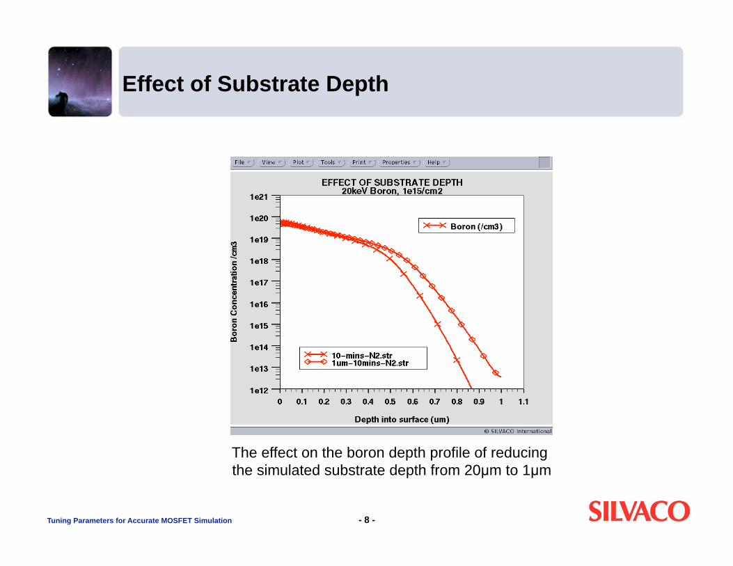
The effect on the boron depth profile of reducing the simulated substrate depth from 20 m to 1 m

Tuning Parameters for Accurate MOSFET Simulation
Effect of Damage Factor on Threshold Voltage
- 9 -
Graph of Vt versus gate length for (i) No interstitial injection (ii) Realistic model (showing asymptotic behavior at 20 m)
Tuning Parameters for Accurate MOSFET Simulation
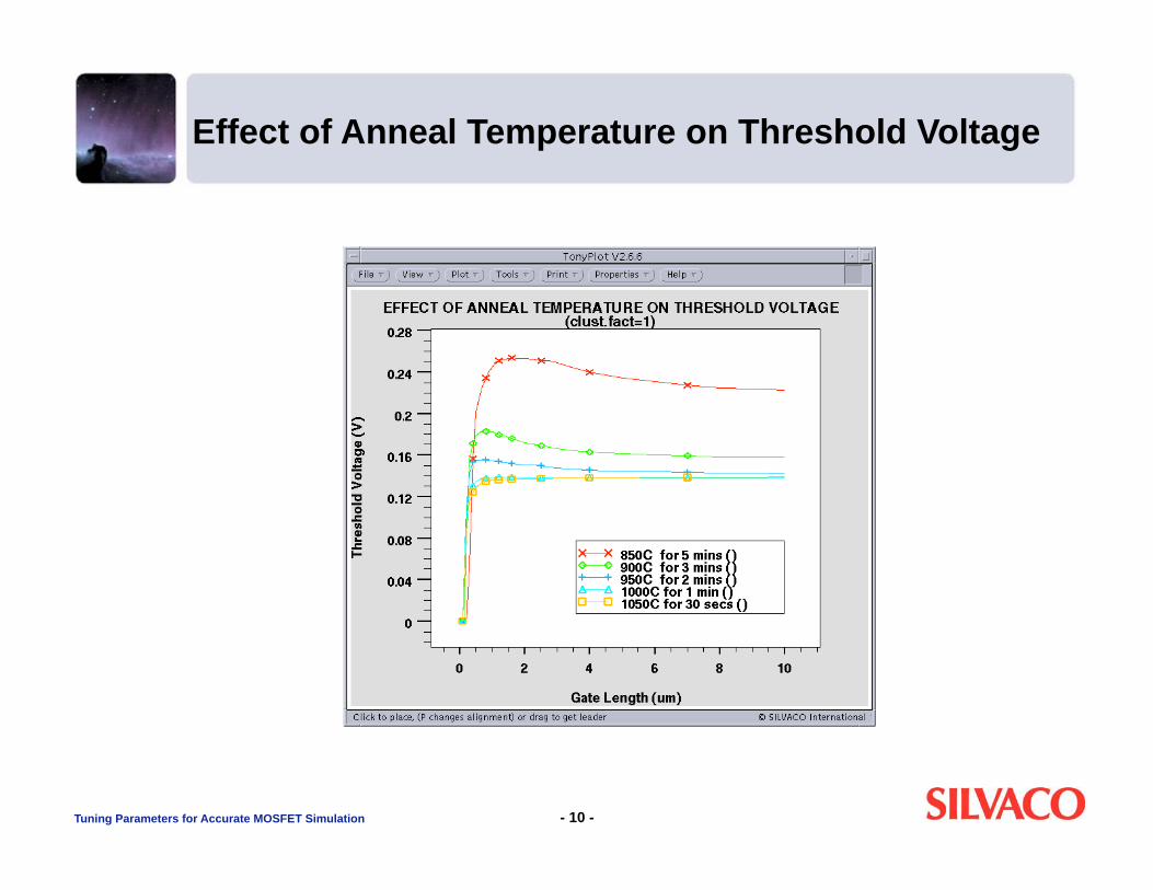
Effect of Anneal Temperature on Threshold Voltage
- 10 -

Tuning Parameters for Accurate MOSFET Simulation
The Importance of Correctly Modeling Interstitials
Interstitial enhanced diffusion important for channel implant during Gate Oxidation(Vt is very sensitive to this diffusion)
Empirical evidence indicates: for a given oxide thickness the total number of interstitials injected is greater for wet compared to dry therefore greater total diffusion possible
- 11 -
Tuning Parameters for Accurate MOSFET Simulation
Oxidation & Diffusion Models
FERMI model - basic[1]
TWO.DIM model - intermediate[2]
FULL.CPL model- advanced[3]
[1] - constant interstitial concentration, OK for non implanted material
[2] - OK for implants < 1x10¹³ /cm2
[3] - required for implants > 1x10¹³ /cm3
- 12 -
Tuning Parameters for Accurate MOSFET Simulation
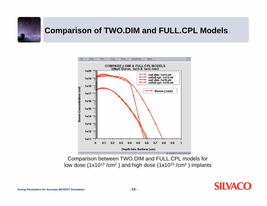
Comparison of TWO.DIM and FULL.CPL Models
- 13 -
Comparison between TWO.DIM and FULL.CPL models for low dose (1x10¹³ /cm2 ) and high dose (1x10¹⁵ /cm2 ) implants
Tuning Parameters for Accurate MOSFET Simulation
Tuning Diffusion During Gate Oxidation
Use MEASURED long channel (20 m) Vt Tune THETA.0 at center channel in 1D
THETA.0 controls intersitials injection at oxide/silicon boundary during oxidation. It is specified in the INTERSTITIAL statement
Fine tune THETA.0 using 2D
- 14 -
Tuning Parameters for Accurate MOSFET Simulation
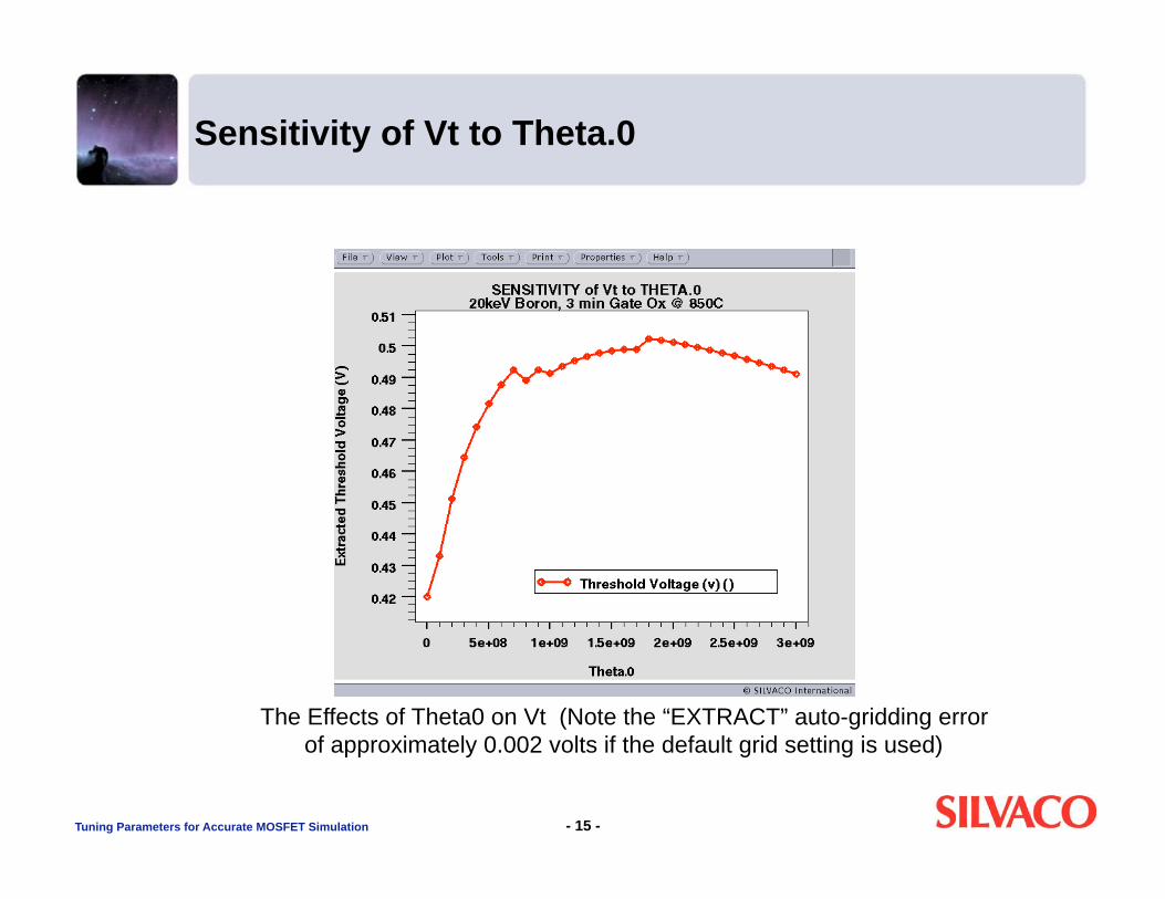
Sensitivity of Vt to Theta.0
- 15 -
The Effects of Theta0 on Vt (Note the “EXTRACT” auto-gridding error of approximately 0.002 volts if the default grid setting is used)
Tuning Parameters for Accurate MOSFET Simulation
For High Dose LDD & Source/Drain Implants
<311> CLUSTER DAMAGE model MUST be used
Tune CLUST.FACT to obtain the correct peak in the RSCE (Vt versus gate length plot)
The CLUSTER.DAM model effectively causes a time release of interstitials.
Tune spacer width to determine the rate of Vt falloff for very short gate lengths (SCE)
BCA implant model is preferable for all sensitive implant steps
- 16 -
Tuning Parameters for Accurate MOSFET Simulation
For LDD & Source/Drain RTA Activation
The CLUSTER.DAM FULL.CPL models MUST be used initially or for at least twice the 95% decay time (see following table)
Tune KSURF.0 to obtain the correct long channel fall off in Vt versus gate length
The FULL.CPL model also takes account of dopant-defect pair formation
- 17 -
Tuning Parameters for Accurate MOSFET Simulation
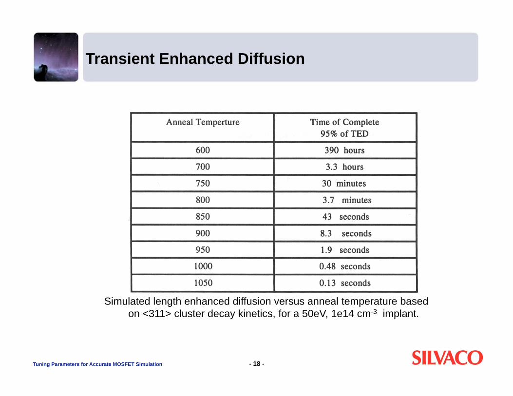
Transient Enhanced Diffusion
Simulated length enhanced diffusion versus anneal temperature based on <311> cluster decay kinetics, for a 50eV, 1e14 cm-3 implant.
- 18 -
Tuning Parameters for Accurate MOSFET Simulation
p-Channel RSCE
For buried p-channel devices, high angle implants usually cause RSCE
Boron source/drain regions absorb interstitials rather than inject them so do NOT use the “cluster.dam” model for high dose boron implants. Unset the “cluster.dam” model using “cluster.dam=f” if it has been set previously in the input file
- 19 -
Tuning Parameters for Accurate MOSFET Simulation
Device Simulation (Verification)
Remember: If the process modeling was accurate...the electrical characteristics should be too.
If not, you have done something wrong with the PROCESS or the GRID.
- 20 -
Tuning Parameters for Accurate MOSFET Simulation
The Grid! (or Mesh)
A suitable grid for process simulation may not be suitable for device simulation
In general, minimize the number of mesh points Solution time »k*(mesh points)2-3
BUT... too few mesh points can take LONGER since each solution takes longer to converge. You cannot beat experience here
10Å mesh in inversion regions. Concentrate mesh at metalurgic junctions
- 21 -

Tuning Parameters for Accurate MOSFET Simulation
Device Modeling Data
C-V data
Contact resistance measurements
Id-Vd | Vg curves
Id-Vg | Vb curves
Id-Vd for Vg=0 (breakdown characteristic)
- 22 -

Tuning Parameters for Accurate MOSFET Simulation
Gate Structures
Look for C-V accumulation anomalies If anomalous, poly dopant has been consumed by silicide giving non ideal workfunction
Use a separate metal contact for simulation or adjust poly workfunctions
Typical values:- 4.17 for in situ N++ poly doping
4.3 to 4.4 for implanted P+ compensated
- 23 -

Tuning Parameters for Accurate MOSFET Simulation
Poly-Doping Effects on C-V Curves
- 24 -
The Effects of Poly-Doping on the Accumulation Region of a Standard High Frequency C-V Plot.
Tuning Parameters for Accurate MOSFET Simulation
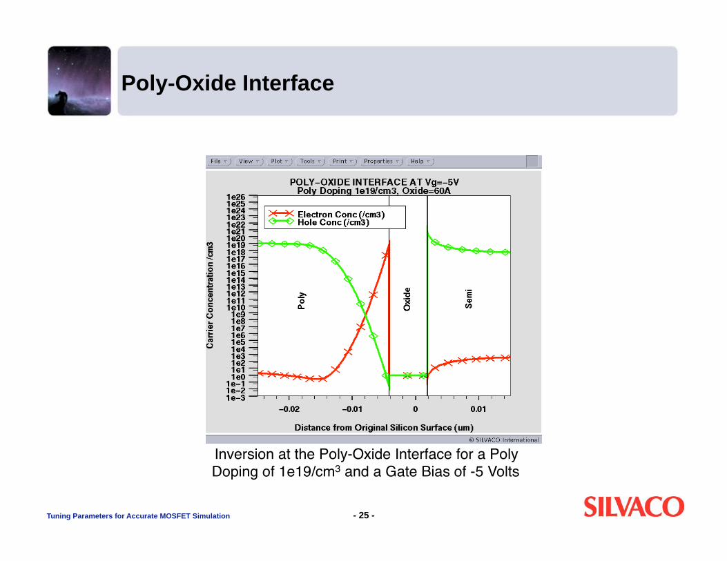
Poly-Oxide Interface
- 25 -
Inversion at the Poly-Oxide Interface for a Poly Doping of 1e19/cm3 and a Gate Bias of -5 Volts

Tuning Parameters for Accurate MOSFET Simulation
MOS Capacitor CV Characteristics
Graph showing differences between the calculated accumulation capacitance MOS of a capacitor using classical and quantum moment calculations
- 26 -
Tuning Parameters for Accurate MOSFET Simulation
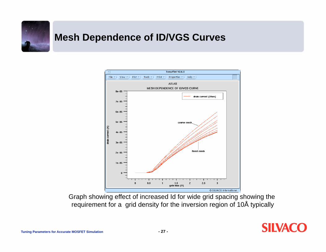
Mesh Dependence of ID/VGS Curves
- 27 -
Graph showing effect of increased Id for wide grid spacing showing the requirement for a grid density for the inversion region of 10Å typically
Tuning Parameters for Accurate MOSFET Simulation
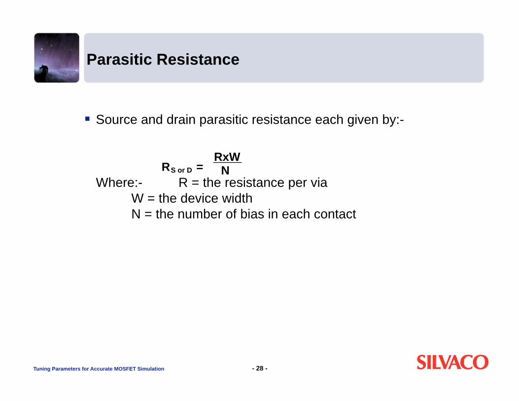
Parasitic Resistance
Source and drain parasitic resistance each given by:-
Where:- R = the resistance per via W = the device width N = the number of bias in each contact
- 28 -
R = S or D
RxW N
Tuning Parameters for Accurate MOSFET Simulation
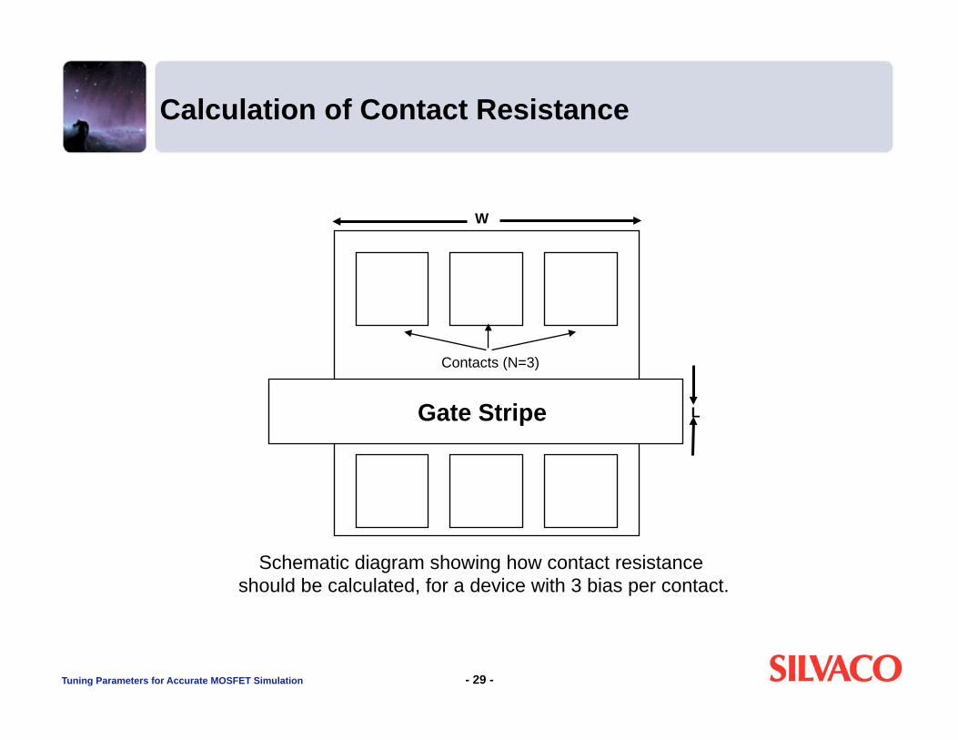
Calculation of Contact Resistance
- 29 -
Schematic diagram showing how contact resistance should be calculated, for a device with 3 bias per contact.
Contacts (N=3)
Gate Stripe L
W
Tuning Parameters for Accurate MOSFET Simulation
Check the Model
Use data NOT used for tuning to check the predictability of the model
Good example:- I-V curves with substrate bias
- 30 -
Tuning Parameters for Accurate MOSFET Simulation
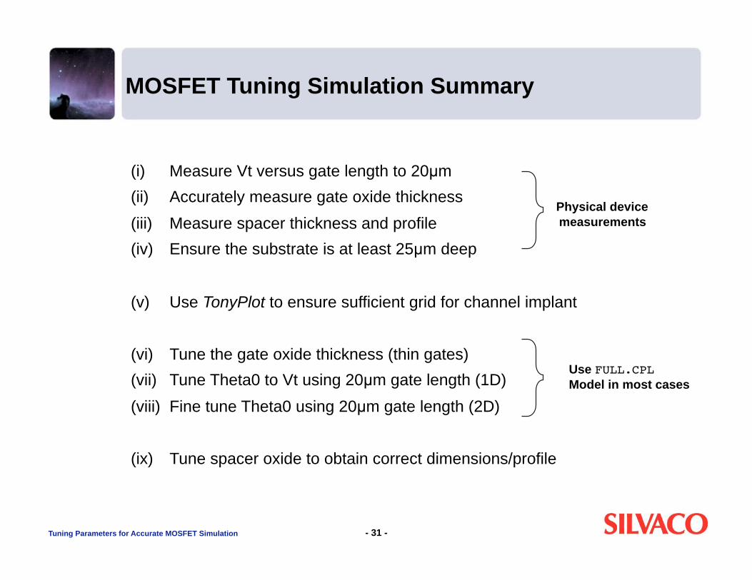
MOSFET Tuning Simulation Summary
(i) Measure Vt versus gate length to 20 m
(ii) Accurately measure gate oxide thickness
(iii) Measure spacer thickness and profile
(iv) Ensure the substrate is at least 25 m deep
(v) Use TonyPlot to ensure sufficient grid for channel implant
(vi) Tune the gate oxide thickness (thin gates)
(vii) Tune Theta0 to Vt using 20 m gate length (1D)
(viii) Fine tune Theta0 using 20 m gate length (2D)
(ix) Tune spacer oxide to obtain correct dimensions/profile
- 31 -
Physical device
measurements
Use FULL.CPL
Model in most cases
Tuning Parameters for Accurate MOSFET Simulation
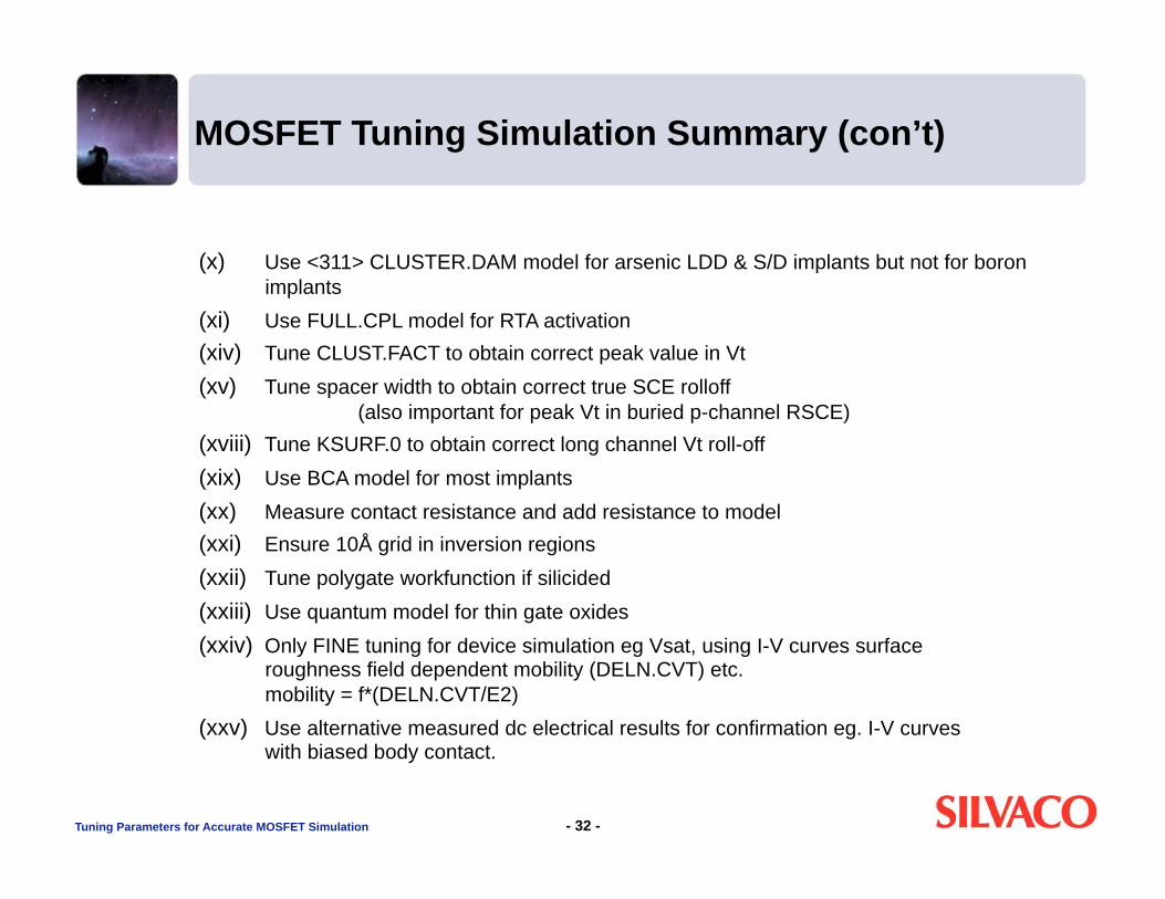
MOSFET Tuning Simulation Summary (con’t)
(x) Use <311> CLUSTER.DAM model for arsenic LDD & S/D implants but not for boron implants
(xi) Use FULL.CPL model for RTA activation
(xiv) Tune CLUST.FACT to obtain correct peak value in Vt
(xv) Tune spacer width to obtain correct true SCE rolloff (also important for peak Vt in buried p-channel RSCE)
(xviii) Tune KSURF.0 to obtain correct long channel Vt roll-off
(xix) Use BCA model for most implants
(xx) Measure contact resistance and add resistance to model
(xxi) Ensure 10Å grid in inversion regions
(xxii) Tune polygate workfunction if silicided
(xxiii) Use quantum model for thin gate oxides
(xxiv) Only FINE tuning for device simulation eg Vsat, using I-V curves surface roughness field dependent mobility (DELN.CVT) etc. mobility = f*(DELN.CVT/E2)
(xxv) Use alternative measured dc electrical results for confirmation eg. I-V curves with biased body contact.
- 32 -