TS256MKR72V3N w/ 09-2930 - Advantech
12
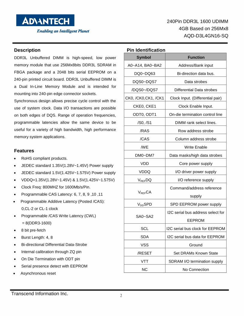
240Pin DDR3L 1600 UDIMM 4GB Based on 256Mx8 AQD-D3L4GN16-SQ Transcend Information Inc. 1 Advantech AQD-D3L4GN16-SQ Datasheet Rev. 1.1 2015-12-09
Transcript of TS256MKR72V3N w/ 09-2930 - Advantech

240Pin DDR3L 1600 UDIMM
4GB Based on 256Mx8
AQD-D3L4GN16-SQ
Transcend Information Inc. 1
Advantech
AQD-D3L4GN16-SQ
Datasheet
Rev. 1.1
2015-12-09
240Pin DDR3L 1600 UDIMM
4GB Based on 256Mx8
AQD-D3L4GN16-SQ
Transcend Information Inc. 2
Description
DDR3L Unbuffered DIMM is high-speed, low power
memory module that use 256Mx8bits DDR3L SDRAM in
FBGA package and a 2048 bits serial EEPROM on a
240-pin printed circuit board. DDR3L Unbuffered DIMM is
a Dual In-Line Memory Module and is intended for
mounting into 240-pin edge connector sockets.
Synchronous design allows precise cycle control with the
use of system clock. Data I/O transactions are possible
on both edges of DQS. Range of operation frequencies,
programmable latencies allow the same device to be
useful for a variety of high bandwidth, high performance
memory system applications.
Features
RoHS compliant products.
JEDEC standard 1.35V(1.28V~1.45V) Power supply
JEDEC standard 1.5V(1.425V~1.575V) Power supply
VDDQ=1.35V(1.28V~1.45V) & 1.5V(1.425V~1.575V)
Clock Freq: 800MHZ for 1600Mb/s/Pin.
Programmable CAS Latency: 6, 7, 8, 9 ,10 ,11
Programmable Additive Latency (Posted /CAS):
0,CL-2 or CL-1 clock
Programmable /CAS Write Latency (CWL)
= 8(DDR3-1600)
8 bit pre-fetch
Burst Length: 4, 8
Bi-directional Differential Data-Strobe
Internal calibration through ZQ pin
On Die Termination with ODT pin
Serial presence detect with EEPROM
Asynchronous reset
Pin Identification
Symbol Function
A0~A14, BA0~BA2 Address/Bank input
DQ0~DQ63 Bi-direction data bus.
DQS0~DQS7 Data strobes
/DQS0~/DQS7 Differential Data strobes
CK0, /CK0,CK1, /CK1 Clock Input. (Differential pair)
CKE0, CKE1 Clock Enable Input.
ODT0, ODT1 On-die termination control line
/S0, /S1 DIMM rank select lines.
/RAS Row address strobe
/CAS Column address strobe
/WE Write Enable
DM0~DM7 Data masks/high data strobes
VDD Core power supply
VDDQ I/O driver power supply
VREFDQ I/O reference supply
VREFCA Command/address reference
supply
VDDSPD SPD EEPROM power supply
SA0~SA2 I2C serial bus address select for
EEPROM
SCL I2C serial bus clock for EEPROM
SDA I2C serial bus data for EEPROM
VSS Ground
/RESET Set DRAMs Known State
VTT SDRAM I/O termination supply
NC No Connection

240Pin DDR3L 1600 UDIMM
4GB Based on 256Mx8
AQD-D3L4GN16-SQ
Transcend Information Inc. 3
Dimensions (Unit: millimeter)
Note: 1. Tolerances on all dimensions +/-0.15mm unless otherwise specified. .

240Pin DDR3L 1600 UDIMM
4GB Based on 256Mx8
AQD-D3L4GN16-SQ
Transcend Information Inc. 4
Pin Assignments
Pin
No
Pin
Name
Pin
No
Pin
Name
Pin
No
Pin
Name
Pin
No
Pin
Name
Pin
No
Pin
Name
Pin
No
Pin
Name
01 VREFDQ 41 VSS 81 DQ32 121 VSS 161 NC 201 DQ37
02 VSS 42 NC 82 DQ33 122 DQ4 162 NC 202 VSS
03 DQ0 43 NC 83 VSS 123 DQ5 163 VSS 203 DM4
04 DQ1 44 VSS 84 /DQS4 124 VSS 164 NC 204 NC
05 VSS 45 NC 85 DQS4 125 DM0 165 NC 205 VSS
06 /DQS0 46 NC 86 VSS 126 NC 166 VSS 206 DQ38
07 DQS0 47 VSS 87 DQ34 127 VSS 167 NC 207 DQ39
08 VSS 48 NC 88 DQ35 128 DQ6 168 /RESET 208 VSS
09 DQ2 49 NC 89 VSS 129 DQ7 169 CKE1,NC 209 DQ44
10 DQ3 50 CKE0 90 DQ40 130 VSS 170 VDD 210 DQ45
11 VSS 51 VDD 91 DQ41 131 DQ12 171 NC 211 VSS
12 DQ8 52 BA2 92 VSS 132 DQ13 172 A14 212 DM5
13 DQ9 53 NC 93 /DQS5 133 VSS 173 VDD 213 NC
14 VSS 54 VDD 94 DQS5 134 DM1 174 A12 214 VSS
15 /DQS1 55 A11 95 VSS 135 NC 175 A9 215 DQ46
16 DQS1 56 A7 96 DQ42 136 VSS 176 VDD 216 DQ47
17 VSS 57 VDD 97 DQ43 137 DQ14 177 A8 217 VSS
18 DQ10 58 A5 98 VSS 138 DQ15 178 A6 218 DQ52
19 DQ11 59 A4 99 DQ48 139 VSS 179 VDD 219 DQ53
20 VSS 60 VDD 100 DQ49 140 DQ20 180 A3 220 VSS
21 DQ16 61 A2 101 VSS 141 DQ21 181 A1 221 DM6
22 DQ17 62 VDD 102 /DQS6 142 VSS 182 VDD 222 NC
23 VSS 63 CK1,NC 103 DQS6 143 DM2 183 VDD 223 VSS
24 /DQS2 64 /CK1,NC 104 VSS 144 NC 184 CK0 224 DQ54
25 DQS2 65 VDD 105 DQ50 145 VSS 185 /CK0 225 DQ55
26 VSS 66 VDD 106 DQ51 146 DQ22 186 VDD 226 VSS
27 DQ18 67 VREFCA 107 VSS 147 DQ23 187 NC 227 DQ60
28 DQ19 68 NC 108 DQ56 148 VSS 188 A0 228 DQ61
29 VSS 69 VDD 109 DQ57 149 DQ28 189 VDD 229 VSS
30 DQ24 70 A10/AP 110 VSS 150 DQ29 190 BA1 230 DM7
31 DQ25 71 BA0 111 /DQS7 151 VSS 191 VDD 231 NC
32 VSS 72 VDD 112 DQS7 152 DM3 192 /RAS 232 VSS
33 /DQS3 73 /WE 113 VSS 153 NC 193 /S0 233 DQ62
34 DQS3 74 /CAS 114 DQ58 154 VSS 194 VDD 234 DQ63
35 VSS 75 VDD 115 DQ59 155 DQ30 195 ODT0 235 VSS
36 DQ26 76 /S1,NC 116 VSS 156 DQ31 196 A13 236 VDDSPD
37 DQ27 77 ODT1,NC 117 SA0 157 VSS 197 VDD 237 SA1
38 VSS 78 VDD 118 SCL 158 NC 198 NC 238 SDA
39 NC 79 NC 119 SA2 159 NC 199 VSS 239 VSS
40 NC 80 VSS 120 VTT 160 VSS 200 DQ36 240 VTT
/S1,ODT1,CKE1:Used for dual-rank UDIMMs; NC on single-rank UDIMMs.
CK1 and /CK1:Used for dual-rank UDIMMs; not used on single-rank UDIMMs but terminated.
240Pin DDR3L 1600 UDIMM
4GB Based on 256Mx8
AQD-D3L4GN16-SQ
Transcend Information Inc. 5
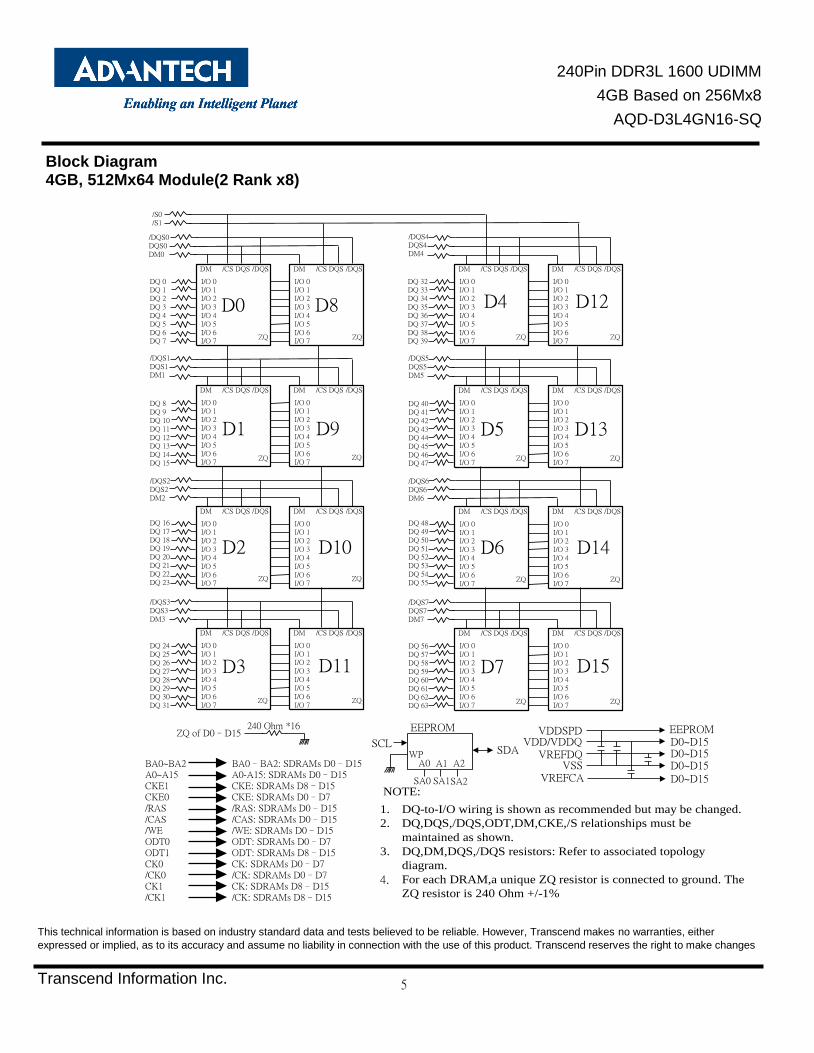
Block Diagram 4GB, 512Mx64 Module(2 Rank x8)
/DQS1DQS1DM1
DQ 8DQ 9DQ 10DQ 11DQ 12DQ 13DQ 14DQ 15
D8
DM
I/O 0I/O 1I/O 2I/O 3I/O 4I/O 5I/O 6I/O 7
/CS DQS /DQS
DQ 0DQ 1DQ 2DQ 3DQ 4DQ 5DQ 6DQ 7
D0
DM
I/O 0I/O 1I/O 2I/O 3I/O 4I/O 5I/O 6I/O 7
/CS DQS /DQS
DM
I/O 0I/O 1I/O 2I/O 3I/O 4I/O 5I/O 6I/O 7
/CS DQS /DQS DM
I/O 0I/O 1I/O 2I/O 3I/O 4I/O 5I/O 6I/O 7
/CS DQS /DQS
DM
I/O 0I/O 1I/O 2I/O 3I/O 4I/O 5I/O 6I/O 7
/CS DQS /DQS DM
I/O 0I/O 1I/O 2I/O 3I/O 4I/O 5I/O 6I/O 7
/CS DQS /DQS
DM
I/O 0I/O 1I/O 2I/O 3I/O 4I/O 5I/O 6I/O 7
/CS DQS /DQS DM
I/O 0I/O 1I/O 2I/O 3I/O 4I/O 5I/O 6I/O 7
/CS DQS /DQS
/DQS0DQS0DM0
/S0/S1
D1 D9
D2 D10
D11D3
DQ 16DQ 17DQ 18DQ 19DQ 20DQ 21DQ 22DQ 23
DQ 24DQ 25DQ 26DQ 27DQ 28DQ 29DQ 30DQ 31
/DQS2DQS2DM2
/DQS3DQS3DM3
/DQS5DQS5DM5
DQ 40DQ 41DQ 42DQ 43DQ 44DQ 45DQ 46DQ 47
DM
I/O 0I/O 1I/O 2I/O 3I/O 4I/O 5I/O 6I/O 7
/CS DQS /DQS DM
I/O 0I/O 1I/O 2I/O 3I/O 4I/O 5I/O 6I/O 7
/CS DQS /DQS
DM
I/O 0I/O 1I/O 2I/O 3I/O 4I/O 5I/O 6I/O 7
/CS DQS /DQS DM
I/O 0I/O 1I/O 2I/O 3I/O 4I/O 5I/O 6I/O 7
/CS DQS /DQS
DM
I/O 0I/O 1I/O 2I/O 3I/O 4I/O 5I/O 6I/O 7
/CS DQS /DQS DM
I/O 0I/O 1I/O 2I/O 3I/O 4I/O 5I/O 6I/O 7
/CS DQS /DQS
/DQS4DQS4DM4
D5 D13
D6 D14
D15D7
DQ 48DQ 49DQ 50DQ 51DQ 52DQ 53DQ 54DQ 55
DQ 56DQ 57DQ 58DQ 59DQ 60DQ 61DQ 62DQ 63
/DQS6DQS6DM6
/DQS7DQS7DM7
DM
I/O 0I/O 1I/O 2I/O 3I/O 4I/O 5I/O 6I/O 7
/CS DQS /DQS DM
I/O 0I/O 1I/O 2I/O 3I/O 4I/O 5I/O 6I/O 7
/CS DQS /DQS
D4 D12
DQ 32DQ 33DQ 34DQ 35DQ 36DQ 37DQ 38DQ 39
VDDSPDVDD/VDDQ
VREFDQVSS
EEPROM
VREFCA
D0~D15D0~D15D0~D15D0~D15
NOTE:
DQ-to-I/O wiring is shown as recommended but may be changed.
DQ,DQS,/DQS,ODT,DM,CKE,/S relationships must be
maintained as shown.
DQ,DM,DQS,/DQS resistors: Refer to associated topology
diagram.
For each DRAM,a unique ZQ resistor is connected to ground. The
ZQ resistor is 240 Ohm +/-1%
1.
2.
3.
4.
SDASCL
EEPROM
WPA1A0 A2
SA0 SA1SA2
ZQ
ZQ
ZQ
ZQ
ZQ ZQ
ZQ ZQZQ ZQ
ZQZQ
ZQ ZQ
ZQ ZQ
ZQ of D0–D15240 Ohm *16
BA0~BA2A0~A15CKE1CKE0/RAS/CAS/WEODT0ODT1CK0/CK0CK1/CK1
BA0–BA2: SDRAMs D0–D15A0-A15: SDRAMs D0–D15CKE: SDRAMs D8–D15CKE: SDRAMs D0–D7/RAS: SDRAMs D0–D15/CAS: SDRAMs D0–D15/WE: SDRAMs D0–D15ODT: SDRAMs D0–D7ODT: SDRAMs D8–D15CK: SDRAMs D0–D7/CK: SDRAMs D0–D7CK: SDRAMs D8–D15/CK: SDRAMs D8–D15
This technical information is based on industry standard data and tests believed to be reliable. However, Transcend makes no warranties, either
expressed or implied, as to its accuracy and assume no liability in connection with the use of this product. Transcend reserves the right to make changes

240Pin DDR3L 1600 UDIMM
4GB Based on 256Mx8
AQD-D3L4GN16-SQ
Transcend Information Inc. 6
in specifications at any time without prior notice.
Operating Temperature Condition
Parameter Symbol Rating Unit Note
Operating Temperature TOPER 0 to 85 C 1,2
Note: 1. Operating Temperature is the case surface temperature on the center/top side of the DRAM. For the measurement conditions, please refer to JESD51-2 standard.
2. At 0 - 85C, operation temperature range are the temperature which all DRAM specification will be supported.
Absolute Maximum DC Ratings Parameter Symbol Value Unit Note
Voltage on VDD relative to Vss VDD -0.4 ~ 1.975 V 1
Voltage on VDDQ pin relative to Vss VDDQ -0.4 ~ 1.975 V 1
Voltage on any pin relative to Vss VIN, VOUT -0.4 ~ 1.975 V 1
Storage temperature TSTG -55~+100 C 1,2
Note: 1. Stress greater than those listed under “Absolute Maximum Ratings” may cause permanent damage to the device. This is a stress rating only and functional operation of the device at these or any other conditions above those indicated in the operational sections of this specification is not implied. Exposure to absolute maximum rating conditions for extended periods may affect reliability.
2. Storage Temperature is the case surface temperature on the center/top side of the DRAM. For the measurement conditions, please refer to JESD51-2 standard.
AC & DC Operating Conditions Recommended DC operating conditions
Parameter Symbol Voltage Rating
Unit Note
s Min Typ. Max
Supply voltage VDD 1.35V 1.283 1.35 1.45 V 1, 2
1.5V 1.425 1.5 1.575
Supply voltage for Output VDDQ 1.35V 1.283 1.35 1.45 V 1, 2
1.5V 1.425 1.5 1.575
I/O Reference Voltage (DQ) VREFDQ(DC) 1.35V 0.49*VDDQ 0.50*VDDQ 0.51*VDDQ V 3
I/O Reference Voltage (CMD/ADD) VREFCA(DC) 1.5V 0.49*VDDQ 0.50*VDDQ 0.51*VDDQ V 3
AC Input Logic High VIH(AC) 1.35V VREF+0.160 - - V
1.5V VREF+0.175 - -
AC Input Logic Low VIL(AC) 1.35V - - VREF-0.160 V
1.5V - - VREF-0.175
DC Input Logic High VIH(DC) 1.35V VREF+0.09 - VDD V
1.5V VREF+0.1 - VDD
DC Input Logic Low VIL(DC) 1.35V VSS - VREF-0.09 V
1.5V VSS - VREF-0.1
Note: 1. Under all conditions VDDQ must be less than or equal to VDD. 2. VDDQ tracks with VDD, AC parameters are measured with VDD and VDDQ tied together. 3. Peak to peak AC noise on VREF may not allow deviate from VREF(DC) by more than +/-1% VDD.

240Pin DDR3L 1600 UDIMM
4GB Based on 256Mx8
AQD-D3L4GN16-SQ
Transcend Information Inc. 7
IDD Specification parameters Definition ( IDD values are for full operating range of Voltage and Temperature)
4GB, 512Mx64 Module(2 Rank x8)
Parameter Symbol DDR3L 1600 CL11 Unit
Operating One bank Active-Precharge current; tCK = tCK(IDD), tRC = tRC(IDD),
tRAS = tRASmin(IDD); CKE is HIGH, /CS is HIGH between valid commands;Address bus inputs are SWITCHING; Data bus inputs are SWITCHING
IDD0 576 mA
Operating One bank Active-read-Precharge current; IOUT = 0mA; BL = 8, CL =
CL(IDD), AL = 0; tCK = tCK(IDD), tRC = tRC (IDD), tRAS = tRASmin(IDD), tRCD = tRCD(IDD); CKE is HIGH, /CS is HIGH between valid commands; Address bus inputs are SWITCHING; Data pattern is same as IDD4W
IDD1 696 mA
Precharge power-down current; All banks idle; tCK = tCK(IDD); CKE is LOW; Other
control and address bus inputs are STABLE; Data bus inputs are FLOATING IDD2P 528 mA
Precharge quiet standby current; All banks idle; tCK = tCK(IDD); CKE is HIGH,
/CS is HIGH; Other control and address bus inputs are STABLE; Data bus inputs are FLOATING
IDD2Q 528 mA
Precharge standby current; All banks idle; tCK = tCK(IDD); CKE is HIGH, /CS is
HIGH; Other control and address bus inputs are SWITCHING; Data bus inputs are SWITCHING
IDD2N 560 mA
Active power - down current; All banks open; tCK = tCK(IDD); CKE is LOW; Other
control and address bus inputs are STABLE; Data bus inputs are FLOATING IDD3P 752 mA
Active standby current; All banks open; tCK = tCK(IDD), tRAS = tRASmax(IDD), tRP
= tRP(IDD); CKE is HIGH, /CS is HIGH between valid commands; Other control and address bus inputs are SWITCHING; Data bus inputs are SWITCHING
IDD3N 832 mA
Operating burst read current; All banks open, Continuous burst reads, IOUT = 0mA;
BL = 4, CL = CL(IDD), AL = 0; tCK = tCK(IDD), tRAS = tRASmax(IDD), tRP = tRP(IDD); CKE is HIGH, /CS is HIGH between valid commands; Address bus inputs are SWITCHING; Data pattern is same as IDD4W
IDD4R 1216 mA
Operating burst write current; All banks open, Continuous burst writes; BL = 8, CL
= CL(IDD), AL = 0; tCK = tCK(IDD), tRAS = tRASmax(IDD), tRP = tRP(IDD); CKE is HIGH, /CS is HIGH between valid commands; Address bus inputs are SWITCHING; Data bus inputs are SWITCHING IDD4R
IDD4W 1096 mA
Burst refresh current; tCK = tCK(IDD); Refresh command at every tRFC(IDD)
interval; CKE is HIGH, /CS is HIGH between valid commands; Other control and address bus inputs are SWITCHING; Data bus inputs are SWITCHING
IDD5 1616 mA
Self refresh current; CK and /CK at 0V; CKE ≒ 0.2V; Other control and address bus
inputs are FLOATING; Data bus inputs are FLOATING IDD6 192 mA
Operating bank interleave read current; All bank interleaving reads, IOUT = 0mA;
BL = 8, CL = CL(IDD), AL = tRCD(IDD)-1*tCK(IDD); tCK = tCK(IDD), Trc = tRC(IDD), tRRD = tRRD(IDD), tRCD = 1*tCK(IDD); CKE is HIGH, CS is HIGH between valid commands;Address bus inputs are STABLE during DESELECTs; Data pattern is same as IDD4R;
IDD7 1856 mA
Note: 1.Module IDD was calculated on the specific brand DRAM(4xnm) component IDD and can be differently
measured according to DQ loading capacitor.

240Pin DDR3L 1600 UDIMM
4GB Based on 256Mx8
AQD-D3L4GN16-SQ
Transcend Information Inc. 8
Timing Parameters & Specifications
Speed DDR3 1600 Unit
Parameter Symbol Min Max
Average Clock Period tCK 1.25 <1.5 ns
CK high-level width tCH 0.47 0.53 tCK
CK low-level width tCL 0.47 0.53 tCK
DQS, /DQS to DQ skew, per group, per access
tDQSQ - 100 ps
DQ output hold time from DQS, /DQS tQH 0.38 - tCK
DQ low-impedance time from CK, /CK tLZ(DQ) -450 225 ps
DQ high-impedance time from CK, /CK
tHZ(DQ) - 225 ps
Data setup time to DQS, /DQS reference to Vih(ac)Vil(ac) levels
tDS 10 - ps
Data hold time to DQS, /DQS reference to Vih(ac)Vil(ac) levels
tDH 45 ps
DQ and DM input pulse width for each input
tDIPW 360 - ps
DQS, /DQS Read preamble tRPRE 0.9 - tCK
DQS, /DQS differential Read postamble
tRPST 0.3 - tCK
DQS, /DQS Write preamble tWPRE 0.9 - tCK
DQS, /DQS Write postamble tWPST 0.3 - tCK
DQS, /DQS low-impedance time tLZ(DQS) -450 225 ps
DQS, /DQS high-impedance time tHZ(DQS) - 225 ps
DQS, /DQS differential input low pulse width
tDQSL 0.45 0.55 tCK
DQS, /DQS differential input high pulse width
tDQSH 0.45 0.55 tCK
DQS, /DQS rising edge to CK, /CK rising edge
tDQSS -0.27 +0.27 tCK
DQS, /DQS falling edge setup time to CK, /CK rising edge
tDSS 0.18 - tCK
DQS, /DQS falling edge hold time to CK, /CK rising edge
tDSH 0.18 - tCK
Delay from start of Internal write transaction to Internal read command
tWTR Max
(4tck, 7.5ns) -
Write recovery time tWR 15 - ns
Mode register set command cycle time
tMRD 4 - tCK

240Pin DDR3L 1600 UDIMM
4GB Based on 256Mx8
AQD-D3L4GN16-SQ
Transcend Information Inc. 9
/CAS to /CAS command delay tCCD 4 - nCK
Auto precharge write recovery + precharge time
tDAL tWR+tRP/tck nCK
Active to active command period for 1KB page size
tRRD Max
(4tck, 6ns) - ns
Speed DDR3 1600 Unit
Parameter Symbol Min Max
Active to active command period for 2KB page size
tRRD Max
(4tck, 7.5ns) -
Four Activate Window for 1KB page size
tFAW 30 - ns
Four Activate Window for 2KB page size products
tFAW 40 - ns
Power-up and RESET calibration time tZQinitl 512 - tCK
Normal operation Full calibration time tZQoper 256 - tCK
Normal operation short calibration time
tZQcs 64 - tCK
Exit self refresh to commands not requiring a locked DLL
tXS Max
(5tCK, tRFC+10ns) -
Exit self refresh to commands requiring a locked DLL
tXSDLL tDLL(min) - tCK
Internal read to precharge command delay
tRTP Max
(4tck, 7.5ns) -
Minimum CKE low width for Self refresh entry to exit timing
tCKESR tCK(min)+1tCK -
Exit power down with DLL to any valid command: Exit Precharge Power Down with DLL
tXP Max
(3tCK, 6ns) -
CKE minimum pulse width (high and low pulse width)
tCKE Max
(3tCK, 5ns)
Asynchronous RTT turn-on delay (Power-Down mode)
tAONPD 2 8.5 ns
Asynchronous RTT turn-off delay (Power-Down mode)
tAOFPD 2 8.5 ns
ODT turn-on tAON -225 225 ps
ODT turn-off tAOF 0.3 0.7 tCK

240Pin DDR3L 1600 UDIMM
4GB Based on 256Mx8
AQD-D3L4GN16-SQ
Transcend Information Inc. 10
SERIAL PRESENCE DETECT SPECIFICATION
AQD-D3L4GN16-SQ Serial Presence Detect
Byte No. Function Described Standard Specification Vendor Part
0 Number of SPD Bytes written / SPD device size / CRC coverage
CRC:0-116Byte
SPD Byte total: 256Byte
SPD Byte use: 176Byte
92
1 SPD Revision Version 1.0 10
2 Key Byte / DRAM Device Type DDR3 SDRAM 0B
3 Key Byte / Module Type UDIMM 02
4 SDRAM Density and Banks 2Gb 8banks 03
5 SDRAM Addressing ROW:15, Column:10 19
6 Reserved 1.35V and 1.5V 02
7 Module Organization 2Rank / x8 09
8 Module Memory Bus Width Non ECC, 64bit 03
9 Fine Timebase Dividend and Divisor 2.5ps 52
10 Medium Timebase Dividend 0.125ns 01
11 Medium Timebase Divisor 0.125ns 08
12 SDRAM Minimum Cycle Time (tCKmin) 1.25ns 0A
13 Reserved -- 00
14 CAS Latencies Supported, Low Byte 6, 7, 8, 9,10,11 FC
15 CAS Latencies Supported, High Byte -- 00
16 Minimum CAS Latency Time (tAAmin) 13.125ns 69
17 Minimum Write Recovery Time (tWRmin) 15ns 78
18 Minimum /RAS to /CAS Delay Time (tRCDmin) 13.125ns 69
19 Minimum Row Active to Row Active Delay Time
(tRRDmin) 6ns 30
20 Minimum Row Precharge Time (tRPmin) 13.125ns 69
21 Upper Nibble for tRAS and tRC - 11
22 Minmum Active to Precharge Time (tRASmin) 35ns 18
23 Minmum Active to Active/Refresh Time (tRCmin) 48.125ns 81
24 Minmum Refresh Recovery Time (tRFCmin), Least
Significant Byte 160ns 00
25 Minmum Refresh Recovery Time (tRFCmin), Most
Significant Byte 160ns 05
26 Minmum Internal Write to Read Command Delay Time
(tWTmin) 7.5ns 3C
27 Minimum Internal Read to Precharge Command Delay
Time (tRTPmin) 7.5ns 3C
28 Upper Nibble for tFAW 30ns 00
29 Minmum Four Active Window Delay Time (tFAWmin) 30ns F0
30 SDRAM Optional Features DLL off Mode,
RZQ/6, RZQ/7 83
31 SDRAM Thermal and Refresh Options No ODTs, No ASR 01
32-59 Reserved -- 00

240Pin DDR3L 1600 UDIMM
4GB Based on 256Mx8
AQD-D3L4GN16-SQ
Transcend Information Inc. 11
60 Module Nominal Height 30mm 0F
61 Module Max Thickness Planar Double Sides 11
62 Reference Raw Card Used R/C B 01
63 Address Mapping from Edge Connector to DRAM Mirrored 01
64-116 Reserved -- 00
117 Module Manufacturer ID Code, Least Significant Byte Transcend 01
118 Module Manufacturer ID Code, Most Significant Byte Transcend 4F
119 Module Manufacturing Location Taipei 54
120-121 Module Manufacturing Date -- 00
122-125 Module Serial Number -- 00
126-127 Cyclical Redundancy Code -- 62, E2
128-145 Module Part Number AQD-D3L4GN16-SQ
41 51 44 2D 44 33
4C 34 47 4E 31 36
2D 53 51 20 20 20
146-147 Revision Code - 00
148-149 DRAM Manufacturer ID Code By Manufacturer Variable
150-175 Manufacturer Specific Data By Manufacturer Variable
176-255 Open for customer use Undefined 00

240Pin DDR3L 1600 UDIMM
4GB Based on 256Mx8
AQD-D3L4GN16-SQ
Transcend Information Inc. 12
Revision History
Version Date Modification Content
1.0 2014/10/20 Initial release
1.1 2015/12/9 Fixed AQD-D3L4GN16-S“Q”