Bio-cryptoeconomy: Smart Contract Blockchain-based Bio-Nano Repair DACs

1
Photonic and phononic crystal research at SandiaSandia National Laboratories and
University of New MexicoT.S. Willie Luk and Ihab El-Kady
Sandia is a multiprogram laboratory operated by Sandia Corporation, a Lockheed Martin Company,for the United States Department of Energy’s National Nuclear Security Administration
under contract DE-AC04-94AL85000.
Quantum, Molecular and High Performance Modeling andSimulation for Devices and Systems (QMHP)
April 16-17, 2007Arlington, VA

2
Outline
• Sandia missions, capabilities and interests.• Recent work in photonic and phononic
crystals

3
Sandia’s Institutional Resources
Information Assurance & SurvivabilityInformation Assurance & SurvivabilityAssessment AnalysisAssessment Analysis

4
Supports Sandia's role as a "Science-Based Engineering" Laboratory
NNSA Science and Technology Thrust• Physical and chemical understanding of NW component operation, aging, failure
mechanisms, and response to radiation exposure.Collective Hierarchical Systems Thrust• The study and simulation of dynamic self-assembly processes and cooperative
behaviors in living systems.Compound Semiconductor Science and Technology Thrust• Advancing semiconductor research in areas such as quantum phenomena, defect
physics, materials and device modeling, and heteroepitaxy.Nanosciences• Explore phenomena that are new and unique at the nanometer length scale, and
develop bridges from the nanometer length scale to longer scales.Optical Sciences• We emphasize innovative work in laser development, nonlinear optics,
spectroscopy, remote sensing, and photon - material interactions.

5
•• 96,000-square-foot CINT Core Facility will be a96,000-square-foot CINT Core Facility will be adistribution point for researchers best served atdistribution point for researchers best served atsmaller smaller ““gatewaysgateways”” at LANL and Sandia at LANL and Sandia
•• $75.8 million Center $75.8 million Center —— one of five funded one of five fundednationwide by the Office of Sciencenationwide by the Office of Science
NanoNano-bio-micro Interfaces:-bio-micro Interfaces: Import biological principles and functions into artificial Import biological principles and functions into artificialbio-mimetic bio-mimetic nanonano- and - and microsystemsmicrosystems..
NanophotonicsNanophotonics and and NanelectronicsNanelectronics:: Precise control of electronic and photonic Precise control of electronic and photonicwavefunctionswavefunctions to invoke novel and unique properties. to invoke novel and unique properties.
Complex Functional Complex Functional NanomaterialsNanomaterials:: Promote complex and collective interactions Promote complex and collective interactionsbetween individual components in materials to yield emergent properties andbetween individual components in materials to yield emergent properties andfunctions.functions.
NanomechanicsNanomechanics:: Understanding the underlying mechanisms of mechanical Understanding the underlying mechanisms of mechanicalbehavior of behavior of nanoscalenanoscale materials and structures is the objective of the materials and structures is the objective of thenanomechanicsnanomechanics theme. theme.

6
Distinguishing Enabler:Tungsten 3-D Fabrication Process
The process is lowtemperature (CMOScompatible), and can beused to fabricate highlycomplex structures fromdielectrics and tungsten

7
Linear ion trap chip micro -fabricated with a metal MEMS process at Sandia
National Laboratories. Planar metallic trap electrodes (W overcoated with Au) and
a hole through the Si substrate define the trapping region and a llow 3D optical
access for lasers to ions trapped between RF leads stretched len gthwise over the hole.
Control electrodes at the hole edges define seven trapping segme nts. Air bridge
metal leads reduce capacitance and RF dissipation to the substra te.
SNL Ion Trap Chip with 3D Optical Access

8
Photonic crystal research
The Why: insurmountable problems in electronic circuits Bandwidth (few GHz) – high inductances from small wire features. Thermal issues (fast degradation in performance at elevatedtemperatures). Slow interchip communication and signal synchronization issueslimits high speed interchip communications.
Photonic crystal offers a new perspective to these problems: Guide and bend light in a unique way. Photonic crystal light source such as selective emitter and threshold-less lasers. Large density of states at the bandedge can be used to controlradiative processes of quantum dot systems. Fabrication technologies are compatible to microelectronic tool sets.
An optical solution is neededAn optical solution is needed

9
300
600
900
1200
0 20 40 60 80
Ener
gy (m
eV)
Angle (degree)
CB Edge
VB Edge
ΚX'
Wav
elen
gth
( m
)1.2
1.5
3.0
2.0
µ
Photonic Band Gap
Si 3-D Photonic Lattice Revolutionizing Photonics
1) Photonic lattices - the optical analogues ofsemiconductors
3) This enables a high level of control over optical properties. 4) Si processing enables the development of well
defined structures.
2) Sandia is developing novel Photonic Lattice designs.
.
0.1
1
10
100
5 10 15 20
Tra
nsm
issio
n A
mp
. (%
)
Wavelength ( m)
7 layers
> 98% attenuation
µ

10
Physics questions : Emissivity is a thermodynamical quantity describing
equilibrium property of electrons, photons andphonons interacting in a common space.
In metallic photonic crystal, photons and otherentities do not occupy the same space except onthe surface.
It is interesting to study what are the conditions todrive a photonic crystal system out of equilibrium.
Thermal emission from photonic crystals
Planckspectrum
Photonic crystalemission,emissivity close to 1(equilibrium condition)
Forbidden due tophotonic bandgap
Wavelength
Emitt
ed p
ower
Non-equilibriumcondition
Unique properties of photonic crystal emission High spectral emissivity in narrow spectral range. Spectral emissivity is fairly independent to temperature. Tunable by crystal design and angle tuning.
Emissivity measurements Temperature of the emitter. Detector gain response. Detector spectral response.
HeaterHeater
BB cavity
Photonic crystal
Sampleclamp

11
Spectral intensity response
Detector response is non-linear. Cubic fit the detectorresponse for each wavelength(1490 points). The actual intensity foreach wavelength (1490 ofthem) is determined bysolving the cubic equation.

12
Thermal analysis
1.6 mm
6.8 mm
Silicon thickness=653 umT(hot)
1.6 mm Heat loss from the silicon is by radiation withemissivity in accordance to its temperature. Use room temperature thermal conductivity.

13
Emissivity measurements of photonic crystal
Uncoupled model
Without temperature correction

14
Harvesting multi-exciton energies withphotonic crystal
Solar source toexcite multi-excitonstates
Multi-excitons inquantumdots
Silicon Photonic crystalInfiltrated withquantum dots
Solar cell
Solar celltuned tosingleexcitonenergy
Multiple-excitonenergy conversion
Photocell
Single exciton
BiexcitonTriexcitonQuadexciton
1Se
1Sh
0.8eVforPbSeQD
Use photonic crystal toenhance emission

15
Single photon source and photonic crystalQuantum information processing requiresnon-classical light (single photon source).
Quantum dot acts like an atom. Photonic crystals provide high Qand small mode volume. Ideal system to study radiativecontrol and dephasing processes.
Two level atom in photonic crystal
hν
Weak coupling
EmissionNotallowed
hν+Ω
Ω
Strong coupling
Allow modes
Bandgap(disallowed
modes)
Photonic crystal structure
Coupling parameter g = (Rabi_Frequency).(interaction_time)
Critical atom number n0 =4/3(radiative_lifetime).(dephasing_time)/(Rabi_Frequency)2
.Critical photon number N0 =2(radiative_lifetime).(cavity_lifetime)/(Rabi_Frequency)2.
Singlequantumdot
Pumpbeam
Singlephotonsource
Requirementsg ~ dipole moment >1n0 ~ V <<1N0 ~ V/Q <<1

16
What about phonon control?What about phonon control?
17
Acoustic Bandgap Crystals:Acoustic Bandgap Crystals:Why, What, and How?Why, What, and How?
Motivation: Telecom (the why):Motivation: Telecom (the why):
Radio/Cellular Operation:Radio/Cellular Operation:
ASP: Electro-Acoustic Coupling Losses:ASP: Electro-Acoustic Coupling Losses:
Rx
Tx
Half DuplexHalf Duplex Rx
Tx
Full Duplex:Full Duplex:
⇒⇒Requires high resolutionRequires high resolutionsteep filteringsteep filtering
⇒⇒Figure of merit QFigure of merit Q≈≈1000-20001000-2000
Coupling LossCoupling Loss
Signal PowerSignal Power Analogue Signal Processing:Analogue Signal Processing:
Cascaded insertion losses implyCascaded insertion losses implythat once we are in the acousticthat once we are in the acousticdomain we would like to remain indomain we would like to remain init!it!
Why not Digital SignalWhy not Digital SignalProcessing:Processing:
Requires high power at highRequires high power at highfrequencies.frequencies.
Low resolution ADCLow resolution ADC
Acoustic SignalAcoustic SignalProcessingProcessing
⇒⇒ ABG ABG’’ss
Coupling LossCoupling Loss Coupling LossCoupling Loss

18
Acoustic Bandgap Crystals:Acoustic Bandgap Crystals:The WhatThe What
What does this have to do with PBGWhat does this have to do with PBG’’s?s?
Inherently non-linearInherently linear
GHZ applications require sub-micronlength scales
THZ applications require sub-micronlength scales
Inherent physical size dependentstructural resonances.
No inherent structural resonances. Finitesize leads only to evanescent mode
issues.
Mechanical wave nature and lowcoupling to air modes along with the
possibility of vacuum packaging allow forfull control using only 2D devices
Light line constraints and ability tocouple to free space modes mandatesthat full control of waves can only be
achieved in 3D devices
2rd order coupled Tensor Equations with3 polarizations
2nd order coupled vector equations with2 polarizations
ABG PhononsPBG Photons
Direct analogy between 2D Acoustic (phononic) and photonic crystals.Direct analogy between 2D Acoustic (phononic) and photonic crystals.
Wealth of Literature on 2D PC that can be used as a first iteration for the design andWealth of Literature on 2D PC that can be used as a first iteration for the design andstudy of ABG crystal applications.study of ABG crystal applications.

19
Acoustic Bandgap Crystals:Acoustic Bandgap Crystals:Contrast to Photonic Bandgap CrystalsContrast to Photonic Bandgap Crystals
PBGPBG
ABGABG
PBGPBG
××ABGABG
ABG = Superposition of Bragg andABG = Superposition of Bragg andMie Scattering:Mie Scattering:
A cermet topology (disconnected) of highA cermet topology (disconnected) of highdensity inclusions in a low densitydensity inclusions in a low densitybackground matrix.background matrix.
Acoustic impedance mismatch between theAcoustic impedance mismatch between theinclusions and the matrix.inclusions and the matrix.
A maximization of the gaps is achieved byA maximization of the gaps is achieved byrequiring the ratio of the longitudinal velocityrequiring the ratio of the longitudinal velocityccll to the shear velocity to the shear velocity ccss values in both the values in both thematrix and inclusion to be as close to thematrix and inclusion to be as close to thefundamental limit of a hard scatterer fundamental limit of a hard scatterer √√22..
Challenges:Challenges: Finding high Q pair systems.Finding high Q pair systems.
Compatibility with AlN and Si-processingCompatibility with AlN and Si-processingtechniques for integrationtechniques for integration
Scaling to um size designs.Scaling to um size designs.

20
Acoustic Bandgap Crystals:Acoustic Bandgap Crystals:Advantages of ABG CircuitryAdvantages of ABG Circuitry
Added Benefits of the Acoustic Domain:Added Benefits of the Acoustic Domain:
MiniatureMiniature Filters FiltersDelay LinesDelay Lines Phase Shifters Phase Shifters Acoustic Signal Processing Acoustic Signal Processing Power Combiners/Dividers Power Combiners/Dividers
Speed of Light = 3x10 Speed of Light = 3x1088 m/s m/s Speed of Sound in SiO Speed of Sound in SiO22 = 5.8x10 = 5.8x1033 m/s m/s Optical Delay Line of 1 Optical Delay Line of 1 µµs = 300 ms = 300 m ABG Delay Line of 1 ABG Delay Line of 1 µµs = 5.8 mms = 5.8 mm ABG delay line is 52,000 times ABG delay line is 52,000 timessmaller than an optical one!smaller than an optical one! ⇒⇒
High-Q distributed ABG filters at GHz frequencies at significant improvement overHigh-Q distributed ABG filters at GHz frequencies at significant improvement overcurrent FBAR technologies resulting in new low power radio architectures.current FBAR technologies resulting in new low power radio architectures.
Integration of multiple components on one chip with little or no losses at a size that isIntegration of multiple components on one chip with little or no losses at a size that is101044-times smaller than current optical or micro-strip technology-times smaller than current optical or micro-strip technology
Allows for distributed circuit techniques that are commonly used in microwave circuitAllows for distributed circuit techniques that are commonly used in microwave circuitdesign to be applied to lower frequency systems (such as cell phones and WLAN) usingdesign to be applied to lower frequency systems (such as cell phones and WLAN) usingacoustic rather than EM waves.acoustic rather than EM waves.

21
Acoustic Bandgap Crystals:Acoustic Bandgap Crystals:The Path to GHz ABGThe Path to GHz ABG’’ss
Proposed System:Proposed System: Suspended membrane topology of 2D rod arrays ofSuspended membrane topology of 2D rod arrays of
W (W (ρρ = 19,300 kg/m3, Z = 89 M = 19,300 kg/m3, Z = 89 MΩΩ) ) in SiOin SiO22 ( (ρρ = 2,200 = 2,200kg/m3, Z = 13 Mkg/m3, Z = 13 MΩΩ) ) matrix (both are high Qmatrix (both are high Qmaterials).materials).
AlN Piezoelectric transducers (allows us toAlN Piezoelectric transducers (allows us toleverage FBAR low insertion loss technologies).leverage FBAR low insertion loss technologies).
11stst generation: MHz devices using a 7 Levels Post- generation: MHz devices using a 7 Levels Post-CMOS Compatible process.CMOS Compatible process.
Modeling:Modeling: FDTD algorithm for the temporal integration of theFDTD algorithm for the temporal integration of the
full elastic wave equation that incorporates bothfull elastic wave equation that incorporates bothLame coefficients.Lame coefficients.
Periodic boundary conditions are used at the edgesPeriodic boundary conditions are used at the edgesof the cell along the x and y directions and space isof the cell along the x and y directions and space isterminated along the z axis (direction ofterminated along the z axis (direction ofpropagation) by Murpropagation) by Mur’’s first order absorbings first order absorbingboundary.boundary.
The time series results collected at the detectionThe time series results collected at the detectionpoint are converted into the frequency domainpoint are converted into the frequency domainusing the fast Fourier transform.using the fast Fourier transform.
> 4 orders ofmagnitude rejection
ABG
r=0.3a; a=1um

22
Acoustic Bandgap Crystals:Acoustic Bandgap Crystals:Theory Versus ExperimentTheory Versus Experiment
Excellent Qualitative Agreement.Excellent Qualitative Agreement.
Differences due to:Differences due to: Use of bulk properties in the simulationUse of bulk properties in the simulation
versus actual measured values of theversus actual measured values of thedeposited materials.deposited materials.
Theoretical gap appears to be wider, (lowTheoretical gap appears to be wider, (lowfrequency end is red-shifted and highfrequency end is red-shifted and highfrequency end is blue shifted), can befrequency end is blue shifted), can beattributed to:attributed to:
Use of lossless materials in model. Use of lossless materials in model.
Infinite size extent in the lateral Infinite size extent in the lateraldimensions.dimensions.
a
r
Tungsten Scatterer
AlN Coupler
a
r
a
r
Tungsten Scatterer
AlN Coupler

23
Acoustic Bandgap Crystals:Acoustic Bandgap Crystals:Line Defects: Theory v.s. ExperimentLine Defects: Theory v.s. Experiment
GuideGuideModeMode
yyZZ
yyZZ

24
Proof of Concept and Lessons LearnedProof of Concept and Lessons Learned
> 4 orders of> 4 orders ofmagnitudemagnituderejectionrejection
BandgapBandgap
Cross-section of the AlN/W ABG
45 _m
14.4 _m
AlN Coupler
TungstenScatterer
Release Pit
45 _m
14.4 _m
45 _m
14.4 _m
AlN Coupler
TungstenScatterer
Release Pit
PhononicPhononic Bandgap Recipe. Bandgap Recipe.
Possibility of introduction of multiple rejection bands per crystalPossibility of introduction of multiple rejection bands per crystal
Because of low coupling to air modes 2D periodicity is sufficient and weBecause of low coupling to air modes 2D periodicity is sufficient and wedo not need to go for the more complicated 3D structures.do not need to go for the more complicated 3D structures.
ThatThat’’s not all!s not all!

25
Phonon Taming by Elastic Phonon Taming by Elastic BandgapsBandgaps Idea:Idea:
Mold and shape the phonon distribution by artificially changing the density ofMold and shape the phonon distribution by artificially changing the density ofstates.states.
Path:Path: Create the phonon equivalent of the band theory of solids: Allowed statesCreate the phonon equivalent of the band theory of solids: Allowed states
separated by a phonon gap (forbidden phonon states).separated by a phonon gap (forbidden phonon states).
Approach:Approach: Superpose Mie resonant scattering by individualSuperpose Mie resonant scattering by individual
scattering centers and Bragg scattering due to theirscattering centers and Bragg scattering due to theirperiodic arrangement in a lattice.periodic arrangement in a lattice.
Requires Mie resonances scattering centers andRequires Mie resonances scattering centers andbackground matrix to be sufficiently separated by anbackground matrix to be sufficiently separated by anacoustic impedance mismatch.acoustic impedance mismatch.
Nph
T
Forbidden States
Allowed Statesgap⇒⇒
≡≡C.B.C.B.
V.B.V.B.
gap ⇒⇒ ⇒⇒ Non OverlappingMie Resonances
Matrix ofMismatchedImpedance

26
Thermal To RF: Energy HarvestingThermal To RF: Energy Harvestingand Passive Taggingand Passive Tagging
Energy Harvesting Scheme:Energy Harvesting Scheme:
Thermal phononspectrum
Phononic Crystalrejection bands+
⇒ PiezoelectricPiezoelectric
CrystalCrystal
RFEmissionSpectrum+ =
upConversion
DownConversion
FrequencyBar Code!
Engineer Elastic band gap to posses single/multiple rejection bandsEngineer Elastic band gap to posses single/multiple rejection bandswhose boundaries lie at the desired harvesting frequencywhose boundaries lie at the desired harvesting frequency
Depleted density of phonon states in the rejection band will force multi-Depleted density of phonon states in the rejection band will force multi-phonon processes to perform up/down frequency conversion allowingphonon processes to perform up/down frequency conversion allowingphonons to escape in the allowed bandsphonons to escape in the allowed bands
Couple lattice to a Piezoelectric material to generated EM radio signal.Couple lattice to a Piezoelectric material to generated EM radio signal.
Cascade crystals of different periods and/or design a single crystal withCascade crystals of different periods and/or design a single crystal withmultiple higher order bands (overtones) to generate discrete multiplemultiple higher order bands (overtones) to generate discrete multiplecommunication channels.communication channels.
Eph1 + Eph2 Eph3Eph1 + Eph2 Eph3
27
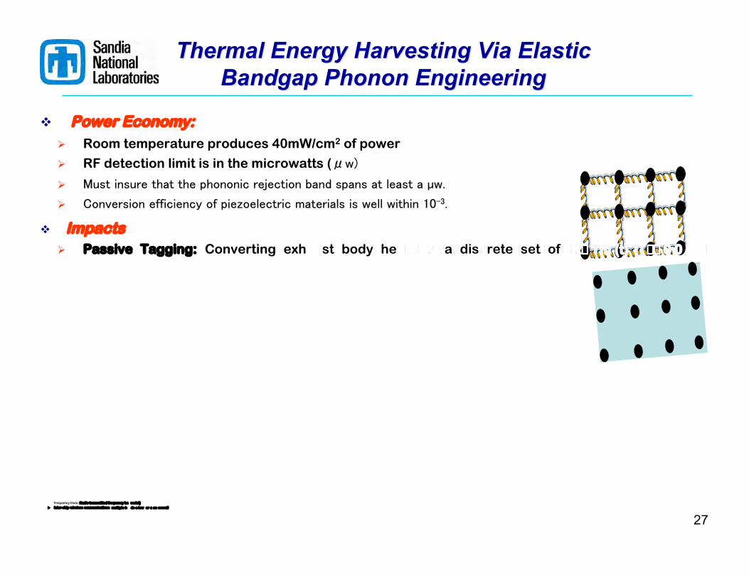
Thermal Energy Harvesting Via ElasticThermal Energy Harvesting Via ElasticBandgap Phonon EngineeringBandgap Phonon Engineering
Power Economy:Power Economy: Room temperature produces 40mW/cmRoom temperature produces 40mW/cm22 of power of power
RF detection limit is in the microwatts (RF detection limit is in the microwatts (μμw)w)
Must insure that the phononic rejection band spans at least a µw.Must insure that the phononic rejection band spans at least a µw.
Conversion efficiency of piezoelectric materials is well within 10Conversion efficiency of piezoelectric materials is well within 10-3-3..
ImpactsImpacts Passive Tagging:Passive Tagging: Converting exhu st body he 1.392 w 2 Tr q 3633.9119 1428 Tm (t) Tj 58 0 0 58 1654.5619 1428Tm ( ) Tj 58 0 0 58 1687.7273 1428 Tm ( ) Tj 58 0 0 58 1720.89287058824 SCt a discrete set f Converting exhaust body heat to a discrete set of
frequency lines (frequency lines (Radio transmitted frequency ba r code!Radio transmitted frequency bar code!))
Inter-chip wireless communications:Inter-chip wireless communications : multiple ba nds a llow for a an overall
multiple bands a llow for a an overall
wider communication bandwidth at zero addition

28
Accelerated Cooling and ModificationAccelerated Cooling and Modificationof the Global Heat Capacityof the Global Heat Capacity
Rapid Accelerated Cooling (Rapid Accelerated Cooling (ballistic phononballistic phonon) Scheme:) Scheme:
Conventional:Conventional: Random Phonon ScatteringRandom Phonon Scattering
Overall Drift velocity Overall Drift velocity vvdd
ColdSide
HotSide
ColdSide
HotSide
EBG Solution :EBG Solution : Directive Phonon GuidesDirective Phonon Guides
Guide Group velocity Guide Group velocity vvgg
Concerns:Concerns: Can we engineer the bandsCan we engineer the bands
so that:so that:
VVgg> > VVdd ? ?
Match guide impedanceMatch guide impedance
Modification of the Global Heat Capacity:Modification of the Global Heat Capacity:
Q
T
Bulk
gapDos
Eph(kT)
cp cp
cp
cp
Q
T
Bulk
Forbidden States
Allowed Statesgap
Nph
Eph⇒⇒

29
Phonon Shielding and AcousticPhonon Shielding and AcousticFocusing and ImagingFocusing and Imaging
Phonon Shielding Phonon Shielding ≡≡ Johnson Noise Reduction Johnson Noise Reduction::
Device AmbientPhonons
Conventional:Conventional: White NoiseWhite Noise
Cap on SensitivityCap on Sensitivity
EBG Solution :EBG Solution : 1D Phonon Shield1D Phonon Shield
2D Phonon Mirrors on the interconnects2D Phonon Mirrors on the interconnects
Device
2D EBG1D EBG
Negative Refraction and Acoustic Focusing:Negative Refraction and Acoustic Focusing:
NegativeSlopingBands
Pononic band gap
Con
serv
ed F
requ
ency
ω
Conserved Wavevectork
⇒⇒ NegativeRefraction
negative group-velocity ornegative curvature (“eff. mass”):Negative refraction,
Super-Lensing
object image
negative refraction medium
super-lens
Veselago (1968)

30
Elastic Bandgap Phonon EngineeringElastic Bandgap Phonon Engineering Challenges:Challenges:
ScalingScaling
Most relevant applications lie in the Most relevant applications lie in the GHz-to-THzGHz-to-THz range these require range these requiresub-sub-µµmm to nm to nm length scales. length scales.
Unclear how the elastic wave equations scaleUnclear how the elastic wave equations scale as we go from theas we go from thecontinuum length scales (KHz) to the quantum length scales (THz)continuum length scales (KHz) to the quantum length scales (THz)
Back fill Back fill thermalizationthermalization??
Unclear how a modification of the phonon distribution affects the heatUnclear how a modification of the phonon distribution affects the heatcapacity.capacity.
Unclear how a phonon insulation scheme for Johnson noise reductionUnclear how a phonon insulation scheme for Johnson noise reductioncan be setup in a frame work that prevents re-thermalization of thecan be setup in a frame work that prevents re-thermalization of thephonon states.phonon states.
Drift Versus Group Velocities and impedance matching.Drift Versus Group Velocities and impedance matching.
Unclear whether or not we can create a preferred direction for phononUnclear whether or not we can create a preferred direction for phononpropagation where the group velocity is higher than the drift velocity andpropagation where the group velocity is higher than the drift velocity andhence allow for accelerated cooling.hence allow for accelerated cooling.
Efficiency of Efficiency of multiphononmultiphonon processes for up/down frequency conversion? processes for up/down frequency conversion?
Problem Statement:Problem Statement: Phononic crystals offer a unique vehicle for full phonon control andPhononic crystals offer a unique vehicle for full phonon control and
as such open the door to a vast group of novel applications, howeveras such open the door to a vast group of novel applications, howeverthere is a great deal of ambiguity in the efficiency of this control andthere is a great deal of ambiguity in the efficiency of this control andwhether or not recipes borrowed from conventional photonic can bewhether or not recipes borrowed from conventional photonic can beimmediately applied or not.immediately applied or not.