trom - McGill Universitydigitool.library.mcgill.ca/thesisfile79273.pdf · fibre-optique, qui...
72
ln compliance with the Canadian Privacy Legislation sorne supporting forms may have been removed trom this dissertation. While these forms may be included in the document page count, their removal does not represent any loss of content from the dissertation.
Transcript of trom - McGill Universitydigitool.library.mcgill.ca/thesisfile79273.pdf · fibre-optique, qui...

ln compliance with the Canadian Privacy Legislation
sorne supporting forms may have been removed trom
this dissertation.
While these forms may be included in the document page count,
their removal does not represent any loss of content from the dissertation.

Design and Analysis of Low Noise Transimpedance Amplifiers for 10 Gb/s
Optical Receivers
Department of Electrical and Computer Engineering
McGill University, Montréal
September 2002
A thesis submitted to the Faculty of Graduate Studies and Research in partial fulfillment of
the requirements for the degree of Master of Engineering
© YeLu, 2002

1+1 National Library of Canada
Bibliothèque nationale du Canada
Acquisitions and Bibliographie Services
Acquisisitons et services bibliographiques
395 Wellington Street Ottawa ON K1A ON4 Canada
395, rue Wellington Ottawa ON K1A ON4 Canada
The author has granted a nonexclusive licence allowing the National Library of Canada to reproduce, loan, distribute or sell copies of this thesis in microform, paper or electronic formats.
The author retains ownership of the copyright in this thesis. Neither the thesis nor substantial extracts from it may be printed or otherwise reproduced without the author's permission.
Canada
Your file Votre référence ISBN: 0-612-88399-X Our file Notre référence ISBN: 0-612-88399-X
L'auteur a accordé une licence non exclusive permettant à la Bibliothèque nationale du Canada de reproduire, prêter, distribuer ou vendre des copies de cette thèse sous la forme de microfiche/film, de reproduction sur papier ou sur format électronique.
L'auteur conserve la propriété du droit d'auteur qui protège cette thèse. Ni la thèse ni des extraits substantiels de celle-ci ne doivent être imprimés ou aturement reproduits sans son autorisation.
Abstract
High-speed optical systems are becoming increasingly important due to the
progress of multimedia communications, which requires ever increasing data-transmission
capacity. SONET-based systems at 10 Obis are under commercial development, and it is
likely that systems based on higher SONET hierarchies will soon be required for further
broadband communications networks.
This the sis de scribes a low-noise and low-power Si-bipolar transimpedance
pre amplifier for the front-end of an optical-fibre receiver using a 0.5 )..lm 250Hz self
aligned double poly silicon bipolar process. Design specifications are met through trade
offs between input noise current, speed, transimpedance gain, power dissipation,
impedanee matching, and supply voltage. This was achieved by 1) using induetors to
enhance the bandwidth, 2) using a tuned noise-matching network at the input to improve
the signal-to-noise ratio (SNR), 3) and using frequency compensation techniques to
improve stability and to further enhance the bandwidth of the pre amplifier.
In this thesis, the design of the amplifier is preceded by an analysis of four
different circuit topologies, with focus on three main design parameters: bandwidth, input
referred noise, and power dissipation. This is followed by a discussion of the specifie
bipolar transimpedance amplifier (TIA) designed and fabricated, and the integration of an
optoelectronic device model with the pre amplifier for the purpose of testing. Design,
simulation, layout and test data of the preamplifier are presented in detail. The
performance of the TIA is finally discussed based on measurements.
Abstrait
Les systèmes optiques à haute vitesse deviennent de plus en plus
importants à cause de l'évolution des communications multimédias, qui requièrent
une capacité de transmission de données aux niveaux de plus en plus élevés. Les
systèmes basés sur la technologie SONET à 10 Gbitls sont déjà en développement
commerical, et c'est une éventualité que les systèmes basés sur la hierarchie
SONET pour transmissions plus élevés seront requises pour les prochaines
générations de réseaux de communications à large bande.
Cette thèse décrit un préamplificateur de transimpedance silicium
bipolaire à faible bruit et à faible puissance pour l'ensemble frontal d'un recepteur
fibre-optique, qui utilise un processus bipolaire, auto-aligné, de double poly
silicium. Les spécifications sont réalisées par la substitution entre l'entrée du
courant de bruit, la vitesse, le gain de transimpedance, la dissipation de puissance,
l'équilibrage d'impedance, et l'alimentation de tension. Ceux-ci sont atteints 1)
en utilisant les bobines d'inductions pour amplifier la largeur de bande 2) en
utilisant un réseau, accordé par le réglage de bruit à l'entrée pour améliorer le
rapport signal-sur-bruit (SIB), et 3) en utilisant les techniques de compensation de
fréquences pour améliorer la stabilité et la largeur de bande du préamplificateur.
Dans cette thèse, le dessin de l'amplificateur a été précédé par une analyse
étendue de quatres topologies de circuits différents, en particulier trois paramètres
de conception principaux: la largeur de bande, l'indication de bruit à l'entrée, et
ii
la dissipation de puissance. Ceci est suivi par une discussion de l'amplificateur
transimpedance bipolaire spécifique qui a été conçu et manufacturé, ainsi que
l'intégration du modèle périphérique opto-électronique avec préamplificateur,
pour raison de vérification. Le dessin, la simulation, la topologie, et les données
de vérification du préamplificateur sont présentées, en détail. Les caractéristiques
de l'amplificateur transimpedance bipolaire sont discutés, basée sur ces résultats.
iii
Acknowledgements
1 would like to express my sincere appreciation to the many people who have made
my graduate studies possible and who have made it such a rewarding experience. First, 1
would like to thank my supervisor, Prof. Mourad El-Gamal, for his guidance and
encouragement throughout my study at McGill. 1 would also like to thank Prof. Gordon
Roberts, Prof. Nick Rumin, Prof. Ishiang Shih, and Prof. Andrew Kirk, and the many
excellent teachers 1 had through the years.
1 would also like to thank my group members and all the folks of the MACS
laboratory, from whom 1 received a lot of valuable technical help, and with whom 1 had
many interesting discussions. Special thanks go to Michael Venditti, Jean-Philippe
Thibodeau, and Charif Beainy for their support with bonding and for providing guidance
for my test setups and experiments. A thank you also goes to the Canadian
Microelectronics Corporation (CMC) , which supported this research, and to Nortel
Networks for IC fabrication.
Next, 1 would like to thank my family and friends for their understanding and
support during my years in graduate school. A special acknowledgment goes to my
mother and father, who have always encouraged me to do the best. They have always been
there sharing times of trial and times of joy. Finally, without the support and
encouragement of my parents and my lovely daughter, Jing Yuan, this work would not
have been possible.
iv
Table of Contents
Abstract .......................................................................................................... i
Acknowledgements ........................................................................................ ii
List of Figures ................................................................................................ v
List of Tables ............................................................................................... vii
Chapter 1 - Introduction ............................................................................... 1
Chapter 2 - Optical Communications Systems........................................ 4
2.1 - Introduction ......................................................................................................... 4 2.2 - Optical Communication Links ............................................................................. 5
2.2.1 - The Photodetector. ........................................................................ 6
2.2.2 - Receiver Systems ........................................................................... 7
Chapter 3 - Optical Receiver Front-ends Design Considerations ........... 13
3.1 - Introduction ....................................................................................................... 13 3.2 - Technology ........................................................................................................ 13 3.3 - Review of Optical Receiver Frontends Design ................................................. 15
3.3.1 - The Low Impedance Voltage Amplifier. ...................................... 15
3.3.2 - The High Impedance Amplifier ................................................... 16 3.3.3 -3.3.4 -
Transimpedance Amplifie r .......................................................... 18
The Noise-Matched or Resonant Amplifier ................................. 23
Chapter 4 - TIA Design, Fabrication, and Testing .................................. 2S
4.1 - Introduction .............................. ; ........................................................................ 25 4.2 - Optimization of a Bipolar Transimpedance Preamplifier.. ................................ 26
4.2.1 - Transimpedance Amplifier Topologies ....................................... 26
4.2.2 - Circuit Design Considerations ................................................... 27
v
4.3 - Transimpedance Preamplifier Design ................................................................ 31 4.4 - Performance Analysis ........................................................................................ 33
4.4.1 - Controlling the Frequency Response .......................................... 33
4.4.2 - Noise Considerations .................................................................. 35
4.5 - Prototype Implementation ................................................................................. 40
4.6 - Experimental Results ......................................................................................... 40
4.6.1 - Test Setup .................................................................................... 41
4.6.2 -
4.6.3 -
Measurements ............................................................................. 43
Results ......................................................................................... 49
Chapter 5 - Conclusion ............................................................................... 53
References .................................................................................................... 54
vi
List of Figures
Figure 2.1 Typical optical data link [24] .......................................................................... 6
Figure 2.2 Block diagram of a typical optical receiver [13] ............................................ 8
Figure 3.1 The low impedance voltage amplifier topology [25] .................................... 16 Figure 3.2 The high impedance topology [25]. .............................................................. 17
Figure 3.3 Transimpedance amplifier topology [25]. ..................................................... 19 Figure 3.4 Noise equivalent circuit for the transimpedance amplifier input stage
[25] ....................................................................................................................... 20 Figure 3.5 Noise matched or resonant topology [25] ..................................................... 23 Figure 4.1 Various topologies (a) Single-stage feedback preamplifier, (b) Common
emitter preamplifier, (c) Cascode pre amplifier, (d) Common-base preamplifier ............................................................................................................ 27
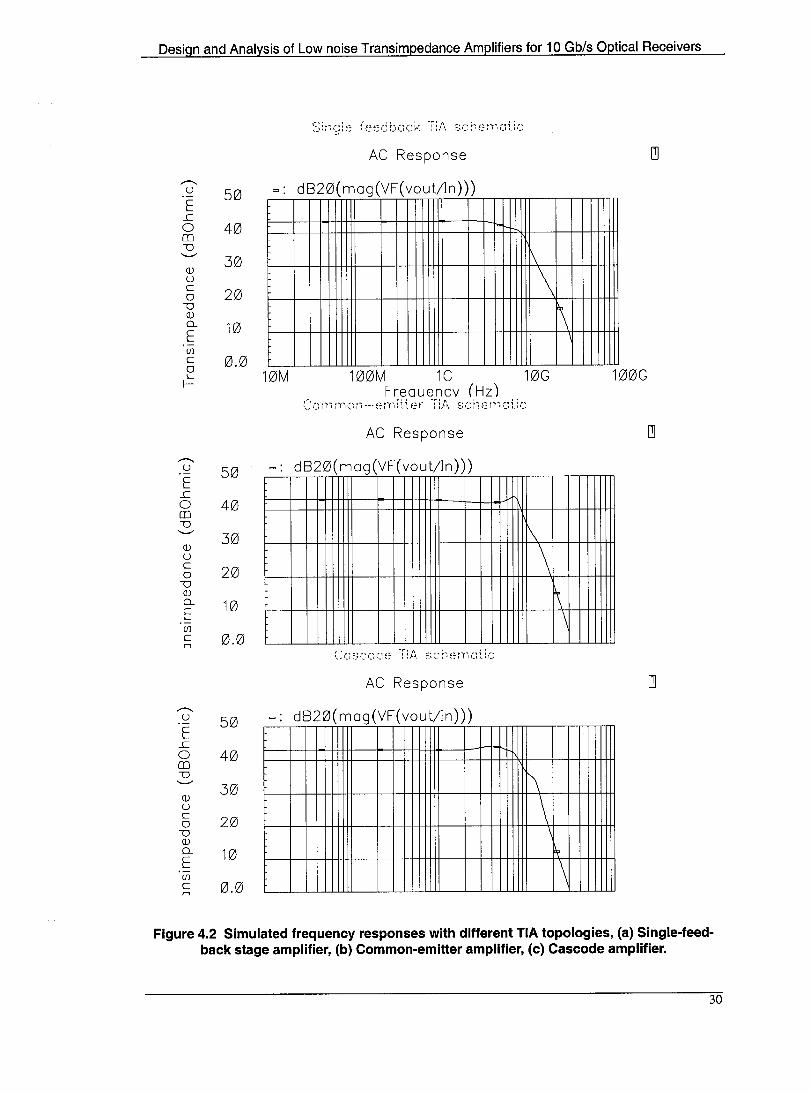
Figure 4.2 Simulated frequency responses with different TIA topologies, (a) Singlefeedback stage amplifier, (b) Common-emitter amplifier, (c) Cascode amplifier ................................................................................................................. 30
Figure 4.3 Hspice simulation of the equivalent input noise current for three different TIA's ..................................................................................................................... 31
Figure 4.4 Transimpedance amplifier circuit schematic, showing the bandwidth enhancing inductor (L2) and the frequency compensation capacitance (Cf) ........................................................................................................................ 32
Figure 4.5 Relationship between circuit parameters and preamplifier characteristics [3] .......................................................................................................................... 32
Figure 4.6 (a) Simulated frequency response with different inductive bandwidth enhancement inductors (L2); and (b) frequency response with different compensation capacitances (Cf) ........................................................................... 34
Figure 4.7 Transimpedance amplifier noise equivalent circuit. .................................................................................................................... 35
Figure 4.8 Circuit for input noise tuning for a reactive source ..................................... 36 Figure 4.9 (a) Hspice simulation of equivalent input noise current for different values
of LI, using the noise-matching network. (b) Corresponding frequency response ................................................................................................................ 38
vii
Figure 4.1O(a) Hspice simulations of input refeITed CUITent noise, and (b) frequency response, for different photodiode capacitances (Cpd) ........................................ 39
Figure 4. IIPhotomicrograph of the transimpedance amplifier ..................................... .40
Figure 4. 12System test setup block diagram ................................................................. .41
Figure 4. 13Photo of the test board and bonding diagram .............................................. .43
Figure 4.14A simple on-chip circuit model of PIN photodiode .................................... .44
Figure 4. 15The measured SU and SI2 ......................................................................... .45
Figure 4. 16The measured S21 and S22 ......................................................................... .46
Figure 4.17 (a) A circuit model and (b) the simulated frequency response with aU associated parasitics and passive components on the PCB board ........................ .48
Figure 4.18The measured and simulated input noise CUITent density ............................ 50
viii
List of Tables
Table 2.1 Summary of photodetector characteristics [24-25] ............................................ 10 Table 2.2 Performances of several Si-bipolar preamplifiers ............................................... 11 Table 2.3 Performances of several SiGe HBT preamplifiers .............................................. 12 Table 2.4 Performances of several HBTs and CMOS preamplifiers .................................. 13 Table 4.1 Performance and comparison to other Si-bipolar preamplifiers ......................... 52
ix
Design and Analysis of Law Noise Transimpedance Amplifiers for 10 Gb/s Qptical Receivers
Chapter 1 - Introduction
High-speed optical systems are becoming increasingly important due to the
progress of multimedia communications, which require ever increasing data-transmission
capacity. SONET-based systems at multiGb/s are under commercial development, and it
is likely that systems based on higher SONET hierarchies and speed will be required for
further broadband communications networks. To meet these demands, optical
transmission hardware operating at several gigabits/second has been introduced to
construct larger-capacity networks. In these systems, there is a strong demand for compact
low-cost receivers. Sorne 10 Gb/s and higher optical link systems have already been
reported [1-5], and most of these are intended for use in long haul systems. The Erbium
doped fiber amplifier (EDFA) is a key component in the se systems, enabling high
sensitivity and wide dynamic range. However, EDFA has the drawback of being relatively
expensive [6].
A typical optical network consists of a transmitter, transmission medium or fiber
cable, and receiver. The transmitter consists of an optical emitter and associated CUITent
drive circuitry, while the receiver includes an optical detector and amplifier circuitry.
In spite of significant advances in GaAs MESFET's [6-8], in high electron
mobility transistors (HEMT) , and heterojunction bipolar transistors (HBT) [9-16]
technologies, silicon bipolar technology remains a promising low-cost and high
performance technology for multiGb/s lightwave communication systems [1-5]. HBT's
1
Design and Analysis of Low Noise Transimpedance Amplifiers for 10 Gb/s Optical Receivers
possess the additional advantages of low base resistance, low emitter junction capacitance,
high injection efficiency, and high transconductance and device capacity. In addition, they
require only modest opticallithographic design rules to realize these performance gains.
Compared to standard digital CMOS technologies [17-18], the advantages of
bipolar transistors are not only their wider bandwidth, but also the process technology
associated with these transistors, which often provides high quality passive components,
such as high quality inductors. CMOS technologies allow higher degrees of integration,
which can deliver more functional blocks in a given size, resulting in a possible single
chip implementation of high level interfaces for optical communication systems.
The silicon bipolar IC technology is a relatively mature technology with proven
low cost and high performance capability. The improvement in speed of silicon bipolar
transistors has been dramatic in recent years. Several technological innovations have
accounted for the performance improvement: self-aligned polysilicon emitter structures,
deep and shallow trench isolation, epitaxial base deposition, and SiGe alloys in the base
[9]. Nortel's NT25 technology is a 0.5!lm 25 GHz fT (40 GHz fmax) self-aligned double
pol Y silicon bipolar process providing designers of high frequency systems with low cost
access to an ultra high speed technology.
The primary objective of the research in this thesis was to analyze, design, and
build a front-end transimpedance pre amplifier of an optical receiver using a state-of-the
art bipolar process. A bipolar transimpedance preamplifier has been designed, fabricated,
and tested. The design of this amplifier is preceded by an analysis of four different
topologies, and attempts of optimization of three major design parameters: bandwidth,
input-referred noise, and power dissipation.
Due to material incompatibility between the optoelectronic devices and the
circuitry of the optical receivers, commercially available optical receivers often use hybrid
devices or discrete devices on printed circuit boards. In the se products, the photodetector
and the circuitry are made using separate processes, and are then connected by bon ding
wires. This causes unwanted inductance and capacitance parasitics between the
2
Design and Analysis of Low Noise Transimpedance Amplifiers for 10 Gbls Optical Receivers
photodetector and the circuitry, degrading the system performance. Sorne researchers have
tried to use the same semiconductor material for the photodetector and the circuitry to get
a fully monolithic device [19]. However, this approach is not always desired as special
fabrication processes are often needed, rather than a standard process, resulting in more
expensive devices.
The ultimate goal of this research was to build a bipolar receiver front-end
supporting 1.3,.unl1.5J!m wavelengths. An on-chip circuit modeling the behavior of a PIN
photodiode is used to simplify electrical testing. For a final implementation, a compound
semiconductor photodetector (such as InGaAslInAIAs Metal-Semiconductor-Metal
(MSM), APD and P-i-N [20-21]) would be integrated with the bipolar amplifier. This
integration leads not only to smaller size, but to better performance by reducing the
parasitics between the photodetector and the amplifier.
This thesis consists of 5 chapters. In Chapter 2, optical communications systems
are briefly introduced. Latest technologies and research trends are presented. In Chapter 3,
existing optical receiver design methods are reviewed and analyzed. In Chapter 4, several
transimpedance amplifier topologies are compared, and design trade-offs are introduced.
The optimization procedure followed for realizing a wide bandwidth optical receiver
pre amplifier in a bipolar technology is described. Considering power dissipation,
operating bandwidth, and sensitivity or input-referred noise level, four transimpedance
amplifier configurations are presented: Common-emitter amplifier (CE), Common-base
amplifier (CB), Cascode amplifier (Cascode), and a single-stage amplifier. The chapter
continues with a discussion of a transimpedance amplifier design for a bipolar technology,
and ends with the integration of an optoelectronic device model with the pre amplifier. The
design, simulation, layout and test of the preamplifier are presented in detail. The
performance of the transimpedance pre amplifier is discussed based on experimental
measurements.
The final chapter of this the sis is devoted to summarizing the results and
contributions of this research. Future research and possible enhancements are presented.
3
Design and Analysis of Low noise Transimpedance Amplifiers for 10 Gb/s Optical Receivers
Chapter 2- Optical Communications
Systems
2.1 - Introduction
The rapid expansion of data and telecommunication services has led to demand for
low-cost systems with operating frequencies in the hundred-mega-Hertz range up to the
giga-Hertz range. Optical communications systems are best suited to provide the se
services for short and long distances. The search for lower cost has spurred a trend
towards monolithic integration of optical and electronic components, referred to as OEICs
(OptoElectronic Integrated Circuits), to achieve improved functionality and performance
with significant cost reduction [22-23]. OEIC receivers are intended for applications in
two main areas: one is the long-distance transmission of optical signaIs in the
1.3J..lm!1.55J..lm band for telecommunications, the other is for use in optical interconnects.
Interconnects may be operated at either the 1. 3 J..lm, 1.55J..lm or O.8J..lm bands. Here, the
ultimate attenuation and dispersion characteristics of the fiber may not be required,
thereby allowing the use of different wavelengths in deference to other system
considerations.
ln long distance telecommunication applications, the volume of receivers required
is relatively low, and performance requirements are high. Thus, sensitivity, speed, and
reliability are of primary concem. Low-speed telecommunication applications requiring
4
Design and Analysis of Low noise Transimpedance Amplifiers for 10 Gb/s Optical Receivers
less sensitivity are appearing in the market, as the fiber network penetrates aIl the way into
homes and businesses to provide broad-band services. Even though the primary
application of optical communications is currently in the long-distance fiber-optic
networks area, multimedia applications such as advanced graphies, audio, video
conferences and other uses are driving the adoption of optical data links for short haul
optical communications.
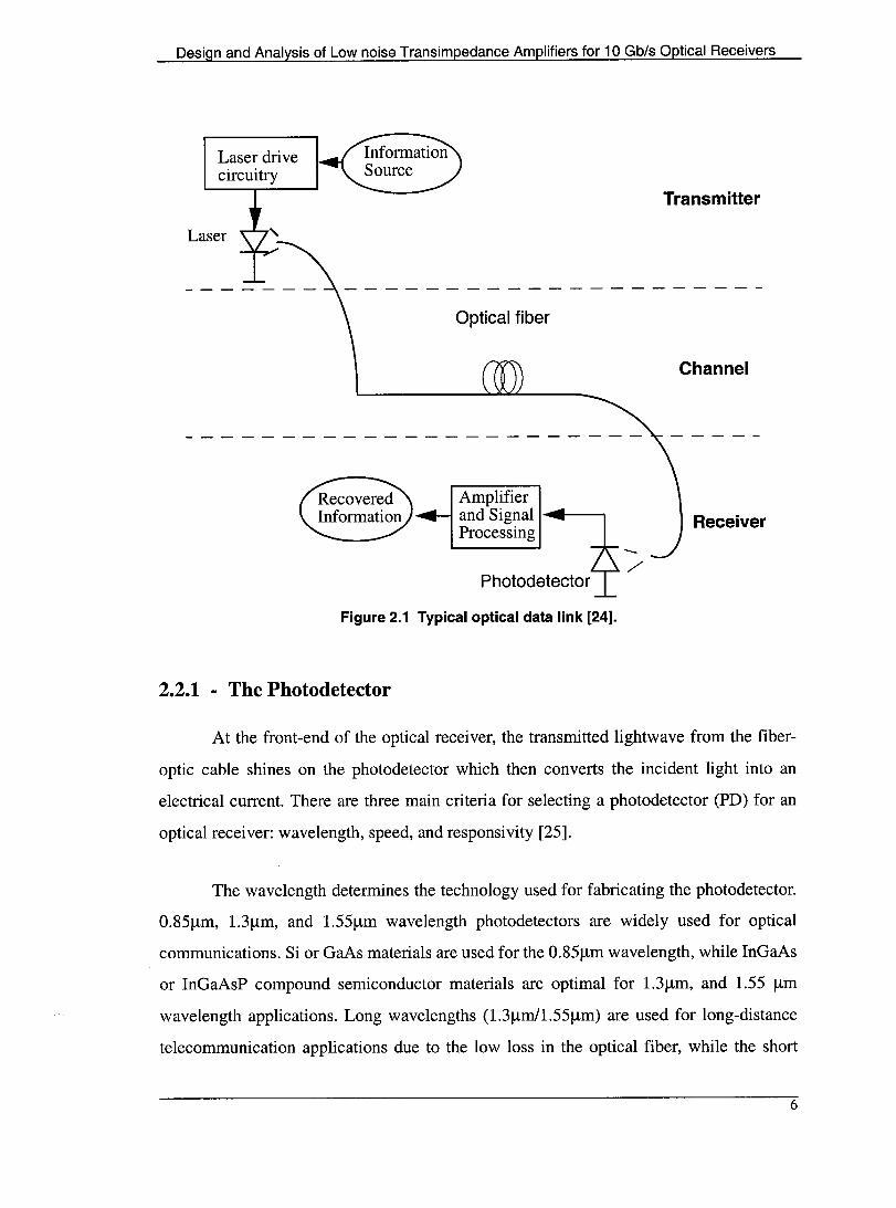
2.2 - Optical Communication Links
Today's low-loss glass fiber optic cable offers almost unlimited bandwidth and
unique advantages over aIl previously developed transmission media. A typical optical
data link, shown in Fig. 2.1, consists of three components: the transmitter, the
transmission medium, and the receiver [24].
The optical transmitter converts an electrical analog or digital signal into a
corresponding optical signal. The source of the optical signal can be either a light emitting
diode, or a solid state laser diode. The most popular wavelengths of operation for optical
transmitters are 850, 1300, or 1550 nanometers.The fiber optic cable consists of one or
more glass fibers, which act as waveguides for the optical signal. A fiber optic cable is
similar to an electrical cable in its construction, but provides special protection for the
optical fiber within. For systems requiring transmission over distances of many
kilometers, or where two or more fiber optic cables must be joined together, an optical
splice is commonly used. The optical receiver converts the optical signal back into a
replica of the original electrical signal. The detector of the optical signal is either a PIN
type photodiode or an avalanche-type photodiode.
Among the three components of an optical communications system, the receiver is
the most difficult to design. Even though a complete optical receiver consists of several
functional blocks, our focus in this work is on the front-end of the receiver which includes
the photodetector and the low-noise wide bandwidth amplifier.
5
Design and Analysis of Law noise Transimpedance Amplifiers for 10 Gb/s Optical Receivers
Laser drive circuitry
Laser
Optical fiber
Amplifier and Signal :} Processing
Photodetector "/
Figure 2.1 Typical optical data link [24].
2.2.1 - The Photodetector
Transmitter
Channel
Receiver
At the front-end of the optical receiver, the transmitted lightwave from the fiber
optic cable shines on the photodetector which then con verts the incident light into an
electrical CUITent. There are three main criteria for selecting a photodetector (PD) for an
optical receiver: wavelength, speed, and responsivity [25].
The wavelength determines the technology used for fabricating the photodetector.
O.85J.1m, 1. 3 J.1m, and 1.55J.1m wavelength photodetectors are widely used for optical
communications. Si or GaAs materials are used for the O.85J.1m wavelength, while InGaAs
or InGaAsP compound semiconductor materials are optimal for 1. 3 J.1m, and 1.55 J.1m
wavelength applications. Long wavelengths (1.3J.1m!1.55J.1m) are used for long-distance
telecommunication applications due to the low loss in the optical fiber, while the short
6
Design and Analysis of Low noise Transimpedance Amplifiers for 10 Gb/s Optical Receivers
wavelength (0.85Jlm) is used for short-distance applications, since GaAs photodetectors
are less complex to build, and result in lower cost.
The speed of the photodetector is mainly determined by either the photodetector
capacitance or the carrier transit time. Depending on the size and structure of the PD, the
photodetector capacitance varies. There are three different types of photodetectors widely
used: avalanche, Metal-Semiconductor-Metal (MSM), and P-i-N PD's. Photodetectors
should have low capacitance, low dark current, and high sensitivity. MSM PD's have the
lowest capacitance among the three at a given size.
Another important characteristic is the responsivity of the photodetector.
Responsivity determines how much current can be generated when a certain amount of
light shines upon the photodetector. Practical photodetector responsivity varies from 0.5
to 1.2 amp/watt, depending on the material and the fabrication method. Selecting a
photodetector with good responsivity is very important for the overall performance of the
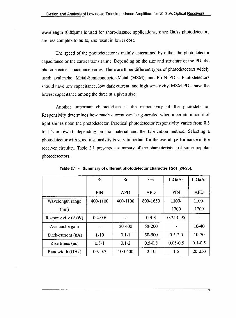
receiver circuitry. Table 2.1 presents a summary of the characteristics of sorne popular
photodetectors.
Table 2.1 - Summary of different photodetector characteristics [24-25].
Si Si Ge InGaAs InGaAs
PIN APD APD PIN APD
Wavelength range 400-1100 400-1100 800-1650 1100- 1100-
(nm) 1700 1700
Responsivity (A/W) 0.4-0.6 - 0.3-3 0.75-0.95 -
Avalanche gain - 20-400 50-200 - 10-40
Dark-current (nA) 1-10 0.1-1 50-500 0.5-2.0 10-50
Rise times (ns) 0.5-1 0.1-2 0.5-0.8 0.05-0.5 0.1-0.5
Bandwidth (GHz) 0.3-0.7 100-400 2-10 1-2 20-250
7
Design and Analysis of Low noise Transimpedance Amplifiers for 10 Gb/s Optical Receivers
Si Si Ge InGaAs InGaAs
PIN APD APD PIN APD
Bias voltage (V) 5 150-400 20-40 5 20-30
Detector 1-5 1-5 1-5 0.2-2 0.2-2
capacitance(pF)
Once a PD converts the incident light into current signal, an amplifier boosts the
small current input from the photodetector and converts it into a voltage output signal.
Therefore, it is known as a transimpedance amplifier. Sorne characteristic requirements
for these ampli fiers are: low noise, wide bandwidth, wide dynamic range, and high gain.
The choice of the design methodology has a large impact on the performance of these
amplifiers.
2.2.2 - Receiver Systems
Future multimedia networks will require high-speed communications systems
even for private networks, such as high speed local area networks (LAN's) and wide area
networks (WAN's). Optical transmission systems operating at several Gb/s will be
introduced into such systems in order to achieve large capacity. For such networks,
however, it is necessary to achieve a compact optical terminal with low power
consumption at low cost. To achieve a compact optical terminal, an optical terminal IC
that fully integrates the desired functions is indispensable. The data rate of several Gb/s is
attractive for LAN's and WAN's because of their connectivity to the trunk line systems in
which synchronous optical network (SONET) or synchronous digital hierarchy (SDH)
schemes are used [13].
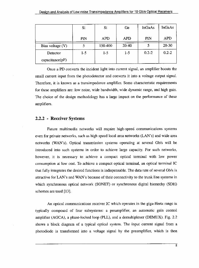
An optical communications receiver IC which operates in the giga-Hertz range is
typically composed of four subsystems: a pre amplifier, an automatic gain control
amplifier (AGCA), a phase-Iocked loop (PLL), and a demultiplexer (DEMUX). Fig. 2.2
shows a block diagram of a typical optical system. The input current signal from a
photodiode is transformed into a voltage signal by the pre amplifier, which is then
8
Design and Analysis of Low noise Transimpedance Amplifiers for 10 Gb/s Optical Receivers
amplified to a fixed value by the AGC circuit. The PLL circuit extracts a clock signal from
the input data, and the DEMUX circuit converts the input seriaI data into an N-bit parallel
data.
Fiber Transmitter
1 r-----------------------~
AGC D-FIF DMUX
Optical data input 1 1
Data output
Receiver Part 1 PLL
1 1 L _______________________ ~
L ________________________________ _
Figure 2.2 Block diagram of a typical optical receiver [13].
Several issues need to be addressed when implementing optical terminal IC's: 1)
DC coupling between circuits, 2) integration of aIl functions, including c10ck extraction,
on the same die, 3) reduction in crosstalk between the digital circuits and the analog
circuits, and 4) minimizing power consumption. New technologies which help mitigating
these challenges have been proposed, such as the high fT Silicon-Germanium (SiGe) alloy
base transistors with wide-gap emitters [26-27], or with retrograded Ge profile [28-29].
Furthermore, isolation technologies (such as trench isolation) and bond and etchback
silicon-on-insulator (SOI) substrates can reduce parasitic capacitances.
Since the sensitivity of a receiver is dominated by the noise sources in the front
end (the pre amplifier stage), the major emphasis in this thesis has been on the design of a
low-noise preamplifier. The goal is to maximize the receiver sensitivity while maintaining
a suitable bandwidth. Preamplifiers used in optical fiber communications receivers can be
c1assified into three broad categories: 1) the low impedance voltage amplifier, 2) the high
impedance voltage amplifier, and 3) the transimpedance amplifier. These will be
discussed in detail the following chapter. Tables 2.2-2.4 show the CUITent research status
9
Design and Analysis of Low noise Transimpedance Amplifiers for 10 Gb/s Optical Receivers
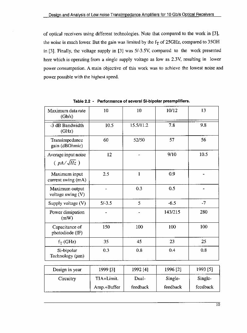
of optical receivers using different technologies. Note that compared to the work in [3],
the noise is much lower. But the gain was limited by the fT of 25GHz, compared to 35GH
in [3]. Finally, the voltage supply in [3] was 5/-3.5V, compared to the work presented
here which is operating from a single supply voltage as low as 2.3V, resulting in lower
power consumpation. A main objective of this work was to achieve the lowest noise and
power possible with the highest speed.
Table 2.2 - Performance of several Si-bipolar preamplifiers.
Maximum data rate 10 10 10/12 13 (Gb/s)
-3 dB Bandwidth 10.5 15.5/11.2 7.8 9.8 (GHz)
Transimpedance 60 52/50 57 56 gain (dBOhmic)
Average input noise 12 - 9/10 10.5
( pAI./Hz )
Maximum input 2.5 1 0.9 -CUITent swing (mA)
Maximum output - 0.3 0.5 -voltage swing (V)
Supply voltage (V) 5/-3.5 5 -6.5 -7
Power dissipation - - 143/215 280 (mW)
Capacitance of 150 100 100 100 photodiode (fF)
fT (GHz) 35 45 23 25
Si-bipolar 0.3 0.8 0.4 0.8 Technology (J.Am)
Design in year 1999 [3] 1992 [4] 1996 [2] 1993 [5]
Circuitry TIA+Limit. Dual- Single- Single-
Amp.+Buffer feedback feedback feedback
10
Design and Analysis of Low noise Transimpedance Amplifiers for 10 Gb/s Optical Receivers
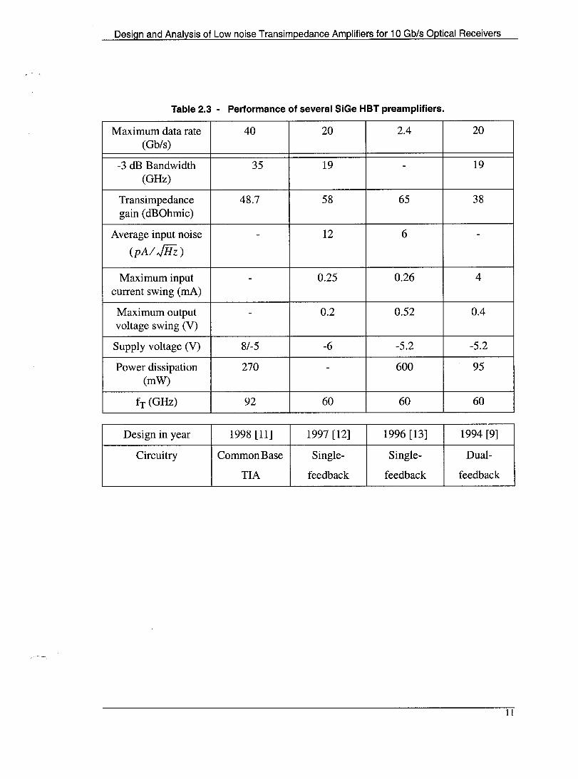
Table 2.3 - Performance of several SiGe HBT preamplifiers.
Maximum data rate 40 20 204 20 (Gb/s)
-3 dB Bandwidth 35 19 - 19 (GHz)
Transimpedance 48.7 58 65 38 gain (dBOhmic)
Average input noise - 12 6 -(pAl JHz)
Maximum input - 0.25 0.26 4 CUITent swing (mA)
Maximum output - 0.2 0.52 004 voltage swing (V)
Supply voltage (V) 8/-5 -6 -5.2 -5.2
Power dissipation 270 - 600 95 (mW)
fT (GHz) 92 60 60 60
Design in year 1998 [11] 1997 [12] 1996 [13] 1994 [9]
Circuitry CommonBase Single- Single- Dual-
TIA feedback feedback feedback
11
Design and Analysis of Low noise Transimpedance Amplifiers for 10 Gb/s Optical Receivers
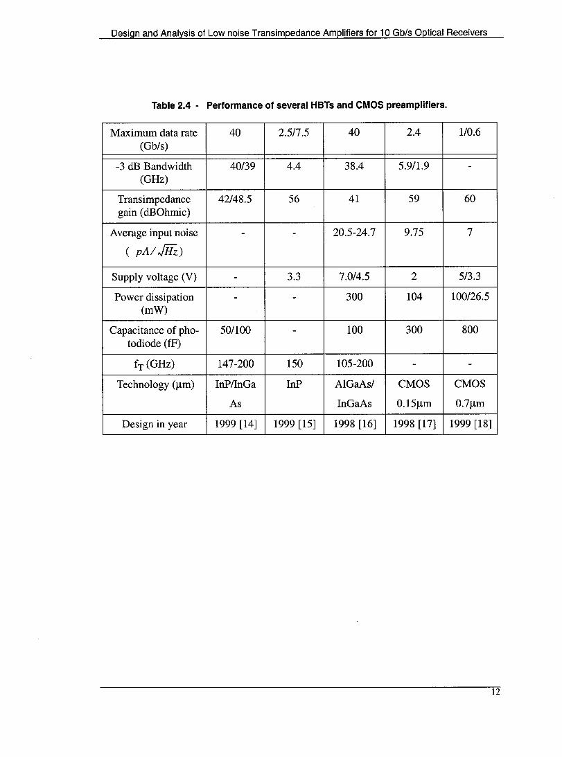
Table 2.4 - Performance of several HBTs and CMOS preamplifiers.
Maximum data rate 40 2.517.5 40 2.4 1/0.6 (Gb/s)
-3 dB Bandwidth 40/39 4.4 38.4 5.9/1.9 -(GHz)
Transimpedance 42/48.5 56 41 59 60 gain (dBOhmic)
Average input noise - - 20.5-24.7 9.75 7
( pAl Jifz)
Supply voltage (V) - 3.3 7.0/4.5 2 5/3.3
Power dissipation - - 300 104 100/26.5 (mW)
Capacitance of pho- 50/100 - 100 300 800 todiode (fF)
fT (GHz) 147-200 150 105-200 - -
Technology (J..lm) InPlInGa InP AIGaAs/ CMOS CMOS
As InGaAs 0.15J..lm 0.7J..lm
Design in year 1999 [14] 1999 [15] 1998 [16] 1998 [17] 1999 [18]
12
Design and Analysis of Low noise Transimpedance Amplifiers for 10 Gb/s Optical Receivers
Chapter 3- Optical Receiver Front
ends Design
Considerations
3.1 - Introduction
In this chapter, research trends and optical receiver design methods are presented
and analyzed.
3.2 - Technology
One of the major goals when designing an optical receiver frontend is to minimize
the noise it generates while amplifying signal. Noise can be reduced by minimizing base
resistance rB and maximizing fT at very low emitter current, as given by the simplified
expression for the minimum noise figure of a bipolar transistor [30]
(3.1)
where
13
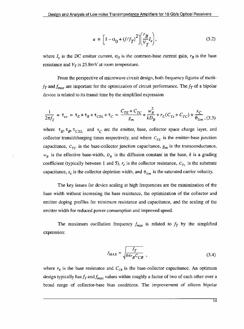
Design and Analysis of Low noise Transimpedance Amplifiers for 10 Gb/s Optical Receivers
(3.2)
where le is the De emitter cUITent, aa is the common-base CUITent gain, rB is the base
resistance and V T is 25. 8m V at room temperature.
From the perspective of microwave circuit design, both frequency figures of merit
fT andfmax are important for the optimization of circuit performance. The fT of a bipolar
device is related to its transit time by the simplified expression
where 'tE' 'tB, 'tesL and 'te are the emitter, base, collector space charge layer, and
collector transitlcharging times respectively, and where eTE is the emitter-base junction
capacitance, eTC is the base-collector junction capacitance, 8m is the transconductance,
WB is the effective base-width, DB is the diffusion constant in the base, k is a grading
coefficient (typically between 1 and 5), rc is the collector resistance, eTs is the substrate
capacitance, Xc is the collector depletion width, and l}lim is the saturated carrier velocity.
The key issues for device scaling at high frequencies are the minimization of the
base width without increasing the base resistance, the optimization of the collector and
emitter doping profiles for minimum resistance and capacitance, and the scaling of the
emitter width for reduced power consumption and improved speed.
The maximum oscillation frequency fmax is related to fT by the simplified
expression:
(3.4)
where rB is the base resistance and CCB is the base-collector capacitance. An optimum
design typically hasfTandfmax values within roughly a factor of two of each other over a
broad range of collector-base bias conditions. The improvement of silicon bipolar
14
Design and Analysis of Low noise Transimpedance Amplifiers for 10 Gb/s Optical Receivers
technologies with respect to higher operating speeds often exhibits compromises in the
form of a reduction in the breakdown voltage. This limit is material related, and
consequently is not amenable to improvements in device design or process technology
[30].
3.3 - Review of Optical Receiver Frontends Design
An optical receiver frontend can usually be categorized as one of four basic
topologies: 1) Resistor termination with a low-impedance voltage amplifier, 2) a high
impedance amplifier, 3) a transimpedance amplifier, and 4) a noise-matched or resonant
amplifier [31]. Any one of these configurations can be built using contemporary electronic
devices such as bipolar junction transistors, field-effect transistors, or high electron
mobility transistors. The receiver performance that is achieved will depend on the devices
and design techniques used. The main design objective is usually to maximize the receiver
sensitivity while maintaining a suitable bandwidth. The different amplifiers do achieve
these goals in different ways.
3.3.1 - The Low Impedance Voltage Amplifier
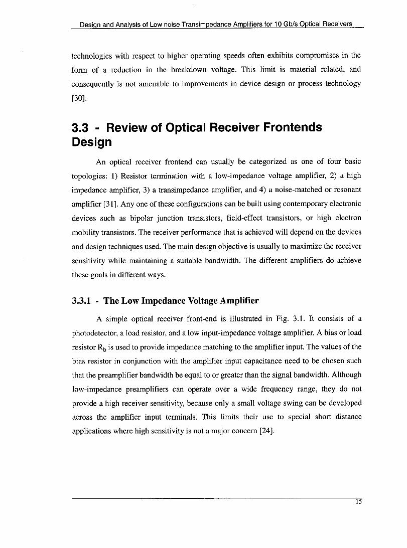
A simple optical receiver front-end is illustrated in Fig. 3.1. It consists of a
photodetector, a load resistor, and a low input-impedance voltage amplifier. A bias or load
resistor Rb is used to provide impedance matching to the amplifier input. The values of the
bias resistor in conjunction with the amplifier input capacitance need to be chosen such
that the preamplifier bandwidth be equal to or greater than the signal bandwidth. Although
low-impedance preamplifiers can operate over a wide frequency range, they do not
provide a high receiver sensitivity, because only a small voltage swing can be developed
across the amplifier input terminaIs. This limits their use to special short distance
applications where high sensitivity is not a major concem [24].
15
Design and Analysis of Low noise Transimpedance Amplifiers for 10 Gb/s Optical Receivers
Received Light Signal
~
-Vbias
Vout
Figure 3.1 The low impedance voltage amplifier topology [25].
3.3.2 - The High Impedance Amplifier
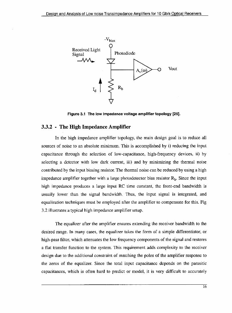
In the high impedance amplifier topology, the main design goal is to reduce aIl
sources of noise to an absolute minimum. This is accomplished by i) reducing the input
capacitance through the selection of low-capacitance, high-frequency devices, ii) by
selecting a detector with low dark cUITent, iii) and by minimizing the thermal noise
contributed by the input biasing resistor. The thermal noise can be reduced by using a high
impedance amplifier together with a large photodetector bias resistor Rb' Since the input
high impedance produces a large input Re time constant, the front-end bandwidth is
usually lower than the signal bandwidth. Thus, the input signal is integrated, and
equalization techniques must be employed after the amplifier to compensate for this. Fig
3.2 illustrates a typical high impedance amplifier setup.
The equalizer after the amplifier ensures extending the receiver bandwidth to the
desired range. In many cases, the equalizer takes the form of a simple differentiator, or
high-pass filter, which attenuates the low frequency components of the signal and restores
a fIat transfer function to the system. This requirement adds complexity to the receiver
design due to the additional constraint of matching the poles of the amplifier response to
the zeros of the equalizer. Since the total input capacitance depends on the parasitic
capacitances, which is often hard to predict or model, it is very difficult to accurately
16
Design and Analysis of Low noise Transimpedance Amplifiers for 10 Gb/s Optical Receivers
compensate for the pales of the amplifier. Ta still achieve a fast frequency response, it is
important ta reduce the input capacitance as much as possible through the selection of a
high-speed optoelectronic device with low capacitance.
Received Light Signal
~
-Vbias
Equalizer Vout
Figure 3.2 The high impedance topology [25].
To avoid using an equalizer, a low value of resistor can be used instead. This leads
ta the low-impedance type amplifier discussed earlier. The latter has a very broad
bandwidth and a good dynamic range at the cast of high noise level.
From Fig. 3.1 and 3.2, the overall gain of the system can be described by
(3.5)
where A( (ù) is the gain of the amplifier, Rb is the bias resistor, and Ct is the total input
capacitance inc1uding the photodiode capacitance (Cpd)' the setup parasitic capacitance
(Cpara)' and the input capacitance (Cin) of the amplifier. Thus
A(w)= (3.6)
17
Design and Analysis of Low noise Transimpedance Amplifiers for 10 Gb/s Optical Receivers
C - C +C +C. t - pd para zn (3.7)
(3.8)
The transfer function in Eq. (3.5) has two poles. Typically the dominant pole of the
transfer function is the one due to the input capacitance (l/CtRb).
Another drawback of using a large Rb lies in the resulting limited dynamic range.
The loss of dynamic range occurs because the accumulation of charges on the input
capacitance over a number of input pulses results in an input DC offset. The reduction of
dynamic range depends on the amount of integration.
In many cases, the input capacitance is mostly dominated by that of the
photodetector. However, as photodetectors with very low capacitances are developed,
other capacitance sources such as pad capacitances or input transistor capacitances could
become dominant. In either case, the total input capacitance is constrained by the device
selection. Thus, changing the resistor value of Rb is the only option left to change the RC
time constant. To get a wider bandwidth, the value of Rb is forced to be low. However, a
low resistance value would affect the sensitivity of the amplifier due to its higher thermal
noise contribution.
3.3.3 - Transimpedance Amplifier
The transimpedance amplifier topology is discussed next. It is a popular approach
to avoid the dynamic range limitations discussed above. This configuration provides a
compromise between the low- and high-impedance configurations, resulting in a relatively
wide bandwidth, a reasonable dynamic range, and a good noise level. It is designed to take
advantage of negative feedback so that the amplifier bandwidth is extended to the desired
value while reducing the effect of noise.
18
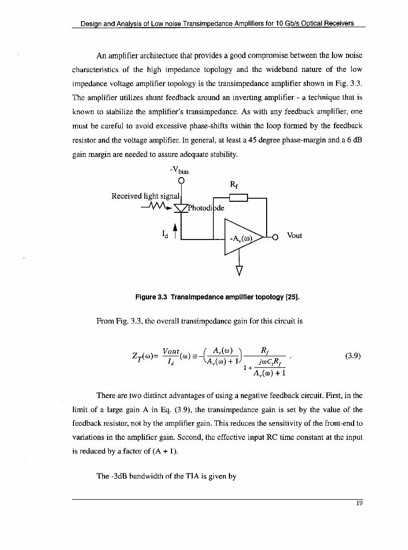
Design and Analysis of Low noise Transimpedance Amplifiers for 10 Gb/s Optical Receivers
An amplifier architecture that provides a good compromise between the low noise
characteristics of the high impedance topology and the wideband nature of the low
impedance voltage amplifier topology is the transimpedance amplifier shown in Fig. 3.3.
The amplifier utilizes shunt feedback around an inverting amplifier - a technique that is
known to stabilize the amplifier's transimpedance. As with any feedback amplifier, one
must be careful to avoid excessive phase-shifts within the loop formed by the feedback
resistor and the voltage amplifier. In general, at least a 45 degree phase-margin and a 6 dB
gain margin are needed to assure adequate stability.
-Vbias
Received light signal
~ hotodi de
Vout
Figure 3.3 Transimpedance amplifier topology [25].
From Fig. 3.3, the overall transimpedance gain for this circuit is
(3.9)
There are two distinct advantages of using a negative feedback circuit. First, in the
limit of a large gain A in Eq. (3.9), the transimpedance gain is set by the value of the
feedback resistor, not by the amplifier gain. This reduces the sensitivity of the front-end to
variations in the amplifier gain. Second, the effective input Re time constant at the input
is reduced by a factor of (A + 1).
The -3dB bandwidth of the TIA is given by
19
Design and Analysis of Law noise Transimpedance Amplifiers for 10 Gb/s Optical Receivers
_A(w)+l fl-3dB = 2nR in Ct '
(3.10)
where Rin is the total input resistance of the input amplifier. If the bias resistor Rb in the
low/high impedance amplifier topology is of the same order of magnitude of the feedback
resistor, this results in an upper -3 dB frequency for the transimpedance amplifier which is
A times larger than the cutoff frequency of the open-Ioop case. However, the maximum-3
dB bandwidth is limited by A(w) from Eq. (3.10), since A(w) itself is frequency
dependent. Therefore, feedback type ampli fiers may not be a good choice when the
system bandwidth requirement approaches the limits of the circuit technology used.
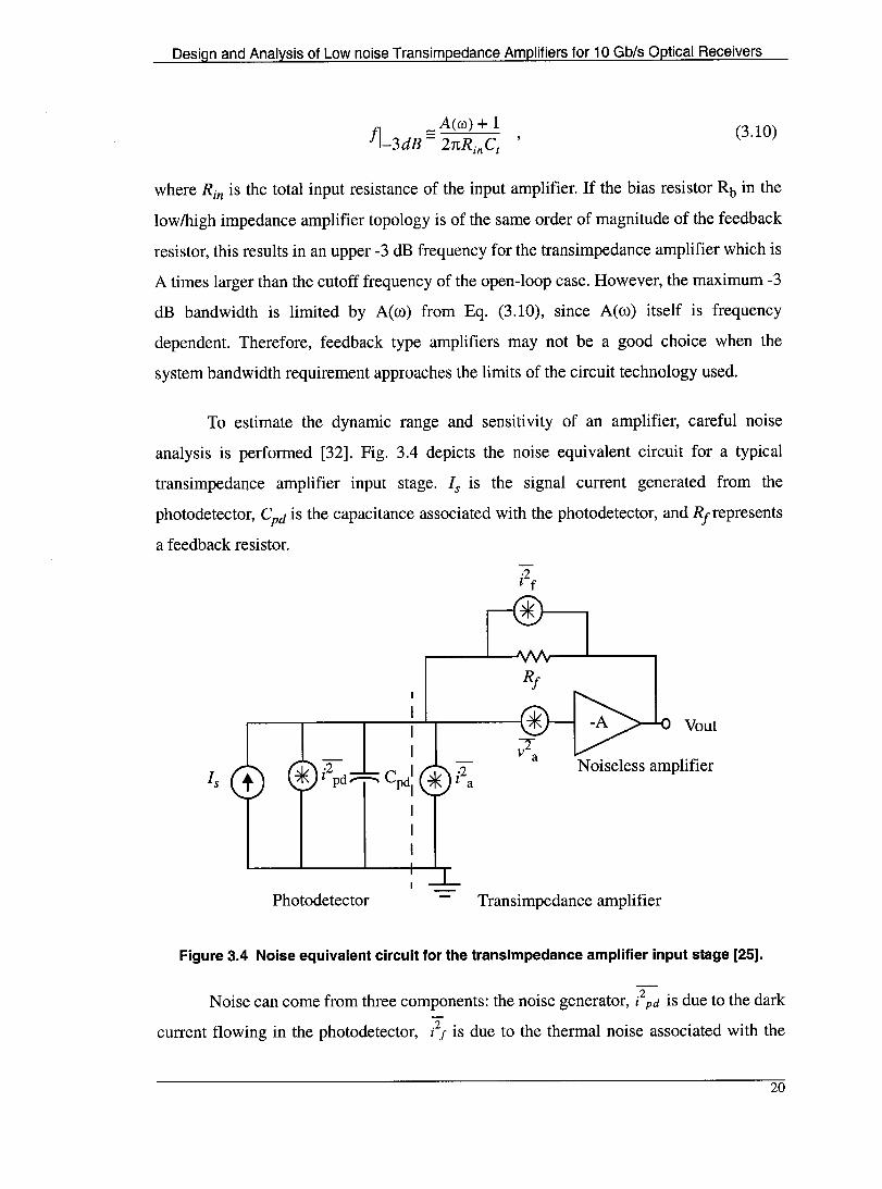
To estimate the dynamic range and sensitivity of an amplifier, careful noise
analysis is performed [32]. Fig. 3.4 depicts the noise equivalent circuit for a typical
transimpedance amplifier input stage. Is is the signal current generated from the
photodetector, Cpd is the capacitance associated with the photodetector, and Rfrepresents
a feedback resistor.
1
1 ·2 1 2 l pd ----- Cpdl "* i a
1 1
1
Photodetector
·2 l f
Vout
Noiseless amplifier
Transimpedance amplifier
Figure 3.4 Noise equivalent circuit for the transimpedance amplifier input stage [25].
Noise can come from three components: the noise generator, i2p d is due to the dark
current flowing in the photodetector, ?f is due to the thermal noise associated with the
20
Design and Analysis of Low noise Transimpedance Amplifiers for 10 Gb/s Optical Receivers
feedback resistor, i2 a and i a characterize the various noise sources in the amplifier,
assuming the amplifier is noise free.
Noise sources associated with subsequent portions of the amplifier are assumed to
be small, and are thus neglected. The spectral density for each noise source is as follows
[33]
(3.11)
:2 _ 4kT Af lf- R L.l ,
f (3.12)
(3.13)
"2 ( 1 ) v a = 4kT r b 1 + 2-- 8f , gml
(3.14)
where 8fis the noise bandwidth, rhl is the base resistance of the input transistor, and gml
is its transconductance, q is the electron charge, k is the Boltzman constant, T is the
absolute temperature, lhl and IcJ are the base and collector currents of the input transistor,
and ~ is the transistor current gain. For low noise performance, Rfshould be appropriately
chosen, and rhl should be minimized.
Eq. (3.11) is the noise spectral density caused by the dark current, ldark' in the
photodetector. Eq. (3.12) is due to the thermal noise from either the biasing resistor Rh, or
the feedback resistor, Rf Eq. (3.13) is the shot noise in the base and collector current
caused by carriers random motion in the input transistor. Finally, Eq. (3.14) is the series
noise term due to the base spreading resistance thermal noise and the emitter resistance
thermal noise. The total noise power spectral density at the input node is given by
21
Design and Analysis of Low noise Transimpedance Amplifiers for 10 Gb/s Optical Receivers
(3.15)
where lin is the admittance at the input node given by
(3.16)
where Ct is the sum of aIl the capacitances connected to the input node. The total output
noise is obtained by integrating the product of the input total noise spectral density by the
power of the system transfer function, over a given noise frequency bandwidth. In
practice, the transfer function has a flat response over the frequency range of interest.
Therefore, the total output noise power would simply be the product of the transfer
function, spectral density, and bandwidth.
The noise of a high-impedance topology would be the same as that of a feedback
amplifier if Rf = Rb' The noise performance of the feedback amplifier is not as good as
that achieved by the high-impedance amplifier because, in practice, the amplifier gain is
finite and the actual transfer function is composed of two or more poles. For a finite open
loop gain, increasing the feedback resistance in order to reduce the noise tends to make the
pole locations complex and, under sorne conditions, can make the amplifier bec orne
unstable.
In summary, the benefits of a transimpedance amplifier are as follows: 1) It has a
wide dynamic range compared to the high impedance amplifier. 2) UsuaIly, little or no
equalization is required because the sum of Rin and the feedback resistor Rf is usually
smaIl, which means that the time constant of the detector is also small. 3) The output
resistance is smaIl, so the amplifier is less susceptible to picked up noise, crosstalk,
electromagnetic interference (EMI), etc. 4) The transfer characteristic of the amplifier is
set by the feedback resistor. Therefore, the overall amplifier is very easily controlled. 5)
Although the transimpedance amplifier is in fact less sensitive than the high impedance
22
Design and Analysis of Low noise Transimpedance Amplifiers for 10 Gb/s Optical Receivers
amplifier, the difference is only in the order of 2-3 dB for most practical wideband designs
[24]. ·2 1 f
Vout
... 1/ ·2 ~ 1 a
Noiseless amplifier
Photodiode small signal circuit
Impedance matching network
Transimpedance amplifier
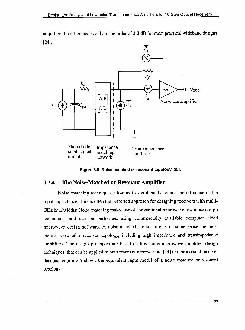
Figure 3.5 Noise matched or resonant topology [25].
3.3.4 - The Noise-Matched or Resonant Amplifier
Noise matching techniques allow us to significantly reduce the influence of the
input capacitance. This is often the preferred approach for designing receivers with multi
GHz bandwidths; Noise matching makes use of conventional microwave low noise design
techniques, and can be performed using commercially available computer aided
microwave design software. A noise-matched architecture is in sorne sense the most
general case of a receiver topology, including high impedance and transimpedance
amplifiers. The design principles are based on low noise microwave amplifier design
techniques, that can be applied to both resonant narrow-band [34] and broadband receiver
designs. Figure 3.5 shows the equivalent input model of a noise matched or resonant
topology.
23
Design and Analysis of Law noise Transimpedance Amplifiers for 10 Gb/s Optical Receivers
The overall noise performance of an optical receiver is generally a strong function
of the photodetector's impedance. The basic principle behind the noise-matched topology
is the use of an impedance matching network, located between the photodetector and the
first amplifier stage, which con verts the highly capacitive source to an impedance that
results in a better noise match for the input transistor. Such noise-matching networks are
based on the noise figure concept, in conjunction with the broadband matching theory
[35].
A limited number of noise-matching network topologies, usually inductive series,
parallel, and T-network types, have been used in optical receiver designs. The choice of a
parallel or series inductance is also influenced by the relative size of the voltage and
current noise sources, and by the ratio of the detector capacitance to the input capacitance.
In general, when the photodetector capacitance is less than or equal to the amplifier's
input capacitance, series tuning is used to advantage. When the detector capacitance is
large it emphasizes the voltage noise, and a parallel inductor is then preferred.
The benefits obtained with noise matching are not without limits. As with any
broadband impedance matching, there are fundamentallimits on the amount of power that
can be transferred without loss from a reactive source, such as a photodiode, to a reactive
load, such as an amplifier. The constraints associated with this give the bounds for lossless
matching using a passive network consisting of inductors, capacitors, and transformers.
Among the different configurations discussed in this chapter, the transimpedance
configuration was chosen and used for the implementation of a bipolar amplifier as
detailed in the following chapter.
24
Design and Analysis of Low noise Transimpedance Amplifiers for 10 Gb/s Optical Receivers
Chapter 4 - TIA Design, Fabrication,
and Testing
4.1 - Introduction
A low-noise, low power Si-bipolar transimpedance pre amplifier for optical-fibre
receivers is presented in this chapter. Design specifications are met in the form of trade
offs between input noise cUITent, speed, transimpedance gain, power dissipation,
impedance matching, and supply voltage. This goal was achieved by 1) using integrated
inductors to enhance the bandwidth, 2) using a tuned noise-matching network at the input
to improve the signal-to-noise ratio (SNR), 3) and using frequency compensation
techniques to improve stability, and to further enhance the bandwidth of the preamplifier.
In a lightwave system, the receiver, composed of a photodetector and preamplifier,
converts light pulses into usable voltage signaIs. To achieve high quality voltage signaIs,
the preamplifier should have high sensitivity, low noise, and large dynamic range. The
input to the preamplifier is a CUITent obtained from a photodiode that is connected to the
amplifier using a very short bondwire. PIN photodiodes are commonly used, since their
bandwidths are much higher than those of avalanche photodiodes (APD's). The output of
the amplifier usually drives a 50 Ohm transmission line, requiring proper on-chip
termination to reduce reflections. Since the input to the amplifier is in CUITent format, and
25
Design and Analysis of Low noise Transimpedance Amplifiers for 10 Gb/s Optical Receivers
the output needs to be in voltage format, a transimpedance preamplifier structure is
commonly used.
Several transimpedance amplifier topologies are compared, and design trade-offs
are introduced. The optimization procedure followed to realize a wide-bandwidth optical
receiver pre amplifier in a bipolar technology is described. Considering power dissipation,
operating bandwidth, and sensitivity (or input referred noise level). Four configurations
are discussed: The common-emitter amplifier (CE), the common-base amplifier (CB), the
cascode transimpedance amplifier, and the single-stage amplifier. This is followed by a
discussion of the transimpedance amplifier implemented, and then the integration of an
optoelectronic device model with the pre amplifier prototype. The design, simulation,
layout and test of the preamplifier are presented in detail. The performance of the TIA is
discussed based on measurements.
4.2 - Optimization of a Bipolar Transimpedance Preampl ifier
4.2.1 - Transimpedance Amplifier Topologies
There are four topologies suitable for the design of transimpedance amplifiers. The
first topology is the single stage transimpedance feedback amplifier (Fig.4.1(a». This
circuit is not commonly used with Si bipolar transistors because it results in a very low
bias voltage between the collector and the base, reducing the speed of the transistor. The
second topology is the commonly used common emitter/common collector (CE)
configuration (Fig.4.1(b». It exhibits the lowest input current noise compared to other
topologies. However, it is limited by the Miller capacitance of the input transistor. To
eliminate the Miller capacitance, and extend the bandwidth, a third topology which
inc1udes a cascode device to the input transistor can be used (Fig.4.1(c». However, the
cascode connection adds an extra transistor to the feedback loop, resulting in addition al
poles and poor noise performance. Recently, a fourth topology based on a common-base
structure has been reported [11] (Fig.4.1(d». It was shown to be more robust and stable
26
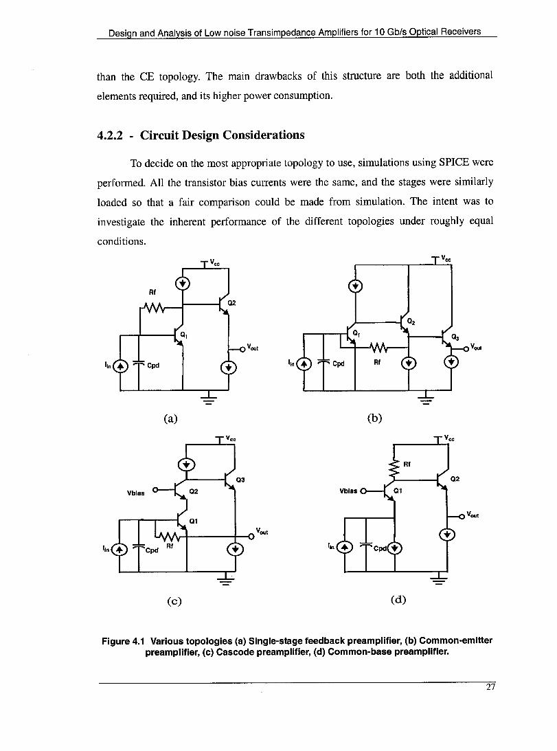
Design and Analysis of Low noise Transimpedance Amplifiers for 10 Gb/s Optical Receivers
than the CE topology. The main drawbacks of this structure are both the addition al
elements required, and its higher power consumption.
4.2.2 - Circuit Design Considerations
To decide on the most appropriate topology to use, simulations using SPICE were
performed. AlI the transistor bias currents were the same, and the stages were similarly
loaded so that a fair comparison could be made from simulation. The intent was to
investigate the inherent performance of the different topologies under roughly equal
conditions.
(a)
Vou! \r-f-----f~D
(c)
(h)
(d)
Figure 4.1 Various topologies (a) Single-stage feedback preamplifier, (b) Common-emitter preamplifier, (c) Cas code preamplifier, (d) Common-base preamplifier.
27
Design and Analysis of Low noise Transimpedance Amplifiers for 10 Gb/s Optical Receivers
The stability, bandwidth, noise, and transimpedance are aU dependent on the
values chosen for the feedback resistor Rf the total input capacitance Ct. and the load
resistor Re' The latter is the most critical component in setting the open loop gain of the
amplifier. The combination of Re. Ct and Rf determines the stability of the amplifier. The
noise of the amplifier in the high speed regime of interest is determined primarily by the
Johnson noise from Rf and the coUector bias CUITent. Earlier research showed that an
optimum bias point exists for obtaining a minimum input noise. For practical high
bandwidth applications, the best bias point is not necessarily at the point where minimum
input noise is obtained. For transistors, high speed operation is often obtained with 1-2mA
of collector CUITent. High speed operation at the optimum bias CUITent for low noise
operation could be maintained by selecting proper transistor sizes, smaller at low
frequencies and larger at high frequencies, in order to achieve the optimum CUITent density
and maintain high speed transistor operation.
Simulations allowed the comparison of the various amplifier topologies in terms of
their transimpedances, stability, and noise performances. Fig 4.2 shows the bandwidth as a
function of the transimpedance obtained for three of the topologies in Figure 4.1 (a-c). The
three topologies can operate at the same frequency. They are more comparable than the
common-base preamplifier in Fig. 4.1 (d). Their frequency responses are dependent on the
values of the collector resistors which, in conjunction with the feedback resistors, set the
open loop gains of the feedback amplifiers. The feedback resistor is chosen such that an
overshoot of less than 10% is obtained in the frequency response. This amount of
overshoot is the limit in practical applications.
The general operation of the circuits can be analyzed as follows: The
transimpedance is set principally by Rf as long as sufficient gain is supplied by RC' Simple
feedback theory gives the bandwidth (BW) and transimpedance (ZT) of this pre amplifier,
(4.1)
28
Design and Analysis of Low noise Transimpedance Amplifiers for 10 Gb/s Optical Receivers
(4.2)
where A is the open loop gain of the amplifier. As the collector resistor is increased, the
open loop gain rises, increasing both the bandwidth and the transimpedance; but this also
results in a lower phase margin for the amplifier, reducing s tabi lit y and increasing
overshoot. As A is increased, the frequency at which instability occurs is reduced. This is
particularly evident for the common-emitter topologies.
The single-stage feedback pre amplifier is very stable over a wide range of
feedback resistor values. This is important for monolithic implementations, because the
stability becomes insensitive to process variations. The disadvantage of the single-stage
feedback topology is its poor noise performance compared to a common-emitter
pre amplifier at equivalent bandwidth. Examples of noise responses as a function of
frequency are shown in Fig. 4.3. These graphs can be analyzed as follows: The open loop
gain Ais roughly proportional to gmRc in the common-emitter amplifier, and to gmR!lRf
in the single-stage feedback amplifier. The latter lower open loop gain, for the same
magnitude of noise generation, results in a higher Zr and consequently a lower input
refeITed noise CUITent for the common-emitter preamplifier. The higher stability of the
single-stage feedback amplifier might be prefeITed despite its poor noise performance,
depending on the application. For the cascode amplifier, it decreases the Miller
capacitance, but adds an extra transistor to the feedback loop, resulting in additional poles
and possible poor noise performance.
29
Design and Analysis of Low noise Transimpedance Amplifiers for 10 Gb/s Optical Receivers
E ..c o m -0
Q) u c o
-0 Q) 0...
E Ul C o L f-
,.-.., u E
..c 0 m -0 ---Q)
u c 0
-0 Q)
0...
E Ul c n
,.-.., u E
..c 0 m -0 ---Q) u c 0
-0 Q) 0...
E Ul c ..,
50
40
30
20
10
0.0
50
40
30
20
10
0.0
50
40
30
20
10
0.0
AC Response
dB20(mog(VF( vout/In)))
1\
\ ~
10M 100M 1G 10G 100G Freouencv (Hz)
C; G nÎ n"'IG n -_. t; n!: 1.i (~r -r i/:1, sc h f: rr'G1.1 C
AC Response
dB20( mog (VF( vout/In)))
\
\ '\ \
AC Response
dB20( mog(VF( vout/In)))
1\ \
\
'" \
Figure 4.2 Simulated frequency responses with different TIA topologies, (a) Single-feedback stage amplifier, (b) Common-emitter amplifier, (c) Cascode amplifier.
30
Design and Analysis of Low noise Transimpedance Amplifiers for 10 Gb/s Optical Receivers
TIANoise X 10-11
3.5,-------,----,-----,-------.----,----,------,
Commolemittet TIA 0.5'-----'------L----'-----...L---'-----L------.J
o 2 Il
Frequency (Hz)
11) 12 14
x 10·
Figure 4.3 Hspice simulation of the equivalent input noise current for three different TIA's.
4.3 - Transimpedance Preamplifier Design
In this section, a pre amplifier based on a common-emiUer configuration, combined
with a feedback resistance (Ri and a frequency compensation capacitance (Cf) is designed
(Fig.4.4). A combination of a resistive (Re) and an inductive (L2) load is used to achieve
low noise and high bandwidth, under a low single supply voltage of 2.3 V. Compared to
an active load, resistive loading only contributes with thermal noise. The compensation
capacitance Cfis used to control the peaking in the frequency response, and to improve the
stability of the preamplifier. The buffer stage (Q3 and Re3) causes small capacitive loading
to the TIA, and does not decrease the bandwidth and it adds slight noise to the output.
Finally, this design operates from a single 2.3 V supply voltage to minimize power, a
highly desirable feature in today's communication systems.
31
Design and Analysis of Low noise Transimpedance Amplifiers for 10 Gb/s Optical Receivers
1 14 =8nH
~II~_~
Figure 4.4 Transimpedance amplifier circuit schematic, showing the bandwidth enhancing inductor (L2) and the frequency compensation capacitance (C,).
To achieve high speed operation with low noise and a good eye-opening, the
design should be carefully optimized. The relationship between the circuit parameters and
the pre amplifier characteristics is shown below [3].
Circuit parameters Preamplifier characteristics
Feedback resistance (Rf) --...... ~ Bandwidth
Load resistance (RL ) Input noise CUITent density
Peaking capacitance (Cf) L-_~ Transimpedance fluctuation
Figure 4.5 Relationship between circuit parameters and preamplifier characteristics [3].
Optimization involving varying individual transistor sizes and bias points to
ensure maximum operating speed, while maximizing the stability margin was performed.
The optimization of transistor sizes is constrained between using small devices with large
base resistances, and using larger devices with increasing parasitic capacitances. Aiso
considered was the effect of the bond wire inductances and the package parasitics on the
circuit performance and stability.
32
Design and Analysis of Low noise Transimpedance Amplifiers for 10 Gb/s Optical Receivers
4.4 - Performance Analysis
4.4.1 - Controlling the Frequency Response
To improve the frequency response and lower the noise, inductors and frequency
compensation techniques are used. Inductive load L 2 is used to increase the bandwidth of
the circuit [35]. This inductor L2 in series with the load resistance Re alters the frequency
response of the amplifier. This technique, called shunt peaking, enhances the response
compared to that of a single pole to one with two poles and a zero. The poles may or may
not be complex. The zero is determined solely by the L 21Re time constant and is primarily
responsible for the bandwidth enhancement. The input inductor LI improves the signal-to
noise ratio (SNR), when connected between the photodetector and the pre amplifier input.
It also enhances the bandwidth of the amplifier. A bondwire inductor for LI would exhibit
a higher quality factor (Q) than an on-chip spiral inductor. Peaking effects could occur due
to the feedback loop. If the c1osed-Ioop response of the transimpedance stage peaks
significantly in the frequency domain, this translates into ringing in the time response, and
can result in higher noise. Thus, the compensation capacitance Cf is used to control
peaking in the frequency response and to improve the stability and bandwidth of the
pre amplifier.
For the preamplifier circuit in Fig. 4.4, the transimpedance gain is approximately
given by
(4.3)
where A(s) is the open-Ioop voltage gain, and Ct is the total input capacitance inc1uding
the photodiode capacitance (Cpd), the setup parasitic capacitance (Cpara)' and the input
capacitance (qn) of the amplifier. Therefore
Ct = C d+ C + C .. P para ln (4.4)
33
Design and Analysis of Low noise Transimpedance Amplifiers for 10 Gb/s Optical Receivers
The -3dB bandwidth of the TIA is given by
(4.5)
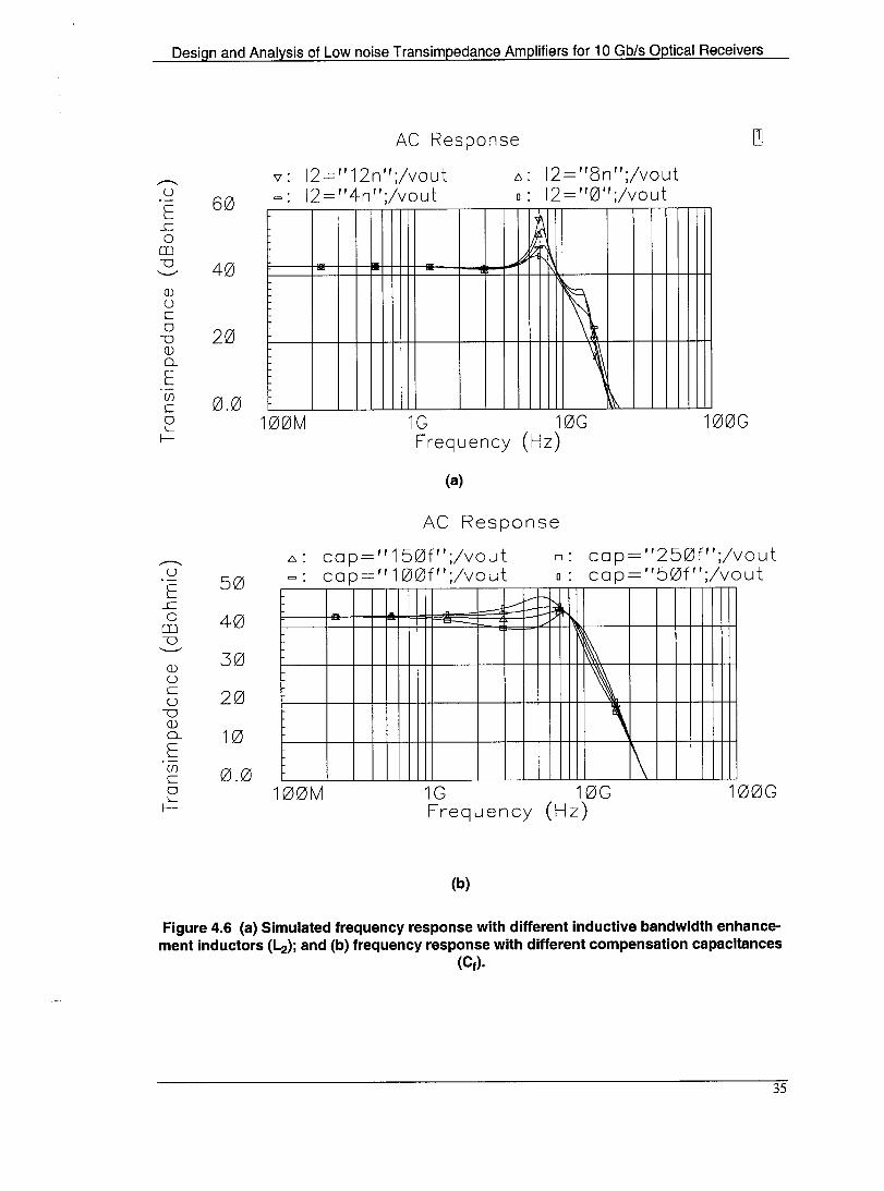
Fig. 4.6 shows the frequency response with different inductive bandwidth enhancement
inductors (L2), and compensation capacitances (Cf).
34
Design and Analysis of Low noise Transimpedance Amplifiers for 10 Gb/s Optical Receivers
..-.. u E 60
...c 0 m -0 40 '--"
Q) u c 0
20 -0 Q) 0...
E UJ
0.0 C 0 L
f--
,--... u
E 50 L 0 40 m
--0
-----Q) 30 u c
20 0 --0 Q)
0... 10 E en 0.0 c 0 L
f-
AC Response
\1: 12="12n";/vout 12="4n";!vout
6.: 12="8n";!vout 0: 12="0";!vout
li ~ J~ ~ - - , ,
~ 100M 1G 10G
Frequency (Hz)
(a)
AC Response
100G
6.' cap="150f";/vout cap=" 100f";/vout
0: cap="250f";/vout 0: cap="50f";!vout
--= 1---r-~~ - 1\
~ \ \ \
100M 1G 10G 100G Frequency (Hz)
(b)
Figure 4.6 (a) Simulated frequency response with different inductive bandwidth enhancement inductors (L2); and (b) frequency response with different compensation capacitances
(Cf)'
35
Design and Analysis of Low noise Transimpedance Amplifiers for 10 Gb/s Optical Receivers
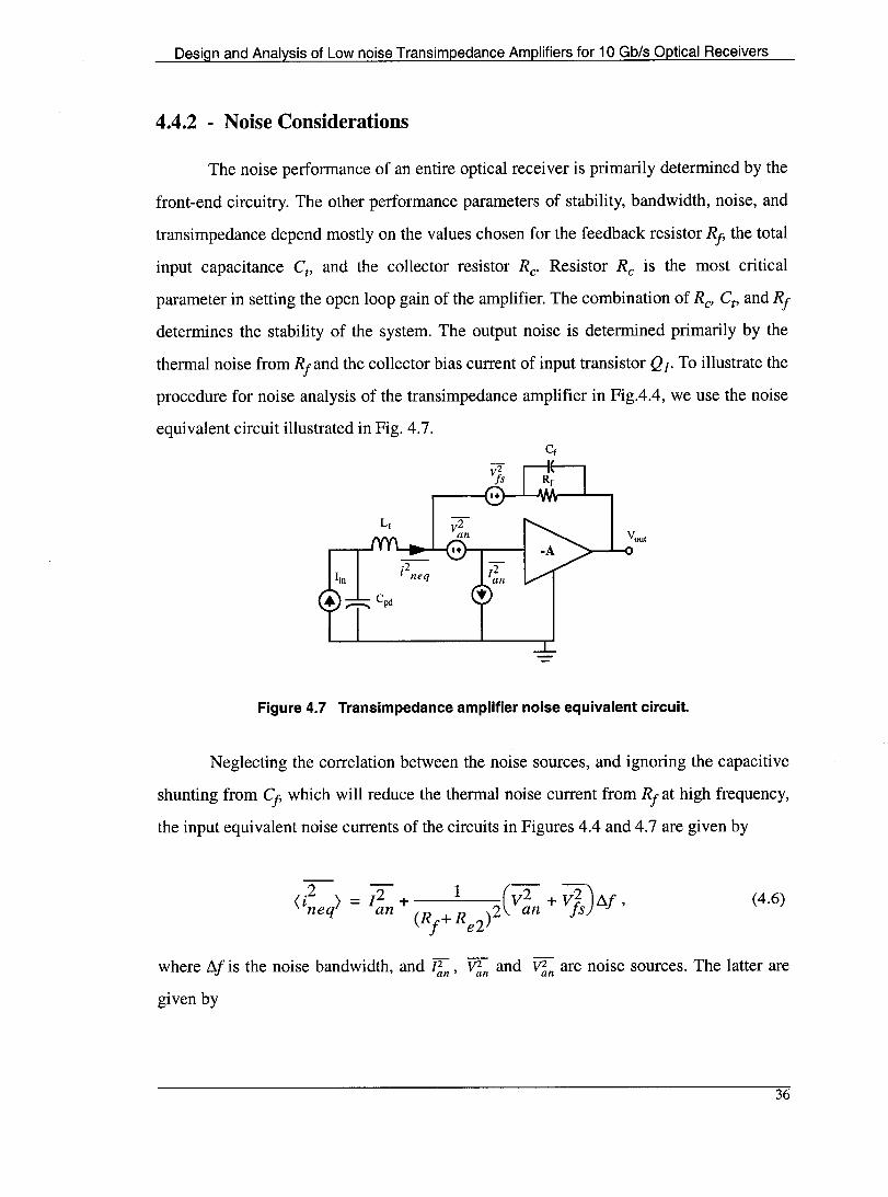
4.4.2 - Noise Considerations
The noise performance of an entire optical receiver is primarily determined by the
front-end circuitry. The other performance parameters of stability, bandwidth, noise, and
transimpedance depend mostly on the values chosen for the feedback resistor Rf' the total
input capacitance Ct' and the collector resistor Re. Resistor Re is the most critical
parameter in setting the open loop gain of the amplifier. The combination of Re. Ct' and Rf
determines the stability of the system. The output noise is determined primarily by the
thermal noise from Rf and the collector bias current of input transistor QI. To illustrate the
procedure for noise analysis of the transimpedance amplifier in Fig.4.4, we use the noise
equivalent circuit illustrated in Fig. 4.7.
Figure 4.7 Transimpedance amplifier noise equivalent circuit.
Neglecting the correlation between the noise sources, and ignoring the capacitive
shunting from Ci' which will reduce the thermal noise current from Rf at high frequency,
the input equivalent noise currents of the circuits in Figures 4.4 and 4.7 are given by
(4.6)
where !lf is the noise bandwidth, and I~n' ~n and ~n are noise sources. The latter are
given by
36
Design and Analysis of Low noise Transimpedance Amplifiers for 10 Gb/s Optical Receivers
(4.7)
-2 cl ( 1 J lan = 2q lb! + 1~12 fl.j
where rb1 is the base resistance of the input transistor, and gmi is its transconductance, lb]
and IcJ are the base and collector currents of the input transistor, and ~ is the transistor
current gain. For low noise performance, Rf should be appropriately chosen, and rb]
should be minimized.
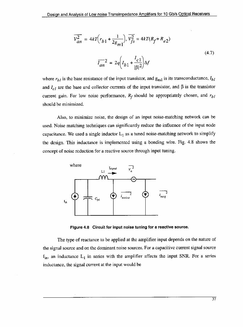
Also, to minimize noise, the design of an input noise-matching network can be
used. Noise matching techniques can significantly reduce the influence of the input node
capacitance. We used a single inductor LI as a tuned noise-matching network to simplify
the design. This inductance is implemented using a bonding wire. Fig. 4.8 shows the
concept of noise reduction for a reactive source through input tuning.
where Isignal V 2
LI --. n
1+
--2 .. --2 .. inoise ineq
Cpd •
Figure 4.8 Circuit for input noise tuning for a reactive source.
The type of reactance to be applied at the amplifier input depends on the nature of
the signal source and on the dominant noise sources. For a capacitive current signal source
lin' an inductance LI in series with the amplifier affects the input SNR. For a series
inductance, the signal current at the input would be
37
Design and Analysis of Low noise Transimpedance Amplifiers for 10 Gb/s Optical Receivers
1 J. 1 = J. , sIgna zn 2
1 + S LI Cpd
and the total noise current at the input would be
:-222 -.2-( 2 '1 2 .2 V- nS Cpd + l neq 1 + S LI Cpd) l noise= ------2----2---
(1 +S L 1Cpd )
(4.8)
(4.9)
From equation (4.8) and (4.9), and assuming for simplicity that vn and inoise are
not correlated, the input signal-to-noise power ratio (SNR) will be
J. 2 (SNR) _ zn
input - - -- 2' 222.2 ( 2 '1
V- nS Cpd + l neq 1 + S LI Cpd)
(4.10)
v2 = V2 + V2 n an fs' (4.11)
whereas the SNR without the inductance would have been
l: (SNR). t =
znpu 2S2C2 .2 V;; pd+ l neq
zn (4.12)
The inductance cancels the source reactance at the resonant frequency, and
modifies a formerly white input equivalent current noise into one with a spectrum
proportional to II-w2L j Cpdl, disappearing totally at the resonant frequency. The
improvement in the SNR is inversely proportional to the bandwidth as shown in Fig. 4.9
for different L j values.
By selecting an appropriate matching network, it is possible to significantly reduce
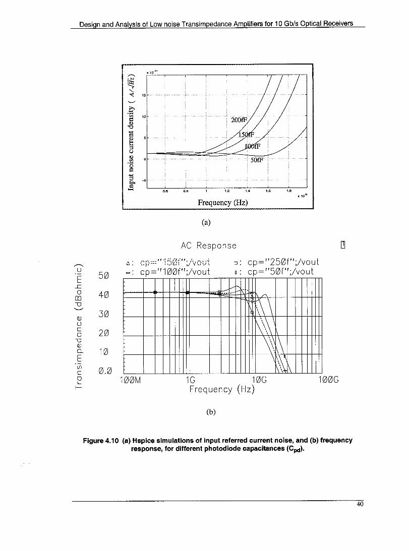
the effect of the (Cpd) photodiode capacitance on the overall noise performance of the
receiver. Fig. 4.10 shows the effect of different Cpd values on the input referred current
38
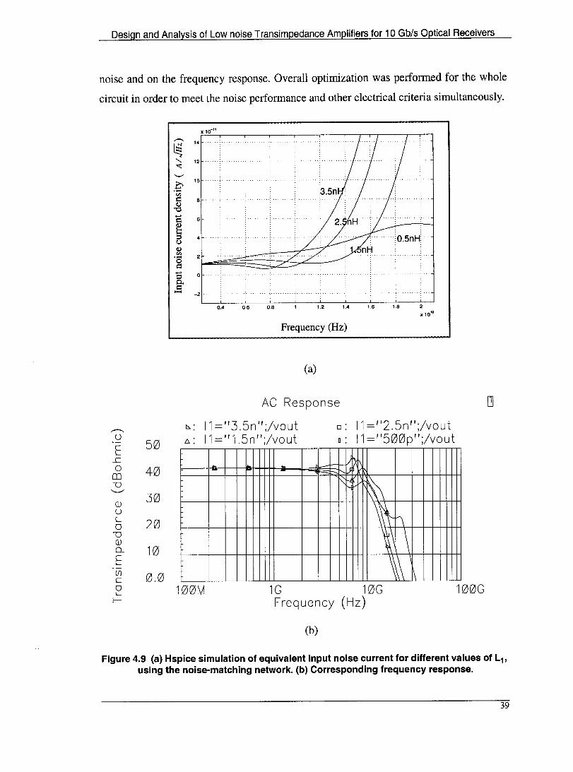
Design and Analysis of Low noise Transimpedance Amplifiers for 10 Gb/s Optical Receivers
noise and on the frequency response. Overall optimization was performed for the whole
circuit in order to meet the noise performance and other electrical criteria simultaneously.
--. u E 50
...c 0 40 m
"D '--"
ru 30 u c 20 0
"D ru 0... 10 E (f]
0.0 c 0 l-
I-
X 10-11
,-... 14
~ "-'<"(
12
'-'
è 10
..... <'-l
~ 8
..... 6 s::
~ 4 () :O~5nH V V>
2 ..... 0 s:: ~ 0
0.. s:: ..... -2
0.4 0.6 0.8 1.2 1.4 1.6 1.8
Frequency (Hz)
(a)
AC Response
1:::..: 11 ="3.5n";/vout 6.: 11="1.5n";/vout
0: 11 ="2.5n";/vout 0: 11="500p";/vout
ft -1- I)~
"''''' ~ '\ h
~ \ ~ ~ 1\
100M 1G 10G Frequency (Hz)
(b)
100G
Figure 4.9 (a) Hspice simulation of equivalent input noise current for different values of L1•
using the noise-matching network. (b) Corresponding frequency response.
39
Design and Analysis of Low noise Transimpedance Amplifiers for 10 Gb/s Optical Receivers
'-"
0 ...... Cf)
r::: a.>
'1:j .... r::: ~ ::l u a.> Cf) ...... 0 r:::
,.-., u
E 50 ...c 0 40 m v '--"
Q) 30
u c
20 0 v Q)
0... 10 E en
0.0 c 0 l- 100M
I---
10
5
0
0.6
Frequency (Hz)
(a)
AC Response
cp= " 100f" ;/vout o· cp="250f";/vout 0: cp="50f";/vout
---v r-,.~ ,
/'\
i"i \\\ i\\\\ \~ 1\\
\\~~ 1\\ 1\
1G 10G 100G Frequency (Hz)
(b)
Figure 4.10 (a) Hspice simulations of input referred current noise, and (b) frequency response, for different photodiode capacitances (Cpd).
40
Design and Analysis of Low noise Transimpedance Amplifiers for 10 Gb/s Optical Receivers
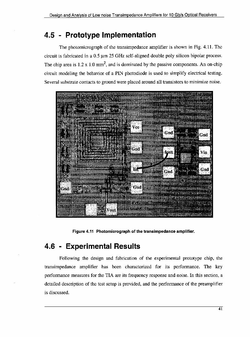
4.5 - Prototype Implementation
The photomicrograph of the transimpedance amplifier is shown in Fig. 4.11. The
circuit is fabricated in a 0.5 !lm 25 GHz self-aligned double pol y silicon bipolar process.
The chip area is 1.2 x 1.0 mm2, and is dominated by the passive components. An on-chip
circuit modeling the behavior of a PIN photodiode is used to simplify electrical testing.
Several substrate contacts to ground were placed around aIl transistors ta minimize noise.
Figure 4.11 Photomicrograph of the transimpedance amplifier.
4.6 - Experimental Results
Following the design and fabrication of the experimental prototype chip, the
transimpedance amplifier has been characterized for its performance. The key
performance measures for the TIA are its frequency response and noise. In this section, a
detailed description of the test setup is provided, and the performance of the preamplifier
is discussed.
41
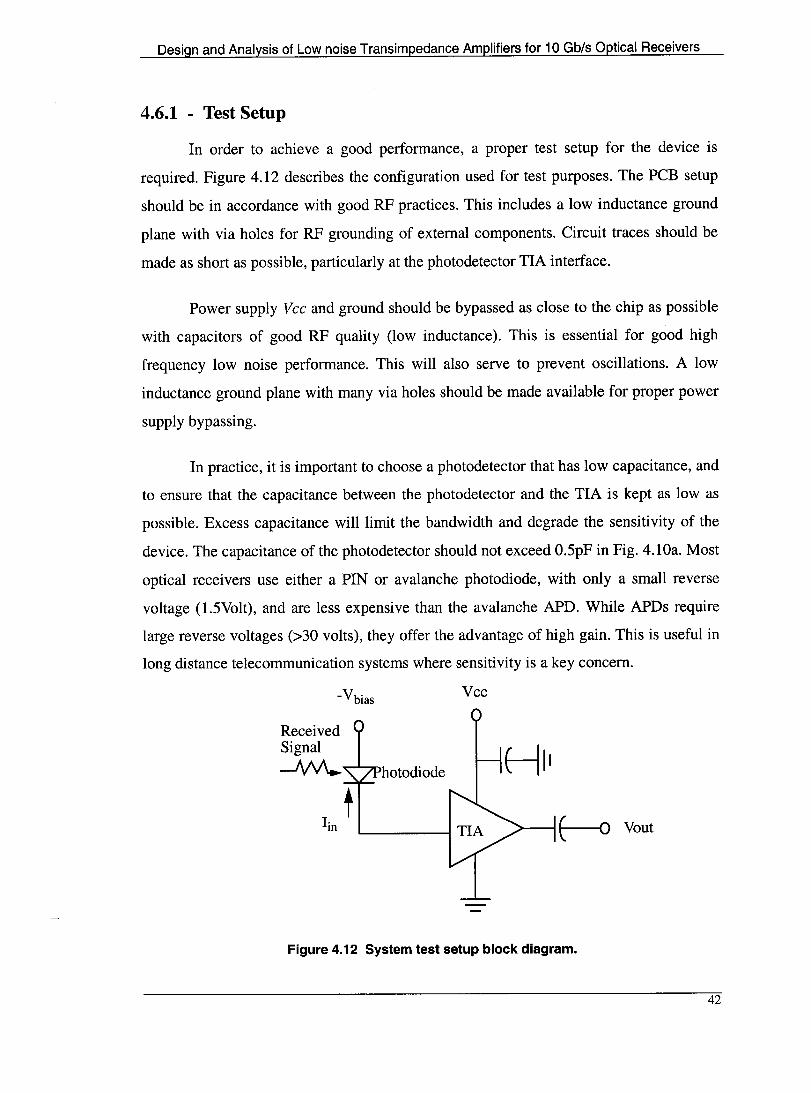
Design and Analysis of Low noise Transimpedance Amplifiers for 10 Gb/s Optical Receivers
4.6.1 - Test Setup
In order to achieve a good performance, a proper test setup for the device is
required. Figure 4.12 de scribes the configuration used for test purposes. The PCB setup
should be in accordance with good RF practices. This includes a low inductance ground
plane with via holes for RF grounding of external components. Circuit traces should be
made as short as possible, particularly at the photodetector TIA interface.
Power supply Vcc and ground should be bypassed as close to the chip as possible
with capacitors of good RF quality (low inductance). This is essential for good high
frequency low noise performance. This will also serve to prevent oscillations. A low
inductance ground plane with many via holes should be made available for proper power
supply bypassing.
In practice, it is important to choose a photodetector that has low capacitance, and
to ensure that the capacitance between the photodetector and the TIA is kept as low as
possible. Excess capacitance will limit the bandwidth and degrade the sensitivity of the
device. The capacitance of the photodetector should not exceed O.5pF in Fig. 4.lOa. Most
optical receivers use either a PIN or avalanche photodiode, with only a small reverse
voltage (1.5Volt), and are less expensive than the avalanche APD. While APDs require
large reverse voltages (>30 volts), they offer the advantage of high gain. This is useful in
long distance telecommunication systems where sensitivity is a key concern.
-Vbias
Received Signal
-AN\..
lin t
Vcc
hotodiode
>---1 E----o Vout
Figure 4.12 System test setup block diagram.
42
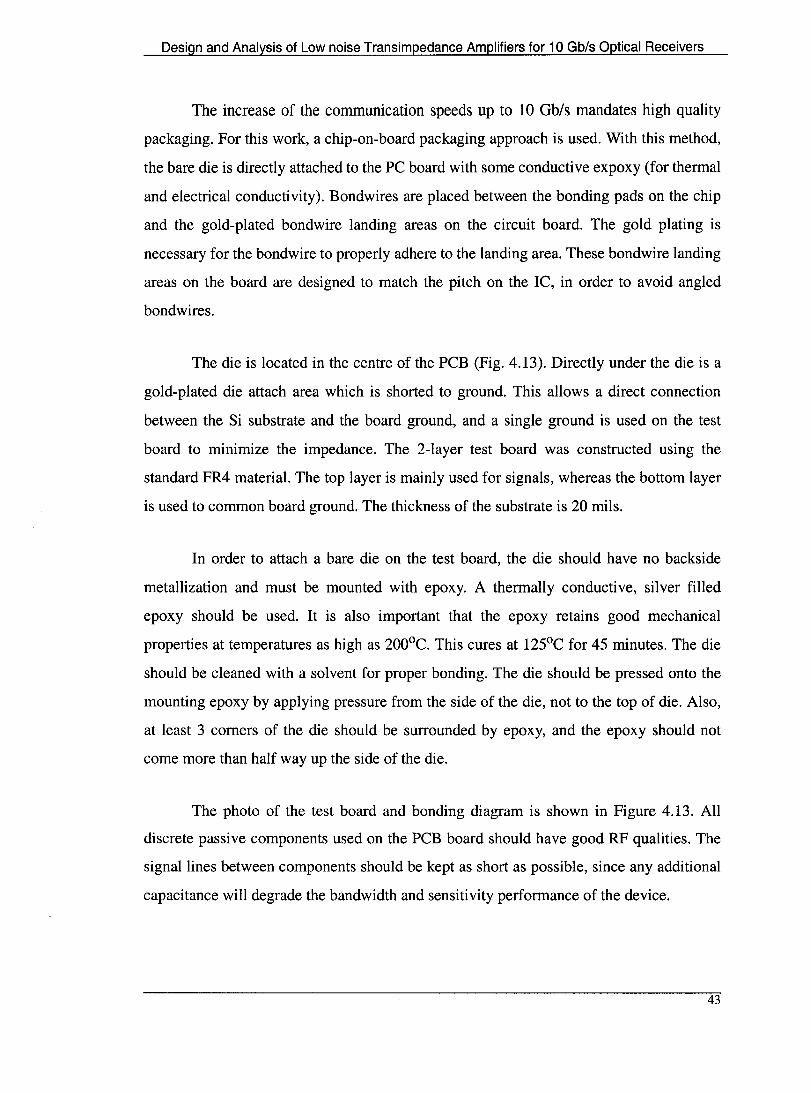
Design and Analysis of Low noise Transimpedance Amplifiers for 10 Gb/s Optical Receivers
The increase of the communication speeds up ta 10 Obis mandates high quality
packaging. For this work, a chip-on-board packaging approach is used. With this method,
the bare die is directly attached to the PC board with sorne conductive expoxy (for thermal
and electrical conductivity). Bondwires are placed between the bonding pads on the chip
and the gold-plated bondwire landing areas on the circuit board. The gold plating is
necessary for the bondwire to properly adhere to the landing area. These bondwire landing
areas on the board are designed to match the pitch on the IC, in order to avoid angled
bondwires.
The die is located in the centre of the PCB (Fig. 4.13). Directly under the die is a
gold-plated die attach area which is shorted to ground. This allows a direct connection
between the Si substrate and the board ground, and a single ground is used on the test
board to minimize the impedance. The 2-layer test board was constructed using the
standard FR4 material. The top layer is mainly used for signaIs, whereas the bottom layer
is used to common board ground. The thickness of the substrate is 20 mils.
ln order to attach a bare die on the test board, the die should have no backside
metallization and must be mounted with epoxy. A thermally conductive, silver filled
epoxy should be used. It is also important that the epoxy retains good mechanical
properties at temperatures as high as 200°C. This cures at 125°C for 45 minutes. The die
should be cleaned with a solvent for proper bonding. The die should be pressed onto the
mounting epoxy by applying pressure from the side of the die, not to the top of die. AIso,
at least 3 corners of the die should be surrounded by epoxy, and the epoxy should not
come more than half way up the side of the die.
The photo of the test board and bonding diagram is shown in Figure 4.13. AlI
discrete passive components used on the PCB board should have good RF qualities. The
signal lines between components should be kept as short as possible, since any addition al
capacitance will degrade the bandwidth and sensitivity performance of the device.
43
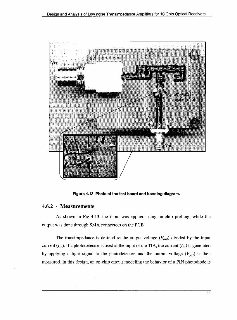
Design and Analysis of Law noise Transimpedance Amplifiers for 10 Gb/s Optical Receivers
Figure 4.13 Photo of the test board and bonding diagram.
4.6.2 - Measurements
As shown in Fig 4.13, the input was applied using on-chip probing, while the
output was done through SMA connectors on the PCB.
The transimpedance is defined as the output voltage (Vout) divided by the input
CUITent (lin)' If a photodetector is used at the input of the TIA, the CUITent (lin) is generated
by applying a light signal to the photodetector, and the output voltage (Vout) is then
measured. In this design, an on-chip circuit modeling the behavior of a PIN photodiode is
44
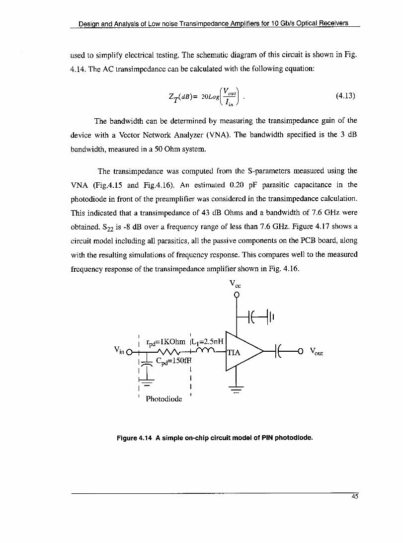
Design and Analysis of Low noise Transimpedance Amplifiers for 10 Gb/s Optical Receivers
used to simplify electrical testing. The schematic diagram of this circuit is shown in Fig.
4.14. The AC transimpedance can be calculated with the foIlowing equation:
(4.13)
The bandwidth can be determined by measuring the transimpedance gain of the
device with a Vector Network Analyzer (VNA). The bandwidth specified is the 3 dB
bandwidth, measured in a 50 Ohm system.
The transimpedance was computed from the S-parameters measured using the
VNA (Fig.4.15 and Fig.4.16). An estimated 0.20 pF parasitic capacitance in the
photodiode in front of the pre amplifier was considered in the transimpedance calculation.
This indicated that a transimpedance of 43 dB Ohms and a bandwidth of 7.6 GHz were
obtained. S22 is -8 dB over a frequency range of less than 7.6 GHz. Figure 4.17 shows a
circuit model including aIl parasitics, aIl the passive components on the PCB board, along
with the resulting simulations of frequency response. This compares weIl to the measured
frequency response of the transimpedance amplifier shown in Fig. 4.16.
Vcc
1 ~ Cpd=150rn
: 1 :
1 1 1 1
Photodiode
Figure 4.14 A simple on-chip circuit model of PIN photodiode.
45
Design and Analysis of Low noise Transimpedance Amplifiers for 10 Gb/s Optical Receivers
Figure 4.15 The measured input reflection 511 and reverse transmission 512.
46
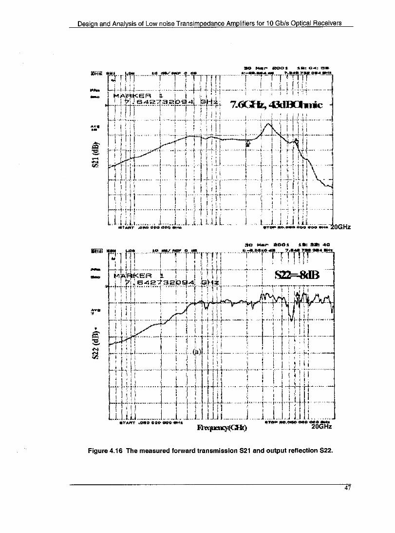
Design and Analysis of Low noise Transimpedance Amplifiers for 10 Gb/s Optical Receivers
... ". 1.
-...
; i ; .l.l .~
lLLüL._
Figure 4.16 The measured forward transmission S21 and output reflection S22.
47
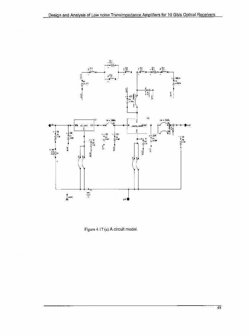
Design and Analysis of Low noise Transimpedance Amplifiers for 10 Gb/s Optical Receivers
13 u 14 hw1 • 3800u
~ hw1 • 3000u o.
IN pr"mp_mod~FOUT vout
r 50 e 601 ~
R21 C 601 c 601 r." Cli
C22 Cl. e 2001
r l0 c=&II1
J C = lp "601 c-6B1 '19 R6
Cl) l tr r·" r tr=100t .
v2=6 _ .
vl=' .,w Il
qnd!
Figure 4.17 (a) A circuit mode!.
48
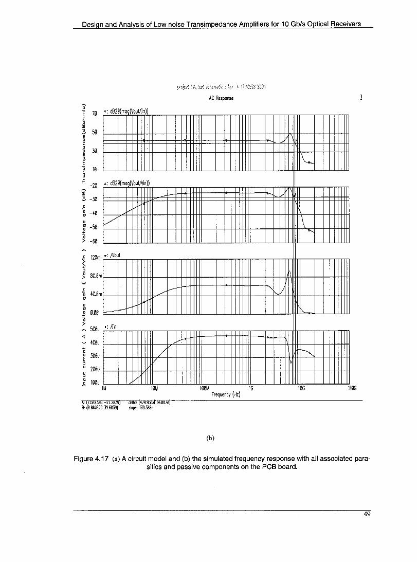
Design and Analysis of Low noise Transimpedance Amplifiers for 10 Gb/s Optical Receivers
,..., .~
70 v; dB20(mog(Vout/lin)) .r: 0
ID '0 50 '-" v u C a
30 '0 V a. .~ ~ 10 c 0 .. r-
-20 A: dB20(mog(Vout;Yin))
al ~ -30 .~ ~ -40 v ~ -50
.... 0 > -60
c 120m ~ J 0 80.0m >
v
.~ 40.0m 0
Cl
v Cl a 0.00 :!: 0 > ,..., 500u 4 ...., 400u ... c ~ 300u c J U
J a.
200u
V
-: /Vout
:.---f-
1; /lin
.5 100u lM
A: \1.56038G -212839) 8: 8.04032G 39.6039)
/V
/' f--"
f-
/ /
,/
10M
delta: (~19.936~ 66.8818) slope: 139.368n
AC Response
I~
1\ .....,
r- "'\ ,-v
f\.-
v
~
100M lG 10G 100G Frequency (Hz)
(b)
Figure 4.17 (a) A circuit model and (b) the simulated frequency response with ail associated parasitics and passive components on the PCB board.
49
Design and Analysis of Low noise Transimpedance Amplifiers for 10 Gb/s Optical Receivers
Figure 4.18 shows the measured input referred noise current versus frequency.
This parameter is directly related to the sensitivity of the device. It is defined as the output
noise voltage (with no input signal), divided by the AC transimpedance. The device
sensitivity can then be ca1culated as follows:
{(6500 X finnoise)}
Sensitivity = lOLog R ' [dBm] (4.14)
where finnoise is the input referred noise current, and R is the responsivity of the
photodetector.
As discussed in Chapter 4, noise-matching techniques can significantly reduce the
influence of the input node capacitance. We used a single inductor as a tuned noise
matching network to improve the signal-to-noise ratio (SNR) of this design. This
inductance is implemented using a bonding wires. Uncertainties in the bonding process,
including height, distance, and the straightness of the bond wire, cause the actual
inductance value (approximately 3.5 nR) to vary from the expected design value (2.5 nR).
Compared to measurement and simulation results, the measured noise and bandwidth are
very close to the simulation results under the approximation of a 3.5 nR for the input
bonding wire. In practice, challenges remain in the need to control the uncertainty in bond
wire inductances, and to improve the IC packaging.
4.6.3 - Results
Measurements were performed on 3 samples. They aIl exhibit very similar
performance. Table 4.1 summarizes the TIA performance and compares it to several state
of-the-art designs. Note in particular the low noise and the low power consumption of the
design presented.
50
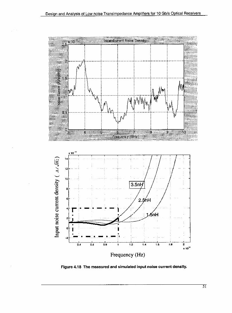
Design and Analysis of Low noise Transimpedance Amplifiers for 10 Gb/s Optical Receivers
-.
~ " ~ --~ .... . -(l)
~ .g .... c Q.)
1: B ~ .-0 C .... = ~ -
;Jo; 1[fl1
14
12
10
8
1)
.. r '. 2
0
-2 - •
0,"
................ .... :- ................... ~ .. .. .. .. ... .. .. .. .. .. .............. .. -:- .................. ~ ................ .. , "
, , ............ .. -,- .................. r .................... , ................ .. -,- ................... ,. .............. ..
- •
-' • 0,6
1 1 1 1 1 1 1 1 1 ,
- ,.' -,
• - • -0,6 U! 1.4 1.6
Frequency (Hz)
L __ ,_
1.8 2 x 11)'0
Figure 4.18 The measured and simulated input noise current density.
51
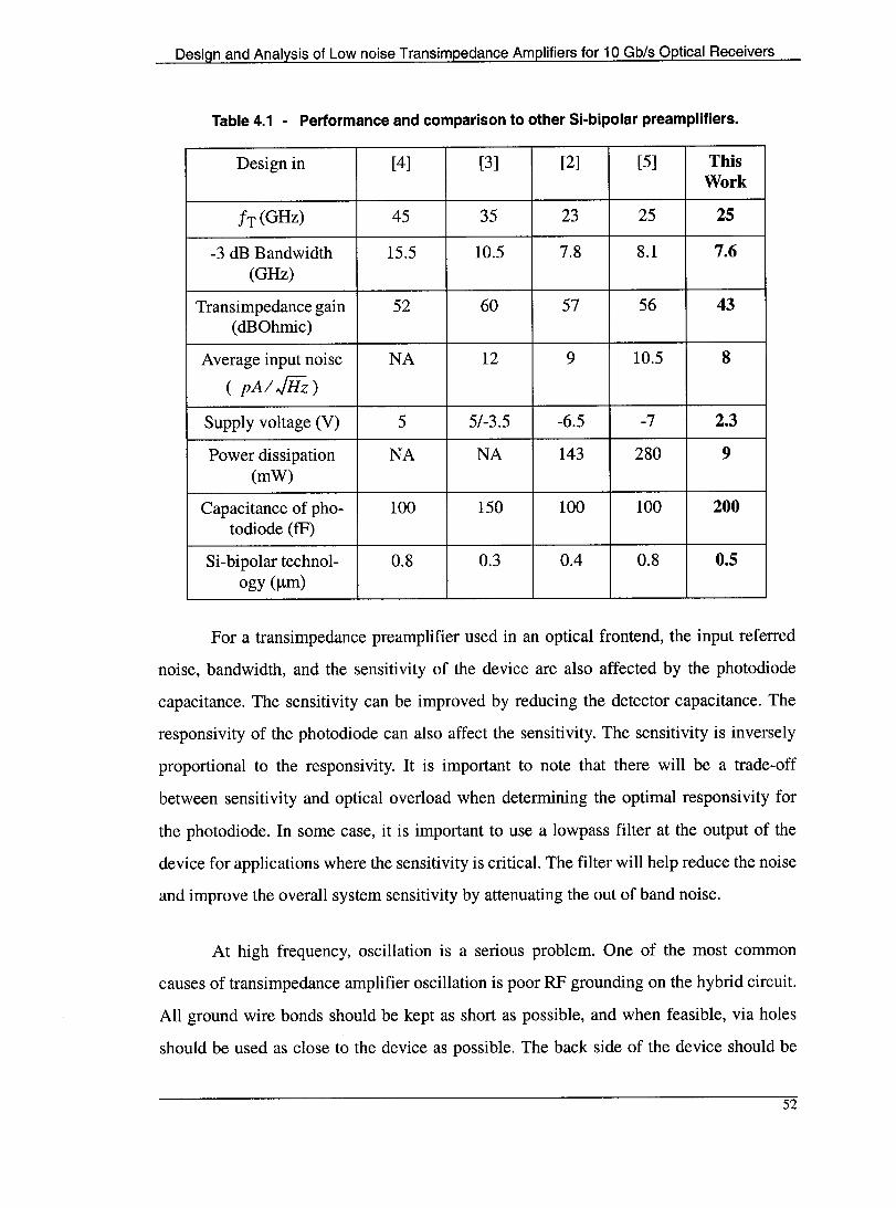
Design and Analysis of Low noise Transimpedance Amplifiers for 10 Gb/s Optical Receivers
Table 4.1 - Performance and comparison to other Si-bipolar preamplifiers.
Design in [4] [3] [2] [5] This Work
fT (GHz) 45 35 23 25 25
-3 dB Bandwidth 15.5 10.5 7.8 8.1 7.6 (GHz)
Transimpedance gain 52 60 57 56 43 (dBOhmic)
Average input noise NA 12 9 10.5 8
( pAl JiTz) Supply voltage (V) 5 5/-3.5 -6.5 -7 2.3
Power dissipation NA NA 143 280 9 (mW)
Capacitance of pho- 100 150 100 100 200 todiode (fF)
Si-bipolar technol- 0.8 0.3 0.4 0.8 0.5 ogy (!-lm)
For a transimpedance preamplifier used in an optical frontend, the input referred
noise, bandwidth, and the sensitivity of the device are also affected by the photodiode
capacitance. The sensitivity can be improved by reducing the detector capacitance. The
responsivity of the photodiode can also affect the sensitivity. The sensitivity is inversely
proportional to the responsivity. It is important to note that there will be a trade-off
between sensitivity and optical overload when determining the optimal responsivity for
the photodiode. In sorne case, it is important to use a lowpass filter at the output of the
device for applications where the sensitivity is critical. The filter will help reduce the noise
and improve the overaH system sensitivity by attenuating the out of band noise.
At high frequency, oscillation is a serious problem. One of the most common
causes of transimpedance amplifier oscillation is poor RF grounding on the hybrid circuit.
AH ground wire bonds should be kept as short as possible, and when feasible, via holes
should be used as close to the device as possible. The back side of the device should be
52
Design and Analysis of Low noise Transimpedance Amplifiers for 10 Gb/s Optical Receivers
mounted to a ground plane. While the device will generally work if the back side is at a
negative dc voltage, the chances of oscillation are significantly increased.
If the frequency response of the device has peaking and resonance, the most likely
cause is long bond wires, particularly for the bypass capacitors connections. Excess
inductance here has been seen to cause low frequency resonance. It is especially important
that the input impedance of the subsequent stages be matched as close to 50 ohms as
possible, particularly for the higher bit rate devices.
Bondwires have been the standard connection method between integrated circuits
and the outside world for decades. The parasitic inductance associated with bondwires has
been a source of problems in IC technology, especially for high speed and high frequency
IC's. However, one can use bondwires to create a high quality inductor. Bondwire
inductors exhibit a higher quality factor (Q) than on-chip spiral inductors. This improves
the signal-to-noise ratio (SNR) of the transimpedance amplifier when connected between
the photodetector and the pre amplifier input as a tuned noise-matching network. The
parasitic capacitance for this structure of bondwires is dominated by the bonding pads.
Uncertainties in the bonding process include height, distance and straightness of the
bondwires. The actual inductance value will vary from the design value. Since each wire
is individually bonded, the matching between a pair of bondwires is also poor. But
bondwires can be very weIl controlled with modern equipment.
53
Design and Analysis of Low noise Transimpedance Amplifiers for 10 Gb/s Optical Receivers
Chapter 5 - Conclusion
This thesis proposes a transimpedance amplifier design based on the synthesis of
optimum noise-matching networks, using an on-chip inductor for bandwidth extension,
combined with frequency compensation techniques. A qualitative study of the various
trade-offs involved in the design process, as weIl as many of the design challenges, have
been discussed.
The thesis also explores the performance limits of the proposed design based on
the noise matching networks. The analysis suggests trade-offs between input noise
current, speed, transimpedance gain, power dissipation, impedance matching, and supply
voltage. By carefully adjusting the bonding wire lengths, the test chip reached 7.6 GHz,
8 pAl JïiZ average input noise at 43 dB Ohmic transimpedance gain. This demonstrates
how careful optimization can be used to push the performance limits of low cost Si
bipolar processes to achieve gigabits/second data rates.
The specifie research contribution of this work includes 1) using inductors to
enhance the bandwidth, 2) using a tuned noise-matching network at the input to improve
the signal-to-noise ratio (SNR), and 3) using frequency compensation techniques to
improve stability, and to further enhance the bandwidth of the pre amplifier. An interesting
continuation of this work would be to control and optimize the parasitie inductance
uncertainties resulting from the bonding process, e.g., height, distance, and the
54
Design and Analysis of Low noise Transimpedance Amplifiers for 10 Gb/s Optical Receivers
straightness of the bondwires. Nowsdays bondwires can be very weIl controlled with modern
equipment.
55
Design and Analysis of Low Noise Transimpedance Amplifiers for 10 Gbls Qptical Receivers
[1]
[2]
[3]
[4]
[5]
[6]
[7]
[8]
References
H. M. Rein and M. Moller, "Design considerations for very high speed Sibipolar IC's operating up to 50 Gb/s," IEEE Journal of Solid-State Circuits, Vol. 31, No. 8, pp. 1076-1090, Aug. 1996.
M. Neuhauser, H. M. Rein, and H. Wernz, "Low-noise, high-gain Sibipolar preamplifier for 10 Gb/s optical-fiber links design and realization," IEEE Journal of Solid-State Circuits, Vol. 31, pp. 24-29, Jan. 1996.
T. Masuda, K. Ohhata, K. Imai, R. Takeyari, and K. Washio, "A wide dynamic range, high-transimpedance Si bipolar preamplifier IC for 10-Gb/s optical fiber links," IEEE Journal of Solid-State Circuits, Vol. 34, pp. 18-24, Jan. 1999.
H. Kitahara, H. Takemura, T. Suzaki, M. Soda, T. Morikawa, H. Tezuka, C. Ogawa, S.Fujita, and T. Tashiro, "A 15.5 GHz bandwidth Si-bipolar preamplifier," in Proc. BCTM, pp. 155-158, 1992.
M. Neuhauser, H. M. Rein, and H. Wernz, "13 Gbitls Si bipolar preamplifiers for optical front ends," Electron. Lett., Vol. 29, pp. 492-493, Mar. 1993.
A. P. Freundorfer, and T. L. Nguyen, "Noise in distributed MESFET preamplifiers," IEEE Journal of Solid-State Circuits, Vol. 31, pp. 1100 -1111, Aug. 1996.
N. Scheinberg, R. J. Bayruns, T. M. Laverick, "Monolithic GaAs transimpedance amplifiers for fiber-optic receivers," IEEE Journal of Solid-State Circuits, Vol. 26, pp.1834 -1839, Dec. 1991.
M. Miyashita, K. Maemura, K. Yamamoto, T. Shimura, M. Nogami, K. Motoshima, T. Kitayama, and Y. Mitsui, "An ultra broadband GaAs MESFET preamplifier IC for a 10 Gb/s optical communication system,"
56
Design and Analysis of Low Noise Transimpedance Amplifiers for 10 Gb/s Optical Receivers
Microwave and Millimeter-Wave Monolithic Circuits Symposium, pp.127-130,1992.
[9] M. Soda, H. Tezuka, P. Sato, T. Hashimoto, S. Nakamura, T. Tatsumi, T. Suzaki, and T. Tashiro, "Si-analog IC's for 20 Obis optical receiver," IEEE Journal of Solid-State Circuits, Vol. 29, pp. 1577 -1582, Dec. 1994.
[10] T. Morikawa, M. Soda, S. Shioirl, T. Hashimoto, P. Sato, and K Emura, "A SiOe single-chip 3.3 V receiver IC for 10 Obis optical communication systems," Solid-State Circuits Conference, pp. 380 -381, 1999.
[11] T. Masuda, K Ohhata, K. Oda, M. Tanabe, H. Shimamoto, T. Onai, and K. Washio, "40 Obis analog IC chipset for optical receiver using SiOe HBTs," Solid-State Circuits Conference, pp. 314 -315, 1998.
[12] R. Schmid, T.P. Meister, M. Neuhauser, A. Felder, W. Bogner, M. Rest, J. Rupeter, and H. -M. Rein, "20 Obit/s transimpedance preamplifier and modulator driver in SiOe bipolar technology," Electronics Letters, Vol. 33 pp. 1136-1137, Jun. 1997.
[13] P. Sato, H. Tezuka, M. Soda, T. Hashimoto, T. Suzaki, T. Tatsumi, T. Morikawa, and T. Tashiro, "A 2.4 Obis receiver and a 1:16 demultiplexer in one chip using a super self-aligned selectively grown SiOe base (SSSB) bipolar transistor," IEEE Journal of Solid-State Circuits, Vol. 31, pp. 1451 -1457, Oct. 1996.
[14] Y. Suzuki, H. Shimawaki, y. Amamiya, N. Nagano, H. Yano, and KHonjo, "A 40-0b/s preamplifier using AIOaAslInOaAs HBTs with regrown base contacts," IEEE Journal of Solid-State Circuits, Vol.34, pp. 143 -147, Feb. 1999.
[15] M. Yung, J. Jensen, R. Walden, M. Rodwell, G. Raghavan, K Elliott, and W. Stanchina, "Highly integrated InP HBT optical receivers," IEEE Journal of Solid-State Circuits, Vol. 34, pp. 219 -227, Feb.1999.
[16] H. Suzuki, K Watanabe, K Ishikawa, H. Masuda, K. Ouchi, T. Tanoue, and R. Takeyari, "Very-high-speed InPlInOaAs HBT ICs for optical transmission systems," IEEE Journal of Solid-State Circuits, Vol. 33, pp. 1313 -1320, Sept. 1998.
[17] A. Tanabe, M. Soda, Y. Nakahara, T. Tamura, K Yoshida, and A. Furukawa, "A single-chip 2.4-0b/s CMOS optical receiver IC with low substrate cross-talk preamplifier," IEEE Journal of Solid-State Circuits, Solid-State Circuits, Vol. 33, pp. 2148 -2153, Dec. 1998.
57
Design and Analysis of Low Noise Transimpedance Amplifiers for 10 Gb/s Optical Receivers
[18] M. Ingels, and M. Steyaert, "A I-Gb/s, 0.7 Ilm CMOS optical receiver with full rail-to-rail output swing," IEEE Journal of Solid-State Circuits, Vol. 34, pp. 971 -977, July 1999.
[19] S. M. Sze, Physics of Semicoductor Devices, 2nd Ed., John Wiley & Sons, New York, N. Y., 1981.
[20] J. Rue, M. Itzler, N. Agrawal, S. Bay, and W. Sherry, "High performance 10 Gb/s PIN and APD optical receivers," Electronic Components and Technology Conference, pp. 207 -215, 1999.
[21] M. Soda, S. Shiori, T. Morikawa, M. Tachigori, 1. Watanabe, and M. Shibutani, "A 2.5-Gb/s one-chip receiver module for gigabit-to-the-home (GfTH) system," Custom Integrated Circuits, pp. 273 -276, 1999.
[22] D. Huber, M. Bitter, M. Dulk, S. Fischer, E. Gini, A. Neiger, R. Schreieck, C. Bergamaschi, and H. Jackel, "A 53 GHz monolithically integrated InPlInGaAs PINIHBT receiver OEIC with an electrical bandwidth of 63 GHz," Indium Phosphide and Related Materials, pp. 325 -328, 2000.
[23] J. Shimizu, T. Suzaki, T. Terakado, S. Fujita, K. Kasahara, T. Itoh, and A. Suzuki, "High sensitivity, high gain, long wavelength OEIC receiver with monolithically integrated three-stage preamplifier," Electronics Letters Vol. 26, pp. 824 -825, June 1990.
[24] Gerd Keiser, Optical Communications, 3rd ed., Mcgraw-Hill series in electrical engineering, 2000.
[25] Stephen B. Alexander, Optical Communication Receiver Design, SPIEThe intrenational society for optical engineering, 1995.
[26] F. Schwierz, M. Rossberg, H. Forster, D. Nuernbergk, and D. Schipanski, "Recent advances in Si/SiGe HBT research," Electron Devices Meeting, pp. 1 - 4, 1996.
[27] A. Gruhle, H. Kibble, U. Erben, and E. Kasper, "Base thickness and highfrequency performance of SiGe HBT's," Electron Deviees, Vol. 40, Nov. 1993.
[28] K. Sunghoon, K. Kyunghae, Y. Junsin, L. Hoongjoo, and R. Byungryul, "Optimum Ge profile for the high cut-off frequency of SiGe HBT," Microwave and Millimeter Wave Technology, pp. 84 -87, 2000.
[29] S.L. Salmon, J.D. Cressler, R. C. Jaeger, and D. L. Harame, "The impact of Ge profile shape on the operation of SiGe HBT precision voltage
58
Design and Analysis of Low Noise Transimpedance Amplifiers for 10 Gb/s Optical Receivers
references," BipolarlBiCMOS Circuits and Technology, pp. 100 -103, 1997.
[30] Lawrence E. Larson, "Silicon bipolar transistor design and modeling for microwave integrated circuit application," BipolarlBiCMOS Circuits and Technology, pp. 142 -148, 1996.
[31] S. M. Park and C. Papavassiliou, "On the design of low-noise, giga-hertz bandwidth preamplifiers for optical receiver applications," Proceedings of the 6th IEEE International Conference on Electronics, Vol. 2, pp. 785-788, 1999.
[32] T. Vanisri and C. Toumazou, "Integrated high frequency low-noise cUITent-mode optical transimpedance preamplifiers: theory and practice," IEEE Journal of Solid-State Circuits, Vol. 30, No. 6, pp. 677-685, June 1995.
[33] Paul R. Gray, Analysis and Design of Analog Integrated Circuits, John Wiley and Sons, Inc. New York, 1994.
[34] A. Olomo-Ngongo, et al., "Network synthesis applied to the design of tuned optical front-ends for microwave lightwave systems," Electronics Letters, vol.30, no.2, pp. 164-165, Jan. 1994.
[35] S. S. Mohan, M. M. Hershenson, S. P. Boyd, and T. H. Lee, "Bandwidth extension in CMOS with optimized on-chip inductors," IEEE Journal of Solid-State Circuits, Vol. 35, No 3, pp. 346-355, Mar. 2000.
59