Trends and Challenges in Multi-Level Inverter with Reduced ...
23
electronics Review Trends and Challenges in Multi-Level Inverter with Reduced Switches Ganesh Kumar Srinivasan 1, * , Marco Rivera 2 , Vijayaraja Loganathan 3 , Dhanasekar Ravikumar 3 and Balaji Mohan 1 Citation: Srinivasan, G.K.; Rivera, M.; Loganathan, V.; Ravikumar, D.; Mohan, B. Trends and Challenges in Multi-Level Inverter with Reduced Switches. Electronics 2021, 10, 368. https://doi.org/10.3390/ electronics10040368 Received: 11 December 2020 Accepted: 26 January 2021 Published: 3 February 2021 Publisher’s Note: MDPI stays neutral with regard to jurisdictional claims in published maps and institutional affil- iations. Copyright: © 2021 by the authors. Licensee MDPI, Basel, Switzerland. This article is an open access article distributed under the terms and conditions of the Creative Commons Attribution (CC BY) license (https:// creativecommons.org/licenses/by/ 4.0/). 1 Department of Electrical and Electronics Engineering, Anna University, Chennai 600025, Tamil Nadu, India; [email protected] 2 Centro Tecnologico de Conversión de Energía, Department of Electrical Engineering, Faculty of Engineering, Campus Curico, Universidad de Talca, Curico 3341717, Chile; [email protected] 3 Department of Electrical and Electronics Engineering, Sri Sairam Institute of Technology, Anna University, Chennai 600044, India; [email protected] (V.L.); [email protected] (D.R.) * Correspondence: [email protected]; Tel.: +91-9791-071-498 Abstract: Multilevel inverter had been paid a lot of attention from the academia and research community in recent times due to its role in high and medium power applications. In this paper, a detailed survey is made on the recently designed multilevel inverter to find the suitability of the inverters for particular applications. Research is performed on various types of multilevel inverters such as: Symmetric, asymmetric, hybrid and modularized multilevel inverter in order to identify the issues in generating more levels at the output. A summary of various issues in multilevel inverter with reduced switch count is provided, so that a novel topology of multilevel inverter can be designed in future. Further, an 81-level switched ladder multilevel inverter using unidirectional and bidirectional switches is designed. Simulation work is carried out using Matlab/Simulink in order to validate the performance of the inverter with change in resistive load and impedance load. The output of the 81-level inverter is fed to a 110 V, 186.5 W single phase induction motor in order to study the characteristics, further speed control of motor is performed by varying the input voltage of the motor and the results are presented. Keywords: cascaded unit; 81-level; induction motor; ladder circuit; multilevel inverter; pulse generation 1. Introduction Nowadays, multilevel inverters (MLI) play a major role in various power applica- tions such as Electric Vehicle [1], Photovoltaic systems [2], Low-Power Loads [3], Grid integration system [4]. It is more attractive because of very low harmonic distortion, low number of drivers, absence of filters, low installation area, reduction in voltage stress and switching losses. A generalized cascaded multilevel inverter is presented with nearest level modulation technique. The proposed converter is discussed with and without half bridge circuits [2]. A new multilevel inverter with one DC source is presented for low power applications. The proposed inverter generates the output voltage eight times higher than the input voltage [3]. In [4], various configurations of MLI’s were analyzed in terms of number of switching devices and modulation techniques. MLI are broadly classified into cascaded H Bridge, neutral clamped and flying capacitor topologies [5]. Recently, for hybrid systems cascade multilevel inverters are applied. Many topologies are there to create the staircase voltages with higher levels with low devices count [6]. A new MLI is designed to generate generate 27-level and fifty one level output voltages using constant voltage sources for resistive-inductive load [7]. An inverter is designed using trinary DC sources and thirteen switches to generate 53 output levels with minimum THD of 1.15% [8]. A new switched source MLI is proposed which operates under both symmetric Electronics 2021, 10, 368. https://doi.org/10.3390/electronics10040368 https://www.mdpi.com/journal/electronics
Transcript of Trends and Challenges in Multi-Level Inverter with Reduced ...

electronics
Review
Trends and Challenges in Multi-Level Inverter withReduced Switches
Ganesh Kumar Srinivasan 1,* , Marco Rivera 2 , Vijayaraja Loganathan 3 , Dhanasekar Ravikumar 3
and Balaji Mohan 1
Citation: Srinivasan, G.K.; Rivera,
M.; Loganathan, V.; Ravikumar, D.;
Mohan, B. Trends and Challenges in
Multi-Level Inverter with Reduced
Switches. Electronics 2021, 10, 368.
https://doi.org/10.3390/
electronics10040368
Received: 11 December 2020
Accepted: 26 January 2021
Published: 3 February 2021
Publisher’s Note: MDPI stays neutral
with regard to jurisdictional claims in
published maps and institutional affil-
iations.
Copyright: © 2021 by the authors.
Licensee MDPI, Basel, Switzerland.
This article is an open access article
distributed under the terms and
conditions of the Creative Commons
Attribution (CC BY) license (https://
creativecommons.org/licenses/by/
4.0/).
1 Department of Electrical and Electronics Engineering, Anna University, Chennai 600025, Tamil Nadu, India;[email protected]
2 Centro Tecnologico de Conversión de Energía, Department of Electrical Engineering, Faculty of Engineering,Campus Curico, Universidad de Talca, Curico 3341717, Chile; [email protected]
3 Department of Electrical and Electronics Engineering, Sri Sairam Institute of Technology, Anna University,Chennai 600044, India; [email protected] (V.L.); [email protected] (D.R.)
* Correspondence: [email protected]; Tel.: +91-9791-071-498
Abstract: Multilevel inverter had been paid a lot of attention from the academia and researchcommunity in recent times due to its role in high and medium power applications. In this paper, adetailed survey is made on the recently designed multilevel inverter to find the suitability of theinverters for particular applications. Research is performed on various types of multilevel inverterssuch as: Symmetric, asymmetric, hybrid and modularized multilevel inverter in order to identifythe issues in generating more levels at the output. A summary of various issues in multilevelinverter with reduced switch count is provided, so that a novel topology of multilevel inverter canbe designed in future. Further, an 81-level switched ladder multilevel inverter using unidirectionaland bidirectional switches is designed. Simulation work is carried out using Matlab/Simulink inorder to validate the performance of the inverter with change in resistive load and impedance load.The output of the 81-level inverter is fed to a 110 V, 186.5 W single phase induction motor in order tostudy the characteristics, further speed control of motor is performed by varying the input voltage ofthe motor and the results are presented.
Keywords: cascaded unit; 81-level; induction motor; ladder circuit; multilevel inverter; pulse generation
1. Introduction
Nowadays, multilevel inverters (MLI) play a major role in various power applica-tions such as Electric Vehicle [1], Photovoltaic systems [2], Low-Power Loads [3], Gridintegration system [4]. It is more attractive because of very low harmonic distortion, lownumber of drivers, absence of filters, low installation area, reduction in voltage stress andswitching losses.
A generalized cascaded multilevel inverter is presented with nearest level modulationtechnique. The proposed converter is discussed with and without half bridge circuits [2].A new multilevel inverter with one DC source is presented for low power applications.The proposed inverter generates the output voltage eight times higher than the inputvoltage [3]. In [4], various configurations of MLI’s were analyzed in terms of number ofswitching devices and modulation techniques. MLI are broadly classified into cascaded HBridge, neutral clamped and flying capacitor topologies [5].
Recently, for hybrid systems cascade multilevel inverters are applied. Many topologiesare there to create the staircase voltages with higher levels with low devices count [6]. Anew MLI is designed to generate generate 27-level and fifty one level output voltages usingconstant voltage sources for resistive-inductive load [7]. An inverter is designed usingtrinary DC sources and thirteen switches to generate 53 output levels with minimum THDof 1.15% [8]. A new switched source MLI is proposed which operates under both symmetric
Electronics 2021, 10, 368. https://doi.org/10.3390/electronics10040368 https://www.mdpi.com/journal/electronics

Electronics 2021, 10, 368 2 of 23
and asymmetric mode. The proposed inverter is designed with six power switches and twovoltage sources [9]. A new 81-level MLI is presented using two stage ladder circuits andthe values of the dc sources are fixed by two different algorithms. The presented topologyis tested with resistive and impedance load [10]. A cascaded MLI is presented to generate9, 15, 27, 33 and 39 output voltage levels at the load. It is observed that increase in numberof voltage levels reduces the presence of harmonic content in load voltage and currentwaveforms. The proposed inverter is simulated in Matlab/Simulink and analyzed the totalharmonic distortion for resistive and resistive-inductive load [11]. Various configurationsof symmetrical, asymmetrical and hybrid MLI’s were synthesized in terms of number ofswitches, capacitors, diodes utilized in the inverter circuit. As well, an analyzes is made interms of THD generation and total standing voltages of all the configurations [12]. Fewdrawbacks such as: switch count, voltage imbalance and number of DC sources are therein all the topologies [13].
Multilevel inverter with minimum switch count is focused nowadays with highervoltage levels [14]. Higher voltage levels are attained using cascaded H bridge MLI withisolated DC voltage sources. The switch count reduction is based on the design of basicunit. MLI with three phase is proposed with reduced power switches and has attainednine output voltage levels. The proposed structure is analyzed for various pulse widthmodulation (PWM) techniques. Total harmonic distortion is examined for all the PWMtechniques [15].
A new optimized structure of MLI is designed to create a rectangular type and circulartype with a smaller number of switching components. A new switching technique isadopted and it is validated through simulation and experimental studies [16]. A three phasecascade H bridge (CHB) inverter is proposed with discontinuous pulse width modulationwhich reduces switching losses and thus increases the lifetime of the switches. MLI alsoadopted with rotation scheme for even distribution of power in the switches [17]. A trinaryCHB MLI is proposed for solar power system with equal number of voltage levels.
For the control of active power and grid interaction, a modified second order integralcontrol is applied [18]. The space vector pulse width modulation scheme is being appliedto the MLI for common mode voltage reduction [19]. Two new MLI structures are designedand interfaced with PV system. Both the MLI structures consists of equal number of powerswitches and generates 9-level output [20].
This paper consists of six sections including introduction. Section 2 discussed about thesurvey on multilevel inverter with reduced switch (MLIRS) designs, Section 3 discussed theissues related with the construction of MLIRS, Section 4 discussed proposed MLI topology,design parameters of switched ladder inverter and generation of 81-levels and Section 5presented pulse generation logic and analysis of results.
2. Survey on MLIRS Designs
For a medium voltage high power single phase application, a fifteen level inverteris designed using three DC sources and ten switches. Further, the design topology ismodified to generate 25-levels at the output using four DC sources and twelve switches. Bycomparing the two inverter design, the extended topology utilized fewer switches to gen-erate more output levels. Nearest level control method is applied to generate pulse for theswitches and this inverter works with symmetrical and asymmetrical configurations [21].
To attain the speed torque characteristics of AC motor under loaded conditions, aseven level inverter is designed using seven power switches and three voltage sources. Theadvantages of using this inverter in medium voltage drives are reduction in the size offilter and low voltage stress [22].
A 17-level inverter is designed using unidirectional and bidirectional switches withfour asymmetric sources which varies in trinary fashion. The designed topology is testedwith impedance load and found to be usage of minimum number of switches to generatemore output levels [23].

Electronics 2021, 10, 368 3 of 23
A 17-level inverter with reduced power switches for open end induction motor drivesis proposed. A level shifted carrier scheme is applied for v/f and d/q control for inductionmotor drives. The circulating power is analyzed and eliminated by space vector analysis.The proposed topology is suitable for traction and induction motor drive application [24].
A multilevel inverter is proposed with fuel cell and attains high output levels. UsingMATLAB simulation is completed with less power electronic switches to obtain outputvoltage levels such as: 5, 7 and 15-levels. Through mathematical calculation efficiency andpower loss is analyzed. Switching loss, device stress and driver circuits are compared withother multilevel inverter topologies [25].
A 9-level and 49-level multilevel inverter is proposed and simulated [26]. The basicstructure consists of two voltage sources and five switches. The harmonic distortionachieved for a 9-level inverter is 9.85% and for a 49-level inverter is 2.01%, it is found thatincrease in output voltage levels leads to reduction in harmonic content at the load [26]. A ‘T’type multilevel inverter is proposed for transformer less DVR with reduced switches. Thebasic structure consists of eight switches which generates five level output voltage usingtwo DC sources. This designed inverter regulates the load voltage under sag condition,but this topology requires high power rated switches [27].
With no additional components such as inductor and capacitor, a new multilevelinverter is proposed. The proposed structure operates on symmetric and asymmetricmode. MATLAB simulation is done for constructing 79-levels and 321-levels. The proposedmultilevel inverter is operated for grid utility from renewable energy sources [28].
Cascaded H bridge multilevel inverter contains a greater number of switching devicesand sources. A new 9-level multilevel inverter in cascaded transformer is proposed withminimum number of switching devices and DC supply. Conventional cascaded transformerbased 9-level MLI is compared with proposed 9-level MLI. The performance is analyzedand tested for multi carrier PWM technique [29].
A new MLI with hybrid structure is proposed. Selective harmonic elimination tech-nique is applied to obtain the quality in the output voltage with reduction in lower orderharmonics. The proposed topology is analyzed for R and RL loads [30]. High voltage stressoccurs in two stage switched capacitor multilevel inverter. To overcome this problem singlestage switched capacitor multilevel inverter is proposed. The basic unit consists of twelveswitches with only one DC source. The proposed topology is tested experimentally [31].Low total standing voltage is achieved by multi-unit MLI with single phase supply usingminimum number of switching components. The proposed structure is compared withexisting MLI units under varying loaded conditions [32]. Various configurations of cas-caded half bridge inverter applied for grid tied PV system is discussed in terms of controlmethodologies. The performance of CHB inverter is validated in all the aspects [33]. Thevarious applications of MLI are shown in Table 1.
Table 1. Applications of MLI with reduced switches.
Type of Applications
Renewable energy systemsFuel cells
Low Voltage and High VoltageGrid connections
DrivesHigh frequency AC distribution systems
Electric Vehicle
Output voltage level generated with respect to the number of switches used for varioustopologies is tabulated in Table 2.

Electronics 2021, 10, 368 4 of 23
Table 2. Number of switches versus Number of Levels.
Reference Paper Number Name of MLI Number of Switches Number of Levels
21 Three Source MLI 8 1522 Bidirectional stepped MLI 7 723 Switched Voltage Cascaded MLI 12 1724 Flying Capacitor MLI 12 17
25 MLI using Proton-exchangemembrane fuel cell
9 510 715 15
26 Modified Half bridge MLI 9 914 49
27 T-type MLI 5 5
28 Trinary MLI 13 7920 321
29 Switched-dc-source sub module MLI 6 930 Bi-direction MLI 10 1331 Single-Stage Switched-Capacitor MLI 12 9
3. Issues in MLI with Low Device Count
In MLI, there are issues such as: Voltage unbalancing, gate pulse generation and circuitcomplexity. The major issues in various MLI topologies are discussed in Table 3. Some ofthe challenges are discussed below. In [20] additional power stage is used, a transformeralong with the inverter which increases the cost. Reactive power capability is absent inthe structure proposed in [20]. The design structure presented in [21,22] requires a greaternumber of components for constructing higher number of levels. The design topologyin [23] uses bidirectional switches which increases the cost and size of the inverter. Theinverter topology in [24,25] utilizes more circuit components to generate higher outputvoltage levels. The reduction of harmonic content in the output load waveform is challeng-ing and it is presented in [26]. Inverter proposed in [27] has higher total standing voltages.The presented topology in [28,29] requires more circuits to achieve more output levels. Acomplex control is necessary in-order to design a bi-direction MLI [30]. Voltage balance inthe capacitor is challenging in the switched capacitor MLI with reduced switch count [31].Balancing the voltage in DC link needs high attention [32]. The configuration presentedin [33] utilizes more switches to generate higher number of voltage levels. In [34], the basicstructure of proposed system requires two bidirectional switches and it is used to generate17-levels in the output via asymmetrical configuration. In order to increase the outputlevels by cascading the SLMLI unit or increasing the ladder structure that is ‘m’, the totalvoltage appeared across the switches Sx and Sy is becoming high and it increases the ratingof the devices. Furthermore, the switching frequency is high to generate desired outputlevels which increases switching losses.
In [35], various topologies of MLI were designed using higher number of voltagesources with less number of switches to achieve more output voltage levels and theissues found in the configurations are listed in Table 2. In [36,37], a symmetric multilevelinverter is designed and found failure in the implementation of medium and high voltageapplications. In [38,39], a multilevel inverter is designed using asymmetrical voltagesources to generate more output voltages levels with increase in the number of switches. Ahybrid MLI designed with complex control technique and it is presented in [40].
In [41], the proposed system is used to generate 9-levels in the output with four dcsources, eight switches and four diodes. While extending the output voltage levels, moreunits are added and thus conduction and switching losses are more. In addition to increasein switching loss, stress across the switch is increasing.
Electronics 2021, 10, 368 5 of 23
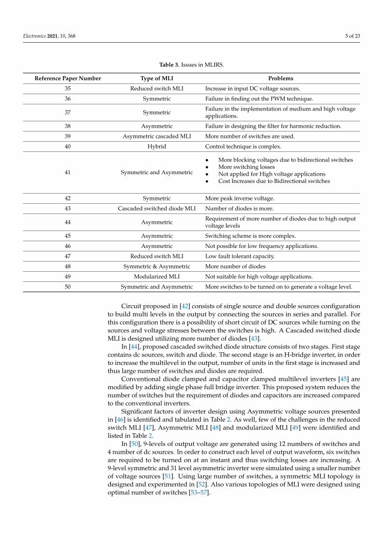
Table 3. Issues in MLIRS.
Reference Paper Number Type of MLI Problems
35 Reduced switch MLI Increase in input DC voltage sources.
36 Symmetric Failure in finding out the PWM technique.
37 Symmetric Failure in the implementation of medium and high voltageapplications.
38 Asymmetric Failure in designing the filter for harmonic reduction.
39 Asymmetric cascaded MLI More number of switches are used.
40 Hybrid Control technique is complex.
41 Symmetric and Asymmetric
• More blocking voltages due to bidirectional switches• More switching losses• Not applied for High voltage applications• Cost Increases due to Bidirectional switches
42 Symmetric More peak inverse voltage.
43 Cascaded switched diode MLI Number of diodes is more.
44 Asymmetric Requirement of more number of diodes due to high outputvoltage levels
45 Asymmetric Switching scheme is more complex.
46 Asymmetric Not possible for low frequency applications.
47 Reduced switch MLI Low fault tolerant capacity.
48 Symmetric & Asymmetric More number of diodes
49 Modularized MLI Not suitable for high voltage applications.
50 Symmetric and Asymmetric More switches to be turned on to generate a voltage level.
Circuit proposed in [42] consists of single source and double sources configurationto build multi levels in the output by connecting the sources in series and parallel. Forthis configuration there is a possibility of short circuit of DC sources while turning on thesources and voltage stresses between the switches is high. A Cascaded switched diodeMLI is designed utilizing more number of diodes [43].
In [44], proposed cascaded switched diode structure consists of two stages. First stagecontains dc sources, switch and diode. The second stage is an H-bridge inverter, in orderto increase the multilevel in the output, number of units in the first stage is increased andthus large number of switches and diodes are required.
Conventional diode clamped and capacitor clamped multilevel inverters [45] aremodified by adding single phase full bridge inverter. This proposed system reduces thenumber of switches but the requirement of diodes and capacitors are increased comparedto the conventional inverters.
Significant factors of inverter design using Asymmetric voltage sources presentedin [46] is identified and tabulated in Table 2. As well, few of the challenges in the reducedswitch MLI [47], Asymmetric MLI [48] and modularized MLI [49] were identified andlisted in Table 2.
In [50], 9-levels of output voltage are generated using 12 numbers of switches and4 number of dc sources. In order to construct each level of output waveform, six switchesare required to be turned on at an instant and thus switching losses are increasing. A9-level symmetric and 31 level asymmetric inverter were simulated using a smaller numberof voltage sources [51]. Using large number of switches, a symmetric MLI topology isdesigned and experimented in [52]. Also various topologies of MLI were designed usingoptimal number of switches [53–57].

Electronics 2021, 10, 368 6 of 23
4. Design of Proposed Cascaded SLMLI to Generate 81 Level
In the proposed work, switched ladder inverter is designed to generate 81 outputvoltage levels. Figure 1a is a generalized structure of SLMLI. Number of output levels canbe increased by either increasing the magnitude of dc sources as shown in Figure 1b or bycascading a number of stages by fixing dc sources in each stage.
Electronics 2021, 10, x FOR PEER REVIEW 6 of 24
In [50], 9-levels of output voltage are generated using 12 numbers of switches and 4 number of dc sources. In order to construct each level of output waveform, six switches are required to be turned on at an instant and thus switching losses are increasing. A 9-level symmetric and 31 level asymmetric inverter were simulated using a smaller number of voltage sources [51]. Using large number of switches, a symmetric MLI to-pology is designed and experimented in [52]. Also various topologies of MLI were de-signed using optimal number of switches [53–57].
4. Design of Proposed Cascaded SLMLI to Generate 81 Level In the proposed work, switched ladder inverter is designed to generate 81 output
voltage levels. Figure 1a is a generalized structure of SLMLI. Number of output levels can be increased by either increasing the magnitude of dc sources as shown in Figure 1b or by cascading a number of stages by fixing dc sources in each stage.
In order to increase the number of levels further, using proposed switched ladder inverter, it leads to increase the component count which makes the system bulky, costly, and complex. As well, the voltage rating on the switches of Sx and Sy is equal to the sum of all sources values. To reduce the number of used components and voltage on Sx and Sy, cascade topology based on series connection of ‘m’ SLMLIs is recommended which is presented in Figure 1b. Proposed structure is named as cascaded switch-ladder inverter (CSLMLI). The output voltage of SLMLI (Vout) is equal to the sum of output voltages of all the SLMIs and it is given in Equation (1).
Vout = Vo1 + Vo2 + … + Vom. (1)
where Vo1, Vo2 and Vom are the output voltage produced by stage-1, stage-2 and stage-m respectively.
(a) (b)
Figure 1. (a) Generalized structure of SLMLI [34]; (b) proposed SLMLI [34]. Figure 1. (a) Generalized structure of SLMLI [34]; (b) proposed SLMLI [34].
In order to increase the number of levels further, using proposed switched ladderinverter, it leads to increase the component count which makes the system bulky, costly,and complex. As well, the voltage rating on the switches of Sx and Sy is equal to the sumof all sources values. To reduce the number of used components and voltage on Sx andSy, cascade topology based on series connection of ‘m’ SLMLIs is recommended which ispresented in Figure 1b. Proposed structure is named as cascaded switch-ladder inverter(CSLMLI). The output voltage of SLMLI (Vout) is equal to the sum of output voltages of allthe SLMIs and it is given in Equation (1).
Vout = Vo1 + Vo2 + . . . + Vom. (1)
where Vo1, Vo2 and Vom are the output voltage produced by stage-1, stage-2 andstage-m respectively.
The voltage levels at the output are achieved by considering the quantity of bidirec-tional switches in each SLMLI and it is given by:
2z1 = 2z2 = . . . = 2zb= 2z (2)
The generalized structure shown in Figure 1 consists of unidirectional and bidirectional switches.

Electronics 2021, 10, 368 7 of 23
4.1. Design Parameters Cascaded SLMLI for Two Stages
The SLMLI design parameters are determined by using two methods and both meth-ods are explained as follows.
Method 1: In this method, necessary expressions are given below:
V1 = V3 = Vdc (3)
V2 = V4 = (z + 2) × Vdc (4)
The maximum output voltage, level generation, switches and sources required are calcu-lated as follows:
Vcascaded,max = 2 × [(z + 1) × (V1 + V4)] (5)
Nlevel = 2 × [(Vcascaded,max)/V1] + 1 (6)
Nswitch = 4 × (2z + 3) (7)
Nsource = 4 × (z + 1) (8)
where z is the number of bidirectional switches in each ladder structure.Method 2: In this method, V3 and V4 values are computed and it is mentioned as follows:
V1 = Vdc (9)
V2 = (z + 2) × Vdc (10)
V3 = (4z) × V1 (11)
V4 = (z + 2) × V3 (12)
The maximum output voltage, level generation, switches and sources required are repre-sented as follows:
Vcascaded,max = (2) × (V1 + V2 + V3 + V4) (13)
Nlevel = 2 × [(Vcascaded,max)/V1] + 1 (14)
Nswitch = 2 × (4z + 6) (15)
Nsource = 4 × (z + 1) (16)
4.2. Cascaded SLMLI to Generate 81 Levels (2-Stages)
Inverter shown in Figure 1b is used to generate ‘n’ number of levels, but the rating ofswitches is increasing with the increase in magnitude of voltage. This problem is solved bycascading number of switch ladder multilevel inverters to generate ‘n’ number of outputlevels. Figure 2 shows the circuit diagram of cascaded SLMLI to generate 81 levels in theoutput voltage.
Stage-1 requires the same number of switches and sources that used in stage-2 Instage-1, unidirectional switches are represented as T11, T12, T13, T14, SX1, SY1 and thebidirectional switches are shown as S11, S12. In stage-2, unidirectional switches arementioned as T21, T22, T23, T24, SX2, SY2 and the bidirectional switches are shown asS21, S22. By cascading two stages, the voltage stress between the switches and dv/dt arereduced and hence it reduces overall cost. Table 4 shows the switching sequence for theproposed SLMLI.

Electronics 2021, 10, 368 8 of 23Electronics 2021, 10, x FOR PEER REVIEW 8 of 24
Figure 2. Cascaded two stages of SLMLI.
Stage-1 requires the same number of switches and sources that used in stage-2 In stage-1, unidirectional switches are represented as T11, T12, T13, T14, SX1, SY1 and the bidirectional switches are shown as S11, S12. In stage-2, unidirectional switches are mentioned as T21, T22, T23, T24, SX2, SY2 and the bidirectional switches are shown as S21, S22. By cascading two stages, the voltage stress between the switches and dv/dt are re-duced and hence it reduces overall cost. Table 4 shows the switching sequence for the proposed SLMLI.
Table 4. Switching sequence for the Proposed SLMLI.
No. of Levels Voltage Levels T11 T12 T13 T14 S11 S12 S1X S1Y T21 T22 T23 T24 S21 S22 S2X S2Y
1 0 δ ø δ ø ø ø δ ø δ ø δ ø δ δ δ ø 2 V1 ø δ ø ø δ ø ø δ δ ø δ ø ø ø δ ø 3 V1 + V1 δ δ ø ø ø ø ø δ δ ø δ ø ø ø δ δ 4 V3 ø ø ø δ ø δ ø δ δ ø δ ø ø ø δ δ 5 V4 ø ø ø ø δ δ ø δ δ ø δ ø ø ø δ δ
37 V1 + V2 + V3 + V3+ V4 + V4 ø ø ø ø δ δ ø δ δ ø δ ø ø ø ø δ 38 V1 + V1 + V2 + V3+ V3 + V4 + V4 δ ø ø δ ø δ ø δ δ ø δ ø ø ø ø δ 39 V2 + V2 + V3 + V3 + V4 + V4 ø ø δ ø δ ø ø δ δ ø δ ø ø ø ø δ 40 V1 + V2 + V2+ V3 + V3 + V4 + V4 ø ø δ ø ø ø ø δ δ ø δ ø ø ø ø δ 41 V1 + V1 + V2 + V2 + V3 + V3 + V4 + V4 δ ø δ ø ø ø ø δ δ ø δ ø ø ø ø δ
Figure 2. Cascaded two stages of SLMLI.
Table 4. Switching sequence for the Proposed SLMLI.
No. of Levels Voltage Levels T11 T12 T13 T14 S11 S12 S1X S1Y T21 T22 T23 T24 S21 S22 S2X S2Y
1 0 δ ø δ ø ø ø δ ø δ ø δ ø δ δ δ ø2 V1 ø δ ø ø δ ø ø δ δ ø δ ø ø ø δ ø3 V1 + V1 δ δ ø ø ø ø ø δ δ ø δ ø ø ø δ δ4 V3 ø ø ø δ ø δ ø δ δ ø δ ø ø ø δ δ5 V4 ø ø ø ø δ δ ø δ δ ø δ ø ø ø δ δ
37 V1 + V2 + V3 + V3+ V4 + V4 ø ø ø ø δ δ ø δ δ ø δ ø ø ø ø δ38 V1 + V1 + V2 + V3+ V3 + V4 + V4 δ ø ø δ ø δ ø δ δ ø δ ø ø ø ø δ39 V2 + V2 + V3 + V3 + V4 + V4 ø ø δ ø δ ø ø δ δ ø δ ø ø ø ø δ40 V1 + V2 + V2+ V3 + V3 + V4 + V4 ø ø δ ø ø ø ø δ δ ø δ ø ø ø ø δ41 V1 + V1 + V2 + V2 + V3 + V3 + V4 + V4 δ ø δ ø ø ø ø δ δ ø δ ø ø ø ø δ
Where the ‘ON’ conditions of the switches are represented as ‘δ’ and the ‘OFF’ condition of the switches are represented as ‘ø’.
5. Pulse Generation and Simulation Results
In order to construct multiple voltage levels in the load side, proper generation ofpulses is needed. Figure 3 explains the method to generate pulses for the inverter. Pulsesare generated by comparing a sinusoidal wave with the constant voltage steps at regularintervals. Switching state will become one when sinusoidal is in between ith level and i+ 1th level. For 81 level generation, value of ‘i’ will be varying from 0 to 41 to constructpositive 41 levels and same will be repeated for negative also. Adder will combine all theswitching states created and it will act as an input to activate the corresponding switchingpattern via a multiport switch. De-multiplexer is used for distributing the pulses for theinverter. Based on the switching sequence shown in Table 4 the pulses will be given toappropriate switches. In the Table 4, the ON condition and OFF condition of the switchesare represented as δ and ø respectively.
Electronics 2021, 10, 368 9 of 23
Electronics 2021, 10, x FOR PEER REVIEW 9 of 24
Where the ‘ON’ conditions of the switches are represented as ‘δ’ and the ‘OFF’ condition of the switches are represented as ‘ø’.
5. Pulse Generation and Simulation Results In order to construct multiple voltage levels in the load side, proper generation of
pulses is needed. Figure 3 explains the method to generate pulses for the inverter. Pulses are generated by comparing a sinusoidal wave with the constant voltage steps at regular intervals. Switching state will become one when sinusoidal is in between ith level and i + 1th level. For 81 level generation, value of ‘i’ will be varying from 0 to 41 to construct positive 41 levels and same will be repeated for negative also. Adder will combine all the switching states created and it will act as an input to activate the corresponding switch-ing pattern via a multiport switch. De-multiplexer is used for distributing the pulses for the inverter. Based on the switching sequence shown in Table 4 the pulses will be given to appropriate switches. In the Table 4, the ON condition and OFF condition of the switches are represented as δ and ø respectively.
Figure 3. Block diagram for pulse generation.
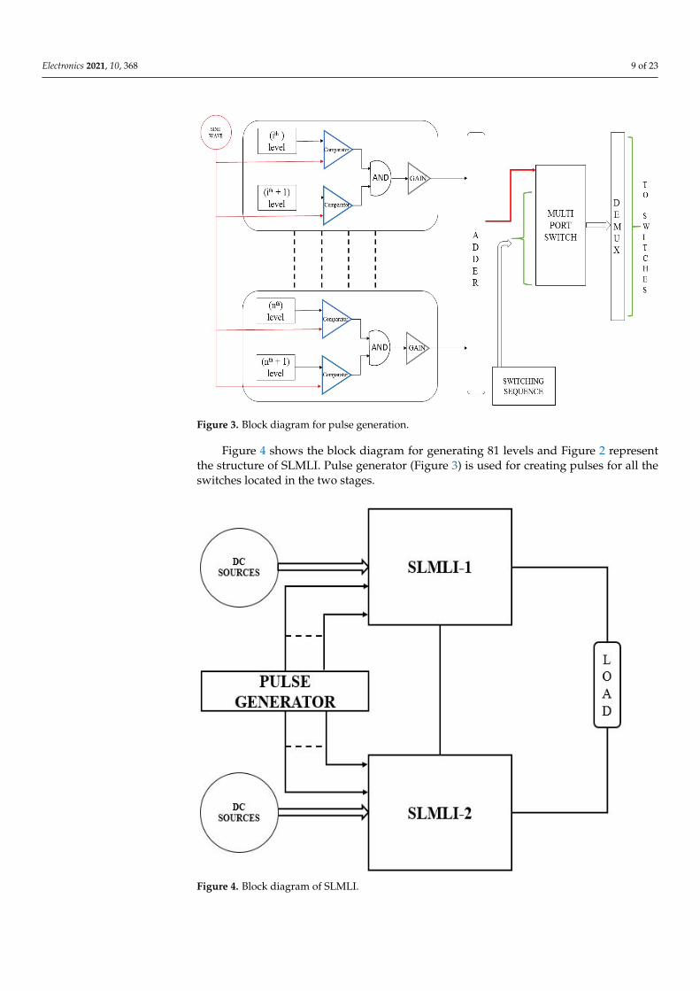
Figure 4 shows the block diagram for generating 81 levels and Figure 2 represent the structure of SLMLI. Pulse generator (Figure 3) is used for creating pulses for all the switches located in the two stages.
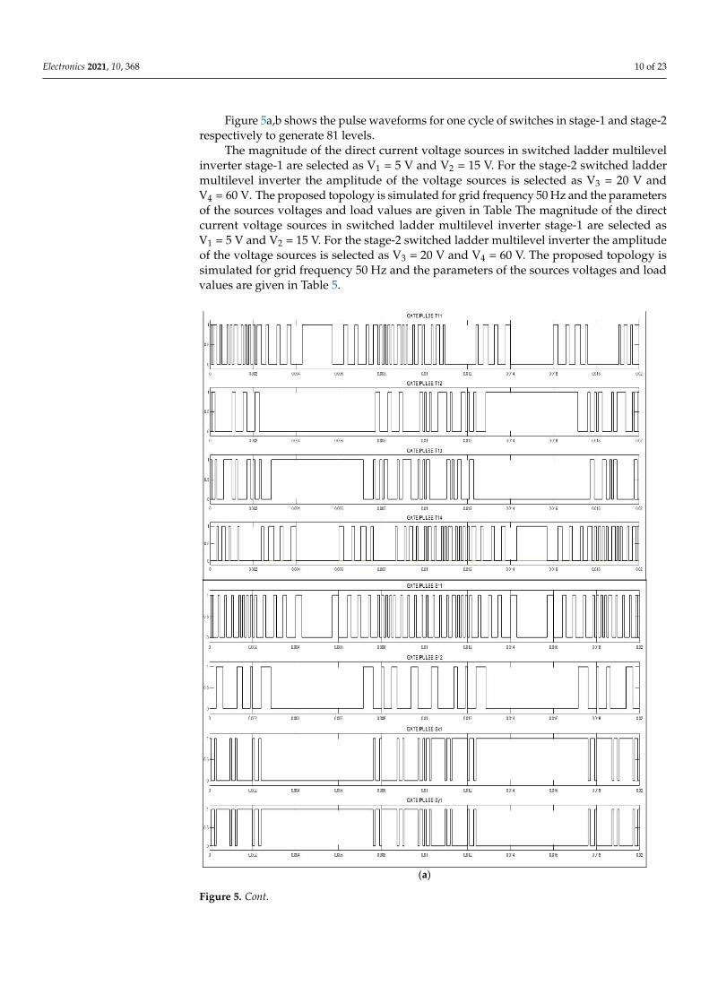
Figure 5a,b shows the pulse waveforms for one cycle of switches in stage-1 and stage-2 respectively to generate 81 levels.
The magnitude of the direct current voltage sources in switched ladder multilevel inverter stage-1 are selected as V1 = 5 V and V2 = 15 V. For the stage-2 switched ladder multilevel inverter the amplitude of the voltage sources is selected as V3 = 20 V and V4 = 60 V. The proposed topology is simulated for grid frequency 50 Hz and the parameters of the sources voltages and load values are given in Table The magnitude of the direct cur-rent voltage sources in switched ladder multilevel inverter stage-1 are selected as V1 = 5 V and V2 = 15 V. For the stage-2 switched ladder multilevel inverter the amplitude of the voltage sources is selected as V3 = 20 V and V4 = 60 V. The proposed topology is simu-lated for grid frequency 50 Hz and the parameters of the sources voltages and load val-ues are given in Table 5.
Figure 3. Block diagram for pulse generation.
Figure 4 shows the block diagram for generating 81 levels and Figure 2 representthe structure of SLMLI. Pulse generator (Figure 3) is used for creating pulses for all theswitches located in the two stages.
Electronics 2021, 10, x FOR PEER REVIEW 10 of 25
Figure 4. Block diagram of SLMLI.
Figure 4. Block diagram of SLMLI.
Electronics 2021, 10, 368 10 of 23
Figure 5a,b shows the pulse waveforms for one cycle of switches in stage-1 and stage-2respectively to generate 81 levels.
The magnitude of the direct current voltage sources in switched ladder multilevelinverter stage-1 are selected as V1 = 5 V and V2 = 15 V. For the stage-2 switched laddermultilevel inverter the amplitude of the voltage sources is selected as V3 = 20 V andV4 = 60 V. The proposed topology is simulated for grid frequency 50 Hz and the parametersof the sources voltages and load values are given in Table The magnitude of the directcurrent voltage sources in switched ladder multilevel inverter stage-1 are selected asV1 = 5 V and V2 = 15 V. For the stage-2 switched ladder multilevel inverter the amplitudeof the voltage sources is selected as V3 = 20 V and V4 = 60 V. The proposed topology issimulated for grid frequency 50 Hz and the parameters of the sources voltages and loadvalues are given in Table 5.
Electronics 2021, 10, x FOR PEER REVIEW 11 of 25
(a)
Figure 5. Cont.

Electronics 2021, 10, 368 11 of 23Electronics 2021, 10, x FOR PEER REVIEW 12 of 25
(b)
Figure 5. (a) Pulse waveforms for stage-1; (b) pulse waveforms for stage-2.
Table 5. Specification of two stage SLMLI.
S.No Parameters Values INPUT VOLTAGES OF SLMLI-1
1 V1 5 V 2 V2 15 V
INPUT VOLTAGES OF SLMLI-2 3 V3 20 V 4 V4 60 V
OUTPUT FREQUENCY 5 F 50 Hz
LOAD 6 R 1st cycle 10 Ω
Figure 5. (a) Pulse waveforms for stage-1; (b) pulse waveforms for stage-2.
Table 5. Specification of two stage SLMLI.
S.No Parameters Values
INPUT VOLTAGES OF SLMLI-11 V1 5 V2 V2 15 V
INPUT VOLTAGES OF SLMLI-23 V3 20 V4 V4 60 V
OUTPUT FREQUENCY5 F 50 Hz
LOAD
6 R1st cycle 10 Ω2nd cycle 5 Ω
3rd and 4th cycle 2.5 Ω
7 L1st cycle 10 Ω, 5 mH2nd cycle 5 Ω, 2.5 mH
3rd and 4th cycle 2.5 Ω, 1.25 mH

Electronics 2021, 10, 368 12 of 23
The 81 level inverter output voltage and output current waveform is shown in Figure 6.The resistive load is tested for four cycles (i.e., 0.08 s). The inverter is tested with resistiveload of 10 Ω for the first cycle (i.e., 0.02 s), during this period the output load current isobserved as 20 A. For the second cycle (i.e., from 0.02 s to 0.04 s) the inverter is connectedwith 5 Ω resistance and obtained the load current as 40 A. For the third and fourth cycle(i.e., from 0.04 s to 0.08 s), the inverter is connected with load resistance of 2.5 Ω to produce80 A at the load. For these entire instances, the peak load output voltage is observedas ±200 V.
Electronics 2021, 10, x FOR PEER REVIEW 13 of 24
Figure 6. Output voltage and change in current waveforms for variable R load.
The harmonic content present in the output voltage and current waveforms are ob-tained from FFT (Fast Fourier transform) analysis are 1.18% and it is shown in Figure 7a,b.
(a)
Figure 6. Output voltage and change in current waveforms for variable R load.
The harmonic content present in the output voltage and current waveforms are obtainedfrom FFT (Fast Fourier transform) analysis are 1.18% and it is shown in Figure 7a,b.
Electronics 2021, 10, x FOR PEER REVIEW 13 of 24
Figure 6. Output voltage and change in current waveforms for variable R load.
The harmonic content present in the output voltage and current waveforms are ob-tained from FFT (Fast Fourier transform) analysis are 1.18% and it is shown in Figure 7a,b.
(a)
Figure 7. Cont.

Electronics 2021, 10, 368 13 of 23Electronics 2021, 10, x FOR PEER REVIEW 14 of 24
(b)
Figure 7. (a) FFT for output voltage fed with R load; (b) FFT for output current fed with R load.
Figure 8 shows the output voltage and variation in the current waveform for the change in impedance load at equal interval of time. For Z = 10.12 Ω, 5.06 Ω and 2.53 Ω the output current is measured as 19.76 A, 39.52 A and 79.05 A respectively.
Figure 8. Output voltage and current waveforms for RL load.
Figure 7. (a) FFT for output voltage fed with R load; (b) FFT for output current fed with R load.
Figure 8 shows the output voltage and variation in the current waveform for thechange in impedance load at equal interval of time. For Z = 10.12 Ω, 5.06 Ω and 2.53 Ω theoutput current is measured as 19.76 A, 39.52 A and 79.05 A respectively.
Figure 8. Output voltage and current waveforms for RL load.
Electronics 2021, 10, 368 14 of 23
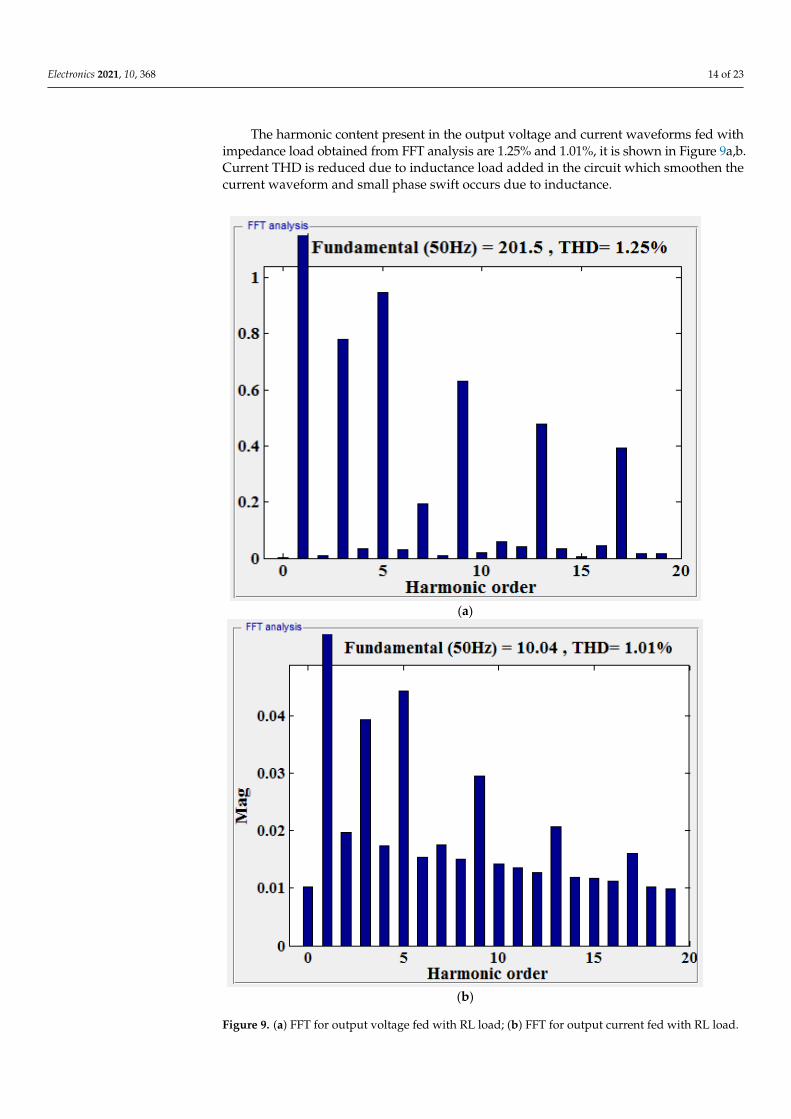
The harmonic content present in the output voltage and current waveforms fed withimpedance load obtained from FFT analysis are 1.25% and 1.01%, it is shown in Figure 9a,b.Current THD is reduced due to inductance load added in the circuit which smoothen thecurrent waveform and small phase swift occurs due to inductance.
Electronics 2021, 10, x FOR PEER REVIEW 15 of 24
The harmonic content present in the output voltage and current waveforms fed with impedance load obtained from FFT analysis are 1.25% and 1.01%, it is shown in Figure 9a,b. Current THD is reduced due to inductance load added in the circuit which smoothen the current waveform and small phase swift occurs due to inductance.
(a)
(b)
Figure 9. (a) FFT for output voltage fed with RL load; (b) FFT for output current fed with RL load. Figure 9. (a) FFT for output voltage fed with RL load; (b) FFT for output current fed with RL load.

Electronics 2021, 10, 368 15 of 23
When motor is supplied by a cascaded two stages of SLMLI of 81 levels in the output,the speed of the motor is shown in Figure 10 for the load torque of 1 Nm, due to loadtorque it settles at average speed of 1730 rpm.
Electronics 2021, 10, x FOR PEER REVIEW 16 of 24
When motor is supplied by a cascaded two stages of SLMLI of 81 levels in the out-put, the speed of the motor is shown in Figure 10 for the load torque of 1 Nm, due to load torque it settles at average speed of 1730 rpm.
Figure 10. Speed of single stage SLMLI fed induction motor.
The electromagnetic torque produced by the given induction motor fed by the cas-caded two stages of SLMLI is shown in Figure 11.
Figure 11. Electromagnetic torque of single stage SLMLI fed induction motor.
FFT analysis for the source voltage and current of induction motor is shown in Fig-ure 12a which contains the fundamental frequency of 60 Hz and the peak magnitude is
Figure 10. Speed of single stage SLMLI fed induction motor.
The electromagnetic torque produced by the given induction motor fed by the cas-caded two stages of SLMLI is shown in Figure 11.
Electronics 2021, 10, x FOR PEER REVIEW 16 of 24
When motor is supplied by a cascaded two stages of SLMLI of 81 levels in the out-put, the speed of the motor is shown in Figure 10 for the load torque of 1 Nm, due to load torque it settles at average speed of 1730 rpm.
Figure 10. Speed of single stage SLMLI fed induction motor.
The electromagnetic torque produced by the given induction motor fed by the cas-caded two stages of SLMLI is shown in Figure 11.
Figure 11. Electromagnetic torque of single stage SLMLI fed induction motor.
FFT analysis for the source voltage and current of induction motor is shown in Fig-ure 12a which contains the fundamental frequency of 60 Hz and the peak magnitude is
Figure 11. Electromagnetic torque of single stage SLMLI fed induction motor.
FFT analysis for the source voltage and current of induction motor is shown in Figure 12awhich contains the fundamental frequency of 60 Hz and the peak magnitude is 156.7 V andthe voltage THD is 1.24%. The input current drawn from the SLMLI fundamental peak is3.434 A and the THD is 4.12% as shown in Figure 12b.

Electronics 2021, 10, 368 16 of 23
Electronics 2021, 10, x FOR PEER REVIEW 17 of 24
156.7 V and the voltage THD is 1.24%. The input current drawn from the SLMLI funda-mental peak is 3.434 A and the THD is 4.12% as shown in Figure 12b.
(a)
(b)
Figure 12. (a) FFT analysis for input voltage for induction motor load; (b) FFT analysis for current for induction motor load.
5.1. Speed Control Technique In this speed control has been done by varying the supply voltage given to the in-
duction motor. Specification of the inverter is shown in Table 6, as per proposed system the output voltage has 81-levels which gives to the rated voltage of 110 V (rms) due to that it will produce the rated speed of the induction motor which is 1800 RPM. The
Figure 12. (a) FFT analysis for input voltage for induction motor load; (b) FFT analysis for currentfor induction motor load.
5.1. Speed Control Technique
In this speed control has been done by varying the supply voltage given to theinduction motor. Specification of the inverter is shown in Table 6, as per proposed systemthe output voltage has 81-levels which gives to the rated voltage of 110 V (rms) due to thatit will produce the rated speed of the induction motor which is 1800 RPM. The magnitudeof the direct current voltage sources in switched ladder multilevel inverter stage-1 areselected as V1 = 4V and V2 = 12 V. For the stage-2 switched ladder multilevel inverter the

Electronics 2021, 10, 368 17 of 23
amplitude of the voltage sources is selected as V3 = 16 V and V4 = 48 V, the specification ofinverter and induction motor is given in Table 6.
Table 6. Specification of Inverter and Induction motor.
S.No Parameters Values
Input voltages of SLMLI-11 V1 4 V2 V2 12 V
Input voltages of SLMLI-23 V3 16 V4 V4 48 V
Output frequency5 f 60 Hz
Induction motor load6 Power 0.25 Hp7 Supply voltage 110 V8 Frequency 60 Hz9 Speed 1800 RPM10 Load torque 1 Nm
Figure 13 shows the various speed responses of the induction motor with respect todifferent input voltages. The blue colored line in the graph shows the speed response forthe rated voltage given by the inverter which is nearly rotates at rated speed of 1736 RPM.
Electronics 2021, 10, x FOR PEER REVIEW 18 of 24
magnitude of the direct current voltage sources in switched ladder multilevel inverter stage-1 are selected as V1 = 4V and V2 = 12 V. For the stage-2 switched ladder multilevel inverter the amplitude of the voltage sources is selected as V3 = 16 V and V4 = 48 V, the specification of inverter and induction motor is given in Table 6.
Table 6. Specification of Inverter and Induction motor.
S.No Parameters Values Input voltages of SLMLI-1
1 V1 4 V 2 V2 12 V
Input voltages of SLMLI-2 3 V3 16 V 4 V4 48 V
Output frequency 5 f 60 Hz
Induction motor load 6 Power 0.25 Hp 7 Supply voltage 110 V 8 Frequency 60 Hz 9 Speed 1800 RPM
10 Load torque 1 Nm
Figure 13 shows the various speed responses of the induction motor with respect to different input voltages. The blue colored line in the graph shows the speed response for the rated voltage given by the inverter which is nearly rotates at rated speed of 1736 RPM.
Figure 13. Various speed responses of the induction motor with respect to different input voltages. Figure 13. Various speed responses of the induction motor with respect to different input voltages.
Variation in the inverter output voltage can be achieved by changing the magnitudeof sinusoidal reference control logic and it is shown in Figure 14. In order to vary the speedof the motor, change in magnitude of reference is done; the other two different speedsare shown in Figure 13 that is plotted with pink and brown lines. These speeds are lesscompared to the rated speed, less than rated speeds only achieved by this control technique.

Electronics 2021, 10, 368 18 of 23
Electronics 2021, 10, x FOR PEER REVIEW 19 of 24
Variation in the inverter output voltage can be achieved by changing the magnitude of sinusoidal reference control logic and it is shown in Figure 14. In order to vary the speed of the motor, change in magnitude of reference is done; the other two different speeds are shown in Figure 13 that is plotted with pink and brown lines. These speeds are less compared to the rated speed, less than rated speeds only achieved by this control technique.
Figure 14. Different Output voltages of a SLMLI.
Figure 14 shows the inverter output voltages for different magnitudes, blue colored voltage in Figure has the magnitude of 110 V rms which gives to the induction motor as per motor rating. The other two colored voltages in the Figure 14 are reduced voltage and the magnitude is less compared to the rated voltage of the motor.
The load torque is applied as 1 Nm at 3 s and 1.25 Nm at 6 s. The variation in load torque, speed and current waveform are shown in Figures 15–17.
Figure 15. Load torque vs. time.
Figure 14. Different Output voltages of a SLMLI.
Figure 14 shows the inverter output voltages for different magnitudes, blue coloredvoltage in Figure has the magnitude of 110 V rms which gives to the induction motor asper motor rating. The other two colored voltages in the Figure 14 are reduced voltage andthe magnitude is less compared to the rated voltage of the motor.
The load torque is applied as 1 Nm at 3 s and 1.25 Nm at 6 s. The variation in loadtorque, speed and current waveform are shown in Figures 15–17.
Electronics 2021, 10, x FOR PEER REVIEW 19 of 24
Variation in the inverter output voltage can be achieved by changing the magnitude of sinusoidal reference control logic and it is shown in Figure 14. In order to vary the speed of the motor, change in magnitude of reference is done; the other two different speeds are shown in Figure 13 that is plotted with pink and brown lines. These speeds are less compared to the rated speed, less than rated speeds only achieved by this control technique.
Figure 14. Different Output voltages of a SLMLI.
Figure 14 shows the inverter output voltages for different magnitudes, blue colored voltage in Figure has the magnitude of 110 V rms which gives to the induction motor as per motor rating. The other two colored voltages in the Figure 14 are reduced voltage and the magnitude is less compared to the rated voltage of the motor.
The load torque is applied as 1 Nm at 3 s and 1.25 Nm at 6 s. The variation in load torque, speed and current waveform are shown in Figures 15–17.
Figure 15. Load torque vs. time. Figure 15. Load torque vs. time.

Electronics 2021, 10, 368 19 of 23Electronics 2021, 10, x FOR PEER REVIEW 20 of 24
Figure 16. Speed variations for various load torque.
Figure 17. Current variations for various load torque.
The main winding current is zoomed and it is shown in Figure 18.
Figure 16. Speed variations for various load torque.
Electronics 2021, 10, x FOR PEER REVIEW 20 of 24
Figure 16. Speed variations for various load torque.
Figure 17. Current variations for various load torque.
The main winding current is zoomed and it is shown in Figure 18.
Figure 17. Current variations for various load torque.
The main winding current is zoomed and it is shown in Figure 18.The proposed SLMLI is constructed with low number of power electronics devices
for generating 81 levels in the output voltage. Design of DC sources is framed withtwo different algorithms. Furthermore, the SLMLI structure is tested with single phaseinduction motor and Speed control has been performed with satisfactory results.

Electronics 2021, 10, 368 20 of 23Electronics 2021, 10, x FOR PEER REVIEW 21 of 24
Figure 18. Main winding current for various load torque.
The proposed SLMLI is constructed with low number of power electronics devices for generating 81 levels in the output voltage. Design of DC sources is framed with two different algorithms. Furthermore, the SLMLI structure is tested with single phase in-duction motor and Speed control has been performed with satisfactory results.
5.2. Cost-Benefit Analysis of 81-Level SLMLI with Conventional MLI’s The unit price of the component is given in Table 7. The cost-benefit analysis of
proposed 81-level switched ladder in comparison with the conventional MLI is shown in Table 8. From the cost analysis it can be concluded that the proposed inverter can be de-signed with low cost compared to conventional MLI’s.
Table 7. Unit price of the circuit components.
Name of the Component Component Number Voltage Rating Unit Price in
$ IGBT (80 A)—Single Switch IKW75N60TFKSA1 600 V 6.97
Diode (80 A) VS-80EBU02 200 V 5.04 Capacitor (10 µF) EEE-FK1K100XP 80 V 0.58
Table 8. Cost-benefit analysis of 81-level SLMLI with conventional MLI’s.
To Generate 81 Level
Number of Switches
Number of Diodes
Number of Capacitors
Overall Cost of Switches in $
Overall Cost of Diodes in
$
Overall Cost of Capacitors in $
Total Cost in $
Proposed MLI 20 Nil Nil 139 Nil Nil 139 CHBMLI 216 Nil Nil 1505 Nil Nil 1505 FCMLI 216 Nil 3240 1505 Nil 1879.2 3384 NPMLI 216 3160 78 1505 15926 45.24 17477
Sources from Infineon Technologies, www.digikey.in (accessed on 30 January 2021).
Figure 18. Main winding current for various load torque.
5.2. Cost-Benefit Analysis of 81-Level SLMLI with Conventional MLI’s
The unit price of the component is given in Table 7. The cost-benefit analysis ofproposed 81-level switched ladder in comparison with the conventional MLI is shownin Table 8. From the cost analysis it can be concluded that the proposed inverter can bedesigned with low cost compared to conventional MLI’s.
Table 7. Unit price of the circuit components.
Name of theComponent Component Number Voltage Rating Unit Price in $
IGBT (80 A)—SingleSwitch IKW75N60TFKSA1 600 V 6.97
Diode (80 A) VS-80EBU02 200 V 5.04Capacitor (10 µF) EEE-FK1K100XP 80 V 0.58
Table 8. Cost-benefit analysis of 81-level SLMLI with conventional MLI’s.
To Generate81 Level
Number ofSwitches
Number ofDiodes
Number ofCapacitors
Overall Cost ofSwitches in $
Overall Costof Diodes in $
Overall Cost ofCapacitors in $ Total Cost in $
Proposed MLI 20 Nil Nil 139 Nil Nil 139CHBMLI 216 Nil Nil 1505 Nil Nil 1505FCMLI 216 Nil 3240 1505 Nil 1879.2 3384NPMLI 216 3160 78 1505 15926 45.24 17477
Sources from Infineon Technologies, www.digikey.in (accessed on 30 January 2021).
6. Conclusions
Much research had been undertaken to design multilevel inverters with reducedcircuit components, minimum losses, low cost, and compact size with high efficiency.A survey is made in this paper to identify the type of multilevel inverter used in highand medium power applications such as Electric Vehicle, Power drives, Grid integrationsystems, etc. A detailed review is conducted on the recent multilevel inverter design withreduced switch count to find out the challenges and key issues. Significant issues of variousmultilevel inverter designs are provided in terms of number of diodes, switches, source

Electronics 2021, 10, 368 21 of 23
utilization and filter requirement. A new 81-level switched ladder inverter is configuredusing MATLAB/Simulink and tested with change in resistive and impedance load at equalperiod of time. The results were analyzed in terms of harmonic content. Further, the outputof 81-level inverter is connected to 0.25 HP, 110 V single phase induction motor. The speedof the induction motor is observed for change in input voltages and the various speedcurves were presented. Variation in the speed with respect to change in load torque isplotted in this paper, thus the performance of the single phase induction motor fed by81-level switched ladder inverter is found satisfactory.
Author Contributions: Conceptualization, methodology and writing—review, V.L., D.R. and B.M.;project administration, funding acquisition editing and supervision, G.K.S. and M.R. All authorshave read and agreed to the published version of the manuscript.
Funding: The authors thank the Department of Electrical and Electronics Engineering, Anna Uni-versity, India for the financial support through RUSA 2.0 (PO 2) project and FONDECYT Regular1191028 and FNDAP SERC Chile 15110019.
Conflicts of Interest: The authors declare no conflict of interest.
Abbreviations
MLI Multilevel InverterDC Direct CurrentTHD Total Harmonics DistortionPWM Pulse Width ModulationCHB Cascaded Half BridgeMLIRS Multilevel Inverter with Reduced SwitchDVR Dynamic Voltage RestorerSLMLI Switched Ladder Multilevel InverterFFT Fast Fourier TransformNm Newton meterRPM Revolution Per MinuteRMS Root Mean Square
References1. Roemer, F.; Ahmad, M.; Chang, F.; Lienkamp, M. Optimization of a cascaded h-bridge inverter for electric vehicle applications
including cost consideration. Energies 2019, 12, 4272. [CrossRef]2. Karthikeyan, D.; Vijayakumar, K.; Jagabar Sathik, M. Generalized cascaded symmetric and level doubling multilevel converter
topology with reduced THD for photovoltaic applications. Electronics 2019, 8, 161.3. Samadaei, E.; Salehi, A.; Iranian, M.; Pouresmaeil, E. Single DC source multilevel inverter with changeable gains and levels for
low-power loads. Electronics 2020, 9, 937. [CrossRef]4. Sunddararaj, S.P.; Srinivasarangan Rangarajan, S.; Subashini, N. An extensive review of multilevel inverters based on their
multifaceted structural configuration, triggering methods and applications. Electronics 2020, 9, 433. [CrossRef]5. Vijayaraja, L.; Kumar, S.G.; Rivera, M. A review on multilevel inverter with reduced switch count. In Proceedings of the 2016
IEEE International Conference on Automatica (ICA-ACCA), Curico, Chile, 19–21 October 2016; pp. 1–5.6. Ahmad, A.; Anas, M.; Sarwar, A.; Zaid, M.; Tariq, M.; Ahmad, J.; Beig, A.R. Realization of a generalized switched-capacitor
multilevel inverter topology with less switch requirement. Energies 2020, 13, 1556. [CrossRef]7. Ganesh, B.; Murugan, N.; Nallaswamy, M.; Rajkumar, K.; Vijayaraja, L.; Ganesh Kumar, S.; Rivera, M. Implementation of twenty
seven level and fifty one level inverter using constant voltage sources. In Proceedings of the 2019 IEEE CHILEAN Conferenceon Electrical, Electronics Engineering, Information and Communication Technologies (CHILECON), Valparaiso, Chile, 13–27November 2019; pp. 1–4.
8. Vijayaraja, L.; Kumar, S.G.; Rivera, M. A new topology of multilevel inverter with reduced part count. In Proceedings of the 2018IEEE International Conference on Automation/XXIII Congress of the Chilean Association of Automatic Control (ICA-ACCA),Concepcion, Chile, 17–19 October 2018; pp. 1–5.
9. Aganah, K.A.; Luciano, C.; Ndoye, M.; Murphy, G. New switched-dual-source multilevel inverter for symmetrical and asymmet-rical operation. Energies 2018, 11, 984. [CrossRef]
10. Vijayaraja, L.; Dhanasekar, R.; Balaji, M.; Ganesh Kumar, S. Performance study of 81-level inverter using two stage switch laddercircuit. In Proceedings of the 1st International Science Exhibition Congress Symposium (SECS-2020), Jharkhand, India, 12–13September 2020.

Electronics 2021, 10, 368 22 of 23
11. Ponkumar, S.; Rivera, M.; Kamroon, F.; Kumar, S.G. Realization of cascaded multilevel inverter. In Proceedings of the 2017CHILEAN Conference on Electrical, Electronics Engineering, Information and Communication Technologies (CHILECON),Pucon, Chile, 18–20 October 2017; pp. 1–7.
12. Hassan, A.; Yang, X.; Chen, W.; Houran, M.A. A state of the art of the multilevel inverters with reduced count components.Electronics 2020, 9, 1924. [CrossRef]
13. Thiyagarajan, V. Simulation analysis of 51-level inverter topology with reduced switch count. Mater. Today Proc. 2020, 33,3870–3876. [CrossRef]
14. Ali, A.I.M.; Sayed, M.A.; Takeshita, T. Isolated single-phase single-stage DC-AC cascaded transformer-based multilevel inverterfor stand-alone and grid-tied applications. Int. J. Electr. Power Energy Syst. 2021, 125, 106534. [CrossRef]
15. Nirmal Mukundan, C.M.; Jayaprakash, P.; Subramaniam, U.; Almakhles, D.J. Trinary hybrid cascaded h-bridge multilevelinverter-based grid-connected solar power transfer system supporting critical load. IEEE Syst. J. 2020. [CrossRef]
16. Rangarajan, P. Investigation of modified multilevel inverter topology for PV system. Microprocess. Microsyst. 2019, 71, 102870.17. Zaid, M.M.; Ro, J.-S. Optimal design of a cascaded rectangular-type and circle-type multilevel inverters with a new switching
technique. IET Power Electron. 2020, 13, 2831–2846. [CrossRef]18. Kim, S.-M.; Lee, E.-J.; Lee, J.-S.; Lee, K.-B. An improved phase-shifted DPWM method for reducing switching loss and thermal
balancing in cascaded h-bridge multilevel inverter. IEEE Access 2020, 8, 187072–187083. [CrossRef]19. Sahoo, S.; Ahmed, I. Common mode voltage reduction in NPC multilevel inverter by SVPWM using gh-coordinate system. In
Proceedings of the International Conference on Computational Intelligence for Smart Power System and Sustainable Energy(CISPSSE), Keonjhar, Odisha, India, 29–31 July 2020; pp. 1–6.
20. Sen, P. Novel multilevel inverter based standalone PV System using reduced number of components. In Proceedings of theInternational Conference on Renewable Energy Integration into Smart Grids: A Multidisciplinary Approach to TechnologyModelling and Simulation (ICREISG), Bhubaneswar, India, 14–15 February 2020; pp. 111–115.
21. Siddique, M.D.; Mekhilef, S.; Shah, N.M.; Sarwar, A.; Iqbal, A.; Memon, M.A. A new multilevel inverter topology with reduceswitch count. IEEE Access 2019, 7, 58584–58594. [CrossRef]
22. Joshi, N.R.; Sant, A.V. Analysis of a new symmetric multilevel inverter topology with reduced component count. In Proceedingsof the International Conference on Emerging Trends in Information Technology and Engineering (ic-ETITE), Vellore, India, 24–25February 2020; pp. 1–6.
23. Ranjbarizad, V.; Aalami, M.; Babaei, E. A new topology for cascaded multilevel inverter to generate more voltage levels with areduced count of power switches. In Proceedings of the 4th International Conference on Power Electronics and their Applications(ICPEA), Elazig, Turkey, 25–27 September 2019; pp. 1–7.
24. Kshirsagar, A.; Kaarthik, R.S.; Rahul, A.; Gopakumar, K.; Umanand, L.; Biswas, S.K.; Cecati, C. 17-level inverter with lowcomponent count for open-end induction motor drives. IET Power Electron. 2018, 11, 922–929. [CrossRef]
25. Dhanamjayulu, C.; Khasim, S.R.; Padmanaban, S.; Arunkumar, G.; Holm-Nielsen, J.B.; Blaabjerg, F. Design and implementationof multilevel inverters for fuel cell energy conversion system. IEEE Access 2020, 8, 183690–183707. [CrossRef]
26. Kahwa, A.; Obara, H.; Fujimoto, Y. Estimation and analysis of power loss in a reduced switches count H-bridge multilevelinverter. In Proceedings of the IEEE International Conference on Mechatronics (ICM), Ilmenau, Germany, 18–20 March 2019;pp. 25–30.
27. Rajkumar, K.; Parthiban, P. Performance investigation of transformerless DVR based on T-type multilevel inverter with reducedswitch count. In Proceedings of the IEEE International Conference on Sustainable Energy Technologies and Systems (ICSETS),Bhubaneswar, India, 26 February–1 March 2019; pp. 236–241.
28. Abdoli, H.; Khorsandi, A.; Eskandari, B.; Moghani, J.S. A new reduced switch multilevel inverter for PV applications. InProceedings of the 11th Power Electronics, Drive Systems, and Technologies Conference (PEDSTC), Tehran, Iran, 4–6 February2020; pp. 1–5.
29. Nasiri Avanaki, H.; Barzegarkhoo, R.; Zamiri, E.; Yang, Y.; Blaabjerg, F. Reduced switch-count structure for symmetric multilevelinverters with a novel switched-DC-source submodule. IET Power Electron. 2019, 12, 311–321. [CrossRef]
30. Babaei, E.; Kangarlu, M.F.; Hosseinzadeh, M.A. Asymmetrical multilevel converter topology with reduced number of components.IET Power Electron. 2013, 6, 1188–1196. [CrossRef]
31. Lee, S.S. Single-stage switched-capacitor module (S3CM) topology for cascaded multilevel inverter. IEEE Trans. Power Electron.2018, 33, 8204–8207. [CrossRef]
32. Majumdar, S.; Mahato, B.; Jana, K.C. Analysis of most optimal multi-unit multi-level inverter having minimum components andlower standing voltage. IETE Tech. Rev. 2020, 1–17. [CrossRef]
33. Ray, S.; Gupta, N.; Gupta, R.A. A comprehensive review on cascaded h-bridge inverter-based large-scale grid-connectedphotovoltaic. IETE Tech. Rev. 2017, 34, 463–477. [CrossRef]
34. Alishah, R.S.; Hosseini, S.H.; Babaei, E.; Sabahi, M. Optimal design of new cascaded switch-ladder. Multilevel inverter structure.IEEE Trans. Ind. Electron. 2017, 64, 2072–2080. [CrossRef]
35. Umashankar, S.; Sreedevi, T.S.; Nithya, V.G.; Vijayakumar, D. A new 7-level symmetric multilevel inverter with minimum numberof switches. Int. Sch. Res. Not. 2013. [CrossRef]

Electronics 2021, 10, 368 23 of 23
36. Prakash, S.; Kumar, L.; Gupta, S.; Agrawal, N. Implementation of symmetrical multilevel inverter topology. In Proceedings of theIEEE 1st International Conference on Power Electronics, Intelligent Control and Energy Systems (ICPEICES), Delhi, India, 4–6July 2016; pp. 1–6.
37. Bharath, K.; Satputaley, R.J. Single phase asymmetrical cascaded multilevel inverter design for induction motor. IJEEDC 2013, 1, 8–13.38. Seth, N.; Goel, V.; Kulkarni, R.D.; Joshi, V.P. Performance analysis of seven level three phase asymmetric multilevel inverter
at various modulation indices. In Proceedings of the 2016 International Conference on Electrical Power and Energy Systems(ICEPES), Bhopal, India, 14–16 December 2016; pp. 407–413.
39. Pires, V.F.; Silva, J.F. Hybrid cascade multilevel inverter using a single DC source for open-end winding induction motors. InProceedings of the 2012 IEEE International Conference on Industrial Technology, Athens, Greece, 19–21 March 2012; pp. 966–970.
40. Khosroshahi, M.T. Crisscross cascade multilevel inverter with reduction in number of components. IET Power Electron. 2014, 7,2914–2924. [CrossRef]
41. Oskuee, M.R.J.; Salary, E.; Najafi-Ravadanegh, S. Creative design of symmetric multilevel converter to enhance the circuit’sperformance. IET Power Electron. 2015, 8, 96–102. [CrossRef]
42. Wang, L.; Wu, Q.H.; Tang, W. Novel cascaded switched-diode multilevel inverter for renewable energy integration. IEEE Trans.Energy Convers. 2017, 32, 1574–1582. [CrossRef]
43. Alishah, R.S.; Nazarpour, D.; Hosseini, S.H.; Sabahi, M. Novel topologies for symmetric, asymmetric, and cascade switched-diodemultilevel converter with minimum number of power electronic components. IEEE Trans. Ind. Electron. 2014, 61, 5300–5310.[CrossRef]
44. Su, G.-J. Multilevel DC-link inverter. IEEE Trans. Ind. Appl. 2005, 41, 848–854. [CrossRef]45. Liu, J.; Cheng, K.W.E.; Ye, Y. A cascaded multilevel inverter based on switched-capacitor for high-frequency AC power distribution
system. IEEE Trans. Power Electron. 2014, 29, 4219–4230. [CrossRef]46. Gupta, K.K.; Jain, S. A novel multilevel inverter based on switched DC sources. IEEE Trans. Ind. Electron. 2014, 61, 3269–3278.
[CrossRef]47. Mokhberdoran, A.; Ajami, A. Symmetric and asymmetric design and implementation of new cascaded multilevel inverter
topology. IEEE Trans. Power. Electron. 2014, 29, 6712–6724. [CrossRef]48. Arun, N.; Noel, M.M. Crisscross switched multilevel inverter using cascaded semi-half-bridge cells. IET Power Electron. 2018, 11,
23–32. [CrossRef]49. Ajami, A.; Oskuee, M.R.J.; Mokhberdoran, A.; van den Bossche, A. Developed cascaded multilevel inverter topology to minimise
the number of circuit devices and voltage stresses of switches. IET Power Electron. 2014, 7, 459–466. [CrossRef]50. Thiyagarajan, V.; Somasundaram, P. Multilevel inverter topology with modified pulse width modulation and reduced switch
coun. Acta Polytechnica Hungarica 2018, 15, 141–167.51. Chappa, A.; Gupta, S.; Sahu, L.K.; Gautam, S.P.; Gupta, K.K. Symmetrical and asymmetrical reduced device multilevel inverter
topology. IEEE J. Emerg. Sel. Top. Power Electron. 2019, 9, 885–896. [CrossRef]52. Ajami, A.; Mokhberdoran, A.; Oskuee, M.R.J. A new topology of multilevel voltage source inverter to minimize the number of
circuit devices and maximize the number of output voltage levels. J. Electr Eng Technol. 2013, 8, 1328–1336. [CrossRef]53. Siddique, M.D.; Mekhilef, S.; Shah, N.M.; Memon, M.A. Optimal design of a new cascaded multilevel inverter topology with
reduced switch count. IEEE Access 2019, 7, 24498–24510. [CrossRef]54. Samadaei, S.E.; Kaviani, M.; Bertilsson, K. A 13-levels module (K-type) with two DC sources for multilevel inverters. IEEE Trans.
Ind. Electron. 2019, 66, 5186–5196. [CrossRef]55. Thiyagarajan, V.; Somasundaram, P.; Ramash Kumar, K. Simulation and analysis of novel extendable multilevel inverter topology.
J. Circuits Syst. Comput. 2020, 28, 1950089. [CrossRef]56. Zeng, J.; Lin, W.; Cen, D.; Liu, J. Novel K-type multilevel inverter with reduced components and self-balance. IEEE J. Emerg. Sel.
Top. Power Electron. 2020, 8, 4343–4354. [CrossRef]57. Loganathan, V.; Srinivasan, G.K.; Rivera, M. Realization of 485 Level Inverter Using Tri-State Architecture for Renewable Energy
Systems. Energies 2020, 13, 6627. [CrossRef]