
Transportation Electrification - ShanghaiTech
13
2325-5987/13/$31.00©2013IEEE IEEE Electrification Magazine / DECEMBER 2013 46 HE U.S. TRANSPORTATION SECTOR consumes approximately 14 million barrels of petroleum every day, which is more than the total oil con- sumption of any other nation in the world. The most prominent sustainable solution to profoundly reduce both oil consumption and greenhouse gas emissions lies in grid-enabled elec- tric vehicles (EVs) These vehicles are propelled either partially or fully by electricity through energy storage systems such as electrochemical batteries, which need to be charged from the grid. One of the most important realities that will facili- tate the adoption of grid-enabled plug-in EVs (PEVs) is the method by which these vehicles will be charged and if the nation’s electrical infrastructure can sustain the charging requirements of PEVs without the need for a comprehensive evolution. Since nearly all residences and businesses in the United States are already equipped with a 120-Vac mains con- nection, and most with a 240-Vac connection, most charging will be done through onboard level 1 (120 Vac/16 A/1.92 kW Max ) and level 2 (240 Vac/ 80 A/19.2 kW Max ) chargers when the vehicle is parked either overnight at home or during the day at the office. Even though onboard level 1 and level 2 charg- ing would be the most prominent charging paradigm Digital Object Identifier 10.1109/MELE.2013.2294238 Date of publication: 26 February 2014 By Haoyu Wang, Amin Hasanzadeh, and Alireza Khaligh Transportation Electrification Conductive charging of electrified vehicles.
Transcript of Transportation Electrification - ShanghaiTech
2325-5987/13/$31.00©2013IEEEIEEE Electr i f icat ion Magazine / december 201346
he U.S. tranSportation Sector consumes approximately 14 million barrels of petroleum every day, which is more than the total oil con-sumption of any other nation in the
world. the most prominent sustainable solution to profoundly reduce both oil consumption and greenhouse gas emissions lies in grid-enabled elec-tric vehicles (eVs) these vehicles are propelled either partially or fully by electricity through energy storage systems such as electrochemical batteries, which need to be charged from the grid.
one of the most important realities that will facili-tate the adoption of grid-enabled plug-in eVs (peVs) is the method by which these vehicles will be charged and if the nation’s electrical infrastructure can sustain the charging requirements of peVs without the need for a comprehensive evolution. Since nearly all residences and businesses in the United States are already equipped with a 120-Vac mains con-nection, and most with a 240-Vac connection, most charging will be done through onboard level 1 (120 Vac/16 a/1.92 kWMax) and level 2 (240 Vac/ 80 a/19.2 kWMax) chargers when the vehicle is parked either overnight at home or during the day at the office. even though onboard level 1 and level 2 charg-ing would be the most prominent charging paradigm
Digital Object Identifier 10.1109/MELE.2013.2294238 Date of publication: 26 February 2014
T
By Haoyu Wang, Amin Hasanzadeh, and Alireza Khaligh
Transportation ElectrificationConductive charging of electrified vehicles.
IEEE Electr i f icat ion Magazine / december 2013 47
for the next generation of peVs, there is a crucial need to deploy high-power off-board level 3 (208– 600 Vac/400 a/240 kWMax) chargers. this would not only eliminate the “range anxiety” phenomenon among drivers but also enable long trips of considerable distance without substantial vehicle downtime, as level 3 chargers would serve a similar func-tion for peVs as gas stations do for con-ventional internal combustion engine (ice) vehicles. this article focuses on the conductive onboard and off-board battery charging of peVs.
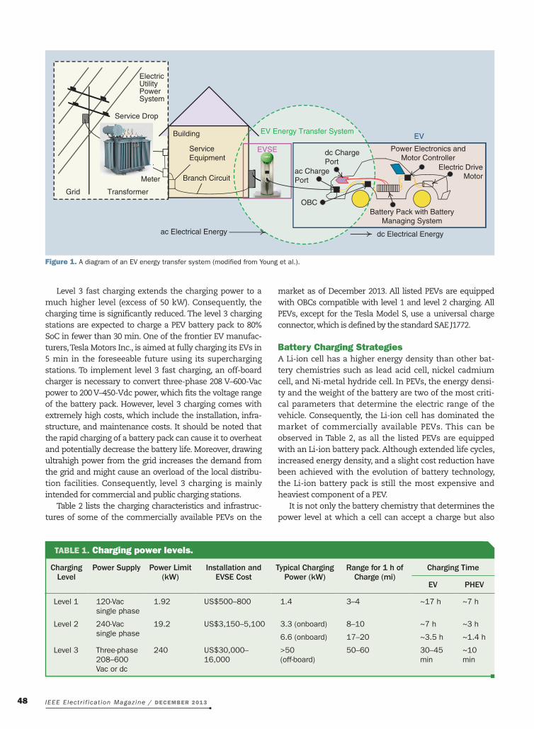
charging Levels and Infrastructuresa diagram of a typical peV energy transfer system is shown in Figure 1. a low-frequency transformer is used to deliver ac power from the grid to the neighborhood where the eV supply
equipment (eVSe) is installed. typically, the eVSe includes conductors; eV connectors; attachment plugs; communication proto-cols; and all other fittings, devices, and power outlets and/or apparatuses. the eVSe serves as the energy transfer interface between the premises’ wirings and the peVs’ onboard or off-board battery chargers.
Depending on the power level and the required charging facilities, the charging of eVs and plug-in hybrid eVs (pheVs), cumu-latively called peVs, can be classified into three different levels. the corresponding power supplies, charging power levels, eVSe costs, all-electric mile ranges for 1 h of charge, and charging times are summa-rized in table 1.
in the United States, level 1 charging is adapted for a single-phase, 120-V/16-a, 60-hz grid outlet. a level 1 charger is easy to inte-grate on board. the installation and eVSe cost for level 1 charging is estimated to be US$500–800. the relatively low price makes level 1 applicable to home charging. a major-ity of the available eVs and pheVs are equipped with an onboard charger (oBc), which is compatible with level 1 charging. however, the low charging power increases the charging time of the battery pack (up to 17 h) to charge a typical 25-kWh battery pack from 20% state of charge (Soc) to full Soc.
Level 2 charging requires a single-phase 240-V power outlet, which is available in most residential garages as well as public facilities. Using the 6.6-kW oBc, it takes 3.5 h to charge a typical 25-kWh battery
pack from 20% Soc to full Soc. in comparison to level 1, without compromising the convenience of accessibility, the level 2 charging time is much less. the installation and eVSe cost of level 2 charging is expected to be US$3,150–5,100. although it is much higher than level 1 charging, it
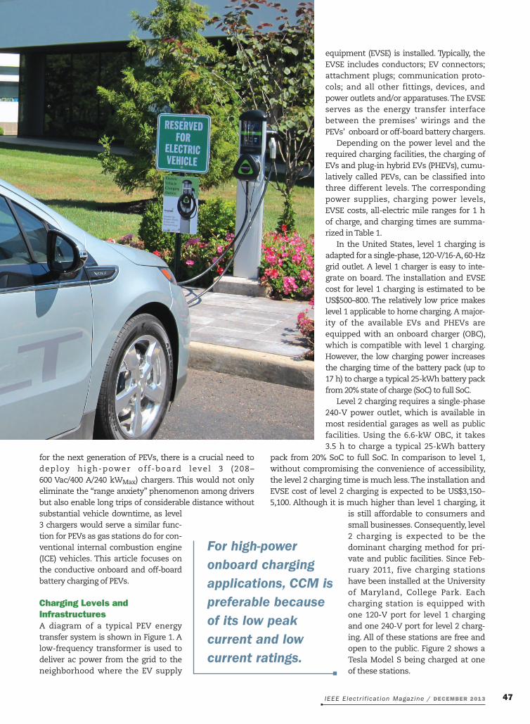
is still affordable to consumers and small businesses. consequently, level 2 charging is expected to be the dominant charging method for pri-vate and public facilities. Since Feb-ruary 2011, five charging stations have been installed at the University of Maryland, college park. each charging station is equipped with one 120-V port for level 1 charging and one 240-V port for level 2 charg-ing. all of these stations are free and open to the public. Figure 2 shows a tesla Model S being charged at one of these stations.
For high-power onboard charging applications, CCM is preferable because of its low peak current and low current ratings.
IEEE Electr i f icat ion Magazine / december 201348
Level 3 fast charging extends the charging power to a much higher level (excess of 50 kW). consequently, the charging time is significantly reduced. the level 3 charging stations are expected to charge a peV battery pack to 80% Soc in fewer than 30 min. one of the frontier eV manufac-turers, tesla Motors inc., is aimed at fully charging its eVs in 5 min in the foreseeable future using its supercharging stations. to implement level 3 fast charging, an off-board charger is necessary to convert three-phase 208 V–600-Vac power to 200 V–450-Vdc power, which fits the voltage range of the battery pack. however, level 3 charging comes with extremely high costs, which include the installation, infra-structure, and maintenance costs. it should be noted that the rapid charging of a battery pack can cause it to overheat and potentially decrease the battery life. Moreover, drawing ultrahigh power from the grid increases the demand from the grid and might cause an overload of the local distribu-tion facilities. consequently, level 3 charging is mainly intended for commercial and public charging stations.
table 2 lists the charging characteristics and infrastruc-tures of some of the commercially available peVs on the
market as of December 2013. all listed peVs are equipped with oBcs compatible with level 1 and level 2 charging. all peVs, except for the tesla Model S, use a universal charge connector, which is defined by the standard Sae J1772.
battery charging Strategiesa Li-ion cell has a higher energy density than other bat-tery chemistries such as lead acid cell, nickel cadmium cell, and ni-metal hydride cell. in peVs, the energy densi-ty and the weight of the battery are two of the most criti-cal parameters that determine the electric range of the vehicle. consequently, the Li-ion cell has dominated the market of commercially available peVs. this can be observed in table 2, as all the listed peVs are equipped with an Li-ion battery pack. although extended life cycles, increased energy density, and a slight cost reduction have been achieved with the evolution of battery technology, the Li-ion battery pack is still the most expensive and heaviest component of a peV.
it is not only the battery chemistry that determines the power level at which a cell can accept a charge but also
ElectricUtilityPowerSystem
Service Drop
Meter
ServiceEquipment
Branch Circuit
Grid
Building EV Energy Transfer System
ac ChargePort
dc ChargePort
ac Electrical Energy dc Electrical Energy
OBCBattery Pack with Battery
Managing System
Power Electronics andMotor Controller
Electric DriveMotor
EV
Transformer
Meter
EVSE
Figure 1. A diagram of an EV energy transfer system (modified from Young et al.).
TAbLe 1. charging power levels.
Charging Level
Power Supply Power Limit (kW)
Installation and EVSE Cost
Typical Charging Power (kW)
Range for 1 h of Charge (mi)
Charging Time
EV PHEV
Level 1 120-Vac single phase
1.92 US$500–800 1.4 3–4 ~17 h ~7 h
Level 2 240-Vac single phase
19.2 US$3,150–5,100 3.3 (onboard) 8–10 ~7 h ~3 h
6.6 (onboard) 17–20 ~3.5 h ~1.4 h
Level 3 Three-phase 208–600 Vac or dc
240 US$30,000–16,000
>50(off-board)
50–60 30–45 min
~10 min
IEEE Electr i f icat ion Magazine / december 2013 49
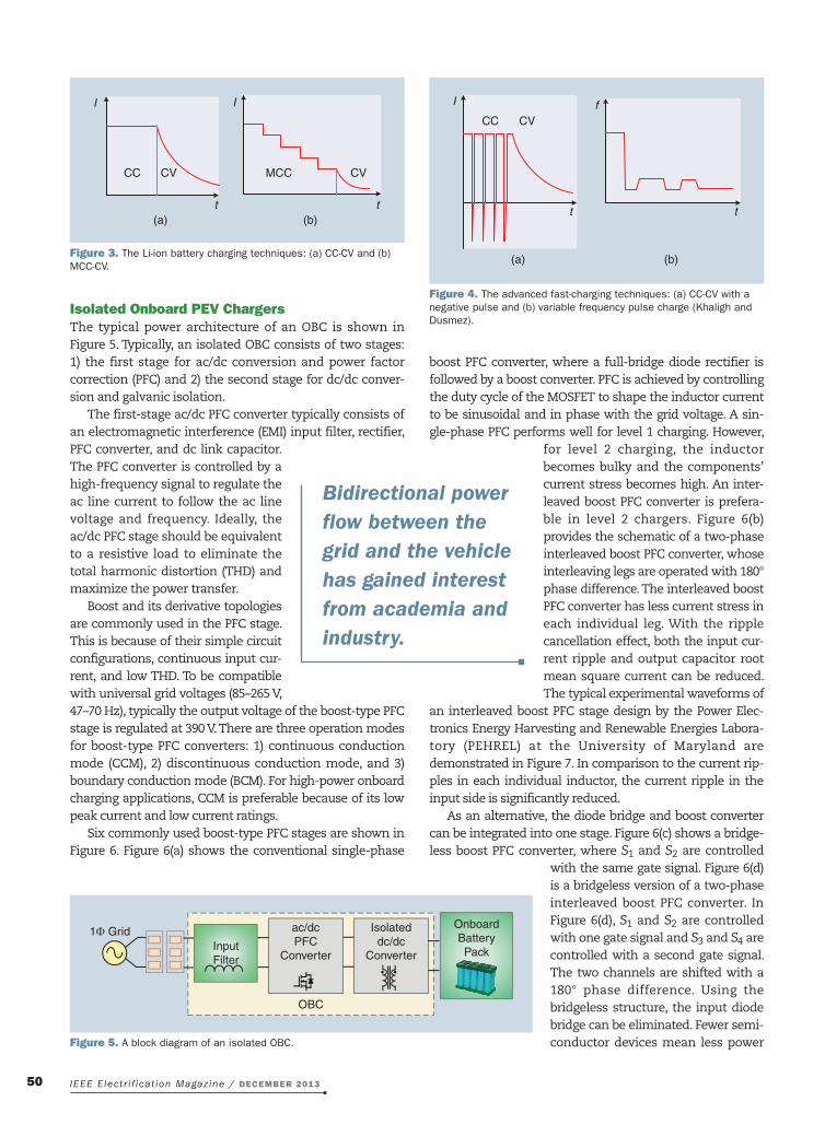
the method used to charge the battery. Various methods can be adopted to safely charge Li-ion batteries. the meth-od shown in Figure 3(a) is called constant current– constant voltage (cc-cV), which is adopted by a majority of the onboard battery chargers. the rate at which a bat-tery is discharged relative to its maximum capacity is known as the c-rate. the basic idea behind this technique is that the battery is charged with a constant current, typi-cally rated at 0.5–1 c. When the battery voltage reaches its cutoff voltage, its voltage is kept fixed and it is charged at this constant voltage until the current draw decreases to the end charging current, e.g., 0.02 c, which represents a full charge. For a deeply depleted battery pack, the battery voltage might go down to 1 V/cell. in this case, a precharge stage is required to charge the battery voltage from 1 V/cell to 2.5 V/cell. in the precharge stage, the charging cur-rent is fixed at a constant rate (typically 0.1 c).
to increase the charge acceptance rate of the battery, multistage cc–cV (Mcc-cV) has been proposed. the prin-ciple is almost the same as cc-cV. however, instead of providing the battery with one constant current level, several current steps are applied up to the cutoff voltage as shown in Figure 3(b).
in addition, a few other charging methods with less impact on battery polarization and higher charge accep-tance rates are being investigated. one approach discharges the battery at specific time intervals during charging to increase the charging acceptance. this approach can be applied to both cc-cV and Mcc-cV
techniques. a simplified example of the cc-cV method with negative pulses is shown in Figure 4(a). another approach uses a variable pulse charge strategy. in this approach, the optimal pulse charge frequency is continu-ously varied to distribute ions in the electrolyte evenly. Between pulses, a variable rest period is applied to neu-tralize and diffuse the ions. this rest period is defined by a maximum power point tracker to determine the maxi-mum level of current acceptance for a given Soc in real time. a typical waveform of the variable frequency associ-ated with pulse charging is shown in Figure 4(b). Using this method, the charge rate can be increased in compari-son to conventional cc-cV and fixed-frequency pulse charging methods.
Figure 2. A Tesla Model S being charged at the University of Mary-land, College Park.
TAbLe 2. The charging characteristics and infrastructures of some of the commercially available PeVs.
Vehicle EV Type Price Battery OBC (kW) E-Range (mi) Connector Type Charging Time (h)
Level 1 Level 2
Nissan Leaf
EV US$35,200 24-kWhLi-ion
3.3 100 SAE J1772JARI/TEPCO
22 8
BMW ActiveE
EV Lease only 32-kWh Li-ion
7.2 100 SAE J1772 8–10 4–5
Ford Focus EV US$39,200 23-kWhLi-ion
6.6 76 SAE J1772 20 3–4
Mitsubishi IEV US$29,125 16-kWh
Li-ion3.3 62 SAE J1772
JARI/TEPCO22.5 7
Honda Fit EV Lease only 20-kWhLi-ion
3.3 76 SAE J1772 6 3
Toyota Prius
PHEV US$32,000 4.4-kWhLi-ion
3.3 15 SAE J1772 3 1.5
Chevy Volt PHEV US$39,145 16-kWhLi-ion
3.3 35 SAE J1772 10 4
Cadillac ELR
PHEV n/a 16.5-kWhLi-ion
3.3 35 SAE J1772 n/a 4.5
Tesla Model S
EV US$95,400 85-kWhLi-ion
10 265 Mobile connec-tor
34 14
Note: Specification data are based on public information and are subject to change.
IEEE Electr i f icat ion Magazine / december 201350
Isolated Onboard PeV chargersthe typical power architecture of an oBc is shown in Figure 5. typically, an isolated oBc consists of two stages: 1) the first stage for ac/dc conversion and power factor correction (pFc) and 2) the second stage for dc/dc conver-sion and galvanic isolation.
the first-stage ac/dc pFc converter typically consists of an electromagnetic interference (eMi) input filter, rectifier, pFc converter, and dc link capacitor. the pFc converter is controlled by a high-frequency signal to regulate the ac line current to follow the ac line voltage and frequency. ideally, the ac/dc pFc stage should be equivalent to a resistive load to eliminate the total harmonic distortion (thD) and maximize the power transfer.
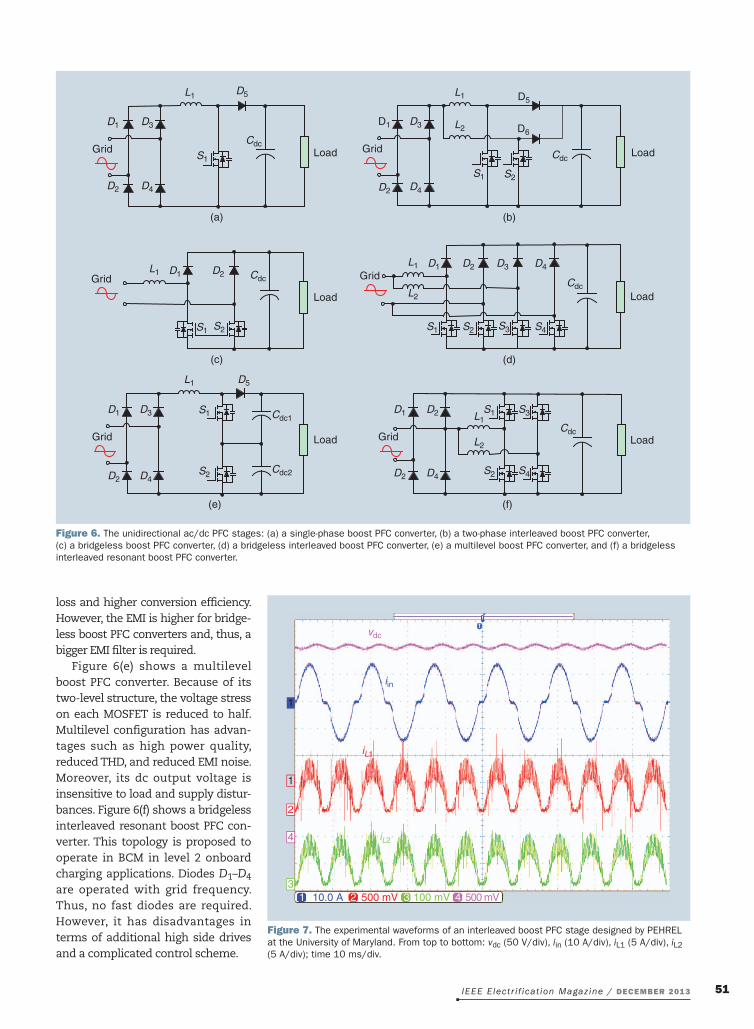
Boost and its derivative topologies are commonly used in the pFc stage. this is because of their simple circuit configurations, continuous input cur-rent, and low thD. to be compatible with universal grid voltages (85–265 V, 47–70 hz), typically the output voltage of the boost-type pFc stage is regulated at 390 V. there are three operation modes for boost-type pFc converters: 1) continuous conduction mode (ccM), 2) discontinuous conduction mode, and 3) boundary conduction mode (BcM). For high-power onboard charging applications, ccM is preferable because of its low peak current and low current ratings.
Six commonly used boost-type pFc stages are shown in Figure 6. Figure 6(a) shows the conventional single-phase
boost pFc converter, where a full-bridge diode rectifier is followed by a boost converter. pFc is achieved by controlling the duty cycle of the MoSFet to shape the inductor current to be sinusoidal and in phase with the grid voltage. a sin-gle-phase pFc performs well for level 1 charging. however,
for level 2 charging, the inductor becomes bulky and the components’ current stress becomes high. an inter-leaved boost pFc converter is prefera-ble in level 2 chargers. Figure 6(b) provides the schematic of a two-phase interleaved boost pFc converter, whose interleaving legs are operated with 180° phase difference. the interleaved boost pFc converter has less current stress in each individual leg. With the ripple cancellation effect, both the input cur-rent ripple and output capacitor root mean square current can be reduced. the typical experimental waveforms of
an interleaved boost pFc stage design by the power elec-tronics energy harvesting and renewable energies Labora-tory (pehreL) at the University of Maryland are demonstrated in Figure 7. in comparison to the current rip-ples in each individual inductor, the current ripple in the input side is significantly reduced.
as an alternative, the diode bridge and boost converter can be integrated into one stage. Figure 6(c) shows a bridge-less boost pFc converter, where S1 and S2 are controlled
with the same gate signal. Figure 6(d) is a bridgeless version of a two-phase interleaved boost pFc converter. in Figure 6(d), S1 and S2 are controlled with one gate signal and S3 and S4 are controlled with a second gate signal. the two channels are shifted with a 180° phase difference. Using the bridgeless structure, the input diode bridge can be eliminated. Fewer semi-conductor devices mean less power
I
t
I
t(a) (b)
CC CV MCC CV
I
t
f
t
(a) (b)
CC CV
1Φ GridInputFilter
ac/dcPFC
Converter
Isolateddc/dc
Converter
OBC
OnboardBatteryPack
Figure 3. The Li-ion battery charging techniques: (a) CC-CV and (b) MCC-CV.
Figure 4. The advanced fast-charging techniques: (a) CC-CV with a negative pulse and (b) variable frequency pulse charge (Khaligh and Dusmez).
Figure 5. A block diagram of an isolated OBC.
Bidirectional power flow between the grid and the vehicle has gained interest from academia and industry.
IEEE Electr i f icat ion Magazine / december 2013 51
loss and higher conversion efficiency. however, the eMi is higher for bridge-less boost pFc converters and, thus, a bigger eMi filter is required.
Figure 6(e) shows a multilevel boost pFc converter. Because of its two- level structure, the voltage stress on each MoSFet is reduced to half. Multilevel configuration has advan-tages such as high power quality, reduced thD, and reduced eMi noise. Moreover, its dc output voltage is insensitive to load and supply distur-bances. Figure 6(f) shows a bridgeless interleaved resonant boost pFc con-verter. this topology is proposed to operate in BcM in level 2 onboard charging applications. Diodes D1–D4 are operated with grid frequency. thus, no fast diodes are required. however, it has disadvantages in terms of additional high side drives and a complicated control scheme.
Grid
D1
D5
D6
D2
D3
D4
S1
CdcLoad
L2
L1
S2
D1 D2 D3 D4
S1 S2 S3 S4
Grid
LoadCdc
L1
L2
Grid
D1
D2
D2
D4
L1
L2
S1
S2
S3
S4
CdcLoadGrid
D1 D3
D2 D4
L1
Load
S1
S2 Cdc2
Cdc1
D5
Grid
D1 D3
D2 D4
L1
S1
D5
CdcLoad
(a) (b)
(c) (d)
(e) (f)
D1 D2
S1 S2
Grid
Load
CdcL1
Figure 6. The unidirectional ac/dc PFC stages: (a) a single-phase boost PFC converter, (b) a two-phase interleaved boost PFC converter, (c) a bridgeless boost PFC converter, (d) a bridgeless interleaved boost PFC converter, (e) a multilevel boost PFC converter, and (f) a bridgeless interleaved resonant boost PFC converter.
vdc
iin
iL1
iL2
1
1
2
4
310.0 A 500 mV 100 mV 500 mV1 2 3 4
Figure 7. The experimental waveforms of an interleaved boost PFC stage designed by PEHREL at the University of Maryland. From top to bottom: vdc (50 V/div), iin (10 A/div), iL1 (5 A/div), iL2 (5 A/div); time 10 ms/div.
IEEE Electr i f icat ion Magazine / december 201352
a typical second-stage isolated dc/dc converter consists of a switching network, a high-frequency transformer, a rectifier, and a low-pass filter. For frequency-modulated resonant converters, an additional resonant tank between switching network and high frequency is required.
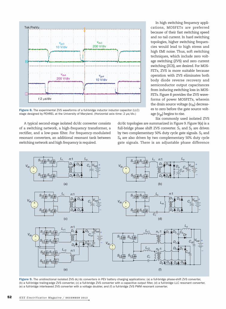
in high switching frequency appli-cations, MoSFets are preferred because of their fast switching speed and no tail current. in hard switching topologies, higher switching frequen-cies would lead to high stress and high eMi noise. thus, soft switching techniques, which include zero volt-age switching (ZVS) and zero current switching (ZcS), are desired. For MoS-Fets, ZVS is more suitable because operation with ZVS eliminates both body diode reverse recovery and semiconductor output capacitances from inducing switching loss in MoS-Fets. Figure 8 provides the ZVS wave-forms of power MoSFets, wherein the drain source voltage (vds) decreas-es to zero before the gate source volt-age (vgs) begins to rise.
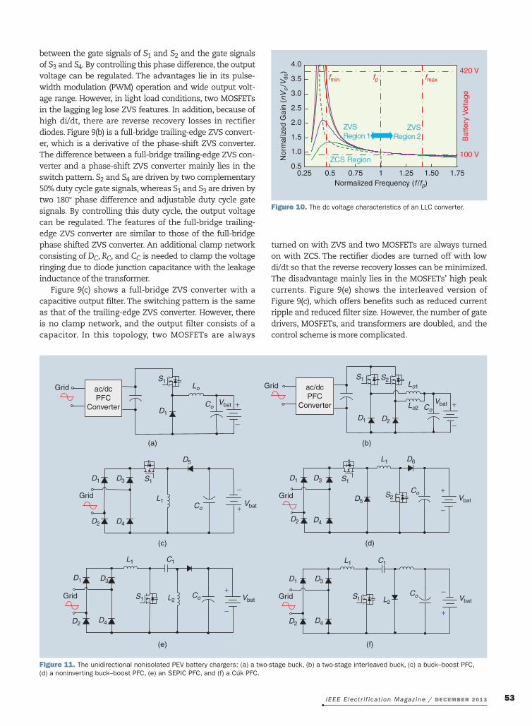
Six commonly used isolated ZVS dc/dc topologies are summarized in Figure 9. Figure 9(a) is a full-bridge phase shift ZVS converter. S1 and S2 are driven by two complementary 50% duty cycle gate signals. S3 and S4 are also driven by two complementary 50% duty cycle gate signals. there is an adjustable phase difference
Tek PreVu
vgs3
10 V/div
vds3
200 V/div
vgs4
10 V/div
vds4
200 V/div
2
3
t :2 µs/div
Vbat
S1 S3
S2 S4
Lr Lo
Co
n:1
D3D1
D4D2
Vdc
(a) (b)
(c) (d)
(e) (f)
+
–
Vbat
Vbat
Vbat
Vbat
Vbat
S1 S3
S2 S4
S1 S3
S8S6
S5 S7
S2 S4
S1
S1
S1
S3
S3
S3
S2
S2
S2
S4
S4
S4
Lr
Lr 1Lo
Lr 1
Lr
Lr
Lm
Lr 2
Cr
Cr
Lr 2
Co
Co2
Co2
Co
Co2Co1
Co1
Co1
n:1
n:1
n:1
n2:1
n1:1
n:1
n:1
D3
D3
D1
D1
D4
D4
D2
D2
Vdc
Vdc
Vdc
+
–
+
–+
–
+
–
+
–
+–
+–
+–
+–
Vdc
Vdc
+–
+–
DrCh
D8D6D4
D4
D4
D2
D2
D2
D7D5
Do
D3
D3
D3
D1
D1
D1 Da
Lo
Figure 8. The experimental ZVS waveforms of a full-bridge inductor inductor capacitor (LLC) stage designed by PEHREL at the University of Maryland. (Horizontal axis–time: 2 μs/div.)
Figure 9. The unidirectional isolated ZVS dc/dc converters in PEV battery charging applications: (a) a full-bridge phase-shift ZVS converter, (b) a full-bridge trailing-edge ZVS converter, (c) a full-bridge ZVS converter with a capacitive output filter, (d) a full-bridge LLC resonant converter, (e) a full-bridge interleaved ZVS converter with a voltage doubler, and (f) a full-bridge ZVS PWM resonant converter.
IEEE Electr i f icat ion Magazine / december 2013 53
between the gate signals of S1 and S2 and the gate signals of S3 and S4. By controlling this phase difference, the output voltage can be regulated. the advantages lie in its pulse-width modulation (pWM) operation and wide output volt-age range. however, in light load conditions, two MoSFets in the lagging leg lose ZVS features. in addition, because of high di/dt, there are reverse recovery losses in rectifier diodes. Figure 9(b) is a full-bridge trailing-edge ZVS convert-er, which is a derivative of the phase-shift ZVS converter. the difference between a full-bridge trailing-edge ZVS con-verter and a phase-shift ZVS converter mainly lies in the switch pattern. S2 and S4 are driven by two complementary 50% duty cycle gate signals, whereas S1 and S3 are driven by two 180° phase difference and adjustable duty cycle gate signals. By controlling this duty cycle, the output voltage can be regulated. the features of the full-bridge trailing-edge ZVS converter are similar to those of the full-bridge phase shifted ZVS converter. an additional clamp network consisting of DC, RC, and CC is needed to clamp the voltage ringing due to diode junction capacitance with the leakage inductance of the transformer.
Figure 9(c) shows a full-bridge ZVS converter with a capacitive output filter. the switching pattern is the same as that of the trailing-edge ZVS converter. however, there is no clamp network, and the output filter consists of a capacitor. in this topology, two MoSFets are always
turned on with ZVS and two MoSFets are always turned on with ZcS. the rectifier diodes are turned off with low di/dt so that the reverse recovery losses can be minimized. the disadvantage mainly lies in the MoSFets’ high peak currents. Figure 9(e) shows the interleaved version of Figure 9(c), which offers benefits such as reduced current ripple and reduced filter size. however, the number of gate drivers, MoSFets, and transformers are doubled, and the control scheme is more complicated.
0.5
1.0
1.5
2.0
2.5
3.0
3.5
4.0420 V
100 V
fmin fmaxfp
ZVSRegion 2
ZVSRegion 1
0.25 0.5 0.75 1 1.25 1.75Normalized Frequency (f /fp)
Nor
mal
ized
Gai
n (nVo
/Vdc
)
Bat
tery
Vol
tage
1.50
ZCS Region
Vbat
Vbat
Vbat
Vbat
Vbat
S1
D1
Lo
Co
ac/dcPFC
Converter
Grid
Vbat
S1
D1
Lo1
Lo2 Co
GridS2
D2
Grid
D1
D2
D3
D5
S1
L1Co
D4
Grid
D1
D2
D3
D4
S1
L1 C1
CoL2
Grid
D1
D2
D3
D4
L1
L2S1
C1
Co
Grid
D1
D2
D3
D4
D5
S1
L1
Co
D6
S2
(a) (b)
(c) (d)
(e) (f)
+
+
+
+
+
–
–
–
–
–
ac/dcPFC
Converter +
–
Figure 10. The dc voltage characteristics of an LLC converter.
Figure 11. The unidirectional nonisolated PEV battery chargers: (a) a two-stage buck, (b) a two-stage interleaved buck, (c) a buck–boost PFC, (d) a noninverting buck–boost PFC, (e) an SEPIC PFC, and (f) a Cúk PFC.
IEEE Electr i f icat ion Magazine / december 201354
Figure 9(d) shows a full-bridge LLc (inductor inductor capacitor) resonant converter. S1 and S4 and S2 and S3 are turned on and off complementarily with a dead band. thus, the output of the full bridge is a square wave and is fed into the resonant network. the output voltage is regulated by controlling the switching frequency. in the case of an induc-tive resonant network, the primary MoSFets would be turned on with ZVS. Figure 10 provides the dc voltage– frequency characteristics of the LLc converter. the benefits of the LLc topology include: 1) short circuit pro-tection, 2) good voltage regulation in light load conditions, 3) the ability to operate with a ZVS over wide load ranges, and 4) no diode reverse recov-ery losses in ZVS region 1. however, because of its high circulating current at maximum gain, it is difficult to opti-mize the efficiency of the LLc convert-er over an ultrawide voltage range (e.g., 100–420 V).
Figure 9(f) shows a full-bridge ZVS pWM resonant converter. the switch-ing pattern is the same as that of the full-bridge phase shift ZVS converter. a half-bridge LLc resonant circuit shares the lagging leg with a full-bridge phase-shift converter, which makes sure the lagging leg MoSFets are turned on with ZVS across the full load range. however, a secondary-side hybrid switching circuit is required to clamp the voltage overshoots that arise dur-ing the turn off of the rectifier diodes.
Nonisolated PeV chargersalthough a two-stage structure with galvanic isolation has been a common topology, with an additional safety mar-gin, isolation is not a requirement for oBcs, according to standards such as Sae J1772. hence, researchers have studied the applicability of nonisolated chargers for peVs.
Six different types of nonisolated battery chargers are summarized in Figure 11. Figure 11(a) shows a two-stage nonisolated eV charger. an ac/dc pFc converter is used to
convert the universal grid input to a fixed dc link voltage, which is higher than the maximum battery voltage. a buck converter is also used to step down the dc link voltage. in this case, both the ccM and BcM modes of operation are considered. ccM has lower current stress on each compo-nent, while BcM has smaller switching losses. in Figure
11(b), a two-phase interleaved noniso-lated buck charger is demonstrated. With this interleaving configuration, output current ripples are mostly com-pensated as they cancel each other out. in addition, the current stress on each leg is reduced to half so that a higher power level can be achieved.
instead of two-stage configura-tions, the pFc and dc/dc stages are integrated into one single stage. the single-stage pFc chargers have reduced power losses, but they have low-frequency (twice the grid fre-quency) ripples in the output. the single-stage topologies must be adaptable to the universal grid (85–265 V, 47–70 hz) from the input, and wide battery voltage (100–420 V) from
the output. thus, the selected topology should be able to both step up and step down the input voltage. Figure 11(c) is a buck–boost pFc converter, which has buck and boost capabilities and a minimum number of components. however, its disadvantages lie in four aspects: 1) high side drive is required; 2) the MoSFet has high voltage stress (Vin + Vout), which means 1,200-V rating MoSFets are required; 3) the ground polarity is reversed on the output side; and 4) the input current is discontinuous, which means a bulky eMi filter is required. Figure 11(d) is a non-inverting buck–boost pFc converter. compared to a con-ventional inverting buck–boost pFc converter, there are two improvements: 1) voltage stresses on MoSFets are reduced and 2) the input ground polarity is the same as that of the output side.
Figure 11(e) and (f) demonstrates single-ended primary-inductor converter (Sepic) pFc and cúk pFc converters,
C1 S1
S2
Grid
Load
Cdc
L1
C2
(a)
S3Grid
Load
CdcL1
S1
S4S2
(b)
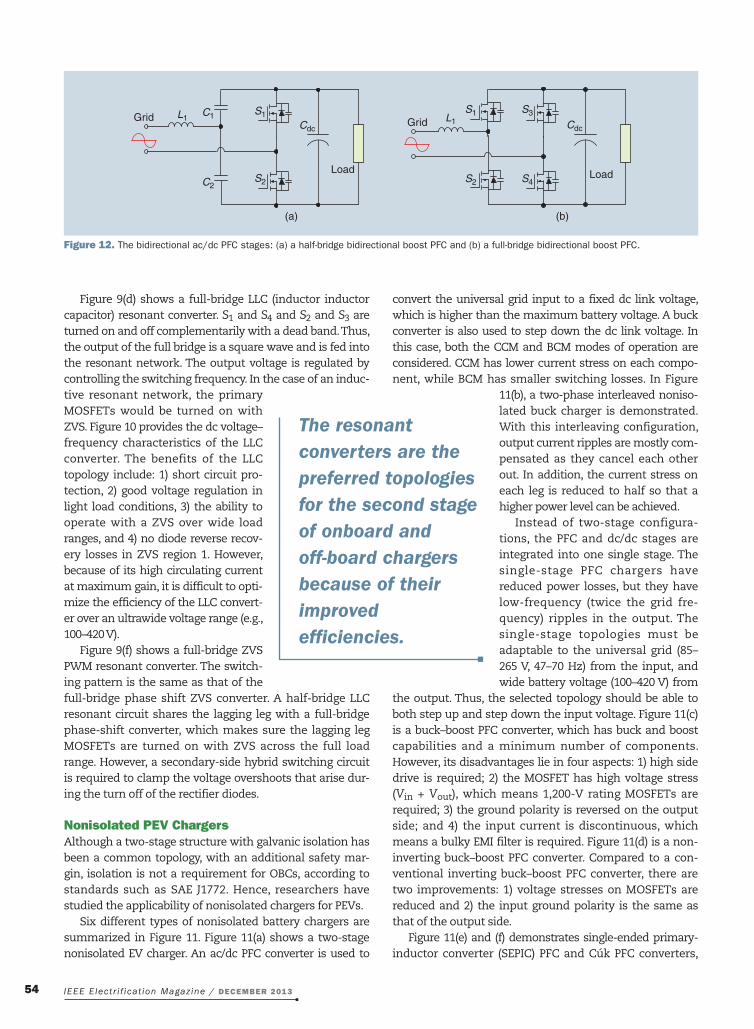
Figure 12. The bidirectional ac/dc PFC stages: (a) a half-bridge bidirectional boost PFC and (b) a full-bridge bidirectional boost PFC.
The resonant converters are the preferred topologies for the second stage of onboard and off-board chargers because of their improved efficiencies.
IEEE Electr i f icat ion Magazine / december 2013 55
respectively. compared to Figure 11(c) and (d), their input currents are both continuous, meaning the size of the eMi filter can be reduced. the Sepic pFc converter is not invert-ing. however, the MoSFet has high voltage stress (Vin + Vout), and 1,200-V MoSFets are required. the cúk pFc converter puts less voltage stress on the switching MoSFet, but its ground polarity in the output is reversed.
bidirectional PeV chargerscurrently, all commercialized oBcs have a unidirectional power flow from the grid to the vehicle. however, since most vehicles are parked an average of 95% of the time, it is fore-seeable that batteries could be used to let power flow from the vehicle to the grid. in this emerging vehicle-to-grid (V2G) technology, oBcs are required to have bidirectional power flow capa-bility. When the vehicle is in idle mode, the battery can feed power back to the grid.
a typical bidirectional peV charger consists of two stages. the first stage is a bidirectional ac/dc pFc convert-er, and the second stage is a bidirectional dc/dc converter. Figure 12(a) shows a single-phase half-bridge bidirec-tional ac/dc pFc converter, while Figure 12(b) shows a sin-gle-phase, full-bridge bidirectional ac/dc pFc converter. although half-bridge topology uses only two MoSFets to achieve voltage doubling, it requires semiconductor devic-es with higher voltage ratings. the full-bridge topology can alleviate capacitor imbalances, but it comes with a higher number of semiconductor devices, increasing the cost and complexity of the control.
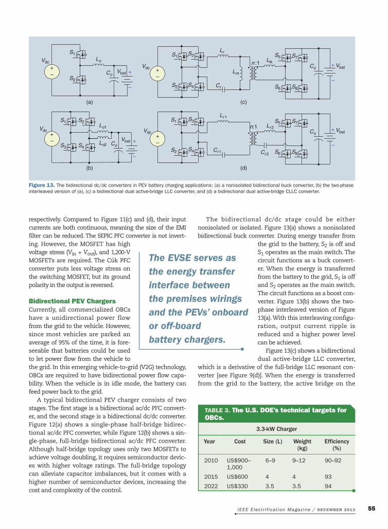
the bidirectional dc/dc stage could be either nonisolated or isolated. Figure 13(a) shows a nonisolated bidirectional buck converter. During energy transfer from
the grid to the battery, S2 is off and S1 operates as the main switch. the circuit functions as a buck convert-er. When the energy is transferred from the battery to the grid, S1 is off and S2 operates as the main switch. the circuit functions as a boost con-verter. Figure 13(b) shows the two-phase interleaved version of Figure 13(a). With this interleaving configu-ration, output current ripple is reduced and a higher power level can be achieved.
Figure 13(c) shows a bidirectional dual active-bridge LLc converter,
which is a derivative of the full-bridge LLc resonant con-verter [see Figure 9(d)]. When the energy is transferred from the grid to the battery, the active bridge on the
Vbat
S1
S2 S4
S3 S5
S6 S8
S7
Lr
Lm
Cr
n :1 CoLlk
S1 S3
S4S2
Lr1
Lr2
Cr1 Cr2
n:1CoVdc
S5
S6
S7
S8
Vbat
Vdc
S1
S2
Lo
Co
Vdc
Vbat
S1
S3
S2
S4
Lo1
Lo2 Co
Vdc
(a) (c)
(b) (d)
+–
+–
+–
+–
+
–
+
–
+
–
Vbat+
–
Figure 13. The bidirectional dc/dc converters in PEV battery charging applications: (a) a nonisolated bidirectional buck converter, (b) the two-phase interleaved version of (a), (c) a bidirectional dual active-bridge LLC converter, and (d) a bidirectional dual active-bridge CLLC converter.
TAbLe 3. The U.S. dOe’s technical targets for Obcs.
3.3-kW Charger
Year Cost Size (L) Weight (kg)
Efficiency (%)
2010 US$900–1,000
6–9 9–12 90–92
2015 US$600 4 4 93
2022 US$330 3.5 3.5 94
The EVSE serves as the energy transfer interface between the premises wirings and the PEVs’ onboard or off-board battery chargers.
IEEE Electr i f icat ion Magazine / december 201356
secondary side of transformer functions as a full-bridge rectifier. When the energy is transferred from the battery to the grid, the secondary-side active bridge functions as an inverter and the primary-side active bridge functions as a rectifier. Figure 13(d) shows a bidirectional dual active-bridge capacitor inductor inductor capaci-tor (cLLc) converter. in this topology, there are two identical inductor capacitor (Lc) networks on both the primary and secondary side.
Bidirectional power flow between the grid and the vehicle has gained interest from academia and industry. however, it has not been implement-ed in any commercial peV on the mar-ket. the challenges mainly lie in four aspects: 1) the additional cost of power electronics, 2) the possible chance of battery degradation due to frequent cycling (which might not be the case in some battery chemistries as a few manufac-turers believe that slow discharge of the battery when it is fully charged would not cause degradation), 3) the require-ment for metering from the utility company, and 4) the lack of precise policies and standards as of December 2013.
Goals and challengesthe U.S. Department of energy’s (Doe’s) technical targets for 3.3-kW level 2 oBcs are summarized in table 3. to design an ultracompact and highly efficient oBc, the fol-lowing considerations must be taken into account: 1) a high switching frequency is desired to reduce the volume and weight, 2) both step-down and step-up operations should be realized to satisfy the wide output voltage range requirements, 3) the ZVS feature is desired to reduce the switching losses and high-frequency eMi, and
4) the conversion efficiency must be optimized across the full battery voltage ranges and different load conditions.
however, it is a challenging task to satisfy all of the above-mentioned con-siderations simultaneously. higher switching frequency is associated with smaller volt–second applied to the magnetic component; consequently, the flux variation is smaller and, hence,
the corresponding core losses are reduced. however, the core loss and the switching loss increase with the increase in fre-quency. With higher switching frequency, the conversion effi-ciency could potentially degrade.
another challenge comes from the wide range of voltage variation of the battery pack. corresponding to the depleted and full Soc, the voltage of the battery pack varies from the cutoff volt-age to the charge voltage (e.g., 100–420 V). this means that the dc/dc conversion stage must be able to adapt to this wide voltage range. the pWM topologies have the advantage of easy regulation of the output voltage in a wide range. howev-er, they also have the disadvantage of
an incomplete ZVS range. Frequency modulation resonant topologies have a full ZVS range. however, using currently known topologies, the efficiency of resonant topologies can only be optimized over a limited range of output voltage. to overcome these challenges and develop an ultracompact, highly efficient onboard charging system, the following components and technologies need to be addressed:
1) Advanced magnetics material: the size of the magnetic component is constrained by the core loss associated with high switching frequency. to solve this problem, a more advanced magnetics material with smaller core losses in higher switching frequen-cies must be adopted.
2) Advanced packaging technique: the packaging is directly relevant to the size of the onboard charging system. advances in the packaging technology improve the space utilization and heat dissipation.
3) Advanced cooling technique: heat sinks take a large volume of the charger. the size of the heat sink is
directly determined by the cooling method. Generally, active cooling is better than passive cooling. Liq-uid cooling is preferred in the case of conventional silicon-based power electronic interfaces.
4) Advanced switching power devic-es: power losses from switching power devices such as MoSFets and diodes take a large portion of
3Φ GridInputFilter
ac/dcConverter
dc/dcConverter
Off-Board Level-3 Charger
OnboardBatteryPack
Figure 14. A block diagram of an off-board level-3 charger.
TAbLe 4. The power levels for dc direct charging.
Type of Charge Charger Power Level (kW)
Heavy Duty SUV/Sedan Small Sedan
Fast charge, 10 min, 100% SoC 500 250 125
Rapid charge, 15 min, 60% SoC 250 125 60
Quick charge, 60 min, 70% SoC 75 35 20
PHEV, 30 min 40 20 10
The Li-ion cell has dominated the market of commercially available PEVs.
IEEE Electr i f icat ion Magazine / december 2013 57
the total system losses. advanced power devices, including wide-band-gap silicon carbide and gallium nitride semiconductor devices with low on resistanc-es, high voltage ratings, faster switching speeds, and high operating temperatures, help reduce the power losses and the thermal stress.
5) Advanced converter topologies and control methods: the converter topology determines the circuit perfor-mances such as the ZVS feature, eMi, circulating cur-rent, conduction losses, and switching losses. an optimized circuit topology and control method would help opti-mize the overall circuit perfor-mance over the wide battery Soc range.
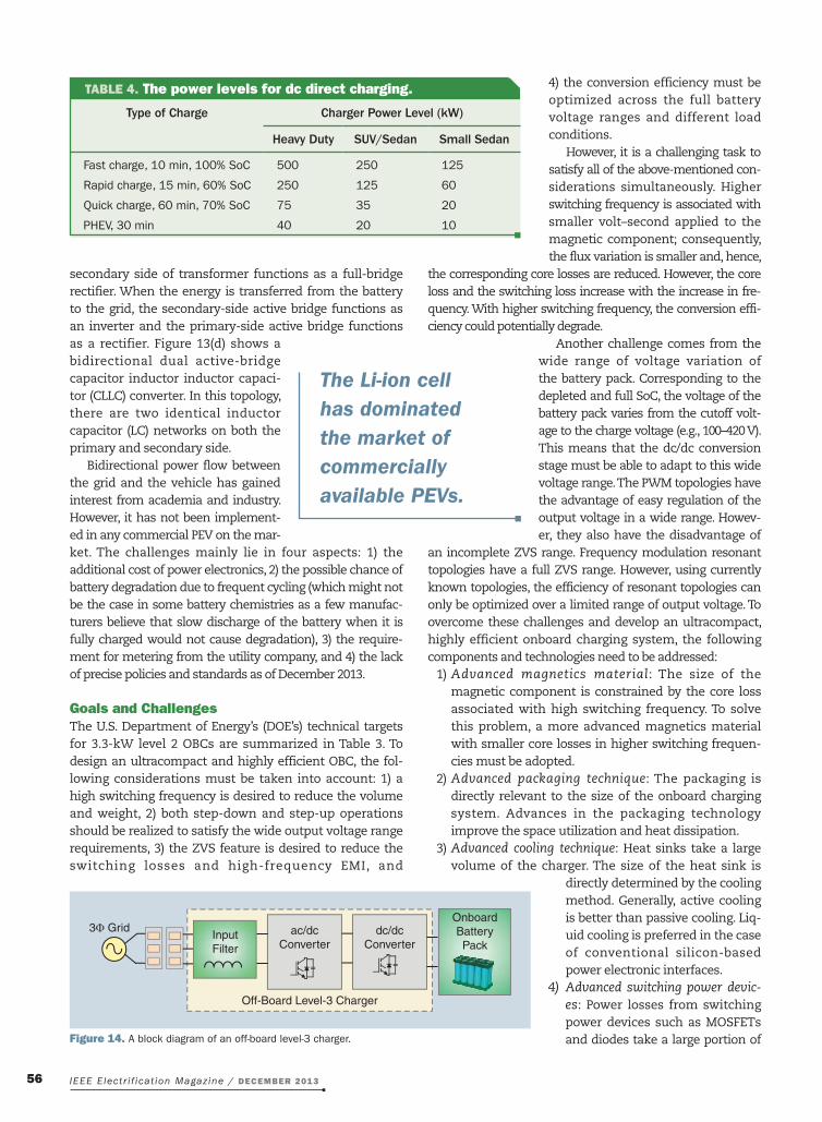
Off-board chargingLevel 3 charging, known as dc fast charging, requires an off-board charger, which is less constrained by size. Fast charge, rapid charge, and quick charge are a few of the commonly used terms for off-board, as shown in table 4. the high power level and high cost of off-board charging make it unfeasible for residential areas. Level 3 charging is not compatible with commercial and residen-tial outlets and, consequently, requires the installment of new charging infrastructure. nonetheless, it is attractive for commercial and public applications such as shopping centers, parking lots, hotels, highway rest areas, and ordinary filling stations.
as shown in Figure 14, a level 3 charger is typically fed through a 208–600-Vac three-phase circuit. this system con-sists of an ac/dc stage and a dc/dc stage. Because of the high current/power requirements, the off-board charging puts power quality burdens on electric utility distribution sys-tems. these burdens can include voltage deviations, har-monic distortion, peak demand, and thermal loading on distribution power systems. in particular, the harmonic and dc injection can particularly increase distribution transform-er losses resulting in thermal loading, which impacts trans-former aging accordingly. although a charging system
equipped with an active front-end rectifier (in the ac/dc stage) can mitigate this problem, it increases the cost of the charging station substantially. alternatively, the degradation of distribution equipment can be reduced by employing a smart charging strategy. the allowable harmonic and dc injection into the grid are limited by ieee 1547, Sae-J2894 iec1000-3-2, and the U.S. national electric code (nec) 690 standards.
Different topologies are reported for three-phase off-board chargers. Since the level 3 battery charger is typical-
ly supplied by 480-V three-phase voltage, the grid voltage would be higher than the battery voltage. as mentioned earlier, an active pFc recti-fier is required to alleviate grid power quality issues. hence, a three-phase boost converter followed by a dc/dc converter is required to charge the battery. additionally, as mentioned in the “isolated onboard peV chargers” section, the galvanic isolation is important in the charger circuits for safety reasons. even though peV charging standards do not mandate galvanic isolation as long as the
ground current is maintained within limited boundaries, if the battery is attached to the vehicle’s chassis, galvanic isolation is mandatory for safety reasons. therefore, to avoid costly and complex shielding considerations for a nonisolated dc/dc converter, an isolated dc/dc converter is preferred. Similar to oBcs, as shown in Figure 9, the reso-nant converters are the preferred topologies for the sec-ond conversion stage of off-board charging because of their improved efficiencies.
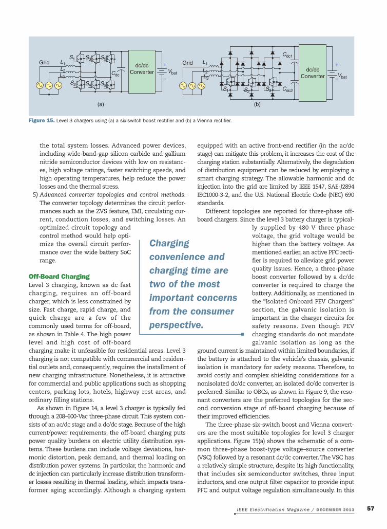
the three-phase six-switch boost and Vienna convert-ers are the most suitable topologies for level 3 charger applications. Figure 15(a) shows the schematic of a com-mon three-phase boost-type voltage–source converter (VSc) followed by a resonant dc/dc converter. the VSc has a relatively simple structure, despite its high functionality, that includes six semiconductor switches, three input inductors, and one output filter capacitor to provide input pFc and output voltage regulation simultaneously. in this
Vbat
Grid
Cdc
L1L2L3
L1
L2L3
S1 S3
S4
S5
S6S2
Vbat
Grid
S1 S2 S3
dc/dcConverter dc/dc
Converter
(a) (b)
+
–
+
–
Cdc2
Cdc1
Figure 15. Level 3 chargers using (a) a six-switch boost rectifier and (b) a Vienna rectifier.
Charging convenience and charging time are two of the most important concerns from the consumer perspective.

IEEE Electr i f icat ion Magazine / december 201358
boost converter, the voltage shape in each phase is inde-pendent of the current as the current flows over the switch (insulated-gate bipolar transistor here) or its anti-parallel diode. at the midpoint of each semiconductor leg with respect to the midpoint across the output capacitor, a positive or a negative voltage may be produced. therefore, because of the two-level behavior of each semiconductor leg, the phase of sinusoidal currents can be simply con-trolled. in fact, the current can be controlled to be in phase with grid voltage for grid-to-vehicle operation or anti-phase with grid voltage for V2G operation. hence, this con-figuration offers bidirectional operation.
the circuit in Figure 15(b) is a Vienna rectifier, which contains only three active switches. the switching of semiconductors is independent of the direction of phase currents. the major advantage of the three-level characteristic is that switches can be rated for only half of the peak value of the line-to-line voltage. Furthermore, because of the three voltage levels, a smaller grid current fundamental ripple is generated, and the value of the input boost inductances can be reduced. in addition, because of lower switching voltages, a lower conducted eMi noise is generated.
conclusionsalthough a great vision has been plotted for transporta-tion electrification, there are several critical hurdles that eVs must stride. among these, charging convenience and charging time are two of the most important concerns from the consumer perspective. Good power quality, com-pact size, and high conversion efficiency are three of the most important features desired from onboard level 1 and level 2 peV chargers. to ensure good power quality, the ac/dc stage must be featured with good pFc and thD reduc-tion performances. higher switching frequency, ZVS, and advanced packaging techniques are necessary to achieve smaller charger size. to achieve high converter efficiency, advanced magnetics materials, power semiconductors, and power electronic topologies must to be addressed. in particular, the advanced control method must be imple-mented to optimize the conversion efficiency across the full Soc range. Level 3 charging is able to reach a much higher power level and is regarded as an important alter-native to level 1 and level 2 onboard charging. it is essen-tial to alleviating range anxiety issues as it allows for long-distance travel similar to conventional ice-powered vehicles. however, it requires an off-board charging station and is mainly intended for commercial and public charging stations.
Acknowledgmentthis work has been sponsored partly by the national Science Foundation Grant 1238985 and the Maryland industrial partnerships program, which are gratefully acknowledged.
For Further readingK. S. K. Young, c. Wang, and L. Y. Wang, “electric vehicle battery technologies,” in Electric Vehicle Integration into Modern Power Networks. Berlin: Springer, 2013, pp. 15–56.
a. Khaligh and S. Dusmez, “comprehensive topological analysis of conductive and inductive charging solutions for plug-in electric vehicles,” IEEE Trans. Veh. Technol., vol. 61, no. 8, pp. 3475–3489, oct. 2012.
M. Yilmaz and p. Krein, “review of battery charger topologies, charging power levels and infrastructure for plug-in electric and hybrid vehicles,” IEEE Trans. Power Electron., vol. 28, no. 5, pp. 2152–2169, May 2013.
c.-Y. oh, D.-h. Kim, D.-G. Woo, W.-Y. Sung, Y.-S. Kim, and B.-K. Lee, “a high-efficient nonisolated single-stage on-board battery charger for electric vehicles,” IEEE Trans. Power Electron., vol. 28, no. 12, pp. 5746–5757, Dec. 2013.
S. Dusmez, a. cook, and a. Khaligh, “comprehensive analysis of high quality power converters for level 3 off-board chargers,” in Proc. IEEE Vehicle Power and Propul-sion Conf., 2011, pp. 1–10.
c. Botsford and a. Szczepanek, “Fast charging vs. slow charging: pros and cons for the new age of electric vehi-cles,” in Proc. Int. Battery, Hybrid and Electric Vehicle Symp. and Expo. (EVS24), Stavanger, norway, May 2009, pp. 1–9.
Sae Standard for electric Vehicle conductive charge coupler, Sae Standard 1772–2009. [online]. available: http://www.arb.ca.gov/msprog/zevprog/stakeholders/infrastructure/finalsaej1772.doc
IEEE Standard for Interconnecting Distributed Resources with Electric Power Systems, ieee Standard 1547–2003, 2003.
SAE Standard for Power Quality Requirements for Plug-In Electric Vehicle Chargers, Sae Standard J2894–2011, 2011.
IEC Standard for Line Current Harmonic Measure-ments, ieee Standard 1000-3-2, 1995.
NEC Standard for Compliance for Photovoltaic Systems, U.S. national electric code (nec) Standard 690.
biographiesHaoyu Wang is a ph.D. candidate at the power electronic, energy harvesting and renewable energies Laboratory at the electrical and computer engineering Department in the University of Maryland. he is a Student Member of the ieee.
Amin Hasanzadeh is a postdoctoral research associate at the power electronic, energy harvesting and renewable energies Laboratory at the electrical and computer engi-neering Department in the University of Maryland. he is a Member of the ieee.
Alireza Khaligh ([email protected]) is an assistant professor and the director of the power electronic, energy harvesting and renewable energies Laboratory at the electrical and computer engineering Department in the University of Maryland. he is a Senior Member of the ieee.


