Transport properties of graphene quantum dots
8
PHYSICAL REVIEW B 83, 155450 (2011) Transport properties of graphene quantum dots J. W. Gonz´ alez and M. Pacheco Departamento de F´ ısica, Universidad T´ ecnica Federico Santa Mar´ ıa, Casilla 110 V, Valpara´ ıso, Chile L. Rosales * Departamento de F´ ısica, Universidad T´ ecnica Federico Santa Mar´ ıa, Casilla 110 V, Valpara´ ıso, Chile and Instituto de F´ ısica, Pontificia Universidad Cat´ olica de Valpara´ ıso, Casilla 4059, Valpara´ ıso, Chile P. A. Orellana Departamento de F´ ısica, Universidad Cat´ olica del Norte, Casilla 1280, Antofagasta, Chile (Received 24 September 2010; revised manuscript received 10 March 2011; published 27 April 2011) In this work we present a theoretical study of transport properties of a double crossbar junction composed of segments of graphene ribbons with different widths forming a graphene quantum dot structure. The systems are described by a single-band tight binding Hamiltonian and the Green’s function formalism using real space renormalization techniques. We show calculations of the local density of states, linear conductance, and I-V characteristics. Our results depict a resonant behavior of the conductance in the quantum dot structures, which can be controlled by changing geometrical parameters such as the nanoribbon segment widths and the distance between them. By application of a gate voltage on determined regions of the structure, it is possible to modulate the transport response of the systems. We show that negative differential resistance can be obtained for low values of applied gate and bias voltages. DOI: 10.1103/PhysRevB.83.155450 PACS number(s): 61.46.−w, 73.22.−f, 73.63.−b I. INTRODUCTION In the last few years, graphene-based systems have attracted a lot of scientific attention. Graphene is a single layer of carbon atoms arranged in a two-dimensional hexagonal lattice. In the literature, several experimental techniques have been reported to obtain this crystal, such as mechanical peeling or epitaxial growth. 1–3 On the other hand, graphene nanoribbons (GNRs) are stripes of graphene which can be obtained by different methods like high-resolution lithography, 4 controlled cutting processes, 5 or unzipping multiwalled carbon nanotubes. 6 Different graphene heterostructures based on patterned GNRs have been proposed and constructed, such as graphene junctions, 7 graphene flakes, 8 graphene antidot superlattices, 9 and graphene nanoconstrictions. 10 The electronic and transport properties of these nanostructures are strongly dependent on their geometric confinement, allowing the possibility to observe quantum phenomena like quantum interference effects, resonant tunneling, and localization. In this sense, the controlled modification of these quantum effects by means of external potentials which change the electronic confinement could be used to develop new technological applications such as graphene-based composite materials, 11 molecular sensor devices, 12,13 and nanotransistors. 14 In this work we study the transport properties of quantum- dot-like structures, formed by segments of graphene ribbons with different widths connected to each other, forming a double-crossbar junction. 17,18 These graphene quantum dots (GQDs) could be versatile experimental systems which allow a range of operational regimes from conventional single- electron detectors to ballistic transport. The systems we have considered are conductors formed by two symmetric crossbar junctions of width N B and length L B , and a central region that separates the junctions, of width N C and length L C . Two semi-infinite leads of width N L = N C are connected to the ends of the central conductor. A schematic view of the considered system is presented in Fig. 1. We studied the different electronic states appearing in the system as functions of the geometrical parameters of the GQD structure. We found that the GQD local density of states (LDOS) as a function of the energy shows the presence of a variety of sharp peaks corresponding to localized states and also states that contribute to the electronic transmission which are manifested as resonances in the linear conductance. By changing the geometrical parameters of the structure, it is possible to control the number and position of these resonances as functions of the Fermi energy. On the other hand a gate voltage applied at selected regions of the conductors allows the modulation of their transport properties, exhibiting a negative differential conductance (NDC) at low values of the bias voltage. II. MODEL All considered systems have been described by using a single-π -band tight binding Hamiltonian, taking into account nearest-neighbor interactions with a hopping parameter γ 0 = 2.75 eV. In addition, we have considered hydrogen passivation by setting a different hopping parameter for the carbon dimers at the ribbon edges, 19 γ edge = 1.12γ 0 . The electronic properties of the systems have been calculated using the surface Green’s function matching formalism. 13,21 In this scheme, we divide the heterostructure into three parts, two leads composed of semi-infinite pristine GNRs, and the conductor region composed of double GNR crossbar junctions, as shown in Fig. 1. In the linear response approach, the electronic conductance is calculated by the Landauer formula. In terms of the 155450-1 1098-0121/2011/83(15)/155450(8) ©2011 American Physical Society
Transcript of Transport properties of graphene quantum dots
PHYSICAL REVIEW B 83, 155450 (2011)
Transport properties of graphene quantum dots
J. W. Gonzalez and M. PachecoDepartamento de Fısica, Universidad Tecnica Federico Santa Marıa, Casilla 110 V, Valparaıso, Chile
L. Rosales*
Departamento de Fısica, Universidad Tecnica Federico Santa Marıa, Casilla 110 V, Valparaıso, Chile andInstituto de Fısica, Pontificia Universidad Catolica de Valparaıso, Casilla 4059, Valparaıso, Chile
P. A. OrellanaDepartamento de Fısica, Universidad Catolica del Norte, Casilla 1280, Antofagasta, Chile
(Received 24 September 2010; revised manuscript received 10 March 2011; published 27 April 2011)
In this work we present a theoretical study of transport properties of a double crossbar junction composedof segments of graphene ribbons with different widths forming a graphene quantum dot structure. The systemsare described by a single-band tight binding Hamiltonian and the Green’s function formalism using real spacerenormalization techniques. We show calculations of the local density of states, linear conductance, and I-Vcharacteristics. Our results depict a resonant behavior of the conductance in the quantum dot structures, whichcan be controlled by changing geometrical parameters such as the nanoribbon segment widths and the distancebetween them. By application of a gate voltage on determined regions of the structure, it is possible to modulatethe transport response of the systems. We show that negative differential resistance can be obtained for low valuesof applied gate and bias voltages.
DOI: 10.1103/PhysRevB.83.155450 PACS number(s): 61.46.−w, 73.22.−f, 73.63.−b
I. INTRODUCTION
In the last few years, graphene-based systems have attracteda lot of scientific attention. Graphene is a single layer of carbonatoms arranged in a two-dimensional hexagonal lattice. In theliterature, several experimental techniques have been reportedto obtain this crystal, such as mechanical peeling or epitaxialgrowth.1–3 On the other hand, graphene nanoribbons (GNRs)are stripes of graphene which can be obtained by differentmethods like high-resolution lithography,4 controlled cuttingprocesses,5 or unzipping multiwalled carbon nanotubes.6
Different graphene heterostructures based on patterned GNRshave been proposed and constructed, such as graphenejunctions,7 graphene flakes,8 graphene antidot superlattices,9
and graphene nanoconstrictions.10 The electronic and transportproperties of these nanostructures are strongly dependenton their geometric confinement, allowing the possibilityto observe quantum phenomena like quantum interferenceeffects, resonant tunneling, and localization. In this sense, thecontrolled modification of these quantum effects by means ofexternal potentials which change the electronic confinementcould be used to develop new technological applications suchas graphene-based composite materials,11 molecular sensordevices,12,13 and nanotransistors.14
In this work we study the transport properties of quantum-dot-like structures, formed by segments of graphene ribbonswith different widths connected to each other, forming adouble-crossbar junction.17,18 These graphene quantum dots(GQDs) could be versatile experimental systems which allowa range of operational regimes from conventional single-electron detectors to ballistic transport. The systems we haveconsidered are conductors formed by two symmetric crossbarjunctions of width NB and length LB , and a central regionthat separates the junctions, of width NC and length LC .Two semi-infinite leads of width NL = NC are connected
to the ends of the central conductor. A schematic view ofthe considered system is presented in Fig. 1. We studied thedifferent electronic states appearing in the system as functionsof the geometrical parameters of the GQD structure. Wefound that the GQD local density of states (LDOS) as afunction of the energy shows the presence of a variety of sharppeaks corresponding to localized states and also states thatcontribute to the electronic transmission which are manifestedas resonances in the linear conductance. By changing thegeometrical parameters of the structure, it is possible to controlthe number and position of these resonances as functions ofthe Fermi energy. On the other hand a gate voltage appliedat selected regions of the conductors allows the modulationof their transport properties, exhibiting a negative differentialconductance (NDC) at low values of the bias voltage.
II. MODEL
All considered systems have been described by using asingle-π -band tight binding Hamiltonian, taking into accountnearest-neighbor interactions with a hopping parameter γ0 =2.75 eV. In addition, we have considered hydrogen passivationby setting a different hopping parameter for the carbon dimersat the ribbon edges,19 γedge = 1.12γ0.
The electronic properties of the systems have beencalculated using the surface Green’s function matchingformalism.13,21 In this scheme, we divide the heterostructureinto three parts, two leads composed of semi-infinite pristineGNRs, and the conductor region composed of double GNRcrossbar junctions, as shown in Fig. 1.
In the linear response approach, the electronic conductanceis calculated by the Landauer formula. In terms of the
155450-11098-0121/2011/83(15)/155450(8) ©2011 American Physical Society
GONZALEZ, PACHECO, ROSALES, AND ORELLANA PHYSICAL REVIEW B 83, 155450 (2011)
FIG. 1. Schematic view of a GQD structure based on leads ofwidth NL = 9, and a conductor region composed of two symmetricaljunctions of width NB = 21 and length LB = 3 separated by a centralstructure of length LC = 4 and width NC = 9.
conductor Green’s functions, it can be written as22
G = 2e2
hT (E) = 2e2
hTr
[�LGR
C�RGAC
], (1)
where T (E) is the transmission function of an electroncrossing the conductor region, and �L/R = i[�L/R − �
†L/R]
is the coupling between the conductor and the respectiveleads, given in terms of the self-energy of each lead: �L/R =VC,L/R gL/R VL/R,C . Here, VC,L/R are the coupling matrixelements and gL/R is the surface Green’s function of thecorresponding lead.13 The retarded (advanced) conductorGreen’s functions are determined by22
GR,AC = [
E − HC − �R,AL − �
R,AR
]−1, (2)
where HC is the Hamiltonian of the conductor. In orderto calculate the differential conductance of the system, wedetermine the I-V characteristics by using the Landauerformalism.22 At zero temperature, it reads
I (V ) = 2e
h
∫ μ0+V/2
μ0−V/2T (E,V ) dE, (3)
where μ0 is the chemical potential of the system in equilibriumand T (E,V ) is defined by Eq. (1). The Green’s functions andthe coupling terms depend on the energy and the bias voltage.We consider a linear voltage drop along the longitudinaldirection of the conductor, and the gate voltage is includedin the on-site energy at the regions in which this potential isapplied. In what follows the Fermi energy is taken as the zeroenergy level, all energies are written in terms of the hoppingparameter γ0, and the conductance is written in units of thequantum of conductance G0 = 2e2/h.
III. RESULTS AND DISCUSSION
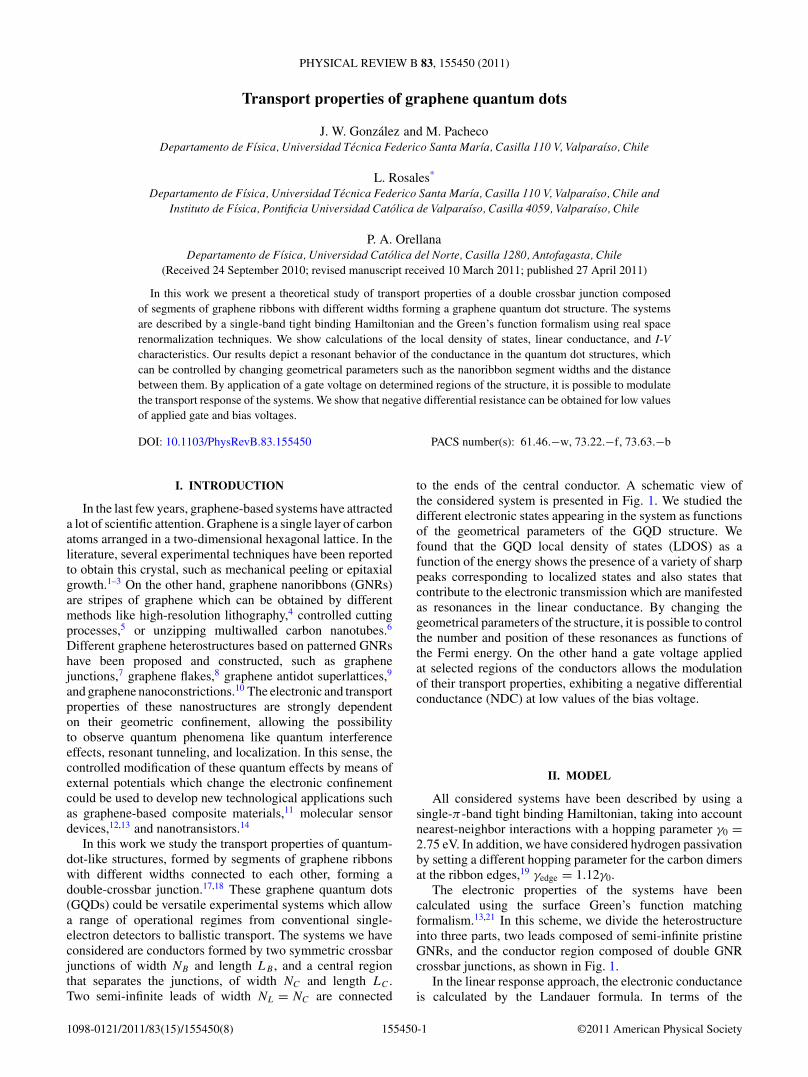
In Fig. 2, we display results of the linear conductance for agraphene quantum dot structure formed by two armchair rib-bon leads of width NL = 5 and a conductor region composedof two symmetric crossbar junctions of width NB = 17 andvariable lengths LB (from 1 up to 7). Two distances betweenthe junctions[Fig. 2(a) LC = 5 and Fig. 2(b) LC = 10] areconsidered and the conductance of a pristine NL = 5 armchairnanoribbon is included as a comparison (light green dottedline).
FIG. 2. (Color online) Conductance as a function of the Fermienergy for a graphene quantum dot structure composed of twoarmchair ribbon leads of width NL = 5 and a double symmetriccrossbar junction of width NB = 17 and variable length, from LB = 1up to LB = 7. The central region has a width NC = 5 and twoseparations (a) LC = 5 and (b) LC = 10. Light green dotted linecorresponds to the conductance of a pristine NL = 5 ribbon. Allcurves have been shifted by 2G0 for a better visualization.
In both panels it is possible to observe a series of peaksat defined energies in the conductance curves. This resonantbehavior of the electronic conductance arises from the inter-ference of the electronic wave functions inside the structure,which travel forth and back forming stationary states in theconductor region (well-like states). In order to understandthese results, it is convenient to define two energy regions,the low-energy range from 0 up to 0.7γ0 (correspondingto the first quantum of conductance for the pristine N = 5armchair ribbon) and the high-energy range, from 0.7γ0 to1.2γ0 (corresponding to the second step of conductance of theN = 5 pristine system).
In the low-energy range, it is clear that the conductancepeaks correspond to resonant states belonging to the centralregion of the conductor. By increasing the relative distanceLC of the central part of the system, the number of allowedwell-like states also increases and, as a consequence, the con-ductance curves exhibit more resonances.13,17,23 The well-likestates remain almost invariant under geometrical modificationsof the crossbar junctions. However, for certain energy rangesand for particular junction lengths, the electronic transmissionof the system exhibits an almost constant value. For instance,in both panels of Fig. 2, for the cases of LB = 1 and 4 atthe energy range 0.4γ0 to 0.65γ0. This effect corresponds toa constructive interference between well-like states from thecentral region with states belonging to the crossbar junction
155450-2
TRANSPORT PROPERTIES OF GRAPHENE QUANTUM DOTS PHYSICAL REVIEW B 83, 155450 (2011)
regions. The different interference effects will be clarified byanalyzing the LDOS of these systems, which is done further inthis paper. In the high-energy region, the conductance curvesexhibit a complex behavior as a function of the geometricalparameters of the GQD structures. There is not a predictablebehavior of the conductance as the width and length of thecrossbar junction are increased.
It is important to point out, from the analysis of Fig. 2, that itis possible to identify some interesting effects associated withwell-known quantum phenomena. For instance, in Figs. 2(a)and 2(b), for the cases LB = 5, 6, and 7 at energies aroundE = 0.5γ0, it is possible to observe a nonsymmetric line shape,which corresponds to a convolution of a Fano-like24 and aBreit-Wigner25 resonance. This kind of line shape, has beenobserved before in other mesoscopic systems by Orellana andco-workers.26 In that reference, a simple model is used of twolocalized states with the same energy ωc directly coupled toeach other by a coupling τ and indirectly coupled throughout acommon continuum. The corresponding resonances have beenadjusted by using the following expression:
T (ω) = 4η2[(ω − ωc)x − τ ]2
[(1 − x2)η2 − (ω − ωc)2 + τ 2]2 + 4(ω − ωc − τx)2,
(4)
where η is the width of a localized state coupled to thecontinuum and x defines the degree of asymmetry of thesystem.
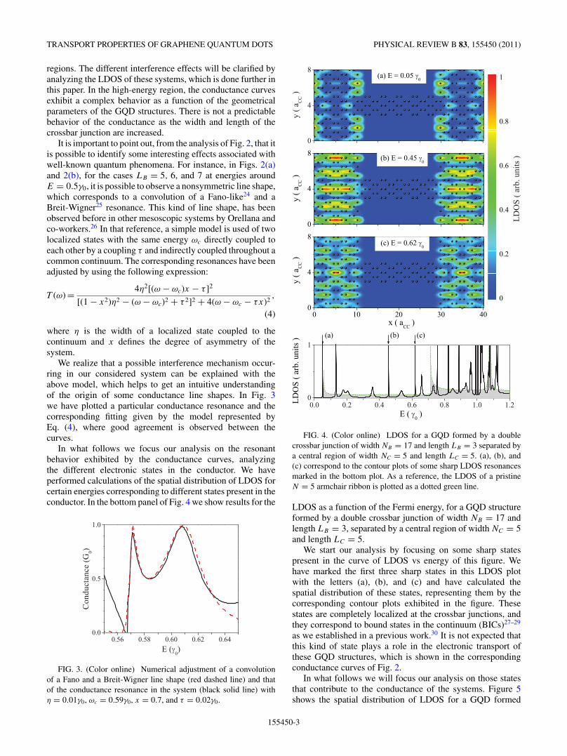
We realize that a possible interference mechanism occur-ring in our considered system can be explained with theabove model, which helps to get an intuitive understandingof the origin of some conductance line shapes. In Fig. 3we have plotted a particular conductance resonance and thecorresponding fitting given by the model represented byEq. (4), where good agreement is observed between thecurves.
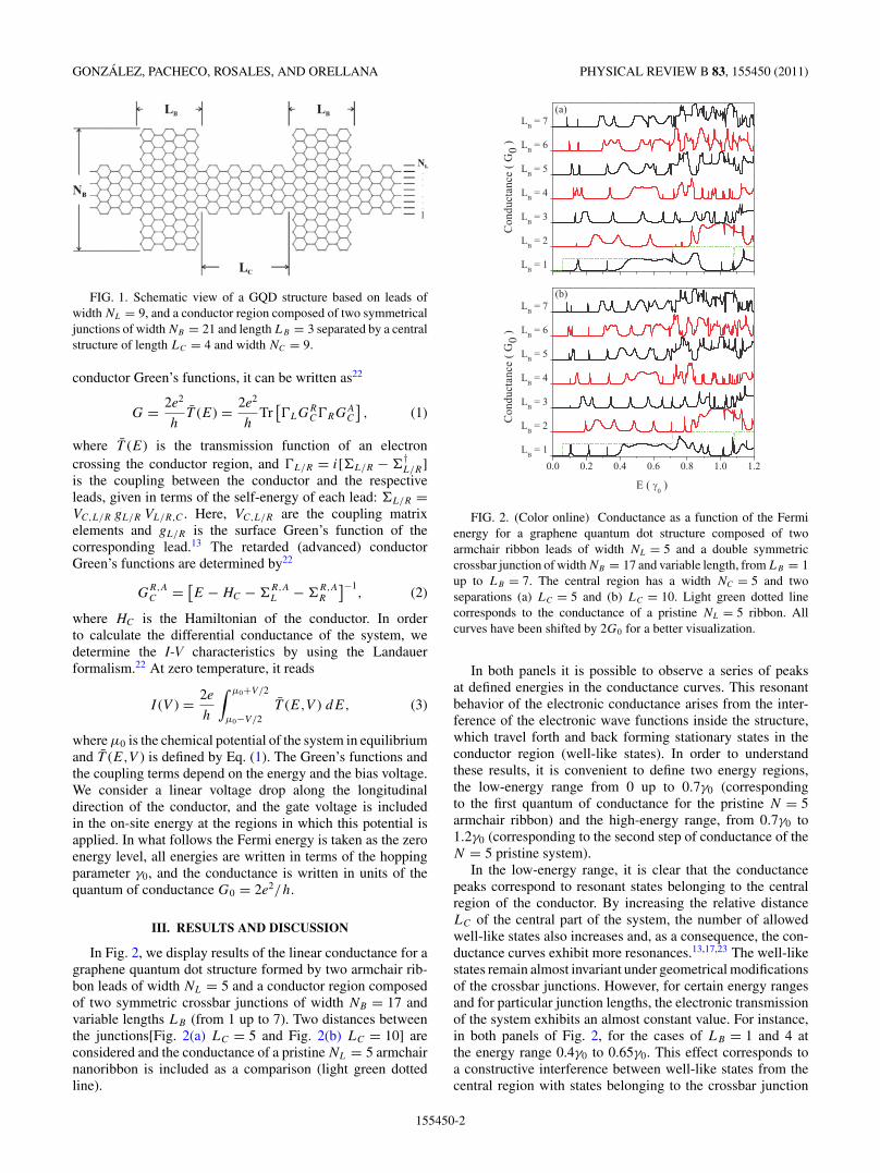
In what follows we focus our analysis on the resonantbehavior exhibited by the conductance curves, analyzingthe different electronic states in the conductor. We haveperformed calculations of the spatial distribution of LDOS forcertain energies corresponding to different states present in theconductor. In the bottom panel of Fig. 4 we show results for the
FIG. 3. (Color online) Numerical adjustment of a convolutionof a Fano and a Breit-Wigner line shape (red dashed line) and thatof the conductance resonance in the system (black solid line) withη = 0.01γ0, ωc = 0.59γ0, x = 0.7, and τ = 0.02γ0.
FIG. 4. (Color online) LDOS for a GQD formed by a doublecrossbar junction of width NB = 17 and length LB = 3 separated bya central region of width NC = 5 and length LC = 5. (a), (b), and(c) correspond to the contour plots of some sharp LDOS resonancesmarked in the bottom plot. As a reference, the LDOS of a pristineN = 5 armchair ribbon is plotted as a dotted green line.
LDOS as a function of the Fermi energy, for a GQD structureformed by a double crossbar junction of width NB = 17 andlength LB = 3, separated by a central region of width NC = 5and length LC = 5.
We start our analysis by focusing on some sharp statespresent in the curve of LDOS vs energy of this figure. Wehave marked the first three sharp states in this LDOS plotwith the letters (a), (b), and (c) and have calculated thespatial distribution of these states, representing them by thecorresponding contour plots exhibited in the figure. Thesestates are completely localized at the crossbar junctions, andthey correspond to bound states in the continuum (BICs)27–29
as we established in a previous work.30 It is not expected thatthis kind of state plays a role in the electronic transport ofthese GQD structures, which is shown in the correspondingconductance curves of Fig. 2.
In what follows we will focus our analysis on those statesthat contribute to the conductance of the systems. Figure 5shows the spatial distribution of LDOS for a GQD formed
155450-3

GONZALEZ, PACHECO, ROSALES, AND ORELLANA PHYSICAL REVIEW B 83, 155450 (2011)
FIG. 5. (Color online) LDOSs for a GQD structure formed bya double crossbar junction of width NB = 17 and length LB = 3separated by a central region of width NC = 5 and length LC = 5.(a), (b), (c), and (d) correspond to the contour plots of those resonantstates marked in the LDOS plot displayed at the bottom.
by a double crossbar junction of width NB = 17 and lengthLB = 3, separated by a central region of width NC = 5 andlength LC = 5. As a reference, in the bottom panel we haveincluded a plot with the LDOS versus Fermi energy of theGQD system, where we have marked with the letters (a), (b),(c), and (d) four particular energy states. The correspondingcontour plots are displayed in the upper parts of the figure.
In these plots, it is possible to observe the resonant behaviorof these states, which are completely distributed along theGQD structure, presenting a maximum of the probabilitydensity at the center of the system. This condition favors
the alignment of the electronic states of the leads with theresonant states in the conductor and consequently a unitarytransmission at those energy values is expected. This behavioris reflected as a series of resonant peaks in the conductance ofthe system that could be controlled by means of the geometricalparameters of the GQD, as shown in Fig. 2. At higher energiesthere is an interplay between localized states in the crossbarjunctions and resonant states in the central region of theconductor. As shown in Fig. 5(d), some states are stronglydependent on the geometry of the junctions; therefore for someparticular configuration it is possible to observe a non-nulltransmission at these energies, while for other cases, there aredestructive interference mechanisms that suppress completelythe transmission in that energy region.
We have studied different configurations of GQD structures,systematically varying some geometric parameters. We haveobserved a quite general behavior of such resonant conductorswith the presence of sharp and resonant states. Dependingon each particular system, changes can be observed in thenumber and position in energy of these states, as well asin their spatial distribution. The different intensity of thepeaks in the LDOS curves depends on the spatial distributionof the states. There are states completely extended alongthe conductor [as in Fig. 5(b)] which generate wider andless intense peaks. On the other hand, there are resonantstates which are more concentrated in certain regions of theconductor [as in Figs. 5(c) and 5(d)] which generate sharperand more intense peaks in the LDOS.
Now we focus our analysis on the effects of an applied gatevoltage on the transport properties of GQD structures. Resultsfor the conductance as a function of the Fermi energy, fordifferent values of a gate voltage applied in selected regions ofa GQD, are shown in Fig. 6. The systems are composed of leadsof width NL = 5, two crossbar junctions of width NB = 17,and a central part of width NC = 5 and length LC = 5. Figures6(a) and 6(c) correspond to junctions of length LB = 2, whileFigs. 6(b) and 6(d) correspond to junctions of length LB = 3.Finally, the upper panels correspond to a gate voltage appliedat the crossbar junction regions, whereas the lower panelscorrespond to a gate voltage applied at the central part of thestructure.
In these contour plots of conductance, it is possible toobserve the behavior of the resonant states of the system witha gate voltage applied at different regions of the structure.The lower panels of Fig. 6 show the case of a gate voltageapplied at the central region of the considered GQDs. In theseplots the linear dependence of the conductance resonances as afunction of the gate voltage is manifested. It can be shown thatthe electronic states of a pristine armchair graphene ribbon areregularly spaced in the whole energy range;15,16,20 therefore, asthe gate voltage is applied, there will be a high probability thatthe lead states become aligned with the resonant states in thecentral region of the structure. This behavior in completelygeneral and independent of the width LB of the crossbarjunctions. The linear behavior of the conductance peaks couldbe useful in nanoelectronic devices, due to the possibilityof controlling the current flow through these systems. Thisargument will become more clear with the analysis ofthe differential conductance, which is shown below in thispaper.
155450-4

TRANSPORT PROPERTIES OF GRAPHENE QUANTUM DOTS PHYSICAL REVIEW B 83, 155450 (2011)
FIG. 6. (Color online) Conductance as a function of Fermi energy and gate voltage for GQDs composed of leads of width NL = 5, twocrossbar junctions of width NB = 17, and a central part of width NC = 5 and length LC = 5. (a) and (c) correspond to junctions of lengthLB = 2, while (b) and (d) correspond to junctions of length LB = 3. In the upper panels the gate voltage is applied at the crossbar regions,and in the lower panels the gate voltage is applied at the central structure. The black segmented lines highlight different slopes discussed in thetext.
The case of a gate voltage applied at the crossbar junctionregions is shown in the upper panels of Fig. 6. The conductancebehavior is more complicated to analyze; nevertheless, it isstill possible to observe a linear dependence of the resonantstates on the gate voltage. However, two different slopes canbe noticed, for states belonging to the crossbar junctions(lower slope) and for states belonging to the central regionof the conductor (higher slope). In addition, the panels exhibitan important reduction in the conductance gap, for differentvalues of gate voltage. This effect is mainly produced by anenergy shift of the localized states at the junctions, whichinduces a less destructive interference with the resonant states.It is important to point out that this effect can be observed onlybecause the gate potential is applied simultaneously to bothcrossbar junctions, otherwise, the conductance gap would notbe noticeably affected by the gate potential. Finally, the dark(blue online) regions present in Fig. 6 occur at energy rangesaround the LDOS singularities of the pristine N = 5 armchairGNR. At these energies, the second and the third allowed statesappear, which interrupt the linear behavior of the conductanceresonances as a function of the gate voltage.
In order to understand the presence of two different slopesin the upper panels of Fig. 6, we present a simple model whichkeeps the underlying physics of the considered system andallows us to explain our results qualitatively.
The scheme showed in Fig. 7 is a simple representation ofour conductor. The system is composed of a linear chain ofthree sites, which are connected to two semi-infinite leads. Wehave considered four quantum dots connected to the extremesof the chain forming a double crossbar junction, at which wehave applied symmetrically a gate voltage Vg . This potentialwill modify the on-site energy of the dots by a linear shift ofenergy proportional to the gate voltage amplitude.
By use of the Dyson equation, it is possible to calculate theGreen’s function of the central site of the chain labeled by 0,which takes the form
G00 = 1
ω − ε0 − �, (5)
where ω is the energy of the incident electrons, ε0 is the centralon-site energy, and the self-energy � is given by the followingexpression (see the Appendix for a detailed derivation):
� = v2(ω − v2
ω−Vg
)2 + �2
[(ω − v2
ω − Vg
)+ i�
]. (6)
In this model, the self-energy of the Green’s functions ofthe central region acquires a real part that depends on thegate voltage applied to the crossbar junction region. As aconsequence, two different slopes appear in the behavior ofthe conductance peaks as a function of the gate voltage. Oneof these slopes corresponds to the direct evolution of the statesbelonging to the crossbar junctions as a function of the gatevoltage (lower slope), and the higher slope corresponds to theindirect states belonging to the central region.
Now we focus our analysis on the I-V characteristics andthe differential conductance of these resonant GQDs. Figure 8shows results of these transport properties for a conductorformed by two crossbar junctions of width NB = 17, lengthLB = 2 and a central region of width NC = 5. In these plotsthe length of the central structure is varied from LC = 1 upto LC = 20. In Fig. 8(a) it is possible to observe that fora very small separation between the two junctions, the I-Vcharacteristics exhibit abrupt slope changes and oscillations forcertain ranges of the bias voltage. This behavior is producedby the increasing number of resonant states as a result of
FIG. 7. (Color online) A simple model of two crossbar junctionsformed by two quantum dots, coupled to a linear chain of sites.
155450-5
GONZALEZ, PACHECO, ROSALES, AND ORELLANA PHYSICAL REVIEW B 83, 155450 (2011)
(a) (b)
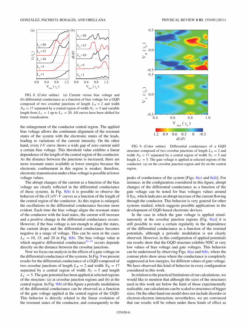
FIG. 8. (Color online) (a) Current versus bias voltage and(b) differential conductance as a function of bias voltage for a GQDcomposed of two crossbar junctions of length LB = 2 and widthNB = 17 separated by a central region of width NC = 5 and variablelength from LC = 1 up to LC = 20. All curves have been shifted forbetter visualization.
the enlargement of the conductor central region. The appliedbias voltage allows the continuum alignment of the resonantstates of the system with the electronic states of the leads,leading to variations of the current intensity. On the otherhand, every I-V curve shows a wide gap of zero current untila certain bias voltage. This threshold value exhibits a lineardependence of the length of the central region of the conductor.As the distance between the junctions is increased, there aremore resonant states available at lower energies because theelectronic confinement in this region is weaker; therefore,electronic transmission under a bias voltage is possible at lowervoltage values.
The abrupt changes of the current as a function of the biasvoltage are clearly reflected in the differential conductanceof these systems. In Fig. 8(b) it is possible to observe thebehavior of the dI/dV -V curves as a function of the length ofthe central region of the conductor. As this region is enlarged,the oscillations in the differential conductance become moreevident. Each time the bias voltage aligns the resonant statesof the conductor with the lead states, the current will increaseand a positive change in the differential conductance occurs.However, if the bias voltage is not enough to align the states,the current drops and the differential conductance becomesnegative in a range of voltage. This can be seen in the casesLC = 10, 15, and 20 in Fig. 8(b). The bias voltage value atwhich negative differential conductance31–33 occurs dependsdirectly on the distance between the crossbar junctions.
Now we focus our analysis in the effects of a gate voltage onthe differential conductance of the systems. In Fig. 9 we presentresults for the differential conductance of a GQD composed oftwo crossbar junctions of length LB = 2 and width NB = 17separated by a central region of width NC = 5 and lengthLC = 5. The gate potential has been applied at selected regionsof the structure: (a) at crossbar junction regions and (b) at thecentral region. In Fig. 9(b) of this figure a periodic modulationof the differential conductance can be observed as a functionof the gate voltage applied at the central region of the GQD.This behavior is directly related to the linear evolution ofthe resonant states of the conductor, and consequently to the
FIG. 9. (Color online) Differential conductance of a GQDstructure composed of two crossbar junctions of length LB = 2 andwidth NB = 17 separated by a central region of width NC = 5 andlength LC = 5. The gate voltage is applied at selected regions of theconductor: (a) on the crossbar junction region and (b) on the centralregion.
peaks of conductance of the system [Figs. 6(c) and 6(d)]. Forinstance, in the configuration considered in this figure, abruptchanges of the differential conductance as a function of thegate voltage can be noted for bias voltages values around0.8γ0, which indicates an abrupt increase of the current flowingthrough the conductor. This behavior is very general for othersystems studied, which suggests possible applications in thedevelopment of GQD-based electronic devices.
In the case in which the gate voltage is applied simul-taneously at the crossbar junction regions [Fig. 9(a)] it isstill possible to note a certain regularity in the dependenceof the differential conductance as a function of the externalpotentials, although a periodic modulation is not clearlyobserved. However, in this configuration of applied potentialsour results show that the GQD structure exhibits NDC at verylow values of bias voltage and gate voltages. This behaviorcan be understood by observing Figs. 6(a) and 6(b), where thecontour plots show areas where the conductance is completelysuppressed at low energies, for different values of gate voltage.We have observed this kind of behavior in every configurationconsidered in this work.
In relation to the practical limitations of our calculations, wewould like to mention that although the sizes of the structuresused in this work are below the limit of those experimentallyrealizable, our calculations can be scaled to structures of biggersizes. On the other hand our model does not include disorder orelectron-electron interaction; nevertheless, we are convincedthat our results will be robust under these kinds of effect as
155450-6

TRANSPORT PROPERTIES OF GRAPHENE QUANTUM DOTS PHYSICAL REVIEW B 83, 155450 (2011)
they are in mesoscopic systems. For instance, it is known thatin quantum dots the resonant tunneling and the Fano effectsurvive the effect of electron-electron interaction.34,35
IV. SUMMARY
In this work we have analyzed the transport propertiesof a GQD structure formed of a double crossbar junctionmade of segments of GNRs of different widths. We havefocused our analysis on the dependence of the electronicand transport properties on the geometrical parameters of thesystem, looking for the modulation of these properties throughexternal potentials applied to the structure. Our results depicta resonant behavior of the conductance in the quantum dotstructures which can be controlled by changing geometricalparameters such as the nanoribbon widths and the distancebetween them. We have explained our results in terms of ananalysis of the different electronic states of the system. Thepossibility of modulating the transport response by applyinga gate voltage on determined regions of the structure hasbeen explored, and it has been found that negative differentialconductance can be obtained for low values of the gateand bias applied voltages. Our results suggest that possibleapplications with GQDs can be developed for new electronicdevices.
ACKNOWLEDGMENTS
The authors acknowledge the financial support of USMInternal Grant No. 110971 and FONDECYT program GrantsNo. 11090212, No. 1100560, and No. 1100672. L.R. alsoacknowledges PUCV-DII Grant No. 123.707/2010.
APPENDIX: GREEN’S FUNCTION OF THESIMPLE MODEL
In Sec. III, we have introduced a simple model in order toexplain the different slopes of Fig. 6. This model is composedof a linear chain of three sites, of the same energy, at whichwe have coupled four quantum dots (QDs) of energies εn (n= u,d), forming a crossbar junction configuration exhibitedin Fig. 7. This simple scheme is very useful in explainingqualitatively the electronic behavior of the graphene quantumdot that we have studied.
Let us start with the Hamiltonian of the system describedby Fig. 7:
HT = Hleads + Hc + Hc,leads, (A1)
where the Hamiltonian of the leads, Hleads, is given by
Hleads =∑
k,α(L,R)
εk,αc†k,αck,α, (A2)
the conductor Hamiltonian Hc is given by
Hc =1∑
i=−1
εif†i fi + t
1∑i=0
(f †i−1fi + H.c.)
+∑
m(−1,1)
∑n(u,d)
[εm,n d†m,n dm,n + v(d†
m,n fm + H.c.)],
(A3)
and finally the leads-conductor Hamiltonian is given by
Hc,leads =∑
k,α(L,R)
∑m(−1,1)
Vα(f †m ck,α + H.c.). (A4)
By using the Dyson equation, it is possible to calculate theGreen’s function of site 0. Following a standard procedure wehave obtained
G00 = g0 + g0 v G10 + g0 v G−10, (A5)
G10 = g1 v G00 + g1
∑k
VRGkR,0, (A6)
G−10 = g0 v G−10 + g−1
∑k
VLGkL,0, (A7)
where GkR,0 = gkVRG10 and GkL,0 = gkVLG−10.Replacing these expression in the previous set of equations,
we obtain
G10 = g1 v G00
1 − g1∑
kRV
†R gkR
VR
, (A8)
G−10 = g−1 v G00
1 − g−1∑
kLV
†L gkL
VL
. (A9)
Considering g0 = 1/(ω − ε0), and replacing the aboveexpressions for G10 and G−10, G00 reads
G00 = 1
ω − ε0 − �, (A10)
where the self-energy is defined by the following expression:
� = g1 v2
1 − g1 i�R
+ g−1 v2
1 − g−1 i�L
(A11)
with �R = ∑kR
V†RgkR
VR and �L = ∑kL
V†LgkL
VL.Using the expressions for the on-site Green’s functions for
the sites −1 and 1 given by g−1 = 1/(ω − ε−1) and g1 =1/(ω − ε1), and considering a gate voltage Vg applied to theQDs, which redefines their on-site energies by εn = εn + Vg ,it is possible to write an expression for the self-energy of thesystems as
� = v2(ω − v2
ω−Vg
)2 + �2
[(ω − v2
ω − Vg
)+ i�
], (A12)
where we have considered a symmetric system (�L = �R). Inthis approach, it is possible to write a compact form for the self-energy given in Eq. (A12), which contains a real (gate-voltagedependent) and an imaginary part.
155450-7

GONZALEZ, PACHECO, ROSALES, AND ORELLANA PHYSICAL REVIEW B 83, 155450 (2011)
*[email protected]. S. Novoselov, A. K. Geim, S. V. Morozov, D. Jiang, Y. Zhang,S. V. Dubonos, I. V. Grigorieva, and A. A. Firsov, Science 306, 666(2004).
2C. Berger, Z. Song, T. Li, X. Li, A. Y. Ogbazghi, R. Feng, Z. Dai,A. N. Marchenkov, E. H. Conrad, P. N. First, and W. A. de Heer,J. Phys. Chem. B 108, 19912 (2004).
3C. Berger, Z. Song, X. Li, X. Wu, N. Brown, C. Naud, D. Mayou,T. Li, J. Hass, A. N. Marchenkov, E. H. Conrad, P. N. First, and W.A. de Heer, Science 312, 1191 (2006).
4X. Li, X. Wang, L. Zhang, S. Lee, and H. Dai, Science 319, 1229(2008).
5L. Ci, Z. Xu, L. Wang, W. Gao, F. Ding, K. F. Kelly, B. I. Yakobson,and P. M. Ajayan, Nano Res. 1, 116 (2008).
6D. V. Kosynkin, A. L. Higginbotham, A. Sinitskii, J. R. Lomeda,A. Dimiev, B. K. Price, and J. M. Tour, Nature (London) 458, 872(2009); M. Terrones, ibid. 458, 845 (2009).
7B. Oezyilmaz, P. Jarillo-Herrero, D. Efetov, D. A. Abanin, L. S.Levitov, and P. Kim, Phys. Rev. Lett. 99, 166804 (2007).
8L. A. Ponomarenko, F. Schedin, M. I. Katsnelson, R. Yang, E.W. Hill, K. S. Novoselov, and A. Geim, Science 320, 356 (2008);J. W. Gonzalez, H. Santos, M. Pacheco, L. Chico, and L. Brey,
Phys. Rev. B 81, 195406 (2010).9T. G. Pedersen, C. Flindt, J. Pedersen, N. A. Mortensen, A. P. Jauho,and K. Pedersen, Phys. Rev. Lett. 100, 136804 (2008).
10B. Oezyilmaz, P. Jarillo-Herrero, D. Efetov, and P. Kim, Appl. Phys.Lett. 91, 192107 (2007).
11S. Stankovich, D. A. Dikin, G. H. B. Dommett, K. M. Kohlhaas,E. J. Zimney, E. A. Stach, R. D. Piner, S. T. Nguyen, and R. S.Ruoff, Nature (London) 442, 282 (2006).
12F. Schedin, A. Geim, S. Morozov, E. Hill, P. Blake, M. Katsnelson,and K. Novoselov, Nature Mater. 6, 652 (2007).
13L. Rosales, M. Pacheco, Z. Barticevic, A. Latge, and P. Orellana,Nanotechnology 19, 065402 (2008); 20, 095705 (2009).
14C. Stampfer, E. Schurtenberger, F. Molitor, J. Guttinger, T. Ihn, andK. Ensslin, Nano Lett. 8, 2378 (2008).
15K. Nakada, M. Fujita, G. Dresselhaus, and M. S. Dresselhaus, Phys.Rev. B 54, 17954 (1996).
16K. Wakabayashi, Phys. Rev. B 64, 125428 (2001).17J. W. Gonzalez, L. Rosales, and M. Pacheco, Physica B 404, 2773
(2009).18B. H. Zhou, W. H. Liao, B. L. Zhou, K. Q. Chen, and G. H. Zhou,
Eur. Phys. J. B 76, 421 (2010).19Young-Woo Son, M. L. Cohen, and S. G. Louie, Phys. Rev. Lett.
97, 216803 (2006).20A. H. Castro Neto, F. Guinea, N. M. R. Peres, K. S. Novoselov, and
A. K. Geim, Rev. Mod. Phys. 81, 109 (2009).21M. B. Nardelli, Phys. Rev. B 60, 7828 (1999).22S. Datta, Electronic Transport Properties of Mesoscopic Systems
(Cambridge University Press, Cambridge, 1995).23Z. Z. Zhang, Kai Chang, and K. S. Chan, Nanotechnology 20,
415203 (2009).24U. Fano, Phys. Rev. 124, 1866 (1961).25G. Breit and E. Wigner, Phys. Rev. 49, 519 (1936).26P. A. Orellana, M. L. Ladron de Guevara, and F. Claro, Phys. Rev.
B 70, 233315 (2004).27J. von Neumman and E. Wigner, Z. Phys. 30, 465 (1929).28F. OuYang, J. Xiao, R. Guo, H. Zhang, and H. Xu, Nanotechnology
20, 055202 (2009).29A. Matulis and F. M. Peeters, Phys. Rev. B 77, 115423 (2008).30J. W. Gonzalez, M. Pacheco, L. Rosales, and P. A. Orellana,
Europhys. Lett. 91, 66001 (2010).31M. Y. Han, B. Ozyilmaz, Y. Zhang, and P. Kim, Phys. Rev. Lett. 98,
206805 (2007).32V. N. Do and P. Dollfus, J. Appl. Phys. 107, 063705 (2010).33H. Ren, Q. Li, Y. Luo, and J. Yang, Appl. Phys. Lett. 94, 173110
(2009).34S. M. Cronenwett, T. H. Oosterkamp, and L. P. Kouwenhoven,
Science 281, 540 (1998).35Masahiro Sato, Hisashi Aikawa, Kensuke Kobayashi, Shingo
Katsumoto, and Yasuhiro Iye, Phys. Rev. Lett. 95, 066801(2005).
155450-8