TRANSMITTERS AMATEUR TRANSISTOR · temperature of the transistor is the single most important...
68
4,..2PHOTOFACT PUBLICATION TTS-1 TRANSISTOR TRANSMITTERS for the AMATEUR Complete details, including cir- cuit descriptions, construction techniques, parts lists, and op- erating instructions, for 12 use- ful transistor devices. Valuable projects for hams, CB'ers, stu- dents, and experimenters.
Transcript of TRANSMITTERS AMATEUR TRANSISTOR · temperature of the transistor is the single most important...
4,..2PHOTOFACT PUBLICATION TTS-1
TRANSISTOR
TRANSMITTERSfor the
AMATEUR
Complete details, including cir-cuit descriptions, construction
techniques, parts lists, and op-erating instructions, for 12 use-
ful transistor devices. Valuable
projects for hams, CB'ers, stu-dents, and experimenters.
k
TRANSISTOR
TRANSMITTERSfor the
AMATEURby Donald L. Stoner, W6TNS
HOWARD W. SAMS & CO., INC.
THE BOBBS-MERRILL COMPANY, INC.Indianapolis New York

FIRST EDITION
FIRST PRINTING - FEBRUARY, 1964
SECOND PRINTING - NOVEMBER, 1966
Copyright © 1964 by Howard W. Sams & Co., Inc., Indian-
apolis, Indiana. Printed in the United States of America.
All rights reserved.Reproduction or use, without express
permission, of editorial or pictorial content, in any manner,
is prohibited. No patent liability is assumed with respect
to the use of the information contained herein.
Library of Congress Catalog Card Number : 63-23372
Preface
Amateur radio has served to introduce thousands of enthu-siasts to the field of electronics. For many, amateur radio is thestart of a rewarding profession; for others, it is a helpful supple-ment to their formal education in engineering.
Constructing your own equipment is a satisfying and educa-tional segment of the hobby. Also, you can keep abreast of thelatest developments in circuits and components at littleexpense.
Construction projects for the beginner, as well as for theexperienced ham, are described in this book. Included areprojects for novice, technician, general -class, and Citizens -bandlicensees.
For example, the "Novice Powerhouse" in Chapter 5 is anideal rig for the beginner or the QRP general -class operator.The modulator described in Chapter 6 can be added to the"Novice Powerhouse" for phone operation. The 10 -meter rigin Chapter 8 can be used to communicate over distances ofthousands of miles under proper conditions.
The latest design and construction techniques are incor-porated throughout, including transistor circuitry and circuit -board layouts.
Every piece of equipment has been built and thoroughlytested on the air. I hope that you will enjoy building andoperating these projects as much as I did preparing them forthis book.
DONALD L. STONER, W6TNS
Contents
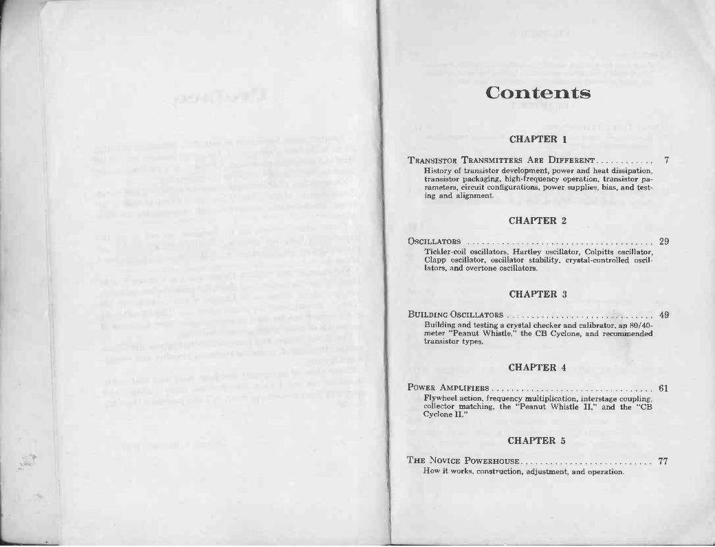
CHAPTER 1
TRANSISTOR TRANSMITTERS ARE DIFFERENTHistory of transistor development, power and heat dissipation,transistor packaging, high -frequency operation, transistor pa-rameters, circuit configurations, power supplies, bias, and test-ing and alignment.
CHAPTER 2
7
OSCILLATORS 29Tickler -coil oscillators, Hartley oscillator, Colpitts oscillator,Clapp oscillator, oscillator stability, crystal -controlled oscil-lators, and overtone oscillators.
CHAPTER 3
BUILDING OSCILLATORS 49Building and testing a crystal checker and calibrator, an 80/40 -meter "Peanut Whistle," the CB Cyclone, and recommendedtransistor types.
CHAPTER 4
POWER AMPLIFIERS 61Flywheel action, frequency multiplication, interstage coupling,collector matching, the "Peanut Whistle II," and the "CBCyclone II."
CHAPTER 5
THE NOVICE POWERHOUSE 77How it works, construction, adjustment, and operation.
CHAPTER 689
MODULATIONFrequency modulation, amplitude modulation, collector modu-
lation, build a low -power modulator,build a half -watt modula-
tor, build a 5-watt modulator,construction, and testing.
CHAPTER 7
TUNNEL -DIODE TRANSMITTERS111
How it works, the tunnel diode, build a 60 -second transmitter,
construction, and adjustment.
CHAPTER 8
HIGH POWER FOR CB OR 10 METERS121
How it works, construction, testing, and obtaining components
INDEX
127
1
TransistorTransmittersAre Different
There is always an element of glamor and just a little extrathrill when operating a short-wave transmitter that employsno vacuum tubes. This is particularly true when you are usingit to communicate with someone several.hundred or even athousand miles away.
Before plunging into the construction and operation of thesesolid-state "peanut whistles," let's review a bit of theory toobtain a clearer understanding of how they work. Even if youare an "old pro" in building rock -crushing tube rigs, transistortransmitters are different. Let's see why.
THE HISTORY OF COMMUNICATIONS TRANSISTORS
Although it may not be immediately obvious, much creditshould be given to the computer industry for the great progresswhich has been made in the field of communications transistors.In the mid -1950's there were few manufacturers who had theforesight to see the vast potential of the transistor for elimi-nating vacuum tubes in communications equipment. Theyseemed content to fabricate noisy, delicate devices suitable foruse in raspy -sounding portable radios.
7

Early transistor devices proved to be a poor second compared
to the vacuum tubes used in communications transmitters.
For several years it appeared that high -power, high-frequency
transistors were theoretically impossible to fabricate. Fortu-
nately for the communications industry this has not proved
to be the case.The computer industry, however, was enthusiastic about this
new electronics infant. They immediately visualized the possi-
bility of eliminating the thousands of heat-generating and
inefficient tubes used in a typical computer. Some of the
"dreamers" went so far as to predict table -top computers
( Fig. 1-1) which could be operated by an average secretary or
bookkeeper.
Fig. 1-1. Transistor IBM 1620 computer.
The transistor was able to replace many of the tubes in the
slower and less "intelligent" computers, but the designers
soon found that the transistor had many shortcomings. When
instructed to "turn on," the process was accomplished rather
slowly. Once the delay in followinginstructions was overcome,
it was reluctant to obey the "turn-off" signal and continued
to plod along for several microseconds. The time characteristics
are illustrated in Fig. 1-2.
8
The designers could not tolerate such sluggish performancein equipment which had to make hundreds of thousands of"decisions" every second. Transistor manufacturers were askedto make faster and faster switching devices in order to raisethe IQ of the next model computer. Devices were also needed
ON
OFF
ON
OFF
TD
TR TD
TD -= DELAY TIME
TR = RISE TIME
TF= FALL TIME
Fig. 1-2. Rise, fall, and delay time characteristics.
which would deliver watts of power, rather than milliwatts ormicrowattg, in order to drive memory cores in the complexelectronic cerebral cortex of the computer.
This constant pressure on transistor manufacturers forfaster and more powerful devices brought about a revolutionin the semiconductor industry. Vast sums were invested inresearch program.13to perfect new ways of making better tran-sistors for less money. The infant industry progressed from thehumble junction transistor, through the drift field, the diffused,and the mesa, to the present-day planar transistor, a miracleof semiconductor technology.
Modern transistors are able to operate at the speed of light.A planar computer transistor is capable of switching from theoff state to the on state in less time than it takes the lightreflected from this page to reach your eyes (remember thatlight travels at the speed of 186,000 miles per second). Todayit is possible to purchase devices which deliver 20 watts or moreof radio -frequency energy while switching on and off 50 milliontimes (50 megacycles) each second. Although these transistorsare very expensive, they are available. Further pressures onthe semiconductor industry, and the ever increasing com-
9

petition within it, will result in greatly reduced prices of com-
munications transistors. If the present rate of progress con-
tinues, it will soon be possible to buy a device which will
perform the same as a 6146 tube for less than $10.
POWER AND HEAT DISSIPATION
If a manufacturer wishes to make a more powerful vacuum
tube, he employs larger elements and encloses them in a larger
bottle. Although the interelectrode capacitance may increase,
generally speaking, the performance will be the same as that
of a physically smaller tube, except that the larger tube will
be able to handle more power without damage. Unfortunately
this is not the case with transistors.
Since the transistor is not a lossless device, it will always
produce heat when a current is passed through it. Its design,
which minimizes these losses through improved manufacturing
techniques, and its ability to get rid of the heat once generated,
determine the power-handling ability of the transistor.
Making the amount of active material and the junction larger
decreases losses in the transistor, but it also impairs its high -
frequency performance. Special techniques must be employed
to keep capacitanceslow while maintaining a large junction to
dissipate heat. Often this conflict results in some rather weird
internal structures, such as the "comb," the "star," and the
"snowflake."If you have ever torn apart a large power transistor (Fig.
1-3) you may have been surprised to see the tiny piece of semi-
conductor material inside. The large metal slug which com-
prises the case (usually copper) is designed to draw heat from
the junction and radiate it through the heat sink on which the
transistor is mounted. The temperature will always tend to
equalize and, in effect, the heat will tend to be drawn out of
the junction into the cooler metal to which it is attached.
Where operating life and reliability are concerned, the junction
temperature of the transistor is the single most important
consideration. When building or using transistor transmitters,
particular importanceshould be placed on the operating tem-
perature of the device to keep it as low as possible. As a "rule
of thumb," the transistor should be mounted on at least 10
10
Fig. 1-3. Construction of a typical transistor.
square inches of copper or aluminum for every watt of powerinput. It is preferable to use commercial heat sinks (Fig. 1-4)which compress 100 square inches into a space of approxi-mately 2" x 3" x 4". Never run the transmitter at its maxi-mum power level in an effort to get the last possible watt intothe antenna. Remember, if the power output is reduced byhalf, it only causes a loss of one "S" unit on a distant receiver.Experimental evidence indicates that for every 10°C. that thejunction temperature is reduced, the expected life span of thedevice will be doubled.
How hot can a transistor get? That depends entirely on themanufacturer's rating, which is determined by the package the
11
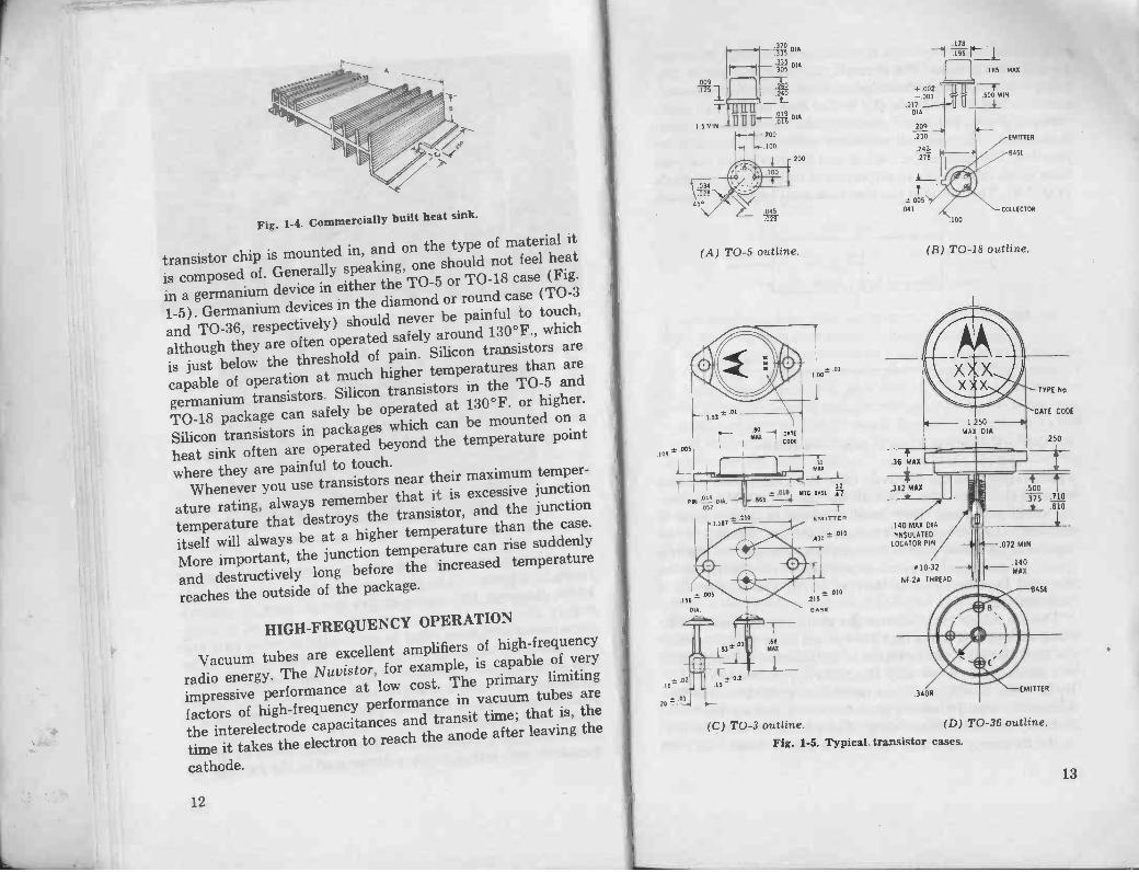
Fig. 1-4. Commercially built heat sink.
transistor chip is mounted in, and on the type of material it
is composed of. Generally speaking, one should not feel heat
in a germanium device in either the TO -5 or TO -18 case (Fig.
1-5). Germanium devices in the diamond or round case (TO -3
and TO -36, respectively)should never be painful to touch,
although they are often operated safely around 130°F., which
is just below the threshold of pain. Silicon transistors are
capable of operation at much higher temperatures than are
germaniumtransistors. Silicon transistors in the TO -5 and
TO -18 package can safely be operated at 130°F. or higher.
Silicon transistors in packages which can be mounted on a
heat sink often are operated beyond the temperature point
where they are painful to touch.,.-± 005
Whenever you use transistors near their maximum temper-
ature rating, alwaysremember that it is excessive junction
temperature that destroys the transistor, and the junction
itself will always be at a higher temperature than the case.
More important, the junction temperature can rise suddenly
and destructively long before the increased temperature
reaches the outside of the package.
HIGH -FREQUENCY OPERATION
Vacuum tubes are excellent amplifiers of high -frequency
radio energy. The Nuvistor, for example, is capable of very
impressive performance at low cost. The primary limiting
factors of high-frequency performance in vacuum tubes are
the interelectrode capacitances and transit time; that is, the
time it takes the electron to reach the anode after leaving the
cathode.
12
ADIA
DIA
009
re --.1 in125
TI 5 MIN Hu {fr- cil DIA
200
100
.200
045 9
(A) TO -5 outline.
.C". DIA.052
.156Y .005
302, 07
20 1.1_.°1
us, -±- 010
r15 - 0.2
100_.01
30M,
M
12N MU 77
EMITTER
4,0.010
215t- .010
RASE
+.002-.001
.017DIA
.209
.230-6
.242-
.278
.041
.100
.185 MAX
.500- M- IN
EMITTER
BASE
COLLECTOR
(B) TO -18 outline.
MAX DIA
.36 tMAX
-4-312MAX .500375 .710
.610
TYPE No
DATE CODE
250
.140 MAX DIA
'INSULATEDLOCATOR PIN
410.32 --I.NF -2A THREAD
.072 MIN
.140MAX
BASE
.3409 EMITTER
(C) TO -3 outline. (D) TO -36 outline.
Fig. 1-5. Typical transistor cases.
13

A similar condition exists in transistors, although it is com-
pounded many times. For example, the junctions are in inti-
mate contact, being physicallyattached, and they generally
exhibit a high capacitance (Ce on the data sheets) . To make
matters worse, the signal injected into the transistor must
pass through the electrode resistance (called Rb) to reach the
junction. The presence of both R and C forms a tiny low-pass
filter which inhibits the amplification of high -frequency signals
( Fig. 1-6) . The fact that the electrons must negotiate through
TRANSISTOR
SIGNAL IN
>SIGNAL
IN
SIGNAL
RbSIGNAL
Fig. 1-6. Rb and Ce form low-pass filter.
a solid rather than the relatively effortless confines of a vacuum
tends to slow them down. Not all the carriers reach the collec-
tor at the same time; they travel different paths and tend to
disperse. This storage effect accounts for the inability of the
transistor to follow instructions instantaneously. As the fre-
quency is increased, a point is reached where the transistor
does not know whether to turn on or off, and as a result it
does nothing.The transistor experimenter generally becomes quite con-
fused with all the terms that have arisen in an effort to define
the high -frequency performance of a transistor. At one time it
was necessary to know only the alpha -cutoff frequency (fab)
By knowing this figure, it was possible to predict roughly how
a transistor would work at a given frequency, and one transistor
could be compared with another. Alpha cutoff is simply defined
as the frequency at which the current gain is down 3 db from
14
a much lower frequency of, say, 1,000 cycles. The term ex-presses the loss of gain in the common -base configuration andis not valid for the more useful common-emitter circuit. Fur-ther, unless input and output impedances are known, it is notpossible to determine power gain. The alpha -cutoff frequencycurve for a typical transistor is shown in Fig. 1-7. It should be
3 db
z
6 db PER
OCTAVE
FREQUENCY--- lab
Fig. 1-7. Alpha -cutoff frequency curve.
pointed out that frequency is shown on a log scale which makesthe high -frequency gain appear to fall off quite rapidly.
Another term which expresses the high -frequency operationof a transistor is ft, the gain -bandwidth product frequency. Itis a convenient figure, for, as a "rule of thumb," it reveals thegain of the transistor at any particular frequency. For example,a transistor with an ft of 60 would have a power gain of 2 at 30mc, 4 at 15 mc, 8 at 7.5 mc, etc. Thus, by knowing the frequencyand the desired power output it is possible to approximate thedriving power required.
A third term, Lt.) will probably become the industry stand-ard; this term is defined as the theoretical or computed maxi-mum frequency at which the transistor is capable of oscillation.Therefore at fn,a, the power gain is equal to unity and the deviceis not capable of amplification.
The high -frequency characteristics of a typical transistor,such as the Philco Micro Alloy Diffused (MADT), is shown inFig. 1-8. Note that it has a flat portion where gain is relativelyconstant. However, as the frequency is increased, a point is
reached where the internal workings of the transistor combineto oppose the amplification of high frequencies. Above thispoint the power falls off at a rate equal to 6 db/octave. Eachtime the applied frequency is doubled, the power gain dropsby 6 db. The point where the rolloff curve intersects the unity -gain line is known as Lit,.
15

70
- 60"fi 50
z 40c.6 30
2°
e 100
6 db PER OCTAVE20 db PER DECADE
FREQUENCY
max max
100
Fig. 1-8. High -frequency characteristics of
typical transistor.
If one works back from unity gain or f,,, it would seem
possible to achieve infinitely high gain at some low frequency.
As Fig. 1-8 shows, this is not the case; a modern high -frequency
transistor is easily capable of more than 50 db of gain. Maxi-
mum available gain (MAG in Fig. 1-8) is a function of the
device current gain and the operating impedances. However,
50 db of radio -frequency gain concentrated in so small a space
tends to be highly unstable and virtually impossible to tame
without extremely complex neutralization and shielding
schemes. For this reason gains are usually held down to 40
db/stage by impedancemismatching in the input or output
circuit, or in both. Thus the 40-db figure is usually considered
to be the maximum useful gain (MUG) . Although some power
gain is lost, the increased stability and reduced circuit com-
plexity make it a small price to pay.Once a 40-db, flat -gain line is assumed and La. (which is
given on the manufacturer's data sheet) is known, it is possible
to predict the maximum power gain for the transistor at any
frequency. The rolloff is more or less constant at 6 db/ octave
or 20 db/decade. Assuming 40-db maximum usable gain, or
two decades, the frequency of the rolloff knee can be calculated
simply by dividing the fn. figure by 100. If the device Li is
100 mc, the knee occurs at 1 mc. At any frequency above this
point the power gain will diminish.
RUGGEDNESS
Newer transistors can withstand high external temperatures.
Most modern germanium transistors may be soldered into a
circuit without heat-sinking the leads or the case itself. The
16
leads can be heated, as in dip -soldering of printed -circuitboards, for as long as 10 seconds without internal damage. Allsilicon transistors can be soldered into a circuit withoutdamage.
The electrical ruggedness of the transistor is not quite soimpressive, however. For years the author used an 807 tubewhich had a hole about the size of a lead pencil in the plate.At one time or another the tube had flashed over internallybecause of excessive voltage and vaporized some of the metal.The tube, even with its "lung" punctured, is probably workingtoday.
In contrast to this, the author currently has a collection oftransistors which were subjected to excessive voltage. Unlikethe durable 807, these transistors are no longer of any electricalvalue.
Excessive voltage across either of the junctions in a tran-sistor can result in instantaneous destruction due to localizedheating. The carriers, propelled at enormous speeds and ingreat quantities, tend to "gang up" in one area while takingthe avenue of least resistance. This causes a sudden tempera-ture rise which virtually melts the transistor and almost in-stantaneously shorts the junction. The destructive avalancheis much faster than the finest fuse or circuit breaker can copewith.
If a resistance were inserted in series with the device to limitcurrent flow below the destructive heating point, no damagewould occur, even if the junction voltage (VrE ) were increasedfar beyond the maximum rating. For example, if a 1-meg re-sistor were inserted in series with a general-purpose PNP audiotransistor and connected to a 500 -volt supply, no damage wouldoccur to the junction because the current would be limited toa few microamperes.
Unfortunately, we cannot do this in a transistor transmitter;the same resistor which limits destructive currents also limitsthe power output below the useful level. Thus the maximumvoltage ratings must be closely observed. It should also bestressed that the maximum voltage supplied by the DC sourcemust always be much less than the maximum transistor rating.For example, in a class -C RF power amplifier, the back emf andflywheel action of the coil can generate peak voltages twice
17

the supply value (Figs. 1-9A and B). If the stage is high-level
collector modulated, the RF peaks will reach at leastloadingfour times
the supply voltage (Fig. 1-9C). If the antenna or
matching is improper, the voltage can reach even higher levels,
12VDC
oV
(A) Power -supplyvoltage of 12 volts
on collector.
Fig. 1-9. Voltage increase due to back emf, flywheel
effect and high-level modulation.
and any one of these peaks can have sufficient duration to
cause instantaneousdestruction of the transistor.
Thus, as a rule of thumb for AM transmitters, always select
a transistor with a Vcc rating at least four times the supply
voltage, or reduce the supply until it is one-fourth the maxi-
mum rating. A transistor with a six -times rating would be more
conservative and result in a greater safety margin in the pres-
ence of transients or voltage surges. In CW, FM, and SSB
equipment a device with a two-times supply rating should be
selected, and one with three times the rating is preferable.
In certain transistors, notably the mesa types, the base -
emitter breakdown voltage is also important. Excessive drive
24V
48V
DRIVE I
18
(B) Increase due to
flywheel effect andback emf.
(A) Drive-limiting resistor.
Fig. 1-10. Base -emitter breakdown protective circuits.
DRIVE I
(C) Increase due tohigh-level collector
modulation.
(B) Peak -voltage limiter.
can cause this junction to break down. Drive -limiting resistorsor peak -voltage limiting devices are often used to prevent thisform of destruction. These techniques are shown in Figs.1-10A and B.
CIRCUIT CONFIGURATIONS
With the exception of grounded -grid amplifiers, mostvacuum tubes are employed in a circuit where the cathode iscommon to the grid -input and plate -output circuit. Likewise,this is the customary arrangement found in transistor circuits.However, there are several other interesting and unusual tran-sistor configurations employed to achieve impedance matching,improved high -frequency performance, and better heat dissi-pation.
The three basic methods of connecting a transistor into thecircuit are common -emitter, common -base and common -collector configurations ( Fig. 1-11). The common -emitter con-figuration (Fig. 1-10A) is generally used in radio-frequencycircuits, since it provides the highest power gain of the threeconfigurations. For example, in a transmitter the common -emitter configuration would require approximately one -fifthas much driving power as the same transistor when connectedin a common -base configuration. The common -emitter con-figuration almost approximates the comparable tube circuit,which appears to make the operation of common -emitter cir-cuitry more easily understood.
A third advantage is not quite so obvious. Of the three con-figurations, the common emitter is the only circuit capable ofphase inversion. Thus, in radio-frequency amplifier circuitsthe output is degenerative (opposite phase) with respect tothe input. Inherently the stage becomes more stable, particu-larly on the flat portion of the transistor response curve, whenconnected common emitter. Neutralization will result in anincrease in power gain of as much as 3 db. Because of increasedstability in the common -emitter mode, circuits tend to becomemore reproduceable: that is, the gain and bandwidth variationsfrom transistor to transistor are greatly reduced.
There is considerable confusion regarding the relative meritsof common emitter versus common base in transmitter circuits.
19
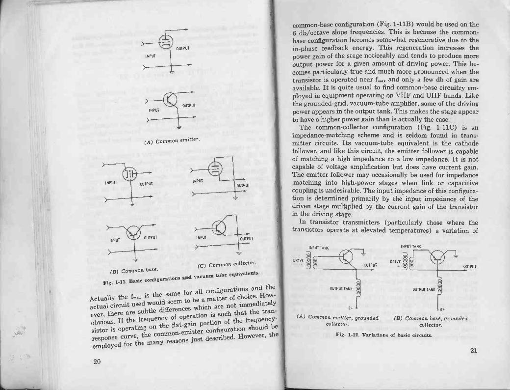
INPUT
(A) Common emitter.
OUTPUT
(C) Common collector.(B) Common base.
Fig. 1-11. Basic configurationsand vacuum tube equivalents.
is the same for all configurations and theActually the fn,actual circuit used would seem to be a matter of choice. How-
ever, there are subtle differenceswhich are not immediately
obvious. If the frequency of operation is such that the tran- 1
sistor is operating on the flat -gain portion of the frequency-
response curve, the common-emitter configuration should be
employed for the many reasons just described. However, the
20
common -base configuration (Fig. 1-11B) would be used on the6 db/octave slope frequencies. This is because the common -base configuration becomes somewhat regenerative due to thein -phase feedback energy. This regeneration increases thepower gain of the stage noticeably and tends to produce moreoutput power for a given amount of driving power. This be-comes particularly true and much more pronounced when thetransistor is operated near and only a few db of gain areavailable. It is quite usual to find common -base circuitry em-ployed in equipment operating on VHF and UHF bands. Likethe grounded -grid, vacuum -tube amplifier, some of the drivingpower appears in the output tank. This makes the stage appearto have a higher power gain than is actually the case.
The common -collector configuration (Fig. 1-11C) is animpedance -matching scheme and is seldom found in trans-mitter circuits. Its vacuum -tube equivalent is the cathodefollower, and like this circuit, the emitter follower is capableof matching a high impedance to a low impedance. It is notcapable of voltage amplification but does have current gain.The emitter follower may occasionally be used for impedance.matching into high -power stages when link or capacitivecoupling is undesirable. The input impedance of this configura-tion is determined primarily by the input impedance of thedriven stage multiplied by the current gain of the transistorin the driving stage.
In transistor transmitters (particularly those where thetransistors operate at elevated temperatures) a variation of
INPUT TANK
DRIVE
OUTPUT TANK
OUTPUTDRIVE
INPUT TANK
OUTPUT TANK
B+
OUTPUT
(A) Common emitter, grounded (B) Common base, groundedcollector. collector.
Fig. 1-12. Variations of basic circuits.
21

these circuits may be employed, asshown in Fig. 1-12. This is
done to permit direct grounding of the collector to the heat
sink without the use of an insulating mica washer. Elimtransistorinating
this resistance to heat transfer greatly reduces the
junction temperature. It should be stressed that common
emitter, for example, is still common emitter even if the tran-
sistor collector is grounded. This is why the term grounded
emitter instead of common emitter can be quite misleading.
To illustrate the point, consider a batterY, a pilot lamp, and a
meter connected in series. Any part in the circuit could be
called common and could be grounded to a chassis without
affecting the circuit. The same is true in transistor circuits,
although they are considerably more complex than the simple
circuit just described. Ground or common is strictly an arbi-
trary term and can be placed at any point so long as the rela-aith-
tionship of other components to this common point is f
fully observed.
POWER SUPPLIES
A particular transistor transmitter circuit may require any-
where between 1.5 and 24 volts for properoperation as con-
trasted to the dangerously high potentialsinvolved in vacuum -
tube equipment. This coin has two sides, however, because for
a given amount of power considerably more current must flow
in the transistor transmitter circuit. This requires heavier
wiring, larger meter ranges, and greatly increased bypass
capacitor values.It is recommended that the transistor transmitter
avoltage
source. Although this may seem rather unglamorous in this
day and age, it is the most practicalsolution to the power -
supply problem. A used battery can be obtained for less than
$5 and even a new one from the supermarket or drug store
seldom runs much more than $10 to $12. Athan,an electronic
power supply costing five to ten times as much. If the lead tie
lugs are exposed, they may be drilled and tapped for connec-
tions to make an adjustable voltage source, as shown in the
accompanying photos(Figs. 1-13 or 1-14A and B) . The case
22
Fig. 1-13. Inexpensive bench voltage source.
= = .
_°T T
FUSE - RATINGAS REQUIRED
12V AUTO BATTERY
(A) Schematic diagram.
8SW ITCH
_*=
VOLTAGE
SELECTOR
0
0FUSE 0
PANEL MOUNTEDWITH SHEETMETAL SCREWS
(B) Construction details.Fig. 1-14. Details of bench voltage source.
COPPER WIRESHUNTS
23
is usually thick enough to permit drilling and tapping for theinstallation of a control panel containing a current meter ormeter jack, a voltage switch, a fuse holder, etc. ( 1-13B).The adjustable -voltage feature is a useful addition since itpermits testing and tuning of transmitters at reduced voltagesbefore applying full power.
In an effort to standardize voltages to aid constructors, allcircuits in this book are optimized for use at 12 volts DC.Further, all circuits are designed with the common bus con-nected to negative so that they may be used in an automobile,if desired.
BIAS AND CLASSES OF OPERATION
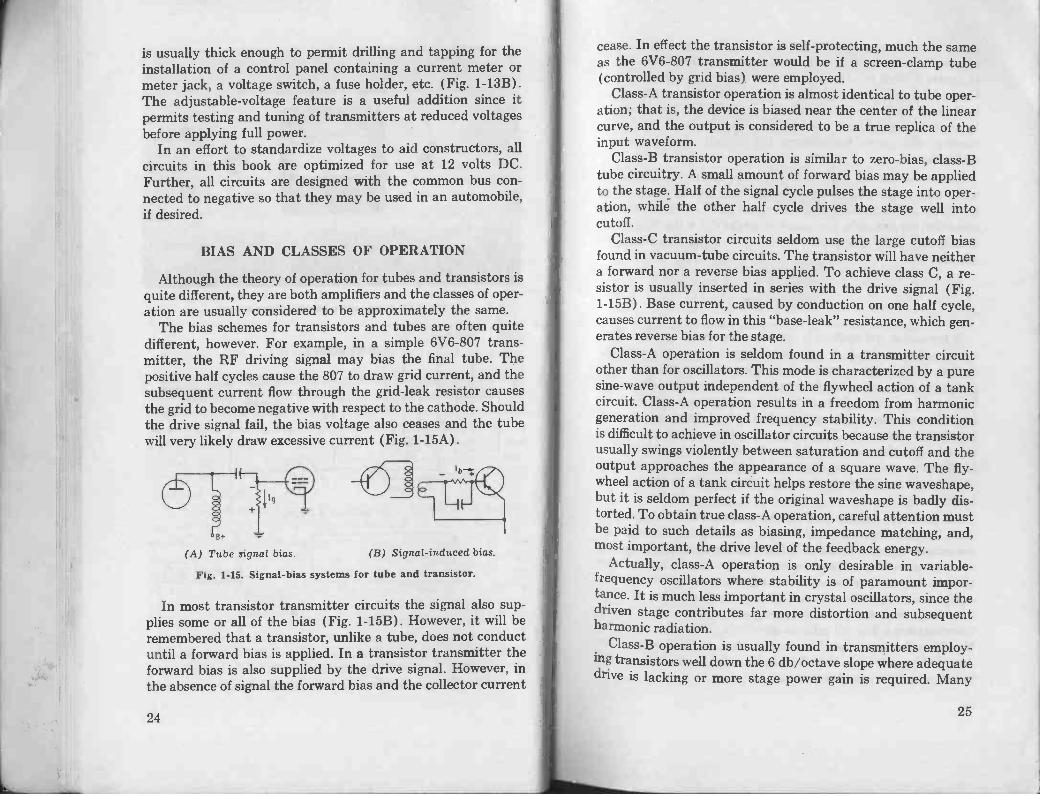
Although the theory of operation for tubes and transistors isquite different, they are both amplifiers and the classes of oper-ation are usually considered to be approximately the same.
The bias schemes for transistors and tubes are often quitedifferent, however. For example, in a simple 6V6-807 trans-mitter, the RF driving signal may bias the final tube. Thepositive half cycles cause the 807 to draw grid current, and thesubsequent current flow through the grid -leak resistor causesthe grid to become negative with respect to the cathode. Shouldthe drive signal fail, the bias voltage also ceases and the tubewill very likely draw excessive current ( Fig. 1-15A).
(A) Tube signal bias. (B) Signal -induced bias.
Fig. 1-15. Signal -bias systems for tube and transistor.
In most transistor transmitter circuits the signal also sup-plies some or all of the bias ( Fig. 1-15B). However, it will beremembered that a transistor, unlike a tube, does not conductuntil a forward bias is applied. In a transistor transmitter theforward bias is also supplied by the drive signal. However, inthe absence of signal the forward bias and the collector current
24
cease. In effect the transistor is self -protecting, much the sameas the 6V6-807 transmitter would be if a screen -clamp tube(controlled by grid bias) were employed.
Class -A transistor operation is almost identical to tube oper-ation; that is, the device is biased near the center of the linearcurve, and the output is considered to be a true replica of theinput waveform.
Class -B transistor operation is similar to zero -bias, class -Btube circuitry. A small amount of forward bias may be appliedto the stage. Half of the signal cycle pulses the stage into oper-ation, while the other half cycle drives the stage well intocutoff.
Class -C transistor circuits seldom use the large cutoff biasfound in vacuum -tube circuits. The transistor will have neithera forward nor a reverse bias applied. To achieve class C, a re-sistor is usually inserted in series with the drive signal (Fig.1-15B). Base current, caused by conduction on one half cycle,causes current to flow in this "base -leak" resistance, which gen-erates reverse bias for the stage.
Class -A operation is seldom found in a transmitter circuitother than for oscillators. This mode is characterized by a puresine -wave output independent of the flywheel action of a tankcircuit. Class -A operation results in a freedom from harmonicgeneration and improved frequency stability. This conditionis difficult to achieve in oscillator circuits because the transistorusually swings violently between saturation and cutoff and theoutput approaches the appearance of a square wave. The fly-wheel action of a tank circuit helps restore the sine waveshape,but it is seldom perfect if the original waveshape is badly dis-torted. To obtain true class -A operation, careful attention mustbe paid to such details as biasing, impedance matching, and,most important, the drive level of the feedback energy.
Actually, class -A operation is only desirable in variable -frequency oscillators where stability is of paramount impor-tance. It is much less important in crystal oscillators, since thedriven stage contributes far more distortion and subsequentharmonic radiation.
Class -B operation is usually found in transmitters employ-ing transistors well down the 6 db/octave slope where adequatedrive is lacking or more stage power gain is required. Many
25
power amplifiers which are supposed to be operating class Cmay actually be in self -bias class B because of insufficient driveto create a large reverse bias. In such cases a small amount of
forward bias ( just enough to place the operating point at thebottom of the linear portion of the curve) will improve outputby overcoming the base barrier potential. This form of class -Bbiasing also seems to improve the output of a frequencymultiplier.
The characteristic of class -C transistor operation iswith vacuum -tube operation, although bias may be obtaineda slightly different manner. In a typical PNP common -emitteramplifier, for example, the negative peaks drive the stage intoconduction while the positive peaks drive the stage beyondcutoff.
ALIGNMENT
A transistor transmitter is considerably easier to align thana vacuum -tube rig. It is only necessary to connect a suitabledummy load to the output and tune everything for maximum
power output. Unless the final transistor is severely overloadedbecause of excessive drive (which is seldom the case) , no dam-age will occur due to excessive loading, out -of -resonance tuning,insufficient drive, etc. The only precaution, which cannot bestressed too often, is always have the output properly loaded.If this precaution is not observed faithfully, excessive voltageof sufficient amplitude to damage or destroy the transistor canbe generated.
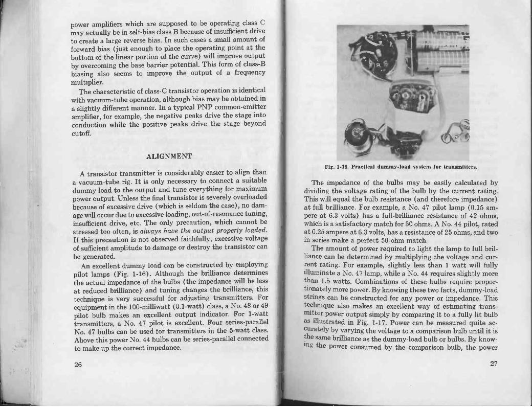
An excellent dummy load can be constructed by employingpilot lamps (Fig. 1-16). Although the brilliance determinesthe actual impedance of the bulbs (the impedance will be less
at reduced brilliance) and tuning changes the brilliance, thistechnique is very successful for adjusting transmitters. Forequipment in the 100-milliwatt (0.1 -watt) class, a No. 48 or 49pilot bulb makes an excellent output indicator. For 1 -watttransmitters, a No. 47 pilot is excellent. Four series -parallelNo. 47 bulbs can be used for transmitters in the 5 -watt class.Above this power No. 44 bulbs can be series -parallel connectedto make up the correct impedance.
26
Fig. 1-16. Practical dummy -load system for transmitters.
The impedance of the bulbs may be easily calculated bydividing the voltage rating of the bulb by the current rating.This will equal the bulb resistance (and therefore impedance)at full brilliance. For example, a No. 47 pilot lamp (0.15 am-pere at 6.3 volts) has a full -brilliance resistance of 42 ohms,which is a satisfactory match for 50 ohms. A No. 44 pilot, ratedat 0.25 ampere at 6.3 volts, has a resistance of 25 ohms, and twoin series make a perfect 50 -ohm match.
The amount of power required to light the lamp to full bril-liance can be determined by multiplying the voltage and cur-rent rating. For example, slightly less than 1 watt will fullyilluminate a No. 47 lamp, while a No. 44 requires slightly morethan 1.5 watts. Combinations of these bulbs require propor-tionately more power. By knowing these two facts, dummy -loadstrings can be constructed for any power or impedance. Thistechnique also makes an excellent way of estimating trans-mitter power output simply by comparing it to a fully lit bulbas illustrated in Fig. 1-17. Power can be measured quite ac-curately by varying the voltage to a comparison bulb until it isthe same brilliance as the dummy -load bulb or bulbs. By know-ing the power consumed by the comparison bulb, the power
27
PILOT LIGHTS
TO TRANSMITTER
OUTPUT
MILLIAMPERES
Fig. 1-17. System for estimating power output.
VOLTAGE
SOURCE
required to light the dummy -load bulb to the same brilliancecan be accurately calculated.
It should be pointed out that the comparison -method be-comes increasingly inaccurate as the transmitting frequencyis raised. This is due to the inductance of the spiral-woundlamp filaments. The error introduced by this inductance isnot particularly severe below 30 mc, however. There is oneother pitfall which almost always traps transistor transmitterexperimenters when measuring power output. One commonmethod of determining the power output of a transmitter isto measure the voltage developed across a known value of loadresistance. The voltage is then squared and divided by thevalue of load resistance and the resultant is the power in watts.However, few RF voltmeter probes are accurate, and smallerrors in voltage produce large errors in power. Even moreimportant, the probes are calibrated to read rms volts. As isoften the case, transmitter output may not be a pure sine waveand the voltmeter may indicate something other than the truerms value. The voltage error increases as the transmitteroutput continues to depart from a true sine wave. For thisreason it is strongly recommended that pilot lamps or otherheating devices be used as power -output indicators.
Diode voltmeters frequently create other problems. It isoften noted, when observing the output of a transistor trans-mitter on an SWR bridge or field -strength indicator, thatmodulating the transmitter makes the meter kick downwardrather than showing the increased reading customarily asso-ciated with upward modulation. However, this is an effectcommon to germanium diode detectors and can generally beignored. The most accurate test of upward modulation, otherthan an oscilloscope, is to observe the dummy -load pilot lamps.They should increase in brilliance a little more than 20% for
true 100% upward modulation.
28
2
Oscillators
Oscillator circuits employing vacuum tubes generally areconfined to two or three well-known types. The transistor,however, can be used in several configurations, as well as varia-tions of these configurations. A myriad of circuits result whenthese configurations are multiplied by the various types ofoscillators.
Figs. 2-1 and 2-2 illustrate a few of these circuits. None ofthese oscillators are crystal controlled; the addition of a
Fig. 2-1. Variations of tickler -coil oscillators.
29
(A) Basic Hartley circuits.
(B) Basic Colpitts circuits.
Fig. 2-2. Hartley- and Colpitts-type oscillators.
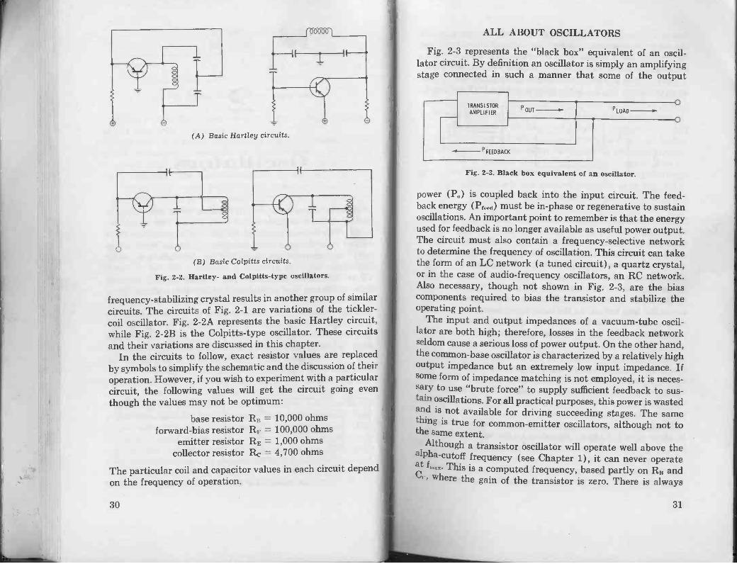
frequency -stabilizing crystal results in another group of similarcircuits. The circuits of Fig. 2-1 are variations of the tickler -
coil oscillator. Fig. 2-2A represents the basic Hartley circuit,while Fig. 2-2B is the Colpitts-type oscillator. These circuitsand their variations are discussed in this chapter.
In the circuits to follow, exact resistor values are replacedby symbols to simplify the schematic and the discussion of theiroperation. However, if you wish to experiment with a particularcircuit, the following values will get the circuit going eventhough the values may not be optimum:
base resistor RH = 10,000 ohmsforward -bias resistor RE = 100,000 ohms
emitter resistor RE = 1,000 ohmscollector resistor Rc = 4,700 ohms
The particular coil and capacitor values in each circuit dependon the frequency of operation.
30
ALL ABOUT OSCILLATORS
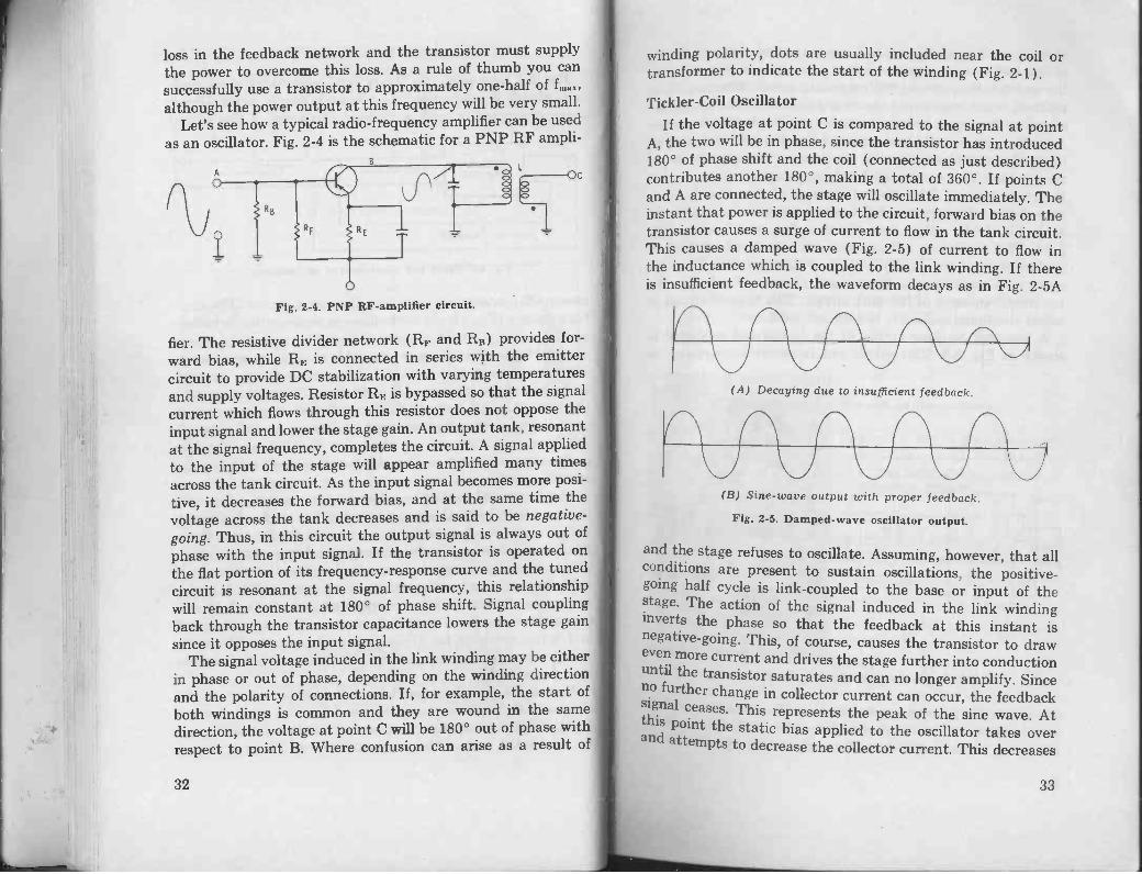
Fig. 2-3 represents the "black box" equivalent of an oscil-lator circuit. By definition an oscillator is simply an amplifyingstage connected in such a manner that some of the output
TRANSISTOR
AMPLIFIER
FEEDBACK
OUT LOAD
Fig. 2-3. Black box equivalent of an oscillator.
power (PO is coupled back into the input circuit. The feed-back energy (13f,,,i) must be in -phase or regenerative to sustainoscillations. An important point to remember is that the energyused for feedback is no longer available as useful power output.The circuit must also contain a frequency -selective networkto determine the frequency of oscillation. This circuit can takethe form of an LC network (a tuned circuit) , a quartz crystal,or in the case of audio -frequency oscillators, an RC network.Also necessary, though not shown in Fig. 2-3, are the biascomponents required to bias the transistor and stabilize theoperating point.
The input and output impedances of a vacuum -tube oscil-lator are both high; therefore, losses in the feedback networkseldom cause a serious loss of power output. On the other hand,the common -base oscillator is characterized by a relatively highoutput impedance but an extremely low input impedance. Ifsome form of impedance matching is not employed, it is neces-sary to use "brute force" to supply sufficient feedback to sus-tain oscillations. For all practical purposes, this power is wastedand is not available for driving succeeding stages. The samething is true for common -emitter oscillators, although not tothe same extent.
Although a transistor oscillator will operate well above thealpha -cutoff frequency (see Chapter 1) , it can never operateat fn... This is a computed frequency, based partly on RR andCf ', where the gain of the transistor is zero. There is always
31
loss in the feedback network and the transistor must supplythe power to overcome this loss. As a rule of thumb you cansuccessfully use a transistor to approximately one-half of f-max,
although the power output at this frequency will be very small.Let's see how a typical radio -frequency amplifier can be used
as an oscillator. Fig. 2-4 is the schematic for a PNP RF ampli-
Fig. 2-4. PNP RF-amplifler circuit.
fier. The resistive divider network (RF and RB) provides for-
ward bias, while RE is connected in series with the emittercircuit to provide DC stabilization with varying temperaturesand supply voltages. Resistor RE is bypassed so that the signalcurrent which flows through this resistor does not oppose theinput signal and lower the stage gain. An output tank, resonantat the signal frequency, completes the circuit. A signal appliedto the input of the stage will appear amplified many timesacross the tank circuit. As the input signal becomes more posi-tive, it decreases the forward bias, and at the same time thevoltage across the tank decreases and is said to be negative -going. Thus, in this circuit the output signal is always out ofphase with the input signal. If the transistor is operated onthe flat portion of its frequency -response curve and the tunedcircuit is resonant at the signal frequency, this relationshipwill remain constant at 180° of phase shift. Signal couplingback through the transistor capacitance lowers the stage gainsince it opposes the input signal.
The signal voltage induced in the link winding may be eitherin phase or out of phase, depending on the winding directionand the polarity of connections. If, for example, the start ofboth windings is common and they are wound in the samedirection, the voltage at point C will be 180° out of phase withrespect to point B. Where confusion can arise as a result of
32
winding polarity, dots are usually included near the coil ortransformer to indicate the start of the winding ( Fig. 2-1).
Tickler -Coil Oscillator
If the voltage at point C is compared to the signal at pointA, the two will be in phase, since the transistor has introduced180° of phase shift and the coil (connected as just described)contributes another 180', making a total of 360°. If points Cand A are connected, the stage will oscillate immediately. Theinstant that power is applied to the circuit, forward bias on thetransistor causes a surge of current to flow in the tank circuit.This causes a damped wave ( Fig. 2-5) of current to flow inthe inductance which is coupled to the link winding. If thereis insufficient feedback, the waveform decays as in Fig. 2-5A
(A) Decaying due to insufficient feedback.
(B) Sine -wave output with proper feedback.
Fig. 2-5. Damped -wave oscillator output.
and the stage refuses to oscillate. Assuming, however, that allconditions are present to sustain oscillations, the positive -going half cycle is link -coupled to the base or input of thestage. The action of the signal induced in the link windinginverts the phase so that the feedback at this instant isnegative -going. This, of course, causes the transistor to draweven more current and drives the stage further into conductionuntil the transistor saturates and can no longer amplify. Sinceno further change in collector current can occur, the feedbacksignal ceases. This represents the peak of the sine wave. Atthis point the static bias applied to the oscillator takes overand attempts to decrease the collector current. This decreases
33
the current through the coil and causes the direction or polarityof the feedback to reverse so that is is now positive -going atthe emitter, thus driving the stage into cutoff. When cutoff isreached, which represents the negative peak in the cycle, thestage can once again no longer amplify and the feedback ceases.As before, the forward bias tries to bring the collector currentup to the static -bias point by overcoming the signal -induced
reverse bias. This causes the feedback polarity to reverse andthe cycle repeats. This second cycle reinforces the dampedwave so that the output signal consists of a series of sine waves
as in Fig. 2-5B, rather than the decaying waveform in Fig.2-5A. This oscillation will continue until the feedback path isbroken or until the supply voltage is disconnected. The fre-
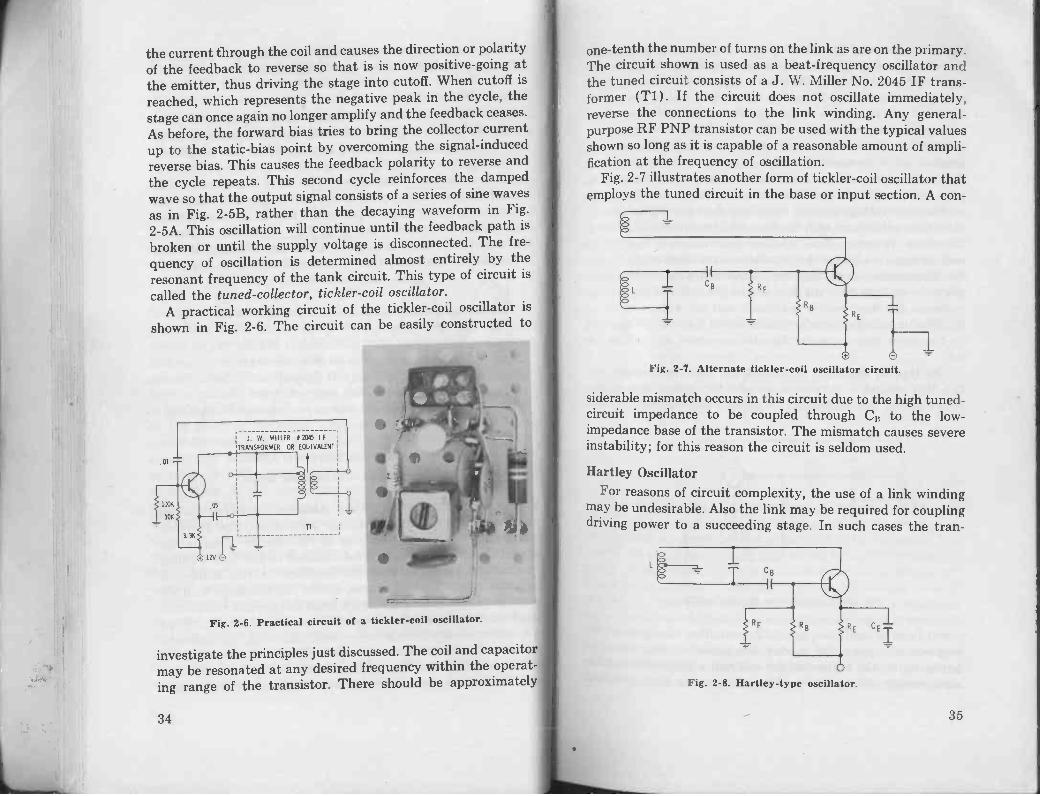
quency of oscillation is determined almost entirely by theresonant frequency of the tank circuit. This type of circuit iscalled the tuned -collector, tickler -coil oscillator.
A practical working circuit of the tickler-coil oscillator isshown in Fig. 2-6. The circuit can be easily constructed to
.01
100K
10K
J. W. MILLER 1 2045 I F
TRANSFORMER OR EQUIVALENT
Ti
120
Fig. 2-6. Practical circuit of a tickler -coil oscillator.
investigate the principles just discussed. The coil and capacitor
may be resonated at any desired frequency within the operat-ing range of the transistor. There should be approximately
34
one -tenth the number of turns on the link as are on the primary.The circuit shown is used as a beat -frequency oscillator andthe tuned circuit consists of a J. W. Miller No. 2045 IF trans-former (T1). If the circuit does not oscillate immediately,reverse the connections to the link winding. Any general-purpose RF PNP transistor can be used with the typical valuesshown so long as it is capable of a reasonable amount of ampli-fication at the frequency of oscillation.
Fig. 2-7 illustrates another form of tickler -coil oscillator thatemploys the tuned circuit in the base or input section. A con -
Fig. 2-7. Alternate tickler -coil oscillator circuit.
siderable mismatch occurs in this circuit due to the high tuned -
circuit impedance to be coupled through C11 to the low -impedance base of the transistor. The mismatch causes severeinstability; for this reason the circuit is seldom used.
Hartley OscillatorFor reasons of circuit complexity, the use of a link winding
may be undesirable. Also the link may be required for couplingdriving power to a succeeding stage. In such cases the tran-
Fig. 2-8. Hartley -type oscillator.
35
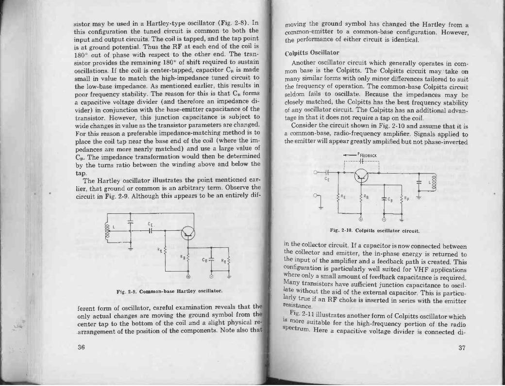
sistor may be used in a Hartley -type oscillator (Fig. 2-8). Inthis configuration the tuned circuit is common to both theinput and output circuits. The coil is tapped, and the tap pointis at ground potential. Thus the RF at each end of the coil is180° out of phase with respect to the other end. The tran-sistor provides the remaining 180° of shift required to sustainoscillations. If the coil is center -tapped, capacitor CB is madesmall in value to match the high -impedance tuned circuit tothe low -base impedance. As mentioned earlier, this results inpoor frequency stability. The reason for this is that Cil formsa capacitive voltage divider (and therefore an impedance di-vider) in conjunction with the base -emitter capacitance of thetransistor. However, this junction capacitance is subject towide changes in value as the transistor parameters are changed.For this reason a preferable impedance -matching method is toplace the coil tap near the base end of the coil (where the im-pedances are more nearly matched) and use a large value ofCB. The impedance transformation would then be determinedby the turns ratio between the winding above and below the
tap.The Hartley oscillator illustrates the point mentioned ear-
lier, that ground or common is an arbitrary term. Observe thecircuit in Fig. 2-9. Although this appears to be an entirely dif-
Fig. 2-9. Common -base Hartley oscillator.
ferent form of oscillator, careful examination reveals that thonly actual changes are moving the ground symbol from thcenter tap to the bottom of the coil and a slight physical rearrangement of the position of the components. Note also tha
36
moving the ground symbol has changed the Hartley from acommon -emitter to a common -base configuration. However,the performance of either circuit is identical.
Colpitts OscillatorAnother oscillator circuit which generally operates in com-
mon base is the Colpitts. The Colpitts circuit may take onmany similar forms with only minor differences tailored to suitthe frequency of operation. The common -base Colpitts circuitseldom fails to oscillate. Because the impedances may beclosely matched, the Colpitts has the best frequency stabilityof any oscillator circuit. The Colpitts has an additional advan-tage in that it does not require a tap on the coil.
Consider the circuit shown in Fig. 2-10 and assume that it isa common -base, radio -frequency amplifier. Signals applied tothe emitter will appear greatly amplified but not phase -inverted
P FEEDBACK
E
Fig. 2-10. Colpitts oscillator circuit.
in the collector circuit. If a capacitor is now connected betweenthe collector and emitter, the in -phase energy is returned tothe input of the amplifier and a feedback path is created. Thisconfiguration is particularly well suited for VHF applicationswhere only a small amount of feedback capacitance is required.Many transistors have sufficient junction capacitance to oscil-late without the aid of the external capacitor. This is particu-larly true if an RF choke is inserted in series with the emitterresistance.
Fig. 2-11 illustrates another form of Colpitts oscillator whichis more suitable for the high -frequency portion of the radiospectrum. Here a capacitive voltage divider is connected di -
37
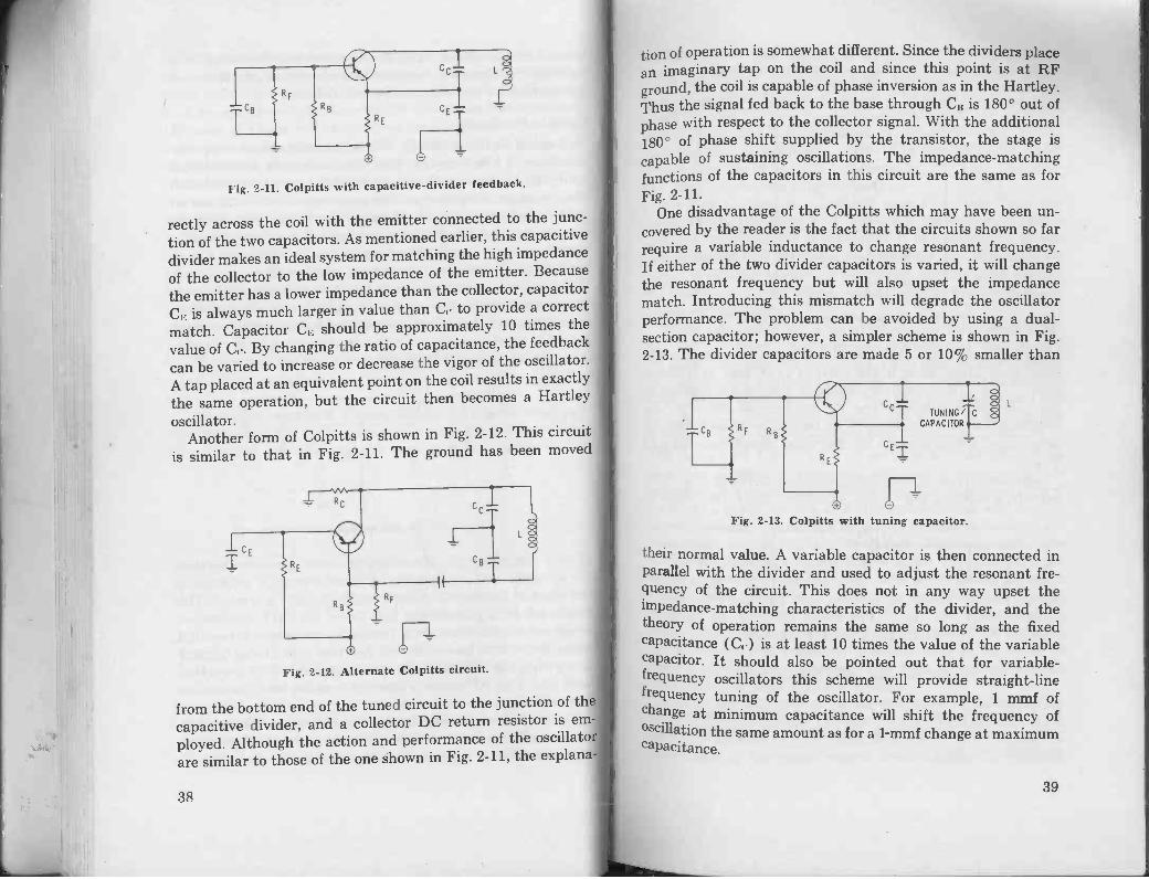
Fig. 2-11. Colpitts with capacitive-divider feedback.
rectly across the coil with the emitter connected to the junc-tion of the two capacitors. As mentioned earlier, this capacitivedivider makes an ideal system for matching the high impedanceof the collector to the low impedance of the emitter. Becausethe emitter has a lower impedance than the collector, capacitorCE is always much larger in value than C, to provide a correctmatch. Capacitor CE should be approximately 10 times the
value of Cc. By changing the ratio of capacitance, the feedbackcan be varied to increase or decrease the vigor of the oscillator.
A tap placed at an equivalent point on the coil results in exactlythe same operation, but the circuit then becomes a Hartleyoscillator.
Another form of Colpitts is shown in Fig. 2-12. This circuitis similar to that in Fig. 2-11. The ground has been moved
Fig. 2-12. Alternate Colpitts circuit.
from the bottom end of the tuned circuit to the junction of thecapacitive divider, and a collector DC return resistor is em-ployed. Although the action and performance of the oscillatoare similar to those of the one shown in Fig. 2-11, the explana
38
tion of operation is somewhat different. Since the dividers placean imaginary tap on the coil and since this point is at RFground, the coil is capable of phase inversion as in the Hartley.Thus the signal fed back to the base through Clt is 180° out of
phase with respect to the collector signal. With the additional180' of phase shift supplied by the transistor, the stage iscapable of sustaining oscillations. The impedance -matchingfunctions of the capacitors in this circuit are the same as forFig. 2-11.
One disadvantage of the Colpitts which may have been un-covered by the reader is the fact that the circuits shown so farrequire a variable inductance to change resonant frequency.If either of the two divider capacitors is varied, it will changethe resonant frequency but will also upset the impedancematch. Introducing this mismatch will degrade the oscillatorperformance. The problem can be avoided by using a dual -section capacitor; however, a simpler scheme is shown in Fig.2-13. The divider capacitors are made 5 or 10% smaller than
TUNING/CAPACITOR
Fig. 2-13. Colpitts with tuning capacitor.
their normal value. A variable capacitor is then connected inparallel with the divider and used to adjust the resonant fre-quency of the circuit. This does not in any way upset theimpedance -matching characteristics of the divider, and thetheory of operation remains the same so long as the fixedcapacitance (Cc) is at least 10 times the value of the variablecapacitor. It should also be pointed out that for variable -frequency oscillators this scheme will provide straight-linefrequency tuning of the oscillator. For example, 1 mmf ofchange at minimum capacitance will shift the frequency ofoscillation the same amount as for a 1-mmf change at maximumcapacitance.
39
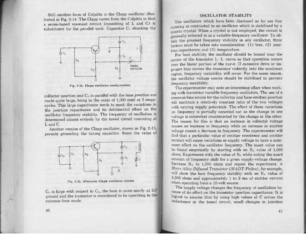
Still another form of Colpitts is the Clapp oscillator illus-trated in Fig. 2-14. The Clapp varies from the Colpitts in thata series -tuned resonant circuit (consisting of L and C) issubstituted for the parallel tank. Capacitor C, shunting the
TUNINGCAPACITOR
Fig. 2-14. Clapp oscillator configuration.
collector junction and CI, in parallel with the base junction aremade quite large, being in the order of 1,000 mmf at 5 mega-cycles. This large capacitance tends to mask the variations inthe junction capacitance and its detrimental effect on theoscillator frequency stability. The frequency of oscillation isdetermined almost entirely by the tuned circuit consisting ofL and C.
Another version of the Clapp oscillator, shown in Fig. 2-15,permits grounding the tuning capacitor. Since the value of
Fig. 2-15. Alternate Clapp oscillator circuit.
CB is large with respect to CE, the base is more nearly at Rground and the transistor is considered to be operating in thcommon -base mode.
40
OSCILLATOR STABILITYThe oscillators which have been discussed so far are free
running as contrasted to an oscillator which is stabilized by a
quartz crystal. When a crystal is not employed, the circuit isgenerally referred to as a variable -frequency oscillator. To ob-tain the greatest frequency stability in any oscillator, threefactors must be taken into consideration: (1) bias, (2) junc-tion capacitance, and (3) temperature.
For best stability the oscillator should be biased near thecenter of the transistor Lt L curve so that operation occursover the linear portion of the curve. If excessive drive or im-proper bias carries the transistor violently into the nonlinearregion, frequency instability will occur. For the same reason,the oscillator voltage source should be stabilized to preventfrequency instability.
The experimenter may note an interesting effect when work-ing with transistor variable -frequency oscillators. The use of acommon bias source for the collector and base -emitter junctionwill maintain a relatively constant ratio of the two voltageswith varying supply potentials. The effect of these variationson frequency is partially canceled out as the change in onevoltage is somewhat counteracted by the change in the other.The reason for this is that an increase in collector voltagecauses an increase in frequency while an increase in emittervoltage causes a decrease in frequency. The experimenter willfind that a particular value of emitter resistance and emittercurrent will cause variations in supply voltage to have a mini-mum effect on the oscillator frequency. The exact value canbe found empirically by starting with an RE value of 1,000ohms. Experiment with the value of RI: while noting the exactamount of frequency shift for a given supply -voltage change.Increase RE to 1,500 ohms and repeat the experiment. AMicro Alloy Diffused Transistor (MADT-Philco), for example,will show the best frequency stability with an RE value of3,300 ohms and approximately 1 to 2 ma of emitter currentwhen operating from a 12 -volt source.
The supply voltage changes the frequency of oscillation be-cause of its effect on the transistor junction capacitance. It islogical to assume that by using high values of C across theinductance in the tuned circuit, small changes in junction
41
capacitance will have less effect on the frequency of oscillation.Obviously a change of 1 mmf out of 1,000 mmf will have lesseffect on the frequency of the tuned circuit than will 1 mmfchange out of 100 mmf. For this reason always use as muchcapacitance as possible in parallel with the tank coil, particu-larly in the Hartley circuit. Excessive capacitance will lowerthe tank impedance to the point where oscillations may cease.The exact amount of capacitance in the tank is a matter forexperimentation. To get in the "ballpark," a good approxima-tion is to divide the frequency of oscillation into the constantnumber 5,000. Thus at 5 mc, one uses 1,000 mmf of capacitancein the tank. The inductance value then must be juggled tomake the circuit oscillate at 5 mc. If it does not oscillate withthis much capacitance, the value can be reduced and theinductance increased. Conversely, if the circuit still oscillatesstrongly, try additional capacitance for even more stability.It might be pointed out that such high -C circuits tend to makethe inductance more critical. This is quite true, but the overallstability with high -C circuits is better due to the masking ofjunction -capacitance variations caused by parameter changes.
For the same reasons, make the capacitive -divider values aslarge .as possible (while maintaining a 10 -to -1 ratio) in theColpitts end Clapp circuits.
Temperature change causes some unique problems in tran-sistor oscillator circuits. Changes in temperature have the sameeffect on components as in tube -type, variable -frequency oscil-lators. In tube equipment, however, the temperature of compo-nents is usually elevated above ambient because of the heatgenerated by the tubes. Thus, changes in ambient temperaturehave less effect on the tube oscillator. In transistor equipmentthe components usually operate at ambient temperature, andchanges in ambient have an adverse effect on the frequency ofoscillation. For this reason temperature compensation of tunedcircuits may be required. For best stability always use goodquality components, such as silver mica or dipped mylar ca-pacitors and temperature -stable coil forms. Employ transistorswhich have a low value of Ce, such as mesa and MADT types.Silicon transistors are less affected by temperature than ger-manium and therefore are recommended for variable-frequencoscillator applications.
42
Crystal -Controlled Oscillators
In this type of frequency -stabilized oscillator a quartz crys-tal either replaces the tuned circuit or takes over its frequency -determining function. Quartz crystals are used because of theirextremely high Q and excellent frequency stability over a giventemperature range.
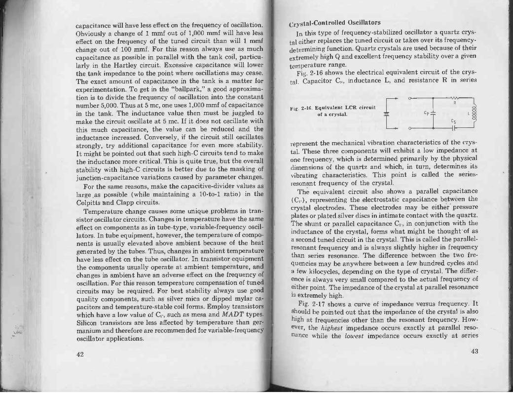
Fig. 2-16 shows the electrical equivalent circuit of the crys-tal. Capacitor Cs, inductance L, and resistance R in series
F.-
Fig. 2-16. Equivalent LCR circuitof a crystal.
represent the mechanical vibration characteristics of the crys-tal. These three components will exhibit a low impedance atone frequency, which is determined primarily by the physicaldimensions of the quartz and which, in turn, determines itsvibrating characteristics. This point is called the series -resonant frequency of the crystal.
The equivalent circuit also shows a parallel capacitance(Cr) , representing the electrostatic capacitance between thecrystal electrodes. These electrodes may be either pressureplates or plated silver discs in intimate contact with the quartz.The shunt or parallel capacitance CI., in conjunction with theinductance of the crystal, forms what might be thought of asa second tuned circuit in the crystal. This is called the parallel -resonant frequency and is always slightly higher in frequencythan series resonance. The difference between the two fre-quencies may be anywhere between a few hundred cycles anda few kilocycles, depending on the type of crystal. The differ-ence is always very small compared to the actual frequency ofeither point. The impedance of the crystal at parallel resonanceis extremely high.
Fig. 2-17 shows a curve of impedance versus frequency. Itshould be pointed out that the impedance of the crystal is alsohigh at frequencies other than the resonant frequency. How-ever, the highest impedance occurs exactly at parallel reso-nance while the lowest impedance occurs exactly at series
43
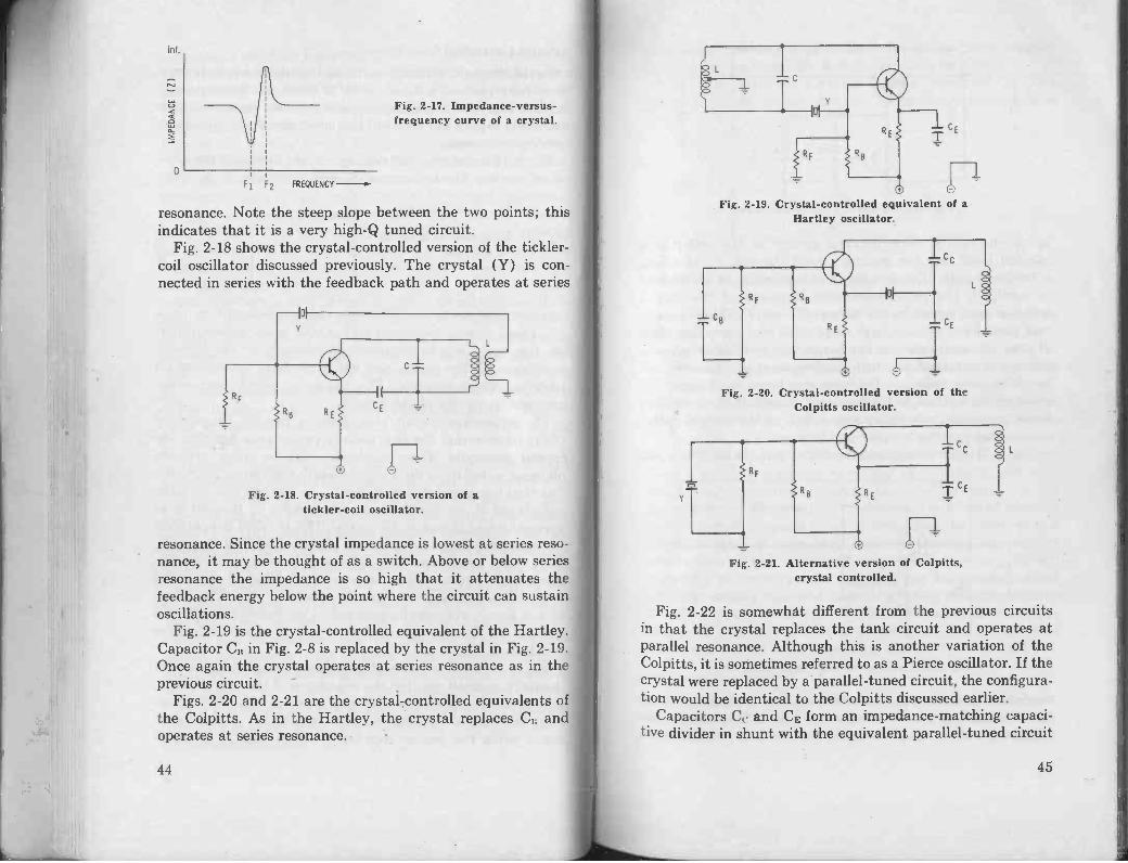
inf.
0
F1 F2 FREQUENCY
Fig. 2-17. Impedance -versus -frequency curve of a crystal.
resonance. Note the steep slope between the two points; thisindicates that it is a very high -Q tuned circuit.
Fig. 2-18 shows the crystal -controlled version of the tickler -coil oscillator discussed previously. The crystal (Y) is con-nected in series with the feedback path and operates at series
Fig. 2-18. Crystal -controlled version of atickler -coil oscillator.
resonance. Since the crystal impedance is lowest at series reso-nance, it may be thought of as a switch. Above or below seriesresonance the impedance is so high that it attenuates thefeedback energy below the point where the circuit can sustainoscillations.
Fig. 2-19 is the crystal -controlled equivalent of the Hartley.Capacitor Ci, in Fig. 2-8 is replaced by the crystal in Fig. 2-19.Once again the crystal operates at series resonance as in theprevious circuit.
Figs. 2-20 and 2-21 are the crystal -controlled equivalents ofthe Colpitts. As in the Hartley, the crystal replaces CI, andoperates at series resonance.
44
CE
Fig. 2-19. Crystal -controlled equivalent of aHartley oscillator.
Fig. 2-20. Crystal -controlled version of theColpitts oscillator.
Fig. 2-21. Alternative version of Colpitts,crystal controlled.
Fig. 2-22 is somewhat different from the previous circuitsin that the crystal replaces the tank circuit and operates atparallel resonance. Although this is another variation of theColpitts, it is sometimes referred to as a Pierce oscillator. If thecrystal were replaced by a parallel -tuned circuit, the configura-tion would be identical to the Colpitts discussed earlier.
Capacitors C(' and CE form an impedance -matching capaci-tive divider in shunt with the equivalent parallel -tuned circuit
45

CEI
IIcc
LB
RC
Fig. 2-22. Circuit of a Pierce oscillator.
inside the crystal. The in -phase energy at the collector iscoupled back into the emitter circuit through C, to createa feedback path. The frequency of oscillation is determinedprimarily by the parallel -resonant frequency of the crystaland to a lesser extent by the values of C,, and Cn. These capaci-tors should be made as large as possible to swamp the effectof junction capacitance on the frequency of oscillation. As thevalues are increased, however, the frequency of oscillation willbe pulled away from parallel resonance lower in frequency. Apoint will be reached, as the frequency of oscillation approachesseries resonance, where the phase shift in the crystal induc-tance is too great to support oscillations.
Fig. 2-23 is the common -emitter version of the oscillator just
Fig. 2-23. Common -emitter Pierce oscillator.
described. In this circuit the crystal assumes a phase -invertingfunction the same as for a parallel -resonant L 'C circuit. Radio -frequency energy coupled to the base is 180` out of phase
46
with respect to the collector signal. When the phase is againinverted by the transistor action, the stage oscillates.
Fig. 2-24 illustrates a rather unusual oscillator. At firstglance it appears to lack most of the necessary requirements
Fig. 2-24. Unusual transistor oscillator circuit.
for an oscillator circuit (tuned circuit, impedance -matchingcapacitors, etc.). If you ignore the ground connections for amoment, the theory of operation becomes somewhat easier tounderstand. The crystal operates at series resonance. CapacitorCE is relatively small and somewhat critical in value (500 mmfat 5 mc). The base -emitter capacitance of the transistor, inconjunction with CE, forms an impedance divider. Neglectingthe grounds, CE is in series with the crystal, and feedback oc-curs between emitter and base through the crystal. Althoughthere is no phase inversion or voltage amplification, the tran-sistor does have current gain. A transistor which has an f, of 100mc or more will oscillate quite vigorously. The effect of junctioncapacitance on frequency can be minimized by connecting acapacitor equal in value to CE between the base and emitterconnections of the transistor. Output RF may be obtainedacross CE. A low -impedance output, quite independent of theoscillator section, may be obtained by lifting the collector fromground and connecting a 50- to 500 -ohm resistor in series withthis point. The output voltage will vary between a fraction ofa volt and several volts, depending on the value selected.
Overtone OscillatorsCrystals have another characteristic which has not been
mentioned. If the output tank circuit of Fig. 2-20 and 2-21,for example, is tuned to a harmonic of the crystal frequency,
47

the circuit will oscillate at this frequency. If a 10-mc crystalwere used in either circuit and the output tank tuned to 30mc, the crystal would oscillate at the third harmonic. The crys-tal is excited to vibrate three times as fast. Most crystals arecapable of establishing vibration modes at 3, 5, and 7 timestheir natural resonant frequency. These higher -order modes arecalled overtones. Because of the difficulty of fabricating crystalsfor frequencies above 15 mc, oscillators above this frequencyusually employ overtone crystals. It should be mentioned thatcrystals operating on an overtone always oscillate at seriesresonance. Thus a fundamental crystal will have an outputslightly less than the actual marked frequency multiplied bythe order of overtone: --
48
3Building Oscillators
Now that the theory of transistor transmitters has beencovered, let's take a look at the practical aspects and constructseveral circuits which illustrate these principles. Since the be-ginning of any transmitter is the oscillator, let's start there.
Several of the circuits which follow, such as the oscillatorsin this chapter, are built on electronic pegboard, manufacturedby Vector and by Lafayette Radio. This method of construc-tion allows simplified step-by-step assembly and results in themost reproduceable performance short of using an etched cir-cuit board. Several of the projects in the following pages in-clude circuit -board layouts, in case the experimenter prefersto use this method of construction.
A BCDE FGH111
2
3
4
Fig. 3-1. Layout guide for 5
construction projects. 6
7
8
9
10
O 0 0 0 0 0 0 0 0 0
O 0 0 0 0 0 0 0 0 0
O 0 0 0 0 0 0 0 0 0
O 0 0 0 0 0 0 0 0 0
O 0 0 0 0 0 0 0 0 0
O 0 0 0 0 0 0 0 0 0
O 0 0 0 0 0 0 0 0 0
O 0 0 0 0 0 0 0 0 0
O 0 0 0 0 0 0 0 0 0
O 0 0 0 0 0 0 0 0 0
49
The use of a pegboard chassis also provides an "electronicroadmap" which is standardized at 10 holes square. Exact posi-tions on the "map" can be located by key letters and numbers,as shown in Fig. 3-1. For example, A-1, J-1, A-10, and J-10are the four corner holes.
CHART 3-1. Recommended Transistor Types
Manufacturer Type Numbers
Amperex OC-170, 2N2672
Motorola 2N741
Philco 2N1727, 2N1745
RCA 2N370, 2N371, 2N3722N384
Texas Instruments 2N711
The circuits are designed so that the type of transistor usedis not critical. Chart 3-1 shows several popular transistors thatare used in many of the projects. Each circuit was optimizedwith the low-cost, high -gain Amperex 2N2672, then it wastested with the other types to verify operation.
BUILD A CRYSTAL CHECKER
Fig. 3-2 is the diagram of a crystal tester which not only canmeasure crystal activity but also can be used to check the fre-
quency of oscillation. Any reasonably active crystal with a
OUTPUT
C5 R4 2.a:--- 270
C3 mmf1K .05
X MFD
12VDC°
Fig. 3-2. Schematic of the crystal checker.
50
fundamental frequency between 100 kc and 15 mc will oscillatein the crystal checker. This includes those hard -to -get -goingsurplus crystals between 370 and 500 kilocycles used in WorldWar II tank transmitters. The crystal checker can also be usedas a 100-kc frequency standard for setting dial calibrations oncommunications receivers. It is only necessary to insert a suit-able 100-kc crystal and replace Cl (47-mmf mica) with a 7- to45-mmf rotary trimmer capacitor. This trimmer is used tozero -beat the crystal with WWV at 5 or 10 mc.
How It WorksThe circuit is similar to the one described in Chapter 2, ex-
cept for the addition of Cl. This capacitor is added so that thecrystal "sees" the standard calibration capacitance of 32 mmf.Thus the crystal oscillates at parallel resonance and the fre-quency can be determined by measurement with an accuratefrequency meter or communications receiver.
ConstructionInsert pegs at A-1 and J-1 and connect together with a piece
of solid tinned wire ( Fig. 3-3). This line becomes the positivebus. Insert pegs at A-10 and J-10 ( Fig. 3-3) and connect to-
ABCDEFGH111
2
3
4
5
6
7
8
9
10
Fig. 3-3. Layout of the crystal checker.
gether as before. This is the negative bus. Install the pegs forthe transistor at E-5 ( base), F-6 (collector), and F-4 (emitter).The t resistor can be soldered to these pegs or a socket canbe use s shown in the accompanying photograph (Fig. 3-4).
51

Fig. 3-4. Photo showing crystal socket.
The two remaining pegs are installed at D-5 and D-7 for thecrystal socket. If the unit is mounted in a metal box, thesepoints can be connected to a crystal socket on the front panel.A socket suitable for hermetically sealed crystals (HC -6 andCR-18/U style) can be connected in parallel with the large -pinsocket for testing both types of crystals.
Testing
The circuit is energized by connecting a source of voltage(6 to 12 volts) in series with an SPST toggle switch and a 0 to5 -ma meter to terminals A-1 or J-1 (positive) and A-10 or J-10(negative). With 12 volts applied, the meter will read approxi-mately 2 ma with no crystal in the circuit. When the crystalis inserted, the current will increase. The activity of the crystalis roughly proportional to the increase in the meter reading.The meter is not required, of course, if the circuit is used as asignal generator or frequency standard.
If the oscillator is installed in a communications receiver,there is no need to use a battery power supply. A source of 6
52
to 12 volts, positive DC, is available at the cathode of theaudio -output tube. The negative line should be connected tochassis ground. A lead from the collector of X1 should bewrapped around the receiver antenna terminal and coupledfor proper signal level.
BUILD AN 80/40 -METER PEANUT WHISTLE
It's truly amazing how far a fraction of a watt can be trans-mitted when it is radiated by an efficient antenna. The "pea-nut whistle" shown in Figs. 3-5 and 3-6 has been used to con-tact stations more than 100 miles away on the 40 -meter band.Signal reports indicated that more distant contacts could havebeen made. The circuit can also be used for testing crystals ontheir fundamentals at frequencies between 2 and 15 mc.
How It Works
The peanut whistle is a practical use for the circuit shownin Fig. 2-24. However, in Fig. 3-5 a 330 -ohm resistor has been
Fig. 3-5. The 80-40 meter "Peanut Whistle."
connected in series with the collector of X1. The signal whentaken from this point is isolated from the oscillator section ofthe transistor.
Construction
Thetransistplaced i
anut whistle is built on a 21/2 " x 21/2 " board. Theis positioned the same as in Fig. 3-3, and pegs arethe four corner holes. The crystal is positioned at
53
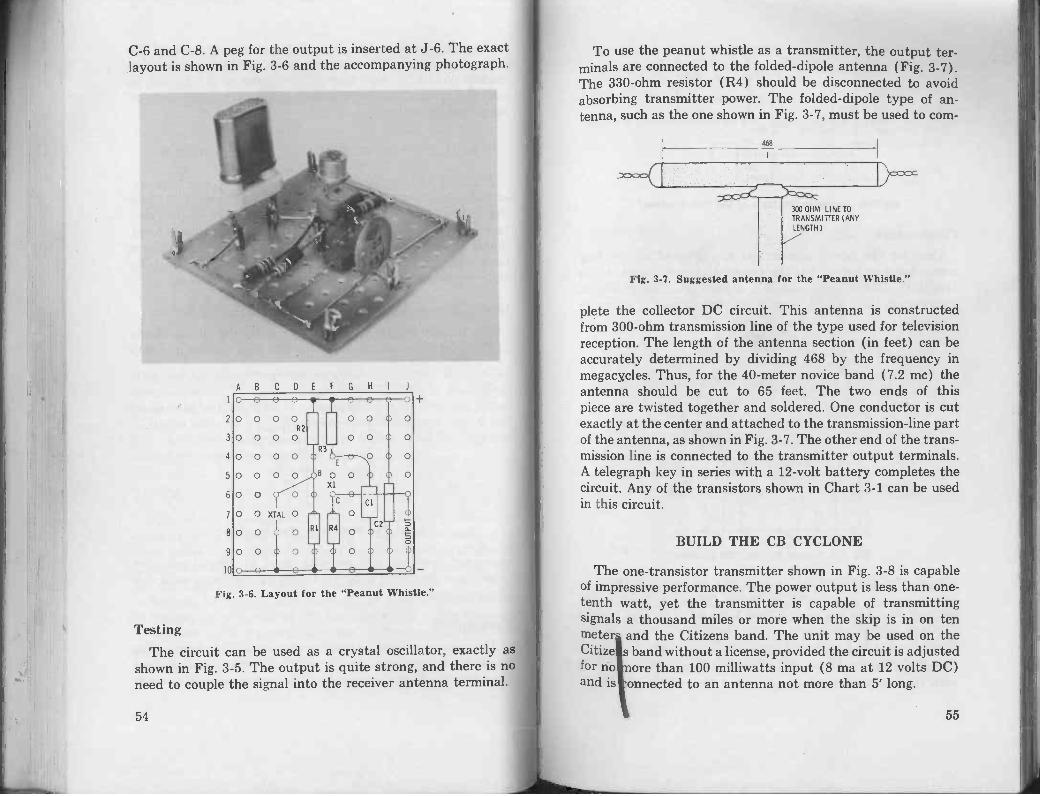
C-6 and C-8. A peg for the output is inserted at J-6. The exactlayout is shown in Fig. 3-6 and the accompanying photograph.
AB CDEF GHI11
2
3
4
5
6
8
9
10
Fig. 3-6. Layout for the "Peanut Whistle."
TestingThe circuit can be used as a crystal oscillator, exactly as
shown in Fig. 3-5. The output is quite strong, and there is noneed to couple the signal into the receiver antenna terminal.
54
To use the peanut whistle as a transmitter, the output ter-minals are connected to the folded -dipole antenna (Fig. 3-7).The 330 -ohm resistor (R4) should be disconnected to avoidabsorbing transmitter power. The folded -dipole type of an-tenna, such as the one shown in Fig. 3-7, must be used to com-
468
300 OHM LINE TOTRANSMITTER (ANY
LENGTH )
Fig. 3-7. Suggested antenna for the "Peanut Whistle."
plete the collector DC circuit. This antenna is constructedfrom 300 -ohm transmission line of the type used for televisionreception. The length of the antenna section (in feet) can beaccurately determined by dividing 468 by the frequency inmegacycles. Thus, for the 40 -meter novice band (7.2 mc) theantenna should be cut to 65 feet. The two ends of thispiece are twisted together and soldered. One conductor is cutexactly at the center and attached to the transmission -line partof the antenna, as shown in Fig. 3-7. The other end of the trans-mission line is connected to the transmitter output terminals.A telegraph key in series with a 12 -volt battery completes thecircuit. Any of the transistors shown in Chart 3-1 can be usedin this circuit.
BUILD THE CB CYCLONE
The one -transistor transmitter shown in Fig. 3-8 is capableof impressive performance. The power output is less than one -tenth watt, yet the transmitter is capable of transmittingsignals a thousand miles or more when the skip is in on tenmeter and the Citizens band. The unit may be used on theCitize s band without a license, provided the circuit is adjustedfor no ore than 100 milliwatts input (8 ma at 12 volts DC)and is onnected to an antenna not more than 5' long.
55

+ 12 VDC
Fig. 3-8. Schematic diagram of the "CB Cyclone."
ConstructionPegs for the power connections are inserted at the four
corner holes as before, but the transistor is positioned at E-4(emitter), D-5 (base), and E-6 (collector). The crystal isinserted at C-6 and C-8. A guide to parts layout is shown inFig. 3-9.
ABCDE F G H I
1
2
3
4
5
6
7
8
9
10
1
Fig. 3-9. Layout for the "CB Cyclone."
To insure duplicating the performance of the unit, the coil -winding details shown in Fig. 3-10 should be followed closely.The exact type of slug -tuned coil form is not important so longas the outside diameter is approximately 5/16" in diameter. Aprinted -circuit type of coil form can be seen in Fig. 3-11. Thecircuit will work equally well on the Citizens band or 10 meterswith the component values given and the coil shown. When
56
inleo
ne
Fig. 3-10. Winding details for Ll.
GN
ANTENNA
h- 5/16"
Fig. 3-11. Finished "CB Cyclone."
10 TURNSNO. 28CLOSE WOUND
COLLECTOR
L1 WINDING
DETAILS
ordering a crystal for this unit, a third -overtone type for thefrequency of operation should be specified.
suitable antenna is shown in Fig. 3-12. The length dependshe frequency of operation and can be determined by divid-the frequency in megacycles into 468. The coaxial shieldis connected to J-10, and the center conductor is con -d to J-4.
57
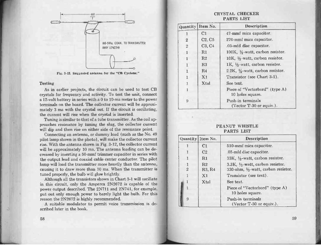
468
oMpMo
RG-59/u COAX. TO TRANSMITTER
(ANY LENGTH)
Fig. 3-12. Suggested antenna for the "CB Cyclone."
TestingAs in earlier projects, the circuit can be used to test CB
crystals for frequency and activity. To test the unit, connecta 12 -volt battery in series with a 0 to 10 -ma meter to the powerterminals on the board. The collector current will be approxi-mately 3 ma with the crystal out. If the circuit is oscillating,the current will rise when the crystal is inserted.
Tuning is similar to that of a tube transmitter. As the coil ap-proaches resonance by tuning the slug, the collector currentwill dip and then rise on either side of the resonance point.
Connecting an antenna, or dummy load (such as the No. 49pilot lamp shown in the photo), will make the collector currentrise. With the antenna shown in Fig. 3-12, the collector currentwill be approximately 10 ma. The antenna loading can be de-creased by inserting a 50-mmf trimmer capacitor in series withthe output lead and coaxial cable center conductor. The pilotlamp will load the transmitter more heavily than the antenna,causing it to draw more than 10 ma. When the transmitter istuned properly, the bulb will glow brightly.
Although all the transistors shown in Chart 3-1 will oscillatein this circuit, only the Amperex 2N2672 is capable of thepower output described. The 2N711 and 2N741, for example,put out only enough power to barely light the bulb. For thisreason the 2N2672 is highly recommended.
A suitable modulator to permit voice transmission is de-scribed later in the book.
58
CRYSTAL CHECKERPARTS LIST
Quantity Item No. Description
1 Cl 47-mmf mica capacitor.
2 C2, C5 270-mmf mica capacitor.
2 C3, C4 .05-mfd disc capacitor.
1 R1 100K, 1/2 -watt, carbon resistor.1 R2 10K, 1/2 -watt, carbon resistor.1 R3 1K, 1/2 -watt, carbon resistor.1 R4 2.2K, 1/2 -watt, carbon resistor.1 X1 Transistor (see Chart 3-1).1 Xtal See text.
I Piece of "Vectorbord" (type A)10 holes square.
9 Push -in terminals(Vector T-30 or equiv.).
PEANUT WHISTLEPARTS LIST
Quantity Item No. Description
1 Cl 510-mmf mica capacitor.
1 C2 .05-mfd disc capacitor.1 R1 33K, 1/2 -watt, carbon resistor.1 R2 3.3K, 1/2 -watt, carbon resistor.2 R3, R4 330 -ohm, 1/2 -watt, carbon resistor.l X1 Transistor (see text).
See text."Vectorbord"
Xtal11
9
Piece of (type A)10 holes square.
Push -in terminals(Vector T-30 or equiv.).
59
CB CYCLONEPARTS LIST
Quantity Item No. Description1 C1 22-mmf mica capacitor.1 C2 68-mmf mica capacitor.1 C3 .05-mfd disc capacitor.1 Ll 10 turns of No. 28 enameled wire
closewound on 5/16" -diameterslug -tuned form. Link 3 turnssame wire closewound over cen-ter of primary coil.
1 R1 22K, 1/2 -watt carbon resistor.1 R2 2.2K, 1/2 -watt carbon resistor.1 R3 330 -ohm, 1/2 -watt carbon resistor.1 X tal See text.1 Piece "Vectorbord" (type A)
10 holes square.15 Push -in terminals
(Vector T-30 or equiv.).
60
4Power Amplifiers
Although the low -power transmitters described in theprevious chapter are capable of impressive range, it is con-siderably easier to make contacts with more power going in-to the antenna. This can be accomplished by adding a power -amplifier stage to the oscillator circuits described earlier.
FLYWHEEL ACTION
To work efficiently, the power amplifier must be properlymatched in both the input and output circuits. The tuned -circuit Q must be high to insure a minimum of harmonicradiation. Fig. 4-lA is the circuit of a typical link -coupled,power -amplifier stage. The drive from the oscillator consistsof a sine wave applied to the base -emitter junction of thepower amplifier. Negative half cycles forward -bias the stageand cause a large pulse of collector current to flow. No currentwill flow during the positive half cycle, and the output, there-fore, consists of a series of pulses resembling the output of ahalf -wave rectifier. This waveform is shown in Fig. 4-1B; it isobtained by replacing the tank circuit in Fig. 4-lA with a10 -ohm resistor. Alone, these pulses, although they are capableof conveying intelligence, are rather useless. They are rich inharmonics and should not be applied to an antenna where
61

OUTPUTD
(A) With inductance in output.
10
OHMS
(B) With resistance in output.
Fig. 4-1. Typical RF power amplifier showing input and outputRF waveforms.
the harmonics can be radiated or cause interference onunauthorized frequencies.
To minimize harmonic radiation, it is customary for thecollector current to flow through a tank circuit ( Fig. 4-1A ) ,
consisting of a high -Q coil and capacitor combination resonantat the signal frequency. Each time a pulse of current flowsthrough the coil, it causes a ringing similar to a damped waveand has a duration of several cycles. Each pulse reinforces thisdamped wave, and the result is a continuous series of relativelypure sine waves that are free of harmonics. The action is similarto that which occurs in oscillator circuits ( Chapter 2).
FREQUENCY MULTIPLICATION
The tank circuit can also be resonated at a multiple of thedrive frequency to reinforce the production of harmonics. Inthis type of frequency multiplier, every second or third pulse( for second- or third -harmonic production) will cause the tank
62
circuit to ring at the harmonic frequency. This process can berepeated many times by cascading frequency multipliers topermit a low -frequency oscillator to control a much highercarrier frequency.
INTERSTAGE COUPLING
To be useful, the power output of one stage must be coupledto the input of a succeeding stage. The coupling system shouldintroduce a nimum of loss since the power output is gen-erally deter ned by the amount of driving power.
There are hree principal ways in which two stages may becoupled to ther, through inductive or capacitive coupling,and throu filter networks. Although inductive coupling isundoubted the most popular system, particularly for high -frequency equipment, the other two methods have advantageswhich the experimenter should be aware of.
Inductive coupling generally involves the use of a primarycoil connected to the driving stage with a link coil woundaround the primary and connected to the driven stage. Occa-sionally a secondary coil may be inductively coupled to theprimary to minimize harmonics. In this case, the link shouldbe wound over the secondary.
Link coupling is generally used for impedance matching.If the loaded Q of the tuned circuit is not important, the col-lector is usually attached to the primary, as in Fig. 4-1A. Theimpedance step-down ratio is easily computed from theformula:
N = leswhere,
N is the turns ratio,Z1. is the primary impedance,Zs is the secondary impedance.
However, in transistor transmitters the impedances are some-times difficult to determine, so the number of turns on the linkwinding and the degree of coupling are usually adjusted formaximum power output. A good starting point is 1 turn onthe link winding for every 8 to 10 turns on the primary. Maxi-mum coupling will occur when the link is near the center of
63

the coil. Thus, by moving the link toward the center of thecoil, while observing power output, it is easy to determinewhether more or fewer turns are required on the link.
There is an amazing amount of power lost due to incompletecoupling in this type of tank circuit. Even though the linkis adjusted for maximum power output, considerable drivingpower does not reach the driven stage due to coupling losses.For this reason, powdered -iron toroid coils are becoming verypopular. A group of typical low -frequency toroids are shownin Fig. 4-2. This type of coil form is characterized by the fact
Fig. 4-2. Some toroid examples.
that virtually all the lines of force are contained in the dough-nut core. Thus, a link wound around this core is likely to becut by more lines of force than in an airwound coil. Further,it is possible to mount the coil very close to a metal chassiswithout adversely affecting the Q of the tuned circuit. Twocompanies selling powdered -iron toroid cores suitable for usein transmitters are Micrometals, 72 E. Montecito Avenue,Sierra Madre, California, and Radio Cores, Inc., 9540 TulleyAvenue, Oak Lawn, Illinois. A chart of popular toroids soldby Radio Cores is shown in Chart 4-1. The Radio Cores 57-1540(1.2" diameter) and 57-1541 ( 3/4" diameter) are particularlyuseful for frequencies between 500 kc and 10 mc. The materialused in these toroids is called Carbonyl E. A variation of thesame material, called TH, is excellent for 10 to 30 mc, while
64
Chart 4-1. Typical RF Toroids
o.
LENGTH
ENSIGNS RADIO CORES, INC.MATERIALS AND PART NUMBERS
O.D. I.D. LENGTH 10 11 12 21 22
21.5 .152.162
.120
.130 57-2336 57-2653 57.2651 57-2652 57-2486.285.307.317
.152
.162.120.130 57-2655 57-2654 57-2656 57-2657 57-2658
.375
.385 .210.200 . 0
.1AT)57-3372 57-3605 57-3596 57-3765 57-3766
.432 .245. 255
.177
.197 57-2002 57-1556 57-1542 57.1538 57.1553
.505
.515.307.317
.177
.197 57-1540 57-1557 57-1543 57-1555 57-1554
763.685 .08070 .240
.1W 57-1753 57-1673 57-1677 57-1687 57-1686
.713
.723.280.290
155.265 57-2339 57-2659 57-2427 57-2660 57-2661
- .495 . 365.785.795 .505 .-3T5
57-1541 57-1735 57-1736 57-1879 57-1878
1.0521.072
.575
.585.430.450 57-2666 57-2667 57-2668 57-2669 57-2670
1.3021.322
.775
.785.435.465 57-1826 57-2107 57.1516 57-1705 57-2662
1.9902.010
1.2401.260
.535
.565 57.1817 57-2108 57-1465 57-2110 57.2663
Fort Relative Permeability 8.70 8.10 7.7 16.2 37.0Diameter
Lin rah for10001-.30 PE 12.3 11.5 11.0 23.0 52.5Toroid
COMPARATIVE MATERIAL COST MED HIGH HIGHEST HIGH LOWEST
COLOR CODE Violet Gray Orange Brown None
FINISH BLACK PHENOLIC RESIN(.005' Max. Increase Over Dimension. Shown in Table)
Courtesy Radio Cores. Inc.
SF is optimum for 30 to 50 mc, and J is useful up to 140 mcor more. Another material, called IRN-9, is used between 50and 200 mc and is somewhat less expensive than the variousCarbonyl mixes. The forms are not expensive and usually costfrom 10 to 25 cents, depending on size and material. There is,however, a minimum charge per type, so it is wise to standard-ize on a particular size and mix.
Because these toroid forms are generally unavailable, exceptdirect from the manufacturer, and because they can seldom befound in wholesale radio supply stores, the author has used
65
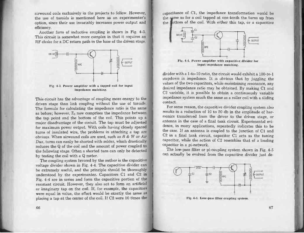
airwound coils exclusively in the projects to follow. However,the use of toroids is mentioned here as an experimenter'soption, since their use invariably increases power output andefficiency.
Another form of inductive coupling is shown in Fig. 4-3.This circuit is somewhat more complex in that it requires anRF choke for a DC return path in the base of the driven stage.
DRIVE
Fig. 4-3. Power amplifier with a tapped coil for inputimpedance matching.
This circuit has the advantage of coupling more energy to thedriven stage than link coupling without the use of toroids.The formula for calculating the impedance ratio is the sameas before; however, Zs now comprises the impedance betweenthe tap point and the bottom of the coil. This points up amajor disadvantage of the circuit. The tap must be adjustedfor maximum power output. With coils having closely spacedturns of insulated wire, the problems in attaching a tap areobvious. When airwound coils are used, such as B & W or AirDux, turns can easily be shorted with solder, which drasticallyreduces the Q of the coil and the amount of power coupled tothe following stage. Often a shorted turn can only be detectedby testing the coil with a Q meter.
The coupling system favored by the author is the capacitivevoltage divider shown in Fig. 4-4. The capacitive divider canbe extremely useful, and the principle should be thoroughlyunderstood by the experimenter. Capacitors Cl and C2 inFig. 4-4 are in series and form the capacitive portion of theresonant circuit. However, they also act to form an artificialor imaginary tap on the coil. If, for example, the capacitorswere equal in value, the effect would be exactly the same asplacing a tap at the center of the coil. If C2 were 10 times the
capacitance of C1, the impedance transformation would bethe me as for a coil tapped at one -tenth the turns up from
ci
the ttom of the coil. With either this tap, or a capacitive
OUTPUT
Fig. 4-4. Power amplifier with capacitive divider forinput impedance matching.
divider with a 1 -to -10 ratio, the circuit would exhibit a 100 -to -1stepdovirn in impedance. It is obvious that by juggling thevalues of the two capacitors, while maintaining resonance, anydesired impedance ratio may be obtained. By making Cl andC2 variable, it is possible to obtain a continuously variableimpedance system much the same as a roller coil with a slidingcontact.
For some reason, the capacitive divider coupling system alsoresults in a reduction of 10 to 20 db in the amplitude of har-monics transferred from the driver to the driven stage, orantenna in the case of a final tank circuit. Experimental evi-dence, in many applications, repeatedly indicates this to bethe case. If an antenna is coupled to the junction of C1 andC2 in a final tank circuit, capacitor Cl acts as the tuningcapacitor, while the action of C2 resembles that of a loadingcapacitor in a pi -network.
The low-pass filter or pi -coupling system shown in Fig. 4-5can actually be evolved from the capacitive divider just de-
Trr.1)(5.° \-1C21I I
Fig. 4-5. Low-pass filter coupling system.
OUTPUT
.
67

61,
scribed. Here the junction of C1 and C2 is grounded ratherthan the junction of C2 and the coil. However, as mentionedearlier, ground is an arbitrary point and can be moved aroundto suit particular circuit considerations. As before, the valueof the two capacitors determines the impedance stepdown ratio.
COLLECTOR MATCHING
Up to this point the various circuit configurations haveshown the collector connected to the top of the tuned circuit.This may be satisfactory in low -power stages (e.g., less than1 watt) which do not draw much collector current. However,for high -power stages the collector impedance is so low thatit may represent only a few ohms shunting the tank. Thisreduces the Q of the coil to an unusable level, prevents properflywheel action, and causes a drastic loss of coupling. Thecapacitive -to -inductive ratio can be increased to raise the Q,but this results in rather enormous and unwieldy capacitorvalues. In such cases it is customary to tap the transistor downon the tank circuit to some low -impedance point ( Fig. 4-6)
Fig. 4-6. Tapped coil for output impedance matching.
or employ some other impedance -matching scheme. For pur-poses of preliminary experimenting the collector impedancecan be approximated by determining the DC resistance usingOhm's law. For example, if the stage draws 1 ampere at 12volts, the collector resistance will be approximately 12 ohms.However, in class C this load is not across the tank at all times,and in actual practice the collector impedance is roughly twotimes the calculated DC resistance. When the collector im-pedance has been estimated, the impedance transformationcan be calculated by using the formula given earlier.
If the taps are placed too far up on the coil, the loaded Qwill be severely reduced and proper flywheel action will be
68
impossible. If the taps are too far down on the coil, the lossesincrease due to the very high voltages induced at the topie coil. Once again, the best position can be determineddjusting the tap position for maximum power output. An
ap oximation which is handy for determining the initial posi-tio of the taps is to assume an impedance across the coil of10, 00 ohms. The collector tap can then be placed at the cor-rect number of turns to transform the collector impedance tothis higher value. The link or capacitive divider can then bearranged to transform the 10,000 -ohm impedance down to theinput impedance of the driven stage.
While on the subject of power amplifiers and the problemsof coupling them to an antenna, the "sloppy -tuned circuit"technique should be mentioned. Tapping the collector of apower amplifier down on the final tank coil results in certainproblems which are not obvious without the aid of a high-speedoscilloscope. During cut-off periods between drive cycles, con-siderable voltage will appear on the collector due to the backemf caused by the collapsing field of the coil. This potentialwill generally be more than twice the supply voltage. A pref-erable circuit is shown in Fig. 4-7. Although it appears to have
wilof
by
Fig. 4-7. "Sloppy -tuned circuit" for outputimpedance matching.
evolved from Fig. 4-6, the operating conditions are quite differ-ent. Coil L1 actually forms a resonant circuit in conjunctionwith the collector capacitance of the transistor. This circuitis parallel resonant at the signal frequency. Coil L2 formsanother resonant circuit at the signal frequency in conjunctionwith the two output capacitors. These two tuned circuits pro-vide more harmonic rejection than the one -coil circuit shownin Fig. 4-6.
69
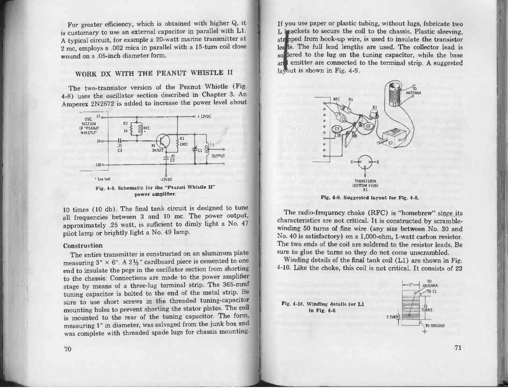
For greater efficiency, which is obtained with higher Q, itis customary to use an external capacitor in parallel with Ll.A typical circuit, for example a 20 -watt marine transmitter at2 mc, employs a .002 mica in parallel with a 15 -turn coil closewound on a .05 -inch diameter form.
WORK DX WITH THE PEANUT WHISTLE II
The two -transistor version of the Peanut Whistle (Fig.4-8) uses the oscillator section described in Chapter 3. AnAmperex 2N2672 is added to increase the power level about
11OSC.
SECTION
OF "PEANUTWHI STLF'
J6
See text -12VDC
Fig. 4-8. Schematic for the "Peanut Whistle II"power amplifier.
10 times (10 db). The final tank circuit is designed to tuneall frequencies between 3 and 10 mc. The power output,approximately .25 watt, is sufficient to dimly light a No. 47pilot lamp or brightly light a No. 49 lamp.
ConstructionThe entire transmitter is constructed on an aluminum plate
measuring 3" x 6". A 21/2" cardboard piece is cemented to oneend to insulate the pegs in the oscillator section from shortingto the chassis. Connections are made to the power amplifierstage by means of a three -lug terminal strip. The 365-mmftuning capacitor is bolted to the end of the metal strip. Besure to use short screws in the threaded tuning -capacitormounting holes to prevent shorting the stator plates. The coilis mounted to the rear of the tuning capacitor. The form,measuring 1" in diameter, was salvaged from the junk box andwas complete with threaded spade lugs for chassis mounting.
70
la
If you use paper or plastic tubing, without lugs, fabricate tworackets to secure the coil to the chassis. Plastic sleeving,sped from hook-up wire, is used to insulate the transistors. The full lead lengths are used. The collector lead is
so ered to the lug on the tuning capacitor, while the basea emitter are connected to the terminal strip. A suggested
ut is shown in Fig. 4-9.
Lstle
TRANSISTOR(BOTTOM VIEW)
X1
Fig. 4-9. Suggested layout for Fig. 4-8.
The radio -frequency choke (RFC) is "homebrew" since itscharacteristics are not critical. It is constructed by scramble -winding 50 turns of fine wire (any size between No. 30 andNo. 40 is satisfactory) on a 1,000 -ohm, 1 -watt carbon resistor.The two ends of the coil are soldered to the resistor leads. Besure to glue the turns so they do not come unscrambled.
Winding details of the final tank coil (L1) are shown in Fig.4-10. Like the choke, this coil is not critical. It consists of 23
Fig. 4-10. Winding details for LIin Fig. 4-8.
5 TURNS
TO
F"--1--1 ANTENNATO Cl
TURNS
TO GROUND
71
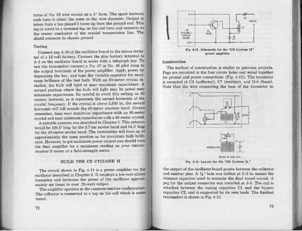
turns of No. 22 wire wound on a 1" form. The space betweeneach turn is about the same as the wire diameter. Output is
taken from a tap placed 5 turns up from the ground end. Thistap is wired to a terminal lug on the coil form and connects tothe center conductor of the coaxial transmission line. Theshield connects to chassis ground.
TestingConnect peg A-10 of the oscillator board to the minus termi-
nal of a 12 -volt battery. Connect the plus battery terminal toA-1 on the oscillator board in series with a telegraph key. Totest the transmitter connect a No. 47 or No. 49 pilot lamp tothe output terminals of the power amplifier. Apply power bydepressing the key, and tune the variable capacitor for maxi-mum brillance of the test bulb. With an 80 -meter crystal in-stalled, the bulb will light at near maximum capacitance. A
second position where the bulb will light may be noted nearminimum capacitance. Be careful to avoid this setting on 80
meters, however, as it represents the second harmonic of thecrystal frequency. If the crystal is above 3,650 kc, the secondharmonic will fall outside the 40 -meter amateur band. Alwaysremember, tune near maximum capacitance with an 80 -metercrystal and near minimum capacitance with a 40 -meter crystal.
A suitable antenna was described in Chapter 3. This antennawould be 126.5' long for the 3.7-mc novice band and 65.5' longfor the 40 -meter novice band. The transmitter will tune up atapproximately the same position as for maximum bulb brilli-ance. However, to get maximum power output you should tunethe final amplifier for a maximum reading on your station -
receiver S meter or a field -strength meter.
BUILD THE CB CYCLONE II
The circuit shown in Fig. 4-11 is a power amplifier for thoscillator described in Chapter 3. It employs a low-cost silicontransistor and increases the power of the oscillator approxi-mately six times to over .25 -watt output.
The amplifier operates in the common -emitter configuration.The collector is connected to a tap on the coil which is series
tuned.
72
.11
ClOUTPUT
J4
CB
CYCLONE 1CIRCUIT
BOARD
J10
Fig. 4-11. Schematic for the "CB Cyclone II"power amplifier.
ConstructionThe method of construction is similar to previous projects.
Pegs are mounted in the four corner holes and wired togetherfor ground and power connections (Fig. 4-12). The transistoris mounted at C5 (collector), C7 (emitter), and D-6 (base).Note that the wire connecting the base of the transistor to
1
7TURNSTUT1
AIRDUX f 616
DETAIL OF TANK COIL.
Fig. 4-12. Layout for the "CB Cyclone II."
the output of the oscillator board passes between the collectorand emitter pins. A 1/4 " hole was drilled at G-3 to mount thetrimmer capacitor used to resonate the final tuned circuit. Apeg for the output connector was installed at J-5. The coil isattached between the tuning capacitor Cl and the bypasscapacitor C2, and is supported by its own leads. The finishedtransmitter is shown in Fig. 4-13.
73
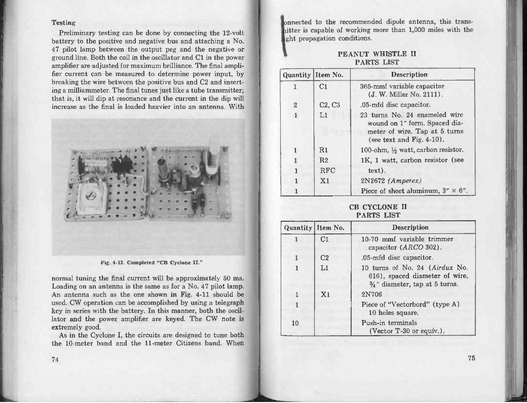
TestingPreliminary testing can be done by connecting the 12 -volt
battery to the positive and negative bus and attaching a No.47 pilot lamp between the output peg and the negative orground line. Both the coil in the oscillator and C1 in the poweramplifier are adjusted for maximum brilliance. The final ampli-fier current can be measured to determine power input, bybreaking the wire between the positive bus and C2 and insert-ing a milliammeter. The final tunes just like a tube transmitter;that is, it will dip at resonance and the current in the dip willincrease as the final is loaded heavier into an antenna. With
Fig. 4-13. Completed "CB Cyclone II."
normal tuning the final current will be approximately 50 ma.Loading on an antenna is the same as for a No. 47 pilot lamp.An antenna such as the one shown in Fig. 4-11 should beused. CW operation can be accomplished by using a telegraphkey in series with the battery. In this manner, both the oscil-lator and the power amplifier are keyed. The CW note isextremely good.
As in the Cyclone I, the circuits are designed to tune boththe 10 -meter band and the 11 -meter Citizens band. When
74
nnected to the recommended dipole antenna, this trans-itter is capable of working more than 1,000 miles with theght propagation conditions.
PEANUT WHISTLE IIPARTS LIST
Quantity Item No. Description
1 Cl 365-mmf variable capacitor(J. W. Miller No. 2111).
2 C2, C3 .05-mfd disc capacitor..1 Ll 23 turns No. 24 enameled wire
wound on 1" form. Spaced dia-meter of wire. Tap at 5 turns(see text and Fig. 4-10).
1 R1 100 -ohm, 1/2 watt, carbon resistor.
1 R2 1K, 1 watt, carbon resistor (see1 RFC text).1 X1 2N2672 (Amperex)1 Piece of sheet aluminum, 3" x 6".
CB CYCLONE IIPARTS LIST
Quantity Item No. Description
1 Cl 10-70 mmf variable trimmercapacitor (ARCO 302).
1 C2 .05-mfd disc capacitor.1 Ll 10 turns of No. 24 (Airdux No.
616), spaced diameter of wire,3/4" diameter, tap at 5 turns.
1 X1 2N706
1 Piece of "Vectorbord" (type A)10 holes square.
10 Push -in terminals(Vector T-30 or equiv.).
75

The NovicePowerhouse
Most of the transmitters described so far have used verylow power. The transmitter to be described in this chapterruns 5 watts input and is capable of the same performance asa novice transmitter employing a 6V6 -type tube. It is capableof transmitting for hundreds or even thousands of miles whenproperly tuned to a correct antenna. Even if the antenna isnot exactly the right length or if the transmitter is slightlymistuned, there is still sufficient reserve power to compensatefor some of the loss. The transmitter operates on both the80- and 40 -meter novice bands and has a tuning range of 3 to8 megacycles. Later a voice modulator will be described forthis transmitter so that you can work AM.
HOW IT WORKS
The transmitter circuit is the type generally referred to asa master -oscillator power amplifier (MOPA). It consists of acrystal -controlled oscillator link -coupled to a power -amplifierstage. The output of the power amplifier, in turn, is connectedto the transmitting antenna. A circuit is also included so thatrelative power output can be observed on a meter.
The circuit for the high -power novice transistor transmitteris shown in Fig. 5-1. Transistor Xl, a PADT-50 (Amperex), is
77

XTAL
R1
3.3K
Cl
Rd
J2
KEY
C7
365
mmf
X2 PADT -50 -
0-1 ma
METER
C9
.051 DI -1N60
.11
RF OUTPUT
10
mmf
COLLECTOR(CASE)
TRANSISTOR PIN
CONNECTIONS
BOTTOM VIEW
Fig. 5-1. Schematic of the "Novice Powerhouse" transmitter.
12 VDC
connected in the common -emitter configuration and serves asthe crystal oscillator. The collector of the oscillator is connectedto a low -impedance point on coil Ll. This coil also serves as animpedance step-up transformer to provide feedback ( throughthe crystal) to the base of the oscillator stage. Resistors R1and R2 forward -bias the oscillator, while R3 provides DC de-generation and prevents thermal runaway. Capacitors C3 andC4 bypass this point so that it is not degenerative to the oscil-lator signal. Capacitor Cl is 30 mmf ( -±10% ) and determinesthe exact frequency of oscillation. The value of C1 is chosenso that the crystal "sees" a 32-mmf load capacitance and thecrystal oscillates at exact parallel resonance. Coil Ll is reso-nated with a 365-mmf variable capacitor; it tunes the circuitbetween 3 and 8 megacycles.
Output from the oscillator is link -coupled to power -amplifierstage X2, a second PADT-50. Resistor R4 (4.7 ohms) is in-cluded to limit the base current of the stage and preventoverdriving. No emitter stabilization is required in this stagesince the transistor is operating in deep class C. In other words,if the crystal is removed or C2 is detuned (so that the oscillatorno longer functions), X2 will draw no collector current. It onlyconducts on a portion of the negative half cycle. CapacitorsC5 and C6 bypass the stage to prevent any RF feedback fromreaching the oscillator circuit. The collector of this stage isalso tapped at a low -impedance point on coil L2, which is
78
resonated at the signal frequency by means of C7, a second365-mmf capacitor. RF power output from the amplifier islink -coupled to the transmission line through connector J1.
lthough an RCA -type phono connector is used, a coaxial con-ector may be substituted, if desired.The RF voltmeter is a relative -output indicator and works
in the following manner. Capacitor C8 (10 mmf) samples asmall amount of the RF appearing across the link and trans-mission line. This radio -frequency energy is rectified by D1,a 1N60 general-purpose germanium diode. A filter consistingof R5 (680 ohms) and C9 (a .05-mfd disc capacitor) removesthe RF component and leaves only DC. This DC is applied toa 0- to 1 -ma meter which provides a relative indication of theamount of voltage appearing across the link and transmissionline. Capacitor C8 determines the exact reading of the meter.With the values shown, the meter will read almost full scaleon 40 meters. If it reads more or less than full scale, the valueof C8 can be varied to suit the constructor. Capacitor C9 isnot critical and may be any value between .001 mfd and .05 mfd.
The transmitter is keyed by breaking the B+ circuit to bothstages. This is accomplished by inserting the key in series withthe negative battery terminal. When the key is depressed,both stages operate and the transmitter emits a carrier signal.The keying note is excellent and even detuning the oscillatorwill not cause excessive chirp.
CONSTRUCTION
The entire transmitter is constructed on a 5" x 7" aluminumchassis. When laying out the holes on the chassis, it is anexcellent idea to make the drawing on the paper wrapper whichaccompanies the chassis. It minimizes scratching or markingthe chassis and the wrapper can be retained to duplicate theproject at a later date.
Referring to the photograph ( Fig. 5-2), note that the oscil-lator circuitry is on the right side of the chassis while thepower amplifier occupies the space at the left. A crystal socketis mounted on the front panel for quick changes of frequency.A meter found in the author's junk box was used for the RFvoltmeter. This meter has a basic 0- to 1 -ma movement and is
79
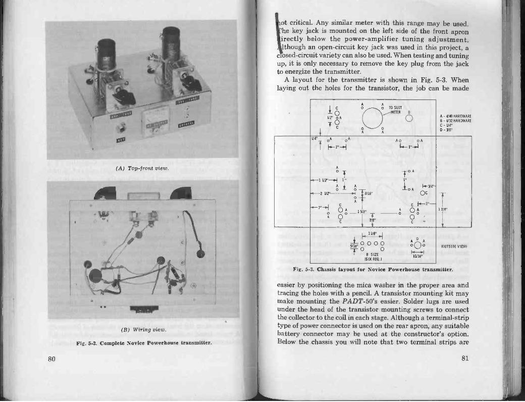
Exo
(A) Top -front view.
AI
141111111P
(B) Wiring view.
Fig. 5-2. Complete Novice Powerhouse transmitter.
80
of critical. Any similar meter with this range may be used.he key jack is mounted on the left side of the front apronirectly below the power -amplifier tuning adjustment.though an open -circuit key jack was used in this project, a
c osed-circuit variety can also be used. When testing and tuningup, it is only necessary to remove the key plug from the jackto energize the transmitter.
A layout for the transmitter is shown in Fig. 5-3. Whenlaying out the holes for the transistor, the job can be made
C
0o A
TO
A Ao TO SUIT
D
0A A
A - 4/40 HARDWAREB - 6(32 HARDWARE
C - 114"D - 318"
oA oA A o o A
T H_r_H
Ao
-f1/2"-H 1"
AlA
A
--2 LIZ
+1 1 0 A 151$'
A 0 °A0
o A
1"
o A11314"-
Oc
T171$"
0 0 000
T5/16" °
SIZE(SIX REQ. I
Aor
11116"
(OUTSIDE VIEW)
Fig. 5-3. Chassis layout for Novice Powerhouse transmitter.
easier by positioning the mica washer in the proper area andtracing the holes with a pencil. A transistor mounting kit maymake mounting the PADT-50's easier. Solder lugs are usedunder the head of the transistor mounting screws to connectthe collector to the coil in each stage. Although a terminal -striptype of power connector is used on the rear apron, any suitablebattery connector may be used at the constructor's option.Below the chassis you will note that two terminal strips are
81
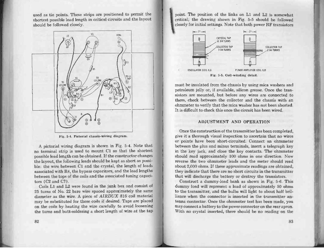
used as tie points. These strips are positioned to permit theshortest possible lead length in critical circuits and the layoutshould be followed closely.
J2MI XTAL
(C3
Cl
TO LITAP
Fig. 5-4. Pictorial chassis -wiring diagram.
A pictorial wiring diagram is shown in Fig. 5-4. Note thatno terminal strip is used to mount Cl so that the shortestpossible lead length can be obtained. If the constructor changesthe layout, the following leads should be kept as short as possi-ble: the wire between Cl and the crystal, the length of leadsassociated with R4, the bypass capacitors, and the lead lengthsbetween the tops of the coils and the associated tuning capaci-tors ( C2 and C7).
Coils L1 and L2 were found in the junk box and consist of25 turns of No. 22 bare wire spaced approximately the samediameter as the wire. A piece of AIRDUX 816 coil materialmay be substituted for these coils if desired. Taps are placedon the coils by heating the wire carefully to avoid looseningthe turns and butt -soldering a short length of wire at the tap
82
tpoint.
The position of the links on L1 and L2 is somewhatcritical; the drawing shown in Fig. 5-5 should be followedclosely for initial settings. Note that both power RF transistors
h.- i" --I 1--1" --4
CRYSTAL TAP11 3/4 TURNS
COLLECTOR TAP
3 314 TURNS
COLLECTOR TAP
2 314 TURNS
OSCILLATOR COIL ILD POWER AMPLIFIER COIL lb
Fig. 5-5. Coil -winding detail.
must be insulated from the chassis by using mica washers andpetroleum jelly or, if available, silicon grease. Once the tran-sistors are mounted, but before any wires are connected tothem, check between the collector and the chassis with anohmmeter to verify that the mica washer has not been shorted.It is difficult to check this once the circuit has been wired.
ADJUSTMENT AND OPERATION
Once the construction of the transmitter has been completed,give it a thorough visual inspection to ascertain that no wiresor points have been short-circuited. Connect an ohmmeterbetween the plus and minus terminals, insert a telegraph keyin the key jack, and close the key contacts. The ohmmetershould read approximately 100 ohms in one direction. Nowreverse the two ohmmeter leads and the meter should readabout 2,000 ohms. If these approximate readings are obtained,they indicate that there are no short circuits in the transmitterthat will discharge the battery or destroy the transistors.
Construct a dummy -load bank as shown in Fig. 5-6. Thisdummy load will represent a load of approximately 50 ohmsto the transmitter, and the bulbs will light to about half bril-liance when the connector is inserted in the transmitter an-tenna connector. Once the ohmmeter test has been made, youmay connect a battery to the power connector on the rear apron.With no crystal inserted, there should be no reading on the
83
6 - NO. 47 PILOT LAMPSCONNECTED SERIES -PARALLEL
PHONO CONNECTOR
Fig. 5-6. Dummy -load bank for transmitter testing.
transmitter meter. Insert a crystal for the 40 -meter CW bandand set both capacitors near minimum capacitance (clockwise) .Now turn the oscillator adjustment counterclockwise veryslowly. If the circuit is working properly, the meter will nowindicate slightly. Now slowly turn the power amplifier adjust-ment ( C7 ) counterclockwise. The meter reading should in-crease as you turn the knob and the lamps should start to glow.Turn the oscillator adjustment for maximum brilliance of thebulbs or maximum reading on the meter. Once again turn theamplifier adjustment for maximum brilliance of the bulbs andthe highest meter reading obtainable. Repeat these adjust-ments, back and forth, until absolute maximum power outputhas been obtained.
If the bulbs do not seem to be particularly bright, try movingthe oscillator link up or down slightly and retuning the oscil-lator and amplifier for maximum power. If the power outputdecreases, move the link in the opposite direction. Each timethe link is adjusted it will be necessary to recheck the settingof C2 and C7. Once the maximum power output has beenobtained by varying the oscillator link, adjust the amplifierlink for maximum power in the same manner. You may findthat more power output can be obtained by reversing the twoleads on the links. When you have completed these adjustmentsthe bulbs should be about half brilliance and the meter shouldread near full scale. If it reads beyond full scale, reduce the
84
size of C8. You can listen to the CW note in your stationreceiver while keying the transmitter. It should sound clean
ith no chirps or clicks.To finish testing the transmitter, insert an 80-meter, novice -
band crystal in the socket. Retune both the oscillator and finalpower -amplifier adjustments near maximum capacitance posi-tion. The bulbs should again light to the same brilliance,although the meter may not read as high as before. This isbecause the capacitive reactance of C8 increases with decreas-ing frequency. Again recheck the keying on this frequency toverify that the note is pure.
Now connect your novice "powerhouse" to an antenna. Forbest results an antenna such as the one shown in Fig. 3-12should be used. Insert a suitable crystal and peak both theoscillator and power -amplifier adjustments for maximum meterreading. You may note that the meter reads higher or lowerwhen connected to the antenna. This is because the impedanceof the antenna may be more or less than the bulbs. Once againit may be necessary to vary the value of C8 to provide a usablemeter reading. Once a value has been selected for C8, it neednot be changed unless a different antenna is employed. Youwill not need to adjust this transmitter with a field -strengthmeter since the RF-voltmeter circuit indicates maximum poweroutput the same as a field -strength meter. You may find, how-ever, that moving the link on the power -amplifier coil (L2)will produce slightly more output than it did on the dummyload.
That completes the adjustment, and you are now ready towork DX with the novice transmitter. As in earlier projects,you are cautioned not to tune the transmitter to its secondharmonic when operating on 80 meters. Always remember thatthe variable capacitor should be set near maximum capacitancewith an 80 -meter crystal and near minimum capacitance witha 40 -meter crystal.
Most of the parts for this transmitter are readily available;however, special mention should be made of the PAD T-50transistors. These are made by Amperex and there are nosubstitute types. These transistors are available from any radiostore handling Amperex devices or may be obtained from vari-ous mail-order distributors. If you have difficulty obtaining
85
the transistors, the name of the nearest source may be obtainedby writing Amperex Semiconductor Products, 230 Duffy Ave-
nue, Hicksville, L.I., N.Y. The constructor may have somedifficulty, also, in locating resistors R3 and R4. Values smallerthan 10 ohms usually are stocked only in the larger radio stores.
NOVICE POWERHOUSE
PARTS LIST
Quantity Item No. Description
1 Cl 30-mmf, 10% dipped-mylar orsilver -mica capacitor.
2 C2, C7 365-mmf maximum, variablecapacitor (J. W. MillerNo. 2111 or equiv.).
5 C3, C4, C5,C6, C9
.05-mfd disc capacitor.
1 C8 10-mmf, 10% dipped-mylar orsilver -mica capacitor.
1 D1 IN60 germanium diode.
1 J1 RCA -style phono connector.
1 J2 Open- or closed-circuit key jack
1 Ll 25 turns No. 22 bare or enam-eled wire wound on 1" diam-eter form. Spacing betweenturns same as wire diameter.Collector tapped at 3 %turns, crystal tapped at 11%turns. Link, two turns No.24 plastic -covered hookupwire wound over bottom 3turns of coil.
1 L2 Same as Ll except collector istapped at 2% turns. Link istwo turns wound over centerof coil.
86
NOVICE POWERHOUSE
PARTS LIST (CONT.)
Quantity Item No. Description1 M1 0 to 1 -ma meter.2 Xl, X2 PADT-50, RF power transistor
(Amperex).1 R1 3.3K, 1/2 -watt, 10% carbon
resistor.1 R2 220 -ohm, 1/2 -watt, 10% carbon
resistor.1 R3 1 -ohm, 1/2 -watt, 10% carbon
resistor (see text).1 R4 4.7 -ohm, 1/2 -watt, 10% carbon
resistor. (see text).1 R5 680 -ohm, 1/2 -watt, 10%
resistor.1 Chassis 5" x 7" x 2"
(aluminum).1 crystal socket.3 1/4 -inch rubber grommets.1 Two -screw terminal strip.2 Knobs.2 Mica washers, and transistor
mounting hardware.Hardware and wire as required.
87
6Modulation_
By definition, modulation is the process of adding intelli-gence to a carrier signal. Modulation can be simple, as in thecase of continuous wave (CW), that is, making or breaking thecarrier to form dots and dashes. It can also be extremely com-plex, such as for time -division multiplex or video -modulationschemes.
The carrier can be modified by voice modulation in two prin-cipal ways. One system, used for hi -fidelity broadcasting andmobile radiotelephones, is frequency or phase modulation. Theother method, known as amplitude modulation, is the subjectof this chapter.
FREQUENCY MODULATION
Although frequency -modulation projects are not included inthis book, the reader should be familiar with the technique.The heart of an FM transmitter is the frequency -modulatedoscillator stage. Fig. 6-1 shows a typical FM oscillator stage.Modulation is applied to the oscillator in such a manner thatthe frequency of oscillation varies in proportion to the appliedsignal. For example, as a positive audio peak is applied to theoscillator, the frequency might move higher. During negativepeaks the frequency would shift lower than the average fre-quency of oscillation. As the modulation waveform crosses itszero axis, the frequency of oscillation is the same as if no modu-
89
OSCILLATOR
REACTANCE MODULATOR
MODULATION "\-,
FM CARRIER
Fig. 6-1. A basic reactance -modulated oscillator circuit.Bias and voltage omitted for simplicity.
lation were applied. The "distance" the frequency changes isin proportion to the modulation amplitude, while the rate ofchange is determined by the modulation frequency.
The FM oscillator is usually followed by a limiter to removeany traces of amplitude modulation, as shown in the blockdiagram of Fig. 6-2. Although only one multiplier is shown, the
MICROPHONE
OSCILLATOR LIMITER MULTIPLIERPOWER
AMPLIFIER
Fig. 6-2. Waveforms found in a typical FM transmitter.
limiter may be followed by several doublers or triplers to in-crease the oscillator output to the desired signal frequency.Each time the frequency is doubled, the modulation bandwidthwill also increase by a factor of two.
In the receiving system the FM signal is again passedthrough a series of limiters, this time to remove impulse noise,static, ignition pulses, etc. Finally the signal is applied to adiscriminator; this circuit has the characteristic of generatingpositive or negative voltages for signals above or below theaverage frequency of oscillation. Thus the output of the dis-
90
criminator will be the signal which originally modulated thetransmitter.
AMPLITUDE MODULATION
As the name implies, this system varies the amplitude ofthe carrier wave rather than the frequency. This is generallyaccomplished in the final or power -amplifier stage in an ampli-tude -modulated transmitter. Amplitude modulation can beintroduced by varying the gain of the amplifier as shown inFig. 6-3. T, is a modulation transformer inserting modulation
FINAL AMPLIFIER
T F.MODULATED
CARRIER INPU CARRIEROUTPUT
X
MODULATION
x
Fig. 6-3. Basic method of modulating an AM transistortransmitter. Only one of the three transformer
connections would be used.
into the base circuit, while Th injects the signal into the emitter.Either of these systems varies the gain of the transistor andcauses the amplitude of the carrier to change in direct propor-tion to the modulation waveform.
Although either connection requires only a small amount ofmodulating power, both types of modulation are inefficient andmake transmitter tuning ( for best modulation) very critical.The most satisfactory modulation system is to vary the col-lector voltage as in T. ( Fig. 6-3) .
(A) Modulationwaveform.
11111111111111
(B) Carrierwaveform.
(C) Modulatedcarrier.
Fig. 6-4. The amplitude of the modulation waveform increases ordecreases the carrier amplitude.
91
II
Fig. 6-4 shows the result of modulating a carrier wave witha sine wave. These waveforms are what would be observed onan oscilloscope if measurements were made in a typical trans-mitter employing one of the three modulating methods justdescribed. The drawing in Fig. 6-4A is a 1,000 -cycle waveformthat has been amplified by the modulator stage. Fig. 6-4B isthe carrier signal applied to the final amplifier stage. Actuallyit also consists of a series of sine waves, as in Fig. 6-4A, butbecause of the high frequency, they show up as a solid bar onthe screen of the average oscilloscope. Fig. 6-4C shows themodulated carrier wave. When the modulation and carrier arecombined in correct proportions, the valleys produce zero RFoutput while the peaks are twice the amplitude of the unmodu-lated carrier. This condition is termed 100% modulation.
COLLECTOR MODULATION
Amplitude modulation is accomplished in transistor trans-mitters in much the same manner as in vacuum -tube equip-ment; however, it is easier with vacuum -tube equipment thanwith transistors, as you will soon see.
Since high-level collector modulation is by far the mostpopular system, let's examine its behavior in detail. Fig. 6-5
FROM
OSCILLATOROR BUFFER
FROM MODULATOR
CARRIER OUTPUTTO ANTENNA
Fig. 6-5. Output circuit of a typical AM transistor transmitter.
is the simplified circuit of a typical collector -modulated tran-sistor final amplifier. The point marked "AM carrier output"connects to the transmission line and radiating antenna. Nega-tive 12 volts is applied to the collector of the power amplifier
92
in series with the secondary of the modulation transformer andthe radio -frequency tuned circuit. The negative -going peaksadd to the supply voltage while the positive -going half of themodulation waveform opposes the supply. It might be thoughtof as two batteries connected in series. When they are con-nected positive to negative, they add; but when they are con-nected positive to positive, they oppose each other.
Under conditions of 100% modulation the peak negative -modulation voltage will equal the supply, and the collectorvoltage will be -24 volts rather than -12 volts. By the sametoken, one-half cycle later the positive peak will exactly cancelthe supply, and the instantaneous collector voltage will bezero. Doubling the collector voltage causes the RF peaks toreach twice the amplitude of the unmodulated carrier. One-halfcycle later the transmitter output will be zero. This corre-sponds to the peaks and valleys in the modulated carrier wave-form shown in Fig. 6-4C.
Unfortunately the preceding description, while technicallyaccurate, is a highly utopian explanation as far as transistorsare concerned. Although the theory of modulation is the samefor tube and transistor transmitters, the results are not thesame. One major problem is the built-in "flat -topping" of themodulated waveform usually found in transistor transmitters.The condition becomes much more noticeable as the powerinput is increased. Two additional and equally vexing problemsare drive requirements and carrier leakthrough.
Flat -topping of the modulated waveform is a direct resultof the inability of the transistor to handle high input powers.During the peak power -output period the instantaneous volt-age is approximately doubled, as explained earlier. Ideally thecollector current also doubles so that the peak power input isfour times the average value. In a transistor transmitter, how-ever, this increased power input is always accompanied by adecrease in hr.., the gain of the transistor. At the same time themodulation waveform is trying to produce more power, thefalling hf., is opposing that power increase. The saturation re-sistance of the transistor is also causing more voltage to be lostacross the junction, since it is in series with the supply andmodulation. The result is a built-in compression of the modu-lation peaks, which prevents the stage from being modulated
93
100%. Fig. 6-6 shows some of the more realistic waveformsfound in transistor transmitters. Fig. 6-6A shows the typical
(A) Typical modulation envelopeof a vacuum -tube final amplifier.
(B) Modulation envelope of atransistor final amplifier.
Fig. 6-6. Comparison of modulation waveforms.
output of a vacuum -tube final amplifier, while Fig. 6-6B illus-trates the likely waveform of a transistor final amplifier thatis not capable of handling the peak powers involved.
The drive requirement of a tube and transistor final is alsoquite different. Unlike a tube final, the power output of a tran-sistor final is largely determined by the drive. available. Eventhough the stage is RF biased into class C, the increase in
power input due to modulation may make it drop into class -Boperation. This lack of drive during peak periods tends tocompound the peak compression mentioned earlier. If thecompression is severe, the oscilloscope may show what appearsto be a 100% -modulated waveform (slightly distorted) andyet a dummy -load lamp will show downward modulation. Be-
osc.
tL
8+
Fig. 6-7. Preferred method of modulating both drivingand final stages.
94
cause of this problem, it is usually mandatory that the bufferstage driving the final, or sometimes even the oscillator, alsobe modulated. Fig. 6-7 shows one system of accomplishing this.The tap of the secondary of the modulation transformer, andtherefore the amplitude fed to the buffer and/or oscillator, isdetermined by the power involved. Generally this tap is ex-perimentally adjusted so that the driving stages are neverquite cut off. If excessive modulation is applied to the drivingstage or stages, negative speech clipping will occur and severesplatter will result. A "trick circuit" to minimize this effect is
BUFFER
B+
FINAL
MODULATEDCARRIEROUTPUT
Fig. 6-8. "Trick circuit" for increasing positive peak modulation.
shown in Fig. 6-8. The final is collector -modulated with themodulating voltage connected in series with the positive power -supply lead. During positive peaks the modulation adds to thesupply voltage. Positive peaks are also coupled to the bufferstage through diode D1 to increase the drive during peak peri-ods; diode D2 is cut off during this period. During negative -peak periods, splatter is prevented since diode D1 no longerconducts audio to the buffer, and the stage is clamped to B+through conducting diode D2. The result is a noticeable in-crease in upward modulation with no change in the negativeor valley part of the waveform.
The problem of leakthrough can also be very annoying. Dur-ing the period when the modulation supposedly cancels thesupply voltage, there will still be a noticeable amount of poweroutput. This is quite unlike vacuum tube RF power amplifiers.
95
The reason for this effect is the junction capacitance. With thebase -emitter junction forward -biased and zero volts on thecollector, the collector -base junction exhibits considerable ca-pacitance. Thus the RF signal appearing on the base is capaci-tively coupled to the output tank circuit. The result is shownin Fig. 6-6B. Note that this waveform is the result of the prob-lem just discussed and is typical of those found in transistortransmitters.
Now that some of the pitfalls have been examined, let's con-struct several modulators for use in conjunction with the trans-mitters described in this book. The low -power modulator formsthe foundation for the medium -power modulator (500 milli -watts or 0.5 watts) and the high -power 5 -watt modulator. Itemploys a Darlington -pair input circuit to increase the inputimpedance to over 400,000 ohms. Thus the circuit can be usedwith crystal and ceramic microphones which must "look into"a high impedance to preserve bass response.
BUILD A LOW -POWER MODULATOR
The circuit for the low -power modulator just described isshown in Fig. 6-9. Three transistors are used to build up thetiny voltage generated by the microphone to a sufficient levelto be used as a modulator for the oscillator projects describedearlier.
Transistors X1 and X2 form a Darlington pair to raise theinput impedance and have no voltage gain. The driver tran-
CI
INPUT°H.05
RI
R3
4700 94, +12 V. D. C.
Fig. 6-9. Schematic diagram for the high -impedance microphonepreamplifier and modulator.
96
sistor ( X3) exhibits considerable power gain. Approximately 1volt rms undistorted output will develop across a 470 -ohmresistor connected to half of the T1 secondary.
The circuit works in the following manner: transistor X1acts as an emitter follower. Forward -bias is developed at thejunction of R2 and R3. Resistor R1 isolates the bias circuitfrom the input circuit. Transistor X2 is a second emitter fol-lower; the input impedance of the emitter follower is deter-mined by its output impedance (the emitter load resistor plusthe input impedance of the driven stage) multiplied by thebeta of the transistor. Thus when two emitter followers arecascaded, the normally low input impedance is raised to severalhundred thousand ohms. In addition, capacitor C2 provides asmall amount of degenerative current feedback to increase theimpedance even further. The audio voltage developed acrossR4 is approximately the same amplitude as that generated bythe microphone, but across a much lower impedance.
The audio voltage is coupled to the driver stage throughcapacitor C4. The driver ( X3) operates in the common -emittermode and exhibits considerable voltage gain. Resistors R6 andR7 form a voltage divider to provide forward -bias forX3, whileR8 stabilizes the gain and current over wide temperature andvoltage variations.
The amplified voltage is developed across the primary ofT1 (10K impedance). Capacitor C6 tunes the primary to at-tenuate high audio frequencies. If a standard 10K to 2K center -
tapped transistor interstage transformer is used, the outputimpedance is either 500 ohms or 2,000 ohms, as shown in Fig.6-9. This transformer is suitable for modulating the oscillatorsdescribed earlier, or it can be used to drive the half -watt modu-lator which follows.
Construction
The entire circuit is constructed on a circuit board measur-ing 2" x 4". This board was supplied by the W. H. PaulinCompany, Box 122, Upland, California. However, if it is moreconvenient, electronic "peg board" can be used with the con-struction style employed earlier. There is no need to use tran-sistor sockets, since the circuit is not critical as to transistortype. Virtually any PNP general-purpose audio transistor can
97
be employed. The circuit can be installed in an LMB box orincorporated as part of the larger modulators which follow.
The constructor should carefully observe the electrolyticpolarity. For example, if capacitor C4 is reversed, the error candamage output transistor X3.
If it is desired, a volume control can be included in the cir-cuit. Resistance R4 would be replaced by the two end connec-tions of a 5,000 -ohm audio -taper volume control. The dottedconnection in Fig. 6-9 would be broken and the negative endof C4 would be connected to the arm or center terminal of thevolume control.
The circuit has been designed to amplify only the voice fre-quencies and produce communications quality. If higher fidel-ity performance is desired, capacitor C6 should be deleted toincrease the high audio frequencies, while replacing C5 with a100-mfd electrolytic will extend the low -frequency response.A slight amount of bass boost can be obtained by connectingthe 100-mfd capacitor between the emitter end of C5 andground.
If the circuit is wired as shown in Fig. 6-9, it should workimmediately without any further experimentation. Connect a
Fig. 6-10. Parts location on modulator board.
98
microphone (ceramic, high -impedance dynamic, or crystal) tothe input, apply power, and connect a pair of headphones tothe 2,000 -ohm output connection. If the unit is working prop-erly, you should hear your voice clearly with no distortion.Approximately 2 to 3 volts rms can be measured across theheadphones or a 2.2K resistor connected to the amplifieroutput. Two views of the finished unit are shown in Figs. 6-10and 6-11.
Fig. 6-11. Completed low -power modulator.
BUILD A HALF -WATT MODULATOR
The project previously described delivers only a few milli -watts of audio and therefore is not capable of 100% modulationof any circuit but a very low -power oscillator. It does, however,make an excellent driver for this circuit to be described.
How It WorksThe circuit shown in Fig. 6-12 is known as a class -B push-pull
modulator. Unlike the class -A driver (X3 in Fig. 6-9), thetransistors in class -B circuits only amplify on alternate halfcycles. Collector current pulses alternate in each half of the
99

:C.Nor.II.F.....
I.___INPUT FROMCIRCUIT OF
FIG. 6-9
TO 8+ CIRCUIT IN
CIRCUIT OF FIG. 6-9 R5
i C2 220
100mfd iFig. 6-12. Schematic of the half -watt modulator.
primary of Ti. The half -cycle waveforms generated by eachtransistor are combined in the secondary to recreate an ampli-fied replica of the driving signal.
The output of the driver signal becomes a push-pull signalby connecting the center tap of the driver transformer to theB supply. When the audio signal is negative to the base of Xl,conduction occurs. At the same time the signal on the base ofX2 is positive -going; thus X1 conducts while X2 is cut off. Dur-ing the next half -cycle period the polarity reverses; then X2conducts while X1 is cut off.
If the transistor characteristic were completely linear fromcutoff to saturation, the waveform shown in Fig. 6-13A would
(A) Output waveform fromproperly biased stage.
(B) Output waveform withinsufficient crosswave bias.
Fig. 6-13. Waveforms showing crossover -distortion effect on anormal sine wave.
represent both the input and output waveform of the modu-lator. Unfortunately this is not the case. All transistors havea "hook" in their curve at the low -current end. This "hook"must be overcome by applying forward bias to the base -emitterjunction. If this is not observed or if the amount of forward
100
bias is insufficient, the output waveform will resemble thatshown in Fig. 6-13B. This effect is known as crossover distor-tion and is very annoying to the ear. The sound is similar tothat created by a speaker with a rubbing voice coil. Even aslight amount of distortion at this point on the waveform isimmediately obvious to the ear, even though it can hardly beobserved with an oscilloscope. Crossover distortion can beminimized by incorporating a forward -bias network. This isthe purpose of R1 and R2 in Fig. 6-12. Resistor R1 will beapproximately 6.8K for the components shown. It should beadjusted for a collector current of 3 ma or until the outputsignal has the least amount of audible distortion with minimumno -signal collector current. The transistors draw more currenton signal peaks and the collector current will vary between 3ma no signal and 30 ma on signal peaks.
Resistors R3 and R4 are included in the circuit to preventthermal runaway. They also supply a small amount of degener-ative feedback to increase the input impedance of the stageand reduce distortion. A filter network consisting of R5 andC2 is included to prevent feedback through the B+ circuit tothe driver stage.
Transistor T1 is a special transistor type used in nine -transistor Citizens band walkie-talkies; it has three windings.The primary impedance is 500 ohms center tapped, while themodulation winding is 3,000 ohms and the speaker winding is3.2 ohms.
Construction
The modulator is constructed on a small LMB chassis boxand is shown in the accompanying photograph ( Fig. 6-14).The circuit board containing the preamplifier and drivercircuitry is mounted inside the box on the rear apron wall.The volume control, which must be used to prevent over-driving the modulator, is mounted at the front apron alongwith the microphone jack. The two class -B transistors aremounted by drilling holes in the top of the box which are thesame size as the outside diameter of the transistor package.This is done so the transistor makes a tight press fit into theholes and permits the chassis to act as a heat sink. If othertypes of transistors are used, clips may be employed to ther-
101
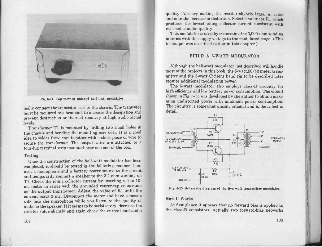
Fig 6-14. Top view of finished half -watt modulator.
mally connect the transistor case to the chassis. The transistormust be mounted to a heat sink to increase the dissipation andprevent destruction or thermal runaway at high audio signallevels.
Transformer T1 is mounted by drilling two small holes inthe chassis and bending the mounting ears over. It is a goodidea to solder these ears together with a short piece of wire tosecure the transformer. The output wires are attached to afour -lug terminal strip mounted near one end of the box.
TestingOnce the construction of the half -watt modulator has been
completed, it should be tested in the following manner. Con-nect a microphone and a battery power source to the circuitand temporarily connect a speaker to the 3.2 -ohm winding onT1. Check the idling collector current by inserting a 0 to 10 -ma meter in series with the grounded center -tap connectionon the output transformer. Adjust the value of R1 until thecurrent reads 3 ma. Disconnect the meter and have someonetalk into the microphone while you listen to the quality ofaudio in the speaker. If it seems to be satisfactory, decrease theresistor value slightly and again check the current and audio
102
quality. Also try making the resistor slightly larger in valueand note the increase in distortion. Select a value for R1 whichproduces the lowest idling collector current consistent withreasonable audio quality.
This modulator is used by connecting the 3,000 -ohm windingin series with the supply voltage to the modulated stage. (Thistechnique was described earlier in this chapter.)
BUILD A 5 -WATT MODULATOR
Although the half -watt modulator just described will handlemost of the projects in this book, the 5-watt,80 /40 meter trans-mitter and the 5 -watt Citizens band rig to be described laterrequire additional modulating power.
The 5 -watt modulator also employs class -B circuitry forhigh efficiency and low battery power consumption. The circuitshown in Fig. 6-15 was developed by the author to obtain maxi-mum undistorted power with minimum power consumption.The circuitry is somewhat unconventional and is described indetail.
Ti
NO CONNECT I067--
TO COLLECTOR
OF X3 IN FIG. 6-9
TO GROUND
TO 8+ CIRCUITOF FIG. 6-9
RI
2.7K
R3
TooClmfd
1000
GROUND-
12V D.C.
T2
p16080
MODULATION
40 OUTPUT
c. COMMON
Fig. 6-15. Schematic diagram of the five -watt transmitter modulator.
How It Works
At first glance it appears that no forward bias is applied tothe class -B transistors. Actually two forward -bias networks
103

are used; they are independent of each other. Resistor R1, inconjunction with the winding resistance in the upper half ofthe secondary of T1, forward biases X1 while R2 and the trans-former winding resistance biases X2. This circuit has the ad-vantage that the operating point of each transistor is individu-ally adjustable for minimum crossover distortion, althoughthis is seldom necessary with the RCA 2N301 power tran-sistors. An even more important benefit of this circuit is thelarge amount of degeneration supplied through the bias net-work. The large audio signal on the collector of each transistoris fed back to the base circuit through the 2.7K resistor andapplied to the base in shunt with, and in opposition to, thedriving signal. This negative feedback tends to smooth outany distortion created by the class -B action. It is so effectivethat only 25 ma of collector current is required to minimizethe crossover distortion. This is half the value recommendedby RCA for the 2N301's. The 2 -to -1 reduction in battery con-sumption may be important in many applications. The pulsat-ing current can cause audio feedback if the B supply to thepreamplifier driver is not well filtered. Audio feedback is indi-cated by a "motorboating" sound in the speaker. The purposeof the filter network (R3 -C1) is to prevent this feedback.
Capacitor C2 tunes the primary of T2 to reduce second -harmonic distortion. The modulation transformer is actuallya matching transformer that is generally used to match a class -B output stage to a speaker. The primary impedance is 48ohms center tapped while the secondary is capable of matching4, 8, or 16 ohms. Thus the circuit can be used as an audio ampli-fier as well as a modulator. It so happens that the secondaryimpedance is almost perfect for 5- to 10 -watt transistor trans-mitters. The common lead connects to B+, the 16 -ohm con-nection delivers modulation to the final, while the 4 -ohm point( the center tap of the winding) is used to modulate the drivingstages described earlier.
Note that the driver transformer used in Fig. 6-9 (T1) willnot match the low input impedance of the 2N301 transistors.In this application the transformer was replaced with the sametype used as a modulation transformer in Fig. 6-12. However,the transformer is reversed so that the primary is used as asecondary and vice versa, to provide a correct impedance
104a
Fig. 6-16. Finished 5 -watt modulator.
match. No substitution of the power audio transistors shouldbe made as the RCA 2N301's were intentionally selected fortheir low leakage and high beta.
Construct ionLike the earlier project, the 5 -watt modulator is constructed
in an LMB aluminum chassis box (Figs. 6-16 and 6-17). Thepreamplifier -driver circuit board is also mounted inside the box.The power audio transistors are mounted on top of the chassiswith mica washers to insulate the transistor case from thechassis which is used as a heat sink. The transformer mountsnext to the transistors, and connections to the secondary aremade through a four -lug terminal strip.
TestingIt is an easy matter to connect the modulator to the 80/40
meter transmitter described in Chapter 5. The connections areshown in Fig. 6-19. Note that if both CW and AM capabilitiesare desired, a double -pole, double -throw toggle switch shouldbe connected to the secondary of T2. The switch is used to
105
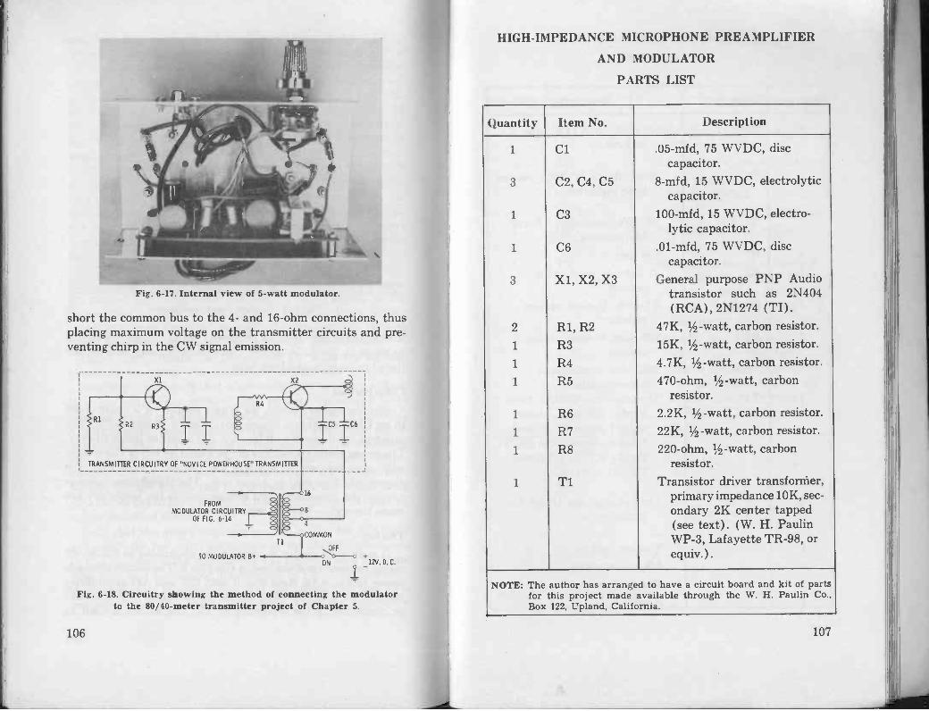
Fig. 6-17. Internal view of 5 -watt modulator.
short the common bus to the 4- and 16 -ohm connections, thusplacing maximum voltage on the transmitter circuits and pre-venting chirp in the CW signal emission.
X1
IIX2
TRANSMITTER CIRCUITRY OF "NOVICE POWERHOUSE" TRANSMITTER
FROMMODULATOR CIRCUITRY
OF FIG. 6-14
TO MODULATOR 13+
T1
4
COMMON
....OFF"0 0 +
ON 12V D C
C6
Fig. 6-18. Circuitry showing the method of connecting the modulatorto the 80/40 -meter transmitter project of Chapter 5.
106
HIGH -IMPEDANCE MICROPHONE PREAMPLIFIER
AND MODULATOR
PARTS LIST
Quantity Item No. Description
1 Cl .05-mfd, 75 WVDC, disccapacitor.
3 C2, C4, C5 8-mfd, 15 WVDC, electrolyticcapacitor.
1 C3 100-mfd, 15 WVDC, electro-lytic capacitor.
1 C6 .01-mfd, 75 WVDC, disccapacitor.
3 Xl, X2, X3 General purpose PNP Audiotransistor such as 2N404(RCA), 2N1274 (TI).
2 R1, R2 47K, 1/2 -watt, carbon resistor.1 R3 15K, 1/2 -watt, carbon resistor.1 R4 4.7K, 1/2 -watt, carbon resistor.1 R5 470 -ohm, 1/2 -watt, carbon
resistor.
1 R6 2.2K, 1/2 -watt, carbon resistor.1 R7 22K, 1/2 -watt, carbon resistor.1 R8 220 -ohm, 1/2 -watt, carbon
resistor.
1 T1 Transistor driver transfornier,primary impedance 10K, sec-ondary 2K center tapped(see text). (W. H. PaulinWP -3, Lafayette TR-98, orequiv.).
NOTE: The author has arranged to have a circuit board and kit of partsfor this project made available through the W. H. Paulin Co.,Box 122, Upland, California.
107
HALF -WATT MODULATOR
PARTS LIST
Quantity Item No. Description
1 Cl .05-mfd, 75 WVDC, discceramic.
1 C2 100-mfd, 15 WVDC, electro-lytic capacitor.
1
2 Xl, X2 2N1274 transistors (TexasInstruments).
1 R1 See text.1 R2 47 -ohm, 1/2 -watt, carbon
resistor.2 R3, R4 4.7 -ohm, 1/2 -watt, carbon
resistor.1 R5 220 -ohm, 1/2 -watt, carbon
resistor.1 R6 5000 -ohm, audio -taper
potentiometer.1 T1 Transistor modulation trans-
former, 500 -ohm, center -tapped primary, 3K and3.2 -ohm secondaries (W. H.Paulin WP -6, LafayetteTR-119 or equiv.).
1 LMB chassis box (LMB No.880 or equiv.).
1 Volume control.1 Microphone jack.1 Terminal strip.1 Knob.
108
5 -WATT TRANSMITTER MODULATOR
PARTS LIST
Quantity Item No. Description
1 C1 100-mfd, 15 WVDC, electro-lytic capacitor.
1 C2 0.5-mfd, 100 V, paper capacitor.2 Xl, X2 Audio power transistors, type
2N301 (RCA).2 R1, R2 2.7K, 1/2 -watt, carbon resistor.1 R3 100 -ohm, 1/2 -watt, carbon
resistor.1 T1 Modulation transformer used
as a driver, primary 3,000ohms, secondary 500 ohmscenter tapped, 3.2 -ohmwinding not used (see text).
1 T2 Class -B, transistors -to -speaker, matching trans-former, primary impedance32 ohms, center tapped, sec-ondary 4, 8, or 16 ohms.(TRIAD TY-64X orequiv.).
109

7
Tunnel - DiodeTransmitters
Contrary to what the name implies, there is no physicalcomparison between the tunnel diode and a passagewaythrough obstacles.
Fig. 7-1. Examples of tunnel diodes.
111

The small size of the tunnel diode is deceiving. Unlike avacuum tube or transistor, the tunnel diode has only twoterminals. It is capable of oscillating at frequencies from thesubaudio range up to several thousand megacycles. This sub-miniature semiconductor Samson is truly an amazing device.Some examples of typical tunnel diodes are shown in Fig. 7-1.
HOW IT WORKS
The theory of operation, when it is used in a relaxationoscillator circuit, is somewhat analogous to that of a neon bulb(Fig. 7-2). A common type of neon bulb, such as the NE -51,
NE -51
Fig. 7-2. A relaxation -type oscillator using a neon bulbas the negative -resistance device.
will produce oscillations when it is connected in this manner.When switch S is closed, voltage is applied to the RC networkand the capacitor acquires a charge through resistor R, whichhas a value of several megohms. At some point on the exponen-tial charging curve the voltage across the capacitor (and con-sequently the lamp) is sufficient to ionize the gas containedin the neon bulb. At this point the bulb fires, or strikes, andrapidly "switches" from an infinitely high impedance to a verylow impedance. This discharges the capacitor, and since thereis insufficient voltage to sustain the gas ionization, the bulb
Fig. 7-3. Waveform generated bythe circuit shown in Fig. 7-1.
112
is extinguished. Since the circuit is now reset to its originalstate, the capacitor once again charges and the cycle repeats.The circuit will continue to oscillate in this manner so longas voltage is applied to the input. The circuit generates a saw -tooth waveform as shown in Fig. 7-3. The frequency of theoscillation is determined by the time constant of R and C.Incidentally, this circuit makes an excellent code -practiceoscillator simply by substituting a telegraph key for S andconnecting a pair of earphones in series with a .001-mfd capaci-tor across the neon bulb.
THE TUNNEL DIODE
Unlike the neon bulb which can ionize and deionize only afew hundred times a second, the tunnel diode does not dependon the firing of a gas. The tunnel diode is "cultured" to exhibit
Fig. 7-4. El characteristic curve ofa typical tunnel diode.
E
a voltage -current curve such as the one shown in Fig. 7-4. Asthe voltage is increased, the current also increases until thepeak point is reached. Increasing the voltage further suddenlycauses the current flowing through the diode junction to de-crease. This corresponds to the valley point on the character-istic curve. Decreasing the voltage will cause the operatingpoint to rise back to the peak point. If a suitable energy -storagecircuit is included in the circuit, the device will oscillate con-tinuously between the peak and valley points. Some tunneldiodes are capable of switching between the peak or valley tenthousand million times in 1 second (10 kilomegacycles).
The theory of the tunnel diode is somewhat difficult to ex -
113
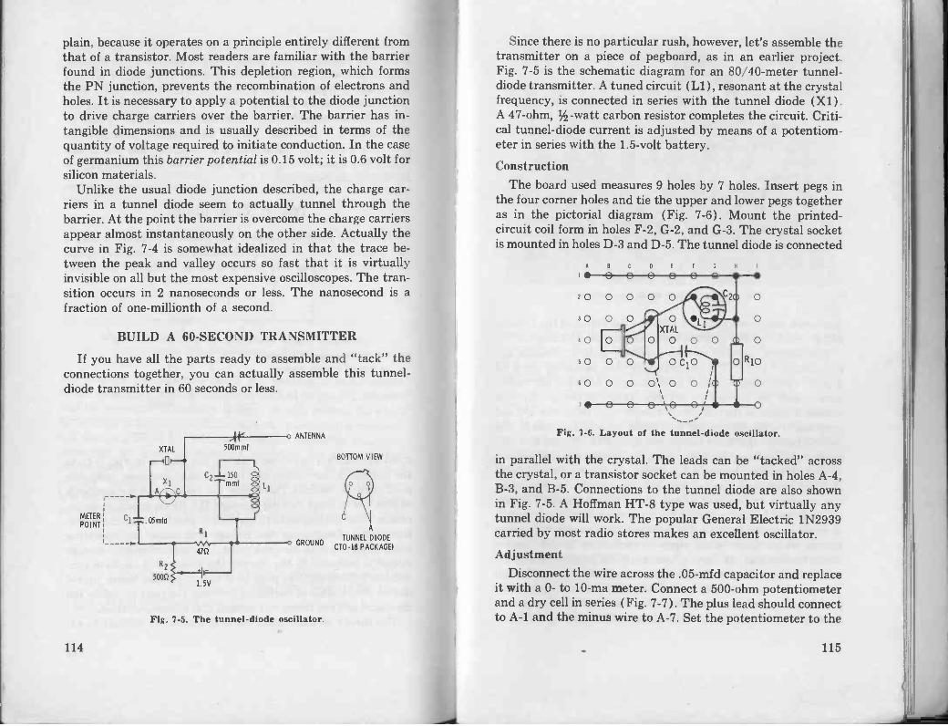
plain, because it operates on a principle entirely different fromthat of a transistor. Most readers are familiar with the barrierfound in diode junctions. This depletion region, which formsthe PN junction, prevents the recombination of electrons andholes. It is necessary to apply a potential to the diode junctionto drive charge carriers over the barrier. The barrier has in-tangible dimensions and is usually described in terms of thequantity of voltage required to initiate conduction. In the caseof germanium this barrier potential is 0.15 volt; it is 0.6 volt forsilicon materials.
Unlike the usual diode junction described, the charge car-riers in a tunnel diode seem to actually tunnel through thebarrier. At the point the barrier is overcome the charge carriersappear almost instantaneously on the other side. Actually thecurve in Fig. 7-4 is somewhat idealized in that the trace be-tween the peak and valley occurs so fast that it is virtuallyinvisible on all but the most expensive oscilloscopes. The tran-sition occurs in 2 nanoseconds or less. The nanosecond is afraction of one -millionth of a second.
BUILD A 60 -SECOND TRANSMITTER
If you have all the parts ready to assemble and "tack" theconnections together, you can actually assemble this tunnel -diode transmitter in 60 seconds or less.
METER
POINT
ANTENNA
BOTTOM VIEW
A
TUNNEL DIODEGROUND
CTO-18 PACKAGE)
1.5V
Fig. 7-5. The tunnel -diode oscillator.
Since there is no particular rush, however, let's assemble thetransmitter on a piece of pegboard, as in an earlier project.Fig. 7-5 is the schematic diagram for an 80/40 -meter tunnel -diode transmitter. A tuned circuit (L1), resonant at the crystalfrequency, is connected in series with the tunnel diode (X1).A 47 -ohm, 1/2 -watt carbon resistor completes the circuit. Criti-cal tunnel -diode current is adjusted by means of a potentiom-eter in series with the 1.5 -volt battery.
ConstructionThe board used measures 9 holes by 7 holes. Insert pegs in
the four corner holes and tie the upper and lower pegs togetheras in the pictorial diagram ( Fig. 7-6). Mount the printed -circuit coil form in holes F-2, G-2, and G-3. The crystal socketis mounted in holes D-3 and D-5. The tunnel diode is connected
A B D f G H
2 0 0 0 0 0
3 0 0 0 0 0XTAL
4o o0 0 0
5 0 0 0 u 0 C10 R10
0 0 0 06 0 0 0
Fig. 7-6. Layout of the tunnel -diode oscillator.
in parallel with the crystal. The leads can be "tacked" acrossthe crystal, or a transistor socket can be mounted in holes A-4,B-3, and B-5. Connections to the tunnel diode are also shownin Fig. 7-5. A Hoffman HT -8 type was used, but virtually anytunnel diode will work. The popular General Electric 1N2939carried by most radio stores makes an excellent oscillator.
AdjustmentDisconnect the wire across the .05-mfd capacitor and replace
it with a 0- to 10 -ma meter. Connect a 500 -ohm potentiometerand a dry cell in series (Fig. 7-7). The plus lead should connectto A-1 and the minus wire to A-7. Set the potentiometer to the
114 115

Fig. 7-7. The tunnel -diode transmitter.
maximum -resistance position. Observe the action of the tunnel -diode current as the potentiometer resistance is decreased.
The current should increase smoothly until it reaches ap-proximately 4 ma. The current will then suddenly drop toa lower value (about 2 ma). Continuing to decrease the resist-ance causes the current to decrease even further to approxi-mately 1 ma, and then it slowly rises to 4 or more ma. Do notdecrease the potentiometer resistance beyond this point; thediode could be damaged because of excessive current flow. Atsome point between the 2 -ma and 1 -ma currents described pre-viously, the diode becomes "unstable" and is capable of oscil-lation. Listen on a communications receiver to the frequencythe crystal is cut for and adjust the coil slug slowly. The an-tenna should be disconnected from the receiver and a 3' lengthof wire connected instead. This will prevent reception of strongsignals which might mask signs of oscillation in the tunnel -diode transmitter. It may be necessary to juggle the adjust-ment of the coil and potentiometer to initiate the oscillation.You will have no trouble recognizing the correct signal onceit starts. The note is very pure and stable. If the coil or poten-tiometer is misadjusted, oscillations will be heard on other
Fig. 7-8. Light -power solar cells.
frequencies but they will be very unstable and obviously notcrystal controlled. Once you get the "feel" of the circuit, con-nect an antenna to the transmitter in series with a 50- to 500-mmf trimmer capacitor. The value of this capacitor may requireadjustment, depending on the length of the antenna.
The transmitter can be keyed by connecting the telegraphkey in series with the antenna. Although the power output ismeasured in microwatts rather than milliwatts, this "pee -weepowerhouse" is capable of communications. In 1960, a NewZealand ham, Lester Earnshaw, ZL1AAX, contacted a station160 miles distant on the 80 -meter CW band using a similartunnel -diode transmitter.
In describing his transmitter (Radio Electronics, March,1961, page 34), Earnshaw points out that the silicon solar cellis an excellent current source for the tunnel diode. It is possibleto make the transmitter operate on "light power" only byreplacing the battery and potentiometer with a silicon solarcell of the type shown in Fig. 7-8.
A line of extremely tiny germanium tunnel diodes hasrecently been announced by Sylvania. Enclosed in the Dot
116 117
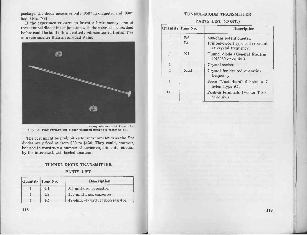
package, the diode measures only .050" in diameter and .030"high (Fig. 7-9).
If the experimenter cares to invest a little money, one ofthese tunnel diodes in conjunction with the solar cells describedbefore could be built into an entirely self-contained transmitterin a size smaller than an air -mail stamp.
Courtesy Sylvania Electric Products Inc.Fig. 7-9. Tiny germanium diodes pictured next to a common pin.
The cost might be prohibitive for most amateurs as the Dotdiodes are priced at from $30 to $130. They could, however,be used to construct a number of novice experimental circuitsby the interested, well heeled amateur.
TUNNEL -DIODE TRANSMITTER
PARTS LIST
Quantity Item No. Description
1 C1 .05-mfd disc capacitor.1 C2 150-mmf mica capacitor.1 R1 47 -ohm, 1/2 -watt, carbon resistor.
118
TUNNEL -DIODE TRANSMITTER
PARTS LIST (CONT.)
Quantity Item No. Description
1 R2 500 -ohm potentiometer.1 Ll Printed -circuit type coil resonant
at crystal frequency.1 X1 Tunnel diode (General Electric
1N2939 or equiv.).1 Crystal socket.1 Xtal Crystal for desired operating
frequency.1 Piece "Vectorbord" 9 holes x 7
holes (type A).14 Push -in terminals (Vector T-30
or equiv.).
119
8High Power
for CB or 10 Meters
This interesting project uses only four silicon planar tran-sistors (plus those in the modulator) and is capable of gener-ating more than 3 watts RF power output on the Citizensband or 2.5 to 3 watts on the 10 -meter amateur band. Thetransistors are designed for very high -frequency operation,and the transmitter should produce more than 2 watts outputon six meters (by rewinding the coils), although this has notbeen verified.
HOW IT WORKS
The circuit for the high -power CB transmitter is shown inFig. 8-1. The popular 2N706 is used as a common -base oscil-lator with feedback occurring through the transistor capac-itance between the collector and emitter. The crystal (a third -overtone, 27-mc type) is connected between base and ground.It operates at series resonance and bypasses the base at itsovertone, thus permitting oscillation only at that frequency.Resistors R1 and R2 provide forward bias, while R3 is usedfor emitter degeneration and stabilization. An RF choke isconnected in series with R3 to prevent the low resistance fromloading the feedback energy.
The 27-mc oscillator energy is developed across L1 andcoupled to the buffer (X2) through a link winding. Resistor
121

XTAL
ZN706
R2
4.30
R3
4752
RI82041
70mmT
J-C2100m ml
-1(-C3
001
RFC
LI
X2
PT -2.88
X3 -X4
PT -88806 .002
R6 1000
0B+ 1
141 MOD. TAP)
CI
6+211652 MOD. TAP)
14
Fig. 8-1. Circuit of high -power CB and 10 -meter transmitter.
RF OUT
R4 limits the buffer base current. Reverse bias is developedacross the resistor which biases the stage into deep class -Coperation. No emitter resistance is required since the stageoperates only over a very narrow portion of the positive half
cycle.Slightly less than 1 watt of drive is applied to the final, which
consists of two PT -888's connected in parallel. Drive -limitingresistors are used here also. Capacitors are used to bypass thesignal around the resistors for maximum drive. Separate net-
-11g. 1-2. Parts layout for CB and 10 -meter transmitter.
works are used in each transistor base circuit to equalize thedrive level to unmatched transistors.
Capacitor C8, the collector capacitance, and inductance L3form the "sloppy -tuned circuit," discussed in Chapter 4 and isbroadly resonant at 27 mc. A double pi network consisting ofC10, D11, C12, L4, and L5 couples the RF energy from thetransistor collector circuit to the antenna. This somewhatcomplex circuit is required to provide some 40 db of attenua-tion to the second -harmonic energy, which could interfere withChannel -2 television or other services.
B -supply connections 1 and 2 can be tied together and con-nected to a source of 12 to 14 volts DC for CW operation. Thehigh -power Citizen band transmitter can also be used for voicetransmissions by connecting it to the 5 -watt modulator de-scribed in Chapter 6.
ConstructionThe transmitter is constructed on a printed -circuit as shown
in Figs. 8-2 and 8-4. This is necessary because of the lowimpedance and high circulation currents involved. The emitter
Fig. 8-3. Coil -winding detail. 10 114TURNS
Ll
5/16"
TAPPEDAT 7 1/4
3 314TURNSTURNS
5116"
TAPPED AT3 3/4 TURNS
leads of X2, X3, and X4 should be kept as short as possibleor tied to the ground line through additional strips of tin toreduce the lead inductance. Printed -circuit coil forms are usedfor L1 and L2, while L3, L4, and L5 are airwound and areself supporting. Coil winding data are given in Fig. 8-3. Fig. 8-4shows a view of the completed transmitter.
TestingOnce the construction has been completed, recheck the
wiring carefully. The transistors are rather expensive, particu-larly when compared to the low-cost, general-purpose devicesused elsewhere in the book. A collector -base short circuit or
122 123

Fig. 8-4. View of complete transmitter.
accidental reversal of the battery polarity can instantly destroyone or more of the transistors.
When the wiring has been verified, connect a dummy load,consisting of four No. 44 pilot lamps connected in series par-allel, between the output terminal and ground. Tie B +1 andB +2 together and connect them to plus 12 volts. If a receivercapable of tuning the crystal frequency is available, use it tomonitor the transmitter signal. Connect a voltmeter (use thelowest range) across R4 and tune the slug in coil L1. The onlyvoltage developed across R4 is due to signal rectification, andit provides an excellent oscillation -strength indicator. Tune Llfor maximum voltage, which should be about 1 to 2 volts. Nextconnect a 1K resistor to the base of X3 or X4 and measure thevoltage between the free end of the resistor and ground; thisshould read approximately 3 volts. Peak coil L2 for a maximumreading on the voltmeter. At this point the dummy -load lampsshould glow slightly. Peak variable capacitors C11 and C12 formaximum output. The constructor can also check the value ofL3 by spreading or compressing turns for maximum output.After each movement of the coil, recheck the setting of C11and C12. Also recheck the adjustment of coils L1 and L2, and
124
repeak the adjustment for maximum output. The bulbs shouldglow brightly.
This transmitter is connected to the 5 -watt modulator con-structed earlier in much the same way as the 80/40 metertransmitter. Both the oscillator/buffer sections and the finalmust be modulated. Connect B +1 (in Fig. 8-1) to the 4 -ohmtap on the modulation transformer and the final B+ (B +2) tothe 16 -ohm connection. When the transmitter is modulated,the brilliance of the dummy -load bulbs should increasenoticeably.
Obtaining ComponentsThe transistor types specified (except the 2N706) have
manufacturer's numbers and may be confusing. They are man-ufactured by Pacific Semiconductors (Aviation Blvd., Haw-thorne, California) and are the type used in the Cadre Citizensband 5 -watt transceiver. The transistors may be obtained fromany large supply house which handles Cadre equipment; theycost $4.50 each. The remaining components should be readilyavailable at radio wholesale stores.
HIGH -POWER CB AND 10 -METER TRANSMITTER
PARTS LIST
Quantity Item No. Description1 Cl 70-mmf silver mica capacitor
(DM -15 or NPO).2 C2, C8 100-mmf silver mica capacitor
(DM -15 or NPO).2 C3, C4 .001-mfd disc ceramic capacitor1 C5 30-mmf silver mica capacitor
(DM -15 or NPO).2 C6, C7 .002-mfd disc ceramic capacitor1 C9 .005-mfd disc ceramic capacitor1 C10 150-mmf silver mica capacitor
(DM -15 or NPO).2 C11, C12 15- to 150-mmf trimmer
capacitor (Arco or equiv.).
125
HIGH -POWER CB AND 10 -METER TRANSMITTER
PARTS LIST (CONT.)
Quantity Item No. Description
1 L1 101/4 turns, No. 26 enameledwire closewound on a slug -tuned, printed -circuit coilform. Link 33% turns, inter -wound in bottom 4 turns ofprimary.
1 L2 71/4 turns, No. 18 enameledwire closewound on a slug -tuned, printed -circuit coilform. Link 33% turns inter -wound in bottom 4 turns ofprimary.
1 L3 7 turns, No. 26.enameled wire,1/4 " inside diameter, close -wound and air supported.
1 L4 10 turns, No. 18 enameled wire%" inside diameter, close -wound and air supported.
1 L5 7 turns, same as L4.1 X1 2N706 transistor.3 X2, X3, X4 PT -888 transistors (Pacific
Semiconductors, see text).1 R1 820 -ohm, 1/2 -watt, carbon
resistor.1 R2 4.3K, 1/2 -watt, 5% carbon
resistor.1 R3 47 -ohm, 1/2 -watt, carbon
resistor.
3 R4, R5, R6 100 -ohm, 1/2 -watt, carbonresistor.
1 Xtal 27-mc, third overtone crystal.
126
IndexA
Alignment, 26-28Alpha cutoff frequency, 13, 14
BBias, 24-26
CCases, transistor, 11-13"CB Cyclone," 55-60
construction, 56, 57schematic, 56testing, 58
"CB Cyclone II," 72-74construction, 73parts list, 75schematic, 73testing, 73, 74
Chartrecommended transistor types, 50typical RF toroids, 65
Circuit, oscillator, 29-40Class -A operation, 25Collector matching, 68-70Communications transistors, history, 7-10Computer, transistor, 8Construction, transistor, 10, 11Crossover distortion, 99, 100Crystal checker, 51-53
construction, 51, 52testing, 52
Crystal -controlled oscillators, 43-48
DDistortion, crossover, 99, 100Drift -field transistor, 9Dummy load, 83-84
E80/40 -Meter "Peanut Whistle," 53-55
construction, 53, 54schematic, 53testing, 54, 55
FFive -watt modulator, 103-107
construction, 105parts list, 109schematic, 103
Flywheel action, 61Flywheel effect, 17Frequency multiplication, 62, 63
HHalf -watt modulator, 99-103
construction, 101parts list, 108schematic, 100
Heat sink, 10, 11High -frequency operation, transistor, 12-16High -power CB or
10 -meter transmitter, 121-126coil winding data, 123construction, 123-125how it works, 121-123parts list, 125, 126schematic, 122
History, communications transistors, 7-10
IInterstage coupling, 63-67
LLow -power modulator, 96-99
construction, 97, 98parts list, 107schematic, 96
MMaximum available gain, 16Maximum useful gain, 16Mesa transistor, 9Modulation, 89-106
AM, 91, 96collector, 91-96frequency, 89-91
Modulatorfive -watt, 103-107half -watt, 99-103low -power, 96-99
NNovice Powerhouse, 77-87
adjustment, 83-86coil winding data, 83construction, 79-83how it works, 77-79schematic, 78
0Operating parameters, 14-19Oscillator
black -box equivalent of, 31circuit values, 30, 37-40Clapp, 40Colpitts, 30crystal controlled, 43-48Hartley, 30, 35-37output impedances of, 31overtone, 47, 48stability, 41, 42tickler coil, 34
Overtone oscillators, 47, 48
P"Peanut Whistle II," 70-72
construction, 70, 71
127

parts list, 75schematic, 70testing, 72
Planar transistor, 9Power amplifiers, 61-75Power and heat dissipation.
transistor, 10, 11Power supplies, 22, 23Protective circuits, 18, 19
RRecommended transistors, oscillator, 50RF-amplifier circuit, 32
SSchematic
basic AM modulation of transistortransmitters, 91
basic Colpitts circuit, 30alternative version,
crystal -controlled, 45crystal -controlled version, 45
basic configurations, 20basic Hartley circuit, 30, 35, 36
crystal -controlled version, 45basic reactance -modulated oscillator
circuit, 90bench voltage source, 23"CB Cyclone," 56"CB Cyclone II" power amplifier, 73Clapp oscillator configuration, 40
alternate Clapp circuit, 40Colpitts oscillator circuit, 37
alternate circuit, 38with capacitive -divider feedback, 38with tuning capacitor, 39
common -base Hartley oscillator, 36common-emitter Pierce oscillator, 46crystal checker, 5180/40 -meter "Peanut Whistle," 53equivalent circuit of a crystal, 43five -watt modulator, 103half -watt modulator, 100high -impedance microphone preamplifier
and modulator, 96high -power CB and 10 -meter
transmitter, 122low-pass filter, 14low-pass filter coupling system, 67method of connecting modulator, 106neon -bulb relaxation oscillator, 112"Novice Powerhouse" transmitter, 78output circuit of typical AM
transistor transmitter, 92"Peanut Whistle II" power amplifier, 70PNP RF amplifier, 32power amplifier with capacitive-divider
input, 67power amplifier with tapped-coil
input, 66
128
preferred method of AM modulation, 94protective circuits, 18signal bias systems, 24"sloppy -tuned" circuit for output
impedance matching, 69
tapped coil for output impedancematching, 68
tickler -coil oscillators, 29, 35crystal -controlled version, 44
"trick circuit" for increasingpositive -peak modulation, 95
tunnel -diode oscillator, 114tunnel -diode transmitter, 116typical RF power amplifier, 62
unusual transistor oscillator, 47variation of basic circuits, 21
Silicon solar cells, 117, 118Sixty-second transmitter, 114-117
adjustment, 115, 116parts list, 118, 119schematic, 114
Solar cells, silicon, 117, 118
TTransistor
alpha -cutoff frequency, 13, 14bias, 24-26cases, 11-13computers, 8classes of operation, 24-26
class A, 25class B, 25class C, 25
configurationscommon emitter, 20common base, 20common collector, 20
common emitter, grounded collector, 21common base, grounded collector, 21
construction, 10, 11drift field, 9high -frequency operation, 12-16history, 7-10maximum available gain, 16maximum useful gain, 16mesa, 9
parameters, 14-19, 23-26planar, 9power and heat dissipation, 10, 11protective circuits, 18, 19transit time, 12-14
Transit time, 12-14Tunnel diode, 111-114
characteristics, 113, 114examples, 111oscillator, 114theory of operation, 112, 113
Tunnel -diode transmitters, 111-119parts list, 118, 119
schematic, 114

TRANSISTOR
TRANSMITTERSfor the
AMATEURby Donald L. Stoner, W6TNS
KISSILGA
The rewords and enjoyment of a fascinatinghobby are well known to all radio amateurs.The greatest satisfaction for many hamscomes from constructing and operating theirlatest developments in communications.
Transistor Transmitters for the Amateur is a book written for all amateurs, whether they
want to build their own transmitter or merely acquaint themselves with transistor transmitter
theory. S.L...ting with a short history of communications transistors, the book progresses
through transistor oscillators, RF amplifiers, modulators, and simple antennas Each con-
struction project contains photographs, schematic diagrams, chassis -layout drawings,
tuning procedures, and operating instructions.The projects described include: a crystal checker and calibrator; an 80/40 meter "Peanut
Whistle"; the "CB Cyclone"; the "Peanut Whistle II"; the "CB Cyclone II"; the "Novice
Powerhouse"; a high -impedance microphone amplifier and modulator; a half -watt modu-
lator; a 5 -watt modulator; and a high -power CB or 10 -meter transmitter-useful equipmentfor all amateurs, CB'ers, students, and experimenters.
Presented in an informal style with extensive use of photos and drawings, TransistorTransmitters for the Amateur is a book that you'll want in your shack as a reference as well
as a construction guide.
ABOUT THE AUTHOR
Don Stoner, well known forhis numerous articles onvarious phases of amateurradio in national maga-zines, has authored severalother books. He is an in-structor at Chaffey Collegein Ontario, California, andpresident of Stoner Elec-tronics. Much of his time isspent as a consultant, de-signer, and builder ofspecial communicationsequipment.
'0)
TTS-1
$2.95 (In Canada $3.75)
own rigs and thus keeping abreast of the
HOWARD W. SAMS & CO., INC.
THE BOBBS-MERRILL COMPANY, INC.