TRANSMISSION ELECTRON MICROSCOPY OF OPTOELECTRONIC MATERIALS … · 2003-12-07 · Transmission...
7
- 1 - TRANSMISSION ELECTRON MICROSCOPY OF OPTOELECTRONIC MATERIALS – BASICS AND ADVANCED TECHNIQUES Fritz Phillipp Max-Planck-Institut für Metallforschung, Heisenbergstr. 3, D-70569 Stuttgart, Germany ABSTRACT Some main aspects of transmission electron microscopy such as selected-area diffraction and diffraction contrast at bright field, dark field and weak-beam conditions and the high-resolution imaging mode are introduced on a basic level. As an advanced method, lattice-strain determination directly from high- resolution micrographs is presented. Examples from studies on opto-electronic materials are used for illustration. 1. INTRODUCTION Fig. 1. Signals generated when a high-energy electron beam penetrates a thin specimen absorbed electrons electron – hole pairs (STEBIC) elastically scattered electrons direct beam characteristic X-rays (EDS) inelastically scattered electrons (EELS) light (CL) backscattered electrons secondary electrons Auger electrons Bremsstrahlung X-rays incident high-energy electron beam
Transcript of TRANSMISSION ELECTRON MICROSCOPY OF OPTOELECTRONIC MATERIALS … · 2003-12-07 · Transmission...
- 1 -
TRANSMISSION ELECTRON MICROSCOPY OF OPTOELECTRONIC
MATERIALS – BASICS AND ADVANCED TECHNIQUES
Fritz Phillipp
Max-Planck-Institut für Metallforschung, Heisenbergstr. 3, D-70569 Stuttgart, Germany ABSTRACT
Some main aspects of transmission electron microscopy such as selected-area diffraction and diffraction contrast at bright field, dark field and weak-beam conditions and the high-resolution imaging mode are introduced on a basic level. As an advanced method, lattice-strain determination directly from high-resolution micrographs is presented. Examples from studies on opto-electronic materials are used for illustration.
1. INTRODUCTION
Fig. 1. Signals generated when a high-energy electron beam penetrates a thin specimen
absorbed electrons electron – hole pairs (STEBIC)
elastically scattered electrons
direct beam
characteristic X-rays (EDS)
inelastically scattered electrons (EELS)
light (CL)
backscattered electrons
secondary electrons
Auger electrons
Bremsstrahlung X-rays
incident high-energy electron beam
1st CEPHONA Workshop on Microscopic Characterisation of Materials and Structures for Photonics
- 2 -
Transmission electron microscopy (TEM) is a most valuable tool for the study of materials on a micro- and nano-scale. The versatility of TEM is a result of the multitude of signals that are generated when a high-energy electron beam, typically 200 – 400 keV for medium voltage microscopes used in materials science (or even ca. 1 MeV in the case of high-voltage microscopes) penetrates the thin specimen (Fig. 1). Most of these signals can be used in different types of electron microscopes. In the present paper we will concentrate on the directly transmitted and the elastically scattered electrons that are used for imaging and diffraction. A complete framework for the mathematical description of scattering and image formation has been developed and can be looked up in the textbooks [e.g., 1-9]. Recent developments and future needs particularly in the field of high-resolution electron microscopy (HREM) may be found in review articles [10-13]. The point resolution of modern instruments ranges between ca. 0.3 nm (200 kV standard instrument), 0.17 nm (400 kV dedicated high-resolution instrument) and 0.1 nm (1250 kV high-voltage atomic resolution microscope [14]).
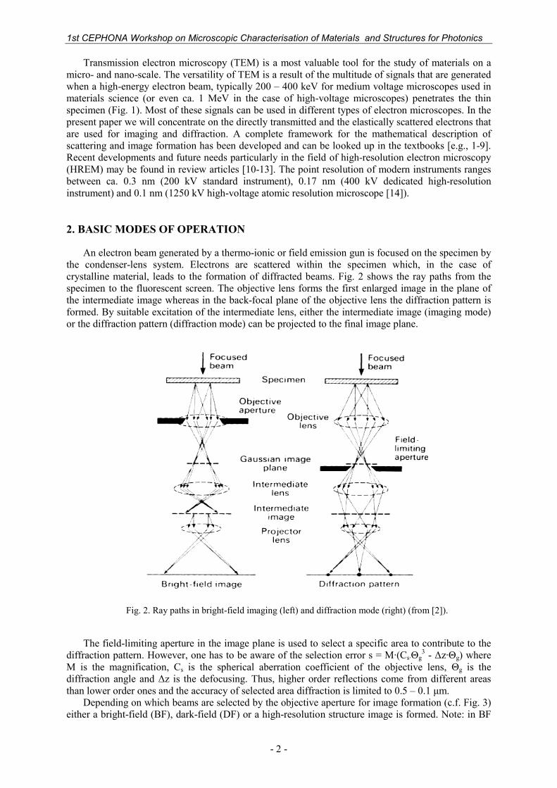
2. BASIC MODES OF OPERATION
An electron beam generated by a thermo-ionic or field emission gun is focused on the specimen by the condenser-lens system. Electrons are scattered within the specimen which, in the case of crystalline material, leads to the formation of diffracted beams. Fig. 2 shows the ray paths from the specimen to the fluorescent screen. The objective lens forms the first enlarged image in the plane of the intermediate image whereas in the back-focal plane of the objective lens the diffraction pattern is formed. By suitable excitation of the intermediate lens, either the intermediate image (imaging mode) or the diffraction pattern (diffraction mode) can be projected to the final image plane.
Fig. 2. Ray paths in bright-field imaging (left) and diffraction mode (right) (from [2]).
The field-limiting aperture in the image plane is used to select a specific area to contribute to the diffraction pattern. However, one has to be aware of the selection error s = M·(Cs·Θg
3 - ∆z·Θg) where M is the magnification, Cs is the spherical aberration coefficient of the objective lens, Θg is the diffraction angle and ∆z is the defocusing. Thus, higher order reflections come from different areas than lower order ones and the accuracy of selected area diffraction is limited to 0.5 – 0.1 µm.
Depending on which beams are selected by the objective aperture for image formation (c.f. Fig. 3) either a bright-field (BF), dark-field (DF) or a high-resolution structure image is formed. Note: in BF

1st CEPHONA Workshop on Microscopic Characterisation of Materials and Structures for Photonics
- 3 -
and DF mode the image shows the intensity distribution in the transmitted or diffracted beam, respectively, there is no information about the atomic structure of the specimen. In order to get information on that, according to Abbe’s theory of image formation at least the first order diffracted beams together with the transmitted beam have to pass through the objective aperture and interfere in the image plane (c.f. Sect. 2.2).
Fig. 3. Ray paths in imaging mode: (a) bright field, (b) tilted illumination axial dark field, (c) high-resolution mode (from [6]).
3. DIFFRACTION CONTRAST IMAGING
In this section a few examples for the application of conventional diffraction contrast and selected area diffraction are presented.
Example 1: DF imaging of domain boundaries in GaInP [15]: At specific growth conditions the ternary system GaInP may develop the CuPtB structure (Fig. 4a). This ordered structure gives rise to superlattice reflections which are not present in the sphalerite structure (Fig. 4b). Using one of these superlattice reflections for DF imaging the domain boundaries in the material appear as black lines whereas the ordered domains appear bright (Fig. 4c). In this way the size and the orientation of the domains can be analyzed.
Example 2: Diffraction contrast imaging of dislocations: If the specimen is oriented slightly off Bragg condition in the perfect lattice, the Bragg condition may be fulfilled in the vicinity of a dislocation due to the local lattice-plane bending (Fig. 5a). This results in a weakening of the transmitted beam in these areas since much intensity is transferred to the diffracted beam. The dislocations therefore appear as dark lines in BF and bright lines in DF. Diffraction contrast is essentially extinguished if g·b = 0, where g is the operating diffraction vector and b is the Burgers vector of the dislocation. By imaging the same dislocation with different diffraction vectors the Burgers vector can be determined. An example of such an analysis is shown in Fig. 5(b) for the case of interface dislocations in GaAs epitaxially grown on Si [16]. Due to the large lattice mismatch of ca. 4% a high density of interface dislocations is present.

1st CEPHONA Workshop on Microscopic Characterisation of Materials and Structures for Photonics
- 4 -
Fig. 4. (a) CuPtB structure of ordered GaInP, (b) diffraction pattern in <110> orientation with superstructure reflections indicated by circles, (c) ordered domains and domain boundaries.
Fig. 5. (a) Schematics of lattice-plane bending at an edge dislocation with the Bragg condition fulfilled for the bent planes near the core (top) and intensity profiles for the transmitted and reflected beam (bottom) (from [4]).
(b) Interface dislocations in GaAs on Si imaged with different diffraction vectors.
As can be seen from Fig. 5(b) the width of the contrast of dislocations imaged with the lattice-plane set close to Bragg condition is rather wide, thus, fine details in the geometry of the dislocations may not be easily investigated. To overcome this problem, weak-beam dark field conditions have to be employed [17]. Under these conditions the specimen is oriented rather far off the Bragg condition. As a result, strong scattering occurs only in a narrow region close to the dislocation core resulting in dark-
GaInP
a b c
1st CEPHONA Workshop on Microscopic Characterisation of Materials and Structures for Photonics
- 5 -
field images width contrast widths as small as 1 nm (as compared to several tens of nm for conventional BF or DF imaging). 3. HIGH-RESOLUTION (HREM) IMAGING
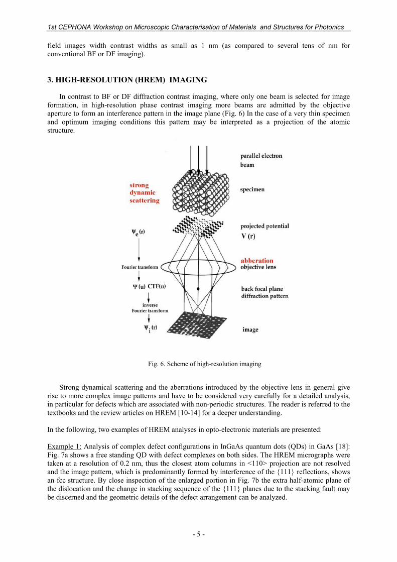
In contrast to BF or DF diffraction contrast imaging, where only one beam is selected for image formation, in high-resolution phase contrast imaging more beams are admitted by the objective aperture to form an interference pattern in the image plane (Fig. 6) In the case of a very thin specimen and optimum imaging conditions this pattern may be interpreted as a projection of the atomic structure.
Fig. 6. Scheme of high-resolution imaging
Strong dynamical scattering and the aberrations introduced by the objective lens in general give rise to more complex image patterns and have to be considered very carefully for a detailed analysis, in particular for defects which are associated with non-periodic structures. The reader is referred to the textbooks and the review articles on HREM [10-14] for a deeper understanding.
In the following, two examples of HREM analyses in opto-electronic materials are presented:
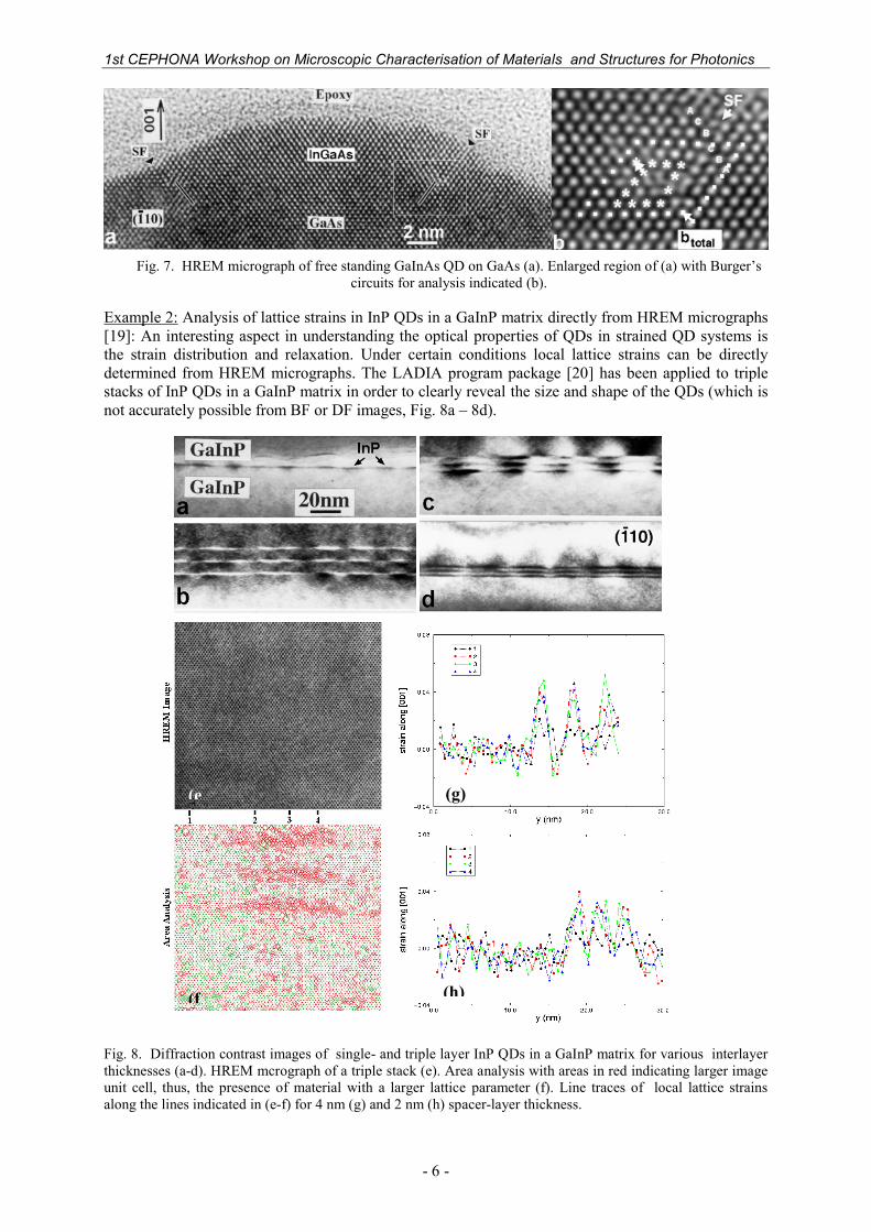
Example 1: Analysis of complex defect configurations in InGaAs quantum dots (QDs) in GaAs [18]: Fig. 7a shows a free standing QD with defect complexes on both sides. The HREM micrographs were taken at a resolution of 0.2 nm, thus the closest atom columns in <110> projection are not resolved and the image pattern, which is predominantly formed by interference of the {111} reflections, shows an fcc structure. By close inspection of the enlarged portion in Fig. 7b the extra half-atomic plane of the dislocation and the change in stacking sequence of the {111} planes due to the stacking fault may be discerned and the geometric details of the defect arrangement can be analyzed.
1st CEPHONA Workshop on Microscopic Characterisation of Materials and Structures for Photonics
- 6 -
Fig. 7. HREM micrograph of free standing GaInAs QD on GaAs (a). Enlarged region of (a) with Burger’s circuits for analysis indicated (b).
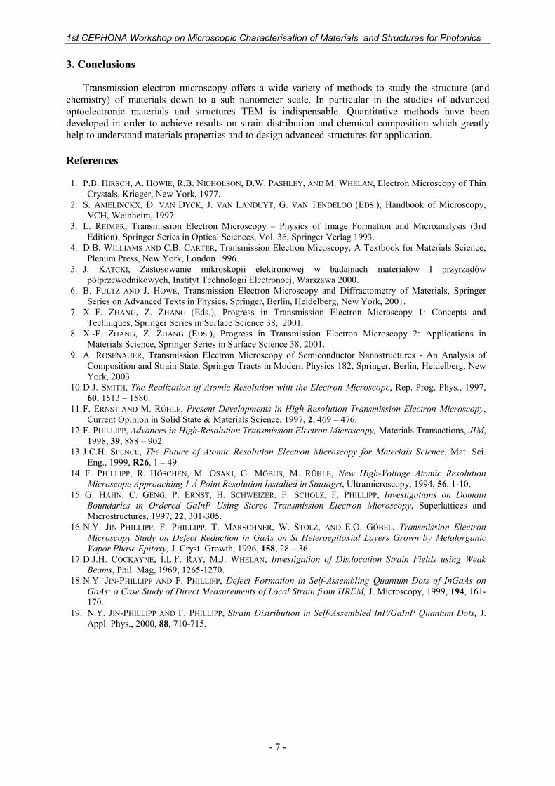
Example 2: Analysis of lattice strains in InP QDs in a GaInP matrix directly from HREM micrographs [19]: An interesting aspect in understanding the optical properties of QDs in strained QD systems is the strain distribution and relaxation. Under certain conditions local lattice strains can be directly determined from HREM micrographs. The LADIA program package [20] has been applied to triple stacks of InP QDs in a GaInP matrix in order to clearly reveal the size and shape of the QDs (which is not accurately possible from BF or DF images, Fig. 8a – 8d).
Fig. 8. Diffraction contrast images of single- and triple layer InP QDs in a GaInP matrix for various interlayer thicknesses (a-d). HREM mcrograph of a triple stack (e). Area analysis with areas in red indicating larger image unit cell, thus, the presence of material with a larger lattice parameter (f). Line traces of local lattice strains along the lines indicated in (e-f) for 4 nm (g) and 2 nm (h) spacer-layer thickness.
(e
(f
(g)
(h)
1st CEPHONA Workshop on Microscopic Characterisation of Materials and Structures for Photonics
- 7 -
3. Conclusions
Transmission electron microscopy offers a wide variety of methods to study the structure (and chemistry) of materials down to a sub nanometer scale. In particular in the studies of advanced optoelectronic materials and structures TEM is indispensable. Quantitative methods have been developed in order to achieve results on strain distribution and chemical composition which greatly help to understand materials properties and to design advanced structures for application. References
1. P.B. HIRSCH, A. HOWIE, R.B. NICHOLSON, D.W. PASHLEY, AND M. WHELAN, Electron Microscopy of Thin Crystals, Krieger, New York, 1977.
2. S. AMELINCKX, D. VAN DYCK, J. VAN LANDUYT, G. VAN TENDELOO (EDS.), Handbook of Microscopy, VCH, Weinheim, 1997.
3. L. REIMER, Transmission Electron Microscopy – Physics of Image Formation and Microanalysis (3rd Edition), Springer Series in Optical Sciences, Vol. 36, Springer Verlag 1993.
4. D.B. WILLIAMS AND C.B. CARTER, Transmission Electron Micoscopy, A Textbook for Materials Science, Plenum Press, New York, London 1996.
5. J. KĄTCKI, Zastosowanie mikroskopii elektronowej w badaniach materiałów I przyrządów półprzewodnikowych, Instityt Technologii Electronoej, Warszawa 2000.
6. B. FULTZ AND J. HOWE, Transmission Electron Microscopy and Diffractometry of Materials, Springer Series on Advanced Texts in Physics, Springer, Berlin, Heidelberg, New York, 2001.
7. X.-F. ZHANG, Z. ZHANG (Eds.), Progress in Transmission Electron Microscopy 1: Concepts and Techniques, Springer Series in Surface Science 38, 2001.
8. X.-F. ZHANG, Z. ZHANG (EDS.), Progress in Transmission Electron Microscopy 2: Applications in Materials Science, Springer Series in Surface Science 38, 2001.
9. A. ROSENAUER, Transmission Electron Microscopy of Semiconductor Nanostructures - An Analysis of Composition and Strain State, Springer Tracts in Modern Physics 182, Springer, Berlin, Heidelberg, New York, 2003.
10. D.J. SMITH, The Realization of Atomic Resolution with the Electron Microscope, Rep. Prog. Phys., 1997, 60, 1513 – 1580.
11. F. ERNST AND M. RÜHLE, Present Developments in High-Resolution Transmission Electron Microscopy, Current Opinion in Solid State & Materials Science, 1997, 2, 469 – 476.
12. F. PHILLIPP, Advances in High-Resolution Transmission Electron Microscopy, Materials Transactions, JIM, 1998, 39, 888 – 902.
13. J.C.H. SPENCE, The Future of Atomic Resolution Electron Microscopy for Materials Science, Mat. Sci. Eng., 1999, R26, 1 – 49.
14. F. PHILLIPP, R. HÖSCHEN, M. OSAKI, G. MÖBUS, M. RÜHLE, New High-Voltage Atomic Resolution Microscope Approaching 1 Å Point Resolution Installed in Stuttagrt, Ultramicroscopy, 1994, 56, 1-10.
15. G. HAHN, C. GENG, P. ERNST, H. SCHWEIZER, F. SCHOLZ, F. PHILLIPP, Investigations on Domain Boundaries in Ordered GaInP Using Stereo Transmission Electron Microscopy, Superlattices and Microstructures, 1997, 22, 301-305.
16. N.Y. JIN-PHILLIPP, F. PHILLIPP, T. MARSCHNER, W. STOLZ, AND E.O. GÖBEL, Transmission Electron Microscopy Study on Defect Reduction in GaAs on Si Heteroepitaxial Layers Grown by Metalorganic Vapor Phase Epitaxy, J. Cryst. Growth, 1996, 158, 28 – 36.
17. D.J.H. COCKAYNE, I.L.F. RAY, M.J. WHELAN, Investigation of Dis.location Strain Fields using Weak Beams, Phil. Mag, 1969, 1265-1270.
18. N.Y. JIN-PHILLIPP AND F. PHILLIPP, Defect Formation in Self-Assembling Quantum Dots of InGaAs on GaAs: a Case Study of Direct Measurements of Local Strain from HREM, J. Microscopy, 1999, 194, 161-170.
19. N.Y. JIN-PHILLIPP AND F. PHILLIPP, Strain Distribution in Self-Assembled InP/GaInP Quantum Dots, J. Appl. Phys., 2000, 88, 710-715.