Transmission Electron Microscopy Skills:Analytical electron microscopy Lecture 12

Ultramicroscopy 111 (2011) 1239–1246
Contents lists available at ScienceDirect
Ultramicroscopy
0304-39
doi:10.1
n Corr
E-m
journal homepage: www.elsevier.com/locate/ultramic
Transmission electron microscopy at 20 kV for imaging and spectroscopy
U. Kaiser a,n, J. Biskupek a, J.C. Meyer a, J. Leschner a, L. Lechner a, H. Rose a, M. Stoger-Pollach b,A.N. Khlobystov c, P. Hartel d, H. Muller d, M. Haider d, S. Eyhusen e, G. Benner e
a Central Facility of Electron Microscopy, Group of Electron Microscopy of Materials Science, Ulm University, Albert-Einstein-Allee 11, 89081 Ulm, Germanyb University Service Centre for TEM (USTEM), Vienna University of Technology, 1040 Wien, Austriac School of Chemistry, University of Nottingham, University Park, Nottingham NG7 2RD, United Kingdomd CEOS GmbH, Englerstraße 28, 69126 Heidelberg, Germanye Carl Zeiss NTS GmbH, Carl-Zeiss-Strasse 56, 73447 Oberkochen, Germany
a r t i c l e i n f o
Article history:
Received 22 December 2010
Received in revised form
10 March 2011
Accepted 16 March 2011Available online 1 April 2011
Keywords:
Low-voltage TEM
Beam damage
High resolution
EELS
91/$ - see front matter & 2011 Elsevier B.V. A
016/j.ultramic.2011.03.012
esponding author.
ail address: [email protected] (U. Kaiser
a b s t r a c t
The electron optical performance of a transmission electron microscope (TEM) is characterized for
direct spatial imaging and spectroscopy using electrons with energies as low as 20 keV. The highly
stable instrument is equipped with an electrostatic monochromator and a CS-corrector. At 20 kV it
shows high image contrast even for single-layer graphene with a lattice transfer of 213 pm (tilted
illumination). For 4 nm thick Si, the 200 reflections (271.5 pm) were directly transferred (axial
illumination). We show at 20 kV that radiation-sensitive fullerenes (C60) within a carbon nanotube
container withstand an about two orders of magnitude higher electron dose than at 80 kV. In
spectroscopy mode, the monochromated low-energy electron beam enables the acquisition of EELS
spectra up to very high energy losses with exceptionally low background noise. Using Si and Ge, we
show that 20 kV TEM allows the determination of dielectric properties and narrow band gaps, which
were not accessible by TEM so far. These very first results demonstrate that low kV TEM is an exciting
new tool for determination of structural and electronic properties of different types of nano-materials.
& 2011 Elsevier B.V. All rights reserved.
1. Introduction
Aberration corrected transmission electron microscopy (TEM)is currently undergoing revolutionary changes in its ability toimage materials at the atomic level using medium energy elec-trons [1–4]. However, the resolution in the TEM image is oftenlimited by radiation damage rather than by the quality of theinstrument [5,6]. The damaging effects include ionization, heat-ing, chemical etching and knock-on displacement of atoms. Whileionization and heating depend on the beam current applied to thespecimen, knock-on damage depends solely on the energy of theelectrons. Therefore, this damage effect can only be avoided byreducing the voltage below the knock-on threshold of the objectsunder study.
Already in the early days of electron microscopy, more than 45years ago, attempts were made to visualize biological sampleswith high contrast in a TEM operating at voltages as low as6 kV [7]. However, at this time the performance of the microscopewas very poor due to the large chromatic aberration. In thefollowing decades, the use of low voltages in TEM was completely
ll rights reserved.
).
abandoned. Recent advances in the design of suitable aberrationcorrectors [1,2] initiated a revival of low-voltage electron micro-scopy [6,8] spurring world-wide activity. For example, a double CS
aberration corrected low-voltage TEM operating at acceleratingvoltages between 30 and 60 kV is currently being designed at theNational Institute of Advanced Industrial Science and Technology(AIST), Tsukuba, Japan [9]. Very recently, it has been demon-strated that also the Nion UltraSTEM is capable of atomic resolu-tion imaging at 60 kV in STEM mode by virtue of its 3rd-generation C3/C5 corrector [10]. These examples illustrate a highlevel of interest in lower voltage TEM driven by the need to imageincreasingly complex and delicate structures.
Within the frame of the Sub-Angstrom Low-Voltage Electron
microscopy (SALVE) project, we aim at improving the instrumen-
tal resolution by optimizing all components of the SALVE micro-
scope and by integrating a new CC/CS corrector into the final
instrument for electron beam (e-beam) energies down to 20 keV.
Our new approach is intended to enhance the specimen resolu-
tion given by ds ¼
ffiffiffiffiffiffiffiffiffiffiffiffiffiffiffiffiffiffiffiffiffiffiffiffiffiffiffiffiffiffiffiffiffiffiffid2
i þðS=NÞ2=DC2q
[6] of radiation-sensitive
materials by low-voltage operation. The product of tolerable dose
D times contrast C is nearly independent of the voltage. Because
the contrast increases with decreasing voltage and the required
signal-to-noise (S/N) ratio is fixed, we can decrease ds by going to

U. Kaiser et al. / Ultramicroscopy 111 (2011) 1239–12461240
lower voltages provided that the instrumental resolution limit di
does not increase [6]. This requirement can be satisfied only bymeans of a novel CC/CS corrector, which compensates for chro-matic and spherical aberrations and provides a wide field of view.
Imaging of predominantly knock-on damage sensitive semi-conductors, minerals, oxides and organic molecules requires low-voltage. Low-voltage TEM in turn necessitates very thin objects toavoid resolution degradation caused by multiple scattering. Formost bulk materials appropriate target preparation methods arenecessary to create self-supporting specimens. Present studies arelimited to very few materials where conventional preparationtechniques can be applied to create electron transparent areas. Incontrast, focused ion beam techniques allow TEM specimens to beprepared from almost any material. Such a lamella suitable forhigh-resolution TEM (HRTEM) observation at 20 kV has to beprepared much thinner than 10 nm. However, using conventionallift-out technique [11] and low-kV Ga milling minimum lamellathicknesses of 20–30 nm are achievable at the best [12]. Inaddition, demands for homogeneity and absence of surface con-tamination are not met by these specimen.
Imaging single molecules requires a supporting conductivesubstrate. We intend to employ graphene, a single-layer graphite[13], as a precisely defined and thinnest possible substrate. More-over, if its structure is removed from the image by Fourier filtering,the HRTEM image of the free-standing object is obtained [8,14] ifbonding effects between molecule and substrate can be neglected.In addition, electrons from the highly conducting substrates mightreplace ejected electrons of the molecules before bonds break [37].
Analytical low-voltage TEM combines imaging with peculiaritiesof spectroscopy at low voltages. Especially for valence EELS (VEELS)low e-beam energies are advantageous, as a strong increase in signalto background ratio is observed. This effect is most probably causedby a reduction or avoidance of relativistic energy losses, like Cerenkovlosses and light-guided modes [15–17]. Calculations [17] predict theCerenkov limit for silicon in a range between 15 and 20 kV. The samethreshold for germanium is below 5 kV. These results suggest that at20 kV at least silicon can be studied free of relativistic energy losses.Furthermore, the range of the Coulomb interaction between theincident electron and the electrons of the sample is also reduced at20 kV resulting in a decreased delocalization width [16]. Since thetransferred momentum _qE increases for lower electron energies, theresolution of the ‘‘inelastic’’ image also increases as long as aberra-tions and/or diffraction are not the limiting factors.
In this study, we report for the first time on specifications andapplications of the prototype SALVE instrument operating at 20 kVaccelerating voltage. Our first example shows the capability of theinstrument to image e-beam-sensitive fullerene C60 molecules.They have been encapsulated in the thinnest and smallest avail-able test-tube, a single-walled carbon nanotube. Defect-freecarbon nanotubes are e-beam transparent and structurally stablefor infinite time at or below 80 kV [18,19]. The second exampledemonstrates the analytical potential of the prototype SALVE
instrument for insulating and/or semiconducting materials byusing EELS at 20 kV for investigating the low-loss region of Siand Ge.
2. Experiments
2.1. Instrumental details
The prototype SALVE microscope is a monochromated Libra200 MC with in-column corrected OMEGA filter and imagingCEOS CS-corrector (CETCOR). For 20 keV electrons the monochro-mator [20] creates high image contrast at high spatial frequen-cies: slit widths of 2.5 and 2 mm result in a full width at half
maximum (FWHM) of 0.17 and 0.15 eV for the incident electronbeam, respectively. The microscope was operated with theOMEGA filter always turned on during all experiments. In imagingmode the energy window (5 eV) of the energy selecting slit wascentered around the zero-loss peak. EELS was carried out using asmaller monochromator slit of 1 mm—resulting in an energyFWHM o0.1 eV when measured for 1 s in vacuum. In order toobtain a good signal-to-noise ratio for the EELS data (includingboth zero-loss peak and plasmon losses) in each experiment 100single spectra were acquired with 0.2 s exposure time. Thespectra were then corrected for energy shifts by drift correlationand subsequently averaged. All images and spectra were recordedby a Gatan 2k�2k slow scan CCD 16 bit camera, type Ultrascan1000. The conversion rate of the camera at 20 kV was determinedto be 0.5 CCD counts per electron by Faraday cup measurements.Since we need a sufficiently large number of electrons in order toachieve signals above the readout noise of the CCD. the poorconversion rate requires much more electrons for exciting asufficient number of photons than the Z5 counts per electronfor conventional HRTEM in medium voltage operation.
The information limit of the microscope at 20 kV is determinedby the combination of image spread and focus spread [21]. Thefocus spread limit, which comprises the effect of the chromaticaberration and other focus instabilities can be reduced from0.5 nm without monochromator to 0.25 nm with a reducedenergy width of 0.17 eV. The image spread limit, which includesall kinds of lateral noise has been determined to be better than0.18 nm.
The accelerator design and the alignment of the FEG have beenoptimized for low-voltage operation. The instrument can cover avoltage range from 20 to 80 kV (200 kV) without any loss inbrightness (referred to the extraction voltage). We demonstratethat especially for low beam energies the electrostatic omegaprinciple for monochromatization and the corrected in-columntechnology are beneficial for filtered images with low energywidth and highly resolved spectroscopy.
2.2. Preparation of Si and Ge samples
We used a Zeiss NVision 40 Ar cross-beam microscopeequipped with a SEM column, a Ga FIB column, and a focusedAr beam. One micrometer thick lamellas were produced frombulk material by conventional in-situ lift-out technique. Theywere planarized and thinned to approximately 0.5 mm thicknessusing 30 kV Ga-ions and low Ga-beam currents (down to 10 pA).Subsequently, a series of rectangular recesses, each about 200 nmdeep, was milled into one side of the lamella. Both sides of thelamella were then polished in several steps, decreasing Ga beamvoltage (down to 1 kV) to reduce the amorphous layer thickness.Finally residual Ga contamination was removed by polishing withthe Ar ion source at 500 V. Using this technique, we obtained Silamellae with thicknesses down to 4 nm (thickness determinedby EELS measurement). Details of the preparation technique aredescribed in [22]. For the EELS experiments, the sample thicknesswas chosen to be in the range from 0.2 to 0.5 times the mean freepath lengths for inelastic scattered electron. This thickness rangeensures low plural scattering – which can then be subsequentlydeconvolved from the spectrum – and a sufficiently high inelasticscattering cross-section.
2.3. Preparation of graphene and C60 at DWNT
Graphene membranes were prepared by following the CVDmethods for graphene synthesis on nickel substrates [23–25]. TheCVD grown graphene sheets were transferred onto commercialTEM grids as described previously [15]. Arc-discharge nanotubes
U. Kaiser et al. / Ultramicroscopy 111 (2011) 1239–1246 1241
(NanoCarbLab) were heated in air at 520 1C for 20 min to removeadsorbed water and to open their termini. The nanotubes werecooled down to room temperature and without delay combinedwith a weight equivalent of crystalline fullerene C60 (99.9% pure,SES Research). The mixture was sealed in a quartz tube in 10�4 Pavacuum and heated at 500 1C for 2 days. The excess of fullereneswas removed from the surface of the nanotubes by extensivewashing with carbon disulfide (CS2). The resultant sample wasdried in air. A small amount of C60@DWNT powder (�10 mg) wassuspended in 2 ml of methanol using an ultrasonic bath. Thesuspension was drop-cast onto a lacey-carbon coated TEM grid.
2.4. EELS analysis
The refractive index has been determined from the dielectricfunction by Kramers–Kronig analysis (KKA) after plural scatteringdeconvolution. Due to the high dispersion of the spectrometer at20 kV (0.023 eV/channel), only a small portion of the EELSspectrum can be recorded on the camera. Consequentially, thehigh-energy end of the spectrum is cut-off so that the intensity ofthe recorded spectrum does not approach zero. This behaviorcauses problems when using the conventional Fourier-log decon-volution routine, because any Fourier deconvolution requires aperiodic function [26]. A way out of this problem is the matrixdeconvolution [27]. After retrieval of the single scattering dis-tribution, conventional KKA can be applied yielding the opticalproperties.
3. Results
3.1. Characterization of the 20 kV SALVE microscope
The information limit and the axial aberrations of our proto-type SALVE microscope optimized for 20 kV operation weremeasured using thin amorphous carbon foils. The results wereconfirmed by crystalline silicon and graphene samples. Spectro-scopy was performed on silicon and germanium.
3.1.1. Information limit
At an energy E0 of 20 keV, the chromatic aberration coefficientCC amounts to 1.26 mm (calculation), which is in good agreementwith the measured value of (1.270.1) mm. This value wasdetermined using CC¼E0/DEyDf, where the change of focus Df
with changed electron energy DE was recorded in several steps of10 eV.
Therefore, without monochromator (DE¼0.75 eV, FWHM) thefocus spread contribution from the chromatic aberration is limit-ing the resolution at 0.52 nm (calculated for a contrast of 13.5%),which is supported by a Young’s fringes measurement shown in
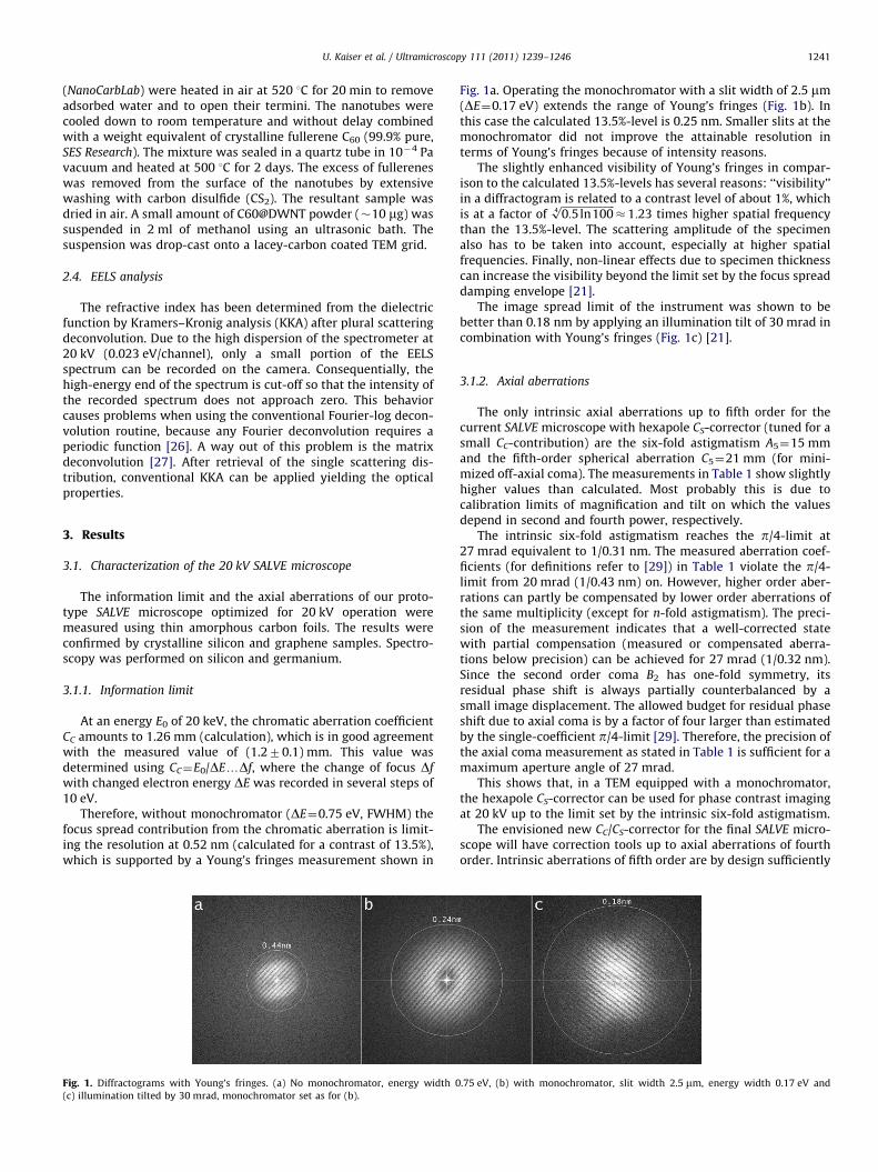
Fig. 1. Diffractograms with Young’s fringes. (a) No monochromator, energy width 0
(c) illumination tilted by 30 mrad, monochromator set as for (b).
Fig. 1a. Operating the monochromator with a slit width of 2.5 mm(DE¼0.17 eV) extends the range of Young’s fringes (Fig. 1b). Inthis case the calculated 13.5%-level is 0.25 nm. Smaller slits at themonochromator did not improve the attainable resolution interms of Young’s fringes because of intensity reasons.
The slightly enhanced visibility of Young’s fringes in compar-ison to the calculated 13.5%-levels has several reasons: ‘‘visibility’’in a diffractogram is related to a contrast level of about 1%, whichis at a factor of
ffiffiffiffiffiffiffiffiffiffiffiffiffiffiffiffiffiffiffiffiffi0:5ln1004p
� 1:23 times higher spatial frequencythan the 13.5%-level. The scattering amplitude of the specimenalso has to be taken into account, especially at higher spatialfrequencies. Finally, non-linear effects due to specimen thicknesscan increase the visibility beyond the limit set by the focus spreaddamping envelope [21].
The image spread limit of the instrument was shown to bebetter than 0.18 nm by applying an illumination tilt of 30 mrad incombination with Young’s fringes (Fig. 1c) [21].
3.1.2. Axial aberrations
The only intrinsic axial aberrations up to fifth order for thecurrent SALVE microscope with hexapole CS-corrector (tuned for asmall CC-contribution) are the six-fold astigmatism A5¼15 mmand the fifth-order spherical aberration C5¼21 mm (for mini-mized off-axial coma). The measurements in Table 1 show slightlyhigher values than calculated. Most probably this is due tocalibration limits of magnification and tilt on which the valuesdepend in second and fourth power, respectively.
The intrinsic six-fold astigmatism reaches the p/4-limit at27 mrad equivalent to 1/0.31 nm. The measured aberration coef-ficients (for definitions refer to [29]) in Table 1 violate the p/4-limit from 20 mrad (1/0.43 nm) on. However, higher order aber-rations can partly be compensated by lower order aberrations ofthe same multiplicity (except for n-fold astigmatism). The preci-sion of the measurement indicates that a well-corrected statewith partial compensation (measured or compensated aberra-tions below precision) can be achieved for 27 mrad (1/0.32 nm).Since the second order coma B2 has one-fold symmetry, itsresidual phase shift is always partially counterbalanced by asmall image displacement. The allowed budget for residual phaseshift due to axial coma is by a factor of four larger than estimatedby the single-coefficient p/4-limit [29]. Therefore, the precision ofthe axial coma measurement as stated in Table 1 is sufficient for amaximum aperture angle of 27 mrad.
This shows that, in a TEM equipped with a monochromator,the hexapole CS-corrector can be used for phase contrast imagingat 20 kV up to the limit set by the intrinsic six-fold astigmatism.
The envisioned new CC/CS-corrector for the final SALVE micro-scope will have correction tools up to axial aberrations of fourthorder. Intrinsic aberrations of fifth order are by design sufficiently
.75 eV, (b) with monochromator, slit width 2.5 mm, energy width 0.17 eV and
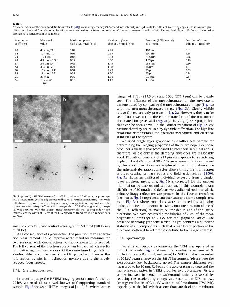
Table 1Axial aberration coefficients (for definitions refer to [28]), measuring accuracy (95% confidence interval) and p/4 limits for different scattering angles. The maximum phase
shifts are calculated from the modulus of the measured values or from the precision of the measurement in units of p/4. The residual phase shift for each aberration
coefficient is considered independently.
Aberration
coefficient
Measured
value
Maximum phase
shift at 20 mrad (p/4)
Maximum phase
shift at 27 mrad (p/4)
Precision (95%-interval)
at 27 mrad
Precision of phase
shift at 27 mrad (p/4)
A2 405 nm/711 1.01 2.48 100 nm 0.61
B2 128 nm/�71 0.95 2.33 89.7 nm 1.65
C3 �24 mm 0.88 2.93 6.25 mm 0.78
A3 4.8 mm/�1061 0.18 0.60 1.53 mm 0.19
S3 2.9 mm/401 0.44 1.45 588 nm 0.30
A4 404 mm/511 0.24 1.08 46 mm 1.07
D4 183 mm/1241 0.54 2.43 29 mm 0.39
B4 112 mm/1571 0.33 1.50 55 mm 0.74
C5 30 mm 0.30 1.81 6.7 mm 0.41
A5 18.7 mm/
�891
0.19 1.12 1.5 mm 0.09
Fig. 2. (a) and (b) HRTEM images of [1 1 0] Si acquired at 20 kV with the prototype
SALVE instrument, (c) and (d) corresponding FFTs (Fourier transforms). The weak
reflections in (d) were encircled to guide the eye. Image (a) was acquired with the
monochromator using the 2 mm slit (corresponds to 0.15 eV energy width). Image
(b) was acquired with the largest monochromator slit that corresponds to the
intrinsic energy width of 0.7 eV of the FEG. Specimen thickness is 4 nm. Scale bars
are 5 nm.
U. Kaiser et al. / Ultramicroscopy 111 (2011) 1239–12461242
small to allow for phase contrast imaging up to 50 mrad (1/0.17 nmat 20 kV).
As a consequence of CC-correction, the precision of the aberra-tion measurement should improve without further measures fortwo reasons: with CC-correction no monochromator is needed.The full current of the electron source can be used which resultsin a better signal-to-noise ratio. At the same time larger tilts forZemlin tableaus can be used since tilting hardly influences theinformation transfer in tilt direction anymore due to the largelyreduced focus spread.
3.1.3. Crystalline specimens
In order to judge the HRTEM imaging performance further at20 kV, we used Si as a well-known self-supporting standardsample. Fig. 2 shows a HRTEM images of [1 1 0] Si, where lattice
fringes of 111Si (313.5 pm) and 200Si (271.5 pm) can be clearlyseen. The influence of the monochromator on the envelope isdemonstrated by comparing the monochromated image (Fig. 1a)with the non-monochromated image (Fig. 2b). Clearly visiblelattice fringes are only present in Fig. 2a. However, they can beseen (much weaker) in the Fourier transform of the non-mono-chromated image as well (Fig. 2d). The 222Si (156.7 pm) reflec-tions can be seen as well in the Fourier transform of Fig. 2c. Weassume that they are caused by dynamic diffraction. The high lineresolution demonstrates the excellent mechanical and electricalstabilities of the system.
We used single-layer graphene as another test sample fordetermining the imaging properties of the microscope. Grapheneproduces a weak signal (compared to most test samples) and is,therefore, visible only if the damping envelopes are reasonablygood. The lattice constant of 213 pm corresponds to a scatteringangle of about 40 mrad at 20 kV. To overcome limitations causedby chromatic aberrations we employed tilted illumination sincethe spherical-aberration corrector allows tilting the illuminationwithout causing primary coma and field astigmatism [21,30].Fig. 3a shows an unfiltered individual exposure from a single-layer graphene membrane, Fig. 3b is corrected for the unevenillumination by background-subtraction. In this example, beamtilt (tilting of 30 mrad) and defocus were adjusted such that all sixprimary Bragg reflections are present in the Fourier transform(see inset). Fig. 3c represents another example (same sample areaas in Fig. 3a) where conditions were optimized (by adjustingdefocus and beam tilt azimuth exactly into the direction of one ofthe 1100 reflection) to maximize transfer in one of the latticedirections. We have achieved a modulation of 2.5% (of the meanbright-field intensity) at 20 kV for the graphene lattice. Thepresence of strong graphene lattice fringes confirms a sufficientstability of all components such that a significant portion of theelectrons scattered to 40 mrad contribute to the image contrast.
3.1.4. Spectroscopy
For all spectroscopy experiments the TEM was operated indiffraction mode. Fig. 4 shows the low-loss spectrum of Si(collection angle 8.3 mrad, red curve) for VEELS analysis recordedat 20 keV beam energy on the SALVE instrument (please note theexceptionary low background noise). The sample thickness wasmeasured to be 10 nm. Reducing the accelerating voltage and themonochromatization in VEELS provides two advantages. First, astrong increase in signal to background ratio is observed byreducing the accelerating voltage and second, the ZLP narrows(energy resolution of 0.11 eV width at half maximum (FWHM)),especially at the full width at one thousandth of the maximum

Fig. 3. HRTEM images of single-layer graphene, observed with SALVE instrument operating at 20 kV. (a) Unfiltered exposure, with beam tilt and defocus adjusted to
transfer all six primary lattice reflections of graphene (corresponding to a 213 pm spacing) with similar intensity. Inset shows Fourier transform of this image.
(b) Background-subtracted section of the image (filtered to remove the uneven illumination). (c) Unfiltered single exposure, with conditions adjusted to maximize transfer
of one of the lattice reflections. Inset shows that a modulation of 2.5% (normalized to the mean intensity) was achieved. (d) Flat-filtered section of image (c). All scale bars
are 1 nm.
1e-005
0.0001
0.001
0.01
0.1
1
-5 0 5 10 15 20 25
inte
nsity
energy loss (eV)
SALVE I SSD
Fig. 4. Low-loss EELS spectra of Si obtained from the SALVE instrument operating
at 20 kV (solid/red curve), demonstrating the good energy resolution (0.1 eV in
vaccum). Please note the logarithmic scaling of the EELS intensity that was
necessary to easily display the zero-loss as well as the plasmon losses
without cropping the data. Sample thickness: 10 nm. The SSD (dashed/blue line)
is the single scattering distribution (SSD) of the spectrum recorded with the SALVE
instrument. (For interpretation of the references to color in this figure legend, the
reader is referred to the web version of this article.)
U. Kaiser et al. / Ultramicroscopy 111 (2011) 1239–1246 1243
(FWTM) with 1.0 eV. This is important for accurate band gapdetermination. Moreover, more spectral details can be observedwhich are otherwise smeared out (as can be seen in the spectrum inthe range from app. 2.6 to 7 eV). Therefore, lowering the acceleratingvoltage and monochromatization are prerequisite for an accuratedetermination of the dielectric function of a material. The strongbroad feature with its maximum at 9 eV is the surface plasmonfollowed by the volume plasmon with its maximum at 16.7 eV. Theenergy range which can be covered by EELS is much largercompared to optical methods (see the blue curve in Fig. 4). Forobserving weak details in the VEELS spectrum high magnification ofthe spectrum was chosen at the spectrometer.
For germanium, the collection angle was 8.3 mrad as well.Here the sample thickness was determined to 15 nm. Residualrelativistic energy losses were removed off-line by using theiterative routine described in [18].
3.2. Applications of 20 kV TEM
3.2.1. Imaging fullerenes in carbon nanotubes (CNT)
The benefit of imaging radiation-sensitive materials withdecreased acceleration voltage is demonstrated by comparisonof HRTEM dose series at 80 and 20 kV (Fig. 5) of C60 moleculesencapsulated within double-walled CNTs. Fullerenes consist ofcarbon atoms ordered in pentagons and hexagons resulting in

Fig. 5. HRTEM images of C60 fullerenes in double-walled CNT at 80 kV (column a) and 20 kV (column b) accelerating voltages representing a dose series with a line-by-line
increasing cumulative dose (first row refers to the initial state corresponding to a dose of �5�106 e�/nm2). The 80 kV HRTEM experiments serve as a reference showing
radiation damage of fullerenes at a dose as low as �1�107 e�/nm2; whereas the 20 kV HRTEM images show corresponding damage at �1�109 e�/nm2, thus a
considerable improvement in e-beam stability in addition to much higher contrast (images were summed up to increase signal-to-noise ratio; scale bar corresponds to
1 nm).
0.1
1
10
0 5 10 15 20 25 30
refra
ctiv
e in
dex
energy loss (eV)
SALVE I Palik
Fig. 6. Refractive indices over energy loss obtained (solid/red curve): from the
VEELS spectra shown in Fig. 3 after corresponding KKA analysis and (crossed/
green curve): from the optical data presented by Palik in Ref. [36]. (For
interpretation of the references to color in this figure legend, the reader is referred
to the web version of this article.)
U. Kaiser et al. / Ultramicroscopy 111 (2011) 1239–12461244
much weaker bonds compared to CNTs, where only hexagons arepresent. However, the good conductivity of CNTs arising from thedelocalized p-electron system slows down radiation damage ofmolecules encapsulated inside them. Nevertheless, after exposingthe C60@DWNT structure to an electron dose of �1�107 e�/nm2
at 80 kV, radiation damage effects arise in the form of coalescenceand polymerization of the fullerenes. After a cumulative dose of�1�109 e�/nm2, almost all molecules got damaged at 80 kV andstarted coalescing to form a third nanotube within the DWNT. Incontrast, at the same dose at 20 kV only very few structuralchanges were observable. This indicates that the electron beamdamage is reduced at 20 kV by a factor of approximately 100times compared to 80 kV. In addition, the images at 20 kV show,in accordance to theory, much higher contrast. However, atpresent the resolution of the atomic lattice of the molecules andnanotubes is limited by chromatic aberration at such low vol-tages. In future these limitations will be eliminated by means ofthe new CC/CS corrector installed in the final SALVE instrument.
3.3. Valence EELS of Si and Ge
3.3.1. Silicon
We have determined the direct band gap of 2.6 eV for Si afterZLP and plural scattering removal. This value is in very goodagreement with band structure calculations [31]. Application ofKKA provided the complex dielectric function and the energy lossdependent refractive index for Si, as depicted in Fig. 6, red curve.The comparison with optical measurements taken from Ref. [30](green crosses) shows a very good agreement with two excep-tions: the energy range of the broad surface plasmon peak around9 eV and the sharp feature at 4.5 eV. The reason for the firstdiscrepancy (around 9 eV) is surface oxidation of the siliconspecimen in our experiment, whereas the optical data was recordedunder ultra-high vacuum conditions preventing surface oxidation.The reason for the absence of the sharp feature at 4.5 eV in ourexperiment is not clear so far. It might be connected to the fact that
the surface plasmon is shifted to lower energies due to the presenceof silicon oxide on the specimen surface. This shift introduces anerror when the KKA routine treats the surface plasmon. The resultrepresents therefore the mean dielectric function of the non-oxidizedbulk and the oxidized surfaces.
3.3.2. Germanium
Calculations show that in the case of Ge, an electron probewith only 5 kV would be necessary to avoid relativistic energylosses [18]. Our experiment demonstrate that an energy of 20 kValready allows a high signal-to background ratio in the band gapregion of the VEELS, which might be caused by a reduction of

0.01
0.1
1
10
0 5 10 15 20 25 30 35 40 45
refr.
ind.
inte
nsity
energy loss (eV)
Fig. 7. Bottom: single scattering distribution of Ge obtained at 20 keV electron
energy with the SALVE instrument as a function of the energy loss. The direct band
gap is measured to be (0.8070.03) eV. Top: refractive indices over energy loss
obtained from the VEELS spectrum shown in Fig. 6 after corresponding KKA
analysis.
U. Kaiser et al. / Ultramicroscopy 111 (2011) 1239–1246 1245
relativistic losses. An iterative routine [18,32] was employed todetermine this result. Subsequently, we calculated the refractionindex as a function of the energy loss by applying KKA. Note thatthe refraction index was derived even for high energy losses,where optical measurements fail. Fig. 7 shows the single scatter-ing distribution (SSD) of germanium recorded with the SALVE
instrument at 20 kV. After subtraction of the zero-loss peak, thedirect band gap is measured to be (0.8070.03) eV. This result isin excellent agreement with those obtained from optical mea-surements and band structure calculations [33,34].
The obtained refractive index is in excellent agreement withearlier work [35]. However, the transition strengths are differentcompared with those obtained from optical methods [30] andcalculations based on density functional theory. The reason forthis discrepancy is not clear yet and needs more detailed study ofthe influence of the collection semi-angle on band bending.
4. Conclusion
We have characterized the new prototype SALVE instrument at20 kV operation, which is based on the Zeiss-Libra200 platformincluding an in-column energy filter and is equipped with anelectrostatic monochromator and a CS-corrector from CEOS. Wehave shown that the high stability of the microscope allows highcontrast imaging resolving lattice fringes in 4 nm thin Si lamellaedirectly up to 271.5 pm (Si {002}) and in single-layer graphene upto 213 pm (graphene {1100}, tilted illumination) at 20 kV.
In high-resolution imaging mode we showed that at 20 kVfullerenes encapsulated within carbon nanotubes withstand a 100times larger electron dose than at 80 kV before any significantdamage in their structures can be noticed. In spectroscopy modewe show that optical properties can be determined at 20 kV in
nearly all materials. Something that is not possible at highervoltages because of much lower signal to background in theVEELS region of the spectra, caused most probably by relativisticenergy losses. We determined, for the first time by means of TEM,the band gap and the refractive index of Si and Ge as functions ofthe energy loss. The obtained results are in very good agreementwith data from optical measurements. We may note that surfaceplasmons in the low-loss region of the EELS spectrum may beincreased because the sample thickness must be reduced for20 kV. Nevertheless, it is now possible to determine opticalproperties in a much wider energy loss region than accessibleby optical spectroscopy.
The final SALVE-instrument equipped with CC/CS corrector andan optimized detector will allow atomic resolution imaging andspectroscopy of radiation-sensitive objects in the near future.
Acknowledgment
We gratefully acknowledge financial support by the GermanResearch Foundation (DFG) and the Ministry of Science, Research,and Arts (MWK) of the state Baden-Wurttemberg within the SubAngstrom Low-Voltage Electron Microscopy (SALVE) project.
References
[1] H. Rose, Outline of a spherically corrected semiaplanatic medium-voltagetransmission electron microscope, Optik 85 (1990) 19–24.
[2] H. Rose, History of aberration correction, Advances in Imaging and ElectronPhysics 156 (2008) 1–36.
[3] M. Haider, H. Rose, S. Uhlemann, E. Schwan, B. Kabius, K. Urban, A spherical-aberration corrected 200 kV transmission electron microscope, Ultramicro-scopy 75 (1998) 53–60.
[4] B. Kabius, P. Hartel, M. Haider, H. Muller, S. Uhlemann, U. Loebau, J. Zach,H. Rose, First application of Cc-corrected imaging for high-resolution andenergy-filtered TEM, Journal of Electron Microscopy 58 (2009) 47–155.
[5] R.F. Egerton, R. McLeod, F. Wang, M. Malac, Basic questions related toelectron-induced sputtering in the TEM, Ultramicroscopy 110 (2009)991–997.
[6] H. Rose, Future trends in aberration-corrected electron microscopy, Philoso-phical Transactions of the Royal Society A 367 (2009) 3809–3823.
[7] A.P. Wilska, Low-voltage electron microscopy, a 6 kV instrument, Journal ofRoyal Microscopical Society 83 (1964) 207–211.
[8] U. Kaiser, A. Chuvilin, J.C. Meyer, J. Biskupek, Microscopy at the bottom, in:W. Grogger, F. Hofer, P. Poelt (Eds.), Materials Science Microscopy ConferenceMC2009, vol. 3, 2009, pp. 1–6.
[9] H. Sawada, T. Sasaki, F. Hosokawa, S. Yuasa, M. Terao, M. Kawazoe,T. Nakamichi, T. Kaneyama, Y. Kondo, K. Kimoto, K. Suenaga, Higher-orderaberration corrector for an image-forming system in a transmission electronmicroscope, Ultramicroscopy 110 (2010) 958–961.
[10] O.L. Krivanek, N. Dellby, M.F. Murfitt, M.F. Chisholm, T.J. Pennycook,K. Suenaga, V. Nicolosi, Gentle STEM: ADF imaging and EELS at low primaryenergies, Ultramicroscopy 110 (2010) 935–945.
[11] L.A. Giannuzzi, J.L. Drown, S.R. Brown, R.B. Irwin, F.A. Stevie, Applications ofthe FIB lift-out technique for TEM specimen preparation, MicroscopyResearch and Technique 41 (1998) 285–290.
[12] R.M. Langford, Focused ion beams techniques for nanomaterials character-ization, Microscopy Research and Technique 69 (2006) 538–549.
[13] A.K. Geim, K.S. Novoselov, The rise of graphene, Nature 6 (2007) 183–191.[14] J.C. Meyer, C. Kisielowski, R. Erni, M.D. Rossel, M.F. Crommie, A. Zettl, Direct
imaging of lattice atoms and topological defects in graphene membranes,Nano Letters 8 (2008) 3582–3586.
[15] M. Stoger-Pollach, Low voltage TEM: influences on electron energy lossspectrometry experiments, Micron 41 (2010) 577–584.
[16] M. Stoger-Pollach, et al., Cerenkov losses: a limit for bandgap determinationand Kramers–Kronig analysis, Micron 37 (2006) 396–402.
[17] M. Stoger Pollach, Optical properties and band gaps from low loss EELS:pitfalls and solutions, Micron 39 (2008) 1092–1110.
[18] K. Suenaga, Y. Sato, Z. Liu, H. Kataura, T. Okazaki, K. Kimoto, H. Sawada,T. Sasaki, K. Omoto, et al., Visualizing and identifying single atoms usingelectron energy-loss spectroscopy with low accelerating voltage, NatureChemistry 1 (2009) 415–418.
[19] A. Chuvilin, A.N. Khlobystov, D. Obergfell, M. Haluska, S. Yang, S. Roth,U. Kaiser, Observations of chemical reactions at the atomic scale: dynamics ofmetal-mediated fullerene coalescence and nanotube rupture, AngewandteChemie International Edition 49 (2010) 193–198.
[20] S. Uhlemann, M. Haider, Experimental set-up of a fully electrostatic mono-chromator for a 200 kV TEM, in: J. Engelbrecht, T. Sewell, M. Witcomb,

U. Kaiser et al. / Ultramicroscopy 111 (2011) 1239–12461246
R. Cross, P. Richards (Eds.), Proceedings of 15th International Congress onElectron Microscopy vol. I, Microscopy Society of Southern Africa, Durban,2002, p. 327.
[21] M. Haider, P. Hartel, H. Muller, S. Uhlemann, J. Zach, Information transfer in aTEM corrected for spherical and chromatic aberration, Microscopy andMicroanalysis 16 (2010) 393–408.
[22] L. Lechner, J. Biskupek, U. Kaiser, Methode und Apparate zur Praparation vonTEM-Proben, German patent # P18420DE.
[23] K.S. Kim, Y. Zhao, H. Jang, S.Y. Lee, J.M. Kim, K.S. Kim, J.-H. Ahn, P. Kim,J.-Y. Choi, B.H. Hong, Large-scale pattern growth of graphene films forstretchable transparent electrodes, Nature 457 (2009) 706.
[24] X. Li, W. Cai, J. An, S. Kim, J. Nah, D. Yang, R. Piner, A. Velamakanni, I. Jung,E. Tutuc, S.K. Banerjee, L. Colombo, R.S. Ruoff, Large-area synthesis of high-quality and uniform graphene films on copper foils, Science 324 (2009) 1312.
[25] H.J. Park, J.C. Meyer, S. Roth, V. Skakalova., Growth and properties of few-layergraphene prepared by chemical vapor deposition, Carbon 48 (2010) 1088.
[26] F. Wang, R.F. Egerton, M. Malac, M., Fourier-ratio deconvolution techniquesfor electron energy-loss spectroscopy (EELS) original research article, Ultra-microscopy 109 (2009) 1245–1249.
[27] P. Schattschneider, A performance test of the recovery of single energy lossprofiles via matrix approach, Ultramicroscopy 11 (1983) 321–322.
[28] S. Uhlemann, M. Haider, Residual wave aberrations in the first sphericalaberration corrected transmission electron microscope, Ultramicroscopy 72(1998) 109–119.
[29] H. Muller, I. Maßmann, S. Uhlemann, P. Hartel, J. Zach, M. Haider, Aplanaticimaging systems for the transmission electron microscope, Nuclear Instru-ments and Methods A, in press, doi:10.1016/j.numa.2010.12.091.
[30] R.R. Meyer, A.I. Kirkland, W.O. Saxton, A new method for the determinationof the wave aberration function for high-resolution TEM: 2. Measurement of
the antisymmetric aberrations, Ultramicroscopy 99 (2004) 115123.[31] D.J. Moss, E. Ghahramani, J.E. Sipe, H.M. van Driel, Band-structure calculation
of dispersion and anisotropy for third-harmonic generation in Si, Ge, andGaAs, Physical Review B 41 (1990) 1542–1560.
[32] E.D. Palik, Handbook of Optical Constants of Solids, Orlando, FL, US, 1985–
1991.[33] M. Stoger-Pollach, A. Laister, P. Schattschneider, Treating retardation effects
in valence-EELS spectra for Kramers Kronig analysis, Ultramicroscopy 108(2008) 439–444.
[34] R.P. Seysan, A.V. Varfolomeev, B.P. Zaharchenya, Properties of semiconduc-tors, Fizika i Tekhnika Poluprovodnikov 2 (1968) 1276–1280.
[35] J. Kim, M.V. Fischetti, Electronic band structure calculations for biaxiallystrained Si, Ge, and III–V semiconductors, Journal of Applied Physics 108(2010) 0113710.
[36] H.R. Philipp, E.A. Taft, Optical constants of germanium in the region of 1 to10 eV, Physical Review 113 (1959) 1002–1005.
[37] E.E. Fill, F. Krausz, M.G. Raizen, Single-molecule electron diffraction imagingwith charge replacement, New Journal of Physics 10, 093015.