
Transmission Electron Microscopy - physics.hu-berlin.de
16
Max-Planck Institut für Metallforschung Universität Stuttgart Transmission Electron Microscopy Christoph T. Koch Max Planck Institut für Metallforschung Heisenbergstr. 3, 70569 Stuttgart Raum 5N8, Tel: 0711/689-3647 Email: [email protected] Part IIIb: Kinematic Electron Diffraction (convergent beams + amorphous materials) Max-Planck Institut für Metallforschung Universität Stuttgart Bragg angle & deflection angle 2θ Bragg θ 2θ 2θ Braggs law: nλ=2d·sin(θ Bragg ) ≈d·sin(2θ Bragg ) Laue condition: nλ=dsin(2θ Bragg ) ≈2d·sin(θ Bragg ) 2θ Bragg d d·sin(θ) Nomenclature : The deflection angle is usually denoted as 2x the Bragg angle! s k q Bragg t 2 ) 2 sin( = ⋅ = ⇒ ϑ ( ) s d n Bragg 2 sin 2 = = λ ϑ Bragg reflection Laue diffraction
Transcript of Transmission Electron Microscopy - physics.hu-berlin.de

1
Max-Planck Institut für Metallforschung Universität Stuttgart
Transmission Electron Microscopy
Christoph T. Koch
Max Planck Institut für MetallforschungHeisenbergstr. 3, 70569 StuttgartRaum 5N8, Tel: 0711/689-3647
Email: [email protected]
Part IIIb: Kinematic Electron Diffraction(convergent beams + amorphous materials)
Max-Planck Institut für Metallforschung Universität Stuttgart
Bragg angle & deflection angle
2θBragg
θ
2θ2θ
Braggs law: nλ=2d·sin(θBragg)≈d·sin(2θBragg)
Laue condition: nλ=dsin(2θBragg)≈2d·sin(θBragg)
2θBragg
d
d·sin(θ)
Nomenclature: The deflection angle is usually denoted as 2x the Bragg angle!
skq Braggt 2)2sin( =⋅=⇒ ϑ( )
sdn Bragg 2
sin2 ==
λϑ
Bragg reflection Laue diffraction
2
Max-Planck Institut für Metallforschung Universität Stuttgart
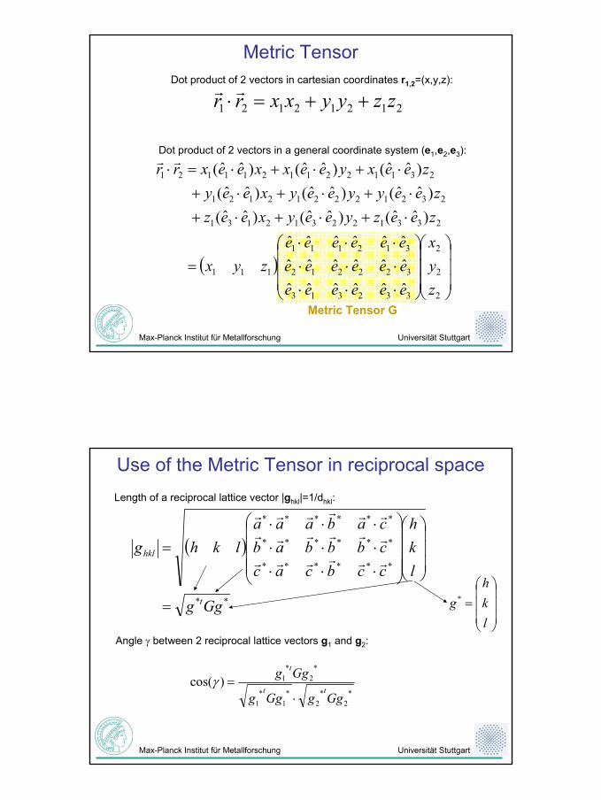
Metric TensorDot product of 2 vectors in cartesian coordinates r1,2=(x,y,z):
21212121 zzyyxxrr ++=⋅rr
Dot product of 2 vectors in a general coordinate system (e1,e2,e3):
( )
⋅⋅⋅⋅⋅⋅⋅⋅⋅
=
⋅+⋅+⋅+⋅+⋅+⋅+
⋅+⋅+⋅=⋅
2
2
2
332313
322212
312111
111
233122312131
232122212121
23112211211121
ˆˆˆˆˆˆˆˆˆˆˆˆˆˆˆˆˆˆ)ˆˆ()ˆˆ()ˆˆ()ˆˆ()ˆˆ()ˆˆ()ˆˆ()ˆˆ()ˆˆ(
zyx
eeeeeeeeeeeeeeeeee
zyx
zeezyeeyxeezzeeyyeeyxeeyzeexyeexxeexrr rr
Metric Tensor G
Max-Planck Institut für Metallforschung Universität Stuttgart
Use of the Metric Tensor in reciprocal space
( )
**
******
******
******
Ggg
lkh
ccbcaccbbbabcabaaa
lkhg
t
hkl
=
⋅⋅⋅⋅⋅⋅⋅⋅⋅
=rrrrrr
rrrrrrrrrrrr
*2
*2
*1
*1
*2
*1)cos(
GggGgg
Gggtt
t
⋅=γ
=lkh
g*
Length of a reciprocal lattice vector |ghkl|=1/dhkl:
Angle γ between 2 reciprocal lattice vectors g1 and g2:

3
Max-Planck Institut für Metallforschung Universität Stuttgart
Metric Tensor in real space
1−=
⋅⋅⋅⋅⋅⋅⋅⋅⋅
= Gcabcaccbbbabcabaaa
Mrrrrrr
rrrrrrrrrrrr
The real-space metric tensor of a given lattice is just the inverse of the reciprocal-space metric tensor.
Max-Planck Institut für Metallforschung Universität Stuttgart
Indexing a diffraction pattern
specimen
-C
amer
a le
ngth
L
lg
2θΒ
lg=L·sin(2θB)=Lλ|g|
1. Calibrate camera length using a specimen with known d-spacings (i.e. known g) according to: L = lg/sin(2θB[g])
2. Measure lg for the unknown specimen.3. Obtain d-spacing dhkl=Lλ/lg4. Look up the obtained d-spacing in a table
of possible lattice plane spacings for the phase(s) in question.[The metric tensor helps to compute |ghkl| very quickly for any (hkl)].
5. Repeat step 2-4 for at least 1 more (better more) diffraction spots.
6. Make sure that the identified phase and orientation agrees with the observed symmetry of the diffraction pattern. Diffraction
plane

4
Max-Planck Institut für Metallforschung Universität Stuttgart
Indexing Kikuchi lines
Laue condition for diffraction spots: nλ=dsin(2θBragg).
Kikuchi lines are Bragg reflected by lattice planes of the crystal. The angle between the reflected beams and the reflecting plane is therefore θBragg.Kikuchi lines appear therefore at ½ the scattering angle of the corresponding diffraction spot.
(800)_
(400)(400)(800)
_
Max-Planck Institut für Metallforschung Universität Stuttgart
Indexing Kikuchi lines
Kikuchi lines in a spot pattern
Angle between excess and deficiancy line: 2θBragg
5
Max-Planck Institut für Metallforschung Universität Stuttgart
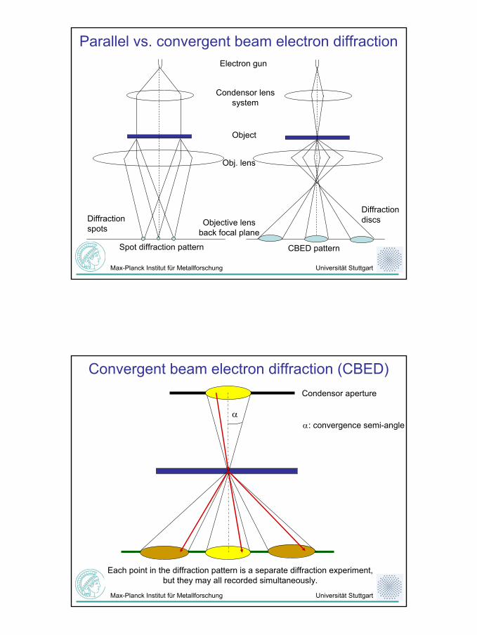
Parallel vs. convergent beam electron diffractionElectron gun
Condensor lenssystem
Object
Spot diffraction pattern CBED pattern
Diffraction spots
Objective lens back focal plane
Diffraction discs
Obj. lens
Max-Planck Institut für Metallforschung Universität Stuttgart
Convergent beam electron diffraction (CBED)Condensor aperture
αα: convergence semi-angle
Each point in the diffraction pattern is a separate diffraction experiment,but they may all recorded simultaneously.

6
Max-Planck Institut für Metallforschung Universität Stuttgart
CBED: many independent diffraction experiments
Max-Planck Institut für Metallforschung Universität Stuttgart
Exact Lause condition within CBED disks
The exact Laue (or Bragg) condition is satisfied only for a single line within each diffraction disk. This line is at different
positions in different disks.
exact Laue condition
Diffraction plane

7
Max-Planck Institut für Metallforschung Universität Stuttgart
HOLZ lines within CBED disks
Inside HOLZ disks the Laue condition is satisfied only in a thin line, because of the steep angle at which the Ewald sphere intersects the HOLZ. The electrons that have scattered into this line are missing in the central disk at exactly the same diffraction angle.
Diffraction plane
Max-Planck Institut für Metallforschung Universität Stuttgart
Geometry of HOLZ lines
-
FOLZ
ZOLZ
gHOLZ
O
Central diffraction disk
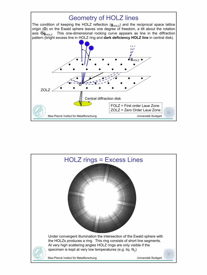
8
Max-Planck Institut für Metallforschung Universität Stuttgart
---
FOLZ
ZOLZ
gHOLZ
O
FOLZ = First order Laue ZoneZOLZ = Zero Order Laue Zone
Central diffraction disk
Geometry of HOLZ linesThe condition of keeping the HOLZ reflection (gHOLZ) and the reciprocal space lattice origin (O) on the Ewald sphere leaves one degree of freedom, a tilt about the rotation axis OgHOLZ. This one-dimensional rocking curve appears as line in the diffraction pattern (bright excess line in HOLZ ring and dark deficiency HOLZ line in central disk).
Max-Planck Institut für Metallforschung Universität Stuttgart
HOLZ rings = Excess Lines
Under convergent illumination the intersection of the Ewald sphere with the HOLZs produces a ring. This ring consists of short line segments.At very high scattering angles HOLZ rings are only visible if the specimen is kept at very low temperatures (e.g. liq. N2)

9
Max-Planck Institut für Metallforschung Universität Stuttgart
HOLZ lines = Deficiency Lines
Electrons that have scattered into the HOLZ ring are missing in the central disc, producing dark HOLZ lines. HOLZ lines carry therefore
3-dimensional information about the crystal structure.
Dynamical effects are especially noticable at HOLZ line intersections.
Max-Planck Institut für Metallforschung Universität Stuttgart
Applications using HOLZ linesHOLZ lines are produced by very long reciprocal lattice vectors gHOLZ. Their position is
therefore extremely sensitive to changes in lattice parameters and /or the electron wavelength and thus the high voltage.
A few applications:1. Very precise sample orientation: HOLZ line patterns are very sensitive to tilt.2. Determination of 3D lattice parameters from a single CBED pattern.3. Strain mapping: CBED patterns are recorded as a fine beam rasters across the
sample. Strain (local changes in lattice constants) is determined by relative shifts of the HOLZ lines.
4. Calibration of the high voltage of the microscope: The relative position of HOLZ lines depends on the radius of the Ewald sphere and thus the accelerating voltage of the microscope (can be determined to <1V accuracy).
5. Determination of 3D symmetry: ZOLZ diffraction data shows the symmetry of the projected structure, HOLZ lines carry 3D information.
6. Analysis of defects … (to be discussed later)
Note: Dynamical scattering (multiple eleastic scattering ) may shift HOLZ line positions. The usage of dynamical diffraction theory (e.g. Bloch wave method) is therefore necessary for quantitative HOLZ line analysis.
10
Max-Planck Institut für Metallforschung Universität Stuttgart
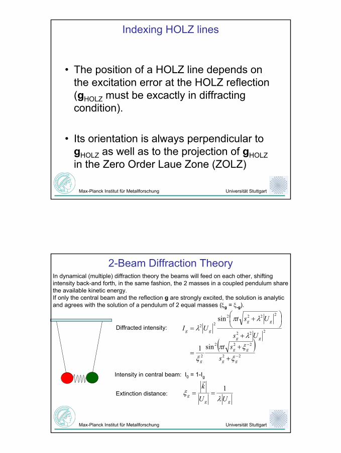
Indexing HOLZ lines
• The position of a HOLZ line depends on the excitation error at the HOLZ reflection (gHOLZ must be excactly in diffracting condition).
• Its orientation is always perpendicular to gHOLZ as well as to the projection of gHOLZin the Zero Order Laue Zone (ZOLZ)
Max-Planck Institut für Metallforschung Universität Stuttgart
2-Beam Diffraction Theory
Extinction distance:
Diffracted intensity:
( )22
222
2
222
2222
22
sin1
sin
−
−
+
+=
+
+
=
gg
gg
g
gg
gg
gg
sst
Us
UstUI
ξξπ
ξ
λ
λπλ
ggg UU
k
λξ 1
==
r
In dynamical (multiple) diffraction theory the beams will feed on each other, shifting intensity back-and forth, in the same fashion, the 2 masses in a coupled pendulum share the available kinetic energy. If only the central beam and the reflection g are strongly excited, the solution is analytic and agrees with the solution of a pendulum of 2 equal masses (ξg = ξ-g).
Intensity in central beam: I0 = 1-Ig
11
Max-Planck Institut für Metallforschung Universität Stuttgart
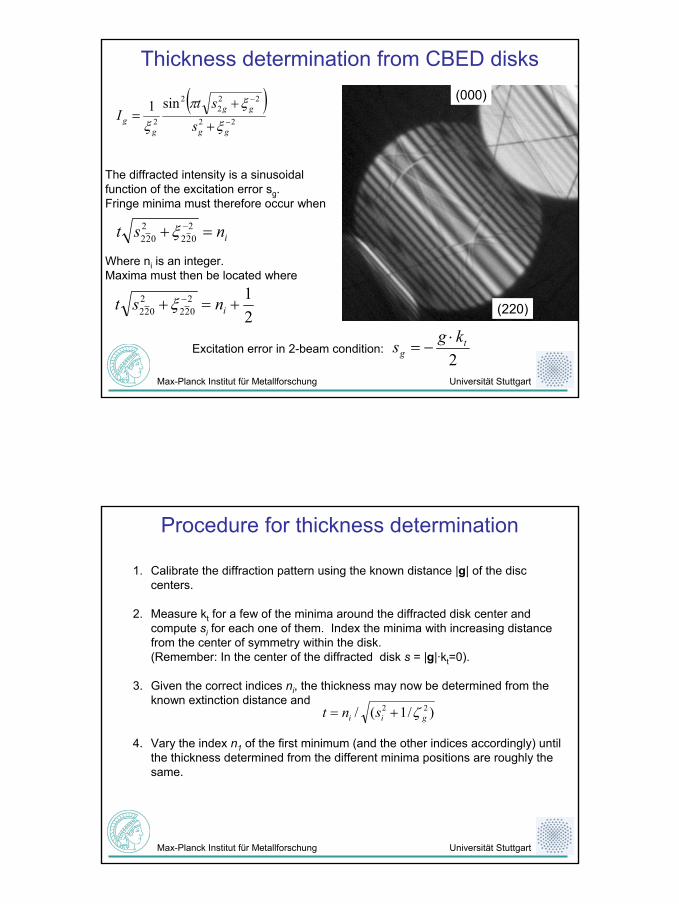
Thickness determination from CBED disks
( )22
222
2
2
sin1−
−
+
+=
gg
gg
gg s
stI
ξξπ
ξ
The diffracted intensity is a sinusoidal function of the excitation error sg. Fringe minima must therefore occur when
Where ni is an integer.Maxima must then be located where
inst =+ −2022
2022 ξ
212
0222022 +=+ −
inst ξ (220)
(000)
Excitation error in 2-beam condition: 2t
gkgs ⋅
−=
Max-Planck Institut für Metallforschung Universität Stuttgart
Procedure for thickness determination
1. Calibrate the diffraction pattern using the known distance |g| of the disc centers.
2. Measure kt for a few of the minima around the diffracted disk center and compute si for each one of them. Index the minima with increasing distance from the center of symmetry within the disk. (Remember: In the center of the diffracted disk s = |g|·kt=0).
3. Given the correct indices ni, the thickness may now be determined from the known extinction distance and
4. Vary the index n1 of the first minimum (and the other indices accordingly) until the thickness determined from the different minima positions are roughly the same.
)/1(/ 22gii snt ζ+=

12
Max-Planck Institut für Metallforschung Universität Stuttgart
Finding the correct index
n1=3: wrong n1=4: correct
ξg(fitted) = 973Å
ξ220(expected) = 960Å
ξg(fitted) = 1234Å
Max-Planck Institut für Metallforschung Universität Stuttgart
Digitalmicrograph: Thickness Measurement GUIhttp://felmpc14.tu-graz.ac.at/dm_scripts/freeware/programs/Thickness_by_CBED.htm

13
Max-Planck Institut für Metallforschung Universität Stuttgart
Diffraction from polycrystalline specimen
Single grain Few grains Many grains
Max-Planck Institut für Metallforschung Universität Stuttgart
Crystal vs. Glass
Glass (SiO2)Certain ranges of preferred distances
Between neighboring atoms.
Crystal (Si)very well defined (sharp) d-spacings

14
Max-Planck Institut für Metallforschung Universität Stuttgart
Radial distribution function G(r)
mean density
distance-dependent density
G(r)
Max-Planck Institut für Metallforschung Universität Stuttgart
RDF from diffraction pattern
Structure factor:
Kin. diffr. pattern:
2D RDF (g(r)):
1D RDF (G(r)):

15
Max-Planck Institut für Metallforschung Universität Stuttgart
RDF of amorphous materials
Experimental diffraction pattern of an amorphous specimen
Simulated diffraction pattern of an amorphous structure.
Reconstructed G(r) and true partial RDFsobtained directly from a Si-O-Ca glass model.
Max-Planck Institut für Metallforschung Universität Stuttgart
Homework: Stereographic projection
The plane of projection is tangential to the equator of the globe. The axis of rotation of the earth lies horizontal in the projection diagram shown to the right.

16
Max-Planck Institut für Metallforschung Universität Stuttgart
Homework: Space Group 227 (diamond structure)
Screenshot from WEBEMAPS (http://emaps.mrl.uiuc.edu/emaps.asp)