Transition-Metal Pentatelluride ZrTe5 and HfTe5: A ... · all-electron full-potential linearized...
8
Transition-Metal Pentatelluride ZrTe 5 and HfTe 5 : A Paradigm for Large-Gap Quantum Spin Hall Insulators Hongming Weng, 1,2 Xi Dai, 1,2,* and Zhong Fang 1,2,† 1 Beijing National Laboratory for Condensed Matter Physics, and Institute of Physics, Chinese Academy of Sciences, Beijing 100190, China 2 Collaborative Innovation Center of Quantum Matter, Beijing 100190, China (Received 13 October 2013; published 15 January 2014) Quantum spin Hall (QSH) insulators, a new class of quantum matter, can support topologically protected helical edge modes inside a bulk insulating gap, which can lead to dissipationless transport. A major obstacle to reaching a wide application of QSH is the lack of suitable QSH compounds, which should be easily fabricated and have a large bulk gap. Here, we predict that single-layer ZrTe 5 and HfTe 5 are the most promising candidates for large-gap insulators, with a bulk direct (indirect) band gap as large as 0.4 eV (0.1 eV) and which are robust against external strains. The three-dimensional crystals of these two materials are good layered compounds with very weak interlayer bonding, and they are located near the phase boundary between weak and strong topological insulators, paving a new way for future experimental studies on both the QSH effect and topological phase transitions. DOI: 10.1103/PhysRevX.4.011002 Subject Areas: Condensed Matter Physics, Topological Insulators I. INTRODUCTION A topological insulator (TI) [1,2] can support gapless boundary states inside a bulk insulating gap, which are topologically protected and robust against perturbations. Particularly in two-dimensional (2D) TIs, namely, the quantum spin Hall (QSH) insulators [3,4], the low-energy (back) scattering of the edge states is prohibited by the time-reversal symmetry, leading to the dissipationless transport edge channels and the QSH effect [5]. How- ever, the known experimental verifications of the QSH effect in HgTe/CdTe [6] and InAs/GaSb [7] quantum-well structures require extreme conditions, such as the precisely controlled molecular-beam epitaxy (MBE) and the ultralow temperature due to the small bulk band gap of the order of meV, which greatly obstructs further experimental studies and possible applications. To be a “good” QSH insulator, the material must meet the following important criteria: (1) It must be a good layered material to easily obtain the chemically stable 2D system; (2) it must have a large 2D bulk band gap to realize the QSH effect at high temperatures. The first proposal of graphene as a QSH insulator [3] is practically useless because of its extremely small gap (10 −3 meV) induced by spin-orbit coupling (SOC) [8], although, so far, graphene is the best 2D material and that be easily made even by the scotch-tape method [9]. Recently, Bi 2 TeI has been pro- posed as another candidate for a QSH insulator [10], but its energy gap is also small. The bismuth (111) bilayer is potentially a large-gap (about 0.2 eV) QSH insulator [11]. However, its interlayer bonding is strong, and its fabrica- tion is difficult [12]. Several other proposals, such as ultrathin tin films [13] and the Cd 3 As 2 quantum well [14], have the same problem. Since they are not layered materials, the well-controlled MBE technique is required to obtain the ultrathin-film samples. Here, we report that the simple binary compounds ZrTe 5 and HfTe 5 , previously known as layered thermoelectric materials, are interlayer weakly bonded materials compa- rable to graphite. Their single-layer sheets, which can be made, in principle, without MBE, are QSH insulators with a large bulk gap, and they are robust against lattice distortions. Therefore, ZrTe 5 and HfTe 5 are the most promising 2D TIs that satisfy both of the above conditions and pave a new way for further experimental studies on the QSH effect. Moreover, our calculations show that the three- dimensional (3D) crystals formed by the stacking of layers are located in the vicinity of a transition between strong and weak TI, further making them a perfect platform to study the topological quantum-phase transitions. II. COMPUTATIONAL METHODS The ab initio calculations have been done by using the all-electron full-potential linearized augmented plane-wave method implemented in the WIEN2k package [15] within the general gradient approximation (GGA). The parameters used in the calculations, such as sampling of the Brillouin zone and the cutoff of augmented plane waves, are carefully * [email protected] † [email protected] Published by the American Physical Society under the terms of the Creative Commons Attribution 3.0 License. Further distri- bution of this work must maintain attribution to the author(s) and the published article’s title, journal citation, and DOI. PHYSICAL REVIEW X 4, 011002 (2014) 2160-3308=14=4(1)=011002(8) 011002-1 Published by the American Physical Society
Transcript of Transition-Metal Pentatelluride ZrTe5 and HfTe5: A ... · all-electron full-potential linearized...

Transition-Metal Pentatelluride ZrTe5 and HfTe5: A Paradigm for Large-GapQuantum Spin Hall Insulators
Hongming Weng,1,2 Xi Dai,1,2,* and Zhong Fang1,2,†1Beijing National Laboratory for Condensed Matter Physics, and Institute of Physics,
Chinese Academy of Sciences, Beijing 100190, China2Collaborative Innovation Center of Quantum Matter, Beijing 100190, China
(Received 13 October 2013; published 15 January 2014)
Quantum spin Hall (QSH) insulators, a new class of quantum matter, can support topologically protectedhelical edge modes inside a bulk insulating gap, which can lead to dissipationless transport. A majorobstacle to reaching a wide application of QSH is the lack of suitable QSH compounds, which should beeasily fabricated and have a large bulk gap. Here, we predict that single-layer ZrTe5 and HfTe5 are the mostpromising candidates for large-gap insulators, with a bulk direct (indirect) band gap as large as 0.4 eV(0.1 eV) and which are robust against external strains. The three-dimensional crystals of these two materialsare good layered compounds with very weak interlayer bonding, and they are located near the phaseboundary between weak and strong topological insulators, paving a new way for future experimentalstudies on both the QSH effect and topological phase transitions.
DOI: 10.1103/PhysRevX.4.011002 Subject Areas: Condensed Matter Physics, Topological Insulators
I. INTRODUCTION
A topological insulator (TI) [1,2] can support gaplessboundary states inside a bulk insulating gap, which aretopologically protected and robust against perturbations.Particularly in two-dimensional (2D) TIs, namely, thequantum spin Hall (QSH) insulators [3,4], the low-energy(back) scattering of the edge states is prohibited by thetime-reversal symmetry, leading to the dissipationlesstransport edge channels and the QSH effect [5]. How-ever, the known experimental verifications of the QSHeffect in HgTe/CdTe [6] and InAs/GaSb [7] quantum-wellstructures require extreme conditions, such as the preciselycontrolled molecular-beam epitaxy (MBE) and the ultralowtemperature due to the small bulk band gap of the orderof meV, which greatly obstructs further experimentalstudies and possible applications.To be a “good” QSH insulator, the material must meet
the following important criteria: (1) It must be a goodlayered material to easily obtain the chemically stable 2Dsystem; (2) it must have a large 2D bulk band gap to realizethe QSH effect at high temperatures. The first proposal ofgraphene as a QSH insulator [3] is practically uselessbecause of its extremely small gap (10−3 meV) induced byspin-orbit coupling (SOC) [8], although, so far, graphene isthe best 2D material and that be easily made even by the
scotch-tape method [9]. Recently, Bi2TeI has been pro-posed as another candidate for a QSH insulator [10], but itsenergy gap is also small. The bismuth (111) bilayer ispotentially a large-gap (about 0.2 eV) QSH insulator [11].However, its interlayer bonding is strong, and its fabrica-tion is difficult [12]. Several other proposals, such asultrathin tin films [13] and the Cd3As2 quantum well[14], have the same problem. Since they are not layeredmaterials, the well-controlled MBE technique is required toobtain the ultrathin-film samples.Here, we report that the simple binary compounds ZrTe5
and HfTe5, previously known as layered thermoelectricmaterials, are interlayer weakly bonded materials compa-rable to graphite. Their single-layer sheets, which can bemade, in principle, without MBE, are QSH insulators witha large bulk gap, and they are robust against latticedistortions. Therefore, ZrTe5 and HfTe5 are the mostpromising 2D TIs that satisfy both of the above conditionsand pave a new way for further experimental studies on theQSH effect. Moreover, our calculations show that the three-dimensional (3D) crystals formed by the stacking of layersare located in the vicinity of a transition between strong andweak TI, further making them a perfect platform to studythe topological quantum-phase transitions.
II. COMPUTATIONAL METHODS
The ab initio calculations have been done by using theall-electron full-potential linearized augmented plane-wavemethod implemented in the WIEN2k package [15] withinthe general gradient approximation (GGA). The parametersused in the calculations, such as sampling of the Brillouinzone and the cutoff of augmented plane waves, are carefully
*[email protected]†[email protected]
Published by the American Physical Society under the terms ofthe Creative Commons Attribution 3.0 License. Further distri-bution of this work must maintain attribution to the author(s) andthe published article’s title, journal citation, and DOI.
PHYSICAL REVIEW X 4, 011002 (2014)
2160-3308=14=4(1)=011002(8) 011002-1 Published by the American Physical Society

checked to ensure the convergence. The SOC is includedself-consistently within the second variational method. Theinterlayer binding energy, i.e., the unit-area total-energydifference between the single-layer sheet and the 3D bulk[16], is calculated by using the local-density approximation(LDA) of Perdew- and Wang-type exchange correlation[17]. The maximally localized Wannier functions (MLWF)for Te p orbitals have been constructed by using a home-made code [18] based on OpenMX [19], which canreproduce the band structures calculated from the firstprinciples quite well. The surface and edge states have beencalculated for slabs by using a tight-binding model con-structed from the MLWFs generated above.
III. RESULTS
A. Layered crystal structure
Both ZrTe5 and HfTe5 take the same crystal structureand have very similar properties. They have been shown topossess interesting electrical-transport properties, such asthe giant resistivity anomaly [20,21] and large thermo-power [22,23]. They crystallize in the orthorhombic layeredstructure [24] with space group Cmcm (D17
2h), as shown inFig. 1 (hereafter, we take ZrTe5 as an example). Trigonalprismatic chains of ZrTe3 (marked by a red dashed line) runalong the a axis, and these prismatic chains are linked viaparallel zigzag chains of Te atoms along the c axis to form a
2D sheet of ZrTe5 in the a-c plane. The sheets of ZrTe5stack along the b axis, forming a layered structure. Theprism of ZrTe3 is formed by a dimer of Ted1;2 atoms (withthe superscript d indicating the dimer and the subscript 1, 2numbering the atoms) and one apical Tea atom (with ameaning the apical), while the zigzag chain is formed bytwo Tez1;2 atoms (with z indicating the zigzag chain). Theprimitive unit cell contains two formula units with twoprismatic chains and two zigzag chains. The correspondingsubscripts numbering the atoms should be doubled.ZrTe5 shows strong quasi-2D anisotropy [25]. The
prismatic and the zigzag chains are connected throughthe apical Te atoms, and the Te-Te bond length between twochains is about 0.4 Å longer than that in the zigzag chain. Ifthe Zr and Ted dimer atoms are neglected, the remainingapical Tea and zigzag Tez atoms can be viewed as a wavedgrid of Te square-lattice sheet [see Fig. 1(d)], leading to astable quasi-2D structure. Each ZrTe5 layer is nominallycharge neutral, and the interlayer distance (along the b axis)is quite large (about 7.25 Å), suggesting the weak interlayercoupling, presumably of van der Waals type. We havecalculated the interlayer binding energies for differentcompounds by using the first-principles total energymethod (see Sec. II). The results shown in Fig. 2 suggestthat the interlayer binding energy of ZrTe5 or HfTe5 is asweak as that of graphite and is much smaller than that of theBi2Se3 and Bi (111) bilayers. Given the easy procedure ofmaking graphene from graphite simply by exfoliation withscotch tape [9], the comparably weak interlayer bindingenergy suggests that a single layer of ZrTe5 (or HfTe5) maybe formed in a similar simple and efficient way.
B. 2D quantum spin Hall insulator
We now focus on the single layer of ZrTe5 in the a-cplane. Its structure is fully optimized by theoretical calcu-lations. It is found that the relaxed lattice constants(a ¼ 4.036 Å and c ¼ 13.843 Å) and the internal atomiccoordinates are all very close to their 3D bulk experimentalvalues (less than 1% difference) [24], again suggesting thestability of the single-layer sheet. The calculated density ofstates shown in Fig. 3(a) suggests that the Zr-4d states are
(a) (b)
(c)
(e)
(d)
FIG. 1 (color online). (a) The crystal structure. (b) The bulkBrillouin zone (BZ) and the projected surface BZ of 3D ZrTe5(HfTe5). (c), (d), and (e) The side view, top view, and BZ of thesingle-layer structure, respectively. In (d), the inversion center isindicated by the red star symbol, and the waved grid of theTe square lattice sheet is shown by the pink dotted lines.
FIG. 2 (color online). The calculated interlayer binding ener-gies for several typical layered compounds.
HONGMING WENG, XI DAI, AND ZHONG FANG PHYS. REV. X 4, 011002 (2014)
011002-2

mostly unoccupied above the Fermi level, leading to thenearly ionic Zr4þ state (by transferring about four electronsonto the neighboring Te atoms). The states near the Fermilevel are dominantly from the covalently bonded Te-5pstates.For the convenience of discussion, hereafter we define
our coordinate system with x, y being along the a and caxes, respectively, and z being out of the 2D plane. Wechoose the origin of the coordinate system to be located onthe Zr site. The calculated band structures for a single-layerZrTe5 are shown in Figs. 3(b) and 3(c). In the case withoutSOC, the system is a semimetal with one band crossingalong the Γ-X direction, implying the existence of bandinversion around Γ-X. The band crossing is unavoidablebecause the two bands belong to different representationsdistinguished by the mirror symmetrymxz (the mirror planeis parallel to the xz plane and passes through the Zr site)along the Γ-X axis. The inclusion of SOC will, however,mix them and open up a gap, resulting in an insulator with alarge direct (indirect) band gap of 0.4 eV (0.1 eV). We haveinvestigated the Z2 topological invariant [3] of this
insulating state by evaluating the parity eigenvalues ofoccupied states at four time-reversal-invariant-momentum(TRIM) points of the BZ [26], and we have concluded thatit is a nontrivial QSH insulator with Z2 ¼ 1. Since the bandgap is mostly determined by the SOC strength of Te porbitals, we do not expect much of an error bar of GGA-type calculations (as is usual for conventional semicon-ductors). Indeed, we have checked the electronic structureby using the hybrid functional HSE06 [27], as well as themodified Becke-Johnson (mBJ) potential [28]. Both ofthem give a similar band gap with the band topologyunchanged since the band gap is opened by SOC betweenbonding and antibonding states of Te p orbitals with veryweak correlation effects.The 2D nontrivial insulating state in single-layer ZrTe5
should support topologically protected conducting edgestates. They are calculated by using the slab modelconstructed with the tight-binding method (see Method).For slab cutting along the x direction, one side is terminatedwith a ZrTe3 prismatic chain and the other side with a Tezigzag chain (see Fig. 7 in Appendix A).This asymmetricslab leads to two separated Dirac cones at Γ, as shown inFig. 3(d). The red lines show the edge with prismatic chaintermination, and the blue lines show the zigzag chaintermination. For the slab cutting along the y axis, the twoedges are the same. This symmetric slab model leads to twoenergetically degenerate Dirac cones located at oppositesides. Because of the nontrivial topology, the edge statesalways exist, while their details may depend explicitly onthe edge; for example, the Dirac cones are located at the Γpoint for the x edge but at the Y point for the y edge.
C. Band inversion mechanism
The band inversion in single-layer ZrTe5 is not due toSOC; instead, it is mainly due to the nonsymmorphicfeatures of the space group. Therefore, the physics of bandinversion here can be understood without SOC, and theonly effect of SOC is to open up an energy gap afterwards.We note that the space group of the single-layer ZrTe5 isPmmn (D13
2h), which is nonsymmorphic, with the inversioncenter located not at the origin but at (1=4, 1=4). As animportant consequence of such space group symmetry, allof the eigenstates at the zone-boundary TRIM points[namely, X, Y, and M in Fig. 1(e)] are fourfold degenerate(including the spin degree of freedom), with two of themhaving even parity and the other two odd parity. This isbecause at the three zone boundary points, the inversionoperation anticommutes with two important mirror oper-ators, mxz and myz (see the Appendix B for details). Theequal number of bands with odd and even parity guaranteesthat any band inversion at those zone-boundary TRIMpoints will not change the topology of the system, and theZ2 index of the material is fully determined by the energyorder of the bands at the Γ point, where only the Kramerdegeneracy holds. We further notice that the mirror
-0.2
-0.1
0
0.1
0.2
0.3
Ene
rgy(
eV)
ΓY Y ΓX X
X Γ Y M Γ-0.8
-0.4
0
0.4
0.8
Ene
rgy(
eV)
X Γ Y M Γ
EF
-6 -5 41-2-3-4-0
5
10
15
20
0 1 2 3Energy (eV)
Den
sity
of
Stat
es (
/eV
/uni
t cel
l)
Total DOSTeZr 4d
VBMCBM
(a)
(c)(b)
(d) (e)
a
EF
FIG. 3 (color online). The calculated electronic structures ofsingle-layer ZrTe5. (a) The density of states. (b) and (c) The bandstructures without and with SOC, respectively. The valence-bandmaximum (VBM) and conduction-band minimum (CBM) defin-ing the indirect band gap are indicated in (c). (d) and (e) Thecalculated edge states for the x and y edges, respectively (see themain text for details).
TRANSITION-METAL PENTATELLURIDE ZrTeZrTe5 AND … PHYS. REV. X 4, 011002 (2014)
011002-3
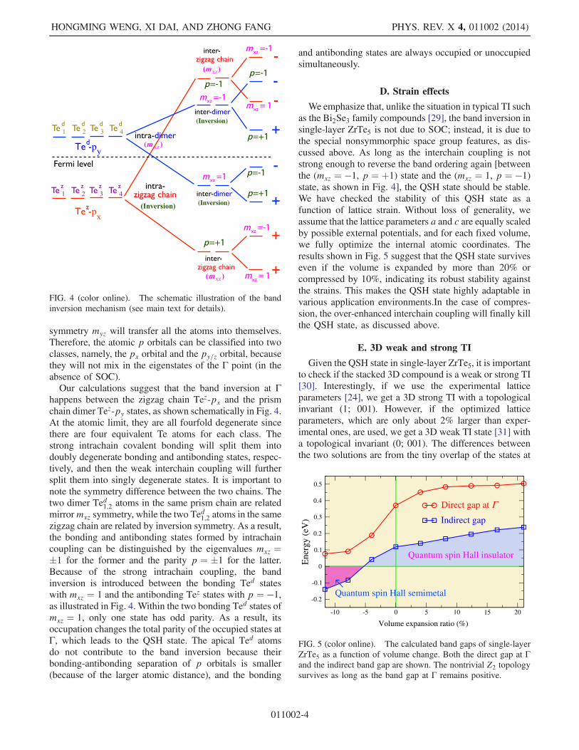
symmetry myz will transfer all the atoms into themselves.Therefore, the atomic p orbitals can be classified into twoclasses, namely, the px orbital and the py=z orbital, becausethey will not mix in the eigenstates of the Γ point (in theabsence of SOC).Our calculations suggest that the band inversion at Γ
happens between the zigzag chain Tez-px and the prismchain dimer Tez-py states, as shown schematically in Fig. 4.At the atomic limit, they are all fourfold degenerate sincethere are four equivalent Te atoms for each class. Thestrong intrachain covalent bonding will split them intodoubly degenerate bonding and antibonding states, respec-tively, and then the weak interchain coupling will furthersplit them into singly degenerate states. It is important tonote the symmetry difference between the two chains. Thetwo dimer Ted1;2 atoms in the same prism chain are relatedmirrormxz symmetry, while the two Ted1;2 atoms in the samezigzag chain are related by inversion symmetry. As a result,the bonding and antibonding states formed by intrachaincoupling can be distinguished by the eigenvalues mxz ¼�1 for the former and the parity p ¼ �1 for the latter.Because of the strong intrachain coupling, the bandinversion is introduced between the bonding Ted stateswith mxz ¼ 1 and the antibonding Tez states with p ¼ −1,as illustrated in Fig. 4. Within the two bonding Ted states ofmxz ¼ 1, only one state has odd parity. As a result, itsoccupation changes the total parity of the occupied states atΓ, which leads to the QSH state. The apical Ted atomsdo not contribute to the band inversion because theirbonding-antibonding separation of p orbitals is smaller(because of the larger atomic distance), and the bonding
and antibonding states are always occupied or unoccupiedsimultaneously.
D. Strain effects
We emphasize that, unlike the situation in typical TI suchas the Bi2Se3 family compounds [29], the band inversion insingle-layer ZrTe5 is not due to SOC; instead, it is due tothe special nonsymmorphic space group features, as dis-cussed above. As long as the interchain coupling is notstrong enough to reverse the band ordering again [betweenthe (mxz ¼ −1, p ¼ þ1) state and the (mxz ¼ 1, p ¼ −1)state, as shown in Fig. 4], the QSH state should be stable.We have checked the stability of this QSH state as afunction of lattice strain. Without loss of generality, weassume that the lattice parameters a and c are equally scaledby possible external potentials, and for each fixed volume,we fully optimize the internal atomic coordinates. Theresults shown in Fig. 5 suggest that the QSH state surviveseven if the volume is expanded by more than 20% orcompressed by 10%, indicating its robust stability againstthe strains. This makes the QSH state highly adaptable invarious application environments.In the case of compres-sion, the over-enhanced interchain coupling will finally killthe QSH state, as discussed above.
E. 3D weak and strong TI
Given the QSH state in single-layer ZrTe5, it is importantto check if the stacked 3D compound is a weak or strong TI[30]. Interestingly, if we use the experimental latticeparameters [24], we get a 3D strong TI with a topologicalinvariant (1; 001). However, if the optimized latticeparameters, which are only about 2% larger than exper-imental ones, are used, we get a 3D weak TI state [31] witha topological invariant (0; 001). The differences betweenthe two solutions are from the tiny overlap of the states at
FIG. 4 (color online). The schematic illustration of the bandinversion mechanism (see main text for details).
-10 -5 0 5 10 15 20
-0.2
-0.1
0
0.1
0.2
0.3
0.4
0.5
Direct gap at ΓIndirect gap
Quantum spin Hall insulator
Quantum spin Hall semimetal
Ene
rgy
(eV
)
Volume expansion ratio (%)
FIG. 5 (color online). The calculated band gaps of single-layerZrTe5 as a function of volume change. Both the direct gap at Γand the indirect band gap are shown. The nontrivial Z2 topologysurvives as long as the band gap at Γ remains positive.
HONGMING WENG, XI DAI, AND ZHONG FANG PHYS. REV. X 4, 011002 (2014)
011002-4

the Γ point of the 3D BZ, which inverse the parity (seeFig. 6). If we use the mBJ potential [28] instead of GGA forthe above two calculations, we get strong TI solutions. Ourresults suggest that the 3D compound is located very closeto the boundary between the weak and strong TI, whichprovides us with an excellent opportunity to study thetopological phase transition experimentally. In Fig. 6, weshow the calculated band structures and the surface states ofboth strong and weak TI solutions. Odd numbers of Diraccones, one for the top and three for the side surface, areobtained in the strong TI phase. For the weak TI case,however, even numbers of Dirac cones, none for the topand two for the side surface, are obtained. It will be veryinteresting to observe such topological phase transitionsin experiments, simply by pressing or stretching thesample along the stacking direction. Considering the largemagneto-resistive effect observed in both ZrTe5 and HfTe5[20], it will also be heuristic to see whether the long-standing mysterious giant resistivity anomaly [21] hasanything to do with the possible weak-to-strong TI phase
transition, by carefully studying the change of latticeparameters and the possible surface states as a functionof temperature or pressure.
IV. DISCUSSION
We have also performed all the calculations for HfTe5,and we draw the same conclusions as for ZrTe5. Their 2Dand 3D band structures and band-gap sizes are all verysimilar. The results for a single layer of HfTe5 are shown inFig. 8 in the Appendix B for comparison. We have alsotried to explore more possible isoelectronic compounds,such as TiTe5 and the similar selenides and sulphides.However, to the best of our knowledge, there is noexperimental report of their existence as yet and they arewell worth the experimental trials [32]. On the other hand,it is experimentally known that the transition metal Zr or Hfcan be substituted by many other elements, such as rareearth, which even shows precursor of possible magneticordering [23]. The breaking of time-reversal symmetry willallow us to study the possible quantum anomalous Halleffect [33,34]. Among possible tetravalent magnetic rare-earth elements, we find that Pr4þ and Tb4þ have slightlylarger ionic radii than Zr4þ and Hf4þ. They might be able torealize the isovalent substitution of Zr and Hf. Moreover,because of the strong 2D features of these materials, theedge states will appear not only at the edge of the single-layer samples but also at the terrace edges on the top surfaceof the 3D materials. When such terrace edges are coveredby an s-wave superconducting layer, 1D topological super-conductors with Majorana bound states at the end of theterrace edges will be induced by the superconductingproximity effect [35–37].
ACKNOWLEDGMENTS
We acknowledge the NSF of China and the 973 Programof China (No. 2011CBA00108 and No. 2013CB921700)for support.
APPENDIX A: EDGES IN SLAB MODEL ANDBAND STRUCTURE OF SINGLE-LAYER HfTe5
To calculate the edge states of single-layer ZrTe5 alongthe x and y axes, we have constructed a tight-bindingmodel Hamiltonian for the 40-unit-cell-thick slab basedon the Wannier function generated for Te p orbitals. Forthe x edge, the slab is terminated with a Te zig-zag chainon one side and a ZrTe5 prism chain on the other side, asshown in Fig. 7(a). For the y edge, the slab is terminatedwith equivalent left and right edges, as shown inFig. 7(b).We have also performed calculations for HfTe5 and
found that it has nearly the same electronic structure as theZrTe5. For comparison, we show the band structure forsingle layer of HfTe5 in Fig. 8 without and with SOC. It caneasily be seen that both of them are very similar to those of
X Γ Y M Γ Z R Γ
-0.8
-0.4
0
0.4
0.8E
nerg
y(eV
)
EF
X Γ Y M Γ Z R Γ
K R Γ T K Γ
-0.4
-0.2
0
0.2
0.4
M X Γ Y M Γ
-0.4
-0.2
0
0.2
0.4
K R Γ T K Γ
EF
EF
M X Γ Y M Γ
Ene
rgy(
eV)
Ene
rgy(
eV)
-0.1
0
0.1
-0.1
0
0.1
Γ Γ
WTI STI(b)(a)
(c) (d)
(e) (f)
FIG. 6 (color online). The calculated band structures andsurface states for 3D ZrTe5. Panels (a) and (b) are for thebulk. Panels (c) and (d) are for the top surface, and panels(e) and (f) are for the side surfaces, as indicated in Fig. 1.The weak TI (WTI) solutions (left panels) are obtained byusing optimized lattice parameters, while the strong TI (STI)solutions (right panels) are from the experimental ones. (Seemain text for details.)
TRANSITION-METAL PENTATELLURIDE ZrTeZrTe5 AND … PHYS. REV. X 4, 011002 (2014)
011002-5

ZrTe5. The indirect band gap of HfTe5 is slightly largerthan that of ZrTe5 since Hf is heavier than Zr, and Te porbitals are hybridized with their d orbitals.
APPENDIX B: BAND PARITY ATZONE-BOUNDARY TRIM POINTS OF THE
NONSYMMORPHIC SPACE GROUP
We prove that for single-layer ZrTe5 and HfTe5, theenergy bands at all the zone-boundary TRIM points are atleast doubly degenerate with opposite parity. For simplicity,we neglect the spin degree of freedom, and the conclusioncan easily be generalized to the spin-1=2 case. Since theenergy bands of ZrTe5 near the Fermi level are formed by Te5p orbitals, the Wannier functions centered at each atomicsite with a particular atomic feature (like px, py, and pz)carry a natural representation for the space group. First, wedefine the following Wannier basis in the momentum space,
φμαkðrÞ ¼
1ffiffiffiffi
Np
X
i
φαðr − τμ − RiÞeikðRiþτμÞ;
where i is the unit-cell index, μ denotes the different atomicpositions in a unit cell, and α labels different orbitals at the
same atomic position. When a general space group operatorfPR∣tRg, with PR and tR representing the rotation andtranslation parts of the operator, respectively, acts on theWannier basis, we have
fPR∣tRgφμαkðrÞ ¼ tRðPRφ
μαkðrÞÞ
¼ 1ffiffiffiffi
Np
X
i0φRαðr − tR −Rτμ − Ri0 Þ
×eiðRkÞðRi0þRτμÞ
¼ 1ffiffiffiffi
Np
X
i0α0μ0φα0 ðr − Rμ
0 − τμ0 − Ri0 Þ
× eiðRkÞðRi0þRμ0þτμ0−tRÞ
¼ φμ0Rα;RkðrÞe−iðRkÞtR
¼X
α0μ0ZRμμ0O
Rαα0φ
μ0α0;RkðrÞe−iðRkÞtR ;
where we have taken tR þRτμ ¼ Rμ0 þ τμ0 and α0 ¼ Rα,
and ZR andOR are matrices describing the transformation inatomic positions and orbitals, respectively. We emphasizethat in the above equation, φμ
αRkðrÞ does not necessarilyequal φμ
αkðrÞ, even when Rk ¼ kþGn, with Gn represent-ing a vector in the reciprocal lattice. They can differ by aphase factor because of the specific choice of the gauge-fixing condition here, which contains a phase factor eikτμ fororbitals located at different atomic positions τμ. Using theWannier representation introduced above and choosing theZr site as the origin of the coordinate frame, we pick twooperators, inversion and mirror myz, which can be written asfollows:
�
I�
�
�
1
2;1
2
�
and fmyzj0; 0g:
First, we apply fIj 12; 12g · fmyzj0; 0g to the Wannier basis,
which leads to
�
Ij 12;1
2
�
· fmyzj0; 0gφμαkðrÞ
¼ ½ZIZyz�μμ0 ½OIOyz�α;α0φμ0α0ðImyzkÞðrÞe−iðImyzkÞtR ;
where we have tR ¼ f12; 12g. And, similarly, with
fmyzj0; 0g · fIj 12 ; 12g, we have
fmyzj0; 0g ·�
Ij 12;1
2
�
φμαkðrÞ
¼ ½ZyzZI�μμ0 ½OyzOI�α;α0φμ0α0ðmyzIkÞðrÞe−iðIkÞtR :
Since we can easily prove that ZyzZI ¼ ZIZyz andOyzOI ¼ OIOyz, the only difference between the abovetwo formulas is the phase factor, which differs by −1 for
(a) (b)
FIG. 7 (color online). A schematic picture of the 40-unit-cell-thick slab used to calculate edges states. (a) The asymmetric slabterminated with a Te zigzag chain and a ZrTe3 prism chain for thex edge. (b) The symmetric slab for the y edge.
-0.8
-0.4
0
0.4
0.8
Ene
rgy
(eV
)
E F
X Γ Γ X ΓY M Y M Γ
Single-layer HfTe5
(a) (b)
FIG. 8 (color online). The calculated band structures of single-layer HfTe5 (a) without and (b) with SOC, respectively.
HONGMING WENG, XI DAI, AND ZHONG FANG PHYS. REV. X 4, 011002 (2014)
011002-6

ðπ; 0Þ and ðπ; πÞ. Therefore, for these two points, we havefIj1
2;12g ·fmyzj0;0g¼−fmyzj0;0g ·fIj12 ;12g. Because both
of the above symmetry operators commute with theHamiltonian, we can easily prove that if φk is an eigenstateof the Hamiltonian with a given parity, the state fmyzj0; 0gφkis another eigenstate of the Hamiltonian but with oppositeparity. Therefore, we have proved that at ðπ; 0Þ and ðπ; πÞ, allthe states come inpairswithopposite parity.Replacingmyz byanother mirror mxz, we can easily prove that another zone-boundary TRIM point ð0; πÞ has the same property. Inconclusion, at all of these zone-boundary TRIM points, theeigenstates always come in degenerate pairs with oppositeparity.
[1] M. Z. Hasan and C. L. Kane, Colloquium: TopologicalInsulators, Rev. Mod. Phys. 82, 3045 (2010).
[2] X.-L. Qi and S.-C. Zhang, Topological Insulators andSuperconductors, Rev. Mod. Phys. 83, 1057 (2011).
[3] C. L. Kane and E. J. Mele, Quantum Spin Hall Effect inGraphene, Phys. Rev. Lett. 95, 226801 (2005); Z2
Topological Order and the Quantum Spin Hall Effect,Phys. Rev. Lett. 95, 146802 (2005).
[4] B. A. Bernevig and S. C. Zhang, Quantum Spin Hall Effect,Phys. Rev. Lett. 96, 106802 (2006).
[5] B. A. Bernevig, T. L. Hughes, and S. C. Zhang, QuantumSpin Hall Effect and Topological Phase Transition in HgTeQuantum Eells, Science 314, 1757 (2006).
[6] M. König, S. Wiedmann, C. Brüne, A. Roth, H. Buhmann,L. W. Molenkamp, X. L. Qi, and S. C. Zhang, QuantumSpin Hall Insulator State in HgTe Quantum Wells, Science318, 766 (2007).
[7] I. Knez, R. R. Du, and G. Sullivan, Evidence for HelicalEdge Modes in Inverted InAs ¼ GaSb Quantum Wells,Phys. Rev. Lett. 107, 136603 (2011).
[8] Y. G. Yao, F. Ye, X. L. Qi, S. C. Zhang, and Z. Fang, Spin-Orbit Gap of Graphene: First-Principles Calculations,Phys. Rev. B 75, 041401 (2007).
[9] K. S. Novoselov, A. K. Geim, S. V. Morozov, D. Jiang, Y.Zhang, S. V. Dubonos, I. V. Grigorieva, and A. A. Firsov,Electric Field Effect in Atomically Thin Carbon Films,Science 306, 666 (2004); A. K. Geim and K. S. Novoselov,The Rise of Graphene, Nat. Mater. 6, 183 (2007).
[10] P. Tang, B. Yan, W. Cao, S.-C. Wu, C. Felser, and W. Duan,Weak Topological Insulators Induced by the Inter-layerCoupling: A First-Principles Study of Stacked Bi2TeI,arXiv:1307.8054.
[11] S. Murakami, Quantum Spin Hall Effect and EnhancedMagnetic Response by Spin-Orbit Coupling, Phys. Rev.Lett. 97, 236805 (2006).
[12] T. Hirahara, G. Bihlmayer, Y. Sakamoto, M. Yamada, H.Miyazaki, S.-i. Kimura, S. Blügel, and S. Hasegawa, Inter-facing 2D and 3D Topological Insulators: Bi(111) Bilayer onBi2Te3, Phys. Rev. Lett. 107, 166801 (2011); F. Yang, L.Miao, Z. F. Wang, M.-Y. Yao, F. Zhu, Y. R. Song, M.-X.Wang, J.-P. Xu, A. V. Fedorov, Z. Sun, G. B. Zhang, C. Liu,F. Liu, D. Qian, C. L. Gao, and J.-F. Jia, Spatial and Energy
Distribution of Topological Edge States in Single Bi(111)Bilayer, ibid. 109, 016801 (2012).
[13] Y. Xu, B. H. Yan, H. J. Zhang, J. Wang, G. Xu, P. Z. Tang,W. H. Duan, and S. C. Zhang, Large-Gap Quantum SpinHall Insulators in Tin Films, Phys. Rev. Lett. 111, 136804(2013).
[14] Z. J. Wang, H. M. Weng, Q. S. Wu, X. Dai, and Z. Fang,Three Dimensional Dirac Semimetal and Quantum SpinHall Effect in Cd3As2, Phys. Rev. B 88, 125427 (2013).
[15] P. Blaha, K. Schwarz, G. Madsen, D. Kvasicka, and J. Luitz,WIEN2k, An Augmented Plane Wave Plus Local OrbitalsProgram for Calculating Crystal Properties (TU Vienna,Vienna, 2001).
[16] H. Lind, S. Lidin, and U. Häussermann, Structure andBonding Properties of ðBi2Se3ÞmðBi2Þn Stacks by First-Principles Density Functional Theory, Phys. Rev. B 72,184101 (2005).
[17] J. P. Perdew and Y. Wang, Accurate and Simple AnalyticRepresentation of the Electron-Gas Correlation Energy,Phys. Rev. B 45, 13244 (1992).
[18] H. Weng, T. Ozaki, and K. Terakura, Revisiting MagneticCoupling in Transition-Metal-Benzene Complexes withMaximally Localized Wannier Functions, Phys. Rev. B79, 235118 (2009).
[19] http://www.openmx‑square.org.[20] T. M. Tritt, N. D. Lowhorn, R. T. Littleton IV, A. Pope, C. R.
Feger, and J. W. Kolis, Large Enhancement of the ResistiveAnomaly in the Pentatelluride Materials HfTe5 and ZrTe5with Applied Magnetic Field, Phys. Rev. B 60, 7816 (1999).
[21] E. F. Skelton, T. J. Wieting, S. A. Wolf, W.W. Fuller, D. U.Gubser, T. L. Francavilla, and F. Levy, Giant Resistivity andX-ray Diffraction Anomalies in Low-Dimensional ZrTe5and HfTe5, Solid State Commun. 42, 1 (1982).
[22] W.W. Fuller, S. A. Wolf, T. J. Wieting, R. C. LaCoe, P. M.Chaikin, and C. Y. Huang, Pressure Effects in HfTe5 andZrTe5, J. Phys. (Paris), Colloq. 44, C3-1709 (1983).
[23] N. D. Lowhorn, T. M. Tritt, E. E. Abbott, and J. W. Kolis,Enhancement of the Power Factor of the Transition MetalPentatelluride HfTe5 by Rare-Earth Doping, Appl. Phys.Lett. 88, 022101 (2006).
[24] H. Fjellvå g and A. Kjekshus, Structural Properties ofZrTe5 andHfTe5 as Seen by Powder Diffraction, Solid StateCommun. 60, 91 (1986).
[25] A. Smontara, K. Biljakovi¢, M. Miljak, and T. Sambong,Thermal and Magnetic Measurements on ZrTe5, Physica(Amsterdam) 143B, 267 (1986).
[26] L. Fu and C. L. Kane, Topological Insulators with InversionSymmetry, Phys. Rev. B 76, 045302 (2007).
[27] J.Heyd,G. E.Scuseria, andM.Ernzerhof,HybridFunctionalsBased on a Screened Coulomb Potential, J. Chem. Phys. 118,8207 (2003); Hybrid Functionals Based on a ScreenedCoulomb Potential, J. Chem. Phys.124, 219906(E) (2006).
[28] F. Tran and P. Blaha, Accurate Band Gaps of Semiconduc-tors and Insulators with a Semilocal Exchange-CorrelationPotential, Phys. Rev. Lett. 102, 226401 (2009).
[29] H. J. Zhang, C.-X. Liu, X.-L. Qi, X. Dai, Z. Fang, and S.-C.Zhang, Topological Insulators in Bi2Se3, Bi2Te3 andSb2Te3 with a Single Dirac Cone on the Surface, Nat.Phys. 5, 438 (2009).
TRANSITION-METAL PENTATELLURIDE ZrTeZrTe5 AND … PHYS. REV. X 4, 011002 (2014)
011002-7

[30] L. Fu, C. L. Kane, and E. J. Mele, Topological Insulators inThree Dimensions, Phys. Rev. Lett. 98, 106803
(2007).[31] B. Yan, L. Müchler, and C. Felser, Prediction of Weak
Topological Insulators in Layered Semiconductors, Phys.
Rev. Lett. 109, 116406 (2012).[32] S. Lebègue, T. Björkman, M. Klintenberg, R. M. Nieminen,
and O. Eriksson, Two-Dimensional Materials from DataFiltering and Ab Initio Calculations, Phys. Rev. X 3,031002 (2013).
[33] R. Yu, W. Zhang, H.-J. Zhang, S.-C. Zhang, X. Dai,and Z. Fang, Quantized Anomalous Hall Effect in MagneticTopological Insulators, Science 329, 61 (2010).
[34] C. Z. Chang et al., Experimental Observation of the Quan-tum Anomalous Hall Effect in a Magnetic TopologicalInsulator, Science 340, 167 (2013).
[35] V. Mourik, K. Zuo, S. M. Frolov, S. R. Plissard, E. P. A. M.Bakkers, and L. P. Kouwenhoven, Signatures of MajoranaFermions in Hybrid Superconductor-Semiconductor Nano-wire Devices, Science 336, 1003 (2012).
[36] R. M. Lutchyn, J. D. Sau, and S. Das Sarma, MajoranaFermions and a Topological Phase Transition in Semi-conductor-Superconductor Heterostructures, Phys. Rev.Lett. 105, 077001 (2010).
[37] Y. Oreg, G. Refael, and F. von Oppen, Helical Liquids andMajorana Bound States in Quantum Wires, Phys. Rev. Lett.105, 177002 (2010).
HONGMING WENG, XI DAI, AND ZHONG FANG PHYS. REV. X 4, 011002 (2014)
011002-8