Optimization of Bonding and Sizing Process for Automotive ...

EE695K VLSI Interconnect
Prepared by CK 1
Transistor/Gate Sizing Optimization
• Given: Logic network with or without cell libraryFind: Optimal size for each transistor/gate to minimize
area or power, both under delay constraint
– Static sizing: based on timing analysis and consider all pathsat once [Fishburn-Dunlop, ICCAD’85][Sapatnekar et al.,TCAD’93] [Berkelaar-Jess, EDAC’90][Chen-Onodera-Tamaru,ICCAD’95]
– Dynamic sizing: based on timing simulation and consider pathsactivated by given patterns [Conn et al., ICCAD’96]
• Transistor sizing versus gate sizing
The Transistor Sizing Problem
Problem statement
minimize Area(x)
subject to Delay(x) ≤ Tspec
or
minimize Power(x)
subject to Delay(x) ≤ Tspec
Comb.Logic

EE695K VLSI Interconnect
Prepared by CK 2
Mathematical Background
• n - dimensional space– Any ordered n-tuple x = (x1, x2, ... , xn) can be thought of as
a point in an n-dimensional space– f(x1,x2, ..., xn) is a function on the n-dimensional space
• Convex functions f(x) is a convex function if given
any two points x a and x b, the line joining the two points lies on or above the function
Nonconvex f:
x
f(x)
xa xb
f(x)
xa xb x
Math Background (Contd.)
• Convex functions in two dimensions
f(x1,x2) = x12 + x2
2
Formally, f(x) is convex if
f(α xa + [1 - α] xb) ≤ α f(xa) + [1 - α] f(xb) 0 ≤ α≤ 1

EE695K VLSI Interconnect
Prepared by CK 3
Math Background (Contd.)
• Convex setsA set S is a convex set if given any two points xa and xb in the
set, the line joining the two points lies entirely within the set
• ExamplesShape of Shape of a
Wyoming pizza
• Non-convex SetsShape of CA Silhouette of
the Taj Mahal
Math Background (Contd.)
• Mathematical characterization of a convex set S– If x1, x2 ∈ S, then
α x1 + (1 - α) x2 ∈ S, for 0 ≤ α≤ 1
• If f(x) is a convex function, f(x) ≤ c is a convex set• An intersection of convex sets is a convex set
x 1
x 2

EE695K VLSI Interconnect
Prepared by CK 4
Math Background (Contd.)
• Convex programming problem
minimize convex function f(x)
such that ∩ ∩ [fi(x) ≤ ci]
• Global minimum value is unique!(Non-rigorous) explanation(from “The Handwaver’s Guide to the Galaxy”)
x
f(x)
xa xb
Math Background (Contd. in English)
• A posynomial is like a polynomial except– all coefficients are positive– exponents could be real numbers (positive or negative)
• Are these posynomials?
6.023 x11.23 + 4.56 x1
3.4 x27.89 x3
-0.12
x1 - 9.78 x24.2 x3
-9.1
(x1 + 2 x2 + 2 x3 + 5)/x1 + (x3 + 2 x4 + 3)/x3
YES
NO
YES
EE695K VLSI Interconnect
Prepared by CK 5
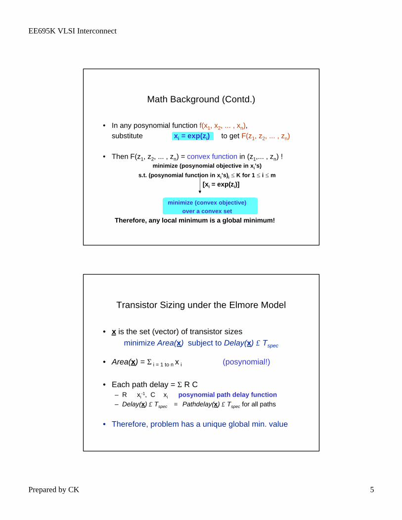
• In any posynomial function f(x1, x2, ... , xn),substitute xi = exp(zi) to get F(z1, z2, ... , zn)
• Then F(z1, z2, ... , zn) = convex function in (z1,... , zn) !minimize (posynomial objective in xi’s)
s.t. (posynomial function in xi’s)i ≤ K for 1 ≤ i ≤ m
[xi = exp(zi)]
minimize (convex objective)over a convex set
Therefore, any local minimum is a global minimum!
Math Background (Contd.)
Transistor Sizing under the Elmore Model
• x is the set (vector) of transistor sizesminimize Area(x) subject to Delay(x) ≤ Tspec
• Area(x) = Σ i = 1 to n x i (posynomial!)
• Each path delay = Σ R C– R ∝ xi
-1, C ∝ xi ⇒ posynomial path delay function– Delay(x) ≤ Tspec ≡ Pathdelay(x) ≤ Tspec for all paths
• Therefore, problem has a unique global min. value
EE695K VLSI Interconnect
Prepared by CK 6
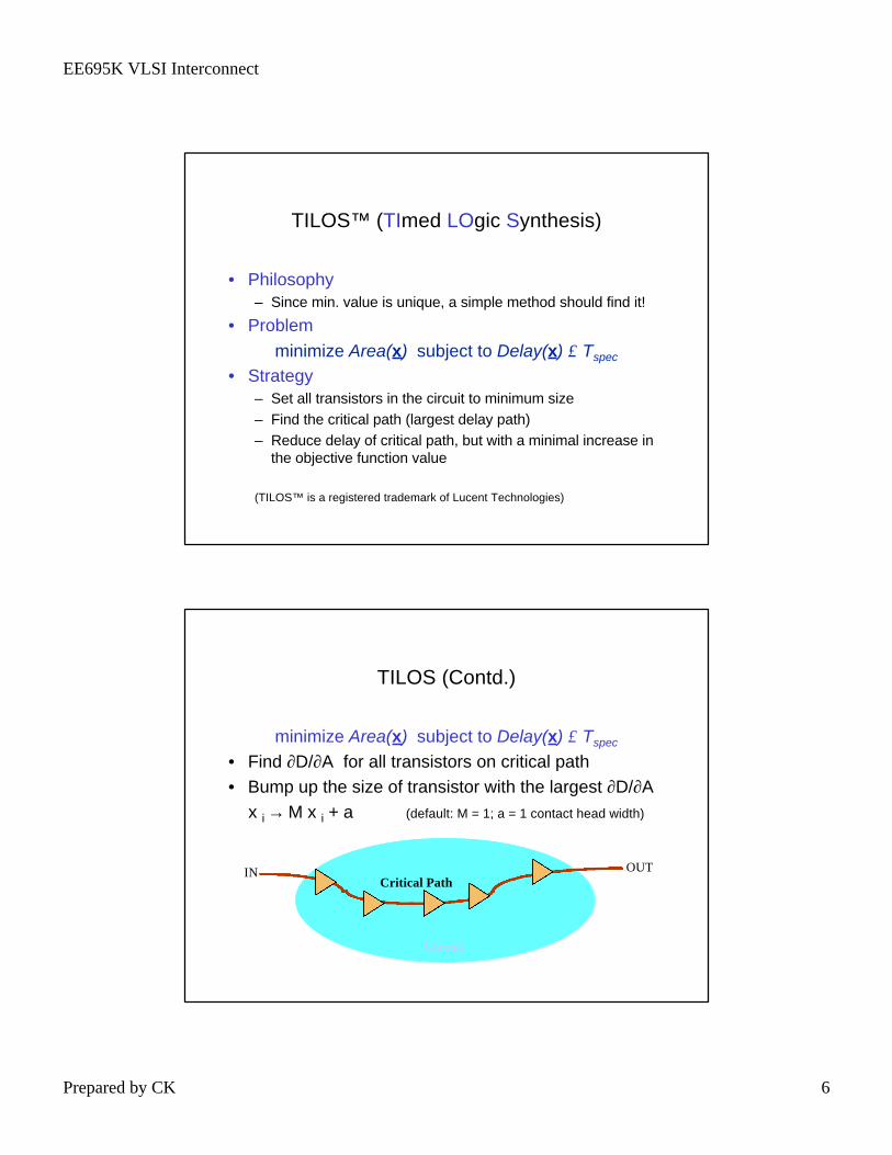
TILOS™ (TImed LOgic Synthesis)
• Philosophy– Since min. value is unique, a simple method should find it!
• Problem
minimize Area(x) subject to Delay(x) ≤ Tspec
• Strategy– Set all transistors in the circuit to minimum size– Find the critical path (largest delay path)– Reduce delay of critical path, but with a minimal increase in
the objective function value
(TILOS™ is a registered trademark of Lucent Technologies)
TILOS (Contd.)
minimize Area(x) subject to Delay(x) ≤ Tspec
• Find ∂D/∂A for all transistors on critical path• Bump up the size of transistor with the largest ∂D/∂A
x i → M x i + a (default: M = 1; a = 1 contact head width)
Circuit
Critical PathIN OUT

EE695K VLSI Interconnect
Prepared by CK 7
Sensitivity Computation
• D(w) = K + Rprev (Cu . w)+ Ru . C / w
• ∂D/∂w = Rprev . Cu - Ru . C / w2
• Could minimize path delay bysetting derivative to zero
• Problem: may cause anotherpath delay to become very high!
Rprev
“1”
wC
Why Isn’t This THE Perfect Solution?
• Problems with interacting paths(1) Better to size A than to size all
of B, C and D(2) If X-E is near-critical and A-D is
critical, size A (not D)
• False paths, layout considerations not incorporated• AND YET..
– TILOS (the commercial tool) gives good solutions– It has handled circuits with 250K transistors– It has linear time performance with increasing circuit size
A
B
C
D
XE

EE695K VLSI Interconnect
Prepared by CK 8
CONTRAST
• Solves the convex optimization problem exactly• Uses an interior point method that is guaranteed to
find the optimal solution
• Can handle circuits with about a thousand transistors
Delay spec.satisfied
Optimal solution
(Convex) Polytopes
• Polytope = n-dimensional convex polygon– Half-space: aT x ≥ b (aT x = b is a hyperplane)
e.g. a1 x1 + a2 x2 ≥ b (in two dimensions)– Polytope = intersection of half-spaces, i.e.,
a1T x ≥ b1
AND a2T x ≥ b 2
AND amT x ≥ bm
Represented as A x ≥ b

EE695K VLSI Interconnect
Prepared by CK 9
Convex Optimization Algorithm (Vaidya)
(1) Enclose solution within a polytope (invariant)– Typically, take a “box” represented by
wi ≤ wMAX and wi ≥ wMIN
as the starting polytope.
(2) Find center of polytope, wc
(3) Does wc satisfy constraints (timing specs)?– Take transistor widths corresponding to wc and perform a
static timing analysis
(4) Add a hyperplane through the center so that thesolution lies entirely in one half-space– Hyperplane equation depends on feasibility of wc
Half-space: ∇ f (wc) . w ≥ ∇ f (wc) . wc
• If wc is feasiblethen f = objective functionFind gradient of area function
• If wc is infeasiblethen f = violated constraintFind gradient of critical path delay
Equation of the New Half-Space
wc

EE695K VLSI Interconnect
Prepared by CK 10
Illustrative Example
f (w) = c, f decreasingsolution
S S
SS
w1
w2
Calculating the Polytope Center
• Finding exact centroid is computationally expensive• Estimate center by minimizing log-barrier function
F(x) = - Σi=1 to m log (aiT x - bi)
Happy “coincidence”:F(x) is a convex function!
• Physical meaning:maximize product of perpendiculardistances to each hyperplanethat defines the polytope

EE695K VLSI Interconnect
Prepared by CK 11
Linear Programming Methods
• LP-based approaches– Model gate delay as a piecewise linear function
Parameters: • transistor widths wn , wp
• fanout transistor widths
• input transition time
– Formulate problem as a linear program (LP)– Use an efficient simplex package to solve LP
Delay
wn
Power-Delay Sizing
minimize Power(w)subject to Delay(w) ≤ Tspec
Area ≤ Aspec
Each gate size ≥ Minsize
Power = dynamic power + short-circuit power

EE695K VLSI Interconnect
Prepared by CK 12
Dynamic Power
• Dynamic Power– Power required to charge/discharge capacitances
Pdynamic = CL Vdd2 f pT
CL = load capacitance, f = clock frequency, pT = transition probability
– Posynomial function in w’s (if pT constant)– Constitutes dominant part of power in a well-designed circuit– Minimize dynamic power ≡≡ minimize CL
≡≡ minimize all transistor sizes! RIGHT? (Unfortunately not!)
POST-IT
Short-Circuit Power
• Short-circuit Power– Power dissipated when a direct Vdd-ground path exists– Approximate formula by Veendrick (many assumptions)
Pshort-ckt = β/12. (β/12. (Vdd -2VT)2 τ τ f pT
β = transconductance, τ = transition time
– Posynomial function in w’s (if pT const)– Other (more accurate) models: table lookup, curve-fitting– “Less than 10-20% of total power in a well-designed circuit”– So what’s the catch?
POST-IT

EE695K VLSI Interconnect
Prepared by CK 13
The Catch
• Delay of gate A is large– Therefore, the value of τ for
B, C, ... , H is large– Therefore short-circuit power
for B, C, ... , H is large– Can be reduced by reducing
the delay of A– In other words, size A!
• Tradeoff dynamic and short-circuit power!
• Minpower ≠ minsize
A
B
C
D
XE
F
G
H
begin Calculate pT's ‘for minsized gates
error < εε? end
Solve gate sizing problem for current pT
Calculate pT's for new sizeserror = ||old pT - new pT ||
Problem: inaccuracies in short-ckt. power model
Solution Technique
Yes
No

EE695K VLSI Interconnect
Prepared by CK 14
Transistor/Gate Sizing[Borah-Owens-Irwin, ISLPD’95, TCAD’96]
γσ
α
τµτµ
++⋅=
⋅⋅⋅+⋅⋅⋅⋅+⋅+⋅⋅⋅= ∑∑==
WW
fWfWkfCLfWcVPn
i
iiin
n
i
iidd
)()(11
2
Optimal transistor size
τµ
µ
τµ
µ
⋅
⋅+⋅⋅=
⋅
⋅+⋅⋅=
∑ ∑
∑ ∑
= =
= =
n
n
i
n
ipiIpip
n
p
n
i
n
iniInin
p
WCWnOW
WCWpOW
1 1)()(
*
1 1)()(
*
)()()(
)()()(
CI = int. cap
Power Optimal Sizes and CorrespondingPower Savings

EE695K VLSI Interconnect
Prepared by CK 15
Power-Delay Optimization
Power, Delay and Power-Delay Curves

EE695K VLSI Interconnect
Prepared by CK 16
Power-Delay Optimal Transistor SizingAlgorithm
• Power-Optimal initial sizing• Timing analysis• While exists path-delay > target-delay
– Power-delay optimal sizing critical path– if path-delay > target-delay
• upsize transistor with minimum power-delay slope
– if path-delay < target-delay• downsize transistor with minimum power-delay
slope
– Incremental timing analysis
Effect of Transistor Sizing