Transistor level implementation of digital reversible circuits
19
International Journal of VLSI design & Communication Systems (VLSICS) Vol.5, No.6, December 2014 DOI : 10.5121/vlsic.2014.5606 43 TRANSISTOR LEVEL IMPLEMENTATION OF DIGITAL REVERSIBLE CIRCUITS K.Prudhvi Raj 1 and Y.Syamala 2 1 PG student, Gudlavalleru Engineering College, Krishna district, Andhra Pradesh, India 2 Departement of ECE, Gudlavalleru engineering college, Krishna district, Andhra Pradesh, India ABSTRACT Now a days each and every electronic gadget is designing smartly and provides number of applications, so these designs dissipate high amount of power. Reversible logic is becoming one of the best emerging design technologies having its applications in low power CMOS, Quantum computing and Nanotechnology. Reversible logic plays an important role in the design of energy efficient circuits. Adders and subtractors are the essential blocks of the computing systems. In this paper, reversible gates and circuits are designed and implemented in CMOS and pass transistor logic using Mentor graphics backend tools. A four-bit ripple carry adder/subtractor and an eight-bit reversible Carry Skip Adder are implemented and compared with the conventional circuits. KEYWORDS Low power, Reversible logic gates, Adder, Subtractor, Mentor graphics tools. 1. INTRODUCTION In modern VLSI systems, power dissipation is the critical limiting factor for more complex circuits. According to the Landauer’s principle [1], every conventional combinational circuit dissipates KTln2 Joules of energy for one-bit loss of information, where k is Boltzmann’s constant (1.3807 x 10 -23 joules per Kelvin) and T is absolute temperature. Reversible computation [2], is a research area having characteristics that are both forward and backward computations. In ideal cases, these circuits have zero information loss. Therefore, reversible computing is an appealing solution in the design of energy efficient circuits, which have low power dissipation. 1.1 Reversible logic Reversible logic is a very forthcoming approach of logic synthesis for power reduction in future computing technologies. Most of the gates used in digital design are not reversible for example AND, OR, EXOR gates do not perform reversible operation. A reversible gate/circuit can generate unique output vector for corresponding input vector i.e. one to one mapping is between input and output vectors. Therefore, out of all commonly used gates NOT gate is the only reversible gate with one input and one output (1×1). A basic structure of reversible gate is shown in figure 1. A gate/circuit is said to be reversible if it follows the below characteristics.
-
Upload
vlsics -
Category
Technology
-
view
246 -
download
1
Transcript of Transistor level implementation of digital reversible circuits

International Journal of VLSI design & Communication Systems (VLSICS) Vol.5, No.6, December 2014
DOI : 10.5121/vlsic.2014.5606 43
TRANSISTOR LEVEL IMPLEMENTATION OF
DIGITAL REVERSIBLE CIRCUITS
K.Prudhvi Raj1 and Y.Syamala
2
1PG student, Gudlavalleru Engineering College, Krishna district, Andhra Pradesh, India
2Departement of ECE, Gudlavalleru engineering college,
Krishna district, Andhra Pradesh, India
ABSTRACT
Now a days each and every electronic gadget is designing smartly and provides number of applications, so
these designs dissipate high amount of power. Reversible logic is becoming one of the best emerging design
technologies having its applications in low power CMOS, Quantum computing and Nanotechnology.
Reversible logic plays an important role in the design of energy efficient circuits. Adders and subtractors
are the essential blocks of the computing systems. In this paper, reversible gates and circuits are designed
and implemented in CMOS and pass transistor logic using Mentor graphics backend tools. A four-bit ripple
carry adder/subtractor and an eight-bit reversible Carry Skip Adder are implemented and compared with
the conventional circuits.
KEYWORDS
Low power, Reversible logic gates, Adder, Subtractor, Mentor graphics tools.
1. INTRODUCTION
In modern VLSI systems, power dissipation is the critical limiting factor for more complex
circuits. According to the Landauer’s principle [1], every conventional combinational circuit
dissipates KTln2 Joules of energy for one-bit loss of information, where k is Boltzmann’s
constant (1.3807 x 10⁻²³ joules per Kelvin) and T is absolute temperature. Reversible computation
[2], is a research area having characteristics that are both forward and backward computations. In
ideal cases, these circuits have zero information loss. Therefore, reversible computing is an
appealing solution in the design of energy efficient circuits, which have low power dissipation.
1.1 Reversible logic
Reversible logic is a very forthcoming approach of logic synthesis for power reduction in future
computing technologies. Most of the gates used in digital design are not reversible for example
AND, OR, EXOR gates do not perform reversible operation. A reversible gate/circuit can
generate unique output vector for corresponding input vector i.e. one to one mapping is between
input and output vectors. Therefore, out of all commonly used gates NOT gate is the only
reversible gate with one input and one output (1×1).
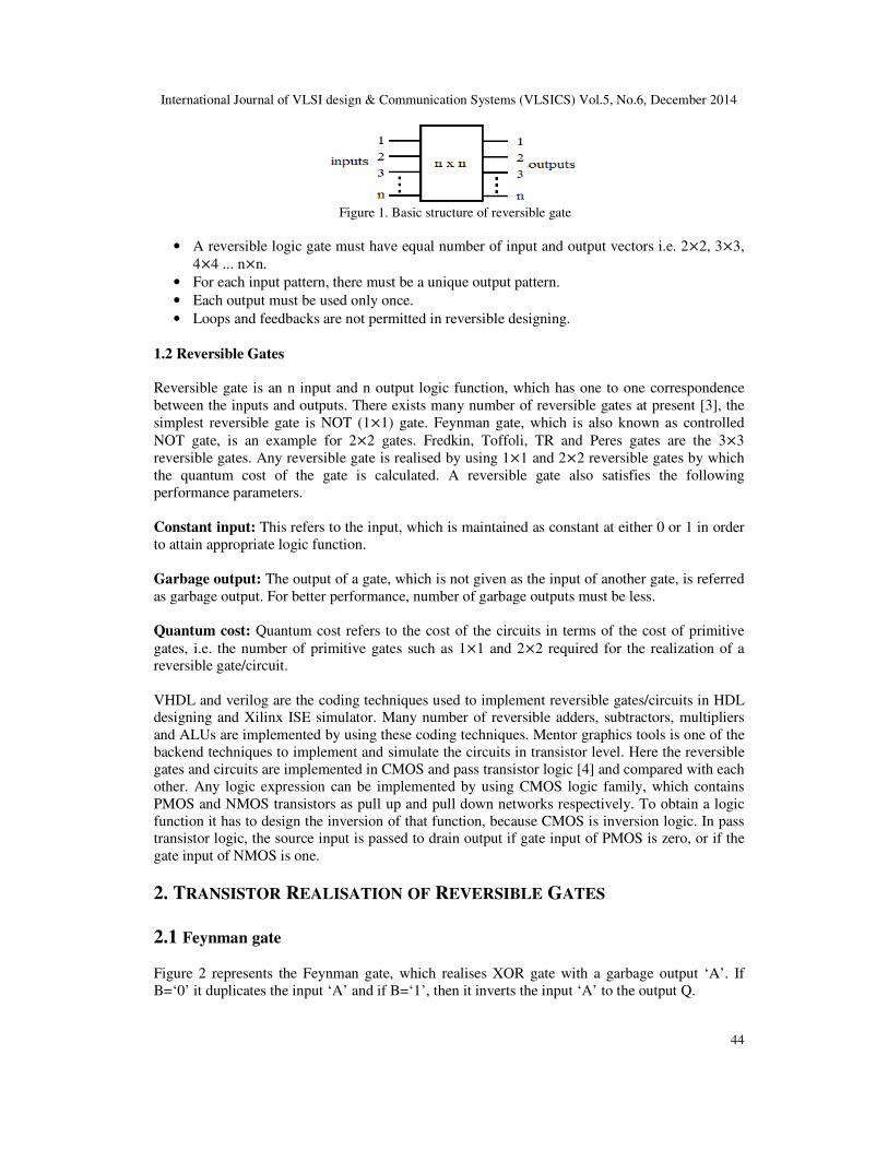
A basic structure of reversible gate is shown in figure 1. A gate/circuit is said to be reversible if it
follows the below characteristics.
International Journal of VLSI design & Communication Systems (VLSICS) Vol.5, No.6, December 2014
44
Figure 1. Basic structure of reversible gate
• A reversible logic gate must have equal number of input and output vectors i.e. 2×2, 3×3,
4×4 ... n×n.
• For each input pattern, there must be a unique output pattern.
• Each output must be used only once.
• Loops and feedbacks are not permitted in reversible designing.
1.2 Reversible Gates
Reversible gate is an n input and n output logic function, which has one to one correspondence
between the inputs and outputs. There exists many number of reversible gates at present [3], the
simplest reversible gate is NOT (1×1) gate. Feynman gate, which is also known as controlled
NOT gate, is an example for 2×2 gates. Fredkin, Toffoli, TR and Peres gates are the 3×3
reversible gates. Any reversible gate is realised by using 1×1 and 2×2 reversible gates by which
the quantum cost of the gate is calculated. A reversible gate also satisfies the following
performance parameters.
Constant input: This refers to the input, which is maintained as constant at either 0 or 1 in order
to attain appropriate logic function.
Garbage output: The output of a gate, which is not given as the input of another gate, is referred
as garbage output. For better performance, number of garbage outputs must be less.
Quantum cost: Quantum cost refers to the cost of the circuits in terms of the cost of primitive
gates, i.e. the number of primitive gates such as 1×1 and 2×2 required for the realization of a
reversible gate/circuit.
VHDL and verilog are the coding techniques used to implement reversible gates/circuits in HDL
designing and Xilinx ISE simulator. Many number of reversible adders, subtractors, multipliers
and ALUs are implemented by using these coding techniques. Mentor graphics tools is one of the
backend techniques to implement and simulate the circuits in transistor level. Here the reversible
gates and circuits are implemented in CMOS and pass transistor logic [4] and compared with each
other. Any logic expression can be implemented by using CMOS logic family, which contains
PMOS and NMOS transistors as pull up and pull down networks respectively. To obtain a logic
function it has to design the inversion of that function, because CMOS is inversion logic. In pass
transistor logic, the source input is passed to drain output if gate input of PMOS is zero, or if the
gate input of NMOS is one.
2. TRANSISTOR REALISATION OF REVERSIBLE GATES
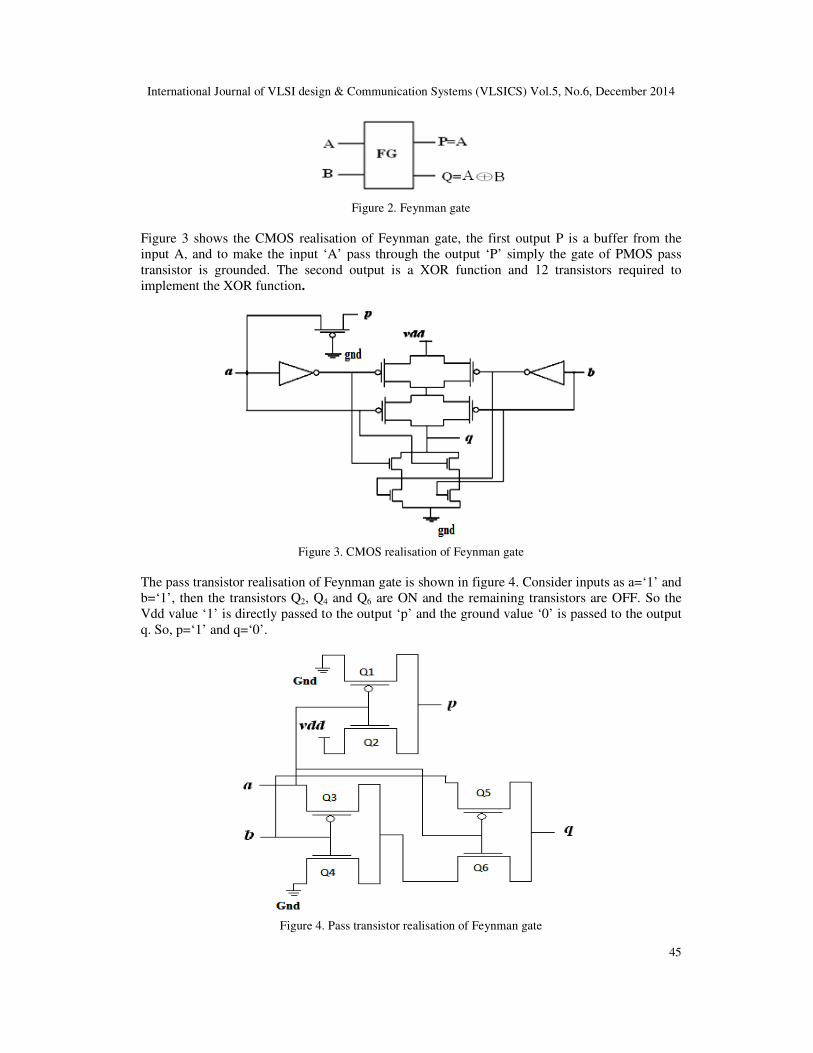
2.1 Feynman gate
Figure 2 represents the Feynman gate, which realises XOR gate with a garbage output ‘A’. If
B=‘0’ it duplicates the input ‘A’ and if B=‘1’, then it inverts the input ‘A’ to the output Q.
International Journal of VLSI design & Communication Systems (VLSICS) Vol.5, No.6, December 2014
Figure 3 shows the CMOS realisation of Feynman gate, the first output P is a buffer from the
input A, and to make the input ‘A’ pass through the output ‘P’ simply the gate of
transistor is grounded. The second output is a XOR function and 12 tran
implement the XOR function.
Figure
The pass transistor realisation of Feynman gate is shown in figure 4. Consider inputs as a=‘1’ and
b=‘1’, then the transistors Q2, Q
Vdd value ‘1’ is directly passed to the output ‘p’ and the ground value ‘0’ is passed to
q. So, p=‘1’ and q=‘0’.
Figure 4
International Journal of VLSI design & Communication Systems (VLSICS) Vol.5, No.6, December 2014
Figure 2. Feynman gate
Figure 3 shows the CMOS realisation of Feynman gate, the first output P is a buffer from the
input A, and to make the input ‘A’ pass through the output ‘P’ simply the gate of
transistor is grounded. The second output is a XOR function and 12 transistors required to
ure 3. CMOS realisation of Feynman gate
The pass transistor realisation of Feynman gate is shown in figure 4. Consider inputs as a=‘1’ and
, Q4 and Q6 are ON and the remaining transistors are OFF. So the
Vdd value ‘1’ is directly passed to the output ‘p’ and the ground value ‘0’ is passed to
4. Pass transistor realisation of Feynman gate
International Journal of VLSI design & Communication Systems (VLSICS) Vol.5, No.6, December 2014
45
Figure 3 shows the CMOS realisation of Feynman gate, the first output P is a buffer from the
input A, and to make the input ‘A’ pass through the output ‘P’ simply the gate of PMOS pass
sistors required to
The pass transistor realisation of Feynman gate is shown in figure 4. Consider inputs as a=‘1’ and
are OFF. So the
Vdd value ‘1’ is directly passed to the output ‘p’ and the ground value ‘0’ is passed to the output
International Journal of VLSI design & Communication Systems (VLSICS) Vol.5, No.6, December 2014
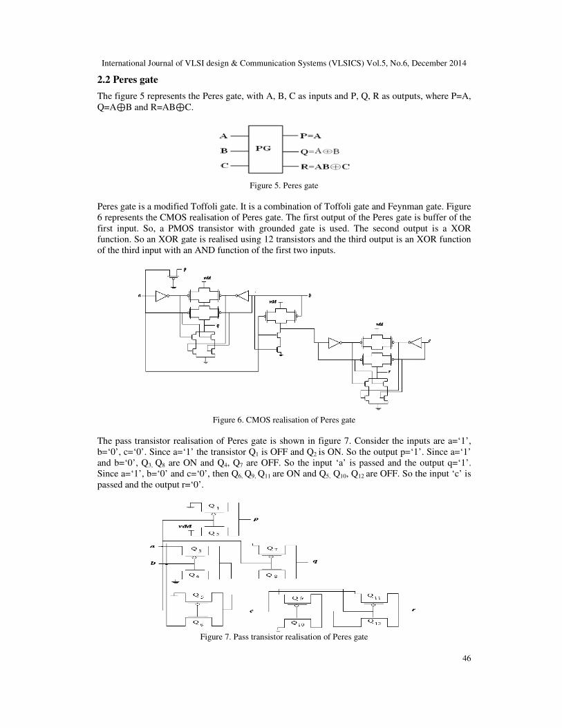
2.2 Peres gate
The figure 5 represents the Peres gate,
Q=A⊕B and R=AB⊕C.
Peres gate is a modified Toffoli gate. It is a combination of Toffoli gate and Feynman gate.
6 represents the CMOS realisation of Peres gate.
first input. So, a PMOS transistor with grounded gate is used. The second output is a XOR
function. So an XOR gate is reali
of the third input with an AND function
Figure
The pass transistor realisation of Peres gate
b=‘0’, c=‘0’. Since a=‘1’ the transistor Q
and b=‘0’, Q3, Q8 are ON and Q
Since a=‘1’, b=‘0’ and c=‘0’, then Q
passed and the output r=‘0’.
Figure
International Journal of VLSI design & Communication Systems (VLSICS) Vol.5, No.6, December 2014
represents the Peres gate, with A, B, C as inputs and P, Q, R as outputs, where P=A,
Figure 5. Peres gate
gate. It is a combination of Toffoli gate and Feynman gate.
represents the CMOS realisation of Peres gate. The first output of the Peres gate is bu
MOS transistor with grounded gate is used. The second output is a XOR
an XOR gate is realised using 12 transistors and the third output is an XOR
the third input with an AND function of the first two inputs.
Figure 6. CMOS realisation of Peres gate
The pass transistor realisation of Peres gate is shown in figure 7. Consider the inputs are
the transistor Q1 is OFF and Q2 is ON. So the output p=‘1’
Q4, Q7 are OFF. So the input ‘a’ is passed and the output q=
, then Q6, Q9, Q11 are ON and Q5, Q10, Q12 are OFF. So the input
ure 7. Pass transistor realisation of Peres gate
International Journal of VLSI design & Communication Systems (VLSICS) Vol.5, No.6, December 2014
46
Q, R as outputs, where P=A,
gate. It is a combination of Toffoli gate and Feynman gate. Figure
The first output of the Peres gate is buffer of the
MOS transistor with grounded gate is used. The second output is a XOR
third output is an XOR function
. Consider the inputs are a=‘1’,
’. Since a=‘1’
is passed and the output q=‘1’.
. So the input ‘c’ is
International Journal of VLSI design & Communication Systems (VLSICS) Vol.5, No.6, December 2014
2.3 Fredkin gate
Figure 8 represents the Fredkin gate
Q=A’B+AC and R=AB+A’C.
Fredkin gate acts as a Multiplexer, if the input A is
swaps between the inputs B and C.
Figure
The CMOS realization of Fredkin gate is shown in figu
buffer of the first input. So, a P
Q=A’B+AC and the third output R=AB+A’C are realised by the pull up and pull down networks
with PMOS and NMOS transistors resp
Figure 10. Pass transistor realisation of Fredkin gate
International Journal of VLSI design & Communication Systems (VLSICS) Vol.5, No.6, December 2014
represents the Fredkin gate with inputs A, B, C and outputs P, Q, and R.
Figure 8. Fredkin gate
Fredkin gate acts as a Multiplexer, if the input A is either ‘0’ or ‘1’ then the outputs Q and R
aps between the inputs B and C.
ure 9. CMOS realisation of Fredkin gate
redkin gate is shown in figure 9. The first output of the Fredkin
ffer of the first input. So, a PMOS transistor with grounded gate is used. The second output
Q=A’B+AC and the third output R=AB+A’C are realised by the pull up and pull down networks
with PMOS and NMOS transistors respectively.
Figure 10. Pass transistor realisation of Fredkin gate
International Journal of VLSI design & Communication Systems (VLSICS) Vol.5, No.6, December 2014
47
. Where P=A,
either ‘0’ or ‘1’ then the outputs Q and R
first output of the Fredkin gate is
MOS transistor with grounded gate is used. The second output
Q=A’B+AC and the third output R=AB+A’C are realised by the pull up and pull down networks
International Journal of VLSI design & Communication Systems (VLSICS) Vol.5, No.6, December 2014
The pass transistor realisation of F
a=‘1’, b=‘0’, c=‘1’. Since a=‘1’, transistors Q
the output p=‘1’. The input ‘c’ is passed through the transistor Q
passed through the transistor Q6. S
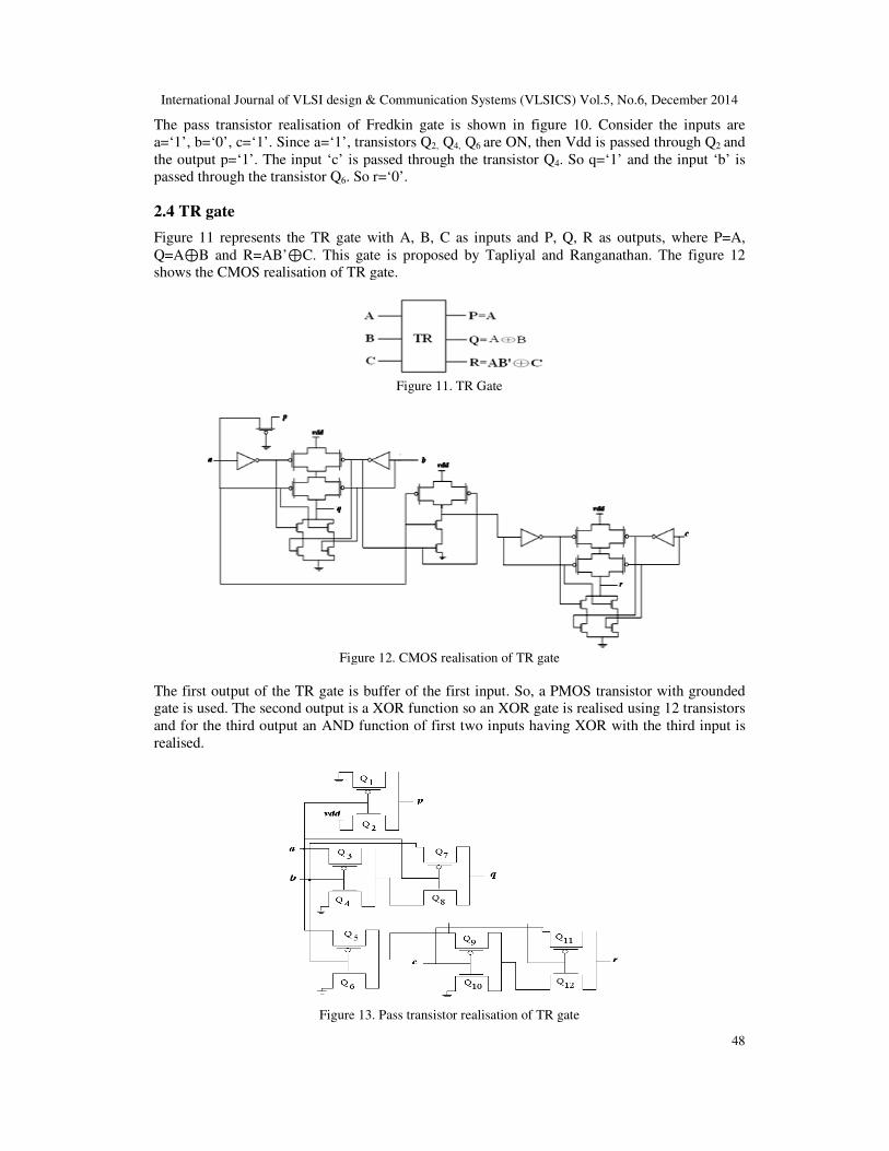
2.4 TR gate
Figure 11 represents the TR gate with A, B, C as inputs and P,
Q=A⊕B and R=AB’⊕C. This gate
shows the CMOS realisation of TR gate.
Fig
The first output of the TR gate is bu
gate is used. The second output is a XOR function so an XOR gate is realised using 12 transistors
and for the third output an AND function of first two inputs having XOR with the third input is
realised.
Figure
International Journal of VLSI design & Communication Systems (VLSICS) Vol.5, No.6, December 2014
The pass transistor realisation of Fredkin gate is shown in figure 10. Consider the inputs are
a=‘1’, b=‘0’, c=‘1’. Since a=‘1’, transistors Q2, Q4, Q6 are ON, then Vdd is passed through
the output p=‘1’. The input ‘c’ is passed through the transistor Q4. So q=‘1’ and the input ‘b’ is
. So r=‘0’.
gate with A, B, C as inputs and P, Q, R as outputs, where P=A,
his gate is proposed by Tapliyal and Ranganathan. The figure 12
shows the CMOS realisation of TR gate.
Figure 11. TR Gate
Figure 12. CMOS realisation of TR gate
The first output of the TR gate is buffer of the first input. So, a PMOS transistor with grounded
gate is used. The second output is a XOR function so an XOR gate is realised using 12 transistors
and for the third output an AND function of first two inputs having XOR with the third input is
ure 13. Pass transistor realisation of TR gate
International Journal of VLSI design & Communication Systems (VLSICS) Vol.5, No.6, December 2014
48
. Consider the inputs are
passed through Q2 and
o q=‘1’ and the input ‘b’ is
Q, R as outputs, where P=A,
. The figure 12
MOS transistor with grounded
gate is used. The second output is a XOR function so an XOR gate is realised using 12 transistors
and for the third output an AND function of first two inputs having XOR with the third input is

International Journal of VLSI design & Communication Systems (VLSICS) Vol.5, No.6, December 2014
49
The pass transistor realisation of TR gate is shown in figure 13. Consider the inputs are a=‘1’,
b=‘1’, c=‘0’. Since a=‘1’ the transistor Q1 is OFF and Q2 is ON. So the output p=‘1’. Since a=‘1’
and b=‘1’, Q4, Q8 are ON and Q3, Q7 are OFF. So the ground value ‘0’ is passed through Q4, Q8
then the output q=‘0’. Since a=‘1’, b=‘1’ and c=‘0’, then Q6, Q9, Q12 are ON and Q5, Q10, Q11 are
OFF. So the ground value ‘0’ is passed through Q10, Q12 then the output r=‘0’.
3. TRANSISTOR REALISATION OF REVERSIBLE CIRCUITS
Reversible circuits are implemented using the reversible gates only. There are many designs of
one bit full adder/subtractor circuits [5, 6]. Here, two designs of full adder/subtractor use 8 and 4
gates respectively. In this work these designs are implemented in CMOS and pass transistor
logics using Mentor graphics tools.
3.1 One-Bit Reversible full Adder/Subtractor
Figure 14 shows a one-bit reversible adder/subtractor [7] using three Feynman gates, two Peres
gates, two TR gates and one Fredkin gate. A control input is given to switch between adder and
subtractor. If control input is ‘1’ addition is performed else if it is ‘0’ subtraction is performed.
Figure 14. Design 1of one bit full adder/subtractor
Figure 15 shows a one-bit reversible adder/subtractor [8] using two Feynman gates and two Peres
gates. A control input is given to switch between adder and subtractor. If control input is ‘0’
addition is performed else if it is ‘1’ subtraction is performed.
Figure 15. Design 2 of one bit full adder/subtractor
3.2 Four-bit ripple carry adder/subtractor
By using the one-bit adder/subtractor, a four-bit ripple carry adder/subtractor [9] is implemented
as shown in figure 16. A control signal is given to all the full adder/subtractor circuits by
duplicating the signal using Feynman gates.
International Journal of VLSI design & Communication Systems (VLSICS) Vol.5, No.6, December 2014
Figure
Two four bit operands A(a3-a0), B(b3
subtraction operations.
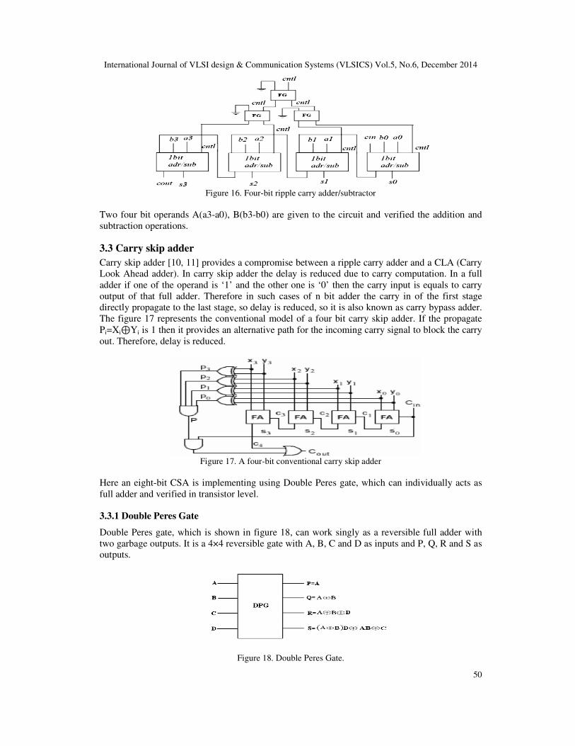
3.3 Carry skip adder
Carry skip adder [10, 11] provides
Look Ahead adder). In carry skip adder the delay is reduced
adder if one of the operand is ‘1’ and the other one is ‘0’ then the carry input is equals to carry
output of that full adder. Therefore in such cases of n bit adder the carry in of the first stage
directly propagate to the last stage, so delay is reduced, so it is also known as carry bypass adder.
The figure 17 represents the conventional model of a four bit carry skip adder. If the propagate
Pi=Xi⊕Yi is 1 then it provides an alternative path for the incoming carry signal to block the carry
out. Therefore, delay is reduced.
Figure 1
Here an eight-bit CSA is implementing using
full adder and verified in transistor level
3.3.1 Double Peres Gate
Double Peres gate, which is shown in figur
two garbage outputs. It is a 4×4 reversi
outputs.
International Journal of VLSI design & Communication Systems (VLSICS) Vol.5, No.6, December 2014
ure 16. Four-bit ripple carry adder/subtractor
a0), B(b3-b0) are given to the circuit and verified the addition and
provides a compromise between a ripple carry adder and a
In carry skip adder the delay is reduced due to carry computation. In a
is ‘1’ and the other one is ‘0’ then the carry input is equals to carry
Therefore in such cases of n bit adder the carry in of the first stage
the last stage, so delay is reduced, so it is also known as carry bypass adder.
The figure 17 represents the conventional model of a four bit carry skip adder. If the propagate
is 1 then it provides an alternative path for the incoming carry signal to block the carry
out. Therefore, delay is reduced.
17. A four-bit conventional carry skip adder
is implementing using Double Peres gate, which can individually acts as
and verified in transistor level.
, which is shown in figure 18, can work singly as a reversible full adder with
It is a 4×4 reversible gate with A, B, C and D as inputs and P, Q, R and S as
Figure 18. Double Peres Gate.
International Journal of VLSI design & Communication Systems (VLSICS) Vol.5, No.6, December 2014
50
to the circuit and verified the addition and
a compromise between a ripple carry adder and a CLA (Carry
computation. In a full
is ‘1’ and the other one is ‘0’ then the carry input is equals to carry
Therefore in such cases of n bit adder the carry in of the first stage
the last stage, so delay is reduced, so it is also known as carry bypass adder.
The figure 17 represents the conventional model of a four bit carry skip adder. If the propagate
is 1 then it provides an alternative path for the incoming carry signal to block the carry
dividually acts as
singly as a reversible full adder with
inputs and P, Q, R and S as
International Journal of VLSI design & Communication Systems (VLSICS) Vol.5, No.6, December 2014
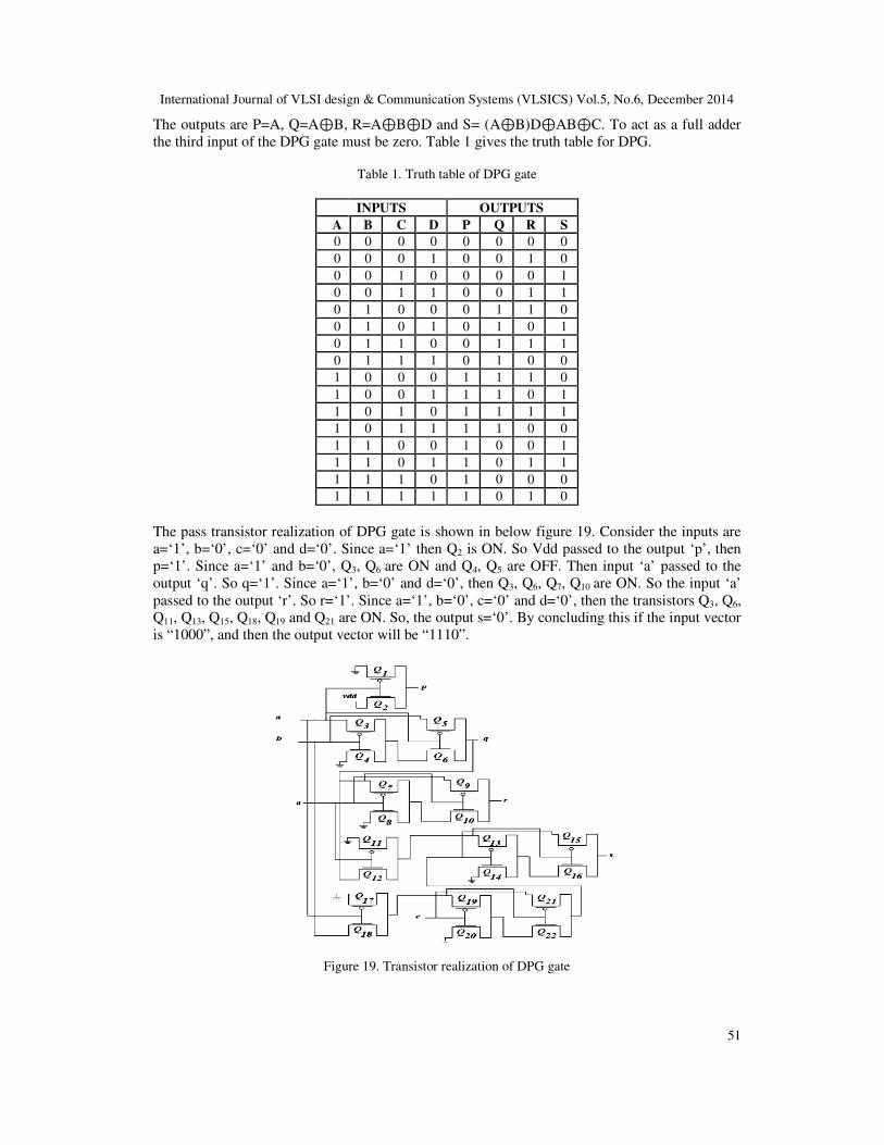
The outputs are P=A, Q=A⊕B, R=A
the third input of the DPG gate must be zero. Table 1 gives the truth table for DPG.
A
0
0
0
0
0
0
0
0
1
1
1
1
1
1
1
1
The pass transistor realization of DPG gate is shown in below figure 19.
a=‘1’, b=‘0’, c=‘0’ and d=‘0’. Since a=‘1’ then Q
p=‘1’. Since a=‘1’ and b=‘0’, Q
output ‘q’. So q=‘1’. Since a=‘1’, b=‘0’ and d=‘0’, then Q
passed to the output ‘r’. So r=‘1’. Since a=‘1’,
Q11, Q13, Q15, Q18, Q19 and Q21 are ON. So
is “1000”, and then the output vector will be
Figure
International Journal of VLSI design & Communication Systems (VLSICS) Vol.5, No.6, December 2014
B, R=A⊕B⊕D and S= (A⊕B)D⊕AB⊕C. To act as a full adder
of the DPG gate must be zero. Table 1 gives the truth table for DPG.
Table 1. Truth table of DPG gate
INPUTS OUTPUTS
B C D P Q R S
0 0 0 0 0 0 0
0 0 1 0 0 1 0
0 1 0 0 0 0 1
0 1 1 0 0 1 1
1 0 0 0 1 1 0
1 0 1 0 1 0 1
1 1 0 0 1 1 1
1 1 1 0 1 0 0
0 0 0 1 1 1 0
0 0 1 1 1 0 1
0 1 0 1 1 1 1
0 1 1 1 1 0 0
1 0 0 1 0 0 1
1 0 1 1 0 1 1
1 1 0 1 0 0 0
1 1 1 1 0 1 0
The pass transistor realization of DPG gate is shown in below figure 19. Consider the inputs are
a=‘1’, b=‘0’, c=‘0’ and d=‘0’. Since a=‘1’ then Q2 is ON. So Vdd passed to the output ‘p’, then
p=‘1’. Since a=‘1’ and b=‘0’, Q3, Q6 are ON and Q4, Q5 are OFF. Then input ‘a’ passed to the
o q=‘1’. Since a=‘1’, b=‘0’ and d=‘0’, then Q3, Q6, Q7, Q10 are ON. So the input
o r=‘1’. Since a=‘1’, b=‘0’, c=‘0’ and d=‘0’, then the transistors Q
are ON. So, the output s=‘0’. By concluding this if the input vector
, and then the output vector will be “1110”.
ure 19. Transistor realization of DPG gate
International Journal of VLSI design & Communication Systems (VLSICS) Vol.5, No.6, December 2014
51
act as a full adder
Consider the inputs are
output ‘p’, then
‘a’ passed to the
are ON. So the input ‘a’
b=‘0’, c=‘0’ and d=‘0’, then the transistors Q3, Q6,
the output s=‘0’. By concluding this if the input vector
International Journal of VLSI design & Communication Systems (VLSICS) Vol.5, No.6, December 2014
3.3.2 Eight-bit carry skip adder
Fig
An eight bit reversible carry skip adder
figure 20, if the propagate signal p
stage of the carry skip adder. So, the delay is reduced and if p
through all the stages. The transistor
verified by Mentor graphics tools
4. RESULTS
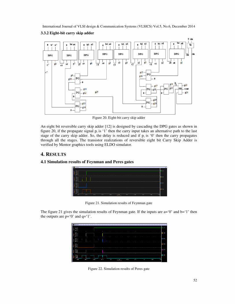
4.1 Simulation results of Feynman and Peres gates
Figure
The figure 21 gives the simulation results of Feynman gate. I
the outputs are p=‘0’ and q=‘1’.
Fig
International Journal of VLSI design & Communication Systems (VLSICS) Vol.5, No.6, December 2014
carry skip adder
Figure 20. Eight-bit carry skip adder
An eight bit reversible carry skip adder [12] is designed by cascading the DPG gates as shown in
figure 20, if the propagate signal pi is ‘1’ then the carry input takes an alternative path to the last
stage of the carry skip adder. So, the delay is reduced and if pi is ‘0’ then the carry propagates
through all the stages. The transistor realizations of reversible eight bit Carry Skip Add
ools using ELDO simulator.
of Feynman and Peres gates
ure 21. Simulation results of Feynman gate
gives the simulation results of Feynman gate. If the inputs are a=‘0’ and b=
Figure 22. Simulation results of Peres gate
International Journal of VLSI design & Communication Systems (VLSICS) Vol.5, No.6, December 2014
52
is designed by cascading the DPG gates as shown in
is ‘1’ then the carry input takes an alternative path to the last
is ‘0’ then the carry propagates
of reversible eight bit Carry Skip Adder is
and b=‘1’ then
International Journal of VLSI design & Communication Systems (VLSICS) Vol.5, No.6, December 2014
53
The simulation results of Peres gate are shown in figure 22, if the inputs are a=‘1’, b=‘0’ and
c=‘1’ then the outputs are p=‘1’, q=‘1’ and r=‘1’.
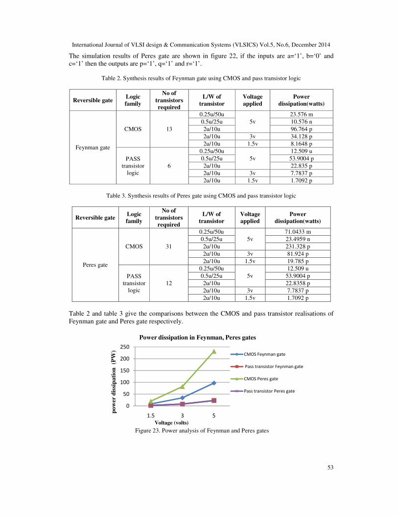
Table 2. Synthesis results of Feynman gate using CMOS and pass transistor logic
Reversible gate Logic
family
No of
transistors
required
L/W of
transistor
Voltage
applied
Power
dissipation(watts)
Feynman gate
CMOS 13
0.25u/50u
5v
23.576 m
0.5u/25u 10.576 n
2u/10u 96.764 p
2u/10u 3v 34.128 p
2u/10u 1.5v 8.1648 p
PASS
transistor
logic
6
0.25u/50u
5v
12.509 u
0.5u/25u 53.9004 p
2u/10u 22.835 p
2u/10u 3v 7.7837 p
2u/10u 1.5v 1.7092 p
Table 3. Synthesis results of Peres gate using CMOS and pass transistor logic
Reversible gate Logic
family
No of
transistors
required
L/W of
transistor
Voltage
applied
Power
dissipation(watts)
Peres gate
CMOS 31
0.25u/50u
5v
71.0433 m
0.5u/25u 23.4959 n
2u/10u 231.328 p
2u/10u 3v 81.924 p
2u/10u 1.5v 19.785 p
PASS
transistor
logic
12
0.25u/50u
5v
12.509 u
0.5u/25u 53.9004 p
2u/10u 22.8358 p
2u/10u 3v 7.7837 p
2u/10u 1.5v 1.7092 p
Table 2 and table 3 give the comparisons between the CMOS and pass transistor realisations of
Feynman gate and Peres gate respectively.
Figure 23. Power analysis of Feynman and Peres gates
0
50
100
150
200
250
1.5 3 5
po
wer
dis
sip
ati
on
(P
W)
Voltage (volts)
Power dissipation in Feynman, Peres gates
CMOS Feynman gate
Pass transistor Feynman gate
CMOS Peres gate
Pass transistor Peres gate
International Journal of VLSI design & Communication Systems (VLSICS) Vol.5, No.6, December 2014
The power dissipations of the gates for different voltages
23 and it is observed that power dissipation of the gates is optimised in pass transistor realisation
compared to CMOS technique.
4.2 Simulation results of Fredkin gate and TR gate
Fig
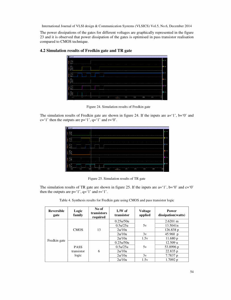
The simulation results of Fredkin gate are shown in figure 24
c=‘1’ then the outputs are p=‘1’, q=
Fig
The simulation results of TR gate are shown in figure 25
then the outputs are p=‘1’, q=‘1’
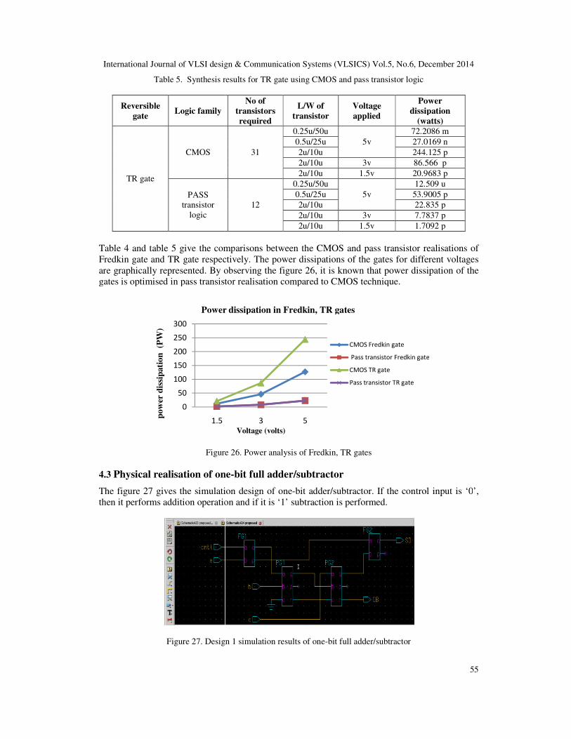
Table 4. Synthesis results for
Reversible
gate
Logic
family transistors
Fredkin gate
CMOS
PASS
transistor
logic
International Journal of VLSI design & Communication Systems (VLSICS) Vol.5, No.6, December 2014
The power dissipations of the gates for different voltages are graphically represented
that power dissipation of the gates is optimised in pass transistor realisation
of Fredkin gate and TR gate
Figure 24. Simulation results of Fredkin gate
dkin gate are shown in figure 24. If the inputs are a=‘1’
, q=‘1’ and r=‘0’.
Figure 25. Simulation results of TR gate
f TR gate are shown in figure 25. If the inputs are a=‘1’, b=
‘1’ and r=‘1’.
Synthesis results for Fredkin gate using CMOS and pass transistor logic
No of
transistors
required
L/W of
transistor
Voltage
applied
Power
dissipation(watts)
13
0.25u/50u
5v
2.6201 m
0.5u/25u 13.5041n
2u/10u 126.838 p
2u/10u 3v 45.960 p
2u/10u 1.5v 11.680 p
6
0.25u/50u
5v
12.509 u
0.5u/25u 53.8996 p
2u/10u 22.835 p
2u/10u 3v 7.7837 p
2u/10u 1.5v 1.7092 p
International Journal of VLSI design & Communication Systems (VLSICS) Vol.5, No.6, December 2014
54
are graphically represented in the figure
that power dissipation of the gates is optimised in pass transistor realisation
‘1’, b=‘0’ and
, b=‘0’ and c=‘0’
CMOS and pass transistor logic
Power
dissipation(watts)
2.6201 m
13.5041n
126.838 p
45.960 p
11.680 p
12.509 u
53.8996 p
22.835 p
7.7837 p
1.7092 p
International Journal of VLSI design & Communication Systems (VLSICS) Vol.5, No.6, December 2014
Table 5. Synthesis results for
Reversible
gate Logic family
TR gate
CMOS
PASS
transistor
logic
Table 4 and table 5 give the comparisons between the CMOS and pass transistor realisations of
Fredkin gate and TR gate respectively.
are graphically represented. By observing the figure 26
gates is optimised in pass transistor realisation compared to CMOS technique.
Figure
4.3 Physical realisation of one
The figure 27 gives the simulation design of one
then it performs addition operation
Figure 27. Design 1 simulation results of one
0
50
100
150
200
250
300
1.5
po
wer
dis
sip
ati
on
(P
W)
Power dissipation in Fredkin, TR gates
International Journal of VLSI design & Communication Systems (VLSICS) Vol.5, No.6, December 2014
Synthesis results for TR gate using CMOS and pass transistor logic
No of
transistors
required
L/W of
transistor
Voltage
applied
Power
dissipation
(watts)
31
0.25u/50u
5v
72.2086 m
0.5u/25u 27.0169 n
2u/10u 244.125 p
2u/10u 3v 86.566 p
2u/10u 1.5v 20.9683 p
12
0.25u/50u
5v
12.509 u
0.5u/25u 53.9005 p
2u/10u 22.835 p
2u/10u 3v 7.7837 p
2u/10u 1.5v 1.7092 p
the comparisons between the CMOS and pass transistor realisations of
e and TR gate respectively. The power dissipations of the gates for different voltages
observing the figure 26, it is known that power dissipation of the
gates is optimised in pass transistor realisation compared to CMOS technique.
ure 26. Power analysis of Fredkin, TR gates
of one-bit full adder/subtractor
The figure 27 gives the simulation design of one-bit adder/subtractor. If the control input is ‘0
then it performs addition operation and if it is ‘1’ subtraction is performed.
Design 1 simulation results of one-bit full adder/subtractor
3 5
Voltage (volts)
Power dissipation in Fredkin, TR gates
CMOS Fredkin gate
Pass transistor Fredkin gate
CMOS TR gate
Pass transistor TR gate
International Journal of VLSI design & Communication Systems (VLSICS) Vol.5, No.6, December 2014
55
Power
dissipation
(watts)
72.2086 m
27.0169 n
244.125 p
86.566 p
20.9683 p
12.509 u
53.9005 p
22.835 p
7.7837 p
1.7092 p
the comparisons between the CMOS and pass transistor realisations of
The power dissipations of the gates for different voltages
, it is known that power dissipation of the
ctor. If the control input is ‘0’,
Pass transistor Fredkin gate

International Journal of VLSI design & Communication Systems (VLSICS) Vol.5, No.6, December 2014
The simulation design of another
input is ‘1’ the circuit performs addition operation and
Figure 28. Design 2 s
The simulation results of adder are
outputs are sum=0 and carry=1.
Fig
The simulation results of subtractor
the outputs are difference=‘1’ and barrow=‘1’
Fig
International Journal of VLSI design & Communication Systems (VLSICS) Vol.5, No.6, December 2014
another one-bit adder/subtractor is shown in figure 28. If the control
’ the circuit performs addition operation and if it is ‘0’ subtraction is performed.
Design 2 simulation results of one-bit full adder/subtractor
of adder are shown in below figure 29. If A=0, B=1 and Cin=1 then the
Figure 29. Simulation results of Adder
of subtractor are shown in the figure 30. If A=‘1’, B=‘1’ and Cin=‘1’
the outputs are difference=‘1’ and barrow=‘1’.
Figure 30. Simulation results of subtractor
International Journal of VLSI design & Communication Systems (VLSICS) Vol.5, No.6, December 2014
56
28. If the control
if it is ‘0’ subtraction is performed.
. If A=0, B=1 and Cin=1 then the
B=‘1’ and Cin=‘1’ then
International Journal of VLSI design & Communication Systems (VLSICS) Vol.5, No.6, December 2014
57
Table 6. Synthesis results of one-bit adder/subtractor circuits for supply voltage 5V
Reversible
circuit
Logic
family
No of
transistors
required
Length/width
of transistor
Power
dissipation
(watts)
adder
Power
dissipation
(watts)
Subtractor
adder/subtractor
design 1
CMOS 194 0.5u/25u 143.1620 n 146.258 n
2u/10u 1.367 n 1.3680 n
Pass
transistor 72
0.5u/25u 1.4283 n 613.7312 p
2u/10u 185.6219 p 184.3425 p
adder/subtractor
design 2
CMOS 88 0.5u/25u 68.144 n 82.680 n
2u/10u 696.199 p 656.185 p
Pass
transistor 36
0.5u/25u 276.6720 p 9.9716 n
2u/10u 90.5589 p 86.8545 p
Table 6 gives the comparisons between the CMOS and pass transistor realisations of one-bit full
adder/subtractor designs. The power dissipations of the adders and subtractors for different
transistor sizes are represented in figures 31 and figure 32 respectively.
Figure 31. Transistor sizes Vs power dissipation of design1one bit full adder/subtractor
Figure 32. Transistor sizes Vs power dissipation of design2 one bit full adder/subtractor
0
20
40
60
80
100
120
140
160
0.5u/25u 2u/10u
po
wer
dis
sip
ati
on
(n
w)
length/width of transistor (metres)
Power dissipation of one bit adder/subtractor (Design1)
CMOS adder
Pass Transistor adder
CMOS subtractor
Pass Transistor subtractor
0
20
40
60
80
100
0.5u/25u 2u/10u
pow
er d
issi
pati
on
(n
w)
length/width of transistor (meters)
Power dissipation of one bit adder/subtractor (Design2)
CMOS adder
Pass Transistor adder
CMOS subtractor
Pass Transistor subtractor

International Journal of VLSI design & Communication Systems (VLSICS) Vol.5, No.6, December 2014
From the figures, it is known that power dissipation
transistor realisation compared to CMOS technique.
4.4 Simulation results of four bit ripple carry adder/subtractor
Figure 33 gives the simulation design of four
is ‘0’ four bit addition is performed and if the control is ‘1’ four bit subtraction is performed.
Figure 33. Simulation
The simulation results are shown in
then addition is performed and the
“1001”, Cin=‘0’ and ctrl=‘1’, then subtraction is performed
is the barrow out.
Figure 34. Simulation results of four
Table 7 gives the comparisons between the CMOS and pass transistor realisations of four
ripple carry adder. The power dissipation of the adder is optimised in pass transistor realisation
compared to CMOS technique.
International Journal of VLSI design & Communication Systems (VLSICS) Vol.5, No.6, December 2014
it is known that power dissipations of the circuits are optimised in pass
transistor realisation compared to CMOS technique.
Simulation results of four bit ripple carry adder/subtractor
gives the simulation design of four-bit ripple carry adder/subtractor. If the control input
four bit addition is performed and if the control is ‘1’ four bit subtraction is performed.
Simulation design of four-bit ripple carry adder/subtractor
simulation results are shown in figure 34. If A= “1100”, B= “1001”, Cin=‘0’ and ctrl=
the result is “10101”. The MSB is the carry out. If A=
, Cin=‘0’ and ctrl=‘1’, then subtraction is performed and the result is “00011
Simulation results of four-bit ripple carry adder/subtractor
Table 7 gives the comparisons between the CMOS and pass transistor realisations of four
ripple carry adder. The power dissipation of the adder is optimised in pass transistor realisation
International Journal of VLSI design & Communication Systems (VLSICS) Vol.5, No.6, December 2014
58
circuits are optimised in pass
If the control input
four bit addition is performed and if the control is ‘1’ four bit subtraction is performed.
, Cin=‘0’ and ctrl=‘0’,
. The MSB is the carry out. If A=“1100”, B=
00011”. The MSB
Table 7 gives the comparisons between the CMOS and pass transistor realisations of four-bit
ripple carry adder. The power dissipation of the adder is optimised in pass transistor realisation

International Journal of VLSI design & Communication Systems (VLSICS) Vol.5, No.6, December 2014
Table 7. Synthesis results of
Reversible
circuit
Logic
family transistor
s required
Four bit
adder/subtractor
CMOS
PASS
transistor
logic
4.4 Simulation results of Eight
Figure
Figure 35 gives the simulation design of eight
simulation results are shown in the figure 36
Figure 36. Simulation
International Journal of VLSI design & Communication Systems (VLSICS) Vol.5, No.6, December 2014
Synthesis results of four-bit adder/subtractor for different supply voltages
No of
transistor
s required
Length/width
of transistor
Voltage
applied
Power
dissipation
(watts)
adder
391
0.25u/50u
5v
1.9677
0.5u/25u 360.156 n
2u/10u 3.046 n
2u/10u 3v 1.120 n
2u/10u 1.5v 279.3899 p
162 0.25u/50u 5v 118.564 m
Simulation results of Eight-bit carry skip adder
ure 35. Simulation design of eight bit CSA
gives the simulation design of eight-bit carry skip adder using Double Peres Gate
sults are shown in the figure 36.
Simulation results of eight-bit Carry Skip Adder
International Journal of VLSI design & Communication Systems (VLSICS) Vol.5, No.6, December 2014
59
for different supply voltages
Power
dissipation
(watts)
subtractor
1.9263
356.597 n
3.116 n
1.025 n
268.525p
260.271 m
using Double Peres Gate. The
International Journal of VLSI design & Communication Systems (VLSICS) Vol.5, No.6, December 2014
60
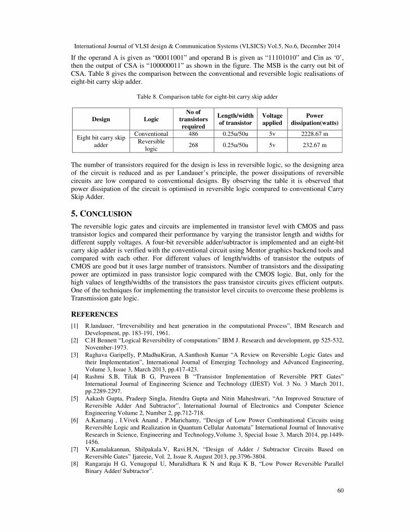
If the operand A is given as “00011001” and operand B is given as “11101010” and Cin as ‘0’,
then the output of CSA is “100000011” as shown in the figure. The MSB is the carry out bit of
CSA. Table 8 gives the comparison between the conventional and reversible logic realisations of
eight-bit carry skip adder.
Table 8. Comparison table for eight-bit carry skip adder
Design Logic
No of
transistors
required
Length/width
of transistor
Voltage
applied
Power
dissipation(watts)
Eight bit carry skip
adder
Conventional 486 0.25u/50u 5v 2228.67 m
Reversible
logic 268 0.25u/50u 5v 232.67 m
The number of transistors required for the design is less in reversible logic, so the designing area
of the circuit is reduced and as per Landauer’s principle, the power dissipations of reversible
circuits are low compared to conventional designs. By observing the table it is observed that
power dissipation of the circuit is optimised in reversible logic compared to conventional Carry
Skip Adder.
5. CONCLUSION
The reversible logic gates and circuits are implemented in transistor level with CMOS and pass
transistor logics and compared their performance by varying the transistor length and widths for
different supply voltages. A four-bit reversible adder/subtractor is implemented and an eight-bit
carry skip adder is verified with the conventional circuit using Mentor graphics backend tools and
compared with each other. For different values of length/widths of transistor the outputs of
CMOS are good but it uses large number of transistors. Number of transistors and the dissipating
power are optimized in pass transistor logic compared with the CMOS logic. But, only for the
high values of length/widths of the transistors the pass transistor circuits gives efficient outputs.
One of the techniques for implementing the transistor level circuits to overcome these problems is
Transmission gate logic.
REFERENCES
[1] R.landauer, “Irreversibility and heat generation in the computational Process”, IBM Research and
Development, pp. 183-191, 1961.
[2] C.H Bennett “Logical Reversibility of computations” IBM J. Research and development, pp 525-532,
November-1973.
[3] Raghava Garipelly, P.MadhuKiran, A.Santhosh Kumar “A Review on Reversible Logic Gates and
their Implementation”, International Journal of Emerging Technology and Advanced Engineering,
Volume 3, Issue 3, March 2013, pp.417-423.
[4] Rashmi S.B, Tilak B G, Praveen B “Transistor Implementation of Reversible PRT Gates”
International Journal of Engineering Science and Technology (IJEST) Vol. 3 No. 3 March 2011,
pp.2289-2297.
[5] Aakash Gupta, Pradeep Singla, Jitendra Gupta and Nitin Maheshwari, “An Improved Structure of
Reversible Adder And Subtractor”, International Journal of Electronics and Computer Science
Engineering Volume 2, Number 2, pp.712-718.
[6] A.Kamaraj , I.Vivek Anand , P.Marichamy, “Design of Low Power Combinational Circuits using
Reversible Logic and Realization in Quantum Cellular Automata” International Journal of Innovative
Research in Science, Engineering and Technology,Volume 3, Special Issue 3, March 2014, pp.1449-
1456.
[7] V.Kamalakannan, Shilpakala.V, Ravi.H.N, “Design of Adder / Subtractor Circuits Based on
Reversible Gates” Ijareeie, Vol. 2, Issue 8, August 2013, pp.3796-3804.
[8] Rangaraju H G, Venugopal U, Muralidhara K N and Raja K B, “Low Power Reversible Parallel
Binary Adder/ Subtractor”.

International Journal of VLSI design & Communication Systems (VLSICS) Vol.5, No.6, December 2014
61
[9] M.SinghSankhwar “Design of High Speed Low Power Reversible Adder Using HNG Gate”,
International Journal of Engineering Research and Applications, Vol. 4, Issue 1(Version 2), January
2014, pp.152-159.
[10] D. P. Bala Subramanian, K.Kalaikaviya and S.Tamilselvan, “Low-Geometry High Speed Feyman
Toffoli 8 Bit Carry Skip Adder”, Journal of Global Research in Electronics and Communication
Volume 1, No. 1, November-December 2012, pp. 6-9.
[11] P. K. Lala, J.P. Parkerson, P. Chakraborty, “Adder Designs using Reversible Logic Gates ”, WSEAS
Transactions on Circuits And Systems, Volume 9, Issue 6, June 2010, pp. 369-378.
[12] HimanshuThapliyal, A.P Vinod “Transistor Realization of Reversible TSG Gate and Reversible
Adder Architectures”, IEEE Asia Pacific Conference on Circuits and Systems, APCCAS 2006,
pp.418-421.
AUTHORS
Prudhvi Raj.K pursuing M.Tech in the branch of Digital Electronics and
Communication Systems at Gudlavalleru Engineering College and received B.Tech
degree in Electronics and Communication Engineering from Prakasam Engineering
College in the year of 2011.
Syamala.Y received her B.E., M.E., from Bharathiyar University, Anna University in
2001, and 2005 respectively. She obtained Ph.D from JNTUH, Hyderabad in 2014.
She has been a member of IEEE, FIETE and MISTE. She has published several
papers in the area of VLSI. Her research interest includes Low power VLSI, Digital
design and Testing.