
TPS54200, TPS54201 4.5-V TO 28-V Input Voltage ... duty cycle ILED/ILED_Full (at 100% PWM duty...
39
PWM duty cycle ILED/ILED_Full (at 100% PWM duty cycle) 1% 1.5% 2% 2.5% 3% 3.5% 4% 4.5% 5% 1% 1.5% 2% 2.5% 3% 3.5% 4% 4.5% 5% 5.5% 6% D001 Unit 1 Unit 2 Unit 3 Unit 4 Unit 5 Unit 6 Unit 7 Unit 8 1 2 3 GND SW VIN 6 5 4 BOOT PWM FB CIN VIN CBOOT CO CF RF RSENSE LO PWM Input Copyright © 2016, Texas Instruments Incorporated Product Folder Order Now Technical Documents Tools & Software Support & Community An IMPORTANT NOTICE at the end of this data sheet addresses availability, warranty, changes, use in safety-critical applications, intellectual property matters and other important disclaimers. PRODUCTION DATA. TPS54200, TPS54201 SLUSCO8B – NOVEMBER 2016 – REVISED JUNE 2018 TPS54200, TPS54201 4.5-V to 28-V Input Voltage, 1.5-A Output Current, Synchronous Buck Mono-Color or IR LED Driver 1 1 Features 1• 4.5-V to 28-V Wide Input Range • Integrated 150-mΩ and 70-mΩ MOSFETs for 1.5‑A, Continuous Output Current • Low, 2-μA Shutdown Current • Fixed 600-kHz Frequency • Peak Current Mode With Internal Compensation • 200-mV and 100-mV Sense Voltage During Analog and PWM Dimming Modes • Precision Analog Dimming (ADIM) by PWM Input • LED-Open and -Short Protection • Sense-Resistor-Open and -Short Protection • Shutdown-and-Latch Mode Protection (TPS54200) • Auto-Retry Mode Protection (TPS54201) • Thermal Shutdown • 6-Pin SOT-23-THIN Package 2 Applications • IR LED for Day or Night Vision – IP Network Camera – Analog Security Camera – Video Doorbell – Embedded Camera System • LED Display and Lighting – Refrigerators and Freezers – Electronic Smart Lock – General-Purpose LED Driver – Architecture Lighting 3 Description The TPS54200 and TPS54201 devices are 1.5-A synchronous buck mono-color or IR drivers with 28-V maximum input voltage. Current-mode operation provides fast transient response and eases loop stabilization. The TPS54200 and TPS54201 can be used to drive single-string or multi-string mono-color or Infrared (IR) LED arrays as in the case of night vision cameras. By integrating the MOSFETs and employing the SOT- 23-THIN package, the TPS54200 and TPS54201 devices provide high power density and only require a small footprint on the PCB. The TPS54200 and TPS54201 devices implement analog dimming by changing the internal reference voltage proportional to the duty cycle of the PWM signal input in analog dimming mode. This devices also support PWM dimming mode, in which the internal reference voltage is halved to 100 mV for higher efficiency. Device Information (1) PART NUMBER PACKAGE BODY SIZE (NOM) TPS54200 SOT-23-THIN (6) 1.6 mm x 2.9 mm TPS54201 SOT-23-THIN (6) 1.6 mm x 2.9 mm (1) For all available packages, see the orderable addendum at the end of the data sheet. Simplified Schematic Excellent Deep Dimming in ADIM
Transcript of TPS54200, TPS54201 4.5-V TO 28-V Input Voltage ... duty cycle ILED/ILED_Full (at 100% PWM duty...

PWM duty cycle
ILE
D/IL
ED
_Ful
l (at
100
% P
WM
dut
y cy
cle)
1% 1.5% 2% 2.5% 3% 3.5% 4% 4.5% 5%1%
1.5%
2%
2.5%
3%
3.5%
4%
4.5%
5%
5.5%
6%
D001
Unit 1Unit 2Unit 3Unit 4Unit 5Unit 6Unit 7Unit 8
1
2
3
GND
SW
VIN
6
5
4
BOOT
PWM
FB
CIN
VIN
CBOOT CO
CF
RF
RSENSE
LO
PWM Input
Copyright © 2016, Texas Instruments Incorporated
Product
Folder
Order
Now
Technical
Documents
Tools &
Software
Support &Community
An IMPORTANT NOTICE at the end of this data sheet addresses availability, warranty, changes, use in safety-critical applications,intellectual property matters and other important disclaimers. PRODUCTION DATA.
TPS54200, TPS54201SLUSCO8B –NOVEMBER 2016–REVISED JUNE 2018
TPS54200, TPS54201 4.5-V to 28-V Input Voltage, 1.5-A Output Current,Synchronous Buck Mono-Color or IR LED Driver
1
1 Features1• 4.5-V to 28-V Wide Input Range• Integrated 150-mΩ and 70-mΩ MOSFETs for
1.5‑A, Continuous Output Current• Low, 2-μA Shutdown Current• Fixed 600-kHz Frequency• Peak Current Mode With Internal Compensation• 200-mV and 100-mV Sense Voltage During
Analog and PWM Dimming Modes• Precision Analog Dimming (ADIM) by PWM Input• LED-Open and -Short Protection• Sense-Resistor-Open and -Short Protection• Shutdown-and-Latch Mode Protection
(TPS54200)• Auto-Retry Mode Protection (TPS54201)• Thermal Shutdown• 6-Pin SOT-23-THIN Package
2 Applications• IR LED for Day or Night Vision
– IP Network Camera– Analog Security Camera– Video Doorbell– Embedded Camera System
• LED Display and Lighting– Refrigerators and Freezers– Electronic Smart Lock– General-Purpose LED Driver– Architecture Lighting
3 DescriptionThe TPS54200 and TPS54201 devices are 1.5-Asynchronous buck mono-color or IR drivers with 28-Vmaximum input voltage. Current-mode operationprovides fast transient response and eases loopstabilization.
The TPS54200 and TPS54201 can be used to drivesingle-string or multi-string mono-color or Infrared (IR)LED arrays as in the case of night vision cameras.
By integrating the MOSFETs and employing the SOT-23-THIN package, the TPS54200 and TPS54201devices provide high power density and only requirea small footprint on the PCB.
The TPS54200 and TPS54201 devices implementanalog dimming by changing the internal referencevoltage proportional to the duty cycle of the PWMsignal input in analog dimming mode. This devicesalso support PWM dimming mode, in which theinternal reference voltage is halved to 100 mV forhigher efficiency.
Device Information(1)
PART NUMBER PACKAGE BODY SIZE (NOM)TPS54200 SOT-23-THIN (6) 1.6 mm x 2.9 mmTPS54201 SOT-23-THIN (6) 1.6 mm x 2.9 mm
(1) For all available packages, see the orderable addendum atthe end of the data sheet.
Simplified Schematic Excellent Deep Dimming in ADIM

2
TPS54200, TPS54201SLUSCO8B –NOVEMBER 2016–REVISED JUNE 2018 www.ti.com
Product Folder Links: TPS54200 TPS54201
Submit Documentation Feedback Copyright © 2016–2018, Texas Instruments Incorporated
Table of Contents1 Features .................................................................. 12 Applications ........................................................... 13 Description ............................................................. 14 Revision History..................................................... 25 Description (continued)......................................... 46 Pin Configuration and Functions ......................... 47 Specifications......................................................... 5
7.1 Absolute Maximum Ratings ...................................... 57.2 ESD Ratings.............................................................. 57.3 Recommended Operating Conditions....................... 57.4 Thermal Information .................................................. 57.5 Electrical Characteristics........................................... 67.6 Timing Requirements ................................................ 77.7 Switching Characteristics .......................................... 77.8 Typical Characteristics .............................................. 8
8 Detailed Description ............................................ 118.1 Overview ................................................................. 118.2 Functional Block Diagram ....................................... 12
8.3 Feature Description................................................. 138.4 Device Functional Modes........................................ 17
9 Application and Implementation ........................ 209.1 Application Information............................................ 209.2 Typical Application ................................................. 20
10 Power Supply Recommendations ..................... 3011 Layout................................................................... 30
11.1 Layout Guidelines ................................................. 3011.2 Layout Example .................................................... 31
12 Device and Documentation Support ................. 3212.1 Device Support...................................................... 3212.2 Documentation Support ....................................... 3212.3 Receiving Notification of Documentation Updates 3212.4 Community Resources.......................................... 3212.5 Trademarks ........................................................... 3212.6 Electrostatic Discharge Caution............................ 3212.7 Glossary ................................................................ 32
13 Mechanical, Packaging, and OrderableInformation ........................................................... 33
4 Revision History
Changes from Revision A (March 2017) to Revision B Page
• Changed "Hiccup Mode" to "Auto-Retry Mode" in the Features section and throughout the data sheet ............................. 1• Changed the package description .......................................................................................................................................... 1• Changed the Applications section .......................................................................................................................................... 1• Changed "WLED" to "mono-color or IR LED" in the first sentence of the Description section .............................................. 1• Changed package descriptor from SOT23 to SOT-23-THIN in the Device Information table................................................ 1• Changed pinout diagram and associated text ........................................................................................................................ 4• Changed "PWM duty input" to "PWM input duty cycle" in the Pin Functions table................................................................ 4• Changed "free-air" to "ambient" in the Absolute Maximum Ratings condition statement ...................................................... 5• Changed "free-air" to "ambient" in the Recommended Operating Conditions condition statement ....................................... 5• Changed the package description in the Thermal Information table header.......................................................................... 5• Changed "Rising" and "Falling" to "Rising VPWM" and "Falling VPWM" for the VADIM, VPDIM, and VPWM Electrical
Characteristics table entries ................................................................................................................................................... 6• Changed "SW" to "VSW" in the Test Conditions column for the RHSD entry in the Electrical Characteristics table................. 6• Changed "dim mode" to "dimming mode" in the Test Conditions column for the ILIM_HS1 entry in the Electrical
Characteristics table ............................................................................................................................................................... 6• Changed the symbol for switching frequency from FSW to fSW .............................................................................................. 7• Changed VIN to VVIN in the Typical Characteristics condition statement ................................................................................ 8• Changed "hiccup up mode" to "auto-retry mode" ................................................................................................................ 11• Changed "duty" to "duty cycle" in multiple locations throughout the data sheet .................................................................. 13• Changed "PWM duty" to "PWM duty cycle" in the Figure 16 image .................................................................................... 13• Changed "floating driver" to "boot regulator" in the Bootstrap Voltage (BOOT) section ..................................................... 14• Changed VIN to VVIN in multiple locations throughout the data sheet................................................................................... 14• Changed various wording in the
Added the Device Support and Documentation Support sections section for clarity, and changed "512 switchingcycles " to "tSHUTDOWN_DELAY" ....................................................................................................................................... 14
• Changed "hiccup up" to "auto-retry mode" in the Fault Protection section .......................................................................... 15

3
TPS54200, TPS54201www.ti.com SLUSCO8B –NOVEMBER 2016–REVISED JUNE 2018
Product Folder Links: TPS54200 TPS54201
Submit Documentation FeedbackCopyright © 2016–2018, Texas Instruments Incorporated
Revision History (continued)• Changed "hiccup" to "auto-retry" or "shuddown -and-restart," and deleted "programmed for XXX switching cycles" text.. 15• Changed "will be clamped by low" to "is clamped at the low-"............................................................................................. 15• Changed "hiccup" to "auto-retry" or "shuddown -and-restart," and deleted "programmed for XXX switching cycles" text.. 15• Changed "hiccup" to "auto-retry" or "shuddown -and-restart," and deleted "programmed for XXX switching cycles" text.. 15• Changed "hiccup" to "auto-retry" or "shuddown -and-restart," and deleted "programmed for XXX switching cycles" text.. 15• Changed "Recycle VIN can reset" to "Cycling VIN resets".................................................................................................... 16• Changed "once the device shuts down, it starts" to "a device shutdown starts".................................................................. 16• Changed "hiccup" to "auto-retry" or "shuddown -and-restart," and deleted "programmed for XXX switching cycles" text.. 16• Changed "hiccup" to "auto-retry" or "shuddown -and-restart," and deleted "programmed for XXX switching cycles" text.. 16• Changed "Vin at" to "VVIN" .................................................................................................................................................... 17• Changed "VADIM" to "VADIM" and "VPDIM" to "VPDIM" .......................................................................................................... 17• Changed "it's" to "the output is"............................................................................................................................................ 17• Changed "VIN" to "VIN" and "recycled" to "cycled" at the end of the Mode Detection ......................................................... 17• Changed "a little big" to "excessive" in the Analog Dimming Mode Operation section........................................................ 18• Changed "PWM duty cycle" to "PWM state" ........................................................................................................................ 19• Changed "12-VIN" to "12-V VVIN"........................................................................................................................................... 20• Changed "FSW" to "fSW" and "VIN(max)" to "VVIN(max)" in Equation 3 from F to f ....................................................................... 21• Changed "FSW" to "fSW" and "VIN(ripple)" to "VVIN(ripple)" in Equation 8 from F to f .................................................................... 21• Changed the symbol for frequency in Equation 11 from F to f............................................................................................. 22• Changed "RF" to "RF" and "CF" to "CF"................................................................................................................................ 22• Changed "VOUT" to "VOUT" in the conditions of multiple application curves........................................................................ 24• Changed the wording of the second and third paragraphs of the Inductor Selection section for clarity.............................. 27• Changed the symbol for frequency in Equation 14 from F to f............................................................................................. 27• Changed "wide areas advantages" to "added width also".................................................................................................... 30• Changed "reduce the possibility" to "minimize" .................................................................................................................... 30• Added the Device Support and Documentation Support sections ....................................................................................... 32
Changes from Original (November 2016) to Revision A Page
• Added initial release of the TPS54201 device........................................................................................................................ 1• Changed description to include protection modes. ................................................................................................................ 4• Changed ILIM_HS1 and ILIM_HS2 CURRENT LIMIT. .................................................................................................................... 6• Changed the low-side source-current limit from (2.4/3.4/4.4) to (2.3/3.3/4.4), ...................................................................... 6• Added TPS54201 tHIC_THERMAL, tHIC_OV and tHIC_WAIT Timing Requirements. ........................................................................... 7• Added TPS54201 LED Short Protection image. .................................................................................................................. 25• Added TPS54201 LED Open Protection image. ................................................................................................................. 25• Added TPS54201 Sense Resistor Short Protection image. ................................................................................................ 25

1GND 6 BOOT
2SW 5 PWM
3VIN 4 FB
Not to scale
4
TPS54200, TPS54201SLUSCO8B –NOVEMBER 2016–REVISED JUNE 2018 www.ti.com
Product Folder Links: TPS54200 TPS54201
Submit Documentation Feedback Copyright © 2016–2018, Texas Instruments Incorporated
(1) I = Input, O = Output, P = Supply, G = Ground
5 Description (continued)Cycle-by-cycle current limit in the high-side MOSFET protects the converter in an overload condition and isenhanced by a low-side MOSFET freewheeling current limit which prevents current runaway. There is a low-side MOSFET sinking current limit to prevent excessive reverse current. For safety and protection, theTPS54200 and TPS54201 devices include LED-open and -short protection, sense-resistor-open and -shortprotection, and device thermal protection. The TPS54200 device implements shutdown-and-latch modeprotection, whereas the TPS54201 device adopts auto-retry mode protection.
6 Pin Configuration and Functions
DDC Package6-Pin SOT-23-THIN
Top View
Pin FunctionsPIN
TYPE (1) DESCRIPTIONNAME NO.
BOOT 6 O A bootstrap capacitor is required between BOOT and SW.FB 4 I LED current-detection feedbackGND 1 G Power ground
PWM 5 IDimming input. Default low (internally pulled low). In analog dimming mode, the internal reference isproportional to the PWM input duty cycle. In PWM dimming mode, LED current is ON during the PWMhigh period in each PWM cycle.
SW 2 O Switching node to the external inductorVIN 3 P Input supply voltage

5
TPS54200, TPS54201www.ti.com SLUSCO8B –NOVEMBER 2016–REVISED JUNE 2018
Product Folder Links: TPS54200 TPS54201
Submit Documentation FeedbackCopyright © 2016–2018, Texas Instruments Incorporated
(1) Stresses beyond those listed under Absolute Maximum Ratings may cause permanent damage to the device. These are stress ratingsonly, which do not imply functional operation of the device at these or any other conditions beyond those indicated under RecommendedOperating Conditions. Exposure to absolute-maximum-rated conditions for extended periods may affect device reliability.
7 Specifications
7.1 Absolute Maximum Ratingsover operating ambient temperature range (unless otherwise noted) (1)
MIN MAX UNIT
Input voltage range, VI
VIN –0.3 30VPWM –0.3 7
FB –0.3 7
Output voltage range, VO
BOOT–SW –0.3 7VSW –0.3 30
SW (20 ns transient) –5 30Operating junction temperature, TJ –40 150 °CStorage temperature range, Tstg –65 150 °C
(1) JEDEC document JEP155 states that 500-V HBM allows safe manufacturing with a standard ESD control process.(2) JEDEC document JEP157 states that 250-V CDM allows safe manufacturing with a standard ESD control process.
7.2 ESD RatingsVALUE UNIT
V(ESD)Electrostaticdischarge
Human-body model (HBM), per ANSI/ESDA/JEDEC JS-001 (1) ±4000V
Charged-device model (CDM), per JEDEC specification JESD22-C101 (2) ±1500
7.3 Recommended Operating Conditionsover operating ambient temperature range (unless otherwise noted)
MIN MAX UNIT
VI Input voltage rangeVIN 4.5 28
VPWM –0.1 6FB –0.1 6
VO Output voltage rangeBOOT-SW –0.1 6.5
VSW –0.1 28
TJ Operating junction temperature –40 125 °C
(1) For more information about traditional and new thermal metrics, see the Semiconductor and IC Package Thermal Metrics applicationreport, SPRA953.
7.4 Thermal Information
THERMAL METRIC (1)TPS5420x
UNITDDC (SOT-23-THIN)6 PINS
RθJA Junction-to-ambient thermal resistance 89.2 °C/WRθJC(top) Junction-to-case (top) thermal resistance 39.5 °C/WRθJB Junction-to-board thermal resistance 14.7 °C/WψJT Junction-to-top characterization parameter 1.2 °C/WψJB Junction-to-board characterization parameter 14.7 °C/W

6
TPS54200, TPS54201SLUSCO8B –NOVEMBER 2016–REVISED JUNE 2018 www.ti.com
Product Folder Links: TPS54200 TPS54201
Submit Documentation Feedback Copyright © 2016–2018, Texas Instruments Incorporated
(1) Not production tested
7.5 Electrical CharacteristicsThe electrical ratings specified in this section apply to all specifications in this document, unless otherwise noted. Thesespecifications are interpreted as conditions that do not degrade the device parametric or functional specifications for the life ofthe product containing it. TJ = –40°C to 125°C, VVIN = 4.5 V to 28 V, (unless otherwise noted).
PARAMETER TEST CONDITIONS MIN TYP MAX UNITINPUT SUPPLYVVIN Input voltage range 4.5 28 VIOFF Shutdown current PWM = GND 2 8.6 µA
VVIN_UVLOVIN undervoltage lockout
Rising VVIN 3.83 4.2 4.47V
Falling VVIN 3.4 3.7 3.95Hysteresis 470 mV
DIMMING (PWM PIN)
VADIM Analog dimming-mode thresholdRising VPWM 1.97 2.07 2.17
VFalling VPWM 1.8
VPDIM PWM dimming-mode thresholdRising VPWM 0.9 1 1.1
VFalling VPWM 0.8
VPWM Threshold to identify PWM duty cycleRising VPWM 0.91 1 1.12
VFalling VPWM 0.5 0.63 0.72
VPWM_SHUTDOWN Shutdown threshold 0.35 0.55 VFEEDBACK AND ERROR AMPLIFIER
VFB1Feedback voltage in analog dimmingmode PWM = 3.3 V, SW duty cycle > 90% 201 205 210 mV
VFB2 Feedback voltage in PWM dimming mode PWM = 1.5 V, SW duty cycle > 90% 96 100 104 mVBOOT PIN
VBOOT_UVLO BOOT-SW UVLO thresholdRising 2.1 2.33
VFalling 2 2.2
POWER STAGERHSD High-side FET on-resistance VBOOT – VSW= 6 V 150 259 mΩ
RLSD Low-side FET on-resistance VVIN > 6 V 70 120 mΩ
CURRENT LIMIT
ILIM_HS1 High-side current limit 1
Either one of the following conditions:1. PWM dimming mode2. Analog dimming mode and PWM dutycycle >25%
2.4 3 3.6 A
ILIM_HS2 High-side current limit 2 Analog dimming mode and PWM dutycycle <25% 1 1.4 1.8 A
ILIM_LS_SOURCE Low-side source current limit VVIN > 6 V 2.3 3.3 4.4 AILIM_LS_SINK Low-side sink current limit VVIN > 6 V 1.25 1.7 2.2 AFAULT PROTECTION
Thermalshutdown (1)
Rising temperature 150 160 170 °CHysteresis 10 °C
VOVP Overvoltage protection 1 VVOCP Overcurrent protection 120%

7
TPS54200, TPS54201www.ti.com SLUSCO8B –NOVEMBER 2016–REVISED JUNE 2018
Product Folder Links: TPS54200 TPS54201
Submit Documentation FeedbackCopyright © 2016–2018, Texas Instruments Incorporated
7.6 Timing RequirementsMIN TYP MAX UNIT
THERMAL SHUTDOWNtHIC_THERMAL TPS54200 and TPS54201 thermal shutdown auto-retry time 32 768 CyclesOVERVOLTAGE PROTECTIONtHIC_OV TPS54201 auto-retry time for overvoltage protection 32 768 CyclesOVERCURRENT AND OPEN-LOOP PROTECTION
tSHUTDOWN_DELAYTPS54200 shutdown delay time for open-loop and overcurrentprotection 512 Cycles
tHIC_WAITTPS54201 auto-retry wait time for open-loop and overcurrentprotection 512 Cycles
tHIC_OC TPS54201 auto-retry time for open-loop and overcurrent protection 16 384 CyclesSOFT STARTtSS Internal soft-start time 0.6 ms
7.7 Switching CharacteristicsTJ = –40°C to 125°C, VVIN = 4.5 V to 28 V, (unless otherwise noted).
PARAMETER TEST CONDITIONS MIN TYP MAX UNITOSCILLATORfsw Switching frequency 480 600 700 kHzON-TIME CONTROL
tMIN_ON Minimum on-time Measured at 90% to 90% and 1-Aloading 90 105 ns

Junction Temperature (°C)
FB
Vol
tage
in P
DIM
(m
V)
-50 -25 0 25 50 75 100 12599
99.5
100
100.5
101
D005Junction Temperature (°C)
Sw
itchi
ng F
requ
ency
(kH
z)
-50 -25 0 25 50 75 100 125580
585
590
595
600
605
610
D006
Junction Temperature (°C)
/RZ�VLGH�)(7�5GV�RQ���P �
-50 -25 0 25 50 75 100 12550
60
70
80
90
100
110
D003Junction Temperature (°C)
FB
Vol
tage
in A
DIM
(m
V)
-50 -25 0 25 50 75 100 125203
203.5
204
204.5
205
205.5
206
206.5
207
D004
Junction Temperature (°C)
Shu
tdow
n Q
uies
cent
Cur
rent
(uA
)
-50 -25 0 25 50 75 100 1250
0.5
1
1.5
2
2.5
3
D001Junction Temperature (°C)
+LJK�VLGH�)(7�5GV�RQ���P �
-50 -25 0 25 50 75 100 125100
120
140
160
180
200
220
240
D002
8
TPS54200, TPS54201SLUSCO8B –NOVEMBER 2016–REVISED JUNE 2018 www.ti.com
Product Folder Links: TPS54200 TPS54201
Submit Documentation Feedback Copyright © 2016–2018, Texas Instruments Incorporated
7.8 Typical CharacteristicsVVIN = 12 V, unless otherwise specified
Figure 1. Shutdown Quiescent Current vs JunctionTemperature
Figure 2. High-Side FET On-Resistance vs JunctionTemperature
Figure 3. Low-Side FET On-Resistance vs JunctionTemperature
Figure 4. FB Voltage in ADIM vs Junction Temperature
Figure 5. FB Voltage in PDIM vs Junction Temperature Figure 6. Switching Frequency vs Junction Temperature

Junction Temperature (°C)
BO
OT
UV
LO T
hres
hold
(V
)
-50 -25 0 25 50 75 100 1251.9
1.95
2
2.05
2.1
2.15
2.2
D011
RisingFalling
Junction Temperature (°C)
VIN
UV
LO T
hres
hold
(V
)
-50 -25 0 25 50 75 100 1253.6
3.7
3.8
3.9
4
4.1
4.2
D012
RisingFalling
Junction Temperature (°C)
Low
Sid
e S
ourc
e C
urre
nt L
imit
(A)
-50 -25 0 25 50 75 100 1253
3.1
3.2
3.3
3.4
3.5
3.6
D009Junction Temperature (°C)
Low
Sid
e S
ink
Cur
rent
Lim
it (A
)
-50 -25 0 25 50 75 100 1251.6
1.65
1.7
1.75
1.8
1.85
D010
Junction Temperature (°C)
Hig
h S
ide
Cur
rent
Lim
it 1
(A)
-50 -25 0 25 50 75 100 1252.9
2.95
3
3.05
3.1
3.15
3.2
3.25
3.3
D007Junction Temperature (°C)
Hig
h S
ide
Cur
rent
Lim
it 2
(A)
-50 -25 0 25 50 75 100 1251.4
1.45
1.5
1.55
1.6
1.65
D008
9
TPS54200, TPS54201www.ti.com SLUSCO8B –NOVEMBER 2016–REVISED JUNE 2018
Product Folder Links: TPS54200 TPS54201
Submit Documentation FeedbackCopyright © 2016–2018, Texas Instruments Incorporated
Typical Characteristics (continued)VVIN = 12 V, unless otherwise specified
Figure 7. High-Side Source Current Limit 1 Threshold vsJunction Temperature
Figure 8. High-Side Source Current Limit 2 Threshold vsJunction Temperature
Figure 9. Low-Side Source Current Limit Threshold vsJunction Temperature
Figure 10. Low-Side Sink Current Limit Threshold vsJunction Temperature
Figure 11. BOOT-SW UVLO Threshold vs JunctionTemperature
Figure 12. VIN UVLO Threshold vs Junction Temperature

Junction Temperature (°C)
PW
M S
hutd
own
Thr
esho
ld (
V)
-50 -25 0 25 50 75 100 1250.3
0.35
0.4
0.45
0.5
0.55
0.6
0.65
D015
Junction Temperature (°C)
Ana
log
Dim
min
g M
ode
Thr
esho
ld (
V)
-50 -25 0 25 50 75 100 1251.8
1.85
1.9
1.95
2
2.05
2.1
D013
RisingFalling
Junction Temperature (°C)
PW
M D
imm
ing
Mod
e T
hres
hold
(V
)
-50 -25 0 25 50 75 100 1250.75
0.8
0.85
0.9
0.95
1
1.05
1.1
D014
RisingFalling
10
TPS54200, TPS54201SLUSCO8B –NOVEMBER 2016–REVISED JUNE 2018 www.ti.com
Product Folder Links: TPS54200 TPS54201
Submit Documentation Feedback Copyright © 2016–2018, Texas Instruments Incorporated
Typical Characteristics (continued)VVIN = 12 V, unless otherwise specified
Figure 13. Analog Dimming Mode Threshold vs JunctionTemperature
Figure 14. PWM Dimming Mode Threshold vs JunctionTemperature
Figure 15. PWM Shutdown Threshold vs Junction Temperature

11
TPS54200, TPS54201www.ti.com SLUSCO8B –NOVEMBER 2016–REVISED JUNE 2018
Product Folder Links: TPS54200 TPS54201
Submit Documentation FeedbackCopyright © 2016–2018, Texas Instruments Incorporated
8 Detailed Description
8.1 OverviewThe TPS5420x device is a 1.5-A synchronous buck LED driver up to 28-V input. Current-mode operationprovides fast transient response. The optimized internal compensation network minimizes the externalcomponent count and simplifies the control loop design.
The TPS5420x device has a fixed 600-kHz switching frequency for a good tradeoff between efficiency and size.
The integrated 150-mΩ high-side MOSFET and 70-mΩ low-side MOSFET allow for a high-efficiency LED driverwith continuous output current up to 1.5 A.
The TPS5420x device supports deep dimming in both analog and PWM dimming modes. In analog dimmingmode, the internal reference voltage is changed in proportion to the duty cycle of the PWM signal in the 1% to100% range. In the PWM dimming mode, the LED turns on and off periodically according to the PWM duty cycle.For higher efficiency, the internal reference is halved to 100 mV.
Cycle-by-cycle current limit in the high-side MOSFET protects the converter in overload conditions and isenhanced by a low-side MOSFET freewheeling current limit which prevents current runaway. There is a low-sideMOSFET sinking-current limit to prevent excessive reverse current.
For safety and protection, the TPS5420x includes LED-open and -short protection, sense-resistor-open and -short protection, and device thermal protection. The TPS54200 device implements shutdown-and-latch modeprotection, whereas the TPS54201 device implements auto-retry mode protection.

4FB
Dimming Control and Error Amp
SS
+
+
OVP Shutdown
OCP Shutdown
1 V
VOCP
Bandgap
Mode
VBGPVIN
DelayPeak
Detector
DIM Mode Selection
Enable
Mode
5
+
PWM
VTH
Timer and Logic
Shutdown Logic
Thermal Shutdown
UVLO
Boot Charge
PWM
3
VIN
OVP Shutdown
Open Loop Shutdown OCP Shutdown
Maximum Clamp
HS MOSFET Current
Comparator
Slope Compensation
Oscillator
Power Stage and Deadtime Control Logic
PWM
Mode
Comp
LS MOSFET Current Limit
RegulatorVIN
2
Boot UVLO
1
SW
GND
Current Sense
6 BOOT
Copyright © 2016, Texas Instruments Incorporated
Enable
PWM
12
TPS54200, TPS54201SLUSCO8B –NOVEMBER 2016–REVISED JUNE 2018 www.ti.com
Product Folder Links: TPS54200 TPS54201
Submit Documentation Feedback Copyright © 2016–2018, Texas Instruments Incorporated
8.2 Functional Block Diagram

PWM duty cycle (%)100
200
VREF (mV)
13
TPS54200, TPS54201www.ti.com SLUSCO8B –NOVEMBER 2016–REVISED JUNE 2018
Product Folder Links: TPS54200 TPS54201
Submit Documentation FeedbackCopyright © 2016–2018, Texas Instruments Incorporated
8.3 Feature Description
8.3.1 Fixed-Frequency PWM ControlThe device uses a fixed-frequency and peak-current-mode control. The LED current is sensed by a resistor inseries with the LED string. The sensed voltage is fed to the FB pin through an RC filter, and then compared to aninternal voltage reference by an error amplifier. An internal oscillator initiates the turnon of the high-side powerswitch. The error amplifier output is compared to the current of the high-side power switch. When the power-switch current reaches the error-amplifier output-voltage level, the high-side power switch is turned off and thelow-side power switch is turned on. Thus, the error amplifier output voltage regulates inductor peak current, andin turn the LED current, to a target value. The device implements a current limit by clamping the error amplifiervoltage to a maximum level and also implements a minimum clamp for improved transient-responseperformance.
8.3.2 Error AmplifierThe device has a transconductance amplifier as the error amplifier. The error amplifier compares the FB voltageto the lower of the internal soft-start voltage or the internal voltage reference. The transconductance of the erroramplifier is 240 μA/V typically. The frequency compensation components are placed internally between theoutput of the error amplifier and ground.
8.3.3 Slope Compensation and Output CurrentThe device adds a compensating ramp to the signal of the switch current. This slope compensation preventssubharmonic oscillations as the duty cycle increases. The available peak inductor current remains constant overthe full duty-cycle range.
8.3.4 Input Undervoltage LockoutThe device implements internal undervoltage-lockout (UVLO) circuitry on the VIN pin. The device is disabledwhen the VIN pin voltage falls below the internal VIN UVLO threshold, which is 3.7 V typical. The internal VINUVLO threshold has a hysteresis of 470 mV.
8.3.5 Voltage ReferenceThe voltage reference system produces a precise ±2.5% voltage reference over temperature by scaling theoutput of a temperature-stable band-gap circuit when the PWM duty cycle is 100%. In PWM dimming mode, thevoltage reference, VREF, is fixed at 100 mV. In analog dimming mode, VREF, is proportional to the duty cycle ofPWM as shown in Figure 16.
Figure 16. VREF vs PWM Duty Cycle in Analog Dimming Mode

REFSENSE
LED
VR
I
14
TPS54200, TPS54201SLUSCO8B –NOVEMBER 2016–REVISED JUNE 2018 www.ti.com
Product Folder Links: TPS54200 TPS54201
Submit Documentation Feedback Copyright © 2016–2018, Texas Instruments Incorporated
Feature Description (continued)8.3.6 Setting LED CurrentOnce the voltage reference, VREF, is chosen, one can set the LED current by choosing the proper sensingresistor according to Equation 1:
(1)
8.3.7 Internal Soft StartThe TPS5420x device uses an internal soft-start function. The internal soft-start time is set to 0.6 ms typically.
8.3.8 Bootstrap Voltage (BOOT)The TPS5420x has an integrated boot regulator and requires a 0.1-μF ceramic capacitor between the BOOT andSW pins to provide the gate drive voltage for the high-side MOSFET. A ceramic capacitor with an X7R or X5Rgrade dielectric is recommended because of the stable characteristics over temperature and voltage. This bootregulator has its own UVLO protection. This UVLO rising threshold is 2.1 V with a hysteresis of 100 mV. A 6-Vbootstrap voltage is maintained between BOOT and SW when VVIN > 6 V.
8.3.9 Overcurrent ProtectionThe device is protected from overcurrent conditions by cycle-by-cycle current limiting on both the high-sideMOSFET and the low-side MOSFET.
8.3.9.1 High-Side MOSFET Overcurrent ProtectionThe device implements current-mode control, which uses the internal COMP voltage to control the turnoff of thehigh-side MOSFET and the turnon of the low-side MOSFET on a cycle-by-cycle basis. During each cycle, theswitch current and the current reference generated by the internal COMP voltage are compared. When the peakswitch current intersects the current reference, the high-side switch turns off. During overcurrent conditions, suchas when the sensing resistor is shorted, or an open circuit occurs in the feedback-filter RC network that drives FBlow, the error amplifier responds by driving the COMP pin high, increasing the switch current. The error amplifieroutput is clamped internally. This clamp functions as a switch-current limit. This current limit is fixed at 3.1 Atypical in PWM dimming mode. In analog dimming mode with the PWM duty cycle >25%, this limit is also 3.1 A.If the PWM duty cycle is below 25%, this limit is halved to 1.5 A typical. Furthermore, if an output overcurrentcondition occurs for more than the shutdown delay time, tSHUTDOWN_DELAY, the device shuts down and latches offto protect the LED from overcurrent damage.
8.3.9.2 Low-Side MOSFET Overcurrent ProtectionWhile the low-side MOSFET is turned on, the conduction current is monitored by the internal circuitry. Duringnormal operation, the low-side MOSFET sources current to the load. At the end of every clock cycle, the low-sideMOSFET sourcing current is compared to the internally set low-side sourcing current-limit. If the low-sidesourcing-current limit is exceeded, the high-side MOSFET does not turn on and the low-side MOSFET stays onfor the next cycle. The high-side MOSFET turns on again when the low-side current is below the low-sidesourcing current-limit at the start of a cycle.
8.3.9.3 Low-Side MOSFET Reverse Overcurrent ProtectionThe TPS5420x device implements low-side reverse-current protection by detecting the voltage across the low-side MOSFET. When the converter sinks current through its low-side FET, the control circuit turns off the low-side MOSFET if the reverse current is more than 1.7 A typical. By implementing this additional protectionscheme, the converter is able to protect itself from excessive sink current during fault conditions.

15
TPS54200, TPS54201www.ti.com SLUSCO8B –NOVEMBER 2016–REVISED JUNE 2018
Product Folder Links: TPS54200 TPS54201
Submit Documentation FeedbackCopyright © 2016–2018, Texas Instruments Incorporated
Feature Description (continued)8.3.10 Fault ProtectionThe device is protected from several kinds of fault conditions, such as LED open and short, sense-resistor openand short, and thermal shutdown. The only difference between the TPS54200 and TPS54201 devices is thedifferent protection mode used. The TPS54200 device implements shutdown-and-latch mode protection, whereasthe TPS54201 device implements auto-retry mode protection.
8.3.10.1 LED-Open ProtectionWhen the LED load is open, the FB voltage is low, and the internal COMP voltage is driven high and clamped.This action triggers a shutdown delay counter (TPS54200) or auto-retry wait counter (TPS54201). For theTPS54200 device, once the shutdown delay time tSHUTDOWN_DELAY expires, the device shuts down and latches off.Both FETs are kept off. This is a latched shutdown. The device can be reset by recycling VIN. For TPS54201,once the auto-retry wait time tHIC_WAIT expires, the device shuts down and starts auto-retry timer tHIC_OC. Duringthe shutdown period, both FETs are kept off. Once the auto-retry timer expires, the TPS54201 device restartsagain. If the failure still exists, the TPS54201 device repeats the foregoing shutdown-and-restart process.
8.3.10.2 LED Short ProtectionWhen the LED load is shorted, the FB voltage is higher than VREF, and the internal COMP voltage is driven lowand clamped, and the high-side MOSFET is commanded on for a minimum on-time each cycle. In this condition,if the output voltage is too low, the inductor current may not be able to balance in a cycle, causing currentrunaway. Finally, the inductor current is clamped at the low-side MOSFET sourcing-current limit, which is muchhigher than target LED current. If the FB voltage is higher than the OCP threshold, which is 250 mV typical inanalog dimming mode, or 120 mV typical in PWM dimming mode, the shutdown delay counter (TPS54200) orauto-retry wait counter (TPS54201) is triggered. For the TPS54200 device, once the shutdown delay timetSHUTDOWN_DELAY expires, the device shuts down and latches off. Both FETs are kept off. This is a latchedshutdown. The device can be reset by recycling VIN. For the TPS54201 device, once the auto-retry wait timetHIC_WAIT expires, the device shuts down and starts auto-retry timer tHIC_OC. During the shutdown period, bothFETs are kept off. Once the auto-retry timer expires, the TPS54201 device restarts again. If the failure still exists,the TPS54201 device repeats the foregoing shutdown-and-restart process.
8.3.10.3 Sense-Resistor Short ProtectionWhen the sense resistor is shorted, the FB voltage is low, and the internal COMP voltage is driven high andclamped. This action triggers the shutdown delay counter (TPS54200) or auto-retry wait counter (TPS54201). Forthe TPS54200 device, once the shutdown delay time tSHUTDOWN_DELAY expires, the device shuts down and latchesoff. Both FETs are kept off. This is a latched shut-down. The device can be reset by recycling VIN. For theTPS54201 device, once the auto-retry wait time tHIC_WAIT expires, the device shuts down and starts auto-retrytimer tHIC_OC. During the shutdown period, both FETs are kept off. Once the auto-retry timer expires, theTPS54201 device restarts again. If the failure still exists, the TPS54201 device repeats the foregoing shutdown-and-restart process.
8.3.10.4 Sense-Resistor Open ProtectionWhen the sense resistor is open before the device powers on, the device charges the BOOT capacitor at thepower-on moment. The charging current flows through the inductor, the output capacitor, and the RC filter at theFB pin to charge up the FB pin voltage. Once the device detects an FB voltage higher than the 1-V OVPthreshold, the device shuts down immediately. For the TPS54200 device, this is a latched shutdown, and thedevice can be reset by cycling VIN. For the TPS54201 device, once the device shuts down, it starts theovervoltage auto-retry timer tHIC_OV. During the shutdown period, both FETs are kept off. Once the overvoltageauto-retry timer expires, the TPS54201 device restarts again. If the failure still exists, the TPS54201 devicerepeats the foregoing auto-retry shutdown-and-restart process.

16
TPS54200, TPS54201SLUSCO8B –NOVEMBER 2016–REVISED JUNE 2018 www.ti.com
Product Folder Links: TPS54200 TPS54201
Submit Documentation Feedback Copyright © 2016–2018, Texas Instruments Incorporated
Feature Description (continued)8.3.10.5 Overvoltage ProtectionWhen the FB pin, for some reason, has a voltage higher than 1 V applied, the device shuts down immediately.Both FETs are kept off. This is called overvoltage protection. For the TPS54200 device, this is a latchedshutdown. Cycling VIN resets the device. For the TPS54201 device, a device shutdown starts the overvoltageauto-retry timer tHIC_OV. During the shutdown period, both FETs are kept off. Once the overvoltage auto-retrytimer expires, the TPS54201 device restarts again. If the failure still exists, the TPS54201 device repeats theforegoing auto-retry shutdown-and-restart process.
8.3.10.6 Thermal ShutdownThe internal thermal-shutdown circuitry forces the device to stop switching if the junction temperature exceeds atypical value of 160°C. When the junction temperature drops below a typical value of 150°C, the internal thermal-auto-retry timer tHIC_THERMAL begins to count. The device reinitiates the power-up sequence once the thermal-auto-retry timer expires.

VADIM
VPDIM
PWM
A
B
+VPWM
Internal
PWM
+
+
Peak Detector
PWM
VTH
EN+
17
TPS54200, TPS54201www.ti.com SLUSCO8B –NOVEMBER 2016–REVISED JUNE 2018
Product Folder Links: TPS54200 TPS54201
Submit Documentation FeedbackCopyright © 2016–2018, Texas Instruments Incorporated
8.4 Device Functional Modes
8.4.1 Enable and Disable DeviceThe PWM pin performs not only the dimming function, but also the enable-and-disable function. When the VINvoltage is above the UVLO threshold, the TPS5420x device can be enabled by driving the PWM pin higher thanthe threshold voltage, 0.56 V typical. To disable the device, keep the PWM pin lower than the threshold voltage,0.55 V typical, for 40 ms or longer. The PWM pin has an internal pulldown resistor, so floating this pin disablesthe device.
The suggested power-on sequence is applying VVIN first, followed by the PWM signal.
8.4.2 Mode DetectionThe magnitude of the PWM signal is used to determine which dimming mode the device enters. The internalpeak detector at the PWM pin holds the magnitude of the PWM signal. Once the device is enabled, after 300-µsdelay, the output of the peak detector is compared with two voltage thresholds, VADIM and VPDIM, which are 1 Vand 2.07 V, respectively. If the output of the peak detector is higher than 2.07 V, analog dimming mode ischosen and locked. If the output is between 1 V and 2.07 V, PWM dimming mode is chosen and locked. If theoutput is less than 1 V, the device waits another 300 µs and compares again, and this process repeats until atleast one mode is chosen and locked. See Figure 17 and Table 1 for reference. After the mode is detected andlocked, soft start begins, the output voltage ramps up, and the LED current is regulated at the target value. Thedimming mode cannot be changed unless VIN or PWM is cycled. section
Figure 17. Mode Detection Circuit
Table 1. Mode Detection ConditionA B MODEH H Enter analog dimming modeL H Enter PWM dimming modeL L Keep detecting until one dimming mode is locked

LED current
PWM 3 V
200 mV/RSENSE
100 mV/RSENSE
50 kHz/50%t
t
18
TPS54200, TPS54201SLUSCO8B –NOVEMBER 2016–REVISED JUNE 2018 www.ti.com
Product Folder Links: TPS54200 TPS54201
Submit Documentation Feedback Copyright © 2016–2018, Texas Instruments Incorporated
8.4.3 Analog Dimming Mode OperationOnce the analog dimming mode is chosen, the internal voltage reference for the FB pin is approximately 200 mVat full scale, and proportional to the PWM duty cycle as shown in Figure 16. LED current is continuous in thismode, and the current magnitude can be adjusted by changing PWM duty cycle, see Figure 18. Because theinternal voltage reference is filtered from the PWM signal, a too-low PWM frequency may cause excessive rippleat the voltage reference. To minimize this ripple, the suggested PWM signal frequency is 10 kHz or higher, suchas 50 kHz.
Figure 18. Analog Dimming Operation
A comparator with 400-mV hysteresis is used to generate the internal PWM signal, see Figure 17. This internalPWM duty cycle determines the voltage reference. To make sure the PWM pin signal is correctly identified, thehigh level of the PWM signal should be higher than 1 V, and the low level should be lower than 0.6 V. Figure 19shows the relationship between the external PWM and internal PWM signals.

INTOP BOT
PWM
VR 1 R
V
§ · � u¨ ¸© ¹
1
2
3
GND
SW
VIN
6
5
4
BOOT
PWM
FB
RTOPCIN
RBOT
VIN
CBOOT CO
CF
RF
RSENSE
LO
1 V
0.6 V
PWM Pin Signal
Internal PWM
LED Current 0
100 mV/RSENSE
19
TPS54200, TPS54201www.ti.com SLUSCO8B –NOVEMBER 2016–REVISED JUNE 2018
Product Folder Links: TPS54200 TPS54201
Submit Documentation FeedbackCopyright © 2016–2018, Texas Instruments Incorporated
8.4.4 PWM Dimming-Mode OperationOnce the PWM dimming mode is chosen, the internal voltage reference for the FB pin is fixed at 100 mV. TheLED current is on or off corresponding to the PWM state, see Figure 19. Due to the limited control-loopresponse, to get a relatively linear dimming performance, the suggested PWM signal frequency should be lessthan 1 kHz.
Figure 19. PWM Dimming Operation
In some application where dimming is not needed, one can just connect a resistor divider from VVIN to the PWMpin as Figure 20 shows.
Figure 20. Application Without Dimming
RTOP and RBOT should be sized to make sure the PWM pin voltage is higher than 1 V when VVIN reaches itssteady voltage. It is best to make sure the PWM pin voltage is less than 2 V, thus one can have 100 mV at theFB pin for better efficiency. Use 10 kΩ as a good starting point for RBOT, then choose RTOP according toEquation 2:
(2)
10µH
L1
0.1µF
C1
0.1µFC3
0.082µFC5
10µFC2
10µFC4
0
R1
910
R2
TP1
0.1R4
0.033R3
GND
GND
GND
GND
VIN3
PWM5
GND1
BOOT6
SW2
FB4
U1
TPS54200DDCR
VIN
PWM
1
23
Infrared
D1SFH 4715A
1
23
Infrared
D2SFH 4715A
1
23
Infrared
D3SFH 4715A
VIN = 10.8V ~ 13.2V
3.3V, 50kHz, 1% to 100% duty
Copyright © 2016, Texas Instruments Incorporated
20
TPS54200, TPS54201SLUSCO8B –NOVEMBER 2016–REVISED JUNE 2018 www.ti.com
Product Folder Links: TPS54200 TPS54201
Submit Documentation Feedback Copyright © 2016–2018, Texas Instruments Incorporated
9 Application and Implementation
NOTEInformation in the following applications sections is not part of the TI componentspecification, and TI does not warrant its accuracy or completeness. TI’s customers areresponsible for determining suitability of components for their purposes. Customers shouldvalidate and test their design implementation to confirm system functionality.
9.1 Application InformationThe TPS5420x device is typically used as a buck converter to drive one or more LEDs from a 4.5-V to 28-Vinput. The TPS5420x device supports both analog dimming mode and PWM dimming mode.
9.2 Typical Application
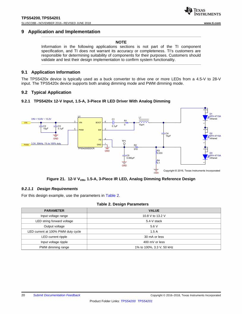
9.2.1 TPS5420x 12-V Input, 1.5-A, 3-Piece IR LED Driver With Analog Dimming
Figure 21. 12-V VVIN, 1.5-A, 3-Piece IR LED, Analog Dimming Reference Design
9.2.1.1 Design RequirementsFor this design example, use the parameters in Table 2.
Table 2. Design ParametersPARAMETER VALUE
Input voltage range 10.8 V to 13.2 VLED string forward voltage 5.4-V stack
Output voltage 5.6 VLED current at 100% PWM duty cycle 1.5 A
LED current ripple 30 mA or lessInput voltage ripple 400 mV or less
PWM dimming range 1% to 100%, 3.3 V, 50 kHz

LEDVIN(ripple) LED CIN
IN SW
I D (1 D)V I ESR
C f
´ ´ -
= + ´
´
� �CIN(rms) LEDI I D 1 D u u �
2L(ripple)2
L(rms) LEDI
I I12
�
L(ripple)L(peak) LED
II I
2 �
OUT VIN(max) OUTL(ripple)
VIN(max) SW
V (V V )I
V L f
´ -
=
´ ´
OUT VIN(max) OUTMIN
VIN(max) IND LED SW
V (V V )L
V K I f
´ -
=
´ ´ ´
21
TPS54200, TPS54201www.ti.com SLUSCO8B –NOVEMBER 2016–REVISED JUNE 2018
Product Folder Links: TPS54200 TPS54201
Submit Documentation FeedbackCopyright © 2016–2018, Texas Instruments Incorporated
9.2.1.2 Detailed Design Procedure
9.2.1.2.1 Inductor Selection
Use Equation 3 to calculate the minimum value of the output inductor (LMIN).
where• KIND is a coefficient that represents the amount of inductor ripple current relative to the maximum LED current.• ILED is the maximum LED current.• VOUT is the sum of the voltage across LED load and the voltage across the sense resistor. (3)
In general, the suggested value of KIND is between 0.2 and 0.4. For an application that can tolerate higher LEDcurrent ripple or use larger output capacitors, one can choose 0.4 for KIND. Otherwise, a smaller KIND like 0.2 canbe chosen to get low-enough LED current ripple.
With the chosen inductor value the user can calculate the actual inductor current ripple using Equation 4.
(4)
The inductor rms-current and saturation-current ratings must be greater than the rms current and saturationcurrent seen in the application. This ensures that the inductor does not overheat or saturate. During power up,transient conditions, or fault conditions, the inductor current can exceed its normal operating current. For thisreason, the most conservative approach is to specify an inductor with a saturation current rating equal to orgreater than the converter current limit. This is not always possible due to application size limitations. The peak-inductor-current and rms-current equations are shown in Equation 5 and Equation 6.
(5)
(6)
In this design, choose KIND = 0.3. According to the LED manufacturer’s data sheet, the IR LED has 1.75-Vforward voltage at 1.5-A current, so VOUT = 1.75 V × 3 + 0.2 V = 5.45 V and the calculated inductance is 11.9 µH.A 10-µH inductor (part number is 744066100 from Wurth) is chosen. With this inductor, the ripple, peak, and rmscurrents of the inductor are 0.53 A, 1.77 A, and 1.51 A, respectively. The chosen inductor has ample margin.
9.2.1.2.2 Input Capacitor Selection
The device requires an input capacitor to reduce the surge current drawn from the input supply and the switchingnoise from the device. Ceramic capacitors with X5R or X7R dielectrics are highly recommended because of theirlow ESR and small temperature coefficients. For most applications, a 10-μF capacitor is enough. An additional0.1-μF capacitor from VIN to GND is optional to provide additional high-frequency filtering. The input capacitormust have a voltage rating greater than the maximum input voltage and have a ripple-current rating greater thanthe maximum input-current ripple of the converter. The rms input-ripple current is calculated in Equation 7, whereD is the duty cycle (output voltage divided by input voltage).
(7)
Use Equation 8 to calculate the input ripple voltage, where ESRCIN is the ESR of input capacitor. Ceramiccapacitance tends to decrease as the applied dc voltage increases. This depreciation must be accounted forwhen calculating input ripple voltage.
(8)
In this design, a 10-µF, 35-V X7R ceramic capacitor, part number GRM32ER7YA106KA12L from muRata, ischosen. This yields around 70-mV input ripple voltage. The calculated rms input ripple current is 0.75 A, wellbelow the ripple-current rating of the capacitor.

FF POLE
1C
2 R f
Su u
COUT L(ripple)LED(ripple)
COUT LED
Z II
Z R
u
�
OUT
SW COUT
1C
2 f Z=
p ´ ´
LED LED(ripple)COUT
L(ripple) LED(ripple)
R IZ
I I
u
�
FLED
F
VR # of LEDs
I'
u'
22
TPS54200, TPS54201SLUSCO8B –NOVEMBER 2016–REVISED JUNE 2018 www.ti.com
Product Folder Links: TPS54200 TPS54201
Submit Documentation Feedback Copyright © 2016–2018, Texas Instruments Incorporated
9.2.1.2.3 Output Capacitor Selection
The output capacitor reduces the high-frequency ripple current through the LED string. Various guidelinesdisclose how much high-frequency ripple current is acceptable in the LED string. Excessive ripple current in theLED string increases the rms current in the LED string, and therefore the LED temperature increases.1. Look up the total dynamic resistance of the LED string (RLED) using the LED manufacturer’s data sheet.2. Calculate the required impedance of the output capacitor (ZOUT), given the acceptable peak-to-peak ripple
current through the LED string, ILED(ripple). IL(ripple) is the peak-to-peak inductor ripple current as calculatedpreviously in the Inductor Selection section.
3. Calculate the minimum effective output capacitance required.4. Increase the output capacitance appropriately due to the derating effect of applied dc voltage.
See Equation 9, Equation 10 and Equation 11.
(9)
(10)
(11)
Once the output capacitor is chosen, Equation 12 can be used to estimate the peak-to-peak ripple currentthrough the LED string.
(12)
An OSRAM IR LED, SFH4715A, is used here. The dynamic resistance of this LED is 0.25 Ω at 1.5-A forwardcurrent. In this design, a 10-µF, 35-V X7R ceramic capacitor is chosen, the part number isGRM32ER7YA106KA12L, from muRata. The calculated ripple current of the LED is about 20 mA.
9.2.1.2.4 FB Pin RC Filter Selection
The RC filter comprising RF and CF and connected between the sense resistor and the FB pin is used togenerate a pole for loop stability purposes. Moving this pole can adjust loop bandwidth. The suggested frequencyof the pole is 2 kHz in analog dimming mode and 4 kHz in PWM dimming mode. Use Equation 13 to choose RFand CF. Due to the dc offset current of the internal amplifier, the suggested value of RF is less than 1 kΩ tominimize the effect on LED current-regulation accuracy.
(13)
Analog dimming mode is implemented in this design. Choose the pole at around 2 kHz, with 910 Ω as the filterresistor; then the calculated filter capacitance is 87 nF. An 82 nF capacitor is chosen for this filter.
9.2.1.2.5 Sense Resistor Selection
The maximum target LED current at 100% PWM duty is 1.5 A, and the corresponding VREF is 200 mV. UsingEquation 1, calculate the needed sense resistance at 133 mΩ. Pay close attention to the power consumption ofthe sense resistor in this design at 300 mW, and make sure the chosen resistor has enough margin in its powerrating.

CH1
CH3
CH4
CH1
CH3
CH4
CH2
CH3
CH4
CH1
CH2
CH4
CH2
CH3
CH4
PWM duty %
Effi
cien
cy
0 10 20 30 40 50 60 70 80 90 10050%
55%
60%
65%
70%
75%
80%
85%
90%
95%
100%
D001
Efficiency_LEDEfficiency_Vout
23
TPS54200, TPS54201www.ti.com SLUSCO8B –NOVEMBER 2016–REVISED JUNE 2018
Product Folder Links: TPS54200 TPS54201
Submit Documentation FeedbackCopyright © 2016–2018, Texas Instruments Incorporated
9.2.1.3 Application Curves
Figure 22. Efficiency
CH2: SW CH3: LED current CH4: Inductor current(AC-coupled)
Figure 23. LED Current Ripple at 1% PWM Duty Cycle
CH2: SW CH3: LED current CH4: Inductorcurrent
(AC-coupled)
Figure 24. LED Current Ripple at 100% PWM Duty Cycle
CH1: VVIN CH2: SW CH4: Inductorcurrent
(AC-coupled)
Figure 25. Input Voltage Ripple at 100% PWM Duty Cycle
CH1: PWM CH3: Inductorcurrent
CH4: LED current
Figure 26. LED Current Transient as PWM Duty CycleChanges From 1% to 99%
CH1: PWM CH3: Inductorcurrent
CH4: LED current
Figure 27. LED Current Transient as PWM Duty CycleChanges From 50% to 99%

CH2
CH3
CH4
CH1
CH2
CH3
CH4
CH1
CH2
CH3
CH4
CH1
CH2
CH3
CH4
CH1
CH1
CH3
CH4
PWM duty %
LED
cur
rent
(m
A)
0 20% 40% 60% 80% 100%0
200
400
600
800
1000
1200
1400
1600
D002
24
TPS54200, TPS54201SLUSCO8B –NOVEMBER 2016–REVISED JUNE 2018 www.ti.com
Product Folder Links: TPS54200 TPS54201
Submit Documentation Feedback Copyright © 2016–2018, Texas Instruments Incorporated
CH1: PWM CH3: Inductorcurrent
CH4: LED current
Figure 28. LED Current Transient as PWM Duty CycleChanges From 99% to 1%
Figure 29. LED Current vs PWM Duty Cycle
CH1: PWM CH2: SW CH3: VOUT CH4: LEDcurrent;
Figure 30. Start-Up at 1% PWM Duty Cycle and 50 kHz
CH1: PWM CH2: SW CH3: VOUT CH4: LEDcurrent;
Figure 31. Shutdown at 1% PWM Duty Cycle and 50 kHz
CH1: PWM CH2: SW CH3: VOUT CH4: LEDcurrent
Figure 32. Start-Up at 100% PWM Duty Cycle
CH1: PWM CH2: SW CH3: VOUT CH4: LEDcurrent
Figure 33. Shutdown at 100% PWM Duty Cycle

CH2
CH3
CH4
CH1
CH2
CH3
CH4
CH1
CH2
CH3
CH4
CH1
25
TPS54200, TPS54201www.ti.com SLUSCO8B –NOVEMBER 2016–REVISED JUNE 2018
Product Folder Links: TPS54200 TPS54201
Submit Documentation FeedbackCopyright © 2016–2018, Texas Instruments Incorporated
CH1: VOUT CH2: SW CH3: FB CH4: Inductorcurrent
Figure 34. LED Short Protection (100% PWM Duty Cycle)of TPS54200
CH1: VOUT CH2: SW CH3: FB CH4: Inductorcurrent
Figure 35. LED Short Protection (100% PWM Duty Cycle)of TPS54201
CH1: VOUT CH2: SW CH3: FB CH4: Inductorcurrent
Figure 36. LED Open Protection (100% PWM Duty Cycle)of TPS54200
CH1: VOUT CH2: SW CH3: FB CH4: Inductorcurrent
Figure 37. LED Open Protection (100% PWM Duty Cycle)of TPS54201
CH1: VOUT CH2: SW CH3: FB CH4:Inductorcurrent
Figure 38. Sense Resistor Short Protection (100% PWMDuty Cycle) of TPS54200
CH1: VOUT CH2: SW CH3: FB CH4: Inductorcurrent
Figure 39. Sense-Resistor Short Protection (100% PWMDuty Cycle) of TPS54201

10µH
L1
0.1µF
C1
0.1µFC3
0.082µFC5
10µFC2
10µFC4
0
R1
200
R2
TP1
0.1R3
GND
GND
GND
GND
VIN3
PWM5
GND1
BOOT6
SW2
FB4
U1
TPS54200DDCR
VIN
PWM
VIN = 21.6V ~ 26.4V
1.5V, 250Hz, 1% to 100% duty
1
32
Cool WhiteD1
1
32
Cool WhiteD2
1
32
Cool WhiteD3
1
32
Cool WhiteD4
GND
GND
GND
GND
Copyright © 2016, Texas Instruments Incorporated
26
TPS54200, TPS54201SLUSCO8B –NOVEMBER 2016–REVISED JUNE 2018 www.ti.com
Product Folder Links: TPS54200 TPS54201
Submit Documentation Feedback Copyright © 2016–2018, Texas Instruments Incorporated
9.2.2 TPS5420x 24-V Input, 1-A, 4-Piece WLED Driver With PWM Dimming
Figure 40. 24-V Input, 1-A, 4-Piece WLED Driver With PWM Dimming Reference Design
9.2.2.1 Design RequirementsFor this design example, use the parameters in Table 3.
Table 3. Design ParametersPARAMETER VALUE
Input voltage range 21.6 V to 26.4 VLED string forward voltage 11.6-V stack
Output voltage 11.7 VLED current at 100% PWM duty cycle 1 A
LED current ripple 30 mA or lessInput voltage ripple 400 mV or less
PWM dimming range 1% to 100%, 1.5 V, 250 Hz

OUT IN(max) OUTMIN
IN(max) L(ripple) SW
V (V V )L
V I f
´ -
=
´ ´
27
TPS54200, TPS54201www.ti.com SLUSCO8B –NOVEMBER 2016–REVISED JUNE 2018
Product Folder Links: TPS54200 TPS54201
Submit Documentation FeedbackCopyright © 2016–2018, Texas Instruments Incorporated
9.2.2.2 Detailed Design ProcedureThe detailed design process in this example is basically the same with that shown in the previous designexample. Following are the design results.
9.2.2.2.1 Inductor Selection
A Cree white LED XLampXML is used. According to the LED manufacturer’s data sheet, this LED has 2.9-Vforward voltage at 1-A current, so VOUT = 2.9 V × 4 + 0.1 V = 11.7 V. Choose KIND = 0.3, which gives a 36-µHinductance. With this inductance, the ripple current on the inductor is only 0.3-A peak-to-peak, which is tooconservative and increases total system cost and size.
For this application, with concerns about system cost and size taken into account, decide the inductance bychoosing a larger peak-to-peak inductor ripple current. To choose a proper peak-to-peak inductor ripple, the low-side FET sink current limit should not be exceeded when the converter works in a no-load condition. To meet thisrequirement, half of the peak-to-peak inductor ripple must be lower than that limit. Another consideration with thislarger peak-to-peak ripple current is the increased core loss and copper loss in the inductor, which is alsoacceptable. Once this peak-to-peak inductor ripple current is chosen, Equation 14 can be used to calculate therequired inductance.
where• IL(RIPPLE) is the peak-to-peak inductor ripple current. (14)
Choose 1-A peak-to-peak inductor ripple current, and half of the current is 0.5 A, much lower than the minimumlow-side sink current limit of 1.25 A. The calculated inductance is 10.9 µH. Choose a 10-µH inductor with partnumber 744066100 from Wurth. The ripple, peak, and rms currents of the inductor are 1.09 A, 1.54 A, and 1.05A, respectively. The chosen inductor has ample margin in this design.
9.2.2.2.2 Input Capacitor Selection
In this design, a 10-µF, 35-V X7R ceramic capacitor, part number GRM32ER7YA106KA12L from muRata, ischosen. This yields around 70-mV input-ripple voltage. The calculated rms input ripple current is 0.5 A, wellbelow the ripple-current rating of the capacitor.
9.2.2.2.3 Output Capacitor Selection
The dynamic resistance of this LED is 0.184 Ω at 1-A forward current. In this design, choose a 10-µF, 35-V X7Rceramic capacitor, part number GRM32ER7YA106KA12L from muRata. The calculated ripple current of the LEDis about 40 mA.
9.2.2.2.4 FB Pin RC Filter Selection
PWM dimming mode is implemented in this design. Choose the pole at around 4 kHz, and choose 475 Ω as thefilter resistor. With those values, an 82 nF capacitor should be chosen for this filter. To get a faster loopresponse, choose a smaller filter resistor. In this design, 200 Ω was chosen to get a pole at approximately 10kHz.
9.2.2.2.5 Sense Resistor Selection
The maximum target LED current at 100% PWM duty cycle is 1 A, and the corresponding VREF is 100 mV. Byusing Equation 1, one can calculate the needed sense resistance of 100 mΩ. Pay close attention to the powerconsumption of the sense resistor in this design at 100 mW. Make sure the chosen resistor has enough marginin the power rating.

CH4
CH1
CH4
CH1
CH2
CH3
CH4
CH1
CH2
CH3
CH4
CH1
CH2
CH3
CH4
CH1
CH2
CH3
CH4
CH1
28
TPS54200, TPS54201SLUSCO8B –NOVEMBER 2016–REVISED JUNE 2018 www.ti.com
Product Folder Links: TPS54200 TPS54201
Submit Documentation Feedback Copyright © 2016–2018, Texas Instruments Incorporated
9.2.2.3 Application Curves
CH1: PWM CH2: SW CH3: VOUT CH4: LEDcurrent
Figure 41. Start-Up at 1% PWM Duty Cycle and 250 Hz
CH1: PWM CH2: SW CH3: VOUT CH4: LEDcurrent
Figure 42. Shutdown at 1% PWM Duty Cycle and 250 Hz
CH1: PWM CH2: SW CH3: VOUT CH4: LEDCurrent
Figure 43. Start-Up at 100% PWM Duty Cycle
CH1: PWM CH2: SW CH3: VOUT CH4: LEDcurrent
Figure 44. Shutdown at 100% PWM Duty Cycle
CH1 PWM CH4: LEDcurrent
Figure 45. PWM Dimming With 2% Duty Cycle and 250 Hz
CH1: PWM CH4: LEDcurrent
Figure 46. PWM Dimming With 50% Duty Cycle and 250 Hz

CH2
CH4
CH1
CH4
CH1
CH2
CH3
CH4
29
TPS54200, TPS54201www.ti.com SLUSCO8B –NOVEMBER 2016–REVISED JUNE 2018
Product Folder Links: TPS54200 TPS54201
Submit Documentation FeedbackCopyright © 2016–2018, Texas Instruments Incorporated
CH1: PWM CH4: LEDcurrent
Figure 47. PWM Dimming With 99% Duty Cycle and 250 Hz
CH2: SW CH3: LEDcurrent
CH4: Inductorcurrent
(AC-coupled)
Figure 48. LED Current Ripple at 100% PWM Duty Cycle
CH1: VVIN CH2: SW CH4: Inductor current(AC-coupled)
Figure 49. Input Voltage Ripple at 100% PWM Duty Cycle

30
TPS54200, TPS54201SLUSCO8B –NOVEMBER 2016–REVISED JUNE 2018 www.ti.com
Product Folder Links: TPS54200 TPS54201
Submit Documentation Feedback Copyright © 2016–2018, Texas Instruments Incorporated
10 Power Supply RecommendationsThe devices are designed to operate from an input voltage supply range between 4.5 V and 28 V. This inputsupply must be well regulated. If the input supply is located more than a few inches from the device or converter,additional bulk capacitance may be required in addition to the ceramic bypass capacitors.
11 LayoutThe TPS5420x requires a proper layout for optimal performance. The following section gives some guidelines tohelp ensure a proper layout.
11.1 Layout GuidelinesAn example of a proper layout for the TPS5420x is shown in Figure 50.• Creating a large GND plane for good electrical and thermal performance is important.• The VIN and GND traces should be as wide as possible to reduce trace impedance. The added width also
provides excellent heat dissipation.• Thermal vias can be used to connect the topside GND plane to additional printed-circuit board (PCB) layers
for heat dissipation and grounding.• The input capacitors must be located as close as possible to the VIN pin and the GND pin.• The SW trace must be kept as short as possible to minimize radiated noise and EMI.• Do not allow switching current to flow under the device.• The FB trace should be kept as short as possible and placed away from the high-voltage switching trace and
the ground shield.• In higher-current applications, routing the load current of the current-sense resistor to the junction of the input
capacitor and GND node may be necessary.

GND
SW
VIN
BOOT
PWM
FB
CONNECTED TO POWER GND ON
INTERNAL OR BOTTOM LAYER
VIA to Ground Plane
VIN
GNDGND
GNDGND
VOUT
SW
VSENSE
INPUT CAPACITOR
OUTPUT CAPACITOR
OUTPUT INDUCTOR
LED LOAD
BOOT CAPACITOR
SENSE RESISTOR
RC FILTER
TO PWM CONTROL
CONNECTED TO POWER GND ON
INTERNAL OR BOTTOM LAYER
31
TPS54200, TPS54201www.ti.com SLUSCO8B –NOVEMBER 2016–REVISED JUNE 2018
Product Folder Links: TPS54200 TPS54201
Submit Documentation FeedbackCopyright © 2016–2018, Texas Instruments Incorporated
11.2 Layout Example
Figure 50. Layout Example

32
TPS54200, TPS54201SLUSCO8B –NOVEMBER 2016–REVISED JUNE 2018 www.ti.com
Product Folder Links: TPS54200 TPS54201
Submit Documentation Feedback Copyright © 2016–2018, Texas Instruments Incorporated
12 Device and Documentation Support
12.1 Device Support
12.1.1 Third-Party Products DisclaimerTI'S PUBLICATION OF INFORMATION REGARDING THIRD-PARTY PRODUCTS OR SERVICES DOES NOTCONSTITUTE AN ENDORSEMENT REGARDING THE SUITABILITY OF SUCH PRODUCTS OR SERVICESOR A WARRANTY, REPRESENTATION OR ENDORSEMENT OF SUCH PRODUCTS OR SERVICES, EITHERALONE OR IN COMBINATION WITH ANY TI PRODUCT OR SERVICE.
12.2 Documentation Support
12.2.1 Related LinksThe table below lists quick access links. Categories include technical documents, support and communityresources, tools and software, and quick access to order now.
Table 4. Related Links
PARTS PRODUCT FOLDER ORDER NOW TECHNICALDOCUMENTS
TOOLS &SOFTWARE
SUPPORT &COMMUNITY
TPS54200 Click here Click here Click here Click here Click hereTPS54201 Click here Click here Click here Click here Click here
12.3 Receiving Notification of Documentation UpdatesTo receive notification of documentation updates, navigate to the device product folder on ti.com. In the upperright corner, click on Alert me to register and receive a weekly digest of any product information that haschanged. For change details, review the revision history included in any revised document.
12.4 Community ResourcesThe following links connect to TI community resources. Linked contents are provided "AS IS" by the respectivecontributors. They do not constitute TI specifications and do not necessarily reflect TI's views; see TI's Terms ofUse.
TI E2E™ Online Community TI's Engineer-to-Engineer (E2E) Community. Created to foster collaborationamong engineers. At e2e.ti.com, you can ask questions, share knowledge, explore ideas and helpsolve problems with fellow engineers.
Design Support TI's Design Support Quickly find helpful E2E forums along with design support tools andcontact information for technical support.
12.5 TrademarksE2E is a trademark of Texas Instruments.All other trademarks are the property of their respective owners.
12.6 Electrostatic Discharge CautionThis integrated circuit can be damaged by ESD. Texas Instruments recommends that all integrated circuits be handled withappropriate precautions. Failure to observe proper handling and installation procedures can cause damage.
ESD damage can range from subtle performance degradation to complete device failure. Precision integrated circuits may be moresusceptible to damage because very small parametric changes could cause the device not to meet its published specifications.
12.7 GlossarySLYZ022 — TI Glossary.
This glossary lists and explains terms, acronyms, and definitions.

33
TPS54200, TPS54201www.ti.com SLUSCO8B –NOVEMBER 2016–REVISED JUNE 2018
Product Folder Links: TPS54200 TPS54201
Submit Documentation FeedbackCopyright © 2016–2018, Texas Instruments Incorporated
13 Mechanical, Packaging, and Orderable InformationThe following pages include mechanical, packaging, and orderable information. This information is the most-current data available for the designated devices. This data is subject to change without notice and withoutrevision of this document. For browser-based versions of this data sheet, see the left-hand navigation pane.

PACKAGE OPTION ADDENDUM
www.ti.com 28-Mar-2018
Addendum-Page 1
PACKAGING INFORMATION
Orderable Device Status(1)
Package Type PackageDrawing
Pins PackageQty
Eco Plan(2)
Lead/Ball Finish(6)
MSL Peak Temp(3)
Op Temp (°C) Device Marking(4/5)
Samples
TPS54200DDCR ACTIVE SOT-23-THIN DDC 6 3000 Green (RoHS& no Sb/Br)
CU SN Level-1-260C-UNLIM -40 to 85 4200
TPS54200DDCT ACTIVE SOT-23-THIN DDC 6 250 Green (RoHS& no Sb/Br)
CU SN Level-1-260C-UNLIM -40 to 85 4200
TPS54201DDCR ACTIVE SOT-23-THIN DDC 6 3000 Green (RoHS& no Sb/Br)
CU SN Level-1-260C-UNLIM -40 to 125 4201
TPS54201DDCT ACTIVE SOT-23-THIN DDC 6 250 Green (RoHS& no Sb/Br)
CU SN Level-1-260C-UNLIM -40 to 125 4201
(1) The marketing status values are defined as follows:ACTIVE: Product device recommended for new designs.LIFEBUY: TI has announced that the device will be discontinued, and a lifetime-buy period is in effect.NRND: Not recommended for new designs. Device is in production to support existing customers, but TI does not recommend using this part in a new design.PREVIEW: Device has been announced but is not in production. Samples may or may not be available.OBSOLETE: TI has discontinued the production of the device.
(2) RoHS: TI defines "RoHS" to mean semiconductor products that are compliant with the current EU RoHS requirements for all 10 RoHS substances, including the requirement that RoHS substancedo not exceed 0.1% by weight in homogeneous materials. Where designed to be soldered at high temperatures, "RoHS" products are suitable for use in specified lead-free processes. TI mayreference these types of products as "Pb-Free".RoHS Exempt: TI defines "RoHS Exempt" to mean products that contain lead but are compliant with EU RoHS pursuant to a specific EU RoHS exemption.Green: TI defines "Green" to mean the content of Chlorine (Cl) and Bromine (Br) based flame retardants meet JS709B low halogen requirements of <=1000ppm threshold. Antimony trioxide basedflame retardants must also meet the <=1000ppm threshold requirement.
(3) MSL, Peak Temp. - The Moisture Sensitivity Level rating according to the JEDEC industry standard classifications, and peak solder temperature.
(4) There may be additional marking, which relates to the logo, the lot trace code information, or the environmental category on the device.
(5) Multiple Device Markings will be inside parentheses. Only one Device Marking contained in parentheses and separated by a "~" will appear on a device. If a line is indented then it is a continuationof the previous line and the two combined represent the entire Device Marking for that device.
(6) Lead/Ball Finish - Orderable Devices may have multiple material finish options. Finish options are separated by a vertical ruled line. Lead/Ball Finish values may wrap to two lines if the finishvalue exceeds the maximum column width.
Important Information and Disclaimer:The information provided on this page represents TI's knowledge and belief as of the date that it is provided. TI bases its knowledge and belief on informationprovided by third parties, and makes no representation or warranty as to the accuracy of such information. Efforts are underway to better integrate information from third parties. TI has taken and

PACKAGE OPTION ADDENDUM
www.ti.com 28-Mar-2018
Addendum-Page 2
continues to take reasonable steps to provide representative and accurate information but may not have conducted destructive testing or chemical analysis on incoming materials and chemicals.TI and TI suppliers consider certain information to be proprietary, and thus CAS numbers and other limited information may not be available for release.
In no event shall TI's liability arising out of such information exceed the total purchase price of the TI part(s) at issue in this document sold by TI to Customer on an annual basis.

TAPE AND REEL INFORMATION
*All dimensions are nominal
Device PackageType
PackageDrawing
Pins SPQ ReelDiameter
(mm)
ReelWidth
W1 (mm)
A0(mm)
B0(mm)
K0(mm)
P1(mm)
W(mm)
Pin1Quadrant
TPS54200DDCR SOT-23-THIN
DDC 6 3000 180.0 9.5 3.17 3.1 1.1 4.0 8.0 Q3
TPS54200DDCT SOT-23-THIN
DDC 6 250 180.0 9.5 3.17 3.1 1.1 4.0 8.0 Q3
TPS54201DDCR SOT-23-THIN
DDC 6 3000 180.0 9.5 3.17 3.1 1.1 4.0 8.0 Q3
TPS54201DDCT SOT-23-THIN
DDC 6 250 180.0 9.5 3.17 3.1 1.1 4.0 8.0 Q3
PACKAGE MATERIALS INFORMATION
www.ti.com 30-Apr-2018
Pack Materials-Page 1

*All dimensions are nominal
Device Package Type Package Drawing Pins SPQ Length (mm) Width (mm) Height (mm)
TPS54200DDCR SOT-23-THIN DDC 6 3000 184.0 184.0 19.0
TPS54200DDCT SOT-23-THIN DDC 6 250 184.0 184.0 19.0
TPS54201DDCR SOT-23-THIN DDC 6 3000 184.0 184.0 19.0
TPS54201DDCT SOT-23-THIN DDC 6 250 184.0 184.0 19.0
PACKAGE MATERIALS INFORMATION
www.ti.com 30-Apr-2018
Pack Materials-Page 2


IMPORTANT NOTICE
Texas Instruments Incorporated (TI) reserves the right to make corrections, enhancements, improvements and other changes to itssemiconductor products and services per JESD46, latest issue, and to discontinue any product or service per JESD48, latest issue. Buyersshould obtain the latest relevant information before placing orders and should verify that such information is current and complete.TI’s published terms of sale for semiconductor products (http://www.ti.com/sc/docs/stdterms.htm) apply to the sale of packaged integratedcircuit products that TI has qualified and released to market. Additional terms may apply to the use or sale of other types of TI products andservices.Reproduction of significant portions of TI information in TI data sheets is permissible only if reproduction is without alteration and isaccompanied by all associated warranties, conditions, limitations, and notices. TI is not responsible or liable for such reproduceddocumentation. Information of third parties may be subject to additional restrictions. Resale of TI products or services with statementsdifferent from or beyond the parameters stated by TI for that product or service voids all express and any implied warranties for theassociated TI product or service and is an unfair and deceptive business practice. TI is not responsible or liable for any such statements.Buyers and others who are developing systems that incorporate TI products (collectively, “Designers”) understand and agree that Designersremain responsible for using their independent analysis, evaluation and judgment in designing their applications and that Designers havefull and exclusive responsibility to assure the safety of Designers' applications and compliance of their applications (and of all TI productsused in or for Designers’ applications) with all applicable regulations, laws and other applicable requirements. Designer represents that, withrespect to their applications, Designer has all the necessary expertise to create and implement safeguards that (1) anticipate dangerousconsequences of failures, (2) monitor failures and their consequences, and (3) lessen the likelihood of failures that might cause harm andtake appropriate actions. Designer agrees that prior to using or distributing any applications that include TI products, Designer willthoroughly test such applications and the functionality of such TI products as used in such applications.TI’s provision of technical, application or other design advice, quality characterization, reliability data or other services or information,including, but not limited to, reference designs and materials relating to evaluation modules, (collectively, “TI Resources”) are intended toassist designers who are developing applications that incorporate TI products; by downloading, accessing or using TI Resources in anyway, Designer (individually or, if Designer is acting on behalf of a company, Designer’s company) agrees to use any particular TI Resourcesolely for this purpose and subject to the terms of this Notice.TI’s provision of TI Resources does not expand or otherwise alter TI’s applicable published warranties or warranty disclaimers for TIproducts, and no additional obligations or liabilities arise from TI providing such TI Resources. TI reserves the right to make corrections,enhancements, improvements and other changes to its TI Resources. TI has not conducted any testing other than that specificallydescribed in the published documentation for a particular TI Resource.Designer is authorized to use, copy and modify any individual TI Resource only in connection with the development of applications thatinclude the TI product(s) identified in such TI Resource. NO OTHER LICENSE, EXPRESS OR IMPLIED, BY ESTOPPEL OR OTHERWISETO ANY OTHER TI INTELLECTUAL PROPERTY RIGHT, AND NO LICENSE TO ANY TECHNOLOGY OR INTELLECTUAL PROPERTYRIGHT OF TI OR ANY THIRD PARTY IS GRANTED HEREIN, including but not limited to any patent right, copyright, mask work right, orother intellectual property right relating to any combination, machine, or process in which TI products or services are used. Informationregarding or referencing third-party products or services does not constitute a license to use such products or services, or a warranty orendorsement thereof. Use of TI Resources may require a license from a third party under the patents or other intellectual property of thethird party, or a license from TI under the patents or other intellectual property of TI.TI RESOURCES ARE PROVIDED “AS IS” AND WITH ALL FAULTS. TI DISCLAIMS ALL OTHER WARRANTIES ORREPRESENTATIONS, EXPRESS OR IMPLIED, REGARDING RESOURCES OR USE THEREOF, INCLUDING BUT NOT LIMITED TOACCURACY OR COMPLETENESS, TITLE, ANY EPIDEMIC FAILURE WARRANTY AND ANY IMPLIED WARRANTIES OFMERCHANTABILITY, FITNESS FOR A PARTICULAR PURPOSE, AND NON-INFRINGEMENT OF ANY THIRD PARTY INTELLECTUALPROPERTY RIGHTS. TI SHALL NOT BE LIABLE FOR AND SHALL NOT DEFEND OR INDEMNIFY DESIGNER AGAINST ANY CLAIM,INCLUDING BUT NOT LIMITED TO ANY INFRINGEMENT CLAIM THAT RELATES TO OR IS BASED ON ANY COMBINATION OFPRODUCTS EVEN IF DESCRIBED IN TI RESOURCES OR OTHERWISE. IN NO EVENT SHALL TI BE LIABLE FOR ANY ACTUAL,DIRECT, SPECIAL, COLLATERAL, INDIRECT, PUNITIVE, INCIDENTAL, CONSEQUENTIAL OR EXEMPLARY DAMAGES INCONNECTION WITH OR ARISING OUT OF TI RESOURCES OR USE THEREOF, AND REGARDLESS OF WHETHER TI HAS BEENADVISED OF THE POSSIBILITY OF SUCH DAMAGES.Unless TI has explicitly designated an individual product as meeting the requirements of a particular industry standard (e.g., ISO/TS 16949and ISO 26262), TI is not responsible for any failure to meet such industry standard requirements.Where TI specifically promotes products as facilitating functional safety or as compliant with industry functional safety standards, suchproducts are intended to help enable customers to design and create their own applications that meet applicable functional safety standardsand requirements. Using products in an application does not by itself establish any safety features in the application. Designers mustensure compliance with safety-related requirements and standards applicable to their applications. Designer may not use any TI products inlife-critical medical equipment unless authorized officers of the parties have executed a special contract specifically governing such use.Life-critical medical equipment is medical equipment where failure of such equipment would cause serious bodily injury or death (e.g., lifesupport, pacemakers, defibrillators, heart pumps, neurostimulators, and implantables). Such equipment includes, without limitation, allmedical devices identified by the U.S. Food and Drug Administration as Class III devices and equivalent classifications outside the U.S.TI may expressly designate certain products as completing a particular qualification (e.g., Q100, Military Grade, or Enhanced Product).Designers agree that it has the necessary expertise to select the product with the appropriate qualification designation for their applicationsand that proper product selection is at Designers’ own risk. Designers are solely responsible for compliance with all legal and regulatoryrequirements in connection with such selection.Designer will fully indemnify TI and its representatives against any damages, costs, losses, and/or liabilities arising out of Designer’s non-compliance with the terms and provisions of this Notice.
Mailing Address: Texas Instruments, Post Office Box 655303, Dallas, Texas 75265Copyright © 2018, Texas Instruments Incorporated


