TPS53315 12-A Step-Down Regulator with Integrated Switcher ... · n/c n/c trip en pgood n/c vbst...
35
N/C N/C TRIP EN PGOOD N/C VBST N/C LL LL LL LL LL LL LL LL VFB RF MODE VDD TPS53315 GND1 PGND VREG GND2 PGND PGND PGND PGND PGND PGND VIN VIN LL LL LL LL LL VIN VIN VIN 1 2 3 4 5 6 7 8 9 10 11 12 20 19 18 17 16 15 14 13 32 31 30 29 28 27 26 25 24 23 22 21 33 34 35 36 37 38 39 40 EN V OUT V IN 3 V to 15 V UDG-10199 VDD 4.5 V to 25 V PGOOD VREG Product Folder Sample & Buy Technical Documents Tools & Software Support & Community TPS53315 SLUSAE6A – DECEMBER 2010 – REVISED DECEMBER 2015 TPS53315 12-A Step-Down Regulator with Integrated Switcher 1 Features 2 Applications 1• Conversion Input Voltage Range: 3 V to 15 V • Server and Desktop Computers • VDD Input Voltage Range: 4.5 V to 25 V • Notebook Computers • Output Voltage Range: 0.6 V to 5.5 V • Telecommunication Equipments • 5-V LDO Output 3 Description • Integrated Power MOSFETs with 12-A Continuous TPS53315 is a D-CAP™ mode, 12-A synchronous Output Current switcher with integrated MOSFETs. It is designed for • <10-μA Shut Down Current ease of use, low external component count, and • Auto-Skip Eco-mode™ for Light-Load Efficiency small package power systems. • D-CAP™ Mode with Fast Transient Response This device features single-rail input support, one 19- • Selectable Switching Frequency from 250 kHz to mΩ and one 7-mΩ integrated MOSFET, accurate 1%, 0.6 V Reference, and integrated boost switch. A 1 MHz with an External Resistor sample of competitive features include: greater than • Built-in 1%, 0.6-V Reference 96% maximum efficiency, 3 V to 15 V wide input • 0.7-ms, 1.4-ms, 2.8-ms and 5.6-ms Selectable voltage range, very low external component count, D- Internal Voltage Servo Soft-Start CAP™ mode control for super fast transient, • Pre-Charged Start-up Capability selectable auto-skip and PWM operation, internal soft-start control, adjustable frequency, and no need • Integrated Boost Switch for compensation. • Adjustable Overcurrent Limit Via External Resistor The conversion input voltage ranges from 3 V to • Overvoltage/Undervoltage, UVLO and Over- 15 V, the supply voltage range is from 4.5 V to 25 V, Temperature Protection and the output voltage range is from 0.6 V to 5.5 V. • Support All Ceramic Output Capacitors The TPS53315 is available in a 5 mm × 7 mm 40-pin, • Open Drain Power Good Indication VQFN package and is specified from –40°C to 85°C. • 40-pin VQFN Package with Thermal Pad Device Information (1) PART NUMBER PACKAGE BODY SIZE (NOM) TPS53315 VQFN (40) 7.00 mm × 5.00 mm (1) For all available packages, see the orderable addendum at the end of the data sheet. Simplified Application 1 An IMPORTANT NOTICE at the end of this data sheet addresses availability, warranty, changes, use in safety-critical applications, intellectual property matters and other important disclaimers. PRODUCTION DATA.
Transcript of TPS53315 12-A Step-Down Regulator with Integrated Switcher ... · n/c n/c trip en pgood n/c vbst...

N/C
N/C
TRIP
EN
PG
OO
D
N/C
VB
ST
N/C LL
LL
LL
LL
LL
LL
LL
LL
VFB
RF
MODE
VDD
TPS53315
GN
D1
PG
ND
VR
EG
GN
D2
PG
ND
PG
ND
PG
ND
PG
ND
PG
ND
PG
ND
VIN
VIN
LL
LL
LL
LL
LL
VIN
VIN
VIN
1 2 3 4 5 6 7 8 9 10 11 12
20
19
18
17
16
15
14
13
32 31 30 29 28 27 26 25 24 23 22 21
33
34
35
36
37
38
39
40
EN
VOUT
VIN
3 V to 15 V
UDG-10199
VDD
4.5 V to 25 V
PGOODVREG
Product
Folder
Sample &Buy
Technical
Documents
Tools &
Software
Support &Community
TPS53315SLUSAE6A –DECEMBER 2010–REVISED DECEMBER 2015
TPS53315 12-A Step-Down Regulator with Integrated Switcher1 Features 2 Applications1• Conversion Input Voltage Range: 3 V to 15 V • Server and Desktop Computers• VDD Input Voltage Range: 4.5 V to 25 V • Notebook Computers• Output Voltage Range: 0.6 V to 5.5 V • Telecommunication Equipments• 5-V LDO Output
3 Description• Integrated Power MOSFETs with 12-A ContinuousTPS53315 is a D-CAP™ mode, 12-A synchronousOutput Currentswitcher with integrated MOSFETs. It is designed for• <10-μA Shut Down Current ease of use, low external component count, and
• Auto-Skip Eco-mode™ for Light-Load Efficiency small package power systems.• D-CAP™ Mode with Fast Transient Response This device features single-rail input support, one 19-• Selectable Switching Frequency from 250 kHz to mΩ and one 7-mΩ integrated MOSFET, accurate 1%,
0.6 V Reference, and integrated boost switch. A1 MHz with an External Resistorsample of competitive features include: greater than• Built-in 1%, 0.6-V Reference96% maximum efficiency, 3 V to 15 V wide input• 0.7-ms, 1.4-ms, 2.8-ms and 5.6-ms Selectable voltage range, very low external component count, D-
Internal Voltage Servo Soft-Start CAP™ mode control for super fast transient,• Pre-Charged Start-up Capability selectable auto-skip and PWM operation, internal
soft-start control, adjustable frequency, and no need• Integrated Boost Switchfor compensation.• Adjustable Overcurrent Limit Via External ResistorThe conversion input voltage ranges from 3 V to• Overvoltage/Undervoltage, UVLO and Over-15 V, the supply voltage range is from 4.5 V to 25 V,Temperature Protection and the output voltage range is from 0.6 V to 5.5 V.
• Support All Ceramic Output CapacitorsThe TPS53315 is available in a 5 mm × 7 mm 40-pin,• Open Drain Power Good Indication VQFN package and is specified from –40°C to 85°C.
• 40-pin VQFN Package with Thermal PadDevice Information(1)
PART NUMBER PACKAGE BODY SIZE (NOM)TPS53315 VQFN (40) 7.00 mm × 5.00 mm
(1) For all available packages, see the orderable addendum atthe end of the data sheet.
Simplified Application
1
An IMPORTANT NOTICE at the end of this data sheet addresses availability, warranty, changes, use in safety-critical applications,intellectual property matters and other important disclaimers. PRODUCTION DATA.
TPS53315SLUSAE6A –DECEMBER 2010–REVISED DECEMBER 2015 www.ti.com
Table of Contents7.4 Device Functional Modes........................................ 161 Features .................................................................. 1
8 Application and Implementation ........................ 172 Applications ........................................................... 18.1 Application Information............................................ 173 Description ............................................................. 18.2 Typical Application ................................................. 174 Revision History..................................................... 2
9 Power Supply Recommendations ...................... 245 Pin Configuration and Functions ......................... 310 Layout................................................................... 256 Specifications......................................................... 5
10.1 Layout Guidelines ................................................. 256.1 Absolute Maximum Ratings ...................................... 510.2 Layout Example .................................................... 266.2 ESD Ratings.............................................................. 510.3 Thermal Considerations ........................................ 266.3 Recommended Operating Conditions....................... 5
11 Device and Documentation Support ................. 276.4 Thermal Information .................................................. 611.1 Community Resources.......................................... 276.5 Electrical Characteristics........................................... 611.2 Trademarks ........................................................... 276.6 Typical Characteristics .............................................. 811.3 Electrostatic Discharge Caution............................ 277 Detailed Description ............................................ 1111.4 Glossary ................................................................ 277.1 Overview ................................................................. 11
12 Mechanical, Packaging, and Orderable7.2 Functional Block Diagram ....................................... 11Information ........................................................... 277.3 Feature Description................................................. 12
4 Revision HistoryNOTE: Page numbers for previous revisions may differ from page numbers in the current version.
Changes from Original (May 2013) to Revision A Page
• Added ESD Ratings table, Feature Description section, Device Functional Modes, Application and Implementationsection, Power Supply Recommendations section, Layout section, Device and Documentation Support section, andMechanical, Packaging, and Orderable Information section. ................................................................................................. 1
2 Submit Documentation Feedback Copyright © 2010–2015, Texas Instruments Incorporated
Product Folder Links: TPS53315

N/C
N/C
TRIP
EN
PG
OO
D
N\C
VB
ST
N/C
32 31 30 29 28 27 26 25 24 23 22 21
LL
LL
LL
LL
LL
LL
LL
LL
33
34
35
36
37
38
39
40
VFB
RF
MODE
VDD
1 2 3 4 5 6 7 8 9 10 11 12
20
19
18
17
16
15
14
13
TPS53315RGF
GN
D1
PG
ND
VR
EG
GN
D2
PG
ND
PG
ND
PG
ND
PG
ND
PG
ND
PG
ND
VIN
VIN
LL
LL
LL
LL
LL
VIN
VIN
VIN
TPS53315www.ti.com SLUSAE6A –DECEMBER 2010–REVISED DECEMBER 2015
5 Pin Configuration and Functions
RGF Package40-Pin VQFN With Exposed Thermal Pad
Top View
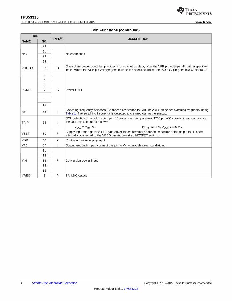
Pin FunctionsPIN
TYPE (1) DESCRIPTIONNAME NO.EN 36 I Enable pinGND1 1 G GND for controllerGND2 4 G GND for half-bridge
161718192021
LL 22 B Output of converted power; connect this pin to the output inductor.232425262728
Soft-start and skip/CCM selection; connect a resistor to select soft-start time using Table 2. The soft-startMODE 39 I time is detected and stored into internal register during start-up.
(1) I = Input, O = Output, B = Bidirectional, G = Ground, P = Supply
Copyright © 2010–2015, Texas Instruments Incorporated Submit Documentation Feedback 3
Product Folder Links: TPS53315
TPS53315SLUSAE6A –DECEMBER 2010–REVISED DECEMBER 2015 www.ti.com
Pin Functions (continued)PIN
TYPE (1) DESCRIPTIONNAME NO.
2931
N/C No connection3334
Open drain power good flag provides a 1-ms start up delay after the VFB pin voltage falls within specifiedPGOOD 32 O limits. When the VFB pin voltage goes outside the specified limits, the PGOOD pin goes low within 10 µs.256
PGND 7 G Power GND89
10Switching frequency selection. Connect a resistance to GND or VREG to select switching frequency usingRF 38 I Table 1. The switching frequency is detected and stored during the startup.OCL detection threshold setting pin, 10 µA at room temperature, 4700 ppm/°C current is sourced and setthe OCL trip voltage as follows:TRIP 35 Ispace VOCL = VTRIP/8 (VTRIP ≤1.2 V, VOCL ≤ 150 mV)Supply input for high-side FET gate driver (boost terminal); connect capacitor from this pin to LL-node.VBST 30 P Internally connected to the VREG pin via bootstrap MOSFET switch.
VDD 40 P Controller power supply inputVFB 37 I Output feedback input; connect this pin to VOUT through a resistor divider.
1112
VIN 13 P Conversion power input1415
VREG 3 P 5-V LDO output
4 Submit Documentation Feedback Copyright © 2010–2015, Texas Instruments Incorporated
Product Folder Links: TPS53315
TPS53315www.ti.com SLUSAE6A –DECEMBER 2010–REVISED DECEMBER 2015
6 Specifications
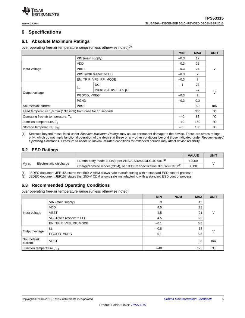
6.1 Absolute Maximum Ratingsover operating free-air temperature range (unless otherwise noted) (1)
MIN MAX UNITVIN (main supply) –0.3 17VDD –0.3 28
Input voltage VBST –0.3 24 VVBST(with respect to LL) –0.3 7EN, TRIP, VFB, RF, MODE –0.3 7
DC –1 23LL
Pulse < 20 ns, E = 5 μJ –7Output voltage V
PGOOD, VREG –0.3 7PGND –0.3 0.3
Source/sink current VBST 50 mALead temperature 1,6 mm (1/16 inch) from case for 10 seconds 300 °COperating free-air temperature, TA –40 85 °CJunction temperature, TJ –40 150 °CStorage temperature, Tstg –55 150 °C
(1) Stresses beyond those listed under Absolute Maximum Ratings may cause permanent damage to the device. These are stress ratingsonly, which do not imply functional operation of the device at these or any other conditions beyond those indicated under RecommendedOperating Conditions. Exposure to absolute-maximum-rated conditions for extended periods may affect device reliability.
6.2 ESD RatingsVALUE UNIT
Human-body model (HBM), per ANSI/ESDA/JEDEC JS-001 (1) ±2000V(ESD) Electrostatic discharge V
Charged-device model (CDM), per JEDEC specification JESD22-C101 (2) ±500
(1) JEDEC document JEP155 states that 500-V HBM allows safe manufacturing with a standard ESD control process.(2) JEDEC document JEP157 states that 250-V CDM allows safe manufacturing with a standard ESD control process.
6.3 Recommended Operating Conditionsover operating free-air temperature range (unless otherwise noted)
MIN NOM MAX UNITVIN (main supply) 3 15VDD 4.5 25
Input voltage VBST 4.5 21 VVBST(with respect to LL) 4.5 6.5EN, TRIP, VFB, RF, MODE –0.1 6.5LL –0.8 15
Output voltage VPGOOD, VREG –0.1 6.5
Source/sink VBST 50 mAcurrentJunction temperature , TJ –40 125 °C
Copyright © 2010–2015, Texas Instruments Incorporated Submit Documentation Feedback 5
Product Folder Links: TPS53315

TPS53315SLUSAE6A –DECEMBER 2010–REVISED DECEMBER 2015 www.ti.com
6.4 Thermal InformationTPS53315
THERMAL METRIC (1) RGF (VQFN) UNIT40 PINS
RθJA Junction-to-ambient thermal resistance 35.8 °C/WRθJC(top) Junction-to-case (top) thermal resistance 23.8 °C/WRθJB Junction-to-board thermal resistance 10.1 °C/WψJT Junction-to-top characterization parameter 0.4 °C/WψJB Junction-to-board characterization parameter 10.0 °C/WRθJC(bot) Junction-to-case (bottom) thermal resistance 2.8 °C/W
(1) For more information about traditional and new thermal metrics, see the Semiconductor and IC Package Thermal Metrics applicationreport, SPRA953.
6.5 Electrical Characteristicsover recommended free-air temperature range, VDD = 12 V (unless otherwise noted)
PARAMETER TEST CONDITIONS MIN TYP MAX UNITSUPPLY VOLTAGE AND SUPPLY CURRENT
VIN pin power conversion inputVVIN 3 15 VvoltageVDD Supply input voltage 4.5 25 VIVIN(leak) VIN pin leakage current VEN = 0 V 1 µA
VDD current, TA = 25°C, No Load, VEN = 5 V,IVDD VDD supply current 420 590 µAVVFB = 0.630 VIVDDSDN VDD shutdown current VDD current, TA = 25°C, No Load, VEN = 0 V 10 µAINTERNAL REFERENCE VOLTAGE
VFB voltage, CCM condition (1) 0.6000 VTA = 25°C 0.597 0.600 0.603
VVFB VFB regulation voltageTA = 0°C to 85°C 0.5952 0.600 0.6048 VTA = –40°C to 85°C 0.594 0.600 0.606
IVFB VFB input current VVFB = 0.630 V, TA = 25°C 0.002 0.2 µALDO OUTPUTVVREG LDO output voltage 0 mA ≤ IVREG ≤ 30 mA 4.77 5.0 5.35 VIVREG LDO output current (1) Maximum current allowed from LDO 30 mAVDO LDO drop out voltage VDD = 4.5 V, IVREG = 30 mA 295 mVBOOT STRAP SWITCHVFBST Forward voltage VVREG-VBST, IF = 10 mA, TA = 25°C 0.1 0.2 VIVBSTLK VBST leakage current VVBST = 23 V, VLL = 17 V, TA = 25°C 0.01 1.5 µADUTY AND FREQUENCY CONTROLtOFF(min) Minimum off time TA = 25°C 150 260 400
nsVVIN = 17 V, VOUT = 0.6 V, RRF = 0 Ω totON(min) Minimum on time 35VREG, TA = 25°C (1)
SOFTSTARTRMODE = 39 kΩ 0.7RMODE = 100 kΩ 1.4Internal SS time from VOUT = 0 totSS msVOUT = 95% RMODE = 200 kΩ 2.8RMODE = 470 kΩ 5.6
(1) Ensured by design. Not production tested.
6 Submit Documentation Feedback Copyright © 2010–2015, Texas Instruments Incorporated
Product Folder Links: TPS53315

TPS53315www.ti.com SLUSAE6A –DECEMBER 2010–REVISED DECEMBER 2015
Electrical Characteristics (continued)over recommended free-air temperature range, VDD = 12 V (unless otherwise noted)
PARAMETER TEST CONDITIONS MIN TYP MAX UNITPOWERGOOD
PG in from lower 92.5% 96% 98.5%VTHPG PG threshold PG in from higher 107.5% 110% 112.5%
PG hysteresis 2.5% 5% 7.8%RPG PG transistor on-resistance 15 30 55 ΩtPGDEL PG Delay after soft-start 0.8 1 1.2 msLOGIC THRESHOLD AND SETTING CONDITIONS
Enable 1.8VEN EN voltage threshold V
Disable 0.6IEN EN input current VEN = 5 V 1 µA
RRF = 0 Ω to GND, TA = 25°C (2) 200 250 300RRF = 187 kΩ to GND, TA = 25°C (2) 250 300 350RRF = 619 kΩ to GND, TA = 25°C (2) 350 400 450RRF = Open, TA = 25°C (2) 450 500 550
fSW Switching frequency kHzRRF = 866 kΩ to VREG, TA = 25°C (2) 580 650 720RRF = 309 kΩ to VREG, TA = 25°C (2) 670 750 820RRF = 124 kΩ to VREG, TA = 25°C (2) 770 850 930RRF = 0 Ω to VREG, TA = 25°C (2) 880 970 1070
PROTECTION: CURRENT SENSEITRIP TRIP source current VTRIP = 1 V, TA = 25°C 9.4 10.0 10.6 µATCITRIP TRIP current temperature coefficent On the basis of 25°C (3) 4700 ppm/°CVTRIP Current limit threshold setting range VTRIP-GND voltage 0.2 1.2 V
VTRIP = 1.2 V 140 150 160VOCL Current limit threshold
VTRIP = 0.2 19 26 33mV
VTRIP = 1.2 V –160 –150 –140VOCLN Negative current limit threshold
VTRIP = 0.2 V –33 –26 –19Positive 3 15
VAZCADJ Auto zero cross adjustable range mVNegative –15 –3
PROTECTION: UVP and OVPVOVP OVP trip threshold OVP detect 115% 120% 125%tOVPDEL OVP propagation delay time VFB delay with 50-mV overdrive 1 µsVUVP Output UVP trip threshold time UVP detect 65% 70% 75%tUVPDEL Output UVP propagation delay time 0.8 1 1.2 mstUVPEN Output UVP enable delay time from EN to UVP workable, RMODE = 39 kΩ 2.0 2.6 3.2 msUVLO
Wake up 4.00 4.20 4.32VUVVRE VREG UVLO threshold VG Hysteresis 0.25THERMAL SHUTDOWN
Shutdown temperature (3) 145TSDN Thermal shutdown threshold °C
Hysteresis (3) 10
(2) Not production tested. Test condition is VIN = 12 V, VOUT= 1.1 V, IOUT= 5 A using application circuit shown in Figure 22.(3) Ensured by design. Not production tested.
Copyright © 2010–2015, Texas Instruments Incorporated Submit Documentation Feedback 7
Product Folder Links: TPS53315

1
10
100
1000
0.01 0.1 1 10 100Output Current (µA)
Sw
itchi
ng F
requ
ency
(kH
z)
FCCMSkip Mode
fSET = 300 kHzVIN = 12 VVOUT = 1.1 V
1
10
100
1000
0.01 0.1 1 10 100Output Current (A)
Sw
itchi
ng F
requ
ency
(kH
z)
FCCMSkip Mode
fSET = 500 kHzVIN = 12 VVOUT = 1.1 V
0
20
40
60
80
100
120
140
−40 −25 −10 5 20 35 50 65 80 95 110 125Temperature (°C)
OV
P/U
VP
Trip
Thr
esho
ld (
%)
OVPUVP
6
7
8
9
10
11
12
13
14
15
16
−40 −25 −10 5 20 35 50 65 80 95 110 125Temperature (°C)
TR
IP P
in C
urre
nt (
µA)
VVDD = 12 V
0
100
200
300
400
500
600
700
−40 −25 −10 5 20 35 50 65 80 95 110 125Temperature (°C)
VD
D S
uppl
y C
urre
nt (
µA)
VEN = 5 VVVDD = 12 VVVFB = 0.63 VNo Load
0
1
2
3
4
5
6
−40 −25 −10 5 20 35 50 65 80 95 110 125Temperature (°C)
VD
D S
hutd
own
Cur
rent
(µA
)
VEN = 0 VVVDD = 12 VNo Load
TPS53315SLUSAE6A –DECEMBER 2010–REVISED DECEMBER 2015 www.ti.com
6.6 Typical CharacteristicsInductor Values: IN06155: 1 µH, 2.3 mΩ, HCB1175-501: 0.5 µH, 0.29 mΩ
Figure 1. VDD Supply Current vs Temperature Figure 2. VDD Shutdown Current vs Temperature
Figure 3. OVP/UVP Trip Threshold vs Temperature Figure 4. Trip Pin Current vs Temperature
Figure 5. Frequency vs Temperature (fSET = 300 kHz) Figure 6. Frequency vs Temperature (fSET = 500 kHz)
8 Submit Documentation Feedback Copyright © 2010–2015, Texas Instruments Incorporated
Product Folder Links: TPS53315

1.090
1.092
1.094
1.096
1.098
1.100
1.102
1.104
1.106
1.108
1.110
5 6 7 8 9 10 11 12 13 14 15Input Voltage (V)
Out
put V
olta
ge (
V)
FCCM, No LoadSkip Mode, No LoadFCCM and Skip Mode, IOUT = 10 A
fSW = 500 kHzVIN = 12 V
0
10
20
30
40
50
60
70
80
90
100
0.01 0.1 1 10 100Output Current (A)
Effi
cien
cy (
%)
Skip Mode, fSW = 500 kHzFCCM, fSW = 500 kHzSkip Mode, fSW = 300 kHzFCCM, fSW = 300 kHz
VIN = 12 VVOUT = 1.1 V
−200
0
200
400
600
800
1000
1200
0 1 2 3 4 5 6Output Voltage (V)
Sw
itchi
ng F
requ
ency
(kH
z)
fSW = 300 kHzfSW = 500 kHzfSW = 750 kHzfSW = 1 MHz
IOUT =10 AVIN = 12 V
1.080
1.085
1.090
1.095
1.100
1.105
1.110
1.115
1.120
0 2 4 6 8 10 12Output Current (A)
Out
put V
olta
ge (
V)
Skip ModeFCCM
1
10
100
1000
0.01 0.1 1 10 100Output Current (A)
Sw
itchi
ng F
requ
ency
(kH
z)
FCCMSkip Mode
fSET = 750 kHzVIN = 12 VVOUT = 1.1 V
1
10
100
1000
0.01 0.1 1 10 100Output Current (A)
Sw
itchi
ng F
requ
ency
(kH
z)
FCCMSkip Mode
fSET = 1 MHzVIN = 12 VVOUT = 1.1 V
TPS53315www.ti.com SLUSAE6A –DECEMBER 2010–REVISED DECEMBER 2015
Typical Characteristics (continued)Inductor Values: IN06155: 1 µH, 2.3 mΩ, HCB1175-501: 0.5 µH, 0.29 mΩ
Figure 7. Frequency vs Temperature (fSET = 750 kHz) Figure 8. Frequency vs Temperature (fSET = 1 MHz)
Figure 9. Switching Frequency vs Output Voltage Figure 10. Output Voltage vs Output Current
Figure 11. Output Voltage vs Input Voltage Figure 12. Efficiency vs Output Current, Inductor: IN06155
Copyright © 2010–2015, Texas Instruments Incorporated Submit Documentation Feedback 9
Product Folder Links: TPS53315

78
90
94
74
70
82
86
0
Effic
iency
(%)
98
2 4 6 8 10 12
Output Current (A)
VIN
= 5 V
FCCM
fSW
= 500 kHz
VOUT
(V)
1.01.11.2
1.51.83.3
78
90
94
74
70
82
86
0
Effic
iency
(%)
98
2 4 6 8 10 12
Output Current (A)
VIN
= 5 V
Skip Mode
fSW
= 500 kHz
VOUT
(V)
1.01.11.2
1.51.83.3
78
90
94
74
70
82
86
0
Effic
iency
(%)
98
2 4 6 8 10 12
Output Current (A)
1.01.11.2
1.51.83.35.0
VOUT
(V)V
IN= 12 V
FCCM
fSW
= 500 kHz
78
90
94
74
70
82
86
0
Effic
iency
(%)
98
2 4 6 8 10 12
Output Current (A)
VOUT
(V)
1.01.11.2
1.51.83.35.0
VIN
= 12 V
Skip Mode
fSW
= 500 kHz
78
90
94
74
70
82
86
0
Effic
iency
(%)
98
2 4 6 8 10 12
Output Current (A)
VIN
= 12 V
FCCM
fSW
= 300 kHz
1.01.11.2
1.51.83.35.0
VOUT
(V) 78
90
94
74
70
82
86
0
Effic
iency
(%)
98
2 4 6 8 10 12
Output Current (A)
VIN
= 12 V
Skip Mode
fSW
= 300 kHz
1.01.11.2
1.51.83.35.0
VOUT
(V)
TPS53315SLUSAE6A –DECEMBER 2010–REVISED DECEMBER 2015 www.ti.com
Typical Characteristics (continued)Inductor Values: IN06155: 1 µH, 2.3 mΩ, HCB1175-501: 0.5 µH, 0.29 mΩ
Inductors: VOUT ≤ 1.8 V: HCB1175-501, VOUT ≥ 3.3 V: IN06155 Inductors: VOUT ≤ 1.8 V: HCB1175-501, VOUT ≥ 3.3 V: IN06155
Figure 13. Efficiency vs Output Current Figure 14. Efficiency vs Output Current
Inductors: VOUT ≤ 1.8 V: HCB1175-501, VOUT ≥ 3.3 V: IN06155 Inductors: VOUT ≤ 1.8 V: HCB1175-501, VOUT ≥ 3.3 V: IN06155
Figure 15. Efficiency vs Output Current Figure 16. Efficiency vs Output Current
Inductor: HCB1175-501 Inductor: HCB1175-501
Figure 17. Efficiency vs Output Current Figure 18. Efficiency vs Output Current
10 Submit Documentation Feedback Copyright © 2010–2015, Texas Instruments Incorporated
Product Folder Links: TPS53315

Sdn VREG
V5OK
LL
TPS53315
tON
One-
Shot
Control
Logic
+
+ OCP
ZC
GND
LL
XCON
PGND
+
1.2 V/0.95 V
EN
UVP/OVP
Logic
+THOK
145°C/135°C
+
4.2 V/3.95 V
VIN
VBST
Fault
VOUT
LL
PGND
RF
++
PWM
+ OV
+20%
UV+0.6 V –30%Delay
SS0.6 V
VFB
TRIP
Enable
+
+
Delay
0.6 V +10/15%
0.6 V –10/15%
PGOOD
Control Logic
� On/Off time
� Minimum On/Off
� Light load
� OVP/UVP
� FCCM/Skip
UDG-10200
10 mA
VREG
+
SS
FCCM/
Skip
Decode
MODE
LDO VDD
EN
Ramp
Compensation
+
TPS53315www.ti.com SLUSAE6A –DECEMBER 2010–REVISED DECEMBER 2015
7 Detailed Description
7.1 OverviewThe TPS53315 is a high-efficiency, single channel, synchronous buck converter suitable for low output voltagepoint-of-load applications in computing and similar digital consumer applications. The device features proprietaryD-CAP™ mode control combined with an adaptive on-time architecture. This combination is ideal for buildingmodern low duty ratio, ultra-fast load step response DC-DC converters. The output voltage ranges from 0.6 V to5.5 V. The conversion input voltage range is from 3 V up to 15 V. The D-CAP™ mode uses the ESR of theoutput capacitor(s) to sense the device current. One advantage of this control scheme is that it does not requirean external phase compensation network. This allows a simple design with a low external component count.Eight preset switching frequency values can be chosen using a resistor connected from the RF pin to ground orthe VREG pin. Adaptive on-time control tracks the preset switching frequency over a wide input and outputvoltage range while allowing the switching frequency to increase at the step-up of the load.
The TPS53315 has a MODE pin to select between auto-skip mode and forced continuous conduction mode(FCCM) for light load conditions. The MODE pin also sets the selectable soft-start time ranging from 0.7 ms to5.6 ms.
7.2 Functional Block Diagram
Copyright © 2010–2015, Texas Instruments Incorporated Submit Documentation Feedback 11
Product Folder Links: TPS53315

VFB
Compensation
RampPWM
tON
tOFF
VREF
UDG-10209
VFB
VREF
PWM
tON
tOFF
UDG-10208
OUTON
IN
Vt
V
æ öµç ÷
è ø
TPS53315SLUSAE6A –DECEMBER 2010–REVISED DECEMBER 2015 www.ti.com
7.3 Feature Description
7.3.1 Adaptive On-Time D-CAP™ ControlThe TPS53315 does not have a dedicated oscillator to determine switching frequency. However, the deviceoperates with pseudo-constant frequency by feed-forwarding the input and output voltages into the on-time one-shot timer. The adaptive on-time control adjusts the on-time to be inversely proportional to the input voltage and
proportional to the output voltage .
This makes the switching frequency fairly constant in steady state conditions over a wide input voltage range.The switching frequency is selectable from eight preset values by a resistor connected between the RF pin andGND or between the RF pin and the VREG pin as shown in Table 1. Leaving the resistance open sets theswitching frequency to 500 kHz.
Table 1. Resistor and Switching FrequencyRESISTOR (RRF) CONNECTIONS SWITCHING FREQUENCY (kHz)
0 Ω to GND 250187 kΩ to GND 300619 kΩ to GND 400
Open 500866 kΩ to VREG 600309 kΩ to VREG 750124 kΩ to VREG 850
0 Ω to VREG 970
The off-time is modulated by a PWM comparator. The VFB node voltage (the mid-point of resistor divider) iscompared to the internal 0.6-V reference voltage added with a ramp signal. When the signal values match, thePWM comparator asserts a set signal to terminate the off-time (turn off the low-side MOSFET and turn on high-side MOSFET). The set signal is valid if the inductor current level is below the OCP threshold, otherwise the off-time is extended until the current level falls below the threshold.
Figure 19 and Figure 20 show two on-time control schemes.
Figure 19. On-Time Control Without Ramp Compensation Figure 20. On-Time Control With Ramp Compensation
12 Submit Documentation Feedback Copyright © 2010–2015, Texas Instruments Incorporated
Product Folder Links: TPS53315

= £
p ´ ´
SW0
OUT
f1f
2 ESR C 4
( )=´ ´ OUT
1H s
s ESR C
R1
R2
Voltage
Divider
37
+
VFB
+
0.6 V
PWM Control
Logic
and
Divider
VIN
L
ESR
COUT
VC
RLOAD
IIND
IOUT
UDG-10203
IC
Switching Modulator
Output
Capacitor
VOUT
TPS53315
LL
VIN
TPS53315www.ti.com SLUSAE6A –DECEMBER 2010–REVISED DECEMBER 2015
7.3.2 Small Signal ModelFrom small-signal loop analysis, a buck converter using D-CAP™ mode can be simplified as shown in Figure 21.
Figure 21. Simplified Modulator Model
The output voltage is compared with the internal reference voltage (ramp signal is ignored here for simplicity).The PWM comparator determines the timing to turn on the high-side MOSFET. The gain and speed of thecomparator can be assumed high enough to keep the voltage at the beginning of each on-cycle substantiallyconstant.
(1)
For the loop stability, the 0 dB frequency, ƒ0, defined in Equation 2 must be lower than ¼ of the switchingfrequency.
(2)
According to Equation 2, the loop stability of D-CAP™ mode modulator is mainly determined by the capacitorchemistry. For example, specialty polymer capacitors (SP-CAP) have COUT on the order of several 100 µF andESR in range of 10 mΩ. These makes ƒ0 on the order of 100 kHz or less and the loop is stable. However,ceramic capacitors have an ƒ0 at more than 700 kHz, and need special care when used with this modulator. Anapplication circuit using ceramic capacitors is described in External Component Selection When Using AllCeramic Output Capacitors section.
7.3.3 Ramp SignalThe TPS53315 adds a ramp signal to the 0.6-V reference in order to improve jitter performance. The feedbackvoltage is compared with the reference information to keep the output voltage in regulation. By adding a smallramp signal to the reference, the signal-to-noise ratio at the onset of a new switching cycle is improved.Therefore the operation becomes less jittery and more stable. The ramp signal is controlled to start with –7 mV atthe beginning of an on-cycle and becomes 0 mV at the end of an off-cycle in steady state.
Copyright © 2010–2015, Texas Instruments Incorporated Submit Documentation Feedback 13
Product Folder Links: TPS53315

( )( )- ´
= ´´ ´
IN OUT OUT
OUT LLSW IN
V V V1I
2 L f V
TPS53315SLUSAE6A –DECEMBER 2010–REVISED DECEMBER 2015 www.ti.com
7.3.4 Auto-Skip Eco-mode™ Light Load OperationWhile the MODE pin is pulled low via RMODE, the TPS53315 automatically reduces the switching frequency atlight-load conditions to maintain high efficiency. Detailed operation is described as follows. As the output currentdecreases from heavy load condition, the inductor current is also reduced and eventually comes to the point thatits rippled valley touches zero level, which is the boundary between continuous conduction and discontinuousconduction modes. The synchronous MOSFET is turned off when this zero inductor current is detected. As theload current further decreases, the converter runs into discontinuous conduction mode (DCM). The on-time ismaintained as it was in the continuous conduction mode so that it takes longer time to discharge the outputcapacitor with smaller load current to the level of the reference voltage. The transition point to the light-loadoperation IOUT(LL) (i.e., the threshold between continuous and discontinuous conduction mode) can be calculatedas shown in Equation 3.
where• ƒSW is the PWM switching frequency (3)
Switching frequency versus output current in the light load condition is a function of L, VIN and VOUT, but itdecreases almost proportionally to the output current from the IOUT(LL) given in Equation 3. For example, it is 60kHz at IOUT(LL)/5 if the frequency setting is 300 kHz.
7.3.5 Adaptive Zero CrossingThe TPS53315 has an adaptive zero crossing circuit which performs optimization of the zero inductor currentdetection at skip mode operation. This function pursues ideal low-side MOSFET turning off timing andcompensates inherent offset voltage of the Z-C comparator and delay time of the Z-C detection circuit. Itprevents SW-node swing-up caused by postponed detection and minimizes diode conduction period caused bypremature detection. As a result, better light-load efficiency is delivered.
7.3.6 Forced Continuous Conduction ModeWhen the MODE pin is tied to PGOOD through a resistor, the controller keeps continuous conduction mode(CCM) during light-load conditions. In this mode, the switching frequency is maintained over the entire load rangewhich is suitable for applications needing tight control of the switching frequency at a cost of lower efficiency.
7.3.7 Power GoodThe TPS53315 has powergood output that indicates high when switcher output is within the target. Thepowergood function is activated after soft-start has finished. If the output voltage becomes within +10% or –5% ofthe target value, internal comparators detect the powergood state and the powergood signal becomes high aftera 1-ms internal delay. If the output voltage goes outside of +15% or –10% of the target value, the power-goodsignal becomes low after two microsecond (2-μs) internal delay. The powergood output is an open drain outputand must be pulled up externally.
In order for the PGOOD logic to be valid, the VDD input must be higher than 1 V. To avoid invalid PGOOD logicbefore the TPS53315 is powered up, it is recommended the PGOOD be pull to VREG (either directly or througha resistor divider) because VREG remains low when the device is off.
14 Submit Documentation Feedback Copyright © 2010–2015, Texas Instruments Incorporated
Product Folder Links: TPS53315

( ) ( )( )- ´
= + = + ´´ ´´ ´
IND(ripple) IN OUT OUTTRIP TRIPOCP
SW INDS(on) DS(on)
I V V VV V 1I
2 2 L f V8 R 8 R
( ) ( ) ( )= W ´ mTRIP TRIP TRIPV mV R k I A
TPS53315www.ti.com SLUSAE6A –DECEMBER 2010–REVISED DECEMBER 2015
7.3.8 Current Sense and Overcurrent ProtectionTPS53315 has cycle-by-cycle overcurrent limiting control. The inductor current is monitored during the OFF stateand the controller maintains the OFF state during the period in that the inductor current is larger than theovercurrent trip level. In order to provide both good accuracy and cost effective solution, TPS53315 supportstemperature compensated MOSFET RDS(on) sensing. The TRIP pin should be connected to GND through the tripvoltage setting resistor, RTRIP. The TRIP pin sources ITRIP current, which is 10 μA typically at room temperature,and the trip level is set to the OCL trip voltage VTRIP as shown in Equation 4.
(4)
The inductor current is monitored by the voltage between the GND pin and the SW pin so that the SW pin shouldbe connected to the drain terminal of the low-side MOSFET properly. ITRIP has 4700 ppm/°C temperature slopeto compensate the temperature dependency of the RDS(on). The GND pin is used as the positive current sensingnode. The GND pin should be connected to the proper current sensing device, (for example, the source terminalof the low-side MOSFET.)
As the comparison is done during the OFF state, VTRIP sets the valley level of the inductor current. Thus, the loadcurrent at the overcurrent threshold, IOCP, can be calculated as shown in Equation 5.
(5)
In an overcurrent condition, the current to the load exceeds the current to the output capacitor, therefore theoutput voltage tends to decrease. Eventually, it crosses the undervoltage protection threshold and shuts down.After a hiccup delay (16 ms with 0.7-ms sort-start), the controller restarts. If the overcurrent condition remains,the procedure is repeated and the device enters hiccup mode.
During CCM, the negative current limit (NCL) protects the internal FET from carrying too much current. The NCLdetect threshold is set as the same absolute value as positive OCL but negative polarity. Note that the thresholdcontinues to represent the valley value of the inductor current.
7.3.9 Overvoltage and Undervoltage ProtectionThe TPS53315 monitors a resistor divided feedback voltage to detect overvoltage and undervoltage. When thefeedback voltage becomes lower than 70% of the target voltage, the UVP comparator output goes high and aninternal UVP delay counter begins counting. After 1 ms, TPS53315 latches OFF both high-side and low-sideMOSFETs drivers. The controller restarts after a hiccup delay (16 ms with 0.7-ms soft-start). This function isenabled 1.5 ms after the soft-start is completed.
When the feedback voltage becomes higher than 120% of the target voltage, the OVP comparator output goeshigh and the circuit latches OFF the high-side MOSFET driver and latches ON the low-side MOSFET driver. Theoutput voltage decreases. If the output voltage reaches the UV threshold, then both high-side MOSFET and low-side MOSFET driver is OFF and the device restarts after a hiccup delay. If the OV condition remains, both high-side MOSFET and low-side MOSFET driver remains OFF until the OV condition is removed.
7.3.10 UVLO ProtectionThe TPS53315 uses VREG undervoltage lockout protection (UVLO). When the VREG voltage is lower than theUVLO threshold voltage, the switch mode power supply shuts off. This is a non-latch protection.
7.3.11 Thermal ShutdownTPS53315 includes a temperature monitoring feature. If the temperature exceeds the threshold value (typically145°C), TPS53315 shuts off. When the temperature falls approximately 10°C below the threshold value, thedevice turns on again. This is a non-latch protection.
Copyright © 2010–2015, Texas Instruments Incorporated Submit Documentation Feedback 15
Product Folder Links: TPS53315

TPS53315SLUSAE6A –DECEMBER 2010–REVISED DECEMBER 2015 www.ti.com
7.4 Device Functional Modes
7.4.1 Enable and Soft-StartWhen the EN pin voltage rises above the enable threshold voltage (typically 1.2 V), the controller enters its start-up sequence. The internal LDO regulator starts immediately and regulates to 5 V at the VREG pin. The controllerthen uses the first 250 μs to calibrate the switching frequency setting resistance attached to the RF pin andstores the switching frequency code in internal registers. However, switching is inhibited during this phase. In thesecond phase, an internal DAC starts ramping up the reference voltage from 0 V to 0.6 V. Depending on theMODE pin setting, the ramping up time varies from 0.7 ms to 5.6 ms. Smooth and constant ramp-up of theoutput voltage is maintained during start-up regardless of load current.
Table 2. Soft-Start and MODESOFT-START TIME RMODEMODE SELECTION ACTION (ms) (kΩ)
0.7 391.4 100
Auto Skip Pull down to GND2.8 2005.6 4750.7 391.4 100
Forced CCM (1) Connect to PGOOD2.8 2005.6 475
(1) The device transitions into FCCM after the PGOOD pin goes high.
16 Submit Documentation Feedback Copyright © 2010–2015, Texas Instruments Incorporated
Product Folder Links: TPS53315

N/C
N/C
TRIP
EN
PG
OO
D
N/C
VB
ST
N/C LL
LL
LL
LL
LL
LL
LL
LL
VFB
RF
MODE
VDD
TPS53315
GN
D1
PG
ND
VR
EG
GN
D2
PG
ND
PG
ND
PG
ND
PG
ND
PG
ND
PG
ND
VIN
VIN
LL
LL
LL
LL
LL
VIN
VIN
VIN
1 2 3 4 5 6 7 8 9 10 11 12
20
19
18
17
16
15
14
13
32 31 30 29 28 27 26 25 24 23 22 21
33
34
35
36
37
38
39
40
L1
1 mH
IN06155VOUT
COUT
330 mF
CIN
22 mF x 4
EN
VIN
3 V to 15 V
UDG-10201
C3
1 mFC4
1 mF
VDD
4.5 V to 25 V
R5
100 kW
R4
IN
R8
80.6 kW
R2
10 kW
PGOOD
VREG
PGOOD
R1
8.06 kW
C5
0.1 mF
R9 0 WR10 100 kW
TPS53315www.ti.com SLUSAE6A –DECEMBER 2010–REVISED DECEMBER 2015
8 Application and Implementation
NOTEInformation in the following applications sections is not part of the TI componentspecification, and TI does not warrant its accuracy or completeness. TI’s customers areresponsible for determining suitability of components for their purposes. Customers shouldvalidate and test their design implementation to confirm system functionality.
8.1 Application InformationThe TPS53315 is a high-efficiency, single channel, synchronous buck converter suitable for low output voltagepoint-of-load applications in computing and similar digital consumer applications. The device features proprietaryD-CAP™ mode control combined with an adaptive on-time architecture. This combination is ideal for buildingmodern low duty ratio, ultra-fast load step response DC-DC converters. The output voltage ranges from 0.6 V to5.5 V. The conversion input voltage range is from 3 V up to 15 V. The D-CAP™ mode uses the ESR of theoutput capacitor(s) to sense the device current. One advantage of this control scheme is that it does not requirean external phase compensation network. This allows a simple design with a low external component count.Eight preset switching frequency values can be chosen using a resistor connected from the RF pin to ground orthe VREG pin. Adaptive on-time control tracks the preset switching frequency over a wide input and outputvoltage range while allowing the switching frequency to increase at the step-up of the load.
8.2 Typical Application
8.2.1 Typical Application Circuit Diagram
Figure 22. Typical Application Circuit Diagram
Copyright © 2010–2015, Texas Instruments Incorporated Submit Documentation Feedback 17
Product Folder Links: TPS53315

( )
( )( )( ) ( )
( )( )- ´ - ´= ´ = ´
´ ´
IN OUT OUT IN OUT OUTmax max
SW IN OUT SW IN(max)IND ripple max max
V V V V V V1 3
LI f V I f V
TPS53315SLUSAE6A –DECEMBER 2010–REVISED DECEMBER 2015 www.ti.com
Typical Application (continued)8.2.1.1 Design RequirementsTable 3 lists the design requirements for the typical application.
Table 3. Design ParametersPARAMETER TEST CONDITIONS MIN TYP MAX UNIT
INPUT CHARACTERISTICSVIN Voltage range 8 12 14 V
Maximum Input current VIN = 8 V, IOUT = 12 A 1.4 AIMAX No load input current VIN = 14 V, IOUT = 0 A with auto-skip mode 1 mAOUTPUT CHARACTERISTICS
Output voltage 1.5 VLine regulation, 8 V ≤ VIN ≤ 15 V 0.1%VOUT Output voltage regulation Load regulation, VIN = 12 V, 0 A ≤ IOUT ≤ 12 A 0.2%with FCCM
VRIPPLE Output voltage ripple VIN = 12 V, IOUT = 12 A with FCCM 20 mVPP
ILOAD Output load current 0 12 AOutput overcurrentIOCP 15 Athreshold
tSS Soft-start time 1.4 msSYSTEMS CHARACTERISTICSfSW Switching frequency 500 kHz
Peak efficiency VIN = 12 V, VOUT = 1.1 V, IOUT = 6 A 85.07%η
Full load efficiency VIN = 12 V, VOUT = 1.1 V, IOUT = 12 A 80.23%TA Operating temperature 25 °C
8.2.1.2 Detailed Design ProcedureRefer to the External Component Selection When Using All Ceramic Output Capacitors section for guidelines forthis design with all ceramic output capacitors.
The external components selection is a simple process when using organic semiconductors or special polymeroutput capacitors.
8.2.1.2.1 Step 1: Select Operation Mode and Soft-Start Time
Select operation mode and soft-start time using Table 2.
8.2.1.2.2 Step 2: Select Switching Frequency
Select the switching frequency from 250 kHz to 1 MHz using Table 1.
8.2.1.2.3 Step 3: Select the Inductance
The inductance value should be determined to give the ripple current of approximately 1/4 to 1/2 of maximumoutput current. Larger ripple current increases output ripple voltage and improves signal-to-noise ratio and helpsensure stable operation, but increases inductor core loss. Using 1/3 ripple current to maximum output currentratio, the inductance can be determined by Equation 6.
The inductor requires a low DCR to achieve good efficiency. It also requires enough room above peak inductorcurrent before saturation. The peak inductor current can be estimated in Equation 7.
(6)
18 Submit Documentation Feedback Copyright © 2010–2015, Texas Instruments Incorporated
Product Folder Links: TPS53315

Time (1 ms/div)
FCCM
VIN
= 12 V
IOUT
= 10 A
EN (5 V/div)
VOUT
(0.5 V/div)
VREG (5 V/div)
PGOOD (5 V/div)
Time (1 ms/div)
FCCM
VIN
= 12 V
IOUT
= 0 A
EN (5 V/div)
VOUT
(0.5 V/div)
VREG (5 V/div)
PGOOD (5 V/div)
0.5 V pre-biased
( ) ( )IN OUT OUTOCP DS(on)
SW INTRIP
TRIP
V V V1I 8 R m
2 L f VR (k )
I ( A)
æ ö- ´æ ö- ´ ´ ´ Wç ÷ç ÷ç ÷´ ´è øè øW =
m
( ) ´- -
= ´
IND ripple
OUT
I ESRV 0.6
2R1 R20.6
( )( )
´ ´ - ´ ´ ´= = = W
´
OUT SW SW
IND ripple
V 10mV (1 D) 10mV L f L fESR
0.6 V I 0.6 V 60
( )( )
( )( )( )
- ´= + ´
´ ´
IN OUT OUTmaxTRIP
IND peakSW INDS on max
V V VV 1I
8 R L f V
TPS53315www.ti.com SLUSAE6A –DECEMBER 2010–REVISED DECEMBER 2015
(7)
8.2.1.2.4 Step 4: Select Output Capacitors
When organic semiconductor capacitors or specialty polymer capacitors are used, for loop stability, capacitanceand ESR should satisfy Equation 2. For jitter performance, Equation 8 is a good starting point to determine ESR.
where• D is the duty factor• the required output ripple slope is approximately 10 mV per tSW (switching period) in terms of VFB terminal
voltage (8)
8.2.1.2.5 Step 5: Determine the Voltage-Divider Resistance (R1 and R2)
The output voltage is programmed by the voltage-divider resistor, R1 and R2 shown in the Small Signal Modelsection. R1 is connected between VFB pin and the output, and R2 is connected between the VFB pin and GND.The recommended R2 value is between 1 kΩ and 20 kΩ. Determine R1 using Figure 21.
(9)
8.2.1.2.6 Step 6: Select the Overcurrent Resistance (RTRIP)
The overcurrent setting resistor, RTRIP, can be determined by Equation 10.
where• ITRIP is the TRIP pin sourcing current (10 µA)• RDS(on) is the thermally compensated on-time resistance value of the low-side MOSFET which is 7 mΩ (10)
8.2.1.3 Application Curves
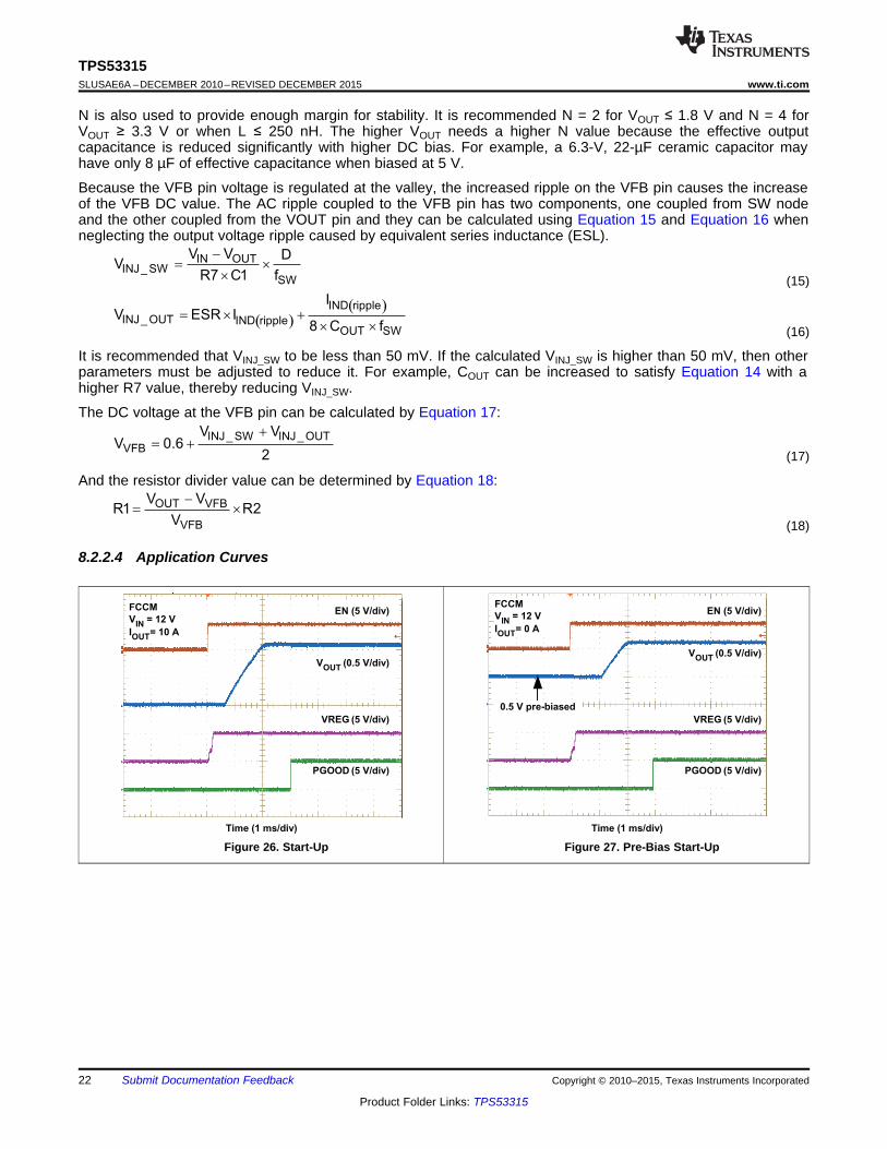
Figure 23. Start-Up Figure 24. Pre-Bias Start-Up
Copyright © 2010–2015, Texas Instruments Incorporated Submit Documentation Feedback 19
Product Folder Links: TPS53315

N/C
N/C
TRIP
EN
PG
OO
D
N/C
VB
ST
N/C LL
LL
LL
LL
LL
LL
LL
LL
VFB
RF
MODE
VDD
TPS53315
GN
D1
PG
ND
VR
EG
GN
D2
PG
ND
PG
ND
PG
ND
PG
ND
PG
ND
PG
ND
VIN
VIN
LL
LL
LL
LL
LL
VIN
VIN
VIN
1 2 3 4 5 6 7 8 9 10 11 12
20
19
18
17
16
15
14
13
32 31 30 29 28 27 26 25 24 23 22 21
33
34
35
36
37
38
39
40
L1
1 mH
IN06155
COUT
100 mF
Ceramic
CIN
22 mF x 4
EN
VOUT
VIN
3 V to 15 V
C3
1 mFC4
1 mF
VDD
4.5 V to 25 V
R5
100 kW
R4
NI
R8
80.6 kW
R2
10 kW
PGOOD
VREG
PGOOD
R1
8.06 kW
R7
1.5 kW
C2 1 nF
C1
0.1 mF
COUT
100 mF
Ceramic
R12
0 W
C5
0.1 mF
R9 0 WR10 100 kW
TPS53315SLUSAE6A –DECEMBER 2010–REVISED DECEMBER 2015 www.ti.com
8.2.2 Typical Application Circuit Diagram With Ceramic Output Capacitors
Figure 25. Typical Application Circuit Diagram with Ceramic Output Capacitors
8.2.2.1 Design RequirementsTable 4 lists the design requirements for the typical application with ceramic output capacitors.
Table 4. Design ParametersPARAMETER TEST CONDITIONS MIN TYP MAX UNIT
INPUT CHARACTERISTICSVIN Voltage range 8 12 14 V
Maximum Input current VIN = 8 V, IOUT = 12 A 1.4 AIMAX No load input current VIN = 14 V, IOUT = 0 A with auto-skip mode 1 mAOUTPUT CHARACTERISTICS
Output voltage 1.5 VLine regulation, 8 V ≤ VIN ≤ 15 V 0.1%VOUT Output voltage regulation Load regulation, VIN = 12 V, 0 A ≤ IOUT ≤ 12 0.2%A with FCCM
VRIPPLE Output voltage ripple VIN = 12 V, IOUT = 12 A with FCCM 20 mVPP
ILOAD Output load current 0 12 AOutput overcurrentIOCP 15 Athreshold
tSS Soft-start time 1.4 msSYSTEMS CHARACTERISTICSfSW Switching frequency 500 kHz
Peak efficiency VIN = 12 V, VOUT = 1.1 V, IOUT = 6 A 85.07%η
Full load efficiency VIN = 12 V, VOUT = 1.1 V, IOUT = 12 A 80.23%TA Operating temperature 25 °C
20 Submit Documentation Feedback Copyright © 2010–2015, Texas Instruments Incorporated
Product Folder Links: TPS53315

´
> ´
´
OUT ONL C tN
R7 C1 2
( ) ( )IN OUT OUTOCP DS(on)
SW INTRIP
TRIP
V V V1I 8 R m
2 L f VR (k )
I ( A)
æ ö- ´æ ö- ´ ´ ´ Wç ÷ç ÷ç ÷´ ´è øè øW =
m
( )( )
( )( )( )
- ´= + ´
´ ´
IN OUT OUTmaxTRIP
IND peakSW INDS on max
V V VV 1I
8 R L f V
( )
( )( )( ) ( )
( )( )- ´ - ´= ´ = ´
´ ´
IN OUT OUT IN OUT OUTmax max
SW IN OUT SW IN(max)IND ripple max max
V V V V V V1 3
LI f V I f V
TPS53315www.ti.com SLUSAE6A –DECEMBER 2010–REVISED DECEMBER 2015
8.2.2.2 Detailed Design ProcedureRefer to the External Component Selection When Using All Ceramic Output Capacitors section for guidelines forthis design with all ceramic output capacitors.
The external components selection is a simple process when using organic semiconductors or special polymeroutput capacitors.
8.2.2.2.1 Step 1: Select Operation Mode and Soft-Start Time
Select operation mode and soft-start time using Table 2.
8.2.2.2.2 Step 2: Select Switching Frequency
Select the switching frequency from 250 kHz to 1 MHz using Table 1.
8.2.2.2.3 Step 3: Select the Inductance
The inductance value should be determined to give the ripple current of approximately 1/4 to 1/2 of maximumoutput current. Larger ripple current increases output ripple voltage and improves signal-to-noise ratio and helpsensure stable operation, but increases inductor core loss. Using 1/3 ripple current to maximum output currentratio, the inductance can be determined by Equation 6.
The inductor requires a low DCR to achieve good efficiency. It also requires enough room above peak inductorcurrent before saturation. The peak inductor current can be estimated in Equation 7.
(11)
(12)
8.2.2.2.4 Step 4: Select Output Capacitance for Ceramic Capacitors
Refer to the External Component Selection When Using All Ceramic Output Capacitors section to select externalcomponents because ceramic output capacitors are used in this design.
8.2.2.2.5 Step 5: Select the Overcurrent Setting Resistance (RTRIP)
where• ITRIP is the TRIP pin sourcing current (10 µA)• RDS(on) is the thermally compensated on-time resistance value of the low-side MOSFET which is 7 mΩ (13)
8.2.2.3 External Component Selection When Using All Ceramic Output CapacitorsWhen a ceramic output capacitor is used, the stability criteria in Equation 2 cannot be satisfied. The rippleinjection approach as shown in Figure 25 is implemented to increase the ripple on the VFB pin and make thesystem stable. In addition to the selections made using Step 1: Select Operation Mode and Soft-Start Timethrough Step 5: Select the Overcurrent Setting Resistance (RTRIP), use the information in the ExternalComponent Selection When Using All Ceramic Output Capacitors section to select the ripple injectioncomponents. The C2 value can be fixed at 1 nF. Select a value for C1 between 10 nF and 200 nF.
where• N is the coefficient to account for L and COUT variation. (14)
Copyright © 2010–2015, Texas Instruments Incorporated Submit Documentation Feedback 21
Product Folder Links: TPS53315
Time (1 ms/div)
FCCM
VIN
= 12 V
IOUT
= 10 A
EN (5 V/div)
VOUT
(0.5 V/div)
VREG (5 V/div)
PGOOD (5 V/div)
Time (1 ms/div)
FCCM
VIN
= 12 V
IOUT
= 0 A
EN (5 V/div)
VOUT
(0.5 V/div)
VREG (5 V/div)
PGOOD (5 V/div)
0.5 V pre-biased
-
= ´OUT VFB
VFB
V VR1 R2
V
+
= +INJ_ SW INJ_ OUT
VFB
V VV 0.6
2
( )( )
= ´ +´ ´
IND ripple
INJ_ OUT IND rippleOUT SW
IV ESR I
8 C f
-
= ´
´
IN OUTINJ_ SW
SW
V V DV
R7 C1 f
TPS53315SLUSAE6A –DECEMBER 2010–REVISED DECEMBER 2015 www.ti.com
N is also used to provide enough margin for stability. It is recommended N = 2 for VOUT ≤ 1.8 V and N = 4 forVOUT ≥ 3.3 V or when L ≤ 250 nH. The higher VOUT needs a higher N value because the effective outputcapacitance is reduced significantly with higher DC bias. For example, a 6.3-V, 22-µF ceramic capacitor mayhave only 8 µF of effective capacitance when biased at 5 V.
Because the VFB pin voltage is regulated at the valley, the increased ripple on the VFB pin causes the increaseof the VFB DC value. The AC ripple coupled to the VFB pin has two components, one coupled from SW nodeand the other coupled from the VOUT pin and they can be calculated using Equation 15 and Equation 16 whenneglecting the output voltage ripple caused by equivalent series inductance (ESL).
(15)
(16)
It is recommended that VINJ_SW to be less than 50 mV. If the calculated VINJ_SW is higher than 50 mV, then otherparameters must be adjusted to reduce it. For example, COUT can be increased to satisfy Equation 14 with ahigher R7 value, thereby reducing VINJ_SW.
The DC voltage at the VFB pin can be calculated by Equation 17:
(17)
And the resistor divider value can be determined by Equation 18:
(18)
8.2.2.4 Application Curves
Figure 26. Start-Up Figure 27. Pre-Bias Start-Up
22 Submit Documentation Feedback Copyright © 2010–2015, Texas Instruments Incorporated
Product Folder Links: TPS53315

Time (100 µs/div)
Skip Mode
VIN
= 12 V
VOUT
= 1.1 V
LL (5 V/div)
VOUT
(20 mV/div)
IL
(2 A/div)
Time (100 µs/div)
Skip Mode
VIN
= 12 V
VOUT
= 1.1 V LL (5 V/div)
VOUT
(20 mV/div)
IL
(2 A/div)
Skip Mode
VIN
= 12 V
IOUT
= 0 A
Time (1 µs/div)
VOUT
(20 mV/div)
IL
(2 A/div)
LL (5 V/div)
FCCM
VIN
= 12 V
IOUT
= 0 A
LL (5 V/div)
VOUT
(20 mV/div)
IL
(2 A/div)
Time (2 µs/div)
VIN
(5 V/div)
VOUT
(0.5 V/div)
VREG (5 V/div)
PGOOD (5 V/div)
FCCM
VEN
= 5 V
IOUT
= 10 A
VDD
= VIN
Time (2 ms/div)
EN (5 V/div)
VOUT
(0.5 V/div)
VREG (5 V/div)
PGOOD (5 V/div)
FCCM
VIN
= 12 V
IOUT
= 10 A
Time (4 ms/div)
TPS53315www.ti.com SLUSAE6A –DECEMBER 2010–REVISED DECEMBER 2015
Figure 28. Turn-Off Figure 29. UVLO Start-Up
Figure 30. 1.1-V Output FCCM Steady-State Operation Figure 31. 1.1-V Output Skip Mode Steady-State Operation
Figure 32. CCM to DCM Transition Figure 33. DCM to CCM Transition
Copyright © 2010–2015, Texas Instruments Incorporated Submit Documentation Feedback 23
Product Folder Links: TPS53315

VIN
= 12 V
IOUT
from 10 A to 15 A
Time (10 ms/div)
VOUT
(1 V/div)
IL
(10 A/div)
LL (10 V/div)
PGOOD (5 V/div)
VIN
= 12 V
IOUT
= 10 A
Time (1 s/div)
VOUT
(1 V/div)
EN (5 V/div)
PGOOD (5 V/div)
FCCM
VIN
= 12 V
VOUT
= 1.1 V
IOUT
from 0 A to 5 A, 2.5A/µs
Time (2 µs/div)
VOUT
(20 mV/div)
IOUT
(5 A/div)
Skip Mode
VIN
= 12 V
VOUT
= 1.1 V
IOUT
from 0 A to 5 A, 2.5A/µs
Time (100 µs/div)
VOUT
(20 mV/div)
IOUT
(5 A/div)
TPS53315SLUSAE6A –DECEMBER 2010–REVISED DECEMBER 2015 www.ti.com
Figure 34. FCCM Load Transient Figure 35. Skip Mode Load Transient
Figure 36. Overcurrent Protection Figure 37. Over-temperature Protection
9 Power Supply RecommendationsThe device is designed to operate from an input voltage supply range between 3 V and 15 V (4.5-V to 25-Vbiased). This input supply must be well regulated. Proper bypassing of input supplies and internal regulators isalso critical for noise performance, as is PCB layout and grounding scheme. See the recommendations in theLayout section.
24 Submit Documentation Feedback Copyright © 2010–2015, Texas Instruments Incorporated
Product Folder Links: TPS53315

TPS53315www.ti.com SLUSAE6A –DECEMBER 2010–REVISED DECEMBER 2015
10 Layout
10.1 Layout GuidelinesCertain points must be considered before starting a layout work using the TPS53315.• The power components (including input/output capacitors, inductor and TPS53315) should be placed on one
side of the PCB (solder side). Other small signal components should be placed on another side (componentside). At least one inner plane should be inserted, connected to ground, in order to shield and isolate thesmall signal traces from noisy power lines.
• All sensitive analog traces and components such as VFB, PGOOD, TRIP, MODE and RF should be placedaway from high-voltage switching nodes such as LL, VBST to avoid coupling. Use internal layer(s) as groundplane(s) and shield feedback trace from power traces and components.
• Place the VIN decoupling capacitors as close to the VIN and PGND pins as possible to minimize the input ACcurrent loop.
• Since the TPS53315 controls output voltage referring to voltage across the VOUT capacitor, the top-sideresistor of the voltage divider should be connected to the positive node of VOUT capacitor. In a same mannerboth bottom side resistor and GND pad of the device should be connected to the negative node of VOUTcapacitor. The trace from these resistors to the VFB pin should be short and thin. Place on the componentside and avoid via(s) between these resistors and the device.
• Connect the overcurrent setting resistors from TRIP pin to ground and make the connections as close aspossible to the device. The trace from TRIP pin to resistor and from resistor to ground should avoid couplingto a high-voltage switching node.
• Connect the frequency setting resistor from RF pin to ground, or to the VREG pin, and make the connectionsas close as possible to the device. The trace from the RF pin to the resistor and from the resistor to groundshould avoid coupling to a high-voltage switching node.
• Connect the MODE setting resistor from MODE pin to ground, or to the PGOOD pin, and make theconnections as close as possible to the device. The trace from the MODE pin to the resistor and from theresistor to ground should avoid coupling to a high-voltage switching node.
• The PCB trace defined as switch node, which connects the LL pins and high-voltage side of the inductor,should be as short and wide as possible.
Copyright © 2010–2015, Texas Instruments Incorporated Submit Documentation Feedback 25
Product Folder Links: TPS53315

GND shape
Keep VFB trace short and
away from noisy signals
Vin shape
Vout shape
LL shape
TRIP
VREG
PGOOD
VDD
VFB
GND
Bottom side
components and trace
VBST
VREG
GND
GND
EN
GND shape
TPS53315SLUSAE6A –DECEMBER 2010–REVISED DECEMBER 2015 www.ti.com
10.2 Layout Example
Figure 38. Layout Recommendation
10.3 Thermal ConsiderationsFigure 39 shows the thermal signature of the TPS53315 EVM at a switching frequency of 500 kHz. Figure 40shows the thermal signature of the TPS53315 EVM at a switching frequency of 650 kHz
VIN = 12 V VOUT = 1.1 V VIN = 12 V VOUT = 3.3 VfSW = 500 kHz TA = 25°C with no airflow fSW = 650 kHz TA = 25°C with no airflowIOUT= 12 A IOUT= 12 A
Figure 39. Thermal Signature of TPS53315 EVM Figure 40. Thermal Signature of TPS53315 EVM
26 Submit Documentation Feedback Copyright © 2010–2015, Texas Instruments Incorporated
Product Folder Links: TPS53315

TPS53315www.ti.com SLUSAE6A –DECEMBER 2010–REVISED DECEMBER 2015
11 Device and Documentation Support
11.1 Community ResourcesThe following links connect to TI community resources. Linked contents are provided "AS IS" by the respectivecontributors. They do not constitute TI specifications and do not necessarily reflect TI's views; see TI's Terms ofUse.
TI E2E™ Online Community TI's Engineer-to-Engineer (E2E) Community. Created to foster collaborationamong engineers. At e2e.ti.com, you can ask questions, share knowledge, explore ideas and helpsolve problems with fellow engineers.
Design Support TI's Design Support Quickly find helpful E2E forums along with design support tools andcontact information for technical support.
11.2 TrademarksEco-mode, D-CAP, E2E are trademarks of Texas Instruments.All other trademarks are the property of their respective owners.
11.3 Electrostatic Discharge CautionThese devices have limited built-in ESD protection. The leads should be shorted together or the device placed in conductive foamduring storage or handling to prevent electrostatic damage to the MOS gates.
11.4 GlossarySLYZ022 — TI Glossary.
This glossary lists and explains terms, acronyms, and definitions.
12 Mechanical, Packaging, and Orderable InformationThe following pages include mechanical, packaging, and orderable information. This information is the mostcurrent data available for the designated devices. This data is subject to change without notice and revision ofthis document. For browser-based versions of this data sheet, refer to the left-hand navigation.
Copyright © 2010–2015, Texas Instruments Incorporated Submit Documentation Feedback 27
Product Folder Links: TPS53315

PACKAGE OPTION ADDENDUM
www.ti.com 31-Dec-2013
Addendum-Page 1
PACKAGING INFORMATION
Orderable Device Status(1)
Package Type PackageDrawing
Pins PackageQty
Eco Plan(2)
Lead/Ball Finish(6)
MSL Peak Temp(3)
Op Temp (°C) Device Marking(4/5)
Samples
TPS53315RGFR ACTIVE VQFN RGF 40 3000 Green (RoHS& no Sb/Br)
CU NIPDAU Level-2-260C-1 YEAR -40 to 85 TPS53315
TPS53315RGFT ACTIVE VQFN RGF 40 250 Green (RoHS& no Sb/Br)
CU NIPDAU Level-2-260C-1 YEAR -40 to 85 TPS53315
(1) The marketing status values are defined as follows:ACTIVE: Product device recommended for new designs.LIFEBUY: TI has announced that the device will be discontinued, and a lifetime-buy period is in effect.NRND: Not recommended for new designs. Device is in production to support existing customers, but TI does not recommend using this part in a new design.PREVIEW: Device has been announced but is not in production. Samples may or may not be available.OBSOLETE: TI has discontinued the production of the device.
(2) Eco Plan - The planned eco-friendly classification: Pb-Free (RoHS), Pb-Free (RoHS Exempt), or Green (RoHS & no Sb/Br) - please check http://www.ti.com/productcontent for the latest availabilityinformation and additional product content details.TBD: The Pb-Free/Green conversion plan has not been defined.Pb-Free (RoHS): TI's terms "Lead-Free" or "Pb-Free" mean semiconductor products that are compatible with the current RoHS requirements for all 6 substances, including the requirement thatlead not exceed 0.1% by weight in homogeneous materials. Where designed to be soldered at high temperatures, TI Pb-Free products are suitable for use in specified lead-free processes.Pb-Free (RoHS Exempt): This component has a RoHS exemption for either 1) lead-based flip-chip solder bumps used between the die and package, or 2) lead-based die adhesive used betweenthe die and leadframe. The component is otherwise considered Pb-Free (RoHS compatible) as defined above.Green (RoHS & no Sb/Br): TI defines "Green" to mean Pb-Free (RoHS compatible), and free of Bromine (Br) and Antimony (Sb) based flame retardants (Br or Sb do not exceed 0.1% by weightin homogeneous material)
(3) MSL, Peak Temp. - The Moisture Sensitivity Level rating according to the JEDEC industry standard classifications, and peak solder temperature.
(4) There may be additional marking, which relates to the logo, the lot trace code information, or the environmental category on the device.
(5) Multiple Device Markings will be inside parentheses. Only one Device Marking contained in parentheses and separated by a "~" will appear on a device. If a line is indented then it is a continuationof the previous line and the two combined represent the entire Device Marking for that device.
(6) Lead/Ball Finish - Orderable Devices may have multiple material finish options. Finish options are separated by a vertical ruled line. Lead/Ball Finish values may wrap to two lines if the finishvalue exceeds the maximum column width.
Important Information and Disclaimer:The information provided on this page represents TI's knowledge and belief as of the date that it is provided. TI bases its knowledge and belief on informationprovided by third parties, and makes no representation or warranty as to the accuracy of such information. Efforts are underway to better integrate information from third parties. TI has taken andcontinues to take reasonable steps to provide representative and accurate information but may not have conducted destructive testing or chemical analysis on incoming materials and chemicals.TI and TI suppliers consider certain information to be proprietary, and thus CAS numbers and other limited information may not be available for release.

PACKAGE OPTION ADDENDUM
www.ti.com 31-Dec-2013
Addendum-Page 2
In no event shall TI's liability arising out of such information exceed the total purchase price of the TI part(s) at issue in this document sold by TI to Customer on an annual basis.

TAPE AND REEL INFORMATION
*All dimensions are nominal
Device PackageType
PackageDrawing
Pins SPQ ReelDiameter
(mm)
ReelWidth
W1 (mm)
A0(mm)
B0(mm)
K0(mm)
P1(mm)
W(mm)
Pin1Quadrant
TPS53315RGFR VQFN RGF 40 3000 330.0 16.4 5.25 7.25 1.45 8.0 16.0 Q1
TPS53315RGFT VQFN RGF 40 250 180.0 16.4 5.25 7.25 1.45 8.0 16.0 Q1
PACKAGE MATERIALS INFORMATION
www.ti.com 31-Dec-2013
Pack Materials-Page 1

*All dimensions are nominal
Device Package Type Package Drawing Pins SPQ Length (mm) Width (mm) Height (mm)
TPS53315RGFR VQFN RGF 40 3000 367.0 367.0 38.0
TPS53315RGFT VQFN RGF 40 250 210.0 185.0 35.0
PACKAGE MATERIALS INFORMATION
www.ti.com 31-Dec-2013
Pack Materials-Page 2

IMPORTANT NOTICE
Texas Instruments Incorporated and its subsidiaries (TI) reserve the right to make corrections, enhancements, improvements and otherchanges to its semiconductor products and services per JESD46, latest issue, and to discontinue any product or service per JESD48, latestissue. Buyers should obtain the latest relevant information before placing orders and should verify that such information is current andcomplete. All semiconductor products (also referred to herein as “components”) are sold subject to TI’s terms and conditions of salesupplied at the time of order acknowledgment.TI warrants performance of its components to the specifications applicable at the time of sale, in accordance with the warranty in TI’s termsand conditions of sale of semiconductor products. Testing and other quality control techniques are used to the extent TI deems necessaryto support this warranty. Except where mandated by applicable law, testing of all parameters of each component is not necessarilyperformed.TI assumes no liability for applications assistance or the design of Buyers’ products. Buyers are responsible for their products andapplications using TI components. To minimize the risks associated with Buyers’ products and applications, Buyers should provideadequate design and operating safeguards.TI does not warrant or represent that any license, either express or implied, is granted under any patent right, copyright, mask work right, orother intellectual property right relating to any combination, machine, or process in which TI components or services are used. Informationpublished by TI regarding third-party products or services does not constitute a license to use such products or services or a warranty orendorsement thereof. Use of such information may require a license from a third party under the patents or other intellectual property of thethird party, or a license from TI under the patents or other intellectual property of TI.Reproduction of significant portions of TI information in TI data books or data sheets is permissible only if reproduction is without alterationand is accompanied by all associated warranties, conditions, limitations, and notices. TI is not responsible or liable for such altereddocumentation. Information of third parties may be subject to additional restrictions.Resale of TI components or services with statements different from or beyond the parameters stated by TI for that component or servicevoids all express and any implied warranties for the associated TI component or service and is an unfair and deceptive business practice.TI is not responsible or liable for any such statements.Buyer acknowledges and agrees that it is solely responsible for compliance with all legal, regulatory and safety-related requirementsconcerning its products, and any use of TI components in its applications, notwithstanding any applications-related information or supportthat may be provided by TI. Buyer represents and agrees that it has all the necessary expertise to create and implement safeguards whichanticipate dangerous consequences of failures, monitor failures and their consequences, lessen the likelihood of failures that might causeharm and take appropriate remedial actions. Buyer will fully indemnify TI and its representatives against any damages arising out of the useof any TI components in safety-critical applications.In some cases, TI components may be promoted specifically to facilitate safety-related applications. With such components, TI’s goal is tohelp enable customers to design and create their own end-product solutions that meet applicable functional safety standards andrequirements. Nonetheless, such components are subject to these terms.No TI components are authorized for use in FDA Class III (or similar life-critical medical equipment) unless authorized officers of the partieshave executed a special agreement specifically governing such use.Only those TI components which TI has specifically designated as military grade or “enhanced plastic” are designed and intended for use inmilitary/aerospace applications or environments. Buyer acknowledges and agrees that any military or aerospace use of TI componentswhich have not been so designated is solely at the Buyer's risk, and that Buyer is solely responsible for compliance with all legal andregulatory requirements in connection with such use.TI has specifically designated certain components as meeting ISO/TS16949 requirements, mainly for automotive use. In any case of use ofnon-designated products, TI will not be responsible for any failure to meet ISO/TS16949.
Products ApplicationsAudio www.ti.com/audio Automotive and Transportation www.ti.com/automotiveAmplifiers amplifier.ti.com Communications and Telecom www.ti.com/communicationsData Converters dataconverter.ti.com Computers and Peripherals www.ti.com/computersDLP® Products www.dlp.com Consumer Electronics www.ti.com/consumer-appsDSP dsp.ti.com Energy and Lighting www.ti.com/energyClocks and Timers www.ti.com/clocks Industrial www.ti.com/industrialInterface interface.ti.com Medical www.ti.com/medicalLogic logic.ti.com Security www.ti.com/securityPower Mgmt power.ti.com Space, Avionics and Defense www.ti.com/space-avionics-defenseMicrocontrollers microcontroller.ti.com Video and Imaging www.ti.com/videoRFID www.ti-rfid.comOMAP Applications Processors www.ti.com/omap TI E2E Community e2e.ti.comWireless Connectivity www.ti.com/wirelessconnectivity
Mailing Address: Texas Instruments, Post Office Box 655303, Dallas, Texas 75265Copyright © 2015, Texas Instruments Incorporated


![i %LL-,! LL> @ cD LL LL¡_chatka_2017… · nu @= nudd]cc@u ( @f nufc@adda cc u@ @] u@@@cccuc ( a< @< a](https://static.fdocuments.net/doc/165x107/5f0d70e67e708231d43a5ed4/i-ll-ll-cd-ll-ll-chatka2017-nu-nuddccu-f-nufcadda-cc-u.jpg)