TPS50601-SP 1.6-V to 6.3-V Input, 6-A Synchronous … Radiation Hardened 1.6- to 6.3-V Input, 6-A...
40
0.00 0.05 0.10 0.15 0.20 0.25 0.30 0.35 0.40 0.45 0.50 0.55 0.60 0.65 0.70 0.75 0.80 0.85 0.90 0.95 1.00 0.00 1.00 2.00 3.00 4.00 5.00 6.00 Efficiency (p.u.) IL- Load Current (A) Vo = 3.3 V Vo = 1.2 V Product Folder Sample & Buy Technical Documents Tools & Software Support & Community Reference Design TPS50601-SP SLVSD45 – DECEMBER 2015 TPS50601-SP Radiation Hardened 1.6- to 6.3-V Input, 6-A Synchronous Buck Converter 1 Features 2 Applications 1• 5962R10221: • Space Satellite Point of Load Supply for FPGAs, Microcontrollers, and ASICs – Radiation Hardness Assurance (RHA) up to • Space Satellite Payloads TID 100 krad (Si) • Radiation-Tolerant Applications – ELDRS Free 100 krad (Si) – 10 mRAD(Si)/s • Available in Military (–55°C to 125°C) – Single Event Latchup (SEL) Immune to Temperature Range LET = 85 MeV-cm 2 /mg (See Radiation Report) • Engineering Evaluation (/EM) Samples are – SEB and SEGR Immune to 85 MeV-cm 2 /mg, Available (1) SOA Curve Available (See Radiation Report) – SET/SEFI Cross-Section Plot Available (See 3 Description Radiation Report) The TPS50601-SP is a radiation hardened, 6.3-V, 6- • Peak Efficiency: 95% (V O = 3.3 V) A synchronous step-down converter, which is • Integrated 55-mΩ/50-mΩ MOSFETs optimized for small designs through high efficiency • Split Power Rail: 1.6 to 6.3 V on PVIN and integrating the high-side and low-side MOSFETs. Further space savings are achieved through current • Power Rail: 3 to 6.3 V on VIN mode control, which reduces component count, and a • 6-A Maximum Output Current high switching frequency, reducing the inductor's • Flexible Switching Frequency Options: footprint. The devices are offered in a thermally enhanced 20-pin ceramic, dual in-line flatpack – 100-kHz to 1-MHz Adjustable Internal package. Oscillator – External Sync Capability: 100 kHz to 1 MHz Device Information (2) – Sync Pin can be Configured as a 500-kHz PART NUMBER PACKAGE BODY SIZE (NOM) Output for Master/Slave Applications CFP (20) 7.38 × 12.70 mm TPS50601-SP • 0.795-V ±1.258% Voltage Reference at 25°C KGD (3) N/A (4) • Monotonic Start-Up into Prebiased Outputs (1) These units are intended for engineering evaluation only. • Adjustable Soft Start Through External Capacitor They are processed to a non-compliant flow (that is no burn- in, and so forth) and are tested to temperature rating of 25°C • Input Enable and Power-Good Output for Power only. These units are not suitable for qualification, production, Sequencing radiation testing or flight use. Parts are not warranted for performance on full MIL specified temperature range of –55°C • Power Good Output Monitor for Undervoltage and to 125°C or operating life. Overvoltage (2) For all available packages, see the orderable addendum at the end of the data sheet. • Adjustable Input Undervoltage Lockout (UVLO) (3) Known good die • 20-Pin Thermally-Enhanced Ceramic Flatpack (4) Bare die in waffle pack Package (HKH) SPACE • See www.ti.com/swift for SWIFT™ Documentation • See the Tools & Software Tab SPACE Efficiency vs Load Current, Vin = 5 V 1 An IMPORTANT NOTICE at the end of this data sheet addresses availability, warranty, changes, use in safety-critical applications, intellectual property matters and other important disclaimers. PRODUCTION DATA.
Transcript of TPS50601-SP 1.6-V to 6.3-V Input, 6-A Synchronous … Radiation Hardened 1.6- to 6.3-V Input, 6-A...

0.00
0.05
0.10
0.15
0.20
0.25
0.30
0.35
0.40
0.45
0.50
0.55
0.60
0.65
0.70
0.75
0.80
0.85
0.90
0.95
1.00
0.00 1.00 2.00 3.00 4.00 5.00 6.00
Eff
icie
ncy
(p
.u.)
IL- Load Current (A)
Vo = 3.3 V
Vo = 1.2 V
Product
Folder
Sample &Buy
Technical
Documents
Tools &
Software
Support &Community
ReferenceDesign
TPS50601-SPSLVSD45 –DECEMBER 2015
TPS50601-SP Radiation Hardened 1.6- to 6.3-V Input, 6-A Synchronous Buck Converter1 Features 2 Applications1• 5962R10221: • Space Satellite Point of Load Supply for FPGAs,
Microcontrollers, and ASICs– Radiation Hardness Assurance (RHA) up to• Space Satellite PayloadsTID 100 krad (Si)• Radiation-Tolerant Applications– ELDRS Free 100 krad (Si) – 10 mRAD(Si)/s• Available in Military (–55°C to 125°C)– Single Event Latchup (SEL) Immune to
Temperature RangeLET = 85 MeV-cm2/mg (See Radiation Report)• Engineering Evaluation (/EM) Samples are– SEB and SEGR Immune to 85 MeV-cm2/mg,
Available(1)SOA Curve Available (See Radiation Report)– SET/SEFI Cross-Section Plot Available (See
3 DescriptionRadiation Report)The TPS50601-SP is a radiation hardened, 6.3-V, 6-• Peak Efficiency: 95% (VO = 3.3 V)A synchronous step-down converter, which is
• Integrated 55-mΩ/50-mΩ MOSFETs optimized for small designs through high efficiency• Split Power Rail: 1.6 to 6.3 V on PVIN and integrating the high-side and low-side MOSFETs.
Further space savings are achieved through current• Power Rail: 3 to 6.3 V on VINmode control, which reduces component count, and a• 6-A Maximum Output Current high switching frequency, reducing the inductor's
• Flexible Switching Frequency Options: footprint. The devices are offered in a thermallyenhanced 20-pin ceramic, dual in-line flatpack– 100-kHz to 1-MHz Adjustable Internalpackage.Oscillator
– External Sync Capability: 100 kHz to 1 MHz Device Information(2)
– Sync Pin can be Configured as a 500-kHz PART NUMBER PACKAGE BODY SIZE (NOM)Output for Master/Slave Applications CFP (20) 7.38 × 12.70 mm
TPS50601-SP• 0.795-V ±1.258% Voltage Reference at 25°C KGD(3) N/A(4)
• Monotonic Start-Up into Prebiased Outputs (1) These units are intended for engineering evaluation only.• Adjustable Soft Start Through External Capacitor They are processed to a non-compliant flow (that is no burn-
in, and so forth) and are tested to temperature rating of 25°C• Input Enable and Power-Good Output for Power only. These units are not suitable for qualification, production,Sequencing radiation testing or flight use. Parts are not warranted for
performance on full MIL specified temperature range of –55°C• Power Good Output Monitor for Undervoltage and to 125°C or operating life.Overvoltage (2) For all available packages, see the orderable addendum at
the end of the data sheet.• Adjustable Input Undervoltage Lockout (UVLO)(3) Known good die• 20-Pin Thermally-Enhanced Ceramic Flatpack(4) Bare die in waffle packPackage (HKH)
SPACE• See www.ti.com/swift for SWIFT™ Documentation• See the Tools & Software Tab SPACE
Efficiency vs Load Current, Vin = 5 V
1
An IMPORTANT NOTICE at the end of this data sheet addresses availability, warranty, changes, use in safety-critical applications,intellectual property matters and other important disclaimers. PRODUCTION DATA.

TPS50601-SPSLVSD45 –DECEMBER 2015 www.ti.com
Table of Contents8.3 Feature Description................................................. 151 Features .................................................................. 18.4 Device Functional Modes........................................ 272 Applications ........................................................... 1
9 Application and Implementation ........................ 283 Description ............................................................. 19.1 Application Information............................................ 284 Revision History..................................................... 29.2 Typical Application ................................................. 285 Description (continued)......................................... 3
10 Power Supply Recommendations ..................... 346 Pin Configuration and Functions ......................... 311 Layout................................................................... 347 Specifications......................................................... 7
11.1 Layout Guidelines ................................................. 347.1 Absolute Maximum Ratings ...................................... 711.2 Layout Example .................................................... 357.2 ESD Ratings.............................................................. 7
12 Device and Documentation Support ................. 367.3 Recommended Operating Conditions....................... 712.1 Documentation Support ........................................ 367.4 Thermal Information .................................................. 812.2 Community Resources.......................................... 367.5 Electrical Characteristics........................................... 812.3 Trademarks ........................................................... 367.6 Dissipation Ratings ................................................. 1012.4 Electrostatic Discharge Caution............................ 367.7 Typical Characteristics ............................................ 1112.5 Glossary ................................................................ 368 Detailed Description ............................................ 14
13 Mechanical, Packaging, and Orderable8.1 Overview ................................................................. 14Information ........................................................... 368.2 Functional Block Diagram ....................................... 1513.1 Device Nomenclature............................................ 36
4 Revision History
DATE REVISION NOTES
Initial release.• Created separate data sheet for this partDecember 2015 * number• Removed the ψJT thermal metric
2 Submit Documentation Feedback Copyright © 2015, Texas Instruments Incorporated
Product Folder Links: TPS50601-SP

Thermal Pad
(Bottom Side)21
GND
EN
RT
SYNC
VIN
PVIN
PVIN
PGND
PGND
PGND PH
PH
PH
PH
PH
BOOT
VSENSE
COMP
SS/TR
PWRGD1
2
3
4
5
6
7
8
9
10 11
12
13
14
15
16
17
18
19
20
TPS50601-SPwww.ti.com SLVSD45 –DECEMBER 2015
5 Description (continued)The output voltage startup ramp is controlled by the SS/TR pin which allows operation as either a stand alonepower supply or in tracking situations. Power sequencing is also possible by correctly configuring the enable andthe open drain power good pins.
Cycle-by-cycle current limiting on the high-side FET protects the device in overload situations and is enhancedby a low-side sourcing current limit which prevents current runaway. There is also a low-side sinking current limitwhich turns off the low-side MOSFET to prevent excessive reverse current. Thermal shutdown disables the partwhen die temperature exceeds thermal shutdown temperature.
6 Pin Configuration and Functions
HKH Package20-Pin CFP
Bottom View
Pin FunctionsPIN
DESCRIPTIONNO. NAME
1 GND Return for control circuitry/thermal pad (1)
EN pin has an internal pullup thus EN pin can be floated to enable the device. As an option external pullup can also2 EN be added if desired. Adjust the input undervoltage lockout (UVLO) with two resistors.3 RT In internal oscillation mode, a resistor is connected between the RT pin and GND to set the switching frequency.4 SYNC Optional 1-MHz external system clock input. The device operates with an internal oscillator if this pin is left open.5 VIN Supplies the power to the output FET controllers6
PVIN Power input. Supplies the power switches of the power converter789 PGND Return for low-side power MOSFET10
(1) Thermal pad (analog ground) must be connected to PGND external to the package.
Copyright © 2015, Texas Instruments Incorporated Submit Documentation Feedback 3
Product Folder Links: TPS50601-SP

TPS50601-SPSLVSD45 –DECEMBER 2015 www.ti.com
Pin Functions (continued)PIN
DESCRIPTIONNO. NAME111213 PH Switch node1415
A bootstrap capacitor is required between BOOT and PH. The voltage on this capacitor carries the gate drive voltage16 BOOT for the high-side MOSFET.17 VSENSE Inverting input of the gm error amplifier18 COMP Error amplifier output and input to the output switch current comparator. Connect frequency compensation to this pin.
Slow-start and tracking. An external capacitor connected to this pin sets the internal voltage reference rise time. The19 SS/TR voltage on this pin overrides the internal reference. It can be used for tracking and sequencing.Power Good fault pin is an open-drain connection. Power Good fault pin. Asserts low if output voltage is low due to20 PWRGD thermal shutdown, dropout, overvoltage, or EN shutdown, or during slow start.
Bare Die InformationBACKSIDE BOND PAD METALLIZATIONDIE THICKNESS BACKSIDE FINISH BOND PAD THICKNESSPOTENTIAL COMPOSITION
15 mils. Silicon with backgrind Ground Al5TiN 557.5 nm
4 Submit Documentation Feedback Copyright © 2015, Texas Instruments Incorporated
Product Folder Links: TPS50601-SP

TPS50601-SPwww.ti.com SLVSD45 –DECEMBER 2015
Copyright © 2015, Texas Instruments Incorporated Submit Documentation Feedback 5
Product Folder Links: TPS50601-SP

TPS50601-SPSLVSD45 –DECEMBER 2015 www.ti.com
Bond Pad Coordinates in MicronsDESCRIPTION PAD NUMBER X MIN Y MIN X MAX Y MAX
GND 1 400.77 5039.325 578.07 5216.625EN 2 44.19 4169.79 221.49 4347.09RT 3 44.19 3894.21 221.49 4071.51
SYNC 4 44.19 3618.63 221.49 3795.93VIN 5 47.565 2952.27 224.865 3129.57
PVIN 6 280.215 2414.115 457.515 2591.415PVIN 7 280.215 2170.665 457.515 2347.965PVIN 8 280.215 1928.115 457.515 2105.415PVIN 9 280.215 1684.665 457.515 1861.965
PGND 10 254.52 1236.285 431.82 1413.585PGND 11 254.52 1008.315 431.82 1185.615PGND 12 254.52 780.345 431.82 957.645PGND 13 254.52 552.375 431.82 729.675PGND 14 254.52 324.405 431.82 501.705PGND 15 254.52 96.435 431.82 273.735
PH 16 1590.12 99.405 1767.42 276.705PH 17 1590.12 321.435 1767.42 498.735PH 18 1590.12 555.345 1767.42 732.645PH 19 1590.12 777.375 1767.42 954.675PH 20 1590.12 1011.285 1767.42 1188.585PH 21 1590.12 1233.315 1767.42 1410.615PH 22 1564.335 1684.665 1741.635 1861.965PH 23 1564.335 1928.115 1741.635 2105.415PH 24 1564.335 2170.665 1741.635 2347.965PH 25 1564.335 2414.115 1741.635 2591.415
BOOT 26 1801.71 3352.14 1979.01 3529.44VSENSE 27 1801.71 3644.145 1979.01 3821.445COMP 28 1801.71 3940.92 1979.01 4118.22SS/TR 29 1801.71 4216.5 1979.01 4393.8
PWRGD 30 1463.67 5039.325 1640.97 5216.625GND 31 1251.09 5039.325 1428.39 5216.625GND 32 1038.51 5039.325 1215.81 5216.625GND 33 825.93 5039.325 1003.23 5216.625GND 34 613.35 5039.325 790.65 5216.6
6 Submit Documentation Feedback Copyright © 2015, Texas Instruments Incorporated
Product Folder Links: TPS50601-SP

TPS50601-SPwww.ti.com SLVSD45 –DECEMBER 2015
7 Specifications
7.1 Absolute Maximum Ratingsover operating temperature (unless otherwise noted) (1)
MIN MAX UNITVIN –0.3 7PVIN –0.3 7EN –0.3 5.5BOOT –0.3 14
Input voltage VSENSE –0.3 3.3 VCOMP –0.3 3.3PWRGD –0.3 5.5SS/TR –0.3 5.5SYNC –0.3 7BOOT-PH 0 7
Output voltage PH –1 7 VPH 10-ns transient –3 7
Vdiff (GND to exposed thermal pad) –0.2 0.2 VOutput current 6 A
PH Current limit ASource current
RT ±100 µAPH Current limit APVIN Current limit A
Sink currentCOMP ±200 µAPWRGD –0.1 5 mA
Operating junction temperature –55 150 °CStorage temperature, Tstg –65 150 °C
(1) Stresses beyond those listed under Absolute Maximum Ratings may cause permanent damage to the device. These are stress ratingsonly, which do not imply functional operation of the device at these or any other conditions beyond those indicated under RecommendedOperating Conditions. Exposure to absolute-maximum-rated conditions for extended periods may affect device reliability.
7.2 ESD RatingsVALUE UNIT
Human body model (HBM), per ANSI/ESDA/JEDEC JS-001, all pins (1) ±1000ElectrostaticV(ESD) Vdischarge Charged device model (CDM), per JEDEC specification JESD22-C101, all pins (2) ±1000
(1) JEDEC document JEP155 states that 500-V HBM allows safe manufacturing with a standard ESD control process.(2) JEDEC document JEP157 states that 250-V CDM allows safe manufacturing with a standard ESD control process.
7.3 Recommended Operating Conditionsover operating free-air temperature range (unless otherwise noted)
MIN NOM MAX UNITTJ Junction operating temperature range –55 125 °C
Copyright © 2015, Texas Instruments Incorporated Submit Documentation Feedback 7
Product Folder Links: TPS50601-SP

TPS50601-SPSLVSD45 –DECEMBER 2015 www.ti.com
7.4 Thermal InformationTPS50601-SP
THERMAL METRIC (1) HKH (CFP) UNIT20 PINS
RθJC(bot) Junction-to-case (bottom) thermal resistance 0.514 °C/W
(1) Taken per Mil Standard 883 method 1012.1
7.5 Electrical CharacteristicsTJ = –55°C to 125°C, VIN = 3 V to 6.3 V, PVIN = 1.6 V to 6.3 V (unless otherwise noted)
PARAMETER TEST CONDITIONS MIN TYP MAX UNITSUPPLY VOLTAGE (VIN AND PVIN PINS)PVIN operating input voltage 1.6 6.3 VVIN operating input voltage 3 6.3 VVIN internal UVLO threshold VIN rising 2.75 3 VVIN internal UVLO hysteresis 50 mVVIN shutdown supply current VEN = 0 V 2.5 5.9 mAVIN operating – non switching supply current VSENSE = VBG 5 10 mAENABLE AND UVLO (EN PIN)
Rising 1.13 1.18Enable threshold V
Falling 1.05 1.09Input current VEN = 1.1 V 3.2 μAHysteresis current VEN = 1.3 V 3 μAVOLTAGE REFERENCE
–55°C 0.767 0.795 0.804Voltage reference 0 A ≤ Iout ≤ 6 A 25°C 0.785 0.795 0.804 V
125°C 0.785 0.795 0.815MOSFETHigh-side switch resistance BOOT-PH = 2.2 V 55 mΩHigh-side switch resistance (1) BOOT-PH = 6.3 V 50 mΩLow-side switch resistance (1) VIN = 6.3 V 50 mΩERROR AMPLIFIERError amplifier transconductance (gm) (2) –2 μA < ICOMP < 2 μA, V(COMP) = 1 V 1300 μSError amplifier dc gain (2) VSENSE = 0.792 V 39000 V/VError amplifier source/sink (2) V(COMP) = 1 V, 40-mV input overdrive ±125 μAStart switching threshold (2) 0.25 VCOMP to Iswitch gm (2) 18 A/VCURRENT LIMITHigh-side switch current limit threshold (3) VIN = 6.3 V 8 11 ALow-side switch sourcing current limit (3) VIN = 6.3 V 7 10 ALow-side switch sinking current limit VIN = 6.3 V 3 ATHERMAL SHUTDOWNThermal shutdown 175 °CThermal shutdown hysteresis 10 °CINTERNAL SWITCHING FREQUENCYInternally set frequency RT = Open 395 500 585 kHz
(1) Measured at pins(2) Ensured by design only. Not tested in production.(3) Parameter is not tested in production.
8 Submit Documentation Feedback Copyright © 2015, Texas Instruments Incorporated
Product Folder Links: TPS50601-SP
TPS50601-SPwww.ti.com SLVSD45 –DECEMBER 2015
Electrical Characteristics (continued)TJ = –55°C to 125°C, VIN = 3 V to 6.3 V, PVIN = 1.6 V to 6.3 V (unless otherwise noted)
PARAMETER TEST CONDITIONS MIN TYP MAX UNITRT = 100 kΩ (1%) 480
Externally set frequency RT = 485 kΩ (1%) 100 kHzRT = 47 kΩ (1%) 1000
EXTERNAL SYNCHRONIZATIONSYNC out low-to-high rise time (10%/90%) Cload = 25 pF 25 111 nsSYNC out high-to-low fall time (90%/10%) Cload = 25 pF 3 15 nsFalling edge delay time (4) 180 °SYNC out high level threshold IOH = 50 µA 2 VSYNC out low level threshold IOL = 50 µA 600 mVSYNC in low level threshold 800 mVSYNC in high level threshold 1.85 VSYNC in frequency range (5) Percent of program frequency –5% 5%
100 1000 kHzPH (PH PIN)
Measured at 10% to 90% of VIN,Minimum on time 94 175 ns25°C, IPH = 2 AMinimum off time BOOT-PH ≥ 3 V 500 nsBOOT (BOOT PIN)BOOT-PH UVLO 2.2 3 VSLOW START AND TRACKING (SS/TR PIN)SS charge current 2.5 μASS/TR to VSENSE matching V(SS/TR) = 0.4 V 30 90 mVPOWER GOOD (PWRGD PIN)
VSENSE falling (fault) 91 % VrefVSENSE rising (good) 94 % Vref
VSENSE thresholdVSENSE rising (fault) 109 % VrefVSENSE falling (good) 106 % Vref
Output high leakage VSENSE = Vref, V(PWRGD) = 5 V 30 181 nAOutput low I(PWRGD) = 2 mA 0.3 VMinimum VIN for valid output V(PWRGD) < 0.5 V at 100 μA 0.6 1 VMinimum SS/TR voltage for PWRGD 1.4 V
(4) Bench verified. Not tested in production.(5) Parameter is production tested at nominal voltage with VIN = PVIN = 5V.
Copyright © 2015, Texas Instruments Incorporated Submit Documentation Feedback 9
Product Folder Links: TPS50601-SP

1000
10000
100000
1000000
10000000
95 105 115 125 135 145
Life
(H
ou
rs)
Operating Junction Temperature (°C)
10080604020
Duty Cycle
TPS50601-SPSLVSD45 –DECEMBER 2015 www.ti.com
7.6 Dissipation RatingsSee (1) (2) (3) (4)
RθJA THERMAL IMPEDANCE, RθJC THERMAL IMPEDANCE, RθJB THERMAL IMPEDANCE,PACKAGE JUNCTION TO AMBIENT JUNCTION TO CASE (THERMAL PAD) JUNCTION TO BOARDHKH 39.9°C/W 0.52°C/W 43.1°C/W
(1) Maximum power dissipation may be limited by overcurrent protection(2) Power rating at a specific ambient temperature, TA, should be determined with a junction temperature of 150°C. This is the point where
distortion starts to substantially increase. Thermal management of the PCB should strive to keep the junction temperature at or below150°C for best performance and long-term reliability. See power dissipation estimate in Application and Implementation for moreinformation.
(3) Test board conditions:(a) 2.5 inches × 2.5 inches, 4 layers, thickness: 0.062 inch(b) 2-oz. copper traces located on the top of the PCB(c) 2-oz. copper ground planes on the 2 internal layers and bottom layer(d) 40.010-inch thermal vias located under the device package
(4) For information on thermal characteristics, see SPRA953.
A. See data sheet for absolute maximum and minimum recommended operating conditions.B. Product operating life design goal is >15 years for 65°C ≤ TJ ≤ 95°C based on silicon technology characterization per
MIL-PRF-38535.C. The predicted operating lifetime versus junction temperature is based on reliability modeling using electromigration as
the dominant failure mechanism affecting device wearout for the specific device process and design characteristics.
Figure 1. 6-A Continuous Current Estimated Device Life
10 Submit Documentation Feedback Copyright © 2015, Texas Instruments Incorporated
Product Folder Links: TPS50601-SP

0
1
2
3
4
5
±75 ±50 ±25 0 25 50 75 100 125
EN
Pin
Hys
tere
sis
Cur
rent
(
A)
Junction Temperature (C)
VIN = 3 V
VIN = 6.3 V
C006
±10
±9
±8
±7
±6
±5
±75 ±50 ±25 0 25 50 75 100 125
En
Pin
Pul
l-Up
Cur
rent
(
A)
Junction Temperature (C)
VIN = 3 V
VIN = 6.3 V
C007
0
250
500
750
1000
1250
±75 ±50 ±25 0 25 50 75 100 125
Osc
illat
or F
requ
ency
(kH
z)
Junction Temperature (C)
NomMinMax
C004
0
1000
2000
3000
4000
5000
6000
±75 ±50 ±25 0 25 50 75 100 125
Shu
tdow
n Q
uies
cent
Cur
rent
(
A)
Junction Temperature (C)
VIN = 3 V
VIN = 6.3 V
C005
40.00
42.00
44.00
46.00
48.00
50.00
52.00
54.00
56.00
58.00
60.00
0.00 2.00 4.00 6.00 8.00 10.00 12.00
Cu
rre
nt
Sh
ari
ng
(%
)
IL- Current Load (A)
POL 1
POL 2
0.76
0.77
0.78
0.79
0.80
0.81
0.82
0.83
±75 ±50 ±25 0 25 50 75 100 125
Vol
tage
Ref
eren
ce (
V)
Junction Temperature (C)
VIN = 3 V
VIN = 6.3 V
C003
TPS50601-SPwww.ti.com SLVSD45 –DECEMBER 2015
7.7 Typical Characteristics
Figure 3. Voltage Reference vs TemperatureFigure 2. Current Sharing vs Load Current
Figure 4. Oscillator Frequency vs Temperature Figure 5. Shutdown Quiescent Current vs Temperature
Figure 6. EN Pin Hysteresis Current vs Temperature Figure 7. EN Pin Pullup Current vs Temperature
Copyright © 2015, Texas Instruments Incorporated Submit Documentation Feedback 11
Product Folder Links: TPS50601-SP
6
7
8
9
10
11
12
±75 ±50 ±25 0 25 50 75 100 125
Cur
rent
Lim
it T
hres
hold
(A
)
Junction Temperature (C)
VIN = 6.3 V
C012
10
30
50
70
90
110
130
150
170
±75 ±50 ±25 0 25 50 75 100 125
On-
Sta
te R
esis
tanc
e (m
Junction Temperature (C)
VIN = 3 V
VIN = 6.3 V
C002
2.2
2.4
2.6
2.8
3.0
3.2
±75 ±50 ±25 0 25 50 75 100 125
Iss
Slo
w S
tart
Cha
rge
Cur
rent
(
A)
Junction Temperature (C)
VIN = 6.3 V
C010
0.00
0.01
0.02
0.03
0.04
0.05
±75 ±50 ±25 0 25 50 75 100 125
(SS
- V
sens
e) O
ffset
(V
)
Junction Temperature (C)
VIN = 3 V
VIN = 6.3 V
C011
1.130
1.135
1.140
1.145
1.150
1.155
1.160
1.165
1.170
±75 ±50 ±25 0 25 50 75 100 125
En
Pin
UV
LO T
hres
hold
(V
)
Junction Temperature (C)
VIN = 3 V
VIN = 6.3 V
C008
3000
3500
4000
4500
5000
5500
6000
6500
7000
7500
8000
±75 ±50 ±25 0 25 50 75 100 125
Non
-Sw
itchi
ng O
pera
ting
Qui
esce
nt C
urre
nt (
A)
Junction Temperature (C)
VIN = 3 V
VIN = 6.3 V
C009
TPS50601-SPSLVSD45 –DECEMBER 2015 www.ti.com
Typical Characteristics (continued)
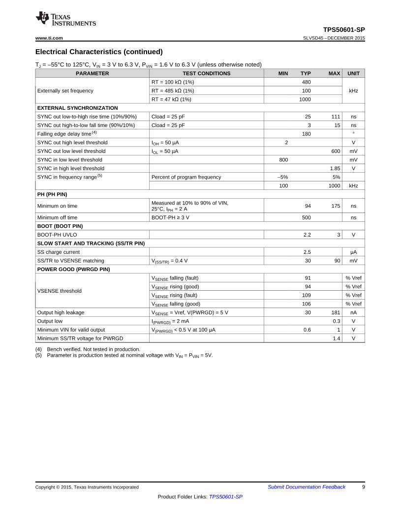
Figure 8. EN Pin UVLO Threshold vs Temperature Figure 9. Non-Switching Operating Quiescent Current (VIN)vs Temperature
Figure 10. Slow Start Charge Current vs Temperature Figure 11. (SS-VSENSE) Offset vs Temperature
Figure 12. High-Side Current Limit Threshold vs Figure 13. Low-Side RDS(On) vs TemperatureTemperature
12 Submit Documentation Feedback Copyright © 2015, Texas Instruments Incorporated
Product Folder Links: TPS50601-SP

0
5
10
15
±75 ±50 ±25 0 25 50 75 100 125
Min
imum
Con
trol
labl
e D
uty
Rat
io (
%)
Junction Temperature (C)
VIN = 3 V
VIN = 6.3 V
C014
20
40
60
80
100
120
140
160
180
±75 ±50 ±25 0 25 50 75 100 125
On-
Sta
te R
esis
tanc
e (m
Junction Temperature (C)
VIN = 3 V
VIN = 6.3 V
C001
50
100
150
200
250
±75 ±50 ±25 0 25 50 75 100 125
Min
imum
Con
trol
labl
e O
n T
ime
(ns)
Junction Temperature (C)
VIN = 3 V
VIN = 6.3 V
C013
TPS50601-SPwww.ti.com SLVSD45 –DECEMBER 2015
Typical Characteristics (continued)
Figure 14. High-Side RDS(On) vs Temperature Figure 15. Minimum Controllable On-Time vs Temperature
Figure 16. Minimum Controllable Duty Ratio vs Temperature
Copyright © 2015, Texas Instruments Incorporated Submit Documentation Feedback 13
Product Folder Links: TPS50601-SP

TPS50601-SPSLVSD45 –DECEMBER 2015 www.ti.com
8 Detailed Description
8.1 OverviewThe device is a 6.3-V or 6-A synchronous step-down (buck) converter with two integrated N-channel MOSFETs.To improve performance during line and load transients, the device implements a constant frequency, peakcurrent mode control, which also simplifies external frequency compensation. The wide switching frequency, 100kHz to 1 MHz, allows for efficiency and size optimization when selecting the output filter components.
The device is designed for safe monotonic startup into prebiased loads. The default start up is when VIN istypically 3 V. The EN pin has an internal pullup current source that can be used to adjust the input voltage UVLOwith two external resistors. In addition, the EN pin can be floating for the device to operate with the internalpullup current. The total operating current for the device is approximately 5 mA when not switching and under noload. When the device is disabled, the supply current is typically less than 2.5 mA.
The integrated MOSFETs allow for high-efficiency power supply designs with continuous output currents up to 6A. The MOSFETs have been sized to optimize efficiency for lower duty cycle applications.
The device reduces the external component count by integrating the boot recharge circuit. The bias voltage forthe integrated high-side MOSFET is supplied by a capacitor between the BOOT and PH pins. The boot capacitorvoltage is monitored by a BOOT to PH UVLO (BOOT-PH UVLO) circuit allowing the PH pin to be pulled low torecharge the boot capacitor. The device can operate over duty cycle range per Equation 2 and Equation 3 aslong as the boot capacitor voltage is higher than the preset BOOT-PH UVLO threshold, which is typically 2.2 V.The output voltage can be stepped down to as low as the 0.795-V voltage reference (Vref).
The device has a power good comparator (PWRGD) with hysteresis which monitors the output voltage throughthe VSENSE pin. The PWRGD pin is an open-drain MOSFET which is pulled low when the VSENSE pin voltageis less than 91% or greater than 109% of the reference voltage Vref and asserts high when the VSENSE pinvoltage is 94% to 106% of the Vref.
The SS/TR (slow start/tracking) pin is used to minimize inrush currents or provide power-supply sequencingduring power-up. A small-value capacitor or resistor divider should be coupled to the pin for slow start or criticalpower-supply sequencing requirements.
The device is protected from output overvoltage, overload, and thermal fault conditions. The device minimizesexcessive output overvoltage transients by taking advantage of the overvoltage circuit power good comparator.When the overvoltage comparator is activated, the high-side MOSFET is turned off and prevented from turningon until the VSENSE pin voltage is lower than 106% of the Vref. The device implements both high-side MOSFEToverload protection and bidirectional low-side MOSFET overload protections, which help control the inductorcurrent and avoid current runaway. The device also shuts down if the junction temperature is higher than thermalshutdown trip point. The device is restarted under control of the slow-start circuit automatically when the junctiontemperature drops 10°C typical below the thermal shutdown trip point.
14 Submit Documentation Feedback Copyright © 2015, Texas Instruments Incorporated
Product Folder Links: TPS50601-SP

ERROR
AMPLIFIER
Boot
Charge
UVLO
Current
Sense
Oscillator
Slope
Compensation
and
Clamp
Voltage
Reference
VSENSE
SS/TR
COMP
PH
BOOT
VIN
PGND
Thermal
Shutdown
EN
Enable
Comparator
Shutdown
Logic
Shutdown
Enable
Threshold
Logic
Shutdown
PWRGD
Thermal Pad/GND
Power Stage
& Deadtime
Control
Logic
LS MOSFET
Current Limit
OV
Minimum Clamp
Pulse Skip
Ip Ih
PVIN
UV
HS MOSFET
Current
Comparator
Current
Sense
RegulatorVIN
Boot
UVLO
PH
PGND
PVIN
Overload Recovery
SYNCDetect
SYNC RT
RT Bias
V/I
TPS50601-SPwww.ti.com SLVSD45 –DECEMBER 2015
8.2 Functional Block Diagram
8.3 Feature Description
8.3.1 VIN and Power VIN Pins (VIN and PVIN)The device allows for a variety of applications by using the VIN and PVIN pins together or separately. The VINpin voltage supplies the internal control circuits of the device. The PVIN pin voltage provides the input voltage tothe power converter system.
If tied together, the input voltage for VIN and PVIN can range from 3 to 6.3 V. If using the VIN separately fromPVIN, the VIN pin must be between 3 and 6.3 V, and the PVIN pin can range from as low as 1.6 to 6.3 V. Avoltage divider connected to the EN pin can adjust the input voltage UVLO appropriately. Adjusting the inputvoltage UVLO on the PVIN pin helps to provide consistent power-up behavior.
8.3.2 PVIN vs FrequencyWith VIN tied to PVIN, minimum off-time determines what output voltage is achievable over frequency range.
8.3.3 Voltage ReferenceThe voltage reference system produces a precise voltage reference as indicated in Electrical Characteristics.
Copyright © 2015, Texas Instruments Incorporated Submit Documentation Feedback 15
Product Folder Links: TPS50601-SP

O O ds _ onLS miscin _ min SW
off _ min SW
V I (R R )PV (f )
1 T f
+ +=
- ·
· ·
· ·
OUT OUT_max Tesr OUT_max ds_lowIN
IN - OUT_max ds_high + OUT_max ds_low
V + I R + I RD(V ) =
V I R I R
VrefR38 R15
Vo Vref=
-
TPS50601-SPSLVSD45 –DECEMBER 2015 www.ti.com
Feature Description (continued)8.3.4 Adjusting the Output VoltageThe output voltage is set with a resistor divider from the output (VOUT) to the VSENSE pin. TI recommends touse 1% tolerance or better divider resistors. Start with a 10 kΩ for R15 (top resistor) and use Equation 1 tocalculate R38 (bottom resistor divider). To improve efficiency at light loads, consider using larger-value resistors.If the values are too high, the regulator is more susceptible to noise and voltage errors from the VSENSE inputcurrent are noticeable.
where• Vref = 0.795 V (1)
The minimum output voltage and maximum output voltage can be limited by the minimum on-time of the high-side MOSFET and bootstrap voltage (BOOT-PH voltage) respectively. For more information, see BootstrapVoltage (BOOT) and Low Dropout Operation.
8.3.5 Maximum Duty Cycle LimitThe TPS50601-SP can operate at duty cycle per Equation 2 and Equation 3 as long as the boot capacitorvoltage is higher than the preset BOOT-PH UVLO threshold, which is typically 2.2 V.
Duty cycle can be calculated based on Equation 2.
where• RTesr = Rdcr + Rtrace
• Rdcr is the dc resistance of the inductor.• Rtrace is the dc trace resistance (miscellaneous drop).• Rds_high is the maximum RDS of the high-side MOSFET.• Rds_low is the maximum RDS of the low-side MOSFET. (2)
8.3.6 PVIN vs FrequencyWith VIN tied to PVIN, minimum off-time determines the output voltage that is achievable over frequency range.For VIN = PVIN must be ≥ 3 V. For VIN = 3 V, PVIN can vary from 1.6 to 6.3 V as highlighted in ElectricalCharacteristics.
This is given by Equation 3.
where• Rds_onLS = Low-side Rds-on
• Rmisc = Miscellaneous trace drops• Toff_min = Minimum off time (3)
Using this approach, the designer can calculate minimum PVIN required for specific VOUT as indicated in theexample in Figure 17.
16 Submit Documentation Feedback Copyright © 2015, Texas Instruments Incorporated
Product Folder Links: TPS50601-SP

PV (100 kHz = 1.889 V)in_min
PV (1000 kHz = 3.396 V)in_minV = 1.5 VO
f - Switching Frequency - Hzsw
TPS50601-SPwww.ti.com SLVSD45 –DECEMBER 2015
Feature Description (continued)
Figure 17. PVIN vs Frequency
8.3.7 Safe Start-Up into Prebiased OutputsThe device is designed to prevent the low-side MOSFET from discharging a prebiased output. During monotonicprebiased startup, the low-side MOSFET is not allowed to sink current until the SS/TR pin voltage is higher than1.4 V.
8.3.8 Error AmplifierThe device uses a transconductance error amplifier. The error amplifier compares the VSENSE pin voltage to thelower of the SS/TR pin voltage or the internal 0.795-V voltage reference. The transconductance of the erroramplifier is 1300 μA/V during normal operation. The frequency compensation network is connected between theCOMP pin and ground. Error amplifier dc gain is typically 39000 V/V with minimum value of 22000 V/V perdesign.
8.3.9 Slope CompensationThe device adds a compensating ramp to the switch current signal. This slope compensation preventssubharmonic oscillations. The available peak inductor current remains constant over the full duty cycle range.Minimum peak-to-peak inductor current should be greater than 1 A.
8.3.10 Enable and Adjust UVLOThe EN pin provides electrical on and off control of the device. When the EN pin voltage exceeds the thresholdvoltage, the device starts operation. If the EN pin voltage is pulled below the threshold voltage, the regulatorstops switching and enters low Iq state. If an external Schottky diode is used from VIN to boot, then a bleedermay be required <1 mA to ensure output is low when the unit is disabled by EN pin.
The EN pin has an internal pullup current source, allowing the user to float the EN pin for enabling the device. Ifan application requires controlling the EN pin, use open-drain or open-collector output logic to interface with thepin.
The device implements internal UVLO circuitry on the VIN pin. The device is disabled when the VIN pin voltagefalls below the internal VIN UVLO threshold. The internal VIN UVLO threshold has a hysteresis of 50 mV typical.
Copyright © 2015, Texas Instruments Incorporated Submit Documentation Feedback 17
Product Folder Links: TPS50601-SP

1
æ ö-ç ÷
è ø
æ ö- +ç ÷
è ø
ENFALLINGSTART STOP
ENRISING
ENFALLINGp h
ENRISING
VV V
VR1 =
VI I
V
EN
ip ihVIN
TPS50601-SP
R 1
R 2
PVIN
EN
ip ihPVIN
TPS50601-SP
R 1
R 2
EN
ip ihVIN
TPS50601-SP
R 1
R 2
TPS50601-SPSLVSD45 –DECEMBER 2015 www.ti.com
Feature Description (continued)If an application requires either a higher UVLO threshold on the VIN pin or a secondary UVLO on the PVIN insplit-rail applications, then the EN pin can be configured as shown in Figure 18, Figure 19, and Figure 20. Whenusing the external UVLO function, TI recommends to set the hysteresis to be >500 mV.
The EN pin has a small pullup current, Ip, which sets the default state of the pin to enable when no externalcomponents are connected. The pullup current is also used to control the voltage hysteresis for the UVLOfunction because it increases by Ih after the EN pin crosses the enable threshold. Calculate the UVLO thresholdswith Equation 4 and Equation 5.
Figure 18. Adjustable VIN UVLO
Figure 19. Adjustable PVIN UVLO, VIN ≥ 3 V
Figure 20. Adjustable VIN and PVIN UVLO
(4)
18 Submit Documentation Feedback Copyright © 2015, Texas Instruments Incorporated
Product Folder Links: TPS50601-SP

0 100 200 300 400 500 600 700 800 900 1 103
x
0
120
240
360
480
600
720
840
960
1.08x10³
1.2x10³
Switching Frequency (F ) - kHzSW
RT
- kW
RT(F )SW
RT = 500 kW
RT(F ) = 67009 x FSW SW
-1.0549
( )
´
- + +
ENFALLING
STOP ENFALLING p h
R1 VR2 =
V V R1 I I
TPS50601-SPwww.ti.com SLVSD45 –DECEMBER 2015
Feature Description (continued)
where• Ih = 3 μA• Ip = 3.2 μA• VENRISING = 1.131 V• VENFALLING = 1.09 V (5)
8.3.11 Adjustable Switching Frequency and Synchronization (SYNC)The switching frequency of the device supports three modes of operations. The modes of operation are set bythe conditions on the RT and SYNC pins. At a high level, these modes can be described as master, internaloscillator, and external synchronization modes.
In master mode, the RT pin should be left floating; the internal oscillator is set to 500 kHz, and the SYNC pin isset as an output clock. The SYNC output is in phase with respect to the internal oscillator. SYNC out signal levelis the same as VIN level with 50% duty cycle. SYNC signal feeding the slave module—which is in phase with themaster clock—gets internally inverted (180° out of phase with the master clock) internally in the slave module.
In internal oscillator mode, a resistor is connected between the RT pin and GND. The SYNC pin requires a 10-kΩ resistor to GND for this mode to be effective. The switching frequency of the device is adjustable from 100kHz to 1 MHz by placing a maximum of 510 kΩ and a minimum of 47 kΩ respectively. To determine the RTresistance for a given switching frequency, use Equation 6 or the curve in Figure 21. To reduce the solution size,the designer should set switching frequency as high as possible, but consider the tradeoffs of supply efficiencyand minimum controllable on-time.
where• RT in kΩ• FSW in kHz (6)
Figure 21. RT vs Switching Frequency
When operating the converter in internal oscillator mode (internal oscillator determines the switching frequency(500 kHz) default), the synchronous pin becomes the output and there is a phase inversion. When trying toparallel with another converter, the RT pin of the second (slave) converter must have its RT pin populated suchthat the converter frequency of the slave converter must be within ±5% of the master converter. This is requiredbecause the RT pin also sets the proper operation of slope compensation.
Copyright © 2015, Texas Instruments Incorporated Submit Documentation Feedback 19
Product Folder Links: TPS50601-SP

SS
Css (nF) Vref (V)t (ms) =
Iss (µA)
´
TPS50601-SPSLVSD45 –DECEMBER 2015 www.ti.com
Feature Description (continued)In external synchronization mode, a resistor is connected between the RT pin and GND. The Sync pin requires atoggling signal for this mode to be effective. The switching frequency of the device goes 1:1 with that of Sync pin.External system clock-user supplied sync clock signal determines the switching frequency. If no external clocksignal is detected for 20 µs, then TPS50601-SP transitions to its internal clock, which is typically 500 kHz. Anexternal synchronization using an inverter to obtain phase inversion is necessary. RT values of the master andslave converter must be within ±5% of the external synchronization frequency. This is necessary for proper slopecompensation. A resistance in the RT pin is required for proper operation of the slope compensation circuit. Todetermine the RT resistance for a given switching frequency, use Equation 6 or the curve in Figure 21. To reducethe solution size, the designer should set switching frequency as high as possible, but consider the tradeoffs ofsupply efficiency and minimum controllable on-time.
These modes are described in Table 1.
Table 1. Switching Frequency, SYNC and RT Pin Usage TableSWITCHINGRT PIN SYNC PIN DESCRIPTION AND NOTESFREQUENCY
SYNC pin behaves as an output. SYNC output signalFloat Generates an output signal 500 kHz is 180° out of phase to the internal 500-kHz switching
frequency.Internally generated switching frequency is based10-kΩ resistor to AGND 100 kHz to 1 MHz upon the resistor value present at the RT pin.
47- to 485-kΩ resistorUser-supplied sync clock orto AGND Internally synchronized to Set value of RT that corresponds to the externallyTPS50601-SP master device external clock supplied sync frequency.sync output
8.3.12 Slow Start (SS/TR)The device uses the lower voltage of the internal voltage reference or the SS/TR pin voltage as the referencevoltage and regulates the output accordingly. A capacitor on the SS/TR pin to ground implements a slow-starttime. The device has an internal pullup current source of 5 mA that charges the external slow-start capacitor.Equation 7 shows the calculations for the slow-start time (Tss, 10% to 90%) and slow-start capacitor (Css). Thevoltage reference (Vref) is 0.795 V and the slow-start charge current (Iss) is 2.5 μA.
(7)
When the input UVLO is triggered, the EN pin is pulled below 1.032 V, or a thermal shutdown event occurs thedevice stops switching and enters low current operation. At the subsequent power-up, when the shutdowncondition is removed, the device does not start switching until it has discharged its SS/TR pin to ground ensuringproper soft-start behavior.
8.3.13 Power Good (PWRGD)The PWRGD pin is an open-drain output. When the VSENSE pin is between 94% and 106% of the internalvoltage reference, the PWRGD pin pull-down is deasserted and the pin floats. TI recommends to use a pullupresistor between 10 to 100 kΩ to a voltage source that is 5.5 V or less. The PWRGD is in a defined state whenthe VIN input voltage is greater than 1 V but has reduced current sinking capability. The PWRGD achieves fullcurrent sinking capability when the VIN input voltage is above 3 V.
The PWRGD pin is pulled low when VSENSE is lower than 91% or greater than 109% of the nominal internalreference voltage. Also, the PWRGD is pulled low, if the input UVLO or thermal shutdown are asserted, the ENpin is pulled low or the SS/TR pin is below 1.4 V.
8.3.14 Bootstrap Voltage (BOOT) and Low Dropout OperationThe device has an integrated boot regulator, and requires a small ceramic capacitor between the BOOT and PHpins to provide the gate drive voltage for the high-side MOSFET. The boot capacitor is charged when the BOOTpin voltage is less than VIN and BOOT-PH voltage is below regulation. The value of this ceramic capacitorshould be 0.1 μF. TI recommends a ceramic capacitor with an X7R- or X5R-grade dielectric with a voltage ratingof 10 V or higher because of the stable characteristics over temperature and voltage.
20 Submit Documentation Feedback Copyright © 2015, Texas Instruments Incorporated
Product Folder Links: TPS50601-SP
SS/TR
ENPWRGD
SS/TR
EN
PWRGD
TPS50601-SP TPS50601-SP
1 ·
·
O ds_on OSW
IN on_max
V + R (I )F = =
T V (T )
TPS50601-SPwww.ti.com SLVSD45 –DECEMBER 2015
To improve dropout, the device is designed to operate at a high duty cycle as long as the BOOT to PH pinvoltage is greater than the BOOT-PH UVLO threshold, which is typically 2.1 V. When the voltage between BOOTand PH drops below the BOOT-PH UVLO threshold, the high-side MOSFET is turned off and the low-sideMOSFET is turned on allowing the boot capacitor to be recharged. In applications with split-input voltage rails,high duty cycle operation can be achieved as long as (VIN – PVIN) > 4 V.
Maximum switching frequency is also limited by minimum on-time (specified in Electrical Characteristics) asindicated by Equation 8. Switching frequency will be worst case at no load conditions.
(8)
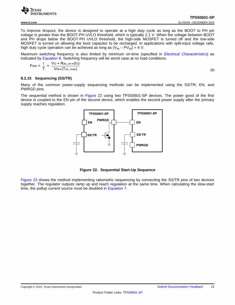
8.3.15 Sequencing (SS/TR)Many of the common power-supply sequencing methods can be implemented using the SS/TR, EN, andPWRGD pins.
The sequential method is shown in Figure 22 using two TPS50601-SP devices. The power good of the firstdevice is coupled to the EN pin of the second device, which enables the second power supply after the primarysupply reaches regulation.
Figure 22. Sequential Start-Up Sequence
Figure 23 shows the method implementing ratiometric sequencing by connecting the SS/TR pins of two devicestogether. The regulator outputs ramp up and reach regulation at the same time. When calculating the slow-starttime, the pullup current source must be doubled in Equation 7.
Copyright © 2015, Texas Instruments Incorporated Submit Documentation Feedback 21
Product Folder Links: TPS50601-SP

> ´ - ´ DR1 2800 Vout1 180 V
V = Vout1 Vout2D -
´
D -
Vref R1R2 =
Vout2 + V Vref
D´
Vout2 + V VssoffsetR1 =
Vref Iss
SS/TR
TPS50601-SP
EN
PWRGD
SS/TR
EN
PWRGD
TPS50601-SP
TPS50601-SPSLVSD45 –DECEMBER 2015 www.ti.com
Figure 23. Ratiometric Start-Up Sequence
Ratiometric and simultaneous power-supply sequencing can be implemented by connecting the resistor networkof R1 and R2 (shown in Figure 24) to the output of the power supply that needs to be tracked or another voltagereference source. Using Equation 9 and Equation 10, the tracking resistors can be calculated to initiate the Vout2slightly before, after, or at the same time as Vout1. Equation 11 is the voltage difference between Vout1 andVout2.
To design a ratiometric start-up in which the Vout2 voltage is slightly greater than the Vout1 voltage when Vout2reaches regulation, use a negative number in Equation 9 and Equation 10 for ΔV. Equation 11 results in apositive number for applications where the Vout2 is slightly lower than Vout1 when Vout2 regulation is achieved.
The ΔV variable is 0 V for simultaneous sequencing. To minimize the effect of the inherent SS/TR to VSENSEoffset (Vssoffset, 29 mV) in the slow-start circuit and the offset created by the pullup current source (Iss, 2 μA)and tracking resistors, the Vssoffset and Iss are included as variables in the equations.
To ensure proper operation of the device, the calculated R1 value from Equation 9 must be greater than thevalue calculated in Equation 12.
(9)
(10)(11)(12)
22 Submit Documentation Feedback Copyright © 2015, Texas Instruments Incorporated
Product Folder Links: TPS50601-SP

SS/TR
TPS50601-SP
EN
PWRGD
SS/TR
TPS50601-SP
EN
PWRGD
VOUT1
VOUT 2
R1
R2
R3R4
TPS50601-SPwww.ti.com SLVSD45 –DECEMBER 2015
Figure 24. Ratiometric and Simultaneous Start-Up Sequence
8.3.16 Output Overvoltage Protection (OVP)The device incorporates an output OVP circuit to minimize output voltage overshoot. For example, when thepower supply output is overloaded, the error amplifier compares the actual output voltage to the internalreference voltage. If the VSENSE pin voltage is lower than the internal reference voltage for a considerable time,the output of the error amplifier demands maximum output current. After the condition is removed, the regulatoroutput rises and the error amplifier output transitions to the steady-state voltage. In some applications with smalloutput capacitance, the power supply output voltage can respond faster than the error amplifier. This leads to thepossibility of an output overshoot. The OVP feature minimizes the overshoot by comparing the VSENSE pinvoltage to the OVP threshold. If the VSENSE pin voltage is greater than the OVP threshold, the high-sideMOSFET is turned off, preventing current from flowing to the output and minimizing output overshoot. When theVSENSE voltage drops lower than the OVP threshold, the high-side MOSFET is allowed to turn on at the nextclock cycle.
8.3.17 Overcurrent ProtectionThe device is protected from overcurrent conditions by cycle-by-cycle current limiting on both the high-side andlow-side MOSFET.
8.3.17.1 High-Side MOSFET Overcurrent ProtectionThe device implements current mode control which uses the COMP pin voltage to control the turn off of the high-side MOSFET and the turn on of the low-side MOSFET on a cycle-by-cycle basis. Each cycle the switch currentand the current reference generated by the COMP pin voltage are compared, when the peak switch currentintersects the current reference, the high-side switch is turned off.
8.3.17.2 Low-Side MOSFET Overcurrent ProtectionWhile the low-side MOSFET is turned on its conduction current is monitored by the internal circuitry. Duringnormal operation the low-side MOSFET sources current to the load. At the end of every clock cycle, the low-sideMOSFET sourcing current is compared to the internally set low-side sourcing current limit. If the low-sidesourcing current is exceeded, the high-side MOSFET is not turned on and the low-side MOSFET stays on for thenext cycle. The high-side MOSFET is turned on again when the low-side current is below the low-side sourcingcurrent limit at the start of a cycle.Copyright © 2015, Texas Instruments Incorporated Submit Documentation Feedback 23
Product Folder Links: TPS50601-SP
VSENSE
COMP
VOUT
R1
R3
C1C2 R2
Coea Roeagm
1300 mA/V
0.8 V
Power StagePH
RESR
CO
RL
b
a
c
18 A/V
TPS50601-SPSLVSD45 –DECEMBER 2015 www.ti.com
The low-side MOSFET may also sink current from the load. If the low-side sinking current limit is exceeded, thelow-side MOSFET is turned off immediately for the rest of that clock cycle. In this scenario, both MOSFETs areoff until the start of the next cycle.
When the low-side MOSFET turns off, the switch node increases and forward biases the high-side MOSFETparallel diode (the high-side MOSFET is still off at this stage).
8.3.18 TPS50601-SP Thermal ShutdownThe internal thermal shutdown circuitry forces the device to stop switching if the junction temperature exceeds175°C typically. The device reinitiates the power-up sequence when the junction temperature drops below 165°Ctypically.
8.3.19 Turn-On BehaviorMinimum on-time specification determines the maximum operating frequency of the design. As the unit starts upand goes through its soft-start process, the required duty-cycle is less than the minimum controllable on-time.This can cause the converter to skip pulses. Thus, instantaneous output pulses can be higher or lower than thedesired voltage. This behavior is only evident when operating at high frequency with high bandwidth. When theminimum on-pulse is greater than the minimum controllable on-time, the turn-on behavior is normal. Whenoperating at low frequencies (100 kHz or less), the turn-on behavior does not exhibit any ringing at initial startup.
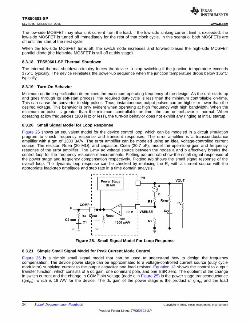
8.3.20 Small Signal Model for Loop ResponseFigure 25 shows an equivalent model for the device control loop, which can be modeled in a circuit simulationprogram to check frequency response and transient responses. The error amplifier is a transconductanceamplifier with a gm of 1300 μA/V. The error amplifier can be modeled using an ideal voltage-controlled currentsource. The resistor, Roea (30 MΩ), and capacitor, Coea (20.7 pF), model the open-loop gain and frequencyresponse of the error amplifier. The 1-mV ac voltage source between the nodes a and b effectively breaks thecontrol loop for the frequency response measurements. Plotting a/c and c/b show the small signal responses ofthe power stage and frequency compensation respectively. Plotting a/b shows the small signal response of theoverall loop. The dynamic loop response can be checked by replacing the RL with a current source with theappropriate load-step amplitude and step rate in a time domain analysis.
Figure 25. Small Signal Model For Loop Response
8.3.21 Simple Small Signal Model for Peak Current Mode ControlFigure 26 is a simple small signal model that can be used to understand how to design the frequencycompensation. The device power stage can be approximated to a voltage-controlled current source (duty cyclemodulator) supplying current to the output capacitor and load resistor. Equation 13 shows the control to outputtransfer function, which consists of a dc gain, one dominant pole, and one ESR zero. The quotient of the changein switch current and the change in COMP pin voltage (node c in Figure 25) is the power stage transconductance(gmps), which is 18 A/V for the device. The dc gain of the power stage is the product of gmps and the load
24 Submit Documentation Feedback Copyright © 2015, Texas Instruments Incorporated
Product Folder Links: TPS50601-SP

O ESR
1z =
C R 2¦
´ ´ p
O L
1p =
C R 2¦
´ ´ p
ps LAdc = gm R´
s1+
2 zVOUT= Adc
VC s1+
2 p
æ öç ÷´ ¦è ø´æ öç ÷
´ ¦è ø
p
p
VOUT
RESR
CO
RL
VC
gmps
fp
fz
Adc
VOUT
RESR
CO
R L
VC
gmps
TPS50601-SPwww.ti.com SLVSD45 –DECEMBER 2015
resistance (RL) as shown in Equation 14 with resistive loads. As the load current increases, the dc gaindecreases. This variation with load may seem problematic at first glance, but fortunately, the dominant polemoves with load current (see Equation 15). The combined effect is highlighted by the dashed line in Figure 27.As the load current decreases, the gain increases and the pole frequency lowers, keeping the 0-dB crossoverfrequency the same for the varying load conditions, which makes it easier to design the frequency compensation.
Figure 26. Simplified Small Signal Model for Peak Current Mode Control
Figure 27. Simplified Frequency Response for Peak Current Mode Control
(13)
(14)
(15)
where• gmea is the GM amplifier gain (1300 μA/V).• gmps is the power stage gain (18 A/V).• RL is the load resistance.• CO is the output capacitance.
Copyright © 2015, Texas Instruments Incorporated Submit Documentation Feedback 25
Product Folder Links: TPS50601-SP

ESRR Co
C2 =R3
´
LR Co
C1 =R3
´
O L
1p =
C R 2
æ ö¦ç ÷
´ ´è øp
ea ps
2 c VOUT CoR3 =
gm Vref gm
´ ¦ ´ ´
´ ´
p
Vref
VOUT
R1
R3
C1
C2R2
CoeaRoea
gmea
COMPVSENSE
Type 2A Type 2B
R3
C1
TPS50601-SPSLVSD45 –DECEMBER 2015 www.ti.com
• RESR is the equivalent series resistance of the output capacitor. (16)
8.3.22 Small Signal Model for Frequency CompensationThe device uses a transconductance amplifier for the error amplifier and readily supports two of the commonlyused frequency compensation circuits shown in Figure 28. In Type 2A, one additional high-frequency pole isadded to attenuate high-frequency noise.
The following design guidelines are provided for advanced users who prefer to compensate using the generalmethod. The step-by-step design procedure described in Detailed Design Procedure may also be used.
Figure 28. Types of Frequency Compensation
The general design guidelines for device loop compensation are as follows:1. Determine the crossover frequency ƒc. A good starting point is one-tenth of the switching frequency, ƒSW.2. R3 can be determined by:
where• gmea is the GM amplifier gain ( 1300 μA/V).• gmps is the power stage gain (18 A/V).• Vref is the reference voltage (0.795 V) (17)
3. Place a compensation zero at the dominant pole .C1 can be determined by
(18)4. C2 is optional. It can be used to cancel the zero from the equivalent series resistance (ESR) of the output
capacitor Co.
(19)
NOTEFor PSpice models and WEBENCH design tool, see the Tools & Software tab.1. PSpice average model (stability – bode plot)2. PSpice transient model (switching waveforms)3. WEBENCH design tool www.ti.com/product/TPS50601-SP/toolssoftware
26 Submit Documentation Feedback Copyright © 2015, Texas Instruments Incorporated
Product Folder Links: TPS50601-SP

TPS50601-SPwww.ti.com SLVSD45 –DECEMBER 2015
8.4 Device Functional Modes
8.4.1 Fixed-Frequency PWM ControlThe device uses fixed frequency, peak current mode control. The output voltage is compared through externalresistors on the VSENSE pin to an internal voltage reference by an error amplifier which drives the COMP pin.An internal oscillator initiates the turn on of the high-side power switch. The error amplifier output is convertedinto a current reference which compares to the high-side power switch current. When the power switch currentreaches the current reference generated by the COMP voltage level, the high-side power switch is turned off andthe low-side power switch is turned on.
8.4.2 Continuous Current Mode (CCM) OperationAs a synchronous buck converter, the device normally works in CCM under all load conditions.
Copyright © 2015, Texas Instruments Incorporated Submit Documentation Feedback 27
Product Folder Links: TPS50601-SP

PH
PVIN
GND
BOOT
VSENSE
COMP
TPS50601-SP
EN
RT/CLK
SS/TR
ExposedThermal
Pad
Css Rrt R3
C1
Cboot
Co
Lo
R1
R2
Cin
C2
VINVIN
VOUT
PWRGD
TPS50601-SPSLVSD45 –DECEMBER 2015 www.ti.com
9 Application and Implementation
NOTEInformation in the following applications sections is not part of the TI componentspecification, and TI does not warrant its accuracy or completeness. TI’s customers areresponsible for determining suitability of components for their purposes. Customers shouldvalidate and test their design implementation to confirm system functionality.
9.1 Application InformationThe TPS50601-SP device is a highly-integrated synchronous step-down DC-DC converter. The device is used toconvert a higher DC-DC input voltage to a lower DC output voltage with a maximum output current of 6 A.
The TPS50601-SP user's guide is available on the TI website, SLVU499. The guide highlights standard EVM testresults, schematic, and BOM for reference. (Basic design equations in following sections are provided forreference only)
9.2 Typical Application
Figure 29. Typical Application Schematic
9.2.1 Design RequirementsThis example details the design of a high frequency switching regulator design using ceramic output capacitors.A few parameters must be known in order to start the design process. These parameters are typically determinedat the system level. For this example, we start with the following known parameters:
Table 2. Design ParametersDESIGN PARAMETER EXAMPLE VALUE
Output voltage 3.3 VOutput current 6 ATransient response 1-A load step ΔVout = 5%Input voltage 5 V nominal, 4.5 to 6.3 VOutput voltage ripple 33 mV p-pStart input voltage (rising Vin) 4.425VStop input voltage (falling Vin) 4.234VSwitching frequency 480 kHz
28 Submit Documentation Feedback Copyright © 2015, Texas Instruments Incorporated
Product Folder Links: TPS50601-SP

2= +
IrippleILpeak Iout
( ) 2
2 1
12 f
æ ö× -= + ×ç ÷ç ÷× ×è ø
oV Vinmax VoILrms Io
Vinmax L1 sw
f
-
= ×
×
Vinmax Vout VoutIripple
L1 Vinmax sw
f
-
= ×
× ×
Vinmax Vout VoutL1
Io Kind Vinmax sw
TPS50601-SPwww.ti.com SLVSD45 –DECEMBER 2015
9.2.2 Detailed Design Procedure
9.2.2.1 Operating FrequencyThe first step is to decide on a switching frequency for the regulator. There is a trade off between higher andlower switching frequencies. Higher switching frequencies may produce smaller a solution size using lowervalued inductors and smaller output capacitors compared to a power supply that switches at a lower frequency.However, the higher switching frequency causes extra switching losses, which hurt the converter’s efficiency andthermal performance. In this design, a moderate switching frequency of 480 kHz is selected to achieve both asmall solution size and a high efficiency operation.
9.2.2.2 Output Inductor SelectionTo calculate the value of the output inductor, use Equation 20. KIND is a coefficient that represents the amountof inductor ripple current relative to the maximum output current. The inductor ripple current is filtered by theoutput capacitor. Therefore, choosing high inductor ripple currents impact the selection of the output capacitorsince the output capacitor must have a ripple current rating equal to or greater than the inductor ripple current. Ingeneral, the inductor ripple value is at the discretion of the designer; however, KIND is normally from 0.1 to 0.4for the majority of applications.
(20)
For this design example, use KIND = 0.1 and the inductor value is calculated to be 2.78 µH. For this design, anearest standard value was chosen: 3.3 µH. For the output filter inductor, it is important that the RMS currentand saturation current ratings not be exceeded. The RMS and peak inductor current can be found fromEquation 22 and Equation 23.
(21)
(22)
(23)
For this design, the RMS inductor current is 6.02 A and the peak inductor current is 6.84 A. The chosen inductoris a Coilcraft MSS1048 series 3.3 µH. It has a saturation current rating of 7.38 A and a RMS current rating of7.22 A.
The current flowing through the inductor is the inductor ripple current plus the output current. During power up,faults or transient load conditions, the inductor current can increase above the calculated peak inductor currentlevel calculated above. In transient conditions, the inductor current can increase up to the switch current limit ofthe device. For this reason, the most conservative approach is to specify an inductor with a saturation currentrating equal to or greater than the switch current limit rather than the peak inductor current.
9.2.2.3 Output Capacitor SelectionThere are three primary considerations for selecting the value of the output capacitor. The output capacitordetermines the modulator pole, the output voltage ripple, and how the regulator responds to a large change inload current. The output capacitance needs to be selected based on the more stringent of these three criteria
The desired response to a large change in the load current is the first criteria. The output capacitor needs tosupply the load with current when the regulator can not. This situation would occur if there are desired hold-uptimes for the regulator where the output capacitor must hold the output voltage above a certain level for aspecified amount of time after the input power is removed. The regulator is also temporarily not able to supplysufficient output current if there is a large, fast increase in the current needs of the load such as a transition fromno load to full load. The regulator usually needs two or more clock cycles for the control loop to see the change
Copyright © 2015, Texas Instruments Incorporated Submit Documentation Feedback 29
Product Folder Links: TPS50601-SP

( )-= × ×
Vinmin VoutVoutIcirms Iout
Vinmin Vinmin
( )
12 f
× -=
× × ×
Vout Vinmax VoutIcorms
Vinmax L1 sw
<
VorippleResr
Iripple
1 1
8 f> ×
×
CoVoripplesw
Iripple
2
f
× D>
× D
IoutCo
sw Vout
TPS50601-SPSLVSD45 –DECEMBER 2015 www.ti.com
in load current and output voltage and adjust the duty cycle to react to the change. The output capacitor must besized to supply the extra current to the load until the control loop responds to the load change. The outputcapacitance must be large enough to supply the difference in current for 2 clock cycles while only allowing atolerable amount of droop in the output voltage. Equation 24 shows the minimum output capacitance necessaryto accomplish this.
(24)
Where ΔIout is the change in output current, Fsw is the regulators switching frequency and ΔVout is theallowable change in the output voltage. For this example, the transient load response is specified as a 5%change in Vout for a load step of 1A. For this example, ΔIout = 1.0 A and ΔVout = 0.05 x 3.3 = 0.165 V. Usingthese numbers gives a minimum capacitance of 25 μF. This value does not take the ESR of the output capacitorinto account in the output voltage change. For ceramic capacitors, the ESR is usually small enough to ignore inthis calculation.
Equation 25 calculates the minimum output capacitance needed to meet the output voltage ripple specification.Where fsw is the switching frequency, Vripple is the maximum allowable output voltage ripple, and Iripple is theinductor ripple current. In this case, the maximum output voltage ripple is 33mV. Under this requirement,Equation 25 yields 13.2 µF.
(25)
Equation 26 calculates the maximum ESR an output capacitor can have to meet the output voltage ripplespecification. Equation 26 indicates the ESR should be less than 19.7 mΩ. In this case, the ceramic caps’ ESR ismuch smaller than 19.7 mΩ.
(26)
Additional capacitance de-ratings for aging, temperature and DC bias should be factored in which increases thisminimum value. For this example, a 47 μF 6.3V X5R ceramic capacitor with 3 mΩ of ESR is be used. Capacitorsgenerally have limits to the amount of ripple current they can handle without failing or producing excess heat. Anoutput capacitor that can support the inductor ripple current must be specified. Some capacitor data sheetsspecify the RMS (Root Mean Square) value of the maximum ripple current. Equation 27 can be used to calculatethe RMS ripple current the output capacitor needs to support. For this application, Equation 27 yields 485mA.
(27)
9.2.2.4 Input Capacitor SelectionThe TPS50601-SP requires a high quality ceramic, type X5R or X7R, input decoupling capacitor of at least 4.7µF of effective capacitance on the PVIN input voltage pins and 4.7 µF on the Vin input voltage pin. In someapplications additional bulk capacitance may also be required for the PVIN input. The effective capacitanceincludes any DC bias effects. The voltage rating of the input capacitor must be greater than the maximum inputvoltage. The capacitor must also have a ripple current rating greater than the maximum input current ripple of theTPS50601-SP. The input ripple current can be calculated using Equation 28.
(28)
The value of a ceramic capacitor varies significantly over temperature and the amount of DC bias applied to thecapacitor. The capacitance variations due to temperature can be minimized by selecting a dielectric material thatis stable over temperature. X5R and X7R ceramic dielectrics are usually selected for power regulator capacitorsbecause they have a high capacitance to volume ratio and are fairly stable over temperature. The outputcapacitor must also be selected with the DC bias taken into account. The capacitance value of a capacitordecreases as the DC bias across a capacitor increases. For this example design, a ceramic capacitor with atleast a 25-V voltage rating is required to support the maximum input voltage. For this example, one 10 μF and
30 Submit Documentation Feedback Copyright © 2015, Texas Instruments Incorporated
Product Folder Links: TPS50601-SP
V re fR 5 R 6
9 R ± 9 UH I
u
Tss(ms) x Iss(μA)C5(nF)
Vref(V)=
0.25
f
×D =
×
IoutmaxVin
Cin sw
TPS50601-SPwww.ti.com SLVSD45 –DECEMBER 2015
one 4.7-µF 25-V capacitors in parallel have been selected as the VIN and PVIN inputs are tied together so theTPS50601-SP may operate from a single supply. The input capacitance value determines the input ripple voltageof the regulator. The input voltage ripple can be calculated using Equation 29. Using the design example values,Ioutmax = 6 A, Cin = 14.7 μF, FSW = 480 kHz, yields an input voltage ripple of 213 mV and a RMS input ripplecurrent of 2.95 A.
(29)
9.2.2.5 Slow Start Capacitor SelectionThe slow start capacitor determines the minimum amount of time it takes for the output voltage to reach itsnominal programmed value during power up. This is useful if a load requires a controlled voltage slew rate. Thisis also used if the output capacitance is very large and would require large amounts of current to quickly chargethe capacitor to the output voltage level. The large currents necessary to charge the capacitor may make theTPS50601-SP reach the current limit or excessive current draw from the input power supply may cause the inputvoltage rail to sag. Limiting the output voltage slew rate solves both of these problems. The soft start capacitorvalue can be calculated using Equation 30. For the example circuit, the soft start time is not too critical since theoutput capacitor value is 47 μF which does not require much current to charge to 3.3 V. The example circuit hasthe soft start time set to an arbitrary value of 3.5 ms which requires a 10-nF capacitor. In TPS50601-SP, Iss is2.5 µA typical, and Vref is 0.795 V.
(30)
9.2.2.6 Bootstrap Capacitor SelectionA 0.1-µF ceramic capacitor must be connected between the BOOT to PH pin for proper operation. TIrecommends to use a ceramic capacitor with X5R or better grade dielectric. The capacitor should have a voltagerating of 10 V or higher.
9.2.2.7 Undervoltage Lockout (UVLO) Set PointThe UVLO can be adjusted using the external voltage divider network of R6a and R7a. R6a is connectedbetween VIN and the EN pin of the TPS50601-SP and R7a is connected between EN and GND . The UVLO hastwo thresholds, one for power up when the input voltage is rising and one for power down or brown outs whenthe input voltage is falling. For the example design, the supply should turn on and start switching once the inputvoltage increases above selected voltage (UVLO start or enable). After the regulator starts switching, it shouldcontinue to do so until the input voltage falls below (UVLO stop or disable) voltage. Equation 4 and Equation 5can be used to calculate the values for the upper and lower resistor values. For the stop voltages specified thenearest standard resistor value for R6a is 10.0 kΩ and for R7a is 3.4 kΩ.
9.2.2.8 Output Voltage Feedback Resistor SelectionThe resistor divider network R5 and R6 is used to set the output voltage. For the example design, 10 kΩ wasselected for R6. Using Equation 31, R5 is calculated as 31.25 kΩ. The nearest standard 1% resistor is 31.6 kΩ.
(31)
9.2.2.8.1 Minimum Output Voltage
Due to the internal design of the TPS50601-SP, there is a minimum output voltage limit for any given inputvoltage. The output voltage can never be lower than the internal voltage reference of 0.8 V. Above 0.8 V, theoutput voltage may be limited by the minimum controllable on time. The minimum output voltage in this case isgiven by Equation 32
spacerVOUTmin = Ontimemin × ƒsmax (VINmax + IOUTmin (RDS2min - RDS1min)) - IOUTmin (RL + RDS2min)
where• VOUTmin = Minimum achievable output voltage• Ontimemin = Minimum controllable on-time (175 ns maximum)
Copyright © 2015, Texas Instruments Incorporated Submit Documentation Feedback 31
Product Folder Links: TPS50601-SP

1
2f
p
=
× × ×
pR2 Cp
Vout CoutC3
Iout R2
×
=
×
2
ea ps
c Vout CoutR2
gm Vref gm
× × ×
=
× ×
fp
2
ff f= ×
swco pmod
f f f= ×co pmod zmod
1
2f
p
=
× × ×
zmodRESR Cout
2f
p
=
× × ×
Ioutpmod
Vout Cout
TPS50601-SPSLVSD45 –DECEMBER 2015 www.ti.com
• ƒsmax = Maximum switching frequency including tolerance• VINmax = Maximum input voltage• IOUTmin = Minimum load current• RDS1min = Minimum high-side MOSFET on-resistance (36-32 mΩ typical)• RDS2min = Minimum low-side MOSFET on-resistance (19 mΩ typical)• RL = Series resistance of output inductor (32)
9.2.2.9 Compensation Component SelectionThere are several industry techniques used to compensate DC/DC regulators. The method presented here iseasy to calculate and yields high phase margins. For most conditions, the regulator has a phase margin between60 and 90 degrees. The method presented here ignores the effects of the slope compensation that is internal tothe TPS50601-SP. Since the slope compensation is ignored, the actual cross over frequency is usually lowerthan the cross over frequency used in the calculations. Use WEBENCH, Pspice model for simulation.
First, the modulator pole, fpmod, and the esr zero, fzmod must be calculated using Equation 33 and Equation 34.For Cout, use a derated value of 22.4 µF. use Equation 35 and Equation 36 to estimate a starting point for theclosed loop crossover frequency fco. Then the required compensation components may be derived. For thisdesign example, fpmod is 12.9 kHz and fzmod is 2730 kHz. Equation 35 is the geometric mean of the modulatorpole and the esr zero and Equation 36 is the geometric mean of the modulator pole and one half the switchingfrequency. Use a frequency near the lower of these two values as the intended crossover frequency fco. In thiscase Equation 35 yields 175 kHz and Equation 36 yields 55.7 kHz. The lower value is 55.7 kHz. A slightly higherfrequency of 60.5 kHz is chosen as the intended crossover frequency.
(33)
(34)
(35)
(36)
Now the compensation components can be calculated. First calculate the value for R2 which sets the gain of thecompensated network at the crossover frequency. Use Equation 37 to determine the value of R2.
(37)
Next calculate the value of C3. Together with R2, C3 places a compensation zero at the modulator polefrequency. Equation 38 to determine the value of C3.
(38)
Using Equation 37 and Equation 38 the standard values for R2 and C3 are 1.69 kΩ and 8200 pF.
An additional high frequency pole can be used if necessary by adding a capacitor in parallel with the seriescombination of R2 and C3. The pole frequency is given by Equation 39. This pole is not used in this design.
(39)
32 Submit Documentation Feedback Copyright © 2015, Texas Instruments Incorporated
Product Folder Links: TPS50601-SP

TPS50601-SPwww.ti.com SLVSD45 –DECEMBER 2015
9.2.3 Application Curve
A. Per EVM - for additional details see the User's Guide, SLVU499
Figure 30. Typical Switching Waveform for 100-kHz Switching Operation
Copyright © 2015, Texas Instruments Incorporated Submit Documentation Feedback 33
Product Folder Links: TPS50601-SP

TPS50601-SPSLVSD45 –DECEMBER 2015 www.ti.com
10 Power Supply RecommendationsThe TPS50601-SP is designed to operate from an input voltage supply range between 3.0V and 6.3V. Thissupply voltage must be well regulated. Power supplies must be well bypassed for proper electrical performance.This includes a minimum of one 4.7 µF (after de-rating) ceramic capacitor, type X5R or better from PVIN to GND,and from VIN to GND. Additional local ceramic bypass capacitance may be required in systems with small inputripple specifications, in addition to bulk capacitance if the TPS50601-SP device is located more than a fewinches away from its input power supply. In systems with an auxiliary power rail available, the power stage input,PVIN, and the analog power input, VIN, may operate from separate input supplies. See Layout Example (layoutrecommendation) for recommended bypass capacitor placement.
11 Layout
11.1 Layout Guidelines• Layout is a critical portion of good power supply design. See Layout Example for a PCB layout example.• The top layer contains the main power traces for VIN, VOUT, and VPHASE. Also on the top layer are
connections for the remaining pins of the TPS50601-SP and a large top side area filled with ground.• The top layer ground area should be connected to the internal ground layer(s) using vias at the input bypass
capacitor, the output filter capacitor and directly under the TPS50601-SP device to provide a thermal pathfrom the exposed thermal pad land to ground
• The GND pin should be tied directly to the power pad under the IC and the power pad.• For operation at full rated load, the top side ground area together with the internal ground plane, must provide
adequate heat dissipating area.• There are several signals paths that conduct fast changing currents or voltages that can interact with stray
inductance or parasitic capacitance to generate noise or degrade the power supplies performance.• To help eliminate these problems, the PVIN pin should be bypassed to ground with a low ESR ceramic
bypass capacitor with X5R or X7R dielectric.• Care should be taken to minimize the loop area formed by the bypass capacitor connections, the PVIN pins,
and the ground connections.• The VIN pin must also be bypassed to ground using a low ESR ceramic capacitor with X5R or X7R dielectric.• Make sure to connect this capacitor to the quite analog ground trace rather than the power ground trace of
the PVIn bypass capacitor.• Since the PH connection is the switching node, the output inductor should be located close to the PH pins,
and the area of the PCB conductor minimized to prevent excessive capacitive coupling.• The output filter capacitor ground should use the same power ground trace as the PVIN input bypass
capacitor.• Try to minimize this conductor length while maintaining adequate width.• The small signal components should be grounded to the analog ground path as shown.• The RT pin is sensitive to noise so the RT resistor should be located as close as possible to the IC and
routed with minimal lengths of trace.• It may be possible to obtain acceptable performance with alternate PCB layouts, however this layout has
been shown to produce good results and is meant as a guideline.• Land pattern and stencil information is provided in the data sheet addendum.
34 Submit Documentation Feedback Copyright © 2015, Texas Instruments Incorporated
Product Folder Links: TPS50601-SP

Bond pad connected to
ground for thermal path
TPS50601-SPwww.ti.com SLVSD45 –DECEMBER 2015
11.2 Layout Example
Figure 31. PCB Layout Example
Copyright © 2015, Texas Instruments Incorporated Submit Documentation Feedback 35
Product Folder Links: TPS50601-SP

TPS50601-SPSLVSD45 –DECEMBER 2015 www.ti.com
12 Device and Documentation Support
12.1 Documentation Support
12.1.1 Related DocumentationFor related documentation see the following:
TPS50601SP EVM, 6-A/12-A, SWIFT ™ Regulator Evaluation Module, SLVU499
12.2 Community ResourcesThe following links connect to TI community resources. Linked contents are provided "AS IS" by the respectivecontributors. They do not constitute TI specifications and do not necessarily reflect TI's views; see TI's Terms ofUse.
TI E2E™ Online Community TI's Engineer-to-Engineer (E2E) Community. Created to foster collaborationamong engineers. At e2e.ti.com, you can ask questions, share knowledge, explore ideas and helpsolve problems with fellow engineers.
Design Support TI's Design Support Quickly find helpful E2E forums along with design support tools andcontact information for technical support.
12.3 TrademarksSWIFT, E2E are trademarks of Texas Instruments.All other trademarks are the property of their respective owners.
12.4 Electrostatic Discharge CautionThese devices have limited built-in ESD protection. The leads should be shorted together or the device placed in conductive foamduring storage or handling to prevent electrostatic damage to the MOS gates.
12.5 GlossarySLYZ022 — TI Glossary.
This glossary lists and explains terms, acronyms, and definitions.
13 Mechanical, Packaging, and Orderable InformationThe following pages include mechanical, packaging, and orderable information. This information is the mostcurrent data available for the designated devices. This data is subject to change without notice and revision ofthis document. For browser-based versions of this data sheet, refer to the left-hand navigation.
13.1 Device NomenclatureKGD Known good die
RHA Radiation hardness assurance for space systems
5962R10221 Same device as TPS50601-SP, shown with standard microcircuit drawing (SMD)
TPS50601-SP Same device as 5962R10221, shown with TI package drawing
36 Submit Documentation Feedback Copyright © 2015, Texas Instruments Incorporated
Product Folder Links: TPS50601-SP

PACKAGE OPTION ADDENDUM
www.ti.com 25-Apr-2017
Addendum-Page 1
PACKAGING INFORMATION
Orderable Device Status(1)
Package Type PackageDrawing
Pins PackageQty
Eco Plan(2)
Lead/Ball Finish(6)
MSL Peak Temp(3)
Op Temp (°C) Device Marking(4/5)
Samples
5962-1022101VSC ACTIVE CFP HKH 20 1 TBD AU N / A for Pkg Type -55 to 125 5962-1022101VSCTPS50601MHKHV
5962R1022101V9A ACTIVE XCEPT KGD 0 25 TBD Call TI N / A for Pkg Type -55 to 125
5962R1022101VSC ACTIVE CFP HKH 20 1 TBD AU N / A for Pkg Type -55 to 125 5962R1022101VSCTPS50601-RHA
TPS50601HKH/EM ACTIVE CFP HKH 20 1 TBD AU N / A for Pkg Type 25 Only TPS50601HKH/EMEVAL ONLY
TPS50601MHKHV ACTIVE CFP HKH 20 1 TBD AU N / A for Pkg Type -55 to 125 5962-1022101VSCTPS50601MHKHV
(1) The marketing status values are defined as follows:ACTIVE: Product device recommended for new designs.LIFEBUY: TI has announced that the device will be discontinued, and a lifetime-buy period is in effect.NRND: Not recommended for new designs. Device is in production to support existing customers, but TI does not recommend using this part in a new design.PREVIEW: Device has been announced but is not in production. Samples may or may not be available.OBSOLETE: TI has discontinued the production of the device.
(2) Eco Plan - The planned eco-friendly classification: Pb-Free (RoHS), Pb-Free (RoHS Exempt), or Green (RoHS & no Sb/Br) - please check http://www.ti.com/productcontent for the latest availabilityinformation and additional product content details.TBD: The Pb-Free/Green conversion plan has not been defined.Pb-Free (RoHS): TI's terms "Lead-Free" or "Pb-Free" mean semiconductor products that are compatible with the current RoHS requirements for all 6 substances, including the requirement thatlead not exceed 0.1% by weight in homogeneous materials. Where designed to be soldered at high temperatures, TI Pb-Free products are suitable for use in specified lead-free processes.Pb-Free (RoHS Exempt): This component has a RoHS exemption for either 1) lead-based flip-chip solder bumps used between the die and package, or 2) lead-based die adhesive used betweenthe die and leadframe. The component is otherwise considered Pb-Free (RoHS compatible) as defined above.Green (RoHS & no Sb/Br): TI defines "Green" to mean Pb-Free (RoHS compatible), and free of Bromine (Br) and Antimony (Sb) based flame retardants (Br or Sb do not exceed 0.1% by weightin homogeneous material)
(3) MSL, Peak Temp. - The Moisture Sensitivity Level rating according to the JEDEC industry standard classifications, and peak solder temperature.
(4) There may be additional marking, which relates to the logo, the lot trace code information, or the environmental category on the device.
(5) Multiple Device Markings will be inside parentheses. Only one Device Marking contained in parentheses and separated by a "~" will appear on a device. If a line is indented then it is a continuationof the previous line and the two combined represent the entire Device Marking for that device.

PACKAGE OPTION ADDENDUM
www.ti.com 25-Apr-2017
Addendum-Page 2
(6) Lead/Ball Finish - Orderable Devices may have multiple material finish options. Finish options are separated by a vertical ruled line. Lead/Ball Finish values may wrap to two lines if the finishvalue exceeds the maximum column width.
Important Information and Disclaimer:The information provided on this page represents TI's knowledge and belief as of the date that it is provided. TI bases its knowledge and belief on informationprovided by third parties, and makes no representation or warranty as to the accuracy of such information. Efforts are underway to better integrate information from third parties. TI has taken andcontinues to take reasonable steps to provide representative and accurate information but may not have conducted destructive testing or chemical analysis on incoming materials and chemicals.TI and TI suppliers consider certain information to be proprietary, and thus CAS numbers and other limited information may not be available for release.
In no event shall TI's liability arising out of such information exceed the total purchase price of the TI part(s) at issue in this document sold by TI to Customer on an annual basis.
OTHER QUALIFIED VERSIONS OF TPS50601-SP :
• Catalog: TPS50601-DIE
NOTE: Qualified Version Definitions:
• Catalog - TI's standard catalog product
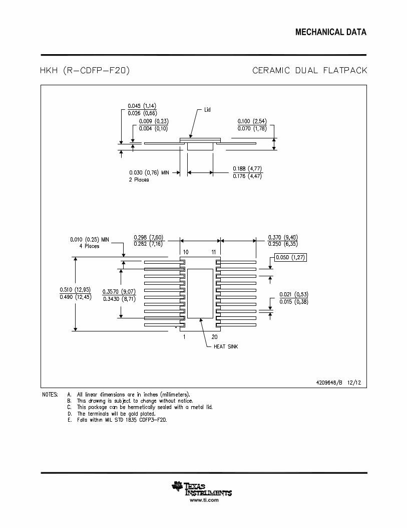

IMPORTANT NOTICE
Texas Instruments Incorporated (TI) reserves the right to make corrections, enhancements, improvements and other changes to itssemiconductor products and services per JESD46, latest issue, and to discontinue any product or service per JESD48, latest issue. Buyersshould obtain the latest relevant information before placing orders and should verify that such information is current and complete.TI’s published terms of sale for semiconductor products (http://www.ti.com/sc/docs/stdterms.htm) apply to the sale of packaged integratedcircuit products that TI has qualified and released to market. Additional terms may apply to the use or sale of other types of TI products andservices.Reproduction of significant portions of TI information in TI data sheets is permissible only if reproduction is without alteration and isaccompanied by all associated warranties, conditions, limitations, and notices. TI is not responsible or liable for such reproduceddocumentation. Information of third parties may be subject to additional restrictions. Resale of TI products or services with statementsdifferent from or beyond the parameters stated by TI for that product or service voids all express and any implied warranties for theassociated TI product or service and is an unfair and deceptive business practice. TI is not responsible or liable for any such statements.Buyers and others who are developing systems that incorporate TI products (collectively, “Designers”) understand and agree that Designersremain responsible for using their independent analysis, evaluation and judgment in designing their applications and that Designers havefull and exclusive responsibility to assure the safety of Designers' applications and compliance of their applications (and of all TI productsused in or for Designers’ applications) with all applicable regulations, laws and other applicable requirements. Designer represents that, withrespect to their applications, Designer has all the necessary expertise to create and implement safeguards that (1) anticipate dangerousconsequences of failures, (2) monitor failures and their consequences, and (3) lessen the likelihood of failures that might cause harm andtake appropriate actions. Designer agrees that prior to using or distributing any applications that include TI products, Designer willthoroughly test such applications and the functionality of such TI products as used in such applications.TI’s provision of technical, application or other design advice, quality characterization, reliability data or other services or information,including, but not limited to, reference designs and materials relating to evaluation modules, (collectively, “TI Resources”) are intended toassist designers who are developing applications that incorporate TI products; by downloading, accessing or using TI Resources in anyway, Designer (individually or, if Designer is acting on behalf of a company, Designer’s company) agrees to use any particular TI Resourcesolely for this purpose and subject to the terms of this Notice.TI’s provision of TI Resources does not expand or otherwise alter TI’s applicable published warranties or warranty disclaimers for TIproducts, and no additional obligations or liabilities arise from TI providing such TI Resources. TI reserves the right to make corrections,enhancements, improvements and other changes to its TI Resources. TI has not conducted any testing other than that specificallydescribed in the published documentation for a particular TI Resource.Designer is authorized to use, copy and modify any individual TI Resource only in connection with the development of applications thatinclude the TI product(s) identified in such TI Resource. NO OTHER LICENSE, EXPRESS OR IMPLIED, BY ESTOPPEL OR OTHERWISETO ANY OTHER TI INTELLECTUAL PROPERTY RIGHT, AND NO LICENSE TO ANY TECHNOLOGY OR INTELLECTUAL PROPERTYRIGHT OF TI OR ANY THIRD PARTY IS GRANTED HEREIN, including but not limited to any patent right, copyright, mask work right, orother intellectual property right relating to any combination, machine, or process in which TI products or services are used. Informationregarding or referencing third-party products or services does not constitute a license to use such products or services, or a warranty orendorsement thereof. Use of TI Resources may require a license from a third party under the patents or other intellectual property of thethird party, or a license from TI under the patents or other intellectual property of TI.TI RESOURCES ARE PROVIDED “AS IS” AND WITH ALL FAULTS. TI DISCLAIMS ALL OTHER WARRANTIES ORREPRESENTATIONS, EXPRESS OR IMPLIED, REGARDING RESOURCES OR USE THEREOF, INCLUDING BUT NOT LIMITED TOACCURACY OR COMPLETENESS, TITLE, ANY EPIDEMIC FAILURE WARRANTY AND ANY IMPLIED WARRANTIES OFMERCHANTABILITY, FITNESS FOR A PARTICULAR PURPOSE, AND NON-INFRINGEMENT OF ANY THIRD PARTY INTELLECTUALPROPERTY RIGHTS. TI SHALL NOT BE LIABLE FOR AND SHALL NOT DEFEND OR INDEMNIFY DESIGNER AGAINST ANY CLAIM,INCLUDING BUT NOT LIMITED TO ANY INFRINGEMENT CLAIM THAT RELATES TO OR IS BASED ON ANY COMBINATION OFPRODUCTS EVEN IF DESCRIBED IN TI RESOURCES OR OTHERWISE. IN NO EVENT SHALL TI BE LIABLE FOR ANY ACTUAL,DIRECT, SPECIAL, COLLATERAL, INDIRECT, PUNITIVE, INCIDENTAL, CONSEQUENTIAL OR EXEMPLARY DAMAGES INCONNECTION WITH OR ARISING OUT OF TI RESOURCES OR USE THEREOF, AND REGARDLESS OF WHETHER TI HAS BEENADVISED OF THE POSSIBILITY OF SUCH DAMAGES.Unless TI has explicitly designated an individual product as meeting the requirements of a particular industry standard (e.g., ISO/TS 16949and ISO 26262), TI is not responsible for any failure to meet such industry standard requirements.Where TI specifically promotes products as facilitating functional safety or as compliant with industry functional safety standards, suchproducts are intended to help enable customers to design and create their own applications that meet applicable functional safety standardsand requirements. Using products in an application does not by itself establish any safety features in the application. Designers mustensure compliance with safety-related requirements and standards applicable to their applications. Designer may not use any TI products inlife-critical medical equipment unless authorized officers of the parties have executed a special contract specifically governing such use.Life-critical medical equipment is medical equipment where failure of such equipment would cause serious bodily injury or death (e.g., lifesupport, pacemakers, defibrillators, heart pumps, neurostimulators, and implantables). Such equipment includes, without limitation, allmedical devices identified by the U.S. Food and Drug Administration as Class III devices and equivalent classifications outside the U.S.TI may expressly designate certain products as completing a particular qualification (e.g., Q100, Military Grade, or Enhanced Product).Designers agree that it has the necessary expertise to select the product with the appropriate qualification designation for their applicationsand that proper product selection is at Designers’ own risk. Designers are solely responsible for compliance with all legal and regulatoryrequirements in connection with such selection.Designer will fully indemnify TI and its representatives against any damages, costs, losses, and/or liabilities arising out of Designer’s non-compliance with the terms and provisions of this Notice.
Mailing Address: Texas Instruments, Post Office Box 655303, Dallas, Texas 75265Copyright © 2017, Texas Instruments Incorporated