Towards the evaluation of defects in MoS2 using cryogenic ...
11
rsc.li/nanoscale As featured in: Showcasing research from Charles University & J. Heyrovsky Institute of Physical Chemistry, Prague, Czech Republic. Towards the evaluation of defects in MoS 2 using cryogenic photoluminescence spectroscopy We reveal the power of cryogenic photoluminescence (PL) for exploring defects in transition metal dichalcogenides (TMDs) via characteristic relaxation mechanisms of the excitons involved. We demonstrate that the transfer process has enormous impact on amount, localization and type of defects within a single flake giving rise to significant variation of electronic and optical properties of the TMD monolayers. Our study thus provides a new insight into the defect-driven phenomena in TMDs, with prospect for research of TMD-based heterostructures and superlattices. Registered charity number: 207890 See Martin Kalbac, Jana Vejpravova et al., Nanoscale, 2020, 12, 3019. Nanoscale rsc.li/nanoscale ISSN 2040-3372 PAPER Edward Chern, Hong-Ren Jiang et al. NanoMuscle: controllable contraction and extension of mechanically interlocked DNA origami Volume 12 Number 5 7 February 2020 Pages 2835-3492
Transcript of Towards the evaluation of defects in MoS2 using cryogenic ...

rsc.li/nanoscale
As featured in: Showcasing research from Charles University & J. Heyrovsky Institute of Physical Chemistry, Prague, Czech Republic.
Towards the evaluation of defects in MoS 2 using cryogenic photoluminescence spectroscopy
We reveal the power of cryogenic photoluminescence (PL) for exploring defects in transition metal dichalcogenides (TMDs) via characteristic relaxation mechanisms of the excitons involved. We demonstrate that the transfer process has enormous impact on amount, localization and type of defects within a single fl ake giving rise to signifi cant variation of electronic and optical properties of the TMD monolayers. Our study thus provides a new insight into the defect-driven phenomena in TMDs, with prospect for research of TMD-based heterostructures and superlattices.
Registered charity number: 207890
See Martin Kalbac, Jana Vejpravova et al. , Nanoscale , 2020, 12 , 3019.
Nanoscalersc.li/nanoscale
ISSN 2040-3372
PAPER Edward Chern, Hong-Ren Jiang et al. NanoMuscle: controllable contraction and extension of mechanically interlocked DNA origami
Volume 12Number 57 February 2020Pages 2835-3492

Nanoscale
PAPER
Cite this: Nanoscale, 2020, 12, 3019
Received 22nd August 2019,Accepted 18th November 2019
DOI: 10.1039/c9nr07246b
rsc.li/nanoscale
Towards the evaluation of defects in MoS2 usingcryogenic photoluminescence spectroscopy†
Tim Verhagen, a Valentino L. P. Guerra,b Golam Haider, b Martin Kalbac *b
and Jana Vejpravova *a
Characterization of the type and density of defects in two-dimensional (2D) transition metal dichalcogen-
ides (TMDs) is important as the nature of these defects strongly influences the electronic and optical pro-
perties of the material, especially its photoluminescence (PL). Defect characterization is not as straight-
forward as it is for graphene films, where the D and D’ Raman scattering modes easily indicate the density
and type of defects in the graphene layer. Thus, in addition to the Raman scattering analysis, other spec-
troscopic techniques are necessary to perform detailed characterization of atomically thin TMD layers.
We demonstrate that PL spectroscopy performed at liquid helium temperatures reveals the key finger-
prints of defects in TMDs and hence provides valuable information about their origin and concentration.
In our study, we address defects in chemical vapor deposition (CVD)-grown MoS2 monolayers. A signifi-
cant difference is observed between the as-grown monolayers compared with the CVD-grown mono-
layers transferred onto a Si/SiO2 substrate, which contain extra defects due to the transfer process. We
demonstrate that the temperature-dependent Raman and PL micro-spectroscopy techniques enable dis-
entangling the contributions and locations of various defect types in TMD systems.
I. Introduction
Two-dimensional (2D) transition metal dichalcogenides(TMDs) possess extraordinary optical and electronicproperties.1–3 The fundamental feature that makes this class ofmaterials unique is the opening of a direct bandgap when atmonolayer thicknesses. Extensive experimental and theoreticalresearch has been reported that explores the strong light–matter interactions of single layer TMDs and van der Waalsheterostructures that consist of stacks of single-layer TMDsand other 2D materials.4,5 This new class of hybrid materialsfeatures a great capacity for numerous optoelectronic appli-cations that vary from light harvesting and emitting sensors6,7
and lasers8 to smart valleytronic devices.9
Significant effort has been invested in the controllablegrowth of TMD monolayers specifically to achieve a desiredmonolayer quality, which has enabled electronic and optical
performances similar to their exfoliated counterparts.4,5 A keyparameter to be tuned with respect to the required quality isthe control over the quantity and type of defects as the opticaland electronic properties are directly related to thedefects.10–12 Typical CVD grown and exfoliated monolayerTMD crystals have a defect density in the order of 1012 to 1013
cm−2.13,14 The actual type of defect depends on the ‘growth’method; sulfur vacancies dominate in mined ‘natural’ MoS2and CVD-grown films,15 whereas metal vacancies and antisitesdominate in crystals grown by chemical vapour transport.16
However, the presence of defects does not represent only a dis-advantage. Recent results on MoS2 based memristors showedthat the bias induced dynamics of defects enables resistiveswitching with a varying Schottky barrier height.17
All defect types modify locally the band structure andseveral theoretical studies showed that the energy levelschange due to these defects.13,18–20 In Fig. 1(a), a schematicenergy diagram of MoS2 is shown. For non-defective MoS2, thewell-known energy diagram shows the splitting of the valenceband due to the strong spin–orbit coupling of the transitionmetal, which results in A and B excitons. The A and B excitonsare the ground state (1s) of the Wannier–Mott excitons, withexcited states 2s, 3s, etc. Introducing defects creates additionalenergy states available, where for S vacancies energy levelswithin the bandgap are predicted.18
The characterization of the type and density of defects isnot as straightforward as it is for graphene, where the D and
†Electronic supplementary information (ESI) available: Additional details on theRaman and PL spectroscopies, decomposition of the Raman and PL spectra,and maps of the Raman and PL spectral parameters at different temperaturesfor the as-grown and transferred CVD MoS2. See DOI: 10.1039/c9nr07246b
aDepartment of Condensed Matter Physics, Faculty of Mathematics and Physics,
Charles University, Ke Karlovu 5, 121 16 Prague 2, Czech Republic.
E-mail: [email protected]. Heyrovsky Institute of Physical Chemistry of the CAS, v.v.i., Dolejskova 2155/3,
CZ-182 23 Prague 8, Czech Republic. E-mail: [email protected]
This journal is © The Royal Society of Chemistry 2020 Nanoscale, 2020, 12, 3019–3028 | 3019
Ope
n A
cces
s A
rtic
le. P
ublis
hed
on 1
3 D
ecem
ber
2019
. Dow
nloa
ded
on 1
2/28
/202
1 9:
52:5
7 A
M.
Thi
s ar
ticle
is li
cens
ed u
nder
a C
reat
ive
Com
mon
s A
ttrib
utio
n 3.
0 U
npor
ted
Lic
ence
.
View Article OnlineView Journal | View Issue

D′ Raman modes are directly related to the defects in the gra-phene layer. For TMDs, room temperature Raman spec-troscopy shows only small changes in the Raman shift with abroadening of the characteristic E′ and A′1 modes.21 Alsostrain and doping change22–24 the Raman modes, whereby thechanges due to these effects in either the Raman shift or full-width-half maximum (FWHM) are small and difficult to disen-tangle. Thus, an alternative method to characterize the defectlevel is strongly desired.
Room temperature PL spectroscopy reveals some infor-mation about the type and density of defects, because theintensity ratio between the A and B excitons depends on thedefect density.25 However, the doping and strain withinthe MoS2 layers strongly influence the PL signal26,27 and thedefects can also enhance the PL,28 owing to the carrier con-finement around defects in the TMD layers. Furthermore, thelarge surface-to-volume ratio of 2D materials causes the chemi-sorbed29 and physisorbed10 molecules to significantly influ-ence the intrinsic properties of these materials. As an analogyto the defect-driven phenomena imprinted in the Raman-active modes, the defect-related PL modes are barely visible atroom temperature and are only observable for very defectivesamples.28
In contrast, the low-temperature PL spectra change drasti-cally based on the sample quality. At these temperatures, thelattice defects allow an exciton to be more strongly bound to acharged or neutral defect as well as to other quasi-particles toform a bound exciton.28 The temperature determines if thebinding energy of a free exciton to a defect (Ebind) is large
enough, such that the exciton can be trapped for sufficientlylong time, or that the thermal energy is significantly largerand the exciton will be released before a radiative recombina-tion occurs. A recent study on CVD-grown WS2 showed that thedefects consist primarily of mono- and di-sulfur vacancies,which are mostly located on the edges of the flake.30 A vacancyat the site of a transition metal (Mo or W) also results in thecreation of a quantum emitter that can emit photons with avery well-defined energy band.31
Dramatic changes in the PL spectra with temperature thusallow temperature-dependent and spatially resolved Ramanand PL spectroscopy techniques to be great tools to explore thetypes and location of defects in TMDs.
Our work focuses on MoS2 monolayers grown via CVD. Toreliably correlate the Raman and PL spectra over all tempera-tures, spectroscopic mapping was performed from the sameflake. We also addressed the differences in the type of defectin the as-grown monolayers and those transferred to anotherSi/SiO2 substrate. We observed significant differences in thetype of defect through the modification of the PL response,suggesting a different exciton relaxation mechanism for the as-grown and the transferred MoS2 monolayers.
II. Experimental methods
The MoS2 monolayers were grown using chemical vapor depo-sition (CVD) with MoO2 (Sigma Aldrich #234761) and S (SigmaAldrich #344621) as the sources at atmospheric pressure.32,33
Fig. 1 (a) Schematic band structure of MoS2. The different energy levels of the exciton and the defect states due to S vacancies are indicated.Optical (b) and AFM (c) images of the as-grown MoS2 monolayers. The white triangle seed is visible in the center of most of the monolayers fromwhich the layer grew. Panels (d) and (e) show Raman and PL spectra of the monolayer at 10 K, with a decomposition of the different Raman modesand PL excitons, respectively. The scale bar in panels (b) and (c) is 100 μm and 5 μm, respectively.
Paper Nanoscale
3020 | Nanoscale, 2020, 12, 3019–3028 This journal is © The Royal Society of Chemistry 2020
Ope
n A
cces
s A
rtic
le. P
ublis
hed
on 1
3 D
ecem
ber
2019
. Dow
nloa
ded
on 1
2/28
/202
1 9:
52:5
7 A
M.
Thi
s ar
ticle
is li
cens
ed u
nder
a C
reat
ive
Com
mon
s A
ttrib
utio
n 3.
0 U
npor
ted
Lic
ence
.View Article Online

For some experiments, the MoS2 was transferred to a differentSi/SiO2 (300 nm) substrate using a wet transfer process.34
Ambient Raman and PL spectral maps were measuredusing a WITec Alpha300R spectrometer equipped with a piezostage and a RayShield Coupler. Temperature dependentRaman and photoluminescence (PL) spectral maps weremeasured using a low temperature confocal Raman micro-scope insert (attoRAMAN, attocube) that was placed in aPhysical Property Measurement System (PPMS, QuantumDesign).
From the obtained Raman spectra, the Raman intensity,Raman shift, and FWHM were obtained by fitting pseudo-Voigt peak functions to the E′, A′1, LO(M), and 2LA(M)modes.35 From the obtained PL spectra, the PL intensity,photon energy, and photon FWHM were obtained by fittingpseudo-Voigt peak functions to the neutral A exciton X0, thecharged exciton (trion, X−), the B exciton, and low temperaturedefect XB1 and XB2 bands.
Ambient AFM images were recorded using a BrukerDimension Icon with ScanAssyst-air silicon nitride probes. Themeasurements were performed in the PeakForce tapping modewith a peak force setpoint of approximately 0.3–0.6 nN. Theimages were further processed using the Gwyddion software.36
For more experimental details please see the ESI.†
III. Results and discussion
The obtained MoS2 monolayers were first inspected usingoptical microscopy and ambient Raman and PL spectroscopytechniques. A typical optical microscope image of the grownMoS2 monolayers is shown in Fig. 1(b). When growing MoS2using MoO2 as the precursor,33 it is possible to obtain a con-tinuous coverage of the entire sample (1 × 3 cm2) with MoS2monolayer triangles that are tens of micrometers large. Thegrowth began with the nucleation of a small MoO2 crystal,which acted as a seed to grow the MoS2 layer. Depending onthe exact growth conditions, such as the time of the S vaporexposure, the seeds may not be completely converted to amonolayer. A small area in the center of the monolayer can beseen in the optical and AFM images [Fig. 1(b) and (c), respect-ively], where the multilayer MoS2 was grown.
Fig. 1(d) and (e) show the typical Raman and PL spectra ofa MoS2 monolayer. Clearly visible are the characteristic E′ andA′1 modes of the MoS2. Furthermore, on the left side of the E2gmode, one can distinguish the LO(M) mode and on the rightside of the A′1 mode there is the 2LA(M) mode. Monolayer andmultilayer MoS2 can be easily identified from the Ramanspectra due to either the difference in the Raman shift of theE′ and A′1 modes22,37 or the presence/absence of shear andbreathing modes that are typical of multilayers.38 For the MoS2flake studied, an average value of the difference of the Ramanmodes of the non-center region is 21 cm−1, which is a charac-teristic value for monolayer MoS2. A map of the differencebetween the Raman shift of the E′ and A′1 modes of the MoS2flake used in this study is shown in Fig. S1(a).† In the low
wavenumber range, the multilayer additionally shows shearand breathing modes, whereas the monolayer has no suchmodes visible for this spectral range, as can be also seen inFig. S1(b).† The overall quality of the MoS2 monolayer can betentatively estimated from the full width at half maximum(FWHM) of the E′ and A′1 modes, which are at approximately 4and 5 cm−1 under ambient conditions, respectively. TheFWHM of the E′ is comparable to previously reported values of3.7–4.2 cm−1.39
The PL part of the spectrum at 10 K (Fig. 1(e)) is dominatedby the XB1 and XB2 modes, which are induced by S vacancies.Furthermore, the A exciton and trion are visible, whereas no Bexciton mode is present.
Both cases – as-grown MoS2 and transferred MoS2 – are dis-cussed individually.
As-grown MoS2
The as grown samples were investigated using temperaturedependent Raman and PL spectroscopy techniques. Fig. 2shows the temperature dependency of the Raman and PLspectra for the MoS2 monolayer at the position as indicated bya black cross in Fig. 3(a). The Raman spectra did not changesignificantly when the flake was cooled from 300 to 10 K.Changes in the Raman shift of the E′ and A′1 modes weresmall, as shown in the ESI (Fig. S34).† The FWHMs of bothmodes were approximately 1.5 cm−1 larger than those obtainedunder ambient conditions outside the cryostat using acommon Raman/PL microscope. Therefore this effect can beattributed to the change in the doping level to some extent40
as the atmosphere in the cryostat (5 mbar He gas) is distinctfrom the ambient air. Furthermore, the 2LA(M) mode becamemore pronounced as the sample was cooled.
In contrast, the PL spectra exhibited a significant tempera-ture dependence [Fig. 2(b)]. At 300 K, the PL spectrum showeda clear contribution of the X0 exciton and a minor contributionof the trion and B exciton (see Fig. S2† for a fit of the individ-ual components). As the MoS2 flake was cooled to 100 K, thecontributions from the bound excitons XB1 and XB2 appeared(see Fig. S14† for a fit of the individual modes). The intensityof the defect-induced excitons increased dramatically whenthe temperature decreased to 10 K and became significantlylarger than the contributions of the neutral X0 and B excitonsor the trion (see Fig. S20† for a fit of the individual com-ponents). The dramatic increase of the XB1 and XB2 intensitycan be tentatively explained by reduced interaction withphonons. In general, the phonons are scattered on defects;hence the non-radiative pathways dominate. However, whenthe temperature is decreased, the phonon states are less popu-lated. Consequently non radiative pathways are less probableand the radiative pathway starts to dominate. The intensity ofthe XB1 and XB2 bands is finally larger than X0 as the energy ofthe states is lower than for X0. Note that the intensity of the X0
remains constant as the temperature decreases because theinteraction of the exciton and phonons is weak.
In Fig. 3, the spatial distribution of the intensity andFWHM for the E′ [Fig. 3(d, j), Fig. 3 A′1 (e, k)], and 2LA(M)
Nanoscale Paper
This journal is © The Royal Society of Chemistry 2020 Nanoscale, 2020, 12, 3019–3028 | 3021
Ope
n A
cces
s A
rtic
le. P
ublis
hed
on 1
3 D
ecem
ber
2019
. Dow
nloa
ded
on 1
2/28
/202
1 9:
52:5
7 A
M.
Thi
s ar
ticle
is li
cens
ed u
nder
a C
reat
ive
Com
mon
s A
ttrib
utio
n 3.
0 U
npor
ted
Lic
ence
.View Article Online

[Fig. 3(f and l)] modes is shown. A slightly larger intensity forboth modes in the center and in the top corner of the flakewas observed. The increased intensity is caused by the pres-ence of multilayer MoS2 at these locations. Interestingly, thespatial distribution for the FWHM of the E′ [Fig. 3( j)] modewas quite homogeneous, whereas the FWHM of the A′1[Fig. 3(k)] mode showed spatially confined enhancements dueto the presence of the multilayer MoS2. Finally, the intensity ofthe 2LA(M) [Fig. 3(f )] indicates the presence of defects and hasa rather homogeneous appearance.35
The intensity of the PL spectra [Fig. 3(a–c)] showed anothertrend. A significant PL peak was observed in defined lines parallelto the edges of the 2D crystal. At 300 K, no clear correlation waspresent between the variations in the PL intensity and the Ramanshift, intensity, and FWHM of the measured Raman modes.
At 50 K, the PL spectrum for the MoS2 monolayer changeddramatically due to the presence of bound excitons XB1 andXB1. The spatial distribution of the intensity and photon ener-gies of the excitons is shown in Fig. 4(a–d) and (f–i). The inten-sity distributions of the excitons and trion are the same asthose observed at 300 K. The intensity distribution of thebound exciton XB1 is the same as for the exciton and trion.However, the intensity distribution of the XB2 exciton wasmuch more localized and the highest intensity is presentbetween the center and the edges and also it decreases at thecorners of the MoS2 triangle. It is assumed that in the centerof the sample the exciton is quenched by the presence of anad-layer, while at the edge of the grain (flake) the sulfurvacancies are more likely passivated by oxygen. The conclusionis corroborated by recent tip-enhanced Raman spectroscopy,
Fig. 2 Temperature-dependent Raman (a) and PL (b) spectra at the same position of the MoS2 monolayer [as indicated in Fig. 3(a) with a cross]. Theblack line represents the sum of the fitted contributions for the individual modes; decomposition of the fit to the individual modes is shown inFig. S2, S5, S8, S11, S14, S17 and S20,† whereas the black dots represent the measured data points.
Fig. 3 Maps of the fit intensities and energies of the neutral exciton X0 (a and g), the charged exciton (trion, X−) (b and h), and the B exciton (c and i)and the fitted intensity and FWHM of the E’ (d and j), A’1 (e and k), and 2LA(M) (f and l) Raman modes at 300 K. The scale bar in each panel is 5 μmand the ‘x’ mark in panel (a) indicates the place where the spectra in Fig. 2 were measured.
Paper Nanoscale
3022 | Nanoscale, 2020, 12, 3019–3028 This journal is © The Royal Society of Chemistry 2020
Ope
n A
cces
s A
rtic
le. P
ublis
hed
on 1
3 D
ecem
ber
2019
. Dow
nloa
ded
on 1
2/28
/202
1 9:
52:5
7 A
M.
Thi
s ar
ticle
is li
cens
ed u
nder
a C
reat
ive
Com
mon
s A
ttrib
utio
n 3.
0 U
npor
ted
Lic
ence
.View Article Online

which revealed oxygen containing structures located systemati-cally at the grain edges.41
The binding energy of the bound exciton is defined as theenergy difference between the neutral exciton and the boundexciton, Ebind as XBi = EX0 − EXBi, i = 1 or 2. Fig. 4(e) and ( j)show the binding energy of both bound excitons, with medianbinding energies of 120 and 170 meV for the Ebind XB1 andEbind XB2, respectively. The binding energies of the defectbound excitons agree with the previously found values of the V1s and V 2s defects in exfoliated MoS2
42 and are slightlysmaller than the values calculated with density functionaltheory using the Perdew–Burke–Ernzerhof functional.18
The intensity of the E′ and A′1 Raman modes [Fig. 4(k) and(l)] at 50 K shows the same variations as the 300 K sample, butthe intensity distribution of the 2LA(M) mode at 50 K [Fig. 4(n)]closely follows the maximum intensity of the PL. Furthermore, asalso shown in Fig. 2 [see Fig. S2 and S20† for a fit of the individ-ual modes at 300 K and 10 K], the LO(M) mode,35 which islocated as the shoulder of the E′ mode, became more pro-nounced as the sample was cooled. The spatial distribution ofthis mode [Fig. 4(m)] follows the same distribution as the otherdisorder-activated 2LA(M) modes [Fig. 4(n)].
Transferred CVD-grown MoS2
The CVD-grown MoS2 was transferred to another SiO2/Si sub-strate using the previously described wet transfer method.Fig. 5(a) shows the AFM image of a transferred flake. No sig-nificant changes in the topography are visible due to thepotential introduction of wrinkles. Some polymer residuals arevisible on both the MoS2 flake and the substrate. The Ramanand PL spectra of the transferred CVD-grown MoS2 flake areshown in Fig. 5(c) and (d). It can be observed that the Ramanspectrum does not possess any significant changes comparedto that of the CVD grown MoS2 monolayer without transfer.However, if the Raman shift of the A′1 mode is plotted versusthe Raman shift of the E′ mode, there is a significant shiftvisible for the E′ mode, as shown in Fig. 5(b). To estimate theinfluence of strain and doping, the data are plotted in thestrain-doping coordinate system,22 with as origin the center ofthe grown data. For the influence of the strain, the usedGrüneisen parameters are 0.86 and 0.15 for the E′ and A′1modes, respectively.22 To model the influence of the doping, ashift rate with a carrier concentration of −0.33 × 10⁻¹³ cm−2
and −2.22 × 10⁻¹³ cm−2 was used for the E′ and A′1 modes,
Fig. 4 Maps of the fitted intensity (first row) and photon energy E (second row) of the neutral exciton X0 (a and f), the charged exciton (trion, X−) (band g), and the low temperature defect modes XB1 (c and h) and XB2 (d and i). The panels (e and j) correspond to the spatial dependence of thebinding energy Ebind of the XB1 and XB2 defect modes. The third row shows the fitted intensity of the E’ (k), A’1 (l), LO(M) (m), and 2LA(M) (n) Ramanmodes at 50 K. The scale bar in each panel is 5 μm.
Nanoscale Paper
This journal is © The Royal Society of Chemistry 2020 Nanoscale, 2020, 12, 3019–3028 | 3023
Ope
n A
cces
s A
rtic
le. P
ublis
hed
on 1
3 D
ecem
ber
2019
. Dow
nloa
ded
on 1
2/28
/202
1 9:
52:5
7 A
M.
Thi
s ar
ticle
is li
cens
ed u
nder
a C
reat
ive
Com
mon
s A
ttrib
utio
n 3.
0 U
npor
ted
Lic
ence
.View Article Online

respectively.22 The contribution of defects to the Raman shiftis not included in this correlation analysis.
If we now assume that the observed Raman shift betweenthe grown and transferred samples is mostly caused by theintroduction of defects during the transfer, which can result ina change of the E′ Raman shift, then a shift of approximately2 cm−1 corresponds to the addition of 1% S vacancies.21
Furthermore, any significant damage of the sample topogra-phy, in particular formation of wrinkles introducing non-homogeneous strain, has been observed by AFM (Fig. 1c). Thisobservation supports the conclusion that the change in sulfurvacancy concentration is the most important factor influencingthe PL spectra.
The two points of clouds from both the transferred andgrown samples stem from the monolayer and the multilayerareas in the center of the flake. However, also a changeddoping and strain landscape play a role in the modified corre-lation between the A′1 and E′ modes, as will be discussedbelow.
The PL spectrum shows different behaviors compared tothose observed for the as-grown MoS2. While the B exciton isnearly invisible in the PL spectrum of the as-grown MoS2, theB exciton is clearly visible in the transferred MoS2 and it isalso shifted to higher energy. The increase of the intensity canbe attributed to the doping caused by KOH. This is consistentwith previous observation.45 The reason for the higher energyof the exciton is not completely clear.
Furthermore, at lower temperatures, the ratio of the intensitiesbetween the A and B excitons increased. However, no XB1 and/orXB2 PL peak appeared down to the lowest measured temperatures.
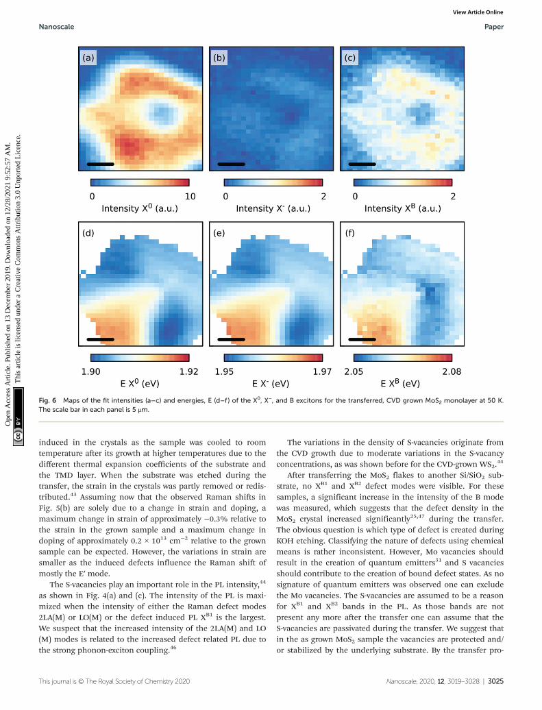
Fig. 6 shows the spatial distributions of the fit intensity andenergy of the X0 (a, d), X− (b, e), and B (c, f ) excitons at 50 K.The PL intensity is more homogeneous except at the center ofthe crystal because of the presence of the thicker seed-crystal.The spatial variations in the energy suggest that the strain wasreleased from the transfer, and/or another strain distributionwas induced in the sample, which can be understood asfollows. During the CVD growth of TMDs, the strain was
Fig. 5 (a) AFM images of the transferred MoS2 flake. The scale bar is 10 μm. (b) Correlation between the fitted Raman shift of the A’1 and E’ modesof the transferred and grown MoS2 crystals, taking only into account the influence of strain ε and doping n at 300 K. Temperature-dependent (c)Raman and (d) PL spectra at the same position of the MoS2 monolayer. As a comparison, also the Raman spectrum of the CVD grown MoS2 mono-layer from Fig. 1(d) is shown (grey line/dots). The black/grey line represents the sum of the fitted contributions of the individual modes; decompo-sition of the fit to the individual modes is shown in Fig. S23, S24, S26, S28, S30 and S32,† whereas the black/grey dots are the measured data points.
Paper Nanoscale
3024 | Nanoscale, 2020, 12, 3019–3028 This journal is © The Royal Society of Chemistry 2020
Ope
n A
cces
s A
rtic
le. P
ublis
hed
on 1
3 D
ecem
ber
2019
. Dow
nloa
ded
on 1
2/28
/202
1 9:
52:5
7 A
M.
Thi
s ar
ticle
is li
cens
ed u
nder
a C
reat
ive
Com
mon
s A
ttrib
utio
n 3.
0 U
npor
ted
Lic
ence
.View Article Online
induced in the crystals as the sample was cooled to roomtemperature after its growth at higher temperatures due to thedifferent thermal expansion coefficients of the substrate andthe TMD layer. When the substrate was etched during thetransfer, the strain in the crystals was partly removed or redis-tributed.43 Assuming now that the observed Raman shifts inFig. 5(b) are solely due to a change in strain and doping, amaximum change in strain of approximately −0.3% relative tothe strain in the grown sample and a maximum change indoping of approximately 0.2 × 1013 cm−2 relative to the grownsample can be expected. However, the variations in strain aresmaller as the induced defects influence the Raman shift ofmostly the E′ mode.
The S-vacancies play an important role in the PL intensity,44
as shown in Fig. 4(a) and (c). The intensity of the PL is maxi-mized when the intensity of either the Raman defect modes2LA(M) or LO(M) or the defect induced PL XB1 is the largest.We suspect that the increased intensity of the 2LA(M) and LO(M) modes is related to the increased defect related PL due tothe strong phonon-exciton coupling.46
The variations in the density of S-vacancies originate fromthe CVD growth due to moderate variations in the S-vacancyconcentrations, as was shown before for the CVD-grown WS2.
44
After transferring the MoS2 flakes to another Si/SiO2 sub-strate, no XB1 and XB2 defect modes were visible. For thesesamples, a significant increase in the intensity of the B modewas measured, which suggests that the defect density in theMoS2 crystal increased significantly25,47 during the transfer.The obvious question is which type of defect is created duringKOH etching. Classifying the nature of defects using chemicalmeans is rather inconsistent. However, Mo vacancies shouldresult in the creation of quantum emitters31 and S vacanciesshould contribute to the creation of bound defect states. As nosignature of quantum emitters was observed one can excludethe Mo vacancies. The S-vacancies are assumed to be a reasonfor XB1 and XB2 bands in the PL. As those bands are notpresent any more after the transfer one can assume that theS-vacancies are passivated during the transfer. We suggest thatin the as grown MoS2 sample the vacancies are protected and/or stabilized by the underlying substrate. By the transfer pro-
Fig. 6 Maps of the fit intensities (a–c) and energies, E (d–f ) of the X0, X−, and B excitons for the transferred, CVD grown MoS2 monolayer at 50 K.The scale bar in each panel is 5 μm.
Nanoscale Paper
This journal is © The Royal Society of Chemistry 2020 Nanoscale, 2020, 12, 3019–3028 | 3025
Ope
n A
cces
s A
rtic
le. P
ublis
hed
on 1
3 D
ecem
ber
2019
. Dow
nloa
ded
on 1
2/28
/202
1 9:
52:5
7 A
M.
Thi
s ar
ticle
is li
cens
ed u
nder
a C
reat
ive
Com
mon
s A
ttrib
utio
n 3.
0 U
npor
ted
Lic
ence
.View Article Online

cedure they are exposed to transfer the polymer and aggressiveKOH environment and thus they can be passivated. The trans-fer remnants could passivate the S vacancies, as was shownbefore for exfoliated MoS2 samples covered with either Al2O3
or HfO2. Nevertheless, they would not passivate theS-vacancies in between MoS2 and the substrate. Therefore weassume that the S-vacancies are passivated by treatment withKOH, which results in oxygen termination. This is furthermoreconsistent with previous theoretical work, which suggestedthat the oxygen passivation of the S-vacancies does not lead tolocalized states.48 We also assume that overall density ofdefects strongly increases after treatment with KOH, whichleads to the decrease of the total PL intensity.
The large differences in the PL spectra for the as-grown andtransferred MoS2 are better explained by considering the life-time of the excitons.25 Assuming that defects are introducedduring the transfer process, the transferred samples have moredefects. As the defects introduce nonradiative pathways toannihilate excitons, the total PL intensity decreases in pro-portion with the defect density. The radiative lifetimes of the Aand B excitons are approximately 800 and 1 ps, respectively,whereas the nonradiative recombination time is approximately10 ps. The total recombination time of the excitations in thecase of the nonradiative recombination significantly decreasesthe recombination time of the A exciton, resulting in a signifi-cantly reduced PL intensity. However, the influence on therecombination time of the B exciton is small due to its muchshorter radiative lifetime; thus, its PL intensity is not signifi-cantly changed.
IV. Conclusions
Well-defined monolayers of MoS2 were grown using CVD onSiO2/Si using MoO2 as a precursor. We transferred some of themonolayers onto another SiO2/Si substrate using a standardwet protocol and investigated the lattice and optical responsesby Raman and PL spectroscopy given a ∼1 μm spatial resolu-tion. We further generated temperature-dependent PL andRaman spectroscopy mappings of the as-grown and trans-ferred MoS2. For the as-grown sample, the Raman spectralmappings revealed a homogeneous spatial distribution andvery moderate temperature dependence, whereas there weresignificant spatial and thermal variations within the PL spec-tral maps. In general, the signal from the defect-induced exci-tons increased dramatically when cooling and dominated thespectra over the X0, B, and trion contributions. In the cryo-genic regime, the spatial distribution of the 2LA(M) Ramanmode, generally used as a measurement for defects, coincidedwell with the spatial distribution of the PL signal due to theXB1, X0, and trion. In contrast, the XB2 PL signal dominated atthe center of the flake edges. After the transfer, the B excitondominated the PL spectra while the defect-induced PL wasnegligible. This observation is consistent with the fact that anoverall larger transfer-induced defect density stimulates thenonradiative pathways for exciton annihilation.
We unambiguously demonstrated that the transfer processplays a significant role in the formation and location of defectsin MoS2. The relaxation mechanisms of the excitons atdifferent positions on the monolayer can be rigorously evalu-ated using cryogenic PL spectroscopy. Our study thus providesa reliable protocol to investigate lattice perturbations in TMDsmonolayers as well as in TMD-based heterostructures andsuperlattices.
Conflicts of interest
There are no conflicts to declare.
Acknowledgements
This research was funded by the European Research Council(ERC-Stg-716265) and the Czech Science Foundation (18-20357S). The low temperature experiments were conductedwith the support of MGML infrastructure, financed by theMEYS (LM2018096). The authors acknowledge the assistanceprovided by the Research Infrastructures NanoEnviCz (ProjectNo. LM2015073) supported by the Ministry of Education,Youth and Sports of the Czech Republic, and the project Pro-NanoEnviCz (Reg. No. CZ.02.1.01/0.0/0.0/16_013/0001821) sup-ported by the Ministry of Education, Youth and Sports of theCzech Republic, and the European Union – EuropeanStructural and Investments Funds in the frame of OperationalProgramme Research Development and Education.
References
1 K. F. Mak, C. Lee, J. Hone, J. Shan and T. F. Heinz, Phys.Rev. Lett., 2010, 105, 136805, DOI: 10.1103/physrevlett.105.136805.
2 A. Splendiani, L. Sun, Y. Zhang, T. Li, J. Kim, C.-Y. Chim,G. Galli and F. Wang, Nano Lett., 2010, 10, 1271, DOI:10.1021/nl903868w.
3 K. F. Mak, C. Lee, J. Hone, J. Shan and T. F. Heinz, Phys.Rev. Lett., 2010, 105, 136805, DOI: 10.1103/PhysRevLett.105.136805.
4 Z. Lin, A. McCreary, N. Briggs, S. Subramanian, K. Zhang,Y. Sun, X. Li, N. J. Borys, H. Yuan, S. K. Fullerton-Shirey,A. Chernikov, H. Zhao, S. McDonnell, A. M. Lindenberg,K. Xiao, B. J. LeRoy, M. Drndic, J. C. M. Hwang, J. Park,M. Chhowalla, R. E. Schaak, A. Javey, M. C. Hersam,J. Robinson and M. Terrones, 2D Mater., 2016, 3, 042001,DOI: 10.1088/2053-1583/3/4/042001.
5 W. Choi, N. Choudhary, G. H. Han, J. Park, D. Akinwandeand Y. H. Lee, Mater. Today, 2017, 20, 116, DOI: 10.1016/j.mattod.2016.10.002.
6 O. Lopez-Sanchez, D. Lembke, M. Kayci, A. Radenovic andA. Kis, Nat. Nanotechnol., 2013, 8, 497, DOI: 10.1038/nnano.2013.100.
Paper Nanoscale
3026 | Nanoscale, 2020, 12, 3019–3028 This journal is © The Royal Society of Chemistry 2020
Ope
n A
cces
s A
rtic
le. P
ublis
hed
on 1
3 D
ecem
ber
2019
. Dow
nloa
ded
on 1
2/28
/202
1 9:
52:5
7 A
M.
Thi
s ar
ticle
is li
cens
ed u
nder
a C
reat
ive
Com
mon
s A
ttrib
utio
n 3.
0 U
npor
ted
Lic
ence
.View Article Online

7 O. Lopez-Sanchez, E. Alarcon Llado, V. Koman,A. Fontcuberta i Morral, A. Radenovic and A. Kis, ACSNano, 2014, 8, 3042, DOI: 10.1021/nn500480u.
8 S. Wu, S. Buckley, J. R. Schaibley, L. Feng, J. Yan,D. G. Mandrus, F. Hatami, W. Yao, J. Vuckovic,A. Majumdar and X. Xu, Nature, 2015, 520, 69, DOI:10.1038/nature14290.
9 K. F. Mak, K. He, J. Shan and T. F. Heinz, Nat. Nanotechnol.,2012, 7, 494, DOI: 10.1038/NNANO.2012.96.
10 S. Tongay, J. Suh, C. Ataca, W. Fan, A. Luce, J. S. Kang,J. Liu, C. Ko, R. Raghunathanan, J. Zhou, F. Ogletree, J. Li,J. C. Grossman and J. Wu, Sci. Rep., 2013, 3, 2657, DOI:10.1038/srep02657.
11 S. Yuan, R. Roldán, M. I. Katsnelson and F. Guinea, Phys.Rev. B: Condens. Matter Mater. Phys., 2014, 90, 041402(R),DOI: 10.1103/PhysRevB.90.041402.
12 P. K. Chow, R. B. Jacobs-Gedrim, J. Gao, T.-M. Lu, B. Yu,H. Terrones and N. Koratkar, ACS Nano, 2015, 9, 1520, DOI:10.1021/nn5073495.
13 D. Rhodes, S. H. Chae, R. Ribeiro-Palau and J. Hone, Nat.Mater., 2019, 18, 541, DOI: 10.1038/s41563-019-0366-8.
14 S. Shree, A. George, T. Lehnert, C. Neumann, M. Benelajla,C. Robert, X. Marie, K. Watanabe, T. Taniguchi, U. Kaiser,B. Urbaszek and A. Turchanin, 2019, arXiv:1907.03342v1.
15 P. Vancsó, G. Z. Magda, J. Pető, J.-Y. Noh, Y.-S. Kim,C. Hwang, L. P. Biró and L. Tapasztó, Sci. Rep., 2016, 6,29726, DOI: 10.1038/srep29726.
16 D. Edelberg, D. Rhodes, A. Kerelsky, B. Kim, J. Wang,A. Zangiabadi, C. Kim, A. Abhinandan, J. Ardelean, M. Scully,D. Scullion, L. Embon, I. Zhang, R. Zu, E. J. G. Santos,L. Balicas, C. Marianetti, K. Barmak, X.-Y. Zhu, J. Hone andA. N. Pasupathy, arXiv:1805.00127v1, 2018.
17 V. K. Sangwan, H.-S. Lee, H. Bergeron, I. Balla, M. E. Beck,K.-S. Chen and M. C. Hersam, Nature, 2018, 554, 500, DOI:10.1038/nature25747.
18 H.-P. Komsa and A. V. Krasheninnikov, Phys. Rev. B:Condens. Matter Mater. Phys., 2015, 91, 125304, DOI:10.1103/PhysRevB.91.125304.
19 S. Haldar, H. Vovusha, M. K. Yadav, O. Eriksson andB. Sanyal, Phys. Rev. B: Condens. Matter Mater. Phys., 2015,92, 235408, DOI: 10.1103/PhysRevB.92.235408.
20 G. Wang, A. Chernikov, M. M. Glazov, T. F. Heinz, X. Marie,T. Amand and B. Urbaszek, Rev. Mod. Phys., 2018, 90,021001, DOI: 10.1103/RevModPhys.90.021001.
21 W. M. Parkin, A. Balan, L. Liang, P. M. Das, M. Lamparski,C. H. Naylor, J. A. Rodríguez-Manzo, A. T. Charlie Johnson,V. Meunier and M. Drndić, ACS Nano, 2016, 10, 4134, DOI:10.1021/acsnano.5b07388.
22 A. Michail, N. Delikoukos, J. Parthenios, C. Galiotis andK. Papagelis, Appl. Phys. Lett., 2016, 108, 173102, DOI:10.1063/1.4948357.
23 H. J. Conley, B. Wang, J. I. Ziegler, R. F. Haglund Jr.,S. T. Pantelides and K. I. Bolotin, Nano Lett., 2013, 13,3626, DOI: 10.1021/nl4014748.
24 B. Chakraborty, A. Bera, D. V. S. Muthu, S. Bhowmick,U. V. Waghmare and A. K. Sood, Phys. Rev. B: Condens.
Matter Mater. Phys., 2012, 85, 161403(R), DOI: 10.1103/PhysRevB.85.161403.
25 K. M. McCreary, A. T. Hanbicki, S. V. Sivaram andB. T. Jonker, APL Mater., 2018, 6, 111106, DOI: 10.1063/1.5053699.
26 J. Conley, B. Wang, J. I. Ziegler, R. F. Haglund Jr.,S. T. Pantelides and K. I. Bolotin, Nano Lett., 2013, 13,3626, DOI: 10.1021/nl4014748.
27 K. F. Mak, K. He, C. Lee, G. H. Lee, J. Hone, T. F. Heinz andJ. Shan, Nat. Mater., 2013, 12, 207, DOI: 10.1038/nmat3505.
28 J. Klein, A. Kuc, A. Nolinder, M. Altzschner, J. Wierzbowski,F. Sigger, F. Kreupl, J. J. Finley, U. Wurstbauer,A. W. Holleitner and M. Kaniber, 2D Mater., 2018, 5,011007, DOI: 10.1088/2053-1583/aa9642.
29 H. Nan, Z. Wang, W. Wang, Z. Liang, Y. Lu, Q. Chen, D. He,P. Tan, F. Miao, X. Wang, J. Wang and Z. Ni, ACS Nano,2014, 8, 5738, DOI: 10.1021/nn500532f.
30 V. Carozo, Y. Wang, K. Fujisawa, B. R. Carvalho,A. McCreary, S. Feng, Z. Lin, C. Zhou, N. Perea-López,A. L. Elías, B. Kabius, V. H. Crespi and M. Terrones, Sci.Adv., 2017, 3, e160281, DOI: 10.1126/sciadv.1602813.
31 J. Klein, M. Lorke, M. Florian, F. Sigger, L. Sigl, S. Rey,J. Wierzbowski, J. Cerne, K. Müller, E. Mitterreiter,P. Zimmermann, T. Taniguchi, K. Watanabe,U. Wurstbauer, M. Kaniber, M. Knap, R. Schmidt,J. J. Finley and A. W. Holleitner, Nat. Commun., 2019, 10,2755, DOI: 10.1038/s41467-019-10632-z.
32 Y. Xie, Z. Wang, Y. Zhan, P. Zhang, R. Wu, T. Jiang, S. Wu,H. Wang, Y. Zhao, T. Nan and X. Ma, Nanotechnology, 2017,28, 084001, DOI: 10.1088/1361-6528/aa5439.
33 I. Bilgin, F. Liu, A. Vargas, A. Winchester, M. K. L. Man,M. Upmanyu, K. M. Dani, G. Gupta, S. Talapatra,A. D. Mohite and S. Kar, ACS Nano, 2015, 9, 8822, DOI:10.1021/acsnano.5b02019.
34 Y.-C. Lin, W. Zhang, J.-K. Huang, K.-K. Liu, Y.-H. Lee,C.-T. Liang, C.-W. Chu and L.-J. Li, Nanoscale, 2012, 4,6637, DOI: 10.1039/C2NR31833D.
35 S. Mignuzzi, A. J. Pollard, N. Bonini, B. Brennan,I. S. Gilmore, M. A. Pimenta, D. Richards and D. Roy, Phys.Rev. B: Condens. Matter Mater. Phys., 2015, 91, 195411, DOI:10.1103/PhysRevB.91.195411.
36 D. Necas and P. Klapetek, Cent. Eur. J. Phys., 2012, 10, 181,DOI: 10.2478/s11534-011-0096-2.
37 S. Kataria, S. Wagner, T. Cusati, A. Fortunelli,G. Iannaccone, H. Pandey, G. Fiori and M. C. Lemme, Adv.Mater. Interfaces, 2017, 4, 1700031, DOI: 10.1002/admi.201700031.
38 X. Zhang, W. P. Han, J. B. Wu, S. Milana, Y. Lu, Q. Q. Li,A. C. Ferrari and P. H. Tan, Phys. Rev. B: Condens. MatterMater. Phys., 2013, 87, 115413, DOI: 10.1103/PhysRevB.87.115413.
39 Y. Yu, C. Li, Y. Liu, L. Su, Y. Zhang and L. Cao, Sci. Rep.,2013, 3, 1866, DOI: 10.1038/srep01866.
40 S. Tongay, J. Zhou, C. Ataca, J. Liu, J. S. Kang,T. S. Matthews, L. You, J. Li, J. C. Grossman and J. Wu,Nano Lett., 2013, 13, 2831, DOI: 10.1021/nl4011172.
Nanoscale Paper
This journal is © The Royal Society of Chemistry 2020 Nanoscale, 2020, 12, 3019–3028 | 3027
Ope
n A
cces
s A
rtic
le. P
ublis
hed
on 1
3 D
ecem
ber
2019
. Dow
nloa
ded
on 1
2/28
/202
1 9:
52:5
7 A
M.
Thi
s ar
ticle
is li
cens
ed u
nder
a C
reat
ive
Com
mon
s A
ttrib
utio
n 3.
0 U
npor
ted
Lic
ence
.View Article Online

41 A. Rodriguez, T. Verhagen, M. Kalbac, J. Vejpravova andO. Frank, Phys. Status Solidi RRL, 2019, 1900381, DOI:10.1002/pssr.201900381.
42 N. Saigala and S. Ghosh, Appl. Phys. Lett., 2016, 109,122105, DOI: 10.1063/1.4963133.
43 T. Hallam, N. C. Berner, C. Yim and G. S. Duesberg,Adv. Mater. Interfaces, 2014, 6, 2196, DOI: 10.1002/admi.201400115.
44 N. Peimyoo, J. Shang, C. Cong, X. Shen, X. Wu,E. K. L. Yeow and T. Yu, ACS Nano, 2013, 7, 10985, DOI:10.1021/nn4046002.
45 S. Dubey, S. Lisi, G. Nayak, F. Herziger, V.-D. Nguyen, T. LeQuang, V. Cherkez, C. González, Y. J. Dappe, K. Watanabe,
T. Taniguchi, L. Magaud, P. Mallet, J.-Y. Veuillen, R. Arenal,L. Marty, J. Renard, N. Bendiab, J. Coraux and V. Bouchiat,ACS Nano, 2017, 11, 11206–11216, DOI: 10.1021/acsnano.7b05520.
46 Q. H. Tan, Y.-J. Sun, X.-L. Liu, Y. Zhao, Q. Xiong, P.-H. Tanand J. Zhang, 2D Mater., 2017, 4, 031007, DOI: 10.1088/2053-1583/aa79bb.
47 M. Amani, M. L. Chin, A. L. Mazzoni, R. A. Burke,S. N. Pulickel, M. Ajayan, J. Lou and M. Dubey, Appl. Phys.Lett., 2014, 104, 203506, DOI: 10.1063/1.4873680.
48 H.-P. Komsa, J. Kotakoski, S. Kurasch, O. Lehtinen,U. Kaiser and A. V. Krasheninnikov, Phys. Rev. Lett., 2012,109, 035503, DOI: PhysRevLett.109.035503.
Paper Nanoscale
3028 | Nanoscale, 2020, 12, 3019–3028 This journal is © The Royal Society of Chemistry 2020
Ope
n A
cces
s A
rtic
le. P
ublis
hed
on 1
3 D
ecem
ber
2019
. Dow
nloa
ded
on 1
2/28
/202
1 9:
52:5
7 A
M.
Thi
s ar
ticle
is li
cens
ed u
nder
a C
reat
ive
Com
mon
s A
ttrib
utio
n 3.
0 U
npor
ted
Lic
ence
.View Article Online