Toward More Efficient Annealing-Based Placement for ... · Toward More E cient Annealing-Based...
71
Toward More Efficient Annealing-Based Placement for Heterogeneous FPGAs by Yingxuan Liu A thesis submitted in conformity with the requirements for the degree of Master of Applied Science Graduate Department of Electrical and Computer Engineering University of Toronto c Copyright 2014 by Yingxuan Liu
Transcript of Toward More Efficient Annealing-Based Placement for ... · Toward More E cient Annealing-Based...

Toward More Efficient Annealing-Based Placement for HeterogeneousFPGAs
by
Yingxuan Liu
A thesis submitted in conformity with the requirementsfor the degree of Master of Applied Science
Graduate Department of Electrical and Computer EngineeringUniversity of Toronto
c© Copyright 2014 by Yingxuan Liu

Abstract
Toward More Efficient Annealing-Based Placement for Heterogeneous FPGAs
Yingxuan Liu
Master of Applied Science
Graduate Department of Electrical and Computer Engineering
University of Toronto
2014
Simulated Annealing (SA) is a popular placement heuristic used in many commercial and academic
FPGA CAD tools. However, SA placement requires high runtime to produce good quality results. As
FPGAs continue to grow in size, runtime has become more crucial for SA-based placers. This thesis aims
to improve SA placement by making it more efficient in two key areas for large heterogeneous FPGAs:
move generation and placement cost evaluation.
This work shows that by using Median Region moves for heterogeneous architectures, the wirelength
is reduced by 5% while maintaining the same critical path delay. We also show that by using a better
search data structure the runtime is improved by 5%.
A new Timing Cost function incorporating Delay Budgets is introduced in this work, and it improves
the circuit speed by 4% with no degradation in wirelength. This cost function also performs better on
large circuits, where it improves circuit speed by 7%.
ii

Acknowledgements
I would like thank my supervisor Dr.Vaughn Betz for his guidance and support over the past two years.
He has been a wonderful mentor to me and shown a great passion for teaching.
My thank also goes to my wife Vivian and my family for their continued patience and encouragement
over the years.
And I feel grateful to spend the past two years with all the wonderful people here at UofT. It has
been a great experience for me.
iii

Contents
1 Introduction 1
1.1 Motivation . . . . . . . . . . . . . . . . . . . . . . . . . . . . . . . . . . . . . . . . . . . . 1
1.2 Contributions . . . . . . . . . . . . . . . . . . . . . . . . . . . . . . . . . . . . . . . . . . . 3
1.3 Organization . . . . . . . . . . . . . . . . . . . . . . . . . . . . . . . . . . . . . . . . . . . 3
2 Background 4
2.1 FPGA Overview . . . . . . . . . . . . . . . . . . . . . . . . . . . . . . . . . . . . . . . . . 4
2.2 FPGA CAD Flow . . . . . . . . . . . . . . . . . . . . . . . . . . . . . . . . . . . . . . . . 6
2.2.1 Logic Synthesis . . . . . . . . . . . . . . . . . . . . . . . . . . . . . . . . . . . . . . 6
2.2.2 Technology Mapping . . . . . . . . . . . . . . . . . . . . . . . . . . . . . . . . . . . 8
2.2.3 Clustering . . . . . . . . . . . . . . . . . . . . . . . . . . . . . . . . . . . . . . . . . 8
2.2.4 Placement . . . . . . . . . . . . . . . . . . . . . . . . . . . . . . . . . . . . . . . . . 9
2.2.5 Routing . . . . . . . . . . . . . . . . . . . . . . . . . . . . . . . . . . . . . . . . . . 11
2.3 VPR and Placement Quality . . . . . . . . . . . . . . . . . . . . . . . . . . . . . . . . . . 11
2.3.1 Placement Quality Metrics . . . . . . . . . . . . . . . . . . . . . . . . . . . . . . . 11
2.3.2 Cost Function . . . . . . . . . . . . . . . . . . . . . . . . . . . . . . . . . . . . . . . 13
2.3.3 VPR Placement Flow . . . . . . . . . . . . . . . . . . . . . . . . . . . . . . . . . . 15
2.4 Prior Work on Annealing Improvement . . . . . . . . . . . . . . . . . . . . . . . . . . . . . 17
2.4.1 Homogeneous Directed Moves . . . . . . . . . . . . . . . . . . . . . . . . . . . . . . 17
2.4.2 Delay Budgets . . . . . . . . . . . . . . . . . . . . . . . . . . . . . . . . . . . . . . 18
3 Move Generation 21
3.1 Overview . . . . . . . . . . . . . . . . . . . . . . . . . . . . . . . . . . . . . . . . . . . . . 21
3.2 Median Region Moves . . . . . . . . . . . . . . . . . . . . . . . . . . . . . . . . . . . . . . 21
3.2.1 Motivations . . . . . . . . . . . . . . . . . . . . . . . . . . . . . . . . . . . . . . . . 21
3.2.2 Implementation . . . . . . . . . . . . . . . . . . . . . . . . . . . . . . . . . . . . . . 22
3.2.3 Experimental Results . . . . . . . . . . . . . . . . . . . . . . . . . . . . . . . . . . 23
3.2.4 Conclusion . . . . . . . . . . . . . . . . . . . . . . . . . . . . . . . . . . . . . . . . 32
3.3 Smart Search Space . . . . . . . . . . . . . . . . . . . . . . . . . . . . . . . . . . . . . . . 33
3.3.1 Motivations . . . . . . . . . . . . . . . . . . . . . . . . . . . . . . . . . . . . . . . . 33
3.3.2 Implementation . . . . . . . . . . . . . . . . . . . . . . . . . . . . . . . . . . . . . . 34
3.3.3 Experimental Results . . . . . . . . . . . . . . . . . . . . . . . . . . . . . . . . . . 35
3.4 Conclusion . . . . . . . . . . . . . . . . . . . . . . . . . . . . . . . . . . . . . . . . . . . . 37
iv

4 Cost Function 38
4.1 Cost Function Tuning . . . . . . . . . . . . . . . . . . . . . . . . . . . . . . . . . . . . . . 38
4.1.1 Motivations . . . . . . . . . . . . . . . . . . . . . . . . . . . . . . . . . . . . . . . . 38
4.1.2 Experimental Results . . . . . . . . . . . . . . . . . . . . . . . . . . . . . . . . . . 38
4.1.3 Conclusion . . . . . . . . . . . . . . . . . . . . . . . . . . . . . . . . . . . . . . . . 44
4.2 Delay Budget . . . . . . . . . . . . . . . . . . . . . . . . . . . . . . . . . . . . . . . . . . . 46
4.2.1 Motivations . . . . . . . . . . . . . . . . . . . . . . . . . . . . . . . . . . . . . . . . 46
4.2.2 Delay Budget Timing Cost Function . . . . . . . . . . . . . . . . . . . . . . . . . . 47
4.2.3 Delay Budget Computation . . . . . . . . . . . . . . . . . . . . . . . . . . . . . . . 49
4.2.4 Iterative-minimax-PERT: Implementation . . . . . . . . . . . . . . . . . . . . . . . 50
4.2.5 Iterative-minimax-PERT: Experimental Results . . . . . . . . . . . . . . . . . . . . 50
4.2.6 Direct Slack: Implementation . . . . . . . . . . . . . . . . . . . . . . . . . . . . . . 51
4.2.7 Direct Slack: Experimental Results . . . . . . . . . . . . . . . . . . . . . . . . . . . 53
4.2.8 Conclusion . . . . . . . . . . . . . . . . . . . . . . . . . . . . . . . . . . . . . . . . 57
5 Conclusion 59
5.1 Summary . . . . . . . . . . . . . . . . . . . . . . . . . . . . . . . . . . . . . . . . . . . . . 59
5.2 Future Directions . . . . . . . . . . . . . . . . . . . . . . . . . . . . . . . . . . . . . . . . . 60
Bibliography 61
v

List of Tables
3.1 Median Region move Experiment Architecture stats. . . . . . . . . . . . . . . . . . . . . . 24
3.2 Largest 5 circuits from the VTR benchmark suite stats[24]. . . . . . . . . . . . . . . . . . 25
3.3 MR QoR Comparison between High and Medium chip utilization (VTR Benchmarks). . . 31
3.4 Placement QoR Comparison between not omitting and omitting high fan-out nets for MR
moves (VTR Benchmarks normalized vs original VPR results). . . . . . . . . . . . . . . . 31
3.5 Smart Search Space results ranking by chip size . . . . . . . . . . . . . . . . . . . . . . . . 37
4.1 Delta Timing Cost using Original VPR Timing Cost Function. . . . . . . . . . . . . . . . 47
4.2 Delta Timing Cost using New VPR Timing Cost Function. . . . . . . . . . . . . . . . . . 49
4.3 PERT Delay Budget Experiment Architecture Stats. . . . . . . . . . . . . . . . . . . . . . 50
4.4 PERT Delay Budget Experiment Architecture Files. . . . . . . . . . . . . . . . . . . . . . 51
4.5 QoR of Delay Budget with PERT method vs Original VPR using “arch1” and VTR
benchmarks. . . . . . . . . . . . . . . . . . . . . . . . . . . . . . . . . . . . . . . . . . . . . 51
4.6 QoR of Delay Budget with PERT method vs Original VPR using “arch2” and VTR
benchmarks. . . . . . . . . . . . . . . . . . . . . . . . . . . . . . . . . . . . . . . . . . . . . 52
4.7 QoR of Delay Budget with PERT method vs Original VPR using “arch3” and MCNC
benchmarks. . . . . . . . . . . . . . . . . . . . . . . . . . . . . . . . . . . . . . . . . . . . . 52
4.8 Direct Slack Results using N10 VTR benchmarks. . . . . . . . . . . . . . . . . . . . . . . 54
4.9 Direct Slack Results using N10 VTR benchmarks normalized vs Original VPR. . . . . . . 55
4.10 Direct Slack Results using N10 VTR benchmarks normalized vs Original VPR (Largest 5). 55
4.11 Direct Slack Results using N4 VTR benchmarks. . . . . . . . . . . . . . . . . . . . . . . . 56
4.12 Direct Slack Results using N4 MCNC benchmarks. . . . . . . . . . . . . . . . . . . . . . . 57
vi

List of Figures
1.1 Typical FPGA CAD flow. . . . . . . . . . . . . . . . . . . . . . . . . . . . . . . . . . . . . 2
1.2 FPGA capacity and CPU speed growth in the 2000s [2]. . . . . . . . . . . . . . . . . . . . 3
2.1 FPGA Basic Logic Element and Configurable Logic Block [3]. . . . . . . . . . . . . . . . . 5
2.2 Island Style Homogeneous FPGA Architecture. . . . . . . . . . . . . . . . . . . . . . . . . 5
2.3 FPGA Connection and Switch Boxes. . . . . . . . . . . . . . . . . . . . . . . . . . . . . . 6
2.4 Heterogeneous FPGA Architecture [13]. . . . . . . . . . . . . . . . . . . . . . . . . . . . . 7
2.5 VTR CAD Flow [24]. . . . . . . . . . . . . . . . . . . . . . . . . . . . . . . . . . . . . . . . 12
2.6 VPR Placement Pseudo Code [3]. . . . . . . . . . . . . . . . . . . . . . . . . . . . . . . . . 16
2.7 Median Region Move [28]. . . . . . . . . . . . . . . . . . . . . . . . . . . . . . . . . . . . . 18
2.8 MR Moves: Cell Shuffling [28]. . . . . . . . . . . . . . . . . . . . . . . . . . . . . . . . . . 19
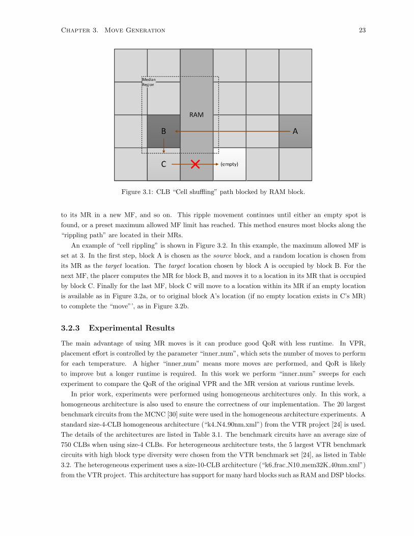
3.1 CLB “Cell shuffling” path blocked by RAM block. . . . . . . . . . . . . . . . . . . . . . . 23
3.2 Cell Rippling with 3 MFs. . . . . . . . . . . . . . . . . . . . . . . . . . . . . . . . . . . . . 24
3.3 QoR vs. fraction of moves are MR type for various placer effort levels (VTR Benchmarks). 26
3.4 QoR vs. fraction of moves are MR type for various placer effort levels (MCNC Benchmarks). 27
3.5 Median Region Cell Rippling Move Fragment sweep (VTR Benchmarks). . . . . . . . . . 29
3.6 Median Region Cell Rippling MF sweep for medium chip utilization (VTR Benchmarks) . 30
3.7 Median Region produces same QoR as original VPR at lower runtime (VTR Benchmarks). 32
3.8 Size-1 range limit for CLBs in a Homogeneous Architecture. . . . . . . . . . . . . . . . . . 33
3.9 Size-1 “‘window” for CLB in Heterogeneous Architecture. . . . . . . . . . . . . . . . . . . 34
3.10 Size-1 “window” for RAM. . . . . . . . . . . . . . . . . . . . . . . . . . . . . . . . . . . . . 35
3.11 Size-1 “‘window” for CLB with SSS. . . . . . . . . . . . . . . . . . . . . . . . . . . . . . . 36
3.12 Size-1 “window” for RAM with SSS. . . . . . . . . . . . . . . . . . . . . . . . . . . . . . . 36
4.1 Cost Function Trade-off Sweep (VTRBM). . . . . . . . . . . . . . . . . . . . . . . . . . . . 39
4.2 Cost Function Tradeoff Sweep 0.1 to 0.9 (VTRBM). . . . . . . . . . . . . . . . . . . . . . 40
4.3 Criticality Exponent Sweep WDP Comparison (λ 0.1 to 0.9). . . . . . . . . . . . . . . . . 41
4.4 Criticality Exponent Sweep WDP Comparison (λ 0.1 to 0.5). . . . . . . . . . . . . . . . . 41
4.5 Criticality Exponent Sweep Delay Comparison (λ 0.1 to 0.5). . . . . . . . . . . . . . . . . 42
4.6 Criticality Exponent Sweep Wirelength Comparison (λ 0.1 to 0.5). . . . . . . . . . . . . . 42
4.7 Criticality Exponent Sweep QoR Comparison (λ = 0.2). . . . . . . . . . . . . . . . . . . . 43
4.8 Criticality Exponent Sweep QoR Comparison (λ = 0.5). . . . . . . . . . . . . . . . . . . . 43
4.9 Changing Criticality Values for Various Critical Paths over an Annealing Process (final
CE= 8). . . . . . . . . . . . . . . . . . . . . . . . . . . . . . . . . . . . . . . . . . . . . . . 44
vii

4.10 Changing Criticality Values for Various Critical Paths over an Annealing Process (final
CE= 30). . . . . . . . . . . . . . . . . . . . . . . . . . . . . . . . . . . . . . . . . . . . . . 45
4.11 QoR comparison between final CE = 8 and 30 for various placer efforts (λ = 0.2). . . . . 45
4.12 QoR comparison between final CE = 8 and 30 for various placer efforts (λ = 0.5). . . . . 46
4.13 Example where the Timing Cost Function fails to identify a “bad move”. . . . . . . . . . 48
viii

Chapter 1
Introduction
Over the past several decades, Integrated Circuits (ICs) have been used in a wide range of applications
from personal mobile devices to large medical equipment. The size and performance of modern ICs has
been growing as per Moore’s law, with the transistor count doubling every two years, and this trend is
expected to continue [22]. Field-Programmable Gate Arrays (FPGAs), as one of the major IC types,
have been following the same trend. Their once simple architecture, which only consisted of hundreds
of Logic and Input/Output (I/O) elements, has grown into more complex architectures that contain up
to millions of logic elements along with various hard blocks such as Random Access Memory (RAM),
Digital Signal Processing (DSP) units, and more. Manual implementation of a design in an FPGA is no
longer manageable.
Computer-Aided Design (CAD) tools were invented to help IC designers deal with large IC designs.
Furthermore, CAD tools increase design efficiency, and shorten turn around time. As the size and
complexity of FPGAs continue to grow, it is more important for FPGA CAD tools to be able to deliver a
high Quality-of-Result (QoR) solution while maintaining reasonable runtime. Many steps of the FPGA
CAD flow are runtime expensive; thus much research has focused on finding high quality heuristics.
However, most of the previous research has used homogeneous architectures rather than the modern
heterogeneous architectures (employed by most commercial FPGAs). The move to heterogeneous FPGAs
has created a new set of FPGA CAD research challenges and opportunities, and the ever increasing size
of FPGA designs motivates new research into fast but high quality CAD.
1.1 Motivation
The FPGA CAD flow is normally broken into 5 steps as shown in Figure 1.1. Placement, the step
which connects the upstream clustering and downstream routing stages, is responsible for determining
the locations of all the blocks of the circuit. Interconnect delay has become the dominant component
of circuit delay in the deep submicron process era, and in an FPGA this delay is largely determined by
placement. Placing connected blocks closer together reduces delays and improves circuit performance.
The quality of placement also directly affects routability, congestion, and power.
Placement is one of the most timing consuming steps in the FPGA CAD flow. Depending on the
circuit size and optimization level, it can take hours or even days to complete [15] [23]. For example, one
circuit from the Titan benchmark suite, “sparcT1 chip2 ”, which contains approximately 815,000 blocks,
1
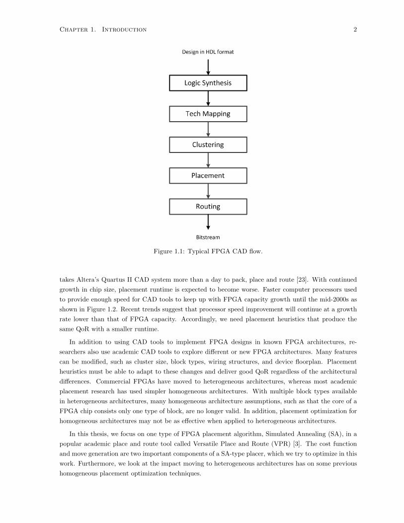
Chapter 1. Introduction 2
Figure 1.1: Typical FPGA CAD flow.
takes Altera’s Quartus II CAD system more than a day to pack, place and route [23]. With continued
growth in chip size, placement runtime is expected to become worse. Faster computer processors used
to provide enough speed for CAD tools to keep up with FPGA capacity growth until the mid-2000s as
shown in Figure 1.2. Recent trends suggest that processor speed improvement will continue at a growth
rate lower than that of FPGA capacity. Accordingly, we need placement heuristics that produce the
same QoR with a smaller runtime.
In addition to using CAD tools to implement FPGA designs in known FPGA architectures, re-
searchers also use academic CAD tools to explore different or new FPGA architectures. Many features
can be modified, such as cluster size, block types, wiring structures, and device floorplan. Placement
heuristics must be able to adapt to these changes and deliver good QoR regardless of the architectural
differences. Commercial FPGAs have moved to heterogeneous architectures, whereas most academic
placement research has used simpler homogeneous architectures. With multiple block types available
in heterogeneous architectures, many homogeneous architecture assumptions, such as that the core of a
FPGA chip consists only one type of block, are no longer valid. In addition, placement optimization for
homogeneous architectures may not be as effective when applied to heterogeneous architectures.
In this thesis, we focus on one type of FPGA placement algorithm, Simulated Annealing (SA), in a
popular academic place and route tool called Versatile Place and Route (VPR) [3]. The cost function
and move generation are two important components of a SA-type placer, which we try to optimize in this
work. Furthermore, we look at the impact moving to heterogeneous architectures has on some previous
homogeneous placement optimization techniques.

Chapter 1. Introduction 3
Figure 1.2: FPGA capacity and CPU speed growth in the 2000s [2].
1.2 Contributions
With millions of logic elements on a chip, the compile time of clustering-placement-routing has gone from
minutes to hours. This increases the design turn-around time using FPGAs, and it will increase further
with future technology generations, motivating recent research into increasing placement efficiency. One
such method is to propose “directed moves” as opposed to random moves [28] [8]. Both these prior works,
however, used only homogeneous architectures. In our work, we implement Median Region moves from
[28] but adapt them to heterogeneous architectures. We also develop a technique to find valid “move-to”
locations more efficiently than the original random search in VPR.
For Simulated Annealing (SA) placement, the cost function quantifies the quality of a design imple-
mentation proposed during annealing. Each component can contribute a different fraction of the total
cost, and it is controlled by a tradeoff weight. Wirelength and critical path delay are two of the most
commonly used design metrics for FPGA placement. Besides the cost function tradeoff, there are a few
other parameters that can affect the QoR in SA placement. In this work we also examine the QoR effect
of those parameters.
For a practical design, the maximum operating frequency (Fmax) is directly proportional to the
inverse of critical path delay, i.e. the slowest path in the circuit. The default cost function in the
VPR placer uses criticality to identify connections that would more likely affect the critical path delay.
However, the current implementation gives limited freedom of movement to less critical connections
and this could restrict some potentially better moves for highly critical connections. In this work we
implement a new timing cost function in VPR that uses the “Delay Budget” concept to increase freedom
of movement.
1.3 Organization
The rest of this thesis is organized as follows. Chapter 2 describes prior work in FPGA architecture and
CAD, particularly placement, and summarizes VPR. Chapter 3 describes the first group of techniques
which relate to placement move generation. Chapter 4 introduces the second group of optimization
improvements which relate to the placement cost function. Finally Chapter 5 concludes, summarizes the
results, and describes some possible future directions.

Chapter 2
Background
2.1 FPGA Overview
Unlike other major IC types, such as Application Specific Integrated Circuits (ASICs), all blocks and
interconnects on a FPGA are prefabricated. The fundamental element on a modern FPGA is a Basic
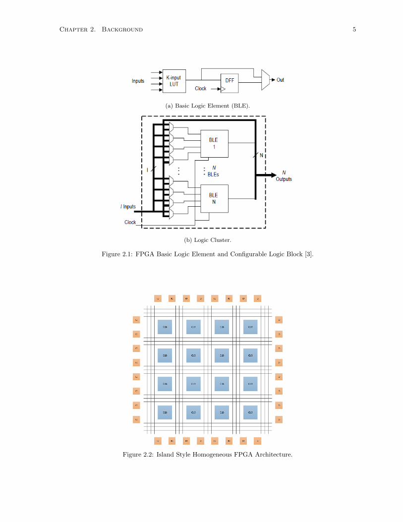
Logic Element (BLE), as shown in Figure 2.1a. A typical BLE consists of a k -input Lookup Table
(LUT), a flipflop, and a MUX. The k -input LUT can be programmed to implement any k -input Boolean
function. The output of a BLE can be either synchronous or asynchronous depending on the MUX
selection. In modern FPGA architectures it is common that a number of BLEs are grouped in a single
Configurable Logic Block (CLB), as shown in Figure 2.1b. Each CLB has N BLEs, I input ports and N
output ports. There are also connections between some BLE outputs and BLE inputs. Crossbars and
MUXes are placed at BLE inputs and outputs to allow flexible connections. Modern FPGAs often have
a size-6 fracturable LUT inside each BLE, and 10 or more BLEs inside a single CLB.
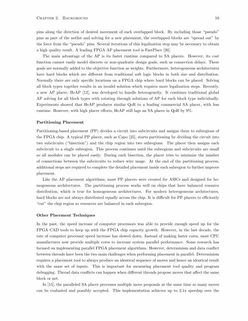
For classic homogeneous FPGAs, as shown in Figure 2.2, wires connecting the CLBs run in both
the horizontal and vertical directions in the space between the CLBs. CLBs are arranged to form a
grid with IO blocks generally located on the periphery. This is often referred to as the Island Style
FPGA [6], and many commercial FPGAs are based on a similar style. Each wiring channel consists of a
number of wiring tracks, and this number is the Channel Width (W). The length of each wire segment
is represented as the number of CLBs it spans. Multiple wire lengths are common in FPGAs to allow
faster connections and better routing flexibility.
CLBs are connected to their adjacent wiring channels through Connection Boxes (CBs) as shown in
Figure 2.3. Switch Boxes (SBs) are used to connect different wire segments together along the same or
different directions. Connections are programmable inside CBs and SBs by using SRAMs. Both the CB
pin connection pattern and SB switching pattern can affect routability and the final CAD QoR, which
is a research topic on its own [20].
For modern FPGAs, the main structure is still Island style but many new block types are incorporated
in the FPGA besides logic blocks. As shown in Figure 2.4, an example from Altera’s Stratix family [13],
the majority of the chip is occupied by soft logic blocks (called “LABs” in Altera devices), but hard blocks
such as RAMs and DSPs are also found among them. These hard blocks are normally larger than CLBs
in size and are distributed more sparsely across the chip. Such FPGA architectures, i.e. heterogeneous
architectures, are relatively new to academic research. Most of the past, as well as some of the current
4
Chapter 2. Background 5
(a) Basic Logic Element (BLE).
(b) Logic Cluster.
Figure 2.1: FPGA Basic Logic Element and Configurable Logic Block [3].
Figure 2.2: Island Style Homogeneous FPGA Architecture.

Chapter 2. Background 6
Figure 2.3: FPGA Connection and Switch Boxes.
FPGA CAD research, has been using homogeneous as opposed to heterogeneous architectures.
2.2 FPGA CAD Flow
The basic goal of the Very Large Scale Integration (VLSI) design flow is to transform a description
of the design into an implementation on a target platform. In the past, when there were only a few
hundreds or thousands of elements in a design, designers were able to manually lay out the whole design
with a reasonable amount of effort, and still achieve good performance. However, in modern FPGAs,
hundreds of thousands or even millions of elements may be involved in a design; it is no longer suitable
for humans to accomplish such a task manually. This problem is taken care of by CAD tools which
help designers their increase productivity, reduce human design errors, and most importantly, find high
quality solutions more effectively.
Furthermore, to achieve high performance, design optimization for speed, area, and/or power is
beneficial at each stage of the CAD flow. With increasing chip size and more complex structures, it has
becoming more difficult for CAD tools to continue delivering high quality results within a reasonable
runtime.
Generally the CAD flow is broken into several steps so each step focuses on one task to achieve high
quality results. For a typical FPGA CAD flow, as shown in Figure 1.1, there are normally 5 steps: logic
synthesis, technology mapping, clustering (packing), placement, and routing. Each step takes the result
from the previous step as its input, and passes its solution to the next step, typically with no back
tracking. The following is a brief description of each FPGA CAD flow step.
2.2.1 Logic Synthesis
Circuit designs are often represented in Hardware Description Language (HDL) format. There are
currently two major HDLs, VHSIC Hardware Description Language (VHDL) and Verilog. During the
Synthesis step, the HDL description is translated into gate-level format and optimized to reduce circuit
resource demand. A common academic format is Berkeley Logic Interchange Format (BLIF) [1]. ODIN

Chapter 2. Background 7
Figure 2.4: Heterogeneous FPGA Architecture [13].

Chapter 2. Background 8
II is a popular academic HDL synthesis tool [14], which provides support for FPGA soft logic blocks as
well as several modern hard blocks.
2.2.2 Technology Mapping
With a netlist of the design produced from the Synthesis step, an FPGA CAD tool then maps each
design element onto the primitive blocks (such as LUTs, flip-flops, RAMs and etc) provided by the
target FPGA architecture. Various logic optimizations with goals such as reducing the number of LUT
inputs, LUT depth, and point-to-point delays, are performed during this step to simplify the design
complexity [7]. A commonly used academic technology mapping tool is ABC [5].
2.2.3 Clustering
The output of Technology Mapping is a netlist with all of its elements mapped to the target FPGA
architecture. During Clustering (Packing), the goal is to transform a netlist of primitives into a netlist
of cluster-level blocks. In general a CLB provides faster interconnects (intra-CLB connections) between
its resident BLEs than the general routing connections between CLBs (inter-CLB connections). Thus
the packer tries to pack as many BLEs into the same CLB as possible to improve delays. Also, by doing
so, more nets are absorbed, which reduces the stress on both placement and routing.
An early popular FPGA clustering algorithm is VPack [3], which has an objective of minimizing logic
cluster count. VPack starts by packing an unclustered logic cell with the highest amount of inputs. This
logic cell is called the “seed” of the cluster. The packer then computes the “attraction” value of all the
unclustered logic cells with respect to the current cluster. The “attraction” is defined as the number
of inputs and outputs shared by an unclustered logic cell and the target cluster. Logic cells with the
highest “attraction” values are packed until the current cluster is full. The packer then starts with a
new seed cell and cluster. This process is repeated until all the logic cells are packed.
VPack is effective at reducing the number of clusters, but has the disadvantage of ignoring timing
information during clustering. An enhanced version of VPack, “T-VPack”, was developed to take timing
into account [19]. T-VPack added timing criticality information to the “attraction” formulation. The
criteria for packing a cluster is based on both connectivity and timing criticality. Results from T-VPack
showed good improvement in both wirelength and circuit delay compared to VPack.
Neither VPack or T-VPack, however, was designed to deal with heterogeneous architectures and
blocks other than CLBs. Hard blocks often have different properties than CLBs so homogeneous packers
cannot be directly applied. Furthermore, both VPack and T-VPack assume that a full crossbar is
available in each CLB so full connectivity exists between all resident BLEs. This optimistic assumption
allows packers to avoid a routing legality check inside CLBs thus shortening runtime. In reality, however,
there is only a partial crossbar available inside each CLB to keep wiring and area costs in check. A new
timing-driven packer, AAPack [16], was developed to deal with these issues. AAPack is similar to VPack
and T-VPack in its basic CLB packing algorithm with a few additional greedy techniques to improve
QoR and runtime. It supports more general packing, including packing hard blocks like RAMs and
DSPs. Furthermore, it performs a routing legality check for connections inside blocks to ensure packing
correctness. Overall AAPack can handle heterogeneous architectures and produces better QoR than its
predecessors.

Chapter 2. Background 9
Prior research has also proposed the idea of combining clustering with placement [8] to allow logic
cells moving between clusters during placement to “repair” earlier low quality clustering decisions.
2.2.4 Placement
During placement, the placer tries to find a legal solution such that all blocks are assigned to a valid
location on the target FPGA chip. It also optimizes for several design goals, such as wirelength, circuit
delay, routing congestion, and power consumption. Because the locations of the blocks are normally
fixed after the placement stage, and placement has a high impact on routing quality, it is very important
that the placement heuristic can produce a high quality solution. Most FPGA placement algorithms
can be categorized into three types: Simulated Annealing, Analytical, and Partitioning-Based.
Simulated Annealing
Simulated Annealing (SA), as its name implies, mimics the metal annealing process. During annealing,
metal is heated to a high temperature to allow atoms to move more freely to find better locations and
relative arrangements. The metal is then cooled down to let atoms settle and form strong bonds between
them. At the beginning of the SA process, a random valid placement is used as the starting point along
with an initial temperature. The block movements are controlled by a cost (objective) function, which
can be defined to focus on one or a few design goals.
The placer proposes moves randomly during the SA process. Each potential move, which is either
an exchange of locations between two blocks of the same type, or a movement of a block to a valid
empty space, would induce a change in the placement cost. This change, or “∆C”, is used by the
annealer to make move decisions. Similar to the metal annealing process, moves have a higher chance
to be accepted at higher temperatures even if the delta cost is positive (increasing the total cost, i.e. a
“bad move”). It is necessary to do this (“hill climbing”) during SA to reduce the chance of becoming
entrapped at local minima. “Good moves”, moves that reduce the overall cost, are always accepted. As
the temperature drops, the annealer will accept fewer “bad moves”. The SA process will eventually stop
when a predefined exit criteria is met.
One of the advantages of SA placement is the versatility of its cost function. This allows it to
combine different optimization goals and arbitrary constraints for different architectures. However,
producing good QoR using SA placement generally requires a long annealing time. Therefore much
research effort has been on reducing runtime for SA placement. In our work, the main focus is also
on reducing runtime, while minimizing the impact on quality. A popular academic FPGA CAD tool,
Versatile Place and Route (VPR), which uses SA as its placement heuristic, is used throughout this
work. VPR and its SA placement algorithm will be described in detail in Section 2.3.
Analytical Placement
Analytical placement (AP) is another popular placement technique originally developed for ASICs. It
models all multi-pin nets using one of the net models, such as clique and star models. It uses an objective
function, commonly the sum of the squared wirelength between every pair of nodes in each net. The
optimal locations for all nodes are obtained by solving the quadratic function for the X and Y dimensions
separately. The solution, however, normally contains block overlaps, and additional legalization steps are
required to remove the overlaps. One of the AP legalization techniques involves adding fixed “pseudo”
Chapter 2. Background 10
pins along the direction of desired movement of each overlapped block. By including those “pseudo”
pins as part of the netlist and solving for a new placement, the overlapped blocks are “spread out” by
the force from the “pseudo” pins. Several iterations of this legalization step may be necessary to obtain
a high quality result. A leading FPGA AP placement tool is FastPlace [26].
The main advantage of the AP is its faster runtime compared to SA placers. However, its cost
function cannot easily model discrete or non-quadratic design goals, such as connection delays. These
goals are normally added to the objective function as weights. Furthermore, heterogeneous architectures
have hard blocks which are different from traditional soft logic blocks in both size and distribution.
Normally there are only specific locations on a FPGA chip where hard blocks can be placed. Solving
all block types together results in an invalid solution which requires more legalization steps. Recently,
a new AP placer, HeAP [12], was developed to handle heterogeneity. It combines traditional global
AP solving for all block types with rotating through solutions of AP for each block type individually.
Experiments showed that HeAP produces similar QoR to a leading commercial SA placer, with less
runtime. However, with high placer efforts, HeAP still lags an SA placer in QoR by 9%.
Partitioning Placement
Partitioning-based placement (PP) divides a circuit into subcircuits and assigns them to subregions of
the FPGA chip. A typical PP placer, such as Capo [25], starts partitioning by dividing the circuit into
two subcircuits (“bisection”) and the chip region into two subregions. The placer then assigns each
subcircuit to a single subregion. This process continues until the subregions and subcircuits are small
so all modules can be placed easily. During each bisection, the placer tries to minimize the number
of connections between the subcircuits to reduce wire usage. At the end of the partitioning process,
additional steps are required to complete the detailed placement inside each subregion to further improve
placement.
Like the AP placement algorithms, most PP placers were created for ASICs and designed for ho-
mogeneous architectures. The partitioning process works well on chips that have balanced resource
distribution, which is true for homogeneous architectures. For modern heterogeneous architectures,
hard blocks are not always distributed equally across the chip. It is difficult for PP placers to efficiently
“cut” the chip region so resources are balanced in each subregion.
Other Placement Techniques
In the past, the speed increase of computer processors was able to provide enough speed up for the
FPGA CAD tools to keep up with the FPGA chip capacity growth. However, in the last decade, the
rate of computer processor speed increase has slowed down. Instead of making faster cores, most CPU
manufactures now provide multiple cores to increase system parallel performance. Some research has
focused on implementing parallel FPGA placement algorithms. However, determinism and data conflict
between threads have been the two main challenges when performing placement in parallel. Determinism
requires a placement tool to always produce an identical sequence of moves and hence an identical result
with the same set of inputs. This is important for measuring placement tool quality and program
debugging. Thread data conflicts can happen when different threads propose moves that affect the same
block or net.
In [15], the paralleled SA placer processes multiple move proposals at the same time so many moves
can be evaluated and possibly accepted. This implementation achieves up to 2.1x speedup over the

Chapter 2. Background 11
sequential version while maintaining determinism. However, the performance does not scale well beyond
4 cores (threads).
Another promising parallel implementation is [29]. This method uses a partitioning-like approach to
divide the FPGA chip into regions. The number of regions equals the number of processor cores available.
Each region is further divided into subregions and only one subregion from each region is optimized at
a given time. This guarantees there will be no overlap between two subregions so no move conflicts can
occur. Each subregion also has a small “extended region” overlapping with the neighboring subregions
to allow some inter-region movement. The placer periodically pauses and allow subregions to exchange
placement updates with the other subregions to limit how stale placement information from other regions
can become. This algorithm can achieve more than 35x speedup on a 25-core system with 8% increase
in delay and 11% increase in wirelength. Further experiments showed good scalability beyond 25 cores.
The followup work [29] improves the region decomposition so inter-region and cross-chip movements are
easier and more frequent. The improved algorithm achieves 51x speedup on a 16-core system. Despite a
great speedup in runtime, this implementation has a significant QoR degradation and was only applied
to a homogeneous architecture.
2.2.5 Routing
Routing is the final step of the FPGA CAD flow, and its main goal is to establish all pin-to-pin con-
nections between all connected blocks. FPGA routing is different from ASIC routing because it can
only use the prefabricated resources, such as wire segments, Connection Boxes (CBs), and Switch Boxes
(SBs). Routibility is a measure of how easily a router can successfully route all connections. Other
important optimization parameters include wirelength, delay, congestion, and power. Modern FPGA
routers perform global and detail routing in one step but normally require several iterations to remove
congestion and achieve good QoR [3] [21].
2.3 VPR and Placement Quality
Versatile Place and Route (VPR) [3] [17] is, perhaps, the most popular and successful academic FPGA
place and route tool available. Introduced more than ten years ago, VPR is an open source software, and
over the years developers have been adding features to allow it to keep up with new FPGA technology
trends. Although there is a significant quality gap between VPR and the leading commercial FPGA
CAD tools [23], VPR provides accurate feedback and a useful framework for much research. It offers the
flexibility to explore different architectural designs, which the commercial tools lack. VPR is also part
of the Verilog-to-Routing (VTR) flow [24], which is an open source FPGA CAD flow package that offers
a complete synthesis flow solution, as shown in Figure 2.5. All work and experiments in this thesis have
been conducted with the VTR flow.
2.3.1 Placement Quality Metrics
Design cost and circuit speed are the two most important metrics for most IC designs. The cost of a
design is proportional to the area required. The area of a design is directly related to the number of logic
elements (CLBs, RAMs, DSPs, and etc) used in a design. This is normally dependent on the upstream
logic synthesis tools and clustering flow which try to ensure the minimum resources are required. Cluster

Chapter 2. Background 12
Figure 2.5: VTR CAD Flow [24].
Chapter 2. Background 13
count generally stays unchanged throughout the rest of the flow after clustering (with the exception of
Physical Synthesis, which VPR does not employ). Another important design parameter is power, which
is affected by the amount of wiring used. A high quality placement solution usually requires fewer wires
in a wiring channel.
Circuit speed has been one of the two main objectives in academic FPGA placement tools along with
wirelength. This is commonly measured as “critical path delay”, which is the delay of the slowest path
of the circuit. By using a cost (objective) function, the placer can focus on minimizing this delay so the
final circuit can run at maximum speed without any timing violation.
Another metric for measuring placement quality is the amount of CPU runtime required. High
runtime means a longer design turn-around cycle, and thus can increase the design cost. Besides its own
runtime, placement quality may also impact the runtime required for the routing stage. A high quality
placement solution often provides better routibility which leads to reduced router runtime.
2.3.2 Cost Function
The ability to model different objectives is essential to produce high quality placement solutions. How-
ever, to accurately model every objective requires a lot of resources and high runtime. Also, the model
has to be flexible so that more than one type of metric, or any new type of metric can be easily integrated.
There are a few different ways to model the metrics for different types of placers. In this thesis we are
focusing on Simulated Annealing placement and VPR, which uses a cost function to model wirelength
and circuit delay.
The current timing-driven cost function in VPR is the sum of the normalized Bounding Box (BB) and
timing costs. A “trade-off” parameter λ is used to adjust the fraction of placement effort on each cost
term during annealing. In Equation 2.1, when λ is 0 all placer focus is on BB (wirelength) minimization,
while λ set to 1 makes the placer focus on timing optimization only. By default λ is set to 0.5, which is
believed to have a balanced placement effort on both cost terms [18].
Total Cost = (1− λ) ∗BB Cost+ λ ∗ Timing Cost (2.1)
Bounding Box Cost
The most accurate wire model would be a full routing, but this leads to an extremely high runtime as the
routing must be re-computed for each placement perturbation. Most SA placement algorithms use the
Half Perimeter Wire Length (HPWL) to estimate routed wirelength. As its name implies, the HPWL is
half of the perimeter of the smallest rectangle (bounding box) that encloses all the pins of a given net.
Placers only need to keep track of the minimum and maximum values of the X and Y coordinates for
each net (4 values per net).
In VPR, the total BB cost is calculated once in the beginning of annealing. For any movement
of a net’s terminals, the BB is only affected when either a block is moved outside of the original BB
(increasing the BB size) or a block on the BB boundary is moved inside of the BB (possibly decreasing
the BB size). In either case, if an update is required, the placer only needs to update the coordinate
information of the BB by looking at a limited number of net terminals instead of all the terminals of
a net. This technique is described as the “Incremental Bounding Box” [4], which can be computed on
average O(1) time for any n-terminal net.

Chapter 2. Background 14
Critical Path Delay and Timing Cost
A path delay in a circuit is the amount of time required for a signal to travel from a source (a primary
input or register output pin) to a sink (a primary output or register input pin). The critical path is
the path with the least amount of slack (or in our experiments, only one timing domain is present so
the critical path is also the largest delay path in the circuit). This delay is directly responsible for the
maximum speed (frequency) that at which the circuit can operate at.
To accurately model the delay of each connection, the placer builds a delay lookup table at the
beginning of annealing. The delays in this table are calculated according to every possible ∆X and ∆Y
distance between any two blocks in the circuit. The placer uses a router to route a connection of each
distance pair to evaluate the delays (i.e. if assumes the best routing path can be achieved). The delay
values are then stored in a ∆X-∆Y lookup table. The placer can quickly retrieve the delay values from
this table given the ∆X and ∆Y distance between two locations.
Timing information is modeled using a directed graph G(V,E), which is a “timing graph”. Each
pin is a node of the graph, and nets connecting them become edges between the nodes. Each edge has
a delay value assigned to it reflecting a cell delay or estimated routing delay. The “timing graph” is
also built once at the beginning of annealing, and the edge delays on it are periodically updated during
annealing.
The annealer recomputes the timing information periodically through “Timing Analysis”. The fol-
lowing is a brief description. For a given node j, its arrival time is defined as in Equation 2.2,
Tarr(j) =
{0, for all source nodes j
max{Tarr(j) + delay(i, j)}, {i,j} in E(2.2)
Once the Arrival Time (Tarr) for all nodes is assigned by a forward traversal of the timing graph,
the path with the highest Tarr also has the highest Path Delay (Dmax). This path is the most critical
path of the circuit, and Dmax is the “critical path delay”. The timing analyzer then sets the Required
Time (Treq) for each sink to Dmax, and does a backward traversal to find all the Treq for each upstream
node. At a node i with an outgoing edge from node i to j, Treq is:
Treq(i) = min{Treq(j)− delay(i, j)} (2.3)
Slack is the difference between the Required Time (Treq) and Arrival Time (Tarr). The critical path
is the path with the least slack. Slack also indicates how much more delay a given edge can add before
it becomes critical.
Slack(i, j) = Treq(j)− Tarr(i)− delay(i, j) (2.4)
Criticality is an important parameter for calculating the timing cost. It indicates how close in timing
a given path or connection is to the most critical path. For the same amount of delay change, the timing
cost is larger for more critical connections than less critical ones. In VPR, the criticality values are
calculated as per Equation 2.5. It is inversely proportional to the slack value. The criticality difference
between high and low criticality connections is controlled by the exponent term “crit exp”, the Criticality
Exponent. For example, when this value is set to 0, all connections have the same criticality value. When
it is set to 1, each connection is assigned a criticality value as a linear function of slack. The higher the
Chapter 2. Background 15
criticality exponent is set, the larger the criticality gap between the high and low slack connections.
Criticality(i, j) = (1− slack(i, j)
Dmax)crit exp (2.5)
Finally, the timing cost is the sum of the product of Criticality and Delay for every connection in
the circuit.
Timing Cost(i, j) =∑
criticality(i, j) ∗ delay(i, j) (2.6)
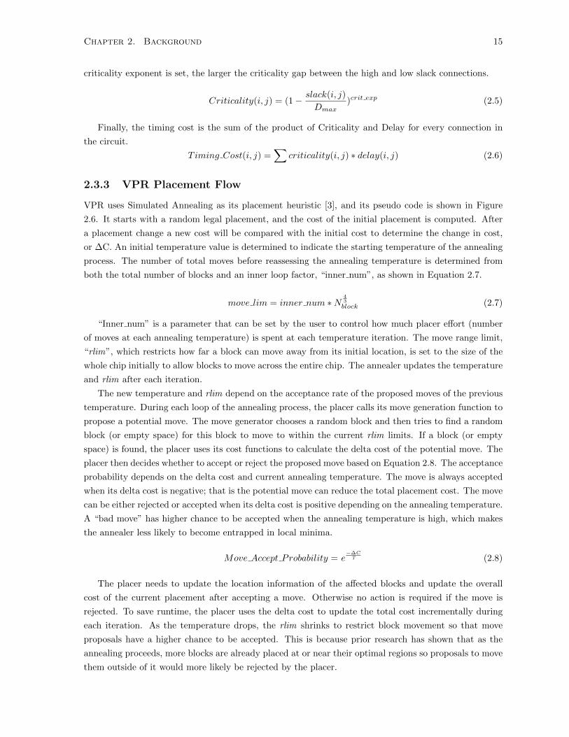
2.3.3 VPR Placement Flow
VPR uses Simulated Annealing as its placement heuristic [3], and its pseudo code is shown in Figure
2.6. It starts with a random legal placement, and the cost of the initial placement is computed. After
a placement change a new cost will be compared with the initial cost to determine the change in cost,
or ∆C. An initial temperature value is determined to indicate the starting temperature of the annealing
process. The number of total moves before reassessing the annealing temperature is determined from
both the total number of blocks and an inner loop factor, “inner num”, as shown in Equation 2.7.
move lim = inner num ∗N43
block (2.7)
“Inner num” is a parameter that can be set by the user to control how much placer effort (number
of moves at each annealing temperature) is spent at each temperature iteration. The move range limit,
“rlim”, which restricts how far a block can move away from its initial location, is set to the size of the
whole chip initially to allow blocks to move across the entire chip. The annealer updates the temperature
and rlim after each iteration.
The new temperature and rlim depend on the acceptance rate of the proposed moves of the previous
temperature. During each loop of the annealing process, the placer calls its move generation function to
propose a potential move. The move generator chooses a random block and then tries to find a random
block (or empty space) for this block to move to within the current rlim limits. If a block (or empty
space) is found, the placer uses its cost functions to calculate the delta cost of the potential move. The
placer then decides whether to accept or reject the proposed move based on Equation 2.8. The acceptance
probability depends on the delta cost and current annealing temperature. The move is always accepted
when its delta cost is negative; that is the potential move can reduce the total placement cost. The move
can be either rejected or accepted when its delta cost is positive depending on the annealing temperature.
A “bad move” has higher chance to be accepted when the annealing temperature is high, which makes
the annealer less likely to become entrapped in local minima.
Move Accept Probability = e−∆C
T (2.8)
The placer needs to update the location information of the affected blocks and update the overall
cost of the current placement after accepting a move. Otherwise no action is required if the move is
rejected. To save runtime, the placer uses the delta cost to update the total cost incrementally during
each iteration. As the temperature drops, the rlim shrinks to restrict block movement so that move
proposals have a higher chance to be accepted. This is because prior research has shown that as the
annealing proceeds, more blocks are already placed at or near their optimal regions so proposals to move
them outside of it would more likely be rejected by the placer.

Chapter 2. Background 16
Figure 2.6: VPR Placement Pseudo Code [3].

Chapter 2. Background 17
2.4 Prior Work on Annealing Improvement
Much research has been focused on producing the same QoR with a reduced amount of runtime, i.e. to
make the placement process more efficient. The majority of SA placement research can be divided into
two main groups, “move generation” and “cost function”, where each focuses on annealing improvement
from a different perspective.
The “move generation” group focuses on how a SA placer proposes block movements. Originally SA
implementations proposed only random moves and relied on high runtime to converge to good QoR.
By “directing” the movements, prior “directed moves” techniques have been shown to be effective in
producing the same level of QoR with less runtime.
SA placers use cost (objective) functions to judge the quality of the current placement and of each
proposed move. Prior work has focused on either improving the accuracy, or adding more flexibility in
the cost functions. Those works have shown improvements in QoR with a small amount of extra runtime
penalty.
2.4.1 Homogeneous Directed Moves
In [28], the authors experiment with several “directed move” techniques for improving both delay and
wirelength cost. For wirelength cost, they used a concept from their prior work [27], called “Median Re-
gion (MR)”, which places a block in one of the optimal wirelength locations given the current placement
of the blocks to which it is connected. This technique first gathers the X and Y direction minima and
maxima of all the connected nets of a given block minus its own coordinates. The MR is bounded by
the median ([n/2], where n is the total number of X or Y direction bounding boxes coordinates) index
and median plus one ([n/2 + 1]) index for both the X and Y directions.
The effectiveness of MR moves is demonstrated in Figure 2.7. The original Bounding Box cost for
the “Selected Block”, is 30 units, and it is connected to 3 nets. To calculate the selected block’s median
region, the first step is to exclude the selected block from all of its nets as shown in Figure 2.7b. The
next step is to collect the new X and Y minima and maxima. The MR is then bounded by the “median”
and “median+1” indices of the new x and y coordinates, as shown in Figure 2.7c. Finally after moving
the selected block to a random location inside its “median region”, the new Bounding Box cost is now
26 units, a 4 unit reduction from the original.
In [28] it is shown that the best QoR occurs when MR moves are mixed with certain amount of
“random moves”; as placement could be entrapped in a local minimum if too many MR moves are
performed during the earlier stages of annealing. Another observation [28] made is that when swapping
two blocks, as shown in Figure 2.8 for block A and B, the forward MR move (move block A to B)
produces a reduction in total cost, but the effect of the return move (B to A) is unknown. The return
move can result in an increase in cost which would reduce the effectiveness of MR moves. In [28], they
introduced the idea of “shuffling” to deal with this issue. During “shuffling”, as shown in Figure 2.8a,
the placer tries to find an empty spot (location E) within a certain range from block B towards block
A. If such a location is available, all the blocks along the path from block B to the empty location,
including block B itself, are shuffled towards the empty spot, and the result is shown in Figure 2.8b.
This technique reduces the possible disturbance to the local placement.
By using MR with this “shuffling” technique mixed with “random moves”, [28] is able to achieve a
5% reduction in wirelength cost with a 2% increase in critical path delay on homogeneous architectures.

Chapter 2. Background 18
(a) Selected Block belongs to 3 nets (BB cost: 36units).
(b) Exclude “selected block” to recompute BB foreach net.
(c) Use new BBs to compute “median region” for“selected block”.
(d) Move “selected block” to a random locationinside its MR (new BB cost: 32).
Figure 2.7: Median Region Move [28].
To overcome the delay cost penalty, they found that by moving blocks into their “feasible regions”, an
idea that was introduced in [8], the critical path delay can be improved by 3%. The “feasible region”
is the overlapping area of all bounding boxes that enclose a block (on the critical path) with all of its
critical inputs and its immediate output. By moving blocks along the critical path to their “feasible
regions”, the connections between all critical path blocks are shortened and thus the critical path delay
is reduced.
[28] also showed that MR moves yield better QoR when applied to medium-utilization (60%) FPGAs
versus high-utilization (more than 95%) designs. This is likely due to the higher probability of locating
empty spots inside median regions.
2.4.2 Delay Budgets
In timing-driven placement, slack is the difference between the critical path delay and the delay of a given
path, and indicates how much extra delay a path can accommodate before it becomes critical. Criticality
is computed using slack to estimate the timing importance of connections in the current placement. A
timing-driven SA placer uses criticality to compute the Timing Cost to guide its placement decisions.
Traditionally, most SA timing cost functions, such as the one in VPR, focus on high criticality connections
but pay little attention to low criticality ones as observed by [11]. This ignorance may cause some low
criticality paths become highly critical or the new critical paths.
In [11], the authors implemented a new timing cost function to solve this issue in routing. The new
timing cost function uses Delay Budgets instead of absolute delay to measure connection criticality. For
each connection, the Delay Budget is the sum of the connection delay and some amount of path slack
assigned to it. It indicates the maximum delay each connection is allowed to have before it becomes
critical. In [11] the modified router has a slack allocation step to assign path slacks to connection delay
budgets. There are many slack allocation methods available, but most of them are runtime intensive.
The Iterative-minimax-PERT method [31] is used in [11], but it requires many iterations and repeating

Chapter 2. Background 19
(a) Before “cell shuffle”.
(b) After “cell shuffle”.
Figure 2.8: MR Moves: Cell Shuffling [28].

Chapter 2. Background 20
timing analysis to complete the slack allocation. As reported, the new router achieves a 3.2% delay
improvement with 0.7% more wirelength and a 5.3% runtime penalty.
A different slack allocation approach was introduced in [10], which involving using a weight function.
In their proposed method, each connection is assigned a weight equal to the amount of potential delay
improvement such that connections with higher potentials will get more slack allocated than those with
lower potentials. This method was implemented in FPGA routing and achieved an average 14% delay
improvement. However, this method is similar to the Iterative-minimax-PERT method as it requires
multiple iterations to converge, and thus is runtime expensive.

Chapter 3
Move Generation
3.1 Overview
Traditional SA placement algorithms rely on a large number of randomly generated moves to produce
good QoR. For modern large FPGA designs, the amount of runtime required to produce good QoR can
reach an unacceptable level [23]. This chapter investigates several move generation methods that aim at
improving Simulated Annealing (SA) placement heuristic efficiency. These methods were implemented
and tested in VPR in a C++ environment.
As described in Section 2.4, adding some Median Region (MR) moves to an annealer improves wire-
length on homogeneous architectures. In our work, we improve on the previous work by adapting MR
to work on heterogeneous architectures. In addition, we have also implemented a new “Cell Rippling”
technique to avoid bad “return moves” as the previous “shuffling” technique has limitations in a hetero-
geneous environment.
“Smart Search Space (SSS)” is the second enhancement introduced in this chapter. One of the new
challenges posed by heterogeneous architectures is that the placer can no longer assume the core of the
chip only contains one type of block (CLB), and blocks can be entrapped in regions bounded by other
types of blocks. Most SA placers, including the one in VPR, use a range limit to define a “window”
within which moves can occur at the current annealing temperature. This is effective at avoiding low
acceptance probability moves in the low temperature annealing stages but it also limits block movement.
SSS separates each block type into an individual data structure to avoid inter-type interference in the
move search space. In this section we examine its effectiveness on heterogeneous architectures.
3.2 Median Region Moves
3.2.1 Motivations
Although random moves are cheap in term of the runtime per move, the placer can still spend a lot of
time searching previously visited or low acceptance probability portions of the search space [28]. Prior
works have proposed “Directed Moves” instead of the traditional random moves [28], and it has answered
a few questions regarding MR moves.
1. It is best to select the source block randomly.
21

Chapter 3. Move Generation 22
2. The return move may hurt the cost gained from the forward move.
3. Too high a fraction of total moves being MR moves can cause placement oscillation and entrapment
in local minima.
Most modern FPGA research has shifted towards heterogeneous architectures, and it is unknown
whether MR moves will still be as effective on such architectures. This section investigates the effec-
tiveness of MR moves for both homogeneous and heterogeneous architectures. In addition, a new cell
rippling implementation suitable for heterogeneous architectures is described.
3.2.2 Implementation
As described before, VPR implements SA as its placement heuristic. A “move”, or a “swap” in VPR,
is either an exchange in locations between two blocks or between a block and an empty spot. Like most
SA placers, a VPR “swap” begins by randomly choosing a block as its source block and then randomly
choosing a same type block (or empty spot) as its target location. The choice of the target location
is bounded by a move range limit, which forms a “window” around the source block, to ensure higher
acceptance probability.
To implement MR in VPR, a few additional steps were added. After choosing the source block,
the placer uses two vectors to hold the X-Y coordinates for all connected nets excluding the source
coordinates. The median values of the new X and Y coordinates are computed, and the MR for the
source block is enclosed by the “median” and “median plus 1” index values. The placer then chooses a
random location within the MR to complete the “swap”, as shown in Figure 2.7. On average the MR
computation takes O(P*K) to complete, where P is the number of pins of the source block and K is the
average fanout of each net to which the block is connected.
Cell Rippling
The movement of a source block to a target location is a forward move, and the move of the target block
(if the target location is not empty) back to the source location is a return move. With MR, the forward
move is likely to improve the total cost but the return move has an unknown effect on cost. In many
cases, the return move can offset some or all of the cost reduction gained from the forward move.
In [28], “cell shuffling” was designed to handle such an issue in homogeneous architectures. The
placer shuffles the target block and blocks along the path towards the closest empty location instead
of moving it to the source location. This reduces the negative effect of a bad return move but risks
creating undesired disruption to the surrounding blocks. As well, it is not always possible to locate an
empty spot within the range limits. This technique works for homogeneous architectures where the core
of the chip is occupied by CLBs, so in most cases there exists a path from the target location to the
chosen empty location. In a heterogeneous FPGA chip, however, this is not always the case. CLBs still
occupy the majority of the chip area but there are also other block types (RAM, DSP, and etc.). A “cell
shuffling” path can be blocked by a “fence” formed by a different block type, such as shown in Figure
3.1.
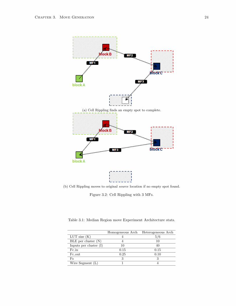
In this work, an alternative technique called “cell rippling” is implemented. “Cell rippling” divides
each move proposal into multiple small move fragments (MFs), which each MF is a move itself. Instead
of moving the target block back to the source location or “shuffling” it to a neighboring empty location,
“cell rippling” moves the target block to its MR. If this displaces another block, that block is also moved
Chapter 3. Move Generation 23
Figure 3.1: CLB “Cell shuffling” path blocked by RAM block.
to its MR in a new MF, and so on. This ripple movement continues until either an empty spot is
found, or a preset maximum allowed MF limit has reached. This method ensures most blocks along the
“rippling path” are located in their MRs.
An example of “cell rippling” is shown in Figure 3.2. In this example, the maximum allowed MF is
set at 3. In the first step, block A is chosen as the source block, and a random location is chosen from
its MR as the target location. The target location chosen by block A is occupied by block B. For the
next MF, the placer computes the MR for block B, and moves it to a location in its MR that is occupied
by block C. Finally for the last MF, block C will move to a location within its MR if an empty location
is available as in Figure 3.2a, or to original block A’s location (if no empty location exists in C’s MR)
to complete the “move”’, as in Figure 3.2b.
3.2.3 Experimental Results
The main advantage of using MR moves is it can produce good QoR with less runtime. In VPR,
placement effort is controlled by the parameter “inner num”, which sets the number of moves to perform
for each temperature. A higher “inner num” means more moves are performed, and QoR is likely
to improve but a longer runtime is required. In this work we perform “inner num” sweeps for each
experiment to compare the QoR of the original VPR and the MR version at various runtime levels.
In prior work, experiments were performed using homogeneous architectures only. In this work, a
homogeneous architecture is also used to ensure the correctness of our implementation. The 20 largest
benchmark circuits from the MCNC [30] suite were used in the homogeneous architecture experiments. A
standard size-4-CLB homogeneous architecture (“k4 N4 90nm.xml”) from the VTR project [24] is used.
The details of the architectures are listed in Table 3.1. The benchmark circuits have an average size of
750 CLBs when using size-4 CLBs. For heterogeneous architecture tests, the 5 largest VTR benchmark
circuits with high block type diversity were chosen from the VTR benchmark set [24], as listed in Table
3.2. The heterogeneous experiment uses a size-10-CLB architecture (“k6 frac N10 mem32K 40nm.xml”)
from the VTR project. This architecture has support for many hard blocks such as RAM and DSP blocks.
Chapter 3. Move Generation 24
(a) Cell Rippling finds an empty spot to complete.
(b) Cell Rippling moves to original source location if no empty spot found.
Figure 3.2: Cell Rippling with 3 MFs.
Table 3.1: Median Region move Experiment Architecture stats.
Homogeneous Arch Heterogeneous Arch
LUT size (K) 4 5/6
BLE per cluster (N) 4 10
Inputs per cluster (I) 10 40
Fc in 0.15 0.15
Fc out 0.25 0.10
Fs 3 3
Wire Segment (L) 1 4

Chapter 3. Move Generation 25
Table 3.2: Largest 5 circuits from the VTR benchmark suite stats[24].
Circuit Name Chip Size Nets IO CLB RAM DSP Total Clustered Blocks
bgm 63 21094 289 2930 0 11 3230
LU8PEEng 53 16278 216 2104 45 8 2373
LU32PEEng 98 54219 216 7544 168 32 7544
mcml 95 52415 69 6615 159 30 6873
stereovision2 86 34476 331 2395 0 213 2939
To fully understand the effect of the MR moves and “cell rippling” implementation in this work,
each benchmark set went through 3 different groups of tests. Test Condition 1 sweeps the percentage of
MR moves and compares QoR to the original “random moves” in VPR. Test Condition 2 takes the best
2 MR move percentages from the Condition 1 test, and sweeps MF from 1 to 5 to find the best value
for MF; values of MF greater than 1 incorporate “cell rippling”. Finally Test Condition 3 repeats the
Condition 2 test with 70% FPGA utilization to check the effect of lower chip utilization on MR moves.
The placement and post-routing results of each test are used to compare the QoR improvement.
All tests were performed using both homogeneous and heterogeneous architectures, and all results are
geometric averages over 5 different placement seeds to minimize CAD noise.
Condition 1: MR Move Fraction Sweep
MR moves have been proven effective at reducing wirelength cost. Intuition would lead one to believe
that using more or entirely MR moves in annealing would achieve the best QoR. However, prior work
has shown that a high percentage of MR moves in fact degrades QoR. To confirm this effect and find
the best MR move percentage, a sweep test of MR percentage is performed in this work. In Figure
3.3, which shows the comparison using the VTR benchmarks, original VPR is shown as the “Org (0%
MR)” points and “100% MR” represents the case when all moves are MR moves. The experiment has
run through five “inner num” values (0.1, 0.3, 1, 3, 10) to compare QoR at different CPU effort levels.
The QoR values are geometric averages normalized against the original VPR results at “inner num =
3”. The lower graph of Figure 3.4 demonstrates how the results are clustered into different “inner num”
groups, and the other plots follow the same pattern.
From both Figures 3.3 and 3.4, it is clear that using entirely MR moves degrades QoR. “100% MR”
produced nearly 6% worse delay with no improvement in wirelength over the original VPR. The lower
graph of Figure 3.4 also shows that MR moves are more runtime expensive than “random moves”.
At “inner num = 10”, most MR runs took 10% to 40% longer than original VPR. However, at lower
“inner num” values, MR runs have a much smaller impact on runtime. At “30%”, MR runs gained about
4% in wirelength at “inner num = 0.1” without giving up any delay quality. At higher “inner num”
values, the wirelength gain is smaller. Combining the results from both VTR and MCNC runs, it is
clear that between 30% and 50%, MR moves has the best tradeoff between QoR and runtime.
Condition 2: Cell Rippling MF Sweep
Condition 1 tests suggested that MR moves are most effective when only 30% to 50% of moves are of
MR type. Therefore those were chosen to be the MR percentage values for the Condition 2 test. The
“cell rippling” technique implemented in this work involves triggering a sequence of MR moves until

Chapter 3. Move Generation 26
Figure 3.3: QoR vs. fraction of moves are MR type for various placer effort levels (VTR Benchmarks).

Chapter 3. Move Generation 27
Figure 3.4: QoR vs. fraction of moves are MR type for various placer effort levels (MCNC Benchmarks).

Chapter 3. Move Generation 28
either an empty spot is found or the maximum number of MFs is reached. This test sweeps “maximum
allowed MFs” from 1 to 5 in searching for the best QoR and runtime trade-off point.
Similar to the Condition 1 tests, all values are geometric averages over 5 seeds and normalized
against the original VPR values at “inner num = 3”. In Figure 3.5, “1mf” represents experiments with
the maximum allowed MFs set to 1, which corresponds to a “swap” (a forward move followed by a return
move if the target location has a block).
Comparing MF = 3 or 4 to MF = 1 (which has no “cell rippling”) at inner nums 0.1 and 0.3, we can
see that wirelength is reduced by a further 2% as shown in Figure 3.5. Placement runtime is increased
by 9% to 20% at each inner num respectively.
Condition 3: QoR Effect of Chip Utilization
For real world FPGA applications, a typical design only uses about 70% or less of the whole chip.
Therefore it is important to evaluate MR moves at a lower chip utilization level. Figure 3.6 shows the
results of the Condition 2 tests repeated with the chip utilization set to 70%. At lower “inner num”
values, there is up to 5% improvement in wirelength.
Table 3.3 lists the QoR comparisons between the High and Medium chip utilization when using 50%
MR moves for “inner nums” from 0.1 to 1. Each group of results are normalized against the original
placement results (0% of MR moves) at each utilization level. The results show that with Medium chip
utilization, 50% MR moves produces 1% to 2% better wirelength than at High utilization for every placer
effort level. The runtime shows no difference between the two conditions. This experiment shows that
MR moves is more effective at improving QoR with lower chip utilization levels as the chance of finding
an empty spot in each median region is higher.
Reducing Runtime: Omitting High Fan-out Nets
The previous experiments show that MR moves are effective at producing lower wirelength than the
original VPR placement. However, these moves normally require 6% to 33% extra placement runtime
depending on the MF level.
Most of the extra runtime is spent in computing MRs for the source blocks, and higher fan-out nets
require a longer runtime to compute their contribution to the MR. In reality, however, high fan-out nets
do not provide much useful information for MR computation as they normally cover much of the chip
area (i.e. their coordinates are unlikely to affect the median values). Therefore we investigate omitting
high fan-out nets from the MR computation. From a quick sweep on omitting net fan-out size, we found
that by omitting nets with fan-out of 5 or higher the QoR is not affected.
To demonstrate the effect of omitting high fan-out nets, we picked one condition from Table 3.3,
“50% MR with 95% Chip Utilization and 3MF at inner num of 0.3”, which uses 36% more placement
runtime than original VPR. The results are shown in 3.4. The omitting high fan-out nets results are
normalized against both original VPR and the original MR version (column “All Nets”). The results
show there is no QoR change by omitting the high fan-out nets, and the runtime is reduced by 12% on
average. This is encouraging for making MR moves a practical optimization for SA placement.

Chapter 3. Move Generation 29
Figure 3.5: Median Region Cell Rippling Move Fragment sweep (VTR Benchmarks).

Chapter 3. Move Generation 30
Figure 3.6: Median Region Cell Rippling MF sweep for medium chip utilization (VTR Benchmarks)

Chapter 3. Move Generation 31
Table 3.3: MR QoR Comparison between High and Medium chip utilization (VTR Benchmarks).
Table 3.4: Placement QoR Comparison between not omitting and omitting high fan-out nets for MRmoves (VTR Benchmarks normalized vs original VPR results).

Chapter 3. Move Generation 32
Figure 3.7: Median Region produces same QoR as original VPR at lower runtime (VTR Benchmarks).
3.2.4 Conclusion
From all 3 comparisons, MR moves have the ability to reduce wirelength without degrading delay at low
runtimes. By using 50% MR moves, there is an up to 5% improvement in wirelength at low runtimes
(inner num = 0.1, 0.3) and up to 2% improvement in wirelength at medium runtimes (inner num = 1),
while maintaining a similar delay cost to all random moves. However, given a sufficiently long runtime,
MR and random moves converge to a similar QoR level. At inner num = 10, MR runs use 30% to 50%
more runtime to produce the same QoR as random moves, due to the more computationally expensive
move proposals.
At inner num = 3, the runtime gap between using MR moves and the original implementation is
about 20% to 40%. MR moves, however, produce a 2% improvement in QoR at inner num = 3. This
is the same QoR level that “random moves” would produce at inner num = 10, which requires 140%
more runtime. To help clarify this observation, a horizontal line is drawn across the plot in Figure 3.7.
It shows that for the same QoR there is a 50% runtime savings by doing 30% MR moves at inner num
= 3 instead of all random moves at inner num = 10.
Overall 30% to 50% of MR moves are effective at improving wirelength at lower placer effort levels,
and reducing the runtime required to produce high quality results at higher placer effort levels. We also
show that by omitting high fan-out nets in MR computations, the placement runtime can be reduced
by a significant amount without any QoR loss.

Chapter 3. Move Generation 33
Figure 3.8: Size-1 range limit for CLBs in a Homogeneous Architecture.
3.3 Smart Search Space
3.3.1 Motivations
In VPR, the size of the “window”, or move range, is a region defined by rlim grid units in all 4 directions
from the source block coordinates, and clipped to the edges of the chip. The minimum grid unit is
defined by the size of the smallest block type. For example, a move range of 4 means a size-1 block can
move within a 9-by-9 box centred on its current location, and clipped to the chip boundaries. At the
beginning of annealing the size of the “window” covers the entire chip. As temperature drops, the size
of the move range limit shrinks, and eventually drops to the minimum size of 1 grid unit, which means
blocks are only allowed to move within a 3-by-3 box as shown in Figure 3.8.
In classic homogeneous architectures, the majority of the chip is occupied by CLB blocks, and thus
in most cases all valid locations enclosed by a “window” are the same type. The source block in Figure
3.8, for example, has a total of 8 valid locations to which it can move within a size-1 “window”. In a
heterogeneous architecture, however, there are more than one type of blocks available across the chip.
In Figure 3.9, blocks are arranged in columns so that blocks are all the same type in each column. In
this example, column 1, 2, and 4 are CLB type, and column 3 is RAM type. A size-1 “window” still
covers the same amount of area as before, but there are 3 invalid locations as the “window” covers part
of a RAM column. Instead of 8 valid CLB locations, the source CLB block has only 5 valid locations
from which to choose. This reduces the placer search space and prevents the CLB blocks from crossing
the “fence” formed by the RAM column (in Figure 3.9, for example, no CLB from the left of column 3
can reach any location on the right side of column 3, and vice versa).
Hard blocks, such as the RAM block in Figure 3.10, are often spread across the chip and separated by
other block types. The size of these blocks are normally larger than CLB blocks. For exampe, in Figure
3.10 the size of the RAM block is 4 grid units, which means they are 4 times the size of a CLB block. In
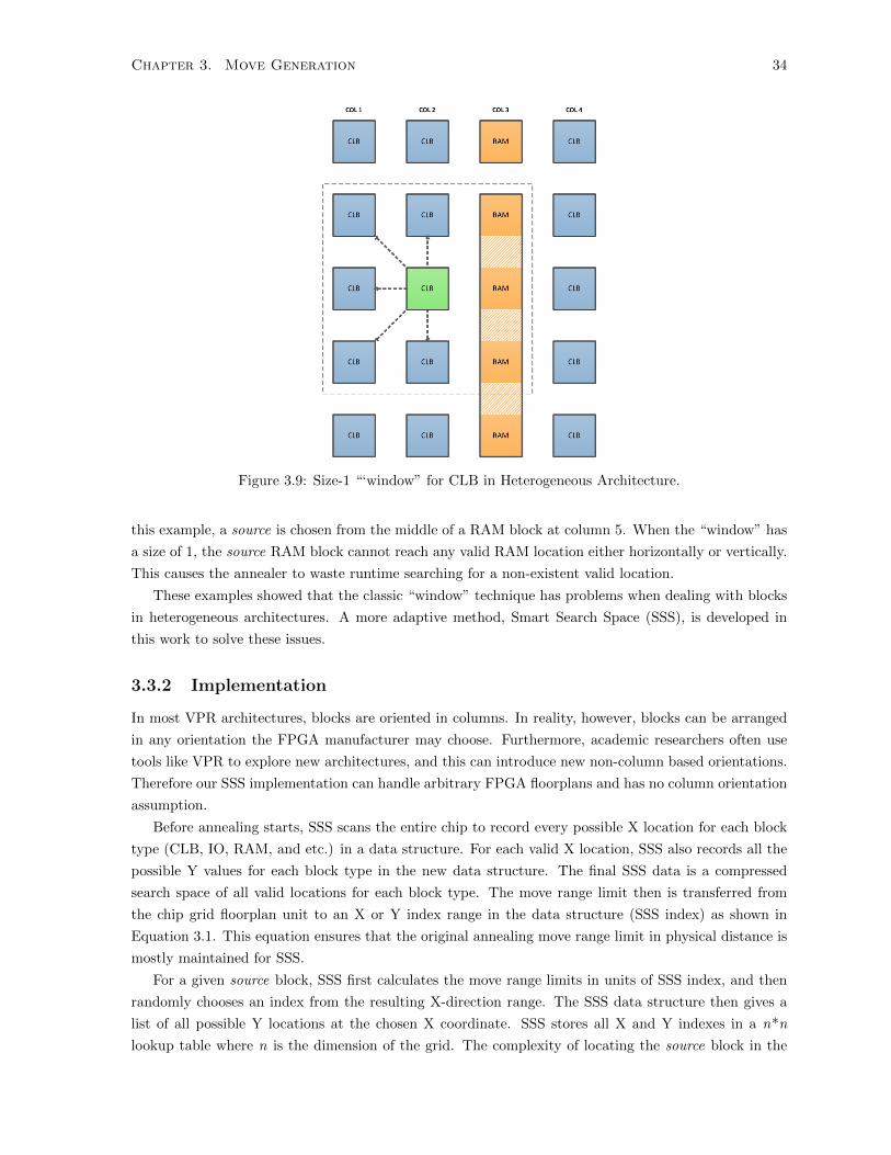
Chapter 3. Move Generation 34
Figure 3.9: Size-1 “‘window” for CLB in Heterogeneous Architecture.
this example, a source is chosen from the middle of a RAM block at column 5. When the “window” has
a size of 1, the source RAM block cannot reach any valid RAM location either horizontally or vertically.
This causes the annealer to waste runtime searching for a non-existent valid location.
These examples showed that the classic “window” technique has problems when dealing with blocks
in heterogeneous architectures. A more adaptive method, Smart Search Space (SSS), is developed in
this work to solve these issues.
3.3.2 Implementation
In most VPR architectures, blocks are oriented in columns. In reality, however, blocks can be arranged
in any orientation the FPGA manufacturer may choose. Furthermore, academic researchers often use
tools like VPR to explore new architectures, and this can introduce new non-column based orientations.
Therefore our SSS implementation can handle arbitrary FPGA floorplans and has no column orientation
assumption.
Before annealing starts, SSS scans the entire chip to record every possible X location for each block
type (CLB, IO, RAM, and etc.) in a data structure. For each valid X location, SSS also records all the
possible Y values for each block type in the new data structure. The final SSS data is a compressed
search space of all valid locations for each block type. The move range limit then is transferred from
the chip grid floorplan unit to an X or Y index range in the data structure (SSS index) as shown in
Equation 3.1. This equation ensures that the original annealing move range limit in physical distance is
mostly maintained for SSS.
For a given source block, SSS first calculates the move range limits in units of SSS index, and then
randomly chooses an index from the resulting X-direction range. The SSS data structure then gives a
list of all possible Y locations at the chosen X coordinate. SSS stores all X and Y indexes in a n*n
lookup table where n is the dimension of the grid. The complexity of locating the source block in the

Chapter 3. Move Generation 35
Figure 3.10: Size-1 “window” for RAM.
SSS data structure is O(1). SSS completes the search by randomly choosing a Y-direction location from
the list bounded by Y-direction move range limits.
SSS Move Range = max(Global Move Range
Average X(orY ) Gap, 1) (3.1)
Looking at the previous example again in Figure 3.11, with SSS the source CLB block now has 8
valid locations in its “window” and it can go across the RAM column to the other side. For the RAM
example in Figure 3.12, SSS enables it to move to 8 possible locations as opposed to original number of
0. SSS increases the search space efficiency for annealer and the chance of finding valid moves.
3.3.3 Experimental Results
SSS was mainly targeting at dealing with “window” issues arising in heterogeneous architectures, so we
have tested SSS for such architectures. The architecture used has size-10 CLBs and support for RAM,
DSP and other type of blocks (“k6 frac N10 mem32K 40nm.xml”).
To minimize CAD noise, both the original VPR and the SSS version were run with 3 different
placement seeds and all results are geometric averages over three seeds. Table 3.5 shows the comparison
between the two sets of results with all values normalized against the original VPR results. The circuits
are sorted in ascending order of their chip size in term of X-Y grid size (e.g. size = 5 means a 5*5 grid).
Overall SSS produces similar QoR as the original VPR with 2% less Minimum Channel Width (W). SSS
also requires 7% fewer moves compares to original VPR, which leads to 5% Placement runtime and 4%

Chapter 3. Move Generation 36
Figure 3.11: Size-1 “‘window” for CLB with SSS.
Figure 3.12: Size-1 “window” for RAM with SSS.

Chapter 3. Move Generation 37
Circuit Name Chip Size Min W Delay Wirelength Total Swaps PL Time RT Time Total Runtimestereovision3 5 0.96 0.95 0.99 0.77 0.85 1.00 0.87ch intrinsics 8 0.99 0.99 1.02 0.88 0.92 0.94 0.93diffeq1 14 1.01 0.99 0.97 1.00 1.00 1.09 1.01diffeq2 14 1.00 1.01 0.98 0.93 1.00 1.05 1.02raygentop 17 1.02 0.99 1.02 0.87 0.92 1.03 0.96sha 17 1.01 1.01 0.96 0.85 0.88 1.02 0.90boundtop 18 1.02 1.01 1.00 1.00 1.02 0.99 1.02mkSMAdapter4B 18 0.99 1.01 1.02 0.86 0.91 1.03 0.94or1200 25 0.99 1.00 1.01 1.00 1.00 0.80 0.95mkPktMerge 26 0.82 1.00 1.05 1.02 1.02 0.84 0.94blob merge 28 1.00 0.99 1.01 0.90 0.92 0.98 0.93stereovision0 35 0.96 0.97 1.00 0.90 0.92 1.03 0.93stereovision1 38 0.99 1.00 0.98 0.90 0.94 0.97 0.95mkDelayWorker32B 48 0.97 1.04 1.03 1.00 0.97 1.04 1.00LU8PEEng 53 0.98 0.99 0.98 0.90 0.95 1.08 0.99bgm 63 0.98 0.98 0.98 0.95 0.96 1.01 0.97stereovision2 86 1.01 0.99 0.98 0.94 1.00 1.02 1.01mcml 95 0.96 0.99 0.95 0.98 0.97 1.01 0.98LU32PEEng 98 0.98 1.01 0.99 0.98 0.95 0.95 0.97Geomean — 0.98 1.00 1.00 0.93 0.95 0.99 0.96Geomean (Largest 5) — 0.98 0.99 0.98 0.96 0.97 1.01 0.98
Table 3.5: Smart Search Space results ranking by chip size
total runtime savings.
More importantly, SSS has better performance for larger circuits. For the largest 5 circuits in this
benchmark suite (bgm, LU8PEEng, LU32PEEng, mcml, stereovision2 ), SSS produces 1% better delay
and 2% better wirelength (as shown in the last row of Table 3.5). There are 5 circuits for which SSS pro-
duces worse QoR than the original VPR (boundtop, mkDelayWorker32B, mkPktMerge, mkSMAdapter4B,
or1200 ) with 1% longer delay and 2% more wirelength on average. These circuits have the highest IO
block count among the entire suite. Therefore this QoR degradation is likely caused by the special
arrangement of IO blocks in VPR, which assumes IO blocks are always on the chip periphery. This
arrangement is very different from all the other block types, which are arranged in columns. Upon fur-
ther observation, circuits with lower IO block ratios tend to have better QoR when using SSS. However,
IO blocks are not always arranged on the periphery in commercial FPGAs [9], and we expect SSS to
perform slightly better for such architectures.
3.4 Conclusion
Smart Search Space is designed to better search the placement space in heterogeneous architectures. By
using SSS, each block type move is no longer interfered with by the other block types when searching
for a valid chip location. It also guarantees the move generator will not search within a range which no
available location exists, and hence increases placer efficiency and requires less placer effort to achieve
the same QoR. The results have shown that SSS produces the same or improved QoR with less runtime.
Moreover, SSS produces better QoR on larger circuits, which is promising for the future.

Chapter 4
Cost Function
4.1 Cost Function Tuning
4.1.1 Motivations
In Section 2.3 we described the timing-driven placement Cost Function of VPR. It consists of both BB
cost and timing cost terms, and each contributes half of the total cost by default. The cost trade-off
parameter, λ, controls the weight of each cost. In this work we sweep different trade-off values to check
whether 0.5, the VPR default, is still the best default value.
Another parameter, “Criticality Exponent (CE)”, controls the criticality magnitude difference be-
tween the high and low criticality paths. In VPR, this parameter changes from the start to the end of
the anneal. CE is set to 1 in the beginning (VPR parameter “td place exp first”) to give only slightly
more focus on high criticality paths than the low ones. As annealing progresses, critical path information
becomes more stable so CE becomes higher to put most annealer focus on highly critical paths. The
schedule by which CE increases is related to the move range limit. The final CE (“td place exp last”)
is currently set to 8 by default in VPR. To the best of our knowledge, no prior research has shown
a comparison between different CE values for heterogeneous architectures ([18] compared to using a
homogeneous architecture). In this work, we compare different CE values and show their effects on
QoR.
4.1.2 Experimental Results
Cost Function Trade-off Value Comparison
The first experiment sweeps different λ values for the current VPR placement cost function. All the other
parameters are set to their defaults (“td place exp first” is set to 1, and “td place exp last” is set to 8,
and “inner num” value to 1). For this experiment and the subsequent experiments in this chapter we
use VTR benchmark circuits, and a default VTR architecture file (“k6 frac N10 mem32K 40nm.xml”).
Figure 4.1 shows the result of the experiment. To save runtime, only placement estimated wirelength
and critical path delay values are shown (i.e. routing was not performed). The X-axis indicates the λ
values are swept from 0.0 (all placement effort on minimizing BB cost) to 1.0 (all placement effort on
minimizing Timing cost), and the Y-axis shows the normalized values against the QoR at λ = 0.5. The
38

Chapter 4. Cost Function 39
Figure 4.1: Cost Function Trade-off Sweep (VTRBM).
blue line with the “diamond” shape indicators shows the wirelength, and the red line with “square”
shape indicators shows the critical path delay. We have noticed that the wirelength-delay trade-off is
not obvious, so a third value, the Wirelength-Delay Product (WDP), is used to help visualize the overall
effect. In this figure, a green dotted line indicates the WDP. In the rest of this chapter we will use a
similar style for QoR comparisons.
From Figure 4.1, it is shown that by solely focusing on either wirelength (BB cost) or critical path
delay (timing cost) the QoR degradation is large. At λ = 0.0, the placer achieves 4% better wirelength
but slows down the circuit by 12%. At the other extreme, when λ = 1.0, the result shows no improvement
in critical path delay but there is a 35% increase in wirelength.
Figure 4.2 shows the same result as Figure 4.1 but without the two extreme cases. In this range,
the trade-off relationship between wirelength and critical path delay is near linear. The lowest achieved
wirelength is 4% less than the default (at λ = 0.5) at λ = 0.1 or 0.2, and the best achieved critical path
delay is only 1% lower at λ = 0.7 or 0.8. The best WDP is at λ = 0.2 or 0.3 with 1% improvement over
the default but with 1% to 3% worse delay. Overall at λ = 0.5 the placement QoR is close to both the
best critical path delay and WDP.
Criticality Exponent Value Comparison
This experiment aims to compare various CE values and find the value that produces the best QoR. The
initial CE value (“td place exp first”) is held at the default value of 1. A wide range of final CE values
(“td place exp last”) are swept: 1, 5, 8 (default value), 10, 15, 20, 25, 30, 35. λ is also swept from 0.1
to 0.9.
The VTR benchmark suite is used, and placement “inner num” is set to 1.0 for this experiment.
Figure 4.3 shows the WDP comparison between all different CE values and at various λ values. The
Y-axis indicates the WDP normalized against VPR placement at default settings.
From this experiment, we see that when λ is equal to 0.7 or higher, the placement QoR becomes
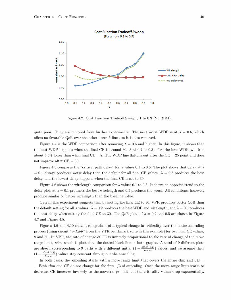
Chapter 4. Cost Function 40
Figure 4.2: Cost Function Tradeoff Sweep 0.1 to 0.9 (VTRBM).
quite poor. They are removed from further experiments. The next worst WDP is at λ = 0.6, which
offers no favorable QoR over the other lower λ lines, so it is also removed.
Figure 4.4 is the WDP comparison after removing λ = 0.6 and higher. In this figure, it shows that
the best WDP happens when the final CE is around 30. λ at 0.2 or 0.3 offers the best WDP, which is
about 4.5% lower than when final CE = 8. The WDP line flattens out after the CE = 25 point and does
not improve after CE = 30.
Figure 4.5 compares the “critical path delay” for λ values 0.1 to 0.5. The plot shows that delay at λ
= 0.1 always produces worse delay than the default for all final CE values. λ = 0.5 produces the best
delay, and the lowest delay happens when the final CE is set to 30.
Figure 4.6 shows the wirelength comparison for λ values 0.1 to 0.5. It shows an opposite trend to the
delay plot, at λ = 0.1 produces the best wirelength and 0.5 produces the worst. All conditions, however,
produce similar or better wirelength than the baseline value.
Overall this experiment suggests that by setting the final CE to 30, VPR produces better QoR than
the default setting for all λ values. λ = 0.2 produces the best WDP and wirelength, and λ = 0.5 produces
the best delay when setting the final CE to 30. The QoR plots of λ = 0.2 and 0.5 are shown in Figure
4.7 and Figure 4.8.
Figures 4.9 and 4.10 show a comparison of a typical change in criticality over the entire annealing
process (using circuit “or1200 ” from the VTR benchmark suite in this example) for two final CE values,
8 and 30. In VPR, the rate of change of CE is inversely proportional to the rate of change of the move
range limit, rlim, which is plotted as the dotted black line in both graphs. A total of 9 different plots
are shown corresponding to 9 paths with 9 different initial (1 − slack(i,j)Dmax
) values, and we assume their
(1− slack(i,j)Dmax
) values stay constant throughout the annealing.
In both cases, the annealing starts with a move range limit that covers the entire chip and CE =
1. Both rlim and CE do not change for the first 1/3 of annealing. Once the move range limit starts to
decrease, CE increases inversely to the move range limit and the criticality values drop exponentially.

Chapter 4. Cost Function 41
Figure 4.3: Criticality Exponent Sweep WDP Comparison (λ 0.1 to 0.9).
Figure 4.4: Criticality Exponent Sweep WDP Comparison (λ 0.1 to 0.5).

Chapter 4. Cost Function 42
Figure 4.5: Criticality Exponent Sweep Delay Comparison (λ 0.1 to 0.5).
Figure 4.6: Criticality Exponent Sweep Wirelength Comparison (λ 0.1 to 0.5).
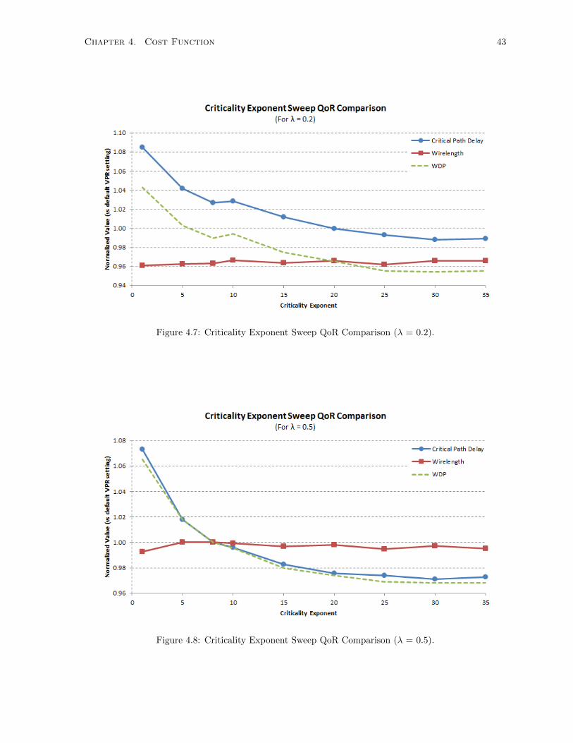
Chapter 4. Cost Function 43
Figure 4.7: Criticality Exponent Sweep QoR Comparison (λ = 0.2).
Figure 4.8: Criticality Exponent Sweep QoR Comparison (λ = 0.5).

Chapter 4. Cost Function 44
Figure 4.9: Changing Criticality Values for Various Critical Paths over an Annealing Process (final CE=8).
Criticality values at CE = 30 drop much sharply than when CE = 8.
During the final 40% of annealing, the move range limit reaches its minimum (1 grid unit in VPR),
and the CE and path criticality values also reach their final values. This region shows the biggest
difference between the two cases. For CE = 8, medium critical paths ((1− slack(i,j)Dmax
) 0.7 to 0.9) still have
some impact on timing cost. However, any placement perturbation of low critical paths at this stage is
unlikely to affect the design timing quality.
For CE = 30, however, the criticality values for all medium and low critical paths are near 0 in
the final annealing stage. This allows the placer to focus only on fine tuning the timing cost of the
connections associated with the most critical paths. At the end, the placer at CE = 30 produces better
timing quality than CE = 8 with same wirelength quality and placement effort.
Note that the results also suggest that for timing cost purposes, medium and low critical paths can be
ignored when the move range limit is so small. Intuitively, when only small perturbations are permitted
(controlled by move range limit), it is unlikely any move will produce a change in delay so large that a
medium or low critical path becomes more critical than the current critical path.
Figures 4.11 and 4.12 show QoR sweeps for different “inner num”s to ensure the QoR gap between
CE = 30 and CE = 8 holds true at different placer efforts. Critical Path Delay and wirelength are
plotted in solid lines while WDP is plotted in dotted line. As the plots show, the QoR gap between final
CE = 8 and 30 is consistent through various placer effort levels.
4.1.3 Conclusion
The cost function trade-off (λ) sweep suggests that the QoR at λ = 0.5 is still the most balanced when
using the default VPR placement settings. It produces nearly the best delay and WDP while maintaining

Chapter 4. Cost Function 45
Figure 4.10: Changing Criticality Values for Various Critical Paths over an Annealing Process (finalCE= 30).
Figure 4.11: QoR comparison between final CE = 8 and 30 for various placer efforts (λ = 0.2).

Chapter 4. Cost Function 46
Figure 4.12: QoR comparison between final CE = 8 and 30 for various placer efforts (λ = 0.5).
a good level of wirelength usage. The Criticality Exponent Sweep shows that by setting the final CE
to 30 the placer puts more focus on improving the critical path delay during the final annealing stages.
This setting outperforms the default value of 8 in VPR with 3% better critical path delay when λ =
0.5, or 4.6% better WDP when λ = 0.2. Furthermore, we have shown that this trend is consistent over
various levels of placer effort.
4.2 Delay Budget
4.2.1 Motivations
Circuit speed is one of the two main design objectives in the FPGA CAD flow. Traditionally the
placement cost function in VPR lacks the ability to focus on low criticality paths which potentially can
become critical and slow down the design, as observed in [11]. A Delay Budget, which indicates the
maximum delay allowed for a given connection before it becomes critical, is used in [11] to improve
circuit speed and close timing constraints in a commercial FPGA CAD routing tool. To the best of
our knowledge, no prior work has used Delay Budgets in timing-driven SA placement. In this work we
investigate some Delay Budget assignment methods and a new timing cost function for placement in
VPR.
To obtain Delay Budgets for each connection, a Slack Allocation step is necessary. Slack Allocation
assigns all “path slack” to its connections but it is normally runtime expensive. In [11], the Iterative-
minimax-PERT method was used, and a few iterations are necessary to finish the allocation. In this work
we first evaluate this method, and then compare it with a new Slack Allocation method that produces
overly-optimistic Delay Budgets.

Chapter 4. Cost Function 47
Table 4.1: Delta Timing Cost using Original VPR Timing Cost Function.
4.2.2 Delay Budget Timing Cost Function
VPR uses a timing cost as shown in Equation 2.6. For a high criticality connection, any change in
connection delay will result in a large change in timing cost. Figure 4.13 gives an example of when the
current timing cost function fails to identify a “bad move” (for simplicity, we ignore the exact unit of
each value).
In this example, the initial placement (Figure 4.13a) has a total timing cost of 14.01 as shown in
Table 4.1, and path B-C-D is the critical path with a path delay of 12. After the annealer proposes a
swap, the new placement timing graph is shown in Figure 4.13b with all the delay changes indicated on
the edges. The total timing cost of the new placement is 13.86, and the change in timing cost is -0.15.
However, as shown in Figure 4.13b, path A-C-D now has a path delay of 13, which surpasses the original
critical path delay of 12. Therefore the new placement has a new critical path which the timing cost
function failed to identify without a timing analysis.
In this work, we propose a new timing cost function for VPR placement as shown in Equation 4.1.
Timing Costc = Criticalityc ∗ (Delayc
Delay Budgetc+max(0,
Delaycdb ratio ∗Delay Budgetc
− 1.0)) (4.1)
The first factor, Criticality, is the same as the original VPR Timing Cost function. We still use
the connection criticality to identify high critical paths and control placer focus. The second factor,
however, is new and has two components. The first component is the “delay budget normalized delay
value”, which is a ratio of the connection delay and its Delay Budget. The second component is a
“penalty” term which is used to add extra cost to connections that use a high fraction of their Delay
Budgets. The fraction level is set by the “db ratio” term.
The first component, means that connections with larger Delayc
Delay Budgetcratio will have more weight
on their delay while other connections will have more movement freedom. This freedom allows the placer
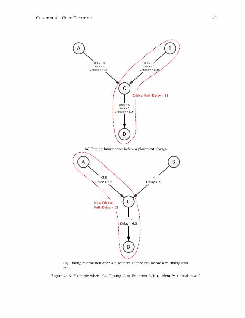
Chapter 4. Cost Function 48
(a) Timing Information before a placement change.
(b) Timing information after a placement change but before a re-timing anal-ysis.
Figure 4.13: Example where the Timing Cost Function fails to identify a “bad move”.

Chapter 4. Cost Function 49
Table 4.2: Delta Timing Cost using New VPR Timing Cost Function.
to explore a broader search space than with the original cost function, and gives a better chance to find
higher quality placement solutions.
To illustrate this, the Delay Budget values of the connections from the previous example are shown
in the third column of Table 4.2. Note that connection C-D has a smaller Delay Budget value than
connection B-C. This ensures that for the same amount of delay change, connection C-D will have a
larger effect on timing cost than connection B-C even though both have the same criticality. Intuitively,
connection C-D belongs to 2 paths which means its delay change can potentially affect the timing of both
paths, whereas connection B-C only belongs to 1 path so it has less potential impact on path delays.
The second component, the penalty term, makes sure the delay of each connection does not go too
high and become speed limiting. The placer will put less focus on lower criticality connections until
they become too slow, which gives more movement freedom to the blocks which they connect. This
penalty term also effectively tries to speed up slow connections towards the “target” delay values set by
“db ratio ∗Delay Budgetc”.
Finally, the last row in Table 4.2 shows the Delta Timing Cost now is +0.24, which correctly identifies
this move as a “bad move”.
4.2.3 Delay Budget Computation
After identifying the problem in the current VPR Timing Cost function and replacing it with an improved
function, the next step is to develop a method to compute the Delay Budget for each connection. In this
work, we first implemented and tested the Iterative-minimax-PERT (PERT) method as used in prior
work in routing [11], and then we introduced a fast but overly optimistic Delay Budget computation
method called Direct Slack.
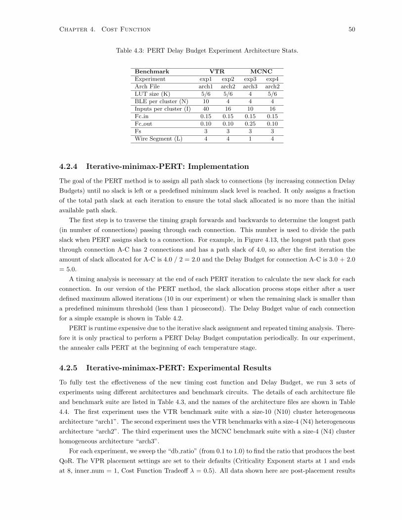
Chapter 4. Cost Function 50
Table 4.3: PERT Delay Budget Experiment Architecture Stats.
Benchmark VTR MCNC
Experiment exp1 exp2 exp3 exp4
Arch File arch1 arch2 arch3 arch2
LUT size (K) 5/6 5/6 4 5/6
BLE per cluster (N) 10 4 4 4
Inputs per cluster (I) 40 16 10 16
Fc in 0.15 0.15 0.15 0.15
Fc out 0.10 0.10 0.25 0.10
Fs 3 3 3 3
Wire Segment (L) 4 4 1 4
4.2.4 Iterative-minimax-PERT: Implementation
The goal of the PERT method is to assign all path slack to connections (by increasing connection Delay
Budgets) until no slack is left or a predefined minimum slack level is reached. It only assigns a fraction
of the total path slack at each iteration to ensure the total slack allocated is no more than the initial
available path slack.
The first step is to traverse the timing graph forwards and backwards to determine the longest path
(in number of connections) passing through each connection. This number is used to divide the path
slack when PERT assigns slack to a connection. For example, in Figure 4.13, the longest path that goes
through connection A-C has 2 connections and has a path slack of 4.0, so after the first iteration the
amount of slack allocated for A-C is 4.0 / 2 = 2.0 and the Delay Budget for connection A-C is 3.0 + 2.0
= 5.0.
A timing analysis is necessary at the end of each PERT iteration to calculate the new slack for each
connection. In our version of the PERT method, the slack allocation process stops either after a user
defined maximum allowed iterations (10 in our experiment) or when the remaining slack is smaller than
a predefined minimum threshold (less than 1 picosecond). The Delay Budget value of each connection
for a simple example is shown in Table 4.2.
PERT is runtime expensive due to the iterative slack assignment and repeated timing analysis. There-
fore it is only practical to perform a PERT Delay Budget computation periodically. In our experiment,
the annealer calls PERT at the beginning of each temperature stage.
4.2.5 Iterative-minimax-PERT: Experimental Results
To fully test the effectiveness of the new timing cost function and Delay Budget, we run 3 sets of
experiments using different architectures and benchmark circuits. The details of each architecture file
and benchmark suite are listed in Table 4.3, and the names of the architecture files are shown in Table
4.4. The first experiment uses the VTR benchmark suite with a size-10 (N10) cluster heterogeneous
architecture “arch1”. The second experiment uses the VTR benchmarks with a size-4 (N4) heterogeneous
architecture “arch2”. The third experiment uses the MCNC benchmark suite with a size-4 (N4) cluster
homogeneous architecture “arch3”.
For each experiment, we sweep the “db ratio” (from 0.1 to 1.0) to find the ratio that produces the best
QoR. The VPR placement settings are set to their defaults (Criticality Exponent starts at 1 and ends
at 8, inner num = 1, Cost Function Tradeoff λ = 0.5). All data shown here are post-placement results

Chapter 4. Cost Function 51
Table 4.4: PERT Delay Budget Experiment Architecture Files.
Arch Name File Name
arch1 k6 frac N10 mem32K 40nm
arch2 k6 frac N4 mem32K 40nm
arch3 k4 N4 90nm
Table 4.5: QoR of Delay Budget with PERT method vs Original VPR using “arch1” and VTR bench-marks.
DB Ratio Delay WL WDP Total Swaps Runtime
0.1 0.983 1.013 0.996 1.03 4.44
0.2 0.982 1.019 1.001 1.05 4.52
0.3 0.984 1.026 1.010 1.05 4.51
0.4 0.981 1.027 1.007 1.05 4.51
0.5 0.979 1.020 0.999 1.04 4.47
0.6 0.979 1.019 0.998 1.04 4.45
0.7 0.983 1.013 0.995 1.03 4.43
0.8 0.982 1.015 0.996 1.03 4.42
0.9 0.980 1.015 0.995 1.02 4.37
1.0 0.986 1.011 0.997 1.01 4.39
Geomean 0.982 1.018 0.999 1.03 4.45
normalized against the original VPR implementation, so both Critical Path Delay and Wirelength are
placement estimated values. Tables 4.5, 4.6, and 4.7 show the results of each experiment, respectively.
Column 5 “Total Swaps” shows the ratio of total annealing swaps examined compared to original VPR
to ensure any QoR gain is not caused by performing significantly more swaps.
Tables 4.5 and 4.6 show the results of experiments using the VTR benchmarks. The best circuit
speed happens at db ratio = 0.6 when using the “arch1” (N10) architecture, where we obtained a
2.1% improvement in critical path delay while giving up 1.9% in wirelength cost. For the “arch2” (N4)
architecture, the best circuit speed is at when db ratio = 0.7, where PERT delay budgets produce a 3.3%
improvement in delay with no degradation in wirelength. On average there is a 2.8% delay improvement
with only 0.8% extra wirelength usage. Overall PERT delay budgets improve delay by 2% to 3% for
the heterogeneous benchmarks with a small degradation in wirelength. In terms of number of swaps,
the delay budgets with PERT implementation uses only 3% more swaps than original VPR. However,
the extra PERT iterations and the timing analyses they entail cause a minimum 4.5x runtime increase
versus original VPR.
The results of experiments using MCNC benchmarks are listed in Table 4.7. Using a standard
homogeneous N4 architecture (“arch3”) from the VPR package, PERT produces the best QoR at db ratio
= 0.9, which reduces delay by 7.2% and only uses 2.6% extra wirelength. However, it also requires a
large amount of extra runtime.
4.2.6 Direct Slack: Implementation
The biggest drawback of the PERT method is the high runtime required. A 4x to 6x runtime increase
is unacceptable. We found, however, that the Delay Budgets need not be exactly accurate, meaning the

Chapter 4. Cost Function 52
Table 4.6: QoR of Delay Budget with PERT method vs Original VPR using “arch2” and VTR bench-marks.
DB Ratio Delay WL WDP Total Swaps Runtime
0.1 0.975 1.001 0.976 1.01 5.42
0.2 0.977 1.004 0.980 1.01 4.93
0.3 0.972 0.996 0.969 1.02 4.66
0.4 0.970 1.000 0.970 1.01 4.53
0.5 0.974 1.006 0.980 1.02 5.27
0.6 0.968 1.014 0.982 1.03 5.52
0.7 0.967 1.014 0.980 1.04 5.44
0.8 0.968 1.016 0.984 1.04 5.44
0.9 0.974 1.012 0.985 1.06 6.12
1.0 0.977 1.012 0.989 1.05 6.45
Geomean 0.972 1.008 0.980 1.03 5.35
Table 4.7: QoR of Delay Budget with PERT method vs Original VPR using “arch3” and MCNCbenchmarks.
DB Ratio Delay WL WDP Total Swaps Runtime
0.1 0.968 1.025 0.992 1.01 5.84
0.2 0.968 1.038 1.005 1.01 5.96
0.3 0.963 1.050 1.011 1.03 5.86
0.4 0.949 1.062 1.008 1.03 5.85
0.5 0.929 1.064 0.988 1.02 5.80
0.6 0.928 1.058 0.982 1.01 5.74
0.7 0.930 1.049 0.975 0.99 5.71
0.8 0.925 1.037 0.959 0.98 6.37
0.9 0.928 1.026 0.952 0.98 6.43
1.0 0.954 1.018 0.971 0.98 6.93
Geomean 0.944 1.043 0.984 1.00 6.04

Chapter 4. Cost Function 53
total slack assigned can exceed the available path slack, to have the new timing cost function work well.
In the previous example, Table 4.2, we see that the path A-C-D has a path slack of 4.0, and this entire
value assigned to connection A-C’s Delay Budget because connection C-D belongs to the critical path
B-C-D. Inspired by this, we propose to assign the path slack directly to each of its connections’ delay
budget in one shot, as shown in Equation 4.2, which we call it the Direct Slack (DS) method. The DS
method in fact maintains the properties of the Delay Budget cost function, and it puts even more placer
focus on high criticality connections.
Delay Budgetc = Delayc + Slackc (4.2)
From an implementation point of view, DS requires much less runtime compared to the PERT
method. Both connection delay and slack values are already available during annealing. The timing cost
computation for DS only needs to add these two values together for each connection during the regular
timing cost update, and only one iteration is necessary to update all delay budget values. Multiple
iterations and timing analysises, as required in PERT, are no longer necessary.
4.2.7 Direct Slack: Experimental Results
We first test DS using the VTR benchmark suite on the “arch1” (N10) heterogeneous architecture. All
VPR placement parameters are set to default values (inner num = 1, and so on.), and the parameter
“db ratio” for the delay budget timing cost function is set to 0.5. Each run goes through placement,
a binary search routing (to find minimum required channel width W), and a “low stress” routing with
1.3x “minimum W”. The flow is repeated with 3 different placement seeds to minimize CAD noise.
Table 4.8 shows the raw data from this experiment, and Table 4.9 shows the same result normalized
against the original VPR placement result. All normalized critical path delay and wirelength values use
3 digits to show more detail. Columns 2 and 3 are the Placement QoR. On average placement estimated
critical path delay is improved by 3.9% and wirelength stays the same compared to original VPR. In
the “Min W” column, we see that placement using the DS method does not cause the VPR router to
use higher routing channel width. The next two columns are the post-routing results. Final routing
critical path delay is reduced by 1.9% and routing wirelength remains the same compared to original
VPR. The last three columns are runtime required for placement, routing, and the overall flow. Using
the DS method the placement runtime is increased by 9% and total runtime is 6% higher.
For “arch1” (N10) architecture, DS is effective at improving circuit speed with no extra wirelength
cost, but there is about a 2% gap between the placement and routing QoR. We have three hypotheses for
the possible causes for this gap. The first possible cause is an inaccurate delay model in VPR placement.
To verify this, we compare the placement QoR of earlier results from the SSS section, and the difference
between placement and routing delay is only 0.6% on average. This is significantly lower than the 2%
from the DS results. The second possible cause is that in this experiment we use the DS cost function
in VPR placement. However, the timing cost function in the VPR router is still the same as that of
the original VPR placement, so this discrepancy may cause the VPR router to disagree with certain
decisions from the delay budget placement.
The last possible cause is related to more paths having delays equal or close to the critical path delay.
Although Delay Budgets are effective at reducing the critical path delay in placement, by doing so more
paths may become near critical than with the original timing cost function. The subsequent effect is

Chapter 4. Cost Function 54
Table 4.8: Direct Slack Results using N10 VTR benchmarks.
that the router now has to focus on improving delay on more paths than before, which increases the
routing difficulty and makes it harder for the router to produce critical path delay improvements that
match those predicted by the placer.
Table 4.10 shows the normalized QoR for the 5 largest VTR circuits. The placement estimated delay
is reduced by 6.6%, and placement wirelength remains the same. The routing results show a similar
behavior with a 3.6% reduction in delay and no change in wirelength respectively. In terms of runtime,
the largest 5 circuits take 12% more time than original VPR, which is 6% higher than the benchmark
average. Overall DS performs better for larger circuits than smaller circuits but with more runtime.
To verify DS performs well for different architectures we also run experiments with “arch2” (N4)
heterogeneous architecture with the VTR benchmarks, and “arch3” (N4) homogeneous architecture with
the MCNC benchmarks. Table 4.11 shows the N4 VTR experiment results. The first four columns are
the raw values of the placement results, and the last four columns are the placement results normalized
against original VPR results. Both Placement Estimated Delay and Wirelength show similar trends as
in the N10 VTR experiment results, and the critical path delay is improved by 4.5% and wirelength is
only increased by 0.8%. Placement runtime is only increased by 5%. DS again performs well for larger
circuits with 7.2% improvement in delay and no degradation in wirelength. However, it requires about
12% more placement runtime when working on the larger circuits.
Table 4.12 shows the DS results with the “arch3” homogeneous architecture (file k4 N4 90nm.xml) on

Chapter 4. Cost Function 55
Table 4.9: Direct Slack Results using N10 VTR benchmarks normalized vs Original VPR.
Table 4.10: Direct Slack Results using N10 VTR benchmarks normalized vs Original VPR (Largest 5).

Chapter 4. Cost Function 56
Table 4.11: Direct Slack Results using N4 VTR benchmarks.

Chapter 4. Cost Function 57
Table 4.12: Direct Slack Results using N4 MCNC benchmarks.
the largest 20 MCNC benchmark circuits. The results show a trend similar to that of the heterogeneous
experiments. Placement Estimated Delay is reduced by 6% while wirelength increased by 3%. Runtime
is 7% higher than the original VPR.
4.2.8 Conclusion
This section identifies an issue with the current VPR timing cost function, and it is improved with a new
timing cost function that incorporates Delay Budgets. Delay Budgets have been shown to be effective in
some prior work but traditional Slack Allocation techniques are often runtime expensive. In this section
we compared both the traditional Iterative-Minimax-PERT method and the new Direct Slack method.
Experiments using both heterogeneous and homogeneous benchmarks show that PERT improves circuit
speed by 2 to 3% while giving up some wirelength cost. However, this technique is impractical as it
requires about 4x to 6x more runtime than the original VPR placement. The Direct Slack method, on
the other hand, improves circuit speed by 4% with no degradation in wirelength. More importantly,
Direct Slack only increases runtime by 6 to 7% compared to original VPR, which makes it a practical
optimization.
The post-placement results also show that Direct Slack performs better with larger designs, where it

Chapter 4. Cost Function 58
improves circuit speed by 6% to 7% with no extra wirelength cost. This aligns well with the main goal
of this thesis, which is to optimize placement algorithms to handle large designs better.
Further experiments also confirm that Direct Slack is versatile for different architectures and bench-
marks. It produces similar QoR gains for smaller cluster heterogeneous and homogeneous architectures.

Chapter 5
Conclusion
5.1 Summary
The continued growth in FPGA chip size and architectural complexity motivate exploration into better
and faster CAD algorithms. In this thesis we examined ways to improve Simulated Annealing placement
by either producing better QoR or shortening runtime. We divided our focus into two main categories:
Move Generation and Cost Function improvements.
In Move Generation we examined both Median Region Moves and Smart Search Space. MR aims
to reduce placement wirelength by placing blocks into their Median Regions, which are the regions
that have the shortest overall distance to all a block’s connected net Bounding Boxes. In this work
we implement MR moves in VPR to handle heterogeneous designs, and the experiments show that by
making 50% of total moves MR moves the wirelength is improved by 2 to 5% depending on placement
effort. Alternatively, one can use MR to produce the same QoR with less runtime; for example MR
produces the same QoR as the original SA placer (at inner num = 10) with approximately half the
runtime, using inner num = 3.
We also implemented the “Smart Search Space (SSS)” move generation to make move generation
more effective for heterogeneous architectures. SSS compresses the search space for each block type so
that move proposals are not interfered with by any boundary formed by the other block types. It also
guarantees the move generator will always search within valid locations regardless of the move range
limit in VPR. Experiments show that SSS is effective at producing the same or better QoR than the
original VPR placement algorithm with no extra runtime required. It also performs better on larger
designs, and reduces the total annealing moves by 7%.
Timing driven SA placers use criticality to determine the timing focus on different connections. We
swept several placement timing cost function parameters, and found that by changing the final criticality
exponent from 8 to 30 the placement estimated circuit speed is improved by 3%. This is a result of putting
more placer focus on high criticality connections during the later stages of annealing.
The current timing cost function in VPR fails to identify certain “bad moves” that are associated with
low criticality connections. By using the Direct Slack method along with a new timing cost function, the
post-placement circuit speed is improved by 4% while maintaining the same wirelength as the original
VPR. Direct Slack also performs better for larger designs; the circuit speed is improved by an average
6% to 7% in post-placement results for the 5 largest VTR benchmarks. Direct Slack also has a very
59
Chapter 5. Conclusion 60
small runtime overhead due to its simplicity, and only adds about 6% extra runtime. This makes Direct
Slack a more practical optimization for placement than the other Delay Budget assignment methods.
5.2 Future Directions
Although Median Region moves showed good performance in our experiment, they are still runtime
expensive. By capping the net size during MR computation the runtime was improved by 12% on
average. As a future work, we need to develop a more efficient way to extract all the coordinates
of all connected nets. A possible solution could be to integrate MR computation with the Incremental
Bounding Box method described in [4], so that BB coordinates only need to be recomputed if the “source
block” is located on the boundary of a BB. Another issue is that given enough placer effort, random
moves are able to produce similar QoR as MR moves. One possible use of MR moves at high placer
efforts is to use MR moves during the later stages of the annealing to “repair” badly placed blocks.
During experiments we noticed that the current SSS implementation does not perform well for designs
with IO blocks dominating the block population. This is likely caused by the special orientation of
IO blocks in the current VPR architecture files, which only allows IO blocks to be located on the chip
periphery. A special move generator can be designed in the future to handle this unique block orientation.
Our experiments showed that the new timing cost function with Direct Slack method is effective
at improving circuit speed, but there remains a gap between post-placement and post-routing QoR
improvements. This is likely due to the difference in timing cost function between the placement and
routing stages. The Direct Slack method may also produce more critical paths during placement which
increases the routing stress. A possible future work would be develop a timing cost function similar to
that we introduced for placement into the VPR router so it can better handle multiple critical paths,
such as is described in [11].
An issue we faced in this work, and it is true for much other FPGA CAD research, is that the avail-
able benchmarks are small compared to modern commercial designs. The largest benchmark available,
LU32PEEng from the VTR benchmarks, has 7544 cluster-level blocks and occupies a 98*98 grid when
mapped to a size-10 cluster architecture. To put this in perspective, LU32PEEng occupies less than 5%
of the chip area of Altera’s Stratix V device [23]. This limitation restricts the CAD problem size we
could model in this work. The Titan benchmark set [23], which consists of 23 benchmark circuits that
are 44x larger than VTR benchmarks on average, would be a better option. However, at the time this
work was conducted, a timing model has not been made available for the Titan benchmarks. As a future
work, it will be important to test the quality of the optimizations we present on the Titan benchmarks.

Bibliography
[1] U Berkeley. Berkeley logic interchange format. Technical report, tech. rep., Technical report,
Technical report, University of California at Berkeley, 1998.
[2] Vaughn Betz. Fpga challenges and opportunities at 40nm and beyond. In FPL, page 4, 2009.
[3] Vaughn Betz and Jonathan Rose. Vpr: A new packing, placement and routing tool for fpga research.
In Field-Programmable Logic and Applications, pages 213–222. Springer, 1997.
[4] Vaughn Betz, Jonathan Rose, and Alexander Marquardt. Architecture and CAD for deep-submicron
FPGAs. Kluwer Academic Publishers, 1999.
[5] Robert Brayton and Alan Mishchenko. Abc: An academic industrial-strength verification tool. In
Computer Aided Verification, pages 24–40. Springer, 2010.
[6] Stephen Brown and Jonathan Rose. Architecture of fpgas and cplds: A tutorial. IEEE Design and
Test of Computers, 13(2):42–57, 1996.
[7] Deming Chen, Jason Cong, and Peichen Pan. Fpga design automation: A survey. Foundations and
Trends R© in Electronic Design Automation, 1(3):139–169, 2006.
[8] Gang Chen and Jason Cong. Simultaneous timing-driven placement and duplication. In Proceedings
of the 2005 ACM/SIGDA 13th international symposium on Field-programmable gate arrays, pages
51–59. ACM, 2005.
[9] Patrick Dorsey. Xilinx stacked silicon interconnect technology delivers breakthrough fpga capacity,
bandwidth, and power efficiency. Xilinx White Paper: Virtex-7 FPGAs, pages 1–10, 2010.
[10] Jon Frankle. Iterative and adaptive slack allocation for performance-driven layout and fpga rout-
ing. In Proceedings of the 29th ACM/IEEE Design Automation Conference, pages 536–542. IEEE
Computer Society Press, 1992.
[11] Ryan Fung, Vaughn Betz, and William Chow. Slack allocation and routing to improve fpga timing
while repairing short-path violations. Computer-Aided Design of Integrated Circuits and Systems,
IEEE Transactions on, 27(4):686–697, 2008.
[12] Marcel Gort and Jason H Anderson. Analytical placement for heterogeneous fpgas. In Field Pro-
grammable Logic and Applications (FPL), 2012 22nd International Conference on, pages 143–150.
IEEE, 2012.
[13] Stratix Device Handbook. Altera corporation, san jose. CA [Online]. Available: www. altera. com.
61

Bibliography 62
[14] Peter Jamieson, Kenneth B Kent, Farnaz Gharibian, and Lesley Shannon. Odin ii-an open-source
verilog hdl synthesis tool for cad research. In Field-Programmable Custom Computing Machines
(FCCM), 2010 18th IEEE Annual International Symposium on, pages 149–156. IEEE, 2010.
[15] Adrian Ludwin, Vaughn Betz, and Ketan Padalia. High-quality, deterministic parallel placement for
fpgas on commodity hardware. In Proceedings of the 16th international ACM/SIGDA symposium
on Field programmable gate arrays, pages 14–23. ACM, 2008.
[16] Jason Luu, Jason Helge Anderson, and Jonathan Scott Rose. Architecture description and pack-
ing for logic blocks with hierarchy, modes and complex interconnect. In Proceedings of the 19th
ACM/SIGDA international symposium on Field programmable gate arrays, pages 227–236. ACM,
2011.
[17] Jason Luu, Ian Kuon, Peter Jamieson, Ted Campbell, Andy Ye, Wei Mark Fang, Kenneth Kent,
and Jonathan Rose. Vpr 5.0: Fpga cad and architecture exploration tools with single-driver routing,
heterogeneity and process scaling. ACM Transactions on Reconfigurable Technology and Systems
(TRETS), 4(4):32, 2011.
[18] Alexander Marquardt, Vaughn Betz, and Jonathan Rose. Timing-driven placement for fpgas. In
Proceedings of the 2000 ACM/SIGDA eighth international symposium on Field programmable gate
arrays, pages 203–213. ACM, 2000.
[19] Alexander Sandy Marquardt, Vaughn Betz, and Jonathan Rose. Using cluster-based logic blocks and
timing-driven packing to improve fpga speed and density. In Proceedings of the 1999 ACM/SIGDA
seventh international symposium on Field programmable gate arrays, pages 37–46. ACM, 1999.
[20] M Imran Masud and Steven JE Wilton. A new switch block for segmented fpgas. In Field Pro-
grammable Logic and Applications, pages 274–281. Springer, 1999.
[21] Larry McMurchie and Carl Ebeling. Pathfinder: a negotiation-based performance-driven router for
fpgas. In Proceedings of the 1995 ACM third international symposium on Field-programmable gate
arrays, pages 111–117. ACM, 1995.
[22] G.E. Moore. Cramming more components onto integrated circuits, 1998.
[23] K.E. Murray, S. Whitty, S. Liu, J. Luu, and V. Betz. From quartus to vpr: Converting hdl to blif
with the titan flow. pages 1–1, 2013.
[24] Jonathan Rose, Jason Luu, Chi Wai Yu, Opal Densmore, Jeffrey Goeders, Andrew Somerville,
Kenneth B Kent, Peter Jamieson, and Jason Anderson. The vtr project: architecture and cad for
fpgas from verilog to routing. In Proceedings of the ACM/SIGDA international symposium on Field
Programmable Gate Arrays, pages 77–86. ACM, 2012.
[25] Jarrod A Roy, David A Papa, Saurabh N Adya, Hayward H Chan, Aaron N Ng, James F Lu, and
Igor L Markov. Capo: robust and scalable open-source min-cut floorplacer. In Proceedings of the
2005 international symposium on Physical design, pages 224–226. ACM, 2005.
[26] Natarajan Viswanathan and CC-N Chu. Fastplace: Efficient analytical placement using cell shifting,
iterative local refinement, and a hybrid net model. Computer-Aided Design of Integrated Circuits
and Systems, IEEE Transactions on, 24(5):722–733, 2005.

Bibliography 63
[27] Kristofer Vorwerk, A Kenning, Jonathan Greene, and Doris T Chen. Improving annealing via
directed moves. In Field Programmable Logic and Applications, 2007. FPL 2007. International
Conference on, pages 363–370. IEEE, 2007.
[28] Kristofer Vorwerk, Andrew Kennings, and Jonathan W Greene. Improving simulated annealing-
based fpga placement with directed moves. Computer-Aided Design of Integrated Circuits and
Systems, IEEE Transactions on, 28(2):179–192, 2009.
[29] Chris C Wang and Guy GF Lemieux. Scalable and deterministic timing-driven parallel placement
for fpgas. In Proceedings of the 19th ACM/SIGDA international symposium on Field programmable
gate arrays, pages 153–162. ACM, 2011.
[30] Saeyang Yang. Logic synthesis and optimization benchmarks user guide: version 3.0. Citeseer, 1991.
[31] Habib Youssef and Eugene Shragowitz. Timing constraints for correct performance. In Computer-
Aided Design, 1990. ICCAD-90. Digest of Technical Papers., 1990 IEEE International Conference
on, pages 24–27. IEEE, 1990.