Touch Technology Briefmultimedia.3m.com/mws/media/788463O/tech-brief-projected...Touch Technology...
8
Projected Capacitive Technology Introduction Projected Capacitive Technology (PCT) is fast becoming one of the most prevalent touch technologies for an expanding variety of applica- tions ranging from consumer devices to commercial applications in retail, gaming and signage. Driven by the increasing number of us- ers of touch-enabled mobile devices, consumer and professional ex- pectations for touch applications have moved far beyond single touch requirements into the realm of multi-touch and multi-user capabili- ties. Since "projected capacitive technology" is a relatively broad term this document explores two of the most prominent sensing methods, "self capacitance" and "mutual capacitance", and the different options within these sensing methods. Each of these sensing methods ad- dress different needs and understanding their strengths and capabili- ties can help hardware and software developers choose the appropri- ate touch technology for their application. How Projected Capacitive Technology Works Projected capacitive technologies detect touch by measuring the capacitance at each addressable electrode. When a finger or a conductive stylus approaches an electrode, it disturbs the electromagnetic field and alters the capacitance. This change in capacitance can be measured by the electronics and then converted into X,Y locations that the system can use to detect touch. There are two main types of sensing methods, self-capacitance and mutual capacitance [see figures 1 and 2], where each has its own advantages and disadvantages. Self-Capacitance In this implementation, the electronics measure the current on each electrode to ground and therefore is called “self-capacitance”. There are two options for how the system can detect touch — multi-pad construction or rows and columns [see figures 3 and 4]. In a multi-pad construction, each electrode, or “pad”, is individually addressable by the electronics requiring an individual connection between the electrode and the controller. This allows multi-pad self- capacitance to support greater than one touch, but given that each pad must be individually addressed, it makes the implementation of this solution for screens greater than 3.5 inches very challenging. In a row-and-column construction, each row and column is an elec- trode and therefore is individually addressed by the controller. Even though the intersection of a row and column represents a unique coordinate pair, the electronics are not able to measure each indi- vidual intersection as they can only measure each electrode. This Figure 1. How Self Capacitance Works Figure 2. How Mutual Capacitance Works Touch Technology Brief
Transcript of Touch Technology Briefmultimedia.3m.com/mws/media/788463O/tech-brief-projected...Touch Technology...

Projected Capacitive Technology
IntroductionProjected Capacitive Technology (PCT) is fast becoming one of the most prevalent touch technologies for an expanding variety of applica-tions ranging from consumer devices to commercial applications in retail, gaming and signage. Driven by the increasing number of us-ers of touch-enabled mobile devices, consumer and professional ex-pectations for touch applications have moved far beyond single touch requirements into the realm of multi-touch and multi-user capabili-ties. Since "projected capacitive technology" is a relatively broad term this document explores two of the most prominent sensing methods, "self capacitance" and "mutual capacitance", and the different options within these sensing methods. Each of these sensing methods ad-dress different needs and understanding their strengths and capabili-ties can help hardware and software developers choose the appropri-ate touch technology for their application.
How Projected Capacitive Technology WorksProjected capacitive technologies detect touch by measuring the capacitance at each addressable electrode. When a finger or a conductive stylus approaches an electrode, it disturbs the electromagnetic field and alters the capacitance. This change in capacitance can be measured by the electronics and then converted into X,Y locations that the system can use to detect touch. There are two main types of sensing methods, self-capacitance and mutual capacitance [see figures 1 and 2], where each has its own advantages and disadvantages.
Self-CapacitanceIn this implementation, the electronics measure the current on each electrode to ground and therefore is called “self-capacitance”. There are two options for how the system can detect touch — multi-pad construction or rows and columns [see figures 3 and 4]. In a multi-pad construction, each electrode, or “pad”, is individually addressable by the electronics requiring an individual connection between the electrode and the controller. This allows multi-pad self-capacitance to support greater than one touch, but given that each pad must be individually addressed, it makes the implementation of this solution for screens greater than 3.5 inches very challenging. In a row-and-column construction, each row and column is an elec-trode and therefore is individually addressed by the controller. Even though the intersection of a row and column represents a unique coordinate pair, the electronics are not able to measure each indi-vidual intersection as they can only measure each electrode. This
Figure 1. How Self Capacitance Works
Figure 2. How Mutual Capacitance Works
Touch Technology Brief

Projected Capacitive Technology
limits row and column self-capacitance implementations to single and dual touch detection where “ghost” points can be a problem. Ghost points are the result of imaginary or false row and column in-tersections in locations other than the touch location [see figure 5].
To sense touch in a self-capacitance implementation, the electron-ics scan through each electrode and measures the amount of cur-rent on each electrode to establish a steady-state current. When a finger or grounded conductive stylus approaches the screen, they couple to the electrodes and increase the current draw as it creates a path to ground. By determining which row and column is closest to the touch location, and using interpolation for higher precision, a controller can determine the location of a touch.
Mutual CapacitanceMutual capacitance is the intentional or unintentional capacitance between two "charge holding objects." Projected capacitance touch-screens intentionally create mutual capacitance between elements of columns and rows [see figure 6] in the vicinity where each intersect the other. This allows the system electronics to measure each node (intersection) individually to detect multiple touches on the screen dur-ing one screen scan.
When a finger touches near an intersection, some of the mutual ca-pacitance between the row and column is coupled to the finger which reduces the capacitance at the intersection as measured by the sys-tem electronics. This reduced capacitance crosses the "touch thresh-old" set by the electronics indicating a touch has occurred.
Figure 6. Mutual Capacitance Rows and ColumnsFigure 3. Self Capacitance Multi-Pads
Figure 4. Self Capacitance Rows and Columns
Figure 5. Ghost Points
2

Capacitance Touchscreen ConstructionSeveral techniques are available to construct a capacitance touch-screen. These include conductive wire construction or the applica-tion of transparent conductive materials, such as Indium Tin Oxide (ITO), to a polyester (PET) film layer "sandwich" or to a glass sub-strate.
Conductive Wire ConstructionConductive wire construction provides a greater signal-to-noise ratio than ITO construction. However, the wired lines are typically visible to the naked eye. Wires can be designed into a grid array pattern and separated by a dielectric layer or specially designed for a single layer with a cover glass or PET over the electrodes.
Indium Tin Oxide (ITO)Indium Tin Oxide (ITO) sputtered onto a surface (glass or PET) achieves a sheet resistance typically in the 30-150 Ω squared range. Sheet resistance and light transmission are directly propor-tional, meaning that higher resistance equals higher light trans-mission as the ITO layer is typically thinner when trying to achieve greater light transmission.
Index matching is one way to reduce pattern visibility when using lower resistance patterns. To create the pattern needed for the ma-trix or diamond design of the capacitance grid, laser etching, pho-
tolithography, and many proprietary methods can be used. In row and column ITO implementations, the conductive layers need to be insulated from one another.
Sensor ConstructionPolyester (PET) film can be used for projected capacitive in three ways: a conductive pattern printed on two separate sheets and then laminated together; a conductive pattern printed on both sides of a single sheet; or two conductive patterns printed on the same side with a dielectric layer in between with conductive bridges. Single layer constructions can reduce the overall stack up which is impor-tant in compact mobile displays, but it requires a double pass (im-aging) on the same layer. For a two layer construction only a single pass is required, but the lamination of two layers of PET requires precision alignment [see figure 7]. On a single sided, double print solution, the bridging pattern can sometimes create optical anoma-lies that can be seen by the naked eye.
Glass solutions can have similar constructions as that of PET. The benefits of glass are that it can offer improved optics and rigidity. The disadvantage of glass on the sensing layers is that it requires a unique layer image mask for each sensor size or design. This can be a barrier to lower volume production and provides less flexibility on sensor customization and design since the cost of new layer masks can range from $10,000 to $50,000. In addition, a PET construction
Projected Capacitive Technology
Figure 7. ITO Sensor Construction
3
Cover Glass
Optically Clear Adhesive (OCA)
Rows printed on Polyester (PET)
Indium Tin Oxide (ITO)
OCA
Columns printed on PET
ITO
OCA
PET
Flexible Printed Curcuit (FPC)
FPC
FPC
Projected Capacitive Technology
allows for higher capacity, roll-to-roll manufacturing process which can reduce cost and increase flexibility, while glass-based solutions require individual glass sheets with a limited number of sensors per sheet.
PatterningMatrix patterns and diamond patterns are most commonly used for manufacturing projected capacitive sensors. Diamond ITO patterns can be more uniformly printed than matrix patterns which helps improve optics by reducing the impedance of the printed pattern, which results in improved overall system performance.
Some touch technologies, such as surface capacitive, have a uni-form conductive coating on the surface which allows for a uniform transmission constant which is less visible. Even though ITO is a transparent conductive layer, with patterned ITO, the breaks in the pattern can be detected by the user due to changes in light refrac-tion. In order to reduce the visibility of the pattern, sophisticated index matching is used to limit light refraction so that the pattern becomes nearly invisible.
OpticsProjected capacitive technology can be offered in many configura-tions. Index-matched ITO patterns on glass or PET can offer im-proved optical characteristics. In addition, minimizing the air gap between the display and touchscreen or optically bonding the touch-screen to the display are other ways to reduce light refraction. This results in better contrast and improved light transmission between the display and the end user. Sensors with wired construction offer good transmission between conductive elements, but the 10 micron wires (typical) are visible in the touchscreen sensor. On single-sided constructions the bridge pattern may also be seen which can affect the optics.
Number of Touch Points (one, two, multiple)Projected capacitive technology in varying configurations can sup-port single, dual and multi-touch. Self-capacitance solutions are limited to single and dual touch where gesturing can be achieved, but ghosting effects can occur. Mutual capacitance is capable of full multi-touch interactivity since each node intersection is individually addressable. Windows 8 requires 5-touch performance as a mini-mum but can support up to 100 simultaneous touch points.
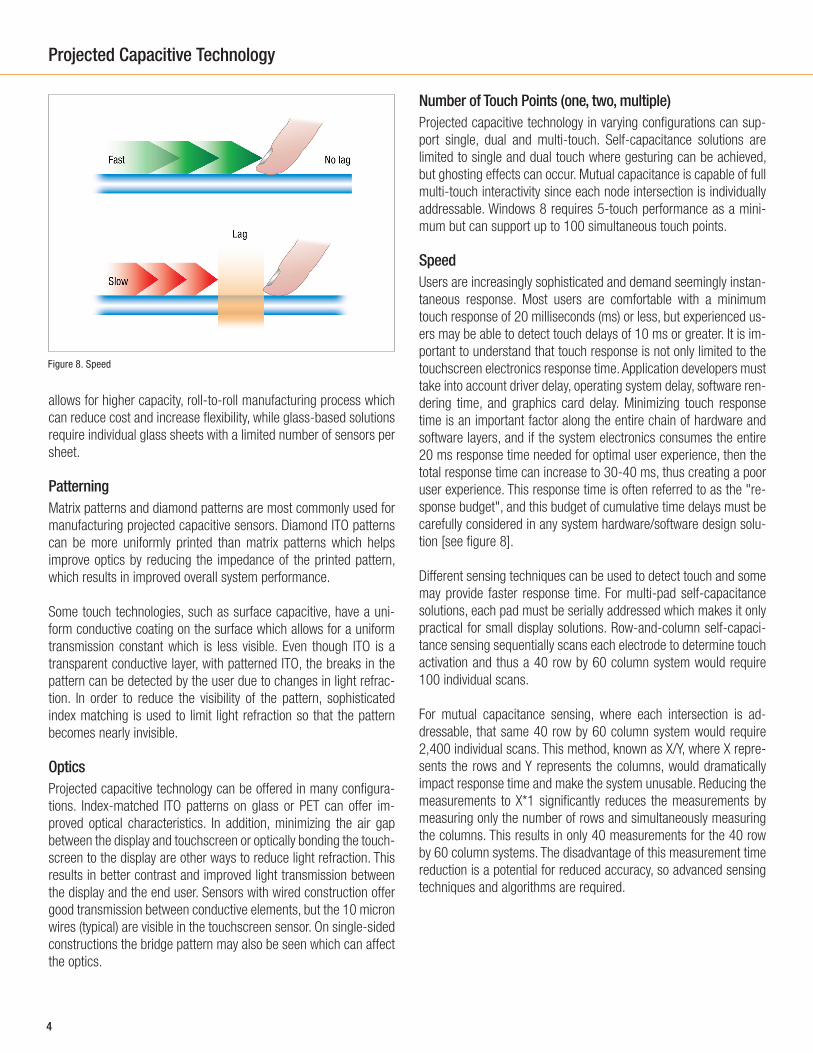
SpeedUsers are increasingly sophisticated and demand seemingly instan-taneous response. Most users are comfortable with a minimum touch response of 20 milliseconds (ms) or less, but experienced us-ers may be able to detect touch delays of 10 ms or greater. It is im-portant to understand that touch response is not only limited to the touchscreen electronics response time. Application developers must take into account driver delay, operating system delay, software ren-dering time, and graphics card delay. Minimizing touch response time is an important factor along the entire chain of hardware and software layers, and if the system electronics consumes the entire 20 ms response time needed for optimal user experience, then the total response time can increase to 30-40 ms, thus creating a poor user experience. This response time is often referred to as the "re-sponse budget", and this budget of cumulative time delays must be carefully considered in any system hardware/software design solu-tion [see figure 8].
Different sensing techniques can be used to detect touch and some may provide faster response time. For multi-pad self-capacitance solutions, each pad must be serially addressed which makes it only practical for small display solutions. Row-and-column self-capaci-tance sensing sequentially scans each electrode to determine touch activation and thus a 40 row by 60 column system would require 100 individual scans.
For mutual capacitance sensing, where each intersection is ad-dressable, that same 40 row by 60 column system would require 2,400 individual scans. This method, known as X/Y, where X repre-sents the rows and Y represents the columns, would dramatically impact response time and make the system unusable. Reducing the measurements to X*1 significantly reduces the measurements by measuring only the number of rows and simultaneously measuring the columns. This results in only 40 measurements for the 40 row by 60 column systems. The disadvantage of this measurement time reduction is a potential for reduced accuracy, so advanced sensing techniques and algorithms are required.
Figure 8. Speed
4

DurabilityProjected capacitive technology projects a signal outward creating an electrical field that can be measured by the system electron-ics. This technology does not require direct contact with the active touch surface so a protective cover lens (usually a glass substrate) is often used as the surface of the touch sensor [see figure 9]. This glass surface can be standard glass, tempered glass, or chemically-strengthened glass depending on the application needs. This "sec-ond surface" technology (a front surface that can withstand wear and scratch damage without affecting touch performance) means that screen cracks, scratches or surface wear would have to extend through the entire thickness of the cover glass to reach the elec-trodes and cause functional damage.
Self-capacitance solutions may have a higher signal level and are typically able to project through thicker cover glass up to 20 mm, although thicker cover glass can affect system performance and accuracy. For mutual capacitance solutions, which has a lower sig-nal level, typical cover glass thickness is in the 0.7 mm to 2.0 mm range.
Transmission (Screen Brightness)Depending on the sensor's construction, projected capacitive offers different levels of light transmission. For a glass-on-glass solution, light transmission in excess of 90% can be achieved. If PET layers are used, this number may be reduced to 86-90%, however, some advanced processes can achieve greater than 88% transmission using a PET-based construction.
Anti-Glare Anti-glare characteristics are important in touch sensor design since it allows for optimal screen viewing in ambient light environments.
Projected Capacitive Technology
The reflections on the touchscreen can be significantly reduced by using an anti-glare cover glass. One anti-glare solution is a chemi-cal etch process which creates surface anomalies that refract light, dispersing the light reflection so the user can still see the image on the screen. The second solution is to use a coating applied to the sensor cover glass or to a PET film overlay. Both solutions serve the purpose of dispersing the reflected light to improve the user experi-ence. A heavy anti-glare treatment can negatively impact clarity, so selecting the proper anti-glare solution for a given application is critical.
Anti-StictionAnti-stiction, meaning the reduction of surface stiction while your finger or object drags on the surface, allows for better user experi-ence. Plain glass and some coatings can increase the friction with a user's fingers during draw, drag, and gesturing applications. With an anti-stiction surface, fingers glide effortlessly across the screen for very smooth, natural gesturing experience [see figure 10].
ScalabilityInherent in projected capacitive technology construction, scaling larger sensor sizes would require additional rows and columns to maintain the same touch fidelity. Since access to each row and col-umn (electrode) is required, new tail designs and electronics are needed for each design size. In addition, in order to create the new pattern in a glass-based solution, a new mask would be needed to create the unique ITO layers. If conductive wires are used, a new program is required to create the new wire pattern. For PET-based solutions, a new program would be required for singulation of the sensor.
Figure 9. Durability
Figure 10. Anti-Stiction
5

Bare Hands, Latex Gloves and StylusProjected capacitive technology's electrical field projects above the cover glass to allow sensing of finger, gloved hands and passive stylus. Self-capacitance systems can be tuned to sense both bare fingers and thick winter gloves, although the ability to sense both under the same setting may reduce accuracy. Mutual capacitance systems can sense bare fingers and thin surgical and food ser-vice gloves, but not thick winter gloves (unless they are conductive gloves). A passive stylus can be designed to work with both tech-nologies, however, the diameter of the stylus tip for a mutual ca-pacitance system can usually be smaller than for a self capacitance system [see figure 11].
Sensing Lines and Touch ResolutionWith projected capacitive technology the number of sensing lines and drive lines determine the number of intersection or nodes. Each of these nodes represent a touch location, plus, by using interpola-tion, the system electronics are able to pin-point touch locations by using the information from many of the surrounding electrodes help determine the exact location of touch. Self capacitance sensing is only limited to the information from each row and column scan which provides less information for the electronics to interpolate. Mutual capacitance sensing has a much higher density of electrode information to interpolate, resulting in very high touch accuracy. In the 40 row by 60 column example, mutual capacitive sensing pro-vides a 24:1 ratio in touch density over self capacitance sensing.
Projected Capacitive Technology
6
Surface ContaminantsProjected capacitive technology is an ideal solution for contaminant-prone, public access or harsh environments where dust and debris can collect on the surface of the touchscreen or along the bezel edge. Since PCT is unaffected by most surface contaminants, it can be a better self-service technology than alternative touch technolo-gies that rely on sensors at the edge or corners of the touchscreen.
Flat Front Surface, Industrial DesignOne of the unique features of projected capacitive touchscreens is that the design allows for a flat front surface (FFS) implementation. With all pattern and tail bonds protected by a cover glass, there is no need for a bezel around the screen. This capability allows for enhanced industrial designs that are aesthetically and functionally appealing to the end user. Bezels can keep the finger from reaching the corners of a screen, but in a full screen PCT design the user can access the most extreme corner placements of buttons. In addition, a printed border under the cover glass gives the illusion of a virtual bezel which may be branded with a company's logo or name [see figure 12]. In addition, utilizing the FFS capability also makes debris build up less likely and simplifies the screen cleaning process.
Product Specifications (typical values)
Mutual Capacitance Capacitance-to-Ground
Light Transmission
84% to 90% 84% to 90%
Stylus Type Finger, Thin Glove, Passive Stylus
Finger, Thick Glove,Passive Stylus
Second Surface
Yes Yes
Sealability NEMA 4 / 12 and IP 65 standards
NEMA 4 / 12 and IP 65 standards
Response Time 6 ms 10 ms
Touches 20+ 1 (dual)
Accuracy > 99% > 98.5%
Figure 11. Latex Glove

7
Projected Capacitive Technology
Figure 12. Flat Front Surface or Virtual Bezel
3M...Enabling the Future of Multi-touch3M’s implementation of projected capacitive technology (3M PCT) is designed specifically for the needs of larger display applications. By maintaining a total solutions focus, 3M leverages its years of proven capacitance electronics expertise to create 3M Multi-Touch PCT systems and display solutions ranging in size from 8.4 to 47 inches.
The result of 3M's electronics expertise is the 3M Multi-Touch Electronics PX, a patented multi-touch controller designed and engineered specifically for this larger display sizes without relying on commonly-used electronics developed for the portable device sizes (3.5” to 11.6”). This optimized controller provides customers with 3M PCT’s unique feature set in a scalable, fully warranted, full multi-touch system solution.
The final key element of the 3M PCT solution is the engineered cover glass. This key element enables leading-edge industrial de-signs that eliminate surface mount components and bezels which can detract from the overall product aesthetics, be susceptible to damage, and may collect debris. With a non-active cover glass, product designers can extend the touchscreen glass to the display edge and incorporate capacitive, or even mechanical buttons to the industrial design.
The overall result is the 3M PCT multi-touch system, a high per-formance, high-fidelity interactive solution to help meet customers' expanding user interface requirements.

3M Touch Systems Subsidiary of 3M Company 501 Griffin Brook Park Drive Methuen, MA 01844 U.S.A.
1-888-659-1080
www.3M.com/touch
3M is a trademark of 3M Company. Printed in USA © 3M 2013 All Rights Reserved. PCT TECH BRIEF-1013
Technical Information: The technical information, recommendations and other statements contained in this document are based upon tests or experience that 3M Touch believes are reliable, but the accuracy or completeness of such information is not guaranteed. The technical information, recommendations and other statements contained in this document are subject to change as technology advancement and experience dictates.
IMPORTANT NOTICE TO PURCHASER: IMPORTANT NOTICE TO PURCHASER: Specifications are subject to change without notice. These 3M Touch Systems’ Products and soft-ware are warranted to meet their published specifications from the date of shipment and for the period stated in the specification. 3M Touch Systems makes no additional war-ranties, express or implied, including but not limited to any implied warranties of merchantability or fitness for a particular purpose. User is responsible for determining whether the 3M Touch Systems Products and software are fit for User’s particular purpose and suitable for its method of production, including intellectual property liability for User’s ap-plication. If the Product, software or software media is proven not to have met 3M Touch Systems’ warranty, then 3M Touch Systems’ sole obligation and User’s and Purchaser’s exclu-sive remedy, will be, at 3M Touch Systems’ option, to repair or replace that Product quantity or software mediator to refund its purchase price. 3M Touch Systems has no obligation un-der 3M Touch Systems’ warranty for any Product, software or software media that has been modified or damaged through misuse, accident, neglect, or subsequent manufacturing operations or assemblies by anyone other than 3M Touch Systems. 3M Touch Systems shall not be liable in any action against it in any way related to the Products or software for any loss or damages, whether non-specified direct, indirect, special, incidental or consequential (including downtime, loss of profits or goodwill) regardless of the legal theory asserted. (7/02)