Topics We are going to discuss the following topics for roughly 3 weeks from today Introduction to...
32
Korea Univ Topics • We are going to discuss the following topics for roughly 3 weeks from today Introduction to Hardware Description Language (HDL) Combinational Logic Design with HDL Synchronous Sequential Logic Design with HDL • Finite State Machine (FSM) Design 1
-
Upload
aubrey-shields -
Category
Documents
-
view
215 -
download
1
Transcript of Topics We are going to discuss the following topics for roughly 3 weeks from today Introduction to...
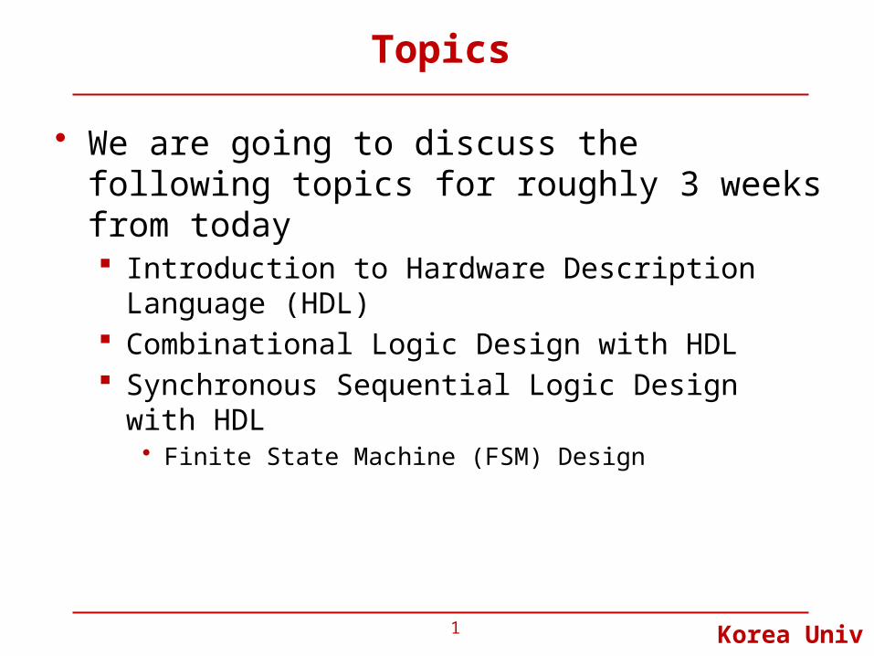
Topics
• We are going to discuss the following topics for roughly 3 weeks from today Introduction to Hardware Description Language
(HDL) Combinational Logic Design with HDL Synchronous Sequential Logic Design with HDL
• Finite State Machine (FSM) Design
1

Introduction
• In old days (~ early 1990s), hardware engineers used to draw schematic of digital logic (combinational and sequential logics), based on Boolean equations
• But, it is not virtually possible to draw schematic as the hardware complexity increases
• As the hardware complexity increases, there has been a necessity of designing hardware in a more efficient way
2

Examples
3
• Core i7 Number of transistors in Core i7 is
roughly 1 billion
Assuming that the gate count is based on 2-input NAND gate, (which is composed of 4 transistors), do you want to draw 250 million gates by hand? Absolutely NOT!
• Midterm Exam Even a simple FSM design problem in
the midterm exam took you more than 30 minutes
Even worse, many of you got your answer wrong in the exam!
Introduction
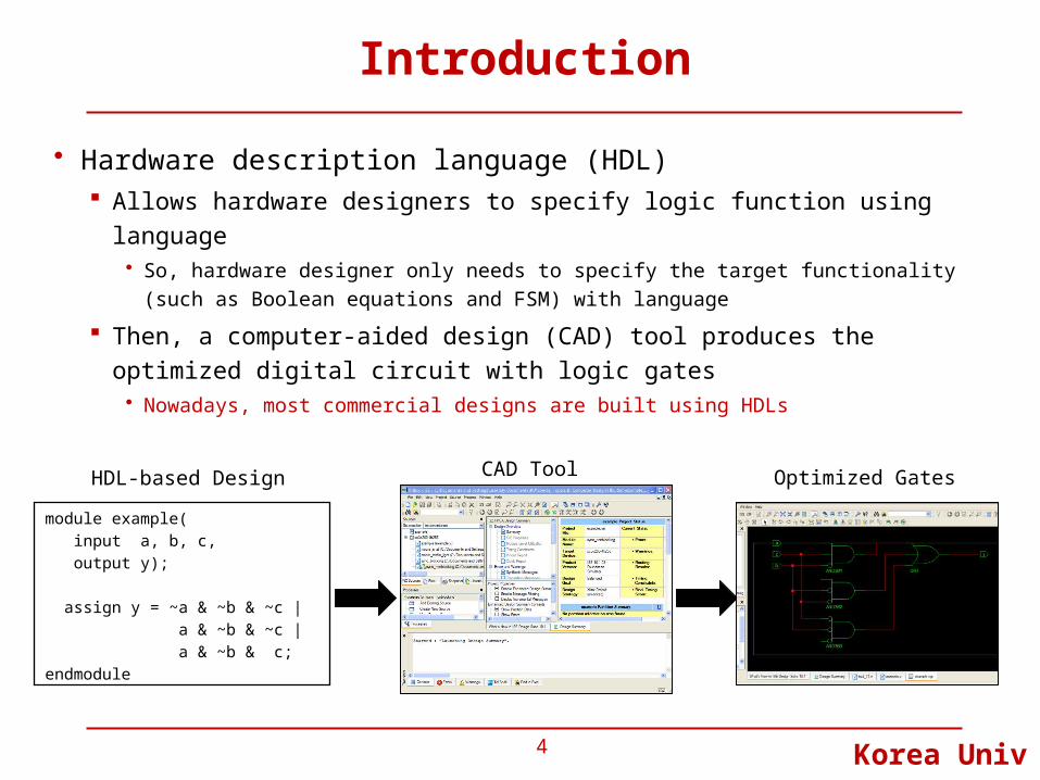
• Hardware description language (HDL) Allows hardware designers to specify logic function using language
• So, hardware designer only needs to specify the target functionality (such as Boolean equations and FSM) with language
Then, a computer-aided design (CAD) tool produces the optimized digital circuit with logic gates
• Nowadays, most commercial designs are built using HDLs
4
module example( input a, b, c, output y);
assign y = ~a & ~b & ~c | a & ~b & ~c | a & ~b & c;endmodule
HDL-based Design CAD Tool Optimized Gates

HDLs
• Two leading HDLs VHDL
• Developed in 1981 by the Department of Defense
• Became an IEEE standard (1076) in 1987
Verilog-HDL• Developed in 1984 by Gateway Design
Automation• Became an IEEE standard (1364) in 1995• We are going to use Verilog-HDL in this class
The book on the right is a good reference (but not required to purchase)
5
IEEE: Institute of Electrical and Electronics Engineers is a professional society responsible for many computing standards including WiFi (802.11), Ethernet (802.3) etc

Hardware Design with HDL
• 3 steps to design hardware with HDL1. Hardware design with HDL
• Describe target hardware with HDL When describing circuits using an HDL, it’s critical to think of
the digital logic the code would produce
2. Simulation• Validate the design
Inputs are applied to the design Outputs checked for correctness Millions of dollars saved by debugging in simulation instead
of hardware
3. Synthesis• Transforms HDL code into a netlist, describing the
hardware Netlist is a text file describing a list of logic gates and the
wires connecting them
6

CAD tools for Simulation
7
• There are renowned CAD companies that provide HDL simulators Cadence
• www.cadence.com Synopsys
• www.synopsys.com Mentor Graphics
• www.mentorgraphics.com• We are going to use ModelSim Altera Starter Edition for simulation
• http://www.altera.com/products/software/quartus-ii/modelsim/qts-modelsim-index.html

CAD tools for Synthesis
• The same companies (Cadence, Synopsys, and Mentor Graphics) provide synthesis tools, too They are extremely expensive to purchase though
• We are going to use a synthesis tool from Altera Altera Quartus-II Web Edition (free)
• Synthesis, place & route, and download to FPGA
• http://www.altera.com/products/software/quartus-ii/web-edition/qts-we-index.html
8

Verilog Modules
• Verilog Module A block of hardware with inputs and outputs
• Examples: AND gate, multiplexer, priority encoder etc
A Verilog module begins with the module name and a list of the inputs and outputs
assign statement is used to describe combinational logic
~ indicates NOT
& indicates AND
| indicates OR
9
ab yc
VerilogModule
module example(input a, b, c, output y);
assign y = ~a & ~b & ~c | a & ~b & ~c | a & ~b & c;
endmodule

Synthesis
• Transforms HDL code into a netlist, that is, collection of gates and their connections
10
module example(input a, b, c, output y); assign y = ~a & ~b & ~c | a & ~b & ~c | a & ~b & c;endmodule

Digital Design w/ Verilog HDL
• Combinational Logic Continuous assignment statement
• It is used to describe simple combinational logic• assign
always statement• It is used to describe complex combinational logic• always @(*)
• Synchronous Sequential Logic FSM is composed of flip-flops and combinational logics Flip-flops are described with always statement
• always @(posedge clk)• always @(negedge clk)
11

Verilog Syntax
• Verilog is case sensitive. So, reset and Reset are NOT the same signal.
• Verilog does not allow you to start signal or module names with numbers For example, 2mux is NOT a valid name
• Verilog ignores whitespace such as spaces, tabs and line breaks Proper indentation and use of blank lines are helpful to make your
design readable
• Comments come in single-line and multi-line varieties like C-language // : single line comment /* */ : multiline comment
12
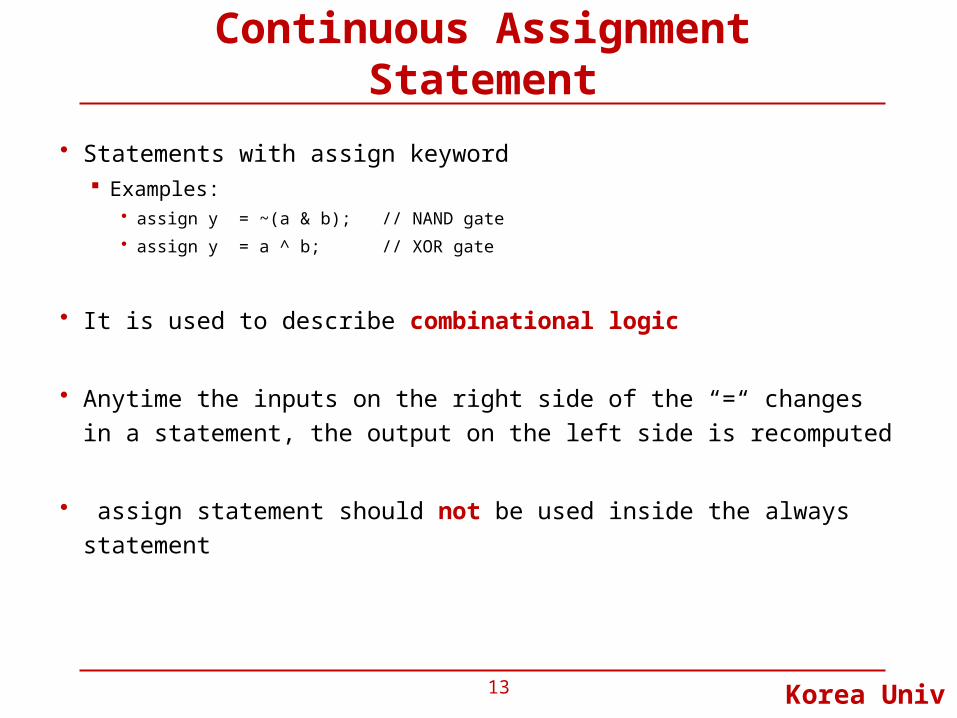
Continuous Assignment Statement
• Statements with assign keyword Examples:
• assign y = ~(a & b); // NAND gate
• assign y = a ^ b; // XOR gate
• It is used to describe combinational logic
• Anytime the inputs on the right side of the “=“ changes in a statement, the output on the left side is recomputed
• assign statement should not be used inside the always statement
13

Bitwise Operators
• Bitwise operators perform a bit-wise operation on two operands Take each bit in one operand and perform the operation
with the corresponding bit in the other operand
14
module gates(input [3:0] a, b, output [3:0] y1, y2, y3, y4, y5);
/* Five different two-input logic gates acting on 4 bit busses */
assign y1 = a & b; // AND assign y2 = a | b; // OR assign y3 = a ^ b; // XOR assign y4 = ~(a & b); // NAND assign y5 = ~(a | b); // NOR
endmodule
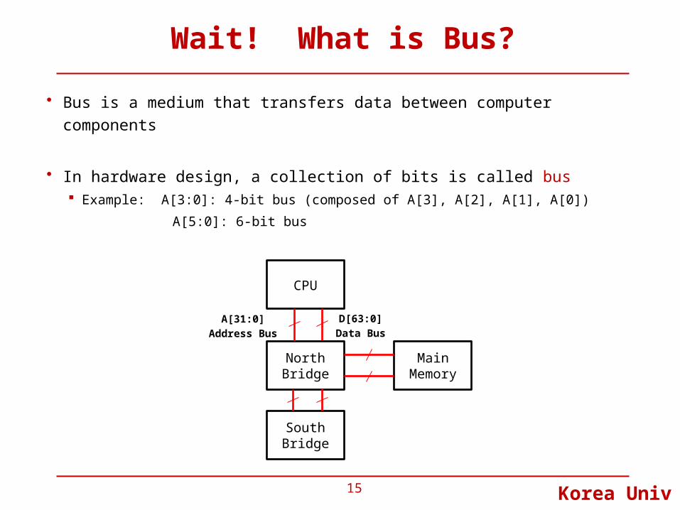
Wait! What is Bus?
15
• Bus is a medium that transfers data between computer components
• In hardware design, a collection of bits is called bus Example: A[3:0]: 4-bit bus (composed of A[3], A[2], A[1], A[0])
A[5:0]: 6-bit bus
CPU
North Bridge
South Bridge
A[31:0]Address Bus
D[63:0]Data Bus
Main Memory

Bus Representation
• Why uses a[3:0] to represent a 4-bit bus? How about a[0:3]?
How about a[1:4] or a[4:1]?
• In digital world, we always count from 0 So, it would be nice to start the bus count from 0
If you use a[0:3],• a[0] indicates MSB
• a[3] indicates LSB
If you use a[3:0], • a[3] indicates MSB
• a[0] indicates LSB
• We are going to follow this convention in this course
16
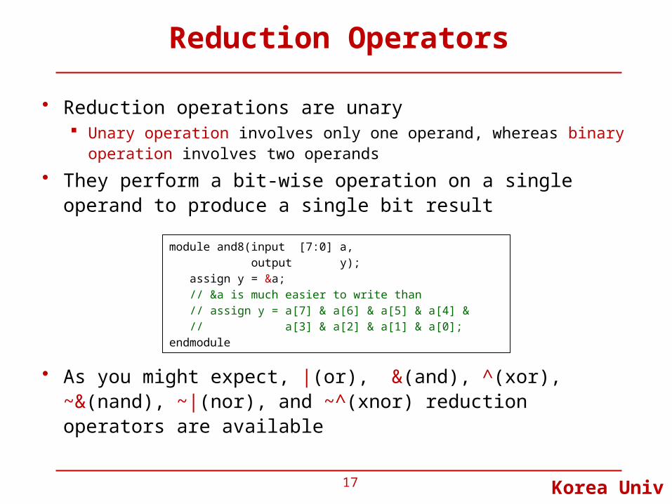
Reduction Operators
• Reduction operations are unary Unary operation involves only one operand, whereas binary
operation involves two operands
• They perform a bit-wise operation on a single operand to produce a single bit result
• As you might expect, |(or), &(and), ^(xor), ~&(nand), ~|(nor), and ~^(xnor) reduction operators are available
17
module and8(input [7:0] a, output y); assign y = &a; // &a is much easier to write than // assign y = a[7] & a[6] & a[5] & a[4] & // a[3] & a[2] & a[1] & a[0];endmodule

Examples
18
& 4’b1001 = & 4’bx111 =~& 4’b1001 = ~& 4’bx001 =| 4’b1001 =~| 4’bx001 =^ 4’b1001 = ~^ 4’b1101 =^ 4’b10x1 =
0x111000x

Conditional Assignment
• The conditional operator ? : chooses between a second and third expression, based on a first expression The first expression is the condition
• If the condition is 1, the operator chooses the second expression• If the condition is 0, the operator chooses the third expression
Therefore, it is a ternary operator because it takes 3 inputs It looks the same as the C-language and Java, right?
19
module mux2(input [3:0] d0, d1, input s, output [3:0] y);
assign y = s ? d1 : d0; // if s is 1, y = d1 // if s is 0, y = d0
endmodule
What kind of hardware do you think this would generate?

Internal Variables
• It is often convenient to break a complex design into intermediate designs
• The keyword wire is used to represent internal variable whose value is defined by an assign statement• For example, in the schematic below, you can declare p
and g as wires
20
p
g s
un1_cout cout
cout
s
cin
ba

Internal Variables Example
21
module fulladder(input a, b, cin, output s, cout);
wire p, g; // internal nodes
assign p = a ^ b; assign g = a & b; assign s = p ^ cin; assign cout = g | (p & cin);
endmodule
p
g s
un1_cout cout
cout
s
cin
ba

Logical & Arithmetic Shifts
22
• Logical shift
• Arithmetic shift

Logical & Arithmetic Shifts
• Logical shift (<<, >>) Every bit in the operand is simply moved by a given number of bit
positions, and the vacant bit-positions are filled in with zeros
• Arithmetic shift (<<<, >>>) Like logical shift, every bit in the operand is moved by a given number of
bit positions
Instead of being filled with all 0s, when shifting to the right, the leftmost bit (usually the sign bit in signed integer representations) is replicated to fill in all the vacant positions
• This is sign extension
Arithmetic shifts can be useful as efficient ways of performing multiplication or division of signed integers by powers of two
• a <<< 2 is equivalent to a x 4 ?
• a >>> 2 is equivalent to a/4? Take floor value if the result is not an integer. The floor value of X (or X) is the greatest
integer number less than or equal to X
Examples:5/2 = 2, -3/2 = -2
23

Operator Precedence
• The operator precedence for Verilog is much like you would expect in other programming languages In particular, AND has precedence over OR
You may use parentheses if the operation order is not clear
24
~ NOT
*, /, % mult, div, mod
+, - add,sub
<<, >> logical shift
<<<, >>> arithmetic shift
<, <=, >, >= comparison
==, != equal, not equal
&, ~& AND, NAND
^, ~^ XOR, XNOR
|, ~| OR, XOR
?: ternary operator
Highest
Lowest

Number Representation
• In Verilog, you can specify base and size of numbers Format: N’Bvalue
• N: size (number of bits)
• B: base (b: binary, d: decimal, o: octal, h: hexadecimal)
• When writing a number, specify both base and size
25
Number # Bits BaseDecimal
Equivalent
Stored
3’b101 3 binary 5 101
8’b11 8 binary 3 00000011
8’b1010_1011
8 binary 171 10101011
3’d6 3 decimal 6 110
6’o42 6 octal 34 100010
8’hAB 8hexadecim
al171 10101011

Replication Operator
• Replication operator is used to replicate a group of bits For instance, if you have a 1-bit variable and you want to
replicate it 3 times to get a 3-bit variable, you can use the replication operator
26
wire [2:0] y;
assign y = {3{b[0]}};
// the above statement produces:// y = b[0] b[0] b[0]

Concatenation Operator
• Concatenation operator { , } combines (concatenates) the bits of 2 or more operands
27
wire [11:0] y;
assign y = {a[2:1], {3{b[0]}}, a[0], 6’b100_010};
// the above statement produces:// y = a[2] a[1] b[0] b[0] b[0] a[0] 1 0 0 0 1 0// underscores (_) are used for formatting only to make
it easier to read. Verilog ignores them.

Tristate buffer and Floating output (Z)
28
Synthesis:
Verilog: module tristate(input [3:0] a, input en, output [3:0] y);
assign y = en ? a : 4'bz;
endmodule
y_1[3:0]
y[3:0][3:0]
en
a[3:0] [3:0] [3:0][3:0]

Verilog Module Description
• Two general styles of describing module functionality Behavioral modeling
• Express the module’s functionality descriptively Structural modeling
• Describe the module’s functionality from combination of simpler modules
29

Behavioral Modeling Example
• Behavioral modeling Express the module’s functionality descriptively
30
module example(input a, b, c, output y);
assign y = ~a & ~b & ~c | a & ~b & ~c | a & ~b & c;
endmodule
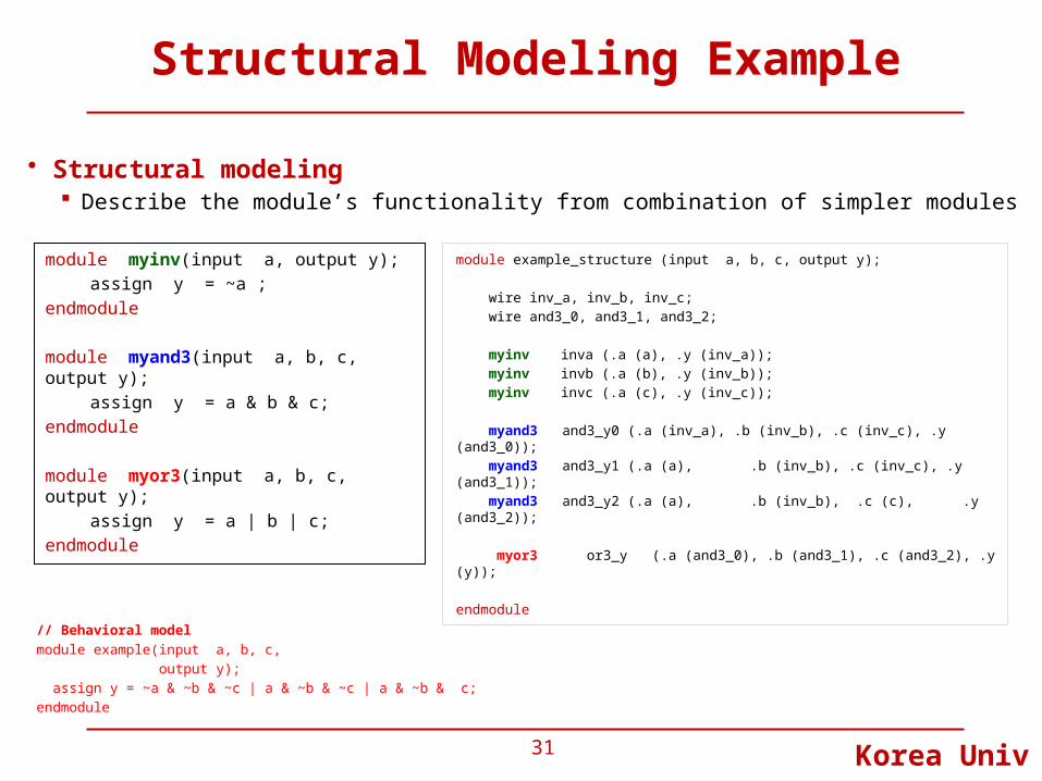
Structural Modeling Example
31
• Structural modeling Describe the module’s functionality from combination of simpler modules
module myinv(input a, output y);assign y = ~a ;
endmodule
module myand3(input a, b, c, output y);
assign y = a & b & c;endmodule
module myor3(input a, b, c, output y);assign y = a | b | c;
endmodule
// Behavioral modelmodule example(input a, b, c, output y); assign y = ~a & ~b & ~c | a & ~b & ~c | a & ~b & c;endmodule
module example_structure (input a, b, c, output y);
wire inv_a, inv_b, inv_c; wire and3_0, and3_1, and3_2;
myinv inva (.a (a), .y (inv_a)); myinv invb (.a (b), .y (inv_b)); myinv invc (.a (c), .y (inv_c));
myand3 and3_y0 (.a (inv_a), .b (inv_b), .c (inv_c), .y (and3_0)); myand3 and3_y1 (.a (a), .b (inv_b), .c (inv_c), .y (and3_1)); myand3 and3_y2 (.a (a), .b (inv_b), .c (c), .y (and3_2));
myor3 or3_y (.a (and3_0), .b (and3_1), .c (and3_2), .y (y));
endmodule

Simulation
32
module example(input a, b, c, output y); assign y = ~a & ~b & ~c | a & ~b & ~c | a & ~b & c;endmodule