
HOW I FIND ABOU IT? I talked with my colleagues in NATIONAL PEDAGOGICAL COLLEGE Ștefan Odobleja;

May 15, 2018 11:50 ws-book9x6 Lessons from Nanoelectronics: B. Quantum Transport 10440-main page v
To my students and colleagues
and all others whose love of learning
has helped me learn
v

May 15, 2018 11:50 ws-book9x6 Lessons from Nanoelectronics: B. Quantum Transport 10440-main page vi

May 15, 2018 11:50 ws-book9x6 Lessons from Nanoelectronics: B. Quantum Transport 10440-main page vii
Preface
Everyone is familiar with the amazing performance of a modern smart-
phone, powered by a billion-plus nanotransistors, each having an active
region that is barely a few hundred atoms long. I believe we also owe a ma-
jor intellectual debt to the many who have made this technology possible.
This is because the same amazing technology has also led to a deeper un-
derstanding of the nature of current flow and heat dissipation on an atomic
scale which I believe should be of broad relevance to the general problems
of non-equilibrium statistical mechanics that pervade many different fields.
To make these lectures accessible to anyone in any branch of science or
engineering, we assume very little background beyond linear algebra and
differential equations. However, we will be discussing advanced concepts
that should be of interest even to specialists, who are encouraged to look
at my earlier books for additional technical details.
This book is based on a set of two online courses originally offered in
2012 on nanoHUB-U and more recently in 2015 on edX. In preparing the
second edition we decided to split it into parts A and B entitled Basic
Concepts and Quantum Transport respectively, along the lines of the two
courses. Even this Second Edition represents lecture notes in unfinished
form.
For ease of reference, Part B includes a list of all equations from Part
A that are referred to (Appendix F). We have also included the overview
chapter (Chapter 1) from Part A with essentially no modification. A list of
available video lectures corresponding to different sections of this volume is
provided upfront. I believe readers will find these useful.
vii

May 15, 2018 11:50 ws-book9x6 Lessons from Nanoelectronics: B. Quantum Transport 10440-main page viii

May 15, 2018 11:50 ws-book9x6 Lessons from Nanoelectronics: B. Quantum Transport 10440-main page ix
Acknowledgments
The precursor to this lecture note series, namely the Electronics from the
Bottom Up initiative on https://nanohub.org was funded by the U.S. Na-
tional Science Foundation (NSF), the Intel Foundation, and Purdue Univer-
sity. Thanks to World Scientific Publishing Corporation and, in particular,
our series editor, Zvi Ruder for joining us in this partnership.
In 2012 nanoHUB-U offered its first two online courses based on this
text. We gratefully acknowledge Purdue and NSF support for this program,
along with the superb team of professionals who made nanoHUB-U a reality
(https://nanohub.org/u) and later helped offer these courses through edX.
A special note of thanks to Mark Lundstrom for his leadership that
made it all happen and for his encouragement and advice. I am grateful to
Shuvro Chowdhury for carefully going through this new edition and fixing
the many errors introduced during conversion to LATEX. I also owe a lot
to many students, ex-students, on-line students and colleagues for their
valuable feedback and suggestions regarding these lecture notes.
Finally I would like to express my deep gratitude to all who have helped
me learn, a list that includes many students, colleagues and teachers start-
ing with the late Richard Feynman whose classic lectures on physics, I am
sure, have inspired many like me and taught us the “pleasure of finding
things out.”
Supriyo Datta
ix

May 15, 2018 11:50 ws-book9x6 Lessons from Nanoelectronics: B. Quantum Transport 10440-main page x

May 15, 2018 11:50 ws-book9x6 Lessons from Nanoelectronics: B. Quantum Transport 10440-main page xi
List of Available Video LecturesQuantum Transport
This book is based on a set of two online courses originally offered in 2012 on
nanoHUB-U and more recently in 2015 on edX. These courses are now avail-
able in self-paced format at nanoHUB-U (https://nanohub.org/u) along
with many other unique online courses.
Additional information about this book along with questions and an-
swers is posted at the book website.
In preparing the second edition we decided to split the book into parts
A and B following the two online courses available on nanoHUB-U entitled
Fundamentals of Nanoelectronics
Part A: Basic Concepts Part B: Quantum Transport
Also of possible interest in this context: NEGF: A Different Perspective.
Following is a detailed list of video lectures available at the course web-
site corresponding to different sections of this volume (Part B: Quantum
Transport). The figures of this volume can be regenerated with these MAT-
LAB codes which are also available in Appendix H.
In the following QTAT stands for
Quantum Transport: Atom to Transistor, Chapter 5–11, Cambridge
(2005). To reproduce the figures of the book use these MATLAB codes.
xi

May 15, 2018 11:50 ws-book9x6 Lessons from Nanoelectronics: B. Quantum Transport 10440-main page xii
xii Lessons from Nanoelectronics: B. Quantum Transport
Lecture in Topic Discussed
Course website in this book
Unit 1: L1.1 Introduction Chapter 17
Unit 1: L1.2 Wave Equation Section 17.1
Unit 1: L1.3 Differential to Matrix Equation Section 17.3
Unit 1: L1.4 Dispersion Relation Section 17.4.1
Unit 1: L1.5 Counting States QTAT 5.1
Unit 1: L1.6 Beyond 1D Section 17.4.2
Unit 1: L1.7 Matrix Equation With Basis QTAT 5.1
Unit 1: L1.8 Graphene Section 17.4.4
Unit 1: L1.9 Reciprocal Lattice/Valleys QTAT 5.2
Unit 1: L1.10 Summary Chapter 17
Unit 2: L2.1 Introduction Chapters 18, 19
Unit 2: L2.2 Semiclassical Model Section 18.1.1
Unit 2: L2.3 Quantum Model Sections 18.1.2,
18.1.3
Unit 2: L2.4 NEGF Equations Sections 18.2.1–
18.2.3
Unit 2: L2.5 Current Operator Sections 18.2.4,
18.3
Unit 2: L2.6 Scattering Theory Section 19.1
Unit 2: L2.7 Transmission Section 19.1.1
Unit 2: L2.8 Resonant Tunneling Section 19.2
Unit 2: L2.9 Dephasing Sections 18.4, 19.3
Unit 2: L2.10 Summary Chapters 18, 19
Unit 3: L3.1 Introduction Chapter 20
Unit 3: L3.2 Quantum Point Contact Section 20.1
Unit 3: L3.3 Self-Energy Section 20.2
Unit 3: L3.4 Surface Green’s Function Section 20.2.2
Unit 3: L3.5 Graphene Section 20.2.3
Unit 3: L3.6 Magnetic Field Section 20.3
Unit 3: L3.7 Golden Rule Section 21.1,
QTAT 10.1
Unit 3: L3.8 Inelastic Scattering Chapter 21,
QTAT 10.3

May 15, 2018 11:50 ws-book9x6 Lessons from Nanoelectronics: B. Quantum Transport 10440-main page xiii
List of Available Video Lectures Quantum Transport xiii
Unit 3: L3.9 Can NEGF Include Everything? Chapter 22
Unit 3: L3.10 Summary Chapter 20
Unit 4: L4.1 Introduction Chapter 23
Unit 4: L4.2 Magnetic Contacts Section 23.3
Unit 4: L4.3 Rotating Contacts Section 23.4
Unit 4: L4.4 Vectors and Spinors Section 23.6
Unit 4: L4.5 Spin-orbit Coupling Section 23.5.2
Unit 4: L4.6 Spin Hamiltonian Section 23.5
Unit 4: L4.7 Spin Density/Current Section 24.1
Unit 4: L4.8 Spin Voltage Section 24.2
Unit 4: L4.9 Spin Circuits Section 24.3
Unit 4: L4.10 Summary Chapter 23

May 15, 2018 11:50 ws-book9x6 Lessons from Nanoelectronics: B. Quantum Transport 10440-main page xiv

May 15, 2018 11:50 ws-book9x6 Lessons from Nanoelectronics: B. Quantum Transport 10440-main page xv
Constants Used in This Book
Electronic charge −q = −1.6× 10⁻¹⁹ C (Coulomb)
Unit of energy 1 eV = 1.6× 10⁻¹⁹ J (Joule)
Boltzmann constant k = 1.38× 10⁻²³ J ·K−1
∼ 25 meV (at 300 K)
Planck’s constant h = 6.626× 10⁻³⁴ J · sReduced Planck’s constant ~ = h/2π = 1.055× 10⁻³⁴ J · sFree electron mass m0 = 9.109× 10⁻³¹ kg
xv

May 15, 2018 11:50 ws-book9x6 Lessons from Nanoelectronics: B. Quantum Transport 10440-main page xvi

May 15, 2018 11:50 ws-book9x6 Lessons from Nanoelectronics: B. Quantum Transport 10440-main page xvii
Some Symbols Used
m Effective Mass Kg
I Electron Current A (Amperes)
T Temperature K (Kelvin)
t Transfer Time s (second)
V Electron Voltage V (Volt)
U Electrostatic Potential eV
µ Electrochemical Potential eV
(also called Fermi level or
quasi-Fermi level)
µ0 Equilibrium Electrochemical Potential eV
R Resistance Ω (Ohm)
G Conductance S (Siemens)
G(E) Conductance at 0 K with µ0 = E S
λ Mean Free Path for Backscattering m
LE Energy Relaxation Length m
Lin Mean Path between Inelastic m
Scattering
τm Momentum Relaxation time s
D Diffusivity m2 · s−1
µ Mobility m2 ·V−1 · s−1
ρ Resistivity Ω ·m (3D), Ω (2D),
Ω ·m−1 (1D)
σ Conductivity S ·m−1 (3D),
S (2D), S ·m (1D)
σ(E) Conductivity at 0 K with µ0 = E S ·m−1 (3D),
S (2D), S ·m (1D)
A Area m2
xvii

May 15, 2018 11:50 ws-book9x6 Lessons from Nanoelectronics: B. Quantum Transport 10440-main page xviii
xviii Lessons from Nanoelectronics: B. Quantum Transport
W Width m
L Length m
E Energy eV
C Capacitance F (Farad)
ε Permittivity F ·m−1
ε Energy eV
f(E) Fermi Function Dimensionless(− ∂f∂E
)Thermal Broadening Function (TBF) eV−1
kT(− ∂f∂E
)Normalized TBF Dimensionless
D(E) Density of States eV−1
N(E) Number of States with Energy < E Dimensionless
(equals number of Electrons
at 0 K with µ0 = E)
n Electron Density (3D or 2D or 1D) m−3 or m−2 or
m−1
ns Electron Density m−2
nL Electron Density m−1
M(E) Number of Channels Dimensionless
(also called transverse modes)
ν Transfer Rate s−1
γ = ~ν Energy Broadening eV
X† Complex conjugate of
transpose of matrix X
H (Matrix) Hamiltonian eV
GR(E) (Matrix) Retarded Green’s function eV−1
Gn(E)/2π (Matrix) Electron Density eV−1,
per gridpoint
A(E)/2π (Matrix) Density of States eV−1,
per gridpoint
Γ(E) (Matrix) Energy Broadening eV
GA(E) (Matrix) Advanced Green’s function eV−1
= [GR(E)]†
BTE Boltzmann Transport Equation
NEGF Non-Equilibrium Green’s Function
DOS Density Of States
QFL Quasi-Fermi Level

May 15, 2018 11:50 ws-book9x6 Lessons from Nanoelectronics: B. Quantum Transport 10440-main page xix
Contents
Preface vii
Acknowledgments ix
List of Available Video Lectures Quantum Transport xi
Constants Used in This Book xv
Some Symbols Used xvii
1. Overview 1
1.1 Conductance . . . . . . . . . . . . . . . . . . . . . . . . . 3
1.2 Ballistic Conductance . . . . . . . . . . . . . . . . . . . . 4
1.3 What Determines the Resistance? . . . . . . . . . . . . . . 5
1.4 Where is the Resistance? . . . . . . . . . . . . . . . . . . . 6
1.5 But Where is the Heat? . . . . . . . . . . . . . . . . . . . 8
1.6 Elastic Resistors . . . . . . . . . . . . . . . . . . . . . . . 10
1.7 Transport Theories . . . . . . . . . . . . . . . . . . . . . . 13
1.7.1 Why elastic resistors are conceptually simpler . . 14
1.8 Is Transport Essentially a Many-body Process? . . . . . . 16
1.9 A Different Physical Picture . . . . . . . . . . . . . . . . . 17
Contact-ing Schrodinger 19
17. The Model 21
17.1 Schrodinger Equation . . . . . . . . . . . . . . . . . . . . . 24
17.1.1 Spatially varying potential . . . . . . . . . . . . . 25
xix

May 15, 2018 11:50 ws-book9x6 Lessons from Nanoelectronics: B. Quantum Transport 10440-main page xx
xx Lessons from Nanoelectronics: B. Quantum Transport
17.2 Electron-electron Interactions and the SCF Method . . . . 28
17.3 Differential to Matrix Equation . . . . . . . . . . . . . . . 30
17.3.1 Semi-empirical tight-binding (TB) models . . . . . 31
17.3.2 Size of matrix, N = n× b . . . . . . . . . . . . . . 32
17.4 Choosing Matrix Parameters . . . . . . . . . . . . . . . . 33
17.4.1 One-dimensional conductor . . . . . . . . . . . . . 33
17.4.2 Two-dimensional conductor . . . . . . . . . . . . . 35
17.4.3 TB parameters in B-field . . . . . . . . . . . . . . 37
17.4.4 Lattice with a “Basis” . . . . . . . . . . . . . . . . 38
18. NEGF Method 43
18.1 One-level Resistor . . . . . . . . . . . . . . . . . . . . . . . 48
18.1.1 Semiclassical treatment . . . . . . . . . . . . . . . 48
18.1.2 Quantum treatment . . . . . . . . . . . . . . . . . 50
18.1.3 Quantum broadening . . . . . . . . . . . . . . . . 53
18.1.4 Do multiple sources interfere? . . . . . . . . . . . 54
18.2 Quantum Transport Through Multiple Levels . . . . . . . 55
18.2.1 Obtaining Eqs. (18.1) . . . . . . . . . . . . . . . . 56
18.2.2 Obtaining Eqs. (18.2) . . . . . . . . . . . . . . . . 57
18.2.3 Obtaining Eq. (18.3) . . . . . . . . . . . . . . . . . 57
18.2.4 Obtaining Eq. (18.4): the current equation . . . . 58
18.3 Conductance Functions for Coherent Transport . . . . . . 59
18.4 Elastic Dephasing . . . . . . . . . . . . . . . . . . . . . . . 60
19. Can Two Offer Less Resistance than One? 65
19.1 Modeling 1D Conductors . . . . . . . . . . . . . . . . . . . 65
19.1.1 1D ballistic conductor . . . . . . . . . . . . . . . . 67
19.1.2 1D conductor with one scatterer . . . . . . . . . . 68
19.2 Quantum Resistors in Series . . . . . . . . . . . . . . . . . 70
19.3 Potential Drop Across Scatterer(s) . . . . . . . . . . . . . 74
More on NEGF 79
20. Quantum of Conductance 81
20.1 2D Conductor as 1D Conductors in Parallel . . . . . . . . 81
20.1.1 Modes or subbands . . . . . . . . . . . . . . . . . 86
20.2 Contact Self-Energy for 2D Conductors . . . . . . . . . . 87
20.2.1 Method of basis transformation . . . . . . . . . . 87

May 15, 2018 11:50 ws-book9x6 Lessons from Nanoelectronics: B. Quantum Transport 10440-main page xxi
Contents xxi
20.2.2 General method . . . . . . . . . . . . . . . . . . . 88
20.2.3 Graphene: ballistic conductance . . . . . . . . . . 90
20.3 Quantum Hall Effect . . . . . . . . . . . . . . . . . . . . . 92
21. Inelastic Scattering 97
21.1 Fermi’s Golden Rule . . . . . . . . . . . . . . . . . . . . . 99
21.1.1 Elastic scattering . . . . . . . . . . . . . . . . . . 100
21.1.2 Inelastic scattering . . . . . . . . . . . . . . . . . . 103
21.2 Self-energy Functions . . . . . . . . . . . . . . . . . . . . . 104
22. Does NEGF Include “Everything?” 107
22.1 Coulomb Blockade . . . . . . . . . . . . . . . . . . . . . . 108
22.1.1 Current versus voltage . . . . . . . . . . . . . . . . 110
22.2 Fock Space Description . . . . . . . . . . . . . . . . . . . . 112
22.2.1 Equilibrium in Fock space . . . . . . . . . . . . . . 113
22.2.2 Current in the Fock space picture . . . . . . . . . 115
22.3 Entangled States . . . . . . . . . . . . . . . . . . . . . . . 117
Spin Transport 123
23. Rotating an Electron 125
23.1 Polarizers and Analyzers . . . . . . . . . . . . . . . . . . . 127
23.2 Spin in NEGF . . . . . . . . . . . . . . . . . . . . . . . . . 130
23.3 One-level Spin Valve . . . . . . . . . . . . . . . . . . . . . 131
23.4 Rotating Magnetic Contacts . . . . . . . . . . . . . . . . . 134
23.5 Spin Hamiltonians . . . . . . . . . . . . . . . . . . . . . . 137
23.5.1 Channel with Zeeman splitting . . . . . . . . . . . 137
23.5.2 Channel with Rashba interaction . . . . . . . . . . 138
23.6 Vectors and Spinors . . . . . . . . . . . . . . . . . . . . . 139
23.7 Spin Precession . . . . . . . . . . . . . . . . . . . . . . . . 143
23.8 Spin-charge Coupling . . . . . . . . . . . . . . . . . . . . . 146
23.9 Superconducting Contacts . . . . . . . . . . . . . . . . . . 150
24. Quantum to Classical 151
24.1 Matrix Electron Density . . . . . . . . . . . . . . . . . . . 151
24.2 Matrix Potential . . . . . . . . . . . . . . . . . . . . . . . 154
24.3 Spin Circuits . . . . . . . . . . . . . . . . . . . . . . . . . 156
24.4 Pseudo-spin . . . . . . . . . . . . . . . . . . . . . . . . . . 158

May 15, 2018 11:50 ws-book9x6 Lessons from Nanoelectronics: B. Quantum Transport 10440-main page xxii
xxii Lessons from Nanoelectronics: B. Quantum Transport
24.5 Quantum Information . . . . . . . . . . . . . . . . . . . . 161
24.5.1 Quantum entropy . . . . . . . . . . . . . . . . . . 161
24.5.2 Does interaction increase the entropy? . . . . . . . 162
24.5.3 How much information can one spin carry? . . . . 163
25. Epilogue: Probabilistic Spin Logic (PSL) 165
25.1 Spins and Magnets . . . . . . . . . . . . . . . . . . . . . . 166
25.1.1 Pseudospins and pseudomagnets . . . . . . . . . . 168
25.2 Unstable Magnets . . . . . . . . . . . . . . . . . . . . . . . 168
25.3 Three-terminal p-bits . . . . . . . . . . . . . . . . . . . . . 170
25.4 p-circuits . . . . . . . . . . . . . . . . . . . . . . . . . . . . 171
Suggested Reading 175
Appendices 187
Appendix F List of Equations and Figures Cited From Part
A 189
Appendix G NEGF Equations 193
G.1 Self-energy for Contacts . . . . . . . . . . . . . . . . . . . 194
G.2 Self-energy for Elastic Scatterers in Equilibrium: . . . . . 196
G.3 Self-energy for Inelastic Scatterers . . . . . . . . . . . . . 196
Appendix H MATLAB Codes Used for Text Figures 199
H.1 Chapter 19 . . . . . . . . . . . . . . . . . . . . . . . . . . 199
H.1.1 Fig. 19.2 Transmission through a single point
scatterer in a 1D wire . . . . . . . . . . . . . . . . 199
H.1.2 Fig. 19.4 Normalized conductance for a wire with
M = 1 due to one scatterer . . . . . . . . . . . . . 200
H.1.3 Fig. 19.5 Normalized conductance for a wire with
M = 1 due to six scatterers . . . . . . . . . . . . . 201
H.1.4 Figs. 19.6–19.7 Potential drop across a scatterer
calculated from NEGF . . . . . . . . . . . . . . . 202
H.1.5 Figs. 19.8–19.9 Potential drop across two scatterers
in series calculated from NEGF . . . . . . . . . . 204
H.2 Chapter 20 . . . . . . . . . . . . . . . . . . . . . . . . . . 206

May 15, 2018 11:50 ws-book9x6 Lessons from Nanoelectronics: B. Quantum Transport 10440-main page xxiii
Contents xxiii
H.2.1 Fig. 20.1 Numerically computed transmission as a
function of energy . . . . . . . . . . . . . . . . . . 206
H.2.2 Fig. 20.3 Transmission calculated from NEGF for
ballistic graphene sheet and CNT . . . . . . . . . 209
H.2.3 Fig. 20.4 Normalized Hall resistance versus B-field
for ballistic channel . . . . . . . . . . . . . . . . . 211
H.2.4 Fig. 20.5 Grayscale plot of local density of states . 213
H.3 Chapter 22 . . . . . . . . . . . . . . . . . . . . . . . . . . 215
H.3.1 Fig. 22.7, n versus µ, single dot . . . . . . . . . . 215
H.3.2 Fig. 22.8, I versus V , single quantum dot . . . . . 216
H.3.3 Fig. 22.9, n versus µ, double quantum dot . . . . 217
H.4 Chapter 23 . . . . . . . . . . . . . . . . . . . . . . . . . . 218
H.4.1 Fig. 23.9 Voltage probe signal as the magnetization
of the probe is rotated . . . . . . . . . . . . . . . . 218
H.4.2 Fig. 23.10 Voltage probe signal due to variation of
gate voltage controlled Rashba coefficient . . . . . 220
Appendix I Table of Contents of Part A: Basic Concepts 223
Appendix J Available Video Lectures for Part A: Basic Concepts 229
Index 231

May 15, 2018 11:50 ws-book9x6 Lessons from Nanoelectronics: B. Quantum Transport 10440-main page xxiv

May 15, 2018 11:50 ws-book9x6 Lessons from Nanoelectronics: B. Quantum Transport 10440-main page 1
Chapter 1
Overview
This chapter is essentially the same as Chapter 1 from Part A. Related
video lecture available at course website, Scientific Overview.
“Everyone” has a smartphone these days, and each smartphone has
more than a billion transistors, making transistors more numerous than
anything else we could think of. Even the proverbial ants, I am told, have
been vastly outnumbered.
There are many types of transistors, but the most common one in use
today is the Field Effect Transistor (FET), which is essentially a resistor
consisting of a “channel” with two large contacts called the “source” and
the “drain” (Fig. 1.1a).
ChannelSource Drain
V +- I(a)
ChannelSource Drain
VG
V +- I(b)
Fig. 1.1 (a) The Field Effect Transistor (FET) is essentially a resistor consisting of achannel with two large contacts called the source and the drain across which we attachthe two terminals of a battery. (b) The resistance R = V/I can be changed by severalorders of magnitude through the gate voltage VG.
The resistance (R) = Voltage (V )/Current (I) can be switched by sev-
eral orders of magnitude through the voltage VG applied to a third terminal
1

May 15, 2018 11:50 ws-book9x6 Lessons from Nanoelectronics: B. Quantum Transport 10440-main page 2
2 Lessons from Nanoelectronics: B. Quantum Transport
called the “gate” (Fig. 1.1b) typically from an “OFF” state of ∼ 100 MΩ
to an “ON” state of ∼ 10 kΩ. Actually, the microelectronics industry uses
a complementary pair of transistors such that when one changes from 100
MΩ to 10 kΩ, the other changes from 10 kΩ to 100 MΩ. Together they
form an inverter whose output is the “inverse” of the input: a low input
voltage creates a high output voltage while a high input voltage creates a
low output voltage as shown in Fig. 1.2.
A billion such switches switching at GHz speeds (that is, once every
nanosecond) enable a computer to perform all the amazing feats that we
have come to take for granted. Twenty years ago computers were far less
powerful, because there were “only” a million of them, switching at a slower
rate as well.
1
10 kΩ
100 MΩInput= 1
0
Output~ 0
1
10 kΩ
100 MΩ
Output~ 1
0
Input= 0
Fig. 1.2 A complementary pair of FET’s form an inverter switch.
Both the increasing number and the speed of transistors are conse-
quences of their ever-shrinking size and it is this continuing miniaturization
that has driven the industry from the first four-function calculators of the
1970s to the modern laptops. For example, if each transistor takes up a
space of say 10 µm × 10 µm, then we could fit 9 million of them into a chip
of size 3 cm × 3 cm, since
3 cm
10 µm= 3000 → 3000× 3000 = 9 million.
That is where things stood back in the ancient 1990s. But now that a
transistor takes up an area of ∼ 1 µm × 1 µm, we can fit 900 million (nearly
a billion) of them into the same 3 cm × 3 cm chip. Where things will go
from here remains unclear, since there are major roadblocks to continued
miniaturization, the most obvious of which is the difficulty of dissipating

May 15, 2018 11:50 ws-book9x6 Lessons from Nanoelectronics: B. Quantum Transport 10440-main page 3
Overview 3
the heat that is generated. Any laptop user knows how hot it gets when it
is working hard, and it seems difficult to increase the number of switches
or their speed too much further.
This book, however, is not about the amazing feats of microelectron-
ics or where the field might be headed. It is about a less-appreciated
by-product of the microelectronics revolution, namely the deeper under-
standing of current flow, energy exchange and device operation that it has
enabled, which has inspired the perspective described in this book. Let me
explain what we mean.
1.1 Conductance
Current
L
Current
A
A basic property of a conductor is its resistance R which is related to
the cross-sectional area A and the length L by the relation
R =V
I=ρL
A(1.1a)
G =I
V=σA
L. (1.1b)
The resistivity ρ is a geometry-independent property of the material that
the channel is made of. The reciprocal of the resistance is the conductance
G which is written in terms of the reciprocal of the resistivity called the
conductivity σ. So what determines the conductivity?
Our usual understanding is based on the view of electronic motion
through a solid as “diffusive” which means that the electron takes a random
walk from the source to the drain, traveling in one direction for some length
of time before getting scattered into some random direction as sketched in
Fig. 1.3. The mean free path, that an electron travels before getting scat-
tered is typically less than a micrometer (also called a micron = 10−3 mm,
denoted µm) in common semiconductors, but it varies widely with temper-
ature and from one material to another.

May 15, 2018 11:50 ws-book9x6 Lessons from Nanoelectronics: B. Quantum Transport 10440-main page 4
4 Lessons from Nanoelectronics: B. Quantum Transport
Length units:1 mm = 1000 µmand 1 µm = 1000 nm
ChannelSource Drain
0.1 mm
10 µm
1 µm
0.1 µm
10 nm
1 nm
0.1 nm
Atomicdimensions
Fig. 1.3 The length of the channel of an FET has progressively shrunk with every newgeneration of devices (“Moore’s law”) and stands today at 14 nm, which amounts to
∼ 100 atoms.
It seems reasonable to ask what would happen if a resistor is shorter than
a mean free path so that an electron travels ballistically (“like a bullet”)
through the channel. Would the resistance still be proportional to length
as described by Eq. (1.1a)? Would it even make sense to talk about its
resistance?
These questions have intrigued scientists for a long time, but even twenty
five years ago one could only speculate about the answers. Today the an-
swers are quite clear and experimentally well established. Even the tran-
sistors in commercial laptops now have channel lengths L ∼ 14 nm, corre-
sponding to a few hundred atoms in length! And in research laboratories
people have even measured the resistance of a hydrogen molecule.
1.2 Ballistic Conductance
It is now clearly established that the resistance RB and the conductance
GB of a ballistic conductor can be written in the form
RB =h
q2
1
M' 25 kΩ× 1
M(1.2a)
GB =q2
hM ' 40 µS×M (1.2b)

May 15, 2018 11:50 ws-book9x6 Lessons from Nanoelectronics: B. Quantum Transport 10440-main page 5
Overview 5
where q, h are fundamental constants and M represents the number of
effective channels available for conduction. Note that we are now using the
word “channel” not to denote the physical channel in Fig. 1.3, but in the
sense of parallel paths whose meaning will be clarified in the first two parts
of this book. In future we will refer to M as the number of “modes”, a
concept that is arguably one of the most important lessons of nanoelectronics
and mesoscopic physics.
1.3 What Determines the Resistance?
The ballistic conductance GB (Eq. (1.2b)) is now fairly well-known, but the
common belief is that it is relevant only for short conductors and belongs
in a course on special topics like mesoscopic physics or nanoelectronics. We
argue that the resistance for both long and short conductors can be written
in terms of GB (λ: mean free path)
G =GB(
1 +L
λ
) . (1.3)
Ballistic and diffusive conductors are not two different worlds, but rather
a continuum as the length L is increased. For L λ, Eq. (1.3) reduces to
G ' GB , while for L λ,
G ' GBλ
L,
which morphs into Ohm’s law (Eq. (1.1b)) if we write the conductivity as
σ =GL
A=GBA
λ =q2
h
M
Aλ (New Expression). (1.4)
The conductivity of long diffusive conductors is determined by the number
of modes per unit area (M/A) which represents a basic material property
that is reflected in the conductance of ballistic conductors.
By contrast, the standard expressions for conductivity are all based
on bulk material properties. For example freshman physics texts typically
describe the Drude formula (momentum relaxation time: τm):
σ = q2 n
mτm (Drude formula) (1.5)
involving the effective mass (m) and the density of free electrons (n). This is
the equation that many researchers carry in their head and use to interpret
experimental data. However, it is tricky to apply if the electron dynamics

May 15, 2018 11:50 ws-book9x6 Lessons from Nanoelectronics: B. Quantum Transport 10440-main page 6
6 Lessons from Nanoelectronics: B. Quantum Transport
is not described by a simple positive effective mass m. A more general
but less well-known expression for the conductivity involves the density of
states (D) and the diffusion coefficient (D)
σ = q2 D
ALD (Degenerate Einstein relation). (1.6)
In Part A of this book we used fairly elementary arguments to establish
the new formula for conductivity given by Eq. (1.4) and show its equivalence
to Eq. (1.6). In Part A we also introduced an energy band model and related
Eqs. (1.4) and (1.6) to the Drude formula (Eq. (1.5)) under the appropriate
conditions when an effective mass can be defined.
We could combine Eqs. (1.3) and (1.4) to say that the standard Ohm’s
law (Eqs. (1.1)) should be replaced by the result
G =σA
L+ λ→ R =
ρ
A(L+ λ), (1.7)
suggesting that the ballistic resistance (corresponding to L λ) is equal
to ρλ/A which is the resistance of a channel with resistivity ρ and length
equal to the mean free path λ.
But this can be confusing since neither resistivity nor mean free path
are meaningful for a ballistic channel. It is just that the resistivity of a
diffusive channel is inversely proportional to the mean free path, and the
product ρλ is a material property that determines the ballistic resistance
RB . A better way to write the resistance is from the inverse of Eq. (1.3):
R = RB
(1 +
L
λ
). (1.8)
This brings us to a key conceptual question that caused much debate
and discussion in the 1980s and still seems less than clear! Let me explain.
1.4 Where is the Resistance?
Equation (1.8) tells us that the total resistance has two parts
RB︸︷︷︸length-independent
andRBL
λ︸ ︷︷ ︸length-dependent
.
It seems reasonable to assume that the length-dependent part is associated
with the channel. What is less clear is that the length-independent part
(RB) is associated with the interfaces between the channel and the two
contacts as shown in Fig. 1.4.

May 15, 2018 11:50 ws-book9x6 Lessons from Nanoelectronics: B. Quantum Transport 10440-main page 7
Overview 7
How can we split up the overall resistance into different components
and pinpoint them spatially? If we were talking about a large everyday
resistor, the approach is straightforward: we simply look at the voltage
drop across the structure. Since the same current flows everywhere, the
voltage drop at any point should be proportional to the resistance at that
point ∆V = I∆R. A resistance localized at the interface should also give
a voltage drop localized at the interface as shown in Fig. 1.4.
Fig. 1.4 The length-dependent part of the resistance in Eq. (1.8) is associated with thechannel while the length-independent part is associated with the interfaces between the
channel and the two contacts. Shown below is the spatial profile of the “potential” which
supports the spatial distribution of resistances shown.
What makes this discussion not so straightforward in the context of
nanoscale conductors is that it is not obvious how to draw a spatial poten-
tial profile on a nanometer scale. The key question is well-known in the
context of electronic devices, namely the distinction between the electro-
static potential and the electrochemical potential.

May 15, 2018 11:50 ws-book9x6 Lessons from Nanoelectronics: B. Quantum Transport 10440-main page 8
8 Lessons from Nanoelectronics: B. Quantum Transport
The former is related to the electric field F
F = −dφdz,
since the force on an electron is qF , it seems natural to think that the
current should be determined by dφ/dz. However, it is well-recognized that
this is only of limited validity at best. More generally current is driven by
the gradient in the electrochemical potential :
I
A≡ J = −σ
q
dµ
dz. (1.9)
Just as heat flows from higher to lower temperatures, electrons flow
from higher to lower electrochemical potentials giving an electron current
that is proportional to −dµ/dz. It is only under special conditions that
µ and φ track each other and one can be used in place of the other. Al-
though the importance of electrochemical potentials and quasi-Fermi levels
is well established in the context of device physics, many experts feel un-
comfortable about using these concepts on a nanoscale and prefer to use
the electrostatic potential instead. However, I feel that this obscures the
underlying physics and considerable conceptual clarity can be achieved by
defining electrochemical potentials and quasi-Fermi levels carefully on a
nanoscale.
The basic concepts are now well established with careful experimen-
tal measurements of the potential drop across nanoscale defects (see for
example, Willke et al., 2015). Theoretically it was shown using a full quan-
tum transport formalism (which we discuss in part B) that a suitably de-
fined electrochemical potential shows abrupt drops at the interfaces, while
the corresponding electrostatic potential is smoothed out over a screening
length making the resulting drop less obvious (Fig. 1.5). These ideas are
described in simple semiclassical terms (following Datta, 1995) in Part 3 of
this volume.
1.5 But Where is the Heat?
One often associates the electrochemical potential with the energy of the
electrons, but at the nanoscale this viewpoint is completely incompatible
with what we are discussing. The problem is easy to see if we consider an
ideal ballistic channel with a defect or a barrier in the middle, which is the
problem Rolf Landauer posed in 1957.
Common sense says that the resistance is caused largely by the barrier
and we will show in Chapter 10 that a suitably defined electrochemical

May 15, 2018 11:50 ws-book9x6 Lessons from Nanoelectronics: B. Quantum Transport 10440-main page 9
Overview 9
ElectrochemicalPotential
ElectrostaticPotential
qV
µ1 µ2
Fig. 1.5 Spatial profile of electrostatic and electrochemical potentials in a nanoscaleconductor using a quantum transport formalism. Reproduced from McLennan et al.,
1991.
potential indeed shows a spatial profile that shows a sharp drop across the
barrier in addition to abrupt drops at the interfaces as shown in Fig. 1.6.
Fig. 1.6 Potential profile across a ballistic channel with a hole in the middle.
If we associate this electrochemical potential with the energy of the
electrons then an abrupt potential drop across the barrier would be ac-
companied by an abrupt drop in the energy, implying that heat is being
dissipated locally at the scatterer. This requires the energy to be trans-
ferred from the electrons to the lattice so as to set the atoms jiggling which
manifests itself as heat. But a scatterer does not necessarily have the de-

May 15, 2018 11:50 ws-book9x6 Lessons from Nanoelectronics: B. Quantum Transport 10440-main page 10
10 Lessons from Nanoelectronics: B. Quantum Transport
grees of freedom needed to dissipate energy: it could for example be just a
hole in the middle of the channel with no atoms to “jiggle”.
In short, the resistance R arises from the loss of momentum caused in
this case by the “hole” in the middle of the channel. But the dissipation
I2R could occur very far from the hole and the potential in Fig. 1.6 cannot
represent the energy. So what does it represent?
The answer is that the electrochemical potential represents the degree
of filling of the available states, so that it indicates the number of electrons
and not their energy. It is then easy to understand the abrupt drop across
a barrier which represents a bottleneck on the electronic highway. As we
all know there are traffic jams right before a bottleneck, but as soon as we
cross it, the road is all empty: that is exactly what the potential profile in
Fig. 1.6 indicates!
In short, everyone would agree that a “hole” in an otherwise ballistic
channel is the cause and location of the resulting resistance and an elec-
trochemical potential defined to indicate the number of electrons correlates
well with this intuition. But this does not indicate the location of the
dissipation I2R.
The hole in the channel gives rise to “hot” electrons with a non-
equilibrium energy distribution which relaxes back to normal through a
complex process of energy exchange with the surroundings over an energy
relaxation length LE ∼ tens of nanometers or longer. The process of dissi-
pation may be of interest in its own right, but it does not help locate the
hole that caused the loss of momentum which gave rise to resistance in the
first place.
1.6 Elastic Resistors
Once we recognize the spatially distributed nature of dissipative processes
it seems natural to model nanoscale resistors shorter than LE as an ideal
elastic resistor which we define as one in which all the energy exchange
and dissipation occurs in the contacts and none within the channel itself
(Fig. 1.7).
For a ballistic resistor RB , as my colleague Ashraf often points out, it
is almost obvious that the corresponding Joule heat I2R must occur in the
contacts. After all a bullet dissipates most of its energy to the object it
hits rather than to the medium it flies through.
There is experimental evidence that real nanoscale conductors do ac-
tually come close to this idealized model which has become widely used

May 15, 2018 11:50 ws-book9x6 Lessons from Nanoelectronics: B. Quantum Transport 10440-main page 11
Overview 11
ChannelSource Drain
V +- I
Heat
HeatNo exchange
of energy
Fig. 1.7 The ideal elastic resistor with the Joule heat V I = I2R generated entirely inthe contacts as sketched. Many nanoscale conductors are believed to be close to this
ideal.
ever since the advent of mesoscopic physics in the late 1980s and is often
referred to as the Landauer approach. However, it is generally believed
that this viewpoint applies only to near-ballistic transport and to avoid
this association we are calling it an elastic resistor rather than a Landauer
resistor.
What we wish to stress is that even a diffusive conductor full of “pot-
holes” that destroy momentum could in principle dissipate all the Joule
heat in the contacts. And even if it does not, its resistance can be calcu-
lated accurately from an idealized model that assumes it does. Indeed we
will use this elastic resistor model to obtain the conductivity expression in
Eq. (1.4) and show that it agrees well with the standard results.
But surely we cannot ignore all the dissipation inside a long resistor
and calculate its resistance accurately treating it as an elastic resistor? We
believe we can do so in many cases of interest, especially at low bias. The
underlying issues can be understood qualitatively using the simple circuit
model shown in Fig. 1.8. For an elastic resistor each energy channel E1,
E2 and E3 is independent with no flow of electrons between them as shown
on the left. Inelastic processes induce “vertical” flow between the energy
channels represented by the vertical resistors as shown on the right. When
can we ignore the vertical resistors?
If the series of resistors representing individual channels are identical,
then the nodes connected by the vertical resistors will be at the same po-
tential, so that there will be no current flow through them. Under these
conditions, an elastic resistor model that ignores the vertical resistors is
quite accurate.

May 15, 2018 11:50 ws-book9x6 Lessons from Nanoelectronics: B. Quantum Transport 10440-main page 12
12 Lessons from Nanoelectronics: B. Quantum Transport
μ1 μ2 μ2μ1Fig. 1.8 A simple circuit model: (a) For elastic resistors, individual energy channelsE1, E2 and E3 are decoupled with no flow between them. (b) Inelastic processes cause
vertical flow between energy channels through the additional resistors shown.
But vertical flow cannot always be ignored. For example, Fig. 1.9a
shows a conductor where the lower energy levels E2 and E3 conduct poorly
compared to E1. We would then expect the electrons to flow upwards in
energy on the left and downwards in energy on the right as shown, thus
cooling the lattice on the left and heating the lattice on the right, leading
to the well-known Peltier effect discussed in Chapter 13.
The role of vertical flow can be even more striking if the left contact
connects only to the channel E1 while the right contact connects only to
E3 as shown in Fig. 1.9b. No current can flow in such a structure without
vertical flow, and the entire current is purely a vertical current. This is
roughly what happens in p-n junctions which is discussed a little further in
Section 12.1.
The bottom line is that elastic resistors generally provide a good de-
scription of short conductors and the Landauer approach has become quite
common in mesoscopic physics and nanoelectronics. What is not well recog-
nized is that this approach can provide useful results even for long conduc-
tors. In many cases, but not always, we can ignore inelastic processes and
calculate the resistance quite accurately as long as the momentum relax-
ation has been correctly accounted for, as discussed further in Section 3.3.
But why would we want to ignore inelastic processes? Why is the theory
of elastic resistors any more straightforward than the standard approach?
To understand this we first need to talk briefly about the transport theories
on which the standard approach is based.

May 15, 2018 11:50 ws-book9x6 Lessons from Nanoelectronics: B. Quantum Transport 10440-main page 13
Overview 13
μ2
μ1
μ2μ1Fig. 1.9 Two examples of structures where vertical flow between energy channels can
be important: (a) If the lower energy levels E2 and E3 conduct poorly, electrons willflow up in energy on the left and down in energy on the right as shown. (b) If the left
contact couples to an upper energy E1 while the right contact couples to a lower energy
E3, then the current flow is purely vertical, occurring only through inelastic processes.
1.7 Transport Theories
Flow or transport always involves two fundamentally different types of pro-
cesses, namely elastic transfer and heat generation, belonging to two dis-
tinct branches of physics. The first involves frictionless mechanics of the
type described by Newton’s laws or the Schrodinger equation. The second
involves the generation of heat described by the laws of thermodynamics.
The first is driven by forces or potentials and is reversible. The second
is driven by entropy and is irreversible. Viewed in reverse, entropy-driven
processes look absurd, like heat flowing spontaneously from a cold to a hot
surface or an electron accelerating spontaneously by absorbing heat from
its surroundings.
Normally the two processes are intertwined and a proper description of
current flow in electronic devices requires the advanced methods of non-
equilibrium statistical mechanics that integrate mechanics with thermody-
namics. Over a century ago Boltzmann taught us how to combine Newto-
nian mechanics with heat generating or entropy-driven processes and the
resulting Boltzmann transport equation (BTE) is widely accepted as the
cornerstone of semiclassical transport theory. The word semiclassical is used
because some quantum effects have also been incorporated approximately
into the same framework.
ClassicalDynamics BTE+ =

May 15, 2018 11:50 ws-book9x6 Lessons from Nanoelectronics: B. Quantum Transport 10440-main page 14
14 Lessons from Nanoelectronics: B. Quantum Transport
A full treatment of quantum transport requires a formal integration
of quantum dynamics described by the Schrodinger equation with heat
generating processes.
QuantumDynamics NEGF+ =
This is exactly what is achieved in the non-equilibrium Green’s function
(NEGF) method originating in the 1960s from the seminal works of Martin
and Schwinger (1959), Kadanoff and Baym (1962), Keldysh (1965) and
others.
1.7.1 Why elastic resistors are conceptually simpler
The BTE takes many semesters to master and the full NEGF formalism,
even longer. Much of this complexity comes from the subtleties of combin-
ing mechanics with distributed heat-generating processes.
Channel
The operation of the elastic resistor can be understood in far more
elementary terms because of the clean spatial separation between the force-
driven and the entropy-driven processes. The former is confined to the
channel and the latter to the contacts. As we will see in the next few
chapters, the latter is easily taken care of, indeed so easily that it is easy
to miss the profound nature of what is being accomplished.
Even quantum transport can be discussed in relatively elementary terms
using this viewpoint. For example, Fig. 1.10 shows a plot of the spatial
profile of the electrochemical potential across our structure from Fig. 1.6
with a hole in the middle, calculated both from the semiclassical BTE
(Chapter 9) and from the NEGF method (part B).
For the NEGF method we show three options. First a coherent model
(left) that ignores all interaction within the channel showing oscillations
indicative of standing waves. Once we include phase relaxation, the con-
structive and destructive interferences are lost and we obtain the result in
the middle which approaches the semiclassical result. If the interactions

May 15, 2018 11:50 ws-book9x6 Lessons from Nanoelectronics: B. Quantum Transport 10440-main page 15
Overview 15
- V +“barrier”
qVa)
b)
c)
f
f
Fig. 1.10 Spatial profile of the electrochemical potential across a channel with a barrier.Solid red line indicates semiclassical result from BTE (part A). Also shown are the
results from NEGF (part B) assuming (a) coherent transport, (b) transport with phase
relaxation, (c) transport with phase and momentum relaxation. Note that no energyrelaxation is included in any of these calculations.

May 15, 2018 11:50 ws-book9x6 Lessons from Nanoelectronics: B. Quantum Transport 10440-main page 16
16 Lessons from Nanoelectronics: B. Quantum Transport
include momentum relaxation as well we obtain a profile indicative of an
additional distributed resistance.
None of these models includes energy relaxation and they all qualify
as elastic resistors making the theory much simpler than a full quantum
transport model that includes dissipative processes. Nevertheless, they all
exhibit a spatial variation in the electrochemical potential consistent with
our intuitive understanding of resistance.
A good part of my own research in the past was focused in this area
developing the NEGF method, but we will get to it only in part B after we
have “set the stage” in this volume using a semiclassical picture.
1.8 Is Transport Essentially a Many-body Process?
The idea that resistance can be understood from a model that ignores in-
teractions within the channel comes as a surprise to many, possibly because
of an interesting fact that we all know: when we turn on a switch and a
bulb lights up, it is not because individual electrons flow from the switch
to the bulb. That would take far too long.
R L
C
Switch Light Bulb
Fig. 1.11 To describe the propagation of signals we need a distributed RLC, modelthat includes an inductance L and a capacitance C which are ordinarily determined by
magnetostatics and electrostatics respectively.
The actual process is nearly instantaneous because one electron pushes
the next, which pushes the next and the disturbance travels essentially
at the speed of light. Surely, our model that localizes all interactions at
arbitrarily placed contacts (Fig. 3.5 of Part A, see Appendix F) cannot
describe this process?
The answer is that to describe the propagation of transient signals we
need a model that includes not just a resistance R, but also an inductance L
and a capacitance C as shown in Fig. 1.11. These could include transport

May 15, 2018 11:50 ws-book9x6 Lessons from Nanoelectronics: B. Quantum Transport 10440-main page 17
Overview 17
related corrections in small conductors but are ordinarily determined by
magnetostatics and electrostatics respectively (Salahuddin et al., 2005).
In this distributedRLC transmission line, the signal velocity determined
by L and C can be well in excess of individual electron velocities reflecting a
collective process. However, L and C play no role at low frequencies, since
the inductor is then like a “short circuit” and the capacitor is like an “open
circuit”. The low frequency conduction properties are represented solely by
the resistance R and can usually be understood fairly well in terms of the
transport of individual electrons along M parallel modes (see Eqs. (1.2))
or “channels”, a concept that has emerged from decades of research. To
quote Phil Anderson from a volume commemorating 50 years of Anderson
localization (see Anderson (2010)):
“ . . . What might be of modern interest is the “channel” concept which
is so important in localization theory. The transport properties at low fre-
quencies can be reduced to a sum over one-dimensional “channels” . . . ”
Even though high frequency signals propagate at the “speed of light”,
there can be no steady-state flow of charge unless an electron transmits from
one end to the other, or as Landauer put it, conductance is transmission.
However, this observation about steady-state currents applies only to charge
and not to other quantities like spin.
1.9 A Different Physical Picture
Let me conclude this overview with an obvious question: why should we
bother with idealized models and approximate physical pictures? Can’t we
simply use the BTE and the NEGF equations which provide rigorous frame-
works for describing semiclassical and quantum transport respectively? The
answer is yes, and all the results we discuss are benchmarked against the
BTE and the NEGF.
However, as Feynman (1963) noted in his classic lectures, even when
we have an exact mathematical formulation, we need an intuitive physical
picture:
“.. people .. say .. there is nothing which is not contained in the equa-
tions .. if I understand them mathematically inside out, I will understand
the physics inside out. Only it doesn’t work that way. .. A physical under-
standing is a completely unmathematical, imprecise and inexact thing, but
absolutely necessary for a physicist.”

May 15, 2018 11:50 ws-book9x6 Lessons from Nanoelectronics: B. Quantum Transport 10440-main page 18
18 Lessons from Nanoelectronics: B. Quantum Transport
Indeed, most researchers carry a physical picture in their head and it is
usually based on the Drude formula (Eq. (1.5)). In this book we will show
that an alternative picture based on elastic resistors leads to a formula
(Eq. (1.4)) that is more generally valid.
Unlike the Drude formula which treats the electric field as the driving
term, this new approach more correctly treats the electrochemical poten-
tial as the driving term. This is well-known at the macroscopic level, but
somehow seems to have been lost in nanoscale transport, where people cite
the difficulty of defining electrochemical potentials. However, that does not
justify using electric field as a driving term, an approach that does not work
for inhomogeneous conductors on any scale.
Since all conductors are fundamentally inhomogeneous on an atomic
scale it seems questionable to use electric field as a driving term. We argue
that at least for low bias transport, it is possible to define electrochemi-
cal potentials or quasi-Fermi levels on an atomic scale and this can lend
useful insight into the physics of current flow and the origin of resistance.
We believe this is particularly timely because future electronic devices will
require a clear understanding of the different potentials.
For example, recent work on spintronics has clearly established experi-
mental situations where upspin and downspin electrons have different elec-
trochemical potentials (sometimes called quasi-Fermi levels) and could even
flow in opposite directions because their dµ/dz have opposite signs. This
cannot be understood if we believe that currents are driven by electric fields,
−dφ/dz, since up and down spins both see the same electric field and have
the same charge. We can expect to see more and more such examples that
use novel contacts to manipulate the quasi-Fermi levels of different group
of electrons (see Chapter 12 of Part A for further discussion).
In short we believe that the lessons of nanoelectronics lead naturally
to a new viewpoint, one that changes even some basic concepts we all
learn in freshman physics. This viewpoint represents a departure from the
established mindset and I hope it will provide a complementary perspective
to facilitate the insights needed to take us to the next level of discovery and
innovation.

May 15, 2018 11:50 ws-book9x6 Lessons from Nanoelectronics: B. Quantum Transport 10440-main page 19
PART 1
Contact-ing Schrodinger
19

May 15, 2018 11:50 ws-book9x6 Lessons from Nanoelectronics: B. Quantum Transport 10440-main page 20

May 15, 2018 11:50 ws-book9x6 Lessons from Nanoelectronics: B. Quantum Transport 10440-main page 21
Chapter 17
The Model
Related video lectures available at course website, Unit 1: L1.1 and Unit 1:
L1.10.
Over a century ago Boltzmann taught us how to combine Newtonian me-
chanics with entropy-driven processes and the resulting Boltzmann trans-
ClassicalDynamics BTE+ =
port equation (BTE) is widely accepted as the cornerstone of semiclassical
transport theory. Most of the results we have discussed so far can be (and
generally are) obtained from the Boltzmann equation, but the concept of
an elastic resistor makes them more transparent by spatially separating
force-driven processes in the channel from the entropy-driven processes in
the contacts.
In this part of this book I would like to discuss the quantum version of
this problem, using the non-equilibrium Green’s function (NEGF) method
to combine quantum mechanics described by the Schrodinger equation with
“contacts” much as Boltzmann taught us how to combine classical dynamics
with “contacts”.
QuantumDynamics NEGF+ =
The NEGF method originated from the classic works in the 1960s that
used the methods of many-body perturbation theory to describe the dis-
tributed entropy-driven processes along the channel. Like most of the work
21

May 15, 2018 11:50 ws-book9x6 Lessons from Nanoelectronics: B. Quantum Transport 10440-main page 22
22 Lessons from Nanoelectronics: B. Quantum Transport
ChannelSource Drain
V
- I(a) Physicalstructure
T0µ1 , T1 µ2 , T2
Σ1 Σ2Σ0H
µ1µ2
Source Drain(b) QuantumTransport
Model
Fig. 17.1 (a) Generic device structure that we have been discussing. (b) General quan-
tum transport model with elastic channel described by a Hamiltonian H and its connec-
tion to each “contact” described by a corresponding self-energy Σ.
Channel
on transport theory (semiclassical or quantum) prior to the 1990s, it was a
“contact-less” approach focused on the interactions occurring throughout
the channel, in keeping with the general view that the physics of resistance
lay essentially in these distributed entropy generating processes.
As with semiclassical transport, our discussion starts at the other end
with the elastic resistor with entropy-driven processes confined to the con-
tacts. This makes the theory less about interactions and more about
“connecting contacts to the Schrodinger equation”, or more simply, about
contact-ing Schrodinger .
But let me put off talking about the NEGF model till the next chapter,
and use subsequent chapters to illustrate its application to interesting prob-
lems in quantum transport. As indicated in Fig. 17.1b the NEGF method
requires two types of inputs: the Hamiltonian, H describing the dynamics
of an elastic channel, and the self-energy Σ describing the connection to the
contacts, using the word “contacts” in a broad figurative sense to denote

May 15, 2018 11:50 ws-book9x6 Lessons from Nanoelectronics: B. Quantum Transport 10440-main page 23
The Model 23
all kinds of entropy-driven processes. Some of these contacts are physical
like the ones labeled “1” and “2” in Fig. 17.1b, while some are conceptual
like the one labeled “0” representing entropy changing processes distributed
throughout the channel.
In this chapter let me just try to provide a super-brief but self-contained
introduction to how one writes down the Hamiltonian H. The Σ can be
obtained by imposing the appropriate boundary conditions and will be
described in later chapters when we look at specific examples applying
the NEGF method.
We will try to describe the procedure for writing down H so that it is
accessible even to those who have not had the benefit of a traditional multi-
semester introduction to quantum mechanics. Moreover, our emphasis here
is on something that may be helpful even for those who have this formal
background. Let me explain.
Most people think of the Schrodinger equation as a differential equation
which is the form we see in most textbooks. However, practical calculations
are usually based on a discretized version that represents the differential
equation as a matrix equation involving the Hamiltonian matrix H of size
N × N , N being the number of “basis functions” used to represent the
structure.
This matrix H can be obtained from first principles, but a widely used
approach is to represent it in terms of a few parameters which are chosen
to match key experiments. Such semi-empirical approaches are often used
because of their convenience and because they can often explain a wide
range of experiments beyond the key ones that are used as input, suggesting
that they capture a lot of essential physics.
In order to follow the rest of the chapter it is important for the readers
to get a feeling for how one writes down this matrix H given an accepted
energy-momentum E(p) relation (Chapter 6) for the material that is be-
lieved to describe the dynamics of conduction electrons with energies around
the electrochemical potential .
But I should stress that the NEGF framework we will talk about in sub-
sequent chapters goes far beyond any specific model that we may choose
to use for H. The same equations could be (and have been) used to de-
scribe say conduction through molecular conductors using first principles
Hamiltonians.

May 15, 2018 11:50 ws-book9x6 Lessons from Nanoelectronics: B. Quantum Transport 10440-main page 24
24 Lessons from Nanoelectronics: B. Quantum Transport
17.1 Schrodinger Equation
Related video lecture available at course website, Unit 1: L1.2.
µ1
µ2
E
D(E)
We started this book by noting that the key input needed to understand
current flow is the density of states, D(E) telling us the number of states
available for an electron to access on its way from the source to the drain.
Theoretical models for D(E) all start from the Schrodinger equation
which tells us the available energy levels. However, we managed to obtain
expressions for D(E) in Chapter 6 without any serious brush with quantum
mechanics by (1) starting from a given energy-momentum relation E(p),
(2) relating the momentum to the wavelength through the de Broglie rela-
tion (p = h/wavelength) and then (3) requiring an integer number of half
wavelengths to fit into the conductor, the same way acoustic waves fit on a
guitar string.
This heuristic principle is mathematically implemented by writing a
wave equation which is obtained from a desired energy-momentum relation
by making the replacements
E → i~∂
∂t, p → −i~∇ (17.1)
where the latter stands for
px → −i~ ∂
∂x, py → −i~ ∂
∂y, pz → −i~ ∂
∂z.
Using this principle, the classical energy-momentum relation
Eclassical(p) =p2x + p2
y + p2z
2m(17.2a)
leads to the wave equation
i~∂
∂tψ(x, y, z, t) = − ~2
2m
(∂2
∂x2+
∂2
∂y2+
∂2
∂z2
)ψ(x, y, z, t) (17.2b)

May 15, 2018 11:50 ws-book9x6 Lessons from Nanoelectronics: B. Quantum Transport 10440-main page 25
The Model 25
whose solutions can be written in the form of exponentials of the form
ψ(x, y, z, t) = ψ0 e+ikxx e+ikyy e+ikzz e−iEt/~ (17.3)
where the energy E is related to the wavevector k by the dispersion relation
E (k) =~2(k2
x + k2y + k2
z)
2m(17.4)
Eq. (17.4) looks just like the classical energy-momentum relation
(Eq. (17.2a)) of the corresponding particle with
p = ~k (17.5)
which relates the particulate property p with the wavelike property k. This
can be seen to be equivalent to the de Broglie relation (p = h/wavelength)
noting that the wavenumber k is related to the wavelength through
k =2π
wavelength.
The principle embodied in Eq. (17.1) ensures that the resulting wave equa-
tion has a group velocity that is the same as the velocity of the correspond-
ing particle
1
~∇k E︸ ︷︷ ︸
Wave group velocity
= ∇pE︸ ︷︷ ︸Particle velocity
17.1.1 Spatially varying potential
The wave equation Eq. (17.2b) obtained from the energy-momentum re-
lation describes free electrons. If there is a force described by a potential
energy U(r) so that the classical energy is given by
Eclassical (r,p) =p2x + p2
y + p2z
2m+ U(x, y, z) (17.6a)
then the corresponding wave equation has an extra term due to U(r)
i~∂
∂tψ = − ~2
2m∇2 ψ + U(r) ψ (17.6b)
where r ≡ (x, y, z) and the Laplacian operator is defined as
∇2 ≡ ∂2
∂x2+
∂2
∂y2+
∂2
∂z2.
Solutions to Eq. (17.6b) can be written in the form
ψ(r, t) = ψ(r) e−iEt/~

May 15, 2018 11:50 ws-book9x6 Lessons from Nanoelectronics: B. Quantum Transport 10440-main page 26
26 Lessons from Nanoelectronics: B. Quantum Transport
where ψ (r) obeys the time-independent Schrodinger equation
Eψ (r) = Hopψ (r) (17.7a)
where Hop is a differential operator obtained from the classical energy fu-
nction in Eq. (17.6a), using the replacement mentioned earlier (Eq. (17.1)):
Hop = − ~2
2m∇2 + U(r). (17.7b)
Quantum mechanics started in the early twentieth century with an effort
to “understand” the energy levels of the hydrogen atom deduced from the
experimentally observed spectrum of the light emitted from an incandescent
source. For a hydrogen atom Schrodinger used the potential energy
U(r) = −Z q2
4π ε0r
where the atomic number Z = 1, due to a point nucleus with charge +q,
and solved Eqs. (17.7) analytically for the allowed energy values En (called
the eigenvalues of the operator Hop) given by
En = −Z2
n2
q2
8π ε0a0(17.8)
with
a0 =4π ε0~2
mq2
and the corresponding solutions
ψn`m(r) = Rn`(r)Y m` (θ, φ)
obeying the equation
En ψn`m(r) =
(− ~2
2m∇2 − Zq2
4πε0r
)ψn`m(r).
The energy eigenvalues in Eq. (17.8) were in extremely good agreement
with the known experimental results, leading to general acceptance of the
Schrodinger equation as the wave equation describing electrons, just as
acoustic waves, for example, on a guitar string are described by
ω2u(z) = − ∂2
∂z2u.
A key point of similarity to note is that when a guitar string is clamped
between two points, it is able to vibrate only at discrete frequencies de-
termined by the length L. Similarly electron waves when “clamped” have

May 15, 2018 11:50 ws-book9x6 Lessons from Nanoelectronics: B. Quantum Transport 10440-main page 27
The Model 27
Fig. 17.2 Energy levels in atoms are catalogued with three indices n, l, and m.
L
discrete energies and most quantum mechanics texts start by discussing the
corresponding “particle in a box” problem.
Shorter the length L, higher the pitch of a guitar and hence the spacing
between the harmonics. Similarly smaller the box, greater the spacing
between the allowed energies of an electron. Indeed one could view the
hydrogen atom as an extremely small 3D box for the electrons giving rise
to the discrete energy levels shown in Fig. 17.2. This is of course just a
qualitative picture. Quantitatively, we have to solve the time-independent
Schrodinger equation (Eq. (17.7)).
There is also a key dissimilarity between classical waves and electron
waves. For acoustic waves we all know what the quantity u(z) stands for:
it is the displacement of the string at the point z, something that can be
readily measured. By contrast, the equivalent quantity for electrons, ψ(r)
(called its wavefunction), is a complex quantity that cannot be measured
directly and it took years for scientists to agree on its proper interpreta-
tion. The present understanding is that the real quantity ψψ∗ describes
the probability of finding an electron in a unit volume around r. This quan-
tity, when summed over many electrons, can be interpreted as the average
electron density.

May 15, 2018 11:50 ws-book9x6 Lessons from Nanoelectronics: B. Quantum Transport 10440-main page 28
28 Lessons from Nanoelectronics: B. Quantum Transport
17.2 Electron-electron Interactions and the SCF Method
After the initial success of the Schrodinger equation in “explaining” the
experimentally observed energy levels of the Hydrogen atom, scientists ap-
plied it to increasingly more complicated atoms and by 1960 had achieved
good agreement with experimentally measured results for all atoms in the
periodic table (Herman and Skillman (1963)). It should be noted, how-
ever, that these calculations are far more complicated primarily because
of the need to include the electron-electron (e-e) interactions in evaluat-
ing the potential energy (Hydrogen has only one electron and hence no e-e
interactions).
For example, Eq. (17.8) gives the lowest energy for a Hydrogen atom as
E1 = −13.6 eV in excellent agreement with experiment. It takes a photon
with at least that energy to knock the electron out of the atom (E > 0), that
is to cause photoemission. Looking at Eq. (17.8) one might think that in
Helium with Z = 2, it would take a photon with energy∼ 4×13.6 eV = 54.5
eV to knock an electron out. However, it takes photons with far less energy
∼ 30 eV and the reason is that the electron is repelled by the other electron
in Helium. However, if we were to try to knock the second electron out of
Helium, it would indeed take photons with energy ∼ 54 eV, which is known
as the second ionization potential. But usually what we want is the first
ionization potential or a related quantity called the electron affinity. Let
me explain.
Current flow involves adding an electron from the source to the channel
and removing it into the drain. However, these two events could occur in
either order.
The electron could first be added and then removed so that the channel
evolves as follows
A. N → N + 1→ N electrons (Affinity levels).
But if the electron is first removed and then added, the channel would
evolve as
B. N → N − 1→ N electrons (Ionization levels).

May 15, 2018 11:50 ws-book9x6 Lessons from Nanoelectronics: B. Quantum Transport 10440-main page 29
The Model 29
In the first case, the added electron would feel the repulsive potential
due to N electrons. Later when removing it, it would still feel the potential
due to N electrons since no electron feels a potential due to itself. So the
electron energy levels relevant to this process should be calculated from the
Schrodinger equation using a repulsive potential due to N electrons. These
are known as the affinity levels.
In the second case, the removed electron would feel the repulsive po-
tential due to the other N − 1 electrons. Later when adding an electron, it
would also feel the potential due to N − 1 electrons. So the electron energy
levels relevant to this process should be calculated from the Schrodinger
equation using a repulsive potential due to N − 1 electrons. These are
known as the ionization levels.
The difference between the two sets of levels is basically the difference
in potential energy due to one electron, called the single electron charging
energy U0. For something as small as a Helium atom it is ∼ 25 eV, so large
that it is hard to miss. For large conductors it is often so small that it can
be ignored, and it does not matter too much whether we use the potential
due to N electrons or due to N − 1 electrons. For small conductors, under
certain conditions the difference can be important giving rise to single-
electron charging effects, which we will ignore for the moment and take up
again later in Chapter 22.
Virtually all the progress that has been made in understanding “con-
densed matter,” has been based on the self-consistent field (SCF) method
where we think of each electron as behaving quasi-independently feeling
an average self-consistent potential U(r) due to all the other electrons in
addition to the nuclear potential. This potential depends on the electron
density n(r) which in turn is determined by the wavefunctions of the filled
states. Given the electron density how one determines U(r) is the subject
of much discussion and research. The “zero order” approach is to calculate
U(r) from n(r) based on the laws of electrostatics, but it is well-established
that this so-called Hartree approximation will overestimate the repulsive
potential and there are various approaches for estimating this reduction.
The density functional theory (DFT) has been spectacularly successful in
describing this correction for equilibrium problems and in its simplest form
amounts to a reduction by an amount proportional to the cube root of the
electron density
U(r) = UHartree −q2
4πε(n (r))
1/3. (17.9)

May 15, 2018 11:50 ws-book9x6 Lessons from Nanoelectronics: B. Quantum Transport 10440-main page 30
30 Lessons from Nanoelectronics: B. Quantum Transport
Many are now using similar corrections for non-equilibrium problems
like current flow as well, though we believe there are important issues that
remain to be resolved.
We should also note that there is a vast literature (both experiment and
theory) on a regime of transport that cannot be easily described within an
SCF model. It is not just a matter of correctly evaluating the self-consistent
potential. The very picture of quasi-independent electrons moving in a self-
consistent field needs revisiting, as we will see in Chapter 22.
17.3 Differential to Matrix Equation
Related video lecture available at course website, Unit 1: L1.3.
All numerical calculations typically proceed by turning the differential equa-
tion in Eq. (17.7) into a matrix equation of the form
E Sψψψ = Hψψψ (17.10a)
or equivalently
E∑m
Snm ψm =∑m
Hnm ψm (17.10b)
by expanding the wavefunction in terms of a set of known functions um (r)
called the basis functions:
ψ (r) =∑m
ψm um (r) . (17.11a)
The elements of the two matrices S and H are given respectively by
Snm =
∫dr u∗n (r) um (r) (17.11b)
Hnm =
∫dr u∗n (r) Hop um (r). (17.11c)
These expressions are of course by no means obvious, but we will not
go into it further since we will not really be making any use of them. Let
me explain why.

May 15, 2018 11:50 ws-book9x6 Lessons from Nanoelectronics: B. Quantum Transport 10440-main page 31
The Model 31
17.3.1 Semi-empirical tight-binding (TB) models
There are a wide variety of techniques in use which differ in the specific
basis functions they use to convert the differential equation into a matrix
equation. But once the matrices S and H have been evaluated, the eigenval-
ues E of Eq. (17.10) (which are the allowed energy levels) are determined
using powerful matrix techniques that are widely available. In modeling
nanoscale structures, it is common to use basis functions that are spatially
localized rather than extended functions like sines or cosines. For example,
if we were to model a Hydrogen molecule, with two positive nuclei as shown
(see Fig. 17.3), we could use two basis functions, one localized around the
left nucleus and one around the right nucleus. One could then work through
the algebra to obtain H and S matrices of the form
H =
[ε t
t ε
]and S =
[1 s
s 1
](17.12)
where ε, t and s are three numbers.
The two eigenvalues from Eq. (17.10) can be written down analytically
as
E1 =ε− t1− s and E2 =
ε+ t
1 + s
+ +u2(r )u1(
r )
Fig. 17.3 To model a Hydrogen molecule with two positive nuclei, one could use two
basis functions, one localized around the left nucleus and one around the right nucleus.
What we just described above would be called a first-principles ap-
proach. Alternatively one could adopt a semi-empirical approach treating
ε, t and s as three numbers to be adjusted to give the best fit to our “fa-
vorite” experiments. For example, if the energy levels E1,2 are known from
experiments, then we could try to choose numbers that match these. In-
deed, it is common to assume that the S matrix is just an identity matrix
(s = 0), so that there are only two parameters ε and t which are then
adjusted to match E1,2. Basis functions with s = 0 are said to be “orthog-
onal”.

May 15, 2018 11:50 ws-book9x6 Lessons from Nanoelectronics: B. Quantum Transport 10440-main page 32
32 Lessons from Nanoelectronics: B. Quantum Transport
17.3.2 Size of matrix, N = n× b
1s
2s,2px,y,z
2 electrons
4 electrons
Carbon, Z=6
1s
2s,2px,y,z
2 electrons
8 electrons
3s,3px,y,z4 electrons
Silicon, Z=14
What is the size of the H matrix? Answer: (N ×N), N being the total
number of basis functions. How many basis functions? Answer: Depends
on the approach one chooses. In the tight-binding (TB) approach, which
we will use, the basis functions are the atomic wavefunctions for individual
atoms, so that N = n× b, n being the number of atoms and b, the number
of basis functions per atom. What is b? Let us look at specific examples.
Suppose we want to model current flow through graphene consisting of
carbon atoms arranged in a two dimensional hexagonal sheet (see Fig. 17.4).
Carbon (Z = 6) has six electrons which are accommodated in the 1s, 2s and
2p levels as shown. The electrons in the highest levels that is the 2s and
2p levels are the so called valence electrons that move around and carry
current. So in the simplest theories, it is common to use the 2s and 2p
levels on each atom as the basis functions, with b = 4.
The same is true of say silicon (Z = 14), the most common semicon-
ductor for electronic devices. Its fourteen electrons are accommodated as
shown with the valence electrons in the 3s, 3p levels. Once again in the
simplest models b = 4, though some models include five 3d levels and/or
the two 4s levels as part of the basis functions too.
One of the nice things about graphene is that the 2s, 2px, 2py or-
bitals are in the simplest approximation completely decoupled from the
2pz orbitals, and for understanding current flow, one can get a reasonable
description with just one 2pz orbital for every carbon atom, so that b = 1.

May 15, 2018 11:50 ws-book9x6 Lessons from Nanoelectronics: B. Quantum Transport 10440-main page 33
The Model 33
2b
ax
y
C C
Fig. 17.4 Graphene consists of a two-dimensional sheet of carbon atoms arranged in a
two-dimensional hexagonal lattice.
In these simplest models, the matrix H is of size (n×n), n being the total
number of carbon atoms. Its diagonal elements have some value ε, while the
matrix element Hnm equals some value t if n and m happen to be nearest
neighbors. If they are not nearest neighbors then one expects the value to
be smaller since the functions um and un appearing in Eqs. (17.11b) and
(17.11c) do not overlap as much. In nearest neighbor tight-binding models
it is common to set all such matrix elements to zero, so that we are finally
left with just two parameters ε and t which are then adjusted to match
known results.
17.4 Choosing Matrix Parameters
One common way to select the parameters is to fit the known energy disper-
sion relation E(k), also called the energy-momentum relation E(p) (Note
that p = ~k) as discussed in Chapter 6. These relations have been arrived at
through years of work combining careful experimental measurements with
sophisticated first-principles calculations. If we can get our semi-empirical
model to fit the accepted dispersion relation for a material, we have in effect
matched the whole set of experiments that contributed to it.
17.4.1 One-dimensional conductor
Related video lecture available at course website, Unit 1: L1.4.
Suppose we have a one-dimensional conductor that we would like to
model with a nearest neighbor orthogonal tight-binding model with two

May 15, 2018 11:50 ws-book9x6 Lessons from Nanoelectronics: B. Quantum Transport 10440-main page 34
34 Lessons from Nanoelectronics: B. Quantum Transport
parameters ε and t representing the diagonal elements and the nearest
neighbor coupling (Fig. 17.5).
a
x t t
Fig. 17.5 A one-dimensional array of atoms spaced by “a” modeled with a nearestneighbor orthogonal tight-binding model with two parameters ε and t representing the
diagonal elements and the nearest neighbor coupling.
How would we choose ε and t so that we approximate a parabolic dis-
persion relation
E(k) = Ec +~2k2
2m? (17.13)
The answer is that our model represents a set of algebraic equations
(see Eqs. (17.10)) which for the orthogonal model reduces to
Eψn =∑m
Hnmψm ⇒ E =∑m
Hnmψmψn
.
If we assume a solution of the form
ψn = ψ0eik na
we obtain the E(k) relation corresponding to Eqs. (17.10):
E(k) =∑m
Hnmeik(m−n)a. (17.14)
Can we always assume a solution of this form? No. In general
Eq. (17.14) will give us different results for E(k) depending on what value
we choose for n when doing the summation and what we get for some
particular choice of n is not very helpful. But if the structure is “trans-
lationally invariant” such that we get the same answer for all n then we
get a unique E(k) relation and ψn = ψ0 exp (ikna) indeed represents an
acceptable solution to our set of equations.
For our particular nearest neighbor model Eq. (17.14) yields straight-
forwardly
E(k) = ε+ t e+ika + t e−ika = ε+ 2t cos (ka). (17.15)
How would we make this match the desired parabolic relation in
Eq. (17.13)? Clearly one could not match them for all values of k, only

May 15, 2018 11:50 ws-book9x6 Lessons from Nanoelectronics: B. Quantum Transport 10440-main page 35
The Model 35
for a limited range. For example, if we want them to match over a range of
k-values around k = 0, we can expand the cosine in a Taylor series around
ka = 0 to write
cos(ka) ≈ 1− (ka)2
2
so that the best match is obtained by choosing
t = − ~2
2ma2(17.16a)
and
ε = Ec − 2t. (17.16b)
a x t t
U0
U1
U1
Fig. 17.6 A spatially varying potential U(x) along the channel is included by adding
the local value of U to the diagonal element ε.
Finally, I should mention that when modeling a device there could be
a spatially varying potential U(x) along the channel which is included by
adding the local value of U to the diagonal element as indicated in Fig. 17.6.
We now no longer have the “translational invariance” needed for a solution
of the form exp (ikx) and the concept of a dispersion relation E(k) is not
valid. But a Hamiltonian of the form just described (Fig. 17.6) can be
used for numerical calculations and appear to be fairly accurate at least for
potentials U(x) that do not vary too rapidly on an atomic scale.
17.4.2 Two-dimensional conductor
Related video lecture available at course website, Unit 1: L1.6.
A two-dimensional array of atoms (Fig. 17.7) can be modeled similarly
with a nearest neighbor orthogonal TB model, with the model parameters

May 15, 2018 11:50 ws-book9x6 Lessons from Nanoelectronics: B. Quantum Transport 10440-main page 36
36 Lessons from Nanoelectronics: B. Quantum Transport
ε and t chosen to yield a dispersion relation approximating a standard
parabolic effective mass relation:
E (kx, ky) = Ec +~2(k2x + k2
y
)2m
. (17.17)
a
x
t
t
t
y
Fig. 17.7 A two-dimensional nearest neighbor orthogonal TB model.
In this case we can assume a solution of the form
ψn = ψ0 eik · rn
where k = kx x + ky y and rn denotes the location of atom n. Substituting
into Eq. (17.10) we obtain the dispersion relation
E(k) =∑m
Hnm eik · (rm−rn) (17.18a)
which for our nearest neighbor model yields
E(k) = ε+ t e+ikxa + t e−ikxa + t e+ikya + t e−ikya
= ε+ 2t cos (kxa) + 2t cos (kya).(17.18b)
Following the same arguments as in the 1D case, we can make this match
the parabolic relation in Eq. (17.17) by choosing
t = − ~2
2ma2(17.19a)
and
ε = Ec − 4t. (17.19b)

May 15, 2018 11:50 ws-book9x6 Lessons from Nanoelectronics: B. Quantum Transport 10440-main page 37
The Model 37
17.4.3 TB parameters in B-field
It is shown in Appendix D that if we replace p with p + qA in Eq. (17.6a)
Eclassical (r,p) =(p + qA) · (p + qA)
2m+ U (r)
yields the correct classical laws of motion of a particle of charge −q in a
vector potential A. The corresponding wave equation is obtained using the
replacement in Eq. (17.1): p → −i~∇.
To find the appropriate TB parameters for the Hamiltonian in a B-field
we consider the homogeneous material with constant Ec and a constant
vector potential. Consider first the 1D problem with
E (px) = Ec +(px + qAx) (px + qAx)
2mso that the corresponding wave equation has a dispersion relation
E (kx) = Ec +(~kx + qAx) (~kx + qAx)
2mwhich can be approximated by a cosine function
E (kx) = ε + 2t cos
(kxa+
qAxa
~
)with ε and t chosen according to Eq. (17.16). This means that we can
model it with the 1D lattice shown here, which differs from our original
model in Fig. 17.5 by the extra phase qAxa/~.
a
x
t e iqAxa/
t e iqAxa/
Similar arguments lead to a similar phase in the y-direction as well.
This is included in the 2D tight-binding model by modifying the nearest
neighbor coupling elements to include an appropriate phase in the nearest
neighbor coupling elements as shown in Fig. 17.8 with
ϕx =qAxa
~, ϕy =
qAya
~.
To include a B-field we have to let the vector potential vary spatially
from one lattice point to the next such that
B = ∇×A.

May 15, 2018 11:50 ws-book9x6 Lessons from Nanoelectronics: B. Quantum Transport 10440-main page 38
38 Lessons from Nanoelectronics: B. Quantum Transport
ax
y
t ei y
at ei y
t ei x
t ei x
Fig. 17.8 The effect of a magnetic field in the z-direction is included in a tight-binding
model by introducing a phase in the nearest neighbor coupling elements as discussed in
the text.
For example, a B-field in the z-direction described in general by a vector
potential Ax(y) and/or Ay(x) such that
Bz =∂Ay∂x
− ∂Ax∂y
.
For a given B-field the potential A is not unique, and it is usually convenient
to choose a potential that does not vary along the direction of current flow.
17.4.4 Lattice with a “Basis”
Related video lecture available at course website, Unit 1: L1.8.
We have seen how for any given TB model we can evaluate the E (k)
relation from Eq. (17.18) and then fit it to a desired function. However,
Eq. (17.18) will not work if we have a “lattice with a basis”. For example if
we apply it to the graphene lattice shown in Fig. 17.9, we will get different
answers depending on whether we choose “n” to be the left carbon atom
or the right carbon atom. The reason is that in a lattice like this these two
carbon atoms are not in identical environments: One sees two bonds to the
left and one bond to the right, while the other sees one bond to the left and
two bonds to the right. We call this a lattice with a basis in the sense that
two carbon atoms comprise a unit cell: if we view a pair of carbon atoms
(marked A and B) as a single entity then the lattice looks translationally
invariant with each entity in an identical environment.

May 15, 2018 11:50 ws-book9x6 Lessons from Nanoelectronics: B. Quantum Transport 10440-main page 39
The Model 39
2b
2ax
y
UnitCell
A B
tt
00t 0
00t 0
0 t0 0
0 t0 0
“n”
Fig. 17.9 If we view two carbon atoms as a single entity then the lattice in Fig. 17.4
looks translationally invariant with each entity in an identical environment. Viewing thetwo atoms in each unit cell as a single entity we can write the set of equations in the
form shown in Eq. (17.20) with Hnm given by (2 × 2) matrices as shown.
We can then write the set of equations in Eq. (17.10) in the form
Eψψψn =∑m
Hnmψψψm (17.20)
where ψψψn is a (2 × 1) column vector whose components represent the two
atoms comprising unit cell number n. Similarly Hnm is a (2 × 2) matrix
representing the coupling between the two components of unit cell n and
unit cell m (see Fig. 17.9).
Now if we write the solution in the form
ψψψn = ψψψ0 eik · rn (17.21)
we obtain from Eq. (17.20)
Eψψψ0 = h (k)ψψψ0 (17.22)
where
h (k) =∑m
Hnm eik · (rm−rn). (17.23)

May 15, 2018 11:50 ws-book9x6 Lessons from Nanoelectronics: B. Quantum Transport 10440-main page 40
40 Lessons from Nanoelectronics: B. Quantum Transport
Note that h (k) obtained from Eq. (17.23) is a (2 × 2) matrix, which can
be shown after some algebra to be
h (k) =
[ε h∗0h0 ε
](17.24)
where
h0 (k) ≡ t(1 + 2e+ikxa cos (kyb)
). (17.25)
Equation (17.22) yields two eigenvalues for the energy E for each value of
k:
E (k) = ε ± |h0 (k)| . (17.26)
Equations (17.26) and (17.25) give a widely used dispersion relation for
graphene. Once again to obtain a simple polynomial relation we need a
Taylor series expansion around the k-value of interest. In this case the
k-values of interest are those that make
h0 (k) = 0
so that
E (k) = ε.
This is because the equilibrium electrochemical potential is located at
ε for a neutral sample for which exactly half of all the energy levels given
by Eq. (17.26) are occupied.
It is straightforward to see that this requires
h0 (k) = 0 → kxa = 0, kyb = ±2π
3. (17.27)
Alternatively one could numerically make a grayscale plot of the magnitude
of h0(k) as shown below and look for the dark spots where it is a minimum.
Each of these spots is called a valley and one can do a Taylor expansion
around the minimum to obtain an approximate dispersion relation valid for
that valley. Note that two of the dark spots correspond to the points in
Eq. (17.27), but there are other spots too and it requires some discussion
to be convinced that these additional valleys do not need to be considered
separately (see for example, Chapter 5, Datta (2005)).
A Taylor expansion around the points in Eq. (17.27) yields
h0 (k) ≈ ± i ta (kx ∓ iβy) , (17.28a)
where
βy ≡ ky ∓2π
3b. (17.28b)

May 15, 2018 11:50 ws-book9x6 Lessons from Nanoelectronics: B. Quantum Transport 10440-main page 41
The Model 41
kxa kyb
0, 23
0, 23
Using this approximate relation we obtain a simple dispersion relation:
E = ε ± at√k2x + k2
y (17.29)
which corresponds to the energy-momentum relation
E = ν0p
that we stated in Chapter 6, if we set ε = 0. The two valleys correspond to
the two values of kyb in Eq. (17.27).
In summary, although the differential form of the Schrodinger equa-
tion (Eq. (17.2)) is the well-known one that appears in most textbooks as
well as on T-shirts, practical calculations are usually based on a discretized
version that represents the Hamiltonian operator, Hop (Eq. (17.8)) as a ma-
trix of size N ×N , N being the number of basis functions used to represent
the structure.
Given a set of basis functions, the matrix H can be obtained from first
principles, but a widely used approach is to use the principles of bandstruc-
ture to represent the matrix in terms of a few parameters which are chosen
to match key experiments. Such semi-empirical approaches are often used
because of their convenience and can explain a wide range of experiments
beyond the key ones used that are used as input, suggesting that they
capture a lot of essential physics.
Our approach in this book will be to
(1) take accepted energy-momentum E(p) relations that are believed
to describe the dynamics of conduction electrons with energies
around the electrochemical potential µ0,

May 15, 2018 11:50 ws-book9x6 Lessons from Nanoelectronics: B. Quantum Transport 10440-main page 42
42 Lessons from Nanoelectronics: B. Quantum Transport
(2) extract appropriate parameters to use in tight-binding model by
discretizing it.
Knowing the H, we can obtain the Σ1,2 describing the connection to the
physical contacts and possible approaches will be described when discussing
specific examples in Chapters 19 through 23. A key difference between the
H and Σ matrices is that the former is Hermitian with real eigenvalues,
while the latter is non-Hermitian with complex eigenvalues, whose signifi-
cance we will discuss in the next chapter.
As we mentioned at the outset, there are many approaches to writing
H of which we have only described the simplest versions. But regardless of
how we chose to write these matrices, we can use the NEGF-based approach
to be described in the next chapter.

May 15, 2018 11:50 ws-book9x6 Lessons from Nanoelectronics: B. Quantum Transport 10440-main page 43
Chapter 18
NEGF Method
In the last chapter I tried to provide a super-brief but hopefully self-
contained introduction to the Hamiltonian matrix H whose eigenvalues
tell us the allowed energy levels in the channel. However, H describes an
isolated channel and we cannot talk about the steady-state resistance of an
isolated channel without bringing in the contacts and the battery connected
across it. In this chapter, I will describe the NEGF-based transport model
that can be used to model current flow, given H and the Σ’s (Fig. 18.1).
I V
[H]
S1 S2
S0H
µ1
µ2
Source Drain
Fig. 18.1 The NEGF-based quantum transport model described here allows us to modelcurrent flow given the Hamiltonian matrix H describing the channel, the self-energy
matrices Σ describing the connection of the channel to the contacts, and Σ0 describing
interactions within the channel.
As I mentioned in Chapters 1 and 17, the NEGF method originated
from the seminal works of Martin and Schwinger (1959), Kadanoff and
Baym (1962), Keldysh (1965) and others who used the methods of many-
43

May 15, 2018 11:50 ws-book9x6 Lessons from Nanoelectronics: B. Quantum Transport 10440-main page 44
44 Lessons from Nanoelectronics: B. Quantum Transport
body perturbation theory (MBPT) to describe the distributed entropy-
generating processes along the channel which were believed to constitute
the essence of resistance. Since MBPT is an advanced topic requiring many
semesters to master, the NEGF method is generally regarded as an esoteric
tool for specialists.
Channel
We will start with elastic resistors for which energy exchange is confined
to the contacts, and the problem of resistance can be treated within a one-
electron picture by connecting contacts to the Schrodinger equation. Indeed
our approach will be to start from the usual time-independent Schrodinger
equation Eψψψ = Hψψψ and add two terms to it representing the outflow and
inflow from the contact
Eψψψ = Hψψψ + Σψψψ︸︷︷︸OUTFLOW
+ s︸︷︷︸INFLOW
.
These two terms arise from imposing open boundary conditions on the
Schrodinger equation with an incident wave from the contact as shown in
Chapters 8 and 9 of Datta (2005). Some readers may notice the similarity
of the additional terms here with those appearing in the Langevin equation
used to describe Brownian motion, but we will not go into it.
Using this modified Schrodinger equation, the wavefunction can be writ-
ten as
ψψψ = [EI−H−Σ]−1
s.
We will then argue that since the inflow from multiple sources ‘s’ are in-
coherent, one cannot superpose the resulting ψψψ’s and it is more convenient
to work in terms of quantities like (superscript ‘†’ denotes conjugate trans-
pose)
Gn ∼ ψψψψψψ†
Σin ∼ s s†
which can be superposed. Defining
GR = [EI−H−Σ]−1
(18.1)

May 15, 2018 11:50 ws-book9x6 Lessons from Nanoelectronics: B. Quantum Transport 10440-main page 45
NEGF Method 45
and GA =[GR]†
we can write
ψψψ = GR s
so that
ψψψψψψ†︸︷︷︸Gn
= GR s s†︸︷︷︸Σin
GA
giving us the second NEGF equation
Gn = GR Σin GA. (18.2)
In this book, we have changed the notation for several key NEGF quan-
tities, writing Σ for the “retarded self-energy function” ΣR, and more im-
portantly the following symbols (Table 18.1, the reader could also look at
Chapter 8, Datta 1995).
Table 18.1 NEGF symbols used in this book and their conventional coun-
terpart used in literature.
Conventional Meaning of Symbol used
NEGF symbol the symbol in this book
−iG< Matrix electron density Gn
+iG> Matrix hole density Gp
−iΣ< In-scattering function Σin
+iΣ> Out-scattering function Σout
Note that the symbols in the rightmost column are all Hermitian.
Equations (18.1) and (18.2) are essentially the same as Eqs. (75)–(77) in
Keldysh (1965), which is one of the seminal founding papers on the NEGF
method that obtained these equations using MBPT. Although for simplicity
we have only discussed the time-independent version here, a similar deriva-
tion could be used for the time-dependent version too (See Appendix, Datta
(2005)).
How could we obtain these results using elementary arguments, without
invoking MBPT? Because we are dealing with an elastic resistor where
all entropy-generating processes are confined to the contacts and can be
handled in a relatively elementary manner. But should we call this NEGF?
It seems to us that NEGF has two aspects, namely
A. Eqs. (18.1) and (18.2) and
B. calculating Σ and Σin that appear in Eqs. (18.1) and (18.2).
May 15, 2018 11:50 ws-book9x6 Lessons from Nanoelectronics: B. Quantum Transport 10440-main page 46
46 Lessons from Nanoelectronics: B. Quantum Transport
For historical reasons, these two aspects, A and B, are often intertwined
in the literature, but they need not be. Indeed these two aspects are com-
pletely distinct in the Boltzmann formalism (Chapter 9). The Boltzmann
transport equation (BTE)
∂f
∂t+ ννν · ∇f + F · ∇pf = Sopf
is used to describe semiclassical transport in many different contexts, but
the evaluation of the scattering operator Sop has evolved considerably since
the days of Boltzmann and varies widely depending on the problem at hand.
Similarly it seems to me that the essence of NEGF is contained in
Eqs. (18.1) and (18.2) while the actual evaluation of the Σ’s may well
evolve as we look at more and more different types of problems. The orig-
inal MBPT–based approach may or may not be the best, and may need to
be modified even for problems involving electron-electron interactions.
Above all we believe that by decoupling Eqs. (18.1) and (18.2) from
the MBPT method originally used to derive them, we can make the NEGF
method more transparent and accessible so that it can become a part of the
standard training of physics and engineering students who need to apply
it effectively to a wide variety of basic and applied problems that require
connecting contacts to the Schrodinger equation.
I should also note briefly the relation between the NEGF method applied
to elastic resistors with the scattering theory of transport or the transmis-
sion formalism widely used in mesoscopic physics. Firstly, the scattering
theory works directly with the Schrodinger equation with open boundary
conditions that effectively add the inflow and outflow terms we mentioned:
Eψψψ = Hψψψ + Σψψψ︸︷︷︸OUTFLOW
+ s︸︷︷︸INFLOW
.
However, as we noted earlier it is then important to add individual sources
incoherently, something that the NEGF equation (Eq. (18.2)) takes care of
automatically.
The second key difference is the handling of dephasing processes in the
channel, something that has no classical equivalent. In quantum transport
randomization of the phase of the wavefunction even without any momen-
tum relaxation can have a major impact on the measured conductance. The
scattering theory of transport usually neglects such dephasing processes and
is restricted to phase-coherent elastic resistors.
Incoherence is commonly introduced in this approach using an insightful
observation due to Buttiker that dephasing processes essentially remove
May 15, 2018 11:50 ws-book9x6 Lessons from Nanoelectronics: B. Quantum Transport 10440-main page 47
NEGF Method 47
electrons from the channel and re-inject them just like the voltage probes
discussed in Section 10.3 and so one can include them phenomenologically
by introducing conceptual contacts in the channel.
This method is widely used in mesoscopic physics, but it seems to in-
troduce both phase and momentum relaxation and I am not aware of a
convenient way to introduce pure phase relaxation if we wanted to. In the
NEGF method it is straightforward to choose [Σ0] so as to include phase
relaxation with or without momentum relaxation as we will see in the next
chapter. In addition, the NEGF method provides a rigorous framework for
handling all kinds of interactions in the channel, both elastic and inelastic,
using MBPT. Indeed that is what the original work from the 1960s was
about.
Let me finish up this long introduction by briefly mentioning the two
other key equations in NEGF besides Eqs. (18.1) and (18.2). As we will
see, the quantity Gn appearing in Eq. (18.2) represents a matrix version
of the electron density (times 2π) from which other quantities of interest
can be calculated. Another quantity of interest is the matrix version of the
density of states (again times 2π) called the spectral function A given by
A = GRΓ GA = GAΓ GR
= i[GR −GA
]= A†
(18.3a)
where GR and GA are defined in Eq. (18.1) and the Γ’s represent the
anti-Hermitian parts of the corresponding Σ’s
Γ = i[Σ−Σ†
](18.3b)
which describe how easily the electrons in the channel communicate with
the contacts.
There is a component of Σ, Γ and Σin for each contact (physical or
otherwise) and the quantities appearing in Eqs. (18.1)–(18.3) are the total
obtained summing all components. The current at a specific contact m,
however, involves only those components associated with contact m:
Im =q
hTrace
[ΣinmA− Γm Gn
]. (18.4)
Note that Im(E) represents the current per unit energy and has to be
integrated over all energy to obtain the total current. In the following
four chapters we will look at a few examples designed to illustrate how
Eqs. (18.1)–(18.4) are applied to obtain concrete results.
But for the rest of this chapter let me try to justify these equations.
We start with a one-level version for which all matrices are just numbers

May 15, 2018 11:50 ws-book9x6 Lessons from Nanoelectronics: B. Quantum Transport 10440-main page 48
48 Lessons from Nanoelectronics: B. Quantum Transport
(Section 18.1), then look at the full multi-level version (Section 18.2), obtain
an expression for the conductance function G(E) for coherent transport
(Section 18.3) and finally look at the different choices for the dephasing
self-energy Σ0 (Section 18.4).
18.1 One-level Resistor
To get a feeling for the NEGF method, it is instructive to look at a partic-
ularly simple conductor having just one level and described by a (1× 1) H
matrix that is essentially a number: H = ε.
Starting directly from the Schrodinger equation we will see how we
can introduce contacts into this problem. This will help set the stage for
Section 18.3 when we consider arbitrary channels described by (N × N)
matrices instead of the simple one-level channel described by (1× 1) “ma-
trices.”
18.1.1 Semiclassical treatment
Related video lecture available at course website, Unit 2: L2.2.
It is useful to first go through a semiclassical treatment as an intuitive
guide to the quantum treatment. Physically we have a level connected to
two contacts, with two different occupancy factors
f1(ε) and f2(ε).
Let us assume the occupation factor to be one for the source and zero for
the drain, so that it is only the source that is continually trying to fill up the
level while the drain is trying to empty it. We will calculate the resulting
current and then multiply it by
f1(ε) − f2(ε)
to account for the fact that there is injection from both sides and the net
current is the difference.
With f1 = 1 in the source and f2 = 0 in the drain, the average number
N of electrons (N < 1) should obey an equation of the form
d
dtN = −(ν1 + ν2)N + S1 + S2 (18.5)
where ν1 and ν2 represent the rates (per second) at which an electron
escapes into the source and drain respectively, while S1 and S2 are the

May 15, 2018 11:50 ws-book9x6 Lessons from Nanoelectronics: B. Quantum Transport 10440-main page 49
NEGF Method 49
S1
n1N
N
n2Nf1 f2
S2
Fig. 18.2 Filling and emptying a level: Semiclassical picture.
rates at which electrons try to enter from the source and drain respectively.
The steady state occupation is obtained by setting
d
dtN = 0 → N =
S1 + S2
ν1 + ν2. (18.6)
We can fix S1, by noting that if the drain were to be disconnected, N should
equal the Fermi function f1(ε) in contact 1, which we will assume one for
this discussion. This means
S1
ν1= f1(ε) and
S2
ν2= f2(ε). (18.7)
The current can be evaluated by writing Eq. (18.5) in the form
dN
dt= (S1 − ν1N) + (S2 − ν2N) (18.8)
and noting that the first term on the right is the current from the source
while the second is the current into the drain. Under steady state condi-
tions, they are equal and either could be used to evaluate the current that
flows in the circuit:
I = q (S1 − ν1N) = q (ν2N − S2). (18.9)
From Eqs. (18.6), (18.7) and (18.9), we have
N =ν1f1(ε) + ν2f2(ε)
ν1 + ν2(18.10a)
and
I = qν1ν2
ν1 + ν2(f1(ε) − f2(ε)) . (18.10b)

May 15, 2018 11:50 ws-book9x6 Lessons from Nanoelectronics: B. Quantum Transport 10440-main page 50
50 Lessons from Nanoelectronics: B. Quantum Transport
18.1.2 Quantum treatment
Related video lecture available at course website, Unit 2: L2.3.
Let us now work out the same problem using a quantum formalism
based on the Schrodinger equation. In the last chapter we introduced the
matrix version of the time-independent Schrodinger equation
Eψψψ = Hψψψ
which can be obtained from the more general time-dependent equation
i~∂
∂tψψψ(t) = H ψψψ(t) (18.11a)
by assuming
ψψψ(t) = ψψψ e−iEt/~. (18.11b)
For problems involving steady-state current flow, the time-independent
version is usually adequate, but sometimes it is useful to go back to the
time-dependent version because it helps us interpret certain quantities like
the self-energy functions as we will see shortly.
In the quantum formalism the squared magnitude of the electronic wave-
function ψ(t) tells us the probability of finding an electron occupying the
level and hence can be identified with the average number of electrons
N(< 1). For a single isolated level with H = ε, the time evolution of the
wavefunction is described by
i~d
dtψ = εψ
which with a little algebra leads to
d
dt
(ψψ∗
)= 0
showing that for an isolated level, the number of electrons ψψ∗ does not
change with time.
Our interest, however, is not in isolated systems, but in channels con-
nected to two contacts. Unfortunately the standard quantum mechanics
literature does not provide much guidance in the matter, but we can do
something relatively simple using the rate equation in Eq. (18.5) as a guide.
We introduce contacts into the Schrodinger equation by modifying
it to read
i~d
dtψ =
(ε− iγ1 + γ2
2
)ψ (18.12a)

May 15, 2018 11:50 ws-book9x6 Lessons from Nanoelectronics: B. Quantum Transport 10440-main page 51
NEGF Method 51
so that the resulting equation for
d
dtψψ∗ = −
(γ1 + γ2
~
)ψψ∗ (18.12b)
looks just like Eq. (18.5) except for the source term S1 which we will discuss
shortly.
We can make Eq. (18.12b) match Eq. (18.5) if we choose
γ1 = ~ν1 (18.13a)
γ2 = ~ν2. (18.13b)
We can now go back to the time-independent version of Eq. (18.12a):
Eψ =
(ε− iγ1 + γ2
2
)ψ (18.14)
obtained by assuming a single energy solution:
ψ(t) = ψ(E) e−iEt/~.
Equation (18.14) has an obvious solution ψ = 0, telling us that at
steady-state there are no electrons occupying the level which makes sense
since we have not included the source term S1. All electrons can do is to
escape into the contacts, and so in the long run the level just empties to
zero.
s1
1
*
2
*
f1=1 f2=0
Fig. 18.3 Filling and emptying a level: Quantum picture.
Introducing a source term into Eq. (18.14) and defining γ ≡ γ1 +γ2,
we have
E ψ =(ε− iγ
2
)ψ + s1. (18.15)
Unlike the semiclassical case (Eq. (18.5)) we are introducing only one
source rather than two. The reason is subtle and we will address it later at

May 15, 2018 11:50 ws-book9x6 Lessons from Nanoelectronics: B. Quantum Transport 10440-main page 52
52 Lessons from Nanoelectronics: B. Quantum Transport
the end of this section. From Eq. (18.15), we can relate the wavefunction
to the source
ψ =s1
E − ε+ i(γ/2). (18.16)
Note that the wavefunction is a maximum when the electron energy E
equals the energy ε of the level, as we might expect. But the important
point about the quantum treatment is that the wavefunction is not signifi-
cantly diminished as long as E differs from ε by an amount less than γ. This
is an example of “broadening” or energy uncertainty that a semiclassical
picture misses.
To obtain the strength of the source we require that the total number
of electrons on integrating over all energies should equal our rate equation
result from Eq. (18.5). That is,∫ +∞
−∞dE ψψ∗ =
ν1
ν1 + ν2=
γ1
γ1 + γ2(18.17)
where we have made use of Eq. (18.13). We now use Eqs. (18.16) and
(18.17) to evaluate the right hand side in terms of the source∫ +∞
− ∞dE ψψ∗ =
∫ +∞
−∞dE
s1s∗1
(E − ε)2 +(γ
2
)2 =2πs1s
∗1
γ(18.18)
where we have made use of a standard integral∫ +∞
−∞dE
γ
(E − ε)2 +(γ
2
)2 = 2π. (18.19)
From Eqs. (18.17) and (18.18) we obtain, noting that
2πs1s∗1 = γ1. (18.20)
The strength of the source is thus proportional to the escape rate which
seems reasonable: if the contact is well coupled to the channel and electrons
can escape easily, they should also be able to come in easily.
Just as in the semiclassical case (Eq. (18.9)) we obtain the current by
looking at the rate of change of N from Eq. (18.12b)
d
dtψψ∗ = (Inflow from 1) − γ1
~ψψ∗ − γ2
~ψψ∗
where we have added a term “Inflow from 1” as a reminder that Eq. (18.12a)
does not include a source term. Both left and right hand sides of this
equation are zero for the steady-state solutions we are considering. But

May 15, 2018 11:50 ws-book9x6 Lessons from Nanoelectronics: B. Quantum Transport 10440-main page 53
NEGF Method 53
just like the semiclassical case, we can identify the current as either the
first two terms or the last term on the right:
I
q= (Inflow from 1) − γ1
~ψψ∗ =
γ2
~ψψ∗.
Using the second form and integrating over energy we can write
I = q
∫ +∞
−∞dE
γ2
~ψψ∗ (18.21)
so that making use of Eqs. (18.16) and (18.20), we have
I =q
~γ1γ2
2π
∫ +∞
−∞dE
1
(E − ε)2 + (γ/2)2 (18.22)
which can be compared to the semiclassical result from Eq. (18.10b) with
f1 = 1 and f2 = 0 (note: γ = γ1 + γ2)
I =q
h
γ1γ2
γ1 + γ2.
18.1.3 Quantum broadening
Note that Eq. (18.22) involves an integration over energy, as if the quantum
treatment has turned the single sharp level into a continuous distribution
of energies described by a density of states D(E):
D =γ/2π
(E − ε)2 + (γ/2)2 . (18.23)
Quantum mechanically the process of coupling inevitably spreads a sin-
gle discrete level into a state that is distributed in energy, but integrated
over all energy still equals one (see Eq. (18.15)). One could call it a conse-
quence of the uncertainty relation
γ t ≥ h
relating the length of time t the electron spends in a level to the uncertainty
“γ” in its energy. The stronger the coupling, shorter the time and larger
the broadening.
Is there any experimental evidence for this energy broadening
(Eq. (18.23)) predicted by quantum theory? A Hydrogen molecule has
an energy level diagram like the one-level resistor we are discussing and
experimentalists have measured the conductance of a Hydrogen molecule
with good contacts and it supports the quantum result (Smit et al., 2002).
Let me elaborate a little.

May 15, 2018 11:50 ws-book9x6 Lessons from Nanoelectronics: B. Quantum Transport 10440-main page 54
54 Lessons from Nanoelectronics: B. Quantum Transport
µ1
µ2
Semiclassical
Picture
µ1
µ2
Quantum
Picture
Comparing Eq. (18.22) with Eq. (3.3) for elastic resistors we can write
the conductance function for a one-level device including quantum broad-
ening as
G(E) =q2
h
γ1γ2
(E − ε)2.+(γ
2
)2 .
If we assume (1) equal coupling to both contacts:
γ1 = γ2 =γ
2and (2) a temperature low enough that the measured conductance equals
G(E = µ0), µ0 being the equilibrium electrochemical potential, we have
G ≈ G(E = µ0) =q2
h
(γ/2)2
(µ0 − ε)2 + (γ/2)2 .
So the quantum theory of the one-level resistor says that the measured
conductance should show a maximum value equal to the quantum of con-
ductance q2/h when µ0 is located sufficiently close to ε. The experimentally
measured conductance is equal to 2q2/h, the extra factor of 2 being due
to spin degeneracy, since levels come in pairs and what we have is really a
two-level rather than a one-level resistor.
18.1.4 Do multiple sources interfere?
In our quantum treatment we considered a problem with electrons injected
only from the source (f1 = 1) with the drain empty (f2 = 0) (Eq. (18.15)),
unlike the semiclassical case where we started with both sources S1 and S2
(Eq. (18.5)).
This is not just a matter of convenience. If instead of Eq. (18.15) we
start from
E ψ =(ε− iγ
2
)ψ + s1 + s2
May 15, 2018 11:50 ws-book9x6 Lessons from Nanoelectronics: B. Quantum Transport 10440-main page 55
NEGF Method 55
we obtain
ψ =s1 + s2
E − ε+ i (γ/2)
so that
ψψ∗ =1
(E − ε)2+ (γ/2)
2 (s1s∗1 + s2s
∗2 + s1s
∗2 + s2s
∗1︸ ︷︷ ︸
Interference
Terms
)
which has two extra interference terms that are never observed experimen-
tally because the electrons injected from separate contacts have uncorre-
lated phases that change randomly in time and average to zero.
The first two terms on the other hand add up since they are positive
numbers. It is like adding up the light from two light bulbs: we add their
powers not their electric fields. Laser sources on the other hand can be
coherent so that we actually add electric fields and the interference terms
can be seen experimentally. Electron sources from superconducting con-
tacts too can be coherent leading to Josephson current that depend on
interference. But that is a different matter.
Our point here is simply that normal contacts like the ones we are
discussing are incoherent and it is necessary to take that into account in
our models. The moral of the story is that we cannot just insert multiple
sources into the Schrodinger equation. We should insert one source at a
time, calculate bilinear quantities (things that depend on the product of
wavefunctions) like electron density and current and add up the contri-
butions from different sources. Next we will describe the non-equilibrium
Green’s function (NEGF) method that allows us to implement this proce-
dure in a systematic way and also to include incoherent processes.
18.2 Quantum Transport Through Multiple Levels
We have seen how we can treat quantum transport through a one-level
resistor with a time-independent Schrodinger equation modified to include
the connection to contacts and a source term:
E ψ =(ε− iγ
2
)ψ + s.
How do we extend this method to a more general channel described by an
N ×N Hamiltonian matrix H whose eigenvalues give the N energy levels?

May 15, 2018 11:50 ws-book9x6 Lessons from Nanoelectronics: B. Quantum Transport 10440-main page 56
56 Lessons from Nanoelectronics: B. Quantum Transport
For an N -level channel, the wavefunction ψψψ and source term s1 are N×1
column vectors and the modified Schrodinger equation looks like
Eψψψ = [H + Σ1 + Σ2] ψψψ + s1 (18.24)
where Σ1 and Σ2 are N×N non-Hermitian matrices whose anti-Hermitian
components
Γ1 = i[Σ1 −Σ†1
]
Γ2 = i[Σ2 −Σ†2
]play the roles of γ1,2 in our one-level problem.
[H]
f1 f2[S1] [S2]
Fig. 18.4 Transport model for multi-level conductor.
In Chapter 17 we discussed how for different structures we can write
down the channel Hamiltonian H and in the next few chapters I will present
examples to show how the Σ are obtained.
For the moment, let us focus on how the basic NEGF equations sum-
marized earlier (Eqs. (18.1)–(18.4)) follow from our contact-ed Schrodinger
equation, Eq. (18.24).
18.2.1 Obtaining Eqs. (18.1)
Related video lecture available at course website, Unit 2: L2.4.
From Eq. (18.24) it is straightforward to write
ψψψ = GR s1
where GR is given by Eq. (18.1) with
Σ = Σ1 + Σ2. (18.25)

May 15, 2018 11:50 ws-book9x6 Lessons from Nanoelectronics: B. Quantum Transport 10440-main page 57
NEGF Method 57
18.2.2 Obtaining Eqs. (18.2)
The matrix electron density, Gn, defined as
Gn → 2πψψψψψψ† = 2πGR s1s†1 GA
where the superscript “ † ” stands for conjugate transpose, and GA stands
for the conjugate transpose of GR.
For the one-level problem 2πs1s∗1 = γ1 (see Eq. (18.20)): the corre-
sponding matrix relation is
2π s1s†1 = Γ1
so that
Gn = GR Γ1 GA.
This is for a single source term. For multiple sources, the electron
density matrices, unlike the wavefunctions, can all be added up with the
appropriate Fermi function weighting to give Eq. (18.2),
Gn = GR Σin GA (same as Eq. (18.2))
with Σin representing an incoherent sum of all the independent sources:
Σin = Γ1 f1(E) + Γ2 f2(E). (18.26)
18.2.3 Obtaining Eq. (18.3)
Equation (18.2) gives us the electron density matrix Gn, in terms of the
Fermi functions f1 and f2 in the two contacts. But if both f1 and f2 are
equal to one then all states are occupied, so that the matrix electron density
becomes equal to the matrix density of states, called the spectral function
matrix A. Setting f1 = 1 and f2 = 1 in Eq. (18.26) yields Σin = Γ1 + Γ2
and plugging it in Eq. (18.2) we have
A = GR Γ GA (18.27)
since Γ = Γ1 + Γ2. This gives us part of Eq. (18.3). The rest of Eq. (18.3)
can be obtained from Eq. (18.1) using straightforward algebra as follows:[GR]−1
= E I−H−Σ. (18.28a)
Taking conjugate transpose of both sides[[GR]−1
] †=[[GR] †
]−1= E I−H−Σ†. (18.28b)

May 15, 2018 11:50 ws-book9x6 Lessons from Nanoelectronics: B. Quantum Transport 10440-main page 58
58 Lessons from Nanoelectronics: B. Quantum Transport
Subtracting Eq. (18.28b) from (18.28a) (note that GA stands for [GR]†)
and making use of Eq. (18.3b)[GR]−1 −
[GA]−1
= iΓ. (18.28c)
Multiplying Eq. (18.28c) with GR from the left and GA from the right we
have
i[GR − GA
]= GR Γ GA
thus giving us another piece of Eq. (18.3). The final piece is obtained by
multiplying Eq. (18.28c) with GA from the left and GR from the right.
18.2.4 Obtaining Eq. (18.4): the current equation
Related video lecture available at course website, Unit 2: L2.5.
Like the semiclassical treatment and the one-level quantum treatment,
the current expression is obtained by considering the time variation of the
number of electrons N . Starting from
i~d
dtψψψ = [H + Σ]ψψψ + s
and its conjugate transpose (noting that H is a Hermitian matrix)
− i~ d
dtψψψ† = ψψψ† [H + Σ†] + s†
we can write
i~d
dtψψψψψψ† =
(i~
d
dtψψψ
)ψψψ† + ψψψ
(i~
d
dtψψψ†)
= ([H + Σ]ψψψ + s)ψψψ† −ψψψ(ψψψ† [H + Σ†] + s†
)=[(H + Σ)ψψψψψψ† −ψψψψψψ†(H + Σ†)
]+[ss†GA −GRss†
]where we have made use of the relations
ψψψ = GR s and ψψψ† = s†GA.
Since the trace of ψψψψψψ† represents the number of electrons, we could define
its time derivative as a matrix current operator whose trace gives us the
current. Noting further that
2πψψψψψψ† = Gn and 2π ss† = Γ
we can write
Iop =[HGn −GnH] + [ΣGn −GnΣ†] + [ΣinGA −GRΣin]
i 2π~.
(18.29)

May 15, 2018 11:50 ws-book9x6 Lessons from Nanoelectronics: B. Quantum Transport 10440-main page 59
NEGF Method 59
We will talk more about the current operator in Chapter 23 when we talk
about spins, but for the moment we just need its trace which tells us the
time rate of change of the number of electrons N in the channel
dN
dt= − i
hTrace
([ΣGn −GnΣ†] + [ΣinGA −GRΣin]
)noting that Trace [AB] = Trace [BA]. Making use of Eq. (18.3b)
dN
dt=
1
hTrace
[ΣinA− ΓGn
].
Now comes a tricky argument. Both the left and the right hand sides
of Eq. (18.29) are zero, since we are discussing steady state transport with
no time variation. The reason we are spending all this time discussing
something that is zero is that the terms on the left can be separated into
two parts, one associated with contact 1 and one with contact 2. They tell
us the currents at contacts 1 and 2 respectively and the fact that they add
up to zero is simply a reassuring statement of Kirchhoff’s law for steady-
state currents in circuits.
With this in mind we can write for the current at contact m (m = 1, 2)
Im =q
hTrace
[ΣinmA − Γm Gn
]as stated earlier in Eq. (18.4). This leads us to the picture shown in Fig. 18.5
where we have also shown the semiclassical result for comparison.
18.3 Conductance Functions for Coherent Transport
Finally we note that using Eqs. (18.2)–(18.3) we can write the current from
Eq. (18.4) a little differently
I(E) =q
hTrace [Γ1G
RΓ2GA] (f1(E)− f2(E))
which is very useful for it suggests a quantum expression for the conduc-
tance function G(E) that we introduced in Chapter 3 for all elastic resistors:
G(E) =q2
hTrace
[Γ1G
RΓ2GA]. (18.30)
More generally with multiterminal conductors we could introduce a self-
energy function for each contact and show that
Im =q
h
∑n
Tmn (fm(E)− fn(E)) (18.31)
with
Tmn ≡ Trace[ΓmGRΓnGA
]. (18.32)

May 15, 2018 11:50 ws-book9x6 Lessons from Nanoelectronics: B. Quantum Transport 10440-main page 60
60 Lessons from Nanoelectronics: B. Quantum Transport
n1N n2N
f1 f2
n1D f1 n2D f2
G1Gn G2G
n
G1A f1 G2A f2
Classical
Quantum
f1f2
Fig. 18.5 Filling and emptying a channel: Classical and quantum treatment.
For low bias we can use our usual Taylor series expansion from Eq. (2.11)
to translate the Fermi functions into electrochemical potentials so that
Eq. (18.31) looks just like the Buttiker equation (Eq. (10.3)) with the con-
ductance function given
Gm,n(E) ≡ q2
hTrace
[ΓmGR ΓnGA
](18.33)
which is energy-averaged in the usual way for elastic resistors (see Eq. (3.1)).
Gm,n =
∫ +∞
−∞dE
(− ∂f0
∂E
)Gm,n(E).
18.4 Elastic Dephasing
Related video lecture available at course website, Unit 2: L2.9.
So far we have focused on the physical contacts described by Σ1,2 and
the model as it stands describes coherent quantum transport where elec-
trons travel coherently from source to drain in some static structure de-
scribed by the Hamiltonian H without any interactions along the channel
described by Σ0 (Fig. 18.1). In order to include Σ0, however, no change is
needed as far as Eqs. (18.1) through (18.4) is concerned. It is just that an

May 15, 2018 11:50 ws-book9x6 Lessons from Nanoelectronics: B. Quantum Transport 10440-main page 61
NEGF Method 61
additional term appears in the definition of Σ and Σin:
Σ = Σ1 + Σ2 + Σ0
Γ = Γ1 + Γ2 + Γ0
Σin = Γ1 f1(E) + Γ2 f2(E) + Σin0 . (18.34)
What does Σ0 represent physically? From the point of view of the elec-
tron a solid does not look like a static medium described by H, but like a
rather turbulent medium with a random potential UR that fluctuates on a
picosecond time scale. Even at fairly low temperatures when phonons have
been frozen out, an individual electron continues to see a fluctuating po-
tential due to all the other electrons, whose average is modeled by the SCF
potential we discussed in Section 17.2. These fluctuations do not cause any
overall loss of momentum from the system of electrons, since any loss from
one electron is picked up by another. However, they do cause fluctuations
in the phase leading to fluctuations in the current. What typical current
measurements tell us is an average flow over nanoseconds if not microsec-
onds or milliseconds. This averaging effect needs to be modeled if we wish
to relate to experiments.
[H]
f1f2
[S0]
[S1] [S2]
UR
Fig. 18.6 Quantum transport model with simple elastic dephasing.
As we mentioned earlier, the NEGF method was originally developed
in the 1960s to deal with the problem of including inelastic processes into a
quantum description of large conductors. For the moment, however, we will
look at simple elastic dephasing processes leaving more general interactions
for Chapter 22.
For such processes the self-energy functions are given by
Σ0 = D×GR (18.35a)

May 15, 2018 11:50 ws-book9x6 Lessons from Nanoelectronics: B. Quantum Transport 10440-main page 62
62 Lessons from Nanoelectronics: B. Quantum Transport
Σin0 = D×Gn (18.35b)
where × denotes element by element multiplication. Making use of the
relations in Eqs. (18.3), it is straightforward to show from Eq. (18.35a) that
Γ0 = D× A. (18.35c)
The elements of the matrix D represent the correlation between the random
potential at location “ i ” and at location “ j ”:
Dij = 〈URi URj〉. (18.36)
Two cases are of particular interest. The first is where the random
potential is well-correlated throughout the channel having essentially the
same value at all points “ i ” so that the every element of the matrix D has
essentially the same value D0:
Model A: Dij = D0. (18.37)
The other case is where the random potential has zero correlation from
one spatial point i to another j, so that
Model B: Dij =
D0 if i = j
0 if i 6= j. (18.38)
Real processes are usually somewhere between the two extremes repre-
sented by models A and B.
To see where Eqs. (18.35) come from we go back to our contact-ed
Schrodinger equation
E ψψψ = [H + Σ1 + Σ2] ψψψ + s1
and noting that a random potential UR should lead to an additional term
that could be viewed as an additional source term
E ψψψ = [H + Σ1 + Σ2] ψψψ + URψψψ + s1
with a corresponding inscattering term given by
Σin0 = 2π UR U
∗R ψψψψψψ
† = D0 Gn
corresponding to Model A (Eq. (18.37)) and a little more careful argument
leads to the more general result in Eq. (18.36). That gives us Eq. (18.35b).
How about Eq. (18.35a) and (18.35c)?
The simplest way to justify Eq. (18.35c) is to note that together with
Eq. (18.35b) (which we just obtained) it ensures that the current at terminal
0 from Eq. (18.4) equals zero:
I0 =q
hTrace [Σin
0 A − Γ0Gn]
=q
hTrace [GnΓ0 − Γ0G
n] = 0.

May 15, 2018 11:50 ws-book9x6 Lessons from Nanoelectronics: B. Quantum Transport 10440-main page 63
NEGF Method 63
This is a required condition since terminal 0 is not a physical contact where
electrons can actually exit or enter from.
Indeed a very popular method due to Buttiker introduces incoherent
processes by including a fictitious probe (often called a Buttiker probe)
whose electrochemical potential is adjusted to ensure that it draws zero
current. In NEGF language this amounts to assuming
Σin0 = Γ0 fP
with the number fP is adjusted for zero current. This would be equiva-
lent to the approach described here if the probe coupling Γ0 were chosen
proportional to the spectral function A as required by Eq. (18.35c).
Note that our prescription in Eq. (18.35) requires a “self-consistent eval-
uation” since Σ and Σin depend on GR and Gn which in turn depend on
Σ and Σin respectively (see Eqs. (18.1) and (18.2)).
Also, Model A (Eq. (18.37)) requires us to calculate the full Green’s
function which can be numerically challenging for large devices described
by large matrices. Model B makes the computation numerically much more
tractable because one only needs to calculate the diagonal elements of the
Green’s functions which can be done much faster using powerful algorithms.
In this book, however, we focus on conceptual issues using “toy” prob-
lems for which numerical issues are not the “show stoppers.” The important
conceptual distinction between Models A and B is that the former destroys
phase but not momentum, while the latter destroys momentum as well
[Golizadeh-Mojarad et al., 2007].
The dephasing process can be viewed as extraction of the electron from
a state described by Gn and reinjecting it in a state described by D×Gn.
Model A is equivalent to multiplying Gn by a constant so that the electron is
reinjected in exactly the same state that it was extracted in, causing no loss
of momentum, while Model B throws away the off-diagonal elements and
upon reinjection the electron is as likely to go on way or another. Hopefully
this will get clearer in the next chapter when we look at a concrete example.
Another question that the reader might raise is whether instead of in-
cluding elastic dephasing through a self-energy function Σ0 we could include
a potential UR in the Hamiltonian itself and then average over a number
of random realizations of UR. The answer is that the two methods are not
exactly equivalent though in some problems they could yield similar results.
This too should be a little clearer in the next chapter when we look at a
concrete example.

May 15, 2018 11:50 ws-book9x6 Lessons from Nanoelectronics: B. Quantum Transport 10440-main page 64
64 Lessons from Nanoelectronics: B. Quantum Transport
For completeness, let me note that in the most general case Dijkl is
a fourth order tensor and the version we are using (Eqs. (18.35)) repre-
sents a special case for which Dijkl is non-zero only if i = k, j = l (see
Appendix G).

May 15, 2018 11:50 ws-book9x6 Lessons from Nanoelectronics: B. Quantum Transport 10440-main page 65
Chapter 19
Can Two Offer Less Resistance thanOne?
In the next three chapters we will go through a few examples of increasing
complexity which are interesting in their own right but have been chosen
primarily as “do it yourself” problems that the reader can use to get famil-
iar with the quantum transport model outlined in the last chapter. The
MATLAB codes are all included in Appendix H.
In this chapter, we will use 1D quantum transport models to study
an interesting question regarding multiple scatterers or obstacles along a
conductor. Are we justified in neglecting all interference effects among them
and assuming that electrons diffuse like classical particles as we do in the
semiclassical picture?
This was the question Anderson raised in his 1958 paper entitled “Ab-
sence of Diffusion in Certain Random Lattices” pointing out that diffusion
could be slowed significantly and even suppressed completely due to quan-
tum interference between scatterers. “Anderson localization” is a vast topic
and we are only using some related issues here to show how the NEGF
model provides a convenient conceptual framework for studying interesting
physics.
For any problem we need to discuss how we write down the Hamilto-
nian H and the contact self-energy matrices Σ. Once we have these, the
computational process is standard. The rest is about understanding and
enjoying the physics.
19.1 Modeling 1D Conductors
Related video lecture available at course website, Unit 2: L2.6.
65

May 15, 2018 11:50 ws-book9x6 Lessons from Nanoelectronics: B. Quantum Transport 10440-main page 66
66 Lessons from Nanoelectronics: B. Quantum Transport
For the one-dimensional examples discussed in this chapter, we use the
1D Hamiltonian from Fig. 17.5, shown here in Fig. 19.1. As we discussed
earlier for a uniform wire the dispersion relation is given by
E(k) = ε+ 2t cos (ka) (19.1a)
which can approximate a parabolic dispersion
E = Ec +~2k2
2m(19.1b)
by choosing
Ec = ε+ 2t (19.2a)
and − t ≡ t0 ≡~2
2ma2. (19.2b)
It is straightforward to write down the H matrix with ε on the diagonal
and “ t ” on the upper and lower diagonals. What needs discussion are the
self-energy matrices. The basic idea is to replace an infinite conduc-
tor described by the Hamiltonian H with a finite conductor described by
[H + Σ1 + Σ2] assuming open boundary conditions at the ends, which
means that electron waves escaping from the surface do not give rise to any
reflected waves, as a good contact should ensure.
a
t t
e
[H][S1] [S2 ]
x®
Fig. 19.1 For the one-dimensional examples discussed in this chapter, we use the 1D
Hamiltonian from Fig. 17.5.
For a one-dimensional lattice the idea is easy to see. We start from the
original equation for the extended system
E ψn = tψn−1 + εψn + t ψn+1
and then assume that the contact has no incoming wave, just an outgoing
wave, so that we can write
ψn+1 = ψn eika

May 15, 2018 11:50 ws-book9x6 Lessons from Nanoelectronics: B. Quantum Transport 10440-main page 67
Can Two Offer Less Resistance than One? 67
a
x®tt
en-2 n-1 n n+1
[H] [S2 ]
a
x®t t
e3210
[H][S1]
which gives
E ψn = t ψn−1 +(ε+ t eika
)ψn.
In other words the effect of the contact is simply to add t exp (+ika) to
Hnn which amounts to adding the self-energy
Σ1 =
teika 0 0 · · · 0
0 0 0 · · · 0
0 0 0 · · · 0...
......
. . ....
0 0 0 · · · 0
to the Hamiltonian. Note the only non-zero element is the (1,1) element.
Similarly at the other contact we obtain
Σ2 =
0 · · · 0 0 0...
. . ....
......
0 · · · 0 0 0
0 · · · 0 0 0
0 · · · 0 0 teika
Note that the only non-zero element is the (n, n) element.
In short, the self-energy function for each contact has a single non-zero
element corresponding to the point that is connected to that contact.
19.1.1 1D ballistic conductor
Related video lecture available at course website, Unit 2: L2.7.
A good test case for any theory of coherent quantum transport is the
conductance function for a length of uniform ballistic conductor: If we

May 15, 2018 11:50 ws-book9x6 Lessons from Nanoelectronics: B. Quantum Transport 10440-main page 68
68 Lessons from Nanoelectronics: B. Quantum Transport
are doing things right, the conductance function G(E) should equal the
quantum of conductance q2/h times an integer equal to the number of
modes M(E) which is one for 1D conductors (neglecting spin). This means
that the transmission (see Eq. (18.32))
T (E) = Trace[Γ1G
RΓ2GA]
(19.3)
should equal one over the energy range
0 < E − Ec < 4t0
covered by the dispersion relation
E = ε+ 2 t cos (ka) = Ec + 2t0(1− cos (ka)) (19.4)
but zero outside this range (see Fig. 19.2 below with U = 0). This is a
relatively simple but good example to try to implement numerically when
getting started. Obtaining a constant conductance across the entire band
is usually a good indicator that the correct self-energy functions are being
used and things have been properly set up.
U = 2 t0U = 0
→
E - Ec
t0
Transmission,T (E) ®
Fig. 19.2 Transmission through a single point scatterer in a 1D wire. For MATLABscript, see Appendix H.1.1.
19.1.2 1D conductor with one scatterer
Another good example is that of a conductor with just one scatterer whose
effect is included in the Hamiltonian H by changing the diagonal element

May 15, 2018 11:50 ws-book9x6 Lessons from Nanoelectronics: B. Quantum Transport 10440-main page 69
Can Two Offer Less Resistance than One? 69
corresponding to that point to ε+ U :
H =
. . ....
......
. . .
· · · ε t 0 · · ·· · · t ε+ U t · · ·· · · 0 t ε · · ·. . .
......
.... . .
Fig. 19.2 shows the numerical results for U = 0 (ballistic conductor) and
for U = 2 t0. Actually there is a simple analytical expression for the trans-
mission through a single point scatterer
T (E) =(2t sin (ka))2
U2 + (2t sin (ka))2=
(~ν/a)2
U2 + (~ν/a)2(19.5)
that we can use to check our numerical results. This expression is obtained
by treating the single point where the scatterer is located as the channel,
so that all matrices in the NEGF method are (1× 1) matrices, that is, just
numbers:
G1 =
[-2t sin ka]
G2 =
[-2t sin ka]
H =
[e +U ]
S1 =
teikaéë
ùû
S2 =
teikaéë
ùû
Ua
It is easy to see that the Green’s function is given by
GR(E) =1
E − (ε+ U)− 2t eika=
1
−U − i2t sin (ka)
making use of Eq. (19.2). Hence
Γ1GRΓ2G
A =(2t sin (ka))2
U2 + (2t sin (ka))2

May 15, 2018 11:50 ws-book9x6 Lessons from Nanoelectronics: B. Quantum Transport 10440-main page 70
70 Lessons from Nanoelectronics: B. Quantum Transport
giving us the stated result in Eq. (19.5). The second form is obtained by
noting from Eq. (19.1a) that
~ν =dE
dk= −2at sin (ka). (19.6)
Once you are comfortable with the results in Fig. 19.2 and are able to
reproduce it, you should be ready to include various potentials into the
Hamiltonian and reproduce the rest of the examples in this chapter.
19.2 Quantum Resistors in Series
Related video lecture available at course website, Unit 2: L2.8.
In Chapter 10 we argued that the resistance of a conductor with one
scatterer with a transmission probability T can be divided into a scatterer
resistance and an interface resistance (see Eqs. (10.1) and (10.2))
R1 =h
q2M
1− TT︸ ︷︷ ︸
scatterer
+ 1︸ ︷︷ ︸interface
.
What is the resistance if we have two scatterers each with transmission T?
U T
1-T
f1f2
UU
f1f2
Fig. 19.3 Channel with (a) one scatterer, and (b) two scatterers.

May 15, 2018 11:50 ws-book9x6 Lessons from Nanoelectronics: B. Quantum Transport 10440-main page 71
Can Two Offer Less Resistance than One? 71
We would expect the scatterer contribution to double:
R2 =h
q2M
21− TT︸ ︷︷ ︸
scatterer
+ 1︸ ︷︷ ︸interface
=
h
q2M
2− TT
.
We can relate the two resistances by the relation:
R2 = R1 (2− T ).
If T is close to one we have the ballistic limit with R2 = R1: two sections
in series have the same resistance as one of them, since all the resistance
comes from the interfaces.
If T 1, we have the Ohmic limit with R2 = 2R1: two sections have
twice the resistance as one of them, since all the resistance comes from the
channel.
But can R2 ever be less than R1? Not as long as electrons behave
like classical particles. There is no way an extra roadblock on a classical
highway can increase the traffic flow. But on a quantum highway this is
quite possible due to wave interference.
We could use our 1D model to study problems of this type. Figure 19.4
shows the transmission functions T (E) calculated numerically for a con-
ductor with one scatterer and a conductor with two scatterers.
If the electrochemical potential happens to lie at an energy like the one
marked “B”, R2 will be even larger than the Ohmic result R1. But if the
electrochemical potential lies at an energy like the one marked “A”, R2 is
less than R1.
At such energies, the presence of the second scatterer creates a reflection
that cancels the reflection from the first one, because they are spaced a
quarter wavelength apart. Such quarter wave sections are widely used to
create anti-reflection coatings on optical lenses and are well-known in the
world of waves, though they are unnatural in the world of particles.
Actually there is a class of devices called resonant tunneling diodes that
deliberately engineer two strategically spaced barriers and make use of the
resulting sharp peaks in conductance to achieve interesting current-voltage
characteristics like the one sketched here where over a range of voltages,
the slope dI/dV is negative (“negative differential resistance, NDR”). We
could use our elastic resistor model for the current from Eq. (3.3) and along

May 15, 2018 11:50 ws-book9x6 Lessons from Nanoelectronics: B. Quantum Transport 10440-main page 72
72 Lessons from Nanoelectronics: B. Quantum Transport
B
A
Transmission,T (E) ®
U = 2t0
S1 S2S1 S2L
→
E - Ec4t0
Fig. 19.4 Normalized conductance for a wire with M = 1 with one scatterer, and with
two scatterers. For MATLAB script, see Appendix H.1.2.
Voltage
Curr
ent
with the conductance function from NEGF
G(E) ≡ q2
hT (E) =
q2
hTrace
[Γ1G
RΓ2GA]
to model devices like this, but it is important to include the effect of the
applied electric field on the H as mentioned earlier (see Fig. 17.6). In this
book we will focus more on low bias response for which this aspect can be
ignored.
Consider for example a resistor with scatterers distributed randomly
throughout the channel. If we were to use the quantum formalism to calcu-
late the conductance function for a single-moded wire with random scatter-
ers we would find that once the classical transmission Mλ/L drops below
one, the quantum conductance is extremely low except for occasional peaks

May 15, 2018 11:50 ws-book9x6 Lessons from Nanoelectronics: B. Quantum Transport 10440-main page 73
Can Two Offer Less Resistance than One? 73
at specific energies (Fig. 19.5). The result marked semiclassical is obtained
by calculating T for a single scatterer and then increasing the scatterer
contribution by a factor of six:
R6 =h
q2M
61− TT︸ ︷︷ ︸
scatterer
+ 1︸ ︷︷ ︸interface
=h
q2M
6− 5T
T.
NEGF
Semiclassical
→
E - Ec
4t0
Transmission,T (E) ®
Fig. 19.5 Normalized conductance for a wire with M = 1 with six scatterers. For
MATLAB script, see Appendix H.1.3.
Comparing the classical and quantum results suggests that such con-
ductors would generally show very high resistances well in excess of Ohm’s
law, with occasional wild fluctuations. In a multi-moded wire too quan-
tum calculations show the same behavior once the classical transmission
Mλ/L drops below one. Such conductors are often referred to as being in
the regime of strong localization. Interestingly, even when Mλ/L is well in
excess of one, the quantum conductance is a little (∼ approximately one)
less than the classical value and this is often referred to as the regime of
weak localization.
However, localization effects like these are usually seen experimentally
only at low temperatures. At room temperature there is seldom any evi-
dence of deviation from Ohm’s law. Consider for instance a copper wire
with a cross-section of 10 nm× 10 nm which should contain approximately
1000 atoms and hence should have M ∼ 1000 (see discussion at end of
Chapter 4). Assuming a mean free path of 40 nm this suggests that a cop-

May 15, 2018 11:50 ws-book9x6 Lessons from Nanoelectronics: B. Quantum Transport 10440-main page 74
74 Lessons from Nanoelectronics: B. Quantum Transport
per wire any longer than Mλ ∼ 40 µm should exhibit strange non-ohmic
behavior, for which there is no experimental evidence. Why?
The answer is that localization effects arise from quantum interference
and will be observed only if the entire conductor is phase-coherent. A
copper wire 40 µm long is not phase coherent, certainly not at room tem-
perature. Conceptually we can think of the real conductor as a series of
individual coherent conductors, each of length equal to the phase coher-
ence length LP and whether we see localization effects will depend not on
Mλ/L, but on Mλ/LP .
The bottom line is that to describe real world experiments especially
at room temperature it is often important to include a certain degree of
dephasing processes as described at the end of the last chapter. Unless
we include an appropriate degree of dephasing our quantum models will
show interference effects leading to resonant tunneling or strong localization
which under certain conditions may represent real world experiments, but
not always. Just because we are using quantum mechanics, the answer is
not automatically more “correct”.
This can be appreciated by looking at the potential variation along
the channel using NEGF and comparing the results to our semiclassical
discussion from Chapter 10.
19.3 Potential Drop Across Scatterer(s)
Related video lecture available at course website, Unit 2: L2.9.
In Chapter 10 we discussed the spatial variation of the occupation fac-
tor which translates to a variation of the electrochemical potential for low
bias. A conductor with one scatterer in it (Fig. 19.6), can be viewed (see
Fig. 10.6) as a normalized interface resistance of one in series with a nor-
malized scatterer resistance of (1− T )/T , which can be written as
(Normalized) Rscatterer =
(Ua
~v
)2
(19.7)
using Eq. (19.5). The semiclassical potential profile in Fig. 19.6 is then
obtained by noting that since the current is the same everywhere, each
section shows a potential drop proportional to its resistance.
The quantum profile is obtained using an NEGF model to calculate the
effective occupation factor throughout the channel by looking at the ratio
of the diagonal elements of Gn and A which are the quantum versions of

May 15, 2018 11:50 ws-book9x6 Lessons from Nanoelectronics: B. Quantum Transport 10440-main page 75
Can Two Offer Less Resistance than One? 75
the electron density and density of states respectively:
f(j) =Gn(j, j)
A(j, j). (19.8)
For low bias, this quantity translates linearly into a local electrochemical
potential as noted in Chapter 2 (see Eq. (2.11)). If we choose f = 0
at one contact, f = 1 at another contact corresponding to qV , then the
f(j) obtained from Eq. (19.8) is simply translated into an electrochemical
potential µ at that point:
µ(j) = qV f(j). (19.9)
The occupation f(j) shows oscillations due to quantum interference making
it hard to see the potential drop across the scatterer (see solid black line
marked NEGF).
U = t0
f=1
NEGF, D0=0Coherent
Semiclassical
→
f
f=0
Fig. 19.6 Potential drop across a scatterer calculated from the quantum formalism:Coherent NEGF calculation at E = t0, compared to semiclassical result based on Chapter
10, Part A. For MATLAB script, see Appendix H.1.4.
Experimentalists have measured profiles such as these using scanning
probe microscopy (SPM) and typically at room temperature the quantum
oscillations are not seen, because of the dephasing processes that are in-
evitably present at room temperature. This is another example of the need
to include dephasing in order to model real world experiments especially at
room temperature.

May 15, 2018 11:50 ws-book9x6 Lessons from Nanoelectronics: B. Quantum Transport 10440-main page 76
76 Lessons from Nanoelectronics: B. Quantum Transport
Indeed if we include pure phase relaxation processes (Eq. (18.37)) in
the NEGF model we obtain a clean profile looking a lot like what we would
expect from a semiclassical picture (see Fig. 19.7a).
U = t0
f=1 f=0
(a) NEGF, PhaseRelaxation Only
Semiclassical
→
f
D0 = 0.09 t02
(a)
U = t0
f=1 f=0
(b) NEGF, Momentum+Phase Relaxation
Semiclassical
→f
D0 = 0.09 t02
(b)
Fig. 19.7 Potential drop for the structure in Fig. 19.6 calculated from the NEGF method
at E = t0 with dephasing, (a) Phase-relaxation only, Eq. (18.37), (b) Phase and momen-
tum relaxation, Eq. (18.38). For MATLAB script, see Appendix H.1.4.
Interestingly, if we use a momentum relaxing model for Σ0 (Eq. (18.38)),
the potential drops linearly across the structure (see Fig. 19.7b), exactly
what we would expect for a distributed classical resistor. The resistance
per lattice site for this distributed resistor due to D0 can be obtained by
replacing U2 with D0 in Eq. (19.7):
(Normalized) R =( a~v
)2
D0︸ ︷︷ ︸Resistance
per lattice site
× L
a︸︷︷︸# of lattice
sites
.
Another interesting example is that of the two quantum resistors in se-
ries that we started with. We noted then that at energies corresponding
to points A and B in Fig. 19.4 we have constructive and destructive in-
terference respectively. This shows up clearly in the potential profile for
coherent transport with D0 = 0 (see Fig. 19.8). At E = 0.6t0 correspond-
ing to destructive interference, the profile looks like what we might expect
for a very large resistor showing a large drop in potential around it along
with some sharp spikes superposed on it. At E = 0.81t0 corresponding to

May 15, 2018 11:50 ws-book9x6 Lessons from Nanoelectronics: B. Quantum Transport 10440-main page 77
Can Two Offer Less Resistance than One? 77
f=1 f=0
U = t0
NEGF, D0=0E = 0.6 t0
NEGF, D0=0E = 0.81 t0
→f
Fig. 19.8 Potential drop across two scatterers in series calculated from the NEGF
method without dephasing at two energies, E = 0.81t0 and E = 0.6t0 correspondingto points marked “A” and “B” respectively in Fig. 19.4. For MATLAB script, see Ap-
pendix H.1.5.
constructive interference, the profile looks like what we expect for a ballistic
conductor with all the drop occurring at the two contacts and none across
the scatterers.
Clearly at E = 0.81t0 the answer to the title question of this chapter
is yes, two scatterers can offer less resistance than one. And this strange
result is made possible by quantum interference. And once we introduce
sufficient phase relaxation into the model using a non-zero D0, the profile at
both energies look much the same like any semiclassical resistor (Fig. 19.9).
Before we move on, let me note that although it is straightforward
to include dephasing into toy calculations like this, for large devices de-
scribed by large matrices, it can be numerically challenging. This is be-
cause with coherent NEGF (D0 = 0) or with the momentum relaxing model
(Eq. (18.38)), it is often adequate to calculate just the diagonal elements
of the Green’s functions using efficient algorithms. But for pure phase re-
laxation (Eq. (18.37)), it is necessary to calculate the full Green’s function
increasing both computational and memory burdens significantly.
So a natural question to ask is whether instead of including dephasing
through Σ0 we could include the potential UR in the Hamiltonian itself and
then average our quantity of interest over a number of random realizations
of UR. Would these results be equivalent?

May 15, 2018 11:50 ws-book9x6 Lessons from Nanoelectronics: B. Quantum Transport 10440-main page 78
78 Lessons from Nanoelectronics: B. Quantum Transport
→
f
NEGF, D0≠0E = 0.81 t0
NEGF, D0≠0E = 0.6 t0
Semi
classical
Semi
classical
Phase Relaxation only: D0 = 0.09 t02
Fig. 19.9 Potential drop across two scatterers in series calculated from the NEGF
method with pure phase relxation at two energies, E = 0.81t0 and E = 0.6t0 corre-
sponding to points marked “A” and “B” respectively in Fig. 19.4. For MATLAB script,see Appendix H.1.5.
For short conductors like the one shown in Fig. 19.4, this seems to be
true, but for long conductors like the one in Fig. 19.5 this may not be true.
With a conductor in the regime of strong localization (Fig. 19.5) it is hard
to see how averaging the coherent quantum result over many configurations
can lead to the semiclassical result.
NEGF with dephasing does not just average over many configurations,
it also averages over different sections of the same configuration and that is
why it is able to capture the semiclassical result which often describes real
world experiments at room temperature quite well.
But could NEGF capture the localization effects observed at low tem-
peratures through a proper choice of Σ0? We believe so, but it would
involve going beyond the simple dephasing models (technically known as
the self-consistent Born approximation) for evaluating Σ0 described in Sec-
tion 18.4.

May 15, 2018 11:50 ws-book9x6 Lessons from Nanoelectronics: B. Quantum Transport 10440-main page 79
PART 2
More on NEGF
79

May 15, 2018 11:50 ws-book9x6 Lessons from Nanoelectronics: B. Quantum Transport 10440-main page 80

May 15, 2018 11:50 ws-book9x6 Lessons from Nanoelectronics: B. Quantum Transport 10440-main page 81
Chapter 20
Quantum of Conductance
Related video lecture available at course website, Unit 3: L3.1.
As I mentioned, our primary objective in Chapters 19–23 is to help
the reader get familiar with the NEGF model through “do it yourself”
examples of increasing complexity. The last chapter used 1D examples. In
this chapter we look at 2D examples which illustrate one of the key results
of mesoscopic physics, namely the observation of conductances that are an
integer multiple of the conductance quantum q2/h.
20.1 2D Conductor as 1D Conductors in Parallel
Related video lecture available at course website, Unit 3: L 3.2.
Among the seminal experiments from the 1980s that gave birth to meso-
scopic physics was the observation that the conductance of a ballistic 2D
conductor went down in integer multiples of 2q2/h as the width of the
narrow region was decreased.
To understand this class of experiments we need a 2D model (Fig. 20.1).
As with 1D, two inputs are required: the Hamiltonian H and the contact
self-energy matrices Σ. Once we have these, the rest is standard.
For H, we use the 2D Hamiltonian from Fig. 17.7 for conductors de-
scribed by parabolic E(k) relations. As we discussed earlier for a uniform
wire the dispersion relation is given by
E(kx, ky) = ε + 2t cos (kxa) + 2t cos (kya) (20.1a)
which can approximate a parabolic dispersion
E = Ec +~2k2
2m(20.1b)
81

May 15, 2018 11:50 ws-book9x6 Lessons from Nanoelectronics: B. Quantum Transport 10440-main page 82
82 Lessons from Nanoelectronics: B. Quantum Transport
by choosing
Ec = ε + 4t (20.2a)
and
− t ≡ t0 ≡~2
2ma2. (20.2b)
1 2
[S1] [H] [S2]
- +(a) Schematic
of physical
structure
at
[H][S1] [S2 ](b) 2D model
used for
NEGF-based
calculation
x
y
(c) Numerical
Result
E - Ect0
Transmission,T (E) ®
→
Fig. 20.1 (a) Schematic of structure for measuring the conductance of a short con-striction created in a two dimensional conductor. (b) 2D model used for NEGF-basedcalculation and discussion. (c) Numerically computed transmission shows steps as a
function of energy. For MATLAB script, see Appendix H.2.1.
Once again what needs discussion are the self-energy matrices, Σ,
but before we get into it let us look at the transmission function
T (E) = Trace[Γ1G
RΓ2GA]
(same as Eq. (19.3))

May 15, 2018 11:50 ws-book9x6 Lessons from Nanoelectronics: B. Quantum Transport 10440-main page 83
Quantum of Conductance 83
obtained directly from the numerical model (Fig. 20.1), which shows steps
at specific energies. How can we understand this?
The elementary explanation from Section 6.4 is that for a ballistic con-
ductor the transmission function is just the number of modes M(E) which
equals the number of half de Broglie wavelengths that fits into the width
W of the conductor (floor(x) denotes the highest integer less than x)
M = floor
(2W
h/p
)= floor
(2W
h
√2m(E − Ec)
)where we have used the parabolic relation E − Ec = p2/2m. To compare
with our numerical results we should use the cosine dispersion relation.
→
T (E = t0 )
Number of points →along width
Experimentally what is measured at low temperatures is M(E = µ0)
and the steps are observed as the width is changed as first reported in
van Wees et al. (1988) and Wharam et al. (1988). To compare with
experimental plots, one could take a fixed energy E = t0 and plot the
transmission as a function of the number of points along the width to get
something like this.
Why does our numerical model show these steps? One way to see this
is to note that our 2D model can be visualized as a linear 1D chain as
shown in the following figure where the individual elements ααα of the chain
represent a column. For example if there are three sites to each column,

May 15, 2018 11:50 ws-book9x6 Lessons from Nanoelectronics: B. Quantum Transport 10440-main page 84
84 Lessons from Nanoelectronics: B. Quantum Transport
[H]
βα
β+
[Σ1] [Σ2 ]
ε t
we would have
ααα =
ε t 0
t ε t
0 t ε
(20.3a)
while the coupling βββ from one column to the next is diagonal:
βββ =
t 0 0
0 t 0
0 0 t
. (20.3b)
Note that the matrix ααα describing each column has off-diagonal elements
t, but we can eliminate these by performing a basis transformation to
diagonalize it:
ααα = V†αααV (20.3c)
where V is a matrix whose columns represent the eigenvectors of ααα.
βᾶ
β+
ε
t
1
ε3
ε2
Since the matrix βββ is essentially an identity matrix it is unaffected by
the basis transformation, so that in this transformed basis we can visualize

May 15, 2018 11:50 ws-book9x6 Lessons from Nanoelectronics: B. Quantum Transport 10440-main page 85
Quantum of Conductance 85
the 2D conductors as a set of independent 1D conductors, each of which
has a different diagonal element
ε1, ε2, ε3
equal to the eigenvalues of ααα. Each of these 1D conductors has a transmis-
sion of one in the energy range (t0 ≡ |t |)εn − 2 t0 < E < εn + 2 t0
as sketched below. Adding all the individual transmissions we obtain the
transmission showing up-steps in the lower part and down-steps in the
upper part.
Usually when modeling n-type conductors we use the lower part of the
band as shown in Fig. 20.1, and so we see only the up-steps occurring at
εn − 2 t0
e1 - 2t0
4t0
4t0
4t0
+ +
e1
e2
e3
=
e2 - 2t0
e3 - 2t0
e1 + 2t0
e2 + 2t0
e3 + 2t0
Now the εn’s are the eigenvalues of α (see Eq. (20.3a)) which are given
by
εn = ε− 2t0 cos (kna), with kna =nπ
N + 1(20.4)
where N is the number of points along the width which determines the size
of ααα. This result is not obvious, but can be shown analytically or checked
easily using MATLAB.
Using Eqs. (20.2) and (20.4) we can write the location of the steps as
εn − 2t0 = Ec + 2t0
(1− cos
(nπ
N + 1
))which matches the numerical result obtained with N = 25 very well as
shown.

May 15, 2018 11:50 ws-book9x6 Lessons from Nanoelectronics: B. Quantum Transport 10440-main page 86
86 Lessons from Nanoelectronics: B. Quantum Transport
T (E)→
E - Ec
t0
æ2ç1- cos
np
26è
ö÷ø
T (E) , n →
20.1.1 Modes or subbands
The approach we just described of viewing a 2D (or 3D) conductor as a
set of 1D conductors in parallel is a very powerful one. Each of these 1D
conductors is called a mode (or subband) and has a dispersion relation
En(kx) = εn − 2t0 cos (kxa)
as shown below. These are often called the subband dispersion relations
obtained from the general dispersion relation in Eq. (20.1a) by requiring kyto take on quantized values given by
kya =nπ
N + 1
where each integer n gives rise to one subband as shown. If we draw a
kxa /p ®
En (kx )- Ec
t0
M(E) = 7
n = 8
n = 1
n = 5
→
horizontal line at any energy E, then the number of dispersion relations it

May 15, 2018 11:50 ws-book9x6 Lessons from Nanoelectronics: B. Quantum Transport 10440-main page 87
Quantum of Conductance 87
crosses is equal to twice the number of modes M(E) at that energy, since
each mode gives rise to two crossings, one for a state with positive velocity,
and one for a state with negative velocity.
20.2 Contact Self-Energy for 2D Conductors
Related video lecture available at course website, Unit 3: L3.3.
Let us now address the question we put off, namely how do we write
the self-energy matrices for the contacts. Ideally the contact regions allow
electrons to exit without any reflection and with this in mind, a simple way
to evaluate Σ is to assume the contacts to be just uniform extensions of
the channel region and that is what we will do here.
20.2.1 Method of basis transformation
The viewpoint we just discussed in Section 20.1 allows us to picture a 2D
conductor as a set of decoupled 1D conductors, by converting from the usual
lattice basis to an abstract mode basis through a basis transformation:
X︸︷︷︸Mode Basis
= V † X︸︷︷︸Lattice Basis
V (20.5a)
X being any matrix in the regular lattice basis. A unitary transformation
like this can be reversed by transforming back:
X︸︷︷︸Lattice Basis
= V X︸︷︷︸Mode Basis
V † (20.5b)
In our present problem we can easily write down the self-energy in the
mode basis for each independent 1D wire and then connect them together.
For example if each wire consisted of just one site along x, then each
wire would have a self-energy of t exp (ika), with the appropriate ka for
that wire at a given energy E. For mode n we have
E = εn − 2t0 cos (kna)
so that overall we could write
Σ1 =
teik1a 0 0 · · ·
0 teik2a 0 · · ·0 0 teik3a · · ·...
......
. . .

May 15, 2018 11:50 ws-book9x6 Lessons from Nanoelectronics: B. Quantum Transport 10440-main page 88
88 Lessons from Nanoelectronics: B. Quantum Transport
t
e1
e2
e3
bb +
a
at
[S1] [S2 ]
bb +a
[S2 ] [S1]
Lattice Basis Mode Basis
Fig. 20.2 A 2D conductor can be pictured as a set of decoupled 1D conductors througha basis transformation.
and then transform it back to the lattice basis as indicated in Eq. (20.5b):
Σ1 = V Σ1 V †.
20.2.2 General method
Related video lecture available at course website, Unit 3: L3.4.
The method of basis transformation is based on a physical picture that is
very powerful and appealing. However, I believe it cannot always be used
at least not as straightforwardly, since in general it may not be possible to
diagonalize both ααα and βββ simultaneously.
For the square lattice βββ = tI (Eq. (20.3b)) making it “immune” to basis
transformations, since the identity matrix remains an identity matrix in
all bases. But in general this may not be so. The graphene lattice from
Fig. 17.9 pictured below is a good example. How do we write Σ in such
cases?
Any conductor with a uniform cross-section can be visualized as a linear
1-D chain of “atoms” each having an on-site matrix Hamiltonian ααα coupled
to the next “atom” by a matrix βββ. Each of these matrices is of size (n×n),
n being the number of basis functions describing each unit.

May 15, 2018 11:50 ws-book9x6 Lessons from Nanoelectronics: B. Quantum Transport 10440-main page 89
Quantum of Conductance 89
bb +
t
[H] S2S1
ee
a
The self-energy matrix is zero except for the last (n × n) block at
the surface
b + bS2
Σ2 (E) =
n− 2 . . .
· · ·· · ·
n− 1...
0
0
n...
0
βββg2βββ†
.The non-zero block is given by
βββ g2 βββ† (20.6a)
where g2 is called the surface Green’s function for contact 2, and is obtai-
ned by iteratively solving the equation:
g−12 = (E + i0+)I− α− βI− α− βI− α− β†g2βββ (20.6b)
for g2, where 0+ represents a positive infinitesimal. Equation (20.6) is of
course not meant to be obvious, but we have relegated the derivation to
Appendix G. We will not go into the significance of the infinitesimal i0+
(see for example Datta (1995), Chapter 3 or Datta (2005), Chapter 8).
For the moment let me just note that for a 1D conductor with ααα = ε
and βββ = t Eq. (20.2) reduces to an ordinary quadratic equation:
g2 (E + i0+ − ε− t2g2) = 1
whose solution gives two possible solutions t exp (± ika) for the self-energy,
and the one we want is that with the negative imaginary part, for which the

May 15, 2018 11:50 ws-book9x6 Lessons from Nanoelectronics: B. Quantum Transport 10440-main page 90
90 Lessons from Nanoelectronics: B. Quantum Transport
corresponding broadening Γ is positive. More generally, we have a matrix
quadratic equation (Eq. (20.6b)) and the infinitesimal i0+ ensures that a
numerical iterative solution converges on the solution for which Γ has all
positive eigenvalues.
20.2.3 Graphene: ballistic conductance
Related video lecture available at course website, Unit 3: L3.5.
As an example we have shown in Fig. 20.3 the transmission T (E) cal-
culated numerically for two common orientations of graphene, the so-called
zigzag and armchair configurations with dimensions chosen so as to have
roughly equal widths. Since these are ballistic conductors, the transmis-
sion is equal to the number of modes M(E) and can be approximately
described by the number of wavelengths that fit into the widths. The ac-
tual energy dependence is different from that obtained for the square lattice
(see Eq. (20.3)) because of the linear E(k) relation: E = ~ν0k = ν0p:
M = floor
(2W
h/p
)= floor
(2W
h
E
ν0
). (20.7)
This applies equally to any orientation of graphene. Both the orientations
shown have the same overall slope, but the details are quite different. For
example, at E = 0, the armchair is non-conducting with M = 0 while the
zigzag is conducting with non-zero M .
For large dimensions the steps are close together in energy (compared
to kT ) and both appear to be semi-metallic. But for small dimensions the
steps are much larger than kT . The zigzag now shows zero transmission
T (E) = 0 at E = 0 (“semiconducting”) while the armchair shows non-zero
conductance (“metallic”). These are clear observable differences that show
up in experiments on samples of small width at low temperatures.
Another interesting observable difference is that between a flat graphene
sheet and a cylindrical carbon nanotube (CNT). Mathematically, they are
both described by the same Hamiltonian H but with different bound-
ary conditions. Graphene like most normal conductors requires “hardwall
boundary conditions” (HBC) where the lattice ends abruptly at the edges.
CNT’s on the other hand are among the few real conductors that require
“periodic boundary conditions” (PBC) with no edges.
The results for CNT are relatively easy to understand analytically, while
those for graphene require a more extensive discussion (see for example Brey
and Fertig, 2006). As we mentioned in Chapter 6, PBC is mathematically

May 15, 2018 11:50 ws-book9x6 Lessons from Nanoelectronics: B. Quantum Transport 10440-main page 91
Quantum of Conductance 91
Current
2b
Armchair edge
Current
3a
Zigzag edge
(a) Graphene
E - e
t0
Transmission,T (E) ®
→
(b) Carbon Nanotube (CNT)
E - e
t0
Transmission,T (E) ®
→
Fig. 20.3 T (E) calculated from NEGF-based model for a ballistic (a) graphene sheetwith armchair and zigzag edges as shown with roughly equal widths (24× 2b ≈ 14× 3a),
(b) carbon nanotube (CNT) obtained by rolling up the graphene sheet along the width.
simpler and that is why it is used so extensively for large conductors where
it is known experimentally that the exact boundary conditions are not very
relevant. But this of course is not true of small conductors and the difference
is evident in Fig. 20.3 for small conductors only a few nanometers in width.
We will not go into this further. Our objective here is simply to show how

May 15, 2018 11:50 ws-book9x6 Lessons from Nanoelectronics: B. Quantum Transport 10440-main page 92
92 Lessons from Nanoelectronics: B. Quantum Transport
easily our quantum transport formalism captures all the known physics.
The power of the numerical method lies in being able to calculate M(E)
automatically even before one has “understood” the results. However, one
should use numerical calculations not as a substitute for understanding,
but as an aid to understanding.
20.3 Quantum Hall Effect
Related video lecture available at course website, Unit 3: L3.6.
The Hall effect (Chapter 11) provides another good example for a two-
dimensional application of the quantum transport model. The basic struc-
ture involves a long conductor with side probes designed to measure the
transverse Hall voltage developed in the presence of a magnetic field.
We use the same 2D Hamiltonian from Fig. 20.1 but now including a
magnetic field as explained in Section 17.4.3. As discussed in Chapter 13,
the Hall resistance is given by the ratio of the Hall voltage to the current.
In a theoretical model we could calculate the Hall voltage in one of two
ways. We could attach a voltage probe to each side and use Buttiker’s
multiterminal method to find the potentials they float to.
Alternatively we could do what we explained in Section 19.3, namely
calculate the fractional occupation of the states at any point j by looking
at the ratio of the diagonal element of the electron density Gn and the
density of states A and use the low bias Taylor expansion (Eq. (2.11)) to
translate the occupation factor profile into a potential profile.
f=1 f=0
1 2[H][S1] [S2]D f =VH /V
Figure 20.4 shows the calculated Hall resistance (normalized to the
quantum of resistance h/q2) as a function of the magnetic field. The strik-
ing result is of course the occurrence of plateaus at high fields known as
the quantum Hall effect (von Klitzing et al., 1980). But first let us note

May 15, 2018 11:50 ws-book9x6 Lessons from Nanoelectronics: B. Quantum Transport 10440-main page 93
Quantum of Conductance 93
Semiclassical
Theory,
Eq.(13.3)
Fig. 20.4 Normalized Hall resistance versus B-field for ballistic channel of width W =26a = 65 nm calculated at an energy E = t0 using a 2D model from Fig. 20.1. For
MATLAB script, see Appendix H.2.3.
the low field regime where the calculated result matches the Hall resistance
expected from semiclassical theory
RH =B
qn(same as Eq. (11.6)).
The dashed line in Fig. 20.3 is obtained from Eq. (11.6) assuming
N
LW=
k2
4π(from Eq. (6.17) using p = ~k)
and noting that the numerical calculation is carried out at E = t, corre-
sponding to ka = π/3, with a = 2.5 nm.
The semiclassical theory naturally misses the high field results which
arise from the formation of Landau levels due to quantum effects. These
are evident in the numerical plots of the local density of states at high
B-field (20 T) shown in Fig. 20.5.
Usually the density of states varies relatively gently with position, but
in the quantum Hall regime, there is a non-trivial modification of the local
density of states which can be plotted from the NEGF method by looking
at the diagonal elements of the spectral function A(j, j;E). Figure 20.5 is
a grayscale plot of A(j, j;E) with energy E on the horizontal axis and the
position j along the width on the vertical axis. The white streaks indicate
a high density of states corresponding to the energy of Landau levels, which
increase in energy along the edge forming what are called edge states.
As we mentioned in Chapter 11, the edge states can be pictured semi-
classically in terms of “skipping orbits” that effectively isolate oppositely

May 15, 2018 11:50 ws-book9x6 Lessons from Nanoelectronics: B. Quantum Transport 10440-main page 94
94 Lessons from Nanoelectronics: B. Quantum Transport
0 nm Width 65 nm
Landau Levels
Edge States E − Ec
t0
→
Width
OccupiedUnoccupied
Fig. 20.5 Grayscale plot of local density of states, obtained from the diagonal elementsof A(E) calculated at B = 20 T from the NEGF method. Also shown on the right are
the diagonal elements of Gn(E) calculated assuming f1 = 1, f2 = 0. For MATLAB
script, see Appendix H.2.4.
moving electrons from each other giving rise to a “divided highway” that
provides an incredible level of ballisticity. This is evident if we plot the
electron density from the diagonal elements of Gn under non-equilibrium
conditions assuming f1 = 1, f2 = 0. Only the edge states on one side of
the sample are occupied. If we reverse the current flow assuming f1 = 0,
f2 = 1, we would find the edge states on the other side of the conductor
occupied.
The energies of the Landau levels are given by
En =
(n+
1
2
)~ωc (20.8)
where n is an integer, ωc being the cyclotron frequency (see Eq. (11.10)).
We expect the streaks to be spaced by
~ωc =~qBm
=2qBa2
~t0
where we have made use of Eqs. (11.10) and (20.2b). Noting that B = 20
T, a = 2.5 nm, we expect a spacing of ∼ 0.37 t0 between the streaks in
approximate agreement with Fig. 20.5.
Equation (20.8) is a quantum result that comes out of the Schrodinger
equation including the vector potential which is part of our numerical
model. One can understand it heuristically by noting that semiclassically

May 15, 2018 11:50 ws-book9x6 Lessons from Nanoelectronics: B. Quantum Transport 10440-main page 95
Quantum of Conductance 95
rc
electrons describe circular orbits in a magnetic field, completing one orbit
in a time (see Eq. (11.10))
tc =2π
ωc=
2πp
qνB
so that the circumference of one orbit of radius rc is given by
2πrc = νtc =2πp
qB.
If we now impose the quantum requirement that the circumference equals
an integer number of de Broglie wavelengths h/p, we have
2πp
qB= integer × h
p.
Semiclassically an electron can have any energy E = p2/2m. But the need
to fit an integer number of wavelengths leads to the condition that
p2 = integer× hqBsuggesting that the allowed energies should be given by
E = integer× hqB
2m= integer× ~ωc
2
which is not exactly the correct answer (Eq. (20.8)), but close enough for
a heuristic argument.
The resulting current equals
q2
hV ×Number of Edge States
while the Hall voltage simply equals the applied voltage since one edge of
the sample is in equilibrium with the source and other with the drain.
This leads to a quantized Hall resistance given by
h
q2× 1
Number of Edge States
giving rise to the plateaus of 1/4, 1/3, 1/2, 1 seen in Fig. 20.4, as the mag-
netic field raises the Landau levels, changing the number of edge states at
an energy E = t0 from 4 to 3 to 2 to 1.

May 15, 2018 11:50 ws-book9x6 Lessons from Nanoelectronics: B. Quantum Transport 10440-main page 96
96 Lessons from Nanoelectronics: B. Quantum Transport
I should mention that the theoretical model does not include the two
spins and so gives a resistance that is twice as large as the experimentally
observed values which look more like
h
2q2× 1
Number of Edge States
because edge states usually come in pairs, except at high B-fields.
Also, we have not talked at all about the fractional quantum Hall effect
observed in pure samples at larger B-fields with Hall resistances that look
like
h
q2× 1
a fraction.
This is a vast and rich area of research on its own beyond the scope of
the simple NEGF model discussed here. As it stands it captures only the
integer Hall effect though innovative extensions could take it beyond this
regime.

May 15, 2018 11:50 ws-book9x6 Lessons from Nanoelectronics: B. Quantum Transport 10440-main page 97
Chapter 21
Inelastic Scattering
Related video lecture available at course website, Unit 3: L3.8.
Back in Chapter 17 we used this picture (Fig. 21.1) to summarize our
NEGF model in which the channel is described by a Hamiltonian H while
the self-energies Σ1 and Σ2 describe the exchange of electrons with the
physical contacts. Σ0 describes the interactions with the surroundings
which can be viewed as additional conceptual “contacts”.
Given these inputs, the basic NEGF equations (see Eqs. (18.1)–(18.4))
tell us how to analyze any given structure. Since then we have been looking
at various examples illustrating how one writes down H and Σ and uses
the NEGF equations to extract concrete results and investigate the physics.
One major simplification we have adopted is in our treatment of the inter-
actions in the channel represented by Σ0 which we have either ignored
(coherent transport) or treated as an elastic dephasing process described
by Eqs. (18.35).
This choice of self-energy functions leads to no exchange of energy with
the surroundings, but it has an effect on transport due to the exchange
of momentum and “phase”. Basically we have been talking about elastic
resistors like the ones we started this book with, except that we are now
including quantum mechanical effects. One could say that in the last few
chapters we have applied the general Non-Equilibrium Green’s Function
(NEGF) method to an elastic resistor, just as in Part A we applied the
general Boltzmann Transport Equation (BTE) to an elastic resistor.
So how do we go beyond elastic resistors? For semiclassical transport,
it is clear in principle how to include different types of interaction into
the BTE for realistic devices and much progress has been made in this
direction. Similarly for quantum transport, the NEGF tells us how to
97

May 15, 2018 11:50 ws-book9x6 Lessons from Nanoelectronics: B. Quantum Transport 10440-main page 98
98 Lessons from Nanoelectronics: B. Quantum Transport
Gn , A
H1 2
0
0Trace[ ]inq Ah
0Trace[ ]n qGh
2Trace[ ]n qGh
2Trace[ ]in qAh
1Trace[ ]inq Ah
1Trace[ ]nq Gh
Fig. 21.1 NEGF model: Channel is described by H while the effect of contacts is
described by Σ1 and Σ2. Scattering processes are like an abstract contact whose effect
is described by Σ0.
evaluate the self-energy Σ0 for any given microscopic interaction. In this
book we have talked only about elastic dephasing which is a small subset of
the interactions considered in the classic work on NEGF (see for example,
Danielewicz, 1984 or Mahan, 1987).
In practice, however, it remains numerically challenging to go beyond
elastic resistors and approximate methods continue to be used widely.
Readers interested in the details of device analysis at high bias may find
an old article (Datta (2000)) useful. This article has a number of concrete
results obtained using MATLAB codes that I had offered to share with
anyone who asked me for it. Over the years many have requested these
codes from me which makes me think they may be somewhat useful and
we plan to have these available on our website for these notes.
I should mention that many devices are rather forgiving when it comes to
modeling the physics of inelastic scattering correctly. Devices with energy
levels that are equally connected to both contacts (Fig. 12.6b) do not really
test the deep physics of inelastic transport and cannot distinguish between
a good theory and a bad one. A good test for inelastic scattering models is

May 15, 2018 11:50 ws-book9x6 Lessons from Nanoelectronics: B. Quantum Transport 10440-main page 99
Inelastic Scattering 99
the device shown in Fig. 12.6a for which the entire terminal current is driven
by inelastic processes. Only a fundamentally sound theory like NEGF will
predict results that comply with the requirements of the second law.
Earlier in Section 18.4 we discussed how to write these functions for
elastic dephasing [Σin0 (E)
]ij
= Dij ×[Gn(E)
]ij
(21.1a)
[Γ0(E)
]ij
= Dij ×[Gn(E) +Gp(E)
]ij
(21.1b)
where we have introduced a new symbol Gp = A −Gn. As we discussed
earlier A/2π and Gn/2π represent matrix versions of density of states and
electron density respectively. It then follows that their difference Gp/2π
represents the matrix version of the “hole” density.
In this chapter my objective is to present the corresponding results
for inelastic scattering. But first let me step back and try to explain a
key distinction between elastic and inelastic processes. Elastic processes
are bidirectional, they proceed equally well in either direction. Inelastic
processes proceed more easily when the system loses energy than when it
gains energy, that is emission is easier than absorption as we had discussed
in Chapter 15, Part A.
This distinction arises because inelastic scatterers like phonons change
their state in the process, while elastic scatterers are usually rigid with
no internal degrees of freedom. Elastic scatterers with internal degrees
of freedom can lead to scattering that is not bidirectional as we argued
in Chapter 16, Part A for a collection of non-interacting spins that could
function like a Maxwell’s demon when it is out-of-equilibrium (Section 16.2).
In this chapter we will not consider such unusual scatterers, or indeed any
specific scatterer.
21.1 Fermi’s Golden Rule
Related video lecture available at course website, Unit 3: L3.7.
All quantum mechanics texts describe the celebrated Fermi’s golden
rule which is widely used to model scattering processes. Let us see how we
can obtain this result from our NEGF expressions.
In Section 20.2.2 (and Appendix G) we partitioned the total Hamilto-
nian Htotal for the structure into a channel Hamiltonian H and a contact

May 15, 2018 11:50 ws-book9x6 Lessons from Nanoelectronics: B. Quantum Transport 10440-main page 100
100 Lessons from Nanoelectronics: B. Quantum Transport
(or reservoir) Hamiltonian HR coupled by a matrix τττ :
Htotal =
[H τττ †
τττ HR
]. (21.2)
We used this partitioning to obtain a general expression for the self-energy
[H] [HR]
Fig. 21.2 Partitioning into channel H and contact (or reservoir) HR with coupling τττ .
function
Σ = τττ † g τττ (21.3)
in terms of the coupling matrix τττ and the Green’s function ‘g’ for the
isolated contact
g(E) =[(E + i0+)I−HR
]−1. (21.4)
We can relate the broadening Γ = i[Σ−Σ′] to the spectral function a =
i[g − g′] using Eq. (21.3)
Γ = τττ † aτττ . (21.5)
We will now discuss the golden rule and show that it follows from Eq. (21.5),
first for elastic scattering and then for inelastic scattering.
21.1.1 Elastic scattering
Consider a channel with a static potential Us(r) that scatters elections
from an incident eigenstate exp (+ik · r) to a final eigenstate exp (+ik′ · r)
as shown in Fig. 21.3. The standard golden rule result for the scattering
rate is given by
S(k′ ← k) =2π
~|τk′,k|2 δ(Ek − Ek′) (21.6)

May 15, 2018 11:50 ws-book9x6 Lessons from Nanoelectronics: B. Quantum Transport 10440-main page 101
Inelastic Scattering 101
Fig. 21.3 Elastic scattering of electrons by a static potential Us(r).
where τk′,k is the “matrix element” obtained from the scattering potential
Us(r) by performing the integral
τk′,k =
∫dr
(1√Ωe(+ik′·r)︸ ︷︷ ︸
final state
)∗Us(r)
(1√Ωe(+ik·r)
)︸ ︷︷ ︸
initial state
. (21.7)
How can we obtain this standard result (Eqs. (21.6) and (21.7)) from
the expression we obtained earlier (Eq. (21.5))? The key idea is to visualize
the scattering problem depicted in Fig. 21.3 as an abstract channel-contact
partitioning problem: the initial state k is the channel while all the other
states k′ form the contact, as shown in Fig. 21.4.
Once we accept this translation from the scattering problem to the
partitioning problem, we can write the broadening for the “channel” from
Eq. (21.5):
Γk,k (E) =∑k′
τ †k,k′ ak′,k′(E) τk′,k (21.8)
where we have written out the matrix product explicitly and made use of
the fact that the spectral function a is diagonal. This is because the k-
states are eigenstates making H diagonal, leading to a diagonal Green’s
function
gk′,k′(E) =[E + i0+ −Hk′,k′
]−1=
1
E + i0+ − Ek′and hence a diagonal spectral function:
ak′,k′(E) = i
(1
E + i0+ − Ek− 1
E − i0+ − Ek
)→ 2πδ(E − Ek′) (21.9)
making use of one definition of the delta function:
2πδ(x) = i
(1
x+ i0+− 1
x− i0+
).

May 15, 2018 11:50 ws-book9x6 Lessons from Nanoelectronics: B. Quantum Transport 10440-main page 102
102 Lessons from Nanoelectronics: B. Quantum Transport
Using Eq. (21.9) in Eq. (21.8), we obtain
Γk,k (E) =∑k′
(τk′,k
)∗2πδ(E − Ek) τk′,k. (21.10)
As we discussed in Section 18.1.3, the broadening of a state is related
to the inverse of the time it spends in that state before getting scattered,
or the inverse “lifetime” of the state
~Lifetime(k)
= Γk,k (Ek) = 2π∑k′
|τk′,k|2 δ(Ek − Ek′)
leading to the following expression for the inverse lifetime
1
Lifetime(k)=
2π
~∑k′
|τk′,k|2 δ(Ek − Ek′)
which can be written as the sum of all the scattering rates into different
states k given by the golden rule that we stated earlier in Eq. (21.6):
1
Lifetime(k)=∑k′
S(k′ ← k). (21.11)
Before moving onto inelastic scattering, let me note that the above
discussion applies to the scattering from any initial eigenstate m to any final
eigenstate m′, which can be viewed as the channel and contact respectively
as shown in Fig. 21.4:
1
Lifetime(m)=
2π
~∑m′
|τm′,m|2 δ(Em − Em′) (21.12)
which can be written as
1
Lifetime(m)=∑m′
S(m′ ← m) (21.13)
where the golden rule scattering rates are given by (cf. Eq. (21.6))
S(m′ ← m) =2π
~|τm′,m|2 δ(Em − Em′) (21.14)
with the matrix elements τ(m′,m) calculated using the appropriate eigen-
functions φm(r) for the eigenstates:
τm′,m =
∫dr φ∗m′(r)︸ ︷︷ ︸
final state
Us(r) φm(r)︸ ︷︷ ︸initial state
. (21.15)

May 15, 2018 11:50 ws-book9x6 Lessons from Nanoelectronics: B. Quantum Transport 10440-main page 103
Inelastic Scattering 103
m m’
Fig. 21.4 More generally we can visualize the initial state m as the channel and all the
other states m′ as the contact.
21.1.2 Inelastic scattering
A time-dependent scattering potential causes inelastic scattering, that is,
scattering with a change in energy.
This can be understood by noting that a sinusoidal scattering potential
multiplying an initial wavefunction with energy Ei gives rise to a wave
function with two new energies Ei ± ~ω:
2Us(r) cos ωt× ψ(r) exp
(−Eit
~
)︸ ︷︷ ︸
Initial state
→ (Usψ)
[exp
(−(Ei + ~ω)t
~
)︸ ︷︷ ︸
absorption
+ exp
(−(Ei − ~ω)t
~
)︸ ︷︷ ︸
emission
]
This heuristic argument would suggest that the scattering rates for ab-
sorption and emission should be equal. However, the correct answer is that
they are not equal:
S(m′ ← m) =2π
~|τm′,m|2 Nω δ(Em−Em′ +~ω) ABSORPTION (21.16a)
S(m′ ← m) =2π
~|τm′,m|2 (Nω+1) δ(Em−Em′−~ω) EMISSION (21.16b)
where Nω is the number of “phonons”, while the scattering potential Us due
to one phonon is used to calculate the matrix element τm,m. Absorption
rate is ∼ Nω while emission rate is ∼ (Nω + 1).
May 15, 2018 11:50 ws-book9x6 Lessons from Nanoelectronics: B. Quantum Transport 10440-main page 104
104 Lessons from Nanoelectronics: B. Quantum Transport
Now let us see how this result for inelastic scattering can be understood
from our earlier result for elastic scattering, namely Eq. (21.14)
S(m′ ← m) =2π
~|τm′,m|2 δ(Em − Em′).
The key idea is to view the electronic system and the “phonon” system
as one composite system whose energy levels are sketched in Fig. 21.5 for
states with Nω− 1, Nω and Nω + 1 phonons. What we normally view as an
inelastic absorption process
m′ ← m with Em′ = Em + ~ω
becomes an elastic process in the composite picture
(m′, Nω − 1)← (m,Nω) with Em′ + (Nω − 1)× ~ω = Em +Nω × ~ω
so that the argument of the delta function becomes the same as that in
Eq. (21.16a).(Em +Nω × ~ω
)−(Em + (Nω − 1)× ~ω
)= Em − Em′ + ~ω.
In the composite picture, the scattering rates for both emission and
absorption are proportional to the larger of the number of phonons in the
initial and final states. Absorption takes the system from Nω to Nω − 1
and so the scattering rate ∼ Nω, while emission takes the system from Nωto Nω + 1 and so the scattering rate ∼ Nω + 1.
21.2 Self-energy Functions
Now that we have seen how our basic result for broadening (Eq. (21.5))
leads to the standard expressions for the golden rule treatment of inelastic
scattering, let us get back to the main objective of this chapter, namely
to show how the expressions for in-scattering Σin0 and broadening Γ0 func-
tions from Section 18.4 for elastic dephasing (Eqs. (21.1a) and (21.1b)) are
generalized to include inelastic processes.
The corresponding results for inelastic scattering for an exchange of
energy ~ω (> 0 for emission, < 0 for absorption) are given by[Σin0 (E)
]ij
= Dij(~ω)×[Gn(E + ~ω)
]ij, (21.17a)[
Γ0(E)]ij
= Dij(~ω)×[Gn(E + ~ω) +Gp(E − ~ω)
]ij. (21.17b)
The inscattering function in Eq. (21.17a) looks reasonable since we expect
the in-scattering at energy E to arise from the electron density (Gn) at
energy E + ~ω. Emission processes correspond to ~ω > 0 while absorption

May 15, 2018 11:50 ws-book9x6 Lessons from Nanoelectronics: B. Quantum Transport 10440-main page 105
Inelastic Scattering 105
m'
m
m'
m
m'
m
Nω −1 Nω
Nω +1Nω
Nω
Abs
Nω +1
Em
Fig. 21.5 Energy levels of composite electron-phonon system. Note that emission (Em)and absorption (Abs) involve different final states for the phonon system as shown on the
left and their strength depends on the number of phonons in the initial or the final state,
whichever is larger. This makes emission processes stronger (∼ Nω + 1) than absorptionprocesses (∼ Nω).
m'
m
Nω +1Nω
Nω
Nω
EmAbs
Fig. 21.6 When phonon states are not indicated explicitly, the picture in Fig. 21.5
appears as shown above, as if absorption and emission processes connect the same initialand final states, with upward transitions (∼ Nω) weaker than downward transitions
(∼ Nω + 1).
processes correspond to ~ω < 0. The broadening function in Eq. (21.17b)
can be understood as the sum of the inscattering function in Eq. (21.17a)
and an out scattering function Σout0 which is proportional to the number
empty states or “holes” at E − ~ω.

May 15, 2018 11:50 ws-book9x6 Lessons from Nanoelectronics: B. Quantum Transport 10440-main page 106
106 Lessons from Nanoelectronics: B. Quantum Transport
As we discussed in Section 21.1, emission processes (~ω > 0) depends
on Nω + 1 while absorption processes (~ω < 0) depend on Nω:
Dij(~ω) = Dij(~ω) × (Nω + 1) , ~ω > 0 (21.18a)
Dij(~ω) = Dij(~ω) × Nω , ~ω < 0 (21.18b)
where the quantity Dij is calculated from the scattering potential Us due
to a single phonon:
Dij = 〈 Us(i)Us(j) 〉 (21.19)
where the 〈· · · 〉 brackets denote the ensemble-averaged value of the random
potential Us.
The indices i and j above refer to locations in real space. More generally
if we use arbitrary basis functions, the results in Eqs. (21.17a) and (21.17b)
have to be generalized to[Σin0 (E)
]ij
=∑m,n
Dim;jn(~ω)×[Gn(E + ~ω)
]mn
(21.20a)
[Γ0(E)
]ij
=∑m,n
Dim;jn(~ω)×[Gn(E + ~ω) +Gp(E − ~ω)
]mn
(21.20b)
where D is a fourth order tensor obtained from the product of the matrix
elements
Di,m;j,n = τi,mτ∗j,n. (21.21)
The matrix elements of τττ are obtained as discussed in the last section
(Eq. (21.15)), but using the scattering potential Us due to a single phonon:
τi,m =
∫dr φ∗i (r) Us(r) φm(r) (21.22)
Eqs. (21.20a) and (21.20b) reduce to the simpler versions in Eqs. (21.17a)
and (21.17b) if τi,m = τi,iδim so that Dim;jn can be replaced by just Dij
where
Di,j → Di,i;j,j = τi,iτ∗j,j .

May 15, 2018 11:50 ws-book9x6 Lessons from Nanoelectronics: B. Quantum Transport 10440-main page 107
Chapter 22
Does NEGF Include “Everything?”
Related video lecture available at course website, Unit 3: L3.9.
In the last chapter we have seen how to include inelastic interactions
through the self-energy function Σ0 in the simplest approximation, techni-
cally known as the self-consistent Born approximation. This is just a small
subset of the interactions considered in the classic work on NEGF which
provide clear prescriptions for including any microscopic interaction to any
degree of approximation (see for example, Danielewicz, 1984 or Mahan,
1987). In practice, however, it remains numerically challenging to include
interactions even in the lowest approximations. But practical issues apart,
can the NEGF method model “everything”, at least in principle?
The formal NEGF method developed in the 1960s was based on many-
body perturbation theory (MBPT) which provided clear prescriptions for
evaluating the self-energy functions Σ and Σin for a given microscopic
interaction up to any order in perturbation theory. It may seem that using
MBPT we can in principle include everything. However, I believe this is not
quite true since it is basically a perturbation theory which in a broad sense
amounts to evaluating a quantity like (1 − x)−1 by summing a series like
1+x+x2 +x3 + · · · , which works very well if x is much less than one. But if
x happens to exceed one, it does not work and one needs non-perturbative
methods, or perhaps a different perturbation parameter.
This is one of the reasons I prefer to decouple the NEGF equations
(Eqs. (18.1) through (18.4)) from the MBPT-based methods used to eval-
uate the self-energy functions. The latter may well evolve and get supple-
mented as people find better approximations that capture the physics in
specific situations.
107

May 15, 2018 11:50 ws-book9x6 Lessons from Nanoelectronics: B. Quantum Transport 10440-main page 108
108 Lessons from Nanoelectronics: B. Quantum Transport
With equilibrium problems, for example, density functional theory
(DFT)-based techniques have proven to be very successful and are often
used in quantum chemistry in place of MBPT. I believe one should be
cautious about expecting the same success with non-equilibrium problems
where a far greater spectrum of many body states are made accessible and
can be manipulated through a judicious choice of contacts, but it is quite
likely that people will find insightful approaches that capture the essential
physics in specific problems.
Like the BTE for semiclassical transport, NEGF-based methods in
their simplest form, seem to provide a good description of problems where
electron-electron interactions can be treated within a mean field theory
based on the widely used picture of quasi-independent electrons moving
in a self-consistent potential U due to the other electrons (Section 17.2).
As we saw in Chapter 8, for low bias calculations one needs to con-
sider only the equilibrium potential which is already included in the semi-
empirical tight-binding (TB) parameters used to construct our Hamiltonian
H. For real devices operating at high bias, the change in the potential due
to any changes in the electron occupation in the channel are routinely in-
cluded using the Poisson equation which is the simplest approximation to
the very difficult problem of electron-electron interactions and there have
been extensive discussions of how the self-consistent field (SCF) can be
corrected to obtain better agreement with experimental results.
However, there are examples where the self-consistent field approach
itself seems to fail and some of the most intriguing properties arise from a
failure of this simple picture. The purpose of this chapter is to alert the
reader that a straightforward application of NEGF may well miss these
important experimentally observable effects. Future challenges and oppor-
tunities may well involve effects of this type, requiring insightful choices for
Σ and Σin if we wish to use the NEGF method.
22.1 Coulomb Blockade
Let us consider the simplest resistor that will show this effect, one that
is only slightly more complicated than the one-level resistor we started
with (Fig. 3.1). We assume two levels, a spin up and a spin down, having
the same energy ε, with the equilibrium chemical potential µ located right
at ε, so that each level is half-filled since the Fermi function f0(E = µ)
equals 0.5. Based on what we have discussed so far we would expect a high
conductance since the electrochemical potential lies right in the middle of
each broadened level as shown in the upper sketch in Fig. 22.1.

May 15, 2018 11:50 ws-book9x6 Lessons from Nanoelectronics: B. Quantum Transport 10440-main page 109
Does NEGF Include “Everything?” 109
µ1
e
Source Drain
e
e +U0
µ1 µ2
µ2
Fig. 22.1 The “bottom-up” view of Coulomb blockade: A two-level channel can showsignificantly lower density of states around E = µ, and hence a higher resistance, if U0
is large.
However, if the single electron charging energy U0 is large then the
picture could change to the lower one where one level floats up by U0 due
to the electron occupying the other level. Why doesn’t the other level
float up as well? Because no level feels any potential due to itself. This
self-interaction correction is missed in the self-consistent field (SCF) model
discussed in Chapter 8 where we wrote U = U0N . Instead we need an
unrestricted SCF where each level i is not restricted to feeling the same
potential. Instead it feels a potential Ui that depends on the change in the
number of electrons occupying all levels except for i:
Ui = U0 (N −Ni). (22.1)
If we were to use Eq. (22.1) instead of U = U0N we would obtain a picture
like the lower one in Fig. 22.1, assuming that µ is adjusted to have approx-
imately one electron inside the channel. We would find a self-consistent
solution with
Ndn = 1 , Uup = U0 , Nup = 0 , and Udn = 0.
The down level will be occupied (Ndn = 1) and the resulting potential
(Uup = U0) will cause the up level to float up and be unoccupied (Nup =
0). Because it is unoccupied, the potential felt by the down level is zero
(Udn = 0), so that it does not float up, consistent with what we assumed
to start with.

May 15, 2018 11:50 ws-book9x6 Lessons from Nanoelectronics: B. Quantum Transport 10440-main page 110
110 Lessons from Nanoelectronics: B. Quantum Transport
Of course, the solution with up and down interchanged
Nup = 1 , Udn = U0 , Ndn = 0 , and Uup = 0
is also an equally valid solution. Numerically we will converge to one or the
other depending on whether we start with an initial guess that has more
Nup or Ndn. Experimentally the system will fluctuate between the two
solutions randomly over time.
Why have we not worried about this before? Because it is not observ-
able unless the charging energy U0 is well in excess of both kT and the
broadening. U0/q is the potential the channel would float to if one elec-
tron were added to it. For a large conductor this potential is microvolts
or smaller and is unobservable even at the lowest of temperatures. After
all, any feature in energy is spread out by kT which is ∼ 25 meV at room
temperature and ∼ 200 µeV at ∼ 1 K. The single electron charging effect
that we are talking about, becomes observable at least at low tempera-
tures, once the conductor is small enough to make U0 of the order of a
meV. For molecular sized conductors, U0 can be hundreds of meV making
these effects observable even at room temperature.
Source Drainelectron
Fig. 22.2 The single electron charging energy U0 is the electrostatic energy associated
with one extra electron in the channel.
However, there is a second factor that also limits the observability of
this effect. We saw in Chapter 18 that in addition to the temperature
broadening ∼ kT , there is a second and more fundamental broadening,
γ ∼ h/t related to the transfer time. Single electron charging effects will be
observed only if the Coulomb gap U0 exceeds this broadening: U0 h/t.
For this reason we would not expect to see this effect even in the smallest
conductors, as long as it has good contacts.
22.1.1 Current versus voltage
Let us now move on from the low bias conductance to the full current-
voltage characteristics of the two-level resistor. For simplicity we will as-
sume that the levels remain fixed with respect to the source and are unaf-

May 15, 2018 11:50 ws-book9x6 Lessons from Nanoelectronics: B. Quantum Transport 10440-main page 111
Does NEGF Include “Everything?” 111
fected by the drain voltage, so that we do not have to worry about the kind
of issues related to simple electrostatics that we discussed in Chapter 8.
A simple treatment ignoring electron-electron interactions then gives
the curve marked “non-interacting” in Fig. 22.3. Once the electrochemical
potential µ2 crosses the levels at ε, the current steps up to its maximum
value.
If we now include charging effects through a self-consistent potential
U = U0N , the current step stretches out over a voltage range of ∼ U0/q,
since the charging of the levels makes them float up and it takes more
voltage to cross them completely.
eeµ1
U = U0 N
Voltage
Curren
t
Non-interacting, U = 0
µ2
Fig. 22.3 Current-voltage characteristic of a two-level resistor with U = 0 and withU = U0N .
But if we include an SCF with self-interaction correction (Eq. (22.1))
we calculate a current-voltage characteristic with an intermediate plateau
as shown in Fig. 22.4 which can be understood in terms of the energy level
diagrams shown. At first only the lower level conducts giving only half the
maximum current and only when the voltage is large enough for µ2 to cross
ε+ U0 that we get the full current.
Such intermediate plateaus in the I-V characteristics have indeed been
observed but the details are not quite right. The correct plateau current is
believed to be 2/3 and not 1/2 of the total current of 2q/t. This represents
an effect that is difficult to capture within a one-electron picture, though
it can be understood clearly if we adopt a different approach altogether,
which we will now describe.

May 15, 2018 11:50 ws-book9x6 Lessons from Nanoelectronics: B. Quantum Transport 10440-main page 112
112 Lessons from Nanoelectronics: B. Quantum Transport
ε
ε + U0
ε
ε + U0
ε
Ui = U0 N
Exact:From “Fock space” analysis
Ui = U0 (N − Ni )
Voltage
Nor
mal
ized
cur
rent
1
23
12
0
Fig. 22.4 Current-voltage characteristic of a two-level resistor: Exact and with twodifferent SCF potentials.
22.2 Fock Space Description
This approach is based on the Fock space picture introduced in Chapter 15.
As we discussed earlier, in this new picture we do not think in terms of one-
electron levels that get filled or emptied from the contacts. Instead we think
in terms of the system being driven from one state to another.
One-electron picture
E = e1
“Fock space”
0
1 E = e1
E = 0
Fig. 22.5 One-electron picture versus Fock space picture for a one-level channel.
For example Fig. 22.5 shows how we would view the one-level resistor
in this Fock space picture where the system can be one of two states: 0
representing an empty state, and 1 representing a full state. Figure 22.6
shows the two pictures for a two-level resistor. In general an N -level resistor
will have 2N Fock space states.
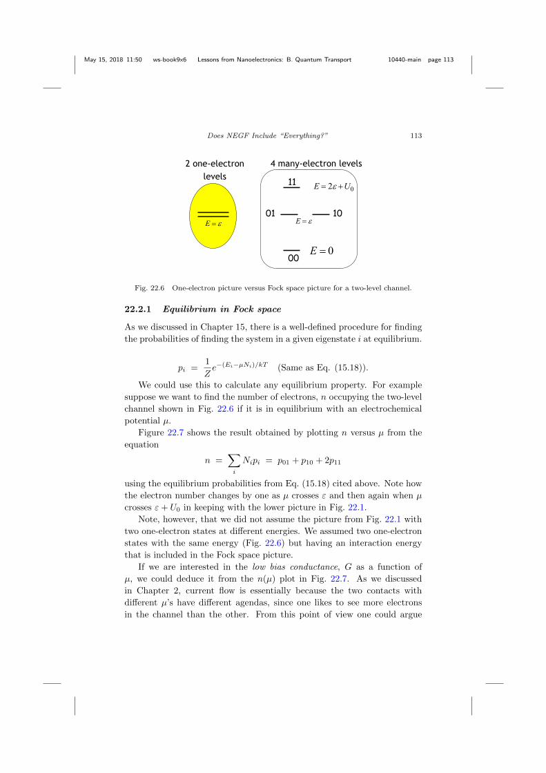
May 15, 2018 11:50 ws-book9x6 Lessons from Nanoelectronics: B. Quantum Transport 10440-main page 113
Does NEGF Include “Everything?” 113
2 one-electronlevels
4 many-electron levels
00
11
01 10
E = 0
E = ε
E = 2ε +U0
E = ε
Fig. 22.6 One-electron picture versus Fock space picture for a two-level channel.
22.2.1 Equilibrium in Fock space
As we discussed in Chapter 15, there is a well-defined procedure for finding
the probabilities of finding the system in a given eigenstate i at equilibrium.
pi =1
Ze−(Ei−µNi)/kT (Same as Eq. (15.18)).
We could use this to calculate any equilibrium property. For example
suppose we want to find the number of electrons, n occupying the two-level
channel shown in Fig. 22.6 if it is in equilibrium with an electrochemical
potential µ.
Figure 22.7 shows the result obtained by plotting n versus µ from the
equation
n =∑i
Nipi = p01 + p10 + 2p11
using the equilibrium probabilities from Eq. (15.18) cited above. Note how
the electron number changes by one as µ crosses ε and then again when µ
crosses ε+ U0 in keeping with the lower picture in Fig. 22.1.
Note, however, that we did not assume the picture from Fig. 22.1 with
two one-electron states at different energies. We assumed two one-electron
states with the same energy (Fig. 22.6) but having an interaction energy
that is included in the Fock space picture.
If we are interested in the low bias conductance, G as a function of
µ, we could deduce it from the n(µ) plot in Fig. 22.7. As we discussed
in Chapter 2, current flow is essentially because the two contacts with
different µ’s have different agendas, since one likes to see more electrons
in the channel than the other. From this point of view one could argue

May 15, 2018 11:50 ws-book9x6 Lessons from Nanoelectronics: B. Quantum Transport 10440-main page 114
114 Lessons from Nanoelectronics: B. Quantum Transport
that the conductance should be proportional to dn/dµ and show peaks at
µ = ε and at µ = ε+ U0 as shown. This is indeed what has been observed
experimentally for the low bias conductance of small conductors in the
single-electron charging regime where U0 exceeds both the thermal energy
kT and the energy broadening due to contacts.
e e +U0
Fig. 22.7 Equilibrium number of electrons, n in the two-level channel shown in Fig. 22.6
as a function of µ, assuming ε = 10 kT , U0 = 20 kT . The conductance can be argued to
be proportional to the derivative dn/dµ showing peaks when µ equals ε and ε+U0. ForMATLAB script, see Appendix H.3.1.
As we saw in Chapter 5, low bias conductance is an equilibrium property
that can be deduced using the principles of equilibrium statistical mechan-
ics. Current flow at higher voltages on the other hand requires the methods
of non-equilibrium statistical mechanics. Let me explain briefly how one
could understand the 2/3 plateau shown in Fig. 22.4 by calculating the
current at high bias in the Fock space picture.

May 15, 2018 11:50 ws-book9x6 Lessons from Nanoelectronics: B. Quantum Transport 10440-main page 115
Does NEGF Include “Everything?” 115
22.2.2 Current in the Fock space picture
To calculate the current we write an equation for the probability that the
system will be found in one of its available states, which must all add up
to one. For example for the one level resistor we could write
nu1p0 = ν2p1 → p1
p0=ν1
ν2→ p1 =
ν1
ν1 + ν2
assuming that the left contact sends the system from the 0 state to the
1 state at a rate ν1, while the right contact takes it in the reverse direction
at a rate ν2 and at steady-state the two must balance. The current is given
by
I = qν2p1 = qν1ν2
ν1 + ν2(22.2)
in agreement with our earlier result in Chapter 18 (see Eq. (18.10b)) ob-
tained from a one-electron picture.
But the real power of this approach is evident when we consider levels
with multiple interacting levels. Consider for example the two-level resistor
biased such that electrons can come in from the left contact and transfer the
system from 00 to 01 or to 10, but not to the 11 state because of the high
charging energy U0. This is the biasing condition that leads to a plateau
at 2/3 the maximum value (Fig. 22.4) that we mentioned earlier.
00
01 10
11
In this biasing condition, the system can only come out of the 11 state,
but never transfer into it, and so the steady-state condition can be calcu-
lated simply by considering the kinetics of the three remaining states in

May 15, 2018 11:50 ws-book9x6 Lessons from Nanoelectronics: B. Quantum Transport 10440-main page 116
116 Lessons from Nanoelectronics: B. Quantum Transport
Fock space, namely 00, 01 and 10:
2ν1p00 = ν2(p01 + p10)
→ p01 + p10
p00=
2ν1
ν2
→ p01 + p10 =2ν1
2ν1 + ν2
where we have made use of the requirement that all three probabilities must
add up to one. Hence
I = qν2(p01 + p10) = q2ν1ν2
2ν1 + ν2
with
ν1 = ν2 → I =2
3qν1
which is 2/3 the maximum current as stated earlier.
It is important to note the very special nature of the solution we just
obtained which makes it hard to picture within a one-electron picture. We
showed that the system is equally likely to be in the states 00, 01 and the
10 states, but zero probability of being in the 11 state.
e e +U0
STRONGLY
CORRELATED
23
Fig. 22.8 The intermediate plateau in the current corresponds to the channel being in
a strongly correlated state. For MATLAB script, see Appendix H.3.2.
In other words, if we looked at the up-spin or the down-spin state (in the
one-electron picture) we would find them occupied with 1/3 probability. If
electrons were independent then we would expect the probability for both
to be occupied to be the product = 1/9.

May 15, 2018 11:50 ws-book9x6 Lessons from Nanoelectronics: B. Quantum Transport 10440-main page 117
Does NEGF Include “Everything?” 117
Instead it is zero, showing that the electrons are correlated and cannot
be described with a one-electron occupation factor f of the type we have
been using throughout this book. Even with quantum transport we replaced
the f ’s with a matrix Gn obtained by summing the ψψψψψψ† for individual
electrons. This adds sophistication to our understanding of the one-electron
state, but it still does not tell us anything about two-electron correlations.
22.3 Entangled States
What we just saw with one quantum dot is actually just the proverbial
tip of the iceberg. Things get more interesting if we consider two or more
quantum dots.
For example, with two coupled quantum dots we could write the one-
electron Hamiltonian matrix as a (4 × 4) matrix using the up and down
states in dots 1 and 2 as the basis functions as follows:
H =u1
u2
d1
d2
u1ε1
t
0
0
u2
t
ε2
0
0
d1
0
0
ε1
t
d2
0
0
t
ε2
(22.3)
µ1
µ2
Source DrainChannel
u1u2
d2
d1
But what are the Fock space states? With four one-electron states we
expect a total of 24 = 16 Fock space states, containing 0, 1, 2, 3 or 4
electrons. The number of n-electron states in Fock space is given by 4Cn:
one with n = 0, four with n = 1, six with n = 2, four with n = 3 and one
with n = 4.
If there were no inter-dot coupling then these sixteen states would be the
eigenstates and we could analyze their dynamics in Fock space just as we did
for one dot. But in the presence of inter-dot coupling the true eigenstates

May 15, 2018 11:50 ws-book9x6 Lessons from Nanoelectronics: B. Quantum Transport 10440-main page 118
118 Lessons from Nanoelectronics: B. Quantum Transport
1111
1110, 1101, 1011, 0111
1100, 1010, 1001, 0110, 0101,0011
1000, 0100, 0010, 0001
0000
4-electron
3-electron
1-electron
0-electron
2-electron
are linear combinations of these states and these entangled states can lead
to novel physics and make it much more interesting.
The 0-electron and 4-electron states are trivially composed of just one
Fock space state, while the 1-electron state is essentially the same as the
states in a one-electron picture. Indeed the 3-electron state also has a
structure similar to the one-electron state and could be viewed as a 1-hole
state.
The 2-electron states, however, have an interesting non-trivial structure.
Consider the six 2-electron states which we label in terms of the two states
that are occupied: u1d1, u2d2, u1d2, u2d1, u1u2, d1d2. Using these we can
write the Fock space Hamiltonian HH as explained below.
The diagonal elements of HH are written straightforwardly by adding
the one-electron energies plus an interaction energy U0 if the two basis
functions happen to be on the same dot making their Coulomb repulsion
much stronger than what it is for two states on neighboring dots.
HH =
u1d1
u2d2
u1d2
u2d1
u1u2
d1d2
u1d1
2ε1 + U0
0
t
t
0
0
u2d2
0
2ε2 + U0
t
t
0
0
u1d2
t
t
ε1 + ε2
0
0
0
u2d1
t
t
0
ε1 + ε2
0
0
u1u2
0
0
0
0
ε1 + ε2
0
d1d2
0
0
0
0
0
ε1 + ε2
(22.4)
The off-diagonal entries t are obtained by noting that this quantity
couples the one electron states u1 to u2 and d1 to d2. With two electron
states we have inserted t for non-diagonal elements that couples those states
for which one state remains unchanged while the other changes from u1 to
u2 or from d1 to d2.
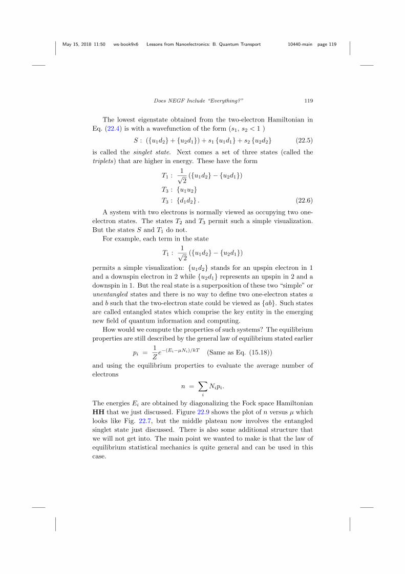
May 15, 2018 11:50 ws-book9x6 Lessons from Nanoelectronics: B. Quantum Transport 10440-main page 119
Does NEGF Include “Everything?” 119
The lowest eigenstate obtained from the two-electron Hamiltonian in
Eq. (22.4) is with a wavefunction of the form (s1, s2 < 1 )
S : (u1d2+ u2d1) + s1 u1d1+ s2 u2d2 (22.5)
is called the singlet state. Next comes a set of three states (called the
triplets) that are higher in energy. These have the form
T1 :1√2
(u1d2 − u2d1)
T3 : u1u2T3 : d1d2 . (22.6)
A system with two electrons is normally viewed as occupying two one-
electron states. The states T2 and T3 permit such a simple visualization.
But the states S and T1 do not.
For example, each term in the state
T1 :1√2
(u1d2 − u2d1)
permits a simple visualization: u1d2 stands for an upspin electron in 1
and a downspin electron in 2 while u2d1 represents an upspin in 2 and a
downspin in 1. But the real state is a superposition of these two “simple” or
unentangled states and there is no way to define two one-electron states a
and b such that the two-electron state could be viewed as ab. Such states
are called entangled states which comprise the key entity in the emerging
new field of quantum information and computing.
How would we compute the properties of such systems? The equilibrium
properties are still described by the general law of equilibrium stated earlier
pi =1
Ze−(Ei−µNi)/kT (Same as Eq. (15.18))
and using the equilibrium properties to evaluate the average number of
electrons
n =∑i
Nipi.
The energies Ei are obtained by diagonalizing the Fock space Hamiltonian
HH that we just discussed. Figure 22.9 shows the plot of n versus µ which
looks like Fig. 22.7, but the middle plateau now involves the entangled
singlet state just discussed. There is also some additional structure that
we will not get into. The main point we wanted to make is that the law of
equilibrium statistical mechanics is quite general and can be used in this
case.

May 15, 2018 11:50 ws-book9x6 Lessons from Nanoelectronics: B. Quantum Transport 10440-main page 120
120 Lessons from Nanoelectronics: B. Quantum Transport
e e +U0
Singlet
State
Fig. 22.9 Equilibrium number of electrons, n in the two-level channel shown in Fig. 22.6as a function of µ, assuming ε = 10 kT , U0 = 20 kT . For MATLAB script, see Ap-
pendix H.3.3.
But the calculation of current at high bias is a non-equilibrium problem
that is not as straightforward. Using the entangled states one could set up
a rate equation as we did in the last section and understand some of the in-
teresting effects that have been observed experimentally including negative
differential resistance (NDR), that is a decrease in current with increasing
voltage (see for example Muralidharan et al., 2007). More generally one
needs quantum rate equations to go beyond the simple rate equations we
discussed and handle coherences (Braun et al., 2004, Braig and Brouwer,
2005).
Can we model transport involving correlated and/or entangled states
exactly if we use a Fock space picture instead of using NEGF and including
interactions only approximately through self-energies? Sort of, but not
quite.
There are two problems. The first is practical. A N -level problem in
the one-electron picture escalates into a 2N level problem n the Fock space
picture. The second is conceptual.
We saw in Chapter 18 how the NEGF method allows us to include quan-
tum broadening in the one-electron Schrodinger equation. To our knowl-
edge there is no comparable accepted method for including broadening in
the Fock space picture. So the rate equation approach from the last section
works fine for weakly coupled contacts where the resulting broadening is
negligible, but the regime with broadening comparable to the charging en-

May 15, 2018 11:50 ws-book9x6 Lessons from Nanoelectronics: B. Quantum Transport 10440-main page 121
Does NEGF Include “Everything?” 121
ergy stands out as a major challenge in transport theory. Even the system
with two levels (Fig. 22.7) shows interesting structure in n(µ) in this regime
(“Kondo peak”) that has occupied condensed matter physicists for many
decades.
One could view Coulomb blockade as the bottom-up version of the Mott
transition, a well-studied phenomenon in condensed matter physics. In a
long chain of atoms, the levels ε and ε + U0 (Fig. 22.1) will each broaden
into a band of width ∼ 2t0, t0/~ being the rate at which electrons move
from one atomic site to the next. These are known as the lower and upper
Hubbard bands. If their separation U0 exceeds the width 2t0 of each band
we will have a Mott insulator where the electrochemical potential lies in the
middle of the two bands with very low density of states and hence very low
conductance. But if U0 is small, then the two bands form a single half-filled
band with a high density of states at E = µ0 and hence a high conductance.
Needless to say, the full theory of the Hubbard bands is far more com-
plicated than this oversimplified description might imply and it is one of
the topics that has occupied condensed matter theorists for over half a
century. Since the late 1980s it has acquired an added significance with
the discovery of a new class of superconductors operating at relatively high
temperatures above 100 K, whose mechanism continues to be controversial
and hotly debated.
This problem remains one of the outstanding problems of condensed
matter theory, but there seems to be general agreement that the essential
physics involves a two-dimensional array of quantum dots with an inter-dot
coupling that is comparable to the single dot charging energy.

May 15, 2018 11:50 ws-book9x6 Lessons from Nanoelectronics: B. Quantum Transport 10440-main page 122

May 15, 2018 11:50 ws-book9x6 Lessons from Nanoelectronics: B. Quantum Transport 10440-main page 123
PART 3
Spin Transport
123

May 15, 2018 11:50 ws-book9x6 Lessons from Nanoelectronics: B. Quantum Transport 10440-main page 124

May 15, 2018 11:50 ws-book9x6 Lessons from Nanoelectronics: B. Quantum Transport 10440-main page 125
Chapter 23
Rotating an Electron
Related video lecture available at course website, Unit 4: L4.1.
Back in Section 12.2 of Part A, we talked about the concept of spin
potentials and how they can be generated in two ways, namely (Fig. 23.1)
(1) use of magnetic contacts with ordinary channels (Section 12.2.1),
(2) use of ordinary contacts with spin-momentum locked channels (Sec-
tion 12.2.2).
µP
(b) Ordinary contact,Spin-momentum
locked channel
IVθ
(a) Magnetic contact,
Ordinary channel
Xx
z
yµP
Fig. 23.1 Spin potentials can be generated (a) using magnetic contacts with ordinary
channels, or (b) using ordinary contacts with spin-momentum locked channels. In eithercase a magnetic probe can be used to measure the spin potential in the channel.
In the first case the channel-contact interface presents different resistances
to the two spins so that the surface potential is different for the two spins
right under the contact, giving rise to a spin potential µS (see Eq. (12.18b),
125

May 15, 2018 11:50 ws-book9x6 Lessons from Nanoelectronics: B. Quantum Transport 10440-main page 126
126 Lessons from Nanoelectronics: B. Quantum Transport
Part A) in addition to the usual charge potential µ:
µ =µup + µdn
2(23.1a)
µS =µup − µdn
2. (23.1b)
This potential persists for a distance up to a spin coherence length from
the contact, and can be measured by placing a magnetic probe within this
range. In the second case the contacts are normal and the current flow
in the channel gives rise to a separation in the potentials µ+ and µ− for
right and left moving electrons. For a 2D spin-momentum locked channel
in the x-y plane, right (+x) and left (−x) moving electrons correspond to
spins with positive and negative components along z× x = y. A difference
(µ+ − µ−) thus translates into a spin potential µS ∼ µup − µdn, where up
and dn refer to spins pointing along positive and negative y.
Fig. 23.2 Simple circuit model for a voltage probe.
How does a magnetic contact measure the spin potential? Through the
difference in the interface conductances gup and gdn for up and down spins
(Fig. 23.2). The probe floats to a potential µP such that
gup(µup − µP ) + gdn(µdn − µP ) = 0 (23.2a)
→ µP =gupµup + gdnµdn
gup + gdn(23.2b)
which can be written in terms of µ, µS and the polarization P of the magnet:
µP = µ+ PµS (23.3a)
P ≡ gup − gdngup + gdn
. (23.3b)

May 15, 2018 11:50 ws-book9x6 Lessons from Nanoelectronics: B. Quantum Transport 10440-main page 127
Rotating an Electron 127
Note that if we reverse a magnet, gup ↔ gdn, so that P → −P . This
means that if we reverse a magnet from +m to −m, the probe potential
will change by
µP (+m)− µP (−m) = 2PµS . (23.4)
Indeed this is the standard method for measuring spin potentials, namely
by looking at the change in the probe potential when the magnet is reversed.
What voltage would the magnetic probe measure if it were neither par-
allel nor anti-parallel to the spins, but instead made some arbitrary angle
with it (Fig. 23.1a)? The answer can be stated quite simply:
µP = µ+ P ·µµµS (23.5)
where P = Pm and the spin potential is a vector pointing in the direction
that defines “up”. The derivation of Eq. (23.5) should be clearer as we
discuss spins in more depth in this chapter.
23.1 Polarizers and Analyzers
How do we understand the general result in Eq. (23.5)? For those unfa-
miliar with electron spin, the simplest analogy is probably that of photon
polarization. As we learn in freshman physics, a polarizer-analyzer combi-
nation lets through a flux proportional to cos2 θ. It is maximum when the
two are parallel (θ = 0), and a minimum when the two are perpendicular
(θ = 90).
Photon Flux ~
P .
A ( )2
~ cos2 q
Polarizer Analyzer
q P
A
What about electrons? Suppose we have electrons that are all up, so
that µdn = 0, and from Eq. (23.1), we have |µS | = µ = µup/2. Equa-
tion (23.5) then gives
µPµup
=1 + P cos θ
2.
As with photons, the voltage is a maximum when the probe (analyzer)
is parallel to the electron polarization (θ = 0). But with electrons the

May 15, 2018 11:50 ws-book9x6 Lessons from Nanoelectronics: B. Quantum Transport 10440-main page 128
128 Lessons from Nanoelectronics: B. Quantum Transport
0 180 360 540 720
µ P
θFig. 23.3 Probe voltage variation as its magnetization is rotated.
minimum occurs, not when the two are perpendicular (θ = 90) but when
the two are antiparallel (θ = 180) as shown in Fig. 23.3.
Indeed if we assume a perfect voltage probe with P = 1, we have
µPµ
=1 + cos θ
2= cos2 θ
2
showing that the analyzer lets through a fraction of electrons proportional
to
cos2
(θ
2
)︸ ︷︷ ︸
Electrons
rather than cos2 θ︸ ︷︷ ︸Photons
.
One point that causes some confusion is the following. It seems that
if we had electrons in the channel whose spin direction we did not know,
we could measure it using a magnet. As we turn the magnet the measured
voltage should go through maxima and minima as shown in Fig. 23.3, and
the direction corresponding to a maximum tells us the direction of the
electron spin.
But doesn’t quantum mechanics teach us that the spin of an electron
cannot be exactly measured? Yes, but that is true if we had just one
electron. Here we are talking of an “army” of electrons identically prepared
by an injecting contact and what our magnet measures is the average over
many many such electrons. This is not in violation of any basic principle.
Anyway, the bottom line is that for electron spin, orthogonal directions
are not represented by say z and x that are 90 degrees apart. Rather they
are represented by ‘up’ and ‘down’ that are 180 degrees apart. And that
is why a proper description of electron spin requires spinors rather than
vectors as we will now discuss.

May 15, 2018 11:50 ws-book9x6 Lessons from Nanoelectronics: B. Quantum Transport 10440-main page 129
Rotating an Electron 129
A vector n is described by three real components, namely the compo-
nents along x, y and z, but spinors are described by two complex compo-
nents, which are its components along up and down:nxnynz
︸ ︷︷ ︸Vector
,
ψupψdn
︸ ︷︷ ︸Spinor
.
Nevertheless we visualize the spinor as an object pointing in some direction
just like a vector. How do we reconcile the visual picture with the 2-
component complex representation?
A spinor pointing along a direction described by a unit vector
x
y
z
q
f
n
n ≡
sin θ cosφ
sin θ sinφ
cos θ
(23.6)
has components given bycos
(θ
2
)e−iφ/2 ≡ c
sin
(θ
2
)e+iφ/2 ≡ s
. (23.7)
This is of course not obvious and later in the chapter I will try to explain
why Eqs. (23.6) and (23.7) represent isomorphic (more correctly “homo-
morphic”) ways to represent an abstract rotatable object pointing in some
direction. For the moment let us accept Eq. (23.7) for the components of
a spinor and work out some of its consequences.

May 15, 2018 11:50 ws-book9x6 Lessons from Nanoelectronics: B. Quantum Transport 10440-main page 130
130 Lessons from Nanoelectronics: B. Quantum Transport
23.2 Spin in NEGF
Although these subtleties of visualization and interpretation take some time
to get used to, formally it is quite straightforward to incorporate spin into
the quantum transport formalism from Chapter 18. The basic equations
from Eq. (18.1) through (18.4) remain the same, but all the matrices like
H, Σ, Gn, and A become twice as big (Fig. 23.4).
updn
(a) Without spin
(b) With spin
Fig. 23.4 Inclusion of spin in NEGF doubles the number of “grid points” or basisfunctions.
Ordinarily these matrices are of size (N×N), if N is the number of grid
points (or more formally the number of basis functions) used to describe the
channel. Inclusion of spin basically doubles the number of basis functions:
every grid point turns into two points, an up and a down (Fig. 23.4).
How would we write down H including spin? We can visualize the TB
parameters (See Fig. 17.7) exactly as before except that each on-site element
ααα and the coupling elements βββ are each (2× 2) matrices (Fig. 23.5). In the
ax →
→
y
[bx ]
[bx+ ]
[by ]
[by+ ]
[a ]
a
Fig. 23.5 2D Lattice with each element given by a (2× 2) matrix to reflect spin-relatedproperties.

May 15, 2018 11:50 ws-book9x6 Lessons from Nanoelectronics: B. Quantum Transport 10440-main page 131
Rotating an Electron 131
simplest case, we can imagine a “spin-innocent” channel that treats both
spin components identically. Such a channel can be modeled by choosing
the TB parameters as follows:
ααα = ε I, βββx = t I, βββy = t I (23.8)
where I is the (2 × 2) identity matrix. We effectively have two identical
decoupled Hamiltonians that includes no new physics.
Similarly we can write the self-energy Σ for ordinary contacts that treat
both spin components identically simply by taking our usual values and
multiplying by I. This would again be in the category of a trivial extension
that introduces no new physics. The results should be the same as what
we would get if we worked with one spin only and multiplied by two at the
end.
All spin-related phenomena like the ones we discussed in Chapter 12
arise either from non-trivial contacts described by Σ with spin-related prop-
erties or from channels described by H with spin-related properties or both.
Let us now try to get a feeling for spin transport problems by applying
the NEGF method to a series of examples, starting with a simple one-level
version of the spin valve we started Chapter 12 with. From a computational
point of view the only question is how to write down H and Σ. Once we
have these, the rest is standard. One can then proceed to understand and
enjoy the physics.
23.3 One-level Spin Valve
Related video lecture available at course website, Unit 4: L4.2.
As we discussed in Chapter 12, a spin valve (Fig. 23.6) shows different
conductances GP and GAP depending on whether the magnetic contacts
have parallel (P) or anti-parallel (AP) magnetizations. Using a simple
model we showed that the magnetoresistance (MR) can be expressed as
MR ≡ GPGAP
− 1 =P 2
1− P 2
where the polarization P was defined in terms of the interface resistances.
In that context we noted that the standard expression for the MR for
magnetic tunnel junctions (MTJ’s) has an extra factor of two
MR ≡ GPGAP
− 1 =2P 2
1− P 2(23.9)

May 15, 2018 11:50 ws-book9x6 Lessons from Nanoelectronics: B. Quantum Transport 10440-main page 132
132 Lessons from Nanoelectronics: B. Quantum Transport
Parallel Anti-Parallel
MR =GP
GAP- 1
V +-
I
+-VI
Fig. 23.6 The spin-valve has different conductances GP and GAP depending on whether
the magnetic contacts have parallel (P) or anti-parallel (AP) magnetization.
which could be understood if we postulated that the overall resistance was
proportional to the product of the interface resistances and not their sum.
We could obtain this result including the factor of two directly from
our NEGF model if we apply it to a one-level resistor and assume that the
equilibrium electrochemical potential µ0 is located many kT ’s below the
energy ε of the level as sketched.
[H][S1] [S2]
m0
e
® - ¶ f0 / ¶E
Figure 23.7 summarizes the (2 × 2) matrices H and Σ for this device.
Also shown for comparison are the corresponding (1× 1) “matrices” (that
is, just numbers) for the same device without spin. Note that the chan-
nel is assumed to treat both spins identically so that H is essentially an
identity matrix, but the Σ’s have different values for the up and downspin
components.
Using these matrices it is straightforward to obtain the Green’s function
GR =
E − ε+ i2 (γ1u + γ2u) 0
0 E − ε+ i2 (γ1d + γ2d)
−1

May 15, 2018 11:50 ws-book9x6 Lessons from Nanoelectronics: B. Quantum Transport 10440-main page 133
Rotating an Electron 133
1
1Without spin
Withspin up
dn
[ ]2
22i γ
Σ =
−[ ]1
1
2i γ
Σ =
−[ ]Hε=
[ ]1
1γΓ =
[ ]2
2γΓ =
1
1
1 00
u
d
γγ
Γ =
2
2
2 00
u
d
γγ
Γ =
00
Hε
ε
=
2
2
2
002
u
d
i γγ
Σ =
−
1
1
1
002
u
d
i γγ
Σ =
−
Fig. 23.7 One-level spin-valve: Modifying the H and Σ for a spin-less one-level deviceto represent a one-level spin valve.
and hence the transmission
T = Trace[Γ1G
RΓ2GA]
=γ1uγ2u
(E − ε)2 +
(γ1u + γ2u
2
)2 +γ1dγ2d
(E − ε)2 +
(γ1d + γ2d
2
)2 . (23.10)
For the parallel (P) configuration we can assume both contacts to be
identical so that we can write (α > β)
γ1u = γ2u ≡ α (23.11a)
γ1d = γ2d ≡ β (23.11b)
while for the anti-parallel (AP) configuration the second contact has the
roles of α and β reversed with respect to the former:
γ1u = γ2d ≡ α (23.12a)
γ1d = γ2u ≡ β. (23.12b)
Inserting Eqs. (23.11) into Eq. (23.10) we have the P - transmission
TP =α2
(E − ε)2 + α2+
β2
(E − ε)2 + β2
while using Eqs. (23.12) in Eq. (23.10) gives the AP - transmission
TAP =2αβ
(E − ε)2 +
(α+ β
2
)2 .

May 15, 2018 11:50 ws-book9x6 Lessons from Nanoelectronics: B. Quantum Transport 10440-main page 134
134 Lessons from Nanoelectronics: B. Quantum Transport
The measured conductance depends on the average transmission over a
range of energies of a few kT around µ0. Assuming that
ε− µ0 kT, α, β
we can write
GP ∼ TP (E = µ0) =α2
(µ0 − ε)2 + α2+
β2
(µ0 − ε)2 + β2≈ α2 + β2
(µ0 − ε)2
and
GAP ∼ TAP (E = µ0) ≈ 2αβ
(µ0 − ε)2.
This gives us
MR ≡ GPGAp
− 1 =α2 + β2
2αβ− 1 =
2P 2
1− P 2
as stated earlier in Eq. (23.9) with the polarization defined as
P ≡ α− βα+ β
. (23.13)
Actually we could also obtain the result without the factor of 2, obtained
from the resistor model in Chapter 12, if we assume that µ0 is located right
around the level ε, with kT α and kT β. But we leave that as an
exercise. After all this is just a toy problem intended to get us started.
23.4 Rotating Magnetic Contacts
Related video lecture available at course website, Unit 4: L4.3.
We argued in the last section that for an anti-parallel spin valve, the
second contact simply has the roles of α and β reversed relative to the first,
so that we can write
Γ1 =
[α 0
0 β
], Γ2 =
[β 0
0 α
].
But how would we write the corresponding matrix for a contact if it were
pointing along some arbitrary direction defined by a unit vector n? The
answer is
Γ =α+ β
2I +
α− β2
[nz nx − i ny
nx + i ny −nz
](23.14)
where nx, ny and nz are the components of the unit vector n along x, y and
z respectively. This result is of course not obvious and we will try to justify

May 15, 2018 11:50 ws-book9x6 Lessons from Nanoelectronics: B. Quantum Transport 10440-main page 135
Rotating an Electron 135
it shortly. But it is reassuring to note that the results for both the parallel
and the anti-parallel contact come out as special cases of this general result
(Eq. (23.14)):
If nz = +1, nx = ny = 0 : Γ =
[α 0
0 β
]
If nz = −1, nx = ny = 0 : Γ =
[β 0
0 α
].
One way to understand where Eq. (23.14) comes from is to note that the
appropriate matrix describing a magnet pointing along n would be
Γ =
[α 0
0 β
](23.15)
if we were to take +n and −n as our reference directions instead
of +z and −z as we normally do. How could we then transform the Γ
from Eq. (23.15) into the usual ± z basis?
Answer: Transform from the ± n to the ± z basis
z
−z
n[c
s
−n
−s∗c∗
]︸ ︷︷ ︸
V
n
−n
n[α
0
−n
0
β
]n
−n
z[c∗
−s
−z
s∗
c
]︸ ︷︷ ︸
V†
(23.16)
using the unitary transformation matrix V whose columns represent the
components of a spinor pointing along ±n. The first column follows from
the result we stated earlier in Eq. (23.7), while the second can be obtained
from Eq. (23.7) if we set
θ → π − θ, φ → π + φ
and remove a common phase factor from the two components.
Multiplying out the three matrices in Eq. (23.16) we have
Γ =
[c −s∗s c∗
] [α 0
0 β
] [c∗ s∗
−s c
]=
[c −s∗s c∗
] [αc∗ αs∗
−βs βc
]
=
[αcc∗ + βss∗ (α− β) cs∗
(α− β) sc∗ αss∗ + βcc∗
].

May 15, 2018 11:50 ws-book9x6 Lessons from Nanoelectronics: B. Quantum Transport 10440-main page 136
136 Lessons from Nanoelectronics: B. Quantum Transport
Making use of the definitions of c and s from Eq. (23.7) and some common
trigonometric identities like
2 cos2
(θ
2
)= 1 + cos θ,
2 sin2
(θ
2
)= 1− cos θ, and (23.17)
2 sin
(θ
2
)cos
(θ
2
)= sin θ
we can rewrite this as
Γ =1
2
[(α+ β) + (α− β) cos θ (α− β) sin θ e−iφ
(α− β) sin θ e+iφ (α+ β)− (α− β) cos θ
]which leads to the result stated earlier in Eq. (23.14) if we make use of
Eq. (23.6) for the x, y and z components of a unit vector.
Finally let me note that if we define the polarization as a vector whose
magnitude is given by Eq. (23.13) and direction is given by n:
P ≡ P n =α− βα+ β
n (23.18)
then we could rewrite Eq. (23.14) as
Γ =α+ β
2
(I +
[Pz Px − i Py
Px + i Py −Pz
])(23.19)
which can be rearranged as shown
Γ
(α+ β)/2=
[1 0
0 1
]︸ ︷︷ ︸
I
+Px
[0 1
1 0
]︸ ︷︷ ︸σx
+Py
[0 −i
+i 0
]︸ ︷︷ ︸
σy
+Pz
[1 0
0 −1
]︸ ︷︷ ︸
σz
.
Any (2× 2) matrix can be expressed in terms of the four matrices appear-
ing here consist of the identity matrix I along with the three Pauli spin
matrices
σx ≡[
0 1
1 0
], σy ≡
[0 −i
+i 0
]and σz ≡
[1 0
0 −1
](23.20)
which are widely used in the spin-related literature.
Making use of the Pauli spin matrices, we could write Eq. (23.19) com-
pactly in the form
Γ =α+ β
2(I + σx Px + σy Py + σz Pz)
=α+ β
2(I + σσσ · P ) .
(23.21)
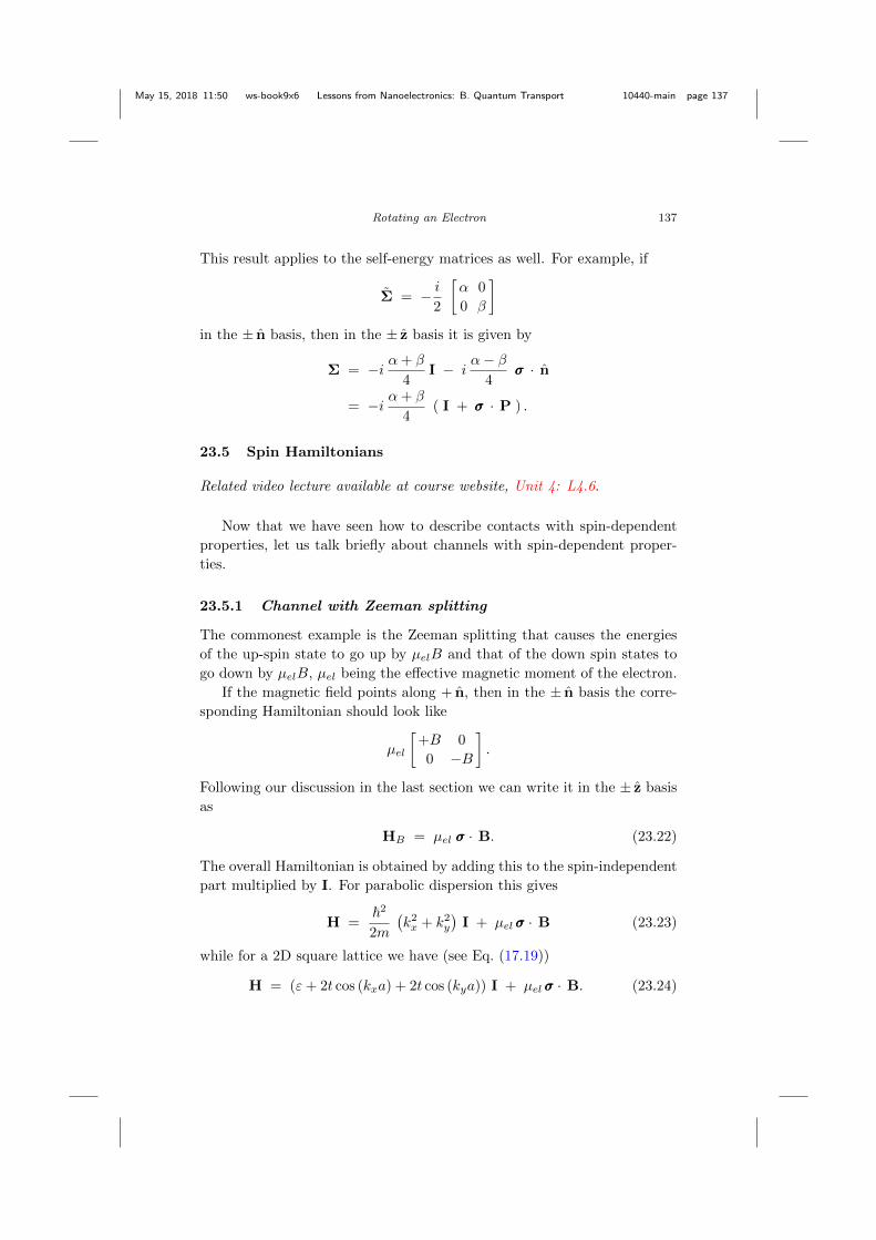
May 15, 2018 11:50 ws-book9x6 Lessons from Nanoelectronics: B. Quantum Transport 10440-main page 137
Rotating an Electron 137
This result applies to the self-energy matrices as well. For example, if
Σ = − i2
[α 0
0 β
]in the ± n basis, then in the ± z basis it is given by
Σ = −i α+ β
4I − i
α− β4
σσσ · n
= −i α+ β
4( I + σσσ · P ) .
23.5 Spin Hamiltonians
Related video lecture available at course website, Unit 4: L4.6.
Now that we have seen how to describe contacts with spin-dependent
properties, let us talk briefly about channels with spin-dependent proper-
ties.
23.5.1 Channel with Zeeman splitting
The commonest example is the Zeeman splitting that causes the energies
of the up-spin state to go up by µelB and that of the down spin states to
go down by µelB, µel being the effective magnetic moment of the electron.
If the magnetic field points along + n, then in the ± n basis the corre-
sponding Hamiltonian should look like
µel
[+B 0
0 −B
].
Following our discussion in the last section we can write it in the ± z basis
as
HB = µel σσσ · B. (23.22)
The overall Hamiltonian is obtained by adding this to the spin-independent
part multiplied by I. For parabolic dispersion this gives
H =~2
2m
(k2x + k2
y
)I + µel σσσ · B (23.23)
while for a 2D square lattice we have (see Eq. (17.19))
H = (ε+ 2t cos (kxa) + 2t cos (kya)) I + µel σσσ · B. (23.24)

May 15, 2018 11:50 ws-book9x6 Lessons from Nanoelectronics: B. Quantum Transport 10440-main page 138
138 Lessons from Nanoelectronics: B. Quantum Transport
ax →
→
y
[bx ]
[bx+ ]
[by ]
[by+ ]
[a ]
a
The corresponding parameters for the 2D lattice in Fig. 23.5 (also shown
here for convenience) are given simply by
ααα = ε I + µel σσσ · B (23.25a)
βββx = t I, βββy = t I. (23.25b)
Only the on-site parameter ααα is changed relative to the spin independent
channel (Eq. (23.8)).
23.5.2 Channel with Rashba interaction
Related video lecture available at course website, Unit 4: L4.5.
A more complicated example is that of the Rashba spin-orbit coupling
described by a Hamiltonian of the form
HR = η z · (σσσ × k) = η (σxky − σykx) (23.26)
whose effect has been observed in 2D surface conduction channels assumed
to lie in the x-y plane. This is believed to be a relativistic effect whereby the
extremely high atomic scale electric fields (that exist even at equilibrium)
are perceived as an effective magnetic field by the electron and the resulting
“Zeeman splitting” is described by HR.
We will not go into the underlying physics of this effect any further here
and simply address the question of how to include it in our 2D lattice model.
With this in mind we approximate the linear terms with sine functions
HR =η
a(σx sin (kya)− σy sin (kxa)) (23.27)
which are written in terms of exponentials:
HR =η
2iaσx(e+ikya − e−ikya) − η
2iaσy(e+ikxa − e−ikxa).

May 15, 2018 11:50 ws-book9x6 Lessons from Nanoelectronics: B. Quantum Transport 10440-main page 139
Rotating an Electron 139
Clearly HR can be described by a Hamiltonian with
βββx =i η
2aσy , βββ†x = − i η
2aσy
βββy = − i η
2aσx , βββ†y =
i η
2aσx
in order to ensure that if we write down the dispersion relation for the
lattice we will indeed get back the original result in Eq. (23.23). Adding
this to the usual spin-independent part from Eq. (23.8) along with any real
magnetic field B we have the overall parameters:
ααα = ε I + µel σσσ · B
βββx = t I +i η
2aσy , βββ
†x = t I− i η
2aσy
βββy = t I− i η
2aσx , βββ
†y = t I +
i η
2aσx.
(23.28)
23.6 Vectors and Spinors
Related video lecture available at course website, Unit 4: L4.4.
One of the important subtleties that takes some time to get used to is
that we represent spin with two complex components, but we visualize it
as a rotatable object pointing in some direction, which we have learnt to
represent with a vector having three real components. To see the connection
between the spinor and the vector, it is instructive to consider the precession
of a spin in a magnetic field from both points of view.
Consider the one-level device with ε = 0, and with a magnetic field in
the z-direction so that the Schrodinger equation can be written as
d
dt
ψuψd
=
µelBzi~
[1 0
0 −1
]︸ ︷︷ ︸
σz
ψuψd
. (23.29)
These are two separate differential equations whose solution is easily written
down:
ψu(t) = ψu(0) e− iω t/2
ψd(t) = ψd(0) e+ iω t/2
where ω ≡ 2µelBz~
. (23.30)

May 15, 2018 11:50 ws-book9x6 Lessons from Nanoelectronics: B. Quantum Transport 10440-main page 140
140 Lessons from Nanoelectronics: B. Quantum Transport
x
y
z
q
f
n
So if the electron starts out at some angle (θ, φ) with a wavefunctionψu(0) = cos
(θ
2
)e−iφ/2
ψd(0) = sin
(θ
2
)e+iφ/2
at t = 0, then at a later time it will have a wavefunction given by
ψu(t) = cos
(θ
2
)e−iφ/2 e−iωt/2
ψd(t) = sin
(θ
2
)e+iφ/2 e+iωt/2
which means that the spin will be rotating around the z-axis such that the
angle θ remains fixed while the angle φ increases linearly with time:
φ(t) = φ(0) + ω t. (23.31)
Making use of Eq. (23.6) for the x, y and z components of the vector n we
can write
nx = sin θ cosφ(t), ny = sin θ sinφ(t) and nz = cos θ. (23.32)
From Eqs. (23.31) and (23.32) we can show that
dnxdt
= −ω ny,dnydt
= +ω nx
which can be written in matrix form
d
dt
nxnynz
= ω
0 −1 0
+1 0 0
0 0 0
︸ ︷︷ ︸
Rz
nxnynz
. (23.33a)

May 15, 2018 11:50 ws-book9x6 Lessons from Nanoelectronics: B. Quantum Transport 10440-main page 141
Rotating an Electron 141
For comparison we have rewritten the Schrodinger equation we started
with (see Eq. (23.29)) in terms of the rotation frequency ω:
d
dt
ψuψd
=
ω
2i
[1 0
0 −1
]︸ ︷︷ ︸
σz
ψuψd
. (23.33b)
If we wanted to describe the rotation of an electron due to a B-
field pointing in the x-direction, it is easy to see how we would modify
Eq. (23.33a): Simply interchange the coordinates, x→ y, y → z, z → x.
d
dt
nxnynz
= ω
0 0 0
0 0 −1
0 +1 0
︸ ︷︷ ︸
Rx
nxnynz
and we obtain Rx in place of Rz. But it is not as clear how to modify
Eq. (23.33b). The correct answer is to replace σz with σx (Eq. (23.20))
d
dt
ψuψd
=
ω
2i
[0 1
1 0
]︸ ︷︷ ︸σx
ψuψd
but the reason is not as obvious.
Equations (23.33a) and (23.33b) both describe the same physics, namely
the rotation of a spin about the z-axis due to an applied B-field in the z-
direction, one in terms of three real components and the other in terms of
two complex components.
But what do matrices like R in Eq. (23.33a) have in common with
matrices like σ in Eq. (23.33b) that makes them “isomorphic” allowing them
to describe the same physics? Answer: They obey the same “commutation
relations”. Let me explain.
It is easy to check that the matrices
Rx =
0 0 0
0 0 −1
0 +1 0
, Ry =
0 0 +1
0 0 0
−1 0 0
, Rz =
0 −1 0
+1 0 0
0 0 0
obey the relations
RxRy −RyRx = Rz
RyRz −RzRy = Rx (23.34a)
RzRx −RxRz = Ry.
May 15, 2018 11:50 ws-book9x6 Lessons from Nanoelectronics: B. Quantum Transport 10440-main page 142
142 Lessons from Nanoelectronics: B. Quantum Transport
The Pauli spin matrices obey a similar relationship with R replaced by
σ/2i:
σxσy − σyσx = 2i σz
σyσz − σzσy = 2i σx (23.34b)
σzσx − σxσz = 2i σy.
The standard textbook introduction to spin starts from these commutation
relations and argues that they are a property of the “rotation group”. In
order to find a mathematical representation with two components for a
rotatable object, one must first write down three (2× 2) matrices obeying
these commutation properties which would allow us to rotate the spinor
around each of the three axes respectively.
What are the components of a spinor that points along z? Since rotating
it around the z-axis should leave it unchanged, it should be an eigenvector
of σz that is, 1
0
or
0
1
which indeed represent an upspin and a downspin along z. Similarly if we
want the components of a spinor pointing along x, then we should look at
the eigenvectors of σx, that is,
1√2
+1
+1
or
1√2
+1
−1
which represent up and down spin along +x. If we consider a spinor pointing
along an arbitrary direction described by a unit vector n (see Eq. (23.6)) and
wish to know what its components are, we should look for the eigenvectors
of
σσσ · n = σx sin θ cosφ+ σy sin θ sinφ+ σz cos θ
=
[cos θ sin θ e−iφ
sin θ e+iφ − cos θ
](23.35a)
which can be written as (c and s defined in Eq. (23.7))c
s
and
−s∗c∗
. (23.35b)
In short, the rigorous approach to finding the spinor representation is
to first determine a set of three matrices with the correct commutation
relations and then look at their eigenvectors. Instead in this chapter, I
adopted a reverse approach stating the spinor components at the outset
and then obtaining the matrices through basis transformations.

May 15, 2018 11:50 ws-book9x6 Lessons from Nanoelectronics: B. Quantum Transport 10440-main page 143
Rotating an Electron 143
23.7 Spin Precession
We have already discussed how to write H and Σ including non-trivial
spin-dependent effects and we could set up numerical models to calculate
the electron density Gn, or the density of states A, or the current using
the standard NEGF equations from Chapter 18. Consider for example,
the non-local spin potential measurement we started this chapter with (see
Fig. 23.8).
a
® x
e[H][SL ] [SR ]
[S1] [S2 ]
IVµprobe
q
m , msz →
Fig. 23.8 Spin potential measurement can be modeled with a 1D channel Hamiltonianhaving four contacts, two of which are magnetic described by Σ1, Σ2.
Figure 23.9 shows the result obtained from the numerical model which
supports the basic result stated in Eq. (23.5). The measured voltage os-
cillates as a function of the angle of magnetization of the voltage probe.
It has a constant part independent of the angle and an oscillatory compo-
nent proportional to the polarization P of the voltage probe which can be
understood in terms of Eq. (23.5) stated at the beginning of this chapter.
I am not sure if the experiment shown in Fig. 23.8 has been done, but
what has been done is to keep both magnets fixed and rotate the electron
spin inside the channel.
How do we rotate the spin? One method that has been widely used
is an external magnetic field B which causes the spin direction to precess
around the magnetic field as we discussed in Section 23.6 with an angular

May 15, 2018 11:50 ws-book9x6 Lessons from Nanoelectronics: B. Quantum Transport 10440-main page 144
144 Lessons from Nanoelectronics: B. Quantum Transport
µ1=1Floating µ2
2
Floating µRµL = 0
θ
zx→→y
P2=1
P2=0.5
P2=0
θ /π
V2
Fig. 23.9 Voltage probe signal as the magnetization of the probe is rotated calculated
from NEGF model. For MATLAB script, see Appendix H.4.1.
frequency given by
ω ≡ 2µelBz~
(same as Eq. (23.30)). (23.36)
This means that the spin voltage at the point where the probe is con-
nected will rotate by an angle ω τ where τ is the time it takes for the
electron to travel from the point of injection to the voltage probe. Writing
τ = L/ν, we have from Eq. (23.5) using Eq. (23.30)
µP = µ+ P2 µs cos
(2µelL
~νBz
). (23.37)
One would expect to see an oscillatory signal as a function of the magnetic
field. However, one is usually not dealing with ballistic transport, and there
is a large spread in the time τ spent by an electron between injection and
detection so that the average value of this signal over all τ is essentially
zero. What is typically observed is not an oscillatory signal as a function
of the B-field but a reduction in the signal from Pµs down to zero, which

May 15, 2018 11:50 ws-book9x6 Lessons from Nanoelectronics: B. Quantum Transport 10440-main page 145
Rotating an Electron 145
is referred to as the Hanle signal. However, Hanle signals showing several
oscillations have also been observed, but this requires that the spread in τ
be much less than its mean value (see for example, Huang et al., 2007).
Another possible approach to rotating electron spins is to use the Rashba
effect in materials with strong spin-orbit coupling. In many semiconductors,
it is now well established that a surface electric field along z (Fig. 23.9) leads
to an effective magnetic field that depends on the electron momentum. This
can be seen by comparing the Hamiltonians for the B-field (Eq. (23.22))
HB = µel σσσ.B
with that for the Rashba interaction (23.26) which can be rewritten as
HR = η z · (σσσ × k) → η σσσ · (z× k)
suggesting that the effective B-field due to the Rashba interaction is given
by
µelBeff = η z× k (23.38)
so that from Eq. (23.37) we expect an oscillatory signal of the form
µP = µ+ P2µs cos
(2ηkL
~ν
)(23.39)
with a period ∆η defined by
2kL
~ν∆η = 2π → ∆η =
2πat0kL
sin (ka) .
This is in approximate agreement with the numerical result obtained
from the NEGF method (Fig. 23.10) using an energy E corresponding to
ka = π/3, and a distance of about L = 40 a between the injector and the
detector.
In the structure shown in Fig. 23.10 the electrons traveling along +x
should feel an effective B-field along y. Since the injected spins have a spin
voltage µµµs pointing along the source and drain magnets (x) it should be
rotated. Note that the oscillation should not be observed if the source and
drain magnets point along y rather than along x.
This phenomenon of voltage-controlled spin precession in 2D conductors
with high spin-orbit coupling was predicted in 1990 (Datta & Das, 1990)
and has now been experimentally established (Koo et al., 2009, Wunderlich
et al., 2010, Choi et al., 2015).

May 15, 2018 11:50 ws-book9x6 Lessons from Nanoelectronics: B. Quantum Transport 10440-main page 146
146 Lessons from Nanoelectronics: B. Quantum Transport
µ1=1Floating µ2
2
Floating µRµL = 0
Change Rashba constantwith gate voltage (not shown)
zx→→y
η / at0
V2
Fig. 23.10 In materials with a large Rashba coefficient, a gate voltage should lead to anoscillatory output, if the source and drain magnets point along x, but not if they point
along z. For MATLAB script, see Appendix H.4.1.
23.8 Spin-charge Coupling
Spin precession is a delicate effect requiring a degree of spin coherence
that is usually available only at low temperatures. That is why voltage-
controlled spin precession seems to have little potential as an electronic
device although it is the basis for many proposals for spin transistors. In-
terestingly, the same basic spin-orbit interaction leads to the phenomenon
of spin-momentum locking which gives rise to robust room temperature ef-
fects that are finding extensive applications as we discussed in Part A (see
Section 12.2.3, Part A).
The phenomenon can be understood by noting that due to the Rashba
interaction (see Eq. (23.26)) an electron in a state k feels an effective mag-

May 15, 2018 11:50 ws-book9x6 Lessons from Nanoelectronics: B. Quantum Transport 10440-main page 147
Rotating an Electron 147
netic field that can be written as
µBBeff = η z× k. (23.40)
This leads to an E(k) relation of the form
E(k) =~2k2
2m± µBBeff =
~2k2
2m± ηk (23.41)
where the positive and negative signs correspond to spins being parallel or
anti-parallel to Beff .
We can turn this E(k) relation around to note that for a given E, there
are two distinct allowed values of k given by
kf2 =√k2F + k2
0 + k0 and kf1 =√k2F + k2
0 − k0 (23.42a)
where kF =2mE
~2, k0 =
ηm
~2. (23.42b)
In other words, for a given energy E, there are two Fermi circles with radii
kf1 and kf2 (see Fig. 23.11a), corresponding to states with spins parallel
and anti-parallel to Beff respectively.
kf1kf2
ky
kx
(a) (b)
up+dn+up-dn-
+-
Fig. 23.11 (a) Surface states in materials with high spin-orbit coupling have two differ-ent Fermi circles with radii kf1 and kf2. Arrows show the direction of the spin associated
with these eigenstates which is parallel and antiparallel to Beff respectively. (b) Thestates are divided into ‘+’ and ‘−’ depending on the sign of the group velocity: Each
has two branches labeled ‘up’ and ‘dn’ depending on the sign of the y-component of thespin. Overall we have four groups up+, dn−,up−, dn+.

May 15, 2018 11:50 ws-book9x6 Lessons from Nanoelectronics: B. Quantum Transport 10440-main page 148
148 Lessons from Nanoelectronics: B. Quantum Transport
In discussing current flow in ordinary conductors we found it useful
to divide all states into positive and negative moving states, ‘+’ and ‘−’
and assigning them different electrochemical potentials µ+ and µ− (see
Chapters 8–11, Part A). In these 2D conductors with spin-orbit coupling
we can do the same as shown in Fig. 23.11b, but each group now has two
branches corresponding to the two Fermi circles. We label these branches
depending on the sign of the y-component of the spin, up: y · s < 0 and
dn: y · s > 0. Overall we have four groups up+,dn−,up−,dn+.
up+
dn-up-
dn+
Fig. 23.12 Surface states in materials with high spin-orbit coupling have equal number
of modes M for up+, dn−, but a different number of modes N for up−,dn+.
Two of these groups up+ and dn− correspond to the larger Fermi circle
of radius kf2 and have a number of modes M that is greater than the
number of modes N for the other two up− and dn+ which correspond to
the smaller Fermi circle of radius kf1 (W : Width of conductor):
M =kf2W
πand N =
kf1W
π. (23.43)
As we discussed in Part A (Chapters 8–12) whenever a current I flows
in any material, there is a separation in the electrochemical potentials µ+
and µ− (Eq. (12.24), GB : Ballistic conductance)
I = GBµ+ − µ−
q. (23.44)
But in the materials with spin-orbit coupling that we are discussing, this
separation in µ+ and µ− manifests itself as a difference in the electrochem-
ical potentials for µup and µdn:
µup =Mµ+ +Nµ−
M +Nand µdn =
Nµ+ +Mµ−
M +N(23.45)

May 15, 2018 11:50 ws-book9x6 Lessons from Nanoelectronics: B. Quantum Transport 10440-main page 149
Rotating an Electron 149
giving rise to a spin potential (see Eq. (23.1)) in the y-direction
µsy =µup − µdn
2= p
µ+ − µ−2
(23.46)
where we have defined the channel polarization as
p ∼ M −NM +N
. (23.47)
In Eq. (23.47) we are not using the equality sign since we have glossed over
a “little” detail involving the fact that the y-component of the spins in each
of the groups up± and dn± has a distribution (see Fig. 23.11), which on
averaging gives rise to a numerical factor.
Making use of Eqs. (23.44) and (23.46) we can rewrite the y-component
of the spin potential in terms of the current I:
µsy =q
2GBpI. (23.48)
Note that the channel polarization “p” appearing in Eq. (23.48) is a chan-
nel property that determines the intrinsic spin potential appearing in the
channel. It is completely different from the probe polarization “P” defined
in Eq. (23.3) which is a magnet property that comes into the picture only
when we use a y-directed magnetic probe to measure the intrinsic spin
potential µsy induced in the channel by the flow of current (I).
This is a remarkable result that shows a new way of generating spin
potentials. We started this chapter with spin valves that generate spin
potentials through the spin-dependent interface resistance of magnetic con-
tacts. By contrast Eq. (23.48) tells us that a spin voltage can be generated
in channels with spin-momentum locking simply by the flow of current with-
out the need for magnetic contacts, arising from the difference between M
and N . The spin voltage can be measured with magnetic contacts.
Alternatively we could reverse the voltage and current terminals and
invoke reciprocity (Section 10.3.3) to argue that a current injected through
a magnetic contact will generate a charge voltage at the ordinary contacts.
This is our view of the Rashba-Edelstein (RE) effect and its inverse
which have been observed in a wide variety of materials like topological
insulators and narrow gap semiconductors. Similar effects are also observed
in heavy metals where it is called the (inverse) spin Hall effect (SHE) and
is often associated with bulk scattering mechanisms, but there is some
evidence that it could also involve the surface mechanism described here.

May 15, 2018 11:50 ws-book9x6 Lessons from Nanoelectronics: B. Quantum Transport 10440-main page 150
150 Lessons from Nanoelectronics: B. Quantum Transport
23.9 Superconducting Contacts
Let me end this chapter (which is too long already) with a brief note about
an area of great current interest, that can be addressed using the NEGF
methods described in this book. This area involves electrical conduction in
devices with normal channel materials like the ones we have been talking
about, but one or both contacts (source / drain) are superconducting.
It takes considerable discussion to clarify the conceptual basis for han-
dling superconducting contacts and the associated phenomenon of Andreev
scattering, but the key point is that the “quasi-particles” are not described
by the Hamiltonian H that we have been discussing but by the Bogoliubov-
deGennes (BdG) Hamiltonian, HBdG.
If the channel has no spin-related properties and can be described by
a spinless Hamiltonian H, then structures with superconducting contacts
can be described by a (2× 2) HBdG (see for example, deGennes, 1968)
HBdG =
[H− µI ∆
∆∗ −(H∗ − µI)
](23.49)
I being the identity matrix of the same size as H, and ∆ being the order
parameter of the superconductor, which is set to zero for the normal con-
tact(s) and the channel. The electrochemical potential µ is set to zero for
the superconducting contact.
Using HBdG we can find the Σ’s for the contacts in the same way and
proceed to use the same NEGF equations as summarized in Appendix G.
Interpreting the results, however, will require an appreciation of the con-
ceptual basis underlying the BdG equation (see Datta and Bagwell, 1999).
Note that the electrochemical potential µ is assumed zero in the super-
conducting contact. But this is not possible if there are multiple supercon-
ducting contacts held at different potentials. The calculation is then more
involved because solutions at different energies get coupled together (see
Samanta and Datta, 1997).
Finally I should mention that there is a lot of current interest in channel
materials whose Hamiltonian includes spin-orbit coupling and other spin-
related properties, and this requires a (4×4) HBdG (see for example, Pikulin
et al., 2012, San-Jose et al., 2013).
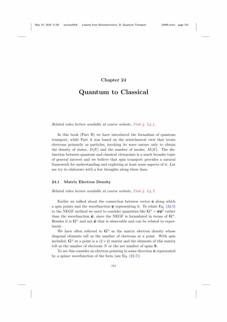
May 15, 2018 11:50 ws-book9x6 Lessons from Nanoelectronics: B. Quantum Transport 10440-main page 151
Chapter 24
Quantum to Classical
Related video lecture available at course website, Unit 4: L4.1.
In this book (Part B) we have introduced the formalism of quantum
transport, while Part A was based on the semiclassical view that treats
electrons primarily as particles, invoking its wave nature only to obtain
the density of states, D(E) and the number of modes, M(E). The dis-
tinction between quantum and classical viewpoints is a much broader topic
of general interest and we believe that spin transport provides a natural
framework for understanding and exploring at least some aspects of it. Let
me try to elaborate with a few thoughts along these lines.
24.1 Matrix Electron Density
Related video lecture available at course website, Unit 4: L4.7.
Earlier we talked about the connection between vector n along which
a spin points and the wavefunction ψψψ representing it. To relate Eq. (23.5)
to the NEGF method we need to consider quantities like Gn ∼ ψψψψψψ† rather
than the wavefunction ψψψ, since the NEGF is formulated in terms of Gn.
Besides it is Gn and not ψψψ that is observable and can be related to exper-
iment.
We have often referred to Gn as the matrix electron density whose
diagonal elements tell us the number of electrons at a point. With spin
included, Gn at a point is a (2× 2) matrix and the elements of this matrix
tell us the number of electrons N or the net number of spins S.
To see this consider an electron pointing in some direction n represented
by a spinor wavefunction of the form (see Eq. (23.7))
151

May 15, 2018 11:50 ws-book9x6 Lessons from Nanoelectronics: B. Quantum Transport 10440-main page 152
152 Lessons from Nanoelectronics: B. Quantum Transport
x
y
z
q
f
n
ψψψ =
cos
(θ
2
)e−iφ/2 ≡ c
sin
(θ
2
)e+iφ/2 ≡ s
so that the corresponding (2× 2) electron density Gn is given by
ψψψψψψ† =
c
s
c∗ s∗
=
[cc∗ cs∗
sc∗ ss∗
].
Making use of Eq. (23.6) and Eq. (23.17) we have
ψψψψψψ† =1
2
[1 + nz nx − i nynx + i ny 1− nz
]=
1
2[I + σσσ · n] .
For a collection of N electrons we can add up all their individual contribu-
tions to ψψψψψψ† to obtain the net Gn given by
Gn
2π=
1
2
[N + Sz Sx − i SySx + iSy N − Sz
]
=1
2(NI + σσσ · S) .
(24.1)
Given a Gn we can extract these quantities from the relations
N =1
2πTrace [Gn] , S =
1
2πTrace [σσσGn] (24.2)
which follow from Eq. (24.1) if we make use of the fact that all three matrices
(Eq. (23.20)) have zero trace, along with the following properties of the
Pauli spin matrices that are easily verified.
σ2x = σ2
y = σ2z = I (24.3a)

May 15, 2018 11:50 ws-book9x6 Lessons from Nanoelectronics: B. Quantum Transport 10440-main page 153
Quantum to Classical 153
σxσy = −σyσx = i σz (24.3b)
σyσz = − σzσy = i σx (24.3c)
σzσx = − σxσz = i σy. (24.3d)
In summary, all the information contained in the (2 × 2) Hermitian
matrix Gn can be expressed in terms of four real quantities consisting of a
scalar N and the three components of a vector S which can be extracted
using Eq. (24.2).
If the transverse components of spin are negligible then we can describe
the physics in terms of N and Sz only. We could interpret the non-zero
components on the diagonal
(N + Sz) as number of up electrons
(N − Sz) as number of down electrons
(per unit energy) and then write semiclassical equations for the two types
of electrons.
Consider for example, the experiment that we discussed in Chapter 23.
An input magnet injects spins into the channel which produce a voltage on
the output magnet given by
µP = µ+ P · µµµs. (24.4)
When can we understand these measurements just in terms of up and down
qµP
-+ 0 180 360 540 720
µ P
θFig. 24.1 An input magnet injects spins into the channel which produce a voltage onthe output magnet that depends on the cosine of the angle between the two magnets.
spins? One possibility is that the magnets are all collinear and there is no
spin-orbit coupling so that we are restricted to angles θ that are multiples of
180 degrees (Fig. 24.1). Another possibility is that various spin dephasing

May 15, 2018 11:50 ws-book9x6 Lessons from Nanoelectronics: B. Quantum Transport 10440-main page 154
154 Lessons from Nanoelectronics: B. Quantum Transport
processes are strong enough to reduce transverse components of spin to
negligible proportions. And if the z-components are reduced too, then we
would not have to worry about spin at all.
What if we had collinear magnets but they point not along z, but along
x? Now the Gn matrix is not diagonal
Gn
2π→
[N Sx
Sx N
]and it might appear that a semiclassical description is not possible. The
trick is to choose the coordinates or more generally the “basis” correctly.
What we should do is to select a basis in which up and down point along
+x and −x respectively so that in this basis Gn is diagonal
Gn
2π→
[N + Sup 0
0 N + Sdn
].
In a word, we should simply call the direction of the magnet z instead of x!
This sounds like a trivial observation, but it represents a general truth.
Later in Section 24.4 we will discuss the concept of pseudo-spins, or diverse
quantum objects that can be viewed as spins. Such pseudo-spins too can
also be visualized in classical terms, if we use a basis in which off-diagonal
elements play a negligible role. More generally, the wave function ψψψ for
any quantum object can be viewed as a giant spin with a large number of
components, and classical visualizations are accurate when the off-diagonal
elements of ψψψψψψ† play a negligible role.
24.2 Matrix Potential
Related video lecture available at course website, Unit 4: L4.8.
To get a little more insight, let us now consider the matrix version of
the classical model for a voltage probe that we used earlier (see Fig. 23.2) to
obtain the scalar version of the result stated at the beginning of Chapter 23:
µP = µ+ P ·µµµs (Same as Eq. (23.5)).
Now we can obtain the general vector version by starting from the NEGF
model for a probe (Fig. 24.2) with the current given by (see Eq. (18.4))
I ∼ Trace (Γ [fPA − Gn])
so that for zero probe current we must have
fP =Trace [Γ Gn]
Trace [A].
May 15, 2018 11:50 ws-book9x6 Lessons from Nanoelectronics: B. Quantum Transport 10440-main page 155
Quantum to Classical 155
fP
NEGF
[Γ] = γ [I +
σ .P]
[G
n] = π (NI +
σ .S)
[A] = πDI
fP
fup fdn
gdngup
Semiclassical
Fig. 24.2 Model for a probe connected to a channel.
Making use of Eq. (24.1) for Gn, assuming that the density of states (D)
is spin-independent
A
2π=
D
2I
writing the probe coupling in the form (see Eq. (23.21))
Γ = γ (I + σσσ · P)
and noting that the Pauli matrices all have zero trace, we obtain
fP = Trace
([I + σσσ · P]
[N
DI + σσσ · S
D
]). (24.5)
Once again there is an identity that can be used to simplify this expres-
sion: For any two vectors P and B, it is straightforward (but takes some
algebra) to verify that
[σσσ · P] [σσσ · B] = (P · B) I + iσσσ · [P×B],
→ [I +σσσ · P] [b I + σσσ · B] = (b+ P · B) I + σσσ · [P + B + iP×B]. (24.6)
Making use of this identity and noting once again that the Pauli matrices
have zero trace, we can write from Eq. (24.5)
fP =N
D+ P · S
D≡ f + P · fs (24.7)
in terms of the charge occupation f and the spin occupation fs. We can
translate these occupations into potentials µ and µs, using the linear rela-
tion between the two for small bias (see Eq. (2.11)) to obtain the relation
stated earlier (see Eq. (23.5)).

May 15, 2018 11:50 ws-book9x6 Lessons from Nanoelectronics: B. Quantum Transport 10440-main page 156
156 Lessons from Nanoelectronics: B. Quantum Transport
24.3 Spin Circuits
Related video lecture available at course website, Unit 4: L4.9.
The NEGF method leads naturally to a (2 × 2) complex matrix Gn
at each point, which can be straightforwardly translated into four physi-
cally transparent components, like N , S or µ, µµµS , which represent a four-
component voltage. We could also define four-component currents I, ISwith 4× 4 conductance matrices G that connect voltages to currents. The
resulting spin circuits look superficially like traditional circuits, except
that the nodal voltages and currents have four components each. Simi-
larly one could use electron densities with four components N , S to write
a differential equation superficially similar to the diffusion equation.
The question one could ask is whether these four-component formula-
tions are equivalent to the NEGF method discussed here. The answer is
that they capture a subset of the effects contained in the NEGF and there
are many problems where this subset may be adequate. Let me explain.
At the beginning of Chapter 23, I mentioned that including spin in-
creases the size of the matrices by a factor of two since every point along
z effectively becomes two points, an up and a down. So if there are three
points in our channel, the matrix Gn will be of size (6× 6).
1up 1dn 2up 2dn 3up 3dn
1up
1dn
2up
2dn
3up
3dn
N1 , S1
N2 , S2
N3 , S3updn
® z1 2 3
Instead of using the entire Gn matrix, as we do in the full NEGF method we
could use just the (2× 2) diagonal blocks of this matrix, representing each
block with four components. What we will clearly miss is the information
contained in the off-diagonal elements between two spatial elements which
as we saw in Chapter 19 gives rise to quantum interference effects. But we
may not be missing much, since as we discussed, dephasing processes often
destroy these interference effects anyway.

May 15, 2018 11:50 ws-book9x6 Lessons from Nanoelectronics: B. Quantum Transport 10440-main page 157
Quantum to Classical 157
Spin information is usually more robust. While phase relaxation times
are often sub-picosecond, spin relaxation times are much longer, in nanosec-
onds. And so it is important to retain the information in the (2× 2) diag-
onal blocks, even if we are throwing away the rest. This four-component
spin diffusion approach will reduce to standard two-component spin diffu-
sion (the celebrated Valet-Fert equation) if spin dephasing processes were
strong enough to destroy the transverse components Sx,y of the spin.
Formally we could do that starting from the NEGF method by defin-
ing a suitable D-matrix of the type discussed in Chapter 18 relating the
inscattering to the electron density (× denotes element by element multi-
plication)
Σin = D× Gn (Same as Eq. (18.35b)).
The dephasing process can be viewed as extraction of the electron from a
state described by Gn and reinjecting it in a state described by D×Gn. We
introduced two models A and B with D defined by Eqs. (18.37) and (18.38)
respectively. Model A was equivalent to multiplying Gn by a constant
so that the electron was reinjected in exactly the same state that it was
extracted in, causing no loss of momentum, while Model B threw away the
off-diagonal elements causing loss of momentum as we saw in the numerical
example in Fig. 19.7. We could define a Model C having a D-matrix that
retains spin information while destroying momentum:
D
D0=
1up
1dn
2up
2dn
3up
3dn
1up[1
1
0
0
0
0
1dn
1
1
]0
0
0
0
2up
0
0[1
1
0
0
2dn
0
0
1
1
]0
0
3up
0
0
0
0[1
1
3dn
0
0
0
0
1
1
]. (24.8)
One could view this as Model B-like with respect to the lattice, but
Model A-like with respect to spin. We could rewrite the NEGF equation
Gn = GR Σin GA
as [Gn] i,i =∑j
[GR]i, j [Σin]j, j [GA]j, i
= D0
∑j
[GR]i, j [Gn]j, j [GA]j, i(24.9)

May 15, 2018 11:50 ws-book9x6 Lessons from Nanoelectronics: B. Quantum Transport 10440-main page 158
158 Lessons from Nanoelectronics: B. Quantum Transport
where the indices i, j refer to lattice points and we have made use of the
fact that in our Model C, Σin is diagonal as far as the lattice is concerned.
We have seen earlier that at any point on the lattice the 2 × 2 matrix
Gn can be expressed in terms of four components, namely N and S so that
with a little algebra we could rewrite Eq. (24.9) in the formN
SxSySz
i
=∑j
4× 4
“Hopping”
Matrix
i,j
N
SxSySz
j
(24.10)
where the (4 × 4) matrix could be viewed as describing the probability
of the (N , S) at a point j hopping to a point i in one time step. Indeed
the (1 × 1) version of Eq. (24.10) resembles the standard description of
Brownian motion on a lattice that leads to the drift-diffusion equation.
Spin diffusion equations based on alternative approaches like the Kubo
formalism have been discussed in the past (see for example, Burkov et al.,
2004). The main point I want to convey is that NEGF-based approaches
can also be used to justify and benchmark spin diffusion models which
could well capture the essential physics and provide insights that a purely
numerical calculation misses.
24.4 Pseudo-spin
A B
One of the nice things about the formalism of spin matrices (Chapter 23)
is that it goes way beyond spins; it applies to any two-component complex
quantity. For example in Chapters 17 and 18 we talked about the graphene
lattice where the unit cell has an “A” atom (on the lattice sites marked
with a red circle) and a “B” atom (on the unmarked lattice sites).
The wavefunction in a unit cell is described by a two component complex
quantity:
ψψψ =
ψAψB

May 15, 2018 11:50 ws-book9x6 Lessons from Nanoelectronics: B. Quantum Transport 10440-main page 159
Quantum to Classical 159
and we could look at the corresponding Gn and use our old relation from
Eq. (24.1) to define a pseudo-spin
Gn
2π=
[ψAψ
∗A ψAψ
∗B
ψBψ∗A ψBψ
∗B
]→
[N + Sz Sx − iSySx + iSy N − Sz
].
This has nothing to do with the real spin, just that they share the same
mathematical framework. Once you have mastered the framework, there is
no need to re-learn it, you can focus on the physics. In the literature on
graphene, there are many references to pseudo spin and what direction it
points in.
f=1 f=0
r t1
e+ikz
r e-ikzíìï
ïîýüï
ïþ
te+ikz
0íìï
ïîýüï
ïþ
Let me point out a less familiar example of pseudospin involving an ex-
ample we have already discussed. In Chapter 19, we discussed the potential
variation across a single scatterer with transmission equal to T (Fig. 19.7).
Let us just look at the diagonal elements of Gn for the same problem.
There are oscillations on the left of the barrier with a constatnt density on
the right. The reason Fig. 19.7 shows oscillations on the right as well is
that we were looking at the occupation obtained from Gn(j, j)/A(j, j) and
A has oscillations on the right. But let us not worry about that.
No
rma
lize
d G
n(z
,z)

May 15, 2018 11:50 ws-book9x6 Lessons from Nanoelectronics: B. Quantum Transport 10440-main page 160
160 Lessons from Nanoelectronics: B. Quantum Transport
Let us see how we can use pseudospins to understand the spatial varia-
tion of the diagonal elements of Gn by viewing positive and negative going
states as the up and down components of a pseudospin. The pseudospinor
wavefunction on the left and right of the barrier have the form
Left Right
ψψψ →e+ikz
re−ikz
,
te+ikz
0
Left Right
ψψψψψψ† →[
1 r∗e+i2kz
re−2ikz rr∗
],
[tt∗ 0
0 0
]
→[N + Sz Sx − iSySx + iSy N − Sz
].
This suggests that the pseudospins to the left of the barrier are described
by (assuming r and t are real)
Left Right
N = (1 + r2)/2 N = t2/2
Sz = (1− r2)/2 Sz = t2/2
Sx = r cos (2kz) Sx = 0
Sy = −r sin (2kz) Sy = 0.
In other words, on the left of the barrier, the pseudospin is rotating round
and round in the x-y plane. When we plot Gn(z, z), we are looking at
the sum of the two pseudospin components and squaring the sum, which
amounts to
Trace
(1 1
ψψψψψψ†
1
1
)= Trace
([1 1
1 1
]ψψψψψψ†
).
In effect we are using a pseudomagnet with Γ =
[1 1
1 1
]which corresponds
to one polarized 100% along x. So from Eq. (24.4), the measured potential
should be proportional to
Left Right
N + x · S → 1 + r2
2+ r cos (2kz)
t2
2
which describes the numerical results quite well.

May 15, 2018 11:50 ws-book9x6 Lessons from Nanoelectronics: B. Quantum Transport 10440-main page 161
Quantum to Classical 161
This is a relatively familiar problem where the concept of pseudospin
probably does not add much to our undergraduate understanding of one-
dimensional standing waves. The purpose was really to add our under-
standing of pseudospins!
24.5 Quantum Information
A) S = 0 B) S = Nk n2
Now that we have seen how “spins” appear everywhere, let us talk
briefly about the information content of a single spin which as we discussed
in Chapter 16 is related to the thermodynamic entropy.
24.5.1 Quantum entropy
We talked about the entropy of two examples of a collection of N spins
obtained from the expression
S
k= −
∑i
pi ln (pi). (24.11)
From a quantum mechanical point of view we could write the wavefunction
of a single spin in collection A as
ψψψ =
1
0
→ ψψψψψψ† =
[1 0
0 0
]and interpret the diagonal elements of ψψψψψψ† (1 and 0) as the pi’s to use in
Eq. (24.11). Writing ψψψψψψ† for a spin in collection B requires us to take a
sum of two equally likely possibilities:
ψψψψψψ† = 0.5
[1 0
0 0
]+ 0.5
[0 0
0 1
]=
[0.5 0
0 0.5
].
Once again we can interpret the diagonal elements of ψψψψψψ† (both 0.5) as
the pi’s to use in Eq. (24.11) and get our semiclassical answers. What if
we have collection C, which looks just like collection A, but the spins all
pointing along x and not z.

May 15, 2018 11:50 ws-book9x6 Lessons from Nanoelectronics: B. Quantum Transport 10440-main page 162
162 Lessons from Nanoelectronics: B. Quantum Transport
C) S = 0
We then have
ψψψ =1√2
1
1
→ ψψψψψψ† =
[0.5 0.5
0.5 0.5
].
If we just took the diagonal elements of ψψψψψψ† (both 0.5) we obtain the same
answer as we got for collection B which is obviously wrong. A collection
with all spins pointing along x (C) should have the same entropy as a
collection pointing along z (A) rather than a random collection (B).
The correct answer is obtained if we first diagonalize ψψψψψψ† and then use
its diagonal elements (which are the eigenvalues) as the pi’s in Eq. (24.11).
This is accomplished if we generalize Eq. (24.11) to write
S
k= −Trace [ρρρ ln (ρρρ)] (24.12)
where ρρρ = ψψψψψψ† is a (2× 2) matrix (called the density matrix).
24.5.2 Does interaction increase the entropy?
Back in Chapter 16 we discussed how a perfect anti-parallel (AP) spin
valve could function like an info-battery (Fig. 16.3) that extracts energy
from a collection of spins as it goes from the low entropy state A to the
high entropy state B. But exactly how does this increase in entropy occur?
In Chapter 16 we described the interaction as a “chemical reaction”
u+D ⇔ U + d (Same as Eq. (16.7))
where u and d represent up and down channel electrons, while U and D
represent up and down localized spins.
From a microscopic point of view the exchange interaction creates a
superposition of wavefunctions as sketched on the next page.
We have shown equal superposition of the two possibilities for simplicity,
but in general the coefficients could be any two complex numbers whose
squared magnitude adds up to one.
Now the point is that the superposition state
1√2u×D +
1√2d× U

May 15, 2018 11:50 ws-book9x6 Lessons from Nanoelectronics: B. Quantum Transport 10440-main page 163
Quantum to Classical 163
ChannelSource
µ1 µ2
Drain
A) S = 0
B) S = Nk n2
u D 12
u D + 12
d U× × ×
has zero entropy just like the original state u×D. Indeed we could picture
a pseudo-spin whose up and down components are u×D and d× U . The
interaction merely rotates the pseudo-spin from the z to the x direction and
as we discussed in the last section, mere rotation of spins or pseudo-spins
causes no generation of entropy.
So how does the increase in entropy occur? The itinerant electron even-
tually gets extracted from the channel. At that moment there is a “collapse
of the wavefunction” either into a u×D or a d× U depending on whether
the channel electron is extracted by the source as an up electron or by the
drain as a down electron. The localized spin is left behind in a down or an
up state with 50% probability each. This is when the entropy increases by
k ln(2).
24.5.3 How much information can one spin carry?
Suppose we decide to use the spin of the electron, that is the direction
of the input magnet in Fig. 24.1 to convey information. It would seem
that we could send large amounts of information, since there are now many
possibilities. For example, suppose we choose a set of say 64 directions of

May 15, 2018 11:50 ws-book9x6 Lessons from Nanoelectronics: B. Quantum Transport 10440-main page 164
164 Lessons from Nanoelectronics: B. Quantum Transport
the magnetization to convey information, it would seem that the entropy
would be
S/k = ln(64).
Note that we are using 64 figuratively to represent the number of magneti-
zation directions we use, which could just as well be 10 or 100.
We have seen in Chapters 12 and 23 that a magnetic voltage probe
making an angle θ with the injected spins measures a voltage proportional
that depends on θ (Fig. 24.1) and it would seem that we could measure
the direction of spin simply by measuring the voltage. This would allow us
to encode 64 possible values of θ thereby transmitting ln(64) rather than
ln(2).
But how can this be correct? Didn’t we argue earlier that for one spin
S/k = ln(2) rather than ln(64)? These two arguments can be recon-
ciled by noting that in order to measure a voltage that depends on θ we
need many many electrons so that we can take their average. An individ-
ual electron would either transmit or not transmit into the magnet with
specific probabilities that depend on θ. Only by averaging over many elec-
trons would we get the average values that we have discussed. This means
that we could send ln(64) worth of information, but only if we send many
identically prepared electrons, so that the receiver can average over many
measurements.
But couldn’t we take one electron that we receive and create many
electrons with the same wavefunction? After all, we can always copy a
classical bit of information. There is a “no cloning theorem” that says we
cannot copy the quantum state of an electron. The sender has to send us
identically prepared electrons if we want to make many measurements and
average.
These concepts are of course part of the field of quantum information
on which much has been written and will be written. At the heart of this
field is the q-bit and spin is its quintessential example.

May 15, 2018 11:50 ws-book9x6 Lessons from Nanoelectronics: B. Quantum Transport 10440-main page 165
Chapter 25
Epilogue:Probabilistic Spin Logic (PSL)
Intel has a website, From Sand to Circuits (http://www.intel.com/
about/companyinfo/museum/exhibits/sandtocircuits/index.htm) de-
scribing the amazing process that turns grains of sand into the chips that
have enabled the modern information age. This book has been about the
physics that these “grains of sand” and the associated technology have
helped illuminate in the last 30 years, the physics that helped validate
the concept of an elastic resistor with a clean separation of entropy-driven
processes from the force-driven ones.
As we discussed in Chapter 1, the amazing progress of electronics has
been enabled by continued downscaling whereby more transistors can be
packed into a chip. The basic physics of field effect transistors (FET)
has not changed much, though significant advances have been enabled by
innovative geometry and/or materials. At this time devices incorporating
new physics like tunneling FET’s and negative capacitance FET’s are also
being explored to continue the downscaling.
Another field that has made great strides in the last two decades is
that of spintronics which seeks to control the spin of electrons instead of
traditional electronics based on the control of its charge. It has merged
with what used to be a distinct field of research, namely nanomagnetics, to
form a single thriving field which has had great impact on memory devices.
This book has been about electronic transport and in the last few chap-
ters we have talked a little about spin transport. But a serious discus-
sion of magnetics would take us too far afield. Nevertheless I would like
to briefly introduce the reader to the remarkable synergistic relationship
between magnets and spins, because they exemplify two key concepts in
information theory, namely the bit which is at the heart of standard digi-
tal computing, and the q-bit which is at the heart of the emerging field of
165

May 15, 2018 11:50 ws-book9x6 Lessons from Nanoelectronics: B. Quantum Transport 10440-main page 166
166 Lessons from Nanoelectronics: B. Quantum Transport
quantum computing. I would also like to use it to motivate a concept that
is intermediate between a bit and a q-bit, which we call a p-bit (Camsari
et al., 2017a).
25.1 Spins and Magnets
Loosely speaking, every electron is like an elementary magnet with a mag-
netic moment given by the Bohr magneton
µB =q~2m
= 9.27× 10⁻²⁴A ·m2 (25.1)
roughly what we would get if a current of 1 mA were circulating in a square
loop with dimensions 0.1 nm × 0.1 nm loop. This was established back in
the 1920s by the celebrated experiment due to Stern and Gerlach. More
correctly the electron magnetic moment is given by
µel =gs2µB (25.2)
gs being the “g-factor” which is approximately equal to 2 for electrons in
vacuum but could be significantly different in solids, just as the effective
mass of electrons in solids can differ from that in vacuum. We will not
worry about this “detail” and assume gs = 2 for the following discussion.
If each electron is like a magnet then why are all materials not magnetic?
Because usually the electrons are all paired with every up magnet balanced
by a corresponding down magnet. It is only in magnetic materials like iron
that internal interactions make it energetically favorable for a large number
of electrons to line up in the same direction giving rise to a macroscopic
magnetization whose magnitude is given by
Ms = µBNsΩ
(25.3)
Ns being the number of spins in a volume Ω. The magnitude of the mag-
netization of a magnet is fixed as long as the temperature T is well below
its transition (Curie) temperature Tc. But its direction denoted by the unit
vector m can change when a magnetic field is applied. The dynamics of m
is described by the Landau-Lifshitz-Gilbert (LLG) equation which is widely
used in the field of magnetics.
Which direction does the magnetization m point? Usually magnets have
an easy axis, say the z-axis such that the magnet has two stable states ± z.
If we put it along + z it will stay that way, and if we put it along − z it
will stay that way.

May 15, 2018 11:50 ws-book9x6 Lessons from Nanoelectronics: B. Quantum Transport 10440-main page 167
Epilogue: Probabilistic Spin Logic (PSL) 167
But how do we put it along +z or −z? The old method was to use a
magnetic field in the z-direction. A more recent method is the use of spin
currents: a large enough flux of z-directed electronic spins can also make
the magnet switch just like a magnetic field (see Fig. 25.1a). This is one of
the two key discoveries that have enabled the integration of nanomagnetics
with spintronics that I mentioned. The other is the use of spin-valves
and magnetic tunnel junctions (MTJ’s) to READ (R) information for a
magnet using the difference between the parallel (GP ) and anti-parallel
(GAP ) conductances that we discussed earlier, see Fig. 23.6.
V
(a) MTJ
FreeLayer
FixedLayer
Imz
+ 1
− 1
Magnetic Field
Spin Current
+HK+ Ic
-HK- Ic
(b) Free Layer Magnetization
+HK+ Ic
-HK- Ic
GP
GAP
(c) TerminalConductance Magnetic Field
Spin Current
Fig. 25.1 (a) A magnet has an “easy axis” assumed to be along z. An external magneticfield or a spin current can be used to change its magnetization between −1 and +1 if
it exceeds a critical field HK . (b) A magnetic tunnel junction (MTJ) has one free layerwhose magnetization can be flipped relatively easily compared to the fixed layer. (c) Thechange in the magnetization of the free layer translates into a change in the conductanceG of the MTJ.

May 15, 2018 11:50 ws-book9x6 Lessons from Nanoelectronics: B. Quantum Transport 10440-main page 168
168 Lessons from Nanoelectronics: B. Quantum Transport
25.1.1 Pseudospins and pseudomagnets
Before moving on, let me mention an important lesson we can learn from the
synergistic relationship between spins and magnets that has emerged in the
last twenty years. We saw in Chapter 24 that diverse 2-component quantum
objects can be viewed as two-component pseudo-spins (Section 24.4). Could
we use these pseudospins to encode and transmit information? Perhaps, but
our experience suggests that for information processing it is not enough to
have a spin, we also need a magnet.
In standard charge-based architectures information is stored in capac-
itors and transmitted from capacitor to capacitor. Similarly we need a
magnet to implement a spin capacitor and devices to transmit the informa-
tion from magnet to magnet. Developments in the last decade have given
us the basic ingredients. Whether we can build a information processing
technology around it, remains to be seen.
It is tempting to go beyond simple spins and look at all kinds of exotic
two-component pseudo-spins or even giant multi-component quasi-spins
that maintain phase coherence over useful lengths of time. But it seems to
me that a key question one should ask is, “do we have a quasi-magnet to
generate and detect the quasi-spin?”
25.2 Unstable Magnets
Magnets with two stable states are routinely used to represent strings of
0’s and 1’s called bits in magnetic disks. A well-known problem with nano-
magnets is that they can become unstable, unless the 0 and 1 states are
separated by an energy barrier well in excess of the thermal energy kT .
Indeed magnets have to be designed to have barriers ∼ 40 kT in order to
ensure that they can store information reliably for acceptable lengths of
time, say a few years. If the barrier is << 40 kT the magnet is unstable.
At any given time they are either 0 or 1, but they continually fluctuate
between the two.
It has been argued that this problem represents an opportunity. Low
barrier magnets will switch back and forth in time between 0 and 1 so that
their conductance fluctuates between GP and GAP (Fig. 25.1). Mathemat-
ically we can write
GMTJ = Gavg + ∆G× sgn(rand(−1,+1)) (25.4a)
where Gavg =GP +GAP
2, ∆G =
GP −GAP2
(25.4b)

May 15, 2018 11:50 ws-book9x6 Lessons from Nanoelectronics: B. Quantum Transport 10440-main page 169
Epilogue: Probabilistic Spin Logic (PSL) 169
and rand(−1,+1) represents a random number between −1 and +1. The
signum function (sign) converts negative values to −1 and positive values
to +1. This describes the magnetization of a telegraphic magnet which
fluctuates between −1 and +1, but does not take on intermediate values.
We can translate this conductance fluctuation into a voltage fluctuation
using a potential divider circuit as shown in Fig. 25.2.
V =VDD
2
GMTJ −GLGMTJ +GL
. (25.5a)
Since GMTJ only takes on two values GP and GAP , we can write the voltage
V in the form
V = Vavg + ∆V × sgn(rand(−1,+1)). (25.5b)
This property has been used to build random binary number generators
(RNG’s) (see for example Grollier et al., 2016).
GMTJ
GL
V+VDD
2
VDD
2
GP
GAP
GMTJ
Time (arb. Units)
V
Fig. 25.2 Conductance of an MTJ with barrier height << 40 kT fluctuates with time
and can be translated into a fluctuating voltage with a potential divider circuit as shown.
Stable magnets are routinely used to represent binary bits. At the other
extreme, there is a large research activity in the area of quantum computers
whose building blocks are q-bits represented by single spins that can exist
in states that are neither ‘0’ or ‘1’, but rather a superposition of the two
represented by a spinor s = a bT . Unstable magnets are either 0 or 1
at any given time, but they continually fluctuate between the two values,
allowing us to implement something intermediate between a bit and a q-bit,
what we call a probabilistic bit or a p-bit.

May 15, 2018 11:50 ws-book9x6 Lessons from Nanoelectronics: B. Quantum Transport 10440-main page 170
170 Lessons from Nanoelectronics: B. Quantum Transport
25.3 Three-terminal p-bits
The power of modern electronics lies not in the individual bits but in the
amazing functionalities that are made possible by interconnecting large
numbers of bits to build circuits. How can we interconnect p-bits to build
p-circuits? We believe two-terminal p-bits like MTJ’s are not suitable
for the purpose. We need three-terminal transistor-like units, such that
the stochastic output Vi of the ith p-bit is controlled by its input νi (see
Fig. 25.3):
Vi(t+ ∆t) = ∆V × sgn
(rand(−1,+1) + tanh
νi(t)
V0
). (25.6a)
If the input voltage νi is zero, the output Vi fluctuates equally between −1
and +1 just like the 2-terminal p-bit. But the input voltage changes the
relative probabilities, pinning it to +1 for large positive νi, and to −1 for
large negative νi. The scale for what is large is set by the parameter V0
which is assumed equal to ∆V/5 in the plot.
Vi Vi
Fig. 25.3 Three-terminal p-bit or a p-transistor: An input voltage νi controls the
stochastic output Vi of the ith p-bit as described mathematically by Eq. (25.6a). Inthis plot V0 = ∆V/5.
In short we now have a p-bit that listens to its input. If the input is derived
from the outputs of other p-bits, they will become correlated. This can be
achieved by interconnecting different p-bits with passive circuit elements
like resistors or capacitors such that
νi(t) =∑j
Jij Vj(t). (25.6b)
How would we build a three-terminal p-bit that follows Eq. (25.6a)? A
relatively straightforward approach was described in Camsari (2017b) that
combines a low-barrier MTJ with an ordinary transistor. Many other ap-
proaches should be possible, not necessarily based on magnets, and we will

May 15, 2018 11:50 ws-book9x6 Lessons from Nanoelectronics: B. Quantum Transport 10440-main page 171
Epilogue: Probabilistic Spin Logic (PSL) 171
not go into the different possibilities. Instead let me conclude by addressing
the motivational question: Why would we want to build p-circuits of the
type described by Eqs. (25.6)?
25.4 p-circuits
Equations. 25.6 are essentially the same as those used to describe stochastic
neural networks which can be designed for all kinds of functions by choosing
the weights Jij appropriately. Rather than implement them with software
simulations based on deterministic hardware, we could build p-circuits to
mimic them in hardware which should be more efficient. Let me give an
example.
A well-known concept in family trees is that of relatedness in family
trees like the one shown in Fig. 25.4a. Consider two siblings F1 and F2
having the same parents GF and GM. Their relatedness is 50%, which we
can understand by writing
F1 = 0.5 GF + 0.5 GM
F2 = 0.5 GF + 0.5 GM.
Assuming GF and GM are uncorrelated, we have
〈F1× F2〉 = 0.25 (〈GF ×GF 〉+ 〈GF ×GM〉+ 〈GM ×GF 〉+ 〈GM ×GM〉)= 0.25
(1 + 0 + 0 + 1
)= 0.5
where the angle brackets denote an average over many genes of GF and
GM. If GF and GM are uncorrelated then they are as likely to have the
same sign (product = +1) as to have the opposite sign (product = −1), so
that the average value of GF × GM is zero. By contrast, both GF × GFand GM ×GM are always +1.
Similarly the relatedness of first cousins C1 and C2 is known to be 12.5%
which can be understood by writing
C1 = 0.5 F1 + 0.5 M1, and C2 = 0.5 F2 + 0.5 M2
so that
〈C1× C2〉 = 0.25 (〈F1× F2〉+ 〈F1×M2〉+ 〈M1× F2〉+ 〈M1×M2〉)= 0.25
(0.5 + 0 + 0 + 0
)= 0.125.

May 15, 2018 11:50 ws-book9x6 Lessons from Nanoelectronics: B. Quantum Transport 10440-main page 172
172 Lessons from Nanoelectronics: B. Quantum Transport
GFGM
F1 F2M1 M2
C1 C2
grandparents
parents
(a) Probabilisticnetwork
GFGM
F1 F2 M2M1
C1 C2
(b) p-circuit tomimic (a)
Fig. 25.4 (a) A well-known probabilistic network: A child C receives half its geneticinformation from each of the parents F,M who in turn get it from their parents. (b) A
p-circuit composed of interconnected p-transistors designed to mimic the probabilistic
network in (a).
Now the point is that a probabilistic network like this can be emulated
with a circuit where each node is represented by a 3-terminal p-bit, and
information is propagated from node i to node j by connecting the output
Vi to the input νj as shown in Fig. 25.4b. The relatedness of two physical
nodes, A and B, can now be obtained by measuring the correlation between
the voltages V at the corresponding circuit nodes.
〈VA × VB〉 =
∫ T
0
dt
TVA(t)VB(t).
The product of VA and VB can be obtained with a simple logic gate (specif-
ically XNOR) and its output can be integrated with a long time constant
( T ) RC circuit. Note that what we are measuring is a time average but
it mimics the genetic relatedness, which is an ensemble average.

May 15, 2018 11:50 ws-book9x6 Lessons from Nanoelectronics: B. Quantum Transport 10440-main page 173
Epilogue: Probabilistic Spin Logic (PSL) 173
I chose this example because of its familiar flavor, but probabilistic net-
works occur in many everyday problems, though they usually have ‘children’
with more than two ‘parents’, since a particular event is often influenced by
more than two causes. In medical diagnosis, for example, multiple factors
could lead to a particular symptom. To represent the causal relationships
in general it may be necessary to introduce auxiliary nodes or ‘hidden vari-
ables’. But let me not digress too far.
The point is that probabilistic nodes are common in everyday life and
p-bits provide a natural representation. Moreover, probabilistic algorithms
have proved very successful in machine learning, optimization and invertible
logic among others. A p-computer should be able to implement such algo-
rithms much more efficiently than a deterministic computer with artificially
introduced randomness.
To build a p-computer we need three-terminal p-bits that can be in-
terconnected into large scale p-circuits. Here we motivated the concept of
p-bits with unstable magnets since spins and magnets span the full range
from bits to p-bits to q-bits. But it is quite likely that as the field progresses,
other physical realizations will emerge that go beyond spins and magnets,
using different kinds of “pseudo-spins” and other generalized spin-like en-
tities (Chapter 24) some of which could be based on charge.
In a seminal paper, Simulating Physics with Computers (Feynman,
1982) Feynman talked about probabilistic computers (p-computers) before
going on to introduce the concept of quantum computers (q-computers),
and highlighting the differences between the two. His vision arguably
inspired the research into q-bits and q-computers. I would argue that
p-bits and p-computers also deserve attention. They should operate ro-
bustly at room temperature with existing technology, unlike q-computers
which require cryogenic temperatures to preserve quantum coherence. If
p-computers can achieve even a fraction of the expected performance of
q-computers, it should be at least a worthwhile intermediate step.
Perhaps, more intriguing is the possibility that a p-bit, could take dig-
ital computing to a new level by providing a natural building block for
something that is more like the human brain.

May 15, 2018 11:50 ws-book9x6 Lessons from Nanoelectronics: B. Quantum Transport 10440-main page 174

May 15, 2018 11:50 ws-book9x6 Lessons from Nanoelectronics: B. Quantum Transport 10440-main page 175
Suggested Reading
This book is based on a set of two online courses originally offered in 2012 on
nanoHUB-U and more recently in 2015 on edX. These courses are now avail-
able in self-paced format at nanoHUB-U (https://nanohub.org/u) along
with many other unique online courses.
In preparing the second edition we decided to split the book into parts
A and B following the two online courses available on nanoHUB-U entitled
Fundamentals of Nanoelectronics
Part A: Basic Concepts Part B: Quantum Transport.
Video lecture of possible interest in this context: NEGF: A Different Per-
spective. A detailed list of video lectures available at the course website
corresponding to different sections of this volume (Part B: Quantum Trans-
port) have been listed at the beginning.
Even this Second Edition represents lecture notes in unfinished form. I
plan to keep posting additions/corrections at the book website.
This book is intended to be accessible to anyone in any branch of science
or engineering, although we have discussed advanced concepts that should
be of interest even to specialists, who are encouraged to look at my earlier
books for additional technical details.
Datta S. (1995). Electronic Transport in Mesoscopic Systems
Datta S. (2005). Quantum Transport: Atom to Transistor
Cambridge University Press
175

May 15, 2018 11:50 ws-book9x6 Lessons from Nanoelectronics: B. Quantum Transport 10440-main page 176
176 Lessons from Nanoelectronics: B. Quantum Transport
Over 50 years ago David Pines in his preface to the Frontiers in Physics
lecture note series articulated the need for both a consistent account of a
field and the presentation of a definite point of view concerning it. That
is what we have tried to provide in this book, with no intent to slight any
other point of view or perspective.
The viewpoint presented here is unique, but not the topics we discuss.
Each topic has its own associated literature that we cannot do justice to.
What follows is a very incomplete list representing a small subset of the rel-
evant literature, consisting largely of references that came up in the text.
Chapter 1
Figure 1.5 is reproduced from
McLennan M. et al. (1991) Voltage Drop in Mesoscopic Systems, Phys.
Rev. B, 43, 13846.
A recent example of experimental measurement of potential drop across
nanoscale defects
Willke P. et al. (2015) Spatial Extent of a Landauer Residual-resistivity
Dipole in Graphene Quantified by Scanning Tunnelling Potentiom-
etry, Nature Communications, 6, 6399.
The transmission line model referenced in Section 1.8 is discussed in Sec-
tion 9.4 and is based on
Salahuddin S. et al. (2005) Transport Effects on Signal Propagation in
Quantum Wires, IEEE Trans. Electron Dev. 52, 1734.
Some of the classic references on the non-equilibrium Green’s function
(NEGF) method
Martin P.C. and Schwinger J. (1959) Theory of Many-particle Systems I,
Phys. Rev. 115, 1342.
Kadanoff L.P. and Baym G. (1962) Quantum Statistical Mechanics, Fron-
tiers in Physics, Lecture note series, Benjamin/Cummings.
Keldysh (1965) Diagram Technique for Non-equilibrium Processes, Sov.
Phys. JETP 20, 1018.

May 15, 2018 11:50 ws-book9x6 Lessons from Nanoelectronics: B. Quantum Transport 10440-main page 177
Suggested Reading 177
The quote on the importance of the “channel” concept in Section 1.8 is
taken from
Anderson P.W. (2010) 50 years of Anderson Localization, ed. E. Abra-
hams, Chapter 1, Thoughts on localization.
The quote on the importance of physical pictures, even if approximate, in
Section 1.9 is taken from
Feynman R.P. (1963) Lectures on Physics, vol. II-2, Addison-Wesley.
Part 1: Contact-ing Schrodinger
Chapter 17
This discussion is based on Chapters 2–7 of Datta (2005).
For a detailed discussion of the self-consistent field method, the reader can
look at
Herman F. and Skillman S. (1963) Atomic Structure Calculations,
Prentice-Hall.
Slater J.C. (1963–1974) Quantum Theory of Molecules and Solids, Vols.
I–IV, McGraw-Hill.
Chapter 18
This discussion is based on Chapter 8 of Datta (1995), and Chapters 8–10
of Datta (2005).
An experiment showing approximate conductance quantization in a hydro-
gen molecule.
Smit R.H.M. et al. (2002) Measurement of the Conductance of a Hydrogen
Molecule, Nature 419, 906.
A standard text on NEGF
Haug H. and Jauho A.P. (1996) Quantum Kinetics in Transport and Optics
of Semiconductors, Springer-Verlag.

May 15, 2018 11:50 ws-book9x6 Lessons from Nanoelectronics: B. Quantum Transport 10440-main page 178
178 Lessons from Nanoelectronics: B. Quantum Transport
The following reference is probably the first to apply NEGF to a device with
contacts.
Caroli C. et al. (1972) A Direct Calculation of the Tunneling Current, J.
Phys. C: Solid State Physics, 5, 21.
The NEGF method was related to the Landauer approach in
Datta, S. (1989) Steady-State Quantum Kinetic Equation, Phys. Rev.,
B40, 5830.
Meir Y. And Wingreen N. (1992) Landauer Formula for the Current
through an Interacting Electron Region, Phys. Rev. Lett. 68,
2512.
Extensive numerical results based on the method of Datta (1989) are pre-
sented in
McLennan M. et al. (1991) Voltage Drop in Mesoscopic Systems, Phys.
Rev. B, 43, 13846.
The dephasing model described in Section 18.4 is based on
R. Golizadeh-Mojarad et al. (2007), Non-equilibrium Green’s function
based model for dephasing in quantum transport, Phys. Rev. B
75, 081301 (2007).
A glimpse of the impressive progress in NEGF-based device modeling
Steiger S. et al. (2011) NEMO5: A Parallel Multiscale Nanoelectronics
Modeling Tool, IEEE Transactions on Nanotechnology, 10, 1464.
Chapter 19
A paper on localization by the person who pioneered the field along with
many other seminal concepts.
Anderson P.W. et al. (1981) New Method for a Scaling Theory of Local-
ization, Phys. Rev. B 23, 4828.
Resonant tunneling is discussed in more detail in Chapter 6 of Datta (1995)
and Chapter 9 of Datta (2005).

May 15, 2018 11:50 ws-book9x6 Lessons from Nanoelectronics: B. Quantum Transport 10440-main page 179
Suggested Reading 179
Part 2: More on NEGF
Chapter 20
Two experiments reporting the discovery of quantized conductance in bal-
listic conductors.
van Wees, B.J. et al. (1988) Quantized Conductance of Points Contacts in
a Two-Dimensional Electron Gas, Phys. Rev. Lett. 60, 848.
Wharam, D.A. et al. (1988) One-Dimensional Transport and the Quanti-
sation of the Ballistic Resistance, J. Phys. C. 21, L209.
An instructive paper on graphene
Brey, L., and H. Fertig, (2006) Edge States and Quantized Hall Effect in
Graphene, Phys. Rev. B 73, 195408.
A recent book with a thorough discussion of graphene-related materials
Torres L.E.F. Foa et al. (2014) Introduction to Graphene-based Nanoma-
terials, Cambridge University Press.
The paper that reported the first observation of the amazing quantization of
the Hall resistance:
von Klitzing K. et al. (1980) New Method for High-Accuracy Determi-
nation of the Fine Structure Constant Based on Quantized Hall
Resistance, Phys. Rev. Lett. 45, 494.
For more on edge states in the quantum Hall regime the reader could look
at Chapter 4 of Datta (1995) and references therein.
Chapter 21
A couple of classic references on the NEGF treatment of interactions
Danielewicz, P. (1984) Quantum Theory of Non-Equilibrium Processes,
Ann. Phys., NY, 152, 239.
Mahan G.D. (1987) Quantum Transport Equation for Electric and Mag-
netic Fields, Phys. Rep. NY, 145, 251.

May 15, 2018 11:50 ws-book9x6 Lessons from Nanoelectronics: B. Quantum Transport 10440-main page 180
180 Lessons from Nanoelectronics: B. Quantum Transport
Readers interested in device analysis at high bias may find this article useful.
MATLAB codes available on our website.
Datta S. (2000) Nanoscale Device Modeling: The Green’s Function
Method, Superlattices and Microstructures, 28, 253.
Chapter 22
The rate equations described here are based on
Beenakker C.W.J. (1991) Theory of Coulomb Blockade Oscillations in the
Conductance of a Quantum Dot, Phys. Rev. B, 44, 1646.
The reader may also find this reference helpful
Bonet E., Deshmukh M.M., and Ralph D.C. (2002) Solving Rate Equations
for Electron Tunneling via Discrete Quantum States, Phys. Rev.
B 65, 045317.
For an application of the rate equations to describe interesting current-
voltage characteristics observed in double quantum dots
Muralidharan B. and Datta S. (2007) Generic model for current collapse
in spin-blockaded transport Phys. Rev. B76, 035432.
For a description of methods that go beyond the simple rate equation, the
reader could look at
M. Braun, J. Koenig, and J. Martinek (2004) Theory of Transport through
Quantum-Dot Spin Valves in the Weak Coupling Regime, Phys.
Rev. B, 70, 195345.
Braig S. and Brouwer P.W. (2005) Rate Equations for Coulomb Blockade
with Ferromagnetic Leads, Phys. Rev. B 71, 195324 (2005).
Part 3: Spin Transport
Chapter 23
Most quantum mechanics texts have a thorough discussion of spinors. A
non-standard reference that the reader may enjoy
May 15, 2018 11:50 ws-book9x6 Lessons from Nanoelectronics: B. Quantum Transport 10440-main page 181
Suggested Reading 181
Misner C.W., Thorne K.S. and Wheeler J.A. (1970) Gravitation, Chapter
41, Freeman.
A textbook written from an applied perspective
Bandyopadhyay, S. and Cahay, M. (2008) Introduction to Spintronics,
Taylor & Francis.
An article on spin injection by one of the inventors of the spin valve:
Fert A. et al. (2007) Semiconductors between Spin-Polarized Sources and
Drains, IEEE Trans. Electron Devices 54, 921.
A review article
Schmidt G. (2005) Concepts for Spin Injection into Semiconductors a
Review J. Phys. D: Appl. Phys. 38, R107.
One of the widely cited papers on non-local spin voltages
Takahashi S. and Maekawa S. (2003) Spin Injection and Detection in Mag-
netic Nanostructures, Phys. Rev. B 67, 052409.
A few interesting experiments showing the effects of spin coherence
Huang B. et al. (2007) Geometric Dephasing-limited Hanle Effect in Long
Distance Lateral Silicon Spin Transport Devices, Appl. Phys. Lett.
93, 162508.
Sih V. et al. (2006) Generating Spin Currents in Semiconductors with the
Spin Hall Effect, Phys. Rev. Lett. 97, 2096605.
A few papers using the NEGF method to model spin transport.
Nikolic B. et al. (2010) Spin Currents in Semiconductor Nanostructures:
A Non-Equilibrium Green-Function Approach, Chapter 24, The
Oxford Handbook on Nanoscience and Technology: Frontiers and
Advances, eds. A. V. Narlikar and Y. Y. Fu, Oxford University
Press (available on condmat, arXiv:0907.4122). See also Chapter
3 by R. Golizadeh-Mojarad et al. and Datta (2010).
Datta D. et al. (2012) Voltage Asymmetry of Spin Transfer Torques, IEEE
Transactions on Nanotechnology, 11, 261.

May 15, 2018 11:50 ws-book9x6 Lessons from Nanoelectronics: B. Quantum Transport 10440-main page 182
182 Lessons from Nanoelectronics: B. Quantum Transport
Zainuddin A.N.M. et al. (2011) Voltage-controlled Spin Precession, Phys.
Rev. B 84, 165306.
An experimental paper showing evidence for spin-polarized surface states,
including references to the literature on topological insulators.
Xiu F. et al. (2011) Manipulating Surface States in Topological Insu-
lator Nanoribbons, Nature Nanotechnology 6, 216 and references
therein.
Electrical control of spins, or the so-called Datta-Das oscillations
Datta S. and Das B. (1990) Electronic analog of the electro-optic modula-
tor, Appl. Phys. Lett., 56, 665.
Koo H.C. et al. (2009) Control of Spin Precession in a Spin- Injected Field
Effect Transistor, Science 325, 1515.
Wunderlich et al. (2010) Spin Hall Effect Transistor, Science 330, 1801.
Choi et al. Electrical detection of coherent spin precession using the bal-
listic intrinsic spin Hall effect (2015) Nat. Nanotech. 10, 666.
A classic reference describing the BdG equation.
P.G. de Gennes (1968) Superconductivity of Metals and Alloys, Advanced
Book Classics (1968).
A couple of references that could help the reader apply the NEGF discussed
here to problems involving Andreev scattering using the (2× 2) BdG equa-
tion.
Datta S. and Bagwell P.F. (1999) Can the Bogoliubov-deGennes equation
be interpreted as a one-particle wave equation? (1999) Superlattices
and Microstructures, 25, 1233.
Samanta M.P. and Datta S. (1998) Electrical transport in junctions be-
tween unconventional superconductors: Application of the Green’s-
function formalism Phys. Rev. B 57, 10972 (1997).
A couple of references that use the 4× 4 BdG equation, which also provide
a lead to the vast literature on Majorana modes.

May 15, 2018 11:50 ws-book9x6 Lessons from Nanoelectronics: B. Quantum Transport 10440-main page 183
Suggested Reading 183
Pikulin D.I. et al. (2012) A zero-voltage conductance peak from weak
antilocalization in a Majorana nanowire, New Journal of Physics
14, 125011.
P. San-Jose (2013) Multiple Andreev reflection and critical current in
topological superconducting nanowire junctions, New Journal of
Physics 15 075019 (2013).
Chapter 24
A spin diffusion equation based on the Kubo formalism is described in
Burkov et al. (2004) Theory of spin-charge-coupled transport in a two-
dimensional electron gas with Rashba spin-orbit interactions, Phys.
Rev. B 70, 155308.
The approach described here is based on
Sayed et al. (2017) Transmission Line Model for Charge and
Spin Transport in Channels with Spin-Momentum Locking,
https://arxiv.org/abs/1707.04051.
Spin circuits provide an attractive approximation to the full NEGF model
that may be sufficiently accurate in many cases. See for example
Brataas A. et al. (2006) Non-Collinear Magnetoelectronics, Phys. Rep.,
427, 157.
Srinivasan S. et al. (2011) All-Spin Logic Device With Inbuilt Nonreciproc-
ity, IEEE Transactions On Magnetics, 47, 4026.
A paper stressing the distinction between transport spin currents and equi-
librium spin currents.
Rashba E.I. (2003) Spin Currents in Thermodynamic Equilibrium: The
Challenge of Discerning Transport Currents, Phys. Rev. B 68,
241315R.
A well-cited paper that discusses some issues of quantum information we
touched on
Zurek W. (2003) Decoherence, Einselection and the Quantum Origins of
the Classical, Rev. Mod. Phys., 75, 715.

May 15, 2018 11:50 ws-book9x6 Lessons from Nanoelectronics: B. Quantum Transport 10440-main page 184
184 Lessons from Nanoelectronics: B. Quantum Transport
Chapter 25
A couple of lucid references that could help introduce the reader to the LLG
Equation and its use in describing the dynamics of magnets.
Sun J.Z. (2000) Spin-current interaction with a monodomain magnetic
body: A model study, Phys. Rev. B, 62, 570, see references.
Butler W. H. et al. (2012) Switching distributions for perpendicular spin-
torque devices within the macrospin approximation. IEEE Trans.
Magn. 48, 4684.
The negative capacitance transistor is based on ferroelectrics, which are
similar to ferromagnets in some ways, but it is based on charge rather than
spin. An old reference and a very recent one
Salahuddin S. and Datta S. (2008) Use of Negative Capacitance to Pro-
vide Voltage Amplification for Ultralow Power Nanoscale Devices,
Nanoletters, 8, 405.
Chatterjee K., Rosner A.J. and Salahuddin S. (2017) Intrinsic speed limit
of negative capacitance transistors, IEEE Trans. Electron Device
Letters, 38, 1328.
Our Eqs. (25.6) describe a subset of the area of stochastic neuromorphic
computing. For a general survey of neuromorphic computing, the reader
could look at
Schuman C.D. et al. A survey of neuromorphic computing and neural
networks in hardware, https://arxiv.org/abs/1705.06963.
A couple of papers highlighting the stochastic behavior of nanomagnets and
their possible applications.
Locatelli N. et al. (2014) Noise-Enhanced Synchronization of Stochastic
Magnetic Oscillators, Phys. Rev. Applied 2, 034009.
Grollier J. et al. (2016) Spintronic Nanodevices for Bioinspired Computing,
Proc. IEEE 104, 2024.
Here are three of our papers proposing different applications of PSL using
p-bits:

May 15, 2018 11:50 ws-book9x6 Lessons from Nanoelectronics: B. Quantum Transport 10440-main page 185
Suggested Reading 185
Ising computing and Bayesian inference: Behin-Aein B., Diep V. and
Datta S. (2016), A Building Block for Hardware Belief Networks,
Scientific Reports 6, 29893.
Traveling salesman problem: Sutton B.M., Camsari K.Y., Behin-Aein B.
and Datta S. (2017) Intrinsic optimization using stochastic nano-
magnets, Scientific Reports, 7, 44370.
Invertible Boolean logic: Camsari K.Y., Faria R., Sutton B.M. and Datta S.
(2017a) Stochastic p-bits for Invertible Boolean Logic, Phys. Rev.
X, 3, 031014.
This paper proposes a way to implement a three-terminal p-bit by combining
an MTJ with a standard transistor.
Camsari K.Y., Salahuddin S. and Datta S. (2017b) Implementing p-bits
with Embedded MTJ, IEEE Trans. Electron Device Letters, 38,
1767.
In this seminal paper which inspired the field of quantum computing, Feyn-
man talks about probabilistic computers before introducing quantum com-
puters.
Feynman R.P. (1982) Simulating physics with computers, International
Journal of Theoretical Physics, 21, 467.

May 15, 2018 11:50 ws-book9x6 Lessons from Nanoelectronics: B. Quantum Transport 10440-main page 186

May 15, 2018 11:50 ws-book9x6 Lessons from Nanoelectronics: B. Quantum Transport 10440-main page 187
PART 4
Appendices
187

May 15, 2018 11:50 ws-book9x6 Lessons from Nanoelectronics: B. Quantum Transport 10440-main page 188

May 15, 2018 11:50 ws-book9x6 Lessons from Nanoelectronics: B. Quantum Transport 10440-main page 189
Appendix F
List of Equations and Figures CitedFrom Part A
The equations cited here from Part A (Basic Concepts) of this book are
listed in this appendix for the convenience of the readers. If the meaning of
a symbol is not clear from the context, the list of symbols at the beginning
of this book may be useful.
Cited Equations
Eq. (2.11): f(E)− f0(E) ≈(−∂f0
∂E
)(µ− µ0)
Eq. (3.1):I
V=
∫ +∞
−∞dE
(−∂f0
∂E
)G(E)
Eq. (3.3): I =1
q
∫ +∞
−∞dE G(E) (f1(E)− f2(E))
Eq. (6.17): N(p) =
2L
L/p, π
LW
(L/p)2 ,
4π
3
LA
(L/p)3
Eq. (9.5):∂f
∂t+ vz
∂f
∂z+ Fz
∂f
∂pz= Sopf
Eq. (10.1): G4t =I
(µ∗1 − µ∗2)/q= M
q2
h
T
1− T
Eq. (10.2): G2t =I
(µ1 − µ2)/q= M
q2
hT
Eq. (10.3): Im =1
q
∑m
Gm,n (µm − µn)
Eq. (11.5):VHW
= vdB
189

May 15, 2018 11:50 ws-book9x6 Lessons from Nanoelectronics: B. Quantum Transport 10440-main page 190
190 Lessons from Nanoelectronics: B. Quantum Transport
Eq. (11.6): RH =VHI
=B
q(N/LW )
Eq. (11.10): ωc =
∣∣∣∣qvBp∣∣∣∣E=µ0
=
∣∣∣∣qBm∣∣∣∣E=µ0
Eq. (12.18a): µ =µup + µdn
2
Eq. (12.18b): µS =µup − µdn
2
Eq. (12.19a): µP = µ+PµS
2
Eq. (12.19b): P =gup − gdngup + gdn
Eq. (12.24): I = GBµ+ − µ−
q
Eq. (15.18): pi =1
Ze−(Ei−µNi)/kT
Eq. (16.7): u+D ⇐⇒ U + d
Cited Figures
Fig. F.1 (Same as Fig. 3.5, Part A) A long resistor can be viewed as a series of ideal
elastic resistors. However, we have to exclude the resistance due to all the conceptual
interfaces that we introduce which are not present in the physical structure.

May 15, 2018 11:50 ws-book9x6 Lessons from Nanoelectronics: B. Quantum Transport 10440-main page 191
List of Equations and Figures Cited From Part A 191
μ1μ2
A
B
e-e-
(a)
μ1 μ2
(b)
Fig. F.2 (Same as Fig. 12.6, Part A) (a) Asymmetric contacts are central to the oper-
ation of the “solar cell”. (b) If contacted symmetrically no electrical output is obtained.

May 15, 2018 11:50 ws-book9x6 Lessons from Nanoelectronics: B. Quantum Transport 10440-main page 192

May 15, 2018 11:50 ws-book9x6 Lessons from Nanoelectronics: B. Quantum Transport 10440-main page 193
Appendix G
NEGF Equations
S1 S2
S0H
µ1
µ2
Source Drain
“Input”:
(1) H-matrix parameters chosen appropriately to match energy levels
or dispersion relations.
(2) Procedure for obtaining Σm for terminal m is summarized below
in Section G.1.
Σ = Σ0 + Σ1 + Σ2 + · · ·
Σin = Σin0 + Σin
1 + Σin2 + · · ·
Γj = i[Σj −Σ†j
], j = 0, 1, 2, · · ·
“Required Equations”:
1. Green’s Function:
GR = [EI−H−Σ]−1
and GA =[GR]†
(same as Eq. (18.1))
2. “Electron Density” times 2π:
Gn = GR Σin GA (same as Eq. (18.2))
193

May 15, 2018 11:50 ws-book9x6 Lessons from Nanoelectronics: B. Quantum Transport 10440-main page 194
194 Lessons from Nanoelectronics: B. Quantum Transport
3. “Density of states” times 2π:
A = GRΓ GA = GAΓ GR = i[GR −GA] (same as Eq. (18.3a))
4a. Current / energy at terminal “m”:
Im =q
hTrace [Σin
mA− Γm Gn] (same as Eq. (18.4))
4b. Current / energy at terminal “m”, to be used only if Σ0 is zero
Im =q
h
∑n
Tmn (fm(E)− fn(E)) (same as Eq. (18.31))
Tmn ≡ Trace[ΓmGRΓnGA
](same as Eq. (18.32))
G.1 Self-energy for Contacts
(1) For 1D problems, the self-energy function for each contact has a
single non-zero element t eika corresponding to the point that is
connected to that contact (see Section 19.1).
bb +
t
[H] S2S1
ee
a
(2) 2D Hamiltonians for any conductor with a uniform cross-section
can be visualized as a linear 1D chain of “atoms” each having an
on-site matrix Hamiltonian ααα coupled to the next “atom” by a
matrix βββ.
Each of the matrices ααα and βββ is of size (n× n), n being the number of
basis functions describing each unit.
The self-energy matrix Σm for terminal m is zero except for the last
(n× n) block at the surface. This block is obtained from
βββ g βββ† (Same as Eq. (20.6a))

May 15, 2018 11:50 ws-book9x6 Lessons from Nanoelectronics: B. Quantum Transport 10440-main page 195
NEGF Equations 195
b + bΗC
where the surface Green function g is calculated from a recursive relation:
g−1 = (E + i0+) I−ααα− βββ gβββ† (Same as Eq. (20.6b))
In the rest of this Appendix, we will obtain Eqs. (20.6). To obtain these
results, first we consider just the last point of the device and its connection
to the infinite contact described by Hc:[ααα B
B† Hc
]where B ≡
[βββ 0 0 · · ·
].
The overall Green’s function can be written as[A −B
−B† Ac
]−1
≡[
GR · · ·· · · · · ·
]where
A ≡ (E + i0+)I −ααα (G.1)
Ac ≡ (E + i0+)Ic −Hc (G.2)
With a little matrix algebra we can show that the top block of the
Green’s function, GR is given by
GR = [A−B A−1c B†]−1 (G.3)
so that we can identify self-energy as
Σ = BA−1c B†.
Since B has only one non-zero element βββ, we can write
Σ = βββgβββ† (same as Eq. (20.6a))
where g represents the top block of [Ac]−1 , often
A −βββ 0 0 · · ·−βββ† A −βββ 0 · · ·
0 −βββ† A −βββ · · ·...
......
.... . .
−1
≡
g · · · · · · · · · · · ·· · · · · · · · · · · · · · ·· · · · · · · · · · · · · · ·...
......
.... . .
(G.4)

May 15, 2018 11:50 ws-book9x6 Lessons from Nanoelectronics: B. Quantum Transport 10440-main page 196
196 Lessons from Nanoelectronics: B. Quantum Transport
To obtain Eq. (20.6b), we apply Eq. (G.3) to the (N × N) matrix in
Eq. (G.4) treating the first block A as the “device”, and the rest of the
(N − 1)× (N − 1) as contact, to obtain
gN = [A− βββgN−1βββ†]−1 (G.5)
where gN represents the g on the right-hand side of Eq. (G.4) if the matrix
on the left is of size N ×N . One could solve Eq. (G.5) recursively starting
from g1 to g2 and so on till gN is essentially the same as gN−1. At that
point we have the solution to Eq. (20.6b)
g = [A− βββ gβββ†]−1 (Similar to Eq. (20.6b))
G.2 Self-energy for Elastic Scatterers in Equilibrium:
Σ kl = Dkl, ij Gij , [Σin] kl = Dkl, ij [Gn] ij (G.6)
where summation over repeated indices is implied and
D kl, ij =⟨[Us] ki [Us]
∗lj
⟩(G.7)
where 〈· · · 〉 denotes average value, and we are considering a general scat-
tering potential with non-zero off-diagonal elements.
In Chapter 18 we assumed that only the diagonal elements are non-zero
then the D can be simplified from a fourth-order tensor to a second-order
tensor or in other words a matrix
D kl = 〈 [Us] kk [Us]∗ll 〉 . (G.8)
In terms of this matrix, Eq. (G.6) can be rewritten as
Σkl = Dkl Gkl, [Σin]kl = Dkl [Gn] kl (G.9)
which amounts to an element by element multiplication:
Σ = D ×G, Σin = D ×Gn (see Eqs. (18.35))
G.3 Self-energy for Inelastic Scatterers
(See Chapter 21, and also Datta(2005 ))
[Σin] kl = Dkl, ij (~ω) [Gn(E − ~ω) ] ij (G.10a)
Γ kl = Dkl, ij (~ω) [Gn(E − ~ω) + Gp(E + ~ω) ] ij (G.10b)

May 15, 2018 11:50 ws-book9x6 Lessons from Nanoelectronics: B. Quantum Transport 10440-main page 197
NEGF Equations 197
where Gp = A−Gn, and summation over repeated indices is implied.
Σkl = hkl︸︷︷︸Hilbert
Transform
of Γkl
− i
2Γkl (G.10c)
For scatterers in equilibrium with temperature Ts,
Dkl,ij(+~ω)
Dji,lk(−~ω)= e−~ω/kTs (G.11)

May 15, 2018 11:50 ws-book9x6 Lessons from Nanoelectronics: B. Quantum Transport 10440-main page 198

May 15, 2018 11:50 ws-book9x6 Lessons from Nanoelectronics: B. Quantum Transport 10440-main page 199
Appendix H
MATLAB Codes Used for TextFigures
These codes are included here mainly for their pedagogical value. It is
planned to make soft copies available through our website Link of codes.
H.1 Chapter 19
H.1.1 Fig. 19.2 Transmission through a single point
scatterer in a 1D wire
1 clear all
2
3 t0=1;Np=11;X=[0:1:Np -1];
4 L=diag ([1 zeros(1,Np -1)]);R=diag([zeros(1,Np -1) 1])
;
5 zplus=i*1e-12;
6
7 H0=2*t0*diag(ones(1,Np))-t0*diag(ones(1,Np -1) ,1)...
8 -t0*diag(ones(1,Np -1) ,-1);
9 N1=3;N2=9; UB1 =2*t0;UB2 =0*2*t0;
10 H0(N1 ,N1)=H0(N1 ,N1)+UB1;H0(N2 ,N2)=H0(N2 ,N2)+UB2;H=
H0;
11
12 VV=0;UV=linspace(0,-VV ,Np);%Linear Potential
13
14 ii=1;dE=5e-2; for EE=[-.5:dE :4.5]* t0
15 ck=(1-(EE -UV(1)+zplus)/(2*t0));ka=acos(ck);
16 s1=-t0*exp(i*ka);sig1=kron(L,s1);
199

May 15, 2018 11:50 ws-book9x6 Lessons from Nanoelectronics: B. Quantum Transport 10440-main page 200
200 Lessons from Nanoelectronics: B. Quantum Transport
17 ck=(1-(EE -UV(Np)+zplus)/(2*t0));ka=acos(ck)
;
18 s2=-t0*exp(i*ka);sig2=kron(R,s2);
19 gam1=i*(sig1 -sig1 ');gam2=i*(sig2 -sig2 ');
20
21 G=inv((EE*eye(Np))-H-diag(UV)-sig1 -sig2);
22 Tcoh(ii)=real(trace(gam1*G*gam2*G'));
23 E(ii)=EE/t0;ii=ii+1;
24 end
25
26 hold on
27 h=plot(Tcoh ,E,'k-o');
28 set(h,'linewidth ' ,[1.2])
29 set(gca ,'Fontsize ' ,[36])
30 axis ([ -0.1 1.1 -.5 4.5]);
31 grid on
H.1.2 Fig. 19.4 Normalized conductance for a wire with
M = 1 due to one scatterer
1 clear all
2
3 t0=1;Np=11;X=[0:1:Np -1];
4 L=diag ([1 zeros(1,Np -1)]);R=diag([zeros(1,Np -1) 1])
;
5 zplus=i*1e-12;
6
7 H0=2*t0*diag(ones(1,Np))-t0*diag(ones(1,Np -1) ,1)...
8 -t0*diag(ones(1,Np -1) ,-1);
9 N1=3;N2=9; UB1 =2*t0;UB2 =2*t0;
10 H0(N1 ,N1)=H0(N1 ,N1)+UB1;H0(N2 ,N2)=H0(N2 ,N2)+UB2;H=
H0;
11
12 VV=0;UV=linspace(0,-VV ,Np); % Linear potential
13
14 ii=1;dE=5e-4; for EE=[ -.25:dE :1.25]* t0
15 ck=(1-(EE -UV(1)+zplus)/(2*t0));ka=acos(ck);
16 theta(ii)=(real(ka)*(N2-N1+1)/pi);

May 15, 2018 11:50 ws-book9x6 Lessons from Nanoelectronics: B. Quantum Transport 10440-main page 201
MATLAB Codes Used for Text Figures 201
17 s1=-t0*exp(i*ka);sig1=kron(L,s1);
18 ck=(1-(EE -UV(Np)+zplus)/(2*t0));ka=acos(ck)
;
19 s2=-t0*exp(i*ka);sig2=kron(R,s2);
20 gam1=i*(sig1 -sig1 ');gam2=i*(sig2 -sig2 ');
21
22 G=inv((EE*eye(Np))-H-diag(UV)-sig1 -sig2);
23 Tcoh(ii)=real(trace(gam1*G*gam2*G'));
24 E(ii)=EE/t0;ii=ii+1;
25 end
26
27 hold on
28 h=plot(Tcoh ,E,'k');
29 set(h,'linewidth ' ,[3.0])
30 set(gca ,'Fontsize ' ,[36])
31 axis ([ -0.1 1.1 -.25 1.25]);
32 grid on
H.1.3 Fig. 19.5 Normalized conductance for a wire with
M = 1 due to six scatterers
1 clear all
2 t0=1;
3 Np =100; Np1 =11; Np2 =23; Np3 =7; Np4 =31;
4 L=diag ([1 zeros(1,Np -1)]);R=diag([zeros(1,Np -1) 1])
;
5 zplus=i*1e-12;
6
7 H0=2*t0*diag(ones(1,Np))-t0*diag(ones(1,Np -1) ,1)...
8 -t0*diag(ones(1,Np -1) ,-1);
9 UB=2*t0;n=1;
10 H=H0+UB*diag([n zeros(1,Np1) 1 zeros(1,Np2) n zeros
(1,Np3) n ...
11 zeros(1,Np4) n zeros(1,Np-Np1 -Np2 -Np3 -Np4 -6) n
]);
12
13 ii=1; for EE=[ -.25:1e -3:1]* t0
14 % for EE=t0:-dE:t0

May 15, 2018 11:50 ws-book9x6 Lessons from Nanoelectronics: B. Quantum Transport 10440-main page 202
202 Lessons from Nanoelectronics: B. Quantum Transport
15 ck=(1-(EE+zplus)/(2*t0));ka=acos(ck);
16 s1=-t0*exp(i*ka);s2=-t0*exp(i*ka);
17 sig1=kron(L,s1);sig2=kron(R,s2);
18 gam1=i*(sig1 -sig1 ');gam2=i*(sig2 -sig2 ');
19
20 G=inv((EE*eye(Np))-H-sig1 -sig2);
21 A=real(diag(i*(G-G')));ii
22 Gn=G*gam1*G';
23
24 Tcoh(ii)=real(trace(gam1*G*gam2*G'));TM(ii)=
real(trace(gam2*Gn));
25 E(ii)=EE/t0;ii=ii+1;
26 end
27
28 hold on
29 %h=plot(Tcoh ./(6. -5* Tcoh),E,'k-o');
30 h=plot(Tcoh ,E,'k');
31 set(h,'linewidth ' ,[3.0])
32 set(gca ,'Fontsize ' ,[36])
33 axis ([-.1 1.1 -.25 1])
34 grid on
H.1.4 Figs. 19.6–19.7 Potential drop across a scatterer
calculated from NEGF
1 clear all
2
3 t0=1;Np=51;X=[0:1:Np -1];Nh=floor(Np/2);
4 L=diag ([1 zeros(1,Np -1)]);R=diag([zeros(1,Np -1) 1])
;
5 zplus=i*1e-12;D=9e-2*t0^2;
6
7 sigB=zeros(Np);siginB=zeros(Np);
8
9 H0=2*t0*diag(ones(1,Np))-t0*diag(ones(1,Np -1) ,1)...
10 -t0*diag(ones(1,Np -1) ,-1);
11 N1=Nh+1; UB1 =1*t0;
12 H0(N1 ,N1)=H0(N1 ,N1)+UB1;H=H0;

May 15, 2018 11:50 ws-book9x6 Lessons from Nanoelectronics: B. Quantum Transport 10440-main page 203
MATLAB Codes Used for Text Figures 203
13
14 EE=t0;
15 ck=(1-(EE+zplus)/(2*t0));ka=acos(ck);
16 v=2*t0*sin(ka);
17 % Semiclassical profile
18 T=real(v^2/( UB1^2+v^2));R1=(1-T)/T;
19 TT=real(v^2/(D+v^2));R2=1*(1-TT)/TT;
20 RR =[0.5 R2*ones(1,Nh) R1 R2*ones(1,Nh) 0.5];
21 RR=cumsum(RR);Vx=ones(1,Np+2) -(RR./RR(Np+2));
22 Fclass=Vx([2:Np+1]);
23 %Based on resistance estimates
24
25 s1=-t0*exp(i*ka);sig1=kron(L,s1);
26 ck=(1-(EE+zplus)/(2*t0));ka=acos(ck);
27 s2=-t0*exp(i*ka);sig2=kron(R,s2);
28 gam1=i*(sig1 -sig1 ');gam2=i*(sig2 -sig2 ');
29
30 G=inv((EE*eye(Np))-H-sig1 -sig2);
31 Tcoh=real(trace(gam1*G*gam2*G'));
32
33 change =100;
34 while change >1e-6
35 G=inv((EE*eye(Np))-H-sig1 -sig2 -sigB);
36 sigBnew=diag(diag(D*G));%sigBnew=D*G;
37 change=sum(sum(abs(sigBnew -sigB)));
38 sigB=sigB +0.25*( sigBnew -sigB);
39 end
40 A=real(diag(i*(G-G')));change =100;
41 while change >1e-6
42 Gn=G*(gam1+siginB)*G';
43 siginBnew=diag(diag(D*Gn));%siginBnew=D*Gn;
44 change=sum(sum(abs(siginBnew -siginB)));
45 siginB=siginB +0.25*( siginBnew -siginB);
46 end
47 F=real(diag(Gn))./A;
48
49 hold on
50 h=plot(X,F,'k');

May 15, 2018 11:50 ws-book9x6 Lessons from Nanoelectronics: B. Quantum Transport 10440-main page 204
204 Lessons from Nanoelectronics: B. Quantum Transport
51 set(h,'linewidth ' ,[3.0])
52 h=plot(X,Fclass ,'r-o');
53 set(h,'linewidth ' ,[1.2])
54 set(gca ,'Fontsize ' ,[36])
55 xlabel(' z ---> ')
56 grid on
57 axis ([-10 60 0 1])
H.1.5 Figs. 19.8–19.9 Potential drop across two scatterers
in series calculated from NEGF
1 clear all
2
3 t0=1;Np=51;X=[0:1:Np -1];Nh=floor(Np/2);
4 L=diag ([1 zeros(1,Np -1)]);R=diag([zeros(1,Np -1) 1])
;
5 zplus=i*1e-12;D=9e-20*t0^2;
6
7 sigB=zeros(Np);siginB=zeros(Np);
8
9 H0=2*t0*diag(ones(1,Np))-t0*diag(ones(1,Np -1) ,1)-...
10 t0*diag(ones(1,Np -1) ,-1);
11 N1=Nh -3;N2=Nh+3; UB1 =2*t0;UB2 =2*t0;
12 H0(N1 ,N1)=H0(N1 ,N1)+UB1;H0(N2 ,N2)=H0(N2 ,N2)+UB2;H=
H0;
13
14 EE =0.6*t0;EE =0.81* t0;
15 ck=(1-(EE+zplus)/(2*t0));ka=acos(ck);
16 v=2*t0*sin(ka);
17
18 %Semiclassical profile
19 T=real(v^2/( UB1^2+v^2));R1=(1-T)/T;
20 TT=real(v^2/(D+v^2));R2=0*(1-TT)/TT;
21 RR =[0.5 R2*ones(1,Nh -4) R1 zeros (1,6) R1 R2*ones(1,
Nh -4) 0.5];
22 RR=cumsum(RR);Vx=ones(1,Np+1) -(RR./RR(Np+1));
23 Fclass=Vx([2:Np+1]);
24 %Based on resistance estimates

May 15, 2018 11:50 ws-book9x6 Lessons from Nanoelectronics: B. Quantum Transport 10440-main page 205
MATLAB Codes Used for Text Figures 205
25
26 s1=-t0*exp(i*ka);sig1=kron(L,s1);
27 ck=(1-(EE+zplus)/(2*t0));ka=acos(ck);
28 s2=-t0*exp(i*ka);sig2=kron(R,s2);
29 gam1=i*(sig1 -sig1 ');gam2=i*(sig2 -sig2 ');
30
31 G=inv((EE*eye(Np))-H-sig1 -sig2);
32 Tcoh=real(trace(gam1*G*gam2*G'));
33
34 change =100;
35 while change >1e-6
36 G=inv((EE*eye(Np))-H-sig1 -sig2 -sigB);
37 sigBnew=diag(diag(D*G));sigBnew=D*G;
38 change=sum(sum(abs(sigBnew -sigB)));
39 sigB=sigB +0.25*( sigBnew -sigB);
40 end
41 A=real(diag(i*(G-G')));change =100;
42 while change >1e-6
43 Gn=G*(gam1+siginB)*G';
44 siginBnew=diag(diag(D*Gn));siginBnew=D*Gn;
45 change=sum(sum(abs(siginBnew -siginB)));
46 siginB=siginB +0.25*( siginBnew -siginB);
47 end
48 F=real(diag(Gn))./A;
49
50 hold on
51 h=plot(X,F,'k');
52 set(h,'linewidth ' ,[3.0])
53 %h=plot(X,Fclass ,'r-o');
54 %set(h,'linewidth ' ,[1.2])
55 set(gca ,'Fontsize ' ,[36])
56 xlabel(' z ---> ')
57 grid on
58 axis ([-10 60 0 1])

May 15, 2018 11:50 ws-book9x6 Lessons from Nanoelectronics: B. Quantum Transport 10440-main page 206
206 Lessons from Nanoelectronics: B. Quantum Transport
H.2 Chapter 20
H.2.1 Fig. 20.1 Numerically computed transmission as a
function of energy
1 clear all
2
3 %Constants (all MKS , except energy which is in eV)
4 hbar =1.06e-34;q=1.6e-19;qh=q/hbar;B=0;
5
6 %inputs
7 a=2.5e-9;t0=1;
8 NW=25;Np=1;L=zeros(Np);R=L;L(1,1)=1;R(Np ,Np)=1;
zplus=i*1e-12;
9
10 %Hamiltonian
11 al=4*t0;by=-t0;bx=-t0;
12 alpha=kron(eye(NW),al)+kron(diag(ones(1,NW -1) ,+1),
by)+kron(diag(ones(1,NW -1) ,-1),by ');
13 alpha=alpha+diag ([1:1: NW ].*0);
14 alpha=alpha+diag([ zeros (1,8) 0*ones (1,9) zeros (1,8)
]);
15 beta=kron(diag(exp(i*qh*B*a*a*[1:1: NW])),bx);
16 H=kron(eye(Np),alpha);
17 if Np >1
18 H=H+kron(diag(ones(1,Np -1) ,+1),beta)+kron(diag(ones
(1,Np -1) ,-1),beta ');end
19
20 ii=0; for EE=[ -0.05:1e -2:1.05]* t0
21 ii=ii+1; ig0=(EE+zplus)*eye(NW)-alpha;
22 if ii==1
23 gs1=inv(ig0);gs2=inv(ig0);end
24 change =1;
25 while change >1e-6
26 Gs=inv(ig0 -beta '*gs1*beta);
27 change=sum(sum(abs(Gs -gs1)))/(sum(sum(abs(gs1)+abs(
Gs))));
28 gs1 =0.5*Gs +0.5* gs1;
29 end

May 15, 2018 11:50 ws-book9x6 Lessons from Nanoelectronics: B. Quantum Transport 10440-main page 207
MATLAB Codes Used for Text Figures 207
30 sig1=beta '*gs1*beta;sig1=kron(L,sig1);gam1=i*(sig1 -
sig1 ');
31
32 change =1;
33 while change >1e-6
34 Gs=inv(ig0 -beta*gs2*beta ');
35 change=sum(sum(abs(Gs -gs2)))/(sum(sum(abs(gs2)+abs(
Gs))));
36 gs2 =0.5*Gs +0.5* gs2;
37 end
38 sig2=beta*gs2*beta ';sig2=kron(R,sig2);gam2=i*(sig2 -
sig2 ');
39
40 G=inv((EE*eye(Np*NW))-H-sig1 -sig2);
41 DD=real(diag(i*(G-G')))./2/pi;
42 Tcoh(ii)=real(trace(gam1*G*gam2*G'));E(ii)=EE/t0;ii
43 end
44
45 ii=1; for kk=pi *[ -1:0.01:1]
46 H=alpha+beta*exp(i*kk)+beta '*exp(-i*kk);
47 [V,D]=eig(H);EK(:,ii)=sort(abs(diag(D)))./t0;K(ii)=
kk/pi;ii=ii+1;
48 end
49
50 X=linspace (0 ,9 ,101);Ean= 2*(1-cos(pi*X./(NW+1)));
51 hold on
52 figure (1)
53 h=plot(Tcoh ,E,'k');
54 set(h,'linewidth ' ,[3.0])
55 %h=plot(X,Ean ,'k--');
56 %set(h,'linewidth ' ,[1.2])
57 set(gca ,'Fontsize ' ,[36])
58 axis ([0 10 -.1 1])
59 % Fig .21.1a, Transmission versus width , at E=t0
60 clear all
61
62 %Constants (all MKS , except energy which is in eV)
63 hbar =1.06e-34;q=1.6e-19;qh=q/hbar;B=0;

May 15, 2018 11:50 ws-book9x6 Lessons from Nanoelectronics: B. Quantum Transport 10440-main page 208
208 Lessons from Nanoelectronics: B. Quantum Transport
64
65 %inputs
66 a=2.5e-9;t0=1;
67 NW=25;Np=1;L=zeros(Np);R=L;L(1,1)=1;R(Np ,Np)=1;
zplus=i*1e-12;
68
69 %Hamiltonian
70 al=4*t0;by=-t0;bx=-t0;
71 alpha1=kron(eye(NW),al)+kron(diag(ones(1,NW -1) ,+1),
by)+kron(diag(ones(1,NW -1) ,-1),by ');
72
73 ii=0;EE=t0*1; for NN =[0:1:NW -1]
74 ii=ii+1;
75
76 alpha=alpha1+diag([ zeros(1,NN) 100* ones(1,NW-NN)]);
77 beta=kron(diag(exp(i*qh*B*a*a*[1:1: NW])),bx);
78 H=kron(eye(Np),alpha);
79 if Np >1
80 H=H+kron(diag(ones(1,Np -1) ,+1),beta)+kron(diag(ones
(1,Np -1) ,-1),beta ');end
81
82 ig0=(EE+zplus)*eye(NW)-alpha;
83 if ii==1
84 gs1=inv(ig0);gs2=inv(ig0);end
85 change =1;
86 while change >1e-6
87 Gs=inv(ig0 -beta '*gs1*beta);
88 change=sum(sum(abs(Gs -gs1)))/(sum(sum(abs(gs1)+abs(
Gs))));
89 gs1 =0.5*Gs +0.5* gs1;
90 end
91 sig1=beta '*gs1*beta;sig1=kron(L,sig1);gam1=i*(sig1 -
sig1 ');
92
93 change =1;
94 while change >1e-6
95 Gs=inv(ig0 -beta*gs2*beta ');

May 15, 2018 11:50 ws-book9x6 Lessons from Nanoelectronics: B. Quantum Transport 10440-main page 209
MATLAB Codes Used for Text Figures 209
96 change=sum(sum(abs(Gs -gs2)))/(sum(sum(abs(gs2)+abs(
Gs))));
97 gs2 =0.5*Gs +0.5* gs2;
98 end
99 sig2=beta*gs2*beta ';sig2=kron(R,sig2);gam2=i*(sig2 -
sig2 ');
100
101 G=inv((EE*eye(Np*NW))-H-sig1 -sig2);
102 DD=real(diag(i*(G-G')))./2/pi;
103 Tcoh(ii)=real(trace(gam1*G*gam2*G'));E(ii)=NN;
104 X(ii)=(NN+1)*(acos(1-(EE/2/t0)))/pi;
105 X1(ii)=(NN+1)*sqrt(EE/2/t0)/pi;ii
106
107 end
108
109 hold on
110 figure (1)
111 h=plot(E,Tcoh ,'k');
112 set(h,'linewidth ' ,[3.0])
113 %h=plot(E,X,'k');
114 %h=plot(E,X1,'k--');
115 %set(h,'linewidth ' ,[1.2])
116 set(gca ,'Fontsize ' ,[36])
117 axis ([0 NW -.1 10])
118 grid on
H.2.2 Fig. 20.3 Transmission calculated from NEGF for
ballistic graphene sheet and CNT
1 clear all
2
3 %Constants (all MKS , except energy which is in eV)
4 hbar =1.06e-34;q=1.6e-19;qh=q/hbar;a=1e-9;
5
6 %inputs
7
8 t0=-2.5;D=1e-50; ctr =0; zplus=i*1e-3;
9 NL=1;L=zeros(NL);R=L;L(1,1)=1;R(NL ,NL)=1;

May 15, 2018 11:50 ws-book9x6 Lessons from Nanoelectronics: B. Quantum Transport 10440-main page 210
210 Lessons from Nanoelectronics: B. Quantum Transport
10 config =1;%1 for armchair , 2 for zigzag edge
11 NW=floor (14* sqrt (3));% Armchair
12 %NW =14;% Zigzag
13
14 %Hamiltonian
15 al=t0*[0 1 0 0;1 0 1 0;0 1 0 1;0 0 1 0];
16 if config ==1
17 bL=t0*[0 0 0 0;0 0 0 0;0 0 0 0;1 0 0 0];
18 bW=t0*[0 0 0 0;1 0 0 0;0 0 0 1;0 0 0 0]; end
19 if config ==2
20 bW=t0*[0 0 0 0;0 0 0 0;0 0 0 0;1 0 0 0];
21 bL=t0*[0 0 0 0;1 0 0 0;0 0 0 1;0 0 0 0]; end
22
23 n=4;% al=4;bW=-1;bL=-1;n=1;
24 alpha=kron(eye(NW),al)+kron(diag(ones(1,NW -1) ,+1),
bW)+kron(diag(ones(1,NW -1) ,-1),bW ');
25 alpha=alpha+kron(diag(ones (1,1) ,1-NW),bW)+kron(diag
(ones (1,1),NW -1),bW ');% for CNT 's
26
27 sigB=zeros(NW*NL*n);siginB=zeros(NW*NL*n);
28
29 ii=0; for EE=t0 *[ -0.5:+0.01:+0.5]
30 ii=ii+1;
31 ig0=(EE+zplus)*eye(NW*n)-alpha;
32 if ii==1
33 gs1=inv(ig0);gs2=inv(ig0);end
34
35 BB=0; beta=kron(diag(exp(i*qh*BB*a*a*[1:1: NW])),bL);
36 %beta=kron(eye(NW),bL);
37 H=kron(eye(NL),alpha);if NL >1
38 H=H+kron(diag(ones(1,NL -1) ,+1),beta)+
39 kron(diag(ones(1,NL -1) ,-1),beta ');end
40
41 change =1;
42 while change >1e-4
43 Gs=inv(ig0 -beta '*gs1*beta);
44 change=sum(sum(abs(Gs -gs1)))/(sum(sum(abs(gs1)+abs(
Gs))));

May 15, 2018 11:50 ws-book9x6 Lessons from Nanoelectronics: B. Quantum Transport 10440-main page 211
MATLAB Codes Used for Text Figures 211
45 gs1 =0.5*Gs +0.5* gs1;
46 end
47 sig1=beta '*gs1*beta;sig1=kron(L,sig1);gam1=i*(sig1 -
sig1 ');
48 change =1;
49 while change >1e-4
50 Gs=inv(ig0 -beta*gs2*beta ');
51 change=sum(sum(abs(Gs -gs2)))/(sum(sum(abs(gs2)+abs(
Gs))));
52 gs2 =0.5*Gs +0.5* gs2;
53 end
54 sig2=beta*gs2*beta ';sig2=kron(R,sig2);gam2=i*(sig2 -
sig2 ');
55
56 G=inv((EE*eye(NW*NL*n))-H-sig1 -sig2);
57 T(ii)=real(trace(gam1*G*gam2*G'));E(ii)=EE/t0;
58 if EE==0
59 T(ii)=T(ii -1);end ,EE
60 end
61
62
63 hold on
64 h=plot(T,E,'k');
65 set(h,'linewidth ' ,[3.0])
66 set(gca ,'Fontsize ' ,[36]);
67 axis ([0 10 -0.5 +0.5])
68 title(' W = 24 * 2b ')
69 grid on
H.2.3 Fig. 20.4 Normalized Hall resistance versus B-field
for ballistic channel
1 clear all
2
3 %Constants (all MKS , except energy which is in eV)
4 hbar =1.06e-34;q=1.6e-19;m=0.1*9.1e-31;qh=q/hbar;
5
6 %inputs

May 15, 2018 11:50 ws-book9x6 Lessons from Nanoelectronics: B. Quantum Transport 10440-main page 212
212 Lessons from Nanoelectronics: B. Quantum Transport
7 a=2.5e-9;t0=(hbar ^2) /(2*m*(a^2)*q);
8 NW=25;Np=1;L=zeros(Np);R=L;L(1,1)=1;R(Np ,Np)=1;
zplus=i*1e-12;
9
10 %Hamiltonian
11 al=4*t0;by=-t0;bx=-t0;
12 alpha=kron(eye(NW),al)+kron(diag(ones(1,NW- 1)
,+1),by)+kron(diag(ones(1,NW -1) ,-1),by ');
13 alpha=alpha+diag ([1:1: NW ].*0);
14
15 EE=t0;ii=0; for B=0:0.1:50
16 %B=0;ii=0;for EE =[ -0.05:0.01:1]* t0
17 ii=ii+1;E(ii)=B;
18 ig0=(EE+zplus)*eye(NW)-alpha;
19 if ii==1
20 gs1=inv(ig0);gs2=inv(ig0);end
21
22 beta=kron(diag(exp(i*qh*B*a*a*[1:1: NW])),bx);
23 H=kron(eye(Np),alpha);
24 if Np >1
25 H=H+kron(diag(ones(1,Np -1) ,+1),beta)+kron(diag(ones
(1,Np -1) ,-1),beta ');end
26
27 change =1;
28 while change >5e-5
29 Gs=inv(ig0 -beta '*gs1*beta);
30 change=sum(sum(abs(Gs -gs1)))/(sum(sum(abs(gs1)+abs(
Gs))));
31 gs1 =0.5*Gs +0.5* gs1;
32 end
33 sig1=beta '*gs1*beta;sig1=kron(L,sig1);gam1=i*(sig1 -
sig1 ');
34
35 change =1;
36 while change >5e-5
37 Gs=inv(ig0 -beta*gs2*beta ');
38 change=sum(sum(abs(Gs -gs2)))/(sum(sum(abs(gs2)+abs(
Gs))));

May 15, 2018 11:50 ws-book9x6 Lessons from Nanoelectronics: B. Quantum Transport 10440-main page 213
MATLAB Codes Used for Text Figures 213
39 gs2 =0.5*Gs +0.5* gs2;
40 end
41 sig2=beta*gs2*beta ';sig2=kron(R,sig2);gam2=i*(sig2 -
sig2 ');
42
43 G=inv((EE*eye(Np*NW))-H-sig1 -sig2);
44 Gn=G*gam1*G';
45
46 A=i*(G-G');V=real(diag(Gn./A));
47 Tcoh=real(trace(gam1*G*gam2*G'));TM=real(trace(gam2
*Gn));
48 %Y(ii)=Tcoh;ii
49 Y(ii)=(V(1)-V(NW))/Tcoh;ii
50 end
51
52 hold on
53 h=plot(E,Y,'k');
54 set(h,'linewidth ' ,[3.0])
55 set(gca ,'Fontsize ' ,[36])
56 xlabel(' B-field (T) ---> ')
57 ylabel(' R_xy ---> ')
58 grid on
H.2.4 Fig. 20.5 Grayscale plot of local density of states
1 clear all
2
3 %Constants (all MKS , except energy which is in eV)
4 hbar =1.06e-34;q=1.6e-19;m=0.1*9.1e-31;qh=q/hbar;B
=20;
5
6 %inputs
7 a=2.5e-9;t0=(hbar ^2) /(2*m*(a^2)*q);
8 NW=25;Np=1;L=zeros(Np);R=L;L(1,1)=1;R(Np ,Np)=1;
zplus=i*1e-12;
9
10 %Hamiltonian
11 al=4*t0;by=-t0;bx=-t0;

May 15, 2018 11:50 ws-book9x6 Lessons from Nanoelectronics: B. Quantum Transport 10440-main page 214
214 Lessons from Nanoelectronics: B. Quantum Transport
12 alpha=kron(eye(NW),al)+kron(diag(ones(1,NW -1) ,+1),
by)+kron(diag(ones(1,NW -1) ,-1),by ');
13 alpha=alpha+diag ([1:1: NW ].*0);
14 beta=kron(diag(exp(i*qh*B*a*a*[1:1: NW])),bx);
15 H=kron(eye(Np),alpha);
16 if Np >1
17 H=H+kron(diag(ones(1,Np -1) ,+1),beta)+kron(diag(ones
(1,Np -1) ,- 1),beta ');end
18
19 ii=0; for EE =[ -0.05:0.008:1.05]* t0
20 ii=ii+1; ig0=(EE+zplus)*eye(NW)-alpha;
21 if ii==1
22 gs1=inv(ig0);gs2=inv(ig0);end
23 change =1;
24 while change >1e-4
25 Gs=inv(ig0 -beta '*gs1*beta);
26 change=sum(sum(abs(Gs -gs1)))/(sum(sum(abs(gs1)+abs(
Gs))));
27 gs1 =0.5*Gs +0.5* gs1;
28 end
29 sig1=beta '*gs1*beta;sig1=kron(L,sig1);gam1=i*(sig1 -
sig1 ');
30
31 change =1;
32 while change >1e-4
33 Gs=inv(ig0 -beta*gs2*beta ');
34 change=sum(sum(abs(Gs -gs2)))/(sum(sum(abs(gs2)+abs(
Gs))));
35 gs2 =0.5*Gs +0.5* gs2;
36 end
37 sig2=beta*gs2*beta ';sig2=kron(R,sig2);gam2=i*(sig2 -
sig2 ');
38
39 G=inv((EE*eye(Np*NW))-H-sig1 -sig2);
40 DD(:,ii)=real(diag(i*(G-G')))./2/pi;
41 Gn=G*gam1*G';
42 NN(:,ii)=real(diag(Gn))./2/pi;
43 end

May 15, 2018 11:50 ws-book9x6 Lessons from Nanoelectronics: B. Quantum Transport 10440-main page 215
MATLAB Codes Used for Text Figures 215
44
45 XX=DD;
46 lo=.4* min(min(XX));hi=.4* max(max(XX));
47
48 figure (1)
49 hold on
50 imagesc(XX ,[lo hi])
51 colormap(gray)
52 set(gca ,'Fontsize ' ,[36])
53 grid on
54 axis ([0 140 0 25])
H.3 Chapter 22
H.3.1 Fig. 22.7, n versus µ, single dot
1 clear all
2 %define constants
3 eps = 10; U = 20;
4
5 %define N and H matrices
6 N = diag ([0 1 1 2]);
7 H = diag ([0 eps eps 2*eps+U]);
8
9 ii=1; for mu = 0:0.1:50
10 p = expm(-(H-mu*N));
11 rho = p/trace(p);
12 n(ii) = trace(rho*N);X(ii)=mu;ii=ii+1;
13 end
14
15 G=diff(n);G=[0 G];G=G./max(G);
16 hold on;
17 grid on;
18 h=plot(X,n,'k');
19 set(h,'linewidth ' ,2.0)
20 set(gca ,'Fontsize ' ,36)
21 xlabel('\mu / kT --->');
22 ylabel(' n ---> ');

May 15, 2018 11:50 ws-book9x6 Lessons from Nanoelectronics: B. Quantum Transport 10440-main page 216
216 Lessons from Nanoelectronics: B. Quantum Transport
H.3.2 Fig. 22.8, I versus V , single quantum dot
1 clear all
2 %define constants
3 eps = 10; U = 20; g1=1; g2=1;N = [0 1 1 2];
4
5 ii=1; mu1 =0; for mu2 =0:1:50
6 f1a=g1/(1+ exp(eps -mu1));
7 f2a=g2/(1+ exp(eps -mu2));
8 f1b=g1/(1+ exp(eps+U-mu1));
9 f2b=g2/(1+ exp(eps+U-mu2));
10
11 W1=[0 g1 -f1a g1 -f1a 0;
12 f1a 0 0 g1 -f1b;
13 f1a 0 0 g1 -f1b;
14 0 f1b f1b 0];W1=W1-diag(sum(W1));
15
16 W2=[0 g2 -f2a g2 -f2a 0;
17 f2a 0 0 g2 -f2b;
18 f2a 0 0 g2 -f2b;
19 0 f2b f2b 0];W2=W2-diag(sum(W2));
20
21 W=W1+W2;
22 [V,D]=eig(W);diag(D);
23 P=V(:,1);P=P./sum(P);
24 I1(ii)=N*W1*P;
25 I2(ii)=N*W2*P;
26 X(ii)=mu2;ii=ii+1;
27 end
28
29 grid on;
30 %h=plot(X,I1,'k');
31 %set(h,'linewidth ' ,2.0)
32 h=plot(X,I2 ,'k');
33 set(h,'linewidth ' ,2.0)
34 set(gca ,'Fontsize ' ,36)
35 xlabel('qV/kT --->');
36 ylabel(' Normalized current ---> ');

May 15, 2018 11:50 ws-book9x6 Lessons from Nanoelectronics: B. Quantum Transport 10440-main page 217
MATLAB Codes Used for Text Figures 217
H.3.3 Fig. 22.9, n versus µ, double quantum dot
1 clear all
2 %define constants
3 eps1 = 20; eps2 = 20; t = 10;
4 U = 20;
5
6 %define N and H matrices
7 N = diag([ones (1,1)*0 ones (1,4)*1 ones (1,6)*2 ones
(1,4)*3 ones (1,1) *4]);
8 H0 = 0;
9 h11 = [eps1 t;t eps2];H1 = blkdiag(h11 ,h11);
10 h21 = [2* eps1+U 0;0 2*eps2+U];
11 h22 = [eps1+eps2 0;0 eps1+eps2];
12 H2 = blkdiag(h21 ,h22 ,h22);H2(1:2 ,3:4)=t;H2(3:4 ,1:2)
=t;
13 h31=[eps1 +2* eps2+U t;t 2*eps1+eps2+U];H3 = blkdiag(
h31 ,h31);
14 H4 = 2*eps1 +2* eps2 +2*U;
15 H = blkdiag(H0,H1,H2,H3,H4);
16
17 ii=1; for mu = 0:60
18 p = expm(-(H-mu*N));
19 rho = p/trace(p);
20 n(ii) = trace(rho*N);X(ii)=mu;ii=ii+1;
21 end
22
23 hold on;
24 grid on;
25 box on;
26 h=plot(X,n,'k');
27 set(h,'linewidth ' ,2.0)
28 set(gca ,'Fontsize ' ,36)
29 xlabel('\mu / kT --->');
30 ylabel(' n ---> ');

May 15, 2018 11:50 ws-book9x6 Lessons from Nanoelectronics: B. Quantum Transport 10440-main page 218
218 Lessons from Nanoelectronics: B. Quantum Transport
H.4 Chapter 23
H.4.1 Fig. 23.9 Voltage probe signal as the magnetization
of the probe is rotated
1 clear all
2 hbar =1.06e-34;q=1.6e-19;m=0.1*9.1e-31;a=2.5e-9;t0=(
hbar ^2) /(2*m*(a^2)*q);
3 sx=[0 1;1 0];sy=[0 -i;i 0];sz=[1 0;0 -1]; zplus=1i*1
e-12;
4
5 Np=50;N1=10;N2=20;X=1*[0:1:Np -1];
6 L=diag ([1 zeros(1,Np -1)]);
7 R=diag([ zeros(1,Np -1) 1]);
8 L1 =0.1* diag([ zeros(1,N1 -1) 1 zeros(1,Np -N1)]);
9 L2 =0.1* diag([ zeros(1,N2 -1) 1 zeros(1,Np -N2)]);
10
11 ii=0; for theta =[0:0.1:4]* pi
12 P1 =0.7*[0 0 1];
13 P2=1*[ sin(theta) 0 cos(theta)];ii=ii+1;
14
15 H0=diag(ones(1,Np));
16 HR=diag(ones(1,Np -1) ,1);HL=diag(ones(1,Np -1) ,-1);
17
18 H=2*t0*kron(H0,eye(2))-t0*kron(HL,eye(2))-t0*kron(
HR,eye(2));
19
20 EE=t0;ck=(1-(EE+zplus)/(2*t0));ka=acos(ck);
21 sL=-t0*exp(1i*ka)*eye (2);sR=sL;
22 s1=-t0*exp(1i*ka)*(eye (2)+P1(1)*sx+P1(2)*sy+P1(3)*
sz);
23 s2=-t0*exp(1i*ka)*(eye (2)+P2(1)*sx+P2(2)*sy+P2(3)*
sz);
24
25 sigL=kron(L,sL);sigR=kron(R,sR);
26 sig1=kron(L1,s1);sig2=kron(L2 ,s2);
27 gamL=1i*(sigL -sigL ');gamR=1i*(sigR -sigR ');
28 gam1=1i*(sig1 -sig1 ');gam2=1i*(sig2 -sig2 ');
29

May 15, 2018 11:50 ws-book9x6 Lessons from Nanoelectronics: B. Quantum Transport 10440-main page 219
MATLAB Codes Used for Text Figures 219
30 G=inv(((EE+zplus)*eye(2*Np))-H-sigL -sigR -sig1 -sig2)
;
31
32 % 1 L 2 R = a b
33
34 TM1L=real(trace(gam1*G*gamL*G'));
35 TML1=real(trace(gamL*G*gam1*G'));
36 Taa=[0 TM1L;TML1 0];
37
38 TM12=real(trace(gam1*G*gam2*G'));
39 TM1R=real(trace(gam1*G*gamR*G'));
40 TML2=real(trace(gamL*G*gam2*G'));
41 TMLR=real(trace(gamL*G*gamR*G'));
42 Tab=[TM12 TM1R;TML2 TMLR];
43
44 TM21=real(trace(gam2*G*gam1*G'));
45 TM2L=real(trace(gam2*G*gamL*G'));
46 TMR1=real(trace(gamR*G*gam1*G'));
47 TMRL=real(trace(gamR*G*gamL*G'));
48 Tba=[TM21 TM2L;TMR1 TMRL];
49
50 TM2R=real(trace(gam2*G*gamR*G'));
51 TMR2=real(trace(gamR*G*gam2*G'));
52 Tbb=[0 TM2R;TMR2 0];
53
54 Taa=diag(sum(Taa)+sum(Tba))-Taa;Tba=-Tba;
55 Tbb=diag(sum(Tab)+sum(Tbb))-Tbb;Tab=-Tab;
56 if abs(sum(sum([Taa Tab;Tba Tbb]))) > 1e-10
57 junk =100,end
58
59 V=-inv(Tbb)*Tba *[1;0];
60 VV2(ii)=V(1);VVR(ii)=V(2);
61 angle(ii)=theta/pi;
62 I2(ii)=TM21;IL(ii)=TML1;IR(ii)=TMR1;
63
64 Gn=G*(gam1+V(1)*gam2+V(2)*gamR)*G';
65 Gn=Gn([2*N2 -1:2*N2],[2*N2 -1:2*N2]);
66 A=i*(G-G');A=A([2*N2 -1:2*N2],[2*N2 -1:2*N2]);

May 15, 2018 11:50 ws-book9x6 Lessons from Nanoelectronics: B. Quantum Transport 10440-main page 220
220 Lessons from Nanoelectronics: B. Quantum Transport
67 g2=i*(s2 -s2 ');XX2(ii)=real(trace(g2*Gn)/trace(g2*A)
);
68 end
69 X2=VV2;XR=VVR;max(X2)-min(X2)
70
71 hold on
72 h=plot(angle ,X2,'k');
73 set(h,'linewidth ' ,2.0)
74 h=plot(angle ,XX2 ,'ro');
75 set(h,'linewidth ' ,2.0)
76 set(gca ,'Fontsize ' ,36)
77 xlabel(' \theta / \pi ---> ')
78 ylabel(' V_2 ---> ')
79 grid on
H.4.2 Fig. 23.10 Voltage probe signal due to variation of
gate voltage controlled Rashba coefficient
1 clear all
2 hbar =1.06e-34;q=1.6e-19;m=0.1*9.1e-31;a=2.5e-9;t0=(
hbar ^2) /(2*m*(a^2)*q);
3 sx=[0 1;1 0];sy=[0 -1i;1i 0];sz=[1 0;0 -1]; zplus=1i
*1e-12;
4
5 Np=50;N1=5;N2=45;X=1*[0:1:Np -1];
6 L=diag ([1 zeros(1,Np -1)]);
7 R=diag([ zeros(1,Np -1) 1]);
8
9 L1 =0.1* diag([ zeros(1,N1 -1) 1 zeros(1,Np -N1)]);
10 L2 =0.1* diag([ zeros(1,N2 -1) 1 zeros(1,Np -N2)]);
11
12 ii=0; for al =[0:0.005:0.3]* t0
13 P1=[0 0 0.7];P2=[0 0 0.7];ii=ii+1;
14 alph=al*1;% Rashba
15 BB=al*0;% Hanle
16
17 H0=diag(ones(1,Np));
18 HR=diag(ones(1,Np -1) ,1);HL=diag(ones(1,Np -1) ,-1);

May 15, 2018 11:50 ws-book9x6 Lessons from Nanoelectronics: B. Quantum Transport 10440-main page 221
MATLAB Codes Used for Text Figures 221
19 beta=t0*eye (2) +1*i*alph*sx;
20 alpha =2*t0*eye(2)+1*BB*sx;
21
22 H=kron(H0 ,alpha)-kron(HL,beta ')-kron(HR ,beta);
23
24 EE=t0;ck=(1-(EE+zplus)/(2*t0));ka=acos(ck);
25 sL=-t0*exp(1i*ka)*eye (2);sR=sL;
26 s1=-t0*exp(1i*ka)*(eye (2)+P1(1)*sx+P1(2)*sy+P1(3)*
sz);
27 s2=-t0*exp(1i*ka)*(eye (2)+P2(1)*sx+P2(2)*sy+P2(3)*
sz);
28
29 sigL=kron(L,sL);sigR=kron(R,sR);
30 sig1=kron(L1,s1);sig2=kron(L2 ,s2);
31 gamL=1i*(sigL -sigL ');gamR=1i*(sigR -sigR ');
32 gam1=1i*(sig1 -sig1 ');gam2=1i*(sig2 -sig2 ');
33
34 G=inv(((EE+zplus)*eye(2*Np))-H-sigL -sigR -sig1 -sig2)
;
35
36 % 1 L 2 R = a b
37 TM1L=real(trace(gam1*G*gamL*G'));
38 TML1=real(trace(gamL*G*gam1*G'));
39 Taa=[0 TM1L;TML1 0];
40
41 TM12=real(trace(gam1*G*gam2*G'));
42 TM1R=real(trace(gam1*G*gamR*G'));
43 TML2=real(trace(gamL*G*gam2*G'));
44 TMLR=real(trace(gamL*G*gamR*G'));
45 Tab=[TM12 TM1R;TML2 TMLR];
46
47 TM21=real(trace(gam2*G*gam1*G'));
48 TM2L=real(trace(gam2*G*gamL*G'));
49 TMR1=real(trace(gamR*G*gam1*G'));
50 TMRL=real(trace(gamR*G*gamL*G'));
51 Tba=[TM21 TM2L;TMR1 TMRL];
52
53 TM2R=real(trace(gam2*G*gamR*G'));

May 15, 2018 11:50 ws-book9x6 Lessons from Nanoelectronics: B. Quantum Transport 10440-main page 222
222 Lessons from Nanoelectronics: B. Quantum Transport
54 TMR2=real(trace(gamR*G*gam2*G'));
55 Tbb=[0 TM2R;TMR2 0];
56
57 Taa=diag(sum(Taa)+sum(Tba))-Taa;Tba=-Tba;
58 Tbb=diag(sum(Tab)+sum(Tbb))-Tbb;Tab=-Tab;
59 if abs(sum(sum([Taa Tab;Tba Tbb]))) > 1e-10
60 junk =100,end
61
62 V=-inv(Tbb)*Tba *[1;0];
63 VV2(ii)=V(1);VVR(ii)=V(2);
64 alp(ii)=al*2/t0;% eta/t0/a
65
66 Gn=G*(gam1+V(1)*gam2+V(2)*gamR)*G';A=i*(G-G');
67 VV(ii)=real(trace(gam2*Gn)/trace(gam2*A));
68 end
69
70 hold on
71 h=plot(alp ,VV2 ,'k');
72 set(h,'linewidth ' ,2.0)
73 h=plot(alp ,VV,'ro');
74 set(h,'linewidth ' ,2.0)
75 set(gca ,'Fontsize ' ,36)
76 ylabel(' Voltage ---> ')
77 grid on

May 15, 2018 11:50 ws-book9x6 Lessons from Nanoelectronics: B. Quantum Transport 10440-main page 223
Appendix I
Table of Contents of Part A: BasicConcepts
Preface vii
Acknowledgments ix
List of Available Video Lectures xi
Constants Used in This Book xv
Some Symbols Used xvii
1. Overview 1
1.1 Conductance . . . . . . . . . . . . . . . . . . . . . . . . . . . . . . . . . . . . . . . . . . . . . . . . . . . 3
1.2 Ballistic Conductance . . . . . . . . . . . . . . . . . . . . . . . . . . . . . . . . . . . . . . . . . .4
1.3 What Determines the Resistance? . . . . . . . . . . . . . . . . . . . . . . . . . . . . . 5
1.4 Where is the Resistance? . . . . . . . . . . . . . . . . . . . . . . . . . . . . . . . . . . . . . . 6
1.5 But Where is the Heat? . . . . . . . . . . . . . . . . . . . . . . . . . . . . . . . . . . . . . . . 8
1.6 Elastic Resistors . . . . . . . . . . . . . . . . . . . . . . . . . . . . . . . . . . . . . . . . . . . . . . 10
1.7 Transport Theories . . . . . . . . . . . . . . . . . . . . . . . . . . . . . . . . . . . . . . . . . . . 13
1.7.1 Why elastic resistors are conceptually simpler . . . . . . . . . 14
1.8 Is Transport Essentially a Many-body Process? . . . . . . . . . . . . . . . 16
1.9 A Different Physical Picture . . . . . . . . . . . . . . . . . . . . . . . . . . . . . . . . . . 17
What Determines the Resistance 19
2. Why Electrons Flow 21
2.1 Two Key Concepts . . . . . . . . . . . . . . . . . . . . . . . . . . . . . . . . . . . . . . . . . . . 22
2.1.1 Energy window for current flow . . . . . . . . . . . . . . . . . . . . . . . .23
2.2 Fermi Function . . . . . . . . . . . . . . . . . . . . . . . . . . . . . . . . . . . . . . . . . . . . . . . 24
2.2.1 Thermal broadening function . . . . . . . . . . . . . . . . . . . . . . . . . . 25
223

May 15, 2018 11:50 ws-book9x6 Lessons from Nanoelectronics: B. Quantum Transport 10440-main page 224
224 Lessons from Nanoelectronics: B. Quantum Transport
2.3 Non-equilibrium: Two Fermi Functions . . . . . . . . . . . . . . . . . . . . . . . 26
2.4 Linear Response . . . . . . . . . . . . . . . . . . . . . . . . . . . . . . . . . . . . . . . . . . . . . . 27
2.5 Difference in “Agenda” Drives the Flow . . . . . . . . . . . . . . . . . . . . . . 29
2.5.1 Drude formula . . . . . . . . . . . . . . . . . . . . . . . . . . . . . . . . . . . . . . . . .29
2.5.2 Present approach . . . . . . . . . . . . . . . . . . . . . . . . . . . . . . . . . . . . . . 30
3. The Elastic Resistor 31
3.1 How an Elastic Resistor Dissipates Heat . . . . . . . . . . . . . . . . . . . . . . 33
3.2 Current in an Elastic Resistor . . . . . . . . . . . . . . . . . . . . . . . . . . . . . . . . 34
3.2.1 Exclusion principle? . . . . . . . . . . . . . . . . . . . . . . . . . . . . . . . . . . . 36
3.2.2 Convention for current and voltage . . . . . . . . . . . . . . . . . . . . 37
3.3 Conductance of a Long Resistor . . . . . . . . . . . . . . . . . . . . . . . . . . . . . . 38
3.4 Degenerate and Non-degenerate Conductors . . . . . . . . . . . . . . . . . . 40
4. Ballistic and Diffusive Transport 43
4.1 Transit Times . . . . . . . . . . . . . . . . . . . . . . . . . . . . . . . . . . . . . . . . . . . . . . . . 45
4.2 Channels for Conduction . . . . . . . . . . . . . . . . . . . . . . . . . . . . . . . . . . . . . 48
5. Conductance from Fluctuation 51
5.1 Introduction . . . . . . . . . . . . . . . . . . . . . . . . . . . . . . . . . . . . . . . . . . . . . . . . . . 51
5.2 Current Fluctuations in an Elastic Resistor . . . . . . . . . . . . . . . . . . . 54
5.2.1 One-level resistor . . . . . . . . . . . . . . . . . . . . . . . . . . . . . . . . . . . . . . 54
5.2.2 Multi-level resistor . . . . . . . . . . . . . . . . . . . . . . . . . . . . . . . . . . . . 55
Simple Model for Density of States 57
6. Energy Band Model 59
6.1 Introduction . . . . . . . . . . . . . . . . . . . . . . . . . . . . . . . . . . . . . . . . . . . . . . . . . . 59
6.2 E(p) or E(k) Relation . . . . . . . . . . . . . . . . . . . . . . . . . . . . . . . . . . . . . . . . 63
6.3 Counting States . . . . . . . . . . . . . . . . . . . . . . . . . . . . . . . . . . . . . . . . . . . . . . 65
6.3.1 Density of states, D(E) . . . . . . . . . . . . . . . . . . . . . . . . . . . . . . . . 66
6.4 Number of Modes . . . . . . . . . . . . . . . . . . . . . . . . . . . . . . . . . . . . . . . . . . . . 67
6.4.1 Degeneracy factor . . . . . . . . . . . . . . . . . . . . . . . . . . . . . . . . . . . . . 68
6.5 Electron Density, n . . . . . . . . . . . . . . . . . . . . . . . . . . . . . . . . . . . . . . . . . . . 69
6.5.1 n-type conductors . . . . . . . . . . . . . . . . . . . . . . . . . . . . . . . . . . . . . 70
6.5.2 p-type conductors . . . . . . . . . . . . . . . . . . . . . . . . . . . . . . . . . . . . . 70
6.5.3 “Double-ended” density of states . . . . . . . . . . . . . . . . . . . . . . 71
6.6 Conductivity versus n . . . . . . . . . . . . . . . . . . . . . . . . . . . . . . . . . . . . . . . . 72
7. The Nanotransistor 75
7.1 Current-voltage Relation . . . . . . . . . . . . . . . . . . . . . . . . . . . . . . . . . . . . . 76
7.2 Why the Current Saturates . . . . . . . . . . . . . . . . . . . . . . . . . . . . . . . . . . . 78

May 15, 2018 11:50 ws-book9x6 Lessons from Nanoelectronics: B. Quantum Transport 10440-main page 225
Table of Contents of Part A: Basic Concepts 225
7.3 Role of Charging . . . . . . . . . . . . . . . . . . . . . . . . . . . . . . . . . . . . . . . . . . . . . 80
7.3.1 Quantum capacitance . . . . . . . . . . . . . . . . . . . . . . . . . . . . . . . . . 83
7.4 “Rectifier” Based on Electrostatics . . . . . . . . . . . . . . . . . . . . . . . . . . . 86
7.5 Extended Channel Model . . . . . . . . . . . . . . . . . . . . . . . . . . . . . . . . . . . . . 88
7.5.1 Diffusion equation . . . . . . . . . . . . . . . . . . . . . . . . . . . . . . . . . . . . . 90
7.5.2 Charging: Self-consistent solution . . . . . . . . . . . . . . . . . . . . . .92
7.6 MATLAB Codes for Figs. 7.9 and 7.11 . . . . . . . . . . . . . . . . . . . . . . . 93
What and Where is the Voltage Drop 97
8. Diffusion Equation for Ballistic Transport 99
8.1 Introduction . . . . . . . . . . . . . . . . . . . . . . . . . . . . . . . . . . . . . . . . . . . . . . . . . . 99
8.1.1 A disclaimer . . . . . . . . . . . . . . . . . . . . . . . . . . . . . . . . . . . . . . . . . 104
8.2 Electrochemical Potentials Out of Equilibrium . . . . . . . . . . . . . . . 104
8.3 Current from QFL’s . . . . . . . . . . . . . . . . . . . . . . . . . . . . . . . . . . . . . . . . . 107
9. Boltzmann Equation 109
9.1 Introduction . . . . . . . . . . . . . . . . . . . . . . . . . . . . . . . . . . . . . . . . . . . . . . . . .109
9.2 BTE from Newton’s Laws” . . . . . . . . . . . . . . . . . . . . . . . . . . . . . . . . . . 111
9.3 Diffusion Equation from BTE . . . . . . . . . . . . . . . . . . . . . . . . . . . . . . . 113
9.3.1 Equilibrium
elds can matter . . . . . . . . . . . . . . . . . . . . . . . . . . . . . . . . . . . . . . . . . . . . . . . . . . 116
9.4 The Two Potentials . . . . . . . . . . . . . . . . . . . . . . . . . . . . . . . . . . . . . . . . . 116
10. Quasi-Fermi Levels 121
10.1 Introduction . . . . . . . . . . . . . . . . . . . . . . . . . . . . . . . . . . . . . . . . . . . . . . . 121
10.2 The Landauer Formulas (Eqs. (10.1) and (10.2)) . . . . . 126
10.3 Buttiker Formula (Eq. (10.3)) . . . . . . . . . . . . . . . . . . . . . . . . . . . . . . 129
10.3.1 Application . . . . . . . . . . . . . . . . . . . . . . . . . . . . . . . . . . . . . . . . . 131
10.3.2 Is Eq. (10.3) obvious? . . . . . . . . . . . . . . . . . . . . . . . . . . . . . . .134
10.3.3 Non-reciprocal circuits . . . . . . . . . . . . . . . . . . . . . . . . . . . . . . 135
10.3.4 Onsager relations . . . . . . . . . . . . . . . . . . . . . . . . . . . . . . . . . . . 136
11. Hall Effect 139
11.1 Introduction . . . . . . . . . . . . . . . . . . . . . . . . . . . . . . . . . . . . . . . . . . . . . . . 139
11.2 Why n- and p-type Conductors are Different . . . . . . . . . . . . . . . 143
11.3 Spatial Profile of Electrochemical Potential . . . . . . . . . . . . . . . . . 145
11.3.1 Obtaining Eq. (11.14) from BTE . . . . . . . . . . . . . . . . . . . . 146
11.4 Edge States . . . . . . . . . . . . . . . . . . . . . . . . . . . . . . . . . . . . . . . . . . . . . . . . 148
12. Smart Contacts 151
12.1 p-n Junctions . . . . . . . . . . . . . . . . . . . . . . . . . . . . . . . . . . . . . . . . . . . . . . 153

May 15, 2018 11:50 ws-book9x6 Lessons from Nanoelectronics: B. Quantum Transport 10440-main page 226
226 Lessons from Nanoelectronics: B. Quantum Transport
12.1.1 Current-voltage characteristics . . . . . . . . . . . . . . . . . . . . . . 155
12.1.2 Contacts are fundamental . . . . . . . . . . . . . . . . . . . . . . . . . . . 158
12.2 Spin Potentials . . . . . . . . . . . . . . . . . . . . . . . . . . . . . . . . . . . . . . . . . . . . . 159
12.2.1 Spin valve . . . . . . . . . . . . . . . . . . . . . . . . . . . . . . . . . . . . . . . . . . .159
12.2.2 Measuring the spin voltage . . . . . . . . . . . . . . . . . . . . . . . . . . 162
12.2.3 Spin-momentum locking . . . . . . . . . . . . . . . . . . . . . . . . . . . . .163
12.3 Concluding Remarks . . . . . . . . . . . . . . . . . . . . . . . . . . . . . . . . . . . . . . . 166
Heat and Electricity 169
13. Thermoelectricity 171
13.1 Introduction . . . . . . . . . . . . . . . . . . . . . . . . . . . . . . . . . . . . . . . . . . . . . . . 171
13.2 Seebeck Coefficient . . . . . . . . . . . . . . . . . . . . . . . . . . . . . . . . . . . . . . . . . 174
13.3 Thermoelectric Figures of Merit . . . . . . . . . . . . . . . . . . . . . . . . . . . . 176
13.4 Heat Current . . . . . . . . . . . . . . . . . . . . . . . . . . . . . . . . . . . . . . . . . . . . . . .178
13.4.1 Linear response . . . . . . . . . . . . . . . . . . . . . . . . . . . . . . . . . . . . . 180
13.5 The Delta Function Thermoelectric . . . . . . . . . . . . . . . . . . . . . . . . .181
13.5.1 Optimizing power factor . . . . . . . . . . . . . . . . . . . . . . . . . . . . 184
14. Phonon Transport 187
14.1 Introduction . . . . . . . . . . . . . . . . . . . . . . . . . . . . . . . . . . . . . . . . . . . . . . . 187
14.2 Phonon Heat Current . . . . . . . . . . . . . . . . . . . . . . . . . . . . . . . . . . . . . . 188
14.2.1 Ballistic phonon current . . . . . . . . . . . . . . . . . . . . . . . . . . . . . 191
14.3 Thermal Conductivity . . . . . . . . . . . . . . . . . . . . . . . . . . . . . . . . . . . . . . 192
15. Second Law 195
15.1 Introduction . . . . . . . . . . . . . . . . . . . . . . . . . . . . . . . . . . . . . . . . . . . . . . . 195
15.2 Asymmetry of Absorption and Emission . . . . . . . . . . . . . . . . . . . . 198
15.3 Entropy . . . . . . . . . . . . . . . . . . . . . . . . . . . . . . . . . . . . . . . . . . . . . . . . . . . . 200
15.3.1 Total entropy increases continually . . . . . . . . . . . . . . . . . . 203
15.3.2 Free energy decreases continually . . . . . . . . . . . . . . . . . . . . 203
15.4 Law of Equilibrium . . . . . . . . . . . . . . . . . . . . . . . . . . . . . . . . . . . . . . . . .205
15.5 Fock Space States . . . . . . . . . . . . . . . . . . . . . . . . . . . . . . . . . . . . . . . . . . 206
15.5.1 Bose function . . . . . . . . . . . . . . . . . . . . . . . . . . . . . . . . . . . . . . . 207
15.5.2 Interacting electrons . . . . . . . . . . . . . . . . . . . . . . . . . . . . . . . . 208
15.6 Alternative Expression for Entropy . . . . . . . . . . . . . . . . . . . . . . . . . 210
15.6.1 From Eq. (15.24) to Eq. (15.25) . . . . . . . . . . . . . . . . . . . . .211
15.6.2 Equilibrium distribution from minimizing free energy 212
16. Fuel Value of Information 215
16.1 Introduction . . . . . . . . . . . . . . . . . . . . . . . . . . . . . . . . . . . . . . . . . . . . . . . 215

May 15, 2018 11:50 ws-book9x6 Lessons from Nanoelectronics: B. Quantum Transport 10440-main page 227
Table of Contents of Part A: Basic Concepts 227
16.2 Information-driven Battery . . . . . . . . . . . . . . . . . . . . . . . . . . . . . . . . . 218
16.3 Fuel Value Comes from Knowledge . . . . . . . . . . . . . . . . . . . . . . . . . 221
16.4 Landauer’s Principle . . . . . . . . . . . . . . . . . . . . . . . . . . . . . . . . . . . . . . . 223
16.5 Maxwell’s Demon . . . . . . . . . . . . . . . . . . . . . . . . . . . . . . . . . . . . . . . . . . 224
Suggested Reading 227
Appendices 235
Appendix A Derivatives of Fermi and Bose Functions 237
A.1 Fermi Function . . . . . . . . . . . . . . . . . . . . . . . . . . . . . . . . . . . . . . . . . . . . . 237
A.2 Bose Function . . . . . . . . . . . . . . . . . . . . . . . . . . . . . . . . . . . . . . . . . . . . . . 238
Appendix B Angular Averaging 239
B.1 One Dimension . . . . . . . . . . . . . . . . . . . . . . . . . . . . . . . . . . . . . . . . . . . . . 239
B.2 Two Dimensions . . . . . . . . . . . . . . . . . . . . . . . . . . . . . . . . . . . . . . . . . . . . 239
B.3 Three Dimensions . . . . . . . . . . . . . . . . . . . . . . . . . . . . . . . . . . . . . . . . . . .240
B.4 Summary . . . . . . . . . . . . . . . . . . . . . . . . . . . . . . . . . . . . . . . . . . . . . . . . . . . 240
Appendix C Current at High Bias for Non-degenerate Resistors 241
Appendix D Semiclassical Dynamics 245
D.1 Semiclassical Laws of Motion . . . . . . . . . . . . . . . . . . . . . . . . . . . . . . . 245
D.1.1 Proof . . . . . . . . . . . . . . . . . . . . . . . . . . . . . . . . . . . . . . . . . . . . . . . . 246
Appendix E Transmission Line Parameters from BTE 247
Index 249

May 15, 2018 11:50 ws-book9x6 Lessons from Nanoelectronics: B. Quantum Transport 10440-main page 228

May 15, 2018 11:50 ws-book9x6 Lessons from Nanoelectronics: B. Quantum Transport 10440-main page 229
Appendix J
Available Video Lectures for Part A:Basic Concepts
Following is a detailed list of video lectures available at the course website
corresponding to different sections of this volume (Part A: Basic Concepts).
Lecture in Discussed
Course website Topic in this book
Scientific Overview Overview Chapter 1
Unit 1: L1.1 Introduction Chapters 2–4
Unit 1: L1.2 Two Key Concepts Section 2.1
Unit 1: L1.3 Why Electrons Flow Chapter 3
Unit 1: L1.4 Conductance Formula Chapter 3
Unit 1: L1.5 Ballistic (B) Conductance Chapter 4
Unit 1: L1.6 Diffusive (D) Conductance Chapter 4
Unit 1: L1.7 Ballistic (B) to Diffusive (D) Chapter 4
Unit 1: L1.8 Angular Averaging Ch. 4, App. B
Unit 1: L1.9 Drude Formula Section 2.5.1
Unit 1: L1.10 Summary Chapters 2–4
Unit 2: L2.1 Introduction Chapter 6
Unit 2: L2.2 E(p) or E(k) Relation Section 6.2
Unit 2: L2.3 Counting States Section 6.3
Unit 2: L2.4 Density of States Section 6.3.1
Unit 2: L2.5 Number of Modes Section 6.4
Unit 2: L2.6 Electron Density (n) Section 6.5
Unit 2: L2.7 Conductivity vs. n Section 6.6
Unit 2: L2.8 Quantum Capacitance Section 7.3.1
229

May 15, 2018 11:50 ws-book9x6 Lessons from Nanoelectronics: B. Quantum Transport 10440-main page 230
230 Lessons from Nanoelectronics: B. Quantum Transport
Unit 2: L2.9 The Nanotransistor Chapter 7
Unit 2: L2.10 Summary Chapter 6
Unit 3: L3.1 Introduction Chapters 8–12
Unit 3: L3.2 A New Boundary Condition Section 8.1
Unit 3: L3.3 Quasi-Fermi Levels (QFL’s) Section 8.2
Unit 3: L3.4 Current From QFL’s Section 8.3
Unit 3: L3.5 Landauer Formulas Section 10.2
Unit 3: L3.6 What a Probe Measures Section 10.3
Unit 3: L3.7 Electrostatic Potential Sections 7.5.2, 9.4
Unit 3: L3.8 Boltzmann Equation Chapter 9
Unit 3: L3.9 Spin Voltages Section 12.2
Unit 3: L3.10 Summary Chapters 8–12
Unit 4: L4.1 Introduction Chapters 13–16
Unit 4: L4.2 Seebeck Coefficient Section 13.2
Unit 4: L4.3 Heat Current Section 13.4
Unit 4: L4.4 One Level Device Section 13.5
Unit 4: L4.5 Second Law Sections 15.1, 15.2
Unit 4: L4.6 Entropy Section 15.3
Unit 4: L4.7 Law of Equilibrium Sections 15.4, 15.5
Unit 4: L4.8 Shannon Entropy Section 15.6
Unit 4: L4.9 Fuel Value of Information Chapter 16
Unit 4: L4.10 Summary Chapters 13–16

May 15, 2018 11:50 ws-book9x6 Lessons from Nanoelectronics: B. Quantum Transport 10440-main page 231
Index
p-bits, 170p-circuits, 171
affinity levels, 29Anderson localization, 17, 65Andreev scattering, 150armchair configuration, 90
Buttiker probe, 63ballistic, 4
conductance, 4resistance, 6
ballistic conductor, 83, 90bandstructure, 41basis functions, 23, 30, 41basis transformation, 84, 87Bogoliubov-deGennes Hamiltonian,
150Bohr magneton, 166Boltzmann transport equation, 13,
21, 46Born approximation, 78, 107broadening, 52, 90, 100, 110Brownian motion, 44, 158
carbon nanotube, 90channel, 1channel polarization, 149coherent transport, 15, 48, 76, 97commutation relations, 141complementary transistor pair, 2
conductance, 3conductivity, 3conjugate transpose, 44contact, 21, 97Coulomb blockade, 108Coulomb gap, 110Coulomb repulsion, 118critical field, 167current-voltage characteristics, 110cyclotron frequency, 94
de Broglie relation, 24, 25degrees of freedom, 10delta function, 101density functional theory, 29, 108density of states, 6, 24, 53dephasing, 46, 63, 74, 98, 156diagonalization, 84differential operator, 26diffusion coefficient, 6diffusive, 3dispersion relation, 25, 33, 37, 40, 81drift-diffusion equation, 158Drude formula, 5
E-k relation, 23, 38easy axis, 166edge states, 93effective mass, 5, 36, 166eigenvalue, 26, 85eigenvector, 142
231

May 15, 2018 11:50 ws-book9x6 Lessons from Nanoelectronics: B. Quantum Transport 10440-main page 232
232 Lessons from Nanoelectronics: B. Quantum Transport
elastic dephasing, 99elastic resistor, 10, 14, 21, 44, 45, 97,
98, 165elastic scattering, 100electric field, 8electrochemical potential, 7, 10, 23,
41electron affinity, 28electron-electron interaction, 28, 46,
108electrostatic potential, 7energy-momentum relation, 24, 33, 41entangled states, 117entropy, 13, 161entropy-driven process, 13, 21
Fermi fucntion, 108Fermi’s golden rule, 99Feynman, 17, 173field effect transistor, 1, 165first principles approach, 23, 31, 41Fock space, 112, 117force-driven process, 13four-component spin diffusion, 157fractional quantum Hall effect, 96
g-factor, 166graphene, 32, 38, 40group velocity, 25
Hall effect, 92Hall resistance, 92Hall voltage, 92Hamiltonian, 22, 43, 118Hanle signal, 145hardwall boundary condition, 90Hartree approximation, 29Hermitian, 42, 58, 153holomorphic, 129hopping matrix, 158Hubbard band, 121
identity matrix, 84in-scattering, 62incoherence, 46incoherent process, 55, 63
inelastic processes, 11inelastic scattering, 98inelastic transport, 98information, 168inteface resistance, 131Intel, 165inter-dot coupling, 117interface resistance, 6, 70, 74inverter, 2ionization levels, 29ionization potential, 28isomorphic, 129
Josephson currents, 55Joule heat, 11
Kirchoff’s law, 59Kondo peak, 121Kubo formalism, 158
Landau levels, 94, 95Landauer resistor, 11Langevin equation, 44Laplacian operator, 25law of equilibrium, 113linear dispersion, 90LLG equation, 166low bias conductance, 110
magnetic moment, 137, 166magnetic tunnel junction, 131, 167magnetization, 131, 166magnetoresistance , 131many-body perturbation theory, 44,
107matrix electron density, 47, 151Maxwell’s demon, 99mean field theory, 108mean free path, 3memory devices, 165mesoscopic physics, 46mode, 86momentum relaxation, 46, 47momentum relaxation time, 5Moore’s Law, 4Mott insulator, 121

May 15, 2018 11:50 ws-book9x6 Lessons from Nanoelectronics: B. Quantum Transport 10440-main page 233
Index 233
Mott transition, 121
nanomagnetics, 165NEGF formalism, 14, 23Newton’s Law, 13no cloning theorem, 164non-equilibrium Green’s function, 21,
97number of modes, 5, 17, 68, 83, 90
occupancy factor, 48Ohm’s law, 3, 73open boundary condition, 46, 66orthogonal basis function, 31
p-n junction, 12parabolic dispersion, 34, 66, 137partitioning, 99Pauli spin matrices, 136, 155Peltier effect, 12periodic boundary condition, 90perturbation theory, 107phase coherence length, 74phase relaxation, 47, 77phase-coherent, 46, 74photoemission, 28Poisson equation, 108polarization, 131precession, 139pseudospin, 158, 160, 168
quantum coherence, 173quantum conductance, 68quantum dot, 117quantum Hall effect, 92quantum interference, 75quantum mechanics, 24quantum of conductance, 81quantum transport, 14, 22quasi-Fermi level, 8quasi-magnet, 168quasi-particles, 150quasi-spin, 168
Rashba Hamiltonian, 138Rashba interaction, 138, 145
Rashba-Edelstein effect, 149resistance, 1resistivity, 3rotation group, 142
scanning probe microscopy, 75scatterer resistance, 74scattering operator, 46scattering potential, 101Schrodinger equation, 13, 21, 24, 44,
50self consistent field, 29, 108, 109self consistent potential, 29, 108, 111self-energy, 22, 66, 67, 87, 89, 100,
137, 194self-interaction correction, 109, 111semi-empirical approach, 31, 41, 108single electron charging energy, 29,
109singlet state, 119spectral function, 47, 57, 100spin degeneracy, 54spin Hall effect, 149spin potential, 125spin precession, 143spin valve, 134, 167spin-charge coupling, 146spin-current, 167spin-momentum locking, 125, 146spin-orbit coupling, 145spinor, 128, 151, 169spintronics, 18, 165Stern-Gerlach experiment, 166strong localization, 73subband, 86superconducting contact, 150
Taylor expansion, 40, 92temperature broadening, 110tensor, 64tight-binding approach, 32tight-binding model, 42, 108transfer time, 110translationally invariant, 34, 38transmission, 68, 82transmission line, 17

May 15, 2018 11:50 ws-book9x6 Lessons from Nanoelectronics: B. Quantum Transport 10440-main page 234
234 Lessons from Nanoelectronics: B. Quantum Transport
triplets, 119
uncertainty relation, 53unit cell, 38Unstable magnets, 168
Valet-Fert equation, 157vector potential, 37, 94
wave equation, 24
wavefunction, 27, 29, 50
wavevector, 25
weak localization, 73
Zeeman splitting, 137, 138
zigzag configuration, 90