
To Increase the Photon Harvesting in the Photoactive … · Matt, Farideh Meghdadi, Dieter...
137
Universität Linz Netzwerk für Forschung, Lehre und Praxis To Increase the Photon Harvesting in the Photoactive Layer of Bulk Heterojunction Organic Solar Cells Dissertation zur Erlangung des akademischen Grades Doctor Technicae im Doktoratsstudium der technischen Wissenschaften Angefertigt am Linzer Institut für Organische Solarzellen Eingereicht von: Dipl. Ing. Christoph Winder Betreuung: o. Univ. Prof. Dr. Serdar Niyazi Sariciftci Dr. Helmut Neugebauer Beurteilung: o. Univ. Prof. Dr. Serdar Niyazi Sariciftci o. Univ. Prof. Dr. Wolfgang Buchberger Linz, Oktober 2004
Transcript of To Increase the Photon Harvesting in the Photoactive … · Matt, Farideh Meghdadi, Dieter...
Universität Linz Netzwerk für Forschung, Lehre und Praxis
To Increase the Photon Harvesting
in the Photoactive Layer of Bulk Heterojunction Organic Solar Cells
Dissertation zur Erlangung des akademischen Grades
Doctor Technicae
im Doktoratsstudium der technischen Wissenschaften
Angefertigt am Linzer Institut für Organische Solarzellen
Eingereicht von:
Dipl. Ing. Christoph Winder
Betreuung: o. Univ. Prof. Dr. Serdar Niyazi Sariciftci
Dr. Helmut Neugebauer
Beurteilung: o. Univ. Prof. Dr. Serdar Niyazi Sariciftci o. Univ. Prof. Dr. Wolfgang Buchberger
Linz, Oktober 2004

I want to thank all the people who supported and helped me to prepare this work:
• All the member of the “Linz Institute for Organic Solar Cells” LIOS, Andrej Andreev,
Elif Arici, Eugen Baumgartner, Elke Bradt, Antonio Cravino, Gilles Dennler, Martin
Drees, Berndt Ebner, Martin Egginger, Anita Fuchsbauer, Serap Gunes, Alexander
Gusenbauer, Sandra Hofer, Harald Hoppe, Christopher Kopecny, Robert Köppe, Manfred
Lipp, Maria Antonietta Loi, Christoph Lungenschmied Nenad Marjanovic, Gebhard
Matt, Farideh Meghdadi, Dieter Meissner, Attila Mozer, Petra Neumaier, Le Hong
Nguyen, Birgit Paulik, Birendra Singh, Assefa Sergawie Asemahegne, Daniela
Stoenescu, all of them for many fruitful discussions and suggestions
• My colleagues in the Christian Doppler Laboratory, the staff from Konarka Austria,
Patrick Denk, Markus Koppe, David Mühlbacher, Franz Padinger and Roman Rittberger,
Markus Scharber, Christoph Topf und Elisabeth Wirtl for the good collaboration.
• All partners and collaborators in the EUROMAP project Dana Chirvase, Vladimir
Dyakonov, Laurence Lutsen, Dirk Vanderzande, Natalie-Oxana Lupsac, Silvia Luzzati,
Maria Catellani, Irina Suske, Josef Salbeck, Maria Viktoria Matrinez-Diaz, Tomàs
Torres, Andreas Gouloumis, Purification Vazquez, Francesco Giacalone, Tomas Torres,
José Segura, Wim Geens, Jeff Portmans, Heinz von Seggern,
• Specially my supervisors Dr. Helmut Neugebauer and Prof. Serdar N. Sariciftci for their
support and helpful advices
• James Durrant, Steffan Cook, Stelios Choulis ( Imperial College London), Gerhard
Gobsch, Christian Arndt, Uladimir Zhokavets ( TU Ilmenau), Wim Geens (IMEC
Leuven) René A. J. Janssen, Stefan Meskers (TU Eindhoven) for cooperation and giving
me the opportunity to visit their laboratories and do experiments
• Peter Skabara (University of Mancherster), Gianluca Farinola (University Bari),
Guglielmo Lanzani (Politecnico di Milano), Helge Lemmetyinen, Tommi Vuorinen
(University of Tampere), I. Perepichka and J. Roncali from the univerité d’ Angers, F.
Wudl, Luis Campos from the University of Los Angeles, J.K. Hummelen from the
University of Groningen, Eitan Ehrenfreund (Technion) for cooperation and many
fruitful discussions.
�
Eidesstattliche Erklärung:
Ich erkläre an Eides statt, dass ich die vorliegende Dissertation selbstständig und
ohne fremde Hilfe verfasst, andere als die angegebenen Quellen und Hilfsmittel
nicht benutzt bzw. die wörtlich oder sinngemäß entnommenen Stellen als solche
kenntlich gemacht habe.
Linz, September 2004 Winder Christoph Die vorliegende Diplomarbeit entstand zwischen November 2001 und September 2004 am Linzer Institut für Organische Solarzellen der Technisch-Naturwissenschaftlichen Fakultät der Universität Linz unter Betreuung von Prof. Dr. N. S. Sariciftci und Dr. Helmut Neugebauer.
Abstract
Thin film solar cells based on conjugated polymer-fullerene interpenetrating networks gained
increased scientific and industrial interest in the last decade. Today, such devices have power
conversion efficiencies of 3.8 % under AM 1.5 illumination, high internal photon to current
conversion efficiencies and show excellent diode behaviour. The main advantages of organic
materials are the possible cheap synthesis and the easy fabrication technology.
One limitation towards higher power conversion efficiencies is the limited absorption of the
today’s used photoactive materials. The absorption range of most of the conjugated polymers is
too small and located between 400 and 600 nm. Fullerenes absorb mainly in the UV, their
absorption in the VIS is symmetry forbidden and therefore weak. However, the maximum of the
solar emission spectrum is located between 600 and 800 nm.
In this thesis, several approaches to increase the photon harvesting in polymer based solar cells
are presented. New conjugated polymers with a lower band gap, electron acceptor polymers as
possible alternatives to fullerenes, donor-acceptor dyad molecules with a highly absorbing dye
molecule and multi component blends are investigated. New materials and material
combinations are investigated by means of absorption, photoluminescence and photoinduced
absorption spectroscopy. Photovoltaic devices are built from the new materials and characterised
by current-voltage and photocurrent spectra measurements.

Zusammenfassung
Dünnschichtsolarzellen, basierend auf Mischungen von konjugierten Polymeren und Fullerenen,
haben im letzten Jahrzehnt an akademischem und industriellem Interesse gewonnen. Solarzellen
mit Energieumwandlungseffizienzen von 3.8 % unter AM 1.5 Bedingungen, hohen internen
Photonen-zu-Strom Umwandlungseffizienzen und ausgezeichnetem Diodenverhalten wurden
demonstriert. Die wichtigsten Voreile von organischen Materialien liegt in der Möglichkeit
einer billigen Synthese und der einfache Verarbeitung.
Ein Limit zu höheren Umwandlungseffizienzen liegt in der Absorption der heutzutage benützten
photoaktiven Materialien. Die Absorptionsbreite der meisten konjugierten Materialien ist schmal
und liegt zwischen 400 und 600 nm. Fullerene absorbieren hauptsächlich im UV, ihre
Absorption im sichtbaren Bereich ist symmetrieverboten und daher schwach. Das Maximum des
Sonnenspektrums liegt jedoch zwischen 600 und 800 nm.
In dieser Doktorarbeit werden Möglichkeiten zur Erhöhung der optischen Absorption in
polymer-basierenden Solarzellen untersucht. Es werden neue Polymere mit kleineren
Bandlücken, Elektronenakzeptorpolymere als mögliche Alternative zu Fullerenen, Donor-
Akzeptor-Diaden mit einem hochabsorbierenden Farbstoffmolekül und
Mehrkomponentensysteme untersucht.
Die neuen Materialien und Materialkombinationen werden mittels optischer Absorption,
Photolumineszenz und photoinduzierter Absorptionsspektroskopie untersucht. Solarzellen
werden aus den neuen Materialien hergestellt und mittels Strom-Spannungskurven und
Photostromspektren charakterisiert.

Table of Content 0. Motivation.....................................................................................0-1
1. Conjugated Polymers, Fullerenes, the Excited State ...................1-1 1.1. Conjugated Polymers ....................................................................................................... 1-1
1.1.2 Materials..................................................................................................................... 1-5 1.2. Fullerenes ........................................................................................................................ 1-6
1.2.1 Soluble Fullerene Derivative PCBM.......................................................................... 1-7 1.3. The Excited State ............................................................................................................. 1-9
1.3.1. Energy transfer .......................................................................................................... 1-9 1.3.2. Photoinduced Charge Transfer................................................................................ 1-10
1.4. References ...................................................................................................................... 1-13 2. Organic and Polymeric Solar Cell Devices..................................2-1
2.1 Photovoltaic Device Architectures.................................................................................... 2-1 2.2 Improving the Solar Cell Device Efficiency ..................................................................... 2-4 2.3 Production of Bulk Heterojunction Devices ..................................................................... 2-8
2.3.1 Experimental .............................................................................................................. 2-8 2.3.2 Device characterization .............................................................................................. 2-9 2.3.3. PPV: fullerene bulk heterojunction devices .............................................................. 2-9 2.3.4 P3HT: fullerene bulk heterojunction devices........................................................... 2-13
2.4 References ....................................................................................................................... 2-18 3. Photoinduced Absorption Spectroscopy ......................................3-1
3.1. Steady State PIA............................................................................................................... 3-1 3.1.1 Principles.................................................................................................................... 3-1 3.1.2 Experimental Setup .................................................................................................... 3-4
3.2 Photophysics of MDMO-PPV and MDMO-PPV: PCBM ................................................ 3-5 3.3 Electric field effects on the photoexcitations. ................................................................... 3-9
3.3.1 Experimental ............................................................................................................ 3-10 3.3.2 Results ...................................................................................................................... 3-12 3.3.3. Discussion ............................................................................................................... 3-16 3.3.4. Conclusion............................................................................................................... 3-17
3.4 References ....................................................................................................................... 3-18 4. Low Band Gap Polymers..............................................................4-1
4.1 Band Gap Tuning of Conjugated Polymers ...................................................................... 4-1 4.2 Low Band Gap Polymers for Bulk Heterojunction Solar Cells ........................................ 4-5 4.3 PEOPT-a Polythiophene with a Tuneable Band Gap........................................................ 4-7
4.3.1. Optical Properties ...................................................................................................... 4-7 4.3.2 Photophysical Properties ............................................................................................ 4-8 4.3.3 Photovoltaic Devices................................................................................................ 4-10
4.4 PTPTB- a Novel Low Band Gap Polymer ...................................................................... 4-12 4.5 Thienylene Vinylene based polymer TTV-PTV ............................................................. 4-14
4.5.1 Optical and Electrochemical Properties ................................................................... 4-14 4.5.2 Photophysical Properties .......................................................................................... 4-15 4.5.3 Photovoltaic Devices from PTV-TTF ...................................................................... 4-18
4.6 References ....................................................................................................................... 4-20

2
5. Electron Acceptor Polymer ..........................................................5-1 5.1 Poly(p-Phenylene vinylene) Fluorinated Copolymer........................................................ 5-1
5.1.1 Photophysical and Electrochemical Properties .......................................................... 5-1 5.1.2 Devices ....................................................................................................................... 5-4 5.1.3 TFPV-DOPV: MDMO-PPV blends........................................................................... 5-5 5.1.4 TFPV-DOPV: PCBM blend..................................................................................... 5-10
5.2 3-Cyano-substituted poly-hexylthiophene P3CN4HT ................................................... 5-12 5.2.1 Optical and Electrochemical Properties ................................................................... 5-12 5.2.2 Photophysical and Device Properties ....................................................................... 5-13
5.3 References ....................................................................................................................... 5-17 6. Donor-Acceptor Dyads.................................................................6-1
6.1. �-extended tetrathiafulvalene-fullerene dyad exTTF-C60 ................................................ 6-1 6.1.1. Electrochemistry........................................................................................................ 6-1 6.1.2 Photophysical Properties ............................................................................................ 6-3 6.1.3 Photovoltaic Devices.................................................................................................. 6-7 6.1.4. Sensitizing MDMO-PPV........................................................................................... 6-9
6.2. Phthalocyanine-C60 dyad................................................................................................ 6-11 6.2.1 Photophysics of Pc-C60............................................................................................. 6-12 6.2.2 Photovoltaic Devices from Pc-C60 ........................................................................... 6-13
6.3 Hexa-thiophene-fluorene dyad 6TDTF........................................................................... 6-15 6.3.1 Photophysical and Electrochemical Properties ........................................................ 6-16 6.3.2 Photovoltaic Devices................................................................................................ 6-22
6.4 References ....................................................................................................................... 6-23 7. Photon Harvesting by Multi-Component Blend ..........................7-1
7.1 Sensitization Mechanism................................................................................................... 7-1 7.2 Sensitized Organic Solar Cells .......................................................................................... 7-2 7.3. MDMO-PPV: Pc-C60 blends ........................................................................................... 7-3
7.3.1 Photophysics of Pc-C60 : MDMO-PPV blends .......................................................... 7-3 7.3.2 Photovoltaic devices from MDMO-PPV: Pc-C60 blends ........................................... 7-4
7.4 References ....................................................................................................................... 7-10 8. Conclusion, Summary and Outlook .............................................8-1
8.2 References ......................................................................................................................... 8-2 Lebenslauf ……………………………………………………………….I
List of Publications ...................................................................................II

1
0. Motivation
Organic molecular and polymeric materials with an extended �-conjugated system gain interest
as alternative semiconductors materials in the last decade. Several applications were
demonstrated for these materials. Devices like light emitting diodes, field effect transistors and
also photovoltaic devices have got industrial interest.
Organic materials show several advantages for the application in solar cells. Their synthesis can
be much cheaper as compared to conventional inorganic materials. Processing from solution is
possible and offers an easy way the for device fabrication. Spin coating, printing techniques and
roll to roll processing are possible and realized. Further, the properties organic materials can be
tuned for the desired application. A wide range of possible materials is accessible.
Recently, polymer photovoltaic devices were demonstrated with power conversion efficiencies
�e = 3.8 % under solar simulated light. These devices show internal quantum efficiencies near
unity and excellent diode behaviour.
Solar cells from polymeric materials show several advantages. The devices can be made flexible
and semi-transparent. Plastic solar cells can be easily integrated into other devices. Materials are
light weight and different colour can be selected.
For the application in solar cells, material properties like good environmental stability, broad and
intense absorption spectra and high charge carrier mobility are needed.
In this work, the problem of the material absorption is approached. The number of absorbed
photons is directly related with the device efficiency and the main limitation towards higher
efficiencies. Different approaches are demonstrated using new materials and device concepts.

1-1
1. Conjugated Polymers, Fullerenes, the Excited State 1.1. Conjugated Polymers
1.1.1. Electronic Properties Polymers with an extended �-electron system show the property of conducting electrical
charges.1 This effect was discovered in 1976 for polyacetylene by Hideki Shirakawa, Alan
MacDiarmid and Alan Heeger.2,3 The science and application of conjugated polymers CP´s has
made rapid progress since that time and this discovery was honoured by awarding the Nobel
Price in 2000 to the three discoverers.
In the intrinsic state, such conjugated polymers are semiconductors. The conductivity can be
tuned by doping, from nearly insulating for undoped to metal like conductivity for highly doped
CP´s. Doping in CP´s are either oxidation or reduction reactions.
The valence band (VB) and conduction band (CB) are formed by the extended �-orbital system
(pz-electrons, the wavefunctions are perpendicular to the polymer backbone). Between the filled
VB and the empty CB is the band gap Eg. The band gap is a result of the bond length alternation.
This was predicted by Rudolf Peierls in 1956, long before the first synthesis of a CP.4 The �-
electron band is split in a filled, bonding �-band (VB) and an empty, antibonding �* band (CB).
The charge carriers are empty states (holes, p-doping) in the VB or filled states (electrons, n-
doping) in the CB. The charge carrier mobility is predominantly along the chain. The bottleneck
is the hopping between the chains. Doping in conjugated polymers is equivalent to oxidation (p-
doping) and reduction (n-doping) and is generally reversible5. Doping in CP´s can be induced by
a variety of techniques:
• Chemical doping is done by either oxidation (p-doping) or reduction (n-doping).
Simultaneously, a counterion has to move into the lattice.
• Electrochemical doping, where the CP is doped by an electrochemical redox reaction.
The electrochemical potential is shifted either in the VB or CB.
• Acid–base chemistry in the case of polyaniline
• Interfacial doping at a CP/ metal interface
• Photodoping, where a photoexcited electron-hole pair (exciton) is split at an interface or
defect. This process will be discussed in more detail in chapter 1.3.
The electronic structure of CP´s was first calculated by Su, Schrieffer and Heeger (SSH), who
formulated the SSH Hamiltonian.6, 7 According to the SSH theory, conjugated polymers are
divided into two classes of electronic structures:

1-2
CP´s with a degenerate groundstate (trans-polyacetylene) and with a non-degenerate groundstate
(cis-polyacetylene and all the others). Figure 1.1 shows the potential energy as a function of the
bond length alternation �Er for trans-acetylene (degenerate groundstate) and poly-para-
phenylene PPP (non-degenerate groundstate). For both cases, the potential energy shows two
minima and a maximum. At the maximum, the bond length alternation is vanished and the �-
electrons are not paired.
In degenerate groundstate CP´s, the change in the bond length alternation leads to equivalent
structures ( phase A, phase B) with the same energy. In non-degenerate groundstate CP´s, the
bond length alternation leads to two different structures (aromatic and quinoid). The two
structures have different energies.
Figure 1. 1: Potential energy as a function of bond length alternation is shown for the two classes of conjugated polymers. The upper picture for a conjugated polymer with degenerate groundstate, trans-polyacetylene. The lower picture show the potential energy for a conjugated with non-degenerate groundstate, in the given example poly-para-phenylene PPP.

1-3
Following from electronic structure, different non-linear excitations are derived for degenerate
and non-degenerate groundstate polymers.
Degenerate groundstate CP´s form solitons. These are quasi particle with one new electronic
state in the middle of the band gap, see Figure 1.2. This state can be singly occupied (neutral
soliton), double occupied (negative solitons) or empty (positive soliton). It is interesting to note
that the spin charge symmetry is inversed in solitons.
Figure 1. 2: Schematic representations and energy diagram is shown for solitons in CP´s. One new energy state is induced in the gap. This can be either empty (positive soliton), half (neutral soliton) or double filled (negative soliton).
In non-degenerate groundstate polymers, the structural relaxation of the backbone leads to two
new states within the band gap. The quasi particles are excitons (neutral), polarons (one charge)
and bipolarons (double charged). Schematic structures and energy diagrams are shown in Figure
1.3.
Polarons show two new electronic transitions (high energy HE and low energy LE peak, others
are symmetry forbidden) and are radicals. Therefore, they show an electron spin resonance
(ESR) signal.
Bipolarons show only one symmetry allowed transition and have no unpaired electron. They are
ESR silent. The spectroscopic features of polarons and bipolarons will be further discussed in
section 1.3 and chapter 3.

1-4
Figure 1. 3: Schematic representation and band diagrams for nonlinear excitation in non-degenerate groundstate CP´s. Allowed optical transitions are shown as dashed arrow.

1-5
1.1.2 Materials
Figure 1.4 shows the two of the mostly used and best known CP´s for photovoltaic application,
poly-[2-methoxy-5-(3´,7´-dimethyloctyloxy)]-para-phenylene vinylene (MDMO-PPV8) and
regio-regular poly-3-hexylthiophene (rr-P3HT).9,10
Figure 1. 4: Structure of poly-[2-methoxy-5-(3´,7´-dimethyloctyloxy)]-para-phenylene vinylene MDMO-PPV and regio-regular poly-3-hexylthiophene (rr-P3HT).
The band gap and the band energy levels are two important parameters of a material. Such
knowledge is necessary for engineering solar cell devices. The optical band gap EgOpt can be
determined by the absorption or luminescence onset. This is shown for the two materials in
Figure 1.5. The onset is around 580 nm, equivalent to 2.1 eV, for MDMO-PPV and around 650
nm (1.9 eV) for P3HT, respectively.
The band energy levels are determined by electrochemistry11,12 or photoemission
spectroscopy.13,14 In electrochemical measurements, the valence band edge is estimated by the
oxidation onset and the conduction band edge is estimated by the reduction potential. For the
conversion from the electrochemical energy scheme into the vacuum level, a value of 4.75 eV is
assumed for the normal hydrogen electrode (NHE).15,16
Further, electrochemical measurements can be used as an alternative method to determine the
band gap. The electrochemical band gap EgEC is defined as the difference of the oxidation and

1-6
reduction potential. Table 1.1 shows the energy values for MDMO-PPV, P3HT and the fullerene
derivative PCBM, for details see next chapter.
Table 1. 1 : Energy levels of MDMO-PPV, P3HT and PCBM, calculated from electrochemical measurements. For PCBM, no oxidation is observed. 11
HOMO / eV LUMO / eV Eg EC / eV Eg Opt / eV MDMO-PPV 5.3 3.0 2.3 2.1
P3HT 5.1 2.9 2.2 1.9 PCBM -- 4.3 -- 1.8
Figure 1. 5: Absorption and Photoluminescence at room temperature of MDMO-PPV and rr-P3HT is shown, all spectra normalized to their maximum.
1.2. Fullerenes
Fullerenes were discovered by Robert Curl, Harold Kroto and Richard Smalley in 1985 as the
third allotropic form of Carbon.17 For this discovery, they were awarded the 1996 Nobel Prize in
Chemistry. C60 is the most abundant form of the class of fullerenes, other forms are C70, C78, C84,
etc. At the end of this series are the nanotubes.

1-7
The 60 carbon atoms are arranged as 12 pentagons and 20 hexagons. The shape is the same as
that of a soccer ball: The black pieces of leather are the pentagons, the hexagons are white. C60
was named after the architect Buckminster Fuller, who used this geometry in his buildings.
Fullerenes show a lot of interesting electronic properties. The HOMO is five times degenerate
and has hu symmetry, the LUMO is triply degenerate and has t1u symmetry, the LUMO+1 is
triply degenerate as well and has t1g.18 The HOMO-LUMO energy gap is around 1.8 eV, but the
HOMO-LUMO optical transition is symmetry forbidden. The band gap absorption is weak.
The electrochemistry of C60 shows six reversible one-electron reductions, reflecting the good
electron acceptor property.19
1.2.1 Soluble Fullerene Derivative PCBM
C60 itself is rather insoluble. Side groups are attached to increase its solubility for the application
in solution-cast processes. The most widely used C60 derivative in solar cell devices is 1-(3-
methoxycarbonyl)propyl-1-phenyl-[6,6]methanofullerene PCBM.20 The structure of PCBM is
shown in Figure 1.6. It shows increased solubility in organic solvents, for example up to 40 mg/
mL in chlorobenzene and 10 mg/ mL in toluene. The electrochemical reduction of PCBM is
shifted 100 mV to cathodic, what is equivalent to less acceptor strength. This is caused by the
loss of one double bond in the cage. Nevertheless, PCBM is an excellent electron acceptor.
Figure 1. 6: Structure of 1-(3-methoxycarbonyl)propyl-1-phenyl-[6,6]methanofullerene PCBM.
The electron mobility in PCBM was investigated recently by several techniques and show values
in the range of 2*10-3 -4.5*10-3 cm2 V-1 s-1. 21,22,23
Figure 1.7 shows the optical absorption and photoluminescence of a PCBM film. According to
the symmetry of the energy levels, the HOMO-LUMO transition is forbidden and the absorption
is therefore weak around 700 nm. The photoluminescence spectrum at room temperature shows a
maximum at 740 nm and a shoulder 810 nm.
1-8
400 600 800 10000.0
0.5
1.0
1.5
2.0
0.0
0.2
0.4
0.6
0.8
1.0
600 700 800
Abs
orpt
ion
/ arb
.u.
Wavelength / nm
Pho
tolu
min
esce
nce
/ arb
.u.
Figure 1. 7: Absorption and luminescence of a PCBM thin film are shown. The inset shows the absorption of PCBM around the onset.

1-9
1.3. The Excited State
Photoexcitation across the band gap leads in CP´s generally to the first excited singlet state S1.
Various de-excitation processes can start from this state. Typical processes are
photoluminescence, radiationless decay, intersystem crossing into the triplet state or interactions
with other molecules, energy and charge transfer. Figure 1.8 gives an overview of the processes
involved.
Figure 1. 8: Energy diagram for possible relaxation pathways of a photoexcitation. S0 is the groundstate, S1 is the first singlet excited state, T1 is the first triplet excited state.
1.3.1. Energy transfer
Energy transfer is an interaction between two molecules in which the excited state energy from
one molecule (donor) is transferred to the other (acceptor). Such processes are often described by
the Foerster mechanism. The rate constant kFET for the Foerster transfer, shown in equation 1.4,
depends on the inverse distance r of the molecules involved to the power of six.
60
1dFET )r/R(k −=τ 1.4
�d is the lifetime of the excited state without acceptor and R0 the characteristic transfer radius. R0
is given by equation 1.5.
�∞
−=0
4gh0 d)()()(FR υυυευα 1.5
Fh and �g describe the donor emission and acceptor absorption spectra, respectively. � is a
proportionality constant. At the distance R0, transfer probability of 50 %.

1-10
Spatial closeness and overlap of donor emission and acceptor absorption are the crucial
parameters for efficient energy transfer. Foerster energy transfer is a radiationless process i.e.
without emission and re-absorption of photons.
Alternatively, energy transfer can also be described by an electron exchange mechanism, so
called Dexter transfer. The transfer rate kDET is described by equation 1.6
)LR2exp(*J*Kk DA
DET −= 1.6
whereas K is a prefactor related to the specific donor-acceptor orbital interaction, J is the
spectral overlap integral, RDA is the donor-acceptor separation relative to L, and L are the van der
Waals radii. Dexter transfer mechanism is important for the interaction of triplet states.
1.3.2. Photoinduced Charge Transfer
Photoinduced charge transfer is an interaction between an excited state and a ground state. The
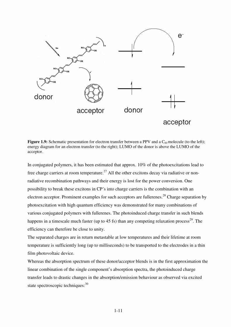
excited state energy is used to separate an electron-hole pair. Figure 1.9 shows an energetic
scheme for such a process.24,25 Either the donor or acceptor molecule is excited by light h� > EG
and is transferred into an excited state. Then, an electron is transferred from the donor LUMO
into the acceptor LUMO or vice versa ( hole transfer from acceptor HOMO into donor HOMO).
The energetic requirement is given by the equation 1.7 (electron transfer).
0IAI CA*D ≤−− 1.7
Where ID* is the ionization energy of the photoexcited donor, AA the electron affinity of the
acceptor and IC is including all coulombic interactions.
Unlike in inorganic materials, primary photoexcitations in organic materials do not directly lead
to free charge carriers in general, but to coulombically bound electron-hole pairs (excitons). The
nature of these excitons in conjugated polymers was heavily discussed in the scientific
community over the last years.26 Especially, the magnitude of the exciton binding energy (i.e.
weakly bound Wannier type excitons versus strongly bound Frenkel excitons) plays an important
role in understanding the nature of the primary photoexcitations.
1-11
Figure 1.9: Schematic presentation for electron transfer between a PPV and a C60 molecule (to the left); energy diagram for an electron transfer (to the right); LUMO of the donor is above the LUMO of the acceptor.
In conjugated polymers, it has been estimated that approx. 10% of the photoexcitations lead to
free charge carriers at room temperature.27 All the other excitons decay via radiative or non-
radiative recombination pathways and their energy is lost for the power conversion. One
possibility to break these excitons in CP´s into charge carriers is the combination with an
electron acceptor. Prominent examples for such acceptors are fullerenes.28 Charge separation by
photoexcitation with high quantum efficiency was demonstrated for many combinations of
various conjugated polymers with fullerenes. The photoinduced charge transfer in such blends
happens in a timescale much faster (up to 45 fs) than any competing relaxation process29. The
efficiency can therefore be close to unity.
The separated charges are in return metastable at low temperatures and their lifetime at room
temperature is sufficiently long (up to milliseconds) to be transported to the electrodes in a thin
film photovoltaic device.
Whereas the absorption spectrum of these donor/acceptor blends is in the first approximation the
linear combination of the single component’s absorption spectra, the photoinduced charge
transfer leads to drastic changes in the absorption/emission behaviour as observed via excited
state spectroscopic techniques:30

1-12
(i) The photoluminescence of the CP´s is heavily quenched: conjugated polymers show a
strong photoluminescence as well as electroluminescence. In a blend with fullerenes,
the depopulation of the photo-excited state of the conjugated polymer by the charge
transfer to the fullerenes is much faster than the radiative decay (τ~500-800 ps). The
addition of 10 % w/w fullerene to the polymer is sufficient to quench the
luminescence of the conjugated polymer by a factor >100.
(ii) Two strong light induced electron spin resonance (LESR)31 signals are observed due
to the radical nature of the photoinduced charge carriers. The signal with the g-value
g = 2.0026 is assigned to a positive polaron on the conjugated polymer. The signal
with the g value g = 1.9997 is assigned to the negative fullerene anion.32,33 The g-
value of the C60- is unusually low as compared to other carbon based organic radical
ions.
(iii) Two photoinduced absorption bands within the optical bandgap are observed by
pump-probe techniques. These two bands are assigned to the high- (HE) and low
energy (LE) absorption of the polaronic state of the conjugated polymer. The
formation of the polaronic bands occurs in a time scale of 45 fs. The stimulated
emission, as probe for the excited state, is quenched at a similar timescale.20 The
signal of the polaronic peaks is observable up to the µs and even ms time regime,
showing the long lifetime of the photoinduced charges.34 In the mid infrared regime
(MIR), photoinduced infrared active vibrations (IRAVs) are observed as a signature
of polaronic relaxation of the lattice. Due to the formation of charged polarons,
symmetry forbidden Ag vibrations of the polymer are activated in the IR and thus
observed in the photoinduced IR absorption spectra.35,36,37
(iv) Time resolved transient photocurrent spectroscopy shows strong sensitization of the
photoconductivity of the conjugated polymer upon addition of small percentage of
fullerenes.38 Both, the magnitude and the lifetime of the photocurrent are increased
significantly.
These experimental results show undoubtedly the formation of separated and long living charge
carriers in poly-para-phenylene vinylenes (PPV) or poly- thiophene (PT) -fullerene blends. The
quantum efficiency of this process is close to 100 % at the donor-acceptor interface. The
presented techniques are useful probes for photoinduced charge transfer in polymer-acceptor
blends and are used routinely for the investigation of new materials and materials
combinations.39

1-13
1.4. References 1 A. J. Heeger, Journal of Physical Chemistry B 2001, 105, 8475 2 H. Shirakawa, E. J. Louis, A. G. MacDiarmid, C. K. Chiang, A. J. Heeger, Journal of The Chemical Society: Chemical Communication 1977, 578 3 C. K. Chiang, C. R. Jr. Fincher, Y. W. Park, A. J. Heeger, H. Shirakawa, E. J. Louis, S.C. Gau, A. G. MacDiarmid Physical Review Letters 1977, 39, 1098 4 R. E. Peierls, “Quantum Theory of Solids”, Oxford, Clarendon Press, London 1956 5 C. K. Chiang, S. C. Gau, C. R. Jr. Fincher, Y. W. Park, A. G. MacDiarmid, Applied Physics Letters 1978, 33,18 6 W. P. Su, J. R. Schrieffer, A. J. Heeger, Physical Review Letters 1979, 42, 1698 7 W. P. Su, J. R. Schrieffer, A. J. Heeger, Journal of Physical Review B 1980, 22, 2099 8 H. Spreitzer, H. Becker, E. Kluge, W. Kreuder, H. Schenk, R. Demandt, H, Schoo, Advanced Materials 1998, 10, 1340 9 R. D. McCullough, R. D. Lowe, M. Jayaraman, D. L. J. Anderson, Journal of Organic Chemistry 1993, 58, 904 10 T.A. Chen, X. Wu, R. D. Rieke, Journal of The American Chemical Society 1995, 117, 233 11 D. Muehlbacher, Diploma thesis, University of Linz 2002 12 J. H. Kaufman, J. W. Kaufer, A. J. Heeger, R. Kaner, A. G. MacDiarmid, Physical Review B 1982, 26, 2327 13 M. Loegdlund and W. R. Salaneck, “Electronic Structure of Surfaces and Interfaces in Conjugated Polymers,” in Semiconducting Polymers, edited by G. Hadziioannou and P. F. van Hutten (VCH, Weinheim, 1999), pp. 115 - 148. 14 H. Ishii, K. Sugiyama, E. Ito, K. Seki, Advanced Materials 1999, 11, 605 15 R. J. Gomer, G. Tryson, Journal of Chemical Physics 1977, 66, 4413 16 R. Koetz, H. Neff, K. Mueller, Journal of Electroanalytical Chemistry 1986, 215, 331 17 H. Kroto, J. Heath, S. O'Brien, R. Curl, R. Smalley, Nature 1985, 318, 167 18 R. C. Haddon, L. E. Brus, H. Raghavachari, Chemical Physics Letters 1986, 125,459 19 Q. Xie, E. Pérez-Cordero, L. Echegoyen, Journal of the American Chemical Society 1992, 114, 3978 20 J. C. Hummelen, B. W. Knight, F. LePeq, F. Wudl, J. Yao, C. L. Wilkins, Journal of Organic Chemistry 1995, 60, 532 21 V. D. Mihailetchi, J. K. J. van Duren, P. W. M. Blom, J. C. Hummelen, R. A. J. Janssen, J. M. Kroon, M. T. Rispens, W. J. H. Verhees, M. M. Weink, Advanced Functional Materials 2003, 13, 43 22 C. Waldauf, P. Schilinsky, M. Perisutti, J. Hauch, C. J. Brabec, Advanced Materials 2003, 15, 2081 23 R. Pacios, J. Nelson, D. D. C. Bradley, C. J. Brabec, Applied Physics Letters 2003, 83, 4764 24 J. J. M. Halls, J. Cornil, D. A. dos Santos, R. Silbey, D. H. Hwang, A. B. Holmes, J. L. Brédas, R. H. Friend, Physical Review B 1999, 60, 5721 25 M. J. Rice and Yu N. Garstein, Physical Review B 1996, 53, 10764 26 “Primary Photoexcitations in Conjugated Polymers: Molecular Exciton versus Semiconductor Band Model” edited by N. S. Sariciftci, World Scientific Publ., Singapore (1997) 27 P.B. Miranda, D. Moses, A. J. Heeger, Physical Review B 2001, 64, 081201 28 N. S. Sariciftci, L. Smilowitz, A. J. Heeger, F. Wudl, Science 1992, 258, 1474 29 C. J. Brabec, G. Zerza, G. Cerullo, S. De-Silvestri, S. Luzzati, J. C. Hummelen, S. Sariciftici, Chemical Physics Letters 2001, 340, 232 30 N. S. Sariciftci, A. J. Heeger, in Handbook of Organic Conductive Molecules and Polymers, Vol 1 (Ed. H. S. Nalwa.), Wiley, New York 1996, 414-450 31 X. Wei, Z. V. Vardeny, N. S. Sariciftci, A. J. Heeger, Physical Review B 1996, 53, 2187 32 P. M. Allemand, G. Srdanov, A. Koch, K. Khemani, F. Wudl, Y. Rubin, F. N. Diedrich, M. M. Alvarez, S. J. Anz, R. L. Whetten, Journal of The American Chemical Society 1991, 113, 2780 33 M. C. Scharber, N. A. Schultz, N. S. Sariciftci, C. J. Brabec Physical Review B 2003, 67, 085202 34A. F. Nogueira, I. Montanari , J. Nelson, J. Durrant, C. Winder, N. S. Sariciftci, C. J. Brabec, Journal of Physical Chemistry B 2003, 107,1567 35 E. Ehrenfreund, Z. V. Vardeny, O. Brafman, B. Horovitz, Physical Review B 1987, 36, 1535 36 K. Lee, R. A. J. Janssen, N. S. Sariciftci, A. J. Heeger, Physical Review B 1994, 49, 5781 37 Y. Furukawa, The Journal of Physical Chemistry 1996, 100, 15644 38 C. H. Lee, G. Yu, D. Moses, K. Pakbaz, C. Zhang, N. S. Sariciftci, A. J. Heeger, F. Wudl, Physical Review B 1993, 48, 15425
2-1
2. Organic and Polymeric Solar Cell Devices
Organic materials gained broader interest for implementing in photovoltaic solar cells in the last
decade.1,2,3,4 Since the report of the first organic thin film solar cell by Tang,1 several concepts
have been presented using small molecules,1,2 conjugated polymers,5 conjugated polymer
blends,4,6,7 polymer-small molecule bilayers8,9 and blends3,10,11 or combinations of organic-
inorganic materials.12,13 Organic materials have several advantages like low cost synthesis and
comparably easy manufacturing of thin film devices by vacuum evaporation or solution cast
technologies.
Furthermore, organic thin films may show optical absorption coefficients14 exceeding
105 cm-1, what makes them good chromophores for optoelectronic applications.
Among these materials, conjugated polymers are of special interest due to several reasons:
(i) The possibility of an all polymer device (plastic solar cell).
(ii) Possibility of using solution cast processes like spin coating or doctor blade15 or
screen-printing16 or roll to roll processes for thin film fabrication.
(iii) Solution cast processes offer an easy way for forming blends of materials, i.e. bulk
heterojunction devices by processing from common solutions.
2.1 Photovoltaic Device Architectures
Bilayer devices, consisting of a p- and n-type (donor and acceptor, respectively) organic
semiconductor materials, were realized for many combinations.1,2,8,9,17,18 The conversion
efficiency of such devices is limited by the charge generation at the donor/ acceptor interface. In
the case of PPV type materials, the interfacial photoactive layer thickness is in the range of 5-10
nm 18,19,20,21 i.e. only excitons created within this distance to the interface can reach the
heterojunction interface. This leads to the loss of photons absorbed further away from the
interface and consequential to low quantum efficiencies. Antibatic behaviour of the photocurrent
action spectra as compared to the optical absorption spectrum of the active material is observed
due to optical filter effects. Most of the light is absorbed to far from the interface.22
Further, the film thickness has to be optimised for interference effects23,24 and charge transport.
With the invention of the bulk heterojunction,3,6 blending the donor and acceptor material, the
exciton diffusion bottleneck could be overcome and efficient charge generation in the whole
volume of the active layer is ensured. For soluble materials, such blends can be easily realized by
casting the composite film from a common solution of the donor and acceptor.

2-2
The driving force for the transport of the photoinduced charges to the opposite electrodes in such
bulk heterojunction solar cells is still unclear. Several concepts have been proposed, attributing
the charge transport either to electric field induced drift of charge carriers or concentration
gradient induced diffusion of them, respectively.25
The metal-insulator-metal picture (MIM),26 was introduced by Parker to describe current-voltage
curves of polymeric light emitting diodes. The charge transport is attributed to an electric field
induced drift. The work function difference of the contacts induces the electric field.
The diffusion-limited concept sees the diffusion of charge carriers induced by concentration
gradients as driving force for transport. The directionality of the diffusion is attributed to
selective electrodes.27 Common for both concepts is that the charge transport is directed by the
asymmetry of the electrodes properties.
Recently, Gregg and Hanna28 proposed a new model of an excitonic solar cell, describing all
types of organic solar cells. The driving force for the charge transport is assigned to the chemical
potential gradient, formed by the charge generation at the interface. The charges are moving
away from this interface to the opposite electrodes. In contrast to the classical inorganic solar
cells, the built in field is not limiting the open circuit potential, but the photoinduced quasi fermi
level difference for positive and negative charges.
Figure 2. 1: Device architecture for a thin film bulk heterojunction photovoltaic device.
ITO
-
GlassPEDOT (~80 nm)
LiF(0.6 nm)
Al / Ca (80 nm)
+
active layer
2-3
Figure 2.1 shows the device structure, which is typically used today for bulk heterojunction
devices. As positive electrode, indium-tin-oxide ITO coated glass or plastic is used.
ITO belongs to the class of transparent and conductive oxides (TCO) and is widely used as
electrode in photovoltaic and LED application.
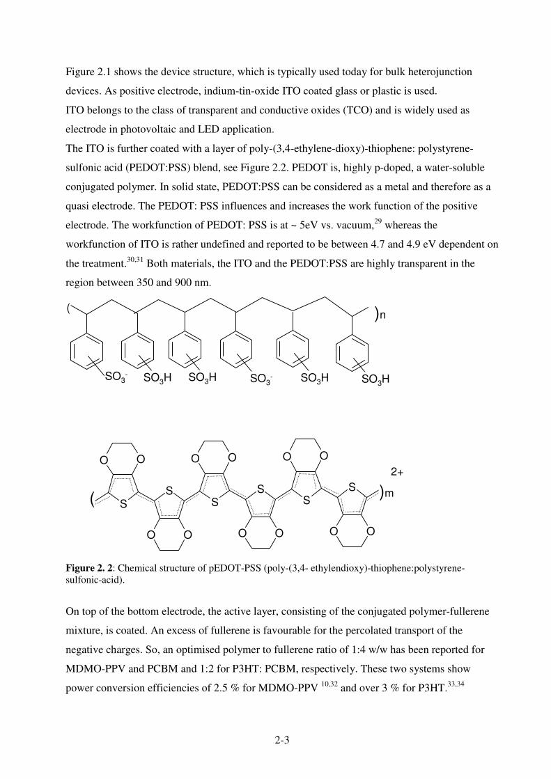
The ITO is further coated with a layer of poly-(3,4-ethylene-dioxy)-thiophene: polystyrene-
sulfonic acid (PEDOT:PSS) blend, see Figure 2.2. PEDOT is, highly p-doped, a water-soluble
conjugated polymer. In solid state, PEDOT:PSS can be considered as a metal and therefore as a
quasi electrode. The PEDOT: PSS influences and increases the work function of the positive
electrode. The workfunction of PEDOT: PSS is at ~ 5eV vs. vacuum,29 whereas the
workfunction of ITO is rather undefined and reported to be between 4.7 and 4.9 eV dependent on
the treatment.30,31 Both materials, the ITO and the PEDOT:PSS are highly transparent in the
region between 350 and 900 nm.
S
O O
S
OO
S
OO
S
O O
S
OO
S
O O
SO3- SO3
-
( )m
( )n
SO3H SO3H SO3HSO3H
2+
Figure 2. 2: Chemical structure of pEDOT-PSS (poly-(3,4- ethylendioxy)-thiophene:polystyrene-sulfonic-acid).
On top of the bottom electrode, the active layer, consisting of the conjugated polymer-fullerene
mixture, is coated. An excess of fullerene is favourable for the percolated transport of the
negative charges. So, an optimised polymer to fullerene ratio of 1:4 w/w has been reported for
MDMO-PPV and PCBM and 1:2 for P3HT: PCBM, respectively. These two systems show
power conversion efficiencies of 2.5 % for MDMO-PPV 10,32 and over 3 % for P3HT.33,34

2-4
As top (negative) electrode, a metal layer, like Al, Ca or Au, is evaporated.35 An interfacial layer
of thermally evaporated LiF was demonstrated to be favourable between the organic and the
metal layer in combination with Al and Au.36 LiF is known to form better electron
injecting/collecting contacts with organic thin films in LED devices. 37,38
2.2 Improving the Solar Cell Device Efficiency
The photovoltaic power conversion efficiency �e is defined by equation (2.1).
(2.1) in
SCOCe P
FF*I*V=η
(2.2) SCOC
mppmpp
I*VV*I
FF =
VOC is the open circuit voltage, ISC is the short circuit current, and FF is the fill factor, defined
after equation 2.2 and Pin the incident light power. The incident light power is standardized for
solar cell testing as AM 1.5 (air mass 1.5) spectrum. This is the solar irradiation (diffuse and
direct) on sea level on a 37° tilted, sun facing surface and attenuated by the earth atmosphere.39
In incident power is 1000 W m-2. Impp and Vmpp are the current and voltage at the maximum
power point in the fourth quadrant of the current-voltage characteristics. For the testing in the
laboratory, solar simulators are used to imitate the AM1.5 solar irradiation.
The critical cell parameters will now discussed in detail:
• Open Circuit Voltage: The thermodynamic limit for the VOC is given by the bandgap of
the active materials. The band gap is limiting the splitting of the quasi fermi level of
electron and hole, induced by the light absorption.40 For heterojunction devices, the
energetic distance between the HOMO of the donor and the LUMO of the acceptor has to
be considered as the limitation for the VOC.
For bulk heterojunction devices containing fullerene acceptor, it was shown that the open
circuit potential is directly dependent on the LUMO level of the fullerene derivative. The
dependence of the VOC on the top electrode metal workfunction is shown to be neglible.35
The metals electrodes Ca, Al, Ag and Au were used with a workfunction range from 5.1
to 2.9 eV vs. vacuum. The experimental findings were attributed to Fermi level pinning
of the metal to the C60 anion.
Mihailetchi, Blom et al41 studied the same system, using LiF/Al, Ag, Au and Pd as
electrode materials. They concluded a strong dependence of the Voc on the metal
2-5
workfunction for non ohmic contact, but no dependence in the case of an ohmic contact.
For the non ohmic contact, a MIM like picture is favoured. For the ohmic contact case,
Fermi level pinning is assumed.
Ramsdale42 et al observed a linear relation of the negative electrode workfunction and the
observed open circuit voltage for donor-acceptor polyfluorene bilayer devices. An
additional contribution of 1 V to the workfunction difference of the electrodes was
observed. This contribution was attributed to the photoinduced dipole formed at the
interface due to the charge transfer.
ITO coated with PEDOT: PSS is regularly used as positive contact. The workfunction of
the PEDOT can be manipulated by adjusting the doping level. A strong dependence of
the open circuit voltage on the work function of the PEDOT:PSS43 was demonstrated.
In contrast to this, Kwanghee Lee et al44 and Ole Inganäs et al45 observed a linear
dependence of the open circuit voltage on the HOMO level of the polymeric donor used
in the bulk-heterojunction device.
• Short Circuit Current: The ISC is determined by the amount of absorbed light and the
internal conversion efficiency. Experimentally accessible is the external quantum
efficiency or incident photon to current efficiency, IPCE [%]. It is defined and calculated
after equation 2.3.
]mW[P*]nm[]cmA[I*1240
##
[%]IPCE2
In
2SC
Ph
El−
−
==λ
µ 2.3
� [nm] is the incident photon wavelength, ISC [µA cm-2] is the photocurrent of the device
and PIn [W m-2] is the incident power. IPCE values up to 76 % at the absorption
maximum are reported for bulk heterojunction solar cells. 33,34 The internal quantum
efficiency is estimated to be close to 100 % for conjugated polymer-fullerene blends.32
For an increase in the photocurrent, the light absorption has to be increased.
The absorption profile of the active layer shows a strong mismatch to the solar photon
flux, as compared in Figure 2.3. Materials absorbing in the maximum of the solar photon
flux, between 600 and 800 nm, are needed to increase the short circuit current. New
concepts to overcome this problem are the major part of this thesis.

2-6
Figure 2. 3: The terrestrial AM1.5 sun spectrum (——) and the integrated spectral photon flux (starting from 0 nm) (-•-) in comparison with the absorption (---) of an MDMO-PPV:PCBM 1:4 blend.
• Fill factor FF: The FF is defined by equation 2.2 and describes the quality of the diode in the
4th quadrant. The fill factor is mainly influenced by the series and shunt resistances, see the
simplified equivalent circuit for a photovoltaic device in Figure 2.4. The equivalent circuit is
described by equation 2.4
PH
SH
SS0 I
RIRU
)1))IRU(nkT
q(exp(II −−+−−= 2.4
The current I consist of following three parts:
i) Diode current: The diode is described by the exponential Shockley equation. I0 is the
saturation current of the diode, q the elementary charge, n the diode ideality factor, k the
Boltzmann constant and T the temperature. The applied voltage U is reduced by the series
resistance RS of the diode. RS should ideally be low.
ii) The shunt current through the shunt resistance RSH. The applied voltage is again reduced
by the series resistance. RSH should be ideally high.
iii) The photo generated current IPH, representing the current generation of the solar cell
under illumination.

2-7
Figure 2. 4: Equivalent circuit for a single junction solar cell. The photogenerated current Iph shows in the inverse direction of the diode. Shunt resistance RSH and series resistance RS are important for the fill factor. Ideally, series resistance should be low and shunt resistance high.
The nanomorphology of donor/acceptor composite is known to have an important influence for
the device efficiency.46 The conditions for the film preparation, i.e. the choice of solvent, are
crucible for the domain size in the interpenetrating network. On the one hand, a large interface
between the donor/acceptor phases is desired for efficient charge separation. The domain size
should be not larger the exciton diffusion length (approx. 10 nm for most CP´s) On the other
hand, interpenetrating paths of the individual phases are required for the charge transport to the
electrodes. It is also expected that a larger interface increase recombination of charge carriers.
The blend morphology is investigated by several techniques like atomic force microscope47,
transmission electron microscope,48,49 scanning electron microscopy,47 photoluminescence47 and
near field optical microscope. It is generally found that smaller domain sizes lead to higher
efficient devices in the case of solution cast processes.
Several approaches were suggested in the literature to control or manipulate the morphology:
• “Double cables” are materials, which are consisting of a conjugated polymer backbone with
acceptor molecules covalently attached. They can be seen as a molecular heterojunction.50
The field of double cables has been recently reviewed be Cravino et al.51
• Block copolymers are materials which consist of alternating conjugated donor and fullerene
bearing blocks.52 It was shown that these materials are able to form supramolecular self-
assemblies.53
• The composite nanomorphology can be influenced by changing the conditions during film
formation. 10,54,55 Shaheen et al observed for the system MDMO-PPV: PCBM power
conversion efficiencies of 1 % devices cast from toluene and 2.5 % for devices cast from
chlorobenzene.
RS
Iph RSH
- U +
I

2-8
• Diffusion bilayers were demonstrated, formed by either lamination of a donor-rich and an
acceptor-rich layer4 or by temperature induced diffusion of an acceptor molecule into the
donor polymer matrix.56,57
• Jenekhe et al demonstrated the formation of encapsulated fullerene nanoparticles.58
• Kietzke et al showed the formation of nanospheres by a miniemulsion process to control
phase separation and demonstrated the application for photovoltaic devices.59
2.3 Production of Bulk Heterojunction Devices
2.3.1 Experimental
Organic thin film photovoltaic devices are fabricated in a sandwich structure, as shown in Figure
2.1. As substrates, glass sheets of 1.5x1.5 cm2 covered with indium tin oxide ITO, from Merck
KGaA Darmstadt, with an ITO thickness of d = 125 nm and a sheet resistance <15 cm-2 are
used.
The ITO is structured by etching with an acidic mixture of HClkonz:HNO3 konz:H2O 4.6:0.4:5 for ~
15 minutes. Half of the substrate is coated with a commercial varnish to protect the active ITO
area against the etching acid. The varnish is removed afterwards by acetone in an ultrasonic bath.
Then, the ITO is cleaned in an ultrasonic bath again with acetone and finally in isopropanole as
cleaning solvents.
On the ITO substrate, a layer of PEDOT:PSS, Baytron PH, purchased from H.C. Starck, is spin
cast twice. PEDOT:PSS, for the structure see Figure 2.2 is an aqueous dispersion with a mean
particle size of 80 nm. (0.5 w%, PEDOT: PSS 2:3).
The active layers are also spin cast. Solutions were stirred and heated up to ~ 50° for at least
twelve hours. For the spin casting, the substrate is mount in the spincoater, Spincoater Model P
6700 Series from SCS Inc. For all spin casting processes a two-step program is used, if not
otherwise referred. First spinning speed is 1500 rpm for 40 sec, followed by 2000 rpm for 30 sec.
The spin cast process is done in ambient conditions unless otherwise referred. The following
evaporations and the characterisation of the devices are done in an argon glovebox, MB 200
from Mbraun.
The top electrode is a two-layer deposition of LiF/Al. The deposition is done by thermal
evaporation at a pressure 10-5 mbar. Tungsten boats are used as source. The average thickness
of the LiF and Al layer is 0.6 nm and 60-100 nm, respectively. The deposition rate of the
materials is monitored by a quartz balance, Intellemetrics IC 600. The evaporation is done
through a shadow mask in order to define the device area.
2-9
2.3.2 Device characterization
Thin layers are characterized by an atomic force microscope (AFM), Dimension 3100"
instrument from Digital Instruments, Santa Barbara, CA, in the tapping mode. The AFM is also
used to determine the film thickness, by measuring the height difference at a scratch.
I-V characteristics of the devices are measured in the dark and under illumination from a
Steuernagel solar simulator (with a metal halogen lamp as light source with an AM 1.5 filter)
under an illumination density of 80 or 100 mW cm-2, respectively. The I-V curves are measured
with a Keithley 2400. ITO is connected to the positive electrode, Al to the negative. The curves
are recorded by continuously sweeping from –2V to +2V and recording data points in 10 mV
steps.
The spectral photocurrent is detected by a Lock-in amplifier. The sample is illuminated with
monochromatic light with ~ 200 µW cm-2 and a FWHM of ~ 4 nm from a 80 W Xenon lamp.
The spectrum of the light source is measured each time with a calibrated monocrystalline silicon
diode.
2.3.3. PPV: fullerene bulk heterojunction devices
The material combination of poly-para-phenylene vinylene and fullerene is probably the most
and best investigated organic heterojunction solar cell. Bulk heterojunction of MDMO-PPV and
PCBM were investigated by several groups in the recent years and the power conversion
efficiency could be pushed up to 2.5 %.10,25,32,35,60,61,62,63,64
The short-circuit current shows nearly linear dependence on the illumination dependence Pin;
Isc = Pin�, with � = 0.92.65,66 This power law dependence with � close to one shows that
bimolecular recombination is negligible.
The open circuit voltage VOC shows a logarithmic behaviour on the illumination dependence,25 as
predicted for classical pn junction by Equation 2.5.
)II
ln(*qTk
V0
SCbOC = (2.5)
where kb is the Boltzmann constant, T the temperature, q the elementary charge and I0 the
saturation current density. The saturation current shows an exponential dependence on the
temperature, see Equation 2.6.
)Tk
E(eI
b
g
0 −∝ (2.6)
2-10
The incident photon to current efficiency (IPCE) is 50 % at the absorption maximum of 500 nm.
The internal quantum efficiency IQE is estimated for thin devices to be close to 1.32 Further
improvements of the photocurrent are only possible by increasing the amount of absorbed light.
For thin film devices with a reflecting back electrode, the absorption is not a logarithmic
function of the absorber thickness, but highly influenced by interference effects. Hoppe et al67
calculated the absorption profile vs. absorber thickness for the combination MDMO-PPV:
PCBM 1:4 and found a nearly steplike function. A conversion efficiency of 1, independent of the
thickness, was assumed for this calculation.
For thicker devices, parasitic recombination is expected. Only charge carriers, which are created
within their mean free path to the electrode are contribution to the photocurrent. In other words,
only charge carriers, which can reach the electrode in their lifetime.
The influence of the active layer thickness on the photocurrent and photovoltaic efficiency is
discussed in the following. The composition of the blend is kept constant.
Figure 2.5 compares the light and dark curves of MDMO-PPV: PCBM 1:4 solar cells for device
thicknesses from 34.5 to 127.5 nm. The photovoltaic efficiency and device parameter are
summarized in Table 2.1.

2-11
Figure 2. 5: Thickness dependence of the I-V curves under illumination with 80 mW cm-2 (upper graph) and in the dark (lower graph) for MDMO-PPV: PCBM 1:4 w/w devices. The rectification at +/- 2V is found to increase with the device thickness. Such behaviour can be
assigned to a decreased saturation current I0 and to an increased shunt resistance.
The maximal power conversion efficiency is found for a thickness of 93 nm, similar as found by
Shaheen et al. The ISC and FF show a maximum for the thickness of 93 nm. The Isc and FF are
decreasing for the thicker device. This is assigned to bimolecular recombination and an increased

2-12
series resistance. The VOC is constant with the thickness, only decreasing for the thinnest device
due to shorts.
Table 2. 1: Diode and photovoltaic parameters are shown as a function of the active layer thickness for a MDMO-PPV: PCBM 1:4, spin cast from chlorobenzene, illumination density is 80 mW cm-2
d / nm VOC / V ISC / mA cm-2 FF Efficiency / % R (+/- 2)
127.5 0.81 3.67 0.44 1.6 210
93 0.81 4.57 0.50 2.3 190
68 0.81 4.46 0.42 1.9 146
61 0.77 4.51 0.44 1.9 53
34.5 0.24 2.23 0.27 0.2 8
Figure 2. 6: Photocurrent spectra (IPCE) for MDMO-PPV: PCBM 1:4 devices as a function of layer thickness.
Figure 2.6 shows the photocurrent spectra for the MDMO-PPV: PCBM devices for different
thicknesses. As predicted from optical simulation, the shape of the photocurrent spectrum is
changing with the thickness. In bulk heterojunction devices, the photogeneration rate of charge

2-13
carriers should be constant throughout the thickness. Optical filter effects can be ruled out.22 It is
concluded that the difference of shape are originating from interference effects.
2.3.4 P3HT: fullerene bulk heterojunction devices
Polythiophenes are among the best and most investigated conjugated polymers.68 The possibility
of synthesis of polymers with regioregular-ordered side chains leads to high mobility polymers.
These polymers show high charge carrier mobilities.69,70
Until recently, polythiophenes could not be successfully implemented in bulk heterojunction
photovoltaic cells. In the year 2002, Brabec et al and Padinger et al reported independently
power conversions efficiency of 3.5 % from P3HT: PCBM solar cells.33,34 P3HT shows a
broader and red shifted absorption compared to MDMO-PPV, resulting in a doubling of the
photocurrent under AM 1.5 conditions.
Further, the higher mobility of P3HT allows thicker absorbing layer without recombination
losses due to limited transport. IPCE of 76 % at the absorption maximum are reported.
Of special interest is the so-called post production treatement reported by Padinger et al. The
device is annealed at a temperature of 80° and simultaneously a voltage of 2.7 V is applied for 4
min. This leads to an improvement in the power conversion efficiency from around 0.5 % to 3.5
%. The detailed photovoltaic data are given in Table 2.2.
Table 2. 2: Photovoltaic parameter for P3HT: PCBM 1:2 devices from chlorobenzene, illumination with 80 mW cm-2.
Voc / V Isc / mA cm-2 FF Efficiency / %
Without treatment 0.3-0.7 2.5 0.3 0.3-0.7
Thermal treatement 0.49 8.3 0.55 2.8
Post production treatment 0.56 9.0 0.6 3.7
Within this thesis, the effect of the post production treatment is investigated. Part of this work
was carried out at the Interuniversity Microelectronic Center IMEC in Leuven, Belgium. The
absorbance ( in reflection geometry) and photocurrent spectra were measured with an integrating
sphere. Devices with an active are of ~1 cm-2 were prepared for these measurements. The
devices are sealed with a glass plate.
2-14
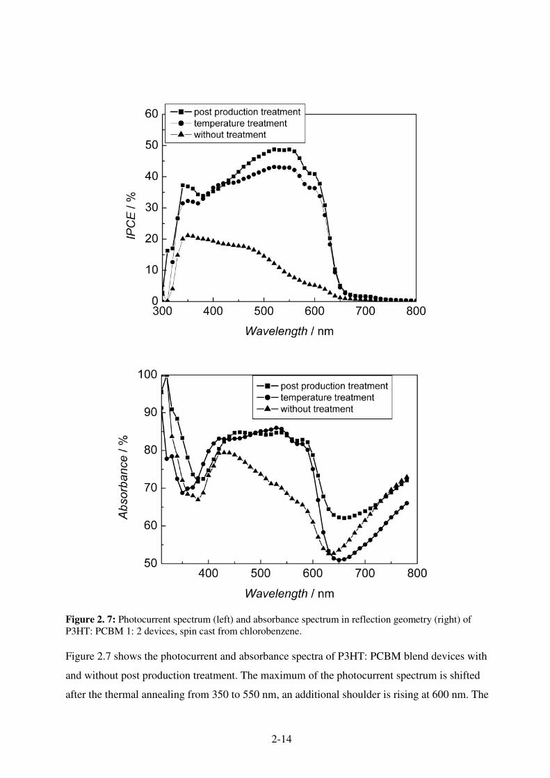
Figure 2. 7: Photocurrent spectrum (left) and absorbance spectrum in reflection geometry (right) of P3HT: PCBM 1: 2 devices, spin cast from chlorobenzene. Figure 2.7 shows the photocurrent and absorbance spectra of P3HT: PCBM blend devices with
and without post production treatment. The maximum of the photocurrent spectrum is shifted
after the thermal annealing from 350 to 550 nm, an additional shoulder is rising at 600 nm. The

2-15
same effect is observed in the absorbance for this device. The additional electrical treatment is
not changing the photocurrent spectrum nor the absorbance as compared with the thermal
treatment. The latter is increased in its strength.
The increased and structured absorption in the range from 450 to 650 nm is assigned to an
interchain -ordered phase in polythiophene.71
Blend of P3HT and PCBM with a high fullerene content (> 50 %) show as spin cast only weak
absorptions in the red. The absorption is less than the simple sum of the individual components
absorption. This absorption can be regained by thermal annealing. One might conclude, that the
thermal treatment provides the activation energy for the formation of the interchain ordered
phase.
The electrical treatment does not change the absorption properties of the material. Generally, the
diode behaviour of the device is improved by the post production treatment.
The thickness dependence of the photovoltaic parameters for P3HT: PCBM devices is shown in
Table 2.3. Untreated and thermally annealed devices are compared in a range from 52 to 240 nm.
Table 2. 3: Photovoltaic and diode parameter of P3HT: PCBM devices as a function of active layer thickness, thermally treated devices are annealed at 120° C for 5´.
Untreated Thermally annealed
d / nm U /V i /
mA cm-2
FF Eff. /
%
R
(+/-2 V)
U /V i /
mA cm-2
FF Eff. /
%
R
(+/-2 V)
240 0.64 1.9 0.36 0.44 1714 0.41 9.5 0.36 1.4 213
195 0.69 1.6 0.34 0.38 526 0.59 6.1 0.50 1.8 231
124 0.61 1.5 0.30 0.27 87 0.62 4.2 0.41 1.1 72
52 0.47 1.8 0.30 0.25 71 0.58 3.1 0.41 0.7 58
For the untreated devices, the highest efficiency is observed for the thickest device, but the
overall efficiency is low. The low rectification values reflect bad diode behaviour due to shunts,
which become less probable for thicker devices. After the thermal treatment, the devices with a
thickness over >100 nm show good diode behaviour. These devices have sufficient high parallel
resistance. The efficiency maximum is observed for a thickness of 195 nm. For the thicker
device, the Isc is increasing, but losses in Voc and FF are observed.
The short circuit current is increasing with the active layer thickness. This is also reflected in the
photocurrent spectra for the annealed devices, see Figure 2.8.

2-16
Figure 2. 8: Thickness dependence of the IPCE spectra for P3HT: PCBM 1:2 devices, spin cast from chlorobenzene and thermally treated, 5´ 120°. 240 nm for the thick full line, 195 nm for dashed line, 124 nm for the thin line and 52 nm for the dotted line.
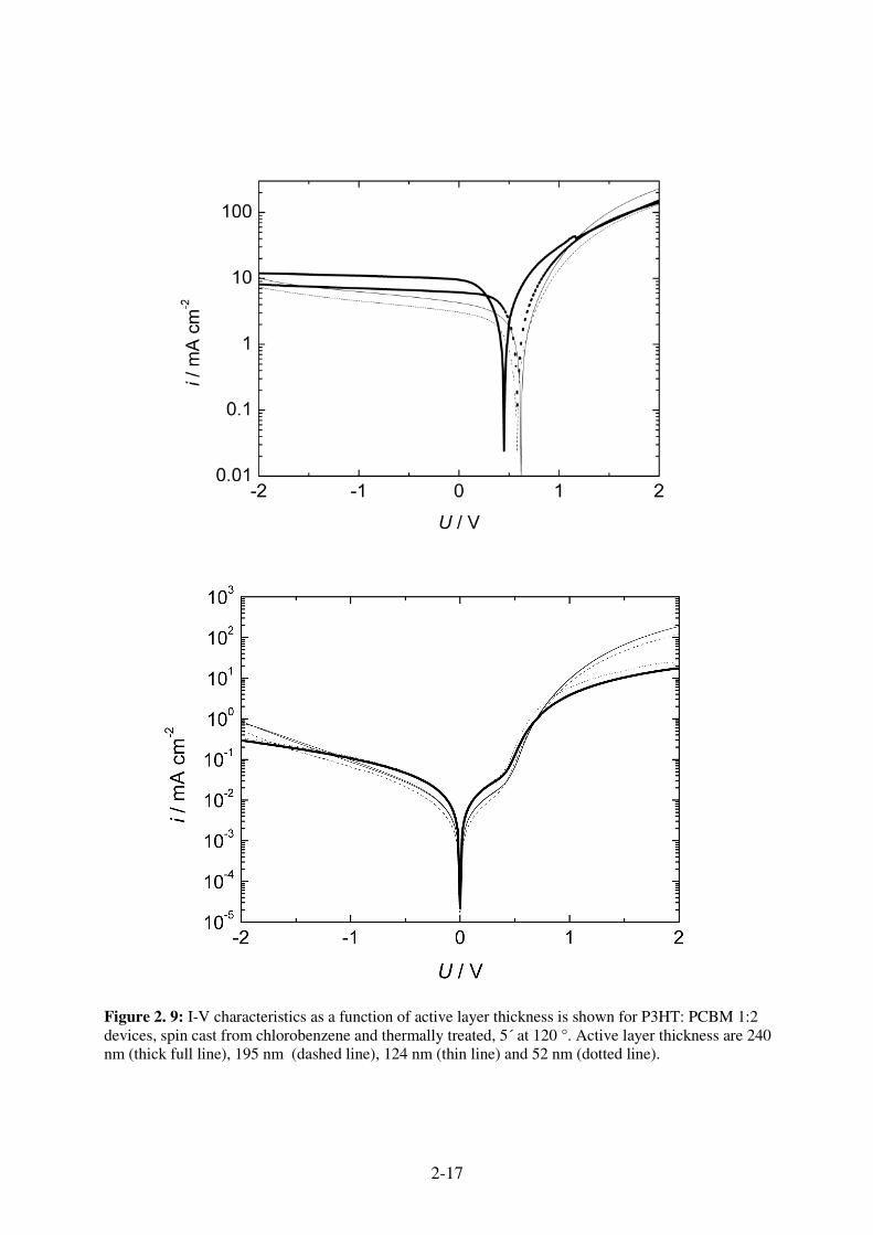
P3HT: PCBM blend devices allow generally higher thicknesses compared to MDMO-PPV. This
observation might be assigned to the higher charge carrier mobility in the P3HT phase. The
increased thickness lead to increased absorption and consequently to higher external quantum
efficiencies. In contrast, P3HT: PCBM device show a lower Voc after the post production
treatment in the range of 600 mV. The diode behaviour of these devices is excellent, what is
reflected in the extraordinary high FF.
2-17
Figure 2. 9: I-V characteristics as a function of active layer thickness is shown for P3HT: PCBM 1:2 devices, spin cast from chlorobenzene and thermally treated, 5´ at 120 °. Active layer thickness are 240 nm (thick full line), 195 nm (dashed line), 124 nm (thin line) and 52 nm (dotted line).

2-18
2.4 References 1 C. W. Tang, Applied Physics Letters 1986, 48, 183 2 D. Wöhrle, D. Meissner Advanced Materials 1991, 3, 129 3 G. Yu, J. Gao, J.C. Hummelen, F. Wudl, A. J. Heeger, Science 1995, 270, 1789 4 M. Granström, K. Petritsch, A. C. Arias, A. Lux, M.R. Andersson, R. H. Friend, Nature 1998, 395, 257 5 H. Antoniadis, B. R. Hsieh, M. A. Abkowitz, S. A. Jenekhe, M. Stolka, Synthetic Metals 1994, 62, 265 6 J. J. M. Halls, C. A. Walsh, N. C. Greenham, E. A. Marseglia, R. H. Friends, S. C. Moratti, A. B. Holmes, Nature 1995, 376, 498 7 G. Yu, A. J. Heeger, Journal of Appied Physics 1995, 78, 4510 8 S. A. Jenekhe, S. Yi, Applied Physics Letters 2000, 77, 2635 9 A. J. Breeze, A. Salomon, D. S. Ginley, B. A. Gregg, H. Tillmann, H. H. Hoerhold, Applied Physics Letters 2002, 81, 3085 10 S. E. Shaheen, C. J. Brabec, N. S. Sariciftci, F. Padinger, T. Fromherz, J. C. Hummelen, Applied Physics Letters 2001, 78, 841 11 J. J. Dittmer, E. A. Marseglia, R. H. Friend, Advanced Materials 2000, 12, 1270 12 B. O. Reagan, M. Graetzel, Nature 1991, 353, 737 13 N. C. Greenham, X. Peng, A. P. Alivisatos, Physical Review B 1996, 54, 17628 14 H. Hoppe, N. S. Sariciftci, D. Meissner, Molecular Crystalls Liquid Crystalls 2002, 385, 113 15 C. J. Brabec, F. Padinger, J. C. Hummelen, R. A. J. Janssen, N. S. Sariciftci, Synthetic Metals 1999, 102, 861 16 S. E. Shaheen, R. Radspinner, N. Peyghambarian, G. E. Jabbour, Applied Physics Letters 2001, 79, 2996 17 N. S. Sariciftci, D. Braun, C. Zhang, V. I. Srdanov, A. J. Heeger, G. Stucky, F. Wudl, Applied Physics Letters 1993, 62, 585 18 J. J. M. Halls, K. Pichler, R. H. Friend, C. S. Moratti, A. B. Holmes, Applied Physics Letters 1996, 68, 3120 19 T. Stuebinger, W. Bruetting, Journal of Applied Physics 2001, 90, 3632 20 A Haugeneder, M. Neges, C. Kallinger, W. Spirkl, U. Lemmer, J. Feldmann, U. Scherf, E. Harth, A. Guegel, K. Muellen, Physical Review B 1999, 59, 15326 21 M. Theander, A. Yartsev, D. Zigmantas, V. Sundstroem, W. Manno, M. R. Andersson, O. Inganaes, Physical Review B 2000, 61, 12957 22 M. G. Harrison, J. Gruener, G. C. W. Spencer, Physical Review B 1997, 55, 7831 23 L.A.A. Pettersson, L. S. Roman, O. Inganas, Journal of Applied Physics 1999, 86, 487 24 J. Ronstalski, D. Meissner, Solar Energy Materials and Solar Cells 2000, 63, 37 25 V. Dyakonov, Physica E 2002, 14, 53 26 I. D. Parker, Journal of Applied Physics. 1994, 75, 1656 27 D. Meissner, J. Ronstalski, Synthetic Metals 2001, 121, 1551 28 B. A. Gregg, M. C. Hanna, Journal of Applied Physics. 2003, 93, 3605 29 N. Koch, A. Kahn, J. Ghijsen, J. J. Prieaux, S. Schwartz, R. L. Johnson, A. Elschner, Applied Physics Letters 2003, 82, 70 30 G. Greczynski, Th. Kugler, M. Keil, W. Osikowicz, M. Fahlman, W. R. Salanck, Journal of Electron Spectroscopy and Related Phenomena 2001, 121, 1 31 J. S. Kim, M. Granstrom. R. H. Friend, N. Johansson, W. R. Salaneck, R. Daik, W. J. Feast, F. Cacialli, Journal of Applied Physics 1998, 84, 6859 32 C. J. Brabec, N. S. Sariciftci, J. K. Hummelen, Advanced Functional Materials. 2001, 11, 15 33 P. Schilinsky, C. Waldauf, C. J. Brabec, Applied Physics Letters 2002, 81, 3885 34 F. Padinger, R. Rittberger, N. S. Sariciftci, Advanced Functional Materials. 2003, 13, 85 35 C. J. Brabec, A. Cravino, D. Meissner, N. S. Sariciftci, T. Fromherz, T. Rispens, L. Sanchez, J. C. Hummelen, Advanced Functional Materials. 2001, 11, 374 36 C. J. Brabec, S. E. Shaheen, C. Winder, N. S. Sariciftci, P. Denk, Applied Physics Letters. 2002, 80, 1288 37 L. S. Hung, C. W. Tang, M. G. Mason, Applied Physics Letters 1997, 70, 151 38 G. E. Jabbour, Y. Kaxabe, S. E. Shaheen, J. F. Wang, M. M. Morrell, B. Kippelen, N. Peyghambarian, Applied Physics Letters 1997, 71, 1762 39 ASTM E 892 40 Peter Würfel, “Physik der Solarzelle”, Spektrum Verlag, 2000 41 V. D. Mihailetchi, P. W. M. Blom, J. C. Hummelen, M. T. Rispens, Journal of Applied Physics 2003, 94, 6849 42 C. M. Ramsdale, J. A. Barker, A. C. Arias, J. D. MacKenzie, R. H. Friend, N. C. Greenham, Journal of Applied Physics. 2002, 92, 4266, 43 H. Frohne, S. Shaheen, C. J. Brabec, D. Mueller, N. S. Sariciftci, K. Meerholz, Chem Phys Chem 2002, 9, 796 44 H. Kim, S. H. Jin, H. Suh, K. Lee, Proceedings of the SPIE 2003, in press 45 A. Gadisa, M. Svensson, M. Andersson, O. Inganäs, Applied Physics Letter 2004, 84, 1609 46 P. Peumans, S. Uchida, S. Forrest, Nature 2003, 425, 158

2-19
47 H. Hoppe, M. Niggeman, C. Winder, A. Hirsch, J. Kraut, R. Hiesgen, D. Meissner, N. S. Sariciftci, Advanced Functional Materials 2004, in press 48 J. K van Duren, J. Loos, F. Morrissey. C. M. Leewis. K. P. H. Kivits, L. J. van Ijzendoorn, M. T. Rispens, J. C. Hummelen, R. A. J. Janssen, Advanded Functional Materials 2002, 12, 665 49 T. Martens, J. D’Haen, T. Munters, Z. Beelen, L. Goris, J. Manca, M. D’Olieslaeger, D. Vanderzande, L. De Schepper and R. Andriessen, Synthetic Metals 2003, 138, 243 50 A. Cravino, N. S. Sariciftci, Nature Materials 2003, 2, 360 51 A. Cravino. N. S. Sariciftci, Journal of Material Chemistry 2002, 12, 1931 52 U. Stalmach, B. de Boer, C. Videlot, P. F. van Hutten, G. Hadziioannou, Journal of The American Chemical Society. 2000, 122, 5464 53 B. de Boer, u. Stalmach, P. F. van Hutten, C. Melzer, V. V. Krasnikov, G. Hadziioannou, Polymer 2001, 42, 9097 54 J. J. M. Halls, A. C. Arias, J. D. MacKenzei, W. Wu, M. Inbasekaran, E. P. Woo, R. H. Friend, Advanced Materials 2000, 12, 498 55 A. C. Arias, N. Cocoran, M. Banach, R. H. Friend, J. D. MacKenzuie, W. T. S. Huck, Applied Physics Letters. 2002, 80, 1695 56 M. Drees, K. Premaratne, W. Graupner, J. R. Heflin, R. M. Davis, D. Marciu, M. Miller, Applied Physics Letters. 2002, 81, 4607 57 M. Drees, R. M. Davis, R. Haflin, Physical Review B 2004, 69, 165320 58 S. A. Jenekhe, X. L. Chen, Science 1998, 279, 1903 59 T. Kietzke, D. Neher, J. Landfester, R. Montenegro, R. Guenter, U. Scherf, Nature Materials 2003, 2, 408 60 J. K. van Duren, J. Loos, F. Morrissey, C. M. Leewis, K. P. K. Kivits, L. J. van Ijzendoorn, M. T. Rispens, J. C. Hummelen, R. A. J. Janssen, Advanced Functional Materials 2002, 12, 665 61 J. M. Kroon, M. M. Wienk, W. J. H. Verhees, J. C. Hummelen, Thin Sold Films 2002, 403-404, 223 62 M.Al-Ibrahim, H. K. Roth, S. Sensfuss, Applied Physics Letters 2004, 85, 1481 63 V. D. Mihaliletchi, J. K. J. van Duren, P. W. M. Blom, J. C. Hummelen, R. A. J. Janssen, J. M. Kroon, M. T. Rispens, W. J. H. Verhees, M. M. Wienk, Advanced Functional Materials 2003, 13, 43 64 J. K. J. van Duren, V. D. Mihailetchi, P. W. M. Blom, T. van Woudenbergh, J. C. Hummelen, M. T. Rispens, R. A. J. Janssen, M. M. Wienk, Applied Physics Letters 2003, 94, 4477 65 I. Riedel, J. Parisi, V. Dyakonov, L. Lutsen, D. Vanderzande, J. C. Hummelen, Advanced Functional Materials 2004, 14, 38 66 E. A. Katz, D. Faiman, S. M. Tuladhar, J. M. Kroon, M. M. Wienk, T. Fromherz, F. Padinger, C. J. Brabec, N. S. Sariciftci, Journal of Applied Physics 2001, 90 , 5343 67 H. Hoppe, N. Arnold, N. S. Sariciftci, D. Meissner, Solar Energy Materials and Solar Cells 2003, 80, 105 68 R. D. McCullough, P. C. Ewbank, Handbook of Conducting Polymers, Chapter 9, p. 225, edited by T. A. Skotheim, R. L. Elsenbaumer, J. R. Reynolds, 1998, Marcel Dekker Inc. 69 H. Sirringhaus, P. J. Brown, R. H. Friend, M. M. Nielsen, K. Bechgaard, B. M. W. Langeveld-Voss, A. J. H. Spiering, R. A. J. Janssen, E. W. Meijer, P. Herwig, D. M. De Leeuw, Science 1999, 401, 685 70 A. Mozer, N. S. Sariciftci, Chemical Physics Letters 2004, 389, 438 71 K. E. Aasmundtvei, E. J. Samuelson, W. Mammo, M. Svensson, M. R. Anderson, L. A. A. Pettersson, O. Inganaes, Macromolecules 2000, 33, 5481
3-1
3. Photoinduced Absorption Spectroscopy
Photoinduced absorption (PIA) spectroscopic techniques are widely used to identify
photoexcited species. Generally, PIA can be measured in two different ways.
• Transient photoinduced absorption, where the sample is excited by a short light pulse and
photoinduced changes are probed in the time domain.1,2,3,4
• Photomodulation PIA technique, where the sample is excited by a modulated continuous
wave (cw) light source and the probe is detected in the frequency mode by a lock-in-
amplifier.5,6,7
For this thesis, generally photomodulation spectroscopy is used and the application of this
technique will be discussed in this chapter.
3.1. Steady State PIA
3.1.1 Principles
Figure 3.1 shows a schematic setup of a photomodulation PIA setup, as it is used for most
experiments in this thesis. Experimental details will be given later. The specimen is excited
across its band gap by the pump beam. Generally, a cw laser is used. The pump is modulated
periodically. Photoexcited states are created in the sample by the pump beam. The density of the
photoexcited species modulates with the modulation frequency of the pump. Changes in the
transmittance of the specimen, induced by the photoexcited states, are detected with the cw
probe light. The probe beam is spectrally resolved by a monochromator and measured by a diode
detector. The detector signal is amplified and detected by a two channel lock-in amplifier. The
reference signal for the lock-in amplifier is the modulation frequency.
The main unit of a lock in amplifier is the phase sensitive detector (PSD). The PSD detects only
signals modulating with the frequency of the reference input. This is mathematically achieved by
multiplying the signal input Vin and reference signal Vref, giving the output signal VPSD of the
phase sensitive detector. The basic equation for the PSD is shown in equation 3.1.
[ ] [ ]{ }unrefrefinrefinrefinrefin
refrefrefinininrefinPSD
t*)(cost*)(cos*V*V*21
)twsin(*V*)t*sin(*VV*VV
θθϖϖθθωω
θθϖ
−−+−−+−=
=−−== 3.1
�in is the frequency of the input signal, �ref is the frequency of the reference signal and � the
phase of the signal.

3-2
The output signal VPSD is filtered by a low pass filter, as a consequence only the first cosinus
term for �in �ref will contribute to the PSD output signal X (in phase signal).
In a second PSD, the input signal is multiplied with the reference signal, shifted for 90°, giving
the output signal Y. Signals at the frequency �ref , but a phase shift of 90°, will contribute to the
output signal Y (out of phase signal).
The total output signal can be regarded as complex number and is alternatively described by a
radius R and phase �, with R = (X2+Y2)^0.5 and �= arctan (Y/X).
Figure 3. 1: Schematic scheme for a photomodulation setup in transmission geometry.
The measured photoinduced signal �Tm may consist of several contributions.
• New absorptions can be observed from photoexcited species. The photoinduced
absorption signal is –�TPIA ~N*�*d, whereas N is the number of photoexcited states, �
their absorption cross-section and d the film thickness.
• Photobleaching �TPB. The sample can become more transparent. The ground state is
depopulated as a consequence of the high pump beam

3-3
• Luminescence �TL can be induced by the pump excitation. This contribution can be
corrected by subtracting the luminescence, which is determined in a separate
measurement.
• Stark effect or electroabsorption �TEA can occur in the region of the band-band
absorption, in the case charges are created. These charges are modulating with the pump
and cause an alternating electric field, which causes the Stark effect. The spectrum for the
Stark effect is the first derivative of the groundstate absorption
The photoinduced spectrum is than calculated by equation 3.2
T)TT(
T)TTTT(
TT LmLLPBPIA ∆−∆−
=∆−∆+∆+∆−
=∆− ( 3.2)
Additional information is got from the signal dependence on the modulation frequency � and the
pump power I.
The dependence of the photoinduced signal on the pump modulation frequency can be used to
estimate the recombination time of the observed species.8,9,10,11,12 Epshtein et al have introduced
recently the analysis for dispersive dynamics9,10, as it is observed in amorphous systems like
conjugated polymers. The frequency response is described by equation 3.3.
αϖτϖ
)i(1R
)(R 0
+= (3.3)
Where R(�) is the complex frequency response, R0 the steady-state response at zero frequency, �
the mean lifetime and � the dispersion factor. The dispersion factor describes the distribution of
lifetimes and vary between 0 for the broadest inhomogeneous distribution and 1 for a
homogeneous distribution.
The in-phase (X, dTx) and out-of-phase frequency (Y, dTy) response are fitted simultaneously by
equation 3.4 and 3.5, respectively.
αα
α
ϖτπαϖτ
παϖτ
20
)()2
cos()(21
)2
cos()(1RX
++
+= (3.4)
αα
α
ϖτπαϖτ
παϖτ
20
)()2
cos()(21
)2
sin()(RY
++= (3.5)

3-4
Generally, the in phase component X is decreasing with �, whereas Y shows a maximum.
The pump power dependence �T ~I� can be used to determine the recombination behaviour of
the detected states. � = 1 for first order kinetic (monomolecular type recombination), � = 0.5
second order kinetic (bimolecular type recombination).
3.1.2 Experimental Setup
For a schematic view of the setup, see Figure 3.1. As pump sources, an Ar+ laser, INNOVA 400,
at the wavelength of 476 nm or 514 nm is used, typically in a power range between 40 and 100
mW. The illumination spot on the sample is around 4mm2.Alternatively, diode lasers with a
wavelength at 664 nm, Iout = 45 mW, or 685 nm, Iout = 30 mW, is used. The pump beam is
modulated by a mechanical chopper, Standford SR 540, with a frequency between 5- 4000 Hz.
The samples are mounted in a homemade N2 cold finger cryostat or a He continuous flow
cryostat Oxford CF 204, Oxford Instruments plc, respectively. As probe, a halogen lamp with a
power of 120 W is used. The light beam is focused on the sample and on the entrance of the
monochromatic unit. The monochromator consists of a turret with 3 gratings, which are blazed at
300, 1000 and 2000 nm. In front of the monochromator is an additional set of cut-off filters to
block the pump excitation and higher order from the gratings. The detector is mounted on the
monochromator exit slit. It is a sandwich diode detector, consisting of Si for the VIS and NIR
<1100 nm and an InGaAsSb for the range between 1100 and 2200 nm. The signal is amplified
and detected by a lock in amplifier, Standford Model SR 830.

3-5
3.2 Photophysics of MDMO-PPV and MDMO-PPV: PCBM
In Figure 3.2, the photoluminescence of MDMO-PPV and its blend with PCBM is shown. The
pristine material shows a strong luminescence with peaks at 600 and 650 nm. The addition of a
small amount of the fullerene derivative PCBM (3.3 % w/w) quenches the photoluminescence by
approximately a factor of 10. Further addition of PCBM (33.3 % w/w) leads to a quenching of a
factor > 100. No photoluminescence from PCBM is detected (peak at 750 nm) for films cast
from chlorobenzene.
Figure 3. 2: Photoluminescence of pristine MDMO-PPV (squares), blends of MDMO-PPV: PCBM 30:1 (circles) and 3:1 (triangles) blends, samples are cast from chlorobenzene solutions. Samples are excited at 476 nm with 40 mW at room temperature.

3-6
Figure 3. 3: Comparison of PIA spectra of MDMO-PPV (triangle) and MDMO-PPV: PCBM 1.1 blend ( squares), excited at 476 nm at 100 K. Spectra a normalized at their maximum for comparison.
Figure 3.3 shows the PIA spectra of a pristine MDMO-PPV film and MDMO-PPV: PCBM 1:1
blend in comparison. The PIA of MDMO-PPV shows a single absorption peak at 1.4 eV (890
nm), which is assigned to a T1� Tn excitation of the polymer.13,14 The features around 2 eV are
most probable uncompensated photoluminescence of MDMO-PPV.
The MDMO-PPV: PCBM blend shows two photoinduced absorption peaks, a broad one on
between 1.1 and 2.1 eV, and a second one < 0.6 eV. These two peaks are assigned to the sub
band gap polaronic absorption (HE, LE), for the energy diagram see Figure 1.3. The strong
negative signal around 2.3 eV is assigned to photobleaching. The origin of the broad HE polaron
absorption will be discussed later.
Strong indications are found for photoinduced charge transfer as the dominant de-excitation
pathway for photoexcitation in MDMO-PPV: PCBM blends.6,7,15 The polymer
photoluminescence and the triplet state of the polymer are quenched in blends with PCBM.
Further, polaronic transition of MDMO-PPV are found in the blend.

3-7
Figure 3.4.a shows the PIA spectrum (in and out of phase) of a MDMO-PPV: PCBM 1:1 film at
16 K, recorded with a modulation frequency of 330 Hz. At this chosen frequency, both
components are of similar magnitude and show mirror image like features. Figure 3.4.b shows the PIA at a modulation frequency of 2970 Hz. The in-phase (X) component
of the high energy absorption decreases by approximately one order of magnitude and shrinks to
Figure 3. 4: a) Photoinduced absorption spectra at 16K of MDMO-PPV/PCBM acquired at a) 330 Hz and b) 2970 Hz. In both spectra in-phase (solid line) and out-of-phase (dashed line) components are plotted.
b)
a)

3-8
a small peak around 1.24 eV. The shape of the out-of-phase part (Y) remains unchanged (Figure
3.4.b).
Figure 3. 5: Modulation frequency dependence of the PIA signal recorded at 0.6 eV, 1.24 eV, 1.36 eV, and 1.8 eV. Measurements were performed at 16 K normalized at the lowest recorded modulation frequency.
In Figure 3.5, the frequency dependencies of several features in the spectrum are shown (0.6 eV,
1.2 eV, 1.36 eV, 1.8 eV). For better comparison, the curves are normalized at the lowest
modulation frequency. By increasing the modulation frequency, the PIA signal at 1.36 eV and
1.8eV are decreasing more than the signals at 0.6 eV and 1.24 eV. This is equivalent to a slower
decay of the species causing the 1.8 and 1.36 eV PIA as compared the species causing the 1.2
and 0.6 eV PIA. This finding contradicts the assumption that the peak between 1.1 eV and 2.1
eV originates from only one type of photoexcited species.
The recombination process at T< 40 K is known to be tunnelling dominated. Lifetimes up to
hours are observed in CP: fullerene blends.16
Recently, Beljonne et al17 calculated the influence on the optical signature of polarons by
interchain interaction in CP. Figure 3.6.a and 3.6.b shows schematically the energy diagram for a
polaron on a isolated chain and for a delocalised polaron on a co-facially aggregated dimer of

3-9
two five-unit PPV oligomers separated by four angstrom. For such aggregates, the polaronic
levels are split and a new absorption (C3) is possible.
One may conclude, that the photoinduced absorptions in MDMO-PPV: PCBM blends are
originating from localized and delocalised polarons. The delocalised polarons show a longer
lifetime compared to isolated chain polarons, at least at the temperature of 16 K. As a
consequence, the signals become easier over-chopped in photomodulation experiments and are
not detectable at high modulation frequencies.
a) b) Figure 3. 6: Allowed optical transitions in a localized (intramolecular) polaron and b) delocalised (on two conjugated segments, intermolecular) polaron. Energetic positions of different levels are only schematic Thick lines are indicating states of the neutral molecule, thin lines additional states of the polaron. Dashed arrows are indicating optical transitions.
3.3 Electric field effects on the photoexcitations.
The influence of an electric field on the photoexcitations in organic materials and conjugated
polymers was investigated by photoluminescence and pump-probe experiments by several
groups.
For the photoluminescence, field induced quenching was observed.18,19,20 This effect is generally
assigned to electric field assisted exciton dissociation.
In steady state pump-probe experiments, triplets are the primarily detected species in pristine
conjugated polymers.21 Upon applying an electric field and charge injection, faster decay of the
triplets was found.22 This effect was assigned to the interaction of injected charges with the
triplets. Furthermore, Zenz et al showed in ps pump probe experiments23 the hexaphenylene
triplet signal increasing due to the effect of an external electric field. The increased triplet signal
Eg
C2
C1 C1
C3 C3
’ Eg
C2
3-10
was assigned to the formation of additional triplets by recombination of polarons, which are
formed by field induced breaking of excitons.
Fewer studies are known on the photophysical behaviour of conjugated polymer: fullerene
blends under bias electric field. Liess et al24 found in C60 doped conjugated polymer films with
low C60 concentration enhancement of the photoinduced polaronic signal under bias. This effect
was attributed to enhanced dissociation of excitons due to tunnelling of the negative charge to
the fullerenes. Further, faster decay of the fullerene anion photoinduced signals under the
influence of the electric fields was found.
In this thesis, a detailed study of the steady state photoinduced absorption in conjugated
polymer/fullerene bulk heterojunction solar cells with high fullerene concentration is presented.
Photoinduced absorption was measured either in transmission/absorption with thin, transparent
electrodes or in reflection/absorption with thick, reflecting electrodes. Significant enhancement
of the photoinduced polaronic absorption signal by applying an external field of several Volts/
100 nm is observed. At higher positive voltages (forward bias, injection regime), the
photoinduced signal is reduced again due to recombination with injected charges. The
temperature dependence of this effect is discussed in comparison with the temperature
dependence of the current-voltage characteristics of the devices. Furthermore, we analysed the
charge carrier lifetimes as a function of the applied field using a dispersive recombination model.
This analysis clearly shows the shortening of the average lifetime of the photoexcited polarons
under applied electric field.
3.3.1 Experimental
The device structure and the light beam pathways for the optical measurements are shown in
Figure 3.7. As top electrode, 0.6 nm of LiF and subsequently a layer of Au or Al were
evaporated. LiF is known to improve the electron injection between Al or Au and organic
materials.25,26 Au and Al show similar behaviour as top electrode material in conjugated
polymer/fullerene bulk heterojunction devices.27 30 nm of Au or Al were used as top electrodes
for semi-transparent devices. Whereas thin Au devices show good stability, thin Al devices show
degradation after a short time period. All electrodes with a thickness over 60 nm show sufficient
stability and were used for spectroscopic measurements in reflection/absorption geometry. The
active area of the device is approx. 2x4 mm².

3-11
Figure 3. 7: The device structure of a bulk heterojunction photovoltaic cell and optical beam paths for the pump-probe experiments in transmission and reflection geometry are shown. The 476 nm line of an Ar+ laser, modulated with a mechanical chopper, was used as pump beam. It illuminated the sample through the ITO electrode. For the transmission measurements, the probe beam entered through a semitransparent top electrode. For the reflection measurements, the probe beam entered from the ITO side and was reflected at the metal electrode.
Photoinduced absorption spectra (PIA) were measured in two different setups: in transmission
geometry with the semi-transparent electrodes and in reflection geometry with devices with
reflecting back contacts. In both setups, the 476 nm line of an Ar+ laser was used as pump,
typically chopped at 73 Hz, and with a power between 40 and 100 mW on a spot diameter of
approx. 2 mm. Under this illumination conditions, a current of 7-20 mA in the area of the laser
spot of approx. 3-4 mm² is induced. The devices absorb roughly 50 % of the incident light in the
active layer and show quantum efficiency for the current extraction of 1. As probe, a tungsten-
halogen lamp was used. In the transmission setup, the monochromator was set after the sample,
in the reflection setup the monochromator was in front of the sample; in this case an additional
1.8 eV cut-off filter was used in front of the detector. The probe was measured with a Si-
InGaAsSb sandwich detector or a N2 cooled Ge detector in transmission and reflection geometry
setups, respectively, and recorded with a lock-in amplifier. The PIA spectra were corrected for
the photoluminescence.
The DC bias was applied between the ITO and Al electrode.
Active layer (~100 nm)
GlassPEDOT: PSS (~80nm)
LiF (0.6 nm)
Al / Au
ITO
Probe transmission
Probe reflection
Pump beam 476 nm
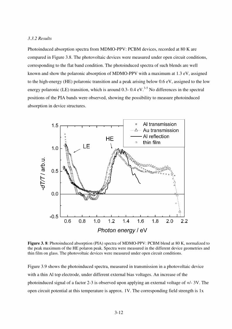
3-12
3.3.2 Results
Photoinduced absorption spectra from MDMO-PPV: PCBM devices, recorded at 80 K are
compared in Figure 3.8. The photovoltaic devices were measured under open circuit conditions,
corresponding to the flat band condition. The photoinduced spectra of such blends are well
known and show the polaronic absorption of MDMO-PPV with a maximum at 1.3 eV, assigned
to the high-energy (HE) polaronic transition and a peak arising below 0.6 eV, assigned to the low
energy polaronic (LE) transition, which is around 0.3- 0.4 eV.3-5 No differences in the spectral
positions of the PIA bands were observed, showing the possibility to measure photoinduced
absorption in device structures.
Figure 3. 8: Photoinduced absorption (PIA) spectra of MDMO-PPV: PCBM blend at 80 K, normalized to the peak maximum of the HE polaron peak. Spectra were measured in the different device geometries and thin film on glass. The photovoltaic devices were measured under open circuit conditions.
Figure 3.9 shows the photoinduced spectra, measured in transmission in a photovoltaic device
with a thin Al top electrode, under different external bias voltages. An increase of the
photoinduced signal of a factor 2-3 is observed upon applying an external voltage of +/- 3V. The
open circuit potential at this temperature is approx. 1V. The corresponding field strength is 1x

3-13
105 V cm-1 at short circuit, 2 x 10⁵ V cm-1 at +3 V and 4x 10⁵ V cm-1 at – 3V. Constant electric
field drop over the active layer is assumed.
Figure 3. 9: Photoinduced absorption at 80 K of a photovoltaic device in transmission with a thin Al electrode under open circuit, short circuit and positive and negative applied bias.
Figure 3.10a shows the photoinduced signal at 1.25 eV as a function of the external applied
voltage at different temperatures. At low temperature, the photoinduced signal is increasing
symmetrically around a voltage of ~ 1 V, what is close to the open circuit potential of these
devices. The open circuit potential can be used as a measure for the built in field. The PIA signal
shows a minimum around this field free case. Generally, the open circuit voltage of MDMO-
PPV: PCBM bulk heterojunction photovoltaic devices shows an increase with the light intensity
and saturation for higher illumination intensities. The threshold for this saturation is around the
solar illumination intensity. Under the illumination conditions in this experiments the cells
operate at high intensities, far beyond the threshold of this saturation. The temperature
dependence of the open circuit voltage in the saturation regimes shows a shift with temperature
from 1 V below 100 K down to 800 mV at room temperature.28,29 Such small variations are
beyond the resolution of the photoinduced absorption measurements.

3-14
Figure 3. 10: PIA at 1.25 eV in reflection geometry on a device with 60 nm Al back electrode at different temperature, (b) I-V curve in the dark of the corresponding device.
For higher applied voltages, an asymmetry is observed; the signal shows a maximum in forward
bias and is decreasing again for higher positive voltages. The voltage, where this maximum
occurs, is decreasing with increasing temperature. At the highest measured temperature of 280
K, no maximum but a saddle point is observed for positive voltage and the PIA vs. voltage curve
becomes completely asymmetric. Furthermore, at temperatures above 160 K the curve flattens
for higher negative voltages.
For the same device, current voltage curves in the dark were recorded, shown in Figure 3.10b.
The I-V curves of the devices show a rectification and good diode behaviour. At 280 K, an onset
for the current injection at 1 V is observed. This onset for the forward bias charge injection is
steadily shifting for lower temperature to a value of ~ 6 V at 80 K. This onset shift corresponds
remarkably with the shift of the maximum of the photoinduced signal in forward bias.

3-15
Table 3.1: Calculated mean polaron lifetimes �0 and dispersion factors � for different applied voltages.
Applied Voltage /V �0 / ms �
-6 0.29 0.62
-4 0.32 0.64
-2 0.38 0.69
0 0.51 0.7
Voc 0.53 0.72
+2 0.43 0.69
+4 0.37 0.66
Figure 3.11 shows the fitted chopping frequency dependence for a device with thin Au top
electrode at 80 K and different bias voltages. For comparison, the in-phase curves have been
normalized to the steady state value at low frequency and the out-of-phase values have been
normalized to their maximum. Table 3.1 sums up the determined lifetimes and dispersion
factors. For positive as well as negative applied bias voltages, the in phase component become
more flat and the out of phase component shifts its maximum to higher chopping frequencies.
The calculated mean lifetime is decreasing from 3.3 ms down to 1.8 ms for negative bias
voltages.
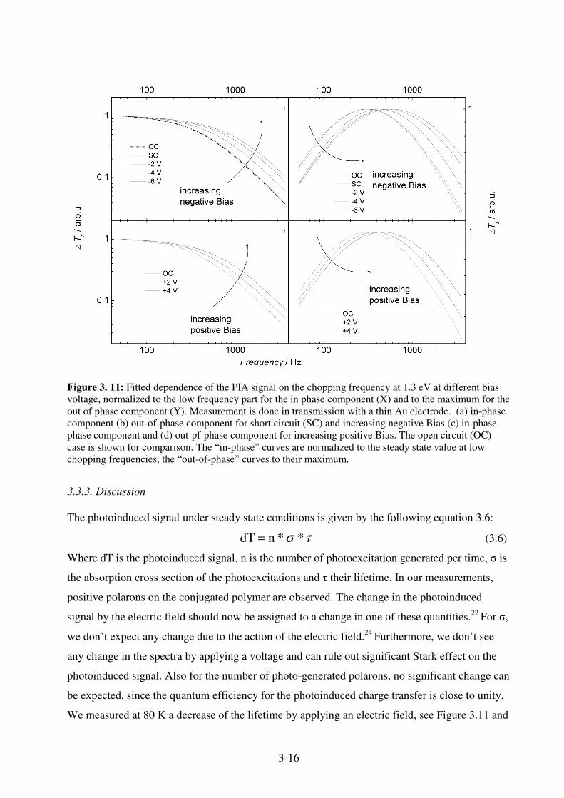
3-16
Figure 3. 11: Fitted dependence of the PIA signal on the chopping frequency at 1.3 eV at different bias voltage, normalized to the low frequency part for the in phase component (X) and to the maximum for the out of phase component (Y). Measurement is done in transmission with a thin Au electrode. (a) in-phase component (b) out-of-phase component for short circuit (SC) and increasing negative Bias (c) in-phase phase component and (d) out-pf-phase component for increasing positive Bias. The open circuit (OC) case is shown for comparison. The “in-phase” curves are normalized to the steady state value at low chopping frequencies, the “out-of-phase” curves to their maximum.
3.3.3. Discussion
The photoinduced signal under steady state conditions is given by the following equation 3.6:
τσ **ndT = (3.6)
Where dT is the photoinduced signal, n is the number of photoexcitation generated per time, � is
the absorption cross section of the photoexcitations and � their lifetime. In our measurements,
positive polarons on the conjugated polymer are observed. The change in the photoinduced
signal by the electric field should now be assigned to a change in one of these quantities.22 For �,
we don’t expect any change due to the action of the electric field.24 Furthermore, we don’t see
any change in the spectra by applying a voltage and can rule out significant Stark effect on the
photoinduced signal. Also for the number of photo-generated polarons, no significant change can
be expected, since the quantum efficiency for the photoinduced charge transfer is close to unity.
We measured at 80 K a decrease of the lifetime by applying an electric field, see Figure 3.11 and

3-17
Table 3.1. This decrease in the lifetime reflects the collection of the charge carriers at the
electrode as additional relaxation pathways for the charge carriers. The maximum lifetime is
observed under open circuit conditions, what is close to flat band conditions. Under these
conditions, we presume that most of the photoinduced charge carriers recombine in the bulk and
a few are reaching the electrodes by simple diffusion processes. Upon applying an external bias
voltage, more charge carriers are drifting to the electrodes under the action of this bias field and
recombine at the electrodes. This decrease of lifetimes seems to be in contrast with the increased
signal for the photoinduced charge carriers under applied bias. This is not so by taking into
account the persistent charge carriers. These charge carriers are not observable in modulation
experiments.
The existence of such persistent charge carriers was observed at low temperature by light
induced electron spin resonance.30 These persistent charge carriers show lifetimes in the range of
seconds and longer at low temperatures and can therefore not be detected by the modulation
techniques we use in our PIA experiments. The origin of these persistent charge carriers is deep
trap states with a low probability of thermally activated recombination. However, these deeply
trapped persistent charge carriers will be influenced by the electric field, escape from the traps
and will drift towards the electrodes. We propose therefore electric field assisted enhanced
recombination of long living charge carriers as a reason for the increase in the photoinduced
signal reported here. The lifetime of these persistent charge carriers is too long to be detected by
the modulation technique, but under the influence of the electric field they can be liberated,
recombine and become detectable for the modulation experiment.
For higher positive voltages, the photoinduced signal is decreasing again. The onset for this
decrease is shifting to smaller voltages at higher temperatures. This point is coinciding with the
onset for current injection into the device. Both effects, the turning point of the PIA vs. voltage
and the current injection show the same temperature behaviour. We assign the decrease of the
photoinduced signal at higher positive bias voltages to recombination of the photoexcitations
with injected charge carriers, resulting lowering the PIA signal.
3.3.4. Conclusion
We studied the electric field effect on the photoinduced charge carrier recombination in
conjugated polymer/ fullerene bulk heterojunction solar cells by means of photoinduced
modulation spectroscopy. The magnitude of the photoinduced spectra is increasing by a factor of
two to three upon applying an electric field on the order of 105 V/cm. We assign this increase to
3-18
the accelerated recombination of persistent charge carriers, which can than be detected by the
modulation spectroscopy, otherwise they are invisible for the modulation spectroscopy. A
decrease of the mean lifetime of the photoexcited charge carrier is observed due to this applied
field.
For higher applied voltages, the photoinduced signal is decreasing due to injected charge
carriers. The onset for this current injection coincides with the turning point for the PIA spectra
vs. voltage and is shifted to higher voltages at lower temperature.
3.4 References 1 B. Kraabel, V. I. Klimov, R. Kohlman, S. Xu, H. L. Wang, D. W. McBranch, Physical Review B 2000, 61, 8501 2 E. Peeters, A. M. Ramos, S. Meskers, R. A. J. Janssen, Journal of Chemical Physics 2000, 112, 9445 3 S. C. J. Meskers, P. A. van Hal, A. J. H. Spiering, J. C. Hummelen, A. F. G. van der Meer, R. A. J. Janssen, Physical Review B 2000, 61, 9917 4 P. B. Miranda, D. Moses, A. J. Heeger, Physical Review B 2001, 64, 081201 5 M. Wohlgennant, W. Graupner, G. Leising, Z. V. Vardeny, Physical Review Letters 1999, 82, 3344 6 M. Wohlgenannt, Z. V. Vardeny, Synthetic Metals 2002, 125, 55 7 X. Wei, Z. V. Vardeny, N. S. Sariciftci, A. J. Heeger, Physical Review B 1996, 53, 2187 8 G. Dellepiane, C.Cuniberti, D. Comoretto, G. F. Musso, G. Figari, A. Piaggi, A. Borghesi, Physical Review B 1993, 48, 7850 9 O. Epsthein, G. Nakhmanovich, Y. Eichen, and E. Ehrenfreund, Physical Review B 2001, 63, 125206 10 O. Epshtein, Y. Eichen , E. Ehrenfreund, M. Wohlgenannt, Z. V. Varedeny, Physical Review Letters 2003, 90, 046804 11 M. Wohlgenannt, W. Graupner, G. Leising, Z. V. Vardeny, Physical Review B 1999, 60, 5321 12 M. Westerling, C. Vijila, R. Österbacka, H. Stubb, Chemical Physics 2003, 286, 315 13 L. Smilowitz, N. S. Sariciftici, R. Wu, C. Gettinger, A. J. Heeger, F. Wudl, Phsical Review B 1993, 47, 13835 14 H. S. Woo, S. C. Graham, D. A. Halliday, D. D. C. Bradley, R. H. Friend, Physical Review B 1992, 46, 7379 15 C. J. Brabec, V. Dyaknov, N. S. Sariciftci, W. Graupner, G. Leising, J. C. Hummelen, Journal of Chemical Physics 1998, 109, 1185 16 N. A. Schultz, M. C. Scharber, C. J. Brabec, N. S. Sariciftci, Physical Review B 2001, 64, 245210 17 D. Beljonne, J. Cornil, H. Sirringhaus, P. J. Brown, M. Shkunov, R. H. Friend and J. L. Bredas, Advanced Functional Materials 2001, 11, 1 18 V. I. Arkhipov, H. Bässler, M. Deussen, E. O. Gobel, R. Kersing, H. Kurz, U. Lemmer, and R. F. Mahrt, Physical Review B 1995, 52, 4932 19 A. Haugeneder, U. Lemmer, and U. Scherf, Chemical Physics Letters 2002, 351, 354 20 M. C. Vissenberg and M. J. M. de Jong, Physical Status Solidi B 1998, 205, 347 21 H. S. Woo, S. C. Graham, D. A. Halliday, D. D. C. Bradley, R. H. Friend, P. L. Burn, and A. B. Holmes, Physical Review B 1992, 46, 7379 22 A. S. Dhoot, D. S. Ginger, D. Beljonne, Z. Shuai, and N. C. Greenham, Chemical Physics Letters 2002, 360, 195 23 C. Zenz, G. Cerullo, G. Lanzani, W. Graupner, F. Meghdadi, G. Leising, and S. De Silvestri, Physical Review B 1999, 59, 14336 24 M. Liess, Z. V. Vardeny, and P. A. Lane, Physical Review B 1999, 59, 11053 25 L. S. Hung, C. W. Tang, and M. G. Manson, Applied Physics Letters 1997 70, 151 26 C. J. Brabec, S. E. Shaheen, C. Winder, N. S. Sariciftci, and P. Denk, Applied Physics Letters 2002, 80, 1288 27 C. J. Brabec, A. Cravino, D. Meissner, N. S. Sariciftci, T. Fromherz, T. Rispen, L. Sanchez, and J. C. Hummelen, Advanced Functional Materials 2001 11, 374 28 V. Dyakonov, Physica E 2002, 14, 53 29 E. A. Katz, D. Faiman. S. M. Tuladhar, J. M. Kroon, M. M. Wienk, T. Fromherz, F. Padinger, C. J. Brabec, and N. S. Sariciftci, Journal of Applied Physics 2001, 90, 5343 30 N. Schultz, M. C. Scharber, C. J. Brabec, and N. S. Sariciftci, Physical Review B 2001, 64, 245210
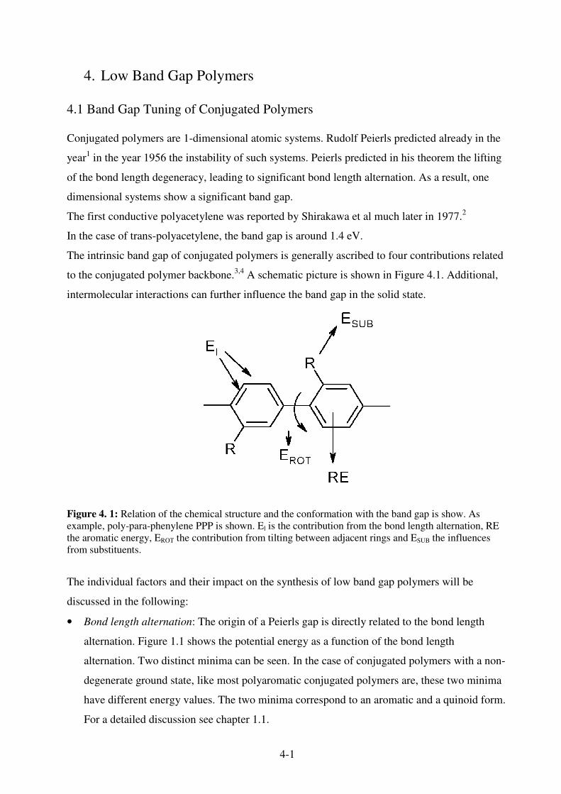
4-1
4. Low Band Gap Polymers
4.1 Band Gap Tuning of Conjugated Polymers
Conjugated polymers are 1-dimensional atomic systems. Rudolf Peierls predicted already in the
year1 in the year 1956 the instability of such systems. Peierls predicted in his theorem the lifting
of the bond length degeneracy, leading to significant bond length alternation. As a result, one
dimensional systems show a significant band gap.
The first conductive polyacetylene was reported by Shirakawa et al much later in 1977.2
In the case of trans-polyacetylene, the band gap is around 1.4 eV.
The intrinsic band gap of conjugated polymers is generally ascribed to four contributions related
to the conjugated polymer backbone.3,4 A schematic picture is shown in Figure 4.1. Additional,
intermolecular interactions can further influence the band gap in the solid state.
Figure 4. 1: Relation of the chemical structure and the conformation with the band gap is show. As example, poly-para-phenylene PPP is shown. El is the contribution from the bond length alternation, RE the aromatic energy, EROT the contribution from tilting between adjacent rings and ESUB the influences from substituents.
The individual factors and their impact on the synthesis of low band gap polymers will be
discussed in the following:
• Bond length alternation: The origin of a Peierls gap is directly related to the bond length
alternation. Figure 1.1 shows the potential energy as a function of the bond length
alternation. Two distinct minima can be seen. In the case of conjugated polymers with a non-
degenerate ground state, like most polyaromatic conjugated polymers are, these two minima
have different energy values. The two minima correspond to an aromatic and a quinoid form.
For a detailed discussion see chapter 1.1.

4-2
S** n
S* *n
S* *n
S* *n
a
b
c
PT aromatic PT quinoid
PITN aromatic PITN quinoid
a
aa
b
bb
c
cc
Figure 4. 2: Band gap as a function of the bond length alternation (�r) (diagram drawn after Lit.5 ). �r is defined as the difference between C-C bonds parallel to the chain axis and C-C bonds inclined with respect to the axis. Lower part shows the aromatic and quinoid form of poly-thiophenes (PT) and poly-isothianaphtene (PITN).

4-3
Manipulating the bond length alternation was shown to be a powerful tool to manipulate the
band gap. Figure 4.2 shows the band gap as a function of the bond length alternation, as
calculated for a poly-thiophene backbone.5 Changes of the bond length alternation are
equivalent to the change from an aromatic character to a quinoid one. The band gap shows a
minimum at �r = 0.06 Å. At this point, the band gap is very small.
This concept could be realized in poly-isothianaphtenes (PITN´s). 6,7,8,9 PITN´s have a band
gap of 1.0 eV. The parent structure poly-thiophene has a band gap of ~ 2.0 eV. The lower
part of Figure 4.2 shows the resonant structures of PT and PITN. In PT, the aromatic
structure is favoured as compared to the quinoid. In PITN, the aromaticity is an interplay
between the thiophene and benzene ring. The thiophene and benzene ring cannot preserve
aromaticity in the same resonant structure. Since the six-ring is aromatic, the [c] bond is
shorter than in the PT case. This stabilizes the quinoid form of the PT part.10,11
• Aromaticity: Most conjugated polymers have aromatic units as monomers; the aromaticity is
preserved in the polymer structure. The aromaticity energy is defined as the energy
difference between the aromatic structure and a hypothetic reference structure, consisting of
isolated double bonds. Aromaticity leads to a confinement of the �-electron on the ring and
competes with the delocalisation. Further, it leads to a stabilisation of the binding orbitals in
the monomer. The inherent HOMO-LUMO gap of the monomer is increased.
• Conjugation length: The longer the conjugation on the backbone, the smaller the band gap.
It was generally found that the band gap is decreasing with increasing conjugation length,
approaching a finite value for infinite conjugation length.12 Torsion between the adjacent
rings partially interrupts the conjugation and leads to an increase of the band gap.
• Substituent effects: Substituents can change the energetic position of the HOMO or LUMO
level, respectively, via mesomeric or inductive effects. Electron donating groups raise the
energetic position of the HOMO. Electron withdrawing groups lower the energetic position
of the LUMO.
Intermolecular interactions: Conjugated polymers show in the solid state generally a red shifted
absorption as compared to the solution phase. This is attributed to an increased interaction
between the chains. Furthermore, mesoscopically ordered phases of conjugated polymers could
occur. Such phases lead to a significant decrease of the band gap as compared to the disordered
phases.
For example, bulky side chains can hinder intermolecular interactions between the backbones.
The regio-stereochemistry has an important influence on the formation of mesoscopic ordered

4-4
phases. As example, regioregular substituted poly-3-alkylthiophenes show in general a lower
band gap compared to their regiorandom counterparts.13,14
N
**
n
N
**n
SS** n
SS** n
n
N
N NS
**
H
n
-
+
(a)
(b)
(c)
Figure 4. 3: (a) shows the resonant stabilization in a push-pull polymer. Only two resonant structures are shown of the example cyano- phenylene vinylene. (b) shows the stabilization of the quinoid form in poly-methine-thiophene. (c) shows the planarization of the conjugated backbone by either a chemical bond (ladder type poly phenylene, to the left) or by a H-bonding linkage between pyrrole N-H and 2,1,3, benzothiadiazole (to the right). Different concepts have been proposed and realized to influence the band gap of conjugated
polymers:15
• Push-pull polymers have altering electron rich (donor) and electron poor units (acceptor).
Interaction between these two units stabilizes the quinoid, low band gap, form.16,17 Also,
electron donating and electron withdrawing substituents are used to form donor and acceptor
units, respectively.18,19 A schematic drawing for such resonant stabilization is shown in
Figure 4.3a.
• Introduction a methine group between the rings can lead to a significant decrease of the band
gap.20,21,22 By this approach, the double bond character of the bridging bond leads to a more
flat structure and hinders angular rotation between the rings. Further, quinoid character is
induced in every second unit. Figure 4.3b shows the resonant structure for poly methine
thiophene.

4-5
• Planarization of the conjugated backbone increases the conjugation length. This can be
achieved by either a bridge via a chemical bond (ladder type polymers)23,24 or by a
zwitterionic structure.25 For examples see Figure 4.3c.
4.2 Low Band Gap Polymers for Bulk Heterojunction Solar Cells
Due to better theoretical understanding, 5,26,27 and much synthetic effort,28,29,30,31, several new
polymers have been proposed as possible low band gap polymers. In the following, CP´s with a
band gap 2 eV (absorption edge > 640 nm) will be considered as low band gap polymer for bulk
heterojunction solar cells.
The most interesting and promising materials are benzodiazathiole32,33,34,35,36,37 push-pull
copolymers, isothianaphtene polymers38 and copolymers39,40 or EDOT-based copolymers41. For
examples see the Figure 4.4 and Table 4.1.
Table 4. 1: material and photovoltaic parameters for several low band gap polymers used in bulk heterojunction devices , chemical structures see Figure 4.4
Materials Voc / V Isc / mA cm-
2
FF Efficiency / % Absorption edge / nm
EDOT-PPV: PCBM 0.28 0.731 0.28 -- 800
PTV: PCBM 0.41 1.4 0.30 0.18b 800
PFD-DBT: PCBM 1.04 4.66 0.46 2.22 650
P3HT: PCBM 0.56 9.3 0.6 3.53 650
PEDOT-EHIITN: PCBM 0.13 1.0 0.34 0.06c 1100
PTPTB: PCBM 0.72 3.1 0.37 1c 750
1 Measured with a halogen lamp 2 AM 1.5 simulated illumination, 100 mW cm-2 3 AM 1.5 simulated illumination, 80 mW cm-2

4-6
S
*
OOOC10H21
H21C10O
*CN
CN
n
S*
*
S S
SS
SHex SHex
n
N NS
NNS
SN
SR
C12H25
R
n
S
O
O
O
** n
SS
*N
NS
*n
TTF-PTV
EDOT-PPV
PTPTB
PEOPT
PFDTBT
Figure 4. 4:Poly-[2,7-(9-(2éthylhexyl)-9hexyl-fluorene)-alt-5,5-(4´,7´,di-2-thienyl-2´,1´,3´-benzothiadiazole] (PFDTBT) EDOT-PPV, (3,4-ethylenedioxythiophene-N-2´ethylhexyl-4,5-dicarboxylic-imide-benzo[c]thiophene (PEDOT-EHI-ITN), poly(3-(4-(1´´,4´´,7´´-trioxaoctyl)phenyl)thiophene (PEOPT), poly N-dodecyl-2,5-bis(2´thienyl)-pyrrole- (2,1,3-benzothiadiazole) (PTPTB), poly- (3´,4´-ethylenedioxy)- thienyl-(2´cyano) vinylene-alt-1,4-(2,5,di-decyloxyl)-phenylene-(1´-cyano)-vinylene EDOT-PPV, TTV-PTV

4-7
4.3 PEOPT-a Polythiophene with a Tuneable Band Gap
Polythiophenes are a versatile class of conjugated polymers and have been investigated for a
wide range of applications.42 For some 3-alkyl-substituted thiophenes, a thermally activated
absorption shift was observed.43 This shift was attributed to a conformational change of the
polymer backbone, induced by a side chain ordering. Longer effective conjugation length by
decreased steric hindrance and increased interchain interactions leads to a reduction of the
HOMO-LUMO gap. X-ray diffraction studies on a wide range of phenyl-substituted thiophenes
proved the occurrence of ordered crystalline phases in this class of polymers.44,45
In the absorption, a significant redshift is observed, which is attributed to the occurrence of
crystalline phases.
The recently discovered postproduction treatment in bulk heterojunction photovoltaic devices
using poly-3-hexylthiophene is partially explained by such effects .42
4.3.1. Optical Properties
The regioregular poly-3-(4´-(1´´,4´´,7´´-trioxaoctyl)phenyl)thiophene PEOPT46,47 (Figure 4.2)
shows the specific case that both, the non-crystalline and partially crystalline phases, are
metastable and the non-crystalline phase can be transferred into the partially crystalline one
easily. This transformation can be seen by eye due to the colour change from orange to blue,
going from the non-ordered to the ordered phase. The band gap is changing from the non-
ordered to the ordered phase from 2.1 to 1.75 eV, see for the absorption and emission spectrum
Figure 4.5.
The non-ordered form shows a single absorption peak, whereas the ordered form shows several
shoulders at the low energy side end, which are typical vibronic satellites for crystalline phases
in conjugated polymers.66 The photoluminescence is shifted for the different phases coincidently
with the absorption. Interestingly, a strong solvatochromism can be observed. The absorption
spectra in good solvents like chloroform resemble the orange phase, whereas the absorption
spectra in benzene, a relative poor solvent for PEOPT, shows shoulders to the low energy end,
typically for the ordered phase.

4-8
Figure 4. 5: Optical absorption and photoluminescence of PEOPT films in the non-ordered and ordered form. The photoluminescence is measured at 100 K and excitation at 488 nm.
The two phases of PEOPT are observed also in blends with PCBM.
The orange phase is got by spin casting from chloroform. This can be transferred to blue phase
by heat treatment at 100 ° C for ten minutes or by treatment with chloroform vapour.
Furthermore, the blue phase is got by spin casting from solvents like chlorobenzene or toluene.
Drop casting lead generally to the blue phase.48
4.3.2 Photophysical Properties
The change in the nanoscopic order of the polymer shows corresponding changes in the
photophysics and the interaction of the excited state with fullerene. Figure 4.6 shows the
photoinduced absorption spectra of the pristine material in the ordered and non-ordered phase,
and the corresponding spectra in the blends with the PCBM.
The non-ordered material shows spectra as observed for many conjugated polymers.
In the pristine material, a single excited state absorption peak is observed below the band gap,
which is generally assigned to a T1�Tn transition.49 This peak is quenched in the mixture with

4-9
fullerene and two new absorption transitions are observed, which are assigned to the polaronic
state absorptions of the polymer cation.
Figure 4. 6: Photoinduced Absorption spectra of PEOPT in the non-ordered and ordered phase (upper graph); Photoinduced Absorption Spectra of PEOPT: PCBM 1:1 blends with the polymer in the ordered and non-ordered phase (lower graph); spectra were recorded at 100 K and excitation at 488 nm.

4-10
The photoinduced absorption spectra of the ordered from is much more complicated. In the
pristine material, see Figure 4.6, a complicated pattern with peaks at 1.5, 1.2 and 0.9 eV is
observed. By addition of fullerene acceptor, for the PIA spectra see Figure 4.6, the low energy
peak at 0.9 eV is quenched, and a new peak is arising below 0.6 eV. In the blend with PCBM, all
transitions are assigned to polaronic absorption. The splitting of the high energy polaron peak
was attributed to the existence of two-dimensional delocalised50 charged photoexcitations.
Recent calculations by Beljonne et al.51 showed interacting chains may give rise to splitting of
the polaronic levels. Figure 3.6 shows a schematic Figure for the one-excitation levels for a
polaron on a single chain and for a polaron with co-facial interaction with an adjacent chain.
This splitting, which will be heavily dependent on the interchain coupling of the polarons, is
presumably much stronger in the ordered phase of the PEOPT and thus can explain this observed
splitting in the high energy photoinduced absorption band. We specifically compare our
experimental Figure 4.6 with the theory of Beljonne et al., calculated for charged polarons, since
the efficient photoinduced electron transfer results in charged polarons on the polymer backbone
in the blends with fullerenes.
4.3.3 Photovoltaic Devices
Figure 4.7 shows the photocurrent action spectra of photovoltaic devices of PEOPT in its two
forms. The spectra of the ordered form are extended to the red as compared to the disordered
form, confirming the lower band gap of the ordered form.
As shown by the photoinduced absorption experiments, interaction of the photoexcited PEOPT
with PCBM leads to efficient charge creation. Photovoltaic devices of PEOPT with fullerene
acceptor have been demonstrated in bilayer with C60 as evaporated acceptor layer well as for
bulk heterojunction blends with PCBM. The photocurrent of both forms can be significantly
enhanced forming bilayer devices with C60.52 Blending of the two distinct forms of PEOPT with
PCBM fullerene acceptor in bulk heterojunction type photovoltaic devices resulted in solar cells
with short circuit responses up to 0.5 mA/cm2 (see Figure 4.8). In the ordered phase of PEOPT,
however, the quality of the films were poor and the devices lost both in short circuit current and
open circuit voltage as compared to the non-ordered phase.

4-11
Figure 4. 7: Photocurrent spectra of a photovoltaic cell of pristine PEOPT in the orange (not-ordered) and blue (ordered form). Inset show the I-V curve, following values were measured: ordered phase Voc = 0.91 V, Isc = 1.9 µA cm-2, FF = 0.30; not-ordered phase Voc = 1.06 V, Isc = 2.2 µA cm-2 and FF = 0.24.
Figure 4. 8: Current- Voltage curve of PEOPT: PCBM 1:1 diodes with the polymer in the ordered and non-ordered form, under illumination from a solar simulator; for the non-ordered polymer, Voc = 0.62 V, Isc = 0.480 µA cm-2 and FF = 0.28; for the ordered form polymer Voc = 0.38 V, Isc = 125 µA cm-2 and FF = 0.49; films were spin cast from chloroform, top contact Al without LiF.

4-12
4.4 PTPTB- a Novel Low Band Gap Polymer53
PTPTB, consisting of alternating electron-rich N-dodecyl-2,5-bis (2´-thienyl)pyrrole (TPT) and
electron-deficient 2,1,3-benzothiadiazole (B) units, for the chemical structure see Figure 4.4, was
synthesized for the application as electron donor polymer in bulk heterojunction solar cells. The
material shows an optical band gap of 1.7 eV, which is in good agreement with the value
determined by electrochemical voltage spectroscopy of 1.8 eV.54 A reversible oxidation is found
with an onset at +0.54 V vs. Ag/Ag+. No reversible reduction is found. Spectroscopic
investigation of blends of PTPTB with fullerene acceptor PCBM demonstrates photoinduced
charge transfer. The polymer photoluminescence is quenched and polaronic transitions occur in
the blend due to photoexcited charges on the polymer backbone.91,55
Figure 4.9 shows the I-V curves and the photocurrent spectra, in comparison with the optical
absorption, of a bulk heterojunction device from PTPTB / PCBM (1:3 wt ratio). In the dark the
current-voltage curve shows a rectification ratio of about 102 at +/- 2V. Under simulated AM 1.5
illumination, a strong photoeffect is observed.
The spectral photocurrent peaks at 600 nm,56 coinciding with the absorption maximum. The
onset of the photocurrent is around 750 nm, demonstrating the low band gap nature of PTPTB
and the efficient photon harvesting.
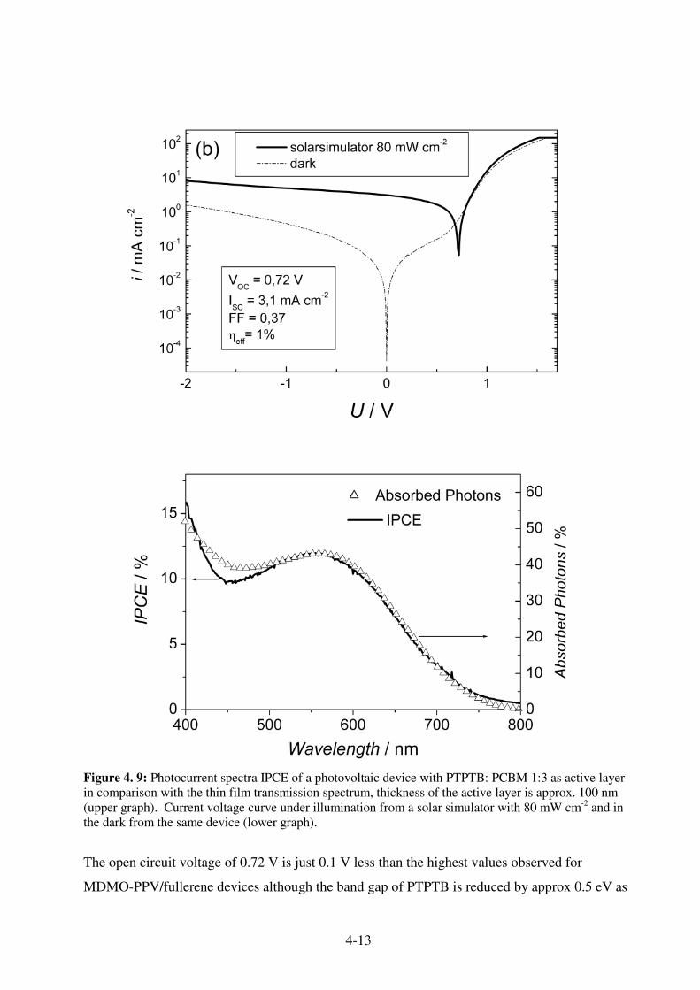
4-13
Figure 4. 9: Photocurrent spectra IPCE of a photovoltaic device with PTPTB: PCBM 1:3 as active layer in comparison with the thin film transmission spectrum, thickness of the active layer is approx. 100 nm (upper graph). Current voltage curve under illumination from a solar simulator with 80 mW cm-2 and in the dark from the same device (lower graph).
The open circuit voltage of 0.72 V is just 0.1 V less than the highest values observed for
MDMO-PPV/fullerene devices although the band gap of PTPTB is reduced by approx 0.5 eV as
4-14
compared to MDMO-PPV. The position of the HOMO level of PTPTB is close to that reported
.for HOMO of MDMO-PPV. Since the energetic position for the positive charge is mainly
determined by the HOMO of the donor and the energetic position for the negative charge by the
LUMO of the fullerene, this explains the similar values for the open circuit voltage between
MDMO and PTPTB based solar cells. The energetic splitting between the donor HOMO and the
acceptor LUMO is the thermodynamic maximum, which can be got from this photovoltaic
device and can be lowered by several reasons, for example low parallel resistance of the device.
Instead, the offset between the LUMO levels of the donor and acceptor is lower in the case of
PTPTB and PCBM with approx. 0.4 eV instead of MDMO-PPV/PCBM with approx. 1 V. This
offset is required for the charge separation, but is on the other hand also an energetic loss. The
short circuit current ISC is measured with 3 mA cm-2 and the fill factor FF is calculated to be
0.37. From these values, the power conversion efficiency �AM1.5 is calculated with ~ 1 %.
While the short circuit current of the device is already high, the overall efficiency of the device is
limited by the low fill factor. Generally, low FF can be induced by high series resistances or by
small shunt resistances. For PTPTB/PCBM devices we find serial resistances below 10 Ohm
cm-2, which cannot explain the low FF. Therefore, the low FF is expected to originate from a
small parallel shunt resistance in the device. Most likely, the low molecular weight of the
polymer, determined with 5-16 aromatic units by size exclusion chromatography, causes the low
film forming quality and the many pinholes that lead to nanoshorts.57
4.5 Thienylene Vinylene based polymer TTV-PTV
Thienylene vinylene based oligomers58,59,60,61 and polymers62,63 have been studied in the last
years as promising candidate for low band gap materials. Optical absorption onsets < 1.5 eV
have been reported for such material systems.64
Here, a novel thienylene vinylene (PTV-TTF) polymer with a tetrathiafulvalene condensed to the
thiophene ring is presented. For the structure, see Figure 4.4. Its electrochemical and
photophysical properties are investigated and, in combination with device results, are discussed
for its suitability for solar cells.
4.5.1 Optical and Electrochemical Properties
The optical absorption of PTV-TTF, see Figure 4.10, shows a maximum around 630 nm and an
onset around 850 nm (EG = 1.5 eV). The photoluminescence is weak and shows a broad
maximum at 800 nm and a relatively sharp peak at 670 nm, for the spectra see Figure 4.10 as
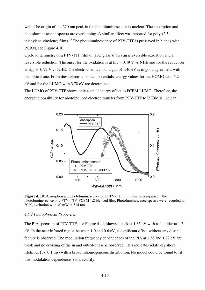
4-15
well. The origin of the 670 nm peak in the photoluminescence is unclear. The absorption and
photoluminescence spectra are overlapping. A similar effect was reported for poly-(2,5-
thienylene vinylene) films.65 The photoluminescence of PTV-TTF is preserved in blends with
PCBM, see Figure 4.10.
Cyclovoltammetry of a PTV-TTF film on ITO glass shows an irreversible oxidation and a
reversible reduction. The onset for the oxidation is at Eox = 0.49 V vs NHE and for the reduction
at Ered = -0.97 V vs NHE. The electrochemical band gap of 1.46 eV is in good agreement with
the optical one. From these electrochemical potentials, energy values for the HOMO with 5.24
eV and for the LUMO with 3.78 eV are determined.
The LUMO of PTV-TTF shows only a small energy offset to PCBM LUMO. Therefore, the
energetic possibility for photoinduced electron transfer from PTV-TTF to PCBM is unclear.
400 600 800 10000.00
0.05
0.10
0.15
0.20
0.0
0.1
0.2
Absorption PTV-TTF
OD
/ ar
b.u.
Wavelength / nm
Pho
tolu
min
esce
ne /
arb.
u.Photoluminescence
PTV-TTF PTV-TTF: PCBM 1:2
Figure 4. 10: Absorption and photoluminescence of a PTV-TTF thin film. In comparison, the photoluminescence of a PTV-TTF: PCBM 1:2 blended film. Photoluminescence spectra were recorded at 80 K, excitation with 40 mW at 514 nm. 4.5.2 Photophysical Properties
The PIA spectrum of PTV-TTF, see Figure 4.11, shows a peak at 1.35 eV with a shoulder at 1.2
eV. In the near infrared region between 1.0 and 0.6 eV, a significant offset without any distinct
feature is observed. The modulation frequency dependences of the PIA at 1.38 and 1.22 eV are
weak and no crossing of the in and out-of-phase is observed. This indicates relatively short
lifetimes (� < 0.1 ms) with a broad inhomogeneous distribution. No model could be found to fit
this modulation dependence satisfactorily.
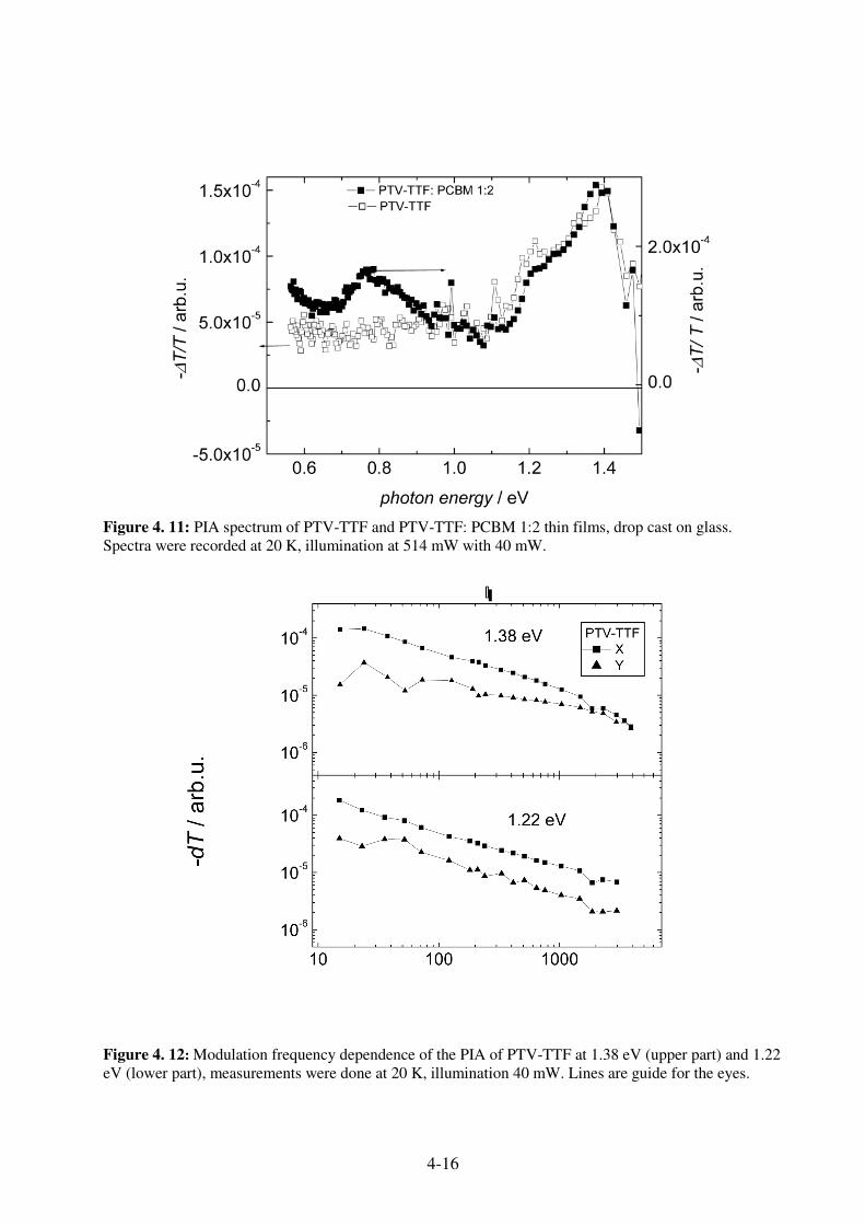
4-16
Figure 4. 11: PIA spectrum of PTV-TTF and PTV-TTF: PCBM 1:2 thin films, drop cast on glass. Spectra were recorded at 20 K, illumination at 514 mW with 40 mW.
Figure 4. 12: Modulation frequency dependence of the PIA of PTV-TTF at 1.38 eV (upper part) and 1.22 eV (lower part), measurements were done at 20 K, illumination 40 mW. Lines are guide for the eyes.

4-17
PIA spectrum of a PTV-TTF: PCBM blend film is shown in Figure 4.11. The 1.4 eV PIA of the
pristine polymer is preserved in the blend, but additionally, two new absorption peaks at 0.8 and
<0.55 eV are observed.
The modulation frequency dependences, see Figure 4.13, show differences for the 1.4 eV and the
new absorption at 0.8 and <0.55 eV. The peak at 1.46 eV could be fitted by the dispersive
recombination model with a mean lifetime of � = 0.7 ms. The lifetime shows a broad
distribution (� = 0.64). The two low energy peaks show a weaker dependence on the modulation
frequency, what indicates shorter lifetimes. Their dependence could not be fitted satisfactorily,
the lines in the graph are guide for the eye. Interestingly, also the shoulder at 1.24 eV shows a
distinct modulation frequency dependence as the 1.46 eV peak.
Figure 4. 13: Modulation frequency dependence of the PIA of PTV-TTF: PCBM 1:2 at 1.46 eV, 1.24 eV, 0.83 eV and 0.59 eV measurements were done at 20 K, illumination 40 mW. For 1.46 eV, an excited state lifetime of 0.7 ms and a dispersion factor of � = 0.64 is calculated. For the other measurements, the fitting procedure does not lead to a satisfying result. Lines are guide for the eyes.
Excited state interactions between oligo- thienylene vinylenes and fulleropyrrolidines MP-C60 in
solution were investigated by Apperloo et al.66 The PIA spectra for PTV-TTF and blend with
PCBM will be compared with spectra for hexyl-substituted dodeca thienylene vinylene (12TV):
MP-C60 mixed solution. The optical absorption of 12TV in CH2Cl2 shows a maximum at 2.11

4-18
eV, as compared for PTV-TTF in chlorobenzene solution 2.06 eV. In solid state, the absorption
maximum is shifted to 1.96 eV.
PIA of 12 TV and MP-C60 in the non-polar solvent toluene shows a peak at 1.42 eV. This peak
is assigned to a T1�Tn absorption of triplet excited 12TV. In the more polar solvent o-
dichlorobenzene, two additional peaks at 0.46 and 1.00 eV are observed besides the 1.42 eV
peak. These two new absorptions are assigned to the 12TV radical cation. This assignment is
confirmed by in-situ electrochemical absorption measurements.67 Further, for poly-thienylene
vinylene polaron absorptions were determined by Lane et al by Photoinduced Absorption
Detected Magnetic Resonance with 1.1 eV and 0.4 eV.68
Apperloo et al determined that the triplet and the charge separated state of 12TV possess
comparable energies. It is therefore assumed that the triplet state of 12TV and charge separated
state can be formed and observed simultaneously.67
In the PIA, for both materials a peak at 1.4 eV is observed. This peak was assigned to a T1�Tn
absorption. Further, the 0.8 eV and <0.55 eV peaks are comparable with the cation absorption of
12TV at 1 eV and 0.46 eV and therefore assigned to the polaron absorption of PTV-TTF. Similar
to the optical absorption, a redshift is observed for the positive polaron.
In blends of PTV-TTF and PCBM, the coexistence of triplets and charge separated state is
concluded. The quantum efficiency for the charge separation is unclear.
4.5.3 Photovoltaic Devices from PTV-TTF
Pristine PTV-TTF shows non-favourable film forming properties, no electro-optical
characterization could be obtained.
In combination with PCBM, thin films of sufficient quality can be spin cast from chlorobenzene
solution. The I-V characteristics shows good diode behaviour with a rectification factor R(+/-
2V) = 250, see for the I-V characteristics Figure 4.14. Under illumination, a photovoltaic effect
is observed with a power conversion efficiency of 0.13 % under solar simulated light. This is
comparable with literature values reported poly-(thienylene vinylene) based bulk heterojunction
devices. 69
The photocurrent spectrum, see Figure 4.15, shows peaks at 350 and 650 nm, corresponding to
PCBM and PTV-TTF absorption, respectively. The onset for the photocurrent is around 850 nm,
corresponding to the absorption onset of PTV-TTF.

4-19
Figure 4. 14: Current –Voltage characteristics for a PTV-TTF: PCBM 1:2 device, spin coat from chlorobenzene, in the dark (dotted line) and under illumination from a solar simulator with 80 mW cm-2. Active area thickness is approx. 50 nm.
Figure 4. 15: Photocurrent spectrum of a PTV-TTF: PCBM 1:2 device, in comparison the optical absorption spectrum of a film, prepared under same conditions, on glass.

4-20
4.6 References 1 R. E. Peierls, Quantum Theory of Solids, Oxford University Press, London 1955 2 H. Shirakawa, E. J. Louis, A. G. MacDiarmid, C. K. Chiang, A. J. Heeger, Journal of The Chemical Society, Chemical Communication 1977, 578 3 J. Roncali, Chemical Review.1997, 97, 173 4 R. Kiesboms et.al, “Synthesis of Electric and Optical Properties of Conjugated Polymer in Handbook of Advanced Electronic and Photonic Material and Devices 8, p 38-47 edited by Hari Singh Nalwa, (2000) 5 J. L. Bredas, A. J. Heeger, F. Wudl, Journal of Chemical Physics 1986, 85, 4673 6 F. Wudl, M. Kobayashi, A. J. Heeger, Journal of Organic Chemistry 1984, 49, 3382 7 M. Kobayashi, N. Colaneri, M. Boysel, F. Wudl, A. J. Heeger, Journal of Chemical Physics 1985, 82, 5717 8 H. Meng, Y. Cheng, F. Wudl, Macromolecules 2001, 34, 1810 9 I. Polec, A. Henckens. L. Goris, M. Nicolas, M. A. Loi, P. J. Adriaensens, L. Lutsen, J. V. Manca, D. Vanderzande, N. S. Sariciftci, Journal of Polymer Science A 2003, 41, 1034 10 G. Zerbi, M. C. Magnoli, I. Hoogmartens, R. Kiebooms, R. Carleer, D. Vanderzande, J. Gelan, Advanced Materials 1995, 7, 1027 11 C. Quattrocchi, R. Lazzaroni, J. L. Brédas, R. Kieboom D. Vanderzande, J. Gelan, Journal fo Physical Chemistry 1995, 99, 3932 12 H. Meier, U. Stalmach, H. Kolshorn, Acta Polymerica 1997, 48, 379 13 R. D. McCullough, R. D. Lowe, M. Jayaraman, D. L. Anderson, Journal of Organic Chemistry 1993, 85, 904 14 T. D. Chen, R. D. Rieke, Journal of The American Chemical Society 1998, 8, 25 15 M. Pomerantz, in Handbook of Conducting Polymers, edited by T. A. Skotheim, R. L. Elsenbaumer, J. R. Reynolds, Marcel Dekker, Inc. New York, Basel, Hong Kong, 1998, 277 16 A. Ajayaghosh, Chemical Society Review 2003, 32, 181 17 G. Brocks, A. Tol, Journal of Physical Chemistry 1996, 100, 1838 18 M. Dietrich, J. Heinze, G. Heywang, F. Jonas, Journal of Electranalytic Chemistry 1994, 369, 87 19 Q. Pei, G. Zuccarello, M. Ahlskog, O. Inganäs, Polymer 1994, 35, 1347 20 S. A. Jenekhe, Nature 1986, 322, 345 21 H. Aota, T. Reikan, A. Matsumoto, M. Kamachi, Chemical Physics Letters 1998, 335 22 M. Hanack, S. Döttinger, Synthetic Metals 1996, 79, 43 23 U. Scherf, K. Müllen, Synthesis 1992, 23 24 Y. Yao, J.J.S. Lamba, H. M. Tour, Journal of The American Chemical Society 1998, 120, 2805 25 T. W. Brockman, J. M. Tour, Journal of The American Chemical Society 1995, 117, 4437 26 J. L. Bredas, Advanced Materials 1995, 7, 263 27 A. Dkhissi, F. Louwet, L. Groenendaal, B. Beljonne, R. Lazzaroni, J. L. Bredas, Chemical Physics Letters 2002, 359, 466 28 L. B. Groenendaal, F. Jonas, D. Freitag, H. Pielartzik, J. R. Reynolds, Advanced Materials 2000, 12, 481 29 C. Aribizzani, M. Castellani, C. G. Cerrroni, M. Mastagostino, Journal of Electroanalytic Chemistry 1997, 423, 23 30 M. Castellani, R. Lazzaroni. J. L. Bredas, S. Luzzati, Synthetic Metals 1999, 101, 175 31 A. Cravino, H. Neugebauer, S. Luzzati, M. Castellani, A. Petr, L. Dunsch, N. S. Sariciftci, Journal of Physical Chemistry B 2002, 106, 3583 32 A. Dhanabalan, P.A. van Hal, J.K.J. van Duren, R. A. J. Janssen, Synthetic Metals 2001 121, 2175 33 A. Dhanabalan, J.K.J. van Duren, P.A. Van Hal, J.L.J. van Dongen, R.A.J. Janssen, Advanced Functional Materials 2001, 11, 255 34 M. Svensson, F. Zhang, S. C. Veenstra,W. J. H. Verhees, J. C. Hummelen, J. M. Kroon, O. Inganäs, M. R. Andersson, Advanced Materials 2003, 15, 988 35 Y. Teketel, F. Zhang, M. Svensson, J. C. Hummelen, M. R. Andersson, O. Inganäs. Thin Solid Films 2004, 449, 152 36 Q. Hou, Y. Xu, W. Yang, M. Yuan, J. Peng, Y. Cao, Journal of Materials Chemistry 2002, 12, 2887 37 Q. Zhou, Q. Hou, L. Zheng, X. Deng, G. Yu, Y. Cao, Applied Physics Letter, 2004, 84, 1653 38 L. Goris, M. A. Loi, A. Cravino, H. Neugebauer, N. S. Sariciftci, I. Polec, L. Lutsen, E. Andries, J. Manca, L. De Schepper, D. Vanderzande, Synthetic Metals 2003, 138, 249 39 A. Cravino, M. A. Loi, M. C. Scharber, C. Winder, H. Neugebauer, P. Denk, H. Meng, Y. Chen, F. Wudl, N. S. Sariciftci, Synthetic Metals 2003, 137, 1435 40 S. E. Shaheen, D. Vangeneugden, R. Kiebooms, D. Vanderzande, T. Fromherz, F. Padinger, C. J. Brabec N. S. Sariciftci, Synthetic Metals 2001, 121, 1583 41 K. Colladet, M. Nicolas, L. Goris, L. Lutsen, D. Vanderzande, Thin Solid Films 2004, 451-452, 7 42 H. Sirringhaus, N. Tessler, R. H. Friend, Science 1998, 280, 1741 43 K. Yoshino, S. Nakajima, Dae-Hee-Park. R. Sugimoto, Japanese Journal of Applied Physics Part 2 1988, 27, 715

4-21
44 H. J. Fell, E. J. Samuelson, M. R. Andersson, J. Als-Nielsen, G. Grübel, J. Mardalen, Synthetic Metals 1995, 73, 279 45 K. E. Aasmundtvei, E. J. Samuelsen, W. Mammo, M . Svensson, M. R. Andersson, L. A. A. Pettersson, O. Inganäs, Macromolecules 2000, 33, 5481 46 M. R. Andersson, O. Thomas, W. Manno, M. Svensson, M. Theander, O. Inganäs, Journal of Materials Chemistry 1999, 9, 1933 47 C. J. Brabec, C. Winder, M. C. Scharber, N. S. Sariciftci, J. C. Hummelen, M. Svensson, M. R. Andersson, Journal of Chemical Physics 2001, 15, 7235 48 C.J. Brabec, C.Winder, M.Scharber, N.S. Sariciftci, M.R.Andersson, O.Inganäs, J.C.Hummelen Material Research Symposium Proceedings 2000, 598, B 3.24.1-6 49 X. Wei, Z. V. Vardeny, N. S. Sariciftci, A. J. Heeger, Physical Review B 1996, 53, 2187 50 R. Österbacka. C. P. An, X. M. Jiang, Z. V. Vardeny, Science 2000, 287, 839 51 D. Beljonne, J. Cornil, H. Sirringhaus, P. J. Brown, M. Shkunov, R. H. Friend, J. L. Bredas, Advanced Functional Materials. 2001, 11, 229 52 L. S. Roman, W. Manno, L. A. A. Pettersson, M. R. Andersson, O. Inganäs, Advanced Materials 1998, 10 , 774 53 part of this work was already presented in: C. Winder, Diplomarbeit, Universität Linz, 2001 54 D. Muehlbacher, H. Neugebauer, A. Cravino, N. S. Sariciftci, J.K.J. van Duren, A. Dhanabalan, P. van Hal, R. A.J. Janssen, J.K. Hummelen, Molecular Crystals and Liquid Crystals. 2002, 385, 85 55 J.K.J. van Duren, A. Dhanabalan, P.A. van Hal, R. A. J. Janssen, Synthetic Metals. 2001121, 1587 56 C. J. Brabec, C. Winder, N. S. Sariciftci, H. C. Hummelen, A. Dhanabalan, P. A. van Hal, R. A. J. Janssen, Advanced Functional. Materials 2002, 12, 709 57 C. Winder, G. Matt, J. C. Hummelen, R. A. J. Janssen, N. S. Sariciftci, C.J. Brabec, Thin Solid Films 2002, 403-404, 373 58 N. Ono, H. Okumura, T. Murashima, Heteroatom Chemistry 2001, 12, 414 59 J. Roncali, I. Jestin, P. Frère, E. Levillain, D. Stievenard, Synthetic Metals 1999, 101, 667 60 C. Martineau, P. Blanchard, D. Rondeau, J. Delaunay, J. Roncali, Advanced Materials 2002, 14, 283 61 D. Rondeau, C. Matrineau, P. Blanchard, J. Roncali, Journal of Mass Spectrometry 2002, 37, 1081 62 H-Q. Xie, C. M. Liu, J. S. Guo, European Polymer Journal 1996, 32, 1131 63 Z. Guijiang, L. Junchao, Y. Cheng, Synthetic Metals 2003, 485, 135 64 I. Jestin, P. Frère, E. Levillain, J. Roncali, Advanced Materials 1999, 11, 134 65 A. J. Brassett, N. F. Colaneri, D. D. C. Bradley, R. A. Lawrence, R. H. Friend, H. Murata, S. Tokito, T. Tsutsui, S. Saito, Physical Reviev B 1990, 41, 10586 66 J. J. Apperloo, C. Matrineau, P. A. van Hal, J. Roncali, R. A. J. Janssen, Journal of Physical Chemistry B 2002, 106, 21 67 J. J. Apperloo, J. M. Raimundo, P. Frère, J. Roncali, R. A. J. Janssen, Chemistry, A European Journal 2000, 6, 1698 68 P.A. Lane, X. Wei, Z. V. Vardeny, Physical Review Letters 1996, 77, 1544 69 A. Henckens, M. Knipper, I. Polec, J. Manca, L. Lutsen, D. Vanderzande, Thin Solid Films 2004, 451, 572

5-1
5. Electron Acceptor Polymer In this chapter, conjugated polymers are presented which have electron accepting properties.
Such materials are cheap alternatives for C60 based acceptors. Further, absorption range, electron
affinity and solubility are important parameter, which can be tuned much easier and over a larger
range as compared to C60. Ellen Moons recently reviewed properties and device applications of
conjugated polymer blends.1
A wide range of electron acceptor polymers has been presented in the literature. Most of them
contain electron-withdrawing groups like cyano, nitro or halogen substitutions. These
substitutions lower the electron density in the polymer backbone and stabilize therefore the
negative charge. Most prominent materials, which were presented for photovoltaic applications,
are MEH-cyano-PPV,2,3 showing in combination with polythiophenes 1.8 % conversion
efficiency, polyfluorene-2,1,3-benzoethiadazole copolymers4,5,6 and poly-(benzamidazobenzo
phenanthroline) BBL.7,8,9
5.1 Poly(p-Phenylene vinylene) Fluorinated Copolymer
The polymer copoly- 2,3,5,6-tetrafluoro-1,4-phenylene vinylene-2,5-dioctyloxy-1,4-phenylene
vinylene, TFPV-DOPV, was synthesized at the university of Bari, group of Prof. Gianluca
Farinola, and provided to the University of Linz. The ratio of the tetrafluoro substituted and
dialkoxy substituted monomers is TFPV: DOPV 60:40. The monomers are randomly distributed
in the chain. The synthesis is performed via the Stille cross-coupling reactions, as described in
the literature.10,11,12
5.1.1 Photophysical and Electrochemical Properties
The polymer is tested as possible donor as well as acceptor material. The chemical structure and
the absorption-emission of a thin solid film are shown in Figure 5.1. The absorption coefficient
at the maximum �max = 450 nm is 1.3* 105 cm –1, see Figure 5.1. The absorption is slightly blue-
shifted compared to parent homopolymer dialkoxy-substituted para-phenylene vinylene PDOPV
(�max = 460 nm), but red-shifted in comparison with the poly-tetrafluoro-phenylene vinylene
PTFPV(�max = 335 nm). Interestingly, the photoluminescence maximum (�max = 660 nm) is red-
shifted in comparison to PDOPV (�max = 580 nm) and PTFPV (�max = 530 nm). This large
Stoke shift in solid state is assigned to an increased interchain interaction in the copolymer.11

5-2
This is further confirmed by the large redshift of the photoluminescence from CHCl3 solution
(�max = 530 nm) to solid state (�max = 660 nm).11
*
n
F F
FF *
OC8H17
OC8H17
m
n = 0.6m= 0.4
Figure 5. 1: Chemical structure of copoly- 2,3,5,6-tetrafluoro-1,4-phenylene vinylene-2,5-dioctyloxy-1,4-phenylene vinylene, TFPV-DOPV (upper part); optical absorption and photoluminescence of TFPV-DOPV thin film. Photoluminescence is measured at 80 K, excitation with 476 nm and 40 mW (lower part).
Cyclic voltammetric experiments were carried out with a platinum foil working electrode (WE)
with a dip-coated film from chloroform solutions (5mg/ml). As a counter electrode (CE) a
platinum foil and as a quasi-reference electrode (RE) a silver wire coated with AgCl were used.
The electrolyte solution, a 0.1 M Bu4NPF6-acetonitril solution, was kept under argon flow to
exclude moisture and oxygen during the electrochemical processes. It can be seen that the
material is both oxidized and reduced with p-doping/dedoping onset potential at about 0.9 V
(HOMO 5.8 eV) and n-doping/dedoping onset potential at about -1.0 V (LUMO 3.9 eV) versus
the quasi Ag/AgCl reference electrode.
Infrared spectroelectrochemical studies show the optical signature of positive and negative
charges. Both charge carriers show different IRAV bands. Photoinduced infrared active vibration
spectroscopy shows predominantly absorption of negative charge carriers.13

5-3
Figure 5. 2: PIA (circles) of TFPV-DOPV drop cast film on glass at 80 K, excitation with 40 mW at 476 nm. Photoluminescence response is shown for comparison (dashed line).
PIA of TFPV-DOPV shows a broad single peak at 1.55 eV, see Figure 5.2. The small dip around
1.75 eV might origin from overcompensated photoluminescence. The photoluminescence
response of the film is shown for comparison. In the spectral range between 1.7 and 2.0 eV, it is
stronger than the PIA signal.
The modulation frequency dependence, see Figure 5.3, is measured at 1.38 eV. At this energy,
the contribution from the photoluminescence is negligible. A well defined (� = 0.90) exited state
lifetime of � = 0.13 ms is calculated. The PIA might be attributed to a T1�Tn transition.

5-4
Figure 5. 3: Modulation frequency dependence of the PIA of TFPV-DOPV at 1.38 eV, at 80 K and 40 mW excitation. Fit (thin line) is done by a dispersive recombination model.
5.1.2 Devices
Figure 5. 4: I-V characteristics of a TFPV-DOPV single layer device, spin cast from chlorobenzene, under solar simulated illumination and in the dark. The active layer thickness is approx. 35 nm. Figure 5.4 shows the I-V characteristics of a TFPV-DOPV single layer device. No photovoltaic
effect is observed, but photoconductivity. Interestingly, the device shows inverse rectification
under illumination.

5-5
5.1.3 TFPV-DOPV: MDMO-PPV blends
The possibility of reversible reduction and the formation of negative charges under illumination
show the electron accepting properties of TFPV-DOPV. Therefore, the material is tested as
possible electron acceptor towards MDMO-PPV. A schematic energy diagram is shown in
Figure 5.5. It shows a large offset between the MDMO-PPV and TFPV-DOPV levels. This is
required for photoinduced charge separation.
Figure 5. 5: Energy levels of HOMO and LUMO of MDMO-PPV, TFPV-DOPV and PCBM, derived from electrochemical measurements in solution. The LUMO level of MDMO-PPV and the HOMO of PCBM are estimated by the optical band gap, since this processes are not observed.
Figure 5.6 shows the photoluminescence for different blends of MDMO-PPV and TFPV-DOPV
and the pristine materials. Small additions of TFPV-DOPV quench the MDMO-PPV
photoluminescence. The second vibronic peak of MDMO-PPV seems to gain intensity with
increasing of TFPV-DOPV concentration, which might be photoluminescence contribution from
the latter one. At higher concentration of TFPV-DOPV, only the TFPV-DOPV
photoluminescence is observed. Interestingly, the photoluminescence of the 1:1 blend is slightly
red shifted compared to pristine TFPV-DOPV. This might be originating from the different
environment in the blends as compared to the pristine material. The strong quenching of the
MDMO-PPV luminescence shows interaction of the photoexcited state with TFPV-DOPV.
Further, the photoluminescence of TFPV-DOPV is solely observed in the blends. Such
behaviour is commonly explained by energy transfer. But no increase of the TFPV-DOPV is
observed, as would be expected for such interaction.
Further, the MDMO-PPV photoluminescence, peak at 600 nm, shows no overlap with the TFPV-
DOPV absorption, which shows its peak at 450 nm. Such an overlap is necessary for efficient
energy transfer (see Chapter 1.3).
3.0 eV
5.2 eV
MDMO-PPV
3.9 eV
5.8 eV
TFPV-DOPV
4.0 eV
5.8 eV
PCBM

5-6
Alternatively, photoinduced electron transfer form MDMO-PPV to TFPV-DOPV can rationalize
the photoluminescence quenching. For the photoexcited state of TFPV-DOPV, no interaction
with MDMO-PPV is assumed, since its photoluminescence is not influenced.
Figure 5. 6: Photoluminescence of MDMO-PPV: TFPV-DOPV blend films (to the right), spincast form chlorobenzene. Measurements are done at room temperature and vacuum p < 10-5 mbar, excitation with 40 mW at 476 nm. On the left, the photoluminescence spectra are shown normalized to their maximum.

5-7
The PIA of the blend, see Figure 5.7, shows a peak at 1.4 eV with a shoulder at 1.2 eV and a
long tail up to 2 eV. A weak absorption feature is observed for probe energies <0.5 eV. In
comparison, the PIA spectra of the MDMO-PPV polaron (from MDMO-PPV: PCBM blends)
and a calculated spectrum of two the two triplet absorption of MDMO-PPV and TFPV-DOPV is
shown. The PIA feature of the polymer blend matches the HE polaron feature of MDMO-PPV.
The low energy feature of the polymer blend is much weaker than the low energy absorption of
the MDMO-PPV polaron. Alternatively, the PIA of the blend is compared with the triplet
features of the pristine material. None of the triplet absorption nor the sum of both match the PIA
of the blend. The absorption spectrum in the VIS-NIR spectral range of TFPV-DOPV polaron
could not be measured.
From the modulation frequency dependence at 1.38 eV, see Figure 5.8, a broad distributed (� =
0.68) and a mean lifetime of � = 0.13 ms is determined. The laser power dependence is fitted by
a power law and shows a gradient of k = 0.53. This indicates bimolecular type recombination
behaviour of the photoexcitation, which is expected for charge carriers.
Figure 5. 7: PIA of a TFPV: MDMO-PPV 1:1 (squares) blend film at 80 K, excitation with 40 mW at 476 nm. In comparison the mathematical sum spectrum of TFPV-DOPV and MDMO-PPV triplet (full line), and MDMO-PPV positive polaron (dashed line).

5-8
Figure 5. 8: Modulation frequency dependence of the PIA at 1.38 eV (upper graph) of TFPV-DOPV: MDMO-PPV, spin cast from chlorobenzene solution, at 80 K and excitation with 40 mW at 476 nm; lines show fit after a dispersive recombination model. Excitation power dependence of the PIA at 1.38 eV (lower part) for the same film, modulation frequency 37 Hz, is shown. The line show fit after a power law. In summary, photophysical experiments of TFPV-DOPV: MDMO-PPV blends show strong
indications for photoinduced charge transfer. The PIA spectrum of this blend resembles most the
absorption of MDMO-PPV polaron. The laser power dependence indicates bimolecular type

5-9
recombination. And the lifetime shows a broad distribution, which is typical for polaronic charge
carriers in conjugated polymer. Further, the photoluminescence of MDMO-PPV is quenched in
blends with TFPV-DOPV.
Figure 5. 9: I-V curve of an MDMO-PPV: TFPV-DOPV 1:1 blend device under solar simulated light (full line) and in the dark (dotted line). Active layer thickness is approx. 60 nm. Figure 5.9 shows the current voltage characteristics of an MDMO-PPV: TFPV-DOPV blend
device. No photovoltaic effect is observed. Interestingly, the device shows an inverse
rectification. This might originate from a wrong choice of contacts.

5-10
5.1.4 TFPV-DOPV: PCBM blend
Blends from TFPV-DOPV and PCBM are investigated to test TFPV-DOPV as possible electron
donor material in combination with fullerenes.
The photoluminescence of a blend with a TFPV-DOPV: PCBM 1:3 ratio, see Figure 5.10, shows
two peaks at 650 nm and 750 nm, assigned to TFPV-DOPV and PCBM, respectively.
Figure 5. 10: Photoluminescence of TFPV-DOPV: PCBM 1:3 blend (thick line), in comparison with the photoluminescence of the pristine materials. Excitation is at 476 nm and 40 mW, spectra are recorded at 80 K. Spectra are normalized for comparison.
The PIA spectrum of the same blend, see Figure5.11, shows a broad peak between 1 eV and 2.2
eV, with a maximum around 1.6 eV. The PIA of TFPV-DOPV is shown for comparison. The
two spectra match well, but the dip around 1.8 eV is not observed in the blend.
For the peak at 1.59 eV, a rather defined lifetime of 0.1 ms, dispersion factor � = 0.93, is
determined from the modulation frequency dependence, see Figure 5.12. These values are
comparable with the pristine material (� = 0.13 ms, � = 0.90) as well. It is therefore assumed,
that in blends of TFPV-DOPV and PCBM, the triplet state of TFPV-DOPV is preserved and the
predominant photoexcitation.

5-11
Figure 5. 11: PIA spectrum of TFPV-DOPV: PCBM 1:3 blend, in comparison with the pristine polymer spectrum. Spectra are recorded at 80 K, excitation at 476 nm and 40 mW.
Figure 5. 12: Modulation frequency dependence of the PIA signal at 1.59 eV, excitation at 476 nm and 40 mW. For the fit, only Y values for modulation frequencies >100 Hz are taken into account.

5-12
5.2 3-Cyano-substituted poly-hexylthiophene P3CN4HT
Several polythiophenes (PT´s) with an high electron affinity have been proposed in the
literature.14,15,16,17,18 Substitution of PT´s on the 3 or 3,4 position with electron withdrawing
groups like cyano, nitro or halogen lowers the electron density in the backbone and increases the
electron affinity. For 3,4-Cyanothiophene, HOMO and LUMO levels of 6.7 eV and 3.6 eV are
reported.19 The LUMO is lowered for 0.6 eV as compared to alkyl-substituted PT. The material
acts as electron acceptor towards photoexcited MEH-PPV. 19
Such materials without any solubilizing alkylchain show often poor solubility in common
organic solvents. Therefore, a novel cyano substituted alkyl-thiophene poly-(3-cyano,4-
hexyl)thiophene P3CN4HT was synthesised at the Patras University and tested for photophysical
and device application. For the chemical structure see Figure 5.13.
5.2.1 Optical and Electrochemical Properties
P3CN4HT shows an absorption maximum around 380 nm and an onset around 500 nm. The
absorption is clearly blue-shifted compared to regioregular poly-3-hexylthiophene P3HT, see for
both spectra Figure 5.13 as well. Further, the absorption of P3CN4HT shows no shoulder at the
red end like rr P3HT. Such features are generally indications for ordered phases in the solid state.
Sterical hindrance by the 3,4 substitution of the backbone might hinder such structures. Also,
thermal annealing at 100° for 5 minutes does not change the absorption spectrum of P3CN4HT.
Such procedure was reported to induce ordering in polythiophenes films and lead to a redshift in
absorption.
The absorption spectra of P3CN4HT: P3HT blends are linear superposition of the individual
component absorption, even at 80 % P3CN4HT content. Thermal annealing shows no significant
change. The occurrence of the well structured P3HT absorption shows that the formation of the
highly ordered P3HT phase is not hindered in this composition, as observed in P3HT: PCBM
blends.
Electrochemical voltage spectroscopy of a P3CN4HT film shows oxidation and reduction at
+1.35 eV vs. NHE (HOMO 6.1 eV) and -1.45 eV vs. NHE (LUMO 3.3 eV), respectively. The
electrochemical band gap of 2.8 eV is slightly higher as the optical with 2.5 eV.
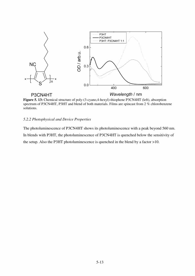
5-13
S
NC
** n
P3CN4HT Figure 5. 13: Chemical structure of poly-(3-cyano,4-hexyl)-thiophene P3CN4HT (left), absorption spectrum of P3CN4HT, P3HT and blend of both materials. Films are spincast from 2 % chlorobenzene solutions.
5.2.2 Photophysical and Device Properties
The photoluminescence of P3CN4HT shows its photoluminescence with a peak beyond 560 nm.
In blends with P3HT, the photoluminescence of P3CN4HT is quenched below the sensitivity of
the setup. Also the P3HT photoluminescence is quenched in the blend by a factor >10.

5-14
Figure 5. 14: Photoluminescence of P3CN4HT, P3HT and a 1:1 blend from both materials (upper part). On the lower graph, the same spectra, normalized to their maximum. Photoluminescence is recorded at room temperature under vacuum, excitation at 476 nm with 40 mW.

5-15
P3CN4HT shows an extraordinary strong single peak PIA absorption at 1.5 eV, see Figure 5.15.
Modulation frequency dependence shows a rather defined lifetime of t = 0.2 ms, dispersion
factor � = 0.94. The excitation power dependence shows a gradient of k = 0.9, indicating
primarily first order type recombination. All these facts let conclude that the PIA in P3CN4HT is
originating from a T1�Tn transition. Triplets were identified earlier in PT and acceptor
substituted PT unambiguously.20,21,22
Further, blends of P3CN4HT and P3HT are investigated. The PIA shows a rather broad feature
with several peaks between 1.8 and 1.2 eV. Further, a weak absorption feature is observed for
probe energies <0.8 eV.
For rr- P3HT, a broad photoinduced absorption spectrum is reported between 1 and 1.9 eV.
Several peaks are observed at 1.1 eV, assigned to an interchain exciplex, 1.25 eV, assigned to the
high energy polaron absorption and at 1.8 eV, assigned to the high energy two dimensional
polaron absorption, are reported. 23,24
The peaks at 1.8 eV and 1.25 eV can be found in the PIA spectrum of the P3HT: P3CN4HT
blend. No PIA is observed at 1.1 eV, therefore no interchain exciplex can be observed in the
blend. The low energy transition for the polaron and two dimensional polaron are found at 0.35
eV and 0.1 eV. These peaks are beyond the range of the setup, but a PIA < 0.8 eV is observed,
which can be attributed to the low energy polaron absorption. The other PIA features in the
P3HT: P3CN4HT blend between 1.5 and 1.7 eV might origin from P3CN4HT negative polaron,
but its spectrum is not known yet.
Modulation frequency dependence of the blend at 1.44 eV shows rather short lifetime (� = 0.18
ms) with a wide distribution (� = 0.50). Fit is only done with the in phase component since the
out of phase signal is rather small and its maximum is out of the measurement range. Excitation
power dependence shows a gradient of k = 0.77. No conclusion on the recombination mechanism
can be drawn.

5-16
Figure 5. 15: PIA spectrum of P3CN4HT (full line) and P3HT: P3CN4HT 1:1 (open triangle) spin cast films on glass. Spectra are recorded at 80 K , excitation with 40 mW at 476 nm.
Figure 5. 16: Modulation frequency dependence (left) with 40 mW excitation power and excitation power dependence (right) with 37 Hz modulation frequency of the PIA signal at 1.44 eV of P3CN4HT. Measurements are done at 80 K.

5-17
Figure 5. 17: Modulation frequency (left) with 40 mW excitation power and excitation power dependence (right) with 37 Hz modulation frequency of the PIA signal at 1.44 eV of P3HT: P3CN4HT. Measurements are done at 80 K. Fit for the modulation frequency dependence is only done with in phase data. In summary, it can be concluded that photoinduced charge separation in P3HT: P3CN4HT
blends is observed. The photoluminescence is quenched for both materials. Photoinduced charge
transfer shows T1�Tn excitation in the pristine P3CN4HT and polaronic absorption in the blend
with P3HT.
Devices from P3HT :P3CN4HT blend devices give a photocurrent of 50 µA cm-2 under solar
illuminated light. The photovoltage is 170 mV.25
5.3 References 1 E. Moons, Journal of Physics: Condensed Matter 2002, 14, 12235 2 G. Yu, A. J. Heeger, Journal of Applied Physics 1995, 78, 4510 3 M. Granström. K. Petritsch, A. C. Arias, A. Lux, M. R. Andersson, R. H. Friend, Nature 1998, 395, 257 4 J. J. M. Halls, A. C. Arias, J. D. MacKenzie, W. Wu, M. Inbasekaran, E. P. Woo, R. H. Friend, Advanced Materials 2000, 12, 498 5 C. M. Ramsdale, J. A. Barker, A. C. Arias, J. D. MacKenzie, R. H. Friend, N. C. Greenham, Journal of Applied Physics 2002, 92, 4266 6 R. C. Pacios, D. Bradley, Synthetic Metals 2002, 127, 261 7 S. A. Jeneke, S. Yi, Applied Physics Letters 2000, 77, 2635 8 A. G. Manoj, A. A. Alagiriswarny, K. S. Narayan, Journal of Applied Physics 2003, 94, 4088 9 X. Zhang, S. A. Jenekhe, Macromolecules 2000, 33, 2069 10 F. Naso, F. Babudri, G. M. Farinosa, Pure and Applied Chemistry 1999, 71, 1485 11 G. M. Farinola, T. Cassano, R. Tommasi, F. Babudri, A. Cardone and F. Naso, Proc. SPIE 2001, 4461, 296. 12 F. Babudri, A. Cardone, G. M. Farinola, F. Naso, T. Cassano, L. Chiavarone and R. Tommasi, Macromol. Chem. Phys .2003, 204, 1621. 13 T. Yohannes, H. Neugebauer, G. M. Farinola, C. Winder , F. Babudri, A. Cardone, F. Naso and N. S. Sariciftci to be submitted 14 U. Salzner, Journal of Physical Chemistry B 2002, 106, 9214 15 G. Casalbore-Miceli, M. C. Gallazzi, S. Zeccin, N. Camioni, A. Geri, C. Bertarelli, Advanced Functional Materials 2003, 13, 307 16 F. Demanze, A. Yassar, F. Garnier, Synthetic Metals 1996, 76, 269 17 Y. Greenwald, J. Poplawski, E. Ehrenfreund, S. Speiser, Synthetic Metals 1997, 85, 1353 18 A. Yassar, F. Demanze, A. Jaafari, M. El Idrissi, C. Coupry, Advanced Functional Materials 2002, 12, 699 19 Y. Greenwald, X. Xu, M Fourmigué, G. Srdanov, C. Koss, F. Wudl, A. J. Heeger, Journal of Polymer Science: Part A: Polymer Chemistry 1998, 36, 3115

5-18
20 L. Smilowitz, N. S. Sariciftci, R. Wu, C. Gettinger, A. J. Heeger, F. Wudl, Physical Review B 1993, 47, 13835 21 Y. Greenwald, X. Wie, S. Jeglinski, J. Poplawski, E. Ehrenfreund, S. Speiser, Z. V. Vardeny, Synthetic Metals 1995, 69, 321 22 X. Jiang, R. Oesterbacka, O. Korovyanko, C. P. An, B. Horowitz, R. A. J. Jannsen, Z. V. Vardeny, Advanced Functional Materials 2002, 12, 587 23 Y. H. Kim, D. Spiegel, S. Hotta, A. J. Heeger, Physical Review B 1988, 38, 5490 24 X. M. Jiang, R. Österbacka, C. P. An, Z. V. Vardeny, Synthetic Metals 2003, 137, 1465 25 Markus Koppe, private communication

6-1
6. Donor-Acceptor Dyads Dyad molecules1,2,3,4, consisting of an electron acceptor moiety covalently linked to an electron
donor, are possible candidates for photoactive systems5. Many of these molecules perform
photoinduced charge separation, resulting in long living (up to few hundred �s in solution)6
intra-molecular charge separated state.
6.1. �-extended tetrathiafulvalene-fullerene dyad exTTF-C60
�-extended tetrathiafulvalene-bridge-fullerene dyad molecules are potential candidates for
photoinduced charge transfer, leading to a long-living charge separated state.7,8 The aim of this
work is to study the charge transfer process in a particular �-extended tetrathiafulvalene-
fullerene dyad, bridged by two phenylene vinylene units, ex-TTF-C60 and test it for its suitability
for organic solar cells.9 As reference compounds, the ex-TTF with the bridge and the
fulleropyrrolidine are investigated. Further, the interaction with MDMO-PPV is investigated and
the possibility to exploit such blends in photovoltaic cells.
6.1.1. Electrochemistry
Electrochemical measurements are performed in a dichlorobenzene: acetonitrile 4:1 solution
with 0.1 M Bu4NClO4 as electrolyte. A glassy carbon electrode serves as working electrode, a
SCE as reference electrode and a platinum wired as counter electrode. Scan rate is 200 mV/s.
From the electrochemical measurements, an energy diagram for the dyad is drawn, shown in
Figure 6.2.
The electrochemical band gap of ex-TTF is determined with 1.98 eV, which is slightly lower
than the optical band gap of 2.1 eV.
The reduction peak of fulleropyrrolidine (C60-P) at -700 mV vs. SCE is a comparable range with
other [6,6] methanofullerenes.
The oxidation and reduction potential of the dyad are in the range of the ex-TTF (donor)
oxidation and C60-P (acceptor) reduction, respectively.

6-2
S
S
S
S OC6H13
OC6H13
ex-TTF
S
S
S
N
C8H17
S OC6H13
OC6H13
ex-TTF-C60 Figure 6. 1: Chemical structure of the �-extended tetrathiafulvalene with a phenylene vinylene bridge (ex-TTF) and the �-extended tetrathiafulvalene-bridge-C60 dyad (ex-TTF-C60) is shown.
The energy diagram of the dyad system, see Figure 6.2, is derived from the electrochemical
measurements, combined with optical absorption. The distinct offset of the LUMO and HOMO
levels between the ex-TTF and C60-P lets expect photoinduced charge separation.

6-3
Figure 6. 2: Energy diagram for ex-TTF, C60-P and the dyad structure ex-TTF-C60, energy values are taken from electrochemical measurements, the first reduction peak is assigned to the LUMO, the first oxidation peak to the HOMO, for C60-P, no oxidation is observed. The band gap is assumed from the absorption with 1.8 eV.
6.1.2 Photophysical Properties
Figure 6.3 shows the absorption and emission of ex-TTF and the ex-TTF- C60 dyad. Ex-TTF-C60
shows the absorption around 450 nm of the ex-TTF and around 330 from C60.
Ex-TTF films, excited at 476 nm, shows a luminescence with a maximum around 700 nm. The
dyad shows no photoluminescence. The photoluminescence is measured with excitation at 476
nm, where the ex-TTF part is predominantly excited, and 664 nm, there the C60 is exclusively
excited.
-1.51 V
Ex-TTF
+0.47 V
Ex-TTF-C60
-0.68 V
C60-P
+0.46 V
-0.7 V
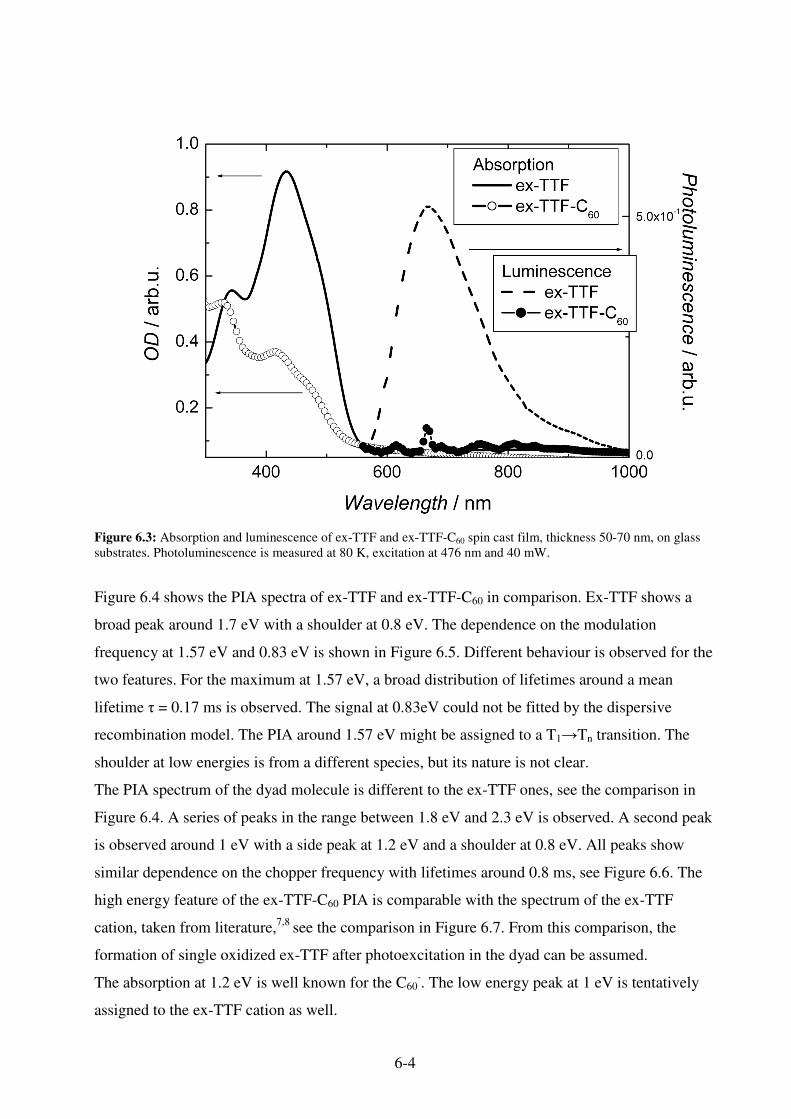
6-4
Figure 6.3: Absorption and luminescence of ex-TTF and ex-TTF-C60 spin cast film, thickness 50-70 nm, on glass substrates. Photoluminescence is measured at 80 K, excitation at 476 nm and 40 mW.
Figure 6.4 shows the PIA spectra of ex-TTF and ex-TTF-C60 in comparison. Ex-TTF shows a
broad peak around 1.7 eV with a shoulder at 0.8 eV. The dependence on the modulation
frequency at 1.57 eV and 0.83 eV is shown in Figure 6.5. Different behaviour is observed for the
two features. For the maximum at 1.57 eV, a broad distribution of lifetimes around a mean
lifetime � = 0.17 ms is observed. The signal at 0.83eV could not be fitted by the dispersive
recombination model. The PIA around 1.57 eV might be assigned to a T1�Tn transition. The
shoulder at low energies is from a different species, but its nature is not clear.
The PIA spectrum of the dyad molecule is different to the ex-TTF ones, see the comparison in
Figure 6.4. A series of peaks in the range between 1.8 eV and 2.3 eV is observed. A second peak
is observed around 1 eV with a side peak at 1.2 eV and a shoulder at 0.8 eV. All peaks show
similar dependence on the chopper frequency with lifetimes around 0.8 ms, see Figure 6.6. The
high energy feature of the ex-TTF-C60 PIA is comparable with the spectrum of the ex-TTF
cation, taken from literature,7,8 see the comparison in Figure 6.7. From this comparison, the
formation of single oxidized ex-TTF after photoexcitation in the dyad can be assumed.
The absorption at 1.2 eV is well known for the C60-. The low energy peak at 1 eV is tentatively
assigned to the ex-TTF cation as well.

6-5
The quenching of the peak at 1.6 eV in the ex-TTF, which is assigned to the triplet state, and the
quenching of the ex-TTF photoluminescence are further indication for photoinduced charge
separation in the dyad.
Figure 6. 4: PIA of ex-TTF and ex-TTF-C60 at 80 K, excitation at 476 nm (2.6 eV) with 40 mW, inset shows the low energy range between 0.5 and 1.6 eV.

6-6
Figure 6. 5: Modulation frequency dependence of ex-TTF at 80 K, excitation with 40 mW at 476 nm (2.6 eV). The signal at 1.57 eV is fitted by the dispersive recombination model, � = 0.57 ms and � = 0.74. The signal at 0.83 eV could not be fitted by this model, the lines are guide for the eye.
Figure 6. 6: Modulation frequency dependence of ex-TTF-C60 at 1.24 eV and 1.97 eV. Measurements are performed at 80 K, excitation with 40 mW at 476 nm (2.6 eV). Fits are done by the dispersive recombination model.

6-7
Figure 6. 7: High energy part of the PIA spectrum of ex-TTF-C60 in comparison with the differential absorption spectrum of the ex-TTF cation, induced by pulse radiolysis, in CH2Cl2. Solution spectrum is taken from literature.8
6.1.3 Photovoltaic Devices
Photovoltaic devices are made with ex-TTF-C60, spin cast from a chlorobenzene solution. The
devices show a clear photovoltaic effect, see Figure 6.8. The power conversion efficiency is 0.02
% under solar simulated light with 80 mW cm-2. The photocurrent spectrum is in good
agreement with the absorption spectrum, The maximum is at 400 nm, which is slightly blue-
shifted to the ex-TTF absorption maximum at 450 nm. The onset of the photocurrent matches
with the absorption onset around 600.

6-8
Figure 6. 8: I-V characteristics (upper graph) of an ex-TTF-C60 dyad device in the dark and illumination from a solar simulator with 80 mW cm-2, active layer thickness is around 50-70 nm. Photocurrent spectrum of the same device in comparison with the absorption spectrum of a thin film (lower graph).
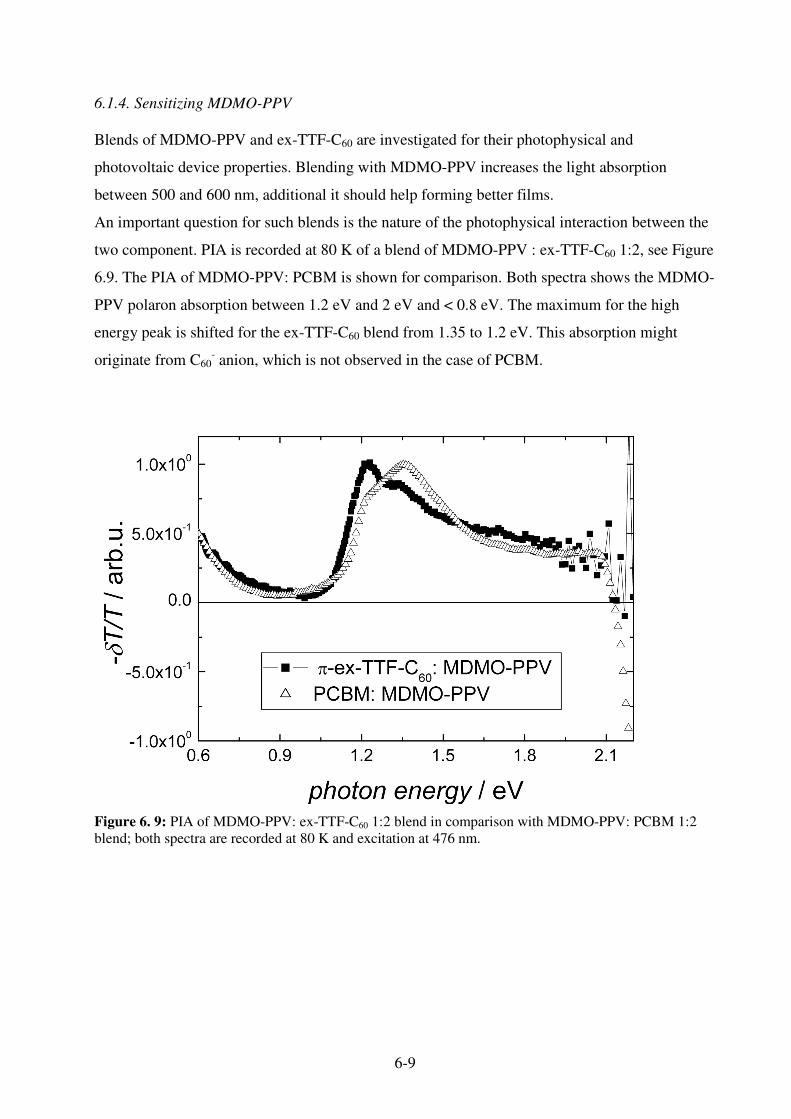
6-9
6.1.4. Sensitizing MDMO-PPV
Blends of MDMO-PPV and ex-TTF-C60 are investigated for their photophysical and
photovoltaic device properties. Blending with MDMO-PPV increases the light absorption
between 500 and 600 nm, additional it should help forming better films.
An important question for such blends is the nature of the photophysical interaction between the
two component. PIA is recorded at 80 K of a blend of MDMO-PPV : ex-TTF-C60 1:2, see Figure
6.9. The PIA of MDMO-PPV: PCBM is shown for comparison. Both spectra shows the MDMO-
PPV polaron absorption between 1.2 eV and 2 eV and < 0.8 eV. The maximum for the high
energy peak is shifted for the ex-TTF-C60 blend from 1.35 to 1.2 eV. This absorption might
originate from C60- anion, which is not observed in the case of PCBM.
Figure 6. 9: PIA of MDMO-PPV: ex-TTF-C60 1:2 blend in comparison with MDMO-PPV: PCBM 1:2 blend; both spectra are recorded at 80 K and excitation at 476 nm.
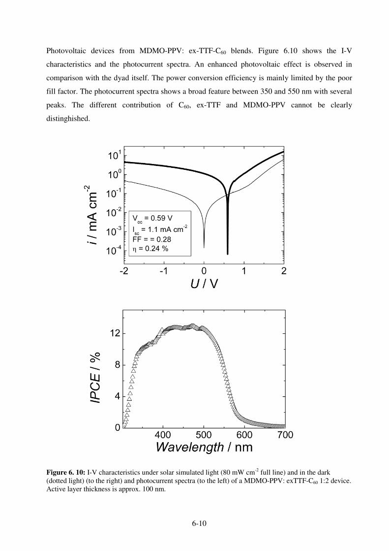
6-10
Photovoltaic devices from MDMO-PPV: ex-TTF-C60 blends. Figure 6.10 shows the I-V
characteristics and the photocurrent spectra. An enhanced photovoltaic effect is observed in
comparison with the dyad itself. The power conversion efficiency is mainly limited by the poor
fill factor. The photocurrent spectra shows a broad feature between 350 and 550 nm with several
peaks. The different contribution of C60, ex-TTF and MDMO-PPV cannot be clearly
distinghished.
Figure 6. 10: I-V characteristics under solar simulated light (80 mW cm-2 full line) and in the dark (dotted light) (to the right) and photocurrent spectra (to the left) of a MDMO-PPV: exTTF-C60 1:2 device. Active layer thickness is approx. 100 nm.
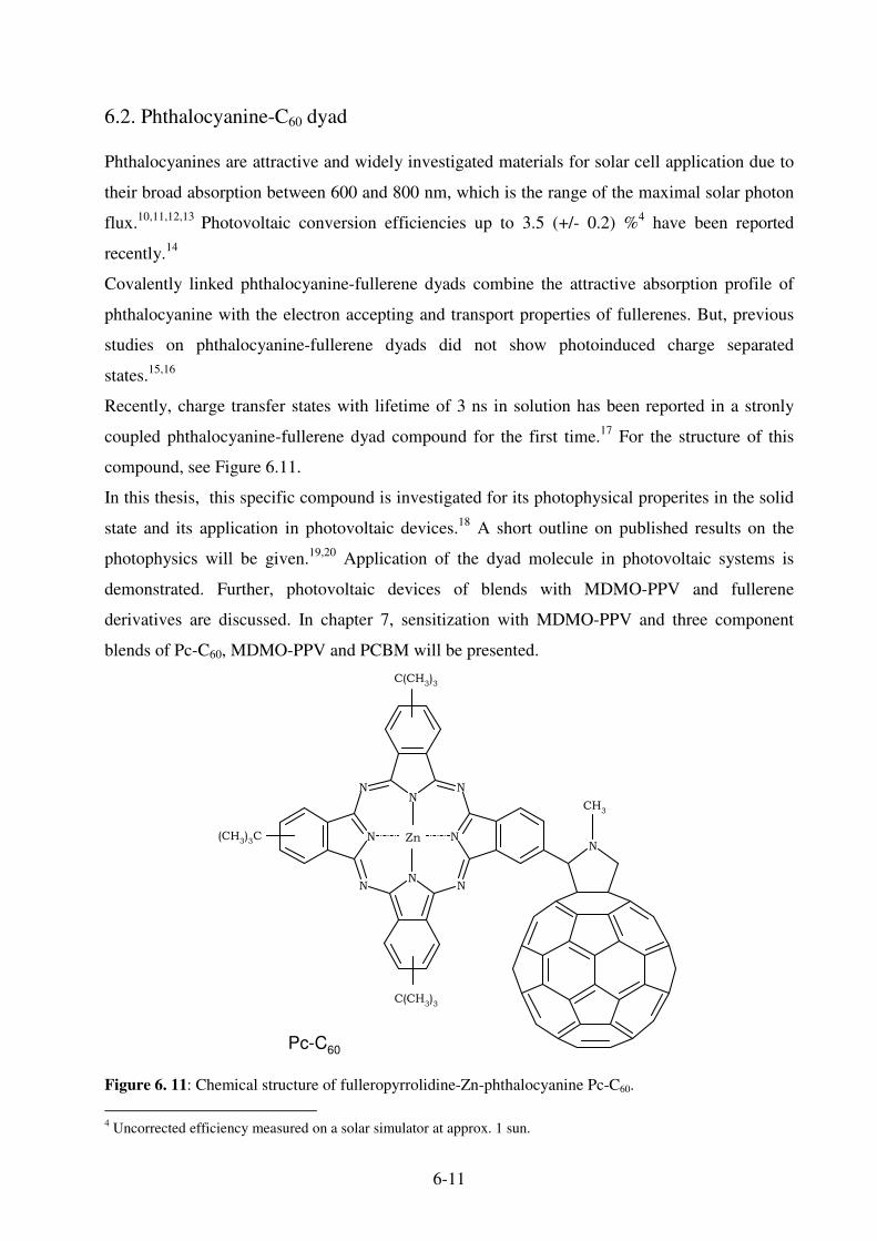
6-11
6.2. Phthalocyanine-C60 dyad
Phthalocyanines are attractive and widely investigated materials for solar cell application due to
their broad absorption between 600 and 800 nm, which is the range of the maximal solar photon
flux.10,11,12,13 Photovoltaic conversion efficiencies up to 3.5 (+/- 0.2) %4 have been reported
recently.14
Covalently linked phthalocyanine-fullerene dyads combine the attractive absorption profile of
phthalocyanine with the electron accepting and transport properties of fullerenes. But, previous
studies on phthalocyanine-fullerene dyads did not show photoinduced charge separated
states.15,16
Recently, charge transfer states with lifetime of 3 ns in solution has been reported in a stronly
coupled phthalocyanine-fullerene dyad compound for the first time.17 For the structure of this
compound, see Figure 6.11.
In this thesis, this specific compound is investigated for its photophysical properites in the solid
state and its application in photovoltaic devices.18 A short outline on published results on the
photophysics will be given.19,20 Application of the dyad molecule in photovoltaic systems is
demonstrated. Further, photovoltaic devices of blends with MDMO-PPV and fullerene
derivatives are discussed. In chapter 7, sensitization with MDMO-PPV and three component
blends of Pc-C60, MDMO-PPV and PCBM will be presented.
��
�
�
�
�
�
�
���
�
���������
�������
�������
Pc-C60 Figure 6. 11: Chemical structure of fulleropyrrolidine-Zn-phthalocyanine Pc-C60.
4 Uncorrected efficiency measured on a solar simulator at approx. 1 sun.

6-12
6.2.1 Photophysics of Pc-C60
Figure 6.12 shows the absorption spectra of Pc-C60 and the individual components of the dyad,
the Zn-phthalocyanine (ZnTBPc) and the fulleropyrrolidine (C60-P). The dyad absorption
spectrum can be seen in first approximation as a superposition of the single component spectra.
However, the photoluminescence of the phthalocyanine is quenched in the dyad molecule by a
factor of ~ 50.
Figure 6. 12: Absorption coefficient of Pc-C60 (full line) and the individual components, Zn-tetra-(tert.-butyl)-phthalocyanine ZnTBPc (dotted line) and fulleropyrrolidine C60-P (dashed line).The absorption is fitted by a dielectric function model by the software SCOUT. Figure 6.13 shows the PIA spectra of Pc-C60 and the individual components, ZnTBPc and C60-P.
C60-P, excited in the UV, shows a single peak around 1.75 eV, which is assigned to T1�Tn
absorption. ZnTBPc shows a single peak around 1 eV, which is also assigned to a T1�Tn
absorption as well. Further, bleaching of the ground state absorption for E >1.5 eV is observed.
In the dyad molecule, both T1�Tn absorption of the phthalocyanine is quenched, instead two
new absorption around 1.2 eV and <0.6 eV are observed. The 1.2 eV absorption is typical for the
C60 anion; the absorption at low probe energies might be assigned to the phthalocyanine cation.
Further, bleaching is observed in the region of the phthalocyanine groundstate absorption. For

6-13
the photoexcitations in the dyad, typical lifetimes of 0.2 ms are determined for the solid state
from the modulation frequency dependence.
Figure 6. 13: PIA of Pc-C60 and the individual components ZnTBPc and C60-P at 80 K. Pc-C60 and ZnTBPc are excited at 685 nm, C60-P by a multiline UV laser.
6.2.2 Photovoltaic Devices from Pc-C60
The I-V characteristics of a Pc-C60 device is shown in Figure 6.14. Diode behaviour with a
rectification ratio of ~10 is observed in the dark. Under white light illumination
with 80 mW cm-2 , an open circuit voltage VOC = 0.46 V and a short circuit current
ISC = 0.51 mA cm-2 have been measured in the best case. The fill factor FF = 0.26 and a power
conversion efficiency �e = 0.08 % are determined. The Voc (0.46 V) is in a similar range to the
high efficient cells reported for evaported phthalocyanine:C60 mixture (Voc = 0.53 V), but the Isc
is lower in the device containing the dyad molecule compared to the evaporated cells.
The spectrally resolved photocurrent of the Pc-C60 device, see Figure 6.14 as well, shows a
maximum around 700 nm and 360 nm. The photocurrent spectra matches the absorption of the
dyad. The maximal quantum efficiency is 3 %, showing the possibility for improvement of the
device performance.

6-14
Figure 6. 14: Photocurrent spectrum (open circles) of a Pc-C60 device, thickness approx. 40 nm, spin cast from chlorobenzene, in comparison with the optical absorption (full line) (upper graph), current-voltage characteristics of the same device under illumination by a solar simulator, 80 mW cm-2 ( thick line) and in the dark (thin line) (lower graph).

6-15
6.3 Hexa-thiophene-fluorene dyad 6TDTF
Poly-thiophenes with incorporated �-conjugated 1,3 Dithiole-2-ylidenefluorene have been
reported as possible �-conjugated donor- acceptor structures.21, 22, 23 The large variety of fluorene
substitution chemistry opens the possibility to tune the electron affinity of the fluorene unit over
a wide range. It was shown that the reduction potential, a measure for the electron affinity, can
be described as a function of the substitution pattern by a Hammett type correlation.22,24 Long
lived photoinduced charge carriers were demonstrated for such polymers with trinitro-substituted
fluorene acceptors.22
Since the solubility of this polymer systems is low, a novel hexa-thiophene oligomere structure
with two 9-(thienodithiino[3,4-c:5,6-4]-1,3-dithiole-2-ylidene)-4,5-dinitro-2,7-
(didodecyloxycarboxy)-fluorene units, 6TDTF, for the structure see Figure 6.15, was developed.
The material was synthesized at the University of Manchester, group of Dr. Skabara. This
material shows sufficient solubility in common organic solvents like chloroform or
chlorobenzene.
S S
S
S
S
S S
CO2C11H23CO2C11H23
NO2O2N
SS
S
S
S
SS
CO2C11H23
O2NNO2
H23C11O2C
Figure 6. 15: Chemical structure of 6TDTF
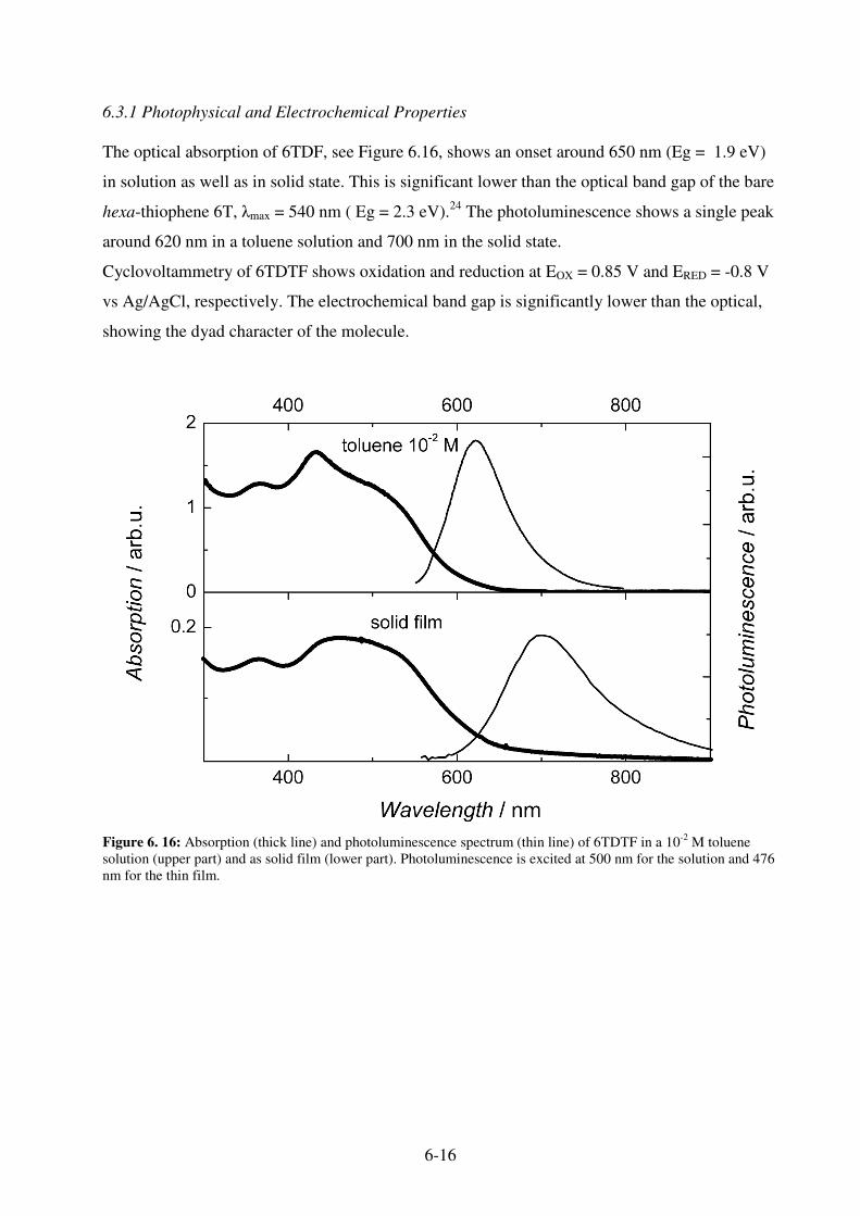
6-16
6.3.1 Photophysical and Electrochemical Properties
The optical absorption of 6TDF, see Figure 6.16, shows an onset around 650 nm (Eg = 1.9 eV)
in solution as well as in solid state. This is significant lower than the optical band gap of the bare
hexa-thiophene 6T, �max = 540 nm ( Eg = 2.3 eV).24 The photoluminescence shows a single peak
around 620 nm in a toluene solution and 700 nm in the solid state.
Cyclovoltammetry of 6TDTF shows oxidation and reduction at EOX = 0.85 V and ERED = -0.8 V
vs Ag/AgCl, respectively. The electrochemical band gap is significantly lower than the optical,
showing the dyad character of the molecule.
Figure 6. 16: Absorption (thick line) and photoluminescence spectrum (thin line) of 6TDTF in a 10-2 M toluene solution (upper part) and as solid film (lower part). Photoluminescence is excited at 500 nm for the solution and 476 nm for the thin film.

6-17
The PIA spectrum of 6TDTF, see Figure 6.17, shows a broad peak between 0.9 and 1.9 eV with
a plateau between 1.2 and 1.5 eV and a shoulder at 1.0 eV. Additional, a raising PIA feature for
small probe energies is observed. Figure 6.18 shows the expansion of the PIA for the NIR-MIR.
A PIA peak around 0.4 eV and infrared active vibration (IRAV) bands in the MIR. The IRAV
bands are clear indication for charged species. The PIA at 0.4 eV might be assigned to the cation
absorption of 6TDTF.
Figure 6. 17: PIA spectra of 6TDTF thin film (full line, left axis) and a 6TDTF: PCBM 1:1 blend film (open squares, right axis), spectra recorded at 80 K, excitation at 476 nm with 40 mW.

6-18
Figure 6. 18: PIA spectrum in the MIR-NIR infrared spectrum of a 6TDTF drop cast film on KBr. Spectra are recorded at 80 K, 30 mW illumination at 476nm. The PIA is obtained by subtracting the spectrum under illumination from the spectra in the dark. The modulation frequency dependence of the PIA feature at 0.62 is shown in Figure 6.19. This
feature can be correlated to the low energy absorption of the cation. The dependence is weak,
this indicates long lifetimes. The curve could not be fitted by any applied model. The signal
increases linear with the excitation power, see Figure 6.20. Such a dependence is assigned to
monomolecular behaviour, which let conclude to intramolecular charge separated state.

6-19
Figure 6. 19: Modulation frequency dependence of the PIA of 6TDTF at 1.38 eV, 1.1 eV and 0.62 eV. No satisfying fits could be obtained for these frequency dependencies. For the 1.1 eV PIA, the in phase component (squares) is fitted, giving a lifetime of 0.07 ms and a distribution factor of 0.4.
The PIA at 1.1 eV and 1.38 eV shows different modulation frequency dependencies, see Figure
6.19 as well. Therefore, it is concluded that the broad absorption in the VIS-NIR origin from
more than one photoexciation. The shoulder at 1.1 eV shows a rather weak dependence on the
modulation frequency, indicating short lifetimes. Fitting of the in phase component (X) results in
a lifetime of � = 0.07 ms and a distribution factor of � = 0.40. The measured range for the out-of-
phase signal (Y) could not be fitted by any modulation frequency model.
The PIA at 1.38 eV shows a much stronger dependence, which indicates longer lifetimes.
At both probe energies, the PIA scales linear with the excitation power as well, see Figure 6.20.

6-20
Figure 6. 20: Excitation power dependence of the PIA of 6TDTF at 1.38 eV, 1.1 eV and 0.62 eV. Fits (thin line) are done by a power law. For high excitation intensities, saturation is observed. These points are not included into the fitting procedure.
In order to find out more on the cation species of 6TDTF, a blend with PCBM as strong electron
acceptor is investigated. PIA show peaks at 1.47 eV with a shoulder around 1.7 eV and at 0.7
eV. All peaks in the blend show quite similar dependence on the modulation frequency at all
investiged probe energies, see Figure 6.21. None of them could be fitted by a modulation
dependence model. The excitation power dependence, Figure 6.22, varies in a small range
between k = 0.55 and k =0.65, fitted by a power law.
This indicate bimolecular recombination as dominant recombination mechanism. The
recombination behaviour of the photoexcitations is quite different in the fullerene blend and the
pristine 6TDTF. Different photophysical processes are involved.
For 6T cation, absorption at 1.55 and 0.8 eV are reported.25,26,27,28 This energies are quite
comparable with the PIA of the 6TDTF: PCBM blends. Although the two systems, 6T and
6TDTF, are not direct comparable, it might be concluded that the positive charge is primarily
located on the hexa-thiophene backbone. Further, the PIA around 1.1 eV in 6TDTF is quenched
in the blend with PCBM. The lifetime of this feature is found to be rather short and different to
the positive charge. We assume therefore that this migth be correlated to a triplet state or to an
charge transfer state.

6-21
Figure 6. 21: Modulation frequency dependence of the PIA of 6TDTF: PCBM 1:1 blend at 1.71 eV, 1.46 eV and 0.69 eV.
Figure 6. 22: Excitation power dependence of the PIA of 6TDTF:PCBM 1:1 at 1.71.eV, 1.46 eV and 0.69 eV. Measurements are done at 80 K with 37 Hz modulation. Fits are done by a power law (thin line).

6-22
6.3.2 Photovoltaic Devices
Photovoltaic devices are prepared for 6TDTF: PCBM blends. The I-V characteristics and
photocurrent spectrum are shown in Figure 6.23. Devices show a photoeffect with a power
conversion efficiency �e = 0.1 %. The device performance is mainly limited by the low fill
factor. The photocurrent spetrum matches the absorption spectrum in the well and show its onset
around 650 nm, coinciding with 6TDTF.
Figure 6. 23: I-V characteristics (left) under solar simulated light, 80 mW cm-2 and in the dark of a 6TDTF: PCBM 1:3 blend, spin cast from chlorobenzene. Photocurrent spectrum in comparison with the absorption spectrum (right).
6-23
6.4 References 1D. Gust, T. A. Moore and A. L. Moore, Journal of Photochemistry and Photobiology B 2000, 58, 63 2 D. Kuciauskas, S. Lin, G. R. Seely, A. L. Moore, T. A. Moore, D. Gust, T. Drovetskaya, C. A. Reed and P. D. W. Boyd, Journal of Physical Chemistry 1996, 100, 15926 3 T. Vemanen, N. V. Tkachenko, A. Y. Tauber, P. H. Hynninen and H. Lemmetyinen, Chemical Physics Letters. 2001, 345, 213 4 P. A. Liddell, D. Kuciauskas, J. P. Sumida, B. Nash, D. Nguyen, A. L. Moore, T. A. Moore and D. Gust, Journal of the American Chemical Society 1997, 119, 1400 5 E. Peeters, P. A. van Hal, J. Knol, C. J. Brabec, N. S. Sariciftci, J. C. Hummelen and R. A. J. Janssen, Journal of Physical Chemistry B 2000, 104, 10174 6 H. Imahori, D. M. Guldi, K. Tamaki, Y. Yoshida, C. Luo, Y. Sakata and S. Fukuzumi, Journal of the American Chemícal Society 2001, 123, 6617 7 N. Martín, L. Sánchez, B. Illescas, S. González, M. A. Herranz, D. M. Guldi, Carbon 2000, 38, 1577 8 L. Sánchez, I. Pérez, N. Martín, D. M. Guldi, Chemical European Journal 2003, 9, 2457 9 C. Winder, H. Neugebauer, N. S. Sariciftci, F. Giacalone, J. L. Segura, N. Martin, submitted to The Proceedings of the Electrochemical Society, San Antonio 2003 10 C. W. Tang, Applied Physics Letters 1986, 48, 183 11 M. Westphalen, U. Kreibig, J. Rostalski, H. Lüth and D. Meissner, Solar Energy Materials and Solar Cells, 2000, 61, 97 12 P. Peumans, S. R. Forrest, Applied Physics Letters, 2001, 79, 126; Erratum: Applied Physics Letters 2002, 80, 338 13 D. Gebeyehu , B. Maennig, J. Drechsel, K. Leo, M. Pfeiffer, Solar Energy Materials and Solar Cells 2003, 79, 81 14 S. Uchida, J. Xue, B. P. Rand. S. R. Forrest, Applied Physics Letters 2004, 84, 4218 15 T. G. Linssen, K. Dürr, M. Hanack and A. Hirsch, Journal of the Chemical Society, Chemical Communícation , 1995, 103 16 A. Sastre, A. Gouloumis, P. Vázquez, T. Torres, V. Doan, B. J. Schwartz, F. Wudl, L. Echegoyen and J. Rivera, Organic Letter, 1999, 1, 1807. 17 D. Guldi, A. Gouloumis, P. Vázquez and T. Torres, Chemical Communication 2002, 2056 18 A. Gouloumis, S.-G. Liu, A. Sastre, P. Vàzquez, L. Echegoyen and T. Torres, Chem. Eur. J. 2000, 6, 3600 19 M. A. Loi, P. Denk, H. Hoppe, H. Neugebauer, C. Winder, D. Meissner, C. Brabec,N. S. Sariciftci, A. Gouloumis, P. Vázquez, T. Torres, Journal of Materials Chemistry 13, 700-704 (2003) 20 H.Neugebauer, M. A. Loi, C. Winder, N. S. Sariciftci, G. Cerullo, A. Gouloumis, P. Vázquez, T. Torres, Solar Energy Materials and Solar Cells 2004, 83, 201 21 P. J. Skabara, I. M. Serebryakov, I. F. Perepichka, N. S. Sariciftci, H. Neugebauer, A. Cravino, Macromolecules 2001, 34, 2232 22 P. J. Skabara, I. M. Serebryakov, I. F. Perepichka, Journal of the Chemical Society, Perkin Transaction 2 1999, 505 23 D. F. Perepichka, M. R. Bryce, A. S. Batsanov, E. J. L. McInnes, J. P. Zhao, R. D. Farley, Chemistry, A European Journal 2002, 8, 4656 24 P.A. Lane, X. Wei, Z. V. Vardeny, J. Poplawski, E. Ehrenfreund, M. Ibrahim, A. J. Frank, Chemical Physics 1996, 210, 229 25 R. A. J. Janssen, D. Moses, N. S. Sariciftci, Journal of Chemical Physics 1994, 101, 9519 26 P. A. Lane, M. Liess, X. Wei, J. Partee, J. Shinar, A. J. Frank, Z. V. Vardeny, Chemical Physics 1998, 227, 57 27 N. Yokounuma, Y. Furukawa, M. Tasumi, M. Kuroda, J. Nakayama, Chemical Physics Letters 1996, 255, 431 28 J. A. E. H. van Haare, E. E. Havinga, J. L. J. van Dongen, R. A. J. Janssen, J. Cornil, J. L. Bredas, Chemistry, A European Journal 1998, 4, 1509
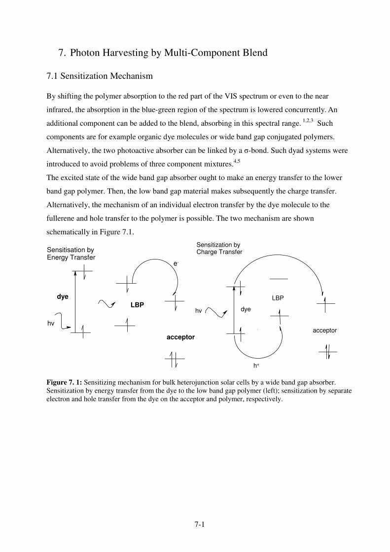
7-1
7. Photon Harvesting by Multi-Component Blend
7.1 Sensitization Mechanism
By shifting the polymer absorption to the red part of the VIS spectrum or even to the near
infrared, the absorption in the blue-green region of the spectrum is lowered concurrently. An
additional component can be added to the blend, absorbing in this spectral range. 1,2,3 Such
components are for example organic dye molecules or wide band gap conjugated polymers.
Alternatively, the two photoactive absorber can be linked by a �-bond. Such dyad systems were
introduced to avoid problems of three component mixtures.4,5
The excited state of the wide band gap absorber ought to make an energy transfer to the lower
band gap polymer. Then, the low band gap material makes subsequently the charge transfer.
Alternatively, the mechanism of an individual electron transfer by the dye molecule to the
fullerene and hole transfer to the polymer is possible. The two mechanism are shown
schematically in Figure 7.1.
hv
dyeLBP
acceptor
e-
Sensitisation byEnergy Transfer
hv dye
LBP
acceptor
h+
Sensitization by Charge Transfer
Figure 7. 1: Sensitizing mechanism for bulk heterojunction solar cells by a wide band gap absorber. Sensitization by energy transfer from the dye to the low band gap polymer (left); sensitization by separate electron and hole transfer from the dye on the acceptor and polymer, respectively.

7-2
7.2 Sensitized Organic Solar Cells
Different photon harvesting systems containing more than two organic absorbers have been
proposed in the literature.
Roman et al showed blends containing two polythiophenes and C60.6
This route was followed later, sensitizing PTPTB: PCBM (see Chapter 4) photovoltaic cells with
MDMO-PPV.7 Significant contribution from both polymer to the photocurrent was found, also
the overall efficiency was smaller as compared to the parent systems. Alternatively, the
sensitization with the highly absorbing dye molecule 9-(Diethylamino)-5-H-
benzoe[a]phenoxazin-5-one (nile red), chemical structures see Figure 7.2, was investigated. The
photocurrent spectra of this system show contribution from the dye absorption as well as the
absorption of the polymer. The overall power conversion efficiency of this system is � = 0.5 %.
For all this systems, energy transfer is assumed as dominant sensitization mechanism.
O
N
ON (CH3CH2)2
Nile Red
Figure 7. 2: Chemical structure of 9-(Diethylamino)-5H-benzo[a]phenoxazin-5-one (nile red).
Chen reported polymer blend/ C60 bilayer devices.1 Different polymer blends were used,
typically containing a wide band gap PPV derivative and a low band gap PT derivative. Energy
transfer was demonstrated as sensitization mechanism by photoluminescence experiments.
Photocurrent measurements show a broad coverage of the spectrum and contribution from both
polymers. Maximal conversion efficiency of IPCE = 38 % at 430 nm and enhanced conversion
efficiency is reported.
Takahashi reported sensitization of PT: perylene bilayer devices.8 Porphyrine was used to
sensitize the perylene acceptor layer. All three materials are shown to contribute to the
photocurrent. Sensitization by charge transfer is assumed to be the sensitizing mechanism.

7-3
7.3. MDMO-PPV: Pc-C60 blends
7.3.1 Photophysics of Pc-C60 : MDMO-PPV blends
The combination of Pc-C60 and MDMO-PPV shows absorption over the whole visible range. In
this blend, three photophysical and electronically active components, C60, MDMO-PPV and
ZnTBPc are present and can interact with each other. C60 is known to be electron acceptor
towards both the other two components.
Unknown is the excited state interaction between the two donors ZnTBPc and MDMO-PPV. A
5% ZnTBPc doped MDMO-PPV film, excited at 476 nm, shows only ZnTBPc
photoluminescence. At the excitation wavelength, MDMO-PPV primarily absorbs. This
indicates energy transfer from MDMO-PPV to ZnTBPc.
In time resolved photoinduced absorption measurements, the bleaching of the MDMO-PPV as
well as of the ZnTBPc groundstate absorption can be observed. The bleaching of the MDMO-
PPV absorption is quenched in a timescale of about 10 ps. This band is taken as indication for
the MDMO-PPV excited state, which is primarily excited. In a similar timescale, the ground
state bleaching of the ZnTBPc raises.
Further, the blend of MDMO-PPV and Pc-C60 is investigated. No steady state
photoluminescence could be observed. Steady state photoinduced absorption, excited at 476 nm,
shows absorption peaks at 1.1 eV, which is unambiguously assigned to C60-, and around 0.7 eV.
Further bleaching is observed around 1.8 eV, indicating a long lived excited state of ZnTBPc.
Time resolved measurements are performed on a MDMO-PPV film with 10 % Pc-C60 (the
phthalocyanine concentration is equivalent to the 5 % ZnTBPc in MDMO-PPV). The
groundstate bleaching of MDMO-PPV vanishes in a timescale of 10 ps, the groundstate
bleaching of the phthalocyanine arise is the same timescale.
The decay time for the MDMO-PPV excited state and the raising time for the phthalocyanine
excited state are in a similar timescale for blends with ZnTBPc and Pc-C60 . It is therefore
concluded, that in the photoexcited state of MDMO-PPV makes primarily an energy transfer to
ZnTBPc, followed from an electron transfer to the C60.

7-4
7.3.2 Photovoltaic devices from MDMO-PPV: Pc-C60 blends
Photovoltaic devices from the Pc-C60 dyad were discussed in Chapter 6.2. The photophysical
interaction of MDMO-PPV and Pc-C60 shows energy transfer from MDMO-PPV to
phthalocyanine, with subsequent charge transfer. This sensitization mechanism should be
exploited for solar cell devices.
A series of photovoltaic devices are prepared, containing different ratios of MDMO-PPV and Pc-
C60. Long living, positive charge carriers on the phthalocyanine molecule are demonstrated for
such combination. Therefore, the positive charges are expected to be primarily transported by the
phthalocyanine.
Figure 7.3 shows the I-V characteristics for the MDMO-PPV: Pc-C60 blend devices under
illumination and in the dark. For this representation, the best device is chosen out of a series of 6
devices. In Table 7.1, the average values of a this series are shown.
The addition of MDMO-PPV leads to a significant decrease of the photocurrent. Also the current
injection at positive bias is decreased, the 1:1 blend device shows a nearly symmetric behaviour
without reaching the injection regime up to a forward bias of +2 V.

7-5
Figure 7. 3: Current voltage curves for MDMO-PPV: Pc-C60 devices with different ratios, under illumination from a solar simulator 80 mW cm-2 (upper graph), best device from a series of six, in the dark for the same device (lower graph).
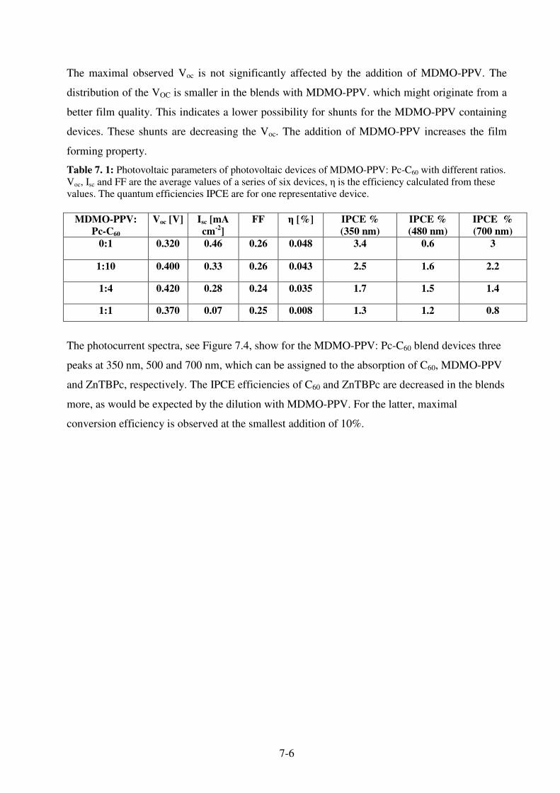
7-6
The maximal observed Voc is not significantly affected by the addition of MDMO-PPV. The
distribution of the VOC is smaller in the blends with MDMO-PPV. which might originate from a
better film quality. This indicates a lower possibility for shunts for the MDMO-PPV containing
devices. These shunts are decreasing the Voc. The addition of MDMO-PPV increases the film
forming property.
Table 7. 1: Photovoltaic parameters of photovoltaic devices of MDMO-PPV: Pc-C60 with different ratios. Voc, Isc and FF are the average values of a series of six devices, � is the efficiency calculated from these values. The quantum efficiencies IPCE are for one representative device.
MDMO-PPV: Pc-C60
Voc [V] Isc [mA cm-2]
FF � [%] IPCE % (350 nm)
IPCE % (480 nm)
IPCE % (700 nm)
0:1 0.320 0.46 0.26 0.048 3.4 0.6 3
1:10 0.400 0.33 0.26 0.043 2.5 1.6 2.2
1:4 0.420 0.28 0.24 0.035 1.7 1.5 1.4
1:1 0.370 0.07 0.25 0.008 1.3 1.2 0.8
The photocurrent spectra, see Figure 7.4, show for the MDMO-PPV: Pc-C60 blend devices three
peaks at 350 nm, 500 and 700 nm, which can be assigned to the absorption of C60, MDMO-PPV
and ZnTBPc, respectively. The IPCE efficiencies of C60 and ZnTBPc are decreased in the blends
more, as would be expected by the dilution with MDMO-PPV. For the latter, maximal
conversion efficiency is observed at the smallest addition of 10%.

7-7
Figure 7. 4: Photocurrent spectra of MDMO-PV: Pc-C60 blend devices with different ratios. The photocurrent spectrum of Pc-C60 is shown in comparison. In summary, it was shown that MDMO-PPV: Pc-C60 blend devices can cover the whole visible
range. Contribution of all three components to the photocurrent is shown. No improvement of
the power conversion efficiency of Pc-C60 devices is found by blending with MDMO-PPV. From
the I-V characteristics, significant decrease of the charge injection and transport is observed for
the blends. It is concluded that the charge transport is hindered in the blends due to unfavourable
morphology and dilution of charge transport pathways. Blending with MDMO-PPV lead to
better film forming properties by spin cast techniques. As a consequence, shunt are less probable
and a better reproducibility of the device fabrication could be achieved.

7-8
7.3.3 MDMO-PPV:Pc-C60: PCBM blends
The photophysics of para-phenylene vinylene, phthalocyanine and fullerene mixtures was
discussed in chapter 7.3.1. Energy transfer from MDMO-PPV to phthalocyanine with subsequent
charge transfer to fullerene was demonstrated. This mechanism can be applied in photovoltaic
devices, as was demonstrated in chapter 7.3.2. But addition of MDMO-PPV led to a decrease of
the overall photovoltaic performance. This was assigned to reduced hole mobility.
In this chapter, Pc-C60 in blends with MDMO-PPV and PCBM is investigated for bulk
heterojunction devices.
Figure 7. 5: IPCE spectra from MDMO-PPV: fullerene 1:4 devices, for the fullerene, different ratios of PCBM and Pc-C60 are used, 0 % Pc-C60 (thin line), 10 % (dotted line), 30 % (thick line), 60 % (open circles) and 100 % (slashed line). The photocurrent spectra for several three component blends with a constant MDMO-PPV :
acceptor ratio of 1:4 (w/w) is shown in Figure 7.5. The overall fullerene concentration is varying
only slightly in these experiments. The devices containing Pc-C60 show two peaks at 500 and
700 nm in the photocurrent. These two peaks are assigned to MDMO-PPV and phthalocyanine.
The IPCE efficiencies are increasing with increasing PCBM addition.
Figure 7.6 and Table 7.2 show the I-V characteristics and photovoltaic parameters for the three
component blends, respectively. The VOC is decreased by addition of Pc-C60 from ~800 mV for

7-9
the MDMO-PPV: PCBM to VOC ~ 500 mV for the three component devices. Similar values for
the VOC have been reported in Chapter 7.3.2 for different phthalocyanine fullerene blends. The
VOC seems to be limited to this value for the phthalocyanine: fullerene combination.
Figure 7. 6: I-V characteristics of MDMO-PPV: fullerene 1:4 devices, for the fullerene, different ratios from PCBM and Pc-C60 are used, 0 % Pc-C60 (thin line), 10 % (dotted line), 30 % (thick line), 60 % (open circles) and 100 % (slashed line).
Interestingly, the forward bias current at +2V is increasing with increasing PCBM concentration
and varies over more than two orders of magnitude. All devices are of comparable thickness
around 100 nm. Therefore, this increase can be attributed to the current transport and electrode
injection property of Pc-C60 and PCBM by the different substitution.
Likewise, the ISC is higher for the PCBM containing devices, even the absorption is less. The
different electrical behaviour of PCBM and Pc-C60 can only be rationalized by the different
substitution pattern of the two molecules.

7-10
Table 7. 2: Photovoltaic parameter of MDMO-PPV: Pc-C60: PCBM devices under illumination from a solar simulator 80 mW cm-2 Pc-C60 / % Voc / V Isc / mA cm-2 FF Eff. / % 0 0.79 4.3 0.56 2.4 10 0.37 2.8 0.32 0.41 30 0.51 3.1 0.32 0.63 60 0.54 2.7 0.31 0.56 100 0.45 0.34 0.25 0.05
7.4 References 1 L. Chen, L. S. Roman, D. M. Johansson, M. Svensson, M. R. Andersson, R. A..J. Janssen, O. Inganaes, Advanced Materials 2000, 12, 1100 2 C. Winder, H. Matt, J. C. Hummelen, R. A. J. Janssen, N. S. Sariciftci, C. J. Brabec, Thin Solid Films 2002, 403-404, 373 3 J. Cabanillas-Gonzales, S. Yeates, D. D. C. Bradley, Synthetic Metals 2003, 139, 637 4 D. M. Russel, A. C. Arias, R. H. Friend, C. Silva, C. Ego, A. C. Grimsdale, K. Muellen, Applied Physics Letters 2002, 80, 2204 5 H. Neugebauer, M.A. Loi, C. Winder, N. S. Sariciftci, G. Cerullo, A. Gouloumis, P. Vazquez, T. Torres, Solar Energy Materials and Solar Cells 2004, 83, 201 6 L.S. Roman, M. R. Andersson, T. Yohannes, O. Inganäs Advanced Materials 1997, 9, 1164 7 C. Winder, Diplomarbeit, Universität Linz 2001 8 K. Takahashi, I. Nakajima, K. Imoto, T. Yamaguchi, T. Komura, K. Murata, Solar Energy Materials and Solar Cells 2003, 76, 115

8-1
8. Conclusion, Summary and Outlook
The efficiency of polymer based bulk heterojunction devices could be steadily increased over the
last decade. Several strategies are used for photon harvesting in organic solar cells. In this thesis,
several novel materials have been investigated by spectroscopic means and have been tested for
implementation into devices:
• Low band gap polymer: Due to increased theoretical understanding and much synthetic
effort, the absorption of CP´s could be shifted to the red part of the VIS and even into the
NIR.
• Acceptor polymers are a cheap alternative for C60 based structures. Further, they show a
much stronger absorption bands compared to fullerenes.
• Dyad molecules, combination of donor and acceptor molecules, are implemented into
photovoltaic devices. They show inherently negligible phase separation and can combine
the absorption profile of tetrathiafulvalene or phthalocyanine with the electron accepting
and transport properties of fullerenes.
• Multicomponent blends to carpet a wider range of the solar spectrum.
.
Several other approaches have been proposed in the literature for increased photon harvesting:
• Multiple layer solar cells with materials of different band gaps, similar to the tandem
cells for inorganic materials. Serial connection of organic solar cells could be
demonstrated by implementing a thin metal layer as tunnelling layer between individual
cells1,2.
• The use of light scattering nano or micro particles embedded in the optically active layer
to enhance the optical pathways in the film due to scattering.
• The use of light trapping mechanisms by structuring the interface of the photovoltaic
devices as presented by Niggemann et.al.3,4 and Roman5
• Hybrid solar cells6,7 are a combination of conjugated polymer donors and inorganic
nanoparticles acceptors. Power conversion efficiency of P3HT: CdSe blend devices with
1.7 % have been demonstrated for such devices. This approach combines the easy
processability of polymer materials with the advantageous absorption profile of inorganic
materials. Additional, the inorganic materials show good transport, which can be
optimised by tuning their shape.
• Dye sensitised solar cells, which are using organic dyes with an absorption onsets around
800 nm on a nanoporous electrode, typically TiO2. This approach is widely used in
8-2
photoelectrochemical cells with an electrolyte as hole conductor. For such cells, power
conversion efficiency of 10 % were demonstrated.8 Recently, an all-solid-state dye
sensitized cell, replacing the liquid electrolyte by an organic hole transport layer, with
efficiencies of 3.2 % was shown9.
8.2 References 1 H. Hiramoto, M. Suezaki, M. Yokoyama, Chemical Letters 1990, 3, 327 2 A. Yakimov, S. Forrest, Applied Physics Letters 2002, 80, 1667 3 M. Niggemann, B. Bläsi, A. Gombert, A. Hinsch, H. Hoppe, P. Lalanne, D. Meissner, V. Wittwer, Proceedings of 17th European Photovoltaic Solar Energy Conference, 2001 4 M. Niggemann, M. Glatthaar, A. Gombert, A. Hinsch, V. Wittwer, Thin Solid Films 2004, 451, 619 5 L.S Roman, O. Inganaes, T. Granlund, T. Nyberg, M. Svensson, M. R. Andersson, J. C. Hummelen, Advanced Materials 2000, 12, 189 6 N. C. Greenham, X. Peng, A. P. Alivisatos, Physical Review B 1996, 54, 17628 7 W. U. Huynh, J. J. Dittmer, A. P. Alivisatos, Science 2002, 295, 2425 8 D. O Reagan, M. Graetzel, Nature 1991, 353, 737 9 J. Krueger, R. Plass, M. Graetzel, H. J. Matthieu, Applied Physics Letters 2002, 81, 367

Lebenslauf
Dipl. Ing. Christoph Winder
geboren. 27.12 1975 in Bregenz
Familienstand: verheiratet
Ausbildung
• November 2001 bis November 2004:
Doktoratsstudium an der Johannes Kepler Universität Linz, Linzer Institute für
Organische Solarzellen, Prof. N. Serdar Sariciftci
• Oktober 1994-Oktober 2001:
Studium der Technischen Chemie an der Johannes Kepler Universität Linz,
Diplomarbeit: „ Sensitization of Low Band Gap Polymer Bulk Heterojunction Solar
Cells“, Abschluss mit Auszeichnung
• September 1986- Juni 1994:
Neusprachliches Gymnasium Bregenz Blumenstrasse 4, 6900 Bregenz, Abschluss mit
gutem Erfolg
• September 1982-Juni 1986
Volksschule Hörbranz
Arbeitgeber und Praxis
• November 2001 bis Dezember 2004:
Christian Doppler Laboratorium für Plastiksolarzellen an der Universität Linz,
Altenbergerstrasse 69, 4040 Linz, Österreich,
Forschungsassistent,
• Oktober 2000- Jänner 2003:
Tutor für Physikalische Chemie an der Johannes Kepler Universität Linz,
• August- September 2000:
Omicron Surface Science Ltd., East Grinstead, Großbritannien, Praktikant
• Juli- September 1998:
Fluka Chemie AG, Industriestrasse 25, 9470 Buchs SG, Schweiz, Praktikant
II
List of Publications
Year 2004 • “Electric field induced enhancement of the photoinduced absorption in conjugated
polymer/fullerene bulk heterojunction solar cells” Christoph winder, Christoph Lungenschmied, N. Serdar Sariciftci, Christian Arndt, Uladizimir Zhokhavets und Gerhard Gobsch, submitted to Organic Electronics
• „Stabilization of the nanomorphology of polymer/fullerene “bulk heterojunction” blends using a novel polymerizable fullerene derivative“ Martin Drees, Harald Hoppe, Christoph Winder, Niyazi S. Sariciftci, Wolfgang Schwinger, Friedrich Schaeffler, Christoph Topf, Markus C. Scharber, Zhengguo Zhu, Russ Gaudiana, submitted to Advanced Functional Materials
• „Photophysics and photovoltaic device properties of phthalocyanine-fullerene dyad: conjugated polymer mixtures“ Helmut Neugebauer, Maria Antonietta Loi, Christoph Winder, N. Serdar Sariciftci, Giulio Cerullo, Andreas Gouloumis, Purificación Vázquez, Tomás Torres, Solar Energy Materials and Solar Cells 93, 201-209 (2004)
• “Nanoscale morphology of conjugated polymer/fullerene based bulk heterojunction solar cells” Harald Hoppe, M. Niggeman, Christoph Winder, Andreas Hirsch, Juergen Kraut, Renate Hiesgen, Dieter Meissner, N. Serdar Sariciftci, accepted by Advanced Functional Materials
• “Photoinduced absorption studies on conjugated polymer/fullerene mixtures at low temperature and high frequencies” Markus Scharber, Christoph Winder and N. Serdar Sariciftci, Synthetic Metals 141, 109-112 (2004)
• “Low Band Gap Polymers for Photon Harvesting in Bulk Heterojunction Solar Cells” Christoph Winder and N. Serdar Sariciftci, Journal of Material Chemistry 2004, 14, 1077-1086, invited feature article
Year 2003
• “ A soluble PEDOT-derivative for Polymeric Solar Cells: Photophysics and Devices” C. Winder, M.A. Loi, A. Cravino, C.J. Brabec, M. C. Scharber, H. Neugebauer, N. S. Sariciftci, I. F. Perepichka, J. Roncali; , submitted to Synthetic Metals
• „ Charge Recombination in conjugated polymer/fullerene solar cells studied by transient absorption spectroscopy“ Ana F. Nogueira, Ivan Montanari, Jenny Nelson, James R. Durrant, Christoph Winder, N. Serdar Sariciftci, Christoph J. Brabec, Journal of Physical Chemistry B 107, 1567 (2003)
• “Long living photoinduced charge separation for solar cell applications in fulleropyrrolidine-phthalocyanine dyad thin films” M. Antonietta Loi, Patrick Denk, Harald Hoppe, Helmut Neugebauer, Christoph Winder, Dieter Meissner, Christoph Brabec, N. Serdar Sariciftci, Andreàs Gouloumis, Purificatión Vázquez and Tomàs Torres, Journal of Materials Chemistry 13, 700-704 (2003)
Year 2002
• „A Soluble Low-Band Gap Polymer for Near-IR Optoelectronic Devices“ C.J. Brabec, Christoph Winder, N. Serdar Sariciftici, Jan.C. Hummelen, Anantharaman Dhanabalan, Paul A.van Hal, René A. J. Janssen, Advanced Functional Materials 10, 709 (2002)
• “Transient optical studies of charge recombination dynamic in a polymer/fullerene composite at room temperature” Ivan Montanari, Ana F. Nogueira, Jenny Nelson, James R. Durrant, Christoph Winder, M. Antonietta Loi, N. Serdar Sariciftci, Christoph J. Brabec, Applied Physics Letters 81, 3001 (2002)
III
• “The Effect of LiF/Metal Electrodes on the Performance of Plastic Solar Cells” Christoph J. Brabec, Sean E. Shaheen, Christoph Winder, N. Serdar Sariciftci, Applied Physics Letters 80, Nr. 7, 1288
Year 2001
• “Influence of Disorder on the Photoinduced Excitations in Phenyl Substituted Polythiophenes” Christoph Brabec, Christoph Winder, Markus Scharber, N. Serdar Sariciftci, J.Kees Hummelen, Mathias Svensson and Mats R.Andersson; Journal of Chemical Physics 115, No. 15, p.7235 (2001)
• Diploma thesis “ Sensitization of Low Band gap Polymer Bulk Heterojunction Solar Cells” Universität Linz, September 2001
Conference Proceedings Year 2004
• “Photophysics and Photovoltaic Devices of a �-Extended Tetrathiafulvalene-Fullerene Dyad” Christoph Winder, Helmut Neugebauer, N. Serdar Sariciftci, Francesco Giacalone, José L. Segura, Nazario Martin, submitted to the proceedings of the ECS annual meeting, San Antonio 2004
• “Electroabsorption Studies on Organic Diodes” Christoph Lungenschmied, Christoph Winder, Markus Scharber, Attila Mozer, Gebhard Matt, Helmut Neugebauer, Niyazi Serdar Sariciftci, submitted to Molecular Crystals and Liquid Crystals
• “Blue emitting self-assembled nano-fibers of para-sexiphenyl grown by Hot Wall Epitaxy”A. Andreev, F. Quochi , A. Kadashchuk , H. Sitter, C. Winder , H. Hoppe , S. Sariciftci , A. Mura , G. Bongiovanni , Physica status solidi a, 201, 2288, (2004)
• “ Investigation of Excited States in Polymer/Fullerene Solar Cells by means of Photoinduced Reflection/- Absorption Spectroscopy” Christian Arndt, Uladimir Zhokavets, Gerhard Gobsch, Christoph Winder, Christoph Lungenschmied, N. Serdar Sariciftci, Thin Solid Films, 451-452, 60-63 (2004) proceedings of the EMRS 03, Strassburg
Year 2003
• “Organic Solar Cells based on polymer/ fullerene interpenetrating networks” Christoph Winder, N. Serdar Sariciftci, summary for Minatec conference, Grenoble 2003, for presentation see http://www.minatec.com/minatec2003/us/index.htm
• “Towards Increasing the Photon Harvesting in Bulk Heterojunction Polymer Solar Cells” Christoph Winder, M. Antonietta Loi, N. Serdar Sariciftci, Patrick Denk, Franz Padinger, Jan. C. Hummelen, René A. J. Janssen, Andreas Gouloumis, Purification Vazquez, Tomàs Torres; Proceedings of the SPIE, 4801, p. 22 (2003)
• “Optoelectronic Devices based on para-sexiphenyl Films grown by Hot Wall Epitaxy” Christoph Winder, Andrei Andreev, Helmut Sitter, Gebi Matt, N. Serdar Sariciftci, Dieter Meissner, Synthetic Metals 139, 573 (2003) proceedings Optical Probes 03
• “Excited State Spectroscopy in Conjugated Polymer/ Fullerene Photovoltaic Devices under Working Conditions” Christoph Winder, Christoph Lungenschmied, N. Serdar Sariciftici, Ana. F Nogueira, Ivan Montanari, James R. Durrant, Christian Arndt, Uladimir Zhokhavets, Gerhard Gobsch, Synthetic Metals 139, 577 (2003)
• “Fulleropyrrolidine-phthalocyanine dyad for photovoltaic application” M. Antonietta Loi, Patrick Denk, Harald Hoppe, Helmut Neugebauer, Dieter Meissner, Christoph

IV
Winder, Christoph Brabec, N. Serdar Sariciftci, Andreas Gouloumis, Purification Vázquez, Tomàs Torres, , Synthetic Metals 137, 1491 (2003)
• “Spectroscopic properties of PEDOTEHIITN, a novel soluble low band-gap conjugated polymer” Antonio Cravino, M. Antonietta Loi, Markus C. Scharber, Christoph Winder, Helmut Neugebauer, Patrick Denk, H. Meng, Y. Chen, Fred Wudl, N. S. Sariciftci, Synthetic Metals 137, 1435 (2003)
• „ Charge Recombination in conjugated polymer/fullerene solar cells studied by transient absorption spectroscopy“ Ana F. Nogueira, Ivan Montanari, Jenny Nelson, James R. Durrant, Christoph Winder, N. Serdar Sariciftci, Christoph J. Brabec, Synthetic Metals 137, 1505 (2003)
Year 2002
• “Polymer Solar Cells and Infrared Light Emitting Diodes: A Dual Function Low Band Gap Polymer” C. Winder, S. Sariciftci, C. Brabec, R. A. J. Janssen, J. C. Hummelen; Molecular Crystals and Liquid Crystals 385, 93-100 (2002)
• “Low Band Gap Polymer Bulk Heterojunction Solar Cells and their Sensitization” Christoph Winder, Christoph J. Brabec, Gebi Matt, N. Serdar Sariciftci, J. Keeps Hummelen, René A. J. Janssen, Thin Solid Films 403-404, p. 373-379 (2002)
Year 2000
• “The Influence of Ordering on the Photoinduced Charge Transfer in Composites of Phenyl-type substituted Polythiophenes with Methanofullerenes” Christoph .J. Brabec, Christoph Winder, Markus Scharber, N. Serdar Sariciftci, Mats R.Andersson, Olle Inganäs, J. Kees Hummelen, Mat. Res. Symp. Proc. Vol. 598, B 3.24.1-6 (2000)
Contribution to Conferences (presenting author) Year 2004
• “Spectroscopic Studies on conjugated polymer-fullerene bulk heterojunction devices” Christoph Winder, Christoph Lungenschmied, N. Serdar Sariciftci, Christian Arndt, Uladzimir Zhokavets, Gerhard Gobsch, ICEPOM-5, Kiev, Ukraine
• “Novel Fullerene Compounds for Organic Solar Cells” Christoph Winder, Helmut Neugebauer, N. Serdar Sariciftci, Tomas Torres, Nazario Martin, talk ECS 03, San Antonio
Year 2003
• “Polymer- Fullerene bulk heterojunction devices- a route to the Plastic Solar Cell” Christoph Winder, N. Serdar Sariciftci, invited talk annual meeting of the Optical Society of America OSA 4th- 8th of October 2003, Tucson, Arizona
• “ Organic solar cells based on polymer fullerene interpenetrating network” Christoph Winder, N. Serdar Sariciftci, invited talk MINATEC conference, 22.-26 September 2003, Grenoble
• “Organic solar cells based on polymer/ fullerene solar cells” Christoph Winder, N. Serdar Sariciftci, talk at “Discussion Meeting on Functional Mechanisms in Organic and Dye Sensitized Solar Cells” 9th -10th of July 2003, Imperial College London
• “Excited State Spectroscopy in Conjugated Polymer/ Fullerene Photovoltaic Devices under Working Conditions” Christoph Winder, Christoph Lungenschmied, N. Serdar

V
Sariciftici, Ana. F Nogueira, Ivan Montanari, James R. Durrant, Christian Arndt, Uladimir Zhokhavets, Gerhard Gobsch, poster presentation, Optical Probes 03 Venice
• “Optoelectronic Devices based on para-sexiphenyl Films grown by Hot Wall Epitaxy” Christoph Winder, Andrei Andreev, Helmut Sitter, Gebi Matt, N. Serdar Sariciftci, Dieter Meissner, poster presentation Optical Probes 03, Venice
Year 2002
• “Plastic Solar Cells” Christoph Winder, N. Serdar Sariciftci, Patrick Denk, Roman Rittberger, Franz Padinger, talk polyscene workshop 28. 10 2002, München
• “Novel fullerene acceptors for bulk heterojunction solar cells” Christoph Winder, Maria A. Loi, David Muehlbacher, Helmut Neugebauer, N. Serdar Sariciftci, Elisabeth Wirtl, Patrick Denk, José Segura, N. Martin, Francesco Giacalone, Andreas Gouloumis, Purificacion Vazquez, Tomàs Torres EUROMAP annual meeting Madrid
• “Plastic Solar Cells” Christoph Winder, Antonio Cravino, exhibition at the PV in Europe conference, Rome 7-11 october 2002
• “New materials for Photon Harvesting in Polymer Based Solar Cells” Christoph Winder, M.Antonietta Loi, N. Serdar Sariciftci, René A. J. Janssen, Jan. C. Hummelen, Tomàs Torres, Talk 81st Bunsenkolloquium on Charge Transfer at Conducting Polymers: Fundamentals and Applications
• “Functional Materials for Photon Harvesting in Organic Polymeric Solar Cells” Christoph Winder, Maria Antonietta Loi, N. Serdar Sariciftci, Jean Roncali, Igor Perepichka, Fred Wudl, René A. J. Janssen, Andreas Gouloumis, Purificacion Vazquez, Tomàs Torres, Talk at COST D-14 mid term evaluation workshop Puidoux-Chexbres, 7-10 September 2002
• “Photon Harvesting in Bulk Heterojunction Polymer Solar Cells” Christoph Winder, M. Antonietta Loi, N. Serdar Sariciftci, Patrick Denk, Franz Padinger, Jan. C. Hummelen, R.A.J. Janssen, Andreas Gouloumis, Pucificacion Vazquez, Tomas Torres, talk at the SPIE 2002 Seattle
• „PEDOT-DERIVATIVES AS PHOTOACTIVE MATERIALS FOR POLYMER SOLAR CELLS” Christoph Winder, Maria A. Loi, Antonio Cravino, Christoph J. Brabec, Helmut Neugebauer, N. Serdar Sariciftci, Igor F. Perepichka, Jean Roncali, Poster ICSM 2002, Shanghai, China
• “A Dual Function Low Band gap Polymer: Infrared LED and Photovoltaics” Christoph Winder , Christoph Brabec, N. Serdar Sariciftci, Rene A. J. Janssen, J. Kees Hummelen, talk at the “International Conference on Electronic Processes in Organic Materials” (ICEPOM-4)", June 3-8, 2002, L'viv, Ukraine
Year 2001
• “Low Band gap Polymer Bulk Heterojunction Solar Cells and their Sensitization” Christoph Winder, Christoph J. Brabec, Gebi Matt, N. Serdar Sariciftci, J. Kees Hummelen, René. A. J. Janssen, EMRS 2001 spring meeting Strassbourg (Poster)


![[XLS] · Web viewShirazi. A.A. Shirbehgi. Hossie Shmlou. A. Shoaie. Shahala Shojaie. Farideh Sholokhov. Mikhail Shourabadi. H.S. Shrat. Rashidov Siedentop. Larry Sigrio. Starling Silone.](https://static.fdocuments.net/doc/165x107/5aa0dbb77f8b9a0d158ec826/xls-viewshirazi-aa-shirbehgi-hossie-shmlou-a-shoaie-shahala-shojaie-farideh.jpg)


