
TMS320F/C240 DSP Controllers Reference Guide - … · TMS320F/C240 DSP Controllers Reference Guide...
474
TMS320F/C240 DSP Controllers Reference Guide Peripheral Library and Specific Devices Literature Number: SPRU161C June 1999 Printed on Recycled Paper
Transcript of TMS320F/C240 DSP Controllers Reference Guide - … · TMS320F/C240 DSP Controllers Reference Guide...
TMS320F/C240 DSP ControllersReference Guide
Peripheral Library and Specific Devices
Literature Number: SPRU161CJune 1999
Printed on Recycled Paper
IMPORTANT NOTICE
Texas Instruments and its subsidiaries (TI) reserve the right to make changes to their productsor to discontinue any product or service without notice, and advise customers to obtain the latestversion of relevant information to verify, before placing orders, that information being relied onis current and complete. All products are sold subject to the terms and conditions of sale suppliedat the time of order acknowledgement, including those pertaining to warranty, patentinfringement, and limitation of liability.
TI warrants performance of its semiconductor products to the specifications applicable at thetime of sale in accordance with TI’s standard warranty. Testing and other quality controltechniques are utilized to the extent TI deems necessary to support this warranty. Specific testingof all parameters of each device is not necessarily performed, except those mandated bygovernment requirements.
CERTAIN APPLICATIONS USING SEMICONDUCTOR PRODUCTS MAY INVOLVEPOTENTIAL RISKS OF DEATH, PERSONAL INJURY, OR SEVERE PROPERTY ORENVIRONMENTAL DAMAGE (“CRITICAL APPLICATIONS”). TI SEMICONDUCTORPRODUCTS ARE NOT DESIGNED, AUTHORIZED, OR WARRANTED TO BE SUITABLE FORUSE IN LIFE-SUPPORT DEVICES OR SYSTEMS OR OTHER CRITICAL APPLICATIONS.INCLUSION OF TI PRODUCTS IN SUCH APPLICATIONS IS UNDERSTOOD TO BE FULLYAT THE CUSTOMER’S RISK.
In order to minimize risks associated with the customer’s applications, adequate design andoperating safeguards must be provided by the customer to minimize inherent or proceduralhazards.
TI assumes no liability for applications assistance or customer product design. TI does notwarrant or represent that any license, either express or implied, is granted under any patent right,copyright, mask work right, or other intellectual property right of TI covering or relating to anycombination, machine, or process in which such semiconductor products or services might beor are used. TI’s publication of information regarding any third party’s products or services doesnot constitute TI’s approval, warranty or endorsement thereof.
Copyright 1999, Texas Instruments Incorporated
iii
Preface
Read This First
About This Manual
The purpose of this user’s guide is to assist you, the hardware or software en-gineer, in developing applications using the TMS320C240/F240 digital signalprocessors (DSPs).
Throughout this book, the TMS320C240 and the TMS320F240 (with on-chipflash EEPROM) are generally referred to as the ’240.
For more information about the ’240 CPU and instruction set, seeTMS320C24x DSP Controllers, CPU and Instruction Set (literature numberSPRU160).
For known exceptions to the functional and emulation specifications for the’240, refer to Enhancements and Exceptions for the ’F240 DSP Controller, Sili-con Releases 1.1, 2.0, 3.1, and 3.2 (literature number SPRS066).
How to Use This Manual
The following table summarizes the ’240 information contained in this manual(refer to the Table of Contents for a complete listing):
If you are looking for information about Turn to
Digital I/O ports Chapter 12, Digital I/O Ports
Dual 10-bit A/D converter Chapter 7, Dual 10-Bit Analog to DigitalConverter (ADC) Module
Event manager Chapter 6, Event Manager Module
External memory interface Chapter 11, External Memory Interface
PLL clock module Chapter 4, PLL Clock Module
Serial communications interface Chapter 8, Serial CommunicationsInterface (SCI) Module
Serial peripheral interface Chapter 9, Serial Peripheral Interface(SPI) Module
Watchdog and real-time interruptmodule
Chapter 5, Watchdog (WD) andReal-Time Interrupt (RTI) Module
Notational Conventions
iv
Notational Conventions
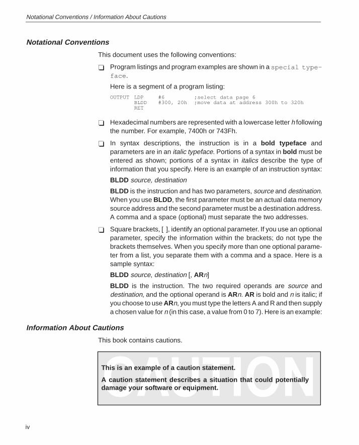
This document uses the following conventions:
� Program listings and program examples are shown in a special type-face .
Here is a segment of a program listing:
OUTPUT LDP #6 ;select data page 6BLDD #300, 20h ;move data at address 300h to 320hRET
� Hexadecimal numbers are represented with a lowercase letter h followingthe number. For example, 7400h or 743Fh.
� In syntax descriptions, the instruction is in a bold typeface andparameters are in an italic typeface. Portions of a syntax in bold must beentered as shown; portions of a syntax in italics describe the type ofinformation that you specify. Here is an example of an instruction syntax:
BLDD source, destination
BLDD is the instruction and has two parameters, source and destination.When you use BLDD , the first parameter must be an actual data memorysource address and the second parameter must be a destination address.A comma and a space (optional) must separate the two addresses.
� Square brackets, [ ], identify an optional parameter. If you use an optionalparameter, specify the information within the brackets; do not type thebrackets themselves. When you specify more than one optional parame-ter from a list, you separate them with a comma and a space. Here is asample syntax:
BLDD source, destination [, ARn]
BLDD is the instruction. The two required operands are source anddestination, and the optional operand is ARn. AR is bold and n is italic; ifyou choose to use ARn, you must type the letters A and R and then supplya chosen value for n (in this case, a value from 0 to 7). Here is an example:
Information About Cautions
This book contains cautions.
This is an example of a caution statement.
A caution statement describes a situation that could potentiallydamage your software or equipment.
Notational Conventions / Information About Cautions
Related Documentation from Texas Instruments
vRead This First
Related Documentation from Texas Instruments
The following books describe the ’F/C240 and related support tools. To obtaina copy of any of these TI documents, call the Texas Instruments LiteratureResponse Center at (800) 477–8924. When ordering, please identify the bookby its title and literature number. Many of these documents are located on theinternet at http://www.ti.com.
TMS320F/C24x DSP Controllers CPU and Instruction Set ReferenceGuide (literature number SPRU160) describes the TMS320F/C24x16-bit fixed-point digital signal processor controller. Covered are itsarchitecture, internal register structure, data and program addressing,and instruction set. Also includes instruction set comparisons and designconsiderations for using the XDS510 emulator.
TMS320F243/F241/C242 DSP Controllers System and PeripheralsReference Guide (literature number SPRU276) describes thearchitecture, system hardware, peripherals, and general operation of theTMS320F243, ’F241, and ’C242 digital signal processor (DSP)controllers.
TMS320C240, TMS320F240 DSP Controllers (literature number SPRS042)data sheet contains the electrical and timing specifications for thesedevices, as well as signal descriptions and pinouts for all of the availablepackages.
TMS320F20x/F24x Embedded Flash Memory Technical Reference(literature number SPRU282) Describes the operation of the embeddedflash EEPROM module on the TMS320F20x/F24x digital signalprocessor (DSP) devices and provides sample code that you can use todevelop your own software.
TMS320C1x/C2x/C2xx/C5x Code Generation Tools Getting StartedGuide (literature number SPRU121) describes how to install theTMS320C1x, TMS320C2x, TMS320C2xx, and TMS320C5x assemblylanguage tools and the C compiler for the ’C1x, ’C2x, ’C2xx, and ’C5x de-vices. The installations for MS-DOS , OS/2 , SunOS , and Solarissystems are covered.
TMS320C1x/C2x/C2xx/C5x Assembly Language Tools User’s Guide (lit-erature number SPRU018) describes the assembly language tools (as-sembler, linker, and other tools used to develop assembly languagecode), assembler directives, macros, common object file format, andsymbolic debugging directives for the ’C1x, ’C2x, ’C2xx, and ’C5x gen-erations of devices.
Related Documentation from Texas Instruments
vi
TMS320C2x/C2xx/C5x Optimizing C Compiler User’s Guide (literaturenumber SPRU024) describes the ’C2x/C2xx/C5x C compiler. This Ccompiler accepts ANSI standard C source code and produces TMS320assembly language source code for the ’C2x, ’C2xx, and ’C5x genera-tions of devices.
TMS320C2xx C Source Debugger User’s Guide (literature numberSPRU151) tells you how to invoke the ’C2xx emulator and simulator ver-sions of the C source debugger interface. This book discusses variousaspects of the debugger interface, including window management, com-mand entry, code execution, data management, and breakpoints. It alsoincludes a tutorial that introduces basic debugger functionality.
TMS320C2xx Simulator Getting Started (literature number SPRU137)describes how to install the TMS320C2xx simulator and the C sourcedebugger for the ’C2xx. The installation for MS-DOS , PC-DOS ,SunOS , Solaris , and HP-UX systems is covered.
TMS320C2xx Emulator Getting Started Guide (literature numberSPRU209) tells you how to install the Windows 3.1 and Windows 95versions of the ’C2xx emulator and C source debugger interface.
XDS51x Emulator Installation Guide (literature number SPNU070)describes the installation of the XDS510 , XDS510PP , andXDS510WS emulator controllers. The installation of the XDS511emulator is also described.
XDS522/XDS522A Emulation System Installation Guide (literature num-ber SPRU171) describes the installation of the emulation system.Instructions include how to install the hardware and software for theXDS522 and XDS522A .
XDS522A Emulation System User’s Guide (literature number SPRU169)tells you how to use the XDS522A emulation system. This book de-scribes the operation of the breakpoint, tracing, and timing functionalityin the XDS522A emulation system. This book also discusses BTTsoftware interface and includes a tutorial that uses step-by-stepinstructions to demonstrate how to use the XDS522A emulation system.
XDS522A Emulation System Online Help (literature number SPRC002) isan online help file that provides descriptions of the BTT software user in-terface, menus, and dialog boxes.
JTAG/MPSD Emulation Technical Reference (literature number SPDU079)provides the design requirements of the XDS510 emulator controller,discusses JTAG designs (based on the IEEE 1149.1 standard), andmodular port scan device (MPSD) designs.
Related Technical Articles
viiRead This First
TMS320 DSP Development Support Reference Guide (literature numberSPRU011) describes the TMS320 family of digital signal processors andthe tools that support these devices. Included are code-generation tools(compilers, assemblers, linkers, etc.) and system integration and debugtools (simulators, emulators, evaluation modules, etc.). Also covered areavailable documentation, seminars, the university program, and factoryrepair and exchange.
TMS320 DSP Designer’s Notebook: Volume 1 (literature numberSPRT125) presents solutions to common design problems using ’C2x,’C3x, ’C4x, ’C5x, and other TI DSPs.
TMS320 Third-Party Support Reference Guide (literature numberSPRU052) alphabetically lists over 100 third parties that provide variousproducts that serve the family of TMS320 digital signal processors. Amyriad of products and applications are offered—software and hardwaredevelopment tools, speech recognition, image processing, noise can-cellation, modems, etc.
Related Technical Articles
The following technical articles contain useful information regarding designs,operations, and applications for signal-processing systems. These articlessupplement the material in this book.
“A Greener World Through DSP Controllers”, Panos Papamichalis, DSP &Multimedia Technology, September 1994.
“A Single-Chip Multiprocessor DSP for Image Processing—TMS320C80”,Dr. Ing. Dung Tu, Industrie Elektronik, Germany, March 1995.
“Application Guide with DSP Leading-Edge Technology”, Y. Nishikori,M. Hattori, T. Fukuhara, R.Tanaka, M. Shimoda, I. Kudo, A.Yanagitani,H. Miyaguchi, et al., Electronics Engineering, November 1995.
“Approaching the No-Power Barrier”, Jon Bradley and Gene Frantz, ElectronicDesign, January 9, 1995.
“Beware of BAT: DSPs Add Brilliance to New Weapons Systems”, PanosPapamichalis, DSP & Multimedia Technology, October 1994.
“Choose DSPs for PC Signal Processing”, Panos Papamichalis, DSP &Multimedia Technology, January/February 1995.
“Developing Nations Take Shine to Wireless”, Russell MacDonald, KaraSchmidt and Kim Higden, EE Times, October 2, 1995.
Related Documentation from Texas Instruments / Related Technical Articles
Related Technical Articles
viii
“Digital Signal Processing Solutions Target Vertical Application Markets”, RonWages, ECN, September 1995.
“Digital Signal Processors Boost Drive Performance”, Tim Adcock, DataStorage, September/October 1995.
“DSP and Speech Recognition, An Origin of the Species”, PanosPapamichalis, DSP & Multimedia Technology, July 1994.
“DSP Design Takes Top-Down Approach”, Andy Fritsch and Kim Asal, DSPSeries Part III, EE Times, July 17, 1995.
“DSPs Advance Low-Cost ‘Green’ Control”, Gregg Bennett, DSP Series PartII, EE Times, April 17, 1995.
“DSPs Do Best on Multimedia Applications”, Doug Rasor, Asian ComputerWorld, October 9–16, 1995.
“DSPs: Speech Recognition Technology Enablers”, Gene Frantz and GreggBennett, I&CS, May 1995.
“Easing JTAG Testing of Parallel-Processor Projects”, Tony Coomes, AndyFritsch, and Reid Tatge, Asian Electronics Engineer, Manila, Philippines,November 1995.
“Fixed or Floating? A Pointed Question in DSPs”, Jim Larimer and DanielChen, EDN, August 3, 1995.
“Function-Focused Chipsets: Up the DSP Integration Core”, PanosPapamichalis, DSP & Multimedia Technology, March/April 1995.
“GSM: Standard, Strategien und Systemchips”, Edgar Auslander, ElektronikPraxis, Germany, October 6, 1995.
“High Tech Copiers to Improve Images and Reduce Paperwork”, Karl Guttag,Document Management, July/August 1995.
“Host-Enabled Multimedia: Brought to You by DSP Solutions”, PanosPapamichalis, DSP & Multimedia Technology, September/October 1995.
“Integration Shrinks Digital Cellular Telephone Designs”, Fred Cohen andMike McMahan, Wireless System Design, November 1994.
“On-Chip Multiprocessing Melds DSPs”, Karl Guttag and Doug Deao, DSPSeries Part III, EE Times, July 18, 1994.
“Real-Time Control”, Gregg Bennett, Appliance Manufacturer, May 1995.
“Speech Recognition”, P.K. Rajasekaran and Mike McMahan, WirelessDesign & Development, May 1995.
Trademarks
ixRead This First
“Telecom Future Driven by Reduced Milliwatts per DSP Function”, PanosPapamichalis, DSP & Multimedia Technology, May/June 1995.
“The Digital Signal Processor Development Environment”, Greg Peake,Embedded System Engineering, United Kingdom, February 1995.
“The Growing Spectrum of Custom DSPs”, Gene Frantz and Kun Lin, DSPSeries Part II, EE Times, April 18, 1994.
“The Wide World of DSPs, ” Jim Larimer, Design News, June 27, 1994.
“Third-Party Support Drives DSP Development for Uninitiated and ExpertsAlike”, Panos Papamichalis, DSP & Multimedia Technology, December1994/January 1995.
“Toward an Era of Economical DSPs”, John Cooper, DSP Series Part I, EETimes, Jan. 23, 1995.
Trademarks
HP-UX is a trademark of Hewlett-Packard Company.
MS-DOS and Windows are registered trademarks of Microsoft Corporation.
OS/2, PC, and PC-DOS are trademarks of International Business MachinesCorporation.
PAL is a registered trademark of Advanced Micro Devices, Inc.
Solaris and SunOS are trademarks of Sun Microsystems, Inc.
320 Hotline On-line, TI, XDS510, XDS510PP, XDS510WS, XDS511, XDS522,and XDS522A are trademarks of Texas Instruments Incorporated.
Related Technical Articles / Trademarks
Contents
xi
Contents
1 Introduction 1-1. . . . . . . . . . . . . . . . . . . . . . . . . . . . . . . . . . . . . . . . . . . . . . . . . . . . . . . . . . . . . . . . . . . . . Summarizes the TMS320 family of products. Introduces the TMS320C24x DSP controllers andprovides an overview of the ’240 device.
1.1 TMS320 Family Overview 1-2. . . . . . . . . . . . . . . . . . . . . . . . . . . . . . . . . . . . . . . . . . . . . . . . . . . 1.2 TMS320C24x Series of DSP Controllers 1-5. . . . . . . . . . . . . . . . . . . . . . . . . . . . . . . . . . . . . . . 1.3 TMS320F/C240 Overview 1-7. . . . . . . . . . . . . . . . . . . . . . . . . . . . . . . . . . . . . . . . . . . . . . . . . . .
2 TMS320F/C240 DSP Controller 2-1. . . . . . . . . . . . . . . . . . . . . . . . . . . . . . . . . . . . . . . . . . . . . . . . . . . Describes the TMS320F/C240 DSP Controller. Includes a device overview, pin-out diagram,memory map, and a discussion on interrupts.
2.1 TMS320F/C240 DSP Controller Overview 2-2. . . . . . . . . . . . . . . . . . . . . . . . . . . . . . . . . . . . . 2.1.1 Architectural Overview 2-13. . . . . . . . . . . . . . . . . . . . . . . . . . . . . . . . . . . . . . . . . . . . . .
2.2 Memory Map 2-15. . . . . . . . . . . . . . . . . . . . . . . . . . . . . . . . . . . . . . . . . . . . . . . . . . . . . . . . . . . . . . 2.3 Peripheral Memory Map 2-17. . . . . . . . . . . . . . . . . . . . . . . . . . . . . . . . . . . . . . . . . . . . . . . . . . . . 2.4 Digital I/O and Shared Pin Functions 2-19. . . . . . . . . . . . . . . . . . . . . . . . . . . . . . . . . . . . . . . . .
2.4.1 Description of Group1 Shared I/O pins 2-19. . . . . . . . . . . . . . . . . . . . . . . . . . . . . . . . 2.4.2 Description of Group 2 Shared I/O Pins 2-21. . . . . . . . . . . . . . . . . . . . . . . . . . . . . . . 2.4.3 Digital I/O Control Registers 2-21. . . . . . . . . . . . . . . . . . . . . . . . . . . . . . . . . . . . . . . . .
2.5 Interrupts 2-27. . . . . . . . . . . . . . . . . . . . . . . . . . . . . . . . . . . . . . . . . . . . . . . . . . . . . . . . . . . . . . . . . 2.5.1 Resets 2-31. . . . . . . . . . . . . . . . . . . . . . . . . . . . . . . . . . . . . . . . . . . . . . . . . . . . . . . . . . . . 2.5.2 Non-Maskable Interrupts (NMI) — Hardware and Software 2-34. . . . . . . . . . . . . . . 2.5.3 Interrupt Structure — Detailed Description 2-36. . . . . . . . . . . . . . . . . . . . . . . . . . . . . 2.5.4 Interrupt Structure — Priority and Ranking 2-40. . . . . . . . . . . . . . . . . . . . . . . . . . . . . 2.5.5 Interrupt Operation: Detailed Description 2-46. . . . . . . . . . . . . . . . . . . . . . . . . . . . . . 2.5.6 Interrupt Latency 2-59. . . . . . . . . . . . . . . . . . . . . . . . . . . . . . . . . . . . . . . . . . . . . . . . . . . 2.5.7 External Interrupts 2-61. . . . . . . . . . . . . . . . . . . . . . . . . . . . . . . . . . . . . . . . . . . . . . . . . . 2.5.8 Peripheral Interrupt Enable Sequence 2-61. . . . . . . . . . . . . . . . . . . . . . . . . . . . . . . . . 2.5.9 Summary of Interrupt Operation 2-62. . . . . . . . . . . . . . . . . . . . . . . . . . . . . . . . . . . . . .
2.6 CPU Interrupt Registers 2-64. . . . . . . . . . . . . . . . . . . . . . . . . . . . . . . . . . . . . . . . . . . . . . . . . . . . 2.6.1 External Interrupt Control Registers 2-67. . . . . . . . . . . . . . . . . . . . . . . . . . . . . . . . . . .
Contents
xii
3 System Functions 3-1. . . . . . . . . . . . . . . . . . . . . . . . . . . . . . . . . . . . . . . . . . . . . . . . . . . . . . . . . . . . . . . Describes ’240 functions that are not specific to any peripheral.
3.1 Peripheral Interface 3-2. . . . . . . . . . . . . . . . . . . . . . . . . . . . . . . . . . . . . . . . . . . . . . . . . . . . . . . . . 3.2 System Configuration Registers 3-4. . . . . . . . . . . . . . . . . . . . . . . . . . . . . . . . . . . . . . . . . . . . . .
3.2.1 System Control Register (SYSCR) 3-6. . . . . . . . . . . . . . . . . . . . . . . . . . . . . . . . . . . . . 3.2.2 System Status Register (SYSSR) 3-7. . . . . . . . . . . . . . . . . . . . . . . . . . . . . . . . . . . . . . 3.2.3 System Interrupt Vector Register (SYSIVR) 3-9. . . . . . . . . . . . . . . . . . . . . . . . . . . . .
3.3 Power -Down Modes 3-10. . . . . . . . . . . . . . . . . . . . . . . . . . . . . . . . . . . . . . . . . . . . . . . . . . . . . . . 3.3.1 Clock Generation 3-10. . . . . . . . . . . . . . . . . . . . . . . . . . . . . . . . . . . . . . . . . . . . . . . . . . . 3.3.2 Setting and Entering the Power-Down Modes 3-12. . . . . . . . . . . . . . . . . . . . . . . . . . 3.3.3 Exiting the Power-Down Modes 3-12. . . . . . . . . . . . . . . . . . . . . . . . . . . . . . . . . . . . . . 3.3.4 Low-Power Mode 3-14. . . . . . . . . . . . . . . . . . . . . . . . . . . . . . . . . . . . . . . . . . . . . . . . . . . 3.3.5 After Exiting Power-Down 3-16. . . . . . . . . . . . . . . . . . . . . . . . . . . . . . . . . . . . . . . . . . . 3.3.6 Summary of Power-Down Mode Operation 3-18. . . . . . . . . . . . . . . . . . . . . . . . . . . .
4 PLL Clock Module 4-1. . . . . . . . . . . . . . . . . . . . . . . . . . . . . . . . . . . . . . . . . . . . . . . . . . . . . . . . . . . . . . . Describes the architecture, functions, and programming of the PLL Clock module.
4.1 PLL Clock Module Overview 4-2. . . . . . . . . . . . . . . . . . . . . . . . . . . . . . . . . . . . . . . . . . . . . . . . . 4.2 PLL Clock Operation 4-5. . . . . . . . . . . . . . . . . . . . . . . . . . . . . . . . . . . . . . . . . . . . . . . . . . . . . . . .
4.2.1 Pin Description 4-5. . . . . . . . . . . . . . . . . . . . . . . . . . . . . . . . . . . . . . . . . . . . . . . . . . . . . . 4.2.2 Oscillator Operation Modes 4-6. . . . . . . . . . . . . . . . . . . . . . . . . . . . . . . . . . . . . . . . . . . 4.2.3 PLL Operation Modes 4-6. . . . . . . . . . . . . . . . . . . . . . . . . . . . . . . . . . . . . . . . . . . . . . . . 4.2.4 CPU Clock (CPUCLK) Frequency Selection 4-7. . . . . . . . . . . . . . . . . . . . . . . . . . . . . 4.2.5 System Clock (SYSCLK) Frequency Selection 4-8. . . . . . . . . . . . . . . . . . . . . . . . . . 4.2.6 Watchdog Counter Clock (WDCLK) 4-9. . . . . . . . . . . . . . . . . . . . . . . . . . . . . . . . . . . . 4.2.7 PLL Startup 4-9. . . . . . . . . . . . . . . . . . . . . . . . . . . . . . . . . . . . . . . . . . . . . . . . . . . . . . . . . 4.2.8 Low-Power Modes 4-10. . . . . . . . . . . . . . . . . . . . . . . . . . . . . . . . . . . . . . . . . . . . . . . . . .
4.3 PLL Clock Control Registers 4-14. . . . . . . . . . . . . . . . . . . . . . . . . . . . . . . . . . . . . . . . . . . . . . . . 4.3.1 Clock Control Register 0 (CKCR0) 4-14. . . . . . . . . . . . . . . . . . . . . . . . . . . . . . . . . . . . 4.3.2 Clock Control Register 1 (CKCR1) 4-16. . . . . . . . . . . . . . . . . . . . . . . . . . . . . . . . . . . .
5 Watchdog and Real-Time Interrupt Module 5-1. . . . . . . . . . . . . . . . . . . . . . . . . . . . . . . . . . . . . . . . Describes the watchdog (WD) and real-time Interrupt (RTI) module. The WD provides inter-rupts at selected intervals (1 to 4096 interrupts per second), while the RTI is operable by pollingor interrupts. Covers the architecture of both functions as well as the registers used to set upthe functions.
5.1 Watchdog (WD) and Real-Time Interrupt (RTI) Overview 5-2. . . . . . . . . . . . . . . . . . . . . . . . . 5.1.1 WD and RTI Components 5-2. . . . . . . . . . . . . . . . . . . . . . . . . . . . . . . . . . . . . . . . . . . . 5.1.2 Control Registers 5-4. . . . . . . . . . . . . . . . . . . . . . . . . . . . . . . . . . . . . . . . . . . . . . . . . . . .
5.2 Operation of Watchdog (WD) and Real-Time Interrupt (RTI) Timers 5-6. . . . . . . . . . . . . . . 5.2.1 WD Timer 5-6. . . . . . . . . . . . . . . . . . . . . . . . . . . . . . . . . . . . . . . . . . . . . . . . . . . . . . . . . . 5.2.2 RTI timer 5-9. . . . . . . . . . . . . . . . . . . . . . . . . . . . . . . . . . . . . . . . . . . . . . . . . . . . . . . . . . .
Contents
xiiiContents
5.3 Watchdog (WD) and Real-Time Interrupt (RTI) Control Registers 5-11. . . . . . . . . . . . . . . . 5.3.1 Real-Time Interrupt Counter Register (RTICNTR) 5-12. . . . . . . . . . . . . . . . . . . . . . . 5.3.2 WD Counter Register (WDCNTR) 5-13. . . . . . . . . . . . . . . . . . . . . . . . . . . . . . . . . . . . 5.3.3 WD Reset Key Register (WDKEY) 5-13. . . . . . . . . . . . . . . . . . . . . . . . . . . . . . . . . . . . 5.3.4 RTI Control Register (RTICR) 5-14. . . . . . . . . . . . . . . . . . . . . . . . . . . . . . . . . . . . . . . . 5.3.5 WD Timer Control Register (WDCR) 5-16. . . . . . . . . . . . . . . . . . . . . . . . . . . . . . . . . .
5.4 Watchdog (WD) and Real-Time Interrupt (RTI) Routines 5-18. . . . . . . . . . . . . . . . . . . . . . . .
6 Event Manager Module 6-1. . . . . . . . . . . . . . . . . . . . . . . . . . . . . . . . . . . . . . . . . . . . . . . . . . . . . . . . . . . Describes the event manager (EV) module. Includes descriptions of the general purpose timer,compare units, pulse-width modulation waveform circuits, capture units, and quadrature en-coder pulse circuits.
6.1 Event Manager (EV) Module Overview 6-2. . . . . . . . . . . . . . . . . . . . . . . . . . . . . . . . . . . . . . . . 6.1.1 EV Functional Blocks 6-2. . . . . . . . . . . . . . . . . . . . . . . . . . . . . . . . . . . . . . . . . . . . . . . . 6.1.2 EV Pins 6-4. . . . . . . . . . . . . . . . . . . . . . . . . . . . . . . . . . . . . . . . . . . . . . . . . . . . . . . . . . . . 6.1.3 Power-Drive Protection 6-5. . . . . . . . . . . . . . . . . . . . . . . . . . . . . . . . . . . . . . . . . . . . . . . 6.1.4 EV Registers 6-6. . . . . . . . . . . . . . . . . . . . . . . . . . . . . . . . . . . . . . . . . . . . . . . . . . . . . . . . 6.1.5 EV Interrupts 6-6. . . . . . . . . . . . . . . . . . . . . . . . . . . . . . . . . . . . . . . . . . . . . . . . . . . . . . . .
6.2 Event Manager (EV) Register Addresses 6-8. . . . . . . . . . . . . . . . . . . . . . . . . . . . . . . . . . . . . . 6.3 General-Purpose (GP) Timers 6-11. . . . . . . . . . . . . . . . . . . . . . . . . . . . . . . . . . . . . . . . . . . . . . .
6.3.1 GP Timer Functional Blocks 6-11. . . . . . . . . . . . . . . . . . . . . . . . . . . . . . . . . . . . . . . . . 6.3.2 GP Timer Inputs 6-12. . . . . . . . . . . . . . . . . . . . . . . . . . . . . . . . . . . . . . . . . . . . . . . . . . . . 6.3.3 GP Timer Outputs 6-13. . . . . . . . . . . . . . . . . . . . . . . . . . . . . . . . . . . . . . . . . . . . . . . . . . 6.3.4 Control of GP Timer Operation 6-13. . . . . . . . . . . . . . . . . . . . . . . . . . . . . . . . . . . . . . . 6.3.5 GP Timer Control Register (GPTCON) 6-13. . . . . . . . . . . . . . . . . . . . . . . . . . . . . . . . 6.3.6 GP Timer Compare Registers 6-13. . . . . . . . . . . . . . . . . . . . . . . . . . . . . . . . . . . . . . . . 6.3.7 GP Timer Period Register 6-14. . . . . . . . . . . . . . . . . . . . . . . . . . . . . . . . . . . . . . . . . . . 6.3.8 Double Buffering of GP Timer Compare and Period Registers 6-14. . . . . . . . . . . . 6.3.9 GP Timer Compare/PWM Output 6-15. . . . . . . . . . . . . . . . . . . . . . . . . . . . . . . . . . . . . 6.3.10 GP Timer Counting Direction 6-15. . . . . . . . . . . . . . . . . . . . . . . . . . . . . . . . . . . . . . . . . 6.3.11 GP Timer Clock 6-16. . . . . . . . . . . . . . . . . . . . . . . . . . . . . . . . . . . . . . . . . . . . . . . . . . . . 6.3.12 32-Bit Timer 6-16. . . . . . . . . . . . . . . . . . . . . . . . . . . . . . . . . . . . . . . . . . . . . . . . . . . . . . . 6.3.13 QEP-Based Clock Input 6-17. . . . . . . . . . . . . . . . . . . . . . . . . . . . . . . . . . . . . . . . . . . . . 6.3.14 GP Timer Synchronization 6-17. . . . . . . . . . . . . . . . . . . . . . . . . . . . . . . . . . . . . . . . . . . 6.3.15 ADC Start by GP Timer Event 6-17. . . . . . . . . . . . . . . . . . . . . . . . . . . . . . . . . . . . . . . . 6.3.16 GP Timer in Emulation Suspend 6-18. . . . . . . . . . . . . . . . . . . . . . . . . . . . . . . . . . . . . . 6.3.17 GP Timer Interrupts 6-18. . . . . . . . . . . . . . . . . . . . . . . . . . . . . . . . . . . . . . . . . . . . . . . . .
6.4 GP Timer Counting Operation 6-19. . . . . . . . . . . . . . . . . . . . . . . . . . . . . . . . . . . . . . . . . . . . . . . 6.4.1 Stop/Hold Mode 6-19. . . . . . . . . . . . . . . . . . . . . . . . . . . . . . . . . . . . . . . . . . . . . . . . . . . . 6.4.2 Single Up Counting Mode 6-19. . . . . . . . . . . . . . . . . . . . . . . . . . . . . . . . . . . . . . . . . . . 6.4.3 Continuous Up Counting Mode 6-22. . . . . . . . . . . . . . . . . . . . . . . . . . . . . . . . . . . . . . . 6.4.4 Directional Up/Down Counting Mode of GP Timers 1 and 3 6-25. . . . . . . . . . . . . . 6.4.5 Directional Up/Down Counting Mode of GP Timer 2 6-26. . . . . . . . . . . . . . . . . . . . . 6.4.6 Single Up/Down Counting Mode 6-28. . . . . . . . . . . . . . . . . . . . . . . . . . . . . . . . . . . . . . 6.4.7 Continuous Up/Down Counting Mode 6-31. . . . . . . . . . . . . . . . . . . . . . . . . . . . . . . . .
Contents
xiv
6.5 GP Timer Compare Operation 6-34. . . . . . . . . . . . . . . . . . . . . . . . . . . . . . . . . . . . . . . . . . . . . . . 6.5.1 Compare/PWM Transition 6-34. . . . . . . . . . . . . . . . . . . . . . . . . . . . . . . . . . . . . . . . . . . 6.5.2 Asymmetric/Symmetric Waveform Generator 6-34. . . . . . . . . . . . . . . . . . . . . . . . . . . 6.5.3 Asymmetric Waveform Generation 6-35. . . . . . . . . . . . . . . . . . . . . . . . . . . . . . . . . . . . 6.5.4 Symmetric Waveform Generation 6-36. . . . . . . . . . . . . . . . . . . . . . . . . . . . . . . . . . . . . 6.5.5 Output Logic 6-37. . . . . . . . . . . . . . . . . . . . . . . . . . . . . . . . . . . . . . . . . . . . . . . . . . . . . . . 6.5.6 Compare Output in Directional Up/Down Counting Mode 6-38. . . . . . . . . . . . . . . . 6.5.7 Active/Inactive Time Calculation 6-39. . . . . . . . . . . . . . . . . . . . . . . . . . . . . . . . . . . . . .
6.6 GP Timer Control Registers (TxCON and GPTCON) 6-40. . . . . . . . . . . . . . . . . . . . . . . . . . . 6.7 Generation of Compare and PWM Outputs Using GP Timers 6-45. . . . . . . . . . . . . . . . . . . .
6.7.1 Generation of Compare Output 6-45. . . . . . . . . . . . . . . . . . . . . . . . . . . . . . . . . . . . . . . 6.7.2 Generation of PWM Output 6-45. . . . . . . . . . . . . . . . . . . . . . . . . . . . . . . . . . . . . . . . . . 6.7.3 GP Timer Reset 6-46. . . . . . . . . . . . . . . . . . . . . . . . . . . . . . . . . . . . . . . . . . . . . . . . . . . .
6.8 Compare Units 6-47. . . . . . . . . . . . . . . . . . . . . . . . . . . . . . . . . . . . . . . . . . . . . . . . . . . . . . . . . . . . 6.8.1 Simple Compare Units 6-47. . . . . . . . . . . . . . . . . . . . . . . . . . . . . . . . . . . . . . . . . . . . . . 6.8.2 Full Compare Units 6-48. . . . . . . . . . . . . . . . . . . . . . . . . . . . . . . . . . . . . . . . . . . . . . . . . 6.8.3 Full Compare Inputs/Outputs 6-49. . . . . . . . . . . . . . . . . . . . . . . . . . . . . . . . . . . . . . . . . 6.8.4 Full Compare Operation Modes 6-49. . . . . . . . . . . . . . . . . . . . . . . . . . . . . . . . . . . . . . 6.8.5 Compare Mode 6-50. . . . . . . . . . . . . . . . . . . . . . . . . . . . . . . . . . . . . . . . . . . . . . . . . . . . 6.8.6 PWM Mode 6-50. . . . . . . . . . . . . . . . . . . . . . . . . . . . . . . . . . . . . . . . . . . . . . . . . . . . . . . . 6.8.7 Register Setup for Full Compare Operation 6-50. . . . . . . . . . . . . . . . . . . . . . . . . . . . 6.8.8 Compare Unit Registers 6-51. . . . . . . . . . . . . . . . . . . . . . . . . . . . . . . . . . . . . . . . . . . . . 6.8.9 Compare Unit Interrupts 6-58. . . . . . . . . . . . . . . . . . . . . . . . . . . . . . . . . . . . . . . . . . . . . 6.8.10 Compare Unit Reset 6-58. . . . . . . . . . . . . . . . . . . . . . . . . . . . . . . . . . . . . . . . . . . . . . . .
6.9 PWM Circuits Associated With Full Compare Units 6-59. . . . . . . . . . . . . . . . . . . . . . . . . . . . . 6.9.1 PWM Generation Capability 6-60. . . . . . . . . . . . . . . . . . . . . . . . . . . . . . . . . . . . . . . . . . 6.9.2 Programmable Dead-Band Unit 6-61. . . . . . . . . . . . . . . . . . . . . . . . . . . . . . . . . . . . . . 6.9.3 Inputs and Outputs of Dead-Band Unit 6-62. . . . . . . . . . . . . . . . . . . . . . . . . . . . . . . . 6.9.4 Dead-Band Generation 6-62. . . . . . . . . . . . . . . . . . . . . . . . . . . . . . . . . . . . . . . . . . . . . . 6.9.5 Other Important Features of Dead-Band Units 6-65. . . . . . . . . . . . . . . . . . . . . . . . . . 6.9.6 Output Logic 6-67. . . . . . . . . . . . . . . . . . . . . . . . . . . . . . . . . . . . . . . . . . . . . . . . . . . . . . .
6.10 PWM Waveform Generation With Compare Units and PWM Circuits 6-69. . . . . . . . . . . . . 6.10.1 PWM Signals 6-69. . . . . . . . . . . . . . . . . . . . . . . . . . . . . . . . . . . . . . . . . . . . . . . . . . . . . . 6.10.2 PWM Signal Generation 6-69. . . . . . . . . . . . . . . . . . . . . . . . . . . . . . . . . . . . . . . . . . . . . 6.10.3 Dead Band 6-70. . . . . . . . . . . . . . . . . . . . . . . . . . . . . . . . . . . . . . . . . . . . . . . . . . . . . . . . 6.10.4 Generation of PWM Outputs With Event Manager 6-70. . . . . . . . . . . . . . . . . . . . . . 6.10.5 Asymmetric and Symmetric PWM Generation 6-70. . . . . . . . . . . . . . . . . . . . . . . . . . 6.10.6 Register Setup for PWM Generation 6-71. . . . . . . . . . . . . . . . . . . . . . . . . . . . . . . . . . 6.10.7 Asymmetric PWM Waveform Generation 6-72. . . . . . . . . . . . . . . . . . . . . . . . . . . . . . 6.10.8 Symmetric PWM Waveform Generation 6-73. . . . . . . . . . . . . . . . . . . . . . . . . . . . . . .
6.11 Space-Vector PWM 6-74. . . . . . . . . . . . . . . . . . . . . . . . . . . . . . . . . . . . . . . . . . . . . . . . . . . . . . . . 6.11.1 3-Phase Power Inverter 6-74. . . . . . . . . . . . . . . . . . . . . . . . . . . . . . . . . . . . . . . . . . . . . 6.11.2 Switching Patterns of a Power Inverter and Basic Space Vectors 6-74. . . . . . . . . 6.11.3 Approximation of Motor Voltage with Basic Space Vectors 6-76. . . . . . . . . . . . . . .
Contents
xvContents
6.11.4 Space-Vector PWM Waveform Generation With EV 6-77. . . . . . . . . . . . . . . . . . . . . 6.11.5 Space-Vector PWM Waveforms 6-78. . . . . . . . . . . . . . . . . . . . . . . . . . . . . . . . . . . . . . 6.11.6 Unused Full Compare Register 6-78. . . . . . . . . . . . . . . . . . . . . . . . . . . . . . . . . . . . . . . 6.11.7 Space-Vector PWM Boundary Conditions 6-78. . . . . . . . . . . . . . . . . . . . . . . . . . . . . .
6.12 Capture Units 6-80. . . . . . . . . . . . . . . . . . . . . . . . . . . . . . . . . . . . . . . . . . . . . . . . . . . . . . . . . . . . . 6.12.1 Features 6-81. . . . . . . . . . . . . . . . . . . . . . . . . . . . . . . . . . . . . . . . . . . . . . . . . . . . . . . . . . 6.12.2 Operation of Capture Units 6-81. . . . . . . . . . . . . . . . . . . . . . . . . . . . . . . . . . . . . . . . . . 6.12.3 Capture Unit Registers 6-82. . . . . . . . . . . . . . . . . . . . . . . . . . . . . . . . . . . . . . . . . . . . . . 6.12.4 Capture Unit FIFO Stacks (CAPnFIFO, n = 1, 2, 3, 4) 6-87. . . . . . . . . . . . . . . . . . .
6.13 Quadrature Encoder Pulse (QEP) Circuit 6-91. . . . . . . . . . . . . . . . . . . . . . . . . . . . . . . . . . . . . 6.13.1 QEP Pins 6-91. . . . . . . . . . . . . . . . . . . . . . . . . . . . . . . . . . . . . . . . . . . . . . . . . . . . . . . . . . 6.13.2 QEP Circuit Time Base 6-91. . . . . . . . . . . . . . . . . . . . . . . . . . . . . . . . . . . . . . . . . . . . . . 6.13.3 QEP Decoding 6-92. . . . . . . . . . . . . . . . . . . . . . . . . . . . . . . . . . . . . . . . . . . . . . . . . . . . . 6.13.4 QEP Counting 6-93. . . . . . . . . . . . . . . . . . . . . . . . . . . . . . . . . . . . . . . . . . . . . . . . . . . . . 6.13.5 Register Setup for the QEP Circuit 6-93. . . . . . . . . . . . . . . . . . . . . . . . . . . . . . . . . . . .
6.14 Event Manager (EV) Interrupts 6-95. . . . . . . . . . . . . . . . . . . . . . . . . . . . . . . . . . . . . . . . . . . . . . 6.14.1 Organization of TMS320C240 Interrupts 6-95. . . . . . . . . . . . . . . . . . . . . . . . . . . . . . . 6.14.2 EV Interrupt Requests and Services 6-95. . . . . . . . . . . . . . . . . . . . . . . . . . . . . . . . . . 6.14.3 EV Interrupt Flag Registers 6-99. . . . . . . . . . . . . . . . . . . . . . . . . . . . . . . . . . . . . . . . . . 6.14.4 EV Interrupt Mask Registers 6-104. . . . . . . . . . . . . . . . . . . . . . . . . . . . . . . . . . . . . . . . 6.14.5 EV Interrupt Vector Registers 6-108. . . . . . . . . . . . . . . . . . . . . . . . . . . . . . . . . . . . . . .
7 Dual 10-Bit Analog-to-Digital Converter (ADC) Module 7-1. . . . . . . . . . . . . . . . . . . . . . . . . . . . . Describes the Dual 10-Bit Analog-to-Digital Converter (ADC) module.
7.1 Dual 10-Bit ADC Overview 7-2. . . . . . . . . . . . . . . . . . . . . . . . . . . . . . . . . . . . . . . . . . . . . . . . . . . 7.2 ADC Operation 7-4. . . . . . . . . . . . . . . . . . . . . . . . . . . . . . . . . . . . . . . . . . . . . . . . . . . . . . . . . . . . .
7.2.1 ADC Module Pin Description 7-4. . . . . . . . . . . . . . . . . . . . . . . . . . . . . . . . . . . . . . . . . . 7.2.2 ADC Module Operational Modes 7-4. . . . . . . . . . . . . . . . . . . . . . . . . . . . . . . . . . . . . . 7.2.3 Analog Signal Sampling/Conversion 7-6. . . . . . . . . . . . . . . . . . . . . . . . . . . . . . . . . . .
7.3 ADC Registers 7-7. . . . . . . . . . . . . . . . . . . . . . . . . . . . . . . . . . . . . . . . . . . . . . . . . . . . . . . . . . . . . 7.3.1 ADC Control Register 1 (ADCTRL1) 7-7. . . . . . . . . . . . . . . . . . . . . . . . . . . . . . . . . . . 7.3.2 ADC Control Register 2 (ADCTRL2) 7-10. . . . . . . . . . . . . . . . . . . . . . . . . . . . . . . . . . 7.3.3 ADC Digital Result Registers 7-13. . . . . . . . . . . . . . . . . . . . . . . . . . . . . . . . . . . . . . . . .
8 Serial Communications Interface (SCI) Module 8-1. . . . . . . . . . . . . . . . . . . . . . . . . . . . . . . . . . . . Describes the architecture, functions, and programming of the serial communications interface(SCI) module.
8.1 SCI Overview 8-2. . . . . . . . . . . . . . . . . . . . . . . . . . . . . . . . . . . . . . . . . . . . . . . . . . . . . . . . . . . . . . 8.1.1 SCI Physical Description 8-2. . . . . . . . . . . . . . . . . . . . . . . . . . . . . . . . . . . . . . . . . . . . . 8.1.2 Architecture 8-5. . . . . . . . . . . . . . . . . . . . . . . . . . . . . . . . . . . . . . . . . . . . . . . . . . . . . . . . . 8.1.3 SCI Control Registers 8-5. . . . . . . . . . . . . . . . . . . . . . . . . . . . . . . . . . . . . . . . . . . . . . . . 8.1.4 Multiprocessor and Asynchronous Communications Modes 8-7. . . . . . . . . . . . . . .
8.2 SCI Programmable Data Format 8-8. . . . . . . . . . . . . . . . . . . . . . . . . . . . . . . . . . . . . . . . . . . . . . 8.3 SCI Multiprocessor Communication 8-9. . . . . . . . . . . . . . . . . . . . . . . . . . . . . . . . . . . . . . . . . . .
8.3.1 Idle-Line Multiprocessor Mode 8-10. . . . . . . . . . . . . . . . . . . . . . . . . . . . . . . . . . . . . . . 8.3.2 Address-Bit Multiprocessor Mode 8-12. . . . . . . . . . . . . . . . . . . . . . . . . . . . . . . . . . . . .
Contents
xvi
8.4 SCI Communication Format 8-14. . . . . . . . . . . . . . . . . . . . . . . . . . . . . . . . . . . . . . . . . . . . . . . . . 8.4.1 Receiver Signals in Communications Modes 8-15. . . . . . . . . . . . . . . . . . . . . . . . . . . 8.4.2 Transmitter Signals in Communications Modes 8-16. . . . . . . . . . . . . . . . . . . . . . . . .
8.5 SCI Port Interrupts 8-17. . . . . . . . . . . . . . . . . . . . . . . . . . . . . . . . . . . . . . . . . . . . . . . . . . . . . . . . . 8.5.1 SCI Baud Rate Calculation 8-18. . . . . . . . . . . . . . . . . . . . . . . . . . . . . . . . . . . . . . . . . .
8.6 SCI Control Registers 8-19. . . . . . . . . . . . . . . . . . . . . . . . . . . . . . . . . . . . . . . . . . . . . . . . . . . . . . 8.6.1 SCI Communication Control Register (SCICCR) 8-20. . . . . . . . . . . . . . . . . . . . . . . . 8.6.2 SCI Control Register 1 (SCICTL1) 8-22. . . . . . . . . . . . . . . . . . . . . . . . . . . . . . . . . . . . 8.6.3 Baud-Select Registers (SCIHBAUD and SCILBAUD) 8-25. . . . . . . . . . . . . . . . . . . . 8.6.4 SCI Control Register 2 (SCICTL2) 8-26. . . . . . . . . . . . . . . . . . . . . . . . . . . . . . . . . . . . 8.6.5 Receiver Status Register (SCIRXST) 8-27. . . . . . . . . . . . . . . . . . . . . . . . . . . . . . . . . . 8.6.6 Receiver Data Buffer Registers 8-29. . . . . . . . . . . . . . . . . . . . . . . . . . . . . . . . . . . . . . . 8.6.7 Transmit data buffer register (SCITXBUF) 8-30. . . . . . . . . . . . . . . . . . . . . . . . . . . . . 8.6.8 Port Control Register 2 (SCIPC2) 8-31. . . . . . . . . . . . . . . . . . . . . . . . . . . . . . . . . . . . . 8.6.9 Priority Control Register (SCIPRI) 8-33. . . . . . . . . . . . . . . . . . . . . . . . . . . . . . . . . . . .
8.7 SCI Initialization Example 8-34. . . . . . . . . . . . . . . . . . . . . . . . . . . . . . . . . . . . . . . . . . . . . . . . . . .
9 Serial Peripheral Interface (SPI) Module 9-1. . . . . . . . . . . . . . . . . . . . . . . . . . . . . . . . . . . . . . . . . . . Describes the architecture, functions, and programming of the serial peripheral interface (SPI)module.
9.1 SPI Overview 9-2. . . . . . . . . . . . . . . . . . . . . . . . . . . . . . . . . . . . . . . . . . . . . . . . . . . . . . . . . . . . . . 9.1.1 SPI Physical Description 9-2. . . . . . . . . . . . . . . . . . . . . . . . . . . . . . . . . . . . . . . . . . . . . 9.1.2 SPI Control Registers 9-4. . . . . . . . . . . . . . . . . . . . . . . . . . . . . . . . . . . . . . . . . . . . . . . .
9.2 SPI Operation 9-6. . . . . . . . . . . . . . . . . . . . . . . . . . . . . . . . . . . . . . . . . . . . . . . . . . . . . . . . . . . . . . 9.2.1 Introduction to Operation 9-6. . . . . . . . . . . . . . . . . . . . . . . . . . . . . . . . . . . . . . . . . . . . . 9.2.2 SPI Module Slave and Master Operation Modes 9-7. . . . . . . . . . . . . . . . . . . . . . . . . 9.2.3 SPI Interrupts 9-8. . . . . . . . . . . . . . . . . . . . . . . . . . . . . . . . . . . . . . . . . . . . . . . . . . . . . . . 9.2.4 Data Format 9-10. . . . . . . . . . . . . . . . . . . . . . . . . . . . . . . . . . . . . . . . . . . . . . . . . . . . . . . 9.2.5 Baud Rate and Clocking Schemes 9-11. . . . . . . . . . . . . . . . . . . . . . . . . . . . . . . . . . . . 9.2.6 Initialization Upon Reset 9-14. . . . . . . . . . . . . . . . . . . . . . . . . . . . . . . . . . . . . . . . . . . . . 9.2.7 Data Transfer Example 9-15. . . . . . . . . . . . . . . . . . . . . . . . . . . . . . . . . . . . . . . . . . . . . .
9.3 SPI Control Registers 9-17. . . . . . . . . . . . . . . . . . . . . . . . . . . . . . . . . . . . . . . . . . . . . . . . . . . . . . 9.3.1 SPI Configuration Control Register (SPICCR) 9-18. . . . . . . . . . . . . . . . . . . . . . . . . . 9.3.2 SPI Operation Control Register (SPICTL) 9-20. . . . . . . . . . . . . . . . . . . . . . . . . . . . . . 9.3.3 SPI Status Register (SPISTS) 9-23. . . . . . . . . . . . . . . . . . . . . . . . . . . . . . . . . . . . . . . . 9.3.4 SPI Baud Rate Register (SPIBRR) 9-24. . . . . . . . . . . . . . . . . . . . . . . . . . . . . . . . . . . . 9.3.5 SPI Emulation Buffer Register (SPIEMU) 9-26. . . . . . . . . . . . . . . . . . . . . . . . . . . . . . 9.3.6 SPI Serial Input Buffer Register (SPIBUF) 9-27. . . . . . . . . . . . . . . . . . . . . . . . . . . . . 9.3.7 SPI Serial Data Register (SPIDAT) 9-28. . . . . . . . . . . . . . . . . . . . . . . . . . . . . . . . . . . . 9.3.8 SPI Port Control Register 1 (SPIPC1) 9-29. . . . . . . . . . . . . . . . . . . . . . . . . . . . . . . . . 9.3.9 SPI Port Control Register 2 (SPIPC2) 9-31. . . . . . . . . . . . . . . . . . . . . . . . . . . . . . . . . 9.3.10 SPI Priority Control Register (SPIPRI) 9-33. . . . . . . . . . . . . . . . . . . . . . . . . . . . . . . . .
9.4 SPI Operation-Mode Initialization Examples 9-34. . . . . . . . . . . . . . . . . . . . . . . . . . . . . . . . . . .
Contents
xviiContents
10 Flash Memory Module 10-1. . . . . . . . . . . . . . . . . . . . . . . . . . . . . . . . . . . . . . . . . . . . . . . . . . . . . . . . . . Describes how the flash EEPROM module is used and how to erase and program the flasharray.
10.1 Flash EEPROM Overview 10-2. . . . . . . . . . . . . . . . . . . . . . . . . . . . . . . . . . . . . . . . . . . . . . . . . . 10.2 Fundamental Concepts 10-3. . . . . . . . . . . . . . . . . . . . . . . . . . . . . . . . . . . . . . . . . . . . . . . . . . . . .
10.2.1 Erasing 10-5. . . . . . . . . . . . . . . . . . . . . . . . . . . . . . . . . . . . . . . . . . . . . . . . . . . . . . . . . . . 10.2.2 Writing 10-6. . . . . . . . . . . . . . . . . . . . . . . . . . . . . . . . . . . . . . . . . . . . . . . . . . . . . . . . . . . .
10.3 Flash Registers 10-7. . . . . . . . . . . . . . . . . . . . . . . . . . . . . . . . . . . . . . . . . . . . . . . . . . . . . . . . . . . 10.3.1 Flash Segment Control Register (SEG_CTR) 10-7. . . . . . . . . . . . . . . . . . . . . . . . . . 10.3.2 Flash Test Register (TST) 10-10. . . . . . . . . . . . . . . . . . . . . . . . . . . . . . . . . . . . . . . . . . 10.3.3 Write Address Register (WADRS) 10-10. . . . . . . . . . . . . . . . . . . . . . . . . . . . . . . . . . . 10.3.4 Write Data Register (WDATA) 10-10. . . . . . . . . . . . . . . . . . . . . . . . . . . . . . . . . . . . . . .
11 External Memory Interface 11-1. . . . . . . . . . . . . . . . . . . . . . . . . . . . . . . . . . . . . . . . . . . . . . . . . . . . . . Describes the external memory interface, including interface to program memory, local datamemory, and I/O space. Describes the wait-state generator.
11.1 External Interface to Program Memory 11-2. . . . . . . . . . . . . . . . . . . . . . . . . . . . . . . . . . . . . . . 11.2 External Interface to Local Data Memory 11-5. . . . . . . . . . . . . . . . . . . . . . . . . . . . . . . . . . . . . . 11.3 Interface to I/O Space 11-8. . . . . . . . . . . . . . . . . . . . . . . . . . . . . . . . . . . . . . . . . . . . . . . . . . . . . . 11.4 Memory Interface Timing Diagrams 11-10. . . . . . . . . . . . . . . . . . . . . . . . . . . . . . . . . . . . . . . . . 11.5 Wait-State Generator 11-12. . . . . . . . . . . . . . . . . . . . . . . . . . . . . . . . . . . . . . . . . . . . . . . . . . . . . .
11.5.1 Generating Wait States With the READY Signal 11-12. . . . . . . . . . . . . . . . . . . . . . . 11.5.2 Generating Wait States With the Wait-State Generator 11-12. . . . . . . . . . . . . . . . .
12 Digital I/O Ports 12-1. . . . . . . . . . . . . . . . . . . . . . . . . . . . . . . . . . . . . . . . . . . . . . . . . . . . . . . . . . . . . . . . Describes the digital I/O ports module.
12.1 Digital I/O Ports Overview 12-2. . . . . . . . . . . . . . . . . . . . . . . . . . . . . . . . . . . . . . . . . . . . . . . . . . 12.2 Digital I/O and Shared Pin Functions 12-2. . . . . . . . . . . . . . . . . . . . . . . . . . . . . . . . . . . . . . . . .
12.2.1 Description of Group1 Shared I/O Pins 12-2. . . . . . . . . . . . . . . . . . . . . . . . . . . . . . . . 12.2.2 Description of Group 2 Shared I/O Pins 12-5. . . . . . . . . . . . . . . . . . . . . . . . . . . . . . .
12.3 Digital I/O Control Registers 12-6. . . . . . . . . . . . . . . . . . . . . . . . . . . . . . . . . . . . . . . . . . . . . . . . .
A Summary of Programmable Registers on the TMS320F/C240 A-1. . . . . . . . . . . . . . . . . . . . . . . Provides a summary of all programmable registers and shows the individual register configura-tions.
A.1 CPU Registers A-6. . . . . . . . . . . . . . . . . . . . . . . . . . . . . . . . . . . . . . . . . . . . . . . . . . . . . . . . . . . . . A.2 Watchdog (WD) and Real-time Interrupt (RTI) Registers A-9. . . . . . . . . . . . . . . . . . . . . . . . . A.3 PLL Clock Registers A-11. . . . . . . . . . . . . . . . . . . . . . . . . . . . . . . . . . . . . . . . . . . . . . . . . . . . . . . A.4 Dual 10-Bit Analog to Digital Converter (ADC) Registers A-12. . . . . . . . . . . . . . . . . . . . . . . . A.5 Serial Peripheral Interface (SPI) Registers A-14. . . . . . . . . . . . . . . . . . . . . . . . . . . . . . . . . . . . A.6 Serial Communications Interface (SCI) Registers A-17. . . . . . . . . . . . . . . . . . . . . . . . . . . . . . A.7 External Interrupt Control Registers A-20. . . . . . . . . . . . . . . . . . . . . . . . . . . . . . . . . . . . . . . . . . A.8 Digital I/O Control Registers A-21. . . . . . . . . . . . . . . . . . . . . . . . . . . . . . . . . . . . . . . . . . . . . . . . . A.9 General Purpose (GP) Timer Registers A-23. . . . . . . . . . . . . . . . . . . . . . . . . . . . . . . . . . . . . . .
Contents
xviii
A.10 Compare Unit Registers A-28. . . . . . . . . . . . . . . . . . . . . . . . . . . . . . . . . . . . . . . . . . . . . . . . . . . . A.11 Capture Unit Registers A-32. . . . . . . . . . . . . . . . . . . . . . . . . . . . . . . . . . . . . . . . . . . . . . . . . . . . . A.12 Dead-Band Timer Control Register A-35. . . . . . . . . . . . . . . . . . . . . . . . . . . . . . . . . . . . . . . . . . . A.13 Event Manager (EV) Interrupt Registers A-36. . . . . . . . . . . . . . . . . . . . . . . . . . . . . . . . . . . . . . A.14 Flash Control Mode Register—Including Flash Segment Control Register A-39. . . . . . . . . A.15 Wait-State Generator Control Register A-40. . . . . . . . . . . . . . . . . . . . . . . . . . . . . . . . . . . . . . . .
B Glossary B-1. . . . . . . . . . . . . . . . . . . . . . . . . . . . . . . . . . . . . . . . . . . . . . . . . . . . . . . . . . . . . . . . . . . . . . . . Explains terms, abbreviations, and acronyms used throughout this book.
C Summary of Updates in This Document C-1. . . . . . . . . . . . . . . . . . . . . . . . . . . . . . . . . . . . . . . . . . . Provides a summary of the updates in this version of the document.
Figures
xixContents
Figures
1–1 TMS320 Family 1-3. . . . . . . . . . . . . . . . . . . . . . . . . . . . . . . . . . . . . . . . . . . . . . . . . . . . . . . . . . . . . . . 1–2 TMS320 Device Nomenclature 1-4. . . . . . . . . . . . . . . . . . . . . . . . . . . . . . . . . . . . . . . . . . . . . . . . . . 2–1 TMS320F/C240 Device Overview 2-3. . . . . . . . . . . . . . . . . . . . . . . . . . . . . . . . . . . . . . . . . . . . . . . 2–2 TMS320F/C240 Pin Out Assignment 2-4. . . . . . . . . . . . . . . . . . . . . . . . . . . . . . . . . . . . . . . . . . . . 2–3 TMS320F/C240 Functional Block Diagram 2-14. . . . . . . . . . . . . . . . . . . . . . . . . . . . . . . . . . . . . . 2–4 TMS320F/C240 Memory Map 2-16. . . . . . . . . . . . . . . . . . . . . . . . . . . . . . . . . . . . . . . . . . . . . . . . . 2–5 ’240 Peripheral Memory Map 2-18. . . . . . . . . . . . . . . . . . . . . . . . . . . . . . . . . . . . . . . . . . . . . . . . . . 2–6 Shared Pin Configuration 2-19. . . . . . . . . . . . . . . . . . . . . . . . . . . . . . . . . . . . . . . . . . . . . . . . . . . . . 2–7 I/O MUX Control Register A (OCRA) — Address 7090h 2-22. . . . . . . . . . . . . . . . . . . . . . . . . . . 2–8 I/O MUX Control Register B (OCRB) — Address 7092h 2-23. . . . . . . . . . . . . . . . . . . . . . . . . . . 2–9 I/O Port A Data and Direction Register (PADATDIR) — Address 7098h 2-24. . . . . . . . . . . . . . 2–10 I/O Port B Data and Direction Register (PBDATDIR) — Address 709Ah 2-25. . . . . . . . . . . . . 2–11 I/O Port C Data and Direction Register (PCDATDIR) — Address 709Ch 2-26. . . . . . . . . . . . . 2–12 Reset Signals 2-31. . . . . . . . . . . . . . . . . . . . . . . . . . . . . . . . . . . . . . . . . . . . . . . . . . . . . . . . . . . . . . . 2–13 Maskable Interrupt Structure For CPU Interrupt Level 1 2-38. . . . . . . . . . . . . . . . . . . . . . . . . . . 2–14 DSP Interrupt Structure 2-40. . . . . . . . . . . . . . . . . . . . . . . . . . . . . . . . . . . . . . . . . . . . . . . . . . . . . . . 2–15 System-Module Interrupt Structure 2-41. . . . . . . . . . . . . . . . . . . . . . . . . . . . . . . . . . . . . . . . . . . . . 2–16 Event Manager Interrupt Structure 2-42. . . . . . . . . . . . . . . . . . . . . . . . . . . . . . . . . . . . . . . . . . . . . . 2–17 Interrupt Operation Flow Chart 2-47. . . . . . . . . . . . . . . . . . . . . . . . . . . . . . . . . . . . . . . . . . . . . . . . . 2–18 Interrupt Service Routine Flow Chart 2-49. . . . . . . . . . . . . . . . . . . . . . . . . . . . . . . . . . . . . . . . . . . 2–19 Interrupt Flag Register (IFR) — Address 0006h 2-65. . . . . . . . . . . . . . . . . . . . . . . . . . . . . . . . . . 2–20 Interrupt Mask Register (IMR) — Address 0004h 2-67. . . . . . . . . . . . . . . . . . . . . . . . . . . . . . . . . 2–21 External Interrupt Control Registers 2-68. . . . . . . . . . . . . . . . . . . . . . . . . . . . . . . . . . . . . . . . . . . . 2–22 NMI Control Register 2-69. . . . . . . . . . . . . . . . . . . . . . . . . . . . . . . . . . . . . . . . . . . . . . . . . . . . . . . . . 2–23 XINT1 Control Register (7070h) 2-71. . . . . . . . . . . . . . . . . . . . . . . . . . . . . . . . . . . . . . . . . . . . . . . . 2–24 XINT2 Control Register (7078h) 2-72. . . . . . . . . . . . . . . . . . . . . . . . . . . . . . . . . . . . . . . . . . . . . . . . 2–25 XINT3 Control Register (707Ah) 2-74. . . . . . . . . . . . . . . . . . . . . . . . . . . . . . . . . . . . . . . . . . . . . . . 3–1 System Configuration Registers 3-5. . . . . . . . . . . . . . . . . . . . . . . . . . . . . . . . . . . . . . . . . . . . . . . . 3–2 System Control Register (SYSCR) — Address 7018h 3-6. . . . . . . . . . . . . . . . . . . . . . . . . . . . . . 3–3 System Status Register (SYSSR) — Address 701Ah 3-7. . . . . . . . . . . . . . . . . . . . . . . . . . . . . . 3–4 System Interrupt Vector Register (SYSIVR) — Address 701Eh 3-9. . . . . . . . . . . . . . . . . . . . . . 3–5 Waking Up the Device from Power Down 3-17. . . . . . . . . . . . . . . . . . . . . . . . . . . . . . . . . . . . . . . . 4–1 PLL Clock Module Block Diagram 4-3. . . . . . . . . . . . . . . . . . . . . . . . . . . . . . . . . . . . . . . . . . . . . . . 4–2 Clock Control Register 0 (CKCR0) — Address 702Bh 4-14. . . . . . . . . . . . . . . . . . . . . . . . . . . . . 4–3 Clock Control Register 1 (CKCR1) — Address 702Dh 4-16. . . . . . . . . . . . . . . . . . . . . . . . . . . . . 5–1 Watchdog (WD) and Real-Time Interrupt (RTI) Module Block Diagram 5-3. . . . . . . . . . . . . . .
Figures
xx
5–2 WD/RTI Module Control Registers 5-11. . . . . . . . . . . . . . . . . . . . . . . . . . . . . . . . . . . . . . . . . . . . . . 5–3 Real–Time Interrupt Counter Register (RTICNTR) — Address 7021h 5-12. . . . . . . . . . . . . . . 5–4 WD Counter Register (WDCNTR) — Address 7023h 5-13. . . . . . . . . . . . . . . . . . . . . . . . . . . . . 5–5 WD Reset Key Register (WDKEY) — Address 7025h 5-13. . . . . . . . . . . . . . . . . . . . . . . . . . . . . 5–6 RTI Control Register (RTICR) — Address 7027h 5-14. . . . . . . . . . . . . . . . . . . . . . . . . . . . . . . . . 5–7 WD Timer Control Register (WDCR) — Address 7029h 5-16. . . . . . . . . . . . . . . . . . . . . . . . . . . 6–1 Event Manager (EV) Block Diagram 6-3. . . . . . . . . . . . . . . . . . . . . . . . . . . . . . . . . . . . . . . . . . . . . 6–2 GP Timer Block Diagram (x = 1, 2, or 3) 6-12. . . . . . . . . . . . . . . . . . . . . . . . . . . . . . . . . . . . . . . . . 6–3 GP Timer Single Up Counting Mode (TxPR = 4 – 1 = 3) 6-20. . . . . . . . . . . . . . . . . . . . . . . . . . . 6–4 GP Timer Continuous Up Counting Mode (TxPR = 3 or 2) 6-23. . . . . . . . . . . . . . . . . . . . . . . . . 6–5 Directional Up/Down Counting Mode of GP Timers 1 and 3
With Prescale Factor 1 and TxPR = 3 6-26. . . . . . . . . . . . . . . . . . . . . . . . . . . . . . . . . . . . . . . . . . 6–6 GP Timer Single Up/down Counting Mode (TxPR = 3) 6-29. . . . . . . . . . . . . . . . . . . . . . . . . . . . 6–7 GP Timer Continuous Up/Down Counting Mode (TxPR = 3 or 2) 6-32. . . . . . . . . . . . . . . . . . . 6–8 GP Timer Compare/PWM Output in Up Counting Mode 6-35. . . . . . . . . . . . . . . . . . . . . . . . . . . 6–9 GP Timer Compare/PWM Output in Up/down Counting Modes 6-37. . . . . . . . . . . . . . . . . . . . . 6–10 GP Timer Control Register (TxCON; x = 1, 2, and 3) — Addresses 7404h,
7408h, and 740Ch 6-40. . . . . . . . . . . . . . . . . . . . . . . . . . . . . . . . . . . . . . . . . . . . . . . . . . . . . . . . . . . 6–11 GP Timer Control Register (GPTCON) — Address 7400h 6-42. . . . . . . . . . . . . . . . . . . . . . . . . 6–12 Simple Compare Unit Block Diagram (x = 1, 2, or 3; y = 7, 8, or 9) 6-48. . . . . . . . . . . . . . . . . . 6–13 Full Compare Unit Block Diagram (x = 1, 2, 3; y = 1, 3, 5) 6-49. . . . . . . . . . . . . . . . . . . . . . . . . 6–14 Compare Control Register (COMCON) — Address 7411h 6-51. . . . . . . . . . . . . . . . . . . . . . . . . 6–15 Full Compare Action Control Register (ACTR) — Address 7413h 6-55. . . . . . . . . . . . . . . . . . . 6–16 Simple Compare Action Control Register (SACTR) — Address 7414h 6-57. . . . . . . . . . . . . . 6–17 PWM Circuits Block Diagram 6-59. . . . . . . . . . . . . . . . . . . . . . . . . . . . . . . . . . . . . . . . . . . . . . . . . . 6–18 Dead-Band Timer Control Register (DBTCON) — Address 7415h 6-61. . . . . . . . . . . . . . . . . . 6–19 Dead-Band Unit Block Diagram (x = 1, 2, or 3) 6-64. . . . . . . . . . . . . . . . . . . . . . . . . . . . . . . . . . . 6–20 Output Logic Block Diagram (x = 1, 2, or 3; y = 1, 2, 3, 4, 5, or 6) 6-68. . . . . . . . . . . . . . . . . . . 6–21 Asymmetric PWM Waveform Generation With Full Compare Unit and
PWM Circuits (x = 1, 3, or 5) 6-72. . . . . . . . . . . . . . . . . . . . . . . . . . . . . . . . . . . . . . . . . . . . . . . . . . . 6–22 Symmetric PWM Waveform Generation With Full Compare Units and
PWM Circuits (x = 1, 3, or 5) 6-73. . . . . . . . . . . . . . . . . . . . . . . . . . . . . . . . . . . . . . . . . . . . . . . . . . . 6–23 3-Phase Power Inverter Schematic Diagram 6-74. . . . . . . . . . . . . . . . . . . . . . . . . . . . . . . . . . . . . 6–24 Basic Space Vectors and Switching Patterns 6-76. . . . . . . . . . . . . . . . . . . . . . . . . . . . . . . . . . . . 6–25 Symmetric Space-Vector PWM Waveforms 6-79. . . . . . . . . . . . . . . . . . . . . . . . . . . . . . . . . . . . . . 6–26 Capture Units Block Diagram 6-80. . . . . . . . . . . . . . . . . . . . . . . . . . . . . . . . . . . . . . . . . . . . . . . . . . 6–27 Capture Control Register (CAPCON) — Address 7420h 6-83. . . . . . . . . . . . . . . . . . . . . . . . . . . 6–28 Capture FIFO Status Register (CAPFIFO) — Address 7422h 6-85. . . . . . . . . . . . . . . . . . . . . . 6–29 Quadrature Encoder Pulse (QEP) Circuit Block Diagram 6-91. . . . . . . . . . . . . . . . . . . . . . . . . . 6–30 Quadrature Encoded Pulses and Decoded Timer Clock and Direction 6-92. . . . . . . . . . . . . . . 6–31 EV Interrupt Flag Register A (EVIFRA) — Address 742Fh 6-99. . . . . . . . . . . . . . . . . . . . . . . . . 6–32 EV Interrupt Flag Register B (EVIFRB) — Address 7430h 6-101. . . . . . . . . . . . . . . . . . . . . . . . 6–33 EV Interrupt Flag Register C (EVIFRC) — Address 7431h 6-103. . . . . . . . . . . . . . . . . . . . . . . . 6–34 EV Interrupt Mask Register A (EVIMRA) — Address 742Ch 6-104. . . . . . . . . . . . . . . . . . . . . . 6–35 EV Interrupt Mask Register B — Address 742Dh 6-106. . . . . . . . . . . . . . . . . . . . . . . . . . . . . . . .
Figures
xxiContents
6–36 EV Interrupt Mask Register C — Address 742Eh 6-107. . . . . . . . . . . . . . . . . . . . . . . . . . . . . . . . 6–37 EV Interrupt Vector Register A (EVIVRA) — Address 7432h 6-108. . . . . . . . . . . . . . . . . . . . . . 6–38 EV Interrupt Vector Register B (EVIVRB) — Address 7433h 6-108. . . . . . . . . . . . . . . . . . . . . . 6–39 EV Interrupt Vector Register C (EVIVRC) — Address 7434h 6-109. . . . . . . . . . . . . . . . . . . . . . 7–1 ADC Module Block Diagram 7-3. . . . . . . . . . . . . . . . . . . . . . . . . . . . . . . . . . . . . . . . . . . . . . . . . . . . 7–2 ADC Control Register 1 (ADCTRL1) — Address 7032h 7-7. . . . . . . . . . . . . . . . . . . . . . . . . . . . 7–3 ADC Control Register 2 (ADCTRL2) — Address 7034h 7-10. . . . . . . . . . . . . . . . . . . . . . . . . . . 7–4 ADC Data Registers FIFO1 (ADCFIFO1) — Address 7036h and
FIFO2 (ADCFIFO2) — Address 7038h 7-13. . . . . . . . . . . . . . . . . . . . . . . . . . . . . . . . . . . . . . . . . . 8–1 SCI Block Diagram 8-4. . . . . . . . . . . . . . . . . . . . . . . . . . . . . . . . . . . . . . . . . . . . . . . . . . . . . . . . . . . 8–2 Typical SCI Data Frame Formats 8-8. . . . . . . . . . . . . . . . . . . . . . . . . . . . . . . . . . . . . . . . . . . . . . . . 8–3 Idle-Line Multiprocessor Communication Format 8-10. . . . . . . . . . . . . . . . . . . . . . . . . . . . . . . . . 8–4 Double-Buffered WUT and TXSHF 8-11. . . . . . . . . . . . . . . . . . . . . . . . . . . . . . . . . . . . . . . . . . . . . 8–5 Address-Bit Multiprocessor Communication Format 8-13. . . . . . . . . . . . . . . . . . . . . . . . . . . . . . 8–6 SCI Asynchronous Communications Format 8-14. . . . . . . . . . . . . . . . . . . . . . . . . . . . . . . . . . . . . 8–7 SCI RX Signals in Communication Modes 8-15. . . . . . . . . . . . . . . . . . . . . . . . . . . . . . . . . . . . . . . 8–8 SCI TX Signals in Communications Modes 8-16. . . . . . . . . . . . . . . . . . . . . . . . . . . . . . . . . . . . . . 8–9 SCI Control Registers 8-19. . . . . . . . . . . . . . . . . . . . . . . . . . . . . . . . . . . . . . . . . . . . . . . . . . . . . . . . 8–10 SCI Communication Control Register (SCICCR) — Address 7050h 8-20. . . . . . . . . . . . . . . . . 8–11 SCI Control Register 1 (SCICTL1) — Address 7051h 8-22. . . . . . . . . . . . . . . . . . . . . . . . . . . . 8–12 SCI Baud-Select MSbyte Register (SCIHBAUD) — Address 7052h 8-25. . . . . . . . . . . . . . . . . 8–13 SCI Baud-Select LSbyte Register (SCILBAUD) — Address 7053h 8-25. . . . . . . . . . . . . . . . . . 8–14 SCI Control Register 2 (SCICTL2) — Address 7054h 8-26. . . . . . . . . . . . . . . . . . . . . . . . . . . . . 8–15 SCI Receiver Status Register (SCIRXST) — Address 7055h 8-27. . . . . . . . . . . . . . . . . . . . . . . 8–16 SCIRXST Bit Associations 8-29. . . . . . . . . . . . . . . . . . . . . . . . . . . . . . . . . . . . . . . . . . . . . . . . . . . . 8–17 SCI Emulation Data Buffer Register (SCIRXEMU) — Address 7056h 8-30. . . . . . . . . . . . . . . 8–18 SCI Receiver Data Buffer Register (SCIRXBUF) — Address 7057h 8-30. . . . . . . . . . . . . . . . . 8–19 SCI Transmit Data Buffer Register (SCITXBUF) — Address 7059h 8-30. . . . . . . . . . . . . . . . . 8–20 SCI Port Control Register 2 (SCIPC2) — Address 705Eh 8-31. . . . . . . . . . . . . . . . . . . . . . . . . . 8–21 SCI Priority Control Register (SCIPRI) — Address 705Fh 8-33. . . . . . . . . . . . . . . . . . . . . . . . . 9–1 4-Pin SPI Module Block Diagram (Slave Mode) 9-3. . . . . . . . . . . . . . . . . . . . . . . . . . . . . . . . . . . 9–2 SPI Master/Slave Connection (4-Pin Option) 9-7. . . . . . . . . . . . . . . . . . . . . . . . . . . . . . . . . . . . . . 9–3 SPICLK Signal Options 9-13. . . . . . . . . . . . . . . . . . . . . . . . . . . . . . . . . . . . . . . . . . . . . . . . . . . . . . . 9–4 SPI: SPICLK-SYSCLK Characteristic when (BRR + 1) is Odd, BRR > 3, and
CLOCK POLARITY = 1 9-14. . . . . . . . . . . . . . . . . . . . . . . . . . . . . . . . . . . . . . . . . . . . . . . . . . . . . . . 9–5 Signals Connecting to Master Processor 9-15. . . . . . . . . . . . . . . . . . . . . . . . . . . . . . . . . . . . . . . . 9–6 Five Bits per Character 9-16. . . . . . . . . . . . . . . . . . . . . . . . . . . . . . . . . . . . . . . . . . . . . . . . . . . . . . . 9–7 SPI Control Registers 9-17. . . . . . . . . . . . . . . . . . . . . . . . . . . . . . . . . . . . . . . . . . . . . . . . . . . . . . . . . 9–8 SPI Configuration Control Register (SPICCR) — Address 7040h 9-18. . . . . . . . . . . . . . . . . . . 9–9 SPI Operation Control Register (SPICTL) — Address 7041h 9-20. . . . . . . . . . . . . . . . . . . . . . . 9–10 SPICLK Signal Options 9-22. . . . . . . . . . . . . . . . . . . . . . . . . . . . . . . . . . . . . . . . . . . . . . . . . . . . . . . 9–11 SPI Status Register (SPISTS) — Address 7042h 9-23. . . . . . . . . . . . . . . . . . . . . . . . . . . . . . . . . 9–12 SPI Baud Rate Register (SPIBRR) — Address 7044h 9-24. . . . . . . . . . . . . . . . . . . . . . . . . . . . . 9–13 SPI Emulation Buffer Register (SPIEMU) — Address 7046h 9-26. . . . . . . . . . . . . . . . . . . . . . .
Figures
xxii
9–14 SPI Serial Input Buffer Register (SPIBUF) — Address 7047h 9-27. . . . . . . . . . . . . . . . . . . . . . 9–15 SPI Serial Data Register (SPIDAT) — Address 7049h 9-28. . . . . . . . . . . . . . . . . . . . . . . . . . . . . 9–16 SPI Port Control Register 1 (SPIPC1) — Address 704Dh 9-29. . . . . . . . . . . . . . . . . . . . . . . . . . 9–17 SPI Port Control Register 2 (SPIPC2) — Address 704Eh 9-31. . . . . . . . . . . . . . . . . . . . . . . . . . 9–18 SPI Priority Control Register (SPIPRI) — Address 704Fh 9-33. . . . . . . . . . . . . . . . . . . . . . . . . . 10–1 Flash Bit Programming 10-3. . . . . . . . . . . . . . . . . . . . . . . . . . . . . . . . . . . . . . . . . . . . . . . . . . . . . . . 10–2 Segment Control Register (SEG_CTR) 10-8. . . . . . . . . . . . . . . . . . . . . . . . . . . . . . . . . . . . . . . . . 11–1 Interface to External Program Memory 11-3. . . . . . . . . . . . . . . . . . . . . . . . . . . . . . . . . . . . . . . . . . 11–2 Interface to External Data Memory 11-7. . . . . . . . . . . . . . . . . . . . . . . . . . . . . . . . . . . . . . . . . . . . . 11–3 I/O Port Interface 11-9. . . . . . . . . . . . . . . . . . . . . . . . . . . . . . . . . . . . . . . . . . . . . . . . . . . . . . . . . . . . . 11–4 Memory Interface Read Waveforms 11-10. . . . . . . . . . . . . . . . . . . . . . . . . . . . . . . . . . . . . . . . . . . 11–5 Memory Interface Write Waveforms 11-11. . . . . . . . . . . . . . . . . . . . . . . . . . . . . . . . . . . . . . . . . . . 11–6 Wait-State Generator Control Register (WSGR) 11-12. . . . . . . . . . . . . . . . . . . . . . . . . . . . . . . . . 12–1 Shared Pin Configuration 12-3. . . . . . . . . . . . . . . . . . . . . . . . . . . . . . . . . . . . . . . . . . . . . . . . . . . . . 12–2 I/O MUX Control Register A (OCRA) — Address 7090h 12-6. . . . . . . . . . . . . . . . . . . . . . . . . . . 12–3 I/O MUX Control Register B (OCRB) — Address 7092h 12-7. . . . . . . . . . . . . . . . . . . . . . . . . . . 12–4 I/O Port A Data and Direction Register (PADATDIR) — Address 7098h 12-8. . . . . . . . . . . . . . 12–5 I/O Port B Data and Direction Register (PBDATDIR) — Address 709Ah 12-9. . . . . . . . . . . . . 12–6 I/O Port C Data and Direction Register (PCDATDIR) — Address 709Ch 12-10. . . . . . . . . . . . A–1 Status Register 0 (ST0) — Internal CPU Register A-6. . . . . . . . . . . . . . . . . . . . . . . . . . . . . . . . . A–2 Status Register 1 (ST1) — Internal CPU Register A-6. . . . . . . . . . . . . . . . . . . . . . . . . . . . . . . . . A–3 Interrupt Mask Register (IMR) — Address 0004h A-7. . . . . . . . . . . . . . . . . . . . . . . . . . . . . . . . . . A–4 Global Memory Allocation Register (GREG) — Address 0005h A-7. . . . . . . . . . . . . . . . . . . . . . A–5 Interrupt Flag Register (IFR) — Address 0006h A-7. . . . . . . . . . . . . . . . . . . . . . . . . . . . . . . . . . . A–6 System Control Register (SYSCR) — Address 7018h A-7. . . . . . . . . . . . . . . . . . . . . . . . . . . . . . A–7 System Status Register (SYSSR) — Address 701Ah A-8. . . . . . . . . . . . . . . . . . . . . . . . . . . . . . A–8 System Interrupt Vector Register (SYSIVR) — Address 701Eh A-8. . . . . . . . . . . . . . . . . . . . . . A–9 Real-Time Interrupt Counter Register (RTICNTR) — Address 7021h A-9. . . . . . . . . . . . . . . . . A–10 Watchdog Counter Register (WDCNTR) — Address 7023h A-9. . . . . . . . . . . . . . . . . . . . . . . . . A–11 Watchdog Reset Key Register (WDKEY) — Address 7025h A-10. . . . . . . . . . . . . . . . . . . . . . . A–12 Real-Time Interrupt Control Register (RTICR) — Address 7027h A-10. . . . . . . . . . . . . . . . . . . A–13 Watchdog Timer Control Register (WDCR) — Address 7029h A-10. . . . . . . . . . . . . . . . . . . . . . A–14 Clock Control Register 0 (CKCR0) — Address 702Bh A-11. . . . . . . . . . . . . . . . . . . . . . . . . . . . . A–15 Clock Control Register 1 (CKCR1) — Address 702Dh A-11. . . . . . . . . . . . . . . . . . . . . . . . . . . . . A–16 ADC Control Register 1 (ADCTRL1) — Address 7032h A-12. . . . . . . . . . . . . . . . . . . . . . . . . . . A–17 ADC Control Register 2 (ADCTRL2) — Address 7034h A-12. . . . . . . . . . . . . . . . . . . . . . . . . . . A–18 ADC Data Register FIFO1 (ADCFIFO1) — Address 7036h A-13. . . . . . . . . . . . . . . . . . . . . . . . A–19 ADC Data Register FIFO2 (ADCFIFO2) — Address 7038h A-13. . . . . . . . . . . . . . . . . . . . . . . . A–20 SPI Configuration Control Register (SPICCR) — Address 7040h A-14. . . . . . . . . . . . . . . . . . . A–21 SPI Operation Control Register (SPICTL) — Address 7041h A-14. . . . . . . . . . . . . . . . . . . . . . . A–22 SPI Status Register (SPISTS) — Address 7042h A-14. . . . . . . . . . . . . . . . . . . . . . . . . . . . . . . . . A–23 SPI Baud Rate Register (SPIBRR) — Address 7044h A-14. . . . . . . . . . . . . . . . . . . . . . . . . . . . . A–24 SPI Emulation Buffer Register (SPIEMU) — Address 7046h A-15. . . . . . . . . . . . . . . . . . . . . . . A–25 SPI Serial Input Buffer Register (SPIBUF) — Address 7047h A-15. . . . . . . . . . . . . . . . . . . . . .
Figures
xxiiiContents
A–26 SPI Serial Data Register (SPIDAT) — Address 7049h A-15. . . . . . . . . . . . . . . . . . . . . . . . . . . . . A–27 SPI Port Control Register 1 (SPIPC1) — Address 704Dh A-15. . . . . . . . . . . . . . . . . . . . . . . . . . A–28 SPI Port Control Register 2 (SPIPC2) — Address 704Eh A-16. . . . . . . . . . . . . . . . . . . . . . . . . . A–29 SPI Priority Control Register (SPIPRI) — Address 704Fh A-16. . . . . . . . . . . . . . . . . . . . . . . . . . A–30 SCI Communication Control Register (SCICCR) — Address 7050h A-17. . . . . . . . . . . . . . . . . A–31 SCI Control Register 1 (SCICTL1) — Address 7051h A-17. . . . . . . . . . . . . . . . . . . . . . . . . . . . . A–32 SCI Baud-Select Register, High Bits (SCIHBAUD) — Address 7052h A-17. . . . . . . . . . . . . . . A–33 SCI Baud-Select Register, Low Bits (SCILBAUD) — Address 7053h A-17. . . . . . . . . . . . . . . . A–34 SCI Control Register 2 (SCICTL2) — Address 7054h A-18. . . . . . . . . . . . . . . . . . . . . . . . . . . . . A–35 SCI Receiver Status Register (SCIRXST) — Address 7055h A-18. . . . . . . . . . . . . . . . . . . . . . . A–36 SCI Emulation Data Buffer Register (SCIRXEMU) — Address 7056h A-18. . . . . . . . . . . . . . . A–37 SCI Receiver Data Buffer Register (SCIRXBUF) — Address 7057h A-18. . . . . . . . . . . . . . . . . A–38 SCI Transmit Data Buffer Register (SCITXBUF) — Address 7059h A-19. . . . . . . . . . . . . . . . . A–39 SCI Port Control Register 2 (SCIPC2) — Address 705Eh A-19. . . . . . . . . . . . . . . . . . . . . . . . . . A–40 SCI Priority Control Register (SCIPRI) — Address 705Fh A-19. . . . . . . . . . . . . . . . . . . . . . . . . A–41 External Interrupt 1 Control Register (XINT1CR) — Address 7070h A-20. . . . . . . . . . . . . . . . . A–42 Nonmaskable Interrupt Control Register (NMICR) — Address 7072h A-20. . . . . . . . . . . . . . . A–43 External Interrupt 2 Control Register (XINT2CR) — Address 7078h A-20. . . . . . . . . . . . . . . . . A–44 External Interrupt 3 Control Register (XINT3CR) — Address 707Ah A-20. . . . . . . . . . . . . . . . A–45 I/O MUX Control Register A (OCRA) — Address 7090h A-21. . . . . . . . . . . . . . . . . . . . . . . . . . . A–46 I/O MUX Control Register B (OCRB) — Address 7092h A-21. . . . . . . . . . . . . . . . . . . . . . . . . . . A–47 I/O Port A Data and Direction Register (PADATDIR) — Address 7098h A-22. . . . . . . . . . . . . . A–48 I/O Port B Data and Direction Register (PBDATDIR) — Address 709Ah A-22. . . . . . . . . . . . . A–49 I/O Port C Data and Direction Register (PCDATDIR) — Address 709Ch A-22. . . . . . . . . . . . . A–50 GP Timer Control Register (GPTCON) — Address 7400h A-23. . . . . . . . . . . . . . . . . . . . . . . . . A–51 GP Timer 1 Counter Register (T1CNT) — Address 7401h A-23. . . . . . . . . . . . . . . . . . . . . . . . . A–52 GP Timer 1 Compare Register (T1CMPR) — Address 7402h A-24. . . . . . . . . . . . . . . . . . . . . . A–53 GP Timer 1 Period Register (T1PR) — Address 7403h A-24. . . . . . . . . . . . . . . . . . . . . . . . . . . . A–54 GP Timer 1 Control Register (T1CON) — Address 7404h A-24. . . . . . . . . . . . . . . . . . . . . . . . . A–55 GP Timer 2 Counter Register (T2CNT) — Address 7405h A-25. . . . . . . . . . . . . . . . . . . . . . . . . A–56 GP Timer 2 Compare Register (T2CMPR) — Address 7406h A-25. . . . . . . . . . . . . . . . . . . . . . A–57 GP Timer 2 Period Register (T2PR) — Address 7407h A-25. . . . . . . . . . . . . . . . . . . . . . . . . . . . A–58 GP Timer 2 Control Register (T2CON) — Address 7408h A-26. . . . . . . . . . . . . . . . . . . . . . . . . A–59 GP Timer 3 Counter Register (T3CNT) — Address 7409h A-26. . . . . . . . . . . . . . . . . . . . . . . . . A–60 GP Timer 3 Compare Register (T3CMPR) — Address 740Ah A-26. . . . . . . . . . . . . . . . . . . . . . A–61 GP Timer 3 Period Register (T3PR) — Address 740Bh A-27. . . . . . . . . . . . . . . . . . . . . . . . . . . A–62 GP Timer 3 Control Register (T3CON) — Address 740Ch A-27. . . . . . . . . . . . . . . . . . . . . . . . . A–63 Compare Control Register (COMCON) — Address 7411h A-28. . . . . . . . . . . . . . . . . . . . . . . . . A–64 Full-Compare Action Control Register (ACTR) — Address 7413h A-28. . . . . . . . . . . . . . . . . . . A–65 Full-Compare Unit Compare Register 1 (CMPR1) — Address 7417h A-29. . . . . . . . . . . . . . . . A–66 Full-Compare Unit Compare Register 2 (CMPR2) — Address 7418h A-29. . . . . . . . . . . . . . . . A–67 Full-Compare Unit Compare Register 3 (CMPR3) — Address 7419h A-29. . . . . . . . . . . . . . . . A–68 Simple-Compare Action Control Register (SACTR) — Address 7414h A-30. . . . . . . . . . . . . . A–69 Simple-Compare Unit Compare Register 1 (SCMPR1) — Address 741Ah A-30. . . . . . . . . . .
Figures
xxiv
A–70 Simple-Compare Unit Compare Register 2 (SCMPR2) — Address 741Bh A-30. . . . . . . . . . . A–71 Simple-Compare Unit Compare Register 3 (SCMPR3) — Address 741Ch A-31. . . . . . . . . . . A–72 Capture Control Register (CAPCON) — Address 7420h A-32. . . . . . . . . . . . . . . . . . . . . . . . . . . A–73 Capture FIFO Status Register (CAPFIFO) — Address 7422h A-32. . . . . . . . . . . . . . . . . . . . . . A–74 Capture 1 FIFO Stack Register (CAP1FIFO) — Address 7423h A-33. . . . . . . . . . . . . . . . . . . . A–75 Capture 2 FIFO Stack Register (CAP2FIFO) — Address 7424h A-33. . . . . . . . . . . . . . . . . . . . A–76 Capture 3 FIFO Stack Register (CAP3FIFO) — Address 7425h A-33. . . . . . . . . . . . . . . . . . . . A–77 Capture 4 FIFO Stack Register (CAP4FIFO) — Address 7426h A-34. . . . . . . . . . . . . . . . . . . . A–78 Dead-Band Timer Control Register (DBTCON) — Address 7415h A-35. . . . . . . . . . . . . . . . . . A–79 EV Interrupt Mask Register A (EVIMRA) — Address 742Ch A-36. . . . . . . . . . . . . . . . . . . . . . . A–80 EV Interrupt Mask Register B (EVIMRB) — Address 742Dh A-36. . . . . . . . . . . . . . . . . . . . . . . A–81 EV Interrupt Mask Register C (EVIMRC) — Address 742Eh A-36. . . . . . . . . . . . . . . . . . . . . . . A–82 EV Interrupt Flag Register A (EVIFRA) — Address 742Fh A-37. . . . . . . . . . . . . . . . . . . . . . . . . A–83 EV Interrupt Flag Register B (EVIFRB) — Address 7430h A-37. . . . . . . . . . . . . . . . . . . . . . . . . A–84 EV Interrupt Flag Register C (EVIFRC) — Address 7431h A-37. . . . . . . . . . . . . . . . . . . . . . . . . A–85 EV Interrupt Vector Register A (EVIVRA) — Address 7432h A-38. . . . . . . . . . . . . . . . . . . . . . . A–86 EV Interrupt Vector Register B (EVIVRB) — Address 7433h A-38. . . . . . . . . . . . . . . . . . . . . . . A–87 EV Interrupt Vector Register C (EVIVRC) — Address 7434h A-38. . . . . . . . . . . . . . . . . . . . . . . A–88 Flash Control Mode Register (FCMR) — I/O Space Address FF0Fh A-39. . . . . . . . . . . . . . . . A–89 Segment Control Register (SEG_CTR) — Program Space Address 0h A-39. . . . . . . . . . . . . . A–90 Wait-State Generator Control Register (WSGR) — I/O Space
Address FFFFh A-40. . . . . . . . . . . . . . . . . . . . . . . . . . . . . . . . . . . . . . . . . . . . . . . . . . . . . . . . . . . . . .
Tables
xxvContents
Tables
2–1 Characteristics of the TMS320F/C240 DSP Controllers 2-2. . . . . . . . . . . . . . . . . . . . . . . . . . . . 2–2 TMS320F/C240 Pin Functions 2-5. . . . . . . . . . . . . . . . . . . . . . . . . . . . . . . . . . . . . . . . . . . . . . . . . 2–3 TMS320F/C240 Shared Pin Configuration 2-20. . . . . . . . . . . . . . . . . . . . . . . . . . . . . . . . . . . . . . . 2–4 Group 2 Shared Pins 2-21. . . . . . . . . . . . . . . . . . . . . . . . . . . . . . . . . . . . . . . . . . . . . . . . . . . . . . . . . 2–5 Addresses of Digital I/O Control Registers 2-21. . . . . . . . . . . . . . . . . . . . . . . . . . . . . . . . . . . . . . . 2–6 I/O MUX Control Register A (OCRA) Configuration 2-22. . . . . . . . . . . . . . . . . . . . . . . . . . . . . . . 2–7 I/O MUX Control Register B (OCRB) Configuration 2-23. . . . . . . . . . . . . . . . . . . . . . . . . . . . . . . 2–8 ’240 DSP Core Interrupt Locations and Priorities 2-29. . . . . . . . . . . . . . . . . . . . . . . . . . . . . . . . . 2–9 Interrupt Priorities at the Level of the DSP Core 2-36. . . . . . . . . . . . . . . . . . . . . . . . . . . . . . . . . . 2–10 Interrupt Lines Controlled by the System Module and Event Manager 2-37. . . . . . . . . . . . . . . 2–11 ’240 Interrupt Locations and Priorities 2-44. . . . . . . . . . . . . . . . . . . . . . . . . . . . . . . . . . . . . . . . . . 2–12 ’240 Maskable Interrupt Vector Table 2-50. . . . . . . . . . . . . . . . . . . . . . . . . . . . . . . . . . . . . . . . . . . 2–13 Example of Method 1 ISR 2-52. . . . . . . . . . . . . . . . . . . . . . . . . . . . . . . . . . . . . . . . . . . . . . . . . . . . . 2–14 Example of Method 2 ISR 2-54. . . . . . . . . . . . . . . . . . . . . . . . . . . . . . . . . . . . . . . . . . . . . . . . . . . . . 2–15 Example of Method 3 ISR 2-56. . . . . . . . . . . . . . . . . . . . . . . . . . . . . . . . . . . . . . . . . . . . . . . . . . . . . 2–16 Implementation of an ISR for NMI 2-57. . . . . . . . . . . . . . . . . . . . . . . . . . . . . . . . . . . . . . . . . . . . . . 3–1 CPU Cycles to Complete Reads From and Writes to the Peripheral Bus 3-3. . . . . . . . . . . . . . 3–2 Power-Down Modes 3-12. . . . . . . . . . . . . . . . . . . . . . . . . . . . . . . . . . . . . . . . . . . . . . . . . . . . . . . . . . 3–3 Setting the Power-Down Mode With the PLLPM Bits 3-12. . . . . . . . . . . . . . . . . . . . . . . . . . . . . . 3–4 Low Power Modes 3-14. . . . . . . . . . . . . . . . . . . . . . . . . . . . . . . . . . . . . . . . . . . . . . . . . . . . . . . . . . . 3–5 Power-Down Modes and Their Terminations 3-15. . . . . . . . . . . . . . . . . . . . . . . . . . . . . . . . . . . . . 3–6 External Interrupt Types and Functions 3-19. . . . . . . . . . . . . . . . . . . . . . . . . . . . . . . . . . . . . . . . . 4–1 Addresses of PLL Clock Module Control Registers 4-4. . . . . . . . . . . . . . . . . . . . . . . . . . . . . . . . 4–2 Oscillator Operation Mode Selection 4-6. . . . . . . . . . . . . . . . . . . . . . . . . . . . . . . . . . . . . . . . . . . . . 4–3 Selectable CPU Clock Frequencies in MHz 4-8. . . . . . . . . . . . . . . . . . . . . . . . . . . . . . . . . . . . . . . 4–4 PLL Prescale Selection Options 4-8. . . . . . . . . . . . . . . . . . . . . . . . . . . . . . . . . . . . . . . . . . . . . . . . . 4–5 Watchdog Counter Clock Frequencies 4-9. . . . . . . . . . . . . . . . . . . . . . . . . . . . . . . . . . . . . . . . . . . 4–6 Low-Power Modes 4-11. . . . . . . . . . . . . . . . . . . . . . . . . . . . . . . . . . . . . . . . . . . . . . . . . . . . . . . . . . . 4–7 CLKMD(1:0) Bits vs. Clock Mode 4-14. . . . . . . . . . . . . . . . . . . . . . . . . . . . . . . . . . . . . . . . . . . . . . . 4–8 CKINF(3:0) Bits vs. Clock-In Frequency (Internal CPU Clock) 4-16. . . . . . . . . . . . . . . . . . . . . . 4–9 PLLFB(2:0) Bits vs. PLL Multiplication Ratio 4-17. . . . . . . . . . . . . . . . . . . . . . . . . . . . . . . . . . . . . 5–1 Addresses of WD/RTI Module Registers 5-5. . . . . . . . . . . . . . . . . . . . . . . . . . . . . . . . . . . . . . . . . 5–2 Typical WDKEY Register Power -up Sequence 5-7. . . . . . . . . . . . . . . . . . . . . . . . . . . . . . . . . . . 5–3 Real-Time Interrupt Selections 5-15. . . . . . . . . . . . . . . . . . . . . . . . . . . . . . . . . . . . . . . . . . . . . . . . . 5–4 WD Overflow (Timeout) Selections 5-17. . . . . . . . . . . . . . . . . . . . . . . . . . . . . . . . . . . . . . . . . . . . . 6–1 EV Pins 6-5. . . . . . . . . . . . . . . . . . . . . . . . . . . . . . . . . . . . . . . . . . . . . . . . . . . . . . . . . . . . . . . . . . . . . .
Tables
xxvi
6–2 Addresses of GP Timer Registers 6-8. . . . . . . . . . . . . . . . . . . . . . . . . . . . . . . . . . . . . . . . . . . . . . . 6–3 Addresses of Full and Simple Compare Unit Registers 6-9. . . . . . . . . . . . . . . . . . . . . . . . . . . . . 6–4 Addresses of Capture Unit and Quadrature Encoder Pulse Decoding Circuit
Registers 6-9. . . . . . . . . . . . . . . . . . . . . . . . . . . . . . . . . . . . . . . . . . . . . . . . . . . . . . . . . . . . . . . . . . . . 6–5 Addresses of EV Interrupt Registers 6-10. . . . . . . . . . . . . . . . . . . . . . . . . . . . . . . . . . . . . . . . . . . . 6–6 GP Timer Compare/PWM Output in Single Up and Continuous Up
Counting Modes 6-38. . . . . . . . . . . . . . . . . . . . . . . . . . . . . . . . . . . . . . . . . . . . . . . . . . . . . . . . . . . . . 6–7 GP Timer Compare/PWM Output in Single Up/Down and Continuous Up/Down
Counting Modes 6-38. . . . . . . . . . . . . . . . . . . . . . . . . . . . . . . . . . . . . . . . . . . . . . . . . . . . . . . . . . . . . 6–8 Dead-Band Generation Examples 6-63. . . . . . . . . . . . . . . . . . . . . . . . . . . . . . . . . . . . . . . . . . . . . . 6–9 Switching Patterns of a 3-Phase Power Inverter 6-75. . . . . . . . . . . . . . . . . . . . . . . . . . . . . . . . . . 6–10 Event Manager Interrupts 6-97. . . . . . . . . . . . . . . . . . . . . . . . . . . . . . . . . . . . . . . . . . . . . . . . . . . . . 7–1 Sample Clock Frequencies and Appropriate Prescaler Values 7-6. . . . . . . . . . . . . . . . . . . . . . . 7–2 Addresses of ADC Registers 7-7. . . . . . . . . . . . . . . . . . . . . . . . . . . . . . . . . . . . . . . . . . . . . . . . . . . 8–1 Addresses of SCI Registers 8-6. . . . . . . . . . . . . . . . . . . . . . . . . . . . . . . . . . . . . . . . . . . . . . . . . . . . 8–2 Programming the Data Format Using SCICCR 8-8. . . . . . . . . . . . . . . . . . . . . . . . . . . . . . . . . . . . 8–3 Asynchronous Baud Register Values for Common SCI Bit Rates 8-18. . . . . . . . . . . . . . . . . . . 8–4 SCI CHAR2 — 0 Bit Values and Character Lengths 8-21. . . . . . . . . . . . . . . . . . . . . . . . . . . . . . . 8–5 SW RESET-Affected Flags 8-23. . . . . . . . . . . . . . . . . . . . . . . . . . . . . . . . . . . . . . . . . . . . . . . . . . . . 9–1 Addresses of SPI Control Registers 9-5. . . . . . . . . . . . . . . . . . . . . . . . . . . . . . . . . . . . . . . . . . . . . 9–2 SPI Clocking Scheme Selection Guide 9-13. . . . . . . . . . . . . . . . . . . . . . . . . . . . . . . . . . . . . . . . . . 9–3 Character Length Control Bit Values 9-19. . . . . . . . . . . . . . . . . . . . . . . . . . . . . . . . . . . . . . . . . . . . 10–1 Addresses of Flash EEPROM Module Registers 10-7. . . . . . . . . . . . . . . . . . . . . . . . . . . . . . . . . 11–1 Key Signals for External Interfacing to Program Memory 11-2. . . . . . . . . . . . . . . . . . . . . . . . . . 11–2 Key Signals for External Interfacing to Local Data Memory 11-5. . . . . . . . . . . . . . . . . . . . . . . . 12–1 TMS320C240 Shared Pin Configuration 12-4. . . . . . . . . . . . . . . . . . . . . . . . . . . . . . . . . . . . . . . . . 12–2 Group 2 Shared Pins 12-5. . . . . . . . . . . . . . . . . . . . . . . . . . . . . . . . . . . . . . . . . . . . . . . . . . . . . . . . . 12–3 Addresses of Digital I/O Control Registers 12-6. . . . . . . . . . . . . . . . . . . . . . . . . . . . . . . . . . . . . . . 12–4 I/O MUX Control Register A (OCRA) Configuration 12-7. . . . . . . . . . . . . . . . . . . . . . . . . . . . . . . 12–5 I/O MUX Control Register B (OCRB) Configuration 12-8. . . . . . . . . . . . . . . . . . . . . . . . . . . . . . . A–1 Addresses of TMS320F/C240 Registers A-2. . . . . . . . . . . . . . . . . . . . . . . . . . . . . . . . . . . . . . . . .
Examples
xxviiContents
Examples
5–1 Watchdog (WD) and Real-Time Interrupt (RTI) Enable Routine 5-18. . . . . . . . . . . . . . . . . . . . . 5–2 Watchdog (WD) and Real-Time Interrupt (RTI) Disable Routine 5-19. . . . . . . . . . . . . . . . . . . . 6–1 Initialization Routine for Single Up Counting Mode 6-21. . . . . . . . . . . . . . . . . . . . . . . . . . . . . . . . 6–2 Initialization Routine for Continuous Up Counting Mode 6-24. . . . . . . . . . . . . . . . . . . . . . . . . . . 6–3 Initialization Routine for Directional Up/down Counting Mode
Using An External Clock 6-27. . . . . . . . . . . . . . . . . . . . . . . . . . . . . . . . . . . . . . . . . . . . . . . . . . . . . . 6–4 Initialization Routine for Single Up/Down Counting Mode 6-30. . . . . . . . . . . . . . . . . . . . . . . . . . 6–5 Initialization Routine for the Continuous Up/Down Counting Mode 6-33. . . . . . . . . . . . . . . . . . 6–6 Example of COMCON Configuration for Full Compare Units in PWM Mode 6-54. . . . . . . . . . 6–7 Initialization Routine for Dead-Band Generation 6-66. . . . . . . . . . . . . . . . . . . . . . . . . . . . . . . . . . 6–8 Initialization Routine for Capture Units 6-88. . . . . . . . . . . . . . . . . . . . . . . . . . . . . . . . . . . . . . . . . . 6–9 Register Setup for a QEP Circuit 6-94. . . . . . . . . . . . . . . . . . . . . . . . . . . . . . . . . . . . . . . . . . . . . . . 7–1 ADC Initialization Example 7-14. . . . . . . . . . . . . . . . . . . . . . . . . . . . . . . . . . . . . . . . . . . . . . . . . . . . 8–1 Asynchronous Communication Routine 8-34. . . . . . . . . . . . . . . . . . . . . . . . . . . . . . . . . . . . . . . . . 9–1 Transmission of Bit from SPIBUF 9-10. . . . . . . . . . . . . . . . . . . . . . . . . . . . . . . . . . . . . . . . . . . . . . . 9–2 Maximum Baud-Rate Calculation 9-12. . . . . . . . . . . . . . . . . . . . . . . . . . . . . . . . . . . . . . . . . . . . . . . 9–3 TMS320x240 SPI Slave Mode Code 9-34. . . . . . . . . . . . . . . . . . . . . . . . . . . . . . . . . . . . . . . . . . . . 9–4 TMS320x240 SPI Master Mode Code 9-40. . . . . . . . . . . . . . . . . . . . . . . . . . . . . . . . . . . . . . . . . . . 11–1 External I/O Port Access 11-8. . . . . . . . . . . . . . . . . . . . . . . . . . . . . . . . . . . . . . . . . . . . . . . . . . . . . . 11–2 I/O-Mapped Register Access 11-8. . . . . . . . . . . . . . . . . . . . . . . . . . . . . . . . . . . . . . . . . . . . . . . . . .
Notes, Cautions, and Warnings
xxviii
Notes, Cautions, and Warnings
Sharing device pins 6-2. . . . . . . . . . . . . . . . . . . . . . . . . . . . . . . . . . . . . . . . . . . . . . . . . . . . . . . . . . . . . . . . . . . Initialize period registers, compare register transparency 6-15. . . . . . . . . . . . . . . . . . . . . . . . . . . . . . . . . Synchronization of the GP Timers 6-42. . . . . . . . . . . . . . . . . . . . . . . . . . . . . . . . . . . . . . . . . . . . . . . . . . . . . Shoot-Through Fault 6-62. . . . . . . . . . . . . . . . . . . . . . . . . . . . . . . . . . . . . . . . . . . . . . . . . . . . . . . . . . . . . . . . . Clearing Interrupt Flags in EVIFx 6-98. . . . . . . . . . . . . . . . . . . . . . . . . . . . . . . . . . . . . . . . . . . . . . . . . . . . . . Address-Bit Format for Transfers of 11 Bytes or Less 8-13. . . . . . . . . . . . . . . . . . . . . . . . . . . . . . . . . . . . Do Not Change Configuration when SW RESET bit = 1 8-22. . . . . . . . . . . . . . . . . . . . . . . . . . . . . . . . . . Register Bit Naming Protocol 9-6. . . . . . . . . . . . . . . . . . . . . . . . . . . . . . . . . . . . . . . . . . . . . . . . . . . . . . . . . . Proper SPI Initialization Using the SPI SW RESET Bit 9-14. . . . . . . . . . . . . . . . . . . . . . . . . . . . . . . . . . . . Reading the SPIBUF 9-27. . . . . . . . . . . . . . . . . . . . . . . . . . . . . . . . . . . . . . . . . . . . . . . . . . . . . . . . . . . . . . . . Segment Protection 10-8. . . . . . . . . . . . . . . . . . . . . . . . . . . . . . . . . . . . . . . . . . . . . . . . . . . . . . . . . . . . . . . . .
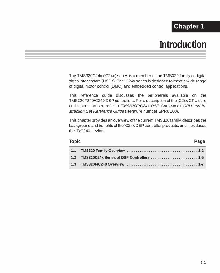
1-1Introduction
Introduction
The TMS320C24x (’C24x) series is a member of the TMS320 family of digitalsignal processors (DSPs). The ’C24x series is designed to meet a wide rangeof digital motor control (DMC) and embedded control applications.
This reference guide discusses the peripherals available on theTMS320F240/C240 DSP controllers. For a description of the ’C2xx CPU coreand instruction set, refer to TMS320F/C24x DSP Controllers, CPU and In-struction Set Reference Guide (literature number SPRU160).
This chapter provides an overview of the current TMS320 family, describes thebackground and benefits of the ’C24x DSP controller products, and introducesthe ’F/C240 device.
Topic Page
1.1 TMS320 Family Overview 1-2. . . . . . . . . . . . . . . . . . . . . . . . . . . . . . . . . . . . . .
1.2 TMS320C24x Series of DSP Controllers 1-5. . . . . . . . . . . . . . . . . . . . . . . . .
1.3 TMS320F/C240 Overview 1-7. . . . . . . . . . . . . . . . . . . . . . . . . . . . . . . . . . . . . .
Chapter 1
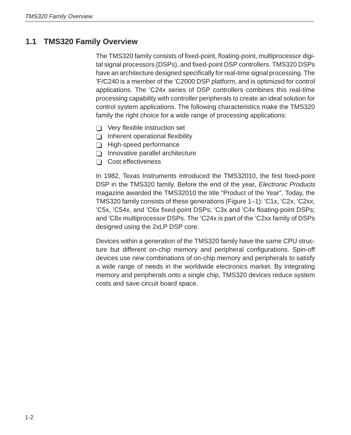
TMS320 Family Overview
1-2
1.1 TMS320 Family Overview
The TMS320 family consists of fixed-point, floating-point, multiprocessor digi-tal signal processors (DSPs), and fixed-point DSP controllers. TMS320 DSPshave an architecture designed specifically for real-time signal processing. The’F/C240 is a member of the ’C2000 DSP platform, and is optimized for controlapplications. The ’C24x series of DSP controllers combines this real-timeprocessing capability with controller peripherals to create an ideal solution forcontrol system applications. The following characteristics make the TMS320family the right choice for a wide range of processing applications:
� Very flexible instruction set� Inherent operational flexibility� High-speed performance� Innovative parallel architecture� Cost effectiveness
In 1982, Texas Instruments introduced the TMS32010, the first fixed-pointDSP in the TMS320 family. Before the end of the year, Electronic Productsmagazine awarded the TMS32010 the title “Product of the Year”. Today, theTMS320 family consists of these generations (Figure 1–1): ’C1x, ’C2x, ’C2xx,’C5x, ’C54x, and ’C6x fixed-point DSPs; ’C3x and ’C4x floating-point DSPs;and ’C8x multiprocessor DSPs. The ’C24x is part of the ’C2xx family of DSPsdesigned using the 2xLP DSP core.
Devices within a generation of the TMS320 family have the same CPU struc-ture but different on-chip memory and peripheral configurations. Spin-offdevices use new combinations of on-chip memory and peripherals to satisfya wide range of needs in the worldwide electronics market. By integratingmemory and peripherals onto a single chip, TMS320 devices reduce systemcosts and save circuit board space.
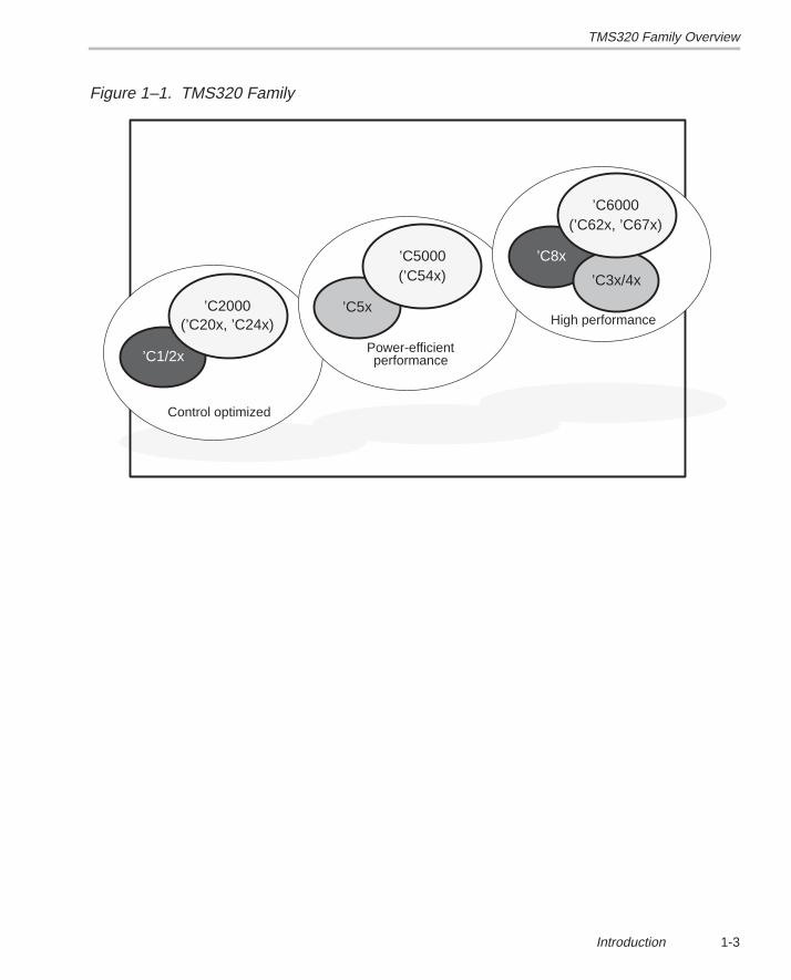
TMS320 Family Overview
1-3Introduction
Figure 1–1. TMS320 Family
Control optimized
’C1/2x
’C2000(’C20x, ’C24x)
performancePower-efficient
’C5xHigh performance
’C8x’C5000(’C54x)
(’C62x, ’C67x)’C6000
’C3x/4x
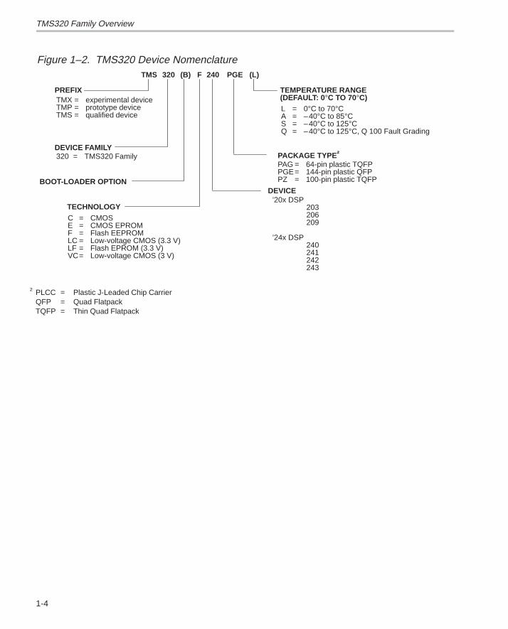
TMS320 Family Overview
1-4
Figure 1–2. TMS320 Device Nomenclature
PREFIX TEMPERATURE RANGE(DEFAULT: 0 °C TO 70°C)
TMS 320 F 240 PGE (L)
TMX = experimental deviceTMP = prototype deviceTMS = qualified device
DEVICE FAMILY320 = TMS320 Family
TECHNOLOGY
L = 0°C to 70°CA = –40°C to 85°CS = –40°C to 125°CQ = –40°C to 125°C, Q 100 Fault Grading
PACKAGE TYPE †PAG = 64-pin plastic TQFPPGE= 144-pin plastic QFPPZ = 100-pin plastic TQFP
C = CMOSE = CMOS EPROMF = Flash EEPROMLC = Low-voltage CMOS (3.3 V)LF = Flash EPROM (3.3 V)VC= Low-voltage CMOS (3 V)
DEVICE’20x DSP
203206209
’24x DSP240241242243
(B)
BOOT-LOADER OPTION
† PLCC = Plastic J-Leaded Chip CarrierQFP = Quad FlatpackTQFP = Thin Quad Flatpack
TMS320C24x Series of DSP Controllers
1-5Introduction
1.2 TMS320C24x Series of DSP Controllers
Designers have recognized the opportunity to redesign existing DMC systemsto use advanced algorithms that yield better performance and reduce systemcomponent count. DSPs enable:
� Design of robust controllers for a new generation of inexpensive motors,such as AC induction, DC permanent magnet, and switched-reluctancemotors
� Full variable-speed control of brushless motor types that have lowermanufacturing cost and higher reliability
� Energy savings through variable-speed control, saving up to 25% of theenergy used by fixed-speed controllers
� Increased fuel economy, improved performance, and elimination ofhydraulic fluid in automotive electronic power steering (EPS) systems
� Reduced manufacturing and maintenance costs by eliminating hydraulicfluids in automotive electronic braking systems
� More efficient and quieter operation due to less generation of torqueripple, resulting in less loss of power, lower vibration, and longer life
� Elimination or reduction of memory lookup tables through real-time poly-nomial calculation, thereby reducing system cost
� Use of advanced algorithms that can reduce the number of sensorsrequired in a system
� Control of power switching inverters, along with control algorithmprocessing
� Single-processor control of multimotor systems
The ’C24x DSP controllers are designed to meet the needs of control-basedapplications. By integrating the high performance of a DSP core and theon-chip peripherals of a microcontroller into a single-chip solution, the ’C24xseries yields a device that is an affordable alternative to traditional microcon-troller units (MCUs) and expensive multichip designs. At 20 million instructionsper second (MIPS), the ’C24x DSP controllers offer significant performanceover traditional 16-bit microcontrollers and microprocessors.
TMS320C24x Series of DSP Controllers
1-6
The 16-bit, fixed-point DSP core of the ’C24x devices provides analog design-ers a digital solution that does not sacrifice the precision and performance oftheir systems. In fact, system performance can be enhanced through the useof advanced control algorithms for techniques such as adaptive control,Kalman filtering, and state control. The ’C24x DSP controllers offer reliabilityand programmability. Analog control systems, on the other hand, are hard-wired solutions and can experience performance degradation due to aging,component tolerance, and drift.
The high-speed central processing unit (CPU) allows the digital designer toprocess algorithms in real time rather than approximate results with look-uptables. The instruction set of these DSP controllers, which incorporates bothsignal processing instructions and general-purpose control functions, coupledwith the extensive development support available for the ’C24x devices,reduces development time and provides the same ease of use as traditional8- and 16-bit microcontrollers. The instruction set also allows you to retain yoursoftware investment when moving from other general-purpose TMS320 fixed-point DSPs. It is source- and object-code compatible with the other membersof the ’C2xx generation, source code compatible with the ’C2x generation, andupwardly source code compatible with the ’C5x generation of DSPs from Tex-as Instruments.
The ’C24x architecture is also well-suited for processing control signals. Ituses a 16-bit word length along with 32-bit registers for storing intermediateresults, and has two hardware shifters available to scale numbers indepen-dently of the CPU. This combination minimizes quantization and truncationerrors, and increases processing power for additional functions. Such func-tions might include a notch filter that could cancel mechanical resonances ina system or an estimation technique that could eliminate state sensors in asystem.
The ’C24x DSP controllers take advantage of an existing set of peripheralfunctions that allow Texas Instruments to quickly configure various seriesmembers for different price/performance points or for application optimization.This library of both digital and mixed-signal peripherals includes:
� Timers� Serial communications ports (SCI, SPI)� Analog-to-digital converters (ADC)� Event manager� System protection, such as low-voltage detection and watchdog timers
The DSP controller peripheral library is continually growing and changing tosuit the needs of tomorrow’s embedded control marketplace.
TMS320F/C240 Overview
1-7Introduction
1.3 TMS320F/C240 Overview
The TMS320F/C240 is the first standard device introduced in the ’24x seriesof DSP controllers. It sets the standard for a single-chip digital motor controller.The ’240 can execute 20 MIPS. Almost all instructions are executed in a singlecycle of 50 ns. This high performance allows real-time execution of very com-plex control algorithms, such as adaptive control and Kalman filters. Very highsampling rates can also be used to minimize loop delays.
The ’240 has the architectural features necessary for high-speed signal proc-essing and digital control functions, and it has the peripherals needed to pro-vide a single-chip solution for motor control applications. The ’240 is manufac-tured using submicron CMOS technology, achieving a low power dissipationrating. Also included are several power-down modes for further power sav-ings.
Some applications that benefit from the advanced processing power of the’240 include:
� Industrial motor drives
� Power inverters and controllers
� Automotive systems, such as electronic power steering, antilock brakes,and climate control
� Appliance and HVAC blower/compressor motor controls
� Printers, copiers, and other office products
� Tape drives, magnetic optical drives, and other mass storage products
� Robotics and CNC milling machines
To function as a system manager, a DSP must have robust on-chip I/O andother peripherals. The event manager of the ’240 is unlike any other availableon a DSP. This application-optimized peripheral unit, coupled with the high-performance DSP core, enables the use of advanced control techniques forhigh-precision and high-efficiency full variable-speed control of all motortypes. Included in the event manager are special pulse-width modulation(PWM) generation functions, such as a programmable dead-band functionand a space vector PWM state machine for 3-phase motors that providesstate-of-the-art maximum efficiency in the switching of power transistors.Three independent up/down timers, each with it’s own compare register,support the generation of asymmetric (noncentered) as well as symmetric(centered) PWM waveforms. Two of the four capture inputs are direct connec-tions for quadrature encoder pulse signals from an optical encoder.
TMS320F/C240 Overview
1-8
Here is a summary of ’240 features:
� TMS320C2xx core CPU:
� 32-bit central arithmetic logic unit (CALU)
� 32-bit accumulator
� 16-bit × 16-bit parallel multiplier with a 32-bit product capability
� Three scaling shifters
� Eight 16-bit auxiliary registers with a dedicated arithmetic unit forindirect addressing of data memory
� Memory:
� 544 words × 16 bits of on-chip data/program dual-access RAM
� 16K words × 16 bits of on-chip program ROM or flash EEPROM
� 224K words × 16 bits of maximum addressable memory space (64Kwords of program space, 64K words of data space, 64K words of I/Ospace, and 32K words of global space)
� External memory interface module with a software wait-stategenerator, a 16-bit address bus, and a 16-bit data bus
� Support of hardware wait-states
� Program control:
� 4-level pipeline operation
� 8-level hardware stack
� Six external interrupts: power-drive protection interrupt, reset, NMI,and three maskable interrupts
� Instruction set:
� Source code compatibility with ’C2x, ’C2xx, and ’C5x fixed-pointgenerations of the TMS320 family
� Single-instruction repeat operation
� Single-cycle multiply/accumulate instructions
� Memory block move instructions for program/data management
� Indexed-addressing capability
� Bit-reversed indexed-addressing capability for radix-2 fast Fouriertransforms (FFTs)
� Power:
� Static CMOS technology� Four power-down modes to reduce power consumption
TMS320F/C240 Overview
1-9Introduction
� Emulation: IEEE Standard 1149.1 test access port interface to on-chipscan-based emulation logic
� Speed: 50-ns (20 MIPS) instruction cycle time, with most instructionssingle cycle
� Event manager:
� 12 compare/pulse-width modulation (PWM) channels (9 independent)
� Three 16-bit general-purpose timers with six modes, including contin-uous up counting and continuous up/down counting
� Three 16-bit full compare units with dead band capability
� Three 16-bit simple compare units
� Four capture units, two of which have quadrature-encoder-pulse-in-terface capability
� Dual 10-bit analog-to-digital converter (ADC)
� 28 individually programmable, multiplexed I/O pins
� Phase-locked loop (PLL) -based clock module
� Watchdog (WD) timer module with real-time interrupt (RTI)
� Serial communication interface (SCI)
� Serial peripheral interface (SPI)
� Development tools available:
� TI ANSI C compiler, assembler/linker, and C-source debugger
� Full range of emulation products: self-emulation (XDS510�)
� Evaluation module (EVM) with JTAG emulation
� Third-party digital motor control and fuzzy-logic development support
2-1TMS320F/C240 DSP Controller
TMS320F/C240 DSP Controller
This chapter contains a general description of the ’240 DSP Controller and pro-vides a pin-out diagram and memory maps.
Topic Page
2.1 TMS320F/C240 DSP Controller Overview 2-2. . . . . . . . . . . . . . . . . . . . . . . .
2.2 Memory Map 2-15. . . . . . . . . . . . . . . . . . . . . . . . . . . . . . . . . . . . . . . . . . . . . . . . .
2.3 Peripheral Memory Map 2-17. . . . . . . . . . . . . . . . . . . . . . . . . . . . . . . . . . . . . .
2.4 Digital I/O and Shared Pin Functions 2-19. . . . . . . . . . . . . . . . . . . . . . . . . .
2.5 Interrupts 2-27. . . . . . . . . . . . . . . . . . . . . . . . . . . . . . . . . . . . . . . . . . . . . . . . . . .
2.6 CPU Interrupt Registers 2-64. . . . . . . . . . . . . . . . . . . . . . . . . . . . . . . . . . . . . .
Chapter 2
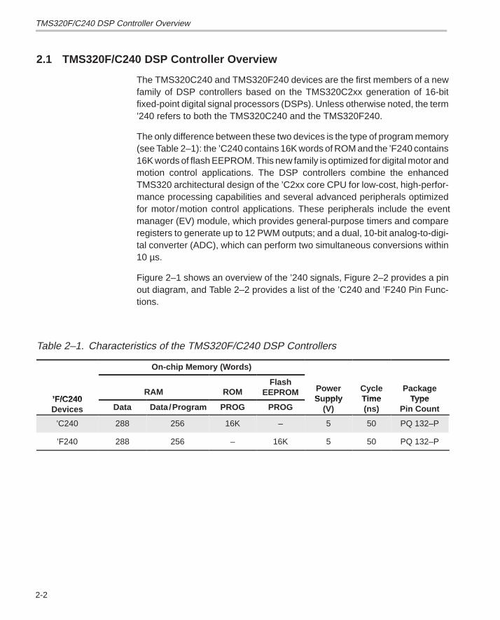
TMS320F/C240 DSP Controller Overview
2-2
2.1 TMS320F/C240 DSP Controller Overview
The TMS320C240 and TMS320F240 devices are the first members of a newfamily of DSP controllers based on the TMS320C2xx generation of 16-bitfixed-point digital signal processors (DSPs). Unless otherwise noted, the term’240 refers to both the TMS320C240 and the TMS320F240.
The only difference between these two devices is the type of program memory(see Table 2–1): the ’C240 contains 16K words of ROM and the ’F240 contains16K words of flash EEPROM. This new family is optimized for digital motor andmotion control applications. The DSP controllers combine the enhancedTMS320 architectural design of the ’C2xx core CPU for low-cost, high-perfor-mance processing capabilities and several advanced peripherals optimizedfor motor/motion control applications. These peripherals include the eventmanager (EV) module, which provides general-purpose timers and compareregisters to generate up to 12 PWM outputs; and a dual, 10-bit analog-to-digi-tal converter (ADC), which can perform two simultaneous conversions within10 µs.
Figure 2–1 shows an overview of the ’240 signals, Figure 2–2 provides a pinout diagram, and Table 2–2 provides a list of the ’C240 and ’F240 Pin Func-tions.
Table 2–1. Characteristics of the TMS320F/C240 DSP Controllers
On-chip Memory (Words)
’F/C240RAM ROM
FlashEEPROM Power
S pplyCycleTime
PackageType’F/C240
Devices Data Data/Program PROG PROGSupp ly
(V)Time(ns)
TypePin Count
’C240 288 256 16K – 5 50 PQ 132–P
’F240 288 256 – 16K 5 50 PQ 132–P
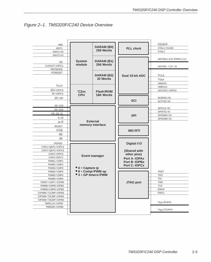
TMS320F/C240 DSP Controller Overview
2-3TMS320F/C240 DSP Controller
Figure 2–1. TMS320F/C240 Device Overview
PDPINT
PLL clockNMI
XINT1
XINT2 / IO
XINT3 / IO
RS
CLKOUT / IOPC1
PMTMODE
PORESET
BIO / IOPC3
XF / IOPC2
R / W
W / R
READY
STRB
WE
BR
CAP1 / QEP1 / IOPC4
CAP2 / QEP2 / IOPC5
CAP3 / IOPC6
CAP4 / IOPC7
PWM1 / CMP1
PWM2 / CMP2
PWM3 / CMP3
PWM4 / CMP4
PWM5 / CMP5
PWM6 / CMP6
PWM7 / CMP7 / IOPB0
PWM8 / CMP8 / IOPB1
PWM9 / CMP9 / IOPB2
T1PWM / T1CMP / IOPB3
T2PWM / T2CMP / IOPB4
T3PWM / T3CMP / IOPB5
TMRCLKI / IOPB7
TMRDIR / IOPB6
OSCBYP
XTAL1 / CLKIN
XTAL2
Systemmodule
ADCIN0,1,8,9 / IOPA0,1,3,2
DARAM (B0)256 Words
’C2xxCPU
Flash/ROM16K Words
DARAM (B1)256 Words
DARAM (B2)32 Words
Externalmemory interface
Event manager
4 × Capture ip9 × Comp/PWM op3 × GP timers /PWM
ADCIN2 - 7,10 - 15
VCCA
VSSA
SCIRXD / IO
SCITXD / IO
SPICLK / IO
SPISTE / IO
SPISIMO / IO
SPISOMI / IO
Dual 10-bit ADC
SCI
SPI
WD/RTI
Digital I /O
JTAG port
(Shared withother pins)
Port A - IOPAxPort B - IOPBxPort C- IOPCx
TRST
TDO
TDI
TMS
TCK
EMU0
EMU1
VDD (8 pins)
VSS (13 pins)
VREFHI
VREFLO
ADCSOC / IOPC0
VCCP
MC / MP
A0 - A15
D0 - D15
PS, DS, IS
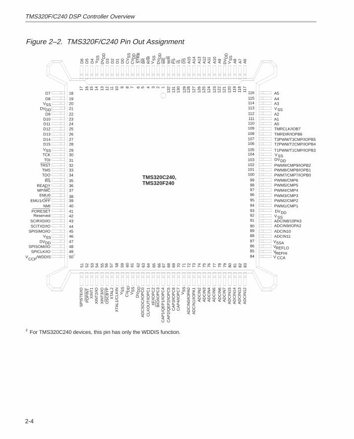
TMS320F/C240 DSP Controller Overview
2-4
Figure 2–2. TMS320F/C240 Pin Out Assignment
SS
A5A4A3
A2A1A0TMRCLK/IOB7TMRDIR/IOPB6T3PWM/T3CMP/IOPB5T2PWM/T2CMP/IOPB4
VT1PWM/T1CMP/IOPB3
DV
PWM9/CMP9/IOPB2PWM8/CMP8/IOPB1PWM7/CMP7/IOPB0PWM6/CMP6PWM5/CMP5PWM4/CMP4PWM3/CMP3
PWM1/CMP1DVVADCIN8/10PA3ADCIN9/IOPA2ADCIN10ADCIN11VVVV
DD
DDSS
SSAREFLOREFHICCA
SSV
PWM2/CMP2
WE
W/R
TMS320C240,TMS320F240
D5
D4
D3
D6
D2
ST
RB
BR
R/W
V DV
PS
D1 S
S DD
10 8 67
VS
S
D0
CV
SS
CV
DD
IS DS
A15
A14
A13
A12
A11
A10
A9
A8
A7
A6
VS
S
5852 53 54 5551 56 59 60 6762 6361 64 6957 6865 66 70 71 72 73 74 75 76 77 78 79 80 81 82 83
911121314151617 1
131
129
130
1322345
124
122
120
121
123
125
126
127
128
119
117
118
XTA
L1/C
LKIN
XTA
L2O
SC
BY
PX
INT
3/IO
XIN
T2/
IOX
INT
1
SP
IST
E/IO
CA
P1/
QE
P1/
IOP
C4
CA
P3/
IOP
C6
CA
P4/
IOP
C7
CA
P2/
QE
P2/
IOP
C5
BIO
/IOP
C3
XF
/IOP
C2
CLK
OU
T/IO
PC
1A
DC
SO
C/IO
PC
0
AD
CIN
5
AD
CIN
7A
DC
IN15
AD
CIN
6
AD
CIN
4A
DC
IN3
AD
CIN
1/IO
PA
1A
DC
IN0/
IOP
A0
AD
CIN
14
AD
CIN
12A
DC
IN13
AD
CIN
2
VS
S
VS
S
VS
S
PD
PIN
T
DV
DD
DV
DD
DV
DD
CV
DD
1819202122232425262728
293031323334353637
38394041424344454647484950
D7D8
VSSDVDD
D9D10D11D12D13D14D15VSSTCKTDI
TRSTTMSTDO
RSREADYMP/MC
EMU0EMU1/OFF
NMIPORESETReserved
SCIRXD/IOSCITXD/IO
SPISIMO/IO
SPISOMI/IOSPICLK/IO
VSSDVDD
VCCP/WDDIS †
116115114113112111110109108107106
105104103102101100
99989796959493929190898887868584
† For TMS320C240 devices, this pin has only the WDDIS function.
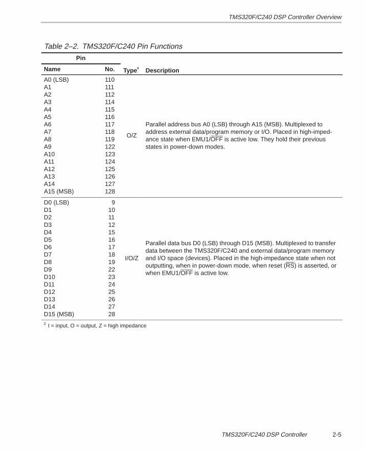
TMS320F/C240 DSP Controller Overview
2-5TMS320F/C240 DSP Controller
Table 2–2. TMS320F/C240 Pin Functions
Pin
Name No. Type† Description
A0 (LSB)A1A2A3A4A5A6A7A8A9A10A11A12A13A14A15 (MSB)
110111112114115116117118119122123124125126127128
O/Z
Parallel address bus A0 (LSB) through A15 (MSB). Multiplexed toaddress external data/program memory or I/O. Placed in high-imped-ance state when EMU1/OFF is active low. They hold their previousstates in power-down modes.
D0 (LSB)D1D2D3D4D5D6D7D8D9D10D11D12D13D14D15 (MSB)
9101112151617181922232425262728
I/O/Z
Parallel data bus D0 (LSB) through D15 (MSB). Multiplexed to transferdata between the TMS320F/C240 and external data/program memoryand I/O space (devices). Placed in the high-impedance state when notoutputting, when in power-down mode, when reset (RS) is asserted, orwhen EMU1/OFF is active low.
† I = input, O = output, Z = high impedance
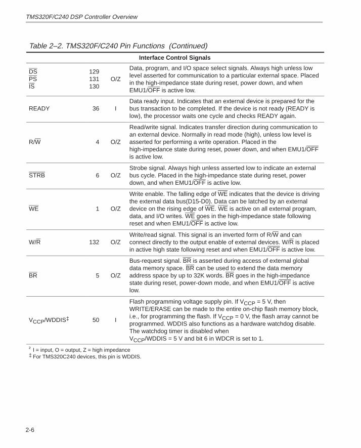
TMS320F/C240 DSP Controller Overview
2-6
Table 2–2. TMS320F/C240 Pin Functions (Continued)
Interface Control Signals
DSPSIS
129131130
O/Z
Data, program, and I/O space select signals. Always high unless lowlevel asserted for communication to a particular external space. Placedin the high-impedance state during reset, power down, and whenEMU1/OFF is active low.
READY 36 IData ready input. Indicates that an external device is prepared for thebus transaction to be completed. If the device is not ready (READY islow), the processor waits one cycle and checks READY again.
R/W 4 O/Z
Read/write signal. Indicates transfer direction during communication toan external device. Normally in read mode (high), unless low level isasserted for performing a write operation. Placed in thehigh-impedance state during reset, power down, and when EMU1/OFFis active low.
STRB 6 O/ZStrobe signal. Always high unless asserted low to indicate an externalbus cycle. Placed in the high-impedance state during reset, powerdown, and when EMU1/OFF is active low.
WE 1 O/Z
Write enable. The falling edge of WE indicates that the device is drivingthe external data bus(D15-D0). Data can be latched by an externaldevice on the rising edge of WE. WE is active on all external program,data, and I/O writes. WE goes in the high-impedance state followingreset and when EMU1/OFF is active low.
W/R 132 O/ZWrite/read signal. This signal is an inverted form of R/W and canconnect directly to the output enable of external devices. W/R is placedin active high state following reset and when EMU1/OFF is active low.
BR 5 O/Z
Bus-request signal. BR is asserted during access of external globaldata memory space. BR can be used to extend the data memoryaddress space by up to 32K words. BR goes in the high-impedancestate during reset, power-down mode, and when EMU1/OFF is activelow.
VCCP/WDDIS‡ 50 I
Flash programming voltage supply pin. If VCCP = 5 V, thenWRITE/ERASE can be made to the entire on-chip flash memory block,i.e., for programming the flash. If VCCP = 0 V, the flash array cannot beprogrammed. WDDIS also functions as a hardware watchdog disable.The watchdog timer is disabled whenVCCP/WDDIS = 5 V and bit 6 in WDCR is set to 1.
† I = input, O = output, Z = high impedance‡ For TMS320C240 devices, this pin is WDDIS.
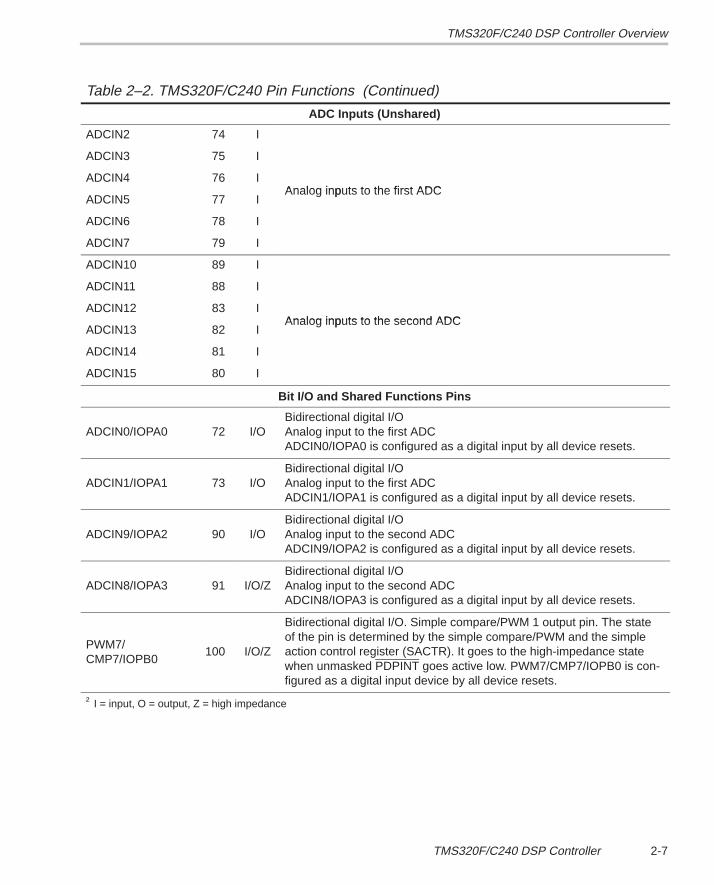
TMS320F/C240 DSP Controller Overview
2-7TMS320F/C240 DSP Controller
Table 2–2. TMS320F/C240 Pin Functions (Continued)
ADC Inputs (Unshared)
ADCIN2 74 I
ADCIN3 75 I
ADCIN4 76 IAnalog inputs to the first ADC
ADCIN5 77 IAnalog inputs to the first ADC
ADCIN6 78 I
ADCIN7 79 I
ADCIN10 89 I
ADCIN11 88 I
ADCIN12 83 IAnalog inputs to the second ADC
ADCIN13 82 IAnalog inputs to the second ADC
ADCIN14 81 I
ADCIN15 80 I
Bit I/O and Shared Functions Pins
ADCIN0/IOPA0 72 I/OBidirectional digital I/OAnalog input to the first ADCADCIN0/IOPA0 is configured as a digital input by all device resets.
ADCIN1/IOPA1 73 I/OBidirectional digital I/OAnalog input to the first ADCADCIN1/IOPA1 is configured as a digital input by all device resets.
ADCIN9/IOPA2 90 I/OBidirectional digital I/OAnalog input to the second ADCADCIN9/IOPA2 is configured as a digital input by all device resets.
ADCIN8/IOPA3 91 I/O/ZBidirectional digital I/OAnalog input to the second ADCADCIN8/IOPA3 is configured as a digital input by all device resets.
PWM7/CMP7/IOPB0
100 I/O/Z
Bidirectional digital I/O. Simple compare/PWM 1 output pin. The stateof the pin is determined by the simple compare/PWM and the simpleaction control register (SACTR). It goes to the high-impedance statewhen unmasked PDPINT goes active low. PWM7/CMP7/IOPB0 is con-figured as a digital input device by all device resets.
† I = input, O = output, Z = high impedance
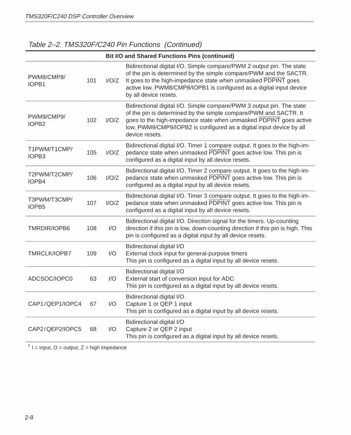
TMS320F/C240 DSP Controller Overview
2-8
Table 2–2. TMS320F/C240 Pin Functions (Continued)
Bit I/O and Shared Functions Pins (continued)
PWM8/CMP8/IOPB1
101 I/O/Z
Bidirectional digital I/O. Simple compare/PWM 2 output pin. The stateof the pin is determined by the simple compare/PWM and the SACTR.It goes to the high-impedance state when unmasked PDPINT goesactive low. PWM8/CMP8/IOPB1 is configured as a digital input deviceby all device resets.
PWM9/CMP9/IOPB2
102 I/O/Z
Bidirectional digital I/O. Simple compare/PWM 3 output pin. The stateof the pin is determined by the simple compare/PWM and SACTR. Itgoes to the high-impedance state when unmasked PDPINT goes activelow. PWM9/CMP9/IOPB2 is configured as a digital input device by alldevice resets.
T1PWM/T1CMP/IOPB3
105 I/O/ZBidirectional digital I/O. Timer 1 compare output. It goes to the high-im-pedance state when unmasked PDPINT goes active low. This pin isconfigured as a digital input by all device resets.
T2PWM/T2CMP/IOPB4
106 I/O/ZBidirectional digital I/O. Timer 2 compare output. It goes to the high-im-pedance state when unmasked PDPINT goes active low. This pin isconfigured as a digital input by all device resets.
T3PWM/T3CMP/IOPB5
107 I/O/ZBidirectional digital I/O. Timer 3 compare output. It goes to the high-im-pedance state when unmasked PDPINT goes active low. This pin isconfigured as a digital input by all device resets.
TMRDIR/IOPB6 108 I/OBidirectional digital I/O. Direction signal for the timers. Up-countingdirection if this pin is low, down-counting direction if this pin is high. Thispin is configured as a digital input by all device resets.
TMRCLK/IOPB7 109 I/OBidirectional digital I/OExternal clock input for general-purpose timersThis pin is configured as a digital input by all device resets.
ADCSOC/IOPC0 63 I/OBidirectional digital I/OExternal start of conversion input for ADCThis pin is configured as a digital input by all device resets.
CAP1/QEP1/IOPC4 67 I/OBidirectional digital I/OCapture 1 or QEP 1 inputThis pin is configured as a digital input by all device resets.
CAP2/QEP2/IOPC5 68 I/OBidirectional digital I/OCapture 2 or QEP 2 inputThis pin is configured as a digital input by all device resets.
† I = input, O = output, Z = high impedance
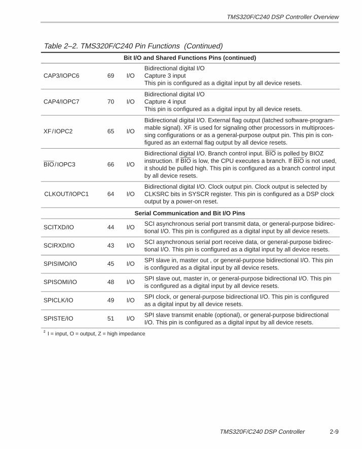
TMS320F/C240 DSP Controller Overview
2-9TMS320F/C240 DSP Controller
Table 2–2. TMS320F/C240 Pin Functions (Continued)
Bit I/O and Shared Functions Pins (continued)
CAP3/IOPC6 69 I/OBidirectional digital I/OCapture 3 inputThis pin is configured as a digital input by all device resets.
CAP4/IOPC7 70 I/OBidirectional digital I/OCapture 4 inputThis pin is configured as a digital input by all device resets.
XF/ IOPC2 65 I/O
Bidirectional digital I/O. External flag output (latched software-program-mable signal). XF is used for signaling other processors in multiproces-sing configurations or as a general-purpose output pin. This pin is con-figured as an external flag output by all device resets.
BIO/ IOPC3 66 I/O
Bidirectional digital I/O. Branch control input. BIO is polled by BIOZinstruction. If BIO is low, the CPU executes a branch. If BIO is not used,it should be pulled high. This pin is configured as a branch control inputby all device resets.
CLKOUT/IOPC1 64 I/OBidirectional digital I/O. Clock output pin. Clock output is selected byCLKSRC bits in SYSCR register. This pin is configured as a DSP clockoutput by a power-on reset.
Serial Communication and Bit I/O Pins
SCITXD/IO 44 I/OSCI asynchronous serial port transmit data, or general-purpose bidirec-tional I/O. This pin is configured as a digital input by all device resets.
SCIRXD/IO 43 I/OSCI asynchronous serial port receive data, or general-purpose bidirec-tional I/O. This pin is configured as a digital input by all device resets.
SPISIMO/IO 45 I/OSPI slave in, master out , or general-purpose bidirectional I/O. This pinis configured as a digital input by all device resets.
SPISOMI/IO 48 I/OSPI slave out, master in, or general-purpose bidirectional I/O. This pinis configured as a digital input by all device resets.
SPICLK/IO 49 I/OSPI clock, or general-purpose bidirectional I/O. This pin is configuredas a digital input by all device resets.
SPISTE/IO 51 I/OSPI slave transmit enable (optional), or general-purpose bidirectionalI/O. This pin is configured as a digital input by all device resets.
† I = input, O = output, Z = high impedance
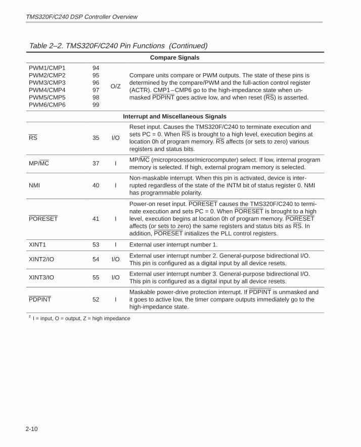
TMS320F/C240 DSP Controller Overview
2-10
Table 2–2. TMS320F/C240 Pin Functions (Continued)
Compare Signals
PWM1/CMP1PWM2/CMP2PWM3/CMP3PWM4/CMP4PWM5/CMP5PWM6/CMP6
949596979899
O/Z
Compare units compare or PWM outputs. The state of these pins isdetermined by the compare/PWM and the full-action control register(ACTR). CMP1–CMP6 go to the high-impedance state when un-masked PDPINT goes active low, and when reset (RS) is asserted.
Interrupt and Miscellaneous Signals
RS 35 I/O
Reset input. Causes the TMS320F/C240 to terminate execution andsets PC = 0. When RS is brought to a high level, execution begins atlocation 0h of program memory. RS affects (or sets to zero) variousregisters and status bits.
MP/MC 37 IMP/MC (microprocessor/microcomputer) select. If low, internal programmemory is selected. If high, external program memory is selected.
NMI 40 INon-maskable interrupt. When this pin is activated, device is inter-rupted regardless of the state of the INTM bit of status register 0. NMIhas programmable polarity.
PORESET 41 I
Power-on reset input. PORESET causes the TMS320F/C240 to termi-nate execution and sets PC = 0. When PORESET is brought to a highlevel, execution begins at location 0h of program memory. PORESETaffects (or sets to zero) the same registers and status bits as RS. Inaddition, PORESET initializes the PLL control registers.
XINT1 53 I External user interrupt number 1.
XINT2/IO 54 I/OExternal user interrupt number 2. General-purpose bidirectional I/O.This pin is configured as a digital input by all device resets.
XINT3/IO 55 I/OExternal user interrupt number 3. General-purpose bidirectional I/O.This pin is configured as a digital input by all device resets.
PDPINT 52 IMaskable power-drive protection interrupt. If PDPINT is unmasked andit goes to active low, the timer compare outputs immediately go to thehigh-impedance state.
† I = input, O = output, Z = high impedance
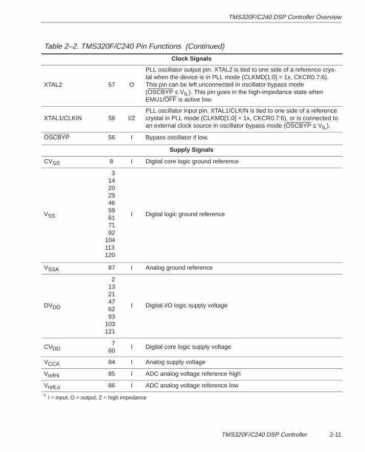
TMS320F/C240 DSP Controller Overview
2-11TMS320F/C240 DSP Controller
Table 2–2. TMS320F/C240 Pin Functions (Continued)
Clock Signals
XTAL2 57 O
PLL oscillator output pin. XTAL2 is tied to one side of a reference crys-tal when the device is in PLL mode (CLKMD[1:0] = 1x, CKCR0.7:6).This pin can be left unconnected in oscillator bypass mode(OSCBYP ≤ VIL). This pin goes in the high-impedance state whenEMU1/OFF is active low.
XTAL1/CLKIN 58 I/ZPLL oscillator input pin. XTAL1/CLKIN is tied to one side of a referencecrystal in PLL mode (CLKMD[1:0] = 1x, CKCR0.7:6), or is connected toan external clock source in oscillator bypass mode (OSCBYP ≤ VIL).
OSCBYP 56 I Bypass oscillator if low.
Supply Signals
CVSS 8 I Digital core logic ground reference
VSS
31420294659617192
104113120
I Digital logic ground reference
VSSA 87 I Analog ground reference
DVDD
21321476293
103121
I Digital I/O logic supply voltage
CVDD7
60I Digital core logic supply voltage
VCCA 84 I Analog supply voltage
VrefHi 85 I ADC analog voltage reference high
VrefLo 86 I ADC analog voltage reference low
† I = input, O = output, Z = high impedance
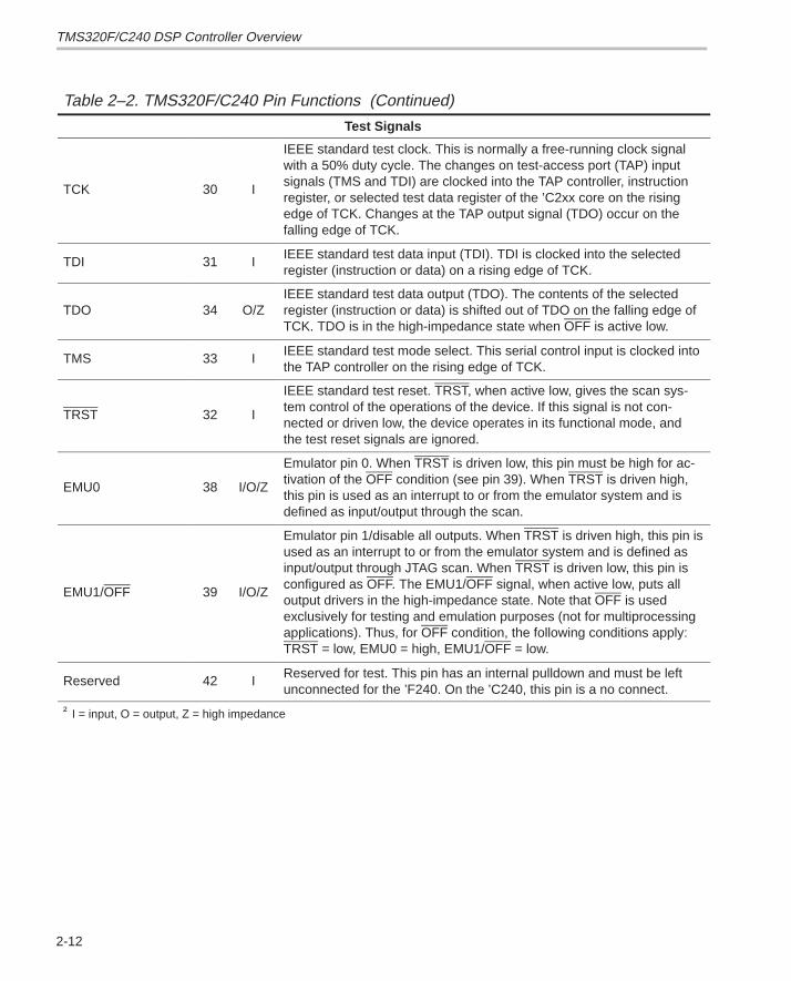
TMS320F/C240 DSP Controller Overview
2-12
Table 2–2. TMS320F/C240 Pin Functions (Continued)
Test Signals
TCK 30 I
IEEE standard test clock. This is normally a free-running clock signalwith a 50% duty cycle. The changes on test-access port (TAP) inputsignals (TMS and TDI) are clocked into the TAP controller, instructionregister, or selected test data register of the ’C2xx core on the risingedge of TCK. Changes at the TAP output signal (TDO) occur on thefalling edge of TCK.
TDI 31 IIEEE standard test data input (TDI). TDI is clocked into the selectedregister (instruction or data) on a rising edge of TCK.
TDO 34 O/ZIEEE standard test data output (TDO). The contents of the selectedregister (instruction or data) is shifted out of TDO on the falling edge ofTCK. TDO is in the high-impedance state when OFF is active low.
TMS 33 IIEEE standard test mode select. This serial control input is clocked intothe TAP controller on the rising edge of TCK.
TRST 32 I
IEEE standard test reset. TRST, when active low, gives the scan sys-tem control of the operations of the device. If this signal is not con-nected or driven low, the device operates in its functional mode, andthe test reset signals are ignored.
EMU0 38 I/O/Z
Emulator pin 0. When TRST is driven low, this pin must be high for ac-tivation of the OFF condition (see pin 39). When TRST is driven high,this pin is used as an interrupt to or from the emulator system and isdefined as input/output through the scan.
EMU1/OFF 39 I/O/Z
Emulator pin 1/disable all outputs. When TRST is driven high, this pin isused as an interrupt to or from the emulator system and is defined asinput/output through JTAG scan. When TRST is driven low, this pin isconfigured as OFF. The EMU1/OFF signal, when active low, puts alloutput drivers in the high-impedance state. Note that OFF is usedexclusively for testing and emulation purposes (not for multiprocessingapplications). Thus, for OFF condition, the following conditions apply:TRST = low, EMU0 = high, EMU1/OFF = low.
Reserved 42 IReserved for test. This pin has an internal pulldown and must be leftunconnected for the ’F240. On the ’C240, this pin is a no connect.
† I = input, O = output, Z = high impedance
TMS320F/C240 DSP Controller Overview
2-13TMS320F/C240 DSP Controller
2.1.1 Architectural Overview
The functional block diagram (Figure 2–3) provides a high level description ofeach component in the ’240 DSP controller device. The ’240 devices are com-posed of three main functional units: a ’C2xx DSP core, internal memory, andperipherals. In addition to these three functional units, there are several sys-tem-level features of the ’240 that are distributed. These system features in-clude the memory map, device reset, interrupts, digital input /output (I /O),clock generation, and low-power operation.
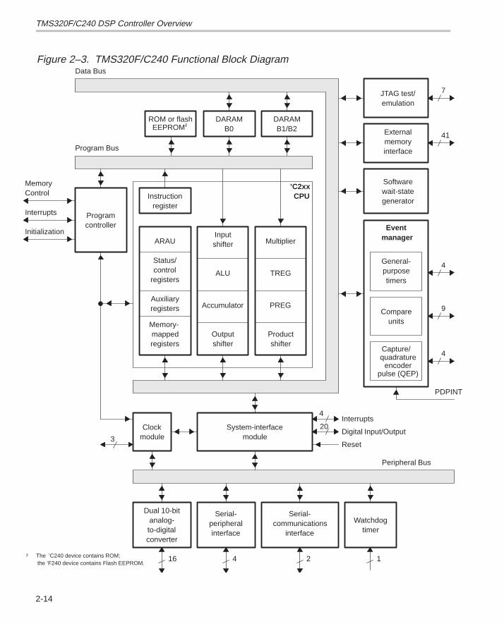
TMS320F/C240 DSP Controller Overview
2-14
Figure 2–3. TMS320F/C240 Functional Block Diagram
ÁÁÁÁÁÁÁÁÁÁÁÁÁÁÁÁÁÁÁÁÁÁÁÁÁÁÁÁÁÁÁÁÁÁÁÁÁÁÁÁÁÁÁÁÁÁÁÁÁÁÁÁÁÁÁÁÁÁÁÁÁÁÁÁÁ
ÁÁÁÁÁÁÁÁÁÁÁÁÁÁÁÁÁÁÁÁÁÁÁÁÁÁÁÁÁÁÁÁÁÁÁÁÁÁÁÁÁÁÁÁÁ
ÁÁÁÁÁÁÁÁÁÁÁÁÁÁÁÁÁÁÁÁÁÁÁÁÁÁÁÁÁÁÁÁÁÁÁÁÁÁÁÁÁÁÁÁÁ
ÁÁÁÁÁÁÁÁÁÁÁÁÁÁÁÁÁÁÁÁÁÁÁÁÁÁÁÁÁÁÁÁÁÁÁÁÁÁÁÁÁÁÁÁÁ
ÁÁÁÁÁÁÁÁÁÁÁÁÁÁÁ
ÁÁÁÁÁÁÁÁÁÁÁÁÁÁÁÁÁÁÁÁÁÁÁÁÁ
ÁÁÁÁÁÁ
24ÁÁÁÁÁÁ
16ÁÁ
Á
PDPINTÁ
4
ÁÁÁ
ÁÁÁ4
9
ÁÁÁ
ÁÁ
ÁÁÁ41
7ÁÁ
ÁÁÁÁ
ÁÁÁ
ÁÁÁ
ÁÁÁ
ÁÁÁÁÁÁ
ÁÁÁÁÁÁÁÁÁÁÁÁÁÁÁÁÁÁÁÁ
ÁÁÁÁÁÁÁÁÁÁÁÁÁÁÁ
ÁÁÁÁÁÁÁÁÁÁÁÁÁÁÁÁÁÁÁÁ
ÁÁÁÁÁÁÁÁÁÁÁÁÁÁÁÁÁÁÁÁ
ÁÁÁÁÁÁÁÁÁÁÁÁÁÁÁÁÁÁÁÁ
ÁÁÁÁÁÁÁÁÁÁÁÁÁÁÁÁÁÁÁÁ
quadratureencoder
pulse (QEP)
Capture/
unitsCompare
timerspurposeGeneral-
Event
generatorwait-stateSoftware
interfacememoryExternal
emulationJTAG test/
Peripheral Bus
ÁÁÁÁÁÁ
ÁÁÁÁÁÁ
ÁÁÁÁÁÁ
ÁÁÁ
ÁÁÁÁÁÁÁÁÁÁÁÁÁÁÁÁ
ÁÁÁÁÁÁÁÁÁÁÁÁÁÁÁÁÁÁÁÁÁÁÁÁ
ÁÁÁÁÁÁÁÁÁÁÁÁÁÁÁÁÁÁÁÁ
ÁÁÁÁÁÁÁÁÁÁÁÁÁÁÁÁÁÁÁÁ
timerWatchdog
interfacecommunications
Serial-
interfaceperipheral
Serial-
converterto-digitalanalog-
Dual 10-bit
Data Bus
ÁÁÁÁÁÁ
ÁÁÁÁ
3
Á
ÁÁ
Reset
Digital Input/Output
Interrupts20
4
ÁÁ
ÁÁÁÁ
Á
ÁÁÁÁÁÁ
ÁÁ
ÁÁÁÁÁÁÁÁÁÁÁÁÁÁÁÁÁÁÁÁÁÁÁÁÁÁÁÁÁÁÁÁÁÁÁÁ
ÁÁÁÁÁÁÁÁÁÁÁÁÁÁÁÁ
moduleSystem-interface
moduleClock
Program Bus
ÁÁÁÁ
ÁÁ
ÁÁÁÁÁÁÁÁ
ÁÁÁÁÁÁÁÁ
ÁÁÁÁÁÁÁÁ
ÁÁÁÁÁÁÁÁ
B1/B2DARAM
B0DARAMROM or flash
EEPROM†
Initialization
Interrupts
ControlMemory
ÁÁÁÁ
ÁÁÁÁ
ÁÁÁÁÁÁÁÁ
ÁÁÁ
ÁÁÁ
Á
controllerProgram
CPU’C2xx
ÁÁÁÁÁÁ
ÁÁ
Á
shifterProduct
PREG
TREG
Multiplier
shifterOutput
Accumulator
ALU
shifterInput
registersmapped
Memory-
registersAuxiliary
registerscontrolStatus/
ARAU
registerInstruction
ÁÁ
ÁÁÁÁ
ÁÁ1† The ’C240 device contains ROM;
the ’F240 device contains Flash EEPROM.
ÁÁÁÁÁÁÁÁ
manager

Memory Map
2-15TMS320F/C240 DSP Controller
2.2 Memory Map
The TMS320F/C240 implements three separate address spaces for programmemory, data memory, and I /O. Each space accommodates a total of 64K16-bit words. Within the 64K words of data space, the 256 to 32K words at thetop of the address range can be defined as external global memory, in incre-ments of powers of two, as specified by the contents of the global memoryallocation register (GREG). Access to global memory is arbitrated using theglobal memory bus request (BR) signal.
On the ’240, the first 96 data memory locations (0–5Fh) are either allocatedfor memory-mapped registers or reserved. This memory-mapped registerspace contains various control and status registers including those for theCPU.
All ’240 on-chip peripherals are mapped into data memory space starting at7000h. Access to these registers is made by CPU instructions addressing theirdata memory locations. Figure 2–4 shows a memory map for the ’F/C240.
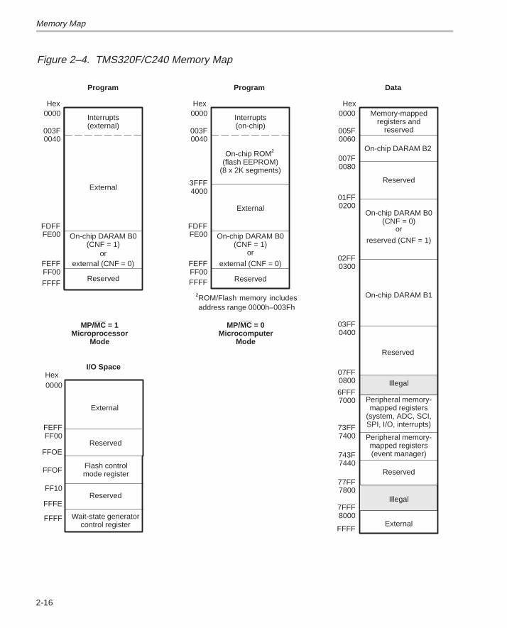
Memory Map
2-16
Figure 2–4. TMS320F/C240 Memory Map
0000 Interrupts(external)
003F0040
External
FDFFFE00
0000 Interrupts(on-chip)
On-chip ROM†(flash EEPROM)
(8 x 2K segments)
0000 Memory-mappedregisters and
reserved005F0060
On-chip DARAM B2
On-chip DARAM B0(CNF = 1)
FFFF
02FF0300
On-chip DARAM B1
FEFFFF00
external (CNF = 0)
03FF0400
07FF0800
Reserved
6FFF7000 Peripheral memory-
mapped registers(system, ADC, SCI,SPI, I/O, interrupts)73FF
7400
743F7440
Reserved77FF7800
0000
External
FFOF
FEFFFF00
Reserved
Reserved
External
3FFF4000
On-chip DARAM B0(CNF = 1)
FFFF
external (CNF = 0)
Reserved
On-chip DARAM B0(CNF = 0)
reserved (CNF = 1)
Peripheral memory-mapped registers(event manager)
I/O Space
Program
Hex
Program
Hex
Data
Hex
007F0080
Reserved
IllegalHex
ExternalFFFF
Illegal7FFF8000
or or
†ROM/Flash memory includesaddress range 0000h–003Fh
or
01FF0200
Wait-state generatorcontrol register
003F0040
FDFFFE00
FEFFFF00
MP/MC = 1Microprocessor
Mode
MP/MC = 0Microcomputer
Mode
FF10
FFFF
FFFE
FFOEReserved
Flash controlmode register

Peripheral Memory Map
2-17TMS320F/C240 DSP Controller
2.3 Peripheral Memory Map
The ’240 system and peripheral control register frame contains all the data,status, and control bits to operate the system and peripheral modules on the’240 device.
Figure 2–5 shows the peripheral memory map for the ’240.
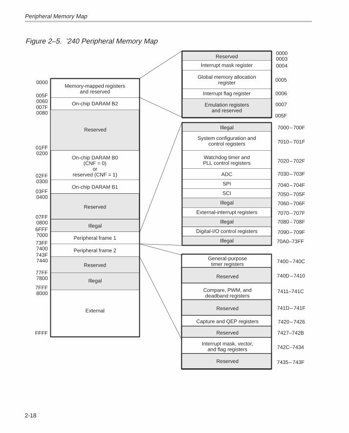
Peripheral Memory Map
2-18
Figure 2–5. ’240 Peripheral Memory Map
Emulation registersand reserved
Reserved
Illegal
Illegal
System configuration andcontrol registers
Watchdog timer andPLL control registers
Global memory allocationregister
000000030004
00050000Memory-mapped registers
and reserved005F0060 On-chip DARAM B2
02FF0300
01FF0200
03FF0400
On-chip DARAM B1
Reserved
73FF7400
Peripheral frame 1
77FF7800
External
FFFF
7000–700F
Reserved
0007
Peripheral frame 2
On-chip DARAM B0(CNF = 0)
orreserved (CNF = 1)
Interrupt mask register
Illegal
Digital-I/O control registers
Illegal
Reserved
Interrupt mask, vector,and flag registers
0006
007F0080
07FF0800
743F7440
7010–701F
7020–702F
7030–703F
7040–704F
7050–705F
7060–706F
7070–707F
7080–708F
7090–709F
70A0–73FF
7400–740C
740D–7410
741D–741F
7420–7426
7427–742B
Interrupt flag register
SPI
SCI
External-interrupt registers
ADC
General-purposetimer registers
Capture and QEP registers
Compare, PWM, anddeadband registers
Reserved
7FFF8000
Illegal
6FFF7000
Illegal
Reserved
005F
Reserved
Reserved
7411–741C
742C–7434
7435–743F
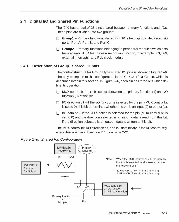
Digital I/O and Shared Pin Functions
2-19TMS320F/C240 DSP Controller
2.4 Digital I/O and Shared Pin Functions
The ’240 has a total of 28 pins shared between primary functions and I/Os.These pins are divided into two groups:
� Group1 – Primary functions shared with I/Os belonging to dedicated I/Oports, Port A, Port B, and Port C.
� Group2 – Primary functions belonging to peripheral modules which alsohave an in-built I/O feature as a secondary function, for example SCI, SPI,external interrupts, and PLL clock module.
2.4.1 Description of Group1 Shared I/O pins
The control structure for Group1 type shared I/O pins is shown in Figure 2–6.The only exception to this configuration is the CLKOUT/IOPC1 pin, which isdescribed later in this section. In Figure 2–6, each pin has three bits which de-fine its operation:
� MUX control bit – this bit selects between the primary function (1) and I/Ofunction (0) of the pin.
� I/O direction bit – if the I/O function is selected for the pin (MUX control bitis set to 0), this bit determines whether the pin is an input (0) or output (1).
� I/O data bit – if the I/O function is selected for the pin (MUX control bit isset to 0) and the direction selected is an input, data is read from this bit;if the direction selected is an output, data is written to this bit.
The MUX control bit, I/O direction bit, and I/O data bit are in the I/O control reg-isters described in subsection 2.4.3 on page 2-21.
Figure 2–6. Shared Pin Configuration
MUX control bit0= I/O function1=Primary function
IOP data bit(Read/Write)
IOP DIR bit0= Input1=Output
Primary functionor
I /O pin
0 1
Primaryfunction
OutInNote: When the MUX control bit=1, the primary
function is selected in all cases except forthe following pins:
(0=Primary function)(0=Primary function)
1. XF / IOPC2 2. BIO / IOPC3
Pin
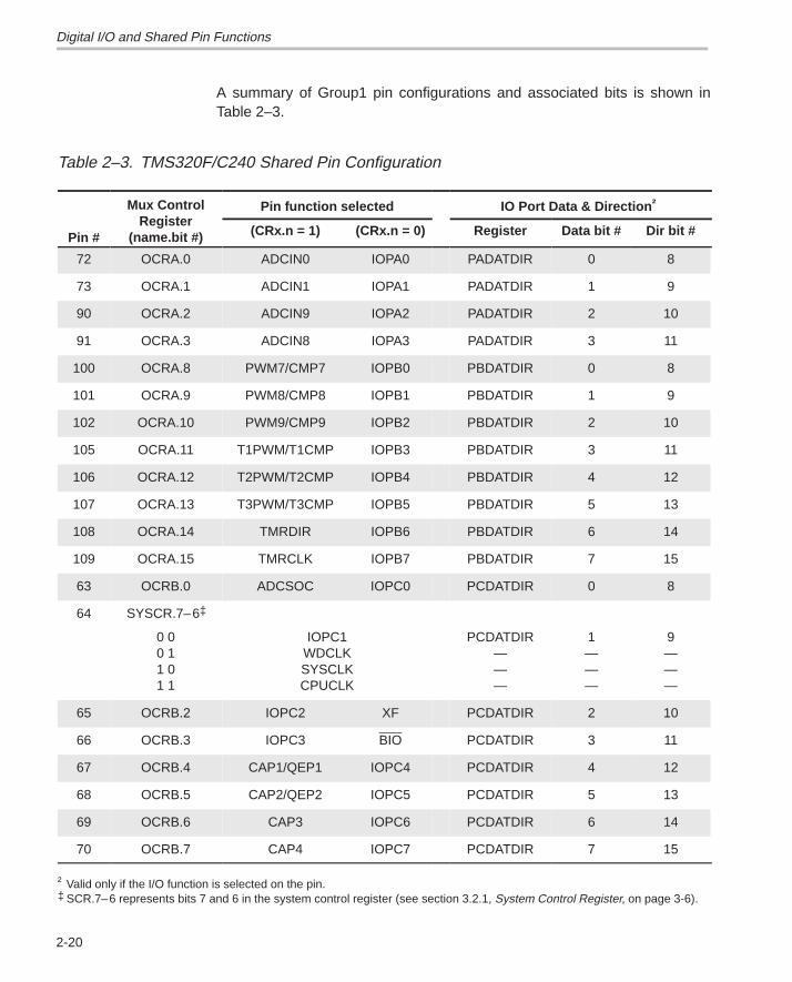
Digital I/O and Shared Pin Functions
2-20
A summary of Group1 pin configurations and associated bits is shown inTable 2–3.
Table 2–3. TMS320F/C240 Shared Pin Configuration
Mux ControlR i t
Pin function selected IO Port Data & Direction †
Pin #Register
(name.bit #) (CRx.n = 1) (CRx.n = 0) Register Data bit # Dir bit #
72 OCRA.0 ADCIN0 IOPA0 PADATDIR 0 8
73 OCRA.1 ADCIN1 IOPA1 PADATDIR 1 9
90 OCRA.2 ADCIN9 IOPA2 PADATDIR 2 10
91 OCRA.3 ADCIN8 IOPA3 PADATDIR 3 11
100 OCRA.8 PWM7/CMP7 IOPB0 PBDATDIR 0 8
101 OCRA.9 PWM8/CMP8 IOPB1 PBDATDIR 1 9
102 OCRA.10 PWM9/CMP9 IOPB2 PBDATDIR 2 10
105 OCRA.11 T1PWM/T1CMP IOPB3 PBDATDIR 3 11
106 OCRA.12 T2PWM/T2CMP IOPB4 PBDATDIR 4 12
107 OCRA.13 T3PWM/T3CMP IOPB5 PBDATDIR 5 13
108 OCRA.14 TMRDIR IOPB6 PBDATDIR 6 14
109 OCRA.15 TMRCLK IOPB7 PBDATDIR 7 15
63 OCRB.0 ADCSOC IOPC0 PCDATDIR 0 8
64 SYSCR.7–6‡
0 00 11 01 1
IOPC1WDCLKSYSCLKCPUCLK
PCDATDIR———
1———
9———
65 OCRB.2 IOPC2 XF PCDATDIR 2 10
66 OCRB.3 IOPC3 BIO PCDATDIR 3 11
67 OCRB.4 CAP1/QEP1 IOPC4 PCDATDIR 4 12
68 OCRB.5 CAP2/QEP2 IOPC5 PCDATDIR 5 13
69 OCRB.6 CAP3 IOPC6 PCDATDIR 6 14
70 OCRB.7 CAP4 IOPC7 PCDATDIR 7 15
† Valid only if the I/O function is selected on the pin.‡ SCR.7–6 represents bits 7 and 6 in the system control register (see section 3.2.1, System Control Register, on page 3-6).

Digital I/O and Shared Pin Functions
2-21TMS320F/C240 DSP Controller
2.4.2 Description of Group 2 Shared I/O Pins
Group 2 shared pins belong to peripherals which have built-in general purposeI/O capability. Control and configuration for these pins is achieved by settingappropriate bits within the control and configuration registers of the peripher-als. Table 2–4 lists the Group 2 shared pins.
Table 2–4. Group 2 Shared Pins
Pin # Primary Function Register Address Peripheral Module
43 SCIRXD SCIPC2 705Eh SCI
44 SCITXD SCIPC2 705Eh SCI
45 SPISIMO SPIPC2 704Eh SPI
48 SPISOMI SPIPC2 704Eh SPI
49 SPICLK SPIPC1 704Dh SPI
51 SPISTE SPIPC1 704Dh SPI
54 XINT2 XINT2CR 7078h External interrupts
55 XINT3 XINT3CR 707Ah External interrupts
For information on:
� Serial communications interface (SCI) – see Chapter 8� Serial peripheral interface (SPI) – see Chapter 9� External Interrupts – see section 2.5.7
2.4.3 Digital I/O Control Registers
Table 2–5 lists the registers available to the digital I/O module. As with other’240 peripherals, the registers are memory mapped to the data space.
Table 2–5. Addresses of Digital I/O Control Registers
Address Register Name Page
7090h OCRA I/O mux control register A 2-22
7092h OCRB I/O mux control register B 2-23
7098h PADATDIR I/O port A data and direction register 2-24
709Ah PBDATDIR I/O port B data and direction register 2-25
709Ch PCDATDIR I/O port C data and direction register 2-26
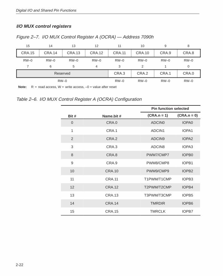
Digital I/O and Shared Pin Functions
2-22
I/O MUX control registers
Figure 2–7. I/O MUX Control Register A (OCRA) — Address 7090h
15 14 13 12 11 10 9 8
CRA.15 CRA.14 CRA.13 CRA.12 CRA.11 CRA.10 CRA.9 CRA.8
RW–0 RW–0 RW–0 RW–0 RW–0 RW–0 RW–0 RW–0
7 6 5 4 3 2 1 0
Reserved CRA.3 CRA.2 CRA.1 CRA.0
RW–0 RW–0 RW–0 RW–0 RW–0
Note: R = read access, W = write access, –0 = value after reset
Table 2–6. I/O MUX Control Register A (OCRA) Configuration
Pin function selected
Bit # Name.bit # (CRA.n = 1) (CRA.n = 0)
0 CRA.0 ADCIN0 IOPA0
1 CRA.1 ADCIN1 IOPA1
2 CRA.2 ADCIN9 IOPA2
3 CRA.3 ADCIN8 IOPA3
8 CRA.8 PWM7/CMP7 IOPB0
9 CRA.9 PWM8/CMP8 IOPB1
10 CRA.10 PWM9/CMP9 IOPB2
11 CRA.11 T1PWM/T1CMP IOPB3
12 CRA.12 T2PWM/T2CMP IOPB4
13 CRA.13 T3PWM/T3CMP IOPB5
14 CRA.14 TMRDIR IOPB6
15 CRA.15 TMRCLK IOPB7
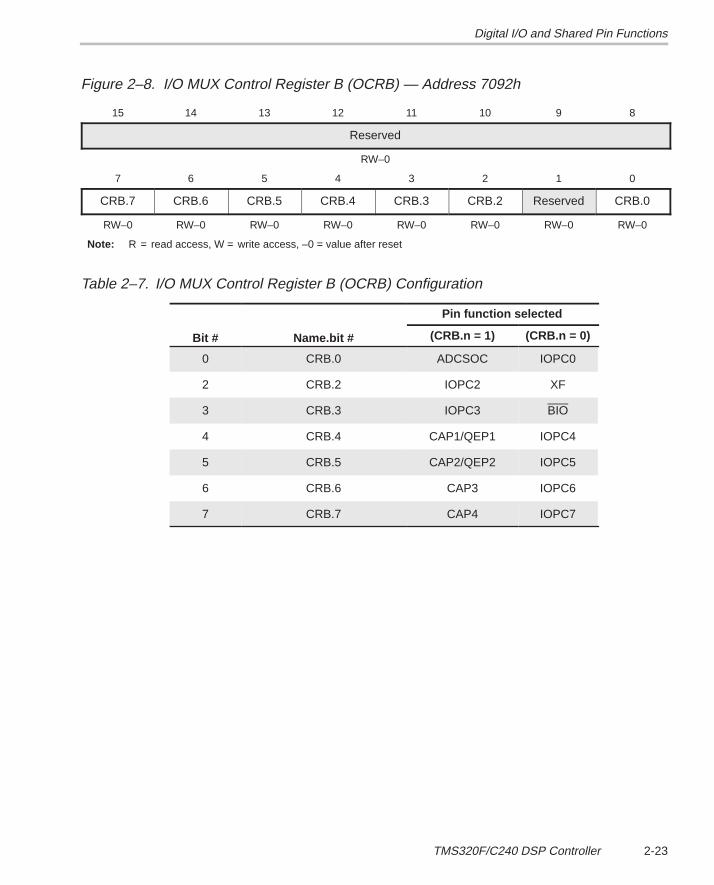
Digital I/O and Shared Pin Functions
2-23TMS320F/C240 DSP Controller
Figure 2–8. I/O MUX Control Register B (OCRB) — Address 7092h
15 14 13 12 11 10 9 8
Reserved
RW–0
7 6 5 4 3 2 1 0
CRB.7 CRB.6 CRB.5 CRB.4 CRB.3 CRB.2 Reserved CRB.0
RW–0 RW–0 RW–0 RW–0 RW–0 RW–0 RW–0 RW–0
Note: R = read access, W = write access, –0 = value after reset
Table 2–7. I/O MUX Control Register B (OCRB) Configuration
Pin function selected
Bit # Name.bit # (CRB.n = 1) (CRB.n = 0)
0 CRB.0 ADCSOC IOPC0
2 CRB.2 IOPC2 XF
3 CRB.3 IOPC3 BIO
4 CRB.4 CAP1/QEP1 IOPC4
5 CRB.5 CAP2/QEP2 IOPC5
6 CRB.6 CAP3 IOPC6
7 CRB.7 CAP4 IOPC7

Digital I/O and Shared Pin Functions
2-24
I/O port data and direction registers
Figure 2–9. I/O Port A Data and Direction Register (PADATDIR) — Address 7098h
15 14 13 12 11 10 9 8
Reserved A3DIR A2DIR A1DIR A0DIR
RW–0 RW–0 RW–0 RW–0
7 6 5 4 3 2 1 0
Reserved IOPA3 IOPA2 IOPA1 IOPA0
RW–0 RW–0 RW–0 RW–0
Note: R = read access, W = write access, –0 = value after reset, n = 0–3
Bits 15–12 Reserved
Bits 11–8 A3DIR–A0DIR . Port A direction control bits.
0 = Configure corresponding pin as an INPUT.1 = Configure corresponding pin as an OUTPUT.
Bits 7–4 Reserved
Bits 3–0 IOPA3–IOPA0 . Port A data bits.
If AnDIR = 0, then:
0 = Corresponding I/O pin is read as a LOW.1 = Corresponding I/O pin is read as a HIGH.
If AnDIR = 1, then:
0 = Set corresponding I/O pin to an output LOW level.1 = Set corresponding I/O pin to an output HIGH level.
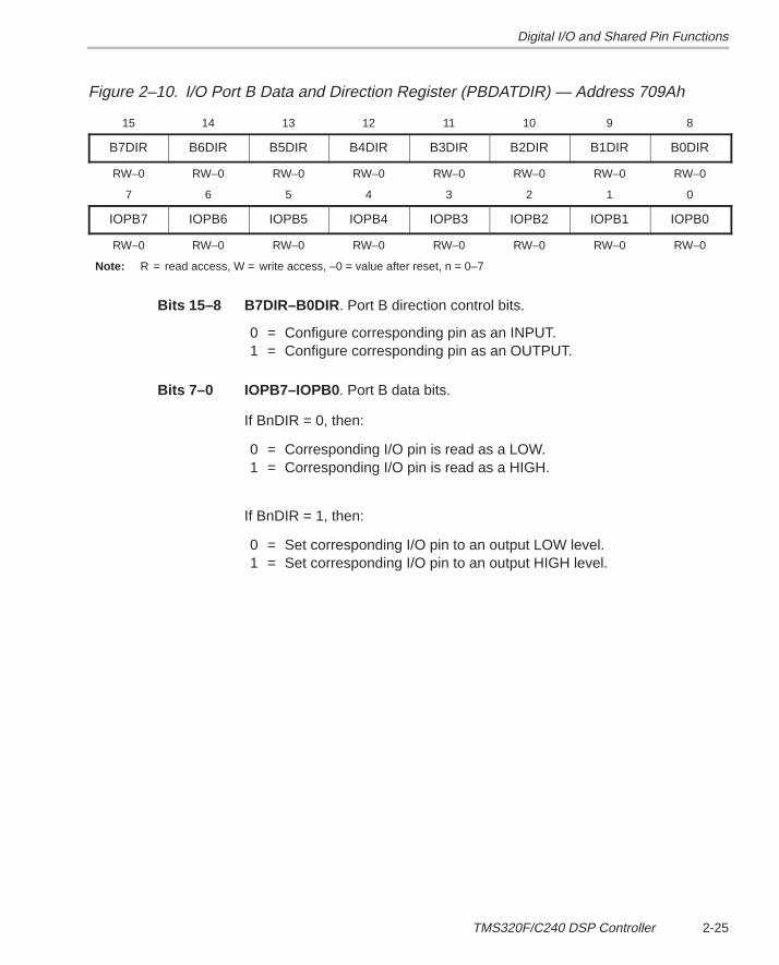
Digital I/O and Shared Pin Functions
2-25TMS320F/C240 DSP Controller
Figure 2–10. I/O Port B Data and Direction Register (PBDATDIR) — Address 709Ah
15 14 13 12 11 10 9 8
B7DIR B6DIR B5DIR B4DIR B3DIR B2DIR B1DIR B0DIR
RW–0 RW–0 RW–0 RW–0 RW–0 RW–0 RW–0 RW–0
7 6 5 4 3 2 1 0
IOPB7 IOPB6 IOPB5 IOPB4 IOPB3 IOPB2 IOPB1 IOPB0
RW–0 RW–0 RW–0 RW–0 RW–0 RW–0 RW–0 RW–0
Note: R = read access, W = write access, –0 = value after reset, n = 0–7
Bits 15–8 B7DIR–B0DIR . Port B direction control bits.
0 = Configure corresponding pin as an INPUT.1 = Configure corresponding pin as an OUTPUT.
Bits 7–0 IOPB7–IOPB0 . Port B data bits.
If BnDIR = 0, then:
0 = Corresponding I/O pin is read as a LOW.1 = Corresponding I/O pin is read as a HIGH.
If BnDIR = 1, then:
0 = Set corresponding I/O pin to an output LOW level.1 = Set corresponding I/O pin to an output HIGH level.

Digital I/O and Shared Pin Functions
2-26
Figure 2–11.I/O Port C Data and Direction Register (PCDATDIR) — Address 709Ch
15 14 13 12 11 10 9 8
C7DIR C6DIR C5DIR C4DIR C3DIR C2DIR C1DIR C0DIR
RW–0 RW–0 RW–0 RW–0 RW–0 RW–0 RW–0 RW–0
7 6 5 4 3 2 1 0
IOPC7 IOPC6 IOPC5 IOPC4 IOPC3 IOPC2 IOPC1 IOPC0
RW–0 RW–0 RW–0 RW–0 RW–0 RW–0 RW–0 RW–0
Note: R = read access, W = write access, –0 = value after reset, n = 0–7
Bits 15–8 C7DIR–C0DIR . Port C direction control bits.
0 = Configure corresponding pin as an INPUT.1 = Configure corresponding pin as an OUTPUT.
Bits 7–0 IOPC7–IOPC0 . Port C data bits.
If CnDIR = 0, then:
0 = Corresponding I/O pin is read as a LOW.1 = Corresponding I/O pin is read as a HIGH.
If CnDIR = 1, then:
0 = Set corresponding I/O pin to an output LOW level.1 = Set corresponding I/O pin to an output HIGH level.
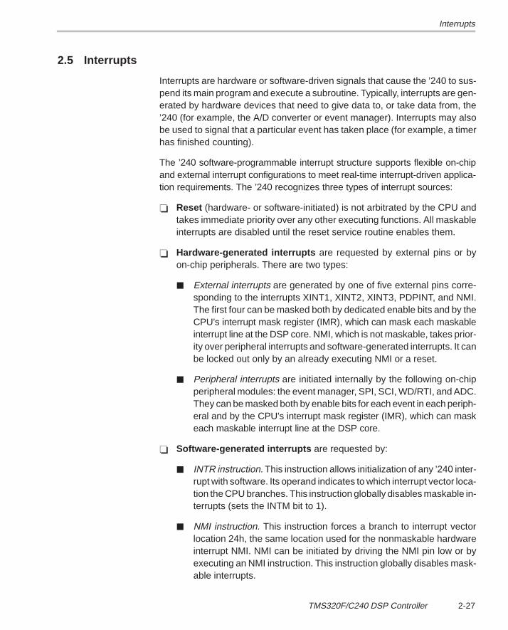
Interrupts
2-27TMS320F/C240 DSP Controller
2.5 Interrupts
Interrupts are hardware or software-driven signals that cause the ’240 to sus-pend its main program and execute a subroutine. Typically, interrupts are gen-erated by hardware devices that need to give data to, or take data from, the’240 (for example, the A/D converter or event manager). Interrupts may alsobe used to signal that a particular event has taken place (for example, a timerhas finished counting).
The ’240 software-programmable interrupt structure supports flexible on-chipand external interrupt configurations to meet real-time interrupt-driven applica-tion requirements. The ’240 recognizes three types of interrupt sources:
� Reset (hardware- or software-initiated) is not arbitrated by the CPU andtakes immediate priority over any other executing functions. All maskableinterrupts are disabled until the reset service routine enables them.
� Hardware-generated interrupts are requested by external pins or byon-chip peripherals. There are two types:
� External interrupts are generated by one of five external pins corre-sponding to the interrupts XINT1, XINT2, XINT3, PDPINT, and NMI.The first four can be masked both by dedicated enable bits and by theCPU’s interrupt mask register (IMR), which can mask each maskableinterrupt line at the DSP core. NMI, which is not maskable, takes prior-ity over peripheral interrupts and software-generated interrupts. It canbe locked out only by an already executing NMI or a reset.
� Peripheral interrupts are initiated internally by the following on-chipperipheral modules: the event manager, SPI, SCI, WD/RTI, and ADC.They can be masked both by enable bits for each event in each periph-eral and by the CPU’s interrupt mask register (IMR), which can maskeach maskable interrupt line at the DSP core.
� Software-generated interrupts are requested by:
� INTR instruction. This instruction allows initialization of any ’240 inter-rupt with software. Its operand indicates to which interrupt vector loca-tion the CPU branches. This instruction globally disables maskable in-terrupts (sets the INTM bit to 1).
� NMI instruction. This instruction forces a branch to interrupt vectorlocation 24h, the same location used for the nonmaskable hardwareinterrupt NMI. NMI can be initiated by driving the NMI pin low or byexecuting an NMI instruction. This instruction globally disables mask-able interrupts.
Interrupts
2-28
� TRAP instruction. This instruction forces the CPU to branch to inter-rupt vector location 22h. The TRAP instruction does not disable mask-able interrupts (INTM is not set to 1); thus when the CPU branches tothe interrupt service routine, that routine can be interrupted by themaskable hardware interrupts.
� An emulator trap. This interrupt can be generated with either an INTRinstruction or a TRAP instruction.
Each of the ’240 interrupts, whether hardware or software, can be placed inone of the following two categories:
� Maskable interrupts. These are hardware interrupts that can be blocked(masked) or enabled (unmasked) by software.
� Nonmaskable interrupts. These are interrupts that cannot be blocked.The ’240 always responds to this type of interrupt and branches from themain program to a subroutine. The ’240 nonmaskable interrupts includeall software interrupts and three external hardware interrupts: reset (RS),power-on reset (PORESET) and NMI. Note that although RS and PORE-SET) are always active low, NMI has programmable polarity.
For information about the reset signal and its effects on the ’240, see sec-tion 2.5.1, Resets, on page 2-31, section 3.3.3, Exiting the Power-DownModes, on page 3-12, and section 5.2.1, WD Timer, on page 5-6.
The ’C2xx CPU offers 32 interrupt vector locations (0000–003E). These vec-tors consists of hardware and software interrupt vectors. The six hardwaremaskable interrupts, INT1–INT6 have been expanded using a system mod-ule. This expansion is required to service all interrupts from ’240 peripherals.Table 2–8 describes the CPU interrupt grouping, along with peripheral inter-rupt vectors.
Table 2–11 summarizes the interrupts available on the ’240. Other maskableinterrupts are available through on-chip peripherals. The relationship betweenthe maskable CPU interrupts (INT1–INT6) and the maskable peripheral inter-rupts is included in this section; however, for details on the peripheral interruptsavailable on a specific ’24x device, see the data sheet for that device.
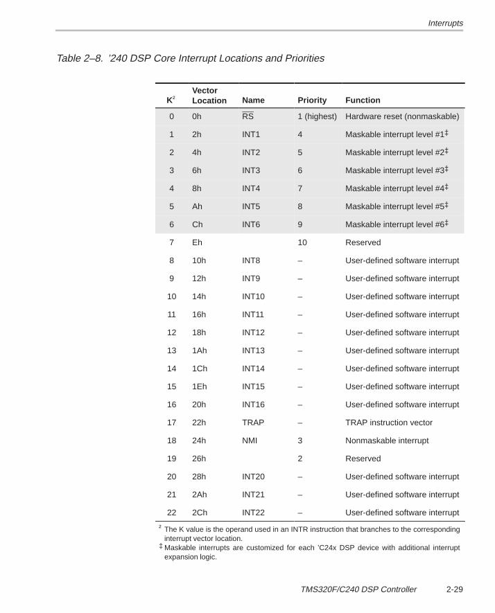
Interrupts
2-29TMS320F/C240 DSP Controller
Table 2–8. ’240 DSP Core Interrupt Locations and Priorities
ÁÁÁÁÁÁK†ÁÁÁÁÁÁÁÁÁÁ
VectorLocation
ÁÁÁÁÁÁÁÁÁÁName
ÁÁÁÁÁÁÁÁPriority
ÁÁÁÁÁÁÁÁÁÁÁÁÁÁÁÁÁÁÁÁFunction
0 0h RS 1 (highest) Hardware reset (nonmaskable)
1 2h INT1 4 Maskable interrupt level #1�
2 4h INT2 5 Maskable interrupt level #2�
3 6h INT3 6 Maskable interrupt level #3�
4 8h INT4 7 Maskable interrupt level #4�
5 Ah INT5 8 Maskable interrupt level #5�
6 Ch INT6 9 Maskable interrupt level #6�ÁÁÁÁÁÁÁÁÁ
7ÁÁÁÁÁÁÁÁÁÁÁÁÁÁÁ
EhÁÁÁÁÁÁÁÁÁÁÁÁÁÁÁ
ÁÁÁÁÁÁÁÁÁÁÁÁ
10ÁÁÁÁÁÁÁÁÁÁÁÁÁÁÁÁÁÁÁÁÁÁÁÁÁÁÁÁÁÁ
Reserved
ÁÁÁÁÁÁ
8 ÁÁÁÁÁÁÁÁÁÁ
10h ÁÁÁÁÁÁÁÁÁÁ
INT8 ÁÁÁÁÁÁÁÁ– ÁÁÁÁÁÁÁÁÁÁ
ÁÁÁÁÁÁÁÁÁÁUser-defined software interrupt
ÁÁÁÁÁÁ
9 ÁÁÁÁÁÁÁÁÁÁ
12h ÁÁÁÁÁÁÁÁÁÁ
INT9 ÁÁÁÁÁÁÁÁ– ÁÁÁÁÁÁÁÁÁÁ
ÁÁÁÁÁÁÁÁÁÁUser-defined software interrupt
ÁÁÁÁÁÁ
10ÁÁÁÁÁÁÁÁÁÁ
14hÁÁÁÁÁÁÁÁÁÁ
INT10ÁÁÁÁÁÁÁÁ–
ÁÁÁÁÁÁÁÁÁÁÁÁÁÁÁÁÁÁÁÁ
User-defined software interruptÁÁÁÁÁÁÁÁÁ
11ÁÁÁÁÁÁÁÁÁÁÁÁÁÁÁ
16hÁÁÁÁÁÁÁÁÁÁÁÁÁÁÁ
INT11ÁÁÁÁÁÁÁÁÁÁÁÁ–
ÁÁÁÁÁÁÁÁÁÁÁÁÁÁÁÁÁÁÁÁÁÁÁÁÁÁÁÁÁÁ
User-defined software interrupt
ÁÁÁÁÁÁ
12ÁÁÁÁÁÁÁÁÁÁ
18h ÁÁÁÁÁÁÁÁÁÁ
INT12 ÁÁÁÁÁÁÁÁ– ÁÁÁÁÁÁÁÁÁÁ
ÁÁÁÁÁÁÁÁÁÁUser-defined software interrupt
ÁÁÁÁÁÁ
13ÁÁÁÁÁÁÁÁÁÁ
1Ah ÁÁÁÁÁÁÁÁÁÁ
INT13 ÁÁÁÁÁÁÁÁ– ÁÁÁÁÁÁÁÁÁÁ
ÁÁÁÁÁÁÁÁÁÁUser-defined software interrupt
ÁÁÁÁÁÁÁÁÁ
14ÁÁÁÁÁÁÁÁÁÁÁÁÁÁÁ
1ChÁÁÁÁÁÁÁÁÁÁÁÁÁÁÁ
INT14ÁÁÁÁÁÁÁÁÁÁÁÁ
–ÁÁÁÁÁÁÁÁÁÁÁÁÁÁÁÁÁÁÁÁÁÁÁÁÁÁÁÁÁÁ
User-defined software interrupt
ÁÁÁÁÁÁ
15ÁÁÁÁÁÁÁÁÁÁ
1Eh ÁÁÁÁÁÁÁÁÁÁ
INT15 ÁÁÁÁÁÁÁÁ– ÁÁÁÁÁÁÁÁÁÁ
ÁÁÁÁÁÁÁÁÁÁUser-defined software interrupt
ÁÁÁÁÁÁ
16ÁÁÁÁÁÁÁÁÁÁ
20h ÁÁÁÁÁÁÁÁÁÁ
INT16 ÁÁÁÁÁÁÁÁ– ÁÁÁÁÁÁÁÁÁÁ
ÁÁÁÁÁÁÁÁÁÁUser-defined software interrupt
ÁÁÁÁÁÁ
17ÁÁÁÁÁÁÁÁÁÁ
22hÁÁÁÁÁÁÁÁÁÁ
TRAPÁÁÁÁÁÁÁÁ–
ÁÁÁÁÁÁÁÁÁÁÁÁÁÁÁÁÁÁÁÁ
TRAP instruction vectorÁÁÁÁÁÁÁÁÁ
18ÁÁÁÁÁÁÁÁÁÁÁÁÁÁÁ
24hÁÁÁÁÁÁÁÁÁÁÁÁÁÁÁ
NMIÁÁÁÁÁÁÁÁÁÁÁÁ
3ÁÁÁÁÁÁÁÁÁÁÁÁÁÁÁÁÁÁÁÁÁÁÁÁÁÁÁÁÁÁ
Nonmaskable interrupt
ÁÁÁÁÁÁ
19ÁÁÁÁÁÁÁÁÁÁ
26h ÁÁÁÁÁÁÁÁÁÁ
ÁÁÁÁÁÁÁÁ2 ÁÁÁÁÁÁÁÁÁÁ
ÁÁÁÁÁÁÁÁÁÁReserved
ÁÁÁÁÁÁ
20ÁÁÁÁÁÁÁÁÁÁ
28h ÁÁÁÁÁÁÁÁÁÁ
INT20 ÁÁÁÁÁÁÁÁ– ÁÁÁÁÁÁÁÁÁÁ
ÁÁÁÁÁÁÁÁÁÁUser-defined software interrupt
ÁÁÁÁÁÁ
21ÁÁÁÁÁÁÁÁÁÁ
2AhÁÁÁÁÁÁÁÁÁÁ
INT21ÁÁÁÁÁÁÁÁ–
ÁÁÁÁÁÁÁÁÁÁÁÁÁÁÁÁÁÁÁÁ
User-defined software interruptÁÁÁÁÁÁÁÁÁ
22ÁÁÁÁÁÁÁÁÁÁÁÁÁÁÁ
2ChÁÁÁÁÁÁÁÁÁÁÁÁÁÁÁ
INT22ÁÁÁÁÁÁÁÁÁÁÁÁ–
ÁÁÁÁÁÁÁÁÁÁÁÁÁÁÁÁÁÁÁÁÁÁÁÁÁÁÁÁÁÁ
User-defined software interrupt
ÁÁÁÁÁÁÁÁÁÁÁÁÁÁÁÁÁÁÁÁÁÁÁÁÁÁÁÁÁÁÁÁÁÁÁÁÁÁÁÁÁÁÁÁÁÁÁÁÁÁÁÁÁÁÁÁÁÁÁÁÁÁÁÁÁÁÁÁÁÁÁÁÁÁÁÁÁÁÁÁÁÁÁÁÁÁÁÁÁÁÁÁ
† The K value is the operand used in an INTR instruction that branches to the correspondinginterrupt vector location.
‡ Maskable interrupts are customized for each ’C24x DSP device with additional interruptexpansion logic.
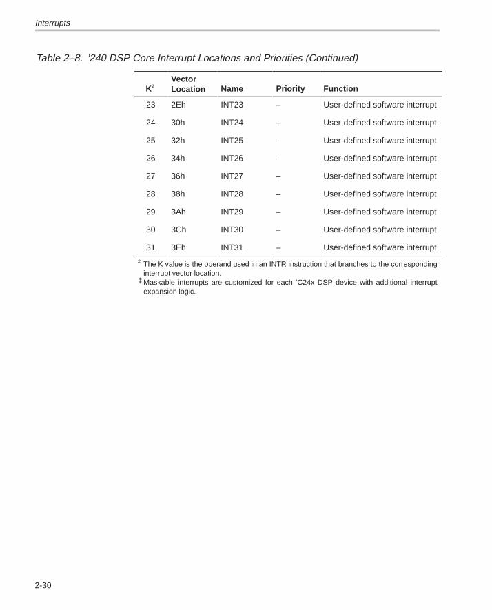
Interrupts
2-30
Table 2–8. ’240 DSP Core Interrupt Locations and Priorities (Continued)
ÁÁÁÁÁÁÁÁÁÁÁÁ
K†ÁÁÁÁÁÁÁÁÁÁÁÁ
VectorLocation
ÁÁÁÁÁÁÁÁÁÁÁÁÁÁÁ
NameÁÁÁÁÁÁÁÁÁÁÁÁÁÁÁ
PriorityÁÁÁÁÁÁÁÁÁÁÁÁÁÁÁÁÁÁÁÁÁÁÁÁÁÁÁFunction
ÁÁÁÁÁÁÁÁ
23 ÁÁÁÁÁÁÁÁ
2Eh ÁÁÁÁÁÁÁÁÁÁ
INT23 ÁÁÁÁÁÁÁÁÁÁ
– ÁÁÁÁÁÁÁÁÁÁÁÁÁÁÁÁÁÁUser-defined software interrupt
ÁÁÁÁÁÁÁÁ
24 ÁÁÁÁÁÁÁÁ
30h ÁÁÁÁÁÁÁÁÁÁ
INT24 ÁÁÁÁÁÁÁÁÁÁ
– ÁÁÁÁÁÁÁÁÁÁÁÁÁÁÁÁÁÁUser-defined software interrupt
ÁÁÁÁÁÁÁÁ25
ÁÁÁÁÁÁÁÁ32h
ÁÁÁÁÁÁÁÁÁÁINT25
ÁÁÁÁÁÁÁÁÁÁ–
ÁÁÁÁÁÁÁÁÁÁÁÁÁÁÁÁÁÁUser-defined software interruptÁÁÁÁ
ÁÁÁÁÁÁÁÁ
26ÁÁÁÁÁÁÁÁÁÁÁÁ
34hÁÁÁÁÁÁÁÁÁÁÁÁÁÁÁ
INT26ÁÁÁÁÁÁÁÁÁÁÁÁÁÁÁ
–ÁÁÁÁÁÁÁÁÁÁÁÁÁÁÁÁÁÁÁÁÁÁÁÁÁÁÁUser-defined software interrupt
ÁÁÁÁÁÁÁÁ
27 ÁÁÁÁÁÁÁÁ
36h ÁÁÁÁÁÁÁÁÁÁ
INT27 ÁÁÁÁÁÁÁÁÁÁ
– ÁÁÁÁÁÁÁÁÁÁÁÁÁÁÁÁÁÁUser-defined software interrupt
ÁÁÁÁÁÁÁÁ
28 ÁÁÁÁÁÁÁÁ
38h ÁÁÁÁÁÁÁÁÁÁ
INT28 ÁÁÁÁÁÁÁÁÁÁ
– ÁÁÁÁÁÁÁÁÁÁÁÁÁÁÁÁÁÁUser-defined software interrupt
ÁÁÁÁÁÁÁÁÁÁÁÁ
29ÁÁÁÁÁÁÁÁÁÁÁÁ
3AhÁÁÁÁÁÁÁÁÁÁÁÁÁÁÁ
INT29ÁÁÁÁÁÁÁÁÁÁÁÁÁÁÁ
–ÁÁÁÁÁÁÁÁÁÁÁÁÁÁÁÁÁÁÁÁÁÁÁÁÁÁÁ
User-defined software interrupt
ÁÁÁÁÁÁÁÁ
30 ÁÁÁÁÁÁÁÁ
3Ch ÁÁÁÁÁÁÁÁÁÁ
INT30 ÁÁÁÁÁÁÁÁÁÁ
– ÁÁÁÁÁÁÁÁÁÁÁÁÁÁÁÁÁÁUser-defined software interrupt
ÁÁÁÁÁÁÁÁ
31 ÁÁÁÁÁÁÁÁ
3Eh ÁÁÁÁÁÁÁÁÁÁ
INT31 ÁÁÁÁÁÁÁÁÁÁ
– ÁÁÁÁÁÁÁÁÁÁÁÁÁÁÁÁÁÁUser-defined software interrupt
ÁÁÁÁÁÁÁÁÁÁÁÁÁÁÁÁÁÁÁÁÁÁÁÁÁÁÁÁÁÁÁÁÁÁÁÁÁÁÁÁÁÁÁÁÁÁÁÁÁÁÁÁÁÁÁÁÁÁÁÁÁÁÁÁÁÁÁÁÁÁÁÁÁÁÁÁÁÁÁÁÁÁÁÁÁÁÁÁÁÁÁÁ
† The K value is the operand used in an INTR instruction that branches to the correspondinginterrupt vector location.
‡ Maskable interrupts are customized for each ’C24x DSP device with additional interruptexpansion logic.
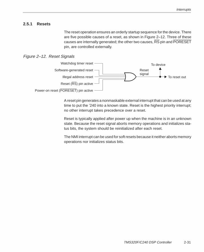
Interrupts
2-31TMS320F/C240 DSP Controller
2.5.1 Resets
The reset operation ensures an orderly startup sequence for the device. Thereare five possible causes of a reset, as shown in Figure 2–12. Three of thesecauses are internally generated; the other two causes, RS pin and PORESETpin, are controlled externally.
Figure 2–12. Reset Signals
Resetsignal
Watchdog timer reset
Software-generated reset
Illegal address reset
Reset (RS) pin active
Power-on reset (PORESET) pin active
To device
To reset out
A reset pin generates a nonmaskable external interrupt that can be used at anytime to put the ’240 into a known state. Reset is the highest priority interrupt;no other interrupt takes precedence over a reset.
Reset is typically applied after power up when the machine is in an unknownstate. Because the reset signal aborts memory operations and initializes sta-tus bits, the system should be reinitialized after each reset.
The NMI interrupt can be used for soft resets because it neither aborts memoryoperations nor initializes status bits.
Interrupts
2-32
The five possible reset signals are generated as follows:
� Watchdog timer reset. A watchdog timer generated reset occurs if thewatchdog timer overflows or an improper value is written to either thewatchdog key register or the watchdog control register. (Note that whenthe device is powered on, the watchdog timer is automatically active.)
� Software-generated reset. This is implemented with the system controlregister (SYSSR). Clearing the RESET0 bit (bit14) or setting the RESET1bit (bit15) causes a system reset.
� Illegal Address. The system and peripheral module control registerframe address map contains unimplemented address locations in theranges labeled reserved. Any access to an address located in theReserved ranges will generate an illegal-address reset.
� Reset pin active. To generate an external reset pulse on the RS pin, alow-level pulse duration of as little as a few nanoseconds is usually effec-tive; however, pulses of one SYSCLK cycle are necessary to ensure thatthe device recognizes the reset signal.
� Power-on Reset pin active . To generate a power-on reset pulse on the PORESET pin, a low-level pulse of one SYSCLK cycle is necessary to en-sure that the device recognizes the reset signal.
Once a reset source is activated, the external RS pin is driven (active) low fora minimum of eight SYSCLK cycles. This allows the ’240 to reset externaldevices connected to the RS pin. (The RS pin is an open-collector I/O pin andmust have a pullup resistor attached.) Additionally, if the RS pin is held low, thereset logic holds the device in a reset state for as long as the RS pin is held low.
When a reset signal is received, the program determines the source of thereset by reading the contents of the system status register (SSR). The SSRcontains one status bit for each of the four internal sources that can cause areset. During a reset, the RAM contents remain unchanged, and all control bitsthat are affected by a reset are initialized.
The occurrence of a reset condition causes the ’240 to terminate executionand affects various registers and status bits. During a reset, RAM contents re-main unchanged, and all control bits that are affected by a reset are initialized.Processor execution begins at location 0, which normally contains a branchinstruction to the system initialization routine.
Interrupts
2-33TMS320F/C240 DSP Controller
In the case of a power-on reset, the PLL control register bits are initialized tozero. Your program must recognize power-on resets and configure the PLLfor correct operation.
Your program can check the power-on reset flag (PORST flag, SYSSR, IS),the legal address flag (ILL ADDR flag, SYSSR.12), the software reset flag(SWRST flag, SYSSR.10), and the watchdog reset flag (WDRST flag,SYSSR.9) to determine the source of the reset. A reset does not clear theseflags. The RS and PORESET pins must be held low until the clock signal isvalid and CVdd/DVdd is within operating range. In addition, PORESET mustbe driven low when CVdd/DVdd drops below the minimum operating range.
When a ’240 reset occurs, the following actions take place:
� A logic 0 is loaded into the CNF (configuration control) bit in status registerST1; this maps dual-access RAM block 0 into the data space.
� The program counter is cleared to 0.
� The INTM (interrupt mode) bit is set to 1, disabling all maskable interrupts.(RS and NMI are not maskable.) Also, the interrupt flag register (IFR) andinterrupt mask register (IMR) are cleared.
� The status bits are loaded with the following values: OV = 0, XF = 1,SXM = 1, PM = 0, CNF = 0, INTM = 1, and C = 1. (The other status bitsremain undefined and should be initialized after a reset.)
� The global memory allocation register (GREG) is cleared to make allmemory local.
� The repeat counter (RPTC) is cleared.
� The wait states (if the device has an external memory interface) are setfor the maximum duration.
� The peripheral register bits are initialized as described in their respectivechapters.
No other CPU registers or status bits (such as the accumulator, the DP, theARP, and the auxiliary registers) are initialized.
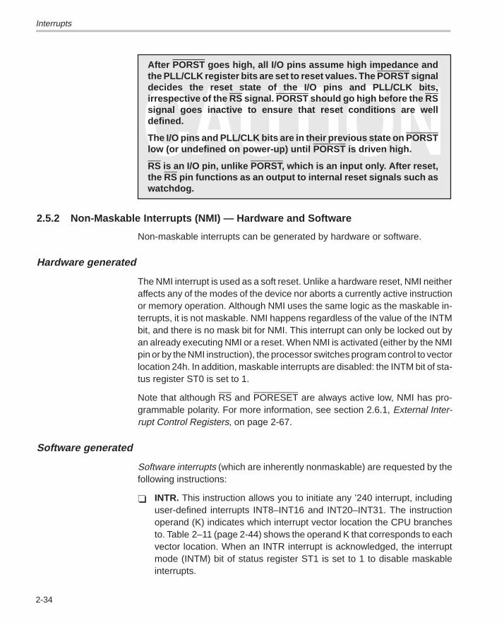
Interrupts
2-34
After PORST goes high, all I/O pins assume high impedance andthe PLL/CLK register bits are set to reset values. The PORST signaldecides the reset state of the I/O pins and PLL/CLK bits,irrespective of the RS signal. PORST should go high before the RSsignal goes inactive to ensure that reset conditions are welldefined.
The I/O pins and PLL/CLK bits are in their previous state on PORSTlow (or undefined on power-up) until PORST is driven high.
RS is an I/O pin, unlike PORST , which is an input only. After reset,the RS pin functions as an output to internal reset signals such aswatchdog.
2.5.2 Non-Maskable Interrupts (NMI) — Hardware and Software
Non-maskable interrupts can be generated by hardware or software.
Hardware generated
The NMI interrupt is used as a soft reset. Unlike a hardware reset, NMI neitheraffects any of the modes of the device nor aborts a currently active instructionor memory operation. Although NMI uses the same logic as the maskable in-terrupts, it is not maskable. NMI happens regardless of the value of the INTMbit, and there is no mask bit for NMI. This interrupt can only be locked out byan already executing NMI or a reset. When NMI is activated (either by the NMIpin or by the NMI instruction), the processor switches program control to vectorlocation 24h. In addition, maskable interrupts are disabled: the INTM bit of sta-tus register ST0 is set to 1.
Note that although RS and PORESET are always active low, NMI has pro-grammable polarity. For more information, see section 2.6.1, External Inter-rupt Control Registers, on page 2-67.
Software generated
Software interrupts (which are inherently nonmaskable) are requested by thefollowing instructions:
� INTR. This instruction allows you to initiate any ’240 interrupt, includinguser-defined interrupts INT8–INT16 and INT20–INT31. The instructionoperand (K) indicates which interrupt vector location the CPU branchesto. Table 2–11 (page 2-44) shows the operand K that corresponds to eachvector location. When an INTR interrupt is acknowledged, the interruptmode (INTM) bit of status register ST1 is set to 1 to disable maskableinterrupts.
Interrupts
2-35TMS320F/C240 DSP Controller
� NMI. This instruction forces a branch to interrupt vector location 24h, thesame location used for the nonmaskable hardware interrupt NMI. Thus,you can either initiate NMI by driving the NMI pin active or by executingan NMI instruction. When the NMI instruction is executed, INTM is set to1 to disable maskable interrupts.
� TRAP. This instruction forces the CPU to branch to interrupt vector loca-tion 22h. The TRAP instruction does not disable maskable interrupts(INTM is not set to 1); thus when the CPU branches to the interrupt serviceroutine, that routine can be interrupted by the maskable hardwareinterrupts.
� EMULATOR TRAP. This interrupt can be generated with either an INTRinstruction or a TRAP instruction.
After acknowledging a nonmaskable interrupt, the CPU:
1) Stores the program counter (PC) value (the return address) to the top ofthe hardware stack
2) Loads the PC with the address of the interrupt vector
3) Fetches the branch instruction that you stored at the vector location
If the interrupt was a hardware interrupt or was requested by either theINTR or NMI instructions, the CPU sets the INTM bit to 1 to disable mask-able interrupts.
4) Executes the branch, which leads it to the address of your ISR
5) Executes the ISR until a return instruction concludes the ISR
If INTM is 1, all maskable interrupts are disabled during the execution ofthe ISR.
6) Pops the return address off the stack and into the PC
7) Continues executing the main program
To determine which vector address has been assigned to each of the inter-rupts, refer to Table 2–11, ’240 Interrupt Locations and Priorities, on page2-44. Each interrupt address has been spaced apart by two locations so thattwo-word branch instructions can be accommodated in those locations.
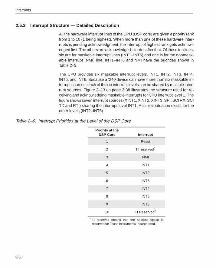
Interrupts
2-36
2.5.3 Interrupt Structure — Detailed Description
All the hardware interrupt lines of the CPU (DSP core) are given a priority rankfrom 1 to 10 (1 being highest). When more than one of these hardware inter-rupts is pending acknowledgment, the interrupt of highest rank gets acknowl-edged first. The others are acknowledged in order after that. Of those ten lines,six are for maskable interrupt lines (INT1–INT6) and one is for the nonmask-able interrupt (NMI) line. INT1–INT6 and NMI have the priorities shown inTable 2–9.
The CPU provides six maskable interrupt levels, INT1, INT2, INT3, INT4,INT5, and INT6. Because a ’240 device can have more than six maskable in-terrupt sources, each of the six interrupt levels can be shared by multiple inter-rupt sources. Figure 2–13 on page 2-38 illustrates the structure used for re-ceiving and acknowledging maskable interrupts for CPU interrupt level 1. Thefigure shows seven interrupt sources (XINT1, XINT2, XINT3, SPI, SCI RX, SCITX and RTI) sharing the interrupt level INT1. A similar situation exists for theother levels (INT2–INT6).
Table 2–9. Interrupt Priorities at the Level of the DSP CoreÁÁÁÁÁÁÁÁÁÁÁÁÁÁÁÁÁÁÁÁÁ
Priority at theDSP Core
ÁÁÁÁÁÁÁÁÁÁÁÁÁÁÁÁÁÁÁÁÁ
Interrupt
1 ResetÁÁÁÁÁÁÁÁÁÁÁÁÁÁÁÁÁÁÁÁÁ
2ÁÁÁÁÁÁÁÁÁÁÁÁÁÁÁÁÁÁÁÁÁ
TI reserved†
3 NMI
ÁÁÁÁÁÁÁÁÁÁÁÁÁÁ
4 ÁÁÁÁÁÁÁÁÁÁÁÁÁÁ
INT1
5 INT2ÁÁÁÁÁÁÁÁÁÁÁÁÁÁÁÁÁÁÁÁÁ
6ÁÁÁÁÁÁÁÁÁÁÁÁÁÁÁÁÁÁÁÁÁ
INT3
7 INT4
ÁÁÁÁÁÁÁÁÁÁÁÁÁÁ
8 ÁÁÁÁÁÁÁÁÁÁÁÁÁÁ
INT5
9 INT6
ÁÁÁÁÁÁÁÁÁÁÁÁÁÁ
10 ÁÁÁÁÁÁÁÁÁÁÁÁÁÁ
TI Reserved†
† TI reserved means that the address space isreserved for Texas Instruments Incorporated.
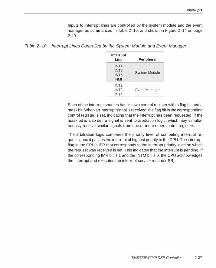
Interrupts
2-37TMS320F/C240 DSP Controller
Inputs to interrupt lines are controlled by the system module and the eventmanager as summarized in Table 2–10, and shown in Figure 2–14 on page2-40.
Table 2–10. Interrupt Lines Controlled by the System Module and Event Manager
InterruptLine Peripheral
INT1INT5INT6NMI
System Module
INT2INT3INT4
Event Manager
Each of the interrupt sources has its own control register with a flag bit and amask bit. When an interrupt signal is received, the flag bit in the correspondingcontrol register is set, indicating that the interrupt has been requested. If themask bit is also set, a signal is sent to arbitration logic, which may simulta-neously receive similar signals from one or more other control registers.
The arbitration logic compares the priority level of competing interrupt re-quests, and it passes the interrupt of highest priority to the CPU. The interruptflag in the CPU’s IFR that corresponds to the interrupt priority level on whichthe request was received is set. This indicates that the interrupt is pending. Ifthe corresponding IMR bit is 1 and the INTM bit is 0, the CPU acknowledgesthe interrupt and executes the interrupt service routine (ISR).
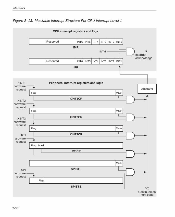
Interrupts
2-38
Figure 2–13. Maskable Interrupt Structure For CPU Interrupt Level 1
INT1Reserved INT2INT3INT4INT5INT6
MaskFlag
MaskFlag
MaskFlag
MaskFlag
Arbitrator
Interruptacknowledge
INTM
IMR
IFR
XINT1CR
XINT2CR
XINT3CR
RTICR
XINT1hardware
request
XINT2hardware
request
XINT3hardware
request
RTIhardware
request
CPU interrupt registers and logic
Peripheral interrupt registers and logic
INT1Reserved INT2INT3INT4INT5INT6
Mask
SPICTL
Flag
SPISTS
SPIhardware
request
Continued onnext page
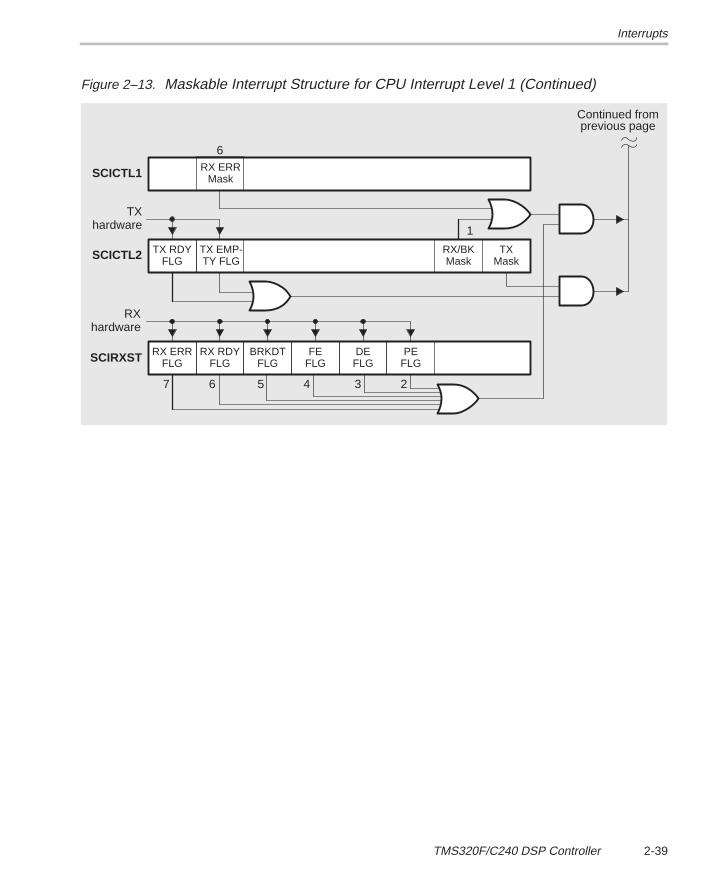
Interrupts
2-39TMS320F/C240 DSP Controller
Figure 2–13. Maskable Interrupt Structure for CPU Interrupt Level 1 (Continued)
Continued fromprevious page
RX ERRMask
TX RDYFLG
RX RDYFLG
RX ERRFLG
TXMask
RX/BKMask
BRKDTFLG
FEFLG
DEFLG
PEFLG
TX EMP-TY FLG
6
7 6 5 4 3 2
1
TXhardware
SCICTL1
SCICTL2
SCIRXST
RXhardware
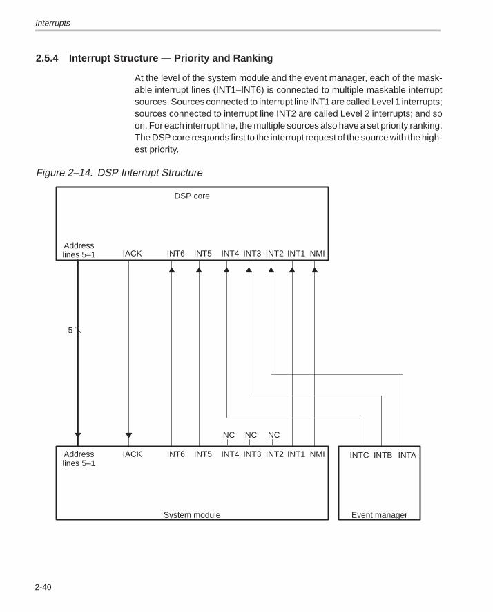
Interrupts
2-40
2.5.4 Interrupt Structure — Priority and Ranking
At the level of the system module and the event manager, each of the mask-able interrupt lines (INT1–INT6) is connected to multiple maskable interruptsources. Sources connected to interrupt line INT1 are called Level 1 interrupts;sources connected to interrupt line INT2 are called Level 2 interrupts; and soon. For each interrupt line, the multiple sources also have a set priority ranking.The DSP core responds first to the interrupt request of the source with the high-est priority.
Figure 2–14. DSP Interrupt Structure
DSP core
5
INTC INTB INTAAddresslines 5–1
INT6 INT5 INT4 INT3 INT2 INT1 NMIAddresslines 5–1
System module Event manager
IACK
INT6 INT5 INT4 INT3 INT2 INT1 NMIIACK
NC NC NC
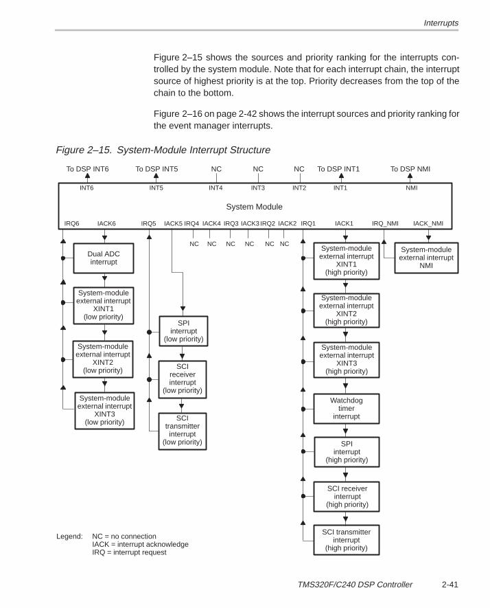
Interrupts
2-41TMS320F/C240 DSP Controller
Figure 2–15 shows the sources and priority ranking for the interrupts con-trolled by the system module. Note that for each interrupt chain, the interruptsource of highest priority is at the top. Priority decreases from the top of thechain to the bottom.
Figure 2–16 on page 2-42 shows the interrupt sources and priority ranking forthe event manager interrupts.
Figure 2–15. System-Module Interrupt Structure
SPIinterrupt
(low priority)
IACK2IRQ2
System-moduleexternal interrupt
XINT3(high priority)
System-moduleexternal interrupt
XINT2(high priority)
IACK1IRQ1IACK5IRQ5IACK6IRQ6
NMIINT1INT6
System-moduleexternal interrupt
NMI
To DSP INT6 To DSP INT1 To DSP NMI
NC = no connectionIACK = interrupt acknowledgeIRQ = interrupt request
Legend:
System-moduleexternal interrupt
XINT1(high priority)
Watchdogtimer
interrupt
SCIreceiverinterrupt
(low priority)
System-moduleexternal interrupt
XINT1(low priority)
System-moduleexternal interrupt
XINT2(low priority)
System-moduleexternal interrupt
XINT3(low priority)
Dual ADCinterrupt
IACK_NMIIRQ_NMIIACK3IRQ3IACK4IRQ4
NC
INT5
To DSP INT5
INT2INT3INT4
NCNCNC
System Module
SCI transmitterinterrupt
(high priority)
SCItransmitterinterrupt
(low priority) SPIinterrupt
(high priority)
SCI receiverinterrupt
(high priority)
NC NC NC NC NC
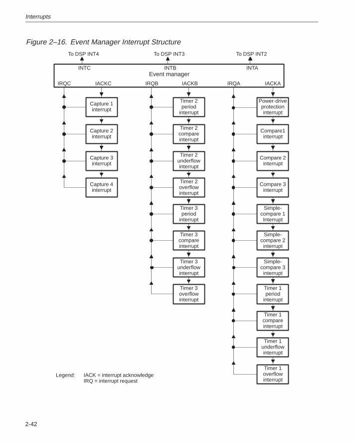
Interrupts
2-42
Figure 2–16. Event Manager Interrupt Structure
IACKAIRQAIACKBIRQBIACKCIRQC
INTAINTBINTC
Power-driveprotectioninterrupt
Compare1interrupt
Compare 2interrupt
Compare 3interrupt
Simple-compare 1Interrupt
Simple-compare 2interrupt
Simple-compare 3interrupt
Timer 1period
interrupt
Timer 1compareinterrupt
Timer 1underflowinterrupt
Timer 1overflowinterrupt
Timer 2period
interrupt
Timer 2compareinterrupt
Timer 2underflowinterrupt
Timer 2overflowinterrupt
Timer 3period
interrupt
Timer 3underflowinterrupt
Timer 3overflowinterrupt
Capture 1interrupt
Capture 2interrupt
Capture 3interrupt
Capture 4interrupt
To DSP INT4 To DSP INT3 To DSP INT2
IACK = interrupt acknowledgeIRQ = interrupt request
Legend:
Event manager
Timer 3compareinterrupt
Interrupts
2-43TMS320F/C240 DSP Controller
Each of the interrupt sources has its own control register with a flag bit and anenable bit. When an interrupt request is received, the flag bit in the correspond-ing control register is set. If the enable bit is also set, a signal is sent to arbitra-tion logic, which may simultaneously receive similar signals from one or moreother control registers. The arbitration logic compares the priority level of com-peting interrupt requests, and it passes the interrupt of highest priority to theCPU. The corresponding flag is set in the interrupt flag register (IFR), indicat-ing that the interrupt is pending. The CPU then must decide whether toacknowledge the request. Maskable hardware interrupts are acknowledgedonly after the following conditions are met:
� Priority is highest. When more than one hardware interrupt is requestedat the same time, the ’240 services them according to the set priority rank-ing.
� INTM bit is 0. The interrupt mode (INTM) bit, bit 9 of status register ST0,enables or disables all maskable interrupts:
� When INTM = 0, all unmasked interrupts are enabled.� When INTM = 1, all unmasked interrupts are disabled.
� INTM is set to 1 automatically when the CPU acknowledges an interrupt(except when initiated by the TRAP instruction) and at reset. It can be setand cleared by software.
� IMR mask bit is 1. Each of the maskable interrupt lines has a mask bitin the interrupt mask register (IMR). To unmask an interrupt line, set itsIMR bit to 1.
When the CPU acknowledges a maskable hardware interrupt, it jams theinstruction bus with the INTR instruction. This instruction forces the programcounter (PC) to the appropriate address from which the CPU fetches the soft-ware vector. This vector leads to an interrupt service routine.
Usually, the interrupt service routine reads the peripheral-vector-address off-set from the peripheral-vector-address register (see Table 3–6) to branch tocode that is meant for the specific interrupt source that initiated the interruptrequest. The ’240 includes a phantom-interrupt vector offset (0000h), whichis a system interrupt integrity feature that allows a controlled exit from animproper interrupt sequence. If the CPU acknowledges a request from aperipheral when, in fact, no peripheral has requested an interrupt, the phan-tom-interrupt vector is read from the interrupt-vector register.
Table 2–11, ’240 Interrupt Locations and Priorities, on page 2-44 summarizesthe interrupt sources, overall priority, vector address/offset, source, and func-tion of each interrupt available on the ’240.
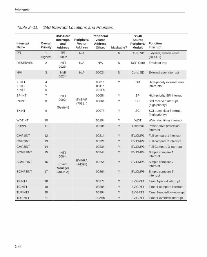
Interrupts
2-44
Table 2–11. ’240 Interrupt Locations and Priorities
InterruptName
OverallPriority
DSP-CoreInterrupt,
andAddress
PeripheralVector
Address
PeripheralVector
AddressOffset Maskable?
’x240Source
PeripheralModule
FunctionInterrupt
RS 1Highest
RS0000h
N/A N Core, SD External, system reset(RESET)
RESERVED 2 INT70026h
N/A N/A N DSP Core Emulator trap
NMI 3 NMI0024h
N/A 0002h N Core, SD External user interrupt
XINT1XINT2XINT3
456
0001h0011h001Fh
Y SD High-priority external userinterrupts
SPIINT 7 INT1 0005h Y SPI High-priority SPI interrupt
RXINT 8 0002h
(System)
SYSIVR(701Eh)
0006h Y SCI SCI receiver interrupt(high priority)
TXINT 9(System)
0007h Y SCI SCI transmitter interrupt(high priority)
WDTINT 10 0010h Y WDT Watchdog timer interrupt
PDPINT 11 0020h Y External Power-drive protectioninterrupt
CMP1INT 12 0021h Y EV.CMP1 Full compare 1 interrupt
CMP2INT 13 0022h Y EV.CMP2 Full compare 2 interrupt
CMP3INT 14 0023h Y EV.CMP3 Full Compare 3 interrupt
SCMP1INT 15 INT20004h
0024h Y EV.CMP4 Simple compare 1interrupt
SCMP2INT 16(Event
Manager
EVIVRA(7432h)
0025h Y EV.CMP5 Simple compare 2interrupt
SCMP3INT 17ManagerGroup A) 0026h Y EV.CMP6 Simple compare 3
interrupt
TPINT1 18 0027h Y EV.GPT1 Timer1-period interrupt
TCINT1 19 0028h Y EV.GPT1 Timer1-compare interrupt
TUFINT1 20 0029h Y EV.GPT1 Timer1-underflow interrupt
TOFINT1 21 002Ah Y EV.GPT1 Timer1-overflow interrupt
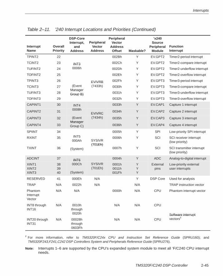
Interrupts
2-45TMS320F/C240 DSP Controller
Table 2–11. ’240 Interrupt Locations and Priorities (Continued)
InterruptName
FunctionInterrupt
’x240Source
PeripheralModuleMaskable?
PeripheralVector
AddressOffset
PeripheralVector
Address
DSP-CoreInterrupt,
andAddress
OverallPriority
TPINT2 22 002Bh Y EV.GPT2 Timer2-period interrupt
TCINT2 23 INT3 002Ch Y EV.GPT2 Timer2-compare interrupt
TUFINT2 24
INT30006h 002Dh Y EV.GPT2 Timer2-underflow interrupt
TOFINT2 25 002Eh Y EV.GPT2 Timer2-overflow interrupt
TPINT3 26 EVIVRB 002Fh Y EV.GPT3 Timer3-period interrupt
TCINT3 27 (EventManager
EVIVRB(7433h) 0030h Y EV.GPT3 Timer3-compare interrupt
TUFINT3 28ManagerGroup B) 0031h Y EV.GPT3 Timer3-underflow interrupt
TOFINT3 29Grou B)
0032h Y EV.GPT3 Timer3-overflow interrupt
CAPINT1 30 INT40008h
0033h Y EV.CAP1 Capture 1 interrupt
CAPINT2 31 0008hEVIVRC
0034h Y EV.CAP2 Capture 2 interrupt
CAPINT3 32 (EventManager
EVIVRC(7434h) 0035h Y EV.CAP3 Capture 3 interrupt
CAPINT4 33ManagerGroup C) 0036h Y EV.CAP4 Capture 4 interrupt
SPIINT 34 0005h Y SPI Low-priority SPI interrupt
RXINT 35 INT5000Ah SYSIVR
(701Eh)
0006h Y SCI SCI receiver interrupt(low priority)
TXINT 36 (System)(701Eh)
0007h Y SCI SCI transmitter interrupt(low priority)
ADCINT 37 INT6 0004h Y ADC Analog-to-digital interrupt
XINT1XINT2XINT3
383940
INT6000Ch
(System)
SYSIVR(701Eh)
0001h0011h001Fh
YYY
Externalpins
Low-priority externaluser interrupts
RESERVED 41 000Eh N/A Y DSP Core Used for analysis
TRAP N/A 0022h N/A N/A TRAP instruction vector
PhantomInterruptVector
N/A N/A 0000h N/A CPU Phantom interrupt vector
INT8 throughINT16
N/A 0010hthrough0020h
N/A N/A CPU
Software interrupt
INT20 throughINT31
N/A 00028hthrough0603Fh
N/A N/A CPU
Software interru tvectors†
† For more information, refer to TMS320F/C24x CPU and Instruction Set Reference Guide (SPRU160); andTMS320F243,F241,C242 DSP Controllers System and Peripherals Reference Guide (SPRU276).
Note: Interrupts 1–6 are supported by the CPU’s expanded system module to meet all ’F/C240 CPU interruptneeds.
Interrupts
2-46
2.5.5 Interrupt Operation: Detailed Description
The ’240 handles interrupts in the following three phases:
1) Receive interrupt request. Suspension of the main program must be re-quested by software (program code) or hardware (a pin or an on-chipdevice).
2) Acknowledge interrupt. The ’240 must acknowledge the interrupt re-quest. If the interrupt is maskable, certain conditions must be met in orderfor the ’240 to acknowledge it. For nonmaskable hardware interrupts andfor software interrupts, acknowledgment is immediate.
3) Execute interrupt service routine. Once the interrupt is acknowledged,the ’240 branches to its corresponding subroutine, called an interrupt ser-vice routine (ISR). The ’240 follows the branch instruction you place at apredetermined address (the vector location) and executes the ISR youhave written.

Interrupts
2-47TMS320F/C240 DSP Controller
Figure 2–17. Interrupt Operation Flow Chart
Interrupt requested
Interruptmaskable?
Interruptsenabled
(INTM bit = 0)?
Interrupt acknowledged
TRAPinstruction?
Yes
Yes
Yes
Yes
No
No
No
No
INTM bit set to 1
PC saved on software stack
Interrupt service routine run
Return instruction restores PC
Main program continues
IMR bitset?
Individualmask bit
set?
No
IFR bit set
Individual flag bit set
Yes
Interrupts
2-48
Acknowledging Maskable Interrupts
Software interrupts and nonmaskable hardware interrupts are acknowledgedimmediately. Maskable hardware interrupts are acknowledged only after cer-tain conditions are met:
� Priority is highest. When more than one hardware interrupt is requestedat the same time, the ’240 services each interrupt according to a set prior-ity ranking (see Figure 2–15 on page 2-41).
� INTM bit is 0. The interrupt mode (INTM) bit, bit 9 of status register ST0,enables or disables all maskable interrupts:
� When INTM = 0, all unmasked interrupts are enabled.� When INTM = 1, all maskable interrupts are disabled.
INTM is set to 1 automatically when the CPU acknowledges an interrupt(except when initiated by the TRAP instruction). INTM can also be set to1 by a hardware reset or by execution of a disable-interrupts instruction(SETC INTM). INTM is reset to 0 by executing the enable-interruptsinstruction (CLRC INTM). INTM has no effect on reset, NMI, or software-interrupts. Also, INTM is unaffected by the LST (load status register)instruction.
INTM does not modify the interrupt mask register (IMR) or the interrupt flagregister (IFR).
� IMR mask bit is 1. Each of the maskable interrupt levels has a mask bitin the IMR. To unmask an interrupt level, set its IMR bit to 1. For more de-tails about the IMR, see Interrupt Mask Register (IMR) on page 2-66.
When the CPU acknowledges a maskable hardware interrupt, it jams theinstruction bus with the INTR instruction. This instruction forces the PC to theappropriate address from which the CPU fetches the software vector.
Two-Part Interrupt Service Routine (ISR)
The ’C2xx CPU has six interrupt levels; however, ’240 devices provide ameans of creating more than six ISRs. Figure 2–18, Interrupt Service RoutineFlow Chart, on page 2-49 illustrates the process of servicing an interrupt request.
For each of the six interrupt levels, the CPU branches to a corresponding gen-eral interrupt service routine (GISR). For example, when responding to an interrupt request on priority level INT1, the CPU branches to and executesGISR1. The GISR, after performing any necessary context saves, identifiesand then branches to the specific interrupt service routine (SISR). The SISRperforms the actions specific to the triggering interrupt and then returns pro-gram control to the interrupted program sequence.
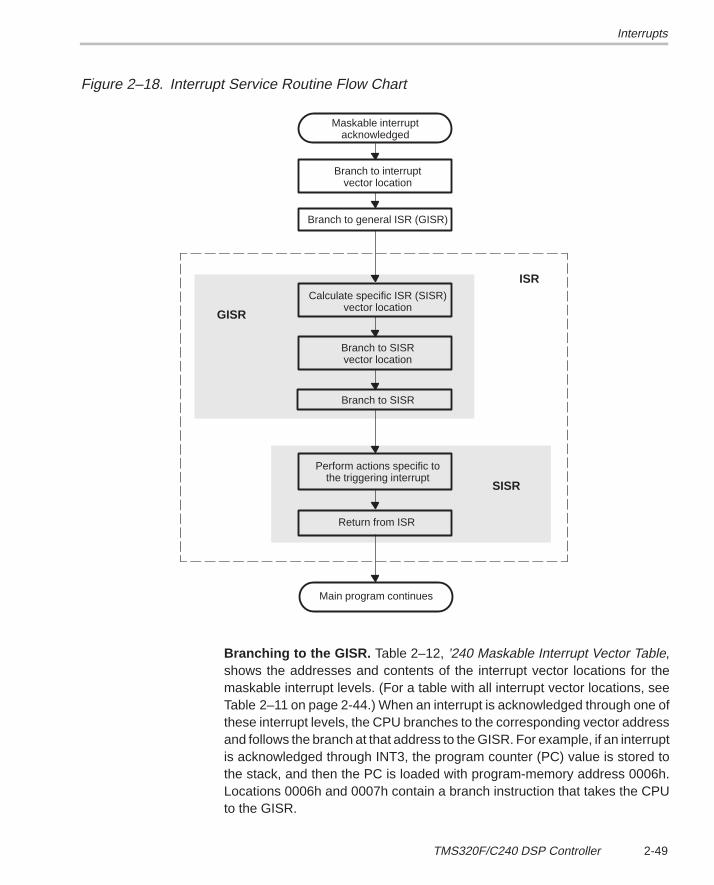
Interrupts
2-49TMS320F/C240 DSP Controller
Figure 2–18. Interrupt Service Routine Flow Chart
Maskable interruptacknowledged
Branch to interruptvector location
Main program continues
Branch to SISRvector location
Branch to SISR
GISR
Perform actions specific tothe triggering interrupt
Return from ISR
SISR
ISR
Branch to general ISR (GISR)
Calculate specific ISR (SISR)vector location
Branching to the GISR. Table 2–12, ’240 Maskable Interrupt Vector Table,shows the addresses and contents of the interrupt vector locations for themaskable interrupt levels. (For a table with all interrupt vector locations, seeTable 2–11 on page 2-44.) When an interrupt is acknowledged through one ofthese interrupt levels, the CPU branches to the corresponding vector addressand follows the branch at that address to the GISR. For example, if an interruptis acknowledged through INT3, the program counter (PC) value is stored tothe stack, and then the PC is loaded with program-memory address 0006h.Locations 0006h and 0007h contain a branch instruction that takes the CPUto the GISR.
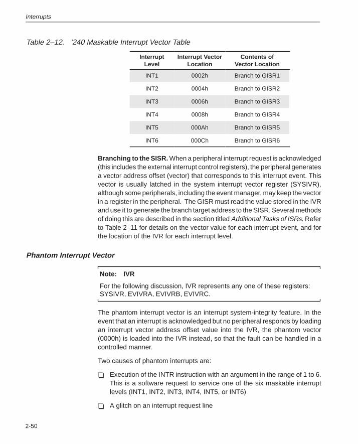
Interrupts
2-50
Table 2–12. ’240 Maskable Interrupt Vector Table
ÁÁÁÁÁÁÁÁÁÁÁÁÁÁÁÁÁÁ
InterruptLevel
ÁÁÁÁÁÁÁÁÁÁÁÁÁÁÁÁÁÁ
Interrupt VectorLocation
ÁÁÁÁÁÁÁÁÁÁÁÁÁÁÁÁÁÁÁÁÁ
Contents ofVector Location
INT1 0002h Branch to GISR1
ÁÁÁÁÁÁÁÁÁÁÁÁ
INT2 ÁÁÁÁÁÁÁÁÁÁÁÁ
0004h ÁÁÁÁÁÁÁÁÁÁÁÁÁÁ
Branch to GISR2
INT3 0006h Branch to GISR3ÁÁÁÁÁÁÁÁÁÁÁÁÁÁÁÁÁÁ
INT4ÁÁÁÁÁÁÁÁÁÁÁÁÁÁÁÁÁÁ
0008hÁÁÁÁÁÁÁÁÁÁÁÁÁÁÁÁÁÁÁÁÁ
Branch to GISR4
INT5 000Ah Branch to GISR5
ÁÁÁÁÁÁÁÁÁÁÁÁ
INT6 ÁÁÁÁÁÁÁÁÁÁÁÁ
000Ch ÁÁÁÁÁÁÁÁÁÁÁÁÁÁ
Branch to GISR6
Branching to the SISR. When a peripheral interrupt request is acknowledged(this includes the external interrupt control registers), the peripheral generatesa vector address offset (vector) that corresponds to this interrupt event. Thisvector is usually latched in the system interrupt vector register (SYSIVR),although some peripherals, including the event manager, may keep the vectorin a register in the peripheral. The GISR must read the value stored in the IVRand use it to generate the branch target address to the SISR. Several methodsof doing this are described in the section titled Additional Tasks of ISRs. Referto Table 2–11 for details on the vector value for each interrupt event, and forthe location of the IVR for each interrupt level.
Phantom Interrupt Vector
Note: IVR
For the following discussion, IVR represents any one of these registers: SYSIVR, EVIVRA, EVIVRB, EVIVRC.
The phantom interrupt vector is an interrupt system-integrity feature. In theevent that an interrupt is acknowledged but no peripheral responds by loadingan interrupt vector address offset value into the IVR, the phantom vector(0000h) is loaded into the IVR instead, so that the fault can be handled in acontrolled manner.
Two causes of phantom interrupts are:
� Execution of the INTR instruction with an argument in the range of 1 to 6.This is a software request to service one of the six maskable interruptlevels (INT1, INT2, INT3, INT4, INT5, or INT6)
� A glitch on an interrupt request line
Interrupts
2-51TMS320F/C240 DSP Controller
In either case, when the interrupt is acknowledged, no peripheral loads a vec-tor into the IVR. Loading the IVR with the phantom interrupt vector ensures thatthe DSP branches to a known location.
Programming ISRs for Maskable Interrupts
The three methods for creating an interrupt service routine (ISR) for a mask-able interrupt are:
� Method 1: A typical ISR
� Method 2: An ISR that is designed to reduce the latency between the timethe interrupt is requested and the time the event-specific portion of the ISRis executed
� Method 3: An ISR that has very little latency — used only if one peripheralinterrupt source is connected to an interrupt request priority level or if onlyone of many interrupt sources connected to an interrupt request prioritylevel is enabled
Method 1: Typical ISR
The method described here is the typical implementation of an ISR for the ’240.Methods 2 and 3, described below are slightly more difficult to program. It isbest to implement this typical ISR first and then develop a more complex rou-tine if the latency for certain events is too high.
In Method 1, the ISR for a maskable interrupt is divided into two segments:
1) General ISR (GISR). When an interrupt on one of the six maskable inter-rupt levels (INT1–INT6) is acknowledged, the GISR reads the relevant in-terrupt vector register (IVR), shifts the value left by one bit, adds an offsetto the value, and then branches to a peripheral interrupt vector table. Fromthis table, it fetches and executes the appropriate branch to the specificISR (SISR).
2) Specific ISR (SISR). The SISR performs actions specific to the event thatcaused the interrupt and then returns program control to the interruptedcode sequence.
Table 2–13, Example of Method 1 ISR, on page 2-52 shows a typical imple-mentation of an ISR.
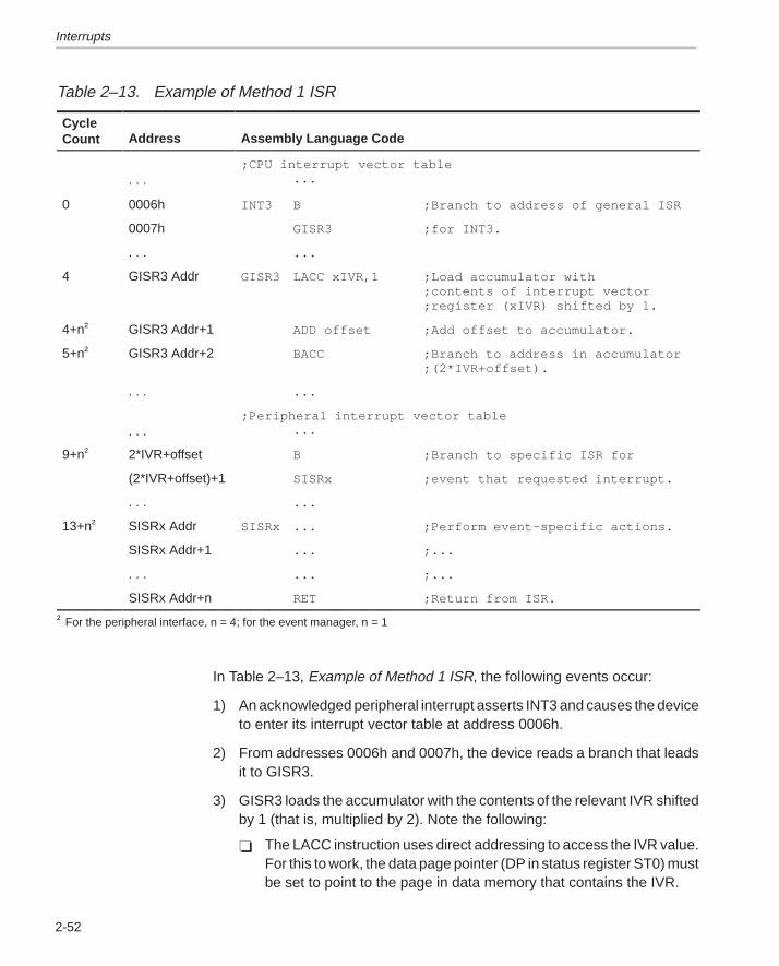
Interrupts
2-52
Table 2–13. Example of Method 1 ISR
ÁÁÁÁÁÁÁÁÁÁÁÁ
CycleCountÁÁÁÁÁÁÁÁÁÁÁÁÁÁÁÁÁÁ
AddressÁÁÁÁÁÁÁÁÁÁÁÁÁÁÁÁÁÁÁÁÁÁÁÁÁÁÁÁÁÁÁÁÁÁÁÁÁÁÁÁÁÁÁÁÁÁÁÁÁÁÁÁÁÁÁÁÁÁÁÁÁÁÁÁÁÁ
Assembly Language Code
ÁÁÁÁÁÁÁÁÁÁÁÁ
ÁÁÁÁÁÁÁÁÁÁÁÁÁÁÁÁÁÁ
. . .ÁÁÁÁÁÁÁÁÁÁÁÁÁÁÁÁÁÁÁÁÁÁÁÁÁÁÁÁÁÁÁÁÁÁÁÁÁÁÁÁÁÁÁÁÁÁÁÁÁÁÁÁÁÁÁÁÁÁÁÁÁÁÁÁÁÁ
;CPU interrupt vector table...
ÁÁÁÁÁÁÁÁ
0 ÁÁÁÁÁÁÁÁÁÁÁÁ
0006h ÁÁÁÁÁÁÁÁÁÁÁÁÁÁÁÁÁÁÁÁÁÁÁÁÁÁÁÁÁÁÁÁÁÁÁÁÁÁÁÁÁÁÁÁ
INT3 B ;Branch to address of general ISR
ÁÁÁÁÁÁÁÁ
ÁÁÁÁÁÁÁÁÁÁÁÁ
0007h ÁÁÁÁÁÁÁÁÁÁÁÁÁÁÁÁÁÁÁÁÁÁÁÁÁÁÁÁÁÁÁÁÁÁÁÁÁÁÁÁÁÁÁÁ
GISR3 ;for INT3.
ÁÁÁÁÁÁÁÁ
ÁÁÁÁÁÁÁÁÁÁÁÁ
. . . ÁÁÁÁÁÁÁÁÁÁÁÁÁÁÁÁÁÁÁÁÁÁÁÁÁÁÁÁÁÁÁÁÁÁÁÁÁÁÁÁÁÁÁÁ
...
ÁÁÁÁÁÁÁÁÁÁÁÁ
4 ÁÁÁÁÁÁÁÁÁÁÁÁÁÁÁÁÁÁ
GISR3 Addr ÁÁÁÁÁÁÁÁÁÁÁÁÁÁÁÁÁÁÁÁÁÁÁÁÁÁÁÁÁÁÁÁÁÁÁÁÁÁÁÁÁÁÁÁÁÁÁÁÁÁÁÁÁÁÁÁÁÁÁÁÁÁÁÁÁÁ
GISR3 LACC xIVR,1 ;Load accumulator with;contents of interrupt vector;register (xIVR) shifted by 1.
ÁÁÁÁÁÁÁÁ
4+n† ÁÁÁÁÁÁÁÁÁÁÁÁ
GISR3 Addr+1ÁÁÁÁÁÁÁÁÁÁÁÁÁÁÁÁÁÁÁÁÁÁÁÁÁÁÁÁÁÁÁÁÁÁÁÁÁÁÁÁÁÁÁÁ
ADD offset ;Add offset to accumulator.ÁÁÁÁÁÁÁÁÁÁÁÁ
5+n† ÁÁÁÁÁÁÁÁÁÁÁÁÁÁÁÁÁÁ
GISR3 Addr+2ÁÁÁÁÁÁÁÁÁÁÁÁÁÁÁÁÁÁÁÁÁÁÁÁÁÁÁÁÁÁÁÁÁÁÁÁÁÁÁÁÁÁÁÁÁÁÁÁÁÁÁÁÁÁÁÁÁÁÁÁÁÁÁÁÁÁ
BACC ;Branch to address in accumulator;(2*IVR+offset).
ÁÁÁÁÁÁÁÁ
ÁÁÁÁÁÁÁÁÁÁÁÁ
. . . ÁÁÁÁÁÁÁÁÁÁÁÁÁÁÁÁÁÁÁÁÁÁÁÁÁÁÁÁÁÁÁÁÁÁÁÁÁÁÁÁÁÁÁÁ
...
ÁÁÁÁÁÁÁÁÁÁÁÁ
ÁÁÁÁÁÁÁÁÁÁÁÁÁÁÁÁÁÁ
. . .
ÁÁÁÁÁÁÁÁÁÁÁÁÁÁÁÁÁÁÁÁÁÁÁÁÁÁÁÁÁÁÁÁÁÁÁÁÁÁÁÁÁÁÁÁÁÁÁÁÁÁÁÁÁÁÁÁÁÁÁÁÁÁÁÁÁÁ
;Peripheral interrupt vector table...
ÁÁÁÁÁÁÁÁ
9+n† ÁÁÁÁÁÁÁÁÁÁÁÁ
2*IVR+offset ÁÁÁÁÁÁÁÁÁÁÁÁÁÁÁÁÁÁÁÁÁÁÁÁÁÁÁÁÁÁÁÁÁÁÁÁÁÁÁÁÁÁÁÁ
B ;Branch to specific ISR for
ÁÁÁÁÁÁÁÁ
ÁÁÁÁÁÁÁÁÁÁÁÁ
(2*IVR+offset)+1ÁÁÁÁÁÁÁÁÁÁÁÁÁÁÁÁÁÁÁÁÁÁÁÁÁÁÁÁÁÁÁÁÁÁÁÁÁÁÁÁÁÁÁÁ
SISRx ;event that requested interrupt.
ÁÁÁÁÁÁÁÁ
ÁÁÁÁÁÁÁÁÁÁÁÁ
. . . ÁÁÁÁÁÁÁÁÁÁÁÁÁÁÁÁÁÁÁÁÁÁÁÁÁÁÁÁÁÁÁÁÁÁÁÁÁÁÁÁÁÁÁÁ
...
ÁÁÁÁÁÁÁÁ
13+n† ÁÁÁÁÁÁÁÁÁÁÁÁ
SISRx Addr ÁÁÁÁÁÁÁÁÁÁÁÁÁÁÁÁÁÁÁÁÁÁÁÁÁÁÁÁÁÁÁÁÁÁÁÁÁÁÁÁÁÁÁÁ
SISRx ... ;Perform event–specific actions.
ÁÁÁÁÁÁÁÁ
ÁÁÁÁÁÁÁÁÁÁÁÁ
SISRx Addr+1ÁÁÁÁÁÁÁÁÁÁÁÁÁÁÁÁÁÁÁÁÁÁÁÁÁÁÁÁÁÁÁÁÁÁÁÁÁÁÁÁÁÁÁÁ
... ;...
ÁÁÁÁÁÁÁÁ
ÁÁÁÁÁÁÁÁÁÁÁÁ
. . . ÁÁÁÁÁÁÁÁÁÁÁÁÁÁÁÁÁÁÁÁÁÁÁÁÁÁÁÁÁÁÁÁÁÁÁÁÁÁÁÁÁÁÁÁ
... ;...ÁÁÁÁÁÁÁÁ
ÁÁÁÁÁÁÁÁÁÁÁÁ
SISRx Addr+nÁÁÁÁÁÁÁÁÁÁÁÁÁÁÁÁÁÁÁÁÁÁÁÁÁÁÁÁÁÁÁÁÁÁÁÁÁÁÁÁÁÁÁÁ
RET ;Return from ISR.
† For the peripheral interface, n = 4; for the event manager, n = 1
In Table 2–13, Example of Method 1 ISR, the following events occur:
1) An acknowledged peripheral interrupt asserts INT3 and causes the deviceto enter its interrupt vector table at address 0006h.
2) From addresses 0006h and 0007h, the device reads a branch that leadsit to GISR3.
3) GISR3 loads the accumulator with the contents of the relevant IVR shiftedby 1 (that is, multiplied by 2). Note the following:
� The LACC instruction uses direct addressing to access the IVR value.For this to work, the data page pointer (DP in status register ST0) mustbe set to point to the page in data memory that contains the IVR.
Interrupts
2-53TMS320F/C240 DSP Controller
� You may want to save the accumulator value before loading the accu-mulator with the shifted IVR value.
� The incoming vector has been multiplied by two because a peripheralinterrupt vector table must support a 2-word branch instruction foreach peripheral interrupt.
4) GISR3 adds an offset to the accumulator that corresponds to the start ofthe peripheral interrupt vector table. The accumulator now contains theaddress that needs to be accessed in the peripheral interrupt vector table.
5) GISR3 branches to the address in the accumulator.
6) From the peripheral interrupt vector location, the device reads a branchthat leads to the SISR for the event that requested the interrupt.
7) The SISR is executed. The SISR concludes with a return instruction,which returns program control to the interrupted code sequence.
Method 2: Minimum latency ISR for multiple events per interrupt level
This method is similar to Method 1, but has reduced latency because one ofthe branches (the branch to the peripheral interrupt vector table) is bypassed.Instead, the general ISR (GISR) branches directly to the specific ISR (SISR)To do this, the GISR shifts the value from the IVR by more than 2 and uses theresult as the branch target. It may be difficult to locate all the SISRs in programspace without leaving some holes in memory. It is best to use Method 1 initiallyand then Method 2 for some interrupts if the higher latency of Method 1 is unac-ceptable.
The Method 2 ISR is implemented as follows:
1) General ISR (GISR). When an interrupt on one of the six maskable inter-rupt levels (INT1–INT6) is acknowledged, the GISR reads the relevant interrupt vector register (IVR), shifts the value left by a predeterminedamount, and then branches to the specific ISR (SISR). The shift amountis chosen such that the accumulator will contain the address of the SISR.For example, if three interrupt sources are tied to INT2 and the SISR foreach of the events is not greater than 16 words long, then a shift of 4 issuitable.
2) Specific ISR (SISR). The SISR performs actions specific to the event thatcaused the interrupt and then returns program control to the interruptedcode sequence.
An example of method 2 is shown in Table 2–14, Example of Method 2 ISR,on page 2-54.
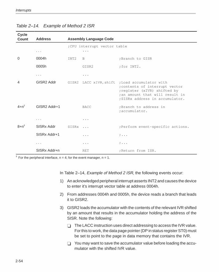
Interrupts
2-54
Table 2–14. Example of Method 2 ISR
ÁÁÁÁÁÁÁÁÁÁÁÁ
CycleCountÁÁÁÁÁÁÁÁÁÁÁÁÁÁÁÁÁÁ
AddressÁÁÁÁÁÁÁÁÁÁÁÁÁÁÁÁÁÁÁÁÁÁÁÁÁÁÁÁÁÁÁÁÁÁÁÁÁÁÁÁÁÁÁÁÁÁÁÁÁÁÁÁÁÁÁÁÁÁÁÁÁÁÁÁÁÁ
Assembly Language Code
ÁÁÁÁÁÁÁÁÁÁÁÁ
ÁÁÁÁÁÁÁÁÁÁÁÁÁÁÁÁÁÁ
. . .ÁÁÁÁÁÁÁÁÁÁÁÁÁÁÁÁÁÁÁÁÁÁÁÁÁÁÁÁÁÁÁÁÁÁÁÁÁÁÁÁÁÁÁÁÁÁÁÁÁÁÁÁÁÁÁÁÁÁÁÁÁÁÁÁÁÁ
;CPU interrupt vector table...
ÁÁÁÁÁÁÁÁ
0 ÁÁÁÁÁÁÁÁÁÁÁÁ
0004h ÁÁÁÁÁÁÁÁÁÁÁÁÁÁÁÁÁÁÁÁÁÁÁÁÁÁÁÁÁÁÁÁÁÁÁÁÁÁÁÁÁÁÁÁ
INT2 B ;Branch to GISR
ÁÁÁÁÁÁÁÁ
ÁÁÁÁÁÁÁÁÁÁÁÁ
0005h ÁÁÁÁÁÁÁÁÁÁÁÁÁÁÁÁÁÁÁÁÁÁÁÁÁÁÁÁÁÁÁÁÁÁÁÁÁÁÁÁÁÁÁÁ
GISR2 ;for INT2.
ÁÁÁÁÁÁÁÁ
ÁÁÁÁÁÁÁÁÁÁÁÁ
. . .ÁÁÁÁÁÁÁÁÁÁÁÁÁÁÁÁÁÁÁÁÁÁÁÁÁÁÁÁÁÁÁÁÁÁÁÁÁÁÁÁÁÁÁÁ
...ÁÁÁÁÁÁÁÁÁÁÁÁÁÁÁÁÁÁÁÁ
4ÁÁÁÁÁÁÁÁÁÁÁÁÁÁÁÁÁÁÁÁÁÁÁÁÁÁÁÁÁÁ
GISR2 AddrÁÁÁÁÁÁÁÁÁÁÁÁÁÁÁÁÁÁÁÁÁÁÁÁÁÁÁÁÁÁÁÁÁÁÁÁÁÁÁÁÁÁÁÁÁÁÁÁÁÁÁÁÁÁÁÁÁÁÁÁÁÁÁÁÁÁÁÁÁÁÁÁÁÁÁÁÁÁÁÁÁÁÁÁÁÁÁÁÁÁÁÁÁÁÁÁÁÁÁÁÁÁÁÁÁÁÁÁÁÁ
GISR2 LACC xIVR,shift ;Load accumulator with;contents of interrupt vector;register (xIVR) shifted by;an amount that will result in;SISRx address in accumulator.
ÁÁÁÁÁÁÁÁÁÁÁÁ
4+n†ÁÁÁÁÁÁÁÁÁÁÁÁÁÁÁÁÁÁ
GISR2 Addr+1ÁÁÁÁÁÁÁÁÁÁÁÁÁÁÁÁÁÁÁÁÁÁÁÁÁÁÁÁÁÁÁÁÁÁÁÁÁÁÁÁÁÁÁÁÁÁÁÁÁÁÁÁÁÁÁÁÁÁÁÁÁÁÁÁÁÁ
BACC ;Branch to address in;accumulator.
ÁÁÁÁÁÁÁÁ
ÁÁÁÁÁÁÁÁÁÁÁÁ
. . .ÁÁÁÁÁÁÁÁÁÁÁÁÁÁÁÁÁÁÁÁÁÁÁÁÁÁÁÁÁÁÁÁÁÁÁÁÁÁÁÁÁÁÁÁ
...ÁÁÁÁÁÁÁÁÁÁÁÁ
8+n†ÁÁÁÁÁÁÁÁÁÁÁÁÁÁÁÁÁÁ
SISRx AddrÁÁÁÁÁÁÁÁÁÁÁÁÁÁÁÁÁÁÁÁÁÁÁÁÁÁÁÁÁÁÁÁÁÁÁÁÁÁÁÁÁÁÁÁÁÁÁÁÁÁÁÁÁÁÁÁÁÁÁÁÁÁÁÁÁÁ
SISRx ... ;Perform event–specific actions.
ÁÁÁÁÁÁÁÁ
ÁÁÁÁÁÁÁÁÁÁÁÁ
SISRx Addr+1ÁÁÁÁÁÁÁÁÁÁÁÁÁÁÁÁÁÁÁÁÁÁÁÁÁÁÁÁÁÁÁÁÁÁÁÁÁÁÁÁÁÁÁÁ
... ;...
ÁÁÁÁÁÁÁÁ
ÁÁÁÁÁÁÁÁÁÁÁÁ
. . . ÁÁÁÁÁÁÁÁÁÁÁÁÁÁÁÁÁÁÁÁÁÁÁÁÁÁÁÁÁÁÁÁÁÁÁÁÁÁÁÁÁÁÁÁ
... ;...ÁÁÁÁÁÁÁÁ
ÁÁÁÁÁÁÁÁÁÁÁÁ
SISRx Addr+nÁÁÁÁÁÁÁÁÁÁÁÁÁÁÁÁÁÁÁÁÁÁÁÁÁÁÁÁÁÁÁÁÁÁÁÁÁÁÁÁÁÁÁÁ
RET ;Return from ISR.
† For the peripheral interface, n = 4; for the event manager, n = 1.
In Table 2–14, Example of Method 2 ISR, the following events occur:
1) An acknowledged peripheral interrupt asserts INT2 and causes the deviceto enter it’s interrupt vector table at address 0004h.
2) From addresses 0004h and 0005h, the device reads a branch that leadsit to GISR2.
3) GISR2 loads the accumulator with the contents of the relevant IVR shiftedby an amount that results in the accumulator holding the address of theSISR. Note the following:
� The LACC instruction uses direct addressing to access the IVR value.For this to work, the data page pointer (DP in status register ST0) mustbe set to point to the page in data memory that contains the IVR.
� You may want to save the accumulator value before loading the accu-mulator with the shifted IVR value.
Interrupts
2-55TMS320F/C240 DSP Controller
4) GISR2 branches to the address in the accumulator (the start address ofthe SISR).
5) The SISR is executed. The SISR concludes with a return instruction,which returns program control to the interrupted code sequence.
Method 3: ISR for single event per interrupt level
A device can be configured such that only one event can assert a particularmaskable interrupt. There are two configurations for this.
� In the first configuration, both of these conditions must be met:
� Only one peripheral is connected to the maskable interrupt level(INT1, INT2, INT3, INT4, INT5, or INT6).
� That one peripheral has only one event that can cause an interrupt re-quest (and, thus, has only one interrupt vector).
� In the second configuration, only one of the many events tied to a particu-lar interrupt priority level is enabled.
With either configuration, there is no need for a two-part ISR like the one inMethod 1 or the one in Method 2. There is one simple ISR and thus, only onebranch instruction. The address of the ISR is known; it does not have to be cal-culated in a routine. The GISR and the SISR become one in the same.
The following events occur during the routine described in Table 2–15, Exam-ple of Method 3 ISR, on page 2-56:
1) An acknowledged peripheral interrupt asserts INT1 and causes the deviceto enter its interrupt vector table at address 0002h.
2) From addresses 0002h and 0003h, the device reads a branch that leadsit directly to the SISR.
3) The SISR is executed and concludes with a return instruction that returnsprogram control to the interrupted code sequence.
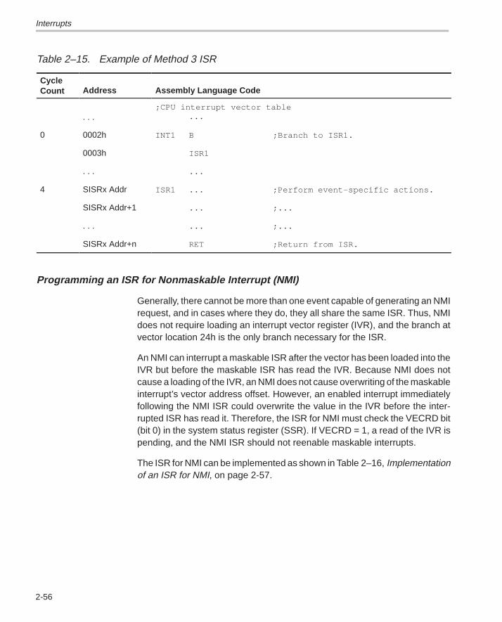
Interrupts
2-56
Table 2–15. Example of Method 3 ISR
ÁÁÁÁÁÁÁÁÁÁÁÁ
CycleCount
ÁÁÁÁÁÁÁÁÁÁÁÁÁÁÁÁÁÁ
AddressÁÁÁÁÁÁÁÁÁÁÁÁÁÁÁÁÁÁÁÁÁÁÁÁÁÁÁÁÁÁÁÁÁÁÁÁÁÁÁÁÁÁÁÁÁÁÁÁÁÁÁÁÁÁÁÁÁÁÁÁÁÁÁÁÁÁ
Assembly Language Code
ÁÁÁÁÁÁÁÁÁÁÁÁ
ÁÁÁÁÁÁÁÁÁÁÁÁÁÁÁÁÁÁ
. . .ÁÁÁÁÁÁÁÁÁÁÁÁÁÁÁÁÁÁÁÁÁÁÁÁÁÁÁÁÁÁÁÁÁÁÁÁÁÁÁÁÁÁÁÁÁÁÁÁÁÁÁÁÁÁÁÁÁÁÁÁÁÁÁÁÁÁ
;CPU interrupt vector table...
ÁÁÁÁÁÁÁÁ
0 ÁÁÁÁÁÁÁÁÁÁÁÁ
0002h ÁÁÁÁÁÁÁÁÁÁÁÁÁÁÁÁÁÁÁÁÁÁÁÁÁÁÁÁÁÁÁÁÁÁÁÁÁÁÁÁÁÁÁÁ
INT1 B ;Branch to ISR1.
ÁÁÁÁÁÁÁÁ
ÁÁÁÁÁÁÁÁÁÁÁÁ
0003h ÁÁÁÁÁÁÁÁÁÁÁÁÁÁÁÁÁÁÁÁÁÁÁÁÁÁÁÁÁÁÁÁÁÁÁÁÁÁÁÁÁÁÁÁ
ISR1
ÁÁÁÁÁÁÁÁ
ÁÁÁÁÁÁÁÁÁÁÁÁ
. . .ÁÁÁÁÁÁÁÁÁÁÁÁÁÁÁÁÁÁÁÁÁÁÁÁÁÁÁÁÁÁÁÁÁÁÁÁÁÁÁÁÁÁÁÁ
...ÁÁÁÁÁÁÁÁÁÁÁÁ
4ÁÁÁÁÁÁÁÁÁÁÁÁÁÁÁÁÁÁ
SISRx AddrÁÁÁÁÁÁÁÁÁÁÁÁÁÁÁÁÁÁÁÁÁÁÁÁÁÁÁÁÁÁÁÁÁÁÁÁÁÁÁÁÁÁÁÁÁÁÁÁÁÁÁÁÁÁÁÁÁÁÁÁÁÁÁÁÁÁ
ISR1 ... ;Perform event–specific actions.
ÁÁÁÁÁÁÁÁ
ÁÁÁÁÁÁÁÁÁÁÁÁ
SISRx Addr+1ÁÁÁÁÁÁÁÁÁÁÁÁÁÁÁÁÁÁÁÁÁÁÁÁÁÁÁÁÁÁÁÁÁÁÁÁÁÁÁÁÁÁÁÁ
... ;...
ÁÁÁÁÁÁÁÁ
ÁÁÁÁÁÁÁÁÁÁÁÁ
. . . ÁÁÁÁÁÁÁÁÁÁÁÁÁÁÁÁÁÁÁÁÁÁÁÁÁÁÁÁÁÁÁÁÁÁÁÁÁÁÁÁÁÁÁÁ
... ;...ÁÁÁÁÁÁÁÁ
ÁÁÁÁÁÁÁÁÁÁÁÁSISRx Addr+n
ÁÁÁÁÁÁÁÁÁÁÁÁÁÁÁÁÁÁÁÁÁÁÁÁÁÁÁÁÁÁÁÁÁÁÁÁÁÁÁÁÁÁÁÁRET ;Return from ISR.
Programming an ISR for Nonmaskable Interrupt (NMI)
Generally, there cannot be more than one event capable of generating an NMIrequest, and in cases where they do, they all share the same ISR. Thus, NMIdoes not require loading an interrupt vector register (IVR), and the branch atvector location 24h is the only branch necessary for the ISR.
An NMI can interrupt a maskable ISR after the vector has been loaded into theIVR but before the maskable ISR has read the IVR. Because NMI does notcause a loading of the IVR, an NMI does not cause overwriting of the maskableinterrupt’s vector address offset. However, an enabled interrupt immediatelyfollowing the NMI ISR could overwrite the value in the IVR before the inter-rupted ISR has read it. Therefore, the ISR for NMI must check the VECRD bit(bit 0) in the system status register (SSR). If VECRD = 1, a read of the IVR ispending, and the NMI ISR should not reenable maskable interrupts.
The ISR for NMI can be implemented as shown in Table 2–16, Implementationof an ISR for NMI, on page 2-57.
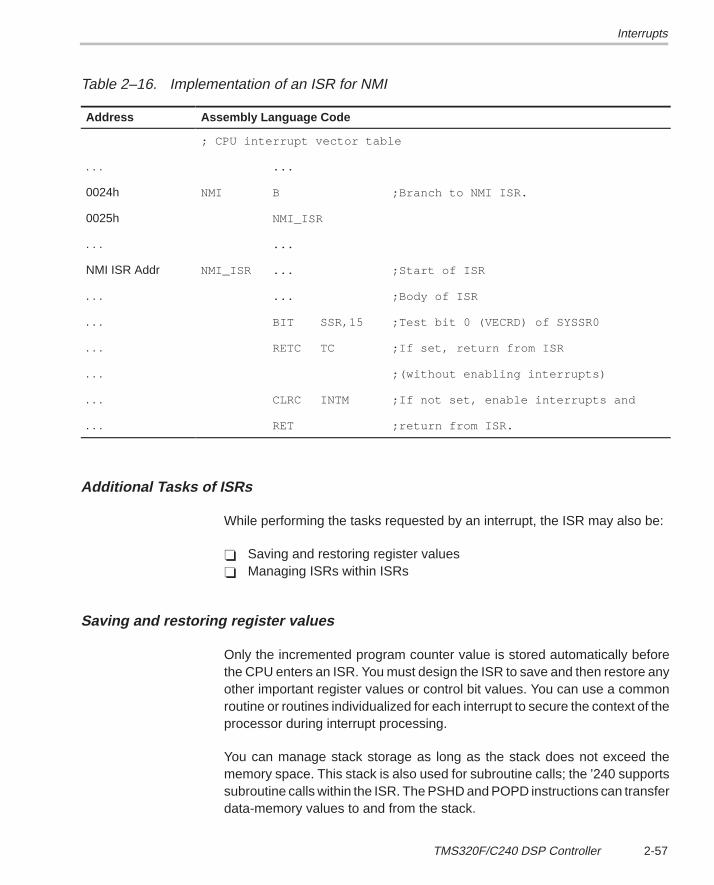
Interrupts
2-57TMS320F/C240 DSP Controller
Table 2–16. Implementation of an ISR for NMI
ÁÁÁÁÁÁÁÁÁÁÁÁ
Address ÁÁÁÁÁÁÁÁÁÁÁÁÁÁÁÁÁÁÁÁÁÁÁÁÁÁÁÁÁÁÁÁÁÁÁÁÁÁÁÁÁÁÁÁÁÁÁÁÁÁ
Assembly Language CodeÁÁÁÁÁÁÁÁÁÁÁÁ
ÁÁÁÁÁÁÁÁÁÁÁÁÁÁÁÁÁÁÁÁÁÁÁÁÁÁÁÁÁÁÁÁÁÁÁÁÁÁÁÁÁÁÁÁÁÁÁÁÁÁ
; CPU interrupt vector tableÁÁÁÁÁÁÁÁÁÁÁÁÁÁÁÁÁÁ
. . .ÁÁÁÁÁÁÁÁÁÁÁÁÁÁÁÁÁÁÁÁÁÁÁÁÁÁÁÁÁÁÁÁÁÁÁÁÁÁÁÁÁÁÁÁÁÁÁÁÁÁÁÁÁÁÁÁÁÁÁÁÁÁÁÁÁÁÁÁÁÁÁÁÁÁÁ
...
ÁÁÁÁÁÁÁÁÁÁÁÁ
0024h ÁÁÁÁÁÁÁÁÁÁÁÁÁÁÁÁÁÁÁÁÁÁÁÁÁÁÁÁÁÁÁÁÁÁÁÁÁÁÁÁÁÁÁÁÁÁÁÁÁÁ
NMI B ;Branch to NMI ISR.
ÁÁÁÁÁÁÁÁÁÁÁÁ
0025h ÁÁÁÁÁÁÁÁÁÁÁÁÁÁÁÁÁÁÁÁÁÁÁÁÁÁÁÁÁÁÁÁÁÁÁÁÁÁÁÁÁÁÁÁÁÁÁÁÁÁ
NMI_ISRÁÁÁÁÁÁÁÁÁÁÁÁ
. . .ÁÁÁÁÁÁÁÁÁÁÁÁÁÁÁÁÁÁÁÁÁÁÁÁÁÁÁÁÁÁÁÁÁÁÁÁÁÁÁÁÁÁÁÁÁÁÁÁÁÁ
...ÁÁÁÁÁÁÁÁÁÁÁÁÁÁÁÁÁÁ
NMI ISR AddrÁÁÁÁÁÁÁÁÁÁÁÁÁÁÁÁÁÁÁÁÁÁÁÁÁÁÁÁÁÁÁÁÁÁÁÁÁÁÁÁÁÁÁÁÁÁÁÁÁÁÁÁÁÁÁÁÁÁÁÁÁÁÁÁÁÁÁÁÁÁÁÁÁÁÁ
NMI_ISR ... ;Start of ISR
ÁÁÁÁÁÁÁÁÁÁÁÁ
. . . ÁÁÁÁÁÁÁÁÁÁÁÁÁÁÁÁÁÁÁÁÁÁÁÁÁÁÁÁÁÁÁÁÁÁÁÁÁÁÁÁÁÁÁÁÁÁÁÁÁÁ
... ;Body of ISR
ÁÁÁÁÁÁÁÁÁÁÁÁ
. . . ÁÁÁÁÁÁÁÁÁÁÁÁÁÁÁÁÁÁÁÁÁÁÁÁÁÁÁÁÁÁÁÁÁÁÁÁÁÁÁÁÁÁÁÁÁÁÁÁÁÁ
BIT SSR,15 ;Test bit 0 (VECRD) of SYSSR0ÁÁÁÁÁÁÁÁÁÁÁÁÁÁÁÁÁÁ
. . .ÁÁÁÁÁÁÁÁÁÁÁÁÁÁÁÁÁÁÁÁÁÁÁÁÁÁÁÁÁÁÁÁÁÁÁÁÁÁÁÁÁÁÁÁÁÁÁÁÁÁÁÁÁÁÁÁÁÁÁÁÁÁÁÁÁÁÁÁÁÁÁÁÁÁÁ
RETC TC ;If set, return from ISR
ÁÁÁÁÁÁÁÁÁÁÁÁ
. . . ÁÁÁÁÁÁÁÁÁÁÁÁÁÁÁÁÁÁÁÁÁÁÁÁÁÁÁÁÁÁÁÁÁÁÁÁÁÁÁÁÁÁÁÁÁÁÁÁÁÁ
;(without enabling interrupts)
ÁÁÁÁÁÁÁÁÁÁÁÁ
. . . ÁÁÁÁÁÁÁÁÁÁÁÁÁÁÁÁÁÁÁÁÁÁÁÁÁÁÁÁÁÁÁÁÁÁÁÁÁÁÁÁÁÁÁÁÁÁÁÁÁÁ
CLRC INTM ;If not set, enable interrupts and
ÁÁÁÁÁÁÁÁÁÁÁÁ
. . .ÁÁÁÁÁÁÁÁÁÁÁÁÁÁÁÁÁÁÁÁÁÁÁÁÁÁÁÁÁÁÁÁÁÁÁÁÁÁÁÁÁÁÁÁÁÁÁÁÁÁ
RET ;return from ISR.
Additional Tasks of ISRs
While performing the tasks requested by an interrupt, the ISR may also be:
� Saving and restoring register values� Managing ISRs within ISRs
Saving and restoring register values
Only the incremented program counter value is stored automatically beforethe CPU enters an ISR. You must design the ISR to save and then restore anyother important register values or control bit values. You can use a commonroutine or routines individualized for each interrupt to secure the context of theprocessor during interrupt processing.
You can manage stack storage as long as the stack does not exceed thememory space. This stack is also used for subroutine calls; the ’240 supportssubroutine calls within the ISR. The PSHD and POPD instructions can transferdata-memory values to and from the stack.
Interrupts
2-58
Managing ISRs within ISRs
The ’240 hardware stack allows you to have ISRs within ISRs. When consider-ing nesting ISRs like this, keep the following in mind:
� If you want the ISR to be interrupted by a maskable interrupt, the ISR mustunmask the interrupt by setting the appropriate individual mask bit and theappropriate IMR bit and globally reenabling interrupts by clearing theINTM bit (CLRC INTM).
� The appropriate interrupt vector register must have been read by the GISRto obtain the vector address offset before globally reenabling interrupts.Otherwise, a subsequent interrupt can cause the old vector value to beoverwritten.
� The hardware stack is limited to eight levels. Each time an interrupt is serv-iced or a subroutine is entered, the return address is pushed onto the hard-ware stack. This provides a way to return to the previous context after theinterrupt service routine. The stack contains eight locations, allowing inter-rupts or subroutines to be nested up to eight levels deep. (One level of thestack is reserved for debugging, specifically for break-point/single-stepoperations. If debugging is not used, this extra level is available for internaluse.) If your software requires more than eight levels of stack, you can usethe POPD and PSHD instructions to extend the stack into data memory.
� You can avoid stack overflow by not nesting ISRs. The ’240 has a featurethat allows you to prevent unintentional nesting. If an interrupt occurs dur-ing the execution of a CLRC INTM instruction, the device always com-pletes CLRC INTM as well as the following instruction before the pendinginterrupt is processed. This ensures that a return (RET) placed immediate-ly after the CLRC INTM can be executed before the next interrupt isprocessed. The processor removes the previous return address from thestack before it adds the new return address.
� If you want an ISR to occur within the current ISR rather than after thecurrent ISR, place the CLRC INTM instruction more than one instructionbefore the return (RET) instruction.
Interrupts
2-59TMS320F/C240 DSP Controller
2.5.6 Interrupt Latency
The length of an interrupt latency—the delay between when an interruptrequest is made and when it is serviced—depends on many factors. This sec-tion describes the factors that determine minimum latency and then describesfactors that may cause additional latency. The maximum latency is a functionof wait states and pipeline protection.
Interrupt latency on the ’240 consists of the following components:
� Peripheral interface synchronization time� CPU response time� ISR branching time
Peripheral interface synchronization time
Peripheral interface synchronization time is the time it takes for the interruptrequest from the peripheral to be recognized by the peripheral interface, arbi-trated, and converted into a request to the DSP. This takes up to one SYSCLKcycle for internal interrupts from on-chip peripherals (peripheral bus operatesat the SYSCLK rate). Therefore, it takes two CPUCLK cycles in divide-by-twoclock mode, and four CPUCLK cycles in divide-by-four mode. External inter-rupts (NMI, INTx) have a two-SYSCLK-cycle synchronization delay.
Interrupt requests from the event manager peripheral are not arbitrated by theperipheral interface; there is a one-CPUCLK-cycle delay for the CPU to recog-nize the interrupt.
CPU response time
CPU response time is the time it takes for the CPU to recognize the enabledinterrupt request, acknowledge the interrupt, clear its pipeline, and begin re-trieving the first instruction from the CPU’s interrupt vector table. The minimumCPU latency is four CPUCLK cycles. If a higher priority maskable interrupt isrequested during this minimum latency period, it is masked until the ISR for theinterrupt being serviced is completed. NMIs are not maskable and are servicedbefore the current ISR is completed.
Latency is longer if the interrupt request occurs during multicycle operationsor other operations that cannot be interrupted. If a higher priority interruptoccurs during this additional latency period, it is serviced before the originallower priority interrupt, assuming both are enabled.
Interrupts
2-60
The effects of multicycle instructions are:
� Memory access using wait states. An instruction that writes to or readsfrom external memory may be delayed by wait states caused by the exter-nal READY pin or the on-chip wait-state generator. These wait states mayaffect the instruction being executed at the time the interrupt is requested,and they may affect the interrupt itself if the interrupt vector must befetched from external memory.
� Repeat loop. When repeated with RPT, instructions run parallel opera-tions in the pipeline, and the context of these additional parallel operationscannot be saved in an interrupt service routine. To protect the context ofthe repeated instruction, the CPU locks out all interrupts except reset untilthe RPT loop completes.
Note:
Reset (RS) is not delayed by multicycle instructions. An NMI can be delayedby multicycle instructions.
If one interrupt is being serviced, there are other factors that delay the servicingof a new interrupt:
� A return address (incremented program counter value) is forced onto thehardware stack every time the CPU follows another interrupt service rou-tine or other subroutine. The ’240 has a feature that helps you keep thehardware stack from overflowing. Interrupts cannot be processedbetween the CLRC INTM (enable maskable interrupts) instruction and thenext instruction in a program sequence. This ensures that a return instruc-tion that directly follows CLRC INTM is executed before an interrupt isprocessed. The return instruction pops the previous return address off thetop of the stack before the new return address is pushed onto the stack.If the interrupt occurs before the return, the new return address is addedto the hardware stack, even if the stack is already full.
� Interrupts are also blocked after an RET instruction until at least oneinstruction is executed at the return address.
ISR branching time
ISR branching time is the time it takes to execute all the necessary branchesto get to the event-specific portion of the ISR. This length of time varies de-pending on how you have implemented the ISR. For the simplest situation inwhich only one branch to the ISR is required, the minimum branching time isfour DSP cycles. See the section titled Additional Tasks of ISRs, for the threedifferent methods of implementing ISRs for maskable interrupts.
Interrupts
2-61TMS320F/C240 DSP Controller
2.5.7 External Interrupts
The ’240 has five external interrupts. These interrupts include:
� XINT1. The XINT1 control register (at 7070h) provides control and statusfor this interrupt. XINT1 can be used as a high-priority (Level 1) or low-priority (Level 6) maskable interrupt or as a general-purpose input pin.
� NMI. The NMI control register (at 7072h) provides control and status forthis interrupt. NMI is a nonmaskable external interrupt or a general-pur-pose input pin.
� XINT2. The XINT2 control register (at 7078h) provides control and statusfor this interrupt. XINT2 can be used as a high-priority (Level 1) or low-priority (Level 6) maskable interrupt or a general-purpose I/O pin.
� XINT3. The XINT3 control register (at 707Ah) provides control and statusfor this interrupt. XINT3 can be used as a high-priority (Level 1) or lowpriority (Level 6) maskable interrupt or as a general-purpose I/O pin.
� PDPINT. This interrupt is provided for safe operation of the power convert-er and motor drive. This maskable interrupt can put the timers and PWMoutput pins in high-impedance states and inform the CPU in case of motordrive abnormalities such as overvoltage, overcurrent, and excessivetemperature rise. PDPINT is a Level 2 interrupt. Figure 3–5 shows thewake up sequence from a power down.
Table 3–6, External Interrupt Types and Functions, on page 3-19 provides asummary of the external interrupt capabilities of the ’240.
2.5.8 Peripheral Interrupt Enable Sequence
You must ensure that the interrupts on the ’F/C240 are enabled correctly. Youcan inadvertently prevent the recognition of interrupts by following an incorrectinitialization order.
This situation occurs when the peripheral interrupts are enabled before thecore IFR, IMR, and INTM are initialized. If this should happen, when an inter-rupt request is sent to the core IFR and the core IFR is then cleared, the inter-rupt request is lost.
You can avoid this situation by using the following three-step procedure:
1) Set up the core interrupts (assume INTM = 1)2) Enable peripheral interrupts3) Enable interrupts globally (INTM = 0)
Interrupts
2-62
The following code shows an example of the recommended sequence:
; STEP1 Set up the core interrupts (assume INTM = 1)
LDP #0h ; set data page
SPLK #111111b,IFR ; clear any pending interrupts
SPLK #001000b,IMR ; enable desired interrupts
; STEP2: Enable peripheral interrupts here ...
EV Capture 1–3 interrupt uses as example
LDP #DP_EV ; set data page
SPLK #0ffffh,EVIRC ; clear all group C interrupt flags
LACL #0111b ; bits 1–3 for capture 1 and 2 and 3
OR EVIMRC ; OR into interrupt mask
register
SACL EVIMRC ; write back
; STEP3: Enable global interrupts in core
CLRC INTM ; enable global interrupts
After interrupt initialization, code should never manually clear an IFR bit(s)without also reading the EVIVRx or SYSIVR register that is mapped to the IFRbit(s) that are being cleared.
2.5.9 Summary of Interrupt Operation
Once an interrupt has been passed to the CPU, the CPU operates in the follow-ing manner (see Figure 2–17, Interrupt Operation Flowchart, on page 2-47):
� If a maskable interrupt is requested:
1) The flag bit in the individual control register is set. If the individualmask bit is also set, the corresponding IFR bit is set.
2) Once the IFR bit is set, the acknowledgement conditions(INTM bit = 0 and IMR bit = 1) are tested. If the conditions are true,the CPU services the interrupt, generating an interrupt acknowledgesignal; otherwise, it ignores the interrupt and continues with the cur-rent code sequence.
Interrupts
2-63TMS320F/C240 DSP Controller
3) When the interrupt has been acknowledged, the IFR bit is cleared to 0and the INTM bit is set to 1 (to block other maskable interrupts). Theflag bit in the corresponding control register is not cleared.
4) The return address (incremented PC value) is saved on the stack.
5) The CPU branches to and executes the interrupt service routine (ISR).The ISR is concluded by a return instruction, which pops the return ad-dress off the stack. The CPU continues with the interrupt code se-quence.
� If a nonmaskable interrupt is requested:
1) The CPU immediately acknowledges the interrupt, generating an in-terrupt acknowledge signal.
Note:
When an interrupt is requested by an INTR instruction and the correspondingIFR bit is set, the CPU does not clear the bit automatically. If an applicationrequires that the IFR bit be cleared, the bit must be cleared by software.
2) If the interrupt was requested by the RS pin, the NMI pin, the NMIinstruction, or the INTR instruction, the the INTM bit is set to 1 to blockmaskable hardware interrupts. If the interrupt was requested by theTRAP instruction, the INTM bit is not set to 1.
3) The return address (incremented PC value) is saved on the stack.
4) The CPU branches to and executes the ISR. The ISR is concluded bya return instruction, which pops the return address of the stack. TheCPU continues with the interrupted code sequence.
CPU Interrupt Registers
2-64
2.6 CPU Interrupt Registers
There are two CPU registers for controlling interrupts:
� The interrupt flag register (IFR) contains flag bits that indicate when mask-able interrupt requests have reached the CPU on levels INT1 throughINT6.
� The interrupt mask register (IMR) contains mask bits that enable or dis-able each of the interrupt levels (INT1 through INT6).
Interrupt Flag Register (IFR)
The interrupt flag register (IFR), a 16-bit, memory-mapped register at address0006h in data-memory space, is used to identify and clear pending interrupts.The IFR contains flag bits for all the maskable interrupts.
When a maskable interrupt is requested, the flag bit in the corresponding con-trol register is set to 1. If the mask bit in that same control register is also 1, theinterrupt request is sent to the CPU, setting the corresponding flag in the IFR.This indicates that the interrupt is pending, or waiting for, acknowledgement.
You can read the IFR to identify pending interrupts and write to the IFR to clearpending interrupts. To clear a single interrupt, write a 1 to the correspondingIFR bit. All pending interrupts can be cleared by writing the current contentsof the IFR back into the IFR. A device reset clears all IFR bits.
The following events also clear an IFR flag:
� The CPU acknowledges the interrupt.� The ’240 is reset.
Notes:
1) To clear an IFR bit, you must write a 1 to it, not a 0.
2) When a maskable interrupt is acknowledged, only the IFR bit is clearedautomatically. The flag bit in the corresponding control register is notcleared. If an application requires that the control register flag becleared, the bit must be cleared by software.
3) When an interrupt is requested by an INTR instruction and the corre-sponding IFR bit is set, the CPU does not clear the bit automatically. Ifan application requires that the IFR bit be cleared, the bit must be clearedby software.
The IFR is shown in Figure 2–19; descriptions of the bits follow the figure.
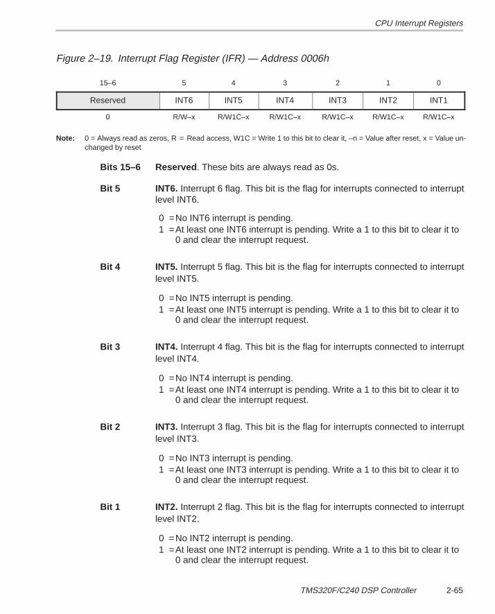
CPU Interrupt Registers
2-65TMS320F/C240 DSP Controller
Figure 2–19. Interrupt Flag Register (IFR) — Address 0006h
15–6 5 4 3 2 1 0
Reserved INT6 INT5 INT4 INT3 INT2 INT1
0 R/W–x R/W1C–x R/W1C–x R/W1C–x R/W1C–x R/W1C–x
Note: 0 = Always read as zeros, R = Read access, W1C = Write 1 to this bit to clear it, –n = Value after reset, x = Value un-changed by reset
Bits 15–6 Reserved . These bits are always read as 0s.
Bit 5 INT6. Interrupt 6 flag. This bit is the flag for interrupts connected to interruptlevel INT6.
0 =No INT6 interrupt is pending.1 =At least one INT6 interrupt is pending. Write a 1 to this bit to clear it to
0 and clear the interrupt request.
Bit 4 INT5. Interrupt 5 flag. This bit is the flag for interrupts connected to interruptlevel INT5.
0 =No INT5 interrupt is pending.1 =At least one INT5 interrupt is pending. Write a 1 to this bit to clear it to
0 and clear the interrupt request.
Bit 3 INT4. Interrupt 4 flag. This bit is the flag for interrupts connected to interruptlevel INT4.
0 =No INT4 interrupt is pending.1 =At least one INT4 interrupt is pending. Write a 1 to this bit to clear it to
0 and clear the interrupt request.
Bit 2 INT3. Interrupt 3 flag. This bit is the flag for interrupts connected to interruptlevel INT3.
0 =No INT3 interrupt is pending.1 =At least one INT3 interrupt is pending. Write a 1 to this bit to clear it to
0 and clear the interrupt request.
Bit 1 INT2. Interrupt 2 flag. This bit is the flag for interrupts connected to interruptlevel INT2.
0 =No INT2 interrupt is pending.1 =At least one INT2 interrupt is pending. Write a 1 to this bit to clear it to
0 and clear the interrupt request.
CPU Interrupt Registers
2-66
Bit 0 INT1. Interrupt 1 flag. This bit is the flag for interrupts connected to interruptlevel INT1.
0 =No INT1 interrupt is pending.1 =At least one INT1 interrupt is pending. Write a 1 to this bit to clear it to
0 and clear the interrupt request.
Interrupt Mask Register (IMR)
The IMR is a 16-bit, memory-mapped register located at address 0004h indata memory space. The IMR contains mask bits for all the maskable interruptlevels (INT1–INT6). Neither NMI nor RS is included in the IMR; thus, IMR hasno effect on these interrupts.
You can read the IMR to identify masked or unmasked interrupt levels, and youcan write to the IMR to mask or unmask interrupt levels. To unmask an interruptlevel, set its corresponding IMR bit to 1. To mask an interrupt level, set its corre-sponding IMR bit to 0. When an interrupt is masked, it is not acknowledged,regardless of the value of the INTM bit. When an interrupt is unmasked, it isacknowledged if the corresponding IFR bit is 1 and the INTM bit is 0. The IMRbits are not cleared by reset.
The IMR is shown in Figure 2–20, Interrupt Mask Register (IMR) on page 2-67.Bit descriptions follow the figure.
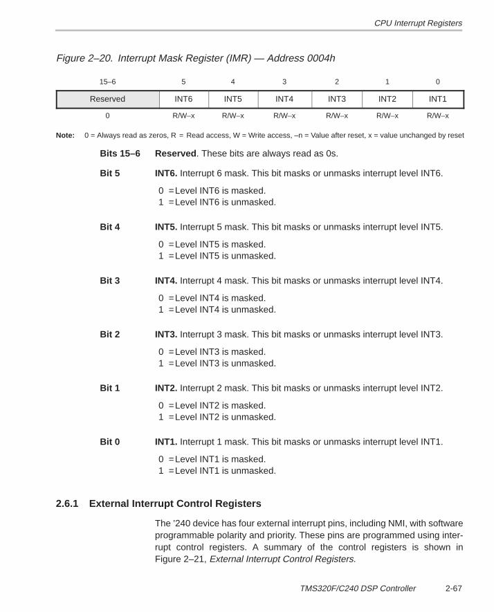
CPU Interrupt Registers
2-67TMS320F/C240 DSP Controller
Figure 2–20. Interrupt Mask Register (IMR) — Address 0004h
15–6 5 4 3 2 1 0
Reserved INT6 INT5 INT4 INT3 INT2 INT1
0 R/W–x R/W–x R/W–x R/W–x R/W–x R/W–x
Note: 0 = Always read as zeros, R = Read access, W = Write access, –n = Value after reset, x = value unchanged by reset
Bits 15–6 Reserved . These bits are always read as 0s.
Bit 5 INT6. Interrupt 6 mask. This bit masks or unmasks interrupt level INT6.
0 =Level INT6 is masked.1 =Level INT6 is unmasked.
Bit 4 INT5. Interrupt 5 mask. This bit masks or unmasks interrupt level INT5.
0 =Level INT5 is masked.1 =Level INT5 is unmasked.
Bit 3 INT4. Interrupt 4 mask. This bit masks or unmasks interrupt level INT4.
0 =Level INT4 is masked.1 =Level INT4 is unmasked.
Bit 2 INT3. Interrupt 3 mask. This bit masks or unmasks interrupt level INT3.
0 =Level INT3 is masked.1 =Level INT3 is unmasked.
Bit 1 INT2. Interrupt 2 mask. This bit masks or unmasks interrupt level INT2.
0 =Level INT2 is masked.1 =Level INT2 is unmasked.
Bit 0 INT1. Interrupt 1 mask. This bit masks or unmasks interrupt level INT1.
0 =Level INT1 is masked.1 =Level INT1 is unmasked.
2.6.1 External Interrupt Control Registers
The ’240 device has four external interrupt pins, including NMI, with softwareprogrammable polarity and priority. These pins are programmed using inter-rupt control registers. A summary of the control registers is shown inFigure 2–21, External Interrupt Control Registers.
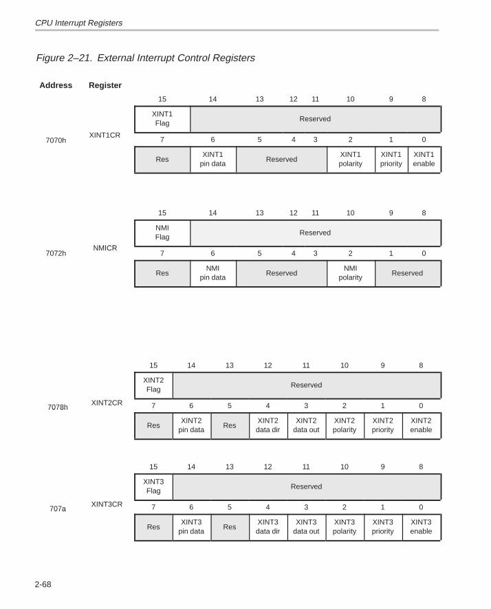
CPU Interrupt Registers
2-68
Figure 2–21. External Interrupt Control Registers
Address Register
15 14 13 12 11 10 9 8
C
XINT1Flag
Reserved
7070hXINT1CR
7 6 5 4 3 2 1 0
ResXINT1
pin dataReserved
XINT1polarity
XINT1priority
XINT1enable
ÉÉÉÉÉÉÉÉÉÉÉÉÉÉÉÉÉÉÉÉÉÉÉÉÉÉÉÉÉÉÉÉÉÉÉÉÉÉÉÉÉÉÉÉÉÉÉÉÉÉÉÉÉÉÉÉÉÉÉÉÉ
ÉÉÉÉÉÉÉÉÉÉÉÉ15 14 13 12 11 10 9 8
NMICR
NMIFlag
Reserved
7072hNMICR
7 6 5 4 3 2 1 0
ResNMI
pin dataReserved
NMIpolarity
Reserved
ÉÉÉÉÉÉÉÉÉÉÉÉÉÉÉÉÉÉÉÉÉÉÉÉÉÉÉÉÉÉÉÉÉÉÉÉÉÉÉÉÉÉÉÉÉÉ
15 14 13 12 11 10 9 8
XINT2Flag
Reserved
7078hXINT2CR 7 6 5 4 3 2 1 07078h
ResXINT2
pin dataRes
XINT2data dir
XINT2data out
XINT2polarity
XINT2priority
XINT2enable
ÉÉÉÉÉÉÉÉÉÉÉÉ
ÉÉÉÉÉÉÉÉÉÉÉÉÉÉÉÉÉÉ15 14 13 12 11 10 9 8
XINT3Flag
Reserved
707aXINT3CR 7 6 5 4 3 2 1 0707a
ResXINT3
pin dataRes
XINT3data dir
XINT3data out
XINT3polarity
XINT3priority
XINT3enable
ÉÉÉÉÉÉÉÉÉÉÉÉ
ÉÉÉÉÉÉÉÉÉÉÉÉÉÉÉÉÉÉ
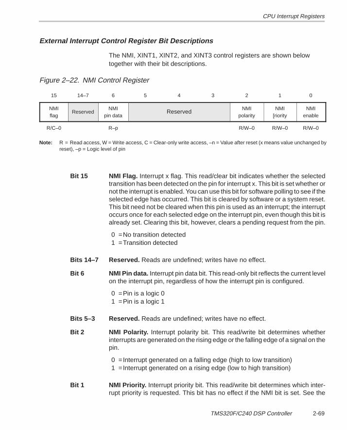
CPU Interrupt Registers
2-69TMS320F/C240 DSP Controller
External Interrupt Control Register Bit Descriptions
The NMI, XINT1, XINT2, and XINT3 control registers are shown below together with their bit descriptions.
Figure 2–22. NMI Control Register
15 14–7 6 5 4 3 2 1 0
NMIflag
ReservedNMI
pin dataReserved
NMIpolarity
NMI[riority
NMIenable
R/C–0 R–p R/W–0 R/W–0 R/W–0
Note: R = Read access, W = Write access, C = Clear-only write access, –n = Value after reset (x means value unchanged byreset), –p = Logic level of pin
Bit 15 NMI Flag. Interrupt x flag. This read/clear bit indicates whether the selectedtransition has been detected on the pin for interrupt x. This bit is set whether ornot the interrupt is enabled. You can use this bit for software polling to see if theselected edge has occurred. This bit is cleared by software or a system reset.This bit need not be cleared when this pin is used as an interrupt; the interruptoccurs once for each selected edge on the interrupt pin, even though this bit isalready set. Clearing this bit, however, clears a pending request from the pin.
0 =No transition detected1 =Transition detected
Bits 14–7 Reserved. Reads are undefined; writes have no effect.
Bit 6 NMI Pin data. Interrupt pin data bit. This read-only bit reflects the current levelon the interrupt pin, regardless of how the interrupt pin is configured.
0 =Pin is a logic 01 =Pin is a logic 1
Bits 5–3 Reserved. Reads are undefined; writes have no effect.
Bit 2 NMI Polarity. Interrupt polarity bit. This read/write bit determines whetherinterrupts are generated on the rising edge or the falling edge of a signal on thepin.
0 =Interrupt generated on a falling edge (high to low transition)1 =Interrupt generated on a rising edge (low to high transition)
Bit 1 NMI Priority. Interrupt priority bit. This read/write bit determines which inter-rupt priority is requested. This bit has no effect if the NMI bit is set. See the
CPU Interrupt Registers
2-70
device data sheet for details about which interrupt level corresponds to highpriority and which interrupt level corresponds to low priority.
0 =High priority1 =Low priority
Bit 0 NMI Enable. Interrupt enable bit. This read/write bit enables or disables themaskable interrupt. This bit has no effect if the NMI bit is set.
0 =Disable interrupt (use pin as digital input)1 =Enable interrupt
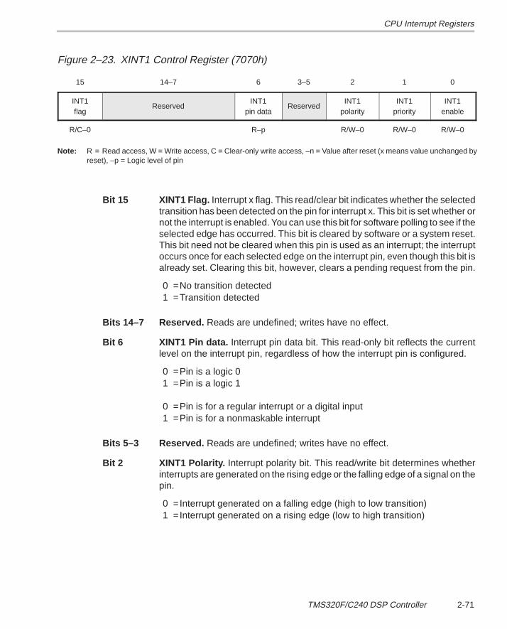
CPU Interrupt Registers
2-71TMS320F/C240 DSP Controller
Figure 2–23. XINT1 Control Register (7070h)
15 14–7 6 3–5 2 1 0
INT1flag
ReservedINT1
pin dataReserved
INT1polarity
INT1priority
INT1enable
R/C–0 R–p R/W–0 R/W–0 R/W–0
Note: R = Read access, W = Write access, C = Clear-only write access, –n = Value after reset (x means value unchanged byreset), –p = Logic level of pin
Bit 15 XINT1 Flag. Interrupt x flag. This read/clear bit indicates whether the selectedtransition has been detected on the pin for interrupt x. This bit is set whether ornot the interrupt is enabled. You can use this bit for software polling to see if theselected edge has occurred. This bit is cleared by software or a system reset.This bit need not be cleared when this pin is used as an interrupt; the interruptoccurs once for each selected edge on the interrupt pin, even though this bit isalready set. Clearing this bit, however, clears a pending request from the pin.
0 =No transition detected1 =Transition detected
Bits 14–7 Reserved. Reads are undefined; writes have no effect.
Bit 6 XINT1 Pin data. Interrupt pin data bit. This read-only bit reflects the currentlevel on the interrupt pin, regardless of how the interrupt pin is configured.
0 =Pin is a logic 01 =Pin is a logic 1
0 =Pin is for a regular interrupt or a digital input1 =Pin is for a nonmaskable interrupt
Bits 5–3 Reserved. Reads are undefined; writes have no effect.
Bit 2 XINT1 Polarity. Interrupt polarity bit. This read/write bit determines whetherinterrupts are generated on the rising edge or the falling edge of a signal on thepin.
0 =Interrupt generated on a falling edge (high to low transition)1 =Interrupt generated on a rising edge (low to high transition)
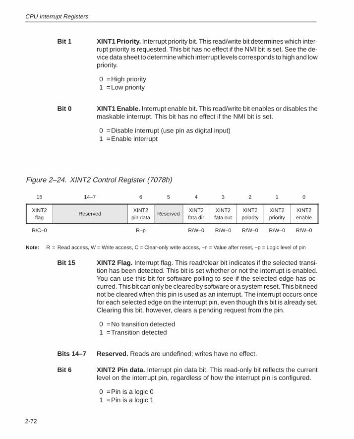
CPU Interrupt Registers
2-72
Bit 1 XINT1 Priority. Interrupt priority bit. This read/write bit determines which inter-rupt priority is requested. This bit has no effect if the NMI bit is set. See the de-vice data sheet to determine which interrupt levels corresponds to high and lowpriority.
0 =High priority1 =Low priority
Bit 0 XINT1 Enable. Interrupt enable bit. This read/write bit enables or disables themaskable interrupt. This bit has no effect if the NMI bit is set.
0 =Disable interrupt (use pin as digital input)1 =Enable interrupt
Figure 2–24. XINT2 Control Register (7078h)
15 14–7 6 5 4 3 2 1 0
XINT2flag
ReservedXINT2
pin dataReserved
XINT2fata dir
XINT2fata out
XINT2polarity
XINT2priority
XINT2enable
R/C–0 R–p R/W–0 R/W–0 R/W–0 R/W–0 R/W–0
Note: R = Read access, W = Write access, C = Clear-only write access, –n = Value after reset, –p = Logic level of pin
Bit 15 XINT2 Flag. Interrupt flag. This read/clear bit indicates if the selected transi-tion has been detected. This bit is set whether or not the interrupt is enabled.You can use this bit for software polling to see if the selected edge has oc-curred. This bit can only be cleared by software or a system reset. This bit neednot be cleared when this pin is used as an interrupt. The interrupt occurs oncefor each selected edge on the interrupt pin, even though this bit is already set.Clearing this bit, however, clears a pending request from the pin.
0 =No transition detected1 =Transition detected
Bits 14–7 Reserved. Reads are undefined; writes have no effect.
Bit 6 XINT2 Pin data. Interrupt pin data bit. This read-only bit reflects the currentlevel on the interrupt pin, regardless of how the interrupt pin is configured.
0 =Pin is a logic 01 =Pin is a logic 1
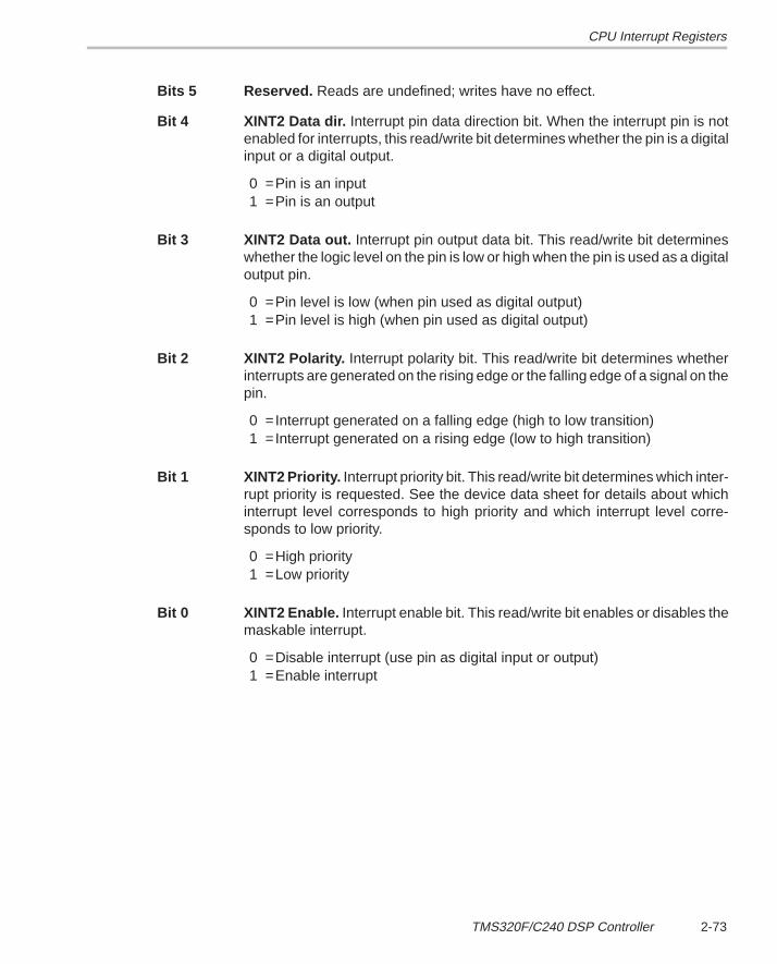
CPU Interrupt Registers
2-73TMS320F/C240 DSP Controller
Bits 5 Reserved. Reads are undefined; writes have no effect.
Bit 4 XINT2 Data dir. Interrupt pin data direction bit. When the interrupt pin is notenabled for interrupts, this read/write bit determines whether the pin is a digitalinput or a digital output.
0 =Pin is an input1 =Pin is an output
Bit 3 XINT2 Data out. Interrupt pin output data bit. This read/write bit determineswhether the logic level on the pin is low or high when the pin is used as a digitaloutput pin.
0 =Pin level is low (when pin used as digital output)1 =Pin level is high (when pin used as digital output)
Bit 2 XINT2 Polarity. Interrupt polarity bit. This read/write bit determines whetherinterrupts are generated on the rising edge or the falling edge of a signal on thepin.
0 =Interrupt generated on a falling edge (high to low transition)1 =Interrupt generated on a rising edge (low to high transition)
Bit 1 XINT2 Priority. Interrupt priority bit. This read/write bit determines which inter-rupt priority is requested. See the device data sheet for details about whichinterrupt level corresponds to high priority and which interrupt level corre-sponds to low priority.
0 =High priority1 =Low priority
Bit 0 XINT2 Enable. Interrupt enable bit. This read/write bit enables or disables themaskable interrupt.
0 =Disable interrupt (use pin as digital input or output)1 =Enable interrupt
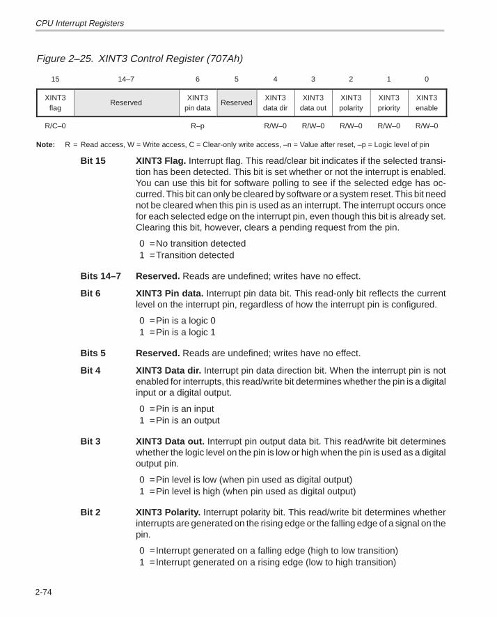
CPU Interrupt Registers
2-74
Figure 2–25. XINT3 Control Register (707Ah)
15 14–7 6 5 4 3 2 1 0
XINT3flag
ReservedXINT3
pin dataReserved
XINT3data dir
XINT3data out
XINT3polarity
XINT3priority
XINT3enable
R/C–0 R–p R/W–0 R/W–0 R/W–0 R/W–0 R/W–0
Note: R = Read access, W = Write access, C = Clear-only write access, –n = Value after reset, –p = Logic level of pin
Bit 15 XINT3 Flag. Interrupt flag. This read/clear bit indicates if the selected transi-tion has been detected. This bit is set whether or not the interrupt is enabled.You can use this bit for software polling to see if the selected edge has oc-curred. This bit can only be cleared by software or a system reset. This bit neednot be cleared when this pin is used as an interrupt. The interrupt occurs oncefor each selected edge on the interrupt pin, even though this bit is already set.Clearing this bit, however, clears a pending request from the pin.
0 =No transition detected1 =Transition detected
Bits 14–7 Reserved. Reads are undefined; writes have no effect.
Bit 6 XINT3 Pin data. Interrupt pin data bit. This read-only bit reflects the currentlevel on the interrupt pin, regardless of how the interrupt pin is configured.
0 =Pin is a logic 01 =Pin is a logic 1
Bits 5 Reserved. Reads are undefined; writes have no effect.
Bit 4 XINT3 Data dir. Interrupt pin data direction bit. When the interrupt pin is notenabled for interrupts, this read/write bit determines whether the pin is a digitalinput or a digital output.
0 =Pin is an input1 =Pin is an output
Bit 3 XINT3 Data out. Interrupt pin output data bit. This read/write bit determineswhether the logic level on the pin is low or high when the pin is used as a digitaloutput pin.
0 =Pin level is low (when pin used as digital output)1 =Pin level is high (when pin used as digital output)
Bit 2 XINT3 Polarity. Interrupt polarity bit. This read/write bit determines whetherinterrupts are generated on the rising edge or the falling edge of a signal on thepin.
0 =Interrupt generated on a falling edge (high to low transition)1 =Interrupt generated on a rising edge (low to high transition)

CPU Interrupt Registers
2-75TMS320F/C240 DSP Controller
Bit 1 XINT3 Priority. Interrupt priority bit. This read/write bit determines which inter-rupt priority is requested. See the device data sheet for details about whichinterrupt level corresponds to high priority and which interrupt level corre-sponds to low priority.
0 =High priority1 =Low priority
Bit 0 XINT3 Enable. Interrupt enable bit. This read/write bit enables or disables themaskable interrupt.
0 =Disable interrupt (use pin as digital input or output)1 =Enable interrupt
3-1
System Functions
This chapter describes the device functions that are not specific to any peripheral. They are:
� Peripheral interface. This interface transfers data between the CPU databus and the peripheral bus, which is independent of the CPU.
� System configuration registers. These registers provide software controland status information for functions that affect both the DSP core and cer-tain peripherals.
� Hardware interrupts (including reset). These interrupts require control byboth CPU registers and peripheral registers.
� Power-down modes. These can affect both the CPU and the peripherals.
Topic Page
3.1 Peripheral Interface 3-2. . . . . . . . . . . . . . . . . . . . . . . . . . . . . . . . . . . . . . . . . . .
3.2 System Configuration Registers 3-4. . . . . . . . . . . . . . . . . . . . . . . . . . . . . . . .
3.3 Power-Down Modes 3-10. . . . . . . . . . . . . . . . . . . . . . . . . . . . . . . . . . . . . . . . . .
Chapter 3
Peripheral Interface
3-2
3.1 Peripheral Interface
In order to support a large number of peripherals without compromising theelectrical performance of the ’C24x DSP CPU’s data bus, ’C24x devices havea separate peripheral bus which operates at a lower frequency than the CPUbuses. All peripherals, except for the event manager, are attached to thisperipheral bus. For improved performance, the event manager interfaces di-rectly to the CPU’s data bus.
One of the functions of the peripheral interface is to interface the CPU to theperipheral bus.
The CPU is clocked at either two times (2� mode) or four times (4� mode)the clock rate of the peripheral bus. Because the peripheral bus runs slowerthan the CPU bus, peripheral bus reads and writes take multiple CPU cycles.The exact number of CPU cycles a peripheral access takes to completedepends on the:
� Peripheral clock rate
� Phase of the peripheral clock in which the CPU initiates the peripheralaccess
� Type of access: read or write
Table 3–1, CPU Cycles to Complete Reads From and Writes to the PeripheralBus, on page 3-3 shows how many CPU clock cycles it takes to completeread and write accesses to peripherals connected to the peripheral bus. As anexample, if the clocks are in 4x mode, a single peripheral read may take 5, 6,7, or 8 CPU cycles, depending on the phase of the peripheral clock when theCPU initiates the peripheral access. If back-to-back accesses are performed,all accesses after the first will take eight cycles in 4� mode.
Note that writes always take one cycle longer than reads. This is consistentwith zero-wait-state external memory accesses and event manager accessesover the CPU’s data bus. These accesses take one cycle for a read and twocycles for a write.
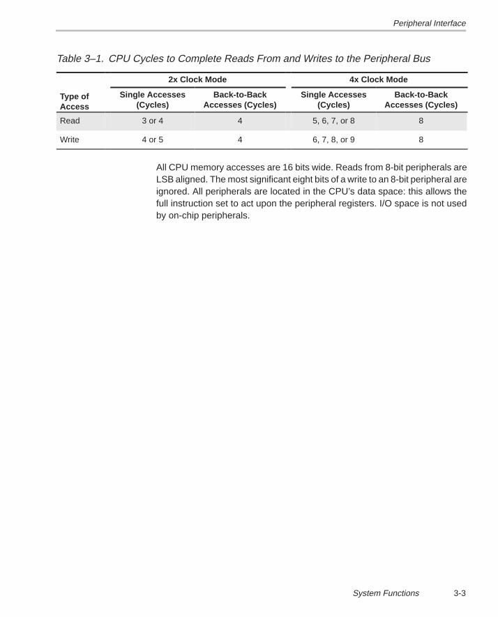
Peripheral Interface
3-3System Functions
Table 3–1. CPU Cycles to Complete Reads From and Writes to the Peripheral Bus
2x Clock Mode 4x Clock Mode
Type ofAccess
Single Accesses(Cycles)
Back-to-BackAccesses (Cycles)
Single Accesses(Cycles)
Back-to-BackAccesses (Cycles)
Read 3 or 4 4 5, 6, 7, or 8 8
Write 4 or 5 4 6, 7, 8, or 9 8
All CPU memory accesses are 16 bits wide. Reads from 8-bit peripherals areLSB aligned. The most significant eight bits of a write to an 8-bit peripheral areignored. All peripherals are located in the CPU’s data space: this allows thefull instruction set to act upon the peripheral registers. I/O space is not usedby on-chip peripherals.
System Configuration Registers
3-4
3.2 System Configuration Registers
The system configuration registers are shown in Figure 3–1 and described insections 3.2.1 through 3.2.3. The following applies to the register locations:
� All unimplemented (reserved) bits are read as indeterminate values (un-less otherwise stated).
� Bit 0 of the peripheral address bus is not decoded; therefore, these 16-bitregisters are accessible at each even address location and at the (odd)address location that follows. For example, the register SYSIVR is nomi-nally at location 701Eh, but it can also be accessed at address 701Fh.
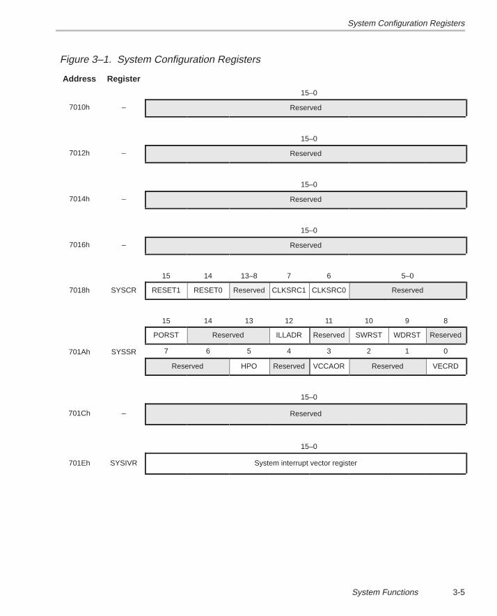
System Configuration Registers
3-5System Functions
Figure 3–1. System Configuration Registers
Address Register
15–0
7010h – Reserved
ÉÉÉÉÉÉÉÉ
ÉÉÉÉÉÉÉÉÉÉÉÉ15–0
7012h – ReservedÉÉÉÉÉÉÉÉ
ÉÉÉÉÉÉÉÉÉÉÉÉ
15–0
7014h – ReservedÉÉÉÉÉÉÉÉÉÉÉÉ
ÉÉÉÉÉÉÉÉÉÉÉÉÉÉÉÉÉÉ15–0
7016h – Reserved
ÉÉÉÉÉÉÉÉ
ÉÉÉÉÉÉÉÉÉÉÉÉ15 14 13–8 7 6 5–0
7018h SYSCR RESET1 RESET0 Reserved CLKSRC1ÉÉÉÉÉÉCLKSRC0 Reserved
ÉÉÉÉÉÉÉÉ
ÉÉÉÉÉÉÉÉÉÉÉÉ15 14 13 12 11 10 9 8
PORST Reserved ILLADR Reserved SWRST WDRST Reserved
701Ah SYSSR 7 6 5 4 3 2 1 0
Reserved HPO Reserved VCCAOR Reserved VECRDÉÉÉÉÉÉÉÉ
ÉÉÉÉÉÉÉÉÉÉÉÉ
15–0
701Ch – Reserved
ÉÉÉÉÉÉÉÉ
ÉÉÉÉÉÉÉÉÉÉÉÉ15–0
701Eh SYSIVR System interrupt vector register
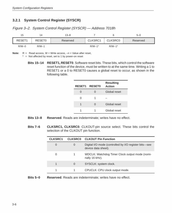
System Configuration Registers
3-6
3.2.1 System Control Register (SYSCR)
Figure 3–2. System Control Register (SYSCR) — Address 7018h
15 14 13–8 7 6 5–0
RESET1 RESET0 Reserved CLKSRC1 CLKSRC0 Reserved
R/W–0 R/W–1 R/W–1* R/W–1*
Note: R = Read access, W = Write access, –n = Value after reset,* = Not affected by reset, set to 1 by power-on reset
Bits 15–14 RESET1, RESET0 . Software reset bits. These bits, which control the softwarereset function of the device, must be written to at the same time. Writing a 1 toRESET1 or a 0 to RESET0 causes a global reset to occur, as shown in thefollowing table.
RESET1 RESET0ResultingAction
0 0 Global reset
0 1 –
1 0 Global reset
1 1 Global reset
Bits 13–8 Reserved . Reads are indeterminate; writes have no effect.
Bits 7–6 CLKSRC1, CLKSRC0 . CLKOUT-pin source select. These bits control theselection of the CLKOUT pin function.
CLKSRC1 CLKSRC0 CLKOUT Pin Function
0 0 Digital I/O mode (controlled by I/O register bits—seedevice data sheet).
0 1 WDCLK: Watchdog Timer Clock output mode (nomi-nally 16 kHz).
1 0 SYSCLK: system clock.
1 1 CPUCLK: CPU clock output mode.
Bits 5–0 Reserved . Reads are indeterminate; writes have no effect.
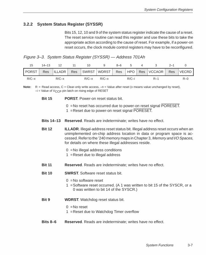
System Configuration Registers
3-7System Functions
3.2.2 System Status Register (SYSSR)
Bits 15, 12, 10 and 9 of the system status register indicate the cause of a reset.The reset service routine can read this register and use these bits to take theappropriate action according to the cause of reset. For example, if a power-onreset occurs, the clock module control registers may have to be reconfigured.
Figure 3–3. System Status Register (SYSSR) — Address 701Ah
15 14–13 12 11 10 9 8–6 5 4 3 2–1 0
PORST Res ILLADR Res SWRST WDRST Res HPO Res VCCAOR Res VECRD
R/C–x R/C–x R/C–x R/C–x R/C–i R–1 R–0
Note: R = Read access, C = Clear-only write access, –n = Value after reset (x means value unchanged by reset),–i = Value of VCCP pin latch on rising edge of RESET
Bit 15 PORST. Power-on reset status bit.
0 =No reset has occurred due to power-on reset signal PORESET.1 =Reset due to power-on reset signal PORESET.
Bits 14–13 Reserved . Reads are indeterminate; writes have no effect.
Bit 12 ILLADR . Illegal-address reset status bit. Illegal address reset occurs when anunimplemented on-chip address location in data or program space is ac-cessed. Refer to the ’240 memory maps in Chapter 3, Memory and I/O Spaces,for details on where these illegal addresses reside.
0 =No illegal address conditions1 =Reset due to illegal address
Bit 11 Reserved . Reads are indeterminate; writes have no effect.
Bit 10 SWRST. Software reset status bit.
0 =No software reset1 =Software reset occurred. (A 1 was written to bit 15 of the SYSCR, or a
0 was written to bit 14 of the SYSCR.)
Bit 9 WDRST. Watchdog reset status bit.
0 =No reset1 =Reset due to Watchdog Timer overflow
Bits 8–6 Reserved . Reads are indeterminate; writes have no effect.
System Configuration Registers
3-8
Bit 5 HPO . Hardware protect override. If the flash programming voltage pin (VCCP)is at 5V on the trailing edge of the reset pin (RS) and is held at that value, theHPO bit is set. (This only applies to an ’F24x device with on-chip flash EE-PROM). This value is cleared either by software or when the VCCP pin levelchanges to 0V.
0 =Normal mode1 =HPO mode: Flash EEPROM programming is enabled and the Watch-
dog can be disabled by setting the WDDIS bit in the WD control regis-ter. For details about this register, see Chapter 13, Watchdog andReal-Time Interrupt Module.
Bit 4 Reserved . Reads are indeterminate; writes have no effect.
Bit 3 VCCAOR . Analog VCC (VCCA) out-of-regulation bit. This bit is only valid if thedevice has an on-chip low-voltage detect module.
0 =VCCA is on and in regulation.1 =VCCA is off or out of regulation.
Bits 2–1 Reserved . Reads are indeterminate; writes have no effect.
Bit 0 VECRD . Interrupt vector read pending bit. This bit is set when an interrupt vec-tor is loaded into the SYSIVR (when the interrupt is acknowledged). It iscleared when the SYSIVR is read. This bit is used by the service routine of non-maskable interrupt NMI (see Programming an ISR for Nonmaskable Interrupt(NMI) on page ).
0 = No read of the interrupt vector register is pending.1 = An interrupt vector has been latched but has not been read yet.
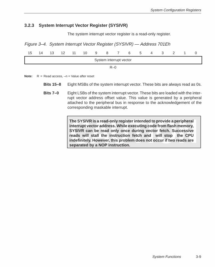
System Configuration Registers
3-9System Functions
3.2.3 System Interrupt Vector Register (SYSIVR)
The system interrupt vector register is a read-only register.
Figure 3–4. System Interrupt Vector Register (SYSIVR) — Address 701Eh
15 14 13 12 11 10 9 8 7 6 5 4 3 2 1 0
System interrupt vector
R–0
Note: R = Read access, –n = Value after reset
Bits 15–8 Eight MSBs of the system interrupt vector. These bits are always read as 0s.
Bits 7–0 Eight LSBs of the system interrupt vector. These bits are loaded with the inter-rupt vector address offset value. This value is generated by a peripheralattached to the peripheral bus in response to the acknowledgement of thecorresponding maskable interrupt.
The SYSIVR is a read-only register intended to provide a peripheralinterrupt vector address. While executing code from flash memory,SYSIVR can be read only once during vector fetch. Successivereads will stall the instruction fetch and will stop the CPUindefinitely. However, this problem does not occur if two reads areseparated by a NOP instruction.
Power -Down Modes
3-10
3.3 Power -Down Modes
A ’240 device can have up to four power-down modes that reduce the operat-ing power of the ’240 device by stopping the clocks (and, thus, the activity andpower consumption) of the CPU and various on-chip peripherals. While the’240 is in a power-down mode, all of its internal contents are maintained andoperation continues unaltered when the power-down mode is terminated withan interrupt. The content of all on-chip RAM remains unchanged. However, ifthe power-down mode is terminated with a reset, the contents of some regis-ters are changed. These are the register contents that are always changedduring a reset.
3.3.1 Clock Generation
The TMS320x240 has an on-chip, PLL-based clock module. This module pro-vides all necessary clocking signals for the device as well as control for low-power mode entry. The only external component necessary for this module isan external fundamental reference crystal.
The ’240 has two basic clocking domains: the CPU clock domain (CPUCLK),and the system clock domain (SYSCLK). The CPU, memories, externalmemory interface, and event manager are located in the CPU clock domain.All other peripherals are in the system clock domain. The CPUCLK runs at 2�or 4� the frequency of the SYSCLK; that is, CPUCLK = 20 MHz,SYSCLK = 10 MHz, or CPUCLK = 20 MHz, SYSCLK = 5 MHz.
There are three different clock domains that can be shut off during powerdown:
� CPU clock domain. All clocks in the CPU and memories except the inter-rupt control registers
� System clock domain. All peripheral clocks (CPUCLK or SYSCLK), andthe clocks for the CPU’s interrupt control registers
� Watchdog clock (WDCLK). The nominally 16 kHz clock used to incre-ment the watchdog timer and real time Interrupt module
Note:
The terms CPUCLK and CPU clock domain, SYSCLK and system clockdomain are not interchangeable.
Power -Down Modes
3-11System Functions
The four types of possible power-down modes on a ’240 device have decreas-ing levels of power consumption and increasing delays to exit the low powermode. All of the possible power-down modes may not be implemented on a’240 device. A low-power mode is entered when the CPU executes an IDLEinstruction. The PLLPM(1:0) bits in the CKCR0 register in the clock module de-termine which of the four possible low power modes is entered.
The power-down modes, in order of decreasing power and increasing startuptime, are as follows:
� Idle1 mode stops the clocks to the CPU (CPU clock domain) but the clocksfor all peripherals (system clock domain) continue to run. Exit from Idle1occurs immediately following any interrupt or a reset.
� Idle2 mode stops the clocks in both the CPU clock domain and the systemclock domain. Exit from Idle2 occurs immediately following a wakeup inter-rupt or a reset. The watchdog clock continues to run, eventually times out,and causes a reset.
� PLL power-down mode powers down the PLL (if enabled). The watchdogclock continues to run. Exit from this mode can be caused by a wakeupinterrupt or a reset. The watchdog clock continues to run, eventually timesout, and causes a reset. The device does not start full-speed operation until the PLL has powered up and reattained lock, which can be hundredsof microseconds.
� Oscillator power-down mode shuts off power to the oscillator (if enabled)and is the lowest power mode available. No clocks are running on thedevice. A wakeup interrupt or reset causes the device to exit this low-power mode. No clock runs until the oscillator has powered back up; thepower-up time is in milliseconds. The device does not start full-speed op-eration until the PLL has powered up and reattained lock (this can be addi-tional hundreds of microseconds).
For details of the low-power mode power consumption for each device, seethe relevant device data sheet. Table 3–2, Power-Down Modes, shows thestatus of the CPU and peripheral clocks during each of the four power-downmodes.
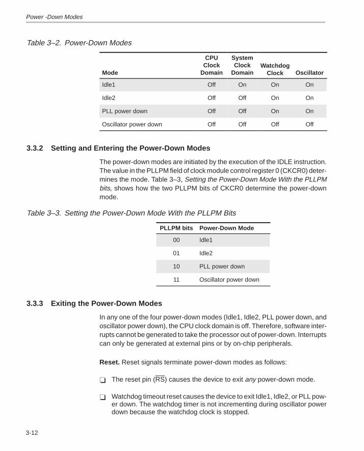
Power -Down Modes
3-12
Table 3–2. Power-Down Modes
Mode
CPUClock
Domain
SystemClock
DomainWatchdog
Clock Oscillator
Idle1 Off On On On
Idle2 Off Off On On
PLL power down Off Off On On
Oscillator power down Off Off Off Off
3.3.2 Setting and Entering the Power-Down Modes
The power-down modes are initiated by the execution of the IDLE instruction.The value in the PLLPM field of clock module control register 0 (CKCR0) deter-mines the mode. Table 3–3, Setting the Power-Down Mode With the PLLPMbits, shows how the two PLLPM bits of CKCR0 determine the power-downmode.
Table 3–3. Setting the Power-Down Mode With the PLLPM Bits
PLLPM bits Power-Down Mode
00 Idle1
01 Idle2
10 PLL power down
11 Oscillator power down
3.3.3 Exiting the Power-Down Modes
In any one of the four power-down modes (Idle1, Idle2, PLL power down, andoscillator power down), the CPU clock domain is off. Therefore, software inter-rupts cannot be generated to take the processor out of power-down. Interruptscan only be generated at external pins or by on-chip peripherals.
Reset. Reset signals terminate power-down modes as follows:
� The reset pin (RS) causes the device to exit any power-down mode.
� Watchdog timeout reset causes the device to exit Idle1, Idle2, or PLL pow-er down. The watchdog timer is not incrementing during oscillator powerdown because the watchdog clock is stopped.

Power -Down Modes
3-13System Functions
External interrupts. All power-down modes terminate when the CPU re-ceives any one of these interrupts at a pin:
� NMI
� XINTn (any external interrupt controlled by the external interrupt controlregisters, if unmasked).
Wakeup interrupts. The external interrupts XINTn and NMI are also wakeupinterrupts. After the clocks are shut off, a combinatorial logic path from thesepins restarts the clocks.
The external interrupts, XINTn, are maskable interrupts and can completelybring the processor out of the power-down mode only if they are unmasked.If they are masked, they wake up the device by starting all clocks; however,the device remains in the IDLE state.
Certain peripherals are also able to generate wakeup interrupts when theclocks in the system clock domain are shut off. For example, some commu-nication ports may be able to generate a wakeup interrupt in response toreceiving a character.
Oscillator power down mode is only terminated by an external interrupt (NMIor XINTn). In this mode, the oscillator is off (no clocks on the device are active);thus, no interrupts can be generated by on-chip peripherals, and the watchdogtimer cannot generate a time-out signal.
Peripheral interrupts. The Idle1, Idle2, and PLL power-down modes can beterminated by various peripheral interrupts under the right conditions. In Idle1mode, all the clocks for the peripheral devices are still running; therefore, anyunmasked peripheral interrupt terminates the Idle1 mode. In the Idle2 and PLLpower-down modes, the clocks in the system clock domain are off. As a result,only unmasked peripheral interrupts that are not timed by the system clock canbring the processor out of the Idle2 and PLL power-down modes.
In oscillator power-down mode, the peripheral clocks and the Watchdog timerclocks are off. Only unmasked peripheral interrupts not timed by either of thoseclocks can terminate oscillator power-down mode.
Table 3–5, Power-Down Modes and Their Terminations, on page 3-15 sum-marizes the state of processors in each power-down mode and lists the inter-rupts that do and do not terminate each mode.
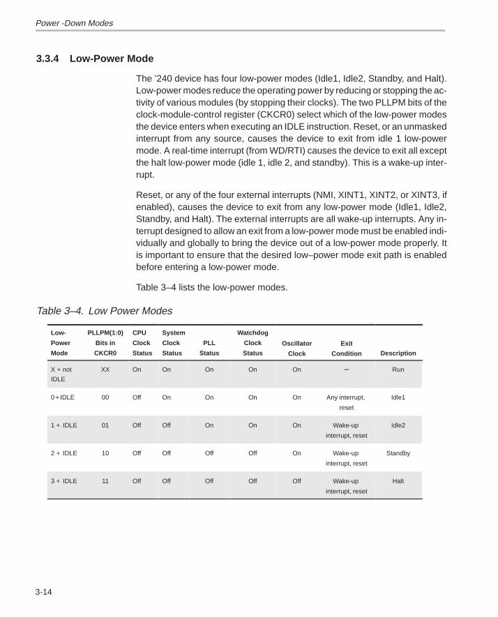
Power -Down Modes
3-14
3.3.4 Low-Power Mode
The ’240 device has four low-power modes (Idle1, Idle2, Standby, and Halt).Low-power modes reduce the operating power by reducing or stopping the ac-tivity of various modules (by stopping their clocks). The two PLLPM bits of theclock-module-control register (CKCR0) select which of the low-power modesthe device enters when executing an IDLE instruction. Reset, or an unmaskedinterrupt from any source, causes the device to exit from idle 1 low-powermode. A real-time interrupt (from WD/RTI) causes the device to exit all exceptthe halt low-power mode (idle 1, idle 2, and standby). This is a wake-up inter-rupt.
Reset, or any of the four external interrupts (NMI, XINT1, XINT2, or XINT3, ifenabled), causes the device to exit from any low-power mode (Idle1, Idle2,Standby, and Halt). The external interrupts are all wake-up interrupts. Any in-terrupt designed to allow an exit from a low-power mode must be enabled indi-vidually and globally to bring the device out of a low-power mode properly. Itis important to ensure that the desired low–power mode exit path is enabledbefore entering a low-power mode.
Table 3–4 lists the low-power modes.
Table 3–4. Low Power Modes
Low-
Power
Mode
PLLPM(1:0)
Bits in
CKCR0
CPU
Clock
Status
System
Clock
Status
PLL
Status
Watchdog
Clock
Status
Oscillator
Clock
Exit
Condition Description
X + not
IDLE
XX On On On On On – Run
0 + IDLE 00 Off On On On On Any interrupt,
reset
Idle1
1 + IDLE 01 Off Off On On On Wake-up
interrupt, reset
Idle2
2 + IDLE 10 Off Off Off Off On Wake-up
interrupt, reset
Standby
3 + IDLE 11 Off Off Off Off Off Wake-up
interrupt, reset
Halt
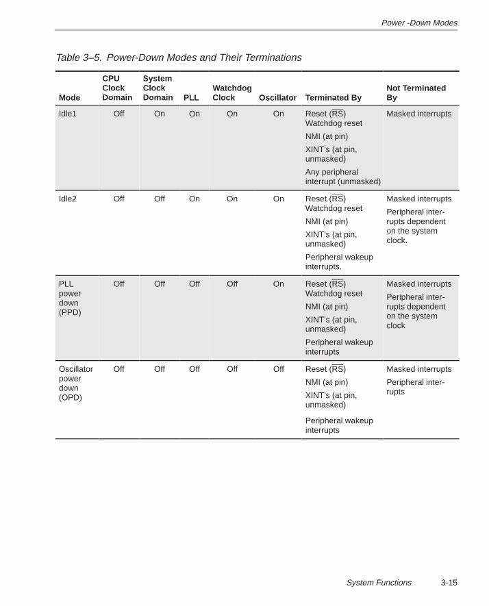
Power -Down Modes
3-15System Functions
Table 3–5. Power-Down Modes and Their Terminations
Mode
CPUClockDomain
SystemClockDomain PLL
WatchdogClock Oscillator Terminated By
Not TerminatedBy
Idle1 Off On On On On Reset (RS)Watchdog reset
NMI (at pin)
XINT’s (at pin, unmasked)
Any peripheral interrupt (unmasked)
Masked interrupts
Idle2 Off Off On On On Reset (RS)Watchdog reset
NMI (at pin)
XINT’s (at pin, unmasked)
Peripheral wakeupinterrupts.
Masked interrupts
Peripheral inter-rupts dependenton the systemclock.
PLL powerdown(PPD)
Off Off Off Off On Reset (RS)Watchdog reset
NMI (at pin)
XINT’s (at pin, unmasked)
Peripheral wakeupinterrupts
Masked interrupts
Peripheral inter-rupts dependenton the systemclock
Oscillatorpowerdown(OPD)
Off Off Off Off Off Reset (RS)
NMI (at pin)
XINT’s (at pin,unmasked)
Peripheral wakeupinterrupts
Masked interrupts
Peripheral inter-rupts
Power -Down Modes
3-16
3.3.5 After Exiting Power-Down
There are two items to consider when deciding how to wake the processor:
� If you use reset or NMI, the CPU immediately executes the correspondinginterrupt service routine.
� If you use a maskable hardware interrupt, the next action depends on theinterrupt mode (INTM) bit of status register ST0:
� INTM = 0: The interrupt is enabled, and the CPU executes thecorresponding interrupt service routine.
� INTM = 1: The interrupt is disabled, and the CPU continues withthe instruction after IDLE.
If you do not want the CPU to execute an interrupt service routine before con-tinuing with the interrupted program sequence:
� Do not use reset or NMI to bring the processor out of power-down.
� Make sure your program sets INTM to 1 (SETC INTM) before IDLE isexecuted.
If you want the CPU to execute the interrupt service routine before continuing:
� Make sure your program clears INTM to 0 (CLRC INTM) before IDLE isexecuted.
� Make sure you enable all relevant interrupt sources, both locally (in theperipheral mask/enable registers) and globally (in the CPU’s interruptmask register).
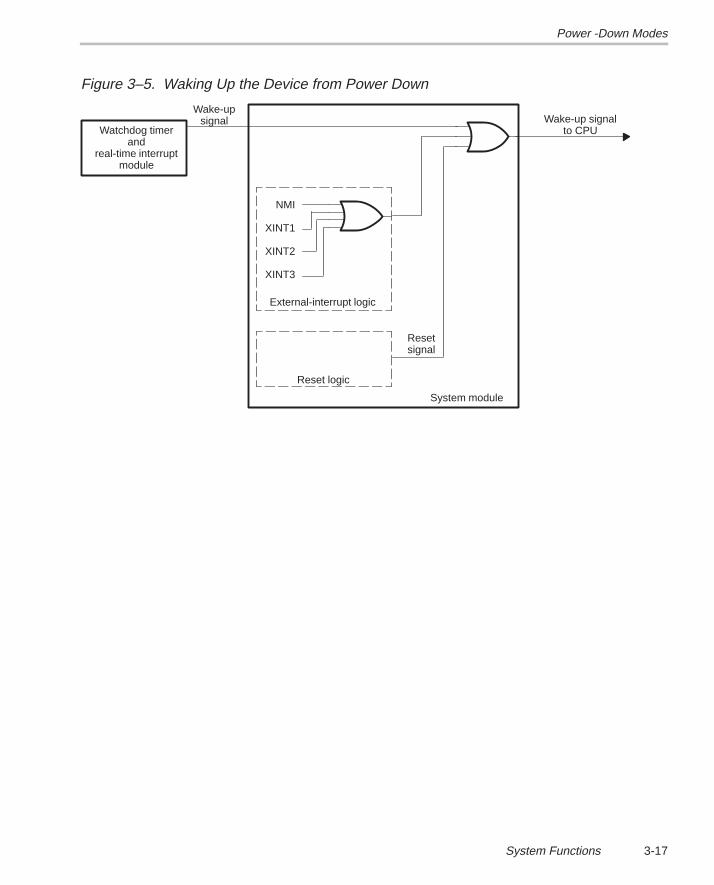
Power -Down Modes
3-17System Functions
Figure 3–5. Waking Up the Device from Power Down
Watchdog timerand
real-time interruptmodule
NMI
XINT1
XINT2
XINT3
External-interrupt logic
Reset logic
Resetsignal
Wake-up signalto CPU
Wake-upsignal
System module
Power -Down Modes
3-18
3.3.6 Summary of Power-Down Mode Operation
When the IDLE instruction is executed:
1) The program counter is incremented once, so that when the power-downmode is exited, the next instruction is the one that follows the IDLE instruc-tion, except in the case of reset.
2) The ’240 enters the power-down mode selected by the PLLPM bits andremains in that low-power state until it receives a proper hardware inter-rupt (as described in section 3.3.3, Exiting the Power-Down Modes, onpage 3-12).
3) Upon receipt of the proper interrupt, the ’240 exits the power-down mode.
4) If you use NMI to wake the processor, the CPU executes the correspond-ing interrupt service routine before continuing with the interruptedprogram sequence.
If you use a maskable interrupt, the next action depends on the value of theINTM bit:
� INTM = 0: Maskable interrupts are enabled; the CPU first executes theinterrupt service routine of the interrupt that brought it out of power-down. Then it continues with the instruction after the IDLE instruction.
� INTM = 1: Maskable interrupts are disabled; the CPU continues exe-cution of the instruction after IDLE.
Table 3–2, Power-Down Modes, on page 3-12 summarizes the four power-down modes, and provides the approximate power level for each. (For moreaccurate power values, see the data sheet for your particular ’C24x device.)In addition, the table shows the status of the ’240 when not in a power-downmode. See Table 3–5, Power-Down Modes and Their Terminations, on page3-15 for the list of interrupts that do and do not terminate each mode.

Power -Down Modes
3-19System Functions
Table 3–6. External Interrupt Types and Functions
ÁÁÁÁÁÁÁÁÁÁÁÁÁÁÁÁÁÁ
ExternalInterrupt
ÁÁÁÁÁÁÁÁÁÁÁÁÁÁÁ
ControlRegisterAddress
ÁÁÁÁÁÁÁÁÁÁÁÁÁÁÁÁÁÁInterrupt Type
ÁÁÁÁÁÁÁÁÁÁÁÁÁÁÁÁÁÁCan Do NMI?
ÁÁÁÁÁÁÁÁÁÁÁÁÁÁÁÁÁÁDigital I/O Pin
ÁÁÁÁÁÁÁÁÁÁÁÁÁÁÁÁÁÁMaskable?ÁÁÁÁÁÁ
ÁÁÁÁÁÁÁÁÁÁÁÁ
XINT1ÁÁÁÁÁÁÁÁÁÁÁÁÁÁÁ
7070hÁÁÁÁÁÁÁÁÁÁÁÁÁÁÁÁÁÁ
AÁÁÁÁÁÁÁÁÁÁÁÁÁÁÁÁÁÁ
NoÁÁÁÁÁÁÁÁÁÁÁÁÁÁÁÁÁÁ
Input onlyÁÁÁÁÁÁÁÁÁÁÁÁÁÁÁÁÁÁ
Yes(Level 1 or 6)
ÁÁÁÁÁÁÁÁÁÁÁÁÁÁÁÁÁÁ
NMIÁÁÁÁÁÁÁÁÁÁÁÁÁÁÁ
7072hÁÁÁÁÁÁÁÁÁÁÁÁÁÁÁÁÁÁ
AÁÁÁÁÁÁÁÁÁÁÁÁÁÁÁÁÁÁ
YesÁÁÁÁÁÁÁÁÁÁÁÁÁÁÁÁÁÁ
Input onlyÁÁÁÁÁÁÁÁÁÁÁÁÁÁÁÁÁÁ
No
ÁÁÁÁÁÁÁÁÁÁÁÁ
N/C ÁÁÁÁÁÁÁÁÁÁ
7074h ÁÁÁÁÁÁÁÁÁÁÁÁ
B Reserved
ÁÁÁÁÁÁÁÁÁÁÁÁ
N/C ÁÁÁÁÁÁÁÁÁÁ
7076h ÁÁÁÁÁÁÁÁÁÁÁÁ
B ReservedÁÁÁÁÁÁÁÁÁÁÁÁÁÁÁÁÁÁ
XINT2ÁÁÁÁÁÁÁÁÁÁÁÁÁÁÁ
7078hÁÁÁÁÁÁÁÁÁÁÁÁÁÁÁÁÁÁ
CÁÁÁÁÁÁÁÁÁÁÁÁÁÁÁÁÁÁ
NoÁÁÁÁÁÁÁÁÁÁÁÁÁÁÁÁÁÁ
I/OÁÁÁÁÁÁÁÁÁÁÁÁÁÁÁÁÁÁ
Yes(Level 1 or 6)
ÁÁÁÁÁÁÁÁÁÁÁÁÁÁÁÁÁÁ
XINT3ÁÁÁÁÁÁÁÁÁÁÁÁÁÁÁ
707AhÁÁÁÁÁÁÁÁÁÁÁÁÁÁÁÁÁÁ
CÁÁÁÁÁÁÁÁÁÁÁÁÁÁÁÁÁÁ
NoÁÁÁÁÁÁÁÁÁÁÁÁÁÁÁÁÁÁ
I/OÁÁÁÁÁÁÁÁÁÁÁÁÁÁÁÁÁÁ
Yes(Level 1 or 6)
ÁÁÁÁÁÁÁÁÁÁÁÁ
N/CÁÁÁÁÁÁÁÁÁÁ
707ChÁÁÁÁÁÁÁÁÁÁÁÁ
PM ReservedÁÁÁÁÁÁÁÁÁÁÁÁÁÁÁÁÁÁ
N/CÁÁÁÁÁÁÁÁÁÁÁÁÁÁÁ
707EhÁÁÁÁÁÁÁÁÁÁÁÁÁÁÁÁÁÁ
PM Reserved
ÁÁÁÁÁÁÁÁÁÁÁÁÁÁÁÁÁÁ
PDPINT ÁÁÁÁÁÁÁÁÁÁÁÁÁÁÁ
742Ch ÁÁÁÁÁÁÁÁÁÁÁÁÁÁÁÁÁÁ
N/A ÁÁÁÁÁÁÁÁÁÁÁÁÁÁÁÁÁÁ
N/A ÁÁÁÁÁÁÁÁÁÁÁÁÁÁÁÁÁÁ
N/A ÁÁÁÁÁÁÁÁÁÁÁÁÁÁÁÁÁÁ
Yes(Level 2)
4-1
PLL Clock Module
This chapter describes the architecture, functions, and programming of thePLL clock module. The PLL clock module provides all necessary clock signalsfor ’C24x devices.
Note: 8-Bit Peripheral
This module is interfaced to the 16-bit peripheral bus as an 8-bit peripheral.Therefore, reads from bits 15–8 are undefined; writes to bits 15–8 have noeffect.
Topic Page
4.1 PLL Clock Module Overview 4-2. . . . . . . . . . . . . . . . . . . . . . . . . . . . . . . . . . .
4.2 PLL Clock Operation 4-5. . . . . . . . . . . . . . . . . . . . . . . . . . . . . . . . . . . . . . . . . .
4.3 PLL Clock Control Registers 4-14. . . . . . . . . . . . . . . . . . . . . . . . . . . . . . . . . .
Chapter 4
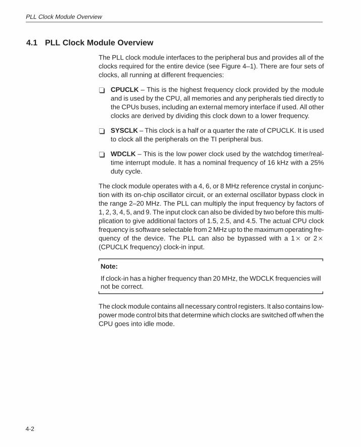
PLL Clock Module Overview
4-2
4.1 PLL Clock Module Overview
The PLL clock module interfaces to the peripheral bus and provides all of theclocks required for the entire device (see Figure 4–1). There are four sets ofclocks, all running at different frequencies:
� CPUCLK – This is the highest frequency clock provided by the moduleand is used by the CPU, all memories and any peripherals tied directly tothe CPUs buses, including an external memory interface if used. All otherclocks are derived by dividing this clock down to a lower frequency.
� SYSCLK – This clock is a half or a quarter the rate of CPUCLK. It is usedto clock all the peripherals on the TI peripheral bus.
� WDCLK – This is the low power clock used by the watchdog timer/real-time interrupt module. It has a nominal frequency of 16 kHz with a 25%duty cycle.
The clock module operates with a 4, 6, or 8 MHz reference crystal in conjunc-tion with its on-chip oscillator circuit, or an external oscillator bypass clock inthe range 2–20 MHz. The PLL can multiply the input frequency by factors of1, 2, 3, 4, 5, and 9. The input clock can also be divided by two before this multi-plication to give additional factors of 1.5, 2.5, and 4.5. The actual CPU clockfrequency is software selectable from 2 MHz up to the maximum operating fre-quency of the device. The PLL can also be bypassed with a 1� or 2�(CPUCLK frequency) clock-in input.
Note:
If clock-in has a higher frequency than 20 MHz, the WDCLK frequencies willnot be correct.
The clock module contains all necessary control registers. It also contains low-power mode control bits that determine which clocks are switched off when theCPU goes into idle mode.
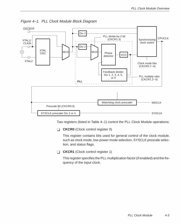
PLL Clock Module Overview
4-3PLL Clock Module
Figure 4–1. PLL Clock Module Block Diagram
ÁÁÁÁ
ÁÁÁÁÁÁÁÁÁÁÁÁÁÁÁÁÁÁÁÁÁÁÁÁÁÁÁÁÁÁÁÁÁÁÁ
ÁÁÁÁÁÁÁÁÁÁÁÁ
ÁÁÁÁÁÁÁÁ
ÁÁÁÁÁÁ
ÁÁÁÁÁÁ
ÁÁÁÁÁÁÁÁÁÁÁÁÁÁÁÁÁÁ
ÁÁÁÁÁÁÁÁÁÁÁÁÁÁÁÁÁÁ
ÁÁÁÁÁÁÁÁÁÁÁÁÁÁÁÁÁÁÁÁÁÁÁÁÁÁÁÁÁÁÁÁÁÁÁÁÁÁÁÁÁÁÁÁ
ÁÁÁÁÁÁÁÁÁÁÁÁÁÁÁÁ
CPUCLKSynchronizingclock switch
VCO
WDCLK
SYSCLK
Clock mode bits(CKCR0.7–6)
Div 2
MUXMUX
Div 2XTALOSC
PLL
SYSCLK prescaler Div 2 or 4
Prescale Bit (CKCR0.0)
Phasedetector
Feedback dividerDiv 1, 2, 3, 4, 5,
or 9
Watchdog clock prescaler
XTAL2
XTAL1/CLKIN
OSCBYP
PLL divide-by-2 bit(CKCR1.3)
PLL multiply ratio(CKCR1.2–0)
Two registers (listed in Table 4–1) control the PLL Clock Module operations:
� CKCR0 (Clock control register 0)
This register contains bits used for general control of the clock module,such as clock mode, low-power mode selection, SYSCLK prescale selec-tion, and status flags.
� CKCR1 (Clock control register 1)
This register specifies the PLL multiplication factor (if enabled) and the fre-quency of the input clock.
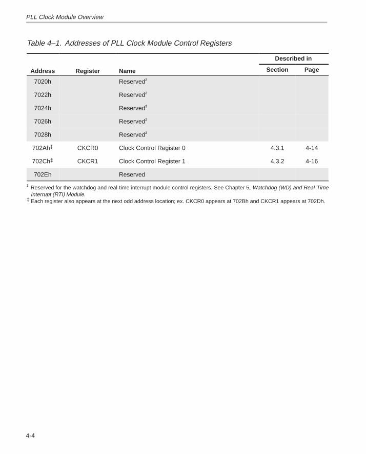
PLL Clock Module Overview
4-4
Table 4–1. Addresses of PLL Clock Module Control Registers
Described in
Address Register Name Section Page
7020h Reserved†
7022h Reserved†
7024h Reserved†
7026h Reserved†
7028h Reserved†
702Ah‡ CKCR0 Clock Control Register 0 4.3.1 4-14
702Ch‡ CKCR1 Clock Control Register 1 4.3.2 4-16
702Eh Reserved
† Reserved for the watchdog and real-time interrupt module control registers. See Chapter 5, Watchdog (WD) and Real-TimeInterrupt (RTI) Module.
‡ Each register also appears at the next odd address location; ex. CKCR0 appears at 702Bh and CKCR1 appears at 702Dh.
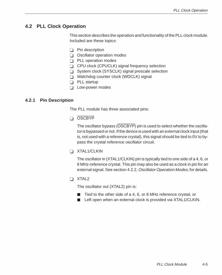
PLL Clock Operation
4-5PLL Clock Module
4.2 PLL Clock Operation
This section describes the operation and functionality of the PLL clock module.Included are these topics:
� Pin description� Oscillator operation modes� PLL operation modes� CPU clock (CPUCLK) signal frequency selection� System clock (SYSCLK) signal prescale selection� Watchdog counter clock (WDCLK) signal� PLL startup� Low-power modes
4.2.1 Pin Description
The PLL module has three associated pins:
� OSCBYP
The oscillator bypass (OSCBYP) pin is used to select whether the oscilla-tor is bypassed or not. If the device is used with an external clock input (thatis, not used with a reference crystal), this signal should be tied to 0V to by-pass the crystal reference oscillator circuit.
� XTAL1/CLKIN
The oscillator in (XTAL1/CLKIN) pin is typically tied to one side of a 4, 6, or8 MHz-reference crystal. This pin may also be used as a clock in pin for anexternal signal. See section 4.2.2, Oscillator Operation Modes, for details.
� XTAL2
The oscillator out (XTAL2) pin is:
� Tied to the other side of a 4, 6, or 8 MHz reference crystal, or� Left open when an external clock is provided via XTAL1/CLKIN.
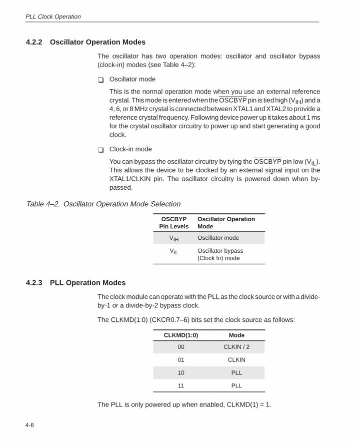
PLL Clock Operation
4-6
4.2.2 Oscillator Operation Modes
The oscillator has two operation modes: oscillator and oscillator bypass(clock-in) modes (see Table 4–2):
� Oscillator mode
This is the normal operation mode when you use an external referencecrystal. This mode is entered when the OSCBYP pin is tied high (VIH) and a4, 6, or 8 MHz crystal is connected between XTAL1 and XTAL2 to provide areference crystal frequency. Following device power up it takes about 1 msfor the crystal oscillator circuitry to power up and start generating a goodclock.
� Clock-in mode
You can bypass the oscillator circuitry by tying the OSCBYP pin low (VIL).This allows the device to be clocked by an external signal input on theXTAL1/CLKIN pin. The oscillator circuitry is powered down when by-passed.
Table 4–2. Oscillator Operation Mode Selection
ÁÁÁÁÁÁÁÁÁÁ
OSCBYPPin Levels
ÁÁÁÁÁÁÁÁÁÁÁÁÁÁÁÁ
Oscillator OperationMode
VIH Oscillator mode
ÁÁÁÁÁÁÁÁÁÁÁÁÁÁÁ
VIL ÁÁÁÁÁÁÁÁÁÁÁÁÁÁÁÁÁÁÁÁÁÁÁÁ
Oscillator bypass(Clock In) mode
4.2.3 PLL Operation Modes
The clock module can operate with the PLL as the clock source or with a divide-by-1 or a divide-by-2 bypass clock.
The CLKMD(1:0) (CKCR0.7–6) bits set the clock source as follows:
ÁÁÁÁÁÁÁÁÁÁÁÁ
CLKMD(1:0) ÁÁÁÁÁÁÁÁÁÁÁÁÁÁ
Mode
00 CLKIN / 2ÁÁÁÁÁÁÁÁÁÁÁÁÁÁÁÁÁÁ
01ÁÁÁÁÁÁÁÁÁÁÁÁÁÁÁÁÁÁÁÁÁ
CLKIN
10 PLL
ÁÁÁÁÁÁÁÁÁÁÁÁ
11 ÁÁÁÁÁÁÁÁÁÁÁÁÁÁ
PLL
The PLL is only powered up when enabled, CLKMD(1) = 1.
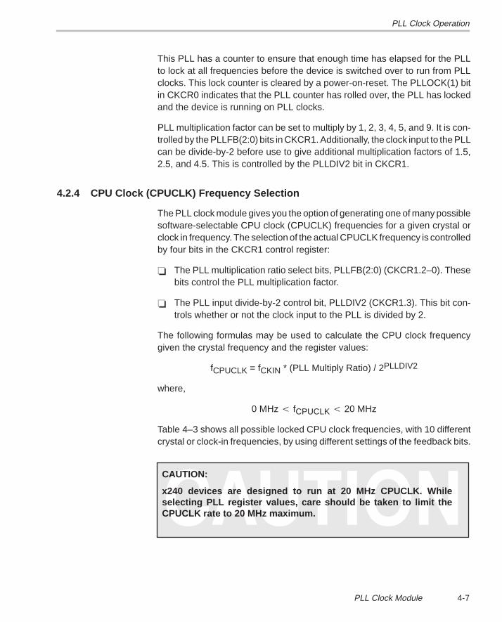
PLL Clock Operation
4-7PLL Clock Module
This PLL has a counter to ensure that enough time has elapsed for the PLLto lock at all frequencies before the device is switched over to run from PLLclocks. This lock counter is cleared by a power-on-reset. The PLLOCK(1) bitin CKCR0 indicates that the PLL counter has rolled over, the PLL has lockedand the device is running on PLL clocks.
PLL multiplication factor can be set to multiply by 1, 2, 3, 4, 5, and 9. It is con-trolled by the PLLFB(2:0) bits in CKCR1. Additionally, the clock input to the PLLcan be divide-by-2 before use to give additional multiplication factors of 1.5,2.5, and 4.5. This is controlled by the PLLDIV2 bit in CKCR1.
4.2.4 CPU Clock (CPUCLK) Frequency Selection
The PLL clock module gives you the option of generating one of many possiblesoftware-selectable CPU clock (CPUCLK) frequencies for a given crystal orclock in frequency. The selection of the actual CPUCLK frequency is controlledby four bits in the CKCR1 control register:
� The PLL multiplication ratio select bits, PLLFB(2:0) (CKCR1.2–0). Thesebits control the PLL multiplication factor.
� The PLL input divide-by-2 control bit, PLLDIV2 (CKCR1.3). This bit con-trols whether or not the clock input to the PLL is divided by 2.
The following formulas may be used to calculate the CPU clock frequencygiven the crystal frequency and the register values:
fCPUCLK = fCKIN * (PLL Multiply Ratio) / 2PLLDIV2
where,
0 MHz � fCPUCLK � 20 MHz
Table 4–3 shows all possible locked CPU clock frequencies, with 10 differentcrystal or clock-in frequencies, by using different settings of the feedback bits.
CAUTION:
x240 devices are designed to run at 20 MHz CPUCLK. Whileselecting PLL register values, care should be taken to limit theCPUCLK rate to 20 MHz maximum.
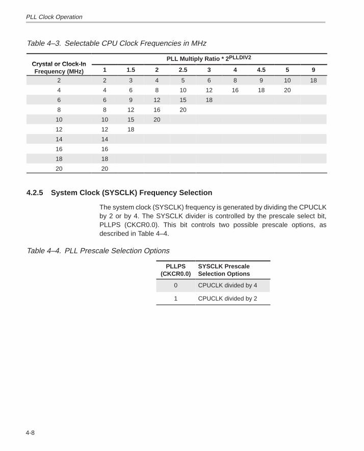
PLL Clock Operation
4-8
Table 4–3. Selectable CPU Clock Frequencies in MHz
ÁÁÁÁÁÁÁÁÁÁÁÁÁÁÁÁCrystal or Clock-In
ÁÁÁÁÁÁÁÁÁÁÁÁÁÁÁÁÁÁÁÁÁÁÁÁÁÁÁÁÁÁÁÁÁÁÁÁÁÁÁÁÁÁÁÁÁÁ
PLL Multiply Ratio * 2 PLLDIV2
ÁÁÁÁÁÁÁÁÁÁÁÁÁÁÁÁ
Crysta l or Clock-InFrequency (MHz)
ÁÁÁÁÁÁ
1 ÁÁÁÁÁÁÁÁ
1.5 ÁÁÁÁÁÁ
2 ÁÁÁÁÁÁÁÁ
2.5 ÁÁÁÁÁÁ
3 ÁÁÁÁÁÁÁÁ
4 ÁÁÁÁÁÁ
4.5ÁÁÁÁÁÁÁÁ
5 ÁÁÁÁÁÁ
9
2 2 3 4 5 6 8 9 10 18ÁÁÁÁÁÁÁÁÁÁÁÁÁÁÁÁ
4 ÁÁÁÁÁÁ
4 ÁÁÁÁÁÁÁÁ
6 ÁÁÁÁÁÁ
8 ÁÁÁÁÁÁÁÁ
10 ÁÁÁÁÁÁ
12 ÁÁÁÁÁÁÁÁ
16 ÁÁÁÁÁÁ
18 ÁÁÁÁÁÁÁÁ
20
6 6 9 12 15 18ÁÁÁÁÁÁÁÁÁÁÁÁÁÁÁÁ
8 ÁÁÁÁÁÁ
8 ÁÁÁÁÁÁÁÁ
12 ÁÁÁÁÁÁ
16 ÁÁÁÁÁÁÁÁ
20
10 10 15 20
ÁÁÁÁÁÁÁÁÁÁÁÁÁÁÁÁ
12 ÁÁÁÁÁÁ
12 ÁÁÁÁÁÁÁÁ
18
14 14
ÁÁÁÁÁÁÁÁÁÁÁÁÁÁÁÁ
16 ÁÁÁÁÁÁ
16
18 18
ÁÁÁÁÁÁÁÁÁÁÁÁÁÁÁÁ
20 ÁÁÁÁÁÁ
20
4.2.5 System Clock (SYSCLK) Frequency Selection
The system clock (SYSCLK) frequency is generated by dividing the CPUCLKby 2 or by 4. The SYSCLK divider is controlled by the prescale select bit,PLLPS (CKCR0.0). This bit controls two possible prescale options, asdescribed in Table 4–4.
Table 4–4. PLL Prescale Selection Options
ÁÁÁÁÁÁÁÁÁÁÁÁÁÁÁ
PLLPS(CKCR0.0)
ÁÁÁÁÁÁÁÁÁÁÁÁÁÁÁÁÁÁÁÁÁÁÁÁ
SYSCLK Prescale Selection Options
0 CPUCLK divided by 4
ÁÁÁÁÁÁÁÁÁÁ
1 ÁÁÁÁÁÁÁÁÁÁÁÁÁÁÁÁCPUCLK divided by 2
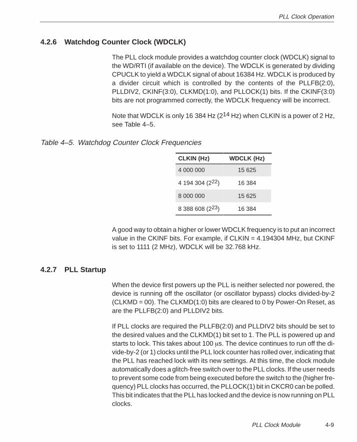
PLL Clock Operation
4-9PLL Clock Module
4.2.6 Watchdog Counter Clock (WDCLK)
The PLL clock module provides a watchdog counter clock (WDCLK) signal tothe WD/RTI (if available on the device). The WDCLK is generated by dividingCPUCLK to yield a WDCLK signal of about 16384 Hz. WDCLK is produced bya divider circuit which is controlled by the contents of the PLLFB(2:0),PLLDIV2, CKINF(3:0), CLKMD(1:0), and PLLOCK(1) bits. If the CKINF(3:0)bits are not programmed correctly, the WDCLK frequency will be incorrect.
Note that WDCLK is only 16 384 Hz (214 Hz) when CLKIN is a power of 2 Hz,see Table 4–5.
Table 4–5. Watchdog Counter Clock Frequencies
ÁÁÁÁÁÁÁÁÁÁÁÁ
CLKIN (Hz) ÁÁÁÁÁÁÁÁÁÁ
WDCLK (Hz)
4 000 000 15 625ÁÁÁÁÁÁÁÁÁÁÁÁ
4 194 304 (222)ÁÁÁÁÁÁÁÁÁÁ
16 384
8 000 000 15 625
ÁÁÁÁÁÁÁÁÁÁÁÁ
8 388 608 (223)ÁÁÁÁÁÁÁÁÁÁ
16 384
A good way to obtain a higher or lower WDCLK frequency is to put an incorrectvalue in the CKINF bits. For example, if CLKIN = 4.194304 MHz, but CKINFis set to 1111 (2 MHz), WDCLK will be 32.768 kHz.
4.2.7 PLL Startup
When the device first powers up the PLL is neither selected nor powered, thedevice is running off the oscillator (or oscillator bypass) clocks divided-by-2(CLKMD = 00). The CLKMD(1:0) bits are cleared to 0 by Power-On Reset, asare the PLLFB(2:0) and PLLDIV2 bits.
If PLL clocks are required the PLLFB(2:0) and PLLDIV2 bits should be set tothe desired values and the CLKMD(1) bit set to 1. The PLL is powered up andstarts to lock. This takes about 100 �s. The device continues to run off the di-vide-by-2 (or 1) clocks until the PLL lock counter has rolled over, indicating thatthe PLL has reached lock with its new settings. At this time, the clock moduleautomatically does a glitch-free switch over to the PLL clocks. If the user needsto prevent some code from being executed before the switch to the (higher fre-quency) PLL clocks has occurred, the PLLOCK(1) bit in CKCR0 can be polled.This bit indicates that the PLL has locked and the device is now running on PLLclocks.
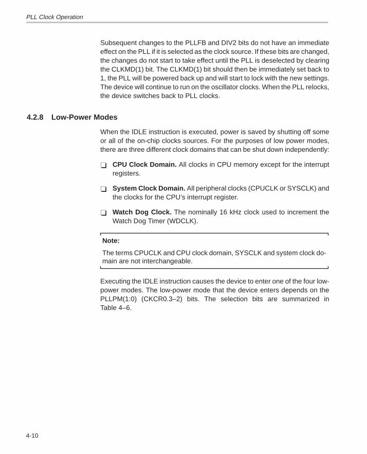
PLL Clock Operation
4-10
Subsequent changes to the PLLFB and DIV2 bits do not have an immediateeffect on the PLL if it is selected as the clock source. If these bits are changed,the changes do not start to take effect until the PLL is deselected by clearingthe CLKMD(1) bit. The CLKMD(1) bit should then be immediately set back to1, the PLL will be powered back up and will start to lock with the new settings.The device will continue to run on the oscillator clocks. When the PLL relocks,the device switches back to PLL clocks.
4.2.8 Low-Power Modes
When the IDLE instruction is executed, power is saved by shutting off someor all of the on-chip clocks sources. For the purposes of low power modes,there are three different clock domains that can be shut down independently:
� CPU Clock Domain. All clocks in CPU memory except for the interruptregisters.
� System Clock Domain. All peripheral clocks (CPUCLK or SYSCLK) andthe clocks for the CPU’s interrupt register.
� Watch Dog Clock. The nominally 16 kHz clock used to increment theWatch Dog Timer (WDCLK).
Note:
The terms CPUCLK and CPU clock domain, SYSCLK and system clock do-main are not interchangeable.
Executing the IDLE instruction causes the device to enter one of the four low-power modes. The low-power mode that the device enters depends on thePLLPM(1:0) (CKCR0.3–2) bits. The selection bits are summarized inTable 4–6.
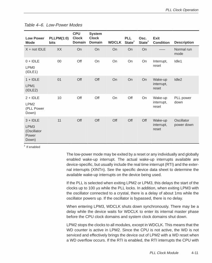
PLL Clock Operation
4-11PLL Clock Module
Table 4–6. Low-Power Modes
ÁÁÁÁÁÁÁÁÁÁÁÁÁÁÁ
Low PowerMode
ÁÁÁÁÁÁÁÁÁÁÁÁÁÁÁ
PLLPM(1:0)bits
ÁÁÁÁÁÁÁÁÁ
CPUClockDomain
ÁÁÁÁÁÁÁÁÁÁÁÁ
SystemClockDomain
ÁÁÁÁÁÁÁÁÁÁÁÁWDCLK
ÁÁÁÁÁÁÁÁÁ
PLLState†
ÁÁÁÁÁÁÁÁÁÁÁÁ
Osc.State†
ÁÁÁÁÁÁÁÁÁÁÁÁ
ExitCondition
ÁÁÁÁÁÁÁÁÁÁÁÁÁÁÁÁÁÁDescription
X + not IDLE XX On On On On On ––– Normal runmode
ÁÁÁÁÁÁÁÁÁÁÁÁÁÁÁÁÁÁÁÁ
0 + IDLE
LPM0(IDLE1)
ÁÁÁÁÁÁÁÁÁÁÁÁÁÁÁÁÁÁÁÁ
00ÁÁÁÁÁÁÁÁÁÁÁÁ
OffÁÁÁÁÁÁÁÁÁÁÁÁÁÁÁÁ
OnÁÁÁÁÁÁÁÁÁÁÁÁÁÁÁÁ
OnÁÁÁÁÁÁÁÁÁÁÁÁ
OnÁÁÁÁÁÁÁÁÁÁÁÁÁÁÁÁ
OnÁÁÁÁÁÁÁÁÁÁÁÁÁÁÁÁ
Interrupt,reset
ÁÁÁÁÁÁÁÁÁÁÁÁÁÁÁÁÁÁÁÁÁÁÁÁ
Idle1
1 + IDLE
LPM1(IDLE2)
01 Off Off On On On Wake-upinterrupt,reset
Idle2
ÁÁÁÁÁÁÁÁÁÁÁÁÁÁÁÁÁÁÁÁÁÁÁÁÁ
2 + IDLE
LPM2(PLL PowerDown)
ÁÁÁÁÁÁÁÁÁÁÁÁÁÁÁÁÁÁÁÁÁÁÁÁÁ
10ÁÁÁÁÁÁÁÁÁÁÁÁÁÁÁ
OffÁÁÁÁÁÁÁÁÁÁÁÁÁÁÁÁÁÁÁÁ
OffÁÁÁÁÁÁÁÁÁÁÁÁÁÁÁÁÁÁÁÁ
OnÁÁÁÁÁÁÁÁÁÁÁÁÁÁÁ
OffÁÁÁÁÁÁÁÁÁÁÁÁÁÁÁÁÁÁÁÁ
OnÁÁÁÁÁÁÁÁÁÁÁÁÁÁÁÁÁÁÁÁ
Wake-upinterrupt,reset
ÁÁÁÁÁÁÁÁÁÁÁÁÁÁÁÁÁÁÁÁÁÁÁÁÁÁÁÁÁÁ
PLL powerdown
3 + IDLE
LPM3(OscillatorPowerDown)
11 Off Off Off Off Off Wake-upinterrupt,reset
Oscillatorpower down
† If enabled
The low-power mode may be exited by a reset or any individually and globallyenabled wake-up interrupt. The actual wake-up interrupts available aredevice-specific, but usually include the real time interrupt (RTI) and the exter-nal interrupts (XINTn). See the specific device data sheet to determine theavailable wake-up interrupts on the device being used.
If the PLL is selected when exiting LPM2 or LPM3, this delays the start of theclocks up to 100 �s while the PLL locks. In addition, when exiting LPM3 withthe oscillator connected to a crystal, there is a delay of about 1ms while theoscillator powers up. If the oscillator is bypassed, there is no delay.
When entering LPM3, WDCLK shuts down synchronously. There may be adelay while the device waits for WDCLK to enter its internal master phasebefore the CPU clock domains and system clock domains shut down.
LPM2 stops the clocks to all modules, except in WDCLK. This means that theWD counter is active in LPM2. Since the CPU is not active, the WD is notserviced and effectively brings the device out of LPM2 with a WD reset whena WD overflow occurs. If the RTI is enabled, the RTI interrupts the CPU with
PLL Clock Operation
4-12
a wake-up interrupt, causing the device to exit standby mode. At this time, theWD could be serviced to prevent the device from being reset.
The LPM3 mode stops all internal clock signals and powers down the PLL andthe oscillator. This stops all modules, including the WD/RTI, resulting in thelowest power consumption possible.
Note:
Do not enter LPM2 if the PLL is not enabled.
LPMODE 0 Entry/Exit Sequence.
When entering this mode:
1) The CPU clock domain is shut down immediately.
2) All other chip clocks continue running.
When exiting this mode with an interrupt or reset:
1) The CPU clock domain starts running again immediately.
LPMODE 1 Entry/Exit Sequence.
When entering this mode:
1) The CPU clock domain is shut down immediately.
2) Wait until the system clock domain is in a HIGH state and then stop in thatstate.
3) WDCLK continues to run.
When exiting this mode with a wake-up interrupt or reset:
1) The clock module internal clocks start running immediately.
2) A few cycles later, the CPU clock domain and the system clock domainstart running again.
LPMODE 2 Entry/Exit Sequence.
When entering this mode:
1) The CPU clock domain is shut down immediately.
2) Wait until the system clock domain is in a HIGH state and then stop in thatstate.
PLL Clock Operation
4-13PLL Clock Module
3) WDCLK continues to run.
4) Clocks to switch from PLL to by 1 or by 2 mode.
5) PLL is powered down.
When exiting this mode with a wake-up interrupt or reset:
1) The PLL is powered up and the lock counter begins counting. Clockmodule internal clocks start running in by 1 or by 2 mode.
2) The CPU clock domain and the system clock domain start running again.
3) When PLL has locked (lock counter rolled over), the clocks automaticallyswitch back to the PLL.
LPMODE 3 Entry/Exit Sequence.
When entering this mode:
1) The CPU clock domain is shut down immediately.
2) Wait until the system clock domain is in a HIGH state and then stop in thatstate.
3) WDCLK continues to run.
4) Clocks to switch from PLL to by 1 or by 2 mode.
5) PLL is powered down.
6) WDCLK keeps running until the internal WDCLK mater phase is LOW.
7) Clock switching logic goes to all off state — that is, all internal clocks arestopped.
8) Oscillator (if used) is powered down.
When exiting this mode with a wake-up interrupt or reset:
1) The oscillator is re-enabled but the oscillator output is not good for about1 ms.
2) Clock-switching logic switches to by-1 or by-2 state, depending on valueof CKMD(0) bit.
3) The PLL is powered up and begins to lock.
4) The CPU clock domain and the system clock domain start running again.
5) When PLL has locked, clocks automatically switch back to the PLL.
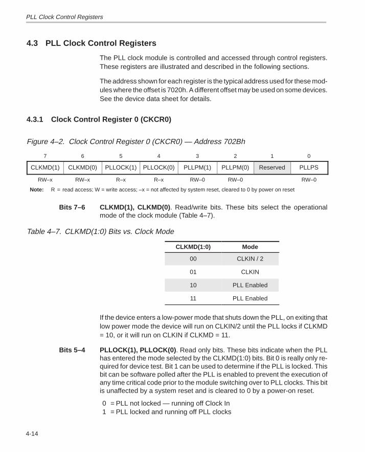
PLL Clock Control Registers
4-14
4.3 PLL Clock Control Registers
The PLL clock module is controlled and accessed through control registers.These registers are illustrated and described in the following sections.
The address shown for each register is the typical address used for these mod-ules where the offset is 7020h. A different offset may be used on some devices.See the device data sheet for details.
4.3.1 Clock Control Register 0 (CKCR0)
Figure 4–2. Clock Control Register 0 (CKCR0) — Address 702Bh
7 6 5 4 3 2 1 0
CLKMD(1) CLKMD(0) PLLOCK(1) PLLOCK(0) PLLPM(1) PLLPM(0) Reserved PLLPS
RW–x RW–x R–x R–x RW–0 RW–0 RW–0
Note: R = read access; W = write access; –x = not affected by system reset, cleared to 0 by power on reset
Bits 7–6 CLKMD(1), CLKMD(0) . Read/write bits. These bits select the operationalmode of the clock module (Table 4–7).
Table 4–7. CLKMD(1:0) Bits vs. Clock Mode
ÁÁÁÁÁÁÁÁÁÁÁÁ
CLKMD(1:0) ÁÁÁÁÁÁÁÁÁÁÁÁ
Mode
00 CLKIN / 2ÁÁÁÁÁÁÁÁÁÁÁÁÁÁÁÁÁÁ
01ÁÁÁÁÁÁÁÁÁÁÁÁÁÁÁÁÁÁ
CLKIN
10 PLL Enabled
ÁÁÁÁÁÁÁÁÁÁÁÁ
11 ÁÁÁÁÁÁÁÁÁÁÁÁ
PLL Enabled
If the device enters a low-power mode that shuts down the PLL, on exiting thatlow power mode the device will run on CLKIN/2 until the PLL locks if CLKMD= 10, or it will run on CLKIN if CLKMD = 11.
Bits 5–4 PLLOCK(1), PLLOCK(0) . Read only bits. These bits indicate when the PLLhas entered the mode selected by the CLKMD(1:0) bits. Bit 0 is really only re-quired for device test. Bit 1 can be used to determine if the PLL is locked. Thisbit can be software polled after the PLL is enabled to prevent the execution ofany time critical code prior to the module switching over to PLL clocks. This bitis unaffected by a system reset and is cleared to 0 by a power-on reset.
0 = PLL not locked — running off Clock In1 = PLL locked and running off PLL clocks
PLL Clock Control Registers
4-15PLL Clock Module
Bits 3–2 PLLPM(1), PLLPM(0) . Read/write bits. These bits specify which low powermode will be entered upon execution of an IDLE instruction. These bits arecleared (00b) during power-on and system reset, making LPM0 the default.See section 4.2.8, Low-Power Modes, on page 4-10.
Bit 1 Reserved. 0 default.
Bit 0 PLLPS. Read/write bit. This bit specifies which of two prescale values will beselected for the System clocks. This bit is cleared (0b) during power-on andsystem reset, making CPUCLK/4 the default System clock (SYSCLK)frequency. See section 4.2.5, System Clock (SYSCLK) Frequency Selection,on page 4-8.
0 =f(SYSCLK) = f(CPUCLK) / 41 =f(SYSCLK) = f(CPUCLK) / 2
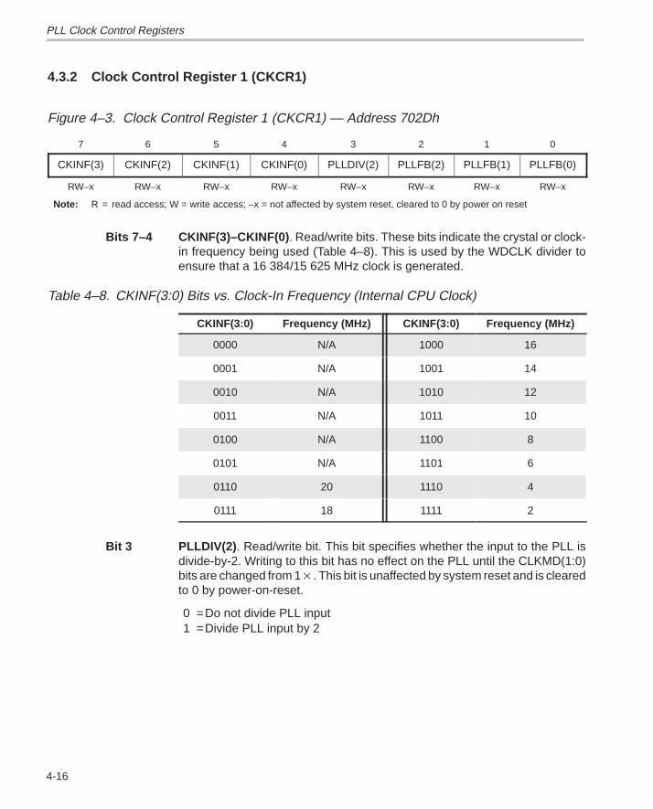
PLL Clock Control Registers
4-16
4.3.2 Clock Control Register 1 (CKCR1)
Figure 4–3. Clock Control Register 1 (CKCR1) — Address 702Dh
7 6 5 4 3 2 1 0
CKINF(3) CKINF(2) CKINF(1) CKINF(0) PLLDIV(2) PLLFB(2) PLLFB(1) PLLFB(0)
RW–x RW–x RW–x RW–x RW–x RW–x RW–x RW–x
Note: R = read access; W = write access; –x = not affected by system reset, cleared to 0 by power on reset
Bits 7–4 CKINF(3)–CKINF(0) . Read/write bits. These bits indicate the crystal or clock-in frequency being used (Table 4–8). This is used by the WDCLK divider toensure that a 16 384/15 625 MHz clock is generated.
Table 4–8. CKINF(3:0) Bits vs. Clock-In Frequency (Internal CPU Clock)
ÁÁÁÁÁÁÁÁÁÁÁÁ
CKINF(3:0)ÁÁÁÁÁÁÁÁÁÁÁÁÁÁ
Frequency (MHz)ÁÁÁÁÁÁÁÁÁÁÁÁ
CKINF(3:0)ÁÁÁÁÁÁÁÁÁÁÁÁÁÁ
Frequency (MHz)
0000 N/A 1000 16
ÁÁÁÁÁÁÁÁÁÁÁÁ
0001 ÁÁÁÁÁÁÁÁÁÁÁÁÁÁ
N/A ÁÁÁÁÁÁÁÁÁÁÁÁ
1001 ÁÁÁÁÁÁÁÁÁÁÁÁÁÁ
14
0010 N/A 1010 12ÁÁÁÁÁÁÁÁÁÁÁÁÁÁÁÁÁÁ
0011ÁÁÁÁÁÁÁÁÁÁÁÁÁÁÁÁÁÁÁÁÁ
N/AÁÁÁÁÁÁÁÁÁÁÁÁÁÁÁÁÁÁ
1011ÁÁÁÁÁÁÁÁÁÁÁÁÁÁÁÁÁÁÁÁÁ
10
0100 N/A 1100 8
ÁÁÁÁÁÁÁÁÁÁÁÁ
0101ÁÁÁÁÁÁÁÁÁÁÁÁÁÁ
N/AÁÁÁÁÁÁÁÁÁÁÁÁ
1101ÁÁÁÁÁÁÁÁÁÁÁÁÁÁ
6
0110 20 1110 4
ÁÁÁÁÁÁÁÁÁÁÁÁ
0111 ÁÁÁÁÁÁÁÁÁÁÁÁÁÁ
18 ÁÁÁÁÁÁÁÁÁÁÁÁ
1111 ÁÁÁÁÁÁÁÁÁÁÁÁÁÁ
2
Bit 3 PLLDIV(2) . Read/write bit. This bit specifies whether the input to the PLL isdivide-by-2. Writing to this bit has no effect on the PLL until the CLKMD(1:0)bits are changed from 1�. This bit is unaffected by system reset and is clearedto 0 by power-on-reset.
0 =Do not divide PLL input1 =Divide PLL input by 2
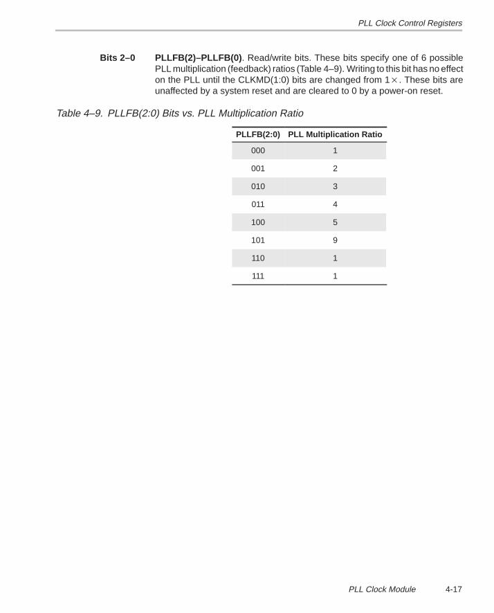
PLL Clock Control Registers
4-17PLL Clock Module
Bits 2–0 PLLFB(2)–PLLFB(0) . Read/write bits. These bits specify one of 6 possiblePLL multiplication (feedback) ratios (Table 4–9). Writing to this bit has no effecton the PLL until the CLKMD(1:0) bits are changed from 1�. These bits areunaffected by a system reset and are cleared to 0 by a power-on reset.
Table 4–9. PLLFB(2:0) Bits vs. PLL Multiplication Ratio
ÁÁÁÁÁÁÁÁÁÁ
PLLFB(2:0)ÁÁÁÁÁÁÁÁÁÁÁÁÁÁÁÁ
PLL Multiplication Ratio
000 1ÁÁÁÁÁÁÁÁÁÁ
001ÁÁÁÁÁÁÁÁÁÁÁÁÁÁÁÁ
2
010 3
ÁÁÁÁÁÁÁÁÁÁ
011 ÁÁÁÁÁÁÁÁÁÁÁÁÁÁÁÁ
4
100 5ÁÁÁÁÁÁÁÁÁÁ101
ÁÁÁÁÁÁÁÁÁÁÁÁÁÁÁÁ9
110 1
ÁÁÁÁÁÁÁÁÁÁ
111 ÁÁÁÁÁÁÁÁÁÁÁÁÁÁÁÁ
1
5-1Watchdog and Real-Time Interrupt Module
Watchdog and Real-Time Interrupt Module
The watchdog (WD) and real-time interrupt (RTI) module monitors softwareand hardware operation, provides interrupts at programmable intervals, andimplements system reset functions upon CPU disruption. If the software goesinto an improper loop, or if the CPU becomes temporarily disrupted, the WDtimer overflows to assert a system reset.
The WD/RTI module is part of the TI peripheral module library. It can be com-bined with other modular building blocks from the TI peripheral module libraryto generate a diversified family of highly integrated devices.
Topic Page
5.1 Watchdog (WD) and Real-Time Interrupt (RTI) Overview 5-2. . . . . . . . . .
5.2 Operation of Watchdog (WD) and Real-Time Interrupt (RTI)Timers 5-6. . . . . . . . . . . . . . . . . . . . . . . . . . . . . . . . . . . . . . . . . . . . . . . . . . . . . . .
5.3 Watchdog (WD) and Real-Time Interrupt (RTI)Control Registers 5-11. . . . . . . . . . . . . . . . . . . . . . . . . . . . . . . . . . . . . . . . . . . .
5.4 Watchdog (WD) and Real-Time Interrupt (RTI) Routines 5-18. . . . . . . . .
Chapter 5
Watchdog (WD) and Real-Time Interrupt (RTI) Overview
5-2
5.1 Watchdog (WD) and Real-Time Interrupt (RTI) Overview
Most conditions that temporarily disrupt chip operation and inhibit proper CPUfunction can be cleared and reset by the watchdog function. By its consistentperformance, the watchdog increases the reliability of the CPU, thus ensuringsystem integrity.
Note: 8-Bit Peripheral
This module is interfaced to the 16-bit peripheral bus as an 8-bit peripheral.Therefore, reads from bits 15–8 are undefined; writes to bits 15–8 have noeffect.
5.1.1 WD and RTI Components
The WD/RTI module design includes the following components:
� WD timer
� 8-bit WD counter that generates a system reset upon overflow
� 7-bit free-running counter that feeds the WD counter via the WDcounter prescale
� A WD reset key (WDKEY) register that clears the WD counter whenthe correct combination of values are written, and generates a reset ifan incorrect value is written to the register
� A WD flag (WD FLAG) bit that indicates whether the WD timer initiateda system reset
� WD check bits that initiate a system reset if the WD timer is corrupted
� Automatic activation of the WD timer, once system reset is released
� A WD prescale with six selections from the 7-bit free-running counterand two (identical) WDCLK signal inputs
� RTI timer
� RTI prescale that selects from 4 taps of the 8-bit real-time counter and4 taps of the 7-bit free-running counter
� Interrupt or polled operation (a software bit enables/disables RTIinterrupts)
� An RTI flag (RTI FLAG) bit that indicates whether the RTI counter(RTICNTR) overflows
Figure 5–1 shows a block diagram of the WD/RTI module.

Watchdog (WD) and Real-Time Interrupt (RTI) Overview
5-3Watchdog and Real-Time Interrupt Module
Figure 5–1. Watchdog (WD) and Real-Time Interrupt (RTI) Module Block Diagram
8-bit watchdog
Bad key
Good
WD FLAG
D
CLR
Systemresetrequest
55+AAdetector
WDKEY.7–0
WDCNTR.7–0
Q
1 0 1(Constant value)
3
3
SeeRegister Name PageRTICNTR Real-Time Interrupt Counter Register 5-12WDCNTR Watchdog Counter Register 5-13WDKEY Watchdog Reset Key Register 5-13RTICR Real-Time Interrupt Control Register 5-14WDCR Watchdog Control Register 5-16
WDCR.7
Bad WDCR key
INTrequest(Level 1only)
/16384‡
/8192‡
/4096‡
/2048‡
/1024‡
/512‡
/256‡
111110
101100011010
000
001
CLR
8-bitreal-time
counter
7-bitfree-
runningcounter
/128‡
/64‡
/32‡
/16‡
/8‡
/4‡
/2‡
111110
101
100
011
010001
000
Anywrite
WDCLK
/32768‡
WD prescaleselect bits
Systemreset
System reset
Watchdogreset keyregister
CLR
CLR
1-cycledelay
PS/257
key
counterCLRPrescale
selection
RTICNTR.7–0
WDCR.2–0WDPS2-0
WDCR.5–3†
RTICR.2–0RTIPS2–0
RTICR.6RTI ENA
INT acknowledge
D
CLR
Q RTICR.7
ClearRTI FLAGRTICR.7
RTI FLAG
ReadRTI FLAG
RTI FLAG
WDCHK2–0
WDCR.6WDDIS
† Writing to bits WDCR.5–3 with anything but the correct pattern (101) generates a system reset.‡ These prescale values are with respect to the WDCLK signal.
Watchdog (WD) and Real-Time Interrupt (RTI) Overview
5-4
5.1.2 Control Registers
Five registers control the WD/RTI operations:
� RTI Counter Register (RTICNTR) contains the value of the RTI counter.
� WD Counter Register (WDCNTR) contains the value of the WD counter.
� WD Reset Key Register (WDKEY) clears the WDCNTR when a 55h val-ue followed by an AAh value is written to WDKEY.
� RTI Control Register (RTICR) contains the following control bits used forRTI configuration:
� RTI flag bit� RTI enable bit� RTI prescale select bits (three)
� WD Control Register (WDCR) contains the following control bits used forwatchdog configuration:
� WD flag bit� WD check bits (three)� WD prescale select bits (three)
Table 5–1 lists the addresses of the WD/RTI registers.
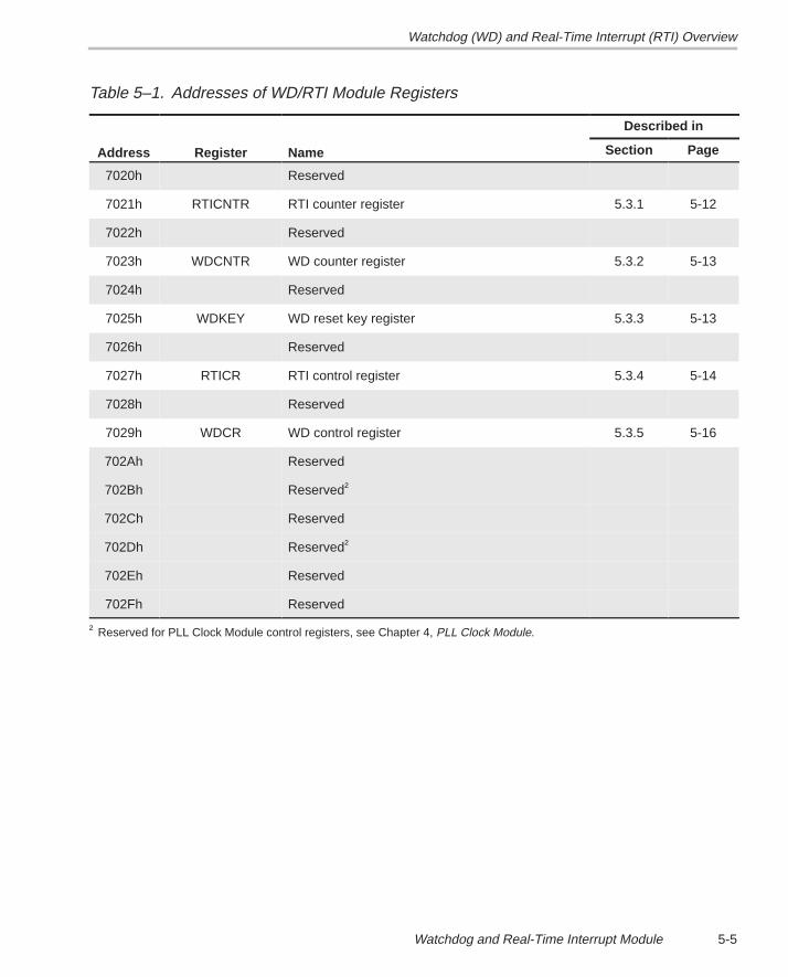
Watchdog (WD) and Real-Time Interrupt (RTI) Overview
5-5Watchdog and Real-Time Interrupt Module
Table 5–1. Addresses of WD/RTI Module Registers
Described in
Address Register Name Section Page
7020h Reserved
7021h RTICNTR RTI counter register 5.3.1 5-12
7022h Reserved
7023h WDCNTR WD counter register 5.3.2 5-13
7024h Reserved
7025h WDKEY WD reset key register 5.3.3 5-13
7026h Reserved
7027h RTICR RTI control register 5.3.4 5-14
7028h Reserved
7029h WDCR WD control register 5.3.5 5-16
702Ah Reserved
702Bh Reserved†
702Ch Reserved
702Dh Reserved†
702Eh Reserved
702Fh Reserved
† Reserved for PLL Clock Module control registers, see Chapter 4, PLL Clock Module.
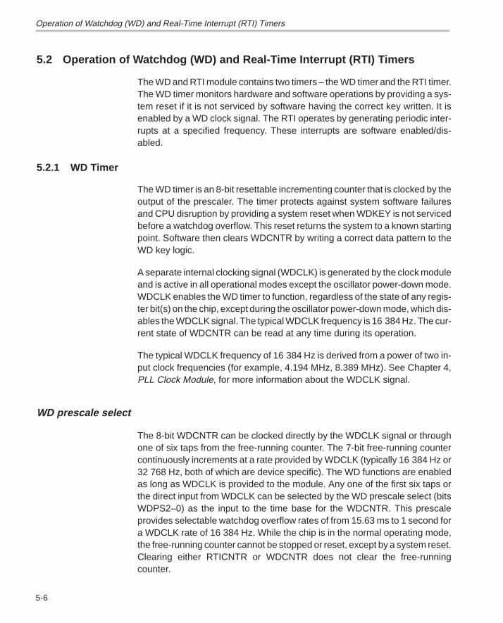
Operation of Watchdog (WD) and Real-Time Interrupt (RTI) Timers
5-6
5.2 Operation of Watchdog (WD) and Real-Time Interrupt (RTI) Timers
The WD and RTI module contains two timers – the WD timer and the RTI timer.The WD timer monitors hardware and software operations by providing a sys-tem reset if it is not serviced by software having the correct key written. It isenabled by a WD clock signal. The RTI operates by generating periodic inter-rupts at a specified frequency. These interrupts are software enabled/dis-abled.
5.2.1 WD Timer
The WD timer is an 8-bit resettable incrementing counter that is clocked by theoutput of the prescaler. The timer protects against system software failuresand CPU disruption by providing a system reset when WDKEY is not servicedbefore a watchdog overflow. This reset returns the system to a known startingpoint. Software then clears WDCNTR by writing a correct data pattern to theWD key logic.
A separate internal clocking signal (WDCLK) is generated by the clock moduleand is active in all operational modes except the oscillator power-down mode.WDCLK enables the WD timer to function, regardless of the state of any regis-ter bit(s) on the chip, except during the oscillator power-down mode, which dis-ables the WDCLK signal. The typical WDCLK frequency is 16 384 Hz. The cur-rent state of WDCNTR can be read at any time during its operation.
The typical WDCLK frequency of 16 384 Hz is derived from a power of two in-put clock frequencies (for example, 4.194 MHz, 8.389 MHz). See Chapter 4,PLL Clock Module, for more information about the WDCLK signal.
WD prescale select
The 8-bit WDCNTR can be clocked directly by the WDCLK signal or throughone of six taps from the free-running counter. The 7-bit free-running countercontinuously increments at a rate provided by WDCLK (typically 16 384 Hz or32 768 Hz, both of which are device specific). The WD functions are enabledas long as WDCLK is provided to the module. Any one of the first six taps orthe direct input from WDCLK can be selected by the WD prescale select (bitsWDPS2–0) as the input to the time base for the WDCNTR. This prescaleprovides selectable watchdog overflow rates of from 15.63 ms to 1 second fora WDCLK rate of 16 384 Hz. While the chip is in the normal operating mode,the free-running counter cannot be stopped or reset, except by a system reset.Clearing either RTICNTR or WDCNTR does not clear the free-runningcounter.
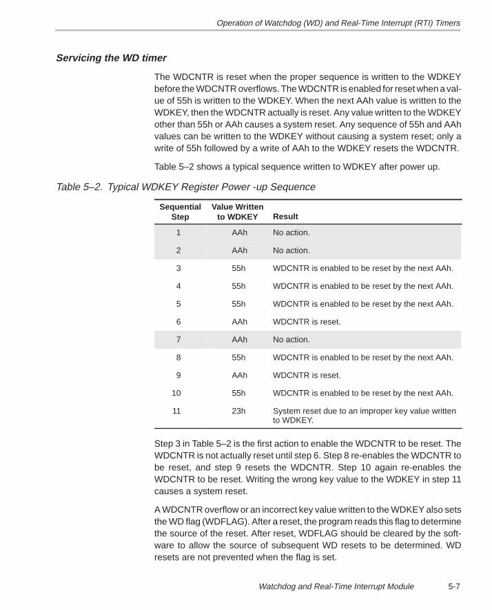
Operation of Watchdog (WD) and Real-Time Interrupt (RTI) Timers
5-7Watchdog and Real-Time Interrupt Module
Servicing the WD timer
The WDCNTR is reset when the proper sequence is written to the WDKEYbefore the WDCNTR overflows. The WDCNTR is enabled for reset when a val-ue of 55h is written to the WDKEY. When the next AAh value is written to theWDKEY, then the WDCNTR actually is reset. Any value written to the WDKEYother than 55h or AAh causes a system reset. Any sequence of 55h and AAhvalues can be written to the WDKEY without causing a system reset; only awrite of 55h followed by a write of AAh to the WDKEY resets the WDCNTR.
Table 5–2 shows a typical sequence written to WDKEY after power up.
Table 5–2. Typical WDKEY Register Power -up Sequence
SequentialStep
Value Writtento WDKEY Result
1 AAh No action.
2 AAh No action.
3 55h WDCNTR is enabled to be reset by the next AAh.
4 55h WDCNTR is enabled to be reset by the next AAh.
5 55h WDCNTR is enabled to be reset by the next AAh.
6 AAh WDCNTR is reset.
7 AAh No action.
8 55h WDCNTR is enabled to be reset by the next AAh.
9 AAh WDCNTR is reset.
10 55h WDCNTR is enabled to be reset by the next AAh.
11 23h System reset due to an improper key value writtento WDKEY.
Step 3 in Table 5–2 is the first action to enable the WDCNTR to be reset. TheWDCNTR is not actually reset until step 6. Step 8 re-enables the WDCNTR tobe reset, and step 9 resets the WDCNTR. Step 10 again re-enables theWDCNTR to be reset. Writing the wrong key value to the WDKEY in step 11causes a system reset.
A WDCNTR overflow or an incorrect key value written to the WDKEY also setsthe WD flag (WDFLAG). After a reset, the program reads this flag to determinethe source of the reset. After reset, WDFLAG should be cleared by the soft-ware to allow the source of subsequent WD resets to be determined. WDresets are not prevented when the flag is set.
Operation of Watchdog (WD) and Real-Time Interrupt (RTI) Timers
5-8
WD reset
When the WDCNTR overflows, the WD timer asserts a system reset. Resetoccurs one WDCNTR clock cycle (either WDCLK or WDCLK divided by aprescale value) later. The reset cannot be disabled in normal operation as longas WDCLK is present. The WD timer is, however, disabled in the oscillatorpower-down mode when WDCLK is not active.
WD disable
For development purposes, the WD timer can be disabled by applying 5V tothe VCCP pin during the device reset sequence and setting the WDDIS bit inthe WD control register (WDCR.6). However, if the hardware and softwareconditions are not met, the WD timer will not be disabled.
WD check bit logic
The WD check bits (WDCR.5–3, described in detail in section 5.3.5, WD TimerControl Register, on page 5-16) are continuously compared to a constant val-ue (1012). If the WD check bits do not match this value, a system reset is gener-ated. This functions as a logic check in case the software improperly writes tothe WDCR, or if an external stimulus (such as voltage spikes, EMI, or otherdisruptive sources) corrupt the contents of the WDCR. Writing to bitsWDCR.5–3 with anything but the correct pattern (1012) generates a systemreset.
Note: WDCR Required Values
Any values written to WDCR must include the value 1012 written to bits 5–3(WDCHK2 – WDCHK0).
WD setup
The WD timer operates independently of the CPU and is always enabled. Itdoes not need any CPU initialization to function. When a system reset occurs,the WD timer defaults to the fastest WD timer rate available (15.63 ms for a16 384 Hz WDCLK signal). As soon as reset is released internally, the CPUstarts executing code, and the WD timer begins incrementing. This meansthat, to avoid a premature reset, WD/RTI setup should occur early in the power-up sequence.
Operation of Watchdog (WD) and Real-Time Interrupt (RTI) Timers
5-9Watchdog and Real-Time Interrupt Module
5.2.2 RTI timer
The RTI timer is an 8-bit counter that can be programmed to generate periodicinterrupts at a software-selectable frequency. Eight taps in all—four from theRTI counter (RTICNTR, further described in section 5.3.1 on page 5-12) andfour from the free-running counter—can be selected through a 1-of-8 multi-plexer to generate the frequency of the periodic interrupt requests. The inter-rupts are enabled and disabled through software. The RTICNTR can be reador cleared at any time. The 7-bit free-running counter, however, cannot becleared except by system reset.
The actual memory-mapped location of the RTI interrupt vector is devicespecific. The CPU always accesses the information in a vector in the samemanner, regardless of the device, although the physical locations of thevectors may differ. Consult the specific device data sheet (Literature numberSPRS042) for the actual physical location of the RTI interrupt vector.
RTI prescale select
The RTICNTR (RTI counter, described in section 5.3.1 on page 5-12) uses the/128 (divide-by-128) tap from the free-running counter as an input to generatefour output taps. These four taps, plus four additional taps taken from the free-running counter can be selected through a 1-of-8 multiplexer that is controlledthrough the three prescale select bits of the RTI control register (RTICR.2–0,described in section 5.3.4 on page 5-14). This prescale provides selectableinterrupt rates of from 1 to 4096 interrupts per second (16 384 Hz WDCLK sig-nal). The RTICNTR is clocked by the WDCLK signal. The RTICNTR can bereset to 00h at any time during normal operation. RTI timer functions are en-abled in all modes except the halt mode.
Clearing the RTICNTR with software does not clear the free-running counter,which provides the RTICNTR prescale. Therefore, after the RTICNTR iscleared, timing measurements from this counter yield up to a 1-bit uncertainty.
RTI enable
The RTI can be enabled or disabled through the RTI enable bit (RTI ENA),which is bit 6 of the RTI control register (RTICR.6). When the RTI is enabled,it allows an interrupt to be generated when the selected overflow occurs. Theinterrupt logic generates only one interrupt for each transition on the selectedtap.
Because the free-running counter cannot be cleared by software, the softwarelogic assumes that the time period specified is measured between consecu-tive overflows of RTICNTR. Therefore, the timing of the first interrupt cannotbe predicted. Accurate timing is provided by waiting until RTI FLAG (RTICR.7)acknowledges the first overflow before enabling the interrupt.
Operation of Watchdog (WD) and Real-Time Interrupt (RTI) Timers
5-10
RTI flag
The RTI flag bit (RTIFLAG) indicates that an overflow has occurred. This isbit 7 of the RTI control register (RTICR.7). The bit can be cleared by softwareservicing the RTI timer; however, clearing the bit is not required for interruptgeneration, and setting the bit with software does not generate an interrupt.
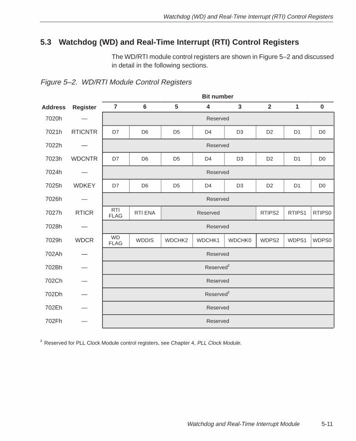
Watchdog (WD) and Real-Time Interrupt (RTI) Control Registers
5-11Watchdog and Real-Time Interrupt Module
5.3 Watchdog (WD) and Real-Time Interrupt (RTI) Control Registers
The WD/RTI module control registers are shown in Figure 5–2 and discussedin detail in the following sections.
Figure 5–2. WD/RTI Module Control Registers
Bit number
Address Register 7 6 5 4 3 2 1 0
7020h — Reserved
7021h RTICNTR D7 D6 D5 D4 D3 D2 D1 D0
7022h — Reserved
7023h WDCNTR D7 D6 D5 D4 D3 D2 D1 D0
7024h — Reserved
7025h WDKEY D7 D6 D5 D4 D3 D2 D1 D0
7026h — Reserved
7027h RTICR RTIFLAG RTI ENA Reserved RTIPS2 RTIPS1 RTIPS0
7028h — Reserved
7029h WDCR WDFLAG WDDIS WDCHK2 WDCHK1 WDCHK0 WDPS2 WDPS1 WDPS0
702Ah — Reserved
702Bh — Reserved†
702Ch — Reserved
702Dh — Reserved†
702Eh — Reserved
702Fh — Reserved
† Reserved for PLL Clock Module control registers, see Chapter 4, PLL Clock Module.
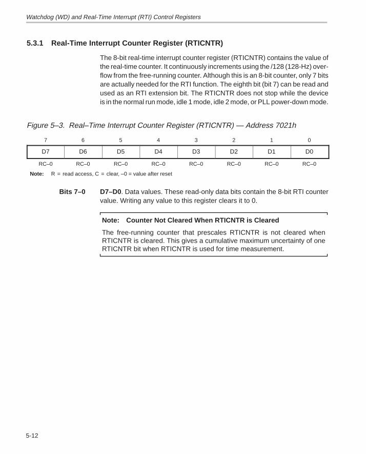
Watchdog (WD) and Real-Time Interrupt (RTI) Control Registers
5-12
5.3.1 Real-Time Interrupt Counter Register (RTICNTR)
The 8-bit real-time interrupt counter register (RTICNTR) contains the value ofthe real-time counter. It continuously increments using the /128 (128-Hz) over-flow from the free-running counter. Although this is an 8-bit counter, only 7 bitsare actually needed for the RTI function. The eighth bit (bit 7) can be read andused as an RTI extension bit. The RTICNTR does not stop while the deviceis in the normal run mode, idle 1 mode, idle 2 mode, or PLL power-down mode.
Figure 5–3. Real–Time Interrupt Counter Register (RTICNTR) — Address 7021h
7 6 5 4 3 2 1 0
D7 D6 D5 D4 D3 D2 D1 D0
RC–0 RC–0 RC–0 RC–0 RC–0 RC–0 RC–0 RC–0
Note: R = read access, C = clear, –0 = value after reset
Bits 7–0 D7–D0 . Data values. These read-only data bits contain the 8-bit RTI countervalue. Writing any value to this register clears it to 0.
Note: Counter Not Cleared When RTICNTR is Cleared
The free-running counter that prescales RTICNTR is not cleared whenRTICNTR is cleared. This gives a cumulative maximum uncertainty of oneRTICNTR bit when RTICNTR is used for time measurement.
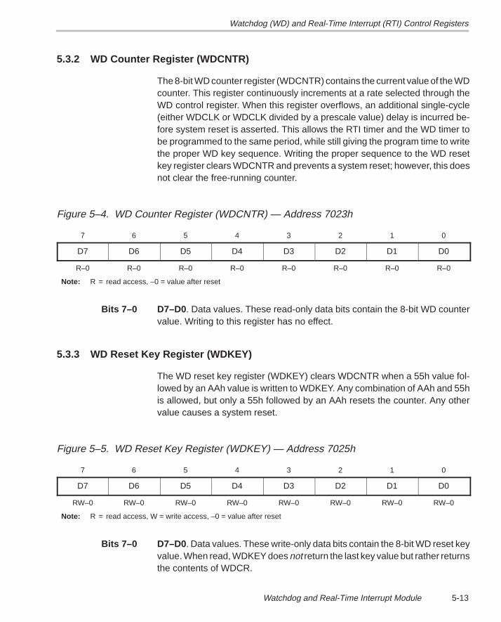
Watchdog (WD) and Real-Time Interrupt (RTI) Control Registers
5-13Watchdog and Real-Time Interrupt Module
5.3.2 WD Counter Register (WDCNTR)
The 8-bit WD counter register (WDCNTR) contains the current value of the WDcounter. This register continuously increments at a rate selected through theWD control register. When this register overflows, an additional single-cycle(either WDCLK or WDCLK divided by a prescale value) delay is incurred be-fore system reset is asserted. This allows the RTI timer and the WD timer tobe programmed to the same period, while still giving the program time to writethe proper WD key sequence. Writing the proper sequence to the WD resetkey register clears WDCNTR and prevents a system reset; however, this doesnot clear the free-running counter.
Figure 5–4. WD Counter Register (WDCNTR) — Address 7023h
7 6 5 4 3 2 1 0
D7 D6 D5 D4 D3 D2 D1 D0
R–0 R–0 R–0 R–0 R–0 R–0 R–0 R–0
Note: R = read access, –0 = value after reset
Bits 7–0 D7–D0 . Data values. These read-only data bits contain the 8-bit WD countervalue. Writing to this register has no effect.
5.3.3 WD Reset Key Register (WDKEY)
The WD reset key register (WDKEY) clears WDCNTR when a 55h value fol-lowed by an AAh value is written to WDKEY. Any combination of AAh and 55his allowed, but only a 55h followed by an AAh resets the counter. Any othervalue causes a system reset.
Figure 5–5. WD Reset Key Register (WDKEY) — Address 7025h
7 6 5 4 3 2 1 0
D7 D6 D5 D4 D3 D2 D1 D0
RW–0 RW–0 RW–0 RW–0 RW–0 RW–0 RW–0 RW–0
Note: R = read access, W = write access, –0 = value after reset
Bits 7–0 D7–D0 . Data values. These write-only data bits contain the 8-bit WD reset keyvalue. When read, WDKEY does not return the last key value but rather returnsthe contents of WDCR.
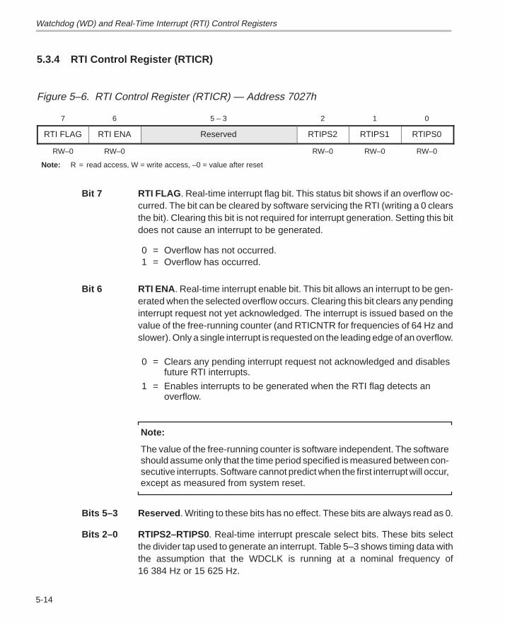
Watchdog (WD) and Real-Time Interrupt (RTI) Control Registers
5-14
5.3.4 RTI Control Register (RTICR)
Figure 5–6. RTI Control Register (RTICR) — Address 7027h
7 6 5 – 3 2 1 0
RTI FLAG RTI ENA Reserved RTIPS2 RTIPS1 RTIPS0
RW–0 RW–0 RW–0 RW–0 RW–0
Note: R = read access, W = write access, –0 = value after reset
Bit 7 RTI FLAG . Real-time interrupt flag bit. This status bit shows if an overflow oc-curred. The bit can be cleared by software servicing the RTI (writing a 0 clearsthe bit). Clearing this bit is not required for interrupt generation. Setting this bitdoes not cause an interrupt to be generated.
0 = Overflow has not occurred.1 = Overflow has occurred.
Bit 6 RTI ENA . Real-time interrupt enable bit. This bit allows an interrupt to be gen-erated when the selected overflow occurs. Clearing this bit clears any pendinginterrupt request not yet acknowledged. The interrupt is issued based on thevalue of the free-running counter (and RTICNTR for frequencies of 64 Hz andslower). Only a single interrupt is requested on the leading edge of an overflow.
0 = Clears any pending interrupt request not acknowledged and disablesfuture RTI interrupts.
1 = Enables interrupts to be generated when the RTI flag detects anoverflow.
Note:
The value of the free-running counter is software independent. The softwareshould assume only that the time period specified is measured between con-secutive interrupts. Software cannot predict when the first interrupt will occur,except as measured from system reset.
Bits 5–3 Reserved . Writing to these bits has no effect. These bits are always read as 0.
Bits 2–0 RTIPS2–RTIPS0 . Real-time interrupt prescale select bits. These bits selectthe divider tap used to generate an interrupt. Table 5–3 shows timing data withthe assumption that the WDCLK is running at a nominal frequency of16 384 Hz or 15 625 Hz.
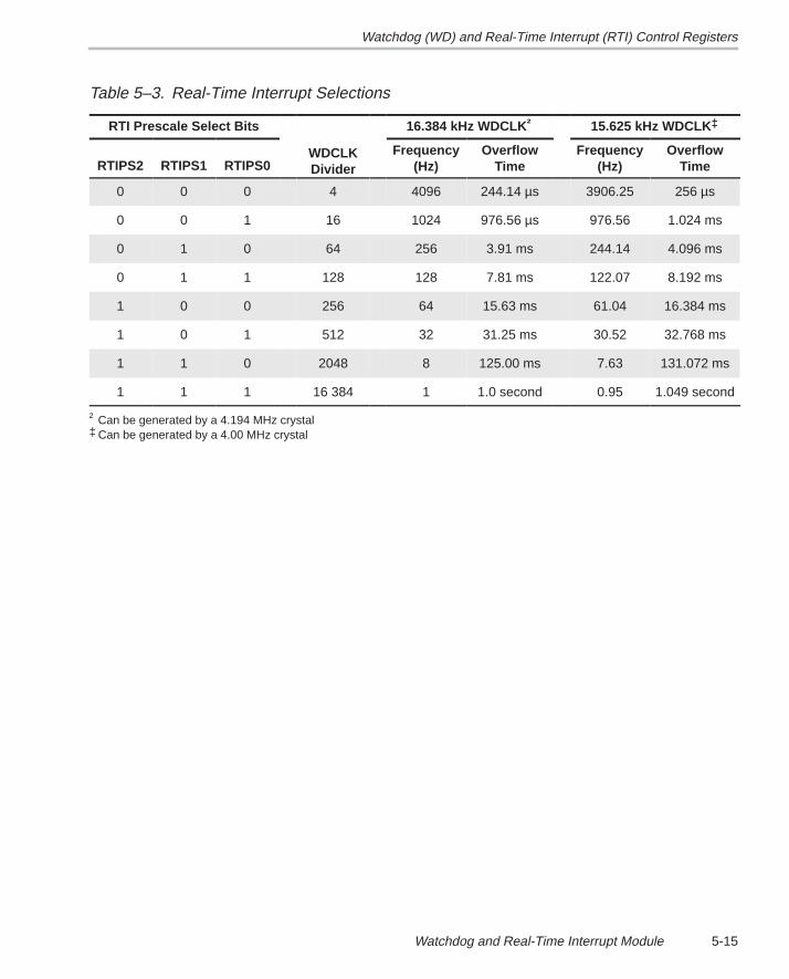
Watchdog (WD) and Real-Time Interrupt (RTI) Control Registers
5-15Watchdog and Real-Time Interrupt Module
Table 5–3. Real-Time Interrupt Selections
RTI Prescale Select Bits 16.384 kHz WDCLK † 15.625 kHz WDCLK ‡
RTIPS2 RTIPS1 RTIPS0WDCLKDivider
Frequency(Hz)
OverflowTime
Frequency(Hz)
OverflowTime
0 0 0 4 4096 244.14 µs 3906.25 256 µs
0 0 1 16 1024 976.56 µs 976.56 1.024 ms
0 1 0 64 256 3.91 ms 244.14 4.096 ms
0 1 1 128 128 7.81 ms 122.07 8.192 ms
1 0 0 256 64 15.63 ms 61.04 16.384 ms
1 0 1 512 32 31.25 ms 30.52 32.768 ms
1 1 0 2048 8 125.00 ms 7.63 131.072 ms
1 1 1 16 384 1 1.0 second 0.95 1.049 second
† Can be generated by a 4.194 MHz crystal‡ Can be generated by a 4.00 MHz crystal
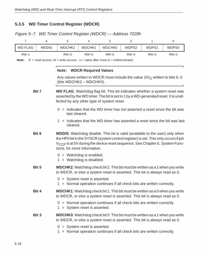
Watchdog (WD) and Real-Time Interrupt (RTI) Control Registers
5-16
5.3.5 WD Timer Control Register (WDCR)
Figure 5–7. WD Timer Control Register (WDCR) — Address 7029h
7 6 5 4 3 2 1 0
WD FLAG WDDIS WDCHK2 WDCHK1 WDCHK0 WDPS2 WDPS1 WDPS0
RW–x RW–0 RW–0 RW–0 RW–0 RW–0 RW–0
Note: R = read access, W = write access, –n = value after reset (x = indeterminate)
Note: WDCR Required Values
Any values written to WDCR must include the value 1012 written to bits 5–3(bits WDCHK2 – WDCHK0).
Bit 7 WD FLAG . Watchdog flag bit. This bit indicates whether a system reset wasasserted by the WD timer. The bit is set to 1 by a WD-generated reset. It is unaf-fected by any other type of system reset.
0 = Indicates that the WD timer has not asserted a reset since the bit waslast cleared.
1 = Indicates that the WD timer has asserted a reset since the bit was lastcleared.
Bit 6 WDDIS . Watchdog disable. This bit is valid (available to the user) only whenthe HP0 bit in the SYSCR (system control register) is set. This only occurs if pinVCCP is at 5V during the device reset sequence. See Chapter 6, System Func-tions, for more information.
0 = Watchdog is enabled.1 = Watchdog is disabled.
Bit 5 WDCHK2 . Watchdog check bit 2. This bit must be written as a 1 when you writeto WDCR, or else a system reset is asserted. This bit is always read as 0.
0 = System reset is asserted.1 = Normal operation continues if all check bits are written correctly.
Bit 4 WDCHK1 . Watchdog check bit 1. This bit must be written as a 0 when you writeto WDCR, or else a system reset is asserted. This bit is always read as 0.
0 = Normal operation continues if all check bits are written correctly.1 = System reset is asserted.
Bit 3 WDCHK0 . Watchdog check bit 0. This bit must be written as a 1 when you writeto WDCR, or else a system reset is asserted. This bit is always read as 0.
0 = System reset is asserted.1 = Normal operation continues if all check bits are written correctly.
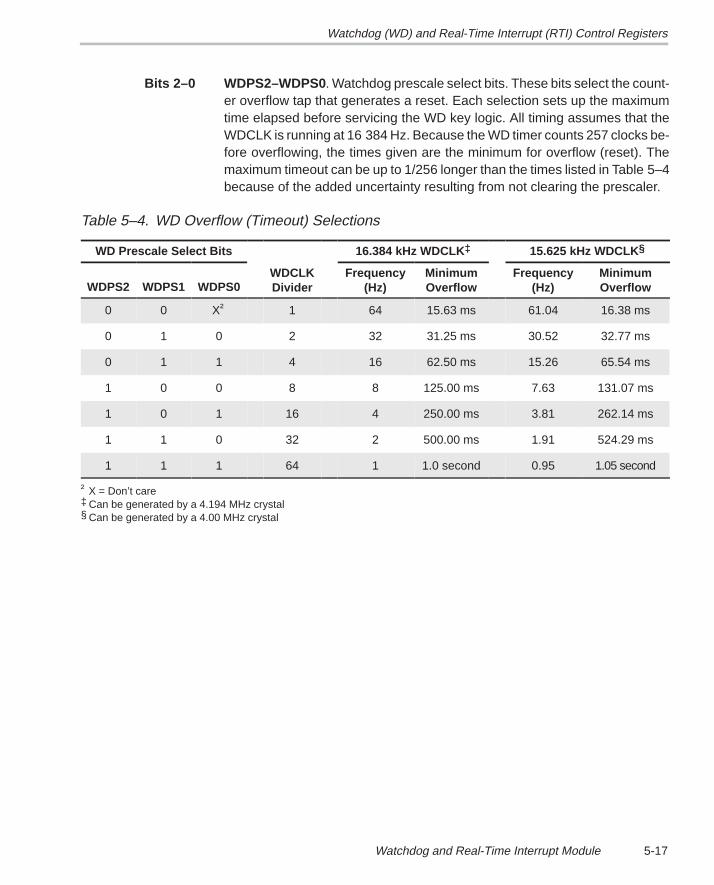
Watchdog (WD) and Real-Time Interrupt (RTI) Control Registers
5-17Watchdog and Real-Time Interrupt Module
Bits 2–0 WDPS2–WDPS0 . Watchdog prescale select bits. These bits select the count-er overflow tap that generates a reset. Each selection sets up the maximumtime elapsed before servicing the WD key logic. All timing assumes that theWDCLK is running at 16 384 Hz. Because the WD timer counts 257 clocks be-fore overflowing, the times given are the minimum for overflow (reset). Themaximum timeout can be up to 1/256 longer than the times listed in Table 5–4because of the added uncertainty resulting from not clearing the prescaler.
Table 5–4. WD Overflow (Timeout) Selections
WD Prescale Select Bits 16.384 kHz WDCLK ‡ 15.625 kHz WDCLK §
WDPS2 WDPS1 WDPS0WDCLKDivider
Frequency(Hz)
MinimumOverflow
Frequency(Hz)
MinimumOverflow
0 0 X† 1 64 15.63 ms 61.04 16.38 ms
0 1 0 2 32 31.25 ms 30.52 32.77 ms
0 1 1 4 16 62.50 ms 15.26 65.54 ms
1 0 0 8 8 125.00 ms 7.63 131.07 ms
1 0 1 16 4 250.00 ms 3.81 262.14 ms
1 1 0 32 2 500.00 ms 1.91 524.29 ms
1 1 1 64 1 1.0 second 0.95 1.05 second
† X = Don’t care‡ Can be generated by a 4.194 MHz crystal§ Can be generated by a 4.00 MHz crystal
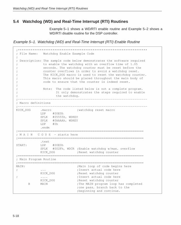
Watchdog (WD) and Real-Time Interrupt (RTI) Routines
5-18
5.4 Watchdog (WD) and Real-Time Interrupt (RTI) Routines
Example 5–1 shows a WD/RTI enable routine and Example 5–2 shows aWD/RTI disable routine for the DSP controller.
Example 5–1. Watchdog (WD) and Real-Time Interrupt (RTI) Enable Routine
;***********************************************************************; File Name: Watchdog Enable Example Code;; Description: The sample code below demonstrates the software required; to enable the watchdog with an overflow time of 1.05 ; seconds. The watchdog counter must be reset before the ; counter overflows in order to avoid a watchdog reset. ; The KICK_DOG macro is used to reset the watchdog counter.; This macro should be placed throughout the main body of ; code to ensure that the counter is indeed reset.;; Note: The code listed below is not a complete program.; It only demonstrates the steps required to enable; the watchdog.;–––––––––––––––––––––––––––––––––––––––––––––––––––––––––––––––––––––––; Macro definitions;–––––––––––––––––––––––––––––––––––––––––––––––––––––––––––––––––––––––KICK_DOG .macro ;watchdog reset macro
LDP #00E0hSPLK #05555h, WDKEYSPLK #0AAAAh, WDKEYLDP #0h.endm
;=====================================================================; M A I N C O D E – starts here;=====================================================================
.textSTART: LDP #00E0h
SPLK #002Fh, WDCR ;Enable watchdog w/max. overflow KICK_DOG ;Reset watchdog counter
;=====================================================================; Main Program Routine;=====================================================================MAIN: ;Main loop of code begins here; ... ;Insert actual code here
KICK_DOG ;Reset watchdog counter; .... ;Insert actual code here
KICK_DOG ;Reset watchdog counterB MAIN ;The MAIN program loop has completed
;one pass, branch back to the ;beginning and continue.
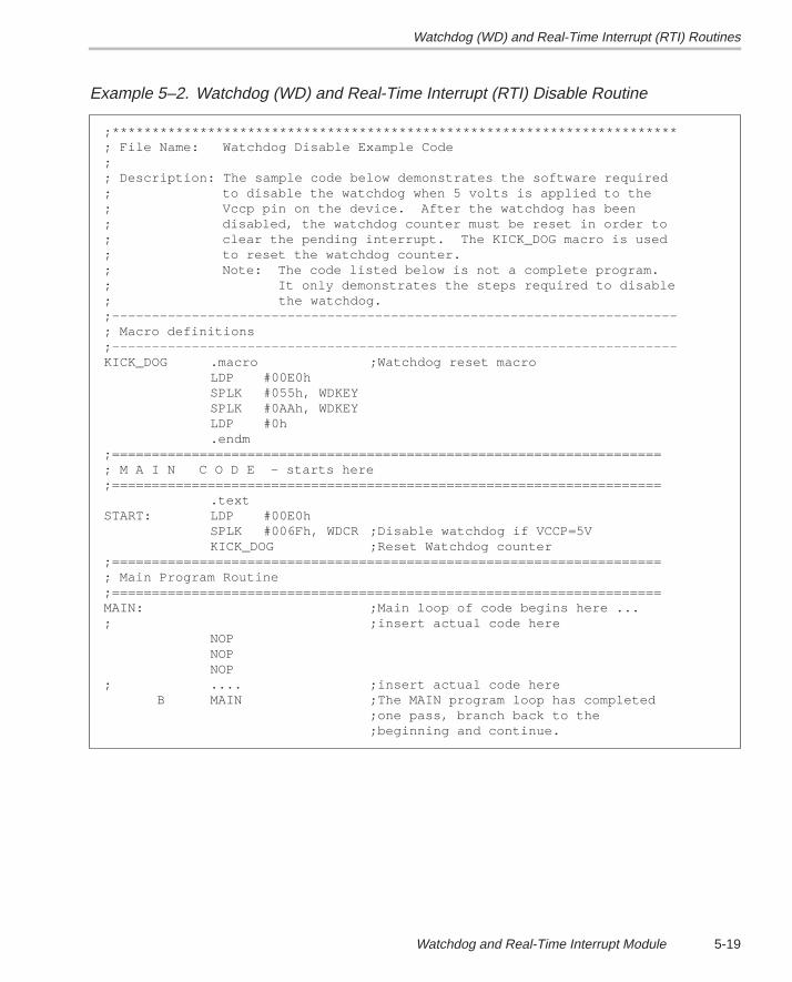
Watchdog (WD) and Real-Time Interrupt (RTI) Routines
5-19Watchdog and Real-Time Interrupt Module
Example 5–2. Watchdog (WD) and Real-Time Interrupt (RTI) Disable Routine
;***********************************************************************; File Name: Watchdog Disable Example Code;; Description: The sample code below demonstrates the software required; to disable the watchdog when 5 volts is applied to the ; Vccp pin on the device. After the watchdog has been ; disabled, the watchdog counter must be reset in order to ; clear the pending interrupt. The KICK_DOG macro is used ; to reset the watchdog counter.; Note: The code listed below is not a complete program.; It only demonstrates the steps required to disable; the watchdog.;–––––––––––––––––––––––––––––––––––––––––––––––––––––––––––––––––––––––; Macro definitions;–––––––––––––––––––––––––––––––––––––––––––––––––––––––––––––––––––––––KICK_DOG .macro ;Watchdog reset macro
LDP #00E0hSPLK #055h, WDKEYSPLK #0AAh, WDKEYLDP #0h.endm
;=====================================================================; M A I N C O D E – starts here;=====================================================================
.textSTART: LDP #00E0h
SPLK #006Fh, WDCR ;Disable watchdog if VCCP=5VKICK_DOG ;Reset Watchdog counter
;=====================================================================; Main Program Routine;=====================================================================MAIN: ;Main loop of code begins here ...; ;insert actual code here
NOPNOPNOP
; .... ;insert actual code hereB MAIN ;The MAIN program loop has completed
;one pass, branch back to the ;beginning and continue.
6-1Event Manager Module
Event Manager Module
This chapter describes the ’C240/’F240 event manager (EV) module in theperipheral library. The EV module includes timers, compare units, simplecompares, a capture unit, and a quadrature encoder pulse (QEP) circuit.
Topic Page
6.1 Event Manager (EV) Module Overview 6-2. . . . . . . . . . . . . . . . . . . . . . . . . .
6.2 Event Manager (EV) Register Addresses 6-8. . . . . . . . . . . . . . . . . . . . . . . .
6.3 General Purpose (GP) Timer 6-11. . . . . . . . . . . . . . . . . . . . . . . . . . . . . . . . . .
6.4 GP Timer Counting Operation 6-19. . . . . . . . . . . . . . . . . . . . . . . . . . . . . . . . .
6.5 GP Timer Compare Operation 6-34. . . . . . . . . . . . . . . . . . . . . . . . . . . . . . . . .
6.6 GP Timer Control Registers (TxCON and GPTCON) 6-40. . . . . . . . . . . . .
6.7 Generation of Compare and PWM Outputs Using GP Timers 6-45. . . . .
6.8 Compare Units 6-47. . . . . . . . . . . . . . . . . . . . . . . . . . . . . . . . . . . . . . . . . . . . . . .
6.9 PWM Circuits Associated With Full Compare Units 6-59. . . . . . . . . . . . .
6.10 PWM Waveform Generation With Compare Units andPWM Circuits 6-69. . . . . . . . . . . . . . . . . . . . . . . . . . . . . . . . . . . . . . . . . . . . . . . .
6.11 Space-Vector PWM 6-74. . . . . . . . . . . . . . . . . . . . . . . . . . . . . . . . . . . . . . . . . . .
6.12 Capture Units 6-80. . . . . . . . . . . . . . . . . . . . . . . . . . . . . . . . . . . . . . . . . . . . . . . .
6.13 Quadrature Encoder Pulse (QEP) Circuit 6-91. . . . . . . . . . . . . . . . . . . . . . .
6.14 Event Manager (EV) Interrupts 6-95. . . . . . . . . . . . . . . . . . . . . . . . . . . . . . . .
Chapter 6
Event Manager (EV) Module Overview
6-2
6.1 Event Manager (EV) Module Overview
The EV module provides a broad range of functions and features that are par-ticularly useful in motion-control and motor-control applications.
Note: Sharing device pins
The device pins used by the EV module can be shared between EV and othermodules. See Chapter 1 for TMS320C240 specific pin sharing information.
6.1.1 EV Functional Blocks
Figure 6–1 shows a block diagram of the EV module containing the followingfunctional blocks:
� Three general-purpose (GP) timers (see section 6.3 on page 6-11)
� Three full compare units (see section 6.8.2 on page 6-48)
� Three simple compare units (see section 6.8.1 on page 6-47)
� Pulse-width modulation (PWM) circuits that include:
� A space-vector PWM circuit (see section 6.9 on page 6-59)
� Dead-band generation units (see section 6.10 on page 6-69)
� Output logic (see section 6.11 on page 6-74)
� Four capture units (see section 6.12 on page 6-80)
� Quadrature encoder pulse (QEP) circuit (see section 6.13 on page 6-91)
� EV interrupts (see section 6.14 on page 6-95)
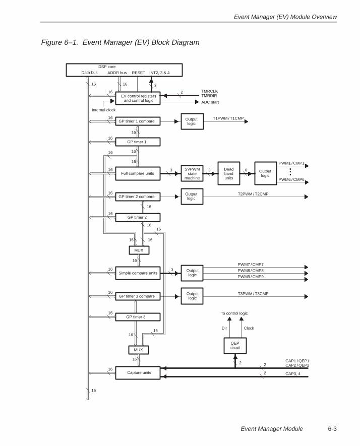
Event Manager (EV) Module Overview
6-3Event Manager Module
Figure 6–1. Event Manager (EV) Block Diagram
DSP coreData bus ADDR bus
EV control registersand control logic
GP timer 1 compare
Full compare units
GP timer 2 compare
GP timer 2
MUX
Simple compare units
GP timer 3 compare
MUX
Capture units
16
16
16
16
16
16
16
GP timer 1
GP timer 3
3
INT2, 3 & 4
2 TMRCLKTMRDIR
ADC start
T1PWM / T1CMP
SVPWMstate
machine
Deadbandunits
Outputlogic
3 3
PWM1 / CMP1
6
PWM6 / CMP6
Outputlogic
T2PWM / T2CMP
Outputlogic
3 PWM8 / CMP8
PWM7 / CMP7
PWM9 / CMP9
Outputlogic
T3PWM / T3CMP
2
22
QEPcircuit
To control logic
ClockDir
CAP1 / QEP1CAP2 / QEP2
CAP3, 4
16
16
16
16
1616
16
16
16
16
16
16
16
16
16
16
16
16
Internal clock
RESET
Outputlogic
16
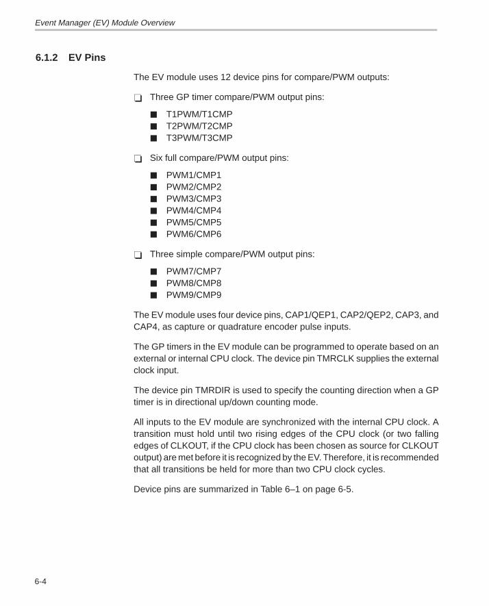
Event Manager (EV) Module Overview
6-4
6.1.2 EV Pins
The EV module uses 12 device pins for compare/PWM outputs:
� Three GP timer compare/PWM output pins:
� T1PWM/T1CMP� T2PWM/T2CMP� T3PWM/T3CMP
� Six full compare/PWM output pins:
� PWM1/CMP1� PWM2/CMP2� PWM3/CMP3� PWM4/CMP4� PWM5/CMP5� PWM6/CMP6
� Three simple compare/PWM output pins:
� PWM7/CMP7� PWM8/CMP8� PWM9/CMP9
The EV module uses four device pins, CAP1/QEP1, CAP2/QEP2, CAP3, andCAP4, as capture or quadrature encoder pulse inputs.
The GP timers in the EV module can be programmed to operate based on anexternal or internal CPU clock. The device pin TMRCLK supplies the externalclock input.
The device pin TMRDIR is used to specify the counting direction when a GPtimer is in directional up/down counting mode.
All inputs to the EV module are synchronized with the internal CPU clock. Atransition must hold until two rising edges of the CPU clock (or two fallingedges of CLKOUT, if the CPU clock has been chosen as source for CLKOUToutput) are met before it is recognized by the EV. Therefore, it is recommendedthat all transitions be held for more than two CPU clock cycles.
Device pins are summarized in Table 6–1 on page 6-5.
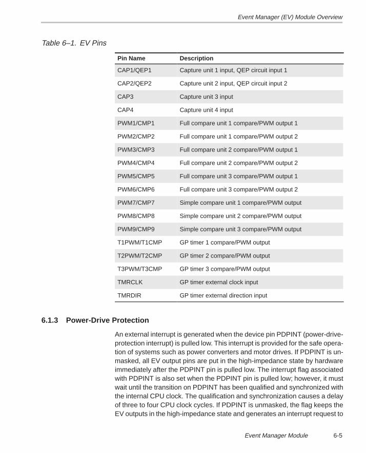
Event Manager (EV) Module Overview
6-5Event Manager Module
Table 6–1. EV Pins
Pin Name Description
CAP1/QEP1 Capture unit 1 input, QEP circuit input 1
CAP2/QEP2 Capture unit 2 input, QEP circuit input 2
CAP3 Capture unit 3 input
CAP4 Capture unit 4 input
PWM1/CMP1 Full compare unit 1 compare/PWM output 1
PWM2/CMP2 Full compare unit 1 compare/PWM output 2
PWM3/CMP3 Full compare unit 2 compare/PWM output 1
PWM4/CMP4 Full compare unit 2 compare/PWM output 2
PWM5/CMP5 Full compare unit 3 compare/PWM output 1
PWM6/CMP6 Full compare unit 3 compare/PWM output 2
PWM7/CMP7 Simple compare unit 1 compare/PWM output
PWM8/CMP8 Simple compare unit 2 compare/PWM output
PWM9/CMP9 Simple compare unit 3 compare/PWM output
T1PWM/T1CMP GP timer 1 compare/PWM output
T2PWM/T2CMP GP timer 2 compare/PWM output
T3PWM/T3CMP GP timer 3 compare/PWM output
TMRCLK GP timer external clock input
TMRDIR GP timer external direction input
6.1.3 Power-Drive Protection
An external interrupt is generated when the device pin PDPINT (power-drive-protection interrupt) is pulled low. This interrupt is provided for the safe opera-tion of systems such as power converters and motor drives. If PDPINT is un-masked, all EV output pins are put in the high-impedance state by hardwareimmediately after the PDPINT pin is pulled low. The interrupt flag associatedwith PDPINT is also set when the PDPINT pin is pulled low; however, it mustwait until the transition on PDPINT has been qualified and synchronized withthe internal CPU clock. The qualification and synchronization causes a delayof three to four CPU clock cycles. If PDPINT is unmasked, the flag keeps theEV outputs in the high-impedance state and generates an interrupt request to
Event Manager (EV) Module Overview
6-6
the DSP core. Therefore, for the outputs to remain in high impedance, PDPINTmust be held low for longer than four CPU clock cycles. The setting of the flagdoes not depend on whether PDPINT is masked. The flag is set as long as aqualified transition has occurred on the PDPINT pin. PDPINT can be used toinform the monitoring program of motor drive abnormalities, such as overvol-tages, overcurrents, and excessive temperature rises.
6.1.4 EV Registers
All registers in the EV module are mapped to data memory. Their addressestake up 64 (16-bit) words of the 64K words of data-memory address range.The registers are treated by software as data memory locations and can beaccessed by a wide range of DSP instructions. The undefined bits in the EVregisters return 0s when read by user software (see Section 6.2, Event Manag-er (EV) Register Addresses, on page 6-8).
6.1.5 EV Interrupts
The interrupts generated by the EV module are arranged into three groups.There are three registers, EVIFRA, EVIFRB, and EVIFRC, in the EV for theflags of the three groups of interrupts. The three groups of interrupts are con-nected to three of the CPU interrupt inputs. Each EV interrupt group has anassociated interrupt vector register, EVIFVRx (x = A, B, and C), that can beread by user software to get the vector (ID) of an interrupt source. Each inter-rupt source has a unique interrupt vector ID.
An interrupt flag is set when an interrupt event (for example, a match betweena compare register and a GP timer) is generated and enabled. There is an in-terrupt mask register, EVIMRx (x = A, B, or C), associated with each EV inter-rupt group. An interrupt is masked if its corresponding bit in EVIMRA, EVIMRB,or EVIMRC is 0, and unmasked if the corresponding bit is 1. An interrupt re-quest is generated to the CPU by an interrupt group if there is an interrupt flagin the group that is set and unmasked.
The set and reset of interrupt flags are independent of whether the corre-sponding interrupts are masked. The interrupt flag can, therefore, be checkedby software to verify the occurrence of an event when the corresponding inter-rupt is masked. An interrupt flag can be reset to 0 in two ways:
� User software writes a 1 to the corresponding bit in EVIFRA, EVIFRB, orEVIFRC.
� User software reads its interrupt vector ID after an interrupt request gener-ated by its group has been taken.
Event Manager (EV) Module Overview
6-7Event Manager Module
After a group generated interrupt request is taken and the interrupt vector isread, the vector ID of the highest priority flag (among those that were set andunmasked) is loaded into the accumulator. A 0 value is returned when the inter-rupt vector register of an interrupt group is read and no interrupt flag in thegroup is set and unmasked. This prevents a strayed interrupt from being rec-ognized as an EV interrupt.
Details of an interrupt event generation are described in the sections that fol-low. Details of request generation, service, and priority of all EV interrupts aresummarized in Section 6.14, Event Manager Interrupts, on page 6-95.
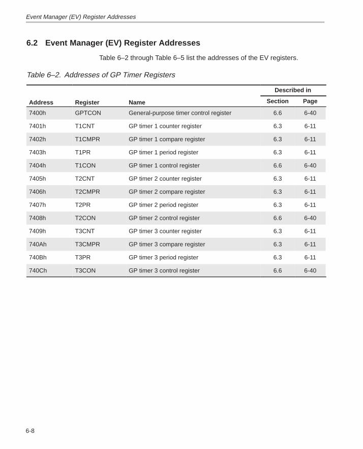
Event Manager (EV) Register Addresses
6-8
6.2 Event Manager (EV) Register Addresses
Table 6–2 through Table 6–5 list the addresses of the EV registers.
Table 6–2. Addresses of GP Timer Registers
Described in
Address Register Name Section Page
7400h GPTCON General-purpose timer control register 6.6 6-40
7401h T1CNT GP timer 1 counter register 6.3 6-11
7402h T1CMPR GP timer 1 compare register 6.3 6-11
7403h T1PR GP timer 1 period register 6.3 6-11
7404h T1CON GP timer 1 control register 6.6 6-40
7405h T2CNT GP timer 2 counter register 6.3 6-11
7406h T2CMPR GP timer 2 compare register 6.3 6-11
7407h T2PR GP timer 2 period register 6.3 6-11
7408h T2CON GP timer 2 control register 6.6 6-40
7409h T3CNT GP timer 3 counter register 6.3 6-11
740Ah T3CMPR GP timer 3 compare register 6.3 6-11
740Bh T3PR GP timer 3 period register 6.3 6-11
740Ch T3CON GP timer 3 control register 6.6 6-40
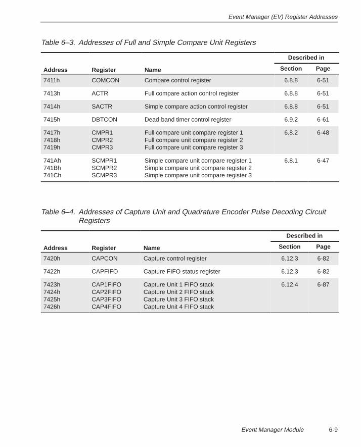
Event Manager (EV) Register Addresses
6-9Event Manager Module
Table 6–3. Addresses of Full and Simple Compare Unit Registers
Described in
Address Register Name Section Page
7411h COMCON Compare control register 6.8.8 6-51
7413h ACTR Full compare action control register 6.8.8 6-51
7414h SACTR Simple compare action control register 6.8.8 6-51
7415h DBTCON Dead-band timer control register 6.9.2 6-61
7417h7418h7419h
CMPR1CMPR2CMPR3
Full compare unit compare register 1Full compare unit compare register 2Full compare unit compare register 3
6.8.2 6-48
741Ah741Bh741Ch
SCMPR1SCMPR2SCMPR3
Simple compare unit compare register 1Simple compare unit compare register 2Simple compare unit compare register 3
6.8.1 6-47
Table 6–4. Addresses of Capture Unit and Quadrature Encoder Pulse Decoding CircuitRegisters
Described in
Address Register Name Section Page
7420h CAPCON Capture control register 6.12.3 6-82
7422h CAPFIFO Capture FIFO status register 6.12.3 6-82
7423h7424h7425h7426h
CAP1FIFOCAP2FIFOCAP3FIFOCAP4FIFO
Capture Unit 1 FIFO stackCapture Unit 2 FIFO stackCapture Unit 3 FIFO stackCapture Unit 4 FIFO stack
6.12.4 6-87
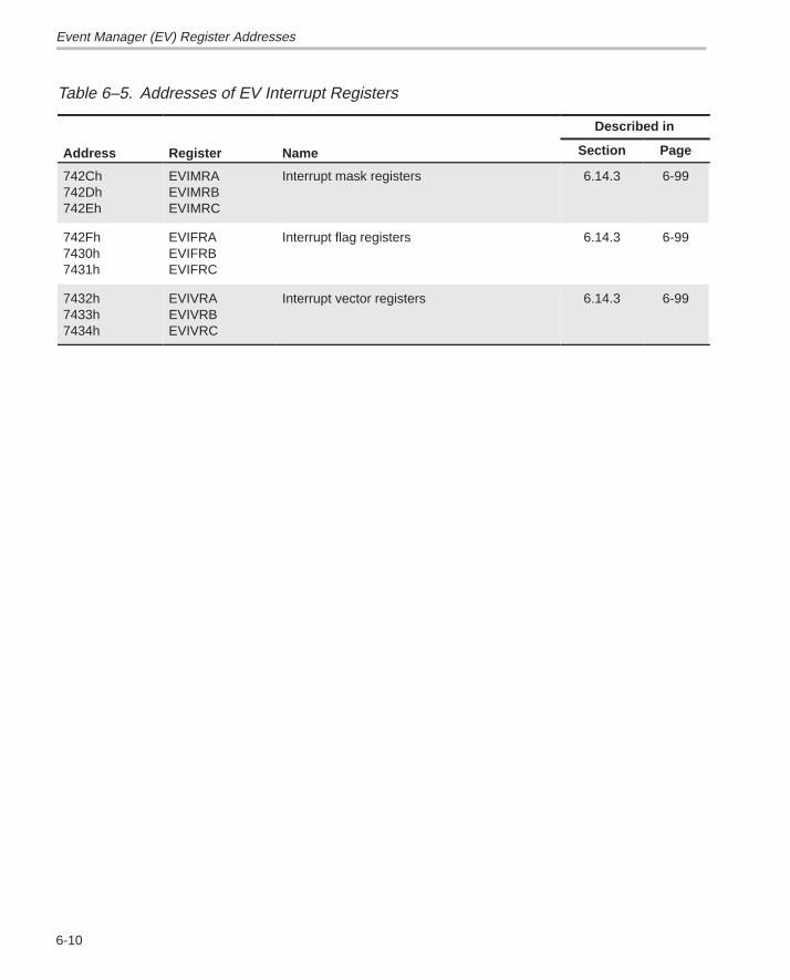
Event Manager (EV) Register Addresses
6-10
Table 6–5. Addresses of EV Interrupt Registers
Described in
Address Register Name Section Page
742Ch742Dh742Eh
EVIMRAEVIMRBEVIMRC
Interrupt mask registers 6.14.3 6-99
742Fh7430h7431h
EVIFRAEVIFRBEVIFRC
Interrupt flag registers 6.14.3 6-99
7432h7433h7434h
EVIVRAEVIVRBEVIVRC
Interrupt vector registers 6.14.3 6-99
General-Purpose (GP) Timers
6-11Event Manager Module
6.3 General-Purpose (GP) Timers
There are three general-purpose (GP) timers in the EV module. These timerscan be used as independent time bases in applications such as:
� Providing a time base for the operation of full and simple compare unitsand associated PWM circuits to generate compare/PWM outputs
� Generation of sampling period in a control system
� Providing a time base for the operation of QEP circuits and capture units
6.3.1 GP Timer Functional Blocks
Figure 6–2 shows a block diagram of the GP timers. Each GP timer includes:
� One read/write (R/W) 16-bit up and up/down counter, TxCNT(x = 1, 2, 3)
� One R/W 16-bit timer compare register (shadowed), TxCMPR (x = 1, 2, 3)
� One R/W 16-bit timer period register (shadowed), TxPR (x = 1, 2, 3)
� One R/W 16-bit control register, TxCON (x = 1, 2, 3)
� Programmable prescaler applicable to both internal and external clock in-puts
� Control and interrupt logic
� One GP timer compare output pin, TxPWM/TxCMP (x = 1, 2, 3)
� Output logic
Another control register, GPTCON, specifies the action to be taken by the GPtimers on different timer events and indicates the counting directions of allthree GP timers. GPTCON is readable and writable; however, writing to thethree status bits has no effect.
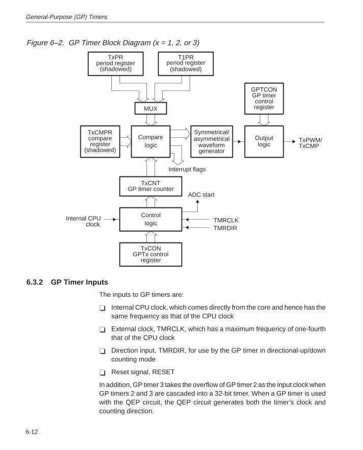
General-Purpose (GP) Timers
6-12
Figure 6–2. GP Timer Block Diagram (x = 1, 2, or 3)
clockInternal CPU
registerGPTx control
TxCON
TMRDIRTMRCLK
ADC start
Controllogic
GP timer counterTxCNT
TxCMPTxPWM/Output
logic
registercontrol
GP timerGPTCON
Interrupt flags
generatorwaveform
Symmetrical/asymmetrical
(shadowed)register
compareTxCMPR
logicCompare
MUX
T1PRperiod register
(shadowed)(shadowed)period register
TxPR
6.3.2 GP Timer Inputs
The inputs to GP timers are:
� Internal CPU clock, which comes directly from the core and hence has thesame frequency as that of the CPU clock
� External clock, TMRCLK, which has a maximum frequency of one-fourththat of the CPU clock
� Direction input, TMRDIR, for use by the GP timer in directional-up/downcounting mode
� Reset signal, RESET
In addition, GP timer 3 takes the overflow of GP timer 2 as the input clock whenGP timers 2 and 3 are cascaded into a 32-bit timer. When a GP timer is usedwith the QEP circuit, the QEP circuit generates both the timer’s clock andcounting direction.
General-Purpose (GP) Timers
6-13Event Manager Module
6.3.3 GP Timer Outputs
The outputs of the GP timers are:
� GP timer compare/PWM outputs TxPWM/TxCMP, x = 1, 2, 3
� ADC start signal to ADC module
� Underflow, overflow, compare match, and period match signals to its owncompare logic, and to full and simple compare units
� Counting direction indication bits
6.3.4 Control of GP Timer Operation
The operation mode of a GP timer is controlled by its control register, TxCON.Bits in the TxCON register determine:
� Whether the timer is enabled or disabled
� Which of the six counting modes the GP timer is in
� Whether the internal or external CPU clock is to be used by the GP timer
� Which of the six prescale factors for input clock (ranging from 1 to 1/128)is to be used
� Which condition the timer compare register is in when reloaded
� Whether the GP timer compare operation is enabled or disabled
� Whether the period register of GP timer 1 or its own period register deter-mines its period (T2CON and T3CON only)
� Whether the carry bit (carryover) of GP timer 2 should be used as its clock(T3CON only)
6.3.5 GP Timer Control Register (GPTCON)
The control register GPTCON specifies the action to be taken by the GP timerson different timer events and indicates their counting directions.
6.3.6 GP Timer Compare Registers
The compare register associated with a GP timer stores the value to beconstantly compared with the counter of the GP timer. When a match is de-tected, the following events occur:
General-Purpose (GP) Timers
6-14
� Transition on the associated compare/PWM output
� Start of ADC according to the bit pattern in GPTCON
� The corresponding compare interrupt flag is set.
This operation can be enabled or disabled by bit 1 of TxCON.
6.3.7 GP Timer Period Register
The value in the period register of a GP timer determines the period of the tim-er. The operation of a GP timer stops and holds at its current value, resets to0, or starts counting downward when a match occurs between the period regis-ter and the timer counter, depending on the counting mode of the timer.
6.3.8 Double Buffering of GP Timer Compare and Period Registers
The compare and period registers, TxCMPR and TxPR, of a GP timer areshadowed. A new value can be written to either of these registers at any timeduring a period; however, the new value is written to the associated shadowregister.
For the compare register, the content in the shadow register is loaded into theworking (active) register only when a certain timer event specified by TxCONoccurs.
The compare register is reloaded on any of the following conditions:
� Immediately after the shadow register is written
� On underflow; that is, when the GP timer counter value is 0
� On underflow or period match; that is, when the counter value is 0 or whenthe counter value equals the value of the period register
For the period register, the working register is reloaded with the value in itsshadow register only when the value of the counter register TxCNT is 0.
The double-buffering feature allows the application code to update thecompare and period registers at any time during a cycle. This changes the tim-er period and the width of the the PWM pulse for the following cycle. On-the-flychange of the timer period value, in the case of PWM generation, means on-the-fly change of the PWM carrier frequency.
General-Purpose (GP) Timers
6-15Event Manager Module
Notes: Initialize period registers, compare register transparency
1) The period register of a GP timer should be initialized before its counteris initialized to a nonzero value. Otherwise, the value of the period regis-ter will remain unchanged until the next underflow.
2) A compare register is transparent (the newly loaded value goes directlyinto the active register) when the associated compare operation is dis-abled. This applies to all compare registers in the EV.
6.3.9 GP Timer Compare/PWM Output
The compare/PWM output of a GP timer can be specified active high, activelow, forced high, or forced low, depending on how the GPTCON bits are config-ured. The output goes from low to high (high to low) on the first compare matchwhen it is active high (low). It then goes from high to low (low to high) on thesecond compare match if the GP timer is in the up/down counting mode, or onperiod match if the GP timer is in the up counting mode. The timer compareoutput becomes high (low) immediately when it is specified forced high (low).
For more details on the compare/PWM output behavior, refer to Section 6.5GP Timer Compare Operation on page 6-34.
6.3.10 GP Timer Counting Direction
The counting directions of all three GP timers are indicated by designated bitsin GPTCON during all timer operations with:
� 1 representing the up counting direction� 0 representing the down counting direction
The input pin TMRDIR determines the direction of counting when a GP timeris in directional up/down counting mode. When TMRDIR is set high, upwardcounting is specified; when TMRDIR is pulled low, downward counting is spe-cified.
General-Purpose (GP) Timers
6-16
6.3.11 GP Timer Clock
The source of the GP timer clock can be the internal CPU clock or the externalclock input, TMRCLK. The frequency of the external clock must be less thanor equal to one-fourth that of the CPU clock. GP timer 2, 3, or 2 and 3 togetheras a 32-bit timer, can be used with QEP circuits in the directional up/downcounting mode. In this case, the QEP circuits provide both the clock and direc-tion inputs to the timer.
A wide range of prescale factors are provided for the clock input to each GPtimer.
6.3.12 32-Bit Timer
The roll-over signal of GP Timer 2 is used as clock input to GP Timer 3 whenGP Timers 2 and 3 are cascaded into a 32-bit timer. When this happens, thecounter of GP Timer 2 acts as the lower 16 bits of the 32-bit counter. The 32-bittimer so obtained can only operate in directional up/down counting mode (seeSection 6.4 on page 6-19 for the GP timer operating modes) with external orinternal clock inputs and external direction inputs. QEP circuits can also bechosen to generate the counting clock and direction for the 32-bit timer. In thiscase, the period registers of GP Timers 2 and 3 are cascaded to provide a32-bit period register for the 32-bit timer, while the compare operation is basedon individual compare registers and occurs individually on 16-bit comparematches. Both underflow and overflow events for the 32-bit timer are 32-bit-based.
The period, underflow, and overflow flags of GP Timer 2 are set on correspond-ing 32-bit matches. Period, underflow, and overflow flags of the GP Timer 3 arenot relevant for 32-bit operation. Compare flags of GP Timer 2 and GP Timer3 are set on individual compare matches.
The directional up/down operating mode for GP Timers 1 and 3 is different fromthat of GP Timer 2. 32-bit operation is similar to the directional up/down operat-ing mode of GP Timers 1 and 3; that is, the 32-bit counter saturates at bothperiod and zero counter values.
General-Purpose (GP) Timers
6-17Event Manager Module
6.3.13 QEP-Based Clock Input
The quadrature encoder pulse (QEP) circuit, when selected, can generate theinput clock and counting direction for GP Timers 2, 3, or 2 and 3 functioningtogether as a 32-bit timer in the directional up/down counting mode. This inputclock cannot be scaled by the GP timer prescaler circuits (that is, the prescalerof the selected GP timer is always 1 if the QEP circuit is selected as the clocksource). Furthermore, the frequency of the clock generated by QEP circuitsis four times that of the frequency of each QEP input channel, because boththe rising and falling edges of both QEP input channels are counted by the se-lected timer. The frequency of QEP input must be less than or equal to one-fourth that of the CPU clock.
6.3.14 GP Timer Synchronization
GP Timers 2 and 3 can be individually synchronized with GP Timer 1 by confi-guring T2CON and T3CON in the following ways:
� Start the operation of GP Timer 2 or 3 by using the same control bit inT1CON that starts the operation of GP Timer 1.
� Initialize the timer counters in GP Timer 2 or 3 with different values beforesynchronized operation starts.
� Specify that GP Timer 2 or 3 uses the period register of GP Timer 1 as itsperiod register (ignoring its own period register).
This configuration provides the desired synchronization between GP timerevents. Since each GP timer starts counting from its current value in the count-er register, a GP timer can be programmed to start with a known delay afterother GP timers. Note, however, that two writes to T1CON are required to syn-chronize GP Timer 1 with GP Timer 2 or GP Timers 2 and 3.
6.3.15 ADC Start by GP Timer Event
The bits in GPTCON can specify that an ADC start signal be generated on aGP timer event such as underflow, compare match, or period match. This fea-ture provides synchronization between the GP timer event and the ADC startwithout any CPU intervention.
General-Purpose (GP) Timers
6-18
6.3.16 GP Timer in Emulation Suspend
GP timer control register bits also define the operation of GP timers duringemulation suspend. These bits can be set to allow the operation of GP timersto continue when emulation interrupt occurs, making in-circuit emulation pos-sible. They can also be set to specify that the operation of GP timer stops im-mediately or after completion of the current counting period when emulationinterrupt occurs.
Emulation suspend occurs when the CPU clock is stopped by the emulator (forexample, when the emulator encounters a break point).
6.3.17 GP Timer Interrupts
There are 12 interrupt flags in EVIFRA and EVIFRB for the three GP timers.Each GP timer can generate four interrupts upon the following events:
� Overflow: TxOFINT (x = 1, 2, or 3)� Underflow: TxUFINT (x = 1, 2, or 3)� Compare match: TxCINT (x = 1, 2, or 3)� Period match: TxPINT (x = 1, 2, or 3)
A timer compare event (match) occurs when the contents of a GP timer count-er is the same as that of the compare register. The corresponding compareinterrupt flag is set two CPU clock cycles after the match, if the compare opera-tion is enabled.
An overflow event occurs when the value of the timer counter reaches FFFFh:an underflow event occurs when the timer counter reaches 0000h. Similarly,a period event occurs when the value of the timer counter is the same as thatof the period register. The overflow, underflow, and period interrupt flags of thetimer are set two CPU clock cycles after the occurrence of each individualevent.
GP Timer Counting Operation
6-19Event Manager Module
6.4 GP Timer Counting Operation
Each GP timer has six selectable modes of operation:
� Stop/hold� Single up counting� Continuous up counting� Directional up/down counting� Single up/down counting� Continuous up/down counting
The bit pattern in the corresponding timer control register TxCON determinesthe counting mode of a GP timer. The timer enabling bit, TxCON[6], enablesor disables the counting operation of a timer. When the timer is disabled, thecounting operation of the timer stops and the prescaler of the timer is reset tox/1. When the timer is enabled, the timer starts counting according to thecounting mode specified by other bits of TxCON.
6.4.1 Stop/Hold Mode
In stop/hold mode, the operation of a GP timer stops and holds at its currentstate. The timer counter, the compare output, and the prescale counter remainunchanged in this mode.
6.4.2 Single Up Counting Mode
In single up counting mode, a GP timer counts up according to the scaled inputclock until the value of the timer counter matches that of the period register.On the next rising edge of the input clock after the match, the GP timer resetsto 0 and disables its counting operation by resetting the timer enable bit,TxCON[6].
The period interrupt flag of the timer is set two CPU clock cycles after the matchbetween the timer counter and the period register. An ADC start is sent to theADC module at the same time the flag is set if the timer’s period interrupt hasbeen programmed to start ADC by appropriate bit selections in GPTCON.
Two clock cycles after the GP timer becomes 0, the underflow interrupt flag ofthe timer is set. An ADC start is sent to the ADC module at the same time if theunderflow interrupt flag has been programmed to start ADC by appropriate bitselections in GPTCON.
The overflow interrupt flag is set two CPU clock cycles after the value in TxCNTmatches FFFFh.
The duration of the counting period of this mode is TxPER + 1 cycles of thescaled clock input if the timer counter is 0 at the beginning of the period.
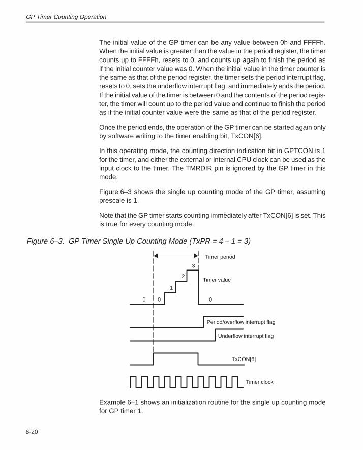
GP Timer Counting Operation
6-20
The initial value of the GP timer can be any value between 0h and FFFFh.When the initial value is greater than the value in the period register, the timercounts up to FFFFh, resets to 0, and counts up again to finish the period asif the initial counter value was 0. When the initial value in the timer counter isthe same as that of the period register, the timer sets the period interrupt flag,resets to 0, sets the underflow interrupt flag, and immediately ends the period.If the initial value of the timer is between 0 and the contents of the period regis-ter, the timer will count up to the period value and continue to finish the periodas if the initial counter value were the same as that of the period register.
Once the period ends, the operation of the GP timer can be started again onlyby software writing to the timer enabling bit, TxCON[6].
In this operating mode, the counting direction indication bit in GPTCON is 1for the timer, and either the external or internal CPU clock can be used as theinput clock to the timer. The TMRDIR pin is ignored by the GP timer in thismode.
Figure 6–3 shows the single up counting mode of the GP timer, assumingprescale is 1.
Note that the GP timer starts counting immediately after TxCON[6] is set. Thisis true for every counting mode.
Figure 6–3. GP Timer Single Up Counting Mode (TxPR = 4 – 1 = 3)
2
Timer period
3
1
0 0
Timer value
Period/overflow interrupt flag
Underflow interrupt flag
TxCON[6]
Timer clock
0
Example 6–1 shows an initialization routine for the single up counting modefor GP timer 1.
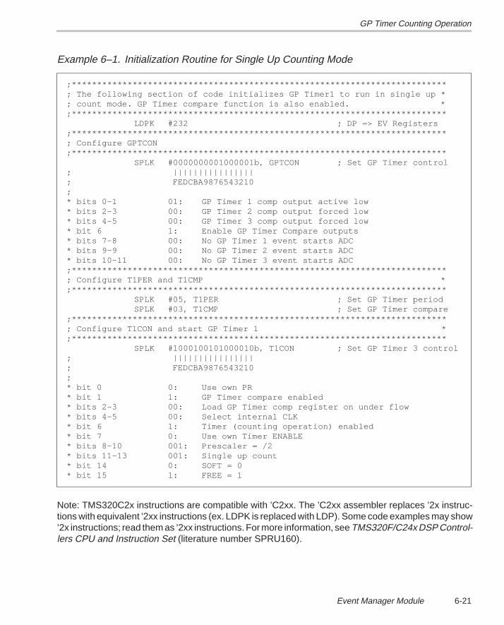
GP Timer Counting Operation
6-21Event Manager Module
Example 6–1. Initialization Routine for Single Up Counting Mode
;**************************************************************************; The following section of code initializes GP Timer1 to run in single up *; count mode. GP Timer compare function is also enabled. *;**************************************************************************
LDPK #232 ; DP => EV Registers;**************************************************************************; Configure GPTCON;**************************************************************************
SPLK #0000000001000001b, GPTCON ; Set GP Timer control; ||||||||||||||||; FEDCBA9876543210;* bits 0–1 01: GP Timer 1 comp output active low* bits 2–3 00: GP Timer 2 comp output forced low* bits 4–5 00: GP Timer 3 comp output forced low* bit 6 1: Enable GP Timer Compare outputs* bits 7–8 00: No GP Timer 1 event starts ADC* bits 9–9 00: No GP Timer 2 event starts ADC* bits 10–11 00: No GP Timer 3 event starts ADC;**************************************************************************; Configure T1PER and T1CMP *;**************************************************************************
SPLK #05, T1PER ; Set GP Timer periodSPLK #03, T1CMP ; Set GP Timer compare
;**************************************************************************; Configure T1CON and start GP Timer 1 *;**************************************************************************
SPLK #1000100101000010b, T1CON ; Set GP Timer 3 control; ||||||||||||||||; FEDCBA9876543210;* bit 0 0: Use own PR* bit 1 1: GP Timer compare enabled* bits 2–3 00: Load GP Timer comp register on under flow* bits 4–5 00: Select internal CLK* bit 6 1: Timer (counting operation) enabled* bit 7 0: Use own Timer ENABLE* bits 8–10 001: Prescaler = /2* bits 11–13 001: Single up count* bit 14 0: SOFT = 0* bit 15 1: FREE = 1
Note: TMS320C2x instructions are compatible with ’C2xx. The ’C2xx assembler replaces ’2x instruc-tions with equivalent ’2xx instructions (ex. LDPK is replaced with LDP). Some code examples may show’2x instructions; read them as ’2xx instructions. For more information, see TMS320F/C24x DSP Control-lers CPU and Instruction Set (literature number SPRU160).
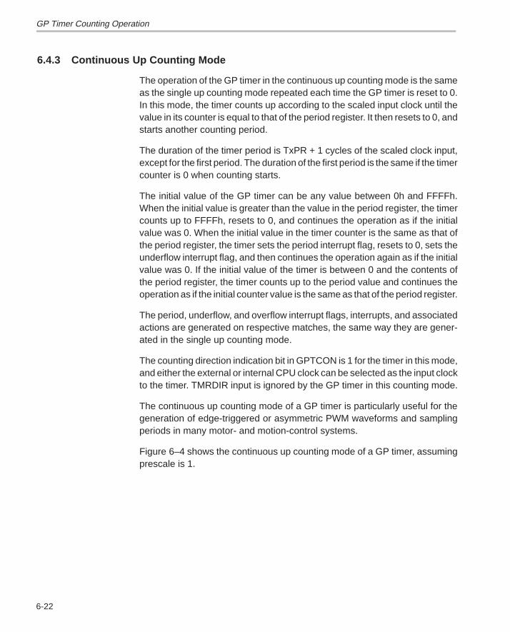
GP Timer Counting Operation
6-22
6.4.3 Continuous Up Counting Mode
The operation of the GP timer in the continuous up counting mode is the sameas the single up counting mode repeated each time the GP timer is reset to 0.In this mode, the timer counts up according to the scaled input clock until thevalue in its counter is equal to that of the period register. It then resets to 0, andstarts another counting period.
The duration of the timer period is TxPR + 1 cycles of the scaled clock input,except for the first period. The duration of the first period is the same if the timercounter is 0 when counting starts.
The initial value of the GP timer can be any value between 0h and FFFFh.When the initial value is greater than the value in the period register, the timercounts up to FFFFh, resets to 0, and continues the operation as if the initialvalue was 0. When the initial value in the timer counter is the same as that ofthe period register, the timer sets the period interrupt flag, resets to 0, sets theunderflow interrupt flag, and then continues the operation again as if the initialvalue was 0. If the initial value of the timer is between 0 and the contents ofthe period register, the timer counts up to the period value and continues theoperation as if the initial counter value is the same as that of the period register.
The period, underflow, and overflow interrupt flags, interrupts, and associatedactions are generated on respective matches, the same way they are gener-ated in the single up counting mode.
The counting direction indication bit in GPTCON is 1 for the timer in this mode,and either the external or internal CPU clock can be selected as the input clockto the timer. TMRDIR input is ignored by the GP timer in this counting mode.
The continuous up counting mode of a GP timer is particularly useful for thegeneration of edge-triggered or asymmetric PWM waveforms and samplingperiods in many motor- and motion-control systems.
Figure 6–4 shows the continuous up counting mode of a GP timer, assumingprescale is 1.
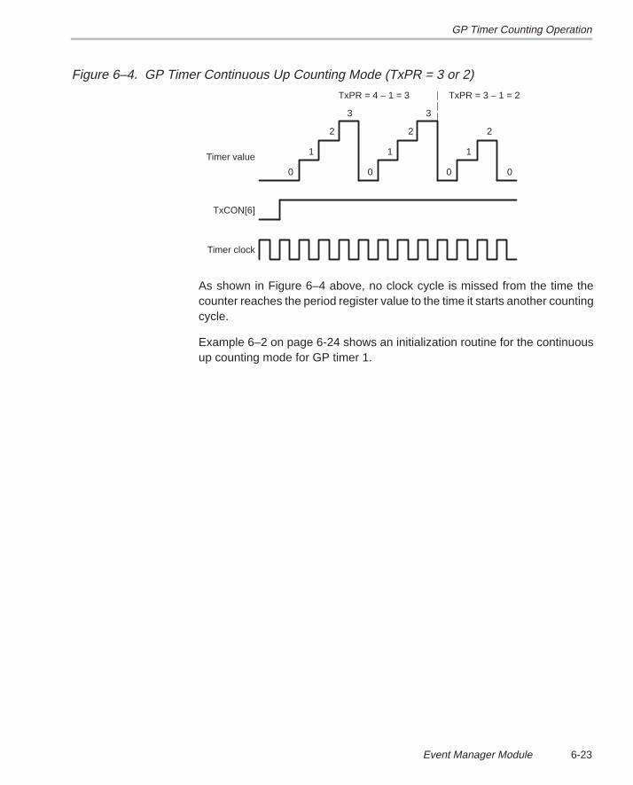
GP Timer Counting Operation
6-23Event Manager Module
Figure 6–4. GP Timer Continuous Up Counting Mode (TxPR = 3 or 2)
2
3
1
0 0
TxCON[6]
Timer clock
TxPR = 4 – 1 = 3
2
3
1
0
2
1
0
Timer value
TxPR = 3 – 1 = 2
As shown in Figure 6–4 above, no clock cycle is missed from the time thecounter reaches the period register value to the time it starts another countingcycle.
Example 6–2 on page 6-24 shows an initialization routine for the continuousup counting mode for GP timer 1.
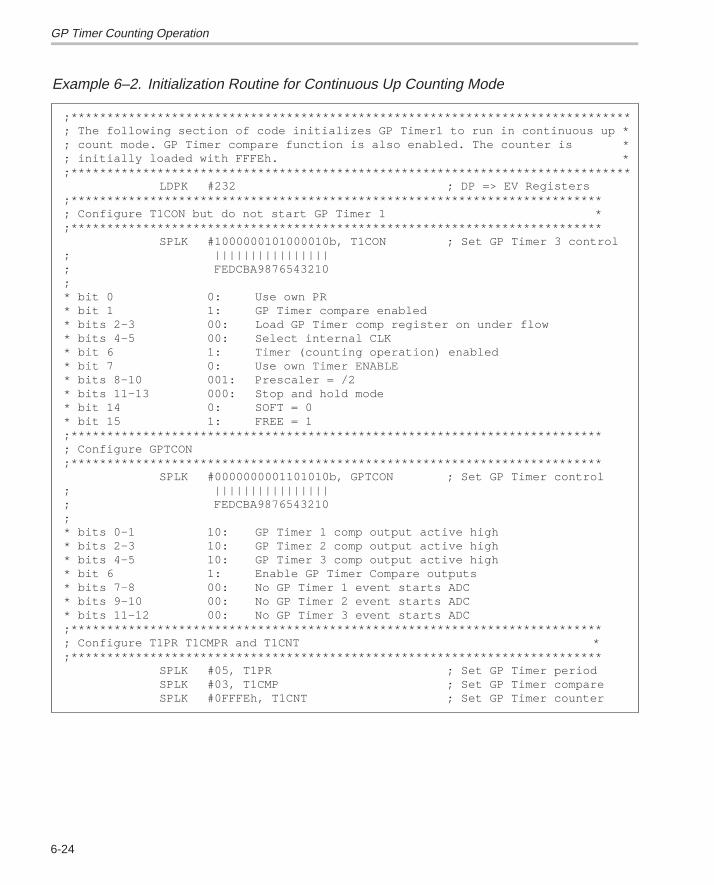
GP Timer Counting Operation
6-24
Example 6–2. Initialization Routine for Continuous Up Counting Mode
;******************************************************************************; The following section of code initializes GP Timer1 to run in continuous up *; count mode. GP Timer compare function is also enabled. The counter is *; initially loaded with FFFEh. *;******************************************************************************
LDPK #232 ; DP => EV Registers;**************************************************************************; Configure T1CON but do not start GP Timer 1 *;**************************************************************************
SPLK #1000000101000010b, T1CON ; Set GP Timer 3 control; ||||||||||||||||; FEDCBA9876543210;* bit 0 0: Use own PR* bit 1 1: GP Timer compare enabled* bits 2–3 00: Load GP Timer comp register on under flow* bits 4–5 00: Select internal CLK* bit 6 1: Timer (counting operation) enabled* bit 7 0: Use own Timer ENABLE* bits 8–10 001: Prescaler = /2* bits 11–13 000: Stop and hold mode* bit 14 0: SOFT = 0* bit 15 1: FREE = 1;**************************************************************************; Configure GPTCON;**************************************************************************
SPLK #0000000001101010b, GPTCON ; Set GP Timer control; ||||||||||||||||; FEDCBA9876543210;* bits 0–1 10: GP Timer 1 comp output active high* bits 2–3 10: GP Timer 2 comp output active high* bits 4–5 10: GP Timer 3 comp output active high* bit 6 1: Enable GP Timer Compare outputs* bits 7–8 00: No GP Timer 1 event starts ADC* bits 9–10 00: No GP Timer 2 event starts ADC* bits 11–12 00: No GP Timer 3 event starts ADC;**************************************************************************; Configure T1PR T1CMPR and T1CNT *;**************************************************************************
SPLK #05, T1PR ; Set GP Timer periodSPLK #03, T1CMP ; Set GP Timer compareSPLK #0FFFEh, T1CNT ; Set GP Timer counter
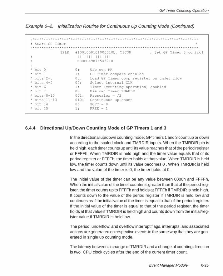
GP Timer Counting Operation
6-25Event Manager Module
Example 6–2. Initialization Routine for Continuous Up Counting Mode (Continued)
;**************************************************************************; Start GP Timer *;**************************************************************************
SPLK #1001000101000010b, T1CON ; Set GP Timer 3 control; ||||||||||||||||; FEDCBA9876543210;* bit 0 0: Use own PR* bit 1 1: GP Timer compare enabled* bits 2–3 00: Load GP Timer comp register on under flow* bits 4–5 00: Select internal CLK* bit 6 1: Timer (counting operation) enabled* bit 7 0: Use own Timer ENABLE* bits 8–10 001: Prescaler = /2* bits 11–13 010: Continuous up count* bit 14 0: SOFT = 0* bit 15 1: FREE = 1
6.4.4 Directional Up/Down Counting Mode of GP Timers 1 and 3
In the directional up/down counting mode, GP timers 1 and 3 count up or downaccording to the scaled clock and TMRDIR inputs. When the TMRDIR pin isheld high, each timer counts up until its value reaches that of the period registeror FFFFh. When TMRDIR is held high and the timer value equals that of itsperiod register or FFFFh, the timer holds at that value. When TMRDIR is heldlow, the timer counts down until its value becomes 0 . When TMRDIR is heldlow and the value of the timer is 0, the timer holds at 0.
The initial value of the timer can be any value between 0000h and FFFFh.When the initial value of the timer counter is greater than that of the period reg-ister, the timer counts up to FFFFh and holds at FFFFh if TMRDIR is held high.It counts down to the value of the period register if TMRDIR is held low andcontinues as if the initial value of the timer is equal to that of the period register.If the initial value of the timer is equal to that of the period register, the timerholds at that value if TMRDIR is held high and counts down from the initial/reg-ister value if TMRDIR is held low.
The period, underflow, and overflow interrupt flags, interrupts, and associatedactions are generated on respective events in the same way that they are gen-erated in single up counting mode.
The latency between a change of TMRDIR and a change of counting directionis two CPU clock cycles after the end of the current timer count.
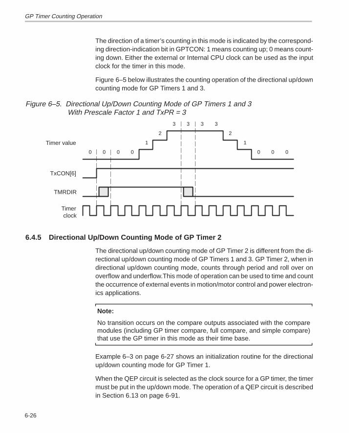
GP Timer Counting Operation
6-26
The direction of a timer’s counting in this mode is indicated by the correspond-ing direction-indication bit in GPTCON: 1 means counting up; 0 means count-ing down. Either the external or Internal CPU clock can be used as the inputclock for the timer in this mode.
Figure 6–5 below illustrates the counting operation of the directional up/downcounting mode for GP Timers 1 and 3.
Figure 6–5. Directional Up/Down Counting Mode of GP Timers 1 and 3 With Prescale Factor 1 and TxPR = 3
clockTimer
TMRDIR
TxCON[6]
Timer value
000
1
2
3333
2
1
0000
6.4.5 Directional Up/Down Counting Mode of GP Timer 2
The directional up/down counting mode of GP Timer 2 is different from the di-rectional up/down counting mode of GP Timers 1 and 3. GP Timer 2, when indirectional up/down counting mode, counts through period and roll over onoverflow and underflow.This mode of operation can be used to time and countthe occurrence of external events in motion/motor control and power electron-ics applications.
Note:
No transition occurs on the compare outputs associated with the comparemodules (including GP timer compare, full compare, and simple compare)that use the GP timer in this mode as their time base.
Example 6–3 on page 6-27 shows an initialization routine for the directionalup/down counting mode for GP Timer 1.
When the QEP circuit is selected as the clock source for a GP timer, the timermust be put in the up/down mode. The operation of a QEP circuit is describedin Section 6.13 on page 6-91.
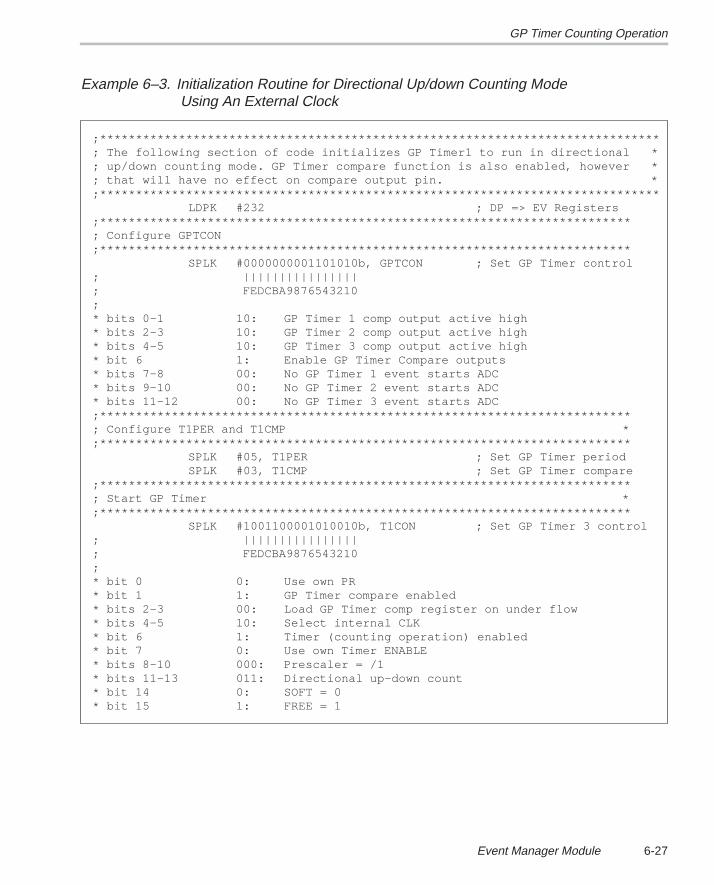
GP Timer Counting Operation
6-27Event Manager Module
Example 6–3. Initialization Routine for Directional Up/down Counting Mode Using An External Clock
;******************************************************************************; The following section of code initializes GP Timer1 to run in directional *; up/down counting mode. GP Timer compare function is also enabled, however *; that will have no effect on compare output pin. *;******************************************************************************
LDPK #232 ; DP => EV Registers;**************************************************************************; Configure GPTCON;**************************************************************************
SPLK #0000000001101010b, GPTCON ; Set GP Timer control; ||||||||||||||||; FEDCBA9876543210;* bits 0–1 10: GP Timer 1 comp output active high* bits 2–3 10: GP Timer 2 comp output active high* bits 4–5 10: GP Timer 3 comp output active high* bit 6 1: Enable GP Timer Compare outputs* bits 7–8 00: No GP Timer 1 event starts ADC* bits 9–10 00: No GP Timer 2 event starts ADC* bits 11–12 00: No GP Timer 3 event starts ADC;**************************************************************************; Configure T1PER and T1CMP *;**************************************************************************
SPLK #05, T1PER ; Set GP Timer periodSPLK #03, T1CMP ; Set GP Timer compare
;**************************************************************************; Start GP Timer *;**************************************************************************
SPLK #1001100001010010b, T1CON ; Set GP Timer 3 control; ||||||||||||||||; FEDCBA9876543210;* bit 0 0: Use own PR* bit 1 1: GP Timer compare enabled* bits 2–3 00: Load GP Timer comp register on under flow* bits 4–5 10: Select internal CLK* bit 6 1: Timer (counting operation) enabled* bit 7 0: Use own Timer ENABLE* bits 8–10 000: Prescaler = /1* bits 11–13 011: Directional up–down count* bit 14 0: SOFT = 0* bit 15 1: FREE = 1
GP Timer Counting Operation
6-28
6.4.6 Single Up/Down Counting Mode
In single up/down counting mode, the GP timer counts up according to thescaled clock input to the value in its period register. It then changes its countingdirection and counts down until it reaches 0. When the timer reaches 0, it re-sets TxCON[6] and its prescale counter, stops, and holds at its current state.
The period of a GP timer in this mode is 2 x (TxPR) cycles of the scaled clockinput if the initial value of the timer is 0.
The initial value of the timer counter can be any value between 0h and FFFFh.If the initial timer value is greater than that of the period register, the timercounts up to FFFFh, resets to 0, and continues as if the initial value of the timerwas 0. If the initial value of the timer is the same as that of the period register,the timer counts down to 0 and ends the period there. If the initial value of thetimer is between 0 and the contents of the period register, the timer counts upto the period value and continues to finish the period as if the initial countervalue was the same as that of the period register.
The period, underflow, and overflow interrupt flags, interrupts, and associatedactions are generated on respective events in the same way that they are gen-erated in single up counting mode. Note, however, that a period event happenswhen a match between the timer counter and the period register is made,which is in the middle of a counting period.
Once the operation of a GP timer in this mode has ended, the operation canbe started again only by software writing a 1 to TxCON[6]. The direction indica-tion bit in GPTCON is 1 when the counting direction is up, and 0 when thecounting direction is down. Either the external clock or the internal CPU clockcan be selected as the clock input to the timer. TMRDIR input is ignored by aGP timer in this mode.
Figure 6–6 shows the single up/down counting mode of a GP timer.Example 6–4 shows an initialization routine for GP Timer 1 in the single up/downcounting mode.
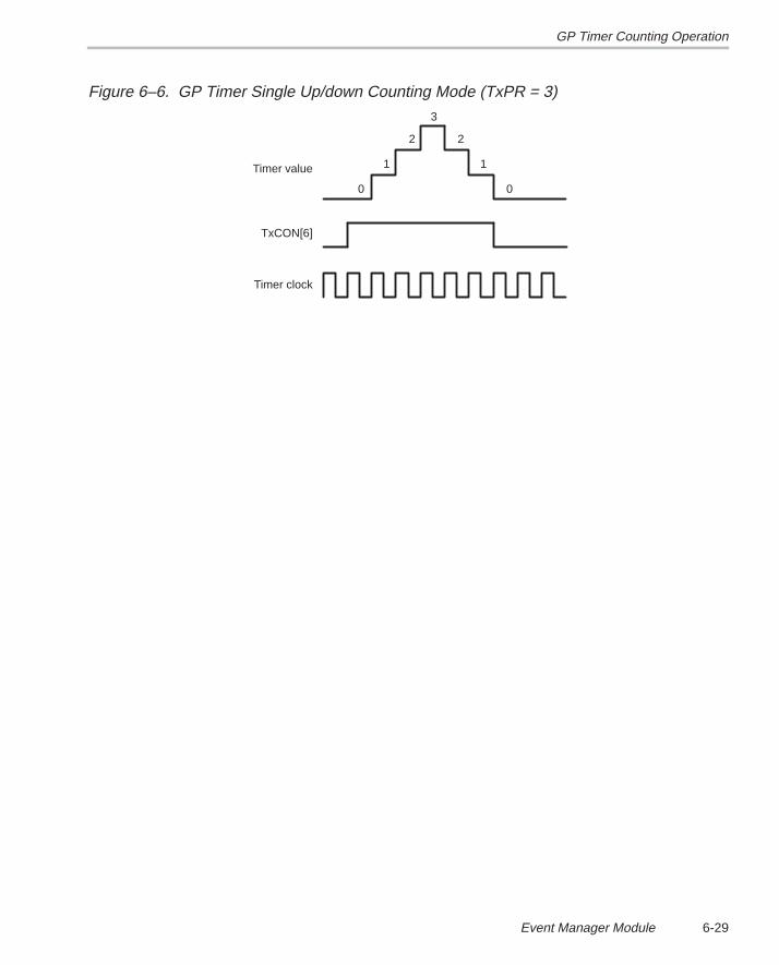
GP Timer Counting Operation
6-29Event Manager Module
Figure 6–6. GP Timer Single Up/down Counting Mode (TxPR = 3)
2
3
1
0 0
2
1
TxCON[6]
Timer value
Timer clock
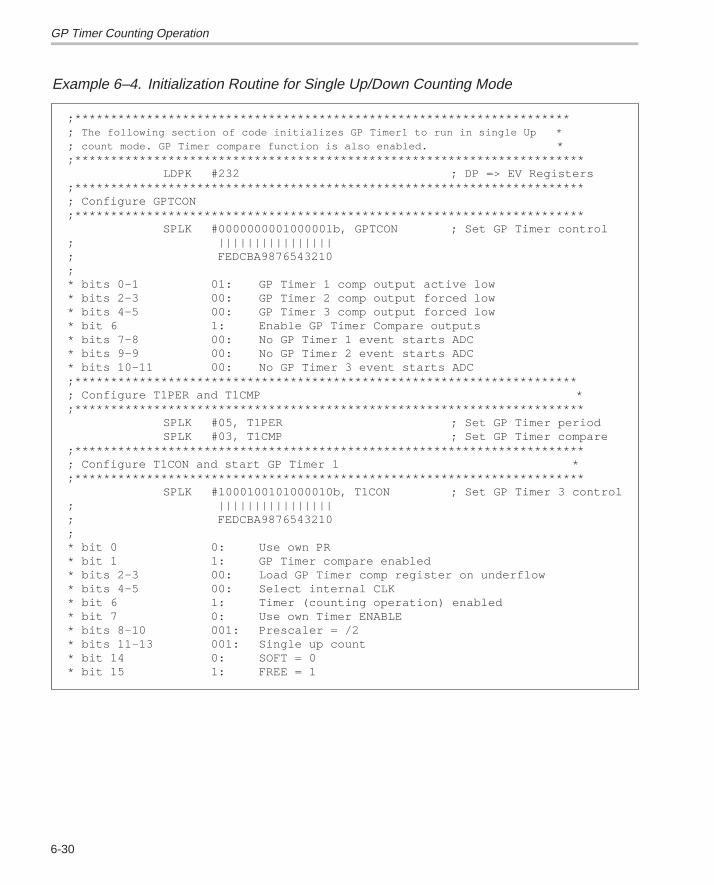
GP Timer Counting Operation
6-30
Example 6–4. Initialization Routine for Single Up/Down Counting Mode
;*********************************************************************; The following section of code initializes GP Timer1 to run in single Up *; count mode. GP Timer compare function is also enabled. *;***********************************************************************
LDPK #232 ; DP => EV Registers;***********************************************************************; Configure GPTCON;***********************************************************************
SPLK #0000000001000001b, GPTCON ; Set GP Timer control; ||||||||||||||||; FEDCBA9876543210;* bits 0–1 01: GP Timer 1 comp output active low* bits 2–3 00: GP Timer 2 comp output forced low* bits 4–5 00: GP Timer 3 comp output forced low* bit 6 1: Enable GP Timer Compare outputs* bits 7–8 00: No GP Timer 1 event starts ADC* bits 9–9 00: No GP Timer 2 event starts ADC* bits 10–11 00: No GP Timer 3 event starts ADC;**********************************************************************; Configure T1PER and T1CMP *;***********************************************************************
SPLK #05, T1PER ; Set GP Timer periodSPLK #03, T1CMP ; Set GP Timer compare
;***********************************************************************; Configure T1CON and start GP Timer 1 *;***********************************************************************
SPLK #1000100101000010b, T1CON ; Set GP Timer 3 control; ||||||||||||||||; FEDCBA9876543210;* bit 0 0: Use own PR* bit 1 1: GP Timer compare enabled* bits 2–3 00: Load GP Timer comp register on underflow* bits 4–5 00: Select internal CLK* bit 6 1: Timer (counting operation) enabled* bit 7 0: Use own Timer ENABLE* bits 8–10 001: Prescaler = /2* bits 11–13 001: Single up count* bit 14 0: SOFT = 0* bit 15 1: FREE = 1
GP Timer Counting Operation
6-31Event Manager Module
6.4.7 Continuous Up/Down Counting Mode
The continuous up/down counting mode is the same as the single up/downcounting mode repeated each time the timer is reset to 0. Once the continuousup/down counting mode is started, no user software or hardware interventionis required to repeat the counting period.
The period of a timer in this mode is 2 x (TxPR) cycles of the scaled clock input,except for the first period. The duration of the first counting period is the sameif the timer counter is 0 when counting starts.
The initial value of a GP timer counter can be any value between 0h andFFFFh. When the initial value is greater than that of the period register, the tim-er counts up to FFFFh, resets to 0, and continues the operation as if the initialvalue is 0. When the initial value in the timer counter is the same as that of theperiod register, the timer counts down to 0 and continues as if the initial valueis 0. If the initial value of the timer is between 0 and the contents of the periodregister, the timer counts up to the period value and continues to finish the peri-od as if the initial counter value is the same as that of the period register.
The period, underflow, and overflow interrupt flags, interrupts, and associatedactions are generated on respective events in the same way that they are gen-erated in single up counting mode.
The counting direction indication bit in GPTCON is 1 for a timer in the continu-ous up/down counting mode when the timer counts up and 0 when the timercounts down. Either the external or internal CPU clock can be selected as theinput clock. TMRDIR input is ignored by a timer in this mode.
The continuous up/down counting mode is particularly useful in generatingcentered or symmetric pulse width modulation (PWM) waveforms found in abroad range of motor/motion-control and power-electronics applications.
Figure 6–7 on page 6-32 shows the continuous up/down counting mode of aGP timer, and Example 6–5 on page 6-33 shows an initialization routine for thecontinuous up/down counting mode.
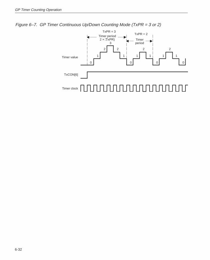
GP Timer Counting Operation
6-32
Figure 6–7. GP Timer Continuous Up/Down Counting Mode (TxPR = 3 or 2)
2
3
1
0 0
2
1 1
2
1
0
1
2
1
0
TxPR = 3TxPR = 2
Timer period2 × ⟨TxPR) Timer
period
TxCON[6]
Timer value
Timer clock
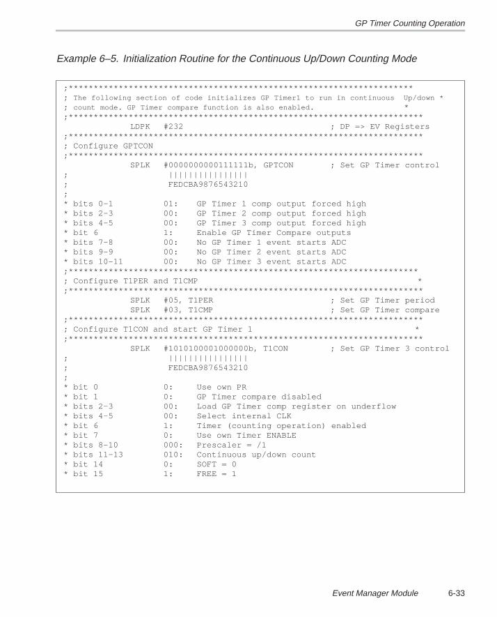
GP Timer Counting Operation
6-33Event Manager Module
Example 6–5. Initialization Routine for the Continuous Up/Down Counting Mode
;*********************************************************************; The following section of code initializes GP Timer1 to run in continuous Up/down *; count mode. GP Timer compare function is also enabled. *;***********************************************************************
LDPK #232 ; DP => EV Registers;***********************************************************************; Configure GPTCON;***********************************************************************
SPLK #0000000000111111b, GPTCON ; Set GP Timer control; ||||||||||||||||; FEDCBA9876543210;* bits 0–1 01: GP Timer 1 comp output forced high* bits 2–3 00: GP Timer 2 comp output forced high* bits 4–5 00: GP Timer 3 comp output forced high* bit 6 1: Enable GP Timer Compare outputs* bits 7–8 00: No GP Timer 1 event starts ADC* bits 9–9 00: No GP Timer 2 event starts ADC* bits 10–11 00: No GP Timer 3 event starts ADC;**********************************************************************; Configure T1PER and T1CMP *;***********************************************************************
SPLK #05, T1PER ; Set GP Timer periodSPLK #03, T1CMP ; Set GP Timer compare
;***********************************************************************; Configure T1CON and start GP Timer 1 *;***********************************************************************
SPLK #1010100001000000b, T1CON ; Set GP Timer 3 control; ||||||||||||||||; FEDCBA9876543210;* bit 0 0: Use own PR* bit 1 0: GP Timer compare disabled* bits 2–3 00: Load GP Timer comp register on underflow* bits 4–5 00: Select internal CLK* bit 6 1: Timer (counting operation) enabled* bit 7 0: Use own Timer ENABLE* bits 8–10 000: Prescaler = /1* bits 11–13 010: Continuous up/down count* bit 14 0: SOFT = 0* bit 15 1: FREE = 1
GP Timer Compare Operation
6-34
6.5 GP Timer Compare Operation
Each GP timer has an associated compare register, TxCMPR, and a compare/PWM output pin, TxPWM/TxCMP. The value of a GP timer counter is constant-ly compared to that of its associated compare register. A compare match oc-curs when the value of the timer counter is the same as that of the compareregister. The compare operation is enabled by setting TxCON[1] to 1. Whenthe compare operation is enabled, the following happens on a compare match:
� The compare interrupt flag of the timer is set two CPU clock cycles afterthe match.
� If the GP timer is not in the directional up/down counting mode, a transitionoccurs on the associated compare/PWM output according to the bit con-figuration in GPTCON, one CPU clock cycle after the match.
� If the compare interrupt flag has been selected by the appropriateGPTCON bits to start ADC, an ADC start signal is generated at the sametime the compare interrupt flag is set.
If the compare operation of the GP timer is disabled, the compare/PWM outputis put in the high impedance state, and none of the above events occur.
6.5.1 Compare/PWM Transition
A transition on the compare/PWM output is controlled by a waveform genera-tor (both symmetric and asymmetric) and the associated output logic, and de-pends on the following:
� The bit definition in GPTCON
� The counting mode of the timer
� The counting direction when in single or continuous up/down countingmode
6.5.2 Asymmetric/Symmetric Waveform Generator
The asymmetric/symmetric waveform generator produces an asymmetric orsymmetric compare/PWM waveform based on the counting mode of the GPtimer.
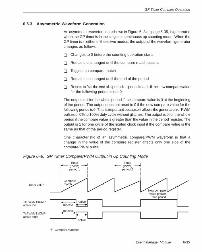
GP Timer Compare Operation
6-35Event Manager Module
6.5.3 Asymmetric Waveform Generation
An asymmetric waveform, as shown in Figure 6–8 on page 6-35, is generatedwhen the GP timer is in the single or continuous up counting mode. When theGP timer is in either of these two modes, the output of the waveform generatorchanges as follows:
� Changes to 0 before the counting operation starts
� Remains unchanged until the compare match occurs
� Toggles on compare match
� Remains unchanged until the end of the period
� Resets to 0 at the end of a period on period match if the new compare valuefor the following period is not 0
The output is 1 for the whole period if the compare value is 0 at the beginningof the period. The output does not reset to 0 if the new compare value for thefollowing period is 0. This is important because it allows the generation of PWMpulses of 0% to 100% duty cycle without glitches. The output is 0 for the wholeperiod if the compare value is greater than the value in the period register. Theoutput is 1 for one cycle of the scaled clock input if the compare value is thesame as that of the period register.
One characteristic of an asymmetric compare/PWM waveform is that achange in the value of the compare register affects only one side of thecompare/PWM pulse.
Figure 6–8. GP Timer Compare/PWM Output in Up Counting Mode
TxPWM/TxCMPactive low Inactive
Inactive
Active
TxPWM/TxCMPactive high
Comparematch
New comparevalue greater
than period
Compare matches
Active
Timer value
Timer(PWM)period 2
Timer(PWM)period 1

GP Timer Compare Operation
6-36
6.5.4 Symmetric Waveform Generation
A symmetric waveform, as shown in Figure 6–9, is generated when the GPtimer is in the single or continuous up/down counting mode. When the GP timeris in either of these two modes, the state of the output of the waveform genera-tor changes as follows:
� Changes to 0 before the counting operation starts
� Remains unchanged until first compare match occurs
� Toggles on the first compare match
� Remains unchanged until the the second compare match occurs
� Toggles on the second compare match
� Remains unchanged until the end of the period
� Resets to 0 at the end of the period if there is no second compare matchand the new compare value for the following period is not 0
The output is set to 1 at the beginning of a period and remains 1 until the se-cond compare match if the compare value is 0. After the first transition from0 to 1, the output remains 1 until the end of the period if the compare value is0 for the rest of the period. When this happens, the output does not reset to0 if the compare value for the following period is still 0. The output is again setto 1 at the beginning of a period and the process repeats itself to assure thegeneration of PWM pulses of 0% to 100% duty cycle without any glitches. Thefirst transition does not occur if the compare value is greater than or equal tothat of the period register for the first half of the period. The output still toggleswhen a compare match occurs in the second half of the period. This error inoutput transition (often the result of a calculation error in the application rou-tine) is corrected at the end of the period because the output resets to 0, unlessthe new compare value for the following period is 0. If the latter happens, theoutput remains 1 (does not reset to 0), which leaves it in the correct state.
Note:
The output logic determines the polarity for all output pins.
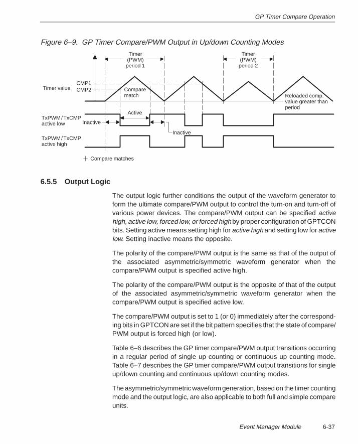
GP Timer Compare Operation
6-37Event Manager Module
Figure 6–9. GP Timer Compare/PWM Output in Up/down Counting Modes
Active
Inactive
Inactive
Compare matches
Timer(PWM)period 1
Timer(PWM)period 2
TxPWM/TxCMPactive low
TxPWM/TxCMPactive high
Timer valueReloaded comp.value greater thanperiod
Comparematch
CMP1CMP2
6.5.5 Output Logic
The output logic further conditions the output of the waveform generator toform the ultimate compare/PWM output to control the turn-on and turn-off ofvarious power devices. The compare/PWM output can be specified activehigh, active low, forced low, or forced high by proper configuration of GPTCONbits. Setting active means setting high for active high and setting low for activelow. Setting inactive means the opposite.
The polarity of the compare/PWM output is the same as that of the output ofthe associated asymmetric/symmetric waveform generator when thecompare/PWM output is specified active high.
The polarity of the compare/PWM output is the opposite of that of the outputof the associated asymmetric/symmetric waveform generator when thecompare/PWM output is specified active low.
The compare/PWM output is set to 1 (or 0) immediately after the correspond-ing bits in GPTCON are set if the bit pattern specifies that the state of compare/PWM output is forced high (or low).
Table 6–6 describes the GP timer compare/PWM output transitions occurringin a regular period of single up counting or continuous up counting mode.Table 6–7 describes the GP timer compare/PWM output transitions for singleup/down counting and continuous up/down counting modes.
The asymmetric/symmetric waveform generation, based on the timer countingmode and the output logic, are also applicable to both full and simple compareunits.
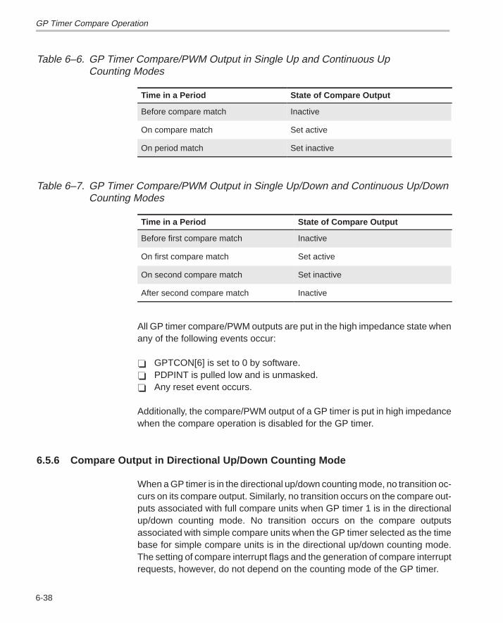
GP Timer Compare Operation
6-38
Table 6–6. GP Timer Compare/PWM Output in Single Up and Continuous Up Counting Modes
Time in a Period State of Compare Output
Before compare match Inactive
On compare match Set active
On period match Set inactive
Table 6–7. GP Timer Compare/PWM Output in Single Up/Down and Continuous Up/Down Counting Modes
Time in a Period State of Compare Output
Before first compare match Inactive
On first compare match Set active
On second compare match Set inactive
After second compare match Inactive
All GP timer compare/PWM outputs are put in the high impedance state whenany of the following events occur:
� GPTCON[6] is set to 0 by software.� PDPINT is pulled low and is unmasked.� Any reset event occurs.
Additionally, the compare/PWM output of a GP timer is put in high impedancewhen the compare operation is disabled for the GP timer.
6.5.6 Compare Output in Directional Up/Down Counting Mode
When a GP timer is in the directional up/down counting mode, no transition oc-curs on its compare output. Similarly, no transition occurs on the compare out-puts associated with full compare units when GP timer 1 is in the directionalup/down counting mode. No transition occurs on the compare outputsassociated with simple compare units when the GP timer selected as the timebase for simple compare units is in the directional up/down counting mode.The setting of compare interrupt flags and the generation of compare interruptrequests, however, do not depend on the counting mode of the GP timer.
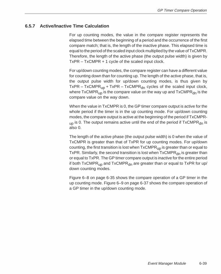
GP Timer Compare Operation
6-39Event Manager Module
6.5.7 Active/Inactive Time Calculation
For up counting modes, the value in the compare register represents theelapsed time between the beginning of a period and the occurrence of the firstcompare match; that is, the length of the inactive phase. This elapsed time isequal to the period of the scaled input clock multiplied by the value of TxCMPR.Therefore, the length of the active phase (the output pulse width) is given byTxPR – TxCMPR + 1 cycle of the scaled input clock.
For up/down counting modes, the compare register can have a different valuefor counting down than for counting up. The length of the active phase, that is,the output pulse width for up/down counting modes, is thus given byTxPR – TxCMPRup + TxPR – TxCMPRdn cycles of the scaled input clock,where TxCMPRup is the compare value on the way up and TxCMPRdn is thecompare value on the way down.
When the value in TxCMPR is 0, the GP timer compare output is active for thewhole period if the timer is in the up counting mode. For up/down countingmodes, the compare output is active at the beginning of the period if TxCMPR-
up is 0. The output remains active until the end of the period if TxCMPRdn isalso 0.
The length of the active phase (the output pulse width) is 0 when the value ofTxCMPR is greater than that of TxPR for up counting modes. For up/downcounting, the first transition is lost when TxCMPRup is greater than or equal toTxPR. Similarly, the second transition is lost when TxCMPRdn is greater thanor equal to TxPR. The GP timer compare output is inactive for the entire periodif both TxCMPRup and TxCMPRdn are greater than or equal to TxPR for up/down counting modes.
Figure 6–8 on page 6-35 shows the compare operation of a GP timer in theup counting mode. Figure 6–9 on page 6-37 shows the compare operation ofa GP timer in the up/down counting mode.
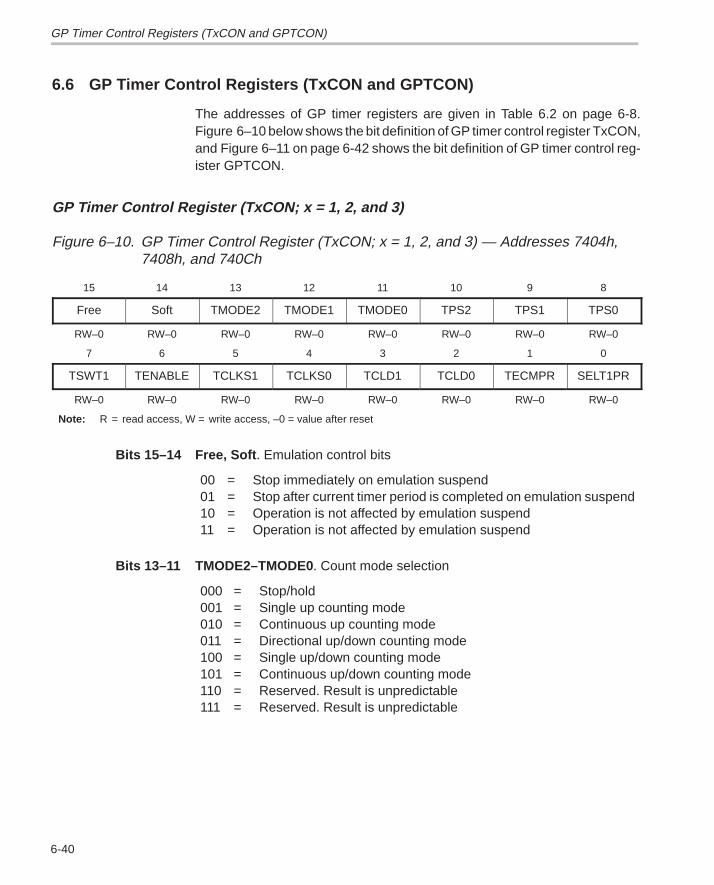
GP Timer Control Registers (TxCON and GPTCON)
6-40
6.6 GP Timer Control Registers (TxCON and GPTCON)
The addresses of GP timer registers are given in Table 6.2 on page 6-8.Figure 6–10 below shows the bit definition of GP timer control register TxCON,and Figure 6–11 on page 6-42 shows the bit definition of GP timer control reg-ister GPTCON.
GP Timer Control Register (TxCON; x = 1, 2, and 3)
Figure 6–10. GP Timer Control Register (TxCON; x = 1, 2, and 3) — Addresses 7404h, 7408h, and 740Ch
15 14 13 12 11 10 9 8
Free Soft TMODE2 TMODE1 TMODE0 TPS2 TPS1 TPS0
RW–0 RW–0 RW–0 RW–0 RW–0 RW–0 RW–0 RW–0
7 6 5 4 3 2 1 0
TSWT1 TENABLE TCLKS1 TCLKS0 TCLD1 TCLD0 TECMPR SELT1PR
RW–0 RW–0 RW–0 RW–0 RW–0 RW–0 RW–0 RW–0
Note: R = read access, W = write access, –0 = value after reset
Bits 15–14 Free, Soft . Emulation control bits
00 = Stop immediately on emulation suspend01 = Stop after current timer period is completed on emulation suspend10 = Operation is not affected by emulation suspend11 = Operation is not affected by emulation suspend
Bits 13–11 TMODE2–TMODE0 . Count mode selection
000 = Stop/hold001 = Single up counting mode010 = Continuous up counting mode011 = Directional up/down counting mode100 = Single up/down counting mode101 = Continuous up/down counting mode110 = Reserved. Result is unpredictable111 = Reserved. Result is unpredictable
GP Timer Control Registers (TxCON and GPTCON)
6-41Event Manager Module
Bits 10–8 TPS2–TPS0 . Input clock prescaler
000 = x/1001 = x/2010 = x/4011 = x/8100 = x/16101 = x/32110 = x/64111 = x/128
x = CPU clock frequency
Bit 7 TSWT1 . (GP timer start with GP timer 1). Start timer with GP timer 1 timerenable bit. This bit is reserved in T1CON.
0 = Use own TENABLE bit
1 = Use TENABLE bit of T1CON to enable and disable operation ignoringown TENABLE bit
Bit 6 TENABLE . Timer enable. In single up counting and single up/down countingmodes, this bit is cleared to 0 by the timer after it completes a period of opera-tion.
0 = Disable timer operation; that is, put the timer in hold and reset theprescaler counter
1 = Enable timer operations
Bits 5–4 TCLKS1, TCLKS0 . Clock source select
00 = Internal
01 = External
10 = Rollover from GP timer 2 (only applicable to T3CON when GP Timers2 and 3 are cascaded into a 32-bit timer; reserved in T1CON andT2CON; ILLEGAL if SELT1PR=1.)
11 = Quadrature encoder pulse circuit (only applicable to T2CON andT3CON; reserved in T1CON; ILLEGAL if SELT1PR is 1)
ILLEGAL means result is unpredictable.
Bits 3–2 TCLD1, TCLD0 . Timer compare (active) register reload condition
00 = When counter is 001 = When counter value is 0 or equals period register value
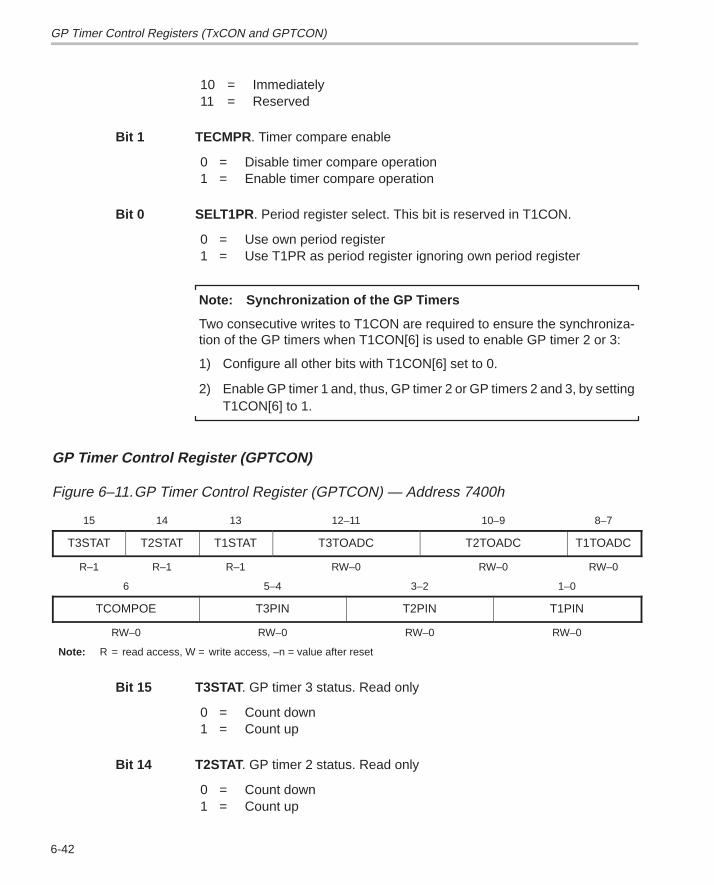
GP Timer Control Registers (TxCON and GPTCON)
6-42
10 = Immediately11 = Reserved
Bit 1 TECMPR . Timer compare enable
0 = Disable timer compare operation1 = Enable timer compare operation
Bit 0 SELT1PR . Period register select. This bit is reserved in T1CON.
0 = Use own period register1 = Use T1PR as period register ignoring own period register
Note: Synchronization of the GP Timers
Two consecutive writes to T1CON are required to ensure the synchroniza-tion of the GP timers when T1CON[6] is used to enable GP timer 2 or 3:
1) Configure all other bits with T1CON[6] set to 0.
2) Enable GP timer 1 and, thus, GP timer 2 or GP timers 2 and 3, by settingT1CON[6] to 1.
GP Timer Control Register (GPTCON)
Figure 6–11.GP Timer Control Register (GPTCON) — Address 7400h
15 14 13 12–11 10–9 8–7
T3STAT T2STAT T1STAT T3TOADC T2TOADC T1TOADC
R–1 R–1 R–1 RW–0 RW–0 RW–0
6 5–4 3–2 1–0
TCOMPOE T3PIN T2PIN T1PIN
RW–0 RW–0 RW–0 RW–0
Note: R = read access, W = write access, –n = value after reset
Bit 15 T3STAT . GP timer 3 status. Read only
0 = Count down1 = Count up
Bit 14 T2STAT . GP timer 2 status. Read only
0 = Count down1 = Count up
GP Timer Control Registers (TxCON and GPTCON)
6-43Event Manager Module
Bit 13 T1STAT . GP timer 1 status. Read only
0 = Count down1 = Count up
Bits 12–11 T3TOADC . Start ADC by GP timer 3 event
00 = No event starts ADC01 = Setting of underflow interrupt flag10 = Setting of period interrupt flag11 = Setting of compare interrupt flag
Bits 10–9 T2TOADC . Start ADC by GP timer 2 event
00 = No event starts ADC01 = Setting of underflow interrupt flag. Starts ADC10 = Setting of period interrupt flag. Starts ADC11 = Setting of compare interrupt flag. Starts ADC
Bits 8–7 T1TOADC .Start ADC by GP timer 1 event
00 = No event starts ADC01 = Setting of underflow interrupt flag10 = Setting of period interrupt flag11 = Setting of compare interrupt flag
Bit 6 TCOMPOE . Compare output enable. Active PDPINT writes 0 to this bit.
0 = Disable all three GP timer compare outputs (all three compare outputsare put in the high-impedance state)
1 = Enable all three GP timer compare outputs
Bits 5–4 T3PIN . Polarity of GP timer 3 compare output
00 = Forced low01 = Active low10 = Active high11 = Forced high
Bits 3–2 T2PIN . Polarity of GP timer 2 compare output
00 = Forced low01 = Active low10 = Active high11 = Forced high

GP Timer Control Registers (TxCON and GPTCON)
6-44
Bits 1–0 T1PIN . Polarity of GP timer 1 compare output
00 = Forced low01 = Active low10 = Active high11 = Forced high
Generation of Compare and PWM Outputs Using GP Timers
6-45Event Manager Module
6.7 Generation of Compare and PWM Outputs Using GP Timers
Each GP timer can be used independently to provide a compare or PWM out-put channel. Thus, up to three compare or PWM outputs may be generatedby the GP timers.
6.7.1 Generation of Compare Output
To generate a compare output, select an appropriate GP timer operatingmode. Then perform the following:
� Set up TxCMPR according to when the compare event will happen.
� Set up GPTCON so that the desired transition on compare output takesplace on compare match.
� Load TxPR with the desired period value, if needed.
� Load TxCNT with the desired initial counter value, if needed.
� Set up TxCON to specify the counting mode and clock source and startthe operation.
6.7.2 Generation of PWM Output
To generate a PWM output with a GP timer, select the continuous up countingor up/down counting mode. Edge-triggered or asymmetric PWM waveformsare generated when the continuous up counting mode is selected. Centeredor symmetric PWM waveforms are generated when the continuous up/downcounting mode is selected. To set up a GP timer for the PWM operation, per-form the following:
� Set up TxPR according to the desired PWM (carrier) period.
� Set up TxCON to specify the counting mode and clock source and startthe operation.
� Load TxCMPR with values corresponding to the on-line calculated widths(duty cycles) of PWM pulses.
When the continuous up counting mode is selected to generate asymmetricPWM waveforms, the period value is obtained by dividing the desired PWMperiod by the period of the GP timer input clock and subtracting 1 from the re-sulting number. When the continuous up/down counting mode is selected togenerate symmetric PWM waveforms, the period value is obtained by dividingthe desired PWM period by 2 times the period of the GP timer input clock
Generation of Compare and PWM Outputs Using GP Timers
6-46
The GP timer can be initialized the same way as in the previous example. Dur-ing run time, the GP timer compare register is constantly updated with newlydetermined compare values corresponding to the newly determined dutycycles.
Figure 6–8 on page 6-35 and Figure 6–9 on page 6-37 are examples of asym-metric and symmetric PWM waveforms that can be generated by a GP timer.
6.7.3 GP Timer Reset
When any RESET event occurs, the following happens:
� All GP timer register bits, except for the counting-direction indication bitsin GPTCON, are reset to 0; thus, the operation of all GP timers is disabled.The counting-direction indication bits are all set to 1.
� All timer interrupt flags are reset to 0.
� All timer interrupt mask bits are reset to 0; thus, all GP timer interrupts aremasked.
� All GP timer compare outputs are put in the high-impedance state.
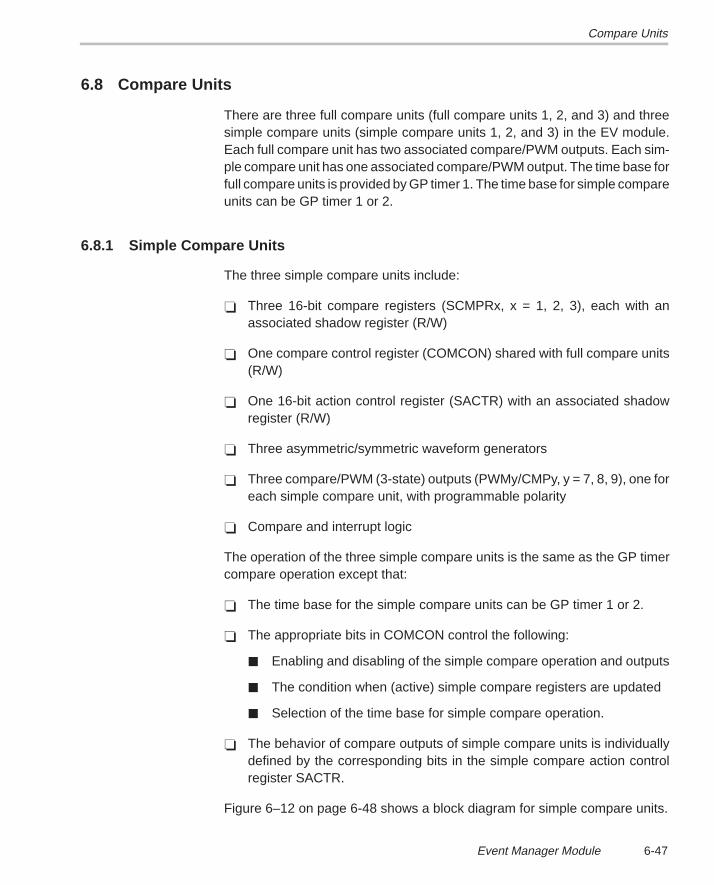
Compare Units
6-47Event Manager Module
6.8 Compare Units
There are three full compare units (full compare units 1, 2, and 3) and threesimple compare units (simple compare units 1, 2, and 3) in the EV module.Each full compare unit has two associated compare/PWM outputs. Each sim-ple compare unit has one associated compare/PWM output. The time base forfull compare units is provided by GP timer 1. The time base for simple compareunits can be GP timer 1 or 2.
6.8.1 Simple Compare Units
The three simple compare units include:
� Three 16-bit compare registers (SCMPRx, x = 1, 2, 3), each with anassociated shadow register (R/W)
� One compare control register (COMCON) shared with full compare units(R/W)
� One 16-bit action control register (SACTR) with an associated shadowregister (R/W)
� Three asymmetric/symmetric waveform generators
� Three compare/PWM (3-state) outputs (PWMy/CMPy, y = 7, 8, 9), one foreach simple compare unit, with programmable polarity
� Compare and interrupt logic
The operation of the three simple compare units is the same as the GP timercompare operation except that:
� The time base for the simple compare units can be GP timer 1 or 2.
� The appropriate bits in COMCON control the following:
� Enabling and disabling of the simple compare operation and outputs
� The condition when (active) simple compare registers are updated
� Selection of the time base for simple compare operation.
� The behavior of compare outputs of simple compare units is individuallydefined by the corresponding bits in the simple compare action controlregister SACTR.
Figure 6–12 on page 6-48 shows a block diagram for simple compare units.
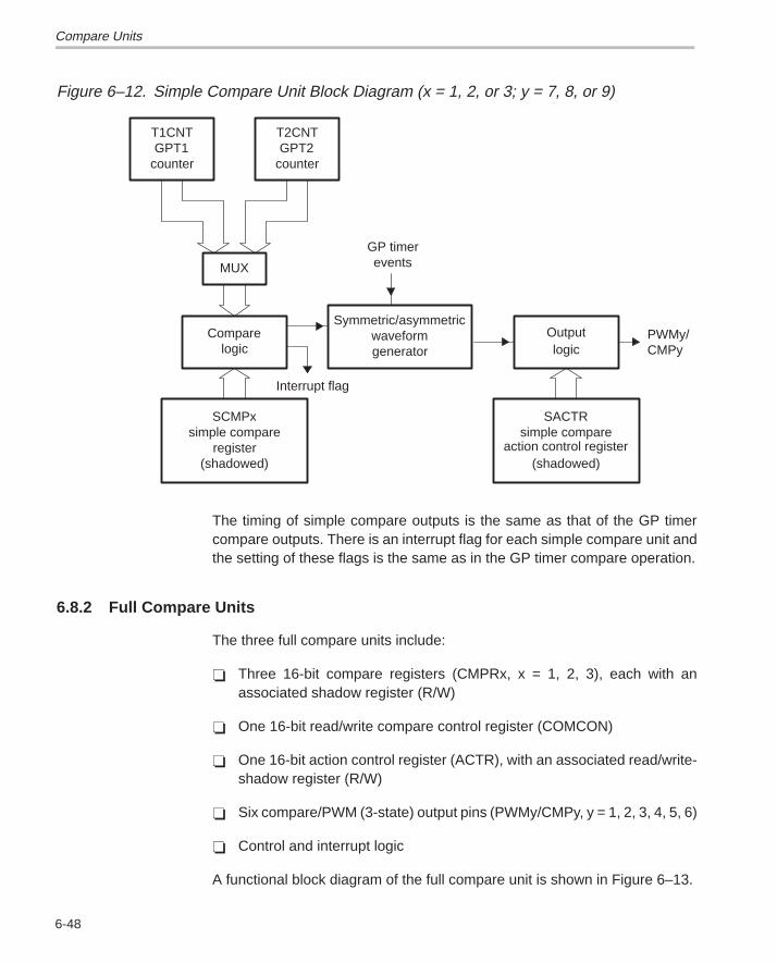
Compare Units
6-48
Figure 6–12. Simple Compare Unit Block Diagram (x = 1, 2, or 3; y = 7, 8, or 9)
CMPyPWMy/
SACTRsimple compare
action control register(shadowed)
eventsGP timer
logicOutput
Interrupt flag
generatorwaveform
Symmetric/asymmetric
(shadowed)register
simple compareSCMPx
logicCompare
MUX
T2CNTGPT2
countercounterGPT1T1CNT
The timing of simple compare outputs is the same as that of the GP timercompare outputs. There is an interrupt flag for each simple compare unit andthe setting of these flags is the same as in the GP timer compare operation.
6.8.2 Full Compare Units
The three full compare units include:
� Three 16-bit compare registers (CMPRx, x = 1, 2, 3), each with anassociated shadow register (R/W)
� One 16-bit read/write compare control register (COMCON)
� One 16-bit action control register (ACTR), with an associated read/write-shadow register (R/W)
� Six compare/PWM (3-state) output pins (PWMy/CMPy, y = 1, 2, 3, 4, 5, 6)
� Control and interrupt logic
A functional block diagram of the full compare unit is shown in Figure 6–13.
Compare Units
6-49Event Manager Module
Figure 6–13. Full Compare Unit Block Diagram (x = 1, 2, 3; y = 1, 3, 5)
PWMy, y + 1
CMPy, y + 1PWMy, y + 1/
CMPy,y + 1
Outputlogic
MUX
circuitsPWM
logicOutput
(shadowed)action control register
full compareACTR
logicCompare
(shadowed)register
full compareCMPRx
counterGPT1
T1CNT
The time base for full compare units and the associated PWM circuits is pro-vided by GP timer 1. This timer can be in any of its six counting modes whenthe compare operation is enabled. However, no transition happens oncompare outputs when GP timer 1 is in the directional up/down counting mode.
6.8.3 Full Compare Inputs/Outputs
The inputs to a full compare unit include:
� Control signals from control registers� GP timer 1 (T1CNT) and its underflow and period match signals� The RESET signal
The output of a full compare unit is a compare match signal. If the compareoperation is enabled, this match signal sets the interrupt flag and causes tran-sitions on the two output pins associated with the full compare unit. When fullcompare operation is disabled, all full compare/PWM outputs are put in thehigh-impedance state.
6.8.4 Full Compare Operation Modes
The operating mode of full compare units is determined by bits in COMCON.These bits determine:
� Whether full compare operation is enabled
� Whether full compare outputs are enabled
� The condition on which full compare registers are updated with values intheir shadow registers
Compare Units
6-50
� The condition on which the full action control register is updated with thevalue in its shadow register
� Whether the space vector PWM mode is enabled
� Whether each full compare unit is in the compare or PWM mode
The three full compare units can operate in either of two operating modes:compare or PWM.
6.8.5 Compare Mode
When the compare mode is selected and full compare is enabled for a fullcompare unit, the value of the GP timer 1 counter is continuously comparedwith that of the compare register and the following occurs on a compare match:
� A transition appears on the two compare/PWM outputs of the full compareunit.
� The compare interrupt of the full compare unit is set.
None of the above occurs if the full compare operation is disabled.
These bits can individually specify each output to hold, reset (go low), set (gohigh), or toggle on a compare match. The timing of output transitions and set-ting of interrupt flags is the same as in the GP timer compare operation. Theoutputs of full compare units in compare mode are subject to modification bythe output logic.
6.8.6 PWM Mode
Each full compare unit can be put individually into the PWM mode. The opera-tion of full compare units in this mode is similar to the GP timer compare opera-tion except that the full compare units are controlled by different control regis-ters and are subject to modification by dead-band units and space vector PWMlogic. The PWM mode of operation is further described in the following sec-tions.
6.8.7 Register Setup for Full Compare Operation
The register setup for full compare operation requires:
� Setting up T1PR� Setting up ACTR� Initializing CMPRx� Setting up COMCON� Setting up T1CON
Note that in many cases, COMCON requires two writes to ensure the correctpolarity of PWM outputs.
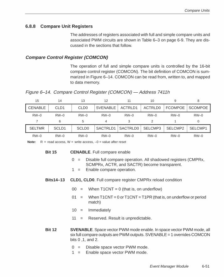
Compare Units
6-51Event Manager Module
6.8.8 Compare Unit Registers
The addresses of registers associated with full and simple compare units andassociated PWM circuits are shown in Table 6–3 on page 6-9. They are dis-cussed in the sections that follow.
Compare Control Register (COMCON)
The operation of full and simple compare units is controlled by the 16-bitcompare control register (COMCON). The bit definition of COMCON is sum-marized in Figure 6–14. COMCON can be read from, written to, and mappedto data memory.
Figure 6–14. Compare Control Register (COMCON) — Address 7411h
15 14 13 12 11 10 9 8
CENABLE CLD1 CLD0 SVENABLE ACTRLD1 ACTRLD0 FCOMPOE SCOMPOE
RW–0 RW–0 RW–0 RW–0 RW–0 RW–0 RW–0 RW–0
7 6 5 4 3 2 1 0
SELTMR SCLD1 SCLD0 SACTRLD1 SACTRLD0 SELCMP3 SELCMP2 SELCMP1
RW–0 RW–0 RW–0 RW–0 RW–0 RW–0 RW–0 RW–0
Note: R = read access, W = write access, –0 = value after reset
Bit 15 CENABLE . Full compare enable
0 = Disable full compare operation. All shadowed registers (CMPRx,SCMPRx, ACTR, and SACTR) become transparent.
1 = Enable compare operation.
Bits14–13 CLD1, CLD0 . Full compare register CMPRx reload condition
00 = When T1CNT = 0 (that is, on underflow)
01 = When T1CNT = 0 or T1CNT = T1PR (that is, on underflow or periodmatch)
10 = Immediately
11 = Reserved. Result is unpredictable.
Bit 12 SVENABLE . Space vector PWM mode enable. In space vector PWM mode, allsix full compare outputs are PWM outputs. SVENABLE = 1 overrides COMCONbits 0 ,1, and 2.
0 = Disable space vector PWM mode.1 = Enable space vector PWM mode.
Compare Units
6-52
Bits11–10 ACTRLD1, ACTRLD0 . Full compare action register ACTR reload condition
00 = When T1CNT = 0 (that is, on underflow)
01 = When T1CNT = 0 or T1CNT = T1PR (that is, on underflow or periodmatch)
10 = Immediately
11 = Reserved. Result is unpredictable.
Bit 9 FCOMPOE . Full compare output enable. Active PDPINT clears this bit to 0.
0 = Full compare output pins are in the high-impedance state; they aredisabled.
1 = Full compare output pins are not in the high-impedance state; theyare enabled.
Bit 8 SCOMPOE . Simple compare output enable. Active PDPINT clears this bit to 0
0 = Simple compare output pins are in the high-impedance state; theyare disabled.
1 = Simple compare output pins are not in the high-impedance state;they are enabled.
Bit 7 SELTMR . Simple compare time base select
0 = GP timer 11 = GP timer 2
Bits 6–5 SCLD1, SCLD0 . Simple compare register SCMPRx reload condition
00 = When TyCNT = 0 (y = 1 or 2 according to SELTMR)01 = When TyCNT = 0 or TyCNT = TyPR10 = Immediately11 = Reserved
Bits 4–3 SACTRLD1, SACTRLD0 . Simple compare action register SACTR reloadcondition
00 = When TyCNT = 0 (y = 1 or 2 according to SELTMR)01 = When TyCNT = 0 or TyCNT = TyPR10 = Immediately11 = Reserved
Compare Units
6-53Event Manager Module
Bit 2 SELCMP3 . Mode select for PWM6/CMP6 and PWM5/CMP5 (for full compareunit 3)
0 = Compare mode1 = PWM mode
Bit 1 SELCMP2 . Mode select for PWM4/CMP4 and PWM3/CMP3 (for full compareunit 2)
0 = Compare mode1 = PWM mode
Bit 0 SELCMP1 . Mode select for PWM2/CMP2 and PWM1/CMP1 (for full compareunit 1)
0 = Compare mode1 = PWM mode
Note:
Two consecutive writes to COMCON are required to ensure the properoperation of full compare units in the PWM mode:
1) Enable PWM mode without enabling compare operation.
2) Enable compare operation by setting COMCON[15] to 1 without changingany other bits.
Example 6–6 on page 6-54 provides an example of COMCON configurationfor full compare units in PWM mode.
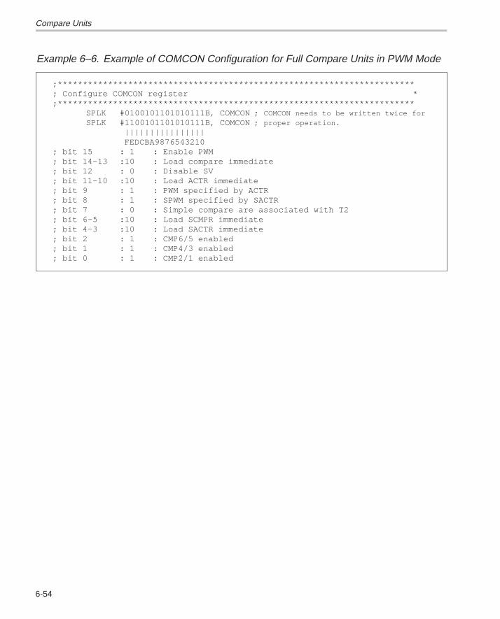
Compare Units
6-54
Example 6–6. Example of COMCON Configuration for Full Compare Units in PWM Mode
;***********************************************************************; Configure COMCON register *;***********************************************************************
SPLK #0100101101010111B, COMCON ; COMCON needs to be written twice forSPLK #1100101101010111B, COMCON ; proper operation.
|||||||||||||||| FEDCBA9876543210
; bit 15 : 1 : Enable PWM; bit 14–13 :10 : Load compare immediate; bit 12 : 0 : Disable SV; bit 11–10 :10 : Load ACTR immediate; bit 9 : 1 : PWM specified by ACTR; bit 8 : 1 : SPWM specified by SACTR; bit 7 : 0 : Simple compare are associated with T2; bit 6–5 :10 : Load SCMPR immediate; bit 4–3 :10 : Load SACTR immediate; bit 2 : 1 : CMP6/5 enabled; bit 1 : 1 : CMP4/3 enabled; bit 0 : 1 : CMP2/1 enabled
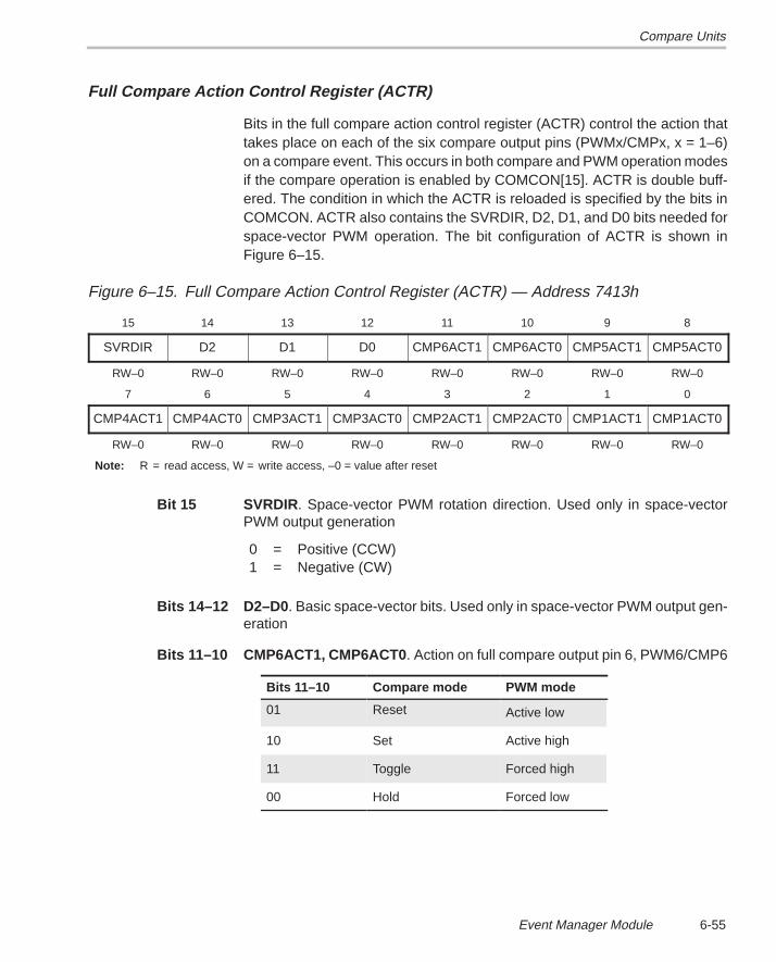
Compare Units
6-55Event Manager Module
Full Compare Action Control Register (ACTR)
Bits in the full compare action control register (ACTR) control the action thattakes place on each of the six compare output pins (PWMx/CMPx, x = 1–6)on a compare event. This occurs in both compare and PWM operation modesif the compare operation is enabled by COMCON[15]. ACTR is double buff-ered. The condition in which the ACTR is reloaded is specified by the bits inCOMCON. ACTR also contains the SVRDIR, D2, D1, and D0 bits needed forspace-vector PWM operation. The bit configuration of ACTR is shown inFigure 6–15.
Figure 6–15. Full Compare Action Control Register (ACTR) — Address 7413h
15 14 13 12 11 10 9 8
SVRDIR D2 D1 D0 CMP6ACT1 CMP6ACT0 CMP5ACT1 CMP5ACT0
RW–0 RW–0 RW–0 RW–0 RW–0 RW–0 RW–0 RW–0
7 6 5 4 3 2 1 0
CMP4ACT1 CMP4ACT0 CMP3ACT1 CMP3ACT0 CMP2ACT1 CMP2ACT0 CMP1ACT1 CMP1ACT0
RW–0 RW–0 RW–0 RW–0 RW–0 RW–0 RW–0 RW–0
Note: R = read access, W = write access, –0 = value after reset
Bit 15 SVRDIR . Space-vector PWM rotation direction. Used only in space-vectorPWM output generation
0 = Positive (CCW)1 = Negative (CW)
Bits 14–12 D2–D0 . Basic space-vector bits. Used only in space-vector PWM output gen-eration
Bits 11–10 CMP6ACT1, CMP6ACT0 . Action on full compare output pin 6, PWM6/CMP6
Bits 11–10 Compare mode PWM mode
01 Reset Active low
10 Set Active high
11 Toggle Forced high
00 Hold Forced low
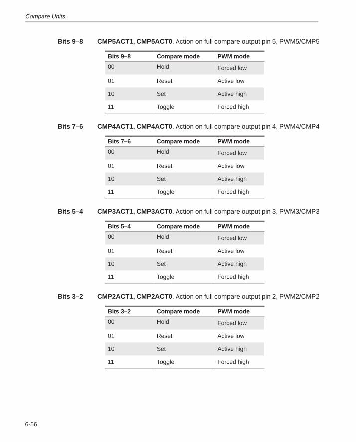
Compare Units
6-56
Bits 9–8 CMP5ACT1, CMP5ACT0 . Action on full compare output pin 5, PWM5/CMP5
Bits 9–8 Compare mode PWM mode
00 Hold Forced low
01 Reset Active low
10 Set Active high
11 Toggle Forced high
Bits 7–6 CMP4ACT1, CMP4ACT0 . Action on full compare output pin 4, PWM4/CMP4
Bits 7–6 Compare mode PWM mode
00 Hold Forced low
01 Reset Active low
10 Set Active high
11 Toggle Forced high
Bits 5–4 CMP3ACT1, CMP3ACT0 . Action on full compare output pin 3, PWM3/CMP3
Bits 5–4 Compare mode PWM mode
00 Hold Forced low
01 Reset Active low
10 Set Active high
11 Toggle Forced high
Bits 3–2 CMP2ACT1, CMP2ACT0 . Action on full compare output pin 2, PWM2/CMP2
Bits 3–2 Compare mode PWM mode
00 Hold Forced low
01 Reset Active low
10 Set Active high
11 Toggle Forced high
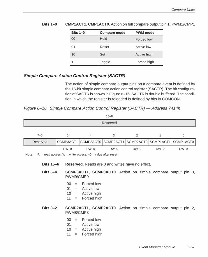
Compare Units
6-57Event Manager Module
Bits 1–0 CMP1ACT1, CMP1ACT0 . Action on full compare output pin 1, PWM1/CMP1
Bits 1–0 Compare mode PWM mode
00 Hold Forced low
01 Reset Active low
10 Set Active high
11 Toggle Forced high
Simple Compare Action Control Register (SACTR)
The action of simple compare output pins on a compare event is defined bythe 16-bit simple compare action control register (SACTR). The bit configura-tion of SACTR is shown in Figure 6–16. SACTR is double buffered. The condi-tion in which the register is reloaded is defined by bits in COMCON.
Figure 6–16. Simple Compare Action Control Register (SACTR) — Address 7414h
15–8
Reserved
7–6 5 4 3 2 1 0
Reserved SCMP3ACT1 SCMP3ACT0 SCMP2ACT1 SCMP2ACT0 SCMP1ACT1 SCMP1ACT0
RW–0 RW–0 RW–0 RW–0 RW–0 RW–0
Note: R = read access, W = write access, –0 = value after reset
Bits 15–6 Reserved . Reads are 0 and writes have no effect.
Bits 5–4 SCMP3ACT1, SCMP3ACT0 . Action on simple compare output pin 3,PWM9/CMP9
00 = Forced low01 = Active low10 = Active high11 = Forced high
Bits 3–2 SCMP2ACT1, SCMP2ACT0 . Action on simple compare output pin 2,PWM8/CMP8
00 = Forced low01 = Active low10 = Active high11 = Forced high
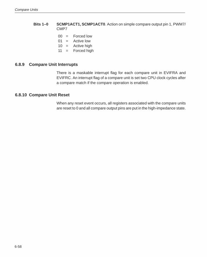
Compare Units
6-58
Bits 1–0 SCMP1ACT1, SCMP1ACT0 . Action on simple compare output pin 1, PWM7/CMP7
00 = Forced low01 = Active low10 = Active high11 = Forced high
6.8.9 Compare Unit Interrupts
There is a maskable interrupt flag for each compare unit in EVIFRA andEVIFRC. An interrupt flag of a compare unit is set two CPU clock cycles aftera compare match if the compare operation is enabled.
6.8.10 Compare Unit Reset
When any reset event occurs, all registers associated with the compare unitsare reset to 0 and all compare output pins are put in the high-impedance state.
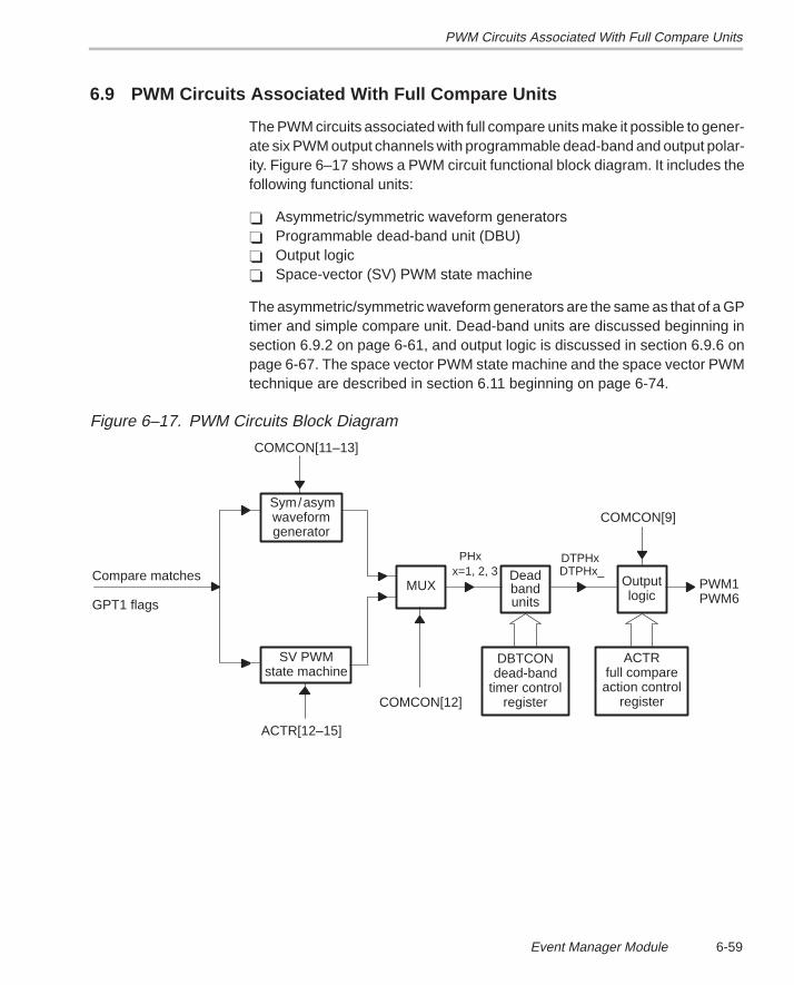
PWM Circuits Associated With Full Compare Units
6-59Event Manager Module
6.9 PWM Circuits Associated With Full Compare Units
The PWM circuits associated with full compare units make it possible to gener-ate six PWM output channels with programmable dead-band and output polar-ity. Figure 6–17 shows a PWM circuit functional block diagram. It includes thefollowing functional units:
� Asymmetric/symmetric waveform generators� Programmable dead-band unit (DBU)� Output logic� Space-vector (SV) PWM state machine
The asymmetric/symmetric waveform generators are the same as that of a GPtimer and simple compare unit. Dead-band units are discussed beginning insection 6.9.2 on page 6-61, and output logic is discussed in section 6.9.6 onpage 6-67. The space vector PWM state machine and the space vector PWMtechnique are described in section 6.11 beginning on page 6-74.
Figure 6–17. PWM Circuits Block Diagram
COMCON[12]
Compare matches
GPT1 flags
Sym/asymwaveformgenerator
ACTRfull compareaction control
register
SV PWMstate machine
Outputlogic
Deadbandunits
MUX
PHx DTPHx DTPHx_x=1, 2, 3
DBTCONdead-band
timer controlregister
PWM1PWM6
COMCON[9]
COMCON[11–13]
ACTR[12–15]
PWM Circuits Associated With Full Compare Units
6-60
PWM circuits are designed to minimize CPU overhead and user interventionin generating pulse width modulated waveforms used in motor control and mo-tion control applications. PWM generation with full compare units andassociated PWM circuits are controlled by the following control registers:
� T1CON� COMCON� ACTR� DBTCON
6.9.1 PWM Generation Capability
The PWM waveform-generation capability of the event manager has thefollowing features:
� Nine independent PWM outputs
� Programmable dead-band for the PWM output pairs associated with fullcompare units of 0–2048 CPU clock cycles, or 0–102.4 �s if the CPU clockcycle is 50 ns
� Minimum dead-band increment/decrement of one CPU clock cycle
� Minimum PWM pulse width and pulse width increment/decrement of oneCPU clock cycle
� 16-bit maximum PWM resolution
� On-the-fly change of PWM carrier frequency (double-buffered period reg-isters)
� On-the-fly change of PWM pulse widths (double-buffered compare regis-ters)
� Power-drive protection interrupt
� Programmable generation of asymmetric, symmetric, and space-vectorPWM waveforms
� Minimum CPU overhead because of the autoreloading of compare andperiod registers
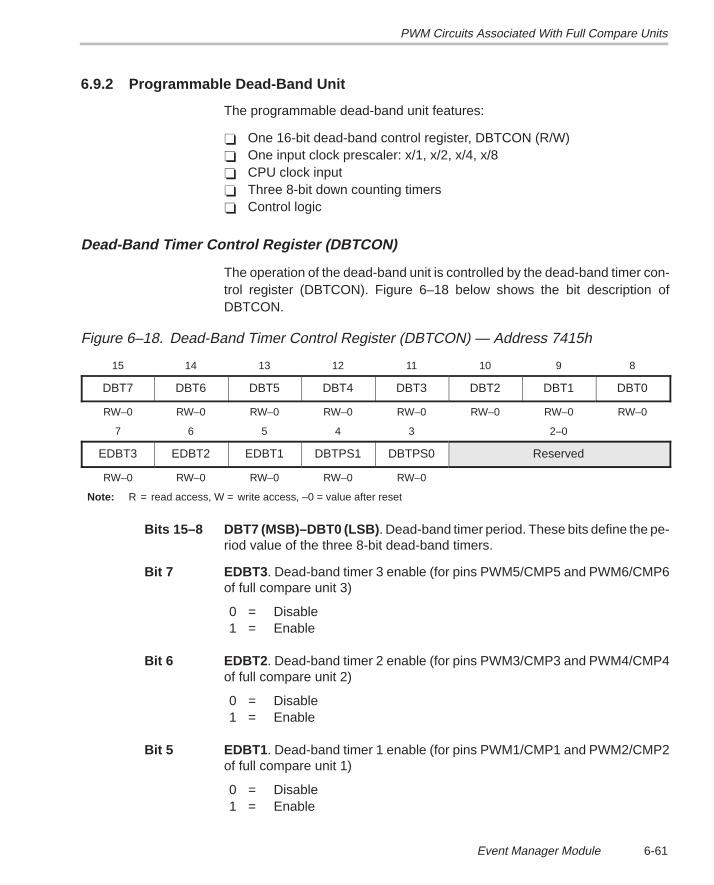
PWM Circuits Associated With Full Compare Units
6-61Event Manager Module
6.9.2 Programmable Dead-Band Unit
The programmable dead-band unit features:
� One 16-bit dead-band control register, DBTCON (R/W)� One input clock prescaler: x/1, x/2, x/4, x/8� CPU clock input� Three 8-bit down counting timers� Control logic
Dead-Band Timer Control Register (DBTCON)
The operation of the dead-band unit is controlled by the dead-band timer con-trol register (DBTCON). Figure 6–18 below shows the bit description ofDBTCON.
Figure 6–18. Dead-Band Timer Control Register (DBTCON) — Address 7415h
15 14 13 12 11 10 9 8
DBT7 DBT6 DBT5 DBT4 DBT3 DBT2 DBT1 DBT0
RW–0 RW–0 RW–0 RW–0 RW–0 RW–0 RW–0 RW–0
7 6 5 4 3 2–0
EDBT3 EDBT2 EDBT1 DBTPS1 DBTPS0 Reserved
RW–0 RW–0 RW–0 RW–0 RW–0
Note: R = read access, W = write access, –0 = value after reset
Bits 15–8 DBT7 (MSB)–DBT0 (LSB) . Dead-band timer period. These bits define the pe-riod value of the three 8-bit dead-band timers.
Bit 7 EDBT3 . Dead-band timer 3 enable (for pins PWM5/CMP5 and PWM6/CMP6of full compare unit 3)
0 = Disable1 = Enable
Bit 6 EDBT2 . Dead-band timer 2 enable (for pins PWM3/CMP3 and PWM4/CMP4of full compare unit 2)
0 = Disable1 = Enable
Bit 5 EDBT1 . Dead-band timer 1 enable (for pins PWM1/CMP1 and PWM2/CMP2of full compare unit 1)
0 = Disable1 = Enable
PWM Circuits Associated With Full Compare Units
6-62
Bits 4–3 DBTPS1, DBTPS0 . Dead-band timer prescaler
00 = x/101 = x/210 = x/411 = x/8where: x = CPU clock frequency
Bits 2–0 Reserved . Reads are 0, and writes have no effect.
Shoot-Through Fault �
COMCON bits 8 and 9 should be used to disable the compareoutputs, not COMCON bit 15. Disabling the compare operationusing COMCON bit 15 when deadband is enabled could result in ashoot-through fault.
† A shoot-through fault occurs when the upper and lower power devices (power transistors) switchon at the same time, momentarily.
6.9.3 Inputs and Outputs of Dead-Band Unit
The inputs to the dead-band unit are PH1, PH2, and PH3 from the asymmetric/symmetric waveform generators of full compare units 1, 2, and 3, respectively.
The outputs of the dead-band unit are DTPH1, DTPH1_; DTPH2, DTPH2_;and DTPH3, and DTPH3_ corresponding to PH1, PH2, and PH3, respectively.
6.9.4 Dead-Band Generation
For each input signal PHx, two output signals, DTPHx and DTPHx_, are gener-ated. When the dead band is not enabled for the compare unit and itsassociated outputs, the two signals are exactly the same. When the dead-band unit is enabled for the compare unit, the transition edges of the two sig-nals are separated by a time interval called the dead band. This time intervalis determined by the DBTCON bits. For example, If the value inDBTCON[15–8] is m and the value in DBTCON[4–3] corresponds to prescalerx/p, then the dead-band value is (p*m) CPU clock cycles.
Table 6–8 shows the dead band generated by typical bit combinations inDBTCON. The values are based on a 50-ns device. Figure 6–19 shows theblock diagram of the dead-band logic for one full compare unit.
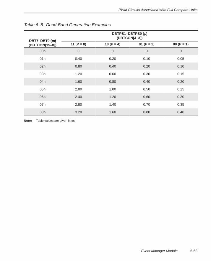
PWM Circuits Associated With Full Compare Units
6-63Event Manager Module
Table 6–8. Dead-Band Generation Examples
DBT7–DBT0 (m)
DBTPS1–DBTPS0 (p)(DBTCON[4–3])
DBT7–DBT0 (m)(DBTCON[15–8]) 11 (P = 8) 10 (P = 4) 01 (P = 2) 00 (P = 1)
00h 0 0 0 0
01h 0.40 0.20 0.10 0.05
02h 0.80 0.40 0.20 0.10
03h 1.20 0.60 0.30 0.15
04h 1.60 0.80 0.40 0.20
05h 2.00 1.00 0.50 0.25
06h 2.40 1.20 0.60 0.30
07h 2.80 1.40 0.70 0.35
08h 3.20 1.60 0.80 0.40
Note: Table values are given in �s.
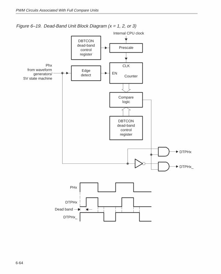
PWM Circuits Associated With Full Compare Units
6-64
Figure 6–19. Dead-Band Unit Block Diagram (x = 1, 2, or 3)
Dead band
DTPHx_
DTPHx
PHx
DTPHx_
DTPHx
SV state machinegenerators/
from waveformPhx
Internal CPU clock
DBTCONdead-band
controlregister
detectEdge
logicCompare
CounterEN
CLK
Prescale
registercontrol
dead-bandDBTCON

PWM Circuits Associated With Full Compare Units
6-65Event Manager Module
6.9.5 Other Important Features of Dead-Band Units
The dead-band unit is designed to assure that no overlap occurs between theturn-on periods of the upper and lower devices that are controlled by the twocompare/PWM outputs associated with each full compare unit. This assuresthat no overlap will occur under any condition, including when the user hasloaded a dead-band value greater than that of the duty cycle, and when theduty cycle is 100% or 0%. As a result, the compare/PWM outputs associatedwith a full compare unit do not reset to an inactive state at the end of a periodwhen the dead band is enabled for the full compare unit.
The dead-band is disabled when a full compare unit is in the compare mode.
Example 6–7 shows a full compare initialization routine for symmetric PWMwaveform generation with the dead-band unit activated.
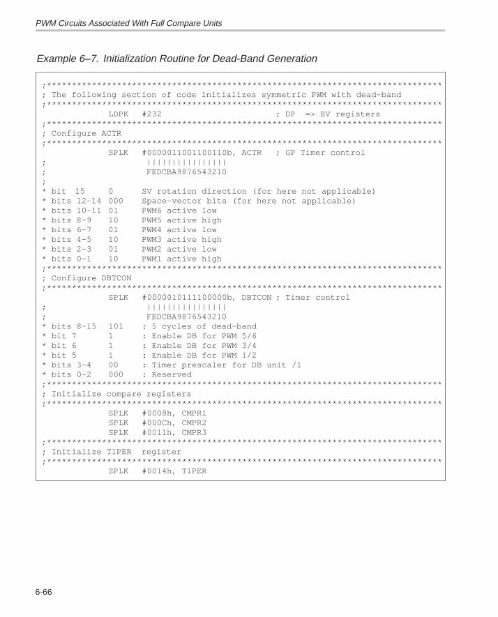
PWM Circuits Associated With Full Compare Units
6-66
Example 6–7. Initialization Routine for Dead-Band Generation
;*******************************************************************************; The following section of code initializes symmetric PWM with dead-band;*******************************************************************************
LDPK #232 ; DP => EV registers;*******************************************************************************; Configure ACTR;*******************************************************************************
SPLK #0000011001100110b, ACTR ; GP Timer control; ||||||||||||||||; FEDCBA9876543210;* bit 15 0 SV rotation direction (for here not applicable)* bits 12–14 000 Space-vector bits (for here not applicable)* bits 10–11 01 PWM6 active low* bits 8–9 10 PWM5 active high* bits 6–7 01 PWM4 active low* bits 4–5 10 PWM3 active high* bits 2–3 01 PWM2 active low* bits 0–1 10 PWM1 active high;*******************************************************************************; Configure DBTCON;*******************************************************************************
SPLK #0000010111100000b, DBTCON ; Timer control; ||||||||||||||||; FEDCBA9876543210* bits 8–15 101 : 5 cycles of dead-band* bit 7 1 : Enable DB for PWM 5/6* bit 6 1 : Enable DB for PWM 3/4* bit 5 1 : Enable DB for PWM 1/2* bits 3–4 00 : Timer prescaler for DB unit /1* bits 0–2 000 : Reserved;*******************************************************************************; Initialize compare registers;*******************************************************************************
SPLK #0008h, CMPR1SPLK #000Ch, CMPR2SPLK #0011h, CMPR3
;*******************************************************************************; Initialize T1PER register;*******************************************************************************
SPLK #0014h, T1PER
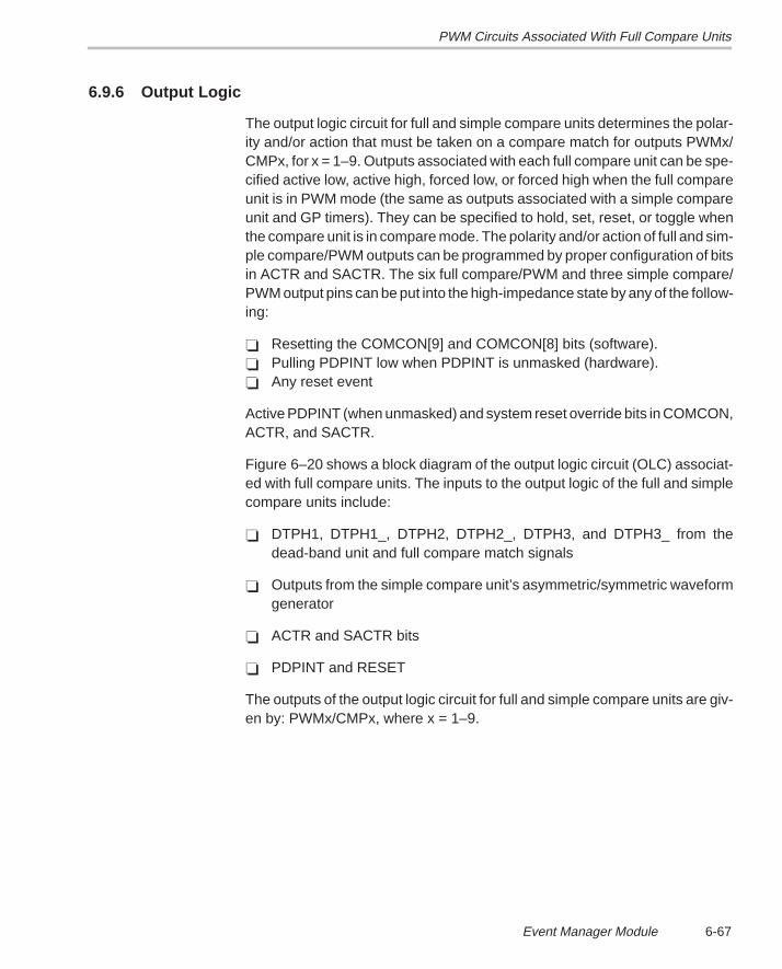
PWM Circuits Associated With Full Compare Units
6-67Event Manager Module
6.9.6 Output Logic
The output logic circuit for full and simple compare units determines the polar-ity and/or action that must be taken on a compare match for outputs PWMx/CMPx, for x = 1–9. Outputs associated with each full compare unit can be spe-cified active low, active high, forced low, or forced high when the full compareunit is in PWM mode (the same as outputs associated with a simple compareunit and GP timers). They can be specified to hold, set, reset, or toggle whenthe compare unit is in compare mode. The polarity and/or action of full and sim-ple compare/PWM outputs can be programmed by proper configuration of bitsin ACTR and SACTR. The six full compare/PWM and three simple compare/PWM output pins can be put into the high-impedance state by any of the follow-ing:
� Resetting the COMCON[9] and COMCON[8] bits (software).� Pulling PDPINT low when PDPINT is unmasked (hardware).� Any reset event
Active PDPINT (when unmasked) and system reset override bits in COMCON,ACTR, and SACTR.
Figure 6–20 shows a block diagram of the output logic circuit (OLC) associat-ed with full compare units. The inputs to the output logic of the full and simplecompare units include:
� DTPH1, DTPH1_, DTPH2, DTPH2_, DTPH3, and DTPH3_ from thedead-band unit and full compare match signals
� Outputs from the simple compare unit’s asymmetric/symmetric waveformgenerator
� ACTR and SACTR bits
� PDPINT and RESET
The outputs of the output logic circuit for full and simple compare units are giv-en by: PWMx/CMPx, where x = 1–9.
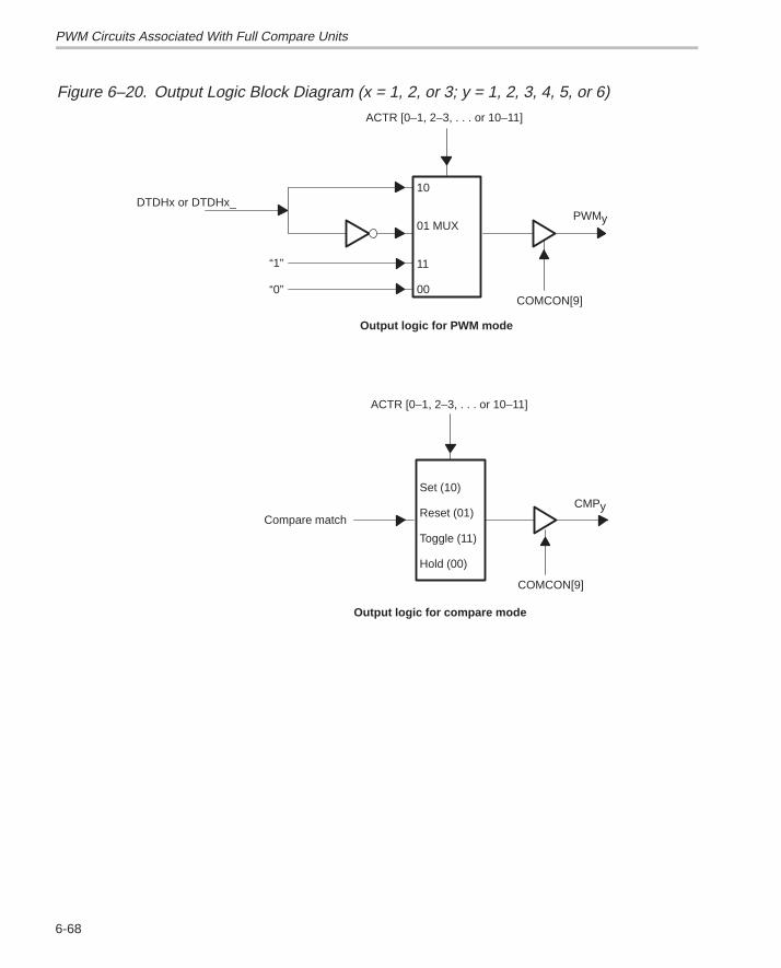
PWM Circuits Associated With Full Compare Units
6-68
Figure 6–20. Output Logic Block Diagram (x = 1, 2, or 3; y = 1, 2, 3, 4, 5, or 6)
DTDHx or DTDHx_10
01 MUX
11
00COMCON[9]
“1”
“0”
ACTR [0–1, 2–3, . . . or 10–11]
PWMy
Set (10)
Reset (01)
Toggle (11)
Hold (00)
COMCON[9]
CMPyCompare match
ACTR [0–1, 2–3, . . . or 10–11]
Output logic for PWM mode
Output logic for compare mode
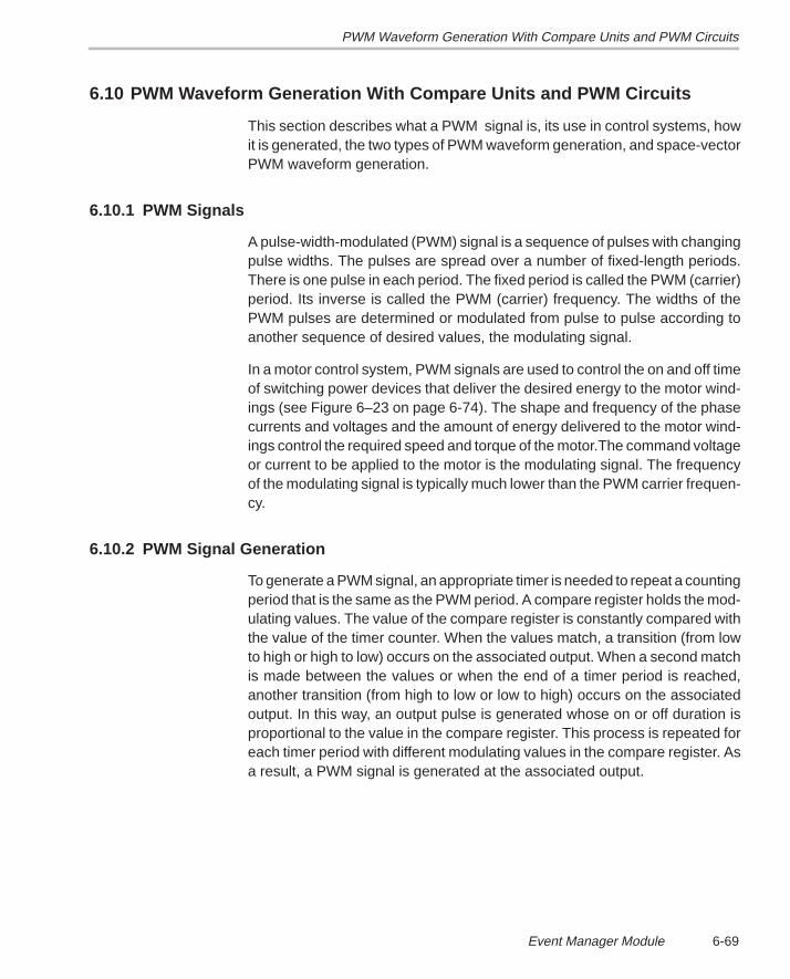
PWM Waveform Generation With Compare Units and PWM Circuits
6-69Event Manager Module
6.10 PWM Waveform Generation With Compare Units and PWM Circuits
This section describes what a PWM signal is, its use in control systems, howit is generated, the two types of PWM waveform generation, and space-vectorPWM waveform generation.
6.10.1 PWM Signals
A pulse-width-modulated (PWM) signal is a sequence of pulses with changingpulse widths. The pulses are spread over a number of fixed-length periods.There is one pulse in each period. The fixed period is called the PWM (carrier)period. Its inverse is called the PWM (carrier) frequency. The widths of thePWM pulses are determined or modulated from pulse to pulse according toanother sequence of desired values, the modulating signal.
In a motor control system, PWM signals are used to control the on and off timeof switching power devices that deliver the desired energy to the motor wind-ings (see Figure 6–23 on page 6-74). The shape and frequency of the phasecurrents and voltages and the amount of energy delivered to the motor wind-ings control the required speed and torque of the motor.The command voltageor current to be applied to the motor is the modulating signal. The frequencyof the modulating signal is typically much lower than the PWM carrier frequen-cy.
6.10.2 PWM Signal Generation
To generate a PWM signal, an appropriate timer is needed to repeat a countingperiod that is the same as the PWM period. A compare register holds the mod-ulating values. The value of the compare register is constantly compared withthe value of the timer counter. When the values match, a transition (from lowto high or high to low) occurs on the associated output. When a second matchis made between the values or when the end of a timer period is reached,another transition (from high to low or low to high) occurs on the associatedoutput. In this way, an output pulse is generated whose on or off duration isproportional to the value in the compare register. This process is repeated foreach timer period with different modulating values in the compare register. Asa result, a PWM signal is generated at the associated output.
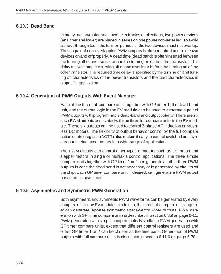
PWM Waveform Generation With Compare Units and PWM Circuits
6-70
6.10.3 Dead Band
In many motion/motor and power electronics applications, two power devices(an upper and lower) are placed in series on one power converter leg. To avoida shoot-through fault, the turn-on periods of the two devices must not overlap.Thus, a pair of non-overlapping PWM outputs is often required to turn the twodevices on and off properly. A dead time (dead band) is often inserted betweenthe turning off of one transistor and the turning on of the other transistor. Thisdelay allows complete turning off of one transistor before the turning on of theother transistor. The required time delay is specified by the turning on and turn-ing off characteristics of the power transistors and the load characteristics ina specific application.
6.10.4 Generation of PWM Outputs With Event Manager
Each of the three full compare units together with GP timer 1, the dead-bandunit, and the output logic in the EV module can be used to generate a pair ofPWM outputs with programmable dead-band and output polarity. There are sixsuch PWM outputs associated with the three full compare units in the EV mod-ule. These six outputs can be used to control 3-phase AC induction or brush-less DC motors. The flexibility of output behavior control by the full compareaction control register (ACTR) also makes it easy to control switched and syn-chronous reluctance motors in a wide range of applications.
The PWM circuits can control other types of motors such as DC brush andstepper motors in single or multiaxis control applications. The three simplecompare units together with GP timer 1 or 2 can generate another three PWMoutputs in case the dead band is not necessary or is generated by circuits offthe chip. Each GP timer compare unit, if desired, can generate a PWM outputbased on its own timer.
6.10.5 Asymmetric and Symmetric PWM Generation
Both asymmetric and symmetric PWM waveforms can be generated by everycompare unit in the EV module. In addition, the three full compare units togeth-er can generate 3-phase symmetric space-vector PWM outputs. PWM gen-eration with GP timer compare units is described in section 6.3.9 on page 6-15.PWM generation with simple compare units is similar to PWM generation withGP timer compare units, except that different control registers are used andeither GP timer 1 or 2 can be chosen as the time base. Generation of PWMoutputs with full compare units is discussed in section 6.11.6 on page 6-78.

PWM Waveform Generation With Compare Units and PWM Circuits
6-71Event Manager Module
6.10.6 Register Setup for PWM Generation
All three kinds of PWM waveform generation with full compare units andassociated circuits require configuration of the same EV registers. The setupprocess for PWM generation includes the following steps:
1) Set up and load ACTR.
2) Set up and load DBTCON, if dead band is to be used.
3) Initialize CMPRx.
4) Set up and load COMCON without enabling compare operation.
5) Set up and load COMCON to enable compare operation.
6) Set up and load T1CON to start the operation.
7) Rewrite CMPRx with newly determined values.
Note:
Before T1CON is written to start the operation, COMCON must be written totwice to ensure that all full compare outputs come up in the correct (inactive)states.
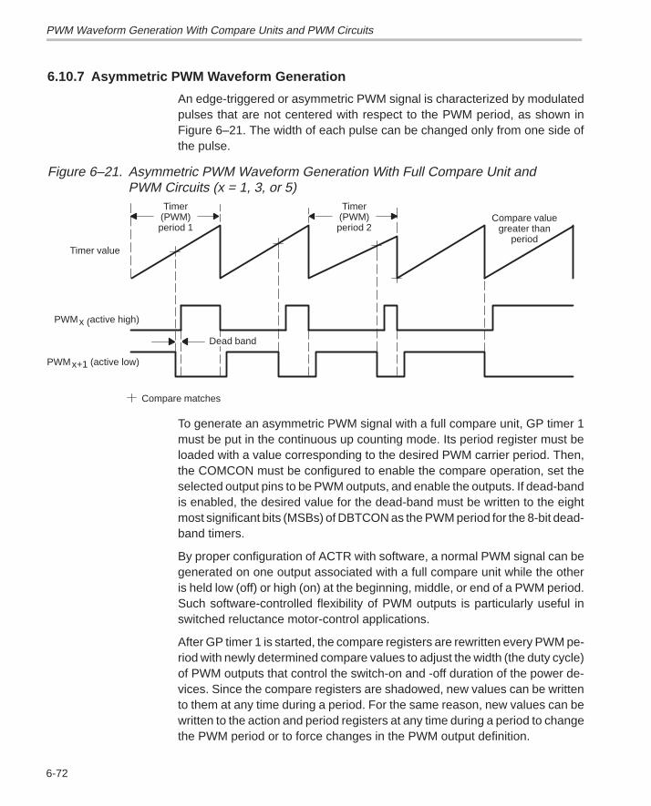
PWM Waveform Generation With Compare Units and PWM Circuits
6-72
6.10.7 Asymmetric PWM Waveform Generation
An edge-triggered or asymmetric PWM signal is characterized by modulatedpulses that are not centered with respect to the PWM period, as shown inFigure 6–21. The width of each pulse can be changed only from one side ofthe pulse.
Figure 6–21. Asymmetric PWM Waveform Generation With Full Compare Unit andPWM Circuits (x = 1, 3, or 5)
PWMx (active high)
Timer(PWM)period 2
PWMx+1 (active low)
Timer value
Compare matches
Dead band
Compare valuegreater than
period
Timer(PWM)period 1
To generate an asymmetric PWM signal with a full compare unit, GP timer 1must be put in the continuous up counting mode. Its period register must beloaded with a value corresponding to the desired PWM carrier period. Then,the COMCON must be configured to enable the compare operation, set theselected output pins to be PWM outputs, and enable the outputs. If dead-bandis enabled, the desired value for the dead-band must be written to the eightmost significant bits (MSBs) of DBTCON as the PWM period for the 8-bit dead-band timers.
By proper configuration of ACTR with software, a normal PWM signal can begenerated on one output associated with a full compare unit while the otheris held low (off) or high (on) at the beginning, middle, or end of a PWM period.Such software-controlled flexibility of PWM outputs is particularly useful inswitched reluctance motor-control applications.
After GP timer 1 is started, the compare registers are rewritten every PWM pe-riod with newly determined compare values to adjust the width (the duty cycle)of PWM outputs that control the switch-on and -off duration of the power de-vices. Since the compare registers are shadowed, new values can be writtento them at any time during a period. For the same reason, new values can bewritten to the action and period registers at any time during a period to changethe PWM period or to force changes in the PWM output definition.
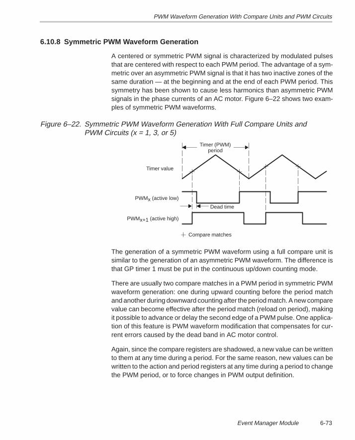
PWM Waveform Generation With Compare Units and PWM Circuits
6-73Event Manager Module
6.10.8 Symmetric PWM Waveform Generation
A centered or symmetric PWM signal is characterized by modulated pulsesthat are centered with respect to each PWM period. The advantage of a sym-metric over an asymmetric PWM signal is that it has two inactive zones of thesame duration — at the beginning and at the end of each PWM period. Thissymmetry has been shown to cause less harmonics than asymmetric PWMsignals in the phase currents of an AC motor. Figure 6–22 shows two exam-ples of symmetric PWM waveforms.
Figure 6–22. Symmetric PWM Waveform Generation With Full Compare Units andPWM Circuits (x = 1, 3, or 5)
PWMx (active low)
Timer value
Compare matches
Dead time
Timer (PWM)period
PWMx+1 (active high)
The generation of a symmetric PWM waveform using a full compare unit issimilar to the generation of an asymmetric PWM waveform. The difference isthat GP timer 1 must be put in the continuous up/down counting mode.
There are usually two compare matches in a PWM period in symmetric PWMwaveform generation: one during upward counting before the period matchand another during downward counting after the period match. A new comparevalue can become effective after the period match (reload on period), makingit possible to advance or delay the second edge of a PWM pulse. One applica-tion of this feature is PWM waveform modification that compensates for cur-rent errors caused by the dead band in AC motor control.
Again, since the compare registers are shadowed, a new value can be writtento them at any time during a period. For the same reason, new values can bewritten to the action and period registers at any time during a period to changethe PWM period, or to force changes in PWM output definition.
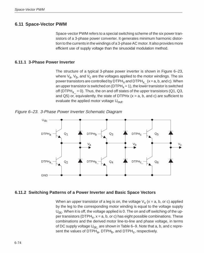
Space-Vector PWM
6-74
6.11 Space-Vector PWM
Space-vector PWM refers to a special switching scheme of the six power tran-sistors of a 3-phase power converter. It generates minimum harmonic distor-tion to the currents in the windings of a 3-phase AC motor. It also provides moreefficient use of supply voltage than the sinusoidal modulation method.
6.11.1 3-Phase Power Inverter
The structure of a typical 3-phase power inverter is shown in Figure 6–23,where Va, Vb, and Vc are the voltages applied to the motor windings. The sixpower transistors are controlled by DTPHx and DTPHx_ (x = a, b, and c). Whenan upper transistor is switched on (DTPHx = 1), the lower transistor is switchedoff (DTPHx_ = 0). Thus, the on and off states of the upper transistors (Q1, Q3,and Q5) or, equivalently, the state of DTPHx (x = a, b, and c) are sufficient toevaluate the applied motor voltage Uout.
Figure 6–23. 3-Phase Power Inverter Schematic Diagram
Udc
Q1
Q2
Va
DTPHa
DTPHa_
GND
Q3
Q4
Vb
DTPHb
DTPHb_
Q5
Q6
Vc
DTPHc
DTPHc_
6.11.2 Switching Patterns of a Power Inverter and Basic Space Vectors
When an upper transistor of a leg is on, the voltage Vx (x = a, b, or c) appliedby the leg to the corresponding motor winding is equal to the voltage supplyUdc. When it is off, the voltage applied is 0. The on and off switching of the up-per transistors (DTPHx, x = a, b, or c) has eight possible combinations. Thesecombinations and the derived motor line-to-line and phase voltage, in termsof DC supply voltage Udc, are shown in Table 6–9. Note that a, b, and c repre-sent the values of DTPHa, DTPHb, and DTPHc, respectively.
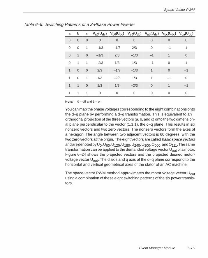
Space-Vector PWM
6-75Event Manager Module
Table 6–9. Switching Patterns of a 3-Phase Power Inverter
a b c Va0(Udc) Vb0(Udc) Vc0(Udc) Vab(Udc) Vbc(Udc) Vca(Udc)
0 0 0 0 0 0 0 0 0
0 0 1 –1/3 –1/3 2/3 0 –1 1
0 1 0 –1/3 2/3 –1/3 –1 1 0
0 1 1 –2/3 1/3 1/3 –1 0 1
1 0 0 2/3 –1/3 –1/3 1 0 –1
1 0 1 1/3 –2/3 1/3 1 –1 0
1 1 0 1/3 1/3 –2/3 0 1 –1
1 1 1 0 0 0 0 0 0
Note: 0 = off and 1 = on
You can map the phase voltages corresponding to the eight combinations ontothe d–q plane by performing a d–q transformation. This is equivalent to an orthogonal projection of the three vectors (a, b, and c) onto the two dimension-al plane perpendicular to the vector (1,1,1), the d–q plane. This results in sixnonzero vectors and two zero vectors. The nonzero vectors form the axes ofa hexagon. The angle between two adjacent vectors is 60 degrees, with thetwo zero vectors at the origin. The eight vectors are called basic space vectorsand are denoted by U0, U60, U120, U180, U240, U300, O000, and O111. The sametransformation can be applied to the demanded voltage vector Uout of a motor.Figure 6–24 shows the projected vectors and the projected desired motor-voltage vector Uout. The d axis and q axis of the d–q plane correspond to thehorizontal and vertical geometrical axes of the stator of an AC machine.
The space-vector PWM method approximates the motor voltage vector Uoutusing a combination of these eight switching patterns of the six power transis-tors.
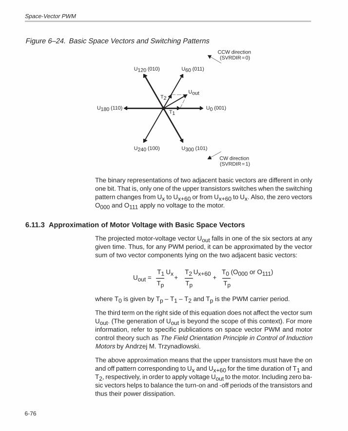
Space-Vector PWM
6-76
Figure 6–24. Basic Space Vectors and Switching Patterns
T2
U120 (010)
T1
U60 (011)
U240 (100) U300 (101)
U0 (001)U180 (110)
Uout
CCW direction(SVRDIR=0)
CW direction(SVRDIR=1)
The binary representations of two adjacent basic vectors are different in onlyone bit. That is, only one of the upper transistors switches when the switchingpattern changes from Ux to Ux+60 or from Ux+60 to Ux. Also, the zero vectorsO000 and O111 apply no voltage to the motor.
6.11.3 Approximation of Motor Voltage with Basic Space Vectors
The projected motor-voltage vector Uout falls in one of the six sectors at anygiven time. Thus, for any PWM period, it can be approximated by the vectorsum of two vector components lying on the two adjacent basic vectors:
T0 (O000 or O111)
Tp Tp TpUout =
T1 Ux+
T2 Ux+60+
where T0 is given by Tp – T1 – T2 and Tp is the PWM carrier period.
The third term on the right side of this equation does not affect the vector sumUout. (The generation of Uout is beyond the scope of this context). For moreinformation, refer to specific publications on space vector PWM and motorcontrol theory such as The Field Orientation Principle in Control of InductionMotors by Andrzej M. Trzynadlowski.
The above approximation means that the upper transistors must have the onand off pattern corresponding to Ux and Ux+60 for the time duration of T1 andT2, respectively, in order to apply voltage Uout to the motor. Including zero ba-sic vectors helps to balance the turn-on and -off periods of the transistors andthus their power dissipation.
Space-Vector PWM
6-77Event Manager Module
6.11.4 Space-Vector PWM Waveform Generation With EV
The EV module has built-in hardware to greatly simplify the generation of sym-metric space-vector PWM waveforms. A description of the software/hardwarerequirements for generating space vector PWM waveforms follows.
Software
To generate space-vector PWM outputs, the user software must:
� Configure ACTR to define the polarity for full compare output pins
� Configure COMCON to enable the compare operation and space vectorPWM mode and set the reload condition for ACTR and CMPRx to be un-derflow
� Put GP timer 1 in continuous up/down counting mode to start the operation
Note:
Enabling space-vector PWM mode automatically sets all full compare outputpins as PWM outputs.
The user software then must
� Determine the voltage Uout to be applied to the motor phases in the two-dimensional d–q plane
� Decompose Uout
� Do the following for each PWM period:
� Determine the two adjacent vectors, Ux and Ux+60
� Determine the parameters T1, T2, and T0
� Write the switching pattern corresponding to Ux in ACTR[14–12] and 0in ACTR[15], or the switching pattern of Ux+60 in ACTR[14–12] and 1in ACTR[15]
� Put (1/2 T1) in CMPR1 and (1/2 T1 + 1/2 T2) in CMPR2 if ACTR[15] is0, or put (1/2 T2) in CMPR1 and (1/2 T1 + 1/2 T2) in CMPR2 ifACTR[15] is 1.
Space-Vector PWM
6-78
Space-Vector PWM Hardware
The space-vector PWM hardware in the EV module does the following to com-plete a space-vector PWM period:
� At the beginning of each period, sets the PWM outputs to the (new) patternUy defined by ACTR[14–12]
� On the first compare match during up counting between CMPR1 and GPtimer 1, switches the PWM outputs to the pattern of Uy+60 if ACTR[15] is0, or to the pattern of Uy if ACTR[15] is 1. U0–60 = U300, U360+60 = U60
� On the second compare match during up counting between CMPR2 andGP timer 1 at (1/2 T1 + 1/2 T2), switches the PWM outputs to the pattern(000) or (111), whichever differs from the second pattern by one bit
� On the first compare match during down counting between CMPR2 andGP timer 1, switches the PWM outputs back to the second output pattern
� On the second compare match during down counting between CMPR1and GP timer 1, switches the PWM outputs back to the first output pattern
6.11.5 Space-Vector PWM Waveforms
The space-vector PWM waveforms generated are symmetric with respect tothe middle of each PWM period. Figure 6–25 on page 6-79 shows two exam-ples of symmetric space-vector PWM waveforms.
6.11.6 Unused Full Compare Register
Only two full compare registers are used in space-vector PWM output genera-tion. The third full compare register, however, is still constantly compared withGP timer 1. When a compare match occurs, the corresponding compare inter-rupt flag is set. Therefore, the compare register that is not used in the space-vector PWM output generation can still be used to time events occurring in aspecific application. Also, because of the extra delay introduced by the statemachine, the full compare output transitions are delayed by two CPU clockcycles in space-vector PWM mode.
6.11.7 Space-Vector PWM Boundary Conditions
All three full compare outputs become inactive when both full compare regis-ters (CMPR1 and CMPR2) are loaded with a zero value in the space-vectorPWM mode. In general, it is the user’s responsibility to assure that(CMPR1) � (CMPR2) � (T1PR) in the space vector PWM mode; otherwise,unpredicted behavior may result.
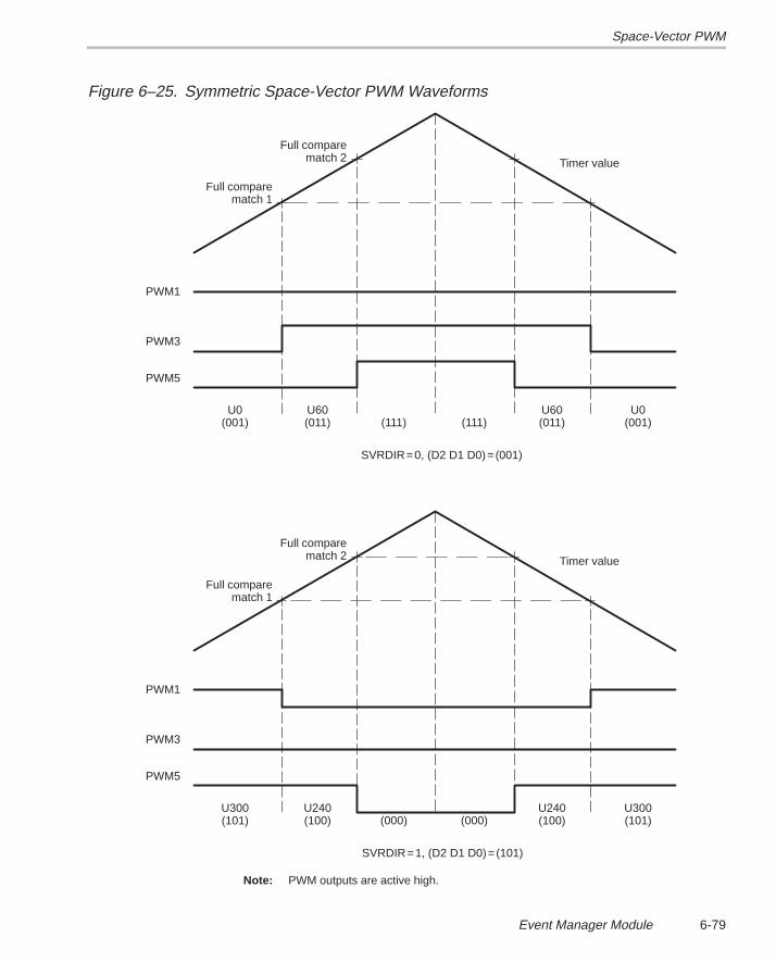
Space-Vector PWM
6-79Event Manager Module
Figure 6–25. Symmetric Space-Vector PWM Waveforms
SVRDIR=0, (D2 D1 D0)=(001)
Full comparematch 2
Full comparematch 1
Timer value
PWM1
PWM3
PWM5
U0(001)
U60(011) (111) (111)
U0(001)
U60(011)
SVRDIR=1, (D2 D1 D0)=(101)
Full comparematch 2
Full comparematch 1
Timer value
PWM1
PWM3
PWM5
U300(101)
U240(100) (000) (000)
U300(101)
U240(100)
Note: PWM outputs are active high.
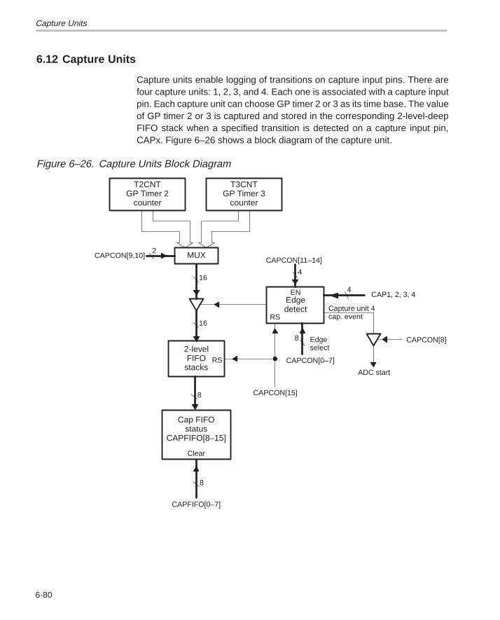
Capture Units
6-80
6.12 Capture Units
Capture units enable logging of transitions on capture input pins. There arefour capture units: 1, 2, 3, and 4. Each one is associated with a capture inputpin. Each capture unit can choose GP timer 2 or 3 as its time base. The valueof GP timer 2 or 3 is captured and stored in the corresponding 2-level-deepFIFO stack when a specified transition is detected on a capture input pin,CAPx. Figure 6–26 shows a block diagram of the capture unit.
Figure 6–26. Capture Units Block Diagram
4
2
Cap FIFOstatus
CAPFIFO[8–15]
RS
ENEdgedetect
RS
Edgeselect
CAPCON[9,10]
CAPCON[0–7]
CAPCON[15]
Clear
CAPFIFO[0–7]
Capture unit 4cap. event
ADC start
CAPCON[8]
CAPCON[11–14]
16
16
CAP1, 2, 3, 44
8
2-levelFIFO
stacks
8
8
MUX
T3CNTGP Timer 3
counter
T2CNTGP Timer 2
counter
Capture Units
6-81Event Manager Module
6.12.1 Features
Capture units have the following features:
� One 16-bit capture control register, CAPCON (R/W)
� One 16-bit capture FIFO status register, CAPFIFO (eight MSBs are readonly, eight LSBs are write only)
� Ability to select GP timer 2 or 3 as the time base
� Four 16-bit 2-level-deep FIFO stacks, one for each capture unit
� Four Schmitt-triggered capture input pins CAP1, CAP2, CAP3, and CAP4,one input pin per each capture unit. (All inputs are synchronized with theCPU clock. For a transition to be captured, the input must hold at its currentlevel to meet the two rising edges of the CPU clock. The input pins CAP1and CAP2 can also be used as QEP inputs to a QEP circuit.)
� User-specified transition (rising edge, falling edge, or both edges) detection
� Four maskable flags, one for each capture unit
6.12.2 Operation of Capture Units
The following three paragraphs describe the operation of the capture units,their association with GP timers, compare/PWM operation, transitions on as-sociated pins, and the register setup.
Capture Unit Time Base Selection
Either GP timer 2 or 3 can be selected by capture units 1 and 2 or by captureunits 3 and 4. In this way, two GP timers can be used at the same time, onefor each pair of capture units.
Capture operation does not affect the operation of any GP timer or thecompare/PWM operations associated with any GP timer.
Capture Operation
After a capture unit is enabled, a specified transition on the associated inputpin causes:
� the counter value of the selected GP timer to be locked into the corre-sponding FIFO stack
� the corresponding interrupt flag to be set
Capture Units
6-82
Afterwards, the corresponding status bits in CAPFIFO are adjusted to reflectthe new status of the FIFO stack each time a new counter value is capturedinto a FIFO stack. The latency, from the time a transition occurs on a captureinput to the time the counter value of the selected GP timer is locked, is 3.5–4.5CPU clock cycles.
All capture unit registers are cleared when the RESET input goes low.
Capture Unit Setup
For a capture unit to function properly, the following register setup is per-formed:
1) Initialize the CAPFIFO. Clear the appropriate status bits.
2) Set the selected GP timer in one of its operating modes.
3) Set the associated GP timer compare register or GP timer period registerif necessary.
4) Set up CAPCON.
6.12.3 Capture Unit Registers
The operation of capture units is controlled by two 16-bit control registers,CAPCON and CAPFIFO. The T2CON and T3CON registers are also neededfor capture operation because the time base for capture circuits is provided byGP timer 2 or 3. Like all other EV registers, these registers are all data-memorymapped and can be treated by user software as data-memory locations.Table 6–4 on page 6-9 shows the addresses of these registers.
Capture Control Register (CAPCON)
In addition to being one of the two registers controlling the operation of captureunits, CAPCON is also used to control the operation of QEP circuits.
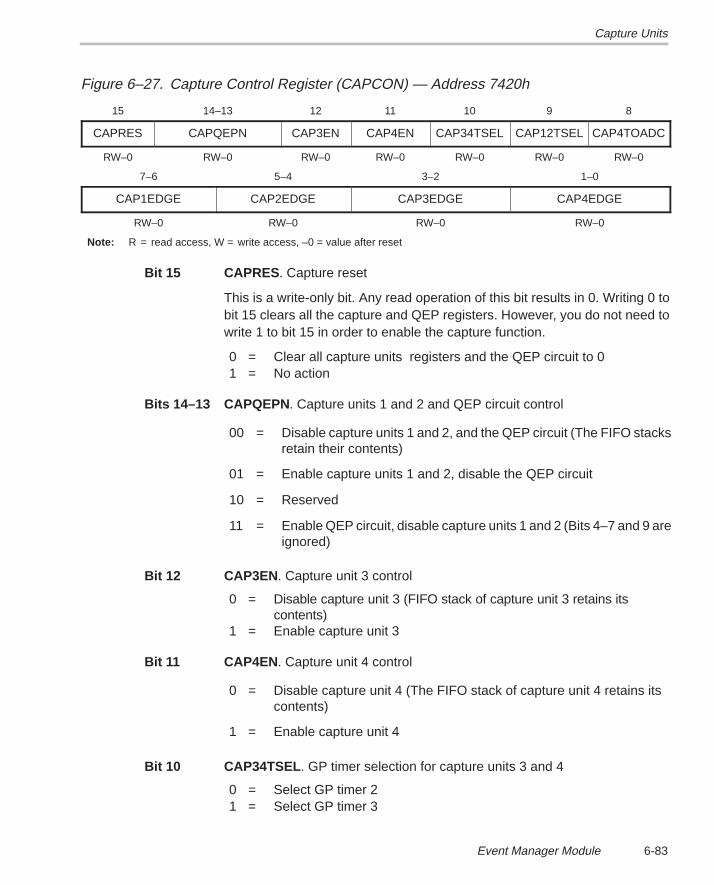
Capture Units
6-83Event Manager Module
Figure 6–27. Capture Control Register (CAPCON) — Address 7420h
15 14–13 12 11 10 9 8
CAPRES CAPQEPN CAP3EN CAP4EN CAP34TSEL CAP12TSEL CAP4TOADC
RW–0 RW–0 RW–0 RW–0 RW–0 RW–0 RW–0
7–6 5–4 3–2 1–0
CAP1EDGE CAP2EDGE CAP3EDGE CAP4EDGE
RW–0 RW–0 RW–0 RW–0
Note: R = read access, W = write access, –0 = value after reset
Bit 15 CAPRES . Capture reset
This is a write-only bit. Any read operation of this bit results in 0. Writing 0 tobit 15 clears all the capture and QEP registers. However, you do not need towrite 1 to bit 15 in order to enable the capture function.
0 = Clear all capture units registers and the QEP circuit to 01 = No action
Bits 14–13 CAPQEPN . Capture units 1 and 2 and QEP circuit control
00 = Disable capture units 1 and 2, and the QEP circuit (The FIFO stacksretain their contents)
01 = Enable capture units 1 and 2, disable the QEP circuit
10 = Reserved
11 = Enable QEP circuit, disable capture units 1 and 2 (Bits 4–7 and 9 areignored)
Bit 12 CAP3EN . Capture unit 3 control
0 = Disable capture unit 3 (FIFO stack of capture unit 3 retains itscontents)
1 = Enable capture unit 3
Bit 11 CAP4EN . Capture unit 4 control
0 = Disable capture unit 4 (The FIFO stack of capture unit 4 retains itscontents)
1 = Enable capture unit 4
Bit 10 CAP34TSEL . GP timer selection for capture units 3 and 4
0 = Select GP timer 21 = Select GP timer 3
Capture Units
6-84
Bit 9 CAP12TSEL . GP timer selection for capture units 1 and 2
0 = Select GP timer 21 = Select GP timer 3
Bit 8 CAP4TOADC . Capture unit 4 event starts ADC
0 = No action1 = Start ADC when the CAP4INT flag is set
Bits 7–6 CAP1EDGE . Edge detection control for capture unit 1
00 = No detection01 = Detect rising edge10 = Detect falling edge11 = Detect both edges
Bits 5–4 CAP2EDGE . Edge detection control for capture unit 2
00 = No detection01 = Detect rising edge10 = Detect falling edge11 = Detect both edges
Bits 3–2 CAP3EDGE . Edge detection control for capture unit 3
00 = No detection01 = Detect rising edge10 = Detect falling edge11 = Detect both edges
Bits 1–0 CAP4EDGE . Edge detection control for capture unit 4
00 = No detection01 = Detect rising edge10 = Detect falling edge11 = Detect both edges
Capture FIFO Status Register (CAPFIFO)
CAPFIFO contains the status bits for each of the four FIFO stacks of captureunits. The bit description of CAPFIFO is given in Figure 6–28. The eight LSBsof CAPFIFO have a one-to-one correspondence with the eight MSBs of CAPFIFO. A 1 written to CAPFIFO[x], x = 0, 1, ... or 7, clears bit CAPFIFO[x+8].CAPFIFO[x], for x = 0, 1, ... 7, are write only and CAPFIFO[y], for y = 8, 9, ...15, are read only.
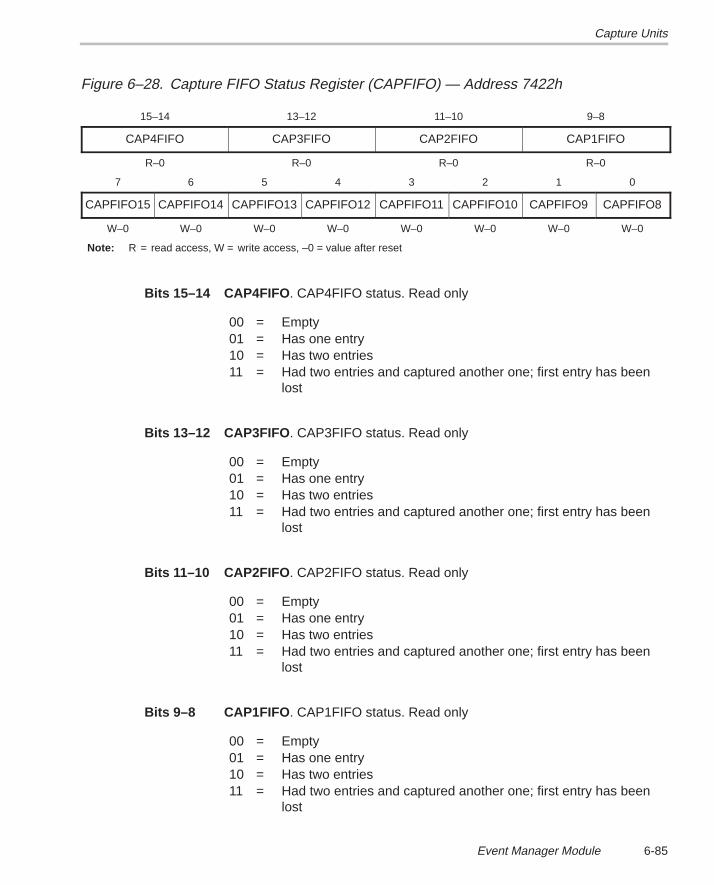
Capture Units
6-85Event Manager Module
Figure 6–28. Capture FIFO Status Register (CAPFIFO) — Address 7422h
15–14 13–12 11–10 9–8
CAP4FIFO CAP3FIFO CAP2FIFO CAP1FIFO
R–0 R–0 R–0 R–0
7 6 5 4 3 2 1 0
CAPFIFO15 CAPFIFO14 CAPFIFO13 CAPFIFO12 CAPFIFO11 CAPFIFO10 CAPFIFO9 CAPFIFO8
W–0 W–0 W–0 W–0 W–0 W–0 W–0 W–0
Note: R = read access, W = write access, –0 = value after reset
Bits 15–14 CAP4FIFO . CAP4FIFO status. Read only
00 = Empty01 = Has one entry10 = Has two entries11 = Had two entries and captured another one; first entry has been
lost
Bits 13–12 CAP3FIFO . CAP3FIFO status. Read only
00 = Empty01 = Has one entry10 = Has two entries11 = Had two entries and captured another one; first entry has been
lost
Bits 11–10 CAP2FIFO . CAP2FIFO status. Read only
00 = Empty01 = Has one entry10 = Has two entries11 = Had two entries and captured another one; first entry has been
lost
Bits 9–8 CAP1FIFO . CAP1FIFO status. Read only
00 = Empty01 = Has one entry10 = Has two entries11 = Had two entries and captured another one; first entry has been
lost
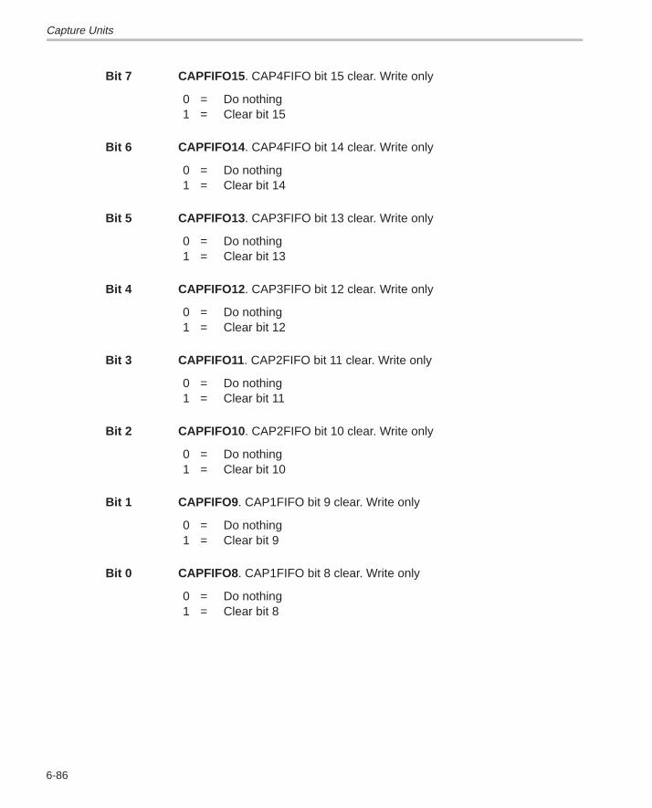
Capture Units
6-86
Bit 7 CAPFIFO15 . CAP4FIFO bit 15 clear. Write only
0 = Do nothing1 = Clear bit 15
Bit 6 CAPFIFO14 . CAP4FIFO bit 14 clear. Write only
0 = Do nothing1 = Clear bit 14
Bit 5 CAPFIFO13 . CAP3FIFO bit 13 clear. Write only
0 = Do nothing1 = Clear bit 13
Bit 4 CAPFIFO12 . CAP3FIFO bit 12 clear. Write only
0 = Do nothing1 = Clear bit 12
Bit 3 CAPFIFO11 . CAP2FIFO bit 11 clear. Write only
0 = Do nothing1 = Clear bit 11
Bit 2 CAPFIFO10 . CAP2FIFO bit 10 clear. Write only
0 = Do nothing1 = Clear bit 10
Bit 1 CAPFIFO9 . CAP1FIFO bit 9 clear. Write only
0 = Do nothing1 = Clear bit 9
Bit 0 CAPFIFO8 . CAP1FIFO bit 8 clear. Write only
0 = Do nothing1 = Clear bit 8
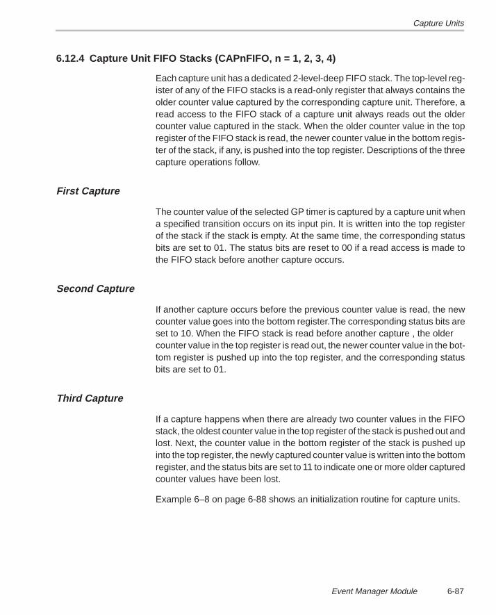
Capture Units
6-87Event Manager Module
6.12.4 Capture Unit FIFO Stacks (CAPnFIFO, n = 1, 2, 3, 4)
Each capture unit has a dedicated 2-level-deep FIFO stack. The top-level reg-ister of any of the FIFO stacks is a read-only register that always contains theolder counter value captured by the corresponding capture unit. Therefore, aread access to the FIFO stack of a capture unit always reads out the oldercounter value captured in the stack. When the older counter value in the topregister of the FIFO stack is read, the newer counter value in the bottom regis-ter of the stack, if any, is pushed into the top register. Descriptions of the threecapture operations follow.
First Capture
The counter value of the selected GP timer is captured by a capture unit whena specified transition occurs on its input pin. It is written into the top registerof the stack if the stack is empty. At the same time, the corresponding statusbits are set to 01. The status bits are reset to 00 if a read access is made tothe FIFO stack before another capture occurs.
Second Capture
If another capture occurs before the previous counter value is read, the newcounter value goes into the bottom register.The corresponding status bits areset to 10. When the FIFO stack is read before another capture , the oldercounter value in the top register is read out, the newer counter value in the bot-tom register is pushed up into the top register, and the corresponding statusbits are set to 01.
Third Capture
If a capture happens when there are already two counter values in the FIFOstack, the oldest counter value in the top register of the stack is pushed out andlost. Next, the counter value in the bottom register of the stack is pushed upinto the top register, the newly captured counter value is written into the bottomregister, and the status bits are set to 11 to indicate one or more older capturedcounter values have been lost.
Example 6–8 on page 6-88 shows an initialization routine for capture units.
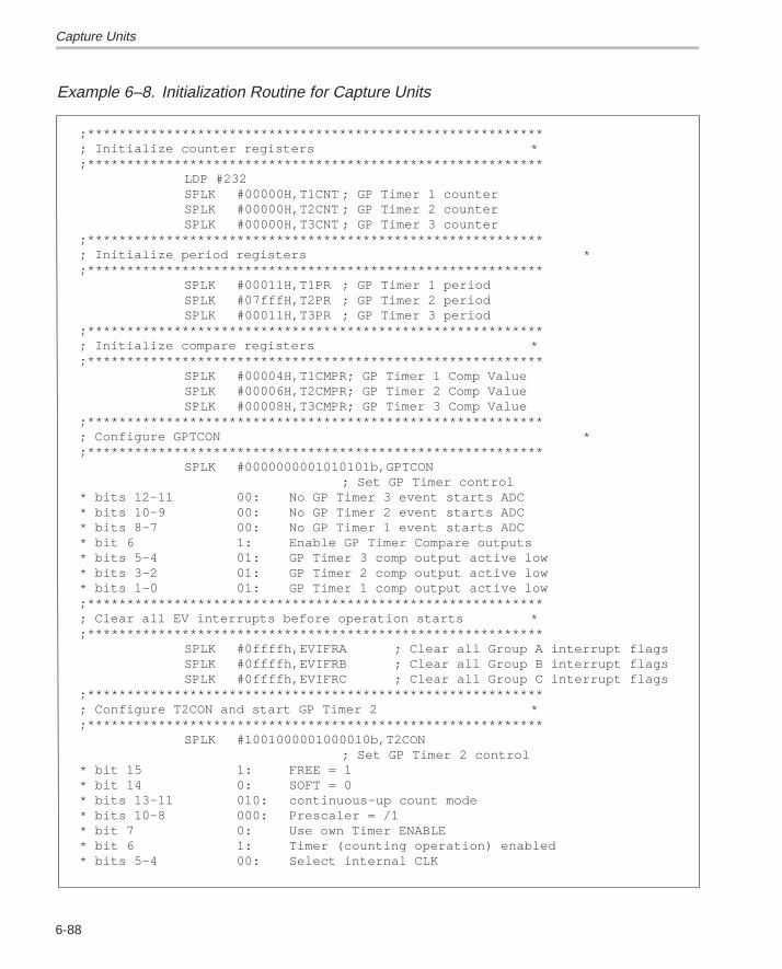
Capture Units
6-88
Example 6–8. Initialization Routine for Capture Units
;**********************************************************; Initialize counter registers *;**********************************************************
LDP #232 SPLK #00000H,T1CNT ; GP Timer 1 counter SPLK #00000H,T2CNT ; GP Timer 2 counter
SPLK #00000H,T3CNT ; GP Timer 3 counter;**********************************************************; Initialize period registers *;********************************************************** SPLK #00011H,T1PR ; GP Timer 1 period SPLK #07fffH,T2PR ; GP Timer 2 period
SPLK #00011H,T3PR ; GP Timer 3 period;**********************************************************; Initialize compare registers *;**********************************************************
SPLK #00004H,T1CMPR; GP Timer 1 Comp ValueSPLK #00006H,T2CMPR; GP Timer 2 Comp ValueSPLK #00008H,T3CMPR; GP Timer 3 Comp Value
;**********************************************************; Configure GPTCON *;**********************************************************
SPLK #0000000001010101b,GPTCON; Set GP Timer control
* bits 12–11 00: No GP Timer 3 event starts ADC* bits 10–9 00: No GP Timer 2 event starts ADC* bits 8–7 00: No GP Timer 1 event starts ADC* bit 6 1: Enable GP Timer Compare outputs* bits 5–4 01: GP Timer 3 comp output active low* bits 3–2 01: GP Timer 2 comp output active low* bits 1–0 01: GP Timer 1 comp output active low;**********************************************************; Clear all EV interrupts before operation starts *;**********************************************************
SPLK #0ffffh,EVIFRA ; Clear all Group A interrupt flagsSPLK #0ffffh,EVIFRB ; Clear all Group B interrupt flagsSPLK #0ffffh,EVIFRC ; Clear all Group C interrupt flags
;**********************************************************; Configure T2CON and start GP Timer 2 *;**********************************************************
SPLK #1001000001000010b,T2CON; Set GP Timer 2 control
* bit 15 1: FREE = 1* bit 14 0: SOFT = 0* bits 13–11 010: continuous–up count mode* bits 10–8 000: Prescaler = /1* bit 7 0: Use own Timer ENABLE* bit 6 1: Timer (counting operation) enabled* bits 5–4 00: Select internal CLK
Capture Units
6-89Event Manager Module
Example 6–8. Initialization Routine for Capture Units (Continued)
* bits 3–2 00: Load GP Timer comp register on underflow* bit 1 1: GP Timer compare enabled* bit 0 0: Use own PR
;**********************************************************; Configure CAPCON and enable capture operation *;**********************************************************
SPLK #1011110001010101b,CAPCON; Capture control
* bit 15 1: No action* bit 14–13 01: Enable Capture Us 1&2 and disable QEP* bit 12 1: Enable Capture U 3* bit 11 1: Enable Capture U 4* bit 10 1: GP Timer 3 is time base for Cap Us 3&4* bit 9 0: GP Timer 2 is time base for Cap Us 1&2* bit 8 0: No Capture U 4 event starts ADC* bits 7–6 01: Capture U 1 detects rising edge* bits 5–4 01: Capture U 2 detects rising edge* bits 3–2 01: Capture U 3 detects rising edge* bits 1–0 01: Capture U 4 detects rising edge;**********************************************************; Configure T3CON *;**********************************************************
SPLK #1001000011000010b,T3CON; Set GP Timer 3 control
* bit 15 1: FREE = 1* bit 14 0: SOFT = 0* bits 13–12 010: continuous–up count mode* bits 10–8 000: Prescaler = /1* bit 7 1: Use Timer ENABLE of GP Timer 1* bit 6 1: Timer (counting operation) enabled* bits 5–4 00: Select internal CLK* bits 3–2 00: Load GP Timer comp register on underflow* bit 1 1: GP Timer compare enabled* bit 0 0: Use own PR;**********************************************************; Configure T1CON and start GP Timers 1&3 *;**********************************************************
SPLK #1001000001000010b,T1CON; Set GP Timer 1 control; Start GP Timers 1&2
* bit 15 1: FREE = 1* bit 14 0: SOFT = 0* bits 13–12 010: continuous–up count mode* bits 10–8 000: Prescaler = /1* bit 7 0: reserved
Capture Units
6-90
Example 6–8. Initialization Routine for Capture Units (Continued)
* bit 6 1: Timer (counting operation) enabled* bits 5–4 00: Select internal CLK* bits 3–2 00: Load GP Timer comp register on underflow* bit 1 1: GP Timer compare enabled* bit 0 0: reserved;**********************************************************; Read captured values and calculate the difference *;**********************************************************
LAR AR2,#01eh ; Loop 16 timesMAR *,AR1 ; ARP<=AR1 point to result log
LOOPLACC CAPFIFO ; Read Capture FIFO statusAND #0000001000000000b
; Got >=2 entries in FIFO 1BCND LOOP,EQ ; No, bypassLACC FIFO1 ; Read Capture FIFO 1 1st entrySACL *+ ; SaveLACC FIFO1 ; 1st entry–2nd entrySACL *– ; SaveSUB *+ ; Calculate diffMAR *+,AR3 ; Adjust pointer and point to diff logSACL *+,AR2 ; Save diff and point to loop control
DLOOP B DLOOP

Quadrature Encoder Pulse (QEP) Circuit
6-91Event Manager Module
6.13 Quadrature Encoder Pulse (QEP) Circuit
The event manager module has a quadrature encoder pulse (QEP) circuit.The QEP circuit, when enabled, decodes and counts the quadrature-encodedinput pulses on pins CAP1/QEP1 and CAP2/QEP2. The QEP circuit can beused to interface with an optical encoder to get position and speed informationfor a rotating machine.
6.13.1 QEP Pins
The two QEP input pins are shared between capture units 1 and 2 and the QEPcircuit. CAPCON bits must be properly configured to enable the QEP circuitand disable capture units 1 and 2. This assigns the two associated input pinsfor use by the QEP circuit.
6.13.2 QEP Circuit Time Base
The time base for the QEP circuit can be provided by GP timers 2, 3, or 2 and3 together as a 32-bit timer. The selection is made by configuration of T2CONor T3CON bits. The selected GP timer or 32-bit timer must be set in directionalup/down counting mode with the QEP circuit as the clock source. Figure 6–29shows a block diagram of a QEP circuit.
Figure 6–29. Quadrature Encoder Pulse (QEP) Circuit Block Diagram
MUX
Decoderlogic
EN
GPT2 clock
T2CON[4,5]
MUXGPT2 dir
MUXGPT3 dir
MUXGPT3 clock
CAPCON[13,14]
CAP1/QEP1CAP2/QEP2
TMRDIRCLK
DIR
other clock source
other clock source
T3CON[4,5]
2
2
2
2
2
2
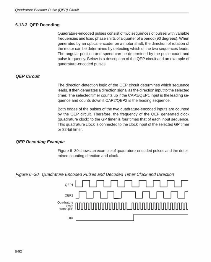
Quadrature Encoder Pulse (QEP) Circuit
6-92
6.13.3 QEP Decoding
Quadrature-encoded pulses consist of two sequences of pulses with variablefrequencies and fixed phase shifts of a quarter of a period (90 degrees). Whengenerated by an optical encoder on a motor shaft, the direction of rotation ofthe motor can be determined by detecting which of the two sequences leads.The angular position and speed can be determined by the pulse count andpulse frequency. Below is a description of the QEP circuit and an example ofquadrature-encoded pulses.
QEP Circuit
The direction-detection logic of the QEP circuit determines which sequenceleads. It then generates a direction signal as the direction input to the selectedtimer. The selected timer counts up if the CAP1/QEP1 input is the leading se-quence and counts down if CAP2/QEP2 is the leading sequence.
Both edges of the pulses of the two quadrature-encoded inputs are countedby the QEP circuit. Therefore, the frequency of the QEP generated clock(quadrature clock) to the GP timer is four times that of each input sequence.This quadrature clock is connected to the clock input of the selected GP timeror 32-bit timer.
QEP Decoding Example
Figure 6–30 shows an example of quadrature-encoded pulses and the deter-mined counting direction and clock.
Figure 6–30. Quadrature Encoded Pulses and Decoded Timer Clock and Direction
DIR
clock
QEP2
QEP1
from QEP
Quadrature
Quadrature Encoder Pulse (QEP) Circuit
6-93Event Manager Module
6.13.4 QEP Counting
The selected GP timer always starts counting from its current value in thecounter. A desired value can be loaded to the selected GP timer counter priorto enabling the QEP operation. When the QEP circuit is selected as the clocksource, the selected timer ignores the TMRDIR and TMRCLK input pins. Be-low are descriptions of the GP timer counting and interrupt operations whenthe QEP circuit is used as clock.
GP Timer Counting Mode in QEP Operation
It is important to note that the directional up/down counting mode of the se-lected GP timer with a QEP circuit as the clock is different from the normal di-rectional up/down counting mode. When the timer selected for QEP operationcounts up to the period value, the GP timer continues counting up until thecounting direction changes. When the timer counts up to FFFFh (orFFFF FFFFh), it rolls over to 0 if the counting direction is up. When the timercounts down to 0, the GP timer rolls over to FFFFh (or FFFF FFFFh) if thecounting direction is down.
GP Timer Interrupt and Associated Compare Outputs in QEP Operation
Period, underflow, overflow, and compare interrupt flags for the GP timer withthe QEP circuit as the clock are generated on respective matches. No transi-tions, however, happen on the compare output of the selected GP timer or anyother compare unit that uses this timer as its time base.
6.13.5 Register Setup for the QEP Circuit
To start the QEP circuit:
1) Configure T2CON or T3CON to set GP timers 2, 3, or 2 and 3 in directionalup/down or 32-bit mode with the QEP circuits as clock source. Enable theselected timer.
2) Configure CAPCON to enable the QEP circuit.
Note:
When appropriate, desired values can be loaded into the selected GP timercounter, period, and compare registers.
Example 6–9 shows an initialization routine for QEP operation.
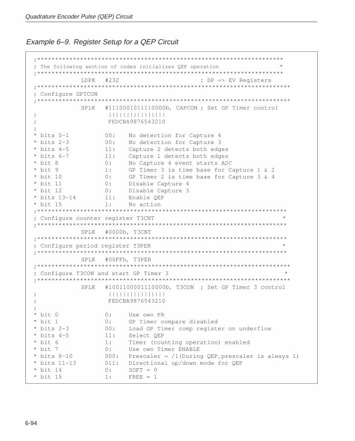
Quadrature Encoder Pulse (QEP) Circuit
6-94
Example 6–9. Register Setup for a QEP Circuit
;*********************************************************************; The following section of codes initializes QEP operation *;*********************************************************************
LDPK #232 ; DP => EV Registers;***********************************************************************; Configure GPTCON;***********************************************************************
SPLK #1110001011110000b, CAPCON ; Set GP Timer control; ||||||||||||||||; FEDCBA9876543210;* bits 0–1 00: No detection for Capture 4* bits 2–3 00: No detection for Capture 3 * bits 4–5 11: Capture 2 detects both edges * bits 6–7 11: Capture 1 detects both edges* bit 8 0: No Capture 4 event starts ADC * bit 9 1: GP Timer 3 is time base for Capture 1 & 2* bit 10 0: GP Timer 2 is time base for Capture 3 & 4* bit 11 0: Disable Capture 4* bit 12 0: Disable Capture 3* bits 13–14 11: Enable QEP* bit 15 1: No action;**********************************************************************; Configure counter register T3CNT *;**********************************************************************
SPLK #0000h, T3CNT ;**********************************************************************; Configure period register T3PER *;**********************************************************************
SPLK #00FFh, T3PER ;***********************************************************************; Configure T3CON and start GP Timer 3 *;***********************************************************************
SPLK #1001100001110000b, T3CON ; Set GP Timer 3 control; ||||||||||||||||; FEDCBA9876543210;* bit 0 0: Use own PR* bit 1 0: GP Timer compare disabled* bits 2–3 00: Load GP Timer comp register on underflow* bits 4–5 11: Select QEP * bit 6 1: Timer (counting operation) enabled* bit 7 0: Use own Timer ENABLE* bits 8–10 000: Prescaler = /1(During QEP,prescaler is always 1)* bits 11–13 011: Directional up/down mode for QEP* bit 14 0: SOFT = 0* bit 15 1: FREE = 1
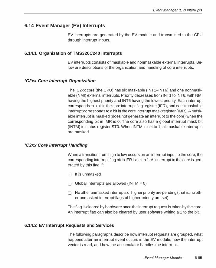
Event Manager (EV) Interrupts
6-95Event Manager Module
6.14 Event Manager (EV) Interrupts
EV interrupts are generated by the EV module and transmitted to the CPUthrough interrupt inputs.
6.14.1 Organization of TMS320C240 Interrupts
EV interrupts consists of maskable and nonmaskable external interrupts. Be-low are descriptions of the organization and handling of core interrupts.
’C2xx Core Interrupt Organization
The ’C2xx core (the CPU) has six maskable (INT1–INT6) and one nonmask-able (NMI) external interrupts. Priority decreases from INT1 to INT6, with NMIhaving the highest priority and INT6 having the lowest priority. Each interruptcorresponds to a bit in the core interrupt flag register (IFR), and each maskableinterrupt corresponds to a bit in the core interrupt mask register (IMR). A mask-able interrupt is masked (does not generate an interrupt to the core) when thecorresponding bit in IMR is 0. The core also has a global interrupt mask bit(INTM) in status register ST0. When INTM is set to 1, all maskable interruptsare masked.
’C2xx Core Interrupt Handling
When a transition from high to low occurs on an interrupt input to the core, thecorresponding interrupt flag bit in IFR is set to 1. An interrupt to the core is gen-erated by this flag if:
� It is unmasked
� Global interrupts are allowed (INTM = 0)
� No other unmasked interrupts of higher priority are pending (that is, no oth-er unmasked interrupt flags of higher priority are set).
The flag is cleared by hardware once the interrupt request is taken by the core.An interrupt flag can also be cleared by user software writing a 1 to the bit.
6.14.2 EV Interrupt Requests and Services
The following paragraphs describe how interrupt requests are grouped, whathappens after an interrupt event occurs in the EV module, how the interruptvector is read, and how the accumulator handles the interrupt.
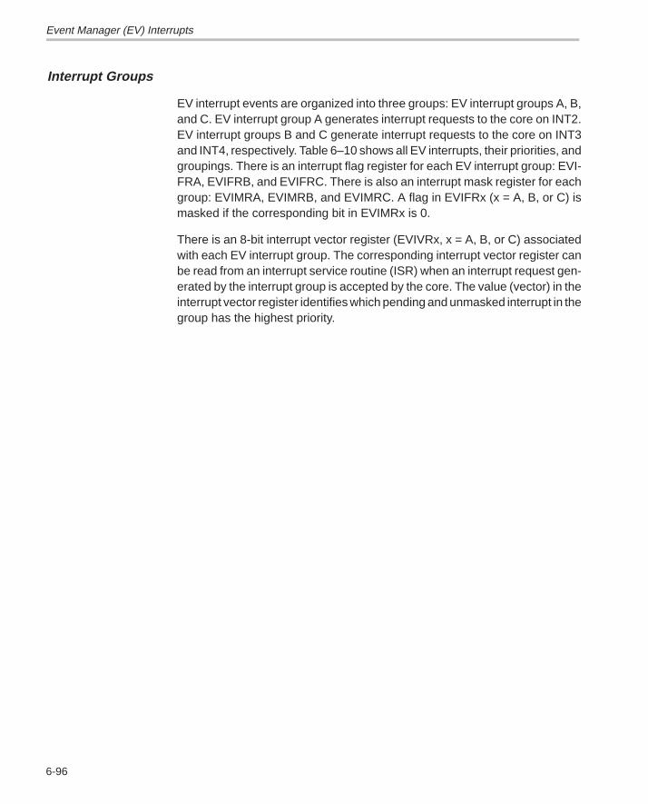
Event Manager (EV) Interrupts
6-96
Interrupt Groups
EV interrupt events are organized into three groups: EV interrupt groups A, B,and C. EV interrupt group A generates interrupt requests to the core on INT2.EV interrupt groups B and C generate interrupt requests to the core on INT3and INT4, respectively. Table 6–10 shows all EV interrupts, their priorities, andgroupings. There is an interrupt flag register for each EV interrupt group: EVI-FRA, EVIFRB, and EVIFRC. There is also an interrupt mask register for eachgroup: EVIMRA, EVIMRB, and EVIMRC. A flag in EVIFRx (x = A, B, or C) ismasked if the corresponding bit in EVIMRx is 0.
There is an 8-bit interrupt vector register (EVIVRx, x = A, B, or C) associatedwith each EV interrupt group. The corresponding interrupt vector register canbe read from an interrupt service routine (ISR) when an interrupt request gen-erated by the interrupt group is accepted by the core. The value (vector) in theinterrupt vector register identifies which pending and unmasked interrupt in thegroup has the highest priority.
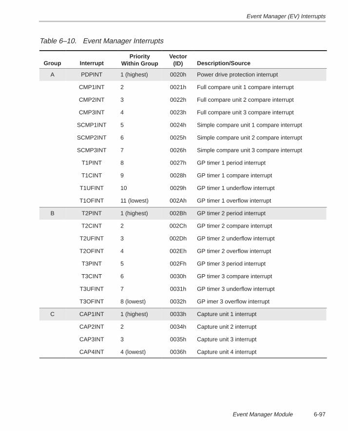
Event Manager (EV) Interrupts
6-97Event Manager Module
Table 6–10. Event Manager Interrupts
Group InterruptPriority
Within GroupVector
(ID) Description/Source
A PDPINT 1 (highest) 0020h Power drive protection interrupt
CMP1INT 2 0021h Full compare unit 1 compare interrupt
CMP2INT 3 0022h Full compare unit 2 compare interrupt
CMP3INT 4 0023h Full compare unit 3 compare interrupt
SCMP1INT 5 0024h Simple compare unit 1 compare interrupt
SCMP2INT 6 0025h Simple compare unit 2 compare interrupt
SCMP3INT 7 0026h Simple compare unit 3 compare interrupt
T1PINT 8 0027h GP timer 1 period interrupt
T1CINT 9 0028h GP timer 1 compare interrupt
T1UFINT 10 0029h GP timer 1 underflow interrupt
T1OFINT 11 (lowest) 002Ah GP timer 1 overflow interrupt
B T2PINT 1 (highest) 002Bh GP timer 2 period interrupt
T2CINT 2 002Ch GP timer 2 compare interrupt
T2UFINT 3 002Dh GP timer 2 underflow interrupt
T2OFINT 4 002Eh GP timer 2 overflow interrupt
T3PINT 5 002Fh GP timer 3 period interrupt
T3CINT 6 0030h GP timer 3 compare interrupt
T3UFINT 7 0031h GP timer 3 underflow interrupt
T3OFINT 8 (lowest) 0032h GP imer 3 overflow interrupt
C CAP1INT 1 (highest) 0033h Capture unit 1 interrupt
CAP2INT 2 0034h Capture unit 2 interrupt
CAP3INT 3 0035h Capture unit 3 interrupt
CAP4INT 4 (lowest) 0036h Capture unit 4 interrupt
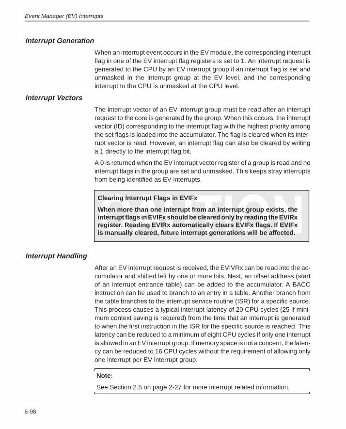
Event Manager (EV) Interrupts
6-98
Interrupt Generation
When an interrupt event occurs in the EV module, the corresponding interruptflag in one of the EV interrupt flag registers is set to 1. An interrupt request isgenerated to the CPU by an EV interrupt group if an interrupt flag is set andunmasked in the interrupt group at the EV level, and the correspondinginterrupt to the CPU is unmasked at the CPU level.
Interrupt Vectors
The interrupt vector of an EV interrupt group must be read after an interruptrequest to the core is generated by the group. When this occurs, the interruptvector (ID) corresponding to the interrupt flag with the highest priority amongthe set flags is loaded into the accumulator. The flag is cleared when its inter-rupt vector is read. However, an interrupt flag can also be cleared by writinga 1 directly to the interrupt flag bit.
A 0 is returned when the EV interrupt vector register of a group is read and nointerrupt flags in the group are set and unmasked. This keeps stray interruptsfrom being identified as EV interrupts.
Clearing Interrupt Flags in EVIFx
When more than one interrupt from an interrupt group exists, theinterrupt flags in EVIFx should be cleared only by reading the EVIRxregister. Reading EVIRx automatically clears EVIFx flags. If EVIFxis manually cleared, future interrupt generations will be affected.
Interrupt Handling
After an EV interrupt request is received, the EVIVRx can be read into the ac-cumulator and shifted left by one or more bits. Next, an offset address (startof an interrupt entrance table) can be added to the accumulator. A BACCinstruction can be used to branch to an entry in a table. Another branch fromthe table branches to the interrupt service routine (ISR) for a specific source.This process causes a typical interrupt latency of 20 CPU cycles (25 if mini-mum context saving is required) from the time that an interrupt is generatedto when the first instruction in the ISR for the specific source is reached. Thislatency can be reduced to a minimum of eight CPU cycles if only one interruptis allowed in an EV interrupt group. If memory space is not a concern, the laten-cy can be reduced to 16 CPU cycles without the requirement of allowing onlyone interrupt per EV interrupt group.
Note:
See Section 2.5 on page 2-27 for more interrupt related information.
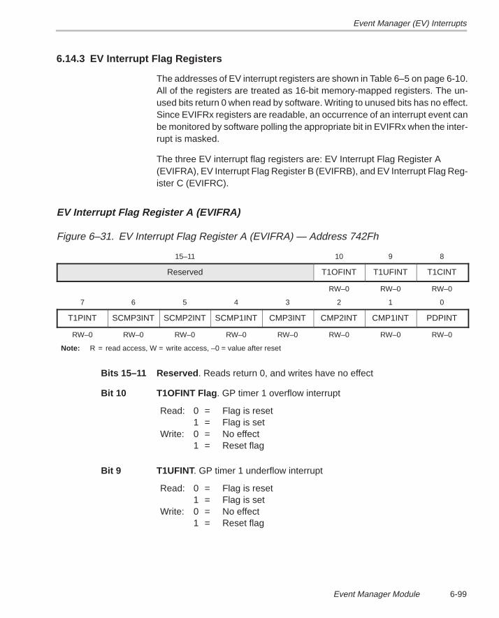
Event Manager (EV) Interrupts
6-99Event Manager Module
6.14.3 EV Interrupt Flag Registers
The addresses of EV interrupt registers are shown in Table 6–5 on page 6-10.All of the registers are treated as 16-bit memory-mapped registers. The un-used bits return 0 when read by software. Writing to unused bits has no effect.Since EVIFRx registers are readable, an occurrence of an interrupt event canbe monitored by software polling the appropriate bit in EVIFRx when the inter-rupt is masked.
The three EV interrupt flag registers are: EV Interrupt Flag Register A (EVIFRA), EV Interrupt Flag Register B (EVIFRB), and EV Interrupt Flag Reg-ister C (EVIFRC).
EV Interrupt Flag Register A (EVIFRA)
Figure 6–31. EV Interrupt Flag Register A (EVIFRA) — Address 742Fh
15–11 10 9 8
Reserved T1OFINT T1UFINT T1CINT
RW–0 RW–0 RW–0
7 6 5 4 3 2 1 0
T1PINT SCMP3INT SCMP2INT SCMP1INT CMP3INT CMP2INT CMP1INT PDPINT
RW–0 RW–0 RW–0 RW–0 RW–0 RW–0 RW–0 RW–0
Note: R = read access, W = write access, –0 = value after reset
Bits 15–11 Reserved . Reads return 0, and writes have no effect
Bit 10 T1OFINT Flag . GP timer 1 overflow interrupt
Read: 0 = Flag is reset1 = Flag is set
Write: 0 = No effect1 = Reset flag
Bit 9 T1UFINT. GP timer 1 underflow interrupt
Read: 0 = Flag is reset1 = Flag is set
Write: 0 = No effect1 = Reset flag
Event Manager (EV) Interrupts
6-100
Bit 8 T1CINT. GP timer 1 compare interrupt
Read: 0 = Flag is reset1 = Flag is set
Write: 0 = No effect1 = Reset flag
Bit 7 T1PINT. GP timer 1 period interrupt
Read: 0 = Flag is reset1 = Flag is set
Write: 0 = No effect1 = Reset flag
Bit 6 SCMP3INT. Simple compare 3 interrupt
Read: 0 = Flag is reset1 = Flag is set
Write: 0 = No effect1 = Reset flag
Bit 5 SCMP2INT. Simple compare 2 interrupt
Read: 0 = Flag is reset1 = Flag is set
Write: 0 = No effect1 = Reset flag
Bit 4 SCMP1INT. Simple compare 1 interrupt
Read: 0 = Flag is reset1 = Flag is set
Write: 0 = No effect1 = Reset flag
Bit 3 CMP3INT. Full compare 3 interrupt
Read: 0 = Flag is reset1 = Flag is set
Write: 0 = No effect1 = Reset flag
Bit 2 CMP2INT Flag . Full compare 2 interrupt
Read: 0 = Flag is reset1 = Flag is set
Write: 0 = No effect1 = Reset flag
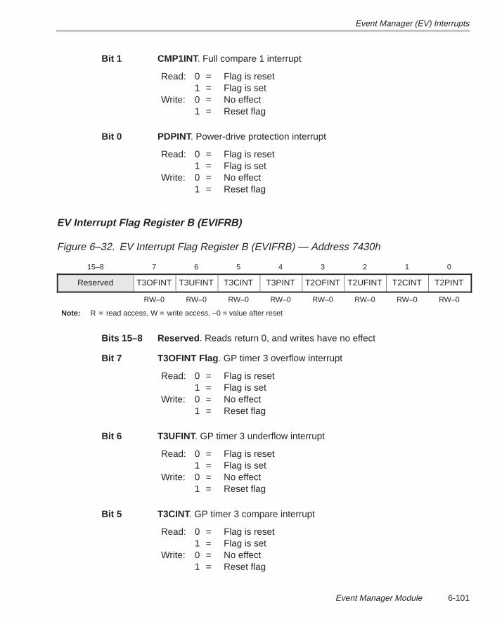
Event Manager (EV) Interrupts
6-101Event Manager Module
Bit 1 CMP1INT. Full compare 1 interrupt
Read: 0 = Flag is reset1 = Flag is set
Write: 0 = No effect1 = Reset flag
Bit 0 PDPINT. Power-drive protection interrupt
Read: 0 = Flag is reset1 = Flag is set
Write: 0 = No effect1 = Reset flag
EV Interrupt Flag Register B (EVIFRB)
Figure 6–32. EV Interrupt Flag Register B (EVIFRB) — Address 7430h
15–8 7 6 5 4 3 2 1 0
Reserved T3OFINT T3UFINT T3CINT T3PINT T2OFINT T2UFINT T2CINT T2PINT
RW–0 RW–0 RW–0 RW–0 RW–0 RW–0 RW–0 RW–0
Note: R = read access, W = write access, –0 = value after reset
Bits 15–8 Reserved . Reads return 0, and writes have no effect
Bit 7 T3OFINT Flag . GP timer 3 overflow interrupt
Read: 0 = Flag is reset1 = Flag is set
Write: 0 = No effect1 = Reset flag
Bit 6 T3UFINT. GP timer 3 underflow interrupt
Read: 0 = Flag is reset1 = Flag is set
Write: 0 = No effect1 = Reset flag
Bit 5 T3CINT. GP timer 3 compare interrupt
Read: 0 = Flag is reset1 = Flag is set
Write: 0 = No effect1 = Reset flag
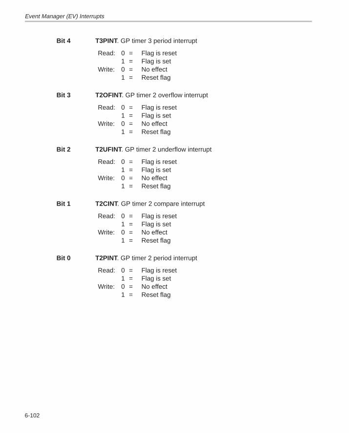
Event Manager (EV) Interrupts
6-102
Bit 4 T3PINT. GP timer 3 period interrupt
Read: 0 = Flag is reset1 = Flag is set
Write: 0 = No effect1 = Reset flag
Bit 3 T2OFINT. GP timer 2 overflow interrupt
Read: 0 = Flag is reset1 = Flag is set
Write: 0 = No effect1 = Reset flag
Bit 2 T2UFINT. GP timer 2 underflow interrupt
Read: 0 = Flag is reset1 = Flag is set
Write: 0 = No effect1 = Reset flag
Bit 1 T2CINT. GP timer 2 compare interrupt
Read: 0 = Flag is reset1 = Flag is set
Write: 0 = No effect1 = Reset flag
Bit 0 T2PINT. GP timer 2 period interrupt
Read: 0 = Flag is reset1 = Flag is set
Write: 0 = No effect1 = Reset flag
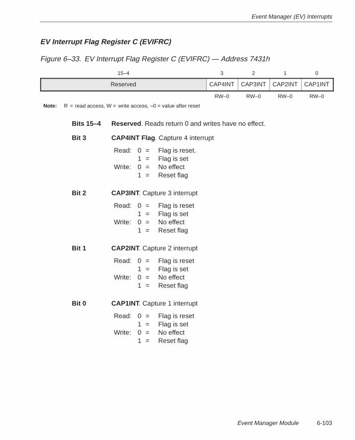
Event Manager (EV) Interrupts
6-103Event Manager Module
EV Interrupt Flag Register C (EVIFRC)
Figure 6–33. EV Interrupt Flag Register C (EVIFRC) — Address 7431h
15–4 3 2 1 0
Reserved CAP4INT CAP3INT CAP2INT CAP1INT
RW–0 RW–0 RW–0 RW–0
Note: R = read access, W = write access, –0 = value after reset
Bits 15–4 Reserved . Reads return 0 and writes have no effect.
Bit 3 CAP4INT Flag . Capture 4 interrupt
Read: 0 = Flag is reset.1 = Flag is set
Write: 0 = No effect1 = Reset flag
Bit 2 CAP3INT . Capture 3 interrupt
Read: 0 = Flag is reset1 = Flag is set
Write: 0 = No effect1 = Reset flag
Bit 1 CAP2INT . Capture 2 interrupt
Read: 0 = Flag is reset1 = Flag is set
Write: 0 = No effect1 = Reset flag
Bit 0 CAP1INT . Capture 1 interrupt
Read: 0 = Flag is reset1 = Flag is set
Write: 0 = No effect1 = Reset flag
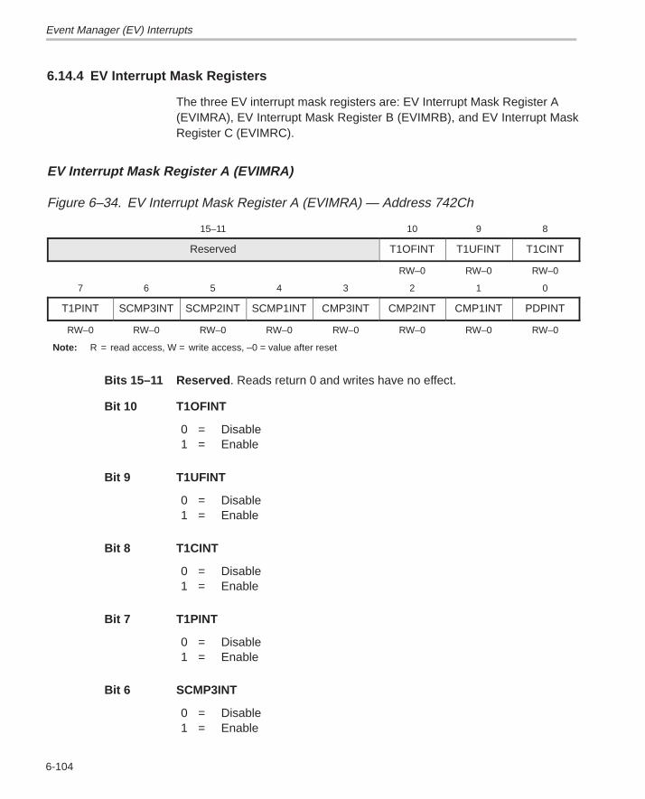
Event Manager (EV) Interrupts
6-104
6.14.4 EV Interrupt Mask Registers
The three EV interrupt mask registers are: EV Interrupt Mask Register A (EVIMRA), EV Interrupt Mask Register B (EVIMRB), and EV Interrupt MaskRegister C (EVIMRC).
EV Interrupt Mask Register A (EVIMRA)
Figure 6–34. EV Interrupt Mask Register A (EVIMRA) — Address 742Ch
15–11 10 9 8
Reserved T1OFINT T1UFINT T1CINT
RW–0 RW–0 RW–0
7 6 5 4 3 2 1 0
T1PINT SCMP3INT SCMP2INT SCMP1INT CMP3INT CMP2INT CMP1INT PDPINT
RW–0 RW–0 RW–0 RW–0 RW–0 RW–0 RW–0 RW–0
Note: R = read access, W = write access, –0 = value after reset
Bits 15–11 Reserved . Reads return 0 and writes have no effect.
Bit 10 T1OFINT
0 = Disable1 = Enable
Bit 9 T1UFINT
0 = Disable1 = Enable
Bit 8 T1CINT
0 = Disable1 = Enable
Bit 7 T1PINT
0 = Disable1 = Enable
Bit 6 SCMP3INT
0 = Disable1 = Enable
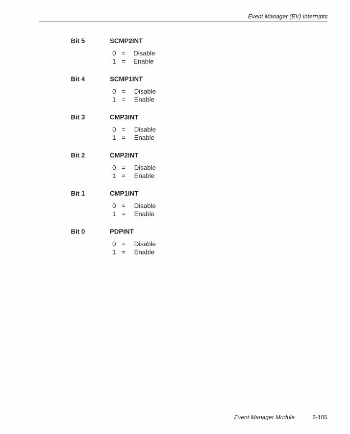
Event Manager (EV) Interrupts
6-105Event Manager Module
Bit 5 SCMP2INT
0 = Disable1 = Enable
Bit 4 SCMP1INT
0 = Disable1 = Enable
Bit 3 CMP3INT
0 = Disable1 = Enable
Bit 2 CMP2INT
0 = Disable1 = Enable
Bit 1 CMP1INT
0 = Disable1 = Enable
Bit 0 PDPINT
0 = Disable1 = Enable
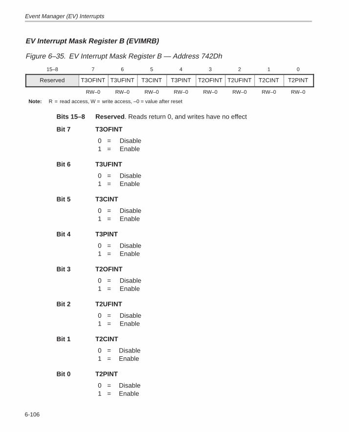
Event Manager (EV) Interrupts
6-106
EV Interrupt Mask Register B (EVIMRB)
Figure 6–35. EV Interrupt Mask Register B — Address 742Dh
15–8 7 6 5 4 3 2 1 0
Reserved T3OFINT T3UFINT T3CINT T3PINT T2OFINT T2UFINT T2CINT T2PINT
RW–0 RW–0 RW–0 RW–0 RW–0 RW–0 RW–0 RW–0
Note: R = read access, W = write access, –0 = value after reset
Bits 15–8 Reserved . Reads return 0, and writes have no effect
Bit 7 T3OFINT
0 = Disable1 = Enable
Bit 6 T3UFINT
0 = Disable1 = Enable
Bit 5 T3CINT
0 = Disable1 = Enable
Bit 4 T3PINT
0 = Disable1 = Enable
Bit 3 T2OFINT
0 = Disable1 = Enable
Bit 2 T2UFINT
0 = Disable1 = Enable
Bit 1 T2CINT
0 = Disable1 = Enable
Bit 0 T2PINT
0 = Disable1 = Enable
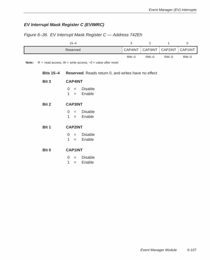
Event Manager (EV) Interrupts
6-107Event Manager Module
EV Interrupt Mask Register C (EVIMRC)
Figure 6–36. EV Interrupt Mask Register C — Address 742Eh
15–4 3 2 1 0
Reserved CAP4INT CAP3INT CAP2INT CAP1INT
RW–0 RW–0 RW–0 RW–0
Note: R = read access, W = write access, –0 = value after reset
Bits 15–4 Reserved . Reads return 0, and writes have no effect
Bit 3 CAP4INT
0 = Disable1 = Enable
Bit 2 CAP3INT
0 = Disable1 = Enable
Bit 1 CAP2INT
0 = Disable1 = Enable
Bit 0 CAP1INT
0 = Disable1 = Enable
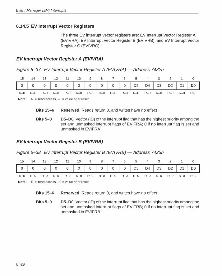
Event Manager (EV) Interrupts
6-108
6.14.5 EV Interrupt Vector Registers
The three EV interrupt vector registers are: EV Interrupt Vector Register A (EVIVRA), EV Interrupt Vector Register B (EVIVRB), and EV Interrupt VectorRegister C (EVIVRC).
EV Interrupt Vector Register A (EVIVRA)
Figure 6–37. EV Interrupt Vector Register A (EVIVRA) — Address 7432h
15 14 13 12 11 10 9 8 7 6 5 4 3 2 1 0
0 0 0 0 0 0 0 0 0 0 D5 D4 D3 D2 D1 D0
R–0 R–0 R–0 R–0 R–0 R–0 R–0 R–0 R–0 R–0 R–0 R–0 R–0 R–0 R–0 R–0
Note: R = read access, –0 = value after reset
Bits 15–6 Reserved . Reads return 0, and writes have no effect
Bits 5–0 D5–D0 . Vector (ID) of the interrupt flag that has the highest priority among theset and unmasked interrupt flags of EVIFRA; 0 if no interrupt flag is set andunmasked in EVIFRA
EV Interrupt Vector Register B (EVIVRB)
Figure 6–38. EV Interrupt Vector Register B (EVIVRB) — Address 7433h
15 14 13 12 11 10 9 8 7 6 5 4 3 2 1 0
0 0 0 0 0 0 0 0 0 0 D5 D4 D3 D2 D1 D0
R–0 R–0 R–0 R–0 R–0 R–0 R–0 R–0 R–0 R–0 R–0 R–0 R–0 R–0 R–0 R–0
Note: R = read access, –0 = value after reset
Bits 15–6 Reserved . Reads return 0, and writes have no effect
Bits 5–0 D5–D0 . Vector (ID) of the interrupt flag that has the highest priority among theset and unmasked interrupt flags of EVIFRB; 0 if no interrupt flag is set andunmasked in EVIFRB
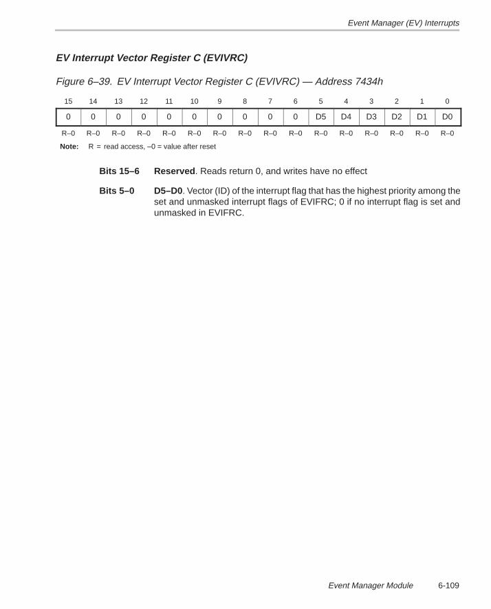
Event Manager (EV) Interrupts
6-109Event Manager Module
EV Interrupt Vector Register C (EVIVRC)
Figure 6–39. EV Interrupt Vector Register C (EVIVRC) — Address 7434h
15 14 13 12 11 10 9 8 7 6 5 4 3 2 1 0
0 0 0 0 0 0 0 0 0 0 D5 D4 D3 D2 D1 D0
R–0 R–0 R–0 R–0 R–0 R–0 R–0 R–0 R–0 R–0 R–0 R–0 R–0 R–0 R–0 R–0
Note: R = read access, –0 = value after reset
Bits 15–6 Reserved . Reads return 0, and writes have no effect
Bits 5–0 D5–D0 . Vector (ID) of the interrupt flag that has the highest priority among theset and unmasked interrupt flags of EVIFRC; 0 if no interrupt flag is set andunmasked in EVIFRC.
7-1Dual 10-Bit Analog-to-Digital Converter (ADC) Module
Dual 10-Bit Analog-to-DigitalConverter (ADC) Module
The analog-to-digital converter (ADC) module used in the ’C240 is a dual10-bit ADC. This chapter provides a general description of the ADC module,explains its operation, and shows its control and data registers.
Topic Page
7.1 Dual 10-Bit ADC Overview 7-2. . . . . . . . . . . . . . . . . . . . . . . . . . . . . . . . . . . . .
7.2 ADC Operation 7-4. . . . . . . . . . . . . . . . . . . . . . . . . . . . . . . . . . . . . . . . . . . . . . .
7.3 ADC Registers 7-7. . . . . . . . . . . . . . . . . . . . . . . . . . . . . . . . . . . . . . . . . . . . . . . .
Chapter 7
Dual 10-Bit ADC Overview
7-2
7.1 Dual 10-Bit ADC Overview
The ADC is a 10 bit string/capacitor converter with internal sample-and-holdcircuitry. The ADC module consists of two 10-bit ADCs with two built in sample-and-hold circuits. A total of 16 analog input channels are available on the’C240. Eight analog inputs are provided for each ADC unit via an eight to oneanalog multiplexer. The total conversion time for each ADC unit is approxi-mately 6 �s. (See the TMS320C240, TMS320F240 data sheet for exact speci-fications.) The reference voltage of the ADC module must be supplied from anexternal source. The upper and lower references can be set to any voltage lessthan or equal to 5 Vdc by connecting VREFHI and VREFLO to the appropriatereference voltages. The VCCA and VSSA pins must be connected to a 5 Vdcsource and the analog ground, respectively.
The ADC module, shown in Figure 7–1, ADC Module Block Diagram, consistsof the following:
� Eight analog inputs for each ADC module, for a total of 16 analog inputs
� Simultaneous measurement of two analog inputs using two ADC units
� Single or continuous conversion
� Conversion can be started by software, internal event, and/or externalevent
� VREFHI and VREFLO (high- and low-voltage) reference inputs
� Analog to digital conversion block
� 2-level-deep digital result registers that contain the digital values of com-pleted conversions
� Two programmable ADC module control registers
� Programmable prescaler select
� Interrupt or polled operation
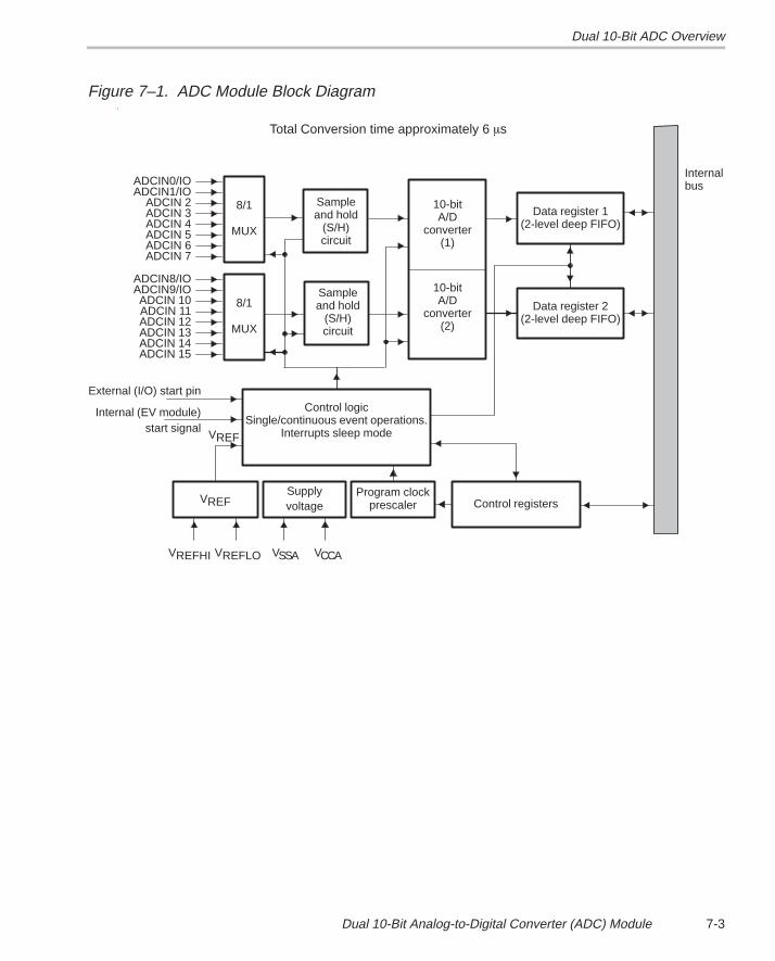
Dual 10-Bit ADC Overview
7-3Dual 10-Bit Analog-to-Digital Converter (ADC) Module
Figure 7–1. ADC Module Block Diagram.
..
Internalbus
10-bitA/D
converter(1)
8/1
MUX
Sampleand hold
(S/H)circuit
Sampleand hold
(S/H)circuit
Control registers
Data register 1(2-level deep FIFO)
Supplyvoltage
VREF
Control logicSingle/continuous event operations.
Interrupts sleep mode
Program clockprescaler
VCCAVSSA
Total Conversion time approximately 6 �s
VREF
External (I/O) start pin
Internal (EV module)
VREFLOVREFHI
10-bitA/D
converter(2)
Data register 2(2-level deep FIFO)
ADCIN0/IO
start signal
ADCIN1/IOADCIN 2ADCIN 3ADCIN 4ADCIN 5ADCIN 6ADCIN 7
8/1
MUX
ADCIN8/IOADCIN9/IOADCIN 10ADCIN 11ADCIN 12ADCIN 13ADCIN 14ADCIN 15
ADC Operation
7-4
7.2 ADC Operation
The digital result of the conversion process for the 10-bit ADC is approximatedby the following equation:
Digital result � 1023 �
Input analog voltage � VREFLO
VREFHI � VREFLO
7.2.1 ADC Module Pin Description
The ADC module provides 20 pins that can interface to external circuitry. Six-teen of these pins, ADCIN0–ADCIN15, are for the analog inputs. Two pins,VREFHI and VREFLO, are the analog reference-voltage pins.
The analog supply pins, VCCA and VSSA (which are separate from any digitalvoltage supply pins), use standard noise reduction techniques to ensure accu-rate conversion. This means that analog power lines connected to VCCA andVSSA are made as short as possible and the two lines are decoupled properly.
Analog voltage input pins ADCIN0 through ADCIN7 belong to the first ADCmodule and ADCIN8 through ADCIN15 belong to the second ADC module.Analog inputs ADCIN0 and ADCIN1 of the first module and analog inputs ADCIN8 and ADCIN9 of the second module are multiplexed with digital I/O.By properly programming the system module, these four analog input pins(ADCIN0, ADCIN1, ADCIN8, and ADCIN9) can be used as digital I/O. The ac-curacy of these four pins; howver, is lower than that of the dedicated analoginput pins (ADCIN2 – ADCIN7, and ADCIN10 – ADCIN15).
7.2.2 ADC Module Operational Modes
The operating modes of the ADC module can:
� Sample and convert two input channels (one for each ADC unit) simultaneously
� Perform single or continuous S/H and conversion operations
� Use two 2-level-deep FIFO result registers for ADC units 1 and 2
� Start operation by software instruction, external signal transition on a de-vice pin, or by the EV events on each of the GP timer/compare outputs andthe capture 4 pins

ADC Operation
7-5Dual 10-Bit Analog-to-Digital Converter (ADC) Module
� Write to those bits in the ADC control registers that are double bufferedwith shadow registers without affecting the ongoing conversion process.The newly written bit values first go to a shadow register instead of the ac-tive register. This new bit configuration is automatically loaded from theshadow register to the active register only after completion of the presentconversion process. The next conversion process is then determined bythe new bit configuration.
� Set an interrupt flag and generate an interrupt at the end of each conver-sion, if the interrupt is unmasked/enabled.
If a third conversion is completed without reading the FIFO, the data fromthe first conversion is lost.
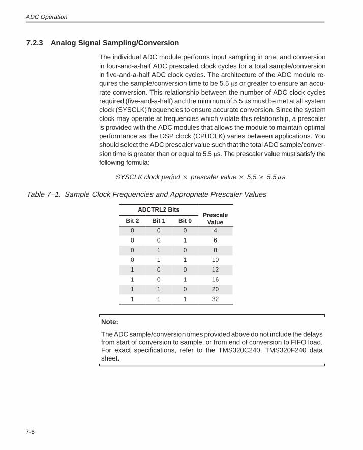
ADC Operation
7-6
7.2.3 Analog Signal Sampling/Conversion
The individual ADC module performs input sampling in one, and conversionin four-and-a-half ADC prescaled clock cycles for a total sample/conversionin five-and-a-half ADC clock cycles. The architecture of the ADC module re-quires the sample/conversion time to be 5.5 �s or greater to ensure an accu-rate conversion. This relationship between the number of ADC clock cyclesrequired (five-and-a-half) and the minimum of 5.5 �s must be met at all systemclock (SYSCLK) frequencies to ensure accurate conversion. Since the systemclock may operate at frequencies which violate this relationship, a prescaleris provided with the ADC modules that allows the module to maintain optimalperformance as the DSP clock (CPUCLK) varies between applications. Youshould select the ADC prescaler value such that the total ADC sample/conver-sion time is greater than or equal to 5.5 �s. The prescaler value must satisfy thefollowing formula:
SYSCLK clock period � prescaler value � 5.5 � 5.5 �s
Table 7–1. Sample Clock Frequencies and Appropriate Prescaler Values
ADCTRL2 BitsPrescale
Bit 2 Bit 1 Bit 0Presca le
Value0 0 0 4
0 0 1 6
0 1 0 8
0 1 1 10
1 0 0 12
1 0 1 16
1 1 0 20
1 1 1 32
Note:
The ADC sample/conversion times provided above do not include the delaysfrom start of conversion to sample, or from end of conversion to FIFO load.For exact specifications, refer to the TMS320C240, TMS320F240 datasheet.
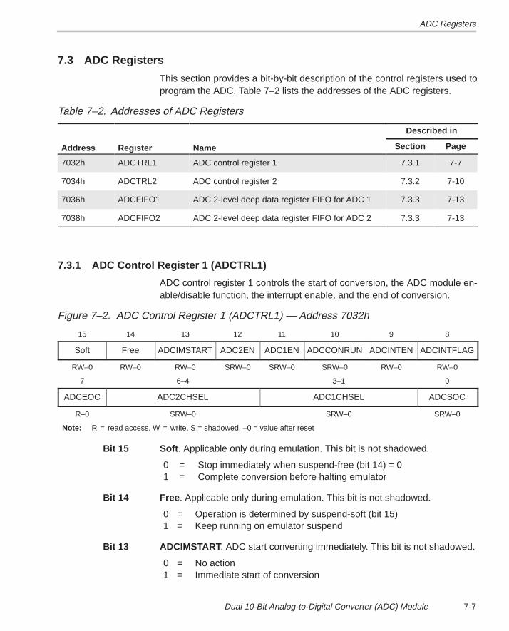
ADC Registers
7-7Dual 10-Bit Analog-to-Digital Converter (ADC) Module
7.3 ADC Registers
This section provides a bit-by-bit description of the control registers used toprogram the ADC. Table 7–2 lists the addresses of the ADC registers.
Table 7–2. Addresses of ADC Registers
Described in
Address Register Name Section Page
7032h ADCTRL1 ADC control register 1 7.3.1 7-7
7034h ADCTRL2 ADC control register 2 7.3.2 7-10
7036h ADCFIFO1 ADC 2-level deep data register FIFO for ADC 1 7.3.3 7-13
7038h ADCFIFO2 ADC 2-level deep data register FIFO for ADC 2 7.3.3 7-13
7.3.1 ADC Control Register 1 (ADCTRL1)
ADC control register 1 controls the start of conversion, the ADC module en-able/disable function, the interrupt enable, and the end of conversion.
Figure 7–2. ADC Control Register 1 (ADCTRL1) — Address 7032h
15 14 13 12 11 10 9 8
Soft Free ADCIMSTART ADC2EN ADC1EN ADCCONRUN ADCINTEN ADCINTFLAG
RW–0 RW–0 RW–0 SRW–0 SRW–0 SRW–0 RW–0 RW–0
7 6–4 3–1 0
ADCEOC ADC2CHSEL ADC1CHSEL ADCSOC
R–0 SRW–0 SRW–0 SRW–0
Note: R = read access, W = write, S = shadowed, –0 = value after reset
Bit 15 Soft . Applicable only during emulation. This bit is not shadowed.
0 = Stop immediately when suspend-free (bit 14) = 01 = Complete conversion before halting emulator
Bit 14 Free . Applicable only during emulation. This bit is not shadowed.
0 = Operation is determined by suspend-soft (bit 15)1 = Keep running on emulator suspend
Bit 13 ADCIMSTART . ADC start converting immediately. This bit is not shadowed.
0 = No action1 = Immediate start of conversion
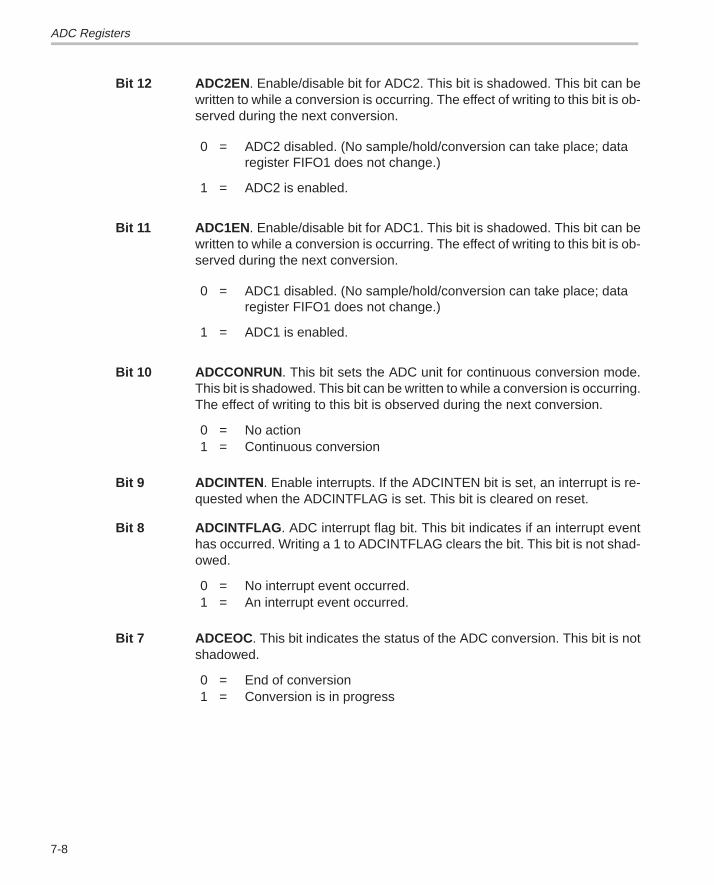
ADC Registers
7-8
Bit 12 ADC2EN . Enable/disable bit for ADC2. This bit is shadowed. This bit can bewritten to while a conversion is occurring. The effect of writing to this bit is ob-served during the next conversion.
0 = ADC2 disabled. (No sample/hold/conversion can take place; dataregister FIFO1 does not change.)
1 = ADC2 is enabled.
Bit 11 ADC1EN . Enable/disable bit for ADC1. This bit is shadowed. This bit can bewritten to while a conversion is occurring. The effect of writing to this bit is ob-served during the next conversion.
0 = ADC1 disabled. (No sample/hold/conversion can take place; dataregister FIFO1 does not change.)
1 = ADC1 is enabled.
Bit 10 ADCCONRUN . This bit sets the ADC unit for continuous conversion mode.This bit is shadowed. This bit can be written to while a conversion is occurring.The effect of writing to this bit is observed during the next conversion.
0 = No action1 = Continuous conversion
Bit 9 ADCINTEN . Enable interrupts. If the ADCINTEN bit is set, an interrupt is re-quested when the ADCINTFLAG is set. This bit is cleared on reset.
Bit 8 ADCINTFLAG . ADC interrupt flag bit. This bit indicates if an interrupt eventhas occurred. Writing a 1 to ADCINTFLAG clears the bit. This bit is not shad-owed.
0 = No interrupt event occurred.1 = An interrupt event occurred.
Bit 7 ADCEOC . This bit indicates the status of the ADC conversion. This bit is notshadowed.
0 = End of conversion1 = Conversion is in progress
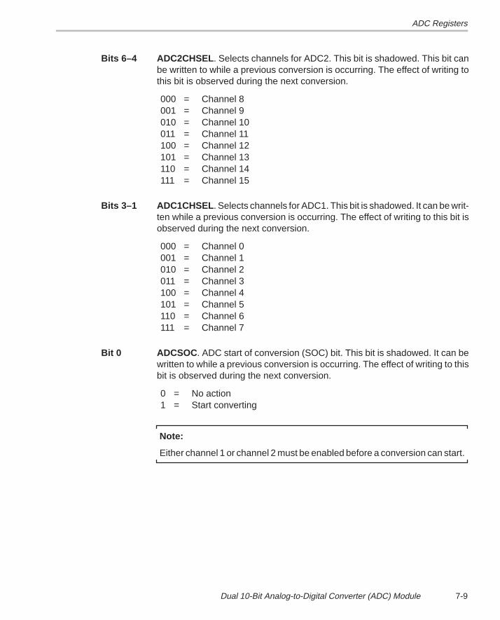
ADC Registers
7-9Dual 10-Bit Analog-to-Digital Converter (ADC) Module
Bits 6–4 ADC2CHSEL . Selects channels for ADC2. This bit is shadowed. This bit canbe written to while a previous conversion is occurring. The effect of writing tothis bit is observed during the next conversion.
000 = Channel 8001 = Channel 9010 = Channel 10011 = Channel 11100 = Channel 12101 = Channel 13110 = Channel 14111 = Channel 15
Bits 3–1 ADC1CHSEL . Selects channels for ADC1. This bit is shadowed. It can be writ-ten while a previous conversion is occurring. The effect of writing to this bit isobserved during the next conversion.
000 = Channel 0001 = Channel 1010 = Channel 2011 = Channel 3100 = Channel 4101 = Channel 5110 = Channel 6111 = Channel 7
Bit 0 ADCSOC . ADC start of conversion (SOC) bit. This bit is shadowed. It can bewritten to while a previous conversion is occurring. The effect of writing to thisbit is observed during the next conversion.
0 = No action1 = Start converting
Note:
Either channel 1 or channel 2 must be enabled before a conversion can start.
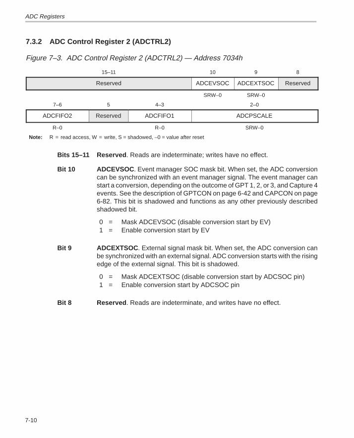
ADC Registers
7-10
7.3.2 ADC Control Register 2 (ADCTRL2)
Figure 7–3. ADC Control Register 2 (ADCTRL2) — Address 7034h
15–11 10 9 8
Reserved ADCEVSOC ADCEXTSOC Reserved
SRW–0 SRW–0
7–6 5 4–3 2–0
ADCFIFO2 Reserved ADCFIFO1 ADCPSCALE
R–0 R–0 SRW–0
Note: R = read access, W = write, S = shadowed, –0 = value after reset
Bits 15–11 Reserved . Reads are indeterminate; writes have no effect.
Bit 10 ADCEVSOC . Event manager SOC mask bit. When set, the ADC conversioncan be synchronized with an event manager signal. The event manager canstart a conversion, depending on the outcome of GPT 1, 2, or 3, and Capture 4events. See the description of GPTCON on page 6-42 and CAPCON on page6-82. This bit is shadowed and functions as any other previously describedshadowed bit.
0 = Mask ADCEVSOC (disable conversion start by EV)1 = Enable conversion start by EV
Bit 9 ADCEXTSOC . External signal mask bit. When set, the ADC conversion canbe synchronized with an external signal. ADC conversion starts with the risingedge of the external signal. This bit is shadowed.
0 = Mask ADCEXTSOC (disable conversion start by ADCSOC pin)1 = Enable conversion start by ADCSOC pin
Bit 8 Reserved . Reads are indeterminate, and writes have no effect.
ADC Registers
7-11Dual 10-Bit Analog-to-Digital Converter (ADC) Module
Bits 7–6 ADCFIFO2. Data register FIFO2 status. These two bits indicate ADC2 FIFOstatus. Two conversion results can be stored before performing a read opera-tion. If a third conversion is made after two conversions, the oldest result is lost.These bits are not shadowed.
00 = FIFO2 is empty.
01 = FIFO2 has one entry.
10 = FIFO2 has two entries.
11 = FIFO2 had two entries and another entry was received; the firstentry was lost.
Bit 5 Reserved . Reads are indeterminate and writes have no effect.
Note:
The start of convert signals are ORed together. When both convert signalsare asserted simultaneously, the first signal starts a conversion and whenthat conversion is finished, the second SOC signal causes a second conver-sion to begin.
Bits 4–3 ADCFIFO1 . Data register FIFO1 status. These two bits indicate ADC1 FIFOstatus. Two conversion results can be stored before performing any readoperations. If a third conversion is made after two conversions, the oldest re-sult is lost. These bits are not shadowed.
00 = FIFO1 is empty.
01 = FIFO1 has one entry.
10 = FIFO1 has two entries.
11 = FIFO1 had two entries and another entry was received; the firstentry was lost.
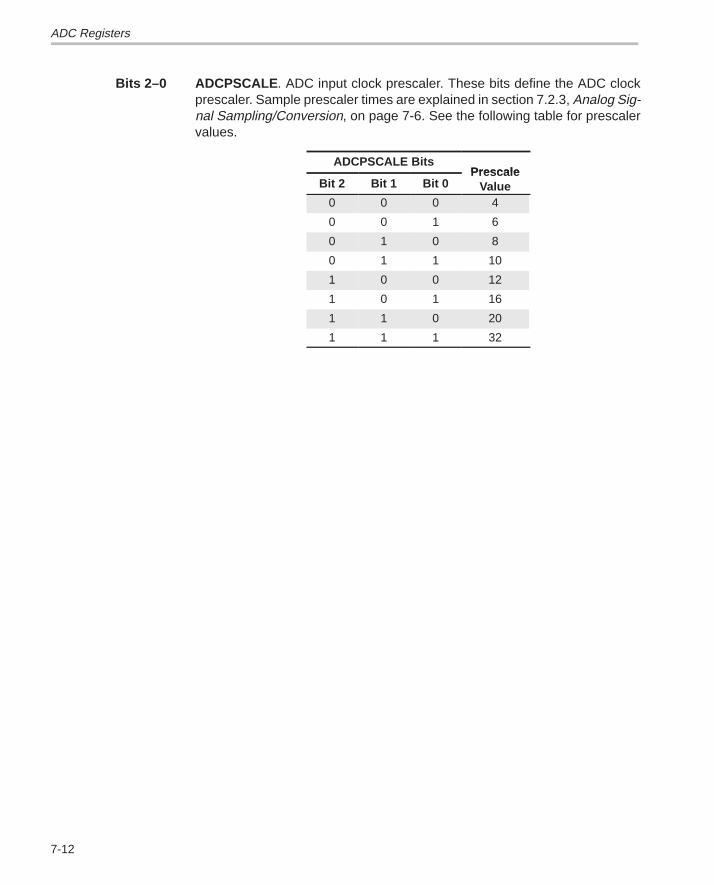
ADC Registers
7-12
Bits 2–0 ADCPSCALE . ADC input clock prescaler. These bits define the ADC clockprescaler. Sample prescaler times are explained in section 7.2.3, Analog Sig-nal Sampling/Conversion, on page 7-6. See the following table for prescalervalues.
ADCPSCALE BitsPrescale
Bit 2 Bit 1 Bit 0Presca le
Value0 0 0 4
0 0 1 6
0 1 0 8
0 1 1 10
1 0 0 12
1 0 1 16
1 1 0 20
1 1 1 32
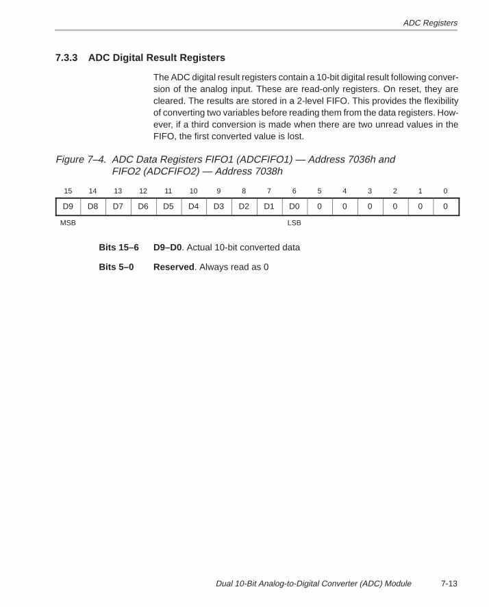
ADC Registers
7-13Dual 10-Bit Analog-to-Digital Converter (ADC) Module
7.3.3 ADC Digital Result Registers
The ADC digital result registers contain a 10-bit digital result following conver-sion of the analog input. These are read-only registers. On reset, they arecleared. The results are stored in a 2-level FIFO. This provides the flexibilityof converting two variables before reading them from the data registers. How-ever, if a third conversion is made when there are two unread values in theFIFO, the first converted value is lost.
Figure 7–4. ADC Data Registers FIFO1 (ADCFIFO1) — Address 7036h andFIFO2 (ADCFIFO2) — Address 7038h
15 14 13 12 11 10 9 8 7 6 5 4 3 2 1 0
D9 D8 D7 D6 D5 D4 D3 D2 D1 D0 0 0 0 0 0 0
MSB LSB
Bits 15–6 D9–D0 . Actual 10-bit converted data
Bits 5–0 Reserved . Always read as 0
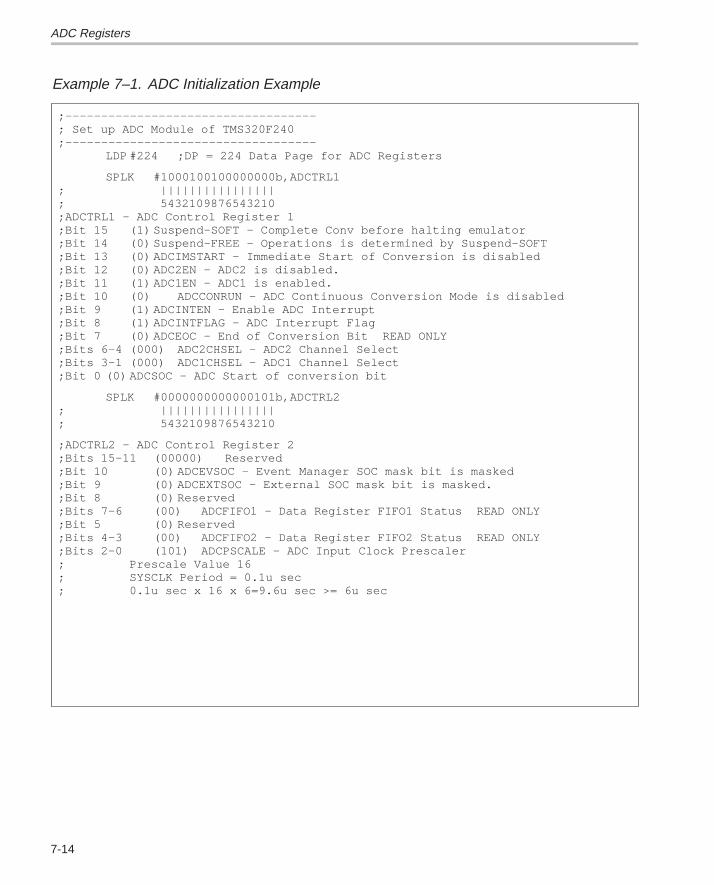
ADC Registers
7-14
Example 7–1. ADC Initialization Example
;–––––––––––––––––––––––––––––––––––; Set up ADC Module of TMS320F240;–––––––––––––––––––––––––––––––––––
LDP #224 ;DP = 224 Data Page for ADC Registers
SPLK #1000100100000000b,ADCTRL1; ||||||||||||||||; 5432109876543210;ADCTRL1 – ADC Control Register 1;Bit 15 (1) Suspend–SOFT – Complete Conv before halting emulator;Bit 14 (0) Suspend–FREE – Operations is determined by Suspend–SOFT;Bit 13 (0) ADCIMSTART – Immediate Start of Conversion is disabled;Bit 12 (0) ADC2EN – ADC2 is disabled.;Bit 11 (1) ADC1EN – ADC1 is enabled.;Bit 10 (0) ADCCONRUN – ADC Continuous Conversion Mode is disabled;Bit 9 (1) ADCINTEN – Enable ADC Interrupt;Bit 8 (1) ADCINTFLAG – ADC Interrupt Flag;Bit 7 (0) ADCEOC – End of Conversion Bit READ ONLY;Bits 6–4 (000) ADC2CHSEL – ADC2 Channel Select;Bits 3–1 (000) ADC1CHSEL – ADC1 Channel Select;Bit 0 (0) ADCSOC – ADC Start of conversion bit
SPLK #0000000000000101b,ADCTRL2; ||||||||||||||||; 5432109876543210
;ADCTRL2 – ADC Control Register 2;Bits 15–11 (00000) Reserved;Bit 10 (0) ADCEVSOC – Event Manager SOC mask bit is masked;Bit 9 (0) ADCEXTSOC – External SOC mask bit is masked.;Bit 8 (0) Reserved;Bits 7–6 (00) ADCFIFO1 – Data Register FIFO1 Status READ ONLY;Bit 5 (0) Reserved;Bits 4–3 (00) ADCFIFO2 – Data Register FIFO2 Status READ ONLY;Bits 2–0 (101) ADCPSCALE – ADC Input Clock Prescaler; Prescale Value 16; SYSCLK Period = 0.1u sec; 0.1u sec x 16 x 6=9.6u sec >= 6u sec
8-1Serial Communications Interface (SCI) Module
Serial Communications Interface (SCI) Module
The programmable serial communications interface (SCI) module supportsdigital communications between the CPU and other asynchronous peripheralsthat use the standard NRZ (nonreturn-to-zero) format. This chapter describesthe architecture, functions, and programming of the SCI module.
Topic Page
8.1 SCI Overview 8-2. . . . . . . . . . . . . . . . . . . . . . . . . . . . . . . . . . . . . . . . . . . . . . . . .
8.2 SCI Programmable Data Format 8-8. . . . . . . . . . . . . . . . . . . . . . . . . . . . . . . .
8.3 SCI Multiprocessor Communication 8-9. . . . . . . . . . . . . . . . . . . . . . . . . . . .
8.4 SCI Communication Format 8-14. . . . . . . . . . . . . . . . . . . . . . . . . . . . . . . . . . .
8.5 SCI Port Interrupts 8-17. . . . . . . . . . . . . . . . . . . . . . . . . . . . . . . . . . . . . . . . . . .
8.6 SCI Control Registers 8-19. . . . . . . . . . . . . . . . . . . . . . . . . . . . . . . . . . . . . . . .
8.7 SCI Initialization Example 8-34. . . . . . . . . . . . . . . . . . . . . . . . . . . . . . . . . . . . .
Chapter 8
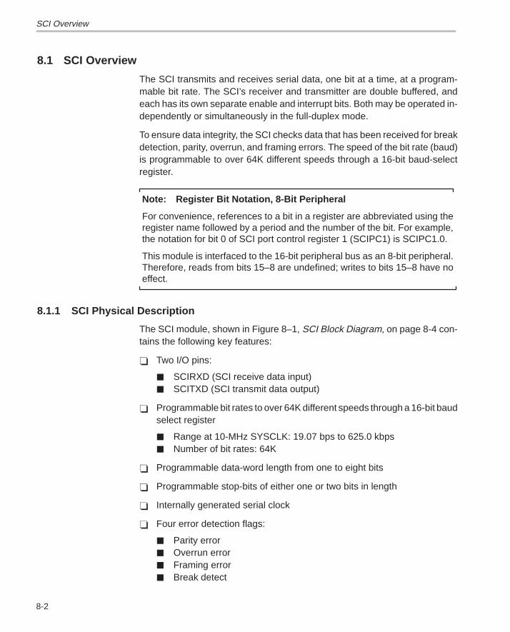
SCI Overview
8-2
8.1 SCI Overview
The SCI transmits and receives serial data, one bit at a time, at a program-mable bit rate. The SCI’s receiver and transmitter are double buffered, andeach has its own separate enable and interrupt bits. Both may be operated in-dependently or simultaneously in the full-duplex mode.
To ensure data integrity, the SCI checks data that has been received for breakdetection, parity, overrun, and framing errors. The speed of the bit rate (baud)is programmable to over 64K different speeds through a 16-bit baud-selectregister.
Note: Register Bit Notation, 8-Bit Peripheral
For convenience, references to a bit in a register are abbreviated using theregister name followed by a period and the number of the bit. For example,the notation for bit 0 of SCI port control register 1 (SCIPC1) is SCIPC1.0.
This module is interfaced to the 16-bit peripheral bus as an 8-bit peripheral.Therefore, reads from bits 15–8 are undefined; writes to bits 15–8 have noeffect.
8.1.1 SCI Physical Description
The SCI module, shown in Figure 8–1, SCI Block Diagram, on page 8-4 con-tains the following key features:
� Two I/O pins:
� SCIRXD (SCI receive data input)� SCITXD (SCI transmit data output)
� Programmable bit rates to over 64K different speeds through a 16-bit baudselect register
� Range at 10-MHz SYSCLK: 19.07 bps to 625.0 kbps� Number of bit rates: 64K
� Programmable data-word length from one to eight bits
� Programmable stop-bits of either one or two bits in length
� Internally generated serial clock
� Four error detection flags:
� Parity error� Overrun error� Framing error� Break detect
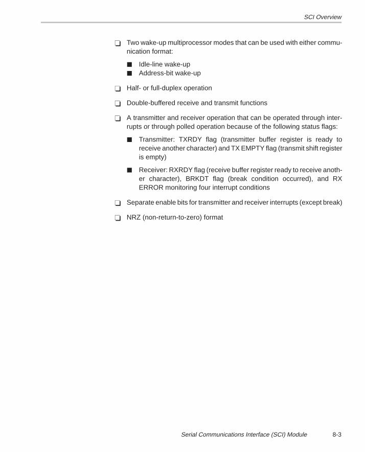
SCI Overview
8-3Serial Communications Interface (SCI) Module
� Two wake-up multiprocessor modes that can be used with either commu-nication format:
� Idle-line wake-up� Address-bit wake-up
� Half- or full-duplex operation
� Double-buffered receive and transmit functions
� A transmitter and receiver operation that can be operated through inter-rupts or through polled operation because of the following status flags:
� Transmitter: TXRDY flag (transmitter buffer register is ready toreceive another character) and TX EMPTY flag (transmit shift registeris empty)
� Receiver: RXRDY flag (receive buffer register ready to receive anoth-er character), BRKDT flag (break condition occurred), and RXERROR monitoring four interrupt conditions
� Separate enable bits for transmitter and receiver interrupts (except break)
� NRZ (non-return-to-zero) format
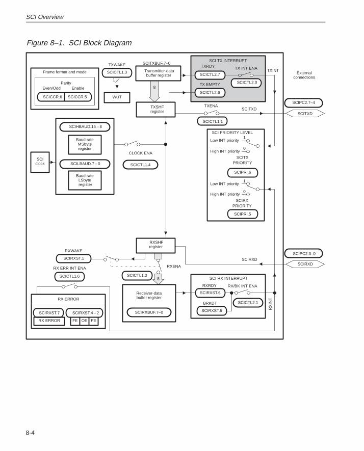
SCI Overview
8-4
Figure 8–1. SCI Block Diagram
SCIclock
WUT
Frame format and mode
Even/Odd EnableParity
SCI RX INTERRUPT
BRKDT
SCICTL1.1
RXRDY
SCIRXST.6
SCICTL1.3 Externalconnections
8
SCICTL2.1
RX/BK INT ENA
SCIRXDSCIRXST.1
TXENA
SCI TX INTERRUPT
TX EMPTY
TXRDY TX INT ENA
SCIPC2.7–4
SCITXD
RXENA
SCIPC2.3–0
SCIRXD
CLOCK ENA
SCICTL1.4
RXWAKE
SCICTL1.0SCICTL1.6
RX ERR INT ENA
TXWAKE
SCITXD
TXINT
SCICCR.6 SCICCR.5
SCITXBUF.7–0
SCIHBAUD.15 – 8
Baud rateMSbyteregister
SCILBAUD.7 – 0
SCIRXBUF.7–0
Receiver-databuffer register
SCIRXST.7
PEFE OE
RX ERROR
RX ERROR
SCIRXST.4 – 2
Transmitter-databuffer register
8SCICTL2.6
SCICTL2.7
Baud rateLSbyte register
RXSHFregister
TXSHF register
SCIRXST.5 RX
INT
1
SCIPRI.5
SCIPRI.6
SCI PRIORITY LEVEL
Low INT priority
High INT priority
Low INT priority
High INT priority
1
0
1
0
SCITXPRIORITY
SCIRXPRIORITY
SCICTL2.0
SCI Overview
8-5Serial Communications Interface (SCI) Module
8.1.2 Architecture
The major elements used in the full duplex operation are shown in Figure 8–1,SCI block Diagram, on page 8-4 and include:
� A transmitter (TX) and its major registers:
� SCITXBUF — transmitter data buffer register. Contains data (loadedby the CPU) to be transmitted
� TXSHF — transmitter shift register. Loads data from SCITXBUF andshifts data onto the SCITXD pin, one bit at a time
� A receiver (RX) and its major registers:
� RXSHF — receiver shift register. Shifts data in from SCIRXD pin, onebit at a time
� SCIRXBUF — receiver data buffer register. Contains data to be readby the CPU. Data from a remote processor is loaded into RXSHF andthen into SCIRXBUF and SCIRXEMU
� A programmable baud generator
� Data memory-mapped control and status registers
Note: The SCI receiver and transmitter can operate independently or simultaneously.
8.1.3 SCI Control Registers
The SCI control registers and their descriptions are shown below in Table 8–1.For more specific information, see Section 8.6, SCI Control Registers, on page8-19.
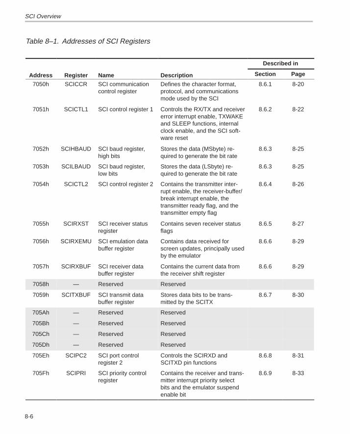
SCI Overview
8-6
Table 8–1. Addresses of SCI Registers
Described in
Address Register Name Description Section Page
7050h SCICCR SCI communicationcontrol register
Defines the character format,protocol, and communicationsmode used by the SCI
8.6.1 8-20
7051h SCICTL1 SCI control register 1 Controls the RX/TX and receivererror interrupt enable, TXWAKEand SLEEP functions, internalclock enable, and the SCI soft-ware reset
8.6.2 8-22
7052h SCIHBAUD SCI baud register, high bits
Stores the data (MSbyte) re-quired to generate the bit rate
8.6.3 8-25
7053h SCILBAUD SCI baud register, low bits
Stores the data (LSbyte) re-quired to generate the bit rate
8.6.3 8-25
7054h SCICTL2 SCI control register 2 Contains the transmitter inter-rupt enable, the receiver-buffer/break interrupt enable, thetransmitter ready flag, and thetransmitter empty flag
8.6.4 8-26
7055h SCIRXST SCI receiver statusregister
Contains seven receiver statusflags
8.6.5 8-27
7056h SCIRXEMU SCI emulation databuffer register
Contains data received forscreen updates, principally usedby the emulator
8.6.6 8-29
7057h SCIRXBUF SCI receiver data buffer register
Contains the current data fromthe receiver shift register
8.6.6 8-29
7058h — Reserved Reserved
7059h SCITXBUF SCI transmit data buffer register
Stores data bits to be trans-mitted by the SCITX
8.6.7 8-30
705Ah — Reserved Reserved
705Bh — Reserved Reserved
705Ch — Reserved Reserved
705Dh — Reserved Reserved
705Eh SCIPC2 SCI port control register 2
Controls the SCIRXD andSCITXD pin functions
8.6.8 8-31
705Fh SCIPRI SCI priority controlregister
Contains the receiver and trans-mitter interrupt priority selectbits and the emulator suspendenable bit
8.6.9 8-33
SCI Overview
8-7Serial Communications Interface (SCI) Module
8.1.4 Multiprocessor and Asynchronous Communications Modes
The SCI has two multiprocessor protocols, the idle-line multiprocessor mode(see section 8.3.1 on page 8-10) and the address-bit multiprocessor mode(see section 8.3.2 on page 8-12). These protocols allow efficient data transferbetween multiple processors.
The SCI offers the universal asynchronous receiver/transmitter (UART)communications mode for interfacing with many popular peripherals. Theasynchronous mode (see section 8.4, SCI Communication Format, on page8-14) requires two lines to interface with many standard devices such as terminals and printers that use RS-232-C formats. Data transmission charac-teristics include:
� One start bit� One to eight data bits� An even/odd parity bit or no parity bit� One or two stop bits

SCI Programmable Data Format
8-8
8.2 SCI Programmable Data Format
SCI data, both receive and transmit, is in NRZ (non-return-to-zero) format.The NRZ data format, shown in Figure 8–2, consists of:
� One start bit� One to eight data bits� An even/odd parity bit (optional)� One or two stop bits� An extra bit to distinguish addresses from data (address-bit mode only)
The basic unit of data is called a character and is one to eight bits in length.Each character of data is formatted with a start bit, one or two stop bits, andoptional parity and address bits. A character of data with its formatting informa-tion is called a frame and is shown in Figure 8–2.
Figure 8–2. Typical SCI Data Frame Formats
Start LSB 2 3 4 5 6 7 MSB Parity Stop
Start LSB 2 3 4 5 7 MSB Addr/Data
Parity Stop6
Idle-line mode
Address-bit mode
Address bit
To program the data format, use the SCI communication control register(SCICCR) described in section 8.6.1 on page 8-20. The bits used to programthe data format are listed in Table 8–2.
Table 8–2. Programming the Data Format Using SCICCR
Bit Name Designation Functions
SCI CHAR2–0 SCICCR.2–0 Selects the character (data) length (one toeight bits). Bit values are shown inTable 8–4 on page 8-21.
PARITY ENABLE SCICCR.5 Enables the parity function if set to 1 ordisables the parity function if cleared to 0
EVEN/ODD PARITY SCICCR.6 If parity is enabled, selects odd parity ifcleared to 0 or even parity when set to 1
STOP BITS SCICCR.7 Determines the number of stop bits trans-mitted—one stop bit if cleared to 0 or twostop bits if set to 1
SCI Multiprocessor Communication
8-9Serial Communications Interface (SCI) Module
8.3 SCI Multiprocessor Communication
The multiprocessor communication format allows one processor to efficientlysend blocks of data to other processors on the same serial link. On one serialline, there can be only one transfer (or transmitter) at a time.
The first byte of a block of information that the transmitter sends contains anaddress byte, that is read by all receivers. Only receivers with the correctaddress can be interrupted by the data bytes that follow the address byte. Thereceivers with an incorrect address remain uninterrupted until the next ad-dress byte.
All processors on the serial link set their SCI’s SLEEP bit (SCICTL1.2) to 1 sothat they are interrupted only when the address byte is detected. When a pro-cessor reads a block address that corresponds to the CPU’s device addressas set by your application software,the program must clear the SLEEP bit toenable the SCI to generate an interrupt on receipt of each data byte.
Although the receiver still operates when the SLEEP bit is 1, it does not setRXRDY, RXINT, or any of the receive error status bits to 1 unless the addressbyte is detected and the address bit in the received frame is a 1. The SCI doesnot alter the SLEEP bit; your software must alter the SLEEP bit.
A processor recognizes an address byte according to the multiprocessormode. For example:
� The idle-line mode (section 8.3.1, Idle-Line Multiprocessor Mode, on page8-10) leaves a quiet space before the address byte. This mode does nothave an extra address/data bit and is more efficient than the address-bitmode for handling blocks that contain more than ten bytes of data. Theidle-line mode should be used for typical nonmultiprocessor SCI commu-nication.
� The address-bit mode (section 8.3.2 on page 8-12) adds an extra bit (ad-dress bit) into every byte to distinguish addresses from data. This modeis more efficient in handling many small blocks of data because, unlike theidle mode, it does not have to wait between blocks of data. However, athigh transmit speeds, the program is not fast enough to avoid a 10-bit idlein the transmission stream.
The multiprocessor mode is software selectable via the ADDR/IDLE MODE bit(SCICCR.3). Both modes use the TXWAKE (SCICTL1.3), RXWAKE(SCIRXST.1), and the SLEEP flag bits (SCICTL1.2) to control the SCI trans-mitter and receiver features of these modes.

SCI Multiprocessor Communication
8-10
In both multiprocessor modes, the receipt sequence is:
1) At the receipt of an address block, the SCI port wakes up and requests aninterrupt. (Bit RX/BK INT ENA—SCICTL2.1—must be enabled to requestan interrupt.) It reads the first frame of the block, which contains the des-tination address.
2) A software routine is entered through the interrupt and checks theRXWAKE flag bit. If the RXWAKE bit is 1, the incoming byte is an address(otherwise, the byte is data) and this address byte is checked against itsdevice address byte stored in memory.
3) If the check shows that the block is addressed to the DSP controller, theCPU clears the SLEEP bit and reads the rest of the block. If not, the soft-ware routine exits with the SLEEP bit still set and does not receive inter-rupts until the next block start.
8.3.1 Idle-Line Multiprocessor Mode
In the Idle-line multiprocessor protocol (ADDR/IDLE MODE bit = 0), the blocksare separated by a longer idle time between blocks than between frames inthe blocks. An idle time of ten or more high-level bits after a frame indicatesthe start of a new block (the time of a single bit is calculated directly from thebaud value in bits per second). The idle-line multiprocessor communicationformat is shown in Figure 8–3 (ADDR/IDLE MODE bit is SCICCR.3).
Figure 8–3. Idle-Line Multiprocessor Communication Format
Address Data Last Data
First frame within blockIs address ; it follows idleperiod of 10 bits or more
Frame withinblock
Idle periodless than10 bits
Idle period of 10 bitsor more
ÇÇÇÇÇÇÇÇÇÇÇ ÇÇÇÇÇÇ ÇÇÇÇÇ
Several blocks of frames
Data format(Pins SCIRXD, SCITXD)
Data format expanded
Idle periods of 10 bits or moreseparate the blocks
Sta
rt
Sta
rt
Sta
rt
One block of frames
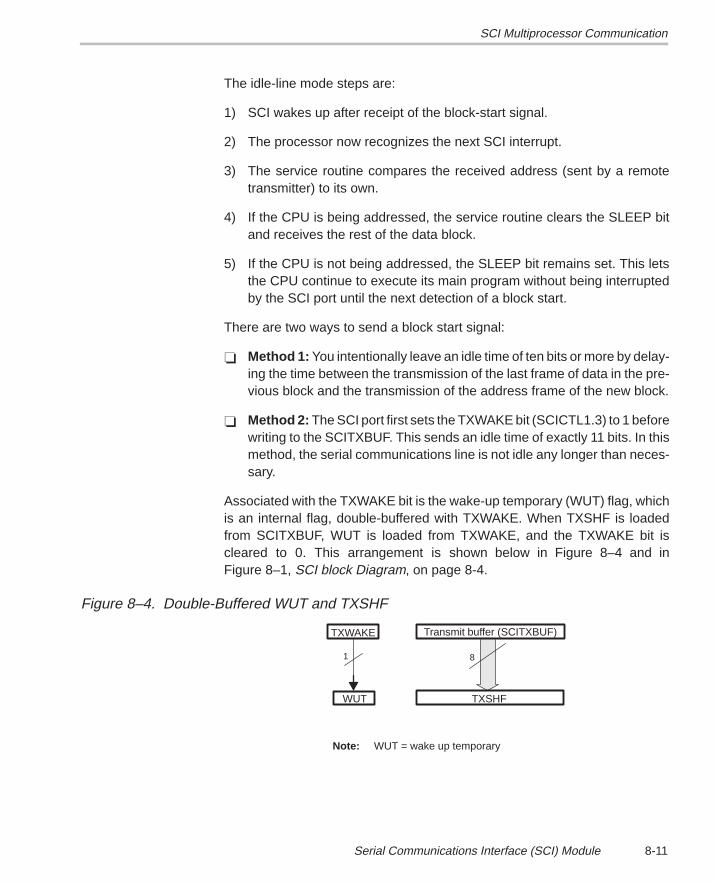
SCI Multiprocessor Communication
8-11Serial Communications Interface (SCI) Module
The idle-line mode steps are:
1) SCI wakes up after receipt of the block-start signal.
2) The processor now recognizes the next SCI interrupt.
3) The service routine compares the received address (sent by a remotetransmitter) to its own.
4) If the CPU is being addressed, the service routine clears the SLEEP bitand receives the rest of the data block.
5) If the CPU is not being addressed, the SLEEP bit remains set. This letsthe CPU continue to execute its main program without being interruptedby the SCI port until the next detection of a block start.
There are two ways to send a block start signal:
� Method 1: You intentionally leave an idle time of ten bits or more by delay-ing the time between the transmission of the last frame of data in the pre-vious block and the transmission of the address frame of the new block.
� Method 2: The SCI port first sets the TXWAKE bit (SCICTL1.3) to 1 beforewriting to the SCITXBUF. This sends an idle time of exactly 11 bits. In thismethod, the serial communications line is not idle any longer than neces-sary.
Associated with the TXWAKE bit is the wake-up temporary (WUT) flag, whichis an internal flag, double-buffered with TXWAKE. When TXSHF is loadedfrom SCITXBUF, WUT is loaded from TXWAKE, and the TXWAKE bit iscleared to 0. This arrangement is shown below in Figure 8–4 and inFigure 8–1, SCI block Diagram, on page 8-4.
Figure 8–4. Double-Buffered WUT and TXSHF
TXWAKE
WUT
Transmit buffer (SCITXBUF)
TXSHF
1 8
Note: WUT = wake up temporary
SCI Multiprocessor Communication
8-12
To send out a block start signal of exactly one frame time during a sequenceof block transmissions, perform the following:
1) Write a 1 to the TXWAKE bit.
2) Write a data word (the content is not important — any value) to the transmitdata buffer (SCITXBUF) to send a block-start signal. The first data wordwritten is suppressed while the block-start signal is sent out and ignored.When the transmit shift register ( TXSHF) is free again, SCITXBUF’s con-tents are shifted to TXSHF, the TXWAKE value is shifted to WUT, andTXWAKE is cleared.
Because TXWAKE was set to 1, the start, data, and parity bits are replacedby an idle period of 11 bits transmitted after the last stop bit of the previousframe.
3) Write a new address value to SCITXBUF.
A data word of any value must first be written to SCITXBUF before theTXWAKE bit value can be shifted to WUT. After the data word (any value) isshifted to TXSHF, SCITXBUF (and TXWAKE, if necessary), SCITXBUF canbe written to again because TXSHF and WUT are both double buffered.
The receiver operates regardless of the SLEEP bit; however, until an addressframe is detected, the receiver does not set RXRDY, does not set the statusbits, and does not request a receive interrupt.
8.3.2 Address-Bit Multiprocessor Mode �
In the address-bit protocol (ADDR/IDLE MODE bit = 1), frames have an extrabit, called an address bit, that immediately follows the last data bit. Theaddress bit is set to 1 in the first frame of the block and to 0 in all other frames.The idle period timing is irrelevant (ADDR/IDLE MODE bit is SCICCR.3). SeeFigure 8–5, Address-Bit Multiprocessor Communication Format, on page8-13.
The TXWAKE bit value is placed in the address bit. During transmission whenthe SCITXBUF and TXWAKE are loaded into the TXSHF and WUT, respec-tively, TXWAKE is reset to 0 and WUT becomes the value of the address bitof the current frame.
�Note: For information about TXWAKE control during multiprocessormode, refer to Enhancements and Exceptions for the ’F240 DSP Controller(literature number SPRS066).
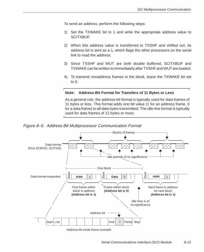
SCI Multiprocessor Communication
8-13Serial Communications Interface (SCI) Module
To send an address, perform the following steps:
1) Set the TXWAKE bit to 1 and write the appropriate address value toSCITXBUF.
2) When this address value is transferred to TXSHF and shifted out, itsaddress bit is sent as a 1, which flags the other processors on the seriallink to read the address.
3) Since TXSHF and WUT are both double buffered, SCITXBUF andTXWAKE can be written to immediately after TXSHF and WUT are loaded.
4) To transmit nonaddress frames in the block, leave the TXWAKE bit setto 0.
Note: Address-Bit Format for Transfers of 11 Bytes or Less
As a general rule, the address-bit format is typically used for data frames of11 bytes or less. This format adds one bit value (1 for an address frame, 0for a data frame) to all data bytes transmitted. The idle-line format is typicallyused for data frames of 12 bytes or more.
Figure 8–5. Address-Bit Multiprocessor Communication Format
MSB Parity
01Addr Data Addr
ÉÉÉÉÉÉData format
(Pins SCIRXD, SCITXD)
Data format expanded
First frame withinblock Is address
(Address bit is 1)
1
ÉÉÉÉÉÉÉÉÉÉÉÉÉÉ
Idle time is ofno significance
Next frame is addressfor next block
(Address bit is 1)
Start LSB Stop
Address-bit mode frame example
Address bit
Frame within block(Address bit is 0)
1
Sta
rt
Sta
rt
Sta
rt
One block
Idle periods of no significance
Blocks of frames
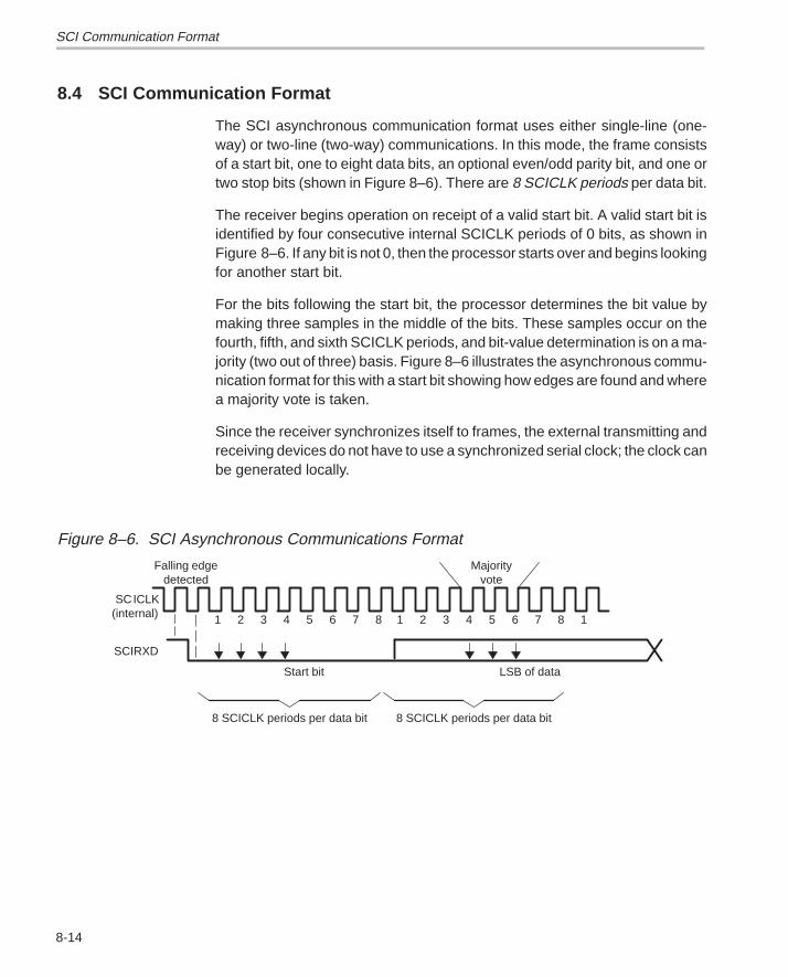
SCI Communication Format
8-14
8.4 SCI Communication Format
The SCI asynchronous communication format uses either single-line (one-way) or two-line (two-way) communications. In this mode, the frame consistsof a start bit, one to eight data bits, an optional even/odd parity bit, and one ortwo stop bits (shown in Figure 8–6). There are 8 SCICLK periods per data bit.
The receiver begins operation on receipt of a valid start bit. A valid start bit isidentified by four consecutive internal SCICLK periods of 0 bits, as shown inFigure 8–6. If any bit is not 0, then the processor starts over and begins lookingfor another start bit.
For the bits following the start bit, the processor determines the bit value bymaking three samples in the middle of the bits. These samples occur on thefourth, fifth, and sixth SCICLK periods, and bit-value determination is on a ma-jority (two out of three) basis. Figure 8–6 illustrates the asynchronous commu-nication format for this with a start bit showing how edges are found and wherea majority vote is taken.
Since the receiver synchronizes itself to frames, the external transmitting andreceiving devices do not have to use a synchronized serial clock; the clock canbe generated locally.
Figure 8–6. SCI Asynchronous Communications Format
Majorityvote
Falling edgedetected
Start bit LSB of data
SCICLK(internal)
SCIRXD
1 2 3 4 5 6 7 8 1 2 3 4 5 6 7 8 1
8 SCICLK periods per data bit 8 SCICLK periods per data bit
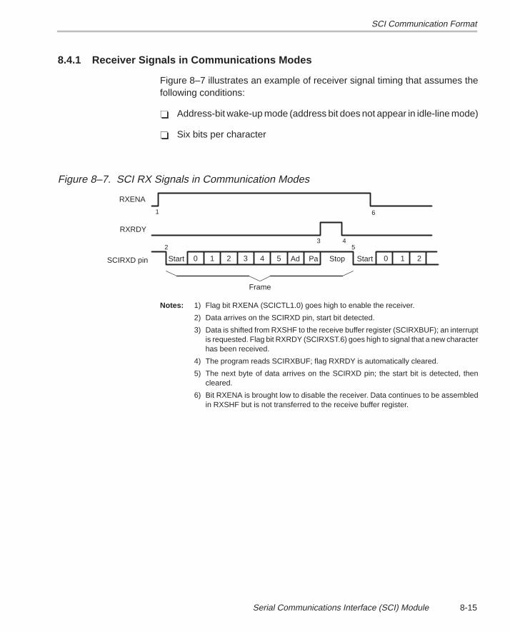
SCI Communication Format
8-15Serial Communications Interface (SCI) Module
8.4.1 Receiver Signals in Communications Modes
Figure 8–7 illustrates an example of receiver signal timing that assumes thefollowing conditions:
� Address-bit wake-up mode (address bit does not appear in idle-line mode)
� Six bits per character
Figure 8–7. SCI RX Signals in Communication Modes
RXENA
RXRDY
1 6
3 452
0 1 2 3 4 5 0 1 2Start Stop StartAd PaSCIRXD pin
Frame
Notes: 1) Flag bit RXENA (SCICTL1.0) goes high to enable the receiver.
2) Data arrives on the SCIRXD pin, start bit detected.
3) Data is shifted from RXSHF to the receive buffer register (SCIRXBUF); an interruptis requested. Flag bit RXRDY (SCIRXST.6) goes high to signal that a new characterhas been received.
4) The program reads SCIRXBUF; flag RXRDY is automatically cleared.
5) The next byte of data arrives on the SCIRXD pin; the start bit is detected, thencleared.
6) Bit RXENA is brought low to disable the receiver. Data continues to be assembledin RXSHF but is not transferred to the receive buffer register.
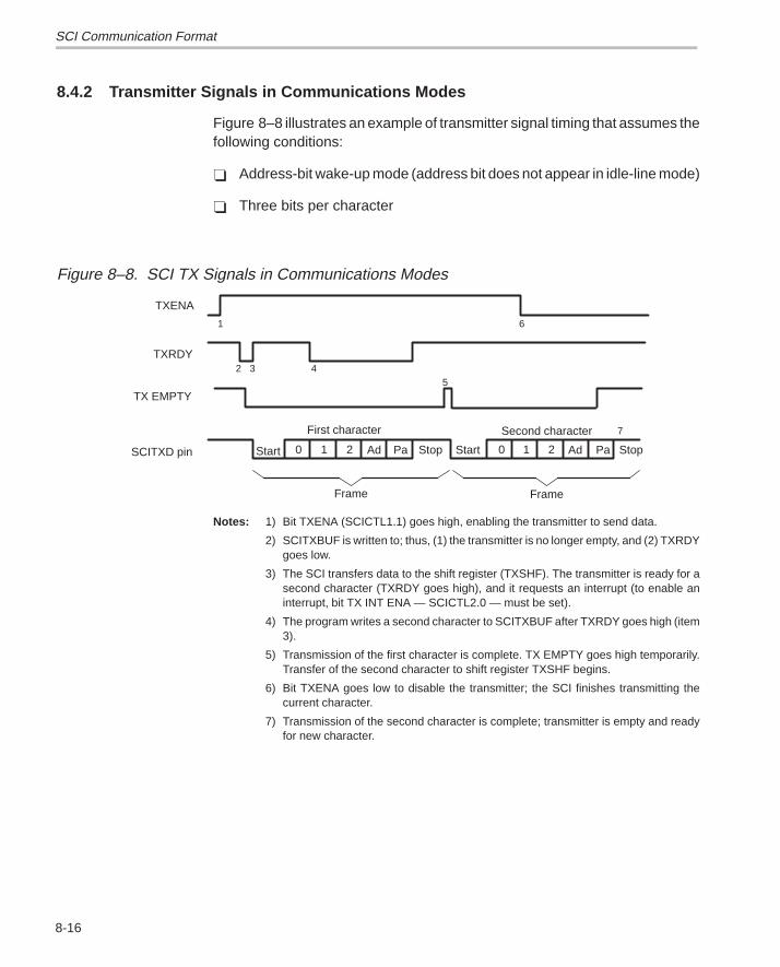
SCI Communication Format
8-16
8.4.2 Transmitter Signals in Communications Modes
Figure 8–8 illustrates an example of transmitter signal timing that assumes thefollowing conditions:
� Address-bit wake-up mode (address bit does not appear in idle-line mode)
� Three bits per character
Figure 8–8. SCI TX Signals in Communications Modes
Ad
TXENA
SCITXD pin
1 6
3 45
2
0 1 2 0 1 2
TXRDY
TX EMPTY
7
Start Start StopStopAd PaPa
First character Second character
Frame Frame
Notes: 1) Bit TXENA (SCICTL1.1) goes high, enabling the transmitter to send data.
2) SCITXBUF is written to; thus, (1) the transmitter is no longer empty, and (2) TXRDYgoes low.
3) The SCI transfers data to the shift register (TXSHF). The transmitter is ready for asecond character (TXRDY goes high), and it requests an interrupt (to enable aninterrupt, bit TX INT ENA — SCICTL2.0 — must be set).
4) The program writes a second character to SCITXBUF after TXRDY goes high (item3).
5) Transmission of the first character is complete. TX EMPTY goes high temporarily.Transfer of the second character to shift register TXSHF begins.
6) Bit TXENA goes low to disable the transmitter; the SCI finishes transmitting thecurrent character.
7) Transmission of the second character is complete; transmitter is empty and readyfor new character.
SCI Port Interrupts
8-17Serial Communications Interface (SCI) Module
8.5 SCI Port Interrupts
The internally-generated serial clock is determined by the SYSCLK frequencyand the bank-select registers. The SCI uses the 16-bit value of the baud-selectregisters to select one of 64K different serial clock rates.
The SCI’s receiver and transmitter can be interrupt controlled. The SCICTL2has one flag bit (TXRDY) that indicates active interrupt conditions andSCIRXST has two interrupt flag bits (RXRDY and BRKDT). The transmitterand receiver have separate interrupt-enable bits. When not enabled, the inter-rupts are not asserted; however, the condition flags remain active, reflectingtransmission and receipt status.
The SCI provides independent interrupt requests and vectors for the receiverand transmitter.
� If the RX/BK INT ENA bit (SCICTL2.1) is set, the receiver interrupt is as-serted when one of the following events occurs:
� The SCI receives a complete frame and transfers the data in RXSHFto SCIRXBUF. This action sets the RXRDY flag (SCIRXST.6) and initi-ates an interrupt.
� A break detect condition occurs (the SCIRXD is low for 10-bit periodsfollowing a missing stop bit). This action sets the BRKDT flag bit(SCIRXST.5) and initiates an interrupt.
� If the TX INT ENA bit (SCICTL2.0) is set, the transmitter interrupt is as-serted whenever the data in SCITXBUF is transferred to TXSHF, indicat-ing that the CPU can write to TXBUF. This action sets the TXRDY flag bit(SCICTL2.7) and initiates an interrupt.
SCI interrupts can be programmed into different priority levels by the SCIRXPRIORITY (SCIPRI.5) and SCITX PRIORITY (SCIPRI.6) control bits. Whenboth RX and TX interrupt requests are made on the same level, the receiveralways has higher priority than the transmitter, reducing the possibility ofreceiver overrun.
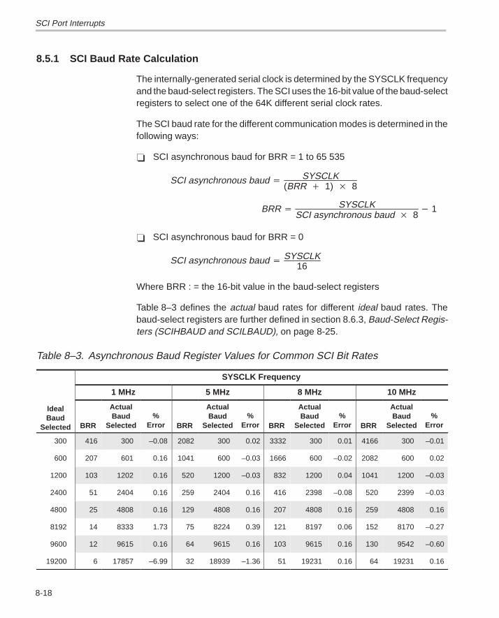
SCI Port Interrupts
8-18
8.5.1 SCI Baud Rate Calculation
The internally-generated serial clock is determined by the SYSCLK frequencyand the baud-select registers. The SCI uses the 16-bit value of the baud-selectregisters to select one of the 64K different serial clock rates.
The SCI baud rate for the different communication modes is determined in thefollowing ways:
� SCI asynchronous baud for BRR = 1 to 65 535
SCI asynchronous baud �SYSCLK
(BRR � 1) � 8
BRR �SYSCLK
SCI asynchronous baud � 8� 1
� SCI asynchronous baud for BRR = 0
SCI asynchronous baud �SYSCLK
16
Where BRR : = the 16-bit value in the baud-select registers
Table 8–3 defines the actual baud rates for different ideal baud rates. Thebaud-select registers are further defined in section 8.6.3, Baud-Select Regis-ters (SCIHBAUD and SCILBAUD), on page 8-25.
Table 8–3. Asynchronous Baud Register Values for Common SCI Bit Rates
SYSCLK Frequency
1 MHz 5 MHz 8 MHz 10 MHz
IdealBaud
Selected BRR
ActualBaud
Selected%
Error BRR
ActualBaud
Selected%
Error BRR
ActualBaud
Selected%
Error BRR
ActualBaud
Selected%
Error
300 416 300 –0.08 2082 300 0.02 3332 300 0.01 4166 300 –0.01
600 207 601 0.16 1041 600 –0.03 1666 600 –0.02 2082 600 0.02
1200 103 1202 0.16 520 1200 –0.03 832 1200 0.04 1041 1200 –0.03
2400 51 2404 0.16 259 2404 0.16 416 2398 –0.08 520 2399 –0.03
4800 25 4808 0.16 129 4808 0.16 207 4808 0.16 259 4808 0.16
8192 14 8333 1.73 75 8224 0.39 121 8197 0.06 152 8170 –0.27
9600 12 9615 0.16 64 9615 0.16 103 9615 0.16 130 9542 –0.60
19200 6 17857 –6.99 32 18939 –1.36 51 19231 0.16 64 19231 0.16
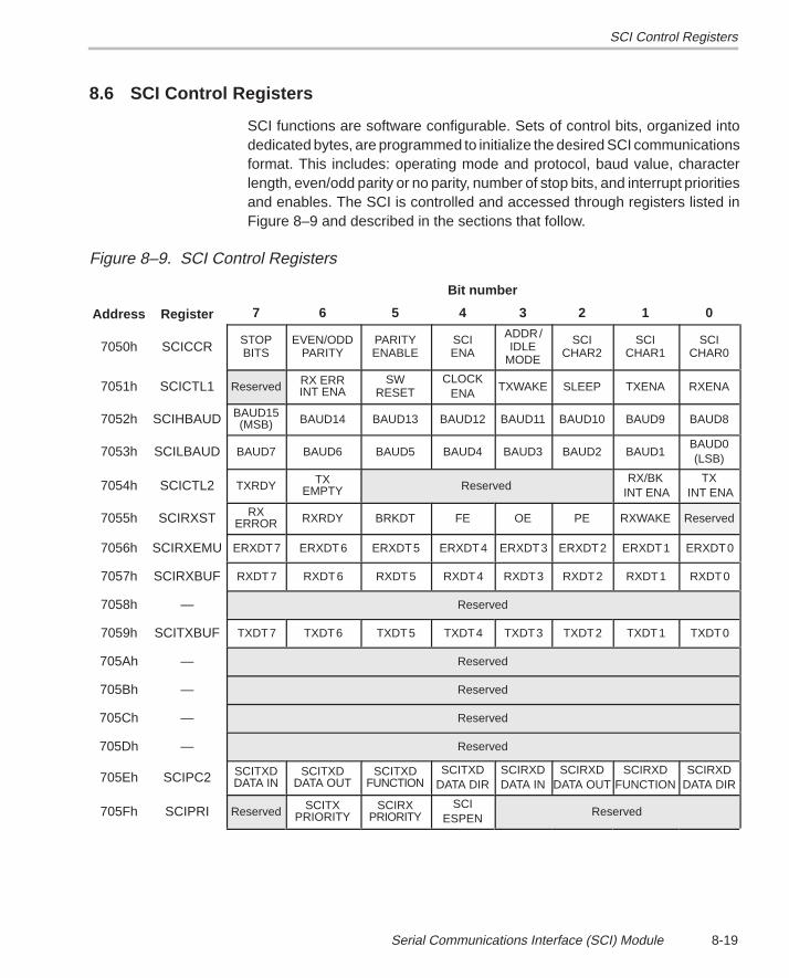
SCI Control Registers
8-19Serial Communications Interface (SCI) Module
8.6 SCI Control Registers
SCI functions are software configurable. Sets of control bits, organized intodedicated bytes, are programmed to initialize the desired SCI communicationsformat. This includes: operating mode and protocol, baud value, characterlength, even/odd parity or no parity, number of stop bits, and interrupt prioritiesand enables. The SCI is controlled and accessed through registers listed inFigure 8–9 and described in the sections that follow.
Figure 8–9. SCI Control Registers
Bit number
Address Register 7 6 5 4 3 2 1 0
7050h SCICCR STOPBITS
EVEN/ODDPARITY
PARITYENABLE
SCIENA
ADDR/IDLE
MODE
SCICHAR2
SCICHAR1
SCICHAR0
7051h SCICTL1 Reserved RX ERRINT ENA
SWRESET
CLOCKENA
TXWAKE SLEEP TXENA RXENA
7052h SCIHBAUD BAUD15(MSB) BAUD14 BAUD13 BAUD12 BAUD11 BAUD10 BAUD9 BAUD8
7053h SCILBAUD BAUD7 BAUD6 BAUD5 BAUD4 BAUD3 BAUD2 BAUD1BAUD0(LSB)
7054h SCICTL2 TXRDY TXEMPTY Reserved
RX/BKINT ENA
TXINT ENA
7055h SCIRXST RXERROR RXRDY BRKDT FE OE PE RXWAKE Reserved
7056h SCIRXEMU ERXDT7 ERXDT6 ERXDT5 ERXDT4 ERXDT3 ERXDT2 ERXDT1 ERXDT0
7057h SCIRXBUF RXDT7 RXDT6 RXDT5 RXDT4 RXDT3 RXDT2 RXDT1 RXDT0
7058h — Reserved
7059h SCITXBUF TXDT7 TXDT6 TXDT5 TXDT4 TXDT3 TXDT2 TXDT1 TXDT0
705Ah — Reserved
705Bh — Reserved
705Ch — Reserved
705Dh — Reserved
705Eh SCIPC2 SCITXDDATA IN
SCITXDDATA OUT
SCITXDFUNCTION
SCITXDDATA DIR
SCIRXDDATA IN
SCIRXDDATA OUT
SCIRXDFUNCTION
SCIRXDDATA DIR
705Fh SCIPRI Reserved SCITXPRIORITY
SCIRXPRIORITY
SCIESPEN
Reserved
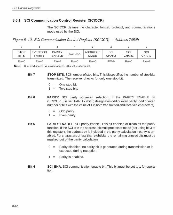
SCI Control Registers
8-20
8.6.1 SCI Communication Control Register (SCICCR)
The SCICCR defines the character format, protocol, and communicationsmode used by the SCI.
Figure 8–10. SCI Communication Control Register (SCICCR) — Address 7050h
7 6 5 4 3 2 1 0
STOPBITS
EVEN/ODDPARITY
PARITYENABLE
SCI ENAADDR/IDLE
MODESCI
CHAR2SCI
CHAR1SCI
CHAR0
RW–0 RW–0 RW–0 RW–0 RW–0 RW–0 RW–0 RW–0
Note: R = read access, W = write access, –0 = value after reset
Bit 7 STOP BITS . SCI number of stop bits. This bit specifies the number of stop bitstransmitted. The receiver checks for only one stop bit.
0 = One stop bit1 = Two stop bits
Bit 6 PARITY . SCI parity odd/even selection. If the PARITY ENABLE bit(SCICCR.5) is set, PARITY (bit 6) designates odd or even parity (odd or evennumber of bits with the value of 1 in both transmitted and received characters).
0 = Odd parity1 = Even parity
Bit 5 PARITY ENABLE . SCI parity enable. This bit enables or disables the parityfunction. If the SCI is in the address-bit multiprocessor mode (set using bit 3 ofthis register), the address bit is included in the parity calculation if parity is en-abled. For characters of less than eight bits, the remaining unused bits must bemasked out of the parity calculation.
0 = Parity disabled; no parity bit is generated during transmission or isexpected during reception.
1 = Parity is enabled.
Bit 4 SC I ENA . SCI communication enable bit. This bit must be set to 1 for opera-tion.
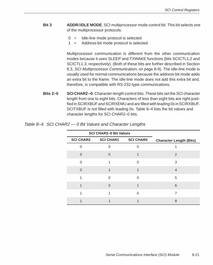
SCI Control Registers
8-21Serial Communications Interface (SCI) Module
Bit 3 ADDR/IDLE MODE . SCI multiprocessor mode control bit. This bit selects oneof the multiprocessor protocols:
0 = Idle-line mode protocol is selected1 = Address-bit mode protocol is selected
Multiprocessor communication is different from the other communicationmodes because it uses SLEEP and TXWAKE functions (bits SCICTL1.2 andSCICTL1.3, respectively). (Both of these bits are further described in Section8.3, SCI Multiprocessor Communication, on page 8-9). The idle-line mode isusually used for normal communications because the address-bit mode addsan extra bit to the frame. The idle-line mode does not add this extra bit and,therefore, is compatible with RS-232-type communications.
Bits 2–0 SCI CHAR2–0 . Character-length control bits. These bits set the SCI characterlength from one to eight bits. Characters of less than eight bits are right-justi-fied in SCIRXBUF and SCIRXEMU and are filled with leading 0s in SCIRXBUF.SCITXBUF is not filled with leading 0s. Table 8–4 lists the bit values and character lengths for SCI CHAR2–0 bits.
Table 8–4. SCI CHAR2 — 0 Bit Values and Character Lengths
SCI CHAR2–0 Bit Values
SCI CHAR2 SCI CHAR1 SCI CHAR0 Character Length (Bits)
0 0 0 1
0 0 1 2
0 1 0 3
0 1 1 4
1 0 0 5
1 0 1 6
1 1 0 7
1 1 1 8
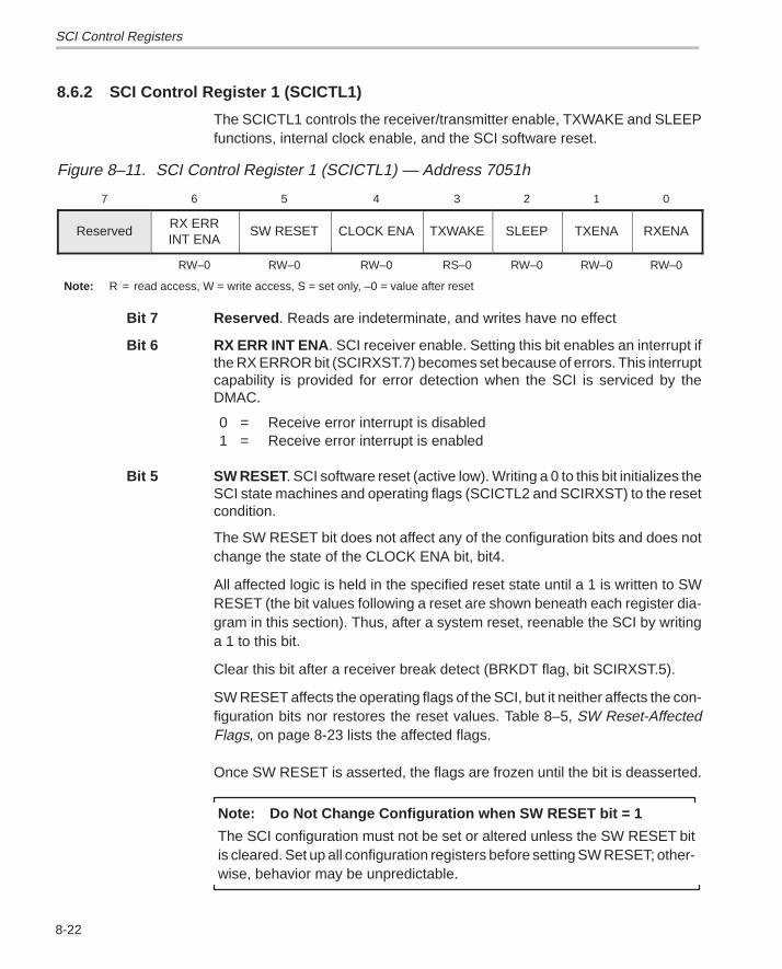
SCI Control Registers
8-22
8.6.2 SCI Control Register 1 (SCICTL1)
The SCICTL1 controls the receiver/transmitter enable, TXWAKE and SLEEPfunctions, internal clock enable, and the SCI software reset.
Figure 8–11. SCI Control Register 1 (SCICTL1) — Address 7051h
7 6 5 4 3 2 1 0
ReservedRX ERRINT ENA
SW RESET CLOCK ENA TXWAKE SLEEP TXENA RXENA
RW–0 RW–0 RW–0 RS–0 RW–0 RW–0 RW–0
Note: R = read access, W = write access, S = set only, –0 = value after reset
Bit 7 Reserved . Reads are indeterminate, and writes have no effect
Bit 6 RX ERR INT ENA . SCI receiver enable. Setting this bit enables an interrupt ifthe RX ERROR bit (SCIRXST.7) becomes set because of errors. This interruptcapability is provided for error detection when the SCI is serviced by theDMAC.
0 = Receive error interrupt is disabled1 = Receive error interrupt is enabled
Bit 5 SW RESET. SCI software reset (active low). Writing a 0 to this bit initializes theSCI state machines and operating flags (SCICTL2 and SCIRXST) to the resetcondition.
The SW RESET bit does not affect any of the configuration bits and does notchange the state of the CLOCK ENA bit, bit4.
All affected logic is held in the specified reset state until a 1 is written to SWRESET (the bit values following a reset are shown beneath each register dia-gram in this section). Thus, after a system reset, reenable the SCI by writinga 1 to this bit.
Clear this bit after a receiver break detect (BRKDT flag, bit SCIRXST.5).
SW RESET affects the operating flags of the SCI, but it neither affects the con-figuration bits nor restores the reset values. Table 8–5, SW Reset-AffectedFlags, on page 8-23 lists the affected flags.
Once SW RESET is asserted, the flags are frozen until the bit is deasserted.
Note: Do Not Change Configuration when SW RESET bit = 1
The SCI configuration must not be set or altered unless the SW RESET bitis cleared. Set up all configuration registers before setting SW RESET; other-wise, behavior may be unpredictable.
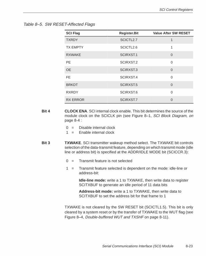
SCI Control Registers
8-23Serial Communications Interface (SCI) Module
Table 8–5. SW RESET-Affected Flags
SCI Flag Register.Bit Value After SW RESET
TXRDY SCICTL2.7 1
TX EMPTY SCICTL2.6 1
RXWAKE SCIRXST.1 0
PE SCIRXST.2 0
OE SCIRXST.3 0
FE SCIRXST.4 0
BRKDT SCIRXST.5 0
RXRDY SCIRXST.6 0
RX ERROR SCIRXST.7 0
Bit 4 CLOCK ENA . SCI internal clock enable. This bit determines the source of themodule clock on the SCICLK pin (see Figure 8–1, SCI Block Diagram, onpage 8-4 :
0 = Disable internal clock1 = Enable internal clock
Bit 3 TXWAKE . SCI transmitter wakeup method select. The TXWAKE bit controlsselection of the data-transmit feature, depending on which transmit mode (idleline or address bit) is specified at the ADDR/IDLE MODE bit (SCICCR.3):
0 = Transmit feature is not selected
1 = Transmit feature selected is dependent on the mode: idle-line oraddress-bit:
Idle-line mode: write a 1 to TXWAKE, then write data to registerSCITXBUF to generate an idle period of 11 data bits
Address-bit mode: write a 1 to TXWAKE, then write data toSCITXBUF to set the address bit for that frame to 1
TXWAKE is not cleared by the SW RESET bit (SCICTL1.5). This bit is onlycleared by a system reset or by the transfer of TXWAKE to the WUT flag (seeFigure 8–4, Double-buffered WUT and TXSHF on page 8-11).
SCI Control Registers
8-24
Bit 2 SLEEP. SCI sleep. In a multiprocessor configuration, this bit controls thereceive sleep function. Clearing this bit brings the SCI out of the sleep mode.This configuration and process are further explained in section 8.3, SCI Multi-processor Communication, on page 8-9.
0 = Sleep mode is disabled1 = Sleep mode is enabled
The receiver still operates when the SLEEP bit is set; however, operation doesnot update the receive buffer ready bit (SCIRXST.6, RXRDY) or the errorstatus bits (SCIRXST.5–2: BRKDT, FE, OE, and PE) unless the address byteis detected. This bit is not cleared when the address byte is detected.
Bit 1 TXENA . SCI transmitter enable. Data is transmitted through the SCITXD pinonly when TXENA is set (see Figure 8–1, SCI Block Diagram, on page 8-4). Ifreset, transmission is halted but only after all data previously written to SCITX-BUF has been sent.
0 = Transmitter is disabled1 = Transmitter is enabled
Bit 0 RXENA . SCI receiver enable. Data is received on the SCIRXD pin (seeFigure 8–1 on page 8-4) and is sent to the receive shift register and then thereceive buffers. This bit enables or disables the receiver (transfers to the buff-ers).
0 = Prevent received characters from transfer into SCIRXEMU andSCIRXBUF receive buffers
1 = Send receive characters into SCIRXEMU and SCIRXBUF
Clearing RXENA stops received characters from being transferred into the tworeceive buffers and also stops the generation of receiver interrupts. However,the receiver shift register can continue to assemble characters. Thus, ifRXENA is set during the reception of a character, the complete character istransferred into the receive buffer registers, SCIRXEMU and SCIRXBUF.
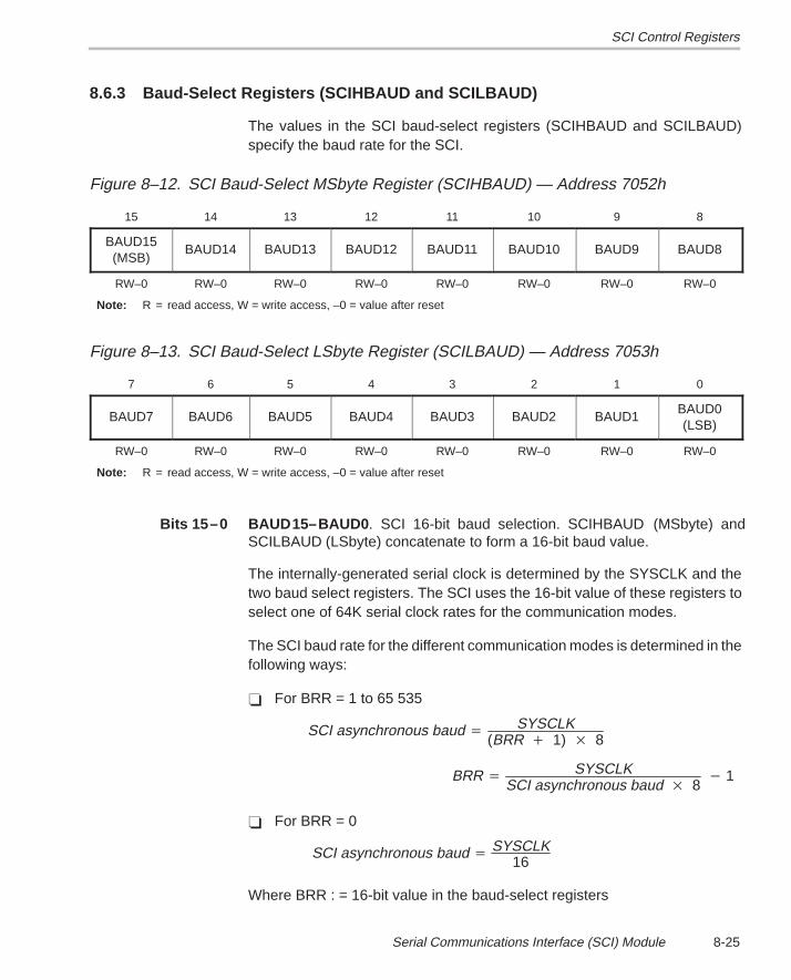
SCI Control Registers
8-25Serial Communications Interface (SCI) Module
8.6.3 Baud-Select Registers (SCIHBAUD and SCILBAUD)
The values in the SCI baud-select registers (SCIHBAUD and SCILBAUD)specify the baud rate for the SCI.
Figure 8–12. SCI Baud-Select MSbyte Register (SCIHBAUD) — Address 7052h
15 14 13 12 11 10 9 8
BAUD15(MSB)
BAUD14 BAUD13 BAUD12 BAUD11 BAUD10 BAUD9 BAUD8
RW–0 RW–0 RW–0 RW–0 RW–0 RW–0 RW–0 RW–0
Note: R = read access, W = write access, –0 = value after reset
Figure 8–13. SCI Baud-Select LSbyte Register (SCILBAUD) — Address 7053h
7 6 5 4 3 2 1 0
BAUD7 BAUD6 BAUD5 BAUD4 BAUD3 BAUD2 BAUD1BAUD0(LSB)
RW–0 RW–0 RW–0 RW–0 RW–0 RW–0 RW–0 RW–0
Note: R = read access, W = write access, –0 = value after reset
Bits 15–0 BAUD15–BAUD0 . SCI 16-bit baud selection. SCIHBAUD (MSbyte) andSCILBAUD (LSbyte) concatenate to form a 16-bit baud value.
The internally-generated serial clock is determined by the SYSCLK and thetwo baud select registers. The SCI uses the 16-bit value of these registers toselect one of 64K serial clock rates for the communication modes.
The SCI baud rate for the different communication modes is determined in thefollowing ways:
� For BRR = 1 to 65 535
SCI asynchronous baud �SYSCLK
(BRR � 1) � 8
BRR �SYSCLK
SCI asynchronous baud � 8� 1
� For BRR = 0
SCI asynchronous baud �SYSCLK
16
Where BRR : = 16-bit value in the baud-select registers
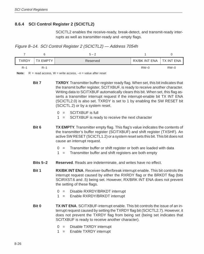
SCI Control Registers
8-26
8.6.4 SCI Control Register 2 (SCICTL2)
SCICTL2 enables the receive-ready, break-detect, and transmit-ready inter-rupts as well as transmitter-ready and -empty flags.
Figure 8–14. SCI Control Register 2 (SCICTL2) — Address 7054h
7 6 5 – 2 1 0
TXRDY TX EMPTY Reserved RX/BK INT ENA TX INT ENA
R–1 R–1 RW–0 RW–0
Note: R = read access, W = write access, –n = value after reset
Bit 7 TXRDY. Transmitter buffer-register ready flag. When set, this bit indicates thatthe transmit buffer register, SCITXBUF, is ready to receive another character.Writing data to SCITXBUF automatically clears this bit. When set, this flag as-serts a transmitter interrupt request if the interrupt-enable bit TX INT ENA(SCICTL2.0) is also set. TXRDY is set to 1 by enabling the SW RESET bit(SCICTL.2) or by a system reset.
0 = SCITXBUF is full1 = SCITXBUF is ready to receive the next character
Bit 6 TX EMPTY. Transmitter empty flag. This flag’s value indicates the contents ofthe transmitter’s buffer register (SCITXBUF) and shift register (TXSHF). Anactive SW RESET (SCICTL1.2) or a system reset sets this bit. This bit does notcause an interrupt request.
0 = Transmitter buffer or shift register or both are loaded with data1 = Transmitter buffer and shift registers are both empty
Bits 5–2 Reserved . Reads are indeterminate, and writes have no effect.
Bit 1 RX/BK INT ENA . Receiver-buffer/break interrupt enable. This bit controls theinterrupt request caused by either the RXRDY flag or the BRKDT flag (bitsSCIRXST.6 and .5) being set. However, RX/BRK INT ENA does not preventthe setting of these flags.
0 = Disable RXRDY/BRKDT interrupt1 = Enable RXRDY/BRKDT interrupt
Bit 0 TX INT ENA . SCITXBUF-interrupt enable. This bit controls the issue of an in-terrupt request caused by setting the TXRDY flag bit (SCICTL2.7). However, itdoes not prevent the TXRDY flag from being set (being set indicates thatSCITXBUF is ready to receive another character).
0 = Disable TXRDY interrupt1 = Enable TXRDY interrupt
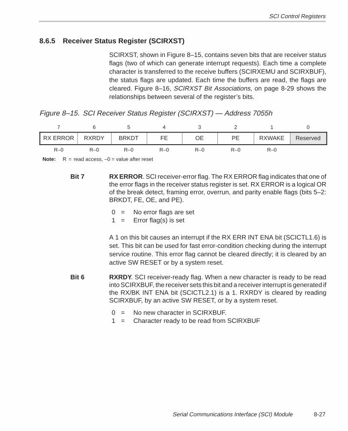
SCI Control Registers
8-27Serial Communications Interface (SCI) Module
8.6.5 Receiver Status Register (SCIRXST)
SCIRXST, shown in Figure 8–15, contains seven bits that are receiver statusflags (two of which can generate interrupt requests). Each time a completecharacter is transferred to the receive buffers (SCIRXEMU and SCIRXBUF),the status flags are updated. Each time the buffers are read, the flags arecleared. Figure 8–16, SCIRXST Bit Associations, on page 8-29 shows therelationships between several of the register’s bits.
Figure 8–15. SCI Receiver Status Register (SCIRXST) — Address 7055h
7 6 5 4 3 2 1 0
RX ERROR RXRDY BRKDT FE OE PE RXWAKE Reserved
R–0 R–0 R–0 R–0 R–0 R–0 R–0
Note: R = read access, –0 = value after reset
Bit 7 RX ERROR . SCI receiver-error flag. The RX ERROR flag indicates that one ofthe error flags in the receiver status register is set. RX ERROR is a logical ORof the break detect, framing error, overrun, and parity enable flags (bits 5–2:BRKDT, FE, OE, and PE).
0 = No error flags are set1 = Error flag(s) is set
A 1 on this bit causes an interrupt if the RX ERR INT ENA bit (SCICTL1.6) isset. This bit can be used for fast error-condition checking during the interruptservice routine. This error flag cannot be cleared directly; it is cleared by anactive SW RESET or by a system reset.
Bit 6 RXRDY. SCI receiver-ready flag. When a new character is ready to be readinto SCIRXBUF, the receiver sets this bit and a receiver interrupt is generated ifthe RX/BK INT ENA bit (SCICTL2.1) is a 1. RXRDY is cleared by readingSCIRXBUF, by an active SW RESET, or by a system reset.
0 = No new character in SCIRXBUF.1 = Character ready to be read from SCIRXBUF
SCI Control Registers
8-28
Bit 5 BRKDT . SCI break-detect flag. The SCI sets this bit when a break conditionoccurs. A break condition occurs when the SCI receive data line (see SCIRXDon the right side of Figure 8–1, SCI Block Diagram, on page 8-4) remainscontinuously low for at least ten bits after a missing first stop bit. The occur-rence of a break causes a receiver interrupt to be generated if the RX/BK INTENA bit is a 1, but it does not cause the receiver buffer to be loaded. A BRKDTinterrupt can occur, even if the receiver SLEEP bit is set to 1.
BRKDT is cleared by an active SW RESET or by a system reset. It is notcleared by receipt of a character after the break is detected. In order to receivemore characters, the SCI must be reset by toggling the SW RESET bit or bya system reset.
0 = No break condition1 = Break condition occurred
Bit 4 FE . SCI framing-error flag. The SCI sets this bit when an expected stop bit isnot found. Only the first stop bit is checked. The missing stop bit indicates thatsynchronization with the start bit has been lost and that the character is incor-rectly framed. It is reset by clearing the SW RESET bit or by a system reset.
0 = No framing error is detected1 = Framing error is detected
Bit 3 OE . SCI overrun-error flag. The SCI sets this bit when a character is trans-ferred into SCIRXEMU and SCIRXBUF before the previous character is fullyread by the CPU — a condition in which the previous character is overwrittenand lost. The OE flag is reset by an active SW RESET or by a system reset.
0 = No overrun error is detected1 = Overrun error is detected
Bit 2 PE . SCI parity-error flag. This flag bit is set when a character is received with amismatch between the number of 1s and its parity bit. The address bit is in-cluded in the calculation. If parity generation and detection is not enabled, thePE flag is disabled and read as 0. The PE bit is reset by an active SW RESETor a system reset.
0 = No parity error or parity is disabled1 = Parity error is detected
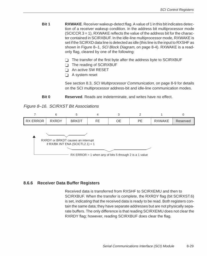
SCI Control Registers
8-29Serial Communications Interface (SCI) Module
Bit 1 RXWAKE . Receiver wakeup-detect flag. A value of 1 in this bit indicates detec-tion of a receiver wakeup condition. in the address bit multiprocessor mode(SCICCR.3 = 1), RXWAKE reflects the value of the address bit for the charac-ter contained in SCIRXBUF. In the idle-line multiprocessor mode, RXWAKE isset if the SCIRXD data line is detected as idle (this line is the input to RXSHF asshown in Figure 8–1, SCI Block Diagram, on page 8-4). RXWAKE is a read-only flag, cleared by one of the following:
� The transfer of the first byte after the address byte to SCIRXBUF� The reading of SCIRXBUF� An active SW RESET� A system reset
See section 8.3, SCI Multiprocessor Communication, on page 8-9 for detailson the SCI multiprocessor address-bit and idle-line communication modes.
Bit 0 Reserved . Reads are indeterminate, and writes have no effect.
Figure 8–16. SCIRXST Bit Associations
7 6 5 4 3 2 1 0
RX ERROR RXRDY BRKDT FE OE PE RXWAKE Reserved
RX ERROR = 1 when any of bits 5 through 2 is a 1 value
RXRDY or BRKDT causes an interrupt if RX/BK INT ENA (SCICTL2.1) = 1
8.6.6 Receiver Data Buffer Registers
Received data is transferred from RXSHF to SCIRXEMU and then to SCIRXBUF. When the transfer is complete, the RXRDY flag (bit SCIRXST.6)is set, indicating that the received data is ready to be read. Both registers con-tain the same data; they have separate addresses but are not physically sepa-rate buffers. The only difference is that reading SCIRXEMU does not clear theRXRDY flag; however, reading SCIRXBUF does clear the flag.
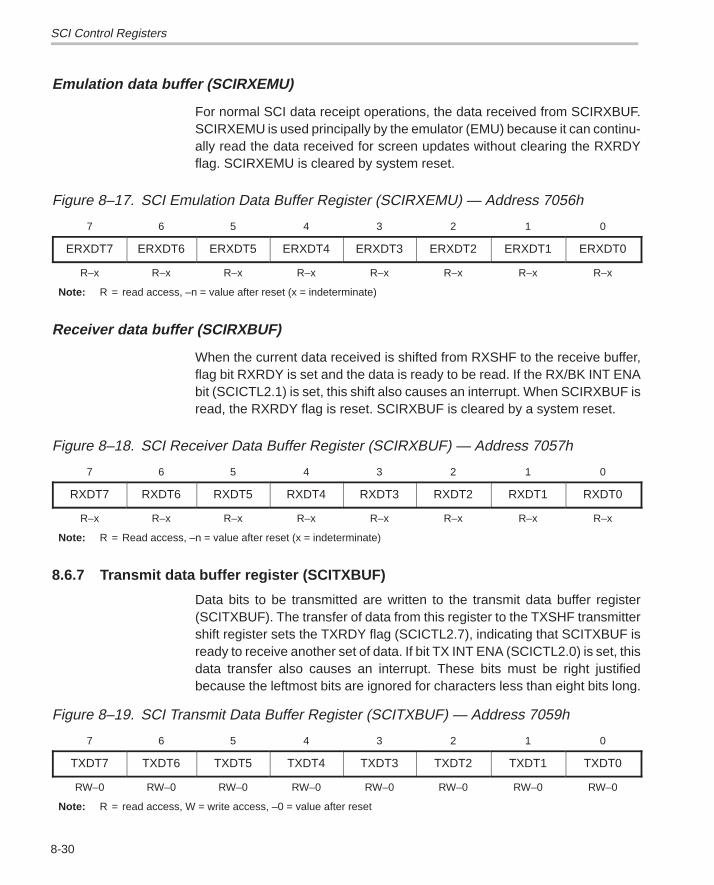
SCI Control Registers
8-30
Emulation data buffer (SCIRXEMU)
For normal SCI data receipt operations, the data received from SCIRXBUF.SCIRXEMU is used principally by the emulator (EMU) because it can continu-ally read the data received for screen updates without clearing the RXRDYflag. SCIRXEMU is cleared by system reset.
Figure 8–17. SCI Emulation Data Buffer Register (SCIRXEMU) — Address 7056h
7 6 5 4 3 2 1 0
ERXDT7 ERXDT6 ERXDT5 ERXDT4 ERXDT3 ERXDT2 ERXDT1 ERXDT0
R–x R–x R–x R–x R–x R–x R–x R–x
Note: R = read access, –n = value after reset (x = indeterminate)
Receiver data buffer (SCIRXBUF)
When the current data received is shifted from RXSHF to the receive buffer,flag bit RXRDY is set and the data is ready to be read. If the RX/BK INT ENAbit (SCICTL2.1) is set, this shift also causes an interrupt. When SCIRXBUF isread, the RXRDY flag is reset. SCIRXBUF is cleared by a system reset.
Figure 8–18. SCI Receiver Data Buffer Register (SCIRXBUF) — Address 7057h
7 6 5 4 3 2 1 0
RXDT7 RXDT6 RXDT5 RXDT4 RXDT3 RXDT2 RXDT1 RXDT0
R–x R–x R–x R–x R–x R–x R–x R–x
Note: R = Read access, –n = value after reset (x = indeterminate)
8.6.7 Transmit data buffer register (SCITXBUF)
Data bits to be transmitted are written to the transmit data buffer register(SCITXBUF). The transfer of data from this register to the TXSHF transmittershift register sets the TXRDY flag (SCICTL2.7), indicating that SCITXBUF isready to receive another set of data. If bit TX INT ENA (SCICTL2.0) is set, thisdata transfer also causes an interrupt. These bits must be right justifiedbecause the leftmost bits are ignored for characters less than eight bits long.
Figure 8–19. SCI Transmit Data Buffer Register (SCITXBUF) — Address 7059h
7 6 5 4 3 2 1 0
TXDT7 TXDT6 TXDT5 TXDT4 TXDT3 TXDT2 TXDT1 TXDT0
RW–0 RW–0 RW–0 RW–0 RW–0 RW–0 RW–0 RW–0
Note: R = read access, W = write access, –0 = value after reset
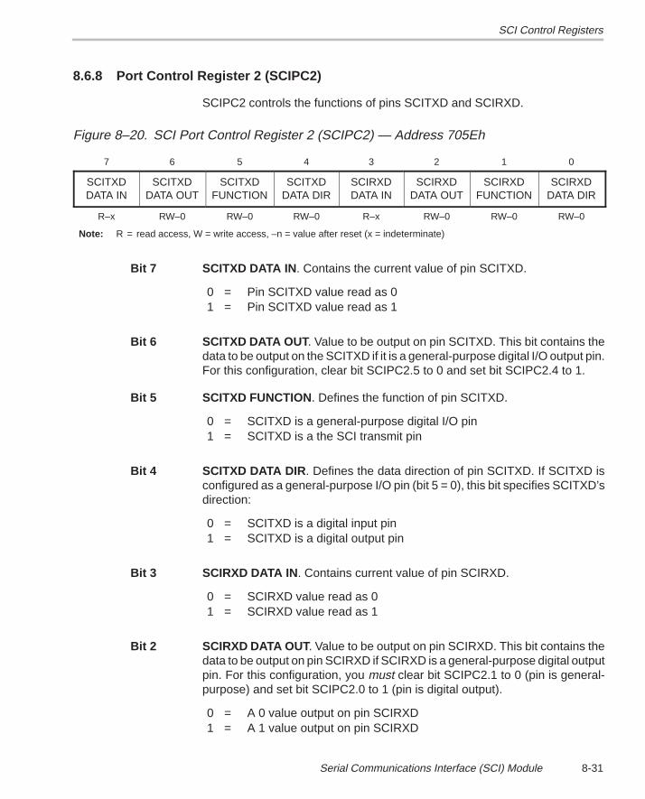
SCI Control Registers
8-31Serial Communications Interface (SCI) Module
8.6.8 Port Control Register 2 (SCIPC2)
SCIPC2 controls the functions of pins SCITXD and SCIRXD.
Figure 8–20. SCI Port Control Register 2 (SCIPC2) — Address 705Eh
7 6 5 4 3 2 1 0
SCITXDDATA IN
SCITXDDATA OUT
SCITXDFUNCTION
SCITXDDATA DIR
SCIRXDDATA IN
SCIRXDDATA OUT
SCIRXDFUNCTION
SCIRXDDATA DIR
R–x RW–0 RW–0 RW–0 R–x RW–0 RW–0 RW–0
Note: R = read access, W = write access, –n = value after reset (x = indeterminate)
Bit 7 SCITXD DATA IN . Contains the current value of pin SCITXD.
0 = Pin SCITXD value read as 01 = Pin SCITXD value read as 1
Bit 6 SCITXD DATA OUT . Value to be output on pin SCITXD. This bit contains thedata to be output on the SCITXD if it is a general-purpose digital I/O output pin.For this configuration, clear bit SCIPC2.5 to 0 and set bit SCIPC2.4 to 1.
Bit 5 SCITXD FUNCTION . Defines the function of pin SCITXD.
0 = SCITXD is a general-purpose digital I/O pin1 = SCITXD is a the SCI transmit pin
Bit 4 SCITXD DATA DIR . Defines the data direction of pin SCITXD. If SCITXD isconfigured as a general-purpose I/O pin (bit 5 = 0), this bit specifies SCITXD’sdirection:
0 = SCITXD is a digital input pin1 = SCITXD is a digital output pin
Bit 3 SCIRXD DATA IN . Contains current value of pin SCIRXD.
0 = SCIRXD value read as 01 = SCIRXD value read as 1
Bit 2 SCIRXD DATA OUT . Value to be output on pin SCIRXD. This bit contains thedata to be output on pin SCIRXD if SCIRXD is a general-purpose digital outputpin. For this configuration, you must clear bit SCIPC2.1 to 0 (pin is general-purpose) and set bit SCIPC2.0 to 1 (pin is digital output).
0 = A 0 value output on pin SCIRXD1 = A 1 value output on pin SCIRXD
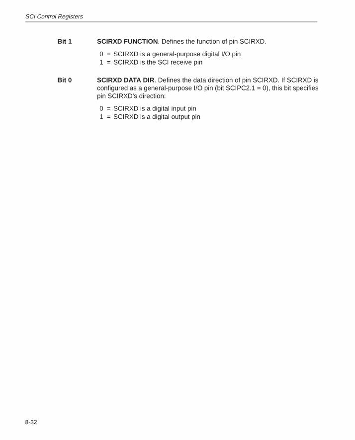
SCI Control Registers
8-32
Bit 1 SCIRXD FUNCTION . Defines the function of pin SCIRXD.
0 = SCIRXD is a general-purpose digital I/O pin1 = SCIRXD is the SCI receive pin
Bit 0 SCIRXD DATA DIR . Defines the data direction of pin SCIRXD. If SCIRXD isconfigured as a general-purpose I/O pin (bit SCIPC2.1 = 0), this bit specifiespin SCIRXD’s direction:
0 = SCIRXD is a digital input pin1 = SCIRXD is a digital output pin
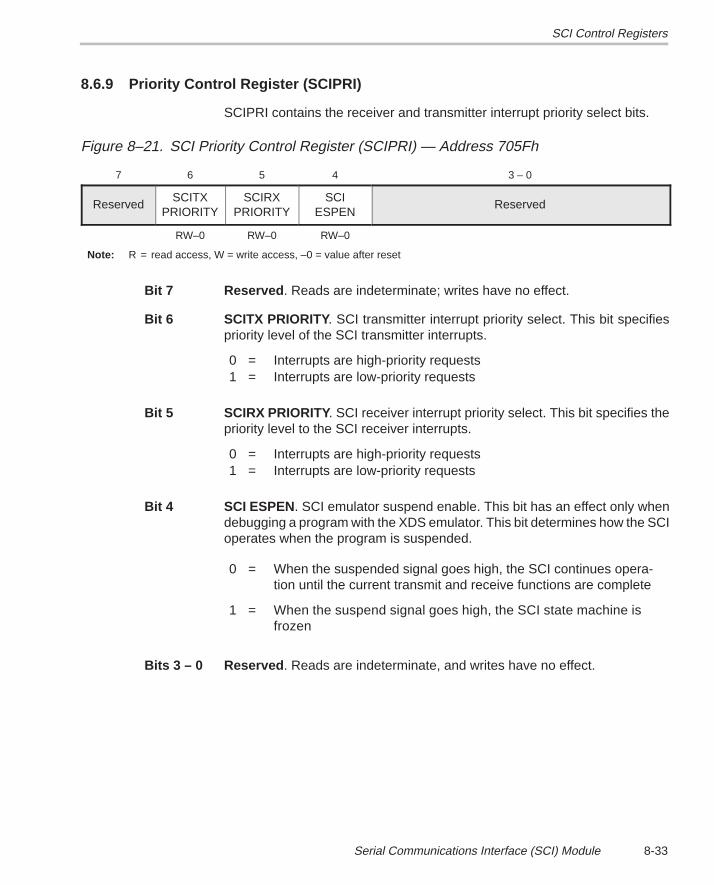
SCI Control Registers
8-33Serial Communications Interface (SCI) Module
8.6.9 Priority Control Register (SCIPRI)
SCIPRI contains the receiver and transmitter interrupt priority select bits.
Figure 8–21. SCI Priority Control Register (SCIPRI) — Address 705Fh
7 6 5 4 3 – 0
ReservedSCITX
PRIORITYSCIRX
PRIORITYSCI
ESPENReserved
RW–0 RW–0 RW–0
Note: R = read access, W = write access, –0 = value after reset
Bit 7 Reserved . Reads are indeterminate; writes have no effect.
Bit 6 SCITX PRIORITY. SCI transmitter interrupt priority select. This bit specifiespriority level of the SCI transmitter interrupts.
0 = Interrupts are high-priority requests1 = Interrupts are low-priority requests
Bit 5 SCIRX PRIORITY. SCI receiver interrupt priority select. This bit specifies thepriority level to the SCI receiver interrupts.
0 = Interrupts are high-priority requests1 = Interrupts are low-priority requests
Bit 4 SCI ESPEN . SCI emulator suspend enable. This bit has an effect only whendebugging a program with the XDS emulator. This bit determines how the SCIoperates when the program is suspended.
0 = When the suspended signal goes high, the SCI continues opera-tion until the current transmit and receive functions are complete
1 = When the suspend signal goes high, the SCI state machine isfrozen
Bits 3 – 0 Reserved . Reads are indeterminate, and writes have no effect.
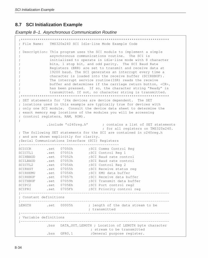
SCI Initialization Example
8-34
8.7 SCI Initialization Example
Example 8–1. Asynchronous Communication Routine
;***********************************************************************; File Name: TMS320x240 SCI Idle–line Mode Example Code;; Description: This program uses the SCI module to implement a simple ; asynchronous communications routine. The SCI is ; initialized to operate in idle–line mode with 8 character ; bits, 1 stop bit, and odd parity. The SCI Baud Rate ; Registers (BRR) are set to transmit and receive data at ; 19200 baud. The SCI generates an interrupt every time a ; character is loaded into the receive buffer (SCIRXBUF). ; The interrupt service routine(ISR) reads the receive ; buffer and determines if the carriage return button, <CR>,; has been pressed. If so, the character string ”Ready” is ; transmitted. If not, no character string is transmitted.;***********************************************************************; SET statements for ’24x devices are device dependent. The SET ; locations used in this example are typically true for devices with ; only one SCI module. Consult the device data sheet to determine the ; exact memory map locations of the modules you will be accessing ; (control registers, RAM, ROM).;
.include ”c240reg.h” ; contains a list of SET statements ; for all registers on TMS320x240.
; The following SET statements for the SCI are contained in c240reg.h; and are shown explicitly for clarity.;Serial Communications Interface (SCI) Registers;~~~~~~~~~~~~~~~~~~~~~~~~~~~~~~~~~~~~~~~~~~~~~~~SCICCR .set 07050h ;SCI Comms Control RegSCICTL1 .set 07051h ;SCI Control Reg 1SCIHBAUD .set 07052h ;SCI Baud rate controlSCILBAUD .set 07053h ;SCI Baud rate controlSCICTL2 .set 07054h ;SCI Control Reg 2SCIRXST .set 07055h ;SCI Receive status regSCIRXEMU .set 07056h ;SCI EMU data bufferSCIRXBUF .set 07057h ;SCI Receive data bufferSCITXBUF .set 07059h ;SCI Transmit data bufferSCIPC2 .set 0705Eh ;SCI Port control reg2SCIPRI .set 0705Fh ;SCI Priority control reg;–––––––––––––––––––––––––––––––––––––––––––––––––––––––––––––––––––––––; Constant definitions;–––––––––––––––––––––––––––––––––––––––––––––––––––––––––––––––––––––––LENGTH .set 00005h ; length of the data stream to be
; transmitted;–––––––––––––––––––––––––––––––––––––––––––––––––––––––––––––––––––––––; Variable definitions;–––––––––––––––––––––––––––––––––––––––––––––––––––––––––––––––––––––––
.bss DATA_OUT,LENGTH ; Location of LENGTH byte character ; stream to be transmitted
.bss GPR0,1 ;General purpose register.
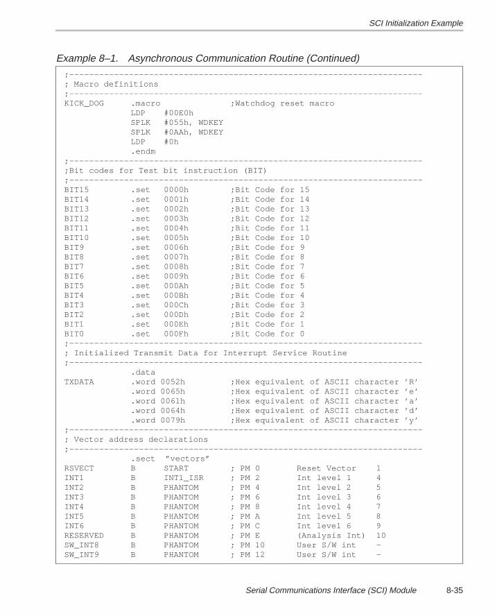
SCI Initialization Example
8-35Serial Communications Interface (SCI) Module
Example 8–1. Asynchronous Communication Routine (Continued)
;–––––––––––––––––––––––––––––––––––––––––––––––––––––––––––––––––––––––; Macro definitions;–––––––––––––––––––––––––––––––––––––––––––––––––––––––––––––––––––––––KICK_DOG .macro ;Watchdog reset macro
LDP #00E0hSPLK #055h, WDKEYSPLK #0AAh, WDKEYLDP #0h.endm
;–––––––––––––––––––––––––––––––––––––––––––––––––––––––––––––––––––––––;Bit codes for Test bit instruction (BIT);–––––––––––––––––––––––––––––––––––––––––––––––––––––––––––––––––––––––BIT15 .set 0000h ;Bit Code for 15BIT14 .set 0001h ;Bit Code for 14BIT13 .set 0002h ;Bit Code for 13BIT12 .set 0003h ;Bit Code for 12BIT11 .set 0004h ;Bit Code for 11BIT10 .set 0005h ;Bit Code for 10BIT9 .set 0006h ;Bit Code for 9BIT8 .set 0007h ;Bit Code for 8BIT7 .set 0008h ;Bit Code for 7BIT6 .set 0009h ;Bit Code for 6BIT5 .set 000Ah ;Bit Code for 5BIT4 .set 000Bh ;Bit Code for 4BIT3 .set 000Ch ;Bit Code for 3BIT2 .set 000Dh ;Bit Code for 2BIT1 .set 000Eh ;Bit Code for 1BIT0 .set 000Fh ;Bit Code for 0;–––––––––––––––––––––––––––––––––––––––––––––––––––––––––––––––––––––––; Initialized Transmit Data for Interrupt Service Routine;–––––––––––––––––––––––––––––––––––––––––––––––––––––––––––––––––––––––
.dataTXDATA .word 0052h ;Hex equivalent of ASCII character ’R’
.word 0065h ;Hex equivalent of ASCII character ’e’
.word 0061h ;Hex equivalent of ASCII character ’a’
.word 0064h ;Hex equivalent of ASCII character ’d’
.word 0079h ;Hex equivalent of ASCII character ’y’;–––––––––––––––––––––––––––––––––––––––––––––––––––––––––––––––––––––––; Vector address declarations;–––––––––––––––––––––––––––––––––––––––––––––––––––––––––––––––––––––––
.sect ”vectors”RSVECT B START ; PM 0 Reset Vector 1INT1 B INT1_ISR ; PM 2 Int level 1 4INT2 B PHANTOM ; PM 4 Int level 2 5INT3 B PHANTOM ; PM 6 Int level 3 6INT4 B PHANTOM ; PM 8 Int level 4 7INT5 B PHANTOM ; PM A Int level 5 8INT6 B PHANTOM ; PM C Int level 6 9RESERVED B PHANTOM ; PM E (Analysis Int) 10SW_INT8 B PHANTOM ; PM 10 User S/W int –SW_INT9 B PHANTOM ; PM 12 User S/W int –
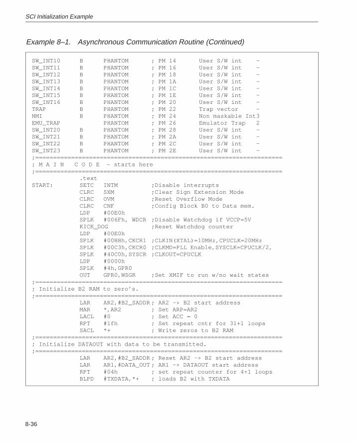
SCI Initialization Example
8-36
Example 8–1. Asynchronous Communication Routine (Continued)
SW_INT10 B PHANTOM ; PM 14 User S/W int –SW_INT11 B PHANTOM ; PM 16 User S/W int –SW_INT12 B PHANTOM ; PM 18 User S/W int –SW_INT13 B PHANTOM ; PM 1A User S/W int –SW_INT14 B PHANTOM ; PM 1C User S/W int –SW_INT15 B PHANTOM ; PM 1E User S/W int –SW_INT16 B PHANTOM ; PM 20 User S/W int –TRAP B PHANTOM ; PM 22 Trap vector –NMI B PHANTOM ; PM 24 Non maskable Int3EMU_TRAP PHANTOM ; PM 26 Emulator Trap 2SW_INT20 B PHANTOM ; PM 28 User S/W int –SW_INT21 B PHANTOM ; PM 2A User S/W int –SW_INT22 B PHANTOM ; PM 2C User S/W int –SW_INT23 B PHANTOM ; PM 2E User S/W int –;=====================================================================; M A I N C O D E – starts here;=====================================================================
.textSTART: SETC INTM ;Disable interrupts
CLRC SXM ;Clear Sign Extension ModeCLRC OVM ;Reset Overflow ModeCLRC CNF ;Config Block B0 to Data mem.LDP #00E0hSPLK #006Fh, WDCR ;Disable Watchdog if VCCP=5VKICK_DOG ;Reset Watchdog counterLDP #00E0hSPLK #00BBh,CKCR1 ;CLKIN(XTAL)=10MHz,CPUCLK=20MHzSPLK #00C3h,CKCR0 ;CLKMD=PLL Enable,SYSCLK=CPUCLK/2,SPLK #40C0h,SYSCR ;CLKOUT=CPUCLKLDP #0000hSPLK #4h,GPR0OUT GPR0,WSGR ;Set XMIF to run w/no wait states
;=====================================================================; Initialize B2 RAM to zero’s.;=====================================================================
LAR AR2,#B2_SADDR ; AR2 –> B2 start address MAR *,AR2 ; Set ARP=AR2LACL #0 ; Set ACC = 0RPT #1fh ; Set repeat cntr for 31+1 loopsSACL *+ ; Write zeros to B2 RAM
;=====================================================================; Initialize DATAOUT with data to be transmitted.;=====================================================================
LAR AR2,#B2_SADDR ; Reset AR2 –> B2 start address LAR AR1,#DATA_OUT ; AR1 –> DATAOUT start addressRPT #04h ; set repeat counter for 4+1 loopsBLPD #TXDATA,*+ ; loads B2 with TXDATA
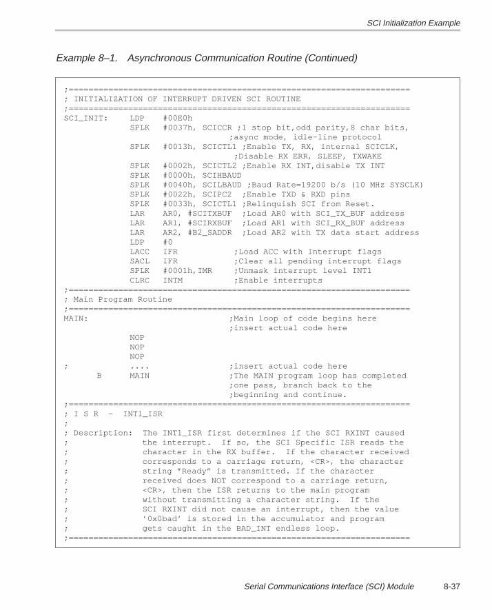
SCI Initialization Example
8-37Serial Communications Interface (SCI) Module
Example 8–1. Asynchronous Communication Routine (Continued)
;=====================================================================; INITIALIZATION OF INTERRUPT DRIVEN SCI ROUTINE;=====================================================================SCI_INIT: LDP #00E0h
SPLK #0037h, SCICCR ;1 stop bit,odd parity,8 char bits,;async mode, idle–line protocol
SPLK #0013h, SCICTL1 ;Enable TX, RX, internal SCICLK, ;Disable RX ERR, SLEEP, TXWAKE
SPLK #0002h, SCICTL2 ;Enable RX INT,disable TX INTSPLK #0000h, SCIHBAUDSPLK #0040h, SCILBAUD ;Baud Rate=19200 b/s (10 MHz SYSCLK)SPLK #0022h, SCIPC2 ;Enable TXD & RXD pinsSPLK #0033h, SCICTL1 ;Relinquish SCI from Reset.LAR AR0, #SCITXBUF ;Load AR0 with SCI_TX_BUF addressLAR AR1, #SCIRXBUF ;Load AR1 with SCI_RX_BUF addressLAR AR2, #B2_SADDR ;Load AR2 with TX data start addressLDP #0LACC IFR ;Load ACC with Interrupt flagsSACL IFR ;Clear all pending interrupt flagsSPLK #0001h,IMR ;Unmask interrupt level INT1CLRC INTM ;Enable interrupts
;=====================================================================; Main Program Routine;=====================================================================MAIN: ;Main loop of code begins here
;insert actual code hereNOPNOPNOP
; .... ;insert actual code hereB MAIN ;The MAIN program loop has completed
;one pass, branch back to the ;beginning and continue.
;=====================================================================; I S R – INT1_ISR;; Description: The INT1_ISR first determines if the SCI RXINT caused ; the interrupt. If so, the SCI Specific ISR reads the ; character in the RX buffer. If the character received ; corresponds to a carriage return, <CR>, the character ; string ”Ready” is transmitted. If the character ; received does NOT correspond to a carriage return, ; <CR>, then the ISR returns to the main program ; without transmitting a character string. If the ; SCI RXINT did not cause an interrupt, then the value ; ’0x0bad’ is stored in the accumulator and program ; gets caught in the BAD_INT endless loop.;=====================================================================
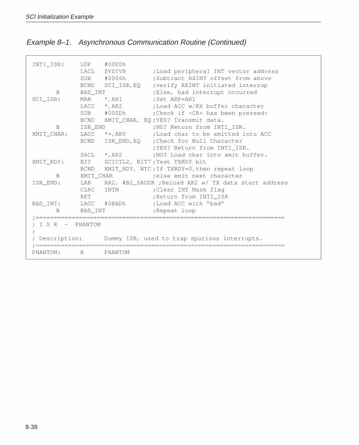
SCI Initialization Example
8-38
Example 8–1. Asynchronous Communication Routine (Continued)
INT1_ISR: LDP #00E0hLACL SYSIVR ;Load peripheral INT vector addressSUB #0006h ;Subtract RXINT offset from aboveBCND SCI_ISR,EQ ;verify RXINT initiated interrup
B BAD_INT ;Else, bad interrupt occurredSCI_ISR: MAR *,AR1 ;Set ARP=AR1
LACC *,AR2 ;Load ACC w/RX buffer characterSUB #000Dh ;Check if <CR> has been pressed:BCND XMIT_CHAR, EQ ;YES? Transmit data.
B ISR_END ;N0? Return from INT1_ISR.XMIT_CHAR: LACC *+,AR0 ;Load char to be xmitted into ACC
BCND ISR_END,EQ ;Check for Null Character;YES? Return from INT1_ISR.
SACL *,AR2 ;NO? Load char into xmit buffer.XMIT_RDY: BIT SCICTL2, BIT7 ;Test TXRDY bit
BCND XMIT_RDY, NTC ;If TXRDY=0,then repeat loop B XMIT_CHAR ;else xmit next character
ISR_END: LAR AR2, #B2_SADDR ;Reload AR2 w/ TX data start addressCLRC INTM ;Clear INT Mask flagRET ;Return from INT1_ISR
BAD_INT: LACC #0BADh ;Load ACC with ”bad”B BAD_INT ;Repeat loop
;=====================================================================; I S R – PHANTOM;; Description: Dummy ISR, used to trap spurious interrupts.;=====================================================================PHANTOM: B PHANTOM
9-1
Serial Peripheral Interface (SPI) Module
The serial peripheral interface (SPI) is a high-speed synchronous serial input/output (I/O) port that allows a serial bit stream of programmed length (one toeight bits) to be shifted into and out of the device at a programmed bit-transferrate. This chapter discusses the architecture, functions, and programming ofthe SPI module.
Note: 8-Bit Peripheral
This module is interfaced to the 16-bit peripheral bus as an 8-bit peripheral.Therefore, reads from bits 15–8 are undefined; writes to bits 15–8 have noeffect.
Topic Page
9.1 SPI Overview 9-2. . . . . . . . . . . . . . . . . . . . . . . . . . . . . . . . . . . . . . . . . . . . . . . . .
9.2 SPI Operation 9-6. . . . . . . . . . . . . . . . . . . . . . . . . . . . . . . . . . . . . . . . . . . . . . . . .
9.3 SPI Control Registers 9-17. . . . . . . . . . . . . . . . . . . . . . . . . . . . . . . . . . . . . . . .
9.4 SPI Operation-Mode Initialization Examples 9-34. . . . . . . . . . . . . . . . . . . .
Chapter 9
SPI Overview
9-2
9.1 SPI OverviewThe SPI is normally used for communications between the DSP controller andexternal peripherals or another controller. Typical applications include externalI/O or peripheral expansion via devices such as shift registers, display drivers,and analog-to-digital converters (ADCs).
Notes: Register Bit Notation, 8-Bit Peripheral
For convenience, references to a bit in a register are abbreviated using theregister name followed by a period and the number of the bit. For example,the notation for bit 7 of the SPI emulation buffer register (SPIEMU) isSPIEMU.7.
Because the SPI module is interfaced to the 16-bit peripheral bus as an 8-bitperipheral, reads from bits 15–8 are undefined; writes to bits 15–8 have noeffect.
9.1.1 SPI Physical Description
The 4-pin SPI module shown in Figure 9–1, 4-Pin SPI Module Block Diagram(Slave Mode), on page 9-3 consists of:
� Four I/O pins:
� SPISIMO (SPI slave in, master out) controlled by bits in SPIPC2� SPISOMI (SPI slave out, master in) controlled by bits in SPIPC2� SPICLK (SPI clock) controlled by bits in SPIPC1� SPISTE (SPI strobe) controlled by bits in SPIPC1
� Master and slave mode operations
� SPI serial input buffer register (SPIBUF). This buffer register contains thedata that is received from the network and ready for the CPU to read.
� SPI serial data register (SPIDAT). This data shift register serves as thetransmit/receive shift register.
� SPICLK phase and polarity control
� State control logic
� Memory-mapped control and status registers
The basic function of the strobe (SPISTE) pin is to enable transmission for theSPI module in slave mode. It prevents the shift register from transmitting byplacing the SOMI pin in a 3-state mode. When the SPI is in the master mode,the SPISTE pin always operates as a general-purpose digital I/O pin and canfunction as the SPI slave module select line. For additional information seesection 9.3.8, Serial Port Control Register 1, on page 9-29 and section 9.3.9,Serial Port Control Register 2, on page 9-31.
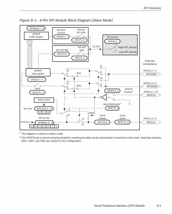
SPI Overview
9-3Serial Peripheral Interface (SPI) Module
Figure 9–1. 4-Pin SPI Module Block Diagram (Slave Mode)
S
S
SPIPC1.3– 0Clock
polarity
TALK
SYSCLK
456
012
SPI bit rate
State control
SPIBUFbuffer register
8
Clockphase
123 0
Receiveroverrun
SPICTL.4
OverrunINT ENA
SPICCR.2–0
SPIBRR.6–0 SPICCR.6 SPICTL.3
SPIBUF.7–0
SPIDAT.7– 0
SPICTL.1
M
S
M
MASTER/SLAVE†
SPI INT flag
SPICTL.0
SPI INTENA
SPIPC2.7– 4
SPIPC2.3– 0
SPISTS.7
SPIDATdata register
SPISTS.6
MS
SPIPC1.5
SPICTL.2SPI char
Externalconnections
SPISIMO
SPISOMI
SPIPC1.7– 4‡
SPISTE
SPICLK
SW2
S
M
M
S
SW3
SPIPRI.6
SPI priority
High INT priority
Low INT priority1
0To CPU
SPISTEfunction‡
MSW1
†
† The diagram is shown in slave mode.‡ The SPISTE pin is shown as being disabled, meaning the data can be transmitted or received in this mode. Note that switches
SW1, SW2, and SW3 are closed in this configuration.
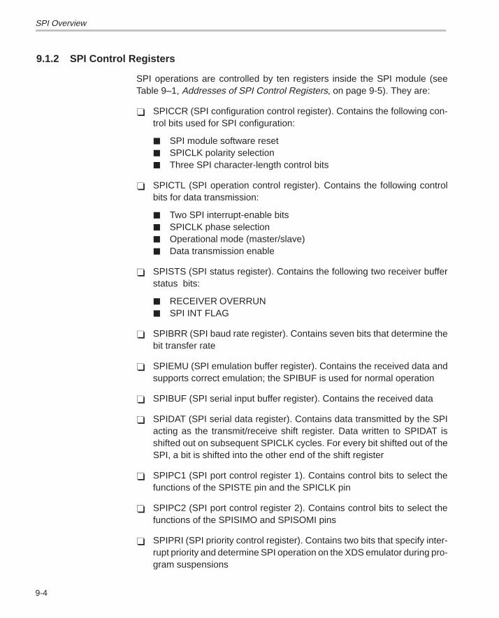
SPI Overview
9-4
9.1.2 SPI Control Registers
SPI operations are controlled by ten registers inside the SPI module (seeTable 9–1, Addresses of SPI Control Registers, on page 9-5). They are:
� SPICCR (SPI configuration control register). Contains the following con-trol bits used for SPI configuration:
� SPI module software reset� SPICLK polarity selection� Three SPI character-length control bits
� SPICTL (SPI operation control register). Contains the following controlbits for data transmission:
� Two SPI interrupt-enable bits� SPICLK phase selection� Operational mode (master/slave)� Data transmission enable
� SPISTS (SPI status register). Contains the following two receiver bufferstatus bits:
� RECEIVER OVERRUN� SPI INT FLAG
� SPIBRR (SPI baud rate register). Contains seven bits that determine thebit transfer rate
� SPIEMU (SPI emulation buffer register). Contains the received data andsupports correct emulation; the SPIBUF is used for normal operation
� SPIBUF (SPI serial input buffer register). Contains the received data
� SPIDAT (SPI serial data register). Contains data transmitted by the SPIacting as the transmit/receive shift register. Data written to SPIDAT isshifted out on subsequent SPICLK cycles. For every bit shifted out of theSPI, a bit is shifted into the other end of the shift register
� SPIPC1 (SPI port control register 1). Contains control bits to select thefunctions of the SPISTE pin and the SPICLK pin
� SPIPC2 (SPI port control register 2). Contains control bits to select thefunctions of the SPISIMO and SPISOMI pins
� SPIPRI (SPI priority control register). Contains two bits that specify inter-rupt priority and determine SPI operation on the XDS emulator during pro-gram suspensions
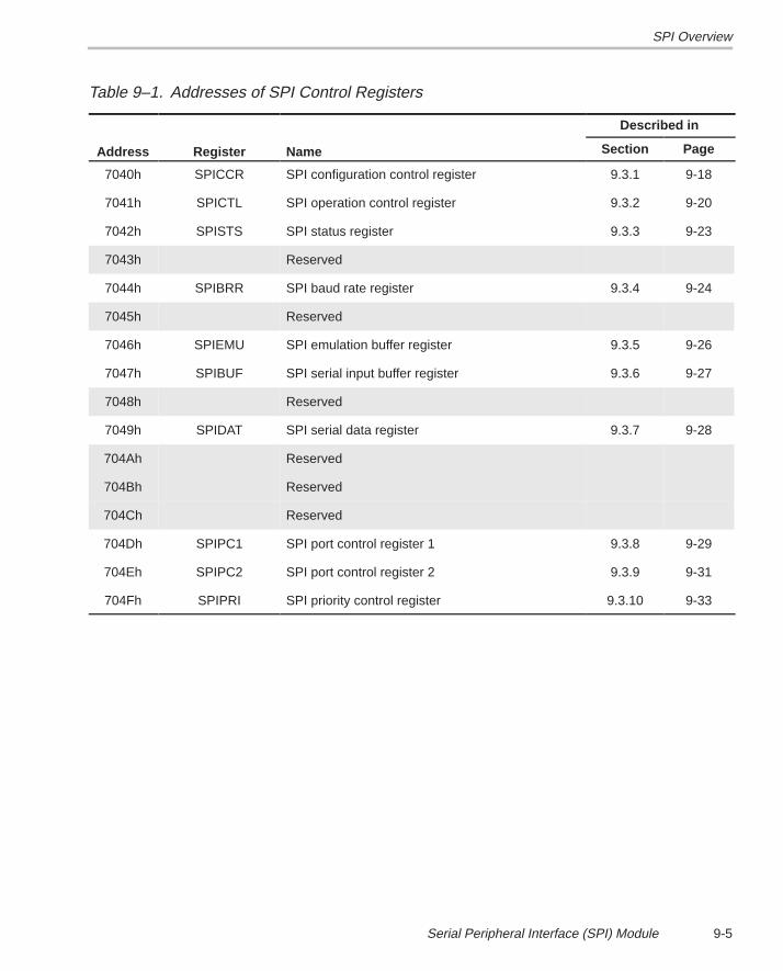
SPI Overview
9-5Serial Peripheral Interface (SPI) Module
Table 9–1. Addresses of SPI Control Registers
Described in
Address Register Name Section Page
7040h SPICCR SPI configuration control register 9.3.1 9-18
7041h SPICTL SPI operation control register 9.3.2 9-20
7042h SPISTS SPI status register 9.3.3 9-23
7043h Reserved
7044h SPIBRR SPI baud rate register 9.3.4 9-24
7045h Reserved
7046h SPIEMU SPI emulation buffer register 9.3.5 9-26
7047h SPIBUF SPI serial input buffer register 9.3.6 9-27
7048h Reserved
7049h SPIDAT SPI serial data register 9.3.7 9-28
704Ah Reserved
704Bh Reserved
704Ch Reserved
704Dh SPIPC1 SPI port control register 1 9.3.8 9-29
704Eh SPIPC2 SPI port control register 2 9.3.9 9-31
704Fh SPIPRI SPI priority control register 9.3.10 9-33
SPI Operation
9-6
9.2 SPI Operation
This section describes the operating modes, interrupts, data format, clocksources, and initialization of the SPI, and shows typical timing diagrams fordata transfers.
Note: Register Bit Naming Protocol
Reference to a bit in a register is abbreviated using the register acronym fol-lowed by a period and the bit number. For example, the MASTER/SLAVE bitof the SPI operation control register (SPICTL) is SPICTL.2.
9.2.1 Introduction to Operation
Figure 9–2, SPI Master/Slave Connection (4–Pin Option), on page 9-7shows typical connections of the SPI for communications between two control-lers: a master and a slave.
The master initiates data transfer by sending the SPICLK signal. For both theslave and the master, data is shifted out of the shift registers on one edge ofthe SPICLK and latched into the shift register on the opposite SPICLK clockedge. If the CLOCK PHASE (bit SPICTL.3) bit is active, data is transmitted andreceived a half cycle before the SPICLK transition (see section 9.2.5, BaudRate and Clocking Schemes, on page 9-11). As a result, both controllers sendand receive data simultaneously. The application software determines if thedata is meaningful data or dummy data. The three possible methods for datatransmission are:
� Master sends data and slave sends dummy data� Master sends data and slave sends data� Master sends dummy data and slave sends data
The master can initiate data transfer at any time because it controls theSPICLK signal. The software, however, determines what the master detectswhen the slave is ready to broadcast data.
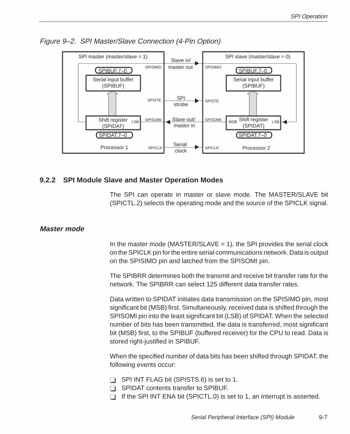
SPI Operation
9-7Serial Peripheral Interface (SPI) Module
Figure 9–2. SPI Master/Slave Connection (4-Pin Option)
SPIstrobe
Processor 1 Processor 2
Serial input buffer(SPIBUF)
Shift register(SPIDAT)
Serial input buffer(SPIBUF)
Shift register(SPIDAT)
SPI master (master/slave = 1) SPI slave (master/slave = 0)Slave in/
master out
Slave out/master in
Serialclock
SPICLK
SPISIMO
SPICLK
SPISOMI
SPISIMO
SPISTESPISTE
SPISOMI
SPIBUF.7–0
LSB
SPIBUF.7–0
SPIDAT.7–0 SPIDAT.7–0
LSBMSB
9.2.2 SPI Module Slave and Master Operation Modes
The SPI can operate in master or slave mode. The MASTER/SLAVE bit(SPICTL.2) selects the operating mode and the source of the SPICLK signal.
Master mode
In the master mode (MASTER/SLAVE = 1), the SPI provides the serial clockon the SPICLK pin for the entire serial communications network. Data is outputon the SPISIMO pin and latched from the SPISOMI pin.
The SPIBRR determines both the transmit and receive bit transfer rate for thenetwork. The SPIBRR can select 125 different data transfer rates.
Data written to SPIDAT initiates data transmission on the SPISIMO pin, mostsignificant bit (MSB) first. Simultaneously, received data is shifted through theSPISOMI pin into the least significant bit (LSB) of SPIDAT. When the selectednumber of bits has been transmitted, the data is transferred, most significantbit (MSB) first, to the SPIBUF (buffered receiver) for the CPU to read. Data isstored right-justified in SPIBUF.
When the specified number of data bits has been shifted through SPIDAT, thefollowing events occur:
� SPI INT FLAG bit (SPISTS.6) is set to 1.� SPIDAT contents transfer to SPIBUF.� If the SPI INT ENA bit (SPICTL.0) is set to 1, an interrupt is asserted.
SPI Operation
9-8
In the master mode, the SPISTE pin always operates as a general-purposeI/O pin, regardless of the value of the SPISTE FUNCTION bit (SPIPC1.5). Ina typical application, the SPISTE pin serves as a chip enable pin for slave SPIdevices. (You must drive this slave select pin low before transmitting masterdata to the slave device, and drive this pin high again after transmitting themaster data.)
Slave mode
In the slave mode (MASTER/SLAVE = 0), data shifts out on the SPISOMI pinand in on the SPISIMO pin. The SPICLK pin is used as the input for the serialshift clock, which is supplied from the external network master. The transferrate is defined by this clock. The SPICLK input frequency should be no greaterthan the SYSCLK (system clock of the device) frequency divided by 8.
Data written to SPIDAT is transmitted to the network when the SPICLK signalis received from the network master. To receive data, the SPI waits for the net-work master to send the SPICLK signal and then shifts the data on the SPISIMO pin into SPIDAT. If data is to be transmitted by the slave simulta-neously, it must be written to the SPIDAT before the beginning of the SPICLKsignal.
When the TALK bit (SPICTL.1) is cleared, data transmission is disabled andthe output line (SPISOMI) is put into the high-impedance state. This allowsmany slave devices to be tied together on the network, but only one slave ata time is allowed to talk.
In the slave mode, the SPISTE pin operates as a general-purpose I/O pin ifthe value of the SPISTE FUNCTION bit (SPIPC1.5) is cleared (0). The SPISTEpin operates as the slave select pin if SPIPC1.5 is set to 1. When the SPISTEpin is operating as the slave select pin, an active low signal on the SPISTE pinallows the slave SPI to transfer data to the serial data line; an inactive high sig-nal causes the slave SPI’s serial shift register to stop and its serial output pinto be put into the high-impedance state. This allows many slave devices to betied together on the network, although only one slave device is selected at atime.
9.2.3 SPI Interrupts
Four control bits are used to initialize the SPI’s interrupts:
� SPI INT ENA bit (SPICTL.0)� SPI INT FLAG bit (SPISTS.6)� OVERRUN INT ENA bit (SPICTL.4)� RECEIVER OVERRUN flag bit (SPISTS.7)
SPI Operation
9-9Serial Peripheral Interface (SPI) Module
SPI interrupt enable bit (SPICTL.0)
When the SPI interrupt enable bit is set and an interrupt condition occurs, thecorresponding interrupt is asserted.
0 = Disable SPI interrupts1 = Enable SPI interrupts
SPI interrupt flag bit (SPISTS.6)
This status flag indicates that a character has been placed in the SPI receiverbuffer and is ready to be read.
When a complete character has been shifted into or out of SPIDAT, the SPI INTFLAG bit (SPISTS.6) is set, and an interrupt is generated if enabled by the SPIINT ENA bit. The interrupt flag remains set until it is cleared by one of the fol-lowing four events:
� The CPU reads the SPIBUF (reading the SPIEMU does not clear the SPIINT FLAG).
� The CPU enters the OSC power-down or PLL power-down mode with anIDLE instruction.
� Software sets the SPI SW RESET bit (SPICCR.7, see Figure 9–8, SPIConfiguration Control Register (SPICCR), on page 9-18).
� A system reset occurs.
To avoid the generation of another interrupt, an interrupt request must be ex-plicitly cleared by one of the four methods listed above. An interrupt requestcan be temporarily disabled by clearing the SPI INT ENA bit. Unless the SPIINT FLAG bit is cleared, however, the interrupt request is reasserted when theSPI INT ENA bit is again set to 1.
When the SPI INT FLAG bit is set, a character has been placed in the SPIBUFand is ready to be read. If the CPU does not read the character by the time thenext complete character has been received, the new character is written intoSPIBUF and the RECEIVER OVERRUN flag bit (SPISTS.7) is set.
OVERRUN interrupt enable bit (SPICTL.4)
Setting the overrun interrupt enable bit allows the assertion of an interruptwhenever the RECEIVER OVERRUN flag bit (SPISTS.7) is set by hardware.Interrupts generated by SPISTS.7 and by the SPI INT FLAG (SPISTS.6) bitshare the same interrupt vector.
0 = Disable RECEIVER OVERRUN flag bit interrupts1 = Enable RECEIVER OVERRUN flag bit interrupts

SPI Operation
9-10
RECEIVER OVERRUN flag bit (SPISTS.7)
The RECEIVER OVERRUN flag bit is set whenever a new character has beenreceived and loaded into the SPIBUF before the previously received characterhas been read from the SPIBUF. The RECEIVER OVERRUN flag bit must becleared by software.
9.2.4 Data Format
Three bits (SPICCR.2-0) specify the number of bits (one to eight) in the datacharacter. This information directs the state control logic to count the numberof bits received or transmitted to determine when a complete character hasbeen processed. The following applies to characters with fewer than eight bits:
� Data must be left justified when written to SPIDAT.
� Data read back from SPIBUF is right justified.
� SPIBUF contains the most recently received character, right justified, plusany bits that remain from previous transmissions that have been shiftedto the left (shown in Example 9–1).
Example 9–1. Transmission of Bit from SPIBUF
SPIDAT (before transmission; = 07Bh)
0 1 1 1 1 0 1 1
SPIDAT (after transmission)
(transmitted) 0 ← 1 1 1 1 0 1 1 x ← (received)
SPIBUF (after transmission)
1 1 1 1 0 1 1 x
Note: 1) x = 1 if SPISOMI data is high; x = 0 if SPISOMI data is low; master mode is assumed.2) Transmission character length = 1 bit (specified in bits SPICCR.2-0)
SPI Operation
9-11Serial Peripheral Interface (SPI) Module
9.2.5 Baud Rate and Clocking Schemes
The SPI module supports 125 different baud rates and four different clockschemes. Depending on whether the SPI clock is in the slave or master mode,the SPICLK pin can receive an external SPI clock signal or provide the SPIclock signal, respectively.
� In the slave mode, the SPI clock is received on the SPICLK pin from theexternal source and can be no greater than the SYSCLK frequency di-vided by 8.
� In the master mode, the SPI clock is generated by the SPI and is outputon the SPICLK pin.
Baud-rate determination
Equation 9–1 shows how to determine SPI baud rates.
Equation 9–1. SPI Baud-Rate Calculations
� For SPIBRR = 3 to 127:
SPI Baud Rate �SYSCLK
(SPIBRR � 1)
� For SPIBRR = 0, 1, or 2:
SPI Baud Rate �SYSCLK
4
where:
SYSCLK = System clock frequency of the deviceSPIBRR = Contents of the SPIBRR in the master SPI device
To determine what value to load into SPIBRR, you must know the device sys-tem clock (SYSCLK) frequency (which is device/user-specific) and the baudrate at which you will be operating.
Example 9–2, Maximum Baud-Rate Calculation, on page 9-12 shows how todetermine the maximum baud rate at which a ’C240 can communicate.Assume that SYSCLK = 10 MHz.
SPI Operation
9-12
Example 9–2. Maximum Baud-Rate Calculation
SPI Baud Rate �SYSCLK
(SPIBRR � 1)
�10 � 106
(SPIBBR � 1)
�10 � 106
(3 � 1)
�10 � 106
4
� 2.5 � 106� 2.5 Mbps
The maximum master SPI baud rate is 2.5 Mbps. However, the SPI slave bauddata has a maximum speed of 1.25 Mbps (SYSCLK/8).
SPI clocking schemes
Control of the four different clocking schemes on the SPICLK pin is handledby the CLOCK POLARITY bit (SPICCR.6 in Figure 9–8, SPi ConfigurationControl Register (SPICCR), on page 9-18) and the CLOCK PHASE bit(SPICTL.3 in Figure 9–9, SPI Operation Control Register (SPICTL), on page9-20). The CLOCK POLARITY bit selects the active edge of the clock, eitherrising or falling. The CLOCK PHASE bit selects a half-cycle delay of the clock.The four different clocking schemes are as follows:
� Falling Edge Without Delay . The SPI transmits data on the falling edgeof the SPICLK and receives data on the rising edge of the SPICLK.
� Falling Edge With Delay . The SPI transmits data one half-cycle aheadof the falling edge of the SPICLK signal and receives data on the fallingedge of the SPICLK signal.
� Rising Edge Without Delay . The SPI transmits data on the rising edgeof the SPICLK signal and receives data on the falling edge of the SPICLKsignal.
� Rising Edge With Delay . The SPI transmits data one half-cycle ahead ofthe rising edge of the SPICLK signal and receives data on the rising edgeof the SPICLK signal.
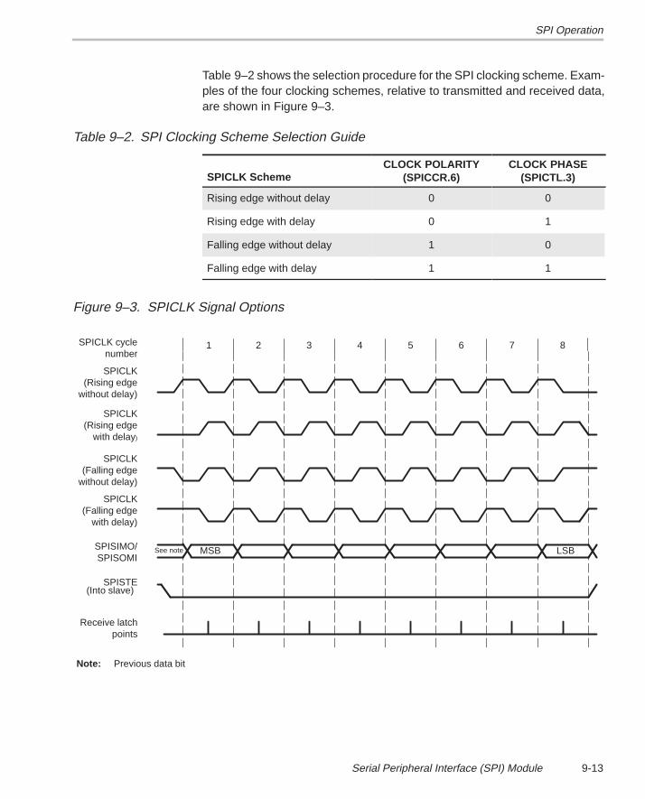
SPI Operation
9-13Serial Peripheral Interface (SPI) Module
Table 9–2 shows the selection procedure for the SPI clocking scheme. Exam-ples of the four clocking schemes, relative to transmitted and received data,are shown in Figure 9–3.
Table 9–2. SPI Clocking Scheme Selection Guide
SPICLK SchemeCLOCK POLARITY
(SPICCR.6)CLOCK PHASE
(SPICTL.3)
Rising edge without delay 0 0
Rising edge with delay 0 1
Falling edge without delay 1 0
Falling edge with delay 1 1
Figure 9–3. SPICLK Signal Options
SPICLK cyclenumber
1 2 3 4 5 6 7 8
SPICLK(Falling edge
without delay)
SPICLK(Falling edge
with delay)
SPISIMO/SPISOMI
SPISTE
MSB LSB
Note: Previous data bit
(Into slave)
Receive latch points
SPICLK(Rising edge
without delay)
SPICLK(Rising edge
with delay)
See note
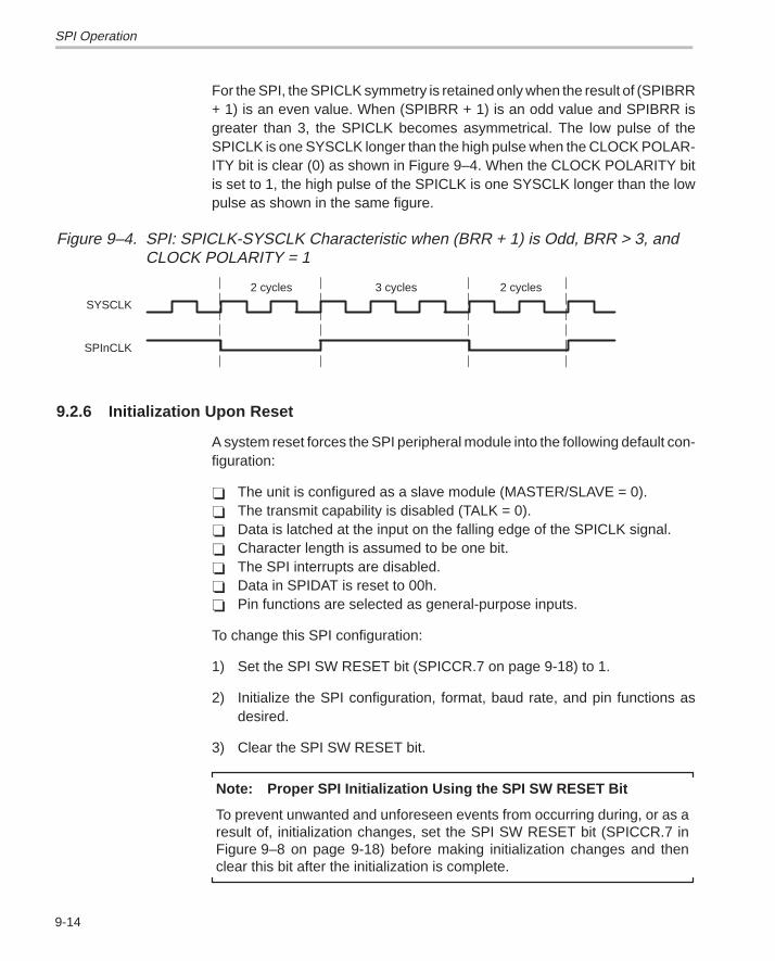
SPI Operation
9-14
For the SPI, the SPICLK symmetry is retained only when the result of (SPIBRR+ 1) is an even value. When (SPIBRR + 1) is an odd value and SPIBRR isgreater than 3, the SPICLK becomes asymmetrical. The low pulse of theSPICLK is one SYSCLK longer than the high pulse when the CLOCK POLAR-ITY bit is clear (0) as shown in Figure 9–4. When the CLOCK POLARITY bitis set to 1, the high pulse of the SPICLK is one SYSCLK longer than the lowpulse as shown in the same figure.
Figure 9–4. SPI: SPICLK-SYSCLK Characteristic when (BRR + 1) is Odd, BRR > 3, andCLOCK POLARITY = 1
SYSCLK
SPInCLK
2 cycles 3 cycles 2 cycles
9.2.6 Initialization Upon Reset
A system reset forces the SPI peripheral module into the following default con-figuration:
� The unit is configured as a slave module (MASTER/SLAVE = 0).� The transmit capability is disabled (TALK = 0).� Data is latched at the input on the falling edge of the SPICLK signal.� Character length is assumed to be one bit.� The SPI interrupts are disabled.� Data in SPIDAT is reset to 00h.� Pin functions are selected as general-purpose inputs.
To change this SPI configuration:
1) Set the SPI SW RESET bit (SPICCR.7 on page 9-18) to 1.
2) Initialize the SPI configuration, format, baud rate, and pin functions asdesired.
3) Clear the SPI SW RESET bit.
Note: Proper SPI Initialization Using the SPI SW RESET Bit
To prevent unwanted and unforeseen events from occurring during, or as aresult of, initialization changes, set the SPI SW RESET bit (SPICCR.7 inFigure 9–8 on page 9-18) before making initialization changes and thenclear this bit after the initialization is complete.
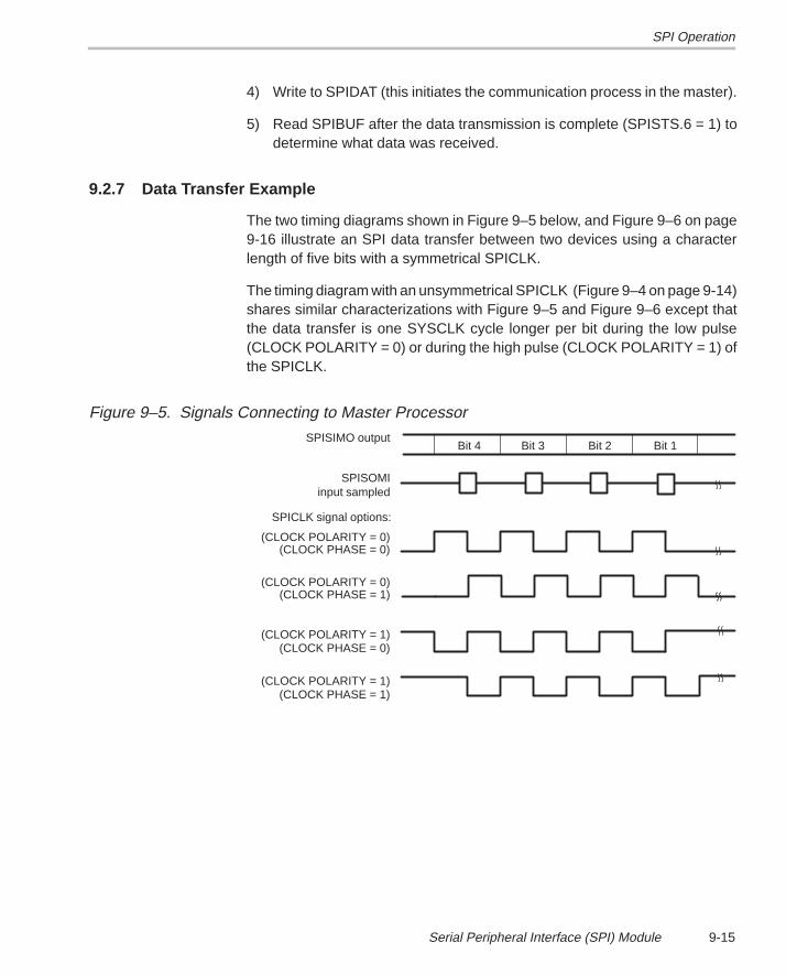
SPI Operation
9-15Serial Peripheral Interface (SPI) Module
4) Write to SPIDAT (this initiates the communication process in the master).
5) Read SPIBUF after the data transmission is complete (SPISTS.6 = 1) todetermine what data was received.
9.2.7 Data Transfer Example
The two timing diagrams shown in Figure 9–5 below, and Figure 9–6 on page9-16 illustrate an SPI data transfer between two devices using a characterlength of five bits with a symmetrical SPICLK.
The timing diagram with an unsymmetrical SPICLK (Figure 9–4 on page 9-14)shares similar characterizations with Figure 9–5 and Figure 9–6 except thatthe data transfer is one SYSCLK cycle longer per bit during the low pulse(CLOCK POLARITY = 0) or during the high pulse (CLOCK POLARITY = 1) ofthe SPICLK.
Figure 9–5. Signals Connecting to Master Processor
Bit 4 Bit 3 Bit 2SPISIMO output
SPISOMIinput sampled
(CLOCK POLARITY = 0)(CLOCK PHASE = 0)
SPICLK signal options:
(CLOCK POLARITY = 0)(CLOCK PHASE = 1)
(CLOCK POLARITY = 1)(CLOCK PHASE = 0)
(CLOCK POLARITY = 1)(CLOCK PHASE = 1)
Bit 1
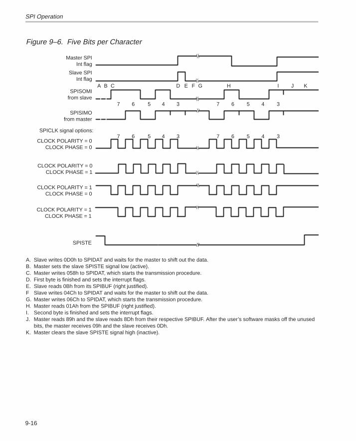
SPI Operation
9-16
Figure 9–6. Five Bits per Character
A C D E F G H I J
7 6 5 4 3 7 6 345
7 6 5 4 3 7 6 345
Master SPIInt flag
Slave SPIInt flag
SPISOMIfrom slave
CLOCK POLARITY = 0CLOCK PHASE = 0
CLOCK POLARITY = 1CLOCK PHASE = 0
SPISIMOfrom master
CLOCK POLARITY = 1CLOCK PHASE = 1
CLOCK POLARITY = 0CLOCK PHASE = 1
B
SPISTE
K
SPICLK signal options:
A. Slave writes 0D0h to SPIDAT and waits for the master to shift out the data.B. Master sets the slave SPISTE signal low (active).C. Master writes 058h to SPIDAT, which starts the transmission procedure.D. First byte is finished and sets the interrupt flags.E. Slave reads 0Bh from its SPIBUF (right justified).F Slave writes 04Ch to SPIDAT and waits for the master to shift out the data.G. Master writes 06Ch to SPIDAT, which starts the transmission procedure.H. Master reads 01Ah from the SPIBUF (right justified).I. Second byte is finished and sets the interrupt flags.J. Master reads 89h and the slave reads 8Dh from their respective SPIBUF. After the user’s software masks off the unused
bits, the master receives 09h and the slave receives 0Dh.K. Master clears the slave SPISTE signal high (inactive).
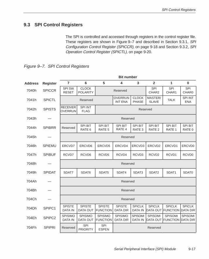
SPI Control Registers
9-17Serial Peripheral Interface (SPI) Module
9.3 SPI Control Registers
The SPI is controlled and accessed through registers in the control register file.These registers are shown in Figure 9–7 and described in Section 9.3.1, SPIConfiguration Control Register (SPICCR), on page 9-18 and Section 9.3.2, SPIOperation Control Register (SPICTL), on page 9-20.
Figure 9–7. SPI Control Registers
Bit number
Address Register 7 6 5 4 3 2 1 0
7040h SPICCRSPI SWRESET
CLOCKPOLARITY
ReservedSPI
CHAR2SPI
CHAR1SPI
CHAR0
7041h SPICTL ReservedOVERRUNINT ENA
CLOCKPHASE
MASTER/SLAVE
TALKSPI INT
ENA
7042h SPISTSRECEIVEROVERRUN
SPI INTFLAG
Reserved
7043h — Reserved
7044h SPIBRR ReservedSPI BITRATE 6
SPI BITRATE 5
SPI BITRATE 4
SPI BITRATE 3
SPI BITRATE 2
SPI BITRATE 1
SPI BITRATE 0
7045h — Reserved
7046h SPIEMU ERCVD7 ERCVD6 ERCVD5 ERCVD4 ERCVD3 ERCVD2 ERCVD1 ERCVD0
7047h SPIBUF RCVD7 RCVD6 RCVD5 RCVD4 RCVD3 RCVD2 RCVD1 RCVD0
7048h — Reserved
7049h SPIDAT SDAT7 SDAT6 SDAT5 SDAT4 SDAT3 SDAT2 SDAT1 SDAT0
704Ah — Reserved
704Bh — Reserved
704Ch — Reserved
704Dh SPIPC1SPISTEDATA IN
SPISTEDATA OUT
SPISTEFUNCTION
SPISTEDATA DIR
SPICLKDATA IN
SPICLKDATA OUT
SPICLKFUNCTION
SPICLKDATA DIR
704Eh SPIPC2SPISIMODATA IN
SPISIMODATA OUT
SPISIMOFUNCTION
SPISIMODATA DIR
SPISOMIDATA IN
SPISOMIDATA OUT
SPISOMIFUNCTION
SPISOMIDATA DIR
704Fh SPIPRI ReservedSPI
PRIORITYSPI
ESPENReserved
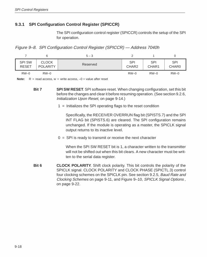
SPI Control Registers
9-18
9.3.1 SPI Configuration Control Register (SPICCR)
The SPI configuration control register (SPICCR) controls the setup of the SPIfor operation.
Figure 9–8. SPI Configuration Control Register (SPICCR) — Address 7040h
7 6 5 – 3 2 1 0
SPI SWRESET
CLOCKPOLARITY
ReservedSPI
CHAR2SPI
CHAR1SPI
CHAR0
RW–0 RW–0 RW–0 RW–0 RW–0
Note: R = read access, w = write access, –0 = value after reset
Bit 7 SPI SW RESET. SPI software reset. When changing configuration, set this bitbefore the changes and clear it before resuming operation. (See section 9.2.6,Initialization Upon Reset, on page 9-14.)
1 = Initializes the SPI operating flags to the reset condition
Specifically, the RECEIVER OVERRUN flag bit (SPISTS.7) and the SPIINT FLAG bit (SPISTS.6) are cleared. The SPI configuration remainsunchanged. If the module is operating as a master, the SPICLK signaloutput returns to its inactive level.
0 = SPI is ready to transmit or receive the next character
When the SPI SW RESET bit is 1, a character written to the transmitterwill not be shifted out when this bit clears. A new character must be writ-ten to the serial data register.
Bit 6 CLOCK POLARITY . Shift clock polarity. This bit controls the polarity of theSPICLK signal. CLOCK POLARITY and CLOCK PHASE (SPICTL.3) controlfour clocking schemes on the SPICLK pin. See section 9.2.5, Baud Rate andClocking Schemes on page 9-11, and Figure 9–10, SPICLK Signal Options ,on page 9-22.
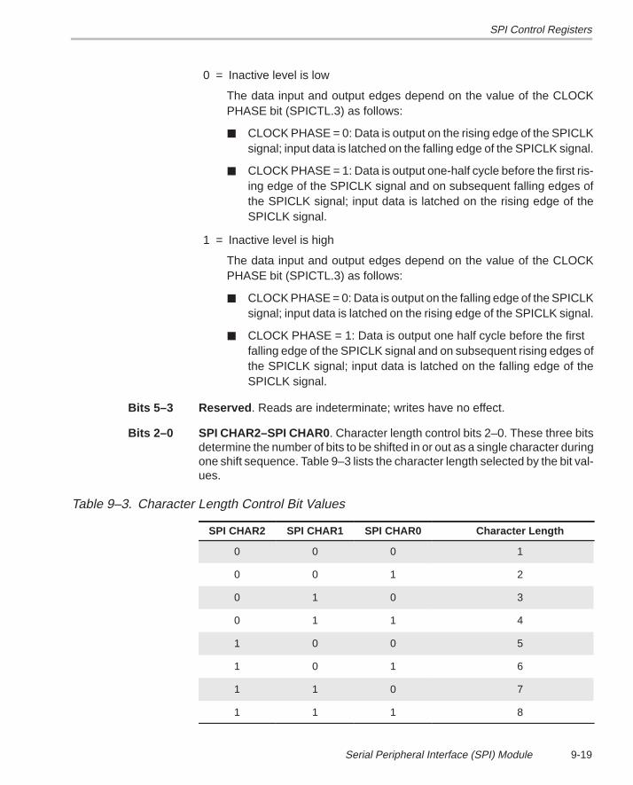
SPI Control Registers
9-19Serial Peripheral Interface (SPI) Module
0 = Inactive level is low
The data input and output edges depend on the value of the CLOCKPHASE bit (SPICTL.3) as follows:
� CLOCK PHASE = 0: Data is output on the rising edge of the SPICLKsignal; input data is latched on the falling edge of the SPICLK signal.
� CLOCK PHASE = 1: Data is output one-half cycle before the first ris-ing edge of the SPICLK signal and on subsequent falling edges ofthe SPICLK signal; input data is latched on the rising edge of theSPICLK signal.
1 = Inactive level is high
The data input and output edges depend on the value of the CLOCKPHASE bit (SPICTL.3) as follows:
� CLOCK PHASE = 0: Data is output on the falling edge of the SPICLKsignal; input data is latched on the rising edge of the SPICLK signal.
� CLOCK PHASE = 1: Data is output one half cycle before the first falling edge of the SPICLK signal and on subsequent rising edges ofthe SPICLK signal; input data is latched on the falling edge of theSPICLK signal.
Bits 5–3 Reserved . Reads are indeterminate; writes have no effect.
Bits 2–0 SPI CHAR2–SPI CHAR0 . Character length control bits 2–0. These three bitsdetermine the number of bits to be shifted in or out as a single character duringone shift sequence. Table 9–3 lists the character length selected by the bit val-ues.
Table 9–3. Character Length Control Bit Values
SPI CHAR2 SPI CHAR1 SPI CHAR0 Character Length
0 0 0 1
0 0 1 2
0 1 0 3
0 1 1 4
1 0 0 5
1 0 1 6
1 1 0 7
1 1 1 8
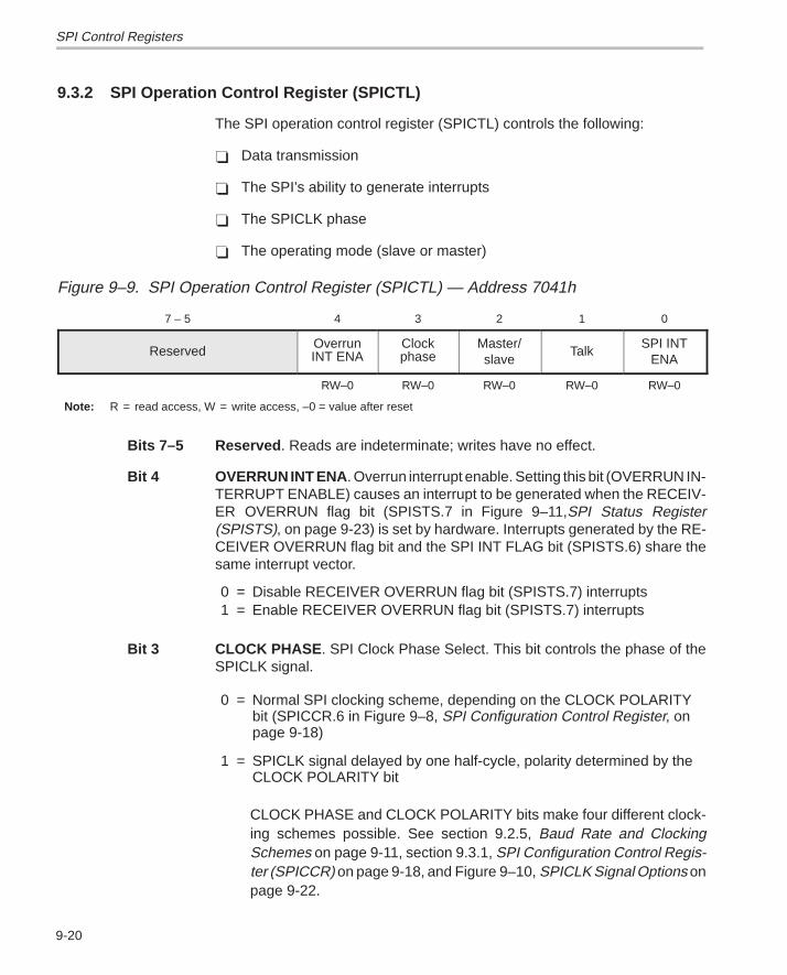
SPI Control Registers
9-20
9.3.2 SPI Operation Control Register (SPICTL)
The SPI operation control register (SPICTL) controls the following:
� Data transmission
� The SPI’s ability to generate interrupts
� The SPICLK phase
� The operating mode (slave or master)
Figure 9–9. SPI Operation Control Register (SPICTL) — Address 7041h
7 – 5 4 3 2 1 0
ReservedOverrunINT ENA
Clockphase
Master/slave
TalkSPI INT
ENA
RW–0 RW–0 RW–0 RW–0 RW–0
Note: R = read access, W = write access, –0 = value after reset
Bits 7–5 Reserved . Reads are indeterminate; writes have no effect.
Bit 4 OVERRUN INT ENA . Overrun interrupt enable. Setting this bit (OVERRUN IN-TERRUPT ENABLE) causes an interrupt to be generated when the RECEIV-ER OVERRUN flag bit (SPISTS.7 in Figure 9–11,SPI Status Register(SPISTS), on page 9-23) is set by hardware. Interrupts generated by the RE-CEIVER OVERRUN flag bit and the SPI INT FLAG bit (SPISTS.6) share thesame interrupt vector.
0 = Disable RECEIVER OVERRUN flag bit (SPISTS.7) interrupts1 = Enable RECEIVER OVERRUN flag bit (SPISTS.7) interrupts
Bit 3 CLOCK PHASE . SPI Clock Phase Select. This bit controls the phase of theSPICLK signal.
0 = Normal SPI clocking scheme, depending on the CLOCK POLARITYbit (SPICCR.6 in Figure 9–8, SPI Configuration Control Register, onpage 9-18)
1 = SPICLK signal delayed by one half-cycle, polarity determined by theCLOCK POLARITY bit
CLOCK PHASE and CLOCK POLARITY bits make four different clock-ing schemes possible. See section 9.2.5, Baud Rate and ClockingSchemes on page 9-11, section 9.3.1, SPI Configuration Control Regis-ter (SPICCR) on page 9-18, and Figure 9–10, SPICLK Signal Options onpage 9-22.
SPI Control Registers
9-21Serial Peripheral Interface (SPI) Module
When operating with CLOCK PHASE high, the SPI (master or slave)makes the first bit of data available after SPIDAT is written and before thefirst edge of the SPICLK signal, regardless of which SPI mode is beingused.
Bit 2 MASTER/SLAVE . SPI network mode control. This bit determines whether theSPI is a network master or slave. During reset initialization, the SPI is automati-cally configured as a network slave.
0 = SPI configured as a slave1 = SPI configured as a master
Bit 1 TALK . Master/slave transmit enable. The TALK bit can disable data transmis-sion (master or slave) by placing the serial data output in the high-impedancestate. If this bit is disabled during a transmission, the transmit shift register con-tinues to operate until the previous character is shifted out. When the TALK bitis disabled, the SPI can still receive characters and update the status flags.TALK is cleared (disabled) by a system reset.
0 = Disables transmission:
Slave mode operation: If not previously configured as a general-pur-pose I/O pin, the SPISOMI pin is put in the high-impedance state.
Master mode operation: If not previously configured as a general-pur-pose I/O pin, the SPISIMO pin is put in the high-impedance state.
1 = Enables transmission
For the four-pin option, make sure you enable the receiver’s SPISTB in-put pin.
Bit 0 SPI INT ENA . SPI Interrupt Enable. This bit controls the SPI’s ability to gener-ate an interrupt. The SPI INT FLAG bit (SPISTS.6) is unaffected by this bit.
0 = Disables interrupt1 = Enables interrupt
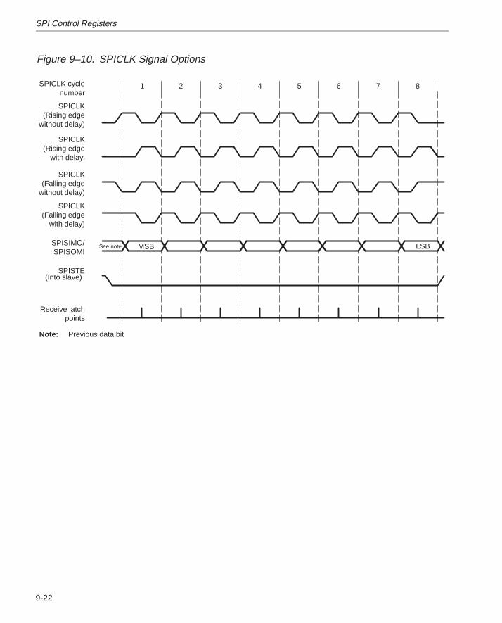
SPI Control Registers
9-22
Figure 9–10. SPICLK Signal Options
SPICLK cyclenumber
1 2 3 4 5 6 7 8
SPICLK(Falling edge
without delay)
SPICLK(Falling edge
with delay)
SPISIMO/SPISOMI
SPISTE
MSB LSB
Note: Previous data bit
(Into slave)
Receive latch points
See note
SPICLK(Rising edge
without delay)
SPICLK(Rising edge
with delay)
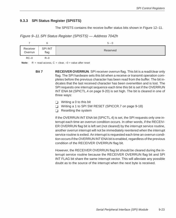
SPI Control Registers
9-23Serial Peripheral Interface (SPI) Module
9.3.3 SPI Status Register (SPISTS)
The SPISTS contains the receive buffer status bits shown in Figure 12–11.
Figure 9–11.SPI Status Register (SPISTS) — Address 7042h
7 6 5 – 0
ReceiverOverrun
SPI INTflag
Reserved
RC–0 R–0
Note: R = read access, C = clear, –0 = value after reset
Bit 7 RECEIVER OVERRUN . SPI receiver overrun flag. This bit is a read/clear onlyflag. The SPI hardware sets this bit when a receive or transmit operation com-pletes before the previous character has been read from the buffer. The bit in-dicates that the last received character has been overwritten and is lost. TheSPI requests one interrupt sequence each time this bit is set if the OVERRUNINT ENA bit (SPICTL.4 on page 9-20) is set high. The bit is cleared in one ofthree ways:
� Writing a 0 to this bit� Writing a 1 to SPI SW RESET (SPICCR.7 on page 9-18)� Resetting the system
If the OVERRUN INT ENA bit (SPICTL.4) is set, the SPI requests only one in-terrupt each time an overrun condition occurs. In other words, if the RECEIV-ER OVERRUN flag bit is left set (not cleared) by the interrupt service routine,another overrun interrupt will not be immediately reentered when the interruptservice routine is exited. An interrupt is requested each time an overrun condi-tion occurs if the OVERRUN INT ENA bit is enabled, regardless of the previouscondition of the RECEIVER OVERRUN flag bit.
However, the RECEIVER OVERRUN flag bit should be cleared during the in-terrupt service routine because the RECEIVER OVERRUN flag bit and SPIINT FLAG bit share the same interrupt vector. This will alleviate any possibledoubt as to the source of the interrupt when the next byte is received.
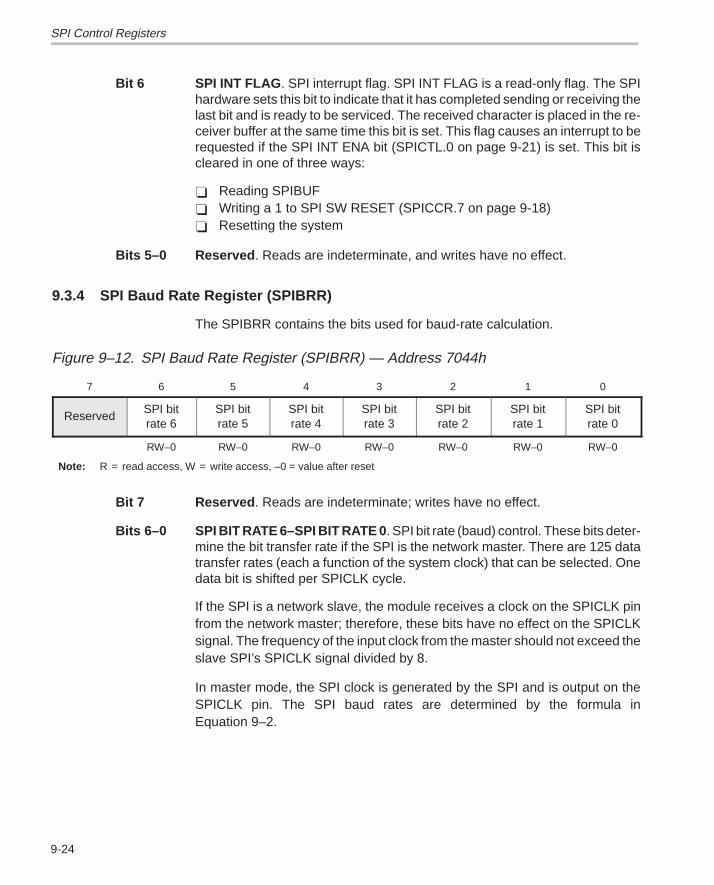
SPI Control Registers
9-24
Bit 6 SPI INT FLAG . SPI interrupt flag. SPI INT FLAG is a read-only flag. The SPIhardware sets this bit to indicate that it has completed sending or receiving thelast bit and is ready to be serviced. The received character is placed in the re-ceiver buffer at the same time this bit is set. This flag causes an interrupt to berequested if the SPI INT ENA bit (SPICTL.0 on page 9-21) is set. This bit iscleared in one of three ways:
� Reading SPIBUF� Writing a 1 to SPI SW RESET (SPICCR.7 on page 9-18)� Resetting the system
Bits 5–0 Reserved . Reads are indeterminate, and writes have no effect.
9.3.4 SPI Baud Rate Register (SPIBRR)
The SPIBRR contains the bits used for baud-rate calculation.
Figure 9–12. SPI Baud Rate Register (SPIBRR) — Address 7044h
7 6 5 4 3 2 1 0
ReservedSPI bitrate 6
SPI bitrate 5
SPI bitrate 4
SPI bitrate 3
SPI bitrate 2
SPI bitrate 1
SPI bitrate 0
RW–0 RW–0 RW–0 RW–0 RW–0 RW–0 RW–0
Note: R = read access, W = write access, –0 = value after reset
Bit 7 Reserved . Reads are indeterminate; writes have no effect.
Bits 6–0 SPI BIT RATE 6–SPI BIT RATE 0 . SPI bit rate (baud) control. These bits deter-mine the bit transfer rate if the SPI is the network master. There are 125 datatransfer rates (each a function of the system clock) that can be selected. Onedata bit is shifted per SPICLK cycle.
If the SPI is a network slave, the module receives a clock on the SPICLK pinfrom the network master; therefore, these bits have no effect on the SPICLKsignal. The frequency of the input clock from the master should not exceed theslave SPI’s SPICLK signal divided by 8.
In master mode, the SPI clock is generated by the SPI and is output on theSPICLK pin. The SPI baud rates are determined by the formula inEquation 9–2.
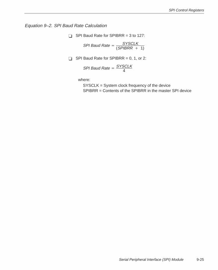
SPI Control Registers
9-25Serial Peripheral Interface (SPI) Module
Equation 9–2. SPI Baud Rate Calculation
� SPI Baud Rate for SPIBRR = 3 to 127:
SPI Baud Rate �SYSCLK
(SPIBRR � 1)
� SPI Baud Rate for SPIBRR = 0, 1, or 2:
SPI Baud Rate �SYSCLK
4
where:SYSCLK = System clock frequency of the deviceSPIBRR = Contents of the SPIBRR in the master SPI device
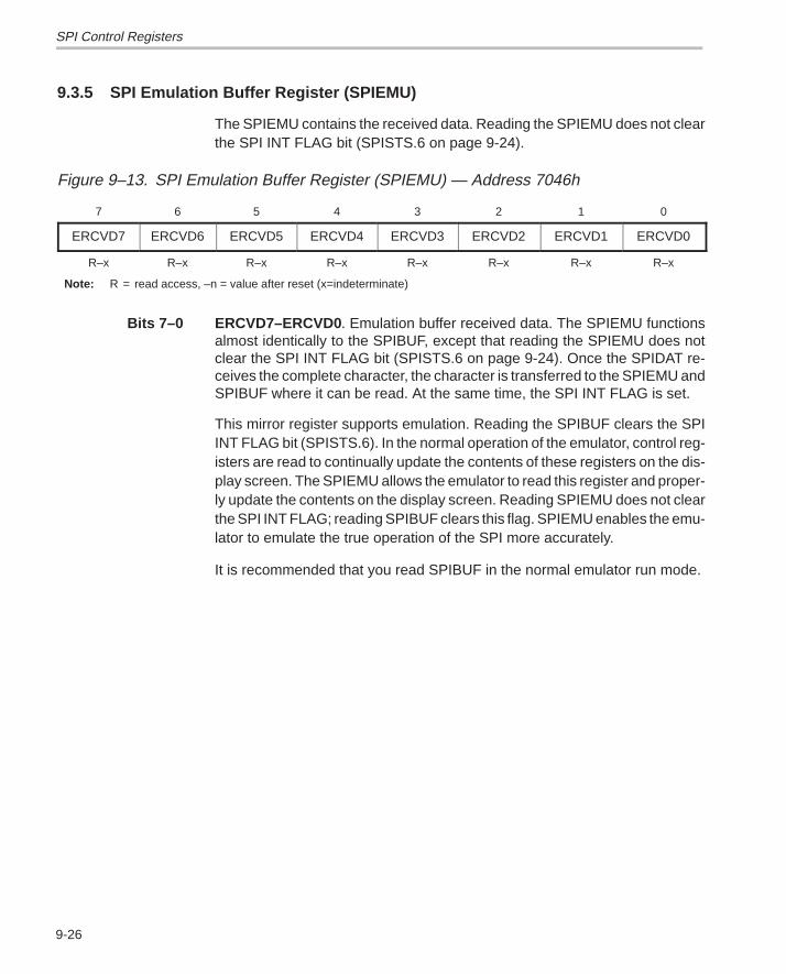
SPI Control Registers
9-26
9.3.5 SPI Emulation Buffer Register (SPIEMU)
The SPIEMU contains the received data. Reading the SPIEMU does not clearthe SPI INT FLAG bit (SPISTS.6 on page 9-24).
Figure 9–13. SPI Emulation Buffer Register (SPIEMU) — Address 7046h
7 6 5 4 3 2 1 0
ERCVD7 ERCVD6 ERCVD5 ERCVD4 ERCVD3 ERCVD2 ERCVD1 ERCVD0
R–x R–x R–x R–x R–x R–x R–x R–x
Note: R = read access, –n = value after reset (x=indeterminate)
Bits 7–0 ERCVD7–ERCVD0 . Emulation buffer received data. The SPIEMU functionsalmost identically to the SPIBUF, except that reading the SPIEMU does notclear the SPI INT FLAG bit (SPISTS.6 on page 9-24). Once the SPIDAT re-ceives the complete character, the character is transferred to the SPIEMU andSPIBUF where it can be read. At the same time, the SPI INT FLAG is set.
This mirror register supports emulation. Reading the SPIBUF clears the SPIINT FLAG bit (SPISTS.6). In the normal operation of the emulator, control reg-isters are read to continually update the contents of these registers on the dis-play screen. The SPIEMU allows the emulator to read this register and proper-ly update the contents on the display screen. Reading SPIEMU does not clearthe SPI INT FLAG; reading SPIBUF clears this flag. SPIEMU enables the emu-lator to emulate the true operation of the SPI more accurately.
It is recommended that you read SPIBUF in the normal emulator run mode.
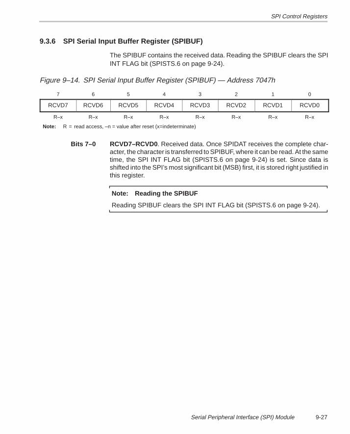
SPI Control Registers
9-27Serial Peripheral Interface (SPI) Module
9.3.6 SPI Serial Input Buffer Register (SPIBUF)
The SPIBUF contains the received data. Reading the SPIBUF clears the SPIINT FLAG bit (SPISTS.6 on page 9-24).
Figure 9–14. SPI Serial Input Buffer Register (SPIBUF) — Address 7047h
7 6 5 4 3 2 1 0
RCVD7 RCVD6 RCVD5 RCVD4 RCVD3 RCVD2 RCVD1 RCVD0
R–x R–x R–x R–x R–x R–x R–x R–x
Note: R = read access, –n = value after reset (x=indeterminate)
Bits 7–0 RCVD7–RCVD0 . Received data. Once SPIDAT receives the complete char-acter, the character is transferred to SPIBUF, where it can be read. At the sametime, the SPI INT FLAG bit (SPISTS.6 on page 9-24) is set. Since data isshifted into the SPI’s most significant bit (MSB) first, it is stored right justified inthis register.
Note: Reading the SPIBUF
Reading SPIBUF clears the SPI INT FLAG bit (SPISTS.6 on page 9-24).
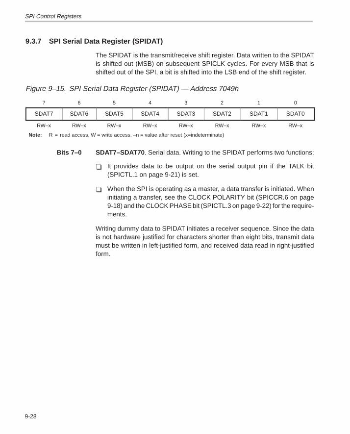
SPI Control Registers
9-28
9.3.7 SPI Serial Data Register (SPIDAT)
The SPIDAT is the transmit/receive shift register. Data written to the SPIDATis shifted out (MSB) on subsequent SPICLK cycles. For every MSB that isshifted out of the SPI, a bit is shifted into the LSB end of the shift register.
Figure 9–15. SPI Serial Data Register (SPIDAT) — Address 7049h
7 6 5 4 3 2 1 0
SDAT7 SDAT6 SDAT5 SDAT4 SDAT3 SDAT2 SDAT1 SDAT0
RW–x RW–x RW–x RW–x RW–x RW–x RW–x RW–x
Note: R = read access, W = write access, –n = value after reset (x=indeterminate)
Bits 7–0 SDAT7–SDAT70 . Serial data. Writing to the SPIDAT performs two functions:
� It provides data to be output on the serial output pin if the TALK bit(SPICTL.1 on page 9-21) is set.
� When the SPI is operating as a master, a data transfer is initiated. Wheninitiating a transfer, see the CLOCK POLARITY bit (SPICCR.6 on page9-18) and the CLOCK PHASE bit (SPICTL.3 on page 9-22) for the require-ments.
Writing dummy data to SPIDAT initiates a receiver sequence. Since the datais not hardware justified for characters shorter than eight bits, transmit datamust be written in left-justified form, and received data read in right-justifiedform.
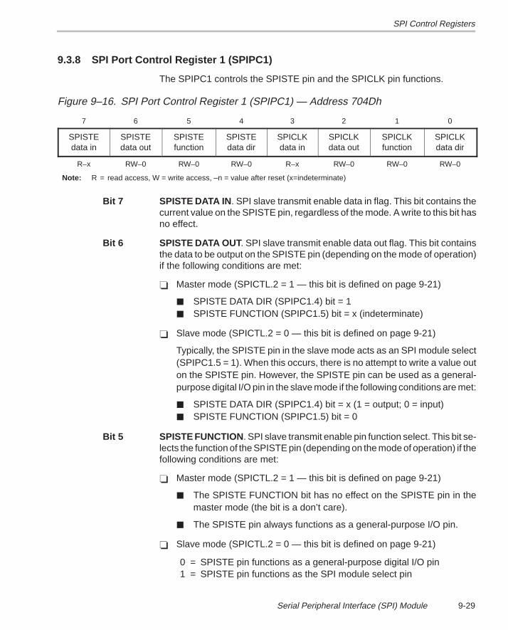
SPI Control Registers
9-29Serial Peripheral Interface (SPI) Module
9.3.8 SPI Port Control Register 1 (SPIPC1)
The SPIPC1 controls the SPISTE pin and the SPICLK pin functions.
Figure 9–16. SPI Port Control Register 1 (SPIPC1) — Address 704Dh
7 6 5 4 3 2 1 0
SPISTEdata in
SPISTEdata out
SPISTEfunction
SPISTEdata dir
SPICLKdata in
SPICLKdata out
SPICLKfunction
SPICLKdata dir
R–x RW–0 RW–0 RW–0 R–x RW–0 RW–0 RW–0
Note: R = read access, W = write access, –n = value after reset (x=indeterminate)
Bit 7 SPISTE DATA IN . SPI slave transmit enable data in flag. This bit contains thecurrent value on the SPISTE pin, regardless of the mode. A write to this bit hasno effect.
Bit 6 SPISTE DATA OUT . SPI slave transmit enable data out flag. This bit containsthe data to be output on the SPISTE pin (depending on the mode of operation)if the following conditions are met:
� Master mode (SPICTL.2 = 1 — this bit is defined on page 9-21)
� SPISTE DATA DIR (SPIPC1.4) bit = 1� SPISTE FUNCTION (SPIPC1.5) bit = x (indeterminate)
� Slave mode (SPICTL.2 = 0 — this bit is defined on page 9-21)
Typically, the SPISTE pin in the slave mode acts as an SPI module select(SPIPC1.5 = 1). When this occurs, there is no attempt to write a value outon the SPISTE pin. However, the SPISTE pin can be used as a general-purpose digital I/O pin in the slave mode if the following conditions are met:
� SPISTE DATA DIR (SPIPC1.4) bit = x (1 = output; 0 = input)� SPISTE FUNCTION (SPIPC1.5) bit = 0
Bit 5 SPISTE FUNCTION . SPI slave transmit enable pin function select. This bit se-lects the function of the SPISTE pin (depending on the mode of operation) if thefollowing conditions are met:
� Master mode (SPICTL.2 = 1 — this bit is defined on page 9-21)
� The SPISTE FUNCTION bit has no effect on the SPISTE pin in themaster mode (the bit is a don’t care).
� The SPISTE pin always functions as a general-purpose I/O pin.
� Slave mode (SPICTL.2 = 0 — this bit is defined on page 9-21)
0 = SPISTE pin functions as a general-purpose digital I/O pin1 = SPISTE pin functions as the SPI module select pin
SPI Control Registers
9-30
Bit 4 SPISTE DATA DIR . SPI slave transmit enable pin data direction. This bit deter-mines the data direction on the SPISTE pin if the SPISTE FUNCTION bit = 0 orif the SPI is operating in the master mode (SPICTL.1 = 1 — this bit is defined onpage 9-21).
0 = SPISTE is configured as an input pin.1 = SPISTE is configured as an output pin.
Bit 3 SPICLK DATA IN . SPICLK pin port data in flag. This bit contains the currentvalue on the SPICLK pin, regardless of the mode. A write to this bit has no ef-fect.
Bit 2 SPICLK DATA OUT . SPICLK pin port data out. This bit contains the data to beoutput on the SPICLK pin if the following conditions are met:
� SPICLK pin has been defined as a general-purpose digital I/O pin(SPICLK FUNCTION = 0).
� SPICLK pin data direction has been defined as output (SPICLK DATADIR = 1).
Bit 1 SPICLK FUNCTION . SPICLK pin function select. This bit defines the functionof the SPICLK pin.
0 = SPICLK is a general-purpose digital I/O pin.1 = SPICLK pin contains the SPI clock.
Bit 0 SPICLK DATA DIR . SPICLK data direction. This bit determines the data direc-tion on the SPICLK pin if SPICLK has been defined as a general-purpose digi-tal I/O pin (SPICLK FUNCTION = 0).
0 = SPICLK pin is an input pin.1 = SPICLK pin is an output pin.
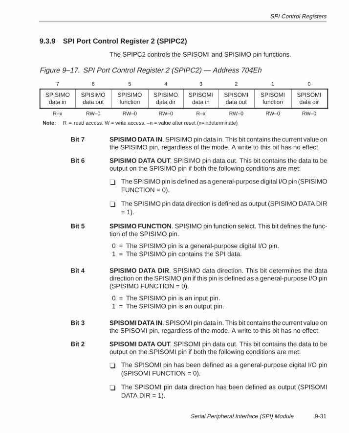
SPI Control Registers
9-31Serial Peripheral Interface (SPI) Module
9.3.9 SPI Port Control Register 2 (SPIPC2)
The SPIPC2 controls the SPISOMI and SPISIMO pin functions.
Figure 9–17. SPI Port Control Register 2 (SPIPC2) — Address 704Eh
7 6 5 4 3 2 1 0
SPISIMOdata in
SPISIMOdata out
SPISIMOfunction
SPISIMOdata dir
SPISOMIdata in
SPISOMIdata out
SPISOMIfunction
SPISOMIdata dir
R–x RW–0 RW–0 RW–0 R–x RW–0 RW–0 RW–0
Note: R = read access, W = write access, –n = value after reset (x=indeterminate)
Bit 7 SPISIMO DATA IN . SPISIMO pin data in. This bit contains the current value onthe SPISIMO pin, regardless of the mode. A write to this bit has no effect.
Bit 6 SPISIMO DATA OUT . SPISIMO pin data out. This bit contains the data to beoutput on the SPISIMO pin if both the following conditions are met:
� The SPISIMO pin is defined as a general-purpose digital I/O pin (SPISIMOFUNCTION = 0).
� The SPISIMO pin data direction is defined as output (SPISIMO DATA DIR= 1).
Bit 5 SPISIMO FUNCTION . SPISIMO pin function select. This bit defines the func-tion of the SPISIMO pin.
0 = The SPISIMO pin is a general-purpose digital I/O pin.1 = The SPISIMO pin contains the SPI data.
Bit 4 SPISIMO DATA DIR . SPISIMO data direction. This bit determines the datadirection on the SPISIMO pin if this pin is defined as a general-purpose I/O pin(SPISIMO FUNCTION = 0).
0 = The SPISIMO pin is an input pin.1 = The SPISIMO pin is an output pin.
Bit 3 SPISOMI DATA IN . SPISOMI pin data in. This bit contains the current value onthe SPISOMI pin, regardless of the mode. A write to this bit has no effect.
Bit 2 SPISOMI DATA OUT . SPISOMI pin data out. This bit contains the data to beoutput on the SPISOMI pin if both the following conditions are met:
� The SPISOMI pin has been defined as a general-purpose digital I/O pin(SPISOMI FUNCTION = 0).
� The SPISOMI pin data direction has been defined as output (SPISOMIDATA DIR = 1).
SPI Control Registers
9-32
Bit 1 SPISOMI FUNCTION . SPISOMI pin function select. This bit defines the func-tion of the SPISOMI pin. When SPISOMI is an input signal and SPISOMIFUNCTION and SPISOMI DATA DIR are disabled, the SPICLK signal stillclocks the internal circuitry.
0 = The SPISOMI pin is a general-purpose digital I/O pin.1 = The SPISOMI pin contains the SPI data.
Bit 0 SPISOMI DATA DIR . SPISOMI data direction. This bit determines the datadirection on the SPISOMI pin if this pin is defined as a general-purpose digitalI/O pin (SPISOMI FUNCTION = 0).
0 = The SPISOMI pin is an input pin.1 = The SPISOMI pin is an output pin.
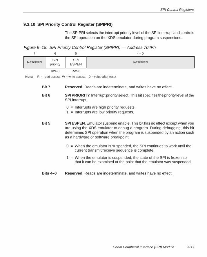
SPI Control Registers
9-33Serial Peripheral Interface (SPI) Module
9.3.10 SPI Priority Control Register (SPIPRI)
The SPIPRI selects the interrupt priority level of the SPI interrupt and controlsthe SPI operation on the XDS emulator during program suspensions.
Figure 9–18. SPI Priority Control Register (SPIPRI) — Address 704Fh7 6 5 4 – 0
ReservedSPI
prioritySPI
ESPENReserved
RW–0 RW–0
Note: R = read access, W = write access, –0 = value after reset
Bit 7 Reserved . Reads are indeterminate, and writes have no effect.
Bit 6 SPI PRIORITY. Interrupt priority select. This bit specifies the priority level of theSPI interrupt.
0 = Interrupts are high priority requests.1 = Interrupts are low priority requests.
Bit 5 SPI ESPEN . Emulator suspend enable. This bit has no effect except when youare using the XDS emulator to debug a program. During debugging, this bitdetermines SPI operation when the program is suspended by an action suchas a hardware or software breakpoint.
0 = When the emulator is suspended, the SPI continues to work until thecurrent transmit/receive sequence is complete.
1 = When the emulator is suspended, the state of the SPI is frozen sothat it can be examined at the point that the emulator was suspended.
Bits 4–0 Reserved . Reads are indeterminate, and writes have no effect.
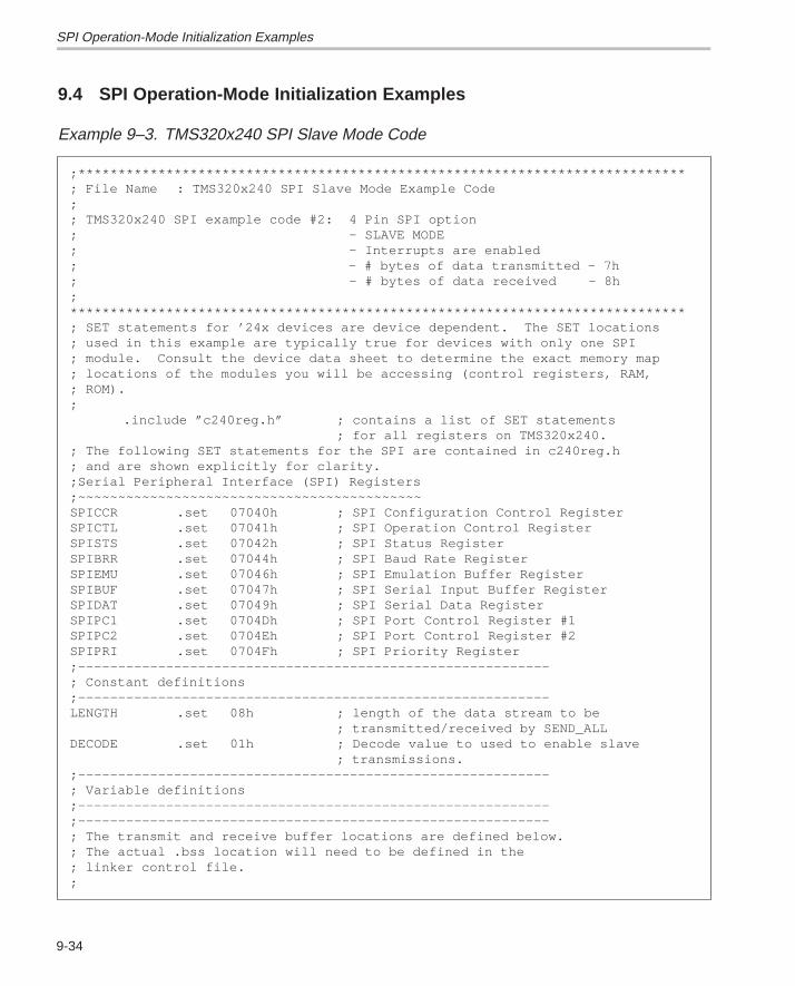
SPI Operation-Mode Initialization Examples
9-34
9.4 SPI Operation-Mode Initialization Examples
Example 9–3. TMS320x240 SPI Slave Mode Code
;****************************************************************************; File Name : TMS320x240 SPI Slave Mode Example Code;; TMS320x240 SPI example code #2: 4 Pin SPI option; – SLAVE MODE; – Interrupts are enabled; – # bytes of data transmitted – 7h; – # bytes of data received – 8h;*****************************************************************************; SET statements for ’24x devices are device dependent. The SET locations; used in this example are typically true for devices with only one SPI; module. Consult the device data sheet to determine the exact memory map; locations of the modules you will be accessing (control registers, RAM,; ROM).; .include ”c240reg.h” ; contains a list of SET statements ; for all registers on TMS320x240.; The following SET statements for the SPI are contained in c240reg.h; and are shown explicitly for clarity.;Serial Peripheral Interface (SPI) Registers ;~~~~~~~~~~~~~~~~~~~~~~~~~~~~~~~~~~~~~~~~~~~SPICCR .set 07040h ; SPI Configuration Control RegisterSPICTL .set 07041h ; SPI Operation Control RegisterSPISTS .set 07042h ; SPI Status RegisterSPIBRR .set 07044h ; SPI Baud Rate RegisterSPIEMU .set 07046h ; SPI Emulation Buffer RegisterSPIBUF .set 07047h ; SPI Serial Input Buffer RegisterSPIDAT .set 07049h ; SPI Serial Data RegisterSPIPC1 .set 0704Dh ; SPI Port Control Register #1SPIPC2 .set 0704Eh ; SPI Port Control Register #2SPIPRI .set 0704Fh ; SPI Priority Register;–––––––––––––––––––––––––––––––––––––––––––––––––––––––––––; Constant definitions;–––––––––––––––––––––––––––––––––––––––––––––––––––––––––––LENGTH .set 08h ; length of the data stream to be ; transmitted/received by SEND_ALL DECODE .set 01h ; Decode value to used to enable slave ; transmissions.;–––––––––––––––––––––––––––––––––––––––––––––––––––––––––––; Variable definitions;–––––––––––––––––––––––––––––––––––––––––––––––––––––––––––;–––––––––––––––––––––––––––––––––––––––––––––––––––––––––––; The transmit and receive buffer locations are defined below.; The actual .bss location will need to be defined in the ; linker control file.;
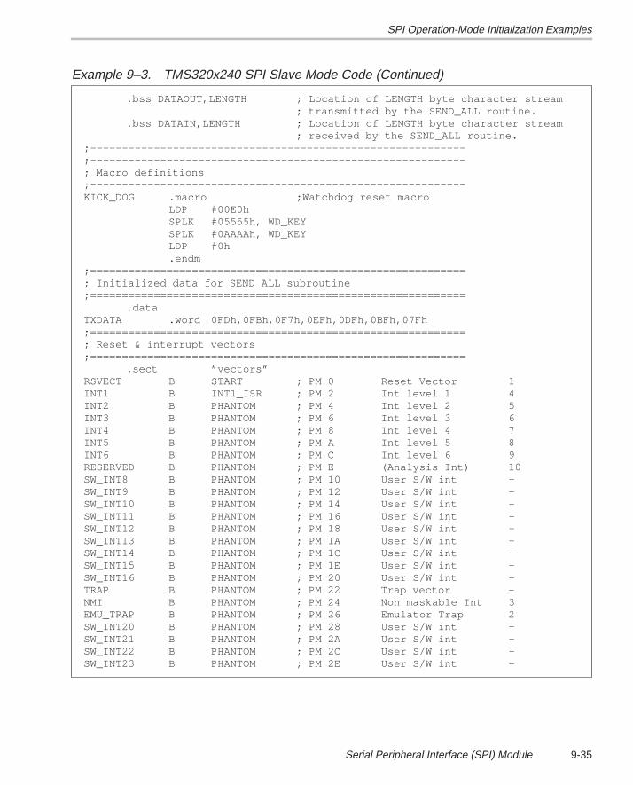
SPI Operation-Mode Initialization Examples
9-35Serial Peripheral Interface (SPI) Module
Example 9–3. TMS320x240 SPI Slave Mode Code (Continued)
.bss DATAOUT,LENGTH ; Location of LENGTH byte character stream ; transmitted by the SEND_ALL routine.
.bss DATAIN,LENGTH ; Location of LENGTH byte character stream ; received by the SEND_ALL routine.;–––––––––––––––––––––––––––––––––––––––––––––––––––––––––––;–––––––––––––––––––––––––––––––––––––––––––––––––––––––––––; Macro definitions;–––––––––––––––––––––––––––––––––––––––––––––––––––––––––––KICK_DOG .macro ;Watchdog reset macro
LDP #00E0hSPLK #05555h, WD_KEYSPLK #0AAAAh, WD_KEYLDP #0h.endm
;===========================================================; Initialized data for SEND_ALL subroutine;===========================================================
.dataTXDATA .word 0FDh,0FBh,0F7h,0EFh,0DFh,0BFh,07Fh;===========================================================; Reset & interrupt vectors;===========================================================
.sect ”vectors”RSVECT B START ; PM 0 Reset Vector 1INT1 B INT1_ISR ; PM 2 Int level 1 4INT2 B PHANTOM ; PM 4 Int level 2 5INT3 B PHANTOM ; PM 6 Int level 3 6INT4 B PHANTOM ; PM 8 Int level 4 7INT5 B PHANTOM ; PM A Int level 5 8INT6 B PHANTOM ; PM C Int level 6 9RESERVED B PHANTOM ; PM E (Analysis Int) 10SW_INT8 B PHANTOM ; PM 10 User S/W int –SW_INT9 B PHANTOM ; PM 12 User S/W int –SW_INT10 B PHANTOM ; PM 14 User S/W int –SW_INT11 B PHANTOM ; PM 16 User S/W int –SW_INT12 B PHANTOM ; PM 18 User S/W int –SW_INT13 B PHANTOM ; PM 1A User S/W int –SW_INT14 B PHANTOM ; PM 1C User S/W int –SW_INT15 B PHANTOM ; PM 1E User S/W int –SW_INT16 B PHANTOM ; PM 20 User S/W int –TRAP B PHANTOM ; PM 22 Trap vector –NMI B PHANTOM ; PM 24 Non maskable Int 3EMU_TRAP B PHANTOM ; PM 26 Emulator Trap 2SW_INT20 B PHANTOM ; PM 28 User S/W int –SW_INT21 B PHANTOM ; PM 2A User S/W int –SW_INT22 B PHANTOM ; PM 2C User S/W int –SW_INT23 B PHANTOM ; PM 2E User S/W int –
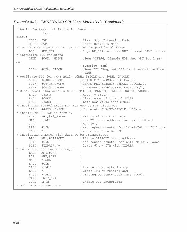
SPI Operation-Mode Initialization Examples
9-36
Example 9–3. TMS320x240 SPI Slave Mode Code (Continued)
; Begin the Reset initialization here ....text
START:CLRC SXM ; Clear Sign Extension ModeCLRC OVM ; Reset Overflow Mode
* Set Data Page pointer to page 1 of the peripheral frameLDP #DP_PF1 ; Page DP_PF1 includes WET through EINT frames
* initialize WDT registersSPLK #06Fh, WDTCR ; clear WDFLAG, Disable WDT, set WDT for 1 se-
cond; overflow (max)
SPLK #07h, RTICR ; c lear RTI Flag, set RTI for 1 second overflow; (max)
* configure PLL for 4MHz xtal, 10MHz SYSCLK and 20MHz CPUCLKSPLK #00E4h,CKCR1 ; CLKIN(XTAL)=4MHz,CPUCLK=20MHzSPLK #0043h,CKCR0 ; CLKMD=PLL disable,SYSCLK=CPUCLK/2,SPLK #00C3h,CKCR0 ; CLKMD=PLL Enable,SYSCLK=CPUCLK/2,
* Clear reset flag bits in SYSSR (PORRST, PLLRST, ILLRST, SWRST, WDRST) LACL SYSSR ; ACCL <= SYSSRAND #00FFh ; Clear upper 8 bits of SYSSRSACL SYSSR ; Load new value into SYSSR
* Initialize IOP20/CLKOUT pin for use as DSP clock outSPLK #40C8h,SYSCR ; No reset, CLKOUT=CPUCLK, VCCA on
* initialize B2 RAM to zero’s. LAR AR1,#B2_SADDR ; AR1 <= B2 start address MAR *,AR1 ; use B2 start address for next indirect ZAC ; ACC <= 0 RPT #1fh ; set repeat counter for 1fh+1=20h or 32 loops SACL *+ ; write zeros to B2 RAM* initialize DATAOUT with data to be transmitted.
LAR AR1,#DATAOUT ; AR1 <= DATAOUT start address RPT #06h ; set repeat counter for 6h+1=7h or 7 loops BLPD #TXDATA,*+ ; loads 60h – 67h with TXDATA* Initialize DSP for interrupts LAR AR6,#IMR ; LAR AR7,#IFR ; MAR *,AR6 LACL #01h ;
SACL *,AR7 ; Enable interrupts 1 onlyLACL * ; Clear IFR by reading andSACL *,AR2 ; writing contents back into itselfCALL INIT_SPICLRC INTM ; Enable DSP interrupts
; Main routine goes here.
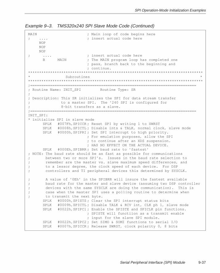
SPI Operation-Mode Initialization Examples
9-37Serial Peripheral Interface (SPI) Module
Example 9–3. TMS320x240 SPI Slave Mode Code (Continued)
MAIN ; Main loop of code begins here; .... ; insert actual code here NOP NOP NOP; .... ; insert actual code here B MAIN ; The MAIN program loop has completed one ; pass, branch back to the beginning and
; continue.******************************************************************************** Subroutines ********************************************************************************;===========================================================================; Routine Name: INIT_SPI Routine Type: SR;; Description: This SR initializes the SPI for data stream transfer; to a master SPI. The ’240 SPI is configured for; 8–bit transfers as a slave.;===========================================================================INIT_SPI:* initialize SPI in slave mode
SPLK #007Fh,SPICCR ; Reset SPI by writing 1 to SWRSTSPLK #0008h,SPICTL ; Disable ints & TALK, normal clock, slave modeSPLK #0000h,SPIPRI ; Set SPI interrupt to high priority.
; For emulation purposes, allow the SPI ; to continue after an XDS suspension. ; HAS NO EFFECT ON THE ACTUAL DEVICE.
SPLK #000Eh,SPIBRR ; Set baud rate to ’fastest’; NOTE: The baud rate should be as fast as possible for communications; between two or more SPI’s. Issues in the baud rate selection to; remember are the master vs. slave maximum speed differences, and; to a lessor degree, the clock speed of each device. For DSP ; controllers and TI peripheral devices this determined by SYSCLK.
; A value of ’0Eh’ in the SPIBRR will insure the fastest available; baud rate for the master and slave device (assuming two DSP controller; devices with the same SYSCLK are doing the communication). This is; case when the master SPI uses a polling routine to determine when; to transmit the next byte.
SPLK #0000h,SPISTS ; Clear the SPI interrupt status bitsSPLK #0009h,SPICTL ; Disable TALK & RCV int, CLK ph 1, slave modeSPLK #0022h,SPIPC1 ; Enable the SPISTE and SPICLK pin functions.
; SPISTE will functiion as a transmit enable ; input for the slave SPI module.
SPLK #0022h,SPIPC2 ; Set SIMO & SOMI functions to serial I/OSPLK #0007h,SPICCR ; Release SWRST, clock polarity 0, 8 bits
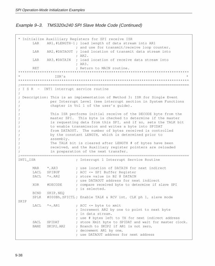
SPI Operation-Mode Initialization Examples
9-38
Example 9–3. TMS320x240 SPI Slave Mode Code (Continued)
* Initialize Auxilliary Registers for SPI receive ISR LAR AR1,#LENGTH–1 ; load length of data stream into AR1 ; and use for transmit/receive loop counter. LAR AR2,#DATAOUT ; load location of transmit data stream into ; AR2. LAR AR3,#DATAIN ; load location of receive data stream into ; AR3. RET ; Return to MAIN routine.******************************************************************************** ISR’s ********************************************************************************;==============================================================================; I S R – INT1 interrupt service routine;; Description: This is an implementation of Method 3: ISR for Single Event; per Interrupt Level (see interrupt section in System Functions; chapter in Vol 1 of the user’s guide).;; This ISR performs initial receive of the DECODE byte from the; master SPI. This byte is checked to determine if the master; is requesting data from this SPI, and if so, sets the TALK bit; to enable transmission and writes a byte into SPIDAT; from DATAOUT. The number of bytes received is controlled; by the constant LENGTH, which is determined prior to ; assembly.; The TALK bit is cleared after LENGTH # of bytes have been; received, and the Auxiliary register pointers are reloaded; in preparation of the next transfer.;==============================================================================INT1_ISR ; Interrupt 1 Interrupt Service Routine
MAR *,AR3 ; use location of DATAIN for next indirect LACL SPIBUF ; ACC <= SPI Buffer Register SACL *+,AR2 ; store value in B2 @ DATAIN ; use DATAOUT address for next indirect XOR #DECODE ; c ompare received byte to determine if slave SPI ; is selected. BCND SKIP,NEQ
SPLK #000Bh,SPICTL ; Enable TALK & RCV int, CLK ph 1, slave modeSKIP
LACL *+,AR1 ; ACC <= byte to xmit ; Increment AR2 by one to point to next byte ; in data stream. ; use # bytes left to TX for next indirect address
SACL SPIDAT ; store Xmit byte to SPIDAT and wait for master clock.BANZ SKIP2,AR2 ; Branch to SKIP2 if AR1 is not zero,
; decrement AR1 by one, ; use DATAOUT address for next address
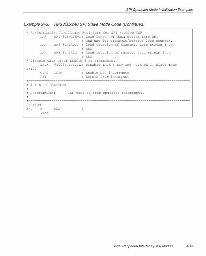
SPI Operation-Mode Initialization Examples
9-39Serial Peripheral Interface (SPI) Module
Example 9–3. TMS320x240 SPI Slave Mode Code (Continued)
* Re–Initialize Auxilliary Registers for SPI receive ISR LAR AR1,#LENGTH–1 ; load length of data stream into AR1 ; and use for transmit/receive loop counter. LAR AR2,#DATAOUT ; load location of transmit data stream into ; AR2. LAR AR3,#DATAIN ; load location of receive data stream into ; AR3.* Disable talk after LENGTH # of transfers.
SPLK #0009h,SPICTL ; Disable TALK & RCV int, CLK ph 1, slave modeSKIP2
CLRC INTM ; Enable DSP interruptsRET ; Return from interrupt
;==============================================================================; I S R – PHANTOM;; Description: ISR used to trap spurious interrupts.;;==============================================================================PHANTOM END B END ; .end
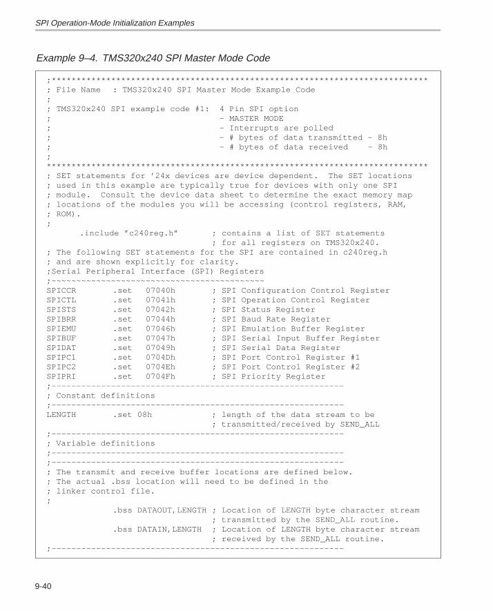
SPI Operation-Mode Initialization Examples
9-40
Example 9–4. TMS320x240 SPI Master Mode Code
;****************************************************************************; File Name : TMS320x240 SPI Master Mode Example Code;; TMS320x240 SPI example code #1: 4 Pin SPI option; – MASTER MODE; – Interrupts are polled; – # bytes of data transmitted – 8h; – # bytes of data received – 8h;*****************************************************************************; SET statements for ’24x devices are device dependent. The SET locations; used in this example are typically true for devices with only one SPI; module. Consult the device data sheet to determine the exact memory map; locations of the modules you will be accessing (control registers, RAM,; ROM).; .include ”c240reg.h” ; contains a list of SET statements ; for all registers on TMS320x240.; The following SET statements for the SPI are contained in c240reg.h; and are shown explicitly for clarity.;Serial Peripheral Interface (SPI) Registers ;~~~~~~~~~~~~~~~~~~~~~~~~~~~~~~~~~~~~~~~~~~~SPICCR .set 07040h ; SPI Configuration Control RegisterSPICTL .set 07041h ; SPI Operation Control RegisterSPISTS .set 07042h ; SPI Status RegisterSPIBRR .set 07044h ; SPI Baud Rate RegisterSPIEMU .set 07046h ; SPI Emulation Buffer RegisterSPIBUF .set 07047h ; SPI Serial Input Buffer RegisterSPIDAT .set 07049h ; SPI Serial Data RegisterSPIPC1 .set 0704Dh ; SPI Port Control Register #1SPIPC2 .set 0704Eh ; SPI Port Control Register #2SPIPRI .set 0704Fh ; SPI Priority Register;–––––––––––––––––––––––––––––––––––––––––––––––––––––––––––; Constant definitions;–––––––––––––––––––––––––––––––––––––––––––––––––––––––––––LENGTH .set 08h ; length of the data stream to be ; transmitted/received by SEND_ALL;–––––––––––––––––––––––––––––––––––––––––––––––––––––––––––; Variable definitions;–––––––––––––––––––––––––––––––––––––––––––––––––––––––––––;–––––––––––––––––––––––––––––––––––––––––––––––––––––––––––; The transmit and receive buffer locations are defined below.; The actual .bss location will need to be defined in the ; linker control file.; .bss DATAOUT,LENGTH ; Location of LENGTH byte character stream ; transmitted by the SEND_ALL routine. .bss DATAIN,LENGTH ; Location of LENGTH byte character stream ; received by the SEND_ALL routine.;–––––––––––––––––––––––––––––––––––––––––––––––––––––––––––

SPI Operation-Mode Initialization Examples
9-41Serial Peripheral Interface (SPI) Module
Example 9–4. TMS320x240 SPI Master Mode Code (Continued)
SPI_DONE .set 070h ; Defined B2 RAM location ’70h’ as SPI transmit ; status location. 1=complete, 0=not complete;–––––––––––––––––––––––––––––––––––––––––––––––––––––––––––; Macro definitions;–––––––––––––––––––––––––––––––––––––––––––––––––––––––––––KICK_DOG .macro ;Watchdog reset macro
LDP #00E0hSPLK #05555h, WD_KEYSPLK #0AAAAh, WD_KEYLDP #0h.endm
;===========================================================; Initialized data for SEND_ALL subroutine;=========================================================== .dataTXDATA .word 01h,02h,04h,08h,10h,20h,40h,80h;===========================================================; Reset & interrupt vectors;===========================================================
.sect ”vectors”RSVECT B START ; PM 0 Reset Vector 1INT1 B PHANTOM ; PM 2 Int level 1 4INT2 B PHANTOM ; PM 4 Int level 2 5INT3 B PHANTOM ; PM 6 Int level 3 6INT4 B PHANTOM ; PM 8 Int level 4 7INT5 B PHANTOM ; PM A Int level 5 8INT6 B PHANTOM ; PM C Int level 6 9RESERVED B PHANTOM ; PM E (Analysis Int) 10SW_INT8 B PHANTOM ; PM 10 User S/W int –SW_INT9 B PHANTOM ; PM 12 User S/W int –SW_INT10 B PHANTOM ; PM 14 User S/W int –SW_INT11 B PHANTOM ; PM 16 User S/W int –SW_INT12 B PHANTOM ; PM 18 User S/W int –SW_INT13 B PHANTOM ; PM 1A User S/W int –SW_INT14 B PHANTOM ; PM 1C User S/W int –SW_INT15 B PHANTOM ; PM 1E User S/W int –SW_INT16 B PHANTOM ; PM 20 User S/W int –TRAP B PHANTOM ; PM 22 Trap vector –NMI B PHANTOM ; PM 24 Non maskable Int 3EMU_TRAP B PHANTOM ; PM 26 Emulator Trap 2SW_INT20 B PHANTOM ; PM 28 User S/W int –SW_INT21 B PHANTOM ; PM 2A User S/W int –SW_INT22 B PHANTOM ; PM 2C User S/W int –SW_INT23 B PHANTOM ; PM 2E User S/W int –; Begin the Reset initialization here ...
.textSTART:
CLRC SXM ; Clear Sign Extension ModeCLRC OVM ; Reset Overflow Mode
* Set Data Page pointer to page 1 of the peripheral frameLDP #DP_PF1 ; Page DP_PF1 includes WET through EINT frames
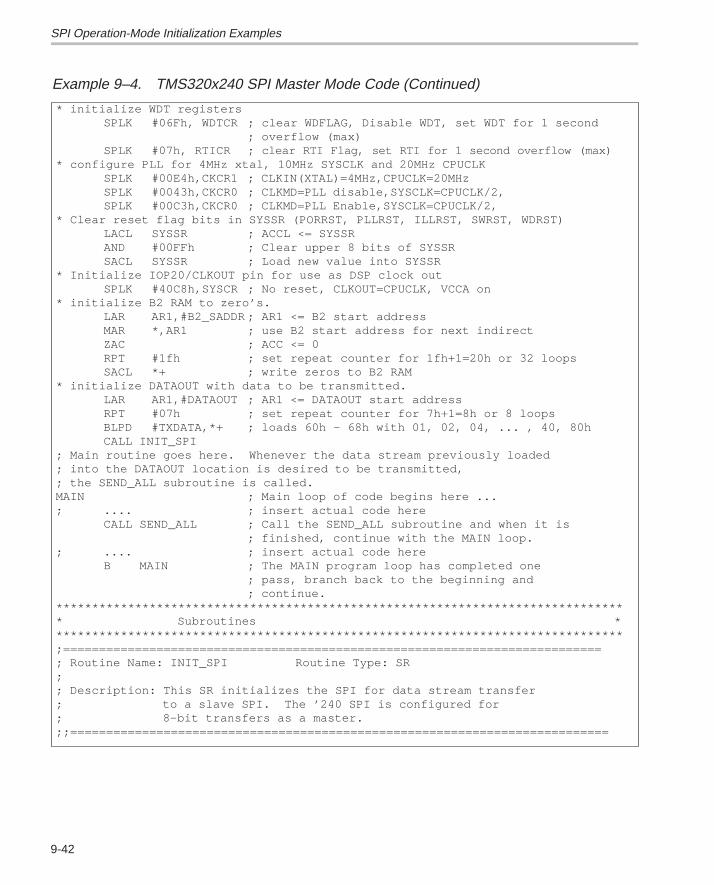
SPI Operation-Mode Initialization Examples
9-42
Example 9–4. TMS320x240 SPI Master Mode Code (Continued)
* initialize WDT registers SPLK #06Fh, WDTCR ; clear WDFLAG, Disable WDT, set WDT for 1 second
; overflow (max) SPLK #07h, RTICR ; c lear RTI Flag, set RTI for 1 second overflow (max)* configure PLL for 4MHz xtal, 10MHz SYSCLK and 20MHz CPUCLK
SPLK #00E4h,CKCR1 ; CLKIN(XTAL)=4MHz,CPUCLK=20MHzSPLK #0043h,CKCR0 ; CLKMD=PLL disable,SYSCLK=CPUCLK/2,SPLK #00C3h,CKCR0 ; CLKMD=PLL Enable,SYSCLK=CPUCLK/2,
* Clear reset flag bits in SYSSR (PORRST, PLLRST, ILLRST, SWRST, WDRST) LACL SYSSR ; ACCL <= SYSSRAND #00FFh ; Clear upper 8 bits of SYSSRSACL SYSSR ; Load new value into SYSSR
* Initialize IOP20/CLKOUT pin for use as DSP clock outSPLK #40C8h,SYSCR ; No reset, CLKOUT=CPUCLK, VCCA on
* initialize B2 RAM to zero’s. LAR AR1,#B2_SADDR ; AR1 <= B2 start address MAR *,AR1 ; use B2 start address for next indirect ZAC ; ACC <= 0 RPT #1fh ; set repeat counter for 1fh+1=20h or 32 loops SACL *+ ; write zeros to B2 RAM* initialize DATAOUT with data to be transmitted. LAR AR1,#DATAOUT ; AR1 <= DATAOUT start address RPT #07h ; set repeat counter for 7h+1=8h or 8 loops BLPD #TXDATA,*+ ; loads 60h – 68h with 01, 02, 04, ... , 40, 80h CALL INIT_SPI; Main routine goes here. Whenever the data stream previously loaded; into the DATAOUT location is desired to be transmitted,; the SEND_ALL subroutine is called.MAIN ; Main loop of code begins here ...; .... ; insert actual code here CALL SEND_ALL ; Call the SEND_ALL subroutine and when it is ; finished, continue with the MAIN loop.; .... ; insert actual code here B MAIN ; The MAIN program loop has completed one ; pass, branch back to the beginning and ; continue.******************************************************************************** Subroutines ********************************************************************************;===========================================================================; Routine Name: INIT_SPI Routine Type: SR;; Description: This SR initializes the SPI for data stream transfer; to a slave SPI. The ’240 SPI is configured for; 8–bit transfers as a master.;;===========================================================================
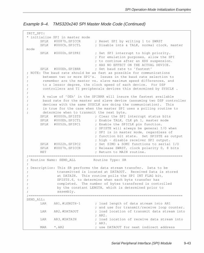
SPI Operation-Mode Initialization Examples
9-43Serial Peripheral Interface (SPI) Module
Example 9–4. TMS320x240 SPI Master Mode Code (Continued)
INIT_SPI:* initialize SPI in master mode
SPLK #0087h,SPICCR ; Reset SPI by writing 1 to SWRSTSPLK #000Ch,SPICTL ; Disable ints & TALK, normal clock, master
modeSPLK #0000h,SPIPRI ; Set SPI interrupt to high priority.
; For emulation purposes, allow the SPI ; to continue after an XDS suspension. ; HAS NO EFFECT ON THE ACTUAL DEVICE.
SPLK #000Eh,SPIBRR ; Set baud rate to ’fastest’; NOTE: The baud rate should be as fast as possible for communications; between two or more SPI’s. Issues in the baud rate selection to; remember are the master vs. slave maximum speed differences, and; to a lessor degree, the clock speed of each device. For DSP ; controllers and TI peripherals devices this determined by SYSCLK .;; A value of ’0Eh’ in the SPIBRR will insure the fastest available; baud rate for the master and slave device (assuming two DSP controller; devices with the same SYSCLK are doing the communication). This ; is true for the case when the master SPI uses a polling routine to; determine when to tranmsit the next byte.
SPLK #0000h,SPISTS ; Clear the SPI interrupt status bitsSPLK #000Eh,SPICTL ; Enable TALK, CLK ph 1, master modeSPLK #0052h,SPIPC1 ; Enable the SPICLK pin function.
; SPISTE will always be general I/O when ; SPI is in master mode, regardless of ; function bit state. Set SPISTE as output ; high – disable receiver SPI output.
SPLK #0022h,SPIPC2 ; Set SIMO & SOMI functions to serial I/OSPLK #0007h,SPICCR ; Release SWRST, clock polarity 0, 8 bitsRET ; Return to MAIN routine.
;===========================================================================; Routine Name: SEND_ALL Routine Type: SR;; Description: This SR performs the data stream transfer. Data to be ; transmitted is located at DATAOUT. Received Data is stored; at DATAIN. This routine polls the SPI INT FLAG bit,; SPISTS.6, to determine when each byte transfer has ; completed. The number of bytes transfered is controlled; by the constant LENGTH, which is determined prior to ; assembly.;===========================================================================SEND_ALL: LAR AR1,#LENGTH–1 ; load length of data stream into AR1 ; and use for transmit/receive loop counter. LAR AR2,#DATAOUT ; load location of transmit data stream into ; AR2. LAR AR3,#DATAIN ; load location of receive data stream into ; AR3. MAR *,AR2 ; use DATAOUT for next indirect address
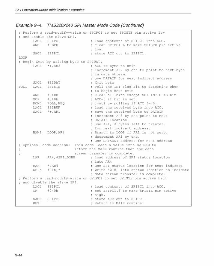
SPI Operation-Mode Initialization Examples
9-44
Example 9–4. TMS320x240 SPI Master Mode Code (Continued)
; Perform a read–modify–write on SPIPC1 to set SPISTE pin active low; and enable the slave SPI. LACL SPIPC1 ; load contents of SPIPC1 into ACC. AND #0BFh ; clear SPIPC1.6 to make SPISTE pin active ; low. SACL SPIPC1 ; store ACC out to SPIPC1.LOOP; Begin Xmit by writing byte to SPIDAT.
LACL *+,AR3 ; ACC <= byte to xmit; Increment AR2 by one to point to next byte; in data stream.; use DATAIN for next indirect address
SACL SPIDAT ; Xmit bytePOLL LACL SPISTS ; Poll the INT Flag Bit to determine when
; to begin next xmitAND #040h ; Clear all bits except SPI INT FLAG bitXOR #040h ; ACC=0 if bit is setBCND POLL,NEQ ; continue polling if ACC != 0.LACL SPIBUF ; load the received byte into ACC.SACL *+,AR1 ; save the received byte to DATAIN
; increment AR3 by one point to next; DATAIN location.; use AR1, # bytes left to tranfer, ; for next indirect address.
BANZ LOOP,AR2 ; Branch to LOOP if AR1 is not zero,; decrement AR1 by one,; use DATAOUT address for next address
; Optional code section: This code loads a value into B2 RAM to ; inform the MAIN routine that the data; stream transfer is complete. LAR AR4,#SPI_DONE ; load address of SPI status location ; into AR4 MAR *,AR4 ; use SPI status location for next indirect SPLK #01h,* ; write ’01h’ into status location to indicate ; data stream transfer is complete.; Perform a read–modify–write on SPIPC1 to set SPISTE pin active high; and disable the slave SPI. LACL SPIPC1 ; load contents of SPIPC1 into ACC. OR #040h ; set SPIPC1.6 to make SPISTE pin active ; high. SACL SPIPC1 ; store ACC out to SPIPC1. RET ; Return to MAIN routine.
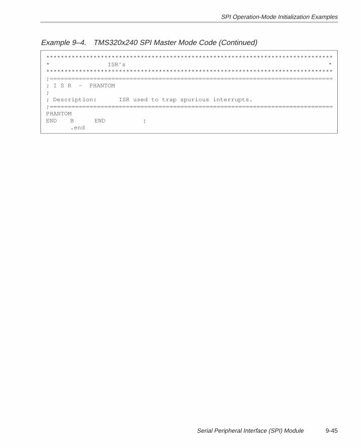
SPI Operation-Mode Initialization Examples
9-45Serial Peripheral Interface (SPI) Module
Example 9–4. TMS320x240 SPI Master Mode Code (Continued)
******************************************************************************** ISR’s ********************************************************************************;==============================================================================; I S R – PHANTOM;; Description: ISR used to trap spurious interrupts.;==============================================================================PHANTOMEND B END ; .end
10-1
Flash Memory Module
This chapter describes the flash EEPROM module, generally referred to as theflash module, or simply, flash. The term flash array refers to the actual memoryarray within the flash module.
For additional information about programming and erasing the flash array, re-fer to TMS320F20x/F24x DSP Embedded Flash Memory Technical Refer-ence (Literature number SPRU282).
Topic Page
10.1 Flash EEPROM Overview 10-2. . . . . . . . . . . . . . . . . . . . . . . . . . . . . . . . . . . . .
10.2 Fundamental Concepts 10-3. . . . . . . . . . . . . . . . . . . . . . . . . . . . . . . . . . . . . . .
10.3 Flash Registers 10-7. . . . . . . . . . . . . . . . . . . . . . . . . . . . . . . . . . . . . . . . . . . . . .
Chapter 10
Flash EEPROM Overview
10-2
10.1 Flash EEPROM Overview
The flash EEPROM module provides an attractive alternative to masked ROMprogram memory. Like ROM, flash EEPROM is also a nonvolatile memorytype; however, it has the advantage of in-target reprogrammability, both on theproduction floor and in the field.
In an actual ’240 device-specific implementation, more than one block may beutilized to give a larger overall flash memory capacity. For specific ’240 devicedetails, see Chapter 2. The following are available features and options for asingle block module of flash:
� Organization: 16K
� Word (�16 bits) implementation
� Low-power mode
� Access rate supports 50 ns CPU machine cycles with no wait states
� Write/erase performed by DSP core
The flash EEPROM module can contain 16K�16 bits of electrically erasable,electrically programmable read-only memory. It may be used to replacemasked ROM or single-access RAM (SARAM) and may be mapped to eitherprogram or data space but not both simultaneously. The block size determinesthe resolution of the start address boundary.
The flash module is erased and programmed by the DSP core itself. Thisallows the application code to manage the use of the flash memory without therequirement of external programming equipment. The initial programming ofthe flash may be done using the XDS510 scan-based emulator by scanningin the erase/program algorithm and data into on-chip RAM.
The flash module interfaces to the regular DSP memory interface. This allowsthe design to take advantage of performance gains provided by the Harvardarchitecture of the ’240 DSP core.
The flash module includes both the flash array and the necessary control reg-isters to erase and program the array.
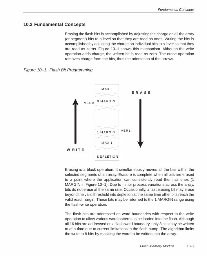
Fundamental Concepts
10-3Flash Memory Module
10.2 Fundamental Concepts
Erasing the flash bits is accomplished by adjusting the charge on all the array(or segment) bits to a level so that they are read as ones. Writing the bits isaccomplished by adjusting the charge on individual bits to a level so that theyare read as zeros. Figure 10–1 shows this mechanism. Although the writeoperation adds charge, the written bit is read as zero. The erase operationremoves charge from the bits, thus the orientation of the arrows.
Figure 10–1. Flash Bit Programming
M A X 0
0 M AR G IN
1 M AR G IN
M A X 1
D E P LET IO N
W R I T E
E R A S E
V E R 0
V E R 1
Erasing is a block operation. It simultaneously moves all the bits within theselected segments of an array. Erasure is complete when all bits are erasedto a point where the application can consistently read them as ones (1MARGIN in Figure 10–1). Due to minor process variations across the array,bits do not erase at the same rate. Occasionally, a fast erasing bit may erasebeyond the valid threshold into depletion at the same time other bits reach thevalid read margin. These bits may be returned to the 1 MARGIN range usingthe flash-write operation.
The flash bits are addressed on word boundaries with respect to the writeoperation to allow various word patterns to be loaded into the flash. Althoughall 16 bits are addressed on a flash word boundary, only 8 bits may be writtento at a time due to current limitations in the flash pump. The algorithm limitsthe write to 8 bits by masking the word to be written into the array.
Fundamental Concepts
10-4
The programming algorithms use leveling techniques to provide a balancederasure and writing of the array bits. This balance provides a measured marginfor the coded bit patterns programmed within a minimum time. It also matchesthe device production test programming levels to the application programminglevels. The leveling mechanism provides special array read modes (VER1 andVER0) to verify that bits are erased/written to a level beyond what is necessaryto meet the specified operational voltage range of the device. The extentbeyond the operation level assures data retention for the life of the applicationand is tested in production test flow of each device.
The leveling technique steps the erase or write operations in increments toalign closer to the margins applied. Due to process variances, some bits areprogrammed faster than others. All bits must be programmed to the specifiedmargins. These smaller incremental steps are used instead of a single largerstep to align closer to the applied margins on a bit-by-bit basis. This betteralignment to the margin has the primary effect of taking less time to erase andwrite, and the secondary effect of reducing the time for the opposing write anderase operations. This incremental method aligns well to DSP devices withembedded flash memory, where an embedded DSP core is capable of manag-ing the adaptive algorithm. It would be more costly in a discrete flash moduledue to the added complexity of the programming state machine.
The array, in a coded state, includes an assortment of ones and zeros of thecoded patterns. The clearing step levels the array to all zeros before erasing.This is necessary so that the erase operation processes the bits evenly. If thearray is not cleared prior to erasure, 1 bits will be erased further than 0 bits.This makes it more difficult to erase programmed bits to an adequate marginwithout pushing already erased bits into depletion. Although it may be possibleto erase the array without the clear step, it is likely to take much longer due tothe flash-write operation necessary to remove the over-erased bits from deple-tion. The program step also takes longer to re-program the deeper erased bits,conflicting with the minimization of the programming time. It is also possibleto reduce the erasure margin, but this conflicts the reliability criteria.
The boost step maintains the 0 margin in conjunction with segment and partialprogramming operations (when part of an array is coded). When other seg-ments of the array are being erased and recoded, it slightly stresses bits in pro-tected segments. The program margins on protected segments may bereduced after numerous clear, erase, and code operations on other, unpro-tected segments. In this case, the programming algorithm should include theboost operation to assure that the margins in the already coded areas remainrobust. The boost operation should be executed any time part of the array iswritten.
Fundamental Concepts
10-5Flash Memory Module
10.2.1 Erasing
The basic flow of the erase algorithm involves the following key steps:
1) Erasing the array to the VER1 margin
2) Inverse-erase verification to identify bits clearly in depletion
3) Flash-write pulses to recover depletion bits
4) Additional flash-write pulse to adjust bits near depletion
Erasing the flash array (step 1) employs a leveling technique discussed in Sec-tion 10.2, Fundamental Concepts. The special margin read mode, used in era-sure, is called VER1. VER1 verifies that the erased array reads ones at a muchlower voltage than the VCC specification of the device (approximately 3.5V).The effective minimum for the erase pulse is 5ms due to the flash-pump opera-tion. In previous revisions of the flash module, a longer pulse produced quickererasures by limiting the overhead associated with the generation of the erasepulse to lower pulse counts. However, characterization of the current revisionof the array indicates the minimum erase pulse of 5ms provides the best bal-ance for erasure.
The inverse-erase verification test (step 2) identifies bits that are erased intodepletion. This test identifies depletion bits on bit-line boundaries instead ofindividual bits. This carries the advantage of checking the full array for deple-tion bits by checking only 32 words of the first row. The inverse-erase test isexecuted after the array is successfully erased and passes VER1 to minimizeoverhead associated with the margin test. If the inverse-erase test indicatesa depletion bit, then the algorithm recovers the bit using an additional flash-write pulse (step 4) to adjust bits near depletion. If the inverse-erase testpasses, flash-write (step 3) is unnecessary, and therefore, skipped.
It is difficult (and sometimes impossible) to write a zero to a bit that has beenerased into depletion. In many flash devices, depletion indicates a device failure. However, this array employs a flash-write (step 3) to recover bits thathave been erased into depletion. The flash-write feature recovers depletedbits without adversely affecting other erased bits. Flash-write, like erase, oper-ates on all unprotected segments and therefore recovers all depleted bits. Theflash-write operation also employs shorter incremental steps to recover,instead of single long steps. Excessive numbers of flash-write pulses stressthe word line of the flash row. For this reason, the number of flash-writes is lim-ited to align to the word line stress exercised in device test.
As previously discussed, the inverse-erase test operates on bit lines. Thesebit lines cross segment boundaries so the inverse-erase test does not identify
Fundamental Concepts
10-6
the segment where the depletion bit resides. This is an issue because theinverse-erase test is affected by temperature and VDD level; and therefore, itis possible that a bit that passed inverse-erase in the full array erase might faillater in a different environment. For this reason, the algorithm adds one flash-write operation (step 2) between erasing to VER1 margin and inverse eraseto push bits that are close to depletion far enough away to avoid theenvironment changes issue. Another way to address this issue is to flash-writethe complete array when inverse-erase indicates a depleted bit in segmenterase operations. As long as the above discussed flash-write limit is in place,either method (or both) may be used.
10.2.2 Writing
Bits are written in each of the clear, code, and boost steps. This write operationis the same for each of these steps. The difference between these steps in-volves the source of the data to be programmed, which does not affect the al-gorithm used in the writing.
To minimize application costs, the embedded flash modules include chargepumps to provide the higher voltages required for write operations so that thedevice may operate with a 5V supply. To minimize the cost of the device, thesecharge pumps are designed to provide enough current to program up to 8 bitsat a time. Design pumps capable of programming more bits at a time can bedesigned, however, they would be significantly larger and more costly.
The bit writing method uses a margin read to provide robust writing of the bits.It reads the bits at a voltage greater than what is specified for the applicationto assure adequate margin for the life of the application. The array design pro-vides a special read mode (VER0) that changes the voltage at the array cellto approximately 6.5V. After a word has been written, it is read back in VER0mode to assure that the programming level still reads a zero beyond the VDDmaximum. Any bits that do not meet this margin are written again. However,bits that do meet the VER0 read are masked on the second write to assure bal-anced programming.
As previously noted, the use of incremental, smaller steps, instead of one largestep, for writing the bits better aligns to the margin. The write pulse used is setto 100�s based upon characterization over all existing revisions of the flashmodule. The benefit derived from a shorter write pulse is a cost reduction inapplication manufacture due to reduced programming time.
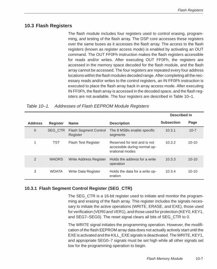
Flash Registers
10-7Flash Memory Module
10.3 Flash Registers
The flash module includes four registers used to control erasing, program-ming, and testing of the flash array. The DSP core accesses these registersover the same buses as it accesses the flash array. The access to the flashregisters (known as register access mode) is enabled by activating an OUTcommand. The OUT FF0Fh instruction makes the flash registers accessiblefor reads and/or writes. After executing OUT FF0Fh, the registers areaccessed in the memory space decoded for the flash module, and the flasharray cannot be accessed. The four registers are repeated every four addresslocations within the flash modules decoded range. After completing all the nec-essary reads and/or writes to the control registers, an IN FF0Fh instruction isexecuted to place the flash array back in array access mode. After executingIN FF0Fh, the flash array is accessed in the decoded space, and the flash reg-isters are not available. The four registers are described in Table 10–1.
Table 10–1. Addresses of Flash EEPROM Module Registers
Described in
Address Register Name Description Subsection Page
0 SEG_CTR Flash Segment ControlRegister
The 8 MSBs enable specificsegments
10.3.1 10-7
1 TST Flash Test Register Reserved for test and is notaccessible during normal op-erational modes
10.3.2 10-10
2 WADRS Write Address Register Holds the address for a writeoperation
10.3.3 10-10
3 WDATA Write Data Register Holds the data for a write op-eration
10.3.4 10-10
10.3.1 Flash Segment Control Register (SEG_CTR)
The SEG_CTR is a 16-bit register used to initiate and monitor the program-ming and erasing of the flash array. This register includes the signals neces-sary to initiate the active operations (WRITE, ERASE, and EXE), those usedfor verification (VER0 and VER1), and those used for protection (KEY0, KEY1,and SEG7–SEG0). The reset signal clears all bits of SEG_CTR to 0.
The WRITE signal initiates the programming operation. However, the modifi-cation of the flash EEPROM array data does not actually actively start until theEXE is activated and the KILL_EXE signals is deactivated. The WRITE, KEY1,and appropriate SEG0–7 signals must be set high while all other signals setlow for the programming operation to begin.
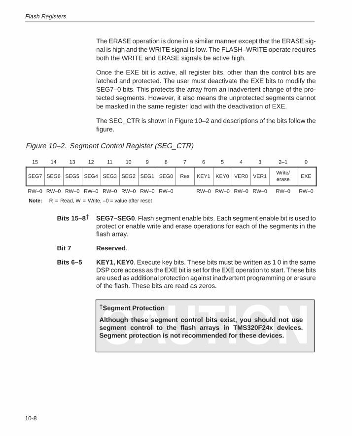
Flash Registers
10-8
The ERASE operation is done in a similar manner except that the ERASE sig-nal is high and the WRITE signal is low. The FLASH–WRITE operate requiresboth the WRITE and ERASE signals be active high.
Once the EXE bit is active, all register bits, other than the control bits arelatched and protected. The user must deactivate the EXE bits to modify theSEG7–0 bits. This protects the array from an inadvertent change of the pro-tected segments. However, it also means the unprotected segments cannotbe masked in the same register load with the deactivation of EXE.
The SEG_CTR is shown in Figure 10–2 and descriptions of the bits follow thefigure.
Figure 10–2. Segment Control Register (SEG_CTR)
15 14 13 12 11 10 9 8 7 6 5 4 3 2–1 0
SEG7 SEG6 SEG5 SEG4 SEG3 SEG2 SEG1 SEG0 Res KEY1 KEY0 VER0 VER1Write/erase
EXE
RW–0 RW–0 RW–0 RW–0 RW–0 RW–0 RW–0 RW–0 RW–0 RW–0 RW–0 RW–0 RW–0 RW–0
Note: R = Read, W = Write, –0 = value after reset
Bits 15–8 � SEG7–SEG0. Flash segment enable bits. Each segment enable bit is used toprotect or enable write and erase operations for each of the segments in theflash array.
Bit 7 Reserved .
Bits 6–5 KEY1, KEY0 . Execute key bits. These bits must be written as 1 0 in the sameDSP core access as the EXE bit is set for the EXE operation to start. These bitsare used as additional protection against inadvertent programming or erasureof the flash. These bits are read as zeros.
�Segment Protection
Although these segment control bits exist, you should not usesegment control to the flash arrays in TMS320F24x devices.Segment protection is not recommended for these devices.
Flash Registers
10-9Flash Memory Module
Bits 4–3 VER0, VER1 . Verify bits. The DSP core verifies proper erasure and program-ming by monitoring these bits. The 1s verify test is used to verify that the arrayis sufficiently erased. This operation mode lowers the voltage on the cell gateduring the read. If the bits still read as 1, the erasure provides sufficient marginfor reliable read and program operations. The 0s verify test is used to verify thata given bit has been sufficiently programmed. This operation mode raises thevoltage at the cell gate. If the bits still read as 0, the programming provides suf-ficient margin for reliable read operations. Possible modes for bits 4 and 3:
0 0 =Normal read0 1 =Read using low-sense voltage to verify margin of 1s
1 0 =Read using high-sense voltage to verify margin of 0s1 1 =Inverse-erase mode; tests for bits erased to depletion
Bits 2–1 WRITE/ERASE . Possible modes for bits 2 and 1:
0 0 =Undefined0 1 =ERASE1 0 =WRITE1 1 =FLASH–WRITE
Bit 0 EXE . Execute bit. This bit starts and stops programming and erasing to theflash array. The EXE bit and the KEY0/1 bits must be written in the same writeaccess. When the programming time has expired, the EXE bit should becleared in the same write as the KEY0/1 bits. The data and address latches arelocked whenever the EXE bit is set and all attempts to read from, or write to, thearray will be ignored (read data will be indeterminate).
Flash Registers
10-10
10.3.2 Flash Test Register (TST)
The flash test register (TST) is a 5-bit register used for testing the flash array.The details of the test operations do not pertain to the customer responsibilitiesfor DSP design and test, and therefore, are not discussed. This register is notaccessible to the DSP core unless the DSP core is in test mode.
10.3.3 Write Address Register (WADRS)
The write address register (WADRS) is a 16-bit register that contains thelatched write address for a programming operation. This register is loaded withthe value on the address bus when writing a data value to the flash modulewhen in array access mode. It may also be loaded by writing to this registerwhen in register access mode.
10.3.4 Write Data Register (WDATA)
The write address register (WDATA) is a 16-bit register that contains thelatched write data for a programming operation. This register may be loadedby writing a data value to the flash module when in array access mode, or bywriting to this register when in register access mode. The WDATA must beloaded with the value FFFFh before the erase operation starts. If this registeris not loaded with this value, the erase operation will not begin.
11-1External Memory Interface
External Memory Interface
This chapter provides a general description of the external memory interface;the interface between the CPU and parts of external memory such as programmemory, local data memory, and I/O space.
Topic Page
11.1 External Interface to Program Memory 11-2. . . . . . . . . . . . . . . . . . . . . . . . .
11.2 External Interface to Local Data Memory 11-5. . . . . . . . . . . . . . . . . . . . . . .
11.3 Interface to I/O Space 11-8. . . . . . . . . . . . . . . . . . . . . . . . . . . . . . . . . . . . . . . .
11.4 Memory Interface Timing Diagrams 11-10. . . . . . . . . . . . . . . . . . . . . . . . . . .
11.5 Wait-State Generator 11-12. . . . . . . . . . . . . . . . . . . . . . . . . . . . . . . . . . . . . . . .
Chapter 11
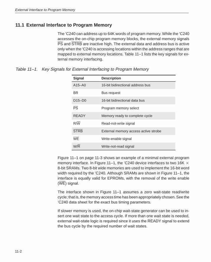
External Interface to Program Memory
11-2
11.1 External Interface to Program Memory
The ’C240 can address up to 64K words of program memory. While the ’C240accesses the on-chip program memory blocks, the external memory signalsPS and STRB are inactive high. The external data and address bus is activeonly when the ’C240 is accessing locations within the address ranges that aremapped to external memory locations. Table 11–1 lists the key signals for ex-ternal memory interfacing.
Table 11–1. Key Signals for External Interfacing to Program Memory
Signal Description
A15–A0 16-bit bidirectional address bus
BR Bus request
D15–D0 16-bit bidirectional data bus
PS Program memory select
READY Memory ready to complete cycle
R/W Read-not-write signal
STRB External memory access active strobe
WE Write-enable signal
W/R Write-not-read signal
Figure 11–1 on page 11-3 shows an example of a minimal external programmemory interface. In Figure 11–1, the ’C240 device interfaces to two 16K �8-bit SRAMs. Two 8-bit wide memories are used to implement the 16-bit wordwidth required by the ’C240. Although SRAMs are shown in Figure 11–1, theinterface is equally valid for EPROMs, with the removal of the write enable(WE) signal.
The interface shown in Figure 11–1 assumes a zero wait-state read/writecycle; that is, the memory access time has been appropriately chosen. See the’C240 data sheet for the exact bus timing parameters.
If slower memory is used, the on-chip wait-state generator can be used to in-sert one wait state to the access cycle. If more than one wait state is needed,external wait-state logic is required since it uses the READY signal to extendthe bus cycle by the required number of wait states.

External Interface to Program Memory
11-3External Memory Interface
Figure 11–1.Interface to External Program Memory
A0
A1
A2
A3
A4
A5
A6
A7
A8
A9
A10
A11
A12
A13
A14
A15
A0
A1
A2
A3
A4
A5
A6
A7
A8
A9
A10
A11
A12
A13
A14
A15D0
D1
D2
D3
D4
D5
D6
D7
D8
D9
D10
D11
D12
D13
D14
D15
D0
D1
D2
D3
D4
D5
D6
D7
D8
D9
D10
D11
D12
D13
D14
D15
IS
DS
PS
BR
R/W
W/R
READY
STRB
WE
IS
DS
PS
BR
R/W
W/R
READY
STRB
WE
TMS320C240
A0
A1
A2
A3
A4
A5
A6
A7
A8
A9
A10
A11
A12
A13
A0
A1
A2
A3
A4
A5
A6
A7
A8
A9
A10
A11
A12
A13
D0
D1
D2
D3
D4
D5
D6
D7
D0
D1
D2
D3
D4
D5
D6
D7
CS
OE
WE
PS
W/R
WE
A0
A1
A2
A3
A4
A5
A6
A7
A8
A9
A10
A11
A12
A13
A0
A1
A2
A3
A4
A5
A6
A7
A8
A9
A10
A11
A12
A13
D8
D9
D10
D11
D12
D13
D14
D15
D0
D1
D2
D3
D4
D5
D6
D7
CS
OE
WE
PS
W/R
WE
Lo Byte Hi Byte
RAM 16K × 8 RAM 16K × 8
READY
10K
VCC
Note: External memory interfacesignals only shown here
External Interface to Program Memory
11-4
The program select (PS) signal is connected directly to the chip select (CS)to select the memory on any external program access. The memory is ad-dressed in any 16K address block in program space. If multiple blocks ofmemory are to be interfaced in program space, a decode circuit that gates PSand the appropriate address bits can be used to drive the memory block chipselects.
The W/R signal is tied directly to the output enable (OE) pin of the memory. TheOE signal enables the output drivers of the memory. The drivers are turned offin time to guarantee that no data bus conflicts occur with an external write bythe ’C240 device.
The ’C240 requires two cycles on all external writes, including a half cyclebefore the WE goes low and a half cycle after WE goes high. This preventsbuffer conflicts on the external busses.
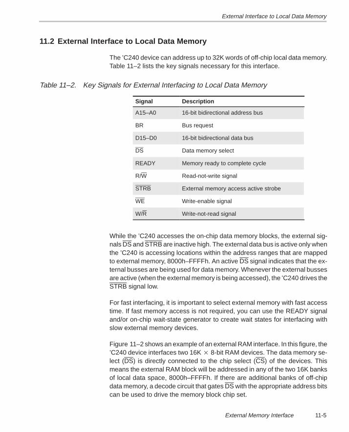
External Interface to Local Data Memory
11-5External Memory Interface
11.2 External Interface to Local Data Memory
The ’C240 device can address up to 32K words of off-chip local data memory.Table 11–2 lists the key signals necessary for this interface.
Table 11–2. Key Signals for External Interfacing to Local Data Memory
Signal Description
A15–A0 16-bit bidirectional address bus
BR Bus request
D15–D0 16-bit bidirectional data bus
DS Data memory select
READY Memory ready to complete cycle
R/W Read-not-write signal
STRB External memory access active strobe
WE Write-enable signal
W/R Write-not-read signal
While the ’C240 accesses the on-chip data memory blocks, the external sig-nals DS and STRB are inactive high. The external data bus is active only whenthe ’C240 is accessing locations within the address ranges that are mappedto external memory, 8000h–FFFFh. An active DS signal indicates that the ex-ternal busses are being used for data memory. Whenever the external bussesare active (when the external memory is being accessed), the ’C240 drives theSTRB signal low.
For fast interfacing, it is important to select external memory with fast accesstime. If fast memory access is not required, you can use the READY signaland/or on-chip wait-state generator to create wait states for interfacing withslow external memory devices.
Figure 11–2 shows an example of an external RAM interface. In this figure, the’C240 device interfaces two 16K � 8-bit RAM devices. The data memory se-lect (DS) is directly connected to the chip select (CS) of the devices. Thismeans the external RAM block will be addressed in any of the two 16K banksof local data space, 8000h–FFFFh. If there are additional banks of off-chipdata memory, a decode circuit that gates DS with the appropriate address bitscan be used to drive the memory block chip set.
External Interface to Local Data Memory
11-6
The W/R signal is tied directly to the output enable (OE) pin of the RAMs. Thissignal enables the output drivers of the RAM and turns them off in time to pre-vent data bus conflicts with an external write by the ’C240. The WE signal ofRAM is connected to the WE signal of ’C240. The ’C240 requires at least twocycles on external writes, including a half cycle before WE goes low and a halfcycle after WE goes high. This prevents buffer conflicts on the external buses.An additional wait state can be generated with the software wait-state genera-tor.
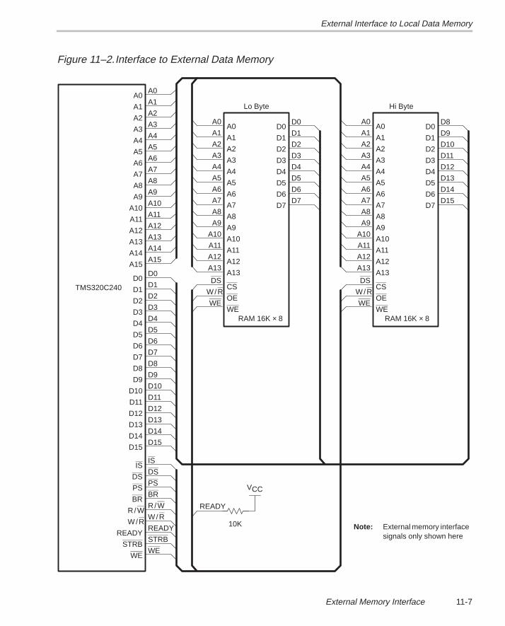
External Interface to Local Data Memory
11-7External Memory Interface
Figure 11–2.Interface to External Data Memory
A0
A1
A2
A3
A4
A5
A6
A7
A8
A9
A10
A11
A12
A13
A14
A15
A0
A1
A2
A3
A4
A5
A6
A7
A8
A9
A10
A11
A12
A13
A14
A15D0
D1
D2
D3
D4
D5
D6
D7
D8
D9
D10
D11
D12
D13
D14
D15
D0
D1
D2
D3
D4
D5
D6
D7
D8
D9
D10
D11
D12
D13
D14
D15
IS
DS
PS
BR
R/W
W/R
READY
STRB
WE
IS
DS
PS
BR
R/W
W/R
READY
STRB
WE
TMS320C240
A0
A1
A2
A3
A4
A5
A6
A7
A8
A9
A10
A11
A12
A13
A0
A1
A2
A3
A4
A5
A6
A7
A8
A9
A10
A11
A12
A13
D0
D1
D2
D3
D4
D5
D6
D7
D0
D1
D2
D3
D4
D5
D6
D7
CS
OE
WE
DS
W/R
WE
A0
A1
A2
A3
A4
A5
A6
A7
A8
A9
A10
A11
A12
A13
A0
A1
A2
A3
A4
A5
A6
A7
A8
A9
A10
A11
A12
A13
D8
D9
D10
D11
D12
D13
D14
D15
D0
D1
D2
D3
D4
D5
D6
D7
CS
OE
WE
DS
W/R
WE
Lo Byte Hi Byte
RAM 16K × 8 RAM 16K × 8
READY
10K
VCC
Note: External memory interfacesignals only shown here
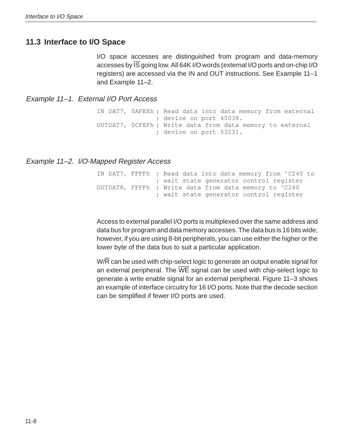
Interface to I/O Space
11-8
11.3 Interface to I/O Space
I/O space accesses are distinguished from program and data-memoryaccesses by IS going low. All 64K I/O words (external I/O ports and on-chip I/Oregisters) are accessed via the IN and OUT instructions. See Example 11–1and Example 11–2.
Example 11–1. External I/O Port Access
IN DAT7, 0AFEEh ; Read data into data memory from external; device on port 45038.
OUTDAT7, 0CFEFh ; Write data from data memory to external; device on port 53231.
Example 11–2. I/O-Mapped Register Access
IN DAT7, FFFFh ; Read data into data memory from ’C240 to; wait state generator control register
OUTDAT8, FFFFh ; Write data from data memory to ’C240; wait state generator control register
Access to external parallel I/O ports is multiplexed over the same address anddata bus for program and data memory accesses. The data bus is 16 bits wide;however, if you are using 8-bit peripherals, you can use either the higher or thelower byte of the data bus to suit a particular application.
W/R can be used with chip-select logic to generate an output enable signal foran external peripheral. The WE signal can be used with chip-select logic togenerate a write enable signal for an external peripheral. Figure 11–3 showsan example of interface circuitry for 16 I/O ports. Note that the decode sectioncan be simplified if fewer I/O ports are used.
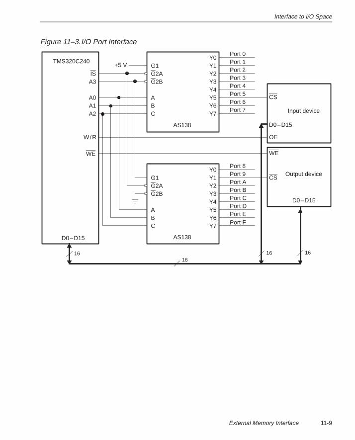
Interface to I/O Space
11-9External Memory Interface
Figure 11–3.I/O Port Interface
TMS320C240
Output deviceCS
AS138
Y7Y6Y5Y4Y3Y2Y1Y0
G1G2AG2B
ABC
Port 8Port 9Port APort BPort CPort DPort E
WE
W/R
WE
Input device
OE
CS
Port 7Port 6Port 5Port 4Port 3Port 2Port 1Port 0
CBA
G2BG2AG1
Y0Y1Y2Y3Y4Y5Y6Y7A2
A1A0
A3IS
+5 V
AS138
Port F
D0–D15
1616
16 16
D0–D15
D0–D15
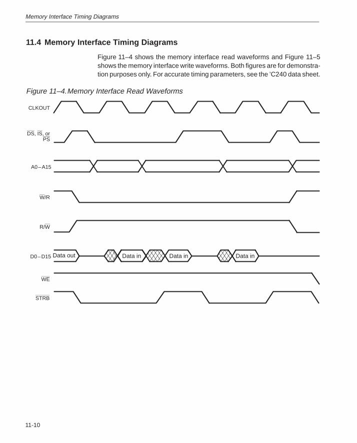
Memory Interface Timing Diagrams
11-10
11.4 Memory Interface Timing Diagrams
Figure 11–4 shows the memory interface read waveforms and Figure 11–5shows the memory interface write waveforms. Both figures are for demonstra-tion purposes only. For accurate timing parameters, see the ’C240 data sheet.
Figure 11–4.Memory Interface Read Waveforms
STRB
WE
D0–D15
W/R
A0–A15
CLKOUT
DS, IS, orPS
R/W
Data in Data in Data inData out
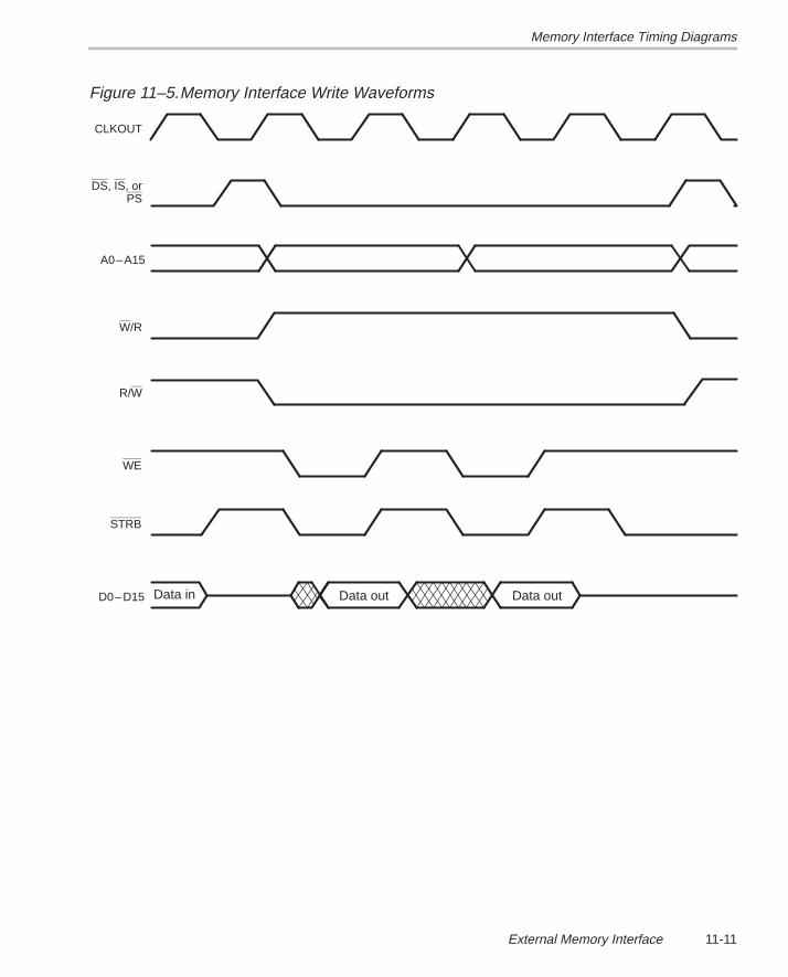
Memory Interface Timing Diagrams
11-11External Memory Interface
Figure 11–5.Memory Interface Write Waveforms
STRB
D0–D15
W/R
A0–A15
CLKOUT
DS, IS, orPS
R/W
Data out Data outData in
WE
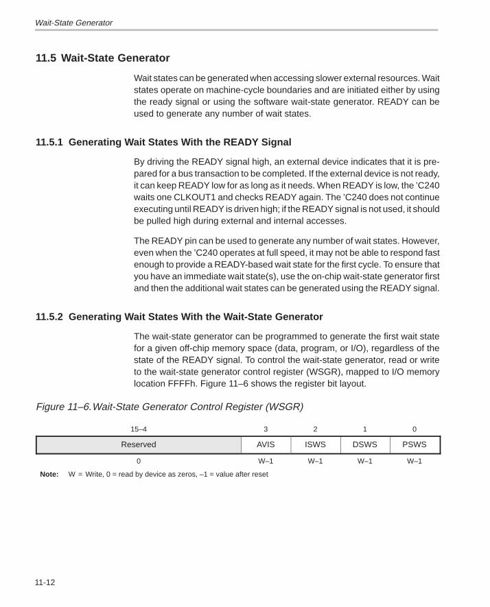
Wait-State Generator
11-12
11.5 Wait-State Generator
Wait states can be generated when accessing slower external resources. Waitstates operate on machine-cycle boundaries and are initiated either by usingthe ready signal or using the software wait-state generator. READY can beused to generate any number of wait states.
11.5.1 Generating Wait States With the READY Signal
By driving the READY signal high, an external device indicates that it is pre-pared for a bus transaction to be completed. If the external device is not ready,it can keep READY low for as long as it needs. When READY is low, the ’C240waits one CLKOUT1 and checks READY again. The ’C240 does not continueexecuting until READY is driven high; if the READY signal is not used, it shouldbe pulled high during external and internal accesses.
The READY pin can be used to generate any number of wait states. However,even when the ’C240 operates at full speed, it may not be able to respond fastenough to provide a READY-based wait state for the first cycle. To ensure thatyou have an immediate wait state(s), use the on-chip wait-state generator firstand then the additional wait states can be generated using the READY signal.
11.5.2 Generating Wait States With the Wait-State Generator
The wait-state generator can be programmed to generate the first wait statefor a given off-chip memory space (data, program, or I/O), regardless of thestate of the READY signal. To control the wait-state generator, read or writeto the wait-state generator control register (WSGR), mapped to I/O memorylocation FFFFh. Figure 11–6 shows the register bit layout.
Figure 11–6.Wait-State Generator Control Register (WSGR)
15–4 3 2 1 0
Reserved AVIS ISWS DSWS PSWS
0 W–1 W–1 W–1 W–1
Note: W = Write, 0 = read by device as zeros, –1 = value after reset
Wait-State Generator
11-13External Memory Interface
Bits 15–4 Reserved . Always read as 0.
Bit 3 AVIS . Address visibility mode. At reset, this bit is set to 1. AVIS does not gener-ate a wait state.
0 =Cleared; reduces power and noise (for production systems)
1 =Enables the address visibility mode of the device. In this mode, thedevice provides a method of tracing the internal code operation: itpasses the internal program address to the address bus when thisbus is not used for an external access.
Bit 2 ISWS . I/O space wait state bit. At reset, this bit is set to 1.
0 =No wait states are generated for off-chip I/O space.
1 =One wait state will be applied to all accesses to off-chip I/O memoryspace.
Bit 1 DSWS . Data space wait state bit. At reset, this bit is set to 1.
0 =No wait states are generated for off-chip data space.
1 =One wait state will be applied to all accesses to off-chip data memoryspace.
Bit 0 PSWS . Program space wait state bit. At reset, this bit is set to 1.
0 =No wait states are generated for off-chip program space.
1 =One wait state will be applied to all accesses to off-chip programmemory space.
In summary, the wait-state generator inserts a wait state to a given memoryspace (data, program, or I/O) if the corresponding bit in WSGR is set to 1, re-gardless of the condition of the READY signal. The READY signal can then beused to further extend wait states. The WSGR bits are all set to 1 by reset sothat the device can operate from slow memory after reset.
12-1
Digital I/O Ports
This chapter contains a general description of the digital I/O ports module, andprovides an overview of the method for controlling dedicated I/O and sharedpin functions.
Topic Page
12.1 Digital I/O Ports Overview 12-2. . . . . . . . . . . . . . . . . . . . . . . . . . . . . . . . . . . .
12-2 Digital I/O and Shared Pin Functions 12-2. . . . . . . . . . . . . . . . . . . . . . . . . .
12.3 Digital I/O Control Registers 12-6. . . . . . . . . . . . . . . . . . . . . . . . . . . . . . . . . .
Chapter 12
Digital I/O Ports Overview
12-2
12.1 Digital I/O Ports Overview
The digital I/O ports module provides a flexible method for controlling bothdedicated I/O and shared pin functions. All I/O and shared pin functions arecontrolled using five 16-bit registers mapped within Peripheral File 9. Theseregisters are divided into three types:
� Output control registers — Used to directly control O/P pins.
� Data and direction control registers — Used to control the data and thedirection of the data to bidirectional I/O pins. The registers are directly con-nected to the bidirectional I/O pins.
12.2 Digital I/O and Shared Pin Functions
The ’C240 has a total of 28 pins shared between primary functions and I/Os.These pins are divided into two groups:
� Group1. These are primary functions shared with I/Os belonging to dedi-cated I/O ports A, B, and C.
� Group2 These are primary functions belonging to peripheral modules thathave a built-in I/O feature as a secondary function. Example are: SCI, SPI,external interrupts, and PLL clock module.
12.2.1 Description of Group1 Shared I/O Pins
The control structure for Group1 type shared I/O pins is shown in Figure 12–1on page 12-3. The only exception to this configuration is the CLKOUT/IOPC1pin described later in this section. In Figure 12–1, each pin has three bits whichdefine its operation:
� MUX control bit . This bit selects between the primary function (1) and I/Ofunction (0) of the pin.
� I/O direction bit . This bit determines whether the pin is an input (0) or out-put (1) when the I/O function is selected for the pin (MUX control bit is setto 0).
� I/O data bit . Data is read from this bit if the I/O function is selected for thepin (MUX control bit is set to 0) and the direction selected is an input. Datais written to this bit if the direction selected is an output.
The MUX control bit, I/O direction bit, and I/O data bit are in the I/O control reg-isters described in section 12.3, Digital I/O control Registers, on page 12-6.
Digital I/O Ports Overview / Digital I/O and Shared Pin Functions
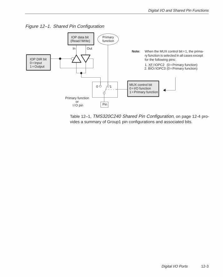
Digital I/O and Shared Pin Functions
12-3Digital I/O Ports
Figure 12–1. Shared Pin Configuration
MUX control bit0= I/O function1=Primary function
IOP data bit(Read/Write)
IOP DIR bit0= Input1=Output
Primary functionor
I /O pin
0 1
Primaryfunction
OutInNote: When the MUX control bit=1, the prima-
ry function is selected in all cases exceptfor the following pins:
(0=Primary function)(0=Primary function)
1. XF / IOPC2 2. BIO / IOPC3
Pin
Table 12–1, TMS320C240 Shared Pin Configuration, on page 12-4 pro-vides a summary of Group1 pin configurations and associated bits.
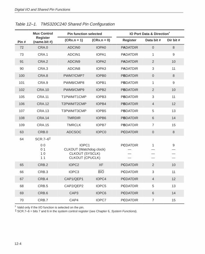
Digital I/O and Shared Pin Functions
12-4
Table 12–1. TMS320C240 Shared Pin Configuration
Mux ControlR i t
Pin function selected IO Port Data & Direction †
Pin #Register
(name.bit #) (CRx.n = 1) (CRx.n = 0) Register Data bit # Dir bit #
72 CRA.0 ADCIN0 IOPA0 PADATDIR 0 8
73 CRA.1 ADCIN1 IOPA1 PADATDIR 1 9
91 CRA.2 ADCIN9 IOPA2 PADATDIR 2 10
90 CRA.3 ADCIN8 IOPA3 PADATDIR 3 11
100 CRA.8 PWM7/CMP7 IOPB0 PBDATDIR 0 8
101 CRA.9 PWM8/CMP8 IOPB1 PBDATDIR 1 9
102 CRA.10 PWM9/CMP9 IOPB2 PBDATDIR 2 10
105 CRA.11 T1PWM/T1CMP IOPB3 PBDATDIR 3 11
106 CRA.12 T2PWM/T2CMP IOPB4 PBDATDIR 4 12
107 CRA.13 T3PWM/T3CMP IOPB5 PBDATDIR 5 13
108 CRA.14 TMRDIR IOPB6 PBDATDIR 6 14
109 CRA.15 TMRCLK IOPB7 PBDATDIR 7 15
63 CRB.0 ADCSOC IOPC0 PCDATDIR 0 8
64 SCR.7–6‡
0 00 11 01 1
IOPC1CLKOUT (Watchdog clock)
CLKOUT (SYSCLK)CLKOUT (CPUCLK)
PCDATDIR———
1———
9———
65 CRB.2 IOPC2 XF PCDATDIR 2 10
66 CRB.3 IOPC3 BIO PCDATDIR 3 11
67 CRB.4 CAP1/QEP1 IOPC4 PCDATDIR 4 12
68 CRB.5 CAP2/QEP2 IOPC5 PCDATDIR 5 13
69 CRB.6 CAP3 IOPC6 PCDATDIR 6 14
70 CRB.7 CAP4 IOPC7 PCDATDIR 7 15
† Valid only if the I/O function is selected on the pin.‡ SCR.7–6 = bits 7 and 6 in the system control register (see Chapter 6, System Functions).
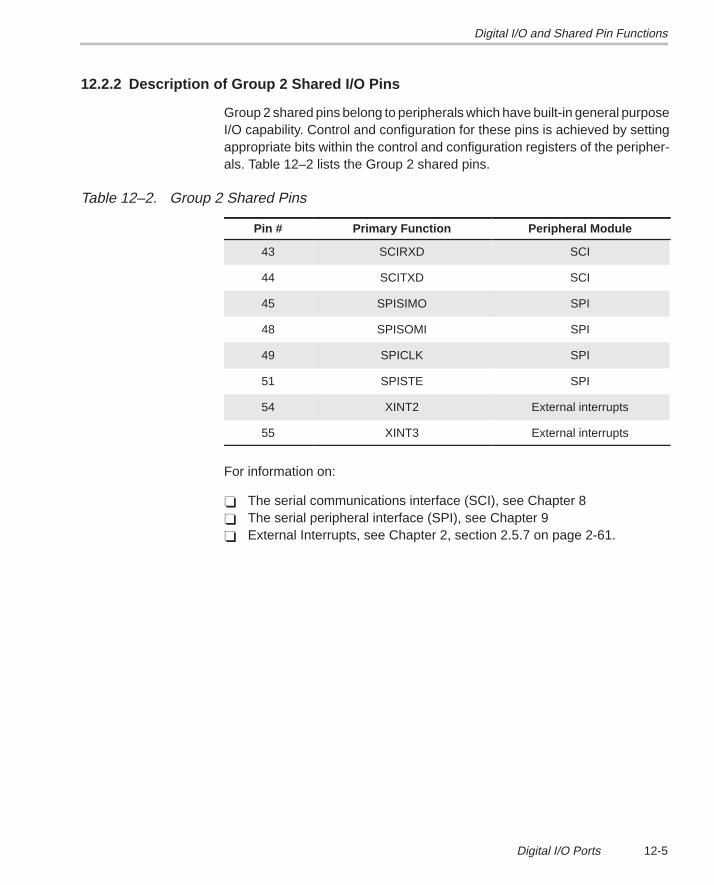
Digital I/O and Shared Pin Functions
12-5Digital I/O Ports
12.2.2 Description of Group 2 Shared I/O Pins
Group 2 shared pins belong to peripherals which have built-in general purposeI/O capability. Control and configuration for these pins is achieved by settingappropriate bits within the control and configuration registers of the peripher-als. Table 12–2 lists the Group 2 shared pins.
Table 12–2. Group 2 Shared Pins
Pin # Primary Function Peripheral Module
43 SCIRXD SCI
44 SCITXD SCI
45 SPISIMO SPI
48 SPISOMI SPI
49 SPICLK SPI
51 SPISTE SPI
54 XINT2 External interrupts
55 XINT3 External interrupts
For information on:
� The serial communications interface (SCI), see Chapter 8� The serial peripheral interface (SPI), see Chapter 9� External Interrupts, see Chapter 2, section 2.5.7 on page 2-61.
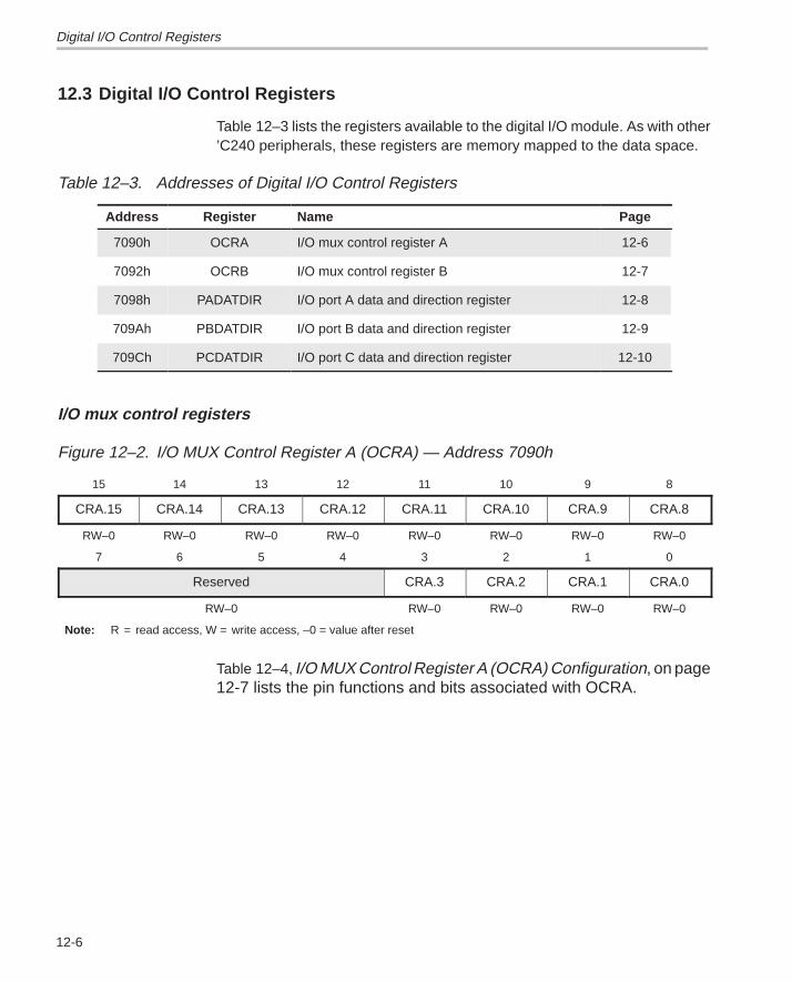
Digital I/O Control Registers
12-6
12.3 Digital I/O Control Registers
Table 12–3 lists the registers available to the digital I/O module. As with other’C240 peripherals, these registers are memory mapped to the data space.
Table 12–3. Addresses of Digital I/O Control Registers
Address Register Name Page
7090h OCRA I/O mux control register A 12-6
7092h OCRB I/O mux control register B 12-7
7098h PADATDIR I/O port A data and direction register 12-8
709Ah PBDATDIR I/O port B data and direction register 12-9
709Ch PCDATDIR I/O port C data and direction register 12-10
I/O mux control registers
Figure 12–2. I/O MUX Control Register A (OCRA) — Address 7090h
15 14 13 12 11 10 9 8
CRA.15 CRA.14 CRA.13 CRA.12 CRA.11 CRA.10 CRA.9 CRA.8
RW–0 RW–0 RW–0 RW–0 RW–0 RW–0 RW–0 RW–0
7 6 5 4 3 2 1 0
Reserved CRA.3 CRA.2 CRA.1 CRA.0
RW–0 RW–0 RW–0 RW–0 RW–0
Note: R = read access, W = write access, –0 = value after reset
Table 12–4, I/O MUX Control Register A (OCRA) Configuration, on page12-7 lists the pin functions and bits associated with OCRA.
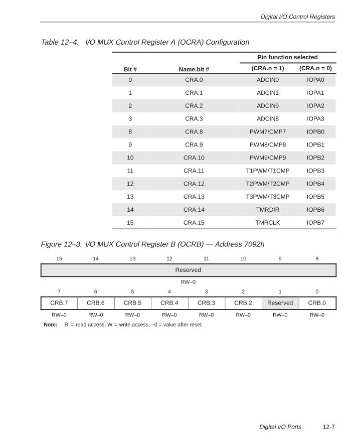
Digital I/O Control Registers
12-7Digital I/O Ports
Table 12–4. I/O MUX Control Register A (OCRA) Configuration
Pin function selected
Bit # Name.bit # (CRA.n = 1) (CRA.n = 0)
0 CRA.0 ADCIN0 IOPA0
1 CRA.1 ADCIN1 IOPA1
2 CRA.2 ADCIN9 IOPA2
3 CRA.3 ADCIN8 IOPA3
8 CRA.8 PWM7/CMP7 IOPB0
9 CRA.9 PWM8/CMP8 IOPB1
10 CRA.10 PWM9/CMP9 IOPB2
11 CRA.11 T1PWM/T1CMP IOPB3
12 CRA.12 T2PWM/T2CMP IOPB4
13 CRA.13 T3PWM/T3CMP IOPB5
14 CRA.14 TMRDIR IOPB6
15 CRA.15 TMRCLK IOPB7
Figure 12–3. I/O MUX Control Register B (OCRB) — Address 7092h
15 14 13 12 11 10 9 8
Reserved
RW–0
7 6 5 4 3 2 1 0
CRB.7 CRB.6 CRB.5 CRB.4 CRB.3 CRB.2 Reserved CRB.0
RW–0 RW–0 RW–0 RW–0 RW–0 RW–0 RW–0 RW–0
Note: R = read access, W = write access, –0 = value after reset
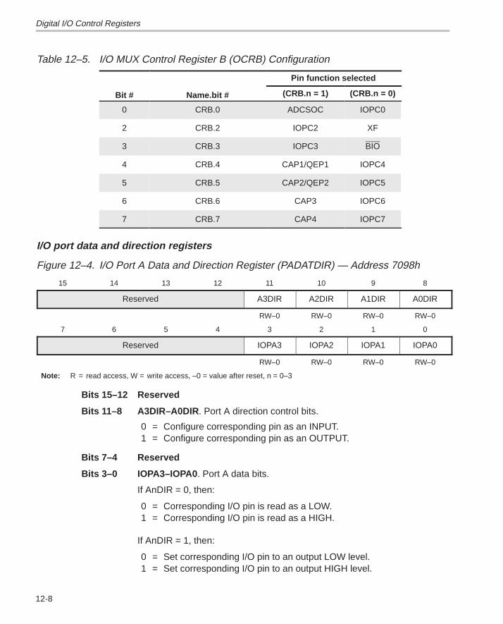
Digital I/O Control Registers
12-8
Table 12–5. I/O MUX Control Register B (OCRB) Configuration
Pin function selected
Bit # Name.bit # (CRB.n = 1) (CRB.n = 0)
0 CRB.0 ADCSOC IOPC0
2 CRB.2 IOPC2 XF
3 CRB.3 IOPC3 BIO
4 CRB.4 CAP1/QEP1 IOPC4
5 CRB.5 CAP2/QEP2 IOPC5
6 CRB.6 CAP3 IOPC6
7 CRB.7 CAP4 IOPC7
I/O port data and direction registers
Figure 12–4. I/O Port A Data and Direction Register (PADATDIR) — Address 7098h
15 14 13 12 11 10 9 8
Reserved A3DIR A2DIR A1DIR A0DIR
RW–0 RW–0 RW–0 RW–0
7 6 5 4 3 2 1 0
Reserved IOPA3 IOPA2 IOPA1 IOPA0
RW–0 RW–0 RW–0 RW–0
Note: R = read access, W = write access, –0 = value after reset, n = 0–3
Bits 15–12 Reserved
Bits 11–8 A3DIR–A0DIR . Port A direction control bits.
0 = Configure corresponding pin as an INPUT.1 = Configure corresponding pin as an OUTPUT.
Bits 7–4 Reserved
Bits 3–0 IOPA3–IOPA0 . Port A data bits.
If AnDIR = 0, then:
0 = Corresponding I/O pin is read as a LOW.1 = Corresponding I/O pin is read as a HIGH.
If AnDIR = 1, then:
0 = Set corresponding I/O pin to an output LOW level.1 = Set corresponding I/O pin to an output HIGH level.
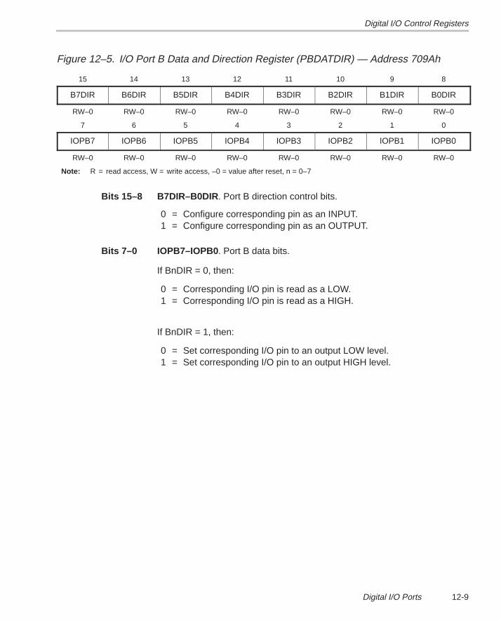
Digital I/O Control Registers
12-9Digital I/O Ports
Figure 12–5. I/O Port B Data and Direction Register (PBDATDIR) — Address 709Ah
15 14 13 12 11 10 9 8
B7DIR B6DIR B5DIR B4DIR B3DIR B2DIR B1DIR B0DIR
RW–0 RW–0 RW–0 RW–0 RW–0 RW–0 RW–0 RW–0
7 6 5 4 3 2 1 0
IOPB7 IOPB6 IOPB5 IOPB4 IOPB3 IOPB2 IOPB1 IOPB0
RW–0 RW–0 RW–0 RW–0 RW–0 RW–0 RW–0 RW–0
Note: R = read access, W = write access, –0 = value after reset, n = 0–7
Bits 15–8 B7DIR–B0DIR . Port B direction control bits.
0 = Configure corresponding pin as an INPUT.1 = Configure corresponding pin as an OUTPUT.
Bits 7–0 IOPB7–IOPB0 . Port B data bits.
If BnDIR = 0, then:
0 = Corresponding I/O pin is read as a LOW.1 = Corresponding I/O pin is read as a HIGH.
If BnDIR = 1, then:
0 = Set corresponding I/O pin to an output LOW level.1 = Set corresponding I/O pin to an output HIGH level.
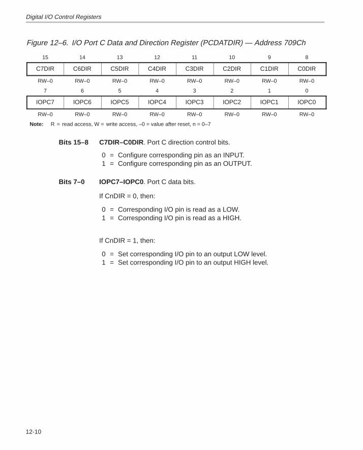
Digital I/O Control Registers
12-10
Figure 12–6. I/O Port C Data and Direction Register (PCDATDIR) — Address 709Ch
15 14 13 12 11 10 9 8
C7DIR C6DIR C5DIR C4DIR C3DIR C2DIR C1DIR C0DIR
RW–0 RW–0 RW–0 RW–0 RW–0 RW–0 RW–0 RW–0
7 6 5 4 3 2 1 0
IOPC7 IOPC6 IOPC5 IOPC4 IOPC3 IOPC2 IOPC1 IOPC0
RW–0 RW–0 RW–0 RW–0 RW–0 RW–0 RW–0 RW–0
Note: R = read access, W = write access, –0 = value after reset, n = 0–7
Bits 15–8 C7DIR–C0DIR . Port C direction control bits.
0 = Configure corresponding pin as an INPUT.1 = Configure corresponding pin as an OUTPUT.
Bits 7–0 IOPC7–IOPC0 . Port C data bits.
If CnDIR = 0, then:
0 = Corresponding I/O pin is read as a LOW.1 = Corresponding I/O pin is read as a HIGH.
If CnDIR = 1, then:
0 = Set corresponding I/O pin to an output LOW level.1 = Set corresponding I/O pin to an output HIGH level.
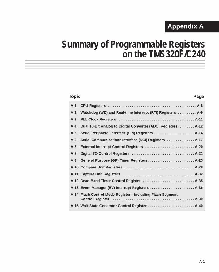
A-1
Appendix A
Summary of Programmable Registerson the TMS320F/C240
Topic Page
A.1 CPU Registers A-6. . . . . . . . . . . . . . . . . . . . . . . . . . . . . . . . . . . . . . . . . . . . . . . .
A.2 Watchdog (WD) and Real-time Interrupt (RTI) Registers A-9. . . . . . . . . .
A.3 PLL Clock Registers A-11. . . . . . . . . . . . . . . . . . . . . . . . . . . . . . . . . . . . . . . . .
A.4 Dual 10-Bit Analog to Digital Converter (ADC) Registers A-12. . . . . . . .
A.5 Serial Peripheral Interface (SPI) Registers A-14. . . . . . . . . . . . . . . . . . . . . .
A.6 Serial Communications Interface (SCI) Registers A-17. . . . . . . . . . . . . . .
A.7 External Interrupt Control Registers A-20. . . . . . . . . . . . . . . . . . . . . . . . . . .
A.8 Digital I/O Control Registers A-21. . . . . . . . . . . . . . . . . . . . . . . . . . . . . . . . . .
A.9 General Purpose (GP) Timer Registers A-23. . . . . . . . . . . . . . . . . . . . . . . . .
A.10 Compare Unit Registers A-28. . . . . . . . . . . . . . . . . . . . . . . . . . . . . . . . . . . . . .
A.11 Capture Unit Registers A-32. . . . . . . . . . . . . . . . . . . . . . . . . . . . . . . . . . . . . . .
A.12 Dead-Band Timer Control Register A-35. . . . . . . . . . . . . . . . . . . . . . . . . . . .
A.13 Event Manager (EV) Interrupt Registers A-36. . . . . . . . . . . . . . . . . . . . . . . .
A.14 Flash Control Mode Register—Including Flash SegmentControl Register A-39. . . . . . . . . . . . . . . . . . . . . . . . . . . . . . . . . . . . . . . . . . . . .
A.15 Wait-State Generator Control Register A-40. . . . . . . . . . . . . . . . . . . . . . . . .
Appendix A
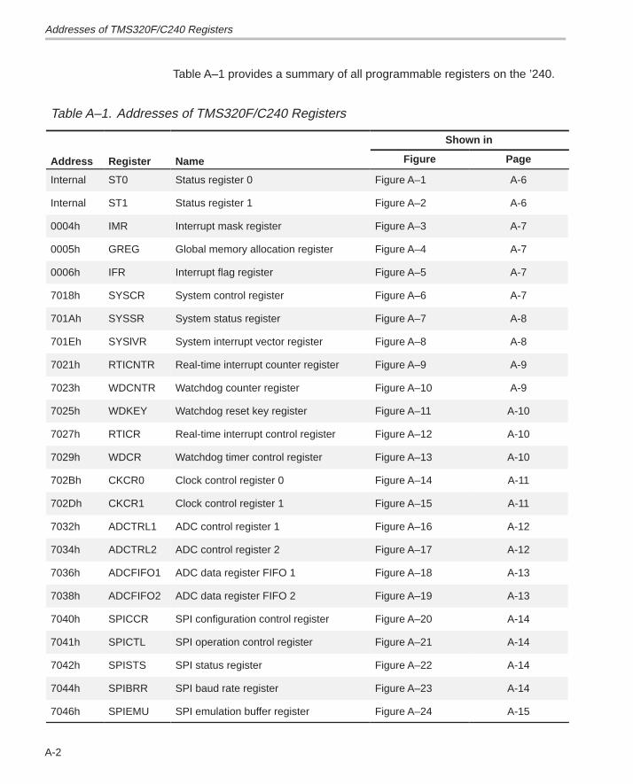
Addresses of TMS320F/C240 Registers
A-2
Table A–1 provides a summary of all programmable registers on the ’240.
Table A–1. Addresses of TMS320F/C240 Registers
Shown in
Address Register Name Figure Page
Internal ST0 Status register 0 Figure A–1 A-6
Internal ST1 Status register 1 Figure A–2 A-6
0004h IMR Interrupt mask register Figure A–3 A-7
0005h GREG Global memory allocation register Figure A–4 A-7
0006h IFR Interrupt flag register Figure A–5 A-7
7018h SYSCR System control register Figure A–6 A-7
701Ah SYSSR System status register Figure A–7 A-8
701Eh SYSlVR System interrupt vector register Figure A–8 A-8
7021h RTICNTR Real-time interrupt counter register Figure A–9 A-9
7023h WDCNTR Watchdog counter register Figure A–10 A-9
7025h WDKEY Watchdog reset key register Figure A–11 A-10
7027h RTICR Real-time interrupt control register Figure A–12 A-10
7029h WDCR Watchdog timer control register Figure A–13 A-10
702Bh CKCR0 Clock control register 0 Figure A–14 A-11
702Dh CKCR1 Clock control register 1 Figure A–15 A-11
7032h ADCTRL1 ADC control register 1 Figure A–16 A-12
7034h ADCTRL2 ADC control register 2 Figure A–17 A-12
7036h ADCFIFO1 ADC data register FIFO 1 Figure A–18 A-13
7038h ADCFIFO2 ADC data register FIFO 2 Figure A–19 A-13
7040h SPICCR SPI configuration control register Figure A–20 A-14
7041h SPICTL SPI operation control register Figure A–21 A-14
7042h SPISTS SPI status register Figure A–22 A-14
7044h SPIBRR SPI baud rate register Figure A–23 A-14
7046h SPIEMU SPI emulation buffer register Figure A–24 A-15
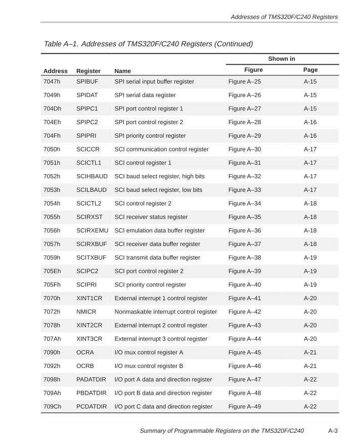
Addresses of TMS320F/C240 Registers
A-3Summary of Programmable Registers on the TMS320F/C240
Table A–1. Addresses of TMS320F/C240 Registers (Continued)
Shown in
NameRegisterAddress PageFigureNameRegisterAddress
7047h SPIBUF SPI serial input buffer register Figure A–25 A-15
7049h SPIDAT SPI serial data register Figure A–26 A-15
704Dh SPIPC1 SPI port control register 1 Figure A–27 A-15
704Eh SPIPC2 SPI port control register 2 Figure A–28 A-16
704Fh SPIPRI SPI priority control register Figure A–29 A-16
7050h SCICCR SCI communication control register Figure A–30 A-17
7051h SCICTL1 SCI control register 1 Figure A–31 A-17
7052h SCIHBAUD SCI baud select register, high bits Figure A–32 A-17
7053h SCILBAUD SCI baud select register, low bits Figure A–33 A-17
7054h SCICTL2 SCI control register 2 Figure A–34 A-18
7055h SCIRXST SCI receiver status register Figure A–35 A-18
7056h SCIRXEMU SCI emulation data buffer register Figure A–36 A-18
7057h SCIRXBUF SCI receiver data buffer register Figure A–37 A-18
7059h SCITXBUF SCI transmit data buffer register Figure A–38 A-19
705Eh SCIPC2 SCI port control register 2 Figure A–39 A-19
705Fh SCIPRI SCI priority control register Figure A–40 A-19
7070h XINT1CR External interrupt 1 control register Figure A–41 A-20
7072h NMICR Nonmaskable interrupt control register Figure A–42 A-20
7078h XINT2CR External interrupt 2 control register Figure A–43 A-20
707Ah XINT3CR External interrupt 3 control register Figure A–44 A-20
7090h OCRA I/O mux control register A Figure A–45 A-21
7092h OCRB I/O mux control register B Figure A–46 A-21
7098h PADATDIR I/O port A data and direction register Figure A–47 A-22
709Ah PBDATDIR I/O port B data and direction register Figure A–48 A-22
709Ch PCDATDIR I/O port C data and direction register Figure A–49 A-22
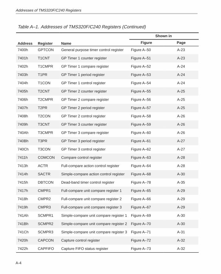
Addresses of TMS320F/C240 Registers
A-4
Table A–1. Addresses of TMS320F/C240 Registers (Continued)
Shown in
NameRegisterAddress PageFigureNameRegisterAddress
7400h GPTCON General purpose timer control register Figure A–50 A-23
7401h T1CNT GP Timer 1 counter register Figure A–51 A-23
7402h T1CMPR GP Timer 1 compare register Figure A–52 A-24
7403h T1PR GP Timer 1 period register Figure A–53 A-24
7404h T1CON GP Timer 1 control register Figure A–54 A-24
7405h T2CNT GP Timer 2 counter register Figure A–55 A-25
7406h T2CMPR GP Timer 2 compare register Figure A–56 A-25
7407h T2PR GP Timer 2 period register Figure A–57 A-25
7408h T2CON GP Timer 2 control register Figure A–58 A-26
7409h T3CNT GP Timer 3 counter register Figure A–59 A-26
740Ah T3CMPR GP Timer 3 compare register Figure A–60 A-26
740Bh T3PR GP Timer 3 period register Figure A–61 A-27
740Ch T3CON GP Timer 3 control register Figure A–62 A-27
7411h COMCON Compare control register Figure A–63 A-28
7413h ACTR Full-compare action control register Figure A–64 A-28
7414h SACTR Simple-compare action control register Figure A–68 A-30
7415h DBTCON Dead-band timer control register Figure A–78 A-35
7417h CMPR1 Full-compare unit compare register 1 Figure A–65 A-29
7418h CMPR2 Full-compare unit compare register 2 Figure A–66 A-29
7419h CMPR3 Full-compare unit compare register 3 Figure A–67 A-29
741Ah SCMPR1 Simple-compare unit compare register 1 Figure A–69 A-30
741Bh SCMPR2 Simple-compare unit compare register 2 Figure A–70 A-30
741Ch SCMPR3 Simple-compare unit compare register 3 Figure A–71 A-31
7420h CAPCON Capture control register Figure A–72 A-32
7422h CAPFIFO Capture FIFO status register Figure A–73 A-32
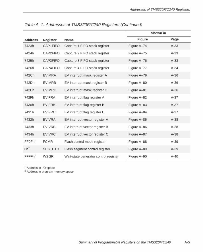
Addresses of TMS320F/C240 Registers
A-5Summary of Programmable Registers on the TMS320F/C240
Table A–1. Addresses of TMS320F/C240 Registers (Continued)
Shown in
NameRegisterAddress PageFigureNameRegisterAddress
7423h CAP1FIFO Capture 1 FIFO stack register Figure A–74 A-33
7424h CAP2FIFO Capture 2 FIFO stack register Figure A–75 A-33
7425h CAP3FIFO Capture 3 FIFO stack register Figure A–76 A-33
7426h CAP4FIFO Capture 4 FIFO stack register Figure A–77 A-34
742Ch EVIMRA EV interrupt mask register A Figure A–79 A-36
742Dh EVIMRB EV interrupt mask register B Figure A–80 A-36
742Eh EVIMRC EV interrupt mask register C Figure A–81 A-36
742Fh EVIFRA EV interrupt flag register A Figure A–82 A-37
7430h EVIFRB EV interrupt flag register B Figure A–83 A-37
7431h EVIFRC EV interrupt flag register C Figure A–84 A-37
7432h EVIVRA EV interrupt vector register A Figure A–85 A-38
7433h EVIVRB EV interrupt vector register B Figure A–86 A-38
7434h EVIVRC EV interrupt vector register C Figure A–87 A-38
FF0Fh† FCMR Flash control mode register Figure A–88 A-39
0h‡ SEG_CTR Flash segment control register Figure A–89 A-39
FFFFh† WSGR Wait-state generator control register Figure A–90 A-40
† Address in I/O space‡ Address in program memory space
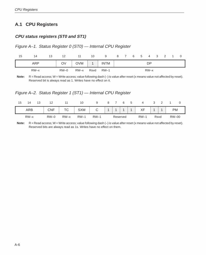
CPU Registers
A-6
A.1 CPU Registers
CPU status registers (ST0 and ST1)
Figure A–1. Status Register 0 (ST0) — Internal CPU Register
15 14 13 12 11 10 9 8 7 6 5 4 3 2 1 0
ARP OV OVM 1 INTM DP
RW–x RW–0 RW–x Rsvd RW–1 RW–x
Note: R = Read access; W = Write access; value following dash (–) is value after reset (x means value not affected by reset).Reserved bit is always read as 1. Writes have no effect on it.
Figure A–2. Status Register 1 (ST1) — Internal CPU Register
15 14 13 12 11 10 9 8 7 6 5 4 3 2 1 0
ARB CNF TC SXM C 1 1 1 1 XF 1 1 PM
RW–x RW–0 RW–x RW–1 RW–1 Reserved RW–1 Rsvd RW–00
Note: R = Read access; W = Write access; value following dash (–) is value after reset (x means value not affected by reset).Reserved bits are always read as 1s. Writes have no effect on them.
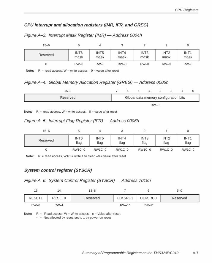
CPU Registers
A-7Summary of Programmable Registers on the TMS320F/C240
CPU interrupt and allocation registers (IMR, IFR, and GREG)
Figure A–3. Interrupt Mask Register (IMR) — Address 0004h
15–6 5 4 3 2 1 0
ReservedINT6mask
INT5mask
INT4mask
INT3mask
INT2mask
INT1mask
0 RW–0 RW–0 RW–0 RW–0 RW–0 RW–0
Note: R = read access, W = write access, –0 = value after reset
Figure A–4. Global Memory Allocation Register (GREG) — Address 0005h
15–8 7 6 5 4 3 2 1 0
Reserved Global data memory configuration bits
RW–0
Note: R = read access, W = write access, –0 = value after reset
Figure A–5. Interrupt Flag Register (IFR) — Address 0006h
15–6 5 4 3 2 1 0
ReservedINT6flag
INT5flag
INT4flag
INT3flag
INT2flag
INT1flag
0 RW1C–0 RW1C–0 RW1C–0 RW1C–0 RW1C–0 RW1C–0
Note: R = read access, W1C = write 1 to clear, –0 = value after reset
System control register (SYSCR)
Figure A–6. System Control Register (SYSCR) — Address 7018h
15 14 13–8 7 6 5–0
RESET1 RESET0 Reserved CLKSRC1 CLKSRC0 Reserved
RW–0 RW–1 RW–1* RW–1*
Note: R = Read access, W = Write access, –n = Value after reset,* = Not affected by reset, set to 1 by power-on reset
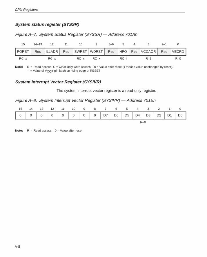
CPU Registers
A-8
System status register (SYSSR)
Figure A–7. System Status Register (SYSSR) — Address 701Ah
15 14–13 12 11 10 9 8–6 5 4 3 2–1 0
PORST Res ILLADR Res SWRST WDRST Res HPO Res VCCAOR Res VECRD
RC–x RC–x RC–x RC–x RC–i R–1 R–0
Note: R = Read access, C = Clear-only write access, –n = Value after reset (x means value unchanged by reset),–i = Value of VCCP pin latch on rising edge of RESET
System Interrupt Vector Register (SYSIVR)
The system interrupt vector register is a read-only register.
Figure A–8. System Interrupt Vector Register (SYSIVR) — Address 701Eh
15 14 13 12 11 10 9 8 7 6 5 4 3 2 1 0
0 0 0 0 0 0 0 0 D7 D6 D5 D4 D3 D2 D1 D0
R–0
Note: R = Read access, –0 = Value after reset
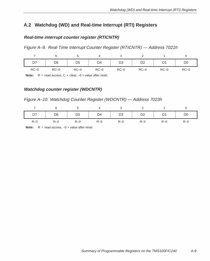
Watchdog (WD) and Real-time Interrupt (RTI) Registers
A-9Summary of Programmable Registers on the TMS320F/C240
A.2 Watchdog (WD) and Real-time Interrupt (RTI) Registers
Real-time interrupt counter register (RTICNTR)
Figure A–9. Real-Time Interrupt Counter Register (RTICNTR) — Address 7021h
7 6 5 4 3 2 1 0
D7 D6 D5 D4 D3 D2 D1 D0
RC–0 RC–0 RC–0 RC–0 RC–0 RC–0 RC–0 RC–0
Note: R = read access, C = clear, –0 = value after reset
Watchdog counter register (WDCNTR)
Figure A–10. Watchdog Counter Register (WDCNTR) — Address 7023h
7 6 5 4 3 2 1 0
D7 D6 D5 D4 D3 D2 D1 D0
R–0 R–0 R–0 R–0 R–0 R–0 R–0 R–0
Note: R = read access, –0 = value after reset
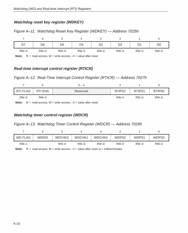
Watchdog (WD) and Real-time Interrupt (RTI) Registers
A-10
Watchdog reset key register (WDKEY)
Figure A–11. Watchdog Reset Key Register (WDKEY) — Address 7025h
7 6 5 4 3 2 1 0
D7 D6 D5 D4 D3 D2 D1 D0
RW–0 RW–0 RW–0 RW–0 RW–0 RW–0 RW–0 RW–0
Note: R = read access, W = write access, –0 = value after reset
Real-time interrupt control register (RTICR)
Figure A–12. Real-Time Interrupt Control Register (RTICR) — Address 7027h
7 6 5 – 3 2 1 0
RTI FLAG RTI ENA Reserved RTIPS2 RTIPS1 RTIPS0
RW–0 RW–0 RW–0 RW–0 RW–0
Note: R = read access, W = write access, –0 = value after reset
Watchdog timer control register (WDCR)
Figure A–13. Watchdog Timer Control Register (WDCR) — Address 7029h
7 6 5 4 3 2 1 0
WD FLAG WDDIS WDCHK2 WDCHK1 WDCHK0 WDPS2 WDPS1 WDPS0
RW–x RW–0 RW–0 RW–0 RW–0 RW–0 RW–0
Note: R = read access, W = write access, –n = value after reset (x = indeterminate)
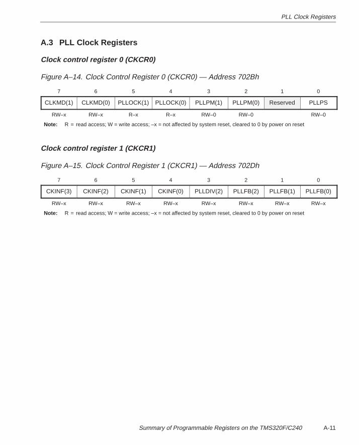
PLL Clock Registers
A-11Summary of Programmable Registers on the TMS320F/C240
A.3 PLL Clock Registers
Clock control register 0 (CKCR0)
Figure A–14. Clock Control Register 0 (CKCR0) — Address 702Bh
7 6 5 4 3 2 1 0
CLKMD(1) CLKMD(0) PLLOCK(1) PLLOCK(0) PLLPM(1) PLLPM(0) Reserved PLLPS
RW–x RW–x R–x R–x RW–0 RW–0 RW–0
Note: R = read access; W = write access; –x = not affected by system reset, cleared to 0 by power on reset
Clock control register 1 (CKCR1)
Figure A–15. Clock Control Register 1 (CKCR1) — Address 702Dh
7 6 5 4 3 2 1 0
CKINF(3) CKINF(2) CKINF(1) CKINF(0) PLLDIV(2) PLLFB(2) PLLFB(1) PLLFB(0)
RW–x RW–x RW–x RW–x RW–x RW–x RW–x RW–x
Note: R = read access; W = write access; –x = not affected by system reset, cleared to 0 by power on reset
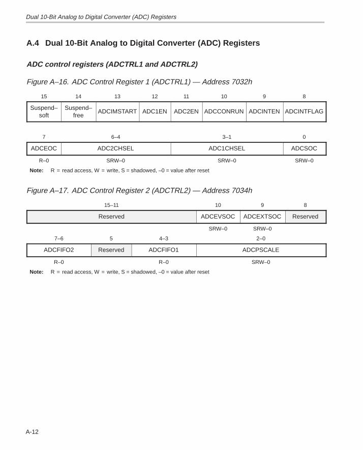
Dual 10-Bit Analog to Digital Converter (ADC) Registers
A-12
A.4 Dual 10-Bit Analog to Digital Converter (ADC) Registers
ADC control registers (ADCTRL1 and ADCTRL2)
Figure A–16. ADC Control Register 1 (ADCTRL1) — Address 7032h
15 14 13 12 11 10 9 8
Suspend–soft
Suspend–free
ADCIMSTART ADC1EN ADC2EN ADCCONRUN ADCINTEN ADCINTFLAG
7 6–4 3–1 0
ADCEOC ADC2CHSEL ADC1CHSEL ADCSOC
R–0 SRW–0 SRW–0 SRW–0
Note: R = read access, W = write, S = shadowed, –0 = value after reset
Figure A–17. ADC Control Register 2 (ADCTRL2) — Address 7034h
15–11 10 9 8
Reserved ADCEVSOC ADCEXTSOC Reserved
SRW–0 SRW–0
7–6 5 4–3 2–0
ADCFIFO2 Reserved ADCFIFO1 ADCPSCALE
R–0 R–0 SRW–0
Note: R = read access, W = write, S = shadowed, –0 = value after reset
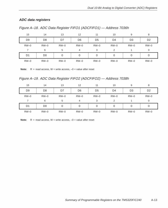
Dual 10-Bit Analog to Digital Converter (ADC) Registers
A-13Summary of Programmable Registers on the TMS320F/C240
ADC data registers
Figure A–18. ADC Data Register FIFO1 (ADCFIFO1) — Address 7036h
15 14 13 12 11 10 9 8
D9 D8 D7 D6 D5 D4 D3 D2
RW–0 RW–0 RW–0 RW–0 RW–0 RW–0 RW–0 RW–0
7 6 5 4 3 2 1 0
D1 D0 0 0 0 0 0 0
RW–0 RW–0 RW–0 RW–0 RW–0 RW–0 RW–0 RW–0
Note: R = read access, W = write access, –0 = value after reset
Figure A–19. ADC Data Register FIFO2 (ADCFIFO2) — Address 7038h
15 14 13 12 11 10 9 8
D9 D8 D7 D6 D5 D4 D3 D2
RW–0 RW–0 RW–0 RW–0 RW–0 RW–0 RW–0 RW–0
7 6 5 4 3 2 1 0
D1 D0 0 0 0 0 0 0
RW–0 RW–0 RW–0 RW–0 RW–0 RW–0 RW–0 RW–0
Note: R = read access, W = write access, –0 = value after reset
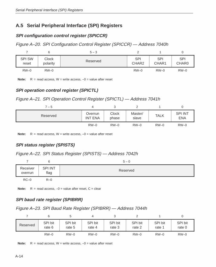
Serial Peripheral Interface (SPI) Registers
A-14
A.5 Serial Peripheral Interface (SPI) Registers
SPI configuration control register (SPICCR)
Figure A–20. SPI Configuration Control Register (SPICCR) — Address 7040h
7 6 5 – 3 2 1 0
SPI SWreset
Clockpolarity
ReservedSPI
CHAR2SPI
CHAR1SPI
CHAR0
RW–0 RW–0 RW–0 RW–0 RW–0
Note: R = read access, W = write access, –0 = value after reset
SPI operation control register (SPICTL)
Figure A–21. SPI Operation Control Register (SPICTL) — Address 7041h
7 – 5 4 3 2 1 0
ReservedOverrunINT ENA
Clockphase
Master/slave
TALKSPI INT
ENA
RW–0 RW–0 RW–0 RW–0 RW–0
Note: R = read access, W = write access, –0 = value after reset
SPI status register (SPISTS)
Figure A–22. SPI Status Register (SPISTS) — Address 7042h
7 6 5 – 0
Receiveroverrun
SPI INTflag
Reserved
RC–0 R–0
Note: R = read access, –0 = value after reset, C = clear
SPI baud rate register (SPIBRR)
Figure A–23. SPI Baud Rate Register (SPIBRR) — Address 7044h
7 6 5 4 3 2 1 0
ReservedSPI bitrate 6
SPI bitrate 5
SPI bitrate 4
SPI bitrate 3
SPI bitrate 2
SPI bitrate 1
SPI bitrate 0
RW–0 RW–0 RW–0 RW–0 RW–0 RW–0 RW–0
Note: R = read access, W = write access, –0 = value after reset
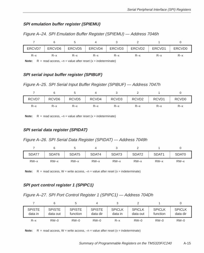
Serial Peripheral Interface (SPI) Registers
A-15Summary of Programmable Registers on the TMS320F/C240
SPI emulation buffer register (SPIEMU)
Figure A–24. SPI Emulation Buffer Register (SPIEMU) — Address 7046h
7 6 5 4 3 2 1 0
ERCVD7 ERCVD6 ERCVD5 ERCVD4 ERCVD3 ERCVD2 ERCVD1 ERCVD0
R–x R–x R–x R–x R–x R–x R–x R–x
Note: R = read access, –n = value after reset (x = indeterminate)
SPI serial input buffer register (SPIBUF)
Figure A–25. SPI Serial Input Buffer Register (SPIBUF) — Address 7047h
7 6 5 4 3 2 1 0
RCVD7 RCVD6 RCVD5 RCVD4 RCVD3 RCVD2 RCVD1 RCVD0
R–x R–x R–x R–x R–x R–x R–x R–x
Note: R = read access, –n = value after reset (x = indeterminate)
SPI serial data register (SPIDAT)
Figure A–26. SPI Serial Data Register (SPIDAT) — Address 7049h
7 6 5 4 3 2 1 0
SDAT7 SDAT6 SDAT5 SDAT4 SDAT3 SDAT2 SDAT1 SDAT0
RW–x RW–x RW–x RW–x RW–x RW–x RW–x RW–x
Note: R = read access, W = write access, –n = value after reset (x = indeterminate)
SPI port control register 1 (SPIPC1)
Figure A–27. SPI Port Control Register 1 (SPIPC1) — Address 704Dh
7 6 5 4 3 2 1 0
SPISTEdata in
SPISTEdata out
SPISTEfunction
SPISTEdata dir
SPICLKdata in
SPICLKdata out
SPICLKfunction
SPICLKdata dir
R–x RW–0 RW–0 RW–0 R–x RW–0 RW–0 RW–0
Note: R = read access, W = write access, –n = value after reset (x = indeterminate)
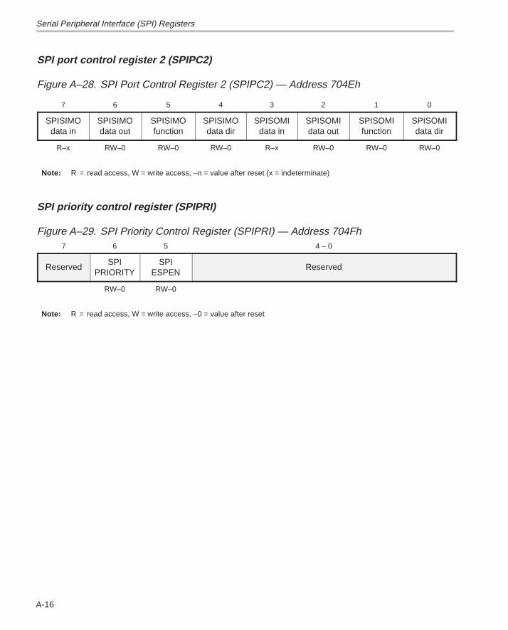
Serial Peripheral Interface (SPI) Registers
A-16
SPI port control register 2 (SPIPC2)
Figure A–28. SPI Port Control Register 2 (SPIPC2) — Address 704Eh
7 6 5 4 3 2 1 0
SPISIMOdata in
SPISIMOdata out
SPISIMOfunction
SPISIMOdata dir
SPISOMIdata in
SPISOMIdata out
SPISOMIfunction
SPISOMIdata dir
R–x RW–0 RW–0 RW–0 R–x RW–0 RW–0 RW–0
Note: R = read access, W = write access, –n = value after reset (x = indeterminate)
SPI priority control register (SPIPRI)
Figure A–29. SPI Priority Control Register (SPIPRI) — Address 704Fh7 6 5 4 – 0
ReservedSPI
PRIORITYSPI
ESPENReserved
RW–0 RW–0
Note: R = read access, W = write access, –0 = value after reset
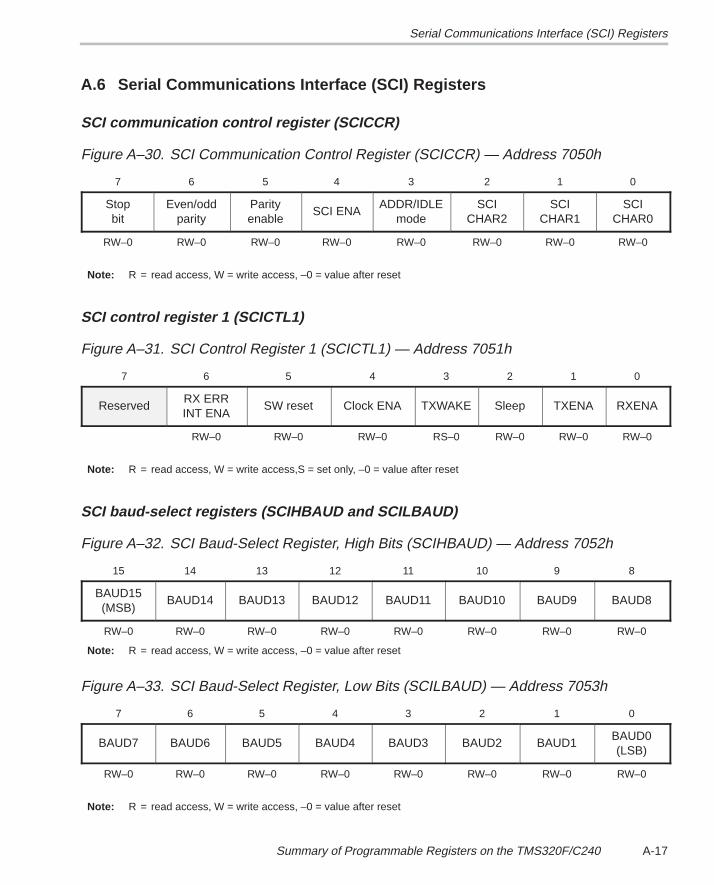
Serial Communications Interface (SCI) Registers
A-17Summary of Programmable Registers on the TMS320F/C240
A.6 Serial Communications Interface (SCI) Registers
SCI communication control register (SCICCR)
Figure A–30. SCI Communication Control Register (SCICCR) — Address 7050h
7 6 5 4 3 2 1 0
Stopbit
Even/oddparity
Parityenable
SCI ENAADDR/IDLE
modeSCI
CHAR2SCI
CHAR1SCI
CHAR0
RW–0 RW–0 RW–0 RW–0 RW–0 RW–0 RW–0 RW–0
Note: R = read access, W = write access, –0 = value after reset
SCI control register 1 (SCICTL1)
Figure A–31. SCI Control Register 1 (SCICTL1) — Address 7051h
7 6 5 4 3 2 1 0
ReservedRX ERRINT ENA
SW reset Clock ENA TXWAKE Sleep TXENA RXENA
RW–0 RW–0 RW–0 RS–0 RW–0 RW–0 RW–0
Note: R = read access, W = write access,S = set only, –0 = value after reset
SCI baud-select registers (SCIHBAUD and SCILBAUD)
Figure A–32. SCI Baud-Select Register, High Bits (SCIHBAUD) — Address 7052h
15 14 13 12 11 10 9 8
BAUD15(MSB)
BAUD14 BAUD13 BAUD12 BAUD11 BAUD10 BAUD9 BAUD8
RW–0 RW–0 RW–0 RW–0 RW–0 RW–0 RW–0 RW–0
Note: R = read access, W = write access, –0 = value after reset
Figure A–33. SCI Baud-Select Register, Low Bits (SCILBAUD) — Address 7053h
7 6 5 4 3 2 1 0
BAUD7 BAUD6 BAUD5 BAUD4 BAUD3 BAUD2 BAUD1BAUD0(LSB)
RW–0 RW–0 RW–0 RW–0 RW–0 RW–0 RW–0 RW–0
Note: R = read access, W = write access, –0 = value after reset
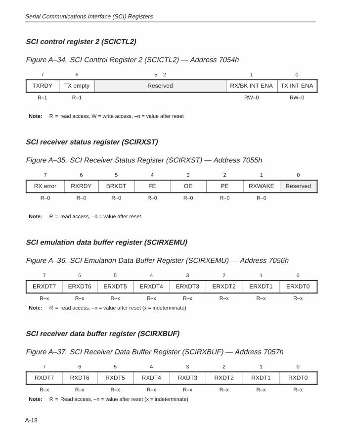
Serial Communications Interface (SCI) Registers
A-18
SCI control register 2 (SCICTL2)
Figure A–34. SCI Control Register 2 (SCICTL2) — Address 7054h
7 6 5 – 2 1 0
TXRDY TX empty Reserved RX/BK INT ENA TX INT ENA
R–1 R–1 RW–0 RW–0
Note: R = read access, W = write access, –n = value after reset
SCI receiver status register (SCIRXST)
Figure A–35. SCI Receiver Status Register (SCIRXST) — Address 7055h
7 6 5 4 3 2 1 0
RX error RXRDY BRKDT FE OE PE RXWAKE Reserved
R–0 R–0 R–0 R–0 R–0 R–0 R–0
Note: R = read access, –0 = value after reset
SCI emulation data buffer register (SCIRXEMU)
Figure A–36. SCI Emulation Data Buffer Register (SCIRXEMU) — Address 7056h
7 6 5 4 3 2 1 0
ERXDT7 ERXDT6 ERXDT5 ERXDT4 ERXDT3 ERXDT2 ERXDT1 ERXDT0
R–x R–x R–x R–x R–x R–x R–x R–x
Note: R = read access, –n = value after reset (x = indeterminate)
SCI receiver data buffer register (SCIRXBUF)
Figure A–37. SCI Receiver Data Buffer Register (SCIRXBUF) — Address 7057h
7 6 5 4 3 2 1 0
RXDT7 RXDT6 RXDT5 RXDT4 RXDT3 RXDT2 RXDT1 RXDT0
R–x R–x R–x R–x R–x R–x R–x R–x
Note: R = Read access, –n = value after reset (x = indeterminate)
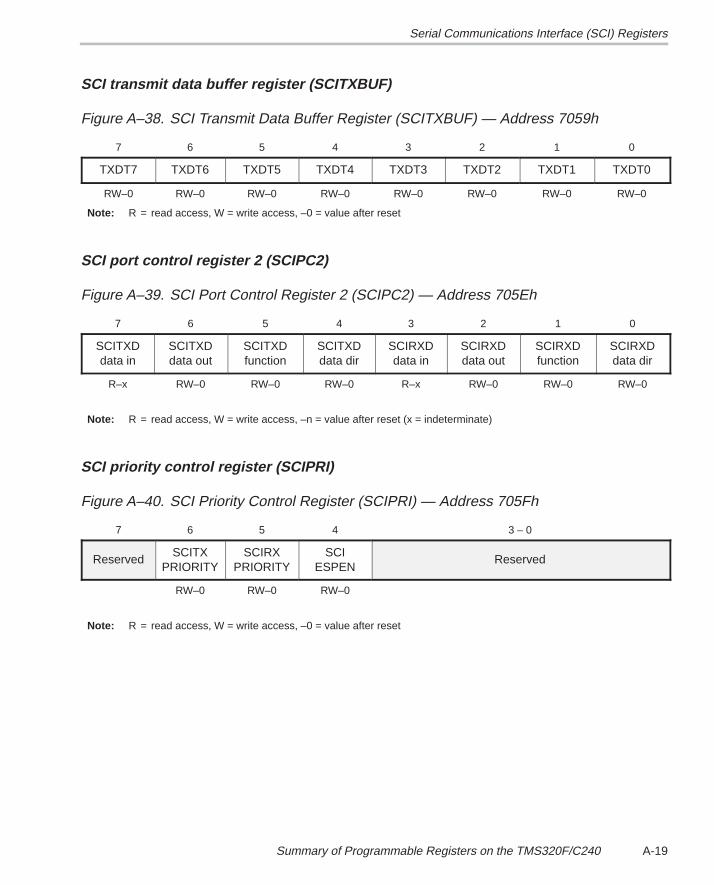
Serial Communications Interface (SCI) Registers
A-19Summary of Programmable Registers on the TMS320F/C240
SCI transmit data buffer register (SCITXBUF)
Figure A–38. SCI Transmit Data Buffer Register (SCITXBUF) — Address 7059h
7 6 5 4 3 2 1 0
TXDT7 TXDT6 TXDT5 TXDT4 TXDT3 TXDT2 TXDT1 TXDT0
RW–0 RW–0 RW–0 RW–0 RW–0 RW–0 RW–0 RW–0
Note: R = read access, W = write access, –0 = value after reset
SCI port control register 2 (SCIPC2)
Figure A–39. SCI Port Control Register 2 (SCIPC2) — Address 705Eh
7 6 5 4 3 2 1 0
SCITXDdata in
SCITXDdata out
SCITXDfunction
SCITXDdata dir
SCIRXDdata in
SCIRXDdata out
SCIRXDfunction
SCIRXDdata dir
R–x RW–0 RW–0 RW–0 R–x RW–0 RW–0 RW–0
Note: R = read access, W = write access, –n = value after reset (x = indeterminate)
SCI priority control register (SCIPRI)
Figure A–40. SCI Priority Control Register (SCIPRI) — Address 705Fh
7 6 5 4 3 – 0
ReservedSCITX
PRIORITYSCIRX
PRIORITYSCI
ESPENReserved
RW–0 RW–0 RW–0
Note: R = read access, W = write access, –0 = value after reset
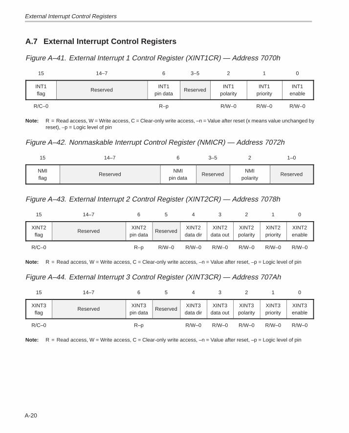
External Interrupt Control Registers
A-20
A.7 External Interrupt Control Registers
Figure A–41. External Interrupt 1 Control Register (XINT1CR) — Address 7070h
15 14–7 6 3–5 2 1 0
INT1flag
ReservedINT1
pin dataReserved
INT1polarity
INT1priority
INT1enable
R/C–0 R–p R/W–0 R/W–0 R/W–0
Note: R = Read access, W = Write access, C = Clear-only write access, –n = Value after reset (x means value unchanged byreset), –p = Logic level of pin
Figure A–42. Nonmaskable Interrupt Control Register (NMICR) — Address 7072h
15 14–7 6 3–5 2 1–0
NMIflag
ReservedNMI
pin dataReserved
NMIpolarity
Reserved
Figure A–43. External Interrupt 2 Control Register (XINT2CR) — Address 7078h
15 14–7 6 5 4 3 2 1 0
XINT2flag
ReservedXINT2
pin dataReserved
XINT2data dir
XINT2data out
XINT2polarity
XINT2priority
XINT2enable
R/C–0 R–p R/W–0 R/W–0 R/W–0 R/W–0 R/W–0 R/W–0
Note: R = Read access, W = Write access, C = Clear-only write access, –n = Value after reset, –p = Logic level of pin
Figure A–44. External Interrupt 3 Control Register (XINT3CR) — Address 707Ah
15 14–7 6 5 4 3 2 1 0
XINT3flag
ReservedXINT3
pin dataReserved
XINT3data dir
XINT3data out
XINT3polarity
XINT3priority
XINT3enable
R/C–0 R–p R/W–0 R/W–0 R/W–0 R/W–0 R/W–0
Note: R = Read access, W = Write access, C = Clear-only write access, –n = Value after reset, –p = Logic level of pin
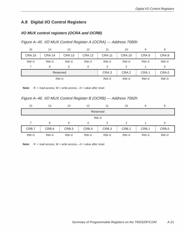
Digital I/O Control Registers
A-21Summary of Programmable Registers on the TMS320F/C240
A.8 Digital I/O Control Registers
I/O MUX control registers (OCRA and OCRB)
Figure A–45. I/O MUX Control Register A (OCRA) — Address 7090h
15 14 13 12 11 10 9 8
CRA.15 CRA.14 CRA.13 CRA.12 CRA.11 CRA.10 CRA.9 CRA.8
RW–0 RW–0 RW–0 RW–0 RW–0 RW–0 RW–0 RW–0
7 6 5 4 3 2 1 0
Reserved CRA.3 CRA.2 CRA.1 CRA.0
RW–0 RW–0 RW–0 RW–0 RW–0
Note: R = read access, W = write access, –0 = value after reset
Figure A–46. I/O MUX Control Register B (OCRB) — Address 7092h
15 14 13 12 11 10 9 8
Reserved
RW–0
7 6 5 4 3 2 1 0
CRB.7 CRB.6 CRB.5 CRB.4 CRB.3 CRB.2 CRB.1 CRB.0
RW–0 RW–0 RW–0 RW–0 RW–0 RW–0 RW–0 RW–0
Note: R = read access, W = write access, –0 = value after reset
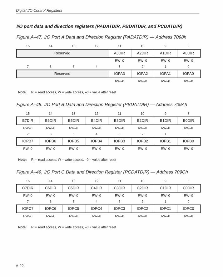
Digital I/O Control Registers
A-22
I/O port data and direction registers (PADATDIR, PBDATDIR, and PCDATDIR)
Figure A–47. I/O Port A Data and Direction Register (PADATDIR) — Address 7098h
15 14 13 12 11 10 9 8
Reserved A3DIR A2DIR A1DIR A0DIR
RW–0 RW–0 RW–0 RW–0
7 6 5 4 3 2 1 0
Reserved IOPA3 IOPA2 IOPA1 IOPA0
RW–0 RW–0 RW–0 RW–0
Note: R = read access, W = write access, –0 = value after reset
Figure A–48. I/O Port B Data and Direction Register (PBDATDIR) — Address 709Ah
15 14 13 12 11 10 9 8
B7DIR B6DIR B5DIR B4DIR B3DIR B2DIR B1DIR B0DIR
RW–0 RW–0 RW–0 RW–0 RW–0 RW–0 RW–0 RW–0
7 6 5 4 3 2 1 0
IOPB7 IOPB6 IOPB5 IOPB4 IOPB3 IOPB2 IOPB1 IOPB0
RW–0 RW–0 RW–0 RW–0 RW–0 RW–0 RW–0 RW–0
Note: R = read access, W = write access, –0 = value after reset
Figure A–49. I/O Port C Data and Direction Register (PCDATDIR) — Address 709Ch
15 14 13 12 11 10 9 8
C7DIR C6DIR C5DIR C4DIR C3DIR C2DIR C1DIR C0DIR
RW–0 RW–0 RW–0 RW–0 RW–0 RW–0 RW–0 RW–0
7 6 5 4 3 2 1 0
IOPC7 IOPC6 IOPC5 IOPC4 IOPC3 IOPC2 IOPC1 IOPC0
RW–0 RW–0 RW–0 RW–0 RW–0 RW–0 RW–0 RW–0
Note: R = read access, W = write access, –0 = value after reset
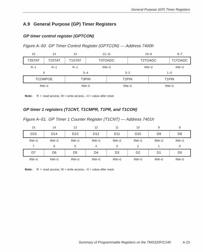
General Purpose (GP) Timer Registers
A-23Summary of Programmable Registers on the TMS320F/C240
A.9 General Purpose (GP) Timer Registers
GP timer control register (GPTCON)
Figure A–50. GP Timer Control Register (GPTCON) — Address 7400h
15 14 13 12–11 10–9 8–7
T3STAT T2STAT T1STAT T3TOADC T2TOADC T1TOADC
R–1 R–1 R–1 RW–0 RW–0 RW–0
6 5–4 3–2 1–0
TCOMPOE T3PIN T2PIN T1PIN
RW–0 RW–0 RW–0 RW–0
Note: R = read access, W = write access, –0 = value after reset
GP timer 1 registers (T1CNT, T1CMPR, T1PR, and T1CON)
Figure A–51. GP Timer 1 Counter Register (T1CNT) — Address 7401h
15 14 13 12 11 10 9 8
D15 D14 D13 D12 D11 D10 D9 D8
RW–0 RW–0 RW–0 RW–0 RW–0 RW–0 RW–0 RW–0
7 6 5 4 3 2 1 0
D7 D6 D5 D4 D3 D2 D1 D0
RW–0 RW–0 RW–0 RW–0 RW–0 RW–0 RW–0 RW–0
Note: R = read access, W = write access, –0 = value after reset
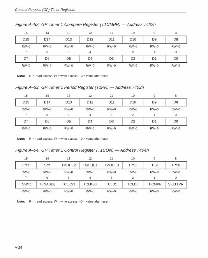
General Purpose (GP) Timer Registers
A-24
Figure A–52. GP Timer 1 Compare Register (T1CMPR) — Address 7402h
15 14 13 12 11 10 9 8
D15 D14 D13 D12 D11 D10 D9 D8
RW–0 RW–0 RW–0 RW–0 RW–0 RW–0 RW–0 RW–0
7 6 5 4 3 2 1 0
D7 D6 D5 D4 D3 D2 D1 D0
RW–0 RW–0 RW–0 RW–0 RW–0 RW–0 RW–0 RW–0
Note: R = read access, W = write access, –0 = value after reset
Figure A–53. GP Timer 1 Period Register (T1PR) — Address 7403h
15 14 13 12 11 10 9 8
D15 D14 D13 D12 D11 D10 D9 D8
RW–0 RW–0 RW–0 RW–0 RW–0 RW–0 RW–0 RW–0
7 6 5 4 3 2 1 0
D7 D6 D5 D4 D3 D2 D1 D0
RW–0 RW–0 RW–0 RW–0 RW–0 RW–0 RW–0 RW–0
Note: R = read access, W = write access, –0 = value after reset
Figure A–54. GP Timer 1 Control Register (T1CON) — Address 7404h
15 14 13 12 11 10 9 8
Free Soft TMODE2 TMODE1 TMODE0 TPS2 TPS1 TPS0
RW–0 RW–0 RW–0 RW–0 RW–0 RW–0 RW–0 RW–0
7 6 5 4 3 2 1 0
TSWT1 TENABLE TCLKS1 TCLKS0 TCLD1 TCLD0 TECMPR SELT1PR
RW–0 RW–0 RW–0 RW–0 RW–0 RW–0 RW–0 RW–0
Note: R = read access, W = write access, –0 = value after reset
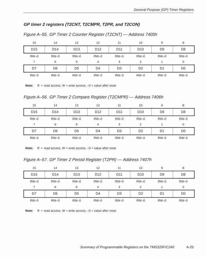
General Purpose (GP) Timer Registers
A-25Summary of Programmable Registers on the TMS320F/C240
GP timer 2 registers (T2CNT, T2CMPR, T2PR, and T2CON)
Figure A–55. GP Timer 2 Counter Register (T2CNT) — Address 7405h
15 14 13 12 11 10 9 8
D15 D14 D13 D12 D11 D10 D9 D8
RW–0 RW–0 RW–0 RW–0 RW–0 RW–0 RW–0 RW–0
7 6 5 4 3 2 1 0
D7 D6 D5 D4 D3 D2 D1 D0
RW–0 RW–0 RW–0 RW–0 RW–0 RW–0 RW–0 RW–0
Note: R = read access, W = write access, –0 = value after reset
Figure A–56. GP Timer 2 Compare Register (T2CMPR) — Address 7406h
15 14 13 12 11 10 9 8
D15 D14 D13 D12 D11 D10 D9 D8
RW–0 RW–0 RW–0 RW–0 RW–0 RW–0 RW–0 RW–0
7 6 5 4 3 2 1 0
D7 D6 D5 D4 D3 D2 D1 D0
RW–0 RW–0 RW–0 RW–0 RW–0 RW–0 RW–0 RW–0
Note: R = read access, W = write access, –0 = value after reset
Figure A–57. GP Timer 2 Period Register (T2PR) — Address 7407h
15 14 13 12 11 10 9 8
D15 D14 D13 D12 D11 D10 D9 D8
RW–0 RW–0 RW–0 RW–0 RW–0 RW–0 RW–0 RW–0
7 6 5 4 3 2 1 0
D7 D6 D5 D4 D3 D2 D1 D0
RW–0 RW–0 RW–0 RW–0 RW–0 RW–0 RW–0 RW–0
Note: R = read access, W = write access, –0 = value after reset
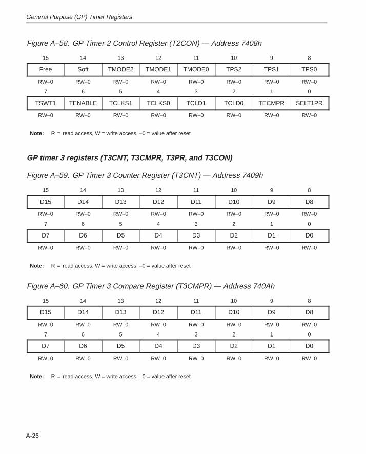
General Purpose (GP) Timer Registers
A-26
Figure A–58. GP Timer 2 Control Register (T2CON) — Address 7408h
15 14 13 12 11 10 9 8
Free Soft TMODE2 TMODE1 TMODE0 TPS2 TPS1 TPS0
RW–0 RW–0 RW–0 RW–0 RW–0 RW–0 RW–0 RW–0
7 6 5 4 3 2 1 0
TSWT1 TENABLE TCLKS1 TCLKS0 TCLD1 TCLD0 TECMPR SELT1PR
RW–0 RW–0 RW–0 RW–0 RW–0 RW–0 RW–0 RW–0
Note: R = read access, W = write access, –0 = value after reset
GP timer 3 registers (T3CNT, T3CMPR, T3PR, and T3CON)
Figure A–59. GP Timer 3 Counter Register (T3CNT) — Address 7409h
15 14 13 12 11 10 9 8
D15 D14 D13 D12 D11 D10 D9 D8
RW–0 RW–0 RW–0 RW–0 RW–0 RW–0 RW–0 RW–0
7 6 5 4 3 2 1 0
D7 D6 D5 D4 D3 D2 D1 D0
RW–0 RW–0 RW–0 RW–0 RW–0 RW–0 RW–0 RW–0
Note: R = read access, W = write access, –0 = value after reset
Figure A–60. GP Timer 3 Compare Register (T3CMPR) — Address 740Ah
15 14 13 12 11 10 9 8
D15 D14 D13 D12 D11 D10 D9 D8
RW–0 RW–0 RW–0 RW–0 RW–0 RW–0 RW–0 RW–0
7 6 5 4 3 2 1 0
D7 D6 D5 D4 D3 D2 D1 D0
RW–0 RW–0 RW–0 RW–0 RW–0 RW–0 RW–0 RW–0
Note: R = read access, W = write access, –0 = value after reset
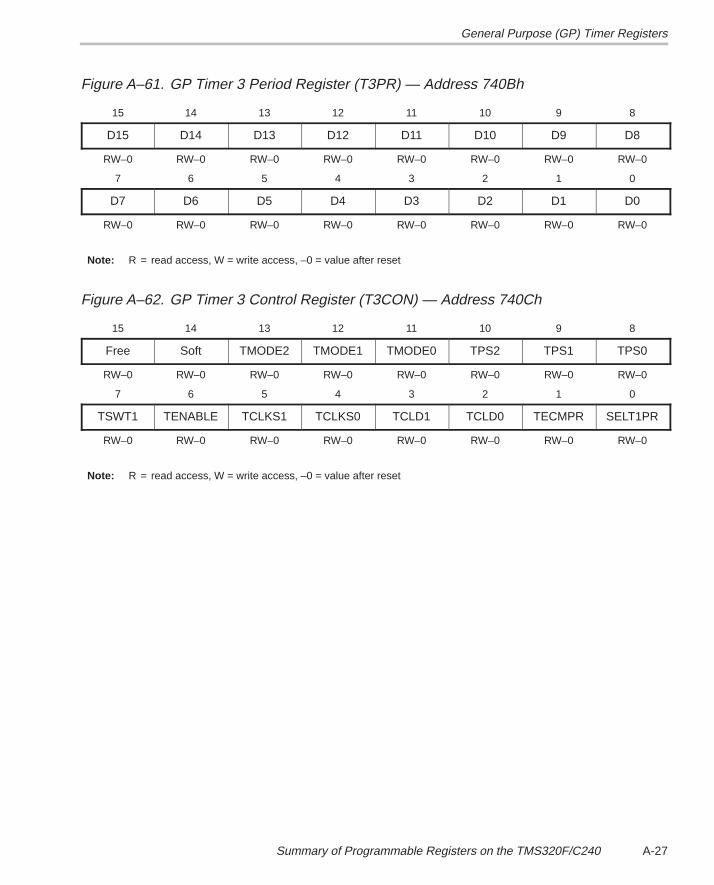
General Purpose (GP) Timer Registers
A-27Summary of Programmable Registers on the TMS320F/C240
Figure A–61. GP Timer 3 Period Register (T3PR) — Address 740Bh
15 14 13 12 11 10 9 8
D15 D14 D13 D12 D11 D10 D9 D8
RW–0 RW–0 RW–0 RW–0 RW–0 RW–0 RW–0 RW–0
7 6 5 4 3 2 1 0
D7 D6 D5 D4 D3 D2 D1 D0
RW–0 RW–0 RW–0 RW–0 RW–0 RW–0 RW–0 RW–0
Note: R = read access, W = write access, –0 = value after reset
Figure A–62. GP Timer 3 Control Register (T3CON) — Address 740Ch
15 14 13 12 11 10 9 8
Free Soft TMODE2 TMODE1 TMODE0 TPS2 TPS1 TPS0
RW–0 RW–0 RW–0 RW–0 RW–0 RW–0 RW–0 RW–0
7 6 5 4 3 2 1 0
TSWT1 TENABLE TCLKS1 TCLKS0 TCLD1 TCLD0 TECMPR SELT1PR
RW–0 RW–0 RW–0 RW–0 RW–0 RW–0 RW–0 RW–0
Note: R = read access, W = write access, –0 = value after reset
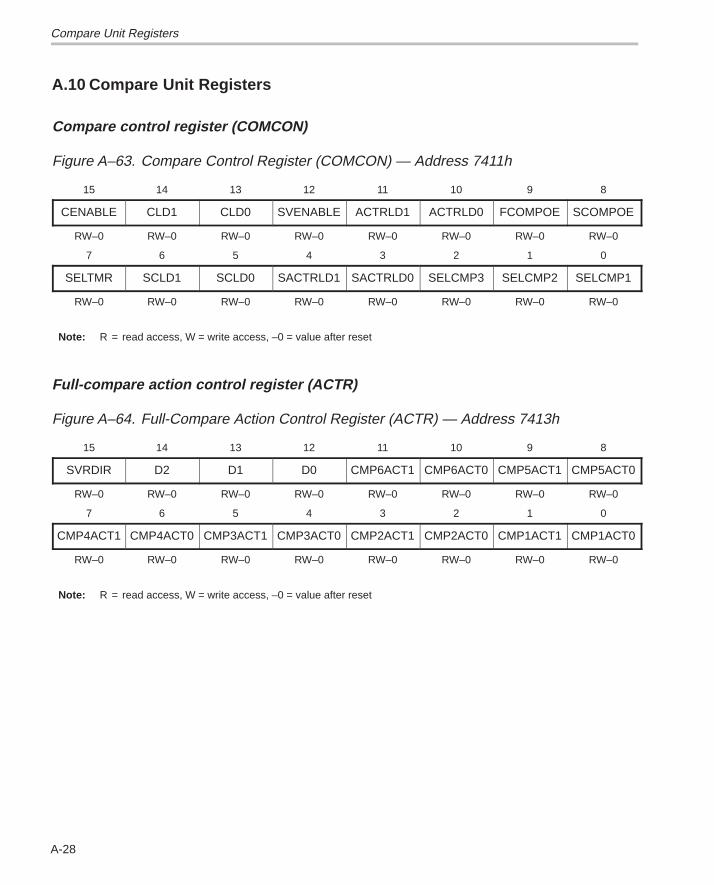
Compare Unit Registers
A-28
A.10 Compare Unit Registers
Compare control register (COMCON)
Figure A–63. Compare Control Register (COMCON) — Address 7411h
15 14 13 12 11 10 9 8
CENABLE CLD1 CLD0 SVENABLE ACTRLD1 ACTRLD0 FCOMPOE SCOMPOE
RW–0 RW–0 RW–0 RW–0 RW–0 RW–0 RW–0 RW–0
7 6 5 4 3 2 1 0
SELTMR SCLD1 SCLD0 SACTRLD1 SACTRLD0 SELCMP3 SELCMP2 SELCMP1
RW–0 RW–0 RW–0 RW–0 RW–0 RW–0 RW–0 RW–0
Note: R = read access, W = write access, –0 = value after reset
Full-compare action control register (ACTR)
Figure A–64. Full-Compare Action Control Register (ACTR) — Address 7413h
15 14 13 12 11 10 9 8
SVRDIR D2 D1 D0 CMP6ACT1 CMP6ACT0 CMP5ACT1 CMP5ACT0
RW–0 RW–0 RW–0 RW–0 RW–0 RW–0 RW–0 RW–0
7 6 5 4 3 2 1 0
CMP4ACT1 CMP4ACT0 CMP3ACT1 CMP3ACT0 CMP2ACT1 CMP2ACT0 CMP1ACT1 CMP1ACT0
RW–0 RW–0 RW–0 RW–0 RW–0 RW–0 RW–0 RW–0
Note: R = read access, W = write access, –0 = value after reset
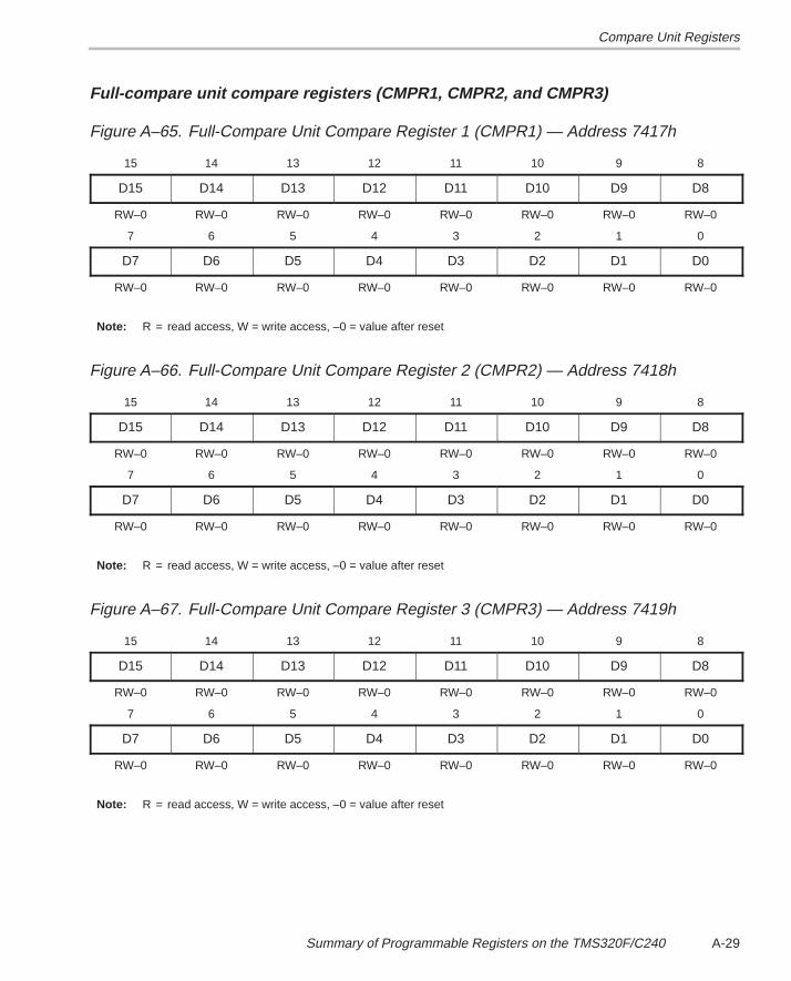
Compare Unit Registers
A-29Summary of Programmable Registers on the TMS320F/C240
Full-compare unit compare registers (CMPR1, CMPR2, and CMPR3)
Figure A–65. Full-Compare Unit Compare Register 1 (CMPR1) — Address 7417h
15 14 13 12 11 10 9 8
D15 D14 D13 D12 D11 D10 D9 D8
RW–0 RW–0 RW–0 RW–0 RW–0 RW–0 RW–0 RW–0
7 6 5 4 3 2 1 0
D7 D6 D5 D4 D3 D2 D1 D0
RW–0 RW–0 RW–0 RW–0 RW–0 RW–0 RW–0 RW–0
Note: R = read access, W = write access, –0 = value after reset
Figure A–66. Full-Compare Unit Compare Register 2 (CMPR2) — Address 7418h
15 14 13 12 11 10 9 8
D15 D14 D13 D12 D11 D10 D9 D8
RW–0 RW–0 RW–0 RW–0 RW–0 RW–0 RW–0 RW–0
7 6 5 4 3 2 1 0
D7 D6 D5 D4 D3 D2 D1 D0
RW–0 RW–0 RW–0 RW–0 RW–0 RW–0 RW–0 RW–0
Note: R = read access, W = write access, –0 = value after reset
Figure A–67. Full-Compare Unit Compare Register 3 (CMPR3) — Address 7419h
15 14 13 12 11 10 9 8
D15 D14 D13 D12 D11 D10 D9 D8
RW–0 RW–0 RW–0 RW–0 RW–0 RW–0 RW–0 RW–0
7 6 5 4 3 2 1 0
D7 D6 D5 D4 D3 D2 D1 D0
RW–0 RW–0 RW–0 RW–0 RW–0 RW–0 RW–0 RW–0
Note: R = read access, W = write access, –0 = value after reset

Compare Unit Registers
A-30
Simple-compare action control register (SACTR)
Figure A–68. Simple-Compare Action Control Register (SACTR) — Address 7414h
15–8
Reserved
7–6 5 4 3 2 1 0
Reserved SCMP3ACT1 SCMP3ACT0 SCMP2ACT1 SCMP2ACT0 SCMP1ACT1 SCMP1ACT0
RW–0 RW–0 RW–0 RW–0 RW–0 RW–0
Note: R = read access, W = write access, –0 = value after reset
Simple-compare unit compare registers (SCMPR1, SCMPR2, and SCMPR3)
Figure A–69. Simple-Compare Unit Compare Register 1 (SCMPR1) — Address 741Ah
15 14 13 12 11 10 9 8
D15 D14 D13 D12 D11 D10 D9 D8
RW–0 RW–0 RW–0 RW–0 RW–0 RW–0 RW–0 RW–0
7 6 5 4 3 2 1 0
D7 D6 D5 D4 D3 D2 D1 D0
RW–0 RW–0 RW–0 RW–0 RW–0 RW–0 RW–0 RW–0
Note: R = read access, W = write access, –0 = value after reset
Figure A–70. Simple-Compare Unit Compare Register 2 (SCMPR2) — Address 741Bh
15 14 13 12 11 10 9 8
D15 D14 D13 D12 D11 D10 D9 D8
RW–0 RW–0 RW–0 RW–0 RW–0 RW–0 RW–0 RW–0
7 6 5 4 3 2 1 0
D7 D6 D5 D4 D3 D2 D1 D0
RW–0 RW–0 RW–0 RW–0 RW–0 RW–0 RW–0 RW–0
Note: R = read access, W = write access, –0 = value after reset
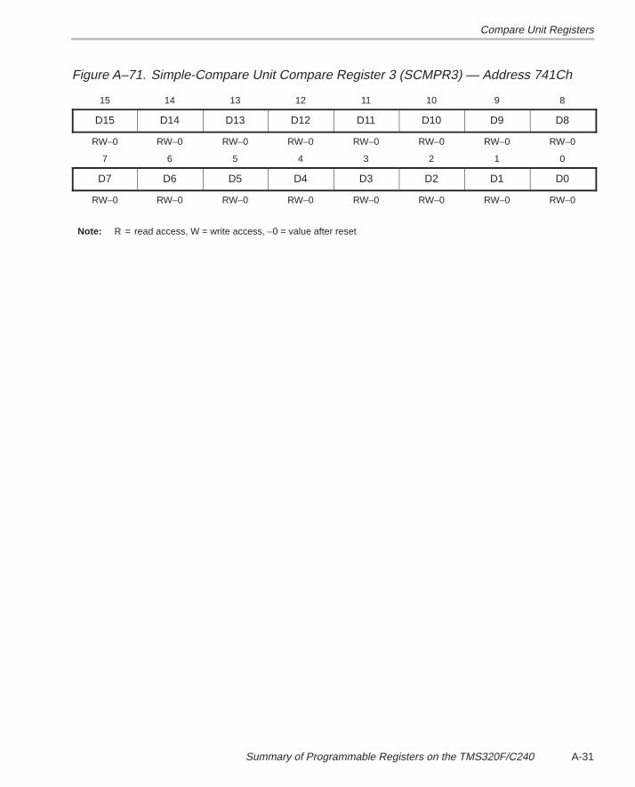
Compare Unit Registers
A-31Summary of Programmable Registers on the TMS320F/C240
Figure A–71. Simple-Compare Unit Compare Register 3 (SCMPR3) — Address 741Ch
15 14 13 12 11 10 9 8
D15 D14 D13 D12 D11 D10 D9 D8
RW–0 RW–0 RW–0 RW–0 RW–0 RW–0 RW–0 RW–0
7 6 5 4 3 2 1 0
D7 D6 D5 D4 D3 D2 D1 D0
RW–0 RW–0 RW–0 RW–0 RW–0 RW–0 RW–0 RW–0
Note: R = read access, W = write access, –0 = value after reset
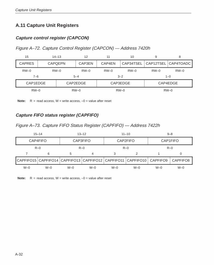
Capture Unit Registers
A-32
A.11 Capture Unit Registers
Capture control register (CAPCON)
Figure A–72. Capture Control Register (CAPCON) — Address 7420h
15 14–13 12 11 10 9 8
CAPRES CAPQEPN CAP3EN CAP4EN CAP34TSEL CAP12TSEL CAP4TOADC
RW–0 RW–0 RW–0 RW–0 RW–0 RW–0 RW–0
7–6 5–4 3–2 1–0
CAP1EDGE CAP2EDGE CAP3EDGE CAP4EDGE
RW–0 RW–0 RW–0 RW–0
Note: R = read access, W = write access, –0 = value after reset
Capture FIFO status register (CAPFIFO)
Figure A–73. Capture FIFO Status Register (CAPFIFO) — Address 7422h
15–14 13–12 11–10 9–8
CAP4FIFO CAP3FIFO CAP2FIFO CAP1FIFO
R–0 R–0 R–0 R–0
7 6 5 4 3 2 1 0
CAPFIFO15 CAPFIFO14 CAPFIFO13 CAPFIFO12 CAPFIFO11 CAPFIFO10 CAPFIFO9 CAPFIFO8
W–0 W–0 W–0 W–0 W–0 W–0 W–0 W–0
Note: R = read access, W = write access, –0 = value after reset
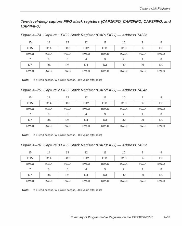
Capture Unit Registers
A-33Summary of Programmable Registers on the TMS320F/C240
Two-level-deep capture FIFO stack registers (CAP1FIFO, CAP2FIFO, CAP3FIFO, andCAP4FIFO)
Figure A–74. Capture 1 FIFO Stack Register (CAP1FIFO) — Address 7423h
15 14 13 12 11 10 9 8
D15 D14 D13 D12 D11 D10 D9 D8
RW–0 RW–0 RW–0 RW–0 RW–0 RW–0 RW–0 RW–0
7 6 5 4 3 2 1 0
D7 D6 D5 D4 D3 D2 D1 D0
RW–0 RW–0 RW–0 RW–0 RW–0 RW–0 RW–0 RW–0
Note: R = read access, W = write access, –0 = value after reset
Figure A–75. Capture 2 FIFO Stack Register (CAP2FIFO) — Address 7424h
15 14 13 12 11 10 9 8
D15 D14 D13 D12 D11 D10 D9 D8
RW–0 RW–0 RW–0 RW–0 RW–0 RW–0 RW–0 RW–0
7 6 5 4 3 2 1 0
D7 D6 D5 D4 D3 D2 D1 D0
RW–0 RW–0 RW–0 RW–0 RW–0 RW–0 RW–0 RW–0
Note: R = read access, W = write access, –0 = value after reset
Figure A–76. Capture 3 FIFO Stack Register (CAP3FIFO) — Address 7425h
15 14 13 12 11 10 9 8
D15 D14 D13 D12 D11 D10 D9 D8
RW–0 RW–0 RW–0 RW–0 RW–0 RW–0 RW–0 RW–0
7 6 5 4 3 2 1 0
D7 D6 D5 D4 D3 D2 D1 D0
RW–0 RW–0 RW–0 RW–0 RW–0 RW–0 RW–0 RW–0
Note: R = read access, W = write access, –0 = value after reset
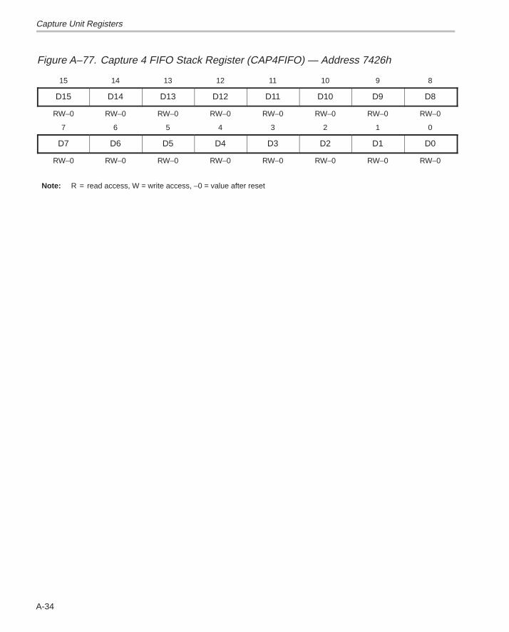
Capture Unit Registers
A-34
Figure A–77. Capture 4 FIFO Stack Register (CAP4FIFO) — Address 7426h
15 14 13 12 11 10 9 8
D15 D14 D13 D12 D11 D10 D9 D8
RW–0 RW–0 RW–0 RW–0 RW–0 RW–0 RW–0 RW–0
7 6 5 4 3 2 1 0
D7 D6 D5 D4 D3 D2 D1 D0
RW–0 RW–0 RW–0 RW–0 RW–0 RW–0 RW–0 RW–0
Note: R = read access, W = write access, –0 = value after reset
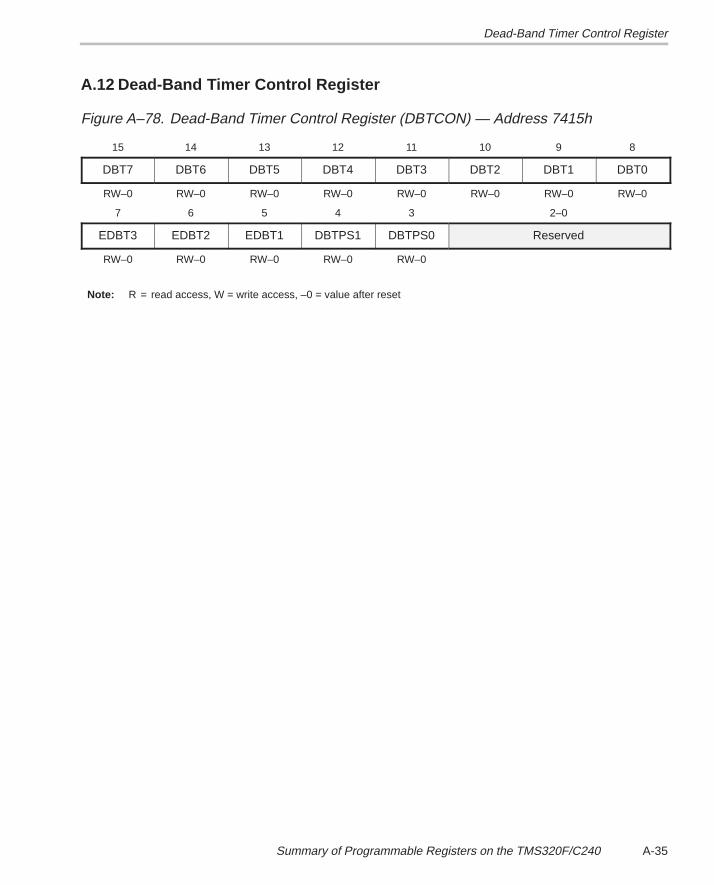
Dead-Band Timer Control Register
A-35Summary of Programmable Registers on the TMS320F/C240
A.12 Dead-Band Timer Control Register
Figure A–78. Dead-Band Timer Control Register (DBTCON) — Address 7415h
15 14 13 12 11 10 9 8
DBT7 DBT6 DBT5 DBT4 DBT3 DBT2 DBT1 DBT0
RW–0 RW–0 RW–0 RW–0 RW–0 RW–0 RW–0 RW–0
7 6 5 4 3 2–0
EDBT3 EDBT2 EDBT1 DBTPS1 DBTPS0 Reserved
RW–0 RW–0 RW–0 RW–0 RW–0
Note: R = read access, W = write access, –0 = value after reset
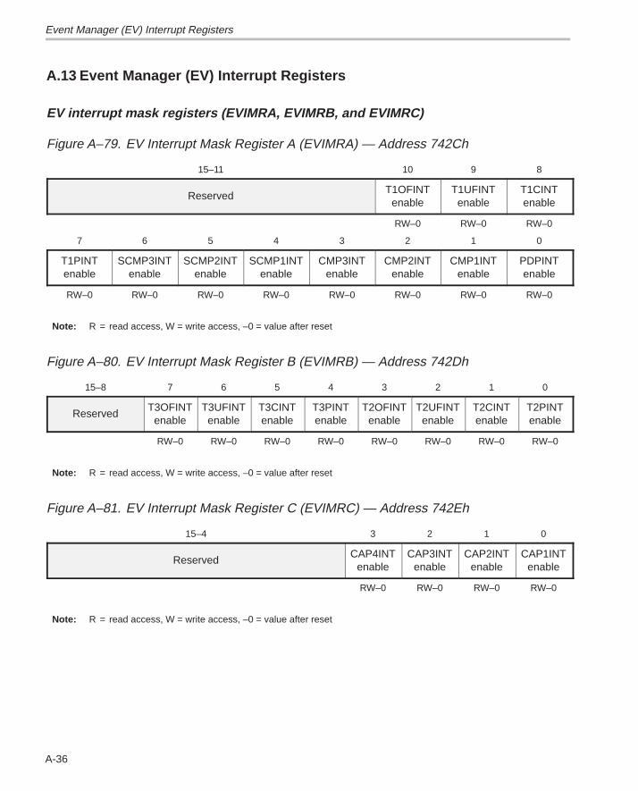
Event Manager (EV) Interrupt Registers
A-36
A.13 Event Manager (EV) Interrupt Registers
EV interrupt mask registers (EVIMRA, EVIMRB, and EVIMRC)
Figure A–79. EV Interrupt Mask Register A (EVIMRA) — Address 742Ch
15–11 10 9 8
ReservedT1OFINT
enableT1UFINT
enableT1CINTenable
RW–0 RW–0 RW–0
7 6 5 4 3 2 1 0
T1PINTenable
SCMP3INTenable
SCMP2INTenable
SCMP1INTenable
CMP3INTenable
CMP2INTenable
CMP1INTenable
PDPINTenable
RW–0 RW–0 RW–0 RW–0 RW–0 RW–0 RW–0 RW–0
Note: R = read access, W = write access, –0 = value after reset
Figure A–80. EV Interrupt Mask Register B (EVIMRB) — Address 742Dh
15–8 7 6 5 4 3 2 1 0
ReservedT3OFINT
enableT3UFINT
enableT3CINTenable
T3PINTenable
T2OFINTenable
T2UFINTenable
T2CINTenable
T2PINTenable
RW–0 RW–0 RW–0 RW–0 RW–0 RW–0 RW–0 RW–0
Note: R = read access, W = write access, –0 = value after reset
Figure A–81. EV Interrupt Mask Register C (EVIMRC) — Address 742Eh
15–4 3 2 1 0
ReservedCAP4INT
enableCAP3INT
enableCAP2INT
enableCAP1INT
enable
RW–0 RW–0 RW–0 RW–0
Note: R = read access, W = write access, –0 = value after reset
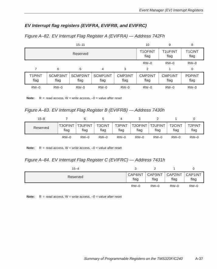
Event Manager (EV) Interrupt Registers
A-37Summary of Programmable Registers on the TMS320F/C240
EV Interrupt flag registers (EVIFRA, EVIFRB, and EVIFRC)
Figure A–82. EV Interrupt Flag Register A (EVIFRA) — Address 742Fh
15–11 10 9 8
ReservedT1OFINT
flagT1UFINT
flagT1CINT
flag
RW–0 RW–0 RW–0
7 6 5 4 3 2 1 0
T1PINTflag
SCMP3INTflag
SCMP2INTflag
SCMP1INTflag
CMP3INTflag
CMP2INTflag
CMP1INTflag
PDPINTflag
RW–0 RW–0 RW–0 RW–0 RW–0 RW–0 RW–0 RW–0
Note: R = read access, W = write access, –0 = value after reset
Figure A–83. EV Interrupt Flag Register B (EVIFRB) — Address 7430h
15–8 7 6 5 4 3 2 1 0
ReservedT3OFINT
flagT3UFINT
flagT3CINT
flagT3PINT
flagT2OFINT
flagT2UFINT
flagT2CINT
flagT2PINT
flag
RW–0 RW–0 RW–0 RW–0 RW–0 RW–0 RW–0 RW–0
Note: R = read access, W = write access, –0 = value after reset
Figure A–84. EV Interrupt Flag Register C (EVIFRC) — Address 7431h
15–4 3 2 1 0
ReservedCAP4INT
flagCAP3INT
flagCAP2INT
flagCAP1INT
flag
RW–0 RW–0 RW–0 RW–0
Note: R = read access, W = write access, –0 = value after reset

Event Manager (EV) Interrupt Registers
A-38
EV interrupt vector registers (EVIVRA, EVIVRB, and EVIVRC)
Figure A–85. EV Interrupt Vector Register A (EVIVRA) — Address 7432h
15 14 13 12 11 10 9 8 7 6 5 4 3 2 1 0
0 0 0 0 0 0 0 0 0 0 D5 D4 D3 D2 D1 D0
R–0 R–0 R–0 R–0 R–0 R–0 R–0 R–0 R–0 R–0 R–0 R–0 R–0 R–0 R–0 R–0
Note: R = read access, W = write access, –0 = value after reset
Figure A–86. EV Interrupt Vector Register B (EVIVRB) — Address 7433h
15 14 13 12 11 10 9 8 7 6 5 4 3 2 1 0
0 0 0 0 0 0 0 0 0 0 D5 D4 D3 D2 D1 D0
R–0 R–0 R–0 R–0 R–0 R–0 R–0 R–0 R–0 R–0 R–0 R–0 R–0 R–0 R–0 R–0
Note: R = read access, W = write access, –0 = value after reset
Figure A–87. EV Interrupt Vector Register C (EVIVRC) — Address 7434h
15 14 13 12 11 10 9 8 7 6 5 4 3 2 1 0
0 0 0 0 0 0 0 0 0 0 D5 D4 D3 D2 D1 D0
R–0 R–0 R–0 R–0 R–0 R–0 R–0 R–0 R–0 R–0 R–0 R–0 R–0 R–0 R–0 R–0
Note: R = read access, W = write access, –0 = value after reset
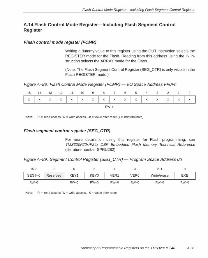
Flash Control Mode Register—Including Flash Segment Control Register
A-39Summary of Programmable Registers on the TMS320F/C240
A.14 Flash Control Mode Register—Including Flash Segment ControlRegister
Flash control mode register (FCMR)
Writing a dummy value to this register using the OUT instruction selects theREGISTER mode for the Flash. Reading from this address using the IN in-struction selects the ARRAY mode for the Flash.
(Note: The Flash Segment Control Register (SEG_CTR) is only visible in theFlash REGISTER mode.)
Figure A–88. Flash Control Mode Register (FCMR) — I/O Space Address FF0Fh
15 14 13 12 11 10 9 8 7 6 5 4 3 2 1 0
x x x x x x x x x x x x x x x x
RW–x
Note: R = read access, W = write access, –n = value after reset (x = indeterminate)
Flash segment control register (SEG_CTR)
For more details on using this register for Flash programming, seeTMS320F20x/F24x DSP Embedded Flash Memory Technical Reference(literature number SPRU282).
Figure A–89. Segment Control Register (SEG_CTR) — Program Space Address 0h
15–8 7 6 5 4 3 2–1 0
SEG7–0 Reserved KEY1 KEY0 VER1 VER0 Write/erase EXE
RW–0 RW–0 RW–0 RW–0 RW–0 RW–0 RW–0
Note: R = read access, W = write access, –0 = value after reset
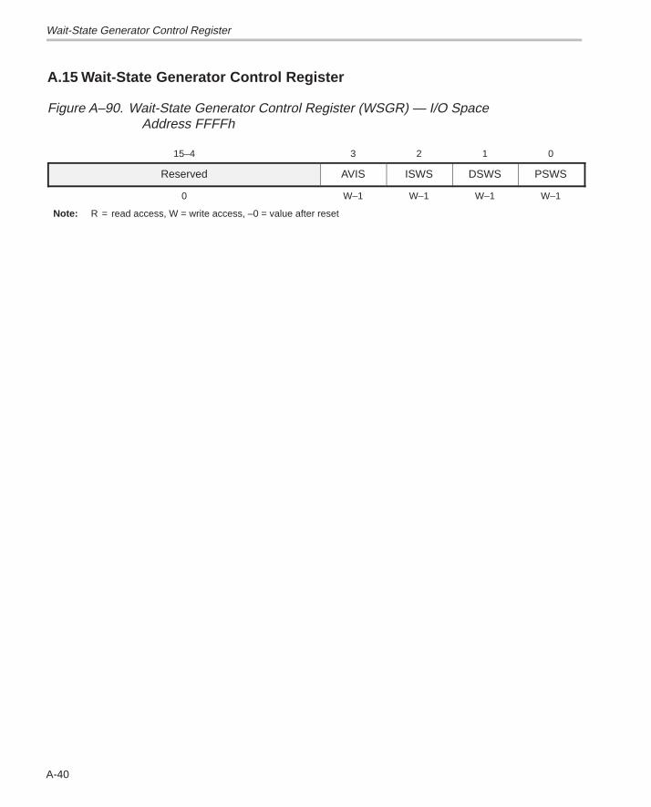
Wait-State Generator Control Register
A-40
A.15 Wait-State Generator Control Register
Figure A–90. Wait-State Generator Control Register (WSGR) — I/O SpaceAddress FFFFh
15–4 3 2 1 0
Reserved AVIS ISWS DSWS PSWS
0 W–1 W–1 W–1 W–1
Note: R = read access, W = write access, –0 = value after reset
B-1
Appendix A
Glossary
AA0–A15: Collectively, the external address bus; the 16 pins are used in par-
allel to address external data memory, program memory, or I/O space.
ACC: See accumulator.
ACCH: Accumulator high word. The upper 16 bits of the accumulator. Seealso accumulator.
ACCL: Accumulator low word. The lower 16 bits of the accumulator. Seealso accumulator.
accumulator: A 32-bit register that stores the results of operations in thecentral arithmetic logic unit (CALU) and provides an input for subsequentCALU operations. The accumulator also performs shift and rotate opera-tions.
address: The location of program code or data stored in memory.
addressing mode: A method by which an instruction interprets its operandsto acquire the data it needs. See also direct addressing; immediateaddressing; indirect addressing.
analog-to-digital (A/D) converter: A circuit that translates an analog signalto a digital signal.
AR: See auxiliary register.
AR0–AR7: Auxiliary registers 0 through 7. See auxiliary register.
ARAU: See auxiliary register arithmetic unit (ARAU).
ARB: See auxiliary register pointer buffer (ARB).
ARP: See auxiliary register pointer (ARP).
auxiliary register: One of eight 16-bit registers (AR7–AR0) used as point-ers to addresses in data space. The registers are operated on by the aux-iliary register arithmetic unit (ARAU) and are selected by the auxiliaryregister pointer (ARP).
Appendix B
Glossary
B-2
auxiliary register arithmetic unit (ARAU): A 16-bit arithmetic unit used toincrement, decrement, or compare the contents of the auxiliary registers.Its primary function is manipulating auxiliary register values for indirectaddressing.
auxiliary register pointer (ARP): A 3-bit field in status register ST0 thatpoints to the current auxiliary register.
auxiliary register pointer buffer (ARB): A 3-bit field in status register ST1that holds the previous value of the auxiliary register pointer (ARP).
B
B0: An on-chip block of dual-access RAM that can be configured as eitherdata memory or program memory, depending on the value of the CNFbit in status register ST1.
B1: An on-chip block of dual-access RAM available for data memory.
B2: An on-chip block of dual-access RAM available for data memory.
BIO pin : A general-purpose input pin that can be tested by conditionalinstructions that cause a branch when an external device drives BIO low.
bit-reversed indexed addressing : A method of indirect addressing thatallows efficient I/O operations by resequencing the data points in aradix-2 fast Fourier transform (FFT) program. The direction of carrypropagation in the ARAU is reversed.
boot loader: A built-in segment of code that transfers code from an externalsource to a 16-bit external program destination at reset.
BR: Bus request pin. This pin is tied to the BR signal, which is asserted whena global data memory access is initiated.
branch: A switching of program control to a nonsequential program-memory address.
Glossary
B-3Glossary
C
C bit: See carry bit.
CALU: See central arithmetic logic unit (CALU).
carry bit: Bit 9 of status register ST1; used by the CALU for extendedarithmetic operations and accumulator shifts and rotates. The carry bitcan be tested by conditional instructions.
central arithmetic logic unit (CALU): The 32-bit wide main arithmetic logicunit for the ’C24x CPU that performs arithmetic and logic operations. Itaccepts 32-bit values for operations, and its 32-bit output is held in theaccumulator.
CLKIN: Input clock signal. A clock source signal supplied to the on-chipclock generator at the CLKIN/X2 pin or generated internally by theon-chip oscillator. The clock generator divides or multiplies CLKIN toproduce the CPU clock signal, CLKOUT1.
CLKOUT: Master clock output signal. The output signal of the on-chip clockgenerator. The CLKOUT1 high pulse signifies the CPU’s logic phase(when internal values are changed), and the CLKOUT1 low pulsesignifies the CPU’s latch phase (when the values are held constant).
clock mode (clock generator): One of the modes which sets the internalCPU clock frequency to a fraction or multiple of the frequency of the inputclock signal CLKIN.
CNF bit: DARAM configuration bit. Bit 12 in status register ST1. CNF is usedto determine whether the on-chip RAM block B0 is mapped to programspace or data space.
codec: A device that codes in one direction of transmission and decodes inanother direction of transmission.
COFF: Common object file format. A system of files configured according toa standard developed by AT&T. These files are relocatable in memoryspace.
context saving/restoring : Saving the system status when the deviceenters a subroutine (such as an interrupt service routine) and restoringthe system status when exiting the subroutine. On the ’C24x, only theprogram counter value is saved and restored automatically; othercontext saving and restoring must be performed by the subroutine.
Glossary
B-4
CPU: Central processing unit. The ’C24x CPU is the portion of the processorinvolved in arithmetic, shifting, and Boolean logic operations, as well asthe generation of data- and program-memory addresses. The CPUincludes the central arithmetic logic unit (CALU), the multiplier, and theauxiliary register arithmetic unit (ARAU).
CPU cycle: The time required for the CPU to go through one logic phase(during which internal values are changed) and one latch phase (duringwhich the values are held constant).
current AR: See current auxiliary register.
current auxiliary register: The auxiliary register pointed to by the auxiliaryregister pointer (ARP). The auxiliary registers are AR0 (ARP = 0)through AR7 (ARP = 7). See also auxiliary register; next auxiliaryregister.
current data page: The data page indicated by the content of the data pagepointer (DP). See also data page; DP.
D
D0–D15: Collectively, the external data bus; the 16 pins are used in parallelto transfer data between the ’C24x and external data memory, programmemory, or I/O space.
DARAM: Dual-access RAM. RAM that can be accessed twice in a singleCPU clock cycle. For example, your code can read from and write toDARAM in the same clock cycle.
DARAM configuration bit (CNF): See CNF bit.
data-address generation logic: Logic circuitry that generates the address-es for data memory reads and writes. This circuitry, which includes theauxiliary registers and the ARAU, can generate one address permachine cycle. See also program-address generation logic.
data page: One block of 128 words in data memory. Data memory contains512 data pages. Data page 0 is the first page of data memory (addresses0000h–007Fh); data page 511 is the last page (addressesFF80h–FFFFh). See also data page pointer (DP); direct addressing.
data page 0: Addresses 0000h–007Fh in data memory; contains thememory-mapped registers, a reserved test/emulation area for specialinformation transfers, and the scratch-pad RAM block (B2).
Glossary
B-5Glossary
data page pointer (DP): A 9-bit field in status register ST0 that specifieswhich of the 512 data pages is currently selected for direct addressgeneration. When an instruction uses direct addressing to access a data-memory value, the DP provides the nine MSBs of the data-memoryaddress, and the instruction provides the seven LSBs.
data-read address bus (DRAB): A 16-bit internal bus that carries theaddress for each read from data memory.
data read bus (DRDB): A 16-bit internal bus that carries data from datamemory to the CALU and the ARAU.
data-write address bus (DWAB): A 16-bit internal bus that carries theaddress for each write to data memory.
data write bus (DWEB): A 16-bit internal bus that carries data to bothprogram memory and data memory.
decode phase: The phase of the pipeline in which the instruction isdecoded. See also pipeline; instruction-fetch phase; operand-fetchphase; instruction-execute phase.
direct addressing: One of the methods used by an instruction to addressdata-memory. In direct addressing, the data-page pointer (DP) holds thenine MSBs of the address (the current data page), and the instructionword provides the seven LSBs of the address (the offset). See alsoindirect addressing.
DP: See data page pointer (DP).
DRAB: See data-read address bus (DRAB).
DRDB: See data read bus (DRDB).
DS: Data memory select pin. The ’C24x asserts DS to indicate an access toexternal data memory (local or global).
DSWS: Data-space wait-state bit(s). A value in the wait-state generatorcontrol register (WSGR) that determines the number of wait statesapplied to reads from and writes to off-chip data space.
dual-access RAM : See DARAM.
dummy cycle: A CPU cycle in which the CPU intentionally reloads theprogram counter with the same address.
DWAB: See data-write address bus (DWAB).
DWEB: See data write bus (DWEB).

Glossary
B-6
E
execute phase: The fourth phase of the pipeline; the phase in which theinstruction is executed. See also pipeline; instruction-fetch phase;instruction-decode phase; operand-fetch phase.
external interrupt: A hardware interrupt triggered by an external eventsending an input through an interrupt pin.
F
FIFO buffer: First-in, first-out buffer. A portion of memory in which data isstored and then retrieved in the same order in which it was stored. Thesynchronous serial port has two four-word-deep FIFO buffers: one for itstransmit operation and one for its receive operation.
flash memory: Electronically erasable and programmable, nonvolatile(read-only) memory.
G
general-purpose input/output pins: Pins that can be used to accept inputsignals or send output signals. These pins are the input pin BIO, the out-put pin XF, and the GPIO pins.
global data space : One of the four ’C24x address spaces. The global dataspace can be used to share data with other processors within a systemand can serve as additional data space. See also local data space.
GREG: Global memory allocation register. A memory-mapped registerused for specifying the size of the global data memory. Addresses notallocated by the GREG for global data memory are available for localdata memory.
H
hardware interrupt: An interrupt triggered through physical connectionswith on-chip peripherals or external devices.
Glossary
B-7Glossary
Iimmediate addressing: One of the methods for obtaining data values used
by an instruction; the data value is a constant embedded directly into theinstruction word; data memory is not accessed.
immediate operand/immediate value: A constant given as an operand inan instruction that is using immediate addressing.
IMR: See interrupt mask register (IMR).
indirect addressing: One of the methods for obtaining data values used byan instruction. When an instruction uses indirect addressing, datamemory is addressed by the current auxiliary register. See also directaddressing.
input clock signal: See CLKIN.
input shifter: A 16- to 32-bit left barrel shifter that shifts incoming 16-bit datafrom 0 to 16 positions left relative to the 32-bit output.
instruction-decode phase: The second phase of the pipeline; the phase inwhich the instruction is decoded. See also pipeline; instruction-fetchphase; operand-fetch phase; instruction-execute phase.
instruction-execute phase: The fourth phase of the pipeline; the phase inwhich the instruction is executed. See also pipeline; instruction-fetchphase; instruction-decode phase; operand-fetch phase.
instruction-fetch phase: The first phase of the pipeline; the phase in whichthe instruction is fetched from program-memory. See also pipeline;instruction-decode phase; operand-fetch phase; instruction-executephase.
instruction register (IR): A 16-bit register that contains the instructionbeing executed.
instruction word: A 16-bit value representing all or half of an instruction. Aninstruction that is fully represented by 16 bits uses one instruction word.An instruction that must be represented by 32 bits uses two instructionwords (the second word is a constant).
internal interrupt: A hardware interrupt caused by an on-chip peripheral.
interrupt: A signal sent to the CPU that (when not masked or disabled)forces the CPU into a subroutine called an interrupt service routine (ISR).This signal can be triggered by an external device, an on-chip peripheral,or an instruction (INTR, NMI, or TRAP).
Glossary
B-8
interrupt acknowledge signal (IACK ): A signal that indicates an interrupthas been received and that the program counter is fetching the interruptvector that will force the processor into the appropriate interrupt serviceroutine.
interrupt flag register (IFR): A 16-bit memory-mapped register that indi-cates pending interrupts. Read the IFR to identify pending interrupts andwrite to the IFR to clear selected interrupts. Writing a 1 to any IFR flagbit clears that bit to 0.
interrupt latency: The delay between the time an interrupt request is madeand the time it is serviced.
interrupt mask register (IMR): A 16-bit memory-mapped register used tomask external and internal interrupts. Writing a 1 to any IMR bit positionenables the corresponding interrupt (when INTM = 0).
interrupt mode bit (INTM): Bit 9 in status register ST0; either enables allmaskable interrupts that are not masked by the IMR or disables all mask-able interrupts.
interrupt service routine (ISR) : A module of code that is executed inresponse to a hardware or software interrupt.
interrupt trap: See interrupt service routine (ISR).
interrupt vector: A branch instruction that leads the CPU to an interruptservice routine (ISR).
interrupt vector location: An address in program memory where an inter-rupt vector resides. When an interrupt is acknowledged, the CPUbranches to the interrupt vector location and fetches the interrupt vector.
INTM bit: See interrupt mode bit (INTM).
I/O-mapped register: One of the on-chip registers mapped to addresses inI/O (input/output) space. These registers, which include the registers forthe on-chip peripherals, must be accessed with the IN and OUT instruc-tions. See also memory-mapped register.
IR: See instruction register (IR).
IS: I/O space select pin. The ’C24x asserts IS to indicate an access to exter-nal I/O space.
ISR: See interrupt service routine (ISR).
ISWS: I/O-space wait-state bit(s). A value in the wait-state generator controlregister (WSGR) that determines the number of wait states applied toreads from and writes to off-chip I/O space.
Glossary
B-9Glossary
L
latch phase: The phase of a CPU cycle during which internal values are heldconstant. See also logic phase; CLKOUT1.
local data space: The portion of data-memory addresses that are not allo-cated as global by the global memory allocation register (GREG). If noneof the data-memory addresses are allocated for global use, all of dataspace is local. See also global data space.
logic phase: The phase of a CPU cycle during which internal values arechanged. See also latch phase; CLKOUT1.
long-immediate value: A 16-bit constant given as an operand of aninstruction that is using immediate addressing.
LSB : Least significant bit. The lowest order bit in a word. When used in pluralform (LSBs), refers to a specified number of low-order bits, beginningwith the lowest order bit and counting to the left. For example, the fourLSBs of a 16-bit value are bits 0 through 3. See also MSB.
M
machine cycle: See CPU cycle.
maskable interrupt : A hardware interrupt that can be enabled or disabledthrough software. See also nonmaskable interrupt.
master clock output signal: See CLKOUT1.
master phase: See logic phase.
memory-mapped register: One of the on-chip registers mapped toaddresses in data memory. See also I/O-mapped register.
microcomputer mode: A mode in which the on-chip ROM or flash memoryis enabled. This mode is selected with the MP/MC pin. See also MP/MCpin; microprocessor mode.
microprocessor mode: A mode in which the on-chip ROM or flash memoryis disabled. This mode is selected with the MP/MC pin. See also MP/MCpin; microcomputer mode.
microstack (MSTACK): A register used for temporary storage of theprogram counter (PC) value when an instruction needs to use the PC toaddress a second operand.
Glossary
B-10
MIPS: Million instructions per second.
MP/MC pin : A pin that indicates whether the processor is operating in micro-processor mode or microcomputer mode. MP/MC high selects micropro-cessor mode; MP/MC low selects microcomputer mode.
MSB: Most significant bit. The highest order bit in a word. When used inplural form (MSBs), refers to a specified number of high-order bits, begin-ning with the highest order bit and counting to the right. For example, theeight MSBs of a 16-bit value are bits 15 through 8. See also LSB.
MSTACK: See microstack.
multiplier: A part of the CPU that performs 16-bit × 16-bit multiplication andgenerates a 32-bit product. The multiplier operates using either signedor unsigned 2s-complement arithmetic.
Nnext AR: See next auxiliary register.
next auxiliary register: The register that is pointed to by the auxiliary regis-ter pointer (ARP) when an instruction that modifies ARP is finishedexecuting. See also auxiliary register; current auxiliary register.
NMI: A hardware interrupt that uses the same logic as the maskable inter-rupts but cannot be masked. It is often used as a soft reset. See alsomaskable interrupt; nonmaskable interrupt.
nonmaskable interrupt: An interrupt that can be neither masked by theinterrupt mask register (IMR) nor disabled by the INTM bit of statusregister ST0.
NPAR: Next program address register. Part of the program-address genera-tion logic. This register provides the address of the next instruction to theprogram counter (PC), the program address register (PAR), the microstack (MSTACK), or the stack.
Ooperand: A value to be used or manipulated by an instruction; specified in
the instruction.
operand-fetch phase: The third phase of the pipeline; the phase in whichan operand or operands are fetched from memory. See also pipeline;instruction-fetch phase; instruction-decode phase; instruction-executephase.
Glossary
B-11Glossary
output shifter: 32- to 16-bit barrel left shifter. Shifts the 32-bit accumulatoroutput from 0 to 7 bits left for quantization management, and outputseither the 16-bit high or low half of the shifted 32-bit data to the data writebus (DWEB).
OV bit: Overflow flag bit. Bit 12 of status register ST0; indicates whether theresult of an arithmetic operation has exceeded the capacity of theaccumulator.
overflow (in a register): A condition in which the result of an arithmeticoperation exceeds the capacity of the register used to hold that result.
overflow mode: The mode in which an overflow in the accumulator causesthe accumulator to be loaded with a preset value. If the overflow is in thepositive direction, the accumulator is loaded with its most positivenumber. If the overflow is in the negative direction, the accumulator isfilled with its most negative number.
OVM bit: Overflow mode bit. Bit 11 of status register ST0; enables ordisables overflow mode. See also overflow mode.
P
PAB: See program address bus (PAB).
PAR: Program address register. A register that holds the address currentlybeing driven on the program address bus for as many cycles as it takesto complete all memory operations scheduled for the current machinecycle.
PC: See program counter (PC).
PCB: Printed circuit board.
pending interrupt: A maskable interrupt that has been successfullyrequested but is awaiting acknowledgement by the CPU.
pipeline : A method of executing instructions in an assembly line fashion.The ’C24x pipeline has four independent phases. During a given CPUcycle, four different instructions can be active, each at a different stageof completion. See also instruction-fetch phase; instruction-decodephase; operand-fetch phase; instruction-execute phase.
PLL: Phase lock loop circuit.
PM bits: See product shift mode bits (PM).
Glossary
B-12
power-down mode: The mode in which the processor enters a dormantstate and dissipates considerably less power than during normal opera-tion. This mode is initiated by the execution of an IDLE instruction. Duringa power-down mode, all internal contents are maintained so that opera-tion continues unaltered when the power-down mode is terminated. Thecontents of all on-chip RAM also remains unchanged.
PRDB: See program read bus (PRDB).
PREG: See product register (PREG).
product register (PREG): A 32-bit register that holds the results of a multi-ply operation.
product shifter: A 32-bit shifter that performs a 0-, 1-, or 4-bit left shift, ora 6-bit right shift of the multiplier product based on the value of theproduct shift mode bits (PM).
product shift mode: One of four modes (no-shift, shift-left-by-one, shift-left-by-four, or shift-right-by-six) used by the product shifter.
product shift mode bits (PM): Bits 0 and 1 of status register ST1; they iden-tify which of four shift modes (no-shift, left-shift-by-one, left-shift-by-four,or right-shift-by-six) will be used by the product shifter.
program address bus (PAB): A 16-bit internal bus that provides theaddresses for program-memory reads and writes.
program-address generation logic: Logic circuitry that generates theaddresses for program memory reads and writes, and an operandaddress in instructions that require two registers to address operands.This circuitry can generate one address per machine cycle. See alsodata-address generation logic.
program control logic: Logic circuitry that decodes instructions, managesthe pipeline, stores status of operations, and decodes conditionaloperations.
program counter (PC): A register that indicates the location of the nextinstruction to be executed.
program read bus (PRDB): A 16-bit internal bus that carries instructioncode and immediate operands, as well as table information, fromprogram memory to the CPU.
PS: Program select pin. The ’C24x asserts PS to indicate an access to exter-nal program memory.
Glossary
B-13Glossary
PSLWS: Lower program-space wait-state bits. A value in the wait-stategenerator control register (WSGR) that determines the number of waitstates applied to reads from and writes to off-chip lower program space(addresses 0000h–7FFFh). See also PSUWS.
PSUWS: Upper program-space wait-state bits. A value in the wait-stategenerator control register (WSGR) that determines the number of waitstates applied to reads from and writes to off-chip upper program space(addresses 8000h–FFFFh). See also PSLWS.
R
RD: Read select pin. The ’C24x asserts RD to request a read from externalprogram, data, or I/O space. RD can be connected directly to the outputenable pin of an external device.
READY: External device ready pin. Used to create wait states externally.When this pin is driven low, the ’C24x waits one CPU cycle and then testsREADY again. After READY is driven low, the ’C24x does not continueprocessing until READY is driven high.
repeat counter (RPTC): A 16-bit register that counts the number of timesa single instruction is repeated. RPTC is loaded by an RPT instruction.
reset: A way to bring the processor to a known state by setting the registersand control bits to predetermined values and signaling execution to startat address 0000h.
reset pin (RS ): A pin that causes a reset.
reset vector: The interrupt vector for reset.
return address: The address of the instruction to be executed when theCPU returns from a subroutine or interrupt service routine.
RPTC: See repeat counter (RPTC).
RS: Reset pin. When driven low, causes a reset on any ’C24x device.
R/W: Read/write pin. Indicates the direction of transfer between the ’C24xand external program, data, or I/O space.
S
SARAM: Single-access RAM. RAM that can be accessed (read from or writ-ten to) once in a single CPU cycle.
Glossary
B-14
scratch-pad RAM: Another name for DARAM block B2 in data space(32 words).
short-immediate value: An 8-, 9-, or 13-bit constant given as an operandof an instruction that is using immediate addressing.
sign bit: The MSB of a value when it is seen by the CPU to indicate the sign(negative or positive) of the value.
sign extend: Fill the unused high order bits of a register with copies of thesign bit in that register.
sign-extension mode (SXM) bit : Bit 10 of status register ST1; enables ordisables sign extension in the input shifter. It also differentiates betweenlogic and arithmetic shifts of the accumulator.
single-access RAM: See SARAM.
slave phase: See latch phase.
software interrupt: An interrupt caused by the execution of an INTR, NMI,or TRAP instruction.
software stack: A program control feature that allows you to extend thehardware stack into data memory with the PSHD and POPD instructions.The stack can be directly stored and recovered from data memory, oneword at time. This feature is useful for deep subroutine nesting or protec-tion against stack overflow.
ST0 and ST1: See status registers ST0 and ST1.
stack: A block of memory reserved for storing return addresses for subrou-tines and interrupt service routines. The ’C24x stack is 16 bits wide andeight levels deep.
status registers ST0 and ST1: Two 16-bit registers that contain bits fordetermining processor modes, addressing pointer values, and indicatingvarious processor conditions and arithmetic logic results. These regis-ters can be stored into and loaded from data memory, allowing the statusof the machine to be saved and restored for subroutines.
STRB: External access active strobe. The ’C24x asserts STRB during ac-cesses to external program, data, or I/O space.
SXM bit: See sign-extension mode bit (SXM).
Glossary
B-15Glossary
T
TC bit: Test/control flag bit. Bit 11 of status register ST1; stores the resultsof test operations done in the central arithmetic logic unit (CALU) or theauxiliary register arithmetic unit (ARAU). The TC bit can be tested byconditional instructions.
temporary register (TREG): A 16-bit register that holds one of the oper-ands for a multiply operation; the dynamic shift count for the LACT,ADDT, and SUBT instructions; or the dynamic bit position for the BITTinstruction.
TOS: Top of stack. Top level of the 8-level last-in, first-out hardware stack.
TREG: See temporary register (TREG).
TTL: Transistor-to-transistor logic.
V
vector: See interrupt vector.
vector location: See interrupt vector location.
W
wait state : A CLKOUT1 cycle during which the CPU waits when readingfrom or writing to slower external memory.
wait-state generator : An on-chip peripheral that generates a limitednumber of wait states for a given off-chip memory space (program, data,or I/O). Wait states are set in the wait-state generator control register(WSGR).
WE: Write enable pin. The ’C24x asserts WE to request a write to externalprogram, data, or I/O space.
WSGR: Wait-state generator control register. This register, which is mappedto I/O memory, controls the wait-state generator.
X
XF bit: XF-pin status bit. Bit 4 of status register ST1 that is used to read orchange the logic level on the XF pin.

Glossary
B-16
XF pin: External flag pin. A general-purpose output pin whose status can beread or changed by way of the XF bit in status register ST1.
Z
zero fill: A way to fill the unused low or high order bits in a register by insert-ing 0s.
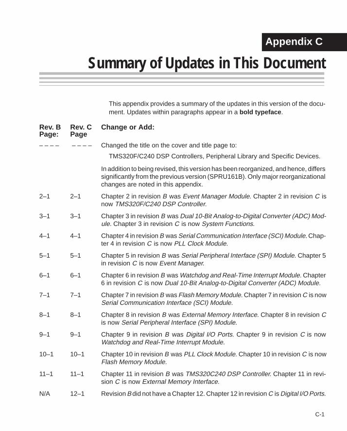
Summary of Updates in This Document
C-1Summary of Updates in This Document
Appendix A
Summary of Updates in This Document
This appendix provides a summary of the updates in this version of the docu-ment. Updates within paragraphs appear in a bold typeface .
Rev. B Rev. C Change or Add:Page: Page
– – – – – – – – Changed the title on the cover and title page to:
TMS320F/C240 DSP Controllers, Peripheral Library and Specific Devices.
In addition to being revised, this version has been reorganized, and hence, differssignificantly from the previous version (SPRU161B). Only major reorganizationalchanges are noted in this appendix.
2–1 2–1 Chapter 2 in revision B was Event Manager Module. Chapter 2 in revision C isnow TMS320F/C240 DSP Controller.
3–1 3–1 Chapter 3 in revision B was Dual 10-Bit Analog-to-Digital Converter (ADC) Mod-ule. Chapter 3 in revision C is now System Functions.
4–1 4–1 Chapter 4 in revision B was Serial Communication Interface (SCI) Module. Chap-ter 4 in revision C is now PLL Clock Module.
5–1 5–1 Chapter 5 in revision B was Serial Peripheral Interface (SPI) Module. Chapter 5in revision C is now Event Manager.
6–1 6–1 Chapter 6 in revision B was Watchdog and Real-Time Interrupt Module. Chapter6 in revision C is now Dual 10-Bit Analog-to-Digital Converter (ADC) Module.
7–1 7–1 Chapter 7 in revision B was Flash Memory Module. Chapter 7 in revision C is nowSerial Communication Interface (SCI) Module.
8–1 8–1 Chapter 8 in revision B was External Memory Interface. Chapter 8 in revision Cis now Serial Peripheral Interface (SPI) Module.
9–1 9–1 Chapter 9 in revision B was Digital I/O Ports. Chapter 9 in revision C is nowWatchdog and Real-Time Interrupt Module.
10–1 10–1 Chapter 10 in revision B was PLL Clock Module. Chapter 10 in revision C is nowFlash Memory Module.
11–1 11–1 Chapter 11 in revision B was TMS320C240 DSP Controller. Chapter 11 in revi-sion C is now External Memory Interface.
N/A 12–1 Revision B did not have a Chapter 12. Chapter 12 in revision C is Digital I/O Ports.
Appendix C
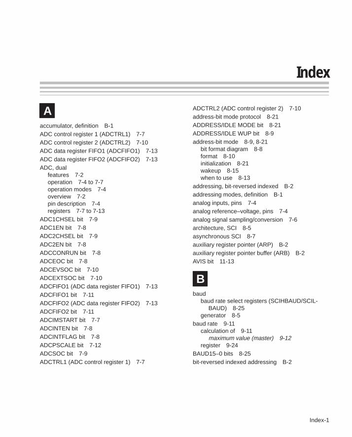
Index
Index-1
Index
Aaccumulator, definition B-1ADC control register 1 (ADCTRL1) 7-7ADC control register 2 (ADCTRL2) 7-10ADC data register FIFO1 (ADCFIFO1) 7-13ADC data register FIFO2 (ADCFIFO2) 7-13ADC, dual
features 7-2operation 7-4 to 7-7operation modes 7-4overview 7-2pin description 7-4registers 7-7 to 7-13
ADC1CHSEL bit 7-9ADC1EN bit 7-8ADC2CHSEL bit 7-9ADC2EN bit 7-8ADCCONRUN bit 7-8ADCEOC bit 7-8ADCEVSOC bit 7-10ADCEXTSOC bit 7-10ADCFIFO1 (ADC data register FIFO1) 7-13ADCFIFO1 bit 7-11ADCFIFO2 (ADC data register FIFO2) 7-13ADCFIFO2 bit 7-11ADCIMSTART bit 7-7ADCINTEN bit 7-8ADCINTFLAG bit 7-8ADCPSCALE bit 7-12ADCSOC bit 7-9ADCTRL1 (ADC control register 1) 7-7
ADCTRL2 (ADC control register 2) 7-10address-bit mode protocol 8-21ADDRESS/IDLE MODE bit 8-21ADDRESS/IDLE WUP bit 8-9address-bit mode 8-9, 8-21
bit format diagram 8-8format 8-10initialization 8-21wakeup 8-15when to use 8-13
addressing, bit-reversed indexed B-2addressing modes, definition B-1analog inputs, pins 7-4analog reference–voltage, pins 7-4analog signal sampling/conversion 7-6architecture, SCI 8-5asynchronous SCI 8-7auxiliary register pointer (ARP) B-2auxiliary register pointer buffer (ARB) B-2AVIS bit 11-13
Bbaud
baud rate select registers (SCIHBAUD/SCIL-BAUD) 8-25
generator 8-5baud rate 9-11
calculation of 9-11maximum value (master) 9-12
register 9-24BAUD15–0 bits 8-25bit-reversed indexed addressing B-2
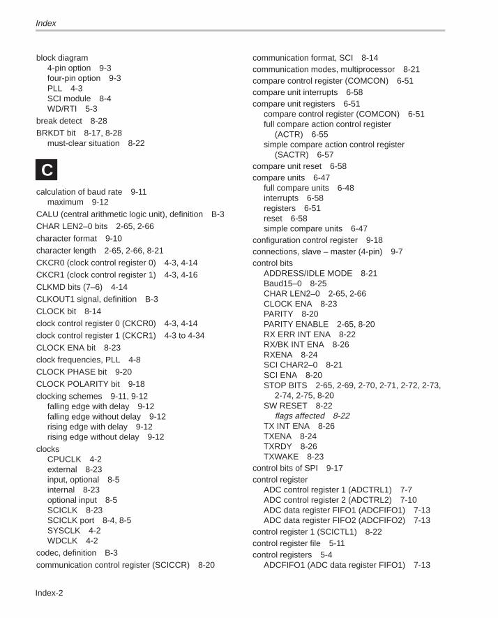
Index
Index-2
block diagram4-pin option 9-3four-pin option 9-3PLL 4-3SCI module 8-4WD/RTI 5-3
break detect 8-28
BRKDT bit 8-17, 8-28must-clear situation 8-22
Ccalculation of baud rate 9-11
maximum 9-12
CALU (central arithmetic logic unit), definition B-3
CHAR LEN2–0 bits 2-65, 2-66
character format 9-10
character length 2-65, 2-66, 8-21
CKCR0 (clock control register 0) 4-3, 4-14
CKCR1 (clock control register 1) 4-3, 4-16
CLKMD bits (7–6) 4-14
CLKOUT1 signal, definition B-3
CLOCK bit 8-14
clock control register 0 (CKCR0) 4-3, 4-14
clock control register 1 (CKCR1) 4-3 to 4-34
CLOCK ENA bit 8-23
clock frequencies, PLL 4-8
CLOCK PHASE bit 9-20
CLOCK POLARITY bit 9-18
clocking schemes 9-11, 9-12falling edge with delay 9-12falling edge without delay 9-12rising edge with delay 9-12rising edge without delay 9-12
clocksCPUCLK 4-2external 8-23input, optional 8-5internal 8-23optional input 8-5SCICLK 8-23SCICLK port 8-4, 8-5SYSCLK 4-2WDCLK 4-2
codec, definition B-3
communication control register (SCICCR) 8-20
communication format, SCI 8-14communication modes, multiprocessor 8-21compare control register (COMCON) 6-51compare unit interrupts 6-58compare unit registers 6-51
compare control register (COMCON) 6-51full compare action control register
(ACTR) 6-55simple compare action control register
(SACTR) 6-57compare unit reset 6-58compare units 6-47
full compare units 6-48interrupts 6-58registers 6-51reset 6-58simple compare units 6-47
configuration control register 9-18connections, slave – master (4-pin) 9-7control bits
ADDRESS/IDLE MODE 8-21Baud15–0 8-25CHAR LEN2–0 2-65, 2-66CLOCK ENA 8-23PARITY 8-20PARITY ENABLE 2-65, 8-20RX ERR INT ENA 8-22RX/BK INT ENA 8-26RXENA 8-24SCI CHAR2–0 8-21SCI ENA 8-20STOP BITS 2-65, 2-69, 2-70, 2-71, 2-72, 2-73,
2-74, 2-75, 8-20SW RESET 8-22
flags affected 8-22TX INT ENA 8-26TXENA 8-24TXRDY 8-26TXWAKE 8-23
control bits of SPI 9-17control register
ADC control register 1 (ADCTRL1) 7-7ADC control register 2 (ADCTRL2) 7-10ADC data register FIFO1 (ADCFIFO1) 7-13ADC data register FIFO2 (ADCFIFO2) 7-13
control register 1 (SCICTL1) 8-22control register file 5-11control registers 5-4
ADCFIFO1 (ADC data register FIFO1) 7-13
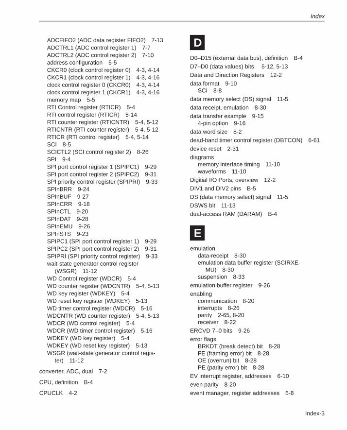
Index
Index-3
ADCFIFO2 (ADC data register FIFO2) 7-13ADCTRL1 (ADC control register 1) 7-7ADCTRL2 (ADC control register 2) 7-10address configuration 5-5CKCR0 (clock control register 0) 4-3, 4-14CKCR1 (clock control register 1) 4-3, 4-16clock control register 0 (CKCR0) 4-3, 4-14clock control register 1 (CKCR1) 4-3, 4-16memory map 5-5RTI Control register (RTICR) 5-4RTI control register (RTICR) 5-14RTI counter register (RTICNTR) 5-4, 5-12RTICNTR (RTI counter register) 5-4, 5-12RTICR (RTI control register) 5-4, 5-14SCI 8-5SCICTL2 (SCI control register 2) 8-26SPI 9-4SPI port control register 1 (SPIPC1) 9-29SPI port control register 2 (SPIPC2) 9-31SPI priority control register (SPIPRI) 9-33SPInBRR 9-24SPInBUF 9-27SPInCRR 9-18SPInCTL 9-20SPInDAT 9-28SPInEMU 9-26SPInSTS 9-23SPIPC1 (SPI port control register 1) 9-29SPIPC2 (SPI port control register 2) 9-31SPIPRI (SPI priority control register) 9-33wait-state generator control register
(WSGR) 11-12WD Control register (WDCR) 5-4WD counter register (WDCNTR) 5-4, 5-13WD key register (WDKEY) 5-4WD reset key register (WDKEY) 5-13WD timer control register (WDCR) 5-16WDCNTR (WD counter register) 5-4, 5-13WDCR (WD control register) 5-4WDCR (WD timer control register) 5-16WDKEY (WD key register) 5-4WDKEY (WD reset key register) 5-13WSGR (wait-state generator control regis-
ter) 11-12
converter, ADC, dual 7-2
CPU, definition B-4
CPUCLK 4-2
DD0–D15 (external data bus), definition B-4
D7–D0 (data values) bits 5-12, 5-13
Data and Direction Registers 12-2
data format 9-10SCI 8-8
data memory select (DS) signal 11-5
data receipt, emulation 8-30
data transfer example 9-154-pin option 9-16
data word size 8-2
dead-band timer control register (DBTCON) 6-61
device reset 2-31
diagramsmemory interface timing 11-10waveforms 11-10
Digitial I/O Ports, overview 12-2
DIV1 and DIV2 pins B-5
DS (data memory select) signal 11-5
DSWS bit 11-13
dual-access RAM (DARAM) B-4
Eemulation
data-receipt 8-30emulation data buffer register (SCIRXE-
MU) 8-30suspension 8-33
emulation buffer register 9-26
enablingcommunication 8-20interrupts 8-26parity 2-65, 8-20receiver 8-22
ERCVD 7–0 bits 9-26
error flagsBRKDT (break detect) bit 8-28FE (framing error) bit 8-28OE (overrun) bit 8-28PE (parity error) bit 8-28
EV interrupt register, addresses 6-10
even parity 8-20
event manager, register addresses 6-8
Index
Index-4
event manager (EV) 6-2block diagram 6-3functional blocks 6-2interrupts 6-6overview 6-2pins 6-4power drive protection 6-5registers 6-6
external memory interfacekey signals 11-2, 11-5overview 11-2
external pins, illustration 8-4
FFE bit (framing error flag) 8-28features
real–time interrupt (RTI) 5-2Watchdog (WD) 5-2
flashbit programming 10-3EEPROM
module register addresses 10-7overview 10-2
erasing 10-5registers 10-7segment control register 10-8writing 10-6
flash EEPROM, overview 10-2flash segment control register 10-7flash test register (TST) 10-10format of character 9-10formula
digital result 7-4prescale sampler 7-6
formulas, SCI baud rate 8-18, 8-25four-pin option
block diagram 9-3features 9-2
framing error 8-28free-running counter 5-6freezing flag content 8-22full compare action control register (ACTR) 6-55full compare unit register, addresses 6-9full compare units
block diagram 6-49functional blocks 6-48
inputs 6-49operation modes 6-49outputs 6-49PWM circuits 6-59
full-duplex mode 8-2
Ggeneral purpose (GP) timer 6-11
32-bit timer 6-16block diagram 6-12clock 6-16compare operation 6-34compare output 6-15compare registers 6-13
double buffering 6-14control of operation 6-13control register (GPTCON) 6-13control registers 6-40counting direction 6-15counting operation 6-19functional blocks 6-11generation of compare output 6-45generation of PWM output 6-45inputs 6-12interrupts 6-18outputs 6-13overview 6-11period register 6-14
double buffering 6-14reset 6-46synchronization 6-17
generator, wait-statedescription 11-12ready signal 11-12
GP timer compare operation 6-34asymmetric waveform generation 6-35asymmetric/symmetric waveform genera-
tor 6-34compare/PWM transition 6-34symmetric waveform generation 6-36
GP timer control register (GPTCON) 6-13, 6-42GP timer control register (TxCON) 6-40GP timer control registers 6-40GP timer counting operation 6-19
continuous-up counting mode 6-22continuous-up/down counting mode 6-31directional-up/down counting mode 6-25single-up counting mode 6-19single-up/down counting mode 6-28
Index
Index-5
stop/hold mode 6-19
GP timer register, addresses 6-8
GP timer reset 6-46
Hhardware interrupts, nonmaskable external,
RS 2-31
hardware reset 2-31effects 2-33 to 2-34
hardware stack, overflow, ISRs within ISRs 2-58
II/O pins
Four-pin option 9-2SPICLK 9-7SPInCLK 9-11SPInSOMI 9-8SPInSTB 9-8SPISOMI 9-7
idle periods exampleindicate block separation 8-10no significance 8-13
idle-line wakeup mode 8-10, 8-21bit format diagram 8-8description 8-9
idle-line mode protocol 8-21
IFR 2-64 to 2-76
IMR 2-66 to 2-76
initialization examples 9-34
initialization upon reset 9-14
initializing SCI state machine 8-22
input divide–by–2 control bit, PLL 4-7
instruction register (IR), definition B-8
INT1 interruptpriority 2-29vector location 2-29
INT10 interrupt, vector location 2-29
INT11 interrupt, vector location 2-29
INT12 interrupt, vector location 2-29
INT13 interrupt, vector location 2-29
INT14 interrupt, vector location 2-29
INT15 interrupt, vector location 2-29
INT16 interrupt, vector location 2-29
INT2 interruptpriority 2-29vector location 2-29
INT20 interrupt, vector location 2-29INT21 interrupt, vector location 2-29INT22 interrupt, vector location 2-29INT23 interrupt, vector location 2-30INT24 interrupt, vector location 2-30INT25 interrupt, vector location 2-30INT26 interrupt, vector location 2-30INT27 interrupt, vector location 2-30INT28 interrupt, vector location 2-30INT29 interrupt, vector location 2-30INT3 interrupt
priority 2-29vector location 2-29
INT30 interrupt, vector location 2-30INT31 interrupt, vector location 2-30INT8 interrupt, vector location 2-29 to 2-31INT9 interrupt, vector location 2-29interrupt
conditionsbreak 8-27BRKDT bit 8-27receive buffer loaded 8-27RXBUF RDY flag 8-27SCITXBUF contents transferred 8-26transmit buffer ready for data 8-26TXBUF RDY flag 8-26
definitions B-8enabling
break 8-26receive buffer 8-26transmit buffer 8-26transmit shift register 8-26
priority designation 8-33interrupt flag bit 9-9interrupt flag register (IFR) 2-64 to 2-76interrupt latency, definition B-9interrupt mask register (IMR) 2-66 to 2-76interrupt service routines (ISRs)
definition B-9ISRs within ISRs 2-58
interrupts 2-27 to 2-63, 9-8hardware
nonmaskable external, RS 2-31priorities 2-50
’C240 2-29, 2-44
Index
Index-6
IMR register 2-66interrupt mask register 2-66interrupt service routines (ISRs), ISRs within
ISRs 2-58latency 2-59 to 2-60
after execution of RET 2-60during execution of CLRC INTM 2-60factors 2-59 to 2-60minimum latency 2-59
masking, interrupt mask register (IMR) 2-66 to2-76
nonmaskable, reset, effects 2-33 to 2-34pending, interrupt flag register (IFR) 2-64 to
2-76saving data 2-57
introductionTMS320 family overview 1-2to control registers 9-17to operation 9-6
IR (instruction register), definition B-8ISR, ISRs within ISRs 2-58ISR (interrupt service routine), definition B-9ISWS bit 11-13
Llatch phase of CPU cycle B-9latency, interrupt 2-59 to 2-60
after execution of RET 2-60during execution of CLRC INTM 2-60factors 2-59minimum latency 2-59
logic phase of CPU cycle B-10low–power modes, PLL 4-10 to 4-20
Mmaster mode, 3-pin option 9-7MASTER/SLAVE, bit 9-21master/slave, connection, 4-pin 9-7MCF (multiprocessor communication format) 8-10,
8-13memory interface timing, diagrams 11-10memory map 5-5, 5-11
SCI 8-6modes
lower power 4-10
LPMODE 0 4-12LPMODE 1 4-12LPMODE 2 4-12LPMODE 3 4-13
modifying SPI configuration 9-14multiplication ratio select bits, PLL 4-7multiprocessor communication 8-21multiprocessor communication format (MCF) 8-10,
8-13multiprocessor communications, SCI 8-9multiprocessor modes 8-9
Nnext program address register (NPAR), defini-
tion B-11NMI instruction, vector location 2-29NMI interrupt, vector location 2-29nonmaskable interrupts, external, RS 2-31nonreturn-to-zero format 8-2NPAR (next program address register), defini-
tion B-11
Oodd parity 8-20OE (output enable) 11-4OE (output enable) signal 11-4OE bit (overrun flag) 8-28operation
ADC, dual 7-4 to 7-7control register 9-20introduction 9-6modes
master, 3-pin option 9-7slave, three-pin option 9-8
WD/RTI timers 5-6operation modes 8-7
clock–in mode 4-6oscillator mode 4-6
operation of SPI 9-6Output Control Registers 12-2output enable (OE) pin 11-4output enable (OE) signal 11-4overrun error 8-28OVERRUN INT ENA bit 9-9, 9-20overview
ADC, dual 7-2
Index
Index-7
external memory interface 11-2SCI 8-2SPI 9-2TMS320 family 1-2
PPAR (program address register), definition B-12
PARITY bit 8-20
PARITY ENABLE bit 2-65, 8-20
parity error 8-28
PE bit (parity error) 8-28
physical description, SPI 9-2
physical descripton , SCI 8-2
pin description, ADC, dual 7-4
pin description, PLL 4-5
pin SCIRXD, receive example 8-15
pinsanalog input 7-4OE (output enable) 11-4output enable (OE) 11-4SPISTB 9-2
pins, externalillustration 8-4SCICLK 8-14SCIRXD 8-4, 8-5
control bits 8-31SCITXD 8-4, 8-5
control bits 8-31pins, PLL
OSCBYP 4-5XTAL1/CLKIN 4-5XTAL2 4-5
PLL 4-2 to 4-4block diagram 4-3control registers 4-14 to 4-29frequency selection
CPUCLK 4-7 to 4-14SYSCLK 4-8
operation 4-5 to 4-10operation modes 4-6 to 4-12
oscillator 4-6overview 4-2 to 4-4pin description 4-5startup 4-9 to 4-18
PLLDIV2 bit 4-7
PLLDIV2 bit (3) 4-16
PLLFB bits 4-7PLLFB bits (2–0) 4-17PLLOCK bits (5–4) 4-14PLLPM bits (3–2) 4-15PLLPS bit (0) 4-8, 4-15port control register 1 9-29port control register 2 9-31port interrupts, SCI 8-17power, lowering requirements 3-10power-down mode 3-10prescale select bit (PLLPS) 4-8prescaler values, list 7-6priority control register 9-33priority control register (SCIPRI) 8-33program address register (PAR), definition B-12program control
interrupts 2-27 to 2-63power-down mode 3-10
program select (PS) signal 11-4programmable dead-band unit 6-61
dead-band timer control register(DBTCON) 6-61
protocolsaddress-bit mode 8-21idle-line mode 8-21
PS (program select) signal 11-4PSWS bit 11-13PWM circuits, block diagram 6-59PWM circuits associated with full compare
units 6-59
Qquadrature encoder pulse (QEP) decoding circuit
register, addresses 6-9
RRCVD 7–0 bits 9-27ready signal 11-12real–time interrupt (RTI)
block diagram 5-3RTI timer, features 5-2selections 5-15
real-time interrupt (RTI) 5-1 to 5-20overview 5-1 to 5-20
Index
Index-8
WD/RTI module 5-1 to 5-20
receive signals (illustration) 8-15
receive/transmit mode, full-duplex 8-2
receiveraddress-bit wakeup 8-12, 8-15data buffer registers
SCIRXBUF (normal operation) 8-29SCIRXEMU (emulation operation) 8-29
data emulation 8-30idle-line wakeup 8-10interrupt priority control 8-33major components 8-5receiver data buffer register (SCIRXBUF) 8-5RXSHF shift register 8-5
RECEIVER OVERRUN flag bit 9-10, 9-23
receiver status register (SCIRXST) 8-27bit association figure 8-29
registersADC control register 1 (ADCTRL1) 7-7ADC control register 2 (ADCTRL2) 7-10ADC data register FIFO1 (ADCFIFO1) 7-13ADC data register FIFO2 (ADCFIFO2) 7-13ADCFIFO1 (ADC data register FIFO1) 7-13ADCFIFO2 (ADC data register FIFO2) 7-13ADCTRL1 (ADC control register 1) 7-7ADCTRL2 (ADC control register 2) 7-10CKCR0 (clock control register 0) 4-3, 4-14CKCR1 (clock control register 1) 4-3, 4-16clock control register 0 (CKCR0) 4-3, 4-14clock control register 1 (CKCR1) 4-3, 4-16interrupt flag register (IFR) 2-64 to 2-76interrupt mask register (IMR) 2-66 to 2-76RTI control register (RTICR) 5-14RTI counter register (RTICNTR) 5-12RTICNTR (RTI counter register) 5-12RTICR (RTI control register) 5-14SCICTL1 (control register 1) 8-22SCICTL2 (control register 2) 8-26SCIHBAUD, SCILBAUD (baud rate) 8-25SCICCR (communication control) 8-20SCIRXBUF (receiver data buffer) 8-29SCIRXEMU (receiver data, emulation) 8-29SCIRXST (receiver status) 8-27
bit association figure 8-29SCITXBUF (transmit data buffer) 8-12, 8-30SPI port control register 1 (SPIPC1) 9-29SPI port control register 2 (SPIPC2) 9-31SPI priority control register (SPIPRI) 9-33SPIBRR (SPI baud rate) 9-4
SPIBUF 9-2SPIBUF (SPI receive buffer) 9-4SPICCR (SPI configuration control) 9-4SPICTL (SPI operation control) 9-4SPIDAT 9-2SPIDAT (SPI data register) 9-4SPIEMU (SPI emulation buffer) 9-4SPInBRR (SPI baud rate) 9-24SPInBUF (SPI receive buffer) 9-27SPInCCR (SPI configuration control) 9-18SPInCTL (SPI operation control) 9-20SPInDAT (SPI data register) 9-28SPInEMU (SPI emulation buffer) 9-26SPInPC2 (SPI port control register 2) 9-4SPInPRI (SPI priority register) 9-4SPInSTS (SPI status) 9-23SPIPC1 (SPI port control register 1) 9-4, 9-29SPIPC2 (SPI port control register 2) 9-31SPIPRI (SPI priority control register) 9-33SPISTS (SPI status) 9-4system control (SYSCR) 3-6system interrupt vector register (SYSIVR) 3-9,
A-8system status (SYSSR) 3-7TXSHF 8-12wait-state generator control register
(WSGR) 11-12WD counter register (WDCNTR) 5-13WD reset key register (WDKEY) 5-13WD timer control register (WDCR) 5-16WDCNTR (WD counter register) 5-13WDCR (WD timer control register) 5-16WDKEY (WD reset key register) 5-13WSGR (wait-state generator control regis-
ter) 11-12WUT 8-12
reset 2-31, 5-7effects 2-33 to 2-34priority 2-29vector location 2-29
reset configuration of SPI 9-14
resetting the module 8-22
RS 2-31effects 2-33 to 2-34priority 2-29vector location 2-29
RS-232-C communications 8-21
RTI control register (RTICR) 5-4, 5-14
WD timer control register (WDCR) 5-16
Index
Index-9
RTI counter register (RTICNTR) 5-4, 5-12
RTI ENA bit 5-14
RTI FLAG bit 5-14
RTI prescale select bits (RTICR register) 5-14
RTI timer 5-2enabling and disabling 5-9free-running counter 5-9overflow flag 5-10prescale select 5-9RTI prescale select bits 5-14
RTICNTR (RTI counter register) 5-4, 5-12
RTICR (RTI control register) 5-4, 5-14
WDCR (WD timer control register) 5-16
RX ERR INT ENA bit 8-22
RX ERROR bit 8-27
RX/BK INT ENA bit 8-26
RXENA bit 8-24receive example 8-15
RXRDY bit 8-17, 8-27receive example 8-15
RXSHF register, description 8-5
RXWAKE bit 8-29
Ssample clock frequencies, list 7-6
SARAM (single-access RAM), definition B-14
SCIarchitecture 8-5communication format 8-14control registers 8-5data format 8-8memory map 8-6multiprocessor communication 8-9physical description 8-2port interrupts 8-17
SCI , overview 8-2
SCI (serial communications interface) regis-ters 8-19overview 8-19
SCI baud rate formulas 8-18, 8-25
SCI block diagram 8-4
SCI CHAR2–0 bits 8-21
SCI control register 2 (SCICTL2) 8-26
SCI ENA bit 8-20
SCI ESPEN bit 8-33SCI port control register 2 (SCIPC2) 8-31SCICCR register (communication control) 8-20SCICLK pin 8-5SCICTL1 register (control register 1) 8-22SCICTL2 register (control register 2) 8-26SCIHBAUD register (baud rate) 8-25SCILBAUD register (baud rate) 8-25SCIPC2 register (port control 2) 8-31SCIPRI register (priority control) 8-33SCIRX PRIORITY bit 8-33SCIRXBUF register 8-30SCIRXD DATA DIR bit 8-32SCIRXD DATA IN bit 8-31SCIRXD DATA OUT bit 8-31SCIRXD FUNCTION bit 8-32SCIRXD pin 8-4, 8-5
control bits 8-31current value 8-31function selection 8-32output value 8-31receive example 8-15
SCIRXEMU register 8-30SCIRXST register (receiver status) 8-27
bit association figure 8-29SCITX PRIORITY bit 8-33SCITXBUF register 8-30SCITXD DATA DIR bit 8-31SCITXD DATA IN bit 8-31SCITXD DATA OUT bit 8-31SCITXD FUNCTION bit 8-31SCITXD pin 8-4, 8-5
control bits 8-31current value 8-31data direction 8-31function selection 8-31output value 8-31
screen updates, register usage 8-30SDAT 7–0 bits 9-28serial communications interface (SCI) registers
overview 8-19summary 8-19
serial data register 9-28serial input buffer register 9-27servicing the watchdog 5-7signal, program select (PS) signal 11-4
Index
Index-10
signalsdata memory select (DS) 11-5DS (data memory select) 11-5for external data memory interface 11-5for external program memory interface 11-2OE (output enable) 11-4output enable (OE) 11-4ready 11-12
simple compare action control register(SACTR) 6-57
simple compare unit register, addresses 6-9
simple compare unitsblock diagram 6-48functional blocks 6-47
single-access RAM (SARAM), definition B-14
slave mode, three-pin option 9-8SLEEP bit, example 8-11
sleep bit 8-24software reset 8-22
SPIcontrol registers 9-4overview 9-2physical description 9-2
SPI bit rate 6–0 bits 9-24SPI CHAR2–0 bit 9-19
SPI ESPEN bit 9-33
SPI INT ENA bit 9-9, 9-21SPI INT FLAG bit 9-24
SPI port control register 1 (SPIPC1) 9-29SPI port control register 2 (SPIPC2) 9-31
SPI PRIORITY bit 9-33
SPI priority control register (SPIPRI) 9-33SPI SW RESET bit initialization 9-14
SPIBRR register, features 9-4SPIBUF (SPI receive buffer), four-pin option 9-2
SPIBUF register, features 9-4
SPICCR register, features 9-4SPICLK, signal options 9-13, 9-22
SPICLK DATA DIR bit 9-30SPICLK DATA IN bit 9-30
SPICLK DATA OUT bit 9-30
SPICLK FUNCTION bit 9-30SPICTL register, features 9-4
SPIDAT, four-pin option 9-2SPIDAT register, features 9-4
SPIEMU register, features 9-4SPInBRR register 9-24
calculation of baud rate 9-11clocking affect 9-14operation 9-7
SPInBUF registerdescription 9-27operation 9-7
SPInCCR register, description 9-18SPInCTL register, description 9-20SPInDAT register
description 9-28operation 9-7, 9-8
SPInEMU register, description 9-26SPInPC2 register, features 9-4SPIPC2 (SPI port control register 2) 9-31SPInPRI register, features 9-4SPInSTS register, description 9-23SPIPC1 (SPI port control register 1) 9-29SPIPC1 register, features 9-4SPIPRI (SPI priority control register) 9-33SPISIMO DATA DIR bit 9-31SPISIMO DATA IN bit 9-31SPISIMO DATA OUT bit 9-31SPISIMO FUNCTION bit 9-31SPISOMI DATA DIR bit 9-32SPISOMI DATA IN bit 9-31SPISOMI DATA OUT bit 9-31SPISOMI FUNCTION bit 9-32SPISTB DATA DIR bit 9-30SPISTB DATA IN bit 9-29SPISTB DATA OUT bit 9-29SPISTB FUNCTION bit 9-29SPISTB pin 9-2SPISTS register, features 9-4stack, overflow, ISRs within ISRs 2-58startup, PLL 4-9 to 4-18state machine initialization 8-22status and control bits 8-33
BRKDT (break flag) 8-28CLOCK 8-14FE (framing error flag) 8-28OE (overrun flag) 8-28PE (parity error) 8-28RX ERROR 8-27RXRDY 8-27
Index
Index-11
RXWAKE 8-29SCI ESPEN 8-33SCIRXD DATA DIR 8-32SCIRXD DATA IN 8-31SCIRXD DATA OUT 8-31SCIRXD FUNCTION 8-32SCITX PRIORITY 8-33SCITXD DATA DIR 8-31SCITXD DATA IN 8-31SCITXD DATA OUT 8-31SCITXD FUNCTION 8-31SLEEP 8-11, 8-12, 8-24TX EMPTY 8-26TXWAKE 8-12WUT 8-11
status register 9-23
stop bits (1 or 2) 2-65, 2-69, 2-70, 2-71, 2-72,2-73, 2-74, 2-75, 8-2, 8-20
suspend–free bit 7-7
suspend–soft bit 7-7
SW RESET bit 8-22flags affected 8-22
SYSCLK 4-2
system control register (SYSCR) 3-6
system interrupt vector register (SYSIVR) 3-9, A-8
system status register (SYSSR) 3-7
TTALK bit 9-21
TMS320 family 1-2 to 1-6advantages 1-2development 1-2history 1-2overview 1-2
TMS320C24x, featuresCPU 1-8emulation 1-9event manager 1-9instruction set 1-8memory 1-8power 1-8program control 1-8speed 1-9
TMS370C16, watchdog setup example 5-18 to5-20
transmission stepsaddress-bit mode 8-13idle-line mode 8-12
transmit bufferinterrupt enable 8-26ready flag 8-26
transmit data, illustration 8-16transmit feature 8-23transmit shift register
interrupt enable 8-26register empty flag 8-26
transmit signals (illustration) 8-16transmit/receive mode, full-duplex 8-2transmitter
address-bit wakeup 8-12address–bit wakeup 8-16idle-line wakeup 8-10interrupt priority control 8-33major components 8-5transmit buffer register (SCITXBUF) 8-5TXSHF shift register 8-5when to use address-bit mode 8-13
TRAP instruction, vector location 2-29TX EMPTY bit 8-26
transmit example 8-16TX INT ENA bit 8-26TXENA bit 8-24
transmit example 8-16TXRDY bit 8-17, 8-26
transmit example 8-16TXSHF register, description 8-5TXWAKE bit 8-11, 8-12, 8-23
transmission use 8-12, 8-13
Vvector locations 2-50
Wwait states, definition B-16wait-state generator
description 11-12ready signal 11-12
wait-state generator control register(WSGR) 11-12
wake up temporary (WUT) 8-11
Index
Index-12
wakeup condition 8-29wakeup modes
address bit 8-12, 8-15receiver 8-15transmitter 8-16
idle line 8-10receiver, transmitter 8-10
watchdog (WD) 5-1 to 5-20block diagram 5-3control registers 5-4overflow selections 5-17overview 5-1 to 5-20WD timer 5-1 to 5-20
features 5-2WD/RTI module 5-1 to 5-20
Watchdog Counter Clock, PLL 4-9waveforms, diagrams 11-10WD control register (WDCR) 5-4WD counter register (WDCNTR) 5-4, 5-13WD FLAG bit 5-16WD key register (WDKEY) 5-4WD reset key register (WDKEY) 5-13WD timer 5-2, 5-6 to 5-8
check bit logic 5-8disable 5-8features 5-2free-running counter 5-6initialization 5-8operation 5-6reset 5-7, 5-8servicing the watchdog 5-7
Setup 5-8WD prescale select 5-6
WD timer and RTI module, avoiding premature re-set 5-8
WD/RTI moduleblock diagram 5-3control register file 5-11control registers 5-11 to 5-17memory map 5-11TMS370C16 setup routine 5-18 to 5-20
WDCHK0 bit 5-16WDCHK1 bit 5-16WDCHK2 bit 5-16WDCLK 4-2, 4-9WDCNTR (WD counter register) 5-4, 5-13WDCR (WD control register) 5-4WDDIS bit 5-16WDKEY (WD key register) 5-4WDKEY (WD reset key register) 5-13WDPS bits 5-17write address register (WADRS) 10-10write data register (WDATA) 10-10WSGR (wait-state generator control regis-
ter) 11-12WUT flag (wake up temporary) 8-11
XXDS emulator 9-33