TM 11-6625-3145-14 TECHNICAL MANUAL …w140.com/tek_318-338-logic-analyzer.pdfTM 11-6625-3145-14...
555
TM 11-6625-3145-14 TECHNICAL MANUAL OPERATOR’S, ORGANIZATIONAL, DIRECT SUPPORT, AND GENERAL SUPPORT MAINTENANCE MANUAL LOGIC ANALYZER TEKTRONIX MODELS 318/338 HEADQUARTERS, DEPARTMENT OF THE ARMY 12 SEPTEMBER 1985
-
Upload
nguyentram -
Category
Documents
-
view
222 -
download
1
Transcript of TM 11-6625-3145-14 TECHNICAL MANUAL …w140.com/tek_318-338-logic-analyzer.pdfTM 11-6625-3145-14...
TM 11-6625-3145-14
TECHNICAL MANUAL
OPERATOR’S, ORGANIZATIONAL, DIRECT SUPPORT,
AND GENERAL SUPPORT MAINTENANCE MANUAL
LOGIC ANALYZER
TEKTRONIX MODELS 318/338
H E A D Q U A R T E R S , D E P A R T M E N T O F T H E A R M Y12 SEPTEMBER 1985

TM 11-6625-3145-14
SAFETY STEPS TO FOLLOW IF SOMEONE IS THE VICTIM OF ELECTRICAL SHOCK
DO NOT TRY TO PULL OR GRAB THE INDIVIDUAL
IF POSSIBLE, TURN OFF THE ELECTRICAL POWER
IF YOU CANNOT TURN OFF THE ELECTRICAL POWER, PULL, PUSH, OR LIFT THEPERSON TO SAFETY USING A DRY WOODEN POLE OR A DRY ROPE OR SOME OTHERINSULATING MATERIAL
SEND FOR HELP AS SOON AS POSSIBLE
AFTER THE INJURED PERSON IS FREE OF CONTACT WITH THE SOURCE OFELECTRICAL SHOCK, MOVE THE PERSON A SHORT DISTANCE AWAY ANDIMMEDIATELY START ARTIFICIAL RESUSCITATION
A
5
1
2
3
4
5
WARNING
WARNING
THE FOLLOWING SERVICING INSTRUCTIONS ARE FOR USE BY QUALIFIEDPERSONNEL ONLY. TO AVOID PERSONAL INJURY, DO NOT PERFORM ANYSERVICING OTHER THAN THAT CONTAINED IN OPERATING INSTRUCTIONSUNLESS YOU ARE QUALIFIED TO DO SO.
Copyright c 1984 Tektronix, Inc. All rights reserved. Contents of this publicationmay not be reproduced in any form without the written permission of Tektronix, Inc.
Products of Tektronix, Inc. and its subsidiaries are covered by U.S. and foreignpatents and/or pending patents.
TEKTRONIX, TEK, SCOPE-MOBILE, and are registered trademarks ofTektronix, Inc. TELEQUIPMENT is a registered trademark of Tektronix U.K. Limited.
Printed in U.S.A. Specification and price change privileges are reserved.
Tektronix, Inc.Walker Road Industrial ParkP.O. Box 4600Beaverton, Or. 97075
B

The commercial manuals cited in paragraph la contain copyright material reproduced by permission of the TEKTRONIX,INC., BEAVERTON, OR 97075
TM 11-6625-3145-14
TECHNICAL MANUAL ) HEADQUARTERS
) DEPARTMENT OF THE ARMY
No. 11-6625-3145-14 ) Washington, DC, 12 September 1985
OPERATOR’S, ORGANIZATIONAL,
DIRECT SUPPORT, AND GENERAL SUPPORT
MAINTENANCE MANUAL
LOGIC ANALYZER
TEKTRONIX MODELS 318/338
REPORTING ERRORS AND RECOMMENDING IMPROVEMENTS
You can help improve this manual. If you find any mistakes, or if you know of away to improve the procedures, please let us know. Mail your letter, DA Form 2028(Recommended Change to Publications and Blank Forms), or DA Form 2028-2located in the back of this manual direct to: Commander, US ArmyCommunications-Electronics Command and Fort Monmouth, ATTN: AMSEL-ME-MP, Fort Monmouth, NJ 07703-5007.
In either case, a reply will be furnished direct to you.
i

TM 11-6625-3145-14
TABLE OF CONTENTS
Section Page
0 INTRODUCTION0-1 Scope .................................................................................................................................... 0-10-2 Consolidated Index of Army Publications and Blank Forms ................................................. 0-10-3 Maintenance Forms, Records and Reports .......................................................................... 0-10-4 Reporting Equipment Improvement Recommendations (EIR) .............................................. 0-10-5 Administrative Storage .......................................................................................................... 0-10-6 Destruction of Army Electronics Material .............................................................................. 0-1
ii

TM 11-6625-3145-14
MANUAL REVISION STATUS
PRODUCT: 318/338 Logic Analyzer Service ManualThis manual supports the following versions of this product: All
REV DATE DESCRIPTION
JAN 1984 Original IssueNOV 1984 Revised Printing: Pages-X1, 1-3, 5-2,-15,-49,-50 and -51, Tab-Fig. 4 Accessories page, Fig. 9-11,
Electrical Parts List, Diagrams < 5>and <6>
iii/(iv blank)
TM 11-6625-3145-14
TABLE OF CONTENTS
PageLIST OF ILLUSTRATIONS........................................................................................................................................... xvLIST OF TABLES ......................................................................................................................................................... xixOPERATOR’S SAFETY SUMMARY............................................................................................................................ xxiSERVICE SAFETY SUMMARY ................................................................................................................................... xxiii
Section 1 INTRODUCTION AND SPECIFICATIONS
INTRODUCTION ................................................................................................................................... 1-1DESCRIPTION ...................................................................................................................................... 1-1MODES OF OPERATION ..................................................................................................................... 1-1CONFIGURATIONS .............................................................................................................................. 1-2RELATED DOCUMENTS...................................................................................................................... 1-2STANDARD AND OPTIONAL ACCESSORIES.................................................................................... 1-3
Standard Accessories ................................................................................................................... 1-3Options .......................................................................................................................................... 1-3Optional Accessories..................................................................................................................... 1-3
SPECIFICATIONS................................................................................................................................. 1-4
Section 2 OPTIONS
Section 3 OPERATING INSTRUCTIONS
INTRODUCTION ................................................................................................................................... 3-1INSTALLATION ..................................................................................................................................... 3-1
Power Requirements..................................................................................................................... 3-1Power Cord.................................................................................................................................... 3-1
MENU CHARACTERISTICS ................................................................................................................. 3-2Power-Up Configuration Display ................................................................................................... 3-2Menus and Submenus .................................................................................................................. 3-2Menu Default Displays................................................................................................................... 3-2Menu Fields and the Edit Cursor................................................................................................... 3-2Error Message and Acquisition Status Readout............................................................................ 3-3Major Mode Selection Field........................................................................................................... 3-3Inputs During Acquisition............................................................................................................... 3-3
MENU FUNCTIONS .............................................................................................................................. 3-3Setup Menu ................................................................................................................................... 3-3Threshold Menu ............................................................................................................................ 3-3Trigger Menu ................................................................................................................................. 3-4State Table Menu .......................................................................................................................... 3-4Timing Diagram Menu (Parallel Only) ........................................................................................... 3-4Character Menu (Serial Only) (318S1/338S1)............................................................................... 3-4Remote (RMT) Menu (318S1/338S1) ........................................................................................... 3-4Non-Volatile (NVM) Menu (318S1/338S1) .................................................................................... 3-4
v

TM 11-6625-3145-14
TABLE OF CONTENTS (cont.)
Section 3 OPERATING INSTRUCTIONS (cont.)
DIAGNOSTICS....................................................................................................................................... 3-5Power-Up Self Test ........................................................................................................................ 3-5Diagnostics Menu........................................................................................................................... 3-6User-Changeable Fields for Each Test’s Display........................................................................... 3-6Diagnostic Test Descriptions.......................................................................................................... 3-8
KBD Test ................................................................................................................................ 3-8CRT Test ................................................................................................................................ 3-8CLK Test .............................................................................................................................. 3-10WR Test ............................................................................................................................... 3-10ACQ Test.............................................................................................................................. 3-11SQRAM Test ........................................................................................................................ 3-11N&DLY Test ......................................................................................................................... 3-12SEQ Test.............................................................................................................................. 3-12THRSH Test ......................................................................................................................... 3-13External Clock Probe Compensation ................................................................................... 3-13P6107 Probe Assignment and Compensation for the
318S1 and 338S1 ........................................................................................................ 3-14SER Test .............................................................................................................................. 3-15RMT Test ............................................................................................................................. 3-16NVM Test ............................................................................................................................. 3-17
Section 4 THEORY OF OPERATION
SECTION ORGANIZATION ................................................................................................................... 4-1DIGITAL LOGIC CONVENTIONS.......................................................................................................... 4-1GENERAL SYSTEM DESCRIPTION..................................................................................................... 4-1Acquisition Module.................................................................................................................................. 4-2
Parallel Data Inputs (A01 AND A02) .............................................................................................. 4-2P6451 Parallel Data Probe..................................................................................................... 4-2P6107 External Clock Probe .................................................................................................. 4-2Data Buffers, Delay Lines, and First Lactches ....................................................................... 4-3External Clock Circuit ............................................................................................................. 4-3Clock Selector ........................................................................................................................ 4-3Word Recognizer ................................................................................................................... 4-3Threshold Circuit .................................................................................................................... 4-3
Acquisition Control Board (A03) ............................................................................................................. 4-3Qualifier Selector.................................................................................................................... 4-3Strobe Generator.................................................................................................................... 4-3Trigger Sequencer.................................................................................................................. 4-3Event/Delay Counter .............................................................................................................. 4-3
Acquisition Memory Board (A04).................................................................................................... 4-3100 MHz Oscillator ................................................................................................................. 4-3Sampled Data RAM and Glitch RAM ..................................................................................... 4-3Acquisition Address Counter and Carry Flag F-F................................................................... 4-3Output Multiplexer .................................................................................................................. 4-3
v

TM 11-6625-3145-14
TABLE OF CONTENTS (cont.)
Section 4 THEORY OF OPERATION (cont.)
Mainframe............................................................................................................................................... 4-4ROM/Threshold Board (A05).......................................................................................................... 4-4
ROM....................................................................................................................................... 4-4Threshold Circuit .................................................................................................................... 4-4
MPU/Display Board (A06) .............................................................................................................. 4-4Microprocessor....................................................................................................................... 4-4RAMs...................................................................................................................................... 4-4Display Controller and Character ROM.................................................................................. 4-4Bus Buffer............................................................................................................................... 4-4Key Control Logic ................................................................................................................... 4-4
Mother Board (A08)........................................................................................................................ 4-4Keyboard (A09) .............................................................................................................................. 4-4CRT Board (A10)............................................................................................................................ 4-4
CRT ....................................................................................................................................... 4-4CRT Circuit............................................................................................................................. 4-4
Power Supply (A11 AND A12)........................................................................................................ 4-5Left-Side Panel ............................................................................................................................... 4-5318S1/338S1 (A07)........................................................................................................................ 4-5
Serial Input Comparator ......................................................................................................... 4-5Serial I/O Controller................................................................................................................ 4-5
DETAILED CIRCUIT DESCRIPTIONS FOR THE 318 .......................................................................... 4-5318 A01 Input A Board <1> <2> A02 Input B Board <3> <4>............................................................... 4-5
Overview ....................................................................................................................................... 4-5Address Decoder <2> .................................................................................................................... 4-6External Clock Input <4> ................................................................................................................ 4-6External Clock Comparator <4> ..................................................................................................... 4-6Clock Selector <4> ......................................................................................................................... 4-6Glitch Control <2> <3> <4> ............................................................................................................ 4-7Pipeline Register <1> <3>.............................................................................................................. 4-7Word Recognizer <1> <2> <3> ...................................................................................................... 4-7Data Threshold Buffer <4> ............................................................................................................. 4-7Probe Compensation <4> .............................................................................................................. 4-8
318 A03 ACQ Control Board <5> <6> <7>............................................................................................. 4-8I/O Address Decoder <6>............................................................................................................. 4-10Qualify/SQRAM Data Register <5>.............................................................................................. 4-11Qualify Logic <5> <6> .................................................................................................................. 4-12START/STOP Logic <6> .............................................................................................................. 4-12Trigger Qualify Flip-Flop <6>........................................................................................................ 4-12Retiming Clock <6> ...................................................................................................................... 4-12Clock Qualify Flip-Flop <6> .......................................................................................................... 4-12Strobe Generator <6>................................................................................................................... 4-12External or Glitch Trigger Circuit <7> ........................................................................................... 4-13Retiming Flip-Flop <6> ................................................................................................................. 4-13Address Buffer <7> ...................................................................................................................... 4-14Trigger Sequencer RAM <7> ....................................................................................................... 4-14
vii

TM 11-6625-3145-14
TABLE OF CONTENTS (cont.)
Section 4 THEORY OF OPERATION (cont.)
Trigger Sequencer Flag <7> ........................................................................................................ 4-14N Flag Circuit........................................................................................................................ 4-14TRIG’D Flag Circuit .............................................................................................................. 4-15SUCCEED Flag Circuit......................................................................................................... 4-15STOP Flag Circuit ................................................................................................................ 4-15
SQRAM Data/Word Recognizer Data Multiplexer <7>................................................................. 4-15LSI-A A03U158 <7> ..................................................................................................................... 4-15
Address Decoder.................................................................................................................. 4-15N Register ............................................................................................................................ 4-16DL Register .......................................................................................................................... 4-16Mask Register ...................................................................................................................... 4-16Event/Delay Counter ............................................................................................................ 4-16ACQ Status Logic................................................................................................................. 4-16
318 A04 ACQ Memory Board <8> <9>................................................................................................. 4-17Acquisition Memory and ACQ Address Counter <8>................................................................... 4-17
Chip Select Latch ................................................................................................................. 4-17Acquisition Memory .............................................................................................................. 4-18ACQ Address Counter and Carry Latch............................................................................... 4-18
Timebase and MPU Bus Interface <9> ........................................................................................ 4-19TTL-to-ECL Translator ......................................................................................................... 4-19Address Decoder.................................................................................................................. 4-19Oscillator .............................................................................................................................. 4-19Divider, Timer, and Slow Clock Detector ............................................................................. 4-19INTCLK Buffer ...................................................................................................................... 4-19Data Selector........................................................................................................................ 4-19ECL-to-TTL Translator and TTL Bus Buffer ......................................................................... 4-19Full Valid Flag Latch............................................................................................................. 4-20LSI-B (A04U 140) ................................................................................................................. 4-20
318/338 A05 ROM/Threshold Board --<10>......................................................................................... 4-24ROM Circuitry ............................................................................................................................... 4-24Threshold Circuit .......................................................................................................................... 4-25
D/A Converter....................................................................................................................... 4-25Analog Switches................................................................................................................... 4-25
318/338 A06 MPU/Display Board <11>................................................................................................ 4-27MPU ..................................................................................................................................... 4-27RAM ..................................................................................................................................... 4-27Bus Drivers ................................................................................................................................... 4-27Keyboard and Keyboard Controller .............................................................................................. 4-27Interrupt Gates ............................................................................................................................. 4-27Display Controller ......................................................................................................................... 4-27
318/338 A07 Serial, Non-Volatile Memory, RS-232C <17> <18> ........................................................ 4-30Serial Input <17> .......................................................................................................................... 4-30
Input Comparator ................................................................................................................. 4-30Offset Adjust......................................................................................................................... 4-30Clock-Level Translator . ....................................................................................................... 4-30
viii

TM 11-6625-3145-14
TABLE OF CONTENTS (cont.)
Section 4 THEORY OF OPERATION (cont.)
Non-Volatile Memory <17>........................................................................................................... 4-30Threshold Voltage Detector.................................................................................................. 4-30Chip Select Controller .......................................................................................................... 4-30Battery Switch....................................................................................................................... 4-31Battery Voltage Checker ...................................................................................................... 4-31Random Access Memory ..................................................................................................... 4-31
Serial Data Acquisition <18> ........................................................................................................ 4-32Data Bus Buffer .................................................................................................................... 4-32I/O Selector .......................................................................................................................... 4-32Baud-Rate Selector .............................................................................................................. 4-32External Trigger Latch and Data Polarity ............................................................................. 4-33Serial I/O Controller.............................................................................................................. 4-33
RS-232 Control <18>.................................................................................................................... 4-34Baud-Rate Selector .............................................................................................................. 4-34Level Converter .................................................................................................................... 4-34Serial I/O Controller.............................................................................................................. 4-34
318/338 A10 CRT Board <14> ............................................................................................................. 4-35Z-Axis Amplifier ............................................................................................................................ 4-35Horizontal Sweep Generator ........................................................................................................ 4-36Vertical Sweep Generator ............................................................................................................ 4-37
318/338 A11 Power Supply <15> <16>................................................................................................ 4-37Line Input <15>............................................................................................................................. 4-37Inverter Start Network <15> ......................................................................................................... 4-38Inverter Control <16>.................................................................................................................... 4-39
Regulator.............................................................................................................................. 4-39Dead Time Controller ........................................................................................................... 4-39
Over/Under Voltage Protection <16> ........................................................................................... 4-39Low Voltage Rectifiers and Regulators <16>............................................................................... 4-39
+12 Volt and -12 Volt Supplies............................................................................................. 4-39-3.3 Volt Supply .................................................................................................................... 4-39+5 Volt Supply ...................................................................................................................... 4-40
Fan Circuit and Fan <16>............................................................................................................. 4-40DETAILED CIRCUIT DESCRIPTIONS FOR THE 338 ........................................................................ 4-40338A01 Input A Board <19> <20> A02lnputBBoard <21> <22> ......................................................... 4-40
Overview ..................................................................................................................................... 4-40Address Decoder <20> ................................................................................................................ 4-40Glitch Control (CH 0-7) <21>........................................................................................................ 4-41Word Recognizer <19> <21> ...................................................................................................... 4-42Threshold Buffer <22>.................................................................................................................. 4-42Probe Compensation <21> <22> ................................................................................................. 4-42
338 A03 ACQ Control Board <5> <6> <7>........................................................................................... 4-42I/O Address Decoder <6>............................................................................................................. 4-44Qualify/SQRAM Data Register <5>.............................................................................................. 4-45Qualify Logic <5>.......................................................................................................................... 4-46
ix
TM 11-6625-3145-14
TABLE OF CONTENTS (cont.)
Section 4 THEORY OF OPERATION (cont.)
START/STOP Logic <6> .............................................................................................................. 4-46Trigger Qualify Flip-Flop <6>........................................................................................................ 4-46Retiming Clock <6> ...................................................................................................................... 4-46Clock Qualify Flip-Flop <6> .......................................................................................................... 4-46Strobe Generator <6>................................................................................................................... 4-47External or Glitch Trigger Circuit <7> ........................................................................................... 4-47Retiming Flip-Flop <6> ................................................................................................................. 4-47Address Buffer <7> ...................................................................................................................... 4-48Trigger Sequencer RAM <7> ....................................................................................................... 4-48Trigger Sequencer Flag <7> ........................................................................................................ 4-48
N Flag Circuit........................................................................................................................ 4-49TRIG’D Flag Circuit .............................................................................................................. 4-49SUCCEED Flag Circuit......................................................................................................... 4-49STOP Flag Circuit ................................................................................................................ 4-49
SQRAM, Data/Word Recognizer, Data Multiplexer <7>............................................................... 4-49LSI A A03U158 <7>...................................................................................................................... 4-49
Address Decoder.................................................................................................................. 4-50N Register ............................................................................................................................ 4-50DL Register .......................................................................................................................... 4-50Mask Register ...................................................................................................................... 4-50Event/Delay Counter ............................................................................................................ 4-50ACQ Status Logic................................................................................................................. 4-50
338 A04 ACQ Memory Board <8> <9>................................................................................................. 4-52Acquisition Memory and ACQ Address Counter <8>................................................................... 4-52
Chip Select Latch ................................................................................................................. 4-52Acquisition Memory .............................................................................................................. 4-52ACQ Address Counter and Carry Latch............................................................................... 4-53
Timebase and MPU Bus Interface <9> ........................................................................................ 4-53TTL-to-ECL Translator ......................................................................................................... 4-53Address Decoder.................................................................................................................. 4-53Oscillator .............................................................................................................................. 4-53Divider, Timer, and Slow Clock Detector ............................................................................. 4-53INTCLK Buffer ...................................................................................................................... 4-53Data Selector........................................................................................................................ 4-53ECL-to-TTL Translator and TTL Bus Buffer ......................................................................... 4-55Full Valid Flag Latch............................................................................................................. 4-55LSI-B A04U140 .................................................................................................................... 4-55
x

TM 11-6625-3145-14
TABLE OF CONTENTS (cont.)
Section 5 VERIFICATION AND ADJUSTMENT PROCEDURES
INTRODUCTION .................................................................................................................................... 5-1318/338 MULTI-PROBE TEST FIXTURE .............................................................................................. 5-1TEST SETUP INFORMATION ............................................................................................................... 5-4
Suggested Test Instruments .......................................................................................................... 5-4FUNCTIONAL CHECK PROCEDURES FOR THE 318......................................................................... 5-6
Index of Functional Checks ............................................................................................................ 5-7Mainframe and Parallel Analyzer.................................................................................................... 5-7
Check 1. Power-up Diagnostics ............................................................................................ 5-7Check 2. Keyboard................................................................................................................ 5-7Check 3. CRT........................................................................................................................ 5-8Check 4. Threshold Voltage.................................................................................................. 5-9Check 5. Parallel Data Acquisition with Test Output........................................................... 5-11Check 6. Glitch Data Acquisition with Test Output.............................................................. 5-18Check 7. Serial State Analyzer Check for the 318 .............................................................. 5-19
ADJUSTMENT PROCEDURES FOR THE 318 ................................................................................... 5-22Introduction................................................................................................................................... 5-22Index of Adjustment Steps ........................................................................................................... 5-23Mainframe .................................................................................................................................... 5-23Parallel Analyzer........................................................................................................................... 5-27Serial State Analyzer.................................................................................................................... 5-39
PERFORMANCE CHECK FOR THE 318 ............................................................................................ 5-43Index of Performance Checks ...................................................................................................... 5-43The Performance Checks ............................................................................................................ 5-43
Test 1. Threshold Voltages ................................................................................................. 5-43Test 2. Parallel Data Acquisition Word Recognition and TriggerSequencer Check with External Clock Minimum Period ...................................................... 5-47Test 3. Glitch Data Acquisition and Glitch Trigger .............................................................. 5-55Test 4. Start Output and Trigger Output Test...................................................................... 5-58Test 5. External Trigger Input Test...................................................................................... 5-59Test 6. Serial State Analyzer (318S1)................................................................................. 5-60
FUNCTIONAL CHECK PROCEDURES FOR THE 318....................................................................... 5-63Index of Functional Checks .......................................................................................................... 5-63Mainframe and Parallel Analyzer.................................................................................................. 5-64
Check 1. Power-up Diagnostics .......................................................................................... 5-64Check 2. Keyboard.............................................................................................................. 5-64Check 3. Crt ........................................................................................................................ 5-64Check 4. Threshold Voltage................................................................................................ 5-66Check 5. Parallel Analyzer Check with Test Output............................................................ 5-67Check 6. Glitch Data Acquisition Using Test Output........................................................... 5-74Check 7. Serial State Analyzer Check for the 338S1.......................................................... 5-75
ADJUSTMENT PROCEDURES FOR THE 338 ................................................................................... 5-77Introduction................................................................................................................................... 5-77Index of Adjustment Steps ........................................................................................................... 5-78
xi

TM 11-6625-3145-14
TABLE OF CONTENTS (cont.)
Section 5 VERIFICATION AND ADJUSTMENT PROCEDURES (cont.)
Mainframe .................................................................................................................................... 5-791. Adjust Power Supplies .................................................................................................... 5-792. Adjust CRT Circuit........................................................................................................... 5-813. Adjust Threshold Voltages on the A05 ROM Board....................................................... 5-82
Parallel Analyzer........................................................................................................................... 5-844. Adjust Threshold Voltages on the A02 Input-B Board.................................................... 5-845. Probe Compensation for the P6107 External Clock Probe ............................................. 5-866. Adjust Ext Clk ↑ and Ext Clk ↓ Delay ............................................................................. 5-877. Adjust delay of RET CLK, WE, ADRS CLK and TRIG CLK............................................ 5-89
Serial State Analyzer.................................................................................................................... 5-938. Adjust Threshold Voltages on the A07 Board ................................................................. 5-939. Adjust Input Capacitance and Serial Data Probe Compensation.................................... 5-9510. Adjust Non-Volatile Memory Battery Backup Threshold ............................................... 5-98
PERFORMANCE CHECK FOR THE 338 ........................................................................................... 5-98Index of Performance Checks ...................................................................................................... 5-98Test 1 - Threshold Voltages ......................................................................................................... 5-99
Setup .................................................................................................................................... 5-99Threshold Level TTL .......................................................................................................... 5-101Threshold Levels V1, V2, and V3....................................................................................... 5-101
Test 2 - Parallel Data Acquisition, Word Recognition, and TriggerSequencer Checks with External Clock Minimum Period .......................................................... 5-102Test 3 - Glitch Data Acquisition and Glitch Trigger .................................................................... 5-111
Setup .................................................................................................................................. 5-112Negative Glitch ................................................................................................................... 5-114
Test 4 - Start Output and Trigger Output.................................................................................... 5-114Test 5 - External Trigger Input.................................................................................................... 5-116Test 6 - Serial State Analyzer (338S1)....................................................................................... 5-117
Section 6 MAINTENANCE: GENERAL INFORMATION
TROUBLESHOOTING TREES .............................................................................................................. 6-1TEST EQUIPMENT REQUIRED FOR MAINTENANCE ........................................................................ 6-1TOOLS REQUIRED FOR MAINTENANCE ........................................................................................... 6-1MAINTENANCE PRECAUTIONS .......................................................................................................... 6-1
Soldering ........................................................................................................................................ 6-1Light-Emitting Diodes (LEDs) ......................................................................................................... 6-2Static Precautions........................................................................................................................... 6-2Lithium Battery Replacement ......................................................................................................... 6-3
PREVENTIVE MAINTENANCE.............................................................................................................. 6-3Exterior Cleaning............................................................................................................................ 6-3Interior Cleaning ............................................................................................................................. 6-4Cleaning Guidelines ....................................................................................................................... 6-4Inspection ....................................................................................................................................... 6-4
xii
TM 11-6625-3145-14
TABLE OF CONTENTS (cont.)
Section 6 MAINTENANCE: GENERAL INFORMATION (cont.)
CORRECTIVE MAINTENANCE............................................................................................................. 6-5Obtaining Replacements ................................................................................................................ 6-5Acquisition Boards and Probes ...................................................................................................... 6-5Repairing Multi-Conductor Connectors .......................................................................................... 6-5Circuit Board Pin Replacement ...................................................................................................... 6-6
DISASSEMBLY/INSTALLATION PROCEDURES ................................................................................. 6-7General Disassembly Precautions ................................................................................................. 6-7Circuit Board Locations .................................................................................................................. 6-7Component Locations .................................................................................................................... 6-7Removing and Replacement Instructions....................................................................................... 6-8
Removing the Cabinet............................................................................................................ 6-9Removing the Front Panel...................................................................................................... 6-9Removing the Keyboard....................................................................................................... 6-10Removing the Power Supply Circuit Boards ........................................................................ 6-10Removing the CRT Circuit Board......................................................................................... 6-12Removing the Cathode-Ray Tube (CRT)............................................................................. 6-12
Section 7 MAINTENANCE: TROUBLESHOOTING
318 DIAGNOSTIC TEST DESCRIPTIONS............................................................................................ 7-1Index of 318 Diagnostic Test Descriptions ..................................................................................... 7-1318 Diagnostic Test Common Signal Paths................................................................................... 7-1Mainframe ...................................................................................................................................... 7-3
1. Keyboard Test ................................................................................................................... 7-32. CRT Test ........................................................................................................................... 7-43. Jump Table ROM Test ...................................................................................................... 7-64. Display RAM Test.............................................................................................................. 7-75. System RAM Test ............................................................................................................. 7-86. ROM Test .......................................................................................................................... 7-9
Parallel Analyzer........................................................................................................................... 7-117. Clock Test ....................................................................................................................... 7-118. Word Recognizer Test .................................................................................................... 7-139. Acquisition RAM Test ...................................................................................................... 7-1710. Sequence RAM Test ..................................................................................................... 7-2011. N & Delay Test .............................................................................................................. 7-2312. Threshold Test .............................................................................................................. 7-2613. SEQ Test....................................................................................................................... 7-28
318S1 Serial Analysis/RS232C/NVM........................................................................................... 7-2914. Battery Test ................................................................................................................... 7-2915. Non-Volatile Memory Test............................................................................................. 7-3016. RS-232 Test .................................................................................................................. 7-3017. Serial Test ..................................................................................................................... 7-32
Option I/O Function List................................................................................................................ 7-33318 TROUBLESHOOTING TREES ..................................................................................................... 7-39
xiii

TM 11-6625-3145-14
TABLE OF CONTENTS (cont.)
Section 7 MAINTENANCE: TROUBLESHOOTING (cont.)
338 DIAGNOSTIC TEST DESCRIPTIONS.......................................................................................... 7-93Index of 338 Diagnostic Test Descriptions ................................................................................... 7-93338 Diagnostic Test Common Signal Paths................................................................................. 7-93Mainframe .................................................................................................................................... 7-95
1. Keyboard Test ................................................................................................................. 7-952. CRT Test ......................................................................................................................... 7-963. Jump Table ROM Test .................................................................................................... 7-984. Display RAM Test............................................................................................................ 7-995. System RAM Test ......................................................................................................... 7-1006. ROM Test ...................................................................................................................... 7-100
Parallel Analyzer................................................................................................................................. 7-1047. Clock Test ..................................................................................................................... 7-1048. Word Recognizer Test .................................................................................................. 7-1069. ACQ RAM Test.............................................................................................................. 7-11010. SQRAM Test ............................................................................................................... 7-11311. N & DELAY Test.......................................................................................................... 7-11612. Threshold Test ............................................................................................................ 7-11913. SEQ Test..................................................................................................................... 7-121
338S1 Serial Analysis/RS232C/NVM......................................................................................... 7-12214. Battery Test ................................................................................................................. 7-12215. Non-Volatile Memory Test........................................................................................... 7-12216. RS-232 Test ................................................................................................................ 7-12317. Serial Test ................................................................................................................... 7-124
Option I/O Function List.............................................................................................................. 7-126338 TROUBLESHOOTING TREES ................................................................................................... 7-133
Section 8 REPLACEABLE ELECTRICAL PARTS................................................................................................ 8-1
Section 9 DIAGRAMS ............................................................................................................................................ 9-1
Section 10 REPLACEABLE MECHANICAL PARTS............................................................................................. 10-1
Appendix A REFERENCES .......................................................................................................................................A-1
Appendix B INTRODUCTION ....................................................................................................................................B-1
Appendix C ERROR AND ACQUISITION STATUS MESSAGES.............................................................................C-1
Appendix D MAINTENANCE ALLOCATION.............................................................................................................D-1
Appendix E ERROR CODES .....................................................................................................................................E-1
xiv

TM 11-6625-3145-14
LIST OF ILLUSTRATIONS
Figure Page3-1 Failure in the power-up Self Test .................................................................................................................. 3-63-2 Successful completion of the power-up Self Test ......................................................................................... 3-63-3 Diagnostics menu: first display...................................................................................................................... 3-73-4 Display sample with ALL/SINGLE and data entry fields................................................................................ 3-73-5 Display sample with LOOP and DISP fields.................................................................................................. 3-73-6 Display for KBD tests..................................................................................................................................... 3-83-7 CRT test: first display .................................................................................................................................... 3-83-8 CRT test: second display .............................................................................................................................. 3-93-9 CRT test: third display ................................................................................................................................... 3-93-10 CRT test: fourth display................................................................................................................................. 3-93-11 Display for CLK tests..................................................................................................................................... 3-103-12 Display for word recognizer’s RAM tests....................................................................................................... 3-103-13 Display for acquisition’s RAM tests ............................................................................................................... 3-113-14 Display for trigger sequencer’s RAM tests .................................................................................................... 3-113-15 Display for N counter or DLY counter tests ................................................................................................... 3-123-16 Display for overall tests on parallel acquisition.............................................................................................. 3-123-17 Display for threshold tests ............................................................................................................................. 3-133-18 Setup of probe compensation ....................................................................................................................... 3-133-19 Display for probe compensation.................................................................................................................... 3-143-20 Setup for serial tests...................................................................................................................................... 3-153-21 Display for serial tests ................................................................................................................................... 3-153-22 Setup for remote tests ................................................................................................................................... 3-163-23 Display for remote tests................................................................................................................................. 3-163-24 Display for non-volatile memory tests ........................................................................................................... 3-17
4-1 318 Input A and Input B block diagram ......................................................................................................... 4-84-2 318 Simplified diagram of the ACQ control circuitry on schematics <5> and <6> ........................................ 4-94-3 318 Simplified diagram of the ACQ control circuitry on schematic <7> ........................................................ 4-104-4 318 SQRAM data register format .................................................................................................................. 4-114-5 318 Qualify register format ............................................................................................................................ 4-114-6 318 Simplified diagram of the acquisition memory and ACQ address counter circuit .................................. 4-184-7 318 Simplified diagram of the timebase and MPU bus interface circuit ........................................................ 4-234-8 318 Timing diagram of the slow-clock detector and timer circuit .................................................................. 4-244-9 318/338 Simplified diagram of the ROM and threshold circuits .................................................................... 4-264-10 318/338 Simplified diagram of the MPU/Display board................................................................................. 4-294-11 318/338 Simplified diagram of the serial acquisition and RS-232C circuit.................................................... 4-314-12 318/338 Simplified diagram of the CRT circuit .............................................................................................. 4-354-13 318/338 Simplified diagram and waveform of the horizontal sweep generator............................................. 4-364-14 318/338 Simplified diagram of the power supply circuit ................................................................................ 4-384-15 338 Input A and Input B block diagram ......................................................................................................... 4-414-16 338 Simplified diagram of the ACQ control circuitry on schematics <5> and <6> ........................................ 4-434-17 338 Simplified diagram of the ACQ control circuity on schematic <7> ......................................................... 4-444-18 338 SQRAM data register format .................................................................................................................. 4-45
xv

TM 11-6625-3145-14
LIST OF ILLUSTRATIONS (cont.)Figure Page4-19 338 Qualify register format ............................................................................................................................ 4-454-20 338 Simplified diagram of the acquisition memory and ACQ address counter circuit .................................. 4-524-21 338 Simplified diagram of the timebase and MPU interface circuit............................................................... 4-544-22 338 Timing diagram of the slow-clock detector and timer circuit .................................................................. 4-55
5-1 Test fixture construction diagram .................................................................................................................. 5-25-2 Assembled test fixture ................................................................................................................................... 5-35-3 318 Successful power-on diagnostic display................................................................................................. 5-75-4 318 Keyboard test display ............................................................................................................................. 5-75-5 318 CRT test cross-hatch pattern ................................................................................................................. 5-85-6 318 CRT test white pattern............................................................................................................................ 5-85-7 318 CRT test parallel acquisition character fonts.......................................................................................... 5-85-8 318 CRT test serial acquisition character fonts............................................................................................. 5-85-9 318 Parallel data acquisition check setup ..................................................................................................... 5-115-10 318 External trigger check setup................................................................................................................... 5-135-11 318 Trigger qualifier check setup .................................................................................................................. 5-165-12 318 Setup for serial data analysis ................................................................................................................. 5-205-13 318 Setup for RS-232C control ..................................................................................................................... 5-215-14 318 Power supply adjustment ....................................................................................................................... 5-245-15 318 CRT adjustment ..................................................................................................................................... 5-255-16 318 Threshold voltage adjustment on the ROM board (A05)....................................................................... 5-275-17 318 Threshold voltage adjustments on the Input B board (A02)................................................................... 5-295-18 318 Test equipment setup for the clock delay adjustment ............................................................................ 5-325-19 318 EXT CLK and DLD CLK signal adjustment locations............................................................................. 5-335-20 318 RET CLK, WE, ADRS CLK, and TRIG CLK adjustments ..................................................................... 5-385-21 318 Capacitor adjustment oscilloscope setup waveform .............................................................................. 5-385-22 318 Capacitor adjustment waveform............................................................................................................. 5-385-23 318 Serial analysis/RS-232C/NVM test points and adjustment locations ..................................................... 5-395-24 318 Side view of A07, Serial analysis’RS-232C/,’NVM board....................................................................... 5-405-25 318 Input capacitance adjustment setup....................................................................................................... 5-425-26 318 Input capacitance waveform................................................................................................................... 5-425-27 318 Threshold voltage check setup............................................................................................................... 5-445-28 318 Parallel data acquisition test setup......................................................................................................... 5-485-29 318 Parallel data acquisition test waveform #1............................................................................................. 5-505-30 318 Parallel data acquisition test waveform #2............................................................................................. 5-505-31 318 Glitch data acquisition test setup............................................................................................................ 5-565-32 318 Glitch data acquisition test waveform #1................................................................................................ 5-575-33 318 Glitch data acquisition test waveform #2................................................................................................ 5-575-34 318 Serial state analyzer performance test setup......................................................................................... 5-615-35 338 Successful power-on diagnostic display................................................................................................. 5-645-36 338 Keyboard test display ............................................................................................................................. 5-645-37 338 CRT test cross hatch display.................................................................................................................. 5-655-38 338 CRT test white pattern............................................................................................................................ 5-655-39 338 CRT test parallel acquisition character fonts.......................................................................................... 5-655-40 338 CRT test serial acquisition character fonts............................................................................................. 5-655-41 338 Parallel data acquisition check setup ..................................................................................................... 5-69
xvi

TM 11-6625-3145-14
LIST OF ILLUSTRATIONS (cont.)
Figure Page5-42 338 External trigger check setup................................................................................................................... 5-715-43 338 Trigger qualifier check setup .................................................................................................................. 5-735-44 338 Setup for serial data analysis ................................................................................................................. 5-765-45 338 Setup for RS-232C control ..................................................................................................................... 5-775-46 338 Power supply adjustment ....................................................................................................................... 5-805-47 338 CRT adjustment ..................................................................................................................................... 5-815-48 338 Threshold voltage adjustment on the ROM board ................................................................................. 5-835-49 338 Threshold voltage adjustment on the (A02) Input B board..................................................................... 5-855-50 338 Test equipment setup for the clock delay adjustment ............................................................................ 5-895-51 338 RET CLK, WE, ADRS CLK, and TRIG CLK adjustments ...................................................................... 5-915-52 338 Capacitor adjustment oscilloscope setup waveform .............................................................................. 5-935-53 338 Capacitor adjustment waveform............................................................................................................. 5-935-54 338 Serial analysis/RS-232C/NVM test points and adjustment locations ..................................................... 5-945-55 338 Side view of A07, Serial analysis/RS-232C/NVM board......................................................................... 5-955-56 338 Input capacitance adjustment................................................................................................................. 5-975-57 338 Input capacitance waveform................................................................................................................... 5-975-58 338 Threshold voltage check setup............................................................................................................... 5-1005-59 338 Parallel data acquisition test setup......................................................................................................... 5-1065-60 338 Parallel data acquisition test waveform #1............................................................................................. 5-1065-61 338 Parallel data acquisition test waveform #2............................................................................................. 5-1065-62 338 Glitch data acquisition test setup............................................................................................................ 5-1125-63 338 Glitch data acquisition test waveform #1................................................................................................ 5-1135-64 338 Glitch data acquisition test waveform #2................................................................................................ 5-1145-65 338 Serial state analyzer performance test setup......................................................................................... 5-117
6-1 Multi-conductor terminal connectors ............................................................................................................. 6-66-2 Circuit board pin replacement ....................................................................................................................... 6-66-3 318/338 circuit board locations...................................................................................................................... 6-86-4 Cabinet removal ............................................................................................................................................ 6-96-5 Power supply removal ................................................................................................................................... 6-11
7-1 318 Keyboard test schematic ........................................................................................................................ 7-47-2 318 CRT calibration and check ..................................................................................................................... 7-57-3 318 Memory map .......................................................................................................................................... 7-67-4 318 MPU memory address assignment ........................................................................................................ 7-77-5 318 A03 and A04 partial ACQ address assignment...................................................................................... 7-107-6 318 Clock test................................................................................................................................................ 7-137-7 318 Word recognizer test .............................................................................................................................. 7-167-8 318 ACQ memory test................................................................................................................................... 7-197-9 318 SQRAM test ........................................................................................................................................... 7-227-10 318 N and Delay counter test........................................................................................................................ 7-257-11 318 Threshold test......................................................................................................................................... 7-287-12 Troubleshooting Tree 1: Power On ............................................................................................................... 7-397-13 Troubleshooting Tree 2: Startup Self Test .................................................................................................... 7-407-14 Troubleshooting Tree 3: Power Supplies A11, A12 ...................................................................................... 7-417-15 Troubleshooting Tree 4: CRT A10 ................................................................................................................ 7-437-16 Troubleshooting Tree 5: MPU A06................................................................................................................ 7-47
xvii
TM 11-6625-3145-14
LIST OF ILLUSTRATIONS (cont.)
Figure Page7-17 Troubleshooting Tree 6: Clock A04............................................................................................................... 7-527-18 Troubleshooting Tree 7: Word Recognizer (WR A01 A02) ........................................................................... 7-547-19 Troubleshooting Tree 8: Data Acquisition (ACQ A01 A02) ........................................................................... 7-577-20 Troubleshooting Tree 9: SQRAM A03........................................................................................................... 7-637-21 Troubleshooting Tree 10: N&DL A03 ............................................................................................................ 7-677-22 Troubleshooting Tree 11: SEQ A03 .............................................................................................................. 7-697-23 Troubleshooting Tree 12: T/H A01, A02........................................................................................................ 7-737-24 Troubleshooting Tree 13: T/H A04................................................................................................................ 7-747-25 Troubleshooting Tree 14: SER A07 (TSTSR2) ............................................................................................. 7-757-26 Troubleshooting Tree 15: RMT A07 (TSTRM2) ............................................................................................ 7-797-27 Troubleshooting Tree 16: Non-Volatile Memory (NVM A07)......................................................................... 7-837-28 Troubleshooting Tree 17: Can’t Get Glitch.................................................................................................... 7-857-29 Troubleshooting Tree 18: Can’t Get Good Data............................................................................................ 7-867-30 Troubleshooting Tree 19: Diagnostics Pass Can’t Stop................................................................................ 7-887-31 Troubleshooting Tree 20: Can’t Get Glitch Trigger ....................................................................................... 7-907-32 Troubleshooting Tree 21: Test Output - Doesn’t Work ................................................................................. 7-917-33 338 Keyboard test schematic ........................................................................................................................ 7-967-34 338 CRT calibration and check ..................................................................................................................... 7-977-35 338 Memory map .......................................................................................................................................... 7-987-36 338 MPU memory address assignment ........................................................................................................ 7-1017-37 338 A03 and A04 partial ACQ address assignment...................................................................................... 7-1037-38 338 Clock test................................................................................................................................................ 7-1057-39 338 Word recognizer test .............................................................................................................................. 7-1097-40 338 ACQ memory test................................................................................................................................... 7-1127-41 338 SQRAM test ........................................................................................................................................... 7-1147-42 338 N and Delay counter test........................................................................................................................ 7-1187-43 338 Threshold test......................................................................................................................................... 7-1197-44 Troubleshooting Tree 1: Power On ............................................................................................................... 7-1337-45 Troubleshooting Tree 2: Self Test ................................................................................................................. 7-1347-46 Troubleshooting Tree 3: Power Supplies A11, A12 ...................................................................................... 7-1357-47 Troubleshooting Tree 4: CRT A10 ................................................................................................................ 7-1377-48 Troubleshooting Tree 5: MPU A06................................................................................................................ 7-1417-49 Troubleshooting Tree 6: Clock A04 (CLK) .................................................................................................... 7-1467-50 Troubleshooting Tree 7: Word Recognizer (WR A01 A02) ........................................................................... 7-1487-51 Troubleshooting Tree 8: Data Acquisition (ACQ A01 A02) ........................................................................... 7-1527-52 Troubleshooting Tree 9: SQRAM A03........................................................................................................... 7-1597-53 Troubleshooting Tree 10: NDL A03............................................................................................................... 7-1637-54 Troubleshooting Tree 11: SEQ A03 .............................................................................................................. 7-1657-55 Troubleshooting Tree 12: T/H A01, A02........................................................................................................ 7-1697-56 Troubleshooting Tree 13: T/H A04................................................................................................................ 7-1707-57 Troubleshooting Tree 14: SER A07 TSTSR2 ............................................................................................... 7-1717-58 Troubleshooting Tree 15: REMOTE A07 TSTRM2 (RMT) ........................................................................... 7-1757-59 Troubleshooting Tree 16: Non-Volatile Memory (NVM A07)......................................................................... 7-1797-60 Troubleshooting Tree 17. Can’t Get Glitch................................................................................................... 7-1817-61 Troubleshooting Tree 18: Can’t Get Good Data............................................................................................ 7-1827-62 Troubleshooting Tree 19: Diagnostics Pass Can’t Stop................................................................................ 7-1847-63 Troubleshooting Tree 20: Can’t Get Glitch Trigger ....................................................................................... 7-1857-64 Troubleshooting Tree 21: Test Output Doesn’t Work ................................................................................... 7-186
xviii
TM 11-6625-3145-14
LIST OF TABLES
Figure Page1-1 318/338 Electrical Specifications................................................................................................................... 1-41-2 318/338 Environmental Specifications .......................................................................................................... 1-161-3 318/338 Physical Specifications.................................................................................................................... 1-17
4-1 318 LSI-A Input Signals................................................................................................................................. 4-164-2 318 LSI-A Output Signals.............................................................................................................................. 4-174-3 318 LSI-B (A04U140) Input Signals .............................................................................................................. 4-214-4 318 LSI-B (A04U140) Output Signals ........................................................................................................... 4-214-5 Internal Clock (INTCLK) ................................................................................................................................ 4-224-6 Memory Map.................................................................................................................................................. 4-244-7 I/O Map.......................................................................................................................................................... 4-254-8 Data Bus Buffer Control ................................................................................................................................ 4-324-9 Option I/O Device Addressing and Function ................................................................................................. 4-334-10 Programmable Bit-Rate Generator Outputs.................................................................................................. 4-344-11 338 LSI-A Input Signals................................................................................................................................. 4-504-12 338 LSI-A Output Signals.............................................................................................................................. 4-514-13 338 LSI-B (A04U140) Input Signals .............................................................................................................. 4-564-14 338 LSI-B (A04U140) Output Signals ........................................................................................................... 4-564-15 338 Internal Clock (INTCLK) ......................................................................................................................... 4-57
5-1 Equipment needed for the Adjustment Procedures and the Performance Check Procedures ..................... 5-55-2 Minimum Specifications for Test Equipment ................................................................................................. 5-65-3 318 Adjustable Power Supply Tolerances..................................................................................................... 5-245-4 318 Non-adjustable Power Supply Tolerances ............................................................................................. 5-255-5 318 Clock Delay With Extender..................................................................................................................... 5-375-6 318 Clock Delay Without Extender................................................................................................................ 5-375-7 318 Voltage Levels for Testing TTL .............................................................................................................. 5-465-8 318 Voltage Levels for Testing V1, V2, and V3............................................................................................. 5-465-9 318 Parallel Data Test Conditions and Expectations .................................................................................... 5-515-10 318 Positive Glitch Pulse Generator Setup................................................................................................... 5-575-11 318 Negative Glitch Pulse Generator Setup ................................................................................................. 5-585-12 318 Serial State Analyzer Test Setup............................................................................................................ 5-625-13 338 Adjustabale Power Supply Tolerances................................................................................................... 5-805-14 338 Non-adjustable Power Supply Tolerances ............................................................................................. 5-805-15 338 Data Threshold DC Balance................................................................................................................... 5-865-16 338 Clock Delay With Extender..................................................................................................................... 5-925-17 338 Clock Delay Without Extender................................................................................................................ 5-935-18 338 Voltage Levels for Testing TTL .............................................................................................................. 5-1015-19 338 Voltage Levels for Testing V1, V2, and V3............................................................................................. 5-1025-20 338 Parallel Data Test Oscilloscope Setup................................................................................................... 5-1055-21 338 Parallel Data Test Pulse Generator Setup ............................................................................................. 5-1055-22 338 Test Conditions and Expectations.......................................................................................................... 5-1075-23 338 Parallel Data Test Conditions and Expectations .................................................................................... 5-1075-24 338 Positive Glitch Pulse Generator Setup................................................................................................... 5-1135-25 338 Negative Glitch Pulse Generator Setup ................................................................................................. 5-1145-26 338 Serial State Analyzer Test Setup............................................................................................................ 5-119
xix

TM 11-6625-3145-14
LIST OF TABLES (cont.)
Figure Page6-1 Relative Susceptibility of Semiconductors to Static Discharge Damage....................................................... 6-37-1 318 Diagnostic Test Common Signal Paths.................................................................................................. 7-27-2 318 Keyboard Test Key Code and Interrupt Assignment.............................................................................. 7-37-3 318 ROM Test Address Assignment ............................................................................................................. 7-97-4 318 Clock Test Program Ranges .................................................................................................................. 7-127-5 318 Word Recognizer Test Port Addresses.................................................................................................. 7-147-6 318 ACQ Test Port Addresses ...................................................................................................................... 7-177-7 318 SQRAM Test Port Addresses................................................................................................................. 7-217-8 318 SQRAM Test SQRAM Data Connections .............................................................................................. 7-217-9 318 SQRAM Test SQRAM Address Connections......................................................................................... 7-227-10 318 Threshold Test Data Values................................................................................................................... 7-277-11 318 RS-232C Test I/O Addresses................................................................................................................. 7-317-12 318 Serial Test I/O Addresses ...................................................................................................................... 7-337-13 318 Serial Test Baud Select Bits................................................................................................................... 7-347-14 318 Diagnostic Test Failure Codes ............................................................................................................... 7-367-15 338 Diagnostic Test Common Signal Paths.................................................................................................. 7-947-16 338 Keyboard Test Key Code and Interrupt Assignment.............................................................................. 7-957-17 338 ROM Test Address Assignment ............................................................................................................. 7-1017-18 338 Clock Test Program Ranges .................................................................................................................. 7-1067-19 338 Word Recognizer Test Port Addresses.................................................................................................. 7-1077-20 338 ACQ Test Port Addresses ...................................................................................................................... 7-1117-21 338 SQRAM Test Port Addresses................................................................................................................. 7-1137-22 338 SQRAM Test SQRAM Data Connections .............................................................................................. 7-1157-23 338 SQRAM Test SQRAM Address Connections......................................................................................... 7-1157-24 338 Threshold Test Data Values................................................................................................................... 7-1207-25 338 RS-232C Test I/O Addresses................................................................................................................. 7-1247-26 338 Serial Test I/O Addresses ...................................................................................................................... 7-1267-27 338 Serial Test Baud Select Bits................................................................................................................... 7-1277-28 338 Diagnostic Test Failure Codes ............................................................................................................... 7-129
E-1 Error Codes in Self Test ................................................................................................................................ E-1E-2 Error Codes of Parallel Tests in Diagnostics Menu....................................................................................... E-2E-3 Error Codes of Serial Tests in Diagnostics Menu ......................................................................................... E-3E-4 Error Codes of Remote Tests in Diagnostics Menu ...................................................................................... E-4E-5 Error Codes of NVM Tests in Diagnostics Menu........................................................................................... E-5
xx

TM 11-6625-3145-14
OPERATOR’S SAFETY SUMMARY
The general safety information in this summary is for both operator and service personnel. Specific cautions andwarnings are found throughout the manual where they apply, but may not appear in this summary.
TERMS IN THIS MANUAL
CAUTION statements identify conditions or practices that could result in damage to the equipment or otherproperty.
WARNING statements identify conditions or practices that could result in personal injury or loss of life.
TERMS AS MARKED ON EQUIPMENT
CAUTION indicates a personal injury hazard not immediately accessible as one reads the marking, or a hazard toproperty including the equipment itself.
DANGER indicates a personal injury hazard immediately accessible as one reads the marking.
DANGER -High voltage.
3 Protective ground (earth) terminal.
ATTENTION - refer to manual.
xxi

TM 11-6625-3145-14
GROUNDING THE PRODUCT
This product is intended to operate from a power source that does not apply more than 250 volts rms between thesupply conductors or between either supply conductor and ground. This product is grounded through thegrounding conductor of the power cord. To avoid electrical shock, plug the power cord into a properly wiredreceptacle before connecting to the product. A protective-ground connection by way of the grounding conductor inthe power cord is essential for safe operation.
DANGER ARISING FROM LOSS OF GROUND
Upon loss of the protective-ground connection, all accessible conductive parts (including knobs and controls thatmay appear to be insulating) can render an electric shock.
USE THE PROPER POWER CORD
Use only the power cord and connector specified for your product, and be sure it is in good condition.
Refer to the Operating Information section of this manual for information on power cords and connectors.
USE THE PROPER FUSE
To avoid fire hazard, use only a fuse of the correct type, voltage rating, and current rating as specified in the partslist for this product. Also, ensure that the line selector switch is in the proper position for- the power source beingused.
BATTERY REPLACEMENT
Refer lithium battery replacement to qualified service personnel.
DO NOT OPERATE IN EXPLOSIVE ATMOSPHERES
To avoid explosion. do riot operate this product in an explosive atmosphere unless it has been specificallycertified for such operation.
xxii

TM 11-6625-3145-14
SERVICE SAFETY SUMMARY
FOR QUALIFIED SERVICE PERSONNEL ONLYRefer also to the Operator’s Safety Summary.
DO NOT SERVICE ALONE
Do not perform internal service or adjustment of this product unless another person capable of rendering first aidand resuscitation is present.
USE CARE WHEN SERVICING WITH POWER ON
Dangerous voltages exist at several points in this product. To avoid personal injury, do not touch exposedconnections and components while power is on. Disconnect power before removing protective panels, soldering,or replacing components.
USE CAUTION WHEN SERVICING THE CRT
The CRT should be serviced only by qualified personnel familiar with CRT servicing procedures and precautions.
CRTs retain hazardous voltages for long periods of time after power-down. Before attempting any work inside themonitor, discharge the CRT by shorting the anode to chassis ground. When discharging the CRT, connect thedischarge path to ground and then the anode.
Use extreme caution when handling the CRT. Rough handling may cause it to implode. Do not nick or scratchthe glass or subject it to undue pressure during removal or installation. When handling the CRT, wear safetygoggles and heavy gloves for protection.
REMOVE LOOSE OBJECTS
During disassembly or installation procedures, screws or other small objects may fall to the bottom of themainframe. To avoid shorting out the power supply, do not power up the instrument until such objects have beenremoved.
LITHIUM BATTERY REPLACEMENT
To avoid personal injury, observe proper procedures for handling and disposal of lithium batteries. Improperhandling may cause fire, explosion, or severe burns. Don’t recharge, crush, disassemble, heat the battery above212° F (100° C), incinerate, or expose contents of the battery to water. Dispose of battery in accordance withlocal, state, and national regulations.
xxiii/(xxiv blank)

TM 11-6625-3145-14
SECTION 0
INTRODUCTION
0-1. SCOPE
This manual describes Logic Analyzer, TEK Model 318/338 and provides instructions for operation and maintenance.
0-2. CONSOLIDATED INDEX OF ARMY PUBLICATIONS AND BLANK FORMS
Refer to the latest issue of DA. Pam 310-1 to determine whether there are new editions, changes or additionalpublications pertaining to the equipment.
0-3. MAINTENANCE FORMS, RECORDS, AND REPORTS
a. Reports of Maintenance and Unsatisfactory Equipment. Department of the Army forms and procedures used forequipment maintenance will be those prescribed by DA Pam 738-750, as contained in Maintenance Management Update.
b. Report of Packaging and Handling Deficiencies. Fill out and forward SF 364 (Report of Discrepancy (ROD)) asprescribed in AR 735-11-2/DLAR 4140.55/ NAVMATINST 4355.73A/AFR 400-54/MCO 4430-3F.
c. Discrepancy in Shipment Report (DISREP) (SF 361). Fill out and forward Discrepancy in Shipment Report(DISREP) (SF 361) as prescribed in AR 55-38/NAVSUPINST 4610.33C/AFR 75-18/MCO P4610.19D/DLAR 4500.15.
0-4. REPORTING EQUIPMENT IMPROVEMENT RECOMMENDATIONS (EIR)
If your Logic Analyzer, TEK Model 318/388 needs improvement, let us know. Send us an EIR. You, the user, are the onlyone who can tell us what you don’t like about your equipment. Let us know why you don’t like the design. Put if on an SF368 (Quality Deficiency Report). Mail it to Commander, US Army Communications- Electronics Command and FortMonmouth, ATTN: AMSEL-ME-MP, Fort Monmouth, NJ 07703-5007. We’ll send you a reply.
0-5. ADMINISTRATIVE STORAGE
Administrative storage of equipment issued to and used by Army activities will have preventive maintenance performed inaccordance with the PMCS charts before storing. When removing the equipment from administrative storage, the PMCSshould be performed to assure operational readiness. Disassembly and repacking of equipment for shipment or limitedstorage are covered in section 6.
0-6. DESTRUCTION OF ARMY ELECTRONICS MATERIEL
Destruction of Army electronics materiel to prevent enemy use shall be in accordance with TM 750-244-2.
0-1/(0-2 blank)
TM 11-6625-3145-14
INTRODUCTION AND SPECIFICATIONS
INTRODUCTION
This manual will help you service both the Sony/Tektronix 318 Logic Analyzer and the Sony/Tektronix 338 Logic Analyzer.The procedures and descriptions contained herein apply to both Instruments. Unless otherwise specified, all screendisplays have been developed from the 338S1. The 338S1 contains all the basic features of the standard 338 plus thefollowing additional features: serial state analysis, an RS-232C interface, and non-volatile memory.
DESCRIPTION
The Sony/Tektronix 318 and 338 are keyboard-controlled, multifunction, portable logic analyzers.
Each can operate as a parallel timing analyzer or a parallel state analyzer, and each is provided with composite videooutput. The Sony/Tektronix 318S1 and 338S1 provide several additional features: serial state analysis, RS-232Cinterface, and non-volatile memory.
The instruments are menu-driven systems. This means that all operations are set up via menus that are displayed on themonitor screen. There are three menus for setting up parallel data acquisition, three menus for setting up serial dataacquisition, one menu for remote operation, one menu for non-volatile memory operation, and two menus for data display.
MODES OF OPERATION
When used as a parallel timing analyzer, the 318 provides a 16-channel-wide input, 50 MHz (maximum) clock speed, and256 bits/channel memory for data. Glitches are captured on all 16 channels. The 338 provides a 32-channel-wide input,20 MHz (maximum) clock speed, and 256 bits/channel memory for data. Glitches are captured on eight channels. Threeword recognizers can be specified on all channels and used in several different triggering sequences. The digital delaycounts up to 65,000 clock cycles. In the 318, data before or after the occurrence of a specified trigger sequence can beacquired and stored at sample intervals ranging from 20 ns to 500 ms with two lock and trigger qualifiers. In the 338, databefore or after the occurrence of a specified trigger sequence can be acquired and stored at sample intervals ranging from50 ns to 500 ms with four clock and trigger qualifiers. The stored data can be displayed on the CRT screen in a timing orstate format.
A composite video output for hard-copy units or video terminals is provided. This feature allows documentation of testresults and operating parameters.
As a serial state analyzer, the 318S1/338S1 acquires serial data in five, six, seven, eight, or nine bits/character inasynchronous or synchronous timing. Two continuous word recognizers provide triggering upon recognition of presetwords. The digital delay counts up to 65,000 words. Data before or after the occurrence of a specified trigger sequencecan be acquired and stored at baud rates ranging from 50 to 19.2K baud. The stored data is displayed on the CRT screenin binary, octal, decimal, hexadecimal, ASCII, or EBCDIC format.
The RS-232C interface port allows the 318S1/338S1 to be linked with terminal equipment through an asynchronous, full-duplex modem. In remote control mode, the 318S1/338S1 can receive all control commands, memory control commands,or reference memory data from the terminal equipment instead of the keyboard. It can send the CRT display informationor memory data to the terminal equipment via the RS-232C port.
1-1

TM 11-6625-3145-14
Introduction & Specifications-318/338 Service
The non-volatile memory can retain three setups and one set of reference or acquired data for about five years. Eachmemory area is selectable for the use of parallel or serial information. The current setup of the instrument is stored bykeyboard control or control commands from the terminal. The stored setup information is recalled in the same manner.The data can be stored and recalled only by the 318S1/338S1 keyboard.
All functional parameters and operation of the instrument are programmable from the front panel or over the RS-232Cport.
CONFIGURATIONS
The Sony/Tektronix 318/338 is available in the following configurations:
• 318 Logic Analyzer
• 338 Logic Analyzer
• 318S1 Logic Analyzer (with serial analysis, RS-232C interface, and non-volatile memory). A standard 318 can beupgraded to 318S1 status by installing the 318F1 package.
• 338S1 Logic Analyzer (with serial analysis, RS-232C interface, and non-volatile memory). A standard 338 can beupgraded to 338S1 status by installing the 338F1 upgrade package.
318F1 Package: Optional field-installable circuit board, probe, and connectors that upgrade the 318 LogicAnalyzer to 318S1 status. The package adds serial analysis, an RS-232C interface, and non-volatile memory tothe basic 318 features.
338F1 Package: Optional field-installable circuit board, probe, and connectors that upgrade the 338 LogicAnalyzer to 338S1 status. The package adds serial analysis, an RS-232C interface, and non-volatile memory tothe basic 338 features.
RELATED DOCUMENTS
In addition to this service manual, the 318/338 Operator's Manual, the 318/338 Logic Analyzer Reference Guide, and the318/338 Logic Analyzer Workbook will also help you understand and operate the 318/338.
1-2
TM 11-6625-3145-14
Introduction & Specifications-318/338 Service
STANDARD AND OPTIONAL ACCESSORIESStandard Accessories:
016-0697-00 Accessory Pouch070-4433-00 318/338 Logic Analyzer Operator’s Manual070-4435-00 318/338 Logic Analyzer Reference Guide070-7061-00 318/338 Logic Analyzer Workbook010-6107-03 P6107 Probe
(1 probe with 318/338)(2 probes with 318S1/338S1)
010-6451-07 P6451 Probe(2 probes with 318)(4 probes with 338)
161-0104-00 Power Cord
Options:
A1-A5 Power Cords318F1/338F1 Field-installable upgrade package; adds serial analysis, RS-232C interface, and non-volatile
memory to standard 318/338.
Optional Accessories:
070-4434-00 318/338 Logic Analyzer Service Manual067-1159-00 Service Maintenance Kit012-0530-00 Null Modem Cable013-0173-01 Self Test Adapter175-1178-00 Trig in/out Cable
1-3

TM 11-6625-3145-14
Introduction & Specifications-318/338 Service
SPECIFICATIONS
Tables 1-1 through 1-3 list the electrical, environmental, and physical characteristics ofthe 318, 338, 318S1 ,and 338S1 logic analyzers. The electrical characteristics are validfor logic analyzers that have been adjusted as described in this manual (refer to theVerification and Adjustment Procedures section). The instruments are adjusted at anambient temperature between +20° to +30°C (+68° to 68° F), and are designed to operatein an ambient temperature between 0° to +50°C (+32° to +122°F) after having warmed upfor at least 15 minutes.
Table 1-1. 318/338 ELECTRICAL SPECIFICATIONS
Performance SupplementalCharacteristics Requirements Information
PARALLEL ANALYZERFUNCTION
Data Input (P6451 Probe) See P6451 literature for moreinformation.
Channels 31816 channels. Glitch data is detected on all 16channels.
33832 channels. Glitch data is detec ted on low-order 8 channels (Pod A).
Input R and C 1 MΩ ± 5%, paralleled by approx. 5 pF(without leads).
Minimum logic swing 500 mV p-p 4% of threshold voltage.
Maximum logic swing -15 V to threshold voltage plus 10 V.
Maximum non-destructive ± 40 V max.
Glitch data width 5 ns minimum with 350 mV overdrive fromthreshold.
Threshold Voltage AccuracyV1 (0.1 V step variable) -10 V to +10 V ±0.2 VV2 (0.1 V step variable) -10 V to -+10 V ±0.2 VV3 (V1 + V2) /2 ±0.2 VTTL +1.4 V ±0.2 V
One of four levels is selectablefor each pod.
1-4

TM 11-6625-3145-14
Introduction & Specifications-318/338 Service
Table 1-1 (cont.)318/338 ELECTRICAL SPECIFICATIONS
Performance SupplementalCharacteristics Requirements Information
Sampling
Clock source internal or external
External clock mode Typically:(using P6107 Probe) 318 338 318 338
Data setup time 13 ns min. 14 ns min. 8 ns 10 ns
Data hold time 0 ns max. 0 ns max. -3 ns -1 ns
Clock period, minimum 20 ns 50 ns
Clock pulse widthHigh-logic level 9 ns min. 15 ns min.Low-logic level 9 ns min. 15 ns min.External Clock
Input R and C 10 MΩ_ ± 3% paralleled by approx. 13 pF at 1.0 MΩ ±5% paralleled by ap-probe tip. prox. 20 pF at BNC
.Minimum logic swing 700 mV p-p centered on threshold voltage.
Maximum logic swing± +20 V peak.
Maximum non-destructive 400 V peak at probe tip.40 V peak at BNC input connector.
Threshold Voltage AccuracyV1 (0.1 V step variable) -10V to +10V ±0.23 VV2 (0.1V step variable) -10 V to +10 V ± 0.23 VV3 (V1 + V2) /2 ± 0.23 VTTL +1.4 V ± 0.23 V
Clock polarity + or - edge
Internal clock mode 318 338
Sample interval 20 ns to 500 ms/ 50 ns to 500 ns/sample in 1-2-5 sample in 1-2-5sequence. sequence.
Crystal oscillator 100 MHz + 0.005 MHz
Data pulse width to 1 sample interval +5 nsensure sampling,minimum
Maximum data skew be- 10 ns max. Typically: 5 nstween channels
1-5

TM 11-6625-3145-14
Introduction & Specifications-318/338 Service
Table 1-1 (cont.)318/338 ELECTRICAL SPECIFICATIONS
Performance SupplementalCharacteristics Requirements Information
Data Memory Depth
Acquisition memory 318 33816 X 256 bits 32 X 256 bits
Reference memory 16 X 256 bits 32 X 256 bits
Glitch memory 16 X 256 bits 8 X 256 bits
Triggering
Trigger source internal, glitch, or external
Internal trigger Word trigger and glitch triggerare OR’ed together.
Word recognizer Three: Word “A", Word “B", and Wor d “C” Selected channels are AND'edtogether.
Input All data input channels from P6451 dataacquisition probe.
Bit condition Logic 1, Logic 0, or X (don't care)selection
Recognizer NXWA FLW'D BYsequence THEN
OROFF
WB FLW'D BYTHENORRESET ONOFF
WC
N: number of WA events, 65,000 max.
Glitch trigger Selected channels are OR'edtogether.
External trigger
External trigger input Mini-jack connector on the right side panel,TTL compatible.
Threshold 1. 4 V nominal (TTL level)Polarity + or - edgePulse width, min. 20 ns
1-6

TM 11-6625-3145-14
Introduction & Specifications-318/338 Service
Table 1-1 (cont.)318/338 ELECTRICAL SPECIFICATIONS
Performance SupplementalCharacteristics Requirements Information
Trigger position In delay mode, the trigger posi-Begin word 7 tion is assigned by the user asCenter word 127 follows:End word 247 Trigger position = (250 - delayDelay word 250 (when delay value is set to 0) value).
Trigger position accuracy ± 1 clock External trigger only.
Trigger mode Immediately (first trigger) or After Memory If instrument does not completeFull full memory acquisition before
the end of store, a fraction ofthe display is indicated as "inva-lid" data on data display.
Trigger output Initiated high when an internal trigger se-quence, glitch trigger, or external trigger wasdetected. Reset on next acquisition start.
Output level TTL 0.7 V or less for low leveloutput.
Voltage, maximum +6 V 2.4 V or more for high leveloutput.
Current, maximum
High-logic level -1 mA
Low-logic level 2 mA
Typical propagation delay 60 ns after the trigger event is clocked anddetected with internal clock.
80 ns after the trigger event is clocked and Measured from external clockdetected with external clock. input to trigger output.
± 1 clock interval when external trigger is Measured from external triggerused. input to trigger output.
Qualifier
Input 9th channel of each P6451 probe is used as For more information, refer toa qualifier input. P6451 literature.
Input R and C 1 MΩ ± 5%, paralleled by approx. 5 pF(without leads).
Minimum logic swing 500 mV p-p centered on threshold voltage.
1-7

TM 11-6625-3145-14
Introduction & Specifications-318/338 Service
Table 1-1 (cont.)318/338 ELECTRICAL SPECIFICATIONS
Performance SupplementalCharacteristics Requirements Information
Maximum logic swing -15 V to threshold voltage plus 10 V.
Maximum non-destructive ±40 V max.
Threshold Threshold level for qualifier inputis same as data inputs.
Mode Each input is programmable for use as either All inputs chosen as clock qualifi-a clock (clock + trigger) or trigger qualifier. ers are ANDed together to quali-
fy the clock. A11 inputs chosenas
trigger qualifiers are ANDed to-gether to qualify the trigger.
318 338Setup time 14 ns max. 20 ns max.Hold time 0 ns max. 0 ns max.
Polarity Selectable HI or LOW.
Data Display
Timing diagram mode
Number of channels Maximum of 8 channels present on thescreen at one time.
Window size 256 (requires fuzz character), 196 bits in mag1, 98 bits in mag 2, 49 bits in mag 4.
Channel ordering Channel reordering is specifiedon the timing data display. A sin-gle channel need not be uniquewithin the timing display. Timingchannel reordering does not alterthe trigger characteristics.
Display page selection 318 3382 pages 4 pages
Glitch display Glitch information can be displayed on timingdiagram as a bit-width transition edge.
CRT DISPLAY SYSTEM
CRT
Display area Approx. 6.8 cm (W) X 5.4 cm (H)
Phosphor P 31
1-8
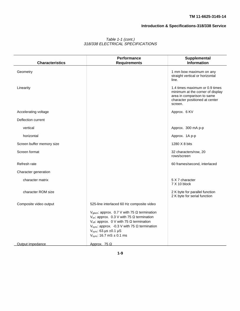
TM 11-6625-3145-14
Introduction & Specifications-318/338 Service
Table 1-1 (cont.)318/338 ELECTRICAL SPECIFICATIONS
Performance SupplementalCharacteristics Requirements Information
Geometry 1 mm bow maximum on anystraight vertical or horizontalline.
Linearity 1.4 times maximum or 0.9 timesminimum at the corner of displayarea in comparison to samecharacter positioned at centerscreen.
Accelerating voltage Approx. 6 KV
Deflection current
vertical Approx. 300 mA p-p
horizontal Approx. 1A p-p
Screen buffer memory size 1280 X 8 bits
Screen format 32 characters/row, 20rows/screen
Refresh rate 60 frames/second, interlaced
Character generation
character matrix 5 X 7 character7 X 10 block
character ROM size 2 K byte for parallel function2 K byte for serial function
Composite video output 525-line interlaced 60 Hz composite video
Vglitch: approx. 0.7 V with 75 Ω terminationVon: approx. 0.3 V with 75 Ω terminationVoff: approx. 0 V with 75 Ω terminationVsync: approx. -0.3 V with 75 Ω terminationVsync: 63.µs ±0.1 µSVsync: 16.7 mS ± 0.1 ms
Output impedance Approx. 75 Ω
1-9

TM 11-6625-3145-14
Introduction & Specifications-318/338 Service
Table 1-1 (cont.)318/338 ELECTRICAL SPECIFICATIONS
Performance SupplementalCharacteristics Requirements Information
TEST SIGNAL OUTPUT
Test Output
Output level TTL level 0.7 V or less for low-leveloutput.2.4 V or more for high-leveloutput.
Voltage, maximum +6 V peak
Current, maximum
High-logic level -0.5 mA
Low-logic level 2 mA
Repetition rates C-10 µs G-GND0-20 µs1-40 µs These test signals may be ac-2-80 µs cessed by P6451 data probe,3-160 µs P6107 external clock probe, or4-320 µs P6107 serial data probe.5-640 µs6-1.28 ms7-2.56 ms
Start Output Generated when the instrument begins toacquire data.
Output level TTL level 0.7 V or less for low-leveloutput.
2.4 V or more for high-leveloutput.
Voltage, maximum +6 V peak
Current, maximum
High-logic level -1 mA
Low-logic level 2 mA
Pulse width Approx. 650 ns
1-10

TM 11-6625-3145-14
Introduction & Specifcations-318/338 Service
Table 1-1 (cont.)318/338 ELECTRICAL SPECIFICATIONS
Performance SupplementalCharacteristics Requirements Information
POWER SUPPLY
Ranges of line voltages 90 V to 132 V AC or 180 V to 250 V AC,48 Hz to 440 Hz, single phase
Power consumption 95 W max, 150 VA max.
DC supply voltages
+ 12 V SupplyRegulation ± 1 V max.Ripple 50 mV p-p max.Max. rated current 0.07A
Current limit point Three terminal regulator-12 V SupplyRegulation ± 1 VRipple 50 mV p-pMax. rated current 0.07A
Current limit point Three terminal regulator+5 V SupplyRegulation ± 0.05 V max.Ripple 50 mV p-p max.Max. Rated current 1.5 A min., 2.6 A max.
Current limit point 110% - 200%-5 V SupplyRegulation ± 0.05 VRipple 50 mV p-p max.Max. rated current 4.0A min., 7.4 A max.
Current limit point 110% - 200%-3.3 V SupplyRegulation ± 0.05 VRipple 4 0 mV p-pMax. rated current 0.5 A min., 1.2 A max.
Current limit point 110% - 200%-2 V SupplyRegulation ± 0.02 V max.Ripple 40 mV p-p max.Max. rated current1. 1.0A min., 2.6 A max.
Fan drive voltage Typically:10V-11V at Ta =25°C
1-11

TM 11-6625-3145-14
Introduction & Specifications-318/338 Service
Table 1-1 (cont.)318/338 ELECTRICAL SPECIFICATIONS
Performance SupplementalCharacteristics Requirements Information
SERIAL STATEANALYZER FUNCTION
Data Input (Using P6107 Probe)
Input R and C 10 MΩ ± 3%, paralleled by approx. 13 pF at P6107 probe should be compen-probe tip. sated for 40 pF input
capacitance.
1 MΩ ± 5%, paralleled by approx. 40 pF atBNC.
Minimum logic swing 500 mV p-p centered on threshold voltage.
Maximum logic swing ± 30 V peak.
Maximum non-destructive 400 V peak at probe tip.
40 V peak at BNC input connector.
Threshold voltage Voltage at probe tip: Accuracy:V1 (0.1 V step variable) -10 V to +10 V ±0.23 VV2 (0.1 V step variable) -10 V to +10 V ±0.23 VV3 (V1 + V2) /2 ± 0.23 VTTL 1.4 V ± 0.23 V
One of four levels is selectable.Sets threshold voltage at 0 V +3 V for measurement of RS-232C interface signal.
Sampling
Clock source internal or external
External clock input (using P6107 probe (the same probe as parallel)P6107 probe)
External clock polarity + or -- edge
Data sampling rates
Internal clock for 50, 75, 110, 134.5, 150, 200, 300, 600, 16X sampling clockasynchronous mode 1200, 1800, 2400, 4800, 9600 and 19200
bits per second
Accuracy of internal ± 0.02%, except 110-134.5 bits per second.clock At these clock rates, the accuracy is relaxed
to 0.9%.
1-12
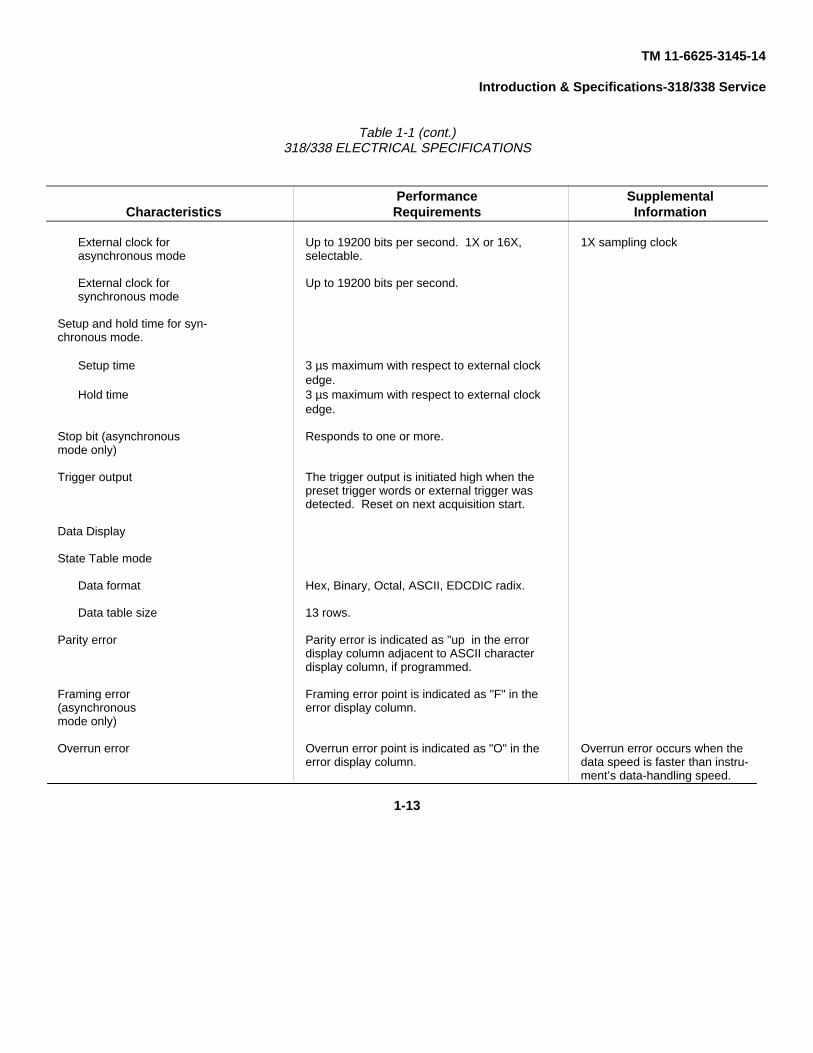
TM 11-6625-3145-14
Introduction & Specifications-318/338 Service
Table 1-1 (cont.)318/338 ELECTRICAL SPECIFICATIONS
Performance SupplementalCharacteristics Requirements Information
External clock for Up to 19200 bits per second. 1X or 16X, 1X sampling clockasynchronous mode selectable.
External clock for Up to 19200 bits per second.synchronous mode
Setup and hold time for syn-chronous mode.
Setup time 3 µs maximum with respect to external clockedge.
Hold time 3 µs maximum with respect to external clockedge.
Stop bit (asynchronous Responds to one or more.mode only)
Trigger output The trigger output is initiated high when thepreset trigger words or external trigger wasdetected. Reset on next acquisition start.
Data Display
State Table mode
Data format Hex, Binary, Octal, ASCII, EDCDIC radix.
Data table size 13 rows.
Parity error Parity error is indicated as "up in the errordisplay column adjacent to ASCII characterdisplay column, if programmed.
Framing error Framing error point is indicated as "F" in the(asynchronous error display column.mode only)
Overrun error Overrun error point is indicated as "O" in the Overrun error occurs when theerror display column. data speed is faster than instru-
ment’s data-handling speed.
1-13

TM 11-6625-3145-14
Introduction & Sp4clfications-318/338 Service
Table 1-1 (cont.)318/338 ELECTRICAL SPECIFICATIONS
Performance SupplementalCharacteristics Requirements Information
RS-232C INTERFACE
Data transmission timing asynchronous only
Communication mode full duplex
Bits/Characters 8 bits with parity ASCII characters
Parity even
Stop bit Responds to one or more, sends one.
Remote echo selection ON or OFF
Data transfer rate 110, 150, 300, 600, 1200, 2400, 4800, 9600,Baud.
Signal characteristics Meets RS-232C standard.
I/O connector 25-pin standard connector
Pin 1 protective ground GND2 transmitted data to DCE3 received data from DCE4 request to send to DCE5 clear to send from DCE6 data set ready from DCE7 signal ground GND8 received line signal detector from DCE
20 data terminal ready to DCE
inputs: 3, 5, 6, 8mark or OFF: -25 V to -3 Vspace or ON: +3 V to +25 Vinput impedance: 3 KΩ to 7 KΩ
outputs: 2, 4, 20mark or OFF: -7.5 V maximumspace or ON: +7.5 V minimumwith load impedance: 3 KΩ minimum
1-14

TM 11-6625-3145-14Introduction & Specifications-318/338 Service
Table 1-1. (cont.)318/338 ELECTRICAL SPECIFICATIONS
Performance SupplementalCharacteristics Requirements Information
NON-VOLATILE MEMORY(Option 01)
Memory size 3 pages for setup parameters; 1 page for 8 X 2048 bitsACQ or REF data.
Non-volatile period Approx. 5 years at room temperature.Non-volatile Memory control From keyboard or RS-232 bus.Battery Lithium battery (battery
capacity: 750 mAH or more)Battery voltage check A check is performed of the battery at
power-up diagnostic.
1-15
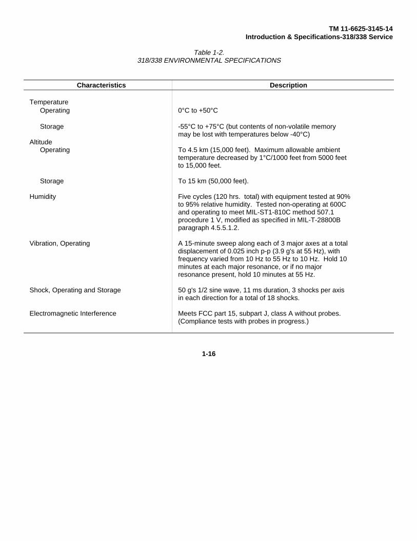
TM 11-6625-3145-14Introduction & Specifications-318/338 Service
Table 1-2.318/338 ENVIRONMENTAL SPECIFICATIONS
Characteristics Description
TemperatureOperating 0°C to +50°C
Storage -55°C to +75°C (but contents of non-volatile memorymay be lost with temperatures below -40°C)
AltitudeOperating To 4.5 km (15,000 feet). Maximum allowable ambient
temperature decreased by 1°C/1000 feet from 5000 feetto 15,000 feet.
Storage To 15 km (50,000 feet).
Humidity Five cycles (120 hrs. total) with equipment tested at 90%to 95% relative humidity. Tested non-operating at 600Cand operating to meet MIL-ST1-810C method 507.1procedure 1 V, modified as specified in MIL-T-28800Bparagraph 4.5.5.1.2.
Vibration, Operating A 15-minute sweep along each of 3 major axes at a totaldisplacement of 0.025 inch p-p (3.9 g's at 55 Hz), withfrequency varied from 10 Hz to 55 Hz to 10 Hz. Hold 10minutes at each major resonance, or if no majorresonance present, hold 10 minutes at 55 Hz.
Shock, Operating and Storage 50 g's 1/2 sine wave, 11 ms duration, 3 shocks per axisin each direction for a total of 18 shocks.
Electromagnetic Interference Meets FCC part 15, subpart J, class A without probes.(Compliance tests with probes in progress.)
1-16

TM 11-6625-3145-14Introduction & Specifications-318/338 Service
Table 1-3.318/338 PHYSICAL SPECIFICATIONS
Characteristics Description
WeightNet, without accessories about 5.1 Kg (about 12 lbs.)
Dimensions
Heights
without accessory pouch 12.0 cm (4.7 in)
with accessory pouch 17.4 cm (6.8 in)
Width with handle 23.7 cm (9.3 in)
Depth, handle not extended 40.9 cm (16.1 in)
Depth, handle extended 49.2 cm (19.4 in)
1-17/(1-18 blank)
TM 11-6625-3145-14
OPTIONS
This section briefly describes the options available for a Sony/Tektronix 318 or 338 Logic Analyzer. Further informationregarding any option can be found in the manual section containing the type of information desired. For instance, to findinformation on the theory of operation of the non-volatile memory for 318S1/338S1, refer to the Theory of Operationsection.
318F1/338F1: SERIAL ANALYSIS, RS-232C INTERFACE, AND NON-VOLATILE MEMORY
The Sony/Tektronix 318F1/338F1 package is a field-installable kit that upgrades the basic 318/338 Logic Analyzers to318S1/338S1 status. The package includes a circuit board, Serial Data Probe, and the necessary connectors to add thefollowing features to the the basic 318/338: Serial state analysis, an RS-232C remote communication interface, and non-volatile memory. The same kit is used to modify both the 318 and the 338 Logic Analyzers.
2-1/(2-2 blank)

TM 11-6625-3145-14
OPERATING INSTRUCTIONS
INTRODUCTION
The 318/338 is a menu-driven system. This means that all operations are set up by means of menus displayed on themonitor screen. Refer to the 318/338 Logic Analyzer Operator’s Manual for additional information on the general operationand characteristics of the 318/338 menus.
INSTALLATION
Installation consists of selecting the appropriate operating voltage, connecting the 318/338 to a power input source, andconnecting the probe(s), as required, to the 318/338 and the circuit under test.
POWER REQUIREMENTS
The 318/338 operates from a nominal 115 or 230 V, 48 to 440 Hz, single-phase power input source. Before connectingthe instrument to a power source, verify that the line-voltage indicator on the back of the instrument is displaying thecorrect nominal voltage for the power input source to be used.
CAUTIONBefore applying power to the instrument make sure the line- voltage indicatorshows the correct voltage for the power input source being used. The instrumentcan be damaged if the line-voltage switch is in the wrong position for the voltagebeing supplied. Adjust the red voltage selector switch on the back-end panel ofthe instrument for the proper line-voltage. Make sure you are using the correctpower supply cord when connecting the 318/338. If you are unsure if either thevoltage selector switch is in the proper position, or if you have the appropriatepower cord, refer the instrument to qualified service personnel.
POWER CORD
This equipment has a 3-wire power cord with a 3-contact plug for connection to the power source and to protective ground.The plug protective-ground contact connects (through the power cord protective-grounding conductor) to the accessiblemetal parts of the equipment. For electrical shock protection, insert this plug into a power input source socket that has asecurely grounded protective-ground contact. The power cord is detachable. When not in use, it should be stored in theaccessory pouch. Instruments are usually factory equipped with a 115 V power cord unless otherwise ordered. For moreinformation on power cords, contact your Tektronix representative or your local Tektronix Field Office.
WARNINGHazardous voltages may be present on the exposed mental surfaces of themainframe if the power source socket’s protective ground connection is notsecurely grounded.
3-1
TM 11-6625-3145-14Operating Instructions-318/338 Service
MENU CHARACTERISTICS
There are certain characteristics and terms common to all menus. The following paragraphs discuss these commoncharacteristics and their implications. More complete information is available in the 318/338 Logic Analyzer Operator’sManual, and as each menu is called later in this section.
POWER-UP CONFIGURATION DISPLAY
When the 318/338 is first powered up, it lists the configuration of the 318/338 and identifies option modules. It then showsthe results of the self test.
MENUS AND SUBMENUS
Each 318/338 menu is displayed on the monitor screen when you press its associated MENU key on the keyboard.
Some of the menus are comprised of several parts called submenus. These submenus are individual screen displayswhich may be selected only after the menu is entered. For example, the parallel State Table menu has two submenus:one for searching for data and one for comparing data. To display either of these submenus, you must first enter theparallel State Table menu.
MENU DEFAULT DISPLAYS
On system power-up, the 318/338 assigns each menu default operating parameters. When you enter the menu, the menuand its default parameters appear on the screen. This initial menu display is called the menu’s default display. If nochanges are made to the menu’s default display, the 318/338 will use the default parameters during the variousoperations.
MENU FIELDS AND THE EDIT CURSOR
When a menu is displayed on the 318/338 screen, the menu’s changeable parameters appear as reverse-video fields.Before making any changes in a specific field, you must first move the blinking edit cursor to that field. The edit cursormoves from field to field, in any direction. It is controlled by these EDIT keys:
↑, ↓, ←, and →. They move the cursor one space up, down, left, or right.
Once the edit cursor is located in a specific field, you can change the field value. The common keys used in making fieldchanges are:
• Data Entry keys - used in fields that have a string of numeric values.
• SELECT key - used in fields with predetermined values.
• INCR and DECR keys - used in fields that have specific incrementing or decrementing numerical values.
• CLEAR key - used in fields that allow a reset to zero.
NOTEIn some fields you must press the EXECUTE key after making any changes with theSELECT key. In these cases, an error message will appear when you try to movethe edit cursor to another field after pressing the SELECT key. Pressing SELECTagain will abort EXECUTE.
3-2

TM 11-6625-3145-14Operating Instructions-318/338 Service
ERROR MESSAGE AND ACQUISITION STATUS READOUT
The 318/338 has a comprehensive set of error and acquisition status messages. These messages appear on the bottomline of the screen: the error message is at the left of the screen and is displayed in blinking, highlighted video; acquisitionstatus is at the right hand of the screen and is displayed in blinking video.
A complete listing of error and acquisition status messages can be found in Appendix A of this manual.
MAJOR MODE SELECTION FIELD
The major mode (PRL/SER/KBD/RMT/NVM) selection field appears in the top left corner of the screen (except whendisplaying the RS-232 Setup menu or the Non-Volatile Memory Setup menu). After making any changes in this field, youmust press the EXECUTE key to access the selected mode.
INPUTS DURING ACQUISITION
Even when acquiring data (when waiting for a trigger or in REPEAT mode), the 318/338 can accept any keys in any fieldsexcept for those that generate the message: PRESS STOP. This capability allows you to change the delay value orsample clock while looking at continuously acquired data, without pressing the STOP key.
MENU FUNCTIONS
SETUP MENU
The Setup menu (parallel) serves two functions. First, it is used to specify the acquisition mode (SINGLE, REPEAT, RPTUNTIL ACQ = REF, RPT UNTIL ACQ ≠ REF) that will be used during acquisition.
The second function of the Setup menu is to determine the way in which acquisition channels are organized for display. Itorganizes the channels into logical groups. This information is then used by the Trigger menu for organizing the wordrecognizer channels, and by the State Table menu for organizing the data display. This channel organization isindependent of the order in which channels are connected to the system under test. The organization only affects thedisplay, not the actual acquisition. Changes can be made to the data display after the data has been acquired.
The Setup menu (serial) also serves the following functions: communication mode (ASYNC/SYNC) selection, baud rateselection, input polarity selection, bits/word selection, and parity selection.
THRESHOLD MENU
The function of the Threshold menu is to determine probe input thresholds (including data lines and the external clockline).
3-3

TM 11-6625-3145-14Operating Instructions-318/338 Service
TRIGGER MENU
The Trigger menu sets up the major acquisition parameters. First, it specifies which trigger mode (INT, EXT, or INT OREXT) will be used during acquisition. Then it specifies the acquisition clock (external or internal) and trigger position(BEGIN, CENTER, END, or DELAY), and enables clock or trigger qualifier lines. The Trigger menu also controls all wordrecognition, triggering parameters, and glitch triggering. The Trigger menu (serial) also controls SYNC WORD and HUNTWORD in synchronous mode.
STATE TABLE MENU
The State Table menu has two submenus: SRCH (search) and CMPR (compare). The SRCH (search) function is usedfor searching through ACQ (acquisition) or REF (reference) memory for a specific data word or a word including a glitch. Itwill show the number of occurrences of the specific data in the memory and it will also show the relative position of thememory cursor to these data. The CMPR (compare) function is used in conjunction with REF (reference) memory. REFmemory is filled with a copy of ACQ memory when EXECUTE is pressed (edit cursor in the ACQ-REF field).The CMPR displays then show differences between REF memory contents and any later ACQ memory contents within theCMPR WDO (window). The channel organization of the parallel state display is controlled by the Setup menu.
TIMING DIAGRAM MENU (PARALLEL ONLY)
The Timing Diagram menu (parallel) has two submenus: SRCH (search) and ∆T (delta time). The search function is thesame as in the parallel State Table menu for displayed data or data on that page. The ∆T (delta time) function makes atiming measurement between two given locations (∆T and C) in the waveform display.
CHARACTER MENU (SERIAL ONLY) (318S1/338S1)
The Character menu (serial) has two submenus: SRCH (search) and CMPR (compare). These are the same asdescribed for the State Table menu. This display shows 256 bytes of data on one screen in either ASCII or EBCDICformat.
REMOTE (RMT) MENU (318S1/338S1)
The purpose of external communication is to allow the user to store reference memories; to retrieve acquisition, reference,and glitch memories; to store and retrieve setups outside the 318/338; and to be able to control the 318/338 from anexternal controller. You can select BAUD RATE and ECHO in the RMT mode.
NON-VOLATILE (NVM) MENU (318S1/338S1)
The values of setup parameters and acquisition or reference memory can be stored in NVM memory. This means thatonce the parameters and memory are saved, they will not change (in the NVM) when the 318/338 is powered off and backon again.
NOTEWhen the NVM diagnostics test is run, all information stored in the NVM memory iserased.
3-4

TM 11-6625-3145-14Operating Instructions-318/338 Service
DIAGNOSTICS
The 318/338 has internal diagnostics to help verify proper instrument performance. Some of the diagnostics occurautomatically whenever the 318/338 is powered on. Other diagnostics require that probes be properly attached to testpoints or require an operator at the keyboard. Any error found during correct operation of the diagnostics means that aninstrument failure has occurred, has been detected, and that service is required. If an error occurs, refer to Section 7,Maintenance: Troubleshooting, of this manual for help in isolating and correcting the problem.
POWER-UP SELF TEST
When you press the POWER switch, the internal diagnostic tests run automatically. These tests check out the majorhardware components and operating firmware.
During the first phase of self test, the 318/338 tests the major blocks of system RAMs and ROMs. After RAM/ROM tests,the 318/338 is initialized. After several seconds, the display shows a configuration listing (see 3 in Figure 3-1). At the topof the screen (1 in Figure 3-1), the message SELF TEST VERSION X.X appears. On the next line (2 in Figure 3-1), themessage IN PROGRESS appears.
Each listed menu is tested and then given a PASS or FAIL notation. (See 4 in Figure 3-1.) If errors are detected, errormessages also appear. (See 5 in Figure 3-1.) PASS means that the test was successful; FAIL means that the test wasunsuccessful.
When all tests are finished, the message COMPLETED appears on the screen. (See 2 in Figure 3-1.) A prompt messagethen appears at the bottom of the screen.
If no errors are found during self test, the screen will look like Figure 3-2.
You may now enter any menu and begin operation. If errors occurred during self test, the screen will look like Figure 3-1.If the errors that occurred do not affect the operations you want to perform, press a MENU key. If you want to enter theDiagnostics menu, press START.
NOTEIf neither of the displays shown in Figure 3-1 or Figure 3-2 appears on the screenafter several seconds, system errors have been detected. Refer to Section 7,Maintenance: Troubleshooting, for help in isolating and correcting the problem.
3-5

TM 11-6625-3145-14Operating Instructions-318/338 Service
Figure 3-1. Failure in the power-up self test. Figure 3-2. Successful completion of the power-up SelfTest.
DIAGNOSTICS MENU
The Diagnostics menu offers more levels of diagnostics. The Diagnostics menu is only accessible when the power-uptests show that a hardware component has failed. To enter the Diagnostics menu, press START.
To access the Diagnostics menu when no errors have been detected by the power-up tests, induce a power-up failurefrom the keyboard by holding down any key (except STOP) from the time the 318 338 is turned on to the time the power-up self tests are completed (approximately 7 seconds).
When first entered, the screen should look like Figure 3-3. To begin testing, press a data entry key equal to a menunumber. Press X to return to Diagnostics menu. Press any MENU key to leave the Diagnostics menu and beginoperation.
USER-CHANGEABLE FIELDS FOR EACH TEST’S DISPLAY
LOOP and DISP (display) are the user-changeable fields in each test (except for the KBD, CRT, CLK, T/H, and N & DLYtests). Some tests have more fields. such as the ALL or SINGLE SELECTION field and the DATA ENTRY field. Refer toFigures 3-4 and 3-5 while reading the following paragraphs.
1 ALL OR SINGLE - Only some tests have this field. You may select either ALL or SINGLE. ALL causes all availableconditions to be tested. SINGLE causes a selected conditon to be tested. When the field is set to SINGLE, the DATAENTRY field appears on the line below. During tests, the field may not be changed. If you wish to change fields, do soafter pressing STOP.
2 DATA ENTRY - Only some tests have this field. The tests are performed with the condition of the selected item orentered data. The field may not be changed during tests. If you wish to change fields, do so after pressing STOP.
3-6

TM 11-6625-3145-14Operating Instructions-318/338 Service
Figure 3-3. Diagnostics menu: first display. Figure 3-4. Display sample with ALL/SINGLE and dataentry fields.
Figure 3-5. Display sample with LOOP and DISP fields.
3 LOOP - You can set this field to OFF, I/O, ERROR, or TEST by pressing SELECT. When the field is set to I/O, thelooping feature allows only I/O instructions to be run repeatedly. The I/O address will appear on the screen. When thefield is set to ERROR, the looping feature allows the tests in which an error is detected to be run repeatedly. When thefield is set to TEST, the looping feature allows one test or sequence of tests to be run continuously. When the field is setto OFF, the looping feature is not available and one test or sequence of tests runs once.
3-7

TM 11-6625-3145-14Operating Instructions-318/338 Service
When the field is set to I/O or ERROR, the prompt message START TO ADVANCE appears at the bottom of the screen.If START is pressed during LOOP tests, the current loop of tests stops and the next loop of tests is started. You canchange fields during tests.
Use this feature for catching intermittent faults or for circuit tracing with an oscilloscope.
4 DISP (display) - This field may be set to ON or OFF. When the field is set to ON, test results appear within the statusarea on the screen. When the field is set to OFF, no test results appear. You can change fields during tests.
5 DISPLAY AREA FOR RESULTS - This area is used to display test results. You cannot move the cursor into the areabetween the dotted lines. If the DISP field is set to OFF, no test results will appear here other than results of the I/O LOOPtest.
6 PROMPT MESSAGES - Press START to begin and to advance tests (except for KDB test). STOP TO CANCEL TESTwill appear under tests instead of START TO BEGIN TEST. Press X to return to the Diagnostics menu for all tests exceptKBD. Press STOP to cancel tests. For KBD test, press STOP to cancel test and return to the Diagnostics menu.
DIAGNOSTIC TEST DESCRIPTIONS
KBD Test. To enter the keyboard test, press 0 while in the Diagnostics menu. The screen display simulates thekeyboard. When any key is pressed, its position on the screen blinks. If the corresponding screen position does not blink,the key is open. If a screen position blinks without a key being pressed, that key is shorted closed. Refer to theDiagnostics menu or to the troubleshooting trees in Section 7 for details. Figure 3-6 illustrates the KBD test.
CRT Test. To enter this test, press 1 while in the Diagnostics menu. This test is for the focus check and the CRT rotationcheck. First, the cross-hatch pattern appears on the screen. Press START; the display will change continuously. Refer tothe Diagnostics menu or to the trouble-shooting tree in Section 7 for details.
Figures 3-7, 3-8, 3-9, and 3-10 illustrate the CRT tests.
This key blinks when hit.
Figure 3-6. Display for KBD tests. Figure 3-7. CRT test: first display.
3-8

TM 11-6625-3145-14Operating Instructions-318/338 Service
Figure 3-8. CRT test: second display. Figure 3-9. CRT test: third display.
Figure 3-10. CRT test: fourth display.
3-9

TM 11-6625-3145-14Operating Instructions-318/338 Service
CLK Test. To enter this test, press 2 while in the Diagnostics menu. This is a test of the internal timebase. It is not averification test; neither PASS nor FAIL will appear on the screen. If ALL is selected, the value of the clock interval beingtested will appear on the screen. You should use an oscilloscope to observe the operation of this test. Refer to theDiagnostics menu or to the troubleshooting trees in Section 7 for details. Figure 3-11 illustrates the CLK test.
operation: Select ALL (default) or SINGLE by pressing SELECT. Press the START key. If you have selected ALL, thevalue of the clock from 20 ns to 1 s will appear on the screen sequentially. Probe the timebase with anoscilloscope to verify that the clock interval is correct. If you have selected SINGLE, the DATA ENTRY fieldwill appear on the next line. You can change the value in this field by pressing INCR or DECR. Press STARTand use the oscilloscope to verify the timebase value you have selected. Nothing will appear on the screen.
WR Test. To enter this test, press 3 while in the Diagnostics menu. This test is for the word-recognizer RAM. Refer tothe Diagnostics menu or to the trouble-shooting tree in Section 7 for details.
operation: Press START to begin this test. The LOOP test and DISP ON/OFF functions are available here. The LOOPtest has four features: OFF, I/O, ERROR, and TEST. You can select these features by pressing SELECTeven during testing. DISP can also be selected during testing. If DISP is set to OFF, no results will appear onthe screen other than results of the I/O LOOP test. To exit this test, wait until the test finishes, or press STOP,and then press X. If errors are detected in the test and DISP is ON, some of the following error codes willappear on the screen.
Error codes: 20, 21, 22, 23 (Refer to Appendix B for details.)
Figure 3-12 illustrates the WR test.
Figure 3-11. Display for CLK tests. Figure 3-12. Display for word recognizer RAM (WR) test.
3-10
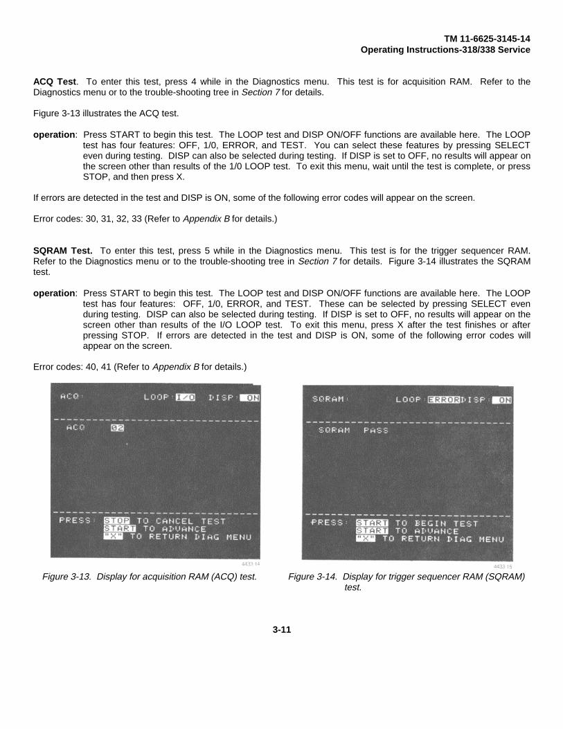
TM 11-6625-3145-14Operating Instructions-318/338 Service
ACQ Test. To enter this test, press 4 while in the Diagnostics menu. This test is for acquisition RAM. Refer to theDiagnostics menu or to the trouble-shooting tree in Section 7 for details.
Figure 3-13 illustrates the ACQ test.
operation: Press START to begin this test. The LOOP test and DISP ON/OFF functions are available here. The LOOPtest has four features: OFF, 1/0, ERROR, and TEST. You can select these features by pressing SELECTeven during testing. DISP can also be selected during testing. If DISP is set to OFF, no results will appear onthe screen other than results of the 1/0 LOOP test. To exit this menu, wait until the test is complete, or pressSTOP, and then press X.
If errors are detected in the test and DISP is ON, some of the following error codes will appear on the screen.
Error codes: 30, 31, 32, 33 (Refer to Appendix B for details.)
SQRAM Test. To enter this test, press 5 while in the Diagnostics menu. This test is for the trigger sequencer RAM.Refer to the Diagnostics menu or to the trouble-shooting tree in Section 7 for details. Figure 3-14 illustrates the SQRAMtest.
operation: Press START to begin this test. The LOOP test and DISP ON/OFF functions are available here. The LOOPtest has four features: OFF, 1/0, ERROR, and TEST. These can be selected by pressing SELECT evenduring testing. DISP can also be selected during testing. If DISP is set to OFF, no results will appear on thescreen other than results of the I/O LOOP test. To exit this menu, press X after the test finishes or afterpressing STOP. If errors are detected in the test and DISP is ON, some of the following error codes willappear on the screen.
Error codes: 40, 41 (Refer to Appendix B for details.)
Figure 3-13. Display for acquisition RAM (ACQ) test. Figure 3-14. Display for trigger sequencer RAM (SQRAM)test.
3-11

TM 11-6625-3145-14Operating Instructions-318/338 Service
N&DLY Test. To enter this test, press 6 while in the Diagnostics menu. This test verifies that the N and DELAY counterwill run continuously. Refer to the Diagnostics menu or to the trouble-shooting tree in Section 7 for details. Figure 3-15illustrates the N&DLY test.
operation: Set the counter values in the N and DELAY fields. (Default: N = 1; DELAY = 0.) Press START to begin thetest. This is not a verification test, so you should probe the LOAD N signal or the LOAD DL signal with anoscilloscope to verify these counters. To exit this test, press STOP and then press X.
NOTEIn the case of N = O (or DLY = 0), the N counter (or the DELAY counter) will not runat all. This status is correct.
SEQ Test. To enter this test, press 7 while in the Diagnostics menu. This is an overall test for parallel acquisitioncomponents. Refer to the Diagnostics menu or to the trouble-shooting tree in Section 7 for details. Figure 3-16 illustratesthe SEQ test.
operation: Press START to begin test. The LOOP test and DISP ON/OFF functions are available here. The LOOP testhas four features: OFF, I/O, ERROR, and TEST. These can be selected by pressing SELECT even duringtesting. DISP can also be selected during testing. If DISP is OFF, no results will appear on the screen otherthan results of the I/O LOOP test. To exit this test, wait until the test finishes, or press STOP, and then pressX. If errors are detected and DISP is ON, some of the following error codes will appear on the screen.
Error codes: 50, 51, 52, 53 (Refer to Appendix B for details.)
Figure 3-15. Display for N counter or DLY counter tests. Figure 3-16. Display for overall tests on parallel acquisition(SEQ test).
3-12
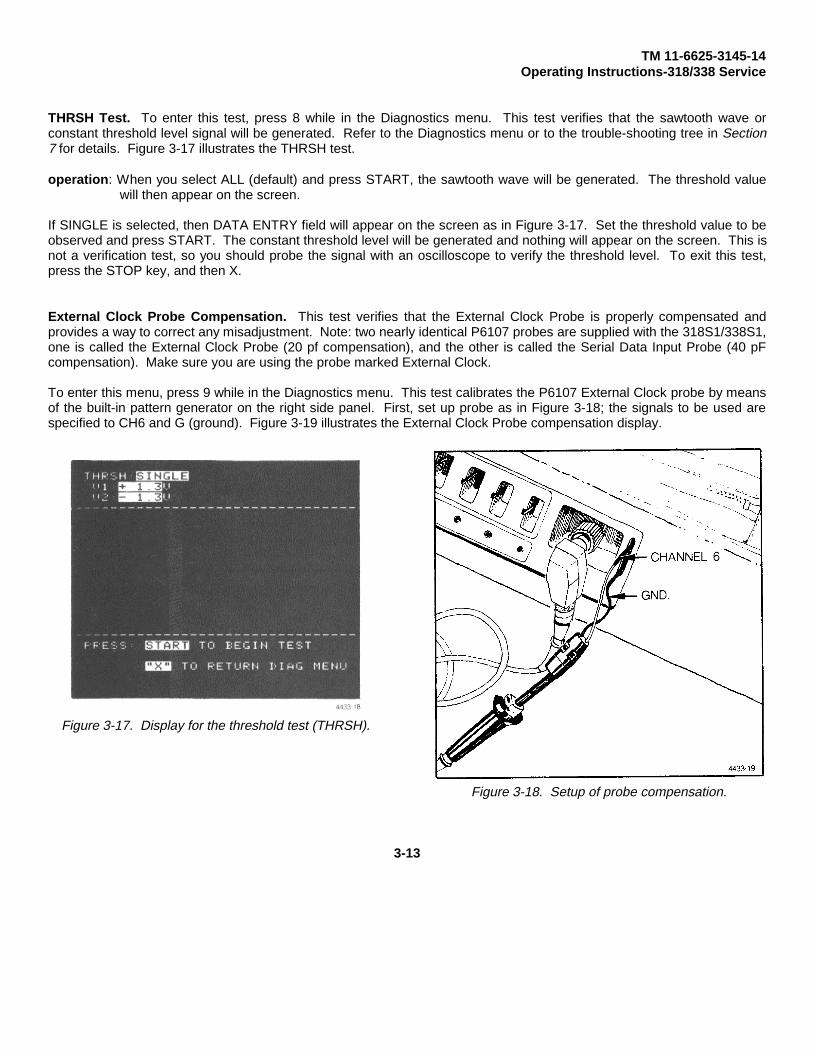
TM 11-6625-3145-14Operating Instructions-318/338 Service
THRSH Test. To enter this test, press 8 while in the Diagnostics menu. This test verifies that the sawtooth wave orconstant threshold level signal will be generated. Refer to the Diagnostics menu or to the trouble-shooting tree in Section7 for details. Figure 3-17 illustrates the THRSH test.
operation: When you select ALL (default) and press START, the sawtooth wave will be generated. The threshold valuewill then appear on the screen.
If SINGLE is selected, then DATA ENTRY field will appear on the screen as in Figure 3-17. Set the threshold value to beobserved and press START. The constant threshold level will be generated and nothing will appear on the screen. This isnot a verification test, so you should probe the signal with an oscilloscope to verify the threshold level. To exit this test,press the STOP key, and then X.
External Clock Probe Compensation. This test verifies that the External Clock Probe is properly compensated andprovides a way to correct any misadjustment. Note: two nearly identical P6107 probes are supplied with the 318S1/338S1,one is called the External Clock Probe (20 pf compensation), and the other is called the Serial Data Input Probe (40 pFcompensation). Make sure you are using the probe marked External Clock.
To enter this menu, press 9 while in the Diagnostics menu. This test calibrates the P6107 External Clock probe by meansof the built-in pattern generator on the right side panel. First, set up probe as in Figure 3-18; the signals to be used arespecified to CH6 and G (ground). Figure 3-19 illustrates the External Clock Probe compensation display.
Figure 3-17. Display for the threshold test (THRSH).
Figure 3-18. Setup of probe compensation.
3-13
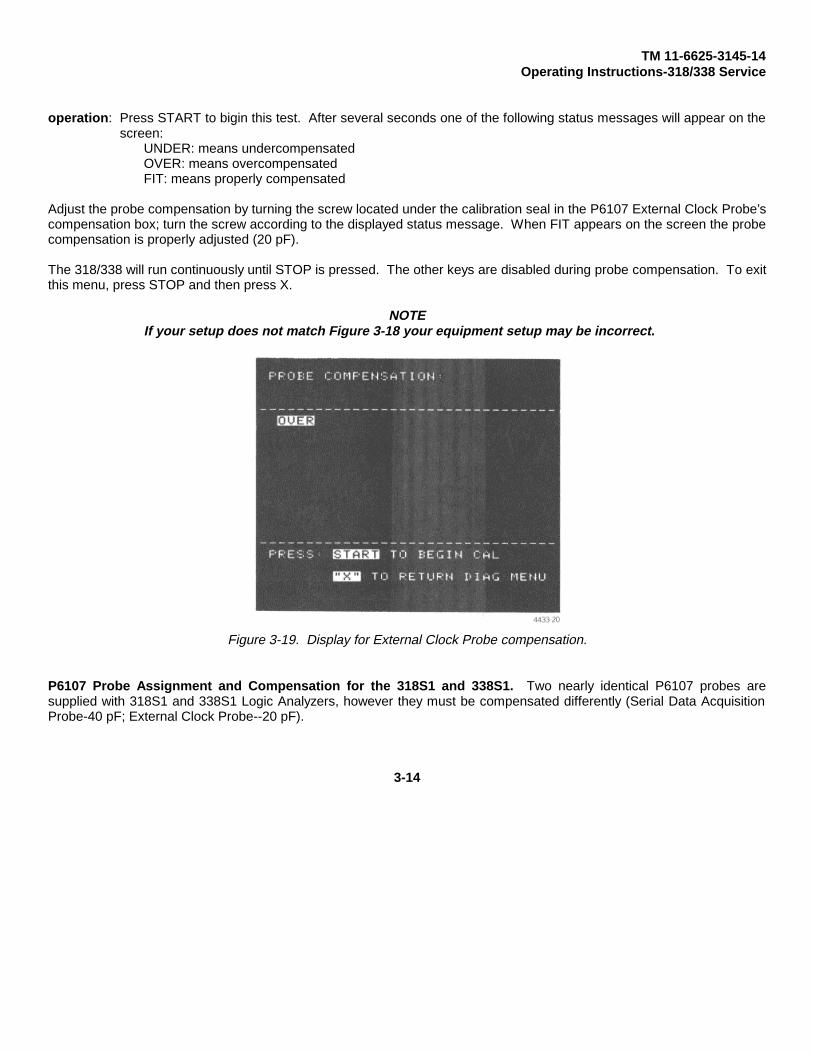
TM 11-6625-3145-14Operating Instructions-318/338 Service
operation: Press START to bigin this test. After several seconds one of the following status messages will appear on thescreen:
UNDER: means undercompensatedOVER: means overcompensatedFIT: means properly compensated
Adjust the probe compensation by turning the screw located under the calibration seal in the P6107 External Clock Probe’scompensation box; turn the screw according to the displayed status message. When FIT appears on the screen the probecompensation is properly adjusted (20 pF).
The 318/338 will run continuously until STOP is pressed. The other keys are disabled during probe compensation. To exitthis menu, press STOP and then press X.
NOTEIf your setup does not match Figure 3-18 your equipment setup may be incorrect.
Figure 3-19. Display for External Clock Probe compensation.
P6107 Probe Assignment and Compensation for the 318S1 and 338S1. Two nearly identical P6107 probes aresupplied with 318S1 and 338S1 Logic Analyzers, however they must be compensated differently (Serial Data AcquisitionProbe-40 pF; External Clock Probe--20 pF).
3-14
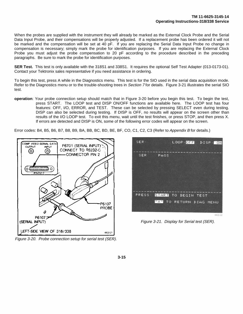
TM 11-6625-3145-14Operating Instructions-318/338 Service
When the probes are supplied with the instrument they will already be marked as the External Clock Probe and the SerialData Input Probe, and their compensations will be properly adjusted. If a replacement probe has been ordered it will notbe marked and the compensation will be set at 40 pF. If you are replacing the Serial Data Input Probe no change incompensation is necessary; simply mark the probe for identification purposes. If you are replacing the External ClockProbe you must adjust the probe compensation to 20 pF according to the procedure described in the precedingparagraphs. Be sure to mark the probe for identification purposes.
SER Test. This test is only available with the 318S1 and 338S1. It requires the optional Self Test Adapter (013-0173-01).Contact your Tektronix sales representative if you need assistance in ordering.
To begin this test, press A while in the Diagnostics menu. This test is for the SIO used in the serial data acquisition mode.Refer to the Diagnostics menu or to the trouble-shooting trees in Section 7 for details. Figure 3-21 illustrates the serial SIOtest.
operation: Your probe connection setup should match that in Figure 3-20 before you begin this test. To begin the test,press START. The LOOP test and DISP ON/OFF functions are available here. The LOOP test has fourfeatures: OFF, I/O, ERROR, and TEST. These can be selected by pressing SELECT even during testing.DISP can also be selected during testing. If DISP is OFF, no results will appear on the screen other thanresults of the I/O LOOP test. To exit this menu, wait until the test finishes, or press STOP, and then press X.If errors are detected and DISP is ON, some of the following error codes will appear on the screen.
Error codes: B4, B5, B6, B7, B8, B9, BA, BB, BC, BD, BE, BF, CO, C1, C2, C3 (Refer to Appendix B for details.)
Figure 3-20. Probe connection setup for serial test (SER).
Figure 3-21. Display for Serial test (SER).
3-15

TM 11-6625-3145-14Operating Instructions-318/338 Service
RMT Test. This test is available only with the 318S1/338S1. To begin this test press B while in the Diagnostics menu.This test is for the SIO used by the remote mode. Refer to the Diagnostics menu or to the trouble-shooting tree in Section7 for details. Figure 3-23 illustrates the display for the remote SIO test.
operation: Your equipment setup should match that in Figure 3-22 before you begin this test. To begin the test, pressSTART. The LOOP test and DISP ON/OFF functions are available here. The LOOP test has four features:OFF, I/O, ERROR, and TEST. These can be selected by pressing SELECT, even while the test is inprogress. DISP can also be selected during testing. If DISP is OFF, no results will appear on the screenother than results of the I/O LOOP test. To exit this test, wait until the test is complete, or press STOP, andthen press X. If errors are detected and DISP is ON, some of the following error codes will appear on thescreen.
Error codes : 96, 97, 98, 99, 9A, 9B, 9C, 9D, 9E, 9F, A0, A1, A2, A3, A4, A5, A6, A7, A8, A9, AA, AB, AC, AD, AE, AF, BO,B1, B2 (Refer to Appendix B for details.)
NOTEThis test may take up to 40 seconds to complete.
Figure 3-22. Equipment setup for remote test (RMT).
Figure 3-23. Display for remote tests (RMT).
3-16

TM 11-6625-3145-14Operating Instructions-318/338 Service
NVM Test. This test is only available for the 318S1 /338S1. ’to begin this test press C while in the Diagnostics menu.This is the non-volatile memory test. Refer to the Diagnostics menu or to the trouble-shooting trees in Section 7 fordetails. Figure 3-24 illustrates the NVM test.
NOTEThe NVM test will overwrite all non-volatile memory data previously saved.
operation: Press START to begin the test The LOOP test and DISP ON/OFF functions are available here. The LOOPtest has four features: OFF, I/O, ERROR, and TEST. These can be selected by pressing SELECT evenduring testing. DISP can also be selected during testing. If DISP is OFF, no results will appear on the screenother than results of the I/O LOOP test. To exit this menu, wait until the test is complete, or press the STOPkey, and then press X. If errors are detected and DISP is ON, some of the following error codes will appearon the screen.
Error codes: C8, C9, CA, CB, CC, CD, CE, CF, D0, D1, D2, D3 (Refer to Appendix B for details.)
Figure 3-24. Display for the non-volatile memory test (NVM).
3-17/(3-18 blank)

TM 11-6625-3145-14Section 4-318/338 Service
THEORY OF OPERATION
SECTION ORGANIZATION
This section contains a functional description of the circuitry used in the 318 and 338 Logic Analyzers. It is divided into twosub-sections: General System Description and Detailed Circuit Description. Block diagrams, wiring diagrams, and detailedschematics for the 318 and 338 are found in the tabbed Diagrams section at the rear of this manual.
Use the 318/338 Block Diagrams in the Diagrams section with the General System Description part of this section. Blockson the block diagrams correspond to sub-headings in the General System Description. Use the system schematics inconjunction with the Detailed Circuit Description part of this section. Schematics are referenced to section headings andsub-headings by corresponding numbers in diamonds. This section and the block diagrams and schematics in theDiagrams section may be valuable as a reference when troubleshooting system circuitry. Specific troubleshootinginformation is presented in the Maintenance. Troubleshooting section of this manual.
NOTEUnless otherwise specified, the text, tables, and figures in this section refer to boththe 318/318S1 and the 338/338S1. Differences are called out as they occur.
DIGITAL LOGIC CONVENTIONS
Digital logic techniques are used to perform most functions within this instrument. Function and operation of the logiccircuits are represented by standard logic symbols and terms. All logic functions are described using the positive logicconvention. Positive logic is a system of notation whereby the more positive of two levels is the true, or 1 state; and themore negative level is the false, or 0 state.
In logic descriptions, the more positive of the two logic voltages is referred to as high, and the more negative state as low.The specific voltages that constitute a high or low state vary between different electronic devices.
Whenever a line name on a schematic is referred to within the text, that line name may be overscored, SIGNAL, indicatingthat the line is an active low. Line names without overscores are active high.
To best understand the circuitry, cross-reference the descriptions in this section with the block diagrams in the Diagramssection. Refer to the Table of Contents at the front of this manual to locate individual circuit descriptions.
GENERAL SYSTEM DESCRIPTION
The following discussion provides an overall description of the 318/338 Logic Analyzer. Refer to the simplified blockdiagrams in this section, and to the system block diagrams in the Diagrams section of this manual. Each major block inthese diagrams represents a major circuit within the instrument. The numbered diamond symbol on each block refers tothe associated schematic diagram for that circuit (also located in the Diagrams section).
The instrument can be divided into two sections:
• Acquisition Module• Mainframe
4-1

TM 11-6625-3145-14Theory of Operation-318/338 Service
The acquisition module consists of:
• Parallel data inputs (Input A and Input B boards) (A01 & A02)• Acquisition (ACQ) Control board (A03)• ACQ Memory board (A04)• Serial Analysis/RS-232/NVM Option 01 board (A07)
NOTEThe 318 and 338 have different acquisition circuitry; make sure you reference thecorrect description for the instrument you are servicing.
The mainframe consists of:
• ROM/Threshold board (A05)• MPU/Display board (A06)• Mother board (A08)• Keyboard (A09)• CRT board (A10)• Power supply (A11 & A12)
The mainframe is common to both the 318 and 338 Logic Analyzers; circuit board assemblies are marked 318/338AXX.
NOTEThe 318 has two unique circuit board assemblies marked 318 A01, and 318 A02; the338 also has two unique circuit board assemblies, marked 338 A01, and 338A02.Circuit boards that are common to both the 318 and 338 are marked 318/338. Thetabs in the Diagrams section of this manual are marked 318/338, 318, or 338 tocorrespond to the circuit board assemblies used in the analyzer.
ACQUISITION MODULE
PARALLEL DATA INPUTS (A01 AND A02)The Input-A (A01) and Input-B (A02) boards configure the parallel data inputs. These boards are mounted into connectorsJ1 and J2, respectively, on the Mother board.
P6451 Parallel Data Probe. In the 318, two P6451 parallel data probes can be connected to the right-side panel. The338 has four P6451 parallel data probes. Each probe accepts eight channels of data and one qualifier channel for eithertrigger or clock qualifications. Thus, 16 channels of data and 2 channels of qualifiers are available for the 318, and 32channels of data and 4 channels of qualifiers are available for the 338.
P6107 External Clock Probe. The P6107 external clock probe is identical to the serial data probe, but the inputcapacitance compensation is slightly different (20 pf for the external clock probe, 40 pf for the serial data probe). See theExternal Clock Probe Compensation paragraph in Section 3 for instructions on adjusting the probe compensation.
This probe receives an external clock signal when the 318/338 is operating in synchronous mode.
4-2

TM 11-6625-3145-14Theory of Operation-318/338 Service
Data Buffers, Delay Lines, and First Lactches. Data acquired by the P6451 probe is sent differentially to a data buffer.The output of the data buffer is routed to a delay line which is used to adjust the setup/hold timings between data andclock. This delayed data is latched by the first latch. Glitch recognition is also performed by the IC containing this latch.
External Clock Circuit. An external clock from the P6107 probe is buffered by the FET buffer and converted to ECL levelby the ultra-fast comparator. Clock delay is adjusted by a delay line with taps connected to the output of the comparator.
Clock Selector. The internal clock, or the external clock’s rising or falling edge, can be selected with this selector.
Word Recognizer. Three kinds of word recognition (Word A, B, and C) are performed by the word recognizer (WR). Theoutputs of the first latches are supplied to these WRs.
Threshold Circuit. The ROM/Threshold board provides threshold levels for each of the parallel data probes and for theexternal clock probe.
ACQUISITION CONTROL BOARD (A03)This board controls all parallel data acquired through J3 on the Mother board.
Qualifier Selector. Qualifier signals from the parallel data inputs are selected by the qualifier selector as either a triggerqualifier or a clock qualifier. Polarity is also selected by this circuit.
Strobe Generator. The strobe generator provides four timing clocks to control triggering and data writing. All timingclocks are adjustable by tapped delay lines and variable capacitors. This generator is enabled by the clock qualifier signal.
Trigger Sequencer. The trigger sequencer performs complex triggering according to the data written in the SequencerRAM (SQRAM). Three outputs from the word recognizers, and the outputs from the glitch trigger are connected to theSQRAM inputs. The trigger sequencer sets the various flags on each word recognition and, once the trigger combinationis satisfied, starts the delay counter.
Event/Delay Counter. LSI-A, specially developed by Sony/Tektronix, contains a 16-bit synchronous counter used as theevent/delay counter. This counter has two functions: trigger event counting and delay counting.
ACQUISITION MEMORY BOARD (A04)
100 MHz Oscillator. A 100 MHz crystal-controlled oscillator is used for asynchronous parallel acquisition. This clock isdivided by a 1-2-5 sequence with LSI-B (A04 U140), to produce a 20 ns to 500 ms range.
Sampled Data RAM and Glitch RAM. In the 318, a 32 X 256-bit high-speed RAM is used for storing both sampled dataand glitch data. In the 338, a 32 X 256-bit high-speed RAM is used for sampled data, and a separate 8 X 256-bit RAM isused for glitch data.
Acquisition Address Counter and Carry Flag F-F. Two 4-bit synchronous counters are used as acquisition addresscounters to provide addresses for the sampled data RAM and glitch RAM. The carry flag F-F holds the carry conditiononce the address counter is full.
Output Multiplexer. Data written in the sampled data RAM, the glitch RAM, and the acquisition status register can beread by the MPU. This multiplexer selects the data to be sent to the MPU.
4-3

TM 11-6625-3145-14Theory of Operation-318/338 Service
MAINFRAME
ROM/THRESHOLD BOARD (A05)The ROM/Threshold board is installed into J5 on the Mother board.
ROM. Six 16K X 8-bit mask ROMs and one 8K X 8-bit EPROM are mounted on the ROM/Threshold board. Part of theROMs are configured into four pages, since only 64K bytes of the 112Kbyte total can be addressed at a time.
Threshold Circuit. The threshold circuit contains two latching digital-to-analog converters. This circuit provides threekinds of threshold levels: V1, V2, and V3 (V1 +V2)/2 for both parallel and serial probes.
MPU/DISPLAY BOARD (A06)The MPU board is plugged into the J06 card-edge connector on the Mother board. The MPU board contains a Z-80Amicroprocessor, RAMs, a display controller, a character ROM, bus buffers, key control logic, and oscillators for the MPUand TV timings.
Microprocessor. A Z-80A microprocessor controls all operations for diagnostics and data acquisition.
RAMs. Two 1K X 8-bit static RAMs are used by the MPU to store data and flags.
Display Controller and Character ROM. This integrated circuit, developed by Sony/Tektronix, controls the 318/338display data stored in the display RAM. The display controller decodes control codes for inverse video, blinking, otherspecial display codes, and letter codes by referring to the character ROM. It then generates control signals for the CRT.
Bus Buffer. All address buses and data buses are buffered to provide sufficient fan-out to drive several boards connectedto the bus through the Mother board.
Key Control Logic. Key signals from the keyboard are encoded by a priority encoder and are sent to the MPU as a keycode with an interrupt. All keys (except the STOP key) can be masked by the MPU with the keyboard mask bit.
MOTHER BOARD (A08)The Mother board provides interconnection for boards A01 through A07 through connectors J1 to J7. In addition, thisboard routes power to all boards and has connectors for the keyboard and the CRT boards.
KEYBOARD (A09)The keyboard serves as the operator’s interface. The operator selects the menu to be displayed and sets up theinstrument from the keyboard. All functions of the 318/338 can be controlled from this keyboard in the local mode.Pressing any key will cause an interrupt to be sent to the MPU, along with the key code corresponding to the key pressed.
CRT BOARD (A10)CRT. The CRT is a four-inch raster-scan type.
CRT Circuit. The CRT circuit provides z-axis voltage and the horizontal and vertical deflection-current outputs that areused for the CRT. A flyback transformer in the horizontal deflection circuit provides the high voltage and other CRTelectrode voltages.
4-4
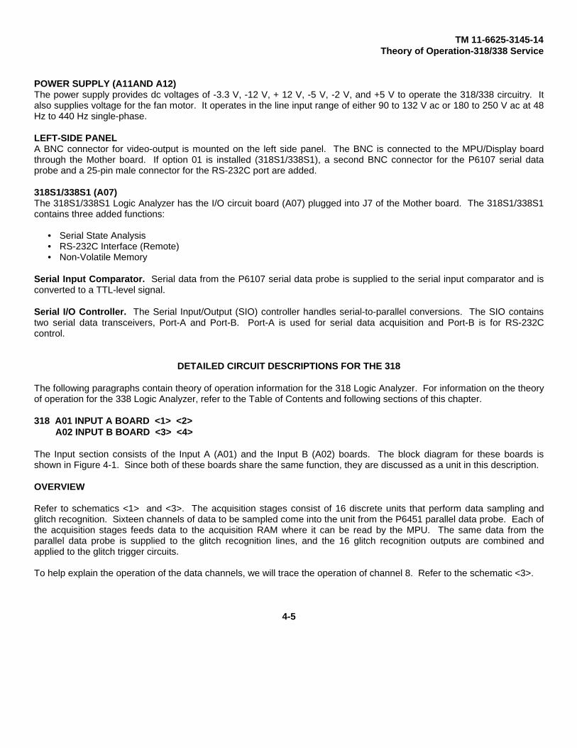
TM 11-6625-3145-14Theory of Operation-318/338 Service
POWER SUPPLY (A11AND A12)The power supply provides dc voltages of -3.3 V, -12 V, + 12 V, -5 V, -2 V, and +5 V to operate the 318/338 circuitry. Italso supplies voltage for the fan motor. It operates in the line input range of either 90 to 132 V ac or 180 to 250 V ac at 48Hz to 440 Hz single-phase.
LEFT-SIDE PANELA BNC connector for video-output is mounted on the left side panel. The BNC is connected to the MPU/Display boardthrough the Mother board. If option 01 is installed (318S1/338S1), a second BNC connector for the P6107 serial dataprobe and a 25-pin male connector for the RS-232C port are added.
318S1/338S1 (A07)The 318S1/338S1 Logic Analyzer has the I/O circuit board (A07) plugged into J7 of the Mother board. The 318S1/338S1contains three added functions:
• Serial State Analysis• RS-232C Interface (Remote)• Non-Volatile Memory
Serial Input Comparator. Serial data from the P6107 serial data probe is supplied to the serial input comparator and isconverted to a TTL-level signal.
Serial I/O Controller. The Serial Input/Output (SIO) controller handles serial-to-parallel conversions. The SIO containstwo serial data transceivers, Port-A and Port-B. Port-A is used for serial data acquisition and Port-B is for RS-232Ccontrol.
DETAILED CIRCUIT DESCRIPTIONS FOR THE 318
The following paragraphs contain theory of operation information for the 318 Logic Analyzer. For information on the theoryof operation for the 338 Logic Analyzer, refer to the Table of Contents and following sections of this chapter.
318 A01 INPUT A BOARD <1> <2>A02 INPUT B BOARD <3> <4>
The Input section consists of the Input A (A01) and the Input B (A02) boards. The block diagram for these boards isshown in Figure 4-1. Since both of these boards share the same function, they are discussed as a unit in this description.
OVERVIEW
Refer to schematics <1> and <3>. The acquisition stages consist of 16 discrete units that perform data sampling andglitch recognition. Sixteen channels of data to be sampled come into the unit from the P6451 parallel data probe. Each ofthe acquisition stages feeds data to the acquisition RAM where it can be read by the MPU. The same data from theparallel data probe is supplied to the glitch recognition lines, and the 16 glitch recognition outputs are combined andapplied to the glitch trigger circuits.
To help explain the operation of the data channels, we will trace the operation of channel 8. Refer to the schematic <3>.
4-5

TM 11-6625-3145-14Theory of Operation-318/338 Service
A02U202 receives ECL-level differential data from channel 8 of the parallel data probe. The data enters the circuit boardvia pins 22 and 10 of J204, and connects to pins 10 and 9 of A02U202.
The data is applied to the differential inputs of a receiver. From the receiver, the data is sent through the delay line DL106A to enable the timing to meet its setup-and-hold-time specification. On the rising edge of each clock (enteringA02U202 at pin 1), data, glitch, and glitch trigger are clocked, then sent off from pins 8, 2, and 14, respectively.
Operation of channels A02U204, A02U206, A02U208, A02U210, A02U212, A02U214, A02U216, A02U100, A02U102,A02U104, A02U106, A02U108, A02U110, A02U112, and A02U114 are the same as for channel 8 (A02U202).
The glitch output goes high if at least two data transitions occur between rising edges of the clock.
If the glitch recognizer off/on line (pin 15, GRC) Is low, the glitch recognizer out line (pin 14, GR) indicates the presence ofone or more glitches. (The (GRC line is controlled by shift registers A02U118 and A02U218.) If the GRC line is high, theoutput line from pin 14 is disabled. The glitch trigger outputs of the 16 M21 8s are wire-ORed together. so whenever anychannel detects a glitch, that line moves to high.
ADDRESS DECODER <2>
The address decoder circuit consists of A01 U130 and A01U132. A01U132 is a TTL-to-ECL-level converter. U130decodes 1/0 addresses 00, 01, 02, and 03. 1/O address 00 (A01U130 pin 11) is used to write trigger word data into theWord Recognizer memory from channel 0 to channel 15. I/O address 01 (A01U130 pin 10) is a clock selector port. I/Oaddress 02 (A01U130 pin 9) resets the word recognizer memory address counter. This port also controls glitch trigger onand off. I/O address 03 (A01U130 pin 7) increments the word recognizer address counter.
EXTERNAL CLOCK INPUT <4>
The external clock input is a high input-impedance (1 M(2) buffer. Transistor A04Q108A is connected as a sourcefollower. Transistor Q108B maintains a constant current flow through A04Q108A. The dc balance adjustment, R234.sets the dc offset voltage of the source follower to 0 V.
EXTERNAL CLOCK COMPARATOR <4>
A02U236A compares the input signal from the source follower with a reference voltage divided by A02R238, A02R239,and A02R240. This circuitry multiplies one-fourth the CLK Threshold level from the A05 ROM/Threshold board by two-fifths to match the P6107 external clock probe attenuation (1/4 x 2/5 = 1/10). If the input signal level is more positive thanthe reference voltage, A02U236 pin 1 is high and A02U236 pin 2 is low R239 compensates for the Q108’s source-drainresistor variation.
CLOCK SELECTOR <4>
Data from shift register A02U224 controls A02U222A, A02U226B, A02U226A, and A02U244A. The MPU sets one ofthese gates to low (enabled); then EXT ↑, EXT ↓, or INT CLK is selected.
These gates have three outputs. One clocks eight M218s on the A02 Input-B board, another clocks eight M218s on theA01 Input-A board, and the third is distributed to the A03 ACQ Control board.
4-6

TM 11-6625-3145-14Theory of Operation-318/338 Service
GLITCH CONTROL <2> <3> <4>
This circuit controls pin 15 of the M218s. M218’s pin 15 is used to control pin 14’s output. If pin 15 is forced high, glitchtrigger output pin 14 is disabled (kept low): if pin 15 is low, pin 14 is enabled. Therefore, if a glitch trigger on a certain lineis expected, the corresponding M218’s pin 15 must be low. Since all M218 pins 14 are wire-ORed, a glitch trigger occurswhen any of M218’s glitch trigger output moves to high. A01 U118 <2> and A02U218 <3> control M218’s pin 15; theseregisters are written to serially; they output their data in parallel to their respective M218s. A02U240 <4> shifts the MPUdata and clock signals by --5 V, and shifts the TTL swing to match the M21 8’s special input level.
PIPELINE REGISTER <1> <3>
This circuit consists of latches A01U122, A01U128, and A01U134 <1>, and latches A02U228, A02U234, and A02U238<3>. The sampled data and glitch from the M218s are applied to the inputs of the pipeline registers. The pipelineregisters synchronize the data for storage in the acquisition (ACQ) memory. Clock signals for the register are provided bythe SYSCLK 2 signal which is delayed by A01DL104 <2> (delayed SYSCLK 2 is called SYSCLK 3) and buffered byA02U200C <4> . Each SYSCLK 2 pulse advances the data from the M218 to the register, where it is held for one clockcycle before being loaded into the ACQ memory.
WORD RECOGNIZER <1> <2> <3>
The Word Recognizer (WR) consists of three 16-channel word recognizers with high-speed memories. The 318 offersthree word recognizer functions where three different words may be set simultaneously. They are named trigger words A,B, and C. The MPU loads data into A01U120 <1 > and A02U220 <3>, according to the trigger word, using A01 U124 <2>,A01 U126 <2>, A02U230 <3>, and A02U232 <3> (memory address counters). The MPU increments these counters oneby one and loads data for trigger word A, B, or C into A01 U120 and A02U220. Each WR RAM has 8 address lines andthree data lines. Data from the M218s is used as address for the WR RAM. Within the WR RAM, data is only three bitswide, corresponding to triggers A. B, and C.
The MPU writes data, according to the trigger word, into the WR memory and increments the address counters. Thisoperation is repeated 256 times. For example, to set the trigger word 7638hex, the MPU writes 0 into the lower WRmemory where the address counter value is 38hex, and 0 is written to the higher WR where the counter value is 76hex. Inall the other addresses, the WR’s are filled with is.
During acquisition, data is supplied to A01U120 and A02U220 address inputs, and if a trigger word comes, A01U120 andA02U220 (whose outputs are wired-ANDed) generate a trigger signal which is sent to the A03 Acquisition Control board.
DATA THRESHOLD BUFFER <4>
The currents from edge-connectors 38B and 39A are applied to the inverting inputs of A02U242B and A02U242A, (gain ofminus one) and the currents from A02J202 pins 4 and 5 and A02J204 are supplied to the non-inverting inputs of theseamplifiers to be summed. The input is divided down to 5/8 of the original value before it is sent to the non-inverting inputsof A02U242A and A02U242B. The output current of these amplifiers is then supplied through A02R262 and A02R256 tothe parallel data probe.
4-7
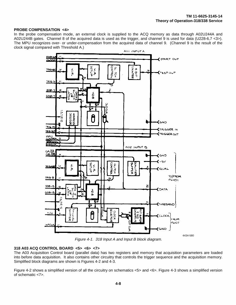
TM 11-6625-3145-14Theory of Operation-318/338 Service
PROBE COMPENSATION <4>In the probe compensation mode, an external clock is supplied to the ACQ memory as data through A02U244A andA02U244B gates. Channel 8 of the acquired data is used as the trigger, and channel 9 is used for data (U228-6,7 <3>).The MPU recognizes over- or under-compensation from the acquired data of channel 9. (Channel 9 is the result of theclock signal compared with Threshold A.)
4434-580
Figure 4-1. 318 Input A and Input B block diagram.
318 A03 ACQ CONTROL BOARD <5> <6> <7>The A03 Acquisition Control board (parallel data) has two registers and memory that acquisition parameters are loadedinto before data acquisition. It also contains other circuitry that controls the trigger sequence and the acquisition memory.Simplified block diagrams are shown is Figures 4-2 and 4-3.
Figure 4-2 shows a simplified version of all the circuitry on schematics <5> and <6>. Figure 4-3 shows a simplified versionof schematic <7>.
4-8

TM 11-6625-3145-14Theory of Operation-318/338 Service
Figure 4-2. 318 Simplified diagram of the ACQ control circuitry on schematics <5> and <6>.
4-9

TM 11-6625-3145-14Theory of Operation-318/338 Service
Figure 4-3. 318 Simplified diagram of the ACQ control circuitry on schematic <7>.
I/O ADDRESS DECODER <6>
The I/O address decoder consists of A03U110 and A03U112. The circuit provides a single pulse, used to activate apreselected device which then communicates with the MPU and controls the start logic and trigger sequencer circuits.Device selection is made using the lowest three bits of the address bus during I/O instruction execution on the ACQControl board.
4-10
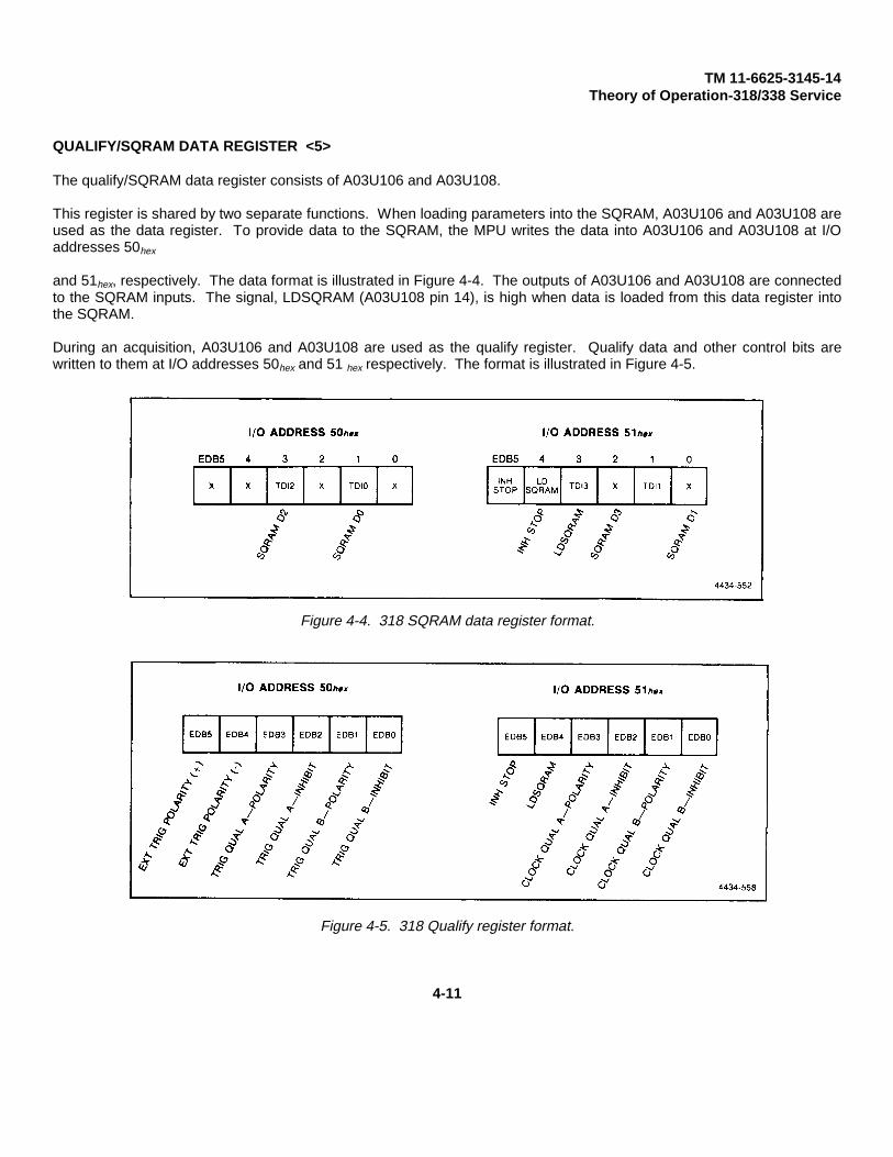
TM 11-6625-3145-14Theory of Operation-318/338 Service
QUALIFY/SQRAM DATA REGISTER <5>
The qualify/SQRAM data register consists of A03U106 and A03U108.
This register is shared by two separate functions. When loading parameters into the SQRAM, A03U106 and A03U108 areused as the data register. To provide data to the SQRAM, the MPU writes the data into A03U106 and A03U108 at I/Oaddresses 50hex
and 51hex, respectively. The data format is illustrated in Figure 4-4. The outputs of A03U106 and A03U108 are connectedto the SQRAM inputs. The signal, LDSQRAM (A03U108 pin 14), is high when data is loaded from this data register intothe SQRAM.
During an acquisition, A03U106 and A03U108 are used as the qualify register. Qualify data and other control bits arewritten to them at I/O addresses 50hex and 51 hex respectively. The format is illustrated in Figure 4-5.
Figure 4-4. 318 SQRAM data register format.
Figure 4-5. 318 Qualify register format.
4-11

TM 11-6625-3145-14Theory of Operation-318/338 Service
QUALIFY LOGIC <5> <6>
The qualify logic circuit consists of A03U 118A, B, A03U1 16A, B. The qualifier signals QA, QB, QA, and QB come fromthe A02 Input B board. Their signals are wire-ORed with the outputs of the Qualify Register, A03U106 and A03U108, andgo to the EXOR gates A03U116 and A03U118 <5> where their polarities are selected according to the polarity selectionbits. Each output of the EXOR gates is wire-ANDed and these signals go to gates A03U126A and A03U126B <6> of thestart logic circuit.
START/STOP LOGIC <6>
The start/stop logic circuit consists of A03U124B, A03U126A,B. When data acquisition starts, the START1 pulse isgenerated at I/O address 56hex and goes to the clock input of A03U124B.
The output signal of this flip-flop enables the trigger qualify and clock qualify signals. These signals pass through gatesA03U126A and A03U126B to the inputs of the trigger qualify and the clock qualify flip-flops.
To read the acquired data from the ACQ memory on the A04 board, START2 is issued at I/O address 55hex. START2enables ADRS CLK, which clocks the memory address counter. At the end of the data acquisition phase, the signalSTOP1 (A03U156A pin 2) is issued by the STOP flag output of A03U158. At the end of the read from ACQ memoryoperation, MANUAL STOP is generated at 1/0 address 53hex.
TRIGGER QUALIFY FLIP-FLOP <6>
The trigger qualify flip-flop circuit is A03U128A. The TRIG QUAL signal is clocked into the D-type flip-flop from A03U126Aevery system clock cycle.
The output of A03U128A connects to one of the retiming flip-flops through delay line A03DL106B.
RETIMING CLOCK <6>
The retiming clock circuit consists of A03U 128B, A03C100, A03R136, A03DL102, A03U 134B, and A03U142C. Thepulse generated by A03U128B, A03C100, and A03R136 is called the retiming clock. This pulse travels through delay lineA03DL102 to the clock pin of A03U134B.
The pulse delay time is adjusted by selecting a tap of A03J200. The pulse is used as the retiming clock which regulateswhen trigger data is latched into the retiming flip-flops.
CLOCK QUALIFY FLIP-FLOP <6>
The clock qualify circuit consists of A03U130A, A03DL100A,B, A03U142D, A03R130, and A03C102.
The pulse generated by A03U 130 and A03DL100B travels through A03DL100A and A03U 142D to the clock pins ofA03U130B, A03U132A, and A03U132B as the the trigger pulse for the strobe generators.
STROBE GENERATOR <6>
The strobe generator contains the write enable ( WE ) circuit, the address clock (ADRSCLK) circuit, and the trigger clock(TRIGCLK1, TRIGCLK2) circuit.
4-12

TM 11-6625-3145-14Theory of Operation-318/338 Service
The write enable (WE) Clock circuit consists of A03U132B, A03R1 12B, A03R132, and A03C106. The output ofA03U132B is wire-ORed with the output of the STOP flag and goes to the write enable inputs of the ACQ memory deviceson the A04 board <8>.
During data acquisition, data acquired from the parallel data probes is written into memory at the location pointed to by theaddress counter. At the end of the data acquisition phase, the output of the STOP flag pulls the WE signal line high, anddata acquisition stops.
The width of the WE pulse is determined by adjustable capacitor A03C106.
The address clock (ADRSCLK) circuit consists of A03U132A, A03R112A, A03R134, and A03C104. The address clockpulse generated by this circuit is applied to the clock inputs of address counter A04U136 and A04U138 on the A04 board<8>.
During data acquisition, the address clock pulse, ADRSCLK, is routed to the address counter, which supplies the locationfor the ACQ memory on the A04 board.
In the data read mode, the address clock is generated by STEP CLOCK.
The width of the address clock is determined by A03C104 <6>.
The trigger clock circuit consists of A03U130B, A03DL104A, A03DL104B, A03U142A, and A03U142B. The pulsegenerated by the A03U130B and A03DL104B travels through A03DL104A to the trigger sequencer flags, at A03U150 andA03U148, and LSI-A <7>. TRIGCLK1 goes to LSI-A; TRIGCLK2 goes to the trigger sequencer flags.
The trigger sequencer advances at the rate of the TRIG Clock as events are recognized.
NOTERefer to Figure 4-3 for a simplified block diagram of the ACQ control circuitry onschematic <7>.
EXTERNAL OR GLITCH TRIGGER CIRCUIT <7>
The external or glitch trigger circuit consists of A03U122A, A03U122B, A03U124A, and A03DL1 06A.
The external trigger polarity is selected by gates A03U122A and A03U122B.
The polarity data EXT ↑ and EXT ↓ come from qualify register A03U106 <5>.
The external trigger signal selected is fed into the clock input of A03U124A. The glitch trigger is connected to the reset pinand the TRIG QUAL signal is connected to the set pin.
Flip-flop A03U124A is enabled while TRIG QUAL is low. The output of EXTVG FLAG is connected to the input of one ofthe retiming flip-flops (A03U138A).
RETIMING FLIP-FLOP <6>
The retiming flip-flops consist of A03U138A, A03U138B, A03U136A, A03U136B, and A03U134A.
The signals TRIG A, TRIG B, TRIG C, EXTVG FLAG, and TRIG QUAL are latched into each flip-flop by the retiming clock(RETIMING CLK).
4-13
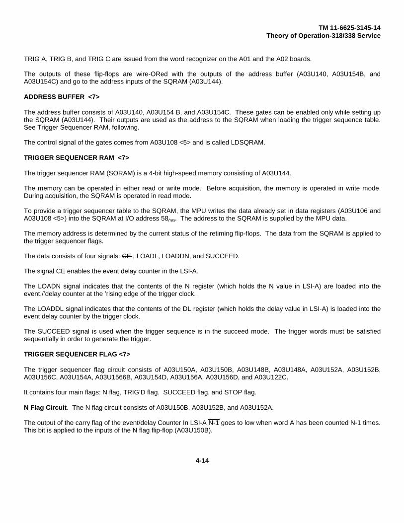
TM 11-6625-3145-14Theory of Operation-318/338 Service
TRIG A, TRIG B, and TRIG C are issued from the word recognizer on the A01 and the A02 boards.
The outputs of these flip-flops are wire-ORed with the outputs of the address buffer (A03U140, A03U154B, andA03U154C) and go to the address inputs of the SQRAM (A03U144).
ADDRESS BUFFER <7>
The address buffer consists of A03U140, A03U154 B, and A03U154C. These gates can be enabled only while setting upthe SQRAM (A03U144). Their outputs are used as the address to the SQRAM when loading the trigger sequence table.See Trigger Sequencer RAM, following.
The control signal of the gates comes from A03U108 <5> and is called LDSQRAM.
TRIGGER SEQUENCER RAM <7>
The trigger sequencer RAM (SORAM) is a 4-bit high-speed memory consisting of A03U144.
The memory can be operated in either read or write mode. Before acquisition, the memory is operated in write mode.During acquisition, the SQRAM is operated in read mode.
To provide a trigger sequencer table to the SQRAM, the MPU writes the data already set in data registers (A03U106 andA03U108 <5>) into the SQRAM at I/O address 58hex. The address to the SQRAM is supplied by the MPU data.
The memory address is determined by the current status of the retiming flip-flops. The data from the SQRAM is applied tothe trigger sequencer flags.
The data consists of four signals: CE , LOADL, LOADDN, and SUCCEED.
The signal CE enables the event delay counter in the LSI-A.
The LOADN signal indicates that the contents of the N register (which holds the N value in LSI-A) are loaded into theevent,/’delay counter at the ’rising edge of the trigger clock.
The LOADDL signal indicates that the contents of the DL register (which holds the delay value in LSI-A) is loaded into theevent delay counter by the trigger clock.
The SUCCEED signal is used when the trigger sequence is in the succeed mode. The trigger words must be satisfiedsequentially in order to generate the trigger.
TRIGGER SEQUENCER FLAG <7>
The trigger sequencer flag circuit consists of A03U150A, A03U150B, A03U148B, A03U148A, A03U152A, A03U152B,A03U156C, A03U154A, A03U1566B, A03U154D, A03U156A, A03U156D, and A03U122C.
It contains four main flags: N flag, TRIG’D flag. SUCCEED flag, and STOP flag.
N Flag Circuit. The N flag circuit consists of A03U150B, A03U152B, and A03U152A.
The output of the carry flag of the event/delay Counter In LSI-A N-1 goes to low when word A has been counted N-1 times.This bit is applied to the inputs of the N flag flip-flop (A03U150B).
4-14

TM 11-6625-3145-14Theory of Operation-318/338 Service
The flag is set high at the next word A and held high until trigger word B arrives.
When the reset word C comes before the trigger word B, the signal LOADN is issued from the SQRAM, and the N flag isreset.
TRIG’D Flag Circuit. The TRIG’D flag circuit consists of A03U150A and A03U156C. When the trigger word comes fromthe parallel data probe, the LOAD DL signal (which is the output of the SQRAM) goes to high, and the TRIG’D flag is set atthe rising edge of the trigger clock.
At the same time, the contents of the DL register are loaded into the event/delay counter and the delay count is started.
The trigger circuit is looped through A03U156, so the flag can not be reset until the acquisition phase is completed.
SUCCEED Flag Circuit. The SUCCEED flag circuit consists of A03U148B, A03U156B, and A03U154A.
This flag is used only when the trigger mode is a three-word successive trigger sequence, such as "N*WA FLW’D BY BFLW’D BY C," or "N*WA THEN B THEN C," or "N*WA FLW’D BY B THEN C." In this mode, when trigger word B arrivesfrom the parallel data probe, the SUCCEED signal (which is output by the SQRAM) goes to high and the succeed flag isset at the rising edge of the trigger clock. The TRIG’D flag follows the SUCCEED flag when word C is acquired. If theacquired data could not form a successful trigger sequence, the LOADN signal is issued from A03U144 to reset the N flagand the SUCCEED flag.
STOP Flag Circuit. The stop flag circuit consists of A03U154D, A03U148A, A03U122C, A03U156A, and A03U156D.
The stop flag is set after the delay counter in LSI-A is counted out. It disables three circuits as follows:
1. Prohibits write operations to the ACQ memory by forcing the WE signal line high.2. Disables the input clock by resettings the start flag flip-flop A03U124B <6>.3. Disables the ACQ address counter (A04U136 and A04U138 <8>) on the A04 ACQ Memory board.
When data acquisition is restarted, the stop flag is reset by the RESET signal.
SQRAM DATA/WORD RECOGNIZER DATA MULTIPLEXER <7>
This circuit consists of A03U146. It is used only for the diagnostic test of the SQRAM and the word recognizer.
LSI-A A03U158 <7>
LSI-A is a bipolar LSI circuit designed by Sony/Tektronix. LSI-A includes an address decoder, 16- bit N register, 16-bit DLregister, 16-bit synchronous preloadable counter with fast-carry propagation logic, the mask register, and the acquisitionstatus logic.
Address Decoder. The address decoder provides necessary pulses for the initialization and presetting of the abovecircuits. Circuit selection is made using the three LSBs of the address bus from the MPU, while CS0X is low.
4-15

TM 11-6625-3145-14Theory of Operation-318/338 Service
N Register. The N register is a 16-bit register that holds the N value assigned in the Trigger menu. The MPU writes the Nvalue into the N register at I/O addresses 41hex and 42hex.
DL Register. The DL register is a 16-bit register that holds the DELAY value assigned in the Trigger menu. The MPUwrites the DELAY value into the DL register at I/O addresses 43hex and 44hex.
Mask Register. The Mask register is a 5-bit register that holds mask bits for interrupts. The MPU writes the mask datainto the mask register at I/O address 40hex.
Event/Delay Counter. The event/delay counter is a 16-bit synchronous preloadable counter with fast-carry propagationlogic.
The counter is controlled by three signals: CE, LOADN, and LOADDL which are described in Table 4-A. The counterincludes carry detection Logic which generates the N-1 signal when it counts out.
ACQ Status Logic. The ACQ status consists of four flags (DTFLG, WAFLG, STFLG, and CRFLG) and the INT signal.
The MPU gets these signals (except INT ) by issuing RDSTS at I/O address 5Dhex.
INT is caused by any state change of any flag, and each flag bit can be masked by the mask bit of the mask register.
The function of each signal in LSI-A is shown in Table 4-1.
Table 4-1.318 LSI-A INPUT SIGNALS
SignalNames Description
EN Active low; indicates that the MPU provides data on the data bus (DO-D7) to LSI-A.
CSox Active low; indicates that the MPU accesses the LSI-A.
AO-A2 The data for the address decoder located in the LSI-A.
DO-D7 The data bus. The MPU puts data for LSI-A on the bus.
TRIG CLK Active high; connected to the clock input of the event/delay counter. The counter increments or loads the contentsof the N register or the DL register according to the control signals.
CE Active low; the count enable signal. The counter increments at the rising edge of TRIG CLK if CE is low.
LOADN Active high; if high, the N value of the N register is loaded into the counter at the rising edge of TRIG CLK.
LOADDL Active high; if high, the DELAY value of the DL register is loaded into the counter at the rising edge of the TRIG CLK.
TIMER Timer from LSI-B (A04U140 <9>) occurs at a constant interval after it is cleared by the CLR INT signal at I/O address5Fhex.
4-16

TM 11-6625-3145-14Theory of Operation-318/338 Service
Table 4-1. (cont.)318 LSI-A INPUT SIGNALS
SignalNames Description
TRIG’D Active high; the output of the TRIG flag. It indicates that the Trigger sequencer is triggered.
RESET Clears the flip-flop in LSI-A that temporarily saves the TRIG’D signal.
N Active low; the output of the N flag. Indicates that NA in the Trigger sequence is completed.
STOP2 Active low; the output of the STOP flag. Indicates that data acquisition is complete.
CARRY Active low; set by the carry flip-flop on the A04 board, which detects a car ry condition of the ACQ memory addresscounter.
RDSTS Generated at I/O address 5Dhex by the MPU to request the status signals.
Table 4-2.LSI-A OUTPUT SIGNALS
SignalNames Description
N-1 Active low; generated as a carry when the event/delay counter counts full.
INT Active low; the output of INT flag in LSI-A. The MPU receives INT when an interrupt in the ACQ status logic occurs.INT is caused by any change of any status signal, and the flag is reset by RDSTS.
WAFLG Active low; read as NFLAG by the MPU issuing RDSTS. WAFLG is the output of the same latch which N is latchedinto by the RDSTS signal.
DTFLG Active high; read as TRIG’D FLAG by the MPU issuing RDSTS. DTFLG is the output of the same latch whichTRIG’D is latched into by the RDSTS signal.
STFLG Active high; read as STOP FLAG by the MPU issuing RDSTS. STFLG is the output of the same latch which STOP2is latched into by the RDSTS signal.
CAFLG Active high; CARRY is read as CARRY FLAG by the MPU issuing RDSTS. CAFLG is the output of the same latchwhich CARRY is latched into by RDSTS.
318 A04 ACQ MEMORY BOARD <8> <9>
ACQUISITION MEMORY AND ACO ADDRESS COUNTER <8>
The acquisition memory and ACQ address counter circuit consists of data memories for parallel acquisition and anaddress counter for these memories. A simplified diagram of the acquisition memory and ACQ address counter is shownin Figure 4-6.
Chip Select Latch. The chip select latch (A04U114) is used to enable each 8-bit pair of the acquisition memory and foridentifying instrument type. It is written by the MPU with the WRITE BS signal from the A03 ACQ Control board.
4-17

TM 11-6625-3145-14Theory of Operation-318/338 Service
Figure 4-6. 318 Simplified diagram of the acquisition memory and ACQ address counter circuit.
Acquisition Memory. The 256-word X 32-bit high-speed memory consists of RAMs A04U116, A04U118, A04U120,A04U122, A04U124, A04U126, A04U128, and A04U130. The ACQ memory location of each data bit to be stored iscontrolled by the address counter. These memories operate in either write or read mode. In the write mode, the low levelof the WE pulse, applied to pin 8 of each RAM, stores the input data in the location defined by the ACQ Address Counter.During the write operation, a low on the CS0, CS1 , CS2, and CS3 lines enables the RAMs. When the RAMs are in theread mode, a high on their WE input prevents them from accepting new data. Data in the RAMs can be sequentially readby incrementing the ACQ address counter after each read operation. The outputs of the RAMs are connected to the dataselector (A04U142 and A04U144 <9>).
ACQ Address Counter and Carry Latch. The ACQ address counter designates the memory location of each data bit tobe stored. The counter, consisting of A04U136 and A04U138, is a synchronous, 8-bit (divide by 256) binary counter whichis reset to zero by the RESET signal from the A03 ACQ Control board at the beginning of each acquisition.
The counter outputs Q0 through Q3 are connected to the address inputs of A04U116, A04U118, A04U120, U122,A04U124, A04U126, A04U128, and A04U130.
Counter U138 provides a carry output to the carry latch (A04U139A). After one full memory cycle, the carry latch providesa latched low-level signal on the output of A04U139A pin 2. It serves as the address counter CARRY signal.
4-18

TM 11-6625-3145-14Theory of uperation-318/338 Service
TIMEBASE AND MPU BUS INTERFACE <9>
The timebase and MPU bus interface circuit consists of the frequency divider, timer, slow clock detector, INTCLK buffer,data selector, full valid flag latch, TTL-to-ECL translater, ECL-to-TTL translator, and address decoder. A simplifieddiagram of this circuit is given in Figure 4-7.
TTL-to-ECL Translator. The TTL-to-ECL translator consists of A04U100, A04U102, A04U104, A04U106, and A04U108.It accepts a TTL-level signal from the MPU bus and translates it into a differential ECL-level signal.
Address Decoder. The address decoder consists of A04U112C and A04U110. It provides the chip-select and enablesignals which select the specific device needed to communicate with the MPU. This selection is made by outputs from the3-line-to-8-line decoder, A04U110. Gate A04U112C supplies the I/O enable signal, EN (which is an ORed signal of BRDand BWR).
Oscillator. The oscillator circuit consists of A04U112A and A04U112B. Crystal A04Y100, and A04U112A form a 100MHz crystal-controlled oscillator. The 100 MHz oscillator is buffered by A04U112B before being divided by A04U140(LSI-B).
Divider, Timer, and Slow Clock Detector. The divider, timer, and slow clock detector are contained on LSI-B(A04U140). More information about LSI-B is provided under the LSI-B (A04U140) paragraph later in this section.
The frequency divider provides the 20 ns to 500 ms clock output. A clock output is determined by the internal timebaseselection register. The selected internal clock signal is sent to the INTCLK buffer A04U112D. The INTCLK selection datais shown in Table 4-5.
The timer generates the selected constant interval signal for an interrupt to the MPU. This signal is reset by the RDSTSsignal.
The slow-clock detector circuit provides the capability to detect a slow sampling clock rate (clock less than 25 ms) in theexternal clock operation mode. When the clock rate is slow, the CLKSLW signal holds a high state and the MPU displaysSLOW CLOCK on the screen. The timing diagram of the timer and the slow-clock detector circuit is shown in Figure 4-8.
INTCLK Buffer. The INTCLK buffer consists of A04U112D. It provides a power boost and improves the waveform shapefor INTCLK signals on the bus.
Data Selector. The data selector consists of A04U142 and A04U144. It provides data selection of either acquisitionmemory output or acquisition status output. This data selector is controlled by the READ ACQ DATA signal.
When the MPU reads the acquisition memory data, it sets the SELECT input (pin 9, READ ACQ DATA signal) to high, andconnects the acquisition memory data to the data selector output. If the SELECT input is low, acquisition status isselected, and the MPU reads acquisition status as data.
ECL-to-TTL Translator and TTL Bus Buffer. The ECL-to-TTL translator and TTL bus buffer consists of A04U146,A04U148, A04U150, A04U156, and A04U152. The ECL-to-TTL translator receives ECL-level signals from data selectorsA04U142 and A04U144. A04U146, A04U148, and A04U150 are ECL-to-TTL translators with totem-pole outputs.A04U156 is a comparator with open-collector output for wired-AND capability. The TTL bus buffer, A04U152, providespower boost with tri-state control for the I/O common bus. It is enabled by the RD and OE signals.
4-19

TM 11-6625-3145-14Theory of Operation-318/338 Service
Full Valid Flag Latch. The full valid flag latch consists of A04U139B. It provides the full valid data display mode. Thislatch is set by the SET F VALID signal and reset by the RESET signal from the A03 ACQ board.
LSI-B (A04U140). A04U140 is a Sony/Tektronix-designed hybrid chip that provides simplified circuit construction andreduced circuit board space and power consumption. Its circuity consists of an address decoder, divider, timer, and slow-clock detector.
The address decoder circuit consists of four decoders that enable the MPU to select the sample interval, gate clockinterval, timer clock interval, or step clock . The address decoder provides the necessary pulses for the initialization andpresetting of these circuits. The selection is made by two bits of address and six bits of data from the MPU when CS1X islow.
The divider circuit consists of a 7-stage decade counter, and divide-by-2 and divide-by-5 counters based on a ring countercircuit. The output of these counters is delivered as the INTCLK signal via the 1-2-5 sequence selector.
The timer circuit consists of an output latch which is reset by the RDSTS signal from the A03 ACQ Control board. Itgenerates a constant interval timing signal ranging from one to five multiples of the internally generated 100 ms clock.
The slow clock detector circuit consists of two shift registers and a control flip-flop. The CLKSLW signal is initialized tohigh level by the RDSTS signal.
If the SYSCLK signal is either high or low for two or more consecutive pulses, the internal shift registers are not clocked,and the low level at the input of the first shift register bit is not transferred to the second shift register; this causes theCLKSLW signal to be output.
When the SYSCLK is less than 25 ms (slow rate) the shift registers are clocked by SYSCLK. But the CLKSLW output isnot changed because a control gate of the shift register closes before the second rising edge of SYSCLK arrives.
When the SYSCLK rate is fast (above 25 ms), the low-level pulse provided is successfully transfered to the CLKSLWoutput via the first and second shift registers.
The CLKSLW output’s four conditions (high, slow, low, and fast) must be read before the start of each gate timing,because the CLKSLW signal is changed by the gated SYSCLK.
The function of each signal for the U140 is as follows:
4-20

TM 11-6625-3145-14Theory of Operation-318/338 Service
Table 4-3.318 LSI-B (A04U140) INPUT SIGNALS
SignalNames Description
EN Generates data latch strobe. The data latch state is by this low-level signal.
CS1X Chip select for A04U140.
A1-A0 Address for data latch. (A1 = MSB, A0 = LSB)
EDBO-EDB5 Data for internal selector. (D5= MSB, D0= LSB)
10NCLK 10 ns period clock for internal divider.
SYSCLK System clock to be compareo with gate clock in slow-clock detector circuit.
RDSTS Read status for slow-clock detector circuit operation, trigger, and timer output reset.
Table 4-4.318 LSI-B (A04U140) OUTPUT SIGNALS
SignalNames Description
INTCLK Selected internal clock (20 ns - 500 ms).
10USCLK 10 us period clock for the test output on the A01 Input-A board.
CLKSLW Compared result of slow-clock detector circuit. This signal condition is:0 --- One period of SYSCLK is shorter than a half interval of gate clock.1 --- One period of SYSCLK is longer than a half interval of gate clock.
TIMER Constant interval timer with reset by RDSTS.
4-21

TM 11-6625-3145-14Theory of Operation-318/338 Service
Table 4-5.INTERNAL CLOCK (INTCLK)
Input of A04U140 Selected internal clock(EN, CS1X low) at of A04U140 pin 13
D5 D4 D3 D2 D1 D0
1 X 0 1 0 1 20ns1 X 1 0 1 0 50ns0 1 1 1 0 0 100ns0 1 1 1 0 1 200ns0 1 1 1 1 0 500ns0 1 1 0 0 0 1µs0 1 1 0 0 1 2µs0 1 1 0 1 0 5µs0 1 0 1 0 0 10µs0 1 0 1 0 1 20µs0 1 0 1 1 0 50µs0 1 0 0 0 0 100µs0 1 0 0 0 1 200µs0 1 0 0 1 0 500µs0 0 1 1 0 0 1ms0 0 1 1 0 1 2ms0 0 1 1 1 0 5ms0 0 1 0 0 0 100ms0 0 1 0 0 1 20ms0 0 1 0 1 0 50ms0 0 0 1 0 0 100ms0 0 0 1 0 1 200ms0 0 0 1 1 0 500ms0 X X X 1 1 * by CPU
0 - Low, 1 - High, X - Don’t careA1, A0 of U140 set to be 00hex.
*Disable internal clock generated by the 100 MHz oscillator
4-22
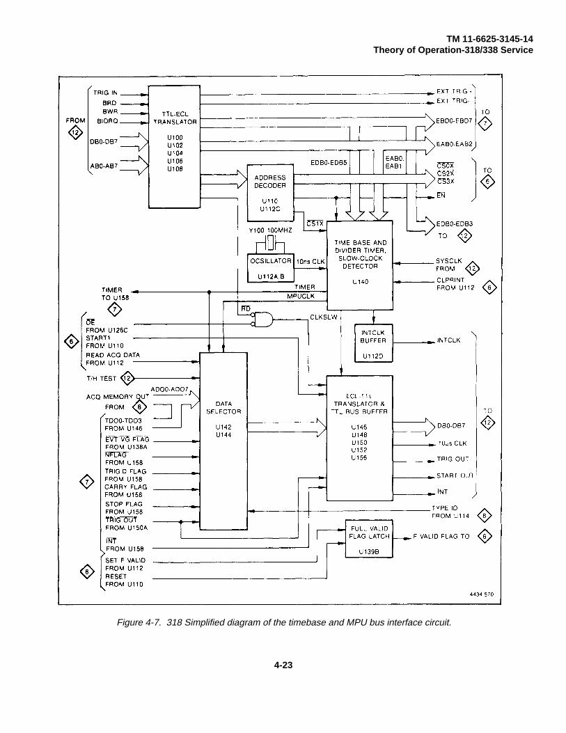
TM 11-6625-3145-14Theory of Operation-318/338 Service
Figure 4-7. 318 Simplified diagram of the timebase and MPU bus interface circuit.
4-23
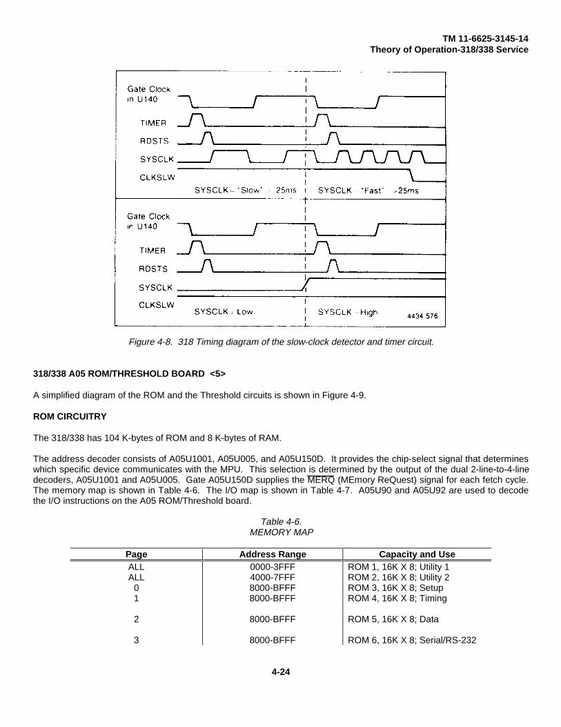
TM 11-6625-3145-14Theory of Operation-318/338 Service
Figure 4-8. 318 Timing diagram of the slow-clock detector and timer circuit.
318/338 A05 ROM/THRESHOLD BOARD <5>
A simplified diagram of the ROM and the Threshold circuits is shown in Figure 4-9.
ROM CIRCUITRY
The 318/338 has 104 K-bytes of ROM and 8 K-bytes of RAM.
The address decoder consists of A05U1001, A05U005, and A05U150D. It provides the chip-select signal that determineswhich specific device communicates with the MPU. This selection is determined by the output of the dual 2-line-to-4-linedecoders, A05U1001 and A05U005. Gate A05U150D supplies the MERQ (MEmory ReQuest) signal for each fetch cycle.The memory map is shown in Table 4-6. The I/O map is shown in Table 4-7. A05U90 and A05U92 are used to decodethe I/O instructions on the A05 ROM/Threshold board.
Table 4-6.MEMORY MAP
Page Address Range Capacity and UseALL 0000-3FFF ROM 1, 16K X 8; Utility 1ALL 4000-7FFF ROM 2, 16K X 8; Utility 2
0 8000-BFFF ROM 3, 16K X 8; Setup1 8000-BFFF ROM 4, 16K X 8; Timing
2 8000-BFFF ROM 5, 16K X 8; Data
3 8000-BFFF ROM 6, 16K X 8; Serial/RS-232
4-24

TM 11-6625-3145-14Theory of Operation-318/338 Service
Table 4-6. (cont.)MEMORY MAP
Page Address Range Capacity and UseALL C000-DFFF ROM 7, 8K X 8; Jump
TableALL E000-E7FF NVM RAM, 2K X 8ALL E800-EFFF Display RAM, 2K X 8ALL F000-F7FF RAM 1, 2K X 8ALL F800-FFFF RAM 2, 2K X 8
Table 4-7.I/O MAP
Address Range I/O Use Board #
00-1F INPUT A&B board A01 & A02
20-3F INPUT A&B board A01 & A02
40-5F ACQ A&B board A03 & A04
60-7F ACQ A&B board A03 & A04
80-9F Option board A07
A0-BF No use
C0-DF No use
E0-FF Mainframe A05, A06, A09, A10
THRESHOLD CIRCUIT
The threshold circuit consists of a dual digital-to-analog (D/A) converter, analog switches, and an I/O decoder.
D/A Converter. The D/A converter consists of A05U70, A05U75, A05U80, A05U85, and A05U130B. A05U70 andA05U80 are D/A converter ICs. A05U75 and A05U85 are dual-OP amplifiers, which convert double eneded to singleended output. A05U130B supplies a reference standard voltage source (3.2 V).
Analog Switches. The analog switch consists of A05U100, A05U105, A05U110, A05U111, A05U112, A05U113,A05U114, A05U120, A05U125, and A05U130A. A05U100 and A05U105 are 1/0 data latch circuits that perform threedifferent functions. They hold data that selects the type of threshold (TTL, V1, V2, or V3). They hold data that selects thepage of the ROM; and they hold data that selects the CROM or the KBMASK. A05U110 to A05U114 are analog-switchICs that select the threshold voltage determined by the latched data from A05U100 and A05U105. A05U120, A05U125,and A05U130A convert high-output impedance to low.
4-25

TM 11-6625-3145-14Theory of Operation-318/338 Service
Figure 4-9. 318/338 Simplified diagram of the ROM and threshold circuits.
4-26
TM 11-6625-3145-14Theory of Operation-318/338 Service
318/338 A06 MPU/DISPLAY BOARD <11>
A simplified diagram of the keyboard, the MPU circuits, and the display circuits is shown in Figure 4-10. The mainelements of these circuits are the MPU, the Display Controller, the Interrupt Gate stages, the RAMs, and the front panelkeyboard controls.
MPU
The Z-80A microprocessor unit (A06U200) is the heart of the 318/338. All other stages of the circuitry either provide datato the MPU and receive instructions from it, or they accept data from the MPU and issue instructions to it.
Due to the complexity of the MPU’s operation, a complete description of A06U200 is not provided. If detailed information isneeded, refer to the Z80-CPU, Z80A-CPU Technical Manual published by Zilog.
RAM
Temporary storage of data and addresses for the MPU, and storage of data acquired from the probe input, is provided byRAMs A06U400 and A06U401.
BUS DRIVERS
The bus drivers consist of A06U210, A06U212, A06U214, and A06U216, A06U210 and A06U212 are address bus drivers,A06U216 is a data bus transceiver, and A06U214 is an MPU control driver (inverted). These drivers send or receive theMPU signals to or from other boards.
KEYBOARD AND KEYBOARD CONTROLLER
Control inputs from front-panel keys (except for the STOP key) are encoded by A06U300 and A06U310. When a key ispressed, X-axis lines (KBX0-KBX7) and Y-axis lines (KBY0-KBY7) supply a data matrix of the key pressed to A06U300and A06U310.
A06U301 encodes eight X-axis lines to three binary lines; A06U300 encodes eight Y-axis lines to three binary lines. Thesesignals and the Key Push Acknowledge (KPA) signal are sent to the MPU data bus via tri-state bus buffer A06U320.A06U320 is controlled by KB CS (MPU I/O address = EO read) from the A05 ROM/Threshold board<10>.
The KPA signal generates the key interrupt signal using A06R320, A06C320, and A06U220. A06R320 and C320 form anintegration circuit, which deletes KPA chattering. KPA without chattering is supplied to A06U220C pin 9.
A06U220 is a Quad 2-Input NAND Schmitt Trigger that controls the keyboard interrupt mask or unmask by KBMASK(MPU I/O address = F2 bit 3 write) from the A05 board.
INTERRUPT GATES
The interrupt gates consist of A06U220 (Quad NAND Schmitt Trigger).
DISPLAY CONTROLLER
The display controller consists of A06U130, A06U134, A06U138, A06U500, A06U510, A06U515, A06U520, A06U525,A06U530, A06U540, A06U542, and A06Q550.
4-27

TM 11-6625-3145-14Theory of Operation-318/338 Service
A06U 130 is the TV timing generator for the display control of the 318 and the 338. It generates C-SYNC (CompositeSYNC), HD (Horizontal Drive), VD (Vertical Drive), and CBL (Composite Blanking) from the output signal of A06U120B(244.4 ns clock).
A06U134 gates A, B, and C generate the blinking clock signal (about 30 Hz) for A06U500. A06U500 is a display control IC;it consists of a display counter, address bus multiplexer, Z-axis generator, and Z-axis controller. The display counterdetermines the location of the FONT in the screen, and either blanks or unblanks the display.
The address bus multiplexer selects the output of either the display counter or the MPU address for the display RAM(U515).
The Z-axis generator generates the Z-axis signal from the output of the character ROM (A06U530). The Z-axis controllercontrols the Z-axis signal (inverse, blank underscore, or blinking) and generates the trace edge for timing displays.
The data bus transceiver stage of the display controller consists of A06U510 and A06U525. This stage controls the datacommunication between the MPU and the display RAM, and allows the MPU to either write data into or read data from thedisplay RAM while the display RAM address is accessed by the MPU.
Character latch A06U520 latches the 8-bit data read-out from the display RAM. The latched data is maintained for sevendisplay clock cycles to achieve seven dots of display per character. Data input to the character latch stage is provided andlatched on the positive-going edge of the character latch clock.
Character ROM A06U530 provides the character fonts which allow a variety of displays. Each character font in this ROMis composed of a 7 X 8-dot matrix and is selected by the 8-bit signal from the character latch stage and a 1-bit signal(CROM) from the A05 board. The CROM bit selects either a parallel-mode character or a serial-mode character.
Each of the eight lines of a character font are selected by the line select signal from the display counter. The seven dotson each line of a character font are read out from the ROM when that character is addressed. The 7-bit parallel outputdata is loaded into shift register A06U500 (Z-axis generator) by the clock and is shifted out in serial format to be used as aZ-axis signal.
A06U505, A06U540, and A06Q550 comprise the video generator and CRT driver. The video generator is a 2-bit (4-level)Digital-to-Analog (DIA) converter.
The output level of the DIA converter is shown as follows:
Video OutC-SYNC INV Z Glitch Volts
H X X -0.3L L L 0.7L L H 0.4L H X 0
4-28

TM 11-6625-3145-14Theory of Operation-318/338 Service
Figure 4-10. 318/338 Simplified diagram of the MPU/Display board.
4-29

TM 11-6625-3145-14Theory of Operation-318/338 Service
318/338 A07 SERIAL, NON-VOLATILE MEMORY, RS232C <17> <18>
SERIAL INPUT <17>
The serial input circuit consists of an input comparator, an offset adjustor, and a clock level translator. It provides serialdata and external clock signals for serial operation. A simplified diagram of the serial input circuit is shown in Figure 4-11.
Input Comparator. The input comparator consists of an FET input pre-amp (A07U100) and a comparator (A07U110).Serial data applied to pin #3 of A07U100 is amplified two-and-one-half times and output on pin 6. Pin 6 is connected to pin2 of A07U110. The threshold voltage is applied to pin 3 of A07U110. Comparator A07U110 compares the serial datainput at pin 2 with the threshold voltage input at pin 3. If the serial data input voltage is higher than the threshold voltage,A07U110 issues a high TTL output at its pin 7.
Offset Adjust. The serial data offset is adjusted by one potentiometer, A07R23. Input serial data is monitored at TP10,and threshold voltage is monitored at TP11. The data 0 volt level can be adjusted to equal the threshold 0 volt level bytweaking A07R23.
Clock-Level Translator. The clock level translator is comparator A07U111. The ECL-level external clock signal from theA02 Input B board connects to pin 2 of A07U111, and the input at pin 3 of A07U111 is set at -1.25 V. ComparatorA07U111 compares the external clock signal at pin 2 with the -1.25 V at pin 3. If the external clock voltage is higher than -1.25 V, A07U111 will issue a TTL output at pin 7.
NON-VOLATILE MEMORY <17>
The non-volatile memory circuit provides battery backup operation for the non-volatile memory. It consists of the thresholdvoltage detector, the chip select controller, the battery switch, the battery voltage checker, and a random access memory.
Threshold Voltage Detector. The threshold voltage detector consists of comparator A07U120 and a 3-volt Zener diode,A07VR100.
Comparator A07U120 compares Vcc - 3 volts (2 volts at this point) at pin 3 with the threshold voltage at pin 2. If Vcc ismore than 4.6 volts A07U120 will output a low at pin 7. When Vcc is less than 4.6 volts, pin 3 is lower than the thresholdvoltage, and A07U120 will output a at pin 7. When the output signal at pin 7 of comparator A07U120 is high, it indicatesthat Vcc is low. If the output of A07U120 is not correct, adjust A07R101 using the adjustment procedure in Section 5.
Chip Select Controller. The chip select controller consists of A07U21C, A07Q120, and A07Q150, The Vcc LOW signalis connected to the base of A07Q120. When system power starts to fail, the Vcc LOW signal changes to high andA07Q120 turns OFF. Then, the input at pin 10 of A07U21 quickly changes to low. When the system power comes backup, the Vcc LOW signal falls to low and A07Q120 turns ON. Then the input at pin 10 of A07U21 becomes high, and pin 11of A07U21 slowly rises to high.
The output at pin 8 of A07U21 is connected to the base of A07Q150. When Vcc is LOW, A07Q150 is OFF and pin 18 ofA07U7 (chip select) stays high. When Vcc voltage is normal (not LOW) A07Q150 is controlled by the NVMCS (non-volatile chip select) signal.
4-30

TM 11-6625-3145-14Theory of Operation-318/338 Service
Figure 4-11. 318/338 Simplified diagram of the serial acquisition and RS-232C circuit.
Battery Switch. The battery switch circuit consists of A07Q140, A07Q141, A07C160, and A07CR170. When the systempower comes up, A07Q140 and A07Q141 turn ON. Pin 18, connected through a 2K resistor, and pin 24 of A07U7 areconnected to the Vcc line. When the system power goes down, A07Q140 and A07Q141 turn OFF. Pin 24 and pin 18 ofA07U7 are connected to the battery power. A07CR170 protects the battery from charging. A07C160 adjusts the switchingspeed between two power sources.
Battery Voltage Checker. The battery voltage checker circuit consists of A07Q170 and A07U32D. A07Q170 comparesthe battery voltage supplied to its base with the voltage at its emitter (2.90V). If the battery voltage is low (<2.2V), the inputat pin 9 of U32 is high. If the battery voltage is normal (>2.2V), A07U32 pin 9 is low. Pin 8 of A07U32 is tied to the CPUvia data bus line 7.
Random Access Memory. A07U1 is a 2040-byte random access memory. It uses a battery backup power source toretain data when system power is off.
4-31

TM 11-6625-3145-14Theory of Operation-318/338 Service
SERIAL DATA ACQUISITION <18>
The serial data acquisition circuit consists of the data bus buffer, I/O selector, baud rate selector, external trigger latch, andserial I/O controller. It provides the serial data acquisition function. A simplified iagram is shown in Figure 4-11.
Data Bus Buffer. Bidirectional bus transceiver A07U25, with tri-state outputs, serves as the data bus buffer, allowing datatransmission either from the A-side bus to the B-side bus or from the B-side bus to the A-side bus of the buffer. The logiclevel on the BRD line controls the direction of data transmission, and the I/O ENABLE line either enables or isolates theentire transceiver.
The I/O ENABLE line is enabled when I/O addresses 80 through 9Fhex, or the NVMCS (Non-volatile Memory Chip Select),are asserted. These two conditions are selected by A07U21A and A07U13.
Control of the data transmission direction and bus isolation is accomplished as depicted in Table 4-8.
Table 4-8.DATA BUS BUFFER CONTROL
I/O Enable RD Data Transmission
Low Low B side to A side
Low High A side to B side
High X (don’t care) Isolated
I/O Selector. The I/O selector A07U30 allows the MPU to address five I/O devices. A07U30 is enabled when the busBM1 signal is false (low), the BWR or BRD signal is true (low), and I/O addresses 80 through 93hex are selected.
The output of A07U30 is controlled by bus lines A4, A3, and A2, supplied to pins 3, 2, and 1, respectively.
The functions and addresses of selected I/O operations are shown in Table 4-9.
Baud-Rate Selector. The baud-rate selector circuit consists of a programmable bit rate generator (A07U6), and bus datalatches A07U31 and A07U22A. The programmable bit-rate generator A07U6 supplies the receiver clock signal to theSlO’s PORT-A. The output clock rate of its pin 10 is determined by the logic input at its pins 11, 12, 13, and 14 (S3through S0, respectively).
The output positive-going edge at pin 12 of I/O selector A07U30 allows A07U31 and A07U22A to latch data. That latcheddata (D7, D6, D5, and D4) output is applied to inputs S3-S0 of A07U6.
Latched data from D4 has another function. It selects the clock used as input at pin 15 of A07U6 (either 19.2K baud or theexternal clock). The chip select function operates when S1, S2, and S3 are low The clock select signal at A07U6 pin 15 iscalled IM. Inverter A07U20A inverts and shapes the baud-rate clock. Table 4-10 shows the 16 input combinations and thecorresponding output rates.
4-32

TM 11-6625-3145-14Theory of Operation-318/338 Service
External Trigger Latch and Data Polarity. Latched data D3 of A07U31 is applied to pin 10 of A07U1 2C. This signal isused to select the external trigger polarity. If the polarity is positive, the external trigger’s positive-going edge setsA07U22B. If polarity is negative, the external trigger’s negative-going edge sets A07U22B. A negative-going edge frompin 14 of the I/O selector A07U30 resets A07U22B.
The MPU can read the status of A07U22B at pin 3 (DO) of tri-state output buffer A07U32. The out- put signal at pin 15 ofI/O selector A07U30 controls the enable line of A07U32.
Latched data D2 from A07U31 is applied to pin 1 of A07U12A. This signal is used to select input data polarity.
Serial I/O Controller. The serial Input/Output controller (SIO, device A07U2) handles serial-to-parallel interfacing.
When receiving data, the SIO checks for stop bits, parity, sync characters, framing errors, and overrun errors. Whentransmitting data, the SIO handles such tasks as sync character insertion, adding parity bits, and adding stop bits.
The Z-80A CPU supplies the CPU clock signal to SIO pin 20 as the control clock (3.68 MHz). A07U12B and U32B adjustthe clock waveform before it reaches the SIO.
When the SIO generates an interrupt, it generates a low signal at pin 5 that ties to the bus INT line.
The SIO contains two serial data tranceivers: PORT-A receives data on pin #12 and a clock on pin 13, PORT-B receivesdata on pin 28 and a clock on pin 27. PORT-A is used for serial data acquisition and PORT-B is used for RS-232 control.
The SIO contains two signal sets for modem control, but only one set is used for RS-232 modem control. The RS-232modem control input signals (pins 22 and 23) and input data spin 28) are tied to the RS-232 receiver, A07U40. TheRS-232 modem control output signals (pins 24 and 25), and out-put data (pin 26) are tied to the RS-232 transmitter,A07U41.
In this system, the SIO is mapped by I/O address. Assigned SIO addresses are 90 and 91 for PORT-A, and 92 and 93 forPORT-B. The output at pin 11 of I/O selector A07U30 is tied to pin 35 of the SOG. Bus AB1 is tied to SIO pin 34, and busABO is tied to pin 33. These three inputs control SIO addressing.
Table 4-9.OPTION I/O DEVICE ADDRESSING AND FUNCTION
AB4 AB3 AB2 Address Function
L L L 80 - 83 Read status (external trigger, battery voltage, modem DSR).
L L H 84 - 87 Reset external trigger latch.
L H L 88 - 8B Set RS-232 bit rate generator.L H H 8C - 8F Set SERIAL bit rate generator, data polarity, external trigger
polarity.
H L L 90 - 93 Select SIO.H L H 94 - 97 Not used.H H L 98 - 9B Not used.H H H 9C - 9F Not used.
4-33

TM 11-6625-3145-14Theory of Operation-318/338 Service
RS-232 CONTROL <18>
The RS-232 control circuit consists of the baud-rate selector, level converter, and serial I/O controller. This circuit providesthe remote control operation. A simplified diagram of this stage is shown in Figure 4-11.
Baud-Rate Selector. The baud-rate selector circuit consists of a programmable bit-rate generator (A07U5), and a datalatch (A07U45).
Programmable bit-rate generator A07U5 supplies the receive and transmit clock signals to SIO PORT-B. This clock rate isdetermined by the logic inputs on A07U5 pins 11, 12, 13, and 14 (S3 through S0, respectively).
The output positive-going edge at pin #13 of I/O selector A07U30 latches data at A07U45. This latched data (D7, D6, D5,and D4) is supplied to the S3 through S0 inputs of A07U5.
The input clock rate for A07U5 is the same as for A07U6; 19.2K baud and external clock for RS-232 are not used. (Referto Table 4-10.)
Level Converter. The level converter stage consists of the RS-232 transmitter A07U41 and the RS-232 receiver A07U40.Transmitter A07U41 converts TTL-level signals to RS-232 level, and receiver A07U40 converts RS-232 level signals toTTL level.
RS-232 transmit signals (TXD, RTS, DTR) are controlled by SIO PORT-B. Receive signals (RXD, CTS, DSR, CD) arecontrolled by the external device.
The DRS signal status appears at pin 11 of A07U32.
Serial I/O Controller. Refer to the Serial Acquisition section.
Table 4-10.PROGRAMMABLE BIT-RATE GENERATOR OUTPUTS
S3 S2 S1 S0 Output RateL L L L EXTERNAL CLOCKL L L H 19.2K baudL L H L 50 baudL L H H 75 baudL H L L 134.5 baudL H L H 200 baudL H H L 600 baudL H H H 2400 baudH L L L 9600 baudH L L H 4800 baudH L H L 1800 baudH L H H 1200 baudH H L L 2400 baudH H L H 300 baudH H H L 150 baudH H H H 110 baud
Input SERIAL-CLOCK is 2.4576 MHZ.
4-34
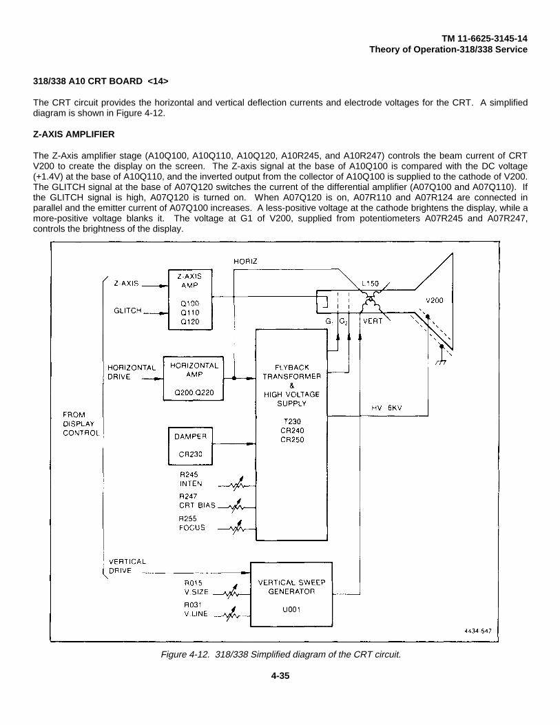
TM 11-6625-3145-14Theory of Operation-318/338 Service
318/338 A10 CRT BOARD <14>
The CRT circuit provides the horizontal and vertical deflection currents and electrode voltages for the CRT. A simplifieddiagram is shown in Figure 4-12.
Z-AXIS AMPLIFIER
The Z-Axis amplifier stage (A10Q100, A10Q110, A10Q120, A10R245, and A10R247) controls the beam current of CRTV200 to create the display on the screen. The Z-axis signal at the base of A10Q100 is compared with the DC voltage(+1.4V) at the base of A10Q110, and the inverted output from the collector of A10Q100 is supplied to the cathode of V200.The GLITCH signal at the base of A07Q120 switches the current of the differential amplifier (A07Q100 and A07Q110). Ifthe GLITCH signal is high, A07Q120 is turned on. When A07Q120 is on, A07R110 and A07R124 are connected inparallel and the emitter current of A07Q100 increases. A less-positive voltage at the cathode brightens the display, while amore-positive voltage blanks it. The voltage at G1 of V200, supplied from potentiometers A07R245 and A07R247,controls the brightness of the display.
Figure 4-12. 318/338 Simplified diagram of the CRT circuit.
4-35
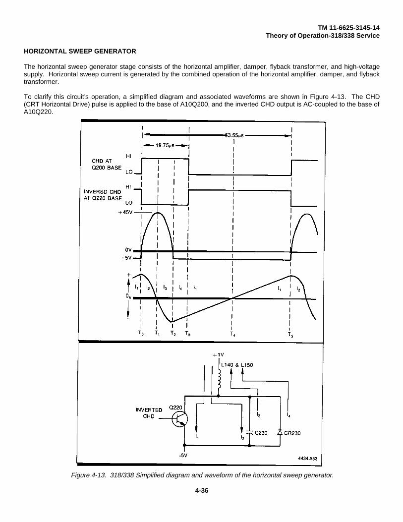
TM 11-6625-3145-14Theory of Operation-318/338 Service
HORIZONTAL SWEEP GENERATOR
The horizontal sweep generator stage consists of the horizontal amplifier, damper, flyback transformer, and high-voltagesupply. Horizontal sweep current is generated by the combined operation of the horizontal amplifier, damper, and flybacktransformer.
To clarify this circuit’s operation, a simplified diagram and associated waveforms are shown in Figure 4-13. The CHD(CRT Horizontal Drive) pulse is applied to the base of A10Q200, and the inverted CHD output is AC-coupled to the base ofA10Q220.
Figure 4-13. 318/338 Simplified diagram and waveform of the horizontal sweep generator.
4-36

TM 11-6625-3145-14Theory of Operation-318/338 Service
Assume that A10Q220 is conducting just before TO and that the current 11 is passing through A10Q220. A10Q220 isturned off at TO by the inverted CHD pulse. The energy stored in L140 and L150 is discharged through A10C230, causingcurrent 12. Current 12 charges up A10C230 to about + 45 volts at T1. The stored energy in A10C230 is dischargedduring the time interval T1 to T2. Discharging current 13 charges L140 and L150, causing the A10Q220 collector voltageto go negative. When the A10Q220 collector voltage goes negative to more than -5 volts at T2, diode A10CR230conducts. The stored energy in L140 and L150 is then discharged through A10CR230, and, at the beginning of T3,through A10Q220. The discharging current decreases to zero at T4. Therefore, L140 and L150 stop discharging and arecharged again in the opposite direction by charging current I1.
Current I1 increases until A10Q220 is turned off again. The A10Q220 collector waveform is shown in Figure 4-13 as theideal waveform; the actual waveform may contain more noise. The collector voltage at A10Q220 is applied to the primarywinding of T230. This transformer provides voltages for G1, G2, and the anode input of the CRT. It also provides voltagefor the Z-axis amplifier. A high-voltage multiplier is included in the flyback transformer box.
VERTICAL SWEEP GENERATOR
The vertical sweep generator stage consists of IC A10U001 which produces the sawtooth current for vertical deflection inyoke L150. The VD (Vertical Drive) signal’s 0.572 ms pulse triggers this circuit every 16.6 ms.
IC A10U001 consists of a triggerable astable multivibrator, sawtooth generator, and output amplifier.
The astable multivibrator’s time-constant is determined by A10R002, A10R005, and A10C005, and locked by the VD pulseat 16.6 ms. The output signal of the multivibrator generates a sawtooth signal when A10R010, A10R015, A10C010, andA10C015 charge and discharge. The sawtooth signal is AC-coupled to pin 7 on A10U001. Amplifier A10U001 drives thevertical deflection yoke L1 50.
318/338 All POWER SUPPLY <15> <16>
The power supply circuit provides the operating power for this instrument from the ac line-voltage source.
Figure 4-14 is a simplified block diagram of the power supply circuit.
LINE INPUT <15>
Power is applied through the line filter FL1, line fuse F1, power switch A12S1, and thermal cutout switch S3. The line filteris designed to keep power-line interference from entering the instrument and to keep the approximately 50-kHz invertersignal from entering the power line.
Line voltage selector switch S2 allows the instrument to operate from either a 115 or 230 volt nominal line voltage source.In the 115V position, rectifier A11CR1 01 operates as a full-wave voltage doubler with energy-storage capacitors A11C121and A11C122. The voltage across the two capacitors in series is the approximate peak-to-peak value of the 115 volt line.For 230 volt operation, A11CR101 is connected as a bridge, supplying approximately the peak value of the 230 volt line.Thus, the dc voltage applied to the inverter stage is about the same for either 115 or 230 volt operation.
4-37

TM 11-6625-3145-14Theory of Operation-318/338 Service
Figure 4-14. 318/338 Simplified diagram of the power supply circuit.
Thermistors A11RT101 and A11RT102 limit the surge current when the power supply is first turned on. After theinstrument is in operation, the resistance of the thermistors decreases so that they have little effect on the circuit. Whenthe instrument is turned off, the Inverter Control stage turns off the inverter, preventing it from discharging A11C121 andA11C122; A11C121 and A11C122 discharge slowly, through A11R121 and A11R122, to allow for thermistor thermalrecovery. This ensures sufficient thermistor resistance to limit the turn-on surge current to a safe level. Since A11C121and A11C122 discharge slowly, dangerous voltages exist within the power supply for several minutes after the POWERswitch is turned off.
Varistors A11VR101 and A11VR102 are surge voltage protectors. If a peak voltage greater than 240 volts is present onthe line, A11VR101 and A11VR102 will conduct and quickly open line fuse F1 to interrupt the input power before theinstrument can be damaged.
INVERTER START NETWORK <15>
Capacitor A11C132 is charged by a constant current source, made up of A11Q131, A11VR131, and A11R132. When thecharge of A11C132 reaches the voltage level set by A11VR135, A11CR138, and the base-emitter voltage of A1Q135,transistors A11Q135, A11Q134, A11Q140, A11Q139, and switching transistor A11Q149 are turned on, A11C132 isdischarged, and energy-storage capacitor A11C155 for A12U21 <16> and A12U1 <16> is charged. When the charge onA1C155 reaches the voltage level required to start A12U21, A12U21 charges A1C143 through A11T140. This causestransistor A11Q141 to turn on and A11Q131 to turn off. This disables the inverter start network after the instrument is on.
4-38

TM 11-6625-3145-14Theory of Operation-318/338 Service
INVERTER CONTROL <16>
The inverter control stage, made up primarily of A12U21, provides voltage regulation, a dead-time controller, and a currentlimiter. For regulation purposes, A12U21 varies the hold-off time of the Inverter Switching transistor. Under normaloperating conditions, only pin 2 of A12U21 controls the hold-off time. However, either the dead-time controller or thecurrent limiter can ffect the hold-off time, or stop the inverter operation altogether. The operation of each individualfunction of the inverter control stage is described in the following paragraphs.
Regulator. A12U21 acts as a pulse width modulator to regulate the inverter circuitry. It runs the inverter at a constantfrequency and regulates by changing the duty factor of the inverter signal. This is accomplished as follows:
At the beginning of the inverter cycle, A12U21 pins 9 and 10 go high, turning on A12Q34. This provides base drive for A11Q149 through A11T140. When A12U21 senses that the -5 V supply has gone below -5 V (via divider network A12R17,A12R18, and A12R23 to A12U21 pin 2) pins 9 and 10 go low, turning off A12Q32 and thus removing removing the basedrive to A11Q149 and stopping the inverter. A11Q149 stays off until the beginning of the next inverter cycle.
The rest of the power supplies have their own regulation circuitry, which are indirectly controlled by the inverter circuitry.The -5 V supply is directly regulated by the inverter regulator; the -5 V supply then regulates the "unregulated" supplies forthe rest of the voltages.
Dead Time Controller. The dead-time controller function of A12U21 protects the power-supply components fromdamage due to excessive current or voltage. During normal operation, the voltage at pin 4 of A12U21 remains at about1.5 volts. If the Under/Over Voltage Stop stage turns on, A12U21 pin 4 voltage rises to about 5 volts, and the inverterstops. The inverter will remain off while A12C53 discharges through al 2Q58, keeping A12VR58 and A12Q59 turned off.This cycle repeats until the fault is corrected, with the inverter turned on for about 200 ms, and turned off for about 200 ms.
OVER/UNDER VOLTAGE PROTECTION <16>
Whenever the any of the regulated voltages goes out of its specified voltage window the output of A12U51C (for overlypositive voltages) or A12U51D (for overly negative voltages) goes low, causing a12U51 B pin 2 to go low. This causesA12U51 A pin 1 to go low, which turns off A12Q57, turns on A12Q32, and turns off A12Q33. This allows A12U21 pin 4(Dead Time) to go high, and thereby shuts off the inverter. A12Q58, A12Q59, and A12C58 hold the inverting input of Al2U51 A (pin 6) high until the supply voltage is back within its voltage window. At this time, A12Q58 turns on, dischargingthe A12R58, A12C58 combination, which allows pin 6 of A12U51 A to go low, thus pulling A12U21 pin 4 (Dead Time) low,and thereby restarting the inverter.
LOW VOLTAGE RECTIFIERS AND REGULATORS <16>
+12 Volt and -12 Volt Supplies. The rectifiers and the filter components are connected to secondary winding. RegulatorsA12U91 and A12U92 provide rectified, regulated positive and negative voltage.
-3.3 Volt Supply. A12U71 is a regulator. If the -3.3 volt supply output is too high, the voltage at pin 5 of A12U71decreases and the current at pin 9 of A12U71 decreases; that is, the base current of A12Q73 decreases, thus the outputvoltage of the -3.3 volt supply is decreased. Transistor A12Q71, A12R80, and A12R81 together form the current protector.If the -3.3 volt supply is shorted, the voltage on A12R80 and A1 2R81 (over-current sensing resistors) goes high; A12Q71is turned on, and A12Q73 is turned off.
4-39
TM 11-6625-3145-14Theory of Operation-318/338 Service
+ 5 Volt Supply. The + 5 volt regulator is similar to the -5 volt regulator described in detail above. Transistor A12Q1 is aswitching transistor. The inverter controller is A12U1; A12R4 is the over-current sensing resistor and A12R10, A12R11,and A12R9 are the voltage-sensing resistors.
FAN CIRCUIT AND FAN <16>
The fan used in the instrument has a brushless motor. Fan speed is controlled by the emitter voltage of A12Q65, which isdetermined by the voltage dividing ratio of A12R66, A12R68, A12R67, and A12RT65. When the temperature rises, thevoltage drop across thermistor A12RT65 decreases, and this increases the base-emitter voltage of Al 2065. As a result,the fan is accelerated.
DETAILED CIRCUIT DESCRIPTIONS FOR THE 338
The following paragraphs contain theory of operation information for the 338 Logic Analyzer. For information on the theoryof operation for the 318 Logic Analyzer, refer to the Table of Contents and preceding sections of this chapter.
338 A01 INPUT A BOARD <19> <20>A02 INPUT B BOARD <21> <22>
The Input section consists of the Input A (A01) and the Input B (A02) boards. The block diagram for these boards isshown in Figure 4-15. Since both of these boards share the same function, they are discussed as a unit in this description.
OVERVIEW
Refer to schematics <19>, <20>, <21>, and <-22,>. Data from Pod A (channels 0-7) flows to the internal buffers of theM218s on the A02 Input B board < 21 >, and their outputs are supplied to the first latches and glitch recognizers (also inthe M218s) through delay lines. Only data supplied by Pod A is processed through the glitch detection circuitry. Data fromPods B, C, and D is routed to the data buffers on the A02 Input B board <22>, and their output goes to the first latchthrough delay lines. The word recognizers work with the latched data from all four pods, and their outputs are wire-ORedon the A02 and A08 boards.
Qualifier data from each probe goes through qualifier buffer A02U250 <22> and then reaches the A03 acquisition controlboard. The address decoder on the A01 board A01U112 and A01U114 <19> generates signals to set up the wordrecognizers, select the clock, and enable the glitch trigger circuitry. When selected, an external clock signal enters theFET buffer, A02Q108 <22>, and is compared with the external clock threshold; the resulting signal is distributed throughthe clock selector to the first latches. When the internal clock is selected by the clock selector, the signal is processed inthe same manner as the external clock.
The threshold-level shifter converts threshold-level signals from the A05 ROM/Threshold board to fit the P6451 thresholdrequirements.
ADDRESS DECODER <20>
The address decoder circuit consists of A01U112 and A01U114. A01U112 decodes 1/0 addresses 00, 01, 02, and 03.A01U114 is a TTL-to-ECL-level converter. I/O address 00 (A01U114 pin 2) is for writing trigger word data into the wordrecognezer (WR) for channels 0 through 15. I/O address 01(A01U114 pin 1) is used to write trigger word data into the
4-40

TM 11-6625-3145-14Theory of Operation-318/338 Service
Figure 4-15. 338 Input A and Input B block diagram.
word recognizer for channels 16 through 31. The I/O address 02 (A01U114 pin 12), resets the WR address counter. TheI/O address 03 (A01U114 pin 14) is the clock selecter port. I/O address 02 also controls the glitch trigger shift register,which enables the glitch trigger circuit.
GLITCH CONTROL (CH 0-7) <21>This circuit controls only the M218s <21> on the A02 board (data from Pod A). M218’s pin 15 controls the glitch output ofPin 14. Pin 14 issues a high-level signal if a glitch is captured. By setting pin 15 to high, the output of pin 14 is disabled(kept low); if pin 15 is low, an output on pin 14 is enabled. Therefore, if a glitch trigger on a certain line is expected, thecorresponding M218’s pin 15 must be low. Since all M218’s pins 14 are wire-ORed, a glitch trigger occurs when any of
4-41

TM 11-6625-3145-14Theory of Operation-318/338 Service
M218’s glitch trigger outputs moves to high. A02U224 <21> receives the glitch trigger enable data serially and sends it tothe M218s in parallel. A02U224 controls the M218's pin 15. This is a shift register and can have data written to it in serial.Data writtern to this shift register from the MPU is adjusted by A02U226 to fit M218's special input level requirements.
WORD RECOGNIZER <21>The word recognizer (WR) consists of three 32-channel word recognizers incorporating high-speed memories. The 338offers three WR functions, where three different words may be set up at once. They are named trigger words A, B, and C.To load data into the WRs, the MPU resets the WR address counters A01U100 <19>, A01U102 <19½>, A01U104 <19>,A01U106 <19>, A01U108 <19>, A01U110 <19>, A02U220 <21> and A02U222 <21>. The MPU then writes the dataaccording to the trigger words eight channels at a time. If the WR address counter value is equal to the trigger word, 0 iswritten into the corresponding WR; otherwise 1 is loaded. The MPU then increments these WR address counters by oneand loads data as above. This operation is repeated 256 times. For example, if the trigger word A is 78310827hex, theMPU resets the WR address counters and increments A01U104 and A01U106 to 08, and writes 0 to A01 U118 pin 6. TheMPU then increments A01U108 and A01U110 to 27 and writes 0 to A01U120 pin 6. Then it increments A01U100 andA01U102 to 31 and writes 0 to A01U122 pin 6, and increments A02U220 and A02U222 to 78 and writes 0 to U218 pin 6.A1 is written into the other addresses. Before an acquisition starts, these WR address counter outputs are reset to 0, andthe MPU changes 10016's on the A01 board to latch mode and sets the output of M218s on the A02 board to on. Duringan acquisition, if the trigger word is latched, the corresponding WR issues a 0 and that trigger line goes to 0.
THRESHOLD BUFFER <22>The currents from the edge-connecter 38B, 39A, 39B, and 40A are applied to the inverting inputs of A02242A, A02U242B,A02U242C, and A02U242D <22> which have a gain of minus one. The currents from pin 5 of J200, J202, J204, and J206are supplied to the non-inverting inputs of these amplifiers to be summed. The output currents of these amplifiers aresupplied through A02R234A, A02R234B, A02R234C, and A02R234D, respectively, to the parallel data probe.
PROBE COMPENSTATION <21> <22>When in the probe compensation mode, an external clock is supplied to the acquisition memory as data through gatesA02U252-A <22> and A02U252-B <21>. Channel 0 is used as trigger and channel 1 is used for data. The MPUrecognizes over- or under-compensation from the aquired data on channel 1. (Channel 1 is the result of the clockcompared with threshold A.) In this mode, A02U234 pin 15 <21> is set to high in order to maintain a high output level atA02U220 <21> and A02U222 <21>.
338 A03 ACQ CONTROL BOARD <5> <6> <7>The A03 acquisition control board (parallel data) contains two registers and memory that acquisition parameters areloaded into before data acquisition. It also contains other circuitry that controls the trigger sequence and the acquisitionmemory.
The simplified block diagrams are shown in Figures 4-16 and 4-17. Figure 4-16 shows the I/O address decoders, startlogic, clock qualify/SQRAM data register, qualify circuit, and strobe generator circuit.
4-42

TM 11-6625-3145-14Theory of Operation-318/338 Service
Figure 4-16. 338 Simplified diagram of the ACQ control circuitry on schematics <5> and <6>.
Figure 4-17 shows the external and glitch trigger circuitry, retiming flip-flops, address buffer, SQRAM, trigger sequencercircuit, SQRAM Data/Word recognizer, data selection circuit, and LSI-A.
4-43
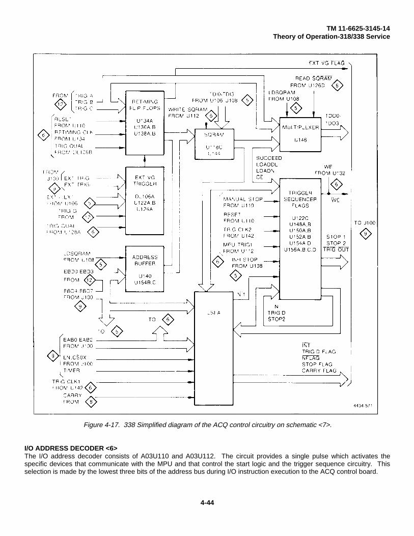
TM 11-6625-3145-14Theory of Operation-318/338 Service
Figure 4-17. 338 Simplified diagram of the ACQ control circuitry on schematic <7>.
I/O ADDRESS DECODER <6>The I/O address decoder consists of A03U110 and A03U112. The circuit provides a single pulse which activates thespecific devices that communicate with the MPU and that control the start logic and the trigger sequence circuitry. Thisselection is made by the lowest three bits of the address bus during I/O instruction execution to the ACQ control board.
4-44

TM 11-6625-3145-14Theory of Operation-318/338 Service
QUALIFY/SQRAM DATA REGISTER <5>The qualify/SQRAM data register consists of A03U106, A03U108, A03U102, and A03U104. The MPU writes the qualifydata into U106 at I/O address 50hex, U108 at I/O address 51hex, and into A03U102 and A03U104 at I/O address 52hex.
The data format is illustrated in Figures 4-18 and 4-19.
Figure 4-18. 338 SQRAM data register format.
Figure 4-19. 338 Qualify register format.
4-45

TM 11-6625-3145-14Theory of Operation-318/338 Service
QUALIFY LOGIC <5>The qualify logic consists of A03U100, A03U114A, A03114B, A03U114C, A03U116A, A03U116B, A03U116C, A03U118A,and A03U118B. The qualifier signals QA, QB, QC, and QD from the A02 INPUT B board go to gate A03U100, where theyare converted into inverting and non-inverting signals. The signals are wire-ANDed with the outputs of qualify registersA03U106, A03U108, A03U102, and A03U104, and go to EXOR gates A03U114, A03U116, and A03U118 where theirpolarities are selected according to the polarity selection bits of A03U102, A03U104, A03U106, and A03U108. Eachoutput of the XOR gates is wire-ANDed to form the trigger and clock qualify signals. These two signals go to gatesA03U126A and A03U126B <6> of the start logic.
START/STOP LOGIC <6>The start/stop logic consists of A03U124B, A03U126A, and A03U126B. When the data acquisition starts, a START1pulse is generated at I/O address 56hex and goes to the clock input of A03U 1 24B.
The output signal of this flip-flop enables the TRIG QUAL1 and CLOCK QUAL signals to pass through gates A03U126Aand A03U126B to the inputs of the trigger qualify and the clock qualify flip-flops.
START2 is issued at I/O address 55hex to get the acquired data from the ACQ memory on the A04 board. The MPU setsthe data by incrementing the address counter on the A04 board at I/O address 54hex.
At the end of the data acquisition, the STOP1 signal is issued by the output of the STOP flag. At the end of the read fromACQ memory operation, MANUAL STOP is generated at I/O address 53hex.
TRIGGER QUALIFY FLIP-FLOP <6>The trigger qualify flip-flop consists of A03U128A. The trigger qualify signal is clocked into the Dtype flip-flop every systemclock.
The output of the flip-flop connects to one of the retiming flip-flops through delay line A03DL106B.
RETIMING CLOCK <6>The retiming clock circuit consists of A03U128B, A03C100, A03R136, A03DL102, A03U134B, and A03U142C <6>. Thepulse generated by A03U128B, A03C100, and A03R136, called the retiming clock genarator, goes through delay lineA03DL102 to the clock pin of A03U134B.
The pulse delay time is adjusted by selecting a tap of J200. The pulse is used as the retiming clock by which the triggerdata is latched into the retiming flip-flops.
CLOCK QUALIFY FLIP-FLOP <6> The clock qualify circuit consists of A03U130, A03DL100B, A03DL100A, A03U142D,A03R130, and A03C1025. The pulse generated by A03U130A and A03DL100B goes through A03DL100A and A03U142Dto the clock pins of A03U130B, A03U132A, and A03U132B as the trigger pulse for the strobe generators.
4-46

TM 11-6625-3145-14Theory of Operation-318/338 Service
STROBE GENERATOR <6>The strobe generator contains the write enable (WE) circuit, teh address clock (ADRSCLK) circuit, and the trigger clock(TRIGCLK1, TRIGCLK2) circuits.
The WE clock circuit consists of A03U132B, A03R112B, A03R132, and A03C106 <6>. The output of A03U132B is wire-ORed with the output of the STOP flag and goes to the write enable inputs of the ACQ memory on the A04 ACQ Memoryboard <8>.
During data acquisition, the data acquired from the parallel data probes is written into memory at the location pointed to bythe address counter. At the end of the data acquisition phase, the output of the STOP flag pulls the WE signal line high,and data acquisition stops.
The width of the WE pulse is determined by the adjustable capacitor A03C104.
The address clock (ADRSCLK) circuit consists of A03U132A, A03R122A, A03R134, and A03C104 <6>. The ADRSCLKpulse generated by this circuit is applied to the clock inputs of the address counter (A04U136 and A04U138 <8>) on theA04 ACQ Memory board.
During data acquisition, the address clock pulse ADRSCLK is supplied to the address counter to determine the address forthe ACQ memory on the A04 board.
In the data read mode, the address clock is generated by STEP CLOCK.
The width of the address clock is determined by A03C104.
The trigger clock circuit consists of A03U130B, A03DL104A, A03DL104B, A03U124A, and A03U142B <6>. The pulsegenerated by A03U130B and A03DL104B goes through A03DL104A to the trigger sequencer flags, at A03U148 andA03U150, and LSI-A <7>. TRIGCLK1 goes to LSI-A; TRIGCLK2 goes to the trigger sequencer flags.
The trigger sequence advances at the rate of the TRIG clock as evens are recognized.
NOTERefer to Figure 4-17 for a simplified block diagram of the ACQ control circuitry onschematic <7>.
EXTERNAL OR GLITCH TRIGGER CIRCUIT <7>This circuit consists of A03U122A, A03U122B, A03U124A, and A03DL106A <7> .
External trigger polarity is selected by gates A03U122A and A03U122B.
Polarity data EXT ↑ and EXT ↓ come from the qualify register A03U106 <5>.
The selected external trigger signal is fed into the clock input of A03U124A. The glitch trigger is connected to the reset pinand the TRIG QUAL signal is connected to the set pin.
Flip-flop A03U124A is enabled when TRIG QUAL is low. The output of A03U124A goes to the input of one (A03U138A<7>) of the retiming flip-flops.
RETIMING FLIP-FLOP <6>The retiming flip-flops consist of A03U138A, A03U138B, A03U136A, A03U136B, and A03U134A <7>.
4-47

TM 11-6625-3145-14Theory of Operation-318/338 Service
The signals TRIG A, TRIG B, TRIG C, EXTVG FLAG, and TRIG QUAL are latched into each flip-flop by the retiming clock.
TRIG A, TRIG B, and TRIG C are issued by the word recognizers on the A01 and the A02 boards.
The outputs of these flip-flops are wire-ORed with the outputs of the address buffer (A03U140 and A03U154B andA03U154C) and go to the address inputs of the SQRAM.
ADDRESS BUFFER <7>The address buffer consists of A03U140, A03U154B, and A03U154C. These gates can be enabled only while setting upthe SQRAM.
Their outputs are used as the address to the SQRAM when loading the trigger sequencer table.
The control signal for the gates is called LDSQRAM. LDSQRAM comes from A03U108 <5>.
TRIGGER SEQUENCER RAM <7>The trigger sequencer RAM (SQRAM) is a 4-bit high-speed memory, consisting of A03U144.
This memory can be operated in either read or write mode. Before acquisition, the memory is operated in write mode.During acquisition, the SQRAM is operated in the Read mode.
To provide a trigger sequencer table to the SQRAM, the MPU writes the data already set in the data register (A03U106and A03U108 <5>) into the SQRAM at I/O address 58hex. The address to the SQRAM is supplied by the MPU data.
The memory address is determined by the current status of the retiming flip-flops. The data from SQRAM is applied to thetrigger sequencer circuit.
The data consists of four signals: CE., LOADN, LOADDN, and SUCCEED.
The CE signal enables the event/delay counter in the LSI-A.
The LOADN signal indicates that the contents of the N register in LSI-A is loaded into the event/ delay counter at the risingedge of the trigger clock.
The LOADDL signal indicates that the contents of the DL register in LSI-A are loaded into the event/delay counter by thetrigger clock, and at the same time, the delay sequence begins.
The SUCCEED signal is used when the trigger sequence is in the succeed mode. The trigger words must be satisfiedsequentially in order to generate the trigger.
TRIGGER SEQUENCER FLAG <7>The trigger sequencer flag circuit consists of A03U122C, A03U148A, A03U148B, A03U150A, A03U150B, A03U152A,A03U152B, A03U154A, A03U154D, A03U156A, A03U156B, A03U156C, and A03U156D.
It contains four main flags: N flag, TRIG’D flag, SUCCEED flag, and STOP flag.
4-48

TM 11-6625-3145-14Theory of Operation-318/338 Service
N Flag Circuit. The N flag circuit consists of A03U150B, A03U152B, and A03U152A.
The output of the carry flag of the event/delay counter N-1 (contained in LSI-A) goes low when Word A has been countedN-1 times. N-1 connects to the inputs of the N flag flip-flop.
The N-1 flag is set to high at the next word A, and held high until trigger word B arrives.
When reset word C arrives before trigger word B, the LOADN signal is issued from the SQRAM and the N flag is reset.
TRIG’D Flag Circuit. The TRIG’D flag circuit consists of A03U150A and A03U156C <7>. When the trigger word arrivesfrom the parallel data probe, the LOAD DL signal from the SQRAM goes high, and the TRIG’D flag is set at the rising edgeof the trigger clock. At the same time, the con- tents of the DL register are loaded into the event/delay counter and thedelay counting is started. The trigger circuit is looped through A03U156, so the flag can not be reset until the acquisitioncycle is complete.
SUCCEED Flag Circuit. The SUCCEED flag circuit consists of A03U148, A03U156B, and A03U154.
This flag is used only when the trigger mode is a three-word successive trigger sequence, such as "WA followed by Bfollowed by C," or "WA then B then C,’ or "WA followed by B then C.’
In this mode, when word B arrives from the parallel data probes, the SUCCEED signal from the SQRAM goes high, andthe SUCCEED flag is set at the rising edge of the trigger clock. The TRIG’D flag follows the SUCCEED flag when word Cis acquired.
If the acquired data could not form a successful trigger sequence, the LOADN signal is issued from A03U144 <7> to resetthe N flag and the SUCCEED flag.
STOP Flag Circuit. The STOP flag circuit consists of A03U154D, A03U148A, A03U122C, A03U156A, and A03U156D<7>.
The STOP flag is set after the delay counter in LSI is counted out; it disables three circuits as follows:
1. Prohibits write operations to the ACQ memory by forcing the WE signal line high.2. Disables the input clock by reseting the START flag flip-flop A03U124B <6>.3. Disables the ACQ address counter (A04U136 and A04U138 <8>) on the A04 ACQ Memory board.
When the data acquisition is restarted, the stop flag will be reset by the RESET signal.
SQRAM, DATA/WORD RECOGNIZER, DATA MULTIPLEXER <7>This circuit consists of U146<7> .It is used only for diagnostic testing of the SQRAM and the word recognizer.
LSI A A03U158 <7>LSI-A (A03U158) is a bipolar LSI circuit designed by Sony/Tektronix.LSI-A includes an address decoder, 16-bit N register, 16-bit DL register, 16-bit synchronous preloadable counter with fast-carry propagation logic, the mask register, and the acquisition status logic.
4-49

TM 11-6625-3145-14Theory of Operation-318/338 Service
Address Decoder. The address decoder provides necessary pulses for the initialization and presetting of the abovecircuits. Circuit selection is made using the three LSBs of Address from the MPU, while CS0X is low.
N Register. The N register is 16-bit register that holds the N value assigned in the trigger menu. The MPU writes the Nvalue into the N register at I/O address 41hex and 42hex.
DL Register. The DL register is 16-bit register that holds the DELAY value assigned in the trigger menu. The MPU writesthe DELAY value into the DL register at I/O address 43hex and 44hex.
Mask Register. The mask register is a 5-bit register that holds mask bits for interrupts. The MPU writes the mask datainto the mask register at I/O address 40hex.
Event/Delay Counter. The event/delay counter is a 16-bit synchronous preloadable counter with fast-carry propagationlogic. The counter is controlled by three signals: CE, LOADN, and LOADDL which are described in the followingparagraphs. The counter includes carry detection logic which generates the N-1 signal when it counts out.
ACQ Status Logic. The ACQ status consists of four flags: DTFLG, WAFLG, STFLG, CRFLG, and the INT signal.
The MPU gets these signals (except for INT , by issuing RDSTS at I/O address 5Dhex.
INT is caused by any state change of any flag, and each flag bit can be masked by the mask bit of the mask register.
The function of each signal in LSI-A is shown in Table 4-11.
Table 4-11.338 LSI-A INPUT SIGNALS
SignalNames Description
EN Active low; indicates that the MPU provides data on the data bus (D0-D7) to LSI-A.CS0X Active low; indicates that the MPU accesses LSI-A.AO-A2 The data for the address decoder located in LSI-A.DO-D7 The data bus. The MPU puts the data for LSI-A on the bus.TRIG CLK Active high; connected to the clock input of the event/delay counter. The counter
increments or loads the contents of the N register or the DL register according to the control signals.CE Active low; the count enable signal. The counter increments at the rising edge o f the TRIG CLK if CE is low.LOADN Active high; if high, the N value of the N register is loaded into the counter at the rising edge of the TRIG CLK.LOADDL Active high; if high, the DELAY value of the DL register is loaded into the counter at the rising edge of the TRIG CLK.
4-50
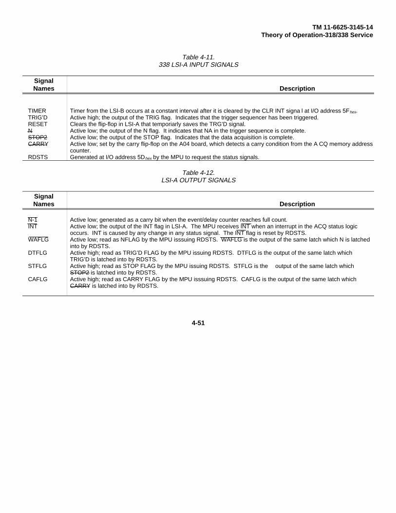
TM 11-6625-3145-14Theory of Operation-318/338 Service
Table 4-11.338 LSI-A INPUT SIGNALS
SignalNames Description
TIMER Timer from the LSI-B occurs at a constant interval after it is cleared by the CLR INT signa l at I/O address 5Fhex.TRIG’D Active high; the output of the TRIG flag. Indicates that the trigger sequencer has been triggered.RESET Clears the flip-flop in LSI-A that temporiarly saves the TRG’D signal.N Active low; the output of the N flag. It indicates that NA in the trigger sequence is complete.STOP2 Active low; the output of the STOP flag. Indicates that the data acquisition is complete.CARRY Active low; set by the carry flip-flop on the A04 board, which detects a carry condition from the A CQ memory address
counter.RDSTS Generated at I/O address 5Dhex by the MPU to request the status signals.
Table 4-12.LSI-A OUTPUT SIGNALS
SignalNames Description
N-1 Active low; generated as a carry bit when the event/delay counter reaches full count.INT Active low; the output of the INT flag in LSI-A. The MPU receives INT when an interrupt in the ACQ status logic
occurs. INT is caused by any change in any status signal. The INT flag is reset by RDSTS.WAFLG Active low; read as NFLAG by the MPU isssuing RDSTS. WAFLG is the output of the same latch which N is latched
into by RDSTS.DTFLG Active high; read as TRIG’D FLAG by the MPU issuing RDSTS. DTFLG is the output of the same latch which
TRIG’D is latched into by RDSTS.STFLG Active high; read as STOP FLAG by the MPU issuing RDSTS. STFLG is the output of the same latch which
STOP2 is latched into by RDSTS.CAFLG Active high; read as CARRY FLAG by the MPU isssuing RDSTS. CAFLG is the output of the same latch which
CARRY is latched into by RDSTS.
4-51
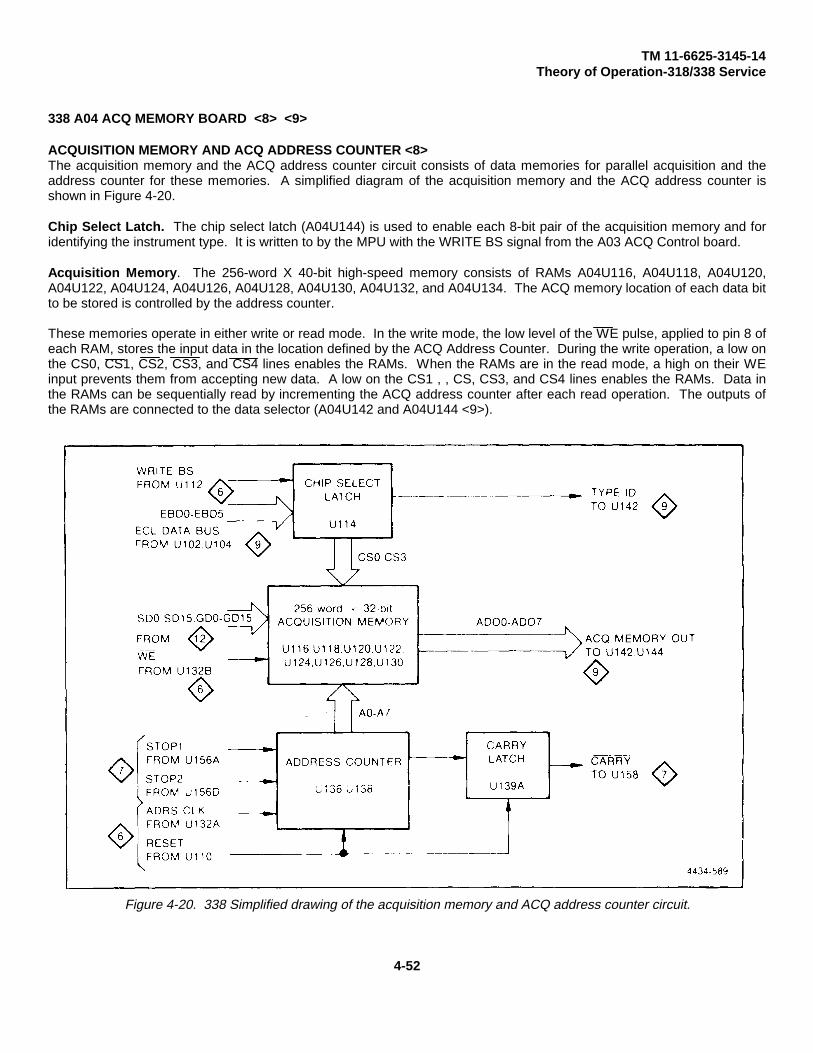
TM 11-6625-3145-14Theory of Operation-318/338 Service
338 A04 ACQ MEMORY BOARD <8> <9>
ACQUISITION MEMORY AND ACQ ADDRESS COUNTER <8>The acquisition memory and the ACQ address counter circuit consists of data memories for parallel acquisition and theaddress counter for these memories. A simplified diagram of the acquisition memory and the ACQ address counter isshown in Figure 4-20.
Chip Select Latch. The chip select latch (A04U144) is used to enable each 8-bit pair of the acquisition memory and foridentifying the instrument type. It is written to by the MPU with the WRITE BS signal from the A03 ACQ Control board.
Acquisition Memory. The 256-word X 40-bit high-speed memory consists of RAMs A04U116, A04U118, A04U120,A04U122, A04U124, A04U126, A04U128, A04U130, A04U132, and A04U134. The ACQ memory location of each data bitto be stored is controlled by the address counter.
These memories operate in either write or read mode. In the write mode, the low level of the WE pulse, applied to pin 8 ofeach RAM, stores the input data in the location defined by the ACQ Address Counter. During the write operation, a low onthe CS0, CS1, CS2, CS3, and CS4 lines enables the RAMs. When the RAMs are in the read mode, a high on their WEinput prevents them from accepting new data. A low on the CS1 , , CS, CS3, and CS4 lines enables the RAMs. Data inthe RAMs can be sequentially read by incrementing the ACQ address counter after each read operation. The outputs ofthe RAMs are connected to the data selector (A04U142 and A04U144 <9>).
Figure 4-20. 338 Simplified drawing of the acquisition memory and ACQ address counter circuit.
4-52

TM 11-6625-3145-14Theory of Operation-318/338 Service
ACQ Address Counter and Carry Latch. The ACQ address counter designates the memory location for each data bit tobe stored. The counter, consisting of A04U136 and A04U138, is a synchronous, 8-bit (divide by 256) binary counter whichis reset to zero by the RESET signal from the A03 ACQ control board at the beginning of each acquisition.
The counter outputs Q0 through Q3 are connected to the address inputs of A04U116, A04U118, A04U120, A04U122,A04U124, A04U126, A04U128, A04U130, A04U132, and A04U134.
Counter A04U138 provides a carry output to the carry latch, A04U139A. After one full memory cycle, the carry latchprovides a latched low-level signal on the pin 2 output of A04U139A. It serves as the address counter CARRY signal.
TIMEBASE AND MPU BUS INTERFACE <9>The timebase and MPU bus interface circuit consists of the frequency divider, timer, slow clock detector, INTCLK buffer,data selector, full valid flag latch, TTL-to-ECL translater, ECL-to-TTL translator, and the address decoder. A simplifieddiagram of this circuit is shown in Figure 4-21.
TTL-to-ECL Translator. The TTL-to-ECL translator consists of A04U100, A04U102, A04U104, A04U106, and A04U108.It accepts a TTL-level signal from the MPU bus and translates it to a differential ECL-level signal.
Address Decoder. The address decoder consists of A04U112C and A04U110. It provides the chip-select and enablesignals which select the specific device needed to communicate with the MPU. This selection is determined by outputsfrom the 3-line-to-8-line decoder, A04U110. Gate A04U112C supplies the I/O enable signal EN (which is an ORed signalof BRD and BWR).
Oscillator. The oscillator circuit consists of A04U112A and A04U112B <9>. A04U112A and crystal A04Y100 form a 100MHz crystal-controlled oscillator. The 100 MHz oscillator is buffered by A04U112B before being divided by A04U140(LSI-B).
Divider, Timer, and Slow Clock Detector. The divider, timer, and slow clock detector are contained on (LSI-B)A04U140. More information about LSI-B is provided under the paragraph labeled LSI-B (A04U140).
The frequency divider provides the 20 ns to 500 ms clock output. A clock output is determined by the internal timebaseselection register. The selected internal clock signal is sent to the INTCLK buffer A04U112D. The INTCLK selection datais shown in Table 4-15.
The timer generates the selected constant interval signal for an interrupt to the MPU. This signal is reset by the RDSTSsignal.
The slow-clock detector circuit provides the capability to detect a slow sampling clock rate (clock less than 25 ms) in theexternal clock operation mode. When the clock rate is slow, the CLKSLW signal holds a high state and the MPU displaysSLOW CLOCK on the screen. The timing diagram of the timer and the slow-clock detector circuit is shown in Figure 4-22.
INTCLK Buffer. The INTCLK buffer consists of A04U112D. It provides a power boost and improves the waveform shapefor INTCLK signals on the bus.
Data Selector. The data selector consists of A04U142 and A04U144. It provides data selection of either acquisitionmemory output or acquisition status output. This data selector is controlled by the READ ACQ DATA signal.
4-53
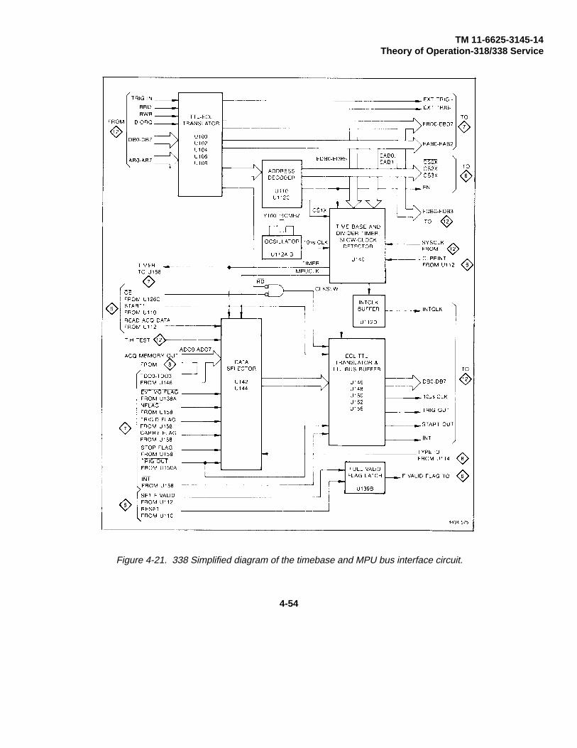
TM 11-6625-3145-14Theory of Operation-318/338 Service
Figure 4-21. 338 Simplified diagram of the timebase and MPU bus interface circuit.
4-54

TM 11-6625-3145-14Theory of Operation-318/338 Service
When the MPU reads the acquisition memory data, it sets the SELECT input (pin 9, READ ACQ DATA signal) to high, andconnects the acquisition memory data to the data selector output. If the SELECT input is low, acquisition status isselected, and the MPU reads acquisition status as data.
ECL-to-TTL Translator and TTL Bus Buffer. The ECL-to-TTL translator and TTL bus buffer consists of A04U146,A04U148, A04U150, A04U156, and A04U152. The ECL-to-TTL translator receives ECL-level signals from the dataselector A04U142 and A04U144. A04U146, A04U148, and A04U150 are ECL-to-TTL translators with totem-pole outputs.A04U156 is a comparator with an open-collector output for wired-AND capability. The TTL bus buffer, A04U152, providesthe power booster with tri-state control for the I/O common bus. It is enabled by the RD and OE signals.
Full Valid Flag Latch. The full valid flag latch consists of A04U139B. It provides the Full Valid Data Display mode. Thislatch is set by the SET F VALID signal and reset by the RESET signal from the A03 ACQ Control board.
LSI-B A04U140. The Sony/Tektronix A04U140 is a hybrid chip that provides simplified circuit construction, reduced circuitboard space, and lower power consumption. Its circuitry consists of an address decoder, divider, timer, and slow clockdetector.
The address decoder circuit consists of four decoders that enable the MPU to select the: sample interval, gate clockinterval, timer clock interval, and step clock . The address decoder provides necessary pulses for the initialization andpresetting of the above circuits. The selection is determined by the two bits of address and six bits of data from the MPUwhen CS1X is low.
The divider circuit consists of a 7-stage decade counter, and divide-by-2 and divide-by-5 counters based on a ring countercircuit. The output of these counters is delivered as the INTCLK signal via the 1-2-5 sequence selector.
The timer circuit consists of an output latch, which is reset by the RDSTS signal from the A03 ACQ Controlboard. Itgenerates a constant interval timing signal ranging from one to five multiples of the internally generated 100 ms clock.
The slow-clock detector circuit consists of two shift registers and a control flip-flop.
Figure 4-22. 338 Timing diagram of the slow-clock detector and timer circuit.
4-55

TM 11-6625-3145-14Theory of Operation-318/338 Service
The CLKSLW signal is initialized to high level by the RDSTS signal.
If the SYSCLK signal is either high or low for two or more consecutive pulses, the internal shift registers are not clocked,and the low level at the input of the first shift register bit is not transferred to the second shift register; this causes theCLKSLW signal to be output.
When the SYSCLK is less than 25 ms (slow rate), the shift registers are clocked by SYSCLK. But the CLKSLW output isnot changed because a control gate of the shift register closes before the second rising edge of SYSCLK arrives.
When the SYSCLK rate is fast (above 25 ms), the low level pulse provided by the first shift register is successfullytransferred to the second shift register which cancels the CLKSLW output.
The four conditions of the CLKSLW output (high, slow, low, and fast) must be read before the start of gate timing, becausethe CLKSLW signal is changed by the gated SYSCLK.
The function of each signal in A04U140 is as follows:
Table 4-13.318 LSI-B (A04U140) INPUT SIGNALS
SignalNames Description
EN Generates data latch strobe. The data latch state is changed by a low-level pulse of this signal.CS1X Chip select for A04U140.A1-A0 Address for data latch. (A1=MSB, A0=LSB)D5-D0 Data for internal selector. (D5= MSB, D0= LSB)10NCLK 10 ns clock for internal divider.SYSCLK System clock to be compared with gate clock in the Slow Clock Detector circuit.RDSTS Read status for Slow Clock Detector circuit operations; trigger and timer output are reset.
Table 4-14318 LSI-B (A04U140) OUTPUT SIGNALS
SignalNames Description
INTCLK Selected internal clock (20 ns - 500 ms).10UCLK 10 us period clock for the test output on the A01 board.CLKSLW Compared result of slow clock detector circuit. This signal condition is:
0 - One period of SYSCLK is shorter than a hal f interval of gate clock.1 - One period of SYS(CLK is longer than a half interval of gate clock.
TIMER Constant interval timer with reset by RDSTS.
4-56
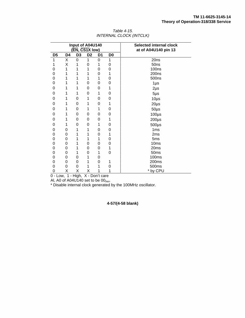
TM 11-6625-3145-14Theory of Operation-318/338 Service
Table 4-15.INTERNAL CLOCK (INTCLK)
Input of A04U140(EN, CS1X low)
Selected internal clockat of A04U140 pin 13
D5 D4 D3 D2 D1 D01 X 0 1 0 1 20ns1 X 1 0 1 0 50ns0 1 1 1 0 0 100ns0 1 1 1 0 1 200ns0 1 1 1 1 0 500ns0 1 1 0 0 0 1µs0 1 1 0 0 1 2µs0 1 1 0 1 0 5µs0 1 0 1 0 0 10µs0 1 0 1 0 1 20µs0 1 0 1 1 0 50µs0 1 0 0 0 0 100µs0 1 0 0 0 1 200µs0 1 0 0 1 0 500µs0 0 1 1 0 0 1ms0 0 1 1 0 1 2ms0 0 1 1 1 0 5ms0 0 1 0 0 0 10ms0 0 1 0 0 1 20ms0 0 1 0 1 0 50ms0 0 0 1 0 100ms0 0 0 1 0 1 200ms0 0 0 1 1 0 500ms0 X X X 1 1 * by CPU
0 - Low, 1 - High, X - Don’t careAl, A0 of A04U140 set to be 00hex.* Disable internal clock generated by the 100MHz oscillator.
4-57/(4-58 blank)

318
VERIFICATION ANDADJUSTMENT PROCEDURES

TM 11-6625-3145-14Section 5-318/338 Service
VERIFICATION AND ADJUSTMENT PROCEDURES
INTRODUCTION
This section of the manual contains three main parts:
• Functional check procedures• Adjustment procedures• Performance check procedures
These procedures, along with the test setup information at the beginning of this section, allows a qualified technician toadjust and verify the operation of the 318/338 and 318S1/338S1 Logic Analyzers.
NOTEThroughout this manual the term verification is used to mean either a functionalcheck or a performance check.
Functional Check Procedures. These tests verify that the device undergoing the functional test is basically operational.The procedure exercises the main user interfaces of the device to verify their operation and checks the main internalfeatures. These tests can be used to determine whether adjustment and/or repair is necessary.
Adjustment Procedures. These instructions for setting variables should bring the device being adjusted whithin productspecifications. If the instrument can not meet the specifications given in this manual after adjustment, repair is necessary.
Performance Check Procedures. These tests provide a detailed check of internal and external product characteristics.All specifications listed in the performance requirements column of the specifications are verified. These checks can beextensive and time consuming. Under normal circumstances, the functional check procedure provides an adequate test ofproduct performance in a less-costly or less time-consuming manner.
318/338 MULTI-PROBE TEST FIXTURE
We recommend that you construct the following test fixture to assist in checking the performance of the 318/338.
The 318/338 multi-probe test fixture functions as a BNC-to-square pin adapter with 50 ohm termination. Its purpose is toconnect multiple 318/338 probe leads to a single pulse generator output without causing excessive capacitive andinductive loading. It also provides a connection for the test oscilloscope's 10X probe used in monitoring the pulsegenerator's output.
NOTEThe lead distance from the ground pins to the BNC connector body is critical; keepthis distance as short as possible. Any excessive lead length in the fixture willdistort high-speed signals. Also, use only short comb lead sets when connectingthis fixture to the P6451 probe.
5-1

TM 11-6625-3145-14Verification and Adjustment Procedures-318/338 Service
Parts list: Part number Quantity
Connector (BNC), male 131-0602-00 1Connector, Rcp. Elect. (oscilloscope probe) 131-0258-00 1Plain hex nut 210-0413-00 1Right-angle terminal set (right-angle square pins) 131-1425-00 2Connector terminal set (straight square pins) 131-1343-00 2Terminal lug 1/4 inch 210-0223-00 1Terminal lug .391 inch l.D. 210-0225-00 1Resistor, 51 ohm, 1 watt 303-0510-00 1Short flying lead set 012-0987-00 1
1. Fabricate the chassis.
a. Using 50 mil aluminum, cut and drill the chassis according to Figure 5-1.
b. Bend the chassis up to right angles at each bend line on the wide part of the chassis. Do not make the final 3/8-inch bend on the tail end at this time.
Figure 5-1. Test Fixture construction diagram.
2. Assemble the square pins.
a. Cut two 11-pin lengths of right-angle square-pin terminals, and two 11-pin lengths of straight-pin terminals.
b. Glue one strip of right-angle square pins on to one strip of straight pins so that the pins align vertically.
c. Solder each right-angle pin to the straight pin immediately below. Repeat this procedure for the other set ofstraight and right-angle square pins.
5-2

TM 11-6625-3145-14Verification and Adjustment Procedures-318/338 Service
d. Place the square pin strips back to back and solder the last pins on each end of the strips together. (You shouldnow have the outermost four pins on each end of the assembly soldered together.)
e. Now solder together the middle nine sets of pins so that all nine middle sets are electrically connected.
f. Clip the end set of four pins (one pin off each strip) from one end of the square-pin assembly. This is now theback end of the assembly. The front set of four pins (those not soldered to the middle nine sets) will be connectedto ground.
3. Assemble the parts
a. Refer to Figure 5-2. Solder the ground lug from the BNC plug to the first set of four pins (front end) on the square-pin assembly. It is important that this connection be as short as practical to avoid high-speed signal loss.
b. Solder one end of the 50 ohm resistor to the scope probe connector’s ground lug.
c. Attach the scope probe connector and the BNC connector (including ground lugs and attached square-pinassembly) to the chassis.
d. Bend the tail end of the aluminum chassis up and glue it to the back end of the square-pin assembly.
e. Solder the center connectors from the BNC connector, and the oscilloscope probe connector to the center nine pinsets on the square-pin assembly. Keep this connection as short as practical to avoid high-speed signal loss.
f. Solder the remaining lead from the 50 ohm resistor to the center pin of the BNC connector. The test fixture isready for use.
Figure 5-2. Assembled Test Fixture
5-3

TM 11-6625-3145-14Verification and Adjustment Procedures-318/338 Service
NOTEUse only short comb lead sets when connecting the test fixture to the P6451 Probe.Here too, short lead lengths are important in avoiding high-speed signal losses.
TEST SETUP INFORMATION
The procedures in this Verification and Adjustment Procedures section require some test equipment and generalinformation relevant to all configurations of the 318/338 Logic Analyzer. This information is presented here at the front ofthe section to prevent duplication throughout the following procedures.
SUGGESTED TEST INSTRUMENTS
There are three procedures in this section: the functional check, the adjustments, and the performance check. Thefunctional check uses the TEST OUTPUT signal, which is delivered from the 318/338 right side panel; no otherinstruments are necessary. The adjustments and the performance checks require other instruments. Table 5-1 lists theinstruments used at some point in each of these procedures, along with their Tektronix equivalents.
5-4

TM 11-6625-3145-14Verification and Adjustment Procedures-318/338 Service
Table 5-1.EQUIPMENT NEEDED FOR THE ADJUSTMENT PROCEDURES
AND THE PERFORMANCE CHECK PROCEDURES
Perf. Adj. TektronixDescription Check Proc. Equivalent
Oscilloscope 100 MHz dual trace(Mainframe) 1 1 7904Vertical plug-in 1 1 7A26Horizontal plug-in 1 1 7B80Horizontal plug-in 1 1 7B85Power module 1 1 TM503Pulse generator 2 1 PG502Digital delay 1 DD501Digital multimeter (DMM) 1 1 DM501Regulated dc power supply 1 PS501Serial data generator 1 834Extender boards 2 Maintenance kit 067-1159-00Ejector 2BNC 50 Q 2 W termination 4 1 011-0049-011 MQ, 40pF normalizer 1 067-0935-002 SQR-pin to probe-tip adapter 1BNC T-connector 3 1 103-0030-00BNC elbow male-to-female adapter 3 103-0031-00BNC female-to-female adapter 1 103-0029-00BNC male-to-dual-binder adapter 4 103-0035-00BNC male-to-male adapter 1 103-0028-00BNC male-to-probe tip adapter 3 2 013-0084-01BNC 50 Q cable, 18 inches long 1 012-0076-00BNC 50 Q cable, 42 inches long 1 012-0057-01Bus wire 5 18 gauge, 4"Computer terminal 1 4025
5-5
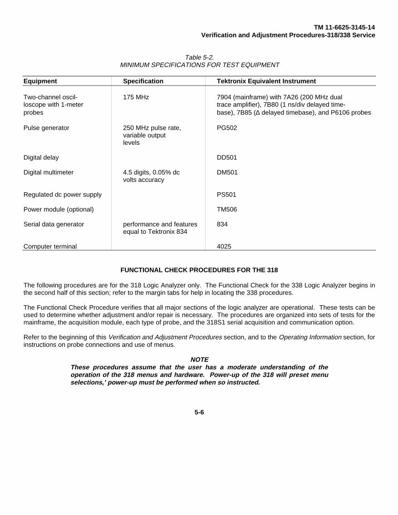
TM 11-6625-3145-14Verification and Adjustment Procedures-318/338 Service
Table 5-2.MINIMUM SPECIFICATIONS FOR TEST EQUIPMENT
Equipment Specification Tektronix Equivalent Instrument
Two-channel oscil- 175 MHz 7904 (mainframe) with 7A26 (200 MHz dualloscope with 1-meter trace amplifier), 7B80 (1 ns/div delayed time-probes base), 7B85 (∆ delayed timebase), and P6106 probes
Pulse generator 250 MHz pulse rate, PG502variable outputlevels
Digital delay DD501
Digital multimeter 4.5 digits, 0.05% dc DM501volts accuracy
Regulated dc power supply PS501
Power module (optional) TM506
Serial data generator performance and features 834equal to Tektronix 834
Computer terminal 4025
FUNCTIONAL CHECK PROCEDURES FOR THE 318
The following procedures are for the 318 Logic Analyzer only. The Functional Check for the 338 Logic Analyzer begins inthe second half of this section; refer to the margin tabs for help in locating the 338 procedures.
The Functional Check Procedure verifies that all major sections of the logic analyzer are operational. These tests can beused to determine whether adjustment and/or repair is necessary. The procedures are organized into sets of tests for themainframe, the acquisition module, each type of probe, and the 318S1 serial acquisition and communication option.
Refer to the beginning of this Verification and Adjustment Procedures section, and to the Operating Information section, forinstructions on probe connections and use of menus.
NOTEThese procedures assume that the user has a moderate understanding of theoperation of the 318 menus and hardware. Power-up of the 318 will preset menuselections,’ power-up must be performed when so instructed.
5-6

TM 11-6625-3145-14Verification and Adjustment Procedures-318/338 Service
INDEX OF FUNCTIONAL CHECKSCheck 1. Power-up DiagnosticsCheck 2. KeyboardCheck 3. CRTCheck 4. Threshold VoltageCheck 5. Parallel Data Acquisition with TEST OUTPUTCheck 6. Glitch Data Acquisition with TEST OUTPUTCheck 7. Serial State Analyzer (318S1)
MAINFRAME AND PARALLEL ANALYZER
CHECK 1. POWER-UP DIAGNOSTICS
1. Turn on the 318.
2. Approximately seven seconds after power is turned on, the screen display is initialized. Check to ensure that FAILis not displayed in any of the test fields. Refer to Figure 5-3.
This key blinks when hit.
Figure 5-3. 318 Successful Power-up Figure 5-4. 318 Keyboard test displaydiagnostics display.
CHECK 2. KEYBOARD
1. Keyboard operation can be checked with the diagnostic program O.KBD. To start this program, turn on the powerwhile pressing any numeric key until an error message appears on the CRT.
2. When an error message appears, press the START key. The Diagnostics menu will be displayed on the screen.Press 0 to run the KBD test. Refer to Figure 5-4.
3. Press each key individually and observe the CRT display to make sure the corresponding rectangle blinks. Press theSTOP key last. The keyboard generates an interrupt and corresponding key code for the MPU when any key exceptthe STOP key is pressed. The MPU reads the key code upon receiving the interrupt from the keyboard and blinks thecorresponding rectangle in the key array displayed on the screen. This test provides a check to ensure that each key(except for the STOP key) is sending the correct key code to the MPU. The STOP key is used to exit this program;thus the STOP key’s function can be checked at the end of this test.
5-7

TM 11-6625-3145-14Verification and Adjustment Procedures-318/338 Service
CHECK 3. CRT
Refer to Figures 5-5, 5-6, 5-7, and 5-8.
Figure 5-5. 318 CRT test cross-hatch pattern. Figure 5-6. 318 CRT test white pattern.
Figure 5-7. 318 CRT test parallel acquisition Figure 5-8. 318 CRT test serial acquisitioncharacter fonts. character fonts.
1. The CRT can be visually checked with the diagnostic program 1.CRT. To start this diagnostic program, turn on thepower while pressing any numeric key until an error message is displayed on the CRT.
2. When an error message is displayed, press the START key. When the Diagnostics menu is displayed on the screen,select #1 for CRT.
5-8

TM 11-6625-3145-14Verification and Adjustment Procedures-318/338 Service
The CRT test generates the following types of patterns for the CRT adjustment and visual check.
• Cross-hatch pattern (Figure 5-5). Used to adjust the CRT circuit.
• White pattern (Figure 5-6). Used to check for phosphor defects.
• All character fonts for Parallel Analyzer mode (Figure 5-7). Used to check the CRT circuit and the CROM(character ROM) for parallel analyzer operations.
• All character fonts for Serial Analyzer mode (Figure 5-8). Used to check the CRT circuit and the CROM for serialanalyzer operations.
3. Press the X key to return to the Diagnostic menu.
CHECK 4. THRESHOLD VOLTAGE
1. Connect all the data and ground leads of the P6451 Parallel Data probes in both Pod A and Pod B together andconnect them to the instrument ground.
2. Press the THRESHOLD menu key (normal operating mode).
Threshold Level TTL
a. Set INPUT Thresholds to TTL for for both Pod A and Pod B.
b. Press the START key. The trigger position (indicated by T) will be displayed on the screen. The trigger positionwill be <T=7W>, <T= 127W>, or <T=247W> depending on the trigger position setting in the Trigger menu (begin,center, or end).
c. Check that all data acquired are O's.
Threshold Level V1
a. Set Threshold LEVEL V1 to +0.3 V.
b. Set both Pod A and Pod B equal to V1.
c. Press the START key. The trigger position displayed on the screen will be <T=7W>, <T=127W>, or <T=247W>depending on the trigger position setting in the Trigger menu.
d. Check that all data acquired are O's.
e. Set Threshold LEVEL V1 to -0.3 V.
f. Press the START key. The trigger position displayed on the screen will be <T=7W>, <T=127W>, or <T=247W>depending on the trigger position setting in the Trigger menu.
g. Check that all data acquired are 1's.
5-9

TM 11-6625-3145-14Verification and Adjustment Procedures-318/338 Service
Threshold Level V2
a. Set Threshold LEVEL V2 to +0.3 V.
b. Set both Pod A and Pod B equal to V2.
c. Press the START key. The trigger position is displayed on the screen will be <T=7W>, <T=127W>, or <T=247W>depending on the trigger position setting in the Trigger menu.
d. Check that all data acquired are 0’s.
e. Set Threshold LEVEL V2 to -0.3 V.
f. Press the START key. The Trigger position displayed on the screen will be <T=7W>, <T=127W>, or <T-247W>depending on the trigger position setting in the Trigger menu.
g. Check that all data acquired are l’s.
Threshold Level V3
a. Set Threshold LEVEL V1 to +2.0V and V2 to -1.5 V.
b. Check that the Threshold LEVEL V3 is -+0.25 V.
c. Set both Pod A and Pod B equal to V3.
d. Press the START key. The trigger position displayed on the screen will be <T=7W>, <T=127W>, or <T-247W>depending on the trigger position setting in the Trigger menu.
e. Check that all data acquired are 0’s.
f. Set Threshold LEVEL V1 to -2.0 V and V2 to + 1.5 V.
g. Check that Threshold LEVEL V3 is -0.25 V.
h. Press the START key. The trigger position displayed on the screen will be <T=7W>, <T= 127W>, or <T=247W>depending on the trigger position setting in the Trigger menu.
i. Check that all data acquired are l’s.
5-10
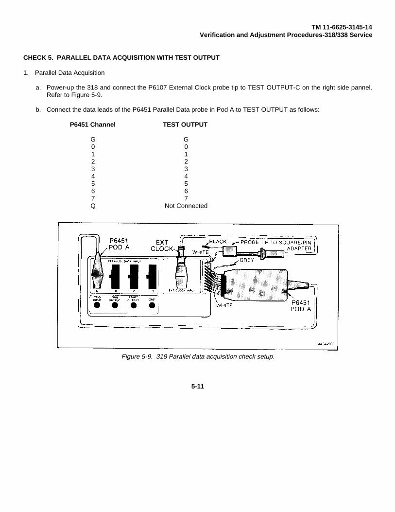
TM 11-6625-3145-14Verification and Adjustment Procedures-318/338 Service
CHECK 5. PARALLEL DATA ACQUISITION WITH TEST OUTPUT
1. Parallel Data Acquisition
a. Power-up the 318 and connect the P6107 External Clock probe tip to TEST OUTPUT-C on the right side pannel.Refer to Figure 5-9.
b. Connect the data leads of the P6451 Parallel Data probe in Pod A to TEST OUTPUT as follows:
P6451 Channel TEST OUTPUT
G G0 01 12 23 34 45 56 67 7Q Not Connected
Figure 5-9. 318 Parallel data acquisition check setup.
5-11
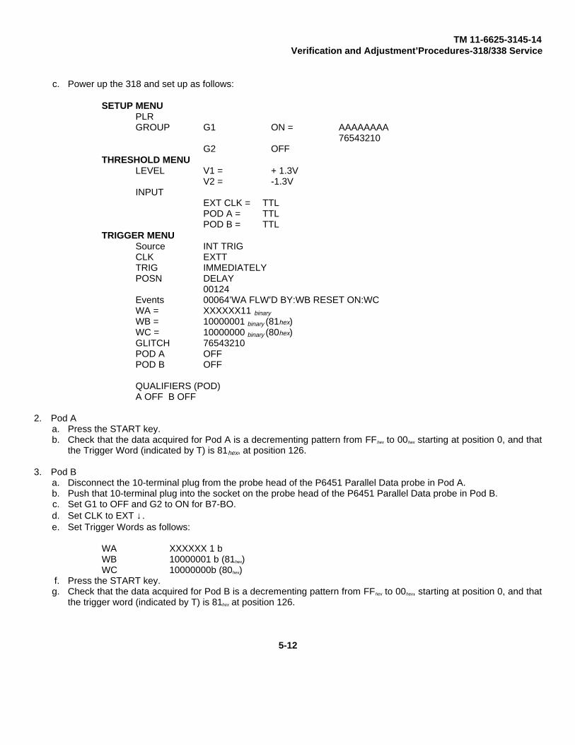
TM 11-6625-3145-14Verification and Adjustment’Procedures-318/338 Service
c. Power up the 318 and set up as follows:
SETUP MENUPLRGROUP G1 ON = AAAAAAAA
76543210G2 OFF
THRESHOLD MENULEVEL V1 = + 1.3V
V2 = -1.3VINPUT
EXT CLK = TTLPOD A = TTLPOD B = TTL
TRIGGER MENUSource INT TRIGCLK EXTTTRIG IMMEDIATELYPOSN DELAY
00124Events 00064’WA FLW’D BY:WB RESET ON:WCWA = XXXXXX11 binary
WB = 10000001 binary (81hex)WC = 10000000 binary (80hex)GLITCH 76543210POD A OFFPOD B OFF
QUALIFIERS (POD)A OFF B OFF
2. Pod Aa. Press the START key.b. Check that the data acquired for Pod A is a decrementing pattern from FFhex to 00hex starting at position 0, and that
the Trigger Word (indicated by T) is 81hex, at position 126.
3. Pod Ba. Disconnect the 10-terminal plug from the probe head of the P6451 Parallel Data probe in Pod A.b. Push that 10-terminal plug into the socket on the probe head of the P6451 Parallel Data probe in Pod B.c. Set G1 to OFF and G2 to ON for B7-BO.d. Set CLK to EXT ↓.e. Set Trigger Words as follows:
WA XXXXXX 1 bWB 10000001 b (81hex)WC 10000000b (80hex)
f. Press the START key.g. Check that the data acquired for Pod B is a decrementing pattern from FFhex to 00hex, starting at position 0, and that
the trigger word (indicated by T) is 81hex at position 126.
5-12

TM 11-6625-3145-14Verification and Adjustment Procedures-318/338 Service
4. 50 MHz Acquisition
a. Set CLK to 20 ns and POSN to DELAY 00250.
b. Set Trigger: 9 * WA OFF:WB OFF:WC
c. Set Trigger Word WA to FF hex.
d. Press the START key.
e. Check that data acquired for Pod B are all FFhex.
5. EXT TRIGGER Check
a. Refer to Figure 5-10. Connect the data leads of the P6451 Parallel Data probe in Pod A to TEST OUTPUTas follows:
P6451 Channel TEST OUTPUTG G0 01 12 23 34 45 56 67 See TextQ Not Connected
Figure 5-10. 318 External trigger check setup.
b. Connect TRIG INPUT, on the right side panel, to TEST OUTPUT-7.
5-13

TM 11-6625-3145-14Verification and Adjustment Procedures-318/338 Service
c. Setup the 318 as follows:SETUP MENU
PLRGROUP G1 ON AAAAA,
765413210G2 OFF
THRESHOLD MENULEVEL V1 +1 3V
V2 -1 3VINPUT
EXT CLK= TTLPOD A= TTLPOD B= TTL
TRIGGER MENUSource EXT TRIGCLK 10-µSTRIG IMMEDIATELYPOSN DELAY
00250EXT TRIG POL=QUALIFIERS (POD)A OFF B OFF
d. Press the START key.
e. Check that all data acquired for Pod A is a repetitive decrementing pattern from 7Fhex to 00hex and that thetrigger word (indicated by T) is 7F at position 0 with <T = 0 ♦> showing in the lower right corner of thedisplay.
f. Set EXT TRIG POL to ↓ .
g. Press the START key.
h. Check that all the data acquired for Pod A is a repetitive decrementing pattern from 7Fhex to 00hex and thatthe Trigger Word (indicated by -T) is 7F at position 0, with <T = 0 ♦> showing in the lower-right corner of thedisplay
6. Trigger Qualifier Check
a. Refer to Figure 5-11. Connect the data leads of the P6451 Parallel Data probe in Pod B to TEST OUTPUTas follows:
P6451 Channel TEST OUTPUTG G0 01 12 23 34 45 56 Not Connected7 Not ConnectedQ See Text
b. Ground all the qualifier and ground leads of the P6451 Parallel Data probes in both Pod A and Pod B.
5-14

TM 11-6625-3145-14Verification and Adjustment Procedures-318/338 Service
c. Set up the 318 as follows:
SETUP MENUPLRGROUP G1 OFF
G2 ON = BBBBBB543210
THRESHOLD MENULEVEL V1 = + 1.3V
V2 = -1.3VINPUT
EXT CLK = TTLPOD A = TTLPOD B = TTL
TRIGGER MENUSource INT TRIGCLK 10,µSTRIG IMMEDIATELYPOSN DELAY
00189Events 00016*WA FLW’D BY:WB RESET ON:WCWA = XXXXXX11 binary
WB = 00000010 binary (02hex)WC = 00000000 binary(00ex)GLITCH 76543210
POD A OFFPOD B OFF
QUALIFIERS (POD)ATRG=H B’TRG=H
d. Press the START key.
e. Check to make sure the 318 is never triggered.
f. Press the STOP key.
g. Connect the qualifier lead of the P6451 Parallel Data probe in Pod A to TEST OUTPUT-7 and the qualifiertip of the P6451 probe in Pod B to TEST OUTPUT-6.
h. Press the START key and wait for the acquisition to be completed.
i. Check that the data acquired for Pod B is a repetitive decrementing pattern from 3Fhx, to 00x starting atposition 0, and that the Trigger Word (indicated by T) is 02hex at position 61.
j. Set QUALIFIER Pod A and Pod B to TRG-L.
k. Press the START key and wait for the acquisition to be completed.
I. Check that the data acquired for Pod B is a repetitive decrementing pattern from 3Fhex to 00hex, starting atposition 0, and Trigger Word (indicated by T) is 02hex at position 61.
5-15

TM 11-6625-3145-14Verification and Adjustment Procedures-318/338 Service
Figure 5-11. 318 Trigger qualifier check setup.
7. Clock Qualifier Check
Setup
a. Connect the data leads of the P6451 Parallel Data probe in Pod A to TEST OUTPUT as follows:
P6451 Channel TEST OUTPUT
G G0 Not Connected1 12 23 34 45 56 67 7Q 0
b. Connect the qualifier lead of the P6451 Parallel Data probe in Pod A to TEST OUTPUT-0.
5-16
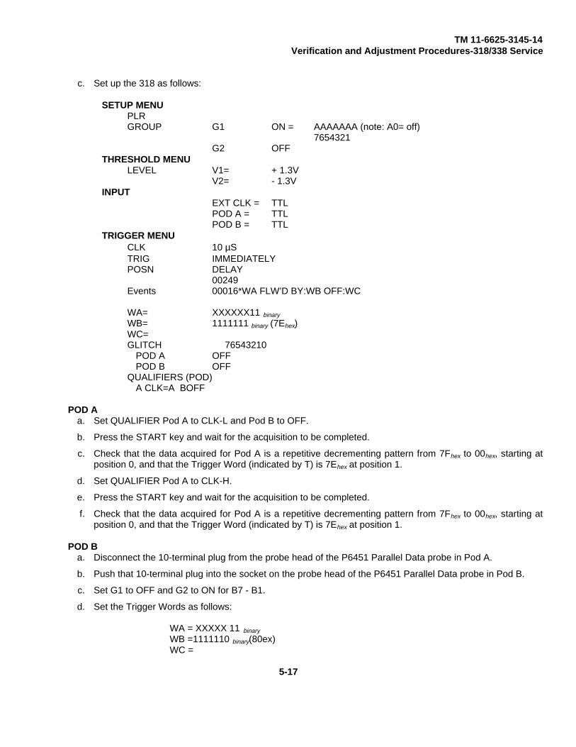
TM 11-6625-3145-14Verification and Adjustment Procedures-318/338 Service
c. Set up the 318 as follows:
SETUP MENUPLRGROUP G1 ON = AAAAAAA (note: A0= off)
7654321G2 OFF
THRESHOLD MENULEVEL V1= + 1.3V
V2= - 1.3VINPUT
EXT CLK = TTLPOD A = TTLPOD B = TTL
TRIGGER MENUCLK 10 µSTRIG IMMEDIATELYPOSN DELAY
00249Events 00016*WA FLW’D BY:WB OFF:WC
WA= XXXXXX11 binary
WB= 1111111 binary (7Ehex)WC=GLITCH 76543210
POD A OFFPOD B OFF
QUALIFIERS (POD)A CLK=A BOFF
POD Aa. Set QUALIFIER Pod A to CLK-L and Pod B to OFF.
b. Press the START key and wait for the acquisition to be completed.
c. Check that the data acquired for Pod A is a repetitive decrementing pattern from 7Fhex to 00hex, starting atposition 0, and that the Trigger Word (indicated by T) is 7Ehex at position 1.
d. Set QUALIFIER Pod A to CLK-H.
e. Press the START key and wait for the acquisition to be completed.
f. Check that the data acquired for Pod A is a repetitive decrementing pattern from 7Fhex to 00hex, starting atposition 0, and that the Trigger Word (indicated by T) is 7Ehex at position 1.
POD Ba. Disconnect the 10-terminal plug from the probe head of the P6451 Parallel Data probe in Pod A.
b. Push that 10-terminal plug into the socket on the probe head of the P6451 Parallel Data probe in Pod B.
c. Set G1 to OFF and G2 to ON for B7 - B1.
d. Set the Trigger Words as follows:
WA = XXXXX 11 binary
WB =1111110 binary(80ex)WC =
5-17
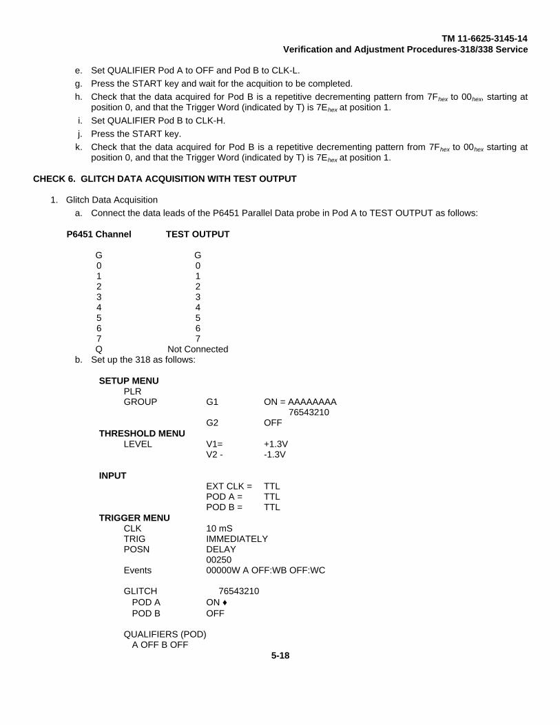
TM 11-6625-3145-14Verification and Adjustment Procedures-318/338 Service
e. Set QUALIFIER Pod A to OFF and Pod B to CLK-L.
g. Press the START key and wait for the acquition to be completed.
h. Check that the data acquired for Pod B is a repetitive decrementing pattern from 7Fhex to 00hex, starting atposition 0, and that the Trigger Word (indicated by T) is 7Ehex at position 1.
i. Set QUALIFIER Pod B to CLK-H.
j. Press the START key.
k. Check that the data acquired for Pod B is a repetitive decrementing pattern from 7Fhex to 00hex starting atposition 0, and that the Trigger Word (indicated by T) is 7Ehex at position 1.
CHECK 6. GLITCH DATA ACQUISITION WITH TEST OUTPUT
1. Glitch Data Acquisition
a. Connect the data leads of the P6451 Parallel Data probe in Pod A to TEST OUTPUT as follows:
P6451 Channel TEST OUTPUT
G G0 01 12 23 34 45 56 67 7Q Not Connected
b. Set up the 318 as follows:
SETUP MENUPLRGROUP G1 ON = AAAAAAAA
76543210G2 OFF
THRESHOLD MENULEVEL V1= +1.3V
V2 - -1.3V
INPUTEXT CLK = TTLPOD A = TTLPOD B = TTL
TRIGGER MENUCLK 10 mSTRIG IMMEDIATELYPOSN DELAY
00250Events 00000W A OFF:WB OFF:WC
GLITCH 76543210POD A ON ♦POD B OFF
QUALIFIERS (POD)A OFF B OFF
5-18

TM 11-6625-3145-14Verification and Adjustment Procedures-318/338 Service
2. Pod Aa. Press the START key and wait for the acquisition to be completed.
b. Check that all the data for Pod A is displayed in inverse video in the GLITCH SEARCH mode, and that <T=0 ♦> is showing in the lower-right corner of the screen.
c. De-select Trigger Glitch A7.
d. Repeat steps (a) through (c) for each of the remaining channels, A6 through A0. Glitch Triggering must bechecked one channel at a time for the test to be valid.
3. Pod Ba. Disconnect the 10-terminal plug from the probe head of the P6451 Parallel Data probe in Pod A.
b. Push the 10-terminal plug into the socket on the probe head of the P6451 Parallel Data probe in Pod B.
c. Set G1 to OFF and G2 to ON for B7 - B0.
d. Set GLITCH Pod A to OFF and Pod B to ON for B7.
e. Press the START key and wait for the acquisition to be completed.
f. Check that all the data for Pod B is displayed in inverse video in the GLITCH SEARCH mode, and that <T =0 ♦> appears in the lower-right corner of the screen.
g. Repeat procedures (e) through (f) for channels B6 through B0 of the Pod B GLITCH Trigger. GlitchTriggering must be checked one channel at a time for the test to be valid.
CHECK 7. SERIAL STATE ANALYZER CHECK FOR THE 318S1
1. Serial Data Acquisition
a. Connect the test setup as shown in Figure 5-12.
b. Set the terminal character format to 8 bits per character.
c. Set the 318 POWER switch to ON and press the SETUP key after the diagnostic program has run.
d. Set the major mode to SERIAL and press the EXECUTE key.
e. Set the baud rate and parity to match that of the terminal. Press the THRESHOLD Menu key.
f. Set the data threshold to 0.00 V. Press the TRIGGER Menu key.
g. Set the trigger mode to IMMEDIATELY. Press the DATA key.
h. Press the START key.
i. Press the A key on the terminal keyboard 10 times.
j. Press the STOP key.
k. Check that the acquired data equals 10 bytes of ASCII A on the screen.
5-19

TM 11-6625-3145-14Verification and Adjustment Procedures-318/338 Service
Figure 5-12. 318 Setup for serial data analysis.
2. Remote Control Operation
a. Connect the test setup as shown in Figure 5-13.
b. Set the terminal character format to 8 bits per character, even parity, (on the 4025, type !parity even) and setthe echo mode to remote.
c. Set the POWER switch to ON and press the SETUP key after the diagnostic program has run.
d. Set the source mode to RMT, then press the EXECUTE key.
e. Set the RS-232 baud rate to match that of the terminal.
f. Press the START key.
g. Key in the IDENT command from the terminal and wait for prompt.
h. Key in the REF? command from the terminal and wait for a prompt.
i. Check that the reference data matches all 0’s on the terminal output.
k. Press the STOP key to end remote control operation.
5-20

TM 11-6625-3145-14Verification and Adjustment Procedures-318/338 Service
Figure 5-13. 318 Setup for RS-232C control.
5-21

TM 11-6625-3145-14Verification and Adjustment Procedures-318/338 Service
ADJUSTMENT PROCEDURES FOR THE 318
INTRODUCTIONThe following pages contains the Adjustment Procedures for the 318 Logic Analyzer. Information on the 338 LogicAnalyzer is located later in Section 5; refer to the page-edge tabs for help in locating 338 information.
The following pages contain procedures for adjusting instrument variables so that the instrument meets or exceedsperformance specifications. If the product cannot be made to meet or exceed specifications by following theseprocedures, repair is necessary.
IMPORTANT-PLEASE READ BEFORE USING THIS PROCEDURE
PURPOSEThe Adjustment Procedure provides a sequence for adjustments. It is not a troubleshooting guide or a verificationprocedure. The Adjustment Procedure is divided into sub-sections that describe adjustments for one particular board orset of boards in the 318.
LIMITS AND TOLERANCESAll limits and tolerances given in this procedure are adjustment guides. They should not be interpreted as instrumentspecifications unless they are also found in the Specifications part of this manual.
Tolerances given are for the instrument under test and do not include test equipment error.
EQUIPMENT REQUIREDThe equipment listed at the beginning of this Adjustment and Verification Procedures section in Table 5-1 is necessary tocomplete all the adjustment procedures. A partial list of equipment needed for each individual check and adjustment isalso shown at the beginning of each procedure’s major step. The equipment specifications given in Table 5-2 are theminimum necessary to produce accurate results. Therefore, equipment substitution must meet or exceed the listedspecifications. Detailed instructions for operating the test equipment are not offered in this manual. Refer to the manualfor the specific test equipment if more information is required.
EQUIPMENT ALTERNATIVESWhen equipment other than recommended test equipment is substituted, control settings or adjustment setups may needto be altered. If the exact equipment listed in Table 5-1 is not available, check the Minimum Specification column inTable 5-2 carefully to see if any other equipment will suffice.
ADJUSTMENT INTERVALTo ensure correct instrument operation, adjustment should be checked every 1000 hours of operation or every six monthsif used infrequently. Before performing the adjustment procedures, perform preventive maintenance as outlined in Section6:Maintenance.
5-22

TM 11-6625-3145-14Verification and Adjustment Procedures-318/338 Service
TEST SEQUENCE
NOTEThese adjustment procedures assume prior knowledge of some aspects ofdisassembly of the 318. If further information is required, refer to the disassemblyprocedures in Section 6:General Maintenance.
It is necessary to perform the following sequence step by step, because all timings in the 318 are level-sensitive.
INDEX OF ADJUSTMENT STEPS
Mainframe
1. Power Supplies2. CRT Circuit3. Threshold Voltages on the A05 ROM Board
Parallel Analyzer
4. Threshold Voltages on the A02 INPUT-B Board5. Probe Compensation for the P6107 External Clock Probe6. EXT CLK T and EXT CLK ↓ Delay7. DLD CLK Delay8. RET CLK, WE, ADRS CLK, and TRIG CLK Delay and Width
Serial State Analyzer (318S1)
9. Threshold Voltages on the A07 Board10. Input Capacitance and Serial Data Probe Compensation (40 pf)11. Non-volatile Memory Battery Backup Threshold
MAINFRAME
1. Adjust Power Supplies
Equipment Required
1 Digital Multimeter (DMM)
a. Refer to Figure 5-14. Remove the 318’s wrap-around cover.
b. Connect P6451 Parallel Data Probes to Inputs A and B.
c. Set the DMM to measure dc voltage.
d. Connect the DMM minus (-) lead to J1 pin 11 (GND) on the A12 REGULATOR board. (See the bottom ofthe power supply chassis.)
5-23

TM 11-6625-3145-14Verification and Adjustment Procedures-318/338 Service
e. Connect the DMM plus (+) lead to each point, starting at -5 V shown in Table 5-3. (Set the DMM range asrequired.)
f. Adjust the corresponding potentiometer on the A12 REGULATOR board to set the voltage level within thelimits given in Table 5-3.
g. Move the DMM plus (+) lead to each point shown in Table 5-4. (Set the DMM range as required.)
h. Check that the DMM readings are within the limits given in Table 5-4.
4434-584Figure 5-14. 318 Power supply adjustments.
Table 5-3.318 ADJUSTABLE POWER SUPPLY TOLERANCES
Pin Voltage Voltage Limits Potentiometereach --5 V pin -4.95 V to -5.05 V R18 (labeled -5 V)+ 5 V pin +4.95 V to +-5.05 V R11 (labeled +5 V)-3.3 V pin -3.25 V to -3.35 V R72 (labeled -3.3 V)
5-24
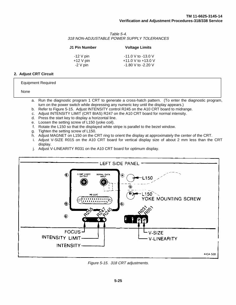
TM 11-6625-3145-14Verification and Adjustment Procedures-318/338 Service
Table 5-4.318 NON-ADJUSTABLE POWER SUPPLY TOLERANCES
J1 Pin Number Voltage Limits
-12 V pin -11.0 V to -13.0 V+12 V pin +11.0 V to +13.0 V-2 V pin -1.80 V to -2.20 V
2. Adjust CRT Circuit
Equipment Required
None
a. Run the diagnostic program 1 CRT to generate a cross-hatch pattern. (To enter the diagnostic program,turn on the power switch while depressing any numeric key until the display appears.)
b. Refer to Figure 5-15. Adjust INTENSITY control R245 on the A10 CRT board to midrange.c. Adjust INTENSITY LIMIT (CRT BIAS) R247 on the A10 CRT board for normal intensity.d. Press the start key to display a horizontal line.e. Loosen the setting screw of L150 (yoke coil).f. Rotate the L150 so that the displayed white stripe is parallel to the bezel window.g. Tighten the setting screw of L150.h. Adjust MAGNET on L150 on the CRT ring to orient the display at approximately the center of the CRT.i. Adjust V-SIZE R015 on the A10 CRT board for vertical display size of about 2 mm less than the CRT
display.j. Adjust V-LINEARITY R031 on the A10 CRT board for optimum display.
Figure 5-15. 318 CRT adjustments.
5-25

TM 11-6625-3145-14Verification and Adjustment Procedures-318/338 Service
3. Adjust Threshold Voltages on the A05 ROM board
Equipment Required
1 Digital Multimeter (DMM)
Refer to: Figure 5-16.
a. Reference Voltage Adjustment(1) Connect the P6451 probes to PARALLEL DATA INPUTS A and B.(2) Set the DMM range to measure about 5 V dc.(3) Connect the DMM minus (-) lead to the GND test point on the A05 ROM board.(4) Connect the DMM plus (+) lead to TP64 (REF) on the A05 ROM board.(5) Adjust REF ADJ R064 on the A05 ROM board for a voltage indication of 3.200 ±.010 V.
b. Threshold VA 0-VOLT Adjustment
(1) Set Threshold LEVEL V1 to 0.0.(2) Press the START key.(3) Move the DMM plus (+) lead to TP78 (V1/4) on the A05 ROM board.(4) Adjust VA O-VOLT ADJ R078 on the A05 ROM board for a DMM indication of 0.000 ±0.010 V.(5) Press the STOP key.(6) Set Threshold LEVEL V1 to + 10.0 V.(7) Press the START key.(8) Check that the DMM reading is +2.500 ±0.010 V.(9) Press the STOP key.
(10) Set Threshold LEVEL V1 to -10.0 V.(11) Press the START key.(12) Check that the DMM reading is -2.500 ±0.010V.(13) Press the STOP key.
c. Threshold VB O-VOLT Adjustment(1) Set Threshold LEVEL V2 to 0.0.(2) Press the START key.(3) Move the DMM plus (+) lead to TP88 (V2/4) on the A05 ROM board.(4) Adjust VB O-VOLT ADJ R088 on the A05 ROM board for a DMM indication of 0.000 ±0.010 V.(5) Press the STOP key.(6) Set Threshold LEVEL V2 to + 10.0 V.(7) Press the START key.(8) Check the DMM reading is +2.500 ±0.010 V.(9) Press the STOP key.
(10) Set Threshold LEVEL V2 to -10.0 V.(11) Press the START key.(12) Check the DMM reading is -2.500 ±0.010 V.(13) Press the STOP key.
5-26

TM 11-6625-3145-14Verification and Adjustment Procedures-318/338 Service
4434-586Figure 5-16. 318 Threshold voltage adjustments on the the ROM board (A05).
PARALLEL ANALYZER
4. Adjust Threshold Voltages on the A02 INPUT-B board
Equipment Required
1 Regulated DC Power Supply1 Digital Multimeter (DMM)1 Oscilloscope
Refer to Figure 5-17.
A. EXT CLK Threshold Adjustment
1. Setup
a. Connect the oscilloscope channel 1 probe tip to TP108 on the A01 INPUT-A board.b. Set the oscilloscope triggering source to channel 1 and the sweep rate to 1 us/div.c. Enter the Threshold menu and set EXT CLK input to V1.d. Set CLK to EXT+.e. Select the TRIGGER Menu and set the events field: 00000*WA OFF:WB OFF:WC. This will cause the 318
to acquire data without triggering.
5-27

TM 11-6625-3145-14Verification and Adjustment Procedures-318/338 Service
2. DC Balance
a. Ground the P6107 External Clock probe tip.b. Enter the Threshold menu and set Threshold LEVEL V1 to 0.0.c. Press the START key.d. Turn EXT CLK DC BALANCE R234 on the A02 INPUT-B board to the counterclockwise end.e. Turn R234 clockwise slowly while observing the oscilloscope waveform and mark the point where the waveform
moves from stationary-low level to stationary-high level.f. Then turn R234 to the clockwise end.g. Turn R234 counterclockwise slowly while observing the oscilloscope waveform and mark the point where the
waveform moves from stationary-high level to stationary-low level.h. Adjust R234 to the center position between the points marked by procedures (e) and (g).i. Press the STOP key.
3. DC Gain
a. Connect the P6107 External Clock probe ground clip to the power supply common terminal.b. Connect the P6107 External Clock probe tip to the power supply plus (+) terminal.c. Connect the DVM leads to the power supply terminals (low to common, high to +).d. Adjust the regulated dc power supply output voltage to +10.00 V.e. Set Threshold LEVEL V1 to +10.0 V.f. Press the START key.g. Turn EXT CLK DC GAIN R239 on the A02 INPUT-B board to the counterclockwise end.h. Turn R239 clockwise slowly while observing the oscilloscope waveform and mark the point where the waveform
moves from stationary-low level to stationary-high level.i. Turn R239 to the clockwise end.j. Turn R239 counterclockwise slowly while observing the oscilloscope waveform and mark the point where the
waveform moves from stationary-low level to stationary-high level.k. Adjust R239 to the center position between the points marked by procedures (h) and (j).I. Press the STOP key.
B. DATA Threshold DC Balance Adjustment
1. Setup
a. Ground all the leads of the P6451 Parallel Data probes in both POD A and POD B.b. Set the oscilloscope triggering source to channel 1 and the sweep rate to 1 µs/div.c. Set Threshold LEVEL V1 = 0.0 V.d. Select Threshold for POD A = V1, and POD B = V1.e. Set CLK to EXTT.f. Select the TRIGGER Menu and set the events field: 00000*WA OFF:WB OFF:WC. This will cause the 318 to
acquire data without triggering.
5-28

TM 11-6625-3145-14Verification and Adjustment Procedures-318/338 Service
2. Pod-A
a. Connect the oscilloscope channel 1 probe lead to TP110 on the A01 INPUT-A board.b. Press the START key.c. Turn POD A Threshold DC BALANCE R308 on the A02 INPUT-B board to the counter-clockwise end.d. Turn R308 clockwise slowly while observing the oscilloscope waveform and mark the point where the waveform
moves from stationary low level to stationary high level.e. Turn R308 to the clockwise end.f. Turn R308 counterclockwise slowly while observing the oscilloscope waveform and mark the point where the
waveform moves from stationary-high level to stationary-low level.g. Adjust R308 to the center position between the points marked by procedures (d) and (f).h. Press the STOP key.
3. Pod-B
a. Connect the oscilloscope channel 1 probe lead to TP208 on the A02 INPUT-B board.b. Press the START key.c. Turn POD B Threshold DC BALANCE R302 on the A02 INPUT-B board to the counter-clockwise end.d. Turn R302 clockwise slowly while observing the oscilloscope waveform and mark the point where the waveform
moves from stationary-low level to stationary-high level.e. Turn R302 to the clockwise end.f. Turn R302 counterclockwise slowly while observing the oscilloscope waveform and mark the point where the
waveform moves from stationary-high level to stationary-low level.g. Adjust R302 to the center position between the points marked in procedures (d) and (f).h. Press the STOP key.
4434-587Figure 5-17. 318 Threshold voltage adjustments on the INPUT-B board (A02).
5-29

TM 11-6625-3145-14Verification and Adjustment Procedures-318/338 Service
5. Probe Compensation for the P6107 External Clock Probe
Equipment Required
None
If you are using a standard 318 Logic Analyzer you will have one P6107 probe labeled External Clock Probe. This probeneeds to be compensated to 20 pF according to the procedure described in Section 3: Operating Instructions. See theProbe Compensation paragraph in the Diagnostic Test Descriptions.
Two nearly identical P6107 probes are supplied with the 318S1 Logic Analyzers; one is the External Clock Probe, and theother is the Serial Data Acquisition Probe. If the probes were supplied as original equipment, they will be labeled as eitherEXT CLOCK, or SERIAL DATA with a sticker on the compensation box. The External Clock Probe is compensated to 20pF, and the Serial Data Acquisition Probe is compensated to 40 pF.
If you have purchased replacement probes, or if you are adding the 318F1/338F1 Serial Analysis/RS-232C/NVM upgradekit to a standard 318, you need to choose which probe will be the External Clock Probe and adjust the compensationaccordingly. Probes supplied from the factory are compensated to 40 pF.
The P6107 Serial Data Acquisition Probe has been factory compensated (40 pF) and sealed with a CALIB. sticker.Recompensation must be performed by qualified service personnel only. It is not necessary to compensate this probe.We recommend that you install the colored marker band (supplied) on the probe for identification purposes.
If the P6107 External Clock Probe is a replacement the compensation must be altered. Remove and discard the CALIB.sticker. Then perform the probe compensation procedure described in the Operating Instructions section (section 3) ofthis manual. (See Probe Compensation under Diagnostic Test Descriptions.) We recommend that you install the coloredmarker band (supplied) on the probe to help in identification.
6. Adjust EXT CLK ↑ and EXT CLK ↓ Delay
Equipment Required1. Oscilloscope Tektronix 7904 with plug in units 7A26, 7B80, and 7B85.1. Pulse Generator Tektronix PG5021. BNC 50 Ω termination1. BNC T-connector2. BNC male to Probe tip Adapters1. 2 SQR-pin to Probe tip Adapter
Figure 5-18. shows the test equipment setup for the Clock Delay adjustment.
Refer to Figures 5-18 and 5-19.
5-30

TM 11-6625-3145-14Verification and Adjustment Procedures-318/338 Service
A. Oscilloscope Setup
1. Install the modules into the 7904 oscilloscope main frame; 7A26 amplifier in the left vertical slot, 7B85 time base inHorizontal slot A and 7B80 time base in Horizontal slot B.
2. Connect a 50 Ω terminator to the pulse generator OUTPUT. Connect a BNC T-connector to the 50 Ω terminator.Connect the CH1 oscilloscope probe to one side of the BNC T-connector.
3. Connect the P6107 External Clock probe tip to the other side of the BNC T-connector.4. Setup the oscilloscope as follows:
7904 Mainframe Horizontal Mode B
7A26 Position Rising edge at center screen
Channel 1 VOLTS/DIV 20 mv (200 mV with 10X probe)Trigger Source CH 1Display Mode ALTPosition 0 v at mid screen
Channel 2 VOLTS/DIV 50 mV (500 mV with 10X probe)Position 0 v 2.4 divisions above midscreen (-1.4 V at midscreen)
7B85 Slope +Triggering Mode Coupling Source
Auto AC INTMagnification 1 XHold Off at minimumB Delay Mode B Starts after DLYTime/DIV 50 ns (5 ns with magnifiction)Trace Sep On, minimum∆ Time zero
7B80 slope +Triggering Mode Coupling Source
Auto AC INTPosition rising edge at center screenHold Off at minimumTime/Div 10 ns (1 ns with magnification)
5. Set the pulse generator as follows:
Termination BACK TERM(pull switch out)
Period 0.1 µsDuration 10 ns (5 ns X 2)High level +0.35 VLow level - 0.35 V
6. Select the A timebase and place the rising edge of the channel 1 waveform on the center graticule on theoscilloscope screen.
7. Select the B timebase.8. Connect the oscilloscope channel 2 probe tip to TP108 on the A01 INPUT-A board.9. Enter the Threshold menu and set EXT CLK to V3 (0.00V).
10. Select the TRIGGER Menu and set the events field to: 00000*WA OFF:WB OFF:WC. This will cause the 318 toacquire data without triggering.
5-31
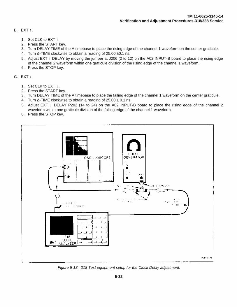
TM 11-6625-3145-14Verification and Adjustment Procedures-318/338 Service
B. EXT ↑.
1. Set CLK to EXT ↑.2. Press the START key.3. Turn DELAY TIME of the A timebase to place the rising edge of the channel 1 waveform on the center graticule.4. Turn ∆-TIME clockwise to obtain a reading of 25.00 ±0.1 ns.5. Adjust EXT ↑ DELAY by moving the jumper at J206 (2 to 12) on the A02 INPUT-B board to place the rising edge
of the channel 2 waveform within one graticule division of the rising edge of the channel 1 waveform.6. Press the STOP key.
C. EXT ↓
1. Set CLK to EXT ↓.2. Press the START key.3. Turn DELAY TIME of the A timebase to place the falling edge of the channel 1 waveform on the center graticule.4. Turn ∆-TIME clockwise to obtain a reading of 25.00 ± 0.1 ns.5. Adjust EXT ↓ DELAY P202 (14 to 24) on the A02 INPUT-B board to place the rising edge of the channel 2
waveform within one graticule division of the falling edge of the channel 1 waveform.6. Press the STOP key.
Figure 5-18. 318 Test equipment setup for the Clock Delay adjustment.
5-32

TM 11-6625-3145-14Verification and Adjustment Procedures-318/338 Service
Figure 5-19. 318 EXT CLK and DLD CLK signal adjustment locations.
7. Adjust DLD CLK Delay
Equipment Required1. Oscilloscope, Tektronix 7904 with plug in units 7A26, 7B80, and 7B85.1. Pulse Generator1. BNC 50 Ω termination1. BNC T-connector2. BNC male to Probe tip Adapters1. 2 SQR-pin to Probe tip Adapter
Refer to Figures 5-18 and 5-19.
a. Install the 7B85 plug-in module into the 7904 A timebase, and install the 7B80 module into the B timebase.b. Connect a 50 Ω terminator to the pulse generator OUTPUT. Connect a BNC T-connector to the 50 Ω
terminator. Connect the oscilloscope channel 1 probe lead to one side of the BNC T-connector.c. Connect the P6107 External Clock probe lead to other side of the BNC T-connector.
5-33
TM 11-6625-3145-14Verification and Adjustment Procedures-318/338 Service
d. Setup the oscilloscope as follows:
7904 Mainframe Horizontal Mode B7A26 Position Rising edge at center screen
Channel 1 VOLTS/DIV 20 mv (200 mv with 10 OX probe)Trigger Source CH 1Display Mode ALTPosition 0 v at mid screen
Channel 2 VOLTS/DIV 50 mv (500 mv with 10X probe)Position 0 v 2.4 divisions above midscreen (-1.4 v at midscreen)
7B85 Slope +Triggering Mode Coupling Source
Auto AC INTMagnification 1 XHold Off at minimumB Delay Mode B Starts after DLYTime/DIV 50 ns (5 ns with magnifiction)Trace Sep On, minimum∆Time zero
7B80 slope +Triggering Mode Coupling Source
Auto AC INTPosition rising edge at center screenHold Off at minimum∆ Time/Div 10 ns (1 ns with magnification)
e. Set the pulse generator as follows:
Termination BACK TERM(pull switch out)
Period 0.1 µsDuration 10 ns (5 ns X 2)High level +0.35 VLow level -0.35 V
f. Select the A timebase and place the rising edge of the channel 1 waveform on the center graticule on theoscilloscope screen.
g. Select the B timebase.h. Turn DELAY TIME of the A timebase to place the rising edge of the channel 1 waveform on the center graticule.i. Connect the oscilloscope channel 2 probe tip to TP106 on the A01 INPUT-A board.j. Select the Threshold menu and set INPUT EXT CLK = V3.
k. Set CLK to EXT ↑.l. Select the Trigger menu and set the events field to 00000*WA OFF:WB OFF:WC. This will cause the 318 to
acquire data without triggering.m. Press the START key.n. Turn A-TIME clockwise to obtain a reading of 43.00 ±0.1 ns.o. Adjust DLD CLK DELAY by moving the jumper at J104 on the A01 INPUT-A board to place the rising edge of
the channel 2 waveform within one graticule division of the rising edge of the channel 1 waveform.p. Press the STOP key.
5-34
TM 11-6625-3145-14Verification and Adjustment Procedures-318/338 Service
8. Adjust RET CLK, WE , ADRS CLK, and TRIG CLK Delay and Width
Equipment Required1. Oscilloscope, Tektronix 7904 with plug-in modules 7A26, 7B80, and 7B85.1. Pulse Generator1. BNC 50 Ω termination1. BNC T-connector2. BNC male-to-Probe-tip Adapters1. 2 SQR pin-to-Probe-tip Adapter2. Extender Boards2. Board Ejectors
Refer to Figures 5-18 and 5-20.
A. Equipment Setup
1. Install the 7B85 plug-in module into the 7904 timebase A, and install the 7B80 module into timebase B.2. Connect a 50 Ω terminator to the pulse generator OUTPUT. Connect a BNC T-connector to the 50 Ω terminator.
Connect the oscilloscope channel 1 probe tip to one side of the BNC T-connector.3. Connect the P6107 External Clock probe tip to the other side of the BNC T-connector.4. Setup the oscilloscope as follows:
Mainframe Horizontal Mode B7A26 Position Rising edge at center screen
Channel 1 VOLTS/DIV 20 mv (200 mv with 10 OX probe)Trigger Source CH 1Display Mode ALTPosition 0 v at mid screen
Channel 2 VOLTS/DIV 50 mv (500 mv with 10X probe)Position 0 v 2.4 divisions above midscreen (-1.4 v at midscreen)
7B85 Slope +Triggering Mode Coupling Source
Auto AC INTMagnification 1XHold Off at minimumB Delay Mode B Starts after DLYTime/DIV 50 ns (5 ns with magnifiction)Trace Sep On, minimum∆ Time zero
7B80 slope +Triggering Mode Coupling Source
Auto AC INTPosition rising edge at center screenHold Off at minimumTime/Div 10 ns (1 ns with magnification)
5-35
TM 11-6625-3145-14Verification and Adjustment Procedures-318/338 Service
5. Set the pulse generator as follows:
Termination BACK TERM(pull switch out)
Period 0.1 µsDuration 10 ns (5 ns X 2)High level +0.35 VLow level -0.35 V
6. Select the A timebase and place the rising edge of the channel 1 waveform on the center graticule on theoscilloscope screen.
7. Select the B timebase.8. Turn DELAY TIME of the A timebase to place the rising edge of the channel 1 waveform on the center graticule.
B. Strap adjustment with Extender boards (Optional Maintenance Kit Required)
1. Turn off the 318.2. Remove the A03 ACQ CONTROL board and the A04 ACQ MEMORY board using the Board ejectors.3. Install Extender boards into the J03 and J04 connectors.4. Mount the A03 ACQ CONTROL board and the A04 ACQ MEMORY board on the top of the Extender boards.5. Turn on the 318.6. Select the Threshold menu and set INPUT EXT CLK = V3 (0.00 V).7. Set CLK to EXTT.8. Select the Trigger menu and set the Events field to: 00000*WA OFF:WB OFF:WC. This will cause the 318 to
acquire data without triggering.9. Press the START key.
10. Repeat the following procedures, (11) through (13), to adjust each clock delay with Extender boards shown inTable 5-5.
11. Connect the oscilloscope channel 2 probe tip to the corresponding test point given in Table 5-5.12. Turn ∆-TIME clockwise to display the clock delay value listed in Table 5-5.13. Adjust the corresponding jumper to place the rising or falling edge (indicated by ↑ or ↓ in Table 5-5) of the channel
2 waveform within one graticule division of the rising edge of the channel 1 waveform.14. Press the STOP key.15. Turn off the 318.16. Dismount the A03 ACQ CONTROL board and the A04 ACQ MEMORY board from the Extender boards.17. Remove the Extender boards from slots A03 and A04.18. Install the A03 ACQ CONTROL board and the A04 ACQ MEMORY board into slots A03 and A04 respectively.19. Turn on the 318.
5-36

TM 11-6625-3145-14Verification and Adjustment Procedures-318/338 Service
Table 5-5.318 CLOCK DELAY WITH EXTENDER
Clock Signal Edge* Delay (ns) Test Point AdjustableCapacitor
RET CLK ↑ 47.60 ± 1.00 TP400 (A03) J200(A03)WE ↓ 55.40 ± 1.00 TP200-2(A04) J300(A03)TRIG CLK ↑ 68.10 ± 1.00 TP500 (A03) J400(A03)
* ↑ means rising edge; ↓ means falling edge
C. Capacitor adjustment
1. Refer to Figures 5-21 and 5-22. Select the Threshold menu and set INPUT EXT CLK = V3 (0.00 v).2. Select the Trigger menu and set CLK = EXT ↑.3. Set the Events field to: 00000*WA OFF:WB OFF:WC. This will cause the 318 to acquire data without triggering.4. Press the START key.5. Repeat the following procedures, (6) through (f), to adjust each clock delay and/or width shown in Table 5-6.6. Connect the oscilloscope channel 2 probe tip to the corresponding test point given in Table 5-6.7. Turn ∆-TIME clockwise to display the clock delay value given in Table 5-6.8. Adjust the corresponding capacitor to place the rising or falling edge (indicated by ↑ or ↓ in Table 5-6) of the
channel 2 waveform within one graticule division of the rising edge of the channel 1 waveform.9. Press the STOP key.
NOTEVertically position signals to center around mid-screen. Delays are measured fromthreshold to threshold of each circuit.
Table 5-6.318 CLOCK DELAY WITHOUT EXTENDER
Clock Signal Edge* Delay (ns) Test Point AdjustableCapacitor
RET CLK ↑ 46.60 ± 0.50 TP400 (A03) C100(A03)WE ↓ 54.40 ± 0.50 TP200-2(A04) C102(A03)WE ↑ 61.40 ± 0.50 TP200-2(A04) C106(A03)ADRS CLK ↑ 61.40 ± 0.50 TP200-4(A04) C104(A03)
* ↑ means rising edge; ↓ means falling edge
5-37

TM 11-6625-3145-14Verification and Adjustment Procedures-318/338 Service
Figure 5-20. 318 RET CLK, WE , ADRS CLK, and TRIG CLK adjustments.
Figure 5-20. 318 RET CLK, WE, ADRS CLK, and TRIG CLK adjustment.
Figure 5-21. 318 Capacitor adjustment oscilloscope Figure 5-22. 318 Capacitor adjustment waveform. setupwaveform.
5-38

TM 11-6625-3145-14Verification and Adjustment Procedures-318/338 Service
SERIAL STATE ANALYZER
9. Adjust the Threshold Voltages on the A07 Board (318S1 Instruments Only)
Equipment Required
1. Digital Multimeter (DMM)
Refer to Figures 5-23 and 5-24
a. Set MODE to SER (any menu).b. Select the Threshold menu and set V1 = 0.0 V and V2 = 0.0 V.c. Connect the DMM minus (-) lead to TP200 (GND) on the A07 board.d. Connect the DMM plus (+) lead to TP11 (Threshold) on the A07 board.e. Set INPUT DATA = V1.f. Press the START key.g. Record the voltage and label it V0 (V0 will be used as a reference later).h. Connect the P6107 Serial Data probe tip to TP200 on the A07 board.i. Move the DMM plus (+) lead to TP10 on the A07 board.j. Adjust R23 DC BALANCE on the A07 board for a DMM indication of V0 ±0.001 V (the voltage measured in step
(7) ± 0.001 V).k. Press the STOP key.I. Set INPUT DATA = V2.
m. Press the START key.n. Check that the DMM indication is V0 ± 0.001 V.o. Press the STOP key.p. Set INPUT DATA = V3.q. Press the START key.r. Check that the DMM indication is V0 ± 0.001 V.s. Press the STOP key.
Figure 5-23. 318 Serial Analysis/RS-232C/NVM test point and adjustment locations
5-39
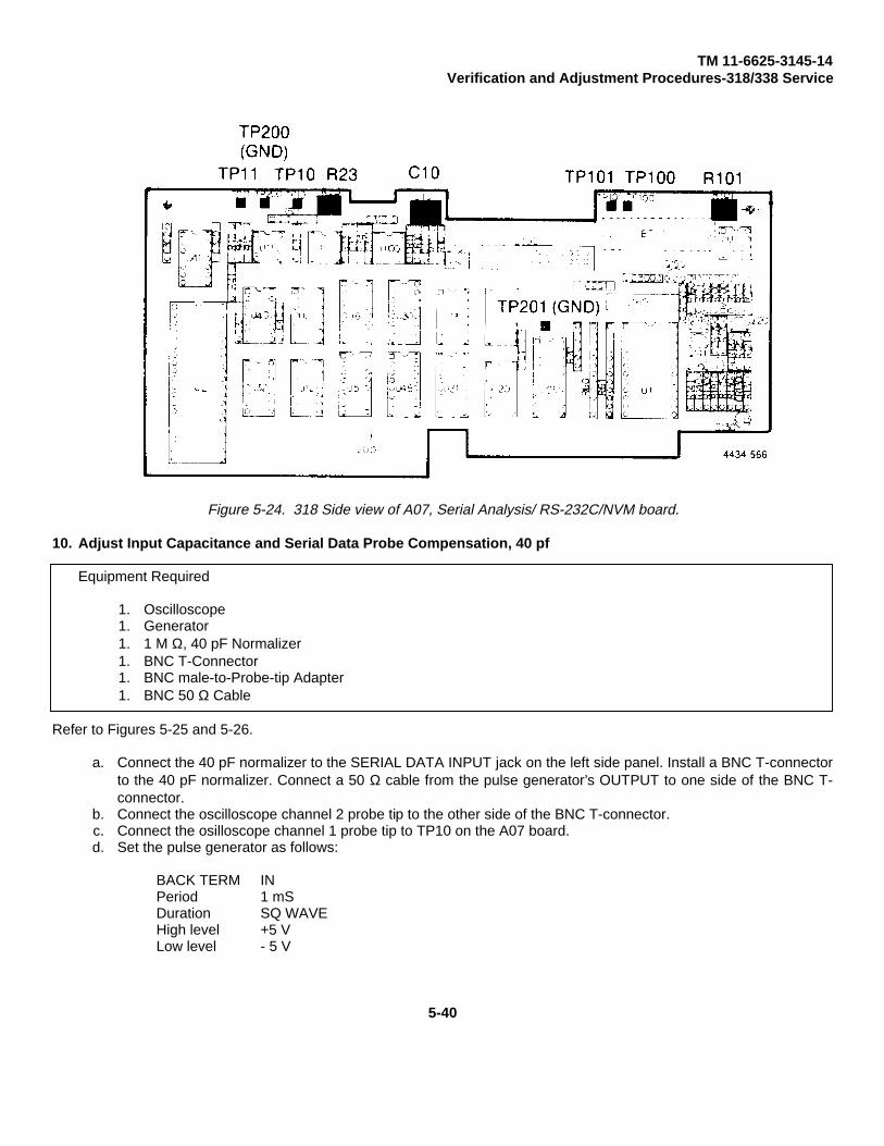
TM 11-6625-3145-14Verification and Adjustment Procedures-318/338 Service
Figure 5-24. 318 Side view of A07, Serial Analysis/ RS-232C/NVM board.
10. Adjust Input Capacitance and Serial Data Probe Compensation, 40 pf
Equipment Required
1. Oscilloscope1. Generator1. 1 M Ω, 40 pF Normalizer1. BNC T-Connector1. BNC male-to-Probe-tip Adapter1. BNC 50 Ω Cable
Refer to Figures 5-25 and 5-26.
a. Connect the 40 pF normalizer to the SERIAL DATA INPUT jack on the left side panel. Install a BNC T-connectorto the 40 pF normalizer. Connect a 50 Ω cable from the pulse generator’s OUTPUT to one side of the BNC T-connector.
b. Connect the oscilloscope channel 2 probe tip to the other side of the BNC T-connector.c. Connect the osilloscope channel 1 probe tip to TP10 on the A07 board.d. Set the pulse generator as follows:
BACK TERM INPeriod 1 mSDuration SQ WAVEHigh level +5 VLow level - 5 V
5-40
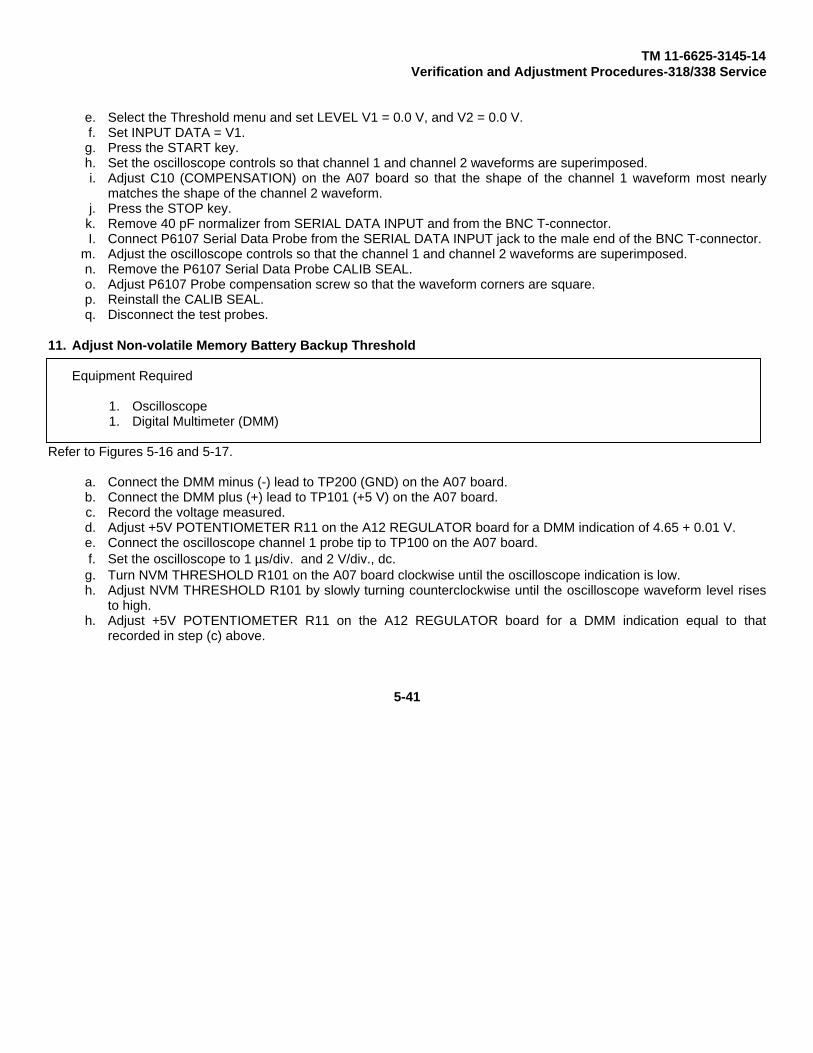
TM 11-6625-3145-14Verification and Adjustment Procedures-318/338 Service
e. Select the Threshold menu and set LEVEL V1 = 0.0 V, and V2 = 0.0 V.f. Set INPUT DATA = V1.g. Press the START key.h. Set the oscilloscope controls so that channel 1 and channel 2 waveforms are superimposed.i. Adjust C10 (COMPENSATION) on the A07 board so that the shape of the channel 1 waveform most nearly
matches the shape of the channel 2 waveform.j. Press the STOP key.
k. Remove 40 pF normalizer from SERIAL DATA INPUT and from the BNC T-connector.I. Connect P6107 Serial Data Probe from the SERIAL DATA INPUT jack to the male end of the BNC T-connector.
m. Adjust the oscilloscope controls so that the channel 1 and channel 2 waveforms are superimposed.n. Remove the P6107 Serial Data Probe CALIB SEAL.o. Adjust P6107 Probe compensation screw so that the waveform corners are square.p. Reinstall the CALIB SEAL.q. Disconnect the test probes.
11. Adjust Non-volatile Memory Battery Backup Threshold
Equipment Required
1. Oscilloscope1. Digital Multimeter (DMM)
Refer to Figures 5-16 and 5-17.
a. Connect the DMM minus (-) lead to TP200 (GND) on the A07 board.b. Connect the DMM plus (+) lead to TP101 (+5 V) on the A07 board.c. Record the voltage measured.d. Adjust +5V POTENTIOMETER R11 on the A12 REGULATOR board for a DMM indication of 4.65 + 0.01 V.e. Connect the oscilloscope channel 1 probe tip to TP100 on the A07 board.f. Set the oscilloscope to 1 µs/div. and 2 V/div., dc.g. Turn NVM THRESHOLD R101 on the A07 board clockwise until the oscilloscope indication is low.h. Adjust NVM THRESHOLD R101 by slowly turning counterclockwise until the oscilloscope waveform level rises
to high.h. Adjust +5V POTENTIOMETER R11 on the A12 REGULATOR board for a DMM indication equal to that
recorded in step (c) above.
5-41
TM 11-6625-3145-14Verification and Adjustment Procedures-318/338 Service
Figure 5-25. 318 Input capacitance adjustment setup. Figure 5-26. 318 Input capacitance waveform.
5-42

TM 11-6625-3145-14Verification and Adjustment Procedures-318/338 Service
PERFORMANCE CHECK FOR THE 318
The Performance Check Procedure provides a detailed check of internal and external product characteristics. Thesechecks can be extensive and time-consuming. Under normal circumstances the Functional Check Procedures will providean adequate test of product performance in a less costly manner.
The Performance Check Procedure is organized into sets of tests for the mainframe, the acquisition module, each type ofprobe, and 318S1 serial analyzer option.
INDEX OF PERFORMANCE CHECKS
• Test 1. Threshold Voltages
• Test 2. Parallel Data Acquisition, Word Recognition, and Trigger Sequencer Checks with External Clock MinimumPeriod.
• Test 3. Glitch Data Acquisition and Glitch Trigger
• Test 4. Start Output and Trigger Output
• Test 5. External Trigger Input
• Test 6. Serial State Analyzer (318S1)
THE PERFORMANCE CHECKS
Test 1. Threshold Voltages
TektronixEquipment Required Equivalent
1 Oscilloscope module 7904 with 7B80and 7A26 plug-inmodules
2 Oscilloscope Probes 10X P61061 Pulse Generator PG 5021 Digital Multimeter (DMM) DM 5021 Regulated DC Power Supply PS 5011 BNC T-Connector 103-0030-002 BNC male-to-Probe-tip Adapters 013-0084-021 BNC 50 Ω Cable 18 inches long 012-0076-001 BNC 50 Ω Cable 42 inches long 012-0057-012 Flying Lead set 5in. (short leads) 012-0987-001 Test Fixture See Figure 5-2.1 BNC Female-to-Dual-Banana connector
5-43
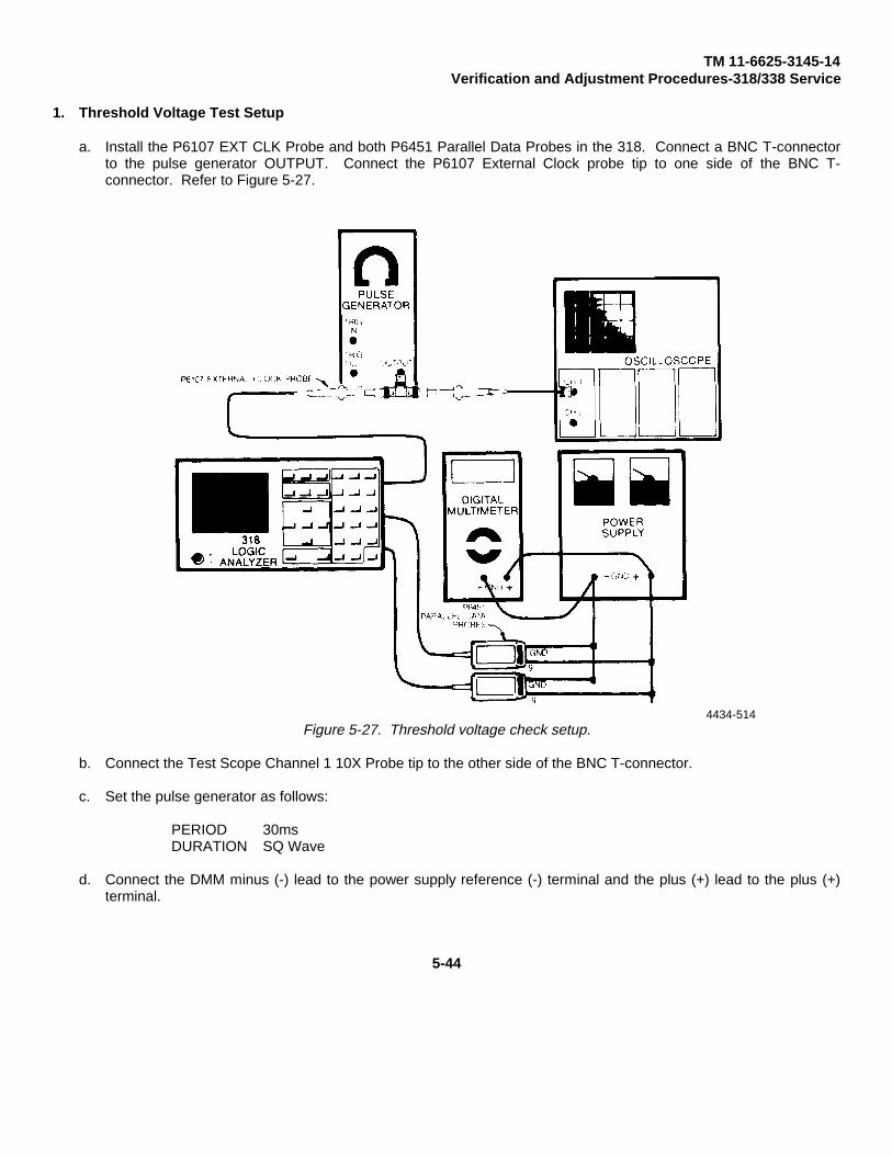
TM 11-6625-3145-14Verification and Adjustment Procedures-318/338 Service
1. Threshold Voltage Test Setup
a. Install the P6107 EXT CLK Probe and both P6451 Parallel Data Probes in the 318. Connect a BNC T-connectorto the pulse generator OUTPUT. Connect the P6107 External Clock probe tip to one side of the BNC T-connector. Refer to Figure 5-27.
4434-514Figure 5-27. Threshold voltage check setup.
b. Connect the Test Scope Channel 1 10X Probe tip to the other side of the BNC T-connector.
c. Set the pulse generator as follows:
PERIOD 30msDURATION SQ Wave
d. Connect the DMM minus (-) lead to the power supply reference (-) terminal and the plus (+) lead to the plus (+)terminal.
5-44

TM 11-6625-3145-14Verification and Adjustment Procedures-318/338 Service
WARNINGDo not reverse the power supply connections when common is connected toground; that would allow excessive current to pass through to the P6451 Probeground. If the P6451 Probe ground lead is connected to a large current source theprobe will be damaged.
e. Connect the P6451 Probe GND leads from Pods A and B to the power supply reference (-) terminal.
f. Connect the P6451 Probe DATA leads from Pods A and B to the Power Supply plus (-) terminal.
g. Power-up and setup 318 as follows:
THRESHOLD MENUINPUT
EXT CLK = TTLPOD A = TTLPOD B = TTL
TRIGGER MENUCLK EXTTPOSN DELAY00249Events 00001*WA FLW’D BY:WB OFF:WC
2. Threshold Level TTL
a. Repeat the following procedures, (b) through (e), for two voltage levels of the power supply output given inTable 5-7.
b. Set the pulse generator output level to that given in Table 5-7 as measured by the oscilloscope. Set theoscilloscope so that + 1.4 V is at midscreen:
1. Set the DVM for 1.40 V2. Momentarily move the oscilloscope CH1 probe to the DVM + 1.40 V output.3. Set the oscilloscope vertical Volts/DIV so that the screen reads 200 mV (20 mV setting using 10x probe).4. Adjust the vertical position so that the trace is at midscreen (+ 1.40 V at midscreen).5. Return the oscilloscope CH1 probe to the pulse generator’s BNC T-connector.6. Adjust the pulse generator output so that the signal is 1 1/4 divisions above and 1 1/4 divisions below
midscreen (+ 1.15 V to = 1.65 V).
c. Set the power supply level to the voltage given in Table 5-7 as measured with the DVM.
d. Press the START key and wait for the acquisition to be completed; make sure that SLOW CLOCK is not displayedon the CRT.
e. Press the DATA key until the State Table is displayed. Check that data acquired are equal to the Expected Datagiven in Table 5-7.
5-45

TM 11-6625-3145-14Verification and Adjustment Procedures-318/338 Service
Table 5-7.318 VOLTAGE LEVELS FOR TESTING TTL
Power Supply Pulse Generator T/H Level Expected
Output (V) High (V) Low (V) V1(V) V2(V) V3(V) Data
+1.65 +1.65 +1.15 ----- ---- ---- all Fs (hex)
+1.15 +1.65 +1.15 ----- ---- ---- all 0s
3. Threshold Levels V1, V2, and V3
a. Press the 318 THRESHOLD key.
b. Refer to the values given in Table 5-8 in setting the power supply output level, the pulse generator output level, thesystem threshold levels, and the INPUT Clock and Pod Threshold levels.
c. Set the test equipment to the values necessary for Test 1 in Table 5-8 and press the DATA key.
d. Press the START key and wait for the acquisition to be completed. Check to make sure that SLOW CLOCK is notdisplayed on the screen.
e. Check that data acquired are equal to the Expected Data given in Table 5-8.
f. Set the 318 SRCH WORD to equal the Expected Data and then check that the quantity of SRCH words equals256.
g. Repeat Steps (a) to (f) for each test in Table 5-8.
h. Disconnect the test setup.
Table 5-8.318 VOLTAGE LEVELS FOR TESTING V1, V2, AND V3
Power T/HTest Supply Pulse Generator T/H Level Input Expected
# Output (V) High (V) Low (V) V1 (V) V2 (V) V3 (V) Clk A, B Data
1 +5.25 +5.25 +4.75 +5.0 -- -- V1 all Fs2 +4.75 +5.25 +4.75 +5.0 -- -- V1 all 0s
* 3 -4.75 -4.75 -5.25 -5.0 -- -- V1 all Fs* 4 -5.25 -4.75 -5.25 -5.0 -- -- V1 all 0s5 +5.25 +5.25 +4.75 -- +5.0 -- V2 all Fs6 +4.75 +5.25 +4.75 -- +5.0 -- V2 all 0s
* 7 -4.75 -4.75 -5.25 -- -5.0 -- V2 all Fs* 8 -5.25 -4.75 -5.25 -- -5.0 -- V2 all 0s9 +5.00 +5.00 +4.50 +10.0 -0.5 +4.75 V3 all Fs10 +4.50 +5.00 +4.50 +10.0 -0.5 +4.75 V3 all 0s11 +0.25 +0.25 -0.25 0.0 0.0 0.00 V3 all 0s
* 12 -0.25 +0.25 -0.25 0.0 0.0 0.00 V3 all 0s* 13 -4.50 -4.50 -5.00 +0.5 -10.0 -4-75 V3 all Fs* 14 -5.00 -4.50 -5.00 +0.5 -10.0 -4.75 V3 all 0s
* Insure that the P6451 probe GND lead connected to the Power Supply Reference terminal is at the same potential as the318 ground.
5-46

TM 11-6625-3145-14Verification and Adjustment Procedures-318/338 Service
TEST 2. Parallel Data Acquisition Word Recognition and Trigger Sequencer Check with External ClockMinimum Period.
Equipment Required TektronixEquivalent
1 Oscilloscope 7904 with 7A26and 7B80 plug-in modules
2 Oscilloscope Probes 10X P61062 Pulse Generators PG 5021 Digital Delay DD 5014 BNC 50 Ω terminators 011-0049-013 BNC T-Connectors 103-0030-003 BNC male-to-Probe-tip Adapters 013-0084-023 BNC elbow male-to-female adapters 103-0031-001 BNC female-to-female adapter 103-0038-001 BNC male-to-male adapter 103-0029-001 BNC 50 Ω Cable 18 inches long 012-0076-001 BNC 50 Ω Cable 42 inches long 012-0057-011 Test Fixture. See Fig. 5-2.2 Flying Lead set 5 in. (short leads) 012-0987-00
Refer to Figure 5-28.
1. Connect a 50 Q terminator to the #1 pulse generator’s OUTPUT. Connect a BNC T-connector to the 50 Qt terminator.Connect the P6107 EXT CLOCK probe tip to one side of the BNC T-connector.
2. Connect the oscilloscope channel 1 10X probe tip to the other side of the BNC T-connector.
3. Connect a BNC elbow to the Digital Delay’s EVENTS INPUT. Connect a BNC T-connector to the elbow. Connect oneside of the T-connector to the #1 pulse generator’s + TRIG OUT using an 18 inch BNC cable and a 50 Q terminator.Connect the other side of the Digital Delay’s BNC T-connector to the Digital Delay’s START INPUT (see Figure 5-28).Using 2 BNC elbows and a BNC female-to-female connector will help here.
4. Connect the Digital Delay DLY’D TRIG OUT to the #2 pulse generator’s +TRIG/DURATION INPUT using a 42 inchBNC cable
5. Connect all the leads from Pod A, and the Qualifier lead from Pod B, to the Test Fixture; then connect the Test Fixtureto the #2 pulse generator’s OUTPUT. Make sure that the P6451 probe GND leads are connected to the Test Fixtureground pins (those pins nearest the BNC connector are ground).
5-47
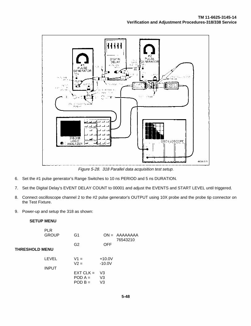
TM 11-6625-3145-14Verification and Adjustment Procedures-318/338 Service
Figure 5-28. 318 Parallel data acquisition test setup.
6. Set the #1 pulse generator’s Range Switches to 10 ns PERIOD and 5 ns DURATION.
7. Set the Digital Delay’s EVENT DELAY COUNT to 00001 and adjust the EVENTS and START LEVEL until triggered.
8. Connect oscilloscope channel 2 to the #2 pulse generator’s OUTPUT using 10X probe and the probe tip connector onthe Test Fixture.
9. Power-up and setup the 318 as shown:
SETUP MENU
PLRGROUP G1 ON = AAAAAAAA
76543210G2 OFF
THRESHOLD MENU
LEVEL V1 = +10.0VV2 = -10.0V
INPUTEXT CLK = V3POD A = V3POD B = V3
5-48

TM 11-6625-3145-14Verification and Adjustment Procedures-318/338 Service
TRIGGER MENU
Source INT TRIGCLK EXTITRIG IMMEDIATELYPOSN DELAY
00249Events 00001*WA FLW’D BY:WB OFF:WC
WA = XXWB = XXWC
10. Set the oscilloscope as shown:.
7904 Mainframe Horizontal Mode B
7A26
Channel 1 VOLTS/DIV 100 mV (10 mV with 10X probe)Trigger Source CH 2Display Mode ALTPosition 0 V at mid-screen
Channel 2 VOLTS/DIV 100 mV (10 mV with 10X probe)Position 0 V at mid-screen
7M80Triggering Mode Coupling Source
Auto AC INTTime/DIV 5 ns (50 ns with magnification)
11. Set the Pulse Generators shown:
Pulse Generator Setup
1 2NORM/CPMPLEMENT COMPLEMENT NORMBACK TERM OUIT (pull) OUT (pull)PERIOD 20 ns at 0 V level EXT TRIGDURATION 10 ns at 0 V level 14 ns + pulse at 0
V levelHIGH LEVEL +0.35V +0.25LOW LEVEL -0.35 -0.25
12. Set the oscilloscope triggering SOURCE to CH2 ONLY.
13. Adjust DD501 EVENTS LEVEL slowly until the channel 2 waveform’s falling edge crosses the channel 1 waveform’srising edge at 0 V (mid-screen). See Figure 5-29 (14 ns setup, 0 ns hold).
REV AUG 19845-49

TM 11-6625-3145-14Verification and Adjustment Procedures-318/338 Service
NOTEOver adjustment of the EVENTS LEVEL will cause a loss of the DD501 triggeringand oscilloscope display. If the adjustment range is not adequate, replace the 42inch BNC cable, from DLY’D TRIG OUT to the #2 Pulse Generator’s +TRIG INPUT,with a longer or shorter cable.
14. Set the 318 CLK and QUALIFIERS for Condition 1 in Table 5-9.
15. Press the 318 DATA key until the State Table is displayed.
16. Press the START key.
17. Check that the data acquired is equal to the Expected Data in Table 5-9.
18. Setup the 318 CLK and QUALIFIERS for Conditions 2 and 3 in Table 5-9. Repeat steps 15 to 17for each Condition.
19. Set the #1 pulse generator’s OUTPUT to NORM.
20. Adjust DD501 EVENTS LEVEL until the channel 2 waveform’s falling edge crosses channel 1’s falling edge at 0 V(mid-screen). See Figure 5-30 (14 ns setup, 0 ns hold).
21. Change the 318 CLK and QUALIFIERS for Conditions 4, 5, and 6 in Table 5-9. Repeat steps 15 to 17 for eachCondition.
Figure 5-29. 318 Parallel data acquisition Figure 5-30. 318 Parallel data acquisitiontest waveform #1. test waveform #2.
5-50

TM 11-6625-3145-14Verification and Adjustment Procedures-318/338 Service
Table 5-9.318 PARALLEL DATA TEST CONDITION AND EXPECTATIONS
Condition 1 2 3 4 5 6
Test WaveformFigure 5-59 5-29 5-29 5-30 5-30 5-30CLK EXT ↑ EXT ↑ EXT ↑ EXT ↓ EXT ↓ EXT ↓QUALIFIERS A OFF CLK-H CLK-H OFF TRG-L TRG-L
B OFF TRG-L TRG-H OFF CLK-L CLK-HEXPECTED 00 ** FF 00 00 **DATA FF ** FF FF 00 **
00 ** FF 00 00 **FF ** FF FF 00 **
NOTEThe ** means the 318 acquires data without triggering. Press the STOP key to stopdata acquisition.
22. Switch the P6451 probes connected to the Parallel Data inputs A and B. All of the leads from Pod Band the Qualifier lead from Pod A should now be connected to the test fixture.
23. Select the SETUP menu and set GROUP G1 = B7-BO.
24. Swap the Qualifier values for A and B in Table 5-9 and repeat steps 11 through 21.
25. Return the #1 pulse generator’s OUTPUT to COMPLEMENT.
26. Adjust the DD501 events level slowly until the channel 2 waveform’s falling edge crosses the channel 1 waveform’srising edge at 0 V (mid-screen). See Figure 5-29 (14 ns setup, 0 ns hold).
27. Change the 318 settings as follows:
SETUP MENUACQ. MODE REPEAT ACQ
TRIGGER MENUCLK = EXT ↑POSITION DELAY 00246EVENTS 00001 * WA THEN:WB THEN:WC
WA = 00WB = FFWC = 00
QUALIFIERS (Pod)A OFFB OFF
28. Press the DATA key until State Table is displayed and then press the START key.
29. Check for the following data and proper trigger location. It may be necessary to scroll through the display.
REV AUG 19845-51

TM 11-6625-3145-14Verification and Adjustment Procedures-318/338 Service
0 ## (Always no data)1 ## or FF2 003 FF
T 4 00 (Trigger location)
30. Press the STOP key and change TRIGGER MENU Word C to WC = FF.
31. Press the START key and check that the 318 does not trigger.
32. Press the STOP key.
33. Change the TRIGGER MENU as follows:
POSITION DELAY 00245EVENTS 00001 * WA THEN:WB FLW’D BY WC
WA = 00WB = FFWC =- FF
34. Press the DATA key and then the START key.
35. Check for the following data and proper trigger location.
0 ## (Always no data)1 ## or FF2 003 FF4 00
T 5 FF (Trigger location)
36. Press the STOP key and then the TRIGGER key.
37. Change the TRIGGER MENU Word B to WB = 00.
38. Press the START key and check that the 318 does not trigger.
39. Press the STOP key.
40. Change the TRIGGER MENU as follows:
EVENTS 00001 ’WA FLW’D BY:WB FLW’D BY:WC
41. Press the DATA key and then the START key.
42. Check for the following data and proper trigger location.
0 ## (Always no data)1 ## or FF2 003 FF4 00
T 5 FF (Trigger location)
43. Press the STOP key and then the TRIGGER key.
44. Change the TRIGGER MENU as follows:EVENTS 00002 * WA OR :WB OR :WC
WA = XXWB = 00WC = FF
45. Press the DATA key and then the START key.
46. Check for the following data and proper trigger location.
5-52

TM 11-6625-3145-14Verification and Adjustment Procedures-318/338 Service
0 ## (Always no data)1 ## (Always no data)2 ## (Always no data)3 ## (Always no data)4 ## (Always no data)
T 5 00 and/or FF (Check several acquisitions)(and make sure that both 00 and) (FF triggers occur.)
47. Press the STOP key and then the TRIGGER key.
48. Change the TRIGGER MENU as follows:
EVENTS 00002 ’ WA OFF:WB RESET ON:WCWA = FFWBWC = 00
49. Press the START key and check that the 318 does not trigger.
50. Press the STOP key.
51. Change the TRIGGER MENU as follows:
POSN DELAY = 00000Events 00001 *WA OFF:WB RESET ON:WC
52. Press the DATA key, the T key (scroll), and then the START key.
53. Check for the following data and proper trigger location.
243 ## (Always no data)244 ## (Always no data)245 ## (Always no data)246 ## (Always no data)247 ## (Always no data)248 ## (Always no data)249 ## or 00
T 250 FF (Trigger location)
54. Press the STOP key and the the TRIGGER key.
55. Increase the DD501 DELAY COUNT by steps of 01000 until the oscilloscope display starts to become too dim toobserve.
56. Adjust the oscilloscope horizontal POSITION to display the channel 2 waveform.
57. Adjust the DD501 EVENTS LEVEL slowly until the channel 2 waveform’s falling edge crosses the channel 1waveform’s rising edge at 0 V (mid-screen). See Figure 5-29 (14 nS setup, 0 nS hold).
NOTEIf adjustment range is not adequate then replace the DLY’D TRIG OUT BNC cablewith a longer or shorter one.
58. Set the DD501 DELAY COUNT to 65000.
59. Change the TRIGGER MENU as follows:
POSITION DELAY = 65000EVENTS 00001 * WA OFF:WB OFF:WC
WA = FF
5-53

TM 11-6625-3145-14Verification and Adjustment Procedures-318/338 Service
60. Press the DATA key and then the START key.
61. Check that data at location 251 contains FF, and all other data locations contain 00.
62. Press the STOP key and check the display, lower right for:
ST:T = 64750W
63. Change the TRIGGER MENU as follows:POSITION DELAY = 00000EVENTS 65000 ’WA OFF:WB RESET ON:WC
WA - 00WBWC = FF
64. Press the DATA key and the START key.
65. Check for the following data and proper trigger location.
243 00244 00245 00246 00247 00248 00249 00
T 250 00 (Trigger location)251 FF252 00
66. Press the STOP key and then the ↓ (scroll) key.
67. Return the DD501 DELAY COUNT to 00001.
68. Adjust the DD501 EVENTS LEVEL slowly until the channel 2 waveform’s falling edge crosses the channel 1waveform’s rising edge at 0 V (mid-screen). See Figure 5-29 (14 nS setup, 0 nS hold).
69. Disconnect the P6451 probe from the Pod A PARALLEL DATA INPUT connector on the right side panel and connect itto the Pod B connector. Connect the P6451 probe that was connected to the Pod B connector to the Pod A connector(i.e. swap the P6451 probes connected to Pods A and B).
70. Change 318 SETUP to GROUP G1 ON = A7-A0.
71. Repeat steps 27 to 68.
5-54
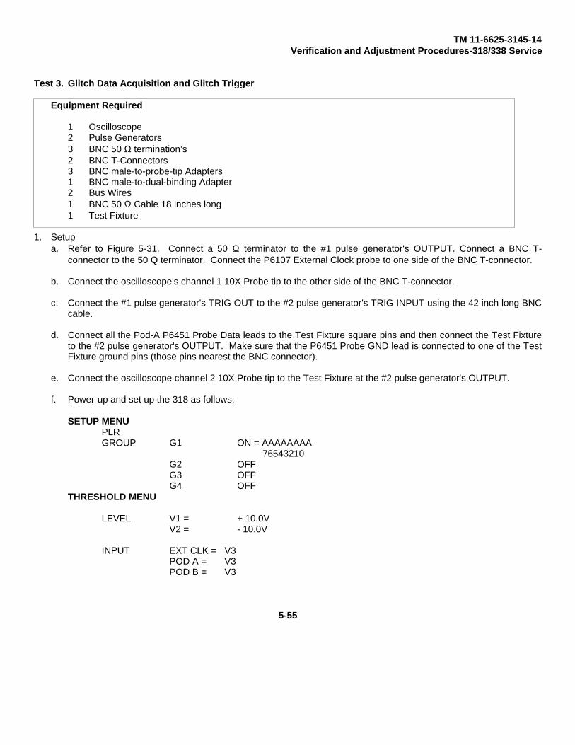
TM 11-6625-3145-14Verification and Adjustment Procedures-318/338 Service
Test 3. Glitch Data Acquisition and Glitch Trigger
Equipment Required
1 Oscilloscope2 Pulse Generators3 BNC 50 Ω termination’s2 BNC T-Connectors3 BNC male-to-probe-tip Adapters1 BNC male-to-dual-binding Adapter2 Bus Wires1 BNC 50 Ω Cable 18 inches long1 Test Fixture
1. Setupa. Refer to Figure 5-31. Connect a 50 Ω terminator to the #1 pulse generator's OUTPUT. Connect a BNC T-
connector to the 50 Q terminator. Connect the P6107 External Clock probe to one side of the BNC T-connector.
b. Connect the oscilloscope's channel 1 10X Probe tip to the other side of the BNC T-connector.
c. Connect the #1 pulse generator's TRIG OUT to the #2 pulse generator's TRIG INPUT using the 42 inch long BNCcable.
d. Connect all the Pod-A P6451 Probe Data leads to the Test Fixture square pins and then connect the Test Fixtureto the #2 pulse generator's OUTPUT. Make sure that the P6451 Probe GND lead is connected to one of the TestFixture ground pins (those pins nearest the BNC connector).
e. Connect the oscilloscope channel 2 10X Probe tip to the Test Fixture at the #2 pulse generator's OUTPUT.
f. Power-up and set up the 318 as follows:
SETUP MENUPLRGROUP G1 ON = AAAAAAAA
76543210G2 OFFG3 OFFG4 OFF
THRESHOLD MENU
LEVEL V1 = + 10.0VV2 = - 10.0V
INPUT EXT CLK = V3POD A = V3POD B = V3
5-55
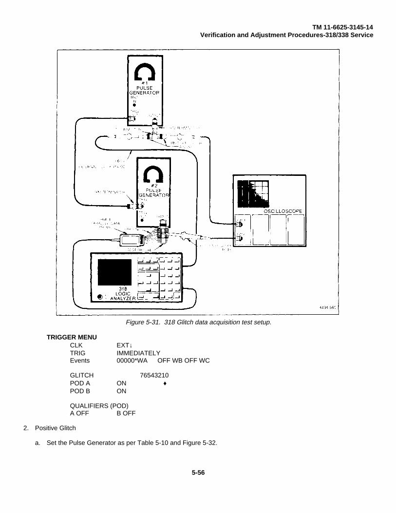
TM 11-6625-3145-14Verification and Adjustment Procedures-318/338 Service
Figure 5-31. 318 Glitch data acquisition test setup.
TRIGGER MENUCLK EXT↓TRIG IMMEDIATELYEvents 00000*WA OFF WB OFF WC
GLITCH 76543210POD A ON ♦POD B ON
QUALIFIERS (POD)A OFF B OFF
2. Positive Glitch
a. Set the Pulse Generator as per Table 5-10 and Figure 5-32.
5-56
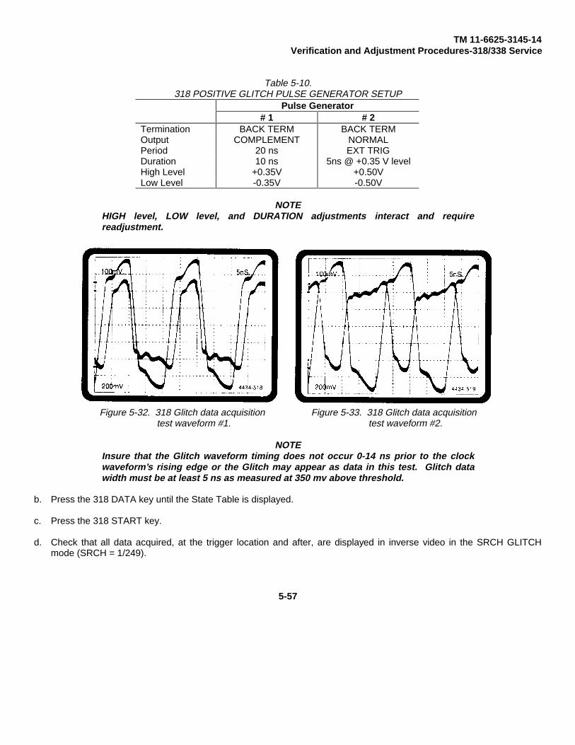
TM 11-6625-3145-14Verification and Adjustment Procedures-318/338 Service
Table 5-10.318 POSITIVE GLITCH PULSE GENERATOR SETUP
Pulse Generator# 1 # 2
Termination BACK TERM BACK TERMOutput COMPLEMENT NORMALPeriod 20 ns EXT TRIGDuration 10 ns 5ns @ +0.35 V levelHigh Level +0.35V +0.50VLow Level -0.35V -0.50V
NOTEHIGH level, LOW level, and DURATION adjustments interact and requirereadjustment.
Figure 5-32. 318 Glitch data acquisition Figure 5-33. 318 Glitch data acquisitiontest waveform #1. test waveform #2.
NOTEInsure that the Glitch waveform timing does not occur 0-14 ns prior to the clockwaveform’s rising edge or the Glitch may appear as data in this test. Glitch datawidth must be at least 5 ns as measured at 350 mv above threshold.
b. Press the 318 DATA key until the State Table is displayed.
c. Press the 318 START key.
d. Check that all data acquired, at the trigger location and after, are displayed in inverse video in the SRCH GLITCHmode (SRCH = 1/249).
5-57

TM 11-6625-3145-14Verification and Adjustment Procedures-318/338 Service
e. Press the 318 TRIGGER key, select the next GLITCH channel, one channel at a time, and repeat steps (b)through (d) until channels 0 through 7 have been tested.
f. Move the P6451 Probe connector from Pod A to Pod B PARALLEL DATA INPUT.
g. Change the SETUP MENU to GROUP G1 ON - B7-B0.
h. Press the TRIGGER MENU and select GLITCH Pod B channel 0 only.
i. Repeat steps (b) to (e).
3. Negative Glitch
a. Set the pulse generators as per Table 5-11 and Figure 5-33.
NOTEHIGH level, LOW level and DURATION adjustments inter-react and requirereadjustment.
b. Follow the same procedure as in the POSITIVE GLITCH test; select the State Table, press the START key, checkfor Glitch Data, select the next channel and repeat until all channels have been tested.
c. Move the P6451 Probe back to the Pod-A INPUT, setup the 318 for G1 = A7-AO and repeat step (b) for Pod-A.
Table 5-11.318 NEGATIVE GLITCH PULSE GENERATOR SETUP
Pulse Generator# 1 # 2
Termination BACK TERM BACK TERMOutput COMPLEMENT COMPLEMENTPeriod 20 ns EXT TRIGDuration 10 ns 5ns @ - 0.35 V levelHigh Level + 0.35V + 0.50VLow Level - 0.35V - 0.50V
Test 4. Start Output and Trigger Output Test.
EQUIPMENT REQUIRED2 PATCH CORDS, 2 inches long 012-0200-00
1. Connect Pod A and Pod B GND leads to the 318 GND mini-jack using one patch cord and grabber tips.
5-58

TM 11-6625-3145-14Verification and Adjustment Procedures-318/338 Service
2. Connect Pod A and Pod B channel 0 leads to the 318 START OUTPUT mini-jack using another patch cord andgrabber tips.
3. Power-up and setup the 318 as follows:
SETUP MENU REPEAT ACQ
THRESHOLD MENULEVEL V1 = +0.7 V
V2 = +2.4 V
INPUT Pod A = V1Pod B = V2
TRIGGER MENUCLOCK 20 nsTRIG = IMMEDIATELYEVENTS 1 * WA OFF:WB OFF:WC
WA = 0000
4. Press the DATA key until State Table is displayed.
5. Set the Search Word to Word = 01-01.
6. Press the START key and check for the following display:
SRCH = 1/34 (Approximately)
WORD = 01 -01G1 G2H H
0 ## ## (Always no data)1 ## ## (Always no data)2 ## ## (Always no data)3 ## ## (Always no data)4 ## ## (Always no data)5 ## ## (Always no data)6 ## ## (Always no data)
T 7 00 00 (Trigger location)8 0X 0X /X = Don’t care and it may \9 0X 0X \change with each acquisition/10 01 01 (Start Output)11 01 0112 01 01
7. Move the mini-jack cable from START OUTPUT to TRIG OUTPUT.
8. Press the START key and check that TRIGGER OUTPUT, WORD 01-01, starts at or near location 12 and the quantityof SRCH WORDS exceed 240.
Test 5. External Trigger Input Test.
Equipment Required1 BNC to Mini-Jack Cable 175-1178-001 Oscilloscope1 Pulse Generator1 10X Probe1 50 ohm Terminator1 BNC-to-Probe Adapter
5-59

TM 11-6625-3145-14Verification and Adjustment Procedures-318/338 Service
1. Connect a 50 ohm terminator to PG502 OUTPUT.
2. Connect a 10X probe from the oscilloscope CH1 to a BNC-to-probe-tip adapter and then to the 50 ohm terminator atthe PG502 OUTPUT.
3. Setup the Oscilloscope as follows:
TRIGGERING AUTO, AC, INT, CH1TIME/DIV 5 ns (Use 10X MAGNIFIER if necessary)CH1 VOLTS/DIV 1.0 V DCCH1 POSITION 0 V (GND) set to the middle of screen
4. Set the Pulse Generator as follows:
BACK TERM OUTOUTPUT NORMPERIOD 0.1 µsHIGH LEVEL + 2.80 VLOW LEVEL 0.00 VDURATION 20 ns @ + 1.4 V level
5. Remove the 10X Probe and BNC-to-probe-tip adapter from the pulse generator.
6. Connect the BNC-to-mini-jack Cable from the 50 ohm terminator at the PG502 OUTPUT to the 318 TRIG INPUT mini-jack. Connect the cable braid lead to the 318 GND mini-jack.
7. Power-up and setup the 318 as follows:
TRIGGER MENUSOURCE EXT TRIGEXT TRIG POL ↑
8. Press the START key and check that the 318 triggers.
9. Set the pulse generator Period to EXT TRIG and insure that no cables are connected to the pulse generator ExternalTrigger input.
10. Press the START key and then press the PG502 MAN TRIG.
11. Check that the 318 triggers only after the PG502 MAN TRIG button is pushed.
12. Set the EXT TRIG POL to negative and the PG502 OUTPUT to COMPLIMENT.
13. Repeat steps (10) and (11).
Test 6. Serial State Analyzer (318S1)
Equipment Required1 Serial Data Generator
Refer to : Figure 5-34.
5-60
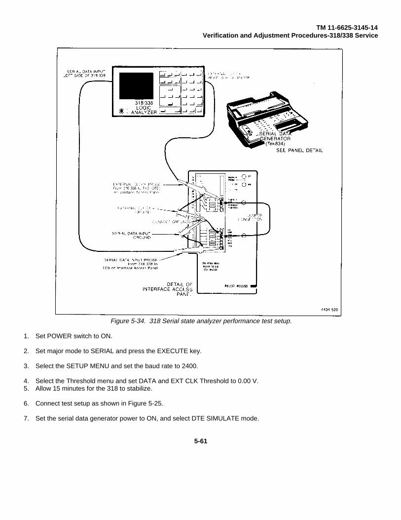
TM 11-6625-3145-14Verification and Adjustment Procedures-318/338 Service
Figure 5-34. 318 Serial state analyzer performance test setup.
1. Set POWER switch to ON.
2. Set major mode to SERIAL and press the EXECUTE key.
3. Select the SETUP MENU and set the baud rate to 2400.
4. Select the Threshold menu and set DATA and EXT CLK Threshold to 0.00 V.5. Allow 15 minutes for the 318 to stabilize.
6. Connect test setup as shown in Figure 5-25.
7. Set the serial data generator power to ON, and select DTE SIMULATE mode.
5-61

TM 11-6625-3145-14Verification and Adjustment Procedures-318/338 Service
8. Set serial data generator SETUP as follows;CODE=ASCII, BAUD=2400, DUPLEX=FULL, SETUP=ASYNC, BITS/CHAR=8, PARITY= NONE, STOPBITS = 1,TIMING= NORMAL..
9. Load the following program into the serial data generator:
STEP MNEMONICCODE
1 SEND #12 JMP #1
10. Load the following hexadecimal data in the serial data generator buffer # 1: E0, E0, E2, E4, E6, E8
11. Press the START key on the serial data generator.
12. Select the DATA DISPLAY STATE TABLE and press the START key.
13. When the 318 displays data on the crt, press the serial data generator STOP key.
14. Check that the 318 display matches the WORD SEQUENCE column on Table 5-12.
15. Set the 318 baud rate to 19.2K (DATA screen).
16. Set the serial data generator baud rate to 19.2K.
17. Set the 318 and the serial data generator controls as indicated in step 1 of Table 5-12 and repeat preceding steps ofTest 6 (11) through (14).
18. Finish steps 2 through 7 Table 5-12 as set up in step (17) of Test 6.
TABLE 5-12.318 SERIAL STATE ANALYZER TEST STEPS
Serial DataStep 318 Generator Word Sequence
1 BITS/WORD = 8 BITS/CHAR = 8 E0, E0, E2, E4, E6. E8
2 BITS/WORD = 7 BITS/CHAR = 7 60, 60, 62, 64, 66, 68
3 BITS/WORD = 6 BITS/CHAR = 6 20, 20, 22, 24, 26, 28
4 BITS/WORD = 5 BITS/CHAR = 5 00, 00, 02, 04, 06, 08
5 BAUD RATE = EXT16BITS/WORD = 6
BITS/CHAR = 6 20, 20, 22, 24, 26, 28
6 COMM. MODE = SYNCBITS/WORD = 8SYNC WORD 1 = 16SYNC WORD 2 = 16
SETUP = SYNCBITS/CHAR = 8CLOCK = DERIVED(INSERT DATA 16, 16 TOTOP OF BUFFER #1)
E0, E0, E2, E4, E6, E8,FF, FF, FF
7 BITS/WORD = 5SYNC WORD 1 = ADSYNC WORD 2 = 05HUNT WORD = 08
BITS/CHAR = 5 00, 02,04,06, 08
5-62

338VERIFICATION AND
ADJUSTMENT PROCEDURES

TM 11-6625-3145-14Verification and Adjustment Procedures-318/338 Service
NOTESelection field for BITS/WORD and COM. MODE (SYNC or ASYNC) and BAUD RATEappear in the 318 SETUP Menu. Selection fields for SYNC WORD and HUNT WORDare in the TRIGGER Menu.
To load SETUP parameters into the serial data generator, the operator must: (a) press SETUP, (b) select SETUP itemusing LEFT or RIGHT Vector keys, (c) select SETUP parameters using UP or DOWN VECTOR key.
To load data into the serial data generator buffer #1, the operator must: (a) press PROGRAM, (b) press RIGHT VECTOR,(c) press DOWN VECTOR, (d) press keys for the two hexadecimal characters to be entered, and (e) press ENTER. Toload additional data , repeat parts (d) and (e).
To load the program into the serial data generator, the operator must: (a) press PROGRAM, (b) select program code byLEFT or RIGHT VECTOR, (c) if program code includes destination number, press alphanumeric key to be entered, andpress ENTER, (d) press DOWN VECTOR, to next program step.
FUNCTIONAL CHECK PROCEDURES FOR THE 338
The following procedures are for the 338 Logic Analyzer only. The Functional Check for the 318 Logic Analyzer begins inthe first half of this section; refer to the margin tabs for help in locating the 318 procedures.
The Functional Check Procedure verifies that all major sections of the instrument being checked are operational. Thesetests can be used to determine whether adjustment and/or repair is necessary. The procedures are organized into sets oftests for the mainframe, the acquisition module, each type of probe, and the 338S1 serial acquisition and communicationoption.
Refer to the beginning of this Verification and Adjustment Procedures section, and to the Operating Information section ofthis manual, for instructions on probe connections and use of menus.
NOTEThese procedures assume that the user has a moderate understanding of theoperation of the 338 menus and hardware. Power-up of the 338 will preset menuselections; power-up must be performed when so instructed.
INDEX OF FUNCTIONAL CHECKS
Check 1. Power-up DiagnosticsCheck 2. KeyboardCheck 3. CRTCheck 4. Threshold VoltageCheck 5. Parallel Data Acquisition using TEST OUTPUTCheck 6. Glitch Data Acquisition using TEST OUTPUTCheck 7. Serial State Analyzer (338S1)
5-63

TM 11-6625-3145-14Verification and Adjustment Procedures-318/338 Service
MAINFRAME AND PARALLEL ANALYZER
CHECK 1. POWER-UP DIAGNOSTICS
1. Turn on the 338.2. Approximately seven seconds after power is turned on the screen display is initialized. Check to insure that FAIL is
not displayed in any of the test fields. Refer to Figure 5-35. This key blinks when hit
4433-03 4433-07Figure 5-35. 338 successful power-up Figure 5-36. 338 Keyboard test display.
diagnostics display.
CHECK 2. KEYBOARD1. Keyboard operation can be checked with the diagnostics program 0.KBD. To start this program, turn on the power
switch while depressing any numeric key until an error message appears on the CRT.
2. When an error message appears, press the START key. The Diagnostics menu will be displayed on the screen.Press 0 to run the KBD test. Refer to Figure 5-36.
3. Press each key individually and observe the CRT display to make sure the corresponding rectangle blinks. Press theSTOP key last. The keyboard generates an interrupt and corresponding key code for the MPU when any key exceptthe STOP key is pressed. The MPU reads the key code upon receiving the interrupt from the keyboard and blinks thecorresponding rectangle in the key array displayed on the screen. This test provides a check to ensure that each key(except the STOP key) is sending the correct key code to the MPU. The STOP key is used to exit this program; thusthe STOP key’s function can be checked at the end of this test.
CHECK 3. CRT
Refer to Figures 5-37, 5-38, 5-39, and 5-40.
1. The CRT can be visually checked with the diagnostic program 1.CRT. To start this diagnostic program, turn on thepower while pressing any numeric key until an error message is displayed on the CRT.
2. When an error message is displayed, press the START key. When the Diagnostics menu is displayed on the screen,select #1 for CRT.
5-64
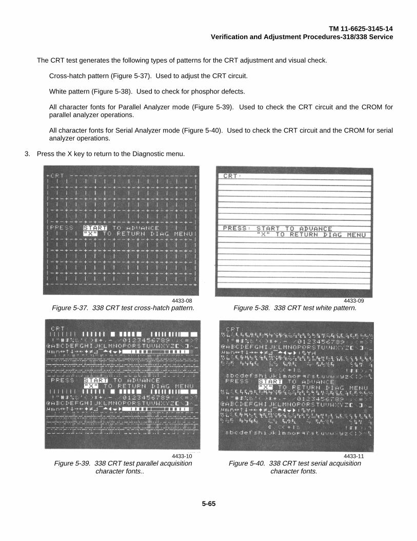
TM 11-6625-3145-14Verification and Adjustment Procedures-318/338 Service
The CRT test generates the following types of patterns for the CRT adjustment and visual check.
Cross-hatch pattern (Figure 5-37). Used to adjust the CRT circuit.
White pattern (Figure 5-38). Used to check for phosphor defects.
All character fonts for Parallel Analyzer mode (Figure 5-39). Used to check the CRT circuit and the CROM forparallel analyzer operations.
All character fonts for Serial Analyzer mode (Figure 5-40). Used to check the CRT circuit and the CROM for serialanalyzer operations.
3. Press the X key to return to the Diagnostic menu.
4433-08 4433-09Figure 5-37. 338 CRT test cross-hatch pattern. Figure 5-38. 338 CRT test white pattern.
4433-10 4433-11Figure 5-39. 338 CRT test parallel acquisition Figure 5-40. 338 CRT test serial acquisition
character fonts.. character fonts.
5-65

TM 11-6625-3145-14Verification and Adjustment Procedures-318/338 Service
CHECK 4. THRESHOLD VOLTAGE
1. Connect all the data and ground leads of the P6451 Parallel Data probes (Pods A through D) together and connectthem to the instrument ground.
2. Press the THRESHOLD menu key (normal operating mode).
Threshold Level TTLa. Set INPUT Thresholds to TTL for Pods A through D.
b. Press the START key. The trigger position (indicated by T) will be displayed on the screen. The trigger positionwill be <T= 7W>, <T = 127W>, or <T = 247W> depending on the trigger position setting in the Trigger menu(begin, center, or end).
c. Check that all data acquired are O’s.
Threshold Level V1
a. Set Threshold LEVEL V1 to +0.3 V.
b. Set Pods A through D equal to V1.
c. Press the START key. The trigger position displayed on the screen will be <T=7W>, <T=127W>, or <T=247W>depending on the trigger position setting in the Trigger menu.
d. Check that all data acquired are O’s.
e. Set Threshold LEVEL V1 to -0.3 V.
f. Press the START key. The trigger position displayed on the screen will be <T=7W>, <T=127W>, or <T=247W>depending on the trigger position setting in the Trigger menu.
g. Check that all data acquired are l’s.
Threshold Level V2
a. Set Threshold LEVEL V2 to +0.3 V.
b. Set Pods A through D equal to V2.
c. Press the START key. The trigger position is displayed on the screen will be <T=7W>, <T=127W>, or <T=247W>depending on the trigger position setting in the Trigger menu.
d. Check that all data acquired are O’s.
e. Set Threshold LEVEL V2 to -0.3 V.
f. Press the START key. The Trigger position displayed on the screen will be <T=7W>, <T= 127W>, or <T=247W>depending on the trigger position setting in the Trigger menu.
g. Check that all data acquired are 1’s.
5-66
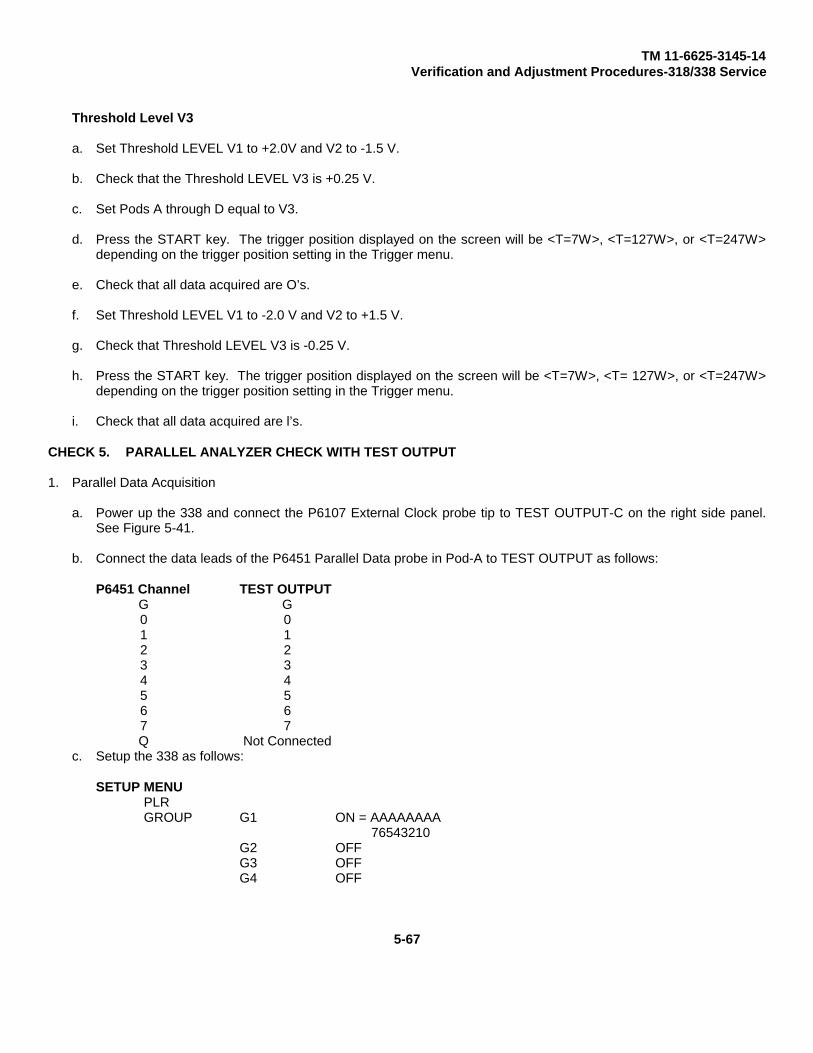
TM 11-6625-3145-14Verification and Adjustment Procedures-318/338 Service
Threshold Level V3
a. Set Threshold LEVEL V1 to +2.0V and V2 to -1.5 V.
b. Check that the Threshold LEVEL V3 is +0.25 V.
c. Set Pods A through D equal to V3.
d. Press the START key. The trigger position displayed on the screen will be <T=7W>, <T=127W>, or <T=247W>depending on the trigger position setting in the Trigger menu.
e. Check that all data acquired are O’s.
f. Set Threshold LEVEL V1 to -2.0 V and V2 to +1.5 V.
g. Check that Threshold LEVEL V3 is -0.25 V.
h. Press the START key. The trigger position displayed on the screen will be <T=7W>, <T= 127W>, or <T=247W>depending on the trigger position setting in the Trigger menu.
i. Check that all data acquired are l’s.
CHECK 5. PARALLEL ANALYZER CHECK WITH TEST OUTPUT
1. Parallel Data Acquisition
a. Power up the 338 and connect the P6107 External Clock probe tip to TEST OUTPUT-C on the right side panel.See Figure 5-41.
b. Connect the data leads of the P6451 Parallel Data probe in Pod-A to TEST OUTPUT as follows:
P6451 Channel TEST OUTPUTG G0 01 12 23 34 45 56 67 7Q Not Connected
c. Setup the 338 as follows:
SETUP MENUPLRGROUP G1 ON = AAAAAAAA
76543210G2 OFFG3 OFFG4 OFF
5-67
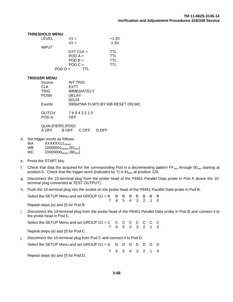
TM 11-6625-3145-14Verification and Adjustment Procedures-318/338 Service
THRESHOLD MENULEVEL V1 = +1.3V
V2 = -1.3VINPUT
EXT CLK = TTLPOD A = TTLPOD B = TTLPOD C = TTL
POD D = TTL
TRIGGER MENUSource INT TRIGCLK EXTTTRIG IMMEDIATELYPOSN DELAY
00124Events 00064*WA FLW’D BY:WB RESET ON:WC
GLITCH 7 6 5 4 3 2 1 0POD A OFF
QUALIFIERS (POD)A OFF B OFF C OFF D OFF
d. Set trigger words as follows:WA XXXXXX11binary
WB 10000001binary (81hex)WC 10000000binary (80hex)
e. Press the START key.
f. Check that data the acquired for the corresponding Pod is a decrementing pattern FFhex through 00hex starting atposition 0. Check that the trigger word (indicated by T) is 81hex at position 126.
g. Disconnect the 10-terminal plug from the probe head of the P6451 Parallel Data probe in Pod A (leave the 10-terminal plug connected at TEST OUTPUT).
h. Push the 10-terminal plug into the socket on the probe head of the P6451 Parallel Data probe in Pod B.
Select the SETUP Menu and set GROUP G1 = B B B B B B B B7 6 5 4 3 2 1 0
Repeat steps (e) and (f) for Pod B.
i. Disconnect the 10-terminal plug from the probe head of the P6451 Parallel Data probe in Pod B and connect it tothe probe head in Pod C.
Select the SETUP Menu and set GROUP G1 = C C C C C C C C7 6 5 4 3 2 1 0
Repeat steps (e) and (f) for Pod C.
j. Disconnect the 10-terminal plug from Pod C and connect it to Pod D.
Select the SETUP Menu and set GROUP G1 = D D D D D D D D
7 6 5 4 3 2 1 0Repeat steps (e) and (f) for Pod D.
5-68

TM 11-6625-3145-14Verification and Adjustment Procedures-318/338 Service
Figure 5-41. 338 Parallel data acquisition check setup.
2. 20 MHz Acquisition
a. Repeat steps (b) through (d), below, for each Pod (A through D). Change probe connections and SETUP Menuaccordingly.
b. Set CLK to 50 ns, and set the trigger position to DELAY 00250.
c. Press the START key.
d. Check that the data acquired for each Pod contains about 200 words of 81 he,, starting at position 0, and that therest of the words are all 80hex.
3. EXT TRIGGER Check
a. Refer to Figure 5-42. Power up the 338 and connect the data leads of the P6451 Parallel Data probe in Pod A toTEST OUTPUT as follows:
P6451 Channel TEST OUTPUTG G0 01 12 23 34 45 56 67 Not ConnectedQ Not Connected
b. Connect TRIG INPUT on the right side panel to TEST OUTPUT-7. A second lead set and a #22-gauge wire strapmay be used, by connecting one lead to OUTPUT-7 and then inserting wire between the comb lead’s end and theTRIG INPUT jack. Oversize wire will damage the connectors.
5-69

TM 11-6625-3145-14Verification and Adjustment Procedures-318/338 Service
c. Set up the 338 as follows:
SETUP MENUPLRGROUP G1 ON - AAAAAAAA
76543210G2 OFFG3 OFFG4 OFF
THRESHOLD MENULEVEL V1 = +1.3V
V2= -1.3V
INPUTEXT CLK = TTLPOD A = TTLPOD B = TTLPOD C = TTLPOD D = TTL
TRIGGER MENUSource INT TRIGCLK 10 µsTRIG IMMEDIATELYPOSN DELAY
00250
EXT TRIG POL = ↑
QUALIFIERS (POD)A OFF B OFF C OFF D OFF
d. Press the START key.
e. Check that all data acquired for Pod A is a repetitive, decrementing pattern from 7Fhex to 00hex, and that the triggerword (indicated by T) is 7F at position 0, with <T = 0 ♦> showing in the lower-right corner in the display.
f. Set EXT TRIG POL to ↓.
g. Press the START key.
h. Check that all data acquired for Pod A is a repetitive, decrementing pattern from 7Fhex to 00hex, and that the triggerword (indicated by T) is 7F at position zero, with <T = 0 ♦> showing in the lower-right corner of the display.
i. Disconnect Pod A from TEST OUTPUT and remove the second 10-termninal lead set.
5-70

TM 11-6625-3145-14Verification and Adjustment Procedures-318/338 Service
Figure 5-42. 338 External trigger check setup.
4. Trigger Qualifier Check
a. Refer to Figure 5-43. Power up the 338 and connect the data leads of the P6451 Parallel Data probe in Pod B toTEST OUTPUT as follows:
P6451 Channel TEST OUTPUTG G0 01 12 23 34 45 56 Not Connected7 Not ConnectedQ Not Connected
b. Ground all the qualifier and GND leads of the P6451 Parallel Data probes in all Pods (Pods A through D).
c. Setup the 338 as follows:
SETUP MENUPLRGROUP G1 OFF
G2 ON = BBBBBBBB76543210
G3 OFFG4 OFF
5-71
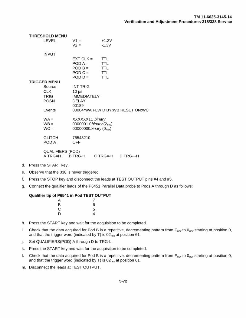
TM 11-6625-3145-14Verification and Adjustment Procedures-318/338 Service
THRESHOLD MENULEVEL V1 = +1.3V
V2 = -1.3V
INPUTEXT CLK = TTLPOD A = TTLPOD B = TTLPOD C = TTLPOD D = TTL
TRIGGER MENUSource INT TRIGCLK 10 µsTRIG IMMEDIATELYPOSN DELAY
00189Events 00004*WA FLW D BY:WB RESET ON:WC
WA = XXXXXX11 binaryWB = 0000001 0binary (2hex)WC = 00000000binary (0hex)
GLITCH 76543210POD A OFF
QUALIFIERS (POD)A TRG=H B TRG-H C TRG=-H D TRG---H
d. Press the START key.
e. Observe that the 338 is never triggered.
f. Press the STOP key and disconnect the leads at TEST OUTPUT pins #4 and #5.
g. Connect the qualifier leads of the P6451 Parallel Data probe to Pods A through D as follows:
Qualifier tip of P6541 in Pod TEST OUTPUTA 7B 6C 5D 4
h. Press the START key and wait for the acquisition to be completed.
i. Check that the data acquired for Pod B is a repetitive, decrementing pattern from Fhex to 0hex starting at position 0,and that the trigger word (indicated by T) is 02hex at position 61.
j. Set QUALIFIERS(POD) A through D to TRG-L.
k. Press the START key and wait for the acquisition to be completed.
I. Check that the data acquired for Pod B is a repetitive, decrementing pattern from Fhex to 0hex starting at position 0,and that the trigger word (indicated by T) is 02hex at position 61.
m. Disconnect the leads at TEST OUTPUT.
5-72
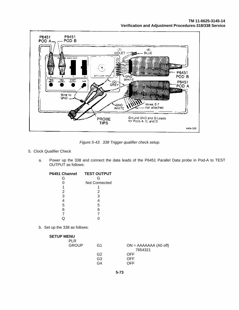
TM 11-6625-3145-14Verification and Adjustment Procedures-318/338 Service
Figure 5-43. 338 Trigger qualifier check setup.
5. Clock Qualifier Check
a. Power up the 338 and connect the data leads of the P6451 Parallel Data probe in Pod-A to TESTOUTPUT as follows:
P6451 Channel TEST OUTPUTG G0 Not Connected1 12 23 34 45 56 67 7Q 0
b. Set up the 338 as follows:
SETUP MENUPLRGROUP G1 ON = AAAAAAA (A0 off)
7654321G2 OFFG3 OFFG4 OFF
5-73

TM 11-6625-3145-14Verification and Adjustment Procedures-318/338 Service
TRIGGER MENUCLK 10 µsTRIG IMMEDIATELYPOSN DELAY
00249Events 00016*WA FLW’D BY:WB RESET ON:WC;
WA = XXXXXX 11 binaryWB = 1111111Obinary (7Ehex)WC =GLITCH 76543210POD A OFF
QUALIFIERS (POD)A CLK=L B OFF C OFF D OFF
c. Press the START key and wait for the acquisition to be completed.
d. Check that the data acquired for Pod A is a repetitive, decrementing pattern from 7Fhex to 00hex, starting atposition 0, and that the trigger word (indicated by T) is 7Ehex at position 1.
e. Set the QUALIFIERS(POD) for Pod A to CLK=H.
f. Press the START key and wait for the acquisition to be completed.
g. Check that the data acquired for Pod A is a repetitive, decrementing pattern from 7Fhex to 00hex starting atposition 0, and that the trigger word (indicated by T) is 7Ehex at position 1.
h. Disconnect the 10-terminal plug from the probe head of the P6451 Parallel Data probe in Pod A. Connect the10-terminal plug into the socket of the Pod B probe head.
Select the SETUP Menu and set GROUP G1 = B B B B B B B B7 6 5 4 3 2 1 0
i. Disconnect the 10-terminal plug from the probe head of the P6451 Parallel Data probe in Pod B and connect itto the socket of the Pod C probe head.
Select the SETUP Menu and set GROUP G1 = C C C C C C C C7 6 5 4 3 2 1 0
Repeat steps (c) through (g) for Pod C.
j. Disconnect the 10-terminal plug from the Pod C P6451 probe head and insert it into the Pod D P6451 probehead.
Select the SETUP Menu and set GROUP G1 = D D D D D D D D7 6 5 4 3 2 1 0
Repeat steps (c) through (g) for Pod C.
CHECK 6. GLITCH DATA ACQUISITION USING TEST OUTPUT
1. Power up the 338 and connect the data leads of the P6451 Parallel Data probe in Pod-A to TEST OUTPUT as follows:
5-74

TM 11-6625-3145-14Verification and Adjustment Procedures-318/338 Service
P6451 Channel TEST OUTPUTG G0 01 12 23 34 45 56 67 7Q Not Connected
2. Setup the 338 as follows:
SETUP MENUPLRGROUP G1 ON = AAAAAAAA
76543210G2 OFFG3 OFFG4 OFF
TRIGGER MENUCLK 10 msTRIG IMMEDIATELYPOSN DELAY
00250Events 00000*WA OFF:WB OFF:WC
GLITCH 76543210POD A ON ♦
QUALIFIERS (POD)A OFF B OFF C OFF D OFF
3. Press the START key and wait for the acquisition to be completed.
4. Check that all the data for Pod A is displayed in inverse video in the GLITCH SRCH mode. Check that theGLITCH trigger flag, indicated by <T = 0♦>, is showing in the lower-right corner of the screen.
5. Repeat steps 3 through 4 for glitch triggers A6 through A0. Glitch triggering must be checked one channel at atime for the test to be valid.
CHECK 7. SERIAL STATE ANALYZER CHECK FOR THE 338S1
1. Serial Data Acquisition and RS-232C Control
a. Connect test setup as shown in Figure 5-44.b. Set terminal character format to 8 bits per character.c. Set the POWER switch to ON and press the SETUP key after the diagnostics program has run.d. Set major mode to SERIAL and press the EXECUTE key.e. Set the baud rate and parity to match the terminal status, and press the THRESHOLD key.f. Set the data threshold to V3 (0.00 V), press the TRIGGER key.g. Set the trigger mode to IMMEDIATELY, and press the DATA key.h. Press the START key.
5-75
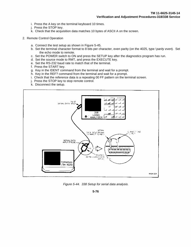
TM 11-6625-3145-14Verification and Adjustment Procedures-318/338 Service
i. Press the A key on the terminal keyboard 10 times.j. Press the STOP key.k. Check that the acquisition data matches 10 bytes of ASCII A on the screen.
2. Remote Control Operation
a. Connect the test setup as shown in Figure 5-45.b. Set the terminal character format to 8 bits per character, even parity (on the 4025, type !parity even). Set
the echo mode to remote.c. Set the POWER switch to ON and press the SETUP key after the diagnostics program has run.d. Set the source mode to RMT, and press the EXECUTE key.e. Set the RS-232 baud rate to match that of the terminal.f. Press the START key.g. Key in the IDENT command from the terminal and wait for a prompt.h. Key in the REF? command from the terminal and wait for a prompt.i. Check that the reference data is a repeating 00 FF pattern on the terminal screen.j. Press the STOP key to stop remote control.k. Disconnect the setup.
Figure 5-44. 338 Setup for serial data analysis.
5-76

TM 11-6625-3145-14Verification and Adjustment Procedures-318/338 Service
Figure 5-45. 338 Setup for RS-232C control.
ADJUSTMENT PROCEDURES FOR THE 338
INTRODUCTION
This section contains the Adjustment Procedures for the 338 Logic Analyzer. Information on the AdjustmentProcedures for the 318 Logic Analyzer is located in the first part of Chapter 5; refer to the page-edge tabs for helpin locating 318 information.
This section contains procedures for adjusting instrument variables so that the instrument meets or exceedsperformance specifications. If the instrument does not meet or exceed specifications after these procedures havebeen followed, repair is necessary.
IMPORTANT-PLEASE READ BEFORE USING THIS PROCEDURE
PURPOSE
The Adjustment Procedure provides a sequence for adjustments. It is not a troubleshooting guide or a verificationprocedure. The Adjustment Procedure is divided into sub-sections that describe adjustments for one particularboard or set of boards in the 338.
5-77

TM 11-6625-3145-14Verification and Adjustment Procedures-318/338 Service
LIMITS AND TOLERANCES
All limits and tolerances given in this procedure are adjustment guides. They should not be interpreted asinstrument specifications unless they are also found in the Specifications part of this manual.
Tolerances given are for the instrument under test and do not include test equipment error.
EQUIPMENT REQUIRED
The equipment, or equivalent, listed at the beginning of this Adjustment and Verification Procedures section inTable 5-1, is necessary to complete all the adjustment procedures. A partial list of equipment needed for eachindividual check and adjustment is also shown at the beginning of each procedure. The specifications given inTable 5-2 are the minimum necessary to produce accurate results. Therefore, related equipment must meet orexceed the listed specifications. Detailed instructions for operating the test equipment are not offered in thismanual. Refer to the manual for the specific piece of test equipment you are using if more information is required.
EQUIPMENT ALTERNATIVES
When equipment other than recommended test equipment is substituted, control settings or adjustment setupsmay need to be altered. If the exact equipment listed in Table 5-1 is not available, check the MinimumSpecification column in Table 5-2 carefully to see if any other equipment will suffice.
ADJUSTMENT INTERVAL
To ensure correct instrument operation, adjustment should be checked every 1000 hours of operation or every sixmonths, if used infrequently. Before performing the adjustment procedures, perform preventive maintenance asoutlined in the Maintenance section.
TEST SEQUENCE
NOTEThese adjustment procedures assume prior knowledge of some aspects of338 disassembly. If further information is required, refer to the disassemblyprocedures in Section 6 Maintenance: General Information.
It is necessary to perform the following sequence step by step, because all timings are level-sensitive.
INDEX OF ADJUSTMENT STEPS
Mainframe
1. Power Supplies
2. CRT Circuit
3. Threshold Voltages on the A05 ROM Board
5-78

TM 11-6625-3145-14Verification and Adjustment Procedures-318/338 Service
Parallel Analyzer
4. Threshold Voltages on the A02 INPUT-B Board
5. Probe Compensation for the P6107 External Clock Probe
6. EXT CLK T and EXT CLK I Delay
7. RET CLK, WE , ADRS CLK and TRIG CLK Delay and Width
Serial State Analyzer (338S1)
8. Threshold Voltages on the A07 board
9. Input Capacitance and Serial Data Probe Compensation (40 pf)
10. Non-volatile Memory Battery Backup Threshold
MAINFRAME
1. ADJUST POWER SUPPLIES
Equipment Required1 Digital Multimeter (DMM)
When performing the following procedures, make sure that all probes are connected properly.
1. Refer to Figure 5-46. Remove the 338 wraparound cover.
2. Install P6451 Parallel Data Probes into each of the four PARALLEL DATA INPUT sockets on the right sidepanel
3. Set the DMM to measure dc voltage.
4. Connect the DMM minus (-) lead to J1 pin #9 (GND) on the A12 Regulator board, located at the bottom rear ofthe 338.
5. Connect the DMM plus (+) lead to each point starting at -5 V shown in Table 5-13. (Set the DMM range asrequired.)
6. Adjust the corresponding potentiometer on the A12 Regulator board to set the voltage level within the limitgiven in Table 5-13.
WARNING
Exposed high voltages are present on the CRT board.
7. Move the DMM plus (+) lead to each point shown in Table 5-14. (Set the DMM range as required.)
8. Check that the DMM readings are within the limits given in Table 5-14.
5-79
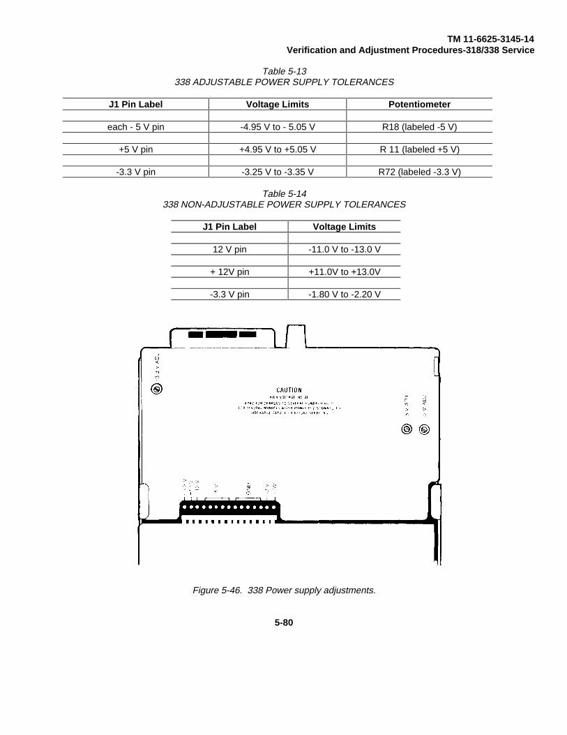
TM 11-6625-3145-14Verification and Adjustment Procedures-318/338 Service
Table 5-13338 ADJUSTABLE POWER SUPPLY TOLERANCES
J1 Pin Label Voltage Limits Potentiometer
each - 5 V pin -4.95 V to - 5.05 V R18 (labeled -5 V)
+5 V pin +4.95 V to +5.05 V R 11 (labeled +5 V)
-3.3 V pin -3.25 V to -3.35 V R72 (labeled -3.3 V)
Table 5-14338 NON-ADJUSTABLE POWER SUPPLY TOLERANCES
J1 Pin Label Voltage Limits
12 V pin -11.0 V to -13.0 V
+ 12V pin +11.0V to +13.0V
-3.3 V pin -1.80 V to -2.20 V
Figure 5-46. 338 Power supply adjustments.
5-80

TM 11-6625-3145-14Verification and Adjustment Procedures-318/338 Service
2. ADJUST CRT CIRCUIT
Equipment RequiredNone
Refer to Figure 5-47.
1. Run the diagnostic program 1 CRT to generate a cross-hatch pattern. (To enter the diagnostic, turn on thepower while pressing any numeric key until the display appears.)
2. Adjust INTENSITY R245 on the A10 CRT board to midrange. (See left side panel.)
3. Adjust INTENSITY LIMIT (CRT BIAS) R247 on the A10 CRT board for optimum intensity.
4. Press the start key to display a white stripe pattern.
5. Loosen the mounting screw of L150 (yoke coil).
6. Rotate L150 so that the display is properly aligned in the window.
7. Tighten the setting screw of L150.
8. Adjust the magnets on L150 on the CRT ring to center the display.
9. Adjust V-SIZE R015 until the display boarders are about 2 mm inside the display window frame.
10. Adjust V-LINEARITY R031 for optimum display.
11. Press X to return to the Diagnostic menu.
Figure 5-47. 338 CRT adjustment
5-81
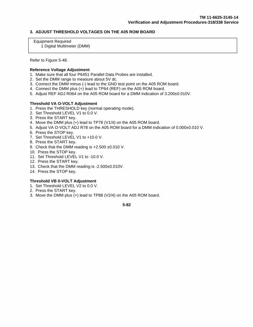
TM 11-6625-3145-14Verification and Adjustment Procedures-318/338 Service
3. ADJUST THRESHOLD VOLTAGES ON THE A05 ROM BOARD
Equipment Required1 Digital Multimeter (DMM)
Refer to Figure 5-48.
Reference Voltage Adjustment1. Make sure that all four P6451 Parallel Data Probes are installed.2. Set the DMM range to measure about 5V dc.3. Connect the DMM minus (-) lead to the GND test point on the A05 ROM board.4. Connect the DMM plus (+) lead to TP64 (REF) on the A05 ROM board.5. Adjust REF ADJ R064 on the A05 ROM board for a DMM indication of 3.200±0.010V.
Threshold VA O-VOLT Adjustment1. Press the THRESHOLD key (normal operating mode).2. Set Threshold LEVEL V1 to 0.0 V.3. Press the START key.4. Move the DMM plus (+) lead to TP78 (V1/4) on the A05 ROM board.5. Adjust VA O-VOLT ADJ R78 on the A05 ROM board for a DMM indication of 0.000±0.010 V.6. Press the STOP key.7. Set Threshold LEVEL V1 to +10.0 V.8. Press the START key.9. Check that the DMM reading is +2.500 ±0.010 V.10. Press the STOP key.11. Set Threshold LEVEL V1 to -10.0 V.12. Press the START key.13. Check that the DMM reading is -2.500±0.010V.14. Press the STOP key.
Threshold VB 0-VOLT Adjustment1. Set Threshold LEVEL V2 to 0.0 V.2. Press the START key.3. Move the DMM plus (+) lead to TP88 (V2/4) on the A05 ROM board.
5-82

TM 11-6625-3145-14Verification and Adjustment Procedures-318/338 Service
4. Adjust VB O-VOLT ADJ R088 on the A05 ROM board for a DMM indication of 0.000 + 0.010 V.5. Press the STOP key.6. Set Threshold LEVEL V2 to +10.0 V.7. Press the START key.8. Check that the DMM reading is +2.500t0.010 V.9. Press the STOP key.10. Set Threshold LEVEL V2 to -10.0 V.11. Press the START key.12. Check that the DMM reading is -2.500 ± 0.010 V.13. Press the STOP key.14. Disconnect the test leads.
Figure 5-48. 338 Threshold voltage adjustment on the ROM board.
5-83

TM 11-6625-3145-14Verification and Adjustment Procedures-318/338 Service
PARALLEL ANALYZER
4. ADJUST THRESHOLD VOLTAGES ON THE A02 INPUT-B BOARD
Equipment Required1 Regulated DC Power Supply1 Digital Multimeter (DMM)1 Oscilloscope
Refer to Figure 5-49.
NOTE
Before starting the following procedures, make sure that all probes are connectedproperly.
EXT CLK Threshold Adjustment
Setup1. Make sure that all four P6451 Parallel Data Probes are connected.2. Connect the oscilloscope channel 1 probe tip to TP100 on the A01 INPUT-A board.3. Set the oscilloscope triggering source to channel 1 and the sweep rate to 1 AS/div.4. Set the EXT CLK Threshold to V1.5. Set CLK to EXTT.6. Select the Trigger menu and set the EVENTS field to 00000:WA OFF:WB OFF:WC. This will cause the 338 to
acquire data without triggering.
DC Balance1. Ground the P6107 External Clock probe tip.2. Set Threshold LEVEL V1 to 0.0 V.3. Press the START key.4. Turn EXT CLK DC BALANCE R284 on the A02 INPUT-B board to the counterclockwise end.5. Turn R284 clockwise slowly while observing the oscilloscope waveform and mark the point where the
waveform moves from stationary-high level to stationary-low level.6. Then turn R284 to the clockwise end.7. Turn R284 counterclockwise slowly while observing the oscilloscope waveform and mark the point where the
waveform moves from stationary-low level to stationary-high level.8. Adjust R284 to the center position between the points you marked in procedures (5) and (7).9. Press the STOP key.
5-84
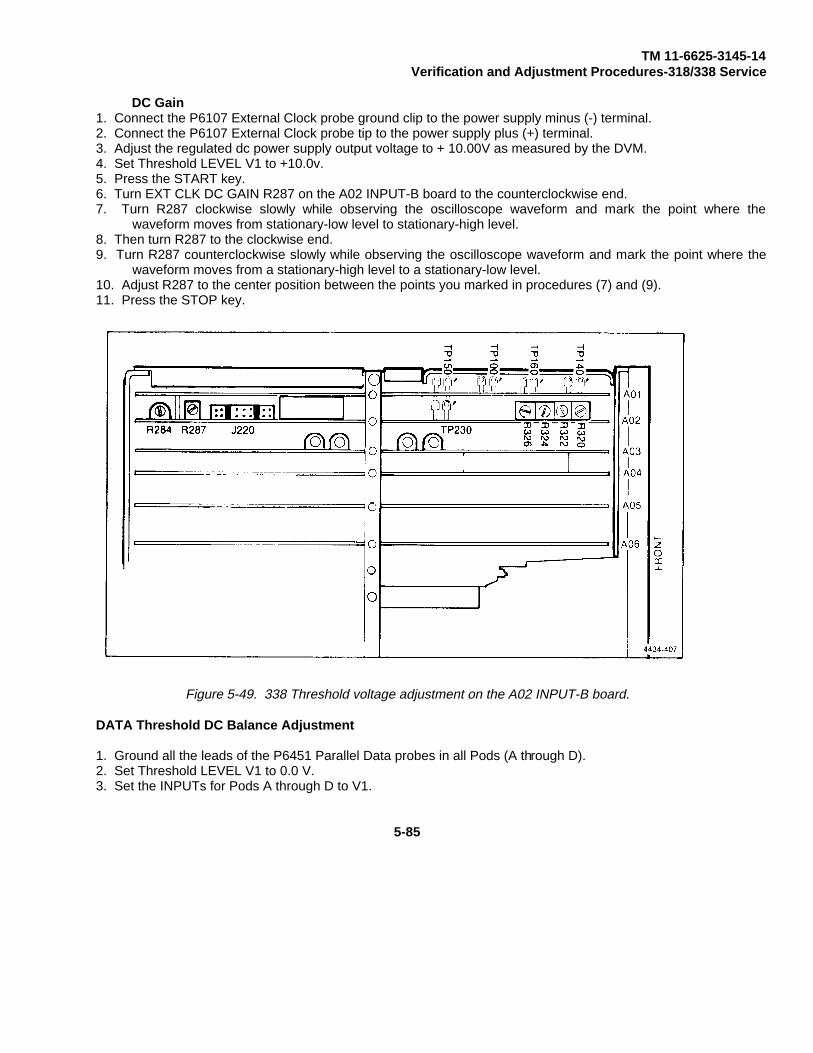
TM 11-6625-3145-14Verification and Adjustment Procedures-318/338 Service
DC Gain1. Connect the P6107 External Clock probe ground clip to the power supply minus (-) terminal.2. Connect the P6107 External Clock probe tip to the power supply plus (+) terminal.3. Adjust the regulated dc power supply output voltage to + 10.00V as measured by the DVM.4. Set Threshold LEVEL V1 to +10.0v.5. Press the START key.6. Turn EXT CLK DC GAIN R287 on the A02 INPUT-B board to the counterclockwise end.7. Turn R287 clockwise slowly while observing the oscilloscope waveform and mark the point where the
waveform moves from stationary-low level to stationary-high level.8. Then turn R287 to the clockwise end.9. Turn R287 counterclockwise slowly while observing the oscilloscope waveform and mark the point where the
waveform moves from a stationary-high level to a stationary-low level.10. Adjust R287 to the center position between the points you marked in procedures (7) and (9).11. Press the STOP key.
Figure 5-49. 338 Threshold voltage adjustment on the A02 INPUT-B board.
DATA Threshold DC Balance Adjustment
1. Ground all the leads of the P6451 Parallel Data probes in all Pods (A through D).2. Set Threshold LEVEL V1 to 0.0 V.3. Set the INPUTs for Pods A through D to V1.
5-85

TM 11-6625-3145-14Verification and Adjustment Procedures-318/338 Service
4. Select the Trigger Menu and set Events to: 00000*WA OFF:WB OFF:WC. This will cause the 338 to acquiredata without triggering.
5. Set the oscilloscope triggering source to channel 1 and the sweep rate to 1 us/div.6. Repeat the following procedures, (7) through (14), for PODs A through D.7. Connect the oscilloscope channel 1 probe tip to the test point shown in Table 5-15.8. Press the START key.9. Turn the corresponding Pod-Threshold DC BALANCE on the A02 INPUT-B board in Table 5-15 to the
counterclockwise end.10. Turn this potentiometer clockwise slowly while observing the oscilloscope waveform and mark the point where
the waveform moves from stationary-low level to stationary-high level.11. Turn the potentiometer to the clockwise end.12. Turn the potentiometer slowly while observing the oscilloscope waveform and mark the point where the
waveform moves from stationary-high level to stationary-low level.13. Adjust the potentiometer to the center position between the points you marked in steps (10) and (12).14. Press the STOP key.
Table 5-15338 DATA THRESHOLD DC BALANCE
POD Test Point Potentiometer
A TP230 on A02 R320
B TP140 on A01 R322
C TP150 on A01 R324
D TP160 on A01 R326
5. PROBE COMPENSATION FOR THE P6107 EXTERNAL CLOCK PROBE
Equipment RequiredNone
If you are using a standard 338 Logic Analyzer, you will have one P6107 probe labeled External Clock Probe. Thisprobe needs to be compensated to 20 pF according to the procedure described in Section 3: OperatingInstructions. See the Probe Compensation paragraph in the Diagnostic Test Descriptions.
5-86

TM 11-6625-3145-14Verification and Adjustment Procedures-318/338 Service
Two nearly identical P6107 probes are supplied with the 338S1 Logic Analyzers; one is the External Clock Probe,and the other is the Serial Data Acquisition Probe. If the probes were supplied as original equipment, they will belabeled as either EXT CLOCK, or SERIAL DATA with a sticker on the compensation box. The External ClockProbe is compensated to 20 pF, and the Serial Data Acquisition Probe is compensated to 40 pF.
If you have purchased replacement probes, or if you are adding the 318F1/338F1 Serial Analysis/RS232C/NVMupgrade kit to a standard 338, you need to choose which probe will be the External Clock Probe and adjust thecompensation accordingly.
Probes supplied from the factory are compensated to 40 pF.
The P6107 Serial Data Acquisition Probe has been factory compensated (40 pF) and sealed with a CALIB.sticker. Recompensation must be performed by qualified service personnel only. It is not necessary tocompensate this probe. We recommend that you install the colored marker band (supplied) on the probe foridentification purposes.
If the P6107 External Clock Probe is a replacement, the compensation must be altered. Remove and discard theCALIB. sticker. Then perform the probe compensation procedure described in the Operating Instructions(Section 3) of this manual. (See Probe Compensation under Diagnostic Test Descriptions.) We recommend thatyou install the colored marker band (supplied) on the probe to help in identification.
6. ADJUST EXT CLK↑ AND EXT CLK↓ DELAY
Equipment Required1 Oscilloscope1 Pulse Generator1 BNC 50 Ω termination1 BNC T-connector2 BNC male-to-Probe-tip adapters1 2 SQR-pin-to-Probe-tip adapter
Refer to Figure 5-50.
Oscilloscope Setup1. Connect a 50 Ω terminator to the pulse generator OUTPUT. Connect a BNC T-connector to the 50 Ω
terminator. Connect the oscilloscope channel 1 probe to one side of the BNC T-connector.2. Connect the P6107 External Clock probe to the other side of the BNC T-connector.3. Select the oscilloscope A time base, set the triggering source to channel 1, and the sweep rate to 5 ns/div
using X10 MAG, if necessary.4. Set B DELAY MODE of the A time base to B STARTS AFTER DELAY, and set TRACE SEP to ON, then adjust
delta-T to 0.5. Set the sweep rate of the B time base to 1 ns/div using X10 MAG if necessary.
5-87

TM 11-6625-3145-14Verification and Adjustment Procedures-318/338 Service
6. Set the pulse generator as follows:
Termination BACK TERM (switch pulled out)Period 0.1 µsDuration 10 ns (5 ns X 3)High level +0.35 VLow level -0.35 V
7. Select the A timebase and place the rising edge of the channel 1 waveform on the center graticule of theoscilloscope screen.
8. Select the B timebase.9. Connect the oscilloscope channel 2 probe tip to TP100 on the A01 INPUT-A board. Adjust the oscilloscope
Channel 2 position so that 0 V GND is 1.2 V above the graticule center level.10. Set Threshold LEVEL INPUT to V3, and set V3 to 0.00 V.11. Select the Trigger menu and set the EVENTS field to: 00000*WA OFF:WB OFF:WC. This will cause the 338
to acquire data without triggering.
EXT↑
1. Set CLK to EXT↑.2. Press the START key.3. Turn DELAY TIME of the A time base to place the rising edge of the channel 1 waveform on the center
graticule.4. Turn delta-TIME clockwise to obtain the delta-T reading of 25.0±0.1 ns.5. Adjust EXT↑ DELAY J220 (14 to 20) on the A02 INPUT-B board to place the rising edge of the channel 2
waveform within one division of the graticule, centered on the rising edge of the channel 1 waveform.6. Press the STOP key.
EXT↓
1. Set CLK to EXT↓.2. Press the START key.3. Turn DELAY TIME of the A timebase to place the falling edge of the channel 1 waveform on the center
graticule.4. Turn delta-TIME clockwise to obtain the delta-T reading of 25.0 ±0.1 ns.5. Adjust EXT- DELAY J220-2 to 12 on the A02 INPUT-B board to place the rising edge of the channel 2
waveform within one division of the graticule centered on the falling edge of the channel 1 waveform.6. Press the STOP key, and remove the oscilloscope test leads.
5-88
TM 11-6625-3145-14Verification and Adjustment Procedures-318/338 Service
Figure 5-50. 338 Test equipment setup for the clock delay adjustment.
7. ADJUST DELAY OF RET CLK, WE, ADRS CLK AND TRIG CLK
Equipment Required1 Oscilloscope1 Pulse Generator1 BNC 50 Ω termination1 BNC T-connector2 BNC male-to-Probe-tip Adapters1 2 Square-pin-to-Probe-tip Adapter2 Extender Boards2 Board Ejectors
Refer to Figures 5-51 and 5-52.
Equipment Setup
1. Connect a 50 Ω terminator to the pulse generator OUTPUT. Connect a BNC T-connector to the 50 Ωterminator. Connect the oscilloscope channel 1 probe tip to one side of the BNC T-connector.
5-89
TM 11-6625-3145-14Verification and Adjustment Procedures-318/338 Service
2. Connect the P6107 External Clock probe tip to the other side of the BNC T-connector.3. Setup the oscilloscope as follows:
Mainframe Horizontal Mode B
7A26 Position Rising edge at center screen
Channel 1 VOLTS/DIV 20 mv (200 mv with 10X probe)Trigger Source CH 1Display Mode ALTPosition 0 v at mid screen
Channel 2 VOLTS/DIV 50 mv (500 mv with 10X probe)Position 0 v 2.4 divisions above midscreen (-1.4 v at midscreen)
7B85 Slope +Triggering Mode Coupling Source
Auto AC INTMagnification 1XHold Off at minimumB Delay Mode B Starts after DLYTime/DIV 50 ns (5 ns with magnification)Trace Sep On, minimum∆ Time zero
7B80 slope +Triggering Mode Coupling Source
Auto AC INTPosition rising edge at center screenHold Off at minimumTime/Div 10 ns (1 ns with magnification)
4. Set the pulse generator as follows:
Termination BACK TERM (switch pulled out)Period 0.1 µsDuration 10ns (5 ns X 2)High level + 0.35VLow level -0.35V
5. Select the A timebase and place the rising edge of the channel 1 waveform on the center graticule of theoscilloscope screen.
6. Select the B time base.7. Turn DELAY TIME of the A time base to place the rising edge of the channel 1 waveform on the center
graticule.
Strap Adjustment with Extender Boards
1. Turn off the 338.2. Remove the A03 ACQ Control board and the A04 ACQ Memory board using the board ejectors.3. Install two Extender boards into the J03 and J04 connectors.4. Mount the A03 ACQ Control board and the A04 ACQ Memory board on the top of the Extender boards.5. Turn on the 338.
5-90

TM 11-6625-3145-14Verification and Adjustment Procedures-3181/338 Service
Figure 5-51. 338 RET CLK, WE , ADRS CLK, and TRIG CLK adjustments.
6. Set Threshold LEVEL to V3 (0.00 V).7. Set CLK to EXTT.8. Select the Trigger menu and set the Events field to: 00000*WA OFF:WB OFF:WC. This will cause the 338 to
acquire data without triggering.9. Press the START key.10. Repeat the following procedures, (11) through (13), to adjust each clock delay with Extender boards shown
in Table 5-16.11. Connect the oscilloscope channel 2 probe tip to the corresponding test point given in Table 5-16.12. Turn delta-TIME clockwise to obtain the delta-T reading of the clock delay being adjusted in Table 5-16.
5-91

TM 11-6625-3145-14Verification and Adjustment Procedures-318/338 Service
13. Adjust the corresponding jumper to place the rising or falling edge (indicated by ↑ or ↓ in Table 5-16) of thechannel 2 waveform within one division of the graticule centered on the rising edge of the channel 1waveform.
14. Press the STOP key.15. Turn off the 338.16. Dismount the A03 ACQ Control board and the A04 ACQ Memory board from the Extender boards.17. Remove the Extender boards from slots A03 and A04.18. Install the A03 ACQ Control board and the A04 ACQ Memory board into slots A03 and A04 respectively.19. Turn on the 338.
Table 5-16338 CLOCK DELAY WITH EXTENDER
DelayClock Ch 2 Edge (ns) Test Point Jumper
RET CLK ↑ 47.60 + 1.00 TP400 (A03) J200(A03)WE ↓ 55.40 + 1.00 TP200-2(A04) J300(A03)TRIG CLK ↑ 68.10 1.00 TP500 (A03) J400(A03)
Capacitor Adjustment
1. Refer to Figures 5-52 and 5-53. Set EXT CLK Threshold to V3 (0.00 V).2. Set CLK to EXT↑.3. Set the Events field to: 00000*WA OFF:WB OFF:WC. This will cause the 338 to acquire data without
triggering.4. Press the START key.5. Repeat the following procedures, (6) through (8), to adjust each clock delay and/or width as shown in Table 5-
17.6. Connect the oscilloscope channel 2 probe tip to the corresponding test point given in Table 5-17.7. Turn delta-TIME clockwise to obtain the delta-T reading of the clock delay being adjusted in Table 5-17.8. Adjust the corresponding capacitor to place the rising or falling edge (indicated by a ↑ or ↓ in Table 5-17) of the
channel 2 waveform within one division of the graticule centered on the rising edge of the channel 1waveform.
9. Press the STOP key.10. Remove the oscilloscope test leads from the test points.
5-92

TM 11-6625-3145-14Verification and Adjustment Procedures-318/338 Service
Table 5-17338 CLOCK DELAY WITHOUT EXTENDER
DelayClock CH2 Edge (ns) Test Point Adjustable
Capacitor
RET CLK ↑ 46.60 + 0.50 TP400 (A03) C100(A03)WE ↓ 54.40 + 0.50 TP200-2(A04) C102(A03)WE ↑ 61.40 + 0.50 TP200-2(A04) C106(A03ADRS CLK ↓ 61.40 + 0.50 TP200-4(A04) C104(A03)
Figure 5-52. 338 Capacitor adjustment oscilloscopesetup waveform.
Figure 5-53. 338 Capacitor adjustment waveform.
SERIAL STATE ANALYZER (338S1)
8. ADJUST THRESHOLD VOLTAGES ON THE A07 BOARD
Equipment Required1 Digital Multimeter (DMM)
Refer to Figures 5-54 and 5-55.
1. Power up the 338.2. Select the Serial mode (any menu).3. Set Threshold LEVEL V1 and V2 to 0.0 V4. Set the DMM range to 2 dc volts.5. Connect the DMM minus (-) lead to TP200 (GND) on the A07 board.
5-93
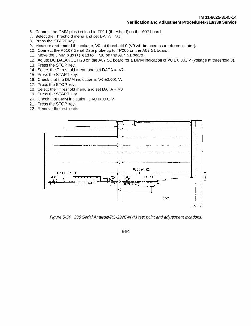
TM 11-6625-3145-14Verification and Adjustment Procedures-318/338 Service
6. Connect the DMM plus (+) lead to TP11 (threshold) on the A07 board.7. Select the Threshold menu and set DATA = V1.8. Press the START key.9. Measure and record the voltage, V0, at threshold 0 (V0 will be used as a reference later).10. Connect the P6107 Serial Data probe tip to TP200 on the A07 S1 board.11. Move the DMM plus (+) lead to TP10 on the A07 S1 board.12. Adjust DC BALANCE R23 on the A07 S1 board for a DMM indication of V0 ± 0.001 V (voltage at threshold 0).13. Press the STOP key.14. Select the Threshold menu and set DATA = V2.15. Press the START key.16. Check that the DMM indication is V0 ±0.001 V.17. Press the STOP key.18. Select the Threshold menu and set DATA = V3.19. Press the START key.20. Check that DMM indication is V0 ±0.001 V.21. Press the STOP key.22. Remove the test leads.
Figure 5-54. 338 Serial Analysis/RS-232C/NVM test point and adjustment locations.
5-94

TM 11-6625-3145-14Verification and Adjustment Procedures-318/338 Service
Figure 5-55. 338 Side view of A07 Serial Analysis/RS232C/NVM board.
9. ADJUST INPUT CAPACITANCE AND SERIAL DATA PROBE COMPENSATION, 40 pF
Equipment Required1 Oscilloscope1 Pulse Generator1 1M Ω, 40 pF Normalizer1 BNC T-Connector1 BNC male-to-Probe-tip adapter1 BNC 50 Ω cable
Refer to Figures 5-56 and 5-57.
1. Connect a 40 pF normalizer to the SERIAL DATA INPUT jack on the left side panel. Install a BNC T-connectorto the 40 pF normalizer. Connect a 50 Ω cable from the pulse generator OUTPUT to one side of the BNCT-connector.
2. Connect the oscilloscope channel 2 probe tip to the other side of the BNC T-connector.3. Connect the oscilloscope channel 1 probe tip to TP10 on the A07 S1 board.
5-95

TM 11-6625-3145-14Verification and Adjustment Procedures-318/338 Service
4. Set the pulse generator as follows:
BACK TERM INPeriod 1 msDuration SQ WAVEHigh level +5 VLow level -5 V
5. Select the Threshold menu and set V1 and V2 to 0.0 V6. Set Threshold DATA = V1.7. Press the START key.8. Set the oscilloscope controls so that the channel 1 and channel 2 waveforms are superimposed.9. Adjust C10 COMPENSATION on the A07 Board so that the shape of the CH1 waveform most nearly matches
the shape of the CH2 waveform.10. Presss the STOP key.11. Disconnect the 40 pF normalizer from the SERIAL DATA INPUT jack and from the BNC T-connector.12. Connect the P6701 Serial Data Probe from the SERIAL DATA INPUT jack to the BNC male T-connector.13. Remove the P6107 serial data probe calibration seal.14. Adjust the oscilloscope controls so that the channel 1 and channel 2 waveforms are superimposed.15. Adjust the probe compensation screw so that waveforms have square corners.16. Re-install the calibration seal.17. Mark the probe to indicate 40 pF compensation.18. Disconnect the test setup.
5-96
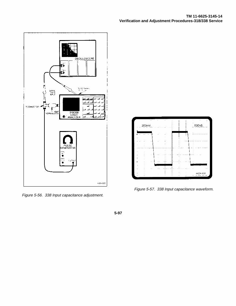
TM 11-6625-3145-14Verification and Adjustment Procedures-318/338 Service
Figure 5-56. 338 Input capacitance adjustment.
Figure 5-57. 338 Input capacitance waveform.
5-97

TM 11-6625-3145-14Verification and Adjustment Procedures-318/338 Service
10. ADJUST NON-VOLATILE MEMORY BATTERY BACKUP THRESHOLD
Equipment Required1 Oscilloscope1 Digital Multimeter (DMM)
1. Connect the DMM minus (-) lead to TP200 (GND) on the A07 S1 Board.2. Connect the DMM plus (+) lead to TP101 (+5V) on the A07 Board.3. Record the voltage measured.
NOTEThis voltage measurement must be recorded. At the end of this procedure, R 11 onthe A07 Board will be adjusted to reinstate this voltage reading. If the voltage isnot returned to this level, a complete recalibration of the machine may benecessary.
4. Adjust +5V potentiometer R11 on the A12 Regulator board for a DMM indication of 4.65 ±0.01 V. (To locateR11, see bottom rear of chassis.)
5. Connect the oscilloscope channel 1 probe tip to TP100 on the A07 S1 board.6. Turn NVM THRESHOLD R101 on the A07 board clockwise until the oscilloscope reading is a stable-low.7. Adjust NVM THRESHOLD by turning R101 in the opposite direction until the oscilloscope indication rises to a
stable-high level.8. Return +5 V POTENTIOMETER R11 on the A12 REGULATOR Board to a DMM indication equal to that
recorded in step (3) above.
PERFORMANCE CHECK FOR THE 338The Performance Check Procedure provides a detailed check of internal and external product characteristics.These checks can be extensive and time-consuming. Under normal circumstances the Functional CheckProcedures will provide an adequate test of product performance in a less costly manner.
The Performance Check Procedure is organized into sets of tests for the mainframe, the acquisition module, eachtype of the probes and 338S1 Serial Analyzer.
INDEX OF PERFORMANCE CHECKS
Test 1 - Threshold Voltages
Test 2 - Parallel Data Acquisition, Word Recognition, and Trigger Sequencer Checks with External Clock MinimumPeriod.
Test 3 - Glitch Data Acquisition and Glitch Trigger
5-98
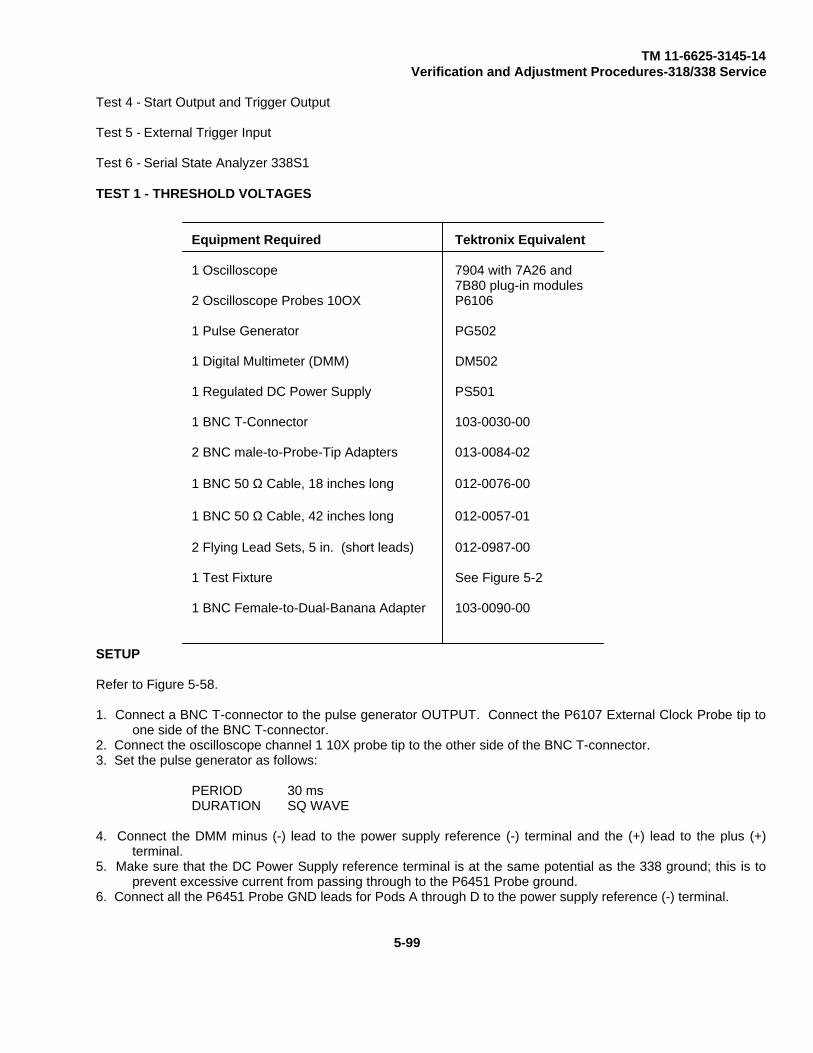
TM 11-6625-3145-14Verification and Adjustment Procedures-318/338 Service
Test 4 - Start Output and Trigger Output
Test 5 - External Trigger Input
Test 6 - Serial State Analyzer 338S1
TEST 1 - THRESHOLD VOLTAGES
Equipment Required Tektronix Equivalent
1 Oscilloscope 7904 with 7A26 and7B80 plug-in modules
2 Oscilloscope Probes 10OX P6106
1 Pulse Generator PG502
1 Digital Multimeter (DMM) DM502
1 Regulated DC Power Supply PS501
1 BNC T-Connector 103-0030-00
2 BNC male-to-Probe-Tip Adapters 013-0084-02
1 BNC 50 Ω Cable, 18 inches long 012-0076-00
1 BNC 50 Ω Cable, 42 inches long 012-0057-01
2 Flying Lead Sets, 5 in. (short leads) 012-0987-00
1 Test Fixture See Figure 5-2
1 BNC Female-to-Dual-Banana Adapter 103-0090-00
SETUP
Refer to Figure 5-58.
1. Connect a BNC T-connector to the pulse generator OUTPUT. Connect the P6107 External Clock Probe tip toone side of the BNC T-connector.
2. Connect the oscilloscope channel 1 10X probe tip to the other side of the BNC T-connector.3. Set the pulse generator as follows:
PERIOD 30 msDURATION SQ WAVE
4. Connect the DMM minus (-) lead to the power supply reference (-) terminal and the (+) lead to the plus (+)terminal.
5. Make sure that the DC Power Supply reference terminal is at the same potential as the 338 ground; this is toprevent excessive current from passing through to the P6451 Probe ground.
6. Connect all the P6451 Probe GND leads for Pods A through D to the power supply reference (-) terminal.
5-99

TM 11-6625-3145-14Verification and Adjustment Procedures-318/338 Service
7. Connect all the P6451 Probe DATA leads for Pods A through D to the power supply plus (+) terminal.8. Power-up and setup 338 as follows:
THRESHOLD MENU
INPUTEXT CLK = TTLPOD A = TTLPOD B = TTLPOD C = TTLPOD D = TTL
TRIGGER MENUCLK EXTTPOSN DELAY
00249Events 00001*WA FLW’D BY:WB OFF:WC
Figure 5-58. 338 Threshold voltage check setup.
5-100

TM 11-6625-3145-14Verification and Adjustment Procedures-318/338 Service
THRESHOLD LEVEL TTL
1. Repeat the following procedures, (2) through (4), for each of the two power supply voltage levels given in Table5-18.
2. Set the pulse generator output level to that given in Table 5-18 as measured by the oscilloscope. Setup theoscilloscope as follows:
a. Set the DVM for +1.40 V.b. Momentarily move the oscilloscope CH1 probe to measure the DVM’s + 1.40 V output.c. Set the oscilloscope’s vertical VOLTS/DIV to 200 mv (20 mv with 10X probe)d. Adjust the vertical position so that the trace is at midscreen (+1.40 V at midscreen).e. Return the oscilloscope CH1 probe to the pulse generator’s BNC T-connector.f. Adjust the pulse generator output so that the signal is 1 1/4 divisions above and 1 1/4 divisions below
midscreen (+1.15 V to =1.65 V).g. Set the power supply level to the voltage given in Table 5-18 as measured by the DVM.
3. Press the START key and wait for the acquisition to be complete; make sure that SLOW CLOCK is notdisplayed on the CRT.
4. Press the DATA key until the STATE TABLE is displayed; check that the data acquired is equal to theExpected Data given in Table 5-18.
Table 5-18338 VOLTAGE LEVELS FOR TESTING TTL
Power Supply Pulse Generator Threshold Level ExpectedOutput (V) High (V) Low (V) V1 (V) V2 (V) V3 (V) Data
+1.65 +1.65 +1.15 ------ ------ ------ all Fs (hex)+1.15 +1.65 +1.15 ------ ------ ------ all Os
THRESHOLD LEVELS V1, V2, AND V3
1. Press the THRESHOLD key.2. Set the power supply output level, the pulse generator output level, and the Threshold V1, V2, EXT CLK, and
Pods A through D levels as shown in Table 5-19.3. Press the 338 DATA key.4. Press the START key and wait for the acquisition to be completed; make sure that SLOW CLOCK is not
displayed on the CRT.5. Check to make sure the data acquired is equal to the Expected Data given in Table 5-19.6. Set the 338 SRCH WORD to equal the Expected Data and then check that the quantity of SRCH words equal
256.7. Repeat Steps (1) to (6) for each test in Table 5-19.
5-101

TM 11-6625-3145-14Verification and Adjustment Procedures-318/338 Service
Table 5-19338 VOLTAGE LEVELS FOR TESTING Vi, V2, AND V3
Power ThresholdTest Supply Pulse Generator Threshold Level Input Expected
# Output (V) High (V) Low (V) V1 (V) V2 (V) V3 (V) Clk A, B Data
1 +5.25 +5.25 +-4.75 + 5.0 -- -- V 1 all Fs2 +4.75 +5.25 +4.75 +5.0 -- -- V 1 all Os
* 3 -4.75 -4.75 -5.25 -5.0 -- -- V 1 all Fs*4 --5.25 4.75 -5.25 -5.0 -- -- V 1 all Os5 - 5.25 +5.25 4.75 -- + 5.0 -- V 2 all Fs6 + 4.75 t5.25 +4.75 -- +5.0 -- V 2 all Os’7 -4.75 -4.75 -5.25 -- -5.0 -- V 2 all Fs*8 -5.25 4.75 -5.25 -- -5.0 -- V 2 all Os9 +5.00 +5.00 +4.50 +10.0 --0.5 +4.75 V 3 all Fs
10 + 4.50 +5.00 +4.50 +10.0 -0.5 + 4.75 V 3 all Os11 -t 0.25 +0.25 -0.25 0.0 0.0 0.00 V 3 all Fs
*12 -0.25 +0.25 0.25 0.0 0.0 0.00 V 3 all O s*13 -4.50 -4.50 -5.00 +0.5 --10.0 -4.75 V 3 all Fs*14 -5.00 -4.50 -5.00 +0.5 --10.0 -4.75 V 3 all Os
*Make sure that the P6451 probe GND leads connect to the Power Supply Reference terminal; the Reference terminalmust be at the same potential as the 338 ground.
TEST 2 - PARALLEL DATA ACQUISITION, WORD RECOGNITION, AND TRIGGER SEQUENCER CHECKS WITHEXTERNAL CLOCK MINIMUM PERIOD
Equipment Required Tektronix Equivalent
1 Oscilloscope 7904 with 7A26 and7B80 plug-ins
2 Oscilloscope Probes 10X P6106
2 Pulse Generators PG 502
1 Digital Delay DD501
4 BNC 50 Ω2 terminators 011-0049-01
3 BNC T-Connectors 103-0030-00
3 BNC male-to-probe-tip adapters 013-0084-02
3 BNC elbow male-to-female adapters 103-0031-00
1 BNC female-to-female adapter 103-0038-00
1 BNC male-to-male adapter 103-0029-00
5-102
TM 11-6625-3145-14Verification and Adjustment Procedures-318/338 Service
(cont.)
Equipment Required Tektronix Equivalent
1 BNC 50 Ω Cable 18 inches long 012-0076-001 BNC 50 Ω Cable 42 inches long 012-0057-011 Test Fixture See Figure 5-24 Flying Lead set 5 in. (short leads) 012-0987-00
Refer to Figures 5-59, 5-60, and 5-61.
1. Connect a 50 Ω terminator to the OUTPUT of the #1 pulse generator. Connect a BNC T-connector to the 50 Ωterminator. Connect the P6107 EXT CLOCK probe tip to one side of the BNC T-connector.
2. Connect the oscilloscope channel 1 10X probe tip to other side of the BNC T-connector.
3. Connect a BNC elbow to the Digital Delay’s EVENTS INPUT. Connect a BNC T-connector to the elbow. Connectone side of the T-connector to the #1 pulse generator’s + TRIG OUT using an 18 inch BNC cable and a 50 Ωterminator. Connect the other side of the Digital Delay’s BNC T-connector to the Digital Delay’s START INPUT (seeFigure 5-59). Using 2 BNC elbows and a BNC female-to-female connector will help here.
4. Connect the Digital Delay DLY’D TRIG OUT to the #2 pulse generator’s +TRIG/DURATION INPUT using a 42-inchBNC cable.
5. Connect all the leads, from Pod A and the Qualifier leads from Pods B, C, and D to the Test Fixture, and thenconnect the Test Fixture to the #2 pulse generator’s OUTPUT. Make sure each P6451 probe GND lead isconnected to the Test Fixture ground pins (those pins nearest the BNC connector are ground).
6. Set the #1 pulse generator’s Range Switches to 10 ns PERIOD and 5 ns DURATION.
7. Set the Digital Delay’s EVENTS DELAY COUNT to 00001 and adjust EVENTS and START LEVELS until triggered.
8. Connect oscilloscope channel 2 to the #2 pulse generator’s OUTPUT using a 10X probe and the probe tip connectoron the Test Fixture.
9. Power up and set up the 338 as shown:
SETUP MENU
PLRGROUP G1 ON = AAAAAAAA
76543210G2 OFFG3 OFFG4 OFF
THRESHOLD MENU
LEVEL V1 = +10.0VV2 = -10.0V
5-103

TM 11-6625-3145-14Verification and Adjustment Procedures-318/338 Service
INPUTEXT CLK = V3POD A = V3POD B = V3POD C = V3POD D = V3
TRIGGER MENU
Source INT TRIGCLK EXTTRIG IMMEDIATELYPOSN DELAY
00249Events 00001*WA FLW’D BY:WB OFF WC
WA = XXWB = XXWC =
GLITCH 76543210POD A OFF
QUALIFIERS (POD)A OFF B OFF C OFF D OFF
10. Set the oscilloscope as shown in Table 5-20.
11. Set the Pulse Generators as shown in Table 5-21.
NOTEOver adjustment of the EVENTS LEVEL will cause a loss of the DD501 triggeringand oscilloscope display. If the adjustment range is not adequate then replace theBNC cables, between the Pulse Generators and the Digital Delay, with longer orshorter cables.
12. Set the oscilloscope triggering source to CH2 ONLY.
13. Adjust DD501 EVENTS LEVEL slowly until the channel 2 waveform’s falling edge crosses the channel 1 waveform’srising edge at 0 V (mid-screen). See Figure 5-60 (20 ns setup, 0 ns hold).
NOTEOver adjustment of the EVENTS LEVEL will cause a loss of the DD501 triggeringand oscilloscope display. If the adjustment range is not adequate replace the 42inch BNC cable, from DLY’D TRIG OUT to the #2 Pulse Generator’s + TRIG INPUT,with a longer or shorter cable, or remove the cable’s 50 Ω terminator.
14. Setup the 338 CLK and QUALIFIERS for Condition 1 in Table 5-22.15. Press the 338 DATA key until the State Table is displayed.16. Press the START key.17. Check that the data acquired is equal to the Expected Data in Table 5-22.18. Setup the 338 CLK and QUALIFIERS for conditions 2 through 4 in Table 5-22. Repeat steps 14 to 16 for each
condition.
5-104

TM 11-6625-3145-14Verification and Adjustment Procedures-318/338 Service
19. Set #1 pulse generator’s OUTPUT to COMPLEMENT.
20. Adjust DD501 EVENTS LEVEL until the channel 2 waveform’s falling edge crosses the channel 1 waveform’s fallingedge at 0 V (mid-screen). See Figure 5-61 (20 ns setup, 0 ns hold).
21. Change the 318 CLK and QUALIFIERS for conditions 5 through 8 in Table 5-22. Repeat steps 14 through 16 foreach condition.
Table 5-20338 PARALLEL DATA TEST OSCILLOSCOPE SETUP
Controls Settings
TIME/DIV 5 nS (Use 10X magnifier if necessary)
TRIGGERING AUTO, AC, INT, CH1 only
DISPLAY MODE ALT
VOLTS/DIVCH1 100 mV DCCH2 100 mV DC
POSITIONCH1 0 V (GND) set to the middle of screenCH2 0 V (GND) set to the middle of screen
Table 5-21338 PARALLEL DATA PULSE GENERATOR SETUP
Pulse Generator #1 Pulse Generator #2
BACK TERM PULL (out) PULL (out)
OUTPUT NORM NORM
HIGH LEVEL +0.35 V +0.25 V
LOW LEVEL -0.35 V -0.25 V
PERIOD 50 nS @ 0 V level EXT TRIG
DURATION 15 nS @ 0 V level 20 nS + pulse @ 0 V level
5-105

TM 11-6625-3145-14Verification and Adjustment Procedures-318/338 Service
Figure 5-59. 338 Parallel data acquisiton test setup.
Figure 5-60. 338 Parallel data acquisition Figure 5-61. 338 Parallel data acquisitiontest waveform #1. test waveform #2.
5-106

TM 11-6625-3145-14Verification and Adjustment Procedures-318/338 Service
Table 5-22338 TEST CONDITIONS AND EXPECTATIONS
Condition 1 2 3 4 5 6 7 8
Pulse Gen Norm Norm Norm Norm Comple- Comple- Comple- Comple-#1 OUTPUT ment ment ment ment
Test Wave-form Figure 5-60 5-60 5-60 5-60 5-61 5-61 5-61 5-61
CLK EXT↑ EXT↑ EXT↑ EXT↑ EXT↓ EXT↓ EXT↓ EXT↓
QUALIFIER A OFF CLK-H CLK-H OFF OFF TRG-L OFF TRG-LQUALIFIER B OFF TRG-L TRG-H OFF OFF CLK-L OFF CLK-HQUALIFIER C OFF CLK-H OFF CLK-H OFF OFF TRG-L TRG-LQUALIFIER D OFF TRG-L OFF TRG-H OFF OFF CLK-L CLK-L
EXPECTED 00 ** FF FF 00 00 00 **DATA FF ** FF FF FF 00 00 **
00 ** FF FF 00 00 00 **FF ** FF FF FF 00 00 **
** Means the 338 is never triggered. Press the STOP key to stop data acquisition.
Table 5-23338 PARALLEL DATA TEST CONDITION AND EXPECTATION
CONDITION 1 2 3
Pulse Gen. #2connectionsPod A Q only Q only Q only Q only
Pod B Data 7-0 & Q Q only Q onlyPod C Q only Data 7-0 & Q Q onlyPod D Q only Q only Data 7-0 & Q
GROUP G1= B7-B0 C7-C0 D7-D0
21. Connect the P6451 probes to the #2 pulse generator (using the Test Fixture) and select the 338 GROUP G1 asoutlined for Condition 1 in Table 5-23.
22. Repeat steps 10 through 20 for each condition in Table 5-23.
23. Disconnect and remove all P6451 Probes except the one with Data leads 7-0 connected to the #2 pulse generator(Pod D).
24. Return the #1 pulse generator OUTPUT to NORM.
25. Adjust the #2 pulse generator’s DURATION to 14 ns, @ 0 V level, positive pulse on oscilloscope channel 2.
5-107

TM 11-6625-3145-14Verification and Adjustment Procedures-318/338 Service
26. Increase the length of the BNC cables on the pulse generators, if necessary, and adjust DD501 EVENTS LEVELuntil the channel 2 waveform’s falling edge crosses the channel 1 waveform’s rising edge at 0 V level (14 ns setup, 0ns hold).
27. Change the 338 settings as follows:
SETUP MENUACQ.MODE RE-
PEATACQ
TRIGGER MENUCLK EXTTPOSN DELAY
00246Events 00001’WA THEN:WB THEN:WCWA = 00WB - FFWC= 00
QUALIFIERS (POD)A OFF B OFF C OFF D OFF
28. Press the DATA key until the State Table is displayed and then press the START key.29. Check for the following data, and proper trigger location.
0 ## (Always no data)1 ## or FF2 003 FF
T 4 00 (Trigger location)
30. Press the STOP key, select the TRIGGER Menu and set word C to WC = FF.31. Press the START key and check that the 338 does not trigger.32. Press the STOP key.33. Change the TRIGGER Menu as follows:
SETUP MENUACQ. MODE REPEAT ACQ
TRIGGER MENUPOSN DELAY
00245Events 00001’WA THEN:WB FLW’D BY:WC
WA = 00WB = FFWC = FF
34. Press the DATA key and then the START key.35. Check for the following data and proper trigger location.
0 ## (Always no data)1 ## or FF2 003 FF4 00
T 5 FF (Trigger location)
5-108

TM 11-6625-3145-14Verification and Adjustment Procedures-318/338 Service
36. Press the STOP key and then the TRIGGER key.37. Change TRIGGER Menu Word B to WB = 00.38. Press START key and check that the 338 does not trigger.39. Press STOP key.40. Change the TRIGGER Menu as follows:
Events 00001 * WA FLW’D BY:WB FLW’D BY:WC
41. Press the DATA key and then the START key.42. Check for the following data and proper trigger location.
0 ## (Always no data)1 ## or FF2 003 FF4 00
T 5 FF (Trigger location)
43. Press the STOP key and then the TRIGGER key.44. Change the TRIGGER Menu as follows:
TRIGGER MENUEvents 00002’WA OR:WB OR:WCWA = XXWB= 00WC = FF
45. Press the DATA key and then the START key.46. Check for the following data and proper trigger location.
0 ## (Always no data)1 ## (Always no data)2 ## (Always no data)3 ## (Always no data)4 ## (Always no data)T 5 00 and/or FF (Check several acquisitions and insure that both 00 and FF
triggers occur.)
47. Press the STOP key and then the TRIGGER key.48. Change the TRIGGER Menu as follows:
TRIGGER MENUEvents 00002*WA OFF:WB RESET ON:WC
WA = FFWB =WC = 00
49. Press the START key and check that the 338 does not trigger.50. Press the STOP key.
5-109
TM 11-6625-3145-14Verification and Adjustment Procedures-318/338 Service
51. Change the TRIGGER Menu as follows:
TRIGGER MENUPOSN DELAY
00000Events 00001’WA OFF:WB RESET ON:WC
52. Press the DATA key, ←↑ T key (scroll), and then the START key.53. Check for the following data and proper trigger location.
243 ## (Always no data)244 ## (Always no data)245 ## (Always no data)246 ## (Always no data)247 ## (Always no data)248 ## (Always no data)249 ## or 00
T 250 FF (Trigger location)
54. Press the STOP key and then the TRIGGER Key.
a. Increase the DD501 DELAY COUNT, by increments of 01000, until the oscilloscope display startsbecoming too dim to observe.
b. Adjust the oscilloscope horizontal POSITION to display the channel 2 waveform.c. Adjust DD501 EVENTS LEVEL slowly until the channel 2 waveform’s falling edge crosses the channel 1
waveform’s rising edge at 0 V (mid-screen). See Figure 5-60 (14 ns setup, 0 ns hold).
NOTE
If adjustment range is not adequate then replace the DLY’D TRIG OUT BNC cablewith a longer or shorter cable.
55. Set the DD501 DELAY COUNT to 65000.56. Change the TRIGGER Menu as follows:
TRIGGER MENUPOSN DELAY
65000Events 00001’WA OFF:WB OFF:WCWA - FFWBWC-
57. Press the DATA key and then the START key.58. Check that data location 251 contains FF and all other data locations contain 00s. Note: The trigger location is off
the display screen.59. Press the STOP key and check the lower-right corner of the display for:
ST:T = -64750W
5-110

TM 11-6625-3145-14Verification and Adjustment Procedures-318/338 Service
60. Change the TRIGGER Menu as follows:
TRIGGER MENUPOSN DELAY
00000Events 65000’WA OFF:WB RESET ON:WCWA = 00WB =WC = FF
61. Press the DATA key and then the START key.62. Check for the following data and proper trigger location.
243 00244 00245 00246 00247 00248 00249 00
T 250 00 (Trigger location)251 FF252 00
63. Press the STOP key and then the -1 (scroll) key.64. Return DD501 DELAY COUNT to 00001.65. Adjust DD501 EVENTS LEVEL slowly until the channel 2 waveform’s falling edge crosses the channel 1 waveform’s
rising edge at 0 V (mid-screen). See Figure 5-60 (14 ns setup, 0 ns hold).66. Move the P6451 probe to the next 338 PARALLEL DATA INPUT and select the corresponding 338 GROUP G1 =
x7-x0.67. Repeat steps 26 to 65 for each of the remaining PARALLEL DATA INPUTS (C-B-A).
TEST 3 - GLITCH DATA ACQUISITION AND GLITCH TRIGGER
Equipment Required1 Oscilloscope2 Pulse Generators1 BNC 50 Ω Terminator1 BNC T-connector2 BNC Male-to-Probe Tip Adapters1 Test Fixture (see Figure 5-1)1 BNC 50 Ω Cable, 42 inches long
5-111

TM 11-6625-3145-14Verification and Adjustment Procedures-318/338 Service
SETUP
Refer to Figure 5-62.
1. Connect a 50 Ω terminator to the #1 pulse generator OUTPUT. Connect a BNC T-connector to the 50 Ωterminator.Connect the P6107 External Clock Probe tip to one side of the BNC T-connector. Connect the oscilloscope channel1 probe to the other side of the BNC T-connector.
2. Connect the #1 pulse generator’s TRIG OUT to the #2 pulse generator’s TRIG INPUT using a 42-inch BNC cable.
Figure 5-62. 338 Glitch data acquisition test setup.
3. Connect all the Pod A P6451 Probe leads to the Test Fixture pins (connect the P6451 ground leads to those pinsnearest the BNC connector; all other pins are interchangable). Connect the Test Fixture to the #2 pulse generator’sOUTPUT.
5-112

TM 11-6625-3145-14Verification and Adjustment Procedures-318/338 Service
4. Connect the oscilloscope channel 2 10X Probe tip to the Test Fixture’s probe connection.5. Power up and set up the 338 as follows:
SETUP MENUPLRGROUP G1 ON - AAAAAAAA
76543210G2 OFFG3 OFFG4 OFF
THRESHOLD MENULEVEL V1 = 10.0V
V2 = 10.0V
INPUTEXT CLK = V3POD A = V3
TRIGGER MENUCLK EXT,TRIG IMMEDIATELYEvents 00000’WA FLW’D BY:WB RESET ON:WCGLITCH 76543210POD A ON ♦QUALIFIERS (POD)A OFF B OFF C OFF D OFF
POSITIVE GLITCH1. Set the pulse generator according to Table 5-24 and Figure 5-63.
Figure 5-63. 338 Glitch data acquisition test waveform#1.
Table 5-24338 POSITIVE GLITCH PULSE GENERATOR SETUP
Pulse Generator#1 #2
Termination BACK TERM BACK TERMOUTPUT NORM NORMPERIOD 50 ns EXT TRIGDURATION 25 ns 5 ns @ +0.35 V levelHIGH level +0.35 V +0.50 VLOW level -0.35 V -0.50 V
NOTE:HIGH level, LOW level and DURATION adjustmentsinterreact and require readjustment.
NOTEEnsure glitch waveform timing does not occur 0-14 ns prior to clock waveformrising edge or the glitch may appear as data in this test. Glitch data width must beat least 5 ns as measured at 350 mv above threshold.
5-113

TM 11-6625-3145-14Verification and Adjustment Procedures-318/338 Service
2. Press the DATA key until the State Table is displayed.3. Press the START key.4. Set the DATA State Table submenu to SRCH GLITCH mode and check that the Trigger location, and all data after
the Trigger location, are displayed in inverse video (SRCH = 1/249, data = 00).5. Press the 338 TRIGGER key, select the next GLITCH channel, one channel at a time, and re- peat steps (2) through
(4) until channels 0 through 7 have been tested.
NEGATIVE GLITCH1. Set the pulse generators according to Table 5-25 and Figure 5-64.2. Follow the same procedure as in the Positive Glitch; select the State Table, press START, check for Glitch Data,
select the next channel, and repeat until all channels have been tested. (SRCH = 1/249, data= FF).
Figure 5-64. 338 Glitch data acquisition test waveform#2.
Table 5-25338 NEGATIVE GLITCH PULSE GENERATOR SETUP
Pulse Generator#1 #2
Termination BACK TERM BACK TERMOUTPUT NORM COMPLEMENTPERIOD 50 ns EXT TRIGDURATION 25 ns 5 ns @ -0.35 V levelHIGH level +0.35 V +0.50 VLOW level -0.35 V -0.50 V
NOTE:HIGH level, LOW level and DURATION adjustmentsinterreact and require readjustment.
TEST 4 - START OUTPUT AND TRIGGER OUTPUT
Equipment Required2 Patch Cord, 2 inches long, 012-0200-00
1. Connect Pod A and Pod B GND leads to GND mini-jack, located on the right-side panel, using a Patch Cord andGrabber Tips.
2. Connect Pod A and Pod B channel 0 leads to the START OUTPUT mini-jack using another Patch Cord and GrabberTips.
5-114
TM 11-6625-3145-14Verification and Adjustment Procedures-318/338 Service
3. Power up and set up the 338 as follows:SETUP MENU
PLRACQ. MODE REPEAT ACQ GROUP
G1 ON - AAAAAAAA76543210
G2 ON - BBBBBBBB76543210
G3 OFFG4 OFF
THRESHOLD MENU
LEVEL V1 = +0.7VV2 = 2.4V
INPUTEXT CLK = TTLPOD A = V1POD B = V2
TRIGGER MENUCLOCK 50 nsTRIG IMMEDIATELYEvents 00001*WA OFF:WB OFF:WCWA = XX XX
4. Press the DATA key until the State Table is displayed.5. Set the State Table submenu to SRCH WORD = 01-01.6. Press the START key and check for the following display:
SRCH = 1/13 (Approximately)WORD = 01-01
G1 G2H H
0 ## ## (Always no data)1 ## ## (Always no data)2 ## ## (Always no data)3 ## ## (Always no data)4 ## ## (Always no data)5 ## ## (Always no data)6 ## ## (Always no data)
T 7 0X 0X (Trigger location)8 0X 0X (X =Don’t care)9 01 01 (Start Output)10 01 0111 01 0112 01 01
7. Move the Mini-jack cable from START OUTPUT to TRIG OUTPUT.8. Press START and check that TRIGGER OUTPUT, WORD 01-01, starts at or near location 9, and the quantity of
SRCH WORDS exceed 240.
5-115

TM 11-6625-3145-14Verification and Adjustment Procedures-318/338 Service
TEST 5 - EXTERNAL TRIGGER INPUT
Equipment Required1 BNC to Mini-Jack Cable, 175-1178-001 Oscilloscope1 Pulse Generator1 10X Probe1 BNC-to-Probe Adapter1 50 ohm Terminator
1. Connect a 50 ohm terminator to the pulse generator OUTPUT.2. Connect a 10 OX probe from the oscilloscope CH1 to the 50 12 terminator at the pulse generator OUTPUT using a
BNC-to-probe Adapter.3. Setup the oscilloscope as follows:
TRIGGERING AUTO, AC, INT, CH1TIME/DIV 5 ns (Use 10OX Magnifier if necessary)CH1 VOLTS/DIV 1.0 V DCCH1 POSITION 0 V (GND) set to the middle of screen
4. Set the pulse generator as follows:
BACK TERM OUTOUTPUT NORMPERIOD .1µSHIGH LEVEL +2.80 VLOW LEVEL 0.00 VDURATION 20 nS @ +-1.4 V level
5. Remove the 10X Probe and BNC-to-probe adapter from the pulse generator.6. Connect a BNC-to Mini-jack Cable from the 50 ohm terminator at the pulse generator’s OUTPUT to the TRIG INPUT
mini-jack on the right-side panel. Connect the cable braid lead to the GND mini-jack, also on the right-side panel.7. Power-up and setup the as follows:
TRIGGER MENU
SOURCE EXT TRIGEXT TRIG POL= ↑
8. Press the START key and check that the 338 triggers.9. Set pulse generator PERIOD to EXT TRIG and ensure no cables are connected to the pulse generator External
Trigger Input.10. Press the START key and then press the pulse generator’s MAN TRIG.11. Check that the 338 triggers only after the PG502 MAN TRIG button is pushed.12. Set EXT TRIG POL to negative and the pulse generator’s OUTPUT to COMPLEMENT.13. Repeat steps (10) and (11).
5-116
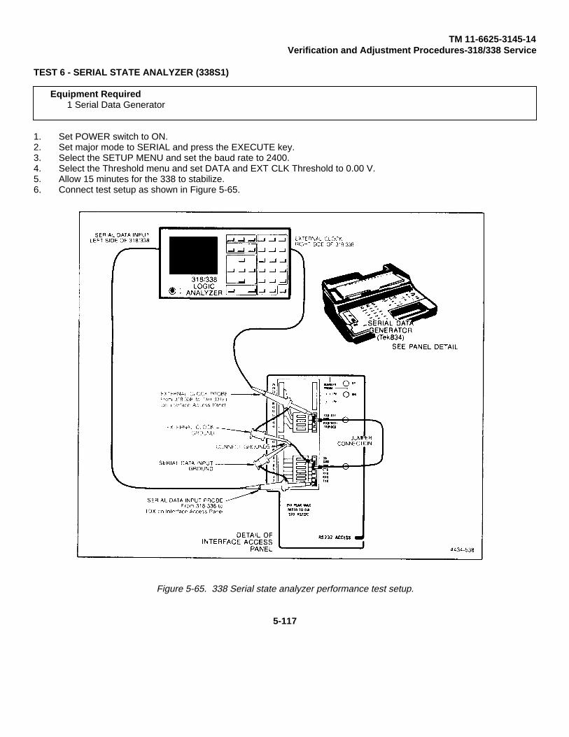
TM 11-6625-3145-14Verification and Adjustment Procedures-318/338 Service
TEST 6 - SERIAL STATE ANALYZER (338S1)
Equipment Required1 Serial Data Generator
1. Set POWER switch to ON.2. Set major mode to SERIAL and press the EXECUTE key.3. Select the SETUP MENU and set the baud rate to 2400.4. Select the Threshold menu and set DATA and EXT CLK Threshold to 0.00 V.5. Allow 15 minutes for the 338 to stabilize.6. Connect test setup as shown in Figure 5-65.
Figure 5-65. 338 Serial state analyzer performance test setup.
5-117

TM 11-6625-3145-14Verification and Adjustment Procedures-318/338 Service
7. Set the serial data generator power to ON, and select DTE SIMULATE mode.8. Set serial data generator SETUP as follows;
CODE=ASCII, BAUD=2400, DUPLEX-FULL, SETUP=ASYNC, BITS/CHAR=8,PARITY= NONE, STOPBITS = 1, TIMING = NORMAL.
9. Load the following program into the serial data generator:
STEP MNEMONICCODE
1 SEND #12 JMP #1
10. Load the following hexadecimal data in the serial data generaotor buffuffer #1: E0, E0, E2, E4, E6, E811. Press the START key on the serial data generator.12. Select the DATA DISPLAY STATE TABLE and press the START key.13. When the 338 displays data on the crt, press the serial data generator STOP key.14. Check that the 338 display matches the WORD SEQUENCE column on Table 5-25.15. Set the 338 baud rate to 19.2K (DATA screen).16. Set the serial data generator baud rate to 19.2K.17. Set the 338 and the serial data generator controls as indicated in step 1 of Table 5-25 and repeat preceding parts
(11) through (14).
Repeat steps 2 through 7 for the remainder of Table 5-25.
NOTESelection field for BITS/’WORD and COM.MODE (SYNC or ASYNC) and BAUD RATEappear in the 338 SETUP Menu. Selection fields for SYNC WORD and HUNT WORDare in the TRIGGER Menu.
To load SETUP parameters into the serial data generator, the operator must: (a) press SETUP, (b) select SETUP itemusing LEFT or RIGHT Vector keys. (c) select SETUP parameters using UP or DOWN VECTOR key.
To load data into the serial data generator buffer #1, the operator must: (a) press PROGRAM, (b) press RIGHT VECTOR,(c) press DOWN VECTOR, (d) press keys for the two hexadecimal characters to be entered, and (e) press ENTER. Toload additional data , repeat parts (d) and (e).
To load the program into the serial data generator, the operator must: (a) press PROGRAM, (b) select program code byLEFT or RIGHT VECTOR, (c) if program code includes distination number, press alphanumeric key to be entered, andpress ENTER, (d) press DOWN VECTOR, to next program step.
5-118

TM 11-6625-3145-14Verification and Adjustment Procedures-318/338 Service
Table 5-26338 SERIAL STATE ANALYZER TEST SETUP
Serial DataStep 318 Generator Word Sequence
1 BITS/WORD = 8 BITS/CHAR = 8 E0, E0, E2, E4, E6, E8
2 BITS/WORD = 7 BITS/CHAR = 7 60, 60, 62, 64, 66, 68
3 BITS/WORD = 6 BITS/CHAR = 6 20, 20, 22, 24, 26, 28
4 BITS/WORD = 5 BITS/CHAR = 5 00, 00, 02, 04, 06, 08
5 BAUD RATE = EXT16 BITS/CHAR = 6 20, 20, 22, 24, 26, 28BITS/WORD = 6
6 COM. MODE = SYNC SETUP = SYNC E0, E0, E2, E4, E6, E8BITS/WORD = 8 BITS/CHAR = 8 FF, FF, FFSYNC WORD 1 = 16 CLOCK = DERIVEDSYNC WORD 2 = 16 (INSERT DATA 16, 16
TOTOP OF BUFFER #1)
7 BITS/WORD = 5 BITS/CHAR = 5 00, 02, 04, 06, 08SYNC WORD 1 = ADSYNC WORD 2 = 05HUNT WORD = 08
5-119/(5-120 blank)

TM 11-6625-3145-14Section 6-318/338 Service
MAINTENANCE: GENERAL INFORMATION
Tektronix maintains repair and recalibration facilities at its local Field Service Centers and the Factory Service Center. Forfurther information or assistance, contact your local Tektronix Field Office or representative.
TROUBLESHOOTING TREES
The troubleshooting trees are divided into two sets; one for the 318, and one for the 338. The trees for the 318 are locatedafter the diagnostic test descriptions for the 318, in roughly the center of Section 7. The Diagnostic trees for the 338 arelocated after the diagnostic test descriptions for that logic analyzer, starting near the end of Section 7. Refer to the page-edge tabs for help in locating the information you need.
The troubleshooting trees are intended to be used as a guide in identifying problem areas and isolating componentmalfunctions. To use the trees, start at the beginning block and answer each logical-block question until the fault isisolated. If there are further problems after the first fault is corrected, you must start over at the beginning block. Somemalfunctions, especially those involving multiple simultaneous failures, may require more elaborate approaches withfrequent reference to the circuit descriptions in Section 4.
TEST EQUIPMENT REQUIRED FOR MAINTENANCE
Test equipment required to service the instrument is listed under Table 5-1 in Section 5 of this manual.
TOOLS REQUIRED FOR MAINTENANCE
The following tools are those most often needed when servicing the instrument:
bristle brush1/2 inch wrench5 mm metric wrench1/16 inch Allen wrenchPhillips head screwdriver15 W soldering irondesoldering toolisopropyl alcohollint-free swabs
MAINTENANCE PRECAUTIONS
SOLDERING
Most of the components in the instrument are soldered in place. If it is necessary to replace a soldered part, use a 15 Wsoldering iron to prevent heat damage to the circuit board or components. Excessive heat will lift circuit runs on the circuitboard.
The flux in the solder may leave a residue on the circuit board which can provide a high resistance leakage path and affectinstrument operation. Be sure to clean off this residue. Isopropyl alcohol may be used.
6-1
TM 11-6625-3145-14Maintenance: General Information-318/338 Service
LIGHT-EMITTING DIODES (LEDS)
To avoid damage to the LEDs, always keep soldering time and temperature to a minimum. Do not bend the leads or applyforce when inserting the leads into circuit board holes. Clean the circuit board holes of all excess solder before attemptingto install a new LED.
NOTE
Damage to the LEDs may not be immediately apparent. Always follow theprecautionary measures listed above when handling LEDs.
STATIC PRECAUTIONS
CAUTION
Static discharge can damage any semiconductor in this instrument.
This instrument contains electrical components that are susceptible to damage from static discharge. See Table 6-1 forthe relative susceptibility of various classes of semiconductors. Static voltages of 1-30 kV are common in unprotectedenvironments.
Observe the following precautions to avoid damage:
1. Minimize handling of static-sensitive components.
2. Transport and store static-sensitive components or assemblies in their original containers, on a metal rail, or onconductive foam. Label any package that contains static-sensitive components or assemblies.
3. Discharge the static voltage from your body by wearing a wrist strap while handling these components. Servicingstatic-sensitive assemblies should be performed only in a static-free work station by qualified service personnel.
4. Nothing capable of generating or holding a static charge should be allowed on the work station surface.
5. Keep the component leads shorted together whenever possible.
6. Pick up components by the body, never by the leads.
7. Do not slide the components over any surface.
8. Avoid handling components in areas that have a floor or work-surface covering capable of generating a staticcharge.
9. Use a soldering iron that is connected to earth ground.
10. Use only special anti-static suction type or wick type desoldering tools.
NOTE
Damage to electrical components may not be immediately apparent. Always followthe precautionary measures listed above when handling static-sensitivecomponents.
6-2

TM 11-6625-3145-14Maintenance: General Information-318/338 Service
Table 6-1Relative Susceptibility of Semiconductors to Static Discharge Damage
Semiconductor Class Danger Voltage a
MOS or CMOS 100 -500 V
ECL 200 - 500 VSchottky signal diodes 250 VSchottky TTL 500 VHigh frequency bipolar transistors 400 - 600 V
JFETs 600 - 800 VLinear microcircuits 400 - 1000 VLow-power Schottky TTL 1200 V
a Voltage discharged from a 100 pF capacitor through a resistance of 100 U.
LITHIUM BATTERY REPLACEMENT
If it is necessary to replace the lithium battery (A07BT1) on the Serial/RS232C/NVM Board, use standard solderingprocedures.
WARNING
To avoid personal injury, observe proper procedures for handling and disposal of lithiumbatteries. Improper handling may cause fire, explosion, or severe burns. Don’t recharge, crush,disassemble, heat the battery above 212° F (100° C), incinerate, or expose contents of the batteryto water. Dispose of battery in accordance with local, state, and national regulations.
PREVENTIVE MAINTENANCE
Preventive maintenance consists of periodic cleaning and inspection. Accumulation of dust on components acts as aninsulating blanket and prevents efficient heat dissipation. This condition can cause overheating and componentbreakdown within the instrument. Periodic cleaning and inspection will reduce instrument breakdown and increasereliability.
This instrument should be cleaned as often as the operating environment requires. A convenient and appropriate time toperform these procedures is immediately prior to instrument adjustment.
EXTERIOR CLEANING
Dust the exterior surfaces with a dry, lint-free cloth or a soft-bristle brush. If hard dirt remains, use a cloth or swabdampened with a 5% mild detergent and warm water solution. The swab is also useful for cleaning in narrow spacesaround the controls. Use the detergent solution for cleaning the screen also. Do not use abrasive compounds on any partof the instrument.
6-3

TM 11-6625-3145-14Maintenance: General Information-318/338 Service
CAUTION
To prevent water from getting inside the instrument during external cleaning, useonly enough water to dampen the cloth or swab.
DO NOT use chemical cleaning agents as they may damage the plastics used in theinstrument. In particular, avoid chemicals that contain benzene, toluene, xylene,acetone, or similar solvents.
INTERIOR CLEANING
To gain access to internal portions of the instrument, refer to Disassembly/lnstallation Procedures later in this section.
Internal cleaning should be done with a dry, low-velocity stream of air. A soft-bristle brush is useful for cleaning aroundcomponents, If a liquid must be used for minor internal cleaning, use isopropyl alcohol, denatured ethyl alcohol, or asolution of 1% mild detergent and 99% de-ionized water.
Should the interior of the instrument require a thorough cleaning, wash according to the following cautionary CleaningGuidelines.
CLEANING GUIDELINES
DO NOT wash the front-panel power switch. The power switch must be covered during washing procedures.
Spray-wash dirty parts with a cleaning solution listed under Interior Cleaning, then use de-ionized water to THOROUGHLYRINSE all parts. IMMEDIATELY DRY all parts with low air pressure.
When washing near unsealed electromechanical components, use as little washing action as possible. This preventswashing the lubricant out of the components and getting an excess of detergent into the contact areas of the switches.DETERGENT RESIDUE WILL CAUSE CORROSION, which may degrade instrument performance.
DO NOT use a freon-based spray cleaner for cleaning the circuit boards. Freon will damage aluminum capacitors.
DO NOT use fluorocarbon-based spray cleaners or silicon spray lubricants on switches or switch contacts. These spraysmay damage the circuit board material or plastic parts, and leave a dust-collecting residue. If necessary, NEWIMPROVED NO NOISE ® may be used as a lubricant.
To prevent damage from electrical arcing, ensure that all circuit boards, switches, and interface connectors are completelydry. Do this by heating the board or switch in an oven at 75° C (167° F) for 15 minutes before applying power.
INSPECTION
Inspect the instrument for broken connections, frayed wires, poorly seated components, leaking capacitors, damagedhardware, and heat-damaged components.
Repair any obvious problems. However, take particular care if you find any heat-damaged parts. Overheating usuallyindicates other circuit problems. To prevent recurrence of the damage, find and correct the cause of the overheating.Note that replacement of electrical components may necessitate readjustment of the affected circuitry. Refer to theReplaceable Electrical Parts section for a list of part and component descriptions.
6-4

TM 11-6625-3145-14Maintenance: General Information-318/338 Service
CORRECTIVE MAINTENANCE
OBTAINING REPLACEMENTS
All electrical and mechanical parts for the instrument can be obtained through your Tektronix Field Office orrepresentative. However, many of the standard electrical components can be obtained locally. Before purchasing anordinary part, check the Replaceable Electrical Parts section for a listing of value, tolerance, rating, and description.
CAUTION
Check the parts list before replacing electrical components. If the part is called outas screened or burned-in, the replacement part must also be screened or burned-inor the repair may not be effective.
NOTE
When selecting replacement parts, remember that the size and shape of thecomponent may affect its performance in the instrument. All replaceable partsshould be direct replacements unless it is known that a different part will notadversely affect instrument performance.
Some of the mechanical parts and electrical parts in this instrument are manufactured or selected by Tektronix to satisfyparticular requirements, or are manufactured to certain specifications for Tektronix. To determine the manufacturer of apart, refer to the Parts List Cross Index of Code Number to Manufacturer. This is found in the Replaceable Electrical Partssection.
When ordering replacement parts from Tektronix, include the following information:
1. instrument type2. instrument serial number3. a description of the part (if electrical, include the component number)4. Tektronix part number
ACQUISITION BOARDS AND PROBES
If it becomes necessary to send in an acquisition board for repair, also send the associated acquisition probe. Along withthe board and probe, write a brief description of the problem and the circumstance in which it was discovered.
REPAIRING MULTI-CONDUCTOR CONNECTORS
Some of the inteconnecting cable assemblies in the instrument consist of muti-conductor cables with machine-installedterminal connectors, mounted in plastic holders. For a picture of these connectors, refer to Figure 6-1. The plastic holderscan be replaced easily. However, if the cable is defective, it must be replaced as a complete cable assembly. If one of theterminal connectors comes loose from the plastic holder, it can be reinstalled as shown in Figure 6-1. When reinstallingthe connectors onto the circuit-board pins, be sure to match the triangle on the connector to the board.
6-5

TM 11-6625-3145-14Maintenance: General Information-318/338 Service
Figure 6-1. Multi-conductor terminal connectorsFigure 6-2. Circuit board pin replacement.
CIRCUIT BOARD PIN REPLACEMENT
A circuit-board pin replacement kit, including necessary tools, instructions, and replacement pins with attached spareferrules, is available from Tektronix.
CAUTION
Replace circuit board pins on multi-layer boards with extreme care. These boardshave conductive paths laminated between the top and bottom board layers. Allsoldering, removal, and reinsertion of pins must be done with extreme care toprevent breaking any electrical paths on the board.
Refer to Figure 6-2 while reading these instructions. To replace pins:
1. Use a 15 W soldering iron to unsolder the pin while pulling it out of the board with a pair of pliers.2. If the ferrule remained in the board, carefully ream the solder out with a 0.031 inch drill. If the ferrule came out with
the pin, clean the excess solder out of the hole with a solder-removing wick and a scribe.3. If the ferrule remained in the board, remove the ferrule from the new pin and insert the pin into the old ferrule in the
same orientation as the old pin. If the ferrule came out with the old pin, insert the new pin with ferrule in the sameorientation as the old pin.
4. When the new pin is properly positioned in the circuit board, carefully solder it on both sides of the board.5. Clean any remaining residue from the circuit board according to the instructions listed under Interior Cleaning.
6-6

TM 11-6625-3145-14Maintenance: General Information-318/338 Service
DISASSEMBLY/INSTALLATION PROCEDURES
WARNING
Dangerous electric-shock hazards inside the mainframe may be exposed when thecovers are removed. Be sure power is off and the power cord is disconnectedbefore removing the covers. Disassembly procedures should only be attempted byqualified service personnel.
Reassembly procedures are the reverse of the disassembly procedures in most cases. Separate reassembly instructionsare provided only when necessary.
Unless otherwise noted, screws mentioned in the text are the pan-head, POZIDRIV type.
In the following procedures, directional terms (top, bottom, left, right, etc.) are based on the assumption that the 318/338 isin a normal, upright position and the user is facing the front of the instrument.
GENERAL DISASSEMBLY PRECAUTIONS• DO NOT attempt any disassembly or installation procedures if the power is on.• DO NOT disconnect probes from the mainframe by pulling on the cables; pull only on the plastic cable
holders.• DO NOT remove connectors between circuit boards by pulling on the wires; pull only on the connectors.• DO NOT press or pull on components when manipulating circuit boards.• GUARD against static discharge damage by following the precautions listed under Maintenance Precautions
earlier in this section.
CIRCUIT BOARD LOCATIONS
Figure 6-3 shows the location of the circuit boards within the instrument.
COMPONENT LOCATIONS
In Section 10, Diagrams, of this manual you will find each circuit diagram and an illustration of the circuit board on whichthe layout of components are identified by their circuit numbers. Tables listing each component by its circuit number arealso provided. These tables enable rapid location of components on both the circuit diagrams and the circuit boardillustrations by listing the grid coordinates.
6-7

TM 11-6625-3145-14Maintenance: General Information-318/338 Service
Figure 6-3. 318/338 circuit board locations.
REMOVAL AND REPLACEMENT INSTRUCTIONS
WARNING
To avoid electric shock, disconnect the instrument from the power source beforeremoving or replacing any component or assembly.
The exploded-view drawing in the Replaceable Mechanical Parts section may be helpful in the removal or disassembly ofindividual components or sub-assemblies. Component locations are shown in the Diagrams section.
Read these instructions completely before attempting any corrective maintenance.
6-8

TM 11-6625-3145-14Maintenance: General Information-318/338 Service
Removing the Cabinet
WARNING
Before removing the cabinet, disconnect the power cord from the back of theinstrument. As the cabinet is being removed, do not touch any component on theCRT circuit board which is mounted in the chassis under the CRT.
The cabinet can be removed by loosening the screws retaining the rear panel and taking out the one screw that securesthe cabinet to the bottom of the chassis. Carefully slide the cabinet off the chassis, being careful not to touch anyconponents on the CRT circuit board. To reinstall the cabinet, slide it over the chassis. Ensure that any cable leadingfrom the boards fits into the recess in the boards. See Figure 6-4.
Figure 6-4. Cabinet removal.
Removing the Front Panel
Front panel removal is accomplished by using a 1/16-inch hex key wrench to remove the four screws holding the frontpanel in place. Unsolder the lead to the screw post, then carefully pull the front panel away from the 318/338 and lay itface-down in front of the instrument. To reinstall the front panel, resolder the lead to the screw post, position the panel inplace, and secure it with the four screws.
6-9

TM 11-6625-3145-14Maintenance: General Information-318/338 Service
Removing the Keyboard
The keyboard is an assembled matrix that fits behind the 318/338’s front panel. Refer to Section 10, ReplaceableMechanical Parts, for a detailed drawing and part numbers. To remove the keyboard, proceed as follows:
1. Remove the front panel (see Removing the Front Panel).2. Remove the six screws that hold the keyboard in place.3. Gently pull the keyboard assembly toward you and disconnect the 16-pin, square-pin connector located near the
power switch. The LED, resistors, connector, screws, and keycaps are all individually replaceable; the large blackswitch assembly is replacable as a unit.
4. When reassembling the keyboard unit, make sure the 16-conductor connector located under the CRT is correctlyindexed with the notch in the cabinet.
Removing the Power Supply Circuit Boards
The power supply assembly is fastened to the main chassis with four screws and contains the Inverter and RegulatorPower Supply boards. To remove the Power Supply boards, proceed as follows:
1. Remove the cabinet (see Removing the Cabinet).
WARNING
Dangerous voltage potentials may exist in the power supply circuitry. Allowapproximately three minutes for the power supply filter capacitors to dischargebefore proceeding with the next step.
2. Support the power supply assembly with one hand while removing the four screws that fasten it to the main chassis.Lift off the power supply assembly. Refer to Figure 6-5.
3. If the Inverter board is being taken out, remove the screw that retains the cover plate at the top of the power supplyassembly and lift off the plate. If the Regulator board is being taken out, remove the screw that retains the bottomcover plate.
4. Remove the four screws that hold the board to the power supply assembly chassis.
5. If the Inverter board is being removed, disconnect J2, J3, J7, J9, and the jack that connects to the fan from theboard. If the Regulator board is being removed, the same connections must be disconnected from the board.
6. Lift out the board and replace any defective components.
The power supply transistors and their mounting bolts are insulated from the board. In addition, silicon grease is used toincrease heat transfer capabilities. Reinstall the insulators and replace the silicon grease after working on thesetransistors. The grease should be applied to both sides of the mica insulators and should be applied to the bottom sides ofthe transistor where it comes in contact with the insulator.
NOTE
After replacing a power transistor, check that the collector is not shorted to groundbefore applying power.
6-10
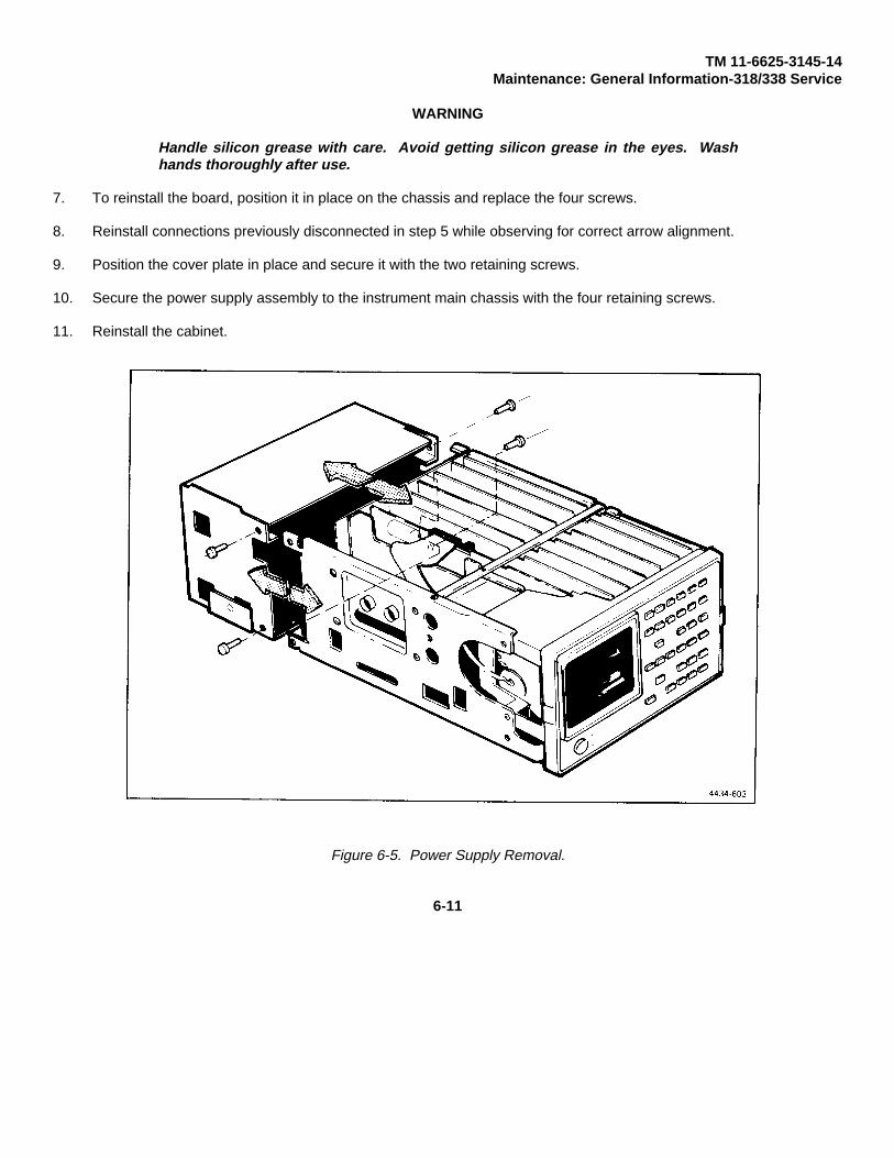
TM 11-6625-3145-14Maintenance: General Information-318/338 Service
WARNING
Handle silicon grease with care. Avoid getting silicon grease in the eyes. Washhands thoroughly after use.
7. To reinstall the board, position it in place on the chassis and replace the four screws.
8. Reinstall connections previously disconnected in step 5 while observing for correct arrow alignment.
9. Position the cover plate in place and secure it with the two retaining screws.
10. Secure the power supply assembly to the instrument main chassis with the four retaining screws.
11. Reinstall the cabinet.
Figure 6-5. Power Supply Removal.
6-11

TM 11-6625-3145-14Maintenance: General Information-318/338 Service
Removing the CRT Circuit Board
1. Remove the cabinet (see Removing the Cabinet).
WARNING
The CRT anode and the output terminal of the high-voltage multiplier may retain ahigh-voltage charge after the instrument is turned off. To avoid electrical shock,ground both the output terminal of the multiplier and the CRT high-voltage anodelead to chassis ground before disconnecting the high-voltage lead.
2. Ground the CRT high-voltage lead to chassis ground, then disconnect the high-voltage lead from the CRT bysqueezing the spring clip in the connector and pulling it outward.
3. Loosen the high-voltage lead from any tight places on the chassis so that it will permit removal of the CRT circuitboard.
4. On the CRT circuit board, disconnect P040, P001 and P100, noting their location.
5. Remove the three screws that secure the board to the chassis.
6. Carefully remove the CRT circuit board from the chassis.
7. To reinstall the CRT circuit board, position it into place on the chassis and secure it with the three retaining screws.
8. Reconnect P040, P001, and P100 while observing correct arrow alignment.
9. Reroute the high-voltage lead and connect it to the CRT.
10. Reinstall the cabinet.
Removing the Cathode-Ray Tube (CRT)
WARNING
Use care when handling a CRT. Protective clothing and safety glasses should beworn. A void striking it on any object which might cause it to crack or implode.When storing a CRT, place it in a protective carton or set it face down on a smoothsurface in a protected location with a soft mat under the faceplate to protect it fromscratches.
1. Remove the cabinet (see Removing the Cabinet).
WARNING
The CRT anode and the output terminal of the high-voltage multiplier may retain ahigh-voltage charge after the instrument is turned off. To avoid electrical shock,ground both the output terminal of the multiplier and the CRT high-voltage anodelead to chassis ground before disconnecting the high-voltage lead.
6-12
TM 11-6625-3145-14Maintenance: General Information-318/338 Service
2. Ground the CRT high-voltage lead to chassis ground, then disconnect the high-voltage lead from the CRT bysqueezing the spring clip in the connector and pulling it outward.
3. Carefully disconnect the socket from the back of the CRT.
4. Remove the front panel (see Removing the Front Panel). This exposes the lower part of the CRT bezel and its tworetaining screws.
5. Remove the two bezel-retaining screws.
WARNING
To prevent injury resulting from the CRT dropping out, keep the instrument in ahorizontal position, leaving sufficient work area in front of the CRT.
6. Swing the bottom of the bezel outward and remove both the bezel and the light filter.
7. Carefully guide the CRT out of the front of the 318/338.
8. To reinstall the CRT, carefully guide the replacement CRT into its housing from the front of the 318/338.
9. Position the bezel and light filter over the face of the CRT and reinstall them. This will require some pressure on theface of the CRT to insert it to the proper depth. Press the light filter against the CRT while installing the bezel. Thenhold the bezel and install the two retaining screws.
CAUTION
When reinstalling the CRT circuit board screws, ensure that the front-panel groundlead is reinstalled on the inside front screw.
10. Reinstall the front panel.
6-13/(6-14 blank)

318___________________TROUBLESHOOTING
TREES

TM 11-6625-3145-14Section 7-318/338 Service
MAINTENANCE: TROUBLESHOOTING
This section contains information about the 318/338 Logic Analyzer Diagnostic tests and troubleshooting trees. Thetest descriptions and Diagnostic trees are divided into two sections. The first half of this section describes theDiagnostic tests available for the 318. The Diagnostic trees for the 318 are located at the end of the test descriptions.The Diagnostic test descriptions and trees for the 338 are located in the second half of this section. Refer to thepage-edge tabs for help in locating the information you need.
318 DIAGNOSTIC TEST DESCRIPTIONS
INDEX OF 318 DIAGNOSTIC TEST DESCRIPTIONS
Mainframe
1. Keyboard Test2. CRT Test3. Jump Table ROM Test4. Display RAM Test5. SYSTEM RAM Test6. ROM Test
Parallel Analyzer
7. Clock Test8. Word Recognizer Test9. Acquisition RAM Test10. Sequence RAM Test11. N & DELAY Test12. Threshold Test13. SEQ Test
318S1 Serial Analysis/RS232C/NVM
14. Battery Test15. Non-Volatile Memory Test16. RS-232 Test17. Serial Test
318 DIAGNOSTIC TEST COMMON SIGNAL PATHS
Some Diagnostic Tests share a common signal path for setting up or reading data. When two or more Diagnostictests that shares the same signal path indicate a failure, the components in the path may be the cause of the testfailure.
7-1

TM 11-6625-3145-14Maintenance: Troubleshooting-318/338 Service
Table 7-1 lists the components common to the signal paths that cause multiple Diagnostic Test failures.
Table 7-1318 DIAGNOSTIC TEST COMMON SIGNAL PATHS
Clock Threshold WR ACQ SQRAM N&DL SEQ ComponentX X X X X X X A04 U152, A04 U150 A03
U126, A03 U112 A04 U110X X X X X A04 U146, A04 U142 A04
U114, A03 U112 A04 U110X X A03 U156, A03 U158 A03
U112, A04 U110 A04 U148(VBB)
X X X A04 U148, A04 U144 A03U112, A04 U110
X X A03 U146, A03 U108 A03U126, A03 U112
X X X A01 U100 to U110 A02U200 to U214 A02 U220,A02 U222 A01 U112, A01U114 A02 U232, A02 U234
X X A03 U106, A03 U108 A03U114, A03 U116 A03 U118,A03 U130 A03 U142
X X A03 U106, A03 U108 A03U114, A03 U116 A03 U118,A03 U130 A03 U132, A03U142 A03 U140, A03 U156
7-2

TM 11-6625-3145-14Maintenance: Troubleshooting-318/338 Service
MAINFRAME
1. KEYBOARD TEST
Program: KBD
Function:
Power on - When power is turned on, the KBD program checks the keyboard to see if any keys are stuck in the closedposition. The MPU reads the resulting data at address E0hex and verifies that all data bits are low.
Troubleshooting - Refer to Figure 7-1. The keyboard generates an interrupt and sends a corresponding key code to theMPU when any key except the STOP key is pressed. The MPU reads the key code at E0hex upon receiving the interruptfrom the keyboard, and blinks the corresponding rectangle in the key array on the screen. This function also provides acheck to see that each key (except the STOP key) is providing the correct key code to the MPU.
The STOP key is used to exit this program; thus the STOP key can be checked at the end of this test.
Description: Key codes are generated by the A09 board when any key is pressed. The Y-lines and X-lines of the keymatrix on the A09 board (excepting the STOP key) are connected to U300 and U310 (8-bit priority encoder, 4053BP) onthe A06 MPU/DISPLAY board through the A08 Mother board. U310 is enabled when U300 receives a key signal andissues an INT (Maskable Interrupt) to the MPU through the CR timer circuit. The INT is controlled by U220 (NAND gate,TC4093) on the A06 board with KBMASKP from U100 (hex D-type flip-flop with reset, 74LS174) on the A05ROM/Threshold board .
The STOP key on the A09 board generates the NMI (Non-Maskable Interrupt) directly to the MPU through the A08 boardwithout decoding, though it is buffered by U200 (inverter, TC4093) on the A06 board. This signal is also controlled by theCR timer to avoid key chattering.
The MPU reads the key code from U320 (octal buffer/line driver with tri-state output, 40H244) on the A06 board, usually oninterrupt at E0hex. KBCSP, which enables this buffer, is delivered from U092A (dual 2-line to 4-line decoder/demultiplexer)on the A05 board when the MPU accesses I/O address E0hex.
A key code with interrupt is expected as shown in Table 7-2.
Table 7-2318 KEYBOARD TEST KEY CODE AND INTERRUPT ASSIGNMENT
7 6 5 4 3 2 1 0ST 0 D5 D4 D3 D2 D1 DO
ST:1 if any key is pressed, otherwise 0.
7-3

TM 11-6625-3145-14Maintenance: Troubleshooting-318/338 Service
Key Code Assignment. Blocks correspond to the key position on the front panel.
00 08 10 18 20 2801 09 11 19 21 29-- 0A -- 1A 22 2A03 0B 13 1B 23 2B-- 0C -- 1C 24 2C05 -- STOP 1D 25 2D
Figure 7-1. 318 Keyboard test schematic.
2. CRT TEST
Program: CRT
Function:
Power on - None.
Troubleshooting - The CRT generates the following four kinds of patterns for the CRT adjustment and visual check.
1. Cross-hatch patternTo adjust the CRT circuit.
2. White patternTo check for phospor defects.
7-4
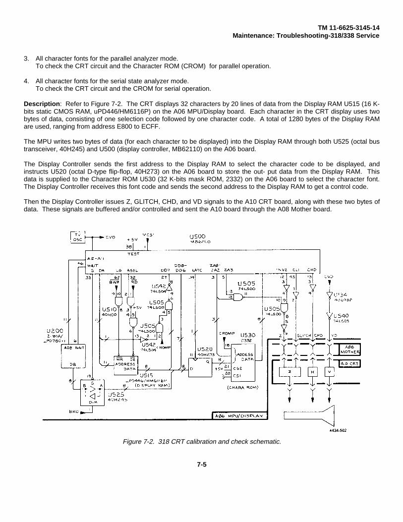
TM 11-6625-3145-14Maintenance: Troubleshooting-318/338 Service
3. All character fonts for the parallel analyzer mode.To check the CRT circuit and the Character ROM (CROM) for parallel operation.
4. All character fonts for the serial state analyzer mode.To check the CRT circuit and the CROM for serial operation.
Description: Refer to Figure 7-2. The CRT displays 32 characters by 20 lines of data from the Display RAM U515 (16 K-bits static CMOS RAM, uPD446/HM6116P) on the A06 MPU/Display board. Each character in the CRT display uses twobytes of data, consisting of one selection code followed by one character code. A total of 1280 bytes of the Display RAMare used, ranging from address E800 to ECFF.
The MPU writes two bytes of data (for each character to be displayed) into the Display RAM through both U525 (octal bustransceiver, 40H245) and U500 (display controller, MB62110) on the A06 board.
The Display Controller sends the first address to the Display RAM to select the character code to be displayed, andinstructs U520 (octal D-type flip-flop, 40H273) on the A06 board to store the out- put data from the Display RAM. Thisdata is supplied to the Character ROM U530 (32 K-bits mask ROM, 2332) on the A06 board to select the character font.The Display Controller receives this font code and sends the second address to the Display RAM to get a control code.
Then the Display Controller issues Z, GLITCH, CHD, and VD signals to the A10 CRT board, along with these two bytes ofdata. These signals are buffered and/or controlled and sent the A10 board through the A08 Mother board.
Figure 7-2. 318 CRT calibration and check schematic.
7-5
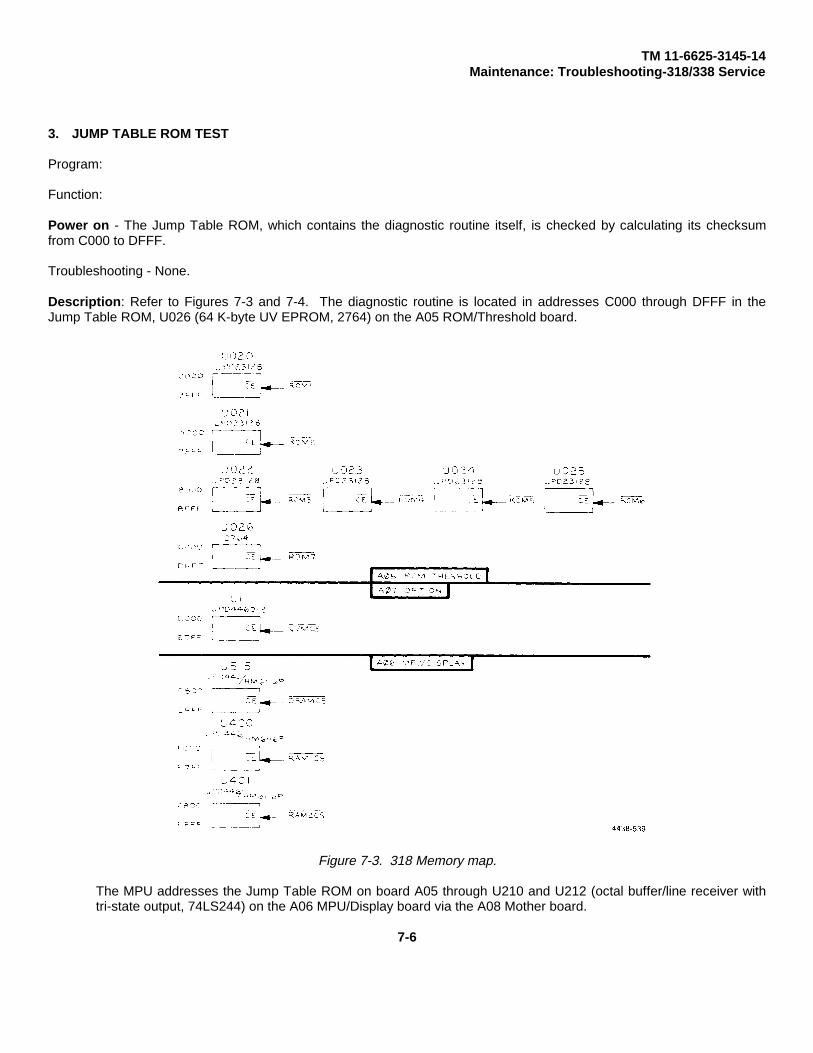
TM 11-6625-3145-14Maintenance: Troubleshooting-318/338 Service
3. JUMP TABLE ROM TEST
Program:
Function:
Power on - The Jump Table ROM, which contains the diagnostic routine itself, is checked by calculating its checksumfrom C000 to DFFF.
Troubleshooting - None.
Description: Refer to Figures 7-3 and 7-4. The diagnostic routine is located in addresses C000 through DFFF in theJump Table ROM, U026 (64 K-byte UV EPROM, 2764) on the A05 ROM/Threshold board.
Figure 7-3. 318 Memory map.
The MPU addresses the Jump Table ROM on board A05 through U210 and U212 (octal buffer/line receiver withtri-state output, 74LS244) on the A06 MPU/Display board via the A08 Mother board.
7-6
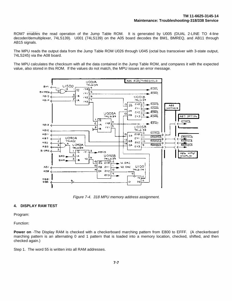
TM 11-6625-3145-14Maintenance: Troubleshooting-318/338 Service
ROM7 enables the read operation of the Jump Table ROM. It is generated by U005 (DUAL 2-LINE TO 4-linedecoder/demultiplexer, 74LS139). U001 (74LS139) on the A05 board decodes the BM1, BMREQ, and AB11 throughAB15 signals.
The MPU reads the output data from the Jump Table ROM U026 through U045 (octal bus transceiver with 3-state output,74LS245) via the A08 board.
The MPU calculates the checksum with all the data contained in the Jump Table ROM, and compares it with the expectedvalue, also stored in this ROM. If the values do not match, the MPU issues an error message.
Figure 7-4. 318 MPU memory address assignment.
4. DISPLAY RAM TEST
Program:
Function:
Power on -The Display RAM is checked with a checkerboard marching pattern from E800 to EFFF. (A checkerboardmarching pattern is an alternating 0 and 1 pattern that is loaded into a memory location, checked, shifted, and thenchecked again.)
Step 1. The word 55 is written into all RAM addresses.
7-7

TM 11-6625-3145-14Maintenance: Troubleshooting-318/338 Service
Step 2. A word is read from a diagnostic cell and checked with the expected word 55. If it is not equal to word 55, an errormessage is displayed and the MPU is halted.
Step 3. If the previous test was successfully completed, the word AA is written into that cell. Then a word in the same cellis read back and compared with AA. If it is not equal to AA, an error message is displayed and the MPU is halted.
Step 4. Steps 2 and 3 are repeated for all RAM addresses.
Troubleshooting - None.
Description: The read and write operation on the Display RAM U515 (16 K-bit static CMOS RAM, uPD446/HM6116P) onthe A06 MPU/Display board is completely controlled by Display Controller U500 (display controller, MB62110) on the A06board.
The MPU reads/writes data from/to the Display RAM through U525 (octal bus transceiver, 40H245) on the A06 board,which is enabled by the Display Controller and the data direction is specified (read or write) by the MPU’s read signal. Theaddresses to the Display RAM are supplied by both the MPU and the Display Controller, however the addresses from theMPU are sent to the Display Controller and the Display Controller gates these signals to the Display RAM.
If there is competition between the MPU and the Display Controller for access to the Display RAM, the Display Controllerforces the MPU to wait until it completes the current read operation by asserting the WAIT signal to the MPU.
The MPU checks the Display RAM with a checkerboard marching pattern. The read and write sequences are alreadymentioned in the preceding Power on paragraph. If the data read is incorrect, the MPU will display an error message.
5. SYSTEM RAM TEST
Program
Function
Power on - SYSTEM RAMs are checked with a checkerboard marching pattern from addresses F000 through F7FF andfrom F800 through FFFF.
Step 1. The word 55 is written into all RAM addresses.
Step 2. A word is read from a selected diagnostic cell and checked against the expected word 55.
If it is not equal to word 55, an error message is displayed and the MPU is halted.
Step 3. If the first test is successfully completed, the word AA is written into that cell. Then the word in the same cell isread back and compared with AA. If it is not equal to AA, an error message is displayed and the MPU is halted.
Step 4. Steps 2 and 3 are repeated for all RAM addresses.
Troubleshooting - None.
Description: RAMs U400 (F000-F7FF) and U401 (F800-FFFF) on the A06 MPU/Display board used by the MPU are calledthe System RAM. The MPU Data Bus (DO-D7) and the partial MPU Address Bus (AO-A10) are directly connected tothese RAMs.
7-8

TM 11-6625-3145-14Maintenance: Troubleshooting-318/338 Service
The chip select signals, RAM1CS and RAM2CS are generated by U005 (dual 2-line to 4-line decoder/multiplexer,74LS139) on the A05 ROM/Threshold board. These signals are sent to the System RAMs through the A08 Mother board.
The MPU checks the System RAMs with the checkerboard marching pattern. The read and write sequences arementioned in the Power on section above. If the data read is incorrect, the MPU will issue an error message.
6. ROM TEST
Program:
Function:
Power on - ROM1 through ROM6 are checked by individually calculating their checksums.
Troubleshooting - None.
Description: Refer to Figure 7-5. All the ROMs (ROM1 through ROM7) are located on the A05 ROM/Threshold board.
Table 7-3318 ROM TEST ADDRESS ASSIGNMENT
ROM U# Address Enabled by
ROM1 U020 0000-3FFF /ROM1
ROM2 U021 4000-7FFF /ROM2
ROM3 U022 8000-BFFF /ROM3
ROM4 U023 8000-BFFF /ROM4
ROM5 U024 8000-BFFF /ROM5
ROM6 U025 8000-BFFF /ROM6
The chip-select signals for ROM1 and ROM2 are decoded by U001 (dual 2-line to 4-line decoder/demultiplexer, 74LS139)on the A05 ROM/Threshold board. All the other chip select signals are doubly decoded. ROM3, ROM4, ROM5, andROM6 are decoded by U001 B (74LS139) which is enabled by U001A (74LS 139) on the A05 board. These ROMS arealso selected by two data bits from U100 (74LS174) on the A05 board in order to constitute four pages of ROM.
The MPU reads data from these ROMs through U045 (octal bus transceiver with tri-state output, 74LS245) on the A05board and through the A08 Mother board. The MPU addresses are sent to these ROMs and the decoders (74LS139) onthe A05 board via U210 and U212 (octal buffer/line driver with tri-state output, 74LS 244) on the A06 MPU/Display boardand through the A08 board. The MPU control signals are also provided through U214 (octal buffer/line driver with tri-stateoutput, 74LS240) on the A06 board and through the A08 board.
The MPU calculates the checksum for each ROM and determines whether it is correct or not. If it is incorrect, an errormessage will be displayed.
7-9

TM 11-625-3145-14Maintenance: Troubleshooting-318/338 Service
Figure 7-5. 318 A03 and A04 Partial ACQ address assignment.
7-10

TM 11-6625-3145-14Maintenance: Troubleshooting-318/338 Service
PARALLEL ANALYZER
7. CLOCK TEST
Program: CLK
Function
Power on - The timebase is programmed for several ranges; its operation is checked by the MPU, which monitors theslow clock flag on each timer interrupt.
Troubleshooting - This is not a verification test, but the user should observe the timebase with an oscilloscope or somesimilar instrument. ALL (all programmable timebases) or SINGLE (one particular timebase) can be selected from themenu for this test.
If ALL is selected, each of the possible timebase values is sequentially set up into the timebase and tested forapproximately five seconds. The next timebase value is then loaded. This test will run continuously until the STOP key ispressed. The CRT screen will display the timebase range being set up. If SINGLE is selected, the user enters the rangeto be observed using the keyboard and then presses the START key. In this case, nothing will appear on the screen.
The following programmable timebase ranges are available:
20nS, 50nS, 100nS, 200nS, 500nS, 1µS, 100uS, 1mS, 10mS, 1S
Description: Refer to Figure 7-6. The Slow Clock Detector compares the SYSCLK signal coming into this detector withthe gate clock internally selected. As long as the SYSCLK is two or more times as fast as the gate clock the slow clockflag is not set. If the SYSCLK is less than twice as fast as the gate clock the slow clock flag is set.
This program also checks the clock path using the Slow Clock Detector.
The MPU selects the internal CLK by writing 111110binary into shift register U224 (hex D master- slave flip-flop, 10176) onthe A02 INPUT-B board at I/O address 01hex. This shift register enables U222B (dual 3-input 3-output NOR gate, 10211)on the A02 board which transmits the INTCLK signal.
The Slow Clock Detector, the Timer, and their associated circuits are located in U140 (timebase, µPB3Z1 99R) on the A04ACQ Memory board. The Timer is programmed to generate an interrupt to the MPU every 100 ms. Then the MPUunmasks the Timer Interrupt and sets the gate clock and the SYSCLK interval as shown in Table 7-4.
7-11
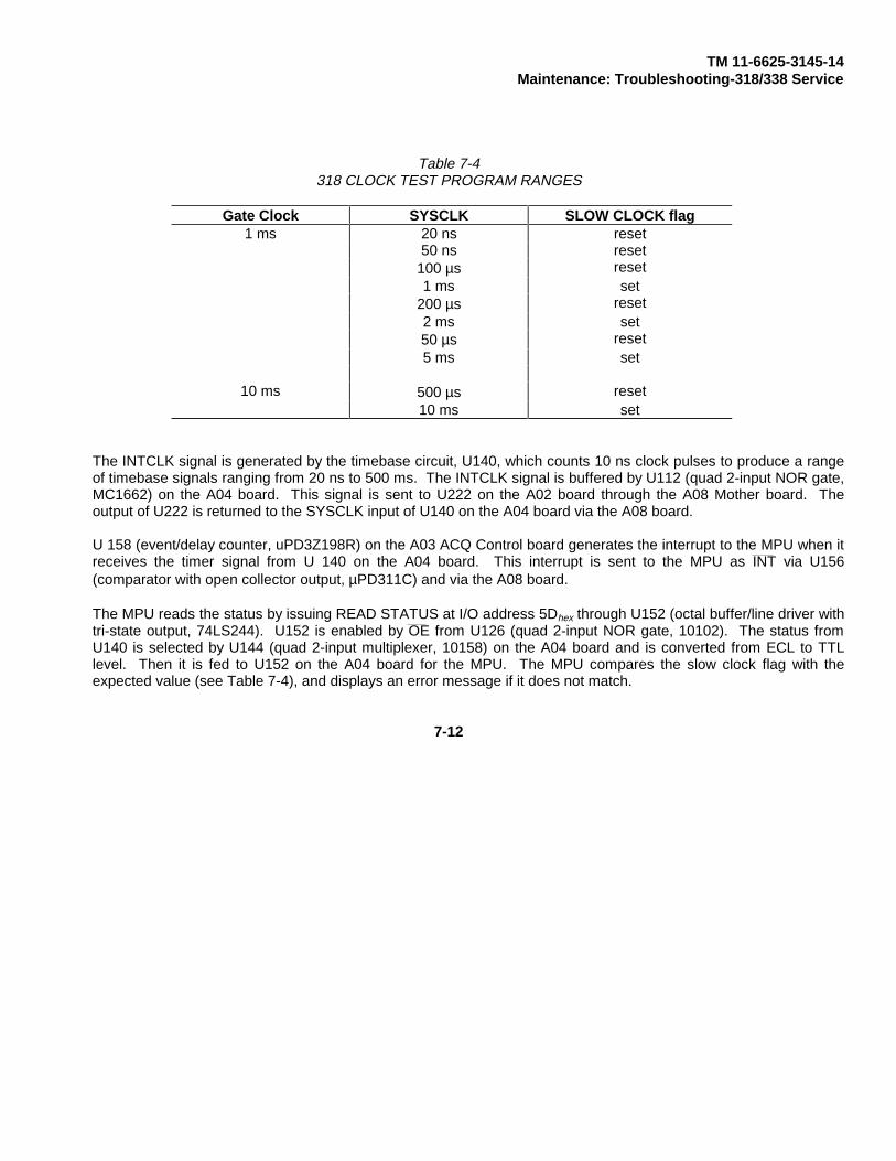
TM 11-6625-3145-14Maintenance: Troubleshooting-318/338 Service
Table 7-4318 CLOCK TEST PROGRAM RANGES
Gate Clock SYSCLK SLOW CLOCK flag1 ms 20 ns reset
50 ns reset100 µs reset1 ms set
200 µs reset2 ms set50 µs reset5 ms set
10 ms 500 µs reset10 ms set
The INTCLK signal is generated by the timebase circuit, U140, which counts 10 ns clock pulses to produce a rangeof timebase signals ranging from 20 ns to 500 ms. The INTCLK signal is buffered by U112 (quad 2-input NOR gate,MC1662) on the A04 board. This signal is sent to U222 on the A02 board through the A08 Mother board. Theoutput of U222 is returned to the SYSCLK input of U140 on the A04 board via the A08 board.
U 158 (event/delay counter, uPD3Z198R) on the A03 ACQ Control board generates the interrupt to the MPU when itreceives the timer signal from U 140 on the A04 board. This interrupt is sent to the MPU as INT via U156(comparator with open collector output, µPD311C) and via the A08 board.
The MPU reads the status by issuing READ STATUS at I/O address 5Dhex through U152 (octal buffer/line driver withtri-state output, 74LS244). U152 is enabled by OE from U126 (quad 2-input NOR gate, 10102). The status fromU140 is selected by U144 (quad 2-input multiplexer, 10158) on the A04 board and is converted from ECL to TTLlevel. Then it is fed to U152 on the A04 board for the MPU. The MPU compares the slow clock flag with theexpected value (see Table 7-4), and displays an error message if it does not match.
7-12

TM 11-6625-3145-14Maintenance: Troubleshooting-318/338 Service
Figure 7-6. 318 Clock test.
8. WORD RECOGNIZER TEST
Program: WR
Function :
Power on - The word recognition (WR) RAMs are checked with the checkerboard marching pattern from 00 through FF.
Step 1. The word 15 is written into all RAM addresses.
7-13

TM 11-6625-3145-14Maintenance: Troubleshooting-318/338 Service
Step 2. A word is read from a diagnostic cell and checked with the expected word 15.
If it is not equal to word 15, an error message is displayed and the MPU is halted.
Step 3. If the first test is successful, the word 2A is written into that cell. The word is then read back out of the cell and itsvalue is compared with 2A. If it is not equal to 2A, an error message is displayed and the MPU is halted.
Step 4. Steps 2 and 3 are repeated for all RAM addresses.
Troubleshooting - This test is the same as that automatically run when the power is first turned on, but here the loopingtest feature is available. The LOOP field can have any of the following 4 options; OFF, I/O, ERROR, and TEST. Whenthe field is set to I/O, the looping feature allows only I/O instructions to be run repeatedly. The I/O address will appear onthe screen. When the field is set to ERROR, the looping feature allows the tests in which an error is detected to be runrepeatedly. When the field is set to TEST, the looping feature allows one test, or sequence of tests, to be runcontinuously. When the field is set to OFF, the looping feature is not available and one test, or sequence of tests, runsonce.
When the field is set to I/O or ERROR, the prompt message START TO ADVANCE appears at the bottom of the thescreen. If START is pressed during LOOP tests, the current loop of the test stops and the next loop of test is started, Youcan change fields during tests. Use this feature to catch intermittent faults and for circuit tracing with an oscilloscope.
In the I/O Looping test, only one or more OUT instructions (subroutines) including one of the following addresses will berun. Unless STOP is pressed, this test will loop continuously without displaying the result of the verification. Use anoscilloscope to observe the word recognizers.
Table 7-5318 WORD RECOGNIZER TEST PORT ADDRESSES (Hex)
Address Content of Looping Test
03 increment WR-address counter for WRO test.
5B write WRO data55 into data latch.
5B write WRO dataAA into data latch.
03 increment WR-address counter for WRI test.
5B write WR1 data55 into data latch.
5B write WR1 dataAA into data latch.
The ERROR looping feature is available only if errors are detected. If no errors are detected the test will perform as if theLOOP test were set to OFF. If some errors are detected, the ERROR looping feature is available for the read cycle of thetest. and the result of this verification will appear on the screen. Refer to Appendix B of this manual for a description oferror codes.
Description: Refer to Figure 7-7. On the A01 INPUT-A board, data from channels 0 through 7 (Pod- A) is latched byM218s U100 through U114 <1> (logic analyzer input, M218) and supplied to the word recognizer (WR) U120 (256 word X
7-14

TM 11-6625-3145-14Maintenance: Troubleshooting-318/338 Service
word recognizer (WR) U120 (256 word x 4 bit RAM, HM10422) for trigger detection. These output lines are wired togetherwith U124 and U126 <2> (4-bit binary counter, F10016) outputs, respectively, to set up the WR.
During acquisition, the outputs of U124 and U126 are held at the reset level by the counter signal from U132 (quad TTL-TO-ECL translator, 10124) which is generated by U130 (3-line to 8-line decoder/demultiplexer, 74LS 138) when the MPUwrites any data at I/O address 02hex.
During WR setup, all the M218’s outputs are set to off (low level) by the OFF/ON signal (TTL swing, shifted to -5V) fromU240A (quad comparator, µPC339C) on the A02 INPUT-B board. This signal is delivered from U224 (hex D master-slaveflip-flop, 10176) on the A02 board when the MPU writes X1XXXbinary serially at I/O address 01 hex. This operation enablesU124 and U126 to act as a WR address counter to point to any address in the WR. This WR address counter can beincremented by a clock pulse generated when the MPU writes to address 03hex.
The word written into the WR is provided along with signals EDBO, EDB1, and EDB2 from the A04 ACQ Memory board,(translated from the TTL-level of the MPU data bus to ECL-level) The write pulse to the WR is generated by U130(74LS138), and is converted to ECL-level by U132 (10124) when the MPU writes at I/O address 00hex.
For channels 8 through 15 on the A02 board, the operation is the same as that described in the preceding paragraph. Thewords for WR U220 (HM10422) are supplied from EDB3, EDB4, and EDB5.
Each output of these two WRs is wired together on the A08 Mother board, and the outputs are sent to U136 and U138(dual type D master-slave flip-flop, 10231) on the A03 ACQ Control board for triggering. These signals are routed to U146(quad 2-input multiplexer/latch, 10173) on the A03 board. The data to U146 (10173) is latched by READ SQRAM fromU112 (binary to 1-8 line decoder, 10162) through inverter U126 (quad 2-input NOR gate, 10102), after being selected byLDSQRAM from U108 (hex D master-slave flip-flop, 10176) on the A03 board. LDSQRAM is set when the MPU writesX1XXXX binary at I/O address 51 hex and READ SQRAM is generated by the MPU’s access to I/O address 5Bhex.
The four outputs of U146 (10173) are connected to U142 (quad 2-input multiplexer, 10158) on the A04 board with theoutputs of the ACQ Memories U1 6 to U130 (HM10422) on the A04 board. Thus, all the ACQ Memories should be set tooff by forcing BS high. This is done by writing 1Fhex into U114 (hex D master-slave flip-flop, 10176) on the A04 board withWRITE BS from U112 (10162) on the A03 board.
The MPU reads the data from U152 (octal buffer/line driver with tri-state output, 74LS244) on the A04 board, when U152 isenabled by OE from U112 (10162) via U126 (10102) on the A03 board. The data fed to U152 (74LS244) is selected byU142 (10158) on the A04 board with the READ SQRAM signal from U112 (10162) on the A03 board at I/O address 59hex.The data is translated from ECL to TTL level by U146 (quad ECL-TO-TTL translator, 10125) on the A04 board.
The MPU follows steps 1 through 4 of the I/O operation described in Power on paragraph at the begining of this testsection, and compares the data with the expected value for each I/O read. If the data is wrong, the MPU will issue an errormessage.
7-15

TM 11-6625-3145-14Maintenance: Troubleshooting-318/338 Service
Figure 7-7. 318 Word recognizer test.

TM 11-6625-3145-14Maintenance: Troubleshooting-318/338 Service
9. ACQUISITION RAM TEST
Program: ACQ
Function:
Power on - All the ACQ RAMs are checked with the checkerboard marching pattern from 00 through FF.
Step 1. The word 55 is written into all RAM addresses.
Step 2. A word is read from a diagnostic cell and compared with the expected word 55.
If the diagnostic cell’s value is not equal to 55, an error message is displayed and the MPU is halted.
Step 3. If no error is found in the above test, the word AA is written into that cell. Then a word in same cell is read backand is compared with AA. If that word is not equal to AA, an error message is displayed and the MPU is halted.
Step 4. Steps 2 and 3 are repeated for all RAM addresses.
Troubleshooting - This test is the same as that performed automatically when the power is turned on, but here theLooping test feature is available. The Looping feature has four options; OFF, I/O, ERROR, and TEST. When the field isset to I/O, the looping feature allows only I/O instrucions to be run repeatedly. The I/O address will appear on the screen.When the field is set to ERROR, the looping feature allows the tests in which an error is detected to be run repeatedly.When the field is set to TEST, the looping feature allows one test, or sequence of tests, to be run continuously. When thefield is set to OFF, the looping feature is not available and one test, or sequence of tests, runs once.
When the I/O Looping test is selected, only those OUT instructions (subroutines) including one of the addresses listed inTable 7-6 below will run. Unless the STOP key is pressed, the selected portions of the test will loop continuously withoutdisplaying the result of the verification. In this case, use an oscilloscope to observe the acquisition circuit board.
Table 7-6318 ACQ TEST PORT ADDRESSES (Hex)
Address Content of Looping Test02 reset WR-address counter to increment WR-address counter to 55 to write 55 into
the background of High-speed memory.5A write CSO & CS1 into CS-latch to read 55 from High-speed memory.55 write AA into High-speed memory after reading 55 from High-speed memory.5A write CSO & CS1 into CS-latch to read AA from High-speed memory.55 write 55 into High-speed memory after reading AA from High-speed memory.
7-17

TM 11-6625-3145-14Maintenance: Troubleshooting-318/338 Service
When ERROR is selected in the looping test field, looping is available only if errors are detected. If no errors are detected,the test runs to completion just as if the looping function had been set to OFF. If some errors are detected, the ERRORlooping feature is available for the read cycle of the test, and the result of the verification will appear on the screen. Referto Appendix B of this manual for an explanation of error codes.
Description: Refer to Figure 7-8. The test data for ACQ Memories U1 16 to U122 <8> (256-word X 4-bit RAM,HM10422) on the A04 ACQ Memory board are generated by U124 and U126 <2> (4-bit binary counter, F10016) on the A01INPUT-A board, and U230 and U232 <3> (F10016) on the A02 INPUT-B board, instead of using the M218’s actual data.The operation for generating this pseudo data is the same as the one used in the WR Test.
Each output of both the M218s and the F10016s respectively are connected together and are delivered to U122 and U128(hex D master-slave flip-flop, 10176) on the A01 board, and U228 and U234 (10176) on the A02 board (these flip-flops areused for delay). The outputs of the flip-flops are connected to each input of the ACQ memories on the A04 board throughthe A08 Mother board.
The addresses for the ACQ Memories are selected by U136 and U138 (4-bit binary counter, F10016) on the A04 board.These counters are set to COUNT ENABLE by U156 (quad 2-input NOR gate, 10102) on the A03 ACQ Control board, andare reset by RESET from U112 (10162) on the A03 board.
At least one pair of the ACQ Memories can be enabled by U114 (hex D master-slave flip-flop, 10176) on the A04 board,when the MPU writes the data into it at I/O address 5Ahex by WRITE BS from U112 (10162) on the A03 board.
The flip-flop U148A <7> (dual D master-slave flip-flop, 10231) sets the STOP condition, and is re-set by RESET fromU110 (10162) on the A03 board. It also frees the WE line. START2, also from U110 (10162), enables the StrobeGenerator circuit by setting the flip-flop U124B (dual D master-slave flip-flop, 10131) on the A03 board.
After the above setup is complete, the MPU selects the internal CLK and sets the timebase U140 (timebase, µPB3Z199R)on the A04 board to generate a single clock pulse when the MPU writes to I/O address 4Ahex. Then the MPU unmasks thecarry interrupt from both U136 and U138 (F10016) on the A04 board.
The MPU starts the test by performing steps 1 through 4 described in the Power On paragraph at the beginning of thissection.
7-18
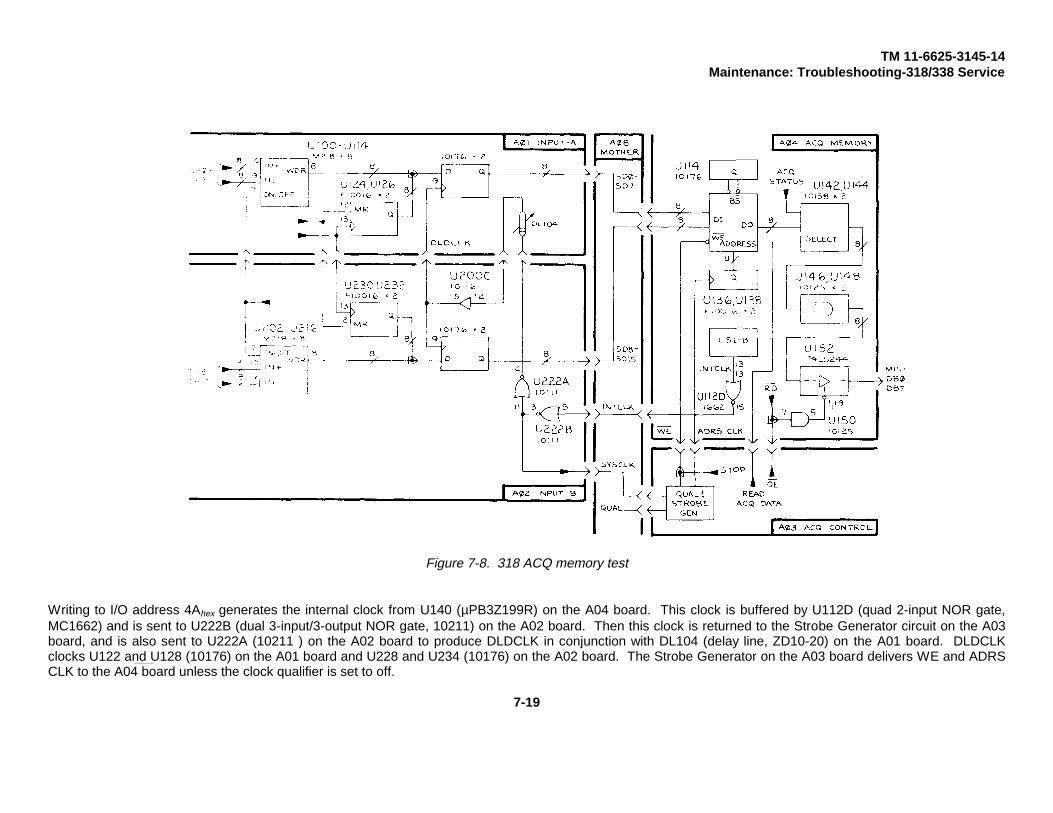
TM 11-6625-3145-14Maintenance: Troubleshooting-318/338 Service
Figure 7-8. 318 ACQ memory test
Writing to I/O address 4Ahex generates the internal clock from U140 (µPB3Z199R) on the A04 board. This clock is buffered by U112D (quad 2-input NOR gate,MC1662) and is sent to U222B (dual 3-input/3-output NOR gate, 10211) on the A02 board. Then this clock is returned to the Strobe Generator circuit on the A03board, and is also sent to U222A (10211 ) on the A02 board to produce DLDCLK in conjunction with DL104 (delay line, ZD10-20) on the A01 board. DLDCLKclocks U122 and U128 (10176) on the A01 board and U228 and U234 (10176) on the A02 board. The Strobe Generator on the A03 board delivers WE and ADRSCLK to the A04 board unless the clock qualifier is set to off.
7-19
TM 11-6625-3145-14Maintenance: Troubleshooting-318/338 Service
During the read phase, the MPU receives data from U152 (octal buffer/line driver with 3-state output, 74LS 244) by issuingREAD ACQ DATA at I/O address 59hex. The READ ACQ DATA signal switches the inputs of U142 and U144 (quad 2-input multiplexer, 10158) on the A04 board to the output of the ACQ Memories.
Outputs of the ACQ Memories are wired together with the outputs of U146 (quad 2-input multiplexer/latch, 10173) on theA03 board, or with Threshold TEST from U244C (QUAD 2-INPUT NOR GATE, 10102) on the A02 board via the A08Mother board. These signals must be kept low in order to read the correct data from the ACQ Memories. To write 0’s intoU146 (10173) on the A03 board, the MPU loads 00 into the SQRAM U144 (256 word X 4 bit RAM, HM10422) on the A03board, then changes the inputs of U146 (10173) to the SQRAM output and issues READ SQRAM . The output of U244C(10102) on the A02 board can be disabled by writing 1XXXX binary serially into U224 (hex D master-slave flip-flop, 10176)on the A02 board at I/O address O1hex.
The data read is checked by the MPU and an error message is displayed if the data is incorrect.
The MPU also checks the interrupt from the carry flip-flop U139A on the A04 board. The carry flip- flop is set when U136and U138 (F10016) on the A04 board issue a carry bit at the same time.
10. SEQUENCE RAM TEST
Program: SQRAM
Function:
Power on - The SQRAM is checked with the checkerboard marching pattern from 00 through FF.
Step 1. The word 55 is written into all RAM addresses.
Step 2. A word is read from a diagnostic cell and compared with the expected word 55. If the selected word is not equalto 55, an error message is displayed and the MPU is halted.
Step 3. The word AA is written into that diagnostic cell. Then a word in same cell is read back and is compared with AA.If it is not equal to AA, an error message is displayed and the MPU is halted.
Step 4. Steps 2 and 3 are repeated for all RAM addresses.
Troubleshooting - This test is the same as that run automatically when the power is first turned on, but here the loopingfeature is available. The looping feature has 4 options; OFF, I/O, ERROR, and TEST. When the field is set to I/O, thelooping feature allows only I/O instructions to be run repeatedly. The I/O address will appear on the screen. When thefield is set to ERROR, the looping feature allows the tests in which an error is detected to be run repeatedly. When thefield is set to TEST, the looping feature allows one test, or sequence of tests, to be run continuously. When the field is setto OFF, the looping feature is not available and one test, or sequence of tests, will run once.
When I/O looping is selected, only those looping instructions including one of the addresses listed in Table 7-7 will run.Unless the STOP key is pressed, the program will continue looping without displaying the result of the verification. In thiscase, the user should observe the ACQ. circuit board with an oscilloscope.
7-20

TM 11-6625-3145-14Maintenance: Troubleshooting-318/338 Service
Table 7-7 318 SQRAM TEST PORT ADDRESSES (Hex)
Address Content of Looping Test5A set CS all OFF into CS-latch to write 55 in the background of the SQRAM.50 set 1 into QUAL (DO & D2) register and set 0 into QUAL (D1 & D3) register.58 write 55 into the background of the SQRAM.5B SQRAM data is latched to read 55 from High-speed memory.58 write AA into SQRAM after reading 55 from High-speed memory.5B SQRAM data is latched to read AA from High-speed memory.
When the ERROR looping function is selected, the program loops only if errors are detected. If no errors are detected, theprogram runs once and displays the result of the verification just as if the looping function were turned OFF. If errors aredetected, the ERROR looping function is available for the read cycle of the test. The results of the read cycle verificationwill appear on the screen. Refer to Appendix B of this manual for a description of error codes.
Description: Refer to Figure 7-9. The SQRAM U144 (256 word X 4-bit RAM, HM10422) on the A03 ACQ Control boardholds the trigger sequence table called Trigger menu.
The SQRAM receives data from U106 and U108 (hex D master-slave flip-flop, 10176) on the A03 board with the followingconnection.
Table 7-8318 SQRAM TEST SQRAM DATA CONNECTIONS
SetupSQRAM U144 Latch MPU Data
D10 (pin 6) U106 Q1 (pin 3) DODI1 (pin 7) U106 Q3 (pin 13) D1D12 (pin 18) U108 Q1 (pin 3) D2D13 (pin 19) U108 Q3 (pin 13) D3
To provide the data to the SQRAM, the MPU writes the two least significant bits of the four data bits into U106 (10176) atI/O address 50hex, and the two most-significant bits into U108 (10176) at I/O address 51hex.
Each address line of the SQRAM is connected to two output lines which are wired together as follows:
7-21
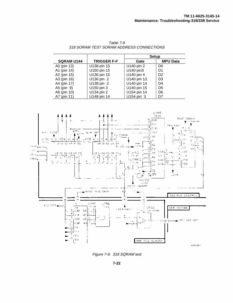
TM 11-6625-3145-14Maintenance: Troubleshooting-318/338 Service
Table 7-9318 SORAM TEST SORAM ADDRESS CONNECTIONS
SetupSQRAM U144 TRIGGER F-F Gate MPU Data
A0 (pin 13) U138 pin 15 U140 pin 2 D0A1 (pin 14) U150 pin 15 U140 pin3 D1A2 (pin 15) U136 pin 15 U140 pin 4 D2A3 (pin 16) U136 pin 2 U140 pin 13 D3A4 (pin 17) U138 pin 2 U140 pin 14 D4A5 (pin 9) U150 pin 3 U140 pin 15 D5A6 (pin 10) U134 pin 2 U154 pin 14 D6A7 (pin 11) U148 pin 14 U154 pin 3 D7
Figure 7-9. 318 SQRAM test
7-22
TM 11-6625-3145-14Maintenance: Troubleshooting-318/338 Service
In order to set up the SQRAM, the MPU data (translated to ECL level) points to the address of the SQRAM. These databits are gated as in the preceding table, enabled by LDSQRAM from U108 <5> (10176) bit 4 on the A03 board. Bit 4 ismaintained high during this setup.
The write pulse to the SQRAM, WRITE SQRAM, is generated when the MPU writes to I/O address 58hex. At the sametime, the address to the SQRAM is supplied by the MPU data.
The read process is the same as in the WR test, except that the inputs for U 146 (quad 2-input multiplexer/latch 10173) onthe A03 board are switched to the outputs of the SQRAM.
During each read, the MPU verifies the data and issues an error message if it is not equal to the expected data.
11. N & DELAY TEST
Program: N & DLY
Function:
Power on - The Event/Delay counter counts word "A" N times when functioning as the Event counter, and counts a certainnumber of clock signals for delay when functioning as the Delay counter.
When functioning as the Event counter, the MPU loads a small N value into the counter register and increments thecounter using clock pulses while observing the carrry bit. The Delay counter functions the same way, using the DELAYvalue as the initial counter value. In both cases the number of clock signals needed to generate the carry are comparedwith the expected values.
Troubleshooting - This is not a verificaion test, so no test result will appear on the CRT screen. This test should beobserved on an oscilloscope. The troubleshooting routine automatically tests the N&DELAY Counter by alternately loadingand running the counter, first with N values as the Event counter, and then with DELAY values for the Delay counter. Theuser programs the N and DELAY values before beginning the test. This test will run forever, or until the user presses theSTOP key. If no test values are entered, the N Counter is set to 1 and the DELAY counter is set to 0. In this case, theN&DELAY Counter will not run. To run this test, N must be greater than 1, and DE-LAY must be greater than 0.
Description: Refer to Figure 7-10. The Event Delay Counter U158 (event/delay counter, µPB3Z198R) on the A03 ACQCONTROL board is controlled by three signals, E, LOAD N, and LOAD DL from the SQRAM U144 (256 word X 4 bit RAM,HM10422) on the A03 board. The counter generates N-1 as a carry when it reaches full count. This Event/Delay Counterhas two registers, the one which holds the N value is called the N-register and the one which holds the DELAY value iscalled the DL register.
In this test, the MPU writes 000Fhex as the N value into the N-register at I/O addresses 41hex and 42hex, and 005Ahex as theDELAY value into the DL register at I/O address 43hex and 44hex.
Start flip-flop U124B (dual type D master-slave flip-flip, 10131) on the A03 board is set by START2 from U110 (binary to 1-8decoder/multiplexer, 10162) on the A03 board. U124B passes a clock signal generated by the MPU.
7-23

TM 11-6625-3145-14Maintenance: Troubleshooting-318/338 Service
Latches U106 and U108 (hex D master-slave flip-flop, 10176) on the A03 board are set to hold data 1100binary for theSQRAM. They also enable U140 (hex AND-gate, 10197) and U154 (quad 2-input AND-gate, 10104) on the A03 board.Those gates control the data supplied to the address line of the SQRAM.
The MPU writes the data already set in the latches into the SQRAM at address FFhex using the WRITE SQRAM signalfrom U112 <6> (10162) on the A03 board. This data generates the LOAD N command for the Event/Delay Counter. Afterthis setup, latches U106 and U108 (10176) are written to set the clock qualifier to off, which enables the MPU to send asingle clock. The MPU generates STEP CLK by writing at I/O address 55he., from U1 10 (10162) on the A03 board, usingFFhex as data. That is, the SQRAM delivers the data at address FFhex as pointed to by the MPU. Event/Delay counter data(LOAD N), and the Strobe Generator circuit on the A03 board generate the TRIG CLK signal to the Event/Delay counter.
By this procedure, the value of the N-register in the Event/Delay counter is loaded into the counter itself.
To keep the Event/Delay Counter enabled during the test, the SQRAM must supply CE to the Event/Delay Counter. So,the same setups mentioned above are repeated in order to load 0000binary into the SQRAM.
After that, the MPU unmasks the interrput of the Event/Delay Counter Carry by writing at I/O address 40hex.
Then the MPU generates STEP CLK by writing FFhex for the SQRAM address until it receives an interrupt signal. Once theinterrupt occurs, the MPU reads the status from I/O address 5Dhex. The signal path for reading the status is same as inthe Clock Test.
The MPU checks to see whether the Event/Delay Counter Carry Flag is set, and also checks the number of STEP CLKsgenerated. If the flag is set and the clock count is correct. the MPU proceeds to the next step, otherwise it issues an errormessage and stops the test.
The DELAY count can be tested in the same way as the Event count, N. In this case, 1010binary is set in latches U106 andU108 (10176) on the A03 board.
7-24

TM 11-6625-3145-14Maintenance: Troubleshooting-31 8/338 Service
Figure 7-10. 318 N and DELAY counter test.
7-25

TM 11-6625-3145-14Maintenance: Troubleshooting-318/338 Service
12. THRESHOLD TEST
Program: THRSH
Function:
Power on - Threshold V1 and Threshold V2 are set for several levels to produce Threshold V3 at - 0.2V or +0.2V. Forevery setting the comparator will detect the Threshold V3 level relative to ground and the MPU checks the comparator’soutput against the expected data (0 or 1).
Troubleshooting - Threshold V1 and Threshold V2 are programmed from -10.0V to +10.0V incrementally with 0.1V stepsin order to generate the saw-tooth waveform.
Description: Refer to Figure 7-11. Two levels of voltage, one for V1 and the other for V2, are produced by DAC U070and U080 (CMOS 8-bit buffered multiplexing DAC, AD7524) on the A05 ROM/Threshold board. When the MPU writesdata into these DACs, this setting is latched inside. The data is supplied from U216 (octal bus transceiver with 3-stateoutput, 74LS245) on the A06 MPU/Display board through the A08 Mother board, and U045 (74LS245) on the A05 board.
When the MPU writes at I/O address E0hex the WR and CS signals are sent to U070 (DAC V1) to latch the data. WR andCS for U080 (DAC V2) are caused by the MPU’s access at I/O address E1hex. The WR signal is delivered from U150C(quadruple 2-input positive NOR gate, 74LS02) on the A05 board, which comes from U214 (octal buffer/line driver with 3-state output, 74LS240) on the A06 board. CS for these DACs are generated by U092B (dual 2-line to 4-linedecoder/demultiplexer, 74LS139) on the A05 board.
A number less than 80hex programs the DAC for positive output, and a number more than 80hex progarms it for negativeoutput centered on GND (80hex) in 0.1V steps. The actual output of these DACs is 1/4 of that specified in theTHRESHOLD menu.
This test sets the DACs to several values, given in Table 7-10, and checks V3 selected for CLK Threshold indirectly.
The settings and expected data are as follows;
7-26
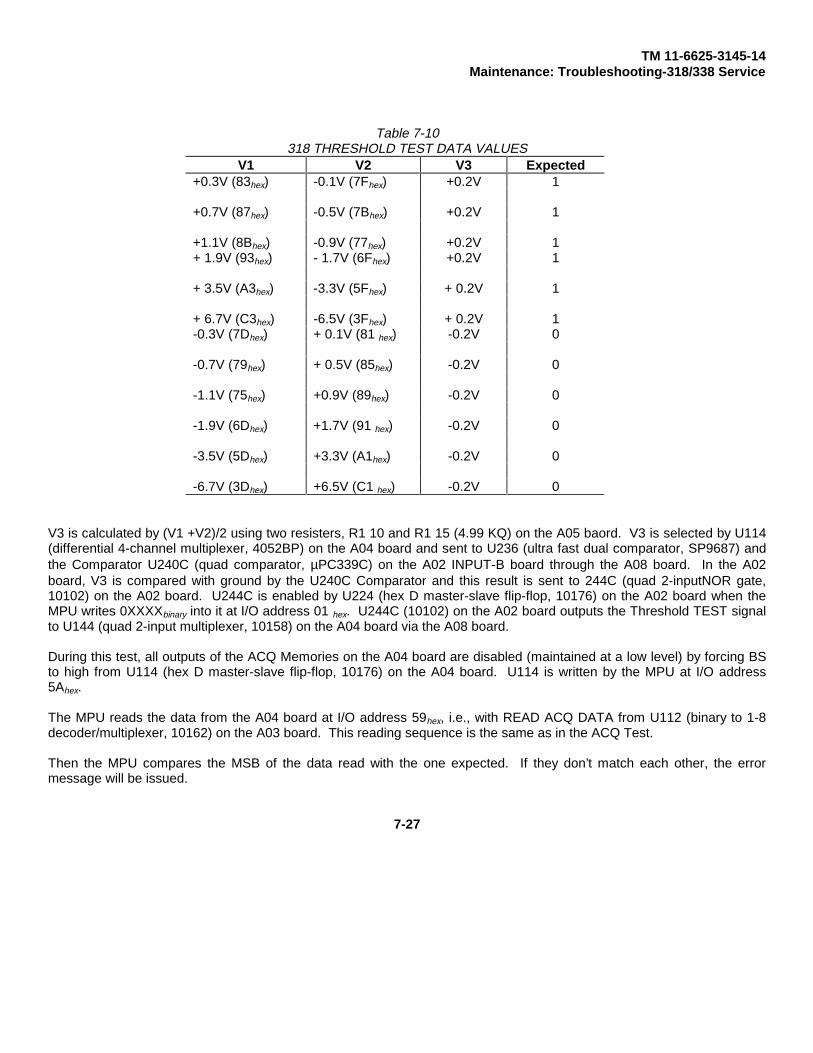
TM 11-6625-3145-14Maintenance: Troubleshooting-318/338 Service
Table 7-10318 THRESHOLD TEST DATA VALUES
V1 V2 V3 Expected+0.3V (83hex) -0.1V (7Fhex) +0.2V 1
+0.7V (87hex) -0.5V (7Bhex) +0.2V 1
+1.1V (8Bhex) -0.9V (77hex) +0.2V 1+ 1.9V (93hex) - 1.7V (6Fhex) +0.2V 1
+ 3.5V (A3hex) -3.3V (5Fhex) + 0.2V 1
+ 6.7V (C3hex) -6.5V (3Fhex) + 0.2V 1-0.3V (7Dhex) + 0.1V (81 hex) -0.2V 0
-0.7V (79hex) + 0.5V (85hex) -0.2V 0
-1.1V (75hex) +0.9V (89hex) -0.2V 0
-1.9V (6Dhex) +1.7V (91 hex) -0.2V 0
-3.5V (5Dhex) +3.3V (A1hex) -0.2V 0
-6.7V (3Dhex) +6.5V (C1 hex) -0.2V 0
V3 is calculated by (V1 +V2)/2 using two resisters, R1 10 and R1 15 (4.99 KQ) on the A05 baord. V3 is selected by U114(differential 4-channel multiplexer, 4052BP) on the A04 board and sent to U236 (ultra fast dual comparator, SP9687) andthe Comparator U240C (quad comparator, µPC339C) on the A02 INPUT-B board through the A08 board. In the A02board, V3 is compared with ground by the U240C Comparator and this result is sent to 244C (quad 2-inputNOR gate,10102) on the A02 board. U244C is enabled by U224 (hex D master-slave flip-flop, 10176) on the A02 board when theMPU writes 0XXXXbinary into it at I/O address 01 hex. U244C (10102) on the A02 board outputs the Threshold TEST signalto U144 (quad 2-input multiplexer, 10158) on the A04 board via the A08 board.
During this test, all outputs of the ACQ Memories on the A04 board are disabled (maintained at a low level) by forcing BSto high from U114 (hex D master-slave flip-flop, 10176) on the A04 board. U114 is written by the MPU at I/O address5Ahex.
The MPU reads the data from the A04 board at I/O address 59hex, i.e., with READ ACQ DATA from U112 (binary to 1-8decoder/multiplexer, 10162) on the A03 board. This reading sequence is the same as in the ACQ Test.
Then the MPU compares the MSB of the data read with the one expected. If they don’t match each other, the errormessage will be issued.
7-27
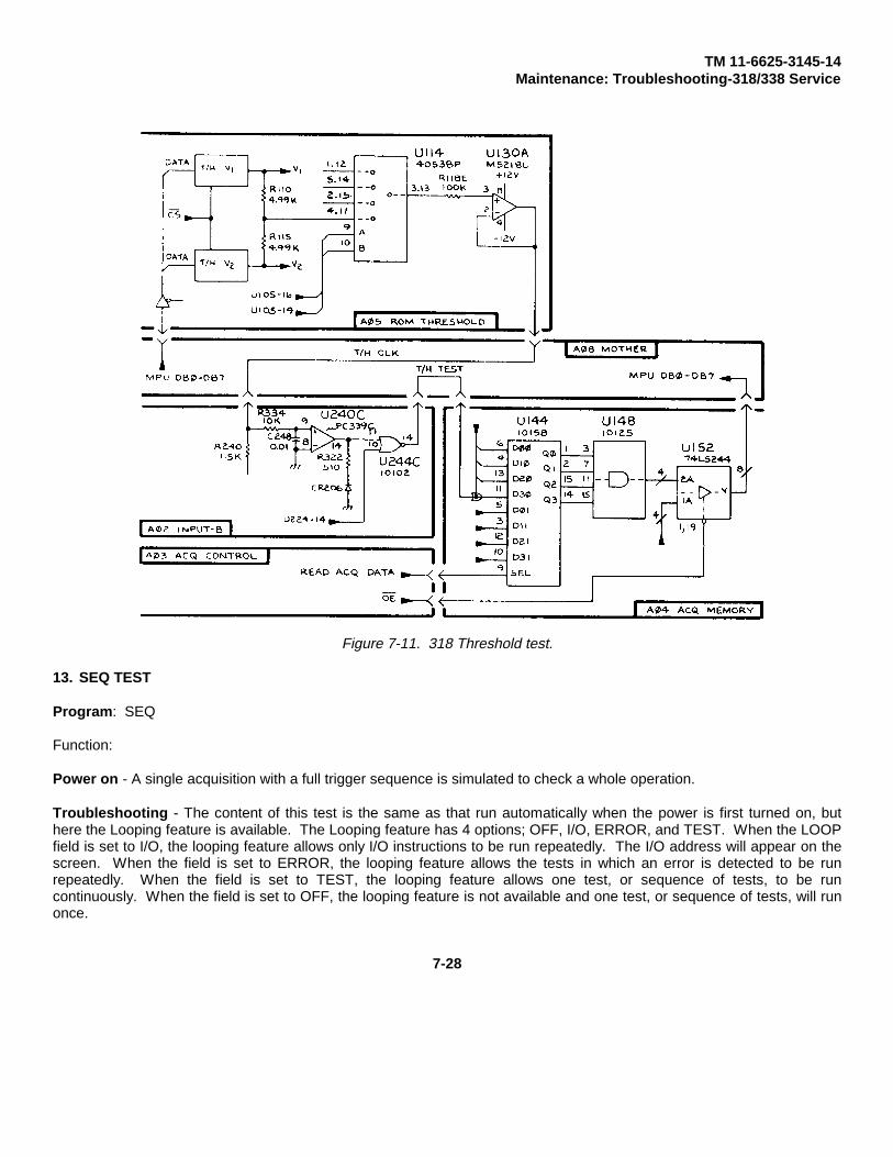
TM 11-6625-3145-14Maintenance: Troubleshooting-318/338 Service
Figure 7-11. 318 Threshold test.
13. SEQ TEST
Program: SEQ
Function:
Power on - A single acquisition with a full trigger sequence is simulated to check a whole operation.
Troubleshooting - The content of this test is the same as that run automatically when the power is first turned on, buthere the Looping feature is available. The Looping feature has 4 options; OFF, I/O, ERROR, and TEST. When the LOOPfield is set to I/O, the looping feature allows only I/O instructions to be run repeatedly. The I/O address will appear on thescreen. When the field is set to ERROR, the looping feature allows the tests in which an error is detected to be runrepeatedly. When the field is set to TEST, the looping feature allows one test, or sequence of tests, to be runcontinuously. When the field is set to OFF, the looping feature is not available and one test, or sequence of tests, will runonce.
7-28

TM 11-6625-3145-14Maintenance: Troubleshooting-318/338 Service
When I/O Looping is selected, only those selected OUT instructions (subroutines), including one of the addresses listedbelow, will run. Unless the STOP key is pressed, this test will continue looping without displaying the result of theverification. In this case, the user should use an oscilloscope to observe the Acquisition circuit board.
PORT ADDRESSES (HEX)
Address Content of Looping Test55 write WA into High-speed memory.
When ERROR is selected, looping will occur only if errors are detected. If no errors are detected, the ERROR looping testwill run through its tests only once, and the results of the verification will be displayed on the CRT just as if the looping fieldhad been selected to OFF. If errors are detected, the ERROR Looping function is available for the read cycle of the test,and the result of the verification will appear on the screen. Refer to the Appendix B of this manual for and explanation oferror codes.
Description: A single acquisition is simulated to check the trigger sequencer operation. Pseudo data is generated inexactly the same way used in the WR and ACQ tests, and applied to the latches on the A01 INPUT-A and INPUT-Bboards.
The words, WA, WB, and WC are set to 01hex, 02hex and 03hex respectively. Then full trigger sequence, 00005*WA FLW’DBY:WB RESET ON:WC is selected with 16 clocks of delay to stop after the trigger recognition.
The data AAAXBCAAXAAAXABXABCXABCXABCXABC is supplied to the WR on the A01 and the A02 boards and to theACQ Memories on the A04 ACQ MEMORY board. SYSCLK is generated by the MPU by writing at I/O address 4Ahex,which is into the timebase U140 on the A04.
The operation of the Trigger Sequencer is observed by the MPU by reading the interrupt and the ACO status. The MPUchecks these conditions on every clock pulse, and if there are any unexpected events the MPU displays an error message.
After the end of the acquisition (all flags are detected at certain clocks), the MPU reads the data from the ACQ Memorieson the A04 board, and compares them with the word sequence applied. An error message is displayed if there aredifferences.
318S1 SERIAL ANALYSIS/RS232C/NVM
14. BATTERY TEST
Program: TSTBTT
Function:
Power on - TSTBTT checks the battery voltage to see if it is more or less than 2.2 volts.
Troubleshooting - None
7-29

TM 11-6625-3145-14Maintenance: Troubleshooting-318/338 Service
Description - Detected battery voltage status is shown in the status register at bit 07. TSTBTT this bit from 1/0 address80. (Refer to the 318S1/338S1 I/O function list)
Battery voltage is detected by Q170, and battery status is applied to bit #7 of the status register by U32.
U30 decodes 318S1/338S1 I/O addresses.
15. NON-VOLATILE MEMORY TEST
Program : TSTNVI (power on), TSTNV2 (Troubleshooting)
Function:
Power-on - The NVM has a checksum word that is used for checking non-volatile memory data. The TSTNV1 programcalculates the checksum by reading NVM data and comparing it with the NVM checksum.
Troubleshooting - The TSTNV2 diagnostic program includes 12 test programs. For all of these tests, the method is readdata after write. (Refer to the failure code list for check data format.)
All NVM data is cleared after the diagnostic test has run.
Description - The NVM address is from E000 through E7FF; the NVM address select signal (NVMCS) is supplied fromthe address decoder on the MPU (A06) board through bus connector 46B. The NVM chip is selected by the inverseNVMCS and the power (+ 5V) monitor signal. If the power moniter circuit detects low power (-: 4.6V), the NVM can not beselected.
NVM data is gated by U25, which is controlled by the BRD, BIORQ, and NVMCS signals. The RD and WR signals (theseare the inverse signals of BRD and BWR) control the direction of NVM data.
16. RS-232 TEST
Program : TSTRM1 (power on) TSTRM2 (Troubleshooting)
Setup: - Before starting TSTRM2, you must connect the self test adapter to the RS-232 commucation port. (Refer toFigure 3-22 in Section 3: Operating Instructions.)
Function:
Power on - TSTRM1 initializes the SIO Port-B and reads its initial status. If the initial status is good, it loads dummy datainto the SIO and checks for status change.
Troubleshooting - TSTRM2 diagonostic has the following three functions:
1. checks MODEM control signals2. checks the SIO Port-B status3. checks data transmit and receive functions
Function 1 includes eight test programs. These programs check the status of MODEM signals RTS, CTS, CD, DTR, andDSR.
Function 2 includes seven test programs. These programs check the SIO Port-B initial status.
7-30
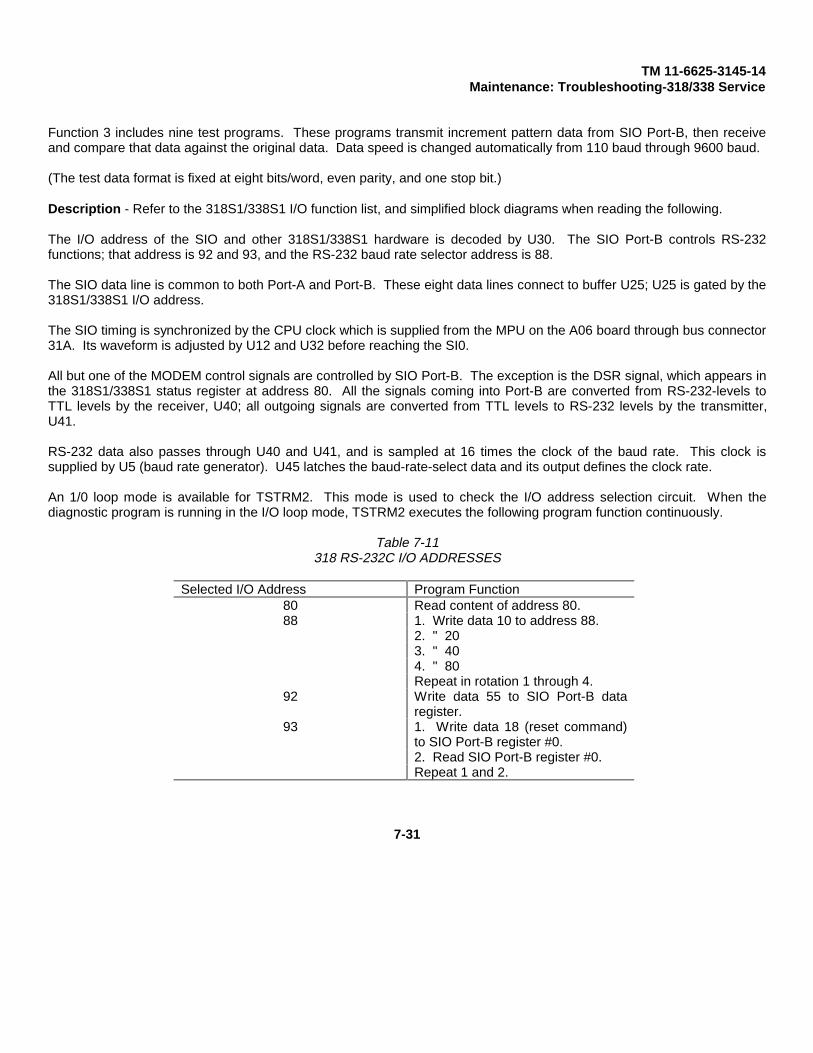
TM 11-6625-3145-14Maintenance: Troubleshooting-318/338 Service
Function 3 includes nine test programs. These programs transmit increment pattern data from SIO Port-B, then receiveand compare that data against the original data. Data speed is changed automatically from 110 baud through 9600 baud.
(The test data format is fixed at eight bits/word, even parity, and one stop bit.)
Description - Refer to the 318S1/338S1 I/O function list, and simplified block diagrams when reading the following.
The I/O address of the SIO and other 318S1/338S1 hardware is decoded by U30. The SIO Port-B controls RS-232functions; that address is 92 and 93, and the RS-232 baud rate selector address is 88.
The SIO data line is common to both Port-A and Port-B. These eight data lines connect to buffer U25; U25 is gated by the318S1/338S1 I/O address.
The SIO timing is synchronized by the CPU clock which is supplied from the MPU on the A06 board through bus connector31A. Its waveform is adjusted by U12 and U32 before reaching the SI0.
All but one of the MODEM control signals are controlled by SIO Port-B. The exception is the DSR signal, which appears inthe 318S1/338S1 status register at address 80. All the signals coming into Port-B are converted from RS-232-levels toTTL levels by the receiver, U40; all outgoing signals are converted from TTL levels to RS-232 levels by the transmitter,U41.
RS-232 data also passes through U40 and U41, and is sampled at 16 times the clock of the baud rate. This clock issupplied by U5 (baud rate generator). U45 latches the baud-rate-select data and its output defines the clock rate.
An 1/0 loop mode is available for TSTRM2. This mode is used to check the I/O address selection circuit. When thediagnostic program is running in the I/O loop mode, TSTRM2 executes the following program function continuously.
Table 7-11318 RS-232C I/O ADDRESSES
Selected I/O Address Program Function80 Read content of address 80.88 1. Write data 10 to address 88.
2. " 203. " 404. " 80Repeat in rotation 1 through 4.
92 Write data 55 to SIO Port-B dataregister.
93 1. Write data 18 (reset command)to SIO Port-B register #0.2. Read SIO Port-B register #0.Repeat 1 and 2.
7-31

TM 11-6625-3145-14Maintenance: Troubleshooting-318/338 Service
17. SERIAL TEST
Program: TSTSR1 (power on), TSTSR2 (Troubleshooting)
Setup: - Loop-back test data of TSTSR2 is supplied from the RS-232 port, so the P6107 SERIAL INPUT PROBE must beconnected to pin #2 of the RS-232 connector.
Function:
Power on - TSTSR1 initializes the SIO Port-A and reads the initial status. If the initial status is good, it loads dummy datainto the SIO and checks for any status change.
Troubleshooting - The TSTSR2 diagnostic program has the following three functions:
1. checks the SIO Port-A status2. checks external trigger circuit3. checks data passing through the circuit
Function 1 includes six test programs. These programs read the initial status of the SIO Port-A.
Function 2 includes two test programs. These programs control the external trigger transition and check the trigger statusin bit #1 of the 318S1/338S1 status register.
Function 3 includes eight test programs. These programs generate serial data (shift pattern data: 01 02 04 08 10 20 40) atpin #2 of the RS-232 connector. The programs also check incoming data at SIO Port-A. Serial data speed is changedautomatically during the test.
(The test data format is fixed at eight bits/word, even parity, and one stop bit. The data threshold is TTL, and data polarityis NEGATIVE.)
Description- Refer to the 318S1/338S1 1/0 function list and the simplified diagram of the Serial Acquisition and RS-232circuits when reading following.
SIO Port-A is used for serial data acquisition. The Port-A address is 90 and 91, and the SERIAL parameter selectoraddress is 8C.
U31 latches the baud select data, input data polarity bit, and the external trigger polarity bit. These are the parameters forserial acquisition control.
U6 generates the receive data sampling clock and supplies this clock to SIO pin #13. U22 switches the input clockselector from either the 19.2 K internal clock or the external clock, but the TSTSR2 program does not test this logic.
The external trigger polarity is defined by U12, and U22 latches on the transition of U12’s output. This status is initializedby writing data to address 84. External trigger status appears at bit 0 of the 318S1/338S1 status register; its address is 80.
The serial input data level is divided by 10 at input and this signal is amplified 2.5 times by U100 before reaching test point10. The data at test point 10 is compared with Threshold C (supplied from the RAM board through bus connector 39B) byU110; then data polarity is defined by U12 and supplied to SIO pin #12.
7-32

TM 11-6625-3145-14Maintenance: Troubleshooting-318/338 Service
The I/O loop feature is available for TSTSR2. This mode is used to check the I/O address selection circuit. When thediagnostic program is running in the I/O loop mode, TSTSR2 executes following program functions continuously.
Table 7-12318 SERIAL TEST I/O ADDRESSES
Selected I/O Address Program Function80 Read content of address 80.84 Write data to address 84.8C 1. Write data 10 to address 8C.
2. " 20 "3. " 40 "4. " 80 "Repeat in rotation 1 through 4.
90 Write data 55 to SIO Port-A dataregister.
91 1. Write data 18 (reset command) toSIO Port-A register #0.2. Read SIO Port-A register #0Repeat 1 and 2.
OPTION I/O FUNCTION LIST
I/O ADDRESS = 80CHIP = U32FUNCTION = OPTION STATUS REGISTERCONTROL = READ ONLY
bit= 7 6 5 4 3 2 1 0batterystatus
xxxxx xxxxx xxxxx xxxxx MODEM DSRstatus
externaltrigger
bit 0: ON = external trigger has occurred.OFF = external trigger has not occurred.
bit 1: ON = DSR signal is OFF.OFF = DSR signal is ON.
bit 7: ON = battery voltage is low. (<2.4 Volt)OFF = battery voltage is normal.
7-33

TM 11-6625-3145-14Maintenance: Troubleshooting-318/338 Service
I/O ADDRESS = 84CHIP = RESET TO U22-BFUNCTION = INITIALIZE THE EXTERNAL TRIGGERCONTROL = WRITE ONLY
bit = 7 6 5 4 3 2 1 0xxxxx xxxxx xxxxx xxxxx xxxxx xxxxx xxxxx xxxxx
NOTE: "xxxxx" data bit has no function.
I/O ADDRESS = 88CHIP = U45FUNCTION = RS-232 BAUD RATE SETUP REGISTERCONTROL = WRITE ONLY
bit= 7 6 5 4 3 2 1 0baud baud baud baudselect select select select xxxxx xxxxx xxxxx xxxxxas S3 as S2 as S1 as SO
Table 7-13318 SERIAL TEST BAUD SELECT BITS
S3 S2 S1 S0 Selected Baud RateOFF OFF OFF OFF NO CLOCK (EXTERNAL CLOCK)OFF OFF OFF ON NO CLOCK (19.2K)OFF OFF ON OFF 50OFF OFF ON ON 75OFF ON OFF OFF 134.5OFF ON OFF ON 200OFF ON ON OFF 600OFF ON ON ON 2400ON OFF OFF OFF 9600ON OFF OFF ON 4800ON OFF ON OFF 1800ON OFF ON ON 1200ON ON OFF OFF 2400ON ON OFF ON 300ON ON ON OFF 150ON ON ON ON 110
NOTE:The baud rate in the bracket is a special speed; it is used only for serial data acquisition.
7-34

TM 11-6625-3145-14Maintenance: Troubleshooting-318/338 Service
I/O ADDRESS = 8CCHIP = U31FUNCTION = SERIAL PARAMETER SETUP REGISTERCONTROL = WRITE ONLY
bit= 7 6 5 4 3 2 1 0baud baud baud baud external serialselect select select select trigger data xxxxx xxxxxas S3 as S2 as S1 as S0 pol. pol.
bit 7, 6, 5, 4: these bits are used to set the serial baud rate. S3, S2, S1, S0 select the baud rate in the same mannershown in RS-232 BAUD RATE SETUP REGISTER.
bit 3: ON = sets the external trigger direction to the trailing edge.OFF = sets the external trigger direction to the leading edge.
bit 2: ON = sets the serial input data polarity to negative.OFF = sets the serial input data polarity to positive.
I/O ADDRESS = 90CHIP = U2FUNCTION = READ DATA OF SERIAL PORTCONTROL = READ
1/O ADDRESS = 91CHIP = U2FUNCTION = SERIAL DATA ACQUISITION CONTROLCONTROL = READ AND WRITE
I/O ADDRESS = 92CHIP = U2FUNCTION = READ AND WRITE DATA OF RS-232 PORTCONTROL = READ AND WRITE
I/O ADDRESS = 93CHIP = U2FUNCTION = RS-232 MODEM SIGNAL AND DATA CONTROLCONTROL = READ AND WRITE
The SIO chip U2 contains the following four I/O address registers: addresses 90 and 91 are SIO Port-A registers, and 92and 93 are SIO Port-B registers. Control addresses 91 and 93 include three read-only and eight write-only internalregisters. These internal registers control and check all SIO functions.
Details of the SIO internal register functions are described in the Z80 SIO Manual by ZILOG, SHARP, and MOSTEK.
7-35

TM 11-6625-3145-14Maintenance: Troubleshooting-318/338 Service
Table 7-14318 DIAGNOSTIC TEST FAILURE CODES
PART 1 --- TSTRM2 (RS232 TEST)
Code Error Information150 (96) RTS NOT ON151 (97) CTS NOT ON152 (98) CD NOT ON153 (99) RTS NOT OFF154 (9A) CTS NOT OFF155 (9B) CD NOT OFF156 (9C) DTR NOT ON157 (9D) DSR NOT ON158 (9E) REGISTER #0 READ ERROR (FOR SIO PORT-B)159 (9F) RECEIVE READY FLAG NOT ON ( " " )160 (A0) TRANSMIT EMPTY FLAG NOT OFF ( " " )162 (A2) REGISTER #1 READ ERROR ( " " )163 (A3) FRAMING ERROR FLAG NOT OFF ( " " )164 (A4) OVER RUN ERROR FLAG NOT OFF ( " " )165 (A5) PARITY ERROR FLAG NOT OFF ( " " )170 (AA) INCREMENT PATTERN DATA (01-FF) LOOP BACK TEST
(FROM RS-232 OUTPUT TO RS-232 INPUT)ERROR AT 110 BAUD
171 (AB) " " " 150 BAUD172 (AC) " " " 300 BAUD173 (AD) " " " 600 BAUD174 (AE) " " " 1200 BAUD175 (AF) " " " 2400 BAUD176 (B0) " " " 4800 BAUD177 (B1) 9600 BAUD178 (B2) INTERRUPT MODE DATA LOOP-BACK TEST ERROR AT 9600 BAUD
7-36

TM 11-6625-3145-14Maintenance: Troubleshooting-318/338 Service
Table 7-14 (cont.)318 DIAGNOSTIC TEST FAILURE CODES
PART 2 --- TSTSR2 (SERIAL TEST)
Code Error Information180 (B4) REG #0 READ ERROR (FOR SIO PORT-A)181 (B5) RX READY NOT OFF ( " " )182 (B6) REG #1 READ ERROR ( " " )183 (B7) FRAMING-ERR BIT NOT OFF ( " " )184 (B8) OVER RUN-ERR BIT NOT OFF ( " " )185 (B9) PARITY-ERR BIT NOT OFF ( " " )186 (BA) EXT-TRIG BIT NOT OFF187 (BB) EXT-TRIG BIT NOT ON188 (BC) DATA LOOP-BACK TEST ERROR AT 75 BAUD
(FROM RS-232 OUTPUT TO SERIAL INPUT)189 (BD) " " " 200 BAUD190 (BE) " " " 2400 BAUD191 (BF) " " " 1800 BAUD192 (C0) " " " 1200 BAUD193 (C1) " " " 300 BAUD194 (C2) " " " 110 BAUD195 (C3) " " " 9600 BAUD
7-37

TM 11-6625-3145-14Maintenance: Troubleshooting-318/338 Service
Table 7-14 (cont.)318 DIAGNOSTIC TEST FAILURE CODES
PART 3 --- TSTNV2 (NVM TEST)
Code Error Information200 (C8) DATA ERROR WHEN DATA PATTERN IS FF201 (C9) " " " 00202 (CA) " " " 01203 (CB) " " " 02204 (CC) " " " 04205 (CD) " " " 08206 (CE) " " " 10207 (CF) " " " 20208 (D0) " " " 40209 (D1) " " " 80210 (D2) " " " MARCHING PATTERN211 (D3) " " " INCREMENTING PATTERN
7-38

TM 11-6625-3145-14Maintenance: Troubleshooting-318/338 Service
Figure 7-12. Troubleshooting Tree 1: Power On.
FIGURE 7-14
FIGURE 7-15
FIGURE 7-16
FIGURE 7-13
7-39
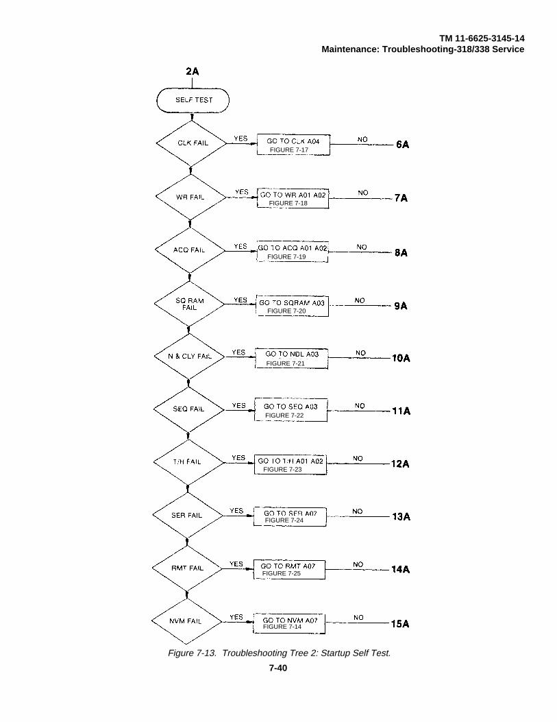
TM 11-6625-3145-14Maintenance: Troubleshooting-318/338 Service
Figure 7-13. Troubleshooting Tree 2: Startup Self Test.
FIGURE 7-17
FIGURE 7-18
FIGURE 7-19
FIGURE 7-20
FIGURE 7-21
FIGURE 7-22
FIGURE 7-23
FIGURE 7-24
FIGURE 7-25
FIGURE 7-14
7-40
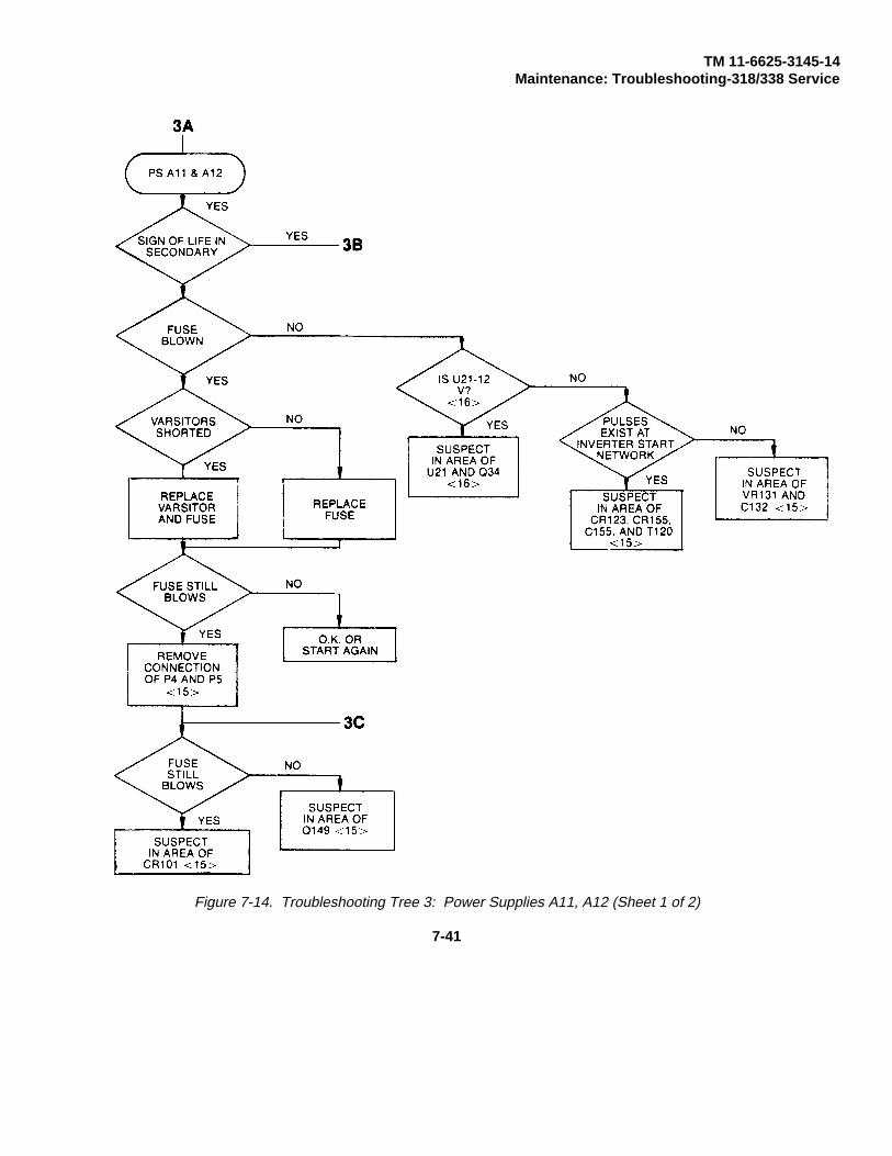
TM 11-6625-3145-14Maintenance: Troubleshooting-318/338 Service
Figure 7-14. Troubleshooting Tree 3: Power Supplies A11, A12 (Sheet 1 of 2)
7-41

TM 11-6625-3145-14Maintenance: Troubleshooting-318/338 Service
3B
Figure 7-14. Troubleshooting Tree 3: Power Supplies A11, A12 (Sheet 2 of 2)
7-42

TM 11-6625-3145-14Maintenance: Troubleshooting-318/338 Service
Figure 7-15. Troubleshooting Tree 4: CRT A10 (Sheet 1 of 4)
7-43
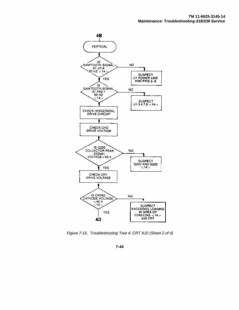
TM 11-6625-3145-14Maintenance: Troubleshooting-318/338 Service
Figure 7-15. Troubleshooting Tree 4: CRT A10 (Sheet 2 of 4)
7-44

TM 11-6625-3145-14Maintenance: Troubleshooting-318/338 Service
Figure 7-15. Troubleshooting Tree 4: CRT A10 (Sheet 3 of 4)
7-45

TM 11-6625-3145-14Maintenance: Troubleshooting-318/338 Service
Figure 7-15. Troubleshooting Tree 4: CRT A10 (Sheet 4 of 4)
7-46

TM 11-6625-3145-14Maintenance: Troubleshooting-318/338 Service
Figure 7-16. Troubleshooting Tree 5: MPU A06. (Sheet 1 of 5)
7-47

TM 11-6625-3145-14Maintenance: Troubleshooting-318/338 Service
Figure 7-16. Troubleshooting Tree 5: MPU A06. (Sheet 2 of 5)
7-48
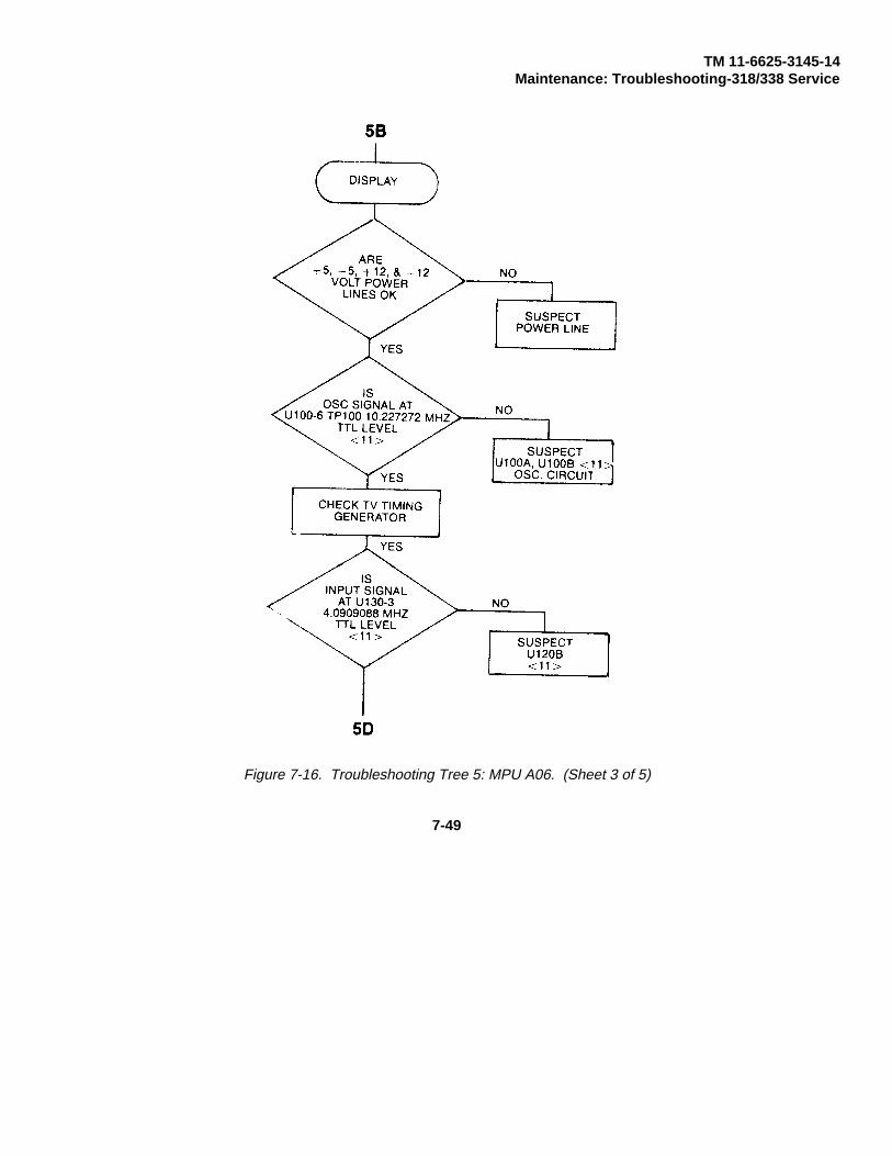
TM 11-6625-3145-14Maintenance: Troubleshooting-318/338 Service
Figure 7-16. Troubleshooting Tree 5: MPU A06. (Sheet 3 of 5)
7-49
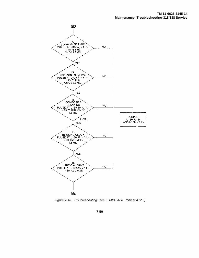
TM 11-6625-3145-14Maintenance: Troubleshooting-318/338 Service
Figure 7-16. Troubleshooting Tree 5: MPU A06. (Sheet 4 of 5)
7-50

TM 11-6625-3145-14Maintenance: Troubleshooting-318/338 Service
Figure 7-16. Troubleshooting Tree 5: MPU A06. (Sheet 5 of 5)
7-51
FIGURE 7-15
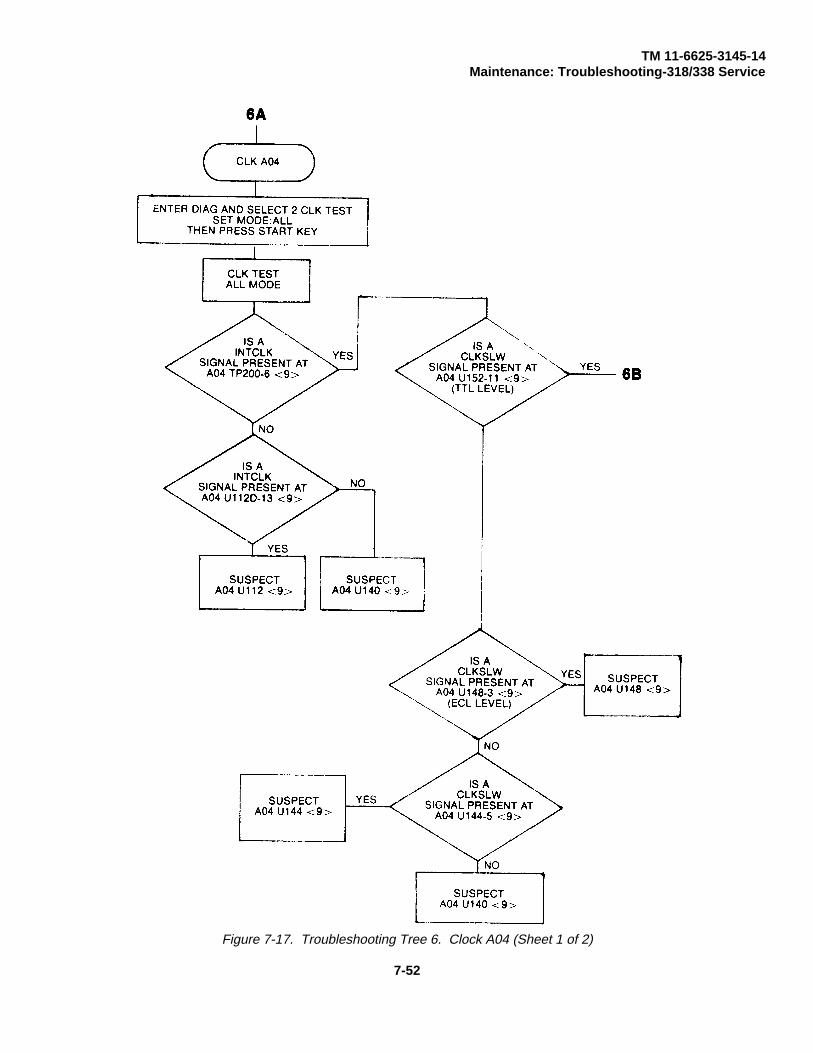
TM 11-6625-3145-14Maintenance: Troubleshooting-318/338 Service
Figure 7-17. Troubleshooting Tree 6. Clock A04 (Sheet 1 of 2)
7-52

TM 11-6625-3145-14Maintenance: Troubleshooting-318/338 Service
Figure 7-17. Troubleshooting Tree 6. Clock A04 (Sheet 2 of 2)
7-53
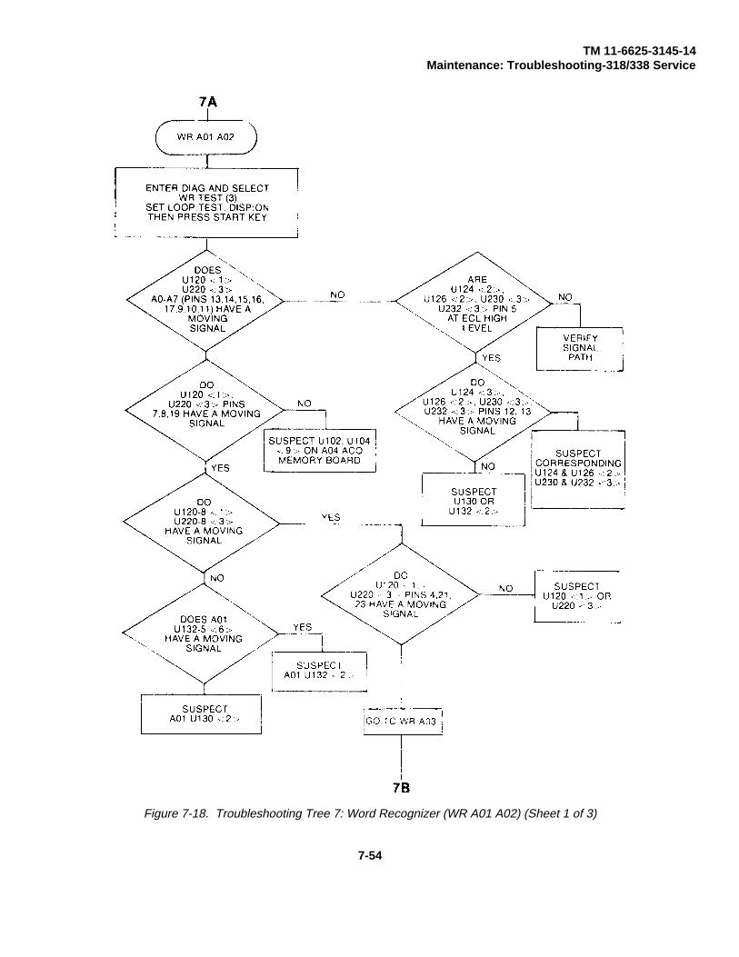
TM 11-6625-3145-14Maintenance: Troubleshooting-318/338 Service
Figure 7-18. Troubleshooting Tree 7: Word Recognizer (WR A01 A02) (Sheet 1 of 3)
7-54

TM 11-6625-3145-14Maintenance: Troubleshooting-318/338 Service
Figure 7-18. Troubleshooting Tree 7: Word Recognizer (WR A01 A02) (Sheet 2 of 3)
7-55
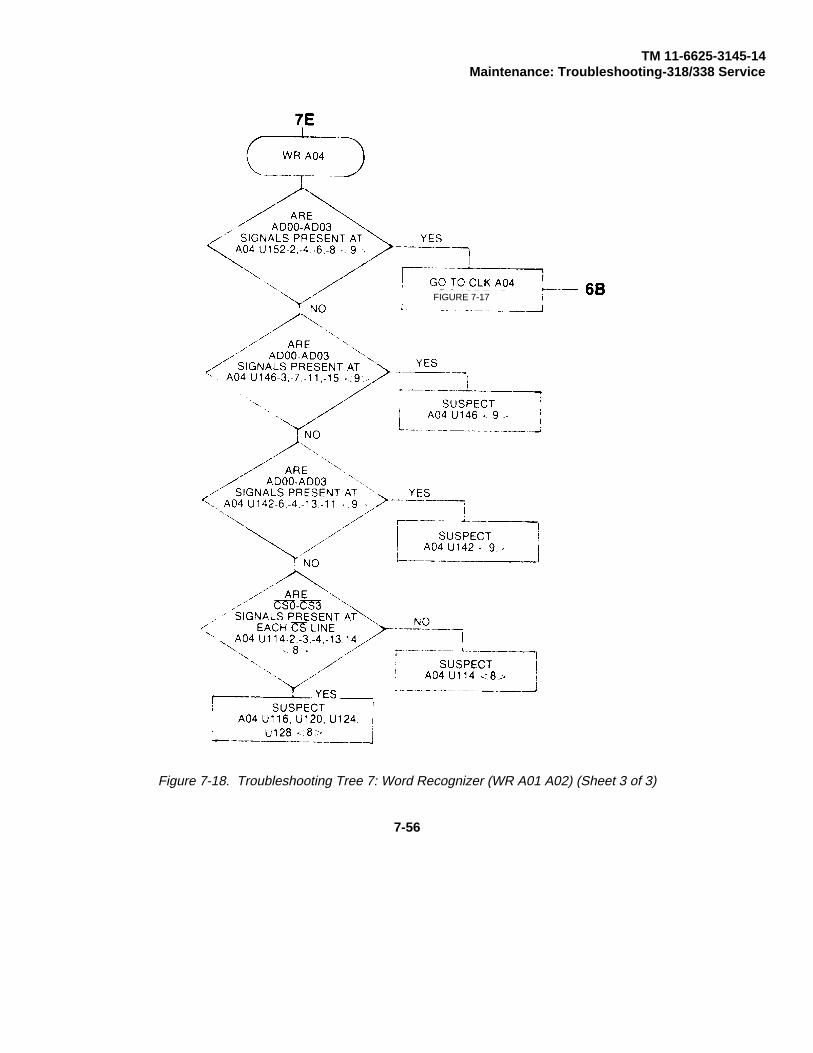
TM 11-6625-3145-14Maintenance: Troubleshooting-318/338 Service
Figure 7-18. Troubleshooting Tree 7: Word Recognizer (WR A01 A02) (Sheet 3 of 3)
7-56
FIGURE 7-17

TM 11-6625-3145-14Maintenance: Troubleshooting-318/338 Service
Figure 7-19. Troubleshooting Tree 8: Data Acquisition (ACQ A01 A02) (Sheet 1 of 6)
7-57

TM 11-6625-3145-14Maintenance: Troubleshooting-318/338 Service
Figure 7-19. Troubleshooting Tree 8: Data Acquisition (ACQ A01 A02) (Sheet 2 of 6)
7-58
FIGURE 7-18

TM 11-6625-3145-14Maintenance: Troubleshooting-318/338 Service
Figure 7-19. Troubleshooting Tree 8: Data Acquisition (ACO A01 A02) (Sheet 3 of 6)
7-59

TM 11-6625-3145-14
Figure 7-19. Troubleshooting Tree 8: Data Acquisition (ACQ A01 A02) (Sheet 4 of 6)
7-60

TM 11-6625-3145-14Maintenance: Troubleshooting-318/338 Service
Figure 7-19. Troubleshooting Tree 8: Data Acquisition (ACQ A01 A02) (Sheet 5 of 6)
7-61
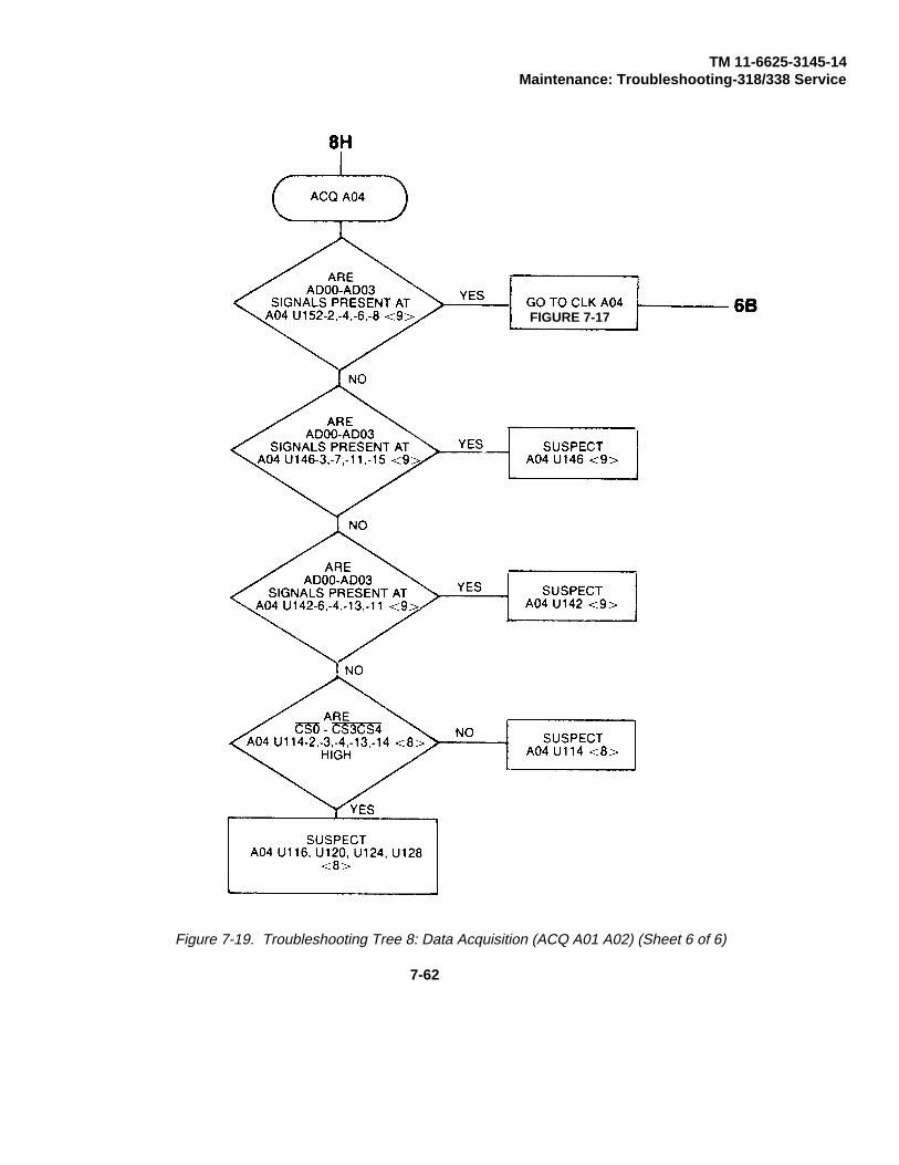
TM 11-6625-3145-14Maintenance: Troubleshooting-318/338 Service
Figure 7-19. Troubleshooting Tree 8: Data Acquisition (ACQ A01 A02) (Sheet 6 of 6)
FIGURE 7-17
7-62
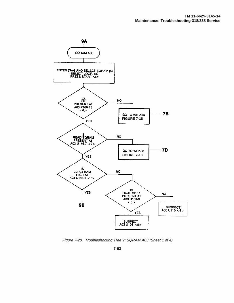
TM 11-6625-3145-14Maintenance: Troubleshooting-318/338 Service
Figure 7-20. Troubleshooting Tree 9: SQRAM A03 (Sheet 1 of 4)
FIGURE 7-18
FIGURE 7-18
7-63

TM 11-6625-3145-14Maintenance: Troubleshooting-318/338 Service
Figure 7-20. Troubleshooting Tree 9: SQRAM A03 (Sheet 2 of 4)
7-64

TM 11-6625-3145-14Maintenance: Troubleshooting-318/338 Service
Figure 7-20. Troubleshooting Tree 9: SQRAM A03 (Sheet 3 of 4)
FIGURE 7-31
7-65

TM 11-6625-3145-14Maintenance: Troubleshooting-318/338 Service
Figure 7-20. Troubleshooting Tree 9: SORAM A03 (Shoot 4 of 4)
FIGURE 7-17
7-66

TM 11-6625-3145-14Maintenance: Troubleshooting-318/338 Service
Figure 7-21. Troubleshooting Tree 10: NDL A03 (Sheet 1 of 2)
FIGURE 7-22
7-67

TM 11-6625-3145-14Maintenance: Troubleshooting-318/338 Service
Figure 7-21. Troubleshooting Tree 10: NDL A03 (Sheet 2 of 2)
FIGURE 7-22
7-68

TM 11-6625-3145-14Maintenance: Troubleshooting-318/338 Service
Figure 7-22. Troubleshooting Tree 11: SEQ A03 (Sheet 1 of 4)
FIGURE 7-18
7-69

TM 11-6625-3145-14Maintenance: Troubleshooting-318/338 Service
Figure 7-22. Troubleshooting Tree 11: SEQ A03 (Sheet 2 of 4)
FIGURE 7-20
7-70
FIGURE 7-19

TM 11-6625-3145-14Maintenance: Troubleshooting-318/338 Service
Figure 7-22. Troubleshooting Tree 11: SEQ A03 (Sheet 3 of 4)
FIGURE 7-19
7-71

TM 11-6625-3145-14Maintenance: Troubleshooting-318/338 Service
Figure 7-22. Troubleshooting Tree 11: SEQ A03 (Sheet 4 of 4)
FIGURE 7-20
7-72
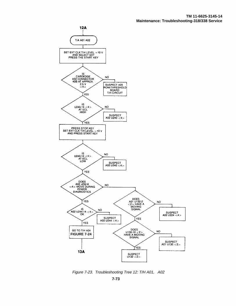
TM 11-6625-3145-14Maintenance: Troubleshooting-318/338 Service
Figure 7-23. Troubleshooting Tree 12: T/H A01, A02
FIGURE 7-24
7-73
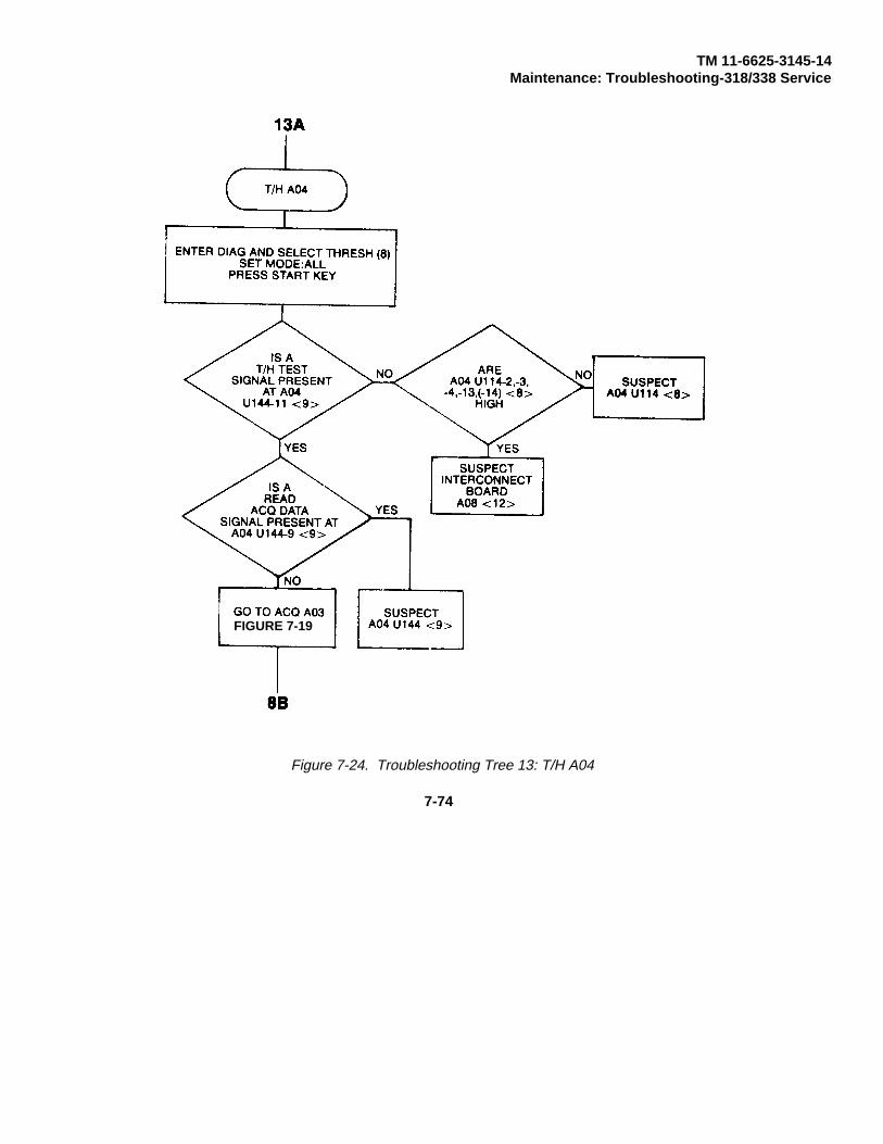
TM 11-6625-3145-14Maintenance: Troubleshooting-318/338 Service
Figure 7-24. Troubleshooting Tree 13: T/H A04
FIGURE 7-19
7-74

TM 11-6625-3145-14Maintenance: Troubleshooting-318/338 Service
Figure 7-25. Troubleshooting Tree 14: SER A07 (TSTSR2) (Sheet 1 of 4)
7-75

TM 11-6625-3145-14Maintenance: Troubleshooting-318/338 Service
Figure 7-25. Troubleshooting Tree 14: SER A07 (TSTSR2) (Sheet 2 of 4)
7-76

TM 11-6625-3145-14Maintenance: Troubleshooting-318/338 Service
Figure 7-25. Troubleshooting Tree 14: SER A07 (TSTSR2) (Sheet 3 of 4)
7-77
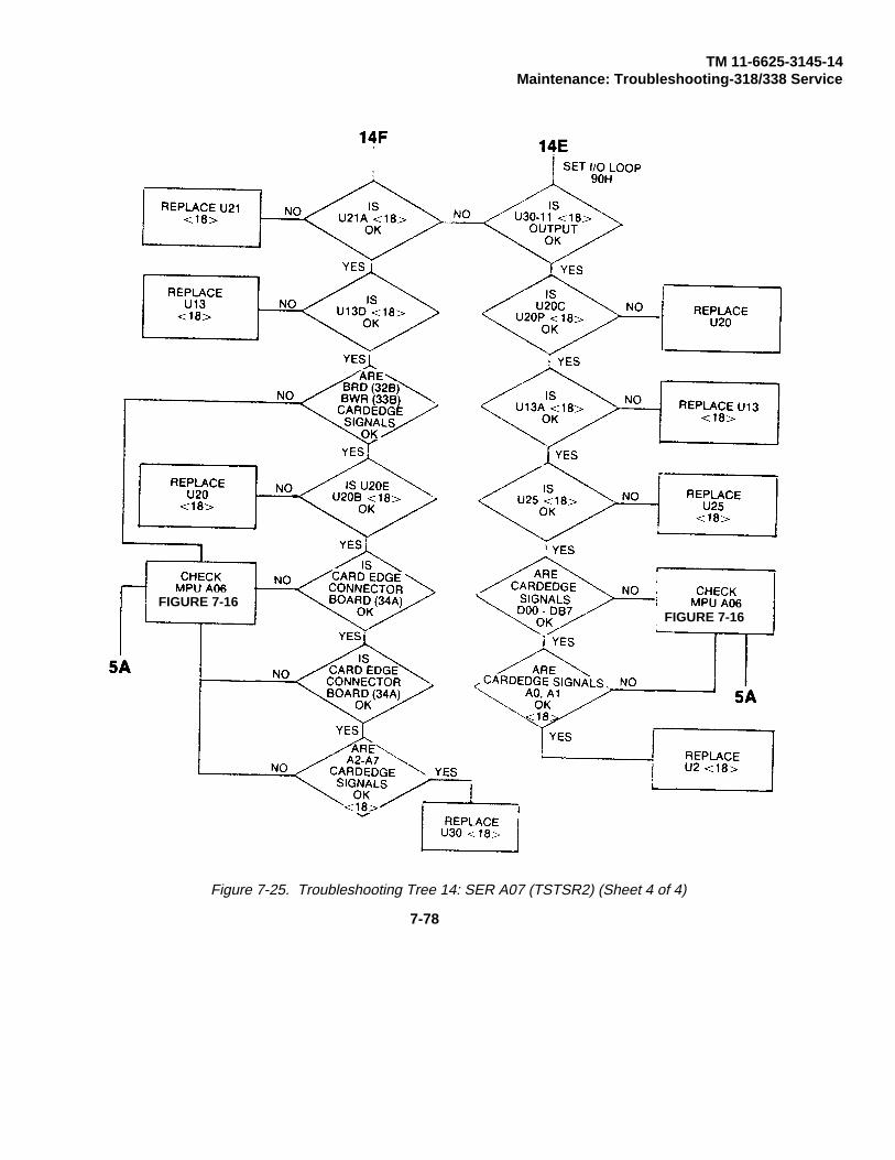
TM 11-6625-3145-14Maintenance: Troubleshooting-318/338 Service
Figure 7-25. Troubleshooting Tree 14: SER A07 (TSTSR2) (Sheet 4 of 4)
FIGURE 7-16FIGURE 7-16
7-78
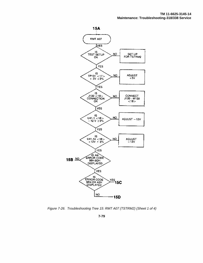
TM 11-6625-3145-14Maintenance: Troubleshooting-318/338 Service
Figure 7-26. Troubleshooting Tree 15: RMT A07 (TSTRM2) (Sheet 1 of 4)
7-79

TM 11-6625-3145-14Maintenance: Troubleshooting-318/338 Service
Figure 7-26. Troubleshooting Tree 15: RMT A07 (TSTRM2) (Sheet 2 of 4)
FIGURE 7-16FIGURE 7-48
FIGURE 7-16
7-80

TM 11-6625-3145-14Maintenance: Troubleshooting-318/338 Service
Figure 7-26. Troubleshooting Tree 15: RMT A07 (TSTRM2) (Sheet 3 of 4)
FIGURE 7-16
7-81
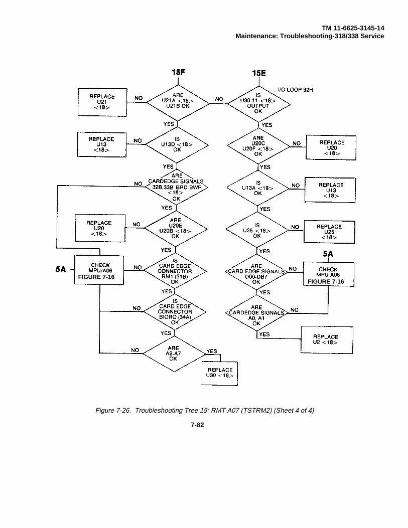
TM 11-6625-3145-14Maintenance: Troubleshooting-318/338 Service
Figure 7-26. Troubleshooting Tree 15: RMT A07 (TSTRM2) (Sheet 4 of 4)
FIGURE 7-16FIGURE 7-16
7-82
TM 11-6625-3145-14Maintenance: Troubleshooting-318/338 Service
Figure 7-27. Troubleshooting Tree 16: Non-Volatile Memory (NVM A07) (Sheet 1 of 2)
FIGURE 7-16
7-83
TM 11-6625-3145-14Maintenance: Troubleshooting-318/338 Service
Figure 7-27. Troubleshooting Tree 16: Non-Volatile Memory (NVM A07) (Sheet 2 of 2)
FIGURE 7-16
7-84

TM 11-6625-3145-14Maintenance: Troubleshooting-318/338 Service
Figure 7-28. Troubleshooting Tree 17: Can’t Get Glitch.
FIGURE 7-29
FIGURE 7-29
7-85
TM 11-6625-3145-14Maintenance: Troubleshooting-318/338 Service
Figure 7-29. Troubleshooting Tree 18: Can’t Get Good Data (Sheet 1 of 2)
7-86
TM 11-6625-3145-14Maintenance: Troubleshooting-318/338 Service
Figure 7-29. Troubleshooting Tree 18: Can’t Get Good Data (Sheet 2 of 2)
7-87

TM 11-6625-3145-14Maintenance: Troubleshooting-318/338 Service
Figure 7-30. Troubleshooting Tree 19: Diagnostics Pass Can’t Stop. (Sheet 1 of 2)
FIGURE 7-29
7-88

TM 11-6625-3145-14Maintenance: Troubleshooting-318/338 Service
Figure 7-30. Troubleshooting Tree 19: Diagnostics Pass Can’t Stop. (Sheet 2 of 2)
7-89

TM 11-6625-3145-14Maintenance: Troubleshooting-318/338 Service
Figure 7-31. Troubleshooting Tree 20: Can’t Get Glitch Trigger
FIGURE 7-19
7-90

338TROUBLESHOOTING
TREES
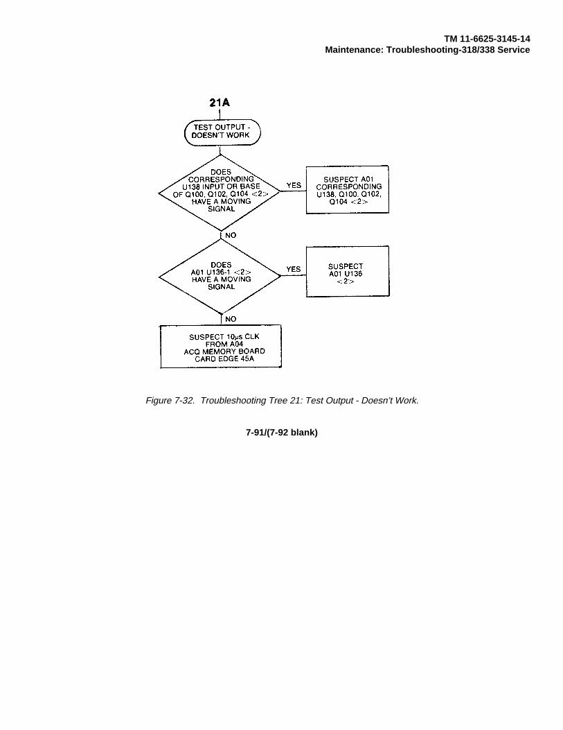
TM 11-6625-3145-14Maintenance: Troubleshooting-318/338 Service
Figure 7-32. Troubleshooting Tree 21: Test Output - Doesn’t Work.
7-91/(7-92 blank)

TM 11-6625-3145-14Maintenance: Troubleshooting-318/338 Service
338 DIAGNOSTIC TEST DESCRIPTIONS
This part of Section 7 contains information about the 338 diagnostics tests and troubleshooting trees. The diagnostic testdescriptions and trees for the 318 are located in the first half of this section. Refer to the page-edge tabs for help inlocating the information you need.
INDEX OF 338 DIAGNOSTIC TEST DESCRIPTIONS
Mainframe1. Keyboard Test
2. CRT Test
3. Jump Table ROM Test
4. Display RAM Test
5. SYSTEM RAM Test
6. ROM Test
Parallel Analyzer7. Clock Test
8. Word Recognizer Test
9. ACQ RAM Test
10. Sequence RAM Test
11. N & DELAY Counter Test
12. Threshold Test
13. SEQ Test
318S1 Serial Analysis/RS-232C/NVM14. Battery Test
15. Non-Volatile Memory Test
16. RS-232 Test
17. Serial Test
338 DIAGNOSTIC TEST COMMON SIGNAL PATHS
Some Diagnostic Tests share a common signal path for setting up or reading data. When two or more Diagnostic teststhat shares the same signal path indicate a failure, the components in the path may be the cause of the test failure.
Table 7-15 lists the components common to the signal paths that cause multiple Diagnostic Test failures.
7-93

TM 11-6625-3145-14Maintenance: Troubleshooting-318/338 Service
Table 7-15338 DIAGNOSTIC TEST COMMON SIGNAL PATHS
Clock Threshold WR ACQ SQRAM N&DL SEQ Component
X X X X X X X A04 U152, A04U150 A03 U126,A03 U112 A04 U110
X X X X X A04 U146, A04U142 A04 U114,A03 U112 A04 U110
X X A03 U156, A03U158 A03 U112,A04 U110 A04 U148(VBB)
X X X A04 U148, A04U144 A03 U112,A04 U110
X X A03 U146, A03U108 A03 U126,A03 U112
X X X A01U 100 to U114A02 U202 to U216A02 U224, A02U240 A01 U124,A01 U126 A02U230, A02 U232A01 U130, A01U132
X X A03 U106, A03U108 A03 U114,A03 U116 A03U118, A03 U130A03 U142
X X A03 U106, A03U108 A03 U114,A03 U116 A03U118, A03 U130A03 U132, A03U142 A03 U140,A03 U156
7-94

TM 11-6625-3145-14Maintenance: Troubleshooting-318/338 Service
MAINFRAME
1. KEYBOARD TEST
Program: KBD
Function:
Power on - When power is turned on, the KBD program checks the keyboard to see if any keys are stuck in the closedposition. The MPU reads the resulting data at address E0hex and verifies that all data bits are low.
Troubleshooting - The keyboard generates an interrupt and sends a corresponding key code to the MPU when any keyexcept the STOP key is pressed. The MPU reads the key code at E0hex upon receiving the interrupt from the keyboardand blinks the corresponding rectangle in the key array on the screen. This function also provides a check to see thateach key (except the STOP key) is providing the correct key code to the MPU.
The STOP key is used to exit this program; thus, the STOP key can be checked at the end of this test.
Description: Refer to Figure 7-33. Key codes are generated by the A09 board when any key is pressed. The Y-lines andX-lines of the key matrix on the A09 board (excepting the STOP key) are connected to U300 and U310 (8-bit priorityencoder, 4053BP) on the A06 MPU/Display board through the A08 Mother board. U310 is enabled when U300 receives akey signal and issues a INT (Maskable Interrupt) to the MPU through the CR timer circuit. The INT is controlled by U220(NAND gate, TC4093) on the A06 board with KBMASKP from U100 (hex D-type flip-flop with reset, 74LS174) on the A05ROM/Threshold board.
The STOP key on the A09 board generates the NMI (Non-Maskable Interrupt) directly to the MPU through the A08 boardwithout decoding, though it is buffered by U200 (inverter, TC4093) on the A06 board. This signal is also controlled by theCR timer to avoid key chattering.
The MPU reads the key code from U320 (octal buffer/line driver with tri-state output, 40H244) on the A06 board, usually oninterrupt at E0hex. KBCSP, which enables this buffer, is delivered from U092A (dual 2-line to 4-line decoder/demultiplexer)on the A05 board when the MPU accesses I/O address E0hex.
A key code with interrupt is expected as follows:
Table 7-16338 KEYBOARD TEST KEY CODE AND INTERRUPT ASSIGNMENT
7 6 5 4 3 2 1 0
ST 0 D5 D4 D3 D2 D1 D0
ST:1 if any key is pressed, otherwise 0.
7-95
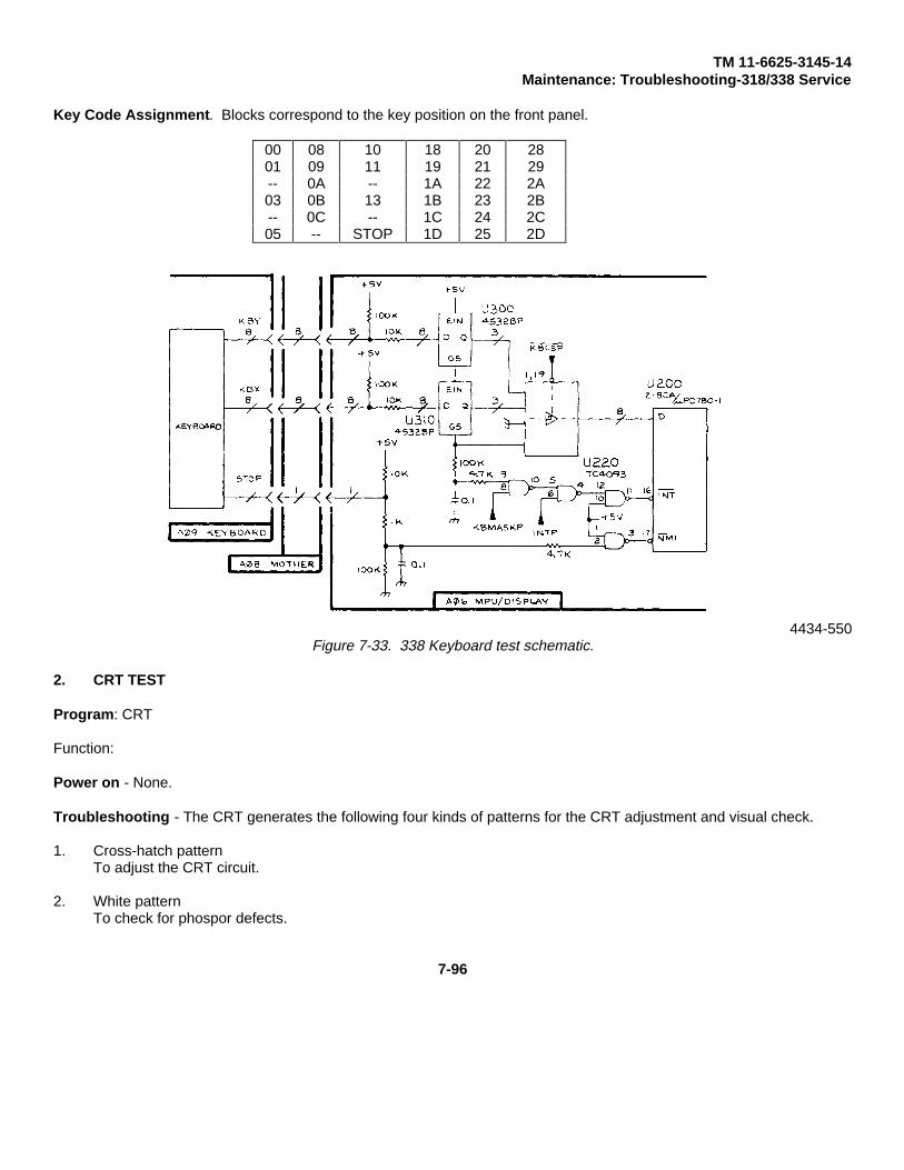
TM 11-6625-3145-14Maintenance: Troubleshooting-318/338 Service
Key Code Assignment. Blocks correspond to the key position on the front panel.
00 08 10 18 20 2801 09 11 19 21 29-- 0A -- 1A 22 2A03 0B 13 1B 23 2B-- 0C -- 1C 24 2C05 -- STOP 1D 25 2D
4434-550Figure 7-33. 338 Keyboard test schematic.
2. CRT TEST
Program: CRT
Function:
Power on - None.
Troubleshooting - The CRT generates the following four kinds of patterns for the CRT adjustment and visual check.
1. Cross-hatch patternTo adjust the CRT circuit.
2. White patternTo check for phospor defects.
7-96

TM 11-6625-3145-14Maintenance: Troubleshooting-318/338 Service
3. All character fonts for the parallel analyzer mode. To check the CRT circuit and the Character ROM (CROM) forparallel operation.
4. All character fonts for the serial state analyzer mode. To check the CRT circuit and the CROM for serial operation.
Description: Refer to Figure 7-34. The CRT displays 32 characters by 20 lines of data from the Display RAM U515 (16 K-bit static CMOS RAM, uPD446/HM6116P) on the A06 MPU/Display board. Each character in the CRT display uses twobytes of data, consisting of one selection code followed by one character code. A total of 1280 bytes of the Display RAMare used, ranging from address E800 to ECFF.
The MPU writes these two bytes of data for each character to be displayed into the Display RAM through both U525 (octalbus transceiver, 40H245) and U500 (display controller, MB62110) on the A06 board.
The Display Controller sends the first address to the Display RAM to select the character code to be displayed, andinstructs U520 (octal D type flip-flop, 40H273) on the A06 board to store the out-put data from the Display RAM. This datais supplied to the Character ROM U530 (32 K-bits mask ROM, 2332) on the A06 board to select the character font. TheDisplay Controller receives this font code and sends the second address to the Display RAM to get a control code.
The Display Controller then issues Z, GLITCH, CHD, and VD signals to the A10 CRT board, along with these two bytes ofdata. These signals are buffered and/or controlled and sent to the A10 board through the A08 Mother board.
4434-556Figure 7-34. 338 CRT calibration and check schematic.
7-97

TM 11-6625-3145-14Maintenance: Troubleshooting-318/338 Service
3. JUMP TABLE ROM TEST
Program:
Function:
Power on - The Jump Table ROM, which contains the diagnostic test routine, is checked by calculating its checksum fromC000 to DFFF.
Troubleshooting - None.
Description: The diagnostic routine is located in addresses C000 through DFFF in the Jump Table ROM, U026 (64 K-byteUV EPROM, 2764) on the A05 ROM/Threshold board.
Figure 7-35. 338 Memory map.
The MPU addresses the Jump Table ROM on board A05 through U210 and U212 (OCTAL BUFFER/LINE RECEIVERWITH 3-STATE OUTPUT, 74LS244) on the A06 MPU/DISPLAY board via the A08 Mother board.
7-98

TM 11-6625-3145-14Maintenance: Troubleshooting-318/338 Service
ROM7 enables the read operation of the Jump Table ROM. It is generated by U005 (dual 2-line to 4-linedecoder/demultiplexer, 74LS139). U001 (74LS139) on the A05 board decodes the BM1, BMREQ, and AB11 throughAB15 signals.
The MPU reads the output data from the Jump Table ROM U026 through U045 (octal bus transceiver with tri-state output,74LS245) and through the A08 board.
The MPU calculates the checksum with all the data contained in the Jump Table ROM, and compares it with the expectedvalue, also stored in this ROM. If the values do not match the MPU issues an error message.
4. DISPLAY RAM TEST
Program:
Function:
Power on The Display RAM is checked with a checkerboard marching pattern from E800 to EFFF. (A checkerboardmarching pattern is an alternating 0 and 1 pattern that is loaded into a memory location, checked, shifted, and checkedagain.)
Step 1. The word 55 is written into all RAM addresses.
Step 2. A word is read from a diagnostic cell and compared with the expected word 55. If it is not equal to 55, an errormessage is displayed and the MPU is halted.
Step 3. If the previous test is successfully completed, the word AA is written into that cell. Then a word in the same cell isread back and is compared with AA. If it is not equal to AA, an error message is displayed and the MPU is halted.
Step 4. Steps 2 and 3 are repeated for all RAM addresses.
Troubleshooting - None.
Description: The read and write operation on the Display RAM U515 (16 K-bit static CMOS RAM, uPD446/HM6116P) onthe A06 MPU/Display board is completely controlled by Display Controller U500 (Display Controller, MB62110) on the A06board.
The MPU reads/writes data from/to the Display RAM through U525 (octal bus transceiver, 40H245) on the A06 board,which is enabled by the Display Controller and has the data direction specified (read or write) by the MPU’s read signal.The addresses to the Display RAM are supplied by both the MPU and the Display Controller, however the addresses fromthe MPU are sent to the Display Controller and the Display Controller gates these signals to the Display RAM.
If there is competition between the MPU and the Display Controller for access to the Display RAM, the Display Controllerforces the MPU to wait until it completes the current read operation by asserting the WAIT signal to the MPU.
The MPU checks the Display RAM with the checkerboard marching pattern. The read and write sequences have alreadybeen mentioned in the Power on paragraph at the begining of this section. If the data read is incorrect, the MPU will issuean error message.
7-99
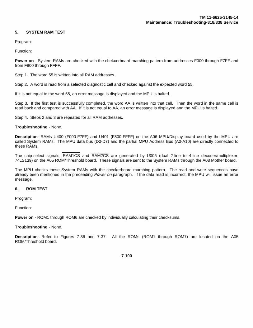
TM 11-6625-3145-14Maintenance: Troubleshooting-318/338 Service
5. SYSTEM RAM TEST
Program:
Function:
Power on - System RAMs are checked with the chekcerboard marching pattern from addresses F000 through F7FF andfrom F800 through FFFF.
Step 1. The word 55 is written into all RAM addresses.
Step 2. A word is read from a selected diagnostic cell and checked against the expected word 55.
If it is not equal to the word 55, an error message is displayed and the MPU is halted.
Step 3. If the first test is successfully completed, the word AA is written into that cell. Then the word in the same cell isread back and compared with AA. If it is not equal to AA, an error message is displayed and the MPU is halted.
Step 4. Steps 2 and 3 are repeated for all RAM addresses.
Troubleshooting - None.
Description: RAMs U400 (F000-F7FF) and U401 (F800-FFFF) on the A06 MPU/Display board used by the MPU arecalled System RAMs. The MPU data bus (D0-D7) and the partial MPU Address Bus (A0-A10) are directly connected tothese RAMs.
The chip-select signals, RAM1CS and RAM2CS are generated by U005 (dual 2-line to 4-line decoder/multiplexer,74LS139) on the A05 ROM/Threshold board. These signals are sent to the System RAMs through the A08 Mother board.
The MPU checks these System RAMs with the checkerboard marching pattern. The read and write sequences havealready been mentioned in the preceeding Power on paragraph. If the data read is incorrect, the MPU will issue an errormessage.
6. ROM TEST
Program:
Function:
Power on - ROM1 through ROM6 are checked by individually calculating their checksums.
Troubleshooting - None.
Description: Refer to Figures 7-36 and 7-37. All the ROMs (ROM1 through ROM7) are located on the A05ROM/Threshold board.
7-100
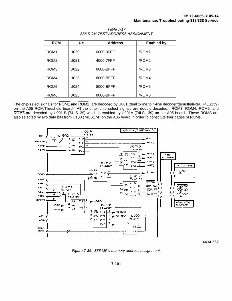
TM 11-6625-3145-14Maintenance: Troubleshooting-318/338 Service
Table 7-17338 ROM TEST ADDRESS ASSIGNMENT
ROM U# Address Enabled by
ROM1 U020 0000-3FFF /ROM1
ROM2 U021 4000-7FFF /ROM2
ROM3 U022 8000-BFFF /ROM3
ROM4 U023 8000-BFFF /ROM4
ROM5 U024 8000-BFFF /ROM5
ROM6 U025 8000-BFFF /ROM6
The chip-select signals for ROM1 and ROM2 are decoded by U001 (dual 2-line to 4-line decoder/demultiplexer, 74LS139)on the A05 ROM/Threshold board. All the other chip select signals are doubly decoded. ROM3, ROM4, ROM5, andROM6 are decoded by U001 B (74LS139) which is enabled by U001A (74LS 139) on the A05 board. These ROMS arealso selected by two data bits from U100 (74LS174) on the A05 board in order to constitute four pages of ROMs.
4434-562
Figure 7-36. 338 MPU memory address assignment.
7-101

TM 11-6625-3145-14Maintenance: Troubleshooting-318/338 Service
The MPU reads data from these ROMs through U045 (octal bus transceiver with tri-state output, 74LS245) on the A05board and through the A08 Mother board. The MPU addresses are sent to these ROMs and the decoders (74LS139) onthe A05 board via U210 and U212 (octal buffer/line driver with tri-state output, 74LS 244) on the A06 MPU/Display boardand through the A08 board. The MPU control signals are also provided through U214 (octal buffer/line driver with tri-stateoutput, 74LS240) on the A06 board and through the A08 board.
The MPU calculates the checksum for each ROM and determines whether it is correct or not. If it is incorrect, an errormessage will be displayed.
7-102

TM 11-6625-3145-14Maintenance: Troubleshooting-318/338 Service
Figure 7-37. 338 A03 and A04 partial ACQ address assignment.
7-103
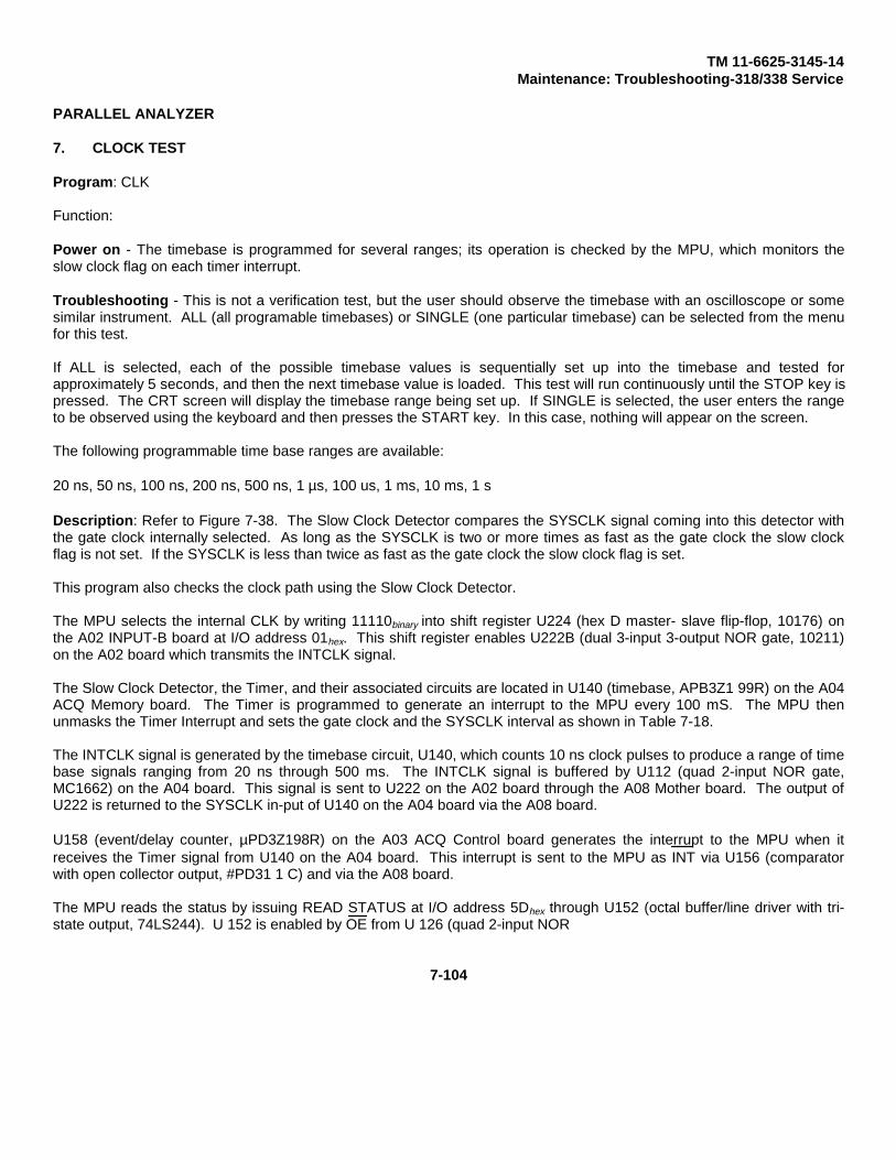
TM 11-6625-3145-14Maintenance: Troubleshooting-318/338 Service
PARALLEL ANALYZER
7. CLOCK TEST
Program: CLK
Function:
Power on - The timebase is programmed for several ranges; its operation is checked by the MPU, which monitors theslow clock flag on each timer interrupt.
Troubleshooting - This is not a verification test, but the user should observe the timebase with an oscilloscope or somesimilar instrument. ALL (all programable timebases) or SINGLE (one particular timebase) can be selected from the menufor this test.
If ALL is selected, each of the possible timebase values is sequentially set up into the timebase and tested forapproximately 5 seconds, and then the next timebase value is loaded. This test will run continuously until the STOP key ispressed. The CRT screen will display the timebase range being set up. If SINGLE is selected, the user enters the rangeto be observed using the keyboard and then presses the START key. In this case, nothing will appear on the screen.
The following programmable time base ranges are available:
20 ns, 50 ns, 100 ns, 200 ns, 500 ns, 1 µs, 100 us, 1 ms, 10 ms, 1 s
Description: Refer to Figure 7-38. The Slow Clock Detector compares the SYSCLK signal coming into this detector withthe gate clock internally selected. As long as the SYSCLK is two or more times as fast as the gate clock the slow clockflag is not set. If the SYSCLK is less than twice as fast as the gate clock the slow clock flag is set.
This program also checks the clock path using the Slow Clock Detector.
The MPU selects the internal CLK by writing 11110binary into shift register U224 (hex D master- slave flip-flop, 10176) onthe A02 INPUT-B board at I/O address 01hex. This shift register enables U222B (dual 3-input 3-output NOR gate, 10211)on the A02 board which transmits the INTCLK signal.
The Slow Clock Detector, the Timer, and their associated circuits are located in U140 (timebase, APB3Z1 99R) on the A04ACQ Memory board. The Timer is programmed to generate an interrupt to the MPU every 100 mS. The MPU thenunmasks the Timer Interrupt and sets the gate clock and the SYSCLK interval as shown in Table 7-18.
The INTCLK signal is generated by the timebase circuit, U140, which counts 10 ns clock pulses to produce a range of timebase signals ranging from 20 ns through 500 ms. The INTCLK signal is buffered by U112 (quad 2-input NOR gate,MC1662) on the A04 board. This signal is sent to U222 on the A02 board through the A08 Mother board. The output ofU222 is returned to the SYSCLK in-put of U140 on the A04 board via the A08 board.
U158 (event/delay counter, µPD3Z198R) on the A03 ACQ Control board generates the interrupt to the MPU when itreceives the Timer signal from U140 on the A04 board. This interrupt is sent to the MPU as INT via U156 (comparatorwith open collector output, #PD31 1 C) and via the A08 board.
The MPU reads the status by issuing READ STATUS at I/O address 5Dhex through U152 (octal buffer/line driver with tri-state output, 74LS244). U 152 is enabled by OE from U 126 (quad 2-input NOR
7-104
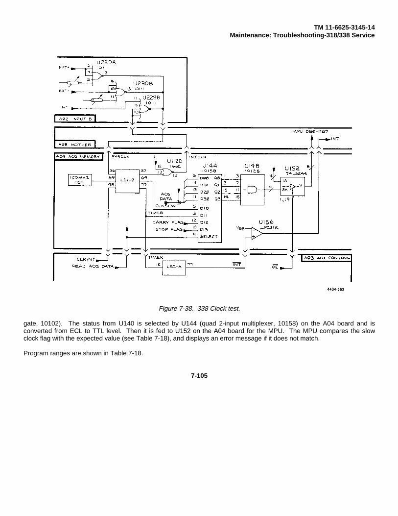
TM 11-6625-3145-14Maintenance: Troubleshooting-318/338 Service
Figure 7-38. 338 Clock test.
gate, 10102). The status from U140 is selected by U144 (quad 2-input multiplexer, 10158) on the A04 board and isconverted from ECL to TTL level. Then it is fed to U152 on the A04 board for the MPU. The MPU compares the slowclock flag with the expected value (see Table 7-18), and displays an error message if it does not match.
Program ranges are shown in Table 7-18.
7-105

TM 11-6625-3145-14Maintenance: Troubleshooting-318/338 Service
Table 7-18338 CLOCK TEST PROGRAM RANGES
Gate Clock SYSCLK SLOW CLOCK flag1mS 20nS reset
50nS reset100uS reset
1mS set200uS reset
2mS set50uS reset5mS set
10Ms 500uS reset10mS set
8. WORD RECOGNIZER TEST
Program: WR
Function:
Power on - The word recognition (WR) RAMs are checked with the checkerboard marching pattern from 00 through FF.
Step 1. The word 15 is written into all RAM addresses.
Step 2. A word is read from a diagnostic cell and compared with the expected word 15.
If it is not equal to 15, an error message is displayed and the MPU is halted.
Step 3. If the first test is successful, the word 2A is written into that cell. Then the word is read back out of the cell and itsvalue is compared with 2A. If it is not equal to 2A, an error message is displayed and the MPU is halted.
Step 4. Steps 2 and 3 are repeated for all RAM addresses.
Troubleshooting - This test is the same as that automatically run when the power is first turned on, but here the loopingtest feature is available. The looping test has four options: OFF, I/O, ERROR, and TEST. When the field is set to I/O, thelooping feature allows only I/O instructions to be run repeatedly. The I/O address will appear on the screen. When thefield is set to ERROR, the looping feature allows the tests in which an error is detected to be run repeatedly. When thefield is set to
TEST, the looping feature allows one test, or sequence of tests, to be run continuously. When the field is set to OFF, thelooping feature is not available and one test, or sequence of tests, will run once.
In the I/O looping test, only one or more OUT instructions (subroutines) including one of the addresses listed in Table 7-19will be run. Unless STOP is pressed, this test will loop continuously without displaying the result of the verification. Use anoscilloscope to observe the word recognizers.
7-106

TM 11-6625-3145-14Maintenance: Troubleshooting-318/338 Service
Table 7-19338 WORD RECOGNIZER TEST PORT ADDRESSES (Hex)
Address Content of Looping Test
03 increment WR-address counter for WRO test.
5B write WRO data 55 into data latch.
5B write WRO data AA into data latch.
03 increment WR-address counter for WR1 test.
5B write WR1 data 55 into data latch.
5B write WR1 data AA into data latch.
The ERROR looping feature is available only if errors are detected. If no errors are detected, the test will perform as if theLOOP field were set to OFF. If some errors are detected, the ERROR looping function is available for the read cycle of thetest, and the result of this verification will appear on the screen. Refer to Appendix B in this manual for a description oferror codes.
Description: Refer to Figure 7-39. On the A01 INPUT-A board, data from channels 8 through 31 are latched by U100through U1 10 (4-bit binary conter, F10016), and are then supplied to the word recognizers (WR) U118, U120 and U122(256 word X 4-bit RAM, HM10422) eight channels at a time for trigger detection. U100 through U110 are used as bothlatches to acquire data, and as WR counters to set up the WRs.
On the A02 INPUT-B board, data from channels 0 through 7 (Pod-A) is latched by M218s U200 through U214 (logicanalyzer INPUT, M218). The same data is also supplied to WR U128 (HM10422), and these output lines are wiredtogether, respectively, with U220 and U222 (F10016) and are used as a WR counter to set up the WR.
During acquisition, U100 through U1 10 on the A01 board are clocked to latch data coming from the parallel data probes.PE (Parallel Load Enable) is forced high by U228A (quad 2-input NOR gate, 10102) on the A02 board. This control signalis delivered from U234 (hex D master-slave flip-flop, 10176) on the A02 board when the MPU writes XX1XXXbinary seriallyto I/O address 03hex.
The outputs of U220 and U222 on the A02 board are held low by MR (Master Reset) from U114 (quad TTL-to-ECLtranslator, 10124), which is generated by U1 12 (3-line to 8-line decoder/demultiplexer, 74LS138) on the A01 board whenthe MPU writes any data to I/O address 02hex.
During WR setup, all eight F10016s are set to count enable for the counting operation by U234 (10176) on the A02 board.The output, XX0XXXbinary, is written serially by the MPU to I/O address 03hex. The enable bit is also converted to TTLswing and then shifted to -5V by U232 (dual comparator, uPC393C) on the A02 board to set the M218’s output to off.
With the above operation, all F10016s can address the WRs. They are incrementally clocked by SYSCLK from U228B(high-speed dual 3-input 3-output NOR gate). The word written into the WR U118 on the A01 board and the WR U218 onthe A02 board is provided with EDBO, EDB1, and EDB2. The word written to WR U120 and U122 on the A01 board isprovided with EDB3, EDB4, and EDB5. These signals are all delivered from the A04 ACQ Memory board after beingtranslated from TTL-level to ECL-level.
7-107

TM 11-6625-3145-14Maintenance: Troubleshooting-318/338 Service
The write pulse to the WR U118 and U120 is generated by U1 12 (74LS138) and converted to ECL- level by U1114(10124) at the time the MPU writes at I/O address 01hex. The I/O address to generate the write pulse for the U218 andU122 is 00hex. Thus two of the four WRs are written at once; U118 and U120, or U218 and U122.
Each output of these four WRs are wired together on the A08 Mother board, and are sent to U136 and U 138 (dual type Dmaster-slave flip-flop, 10231) on the A03 ACQ Control board for triggering. In addition to that, these signals are routed toU146 (quad 2-input multiplexer/latch, 10173) on the A03 board. The data to U146 (10173) are latched by READ SQRAMfrom U112 (binary to 1-8 line decoder, 10162) through inverter U126 (quad 2-input NOR gate, 10102), after being selectedby LDSQRAM from U108 (hex D master-slave flip-flop, 10176) on the A03 board. LDSQRAM is set when the MPU writesX1XXXXbinary at I/O address 51hex, and READ SQRAM is generated by the MPU’s access to I/O address 5Bhex.
The four outputs of U146 (10173) are connected to U142 (quad 2-input multiplexer, 10158) on the A04 board with theoutputs of the ACQ Memories U116 through U130 (HM10422) on the A04 board. Thus, all the ACQ Memories areset tooff by forcing BS high. This is done by writing 1Fhex into U114 (hex D master-slave flip-flop, 10176) on the A04 board usingthe WRITE BS signal from U112 (10162) on the A03 board.
The MPU reads the data from U152 (octal buffer/line driver with tri-state output, 74LS244) on the A04 board when enabledby OE from U112 (10162) via U126 (10102) on the A03 board. The data fed to U152 (74LS244) are selected by U142(10158) on the A04 board with READ SQRAM from U1 12 (10162) on the A03 board at I/O address 59hex, and aretranslated from ECL-to-TTL by U146 (quad ECL-to-TTL translator, 10125) on the A04 board.
The MPU follows Steps 1 through 4 of the I/O operation described in the preceding Power On para- graph, and comparesthe data with the expected value on each I/O read. If the data is incorrect, the MPU will issue an error message.
7-108

TM 11-6625-3145-14Maintenance: Troubleshooting-318/338 Service
4434-567
Figure 7-39. 338 Word recognizer test.
7-109

TM 11-6625-3145-14Maintenance: Troubleshooting-318/338 Service
9. ACQ RAM TEST
Program : ACQ
Function:
Power on - All the ACQ RAMs are checked with the checkerboard marching pattern from 00 through FF.
Step 1. The word 55 is written into all RAM addresses.
Step 2. A word is read from a diagnostic cell and compared with the expected word 55. If the diagnostic cell’s value is notequal to 55, an error message is displayed and the MPU is halted.
Step 3. If no error is found in the above test, the word AA is written into that cell. Then a word in same cell is read backand is compared with AA. If that word is not equal to AA, an error message is displayed and the MPU is halted.
Step 4. Steps 2 and 3 are repeated for all RAM addresses.
Troubleshooting - This test is the same as that performed automatically when the power is turned on, but here thelooping feature is available. The looping feature has four options; OFF, I/O, ERROR, and TEST. When the LOOP field isset to I/O, the looping feature allows only I/O instructions to be run repeatedly. The I/O address will appear on the screen.When the field is set to ERROR, the looping feature allows the tests in which an error is detected to be run repeatedly.When the field is set toTEST, the looping feature allows one test, or sequence of tests, to be run continuously. When the field is set to OFF, thelooping feature is not available and one test, or sequence of tests, will run once.
When the I/O looping function is selected, only those OUT instructions (subroutines) including one of the addresses listedin Table 7-20 will run. Unless the STOP key is pressed, the selected portions of the test will loop continuously withoutdisplaying the result of the verification. In this case, use an oscilloscope to observe the acquisition circuit board.
7-110

TM 11-6625-3145-14Maintenance: Troubleshooting-318/338 Service
Table 7-20338 ACQ TEST PORT ADDRESSES (Hex)
Address Content of Looping Test02 reset WR-address counter to count up WR-address counter to 55 to write 55 into
the background of high-speed memory.5A write CSO & CS1, CS2, CS3 into CS-latch to read 55 from high-speed memory.55 write AA into high-speed memory after reading 55 from high-speed memory.5A write CSO & CS1, CS2, CS3 into CS-latch to read AA from high-speed memory.55 write 55 into high-speed memory after reading AA from high-speed memory.
When ERROR is selected in the looping test field, looping is available only if errors are detected. If no errors are detected,the test runs to completion just as if the looping function had been set to OFF. If errors are detected, the ERROR loopingfeature is available for the read cycle of the test, and the result of the verification will appear on the screen. Refer toAppendix B of this manual for an explaination of error codes.
Description: Refer to Figure 7-40. The test data for ACQ Memories U1 16 through U130 (256 word X 4-bit RAM,HM10422) on the A04 ACQ Memory board are generated by U220 and U222 (4-bit binary counter, F10016) on the A02Input-B board, and U100 through U110 (F10016) on the A01 In-put-A board. No acquired data is used. The operation forgenerating pseudo data is the same as that used in the WR Test.
The addresses for the ACQ Memories are pointed at by U136 and U138 (4-bit binary counter, F10016) on the A04 board.These counters are set to count enable by U156 (quad 2-input NOR gate, 10102) on the A03 ACQ Control board, and arereset by RESET from U112 (10162) on the A03 board.
At least one pair of the ACQ Memories can be enabled by U114 (hex D master-slave flip-flop, 10176) on the A04 boardwhen the MPU writes data to it at I/O address 5Ahex using WRITE BS from U112 (10162) on the A03 board.
The flip-flop U148A <7> (dual D master-slave flip-flop, 10231) sets the STOP condition, and is reset by RESET from U110(10162) on the A03 board. It also frees the WE line. START2, also from U110 (10162), enables the strobe generatorcircuit by setting the flip-flop U124B (dual D master-slave flip-flop, 10131) on the A03 board.
After the above setup is complete, the MPU selects the internal CLK and sets the timebase U140 (timebase, µPB3Z1 99R)on the A04 board to generate a single clock pulse when the MPU writes to I/O address 4Ahex. The MPU then unmasks thecarry interrupt from both U136 and U138 (F10016) on the A04 board.
The MPU starts the test according to Steps 1 to 4 already mentioned in the preceding Power on paragraph in this section.
Writing at I/O address 4Ahex generates the internal clock from U140 (uPB3Z199R) on the A04 board. This clock isbuffered by U112D (quad 2-input NOR gate, MC1662) and is sent to U228 (dual
7-111
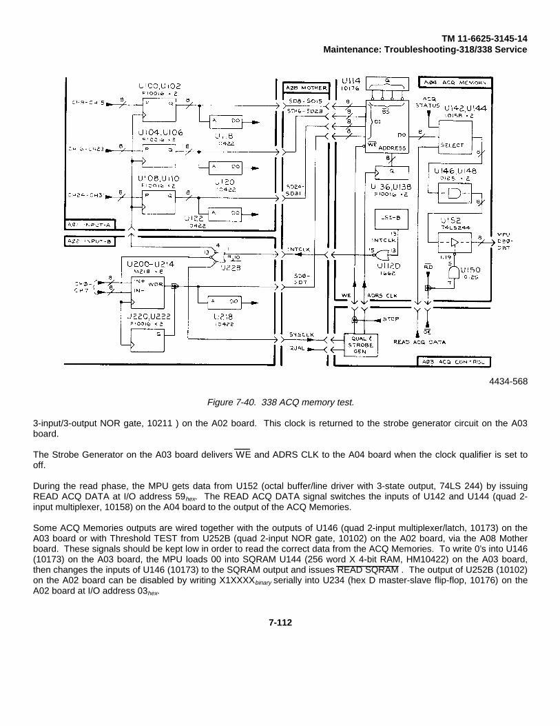
TM 11-6625-3145-14Maintenance: Troubleshooting-318/338 Service
4434-568
Figure 7-40. 338 ACQ memory test.
3-input/3-output NOR gate, 10211 ) on the A02 board. This clock is returned to the strobe generator circuit on the A03board.
The Strobe Generator on the A03 board delivers WE and ADRS CLK to the A04 board when the clock qualifier is set tooff.
During the read phase, the MPU gets data from U152 (octal buffer/line driver with 3-state output, 74LS 244) by issuingREAD ACQ DATA at I/O address 59hex. The READ ACQ DATA signal switches the inputs of U142 and U144 (quad 2-input multiplexer, 10158) on the A04 board to the output of the ACQ Memories.
Some ACQ Memories outputs are wired together with the outputs of U146 (quad 2-input multiplexer/latch, 10173) on theA03 board or with Threshold TEST from U252B (quad 2-input NOR gate, 10102) on the A02 board, via the A08 Motherboard. These signals should be kept low in order to read the correct data from the ACQ Memories. To write 0’s into U146(10173) on the A03 board, the MPU loads 00 into SQRAM U144 (256 word X 4-bit RAM, HM10422) on the A03 board,then changes the inputs of U146 (10173) to the SQRAM output and issues READ SQRAM . The output of U252B (10102)on the A02 board can be disabled by writing X1XXXXbinary serially into U234 (hex D master-slave flip-flop, 10176) on theA02 board at I/O address 03hex.
7-112

TM 11-6625-3145-14Maintenance: Troubleshooting-318/338 Service
10. SQRAM Test
Program: SQRAM
Function:
Power on - The SQRAM is checked with the checkerboard marching pattern from 00 through FF.
Step 1. The word 55 is written into all RAM addresses.
Step 2. A word is read from a diagnostic cell and compared with the expected word 55. If the selected word is not equalto 55, an error message is displayed and the MPU is halted.
Step 3. The word AA is written into that cell. Then a word in same cell is read back and is compared with AA. If it is notequal to AA, an error message is displayed and the MPU is halted.
Step 4. Steps 2 and 3 are repeated for all RAM addresses.
Troubleshooting - This test is the same as that automatically run when the power is first turned on, but here the loopingfeature is available. The looping feature has four options; OFF, I/O, ERROR, and TEST. When the LOOP field is set toI/O, the looping feature allows only I/O instructions to be run repeatedly. The I/O address will appear on the screen. Whenthe field is set to ERROR, the looping feature allows the tests in which an error is detected to be run repeatedly. When thefield is set to TEST, the looping feature allows one test, or sequence of tests, to be run continuously. When the field is setto OFF, the looping feature is not available and one test, or sequence of tests, will run once.
When I/O looping is selected, only those OUT instructions (subroutines) included one of the addresses listed in Table 7-21will run. Unlesss the STOP key is pressed, the program will continue looping continuously without displaying the result ofthe verification. In this case, the user should observe the ACQ. circuit board with an oscilloscope.
Table 7-21338 SQRAM TEST PORT ADDRESSES (Hex)
Address Content of Looping Test5A set CS all OFF into CS-latch to write 55 in the background of the SQRAM.50 set 1 into QUAL (DO & D2) register and set 0 into QUAL (D1 & D3) register.58 write 55 into the background of the SQRAM.5B SQRAM data is latched to read 55 from high-speed memory.58 write AA into SQRAM after reading 55 from high-speed memory.5B SQRAM data is latched to read AA from high-speed memory.
When the ERROR looping function is selected, the program loops only if errors are detected. If no errors are detected theprogram runs once and displays the result of the verification just as if the looping function were turned OFF. If errors aredetected, the ERROR looping function is available for the read cycle of the test. The results of the read cycle verificationwill appear on the screen. Refer to the Appendix B in this manual for an explanation of error codes.
7-113
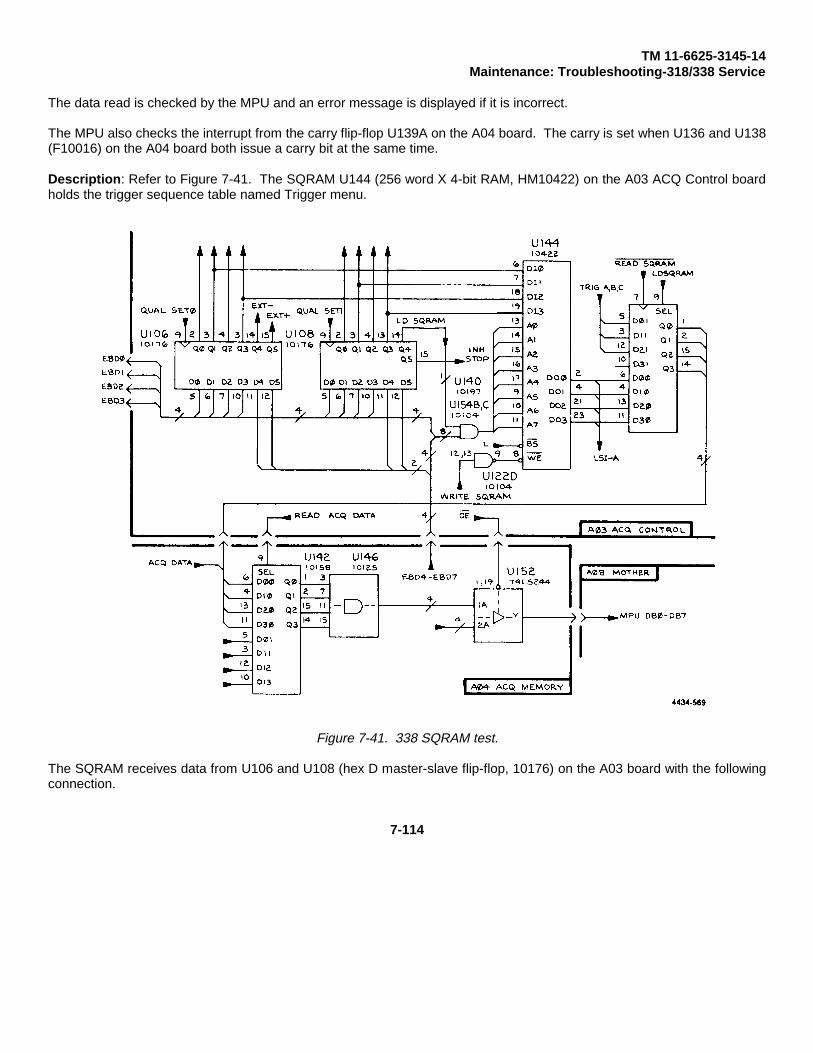
TM 11-6625-3145-14Maintenance: Troubleshooting-318/338 Service
The data read is checked by the MPU and an error message is displayed if it is incorrect.
The MPU also checks the interrupt from the carry flip-flop U139A on the A04 board. The carry is set when U136 and U138(F10016) on the A04 board both issue a carry bit at the same time.
Description: Refer to Figure 7-41. The SQRAM U144 (256 word X 4-bit RAM, HM10422) on the A03 ACQ Control boardholds the trigger sequence table named Trigger menu.
Figure 7-41. 338 SQRAM test.
The SQRAM receives data from U106 and U108 (hex D master-slave flip-flop, 10176) on the A03 board with the followingconnection.
7-114

TM 11-6625-3145-14Maintenance: Troubleshooting-318/338 Service
Table 7-22338 SQRAM TEST SQRAM DATA CONNECTIONS
SetupSQRAM U144
Latch MPU DataDI0 (pin 6) U106 Q1 (pin 3) D0DI1 (pin 7) U106 Q3 (pin 13) D1DI2 (pin 18) U108 Q1 (pin 3) D2DI3 (pin 19) U108 Q3 (pin 13) D3
To provide the data to the SQRAM, the MPU writes the two least significant bits of the four data bits into U106 (10176) atI/O address 50hex, and the two most significant bits into U108 (10176) at I/O address 51hex.
Each address line of the SQRAM is connected to two output lines which are wired together as follows:
Table 7-23338 SQRAM TEST SQRAM ADDRESS CONNECTIONS
SetupSQRAM U144 TRIGGER F-F
Gate MPU DataA0 (pin 13) U138 pin 15 U140 pin 2 D0A1 (pin 14) U150 pin 15 U140 pin 3 D1A2 (pin 15) U136 pin 15 U140 pin 4 D2A3 (pin 16) U136 pin 2 U140 pin 13 D3A4 (pin 17) U138 pin 2 U140 pin 14 D4A5 (pin 9) U150 pin 3 U140 pin 15 D5A6 (pin 10) U134 pin 2 U154 pin 14 D6A7 (pin 11) U148 pin 14 U154 pin 3 D7
In order to set up the SQRAM, the MPU data (translated to ECL-level) points to the address of the SQRAM. These databits are gated as in the table above, enabled by LDSQRAM from U108 <5> (10176) bit 4 on the A03 board. Bit 4 ismaintained high during this setup.
The write pulse to the SQRAM, WRITE SQRAM is generated when the MPU writes at I/O address 58hex. At the sametime, the address to the SQRAM is supplied by the MPU data.
The Read process is the same as in the WR Test, except that the inputs for U 146 (quad 2-input multiplexer/latch, 10173)on the A03 board are switched to the outputs of the SQRAM.
During each read, the MPU verifies the data and issues an Error Message if it is not equal to the expected data.
7-115

TM 11-6625-3145-14Maintenance: Troubleshooting-318/338 Service
11. N & DELAY TEST
Program: N & DLY
Function:
Power on - The Event/Delay counter counts word "A" N times when functioning as the event counter, and counts a certainnumber of clock signals for delay when functioning as the delay counter.
When functioning as the event counter, the MPU loads a small N value into the counter register and increments thecounter using clock pulses while observing the carrry bit. The Delay counter functions the same way, using the DELAYvalue as the initial counter value. In both cases the number of clock signals needed to generate the carry are comparedwith the expected values.
Troubleshooting - This is not a verification test, so no test result will appear on the CRT screen. This test should beobserved on an oscilloscope. The Troubleshooting routine automatically tests the N&DELAY counter by alternatelyloading and running the counter, first with N values as the event counter, and then with DELAY values for the delaycounter. The user programs the N and DELAY values before beginning the test. This test will run continuously until theuser presses the STOP key. If no test values are entered, the N counter is set to 1 and the DELAY counter is set toZERO. In this case, the N&DELAY counter will not run. To run this test, N must be greater than 1, and DELAY must begreater than 0.
Description: Refer to Figure 7-42. The Event Delay counter U158 (event/delay counter, µPB3Z198R) on the A03 ACQControl board is controlled by three signals, CE , LOAD N, and LOAD DL from the SQRAM U144 (256 word X 4-bit RAM,HM10422) on the A03 board. The counter generates N-1 as a carry when it reaches full count. This Event/Delay counterhas two registers, the one which holds the N value is called the N-register and the one which holds the DELAY value iscalled the DL register.
In this test, the MPU writes 000Fhex as the N value into the N-register at I/O addresses 41hex and 42hex, and 005Ahex as theDELAY value into the DL register at I/O address 43hex and 44hex.
Start flip-flop U124B (dual type D master-slave flip-flop, 10131) on the A03 board is set by START2 from U 110 (binary to1-8 decoder/multiplexer, 10162) on the A03 board. U124B passes a clock signal generated by the MPU.
Latches U106 and U108 (hex D master-slave flip-flop, 10176) on the A03 board are set to hold data 1100b for theSQRAM. They also enable U140 (hex AND-gate, 10197) and U154 (quad 2-input AND-gate, 10104) on the A03 board.Those gates control the data supplied to the address line of the SQRAM.
The MPU writes the data already set in the latches into the SQRAM at address FFhex using the WRITE SQRAM signalfrom U1 12 <6> (10162) on the A03 board. This data generates the LOAD N command for the Event/Delay counter. Afterthis setup, latches U106 and U108 (10176) are written to set the clock qualifier to off, which enables the MPU to send asingle clock. The MPU generates STEP CLK by writing at I/O address 55hex from U1 10 (10162) on the A03 board, usingFFhex as data. That is, the SQRAM delivers the data at address FFhex pointed to by the MPU Data to the Event/Delaycounter, it is LOAD N, and the strobe generator circuit on the A03 board generates TRIG CLK to the Event/Delay counter.
By this procedure, the N value of the N-register in the Event/Delay counter is loaded into the counter itself.
7-116

TM 11-6625-3145-14Maintenance: Troubleshooting-318/338 Service
To keep the Event/Delay counter enabled during the test, the SQRAM must supply CE to the Event/Delay counter. So, thesame setups mentioned above are repeated in order to load 0000binary into the SQRAM.
After that, the MPU unmasks the interrput of the Event/Delay counter carry by writing at I/O address 40hex.
Then the MPU generates STEP CLK by writing FFhex for the SQRAM address until it receives an interrupt signal. Once theinterrupt occurs, the MPU reads the status from I/O address 5Dhex. The signal path for reading the status is same as inthe Clock Test.
The MPU checks to see whether the Event/Delay counter Carry flag is set, and also checks the number of STEP CLKsgenerated.
If the flag is set and the clock count is correct, the MPU proceeds to the next step, otherwise it is- sues an error messageand stops the test.
The DELAY count can be tested in the same way as the Event count, N. In this case, 1010binary is set in latches U106 andU108 (10176) on the A03 board.
7-117

TM 11-6625-3145-14Maintenance: Troubleshooting-318/338 Service
4434490
Figure 7-42. 338 N and DELAY counter test.
7-118
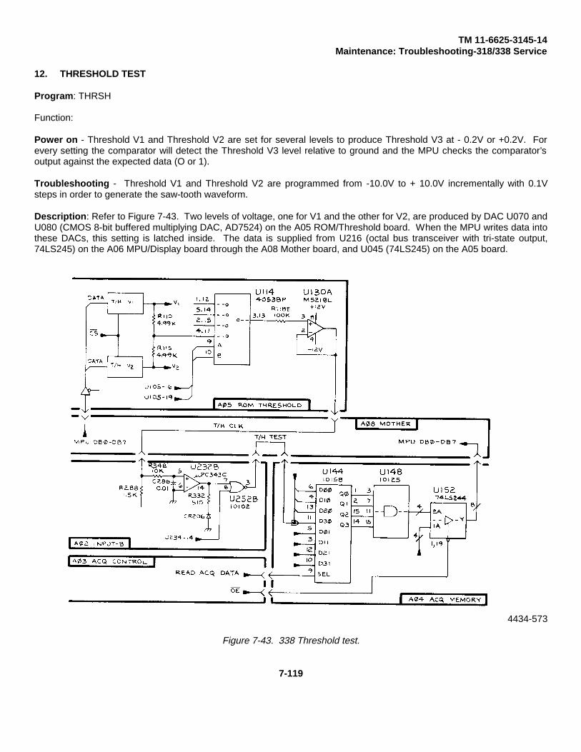
TM 11-6625-3145-14Maintenance: Troubleshooting-318/338 Service
12. THRESHOLD TEST
Program: THRSH
Function:
Power on - Threshold V1 and Threshold V2 are set for several levels to produce Threshold V3 at - 0.2V or +0.2V. Forevery setting the comparator will detect the Threshold V3 level relative to ground and the MPU checks the comparator’soutput against the expected data (O or 1).
Troubleshooting - Threshold V1 and Threshold V2 are programmed from -10.0V to + 10.0V incrementally with 0.1Vsteps in order to generate the saw-tooth waveform.
Description: Refer to Figure 7-43. Two levels of voltage, one for V1 and the other for V2, are produced by DAC U070 andU080 (CMOS 8-bit buffered multiplying DAC, AD7524) on the A05 ROM/Threshold board. When the MPU writes data intothese DACs, this setting is latched inside. The data is supplied from U216 (octal bus transceiver with tri-state output,74LS245) on the A06 MPU/Display board through the A08 Mother board, and U045 (74LS245) on the A05 board.
4434-573
Figure 7-43. 338 Threshold test.
7-119
TM 11-6625-3145-14Maintenance: Troubleshooting-318/338 Service
When the MPU writes at I/O address E0hex the WR and CS signals are sent to U070 (DAC V1) to latch the data. WR andCS for U080 (DAC V2) are caused by the MPU’s access at I/O address E1hex. The WR signal is delivered from U150C(quadruple 2-input positive NOR gate, 74LS02) on the A05 board, which comes from U214 (octal buffer/line driver with tri-state output, 74LS240) on the A06 board. CS for these DACs are generated by U092B (dual 2-line to 4-linedecoder/demultiplexer, 74LS139) on the A05 board.
A number less than 80hex programs the DAC for positive output, and a number more than 80hex progarms it for negativeoutput centered on GND (80hex) in 0.1V steps. The actual output of these DACs is 1/4 of that specified in the Thresholdmenu.
This test sets the DACs to several values, given in Table 7-24, and checks V3 selected for CLK Threshold indirectly.
The settings and expected data are shown in Table 7-24.
Table 7-24338 THRESHOLD TEST DATA VALUES
V1 V2 V3 Expected
+0.3V (83hex) - 0.1 V (7Fhex) + 0.2V 1
+0.7V (87hex) -0.5V (7Bhex) +0.2V 1
+1.1V (8Bhex) - 0.9V (77hex) + 0.2V 1
+1.9V (93hex) -1 .7V (6Fhex) + 0.2V 1
+3.5V (A3hex) -3.3V (5Fhex) +0.2V 1
+6.7V (C3hex) -6.5V (3Fhex) +0.2V 1
-0.3V (7Dhex) +0.1V (81hex) --0.2V 0
-0.7V (79hex) +0.5V (85hex) -0.2V 0
-1.1V (75hex) +0.9V (89hex) -0.2V 0
-1.9V (6Dhex) +1.7V (91hex) -0.2V 0
-3.5V (5Dhex) +3.3V (A1hex) -0.2V 0
-6.7V (3Dhex) +6.5V (C1hex) -0.2V 0
V3 is calculated by (V1 + V2)/2 using two resistors, R 110 and R1 15 (4.99 KΩ) on the A05 board. V3 is selected by U1 14(differential 4-channel multiplexer, 4052BP) on the A04 board and sent to U216 (ultra fast dual comparator, SP9687) andthe Comparator U232 (dual comparator, uPC393C) on the A02 Input-B board through the A08 board. In the A02 board,V3 is compared with ground by the U232 Comparator and its output is sent to U252B (quad 2-input NOR gate, 10102) onthe A02 board. U252B is enabled by U234 (hex D master-slave flip-flop, 10176) on the A02 board when the MPU writesX0XXXXbinary into it at I/O address 03hex. U252B (10102) on the A02 board outputs the Threshold TEST signal to U144(quad 2-input multiplexer, 10158) on the A04 board via the A08 board.
7-120
TM 11-6625-3145-14Maintenance: Troubleshooting-318/338 Service
During this test, all outputs of the ACQ Memories on the A04 board are disabled (maintained low) y forcing BS high fromU114 (hex D master-slave flip-flop, 10176) on the A04 board. U1 14 is written by the MPU at I/O address 5Ahex.
The MPU reads the data from the A04 board at I/O address 59hex, i.e., with READ ACQ DATA from 112 (binary to 1-8decoder/multiplexer, 10162) on the A03 board. This reading sequence is the ame as in the ACQ Test.
Then the MPU compares the MSB of the data read to the one expected. If they don’t match each other, an error messagewill be issued.
13. SEQ TEST
Program: SEQ
Function:
Power on - A single acquisition with a full trigger sequence is simulated to check a whole operation.
Troubleshooting - The content of this test is the same as that run automatically when the power s first turned on, but herethe Looping feature is available. The Looping feature has 4 options; OFF, /O, ERROR, and TEST. When the LOOP fieldis set to I/O, the looping feature allows only I/O instructions to be run repeatedly. The I/O address will appear on thescreen. When the field is set to ERROR, the looping feature allows the tests in which an error is detected to be runrepeatedly. When the field is set to TEST, the looping feature allows one test, or sequence of tests, to be runcontinuously. When the field is set to OFF, the looping feature is not available and one test, or sequence of tests, will runonce.
When I/O Looping is selected, only those selected OUT instructions (subroutines), including one of the addresses listedbelow, will run. Unless the STOP key is pressed, this test will continue looping without displaying the result of theverification. In this case, the user should use an oscilloscope to observe the Acquisition circuit board.
PORT ADDRESSES (HEX)
Address Content of Looping Test
55 write WA into High-speed memory.
When ERROR is selected, looping will occur only if errors are detected. If no errors are detected, the ERROR looping testwill run through its tests only once, and the results of the verification will be displayed on the CRT just as if the looping fieldhad been selected to OFF. If errors are detected, the ERROR Looping function is available for the read cycle of the test,and the result of the verification will appear on the screen. Refer to the Appendix B in this manual for an explanation oferror codes.
Description: A single acquisition is simulated to check the trigger sequencer operation. Pseudo data is generated inexactly the same way used in the WR and ACQ tests, and applied to the latches on the A01 INPUT-A and INPUT-Bboards.
7-121
TM 11-6625-3145-14Maintenance: Troubleshooting-318/338 Service
The words, WA, WB, and WC are set to 01hex, 02hex and 03hex respectively. Then full trigger sequence, 5*WA FLW’DBY:WB RESET ON:WC is selected with 16 clocks of delay to stop after the trigger recognition.
The data AAAXBCAAXAAAXABXABCXABCXABCXABC is supplied to the WR on the A01 and the A02 boards and to theACQ Memories on the A04 ACQ MEMORY board. SYSCLK is generated by the MPU by writing at I/O address 4Ahex,which is into the Time Base U140 on the A04.
The operation of the Trigger Sequencer is observed by the MPU by reading the interrupt and the ACQ status. The MPUchecks these conditions on every clock pulse, and if there are any unexpected events the MPU displays an error message.
After the end of the acquisition (all flags are detected at certain clocks), the MPU reads the data from the ACQ Memorieson the A04 board, and compares them with the word sequence applied. An error message is displayed if there aredifferences.
338S1 SERIAL ANALYSIS/RS232C/NVM
14. BATTERY TEST
Program: TSTBTT
Function:
Power on - TSTBTT checks the battery voltage to see if it is more or less than 2.2 Volts.
Troubleshooting - None
Description - Detected battery voltage status is shown in the option status register at bit 07. TSTBTT reads this bit fromI/O address 80. (Refer to option I/O function list)
Battery voltage is detected by Q170, and battery status is applied to bit #7 of the status register by U32.
U30 decodes option I/O addresses.
15. NON-VOLATILE MEMORY TEST
Program: TSTNV1 (power on), TSTNV2 (Troubleshooting)
Function:
Power on - The NVM has a check-sum word that is used for checking non-volatile memory data. The TSTNV1 programcalculates the check sum by reading NVM data and comparing it with the NVM check sum.
Troubleshooting - The TSTNV2 diagnostic program includes twelve test programs. For all of these tests, the method isread data after write. (Refer to the failure code list for check data format.)
All NVM data is cleared after the diagnostic has run.
7-122

TM 11-6625-3145-14Maintenance: Troubleshooting-318/338 Service
Description - The NVM address is from EOOO through E7FF; NVM address select signal (NVMCS) is supplied from theaddress decoder on the MPU (A06) board through bus connector 46B. The NVM chip is selected by the inverse NVMCSand the power(+5V) monitor signal. If the power monitor circuit detects low power (< 4.6V), the NVM can not be selected.NVM data is gated by U25, which is controlled by the BRD, BIORQ, and NVMCS signals. The RD and WR signals (theseare inverse signals of BRD and BWR) control the direction of NVM data.
16. RS-232 TEST
Program: TSTRM1 (power on), TSTRM2 (Troubleshooting)
Setup: - Before starting TSTRM2, you must connect the self test adapter to the RS-232 communication port. (Refer toFigure 7-23.)
Function:
Power on - TSTRM1 initializes the SIO Port-B and reads its initial status. If the initial status is good, it loads dummy datainto the SIO and checks for status change.
Troubleshooting - TSTRM2 diagnostic has the following three functions;
1. checks MODEM control signals2. checks the SIO Port-B status3. checks data transmit and receive functions
Function 1 includes eight test programs. These programs check the status of MODEM signals RTS, CTS, CD, DTR, andDSR.
Function 2 includes seven test programs. These programs check the SIO Port-B initial status.
Function 3 includes nine test programs. These programs transmit increment pattern data from SIO Port-B, then receiveand compare that data against the original data. Data speed is changed automatically from 110 baud through 9600 baud.
(Test data format is fixed at 8 bits/word, even parity, and one stop bit, )
Description - Refer to the 01 Option I/O function list, and simplified block diagrams for SERIAL and RS-232 when readingthe following.
The SIO and other option hardware I/O address is decoded by U30. The SIO Port-B cotrolls RS- 232 functions; thataddress is 92 and 93, and the RS-232 baud rate selector address is 88.
The SIO data line is common for both Port-A and Port-B. These eight data lines connect to buffer U25; U25 is gated bythe option I/O address.
The SIO timing is synchronized by the CPU clock. That clock is supplied from the MPU on the A06 board through busconnector 31A, and its waveform is adjusted by U12 and U32 before reaching the SIO.
All but one of the MODEM control signals are controled by SIO Port-B. The exception is the DSR signal, which appears inthe option status register at address 80. All the signals coming into Port-B are converted from RS-232 levels to TTL levelsby the receiver, U40; and all outgoing signals are converted from TTL levels to RS-232 levels by the transmitter, U41.
7-123
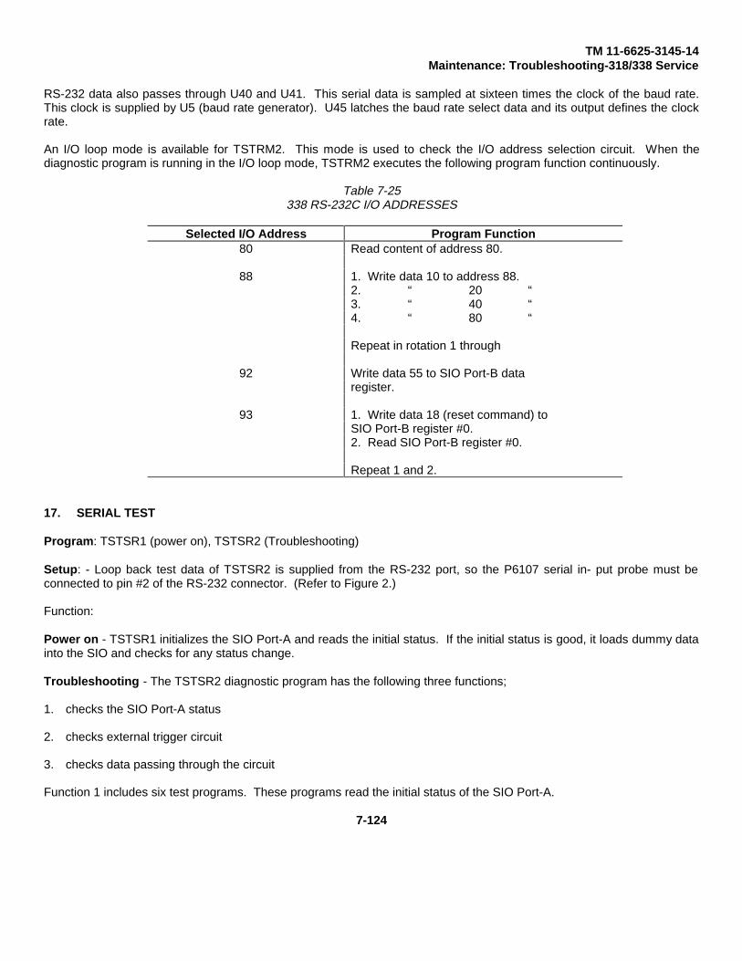
TM 11-6625-3145-14Maintenance: Troubleshooting-318/338 Service
RS-232 data also passes through U40 and U41. This serial data is sampled at sixteen times the clock of the baud rate.This clock is supplied by U5 (baud rate generator). U45 latches the baud rate select data and its output defines the clockrate.
An I/O loop mode is available for TSTRM2. This mode is used to check the I/O address selection circuit. When thediagnostic program is running in the I/O loop mode, TSTRM2 executes the following program function continuously.
Table 7-25338 RS-232C I/O ADDRESSES
Selected I/O Address Program Function80 Read content of address 80.
88 1. Write data 10 to address 88.2. “ 20 “3. “ 40 “4. “ 80 “
Repeat in rotation 1 through
92 Write data 55 to SIO Port-B dataregister.
93 1. Write data 18 (reset command) toSIO Port-B register #0.2. Read SIO Port-B register #0.
Repeat 1 and 2.
17. SERIAL TEST
Program: TSTSR1 (power on), TSTSR2 (Troubleshooting)
Setup: - Loop back test data of TSTSR2 is supplied from the RS-232 port, so the P6107 serial in- put probe must beconnected to pin #2 of the RS-232 connector. (Refer to Figure 2.)
Function:
Power on - TSTSR1 initializes the SIO Port-A and reads the initial status. If the initial status is good, it loads dummy datainto the SIO and checks for any status change.
Troubleshooting - The TSTSR2 diagnostic program has the following three functions;
1. checks the SIO Port-A status
2. checks external trigger circuit
3. checks data passing through the circuit
Function 1 includes six test programs. These programs read the initial status of the SIO Port-A.
7-124

TM 11-6625-3145-14Maintenance: Troubleshooting-318/338 Service
Function 2 includes two test programs. These programs control the external trigger transition, and check the trigger statusin bit #1 of the option status register.
Function 3 includes eight test programs. These programs generate serial data (shift pattern data: 01 02 04 08 10 20 40) atpin #2 of the RS-232 connector. The programs also check incoming data at SIO Port-A. Serial data speed is changedautomatically during the test.
(The Test data format is fixed to 8 bits/word, even parity, 1 stop bit. The data threshold is TTL, and data polarity isnegative.)
Description- Refer to the 01 Option I/O function list and simplified diagram of the Serial and the RS-232 when reading thefollowing:
SIO Port-A is used for Serial data acquisition. The Port-A address is 90 and 91, and the Serial parameter selector addressis 8C.
U31 latches the baud select data, input data polarity bit, and the external trigger polarity bit. These are the parameters forSerial acquisition control.
U6 generates the receive data sampling clock and supplies this clock to SIO pin #13. U22 switches the input clockselector from either the 19.2 K internal clock or the External clock; but the TSTSR2 program does not test this logic.
The external trigger polarity is defined by U12, and U22 latches on the transition of U12’s output. This status is initializedby writing data to address 84. External trigger status appears at bit #0 of the option status register; its address is 80.
The serial input data level is devided by 10 at input and this signal is amplified 2.5 times by U100 before reaching TestPoint 10. The data at T.P. 10 is compared with Threshold C (supplied from the RAM board through bus connector 39B)by U110; then data polarity is defined by U12 and supplied to SIO pin #12.
The 1/0 loop feature is available for TSTSR2. This mode is used to check the I/O address selection circuit. When thediagnostic program is running in the I/O loop mode, TSTSR2 executes following program functions continuously.
7-125

TM 11-6625-3145-14Maintenance: Troubleshooting-318/338 Service
Table 7-26338 SERIAL TEST I/O ADDRESSES
Selected I/O Address Program Function80 Read content of address 80.
84 Write data to address 84.
8C 1. Write data 10 to address 8C.2. “ 20 “3. ” 40 “4. “ 80 “
. Repeat in rotation 1 through 4
90 Write data 55 to SIO Port-A dataregister.
91 1. Write data 18 (reset command) toSIO Port-A register #0.2. Read SIO Port-A register #0
Repeat 1 and 2.
OPTION I/O FUNCTION LIST
I/O ADDRESS = 80CHIP = U32FUNCTION = OPTION STATUS REGISTERCONTROL = READ ONLY
bit = 7 6 5 4 3 2 1 0
battery MODEM externalstatus xxxxx xxxxx xxxxx xxxxx xxxxx DSR trigger
status
bit 0: ON = external trigger is occured.OFF = external trigger is not occured.
bit 1: ON = DSR signal is OFF.OFF = DSR signal is ON.
bit 7: ON = battery voltage is low. (<2.4 Volt)OFF = battery voltage is normal.
I/O ADDRESS = 84CHIP = RESET TO U22-BFUNCTION = INITIALIZE THE EXTERNAL TRIGGERCONTROL = WRITE ONLY
7-126
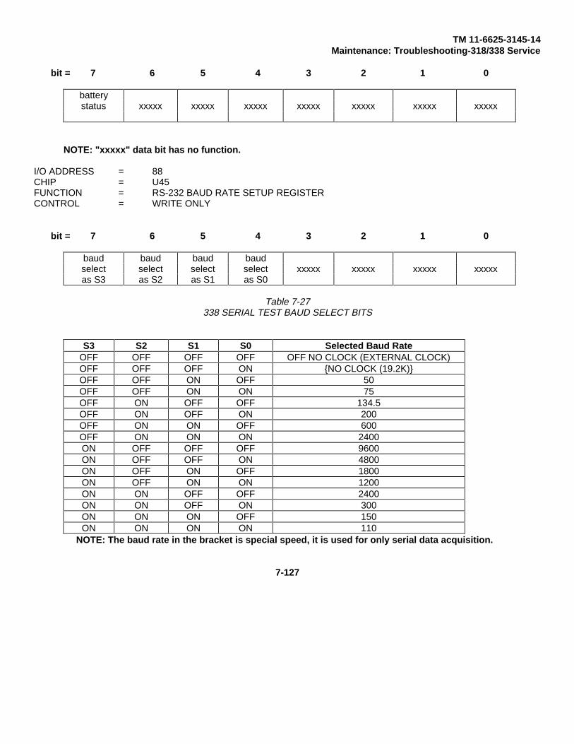
TM 11-6625-3145-14Maintenance: Troubleshooting-318/338 Service
bit = 7 6 5 4 3 2 1 0
batterystatus xxxxx xxxxx xxxxx xxxxx xxxxx xxxxx xxxxx
NOTE: "xxxxx" data bit has no function.
I/O ADDRESS = 88CHIP = U45FUNCTION = RS-232 BAUD RATE SETUP REGISTERCONTROL = WRITE ONLY
bit = 7 6 5 4 3 2 1 0
baud baud baud baudselect select select select xxxxx xxxxx xxxxx xxxxxas S3 as S2 as S1 as S0
Table 7-27338 SERIAL TEST BAUD SELECT BITS
S3 S2 S1 S0 Selected Baud RateOFF OFF OFF OFF OFF NO CLOCK (EXTERNAL CLOCK)OFF OFF OFF ON NO CLOCK (19.2K)OFF OFF ON OFF 50OFF OFF ON ON 75OFF ON OFF OFF 134.5OFF ON OFF ON 200OFF ON ON OFF 600OFF ON ON ON 2400ON OFF OFF OFF 9600ON OFF OFF ON 4800ON OFF ON OFF 1800ON OFF ON ON 1200ON ON OFF OFF 2400ON ON OFF ON 300ON ON ON OFF 150ON ON ON ON 110
NOTE: The baud rate in the bracket is special speed, it is used for only serial data acquisition.
7-127

TM 11-6625-3145-14Maintenance: Troubleshooting-318/338 Service
I/O ADDRESS = 8CCHIP = RESET TO U31FUNCTION = SERIAL PARAMETER SETUP REGISTERCONTROL = WRITE ONLY
bit = 7 6 5 4 3 2 1 0
baud baud baud baud extern. Serialselect select select select trigger data xxxxx xxxxxas S3 as S2 as S1 as S0 pol. pol.
NOTE: xxxxx data bits have no function.
bit 7, 6, 5, 4: these four bits are used to set serial baud rate. S3, S2, S1, SO select the baud rate bysame manner shown in RS-232 BAUD RATE SETUP REGISTER.
bit 3: ON = set external trigger direction to trailing edge.OFF = set external trigger direction to leading edge.
bit 2 ON = set serial input data polarity to negative.OFF = set serial input date polarity to positive.
I/O ADDRESS = 90CHIP = U2FUNCTION = READ DATA OF SERIAL PORTCONTROL = READ
I/O ADDRESS = 91CHIP = U2FUNCTION = SERIAL DATA ACQUISITION CONTROLCONTROL = READ AND WRITE
I/O ADDRESS = 92CHIP = U2FUNCTION = READ AND WRITE DATA OF RS-232 PORTCONTROL = READ AND WRITE
I/O ADDRESS = 93CHIP = U2FUNCTION RS-232 MODEM SIGNAL AND DATA CONTROLCONTROL = READ AND WRITE
The SIO chip U2 has these four I/O address registers: Address 90 and 91 are SIO Port-A registers, and 92 and 93 are SIOPort-B registers. Control addresses 91 and 93 include three READ only and eight WRITE only internal registers. Theseinternal registers control and check all SIO functions.
Details of the SIO internal register functions are described in the Z80 SIO MANUAL by ZILOG, SHARP, MOSTEK.
7-128

TM 11-6625-3145-14Maintenance: Troubleshooting-318/338 Service
Table 7-28338 DIAGNOSTIC TEST FAILURE CODES
PART 1 - TSTRM2 (RS-232 TEST)
Code Error Information150 (96) RTS NOT ON
151 (97) CTS NOT ON
152 (98) CD NOT ON
153 (99) RTS NOT OFF
154 (9A) CTS NOT OFF
155 (9B) CD NOT OFF
156 (9C) DTR NOT ON
157 (9D) DSR NOT ON
158 (9E) REGISTER #0 READ ERROR (FOR SIO PORT-B)
159 (9F) RECEIVE READY FLAG NOT ON ( “ “ )
160 (A0) TRANSMIT EMPTY FLAG NOT OFF ( “ “ )
162 (A2) REGISTER #1 READ ERROR ( “ “ )
163 (A3) FRAMING ERROR FLAG NOT OFF ( " “ )
164 (A4) OVER RUN ERROR FLAG NOT OFF ( “ “ )
165 (A5) PARITY ERROR FLAG NOT OFF ( “ “ )
170 (AA) INCREMENT PATTERN DATA (01-FF) LOOP BACK TEST(FROM RS-232 OUTPUT TO RS-232 INPUT)ERROR AT 110 BAUD
171 (AB) " “ “ 150 BAUD
172 (AC) " " “ 300 BAUD
173 (AD) " “ “ 600 BAUD
174 (AE) " " “ 1200 BAUD
175 (AF) “ “ “ 2400 BAUD
176 (B0) " " “ 4800 BAUD
177 (B1) “ “ “ 9600 BAUD
178 (B2) INTERRUPT MODE DATA LOOP-BACK TEST ERROR AT 9600 BAUD7-129
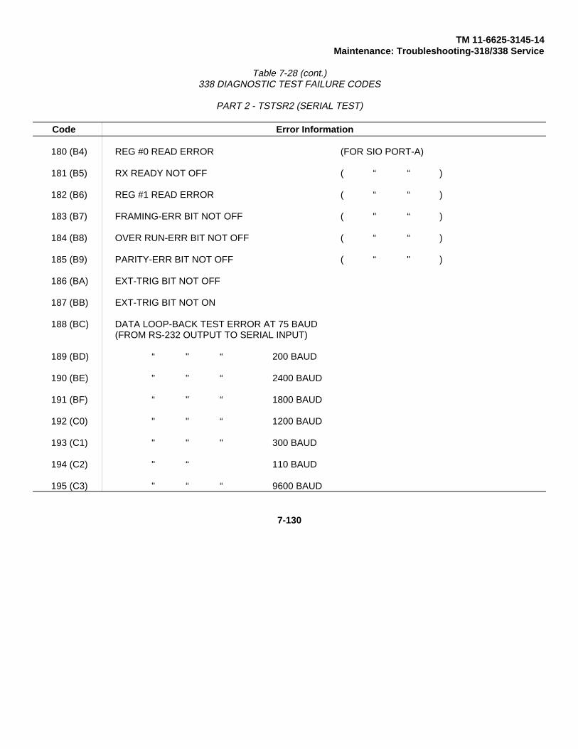
TM 11-6625-3145-14Maintenance: Troubleshooting-318/338 Service
Table 7-28 (cont.)338 DIAGNOSTIC TEST FAILURE CODES
PART 2 - TSTSR2 (SERIAL TEST)
Code Error Information
180 (B4) REG #0 READ ERROR (FOR SIO PORT-A)
181 (B5) RX READY NOT OFF ( “ “ )
182 (B6) REG #1 READ ERROR ( “ “ )
183 (B7) FRAMING-ERR BIT NOT OFF ( " “ )
184 (B8) OVER RUN-ERR BIT NOT OFF ( “ “ )
185 (B9) PARITY-ERR BIT NOT OFF ( “ " )
186 (BA) EXT-TRIG BIT NOT OFF
187 (BB) EXT-TRIG BIT NOT ON
188 (BC) DATA LOOP-BACK TEST ERROR AT 75 BAUD(FROM RS-232 OUTPUT TO SERIAL INPUT)
189 (BD) “ " “ 200 BAUD
190 (BE) " " “ 2400 BAUD
191 (BF) “ " “ 1800 BAUD
192 (C0) " " “ 1200 BAUD
193 (C1) " " " 300 BAUD
194 (C2) " “ 110 BAUD
195 (C3) " “ “ 9600 BAUD
7-130

TM 11-6625-3145-14Maintenance: Troubleshooting-318/338 Service
Table 7-28 (cont.)338 DIAGNOSTIC TEST FAILURE CODES
PART 3 - TSTNV2 (NVM TEST)
Code Error Information
200 (C8) DATA ERROR WHEN DATA PATTERN IS FF
201 (C9) “ “ “ 00
202 (CA) “ “ “ 01
203 (CB) " " “ 02
204 (CC) “ “ “ 04
205 (CD) " “ “ 08
206 (CE) " " “ 10
207 (CF) " “ “ 20
208 (D0) " " " 40
209 (D1) " “ “ 80
210 (D2) " “ " MARCHING PATTERN
211 (D3) " “ " INCREMENTING PATTERN
7-131/(7-132 blank)

TM 11-6625-3145-14Maintenance: Troubleshooting-318/338 Service
Figure 7-44. Troubleshooting Tree 1: Power On.
FIGURE 7-46
FIGURE 7-47
FIGURE 7-45
FIGURE 7-48
7-133
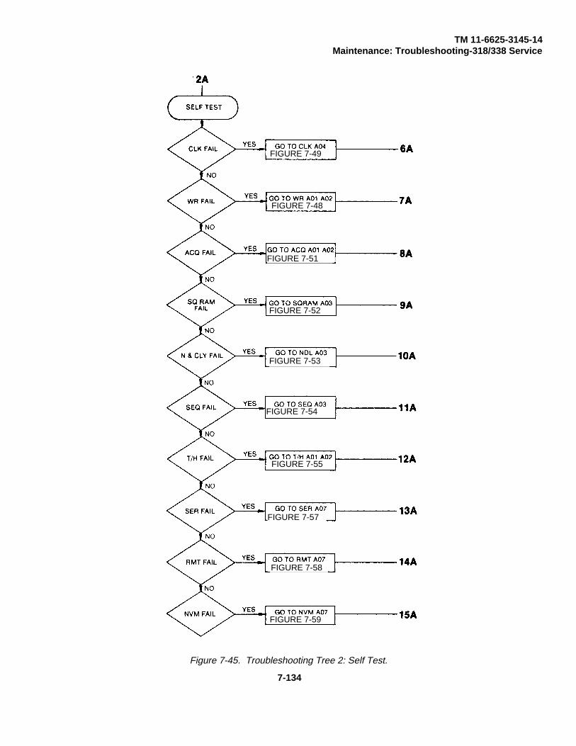
TM 11-6625-3145-14Maintenance: Troubleshooting-318/338 Service
Figure 7-45. Troubleshooting Tree 2: Self Test.
FIGURE 7-49
FIGURE 7-48
FIGURE 7-51
FIGURE 7-52
FIGURE 7-53
FIGURE 7-54
FIGURE 7-55
FIGURE 7-57
FIGURE 7-58
FIGURE 7-59
7-134

TM 11-6625-3145-14Maintenance: Troubleshooting-318/338 Service
Figure 7-46. Troubleshooting Tree 3: Power Supplies A11, A12 (Sheet 1 of 2).
7-135
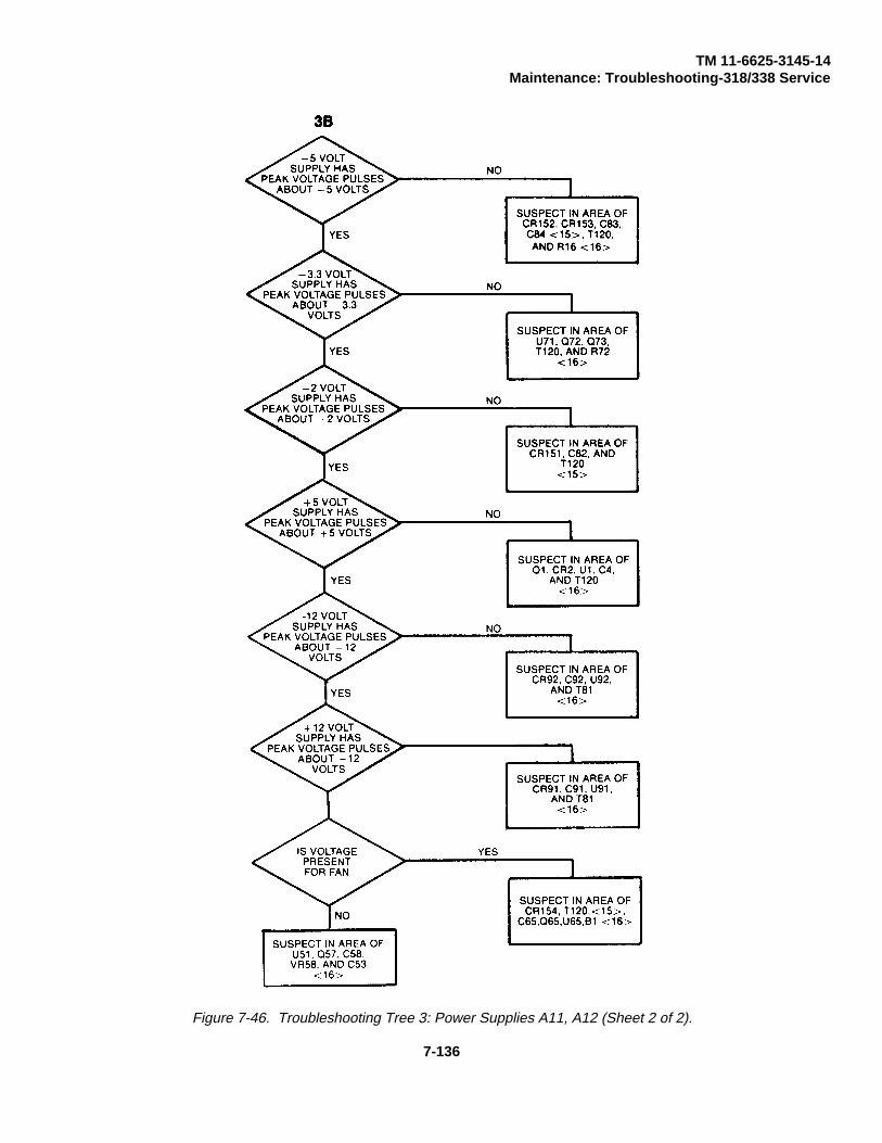
TM 11-6625-3145-14Maintenance: Troubleshooting-318/338 Service
Figure 7-46. Troubleshooting Tree 3: Power Supplies A11, A12 (Sheet 2 of 2).
7-136

TM 11-6625-3145-14Maintenance: Troubleshooting-318/338 Service
Figure 7-47. Troubleshooting Tree 4: CRT A10 (Sheet 1 of 4).
7-137
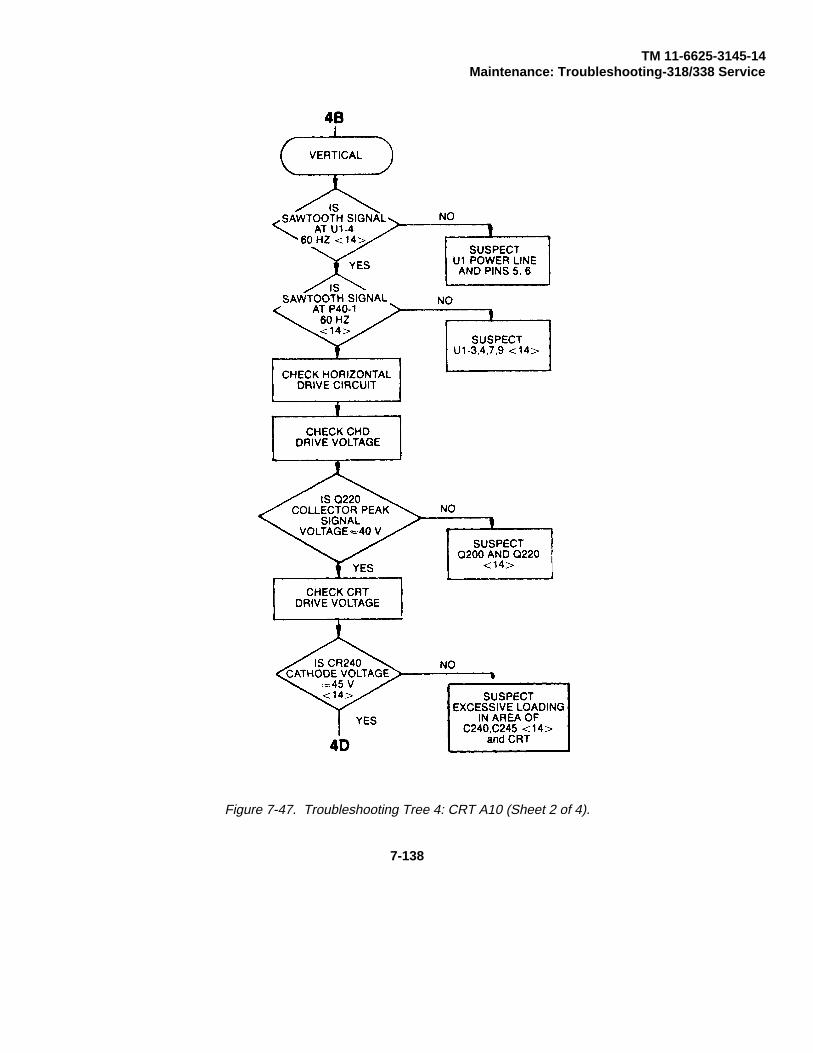
TM 11-6625-3145-14Maintenance: Troubleshooting-318/338 Service
Figure 7-47. Troubleshooting Tree 4: CRT A10 (Sheet 2 of 4).
7-138

TM 11-6625-3145-14Maintenance: Troubleshooting-318/338 Service
Figure 7-47. Troubleshooting Tree 4: CRT A10 (Sheet 3 of 4).
7-139

TM 11-6625-3145-14Maintenance: Troubleshooting-318/338 Service
Figure 7-47. Troubleshooting Tree 4: CRT A10 (Sheet 4 of 4).
7-140

TM 11-6625-3145-14Maintenance: Troubleshooting-318/338 Service
Figure 7-48. Troubleshooting Tree 5: MPU A06 (Sheet 1 of 5).
7-141
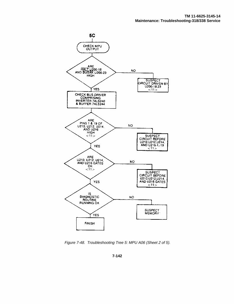
TM 11-6625-3145-14Maintenance: Troubleshooting-318/338 Service
Figure 7-48. Troubleshooting Tree 5: MPU A06 (Sheet 2 of 5).
7-142

TM 11-6625-3145-14Maintenance: Troubleshooting-318/338 Service
Figure 7-48. Troubleshooting Tree 5: MPU A06 (Sheet 3 of 5).
7-143
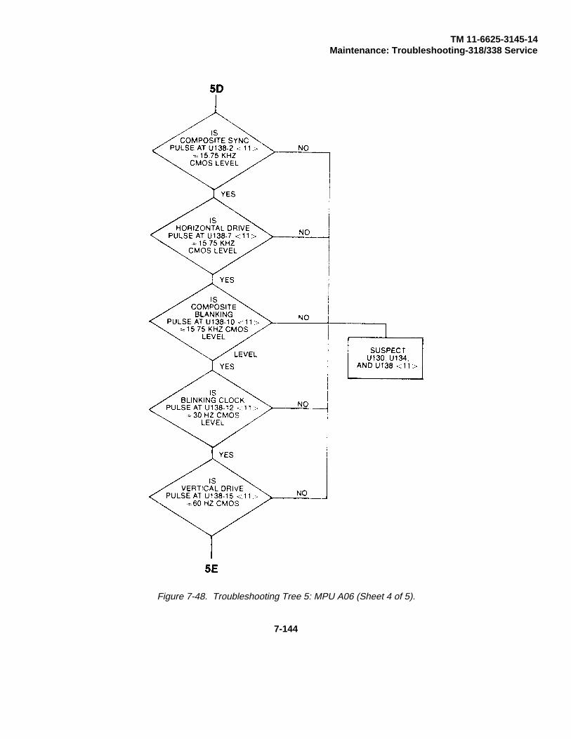
TM 11-6625-3145-14Maintenance: Troubleshooting-318/338 Service
Figure 7-48. Troubleshooting Tree 5: MPU A06 (Sheet 4 of 5).
7-144
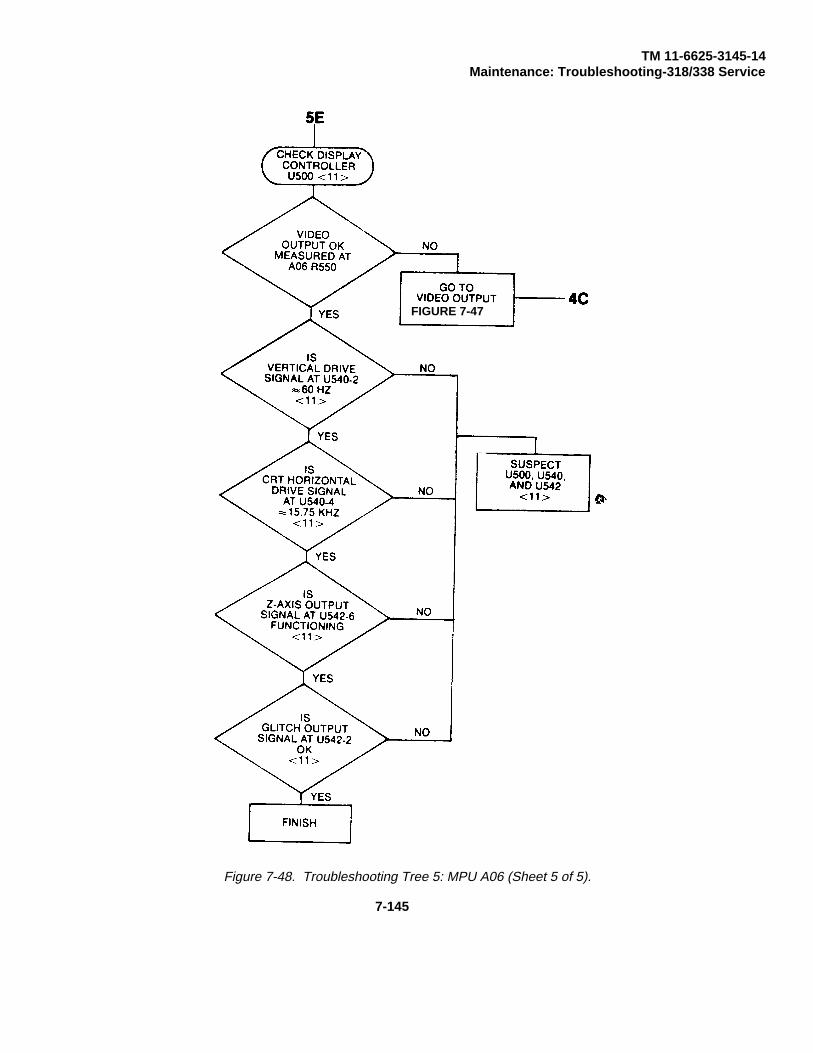
TM 11-6625-3145-14Maintenance: Troubleshooting-318/338 Service
Figure 7-48. Troubleshooting Tree 5: MPU A06 (Sheet 5 of 5).
FIGURE 7-47
7-145

TM 11-6625-3145-14Maintenance: Troubleshooting-318/338 Service
Figure 7-49. Troubleshooting Tree 6: Clock A04 (CLK) (Sheet 1 of 2).
7-146

TM 11-6625-3145-14Maintenance: Troubleshooting-318/338 Service
Figure 7-49. Troubleshooting Tree 6: Clock A04 (CLK) (Sheet 2 of 2).
7-147
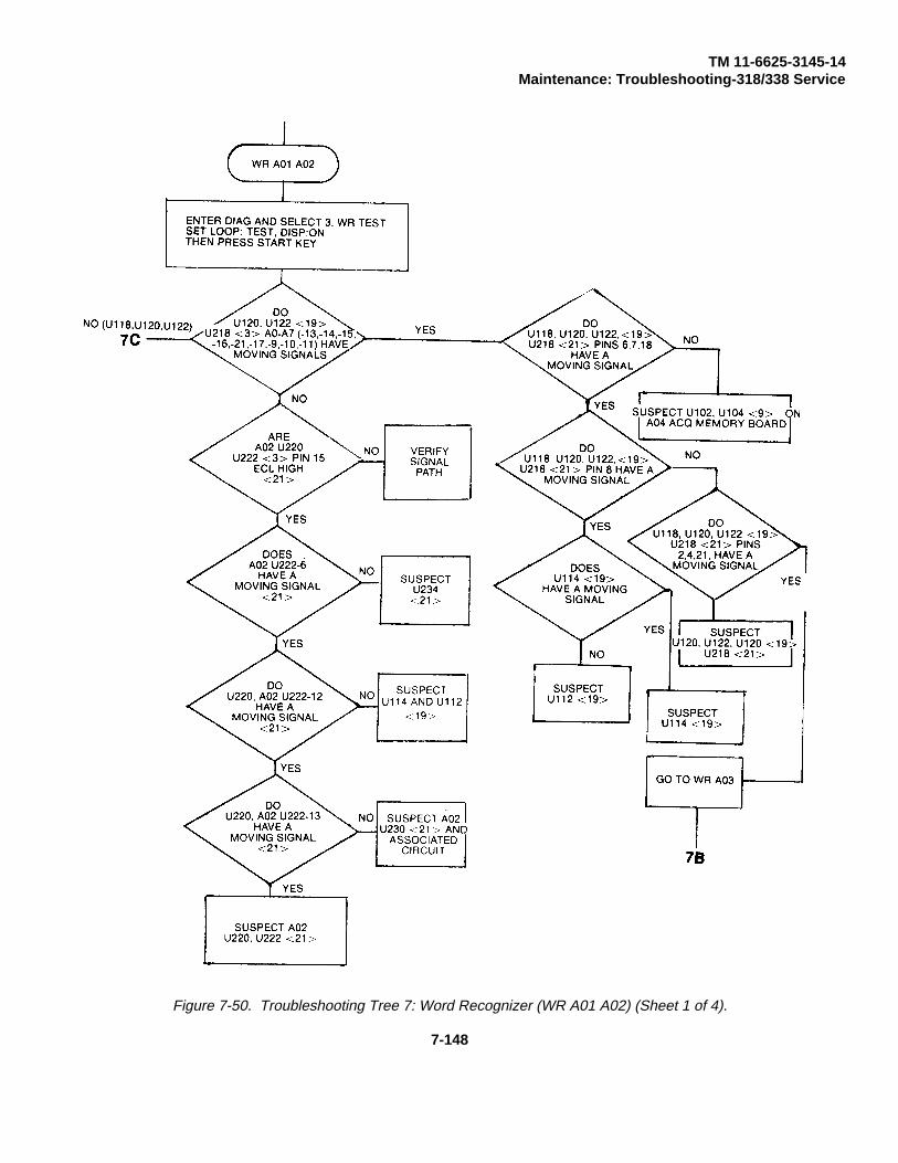
TM 11-6625-3145-14Maintenance: Troubleshooting-318/338 Service
Figure 7-50. Troubleshooting Tree 7: Word Recognizer (WR A01 A02) (Sheet 1 of 4).
7-148

TM 11-6625-3145-14Maintenance: Troubleshooting-318/338 Service
Figure 7-50. Troubleshooting Tree 7: Word Recognizer (WR A01 A02) (Sheet 2 of 4).
7-149

TM 11-6625-3145-14Maintenance: Troubleshooting-318/338 Service
Figure 7-50. Troubleshooting Tree 7: Word Recognizer (WR A01 A02) (Sheet 3 of 4).
7-150

TM 11-6625-3145-14Maintenance: Troubleshooting-318/338 Service
Figure 7-50. Troubleshooting Tree 7: Word Recognizer (WR A01 A02) (Sheet 4 of 4).
FIGURE 7-49
7-151

TM 11-6625-3145-14Maintenance: Troubleshooting-318/338 Service
Figure 7-51. Troubleshooting Tree 8: Data Acquisition (ACQ A01 A02) (Sheet 1 of 7).
7-152

TM 11-6625-3145-14Maintenance: Troubleshooting-318/338 Service
Figure 7-51. Troubleshooting Tree 8: Data Acquisition (ACQ A01 A02) (Sheet 2 of 7).
7-153
FIGURE 7-50

TM 11-6625-3145-14Maintenance: Troubieshooting-318/338 Service
Figure 7-51. Troubleshooting Tree 8: Data Acquisition (ACQ A01 A02) (Sheet 3 of 7).
7-154

TM 11-6625-3145-14Maintenance: Troubleshooting-318/338 Service
Figure 7-51. Troubleshooting Tree 8: Data Acquisition (ACQ A01 A02) (Sheet 4 of 7).
7-155
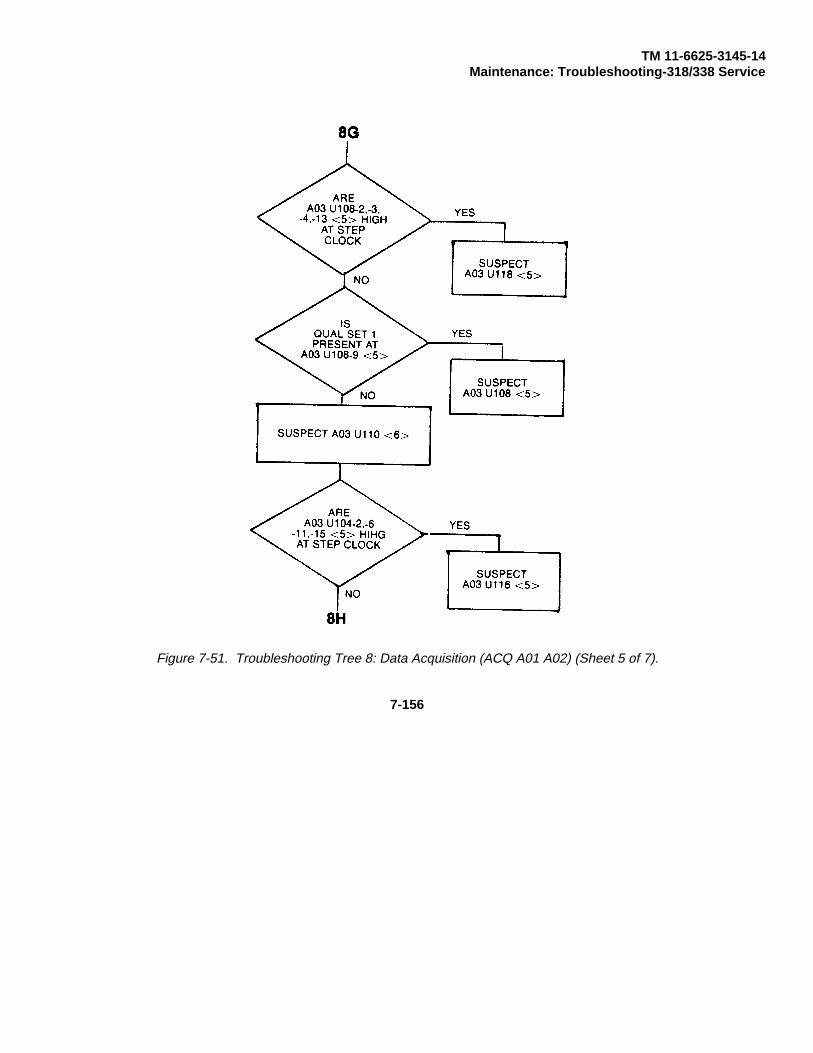
TM 11-6625-3145-14Maintenance: Troubleshooting-318/338 Service
Figure 7-51. Troubleshooting Tree 8: Data Acquisition (ACQ A01 A02) (Sheet 5 of 7).
7-156

TM 11-6625-3145-14Maintenance: Troubleshooting-318/338 Service
Figure 7-51. Troubleshooting Tree 8: Data Acquisition (ACQ A01 A02) (Sheet 6 of 7).
7-157
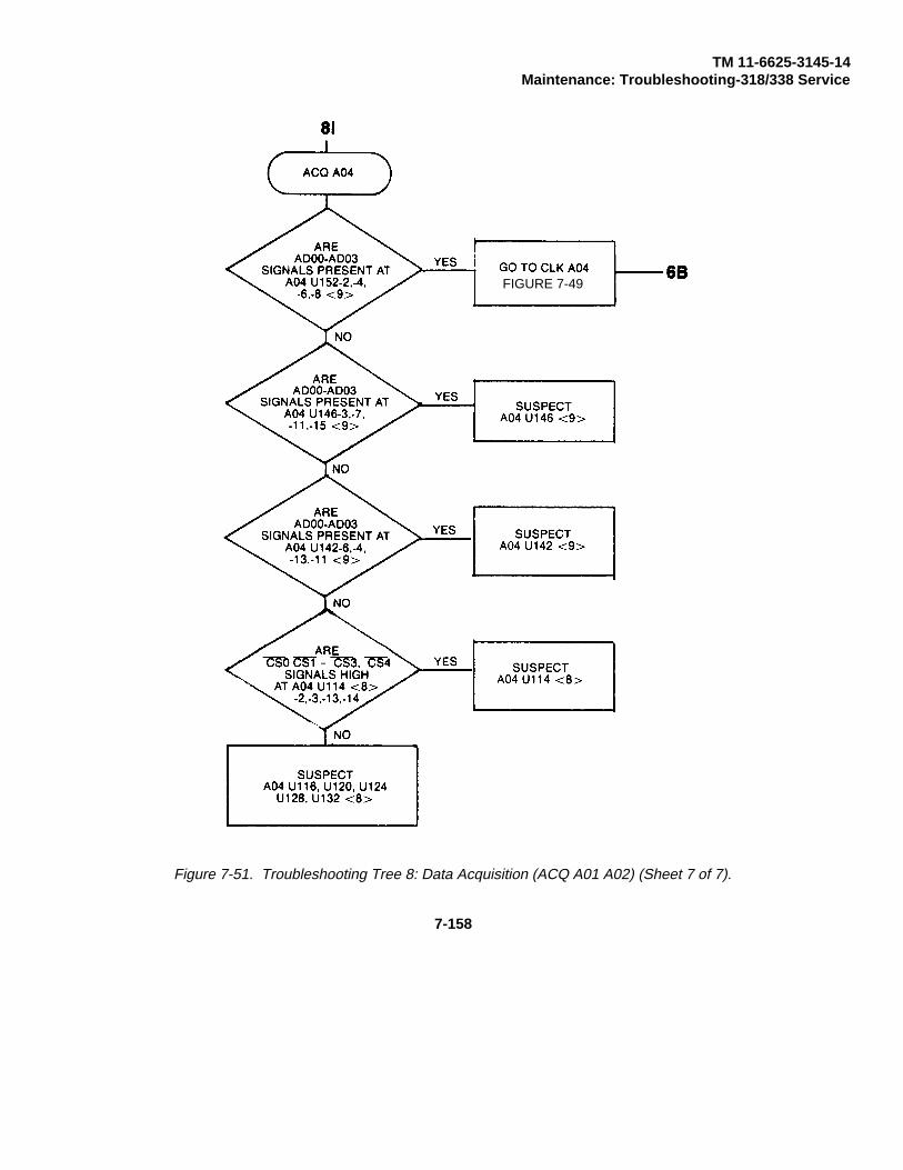
TM 11-6625-3145-14Maintenance: Troubleshooting-318/338 Service
Figure 7-51. Troubleshooting Tree 8: Data Acquisition (ACQ A01 A02) (Sheet 7 of 7).
7-158
FIGURE 7-49
7-158

TM 11-6625-3145-14Maintenance: Troubleshooting-318/338 Service
Figure 7-52. Troubleshooting Tree 9: SQRAM A03 (Sheet 1 of 4).
FIGURE 7-50
FIGURE 7-50
7-159

TM 11-6625-3145-14Maintenance: Troubleshooting-318/338 Service
Figure 7-52. Troubleshooting Tree 9: SQRAM A03 (Sheet 2 of 4).
7-160

TM 11-6625-3145-14Maintenance: Troubleshooting-318/338 Service
Figure 7-52. Troubleshooting Tree 9: SQRAM A03 (Sheet 3 of 4).
FIGURE 7-63
7-161

TM 11-6625-3145-14Maintenance: Troubleshooting-318/338 Service
Figure 7-52. Troubleshooting Tree 9: SQRAM A03 (Sheet 4 of 4).
7-162
FIGURE 7-49
7-162
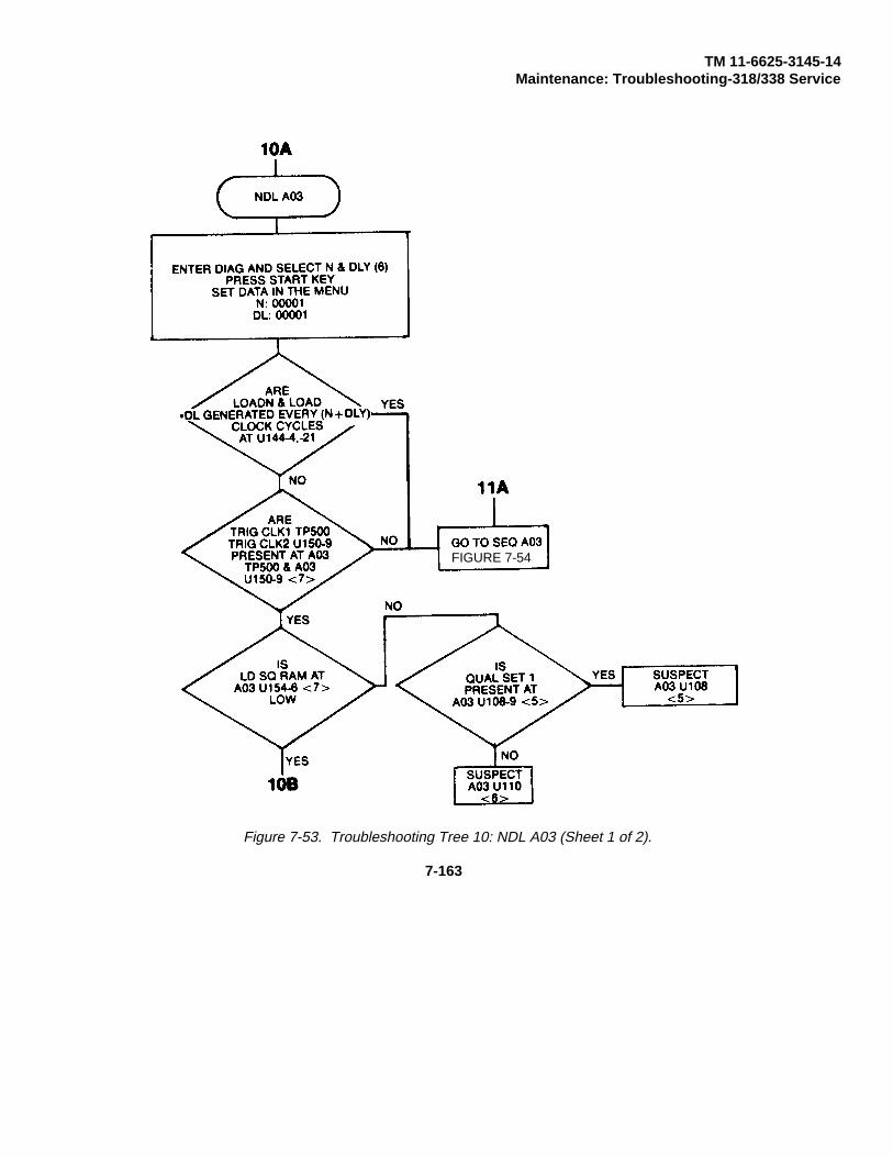
TM 11-6625-3145-14Maintenance: Troubleshooting-318/338 Service
Figure 7-53. Troubleshooting Tree 10: NDL A03 (Sheet 1 of 2).
FIGURE 7-54
7-163

TM 11-6625-3145-14Maintenance: Troubleshooting-318/338 Service
Figure 7-53. Troubleshooting Tree 10: NDL A03 (Sheet 2 of 2).
FIGURE 7-54
7-164

TM 11-6625-3145-14Maintenance: Troubleshooting-318/338 Service
Figure 7-54. Troubleshooting Tree 11: SEQ A03 (Sheet 1 of 4).
FIGURE 7-50
7-165

TM 11-6625-3145-14Maintenance: Troubleshooting-318/338 Service
Figure 7-54. Troubleshooting Tree 11: SEQ A03 (Sheet 2 of 4).
FIGURE 7-51
FIGURE 7-52
7-166

TM 11-6625-3145-14Maintenance: Troubleshooting-318/338 Service
Figure 7-54. Troubleshooting Tree 11: SEQ A03 (Sheet 3 of 4)
FIGURE 7-51
7-167
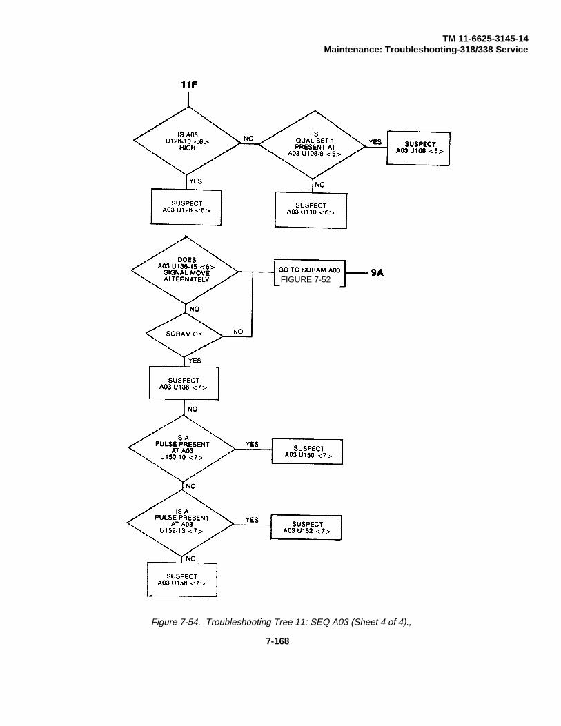
TM 11-6625-3145-14Maintenance: Troubleshooting-318/338 Service
Figure 7-54. Troubleshooting Tree 11: SEQ A03 (Sheet 4 of 4).,
7-168
FIGURE 7-52
7-168

TM 11-6625-3145-14Maintenance: Troubleshooting-318/338 Service
Figure 7-55. Troubleshooting Tree 12: T/H A01 A02
7-169

TM 11-6625-3145-14Maintenance: Troubleshooting-318/338 Service
Figure 7-56. Troubleshooting Tree 13: T/H A04.
FIGURE 7-51
7-170
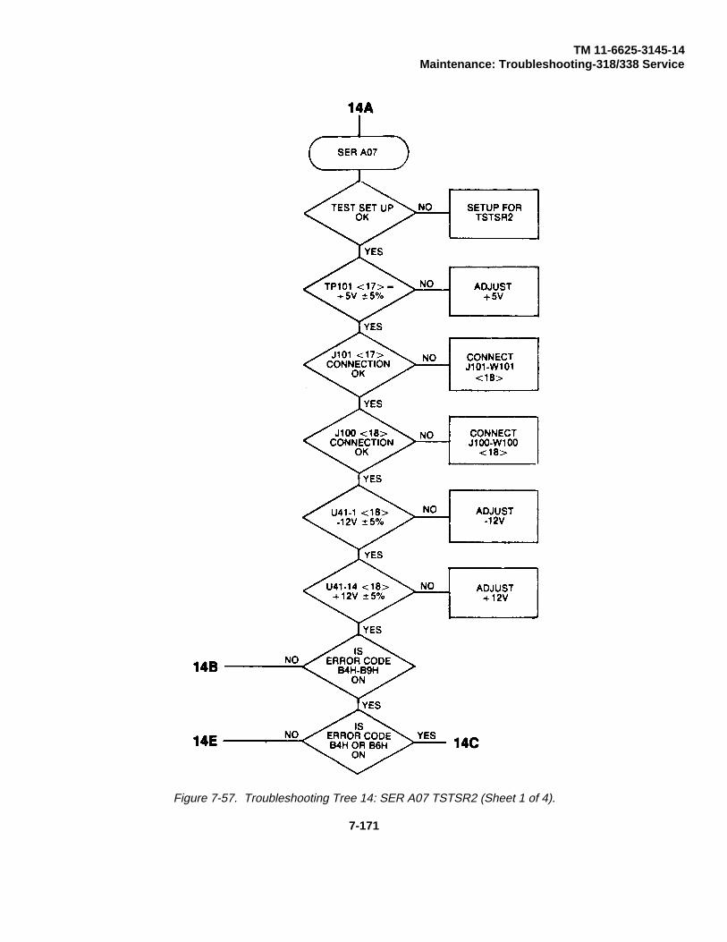
TM 11-6625-3145-14Maintenance: Troubleshooting-318/338 Service
Figure 7-57. Troubleshooting Tree 14: SER A07 TSTSR2 (Sheet 1 of 4).
7-171

TM 11-6625-3145-14Maintenance: Troubleshooting-318/338 Service
Figure 7-57. Troubleshooting Tree 14: SER A07 TSTSR2 (Sheet 2 of 4).
7-172

TM 11-6625-3145-14Maintenance: Troubleshooting-318/338 Service
Figure 7-57. Troubleshooting Tree 14: SER A07 TSTSR2 (Sheet 3 of 4).
7-173
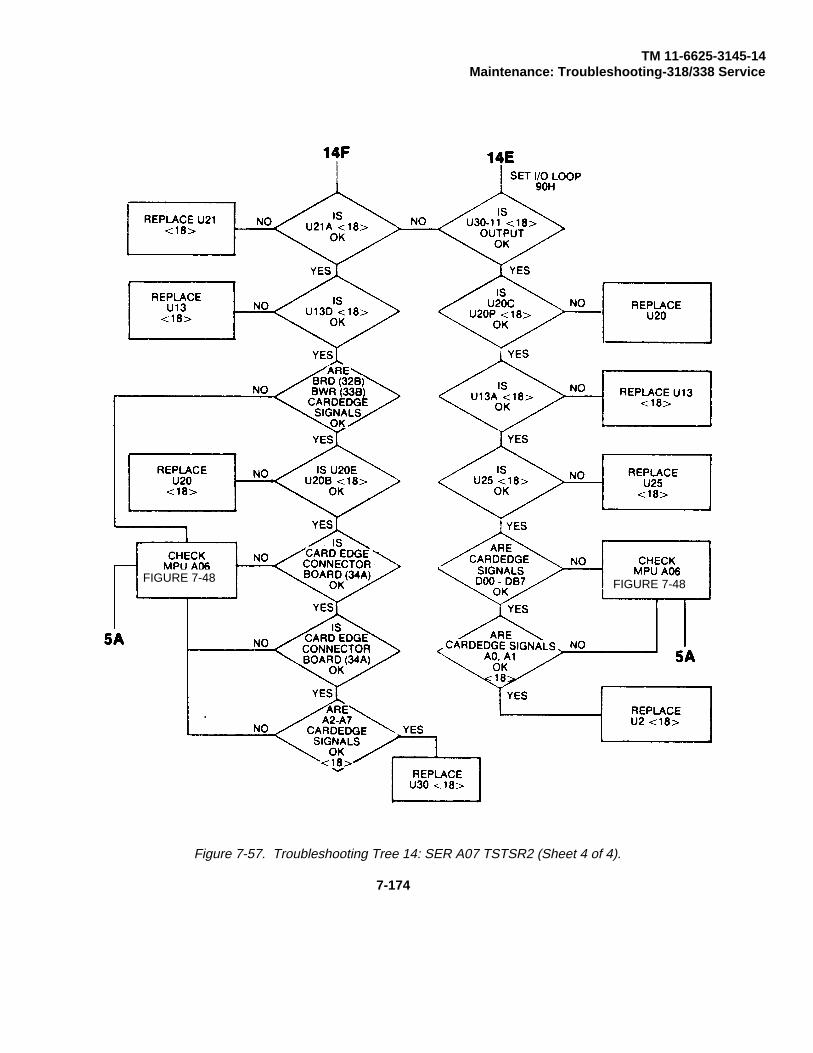
TM 11-6625-3145-14Maintenance: Troubleshooting-318/338 Service
Figure 7-57. Troubleshooting Tree 14: SER A07 TSTSR2 (Sheet 4 of 4).
FIGURE 7-48 FIGURE 7-48
7-174

TM 11-6625-3145-14Maintenance: Troubleshooting-318/338 Service
Figure 7-58. Troubleshooting Tree 15: REMOTE A07 TSTRM2 (RMT) (Sheet 1 of 4).
7-175

TM 11-6625-3145-14Maintenance: Troubleshooting-318/338 Service
Figure 7-58. Troubleshooting Tree 15: REMOTE A07 TSTRM2 (RMT) (Sheet 2 of 4).
FIGURE 7-48
FIGURE 7-48
7-176

TM 11-6625-3145-14Maintenance: Troubleshooting-318/338 Service
Figure 7-58. Troubleshooting Tree 15: REMOTE A07 TSTRM2 (RMT) (Sheet 3 of 4).
FIGURE 7-48
7-177

TM 11-6625-3145-14Maintenance: Troubleshooting-318/338 Service
Figure 7-58. Troubleshooting Tree 15: REMOTE A07 TSTRM2 (RMT) (Sheet 4 of 4).
FIGURE 7-48 FIGURE 7-48
7-178

TM 11-6625-3145.14Maintenance: Troubleshooting-318/338 Service
Figure 7-59. Troubleshooting Tree 16: Non Volatile Memory (NVM A07) (Sheet 1 of 2).
FIGURE 7-48
7-179

TM 11-6625-3145-14Maintenance: Troubleshooting-318/338 Service
Figure 7-59. Troubleshooting Tree 16: Non Volatile Memory (NVM A07) (Sheet 2 of 2),
FIGURE 7-48
7-180

TM 11-6625-3145-14Maintenance: Troubleshooting-318/338 Service
Figure 7-60. Troubleshooting Tree 17: Can’t Get Glitch.
7-181

TM 11-6625-3145-14Maintenance: Troubleshooting-318/338 Service
Figure 7-61. Troubleshooting Tree 18: Can’t Get Good Data (Sheet 1 of 2).
7-182

TM 11-6625-3145-14Maintenance: Troubleshooting-318/338 Service
Figure 7-61. Troubleshooting Tree 18: Can’t Get Good Data (Sheet 2 of 2).
7-183

TM 11-6625-3145-14Maintenance: Troubleshooting-318/338 Service
Figure 7-62. Troubleshooting Tree 19: Diagnostics Pass Can’t Stop.
7-184
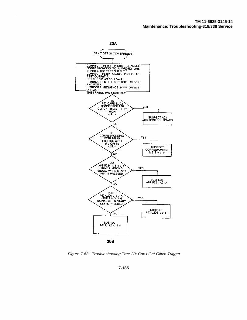
‘TM 11-6625-3145-14
Maintenance: Troubleshooting-318/338 Service
Figure 7-63. Troubleshooting Tree 20: Can’t Get Glitch Trigger
7-185

TM 11-6625-3145-14Maintenance: Troubleshooting-318/338 Service
Figure 7-64. Troubleshooting Tree 21: Test Output Doesn’t Work.
7-186

TM 11-6625-3145-14REPLACEABLE 318/338 Service
ELECTRICAL PARTS
PARTS ORDERING INFORMATIONReplacement parts are available from or through
your local Tektronix, Inc. Field Office or representative.
Changes to Tektronix instruments are sometimesmade to accommodate improved components as theybecome available, and to give you the benefit of thelatest circuit improvements developed in our engineeringdepartment. It is therefore important, when orderingparts, to include the following information in your order:Part number, instrument type or number, serial number,and modification number if applicable.
If a part you have ordered has been replaced with anew or improved part, your local Tektronix, Inc. FieldOffice or representative will contact you concerning anychange in part number.
Change information, if any, is located at the rear ofthis manual.
LIST OF ASSEMBLIESA list of assemblies can be found at the beginning of
the Electrical Parts List. The assemblies are listed innumerical order. When the complete componentnumber of a part is known, this list will identify theassembly in which the part is located.
CROSS INDEX-MFR. CODE NUMBER TOMANUFACTURER
The Mfr. Code Number to Manufacturer index forthe Electrical Parts List is located immediately after thispage. The Cross Index provides codes, names andaddresses of manufacturers of components listed in theElectrical Parts List.
ABBREVIATIONSAbbreviations conform to American National
Standard Y1.1.
COMPONENT NUMBER (column one of the ElectricalParts List)
A numbering method has been used to identifyassemblies, subassemblies and parts. Examples of thisnumbering method and typical expansions are illustratedby the following:
Only the circuit number will appear on the diagramsand circuit board illustrations. Each diagram and circuitboard illustration is clearly marked with the assemblynumber. Assembly numbers are also marked on themechanical exploded views located in the MechanicalParts List. The component number is obtained byadding the assembly number prefix to the circuit number.
The Electrical Parts List is divided and arranged byassemblies in numerical sequence (e.g., assembly A1with its subassemblies and parts, precedes assembly A2with its subassemblies and parts).
Chassis-mounted parts have no assembly numberprefix and are located at the end of the Electrical PartsList.
TEKTRONIX PART NO. (column two of theElectrical Parts List)
Indicates part number to be used when orderingreplacement part from Tektronix.
SERIAL/MODEL NO. (columns three and fourof the Electrical Parts List)
Column three (3) indicates the serial number atwhich the part was first used. Column four (4) indicatesthe serial number at which the part was removed. Noserial number entered indicates part is good for all serialnumbers.
NAME & DESCRIPTION (column five of theElectrical Parts List)
In the Parts List, an Item Name is separated fromthe description by a colon (:). Because of spacelimitations, an Item Name may sometimes appear asincomplete. For further Item Name identification, theU.S. Federal Cataloging Handbook H6-1 can be utilizedwhere possible.
MFR. CODE (column six of the Electrical PartsList)
Indicates the code number of the actualmanufacturer of the part. (Code to name and addresscross reference can be found immediately after thispage.)
MFR. PART NUMBER (column seven of theElectrical Parts List)
Indicates actual manufacturers part number.
8-1

TM 11-6625-3145-14Replaceable Electrical Parts-318/338 Service
CROSS INDEX-MFR. CODE NUMBER TO MANUFACTURER
Mfr. Code Manufacturer Address City, State, Zip
0000M SONY/TEKTRONIX CORPORATION P O BOX 14, HANEDA AIRPORT TOKYO 149, JAPAN000FJ MARCOM SWITCHES INC 67 ALBANY STREET CAZENOVIA, N.Y. 1303501121 ALLEN-BRADLEY COMPANY 1201 2ND STREET SOUTH MILWAUKEE, WI 5320401295 TEXAS INSTRUMENTS, INC.
SEMICONDUCTOR GROUP P.O. BOX 5012 DALLAS, TX 7522204222 AVX CERAMICS, DIVISION OF AVX CORP P O BOX 867 MYRTLE BEACH, SC 2957704713 MOTOROLA, INC., SEMICONDUCTOR PROD. DIV 5005 E MCDOWELL RD,PO BOX 20923 PHOENIX, AZ 8503607263 FAIRCHILD SEMICONDUCTOR, A DIV. OF
FAIRCHILD CAMERA AND INSTRUMENT CORP 464 ELLIS STREET MOUNTAIN VIEW, CA 9404212969 UNITRODE CORPORATION 580 PLEASANT STREET WATERTOWN, MA 0217213511 AMPHENOL CARDRE DIV., BUNKER RAMO CORP LOS GATOS, CA 9503017856 SILICONIX, INC 2201 LAURELWOOD DRIVE SANTA CLARA, CA 9505418324 SIGNETICS CORP 811 E. ARQUES SUNNYVALE, CA 9408619701 ELECTRA-MIDLAND CORP., MEPCO ELECTRA INC P O BOX 760 MINERAL WELLS, TX 7606727014 NATIONAL SEMICONDUCTOR CORP 2900 SEMICONDUCTOR DR SANTA CLARA, CA 9505131918 IEE/SCHADOW INC 8081 WALLACE ROAD EDEN PRAIRIE, MN 5534350434 HEWLETT-PACKARD COMPANY 640 PAGE MILL ROAD PALO ALTO, CA 9430451642 CENTRE ENGINEERING INC 2820 E COLLEGE AVENUE STATE COLLEGE, PA 1680154583 TDK ELECTRONICS CORP 755 EASTGATE BLVD GARDEN CITY, NY 1153055680 NICHICON/AMERICA/CORP 6435 N PROESEL AVENUE CHICAGO, IL 6064556289 SPRAGUE ELECTRIC CO 87 MARSHALL ST NORTH ADAMS, MA 0124757668 R-OHM CORP 16931 MILLIKEN AVE IRVINE, CA 9271359821 CENTRALAB INC 7158 MERCHANT AVE EL PASO, TX 79915
SUB NORTH AMERICAN PHILIPS CORP71400 BUSSMAN MFG., DIVISION OF MCGRAW-
EDISON CO 2536 W. UNIVERSITY ST ST. LOUIS, MO 6310771785 TRW, CINCH CONNECTORS 1501 MORSE AVENUE ELK GROVE VILLAGE, IL
6000772982 ERIE TECHNOLOGICAL PRODUCTS, INC 644 W. 12TH ST ERIE, PA 1651280009 TEKTRONIX, INC P O BOX 500 BEAVERTON, OR 9707790201 MALLORY CAPACITOR CO., DIV. OF 3029 E. WASHINGTON STREET
P. R. MALLORY AND CO INC P. O. BOX 372 INDIANAPOLIS, IN 46206
91637 DALE ELECTRONICS, INC P. O. BOX 609 COLUMBUS, NE 6860193410 ESSEX INTERNATIONAL, INC., CONTROLS DIV.
LEXINGTON PLANT P. O. BOX 1007 MANSFIELD, OH 4490396733 SAN FERNANDO ELECTRIC MFG CO 1501 FIRST ST SAN FERNANDO, CA 91341T0058 NEC ELECTRON INC 252 HUMBOLT COURT SUNNYVALE, CA 94086T0191 SONY TEKTRONIX P.O. BOX 14, HANEDA AIRPORT TOKYO 149, JAPAN
8-2

TM 11-6625-3145-14Replaceable Electrical Parts-318/338 Service
Tektronix Serial/Model No. MfrComponent No. Part No. Eff Dscont Name & Description Code Mfr. Part NumberA01 670-7819-00 CKT BOARD ASSY: DATA INPUT A 80009 670-7819-00A01 ---- ---- (318 ONLY)A01 670-7817-00 CKT BOARD ASSY: DATA INPUT A 80009 670-7817-00A01 ---- ---- (338 ONLY)A02 670-7818-00 CKT BOARD ASSY: DATA INPUT B 80009 670-7818-00
A02 ---- ---- (318 ONLY)A02 670-7816-00 CKT BOARD ASSY: DATA INPUT B 80009 670-7816-00A02 ---- ---- (338 ONLY)A03 670-7815-00 CKT BOARD ASSY: ACQ CONTROL 80009 670-7815-00A03 ---- ---- (318 ONLY)A03 670-7822-00 CKT BOARD ASSY: ACQ CONNECTOR 80009 670-7822-00A03 ---- ---- (338 ONLY)
A04 670-7814-00 CKT BOARD ASSY: ACQ MEMORY 80009 670-7814-00A04 ---- ---- (318 ONLY)A04 670-7823-00 CKT BOARD ASSY: ACQ MEMORY 80009 670-7823-00A04 ----- ----- (338 ONLY)A05 670-7813-00 CKT BOARD ASSY: ROM/THRESHOLD 80009 670-7813-00A05 ---- ---- (318/338 ONLY)
A06 670-7812-00 CKT BOARD ASSY: MPU DISPLAY 80009 670-7812-00A06 ---- ---- (318/338 ONLY)A07 670-7809-00 CKT BOARD ASSY: SERIAL/RS232/NUM 80009 670-7809-00A07 ---- ---- (318/338 OPTION 01 ONLY)A08 670-7811-00 CKT BOARD ASSY: MOTHER 80009 670-7811-00A08 ---- ---- (318/338 ONLY)
A09 260-2133-00 SWITCH PB ASSY: KEYBOARD 80009 260-2133-00A09 ---- ---- 18/338 ONLY)A10 670-7810-00 CKT BOARD ASSY: CRT CIRCUIT 80009 670-7810-00A10 ----- ----- (318/338 ONLY)A11 670-7821-00 CKT BOARD ASSY: INVERTER 80009 670-7821-00A11 ---- ---- (318/338 ONLY)
A12 670-7820-00 CKT BOARD ASSY: REGULATOR 80009 670-7820-00A12 ---- ---- (318/338 ONLY)
A01 670-7819-00 CKT BOARD ASSY: DATA INPUT A 80009 670-7819-00A01 ---- ---- (318 ONLY)
A01 670-7817-00 CKT BOARD ASSY: DATA INPUT B 80009 670-7817-00A01 ---- ---- (338 ONLY)A01C100 281-0768-00 CAP., FXD, CER DI: 470PF, 20%, 100V 56289 292CC0G471M100BA01C102 290-0995-00 CAP., FXD, ELCTLT: 47UF, 20%, 16V 0000M 290-0995-00A01C104 281-0775-00 CAP., FXD, CER DI: 0.1UF, 20%, 50V 04222 MA205E104MAAA01C104 ---- ---- (318 ONLY)
A01C104 290-0995-00 CAP., FXD, ELCTLT: 47UF, 20%, 16V 0000M 290-0995-00A01C104 ---- ---- (338 ONLY)A01C106 281-0775-00 CAP., FXD, CER DI: 0.1UF, 20%, 50V 04222 MA205E104MAAA01C108 290-0995-00 CAP., FXD, ELCTLT: 47UF, 20%, 16V 0000M 290-0995-00A01C108 ---- ---- (318 ONLY)A01C108 281-0775-00 CAP., FXD, CER DI: 0.1UF, 20%, 50V 04222 MA205E104MAA
A01C108 ---- ---- (338 ONLY)A01C110 281-0775-00 CAP., FXD, CER DI: 0.1UF, 20%, 50V 04222 MA205E104MAAA01C110 ---- ---- (318 ONLY)A01C110 290-0995-00 CAP., FXD, ELCTLT: 47UF, 20%, 16V 0000M 290-0995-00A01C110 ---- ---- (338 ONLY)A01C112 281-0775-00 CAP., FXD, CER DI: 0.1UF, 20%, 50V 04222 MA205E104MAA
8-3
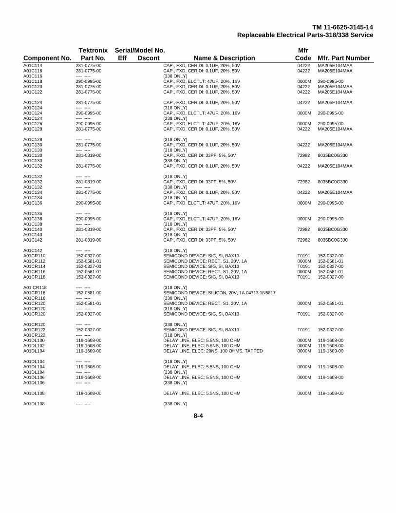
TM 11-6625-3145-14Replaceable Electrical Parts-318/338 Service
Tektronix Serial/Model No. MfrComponent No. Part No. Eff Dscont Name & Description Code Mfr. Part NumberA01C114 281-0775-00 CAP., FXD, CER DI: 0.1UF, 20%, 50V 04222 MA205E104MAAA01C116 281-0775-00 CAP., FXD, CER DI: 0.1UF, 20%, 50V 04222 MA205E104MAAA01C116 ---- ---- (338 ONLY)A01C118 290-0995-00 CAP., FXD, ELCTLT: 47UF, 20%, 16V 0000M 290-0995-00A01C120 281-0775-00 CAP., FXD, CER DI: 0.1UF, 20%, 50V 04222 MA205E104MAAA01C122 281-0775-00 CAP., FXD, CER DI: 0.1UF, 20%, 50V 04222 MA205E104MAA
A01C124 281-0775-00 CAP., FXD, CER DI: 0.1UF, 20%, 50V 04222 MA205E104MAAA01C124 ---- ---- (318 ONLY)A01C124 290-0995-00 CAP., FXD, ELCTLT: 47UF, 20%, 16V 0000M 290-0995-00A01C124 ---- ---- (338 ONLY)A01C126 290-0995-00 CAP., FXD, ELCTLT: 47UF, 20%, 16V 0000M 290-0995-00A01C128 281-0775-00 CAP., FXD. CER DI: 0.1UF, 20%, 50V 04222 MA205E104MAA
A01C128 ---- ---- (318 ONLY)A01C130 281-0775-00 CAP., FXD, CER DI: 0.1UF, 20%, 50V 04222 MA205E104MAAA01C130 ---- ---- (318 ONLY)A01C130 281-0819-00 CAP., FXD, CER DI: 33PF, 5%, 50V 72982 8035BC0G330A01C130 ---- ---- (338 ONLY)A01C132 281-0775-00 CAP., FXD, CER DI: 0.1UF, 20%, 50V 04222 MA205E104MAA
A01C132 ---- ---- (318 ONLY)A01C132 281-0819-00 CAP., FXD, CER DI: 33PF, 5%, 50V 72982 8035BC0G330A01C132 ---- ---- (338 ONLY)A01C134 281-0775-00 CAP., FXD, CER DI: 0.1UF, 20%, 50V 04222 MA205E104MAAA01C134 ---- ---- (318 ONLY)A01C136 290-0995-00 CAP., FXD. ELCTLT: 47UF, 20%, 16V 0000M 290-0995-00
A01C136 ---- ---- (318 ONLY)A01C138 290-0995-00 CAP., FXD, ELCTLT: 47UF, 20%, 16V 0000M 290-0995-00A01C138 ---- ---- (318 ONLY)A01C140 281-0819-00 CAP., FXD, CER DI: 33PF, 5%, 50V 72982 8035BC0G330A01C140 ---- ---- (318 ONLY)A01C142 281-0819-00 CAP., FXD, CER DI: 33PF, 5%, 50V 72982 8035BC0G330
A01C142 ---- ---- (318 ONLY)A01CR110 152-0327-00 SEMICOND DEVICE: SIG, SI, BAX13 T0191 152-0327-00A01CR112 152-0581-01 SEMICOND DEVICE: RECT, S1, 20V, 1A 0000M 152-0581-01A01CR114 152-0327-00 SEMICOND DEVICE: SIG, SI, BAX13 T0191 152-0327-00A01CR116 152-0581-01 SEMICOND DEVICE: RECT, S1, 20V, 1A 0000M 152-0581-01A01CR118 152-0327-00 SEMICOND DEVICE: SIG, SI, BAX13 T0191 152-0327-00
A01 CR118 ---- ---- (318 ONLY)A01CR118 152-0581-00 SEMICOND DEVICE: SILICON, 20V, 1A 04713 1N5817A01CR118 ---- ---- (338 ONLY)A01CR120 152-0581-01 SEMICOND DEVICE: RECT, S1, 20V, 1A 0000M 152-0581-01A01CR120 ---- ---- (318 ONLY)A01CR120 152-0327-00 SEMICOND DEVICE: SIG, SI, BAX13 T0191 152-0327-00
A01CR120 ---- ---- (338 ONLY)A01CR122 152-0327-00 SEMICOND DEVICE: SIG, SI, BAX13 T0191 152-0327-00A01CR122 ---- ---- (318 ONLY)A01DL100 119-1608-00 DELAY LINE, ELEC: 5.5NS, 100 OHM 0000M 119-1608-00A01DL102 119-1608-00 DELAY LINE, ELEC: 5.5NS, 100 OHM 0000M 119-1608-00A01DL104 119-1609-00 DELAY LINE, ELEC: 20NS, 100 OHMS, TAPPED 0000M 119-1609-00
A01DL104 ---- ---- (318 ONLY)A01DL104 119-1608-00 DELAY LINE, ELEC: 5.5NS, 100 OHM 0000M 119-1608-00A01DL104 ---- ---- (338 ONLY)A01DL106 119-1608-00 DELAY LINE, ELEC: 5.5NS, 100 OHM 0000M 119-1608-00A01DL106 ---- ---- (338 ONLY)
A01DL108 119-1608-00 DELAY LINE, ELEC: 5.5NS, 100 OHM 0000M 119-1608-00
A01DL108 ---- ---- (338 ONLY)
8-4
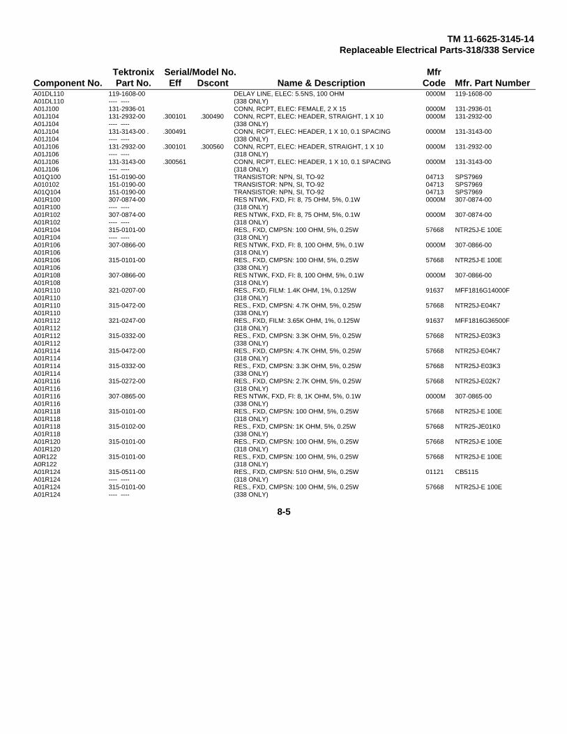
TM 11-6625-3145-14Replaceable Electrical Parts-318/338 Service
Tektronix Serial/Model No. MfrComponent No. Part No. Eff Dscont Name & Description Code Mfr. Part NumberA01DL110 119-1608-00 DELAY LINE, ELEC: 5.5NS, 100 OHM 0000M 119-1608-00A01DL110 ---- ---- (338 ONLY)A01J100 131-2936-01 CONN, RCPT, ELEC: FEMALE, 2 X 15 0000M 131-2936-01A01J104 131-2932-00 .300101 .300490 CONN, RCPT, ELEC: HEADER, STRAIGHT, 1 X 10 0000M 131-2932-00A01J104 ---- ---- (338 ONLY)A01J104 131-3143-00 . .300491 CONN, RCPT, ELEC: HEADER, 1 X 10, 0.1 SPACING 0000M 131-3143-00A01J104 ---- ---- (338 ONLY)A01J106 131-2932-00 .300101 .300560 CONN, RCPT, ELEC: HEADER, STRAIGHT, 1 X 10 0000M 131-2932-00A01J106 ---- ---- (318 ONLY)A01J106 131-3143-00 .300561 CONN, RCPT, ELEC: HEADER, 1 X 10, 0.1 SPACING 0000M 131-3143-00A01J106 ---- ---- (318 ONLY)A01Q100 151-0190-00 TRANSISTOR: NPN, SI, TO-92 04713 SPS7969A010102 151-0190-00 TRANSISTOR: NPN, SI, TO-92 04713 SPS7969A01Q104 151-0190-00 TRANSISTOR: NPN, SI, TO-92 04713 SPS7969A01R100 307-0874-00 RES NTWK, FXD, FI: 8, 75 OHM, 5%, 0.1W 0000M 307-0874-00A01R100 ---- ---- (318 ONLY)A01R102 307-0874-00 RES NTWK, FXD, FI: 8, 75 OHM, 5%, 0.1W 0000M 307-0874-00A01R102 ---- ---- (318 ONLY)A01R104 315-0101-00 RES., FXD, CMPSN: 100 OHM, 5%, 0.25W 57668 NTR25J-E 100EA01R104 ---- ---- (318 ONLY)A01R106 307-0866-00 RES NTWK, FXD, FI: 8, 100 OHM, 5%, 0.1W 0000M 307-0866-00A01R106 (318 ONLY)A01R106 315-0101-00 RES., FXD, CMPSN: 100 OHM, 5%, 0.25W 57668 NTR25J-E 100EA01R106 (338 ONLY)A01R108 307-0866-00 RES NTWK, FXD, FI: 8, 100 OHM, 5%, 0.1W 0000M 307-0866-00A01R108 (318 ONLY)A01R110 321-0207-00 RES., FXD, FILM: 1.4K OHM, 1%, 0.125W 91637 MFF1816G14000FA01R110 (318 ONLY)A01R110 315-0472-00 RES., FXD, CMPSN: 4.7K OHM, 5%, 0.25W 57668 NTR25J-E04K7A01R110 (338 ONLY)A01R112 321-0247-00 RES., FXD, FILM: 3.65K OHM, 1%, 0.125W 91637 MFF1816G36500FA01R112 (318 ONLY)A01R112 315-0332-00 RES., FXD, CMPSN: 3.3K OHM, 5%, 0.25W 57668 NTR25J-E03K3A01R112 (338 ONLY)A01R114 315-0472-00 RES., FXD, CMPSN: 4.7K OHM, 5%, 0.25W 57668 NTR25J-E04K7A01R114 (318 ONLY)A01R114 315-0332-00 RES., FXD, CMPSN: 3.3K OHM, 5%, 0.25W 57668 NTR25J-E03K3A01R114 (338 ONLY)A01R116 315-0272-00 RES., FXD, CMPSN: 2.7K OHM, 5%, 0.25W 57668 NTR25J-E02K7A01R116 (318 ONLY)A01R116 307-0865-00 RES NTWK, FXD, FI: 8, 1K OHM, 5%, 0.1W 0000M 307-0865-00A01R116 (338 ONLY)A01R118 315-0101-00 RES., FXD, CMPSN: 100 OHM, 5%, 0.25W 57668 NTR25J-E 100EA01R118 (318 ONLY)A01R118 315-0102-00 RES., FXD, CMPSN: 1K OHM, 5%, 0.25W 57668 NTR25-JE01K0A01R118 (338 ONLY)A01R120 315-0101-00 RES., FXD, CMPSN: 100 OHM, 5%, 0.25W 57668 NTR25J-E 100EA01R120 (318 ONLY)A0R122 315-0101-00 RES., FXD, CMPSN: 100 OHM, 5%, 0.25W 57668 NTR25J-E 100EA0R122 (318 ONLY)A01R124 315-0511-00 RES., FXD, CMPSN: 510 OHM, 5%, 0.25W 01121 CB5115A01R124 ---- ---- (318 ONLY)A01R124 315-0101-00 RES., FXD, CMPSN: 100 OHM, 5%, 0.25W 57668 NTR25J-E 100EA01R124 ---- ---- (338 ONLY)
8-5

TM 11-6625-3145-14Replaceable Electrical Parts-318/338 Service
Tektronix Serial/Model No. MfrComponent No. Part No. Eff Dscont Name & Description Code Mfr. Part Number
A01R126 315-0472-00 RES., FXD, CMPSN: 4.7K OHM, 5%, 0.25W 57668 NTR25J-E04K7A01R126 ---- ---- (318 ONLY)A01R126 315-0101-00 RES., FXD, CMPSN: 100 OHM, 5%, 0.25W 57668 NTR25J-E 100EA01R126 ---- ---- (338 ONLY)A01R128 307-0865-00 RES NTWK, FXD, FI: 8, 1K OHM, 5%, 0.1W 0000M 307-0865-00A01R128 ---- ---- (318 ONLY)
A01R128 315-0332-00 RES., FXD, CMPSN: 3.3K OHM, 5%, 0.25W 57668 NTR25J-E03K3A01R128 ---- ---- (338 ONLY)A01R130 315-0102-00 RES., FXD, CMPSN: 1K OHM, 5%, 0.25W 57668 NTR25-JE01K0A01R130 ---- ---- (318 ONLY)A01R130 315-0511-00 RES., FXD, CMPSN: 510 OHM, 5%, 0.25W 01121 CB5115A01R130 ---- ---- (338 ONLY)
A01R134 307-0868-00 RES NTWK, FXD, FI: .6, 100 OHMS, 5%, 0.1W 0000M 307-0868-00A01R134 (338 ONLY)A01R136 315-0332-00 RES., FXD, CMPSN: 3.3K OHM, 5%, 0.25W 57668 NTR25J-E03K3A01R136 ---- ---- (318 ONLY)A01R136 307-0867-00 RES NTWK, FXD, FI: 3, 100 OHM, 5%, 0.1W 0000M 307-0867-00A01R136 ---- ---- (338 ONLY)
A01R138 315-0332-00 RES., FXD, CMPSN: 3.3K OHM, 5%, 0.25W 57668 NTR25J-E03K3A01R138 ---- ---- (318 ONLY)A01R138 315-0511-00 RES., FXD, CMPSN: 510 OHM, 5%, 0.25W 01121 CB5115A01R138 ---- ---- (338 ONLY)A01R140 315-0332-00 RES., FXD, CMPSN: 3.3K OHM, 5%, 0.25W 57668 NTR25J-E 03K3A01R140 ---- ---- (318 ONLY)
A01R140 315-0511-00 RES., FXD, CMPSN: 510 OHM, 5%, 0.25W 01121 CB5115A01R140 ---- ---- (338 ONLY)A01R142 307-0111-00 RES., FXD, CMPSN: 3.6 OHM, 5%, 0.25W 01121 CB36G5A01R142 ---- ---- (318 ONLY)A01R142 315-0511-00 RES., FXD, CMPSN: 510 OHM, 5%, 0.25W 01121 CB5115A01R142 ---- ---- (338 ONLY)
A01R144 315-0511-00 RES., FXD, CMPSN: 510 OHM, 5%, 0.25W 01121 CB5115A01R144 ---- ---- (338 ONLY)A01R146 315-0102-00 RES., FXD, CMPSN: 1K OHM, 5%, 0.25W 57668 NTR25J-E01K0A01R146 ---- ---- (318 ONLY)A01R148 315-0102-00 RES., FXD, CMPSN: 1K OHM, 5%, 0.25W 57668 NTR25J-E01K0A01R148 ---- ---- (318 ONLY)
A01R150 315-0101-00 RES., FXD, CMPSN: 100 OHM, 5%, 0.25W 57668 NTR25J-E 100EA01R150 ---- ---- (318 ONLY)A01R152 315-0510-00 RES., FXD, CMPSN: 51 OHM, 5%, 0.25W 57668 NTR25J-E51 E0A01R152 ---- ---- (318 ONLY)A01R154 307-0868-00 RES NTWK, FXD, FI: 6, 100 OHM, 5%, 0.1W 0000M 307-0868-00A01R154 ---- ---- (318 ONLY)
A01R156 307-0867-00 RES NTWK, FXD, FI: 3, 100 OHM, 5%, 0.1W 0000M 307-0867-00A01R156 ---- ---- (318 ONLY)A01TP100 214-0579-00 TERM, TEST POINT: BRS CD PL 80009 214-0579-00A01TP102 214-0579-00 TERM, TEST POINT: BRS CD PL 80009 214-0579-00A01TP104 214-0579-00 TERM, TEST POINT: BRS CD PL 80009 214-0579-00A01TP104 ---- ---- (338 ONLY)
A01TP106 214-0579-00 TERM, TEST POINT: BRS CD PL 80009 214-0579-00A01TP106 ---- ---- (338 ONLY)A01U100 155-0215-00 MICROCIRCUIT, DI: LOGIC ANALYZER INPUT, 16 DIP 80009 155-0215-00A01U100 ---- ---- (318 ONLY)A01U100 156-1038-00 MICROCIRCUIT, DI: 4 BIT BINARY COUNTER 80009 156-1038-00A01U100 ---- ---- (338 ONLY)
8-6

TM 11-6625-3145-14Replaceable Electrical Parts-318/338 Service
Tektronix Serial/Model No. MfrComponent No. Part No. Eff Dscont Name & Description Code Mfr. Part Number
A01U102 155-0215-00 MICROCIRCUIT, DI: LOGIC ANALYZER INPUT, 16 DIP 80009 155-0215-00A01U102 ---- ---- (318 ONLY)A01U102 156-1038-00 MICROCIRCUIT, DI: 4 BIT BINARY COUNTER 80009 156-1038-00A01U102 ---- ---- (338 ONLY)A01U104 155-0215-00 MICROCIRCUIT, DI: LOGIC ANALYZER INPUT, 16 DIP 80009 155-0215-00A01U104 ---- ---- (318 ONLY)
A01U104 156-1038-00 MICROCIRCUIT, DI: 4 BIT BINARY COUNTER 80009 156-1038-00A01U104 ---- ---- (338 ONLY)A01U106 155-0215-00 MICROCIRCUIT, DI: LOGIC ANALYZER INPUT, 16 DIP 80009 155-0215-00A01U106 ---- ---- (318 ONLY)A01U106 156-1038-00 MICROCIRCUIT, DI: 4 BIT BINARY COUNTER 80009 156-1038-00A01U106 ---- ---- (338 ONLY)
A01U108 155-0215-00 MICROCIRCUIT, DI: LOGIC ANALYZER INPUT, 16 DIP 80009 155-0215-00A01U108 ---- ---- (318 ONLY)A01U108 156-1038-00 MICROCIRCUIT, DI: 4 BIT BINARY COUNTER 80009 156-1038-00A01U108 ---- ---- (338 ONLY)A01U110 155-0215-00 MICROCIRCUIT, DI: LOGIC ANALYZER INPUT, 16 DIP 80009 155-0215-00A01U110 ---- ---- (318 ONLY)
A01U110 156-1038-00 MICROCIRCUIT, DI: 4 BIT BINARY COUNTER 80009 156-1038-00A01U110 ---- ---- (338 ONLY)A01U112 155-0215-00 MICROCIRCUIT, DI: LOGIC ANALYZER INPUT, 16 DIP 80009 155-0215-00A01U112 ---- ---- (318 ONLY)A01U112 156-0469-02 MICROCIRCUIT, DI: 3/8 LINE DCDR 01295 SN74LS138NP3A01U112 ---- ---- (338 ONLY)
A01U114 155-0215-00 MICROCIRCUIT, DI: LOGIC ANALYZER INPUT, 16 DIP 80009 155-0215-00A01U114 ---- ---- (318 ONLY)A01U114 156-0368-00 MICROCIRCUIT, DI: QUAD TTL TO ECL CONVERTER 04713 MC10124LA01U114 ---- ---- (338 ONLY)A01U116 156-1784-00 MICROCIRCUIT, LI: DUAL COMPARATOR 0000M 156-1784-00A01U116 ---- ---- (318 ONLY)
A01U118 156-0651-00 .300101 .300280 MICROCIRCUIT, DI: 8-BIT PRL-OUT SER SHF RGTR 01295 SN74LS164NP3A01U118 ---- ---- (318 ONLY)A01U118 156-0651-02 .300281 MICROCIRCUIT, DI: 8 BIT PRL-OUT SER SHF RGTR 01295 SN74LS164(NP3 ORA01U118 ---- ---- (318 ONLY)A01U118 156-1773-00 MICROCIRCUIT, DI: 256 WORD X 4 BIT RAM 0000M 156-1773-00A01U118 ---- ---- (338 ONLY)
A01U120 156-1773-00 .300101 .300720 MICROCIRCUIT, DI: 256 WORD X 4 BIT RAM 0000M 156-1773-00A01U120 ---- ---- (318 ONLY)A01U120 156-1635-00 .300721 MICROCIRCUIT, DI: 256 X 4 SRAM, 24 PIN DIP, CER 27014 DM10422AA01U120 ---- ---- (318 ONLY)A01U120 156-1773-00 .300101 .300745 MICROCIRCUIT, DI: 256 WORD X 4 BIT RAM 0000M 156-1773-00A01U120 ---- ---- (338 ONLY)
A01U120 156-1635-00 .300746 MICROCIRCUIT, DI: 256 X 4 SRAM, 24 PIN DIP, CER 27014 DM10422AA01U120 ---- ---- (338 ONLY)A01U122 156-0633-00 MICROCIRCUIT, DI: HEX D MASTER SLAVE F-F 80009 156-0633-00A01U122 ---- ---- (318 ONLY)A01U122 156-1773-00 MICROCIRCUIT, DI: 256 WORD X 4 BIT RAM 0000M 156-1773-00A01U122 ---- ---- (338 ONLY)
A01U124 156-1038-00 MICROCIRCUIT, DI: 4 BIT BINARY COUNTER 80009 156-1038-00A01U124 ---- ---- (318 ONLY)A01U124 156-1172-00 .300101 .300150 MICROCIRCUIT, DI: DUAL4 BIT BIN CNTR, SCRN 01295 SN74LS393A01U124 ---- ---- (338 ONLY)A01U124 156-1172-01 .300151 MICROCIRCUIT, DI: DUAL 4 BIT CNTR 01295 SN74LS393A01U124 ---- ---- (338 ONLY)
8-7

TM 11-6625-3145-14Replaceable Electrical Parts-318/338 Service
Tektronix Serial/Model No. MfrComponent No. Part No. Eff Dscont Name & Description Code Mfr. Part Number
A01U126 156-1038-00 MICROCIRCUIT, DI: 4 BIT BINARY COUNTER 80009 156-1038-00A01U126 ---- ---- (318 ONLY)A01U126 156-0092-01 .300101 .300150 MICROCIRCUIT, DI: HEX INV W/OPEN COLL, CHK 80009 156-0092-01A01U126 ---- ---- (338 ONLY)A01U126 156-0092-02 .300151 MICROCIRCUIT, DI: HEX INV W/OPEN COLLECTOR 80009 156-0092-02A01U126 ---- ---- (338 ONLY)
A01U128 156-0633-00 MICROCIRCUIT, DI: HEX D MASTER SLAVE F-F 80009 156-0633-00A01U128 ---- ---- (318 ONLY)A01U130 156-0469-00 .300101 .300280 MICROCIRCUIT, DI: 3/8 LINE DCDR, SCRN 01295 SN74LS138A01U130 ---- ---- (318 ONLY)A01Ul30 156-0469-02 .300281 MICROCIRCUIT, DI: 3/8 LINE DCDR 01295 SN74LS138NP3A01U130 ---- ---- (318 ONLY)
A01U132 156-0368-00 MICROCIRCUIT, DI: QUAD TTL TO ECL CONVERTER 04713 MC10124LA01U132 ---- ---- (318 ONLY)A01U134 156-0633-00 MICROCIRCUIT, DI: HEX D MASTER SLAVE F-F 80009 156-0633-00A01U134 ---- ---- (318 ONLY)A01U136 156-1172-00 .300101 .300280 MICROCIRCUIT, DI: DUAL4 BIT BIN CNTR, SCRN 01295 SN74LS393A01U136 ---- ---- (318 ONLY)
A01U136 156-1172-01 .300281 MICROCIRCUIT, DI: DUAL 4 BIT CNTR 01295 SN74LS393A01U136 ---- ---- (318 ONLY)A01U138 156-0092-01 .300101 .300280 MICROCIRCUIT, DI: HEX INV W/OPEN COLL, CHK 80009 156-0092-01A01U138 ---- ---- (318 ONLY)A01U138 156-0092-02 .300281 MICROCIRCUIT, DI: HEX INV W/OPEN COLLECTOR 80009 156-0092-02A01U138 ---- ---- (318 ONLY)
8-8

TM 11-6625-3145-14Replaceable Electrical Parts-318/338 Service
Tektronix Serial/Model No. MfrComponent No. Part No. Eff Dscont Name & Description Code Mfr. Part NumberA02 670-7818-00 CKT BOARD ASSY: DATA INPUT B 80009 670-7818-00A02 ---- ---- (318 ONLY)A02 670-7816-00 CKT BOARD ASSY: DATA INVERTER 80009 670-7816-00A02 ---- ---- (338 ONLY)A02C200 281-0775-00 CAP., FXD, CER DI: 0.1UF, 20%, 50V 04222 MA205E104MAAA02C202 290-0995-00 CAP., FXD, ELCTLT: 47UF, 20%, 16V 0000M 290-0995-00
A02C202 ---- ---- (318 ONLY)A02C202 281-0775-00 CAP., FXD, CER DI: 0.1UF, 20%, 50V 04222 MA205E104MAAA02C202 ---- ---- (338 ONLY)A02C204 281-0775-00 CAP., FXD, CER DI: 0.1UF, 20%, 50V 04222 MA205E104MAAA02C206 281-0775-00 CAP., FXD, CER DI: 0.1UF, 20%, 50V 04222 MA205E104MAAA02C208 281-0775-00 CAP., FXD, CER DI: 0.1UF, 20%, 50V 04222 MA205E104MAA
A02C210 281-0775-00 CAP., FXD, CER DI: 0.1UF, 20%, 50V 04222 MA205E104MAAA02C212 290-0995-00 CAP., FXD, ELCTLT: 47UF, 20%, 16V 0000M 290-0995-00A02C214 281-0775-00 CAP., FXD, CER DI: 0.1UF, 20%, 50V 04222 MA205E104MAAA02C216 290-0995-00 CAP., FXD, ELCTLT: 47UF, 20%, 16V 0000M 290-0995-00A02C218 281-0775-00 CAP., FXD, CER DI: 0.1UF, 20%, 50V 04222 MA205E104MAAA02C220 281-0775-00 CAP., FXD, CER DI: 0.1UF, 20%, 50V 04222 MA205E104MAA
A02C222 281-0775-00 CAP., FXD, CER DI: 0.1UF, 20%, 50V 04222 MA205E104MAAA02C224 281-0775-00 CAP., FXD, CER DI: 0.1UF, 20%, 50V 04222 MA205E104MAAA02C224 ---- ---- (318 ONLY)A02C226 281-077500 CAP., FXD, CER DI: 0.1UF, 20%, 50V 04222 MA205E104MAAA02C226 ---- ---- (318 ONLY)A02C226 281-0815-00 CAP., FXD, CER DI: 0.027UF, 20%/, 50V 72982 8005D9AABW5R273M
A02C226 ---- ---- (338 ONLY)A02C228 281-0775-00 CAP., FXD, CER DI: 0.1UF, 20%, 50V 04222 MA205E104MAAA02C228 ---- ---- (318 ONLY)A02C230 281-0775-00 CAP., FXD, CER DI: 0.1UF, 20%, 50V 04222 MA205E104MAAA02C230 -- (318 ONLY)A02C230 281-0815-00 CAP., FXD, CER DI: 0.027UF, 20%, 50V 72982 8005D9AABW5R273M
A02C230 ---- ---- (338 ONLY)A02C232 281-0775-00 CAP., FXD, CER DI: 0.1UF, 20%/, 50V 04222 MA205E104MAAA02C232 ---- ---- (318 ONLY)A02C234 281-0815-00 CAP., FXD, CER DI: 0.027UF, 20%, 50V 72982 8005D9AABW5R273MA02C236 281-0815400 CAP., FXD, CER DI: 0.027UF, 20%, 50V 72982 8005D9AABW5R273MA02C236 ---- ---- (318 ONLY)
A02C238 281-0815-00 CAP., FXD, CER DI: 0.027UF, 20%, 50V 72982 8005D9AABW5R273MA02C240 281-0815-00 CAP., FXD, CER DI: 0.027UF, 20%, 50V 72982 8005D9AABW5R273MA02C240 ---- ---- (318 ONLY)A02C240 281-0775-00 CAP., FXD, CER DI: 0.1UF, 20%/, 50V 04222 MA205E104MAAA02C240 ---- ---- (338 ONLY)A02C242 281-0775-00 CAP., FXD, CER DI: 0.1UF, 20%, 50V 04222 MA205E104MAA
A02C244 281-0812-00 CAP., FXD, CER DI: 1000PF, 10’%, 100V 04222 MA101C102KAAA02C244 ---- ---- (318 ONLY)A02C244 290-995-00 CAP., FXD, ELCTLT: 47UF, 20%, 16V 0000M 290-0995-00A02C244 ---- ---- (338 ONLY)A02C246 281-0812-00 CAP., FXD, CER DI: 1000PF, 10%/, 100V 04222 MA101C102KAAA02C246 ---- ---- (318 ONLY)
A02C246 281-0775-00 CAP., FXD, CER DI: 0.1UF, 20%o, 50V 04222 MA205E104MAAA02C246 ---- ---- (338 ONLY)A02C248 281-0773-00 CAP., FXD, CER DI: 0.1UF, 20%, 50V 04222 MA201C103KAAA02C248 ---- ---- (318 ONLY)A02C248 290-0995-00 CAP., FXD, ELCTLT: 47UF, 20%, 16V 0000M 290-0995-00A02C248 ---- ---- (338 ONLY)
8-9

TM 11-6625-3145-14Replaceable Electrical Parts-318/338 Service
Tektronix Serial/Model No. MfrComponent No. Part No. Eff Dscont Name & Description Code Mfr. Part NumberA02C250 281-0775-00 CAP., FXD, CER DI: 0.1UF, 20%, 50V 04222 MA205E104MAAA02C252 281-0775-00 CAP., FXD, CER DI: 0.1UF, 20%, 50V 04222 MA205E104MAAA02C252 ---- ---- (338 ONLY)A02C254 281-0775-00 CAP., FXD, CER DI: 0.1UF, 20%, 50V 04222 MA205E104MAAA02C254 ---- ---- (338 ONLY)A02C256 281-0812-00 CAP., FXD, CER DI: 1000PF, 10%, 100V 04222 MA101C102KAAA02C256 ---- ---- (338 ONLY)A02C258 281-0812-00 CAP., FXD, CER Dl: 1000PF, 10%, 100V 04222 MA101C102KAAA02C258 ---- ---- (338 ONLY)A02C260 281-0815-00 CAP., FXD, CER DI: 0.027UF, 20%, 50V 72982 8005D9AABW5R273MA02C260 ---- ---- (338 ONLY)A02C262 281-0812-00 CAP., FXD, CER DI: 1000PF, 10%, 100V 04222 MA101C102KAA
A02C262 ---- ---- (318 ONLY)A02C264 281-0812-00 CAP., FXD, CER DI: 1000PF, 10%, 100V 04222 MA101C102KAAA02C264 ---- ---- (318 ONLY)A02C268 290-0995-00 CAP., FXD, ELCTLT: 47UF, 20%, 16V 0000M 290-0995-00A02C268 ---- ---- (318 ONLY)A02C270 290-0995-00 CAP., FXD, ELCTLT: 47UF, 20%, 16V 0000M 290-0995-00
A02C270 ---- ---- (318 ONLY)A02C270 281-0775-00 CAP., FXD, CER DI: 0.1UF, 20%, 50V 04222 MA205E104MAAA02C270 ---- ---- (338 ONLY)A02C272 281-0775-00 CAP., FXD, CER DI: 0.1UF, 20%, 50V 04222 MA205E104MAAA02C274 281-0775-00 CAP., FXD, CER DI: 0.1UF, 20%, 50V 04222 MA205E104MAAA02C276 281-0775-00 CAP., FXD, CER DI: 0.1UF, 20%, 50V 04222 MA205E104MAA
A02C278 281-0778-00 .300101 .300330 CAP., FXD, CER DI: 1.8PF, 20%, 50VA02C278 ---- ---- (318 ONLY)A02C280 290-0995-00 CAP., FXD, ELCTLT: 47UF, 20%, 16V 0000M 290-0995-00A02C280 ---- ---- (338 ONLY)A02C282 290-0995-00 CAP., FXD, ELCTLT: 47UF, 20%, 16V 0000M 290-0995-00A02C282 ---- ---- (338 ONLY)
A02C284 281-0815-00 CAP., FXD, CER DI: 0.027UF, 20%, 50V 72982 8005D9AABW5R273MA02C284 ---- ---- (338 ONLY)A02C286 281-0773-00 CAP., FXD, CER DI: 0.1UF, 20%, 50V 04222 MA201C103KAAA02C286 ---- ---- (338 ONLY)A02C288 281-0775-00 CAP., FXD, CER DI: 0.1UF, 20%, 50V 04222 MA205E104MAAA02C288 ---- ---- (338 ONLY)A02C290 281-0775-00 CAP., FXD, CER DI: 0.1UF, 20%, 50V 04222 MA205E104MAAA02C290 ---- ---- (338 ONLY)A02C294 281-0778-00 .300101 .300200 CAP., FXD, CER DI: 1.8PF, 20%, 50VA02C294 ---- ---- (338 ONLY)A02C296 281-0775-00 CAP., FXD, CER DI: 0.1UF, 20%, 50V 04222 MA205E104MAAA02C296 ---- ---- (338 ONLY)
A02C300 281-0811-00 .300376 CAP., FXD, CER Dl: 10PF, 10%, 100V 96733 R2911A02C300 (318 ONLY)A02C300 281-0811-00 .300246 CAP., FXD, CER DI: 10PF, 10%, 100V 96733 R2911A02C300 (338 ONLY)A02CR200 152-0327-00 SEMICOND DEVICE: SIG, SI, BAX 13 T0191 152-0327-00A02CR202 152-0323-03 SEMICOND DEVICE: SIG, SI, BAX 13 0000M 152-0323-03A02CR204 152-0323-03 SEMICOND DEVICE: SIG, SI, BAX 13 0000M 152-0323-03A02CR206 152-0327-00 SEMICOND DEVICE: SIG, SI, BAX13 T0191 152-0327-00A02DL106 119-1608-00 DELAY LINE, ELEC: 5.5NS, 100 OHM 0000M 119-1608-00A02DL106 ---- ---- (318 ONLY)A02DL108 119-1608-00 DELAY LINE, ELEC: 5.5NS, 100 OHM 0000M 119-1608-00A02DL108 ---- ---- (318 ONLY)
8-10

TM 11-6625-3145-14Replaceable Electrical Parts-318/338 Service
Tektronix Serial/Model No. MfrComponent No. Part No. Eff Dscont Name & Description Code Mfr. Part NumberA02DL110 119-1610-00 DELAY LINE, ELEC: 5NS, 100 OHMS, TAPPED 0000M 119-1610-00A02DL110 ---- ---- (318 ONLY)A02DL112 119-1608-00 DELAY LINE, ELEC: 5.5NS, 100 OHM 0000M 119-1608-00A02DL112 ---- ---- (338 ONLY)A02DL114 119-1608-00 DELAY LINE, ELEC: 5.5NS, 100 OHM 0000M 119-1608-00A02DL114 ---- ---- (338 ONLY)A02DL116 119-1610-00 DELAY LINE, ELEC: 5NS, 100 OHMS, TAPPED 0000M 119-1610-00A02DL116 ---- ---- (338 ONLY)A02J200 131-2944-00 CONN, RCPT, ELEC: HEADER, STRAIGHT, 2 X 15 0000M 131-2944-00A02J200 ---- ---- (318 ONLY)A02J200 131-1897-00 CONNECTOR, RCPT, : 25 MALE CONTACT 71785 2805125002A02J200 ---- ---- (338 ONLY)
A02J202 131-1897-00 CONNECTOR, RCPT, : 25 MALE CONTACT 71785 2805125002A02J204 131-1897-00 CONNECTOR, RCPT, : 25 MALE CONTACT 71785 2805125002A02J206 131-2931-00 CONN, RCPT, ELEC: HEADER, ANGLE, 2 X 12 0000M 131-2931-00A02J206 ---- ---- (318 ONLY)A02J206 131-1897-00 CONNECTOR, RCPT, : 25 MALE CONTACT 71785 2805125002A02J206 ---- ---- (338 ONLY)
A02J208 131-0955-00 CONN, RCPT, ELEC: BNC, FEMALE 13511 31-279A02J208 ---- ---- (318 ONLY)A02J210 131-2945-00 CONN, RCPT, ELEC: HEADER, STRAIGHT, 2 X 17 0000M 131-2945-00A02J210 ---- ---- (338 ONLY)A02J212 131-0955-00 CONN, RCPT, ELEC: BNC, FEMALE 13511 31-279A02J212 ---- ---- (338 ONLY)
A02J220 131-2931-00 CONN, RCPT, ELEC: HEADER, ANGLE, 2 X 12 0000M 131-2931-00A02J220 ---- ---- (338 ONLY)A02Q106 151-0188-00 TRANSISTOR: PNP, SI, TO-92 T0058 2N3906A02Q108 151-1032-00 TRANSISTOR: SILICON, FET, DUAL 17856 DN399A02R200 307-0875-00 RES NTWK, FXD, FI: 4, 75 OHM, 5%, 0.1W 0000M 307-0875-00A02R200 ---- ---- (318 ONLY)
A02R200 307-0874-00 RES NTWK, FXD, FI: 8, 75 OHM, 5%, 0.1W 0000M 307-0874-00A02R200 ---- ---- (338 ONLY)A02R202 307-0874-00 RES NTWK, FXD, FI: 8, 75 OHM, 5%, 0.1W 0000M 307-0874-00A02R204 307-0874-00 RES NTWK, FXD, FI: 8, 75 OHM, 5%, 0.1W 0000M 307-0874-00A02R204 ---- ---- (318 ONLY)A02R206 307-0866-00 RES NTWK, FXD, FI: 8, 100 OHM, 5%, 0.1W 0000M 307-0866-00A02R206 ---- ---- (318 ONLY)A02R206 315-0102-00 RES., FXD, CMPSN: 1K OHM, 5%, 0.25W 57668 NTR25JE01K0A02R206 ---- ---- (338 ONLY)A02R208 307-0866-00 RES NTWK, FXD, FI: 8, 100 OHM, 5%, 0.1W 0000M 307-0866-00A02R208 ---- ---- (318 ONLY)A02R208 315-0102-00 RES., FXD, CMPSN: 1K OHM, 5%, 0.25W 57668 NTR25J-E01 K0A02R208 ---- ---- (338 ONLY)A02R210 315-0472-00 RES., FXD, CMPSN: 4.7K OHM, 5%, 0.25W 57668 NTR25J-E04K7A02R210 ---- ---- (318 ONLY)A02R210 307-0103-00 RES., FXD, CMPSN: 2.7 OHM, 5%, 0.25W 01121 CB27G5A02R210 ---- ---- (338 ONLY)A02R212 307-0869-00 RES NTWK, FXD, FI: 8, 510 OHM, 5%, 0.1W 0000M 307-0869-00
A02R212 ---- ---- (318 ONLY)A02R212 307-0111-00 RES., FXD, CMPSN: 3.6 OHM, 5%, 0.25W 01121 CB36G5A02R212 ---- ---- (338 ONLY)A02R214 315-0511-00 RES., FXD, CMPSN: 510 OHM, 5%, 0.25W 01121 CB5115A02R214 ---- ---- (318 ONLY)A02R214 307-0111-00 RES., FXD, CMPSN: 3.6 OHM, 5%, 0.25W 01121 CB36G5
A02R214 ---- ---- (338 ONLY)
8-11

TM 11-6625-3145-14Replaceable Electrical Parts-318/338 Service
Tektronix Serial/Model No. MfrComponent No. Part No. Eff Dscont Name & Description Code Mfr. Part Number
A02R216 315-0272-00 RES., FXD, CMPSN: 2.7K OHM, 5%, 0.25W 57668 NTR25J-E02K7A02R216 ---- ---- (318 ONLY)A02R216 307-0111-00 RES., FXD, CMPSN: 3.6 OHM, 5%, 0.25W 01121 CB36G5A02R216 ---- ---- (338 ONLY)A02R218 315-0272-00 RES., FXD, CMPSN: 2.7K OHM, 5%, 0.25W 57668 NTR25J-E02K7A02R218 ---- ---- (318 ONLY)
A02R218 307-0870-00 RES NTWK, FXD, FI: 6, 510 OHM, 5%, 0.1W 0000M 307-0870-00A02R218 ---- ---- (338 ONLY)A02R220 315-0622-00 RES., FXD, CMPSN: 6.2K OHM, 5%, 0.25W 01121 CB6225A02R220 ---- ---- (318 ONLY)A02R220 307-0874-00 RES NTWK, FXD, FI: 8, 75 OHM, 5%, 0.1W 0000M 307-0874-00A02R220 ---- ---- (338 ONLY)
A02R222 315-0102-00 RES., FXD, CMPSN: 1K OHM, 5%, 0.25W 57668 NTR25JE01K0A02R222 ---- ---- (318 ONLY)A02R222 307-0874-00 RES NTWK, FXD, FI: 8, 75 OHM, 5%, 0.1W 0000M 307-0874-00A02R222 ---- ---- (338 ONLY)A02R224 321-0481-04 RES., FXD, FILM: 1M OHM, 0.1%, 0.125W 91637 CMF55116D10003BA02R224 ---- ---- (318 ONLY)
A02R224 307-0874-00 RES NTWK, FXD, FI: 8, 75 OHM, 5%, 0.1W 0000M 307-0874-00A02R224 ---- ---- (338 ONLY)A02R226 315-0104-00 RES., FXD, CMPSN: 100K OHM, 5%, 0.25W 57668 NTR25J-E 100KA02R226 ---- ---- (318 ONLY)A02R226 307-0874-00 RES NTWK, FXD, FI: 8, 75 OHM, 5%, 0.1W 0000M 307-0874-00A02R226 ---- ---- (338 ONLY)
A02R228 315-0470-00 RES., FXD, CMPSN: 47 OHM, 5%, 0.25W 57668 NTR25J-E47E0A02R228 ---- ---- (318 ONLY)A02R228 307-0874-00 RES NTWK, FXD, FI: 8, 75 OHM, 5%, 0.1W 0000M 307-0874-00A02R228 ---- ---- (338 ONLY)A02R230 321-0030-00 RES., FXD, FILM: 20 OHM, 1%, 0.125W 91637 CMF55116G20R00FA02R230 ---- ---- (318 ONLY)
A02R230 307-0874-00 RES NTWK, FXD, FI: 8, 75 OHM, 5%, 0.1W 0000M 307-0874-00A02R230 ---- ---- (338 ONLY)A02R232 315-0100-00 RES., FXD, CMPSN: 10 OHM, 5%, 0.25W 57668 NTR25J-E 10E0A02R232 ---- ---- (318 ONLY)A02R232 307-0874-00 RES NTWK, FXD, FI: 8, 75 OHM, 5%, 0.1W 0000M 307-0874-00A02R232 ---- ---- (338 ONLY)
A02R234 311-1608-00 RES, VAR, NONWW: CKT BD, 20 OHM, 20%, 0.5W 0000M 311-1608-00A02R234 ---- ---- (318 ONLY)A02R234 307-0871-00 RES NTWK, FXD, FI: 4, 100 OHM, 5%, 0.1W 0000M 307-0871-00A02R234 ---- ---- (338 ONLY)A02R236 315-0103-00 RES., FXD, CMPSN: 10K OHM, 5%, 0.25W 57668 NTR25J-E10K0A02R236 ---- ---- (318 ONLY)
A02R238 321-0187-00 RES., FXD, FILM: 866 OHM, 1%, 0.125W 91637 MFF1816G866R0FA02R238 ---- ---- (318 ONLY)A02R238 307-0872-00 RES NTWK, FXD, FI: 4, 3.9K OHM, 2%, 0.1W 0000M 307-0872-00A02R238 ---- ---- (338 ONLY)A02R239 311-1612-00 RES., VAR, NONWW: CKT, 100 OHM, 20%, 0.5W 0000M 311-1612-00A02R239 ---- ---- (318 ONLY)
A02R240 321-0210-00 RES., FXD, FILM: 1.5K OHM, 1%, 0.125W 91637 MFF1816G15000FA02R240 ---- ---- (318 ONLY)A02R250 321-0929-07 RES., FXD, FILM: 2.5K OHM, 0.10%, 0.125W 91637 CMF55116C25000BA02R250 ---- ---- (318 ONLY)A02R252 315-0392-00 RES., FXD, CMPSN: 3.9K OHM, 5%, 0.25W 57668 NTR25J-E03K9A02R252 ---- ---- (318 ONLY)
8-12
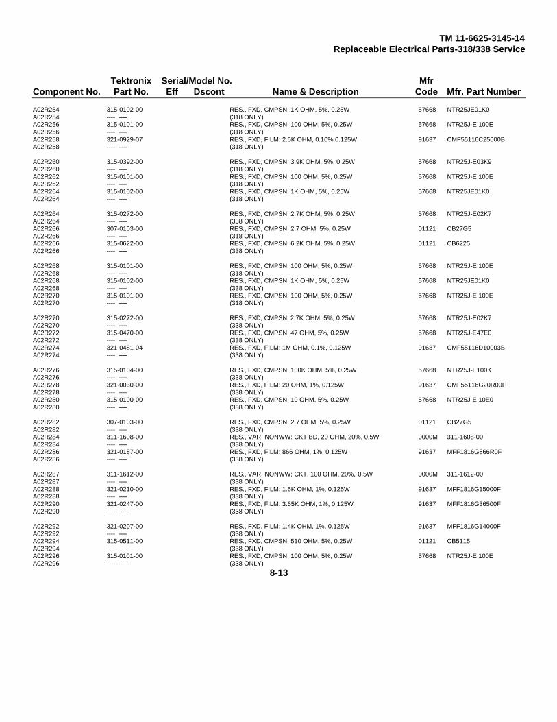
TM 11-6625-3145-14Replaceable Electrical Parts-318/338 Service
Tektronix Serial/Model No. MfrComponent No. Part No. Eff Dscont Name & Description Code Mfr. Part Number
A02R254 315-0102-00 RES., FXD, CMPSN: 1K OHM, 5%, 0.25W 57668 NTR25JE01K0A02R254 ---- ---- (318 ONLY)A02R256 315-0101-00 RES., FXD, CMPSN: 100 OHM, 5%, 0.25W 57668 NTR25J-E 100EA02R256 ---- ---- (318 ONLY)A02R258 321-0929-07 RES., FXD, FILM: 2.5K OHM, 0.10%.0.125W 91637 CMF55116C25000BA02R258 ---- ---- (318 ONLY)
A02R260 315-0392-00 RES., FXD, CMPSN: 3.9K OHM, 5%, 0.25W 57668 NTR25J-E03K9A02R260 ---- ---- (318 ONLY)A02R262 315-0101-00 RES., FXD, CMPSN: 100 OHM, 5%, 0.25W 57668 NTR25J-E 100EA02R262 ---- ---- (318 ONLY)A02R264 315-0102-00 RES., FXD, CMPSN: 1K OHM, 5%, 0.25W 57668 NTR25JE01K0A02R264 ---- ---- (318 ONLY)
A02R264 315-0272-00 RES., FXD, CMPSN: 2.7K OHM, 5%, 0.25W 57668 NTR25J-E02K7A02R264 ---- ---- (338 ONLY)A02R266 307-0103-00 RES., FXD, CMPSN: 2.7 OHM, 5%, 0.25W 01121 CB27G5A02R266 ---- ---- (318 ONLY)A02R266 315-0622-00 RES., FXD, CMPSN: 6.2K OHM, 5%, 0.25W 01121 CB6225A02R266 ---- ---- (338 ONLY)
A02R268 315-0101-00 RES., FXD, CMPSN: 100 OHM, 5%, 0.25W 57668 NTR25J-E 100EA02R268 ---- ---- (318 ONLY)A02R268 315-0102-00 RES., FXD, CMPSN: 1K OHM, 5%, 0.25W 57668 NTR25JE01K0A02R268 ---- ---- (338 ONLY)A02R270 315-0101-00 RES., FXD, CMPSN: 100 OHM, 5%, 0.25W 57668 NTR25J-E 100EA02R270 ---- ---- (318 ONLY)
A02R270 315-0272-00 RES., FXD, CMPSN: 2.7K OHM, 5%, 0.25W 57668 NTR25J-E02K7A02R270 ---- ---- (338 ONLY)A02R272 315-0470-00 RES., FXD, CMPSN: 47 OHM, 5%, 0.25W 57668 NTR25J-E47E0A02R272 ---- ---- (338 ONLY)A02R274 321-0481-04 RES., FXD, FILM: 1M OHM, 0.1%, 0.125W 91637 CMF55116D10003BA02R274 ---- ---- (338 ONLY)
A02R276 315-0104-00 RES., FXD, CMPSN: 100K OHM, 5%, 0.25W 57668 NTR25J-E100KA02R276 ---- ---- (338 ONLY)A02R278 321-0030-00 RES., FXD, FILM: 20 OHM, 1%, 0.125W 91637 CMF55116G20R00FA02R278 ---- ---- (338 ONLY)A02R280 315-0100-00 RES., FXD, CMPSN: 10 OHM, 5%, 0.25W 57668 NTR25J-E 10E0A02R280 ---- ---- (338 ONLY)
A02R282 307-0103-00 RES., FXD, CMPSN: 2.7 OHM, 5%, 0.25W 01121 CB27G5A02R282 ---- ---- (338 ONLY)A02R284 311-1608-00 RES., VAR, NONWW: CKT BD, 20 OHM, 20%, 0.5W 0000M 311-1608-00A02R284 ---- ---- (338 ONLY)A02R286 321-0187-00 RES., FXD, FILM: 866 OHM, 1%, 0.125W 91637 MFF1816G866R0FA02R286 ---- ---- (338 ONLY)
A02R287 311-1612-00 RES., VAR, NONWW: CKT, 100 OHM, 20%, 0.5W 0000M 311-1612-00A02R287 ---- ---- (338 ONLY)A02R288 321-0210-00 RES., FXD, FILM: 1.5K OHM, 1%, 0.125W 91637 MFF1816G15000FA02R288 ---- ---- (338 ONLY)A02R290 321-0247-00 RES., FXD, FILM: 3.65K OHM, 1%, 0.125W 91637 MFF1816G36500FA02R290 ---- ---- (338 ONLY)
A02R292 321-0207-00 RES., FXD, FILM: 1.4K OHM, 1%, 0.125W 91637 MFF1816G14000FA02R292 ---- ---- (338 ONLY)A02R294 315-0511-00 RES., FXD, CMPSN: 510 OHM, 5%, 0.25W 01121 CB5115A02R294 ---- ---- (338 ONLY)A02R296 315-0101-00 RES., FXD, CMPSN: 100 OHM, 5%, 0.25W 57668 NTR25J-E 100EA02R296 ---- ---- (338 ONLY)
8-13

TM 11-6625-3145-14Replaceable Electrical Parts-318/338 Service
Tektronix Serial/Model No. MfrComponent No. Part No. Eff Dscont Name & Description Code Mfr. Part Number
A02R300 315-0622-00 RES., FXD, CMPSN: 6.2K OHM, 5%, 0.25W 01121 CB6225A02R300 ---- ---- (318 ONLY)A02R300 321-0929-07 RES., FXD, FILM: 2.5K OHM, 0.10%, 0.125W 91637 CMF55116C25000BA02R300 ---- ---- (338 ONLY)A02R302 311-2084-00 .300101 .300815 RES., VAR, NONWIR: TRMR, 500 OHM, 10%, 0.5W 0000M 311-2084-00A02R302 ---- ---- (318 ONLY)
A02R302 311-2084-01 .300816 RES, VAR, NONWW: 500 OHM, 20%, 0.5W 0000M 311-2084-01A02R302 ---- ---- (318 ONLY)A02R302 321-0929-07 RES., FXD, FILM: 2.5K OHM, 0.10%, 0.125W 91637 CMF55116C25000BA02R302 - ---- ---- (338 ONLY)A02R304 321-0929-07 RES., FXD, FILM: 2.5K OHM, 0.10%, 0.125W 91637 CMF55116C25000BA02R306 315-0622-00 RES., FXD, CMPSN: 6.2K OHM, 5%, 0.25W 01121 CB6225
A02R306 ---- ---- (318 ONLY)A02R306 321-0929-07 RES., FXD, FILM: 2.5K OHM, 0.10%, 0.125W 91637 CMF55116C25000BA02R306 ---- ---- (338 ONLY)A02R308 311-2084-00 .300101 .300815 RES., VAR, NONWIR: TRMR, 500 OHM, 10%, 0.5W 0000M 311-2084-00A02R308 ---- ---- (318 ONLY)A02R308 311-2084-01 .300816 RES, VAR, NONWW: 500 OHM, 20%, 0.5W 0000M 311-2084-01
A02R308 ---- ---- (318 ONLY)A02R308 321-0929-07 RES., FXD, FILM: 2.5K OHM, 0.10%, 0.125W 91637 CMF55116C25000BA02R308 ---- ---- (338 ONLY)A02R310 321-0929-07 RES., FXD, FILM: 2.5K OHM, 0.10%/o, 0.125W 91637 CMF55116C25000BA02R312 315-0511-00 RES., FXD, CMPSN: 510 OHM, 5%, 0.25W 01121 CB5115A02R312 ---- ---- (318 ONLY)
A02R312 321-0929-07 RES., FXD, FILM: 2.5K OHM, 0.10%, 0.125W 91637 CMF55116C25000BA02R312 ---- ---- (338 ONLY)A02R314 315-0510-00 RES., FXD, CMPSN: 51 OHM, 5%, 0.25W 57668 NTR25J-E51 E0A02R314 ---- ---- (318 ONLY)A02R314 321-0929-07 RES., FXD, FILM: 2.5K OHM, 0.10%, 0.125W 91637 CMF55116C25000BA02R314 ---- ---- (338 ONLY)
A02R316 315-0432-00 RES., FXD, CMPSN: 4.3K OHM, 5%, 0.25W 57668 NTR25J-E04K3A02R316 ---- ---- (318 ONLY)A02R316 307-0886-00 RES NTWK, FXD, FI: 4, 1K OHM, 5%, 0.1W 0000M 307-0886-00A02R316 ---- ---- (338 ONLY)A02R318 315-0511-00 RES., FXD, CMPSN: 510 OHM, 5%, 0.25W 01121 CB5115A02R318 ---- ---- (318 ONLY)
A02R318 307-0873-00 RES NTWK, FXD, FI: 4, 6.2K OHM, 2%, 0.1W 0000M 307-0873-00A02R318 ---- ---- (338 ONLY)A02R320 315-0511-00 RES., FXD, CMPSN: 510 OHM, 5%, 0.25W 01121 CB5115A02R320 ---- ---- (318 ONLY)A02R320 311-2084-00 .300101 .300895 RES., VAR, NONWIR: TRMR, 500 OHM, 10%, 0.5W 0000M 311-2084-00A02R320 ---- ---- (338 ONLY)
A02R320 311-2084-01 .300896 RES, VAR, NONWW: 500 OHM, 20%, 0.5W 0000M 311-2084-01A02R320 ---- ---- (338 ONLY)A02R322 315-0511-00 RES., FXD, CMPSN: 510 OHM, 5%, 0.25W 01121 CB5115A02R322 ---- ---- (318 ONLY)A02R322 311-2084-00 .300101 .300895 RES., VAR, NONWIR: TRMR, 500 OHM, 10%/, 0.5W 0000M 311-2084-00A02R322 ---- ---- (338 ONLY)
A02R322 311-2084-01 .300896 RES, VAR, NONWW: 500 OHM, 20%, 0.5W 0000M 311-2084-01A02R322 ---- ---- (338 ONLY)A02R324 315-0510-00 .300101 .300280 RES., FXD, CMPSN: 51 OHM, 5%, 0.25W 57668 NTR25J-E51 E0A02R324 ---- ---- (318 ONLY)A02R324 315-0152-00 .300281 RES., FXD, CMPSN: 1.5K OHM, 5%, 0.25W 57668 NTR25J-E01 K5A02R324 ---- ---- (318 ONLY)
8-14

TM 11-6625-3145-14Replaceable Electrical Parts-318/338 Service
Tektronix Serial/Model No. MfrComponent No. Part No. Eff Dscont Name & Description Code Mfr. Part Number
A02R324 311-2084-00 .300101 .300895 RES., VAR, NONWIR: TRMR, 500 OHM, 10%, 0.5W 0000M 311-2084-00A02R324 ---- ---- (338 ONLY)A02R324 311-2084-01 . 300896 RES, VAR, NONWW: 500 OHM, 20%, 0.5W 0000M 311-2084-01A02R324 ---- ---- (338 ONLY)A02R326 315-0100-00 RES., FXD, CMPSN: 10 OHM, 5%, 0.25W 57668 NTR25J-E 10E0A02R326 ---- ---- (318 ONLY)
A02R326 311-2084-00 .300101 .300895 RES., VAR, NONWIR: TRMR, 500 OHM, 10%, 0.5W 0000M 311-2084-00A02R326 ---- ---- (338 ONLY)A02R326 311-2084-01 .300896 RES, VAR, NONWW: 500 OHM, 20%, 0.5W 0000M 311-2084-01A02R326 ---- ---- (338 ONLY)A02R328 315-0100-00 RES., FXD, CMPSN: 10 OHM, 5%, 0.25W 57668 NTR25J-E 10E0A02R328 ---- ---- (318 ONLY)
A02R328 315-0102-00 RES., FXD, CMPSN: 1K OHM, 5%, 0.25W 57668 NTR25JE01K0A02R328 ---- ---- (338 ONLY)A02R330 315-0101-00 RES., FXD, CMPSN: 100 OHM, 5%, 0.25W 57668 NTR25J-E 100EA02R330 ---- ---- (318 ONLY)A02R330 315-0432-00 .300101 .300114 RES., FXD, CMPSN: 4.3K OHM, 5%, 0.25W 57668 NTR25J-E04K3A02R330 ---- ---- (338 ONLY)
A02R330 315-0362-00 .300115 RES., FXD, CMPSN: 3.6K OHM, 5%, 0.25W 01121 CB3625A02R330 ---- ---- (338 ONLY)A02R332 315-0511-00 RES., FXD, CMPSN: 510 OHM, 5%, 0.25W 01121 CB5115A02R332 ---- ---- (338 ONLY)A02R334 315-0103-00 RES., FXD, CMPSN: 10K OHM, 5%, 0.25W 57668 NTR25J-E10K0A02R334 ---- ---- (318 ONLY)
A02R334 315-0511-00 .300101 .300114 RES., FXD, CMPSN: 51’0 OHM, 5%, 0.25W 01121 CB5115A02R334 ---- ---- (338 ONLY)A02R334 315-0510-00 .300115 .300115 RES., FXD, CMPSN: 51 OHM, 5%, 0.25W 57668 NTR25J-E51 E0A02R334 ---- ---- (338 ONLY)A02R334 315-0152-00 .300116 RES., FXD, CMPSN: 1.5K OHM, 5%, 0.25W 57668 NTR25J-E01K5A02R334 ---- ---- (338 ONLY)
A02R336 321-0261-00 RES., FXD, FILM: 5.11K OHM, 1%, 0.125W 91637 MFF1816G51100FA02R336 ---- ---- (318 ONLY)A02R336 315-0511-00 RES., FXD, CMPSN: 510 OHM, 5%, 0.25W 01121 CB5115A02R336 ---- ---- (338 ONLY)A02R338 321-0317-00 RES., FXD, FILM: 19.6K OHM, 1%, 0.125W 91637 MFF1816G19601FA02R338 ---- ---- (318 ONLY)
A02R338 315-0511-00 RES., FXD, CMPSN: 510 OHM, 5%, 0.25W 01121 CB5115A02R338 ---- ---- (338 ONLY)A02R340 315-0511-00 RES., FXD, CMPSN: 510 OHM, 5%, 0.25W 01121 CB5115A02R340 ---- ---- (338 ONLY)A02R342 315-0510-00 RES., FXD, CMPSN: 51 OHM, 5%, 0.25W 57668 NTR25J-E51E0A02R342 ---- ---- (338 ONLY)
A02R344 315-0100-00 RES., FXD, CMPSN: 10 OHM, 5%, 0.25W 57668 NTR25J-E 10E0A02R344 ---- ---- (338 ONLY)A02R346 315-0100-00 RES., FXD, CMPSN: 10 OHM, 5%, 0.25W 57668 NTR25J-E 10E0A02R346 ---- ---- (338 ONLY)A02R348 315-0103-00 RES., FXD, CMPSN: 10K OHM, 5%, 0.25W 57668 NTR25J-E10K0A02R348 ---- ---- (338 ONLY)
A02R350 315-0102-00 RES., FXD, CMPSN: 1K OHM, 5%, 0.25W 57668 NTR25JE01K0A02R350 ---- ---- (318 ONLY)A02R350 315-0472-00 RES., FXD, CMPSN: 4.7K OHM, 5%, 0.25W 57668 NTR25J-E04K7A02R350 ---- ---- (338 ONLY)A02R352 321-0261-00 RES., FXD, FILM: 5.11K OHM, 1%, 0.125W 91637 MFF1816G51100FA02R352 ---- ---- (338 ONLY)
8-15
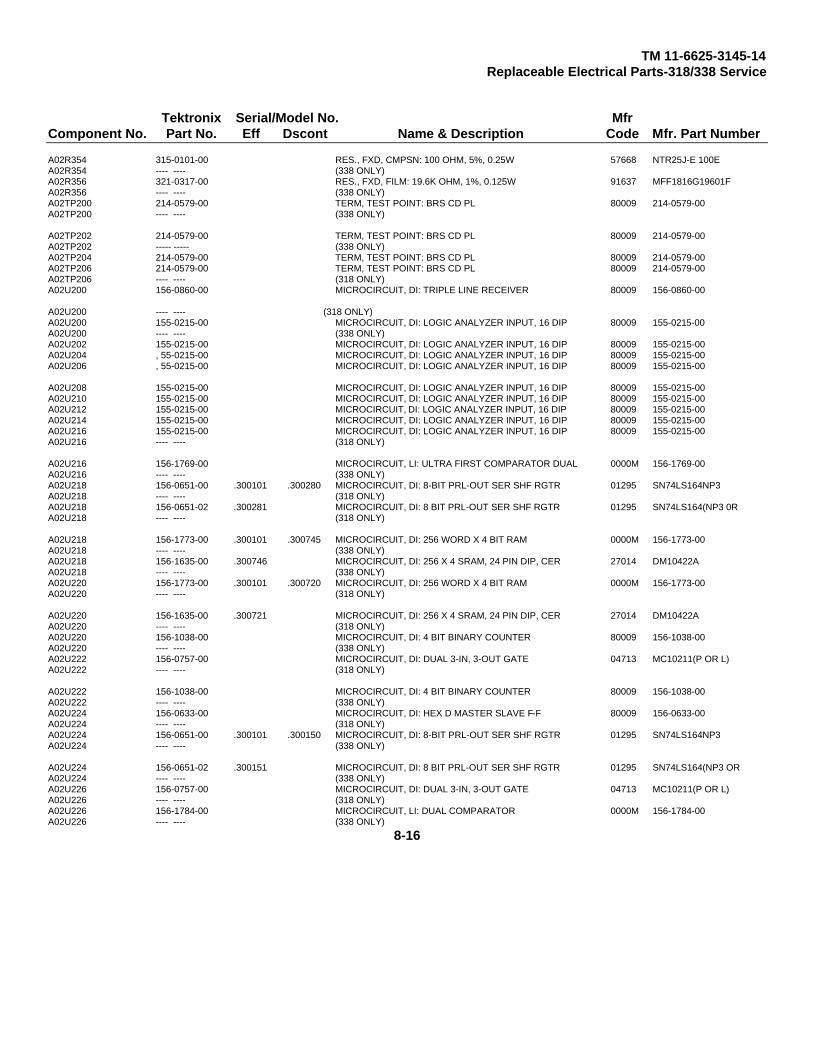
TM 11-6625-3145-14Replaceable Electrical Parts-318/338 Service
Tektronix Serial/Model No. MfrComponent No. Part No. Eff Dscont Name & Description Code Mfr. Part Number
A02R354 315-0101-00 RES., FXD, CMPSN: 100 OHM, 5%, 0.25W 57668 NTR25J-E 100EA02R354 ---- ---- (338 ONLY)A02R356 321-0317-00 RES., FXD, FILM: 19.6K OHM, 1%, 0.125W 91637 MFF1816G19601FA02R356 ---- ---- (338 ONLY)A02TP200 214-0579-00 TERM, TEST POINT: BRS CD PL 80009 214-0579-00A02TP200 ---- ---- (338 ONLY)
A02TP202 214-0579-00 TERM, TEST POINT: BRS CD PL 80009 214-0579-00A02TP202 ----- ----- (338 ONLY)A02TP204 214-0579-00 TERM, TEST POINT: BRS CD PL 80009 214-0579-00A02TP206 214-0579-00 TERM, TEST POINT: BRS CD PL 80009 214-0579-00A02TP206 ---- ---- (318 ONLY)A02U200 156-0860-00 MICROCIRCUIT, DI: TRIPLE LINE RECEIVER 80009 156-0860-00
A02U200 ---- ---- (318 ONLY)A02U200 155-0215-00 MICROCIRCUIT, DI: LOGIC ANALYZER INPUT, 16 DIP 80009 155-0215-00A02U200 ---- ---- (338 ONLY)A02U202 155-0215-00 MICROCIRCUIT, DI: LOGIC ANALYZER INPUT, 16 DIP 80009 155-0215-00A02U204 , 55-0215-00 MICROCIRCUIT, DI: LOGIC ANALYZER INPUT, 16 DIP 80009 155-0215-00A02U206 , 55-0215-00 MICROCIRCUIT, DI: LOGIC ANALYZER INPUT, 16 DIP 80009 155-0215-00
A02U208 155-0215-00 MICROCIRCUIT, DI: LOGIC ANALYZER INPUT, 16 DIP 80009 155-0215-00A02U210 155-0215-00 MICROCIRCUIT, DI: LOGIC ANALYZER INPUT, 16 DIP 80009 155-0215-00A02U212 155-0215-00 MICROCIRCUIT, DI: LOGIC ANALYZER INPUT, 16 DIP 80009 155-0215-00A02U214 155-0215-00 MICROCIRCUIT, DI: LOGIC ANALYZER INPUT, 16 DIP 80009 155-0215-00A02U216 155-0215-00 MICROCIRCUIT, DI: LOGIC ANALYZER INPUT, 16 DIP 80009 155-0215-00A02U216 ---- ---- (318 ONLY)
A02U216 156-1769-00 MICROCIRCUIT, LI: ULTRA FIRST COMPARATOR DUAL 0000M 156-1769-00A02U216 ---- ---- (338 ONLY)A02U218 156-0651-00 .300101 .300280 MICROCIRCUIT, DI: 8-BIT PRL-OUT SER SHF RGTR 01295 SN74LS164NP3A02U218 ---- ---- (318 ONLY)A02U218 156-0651-02 .300281 MICROCIRCUIT, DI: 8 BIT PRL-OUT SER SHF RGTR 01295 SN74LS164(NP3 0RA02U218 ---- ---- (318 ONLY)
A02U218 156-1773-00 .300101 .300745 MICROCIRCUIT, DI: 256 WORD X 4 BIT RAM 0000M 156-1773-00A02U218 ---- ---- (338 ONLY)A02U218 156-1635-00 .300746 MICROCIRCUIT, DI: 256 X 4 SRAM, 24 PIN DIP, CER 27014 DM10422AA02U218 ---- ---- (338 ONLY)A02U220 156-1773-00 .300101 .300720 MICROCIRCUIT, DI: 256 WORD X 4 BIT RAM 0000M 156-1773-00A02U220 ---- ---- (318 ONLY)
A02U220 156-1635-00 .300721 MICROCIRCUIT, DI: 256 X 4 SRAM, 24 PIN DIP, CER 27014 DM10422AA02U220 ---- ---- (318 ONLY)A02U220 156-1038-00 MICROCIRCUIT, DI: 4 BIT BINARY COUNTER 80009 156-1038-00A02U220 ---- ---- (338 ONLY)A02U222 156-0757-00 MICROCIRCUIT, DI: DUAL 3-IN, 3-OUT GATE 04713 MC10211(P OR L)A02U222 ---- ---- (318 ONLY)
A02U222 156-1038-00 MICROCIRCUIT, DI: 4 BIT BINARY COUNTER 80009 156-1038-00A02U222 ---- ---- (338 ONLY)A02U224 156-0633-00 MICROCIRCUIT, DI: HEX D MASTER SLAVE F-F 80009 156-0633-00A02U224 ---- ---- (318 ONLY)A02U224 156-0651-00 .300101 .300150 MICROCIRCUIT, DI: 8-BIT PRL-OUT SER SHF RGTR 01295 SN74LS164NP3A02U224 ---- ---- (338 ONLY)
A02U224 156-0651-02 .300151 MICROCIRCUIT, DI: 8 BIT PRL-OUT SER SHF RGTR 01295 SN74LS164(NP3 ORA02U224 ---- ---- (338 ONLY)A02U226 156-0757-00 MICROCIRCUIT, DI: DUAL 3-IN, 3-OUT GATE 04713 MC10211(P OR L)A02U226 ---- ---- (318 ONLY)A02U226 156-1784-00 MICROCIRCUIT, LI: DUAL COMPARATOR 0000M 156-1784-00A02U226 ---- ---- (338 ONLY)
8-16

TM 11-6625-3145-14Replaceable Electrical Parts-318/338 Service
Tektronix Serial/Model No. MfrComponent No. Part No. Eff Dscont Name & Description Code Mfr. Part Number
A02U228 156-0633-00 MICROCIRCUIT, DI: HEX D MASTER SLAVE F-F 80009 156-0633-00A02U228 ---- ---- (318 ONLY)A02U228 156-0757-00 MICROCIRCUIT, DI: DUAL 3-IN, 3-OUT GATE 04713 MC10211(P OR L)A02U228 (338 ONLY)A02U230 156-1038-00 MICROCIRCUIT, DI: 4 BIT BINARY COUNTER 80009 156-1038-00A02U230 ---- ---- (318 ONLY)
A02U230 156-0757-00 MICROCIRCUIT, DI: DUAL 3-IN, 3-OUT GATE 04713 MC10211(P OR L)A02U230 ---- ---- (338 ONLY)A02U232 156-1038-00 MICROCIRCUIT, DI: 4 BIT BINARY COUNTER 80009 156-1038-00A02U232 ---- ---- (318 ONLY)A02U232 156-1773-00 MICROCIRCUIT, DI: 256 WORD X 4 BIT RAM 0000M 156-1773-00A02U232 ---- ---- (338 ONLY)
A02U234 156-0633-00 MICROCIRCUIT, DI: HEX D MASTER SLAVE F-F 80009 156-0633-00A02U236 156-1769-00 MICROCIRCUIT, LI: ULTRA FIRST COMPARATOR 0000M 156-1769-00
DUALA02U236 ---- ---- (318 ONLY)A02U236 156-0308-05 MICROCIRCUIT, DI: RECEIVER QUAD DIFF LINE 0000M 156-0308-05A02U236 ---- ---- (338 ONLY)A02U238 156-0633-00 MICROCIRCUIT, DI: HEX D MASTER SLAVE F-F 80009 156-0633-00
A02U238 ---- ---- (318 ONLY)A02U238 156-0308-05 MICROCIRCUIT, DI: RECEIVER QUAD DIFF LINE 0000M 156-0308-05A02U238 ---- ---- (338 ONLY)A02U240 156-1783-00 MICROCIRCUIT, LI: QUAD COMPARATOR 0000M 156-1783-00A02U240 ---- ---- (318 ONLY)A02U240 156-0308-05 MICROCIRCUIT, DI: RECEIVER QUAD DIFF LINE 0000M 156-0308-05
A02U240 ---- ---- (338 ONLY)A02U242 156-0158-00 MICROCIRCUIT, LI: DUAL OPERATIONAL AMPLIFIER 18324 MC1458NA02U242 ---- ---- (318 ONLY)A02U242 156-1265-00 MICROCIRCUIT, LI: OPNL AMPL, QUAD 0000M 156-1265-00A02U242 ---- ---- (338 ONLY)A02U244 156-0205-00 MICROCIRCUIT, DI: QUAD 2-INPUT NOR GATE 04713 MC10102 (P OR L)
A02U244 ---- ---- (318 ONLY)A02U244 156-0308-05 MICROCIRCUIT, DI: RECEIVER QUAD DIFF LINE 0000M 156-0308-05A02U244 ---- ---- (338 ONLY)A02U246 156-0308-05 MICROCIRCUIT, DI: RECEIVER QUAD DIFF LINE 0000M 156-0308-05A02U246 ---- ---- (338 ONLY)A02U248 156-0308-05 MICROCIRCUIT, DI: RECEIVER QUAD DIFF LINE 0000M 156-0308-05
A02U248 ---- ---- (338 ONLY)A02U250 156-0308-05 MICROCIRCUIT, DI: RECEIVER QUAD DIFF LINE 0000M 156-0308-05A02U250 ---- ---- (338 ONLY)A02U252 156-0205-00 MICROCIRCUIT, DI: QUAD 2-INPUT NOR GATE 04713 MC10102 (P OR L)A02U252 ---- ---- (338 ONLY)
8-17

TM 11-6625-3145-14Replaceable Electrical Parts-318/338 Service
Tektronix Serial/Model No. MfrComponent No. Part No. Eff Dscont Name & Description Code Mfr. Part Number
A03 670-7815-00 CKT BOARD ASSY: ACQ CONTROL 80009 670-7815-00A03 ---- ---- (318 ONLY)A03 670-7822-00 CKT BOARD ASSY: ACQ CONNECTOR 80009 670-7822-00A03 ---- ---- (338 ONLY)A03C100 281-0257-00 CAP., VAR, CER DI: 4-28PF, 250V 0000M 281-0257-00A03C102 281-0257-00 CAP, , VAR, CER DI: 4-28PF, 250V 0000M 281-0257-00
A03C104 281-0257-00 CAP., VAR, CER DI: 4-28PF, 250V 0000M 281-0257-00A03C 106 281-0257-00 CAP., VAR, CER DI: 4-28PF, 250V 0000M 281-0257-00A03C200 290-0995-00 CAP., FXD, ELCTLT: 47UF, 20%, 16V 0000M 290-0995-00A03C202 281-0775-00 CAP., FXD, CER DI: 0.1UF, 20%, 50V 04222 MA205E104MAAA03C204 281-0775-00 CAP., FXD, CER DI: 0.1UF, 20%, 50V 04222 MA205E104MAAA03C206 281-0775-00 CAP., FXD, CER DI: 0.1UF, 20%, 50V 04222 MA205E104MAA
A03C208 281-0775-00 CAP., FXD, CER DI: 0.1UF, 20%, 50V 04222 MA205E104MAAA03C210 281-0775-00 CAP., FXD, CER DI: 0.1UF, 20%, 50V 04222 MA205E104MAAA03C212 281-0775-00 CAP., FXD, CER DI: 0.1UF, 20%, 50V 04222 MA205E104MAAA03C214 281-0775-00 CAP., FXD, CER DI: 0.1UF, 20%, 50V 04222 MA205E104MAAA03C216 281-0775-00 CAP., FXD, CER DI: 0.1UF, 20%, 50V 04222 MA205E104MAAA03C218 281-0775-00 CAP., FXD, CER DI: 0.1UF, 20%, 50V 04222 MA205E104MAA
A03C220 281-0775-00 CAP., FXD, CER DI: 0.1UF, 20%, 50V 04222 MA205E104MAAA03C222 281-0775-00 CAP., FXD, CER DI: 0.1UF, 20%, 50V 04222 MA205E104MAAA03C224 281-0775-00 CAP., FXD, CER DI: 0.1UF, 20%, 50V 04222 MA205E104MAAA03C226 281-0775-00 CAP., FXD, CER DI: 0.1UF, 20%, 50V 04222 MA205E104MAAA03C228 281-0775-00 CAP., FXD, CER DI: 0.1UF, 20%, 50V 04222 MA205E104MAAA03C230 281-0775-00 CAP., FXD, CER DI: 0.1UF, 20%, 50V 04222 MA205E104MAA
A03C232 290-0995-00 CAP., FXD, ELCTLT: 47UF, 20%, 16V 0000M 290-0995-00A03C234 281-0775-00 CAP., FXD, CER DI: 0.1UF, 20%, 50V 04222 MA205E104MAAA03C236 281-0775-00 CAP., FXD, CER DI: 0.1UF, 20%, 50V 04222 MA205E104MAAA03C238 281-0775-00 CAP., FXD, CER DI: 0.1UF, 20%, 50V 04222 MA205E104MAAA03C240 281-0775-00 CAP., FXD, CER DI: 0.1UF, 20%, 50V 04222 MA205E104MAAA03C242 281-0775-00 CAP., FXD, CER DI: 0.1UF, 20%, 50V 04222 MA205E104MAA
A03C244 290-0995-00 CAP.., FXD, ELCTLT: 47UF, 20%, 16V 0000M 290-0995-00A03C246 281-0775-00 CAP., FXD, CER DI: 0.1UF, 20%, 50V 04222 MA205E104MAAA03C300 281-0775-00 CAP., FXD, CER DI: 0.1UF, 20%, 50V 04222 MA205E104MAAA03C330 281-0775-00 CAP., FXD, CER DI: 0.1UF, 20%, 50V 04222 MA205E104MAAA03C332 281-0775-00 CAP., FXD, CER DI: 0.1UF, 20%, 50V 04222 MA205E104MAAA03C334 281-0775-00 CAP., FXD, CER DI: 0.1UF, 20%, 50V 04222 MA205E104MAA
A03C336 281-0775-00 CAP., FXD, CER DI: 0.1UF, 20%, 50V 04222 MA205E104MAAA03C338 281-0775-00 CAP., FXD, CER DI: 0.1UF, 20%, 50V 04222 MA205E104MAAA03C360 281-0775-00 CAP., FXD, CER DI: 0.1UF, 20%, 50V 04222 MA205E104MAAA03DL100 119-1612-01 DELAY LINE, ELEC: 20NS, 100 OHMS, TAPPED 0000M 119-1612-01A03DL102 119-1611-01 DELAY LINE, ELEC: 20NS, 100 OHMS, TAPPED 0000M 119-1611-01A03DL104 119-1612-01 DELAY LINE, ELEC: 20NS, 100 OHMS, TAPPED 0000M 119-1612-01
A03DL106 119-1614-01 DELAY LINE, ELEC: 5NS, 100 OHMS, TAPPED 0000M 119-1614-01A03J050 131-2872-00 CONN, RCPT, ELEC HEADER, 2 X 4, 2.54 SPACINGA03J050 ---- ---- (318 ONLY)A03J200 131-2230-01 CONN, RCPT, ELEC: HEADER, 2 X 8, 2.54 SPACINGA03J300 131-2933-00 CONN, RCPT, ELEC: HEADER, STRAIGHT, 2 X 6 0000M 131-2933-00A03J400 131-2933-00 CONN, RCPT, ELEC: HEADER, STRAIGHT, 2 X 6 0000M 131-2933-00
A03R100 307-0876-00 RES NTWK, FXD, FI: 8, 100 OHM, 5%, 0.125W 000 M 307-0876-00A03R102 307-0876-00 RES NTWK, FXD, FI: 8, 100 OHM, 5%, 0.125W 000 M 307-0876-00A03R104 307-0876-00 RES NTWK, FXD, FI: 8, 100 OHM, 5%, 0.125W 000 M 307-0876-00A03R106 307-0876-00 RES NTWK, FXD, FI: 8, 100 OHM, 5%, 0.125W 000 M 307-0876-00A03R108 307-0876-00 RES NTWK, FXD FI: 8, 100 OHM, 5%, 0.125W 000 M 307-0876-00A03R110 307-0877-00 RES NTWK, FXD, FI: 8, 510 OHM, 5%, 0.125W 000 M 307-0877-00
8-18
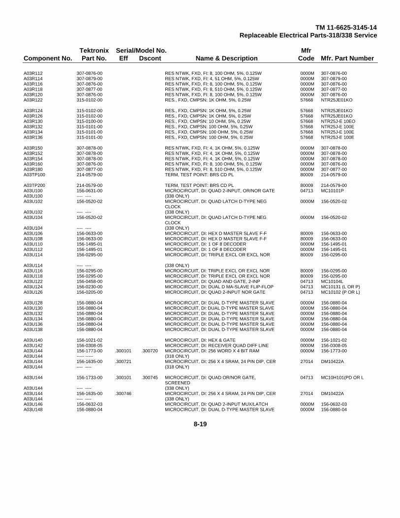
TM 11-6625-3145-14Replaceable Electrical Parts-318/338 Service
Tektronix Serial/Model No. MfrComponent No. Part No. Eff Dscont Name & Description Code Mfr. Part Number
A03R112 307-0876-00 RES NTWK, FXD, FI: 8, 100 OHM, 5%, 0.125W 0000M 307-0876-00A03R114 307-0879-00 RES NTWK, FXD, FI: 4, 51 OHM, 5%, 0.125W 0000M 307-0879-00A03R116 307-0876-00 RES NTWK, FXD, FI: 8, 100 OHM, 5%, 0.125W 0000M 307-0876-00A03R118 307-0877-00 RES NTWK, FXD, FI: 8, 510 OHM, 5%, 0.125W 0000M 307-0877-00A03R120 307-0876-00 RES NTWK, FXD, FI: 8, 100 OHM, 5%, 0.125W 0000M 307-0876-00A03R122 315-0102-00 RES., FXD, CMPSN: 1K OHM, 5%, 0.25W 57668 NTR25JE01KO
A03R124 315-0102-00 RES., FXD, CMPSN: 1K OHM, 5%, 0.25W 57668 NTR25JE01KOA03R126 315-0102-00 RES., FXD, CMPSN: 1K OHM, 5%, 0.25W 57668 NTR25JE01KOA03R130 315-0100-00 RES., FXD, CMPSN: 10 OHM, 5%, 0.25W 57668 NTR25J-E 10EOA03R132 315-0101-00 RES., FXD, CMPSN: 100 OHM, 5%, 0.25W 57668 NTR25J-E 100EA03R134 315-0101-00 RES., FXD, CMPSN: 100 OHM, 5%, 0.25W 57668 NTR25J-E 100EA03R136 315-0101-00 RES., FXD, CMPSN: 100 OHM, 5%, 0.25W 57668 NTR25J-E 100E
A03R150 307-0878-00 RES NTWK, FXD, FI: 4, 1K OHM, 5%, 0.125W 0000M 307-0878-00A03R152 307-0878-00 RES NTWK, FXD, FI: 4, 1K OHM, 5%, 0.125W 0000M 307-0878-00A03R154 307-0878-00 RES NTWK, FXD, FI: 4, 1K OHM, 5%, 0.125W 0000M 307-0878-00A03R160 307-0876-00 RES NTWK, FXD, FI: 8, 100 OHM, 5%, 0.125W 0000M 307-0876-00A03R180 307-0877-00 RES NTWK, FXD, FI: 8, 510 OHM, 5%, 0.125W 0000M 307-0877-00A03TP100 214-0579-00 TERM, TEST POINT: BRS CD PL 80009 214-0579-00
A03TP200 214-0579-00 TERM, TEST POINT: BRS CD PL 80009 214-0579-00A03U100 156-0631-00 MICROCIRCUIT, DI: QUAD 2-INPUT, OR/NOR GATE 04713 MC10101PA03U100 ---- ---- (338 ONLY)A03U102 156-0520-02 MICROCIRCUIT, DI: QUAD LATCH D-TYPE NEG 0000M 156-0520-02
CLOCKA03U102 ---- ---- (338 ONLY)A03U104 156-0520-02 MICROCIRCUIT, DI: QUAD LATCH D-TYPE NEG 0000M 156-0520-02
CLOCKA03U104 ---- ---- (338 ONLY)A03U106 156-0633-00 MICROCIRCUIT, DI: HEX D MASTER SLAVE F-F 80009 156-0633-00A03U108 156-0633-00 MICROCIRCUIT, DI: HEX D MASTER SLAVE F-F 80009 156-0633-00A03U110 156-1495-01 MICROCIRCUIT, DI: 1 OF 8 DECODER 0000M 156-1495-01A03U112 156-1495-01 MICROCIRCUIT, DI: 1 OF 8 DECODER 0000M 156-1495-01A03U114 156-0295-00 MICROCIRCUIT, DI: TRIPLE EXCL OR EXCL NOR 80009 156-0295-00
A03U114 ---- ---- (338 ONLY)A03U116 156-0295-00 MICROCIRCUIT, DI: TRIPLE EXCL OR EXCL NOR 80009 156-0295-00A03U118 156-0295-00 MICROCIRCUIT, DI: TRIPLE EXCL OR EXCL NOR 80009 156-0295-00A03U122 156-0458-00 MICROCIRCUIT, DI: QUAD AND GATE, 2-INP 04713 MC10104LA03U124 156-0230-00 MICROCIRCUIT, DI: DUAL D MA-SLAVE FLIP-FLOP 04713 MC10131 (L OR P)A03U126 156-0205-00 MICROCIRCUIT, DI: QUAD 2-INPUT NOR GATE 04713 MC10102 (P OR L)
A03U128 156-0880-04 MICROCIRCUIT, DI: DUAL D-TYPE MASTER SLAVE 0000M 156-0880-04A03U130 156-0880-04 MICROCIRCUIT, DI: DUAL D-TYPE MASTER SLAVE 0000M 156-0880-04A03U132 156-0880-04 MICROCIRCUIT, DI: DUAL D-TYPE MASTER SLAVE 0000M 156-0880-04A03U134 156-0880-04 MICROCIRCUIT, DI: DUAL D-TYPE MASTER SLAVE 0000M 156-0880-04A03U136 156-0880-04 MICROCIRCUIT, DI: DUAL D-TYPE MASTER SLAVE 0000M 156-0880-04A03U138 156-0880-04 MICROCIRCUIT, DI: DUAL D-TYPE MASTER SLAVE 0000M 156-0880-04
A03U140 156-1021-02 MICROCIRCUIT, DI: HEX & GATE 0000M 156-1021-02A03U142 156-0308-05 MICROCIRCUIT, DI: RECEIVER QUAD DIFF LINE 0000M 156-0308-05A03U144 156-1773-00 .300101 .300720 MICROCIRCUIT, DI: 256 WORD X 4 BIT RAM 0000M 156-1773-00A03U144 ----- ----- (318 ONLY)A03U144 156-1635-00 .300721 MICROCIRCUIT, DI: 256 X 4 SRAM, 24 PIN DIP, CER 27014 DM10422AA03U144 ---- ---- (318 ONLY)
A03U144 156-1733-00 .300101 .300745 MICROCIRCUIT, DI: QUAD OR/NOR GATE, 04713 MC10H101(PD OR LSCREENED
A03U144 ---- ---- (338 ONLY)A03U144 156-1635-00 .300746 MICROCIRCUIT, DI: 256 X 4 SRAM, 24 PIN DIP, CER 27014 DM10422AA03U144 ---- ---- (338 ONLY)A03U146 156-0632-03 MICROCIRCUIT, DI: QUAD 2-INPUT MUX/LATCH 0000M 156-0632-03A03U148 156-0880-04 MICROCIRCUIT, DI: DUAL D-TYPE MASTER SLAVE 0000M 156-0880-04
8-19

TM 11-6625-3145-14Replaceable Electrical Parts-318/338 Service
Tektronix Serial/Model No. MfrComponent No. Part No. Eff Dscont Name & Description Code Mfr. Part Number
A03U150 156-0880-04 MICROCIRCUIT, DI: DUAL D-TYPE MASTER SLAVE 0000M 156-0880-04A03U152 156-0229-02 MICROCIRCUIT, DI: DUAL 4-5 INPUT OR/NOR 0000M 156-0229-02A03U154 156-0458-00 MICROCIRCUIT, DI: QUAD AND GATE, 2-INP 04713 MC10104LA03U156 156-0205-00 MICROCIRCUIT, DI: QUAD 2-INPUT NOR GATE 04713 MC10102 (P OR L)A03U158 156-1715-00 MICROCIRCUIT, DI: EVENT/DELAY COUNTER 0000M 156-1715-00A03W100 131-0566-00 BUS CONDUCTOR: DUMMY RES, 2.375, 22 AWG 57668 JWW-0200E0
A03W100 ---- ---- (318 ONLY)A03W102 131-0566-00 BUS CONDUCTOR: DUMMY RES, 2.375, 22 AWG 57668 JWW-0200E0A03W102 ---- ---- (318 ONLY)
8-20

TM 11-6625-3145-14Replaceable Electrical Parts-318/338 Service
Tektronix Serial/Model No. MfrComponent No. Part No. Eff Dscont Name & Description Code Mfr. Part Number
A04 670-7814-00 CKT BOARD ASSY: ACO MEMORY 80009 670-7814-00A04 ---- ---- (318 ONLY)A04 670-7823-00 CKT BOARD ASSY: ACO MEMORY 80009 670-7823-00A04 ---- ---- (338 ONLY)A04C100 281-0811-00 CAP., FXD, CER DI: 10PF, 10%, 100V 96733 R2911A04C101 281-0775-00 CAP., FXD, CER DI: 0.1UF, 20%, 50V 04222 MA205E104MAA
A04C102 281-0775-00 CAP., FXD, CER DI: 0.1UF, 20%, 50V 04222 MA205E104MAAA04C104 281-0775-00 CAP., FXD, CER DI: 0.1UF, 20%, 50V 04222 MA205E104MAAA04C106 281-0775-00 CAP., FXD, CER DI: 0.1UF, 20%, 50V 04222 MA205E104MAAA04C108 290-0995-00 CAP., FXD, ELCTLT: 47UF, 20%, 16V 0000M 290-0995-00A04C109 281-0775-00 CAP., FXD, CER DI: 0.1UF, 20%, 50V 04222 MA205E104MAAA04C110 281-0775-00 CAP., FXD, CER DI: 0.1UF, 20%, 50V 04222 MA205E104MAAA04C112 281-0775-00 CAP., FXD, CER DI: 0.1UF, 20%, 50V 04222 MA205E104MAAA04C114 290-0995-00 CAP., FXD, ELCTLT: 47UF, 20%, 16V 0000M 290-0995-00A04C116 281-0775-00 CAP., FXD, CER DI: 0.1UF, 20%, 50V 04222 MA205E104MAAA04C118 290-0995-00 CAP., FXD, ELCTLT: 47UF, 20%, 16V 0000M 290-0995-00A04C120 281-0775-00 CAP., FXD, CER DI: 0.1UF, 20%, 50V 04222 MA205E104MAAA04C122 281-0775-00 CAP., FXD, CER DI: 0.1UF, 20%, 50V 04222 MA205E104MAA
A04C124 281-0775-00 CAP., FXD, CER DI: 0.1UF, 20%, 50V 04222 MA205E104MAAA04C126 281-0775-00 CAP., FXD, CER DI: 0.1UF, 20%, 50V 04222 MA205E104MAAA04C128 290-0995-00 CAP., FXD, ELCTLT: 47UF, 20%, 16V 0000M 290-0995-00A04C132 281-0775-00 CAP., FXD, CER DI: 0.1UF, 20%, 50V 04222 MA205E104MAAA04C134 281-0775-00 CAP., FXD, CER DI: 0.1UF, 20%, 50V 04222 MA205E104MAAA04L100 108-0182-00 COIL, RF: FIXED, 285NH 80009 108-0182-00
A04R100 307-0876-00 RES NTWK, FXD, FI: 8, 100 OHM, 5%, 0.125W 0000M 307-0876-00A04R102 307-0876-00 RES NTWK, FXD, FI: 8, 100 OHM, 5%, 0.125W 0000M 307-0876-00A04R104 307-0876-00 RES NTWK, FXD, FI: 8, 100 OHM, 5%, 0.125W 0000M 307-0876-00A04R106 307-0876-00 RES NTWK, FXD, FI: 8, 100 OHM, 5%, 0.125W 0000M 307-0876-00A04R108 307-0876-00 RES NTWK, FXD, FI: 8, 100 OHM, 5%, 0.125W 0000M 307-0876-00A04R108 ---- ---- (338 ONLY)
A04R110 315-0102-00 RES., FXD, CMPSN: 1K OHM, 5%, 0.25W 57668 NTR25JE01K0A04R112 307-0877-00 RES NTWK, FXD, FI: 8, 510 OHM, 5%, 0.125W 0000M 307-0877-00A04R113 315-0511-00 RES., FXD, CMPSN: 510 OHM, 5%, 0.25W 01121 CB5115A04R114 307-0877-00 RES NTWK, FXD, FI: 8, 510 OHM, 5%, 0.125W 0000M 307-0877-00A04R116 315-0511-00 RES., FXD, CMPSN: 510 OHM, 5%, 0.25W 01121 CB5115A04R118 307-0877-00 RES NTWK, FXD, FI: 8, 510 OHM, 5%, 0.125W 0000M 307-0877-00
A04R120 315-0512-00 RES., FXD, CMPSN: 5.1K OHM, 5%, 0.25W 57668 NTR25J-E05K1A04R122 315-0221-00 RES., FXD, CMPSN: 220 OHM, 5%, 0.25W 57668 NTR25J-E220EA04R124 315-0102-00 RES., FXD, CMPSN: 1K OHM, 5%, 0.25W 57668 NTR25JE01K0A04R125 315-0510-00 RES., FXD, CMPSN: 51 OHM, 5%, 0.25W 57668 NTR25J-E51E0A04R126 315-0101-00 RES., FXD, CMPSN: 100 OHM, 5%, 0.25W 57668 NTR25J-E 100EA04R127 315-0510-00 RES., FXD, CMPSN: 51 OHM, 5%, 0.25W 57668 NTR25J-E51E0
A04R128 315-0101-00 RES., FXD, CMPSN: 100 OHM, 5%, 0.25W 57668 NTR25J-E 100EA04R129 315-0101-00 RES., FXD, CMPSN: 100 OHM, 5%, 0.25W 57668 NTR25J-E 100EA04R130 307-0876-00 RES NTWK, FXD, FI: 8, 100 OHM, 5%, 0.125W 0000M 307-0876-00A04R131 315-0101-00 RES., FXD, CMPSN: 100 OHM, 5%, 0.25W 57668 NTR25J-E 100EA04R132 315-0510-00 RES., FXD, CMPSN: 51 OHM, 5%, 0.25W 57668 NTR25J-E51E0A04R133 315-0101-00 RES., FXD, CMPSN: 100 OHM, 5%, 0.25W 57668 NTR25J-E 100E
A04R134 315-0301-00 RES., FXD, CMPSN: 300 OHM, 5%, 0.25W 57668 NTR25J-E300EA04R136 307-0877-00 RES NTWK, FXD, FI: 8, 510 OHM, 5%, 0.125W 0000M 307-0877-00A04R138 315-0511-00 RES., FXD, CMPSN: 510 OHM, 5%, 0.25W 01121 CB5115A04R139 315-0102-00 RES., FXD, CMPSN: 1K OHM, 5%, 0.25W 57668 NTR25JE01KOA04R140 315-0101-00 RES., FXD, CMPSN: 100 OHM, 5%, 0.25W 57668 NTR25J-E 100EA04R144 307-0877-00 RES NTWK, FXD, FI: 8, 510 OHM, 5%, 0.125W 0000M 307-0877-00
8-21

TM 11-6625-3145-14Replaceable Electrical Parts-318/338 Service
Tektronix Serial/Model No. MfrComponent No. Part No. Eff Dscont Name & Description Code Mfr. Part Number
A04R146 315-0511-00 RES., FXD, CMPSN: 510 OHM, 5%, 0.25W 01121 CB5115A04TP110 214-0579-00 TERM, TEST POINT: BRS CD PL 80009 214-0579-00A04TP111 214-0579-00 TERM, TEST POINT: BRS CD PL 80009 214-0579-00A04TP200 131-2986-00 CONN, RCPT, ELEC: HEADER, RIGHT ANGLE 0000M 131-2986-00A04U100 156-0368-04 .300101 .300460 MICROCIRCUIT, DI: QUAD TTL TO ECL COMPARATOR 0000M 156-0368-04A04U100 ---- ---- (318 ONLY)
A04U100 156-0368-00 .300461 MICROCIRCUIT, DI: QUAD TTL TO ECL CONVERTER 04713 MC10124LA04U100 ---- ---- (318 ONLY)A04U100 156-0368-04 .300101 .300392 MICROCIRCUIT, DI: QUAD TTL TO ECL COMPARATOR 0000M 156-0368-04A04U100 ---- ---- (338 ONLY)A04U100 156-0368-00 .300393 MICROCIRCUIT, DI: QUAD TTL TO ECL CONVERTER 04713 MC10124LA04U100 ---- ---- (338 ONLY)
A04U102 156-0368-04 .300101 .300460 MICROCIRCUIT, DI: QUAD TTL TO ECL COMPARATOR 0000M 156-0368-04A04U102 ---- ---- (318 ONLY)A04U102 156-0368-00 .300461 MICROCIRCUIT, DI: QUAD TTL TO ECL CONVERTER 04713 MC10124LA04U102 ---- ---- (318 ONLY)A04U102 156-0368-04 .300101 .300392 MICROCIRCUIT, DI: QUAD TTL TO ECL COMPARATOR 0000M 156-0368-04A04U102 ---- ---- (338 ONLY)
A04U102 156-0368-00 .300393 MICROCIRCUIT, DI: QUAD TTL TO ECL CONVERTER 04713 MC10124LA04U102 ---- ---- (338 ONLY)A04U104 156-0368-04 .300101 .300460 MICROCIRCUIT, DI: QUAD TTL TO ECL COMPARATOR 0000M 156-0368-04A04U104 ---- ---- (318 ONLY)A04U104 156-0368-00 .300461 MICROCIRCUIT, DI: QUAD TTL TO ECL CONVERTER 04713 MC10124LA04U104 ---- ---- (318 ONLY)
A04U104 156-0368-04 .300101 .300392 MICROCIRCUIT, DI: QUAD TTL TO ECL COMPARATOR 0000M 156-0368-04A04U104 ---- ---- (338 ONLY)A04U104 156-0368-00 .300393 MICROCIRCUIT, DI: QUAD TTL TO ECL CONVERTER 04713 MC10124LA04U104 ---- ---- (338 ONLY)A04U106 156-0368-04 .300101 .300460 MICROCIRCUIT, DI: QUAD TTL TO ECL COMPARATOR 0000M 156-0368-04A04U106 ---- ---- (318 ONLY)
A04U106 156-0368-00 .300461 MICROCIRCUIT, DI: QUAD TTL TO ECL CONVERTER 04713 MC10124LA04U106 ---- ---- (318 ONLY)A04U106 156-0368-04 .300101 .300392 MICROCIRCUIT, DI: QUAD TTL TO ECL COMPARATOR 0000M 156-0368-04A04U106 ---- ---- (338 ONLY)A04U106 156-0368-00 .300393 MICROCIRCUIT, DI: QUAD TTL TO ECL CONVERTER 04713 MC10124LA04U106 ---- ---- (338 ONLY)
A04U108 156-0368-04 .300101 .300460 MICROCIRCUIT, DI: QUAD TTL TO ECL COMPARATOR 0000M 156-0368-04A04U108 ---- ---- (318 ONLY)A04U108 156-0368-00 .300461 MICROCIRCUIT, DI: QUAD TTL TO ECL CONVERTER 04713 MC10124LA04U108 ---- ---- (318 ONLY)A04U108 156-0368-04 .300101 .300392 MICROCIRCUIT, DI: QUAD TTL TO ECL COMPARATOR 0000M 156-0368-04A04U108 ---- ---- (338 ONLY)
A04U108 156-0368-00 .300393 MICROCIRCUIT, DI: QUAD TTL TO ECL CONVERTER 04713 MC10124LA04U108 ---- ---- (338 ONLY)A04U110 156-0920-00 MICROCIRCUIT, DI: BIN TO 1-8 DECODER 80009 156-0920-00A04U112 156-0226-03 MICROCIRCUIT, DI: QUAD 2-INPUT 0000M 156-0226-03A04U114 156-0633-00 MICROCIRCUIT, DI: HEX D MASTER SLAVE F-F 80009 156-0633-00A04U116 156-1773-00 .300101 .300720 MICROCIRCUIT, DI: 256 WORD X 4 BIT RAM 0000M 156-1773-00A04U116 ---- ---- (318 ONLY)A04U116 156-1635-00 .300721 MICROCIRCUIT, DI: 256 X 4 SRAM, 24 PIN DIP, CER 27014 DM10422AA04U116 ---- ---- (318 ONLY)A04U116 156-1775-00 .300101 .300745 MICROCIRCUIT, DI: 256 WORD X 4 BIT RAM 0000M 156-1775-00A04U116 ---- ---- (338 ONLY)A04U116 156-1635-00 .300746 MICROCIRCUIT, DI: 256 X 4 SRAM, 24 PIN DIP, CER 27014 DM10422A
A04U116 ---- ---- (338 ONLY)
8-22
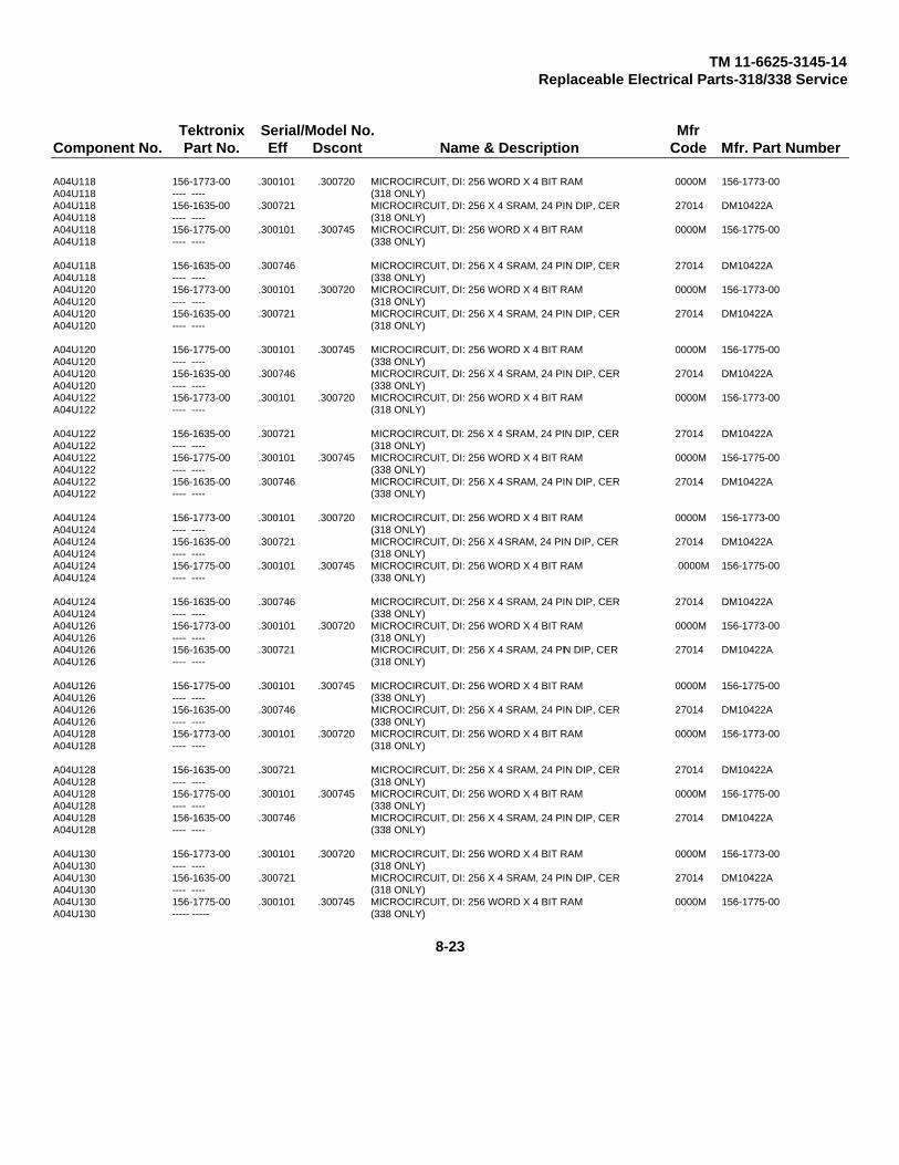
TM 11-6625-3145-14Replaceable Electrical Parts-318/338 Service
Tektronix Serial/Model No. MfrComponent No. Part No. Eff Dscont Name & Description Code Mfr. Part Number
A04U118 156-1773-00 .300101 .300720 MICROCIRCUIT, DI: 256 WORD X 4 BIT RAM 0000M 156-1773-00A04U118 ---- ---- (318 ONLY)A04U118 156-1635-00 .300721 MICROCIRCUIT, DI: 256 X 4 SRAM, 24 PIN DIP, CER 27014 DM10422AA04U118 ---- ---- (318 ONLY)A04U118 156-1775-00 .300101 .300745 MICROCIRCUIT, DI: 256 WORD X 4 BIT RAM 0000M 156-1775-00A04U118 ---- ---- (338 ONLY)
A04U118 156-1635-00 .300746 MICROCIRCUIT, DI: 256 X 4 SRAM, 24 PIN DIP, CER 27014 DM10422AA04U118 ---- ---- (338 ONLY)A04U120 156-1773-00 .300101 .300720 MICROCIRCUIT, DI: 256 WORD X 4 BIT RAM 0000M 156-1773-00A04U120 ---- ---- (318 ONLY)A04U120 156-1635-00 .300721 MICROCIRCUIT, DI: 256 X 4 SRAM, 24 PIN DIP, CER 27014 DM10422AA04U120 ---- ---- (318 ONLY)
A04U120 156-1775-00 .300101 .300745 MICROCIRCUIT, DI: 256 WORD X 4 BIT RAM 0000M 156-1775-00A04U120 ---- ---- (338 ONLY)A04U120 156-1635-00 .300746 MICROCIRCUIT, DI: 256 X 4 SRAM, 24 PIN DIP, CER 27014 DM10422AA04U120 ---- ---- (338 ONLY)A04U122 156-1773-00 .300101 .300720 MICROCIRCUIT, DI: 256 WORD X 4 BIT RAM 0000M 156-1773-00A04U122 ---- ---- (318 ONLY)
A04U122 156-1635-00 .300721 MICROCIRCUIT, DI: 256 X 4 SRAM, 24 PIN DIP, CER 27014 DM10422AA04U122 ---- ---- (318 ONLY)A04U122 156-1775-00 .300101 .300745 MICROCIRCUIT, DI: 256 WORD X 4 BIT RAM 0000M 156-1775-00A04U122 ---- ---- (338 ONLY)A04U122 156-1635-00 .300746 MICROCIRCUIT, DI: 256 X 4 SRAM, 24 PIN DIP, CER 27014 DM10422AA04U122 ---- ---- (338 ONLY)
A04U124 156-1773-00 .300101 .300720 MICROCIRCUIT, DI: 256 WORD X 4 BIT RAM 0000M 156-1773-00A04U124 ---- ---- (318 ONLY)A04U124 156-1635-00 .300721 MICROCIRCUIT, DI: 256 X 4 SRAM, 24 PIN DIP, CER 27014 DM10422AA04U124 ---- ---- (318 ONLY)A04U124 156-1775-00 .300101 .300745 MICROCIRCUIT, DI: 256 WORD X 4 BIT RAM 0000M 156-1775-00A04U124 ---- ---- (338 ONLY)
A04U124 156-1635-00 .300746 MICROCIRCUIT, DI: 256 X 4 SRAM, 24 PIN DIP, CER 27014 DM10422AA04U124 ---- ---- (338 ONLY)A04U126 156-1773-00 .300101 .300720 MICROCIRCUIT, DI: 256 WORD X 4 BIT RAM 0000M 156-1773-00A04U126 ---- ---- (318 ONLY)A04U126 156-1635-00 .300721 MICROCIRCUIT, DI: 256 X 4 SRAM, 24 PIN DIP, CER 27014 DM10422AA04U126 ---- ---- (318 ONLY)
A04U126 156-1775-00 .300101 .300745 MICROCIRCUIT, DI: 256 WORD X 4 BIT RAM 0000M 156-1775-00A04U126 ---- ---- (338 ONLY)A04U126 156-1635-00 .300746 MICROCIRCUIT, DI: 256 X 4 SRAM, 24 PIN DIP, CER 27014 DM10422AA04U126 ---- ---- (338 ONLY)A04U128 156-1773-00 .300101 .300720 MICROCIRCUIT, DI: 256 WORD X 4 BIT RAM 0000M 156-1773-00A04U128 ---- ---- (318 ONLY)
A04U128 156-1635-00 .300721 MICROCIRCUIT, DI: 256 X 4 SRAM, 24 PIN DIP, CER 27014 DM10422AA04U128 ---- ---- (318 ONLY)A04U128 156-1775-00 .300101 .300745 MICROCIRCUIT, DI: 256 WORD X 4 BIT RAM 0000M 156-1775-00A04U128 ---- ---- (338 ONLY)A04U128 156-1635-00 .300746 MICROCIRCUIT, DI: 256 X 4 SRAM, 24 PIN DIP, CER 27014 DM10422AA04U128 ---- ---- (338 ONLY)
A04U130 156-1773-00 .300101 .300720 MICROCIRCUIT, DI: 256 WORD X 4 BIT RAM 0000M 156-1773-00A04U130 ---- ---- (318 ONLY)A04U130 156-1635-00 .300721 MICROCIRCUIT, DI: 256 X 4 SRAM, 24 PIN DIP, CER 27014 DM10422AA04U130 ---- ---- (318 ONLY)A04U130 156-1775-00 .300101 .300745 MICROCIRCUIT, DI: 256 WORD X 4 BIT RAM 0000M 156-1775-00A04U130 ----- ----- (338 ONLY)
8-23

TM 11-6625-3145-14Replaceable Electrical Parts-318/338 Service
Tektronix Serial/Model No. MfrComponent No. Part No. Eff Dscont Name & Description Code Mfr. Part Number
A04U130 156-1635-00 .300746 MICROCIRCUIT, DI: 256 X 4 SRAM, 24 PIN DIP, CER 27014 DM10422AA04U130 ---- ---- (338 ONLY)A04U132 156-1775-00 .300101 .300720 MICROCIRCUIT, DI: 256 WORD X 4 BIT RAM 0000M 156-1775-00A04U132 ---- ---- (338 ONLY)A04U132 156-1635-00 .300721 MICROCIRCUIT, DI: 256 X 4 SRAM, 24 PIN DIP, CER 27014 DM10422AA04U132 ---- ---- (338 ONLY)
A04U134 156-1775-00 .300101 .300745 MICROCIRCUIT, DI: 256 WORD X 4 BIT RAM 0000M 156-1775-00A04U134 ---- ---- (338 ONLY)A04U134 156-1635-00 .300746 MICROCIRCUIT, DI: 256 X 4 SRAM, 24 PIN DIP, CER 27014 DM10422AA04U134 ---- ---- (338 ONLY)A04U136 156-1038-00 MICROCIRCUIT, DI: 4 BIT BINARY COUNTER 80009 156-1038-00A04U138 156-1038-00 MICROCIRCUIT, DI: 4 BIT BINARY COUNTER 80009 156-1038-00
A04U139 156-0230-00 MICROCIRCUIT, DI: DUAL D MA-SLAVE FLIP-FLOP 04713 MC10131 (L OR P)A04U140 156-1716-00 MICROCIRCUIT, DI: TIME BASE 0000M 156-1716-00A04U142 156-0746-02 MICROCIRCUIT, DI: QUAD 2-INPUT NON-INV MUX 0000M 156-0746-02A04U144 156-0746-02 MICROCIRCUIT, DI: QUAD 2-INPUT NON-INV MUX 0000M 156-0746-02A04U146 156-0316-00 MICROCIRCUIT, DI: QUAD ECL TO TTL CONVERTER 04713 MC10125LA04U148 156-0316-00 MICROCIRCUIT, DI: QUAD ECL TO TTL CONVERTER 04713 MC10125L
A04U150 156-0316-00 MICROCIRCUIT, DI: QUAD ECL TO TTL CONVERTER 04713 MC10125LA04U152 156-0956-00 .300101 .300280 MICROCIRCUIT, DI: OCTAL BFR W/3 STATE OUT 01295 SN74LS244NP3A04U152 ---- ---- (318 ONLY)A04U152 156-0956-02 .300281 MICROCIRCUIT, DI: OCTAL BFR W/3 STATE OUT 01295 SN74LS244NP3A04U152 ---- ---- (318 ONLY)A04U152 156-0956-00 .300101 .300150 MICROCIRCUIT, DI: OCTAL BFR W/3 STATE OUT 01295 SN74LS244NP3A04U152 ---- ---- (338 ONLY)A04U152 156-0956-02 .300151 MICROCIRCUIT, DI: OCTAL BFR W/3 STATE OUT 01295 SN74LS244NP3A04U152 ---- ---- (338 ONLY)A04U156 156-1126-02 MICROCIRCUIT, LI: COMPARATOR SINGLE W/STROBE 0000M 156-1126-02A04W118 131-0566-00 BUS CONDUCTOR: DUMMY RES, 2.375, 22 AWG 57668 JWW-0200E0A04W118 ---- ---- (338 ONLY)
A04Y100 158-0106-01 XTAL UNIT, QTZ: 100MHZ, 0.0015%, SERIES 0000M 158-0106-01
8-24

TM 11-6625-3145-14Replaceable Electrical Parts-318/338 Service
Tektronix Serial/Model No. MfrComponent No. Part No. Eff Dscont Name & Description Code Mfr. Part Number
A05 670-7813-00 CKT BOARD ASSY: ROM/THRESHOLD 80009 670-7813-00A05 ---- ---- (318/338 ONLY)A05C070 281-0814-00 CAP., FXD, CER DI: 100PF, 10%, 100V 04222 GC101A101KA05C072 281-0812-00 CAP., FXD, CER DI: 1000PF, 10%, 100V 04222 MA101C102KAAA05C080 281-0814-00 CAP., FXD, CER DI: 100PF, 10%, 100V 04222 GC101A101KA05C082 281-0812-00 CAP., FXD, CER DI: 1000PF, 10%, 100V 04222 MA101C102KAA
A05C300 290-0995-00 CAP., FXD, ELCTLT: 47UF, 20%, 16V 0000M 290-0995-00A05C301 290-0995-00 CAP., FXD, ELCTLT: 47UF, 20%, 16V 0000M 290-0995-00A05C350 281-0775-00 CAP., FXD, CER DI: 0.1UF, 20%, 50V 04222 MA205E104MAAA05C400 290-0995-00 CAP., FXD, ELCTLT: 47UF, 20%, 16V 0000M 290-0995-00A05C401 281-0775-00 CAP., FXD, CER DI: 0.1UF, 20%, 50V 04222 MA205E104MAAA05C402 281-0775-00 CAP., FXD, CER DI: 0.1UF, 20%, 50V 04222 MA205E104MAA
A05C403 281-0775-00 CAP., FXD, CER DI: 0.1UF, 20%, 50V 04222 MA205E104MAAA05C404 281-0775-00 CAP., FXD, CER DI: 0.1UF, 20%, 50V 04222 MA205E104MAAA05C405 281-0775-00 CAP., FXD, CER DI: 0.1UF, 20%, 50V 04222 MA205E104MAAA05C406 281-0775-00 CAP., FXD, CER DI: 0.1UF, 20%, 50V 04222 MA205E104MAAA05C407 281-0775-00 CAP., FXD, CER DI: 0.1UF, 20%, 50V 04222 MA205E104MAAA05C408 281-0775-00 CAP., FXD, CER DI: 0.1UF, 20%, 50V 04222 MA205E104MAA
A05C409 281-0775-00 CAP., FXD, CER DI: 0.1UF, 20%, 50V 04222 MA205E104MAAA05C410 281-0775-00 CAP., FXD, CER DI: 0.1UF, 20%, 50V 04222 MA205E104MAAA05CR070 152-0322-00 SEMICOND DEVICE: SILICON, 15V, HOT CARRIER 50434 5082-2672A05CR072 152-0322-00 SEMICOND DEVICE: SILICON, 15V, HOT CARRIER 50434 5082-2672A05CR080 152-0322-00 SEMICOND DEVICE: SILICON, 15V, HOT CARRIER 50434 5082-2672A05CR082 152 0322-00 SEMICOND DEVICE: SILICON, 15V, HOT CARRIER 50434 5082-2672
A05GND002 214-0579-00 TERM, TEST POINT: BRS CD PL 80009 214-0579-00A05R026 315-0472-00 RES., FXD, CMPSN: 4.7K OHM, 5%, 0.25W 57668 NTR25J-E04K7A05R040 307-0750-00 RES, NTWK, FXD, FI: (8)4.7K OHM, 100%, 0.125W T0191 307-0750-00A05R060 321-0177-00 RES., FXD, FILM: 681 OHM, 1%, 0.125W 01121 ORD BY DESCRA05R062 321-0285-00 RES., FXD, FILM: 9.09K OHM, 1%, 0.125W 91637 MFF1816G90900FA05R064 311-1741-00 RES., VAR, NONWIR: TRMR, 2K OHM, 20%, 0.5W 0000M 311-1741-00
A05R066 321-0287-00 RES., FXD, FILM: 9.53K OHM, 1%, 0.125W 91637 MFF1816G95300FA05R068 321-1332-00 RES., FXD, FILM: 28.4K OHM, 1%, 0.125WA05R069 321-0245-00 RES., FXD, FILM: 3.48K OHM, 1%, 0.125W 91637 MFF1816G34800FA05R070 321-0260-01 RES., FXD, FILM: 4.99K OHM, 0.5%, 0.125W 91637 MFF1816G49900DA05R072 321-0260-01 RES., FXD, FILM: 4.99K OHM, 0.5%, 0.125W 91637 MFF1816G49900DA05R074 315-0754-00 RES., FXD, CMPSN: 750K OHM, 5%, 0.25W 01121 CB7545
A05R076 315-0103-00 RES., FXD, CMPSN: 10K OHM, 5%, 0.25W 57668 NTR25J-E100K0A05R078 311-1745-00 RES., VAR, NONWIR: TRMR, 100K OHM, 10%, 0.5W 0000M 311-1745-00A05R080 321-0260-01 RES., FXD, FILM: 4.99K OHM, 0.5%, 0.125W 91637 MFF1816G49900DA05R082 321-0260-01 RES., FXD, FILM: 4.99K OHM, 0.5%, 0.125W 91637 MFF1816G49900DA05R084 315-0754-00 RES., FXD, CMPSN: 750K OHM, 5%, 0.25W 01121 CB7545A05R086 315-0103-00 RES., FXD, CMPSN: 10K OHM, 5%, 0.25W 57668 NTR25J-E100K0
A05R088 311-1745-00 RES., VAR, NONWIR: TRMR, 100K OHM, 10%, 0.5W 0000M 311-1745-00A05R100 307-0750-00 RES, NTWK, FXD, FI: (8)4.7K OHM, 100%, 0.125W T0191 307-0750-00A05R110 321-0260-01 RES., FXD, FILM: 4.99K OHM, 0.5%, 0.125W 91637 MFF1816G49900DA05R115 321-0260-01 RES., FXD, FILM: 4.99K OHM, 0.5%, 0.125W 91637 MFF1816G49900DA05R118 307-0880-00 RES NTWK, FXD, FI: 5, 100K OHM, 10%, 0.25W 0000M 307-0880-00A05R120 315-0511-00 RES., FXD, CMPSN: 510 OHM, 5%, 0.25W 01121 CB5115
A05R122 315-0511-00 RES., FXD, CMPSN: 510 OHM, 5%, 0.25W 01121 CB5115A05R125 315-0511-00 RES., FXD, CMPSN: 510 OHM, 5%, 0.25W 01121 CB5115A05R127 315-0511-00 RES., FXD, CMPSN: 510 OHM, 5%, 0.25W 01121 CB5115A05R130 315-0511-00 RES., FXD, CMPSN: 510 OHM, 5%, 0.25W 01121 CB5115A05TP064 214-0579-00 TERM, TEST POINT: BRS CD PL 80009 214-0579-00A05TP078 214-0579-00 TERM, TEST POINT: BRS CD PL 80009 214-0579-00
8-25
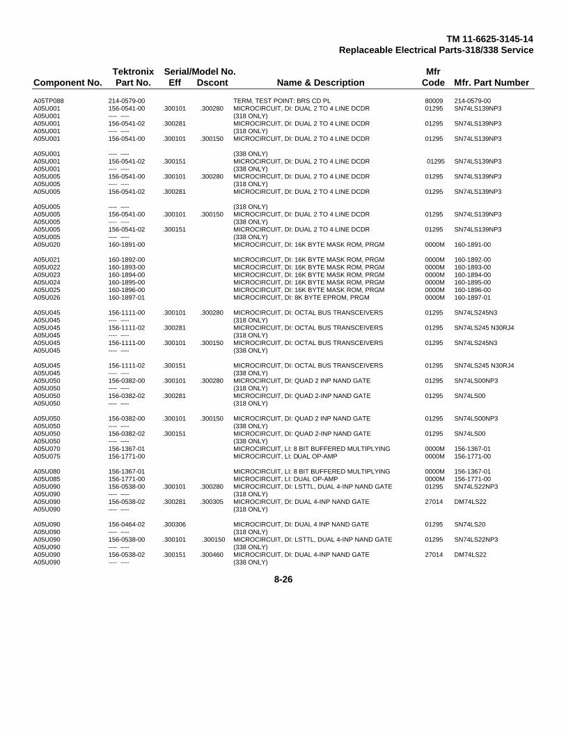
TM 11-6625-3145-14Replaceable Electrical Parts-318/338 Service
Tektronix Serial/Model No. MfrComponent No. Part No. Eff Dscont Name & Description Code Mfr. Part Number
A05TP088 214-0579-00 TERM, TEST POINT: BRS CD PL 80009 214-0579-00A05U001 156-0541-00 .300101 .300280 MICROCIRCUIT, DI: DUAL 2 TO 4 LINE DCDR 01295 SN74LS139NP3A05U001 ---- ---- (318 ONLY)A05U001 156-0541-02 .300281 MICROCIRCUIT, DI: DUAL 2 TO 4 LINE DCDR 01295 SN74LS139NP3A05U001 ---- ---- (318 ONLY)A05U001 156-0541-00 .300101 .300150 MICROCIRCUIT, DI: DUAL 2 TO 4 LINE DCDR 01295 SN74LS139NP3
A05U001 ---- ---- (338 ONLY)A05U001 156-0541-02 .300151 MICROCIRCUIT, DI: DUAL 2 TO 4 LINE DCDR 01295 SN74LS139NP3A05U001 ---- ---- (338 ONLY)A05U005 156-0541-00 .300101 .300280 MICROCIRCUIT, DI: DUAL 2 TO 4 LINE DCDR 01295 SN74LS139NP3A05U005 ---- ---- (318 ONLY)A05U005 156-0541-02 .300281 MICROCIRCUIT, DI: DUAL 2 TO 4 LINE DCDR 01295 SN74LS139NP3
A05U005 ---- ---- (318 ONLY)A05U005 156-0541-00 .300101 .300150 MICROCIRCUIT, DI: DUAL 2 TO 4 LINE DCDR 01295 SN74LS139NP3A05U005 ---- ---- (338 ONLY)A05U005 156-0541-02 .300151 MICROCIRCUIT, DI: DUAL 2 TO 4 LINE DCDR 01295 SN74LS139NP3A05U005 ---- ---- (338 ONLY)A05U020 160-1891-00 MICROCIRCUIT, DI: 16K BYTE MASK ROM, PRGM 0000M 160-1891-00
A05U021 160-1892-00 MICROCIRCUIT, DI: 16K BYTE MASK ROM, PRGM 0000M 160-1892-00A05U022 160-1893-00 MICROCIRCUIT, DI: 16K BYTE MASK ROM, PRGM 0000M 160-1893-00A05U023 160-1894-00 MICROCIRCUIT, DI: 16K BYTE MASK ROM, PRGM 0000M 160-1894-00A05U024 160-1895-00 MICROCIRCUIT, DI: 16K BYTE MASK ROM, PRGM 0000M 160-1895-00A05U025 160-1896-00 MICROCIRCUIT, DI: 16K BYTE MASK ROM, PRGM 0000M 160-1896-00A05U026 160-1897-01 MICROCIRCUIT, DI: 8K BYTE EPROM, PRGM 0000M 160-1897-01
A05U045 156-1111-00 .300101 .300280 MICROCIRCUIT, DI: OCTAL BUS TRANSCEIVERS 01295 SN74LS245N3A05U045 ---- ---- (318 ONLY)A05U045 156-1111-02 .300281 MICROCIRCUIT, DI: OCTAL BUS TRANSCEIVERS 01295 SN74LS245 N30RJ4A05U045 ---- ---- (318 ONLY)A05U045 156-1111-00 .300101 .300150 MICROCIRCUIT, DI: OCTAL BUS TRANSCEIVERS 01295 SN74LS245N3A05U045 ---- ---- (338 ONLY)
A05U045 156-1111-02 .300151 MICROCIRCUIT, DI: OCTAL BUS TRANSCEIVERS 01295 SN74LS245 N30RJ4A05U045 ---- ---- (338 ONLY)A05U050 156-0382-00 .300101 .300280 MICROCIRCUIT, DI: QUAD 2 INP NAND GATE 01295 SN74LS00NP3A05U050 ---- ---- (318 ONLY)A05U050 156-0382-02 .300281 MICROCIRCUIT, DI: QUAD 2-INP NAND GATE 01295 SN74LS00A05U050 ---- ---- (318 ONLY)
A05U050 156-0382-00 .300101 .300150 MICROCIRCUIT, DI: QUAD 2 INP NAND GATE 01295 SN74LS00NP3A05U050 ---- ---- (338 ONLY)A05U050 156-0382-02 .300151 MICROCIRCUIT, DI: QUAD 2-INP NAND GATE 01295 SN74LS00A05U050 ---- ---- (338 ONLY)A05U070 156-1367-01 MICROCIRCUIT, LI: 8 BIT BUFFERED MULTIPLYING 0000M 156-1367-01A05U075 156-1771-00 MICROCIRCUIT, LI: DUAL OP-AMP 0000M 156-1771-00
A05U080 156-1367-01 MICROCIRCUIT, LI: 8 BIT BUFFERED MULTIPLYING 0000M 156-1367-01A05U085 156-1771-00 MICROCIRCUIT, LI: DUAL OP-AMP 0000M 156-1771-00A05U090 156-0538-00 .300101 .300280 MICROCIRCUIT, DI: LSTTL, DUAL 4-INP NAND GATE 01295 SN74LS22NP3A05U090 ---- ---- (318 ONLY)A05U090 156-0538-02 .300281 .300305 MICROCIRCUIT, DI: DUAL 4-INP NAND GATE 27014 DM74LS22A05U090 ---- ---- (318 ONLY)
A05U090 156-0464-02 .300306 MICROCIRCUIT, DI: DUAL 4 INP NAND GATE 01295 SN74LS20A05U090 ---- ---- (318 ONLY)A05U090 156-0538-00 .300101 .300150 MICROCIRCUIT, DI: LSTTL, DUAL 4-INP NAND GATE 01295 SN74LS22NP3A05U090 ---- ---- (338 ONLY)A05U090 156-0538-02 .300151 .300460 MICROCIRCUIT, DI: DUAL 4-INP NAND GATE 27014 DM74LS22A05U090 ---- ---- (338 ONLY)
8-26

TM 11-6625-3145-14Replaceable Electrical Parts-318/338 Service
Tektronix Serial/Model No. MfrComponent No. Part No. Eff Dscont Name & Description Code Mfr. Part Number
A05U090 156-0464-02 .300461 MICROCIRCUIT, DI: DUAL 4 INP NAND GATE 01295 SN74LS20A05U090 ---- ---- (338 ONLY)A05U092 156-0541-00 .300101 .300280 MICROCIRCUIT, DI: DUAL 2 TO 4 LINE DCDR 01295 SN74LS139NP3A05U092 ---- ---- (318 ONLY)A05U092 156-0541-02 .300281 MICROCIRCUIT, DI: DUAL 2 TO 4 LINE DCDR 01295 SN74LS139NP3A05U092 ---- ---- (318 ONLY)
A05U092 156-0541-00 .300101 .300150 MICROCIRCUIT, DI: DUAL 2 TO 4 LINE DCDR 01295 SN74LS139NP3A05U092 ---- ---- (338 ONLY)A05U092 156-0541-02 .300151 MICROCIRCUIT, DI: DUAL 2 TO 4 LINE DCDR 01295 SN74LS139NP3A05U092 ---- ---- (338 ONLY)A05U100 156-0391-00 .300101 .300280 MICROCIRCUIT, DI: HEX LATCH W/CLEAR SCRN 01295 SN74LS174A05U100 ---- ---- (318 ONLY)
A05U100 156-0391-02 .300281 MICROCIRCUIT, DI: HEX LATCH W/CLEAR 01295 SN74LS174A05U100 ---- ---- (318 ONLY)A05U100 156-0391-00 .300101 .300150 MICROCIRCUIT, DI: HEX LATCH W/CLEAR SCRN 01295 SN74LS174A05U100 ---- ---- (338 ONLY)A05U100 156-0391-02 .300151 MICROCIRCUIT, DI: HEX LATCH W/CLEAR 01295 SN74LS174A05U100 ---- ---- (338 ONLY)
A05U105 156-1770-00 MICROCIRCUIT, DI: OCTAL D-TYPE W/CLEAR 0000M 156-1770-00A05U110 156-0514-03 MICROCIRCUIT, DI: DIFF 4-CHANNEL MUX 0000M 156-0514-03A05U111 156-0514-03 MICROCIRCUIT, DI: DIFF 4-CHANNEL MUX 0000M 156-0514-03A05U112 156-0514-03 MICROCIRCUIT, DI: DIFF 4-CHANNEL MUX 0000M 156-0514-03A05U113 156-0514-03 MICROCIRCUIT, DI: DIFF 4-CHANNEL MUX 0000M 156-0514-03A05U114 156-0514-03 MICROCIRCUIT, DI: DIFF 4-CHANNEL MUX 0000M 156-0514-03
A05U120 156-1771-00 MICROCIRCUIT, LI: DUAL OP-AMP 0000M 156-1771-00A05U125 156-1771-00 MICROCIRCUIT, LI: DUAL OP-AMP 0000M 156-1771-00A05U130 156-1771-00 MICROCIRCUIT, LI: DUAL OP-AMP 0000M 156-1771-00A05U150 156-0383-00 .300101 .300280 MICROCIRCUIT DI: QUAD 2-IMP NOR GATE, SCRN 01295 SN74LS02A05U150 ---- ---- (318 ONLY)A05U150 156-0383-02 .300281 MICROCIRCUIT, DI: QUAD 2-INP NOR GATE 01295 SN74LS02
A05U150 ---- ---- (318 ONLY)A05U150 156-0383-00 .300101 .300150 MICROCIRCUIT DI: QUAD 2-IMP NOR GATE, SCRN 01295 SN74LS02A05U150 ---- ---- (338 ONLY)A05U150 156-0383-02 .300151 MICROCIRCUIT, DI: QUAD 2-INP NOR GATE 01295 SN74LS02A05U 150 ---- ---- (338 ONLY)A05VR060 152-0461-00 SEMICOND DEVICE: ZENER, 0.4W, 6.2V, 5% 04713 SZG25002K2
8-27

TM 11-6625-3145-14Replaceable Electrical Parts-318/338 Service
Tektronix Serial/Model No. MfrComponent No. Part No. Eff Dscont Name & Description Code Mfr. Part Number
A06 670-7812-00 CKT BOARD ASSY: MPU DISPLAY 80009 670-7812-00A06 ---- ---- (318/338 ONLY)A06C100 281-0811-00 CAP., FXD, CER DI: 10PF, 10%, 100V 96733 R2911A06C106 281-0797-00 CAP., FXD, CER DI: 15PF, 10%, 100V 04222 MA 106A 150KAAA06C110 281-0811-00 CAP., FXD, CER DI: 10PF, 10%, 100V 96733 R2911A06C116 281-0797-00 CAP., FXD, CER DI: 15PF, 10%, 100V 04222 MA 106A 150KAA
A06C132 281-0775-00 CAP., FXD, CER DI: 0.1UF, 20%, 50V 04222 MA205E104MAAA06C202 ---- ---- CAP., FXD, CER DI: 10UF, 20%, 50VA06C202 ---- ---- (P/N NOT AVAILABLE AT THIS PRINTING)A06C220 281-0775-00 CAP., FXD, CER DI: 0.1UF, 20%, 50V 04222 MA205E104MAAA06C320 281-0775-00 CAP, , FXD, CER DI: 0.1UF, 20%, 50V 04222 MA205E104MAAA06C600 290-0995-00 CAP., FXD, ELCTLT: 47UF, 20%, 16V 0000M 290-0995-00
A06C601 281-0775-00 CAP., FXD, CER DI: 0.1UF, 20%, 50V 04222 MA205E104MAAA06C602 281-0775-00 CAP., FXD, CER DI: 0.1UF, 20%, 50V 04222 MA205E104MAAA06C603 281-0775-00 CAP., FXD, CER DI: 0.1UF, 20%, 50V 04222 MA205E104MAAA06C604 281-0775-00 CAP., FXD, CER DI: 0.1UF, 20%, 50V 04222 MA205E104MAAA06C605 281-0775-00 CAP., FXD, CER DI: 0.1UF, 20%, 50V 04222 MA205E104MAAA06C606 281-0775-00 CAP., FXD, CER DI: 0.1UF, 20%, 50V 04222 MA205E104MAA
A06C607 281-0775-00 CAP., FXD, CER DI: 0.1UF, 20%, 50V 04222 MA205E104MAAA06C608 281-0775-00 CAP., FXD, CER DI: 0.1UF, 20%, 50V 04222 MA205E104MAAA06C609 281-0775-00 CAP., FXD, CER DI: 0.1UF, 20%, 50V 04222 MA205E104MAAA06C610 281-0775-00 CAP., FXD, CER DI: 0.1UF, 20%, 50V 04222 MA205E104MAAA06C700 290-0995-00 CAP., FXD, ELCTLT: 47UF, 20%, 16V 0000M 290-0995-00A06C701 281-0775-00 CAP., FXD, CER DI: 0.1UF, 20%, 50V 04222 MA205E104MAA
A06CR200 152-0327-00 SEMICOND DEVICE: SIG, SI, BAX13 T0191 152-0327-00406DS700 150-1081-00 LT EMITTING DIO: RED 0000M 150-1081-00A06GND001 214-0579-00 TERM, TEST POINT: BRS CD PL 80009 214-0579-00A06GND002 214-0579-00 TERM, TEST POINT: BRS CD PL 80009 214-0579-00A060550 151-0190-00 TRANSISTOR: NPN, SI, TO-92 04713 SPS7969A06R100 315-0181-00 RES., FXD, CMPSN: 180 OHM, 5%, 0.25W 57668 NTR25J-E180E
A06R101 315-0271-00 RES., FXD, CMPSN: 270 OHM, 5%, 0.25W 01121 CB2715A06R102 315-0242-00 RES., FXD, CMPSN: 2.4K OHM, 5%, 0.25W 57668 NTR25J-E02K4A06R 103 315-0331-00 RES., FXD, CMPSN: 330 OHM, 5%, 0.25W 57668 NTR25J-E330EA06R110 315-0181-00 RES., FXD, CMPSN: 180 OHM, 5%, 0.25W 57668 NTR25J-E180EA06R111 315-0271-00 RES., FXD, CMPSN: 270 OHM, 5%, 0.25W 01121 CB2715A06R112 315-0242-00 RES., FXD, CMPSN: 2.4K OHM, 5%, 0.25W 57668 NTR25J-E02K4
A06R113 315-0331-00 RES., FXD, CMPSN: 330 OHM, 5%, 0.25W 57668 NTR25J-E330EA06R120 315-0471-00 RES., FXD, CMPSN: 470 OHM, 5%, 0.25W 57668 NTR25J-E470EA06R130 315-0154-00 RES., FXD, CMPSN: 150K OHM, 5%, 0.25W 57668 NTR25J-E150KA06R132 315-0334-00 RES., FXD, CMPSN: 330K OHM, 5%, 0.25W 01121 CB3345A06R200 315-0473-00 RES., FXD, CMPSN: 47K OHM, 5%, 0.25W 57668 NTR25J-E47K0A06R203 315-0102-00 RES., FXD, CMPSN: 1K OHM, 5%, 0.25W 57668 NTR25JE01 K0
A06R215 315-0472-00 RES., FXD, CMPSN: 4.7K OHM, 5%, 0.25W 57668 NTR25J-E04K7A06R216 315-0473-00 RES., FXD, CMPSN: 47K OHM, 5%, 0.25W 57668 NTR25J-E47K0A06R220 315-0104-00 RES., FXD, CMPSN: 100K OHM, 5%, 0.25W 57668 NTR25J-E100KA06R221 315-0472-00 RES., FXD, CMPSN: 4.7K OHM, 5%, 0.25W 57668 NTR25J-E04K7A06R222 307-0883-00 RES NTWK, FXD, FI: 4, 1K OHM, 10%, 0.25W 0000M 307-0883-00A06R224 307-0881-00 RES NTWK, FXD, FI: 8, 10K OHM, 10%, 0.125W 0000M 307-0881-00
A06R226 307-0883-00 RES NTWK, FXD, FI: 4, 1K OHM, 10%, 0.25W 0000M 307-0883-00A06R300 307-0729-00 RES NTWK, FXD, FI: (4)10K OHM, 10%, 0.125W T0191 307-0729-00A06R302 307-0729-00 RES NTWK, FXD, FI: (4)10K OHM, 10%, 0.125W T0191 307-0729-00A06R306 307-0882-00 RES NTWK, FXD, FI: 8, 100K OHM, 10%, 0.125W 0000M 307-0882-00A06R310 307-0729-00 RES NTWK, FXD, FI: (4)10K OHM, 10%, 0.125W T0191 307-0729-00A06R312 307-0729-00 RES NTWK, FXD, FI: (4)10K OHM, 10%, 0.125W T0191 307-0729-00
8-28

TM 11-6625-3145-14Replaceable Electrical Parts-318/338 Service
Tektronix Serial/Model No. MfrComponent No. Part No. Eff Dscont Name & Description Code Mfr. Part Number
A06R316 307-0882-00 RES NTWK, FXD, FI: 8, 100K OHM, 10%, 0.125W 0000M 307-0882-00A06R320 315-0104-00 RES., FXD, CMPSN: 100K OHM, 5%, 0.25W 57668 NTR25J-E100KA06R322 315-0472-00 RES., FXD, CMPSN: 4.7K OHM, 5%, 0.25W 57668 NTR25J-E04K7A06R540 321-0147-00 RES., FXD, FILM: 332 OHM, 1%, 0.125W 91637 MFF1816G332R0FA06R542 321-0105-00 RES., FXD, FILM: 121 OHM, 1%, 0.125W 01121 ORD BY DESCRA06R544 321-0143-00 RES., FXD, FILM: 301 OHM, 1%, 0.125W 91637 MFF1816G301R0F
A06R545 321-0230-00 RES., FXD, FILM: 2.43K OHM, 1%, 0.125W 91637 MFF1816G24300FA06R546 321-0260-01 RES., FXD, FILM: 4.99K OHM, 0.5%, 0.125W 91637 MFF1816G49900DA06R548 321-0260-01 RES., FXD, FILM: 4.99K OHM, 0.5%, 0.125W 91637 MFF1816G49900DA06R550 315-0750-00 RES., FXD, CMPSN: 75 OHM, 5%, 0.25W 57668 NTR25J-E75E0A06R555 315-0271-00 RES., FXD, CMPSN: 270 OHM, 5%, 0.25W 01121 CB2715A06R700 315-0331-00 RES., FXD, CMPSN: 330 OHM, 5%, 0.25W 57668 NTR25J-E330E
A06U100 156-0385-00 .300101 .300280 MICROCIRCUIT, DI: HEX INVERTER, SCRN, 74LS04 01295 SN74LS04A06U100 ---- ---- (318 ONLY)A06U100 156-0385-02 .300281 MICROCIRCUIT, DI: HEX INVERTER 01295 SN74LS04A06U100 ---- ---- (318 ONLY)A06U100 156-0385-00 .300101 .300150 MICROCIRCUIT, DI: HEX INVERTER, SCRN, 74LS04 01295 SN74LS04A06U100 ---- ---- (338 ONLY)
A06U100 156-0385-02 .300151 MICROCIRCUIT, DI: HEX INVERTER 01295 SN74LS04A06U100 ---- ---- (338 ONLY)A06U110 156-1108-00 .300101 .300280 MICROCIRCUIT, DI: DIVIDE BY 12 COUNTER, SCRN 01295 SN74LS92A06U110 ---- ---- (318 ONLY)A06U110 156-1108-02 .300281 MICROCIRCUIT, DI: DIVIDE BY 12 COUNTER, SCRN 01295 SN74LS92(NP3 ORA06U110 ---- ---- (318 ONLY)
A06U110 156-1108-00 .300101 .300150 MICROCIRCUIT, DI: DIVIDE BY 12 COUNTER, SCRN 01295 SN74LS92A06U110 ---- ---- (338 ONLY)A06U110 156-1108-02 .300151 MICROCIRCUIT, DI: DIVIDE BY 12 COUNTER, SCRN 01295 SN74LS92(NP3 ORA06U110 ---- ---- (338 ONLY)A06U120 156-0910-00 .300101 .300280 MICROCIRCUIT, DI: DUAL DECADE COUNTER, SCRN 01295 SN74LS390A06U120 ---- ---- (318 ONLY)
A06U120 156-0910-02 .300281 MICROCIRCUIT, DI: DUAL DECADE COUNTER 01295 SN74LS390A06U120 ---- ---- (318 ONLY)A06U120 156-0910-00 .300101 .300150 MICROCIRCUIT, DI: DUAL DECADE COUNTER, SCRN 01295 SN74LS390A06U120 ----- ----- (338 ONLY)A06U120 156-0910-02 .300151 MICROCIRCUIT, DI: DUAL DECADE COUNTER 01295 SN74LS390A06U120 ---- ---- (338 ONLY)
A06U130 156-1774-00 MICROCIRCUIT, LI: TV SYNC GENERATOR 0000M 156-1774-00A06U134 156-0745-02 MICROCIRCUIT, DI: INVERTER HEX 0000M 156-0745-02A06U138 156-1768-00 MICROCIRCUIT, DI: HEX D-TYPE W/COMM CLEAR 0000M 156-1768-00A06U200 156-0983-04 MICROCIRCUIT, DI: NMOS, 8 BIT MICROPROCESSORA06U210 156-0956-00 .300101 .300280 MICROCIRCUIT, DI: OCTAL BFR W/3 STATE OUT 01295 SN74LS244NP3A06U210 ---- ---- (318 ONLY)
A06U210 156-0956-02 .300281 MICROCIRCUIT, DI: OCTAL BFR W/3 STATE OUT 01295 SN74LS244NP3A06U210 ---- ---- (318 ONLY)A06U210 156-0956-00 .300101 .300150 MICROCIRCUIT, DI: OCTAL BFR W/3 STATE OUT 01295 SN74LS244NP3A06U210 ---- ---- (338 ONLY)A06U210 156-0956-02 .300151 MICROCIRCUIT, DI: OCTAL BFR W/3 STATE OUT 01295 SN74LS244NP3A06U210 ---- ---- (338 ONLY)
A06U212 156-0956-00 .300101 .300280 MICROCIRCUIT, DI: OCTAL BFR W/3 STATE OUT 01295 SN74LS244NP3A06U212 ---- ---- (318 ONLY)A06U212 156-0956-02 .300281 MICROCIRCUIT, DI: OCTAL BFR W/3 STATE OUT 01295 SN74LS244NP3A06U212 ---- ---- (318 ONLY)A06U212 156-0956-00 .300101 .300150 MICROCIRCUIT, DI: OCTAL BFR W/3 STATE OUT 01295 SN74LS244NP3A06U212 ---- ---- (338 ONLY)
8-29
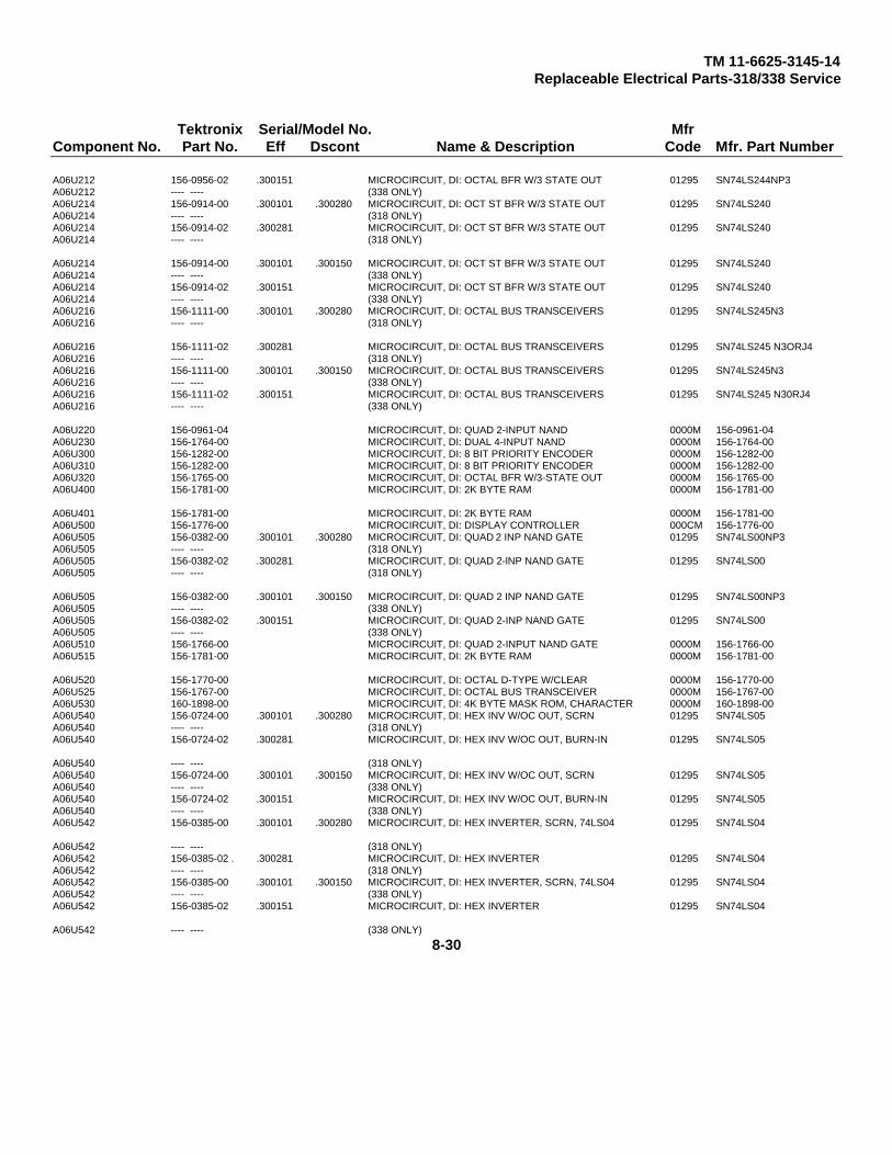
TM 11-6625-3145-14Replaceable Electrical Parts-318/338 Service
Tektronix Serial/Model No. MfrComponent No. Part No. Eff Dscont Name & Description Code Mfr. Part Number
A06U212 156-0956-02 .300151 MICROCIRCUIT, DI: OCTAL BFR W/3 STATE OUT 01295 SN74LS244NP3A06U212 ---- ---- (338 ONLY)A06U214 156-0914-00 .300101 .300280 MICROCIRCUIT, DI: OCT ST BFR W/3 STATE OUT 01295 SN74LS240A06U214 ---- ---- (318 ONLY)A06U214 156-0914-02 .300281 MICROCIRCUIT, DI: OCT ST BFR W/3 STATE OUT 01295 SN74LS240A06U214 ---- ---- (318 ONLY)
A06U214 156-0914-00 .300101 .300150 MICROCIRCUIT, DI: OCT ST BFR W/3 STATE OUT 01295 SN74LS240A06U214 ---- ---- (338 ONLY)A06U214 156-0914-02 .300151 MICROCIRCUIT, DI: OCT ST BFR W/3 STATE OUT 01295 SN74LS240A06U214 ---- ---- (338 ONLY)A06U216 156-1111-00 .300101 .300280 MICROCIRCUIT, DI: OCTAL BUS TRANSCEIVERS 01295 SN74LS245N3A06U216 ---- ---- (318 ONLY)
A06U216 156-1111-02 .300281 MICROCIRCUIT, DI: OCTAL BUS TRANSCEIVERS 01295 SN74LS245 N3ORJ4A06U216 ---- ---- (318 ONLY)A06U216 156-1111-00 .300101 .300150 MICROCIRCUIT, DI: OCTAL BUS TRANSCEIVERS 01295 SN74LS245N3A06U216 ---- ---- (338 ONLY)A06U216 156-1111-02 .300151 MICROCIRCUIT, DI: OCTAL BUS TRANSCEIVERS 01295 SN74LS245 N30RJ4A06U216 ---- ---- (338 ONLY)
A06U220 156-0961-04 MICROCIRCUIT, DI: QUAD 2-INPUT NAND 0000M 156-0961-04A06U230 156-1764-00 MICROCIRCUIT, DI: DUAL 4-INPUT NAND 0000M 156-1764-00A06U300 156-1282-00 MICROCIRCUIT, DI: 8 BIT PRIORITY ENCODER 0000M 156-1282-00A06U310 156-1282-00 MICROCIRCUIT, DI: 8 BIT PRIORITY ENCODER 0000M 156-1282-00A06U320 156-1765-00 MICROCIRCUIT, DI: OCTAL BFR W/3-STATE OUT 0000M 156-1765-00A06U400 156-1781-00 MICROCIRCUIT, DI: 2K BYTE RAM 0000M 156-1781-00
A06U401 156-1781-00 MICROCIRCUIT, DI: 2K BYTE RAM 0000M 156-1781-00A06U500 156-1776-00 MICROCIRCUIT, DI: DISPLAY CONTROLLER 000CM 156-1776-00A06U505 156-0382-00 .300101 .300280 MICROCIRCUIT, DI: QUAD 2 INP NAND GATE 01295 SN74LS00NP3A06U505 ---- ---- (318 ONLY)A06U505 156-0382-02 .300281 MICROCIRCUIT, DI: QUAD 2-lNP NAND GATE 01295 SN74LS00A06U505 ---- ---- (318 ONLY)
A06U505 156-0382-00 .300101 .300150 MICROCIRCUIT, DI: QUAD 2 INP NAND GATE 01295 SN74LS00NP3A06U505 ---- ---- (338 ONLY)A06U505 156-0382-02 .300151 MICROCIRCUIT, DI: QUAD 2-INP NAND GATE 01295 SN74LS00A06U505 ---- ---- (338 ONLY)A06U510 156-1766-00 MICROCIRCUIT, DI: QUAD 2-INPUT NAND GATE 0000M 156-1766-00A06U515 156-1781-00 MICROCIRCUIT, DI: 2K BYTE RAM 0000M 156-1781-00
A06U520 156-1770-00 MICROCIRCUIT, DI: OCTAL D-TYPE W/CLEAR 0000M 156-1770-00A06U525 156-1767-00 MICROCIRCUIT, DI: OCTAL BUS TRANSCEIVER 0000M 156-1767-00A06U530 160-1898-00 MICROCIRCUIT, DI: 4K BYTE MASK ROM, CHARACTER 0000M 160-1898-00A06U540 156-0724-00 .300101 .300280 MICROCIRCUIT, DI: HEX INV W/OC OUT, SCRN 01295 SN74LS05A06U540 ---- ---- (318 ONLY)A06U540 156-0724-02 .300281 MICROCIRCUIT, DI: HEX INV W/OC OUT, BURN-IN 01295 SN74LS05
A06U540 ---- ---- (318 ONLY)A06U540 156-0724-00 .300101 .300150 MICROCIRCUIT, DI: HEX INV W/OC OUT, SCRN 01295 SN74LS05A06U540 ---- ---- (338 ONLY)A06U540 156-0724-02 .300151 MICROCIRCUIT, DI: HEX INV W/OC OUT, BURN-IN 01295 SN74LS05A06U540 ---- ---- (338 ONLY)A06U542 156-0385-00 .300101 .300280 MICROCIRCUIT, DI: HEX INVERTER, SCRN, 74LS04 01295 SN74LS04
A06U542 ---- ---- (318 ONLY)A06U542 156-0385-02 . .300281 MICROCIRCUIT, DI: HEX INVERTER 01295 SN74LS04A06U542 ---- ---- (318 ONLY)A06U542 156-0385-00 .300101 .300150 MICROCIRCUIT, DI: HEX INVERTER, SCRN, 74LS04 01295 SN74LS04A06U542 ---- ---- (338 ONLY)A06U542 156-0385-02 .300151 MICROCIRCUIT, DI: HEX INVERTER 01295 SN74LS04
A06U542 ---- ---- (338 ONLY)
8-30
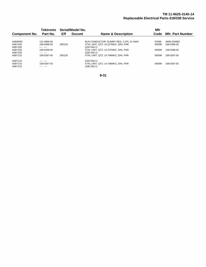
TM 11-6625-3145-14Replaceable Electrical Parts-318/338 Service
Tektronix Serial/Model No. MfrComponent No. Part No. Eff Dscont Name & Description Code Mfr. Part Number
A06W500 131-0566-00 BUS CONDUCTOR: DUMMY RES, 2.375, 22 AWG 57668 JWW-0200E0A06Y105 158-0268-00 .300126 XTAL UNIT, QTZ: 10.227MHZ, 20%, PAR 0000M 158-0268-00A06Y105 ---- ---- (318 ONLY)A06Y105 158-0268-00 XTAL UNIT, QTZ: 10.227MHZ, 20%, PAR 0000M 158-0268-00A06Y105 ---- ---- (338 ONLY)A06Y115 158-0267-00 .300126 XTAL UNIT, QTZ: 14.746MHZ, 20%, PAR 0000M 158-0267-00
A06Y115 ---- ---- (318 ONLY)A06Y115 158-0267-00 XTAL UNIT, QTZ: 14.746MHZ, 20%, PAR 0000M 158-0267-00A06Y115 ---- ---- (338 ONLY)
8-31

TM 11-6625-3145-14Replaceable Electrical Parts-318/338 Service
Tektronix Serial/Model No. MfrComponent No. Part No. Eff Dscont Name & Description Code Mfr. Part Number
A07 670-7809-00 CKT BOARD ASSY: SERIAL/RS232/NUM 80009 670-7809-00A07 ---- ---- (318/338 OPTION 01 ONLY)A07BT001 146-0046-00 BATTERY, DRY: 3.4V, 850MA, LITHIUM 0000M 146-0046-00A07C010 281-0900-00 CAP., VAR, CER DI: 2-12PF, 300V 0000M 281-0900-00A07C011 281-0772-00 CAP., FXD, CER DI: 0.0047UF, 10%.100V 04222 GC701C472KA07C030 283-0059-00 CAP., FXD, CER DI: 1UF, +80-20%, 50V 51642 400050Z5U105Z
A07C031 281-0819-00 CAP., FXD, CER DI: 33PF, 5°o, 50V 72982 8035BC0G330A07C040 281-0768-00 CAP., FXD, CER DI: 470PF, 20'%/, 100V 56289 292CC0G471M100BA07C130 290-0995-00 CAP., FXD, ELCTLT: 47UF, 20%, 16V 0000M 290-0995-00A07C150 281-0768-00 CAP., FXD, CER DI: 470PF, 20%, 100V 56289 292CC0G471M100BA07C160 290-0993-00 CAP., FXD, ELCTLT: 100UF, t+5-10%/., 16V 0000M 290-0993-00A07C200 290-0995-00 CAP .FXD, ELCTLT: 47UF, 20'%/, 16V 0000M 290-0995-00
A07C201 281-0775-00 CAP ., FXD, CER DI: 0.1UF, 20%o, 50V 04222 MA205E104MAAA07C300 281-0775-00 CAP., FXD, CER DI: 0.1UF, 20%, 50V 04222 MA205E104MAAA07C301 281-0775-00 CAP., FXD, CER DI: 0.1UF, 20'%, 50V 04222 MA205E104MAAA07C302 281-0775-00 CAP., FXD, CER DI: 0.1UF, 20'%, 50V 04222 MA205E104MAAA07C310 281-0775-00 CAP., FXD, CER DI: 0.1UF, 20%, 50V 04222 MA205E104MAAA07C311 281-0775-00 CAP , FXD, CER DI: 0.1UF, 20%, 50V 04222 MA205E104MAA
A07C320 281-0775-00 CAP., FXD, CER DI: 0.1UF, 20%, 50V 04222 MA205E104MAAA07C321 281-0775-00 CAP., FXD, CER DI: 0.1UF, 20%, , 50V 04222 MA205E104MAAA07CR010 152-0323-03 SEMICOND DEVICE: SIG, SI, BAX 13 0000M 152-0323-03A07CR011 152-0323-03 SEMICOND DEVICE: SIG, SI, BAX 13 0000M 152-0323-03A07CR120 152-0327-00 SEMICOND DEVICE: SIG, SI, BAX13 T0191 152-0327-00A07CR130 152-0327-00 SEMICOND DEVICE: SIG, SI., BAX13 T0191 152-0327-00
A07CR170 152-0327-00 SEMICOND DEVICE: SIG, SI, BAX13 T0191 152-0327-00A07J100 131-2942-01 CONN, RCPT, ELEC: HEADER, ANGLE, 2 X 13 0000M 131-2942-01A07Q120 151-0188-00 TRANSISTOR: PNP, SI, TO-92 T0058 2N3906A07Q140 151-0188-00 TRANSISTOR: PNP, SI, TO-92 T0058 2N3906A07Q141 151-0190-00 TRANSISTOR: NPN, SI, TO-92 04713 SPS7969A07Q150 151-0190-00 TRANSISTOR: NPN, SI, TO-92 04713 SPS7969
A07Q170 151-0188-00 TRANSISTOR: PNP, SI, TO-92 T0058 2N3906A07R010 321-0481-04 RES., FXD, FILM: 1M OHM, 0.1%, 0.125W 91637 CMF55116D10003BA07R011 315-0474-00 RES., FXD, CMPSN: 470K OHM, 5, %, 0.25W 57668 NTR25J-E470KA07R023 311-1616-00 RES., VAR, NONWW: 25K OHM, 20°%, 0.5W 0000M 311-1616-00A07R030 315-0202-00 RES., FXD, CMPSN: 2K OHM, 5°%, 0.25W 57668 NTR25J-E02K0A07R033 ---- ---- (PART NUMBER NOT AVLBL AT THIS PRINTING)
A07R034 321-0603-07 RES., FXD, FILM: 15K OHM, 0.10, 0.125W 91637 MFF1816C15001BA07R040 315-0181-00 RES., FXD, CMPSN: 180 OHM, 5°'o, 0.25W 57668 NTR25J-E180EA07R041 315-0111-00 RES., FXD, CMPSN: 110 OHM, 5%, 0.25W 57668 NTR25J-E110EA07R045 315-0392-00 RES., FXD, CMPSN: 3.9K OHM, 5%, 0.25W 57668 NTR25J-E03K9A07R046 315-0132-00 RES., FXD, CMPSN: 1.3K OHM, 5%, 0.25W 57668 NTR25J-E001K3A07R050 307-0637-00 RES NTWK, FXD, FI: 5, 2K OHM, 2, %, 0.125W 01121 206A202
A07R060 307-0884-00 RES NTWK, FXD, FI: 6, 10K OHM, 5%, 0.25W 0000M 307-0884-00A07R061 307-0884-00 RES NTWK, FXD, FI: 6, 10K OHM, 5%, 0.25W 0000M 307-0884-00A07R070 307-0885-00 RES NTWK, FXD, FI: 5, 100K OHM, 5%, 0.125W 0000M 307-0885-00A07R100 315-0202-00 RES., FXD, CMPSN: 2K OHM, 5%, 0.25W 57668 NTR25J-E02K0A07R101 311-1615-00 RES., VAR, NONWW: 2K OHM, 20%, 0.5W 0000M 311-1615-00A07R102 315-0681-00 RES., FXD, CMPSN: 680 OHM, 5%, 0.25W 57668 NTR25J-E680E
A07R112 315-0821-00 RES., FXD, CMPSN: 820 OHM, 5%, 0.25W 57668 NTR25J-E 820EA07R120 315-0471-00 RES., FXD, CMPSN: 470 OHM, 5%, 0.25W 57668 NTR25J-E470EA07R121 315-0202-00 RES., FXD, CMPSN: 2K OHM, 5%, 0.25W 57668 NTR25J-E02K0A07R122 315-0202-00 RES., FXD, CMPSN: 2K OHM, 5%, 0.25W 57668 NTR25J-E02K0A07R123 315-0511-00 RES., FXD, CMPSN: 510 OHM, 5%, 0.25W 01121 CB5115A07R130 315-0102-00 RES., FXD, CMPSN: 1K OHM, 5%o, 0.25W 57668 NTR25JE01K0
8-32

TM 11-6625-3145-14Replaceable Electrical Parts-318/338 Service
Tektronix Serial/Model No. MfrComponent No. Part No. Eff Dscont Name & Description Code Mfr. Part Number
A07R131 315-0104-00 RES., FXD, CMPSN: 100K OHM, 5%, 0.25W 57668 NTR25J-E100KA07R140 315-0622-00 RES., FXD, CMPSN: 6.2K OHM, 5%, 0.25W 01121 CB6225A07R141 315-0152-00 RES., FXD, CMPSN: 1.5K OHM, 5%, 0.25W 57668 NTR25J-E01K5A07R150 315-0510-00 RES., FXD, CMPSN: 51 OHM, 5%, 0.25W 57668 NTR25J-E51E0A07R151 315-0511-00 .300161 RES., FXD, CMPSN: 510 OHM, 5%, 0.25W 01121 CB5115A07R160 315-0202-00 RES., FXD, CMPSN: 2K OHM, 5%, 0.25W 57668 NTR25J-E02K0
A07R170 315-0104-00 RES., FXD, CMPSN: 100K OHM, 5%, 0.25W 57668 NTR25J-E100KA07R171 315-0392-00 RES., FXD, CMPSN: 3.9K OHM, 5%, 0.25W 57668 NTR25J-E03K9A07R175 315-0332-00 RES., FXD, CMPSN: 3.3K OHM, 5%, 0.25W 57668 NTR25J-E03K3A07R180 315-0202-00 RES., FXD, CMPSN: 2K OHM, 5%, 0.25W 57668 NTR25J-E02K0A07R181 315-0332-00 RES., FXD, CMPSN: 3.3K OHM, 5%, 0.25W 57668 NTR25J-E03K3A07TP010 214-0579-00 TERM, TEST POINT: BRS CD PL 80009 214-0579-00
A07TP011 214-0579-00 TERM, TEST POINT: BRS CD PL 80009 214-0579-00A07TP100 214-0579-00 TERM, TEST POINT: BRS CD PL 80009 214-0579-00A07TP101 214-0579-00 TERM, TEST POINT: BRS CD PL 80009 214-0579-00A07TP200 214-0579-00 TERM, TEST POINT: BRS CD PL 80009 214-0579-00A07TP201 214-0579-00 TERM, TEST POINT: BRS CD PL 80009 214-0579-00A07U001 156-1781-00 MICROCIRCUIT, DI: 2K BYTE RAM 0000M 156-1781-00
A07U002 156-1424-02 MICROCIRCUIT, DI: SERIAL I/O 0000M 156-1424-02A07U005 156-0850-00 .300101 .300280 MICROCIRCUIT, DI: PRGM BIT RATE GEN SCRN 07263 4702BDCQRA07U005 ---- ---- (318 ONLY)A07U005 156-0850-02 .300281 MICROCIRCUIT, DI: PRGM BIT RATE GEN SCRN 07263 4702BDCQRA07U005 ---- ---- (318 ONLY)A07U005 156-0850-00 .300101 .300150 MICROCIRCUIT, DI: PRGM BIT RATE GEN SCRN 07263 4702BDCQR
A07U005 ---- ---- (338 ONLY)A07U005 156-0850-02 .300151 MICROCIRCUIT, DI: PRGM BIT RATE GEN SCRN 07263 4702BDCQRA07U005 ---- ---- (338 ONLY)A07U006 156-0850-00 .300101 .300280 MICROCIRCUIT, DI: PRGM BIT RATE GEN SCRN 07263 4702BDCQRA07U006 ---- ---- (318 ONLY)A07U006 156-0850002 .300281 MICROCIRCUIT, DI: PRGM BIT RATE GEN SCRN 07263 4702BDCQR
A07U006 ---- ---- (318 ONLY)A07U006 156-0850-00 .300101 .300150 MICROCIRCUIT, DI: PRGM BIT RATE GEN SCRN 07263 4702BDCQRA07U006 ---- ---- (338 ONLY)A071J006 156-0850-02 .300151 MICROCIRCUIT, DI: PRGM BIT RATE GEN SCRN 07263 4702BDCQRA07U006 ---- ---- (338 ONLY)A07U012 156-0381-00 .300101 .300280 MICROCIRCUIT, DI: QUAD 2-INP EXCL OR GATE 01295 SN74LS86
A07U012 ---- ---- (318 ONLY)A07U012 156-0381-02 .300281 MICROCIRCUIT, DI: QUAD 2-INP EXCL OR GATE 01295 SN74LS86A07U012 ---- ---- (318 ONLY)A07U012 156-0381-00 .300101 .300150 MICROCIRCUIT, DI: QUAD 2-INP EXCL OR GATE 01295 SN74LS86A07U012 ---- ---- (338 ONLY)A07U012 156-0381-02 .300151 MICROCIRCUIT, DI: QUAD 2-INP EXCL OR GATE 01295 SN74LS86
A07U012 ---- ---- (338 ONLY)A07U013 156-0383-00 .300101 .300280 MICROCIRCUIT DI: QUAD 2-IMP NOR GATE, SCRN 01295 SN74LS02A07U013 ---- ---- (318 ONLY)A07U013 156-0383-02 .300281 MICROCIRCUIT, DI: QUAD 2-INP NOR GATE 01295 SN74LS02A07U013 ---- ---- (318 ONLY)A07U013 156-0383-00 .300101 .300150 MICROCIRCUIT DI: QUAD 2-IMP NOR GATE, SCRN 01295 SN74LS02
A07U013 ---- ---- (338 ONLY)A07U013 156-0383-02 .300151 MICROCIRCUIT, DI: QUAD 2-INP NOR GATE 01295 SN74LS02A07U013 ---- ---- (338 ONLY)A07U020 156-0385-00 .300101 .300280 MICROCIRCUIT, DI: HEX INVERTER, SCRN, 74LS04 01295 SN74LS04A07U020 ---- ---- (318 ONLY)A07U020 156-0385-02 .300281 MICROCIRCUIT, DI: HEX INVERTER 01295 SN74LS04
A07U020 ---- ---- (318 ONLY)
8-33

TM 11-6625-3145-14Replaceable Electrical Parts-318/338 Service
Tektronix Serial/Model No. MfrComponent No. Part No. Eff Dscont Name & Description Code Mfr. Part Number
A07U020 156-0385-00 .300101 .300150 MICROCIRCUIT, DI: HEX INVERTER, SCRN, 74LS04 01295 SN74LS04A07U020 ---- ---- (338 ONLY)A07U020 156-0385-02 .300151 MICROCIRCUIT, DI: HEX INVERTER 01295 SN74LS04A07U020 ---- ---- (338 ONLY)A07U021 156-0481-00 .300101 .300280 MICROCIRCUIT, DI: TRIPLE 3-INP & GATE, SCRN 01295 SN74LS11A07U021 ---- ---- (318 ONLY)
A07U021 156-0481-02 .300281 MICROCIRCUIT, DI: TRIPLE 3 INP & GATE 27014 DM74LS11NA+A07U021 ---- ---- (318 ONLY)A07U021 156-0481-00 .300101 .300150 MICROCIRCUIT, DI: TRIPLE 3-INP & GATE, SCRN 01295 SN74LS11A07U021 ---- ---- (338 ONLY)A07U021 156-0481-02 .300151 MICROCIRCUIT, DI: TRIPLE 3 INP & GATE 27014 DM74LS11NA+A07U021 ---- ---- (338 ONLY)
A07U022 156-0388-00 .300101 .300280 MICROCIRCUIT, DI: DUAL D FLIP-FLOP, SCRN 01295 SN74LS74AA07U022 ---- ---- (318 ONLY)A07U022 156-0388-03 .300281 MICROCIRCUIT, DI: DUAL D FLIP-FLOP 07263 74LS74AA07U022 ---- ---- (318 ONLY)A07U022 156-0388-00 .300101 .300150 MICROCIRCUIT, DI: DUAL D FLIP-FLOP, SCRN 01295 SN74LS74AA07U022 ---- ---- (338 ONLY)
A07U022 156-0388-03 .300151 MICROCIRCUIT, DI: DUAL D FLIP-FLOP 07263 74LS74AA07U022 ---- ---- (338 ONLY)A07U025 156-1111-00 .300101 .300280 MICROCIRCUIT, DI: OCTAL BUS TRANSCEIVERS 01295 SN74LS245N3A07U025 ---- ---- (318 ONLY)A07U025 156-1111-02 .300281 MICROCIRCUIT, DI: OCTAL BUS TRANSCEIVERS 01295 SN74LS245 N30RJ4A07U025 ---- ---- (318 ONLY)
A07U025 156-1111-00 .300101 .300150 MICROCIRCUIT, DI: OCTAL BUS TRANSCEIVERS 01295 SN74LS245N3A07U025 (338 ONLY)A07U025 156-1111-02 .300151 MICROCIRCUIT, DI: OCTAL BUS TRANSCEIVERS 01295 SN74LS245 N30RJ4A07U025 ---- ---- (338 ONLY) __-A07U030 156-0469-00 .300101 .300280 MICROCIRCUIT, DI: 3/8 LINE DCDR, SCRN 01295 SN74LS138A07U030 ---- ---- (318 ONLY)
A07U030 156-0469-02 .300281 MICROCIRCUIT, DI: 3/8 LINE DCDR 01295 SN74LS138NP3A07U030 ---- ---- (318 ONLY)A07U030 156-0469-00 .300101 .300150 MICROCIRCUIT, DI: 3/8 LINE DCDR, SCRN 01295 SN74LS138A07U030 ---- ---- (338 ONLY)A07U030 156-0469-02 .300151 MICROCIRCUIT, DI: 3/8 LINE DCDR 01295 SN74LS138NP3A07U030 ---- ---- (338 ONLY)
A07U031 156-0391-00 .300101 .300280 MICROCIRCUIT, DI: HEX LATCH W/CLEAR, SCRN 01295 SN74LS174A07U031 ---- ---- (318 ONLY)A07U031 156-0391-02 .300281 MICROCIRCUIT, DI: HEX LATCH W/CLEAR 01295 SN74LS174A07U031 ---- ---- (318 ONLY)A07U031 156-0391-00 .300101 .300150 MICROCIRCUIT, DI: HEX LATCH W/CLEAR, SCRN 01295 SN74LS174A07U031 ---- ---- (338 ONLY)
A07U031 156-0391-02 .300151 MICROCIRCUIT, DI: HEX LATCH W/CLEAR 01295 SN74LS174A07U031 ---- ---- (338 ONLY)A07U032 156-1373-01 MICROCIRCUIT, DI: QUAD BUS BFR GATES W/3 01295 SN74LS125N3A07U040 156-0878-02 MICROCIRCUIT, DI: QUAD RS232 LINE RCVR 0000M 156-0878-02A07U041 156-0879-02 MICROCIRCUIT, DI: QUAD RS232 LINE RCVR 0000M 156-0879-02A07U045 156-0391-00 .300101 .300280 MICROCIRCUIT, DI: HEX LATCH W/CLEAR, SCRN 01295 SN74LS174
A07U045 ---- ---- (318 ONLY)A07U045 156-0391-02 .300281 MICROCIRCUIT, DI: HEX LATCH W/CLEAR 01295 SN74LS174A07U045 ---- ---- (318 ONLY)A07U045 156-0391-00 .300101 .300150 MICROCIRCUIT, DI: HEX LATCH W/CLEAR, SCRN 01295 SN74LS174A07U045 ---- ---- (338 ONLY)A07U045 156-0391-02 .300151 MICROCIRCUIT, DI: HEX LATCH W/CLEAR 01295 SN74LS174
P045 (338 ONLY)
8-34

TM 11-6625-3145-14Replaceable Electrical Parts-318/338 Service
Tektronix Serial/Model No. MfrComponent No. Part No. Eff Dscont Name & Description Code Mfr. Part Number
A07U100 156-1156-01 MICROCIRCUIT, LI: OPERATIONAL AMPL 27014 LF356N/A +A07U110 156-1126-02 MICROCIRCUIT, LI: COMPARATOR SINGLE W/STROBE 0000M 156-1126-02A07U111 156-1126-02 MICROCIRCUIT, LI: COMPARATOR SINGLE W/STROBE 0000M 156-1126-02A07U120 156-1126-02 MICROCIRCUIT, LI: COMPARATOR SINGLE W/STROBE 0000M 156-1126-02A07VR100 152-0813-00 SEMICOND DEVICE: ZENER, SI, 3.0V, 5, %, 5W 0000M 152-0813-00A07W100 175-0142-00 CA ASSY, SP, ELEC: 26 AWG, 20CM 0000M 175-0142-00
8-35

TM 11-6625-3145-14Replaceable Electrical Parts-318/338 Service
Tektronix Serial/Model No. MfrComponent No. Part No. Eff Dscont Name & Description Code Mfr. Part Number
A08 670-7811-00 CKT BOARD ASSY: MOTHER 80009 670-7811-00A08 ---- ---- (318/338 ONLY)A08J001 131-3065-00 .300126 CONN, RCPT, ELEC: EDGE CARD, 50 FEMALE 0000M 131-3065-00A08J001 ---- ---- (318 ONLY)A08J001 131-3065-00 CONN, RCPT, ELEC: EDGE CARD, 50 FEMALE 0000M 131-3065-00A08J001 ---- ---- (338 ONLY)
A08J002 131-3065-00 .300126 CONN, RCPT, ELEC: EDGE CARD, 50 FEMALE 0000M 131-3065-00A08J002 ---- ---- (318 ONLY)A08J002 131-3065-00 CONN, RCPT, ELEC: EDGE CARD, 50 FEMALE 0000M 131-3065-00A08J002 ---- ---- (338 ONLY)A08J003 131-3065-00 .300126 CONN, RCPT, ELEC: EDGE CARD, 50 FEMALE 0000M 131-3065-00A08J003 ---- ---- (318 ONLY)
A08J003 131-3065-00 CONN, RCPT, ELEC: EDGE CARD, 50 FEMALE 0000M 131-3065-00A08J003 ---- ---- (338 ONLY)A08J004 131-3065-00 .300126 CONN, RCPT, ELEC: EDGE CARD, 50 FEMALE 0000M 131-3065-00A08J004 ---- ---- (318 ONLY)A08J004 131-3065-00 CONN, RCPT, ELEC: EDGE CARD, 50 FEMALE 0000M 131-3065-00A08J004 ---- ---- (338 ONLY)
A08J005 131-3065-00 .300126 CONN, RCPT, ELEC: EDGE CARD, 50 FEMALE 0000M 131-3065-00A08J005 ---- ---- (318 ONLY)A08J005 131-3065-00 CONN, RCPT, ELEC: EDGE CARD, 50 FEMALE 0000M 131-3065-00A08J005 ---- ---- (338 ONLY)A08J006 131-3065-00 .300126 CONN, RCPT, ELEC: EDGE CARD, 50 FEMALE 0000M 131-3065-00A08J006 ---- ---- (318 ONLY)
A08J006 131-3065-00 CONN, RCPT, ELEC: EDGE CARD, 50 FEMALE 0000M 131-3065-00408J006 ---- ---- (338 ONLY)A08J007 131-3064-00 .300126 CONN, RCPT, ELEC: EDGE CARD, 25 FEMALE 0000M 131-3064-00A08J007 ---- ---- (318 ONLY)A08J007 131-3064-00 CONN, RCPT, ELEC: EDGE CARD, 25 FEMALE 0000M 131-3064-00A08J007 ---- ---- (338 ONLY)
A08J050 131-3062-00 .300126 CONN, RCPT, ELEC: CKT BD, 5 MALE 0000M 131-3062-00A08J050 ---- ---- (318 ONLY)A08J050 131-3062-00 CONN, RCPT, ELEC: CKT BD, 5 MALE 0000M 131-3062-00A08J050 ---- ---- (338 ONLY)A08J051 131-3063-00 .300126 CONN, RCPT, ELEC: CKT BD, 10 MALE 0000M 131-3063-00A08J051 ---- ---- (318 ONLY)
A08J051 131-3063-00 CONN, RCPT, ELEC: CKT BD, 10 MALE 0000M 131-3063-00A08J051 ---- ---- (338 ONLY)A08J100 175-0049-00 CA ASSY, SP, ELEC: 16, 28 AWG, 20CM 0000M 175-0049-00
8-36
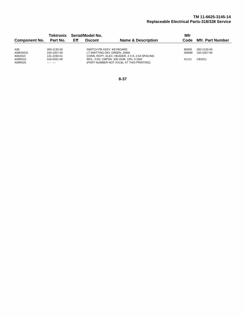
TM 11-6625-3145-14Replaceable Electrical Parts-318/338 Service
Tektronix Serial/Model No. MfrComponent No. Part No. Eff Dscont Name & Description Code Mfr. Part Number
A09 260-2133-00 SWITCH PB ASSY: KEYBOARD 80009 260-2133-00A09DS010 150-1057-00 LT EMITTING DIO: GREEN, 20MA 0000M 150-1057-00A09J010 131-2230-01 CONN, RCPT, ELEC: HEADER, 2 X 8, 2.54 SPACINGA09R010 316-0331-00 RES., FXD, CMPSN: 330 OHM, 10%, 0.25W 01121 CB3311A09R020 ---- ---- (PART NUMBER NOT AVLBL AT THIS PRINTING)
8-37
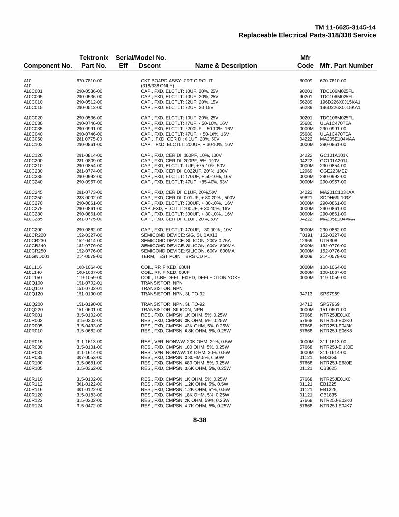
TM 11-6625-3145-14Replaceable Electrical Parts-318/338 Service
Tektronix Serial/Model No. MfrComponent No. Part No. Eff Dscont Name & Description Code Mfr. Part Number
A10 670-7810-00 CKT BOARD ASSY: CRT CIRCUIT 80009 670-7810-00A10 ---- ---- (318/338 ONLY)A10C001 290-0536-00 CAP., FXD, ELCTLT: 10UF, 20%, 25V 90201 TDC106M025FLA10C005 290-0536-00 CAP., FXD, ELCTLT: 10UF, 20%, 25V 90201 TDC106M025FLA10C010 290-0512-00 CAP., FXD, ELCTLT: 22UF, 20%, 15V 56289 196D226X0015KA1A10C015 290-0512-00 CAP., FXD, ELCTLT: 22UF, 20 15V 56289 196D226X0015KA1
A10C020 290-0536-00 CAP., FXD, ELCTLT: 10UF, 20%, 25V 90201 TDC106M025FLA10C030 290-0746-00 CAP., FXD, ELCTLT: 47UF, - 50-10%, 16V 55680 ULA1C470TEAA10C035 290-0991-00 CAP., FXD, ELCTLT: 2200UF, - 50-10%, 16V 0000M 290-0991-00A10C040 290-0746-00 CAP., FXD, ELCTLT: 47UF, + 50-10%, 16V 55680 ULA1C470TEAA10C050 281 0775-00 CAP., .FXD, CER DI: 0.1UF, 20%, 50V 04222 MA205E104MAAA10C103 290-0861-00 CAP. .FXD, ELCTLT: 200UF, + 30-10%, 16V 0000M 290-0861-00
A10C120 281-0814-00 CAP., FXD, CER DI: 100PF, 10%, 100V 04222 GC101A101KA10C200 281-0809-00 CAP., FXD, CER DI: 200PF, 5%, 100V 04222 GC101A201JA10C210 290-0854-00 CAP., FXD, ELCTLT: 1UF, +75-10%, 50V 0000M 290-0854-00A10C230 281-0774-00 CAP., FXD, CER DI: 0.022UF, 20°%, 100V 12969 CGE223MEZA10C235 290-0992-00 CAP., FXD, ELCTLT: 470UF, + 50-10%, 16V 0000M 290-0992-00A10C240 290-0957-00 CAP., FXD, ELCTLT: 47UF, +85-40%, 63V 0000M 290-0957-00
A10C245 281-0773-00 CAP., FXD, CER DI: 0.1UF, 20%.50V 04222 MA201C103KAAA10C250 283-0002-00 CAP., FXD, CER DI: 0.01UF, + 80-20%., 500V 59821 SDDH69L103ZA10C270 290-0861-00 CAP., FXD, ELCTLT: 200UF, + 30-10%, .16V 0000M 290-0861-00A10C275 290-0861-00 CAP .FXD, ELCTLT: 200UF, + 30-10%, 16V 0000M 290-0861-00A10C280 290-0861-00 CAP., FXD, ELCTLT: 200UF, + 30-10%., 16V 0000M 290-0861-00A10C285 281-0775-00 CAP., FXD, CER DI: 0.1UF, 20%,.50V 04222 MA205E104MAA
A10C290 290-0862-00 CAP., FXD, ELCTLT: 470UF, - 30-10%., 10V 0000M 290-0862-00A10CR220 152-0327-00 SEMICOND DEVICE: SIG, SI, BAX13 T0191 152-0327-00A10CR230 152-0414-00 SEMICOND DEVICE: SILICON, 200V.0.75A 12969 UTR308A10CR240 152-0776-00 SEMICOND DEVICE: SILICON, 600V, 800MA 0000M 152-0776-00A10CR250 152-0776-00 SEMICOND DEVICE: SILICON, 600V, 800MA 0000M 152-0776-00A10GND001 214-0579-00 TERM, TEST POINT: BRS CD PL 80009 214-0579-00
A10L116 108-1064-00 COIL, RF: FIXED, 68UH 0000M 108-1064-00A10L140 108-1667-00 COIL, RF: FIXED, 68UF 0000M 108-1667-00A10L150 119-1059-00 COIL, TUBE DEFL: FIXED, DEFLECTION YOKE 0000M 119-1059-00A10Q100 151-0702-01 TRANSISTOR: NPNA10Q110 151-0702-01 TRANSISTOR: NPNA10Q120 151-0190-00 TRANSISTOR: NPN, SI, TO-92 04713 SPS7969
A10Q200 151-0190-00 TRANSISTOR: NPN, SI, TO-92 04713 SPS7969A10Q220 151-0601-00 TRANSISTOR: SILICON, NPN 0000M 151-0601-00A10R001 315-0102-00 RES., FXD, CMPSN: 1K OHM, 5%, 0.25W 57668 NTR25JE01K0A10R002 315-0302-00 RES., FXD, CMPSN: 3K OHM, 5%, 0.25W 57668 NTR25J-E03K0A10R005 315-0433-00 RES., FXD, CMPSN: 43K OHM, 5%, 0.25W 57668 NTR25J-E043KA10R010 315-0682-00 RES., FXD, CMPSN: 6.8K OHM, 5%, 0.25W 57668 NTR25J-E06K8
A10R015 311-1613-00 RES., VAR, NONWW: 20K OHM, 20%, 0.5W 0000M 311-1613-00A10R030 315-0101-00 RES., FXD, CMPSN: 100 OHM, 5%, 0.25W 57668 NTR25J-E 100EA10R031 311-1614-00 RES., VAR, NONWW: 1K OHM, 20%, 0.5W 0000M 311-1614-00A10R035 307-0053-00 RES., FXD, CMPSN: 3 30HM.5%, 0.50W 01121 EB33G5A10R100 315-0681-00 RES , FXD, CMPSN: 680 OHM, 5%, 0.25W 57668 NTR25J-E680EA10R105 315-0362-00 RES., FXD, CMPSN: 3.6K OHM, 5%, 0.25W 01121 CB3625
A10R110 315-0102-00 RES., FXD, CMPSN: 1K OHM, 5%, 0.25W 57668 NTR25JE01K0A10R112 301-0122-00 RES , FXD, CMPSN: 1.2K OHM, 5%, 0.5W 01121 EB1225A10R116 301-0122-00 RES., FXD, CMPSN: 1.2K OHM, 5°%, 0.5W 01121 EB1225A10R120 315-0183-00 RES., FXD, CMPSN: 18K OHM, 5%, 0.25W 01121 CB1835A10R122 315-0202-00 RES., FXD, CMPSN: 2K OHM, 59%, 0.25W 57668 NTR25J-E02K0A10R124 315-0472-00 RES., FXD, CMPSN: 4.7K OHM, 5%, 0.25W 57668 NTR25J-E04K7
8-38

TM 11-6625-3145-14Replaceable Electrical Parts-318/338 Service
Tektronix Serial/Model No. Mfr.Component No. Part No. Eff Dscont Name & Description Code Mfr. Part Number
A10R130 315-0362-00 RES., FXD, CMPSN:3.6K OHM, 5%, 0.25W 01121 CB3625A10R135 315-0132-00 RES., FXD, CMPSN:1.3K OHM, 5%, 0.25W 57668 NTR25J-E01K3A10R140 315-0102-00 RES., FXD, CMPSN:1K OHM, 5%, 0.25W 57668 NTR25JE01K0A10R200 315-0472-00 RES., FXD, CMPSN:4.7K OHM, 5%, 0.25W 57668 NTR25J-E04K7A10R202 315-0242-00 RES., FXD, CMPSN:2.4K OHM, 5%, 0.25W 57668 NTR25J-E02K4A10R210 315-0271-00 RES., FXD, CMPSN:270 OHM, 5%, 0.25W 01121 CB2715A10R240 315-0334-00 RES., FXD, CMPSN:330K OHM, 5%, 0.25W 01121 CB3345A10R245 311-1619-00 RES., VAR, NONWW:100K OHM, 20%, 0, 5W 0000M 311-1619-00A10R247 311-1618-00 RES., VAR, NONWW:500K OHM, 20%, 0.5W 0000M 311-1618-00A10R250 315-0303-00 RES., FXD, CMPSN:30K OHM, 5%, 0.25W 01121 CB3035A10R253 315-0205-00 .300101 .300374 RES., FXD, CMPSN:2M OHM, 5%, 0.25W 01121 CB2055A10R253 ----- ----- (318 ONLY)A10R253 315-0105-00 .300375 RES., FXD, CMPSN:1M OHM, 5%, 0.25W 01121 CB1055A10R253 ----- ----- (318 ONLY)A10R253 315-0205-00 .300101 .300244 RES., FXD, CMPSN:2M OHM, 5%, 0.25W 01121 CB2055A10R253 ----- ----- (338 ONLY)A10R253 315-0105-00 .300245 RES., FXD, CMPSN:1M OHM, 5%, 0.25W 01121 CB1055A10R253 ----- ----- (338 ONLY)A10R255 311-1617-00 RES., VAR, NONWW:2M OHM, 20%, 0.5W 0000M 311-1617-00A10R280 307-0023-00 RES., FXD, CMPSN:4.7 OHM, 10%, 0.50W 01121 EB47G1A10T230 120-1205-00 TRANSFORMER, RF:FLYBACK 0000M 120-1205-00A10TP140 214-0579-00 TERM, TEST POINT:BRS CD PL 80009 214-0579-00A10TP145 214-0579-00 TERM, TEST POINT:BRS CD PL 80009 214-0579-00A10U001 156-1779-00 MICROCIRCUIT, LI:V OSC & DRIVE 0000M 156-1779-00A10U280 156-1224-00 MICROCIRCUIT, LI:3 TERM POS 0000M 156-1224-00
VOLTAGE REGA10V200 154-0867-00 ELECTRON TUBE:CRT 0000M 154-0867-00
8-39

TM 11-6625-3145-14Replaceable Electrical Parts-318/338 Service
Tektronix Serial/Model No. MfrComponent No. Part No. Eff Dscont Name & Description Code Mfr. Part Number
A11 670-7821-00 CKT BOARD ASSY:INVERTER 80009 670-7821-00A11 ----- ----- (318/338 ONLY)A1C102 285-1272-00 CAP., FXD, PLASTIC:0.22UF, 20%, 250V 0000M 285-1272-00A1C105 285-1273-00 CAP., FXD, PLASTIC:0.0022UF, 20%, 250V 0000M 285-1273-00A11C106 285-1273-00 CAP., FXD, PLASTIC:0.0022UF, 20%, 250V 0000M 285-1273-00A11C121 290-0998-00 CAP., FXD, ELCTLT:330UF, 20%, 200V 0000M 290-0998-00A11C122 290-0998-00 CAP .FXD, ELCTLT:330UF, 20%, 200V 0000M 290-0998-00A11C123 283-0496-00 CAP., FXD, CER DI:330PF, 10%, 1KV 0000M 283-0496-00A11C124 285-1263-00 CAP., FXD, MTLZD:0.01UF, 10%, 630V 0000M 285-1263-00A11C132 285-1264-00 CAP., FXD, MTLZD:0.22UF, 10%, 63V 0000M 285-1264-00A11C143 285-1265-00 CAP., FXD, PLASTIC:0.033UF, 10%, 50V 0000M 285-1265-00A11C147 285-1266-00 CAP., FXD, MTLZD:0.1UF, 10%, 250V 0000M 285-1266-00A11C150 283-0494-00 CAP., FXD, CER DI:470PF, 10%, 1KV 0000M 283-0494-00A11C151 285-1269-00 CAP., FXD, PLASTIC:0.01UF, 10%, 250V 0000M 285-1269-00A11C152 285-1269-00 CAP., FXD, PLASTIC:0.01UF, 10%, 250V 0000M 285-1269-00A11C153 285-1270-00 CAP., FXD.PLASTIC:0.0047UF, 10%, 250V 0000M 285-1270-00A11C154 285-1268-00 CAP., FXD, PLASTIC:0.0022UF, 10%, 250V 0000M 285-1268-00A11C155 290-1001-00 CAP., FXD, ELCTLT:100UF, 20%, 35V 0000M 290-1001-00A11C156 285-1277-00 CAP., FXD, PLASTIC:0.0033UF, 10%.250V 0000M 285-1277-00A11CR101 152-0605-00 SEMICOND DEVICE:RECT, SI, 600V, 4A 0000M 152-0605-00A11CR123 152-0603-00 SEMICOND DEVICE:RECT, SI, 1KV, 1A 0000M 152-0603-00A11CR125 152-0603-00 SEMICOND DEVICE:RECT, SI, 1KV, 1A 0000M 152-0603-00A11CR135 152-0333-03 SEMICOND DEVICE:SILICON, 50V, 200MA 0000M 152-0333-03A11CR136 152-0333-03 SEMICOND DEVICE:SILICON, 50V, 200MA 0000M 152-0333-03A11CR137 152-0333-03 SEMICOND DEVICE:SILICON, 50V, 200MA 0000M 152-0333-03A11CR138 152-0333-03 SEMICOND DEVICE:SILICON, 50V, 200MA 0000M 152-0333-03A11CR142 152-0333-03 SEMICOND DEVICE:SILICON, 50V, 200MA 0000M 152-0333-03A11CR145 152-0603-00 SEMICOND DEVICE:RECT, SI, 1KV, 1A 0000M 152-0603-00A11CR146 152-0333-03 SEMICOND DEVICE:SILICON, 50V, 200MA 0000M 152-0333-03A11CR147 152-0333-03 SEMICOND DEVICE:SILICON, 50V, 200MA 0000M 152-0333-03A11CR148 152-0586-02 SEMICOND DEVICE:RECT, SI, 600V, 0.5A 0000M 152-0586-02A11CR149 152-0333-03 SEMICOND DEVICE:SILICON, 50V, 200MA 0000M 152-0333-03A11CR151 152-0815-00 SEMICOND DEVICE:SCHOTTKY, SI, 40V, 16A 0000M 152-0815-00A11CR152 152-0815-00 SEMICOND DEVICE:SCHOTTKY, SI, 40V, 16A 0000M 152-0815-00A11CR153 152-0815-00 SEMICOND DEVICE:SCHOTTKY, SI, 40V, 16A 0000M 152-0815-00A11CR154 152-0604-00 SEMICOND DEVICE:RECT, SI, 140V, 8A 0000M 152-0604-00A11CR155 152-0586-02 SEMICOND DEVICE:RECT, SI, 600V, 0.5A 0000M 152-0586-02A11CR156 152-0333-03 SEMICOND DEVICE:SILICON.50V, 200MA 0000M 152-0333-03A11E123 276-0015-00 CORE, EM:FERRITE 0000M 276-0015-00A11E124 276-0015-00 CORE, EM:FERRITE 0000M 276-0015-00A11J004 131-2988-00 CONN, RCPT, ELEC:2.MALE, CONTACT 0000M 131-2988-00A11J005 131-2988-00 CONN, RCPT, ELEC:2, MALE, CONTACT 0000M 131-2988-00A11J008 131-2983-00 CONN.RCPT, ELEC:CONTACT, 8 MALE 0000M 131-2983-00A11J010 131-2983-00 CONN, RCPT, ELEC:CONTACT, 8 MALE 0000M 131-2983-00A11J011 131-2988-00 CONN, RCPT, ELEC:2, MALE.CONTACT 0000M 131-2988-00A11L101 108-1184-00 COIL, RF:6.8UH 0000M 108-1184-00A11L102 108-1180-00 COIL, RF:120UH 0000M 108-1180-00A11L103 108-1180-00 COIL, RF:120UH 0000M 108-1180-00A11PS001 620-0315-00 POWER SUPPLY: 0000M 620-0315-00A11Q131 151-0769-00 TRANSISTOR:SILICON, NPN 0000M 151-0769-00A11Q134 151-0767-00 TRANSISTOR:SILICON, PNP 0000M 151-0767-00A11Q135 151-0764-00 TRANSISTOR: SILICON, NPN 0000M 151-0764-00A11Q139 151-0765-00 TRANSISTOR: SILICON, NPN 0000M 151-0765-00A11Q140 151-0764-00 TRANSISTOR: SILICON, NPN 0000M 151-0764-00
8-40

TM 11-6625-3145-14Replaceable Electrical Parts-318/338 Service
Tektronix Serial/Model No. Mfr.Component No. Part No. Eff Dscont Name & Description Code Mfr. Part Number
A11Q141 151-0764-00 TRANSISTOR:SILICON, NPN 0000M 151-0764-00A11Q149 151-0766-00 TRANSISTOR:SILICON, NPN 0000M 151-0766-00A11R121 301-0224-00 RES., FXD, CMPSN:220K OHM, 5%, 0.5W 01121 EB2245A11R122 301-0224-00 RES., FXD, CMPSN:220K OHM, 5%, 0.5W 01121 EB2245A11R124 305-0104-01 RES., FXD, CMPSN:100K OHM, 5%, 2W 0000M 305-0104-01A11R131 301-0664-00 RES., FXD, CMPSN:680K OHM, 5%, 0.50W 01121 EB6845
A11R132 322-1607-00 RES., FXD, FILM:6.2K OHM, 1%, 0.25W 0000M 322-1607-00A11R134 315-0102-00 RES., FXD, CMPSN:1K OHM, 5%, 0.25W 57668 NTR25JE01K0A11R135 315-0472-00 RES., FXD, CMPSN:4.7K OHM, 5%, 0.25W 57668 NTR25J-E04K7A11R137 315-0271-00 RES., FXD, CMPSN:270 OHM, 5%, 0.25W 01121 CB2715A11R138 315-0332-00 RES., FXD, CMPSN:3.3K OHM, 5%, 0.25W 57668 NTR25J-E03K3A11R139 315-0561-00 RES., FXD, CMPSN:560 OHM, 5%, 0.25W 01121 CB5615
A11R140 315-0102-00 RES., FXD, CMPSN:1K OHM, 5%, 0.25W 57668 NTR25JE01KA11R141 315-0102-00 RES., FXD, CMPSN:1K OHM, 5%, 0.25W 57668 NTR25JE01K0A11R142 315-0102-00 RES., FXD, CMPSN:1K OHM, 5%, 0.25W 57668 NTR25JE01K0A11R143 315-0682-00 RES., FXD, CMPSN:6.8K OHM, 5%, 0.25W 57668 NTR25J-E06K8A11R145 301-0100-00 RES., FXD, CMPSN:10 OHM, 5%, 0.50W 01121 EB1005A11R147 307-0040-00 RES., FXD, CMPSN:4.7 OHM, 5%, 1W 0000M 307-0040-00
A11R149 303-0220-00 RES., FXD, CMPSN:22 OHM, 5%, 1W 01121 GB2205A11R151 301-0100-00 RES., FXD, CMPSN:10 OHM, 5%, 0.50W 01121 EB1005A11R152 301-0100-00 RES., FXD, CMPSN:10 OHM, 5%, 0.50W 01121 EB1005A11R154 301-0100-00 RES., FXD, CMPSN:10 OHM, 5%, 0.50W 01121 EB1005A11RT101 307-0917-00 RES THERMAL:5 OHM, 20% 0000M 307-0917-00A11RT102 307-0917-00 RES THERMAL:5 OHM, 20% 0000M 307-0917-00
A11S002 260-1967-00 SWITCH, SLIDE:DPDT, 5A/250V 000FJ 4021.0512A11S003 260-0638-00 SW, THERMOSTATIC:10A, 240V, OPEN 75 DEG C 93410 430-364A11T101 120-1117-00 TRANSFORMER, RF:COMMON MODE 0000M 120-1117-00A11T102 120-1117-00 TRANSFORMER, RF:COMMON MODE 0000M 120-1117-00A11T120 120-1500-00 TRANSFORMER, RF:CONVERTER 0000M 120-1500-00A11T140 120-1501-00 TRANSFORMER, RF:BASE DRIVER 0000M 120-1501-00
A11VR101 ----- ----- (P/N NOT AVAILABLE AT THIS PRINTING)A11VR102 ----- ----- (P/N NOT AVAILABLE AT THIS PRINTING)A11VR131 152-0816-00 SEMICOND DEVICE:ZEN, SI, 12V, 5%, 0.4W 0000M 152-0816-00A11VR135 152-0817-00 SEMICOND DEVICE:ZEN, SI, 15V, 5%, 0.4W 0000M 152-0817-00A11VR138 152-0821-00 SEMICOND DEVICE:ZEN, SI, 6.8V, 5, 0.4W 0000M 152-0821-00A11VR149 152-0818-00 SEMICOND DEVICE:ZEN, SI, 3.9V, 5%, 0.4W 0000M 152-0818-00
8-41

TM 11-6625-3145-14Replaceable Electrical Parts-318/338 Service
Tektronix Serial/Model No. MfrComponent No. Part No. Eff Dscont Name & Description Code Mfr. Part Number
A12 670-7820-00 CKT BOARD ASSY:REGULATOR 80009 670-7820-00A12 ----- ----- (318/338 ONLY)A12C003 285-1269-00 CAP., FXD, PLASTIC:0.01UF, 10%, 250V 0000M 285-1269-00A12C004 290-0999-00 CAP., FXD, ELCTLT:2200UF, 20%, 10V 0000M 290-0999-00A12C005 290-1000-00 CAP., FXD, ELCTLT:330UF, 20%, 10V 0000M 290-1000-00A12C006 285-1267-00 CAP., FXD, MTLZD:1UF, 10%, 100V 0000M 285-1267-00
A12C007 285-1267-00 CAP., FXD, MTLZD:1UF, 10%, 100V 0000M 285-1267-00A12C009 285-1274-00 CAP., FXD, PLASTIC:0.01 UF, 10%, 50V 0000M 285-1274-00A12C012 283-0497-00 CAP., FXD, CER DI:0.047UF, 20%, 25V 0000M 283-0497-00A12C017 285-1274-00 CAP., FXD, PLASTIC:0.01UF, 10%, 50V 0000M 285-1274-00A12C022 285-1267-00 CAP., FXD, MTLZD:1UF, 10%, 100V 0000M 285-1267-00A12C028 285-1271-00 CAP., FXD, PLASTIC:0.001UF, 1%, 100V 0000M 285-1271-00
A12C029 283-0497-00 CAP., FXD, CER DI:0.047UF, 20%, 25V 0000M 283-0497-00A12C036 290-1001-00 CAP., FXD, ELCTLT:100UF, 20%, 35V 0000M 290-1001-00A12C050 283-0497-00 CAP., FXD, CER DI:0.047UF, 20%, 25V 0000M 283-0497-00A12C051 283-0497-00 CAP., FXD, CER DI:0.047UF, 20%, 25V 0000M 283-0497-00A12C053 290-1002-00 CAP., FXD, ELCTLT:330UF, 20%, 16V 0000M 290-1002-00A12C058 290-1003-00 CAP., FXD, ELCTLT:33UF, 20%, 35V 0000M 290-1003-00A12C065 290-1004-00 CAP., FXD, ELCTLT:330UF, 20%, 25V 0000M 290-1004-00A12C066 290-1005-00 CAP., FXD, ELCTLT:100UF, 20%, 25V 0000M 290-1005-00A12C067 283-0498-00 CAP., FXD, CER DI:100PF, 5%, 50V 0000M 283-0498-00A12C069 283-0497-00 CAP., FXD, CER DI:0.047UF, 20%, 25V 0000M 283-0497-00A12C070 285-1275-00 CAP., FXD, PLASTIC:0.015UF, 10%, 50V 0000M 285-1275-00A12C071 283-0497-00 CAP., FXD, CER DI:0.047UF, 20%, 25V 0000M 283-0497-00A12C072 285-1276-00 CAP., FXD, PLASTIC:0.0015UF, 10%, 50V 0000M 285-1276-00A12C073 283-0497-00 CAP., FXD, CER DI:0.047UF, 20%, 25V 0000M 283-0497-00A12C074 290-1000-00 CAP., FXD, ELCTLT:330UF, 20%, 10V 0000M 290-1000-00A12C075 290-1000-00 CAP., FXD, ELCTLT:330UF, 20%, 10V 0000M 290-1000-00A12C076 285-1267-00 CAP., FXD, MTLZD: 1 UF, 10%, 100V 0000M 285-1267-00A12C077 285-1267-00 CAP., FXD, MTLZD: 1 UF, 10%, 100V 0000M 285-1267-00A12C078 283-0499-00 CAP., FXD, CER DI:220PF, 10%, 1KV 0000M 283-0499-00A12C081 283-0499-00 CAP., FXD, CER DI:220PF, 10%, 1KV 0000M 283-0499-00A12C082 290-0999-00 CAP., FXD, ELCTLT:2200UF, 20%, 10V 0000M 290-0999-00A12C083 290-0999-00 CAP., FXD, ELCTLT:2200UF, 20%, 10V 0000M 290-0999-00A12C084 290-0999-00 CAP., FXD, ELCTLT:2200UF, 20%, 10V 0000M 290-0999-00A12C085 290-0999-00 CAP., FXD, ELCTLT:2200UF, 20%, 10V 0000M 290-0999-00A12C086 290-0999-00 CAP., FXD, ELCTLT:2200UF, 20%, 10V 0000M 290-0999-00A12C087 285-1267-00 CAP., FXD, MTLZD:1 UF, 10%, 100V 0000M 285-1267-00A12C088 285-1267-00 CAP., FXD, MTLZD:1 UF, 10%, 100V 0000M 285-1267-00A12C089 285-1267-00 CAP., FXD, MTLZD:1 UF, 10%, 100V 0000M 285-1267-00A12C090 285-1267-00 CAP., FXD, MTLZD:1 UF, 10%, 100V 0000M 285-1267-00A12C091 290-1005-00 CAP., FXD, ELCTLT:100UF, 20%, 25V 0000M 290-1005-00A12C092 290-1005-00 CAP., FXD, ELCTLT:100UF, 20%, 25V 0000M 290-1005-00A12C093 290-1005-00 CAP., FXD, ELCTLT:100UF, 20%, 25V 0000M 290-1005-00A12C094 290-1005-00 CAP., FXD, ELCTLT:100UF, 20%, 25V 0000M 290-1005-00A12C095 285-1267-00 CAP., FXD, MTLZD:1 UF, 10%, 100V 0000M 285-1267-00A12C096 285-1267-00 CAP., FXD, MTLZD:1 UF, 10%, 100V 0000M 285-1267-00A12C097 285-1267-00 CAP., FXD, MTLZD:1 UF, 10%, 100V 0000M 285-1267-00A12C098 285-1267-00 CAP., FXD, MTLZD:1 UF, 10%, 100V 0000M 285-1267-00A12C099 285-1267-00 CAP., FXD, MTLZD:1 UF, 10%, 100V 0000M 285-1267-00A12CR001 152-0066-04 SEMICOND DEVICE:RECT, SI, 400V, 1A 0000M 152-0066-04A12CR002 152-0815-00 SEMICOND DEVICE:SCHOTTKY, SI, 40V, 16A 0000M 152-0815-00A12CR005 152-0333-03 SEMICOND DEVICE:SILICON, 50V, 200MA 0000M 152-0333-03A12CR006 152-0333-03 SEMICOND DEVICE:SILICON, 50V, 200MA 0000M 152-0333-03
8-42

TM 11-6625-3145-14Replaceable Electrical Parts-318/338 Service
Tektronix Serial/Model No. Mfr.Component No. Part No. Eff Dscont Name & Description Code Mfr. Part Number
A12CR007 152-0333-03 SEMICOND DEVICE:SILICON, 50V, 200MA 0000M 152-0333-03A12CR034 152-0333-03 SEMICOND DEVICE:SILICON, 50V, 200MA 0000M 152-0333-03A12CR035 152-0333-03 SEMICOND DEVICE:SILICON, 50V, 200MA 0000M 152-0333-03A12CR036 152-0333-03 SEMICOND DEVICE:SILICON, 50V, 200MA 0000M 152-0333-03A12CR044 152-0333-03 SEMICOND DEVICE:SILICON, 50V, 200MA 0000M 152-0333-03A12CR045 152-0333-03 SEMICOND DEVICE:SILICON, 50V, 200MA 0000M 152-0333-03A12CR046 152-0333-03 SEMICOND DEVICE:SILICON, 50V, 200MA 0000M 152-0333-03A12CR049 152-0333-03 SEMICOND DEVICE:SILICON, 50V, 200MA 0000M 152-0333-03A12CR053 152-0333-03 SEMICOND DEVICE:SILICON, 50V, 200MA 0000M 152-0333-03A12CR054 152-0333-03 SEMICOND DEVICE:SILICON, 50V, 200MA 0000M 152-0333-03A12CR061 152-0333-03 SEMICOND DEVICE:SILICON, 50V, 200MA 0000M 152-0333-03A12CR062 152-0333-03 SEMICOND DEVICE:SILICON, 50V, 200MA 0000M 152-0333-03A12CR063 152-0333-03 SEMICOND DEVICE:SILICON, 50V.200MA 0000M 152-0333-03A12CR064 152-0333-03 SEMICOND DEVICE:SILICON, 50V, 200MA 0000M 152-0333-03A12CR065 152-0333-03 SEMICOND DEVICE:SILICON, 50V, 200MA 0000M 152-0333-03A12CR066 152-0333-03 SEMICOND DEVICE:SILICON, 50V, 200MA 0000M 152-0333-03A12CR071 152-0333-03 SEMICOND DEVICE:SILICON, 50V, 200MA 0000M 152-0333-03A12CR072 152-0333-03 SEMICOND DEVICE:SILICON, 50V, 200MA 0000M 152-0333-03A12CR073 152-0333-03 SEMICOND DEVICE:SILICON, 50V, 200MA 0000M 152-0333-03A12CR074 152-0333-03 SEMICOND DEVICE:SILICON, 50V, 200MA 0000M 152-0333-03A12CR075 152-0333-03 SEMICOND DEVICE:SILICON, 50V, 200MA 0000M 152-0333-03A12CR076 152-0333-03 SEMICOND DEVICE:SILICON, 50V, 200MA 0000M 152-0333-03A12CR091 152-0586-02 SEMICOND DEVICE:RECT.SI, 600V, 0.5A 0000M 152-0586-02A12CR092 152-0586-02 SEMICOND DEVICE:RECT, SI, 600V, 0.5A 0000M 152-0586-02A12FL001 119-0420-03 FILTER, RFI:3A, 250VAC, 400HZ 0000M 119-0420-03A12J001 131-2984-00 CONN, RCPT, ELEC:CONTACT, 15 MALE 0000M 131-2984-00A12J002 131-2988-00 CONN, RCPT, ELEC:2, MALE, CONTACT 0000M 131-2988-00A12J003 131-2988-00 CONN, RCPT, ELEC:2, MALE, CONTACT 0000M 131-2988-00A12J006 131-2989-00 CONN, RCPT, ELEC:2, MALE, CONTACT 0000M 131-2989-00A12J007 131-2983-00 CONN, RCPT, ELEC:CONTACT, 8 MALE 0000M 131-2983-00A12J009 131-2983-00 CONN, RCPT, ELEC:CONTACT, 8 MALE 0000M 131-2983-00A12L001 108-1181-00 COIL, RF:FIXED.330UH 0000M 108-1181-00A12L002 108-1182-00 COIL, RF:FIXED, 6UH 0000M 108-1182-00A12L071 108-1182-00 COIL, RF:FIXED, 6UH 0000M 108-1182-00A12L082 108-1182-00 COIL, RF:FIXED, 6UH 0000M 108-1182-00A12L083 108-1183-00 COIL, RF:FIXED, 3.3UH 0000M 108-1183-00A12Q001 151-0738-00 TRANSISTOR:SILICON, NPN 0000M 151-0738-00A12Q005 151-0765-00 TRANSISTOR:SILICON, NPN 0000M 151-0765-00A12Q032 151-0764-00 TRANSISTOR:SILICON, NPN 0000M 151-0764-00A12Q033 151-0764-00 TRANSISTOR:SILICON, NPN 0000M 151-0764-00A12Q034 151-0765-00 TRANSISTOR:SILICON, NPN 0000M 151-0765-00A12Q035 151-0764-00 TRANSISTOR:SILICON, NPN 0000M 151-0764-00A12Q036 151-0768-00 TRANSISTOR:SILICON, NPN 0000M 151-0768-00A12Q057 151-0764-00 TRANSISTOR:SILICON, NPN 0000M 151-0764-00A12Q058 151-0764-00 TRANSISTOR:SILICON, NPN 0000M 151-0764-00A12Q059 151-0764-00 TRANSISTOR:SILICON, NPN 0000M 151-0764-00A12Q065 151-0635-00 TRANSISTOR:SILICON, PNP 0000M 151-0635-00A12Q071 151-0764-00 TRANSISTOR:SILICON, NPN 0000M 151-0764-00A12Q072 151-0765-00 TRANSISTOR:SILICON, NPN 0000M 151-0765-00A12Q073 151-0735-00 TRANSISTOR:SILICON, NPN 0000M 151-0735-00A12R001 301-0220-00 RES., FXD, CMPSN:22 OHM, 5%, 0.5W 57668 TR50J-E22EA12R002 307-0053-00 RES., FXD, CMPSN:3.3 OHM, 5%, 0.50W 01121 EB33G5A12R003 301-0100-00 RES., FXD, CMPSN:10 OHM, 5%, 0.50W 01121 EB1005A12R004 308-0849-00 RES., FXD, WW:30M OHM, 10%, 2W 0000M 308-0849-00
8-43

TM 11-6625-3145-14Replaceable Electrical Parts-318/338 Service
Tektronix Serial/Model No. Mfr.Component No. Part No. Eff Dscont Name & Description Code Mfr. Part Number
A12R005 315-0122-00 RES., FXD, CMPSN:1.2K OHM, 5%, 0.25W 57668 NTR25J-E01K2A12R006 315-0102-00 RES., FXD, CMPSN:1K OHM, 5%, 0.25W 57668 NTR25JE01K0A12R007 321-0097-00 RES., FXD, FILM:100 OHM, 1%, 0.125W 91637 MFF1816G100R0FA12R008 315-0820-00 RES., FXD, CMPSN:82 OHM, 5%, 0.25W 57668 NTR25J-E82E0A12R009 315-0222-00 RES., FXD, CMPSN:2.2K OHM, 5%, 0.25W 57668 NTR25J-E02K2A12R010 315-0122-00 RES., FXD, CMPSN:1.2K OHM, 5%, 0.25W 57668 NTR25J-E01K2A12R011 311-1611-00 RES., VAR, NONWW:TRMR, 2K OHM, 20%, 0.5W 0000M 311-1611-00A12R012 315-0473-00 RES., FXD, CMPSN:47K OHM, 5%, 0.25W 57668 NTR25J-E47K0A12R013 315-0222-00 RES., FXD, CMPSN:2.2K OHM, 5%, 0.25W 57668 NTR25J-E02K2A12R014 315-0104-00 RES., FXD, CMPSN:100K OHM, 5%, 0.25W 57668 NTR25J-E100KA12R015 322-0472-01 RES., FXD, FILM:4.7K OHM, 1%, 0.25W 0000M 322-0472-01A12R016 315-0222-00 RES., FXD, CMPSN:2.2K OHM, 5%, 0.25W 57668 NTR25J-E02K2A12R017 315-0562-00 RES., FXD, CMPSN:5.6K OHM, 5%, 0.25W 57668 NTR25J-E05K6A12R018 311-1611-00 RES., VAR, NONWW:TRMR, 2K OHM, 20%, 0.5W 0000M 311-1611-00A12R019 315-0473-00 RES., FXD, CMPSN:47K OHM, 5%, 0.25W 57668 NTR25J-E47K0A12R020 315-0222-00 RES., FXD, CMPSN:2.2K OHM, 5%, 0.25W 57668 NTR25J-E02K2A12R021 315-0222-00 RES., FXD, CMPSN:2.2K OHM, 5%, 0.25W 57668 NTR25J-E02K2A12R022 322-1615-00 RES., FXD, FILM:22K OHM, 10%, 0.25W 0000M 322-1615-00A12R023 315-0222-00 RES., FXD, CMPSN:2.2K OHM, 5%, 0.25W 57668 NTR25J-E02K2A12R024 315-0104-00 RES., FXD, CMPSN:100K OHM, 5%, 0.25W 57668 NTR25J-E100KA12R025 322-0472-01 RES., FXD, FILM:4.7K OHM, 1%, 0.25W 0000M 322-0472-01A12R026 315-0470-00 RES., FXD, CMPSN:47 OHM, 5%., 0;.25W 57668 NTR25J-E47E0A12R027 322-1614-00 RES., FXD, FILM:1K OHM, 10°%, 0.25W 0000M 322-1614-00A12R028 322-1615-00 RES., FXD, FILM:22K OHM, 10%, 0.25W 0000M 322-1615-00A12R029 322-0289-01 RES., FXD, FILM:10K OHM, 1%, 0.25W 0000M 322-0289-01A12R030 315-0472-00 RES., FXD, CMPSN:4.7K OHM, 5%, 0.25W 57668 NTR25J-E04K7A12R031 315-0472-00 RES., FXD, CMPSN:4.7K OHM, 5%, 0.25W 57668 NTR25J-E04K7A12R032 315-0272-00 RES., FXD, CMPSN:2.7K OHM, 5%, 0.25W 57668 NTR25J-E02K7A12R033 315-0102-00 RES., FXD, CMPSN:1K OHM, 5°%, 0.25W 57668 NTR25JE01K0A12R034 315-0681-00 RES., FXD, CMPSN:680 OHM, 5%, 0.25W 57668 NTR25J-E680EA12R035 315-0102-00 RES., FXD, CMPSN:1K OHM, 5%, 0.25W 57668 NTR25JE01K0A12R036 315-0471-00 RES., FXD, CMPSN:470 OHM, 5%, 0.25W 57668 NTR25J-E470EA12R037 307-0915-00 RES NTWK, FXD, FI:4, 3.3K OHM, 5%, 0.125W 0000M 307-0915-00A12R038 307-0915-00 RES NTWK, FXD, FI:4, 3.3K OHM, 5%, 0.125W 0000M 307-0915-00A12R039 307-0915-00 RES NTWK, FXD, FI:4, 3.3K OHM, 5%, 0.125W 0000M 307-0915-00A12R040 322-0293-01 RES., FXD, FILM: 11K OHM, 1%°, 0.25W 0000M 322-0293-01A12R041 322-1613-00 RES., FXD, FILM:9.1K OHM, 1%, 0.25W 0000M 322-1613-00A12R042 322-1615-00 RES., FXD, FILM:22K OHM, 1%, 0.25W 0000M 322-1615-00A12R043 322-1612-00 RES., FXD, FILM:24K OHM, 1%, 0.25W 0000M 322-1612-00A12R044 315-0103-00 RES., FXD, CMPSN:10K OHM, 5%, 0.25W 57668 NTR25J-100K0A12R045 322-1611-00 RES., FXD, FILM:13K OHM, 1%, 0.25W 0000M 322-1611-00A12R046 322-0289-01 RES., FXD.FILM:10K OHM, 1%, 0.25W 0000M 322-0289-01A12R047 322-0289-01 RES., FXD, FILM:10K OHM, 1%, 0.25W 0000M 322-0289-01A12R048 322-0289-01 RES., FXD, FILM:10K OHM, 1%, 0.25W 0000M 322-0289-01A12R049 322-1611-00 RES., FXD, FILM:13K OHM, 1%, 0.25W 0000M 322-1611-00A12R050 315-0102-00 RES., FXD, CMPSN:1K OHM, 5%, 0.25W 57668 NTR25JE001K0A12R051 322-1610-00 RES., FXD, FILM:2.2K OHM, 1%, 0.25W 0000M 322-1610-00A12R052 322-1610-00 RES., FXD, FILM:2.2K OHM, 1%, 0.25W 0000M 322-1610-00A12R053 315-0331-00 RES., FXD, CMPSN:330 OHM, 5%, 0.25W 57668 NTR25J-E330EA12R054 315-0393-00 RES., FXD, CMPSN:39K OHM, 5%, 0.25W 57668 NTR25J-E39K0A12R055 315-0472-00 RES., FXD, CMPSN:4.7K OHM, 5%, 0.25W 57668 NTR25J-E04K7A12R056 315-0472-00 RES., FXD, CMPSN:4.7K OHM, 5%, 0.25W 57668 NTR25J-E04K7A12R057 315-0682-00 RES., FXD, CMPSN:6.8K OHM, 5%, 0.25W 57668 NTR25J-E06K8A12R058 315-0273-00 RES., FXD, CMPSN:27K OHM, 5%, 0.25W 57668 NTR25J-E27K0
8-44

TM 11-6625-3145-14Replaceable Electrical Parts-318/338 Service
Tektronix Serial/Model No. Mfr.Component No. Part No. Eff Dscont Name & Description Code Mfr. Part Number
A12R059 315-0683-00 RES., FXD, CMPSN:68K OHM, 5%, 0.25W 57668 NTR25J-E68K0A12R060 315-0183-00 RES., FXD, CMPSN:18K OHM, 56%, 0.25W 01121 CB1835A12R061 315-0103-00 RES., FXD, CMPSN:10K OHM, 5%, ..25W 57668 NTR25J-E10K0A12R062 307-0916-00 RES NTWK, FXD, FI:4, 4.7K OHM, 5%, 0.125W 0000M 307-0916-00A12R063 301-0221-00 RES., FXD, CMPSN:220 OHM, 5%, 0.5W 57668 TR50J-E220EA12R064 315-0102-00 RES., FXD, CMPSN:1K OHM, 5%o, 0.25W 57668 NTR25JE01K0A12R065 315-0102-00 RES., FXD, CMPSN:1K OHM, 5%, o0.25W 57668 NTR25JE01K0A12R066 322-1608-00 RES., FXD, FILM:680 OHM, 1%, 0.25W 0000M 32-1608-00A12R067 321-0114-00 RES., FXD, FILM:150 OHM, 1, 0.125W 91637 MFF1816G150R0FA12R068 322-1609-00 RES., FXD, FILM:4.3K OHM, 1%’, 0.25W 0000M 322-1609-00A12R069 315-0471-00 RES., FXD, CMPSN:470 OHM, 5%.0.25W 57668 NTR25J-E470EA12R070 315-0102-00 RES., FXD, CMPSN:1K OHM, 5%, 0.25W 57668 NTR25JEO01K0A12R071 315-0822-00 RES., FXD, CMPSN:8.2K OHM.5% .0.25W 01121 CB8225A12R072 311-1611-00 RES., VAR, NONWW:TRMR, 2K OHM, 20%, 0.5W 0000M 311-1611-00A12R073 315-0122-00 RES., FXD, CMPSN:1.2K OHM, 5%, 0.25W 57668 NTR25J-E01K2A12R074 315-0472-00 RES., FXD, CMPSN:4.7K OHM, 5%, 0.25W 57668 NTR25J-E04K7A12R075 315-0222-00 RES., FXD, CMPSN:2.2K OHM, 5%, 0.25W 57668 NTR25J-E02K2A12R076 315-0103-00 RES., FXD, CMPSN:10K OHM, 5%, 0.25W 57668 NTR25J-E100K0A12R077 315-0100-00 RES., FXD, CMPSN:10 OHM, 5%, 0.25W 57668 NTR25J-E10E0A12R078 315-0472-00 RES., FXD, CMPSN:4 7K OHM, 5%, O.25W 57658 NTR25J-E04K7A12R079 315-0820-00 RES., FXD, CMPSN:82 OHM, 5%, 0.25W 57668 NTR25J-E82E0A12R080 325-0392-00 RES., FXD, FILM:0 56 OHM, 5c, 1W 0000M 325-0392-00A12R081 325-0392-00 RES ..FXD.FILM:0.56 OHM, 5c., 1lW 0000M 325-0392-00A12R082 315-0680-00 RES., FXD.CMPSN:68 OHM, 5%, 0.25W 57668 NTR25J-E68E0A12R083 315-0222-00 RES., FXD, CMPSN:2.2K OHM.5%, 0.25W 57668 NTR25J-E02K2A12R084 315-0102-00 RES., FXD.CMPSN:1K OHM, 5%., 0.25W 57668 NTR25JE01K0A12R085 308-0848-00 RES., FXD, WW:7M OHM, 10% 0000M 308-0848-00A12R086 308-0848-00 RES., FXD, WW:7M OHM, 10% 0000M 308-0848-00A12R087 315-0470-00 RES , FXD, CMPSN:47 OHM, 5%, 0.25W 57668 NTR25J-E47E0A12R088 315-0121-00 RES., FXD, CMPSN:120 OHM, 5%, 0.25W 01121 CB1215A12R091 307-0659-00 RES., FXD, FILM:2.2 OHM, 5%, 0.25W 19701 5043CX2R200JA12R092 307-0659-00 RES., FXD, FILM:2.2 OHM.5%, 0.25W 19701 5043CX2R200JA12R093 315-0222-00 RES., FXD, CMPSN:2.2K OHM, 5%, 0.25W 57668 NTR25J-E02K2A12R094 315-0222-00 RES., FXD, CMPSN:2.2K OHM, 5%D, 0.25W 57668 NTR25J-E02K2A12RT065 307-0918-00 RES THERMAL:2 5K OHM, 10%, 5V 0000M 307-0918-00A12S001 260-1849-00 SWITCH, PUSH:DPDT, 4A, 250VAC 31918 NE15/F2U1003EEA12T001 120-1498-00 TRANSFORMER.RF:BASE DRIVER 0000M 120-1498-00A12T081 120-1499-00 TRANSFORMER, RF:REGULATOR 0000M 120-1499-00A12TP001 131-3066-00 TERMINAL, PIN:12.6MM L X 0.64MM SQ 0000M 131-3066-00A12TP002 131-3066-00 TERMINAL, PIN:12.6MM L X 0.64MM SO 0000M 131-3066-00A12TP003 131-3066-00 TERMINAL, PIN:12.6MM L X 0.64MM SO 0000M 131-3066-00A12U001 156-1848-00 MICROCIRCUIT, LI:PWR SUPPLY, SW RGLTR CONT 0000M 156-1848-00A12U021 156-1848-00 MICROCIRCUIT, LI:PWR SUPPLY, SW RGLTR CONT 00000M156-1848-00A12U041 156-1631-00 MICROCIRCUIT, LI:ADJ SHUNT REGULATOR 01295 TL431C-LPA12U042 156-1631-00 MICROCIRCUIT, LI:ADJ SHUNT REGULATOR 01295 TL431C-LPA12U051 156-1847-00 MICROCIRCUIT, LI:OUAD OPERATIONAL AMP 0000M 156-1847-00A12U052 156-1631-00 MICROCIRCUIT, LI:ADJ SHUNT REGULATOR 01295 TL431C-LPA12U065 156-1846-00 MICROCIRCUIT, LI:VOLTAGE REGULATOR 0000M 156-1846-00A12U071 156-1846-00 MICROCIRCUIT, LI:VOLTAGE REGULATOR 0000M 156-1846-00A12U091 156-1160-02 MICROCIRCUIT, LI:VOLTAGE REGULATOR 0000M 156-1160-02A12U092 156-1160-02 MICROCIRCUIT, LI:VOLTAGE REGULATOR 0000M 156-1160-02A12VR032 152-0127-02 SEMICOND DEVICE:ZEN, SI, 7.5V, 5%, 0.4W 0000M 152-0127-02A12VR036 152-0055-02 SEMICOND DEVICE:ZEN, SI, 11V V, 5%, 0.4W 0000M 152-0055-02A12VR037 152-0724-01 SEMICOND DEVICE:ZEN, SI, 4 7V, 5%., 0.4W 0000M 152-0724-01
8-45

TM 11-6625-3145-14Replaceable Electrical Parts-318/338 Service
Tektronix Serial/Model No. Mfr.Component No. Part No. Eff Dscont Name & Description Code Mfr. Part Number
A12VR038 152-0819-00 SEMICOND DEVICE:ZEN, SI, 2.7V, 5%, 0.4W 0000M 152-0819-00A12VR039 152-0816-00 SEMICOND DEVICE:ZEN, SI, 12V, 5%, 0.4W 0000M 152-0816-00A12VR040 152-0217-01 SEMICOND DEVICE:ZEN, SI, 8.2V, 5%, 0.4W 0000M 152-0217-01A12VR041 152-0821-00 SEMICOND DEVICE:ZEN, SI, 6.8V, 5%, 0.4W 0000M 152-0821-00A12VR042 152-0724-01 SEMICOND DEVICE:ZEN, SI, 4.7V, 5%, 0.4W 0000M 152-0724-01A12VR043 152-0820-00 SEMICOND DEVICE:ZEN, SI, 13V, 5%, 0.4W 0000M 152-0820-00
A12VR044 152-0175-02 SEMICOND DEVICE:ZEN, SI, 15.6V, 5%, 0.4W 0000M 152-0175-02A12VR045 152-0822-00 SEMICOND DEVICE:ZEN, SI, 18V, 5%, 0.4W 0000M 152-0822-00A12VR046 152-0306-02 SEMICOND DEVICE:ZEN, SI, 9.1V, 5%, 0.4W 0000M 152-0306-02A12VR058 152-0823-00 SEMICOND DEVICE:ZEN, SI, 6.2V, 5%, 0.4W 0000M 152-0823-00A12VR068 152-0127-02 SEMICOND DEVICE:ZEN, SI, 7.V, 5%.0.4W 0000M 152-0127-02
8-46

TM 11-6625-3145-14Replaceable Electrical Parts-318/338 Service
Tektronix Serial/Model No. Mfr.Component No. Part No. Eff Dscont Name & Description Code Mfr. Part Number
CHASSIS PARTSB001 119-1648-01 FAN, TUBEAXIAL:1 2VDC, 3-8W, 53300RPM 0000M 119-1648-01F1 159-0032-00 FUSE, CARTRIDGE:3AG, 0.5A, 250V, SLOW- 71400 MDL 1/2
BLOWF001 159-0015-02 FUSE, CARTRIDGE:3AG, 3A, 250V, FAST 0000M 159-0015-02FL1 119-0420-03 300101 .300598 FILTER, RFI:3A, 250VAC, 400HZ 0000M 119-0420-03FL1 ----- ----- (318 ONLY)FL1 119-1536-00 300599 FILTER, RFI:3A, 250VAC, 50/60 HZ 54583 ZUB2203-000FL1 ----- ----- (318 ONLY)FL1 119-0420-03 300101 .300490 FILTER, RFI:3A, 250VAC, 400HZ 0000M 119-0420-03FL1 ----- ----- (338 ONLY)FL1 119-1536-00 300491 FILTER, RFI:3A, 250VAC, 50/60 HZ 54583 ZUB2203-000FL1 ----- ----- (338 ONLY)L150 119-1059-00 COIL, TUBE DEFL:FIXED, DEFLECTION YOKE 0000M 119-1059-00S2 260-1967-00 SWITCH, SLIDE:DPDT, 5A/250V 000FJ 4021.0512V200 154-0867-00 ELECTRON TUBE:CRT 0000M 154-0867-00WI002 175-8470-00 STRD, 18 AWG, 600V, BLACK, UL10 0000M 175-8470-00
8-47/(8-48 blank)

TM 11-6625-3145-14DIAGRAMS AND CIRCUIT BOARD ILLUSTRATIONS
Symbols
Graphic symbols and class designation letters are basedon ANSI Standard Y32.2-1975.
Logic symbology is based on ANSI Y32. 14-1973 interms of positive logic. Logic symbols depict the logicfunction performed and may differ from themanufacturer’s data.
Active low signals are indicated by an (L) following thesignal name or by a horizontal line above the signalname (e.g., IRQ). Signal names without indicators areconsidered active-high. Some active-high signals areindicated by an (H) following the signal name.
Abbreviations are based on ANSI Y1.1-1972.
Other ANSI standards that are used in the preparation ofdiagrams by Tektronix, Inc. are:
Y14.15, 1966 Drafting Practices.
Y14.2, 1973 Line Conventions and Lettering.
Y10.5, 1968 Letter Symbols for Quantities Used inElectrical Science and ElectricalEngineering.
American National Standard Institute1430 Broadway
New York, New York 10018
Component Values
Electrical components shown on the diagrams are in thefollowing units unless noted otherwise:
Capacitors = Values one or greater are in picofarads(pF). Values less than one are inmicrofarads (µ/F).
Resistors = Ohms (Ω).
The information and special symbols below may appear in this manual.
Assembly Numbers and Grid CoordinatesEach assembly in the instrument is assigned anassembly number (e.g., A20). The assembly numberappears on the circuit board outline on the diagram, inthe title for the circuit board component locationillustration, and in the lookup table for the schematicdiagram and corresponding component locatorillustration. The Replaceable Parts list is arranged byassemblies in numerical sequence; the components arelisted by component number *(see following illustrationfor constructing a component number).
The schematic diagram and circuit board componentlocation illustration have grids. A lookup table with thegrid coordinates is provided for ease of locating thecomponent. Only the components illustrated on thefacing diagram are listed in the lookup table. Whenmore than one schematic diagram is used to illustratethe circuitry on a circuit board, the circuit boardillustration may only appear opposite the first diagram onwhich it was illustrated; the lookup table will list thediagram number of other diagrams that the circuitry ofthe circuit board appears on.
9-1
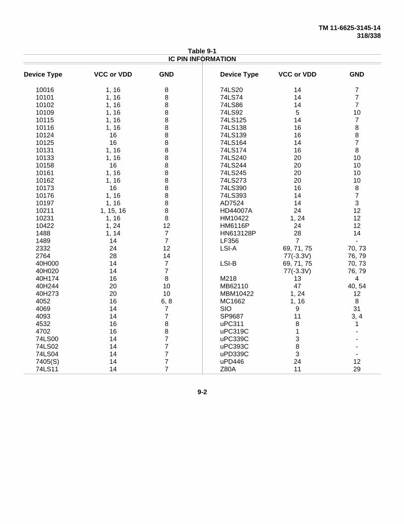
TM 11-6625-3145-14318/338
Table 9-1IC PIN INFORMATION
Device Type VCC or VDD GND Device Type VCC or VDD GND
10016 1, 16 8 74LS20 14 710101 1, 16 8 74LS74 14 710102 1, 16 8 74LS86 14 710109 1, 16 8 74LS92 5 1010115 1, 16 8 74LS125 14 710116 1, 16 8 74LS138 16 810124 16 8 74LS139 16 810125 16 8 74LS164 14 710131 1, 16 8 74LS174 16 810133 1, 16 8 74LS240 20 1010158 16 8 74LS244 20 1010161 1, 16 8 74LS245 20 1010162 1, 16 8 74LS273 20 1010173 16 8 74LS390 16 810176 1, 16 8 74LS393 14 710197 1, 16 8 AD7524 14 310211 1, 15, 16 8 HD44007A 24 1210231 1, 16 8 HM10422 1, 24 1210422 1, 24 12 HM6116P 24 121488 1, 14 7 HN613128P 28 141489 14 7 LF356 7 -2332 24 12 LSI-A 69, 71, 75 70, 732764 28 14 77(-3.3V) 76, 7940H000 14 7 LSI-B 69, 71, 75 70, 7340H020 14 7 77(-3.3V) 76, 7940H174 16 8 M218 13 440H244 20 10 MB62110 47 40, 5440H273 20 10 MBM10422 1, 24 124052 16 6, 8 MC1662 1, 16 84069 14 7 SIO 9 314093 14 7 SP9687 11 3, 44532 16 8 uPC311 8 14702 16 8 uPC319C 1 -74LS00 14 7 uPC339C 3 -74LS02 14 7 uPC393C 8 -74LS04 14 7 uPD339C 3 -7405(S) 14 7 uPD446 24 1274LS11 14 7 Z80A 11 29
9-2

TM 11-6625-3145-14318/338 Service
REPLACEABLEMECHANICAL PARTS
PARTS ORDERING INFORMATION
Replacement parts are available from or throughyour local Tektronix Inc. Field Office or representative
Changes to Tektronix Instruments are sometimesmade to accommodate improved components as theybecome available and to give you the benefit of the latestcircuit improvements developed in our engineeringdepartment It is therefore important when ordering parts,to include the following information in your order Partnumber instrument type or number serial number, andmodification number if applicable
If a part you have ordered has been replaced with anew or improved part, your local Tektronix, Inc. FieldOffice or representative will contact you concerning anychange in part number
Change information if any is located at the rear ofthis manual
ITEM NAME
In the Parts List an Item Name is separated from thedescription by a colon (:) Because of space limitations,an Item Name may sometimes appear as incomplete Forfurther Item Name Identification the U S FederalCataloging Handbook H6-1 can be utilized wherepossible
FIGURE AND INDEX NUMBERS
Items in this section are referenced by figure andindex numbers to the illustrations
INDENTATION SYSTEMThis mechanical parts list is indented to indicate item
relationships Following is an example of the indentationsystem used in the description column
1 2 3 4 5 Name & DescriptionAssembly and or ComponentAttaching parts for Assembly and or Component
- - - * - - -Detail Part of Assembly and or ComponentAttaching parts for Detail Part
- - - * - - -Parts of Detail PartAttaching parts for Parts of Detail Part
- - - * - - -Attaching Parts always appear in the same
indentation as the item it mounts. while the detail partsare indented to the right indented Items are part of, andincluded with, the next higher indentation The separationsymbol - - -* - - -indicates the end of attaching partsAttaching parts must be purchased separately,unless otherwise specified.
ABBREVIATIONS“ INCH ELCTRN ELECTRON IN NCH SE SINGLE END# NUMBER SIZE ELEC ELECTRPICA: INCAND NCANDESCENT SECT SECTIONACTR ACTUATOR ELCTLT ELECTROLYTIC INSUL INSULATOR SEMICOND
SEMICONDUCTORADPTR ADAPTER ELEM ELEMENT INTL INTERNAL SHLD SHIELDALIGN ALIGNMENT EPL ELECTRICAL PARTS LIST L.PHLDR LAMPHOLDER SHLDR
SHOULDEREDAL ALUMINUM, EQPT EOUIPMENT MACH MACHINE SKT SOCKETASSEM ASSEMBLED EXT EXTERNAL MECH MECHANICAL SL SLIDEASSY ASSEMBLY FIL FILLISTER HEAD MTG MOUNTING SLFLKG SELF-LOCKINGATTEN ATTENUATOR FLEX FLEXIBLE NIP NIPPLE SLVG SLEEVINGAWG AMERICAN WIRE GAGE FLH FLAT HEAD NON WIRE NOT WIRE WOUND SPR SPRINGHO BOARD FLTR FILTER ORD ORDER BY DESCRIPTION SO SQUAREBRKT BRACKET FR FRAME or, FRONT OD OUTSIDE DIAMETER SST STAINLESSSTEELBRS BRASS FSTNR FASTENER OVH 0VAL HEAD STL STEELHRZ BRONZE FT FOOT PH BRZ PHOSPHOR BRONZE SW SWITCHRSHG BUSHING FXD FIXED PL PL.AIN or PLATE T TUBE'AB CABINET GSKT GASKET PLSTC PL ASTIC TERM TERMINALCAP CAPACITOR HDL HANDLE PN PART NUMBER THD THREADCER CERAMIC HEX HEXAGON PNH PAN HEAD THK THICKSHAS CHASSIS HEX HD HEXAGONAL HEAD PWR POWER TNSN TENSIONCKT CIRCUIT HEX SOC HEXAGONAL SOCKET RCPT RECEPTACLE TPG TAPPINGCOMP COMPOSITION HLCPS HELICAL COMPRESSION RES RESISTOR TRH TRUSSHEADCONN CONNECTOR HLEXT HELICAL EXTENSION ROGD RIGID V VOLTAGECOV COVER HV HIGH VOLTAGE RLF RELIEF VAR VARIABLECPLG COUPLING IC INTEGRATED CIRCUIT RTNR RETAINER W WITHCRT CATHODE RAY TUBE ID INSIDE DIAMETER SCH SOCKET HEAD WSHR WASHERDEG DEGREE IDENT IDENTIFICATION SCOPE OSCILLOSCOPE XFMR TRANSFORMERDVVR DRAWER IMPLR MPELLER SCR SCREW XSTR TRANSISTOR
10-1

TM 11-6625-3145-14Replaceable Mechanical Parts-318/338 Service
CROSS INDEX-MFR. CODE NUMBER TO MANUFACTURER
Mfr Code Manufacturer Address City, State. Zip
0000M SONY TEKTRONIX CORPORATION P O BOX 14, HANEDA AIRPORT TOKYO 149, JAPAN000BK STAUFFER SUPPLY 105 SE TAYLOR PORTLAND, OR 97214000JA J. PHILLIP INDUSTRIES INC. 5713 NORTHWEST HIGHWAY CHICAGO, ILL 6064600779 AMP, INC. P.O. BOX 3608 HARRISBURG, PA 1710509922 BURNDY CORPORATION RICHARDS AVENUE NORWALK, CT 0685212327 FREEWAY CORPORATION 9301 ALLEN DRIVE CLEVELAND, OH 4412513511 AMPHEN0L CARDRE DIV., BUNKER RAMO CORP. LOS GATOS, CA 9503022526 BERG ELECTRONICS, INC. YOUK EXPRESSWAY NEW CUMBERLAND. PA 1707024931 SPECIALITY CONNECTOR CO., INC. 2620 ENDRESS PLACE GREENWOOD, IN 4614270903 BELDEN CORP. 2000 S BATAVIA AVENUE GENEVA, IL 6013471279 CAMBRIDGE THERMIONIC CORP. 445 CONCORD AVE. CAMBRIDGE, MA 0213873743 FISCHER SPECIAL MFG. CO. 446 MORGAN ST. CINCINNATI, OH 4520678189 ILLINOIS TOOL WORKS, INC.
SHAKEPROOF DIVISION ST. CHARLES ROAD ELGIN, IL 6012080009 TEKTRONIX, INC. P O BOX 500 BEAVERTON, OR 9707783385 CENTRAL SCREW CO. 2530 CRESCENT DR. BROADVIEW, IL 6015398159 RUBBER TECK, INC. 19115 HAMILTON AVE., P O BOX 389 GARDENA, CA 90247S3109 C’O PANEL COMPONENTS CORP. P.O. BOX 6626 SANTA ROSA, CA 95406S3629 PANEL COMPONENTS CORP. 2015 SECOND ST. BERKELEY, CA 94170T1105 J PHILLIP INDUSTRIES INC 5713 NORTHWEST HIGHWAY CHICAGO, IL 60646
10-2

TM 11-6625-3145-14Replaceable Mechanical Parts-318/338 Service
Fig. &Index Tektronix Serial/Model No. Mfr.No. Part No. Eff Dscont Qty 1 2 3 4 5 Name & Description Code Mfr Part Number
1-1 016-0408-00 .300101 .300925 1 COVER, PROT:FRONT PANEL 0000M 016-0408-00----- ----- - (318 ONLY)016-0408-01 .300926 1 COVER, PROT:FRONT PANEL 0000M 016-040801----- ----- - (318 ONLY)016-0408-00 .300101 .300945 1 COVER, PROT:FRONT PANEL 0000M 016-0408-00----- ----- - (338 ONLY)016-0408-01 .300946 1 COVER, PROT:FRONT PANEL 0000M 016-0408-01----- ----- - (338 ONLY)
-2 390-0886-00 1 CAB., WRAPAROUND:COLOR 0000M 390-0886-00- ***********(ATTACHING PARTS)*************
-3 211-0503-00 1 SCREW, MACHINE:6-32 X 0.188 INCH, PNH STL 83385 ORD BY DESCR***********(END ATTACHING PARTS)*******
-4 348-0080-01 4 FOOT, CABINET: BOTTOM 80009 348-0080-01-5 334-4913-00 1 PLATE, IDENT:318 LOGIC ANALYZER 0000M 3344913-00
----- ----- - (318 ONLY)334-4914-00 1 PLATE, IDENT:338 LOGIC ANALYZER 0000M 334-4914-00----- ----- (338 ONLY)
-6 200-1342-01 2 COVER, HANDLE:35.5MM OD X 14MM H, PLASTIC 0000M 200-1342-01-7 386-3936-00 2 PLATE, MOUNTING:HANDLE, STEEL 0000M 386-3936-00
*********(ATTACHING PARTS)***************-8 212-0033-00 2 SCREW, MACHINE:8-32 X 0.750 INCH, PNH STL 83385 ORDER BY
DESCR-9 210-0008-00 2 WASHER, LOCK:INTL, 0.02 THK 78189 1208-00-00-0541C
*********(END ATTACHING PARTS)************-10 386-2182-00 4 PLATE, FRICTION: 0000M 386-2182-00-11 367-0203-00 1 HANDLE, CARRYING:BLACK VINYL 0000M 367-0203-00-12 343-0757-00 2 RETAINER, HANDLE: 0000M 343-0757-00
10-3/(10-4 blank)

TM 11-6625-3145-14Replaceable Mechanical Parts-318/338 Service
Fig. &Index Tektronix Serial/Model No. Mfr.No. Part No. Eff Dscont Qty 1 2 3 4 5 Name & Description Code Mfr Part Number
2-1 333-2999-00 300101 .300260 PANEL, FRONT:318 0000M 333-2999-00----- ----- (318 ONLY)333-2999-01 .300261 1 PANEL, FRONT:318 0000M 333-2999-01----- ----- - (318 ONLY)333-2998-00 .300101 .300125 1 PANEL FRONT:338 0000M 333-2998-00----- ----- - (338 ONLY)333-2998-01 .300126 1 PANEL, FRONT:338 0000M 333-2998-01----- ----- - (338 ONLY)
- **********(ATTACHING PARTS)***************-2 211-0680-00 .300101 .300510 4 SCREW, MACHINE:2-56 X 0.138 L, TRUSS, STL 0000M 211-0680-00
----- ----- - (318 ONLY)211-0342-00 .300511 4 SCREW, CAP:2-56 X 0.177, HEX SOCKET----- ----- - (318 ONLY)211-0680-00 .300101 .300425 4 SCREW, MACHINE:2-56 X 0.138 L, TRUSS, STL 0000M 211-0680-00----- ----- - (338 ONLY)211-0342-00 .300426 4 SCREW, CAP:2-56 X 0.177, HEX SOCKET----- ----- - (338 ONLY)361-1266-00 4 SPACER, RING:0.7 L X 2.4 ID MM 0000M 361-1266-00
**********(END ATTACHING PARTS)***********198-5297-00 1 WIRE SET, ELEC:FRONT PANEL, 318 0000M 198-5297-00
-3 210-0202-00 1 TERMINAL, LUG:0.146 ID, LOCKING, BRZ, TIN PL 78189 2104-06-00-2520N************(ATTACHING PARTS)****************
-4 211-0503-00 1 SCREW, MACHINE:6-32 X 0.188 INCH, PNH STL 83385 ORD BY DESCR***********(END ATTACHING PARTS)***********
-5 343-0787-01 .300101 300560 1 RETAINER, CRT: 0000M 343-0787-01----- ----- - (318 ONLY)343-0787-03 .300561 1 RETAINER, CRT:318/1338 0000M 343-0787-03----- ----- - (318 ONLY)343-0787-01 .300101 300490 1 RETAINER, CRT: 0000M 343-0787-01----- ----- - (338 ONLY)343-0787-03 .300491 1 RETAINER, CRT:3181338 0000M 343-0787-03----- ----- - (338 ONLY)348-0818-00 .300561 1 CUSHION, RUBBER:RIGHT 0000M 348-0818-00----- ----- - (318 ONLY)348-0818-00 .300491 1 CUSHION, RUBBER:RIGHT 0000M 348-0818-00----- ----- - (338 ONLY)348-0817-00 .300561 1 CUSHION, RUBBER:LEFT 0000M 348-0817-00----- ----- - (318 ONLY)348-0817-00 .300491 1 CUSHION, RUBBER:LEFT 0000M 348-0817-00----- ----- - (338 ONLY)
**************(ATTACHING PARTS)**************-6 211-0661-00 2 SCREW, MACHINE:4-40 X 0.25 INCH, PNH, STL 78189 ORD BY DESCR
**************(END ATTACHING PARTS) *******-7 337-2600-00 1 SHIELD, CRT: 0000M 337-2600-00-8 366-2032-01 1 PUSH BUTTON:IVORY GRAY, 1 0000M 366-2032-01
366-2032-02 1 PUSH BUTTON:IVORY GRAY, 2 0000M 366-2032-02366-2032-03 1 PUSH BUTTON:IVORY GRAY, 3 0000M 366-2032-03366-2032-04 1 PUSH BUTTON:IVORY GRAY, 4 0000M 366-2032-04366-2032-05 1 PUSH BUTTON:IVORY GRAY, 5 0000M 366-2032-05366-2032-06 1 PUSH BUTTON:IVORY GRAY, 6 0000M 366-2032-06366-2032-07 1 PUSH BUTTON:IVORY GRAY, 7 0000M 366-2032-07366-2032-08 1 PUSH BUTTON:IVORY GRAY, 8 0000M 366-2032-08366-2032-09 1 PUSH BUTTON:IVORY GRAY, 9 0000M 366-2032-09366-2032-10 1 PUSH BUTTON:IVORY GRAY, 0 0000M 366-2032-10366-2032-11 1 PUSH BUTTON:IVORY GRAY, A 0000M 366-2032-11366-2032-12 1 PUSH BUTTON:IVORY GRAY, B 0000M 366-2032-12366-2032-13 1 PUSH BUTTON:IVORY GRAY, C 0000M 366-2032-13366-2032-14 1 PUSH BUTTON:IVORY GRAY.D 0000M 366-2032-14366-2032-15 1 PUSH BUTTON:IVORY GRAY, E 0000M 366-2032-15366-2032-16 1 PUSH BUTTON:IVORY GRAY, F 0000M 366-2032-16366-2032-17 1 PUSH BUTTON:IVORY GRAY, X 0000M 366-2032-17366-2029-00 6 PUSH BUTTON:DOVE GRAY, 0.45 X 0.275 0000M 366-2029-00366-2029-20 4 PUSH BUTTON:GRAY, UP ARROW 0000M 366-2029-20366-2029-21 2 PUSH BUTTON:GRAY, RIGHT ARROW 0000M 366-2029-21366-2031-00 2 PUSH BUTTON:SLATE GRAY, 0.45 X 0.275 0000M 366-2031-00
10-5

TM 11-6625-3145-14Replaceable Mechanical Parts-318/338 Service
Fig. &Index Tektronix Serial/Model No. Mfr.No. Part No. Eff Dscont Qty 1 2 3 4 5 Name & Description Code Mfr Part Number2-9 ----- ----- 1 CKT BOARD ASSY:KEY(SEE A09 REPL)
************* (ATTACHING PARTS) *************-10 211-0012-00 5 SCREW, MACHINE:4-40 X 0.375, PNH STL CD PL 83385 ORD BY DESCR-11 210-0054-00 5 WASHER, LOCK:#4 SPLIT, 0.025 THK STL CD P 83385 ORD BY DESCR-12 211-0661-00 1 SCREW, MACHINE:4-40 X 0.25 INCH, PNH, STL 78189 ORD BY DESCR
************* (END ATTACHING PARTS) ********----- ----- - .CKT BOARD ASSY INCLUDES:
-13 ----- ----- 1 .SWITCH ASSY:(SEE A09 REPL)-14 1 .CONNECTOR:(SEE A09J010 REPL)
198-5297-00 1 .WIRE SET, ELEC:FRONT PANEL, 318 0000M 198-5297-00-15 334-3360-00 1 MARKER, IDENT:MARKED WARNING 0000M 334-3360-00-16 386-4962-00 1 SUBPANEL, FRONT: 0000M 386-4962-00
************* (ATTACHING PARTS) *************-17 211-0105-00 2 SCREW, MACHINE:4-40 X 0.188, 100 DEG, FLH ST 83385 ORD BY DESCR-18 211-0538-00 2 SCREW, MACHINE:6-32 X 0.312"100 DEG, FLH 83385 ORD BY DESCR
************* (END ATTACHING PARTS) *********-19 337-2599-00 1 SHIELD, CRT: 0000M 337-2599-00
************* (ATTACHING PARTS) *************-20 211-0101-00 1 SCREW, MACHINE.4-40 X 0.25, FLH, 100 DEG, STL 83385 ORD BY DESCR-21 210-0586-00 1 NUT, PL, ASSEM WA:4-40 X 0.25, STL, CD PL 78189 211-041800-00-22 211-0538-00 2 SCREW, MACHINE:6-32 X 0.312"100 DEG, FLH 83385 ORD BY DESCR
************* (END ATTACHING PARTS) ******-23 210-0202-00 1 TERMINAL, LUG:0.146 ID, LOCKING, BRZ, TIN PL 78189 2104-06-00-2520N
************* (ATTACHING PARTS) *************-24 210-0457-00 1 NUT, PL, ASSEM WA:6-32 X 0.312, STL CD PL 83385 ORD BY DESCR
************* (END ATTACHING PARTS) ********-25 441-1662-00 .300101 .300280 1 CHAS, LGC ANALY:LEFT 318/338 0000M 441-1662-00
----- ----- - (318 ONLY)441-1662-01 .300281 1 CHAS, LGC ANALY:LEFT 318/338 0000M 441-1662-01----- ----- - (318 ONLY)441-1662-00 .300101 .300145 1 CHAS, LGC ANALY:LEFT 318/338 0000M 441-1662-00----- ----- - (338 ONLY)441-1662-01 .300146 1 CHAS, LGC ANALY:LEFT 318/338 0000M 441-1662-01----- ----- - (338 ONLY)
**************(ATTACHING PARTS)***************-26 211-0105-00 5 SCREW, MACHINE:4-40 X 0.188, 100 DEG, FLH S 83385 ORD BY DESCR
*************(END ATTACHING PARTS)*********-27 351-0705-00 1 GUIDE, EXT SHAFT: 0000M 351-0705-00-28 214-3420-00 1 SPRING, HLCPS:10.0MM OD X 9.5MM L 0000M 214-3420-00-29 384-1660-00 1 EXTENSION SHAFT:248.9MM L X 12.0MM OD 0000M 384-1660-00-30 366-1767-01 1 PUSH BUTTON:BLACK, GREEN INDICATOR 0000M 366-1767-01-31 441-1661-00 1 CHAS, LGC ANALY:RIGHT 0000M 441-1661-00
*************(ATTACHING PARTS)**************-32 211-0101-00 2 SCREW, MACHINE:4-40 X 0.25, FLH, 100 DEG, STL 83385 ORD BY DESCR-33 211-0105-00 2 SCREW, MACHINE:4-40 X 0.188, 100 DEG, FLH ST 83385 ORD BY DESCR
************(END ATTACHING PARTS)***********-34 ----- ----- 1 CKT BOARD ASSY:MOTHER(SEE A08 REPL)
*************(ATTACHING PARTS)**************-35 211-0661-00 7 SCREW.MACHINE:4-40 X 0.25 INCH, PNH, STL 78189 ORD BY DESCR
************(END ATTACHING PARTS)************-----.----- - .CKTBOARD ASSY INCLUDES:
-36 ----- ----- 2 .CONNECTOR:(SEE A08J50, A08J51 REPL)-37 ----- ----- 6 .CONN, RCPT, ELEC:(SEE A08J01, J02, J03, J04, J0
----- ----- - .J06 REPL)-38 ----- ----- 1 .CONN, RCPT, ELEC:(SEE A08J07 REPL)-39 131-0608-00 2 .TERMINAL, PIN:0.365 L X 0.025 PH BRZ GOLD 22526 48283-036-40 198-5292-00 1 WIRE SET, ELEC: 0000M 198-5292-00-41 352-0165-01 1 .HLDR, TERM CONN:7 WIRE, BROWN 80009 352-0165-01-42 175-0049-00 1 CA ASSY, SP, ELEC:16.28 AWG, 20CM 0000M 175-0049-00-43 386-4965-00 1 PLATE, HOLDER:CIRCUIT BOARD 0000M 386-4965-00
***********(ATTACHING PARTS)*****************-44 211-0101-00 3 SCREW, MACHINE:4-40 X 0.25, FLH, 100 DEG, STL 83385 ORD BY DESCR
**********(END ATTACHING PARTS)***********
10-6
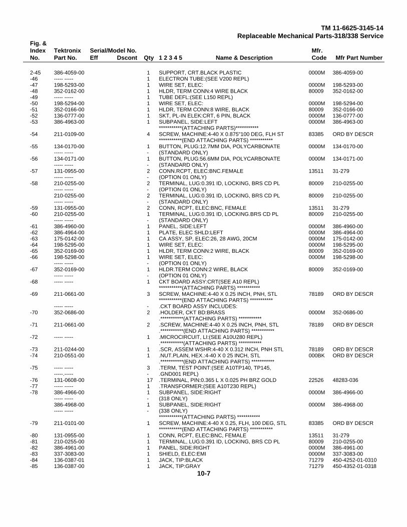
TM 11-6625-3145-14Replaceable Mechanical Parts-318/338 Service
Fig. &Index Tektronix Serial/Model No. Mfr.No. Part No. Eff Dscont Qty 1 2 3 4 5 Name & Description Code Mfr Part Number
2-45 386-4059-00 1 SUPPORT, CRT.BLACK PLASTIC 0000M 386-4059-00-46 ----- ----- 1 ELECTRON TUBE:(SEE V200 REPL)-47 198-5293-00 1 WIRE SET, ELEC: 0000M 198-5293-00-48 352-0162-00 1 HLDR, TERM CONN:4 WIRE BLACK 80009 352-0162-00-49 ----- ----- 1 TUBE DEFL:(SEE L150 REPL)-50 198-5294-00 1 WIRE SET, ELEC: 0000M 198-5294-00-51 352-0166-00 1 HLDR, TERM CONN:8 WIRE, BLACK 80009 352-0166-00-52 136-0777-00 1 SKT, PL-IN ELEK:CRT, 6 PIN, BLACK 0000M 136-0777-00-53 386-4963-00 1 SUBPANEL, SIDE:LEFT 0000M 386-4963-00
***********(ATTACHING PARTS)***********-54 211-0109-00 4 SCREW, MACHINE:4-40 X 0.875"100 DEG, FLH ST 83385 ORD BY DESCR
***********(END ATTACHING PARTS) ***********-55 134-0170-00 1 BUTTON, PLUG:12.7MM DIA, POLYCARBONATE 0000M 134-0170-00
----- ----- - (STANDARD ONLY)-56 134-0171-00 1 BUTTON, PLUG:56.6MM DIA, POLYCARBONATE 0000M 134-0171-00
----- ----- - (STANDARD ONLY)-57 131-0955-00 2 CONN.RCPT, ELEC:BNC.FEMALE 13511 31-279
----- ----- - (OPTION 01 ONLY)-58 210-0255-00 2 TERMINAL, LUG:0.391 ID, LOCKING, BRS CD PL 80009 210-0255-00
----- ----- - (OPTION 01 ONLY)210-0255-00 2 TERMINAL, LUG:0.391 ID, LOCKING, BRS CD PL 80009 210-0255-00----- ----- - (STANDARD ONLY)
-59 131-0955-00 2 CONN, RCPT, ELEC:BNC, FEMALE 13511 31-279-60 210-0255-00 1 TERMINAL, LUG:0.391 ID, LOCKING.BRS CD PL 80009 210-0255-00
----- ----- - (STANDARD ONLY)-61 386-4960-00 1 PANEL, SIDE:LEFT 0000M 386-4960-00-62 386-4964-00 1 PLATE, ELEC SHLD:LEFT 0000M 386-4964-00-63 175-0142-00 1 CA ASSY, SP, ELEC:26, 28 AWG, 20CM 0000M 175-0142-00-64 198-5295-00 1 WIRE SET, ELEC: 0000M 198-5295-00-65 352-0169-00 1 HLDR, TERM CONN:2 WIRE, BLACK 80009 352-0169-00-66 198-5298-00 1 WIRE SET, ELEC: 0000M 198-5298-00
----- ----- - (OPTION 01 ONLY)-67 352-0169-00 1 HLDR.TERM CONN:2 WIRE, BLACK 80009 352-0169-00
----- ----- - (OPTION 01 ONLY)-68 ----- ----- 1 CKT BOARD ASSY:CRT(SEE A10 REPL)
***********(ATTACHING PARTS) ***********-69 211-0661-00 3 SCREW, MACHINE:4-40 X 0.25 INCH, PNH, STL 78189 ORD BY DESCR
***********(END ATTACHING PARTS) ***********----- ----- - .CKT BOARD ASSY INCLUDES:
-70 352-0686-00 2 .HOLDER, CKT BD:BRASS 0000M 352-0686-00.***********(ATTACHING PARTS) ***********
-71 211-0661-00 2 .SCREW, MACHINE:4-40 X 0.25 INCH, PNH, STL 78189 ORD BY DESCR.***********(END ATTACHING PARTS) ***********
-72 ----- ----- 1 .MICROCIRCUIT, LI:(SEE A10U280 REPL).***********(ATTACHING PARTS) ***********
-73 211-0244-00 1 .SCR, ASSEM WSHR:4-40 X 0.312 INCH, PNH STL 78189 ORD BY DESCR-74 210-0551-00 1 .NUT.PLAIN, HEX.:4-40 X 0 25 INCH, STL 000BK ORD BY DESCR
.***********(END ATTACHING PARTS) ***********-75 ----- ----- 3 .TERM, TEST POINT:(SEE A10TP140, TP145,
-----.----- - .GND001 REPL)-76 131-0608-00 17 .TERMINAL, PIN:0.365 L X 0.025 PH BRZ GOLD 22526 48283-036-77 ----- ----- 1 .TRANSFORMER:(SEE A10T230 REPL)-78 386-4966-00 1 SUBPANEL, SIDE:RIGHT 0000M 386-4966-00
----- ----- - (318 ONLY)386-4968-00 1 SUBPANEL, SIDE:RIGHT 0000M 386-4968-00----- ----- - (338 ONLY)
***********(ATTACHING PARTS) ***********-79 211-0101-00 1 SCREW, MACHINE:4-40 X 0.25, FLH, 100 DEG, STL 83385 ORD BY DESCR
***********(END ATTACHING PARTS) ***********-80 131-0955-00 1 CONN, RCPT, ELEC:BNC, FEMALE 13511 31-279-81 210-0255-00 1 TERMINAL, LUG:0.391 ID, LOCKING, BRS CD PL 80009 210-0255-00-82 386-4961-00 1 PANEL, SIDE:RIGHT 0000M 386-4961-00-83 337-3083-00 1 SHIELD, ELEC:EMI 0000M 337-3083-00-84 136-0387-01 1 JACK, TIP:BLACK 71279 450-4252-01-0310-85 136-0387-00 1 JACK, TIP:GRAY 71279 450-4352-01-0318
10-7

TM 11-6625-3145-14Replaceable Mechanical Parts-318/338 Service
Fig. &Index Tektronix Serial/Model No. Mfr.No. Part No. Eff Dscont Qty 1 2 3 4 5 Name & Description Code Mfr Part Number
2-86 198-5296-00 1 WIRE SET, ELEC:INPUT BRACKET 0000M 198-5296-00-87 352-0162-00 1 .HLDR, TERM CONN:4 WIRE BLACK 80009 352-0162-00-88 ----- ----- 1 CKT BOARD ASSY:(SEE A01 REPL)
**********(ATTACHING PARTS) **********-89 211-0661-00 4 SCREW.MACHINE:4-40 X 0.25 INCH, PNH, STL 78189 ORD BY DESCR
**********(END ATTACHING PARTS) **********----- ----- - .CKT BOARD ASSY INCLUDES:
-90 ----- ----- 5 .TERM, TEST POINT:(SEE A01TP100, TP102 REPL)-91 131-0608-00 12 .TERMINAL, PIN:0.365 L X 0.025 PH BRZ GOLD 22526 48283-036
----- ----- - .(318 ONLY)-92 131-0993-00 1 .BUS, CONDUCTOR:2 WIRE BLACK 00779 850100-01
----- ----- - .(318 ONLY)-93 131-0589-00 4 .TERMINAL, PIN:0.46 L X 0.025 SQ 22526 48283-029
----- ----- - .(318 ONLY)-94 131-0589-00 4 .TERMINAL, PIN:0.46 L X 0.025 SQ 22526 48283-029
.----- ----- - .(318 ONLY)131-0589-00 8 .TERMINAL.PIN:0.46 L X 0.025 SQ 22526 48283-029----- ----- - .(338 ONLY)
-95 ----- ----- 1 .CONNECTOR:(SEE A01J100 REPL)-96 ----- ----- 1 .CONNECTOR:(SEE A01J106 OR J104 REPL)-97 129-0996-00 3 .SPACER, POST:9MM, 4-40 BRASS, 4.775 HEX 0000M 129-0996-00-98 129-0995-00 2 SPACER.POST:12.9MM, 4-40 BRASS, 4.775 HEX 0000M 129-0995-00-99 ----- ----- 1 CKT BOARD ASSY:INPUT B(SEE A02 REPL)
***********(ATTACHING PARTS) ***********-100 211-0661-00 4 SCREW, MACHINE:4-40 X 0.25 INCH, PNH, STL 78189 ORD BY DESCR
***********(END ATTACHING PARTS) ***********----- ----- - .CKT BOARD ASSY INCLUDES:
-101 ----- ----- 5 .TERM, TEST POINT:(SEE A02TP202, TP204, TP206----- ----- - .TP300, TP302 REPL)
102 131-0589-00 2 .TERMINAL, PIN:0.46 L X 0.025 SO 22526 48283-029-103 ----- ----- 1 .CONNECTOR.:(SEE A02J200 OR J210 REPL)-104 131-0993-00 2 .BUS.CONDUCTOR:2 WIRE BLACK 00779 850100-01-105 ----- ----- 1 .CONNECTOR:(SEE A02J206 OR J220 REPL)-106 361-0955-00 1 .SPACER, CONN:0.433 THK, POLYCARBONATE 0000M 361-0955-00
---- ----- - .(318 ONLY)361-0955-00 2 .SPACER, CONN:0.433 THK, POLYCARBONATE 0000M 361-0955-00---- ----- - .(338 ONLY)
-107 ----- ----- 4 .CONNECTOR:(SEE A02J200.J202, J204, J206 REP-108 ----- ----- 1 CKT BOARD ASSY:ACQ CONTROL(SEE A03 REPL)
**********(ATTACHING PARTS) **********-109 211-0661-00 4 SCREW, MACHINE:4-40 X 0.25 INCH, PNH.STL 78189 ORD BY DESCR
**********(END ATTACHING PARTS) **********----- ----- - .CKT BOARD ASSY INCLUDES:
-110 ----- ----- 2 .TEST POINT:(SEE A03TP100, TP200 REPL)-111 131-0993-00 7 .BUS, CONDUCTOR:2 WIRE BLACK 00779 850100-01
----- ----- - .(318 ONLY)131-0993-00 3 .BUS.CONDUCTOR:2 WIRE BLACK 00779 850100-01----- ----- - .(338 ONLY)
-112 ----- ----- 1 .CONNECTOR:(SEE A03J050 REPL)-113 ----- ----- 1 .CONNECTOR:(SEE A03J200 REPL)-114 ----- ----- 2 .CONNECTOR:(SEE A03J300, J400 REPL)-115 214-3419-00 1 .HEAT SINK:MSL 0000M 214-3419-00-116 131-0589-00 6 .TERMINAL, PIN:0.46 L X 0.025 SO 22526 48283-029-117 131-2939-01 1 .CONN.RCPT, ELEC:FEMALE, 2 X 20 0000M 131-2939-01-118 129-0997-00 4 SPACER, POST:9.8MM W/4-40 THD, BRASS 0000M 129-0997-00-119 ----- ----- 1 CKT BOARD ASSY:ACQ MEMORY(SEE A04 REPL)
**********(ATTACHING PARTS) **********-120 211-0661-00 4 SCREW.MACHINE:4-40 X 0.25 INCH, PNH, STL 78189 ORD BY DESCR
**********(END ATTACHING PARTS) **********----- ----- .CKT BOARD ASSY INCLUDES:
-121 ----- ----- 2 .TEST POINT:(SEE A04TP110, TP111 REPL)-122 131-0589-00 40 .TERMINAL, PIN:0.46 L X 0.025 SQ 22526 48283-029-123 ----- ----- 1 .CONNECTOR:(SEE A04J200 REPL)124 346-0032-00 1 .STRAP, RTNING:0.075 DIA X 4.0 L, MLD RBR 98159 2859-75-4125 214-3419-00 1 .HEAT SINK:MSL 0000M 214-3419-00
10-8
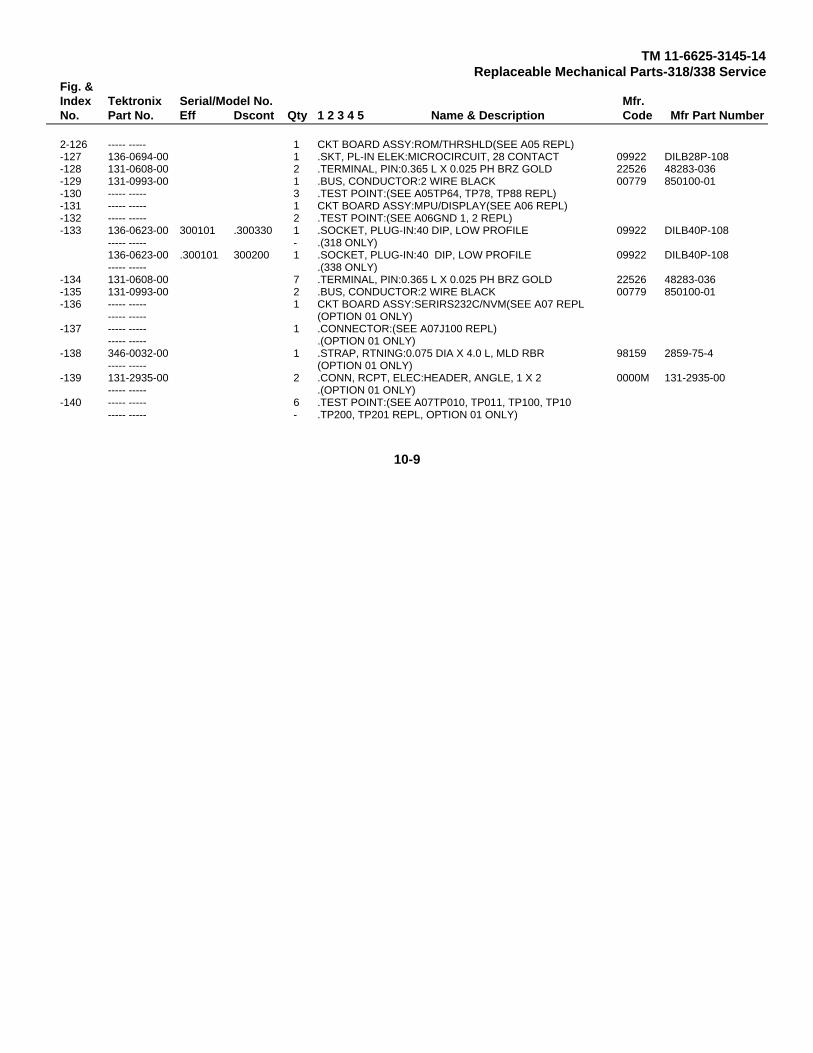
TM 11-6625-3145-14Replaceable Mechanical Parts-318/338 Service
Fig. &Index Tektronix Serial/Model No. Mfr.No. Part No. Eff Dscont Qty 1 2 3 4 5 Name & Description Code Mfr Part Number
2-126 ----- ----- 1 CKT BOARD ASSY:ROM/THRSHLD(SEE A05 REPL)-127 136-0694-00 1 .SKT, PL-IN ELEK:MICROCIRCUIT, 28 CONTACT 09922 DILB28P-108-128 131-0608-00 2 .TERMINAL, PIN:0.365 L X 0.025 PH BRZ GOLD 22526 48283-036-129 131-0993-00 1 .BUS, CONDUCTOR:2 WIRE BLACK 00779 850100-01-130 ----- ----- 3 .TEST POINT:(SEE A05TP64, TP78, TP88 REPL)-131 ----- ----- 1 CKT BOARD ASSY:MPU/DISPLAY(SEE A06 REPL)-132 ----- ----- 2 .TEST POINT:(SEE A06GND 1, 2 REPL)-133 136-0623-00 300101 .300330 1 .SOCKET, PLUG-IN:40 DIP, LOW PROFILE 09922 DILB40P-108
----- ----- - .(318 ONLY)136-0623-00 .300101 300200 1 .SOCKET, PLUG-IN:40 DIP, LOW PROFILE 09922 DILB40P-108----- ----- .(338 ONLY)
-134 131-0608-00 7 .TERMINAL, PIN:0.365 L X 0.025 PH BRZ GOLD 22526 48283-036-135 131-0993-00 2 .BUS, CONDUCTOR:2 WIRE BLACK 00779 850100-01-136 ----- ----- 1 CKT BOARD ASSY:SERIRS232C/NVM(SEE A07 REPL
----- ----- (OPTION 01 ONLY)-137 ----- ----- 1 .CONNECTOR:(SEE A07J100 REPL)
----- ----- .(OPTION 01 ONLY)-138 346-0032-00 1 .STRAP, RTNING:0.075 DIA X 4.0 L, MLD RBR 98159 2859-75-4
----- ----- (OPTION 01 ONLY)-139 131-2935-00 2 .CONN, RCPT, ELEC:HEADER, ANGLE, 1 X 2 0000M 131-2935-00
----- ----- .(OPTION 01 ONLY)-140 ----- ----- 6 .TEST POINT:(SEE A07TP010, TP011, TP100, TP10
----- ----- - .TP200, TP201 REPL, OPTION 01 ONLY)
10-9

TM 11-6625-3145-14Replaceable Mechanical Parts-318/338 Service
Fig. &Index Tektronix Serial/Model No. Mfr.No. Part No. Eff Dscont Qty 1 2 3 4 5 Name & Description Code Mfr Part Number
3-1 441-1663-00 .300101 .300280 1 CHAS, PWR SUPPLY:318/338 0000M 441-1663-00----- ----- - (318 ONLY)441-1663-01 .300281 1 CHAS, PWR SUPPLY:318/338 0000M 441-1663-01----- ----- - (318 ONLY)441-1663-00 .300101 .300145 1 CHAS, PWR SUPPLY:318/338 0000M 441-1663-00----- ----- - (338 ONLY)441-1663-01 .300146 1 CHAS, PWR SUPPLY:318/338 0000M 441-1663-01----- ----- - (338 ONLY)
-2 334-3379-00 1 MARKER, IDENT:MARKED GROUND SYMBOL 80009 334-3379-00-3 210-0202-00 1 TERMINAL.LUG:0.146 ID, LOCKING, BRZ, TIN PL 78189 2104-06-00-2520N
***********(ATTACHING PARTS) ***********-4 210-0457-00 1 NUT, PL, ASSEM WA:6-32 X 0.312, STL CD PL 83385 ORD BY DESCR
*********** (END ATTACHING PARTS) ***********-5 361-1235-00 1 SPACER, FILTER:4.6MM THK, POLYCARBONATE 0000M 361-1235-00-6 ----- ----- 1 FILTER:(SEE FL1 REPL)
***********(ATTACHING PARTS) ***********-7 210-0586-00 2 NUT, PL, ASSEM WA:4-40 X 0.25, STL, CD PL 78189 211-041800-00
*********** (END ATTACHING PARTS) ***********-8 ----- ----- 1 SWITCH, SLIDE:(SEE S2 REPL)
***********(ATTACHING PARTS) ***********-9 210-0406-00 2 NUT, PLAIN, HEX:4-40 X 0, 188, BRS, CD PL 73743 12161-50-10 210-0004-00 2 WASHER, LOCK:#4 INTL, 0.015 THK, STL CD PL 000BK ORD BY DESCR
*********** (END ATTACHING PARTS) ***********-11 200-2264-00 1 CAP., FUSEHOLDER:3AG FUSES S3629 FEK 031 1666-12 204-0833-00 1 BODY, FUSEHOLDER:3AG & 5 X 20MM FUSES S3629 031.1653(MDLFEU)-13 210-1039-00 1 WASHER, LOCK:INT, 0.521 ID X 0.625 INCH O 24931 ORD BY DESCR-14 200-2820-00 1 COVER, FAN:COPPER 0000M 200-2820-00-15 ----- ----- 1 FAN ASSY:(SEE B1 REPL)
***********(ATTACHING PARTS) ***********-16 211-0020-00 4 SCREW, MACHINE:4-40 X 1.125 INCH, PNH STL 83385 ORD BY DESCR-17 210-0004-00 4 WASHER, LOCK:#4 INTL, 0.015 THK, STL CD PL 000BK ORD BY DESCR
***********(END ATTACHING PARTS)" ***********- .FAN ASSY INCLUDES:
-18 352-0371-00 1 .HLDR, TERM CONN:2, FEMALE 000 M 352-0371-00-19 200-2822-00 1 COVER, PWR SPLY:BOTTOM, ALUMINUM 0000M 200-2822-00
----- ----- *********** (ATTACHING PARTS) ***********-20 211-0105-00 1 SCREW, MACHINE:4-40 X 0.188, 100 DEG, FLH ST 83385 ORD BY DESCR
***********(END ATTACHING PARTS) ***********-21 342-0627-00 1 INSULATOR, PLATE:BOTTOM, POLYCARBONATE 0000M 342-0628-00-22 200-2821-00 1 COVER, PWR SUPPLY:TOP, ALUMINUM 0000M 200-2821-00
*********** (ATTACHING PARTS) ***********-23 211-0105-00 1 SCREW.MACHINE:4-40 X 0.188, 100 DEG, FLH ST 83385 ORD BY DESCR
*********** (END ATTACHING PARTS) ***********-24 342-0628-00 1 INSULATOR, PLATE:TOP, POLYCARBONATE 0000M 342-0628-00-25 333-2969-00 .300101 .300280 1 PANEL, REAR:318/338 0000M 333-2969-00
----- ----- - (318 ONLY)333-2969-01 .300281 1 PANEL, REAR:318/338 0000M 333-2969-01----- ----- - (318 ONLY)333-2969-00 .300101 .300145 1 PANEL, REAR:318/1338 0000M 333-2969-00----- ----- - (338 ONLY)333-2969-01 .300146 1 PANEL, REAR:318/338 0000M 333-2969-01----- ----- - (338 ONLY)
***********(ATTACHING PARTS) ***********-26 211-0510-00 2 SCREW, MACHINE:6-32 X 0.375, PNH, STL, CD PL 83385 ORD BY DESCR
***********(END ATTACHING PARTS) ***********-27 334-4911-00 1 MARKER, IDENT:CAUTION 0000M 334-4911-00-28 ----- ----- 1 CKT BOARD ASSY:INVERTER(SEE A11 REPL)
***********(ATTACHING PARTS) ***********-29 211-0661-00 4 SCREW, MACHINE:4-40 X 0.25 INCH, PNH, STL 78189 ORD BY DESCR
***********(END ATTACHING PARTS) ***********..----- ----- - .CKT BOARD ASSY INCLUDES:
-30 352-0686-00 2 . HOLDER, CKT BD:BRASS 0000M 352-0686-00.***********-(ATTACHING PARTS)***********
31 211-0661-00 2 .SCREW, MACHINE:4-40 X 0.25 INCH, PNH, STL 78189 ORD BY DESCR.***********(END ATTACHING PARTS) ***********
10-10

TM 11-6625-3145-14Replaceable Mechanical Parts-318/338 Service
Fig. &Index Tektronix Serial/Model No. Mfr.No. Part No. Eff Dscont Qty 1 2 3 4 5 Name & Description Code Mfr Part Number
3-32 ----- ----- 1 .DIODE:(SEE A11CR151 REPL).***********(ATTACHING PARTS) ***********
-33 211-0121-00 1 .SCR, ASSEM WSHR:4-40 X 0.438 INCH, PNH BRS 83385 ORD BY DESCR.***********(END ATTACHING PARTS)’***********
-34 214-2063-00 1 .HEAT SINK, DIODE:(2) ALUMINUM 0000M 214-2063-00.***********(ATTACHING PARTS) ***********
-35 211-0661-00 2 .SCREW, MACHINE:4-40 X 0.25 INCH, PNH, STL 78189 ORD BY DESCR.***********(END ATTACHING PARTS) ***********
-36 ----- ----- 1 .DIODE:(SEE A11CR153 REPL).***********(ATTACHING PARTS) ***********
-37 211-0121-00 1 .SCR, ASSEM WSHR:4-40 X 0.438 INCH, PNH BRS 83385 ORD BY DESCR.***********(END ATTACHING PARTS) ***********
-38 ----- 1 .DIODE:(SEE A11CR152 REPL).***********(ATTACHING PARTS) ***********
-39 211-0121-00 1 .SCR, ASSEM WSHR:4-40 X 0.438 INCH, PNH BRS 83385 ORD BY DESCR.***********(END ATTACHING PARTS) ***********
-40 214-2048-00 1 .HEAT SINK, DIODE:(1)ALUMINUM DDDDM 214-2048-00.***********(ATTACHING PARTS) ***********
-41 211-0661-00 2 .SCREW, MACHINE:4-40 X 0.25 INCH, PNH, STL 78189 ORD BY DESCR.***********(END ATTACHING PARTS) ***********
-42 ----- ----- 1 .TRANSISTOR:(SEE A11 Q149 REPL).***********(ATTACHING PARTS) ***********
-43 211-0121-00 1 .SCR, ASSEM WSHR:4-40 X 0.438 INCH, PNH BRS 83385 ORD BY DESCR.***********(END ATTACHING PARTS) ***********
-44 ----- ----- 1 .THERMOSTATIC:(SEE A11 S3 REPL).***********(ATTACHING PARTS) ***********
-45 211-0661-00 2 .SCREW, MACHINE:4-40 X 0.25 INCH, PNH, STL 78189 ORD BY DESCR.***********(END ATTACHING PARTS) ***********
-46 214-2064-00 1 .HEAT SINK, XSTR:TO-218, ALUMINUM 0000M 214-2064-00.***********(ATTACHING PARTS) ***********
-47 211-0661-00 2 .SCREW, MACHINE:4-40 X 0.25 INCH, PNH, STL 78189 ORD BY DESCR.***********(END ATTACHING PARTS)- ***********
-48 ----- ----- 3 .CONNECTOR:(SEE A11J4, J5, J11 REPL)-49 ----- ----- 2 .CONNECTOR:(SEE A11J8, J10 REPL)-50 ----- ----- 1 CKT BOARD ASSY:REGULATOR(SEE A12 REPL)
***********(ATTACHING PARTS) ***********-51 211-0661-00 4 SCREW, MACHINE:4-40 X 0.25 INCH, PNH, STL 78189 ORD BY DESCR
***********(END ATTACHING PARTS) ***********----- ----- .CKT BOARD ASSY INCLUDES:
-52 ----- ----- 2 .CONNECTOR:(SEE A12J7, J9 REPL)-53 ----- ----- 1 .CONNECTOR:(SEE A12J6 REPL)-54 ----- ----- 1 .TERM, TEST:(SEE A12TP1, TP2, TP3 REPL)-55 131-2994-00 1 .BUS, CONDUCTOR:5 CONDUCTOR, 73MM L 0000M 131-2994-00-56 ----- ----- 1 .CONNECTOR:(SEE A12J1 REPL)-57 ----- --- 2 .CONNECTOR:(SEE A12J2, J3 REPL)
175-8753-00 1 CA ASSY, SP, ELEC:ECB PWR SUPPLY 0000M 175-8753-00-58 175-8464-00 2 .CA ASSY, SP, ELEC:7, 22 AWG, 105MM L, RIBBON 0000M 175-8464-00-59 175-8748-00 1 .CA ASSY, SP, ELEC:2, 18 AWG, 14 CM, O-N, 9-N 0000M 175-8748-00-60 352-0370-00 2 ..HLDR, TERM CONN:2, FEMALE 0000M 352-0370-00-61 175-8749-00 1 .LEAD ASSY, ELEC:1, 18 AWG, 7CM, 9-N 0000M 175-8749-00-62 175-8750-00 1 .LEAD ASSY, ELEC:2, 20 AWG, 13CM, 9-N 0000M 175-8750-00-63 352-0370-00 1 ..HLDR, TERM CONN:2, FEMALE 0000M 352-0370-00-64 175-8751-00 1 .LEAD ASSY, ELEC:2, 20 AWG, 13CM, 9-N 0000M 175-8751-00-65 352-0370-00 1 ..HLDR.TERM CONN:2, FEMALE 0000M 352-0370-00
175-8752-00 1 CA ASSY, SP, ELEC:3, 18 AWG.14CM, 4-5, 2-N 0000M 175-8752-00
10-11
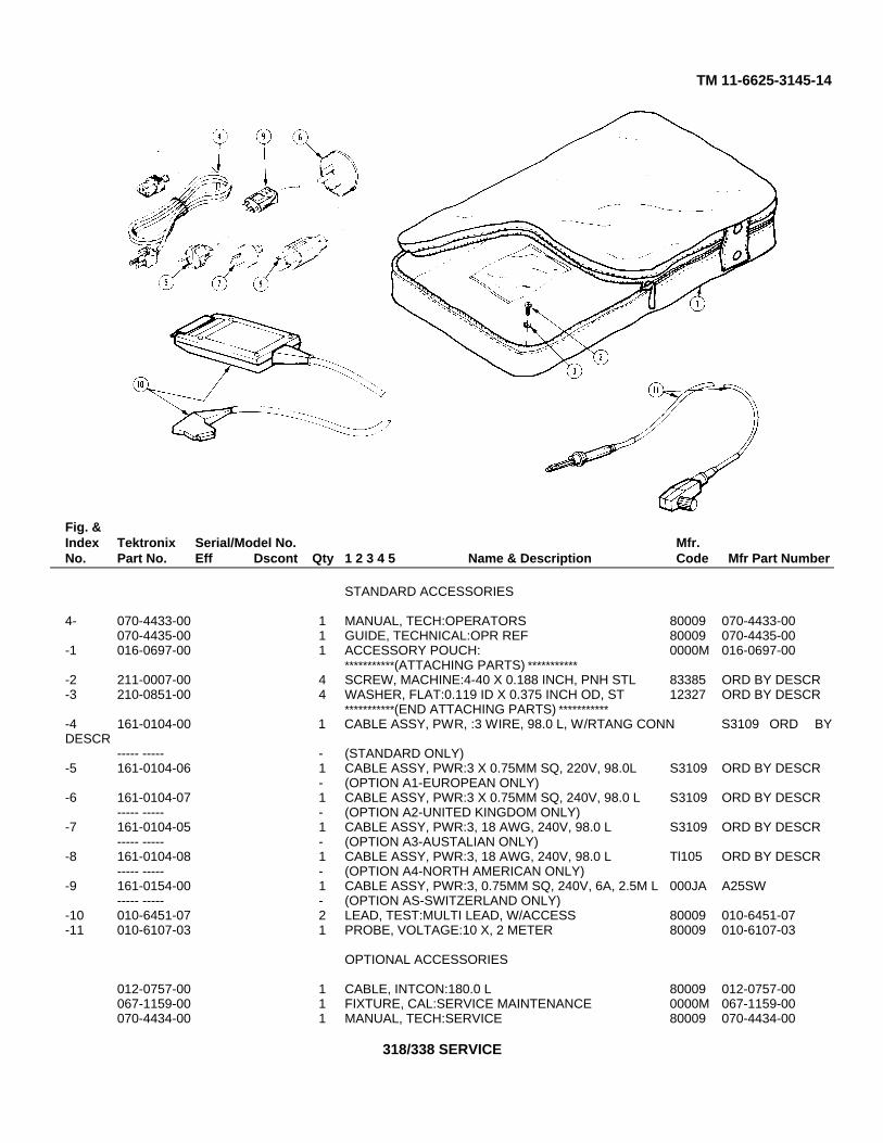
TM 11-6625-3145-14
Fig. &Index Tektronix Serial/Model No. Mfr.No. Part No. Eff Dscont Qty 1 2 3 4 5 Name & Description Code Mfr Part Number
STANDARD ACCESSORIES
4- 070-4433-00 1 MANUAL, TECH:OPERATORS 80009 070-4433-00070-4435-00 1 GUIDE, TECHNICAL:OPR REF 80009 070-4435-00
-1 016-0697-00 1 ACCESSORY POUCH: 0000M 016-0697-00***********(ATTACHING PARTS) ***********
-2 211-0007-00 4 SCREW, MACHINE:4-40 X 0.188 INCH, PNH STL 83385 ORD BY DESCR-3 210-0851-00 4 WASHER, FLAT:0.119 ID X 0.375 INCH OD, ST 12327 ORD BY DESCR
***********(END ATTACHING PARTS) ***********-4 161-0104-00 1 CABLE ASSY, PWR, :3 WIRE, 98.0 L, W/RTANG CONN S3109 ORD BYDESCR
----- ----- - (STANDARD ONLY)-5 161-0104-06 1 CABLE ASSY, PWR:3 X 0.75MM SQ, 220V, 98.0L S3109 ORD BY DESCR
- (OPTION A1-EUROPEAN ONLY)-6 161-0104-07 1 CABLE ASSY, PWR:3 X 0.75MM SQ, 240V, 98.0 L S3109 ORD BY DESCR
----- ----- - (OPTION A2-UNITED KINGDOM ONLY)-7 161-0104-05 1 CABLE ASSY, PWR:3, 18 AWG, 240V, 98.0 L S3109 ORD BY DESCR
----- ----- - (OPTION A3-AUSTALIAN ONLY)-8 161-0104-08 1 CABLE ASSY, PWR:3, 18 AWG, 240V, 98.0 L Tl105 ORD BY DESCR
----- ----- - (OPTION A4-NORTH AMERICAN ONLY)-9 161-0154-00 1 CABLE ASSY, PWR:3, 0.75MM SQ, 240V, 6A, 2.5M L 000JA A25SW
----- ----- - (OPTION AS-SWITZERLAND ONLY)-10 010-6451-07 2 LEAD, TEST:MULTI LEAD, W/ACCESS 80009 010-6451-07-11 010-6107-03 1 PROBE, VOLTAGE:10 X, 2 METER 80009 010-6107-03
OPTIONAL ACCESSORIES
012-0757-00 1 CABLE, INTCON:180.0 L 80009 012-0757-00067-1159-00 1 FIXTURE, CAL:SERVICE MAINTENANCE 0000M 067-1159-00070-4434-00 1 MANUAL, TECH:SERVICE 80009 070-4434-00
318/338 SERVICE

TM 11-6625-3145-14
APPENDIX A REFERENCES
DA Pam 310-1 Consolidated Index of Army Publicationsand Blank Forms.
DA Pam 738-750 The Army Maintenance Management System(TAMMS)
TM 11-6625-3145-24P Organization, Direct Support, and GeneralSupport Maintenance, including DepotMaintenance Repair Parts and SpecialTools Lists for Logic Analyzer, TEKModels 318/338
TM 7520-244-2 Procedures for Destruction of ElectronicsMateriel to Prevent Enemy Use(Electronics Command)
A-1/(A-2 blank)

TM 11-6625-3145-14
APPENDIX BCOMPONENTS OF END ITEM LIST
SECTION I. INTRODUCTION
B-1. Scope
The appendix lists integral components of and basic issue items for Logic Analyzer, TEK Models 318/338 to help youinventory items required for safe and efficient operation.
B-2. General
This Components of End Item List is divided into the following sections:
a. SECTION II. Integral Components of End Item. These items, when assembled, comprise the Logic Analyzer, TEKModels 318/338. These components must accompany the End Item whenever it is transferred or turned in. Theillustrations referenced will help you identify these items.
b. SECTION III. Basic Issue Items. Not applicable.
B-3. SECTION II. Integral Components of End Item. Explanation of Column Entries.
a. Column 1, Illustration. This column is divided as follows:(1) Column A, Figure Number. Indicates the figure number of the illustration on which the item is shown.(2) Column B, Item Number. The number used to identify the item called out in the illustration.
b. Column 2, National Stock Number. Indicates the National Stock Number assigned to the item, the number will beused for requisitioning.
c. Column 3, Description. Indicates the Federal item name and, if required, gives a minimum description to identifythe item. The Part Number indicated is the primary number used by the manufacturer, which controls the design andcharacteristics of the item by means of its engineering drawings, specification, standards, and inspection requirements toidentify an item or range of items. Following the Part Number, the Federal Supply Code for Manufacturers (FSCM) isshown in parentheses.
d. Column 4, Location. The physical location of each item listed is given, The lists are designed to inventory all itemsin one area of the major item before moving into an adjacent area.
B-1

TM 11-6625-3145-14
e. Column 5, Usable on Code. Not applicable.f. Column 6, Quantity Required (Qty Reqd). This column lists the quantity of each item required for a complete
major item.g. Column 7, Quantity. This column is divided into two columns. In the Received (Rcvd) column, list the
quantity actually received on your major item. The Date column is left blank for later use during inventory ofthe major item.
B-2

TM 11-6625-3145-14SECTION II INTEGRAL COMPONENTS OF END ITEM
APPENDIX B
(1) (2) (3) (4) (5) (6) (7)ILLUSTRATION QUANTITY
(A) (B) NATIONAL DESCRIPTION USUABLEFIG. ITEM STOCK ON QTYNO. NO. NUMBER PART NUMBER (FSCM) LOCATION CODE REQD RCVD DATE
LOGIC ANALYZER, TEKTRONIX MODEL 31851(FSCM) (80009)
DRSEL-MA Form 6010, (1 Mar 77) (Edition of 1 Jun 76 is obsolete) B-3(B-4 blank)
B-3(B-4 blank)

TM 11-6625-3145-14
APPENDIX CERROR AND ACQUISITION STATUS MESSAGES
The following table lists the error and acquisition status messages which may appear on the screen. The messages arelisted in alphabetical order.
Message Description
COMM ERR:CD REMOTE MODE message.COMM ERR:CTS These messages appear when the 318/338 detects a modem orCOMM ERR:DSR communication line error.<SETUP CHANGED> This message appears when you change the hardware setup
during data acquisition.NO RESPONSE REMOTE MODE message.
Link message time out.REMOTE START Communication link is complete. Start remote control.REMOTE STOP Remote mode is closed.PRESS STOP Some fields require you to press the STOP key when instructed.USE SELECT These messages appear when you use the wrong key when tryingUSE EXECUTE to select a field value. The messages li st the valid keys.USE INCR/DECRUSE 0-1, X USE 0-7, XUSE 0-9, X USE 0-F, XUSE A, B, X USE O-D, X<SLOW CLOCK> This messages appears when external clock interval is longer than
25 mS.<ST:SETUP CHANGED> These messages (except <ST:NO ACQ>) appear when you<ST:NO ACQ> press the STOP key during data acquisition. <ST:NO ACQ><ST:NO TRIG> appears when you press the STOP key during hardware setup in<ST:T=-1000W> the single acquisition mode or the first cycle of the repeat acquisi-<ST:NO ACQ> tion mode.<T=255W> These messages appear when the 318/338 has finished acquiring<T=-100> data; the numbers included in these messages indicate the trigger
position.TRYING TO LINK REMOTE MODE message. The 318/338 is waiting for a link
message from the terminal.<WAITING TRIG> This message means that the 318/338 is waiting for a trigger word.
This message appears just before the 318/338 starts anacquisition.
C-1/(C-2 blank)
TM 11-6625-3145-14
APPENDIX D
MAINTENANCE ALLOCATION
SECTION 1. INTRODUCTION
D-1. GeneralThis appendix provides a summary of the maintenance operations for Logic Analyzer, TEK Models 318/338. It authorizescategories of maintenance for specific maintenance functions on repairable items and components and the tools andequipment required to perform each function. This appendix may be used as an aid in planning maintenance operations.
D-2. Maintenance
Function Maintenance functions will be limited to and defined as follows:
a. Inspect. To determine the serviceability of an item by comparing its physical, mechanical, and/or electricalcharacteristics with established standards through examination.
b. Test. To verify serviceability and to detect incipient failure by measuring the mechanical or electricalcharacteristics of an item and comparing those characteristics with prescribed standards.
c. Service. Operations required periodically to keep an item in proper operating condition; i.e., to clean(decontaminate), to preserve, to drain, to paint, or to replenish fuel, lubricants, hydraulic fluids, or compressed air supplies.
d. Adjust. To maintain, within prescribed limits, by bringing into proper or exact position, or setting theoperating characteristics to specified parameters.
e. Aline. To adjust specified variable elements of an item to bring about optimum or desired performance.
f. Calibrate. To determine and cause corrections to be made or to be adjusted in instruments or test
D-1
TM 11-6625-3145-14
measuring and diagnostics equipments use in precision measurement. Consists of comparison of two instruments, one inwhich is a certified standard of know accuracy of the instrument being compared.
g. Install. The act of emplacing, seating, or fixing into position an item, part, module (component or assembly)in a manner to allow the proper functioning of the equipment or system.
h. Replace. The application of maintenance services (inspect, test, service, adjust, aline, calibrate, replace) orother maintenance actions (welding, grinding, riveting, straightening, facing, remachining, or resurfacing) to restoreserviceability to an item by correction specific damage, fault, malfunction, or failure in a part, subassembly, module(component or assembly), end item, or system. This function does not include the trail and error replacement of runningspare type items such as fuses, lamps, or electron tubes.
j. Overhaul. That maintenance effort (service/action) necessary to restore an item to a completelyserviceable/operational condition as prescribed by maintenance standards (i.e., DMWR) in appropriate technicalpublications. Overhaul is normally the highest degree of maintenance performed by the Army. Overhaul does notnormally return an item to like new condition.
k. Rebuild. Consists of those services/actions necessary for the restoration of unserviceable equipment to alike new condition in accordance with original manufacturing standards. Rebuild is the highest degree of materielmaintenance applied to Army equipment. The rebuild operation includes the act of returning to zero those agemeasurements (hours, miles, etc.) considered in classifying Army equipment/ components.
D-3. SECTION II. Maintenance Allocation Chart. Explanation of Column Entries
a. Column 1, Group Number. This column lists group numbers, the purpose of which is to identifycomponents, assemblies, subassemblies.
D-2

TM 11-6625-3145-14
and modules with the next higher assembly.
b. Column 2, Component/Assembly. Indicates the noun names of components, assemblies, subassemblies,and modules for which maintenance is authorized.
c. Column 3, Maintenance Function. Lists the functions to be performed on the item listed column 2. Whenitems are listed without maintenance functions. This is done solely for the purpose of having the group numbers in theMAC and RPSTL coincide.
d. Column 4, Maintenance Category. Specifies, by the listing of a "work time" figure in the appropriatesubcolumn(s), the lowest level of maintenance authorized to perform the function listed in column 3. This figure representsthe active time required to perform that maintenance function at the indicated category of maintenance. If the number orcomplexity of the tasks within the listed maintenance function varies at different maintenance categories, appropriate "worktime" figures will be shown for each category. The number of task-hours specified by the "work time" figure represents theaverage time required to restore an item (assembly, subassembly, components, module, end item or system) to aserviceable condition under typical field operating conditions. This time includes preparation time, troubleshooting time,and quality assurance/quality control time in addition to the time required to perform the specific tasks identified for themaintenance function authorized in the maintenance allocation chart. Subcolumns of column 4 are as follows:
C = Operator/CrewO = OrganizationalF = Direct SupportH = General SupportD = Depot
e. Column 5, Tools and Equipment. Specifies by code, shown in Section III, those common tools sets (notindividual tools), special tools, and test and support equipment required to perform the designated function.
f. Column 6, Remarks. Contains an alphabetic code which refers to the applicable remark in Section IV.
D-3

TM 11-6625-3145-14
D-4. SECTION III. Tool and Test Equipment Requirements.
a. Tool or Test Equipment Reference Code. The numbers in this column coincide with the numbers used inthe tools and equipment column of the MAC. The numbers indicate the applicable tool or test equipment for themaintenance functions.
b. Maintenance Category. The codes in this column indicate the maintenance category allocated the tool ortest equipment.
c. Nomenclature. This column lists the noun name and nomenclature of the tools and test functions.
d. National/NATO Stock Number. This column lists the National/ NATO Stock Number of the specific tool ortest equipment.
e. Tool Number. This column lists the manufacturer’s Part Number of the tool and is followed by the FederalSupply Code for Manufacturers (FSCM) (5 digits) in parentheses.
D-5. Section IV. Remarks
a. Reference Code. This code refers to the appropriate item in Section II, column 6.
b. Remarks. This column provides the required explanatory information necessary to clarify items appearing inSection II.
D-4

TM 11-6625-3145-14SECTION II MAINTENANCE ALLOCATION CHART
FORLOGIC ANALYZER 318S1
(1) (2) (3) (4) (5) (6)MAINTENANCE LEVEL
GROUP MAINTENANCE TOOLS ANDNUMBER COMPONENT ASSEMBLY FUNCTION C O F H D EQUIPMENT REMARKS
00 LOGIC ANALYZER Inspect 0.5318S1 (80009) Test 1.0 1-9
Test 3.0Service 0.5Replace 0.3Repair 2.0 1-9 A, B, CRepair 4.0
01 DATA INPUT A CCA Inspect 0.1670-7819-00 Test 3.0
A1 Replace 0.3Repair 4.0
02 DATA INPUT B CCA Inspect 0.1670-7818-00 Test 3.0
A2 Replace 0.3Repair 4.0
03 ACQ CONTROL CCA Inspect 0.1670-7815-00 Test 3.0
A3 Replace 0.3Repair 4.0
04 ACQ MEMORY CCA Inspect 0.1670-7814-00 Test 3.0
A4 Replace 0.3Repair 4.0
05 ROM/THRESHOLD CCA Inspect 0.1670-7813-00 Test 3.0
A5 Replace 0.3Repair 4.0
06 MPU DISPLAY CCA Inspect 0.1670-7812-00 Test 3.0
A6 Replace 0.3Repair 4.0
07 SERIAL/RS232/NUM Inspect 0.1670-7809-00 Test 3.0
A7 Replace 0.3Repair 4.0
08 MOTHER BOARD CCA Inspect 0.5670-7811-00 Test 1.0
A8 Replace 1.0Repair 4.0
09 CRT CIRCUIT CCA Inspect 0.1670-7810-00 Test 3.0
A10 Replace 0.3Repair 4.0
10 INVERTER CCA Inspect 0.1670-7821-00 Test 3.0A11 Replace 0.3
Repair 4.011 REGULATOR CCA Inspect 0.1
670-7820-00 Test 3.0A12 Replace 0.3
Repair 4.0
D-5

TM 11-6625-3145-14
SECTION III TOOL AND TEST EQUIPMENT REQUIREMENTSFOR
LOGIC ANALYZER 318S1TOOL OR TEST MAINTENANCE NATIONAL/NATO TOOLEQUIPMENT CATEGORY NOMENCLATURE STOCK NUMBER NUMBERREF CODE
1 H DUAL TRACE OSCILLOSCOPE TEK475OS261C/U (80009)
2 H POWER MODULE TM503OS261C/U (80009)
3 H PULSE GENERATOR 6625-01-137-5369SG-1205/U
4 H DIGITAL MULTIMETER 6625-01-145-2430AN/USM-486
5 H DIGITAL DELAYDD501
(80009)6 H POWER SUPPLY PS501
(80009)7 H MAINTENANCE KIT 067-1159-00
(80009)8 COMPUTER TERMINAL 4025
(80009)9 GENERATOR 834
(80009)
D-6
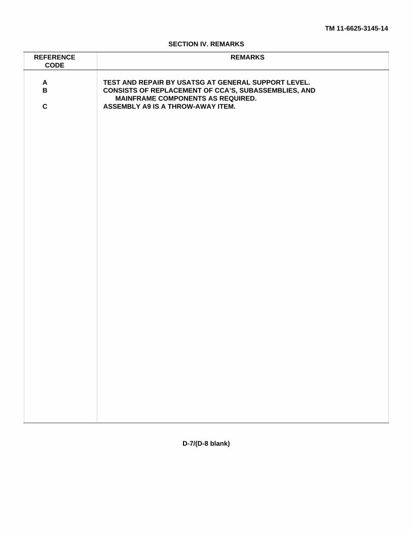
TM 11-6625-3145-14
SECTION IV. REMARKS
REFERENCE REMARKSCODE
A TEST AND REPAIR BY USATSG AT GENERAL SUPPORT LEVEL.B CONSISTS OF REPLACEMENT OF CCA’S, SUBASSEMBLIES, AND
MAINFRAME COMPONENTS AS REQUIRED.C ASSEMBLY A9 IS A THROW-AWAY ITEM.
D-7/(D-8 blank)

TM 11-6625-3145-14
APPENDIX EERROR CODES
Table E-1ERROR CODES IN SELF TEST
Code Description
00 ROM U1 ( 00 TO 3FFF ) MAY BE DAMAGED.01 ROM U2 ( 4000 TO 7FFF ) MAY BE DAMAGED.02 ROM U3 ( PAGE 1: 8000 TO BFFF ) MAY BE DAMAGED.03 ROM U4 ( PAGE 2: 8000 TO BFFF ) MAY BE DAMAGED.04 ROM U5 ( PAGE 3: 8000 TO BFFF ) MAY BE DAMAGED.05 ROM U6 ( PAGE 4: 8000 TO BFFF ) MAY BE DAMAGED.06 ROM U7 ( C000 TO DFFF ) MAY BE DAMAGED.10 DISPLAY RAM ( E800 TO EFFF ) MAY BE DAMAGED.11 SYSTEM RAM ( FOOO TO FFFF ) MAY BE DAMAGED.KBD SOME KEYS MAY BE DEPRESSED.TIME BASE TIMER OR SOME OF SYSTEM CLOCK MAY BE DAMAGED.T/H SOME ERRORS ARE DETECTED IN V3=(V1 +V2)2 TEST.WR THE WORD RECOGNIZER RAMS ( WRO AND WR1 ) MAY BE DAMAGED.ACQ HIGH SPEED RAM MAY BE DAMAGED.SQRAM SEQUENCER RAM MAY BE DAMAGED.NDL EVENT/DELAY CARRY FLAG IS NOT SET.SEQ SOME TRIGGER SEQUENCE FLAGS MAY BE DAMAGED.SER SIO FOR SERIAL ACQUISITION MAY BE DAMAGED.RMT SIO FOR REMOTE CONTROL MAY BE DAMAGED.NVM NON VOLATILE MEMORY MAY BE DAMAGED.
E-1

TM 11-6625-3145-14
Table E-2ERROR CODES OF PARALLEL TESTS IN DIAGNOSTICS MENU
Code Description
20 CAN NOT WRITE WORD "55" INTO WRO, OR CAN NOT READ DATA FROMHIGH SPEED RAM.
21 CAN NOT WRITE WORD "AA" INTO WRO, OR CAN NOT READ DATA FROMHIGH SPEED RAM.
22 CAN NOT WRITE WORD "55" INTO WR1, OR CAN NOT READ DATA FROMSPEED RAM.
23 CAN NOT WRITE WORD "AA" INTO WR1, OR CAN NOT READ DATA FROMSPEED RAM.
30 CAN NOT WRITE "55H" INTO HIGH SPEED RAM, OR CAN NOT READ DATAFROM HIGH SPEED RAM.
31 ADDRESS COUNTER CARRY FLAG IS NOT SET.
32 CAN NOT WRITE "OAAH" INTO HIGH SPEED RAM, OR READ DATA FROMHIGH SPEED RAM.
33 ADDRESS COUNTER CARRY FLAG IS NOT SET.
40 CAN NOT WRITE "55H" INTO SQRAM, OR CAN NOT READ DATA FROMHIGH SPEED DATA.
41 CAN NOT WRITE "OAAH" INTO SQRAM, OR CAN NOT READ DATA FROMHIGH SPEED DATA.
50 N-FLAG IS NOT SET.
51 TRIG’D FLAG IS NOT SET.
52 STOP FLAG IS NOT SET.
53 ACQUIRED DATA IS NOT EQUAL TO EXPECTED DATA.
E-2

TM 11-6625-3145-14
Table E-3ERROR CODES OF SERIAL TESTS IN DIAGNOSTICS MENU
Code Description
B4 SERIAL STATUS REGISTER READ ERROR
B5 SERIAL RECEIVE READY NOT OFF
B6 SERIAL ERROR REGISTER READ ERROR
B7 SERIAL FRAMING-ERR BIT NOT OFF
B8 SERIAL OVER RUN-ERR BIT NOT OFF
B9 SERIAL PARITY-ERR BIT NOT OFF
BA EXT-TRIG BIT NOT OFF
BB EXT-TRIG BIT NOT ON
BC DATA LOOP-BACK TEST ERROR AT 75 BAUD(FROM RS232 OUTPUT TO SERIAL INPUT)
BD " " " 200 BAUD
BE " " " 2400 BAUD
BF " " " 1800 BAUD
C0 " " " 1200 BAUD
C1 " " " 4800 BAUD
C2 " " " 110 BAUD
C3 " " " 9600 BAUD
E-3

TM 11-6625-3145-14
Table E-4 ERROR CODES OF REMOTE TESTS IN DIAGNOSTICS MENU
Code Description
96 RTS NOT ON97 CTS NOT ON98 CD NOT ON99 RTS NOT OFF9A CTS NOT OFF9B CD NOT OFF9C DTR NOT ON9D DSR NOT ON9E RS232 STATUS REGISTER READ ERROR9F RS232 RECEIVE READY FLAG NOT OFFA0 RS232 TRANSMIT EMPTY FLAG NOT ONA2 RS232 ERROR REGISTER READ ERRORA3 RS232 FRAMING ERROR FLAG NOT OFFA4 RS232 OVER RUN ERROR FLAG NOT OFFA5 RS232 PARITY ERROR FLAG NOT OFFAA INCREMENT PATTERN DATA LOOP BACK TEST
(FROM RS232 OUTPUT TO RS232 INPUT)ERROR AT 110 BAUD
AB " " " 150 BAUDAC " " " 300 BAUDAD " " " 600 BAUDAE " " " 1200 BAUDAF " " " 2400 BAUDB0 " " " 4800 BAUDB1 " " " 9600 BAUDB2 INTERRUPT MODE DATA LOOPBACK TEST ERROR AT 9600 BAUD
E-4

TM 11-6625-3145-14
Table E-5ERROR CODES OF NVM TESTS IN DIAGNOSTICS MENU
Code Description
C8 DATA ERROR WHEN DATA PATTERN IS FFC9 00
CA 01
CB 02CC 04
CD 08
CE 10
CF 20
DO 40
D1 80
D2 MARCHING PATTERN
D3 INCREMENTING PATTERN
E-5/(E-6 blank)

By Order of the Secretary of the Army:
JOHN A. WICKHAM JR.General, United States Army
Official: Chief of Staff
DONALD J. DELANDROBrigadier General, United States Army
The Adjutant General
Distribution:
To be distributed in accordance with special list.
* U.S. GOVERNMENT PRINTING OFFICE: 1985-515-085:20165

TM 11-6625-3145-14318/338
4434-923
318 Block Diagram

TM 11-6625-3145-14318/338
4434-924338 Block Diagram
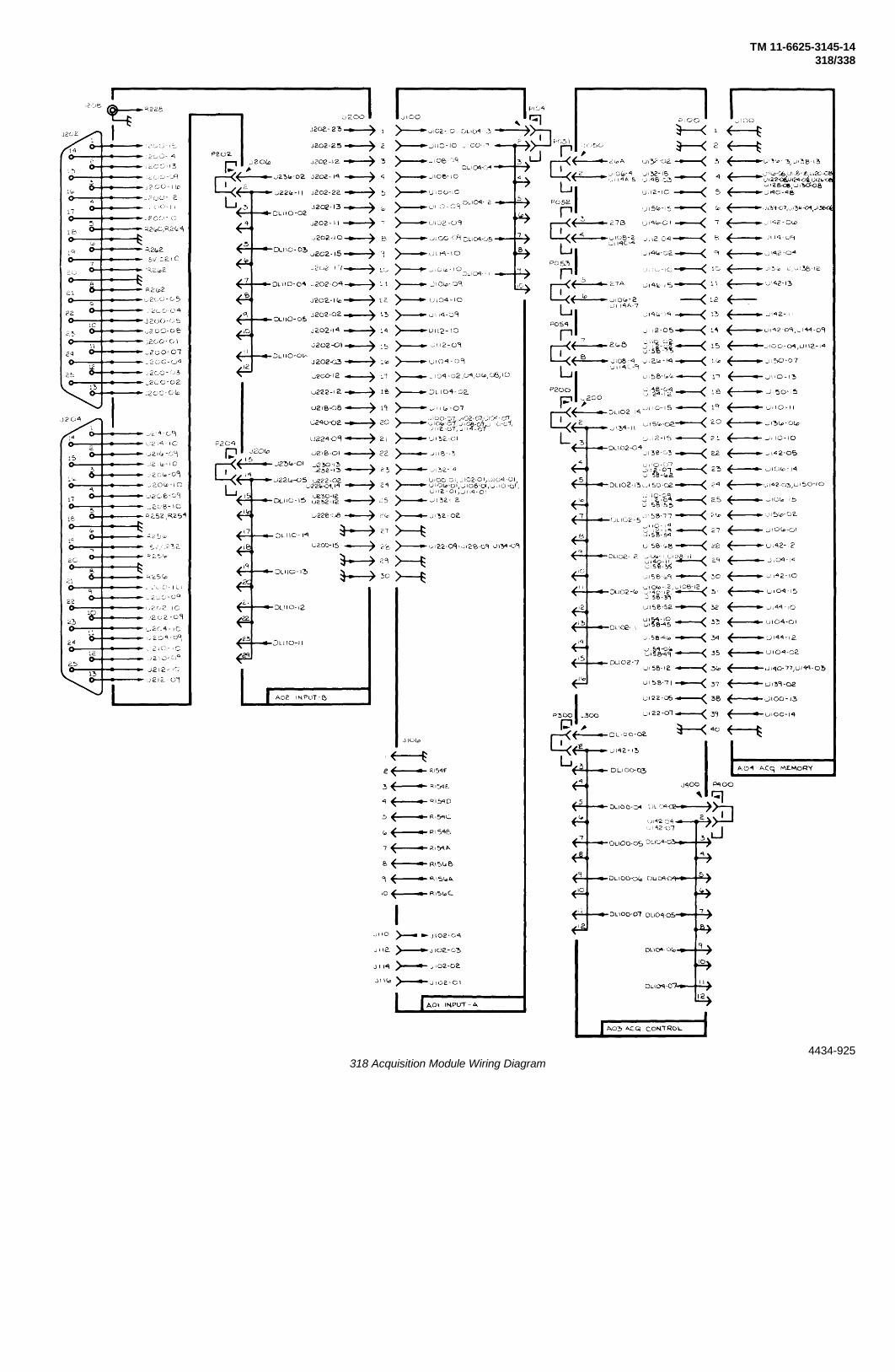
TM 11-6625-3145-14318/338
4434-925318 Acquisition Module Wiring Diagram

TM 11-6625-3145-14318/338
4434-926318/338 Mainframe Wiring Diagram

TM 11-6625-3145-14318/338
4434-926338 Acquisition Module Wiring Diagram
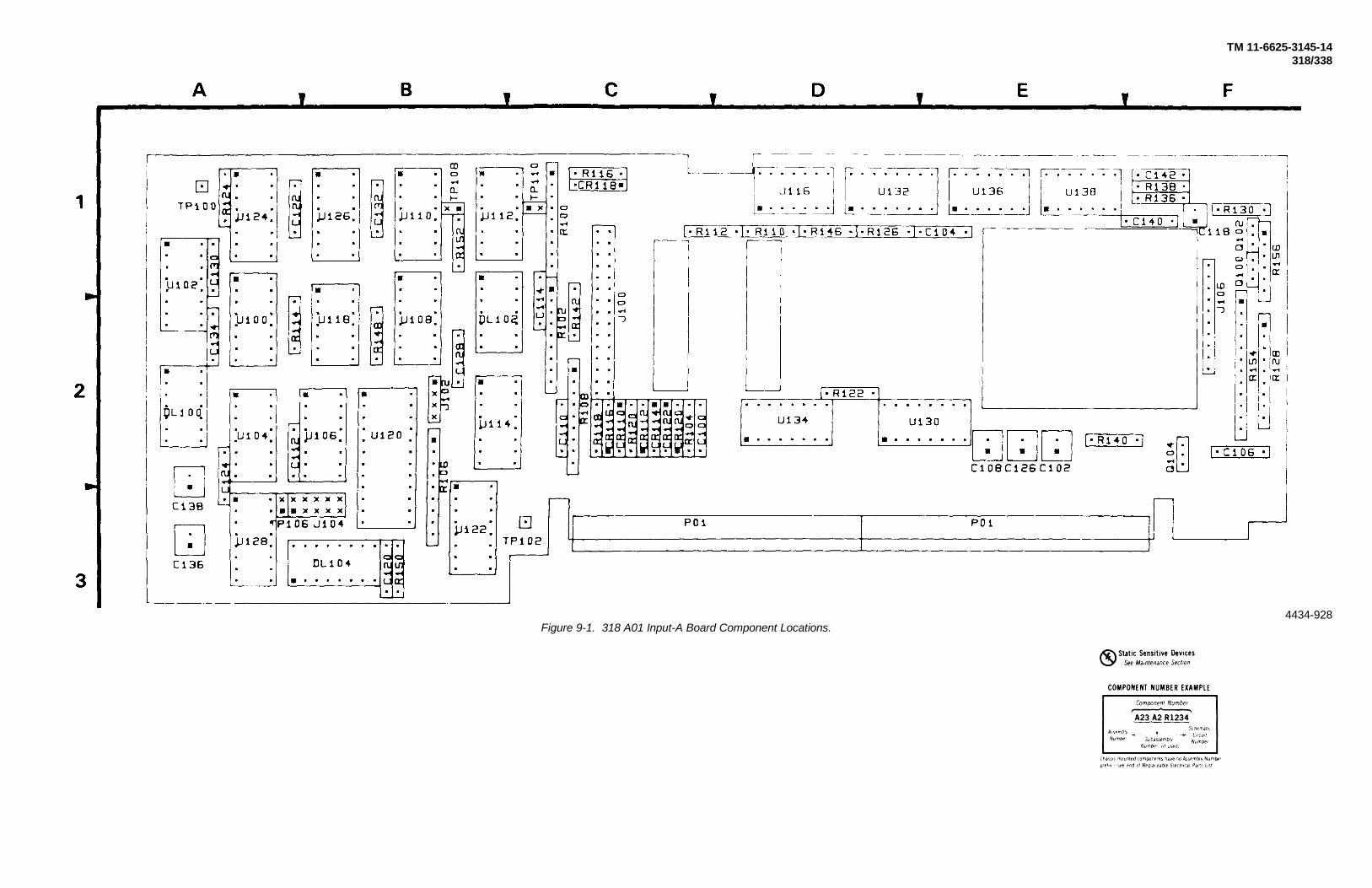
TM 11-6625-3145-14318/338
4434-928Figure 9-1. 318 A01 Input-A Board Component Locations.

TM 11-6625-3145-14
Table 9-2318 CH 0-7 FRONT END -<1> INPUT-A BOARD, ASSEMBLY A01
CIRCUIT SCHEMATIC BOARD CIRCUIT SCHEMATIC BOARDNUMBER LOCATION LOCATION NUMBER LOCATION LOCATION
DL100 A B2 A2 R106E E1 B2DL100B B3 A2 R 106F E1 B2DL100C B4 A2 R106G E1 B2DL100D B5 A2 R106H E1 B2DL102A D2 B2 R108B E1 C2DL102B D3 B2 R108C E1 C2DL102C D4 B2 R108C E1 C2DL102D D5 B2 R108D E1 C2J100 Al C2 R108E E1 C2J100 E4 C2 R108F E1 C2J100 C1 C2 R108G E1 C2J100 F2 C2 R108H E1 C2R100A A3 C1 R122 E4 D2R100B A2 C1 R152 Dl B1R100C A2 C1 TP100 F5 AlR100D A3 C1 TP102 F5 C3R100E A4 C1 TP106 E4 A3R100OF A5 C1 TP108 B1 B1R100G A4 C1 TP110 D4 C1R100H A5 C1 U100 B2 A2R102A C2 C2 U102 B3 AlR102B C4 C2 U104 B4 A2R 102C C4 C2 U106 B5 B2R102D C2 C2 U108 D2 B2R102E C3 C2 U110 D3 B1R102F C3 C2 U112 D4 B1R102G C5 C2 U114 D5 B2R102H C5 C2 U120 Fl B2R106A E1 B2 U122 F2 B3R 106B E1 B2 U128 F3 A3R106C E1 B2 U134 F4 D2R 106D E1 B2

TM 11-6625-3145-14
Table 9-3
318 INPUT CONTROL - INPUT-A BOARD, ASSEMBLY A01
CIRCUITNUMBER
SCHEMATICLOCATION
BOARDLOCATION
CIRCUITNUMBER
SCHEMATICLOCATION
BOARDLOCATION
C100 B2 C2 Q100 E4 F1C102 D2 E2 0102 E4 F1C104 C2 El Q104 E4 F2C106 C2 F2 R104 B2 C2C108 B5 E2 R110 B2 D1C110 B5 C2 R112 B2 C1C112 B5 A2 R114 C3 A2C114 B5 C1 R116 B3 C1C118 E4 F1 R118 F2 C2C120 F1 B3 R120 F2 C2C122 F1 A1 R124 B4 A1C124 F1 A2 R126 B5 D1C126 F1 E2 R128A E4 F2C128 F1 B2 R128B E3 F2C130 F1 A1 R128C E3 F2C132 F1 B1 R128D E3 F2C134 B5 A2 R128E E3 F2C136 F1 A3 R128F E3 F2C138 B5 A3 R128G E3 F2C140 E4 F1 R130 E4 F1C142 E4 F1 R136 E4 F1CR110 F2 C2 R138 E4 F1CR112 E2 C2 R140 D3 E2CR114 F2 C2 R142 B5 C2CR116 F2 C2 R146 B3 D1CR118 B3 C1 R148 B3 B2CR120 C2 C2 R150 E2 B3CR122 C2 C2 R154 F3 F2DL104 E2 B3 R156A F4 FlJ100 D3 C2 R156B F4 F1J100 D5 C2 R156C F4 F1J100 F2 C2 U116A B2 D1J100 D2 C2 U116B B3 D1J102 A2 B2 U118 C3 B2J102 F2 B2 U124 B4 A1J104 E3 B3 U126 C4 B1J106 F4 F2 U130 B5 E2P105 E3 Harmonica U132 B5 D1
to J104 U136 E3 E1U138 E3 E1

TM 11-6625-3145-14
Table 9-4318 CH 8-15 FRONT END <3> -INPUT -B BOARD, ASSEMBLY A02
CIRCUITNUMBER
SCHEMATICLOCATION
BOARDLOCATION
CIRCUITNUMBER
SCHEMATICLOCATION
BOARDLOCATION
C200 A1 D1 R206D E2 B2C202 D5 F2 R206E E2 B2C204 D5 D2 R206F E2 B2C206 E5 B2 R206G E2 B2C208 E5 D2 R206H E2 B2C270 E5 B3 R208A E2 B2C276 E5 C1 R208B E2 B2DL106A B2 A2 R208C E2 B2DL106B B3 A2 R208D E2 B2DL106C B4 A2 R208E E2 B2DL106D B5 A2 R208F E2 B2DL108A C2 A2 R208G E2 B2DL108B C3 A2 R208H E2 B2DL108C C4 A2 R210 E3 C1DL108D C5 A2 R212F D4 D2J200 B5 C2 R212G D4 D2J200 D3 C2 R266 E5 A1J200 D2 C2 R270 F3 B3J200 D4 C2 R312 F2 B3J204 C1 D2 R314 C5 A2J204 A1 D2 R138 E4 B3R202A A2 A2 R326 A1 E2R202B A2 A2 TP204 F4 F1R202C A3 A2 TP206 F4 C1R202D A3 A2 TP208 D2 A1R202E A4 A2 U202 B2 B2R202F A4 A2 U204 B2 B2R202G A5 A2 U206 B3 A2R202H A5 A2 U208 B4 A3R204A C2 A2 U210 C2 B1R204B C2 A2 U212 C3 B1R204C C3 A2 U213 C3 A1R204D C3 A2 U216 C4 A1R204E C4 A2 U218 E3 B1R204F C4 A2 U220 F1 B2R20G C5 A2 U228 F3 B2R204H C5 A2 U230 E4 B3R206A E2 B2 U232 E4 A3R206B E2 B2 U234 F3 B2R206C E2 B2 U238 F4 B2
Figure 9-2. 318 A02 Input-B Board Component Locations
Figure 9-2. 318 A02 Input-B Board Component Locations.
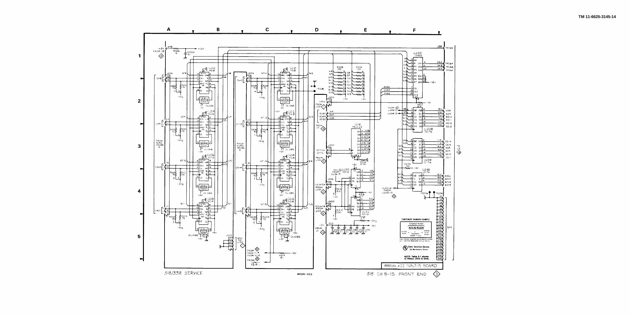
TM 11-6625-3145-14
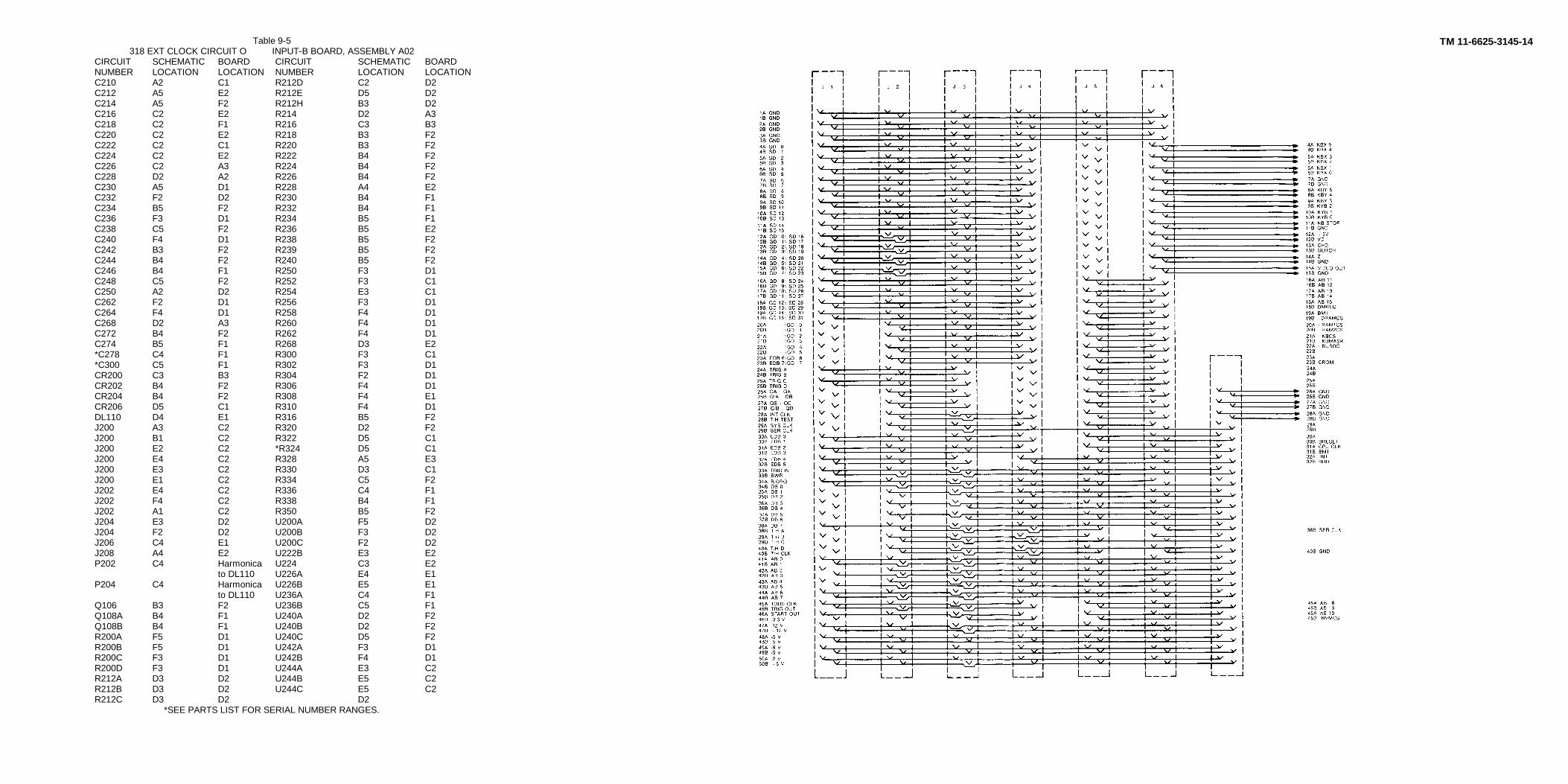
Table 9-5318 EXT CLOCK CIRCUIT O INPUT-B BOARD, ASSEMBLY A02
CIRCUITNUMBER
SCHEMATICLOCATION
BOARDLOCATION
CIRCUITNUMBER
SCHEMATICLOCATION
BOARDLOCATION
C210 A2 C1 R212D C2 D2C212 A5 E2 R212E D5 D2C214 A5 F2 R212H B3 D2C216 C2 E2 R214 D2 A3C218 C2 F1 R216 C3 B3C220 C2 E2 R218 B3 F2C222 C2 C1 R220 B3 F2C224 C2 E2 R222 B4 F2C226 C2 A3 R224 B4 F2C228 D2 A2 R226 B4 F2C230 A5 D1 R228 A4 E2C232 F2 D2 R230 B4 F1C234 B5 F2 R232 B4 F1C236 F3 D1 R234 B5 F1C238 C5 F2 R236 B5 E2C240 F4 D1 R238 B5 F2C242 B3 F2 R239 B5 F2C244 B4 F2 R240 B5 F2C246 B4 F1 R250 F3 D1C248 C5 F2 R252 F3 C1C250 A2 D2 R254 E3 C1C262 F2 D1 R256 F3 D1C264 F4 D1 R258 F4 D1C268 D2 A3 R260 F4 D1C272 B4 F2 R262 F4 D1C274 B5 F1 R268 D3 E2*C278 C4 F1 R300 F3 C1*C300 C5 F1 R302 F3 D1CR200 C3 B3 R304 F2 D1CR202 B4 F2 R306 F4 D1CR204 B4 F2 R308 F4 E1CR206 D5 C1 R310 F4 D1DL110 D4 E1 R316 B5 F2J200 A3 C2 R320 D2 F2J200 B1 C2 R322 D5 C1J200 E2 C2 *R324 D5 C1J200 E4 C2 R328 A5 E3J200 E3 C2 R330 D3 C1J200 E1 C2 R334 C5 F2J202 E4 C2 R336 C4 F1J202 F4 C2 R338 B4 F1J202 A1 C2 R350 B5 F2J204 E3 D2 U200A F5 D2J204 F2 D2 U200B F3 D2J206 C4 E1 U200C F2 D2J208 A4 E2 U222B E3 E2P202 C4 Harmonica U224 C3 E2
to DL110 U226A E4 E1P204 C4 Harmonica U226B E5 E1
to DL110 U236A C4 F1Q106 B3 F2 U236B C5 F1Q108A B4 F1 U240A D2 F2Q108B B4 F1 U240B D2 F2R200A F5 D1 U240C D5 F2R200B F5 D1 U242A F3 D1R200C F3 D1 U242B F4 D1R200D F3 D1 U244A E3 C2R212A D3 D2 U244B E5 C2R212B D3 D2 U244C E5 C2R212C D3 D2 D2
*SEE PARTS LIST FOR SERIAL NUMBER RANGES.
TM 11-6625-3145-14

TM 11-6625-3145-14
Figure 9-3. 318/338 A03 ACQ Control Board Component Locations.

TM 11-6625-3145-14
Table 9-6318/338 ACQUISITION CONTROL BOARD <5> - ASSEMBLY A03
CIRCUIT SCHEMATIC
BOARD CIRCUIT SCHEMATIC BOARD
NUMBER LOCATION LOCATION NUMBER LOCATION LOCATIONJ050 * B3 D2 R110F B1 E1R100A A1 D2 R110G E5 E1R100B A1 D2 R110H C5 E1R100C A1 D2 R160E F2 E1R100D A1 D2 R160H F3 E1R104A E2 E2 TP100 A1 E1R104B E2 E2 TP200 F5 C1R104C E2 E2 U100* * B2 D2R104 E2 E2 U103* * C1 F1R104E E2 E2 U104* * D1 F2R104F E2 E2 U106 C5 F2R104G E2 E2 U108 E5 F2R104H E2 E2 U114A* * F2 E2R106A E3 E2 U114B* * F2 E2R106B E3 E2 U114C* * F3 E2R106C E3 E2 U116A F2 E2R106D E3 E2 U116B F2 E2R106E E3 E2 U116C F3 E2R106F E3 E2 U118A F4 E2R106G E3 E2 U118B F4 E2R106H E3 E2
* 318 only* * 318 only
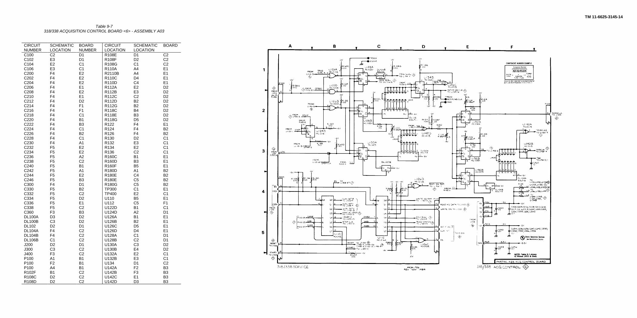
TM 11-6625-3145-14
Table 9-7318/338 ACQUISITION CONTROL BOARD <6> - ASSEMBLY A03
CIRCUIT SCHEMATIC BOARD CIRCUIT SCHEMATIC BOARDNUMBER LOCATION NUMBER LOCATION LOCATIONC100 C2 D1 R108E D1 C2C102 E3 D1 R108F D2 C2C104 E2 C1 R108G C1 C2C106 E3 C1 R110A A4 E1C200 F4 E2 R2110B A4 E1C202 F4 E2 R110C D4 E1C204 F4 E2 R110D C4 E1C206 F4 E1 R112A E2 D2C208 F4 E2 R112B E3 D2C210 F4 E1 R112C C2 D2C212 F4 D2 R112D B2 D2C214 F4 F1 R112G B2 D2C216 F4 F1 R118C B4 D2C218 F4 C1 R118E B3 D2C220 F4 B1 R118G D5 D2C222 F4 B3 R122 F4 E1C224 F4 C1 R124 F4 B2C226 F4 B2 R126 F4 B2C228 F4 C1 R130 D2 C1C230 F4 A1 R132 E3 C1C232 F5 E2 R134 E2 C1C234 F5 E2 R136 C2 C1C236 F5 A2 R160C B1 E1C238 F5 C2 R160D B3 E1C240 F5 B1 R160F B5 E1C242 F5 A1 R180D A1 B2C244 F5 E2 R180E C4 B2C246 F5 B3 R180E C5 B2C300 F4 D1 R180G C5 B2C330 F5 B2 TP300 C1 E1C332 F5 C2 TP400 E2 C1C334 F5 D2 U110 B5 E1C336 F5 E1 U112 C5 F1C338 F5 C2 U122D B1 C1C360 F3 B3 U124D A2 D1DL100A D3 D2 U126A B1 E1DL100B C3 D2 U126B B2 E1DL102 D2 D1 U126C D5 E1DL104A F4 C2 U126D D4 E1DL104B F4 C2 U128A C1 D1DL106B C1 C2 U128B C2 D1J200 D2 D1 U130A C3 D2J300 C3 C2 U130B E4 D2J400 F3 C2 U132A E2 C1P100 A1 B1 U132B E3 C1P100 F2 B1 U134 D1 C2P100 A4 B1 U142A F2 B3R102F B1 C2 U142B F3 B3R108C D2 C2 U142C E1 B3R108D D2 C2 U142D D3 B3

TM 11-6625-3145-14
Table 9-8318/338 ACQUISITION CONTROL BOARD <7> - ASSEMBLY A03
CIRCUIT SCHEMATIC BOARD CIRCUIT SCHEMATIC BOARDNUMBER LOCATION LOCATION NUMBER LOCATION LOCATIONDL106A B1 C2 R150B A4 A2P100 A4 B1 R150C A4 A2P100 F1 B1 R152A A4 E2P100 A5 B1 R`52B A4 E2P100 F4 B1 R152C A4 E2P100 A2 B1 R152D A4 E2R100E B3 D2 R154A A5 E2R100F B3 D2 R154B A5 E2R100G B3 D2 R154C A5 E2R102A B2 C2 R154D A5 E2R102B B2 C2 R180A F1 B2R102C A2 C2 R180B F3 B2R102D B2 C2 R180C C4 B2R102E B2 C2 TP500 D4 A1R102G B2 C2 U118C D1 E2R102H B1 C2 U122A B2 C1R108A F3 C2 U122B B2 C1R108B F4 C2 U122C F2 C1R108H F2 C2 U134A C5 C2R110F D2 E1 U136A C4 B1R112E E1 D2 U136B C4 B1R112F B2 D2 U138A C3 B1R114A D4 A2 U138B C3 B1R114B D4 A2 U140 C3 A2R114C D4 A2 U144 D2 B2R114D D4 A2 U146 E2 C1R116A C2 A2 U148A F2 B2R116B C2 A2 U148B F3 B2R116C C2 A2 U150A F3 B3R116D C2 A2 U150B F4 B3R116E C2 A2 U152A E4 B3R116F F5 A2 U152B E4 B3R116H C2 A2 U154A F3 A2R118A D1 D2 U154B C3 A2R118D E1 D2 U154C C3 A2R120A F4 B2 U154D E2 A2R120B F3 B2 U156A F2 B2R120C C5 B2 U156B F3 B2R120D F3 B2 U156C F3 B2R120E E4 B2 U156D F3 B2R120F E2 B2 U158 D5 A2R120G E2 B2 W100 * F3 D2R120H E4 B2 W102 * F3 D2R150A A4 A2
* 318 only

TM 11-6625-3145-14

TM 11-6625-3145-14
Table 9-9318/338 ACQUISITION MEMORY BOARD <8> - ASSEMBLY A04
CIRCUIT SCHEMATIC BOARD CIRCUIT SCHEMATIC BOARDNUMBER LOCATION LOCATION NUMBER LOCATION LOCATION
J100 F4 E1 R134 B4 E2J100 A4 E1 TP110 D4 D1R100 B2 D1 TP111 E4 A1R102 B2 D1 TP200 E3 F1R104 B3 C1 U114 E4 E2R106 B3 B1 U116 B2 D1R108 * B4 A1 U118 B3 D1R118C E5 E2 U120 C2 D1R118D E4 E2 U122 C3 C1R118E E4 E2 U124 D2 C1R118F E4 E2 U126 D3 C1R118G E4 E2 U128 E2 B1R118H E4 E2 U130 E3 B1R127 F2 A1 U132 * F2 B1R128 B4 E2 U134 * F3 A1R129 B4 E2 U136 B4 E1R130 C4 A1 U138 B5 E1R131 B5 E2 U139A B5 E1R132 B5 E2 W118 * E5 F2R133 C5 E2
* 338 only

TM 11-6625-3145-14
Table 9-10318/338 ACQUISITION MEMORY BOARD <9> - ASSEMBLY A04
CIRCUIT SCHEMATIC BOARD CIRCUIT SCHEMATIC BOARDNUMBER LOCATION LOCATION NUMBER LOCATION LOCATIONC100 A1 E3 R122 B1 E3C101 A1 E3 R124 B1 E3C102 F1 C2 R125 B1 F2C104 F1 B2 R126 B1 E3C106 F1 D2 R136 D2 F2C108 F1 A2 R138 E3 F2C109 F2 A2 R139 D3 F2C110 F2 C1 R140 D3 F2C112 F2 F2 R144A E2 D2C114 F2 A2 R144B E2 D2C116 F2 E3 R144C E2 D2C118 F2 E3 R144D E2 D2C120 F1 B2 R144E E3 D2C122 F1 E3 R144F E3 D2C124 F1 F2 R144G E3 D2C126 F1 D2 R144H E3 D2C128 F1 A2 R146 E4 A2C132 F1 B2 TP200 F4 F1C134 F1 A2 U100 A2 C2J100 C2 E1 U102 A3 C2J100 D3 E1 U104 A4 B1J100 D4 E1 U106 A4 B1J100 C3 E1 U108 A5 B1L100 A1 E2 U110 B5 A2R110 A2 C2 U112A B1 E2R112A B5 B2 U112B B1 E2R112B B5 B2 U112C B2 E2R112C B5 B2 U112D F4 E2R112D B5 B2 U139B E5 E1R112E B4 B2 U140 D4 F3R112F B4 B2 U142 E2 F2R112G B4 B2 U144 E3 F2R122H B4 B2 U146 F2 D2R113 B5 E3 U148 F4 D2R114 B3 D2 U150 F4 C2R116 B2 E3 U152 F2 C2R118A B2 E2 U156 F5 E3R118B B2 E2 Y100 B1 E2R120 A1 E3
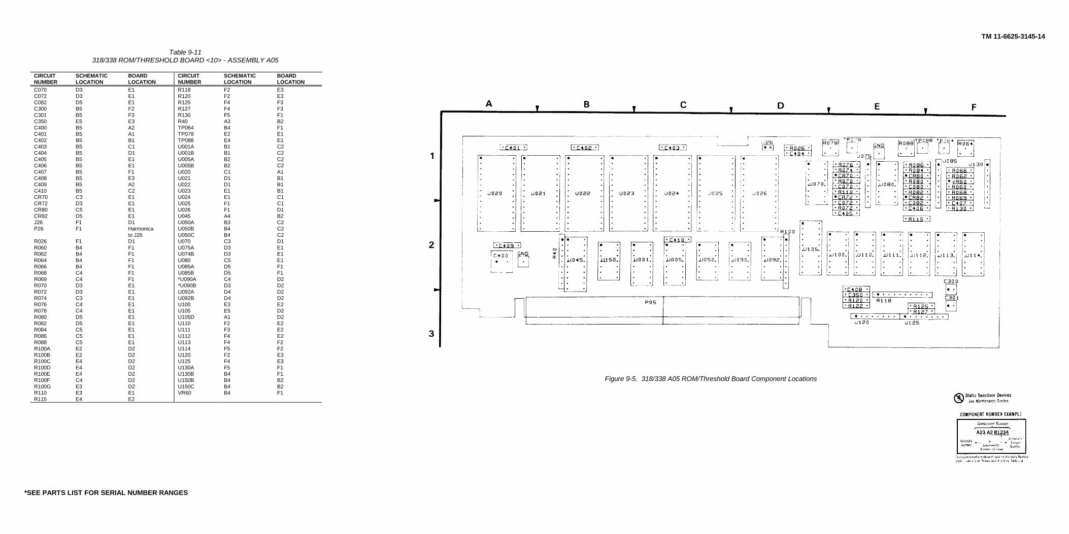
TM 11-6625-3145-14
Table 9-11318/338 ROM/THRESHOLD BOARD <10> - ASSEMBLY A05
CIRCUITNUMBER
SCHEMATICLOCATION
BOARDLOCATION
CIRCUITNUMBER
SCHEMATICLOCATION
BOARDLOCATION
C070 D3 E1 R118 F2 E3C072 D3 E1 R120 F2 E3C082 D5 E1 R125 F4 F3C300 B5 F2 R127 F4 F3C301 B5 F3 R130 F5 F1C350 E5 E3 R40 A3 B2C400 B5 A2 TP064 B4 F1C401 B5 A1 TP078 E2 E1C402 B5 B1 TP088 E4 E1C403 B5 C1 U001A B1 C2C404 B5 D1 U001B B1 C2C405 B5 E1 U005A B2 C2C406 B5 E1 U005B B2 C2C407 B5 F1 U020 C1 A1C408 B5 E3 U021 D1 B1C409 B5 A2 U022 D1 B1C410 B5 C2 U023 E1 B1CR70 C3 E1 U024 E1 C1CR72 D3 E1 U025 F1 C1CR80 C5 E1 U026 F1 D1CR82 D5 E1 U045 A4 B2J26 F1 D1 U050A B3 C2P26 F1 Harmonica U050B B4 C2
to J26 U050C B4 C2R026 F1 D1 U070 C3 D1R060 B4 F1 U075A D3 E1R062 B4 F1 U074B D3 E1R064 B4 F1 U080 C5 E1R066 B4 F1 U085A D5 F1R068 C4 F1 U085B D5 F1R069 C4 F1 *U090A C4 D2R070 D3 E1 *U090B D3 D2R072 D3 E1 U092A D4 D2R074 C3 E1 U092B D4 D2R076 C4 E1 U100 E3 E2R078 C4 E1 U105 E5 D2R080 D5 E1 U105D A1 D2R082 D5 E1 U110 F2 E2R084 C5 E1 U111 F3 E2R086 C5 E1 U112 F4 E2R088 C5 E1 U113 F4 F2R100A E2 D2 U114 F5 F2R100B E2 D2 U120 F2 E3R100C E4 D2 U125 F4 E3R100D E4 D2 U130A F5 F1R100E E4 D2 U130B B4 F1R100F C4 D2 U150B B4 B2R100G E3 D2 U150C B4 B2R110 E3 E1 VR60 B4 F1R115 E4 E2
Figure 9-5. 318/338 A05 ROM/Threshold Board Component Locations
*SEE PARTS LIST FOR SERIAL NUMBER RANGES
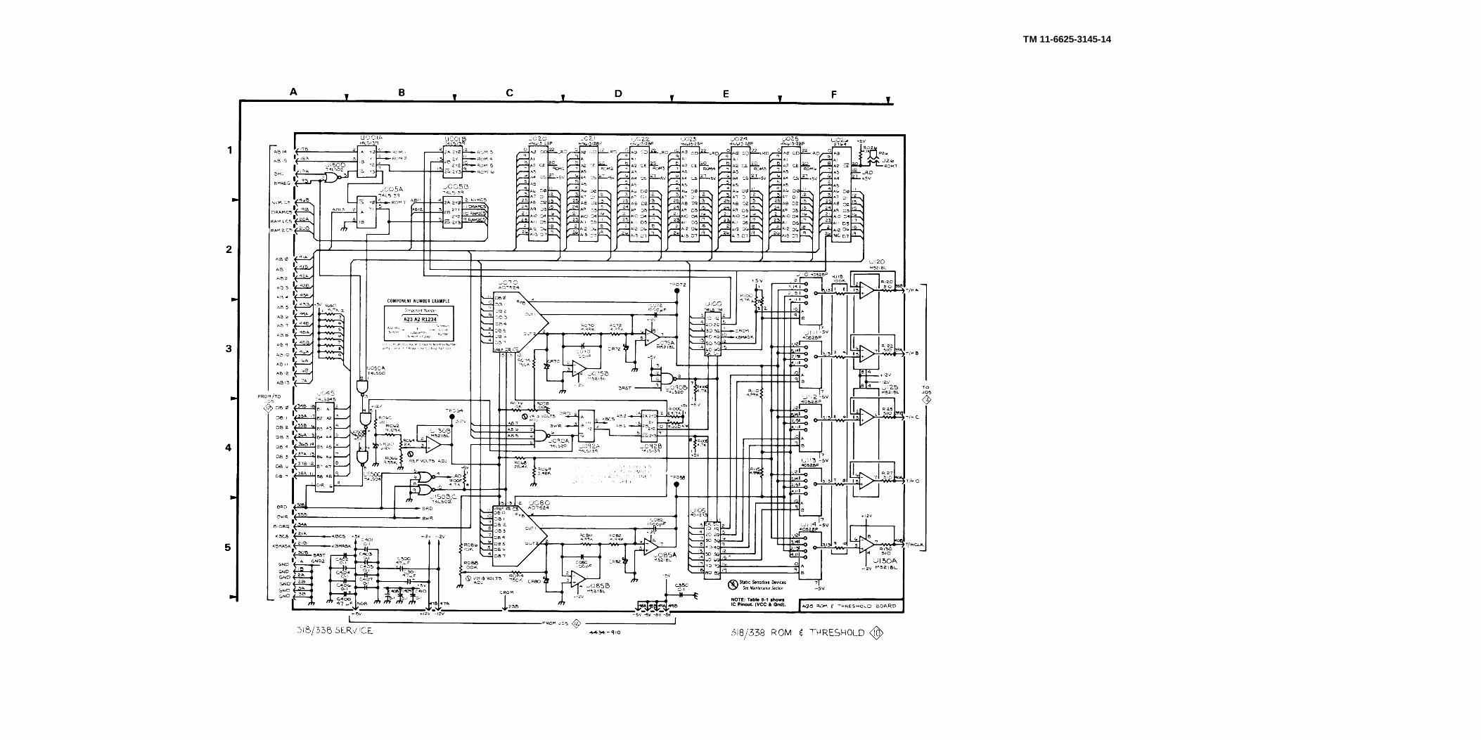
TM 11-6625-3145-14

Table 9-12318/338 MUP/DISPLAY <11> - ASSEMBLY A06
CIRCUITNUMBER
SCHEMATICLOCATION
BOARDLOCATION
CIRCUITNUMBER
SCHEMATICLOCATION
BOARD LOCATION
C100 A1 A1 R548 F3 D1C106 A2 A1 R550 F3 D1C110 A2 A2 R555 F3 D2C116 A2 A2 R700 E3 A3C132 C2 A2 TP100 B1 A1C202 A5 E1 TP110 B2 B2C220 C4 D2 U100A A1 B1C320 D4 D1 U100B B1 B1C600 F3 D1 U100C B1 B1C601 F3 A1 U100D A2 B1C602 F3 A2 U100E B2 B1C603 F3 B3 U100F B2 B1C604 F3 D1 U110A B2 B2C605 F32 E1 U110B B2 B2C606 E3 F1 U120A B1 B2C607 F3 F3 U120B B1 B2C608 F3 B1 U120C B2 B2C609 F3 C1 U130 C1 A3C610 E3 C1 U134A C2 A3C700 F3 D1 U134D C2 A3C701 F3 D1 U134E F1 A3CR200 B5 E1 U134F C1 A3DS700 E3 A3 U138 C1 B3J202 A5 E1 U200 B3 E1P202 A5 Harmonica U210 A3 F2
to J202 U212 A4 D2Q550 F2 D1 U214 B5 E2R100 A1 A1 U216 F4 F2R101 B1 A1 U220 B4 D2R102 A1 A1 U230 F5 E2R103 B1 A1 U300 E4 C2R110 A2 A2 U310 D4 C2R111 B2 A2 U320 D4 D2R112 A2 A2 U400 B3 F1R113 B2 A2 U401 C3 F1R120 B2 A2 U500 F1 B2R130 C2 A2 U505A D2 C1R132 C2 A2 U505B E2 C1R200 A5 E1 U505C F2 C1R203 A5 E1 U505D E2 C1R215 A3 E2 U510 D2 B1R216 A3 E2 U515 D3 B1R220 C5 D2 U520 E2 B1R221 C4 D2 U525 D3 C1R222 C5 D2 U530 E2 C2R224 D5 D2 U540A F1 B3R226 C5 D2 U540B F2 B3R300 E5 D2 U540C F2 B3R302 E5 D2 U540D F2 B3R306 F5 D2 U540E F2 B3R310 D5 C2 U540F F2 B3R312 D5 C2 U542A F2 C1R316 E5 C2 U542B F2 C1R320 D4 D1 U542C A5 C1R322 C4 D1 U542D D1 C1R540 F2 B3 U542E A4 C1R542 F2 B3 U542F D2 C1R544 F2 B3 W500 E2 C1R545 F3 B3 Y105 B2 A1R546 F2 D1 Y115 B2 A2
TM 11-6625-3145-14
Figure 9-6. 318/338 A06 MPU/Display Board Component Locations.

TM 11-6625-3145-14

TM 11-6625-3145-14

TM 11-6625-3145-14

TM 11-6625-3145-14

TM 11-6625-3145-14
Figure 9-8. 318/338 A10 CRT Board Component Locations.

Table 9-13318/338 CRT BOARD<14> ASSEMBLY A10
CIRCUITNUMBER
SCHEMATICLOCATION
BOARDLOCATION
CIRCUITNUMBER
SCHEMATICLOCATION
BOARDLOCATION
C001 B2 D2 Q120 B4 C1C005 B2 D1 0200 B5 C1C010 C2 D2 Q220 85 B1C015 D2 D2 R001 B2 D2C020 C2 E2 R002 B2 D2C030 D1 D2 R005 B1 D2C035 D2 D1 R010 C2 D2C040 D2 E2 R015 C2 D2C050 D1 E2 R030 D2 02C103 B1 D1 R031 D2 D2C120 B4 C2 R035 D1 D2C200 B5 C1 R100 B4 C2C210 B5 B1 R105 B4 C2C230 C5 B1 R110 B4 C1C235 C4 C1 R112 B3 C2C240 D4 B1 R116 B3 D2C245 D4 B2 R120 B4 C2C250 D5 B2 R122 B4 C1C270 B3 E1 R124 B4 C1C275 B3 E1 R130 C4 C1C280 B3 E1 R135 C4 D1C285 B3 E1 R140 D3 C2C290 C4 C1 R200 B5 C2CR220 B5 B1 R202 B5 C2CR230 C5 A2 R210 B5 C2CR240 D4 B2 R240 D4 B2CR250 D5 B2 R245 D4 C2J001 A2 C2 R247 E4 B2J040 D1 C2 R250 D5 B2J100 D3 B2 *R253 E5 B2L116 B4 C2 R255 E5 B2L140 C4 B1 R280 B3 E1L150 E3 Off Board T230 C4 B1P001 A2 Off Board TP140 C3 D2P040 D1 Off Board TP145 D3 D2P100 D3 Off Board U001 C1 E2Q100 B4 C1 U280 B3 E1Q110 B4 C1 V200 F3 Off Board
*SEE PARTS LIST FOR SERIAL NUMBER RANGES.
TM 11-6625-3145-14

TM 11-6625-3145-14
Figure 9-9. 318/338 A11 Inverter Board component Locations.

TM 11-6625-3145-14
Table 9-14318/338 INVERTER BOARD <15> - ASSEMBLY A11
CIRCUIT SCHEMATIC BOARD CIRCUIT SCHEMATIC BOARDNUMBER LOCATION LOCATION NUMBER LOCATION LOCATIONC102 A3 A2 J8 F3 B3C105 C2 C1 J8 F1 B3C106 C2 A1 J8 F4 B3C121 C2 C1 L101 C2 A1C122 C2 B1 L102 A4 A3C123 D2 D1 L103 A4 A2C124 D2 D1 Q131 B3 D2C132 B4 D2 0134 C3 D3C143 D5 C3 Q135 C5 D3C147 D4 D2 0139 D4 D3C150 F1 B3 0140 C3 E3C151 F3 C2 0141 D5 D3C152 F3 C3 0149 D2 E2C153 F3 C2 R121 C2 C1C154 F4 C2 R122 C2 B2C155 F4 C2 R124 E2 D1C156 F4 C3 R131 C2 D2CR101 A2 A1 R132 B3 D2CR123 E2 D1 R134 C3 D3CR125 E2 D1 R135 C4 D3CR135 C4 D3 R137 C3 D3CR136 C4 D3 R138 C5 D3CR137 C4 D3 R139 D4 D3CR138 C5 D3 R140 D4 D3CR142 D5 D3 R141 D5 D3CR145 D3 D2 R142 D5 D3CR146 D3 E2 R143 D5 D3CR147 E5 D3 R145 D3 D2CR148 D3 E2 R147 D4 D2CR149 D2 D2 R149 D3 E2CR151 F2 C2 R151 F2 C2CR152 F3 B3 R152 F3 C3CR153 F3 B3 R154 F4 C3CR154 F4 C3 RT101 A1 A1CR155 F4 C2 RT102 A2 A1CR156 F5 C3 S1 A4 Part of A12E123 D2 C1 T101 A3 A2E124 D2 D1 T102 A3 A2F1 A5 Off Board T120 E1 C1J1 A4 A3 T140 E5 D2J10 F2 B3 VR101 A2 B2J10 F3 B3 VR102 A2 B2J2 A4 Part of A12 VR131 B3 D3J3 A4 Part of A12 VR135 C4 D3J4 B1 B2 VR138 C4 D3J5 B1 B1 VR149 D3 E2
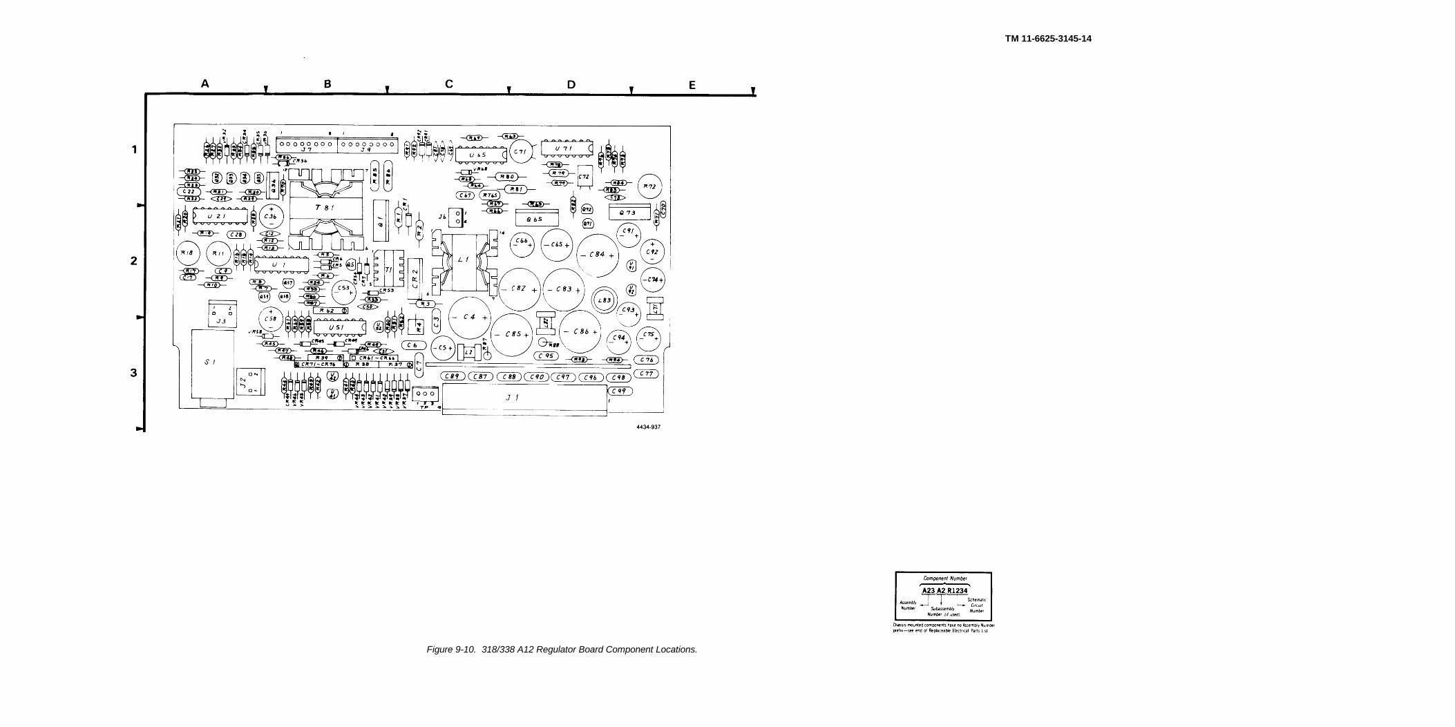
TM 11-6625-3145-14
Figure 9-10. 318/338 A12 Regulator Board Component Locations.
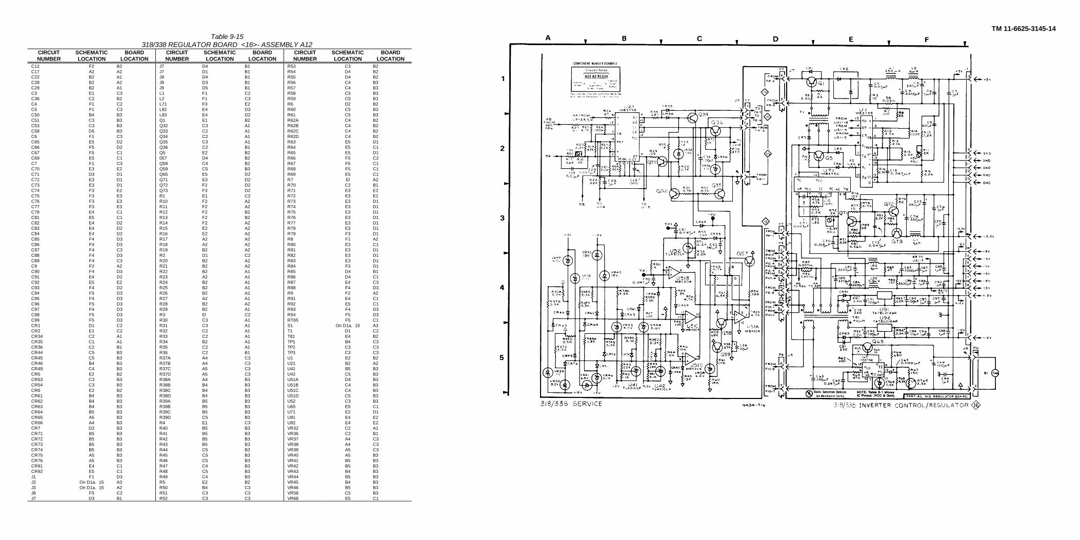
TM 11-6625-3145-14Table 9-15
318/338 REGULATOR BOARD <16>- ASSEMBLY A12CIRCUIT SCHEMATIC BOARD CIRCUIT SCHEMATIC BOARD CIRCUIT SCHEMATIC BOARDNUMBER LOCATION LOCATION NUMBER LOCATION LOCATION NUMBER LOCATION LOCATION
C12 F2 B2 J7 D4 B1 R53 C3 B2C17 A2 A2 J7 D1 B1 R54 D4 B2C22 B2 A1 J9 D4 B1 R55 D4 B2C28 B2 A2 J9 D3 B1 R56 C4 B3C29 B2 A1 J9 D5 B1 R57 C4 B3C3 E1 C3 L1 F1 C2 R58 C5 B3C36 C2 B2 L2 F1 C3 R59 C5 B3C4 F1 C2 L71 F3 E2 R6 D2 B2C5 F1 C3 L82 E4 D3 R60 C5 B3C50 B4 B3 L83 E4 D2 R61 C5 B3C51 C3 B3 Q1 E1 B2 R62A C4 B2C53 C3 B3 Q32 C3 A1 R62B C4 B2C58 D5 B3 Q33 C2 A1 R62C C4 B2C6 F1 C3 Q34 C2 A1 R62D C4 B2C65 E5 D2 Q35 C3 A1 R63 E5 D1C66 F5 D2 Q36 C2 B1 R64 E5 C1C67 F5 C1 Q5 E2 B2 R65 E5 D1C69 E5 C1 057 D4 B2 R66 F5 C2C7 F1 C3 Q58 C4 B2 R67 F5 C1C70 E3 E2 Q59 C5 B3 R68 F5 C1C71 D3 D1 Q65 E5 D2 R69 E5 C1C72 E3 D1 Q71 E3 D2 R7 El A2C73 E3 D1 Q72 F2 D2 R70 C2 B1C74 F3 E2 Q73 F3 D2 R71 E3 E2C75 F3 E3 R1 E1 C2 R72 E3 E1C76 F3 E3 R10 F2 A2 R73 E3 D1C77 F3 E3 R11 F2 A2 R74 E3 D1C78 E4 C1 R12 F2 B2 R75 E3 D1C81 E5 C1 R13 F2 B2 R76 E3 D1C82 E4 D2 R14 F2 A2 R77 E3 D1C83 E4 D2 R15 E2 A2 R78 E3 D1C84 E4 D2 R16 E2 A2 R79 F3 D1C85 F4 D3 R17 A2 A2 R8 F1 A2C86 F4 D3 R18 A2 A2 R80 E3 C1C87 F4 C3 R19 B2 A2 R81 E3 D1C88 F4 D3 R2 D1 C2 R82 E3 D1C89 F4 C3 R20 B2 A2 R83 E3 D1C9 F2 A2 R21 B2 A2 R84 F3 D1C90 F4 D3 R22 B2 A1 R85 D4 B1C91 E4 D2 R23 A2 A1 R86 D4 C1C92 E5 E2 R24 B2 A1 R87 E4 C3C93 F4 D2 R25 B2 A1 R88 F4 D3C94 F5 D3 R26 B2 A1 R9 F2 A2C95 F4 D3 R27 A2 A1 R91 E4 C1C96 F5 D3 R28 B2 A2 R92 E5 C1C97 F4 D3 R29 B2 A1 R93 F4 D3C98 F5 D3 R3 El C2 R94 F5 D3C99 F5 D3 R30 C3 A1 RT65 F5 C1CR1 D1 C2 R31 C3 A1 S1 On D1a. 15 A3CR2 E1 C2 R32 C2 A1 T1 D1 C2CR34 C2 A1 R33 C2 A1 T81 E4 B2CR35 C1 A1 R34 B2 A1 TP1 B4 C3CR36 C2 B1 R35 C2 A1 TP2 C3 C3CR44 C5 B3 R36 C2 B1 TP3 C3 C3CR45 C5 B3 R37A A4 C3 U1 E2 B2CR46 B4 B3 R37B A4 C3 U21 B2 A2CR49 C4 B3 R37C A5 C3 U41 B5 B3CR5 E2 B2 R37D A5 C3 U42 C5 B3CR53 C3 B3 R38A A4 B3 U51A D4 B3CR54 C3 B3 R38B B4 B3 U51B C4 B3CR6 E2 B2 R38C B4 B3 U51C C4 B3CR61 B4 B3 R38D B4 B3 U51D C5 B3CR62 B4 B3 R39A B5 B3 U52 C3 B3CR63 B4 B3 R39B B5 B3 U65 E5 C1CR64 B5 B3 R39C B5 B3 U71 E2 D1CR65 A5 B3 R39D C5 B3 U91 E4 E2CR66 A4 B3 R4 E1 C3 U92 E4 E2CR7 D2 B3 R40 B5 B3 VR32 C2 A1CR71 B5 B3 R41 B5 B3 VR36 C2 B1CR72 B5 B3 R42 B5 B3 VR37 A4 C3CR73 B5 B3 R43 B5 B3 VR38 A4 C3CR74 B5 B3 R44 C5 B3 VR39 A5 C3CR75 A5 B3 R45 C5 B3 VR40 A5 B3CR76 A5 B3 R46 C5 B3 VR41 B5 B3CR91 E4 C1 R47 C4 B3 VR42 B5 B3CR92 E5 C1 R48 C5 B3 VR43 B4 B3J1 F1 D3 R49 C4 B3 VR44 B5 B3J2 On D1a. 15 A3 R5 E2 B2 VR45 B4 B3J3 On D1a. 15 A2 R50 B4 C3 VR46 B5 B3J6 F5 C2 R51 C3 C3 VR58 C5 B3J7 D3 B1 R52 C3 C3 VR68 E5 C1
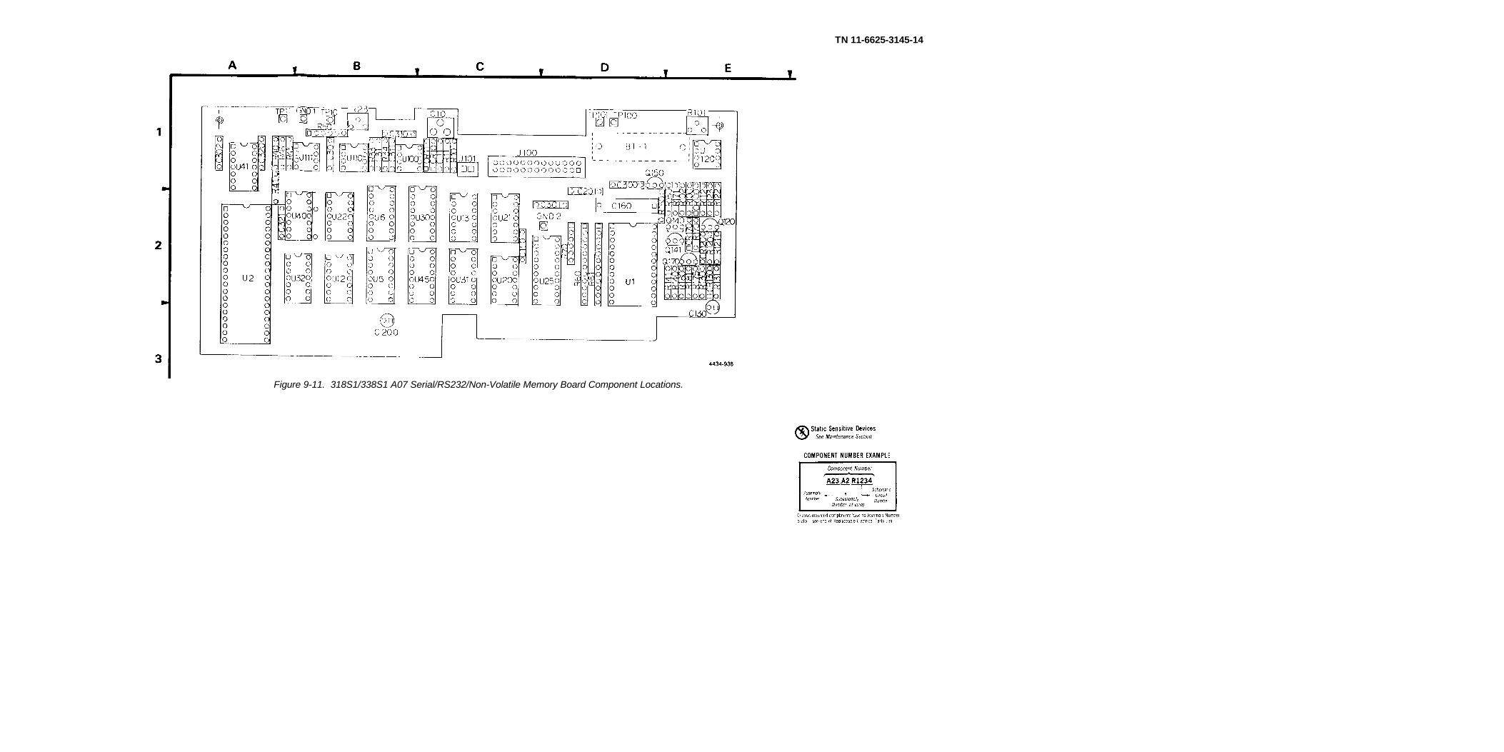
TN 11-6625-3145-14
Figure 9-11. 318S1/338S1 A07 Serial/RS232/Non-Volatile Memory Board Component Locations.

TM 11-6625-3145-14
Table 9-16318S1/338S1 OPTION SERIAL <17> SERIAL/RS232/NON-VOLATILE MEMORY BD.
ASSEMBLY A07CIRCUIT SCHEMATIC BOARD CIRCUIT SCHEMATIC BOARDNUMBER LOCATION LOCATION NUMBER LOCATION LOCATION
BT1 D2 D1 R141 C1 E2C10 A5 C1 R150 C2 D2C11 B4 C1 *R151 C2 E2C130 C2 E2 R161 C1 E2C150 A2 C2 R170 D1 E2C160 D1 D2 R171 D2 E2C200 F4 B3 R175 D2 E2C201 F4 D1 R180 E1 E2C30 B5 B1 R181 E1 E2C300 F4 D1 R23 B5 B1C301 F4 D2 R30 B5 B1C302 F4 A1 R33 B5 B1C31 B5 B1 R34 B5 B1C310 F4 B1 R40 D4 A1C311 F4 B1 R41 D4 A1C320 E2 A1 R45 D5 A1C321 E2 A2 R46 D5 A1CR10 B4 C1 R50A E2 B1CR11 B5 C1 R50E D5 B1CR120 C1 E2 R60 C3 D2CR130 C2 E2 R61 C4 D2CR170 D1 E2 R70A B4 D2J101 A4 C1 R70B B4 D2J200 A4 BNC to side R70C B3 D2
panel R70C B4 D2Q120 B1 E2 R70E B3 D2Q140 C1 E2 TP10 C5 B1Q141 C1 E2 TP100 B1 D1Q150 C2 D1 TP101 C1 D1Q170 D1 E2 TP11 C5 A1R10 B5 C1 TP200 F4 B1R100 A1 E2 TP201 F4 D2R101 A1 E1 U1 C3 D2R102 A1 E2 U100 B5 B1R11 B4 C1 U110 C5 B1R112 B2 E2 U111 E2 B1R120 B2 E2 U120 B1 E1R121 B2 E2 U20D B2 C2R122 B1 E2 U21C C2 C2R123 B1 E2 U32B E2 B2R130 C1 E2 VR100 B2 E2R131 C2 E2 W101 A4 Off BoardR140 C1 E2
*SEE PARTS LIST FOR SERIAL NUMBER RANGES.
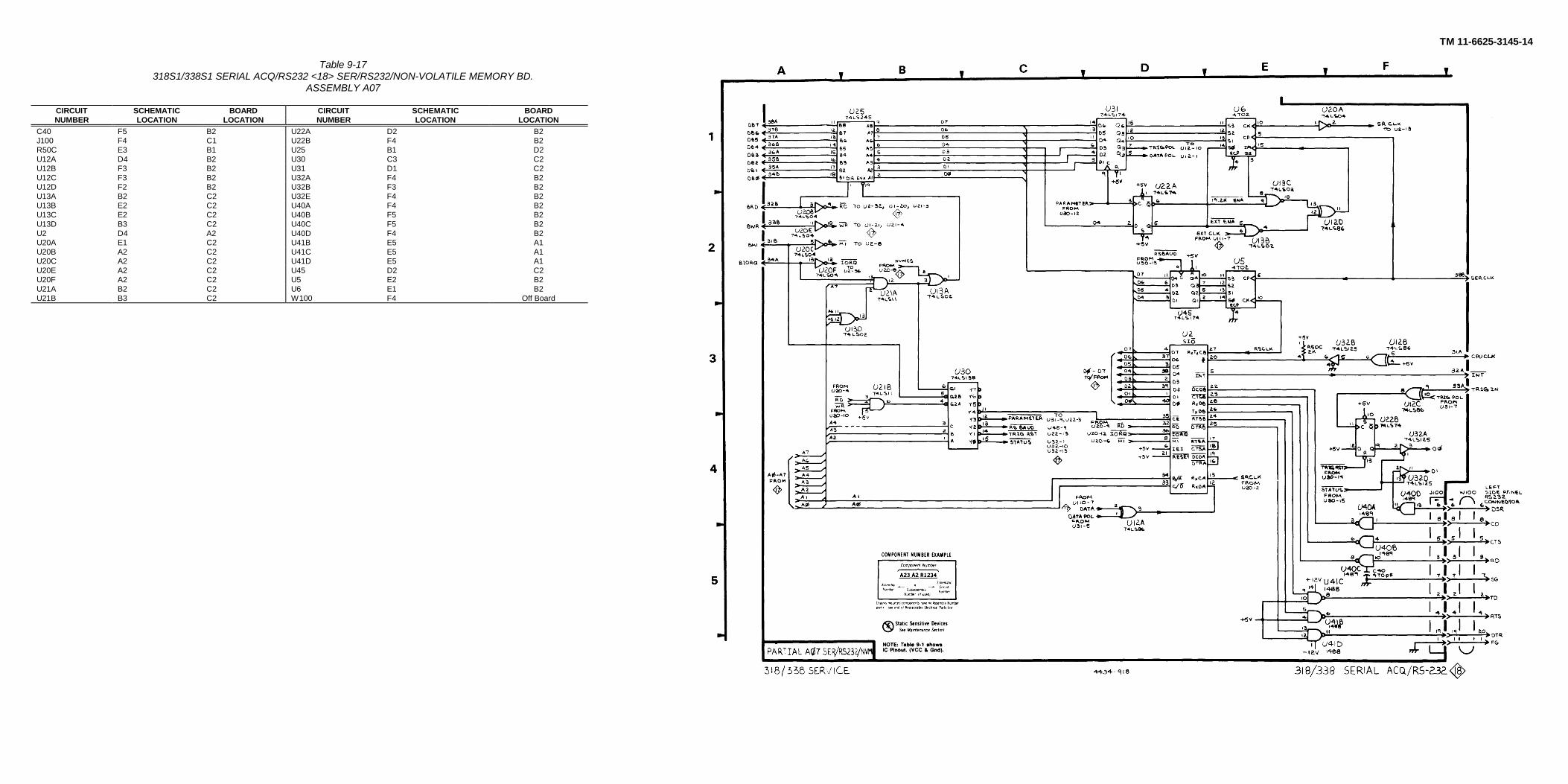
TM 11-6625-3145-14
Table 9-17318S1/338S1 SERIAL ACQ/RS232 <18> SER/RS232/NON-VOLATILE MEMORY BD.
ASSEMBLY A07
CIRCUIT SCHEMATIC BOARD CIRCUIT SCHEMATIC BOARDNUMBER LOCATION LOCATION NUMBER LOCATION LOCATION
C40 F5 B2 U22A D2 B2J100 F4 C1 U22B F4 B2R50C E3 B1 U25 B1 D2U12A D4 B2 U30 C3 C2U12B F3 B2 U31 D1 C2U12C F3 B2 U32A F4 B2U12D F2 B2 U32B F3 B2U13A B2 C2 U32E F4 B2U13B E2 C2 U40A F4 B2U13C E2 C2 U40B F5 B2U13D B3 C2 U40C F5 B2U2 D4 A2 U40D F4 B2U20A E1 C2 U41B E5 A1U20B A2 C2 U41C E5 A1U20C A2 C2 U41D E5 A1U20E A2 C2 U45 D2 C2U20F A2 C2 U5 E2 B2U21A B2 C2 U6 E1 B2U21B B3 C2 W100 F4 Off Board

TM 11-6625-3145-14
Figure 9-12. 338 A01 Input-A Board Component Locations.
`
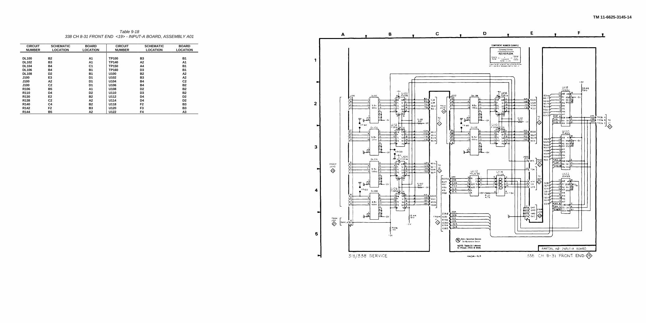
TM 11-6625-3145-14
Table 9-18338 CH 8-31 FRONT END <19> - INPUT-A BOARD, ASSEMBLY A01
CIRCUIT SCHEMATIC BOARD CIRCUIT SCHEMATIC BOARDNUMBER LOCATION LOCATION NUMBER LOCATION LOCATION
DL100 B2 A1 TP100 B3 B1DL102 B3 A1 TP140 A2 A1DL104 B4 C1 TP150 A4 B1DL106 B4 B1 TP160 D3 B1DL108 D2 B1 U100 B2 A2J100 E3 D1 U102 B3 A2J100 A2 D1 U104 B4 C2J100 C2 D1 U106 B4 B2R106 B5 A1 U108 D2 B2R110 D4 D2 U110 D3 B2R130 E2 B2 U112 D4 D2R138 C2 A2 U114 D4 D2R140 C4 B2 U118 F2 B3R142 F2 B3 U120 F3 B3R144 B5 A2 U122 F4 A3

TM 11-6625-3145-14
318/338 SERVICE

PIN: 058584