TM 11-6625-2884-30 NAVAIR 16-35TS3615-2 · TM 11-6625-2884-30/NAVAIR 16-35TS3615-2 HOW TO USE THIS...
261
NAVAIR 16-35TS3615-2 TM 11-6625-2884-30
Transcript of TM 11-6625-2884-30 NAVAIR 16-35TS3615-2 · TM 11-6625-2884-30/NAVAIR 16-35TS3615-2 HOW TO USE THIS...

NAVAIR 16-35TS3615-2
TM 11-6625-2884-30

WARNING
WARNING
WARNING
A
TM 11-6625-2884-30 NAVAIR 16-35TS3615-2
Do not be misled by the term “low voltage”.Potentials as low as 50 volts may cause deathunder adverse conditions. For Artificial Res-piration refer to FM21-ll.
WARNING
TM 11-6625-2884-30/NAVAIR 16-35TS3615-2
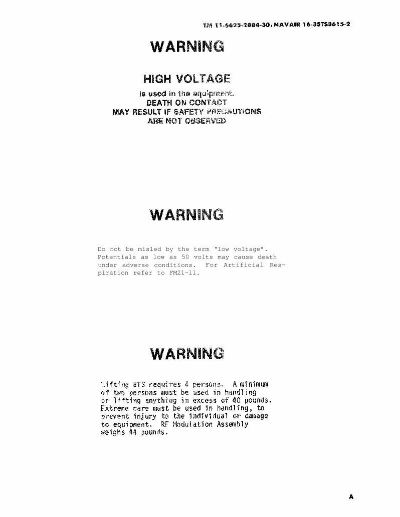
Never work on electronic equipment unless there is another person nearby who isfamiliar with the operation and hazards of the equipment and who is competentin administering first aid. When the technician is aided by operators, he mustwarn them about dangerous areas.
Whenever possible, the power supply to the equipment must be shut off beforebeginning work on the equipment. Take particular care to ground every capacitorlikely to hold a dangerous potential. When working inside the equipment, afterthe power has been turned off, always ground every part before touching it.
Be careful not to contact high-voltage connections or 115 volts ac inputconnections when installing or operating this equipment.
Whenever the nature of the operation permits, keep one hand away fromequipment to reduce the hazard of current flowing through the body.
Do not be misled by the term “low voltage.” Potentials as low as 50 volts maycause death under adverse conditions.
For Artificial Respiration, refer to FM 21-11.
B

TM 11-6625-2884-30 NAVAIR 16-35TS3615-2
FIRST AID
SAFETY STEPS TO FOLLOW IF SOMEONE ISTHE VICTIM OF ELECTRICAL SHOCK
DO NOT TRY TO PULL OR GRAB THEINDIVIDUAL
IF POSSIBLE, TURN OFF THE ELECTRICALPOWER
IF YOU CANNOT TURN OFF THE ELECTRICALPOWER, PULL, PUSH, OR LIFT THE PERSONTO SAFETY USING A WOODEN POLE OR AROPE OR SOME OTHER INSULATING MATERIAL
SEND FOR HELP AS SOON AS POSSIBLE
AFTER THE INJURED PERSON IS FREE OFCONTACT WITH THE SOURCE OF ELECTRICALSHOCK, MOVE THE PERSON A SHORTDISTANCE AWAY AND IMMEDIATELY STARTARTIFICIAL RESUSCITATION
C/(D blank)

TM 11-6625-2884-30NAVAIR 16-35TS3615-2
DEPARTMENTS OF THE ARMY AND THE NAVYWashington, DC, 23 February 1984
AVIATION INTERMEDIATE
MAINTENANCE MANUAL
T E S T S E T , C O U N T E R M E A S U R E S S E TT S - 3 6 1 5 / A L Q - 1 3 6 ( V )
( N S N 6 6 2 5 - 0 1 - 1 2 1 - 8 9 8 4 )
REPORTING OF ERRORS AND RECOMMENDING IMPROVEMENTS
You can help improve this manual. If you find any mistakes or if you knowof a way to improve the procedures, please let us know. Mail your 1etter,DA Form 2028 (Recommanded Changes to Publications and Blank Forms), or DAForm 2028-2 located in the back of this manual direct to: Commander, US ArmyCommunications-Electronics Command and Fort Monmouth, ATTN: DRSEL-ME-MP,Fort Monmouth, New Jersey 07703.
For Navy, submit comments on OPNAV 4790/66 (Technical Publications DeficiencyReport) to the Commander, Naval Air Technical Services Facility, ATTN: Code 04,700 Robbins Avenue, Philadelphia, Pennsylvania 19111.
In either case, a reply will be furnished direct to you.
i
TM 11-6625-2884-30/NAVAIR 16-35TS3615-2
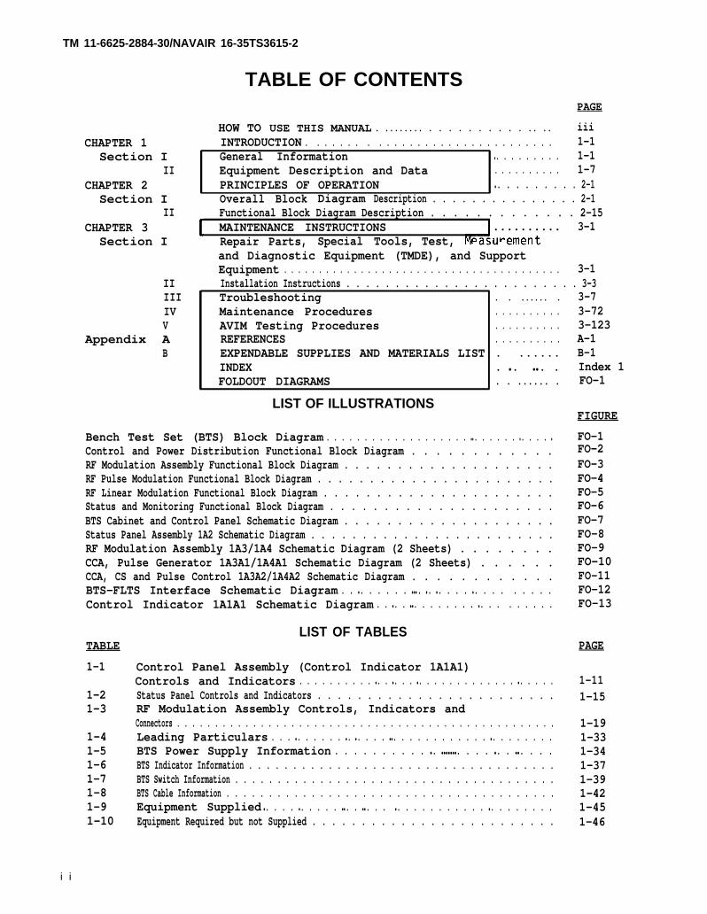
TABLE OF CONTENTSPAGE
CHAPTER 1Section I
IICHAPTER 2Section I
IICHAPTER 3Section I
II
HOW TO USE THIS MANUAL . ........ . . . . . . . . . . .. .. iiiINTRODUCTION . . . . . . . . . . . . . . . . . . . . . . . . . . . . . . . 1-1General Information ● . . . . . . . . . 1-1Equipment Description and Data . . . . . . . . . . 1-7PRINCIPLES OF OPERATION ● . . . . . . . . . 2-1Overall Block Diagram Description . . . . . . . . . . . . . . . 2-1Functional Block Diagram Description . . . . . . . . . . . . . 2-15MAINTENANCE INSTRUCTIONS . . . . . . . . . . 3-1Repair Parts, Special Tools, Test,and Diagnostic Equipment (TMDE), and SupportEquipment . . . . . . . . . . . . . . . . . . . . . . . . . . . . . . . . . . . . . . . . 3-1Installation Instructions . . . . . . . . . . . . . . . . . . . . . . . . 3-3
III TroubleshootingIV Maintenance ProceduresV AVIM Testing Procedures
Appendix A REFERENCESB EXPENDABLE SUPPLIES AND MATERIALS LIST
INDEXFOLDOUT DIAGRAMS
. . . . . . . . . 3-7
. . . . . . . . . . 3-72
. . . . . . . . . . 3-123
. . . . . . . . . . A-1
. ...... B-1
. ● . ● ● . . Index 1
. . ...... . FO-1
LIST OF ILLUSTRATIONSFIGURE
Bench Test Set (BTS) Block Diagram . . . . . . . . . . . . . . . . . . . ● ● . . . . . . ● . . . . ●
Control and Power Distribution Functional Block Diagram . . . . . . . . . . . .RF Modulation Assembly Functional Block Diagram . . . . . . . . . . . . . . . . . . . .RF Pulse Modulation Functional Block Diagram . . . . . . . . . . . . . . . . . . . . . . .RF Linear Modulation Functional Block Diagram . . . . . . . . . . . . . . . . . . . . . .Status and Monitoring Functional Block Diagram . . . . . . . . . . . . . . . . . . . . .BTS Cabinet and Control Panel Schematic Diagram . . . . . . . . . . . . . . . . . . . .Status Panel Assembly 1A2 Schematic Diagram . . . . . . . . . . . . . . . . . . . . . . . .RF Modulation Assembly 1A3/1A4 Schematic Diagram (2 Sheets) . . . . . . . .CCA, Pulse Generator 1A3A1/1A4A1 Schematic Diagram (2 Sheets) . . . . . .CCA, CS and Pulse Control 1A3A2/1A4A2 Schematic Diagram . . . . . . . . . . . .BTS-FLTS Interface Schematic Diagram . . ● . . . . . . ● ● ● . ● . ● . . . . ● . . . . . . . . .Control Indicator 1A1A1 Schematic Diagram . . ● . . ● ● . . . . . . . . ● . . . . . . . . .
FO-1FO-2FO-3FO-4FO-5FO-6FO-7FO-8FO-9FO-10FO-11FO-12FO-13
TABLE
1-1
1-21-3
1-41-51-61-71-81-91-10
LIST OF TABLESPAGE
Control Panel Assembly (Control Indicator 1A1A1)Controls and Indicators . . . . . . . . . . ● . . ● . . . ● . . . . . . . . . . . . . ● . . . . .Status Panel Controls and Indicators . . . . . . . . . . . . . . . . . . . . . . . .RF Modulation Assembly Controls, Indicators andConnectors . . . . . . . . . . . . . . . . . . . . . . . . . . . . . . . . . . . . . . . . . . . . . . . . . .Leading Particulars . . . ● . . . . . . ● . ● . . . . ● ● . . . . . . . . . . . . ● . . . . . . . .BTS Power Supply Information . . . . . . . . . . ● . ● ● ● ● ● ● ● . . . . ● . . ● ● . . . .BTS Indicator Information . . . . . . . . . . . . . . . . . . . . . . . . . . . . . . . . . . .BTS Switch Information . . . . . . . . . . . . . . . . . . . . . . . . . . . . . . . . . . . . . .BTS Cable Information . . . . . . . . . . . . . . . . . . . . . . . . . . . . . . . . . . . . . . .Equipment Supplied ● . . . . ● . . . . . ● ● . . ● ● . . . ● . . . . . . . . . . . ● . . . . . . . .Equipment Required but not Supplied . . . . . . . . . . . . . . . . . . . . . . . . .
1-111-15
1-191-331-341-371-391-421-451-46
i i

TM 11-6625-2884-30/NAVAIR 16-35TS3615-2
HOW TO USE THIS MANUAL
This manual tells you about maintaining the TS-3615/ALQ-136(V) Bench Test Set(BTS) at the Aviation Intermediate Maintenance (AVIM) Level. Aviation inter-mediate maintenance procedures for testing Countermeasures Set AN/ALQ-136(V)1utilizing the BTS are described in TM-11-5865-202-30. AVIM procedures fortesting the Flight Line Test Set (FLTS) TS-3614/ALQ-136(V) utilizing the BTSare described in TM-11-6625-2885-30. Relevant classified information will be
found in TM-11-5865-202-30 appendix C. Repair parts and special tools requiredto perform AVIM on the BTS are listed in TM 11-6625-2884-20P.
Operating instructions and Aviation Unit Maintenance (AVUM) instructions forthe TS-3615/ALQ-136(V) bench test set are described in TM-11-6625-2884-12. TheAVUM manual also contains the maintenance allocation chart (MAC).
For your convenience this manual has been divided into chapters, sections andparagraphs which are numbered sequentially; tables are numbered in the sameway. Illustrations are integrated with the text. In addition to thisnumbering system, a system of captions in colored print helps you quickly findthe information you need. These captions name the equipment and maintenanceprocedures that you will be performing.
Some of the procedures consist ofthese smaller procedures are underas they are continued. Each largelists the procedures by title and
NO ONE EVER REPAIRED OR TESTEDELECTRONIC EQUIPMENT WITHOUTFIRST READING THE AVIATIONINTERMEDIATE MAINTENANCE(AVIM) MANUAL.
several smallerthe larger onessection beginspage number.
procedures. The captions for; both appear on each pagewith a section contents which
i i i

TM 11-6625-2884-30/NAVAIR 16-35TS3615-2
TEST SET, COUNTERMEASURES SET TS-3615/ALQ-136(V)
1-0

TM 11-6625-2884-30/NAVAIR 16-35TS3615-2
CHAPTER 1INTRODUCTION
S E C T I O N I
GENERAL INFORMATION
SCOPE . . .. . . . . . .. . . . . . . . . . . . . . . . . . . . . . .. . . . . . . . . . . . . . .. . .. . .. . . . . . . . . . . . . . . . . . . . . . . . . . . . . . . . . . . . . . . . . . ..CONSOLIDATED INDEX OF ARMY PUBLICATIONS AND BLANK FORMS . .... . . . . .. . . . . . . . . . . . . . . . . . . . . .MAINTENANCE FORMS, RECORDS AND REPORTS. .. . . . . . . . . . . .. . . . . . . . . . . . .DESTRUCTION OF ARMY ELECTRONICS MATERIEL. . . . . . . . . . . . . . . . . . . . .. . . . . . . PREPARATION FOR STORAGE OR SHIPMENT. . . . . . . . . . . . . . .. . . . .. .. . . . . . . .NOMENCLATURE CROSS-REFERENCE LIST. . . . . . . . . . . . . . . . . . . . . . . .. . . . . . . . . . . . . . . . . .. . . . .. . . . . . . .REPORTING EQUIPMENT IMPROVEMENT RECOMMENDATIONS (EIR). . . . . . . . . . . . . . . . . . . . . .
1 - 11 - 31 - 31 - 31 - 31 - 41 - 5
SCOPE
1-1 .Th is i s one o f a se r ies o f techn ica l manua ls cover ing the opera t ion andmaintenance of Countermeasures Set AN/ALQ-136(V)1. I t i s used by Av ia t ionIntermediate Maintenance (AVIM) personnel.
Th is manua l con ta ins phys ica l and func t iona l desc r ip t ions , p r inc ip les o foperat ion, maintenance instruct ions and schemat ic diagrams.
Type of Manual: Aviat ion Intermediate Maintenance (AVIM)
Model Number andEquipment Name: Test set, Countermeasures Set TS-3615/ALQ-136(V)
Purpose ofEquipment: Tests Countermeasures Set AN/ALQ-136(V)1 at AVIM
l e v e l .
Tests Test Set, Countermeasures Set TS-3614/ALQ-136(V) at AVIM level .
1-1

TM 11-6625-2884-30/NAVAIR 16-35TS3615-2
SCOPE (Continued)
The Bench Test Set (BTS) provides test signals and measurement circuits neededto perform Aviation Intermediate Maintenance (AVIM) on the followingequipment:
Receiver-Transmitter, Countermeasures Set: RT-1149(V)1/ALQ-136(V).
Test Set, Countermeasures Set TS-3614/ALQ-136(V) (FLTS).
This manual contains functional descriptions, troubleshooting proceduresprocedures for corrective maintenance.
and
1-2

TM 11-6625-2884-30/NAVAIR 16-35TS3615-2
CONSOLIDATED INDEX OF ARMY PUBLICATlONS AND BLANK FORMS
1-2. Refer to the latest issue of DA Pam 310-1 to determine whether there arenew editions, changes or additional publications pertaining to the equipment.
MAINTENANCE FORMS, RECORDS AND REPORTS
1-3. Department of the Army forms and procedures used for equipment mainten-ance will be those prescribed by DA PAM 738-750 as contained in MaintenanceManagement Update.
a. Reports of Maintenance and Unsatisfactory Equipment. Department of theArmy forms and procedures used for equipment maintenance will be thoseprescribed by DA PAM 738-750 as contained in Maintenance Management Update.Navy personnel will report maintenance performed utilizing the MaintenanceData Collection Subsystem (MDCS) IAW OPNAVINST 4790.2, Vol 3 and unsatisfactorymaterial/conditions (UR submissions) IAW OPNAVINST 4790.2, Vol 2, chapter 17.
b. Report of Packaging and Handling Deficiencies. Fill out and forwardSF 364 Report of Discrepancy [ROD]) as prescribed in AR 735-11-2/DLAR4140.55/NAVMATINST 4355.73/AFR 400-54/MCO 4430.3E.
c. Discrepancy in Shipment Report (DISREP) (SF 361). Fill out and forwardDiscrepancy in Shipment Report (DISREP) (SF 361) as perscribed in AR 55-38/NAVSUPINST 4610.33B/AFR 75-18/MCO P4610.19C/DLAR 4500.15.
DESTRUCTION OF ARMY ELECTRONICS MATERIEL
1-4. Destruction of Army electronics materiel to prevent enemyaccordance with TM 750-244-2.
PREPARATION FOR STORAGE OR SHIPMENT
use shall be in
Army activitieswith its front
1-5. Administrative storage of equipment issued to and used byshall be in accordance with TM 740-90-1. Store or ship the BTSand rear covers securely latched. No extra packing is required. Be sure allancillary equipment is stored in the front cover. (See page 1-8).
1-3
TM 11-6625-2884-30/NAVAIR 16-35TS3615-2
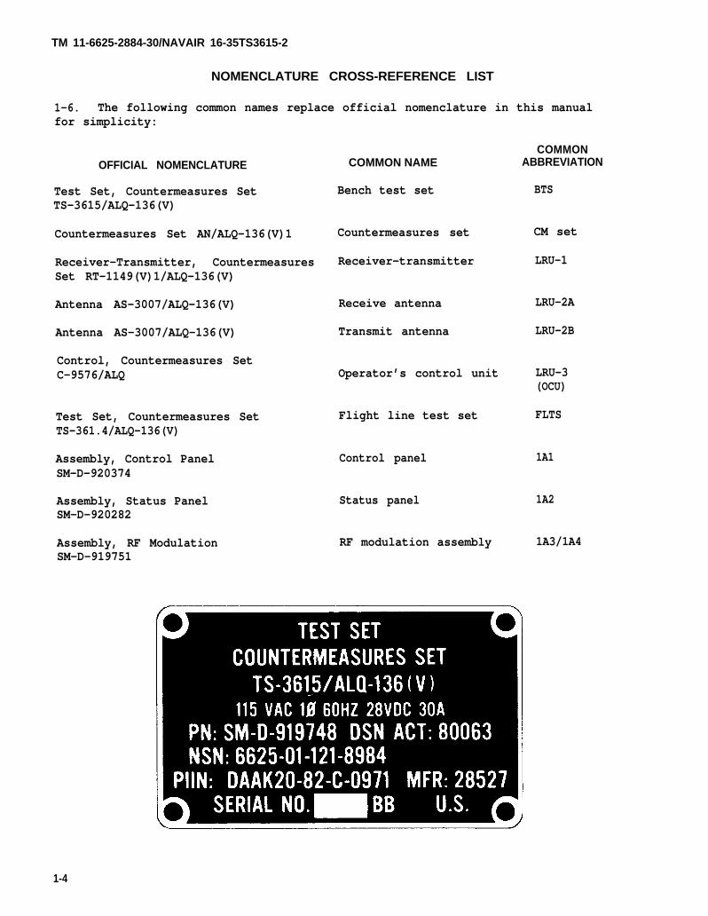
NOMENCLATURE CROSS-REFERENCE LIST
1-6. The following common names replace official nomenclature in this manualfor simplicity:
COMMONOFFICIAL NOMENCLATURE
Test Set, Countermeasures SetTS-3615/ALQ-136(V)
Countermeasures Set AN/ALQ-136(V)1
Receiver-Transmitter, CountermeasuresSet RT-1149(V)1/ALQ-136(V)
Antenna AS-3007/ALQ-136(V)
Antenna AS-3007/ALQ-136(V)
Control, Countermeasures SetC-9576/ALQ
Test Set, Countermeasures SetTS-361.4/ALQ-136(V)
Assembly, Control PanelSM-D-920374
Assembly, Status PanelSM-D-920282
Assembly, RF ModulationSM-D-919751
COMMON NAME
Bench test set
Countermeasures set
Receiver-transmitter
Receive antenna
Transmit antenna
Operator’s control unit
Flight line test set
Control panel
Status panel
RF modulation assembly
ABBREVIATION
BTS
CM set
LRU-1
LRU-2A
LRU-2B
LRU-3(OCU)
FLTS
1A1
1A2
1A3/1A4
1-4

1-7.
TM 11-6625-2884-30/NAVAIR 16-35TS3615-2
a. Army. If your bench test set needs improvement, let us know. Send us anEIR. You, the user, are the only one who can tell us what you don’t like aboutyour equipment. Put it on an SF 368 (Quality Deficiency Report). Mail it toCommander, US Army Communications-Electronics Command and Fort Monmouth, ATTEN:DRSEL-ME-MP, Fort Monmouth, New Jersey 07703. We’ll send you a reply.
b. Navy. Navy personnel are encouraged to submit EIR’s through their localBeneficial Suggestion Program.
1-5/1-6(Blank)

E Q U I P M E N T
TM 11-6625-2884-30/NAVAIR 16-35TS3615-2
S E C T I O N I I
D E S C R I P T I O N A N D D A T A
SECTION CONTENTS PAGE
EQUIPMENT CHARACTERISTICS, CAPABILITIES AND FEATURES . . . . . . . . . . . . . . . . 1-7FRONT PANEL COMPONENTS . . . . . . . . . . . . . ... . . . . . 1-10LOCATION AND DESCRIPTION OF MAJOR COMPONENTS . . . . . . . . . . . . . . . . . . . . . . . 1-20EQUIPMENT DATA . . . . . . . . . . . . . . . . . . . . . . . . . . . . . . . . . . . . . . . 1-33EQUIPMENT CONFIGURATION . . . . . . . . . . . . . . . . . . . . . . . . . . . . . . . . . . . 1-45SAFETY, CARE AND HANDLING . . . . . . . . . . . . . . . . . . . . . . . . . . . . . . . . . . . . 1-47
EQUIPMENT CHARACTERISTICS, CAPABILITIES AND FEATURES
1-8. The BTS provides stimulus (simulated radar threat signals) required forcontrol and activation of the CM set or the FLTS. Response monitoring of theUnit Under Test (UUT) aids in maintenance, and failure diagnosis to eachreplaceable assembly.
Controls and distributes primary power to itself and to UUT.
Controls UUT functions.
Generates (and transmits to UUT) simulated radar threat signals.
Provides facility for manually forcing various UUT functions.
Monitors all UUT responses to simulated radar threat signals andforced functions.
Modular design allows easy access to equipment for easy maintenance.
Each component, and replaceable assembly can be repaired/replacedindependently.
1-7

TM 11-6625-2884-30/NAVAIR 16-35TS3615-2
EQUIPMENT CHARACTERISTICS, CAPABILITIES AND FEATURES (Continued)
The following paragraphs describe the characteristics, capabilities andfeatures of the BTS. The physical description of the BTS is explained in theAviation Unit Maintenance (AVUM) Manual.
BENCH TEST SET
FRONT COVER REMOVED
1-8

TM 11-6625-2884-30/NAVAIR 16-35TS3615-2
The BTS provides two major functions required to test and troubleshoot LRU-1or FLTS unit under test (UUT).
FUNCTION 1: Generates RF signalsto activate the threat recognitioncircuits of the UUT.
1-9

TM 11-6625-2884-30/NAVAIR 16-35TS3615-2
FRONT PANEL COMPONENTS
1-9.a. Control Panel Assembly 1A1. The controls and indicators of the control
panel assembly, and their respective functions, are listed and described intable 1-1. They are shown on accompanying illustrations.
CONTROL PANEL ASSEMBLY CONTROLS AND INDICATORS
1-10

TM 11-6625-2884-30/NAVAIR 16-35TS3615-2
TABLE 1-1. CONTROL PANEL ASSEMBLY (CONTROL INDICATOR 1A1A1)CONTROLS AND INDICATORS
REFERENCE
1
2
3
3-1
3-2
3-3
3-4
4
DEVICE
POWER 115 VAC 60 Hz10 circuit breaker1A1CB2
POWER 28V DC circuitbreaker 1A1CB1
CONTROL INDICATOR
OPR/STBY/OFF toggleswitch 1A1A1S1
OPR
STBY
OFF
ON indicator (green)1A1A1DS1
STBY indicator (amber)1A1A1DS2
OPR indicator (green)1A1A1DS3
JAM/TEST/GO/NO-GO1A1S4/D11
JAM (green)
TEST (yellow)
GO (green)
NO-GO (yellow)
FUNCTION
Controls application of ac powerto BTS. Provides overcurrentprotection to BTS.
Controls application of dc powerto unit under test (UUT). Pro-vides overcurrent protection toUUT.
Controls status of LRU-1.
Applies high voltage to travel-ing wave tube (TWT) after 3 min-ute warm-up delay, (turns TWT on).
Applies dc power to LRU-1, butinhibits LRU-1 TWT control.
Removes all dc power from LRU-1.
When lit, indicates LRU-1 is inSTBY or OPR mode.
When lit, indicates LRU-1 is instandby mode.
When lit, indicates LRU-1 is inoperate mode.
When pressed, initiates built-in-test equipment (BITE) in LRU-1under test.
Lights when LRU-1 under test hasacquired a simulated threat andhas activated ECM.
Lights when BITE in LRU-1 undertest has been initiated.
Lights when LRU-1 under test isoperating correctly.
Lights when a fault is detectedLRU-1 under test.
1-11

TM 11-6625-2884-30/NAVAIR 16-35TS3615-2
COMPONENTS (Continued)
CONTROL PANEL ASSEMBLY CONTROLS AND INDICATORS
1-12
TM 11-6625-2884-30/NAVAIR 16-35TS3615-2
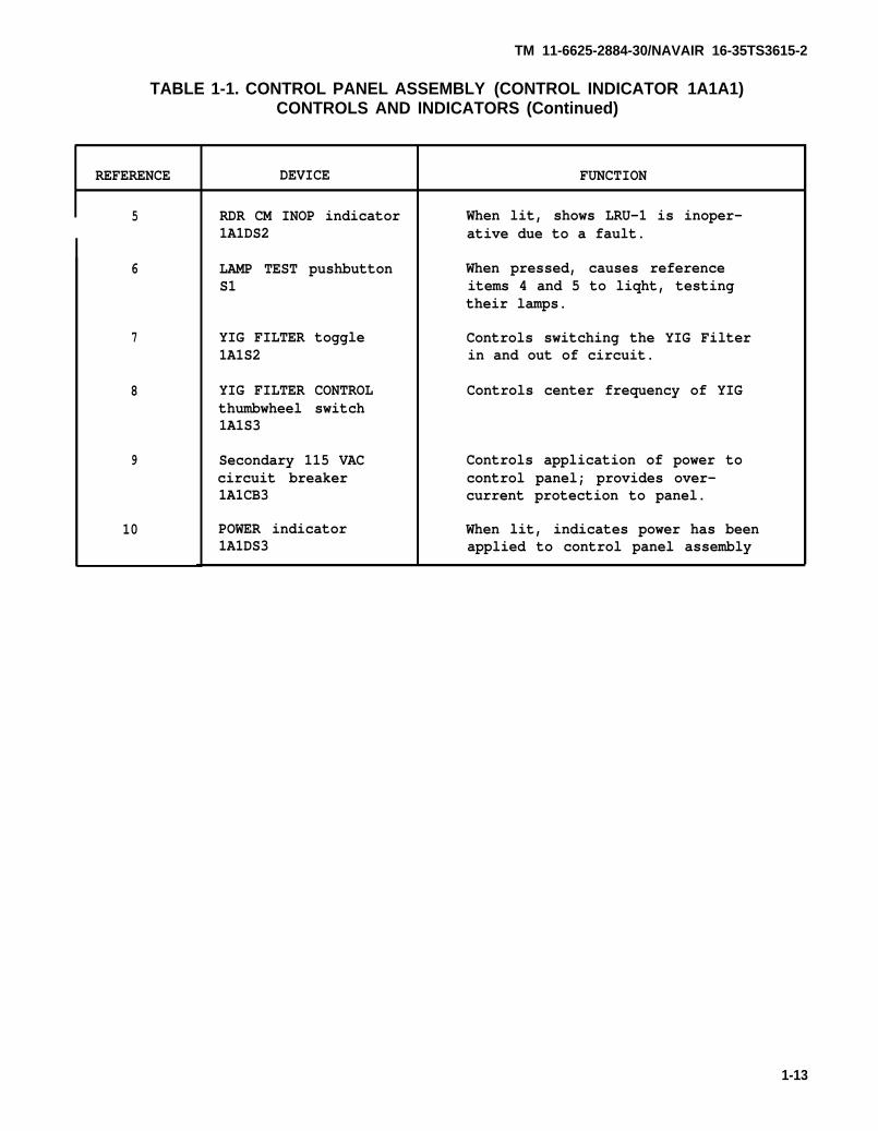
TABLE 1-1. CONTROL PANEL ASSEMBLY (CONTROL INDICATOR 1A1A1)CONTROLS AND INDICATORS (Continued)
REFERENCE
5
6
7
8
9
10
DEVICE
RDR CM INOP indicator1A1DS2
LAMP TEST pushbuttonS1
YIG FILTER toggle1A1S2
YIG FILTER CONTROLthumbwheel switch1A1S3
Secondary 115 VACcircuit breaker1A1CB3
POWER indicator1A1DS3
FUNCTION
When lit, shows LRU-1 is inoper-ative due to a fault.
When pressed, causes referenceitems 4 and 5 to liqht, testingtheir lamps.
Controls switching the YIG Filterin and out of circuit.
Controls center frequency of YIG
Controls application of power tocontrol panel; provides over-current protection to panel.
When lit, indicates power has beenapplied to control panel assembly
1-13

TM 11-6625-2884-30/NAVAIR 16-35TS3615-2
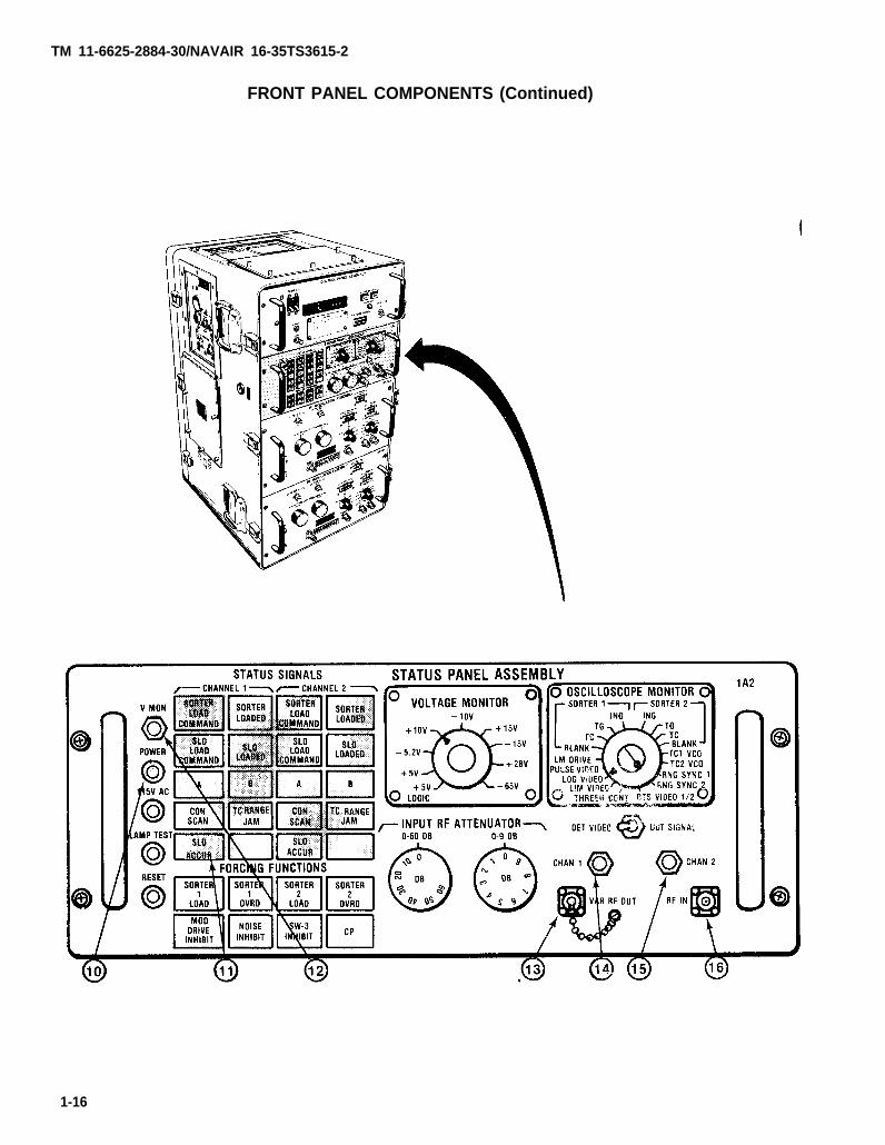
FRONT PANEL COMPONENTS (Continued)
Status Panel Assembly 1A2.b. The controls and indicators of the statuspanel are listed and described in table 1-2. They are shown on the followingillustration and keyed to the table reference numbers.
1-14
TM 11-6625-2884-30/NAVAIR 16-35TS3615-2
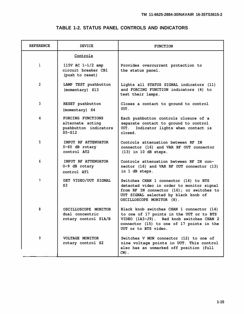
TABLE 1-2. STATUS PANEL CONTROLS AND INDICATORS
REFERENCE
1
2
3
4
5
6
7
8
9
DEVICE
Controls
115V AC 1-1/2 ampcircuit breaker CB1(push to reset)
LAMP TEST pushbutton(momentary) S13
RESET pushbutton(momentary) S4
FORCING FUNCTIONSalternate actingpushbutton indicatorsS5-S12
INPUT RF ATTENUATOR0-60 dB rotarycontrol AT2
INPUT RF ATTENUATORO-9 dB rotarycontrol AT1
DET VIDEO/UUT SIGNALS3
OSCILLOSCOPE MONITORdual concentricrotary control S1A/B
VOLTAGE MONITORrotary control S2
FUNCTION
Provides overcurrent protection tothe status panel.
Lights all STATUS SIGNAL indicators (11)and FORCING FUNCTION indicators (4) totest their lamps.
Closes a contact to ground to controlUUT.
Each pushbutton controls closure of aseparate contact to ground to controlUUT. Indicator lights when contact isclosed.
Controls attenuation between RF INconnector (16) and VAR RF OUT connector(13) in 10 dB steps.
Controls attenuation between RF IN con-nector (16) and VAR RF OUT connector (13)in 1 dB steps.
Switches CHAN 1 connector (14) to BTSdetected video in order to monitor signalfrom RF IN connector (16); or switches toUUT SIGNAL selected by black knob ofOSCILLOSCOPE MONITOR (8).
Black knob switches CHAN 1 connector (14)to one of 17 points in the UUT or to BTSVIDEO (1A3-J9). Red knob switches CHAN 2connector (15) to one of 17 points in theUUT or to BTS video.
Switches V MON connector (12) to one ofnine voltage points in UUT. This controlalso has an unmarked off position (fullCW).
1-15
TM 11-6625-2884-30/NAVAIR 16-35TS3615-2
FRONT PANEL COMPONENTS (Continued)
1-16

TM 11-8625-2884-30/NAVAIR 16-35TS3815-2
TABLE 1-2. STATUS PANEL CONTROLS AND INDICATORS (Continued)
REFERENCE DEVICE FUNCTION
Indicators
10 POWER DS21 (green) This indicator, when lit, indicatespresence of 12 V dc power in statuspanel assembly confirming presenceof 115 V ac power.
11 STATUS SIGNALS Each indicator, when lit, showsindicators DS1-DS20 continuity to ground at a separate
point to be monitored in the UUT.
Connectors
12 V MON J6 Connects to voltage point in UUT selectedby V MON (Voltage Monitor) control S2(7).
13 VAR RF OUT J3 Undetected RF output controlled by INPUTRF ATTENUATOR (5,6).
14 CHAN 1 J4 Connects to point selected by DET VIDEO/UUT SIGNAL switch S3 (9).
15 CHAN 2 J5 Connects to point selected by red knobS1B of OSCILLOSCOPE MONITOR control (8).
16 RF IN J2 Connects to input of INPUT RF ATTENUATORAT1 (5,6).
1-17
TM 11-6625-2884-30/NAVAIR 16-35TS3615-2
FRONT PANEL COMPONENTS (Continued)
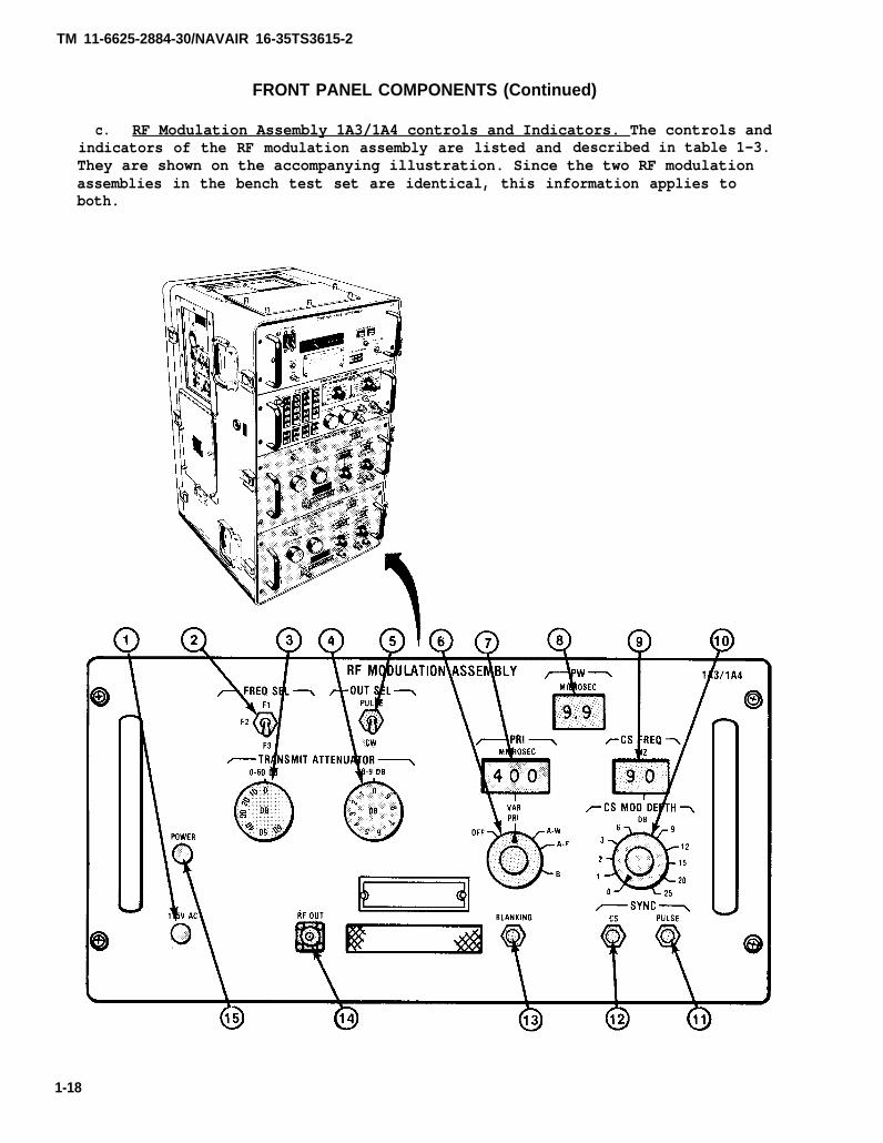
c. RF Modulation Assembly 1A3/1A4 controls and Indicators. The controls andindicators of the RF modulation assembly are listed and described in table 1-3.They are shown on the accompanying illustration. Since the two RF modulationassemblies in the bench test set are identical, this information applies toboth.
1-18

TM 11-6625-2884-30/NAVAIR 16-35TS3615-2
TABLE 1-3. RF MODULATION ASSEMBLY CONTROLS, INDICATORS AND CONNECTORS
REFERENCE DEVICE FUNCTION
Controls
1 115v Ac 1-1/2 amp Provides overcurrent protection to thecircuit breaker CB1 RF modulation assembly.
2 FREQ SEL F1/F2/F3 Selects one of three preset RFthree position toggle frequencies.switch S1
3 TRANSMIT ATTENUATOR Controls level at RF OUT connector (14)0-60 dB rotary control in 10 dB steps.AT4
4 TRANSMIT ATTENUATOR Controls level at RF OUT connector (14)0-9 dB rotary control in 1 dB steps.AT3
5 OUT SEL PULSE/CW Permits selection of either pulse ortoggle switch S3 CW RF output.
6 PRI OFF/VAR PRI/A-W/ Permits selection of one of three presetA-F/B rotary control PRI’s, or variable PRI under control ofS7A/B PRI MICROSEC switches (7).
7 PRI MICROSEC three Sets PRI when switch (6) is in VAR PRIsection thumbwheel position. PRI range is 300 to 999 uscontrol S5 in steps of 1 us.
8 PW MICROSEC two Sets pulse width in steps from O.1 us tosection thumbwheel 9.9 us.control S4
9 CS FREQ HZ two Sets CS frequency in 1 Hz steps from 1section thumbwheel Hz to 99 Hz.control S2
10 CS MOD DEPTH DB rotary Permits selection of one of ten presetcontrol S6 CS modulation depths in discrete steps
from O to 25 dB.
Connectors
11 SYNC PULSE J4 Supplies pulse sync.
12 SYNC CS J5 Supplies CS modulation sync.
13 BLANKING J6 Supplies negative going blanking pulses.
14 RF OUT J1 Supplies modulated RF output.
Indicator
15 POWER DS1 When lit, (green) shows the presence of-15 Vdc, confirming application of115 Vac power to RF modulation assembly.
1-19
TM 11-6625-2884-30/NAVAIR 16-35TS3615-2
FRONT PANEL COMPONENTS (Continued)
TM 11-6625-2884-12 Aviation Unit Maintenance(AVUM) on the bench test set provides theoperation and basic descriptions of the RFmodulation assembly functions.
LOCATION AND DESCRIPTION OF MAJOR COMPONENTS
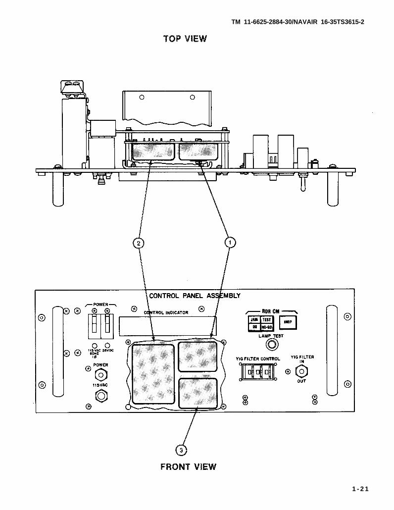
1-10.a. Control Panel Assembly 1A1 (Top View).
(1) PS1 - Power supply that distributes -15 Vdc to the YIG filter in thestatus panel.
(2) PS2 - Power supply that distributes +15 Vdc to the YIG filter in thestatus panel.
(3) PS3 - Power supply that distributes +10 Vdc to the YIG FILTERCONTROL switch S3.
1-20
TM 11-6625-2884-30/NAVAIR 16-35TS3615-2
1 - 2 1
TM 11-6625-2884-30/NAVAIR 16-35TS3615-2
LOCATION AND DESCRIPTION OF MAJOR COMPONENTS (Continued)
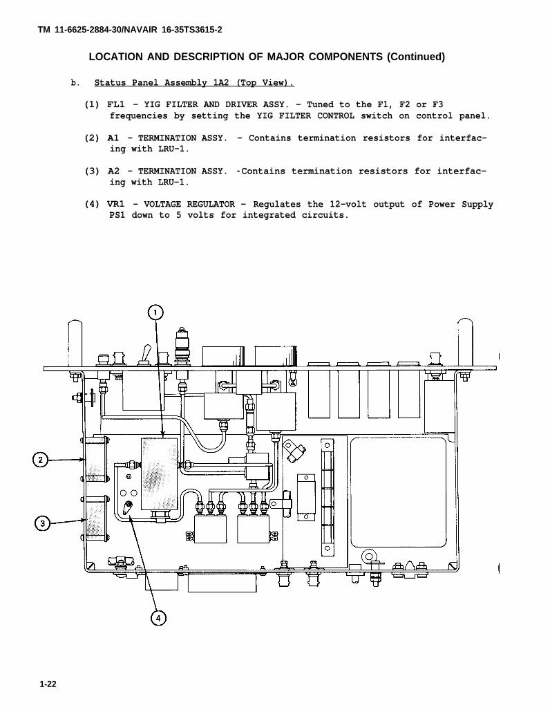
b. Status Panel Assembly 1A2 (Top View).
(1) FL1 - YIG FILTER AND DRIVER ASSY. - Tuned to the F1, F2 or F3frequencies by setting the YIG FILTER CONTROL switch on control panel.
(2) A1 - TERMINATION ASSY. - Contains termination resistors for interfac-ing with LRU-1.
(3) A2 - TERMINATION ASSY. - Contains termination resistors for interfac-ing with LRU-1.
(4) VR1 - VOLTAGE REGULATOR - Regulates the 12-volt output of Power SupplyPS1 down to 5 volts for integrated circuits.
1-22
TM 11-6625-2884-30/NAVAIR 16-35TS3615-2
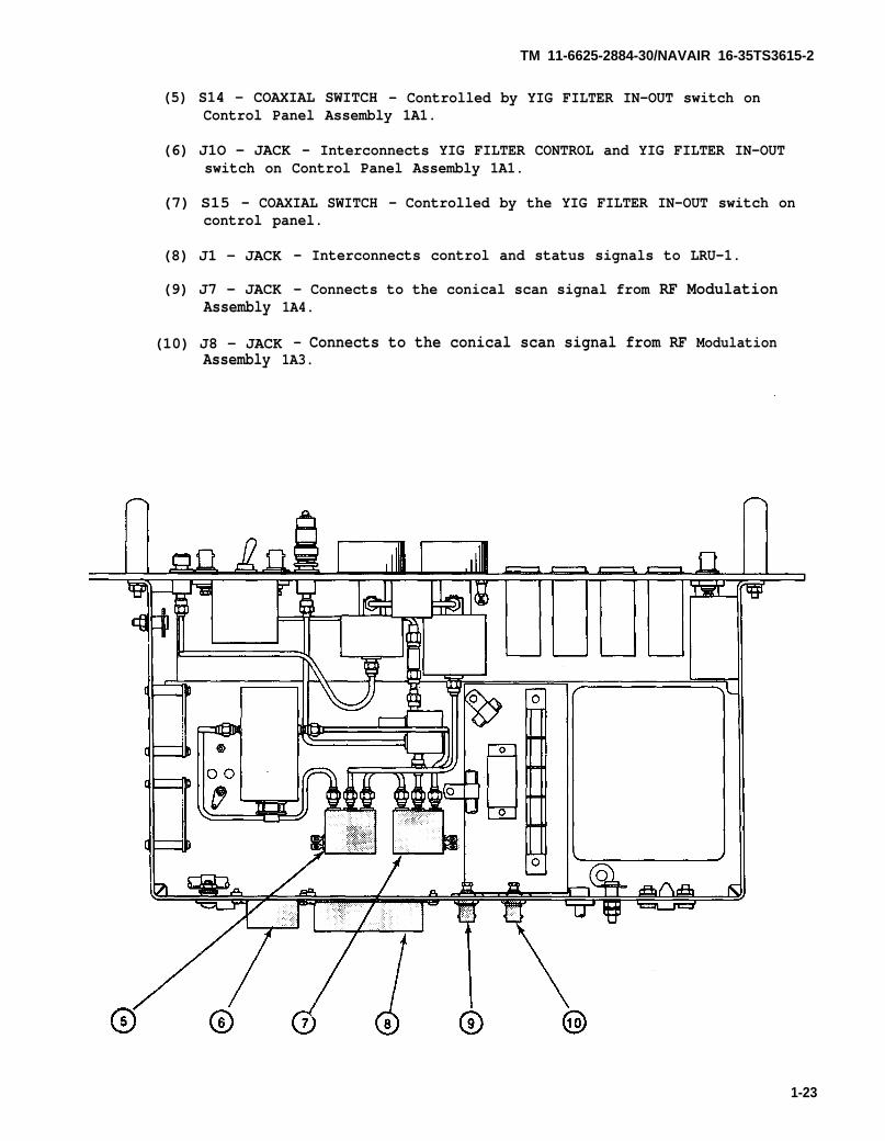
(5) S14 - COAXIAL SWITCH - Controlled by YIG FILTER IN-OUT switch onControl Panel Assembly 1A1.
(6) J1O - JACK - Interconnects YIG FILTER CONTROL and YIG FILTER IN-OUTswitch on Control Panel Assembly 1A1.
(7) S15 - COAXIAL SWITCH - Controlled by the YIG FILTER IN-OUT switch oncontrol panel.
(8) J1 - JACK - Interconnects control and status signals to LRU-1.
(9) J7 - JACK - Connects to the conical scan signal from RF ModulationAssembly 1A4.
(10) J8 - JACK - Connects to the conical scan signal from RF ModulationAssembly 1A3.
1-23

TM 11-6625-2884-30/NAVAIR 16-35TS3615-2
LOCATION AND DESCRIPTION OF MAJOR COMPONENTS (Continued)
(11)
(12)
(13)
(14)
(15)
J6 - JACK - Connects to voltage point in LRU-1 under test selected bythe voltage monitor switch S2. (15)
PS1 - POWER SUPPLY - Supplies +12 Vdc to status signal, and forcingfunction lamps.
A3 - LAMP DRIVER ASSY - Provides a ground return to status signallamps, when enabled by LRU-1 under test.
AT2 - INPUT RF ATTENUATOR - Controls RF output level at VAR RF OUTConnector J3 in 0-60 dB steps.
S2 - VOLTAGE MONITOR - Monitors dc voltages in the LRU-1 under test.
1-24

TM 11-6625-2884-30/NAVAIR 16-35TS3615-2
(16) DC1 - DIRECTIONAL COUPLER - Splits RF received from Coaxial SwitchS15 and directs the RF to Detector CR1 and to VAR RF OUT Connector J3.
(17) AT1 - INPUT RF ATTENUATOR - Controls RF output level at VAR RF OUTconnector J3 (19) in 0-9 db steps.
(18) CR1 - RF DETECTOR - Converts RF to detected video to be monitored onthe Oscilloscope.
(19) J3, AT3 - VAR RF OUT AND DUMMY LOAD - Jack J3 provides variable RFoutput level that can be used for external monitoring. When not beingused this jack is teminated with dummy load AT3.
1-25

TM 11-6625-2884-30/NAVAIR 16-35TS3615-2
LOCATION AND DESCRIPTION OF MAJOR COMPONENTS (Continued)
(20) J4 - CHAN 1 - Connects to oscilloscope to monitor 17 test points inLRU-1 under test or 1 signal from BTS, controlled by the OSCILLOSCOPEMONITOR Switch S1 (21) and UUT SIGNAL/DET VIDEO Switch S3.
(21) S1 - OSCILLOSCOPE MONITOR - Dual concentric rotary switch. Blackknob switches CHAN 1 (20) connector to 1 of 17 points in the LRU-1under test or to BTS 1 VIDEO J7 (9). Red knob switches CHAN 2 (22)connector to 1 of 17 points in LRU-1 under test or to BTS 2 VIDEO J8(lo).
(22) J5 - CHAN 2 - Connects to oscilloscope to monitor 17 test points inLRU-1 under test or 1 signal from BTS.
(23) J2 - RF IN - Connects to RF output of LRU-1 under test.
1-26
TM 11-6625-2884-30/NAVAIR 16-35TS3615-2
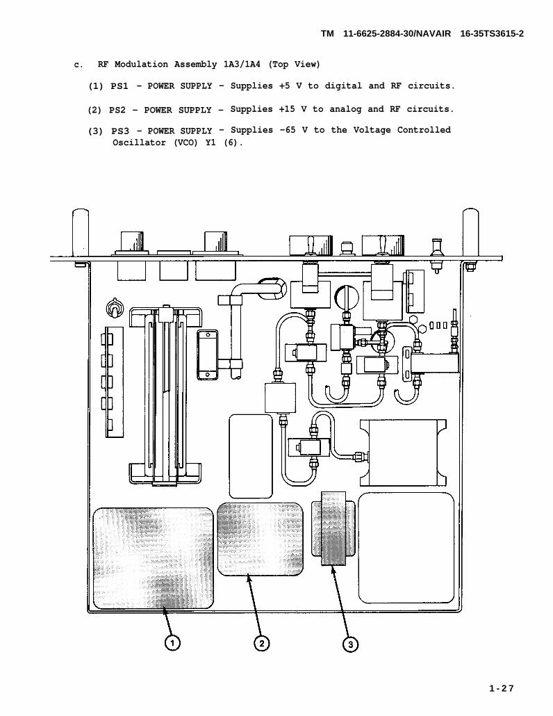
c. RF Modulation Assembly 1A3/1A4 (Top View)
(1) PS1 - POWER SUPPLY - Supplies +5 V to digital and RF circuits.
(2) PS2 - POWER SUPPLY - Supplies +15 V to analog and RF circuits.
(3) PS3 - POWER SUPPLY - Supplies -65 V to the Voltage ControlledOscillator (VCO) Y1 (6).
1 - 2 7
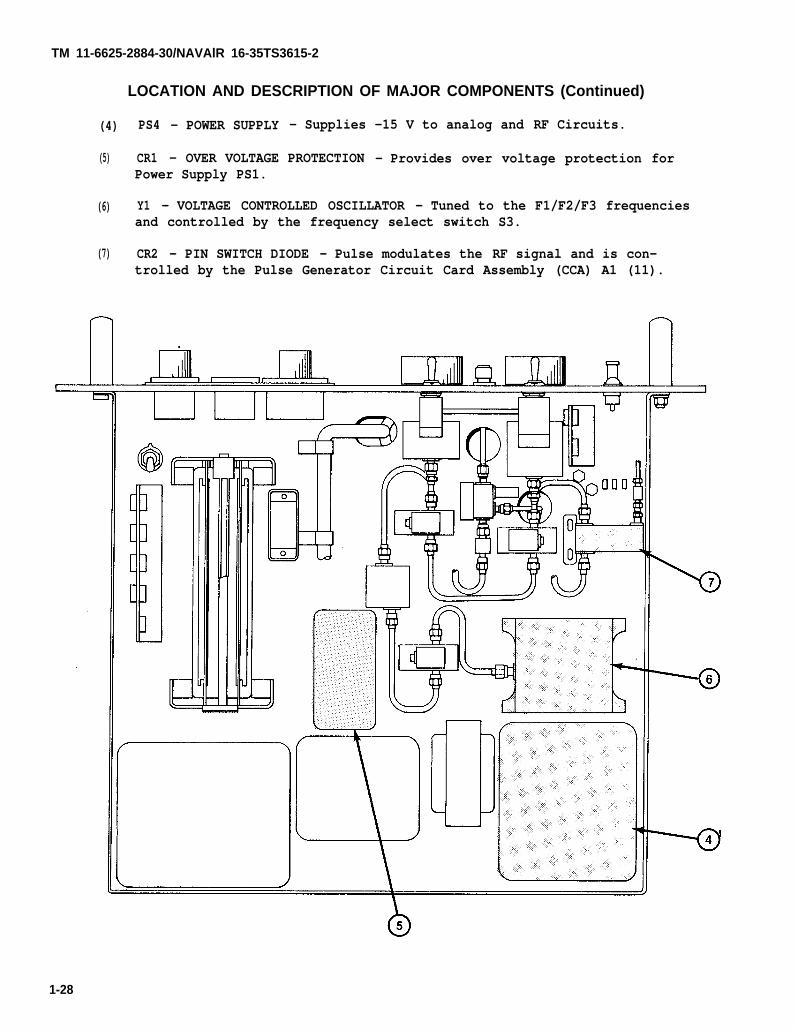
TM 11-6625-2884-30/NAVAlR 16-35TS3615-2
(4)
(5)
(6)
(7)
LOCATION AND DESCRIPTION OF MAJOR COMPONENTS (Continued)
PS4 - POWER SUPPLY - Supplies -15 V to analog and RF Circuits.
CR1 - OVER VOLTAGE PROTECTION - Provides over voltage protection forPower Supply PS1.
Y1 - VOLTAGE CONTROLLED OSCILLATOR - Tuned to the F1/F2/F3 frequenciesand controlled by the frequency select switch S3.
CR2 - PIN SWITCH DIODE - Pulse modulates the RF signal and is con-trolled by the Pulse Generator Circuit Card Assembly (CCA) A1 (11).
1-28

TM 11-6625-2884-30/NAVAIR 16-351S3615-2
(8) CR3 - LINEAR MODULATOR - Used to amplitude modulate the RF signal fromthe VCO (6) and is controlled by the CS and Pulse Control CCA AZ (12).
(9) 1A3/A4-A3 - MOD DEPTH CONTROL ASSY - Nine potentiometers used toadjust the depth of modulation at 1, 2, 3, 6, 9, 12, 15, 20 and 25 dB.
(10) S8 - NORMAL-PATTERN SYNC - Provides either PULSE SYNC or PATTERN SYNCto SYNC PULSE JACK (J4) on front panel.
1-29
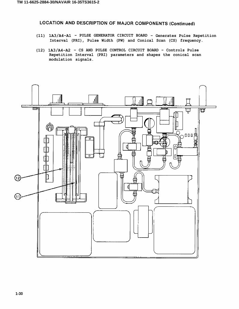
TM 11-6625-2884-30/NAVAIR 16-35TS3615-2
(11) 1A3/A4-A1 - PULSE GENERATOR CIRCUIT BOARD - Generates Pulse RepetitionInterval (PRI), Pulse Width (PW) and Conical Scan (CS) frequency.
(12) 1A3/A4-A2 - CS AND PULSE CONTROL CIRCUIT BOARD - Controls PulseRepetition Interval (PRI) parameters and shapes the conical scanmodulation signals.
1-30
TM 11-6625-2884-30/NAVAIR 16-35TS3615-2
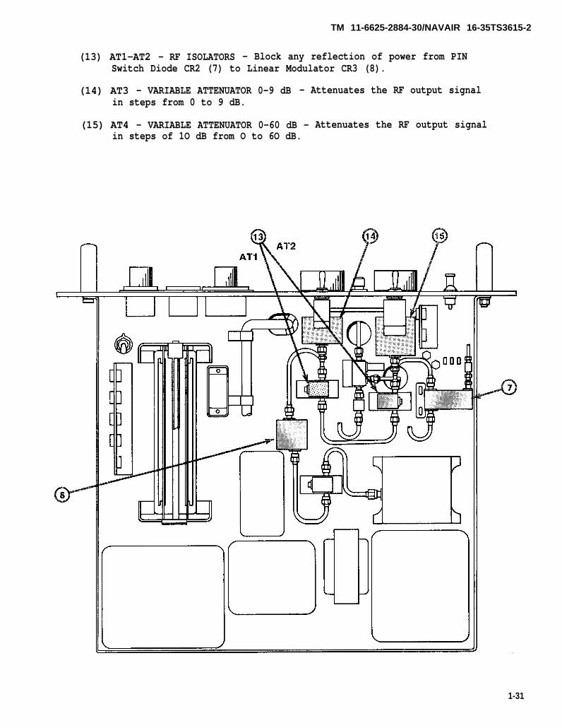
(13) AT1-AT2 - RF ISOLATORS - Block any reflection of power from PINSwitch Diode CR2 (7) to Linear Modulator CR3 (8).
(14) AT3 - VARIABLE ATTENUATOR 0-9 dB - Attenuates the RF output signalin steps from 0 to 9 dB.
(15) AT4 - VARIABLE ATTENUATOR 0-60 dB - Attenuates the RF output signalin steps of 1O dB from O to 6O dB.
1-31
TM 11-6625-2884-30/NAVAIR 16-35TS3615-2
LOCATION AND DESCRIPTION OF MAJOR COMPONENTS (Continued)
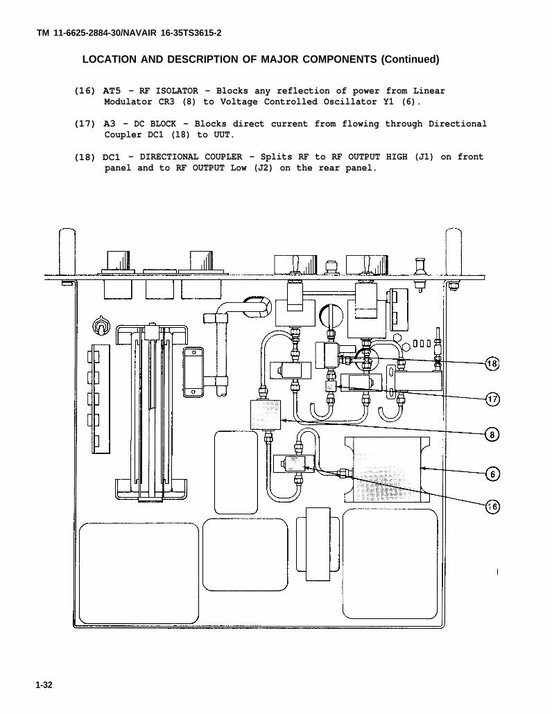
(16) AT5 - RF ISOLATOR - Blocks any reflection of power from LinearModulator CR3 (8) to Voltage Controlled Oscillator Y1 (6).
(17) A3 - DC BLOCK - Blocks direct current from flowing through DirectionalCoupler DC1 (18) to UUT.
(18) DC1 - DIRECTIONAL COUPLER - Splits RF to RF OUTPUT HIGH (J1) on frontpanel and to RF OUTPUT Low (J2) on the rear panel.
1-32
TM 11-6625-2884-30/NAVAIR 16-35TS3615-2
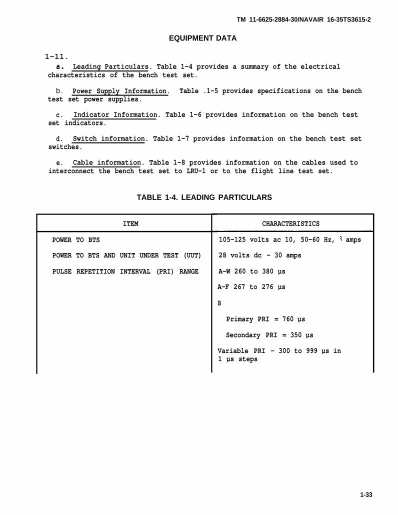
EQUIPMENT DATA
1-11.Leading Particulars. Table 1-4 provides a summary of the electrical
characteristics of the bench test set.
b . Power Supply Information. Table .1-5 provides specifications on the benchtest set power supplies.
c. Indicator Information. Table 1-6 provides information on the bench testset indicators.
d. Switch information. Table 1-7 provides information on the bench test setswitches.
e. Cable information. Table 1-8 provides information on the cables used tointerconnect the bench test set to LRU-1 or to the flight line test set.
TABLE 1-4. LEADING PARTICULARS
ITEM
POWER TO BTS
POWER TO BTS AND UNIT UNDER TEST (UUT)
PULSE REPETITION INTERVAL (PRI) RANGE
CHARACTERISTICS
105-125 volts ac 10, 50-60 Hz, 1 amps
28 volts dc - 30 amps
A-W 260 to 380 µs
A-F 267 to 276 µs
B
Primary PRI = 760 µs
Secondary PRI = 350 µs
Variable PRI - 300 to 999 µs in1 µs steps
1-33

TM 11-6625-2884-30/NAVAIR 16-35TS3615-2
TABLE 1-4. LEADING PARTICULARS (Continued)
ITEM
PULSE WIDTH (PW) RANGE
RF FREQUENCY RANGE
RF POWER OUTPUT LEVELS
C S MOD DEPTH(Conical Scan Modulation Depth)
OPERATING TEMPERATURE
STORAGE TEMPERATURE
CHARACTERISTICS
0.1 to 9.9 µs in O.1 µs-steps
Three preset adjustable frequencies
F1
F2
F3
HIGH - +3 dBm maximum at the RF OUTjack J1 on the RF ModulationAssemblies 1A3/1A4
LOW - -10 dBm minimum at combined RFjack J4 on the BTS connectorpanel
Adjustable from O-25 dB in steps of O,1, 2, 3, 6, 9, 12, 15, 20 and 25.
+32°F to +131°F(0°C to 55°C)
-70°F to 160°F(-57°C to +71°C)
POWER SUPPLY
1A1PS1
TABLE 1-5. BTS POWER SUPPLY INFORMATION
FUNCTION AND CHARACTERISTICS
Supplies -15 V to the YIG FILTER in the Status PanelAssembly 1A2. The characteristics of the Power Supplyare:
INPUT VOLTAGE 105-125 V ac, 50-420 Hz
OUTPUT VOLTAGE -14.85 to -15.15 V
OUTPUT CURRENT 0.1 amp
REGULATED - Yes
OVERVOLTAGE PROTECTION - No
SHORT CIRCUIT PROTECTION - Yes
1-34

TM 11-6625-2884-30/NAVAIR 16-35TS3615-2
TABLE 1-5. BTS POWER SUPPLY INFORMATION (Continued)
1A1PS2
1A1PS3
1A2PS1
FUNCTION AND CHARACTERISTICS
Supplies +15 V to the YIG FILTER in the Status PanelAssembly 1A2. The characteristics of the power supplyare:
INPUT VOLTAGE 105-125 V ac, 50-420 Hz
OUTPUT VOLTAGE +14.85 to +15.15 V dc
OUTPUT CURRENT - 1.0 amp
REGULATED - Yes
OVERVOLTAGE PROTECTION - NO
SHORT CIRCUIT PROTECTION - Yes
Supplies +10 V to the YIG FILTERControl Panel Assembly 1A1. Thepower supply are:
CONTROL switch (S3) incharacteristics of the
INPUT VOLTAGE 105-125 V ac, 50-420 Hz
OUTPUT VOLTAGE +9.9 to +10.1 V dc
OUTPUT CURRENT - 0.12 amp
REGULATED- Yes
OVERVOLTAGE PROTECTION - NO
SHORT CIRCUIT PROTECTION - Yes
Supplies +12 V to the status signal and forcing functionlamps in the Status Panel Assembly 1A2. The characteristicsof the power supply are:
INPUT VOLTAGE 105-125 V ac, 50-420 Hz
OUTPUT VOLTAGE - Adjustable from +11.4 to +12.5V
OUTPUT CURRENT 3.0 amps
REGULATED- Yes
OVERVOLTAGE PROTECTION - Yes
SHORT CIRCUIT PROTECTION - Yes
1-35

TM 11-6625-2884-30/NAVAIR 16-35TS3615-2
TABLE 1-5. BTS POWER SUPPLY INFORMATION (Continued)
POWER SUPPLY
1A3/1A4PS1
1A3/1A4PS2
1A3/1A4PS3
FUNCTION AND CHARACTERISTICS
Supplies +5 V to digital and RF circuits in 1A3/1A4. Thecharacteristics of the power supply are:
INPUT VOLTAGE - 105-125 V ac, 50-420 Hz
OUTPUT VOLTAGE Adjustable from 4.7 to 5.3 V dc
OUTPUT CURRENT 6.0 amps
REGULATED - Yes
OVERVOLTAGE PROTECTION - Yes (Built-in turn-off circuit)
SHORT CIRCUIT PROTECTION - Yes
Supplies +15 V to digital and RF circuits in 1A3/1A4. Thecharacteristics of the power supply are:
INPUT VOLTAGE 105-125 V ac, 50-420 Hz
OUTPUT VOLTAGE - Adjustable from +13.7 to +15.2 V
OUTPUT CURRENT - 1.5 amps
REGULATED - Yes
OVERVOLTAGE PROTECTION - NO
SHORT CIRCUIT PROTECTION - Yes
Supplies -65 V to the voltage controlled oscillator(VCO). The characteristics of the power supply are:
INPUT VOLTAGE - 105-125 V ac, 50-420 Hz
OUTPUT VOLTAGE - Adjustable from -59.0 to -65.0 V
OUTPUT CURRENT .05 amps
REGULATED - Yes
OVERVOLTAGE PROTECTION - Yes (Built-in turn-off circuit)
SHORT CIRCUIT PROTECTION - Yes
1-36
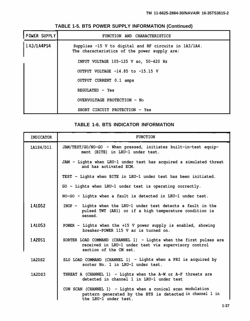
TM 11-6625-2884-30/NAVAIR 16-35TS3615-2
INDICATOR
1A1S4/D11
1A2DS2
1A2DS3
TABLE 1-5. BTS POWER SUPPLY INFORMATION (Continued)
FUNCTION AND CHARACTERISTICS
Supplies -15 V to digital and RF circuits in 1A3/1A4.The characteristics of the power supply are:
INPUT VOLTAGE 105-125 V ac, 50-420 Hz
OUTPUT VOLTAGE -14.85 to -15.15 V
OUTPUT CURRENT 0.1 amps
REGULATED - Yes
OVERVOLTAGE PROTECTION - NO
SHORT CIRCUIT PROTECTION - Yes
TABLE 1-6. BTS INDICATOR INFORMATION
FUNCTION
JAM/TEST/GO/NO-GO - When pressed, initiates built-in-test equip-ment (BITE) in LRU-1 under test.
JAM - Lights when LRU-1 under test has acquired a simulated threatand has activated ECM.
TEST - Lights when BITE in LRU-1 under test has been initiated.
GO - Lights when LRU-1 under test is operating correctly.
NO-GO - Lights when a fault is detected in LRU-1 under test.
INOP - Lights when the LRU-1 under test detects a fault in thepulsed TWT (AR1) or if a high temperature condition issensed.
POWER - Lights when the +15 V power supply is enabled, showingbreaker-POWER 115 V ac is turned on.
SORTER LOAD COMMAND (CHANNEL 1) - Lights when the first pulses arereceived in LRU-1 under test via supervisory controlsection of the CM set.
SLO LOAD COMMAND (CHANNEL 1) - Lights when a PRI is acquired bysorter No. 1 in LRU-1 under test.
THREAT A (CHANNEL 1) - Lights when the A-W or A-Fdetected in channel 1 in LRU-1 under test
CON SCAN (CHANNEL 1) - Lights when a conical scanpattern generated by the BTS is detectedthe LRU-1 under test.
threats are
modulationin channel 1 in
1-37

TM 11-6625-2884-31/NAVAIR 16-35TS3615-2
TABLE 1-6. BTS INDICATOR lNFORMATlON (Continued)
INDICATOR
1A2DS5
1A2DS6
1A2DS7
1A2DS8
1A2DS9
1A2DS1O
1A2DS11
1A2DS12
1A2DS13
1A2DS14
1A2DS15
1A2DS16
1A2DS17
1A2DS18
1A2DS19
1A2DS20
1A2DS21
FUNCTION
SLO ACCURACY (CHANNEL 1) - Lights when SLO 1 in LRU-1 undertest has locked on to the threat frequency.
SORTER LOADED (CHANNEL 1) - Lights when sorter 1 in LRU-1under test is in the tracking mode.
SLO LOADED (CHANNEL 1) - Lights when the SLO in channel1 in LRU-1 under test has acquired the threatfrequency.
THREAT B (CHANNEL 1) - Lights when the B threat is detectedin channel 1 in LRU-1 under test.
TC RANGE JAM (CHANNEL 1) - Lights when range deception isbeing transmitted in channel 1 of LRU-1 under test.
SPARE - Included for future expansion.
SORTER LOAD COMMAND (CHANNEL 2) - Lights when the firstpulses are received in LRU-1 under test via super-visory control section of LRU-1.
SLO LOAD COMMAND (CHANNEL 2) - Lights when a PRI is acquiredby sorter No.2 in LRU-1 under test.
THREAT A (CHANNEL 2) - Lights when the A-W or A-F threatsare detected in channel 2 in LRU-1 under test.
CON SCAN (CHANNEL 2) - Lights when a conical scan modulationpattern generated by the BTS is detected in channel2 in LRU-1 under test.
SLO ACCURACY (CHANNEL 2) - Lights when SLO 2 in LRU-1 undertest has locked on to the threat frequency.
SORTER LOADED (CHANNEL 2) - Lights when sorter 2 in LRU-1under test is in the tracking mode.
SLO LOADED (CHANNEL 2) - Lights when the SLO in channel 2in LRU-1 under test has acquired the threat fre-quency.
THREAT B (CHANNEL 2) - Lights when the B threat is detectedin channel 2 in LRU-1 under test.
TC RANGE JAM (CHANNEL 2) - Lights when range deception isbeing transmitted in channel 2 of the LRU-1 undertest.
SPARE - Included for future expansion.
Lights green to indicate +12V power for status panel.
1 -38

TM 11-6625-2884-30/NAVAIR 16-35TS3615-2
TABLE 1-7. BTS SWITCH INFORMATION
SWITCH
1A1S1
1A1S2
1A1S3
1A2S1
1A2S2
1A2S3
1A2S4
1A2S5
1A2S6
1A2S7
1A2S8
1A2S9
FUNCTION
LAMP TEST - Pushbutton switch, when pressed lights the JAM/TEST/GO/NO-GO (1A1S4/D11) and INOP (1A1DS2) indica-tors on the control panel assembly.
YIG FILTER IN OUT - Switch used to switch the YIG FILTER(FL1) “IN” or “OUT” of the RF path in Status PanelAssembly 1A2.
YIG FILTER CONTROL - Three decade thumbwheel switch used totune the YIG filter in the Status Panel Assembly 1A2.
OSCILLOSCOPE MONITOR - Dual concentric rotary 18 positionswitch used for selecting 17 test points in theLRU-1 under test or 1 signal from the RF ModulationAssembly 1A3/1A4.
VOLTAGE MONITOR - Nine-position rotary switch used tomonitor the nine dc voltages in LRU-1 under test.
DET VIDEO/UUT SIGNAL - Two position toggle switch. Whenin the DET VIDEO position, enables the monitoringof detected RF from the LRU-1 under test. When inthe UUT position, enables the selection of one of 17test points from LRU-1 under test, or 1 signal fromBTS via OSCILLOSCOPE MONITOR switch 1A2S1A.
RESET - Pushbutton switch - When pressed provides a masterreset signal to LRU-1 under test.
SORTER 1 LOAD - Alternate action pushbutton - When enabled,sends a load command to sorter 1 of LRU-1 undertest.
SORTER 1 OVRD - Alternate action pushbutton - When enabled,prevents sorter 1 from locking to any input signal.
SORTER 2 LOAD - Alternate action pushbutton - When enabled,sends a load command to sorter 2 of LRU-1 undertest.
SORTER 2 OVRD - Alternate action pushbutton - When enabled,prevents sorter 2 from locking to any input signal.
MOD DRIVE INHIBIT - Alternate action pushbutton - When en-abled, scan modulation is disabled in LRU-1 undertest.
1-39

TM 11-6625-2884-30/NAVAIR 16-35TS3615-2
SWITCH
1A2S1O
1A2S11
1A2S12
1A2S13
1A2S14
1A2S15
1A3/1A4S1
1A3/1A4S2
1A3/1A4S3
1A3/1A4S4
TABLE 1-7. BTS SWITCH INFORMATION (Continued)
FUNCTION
NOISE INHIBIT - Alternate action pushbutton - When enabledinhibits random noise ECM in LRU-1 under test.
SW-3 INHIBIT - Alternate action pushbutton - When enabledinhibits SW-3 ECM in LRU-1 under test.
CP - Alternate action pushbutton - When enabled inhibitspulse program in LRU-1 under test.
LAMP TEST - Pushbutton switch - When pressed provides aground return to light the status signal lamps andforcing function lamps on status panel.
SWITCH COAXIAL - Enabled by the YIG FILTER IN-OUT switchon control panel.
IN Position - YIG filter and driver control (FL1)is connected into the RF path of status panel.
OUT Position - YIG filter and driver control (FL1)is disconnected from RF path.
SWITCH COAXIAL - Enabled by the YIG FILTER IN-OUT Switchcontrol panel.
IN POSITION - YIG filter and driver control (FL1)is connected into the RF path of status panel.
OUT POSITION - YIG filter and driver control (FL1)is disconnected from RF path.
on
FREQ SEL (F1-F2-F3) - Three position toggle switch - Selectsthe low, mid and high RF frequencies directed tothe UUT.
CS FREQ - Two decade thumbwheel switch- Sets conical scan(CS) frequency in 1 Hz steps from O to 99.
OUT SEL (PULSE/CW) - Two position toggle switch - Selectseither pulse modulation of RF signal or ContinuousWave (CW) RF output to LRU-1 under test.
PW - Two decade thumbwheel switch - Sets the pulse widthfrom 0.1 to 9.9 microseconds in 0.1 microsec steps.
1-40

TM 11-6625-2884-30/NAVAIR 16-35TS3615-2
TABLE 1-7. BTS SWITCH INFORMATION (Continued)
SWITCH FUNCTION
1A3/1A4S5
1A3/1A4S6
1A3/1A4S7
1A3/1A4S8
PRI - Three decade thumbwheel switch - Sets the PRI from 300to 999 microseconds in 1 microsecond steps.
CS MOD DEPTH - Ten-position rotary switch - Sets the depthof CS modulation to 0, 1, 2, 3, 6, 9, 12, 15, 20 or25 dB.
PRI SELECT - Five position rotary switch - Selects one ofthree preset pulse repetition intervals A-W/A-F/Elor a VAR PRI set by PRI switch S5.
SYNC (NORMAL/PATTERN) - Two position toggle switch (locatedinside the 1A3/1A4 chassis). Provides either pulsesync or pattern sync to the SYNC PULSE Jack (J4)on the front panel.
1-41

TM 11-6625-2884-30/NAVAIR 16-35TS3615-2
TABLE 1-8. BTS CABLE INFORMATION
ITEM CABLE FUNCTION
1 W1 CONTROL and STATUS - Connects MONITOR (LRU-1) 1J7 to MONITOR(BTS) 1J1. Used to interface the Status PanelAssembly 1A2 of the BTS with LRU-1 under test.
2 W2 CONTROL - Connects the CONTROL (BTS) 1J2 to CONTROL (LRU-1)1J2. Connects power and control signals from the(BTS) Control Indicator 1A1A1 to LRU-1 under test.
3 W3 POWER - Connects the 28V POWER (BTS) 1J3 to POWER (LRU-1)1J1. Supplies 28 Vdc to LRU-1 under test.
4 W4 RF COAX - Connects the RF OUT (LRU-1) 1J4 to RF IN (BTS) 1A2J2 through 30 dB attenuator. Used to sample theRF output of LRU-1 under test.
5 W5 RF COAX - Connects either the CMBD RF (BTS) 1J4 or the RFOUT (BTS) 1A3/1A4J1 to RF IN (LRU-1) 1J3. Used tosupply CW or pulse and pattern modulated RF to LRU-1under test.
6 W6 INPUT POWER - Connects 115V-60 Hz (BTS) 1J5 to the ac powersource.
7 W7 INPUT POWER - Connects 28 VDC (BTS) 1J6 to the 28 Vdc powersupply.
8 W8 BLANKING - Connects BLANKING (BTS) 1A3/1A4 J6 to BLK IN(LRU-1) 1J5. Used to test external aircraft blank-ing circuits of LRU-1 under test.
9 W9 VOLTAGE MONITOR - Connects V MON (BTS) 1A2J6 to the digitalmultimeter. Used to monitor dc voltages in LRU-1under test.
10 W10 VIDEO CABLES - Three cables which connect:
CHAN 1 (BTS) 1A2J4 to CHAN 1 of the oscilloscope.
CHAN 2 (BTS) 1A2J5 to CHAN 2 of the oscilloscope.
SYNC (BTS) 1A3/1A4J4 PULSE to the external syncinput of the oscilloscope
Used to monitor various test points in LRU-1 undertest.
1-42

TM 11-6625-2884-30/N
AV
AIR
16-35TS3615-2
1-43

TM 11-6625-2884-30/NAVAIR 16-35TS3615-2
TABLE 1-8. BTS CABLE INFORMATION (Continued)
ITEM CABLE FUNCTION
11 W11 MONITOR and POWER - Connects (BTS) MONITOR 1J1 and POWER 1J3to FLTS PWR 1A2J1. Used to perform AVIM on theflight line test set.
1 - 4 4

TM 11-6625-2884-30/NAVAIR 16-35TS3615-2
EQUIPMENT CONFIGURATION1-12.
a. Equipment Supplied. Table 1-9 provides a summary of the functions of theBTS equipment units.
b. Equipment Required but not Supplied. Table 1-10 provides a summary forthe equipment required but not supplied with the BTS.
TABLE 1-9. EQUIPMENT SUPPLIED
QTY NOMENCLATURE
COMBINATION CASE
CONTROL PANEL ASSY.(1A1)
STATUS PANEL ASSY.(1A2)
RF MODULATION ASSY.(1A3/1A4)
FUNCTION
Houses four major assemblies 1A1, 1A2, 1A3 and 1A4.Front cover provides storage for ancillary equipment.Rear cover provides access to equipment.
Provides the following:
● AC power distribution to BTS.
DC power distribution to UUT.
YIG FILTER control.
Fault and status indicators
● CONTROL INDICATOR - Controls LRU-1 under test.
Provides the following:
Monitoring of power, RF and video signals onUUT.
Monitoring of STATUS SIGNALS on LRU-1 undertest.
● Manual control of functions in UUT.
Provides the following:
● Generation of CW, pulse and CS modulated RFsignals to UUT.
1-45

TM 11-6625-2884-30/NAVAlR 16-35TS3615-2
TABLE 1-9. EQUIPMENT SUPPLIED (Continued)
QTY NOMENCLATURE FUNCTION
2 RF MODULATION ASSY. ● Setting of PW, PRI, CS FREQ and CS MOD DEPTH.(Con’t)
1
QTY
1
1
1
1
1
1
1
FRONT COVER
Control of RF generated to UUT.
Provides storage for the ancillary equipment.
Cable assemblies and air hose.
Adapters - RF, test point, air hose and torquewrench.
Clamps for air hose.
RF Attenuator (30 dB).
Circuit card extractor.
TABLE 1-10. EQUIPMENT REQUIRED BUT NOT SUPPLIED
NOMENCLATURE
OSCILLOSCOPEAN/USM-281A
Including:
AMPLIFIER,VERTICAL PLUG-IN
TIME BASE ANDDELAY GENERATORPLUG-IN
DIGITAL MULTIMETERAN/USM-451
+28V POWER SUPPLYPP-1104G
RF POWER METERHP 435A
RF POWER SENSORHP 8481A
FUNCTION
Provides for the monitoring of detected video and thestandard logic levels of LRU-1 under test.
Logic 1 = +2.4 to 5.0 Volts
Logic O = O to 0.6 Volts
Amplifies test signals - 2 channels.
Provides time base and trigger delay.
Provides for the monitoring of voltage, current andresistance in UUT.
Provides prime power to UUT via the BTS. Alsoprovides power for some BTS circuits.
Provides RF power measurement while performing AVIMon UUT and the BTS.
Senses RF power
1-46

TM 11-6625-2884-30/NAVAIR 16-35TS3615-2
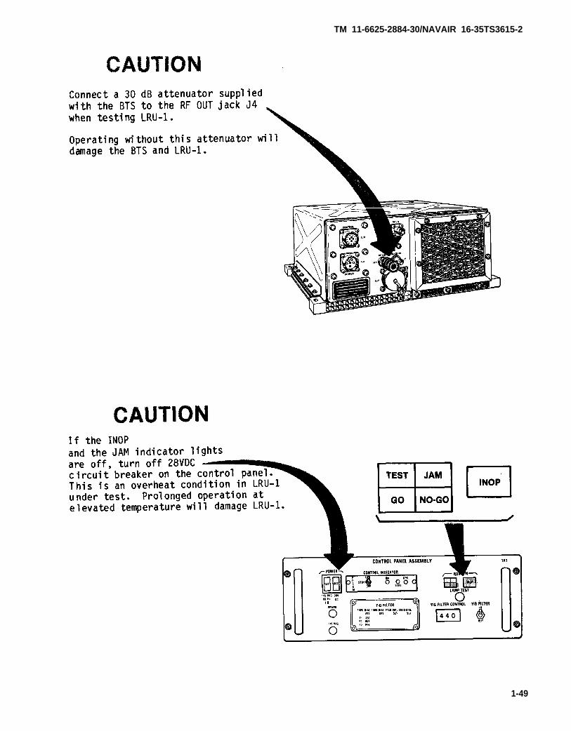
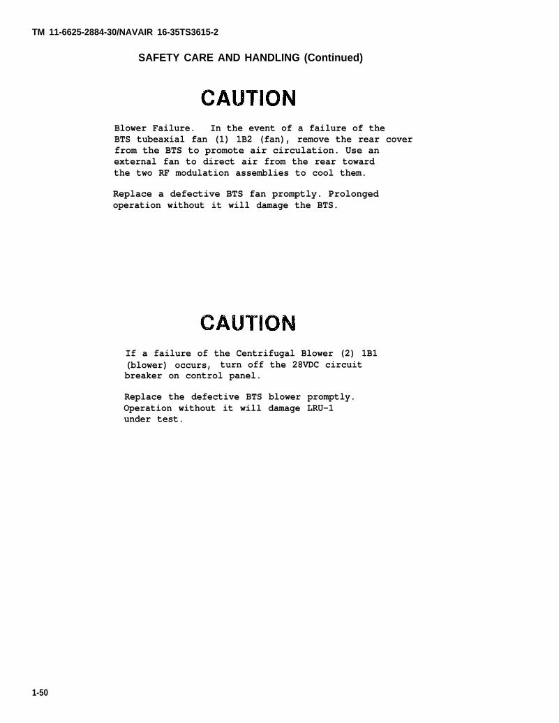
SAFETY, CARE AND HANDLING
1-13.
The following safety precautions are for YOU the AVIM Technician,
and for the BTS equipment.
High voltage is used in the operation of thisequipment. Avoid contacting high-voltageconnections when installing or operating thisequipment. Injury or death may result ifpersonnel fail to observe safety precautions.
The BTS weighs 250 pounds. Four person lift.Handle with care to prevent personal injuryor equipment damage.
1-47

TM 11-6625-2884-30/NAVAIR 16-35TS3615-2
SAFETY, CARE AND HANDLING (Continued)
Circuit breakers, designated 115 VAC, on thefront of the control panel, status panel andeach of the two RF modulation assemblies arepush-to-reset types. When the circuit breakeris closed, it is depressed in its housingconcealing the side surface. When the breakeris open, a button protrudes from its housingdisplaying a white side surface. This visiblewhite side surface on the button shows thebreaker is open. These circuit breakers arenot intended be used as on/off switches.Energizing/de-energizing of the bench test setis only to be controlled by use of 115 VAC60 Hz, 10 POWER circuit breaker CB2 on thefront of the control panel.
1-48
TM 11-6625-2884-30/NAVAIR 16-35TS3615-2
1-49
TM 11-6625-2884-30/NAVAIR 16-35TS3615-2
SAFETY CARE AND HANDLING (Continued)
Blower Failure. In the event of a failure of theBTS tubeaxial fan (1) 1B2 (fan), remove the rear coverfrom the BTS to promote air circulation. Use anexternal fan to direct air from the rear towardthe two RF modulation assemblies to cool them.
Replace a defective BTS fan promptly. Prolongedoperation without it will damage the BTS.
If a failure of the Centrifugal Blower (2) 1B1(blower) occurs, turn off the 28VDC circuitbreaker on control panel.
Replace the defective BTS blower promptly.Operation without it will damage LRU-1under test.
1-50

TM 11-6625-2884-30/NAVAIR 16-35TS3615-2
1-51/1-52(Blank)

TM 11-6625-2884-30/NAVAIR 16-35TS3615-2
C H A P T E R 2
P R I N C I P L E S O F O P E R A T I O N
S E C T I O N I
O V E R A L L B L O C K D I A G R A M D E S C R I P T I O N
SECTION CONTENTS PAGE
INTRODUCTION ...... . . ........ . . . . . ...... . . . .... ...... . . 2-1BLOCK DIAGRAM DESCRIPTION . . ... .. ...... . ..... . .. 2-2CONTROL PANEL ASSEMBLY 1A1 . . . . . . . . . . . . . . . . . . . . . . . . . . 2-2STATUS PANEL ASSEMBLY 1A2 . . . . . . . . . . . . . . . . . . . . . . . . . . . . . . . . . . . . . . . . . . . 2-5RF MODULATION ASSEMBLIES 1A3/1A4 . . . . . . . . . . . . . . .. . .. . . 2-10
INTRODUCTION
2-1. This chapter describes the principles of operation of the bench test set(BTS). The chapter is divided into two sections:
SECTION I: OVERALL BLOCK DIAGRAM DESCRIPTION (fig. FO-1)
SECTION II: FUNCTIONAL BLOCK DIAGRAM DESCRIPTION
CONTROL AND POWER DISTRIBUTION (fig. FO-2)
● RF MODULATION (fig. FO-3)
● PULSE MODULATION (fig. FO-4)
● LINEAR MODULATION (fig. FO-5)
● STATUS AND MONITORING (fig. FO-6)
2-1

TM 11-6625-2884-30/NAVAIR 16-35TS3615-2
INTRODUCTION(Continued)
Section I provides the overall block diagram description. The following unitsof the bench test set will be discussed:
CONTROL PANEL ASSEMBLY 1A1
STATUS PANEL ASSEMBLY 1A2
RF MODULATION ASSEMBLY 1A3
RF MODULATION ASSEMBLY 1A4
Section II provides a more detailed description of each of the major functionsof the bench test set.
Foldout block diagrams and functional block diagrams of the BTS are included inthe rear of this manual in Appendix C for reference purposes.
BLOCK DIAGRAM
2-2. (Refer to figure F0-1.) The benchControl Panel Assembly 1A1, Status PanelModulation Assemblies 1A3 and 1A4.
test set consists of four assemblies,Assembly 1A2, and two identical RF
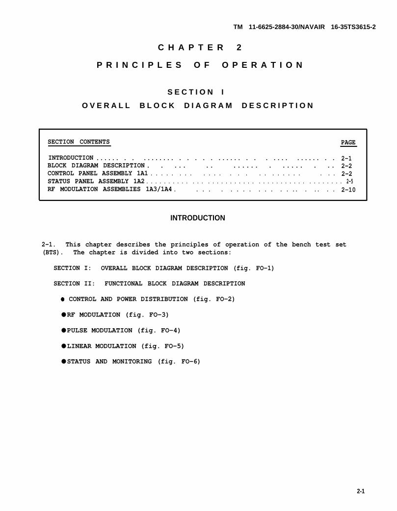
a. Control Panel Assembly 1A1. (Refer to figure FO-1.)The control panel assembly is divided into two functional areas.
Power, Control, Error and Status to and from LRU-1.
Power to the bench test set for AC Power, distribution, cooling, andYIG FILTER CONTROL.
(1) Power, Control, Error & Status
to UUT
2-2
TM 11-6625-2884-30/NAVAIR 16-35TS3615-2TM 11-6625-2884-30 NAVAIR 16-35TS3615-2
modes of operation are:
OFF -
STBY -
OPR -
No power applied to LRU-1
+28 V applied to enablereceiver circuits
Enables some transmittingcircuits
The INOP indicator lights when afault signal is received from LRU-1under test. The signal from LRU-1enables a relay in Control Indicator(1A1A1) . A ground return from therelay completes the circuit via CB1to +28 V,
The JAM indicator lights when LRU-1is transmitting active ECM. Thesignal from LRU-1 enables a relay inControl Indicator (1A1A1). A groundreturn from the relay completes thecircuit via CB1 to +28 V.
The TEST indicator lights whenLRU-1 self-test (BITE) isselected.
The GO [or the NO-GO) indicatorlights to indicate that LRU-1 is(or is not) functioning correctly.
2-3

TM 11-6625-2884-30/NAVAIR 16-35TS3615-2
BLOCK DIAGRAM DESCRIPTION (Continued)
(2) AC Power Distribution, Cooling and YIG FILTER CONTROL
AC POWER DISTRIBUTION : When CB2 is enabled 115V ac 60 Hz is applied to:
● CONTROL PANEL 1A1
STATUS PANEL 1A2
RF MODULATION 1A3
● RF MODULATION 1A4
When CB2 is enabled 115 VAC 60 Hz isapplied to:
CENTRIFUGAL BLOWER B1
● TUBEAXIAL FAN B2
Blower B1 is used to cool LRU-1 undertest.
Blower B2 is used to cool the BenchTest Set.
YIG FILTER CONTROL Circuit Breakers CB2 and CB3supply 115 V 60 Hz power topower supplies PS1, PS2 andPS3.
PS1 - 15 voltsTO YIG FILTER ONSTATUS PANEL
PS2 + 15 volts
PS3 + 10 volts TO YIG FILTER CONTROLSWITCHES
YIG FILTER IN/OUT switch S2 switchesYIG FILTER in and out of RF PATH.
The YIG FILTER CONTROL S3 thumbwheelcontrols the YIG FILTER in statuspanel 1A2 for the setting of RFfrequency.
2-4

TM 11-6625-2884-30 NAVAIR 16-35TS3615-2
b. Status Panel Assembly 1A2 (Refer to figure FO-1). The Status panelAssembly (1A2) is divided into three functional areas.
The Status Panel (1A2)provides forcing func-tion signals to UUT.Forcing Functions areenabled by pressingone of eight FORCINGFUNCTION lamp switcheswhich connect a groundfrom the Status Panel toUUT. The forcing func-tion signals consist ofthe following:
1 SORTER 1 LOAD (S5)
2 SORTER 1 OVRD (S6)
3 SORTER 2 LOAD (S7)
4 SORTER 2 OVRD (S8)
5 MOD DRIVE INHIBIT (S9)
6 NOISE INHIBIT (S10)
7 SW-3 INHIBIT (S11)
8 CP (S12)
2-5
TM 11-6625-2884-30/NAVAIR 16-35TS3615-2
BLOCK DIAGRAM DESCRIPTION (Continued)
The LAMP TEST pushbutton (S13) lights all FORCING FUNCTION lamps on the StatusPanel for test purposes.
STATUS and MONITORING The Status and MonitoringFunction consists of:
STATUS SIGNAL INDICATOR
VOLTAGE MONITOR SWITCH
OSCILLOSCOPE MONITOR
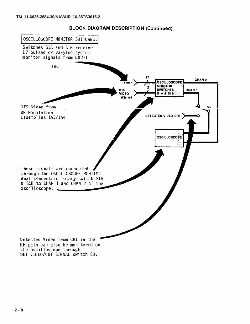
STATUS SIGNAL INDICATORS : A total of 18 statussignals are received
1
2
3
4
5
6
7
8
9
from LRU-1 under test.The signals are moni-tored with indicatorlights DS1 through DS20
The Status Panel lampsmonitor Sorter 1 andSorter 2 in LRU-1 undertest. The Status Panellamps consist of thefollowing:
CHANNEL 1 (SORTER 1)
SORTER LOAD COMMAND (DS1)
SLO LOAD COMMAND (DS2)
THREAT A (DS3)
CON SCAN (DS4)
SLO ACCUR (DS5)
SORTER LOADED (DS6)
SLO LOADED (DS7)
THREAT B (DS8)
TC RANGE JAM (DS9)
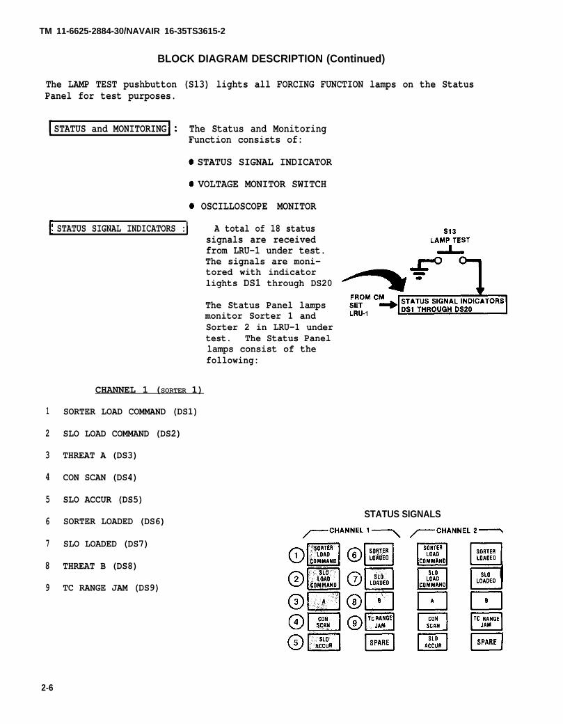
STATUS SIGNALS
2-6
TM 11-6625-2884-30 NAVAIR 16-35TS3615-2
CHANNEL 2 (SORTER 2)
10 SORTER LOAD COMMAND (DS11)
11 SLO LOAD COMMAND (DS12)
12 THREAT A (DS13)
13 CON SCAN (DS14)
14 SLO ACCUR (DS15)
15 SORTER LOADED (DS16)
16 SLO LOADED (DS17)
17 THREAT B (DS18)
18 TC RANGE JAM (DS19)
The LAMP TEST pushbuttonPanel for test purposes.
(S13) lights all Status signal lamps on the Status
VOLTAGE MONITOR SWITCH
2-7
TM 11-6625-2884-30/NAVAIR 16-35TS3615-2
2 - 8

TM 11-6625-2884-30/NAVAlR 16-35TS3615-2
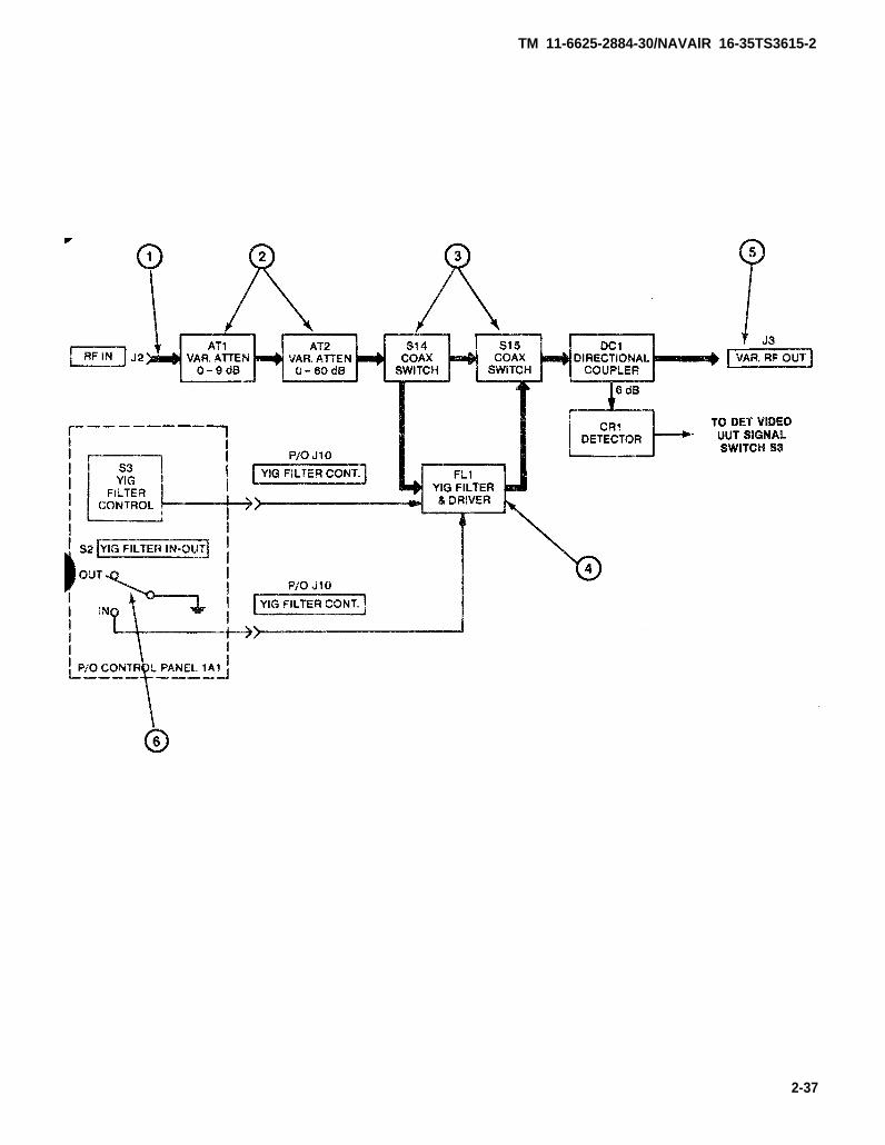
The RF output from LRU-1 under test is reduced to a safe level bya 30 dB attenuator and applied to RF Input of the status panel.
The RF feeds through two step Coax Switches S14 and S15attenuators controlled by the YIG FILTER
IN-OUT switch on controlAT1 - O-9dB 1A1 directs the RF either:AT2 - - 0
THROUGH YIG FILTER - RF MODULATEDSIGNALS.
2-9

TM 11-6625-2884-30/NAVAIR 16-35TS3615-2
BLOCK DIAGRAM DESCRIPTION (Continued)
The RF signal from Coax Switch S15 issplit at DIRECTIONAL COUPLER DC1
c. RF Modulation Assemblies 1A3/1A4.RF Modulation Assemblies are divided into
RF PATH (CW)
LINEAR MODULATION (CON SCAN)
PULSE MODULATION (A-W/A-F/B/VAR
(Refer to figure FO-l. ) Thethree functional areas.
PRI)
(1) RF Path (CW). (Refer to figure FO-1.) The RF sourceis a linearized voltage controlled oscillator VCO. (+17 dBmoutput)
2-10
TM 11-6625-2884-30/NAVAIR 16-36TS3615-2
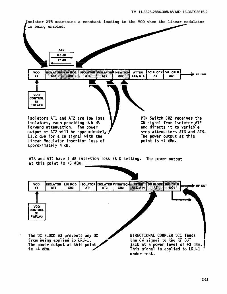
Isolator AT5 maintains a constant loading to the VCO when the linear modulatoris being enabled.
2-11
TM 11-6625-2884-30/NAVAIR 16-35TS3615-2
BLOCK DIAGRAM DESCRIPTION (Continued)
The Conical Scan Generator frequencies are generated digitallyand controlled by thumbwheel switches on the front panel of 1A3/1A4.
2-12
TM 11-6625-2884-30/NAVAIR 16-35TS3615-2
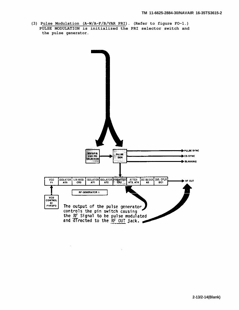
(3) Pulse Modulation (A-W/A-F/B/VAR PRI). (Refer to figure FO-1.)PULSE MODULATION is initialized the PRI selector switch andthe pulse generator.
2-13/2-14(Blank)


TM 11-6625-2884-30 NAVAIR 16-35TS3615-2
S E C T I O N I I
F U N C T I O N A L B L O C K D I A G R A M D E S C R I P T I O N
SECTION CONTENTS PAGE
CONTROL AND POWER DISTRIBUTION . . . . . . . . . . . . . . . . . . . . . . 2-15RF MODULATION . . . . . . . . . . . . . . . . . . . . . . . . . . . . . . . . . . . . .... . . . . . . . . . . . . 2-23PULSE MODULATION . .. . . . . . . . . . . . . . . . . . . . . . . 2-30LINEAR MODULATION . . ... . . . . . . . . .. . . . . . . . . . . . . . 2-34STATUS AND MONITORING . . . .. . . . . . . . . . . . . . . . . . . . . . . . . . . . . . . . . . . . . . . . . 2-36
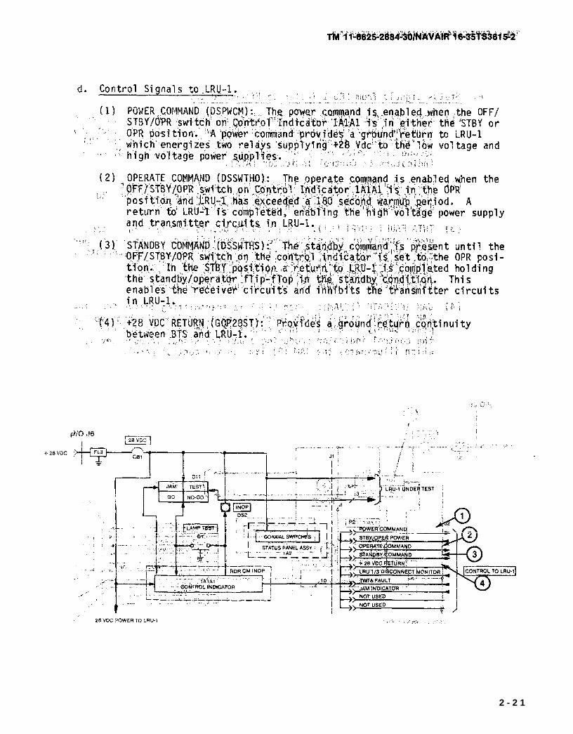
CONTROL AND POWER DISTRIBUTION
2-3. (Refer to figure FO-2.) The control and power distribution functionswill be discussed in the following five sections, all located on figure FO-2.
115 Vac power distribution to the bench test set and blowers.
YIG filter control.
+28 Vdc power distribution to UUT and the control indicator.
Control signals to LRU-1.
Status signals from LRU-1.
2-15
TM 11-6625-2884-30/NAVAIR 16-35TS3615-2
CONTROL AND POWER DISTRIBUTION (Continued)
a. 115 Vac Power Distribution to the Bench Test Set and Blowers.
(1)
(2)
(3)
(4)
(5)
(6)
115 Vat, 60 Hz Power Cable W6 connects 115 Vac to input power 115VAC, 60 Hz jack J5.
Filters, FL1 and FL2 provide electromagnetic interference EMI inte-grity. The line filters eliminate conductive interference from theBTS.
When circuit breaker CB2 is enabled 115 Vac is applied to Blowers B1and B2.
Centrifugal Blower B1 when enabled delivers cooling air to LRU-1 at145 CFM at a nominal motor speed of 3150 RPM.
Tubeaxial Fan B2 when enabled delivers cooling air to the BTS cabi-net at 110 CFM at a nominal motor speed of 3250 RPM.
The 115 Vac, 60 Hz, single phase feeds Control Panel Assembly 1A1,and is distributed through Jack J7 to:
RF MODULATION ASSEMBLY 1A4
2-16

TM 11-6625-2884-30/NAVAIR 16-351S3615-2
2-17
TM 11-6625-2884-30/NAVAIR 16-35TS3615-2
CONTROL AND POWER DISTRIBUTION (Continued)
b. YIG FILTER Control . The BTS contains a microwave bandpass filter of theYttrium Iron Garnet (YIG) type.
(1) 115 VAC, 60 Hz, 10 is applied through input power jack J5 to linefilters FL1 and FL2 which eliminate conductive EMI from the BTS.Circuit Breaker CB2, when enabled, supplies input ac power toCircuit Breaker CB3.
(2) Circuit Breaker CB3 is a push-to-reset device located on the frontpanel of 1A1. When CB3 is enabled ac power is applied toYIG Filter Power Supplies PS1, PS2 and PS3.
( 3) Power Supply PS1, when enabled, supplies -15 Vdc ±1% with anoutput current of 0.1 amps to the YIG filter in the status panelassembly. Power Supply PS2, when enabled, supplies +15 Vdc ±1%with an output current of 1.0 amps to the YIG filter in the statuspanel.
(4) POWER Indicator DS3 lights when +15V Power Supply PS2 is enabled.
(5) Power Supply PS3, when enabled, supplies +10 Vdc ±1% with anoutput current of 0.12 amps to the YIG FILTER CONTROL switch S3.S3 is a three decade thumbwheel switch used to tune the YIG filterto the F1, F2 and F3 frequencies.
(6) The +28 Vdc is applied through INPUT POWER jack J6 to line filterFL3 and FL4 which eliminate conductive EMI from the BTS. CircuitBreaker CB1, when enabled, supplies heater power to YIG filter1A2FL1.
(7) YIG FILTER IN/OUT Switch S2 is used to switch the YIG filter in orout of the RF Path in the status panel.
OUT position - YIG filter bypassed (no insertion loss)
IN position = YIG filter in circuit (used to measure depth of modu-lation)
(8) Al 1 signals are routed through P4 to status panel connector 1A2J10.
2-18
TM 11-6625-2884-30/N
AV
AIR
16-35TS3615-2
2-19
TM 11-6625-2884-30/NAVAIR 16-35TS3615-2
CONTROL AND POWER DISTRIBUTION (Continued)
c. 28 VDC Power Distribution to LRU-1 and the Control Indicator.
(1)
(2)
(3)
(4)
(5)
Power cable W7 connects 28 Vdc from the power supply to Input Power28 VDC jack J6.
Line Filters FL3 and FL4 contribute to electromagnetic interference(EMI) integrity. The filters eliminate conductive interference fromthe BTS.
When circuit breaker CB1 is enabled, 28 Vdc is applied to controlindicator, UUT, one side of the JAM and INOP lamps and to YIG filtercoaxial switches on 1A2.
28 Vdc to the control indicator enables LRU-1 disconnect monitorrelay K3 which sets up conditions for entering the standby andoperate modes.
28 Vdc is routed through 28V POWER jack J3 to UUT via cable W3.
2-20
TM 11-6625-2884-30 NAVAIR 16-35TS3615-2
2 - 2 1
TM 11-6625-2884-30/NAVAIR 16-35TS3615-2
CONTROL AND POWER DISTRIBUTION (Continued)
e. Status Signals from LRU-1 (refer to Figure FO-13).
(1)
(2)
(3)
(4)
STBY/OPR POWER (DQTDOPR): The STBY/OPR Power (+28 V dc) is receivedfrom the low voltage power bus in LRU-1 when the control indicatoris switched to standby or operate. The +28 Vdc enables the 180second time delay relay and supplies +23 V to the ON, STBY and OPRindicators in Control Indicator 1A1A1.
LRU-1 DISCONNECT MONITOR (GOP28ST): The LRU-1 disconnectmonitor (ground) is received from LRU-1 and energizes the LRU-1disconnect monitor relay in Control Indicator 1A1A1.
TWTA FAULT (OVPT FLT): When a fault occurs in the high voltagepower supply or traveling wave tube amplifier or if an overtempera-ture condition occurs in LRU-1, a TWTA fault signal is generated.This causes the fault relay in the control indicator tode-energize, generating an INOP (5) ground level signal,illuminating the INOP (6) lamp on the control panel.
JAM INDICATE (1YJAM): When LRU-1 is transmitting active ECM, theJAM INDICATE signal (high level) is received from the high voltagepower supply in LRU-1. This causes the jam relay to energize inthe control indicator producing a JAM (7) signal (ground level)which illuminates the JAM (8) lamp on the control panel.
2-22
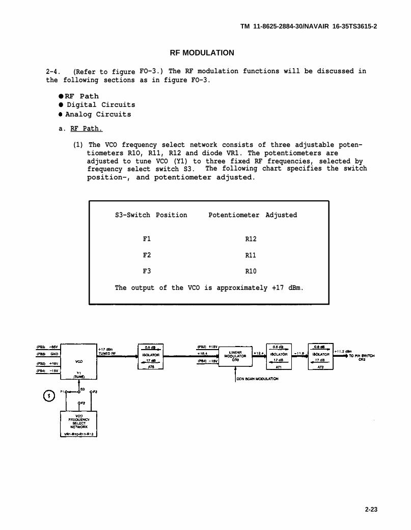
2-4. (Refer to figurethe following sections
TM 11-8625-2884-30/NAVAIR 16-35TS3615-2
RF MODULATION
FO-3.) The RF modulation functions will be discussed inas in figure FO-3.
● RF Path● Digital CircuitsAnalog Circuits
a. RF Path.
(1) The VCO frequency select network consists of three adjustable poten-tiometers R1O, R11, R12 and diode VR1. The potentiometers areadjusted to tune VCO (Y1) to three fixed RF frequencies, selected byfrequency select switch S3. The following chart specifies the switchposition-, and potentiometer adjusted.
S3-Switch Position Potentiometer Adjusted
F1 R12
F2 R11
F3 R10
The output of the VCO is approximately +17 dBm.
2-23
TM 11-6625-2884-30/NAVAIR 16-35TS3615-2
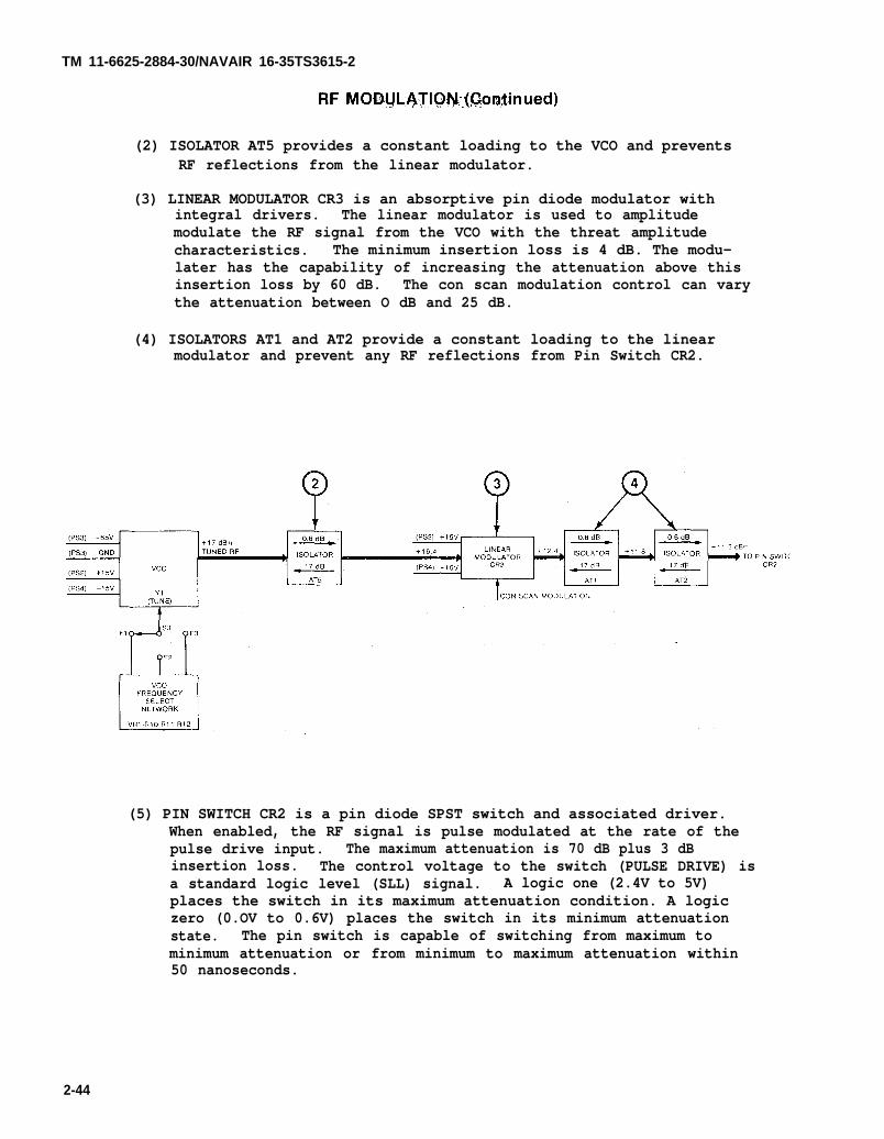
(2) ISOLATOR AT5 provides a constant loading to the VCO and preventsRF reflections from the linear modulator.
(3) LINEAR MODULATOR CR3 is an absorptive pin diode modulator withintegral drivers. The linear modulator is used to amplitudemodulate the RF signal from the VCO with the threat amplitudecharacteristics. The minimum insertion loss is 4 dB. The modu-later has the capability of increasing the attenuation above thisinsertion loss by 60 dB. The con scan modulation control can varythe attenuation between O dB and 25 dB.
(4) ISOLATORS AT1 and AT2 provide a constant loading to the linearmodulator and prevent any RF reflections from Pin Switch CR2.
(5) PIN SWITCH CR2 is a pin diode SPST switch and associated driver.When enabled, the RF signal is pulse modulated at the rate of thepulse drive input. The maximum attenuation is 70 dB plus 3 dBinsertion loss. The control voltage to the switch (PULSE DRIVE) isa standard logic level (SLL) signal. A logic one (2.4V to 5V)places the switch in its maximum attenuation condition. A logiczero (0.OV to 0.6V) places the switch in its minimum attenuationstate. The pin switch is capable of switching from maximum tominimum attenuation or from minimum to maximum attenuation within50 nanoseconds.
2-44
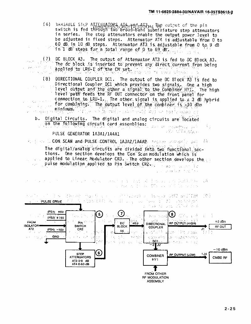
TM 11-6625-2884-30 NAVAIR 16-35TS3615-2
2 - 2 5

TM 11-6625-2884-30/NAVAIR 16-35TS3615-2
RF MODULATION (Continued)
c. Analog Circuits
(1)
(2)
(3)
(4)
(5)
(6)
(7)
(8)
(9)
(10)
(11)
CON SCAN FREQUENCY SELECT SWITCH S2 is a two decade thumbwheel switchwhich selects the con scan frequency from O-99 Hz.
PULSE GENERATOR 1A3A1/1A4A1 contains a clock generator, counters, com-parators, digital con scan generator and a D/A converter which producea triangle wave at the preset frequency of the con scan frequency selectswitch S2.
The digital con scan generator providescrossover of the triangle wave at front
the CON SCAN SYNC at the zeropanel jack SYNC-CS J5.
CON SCAN SHAPER and PULSE CONTROL 1A3A2/1A4A2 receives the triangle waveand shapes it into a sinewave. The depth of modulation of the sinewaveis controlled by CON SCAN MODULATION DEPTH SWITCH S6, adjustable fromO-25 dB.
The sinewave output of the shaper is amplified and sent to LINEARMODULATOR CR3.
The sinewave output of the shaper is also directed to CS MONITOR jackJ9. Jack J9 connects to BTS VIDEO on the Status Panel 1A2 to bemonitored by the oscilloscope.
PULSE MODULATION TO PIN SWITCH CR2. PRI Selector Switch S7 selects onof three preset PRI’s A-W, A-F, B, or a variable PRI set by the PRIselect switch S5.
VARIABLE PRI Select Switch is a three decade thumbwheel switch with arange of 300 to 999 microseconds.
PATTERN SYNC signal is developed from a threatregister. It is used to sync the oscilloscopeA-W/A-F/B are selected.
decoder and PROM addresswhen the preset PRI’s
PRI DATA is developed from programmed ROM’s and pulse control circuitryfor controlling the PRI generator on the pulse generator card.
When PRI data (interval between two pulses) is received at the pulsegenerator an advance address signal is sent to the con scan shaper andpulse control card to set up the next PRI.
2-26

TM 11-6625-2884-30/NAVAIR 16-36TS3615-2
2-27
TM 11-6625-2884-30/NAVAIR 16-35TS3615-2
RF MODULATION (Continued)
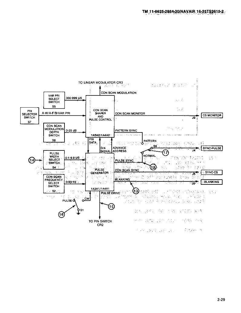
(12) PULSE SYNC is generated together with ADDRESS ADVANCE and is used tosync the oscilloscope.
(13) BLANKING pulse is generated 100 ns prior to the leading edge of thePULSE DRIVE signal and ends 600 ns after the trailing edge of PULSEDRIVE. The pulse is available at Blanking Jack J6 to simulate theblanking pulse supplied to LRU-1 from the aircraft.
(14) PULSE WIDTH SELECT SWITCH S4. This control is capable of setting thewidth from 0.1 to 9.9 µs in 0.1 µs steps.
(15) PULSE DRIVE. The PRI generator produces a pulse train simulating radarthreats except when PRI select switch is in OFF. The pulse drive signalenables Pin Switch CR2 to pulse modulate the RF signal.
(16) PULSE/CW SWITCH S1. In the pulse position, the pulse drive signal isIn the CW position the pulse drive signal is inhibited.
(17) NORMAL/PATTERN SWITCH S8. Selects either pulse syncsync the oscilloscope when performing maintenance on
or pattern sync toLRU-1.
2-28
TM 11-6625-2884-30 NAVAIR 16-35TS3615-2
2-29
TM 11-6625-2884-30/NAVAIR 16-35TS3615-2
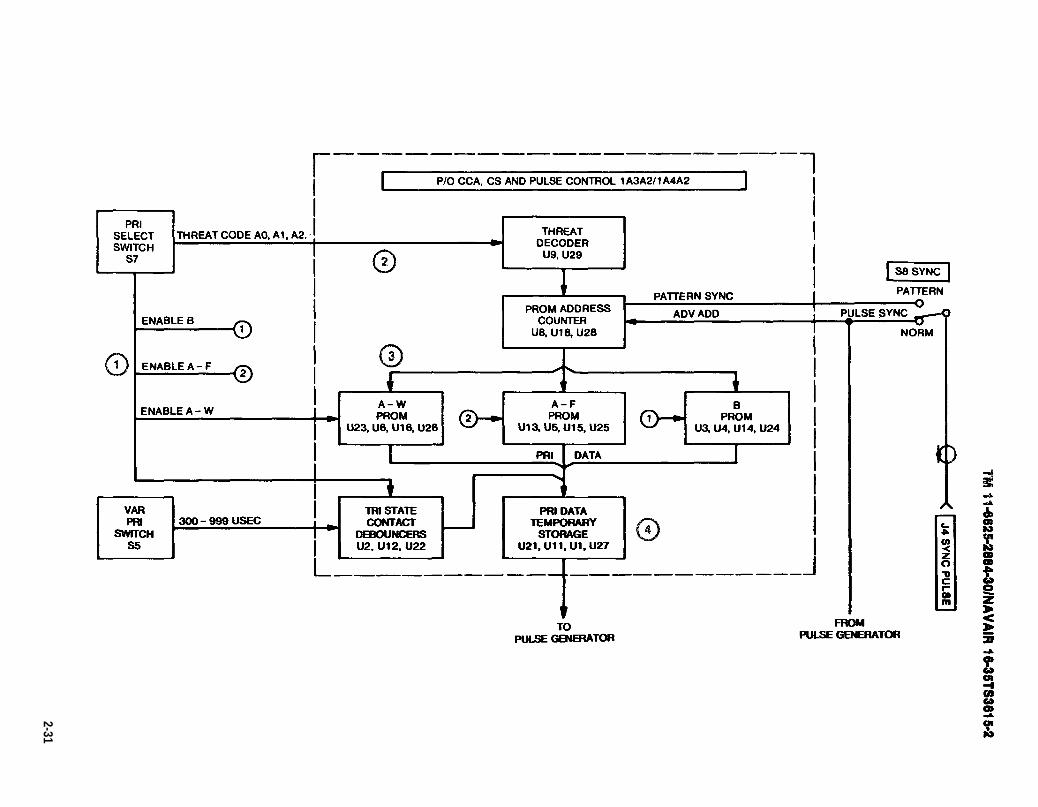
PULSE MODULATED
2-5. (Refer to figure FO-4.) The pulse modulation circuits are located onCCA, CS and Pulse Control 1A3A2/1A4A2 and CCA, Pulse Generator 1A3A1/1A4A1.
(1) PRI SELECT SWITCH S7 is a four position rotary switch which selects the
(2)
(3)
(4)
PRI pattern for the Pulse Generator. Three positions of the switchselect one of three preset PRI’s. The switch position and threat codesare as follows:
S7-Switch Position Threat Code
A-W AO
A-F A1
B A2
VAR PRI
The other position of the switch selects a variable PRI controlled byVARIABLE PRI Switch S5.
THREAT DECODER. The threat decoder consists of two programmed micro-circuits U9, U29. Each PROM contains 32 words, each word contains 8bits of data. The two PROM’s make up a 16 digit word. The first wordaddresses the A-W mode, the second word addresses the A-F mode and thethird word addresses the B mode. The information from the threatdecoder is loaded into the PROM address counter U8, U18, U28.
A-W/A-F/B PROM’S. The PROM address counter addresses the A-W/A-F/BPROM’s, Each mode contains 4 PROM’S. Each PROM contains 512 words.Each word contains 4 bits of data.
A-W PROMS U23, U6, U16, U26
A-F PROMS U13, U5, U15, U25
B PROMS U3, U4, U14, U24
PRI DATA TEMPORARY STORAGE. 16 bits of PRI data from A-W/A-F/B, and 16bits of PRI data from the VAR PRI switch S5, via contact denouncers U2,U12, U22, are OR’ed at the input of the PRI data temporary storage U21,U11, U1, U27. The information stored is determined by the enablesignals from the PRI select switch S7.
2-30
TM
11-6625-2884-30N
AV
AIR
16-35TS
3615-2
2-31

TM 11-6625-2884-30/NAVAIR 16-35TS3615-2
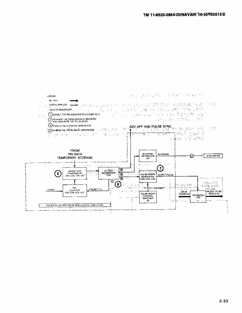
(5)
(6)
(7)
PULSE MODULATION (Continued)
MAGNITUDE COMPARATOR. The magnitude comparator U44, U33, U35, U47 com-pares the PRI data in the temporary storage with the PRI counter U45,U25, U26, U37. When a comparison occurs, output sequencer U29 isenabled.
OUTPUT SEQUENCER. When the output sequencer is enabled the followingevents occur:
PRI COUNTER is preset (1) to a count of 2.
PROM ADDRESS REGISTER is advanced (2) and pulse sync is generated.
BLANKING GENERATOR U27 is enabled (3).
PULSE WIDTH GENERATOR U48, U49, U38 is enabled (4).
WIDTH GENERATOR. The pulse width generator, when enabled bythe output sequencer, generates the output pulse to PIN Switch CR2.The width of the pulse is determined by the setting of the pulsewidth control switch S4.
2-32
TM 11-6625-2884-30 NAVAIR 16-35TS3615-2
2-33
TM 11-6625-2884-30/NAVAIR 16-35TS3615-2
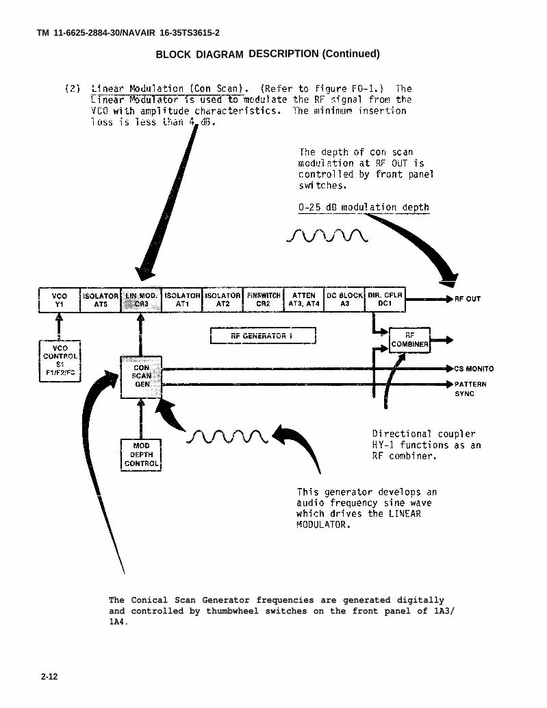
LINEAR MODULATION
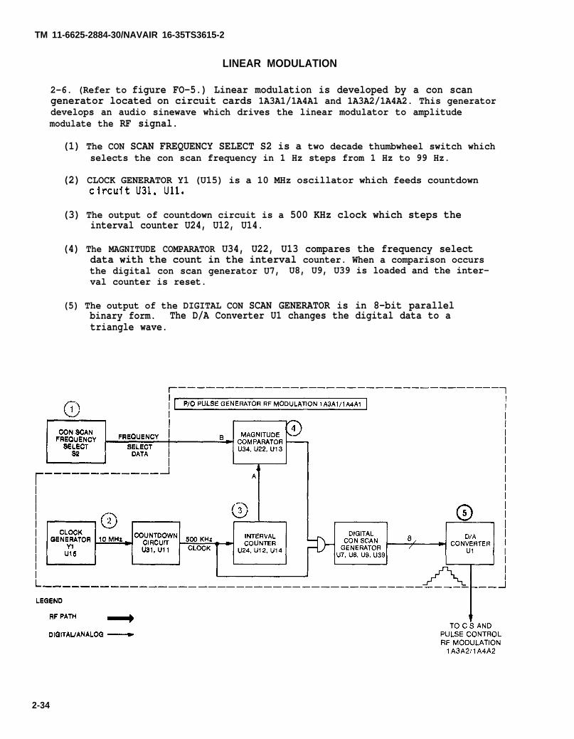
2-6. (Refer to figure FO-5.) Linear modulation is developed by a con scangenerator located on circuit cards 1A3A1/1A4A1 and 1A3A2/1A4A2. This generatordevelops an audio sinewave which drives the linear modulator to amplitudemodulate the RF signal.
(1) The CON SCAN FREQUENCY SELECT S2 is a two decade thumbwheel switch whichselects the con scan frequency in 1 Hz steps from 1 Hz to 99 Hz.
(2) CLOCK GENERATOR Y1 (U15) is a 10 MHz oscillator which feeds countdown
(3) The output of countdown circuit is a 500 KHz clock which steps theinterval counter U24, U12, U14.
(4) The MAGNITUDE COMPARATOR U34, U22, U13 compares the frequency selectdata with the count in the interval counter. When a comparison occursthe digital con scan generator U7, U8, U9, U39 is loaded and the inter-val counter is reset.
(5) The output of the DIGITAL CON SCAN GENERATOR is in 8-bit parallelbinary form. The D/A Converter U1 changes the digital data to atriangle wave.
2-34
TM 11-6625-2884-30 NAVAIR 16-35ts3615-2
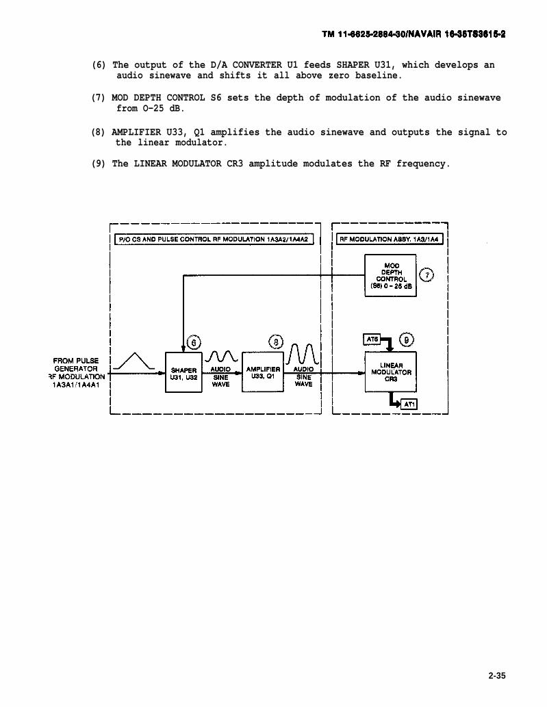
(6) The output of the D/A CONVERTER U1 feeds SHAPER U31, which develops anaudio sinewave and shifts it all above zero baseline.
(7) MOD DEPTH CONTROL S6 sets the depth of modulation of the audio sinewavefrom O-25 dB.
(8) AMPLIFIER U33, Q1 amplifies the audio sinewave and outputs the signal tothe linear modulator.
(9) The LINEAR MODULATOR CR3 amplitude modulates the RF frequency.
2-35

TM 11-6625-2884-30/NAVAIR 16-35TS3615-2
STATUS AND MONITORING
2-7. (Refer to figure FO-6.) Status Panel Assembly 1A2 has an RF path,moni-toring switch, status indicators and control switches relating to UUT status.
a. RF Path.
(1) The high RF power output from LRU-1 is reduced by a 30 dB RF powerattenuator installed at the RF output of LRU-1. The output of the30 dB attenuator is coupled through RF IN Jack J2 at the front ofthe status panel and then through two step attenuators.
(2) Attenuator AT1 provides O dB to 9 dB in increments of 1 dB. Atten-uator AT2 provides O dB to 60 dB in increments of 10 dB. This pro-vides a range of O dB to 69 dB by the settings of the respectiveswitches.
(3) Coax Switches S14 and S15 are controlled by the YIG FILTER IN/OUTSwitch S2 on the control panel. When the switch is in the OUTposition, the coax switch is de-energized and RF is directedstraight through to Directional Coupler DC1. This is the normalcondition when monitoring detected video signals.
(4) When a modulation depth signal is being tested, the YIG FILTERIN/OUT switch S2 will be in the IN position. This energizes CoaxSwitches S14 and S15, directing the RF through YIG filter anddriver and then to Directional Coupler DC1.
(5) Directional Coupler DC1 splits the RF. One path going to VAR RFOUT Jack J3 at the front of the status panel and the other path(reduced by 6 dB) going to Detector CR1. The detected video fromCR1 is sent to the DET VIDEO/UUT SIGNAL Switch S3.
(6) The YIG FILTER CONTROL Switch S3 1ocated on Control Panel Assembly1A1 is used to tune the YIG Filter and Driver FL1 to the F1, F2 andF3 frequencies as follows:
FREQUENCY YIG FILTER CONTROL SETTINGS
F1 330
F2 509
F3 688
2-36
TM 11-6625-2884-30/NAVAlR 16-35TS3615-2
2-37

TM 11-6625-2884-30 NAVAIR 16-35TS3615-2
b. Monitoring.
(1)
(2)
(3)
OSCILLOSCOPE MONITOR (BLACK) S1A and OSCILLOSCOPE MONITOR (RED)S1B. This dual concentric rotary switch receives a total of 17pulsed or varying system monitor signals from LRU-1 jack J7,connected through cable W1 to jack J1 on the status panel. Theswitch also receives the BTS VIDEO 1 (J7) from RF ModulationAssembly 1A4 and BTS VIDEO 2 (J8) from RF Modulation Assembly 1A3.The rotary switch black knob switches CHAN 1 connector J4 to one of17 points in LRU-1 or to BTS VIDEO J7. The rotary switch red knobswitches CHAN 2 (J5) to one of 17 points in the UUT or the BTSVIDEO J8.
DET VIDEO/UUT SIGNAL S3. This toggle switch selects either the de-tected video from CR1 in the RF path or the signal being monitoredby OSCILLOSCOPE MONITOR (BLACK) S1A and directs it to CHAN 1 con-nector J4.
VOLTAGE MONITOR S2. Nine DC voltages from the low voltage powersupply in LRU-1 are connected through LRU-1 J7, Cable W1, to statuspanel jack J1. The voltages are selectable by VOLTAGE MONITORSwitch S2 on the front panel for measurement with an external digi-tal multimeter connected to V MON J6.
2-38

TM 11-6625-2884-30 NAVAIR 16-35TS3615-2
c. Status.
(1) A total of 18 status signals and 2 spares are supplied from LRU-1to the BTS to monitor the status of LRU-1. The signals aremonitored by indicator lights. The status signal, negative logicis connected from LRU-1 Jack J7 through Cable W1 to Jack J1 on thestatus panel.
(2) LAMP DRIVER ASSY 1A2A3 (U1, U2, U3, U4, U5) receives the statussignals from J1. The status signals are connected to fiveidentical integrated circuit chips. Each chip contains four lampdriver circuits. Each driver consists of a two-input nand gate andoutput power driver.
(3) Power Supply PS1 supplies +12 Volts to one terminal of al 1 statuspanel lamps.
(4) Whenever the inverting output power driver receives a positivelogic 1 signal, that particular status panel lamp illuminates. Thefollowing is a simplified circuit of the U1 lamp driver and statuslamp DS1.
2-39

TM 11-6625-2884-30/NAVAIR 16-35TS3615-2
STATUS AND MONITORING (Continued)
LAMP TEST Switch S13, when depressed, applies a ground level to oneinput of the nand gate on the lamp driver assembly. The high outputfrom the nand gate turns on the output power drivers, illuminatingthe lamps on the status panel.
d. Control .
(1) The status panel provides forcing signals to LRU-1 to forceit to a particular state. This is accomplished by pressing one of8 forcing function lamp switches S5 through S12 on the forcingfunction panel. The forcing function lamp switches connect aground froin the Status Panel to a point in LRU-1. When a functionis being forced, the indicator on the forcing function switch islit.
(2) POWER SUPPLY PS1 supplies +12V to one terminal of each forcingWhen the switch is depressed a ground return is supplied to
the other terminal.
(3) LAMP TEST S13, when depressed, provides a ground return to illumi-nate all forcing function lamps.
(4) RESET S4, when depressed, provides a master reset signal (groundlevel) to LRU-1 under test.
2-40

TM 11-6625-2884-30/NAVAIR 16-35TS3615-2
2-41/2-42(Blank)


TM 11-6625-2884-30/NAVAIR 16-35STS3615-2
C H A P T E R 3
M A I N T E N A N C E I N S T R U C T I O N S
S E C T I O N I
R E P A I R P A R T S , S P E C I A L T O O L S ; T E S T ,
M E A S U R E M E N T A N D D I A G N O S T I C E Q U I P M E N T ( T M D E ) ;
A N D S U P P O R T E Q U I P M E N T
SECTION CONTENTS PAGE
INTRODUCTION . . . . . . . . . . . ...... . . . . . . . . . . . . . . . . . . . . . . . . . . . . . . . 3-1SCHEMATIC DIAGRAMS . .... . . . . . ... ...... . . . . ..... ... 3-2TOOLS AND REPAIR PARTS . . ...... . ...... . . . . ..... . . . . . .... . TEST EQUIPMENT . ...... . . . . . . . . . . . . . . ....... . .......... . 3-2
INTRODUCTION
3-1. This chapter contains the aviation intermediate maintenance instructions
3-2
for the BTS. Section II contains installation instructions for the BTS. Sec-tion III provides detaisolating it to a Shoption, removal , and replprocedures. Section V
iled troubleshooting procedures for detecting a fault andReplaceable Unit (SRU). Section IV provides unit loca-acement information including power supply adjustmentprovides AVIM testing and re-test instructions.
3-1

TM 11-6625-2884-30/NAVAIR 16-35TS3615-2
SCHEMATIC DIAGRAMS
3-2. Foldout schematic diagrams of the BTS are included in the rear of thismanual, for reference purposes and as further troubleshooting aids.
TOOLS AND REPAIR PARTS
3-3. Tool Kit, Electronic Equipment TK-105/G contains hand tools necessary formaintenance of the BTS. Various sizes of screwdrivers and wrenches are neededto remove and replace the BTS chassis assemblies and power supplies. Refer toTM 11-6625-2884-30P for repair parts.
TEST EQUIPMENT
3-4. The following test equipment is required to maintain the BTS. Testequipment similar to and having characteristics equal to this test equipmentmay be used.
Common Name
Oscilloscope including:Dual Channel AmplifierTime Base & Delay Generator10X Probe (2 each)
Digital MultimeterFrequency MeterRF Power MeterRF Power SensorPower Supply, 28V (30A min)
Manufacturer and Type
AN/USM-281A
AN/USM-451HP P532AHP 435AHP 8481APP-1104/G
3-2

TM 11-6625-2884-30/NAVAIR 16-35TS3615-2
SECTION IIINSTALLATION INSTRUCTIONS
SECTION CONTENTS
GENERAL ....... . . . . . . ... . ........ . ...... . . . . . . . . . . . . . . . . . . . . . . . . . .CONNECTIONS . . . . . .... . ........ . . . . . . . . . . ● ...... ● . . ...... . . . . . . . . . .CABLING/HOSE ATTACHMENT TO BTS CONNECTOR PANEL . . . . ..... . . . . . . . . . . . . . . . . .POWER REQUIREMENTS . . . . . . . . . . . . . . . . . . . . . . ● ..... . . . . ..... . . .....CHECKOUT . . . . . . . . . ● ● . . . . . . . . . . . . . . . . . . . . . . . . . . . . . . . . . . . . . . . . . . . . . .
PAGE
3-33-33-43-63-6
GENERAL
3-5. This section describes the bench requirements, cable and air duct connec-tions and ac power requirements of the BTS. Use a bench at least 30" x 72",capable of supporting 500 lbs.
CONNECTIONS
3-6. Loosen cover fasteners and open hinged covers on the upper left side andtop of the BTS to expose the connector panel and blower panel.
3-3
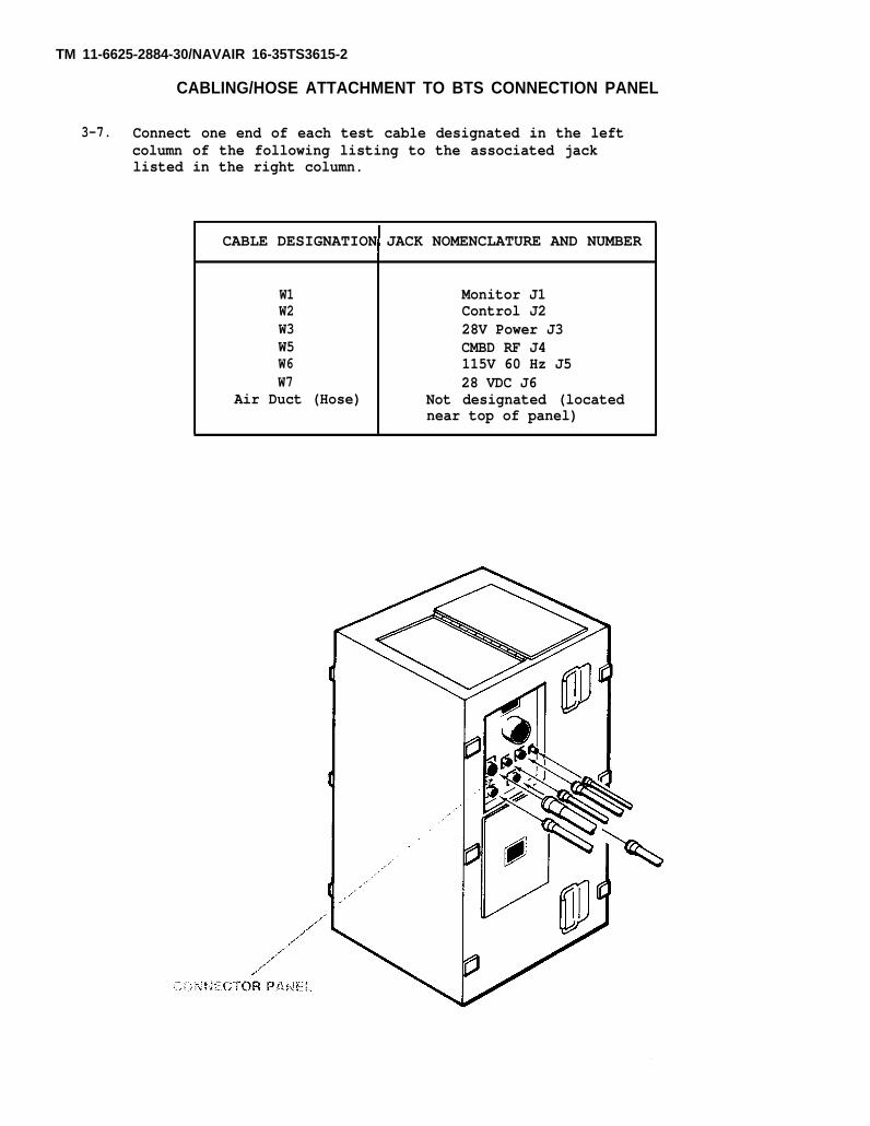
TM 11-6625-2884-30/NAVAIR 16-35TS3615-2
CABLING/HOSE ATTACHMENT TO BTS CONNECTION PANEL
3-7. Connect one end of each test cable designated in the leftcolumn of the following listing to the associated jacklisted in the right column.
CABLE DESIGNATION JACK NOMENCLATURE AND NUMBER
W1W2W3W5W6W7
Air Duct (Hose)
Monitor J1Control J228V Power J3CMBD RF J4115V 60 Hz J528 VDC J6
Not designated (locatednear top of panel)

TM 11-6625-2884-30 NAVAIR 16-35TS3615-2
3-5

TM 11-6625-2884-30/NAVAIR 16-35TS3615-2
CABLING/HOSE ATTACHMENT TO BTS CONNECTOR PANEL (Continued)
Secure the air duct to the BTS using one of two supplied hose clamps. Use thesecond hose clamp to secure the air duct to LRU-1, using the BTS ring adapter.
3-8. Equip the test bench for 115 Vac 60 Hz to operate the BTS, and with 28Vdc with 30 ampere capacity via a PP-1104/G power supply, or equivalent, tooperate LRU-1.
CHECKOUT
3-9. After installation, adjustment, repair or replacement of a BTS component,check out the BTS as in section III.
3-6

TM 11-6625-2884-30/NAVAIR 16-35TS3615-2
SECTION IllTROUBLESHOOTING
SECTION CONTENTS
GENERALTEST CONDITIONSDEFINITIONSTEST EQUIPMENT USEPRELIMINARY TEST SET-UPRF OUTPUT LEVEL CHECKRF OUTPUT FREQUENCY CHECKVARIABLE PRI CHECKCON SCAN MODULATION CHECKPRI CHECKBLANKING OUTPUT TESTPULSE SYNC TESTCON SCAN SYNC TESTSTATUS PANEL INDICATOR CHECKSTATUS PANEL FORCING FUNCTION CHECKSTATUS PANEL OSCILLOSCOPE MONITOR CHECKSTATUS PANEL VOLTAGE MONITOR CHECKYIG FILTER CHECKCONTROL PANEL CHECK
PAGE
3-9
3-73-9
3-93-113-143-193-233-293-363-403-433-463-493-523-553-603-623-70
GENERAL
3-10. Troubleshooting information is covered in paragraphs 3-15 through 3-28.Each paragraph provides the test set-up and contains tests in tabular logictree format consisting of four staggered columns. Column 1 contains STEPnumbers with the steps in ascending order. Column 2 designated ACTION explainsthe test. Column 3 NORMAL INDICATION states what measurements should beobserved for normal circuit operation. Column 4 designated FIX lists whatcourse to follow if a measurement deviates excessively from the stated value incolumn 3.
3-7
TM 11-6625-2884-30/NAVAIR 16-35TS3615-2
GENERAL (Continued)
To fix a specific trouble, go to the page listed in the following symptomindex.
SYMPTOM INDEX
TROUBLE WITH PAGE
CONTROL PANEL ASSEMBLY 1A1Controls 3-70YIG Filter 3-62
STATUS PANEL ASSEMBLY 1A2Forcing Functions 3-52Status Indicators 3-49Oscilloscope Monitor 3-55Voltage Monitor 3-60
RF MODULATION ASSEMBLY 1A3/1A4Blanking Output 3-40Con Scan Modulation 3-29Con Scan Sync 3-46
PRIPulse SyncRF Output Level
3-363-433-14
RF Output Frequency 3-19Variable PRI 3-23
To check out the entire BTS, perform all the procedures in this section.
3-8
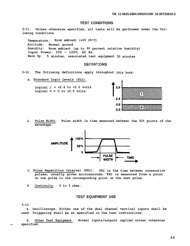
—
TM 11-6625-2884-30/NAVAIR 16-35TS3615-2
TEST CONDITIONS
3-11. Unless otherwise specified, all tests will be performed under the fol-lowing conditions.
Temperature: Room ambient (+25 ±5°C)Altitude: Normal groundHumidity: Room ambient (up to 90 percent relative humidity)Input Power: 105 - 125V, 60 HzWarm Up: 5 minutes, associated test equipment
3-12. The following definitions apply throughout
30 minutes
this book:
a. Standard Logic Levels (SLL).
Logical 1 = +2.4 to +5.0 voltsLogical O = O to +O.6 volts
b. Pulse Width. Pulse width is time measured betweenwaveshape.
the 50% points of the
c. Pulse Repetition Interval (PRI). PRI is the time between consecutivepulses, usually given microseconds. PRI is measured from a pointon one pulse to the corresponding point on the next pulse.
d. Continuity. O to 3 ohms.
TEST EQUIPMENT USE
3-13.a. Oscilloscope. Either one of the dual channel vertical inputs shall be
used. Triggering shall be as specified in the test instructions.
b. Other Test Equipment. Normal inputs/outputs implied unless otherwisespecified.
3-9
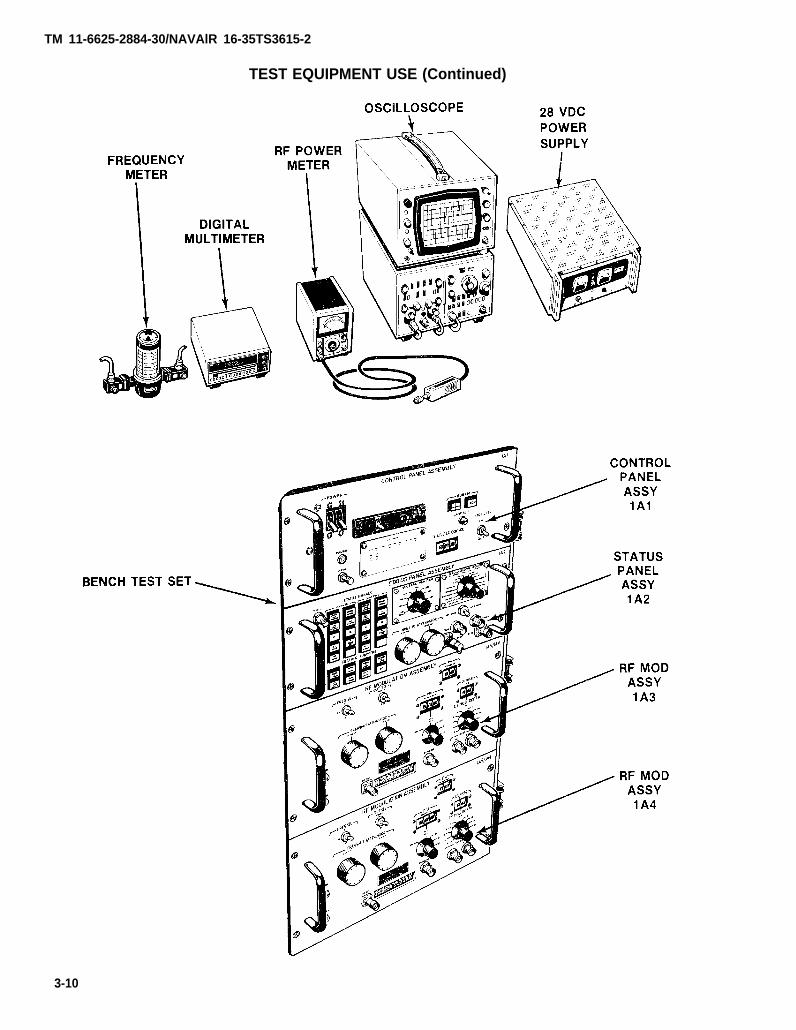
TM 11-6625-2884-30/NAVAlR 16-35TS3615-2
TEST EQUIPMENT USE (Continued)
3-10
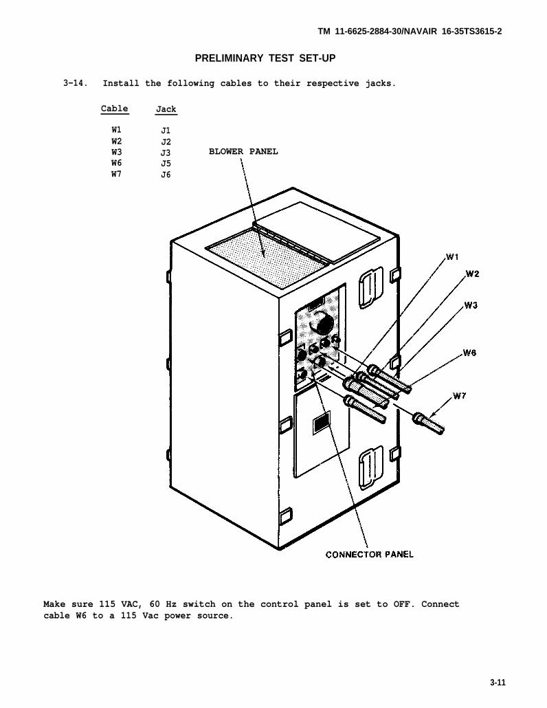
TM 11-6625-2884-30/NAVAIR 16-35TS3615-2
PRELIMINARY TEST SET-UP
3-14. Install the following cables to their respective jacks.
Cable Jack
W1 J1W2 J2W3 J3 BLOWER PANELW6 J5W7 J6
Make sure 115 VAC, 60 Hz switch on the control panel is set to OFF. Connectcable W6 to a 115 Vac power source.
3-11
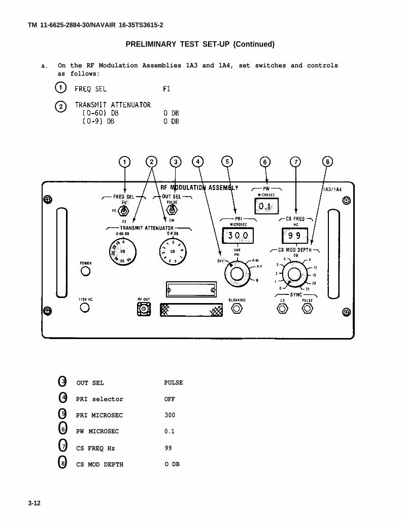
TM 11-6625-2884-30/NAVAIR 16-35TS3615-2
PRELIMINARY TEST SET-UP (Continued)
a. On the RF Modulation Assemblies 1A3 and 1A4, set switches and controlsas follows:
o3 OUT SEL PULSE
o4 PRI selector OFF
o5 PRI MICROSEC 300
06 PW MICROSEC 0.1
07 CS FREQ Hz 99
08 CS MOD DEPTH O DB
3-12
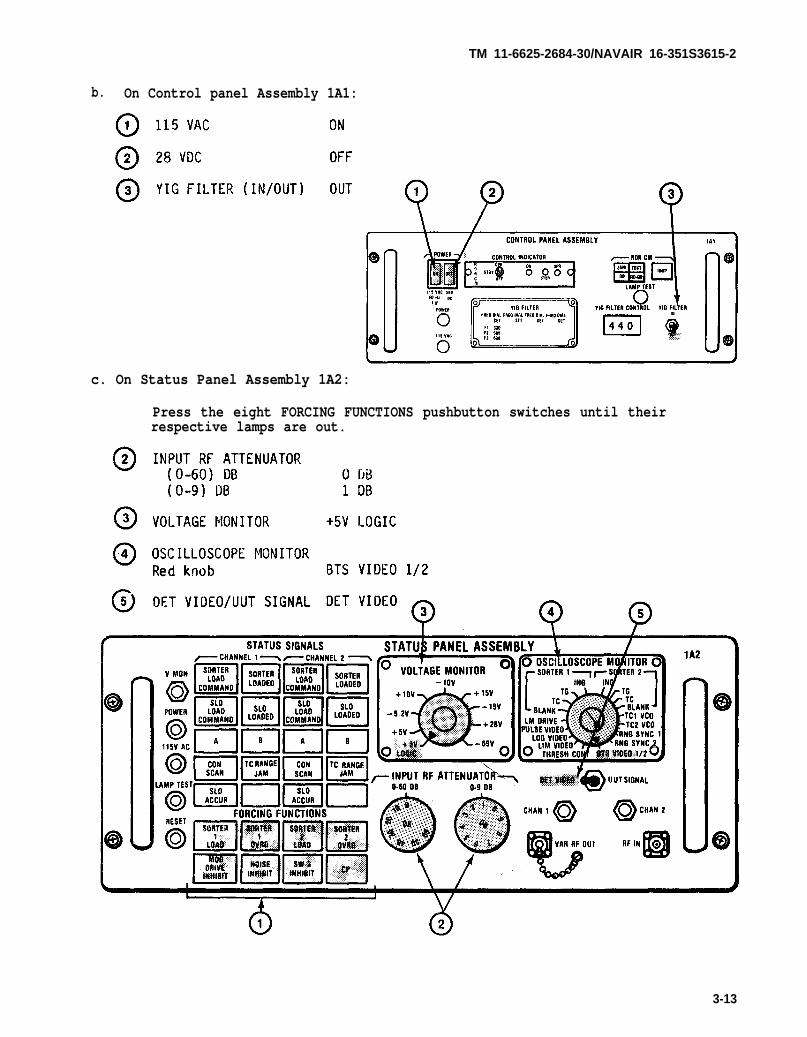
TM 11-6625-2684-30/NAVAIR 16-351S3615-2
b. On Control panel Assembly 1A1:
c. On Status Panel Assembly 1A2:
Press the eight FORCING FUNCTIONS pushbutton switches until theirrespective lamps are out.
3-13
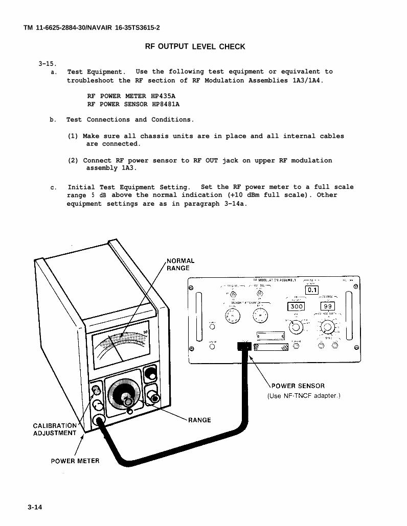
TM 11-6625-2884-30/NAVAIR 16-35TS3615-2
RF OUTPUT LEVEL CHECK
3-15.a. Test Equipment. Use the following test equipment or equivalent to
troubleshoot the RF section of RF Modulation Assemblies 1A3/1A4.
RF POWER METER HP435ARF POWER SENSOR HP8481A
b. Test Connections and Conditions.
(1) Make sure all chassis units are in place and all internal cablesare connected.
(2) Connect RF power sensor to RF OUT jack on upper RF modulationassembly 1A3.
c. Initial Test Equipment Setting. Set the RF power meter to a full scalerange 5 dB above the normal indication (+10 dBm full scale). Otherequipment settings are as in paragraph 3-14a.
3-14

(see table 1-2).
(refer to para' s 3-33, 3-34, 3-35)
TM 11-6625-2884-30/NAVAIR 16-35TS3615-2
d. Procedure.
NOTE
See (S) TM 11-5865-202-30(U) appendix C forvalue of F1.
3-1 5

TM 11-6625-2884-30/NAVAIR 16-35TS3615-2
RF OUTPUT LEVEL CHECK (Continued)
Disconnect power from RFmodulation assembly.Place assembly rightside up and substitutecircuit cards A1 and A2.Connect power to drawer.
Output power level shallbe +3 dBm min. If powerlevel is normal go tostep 3.
Repeat steps 1 and 2 forFREQ SEL set for F2 andF3.
Set power meter to mini-mum sensitivity beforechanging inputs. Exces-sive power input willdamage meter.
3-16

TM 11-6625-2884-30/NAVAIR 16-35TS3615-2
Set FREQ SEL to F1. SetTRANSMIT ATTENUATOR O-9DB through all its posi-tions. Note RF power
RF power should decrease1 ±O.5 dB for each step.If’ readings are correct,set attenuator to O andgo to step 5.
Replace RF modulationassembly and check fornormal indication.
Set TRANSMIT ATTENUATOR0-60 D13 to its 10 and 20DB positions. Note RFpower readings.
RF power should decrease10 ± 1 dB for each posi-tion. If power level isnormal, go to step 6.
Replace RF modulationassembly and check fornormal indication.
3-17
TM 11-6625-2884-30/NAVAIR 16-35TS3615-2
RF OUTPUT LEVEL CHECK (Continued)
Return TRANSMIT ATTENUA-TOR to 1 DB. Set OUT SELswitch on 1A3 to PULSEand connect power metersensor to CMBD RF J4on left side of BTScabinet. Set OUT SELswitch to CW and recordPower level.
Power level reading above-10 dBm. If power levelis normal, go to step 7.
Repeat step 6 for FREQSEL set to F2 and F3.
Set 1A3 OUT SEL switchto PULSE, PRI modeswitch to OFF.
Connect RF power sensorto RF Modulation Assembly1A4 RF OUT jack. Repeatsteps 1 through 8 for RFModulation Assembly 1A4.
If testing RF ModulationAssembly 1A3, replaceinternal cable W2. Iftesting RF modulationassembly 1A4, replaceinternal cable W3. Ifmal function still exists,trace RF signal from RFmodulation assembly toJ4 (fig. FO-7).
Remove power metersensor.
END OF TEST.
3-18
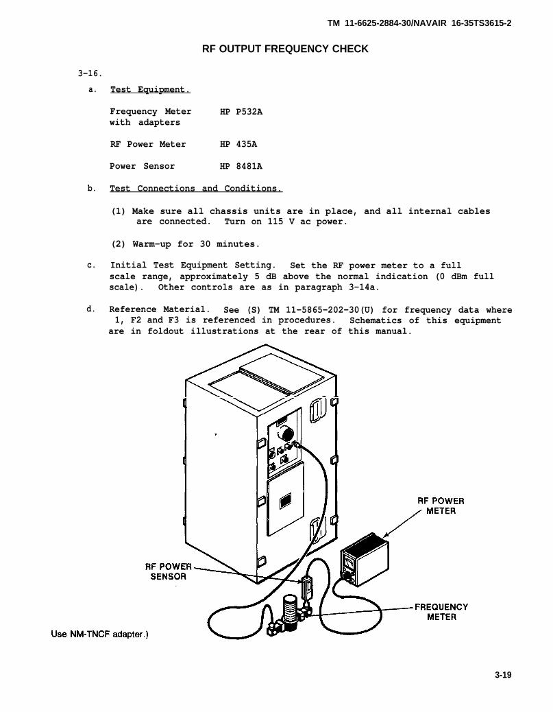
TM 11-6625-2884-30/NAVAIR 16-35TS3615-2
RF OUTPUT FREQUENCY CHECK
3-16.
a. Test Equipment.
Frequency Meter HP P532Awith adapters
RF Power Meter HP 435A
Power Sensor HP 8481A
b. Test Connections and Conditions.
(1) Make sure all chassis units are in place, and all internal cablesare connected. Turn on 115 V ac power.
(2) Warm-up for 30 minutes.
c. Initial Test Equipment Setting. Set the RF power meter to a fullscale range, approximately 5 dB above the normal indication (0 dBm fullscale). Other controls are as in paragraph 3-14a.
d. Reference Material. See (S) TM 11-5865-202-30(U) for frequency data where1, F2 and F3 is referenced in procedures. Schematics of this equipment
are in foldout illustrations at the rear of this manual.
3-19

TM 11-6625-2884-30/NAVAIR 16-35TS3615-2
e. Procedure. RF OUTPUT FREQUENCY CHECK (Continued)
1.
2.
3.
4.
Connect frequency meterto CMBD RF jack J4 onupper left side of BTScabinet.
Connect RF power metersensor to the frequencymeter output.
Set OUT SEL switch on1A3 to CM, PRI selectorswitch to VAR PRI. Set1A4 PRI selector switchto OFF.
Tune RF frequency meterfor a dip in RF power asobserved on the powermeter, record dial read-ing at which the dipoccurs as frequency F1.
Frequency = F1 ±O.1 GHz(See (S) TM-11-5865-202-30 (U)for values of F1, F2 and F3.)
perform the followingsteps.
a. Remove semi-rigidconnector from jackJ2 on rear of unit.Disconnect frequencymeter from jack J4,and connect to RF OUTconnector on frontpanel of unit.
3-20
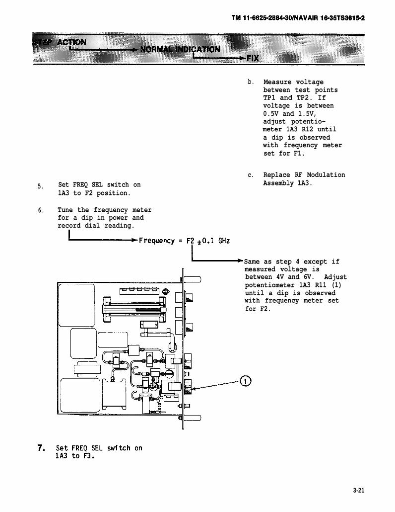
5.
6.
Set FREQ SEL switch on1A3 to F2 position.
Tune the frequency meterfor a dip in power andrecord dial reading.
b.
c.
Measure voltagebetween test pointsTP1 and TP2. Ifvoltage is between0.5V and 1.5V,adjust potentio-meter 1A3 R12 untila dip is observedwith frequency meterset for F1.
Replace RF ModulationAssembly 1A3.
Same as step 4 except ifmeasured voltage isbetween 4V and 6V. Adjustpotentiometer 1A3 R11 (1)until a dip is observedwith frequency meter setfor F2.
3-21

TM 11-6625-2884-30/NAVAIR 16-35TS3615-2
a. Tune the frequency meterfor a dip in power andrecord dial reading.
Frequency = F3 ±O.1 GHz
Set 1A3 OUT SEL switchto PULSE, PRI selectswitch to OFF and repeatsteps 3 through 7 for RFModulation Assembly 1A4.
Same as step 4 except ifmeasured voltage isbetween 8V and 10V, adjustpotentiometer 1A3 (1) R1Ountil a dip is observedwith frequency meter at F3.
Disconnect and removefrequency and powermeters.
END OF TEST
3-22
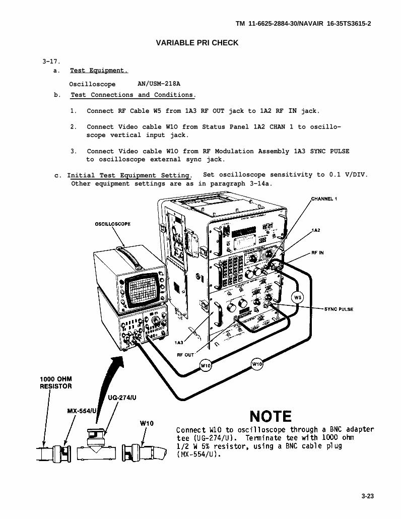
3-17.
TM 11-6625-2884-30/NAVAIR 16-35TS3615-2
VARIABLE PRI CHECK
a. Test Equipment.
Oscilloscope AN/USM-218Ab. Test Connections and Conditions.
1. Connect RF Cable W5 from 1A3 RF OUT jack to 1A2 RF IN jack.
2. Connect Video cable W1O from Status Panel 1A2 CHAN 1 to oscillo-scope vertical input jack.
3. Connect Video cable W1O from RF Modulation Assembly 1A3 SYNC PULSEto oscilloscope external sync jack.
c. Initial Test Equipment Setting. Set oscilloscope sensitivity to 0.1 V/DIV.Other equipment settings are as in paragraph 3-14a.
3-23
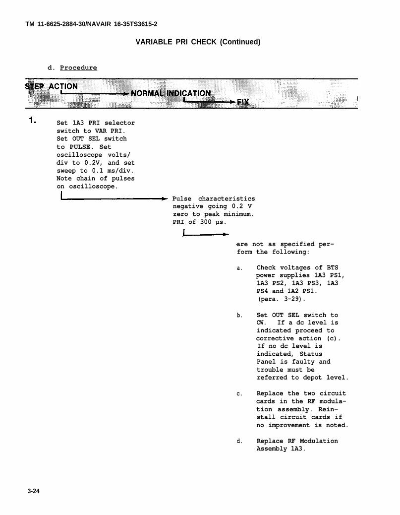
TM 11-6625-2884-30/NAVAIR 16-35TS3615-2
VARIABLE PRI CHECK (Continued)
d. Procedure
Set 1A3 PRI selectorswitch to VAR PRI.Set OUT SEL switchto PULSE. Setoscilloscope volts/div to 0.2V, and setsweep to 0.1 ms/div.Note chain of pulseson oscilloscope.
Pulse characteristicsnegative going 0.2 Vzero to peak minimum.PRI of 300 µs.
are not as specified per-form the following:
a. Check voltages of BTS
b.
c.
d.
power supplies 1A3 PS1,1A3 PS2, 1A3 PS3, 1A3PS4 and 1A2 PS1.(para. 3-29).
Set OUT SEL switch toCW. If a dc level isindicated proceed tocorrective action (c).If no dc level isindicated, StatusPanel is faulty andtrouble must bereferred to depot level.
Replace the two circuitcards in the RF modula-tion assembly. Rein-stall circuit cards ifno improvement is noted.
Replace RF ModulationAssembly 1A3.
3-24

TM 11-6625-2884-30/NAVAIR 16-35TS3615-2
Adjust oscilloscope toview the first pulse.Use 50 ohm termination.
Set the 1A3 PW tenthsswitch from 9 down tozero while observing theoutput pulse width ateach step.
The width decreases0.1 ±O.05 µs for eachstep.
Set 1A3 PW units switchto 9.0.
Pulse width - 9.0±0.5 µs.
Repeat step 2 using thePW units switch whileobserving the output pulsewidth at each step.
The output pulse widthdecreases 1 µs for eachstep.
Same as step 1, FIX 1Cand 1d.
3-25

TM 11-6625-2884-30/NAVAIR 16-35TS3615-2
Set PW switch to 9.9 µs.
Adjust oscilloscope sweepspeed to 0.1 ms/div.
Set PRI hundreds switchfrom 9 down to 3 whileobserving the output PRI.
Width = 9.9 µs.
PRI decreases 100 µsfor each switch step.
SWEEP : 0.1 ms/DIV
Same as step 1, FIX 1Cand 1d.
Check that PRI hundredsswitch is at 3.
Set oscilloscope sweepspeed to 50 µs/div.
3-26
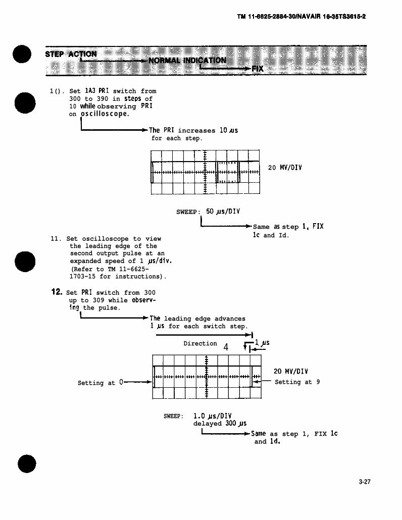
TM 11=8625-2884-301NAVAIR 1%-35TS3616-2
01(). Set M3 PRI switch from
300 to 390 in stem of10on
while observing PRIo s c i l l o s c o p e .I~The PRI increases 10AS
for each step.
20 MV/DIV
SWEEP: 50JJs/DIV
11. Set oscilloscope to viewthe leading edge of thesecond output pulse at anexpanded speed of 1 +Wdiv.(Refer to TM 11-6625-1703-15 for instructions).
i--- Same as step 1, FIXIc and Id.
12. Set PRI switch from 300up to 309 while observ-ing the pulse.
I *The leading edge advancesI AS for each switch step.
Setting at
Direction 4 F@s
*? I+$+ i+++ +H+ ++++ +H+ +-n+ w+ . ii+
o~ +—20 MV/DIVSetting at 9
SWEEP: l.Oys/DIVdelayed 300J!s~Same as step 1, FIX lC
and ld.
3-27

TM 11-6625-2884-30/NAVAIR 16-35TS3615-2
VARIABLE PRI CHECK (Continued)
Disconnect W5 from 1A3RF OUT and connect to1A4 RF OUT. Connectoscilloscope externalsync to 1A4 SYNC PULSEjack.
Repeat steps 1 through12 substituting RFModulation Assembly1A4 for 1A3.
END OF TEST
3-28

TM 11-6625-2884-30/NAVAIR 16-35TS3615-2
CON SCAN MODULATION CHECK
a. Test Equipment. Oscilloscope AN/USM-281A with HP 1805A and HP 1825Aplug-ins, or equivalent.
b. Test Connections and Conditions.
(1) Connect oscilloscope external sync jack to 1A3 SYNC CS jack.
(2) Connect oscilloscope vertical input to Status Panel 1A2 CHAN 1 jack.
(3) Connect RF cable W5 from 1A3 RF OUT jack to 1A2 RF IN jack.
3-29
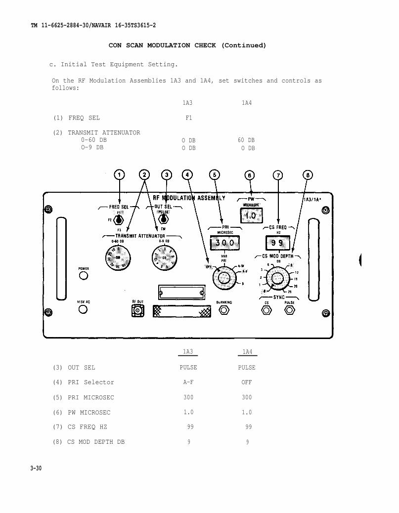
TM 11-6625-2884-30/NAVAIR 16-35TS3615-2
CON SCAN MODULATION CHECK (Continued)
c. Initial Test Equipment Setting.
On the RF Modulation Assemblies 1A3 and 1A4, set switches and controls asfollows:
1A3 1A4
(1) FREQ SEL F1
(2) TRANSMIT ATTENUATOR0-60 DB O DB 60 DBO-9 DB O DB O DB
1A3 1A4
(3) OUT SEL PULSE PULSE
(4) PRI Selector A-F OFF
(5) PRI MICROSEC 300 300
(6) PW MICROSEC 1.0 1.0
(7) CS FREQ HZ 99 99
(8) CS MOD DEPTH DB 9 9
3-30
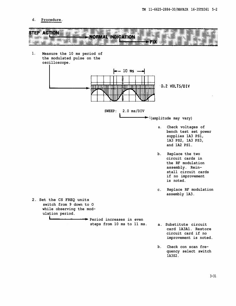
TM 11-6625-2884-30/NAVAIR 16-35TS361 5-2
d. Procedure.
1. Measure the 10 ms period ofthe modulated pulse on theoscilloscope.
SWEEP: 2.0 ms/DIV
(amplitude may vary)
a.
b.
c.
Check voltages ofbench test set powersupplies 1A3 PS1,1A3 PS2, 1A3 PS3,and 1A2 PS1.
Replace the twocircuit cards inthe RF modulationassembly. Rein-stall circuit cardsif no improvementis noted.
Replace RF modulationassembly 1A3.
2. Set the CS FREQ unitsswitch from 9 down to Owhile observing the mod-ulation period.
Period increases in evensteps from 10 ms to 11 ms. a. Substitute circuit
card 1A3A1. Restorecircuit card if noimprovement is noted.
b. Check con scan fre-quency select switch1A3S2.
3-31

TM 11-6625-2884-30/NAVAIR 16-35TS3615-2
CON SCAN MODULATION CHECK (Continued)
3. Set CS FREQ tens switchand observe modulationperiod.
ISwitchPosition
87654321
Period
12.5 ms14.3 ms16.7 ms20.0 ms25.0 ms33.3 ms50.0 ms
100. O ms
Same as in step 2.
4. Set CS FREQ switch to90 and CS MOD DEPTHswitch to 1 dB.
5. Set INPUT RF ATTENUATOR1A2AT1 on Status Panelto 2 dB.
6. Set oscilloscope for - UPdisplay. set Pw to 4 µs.Set PRI to VAR PRI. Increaseoscilloscope gain until themodulation is equal to 1 DIVpeak-to-peak. Set modulationbottom on a horizontal refer-ence line.
I
SWEEP: 2.0 ms/DIV
3-32
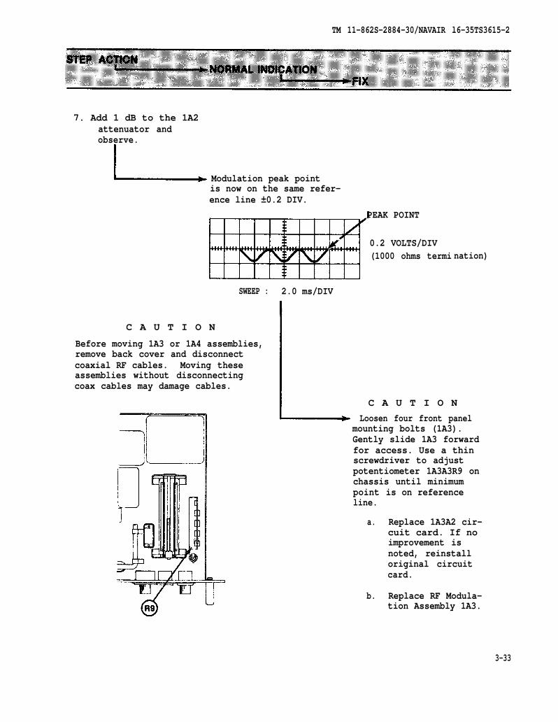
TM 11-862S-2884-30/NAVAIR l6-35TS3615-2
7. Add 1 dB to the 1A2attenuator andobserve.
Modulation peak pointis now on the same refer-ence line ±0.2 DIV.
PEAK POINT
0.2 VOLTS/DIV(1000 ohms termi
SWEEP : 2.0 ms/DIV
C A U T I O N
Before moving 1A3 or 1A4 assemblies,remove back cover and disconnectcoaxial RF cables. Moving theseassemblies without disconnectingcoax cables may damage cables.
nation)
C A U T I O NLoosen four front panel
mounting bolts (1A3).Gently slide 1A3 forwardfor access. Use a thinscrewdriver to adjustpotentiometer 1A3A3R9 onchassis until minimumpointline.
a.
b.
is on reference
Replace 1A3A2 cir-cuit card. If noimprovement isnoted, reinstalloriginal circuitcard.
Replace RF Modula-tion Assembly 1A3.
3-33
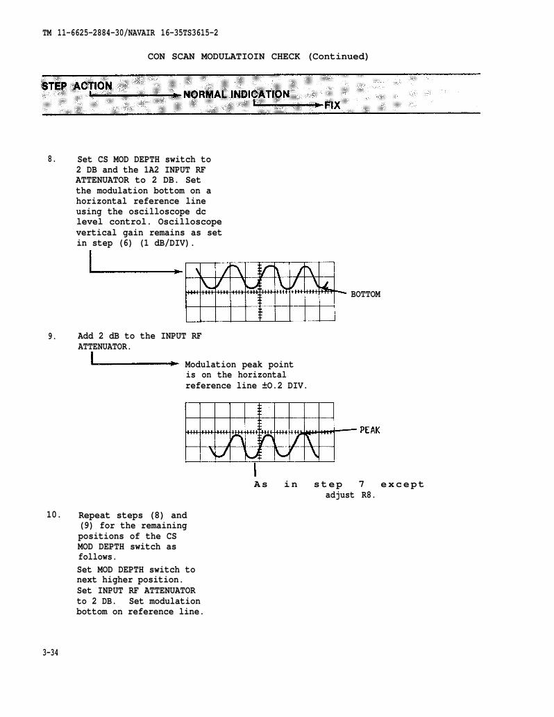
TM 11-6625-2884-30/NAVAIR 16-35TS3615-2
CON SCAN MODULATIOIN CHECK (Continued)
8. Set CS MOD DEPTH switch to2 DB and the 1A2 INPUT RFATTENUATOR to 2 DB. Setthe modulation bottom on ahorizontal reference lineusing the oscilloscope dclevel control. Oscilloscopevertical gain remains as setin step (6) (1 dB/DIV).
BOTTOM
9. Add 2 dB to the INPUT RFATTENUATOR.
Modulation peak pointis on the horizontalreference line ±O.2 DIV.
As in step 7 exceptadjust R8.
10. Repeat steps (8) and(9) for the remainingpositions of the CSMOD DEPTH switch asfollows.Set MOD DEPTH switch tonext higher position.Set INPUT RF ATTENUATORto 2 DB. Set modulationbottom on reference line.
3-34

TM 11-6625-2884-30/NAVAIR 16-35TS3615-2
Increase gain and use off-set as necessary. IncreaseINPUT RF ATTENUATOR byCS MOD DEPTH setting. observemodulation peak.
Modulation sinewavewill appear distortedon oscilloscope becauseof video detector.
11.
END OF TEST
CS MOD DEPTHAttenuation
Mod Depth
1 dB3 dB6 dB9 dB12 dB15 dB20 dB25 dB
Disconnect W5 from1A3 RF OUT and recon-nect to 1A4 RF OUT.Connect oscilloscopeexternal sync to 1A4sync CS. Set 1A3 CSMOD DEPTH to O and1A3 VAR PRI to OFF.Set 1A4 CS MOD DEPTHto 9 dB. Repeat steps1-10 above.
and 1A2Tolerance.
Tolerance
±O.1 dB±O.2 dB±0.3 dB±0.6 dB±0.9 dB± 1.0 dB± 1.0 dB±1.O dB± 1.0 dB
Set
R9R8R7R6R5R4R3R2R1
As in step 7 exceptadjust the correspond-ing potentiometer (SET).
3-35

TM 11-6625-2884-30/NAVAIR 16-35TS3615-2
PRI CHECK3-19.
a. Test Equipment.
Oscilloscope AN/USM-281A.
b. Test Connections and Conditions. Connect RF cable W5 from 1A3 RF OUTPUTjack to 1A2 RF IN jack. Connect coax cable W1O from oscilloscope verti-cal input to status panel 1A2 CHAN 1 jack.
c. Initial Test Equipment Settings.
(1) Set oscilloscope sync to internal.(2) Set sweep speed to 50 µs/div.(3) Set 1A3 CS MOD DEPTH to O DB.(4) Set 1A2 INPUT RF ATTENUATOR to O DB.(5) Other controls are as in paragraph 3-14.
3-36
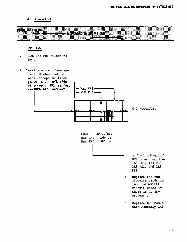
TM 11-6625-2884-30/NAVAIR 16-35TS3615-2
1. Set 1A3 PRI switch toA-W .
2. Terminate oscilloscopein 1000 ohms, adjustoscilloscope so firstpulofmea
SWEEP : 50 µs/DIVMin PRI 260 µSMax PRI 380 µs
b.
0.2 VOLTS/DIV
a. Check voltages ofBTS power supplies1A3 PS1, 1A3 PS2,1A3 PS3, and 1A3PS4.
Replace the twocircuits cards in1A3. Reinstallcircuit cards ifthere is no im-provement.
c. Replace RF Modula-tion Assembly 1A3.
3-37
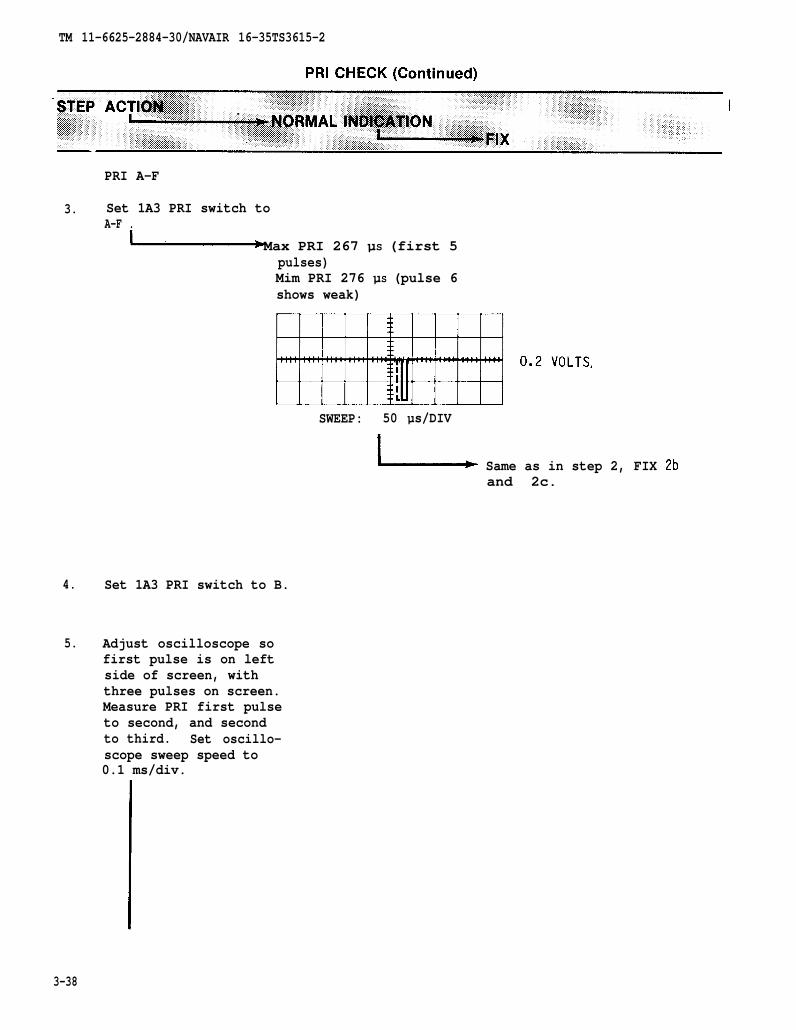
TM 11-6625-2884-30/NAVAIR 16-35TS3615-2
PRI A-F
3. Set 1A3 PRI switch toA-F .
Max PRI 267 µS (first 5pulses)Mim PRI 276 µS (pulse 6shows weak)
SWEEP: 50 µs/DIV
ISame as in step 2, FIX 2band 2c.
4. Set 1A3 PRI switch to B.
5. Adjust oscilloscope sofirst pulse is on leftside of screen, withthree pulses on screen.Measure PRI first pulseto second, and secondto third. Set oscillo-scope sweep speed to0.1 ms/div.
3-38

TM 11-6625-2884-30/NAVAIR 16-35TS3615-2
410A µs A to B, 3504 µs B to C
SWEEP: 0.1 ms/DIV
SWEEP: 0.1 ms/DIV
in step 2, FIX 2b
6.
Same asand 2c.
Move W5 from 1A3 RF OUTjack to 1A4 RF OUT jack,and repeat steps 1 through
Check lA4 as in step 2.
END OF TEST
3-39

TM 11-6625-2884-30/NAVAIR 16-35TS3615-2
BLANKING OUTPUT TEST
3-20.a. Test Equipment.
Oscilloscope AN/USM-281A
b. Test Connection and Conditions.
(1) Connect RF cable W5 from 1A3 RF OUT jack to 1A2 RF IN jack.
(2) Connect W1O cable from 1A3sync jack.
(3) Connect W1O cable from 1A2channel A.
(4) Connect W1O cable from 1A3channel B.
SYNC PULSE jack to oscilloscope external
CHAN 1 jack to oscilloscope vertical
BLANKING jack to oscilloscope vertical
c. Initial Test Equipment Setting.
(1) Set oscilloscope to ALT mode, delayed sweep.
(2) Other settings are as in paragraph 3-14.
3-40
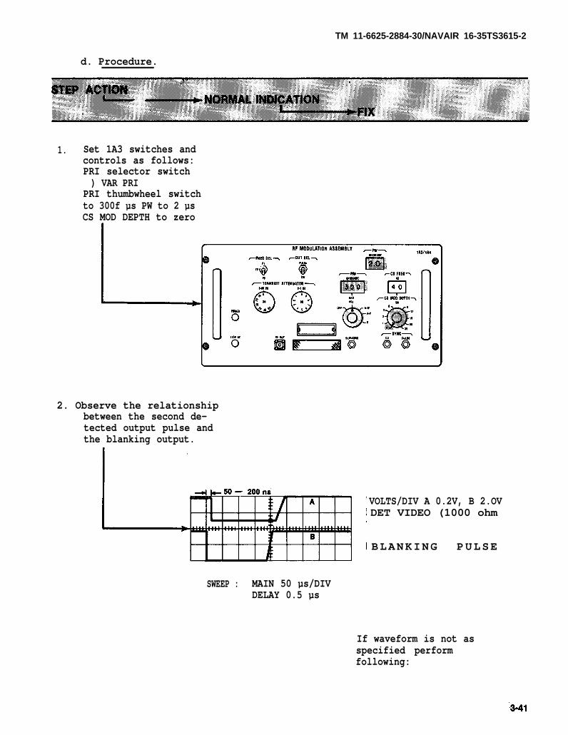
3-41
TM 11-6625-2884-30/NAVAIR 16-35TS3615-2
d. Procedure.
1. Set 1A3 switches andcontrols as follows:PRI selector switch) VAR PRI
PRI thumbwheel switchto 300f µs PW to 2 µsCS MOD DEPTH to zero
2. Observe the relationshipbetween the second de-tected output pulse andthe blanking output.
VOLTS/DIV A 0.2V, B 2.OVDET VIDEO (1000 ohm
BLANKING PULSE
SWEEP : MAIN 50 µs/DIVDELAY 0.5 µs
If waveform is not asspecified performfollowing:

TM 11-6625-2884-30/NAVAIR 16-35TS3615-2
2. (Continued)
a. Check voltages ofbench test setPower Supplies1A3PS1, 1A3PS2,1A3PS3 and 1A3PS4.
b. Replace 1A3A1 circuitcard in the RF modula-tion assembly. Reinstallcircuit card if no im-provement is noted.
c. Replace RF Modula-tion Assembly 1A3.
3. Reconnect W5 to 1A4 RFOUT jack. Reconnectoscilloscope channel Bto 1A4 BLANKING. Re-connect oscilloscopesyric to SYNC PULSE on1A4. Repeat steps 1through 2 for 1A4drawer.
Check lA4 as in Step 2.
END OF TEST.
3-42

3-43
TM 11-6625-2884-30/NAVAIR 16-35TS3615-2
PULSE SYNC TEST
3-21.a. Test Equipment.
Oscilloscope AN/USM-281A.
b. Test Connections and Conditions.
(1) Connect RF Cable W5 from RF OUT jack on RF Modulation Assembly 1A3to RF IN jack on status panel.
(2) Install a BNC tee connector at SYNC PULSE jack of RF ModulationAssembly 1A3. Connect one side of BNC tee to oscilloscope EXT input.de of BNC tee to oscilloscope B input.
(3) Set switch to DET VIDEO on status panel. Connect CHAN 1 tooscilloscope A Input.
c. Initial Test Equipment Setting.
(1) On oscilloscope time base and delay generator, set POS/NEG push-button switch to NEG.
(2) Set oscilloscope for CHOP MODE and TIME/DIV for 0.5 µS.

TM 11-6625-2884-30/NAVAIR 16-35TS3615-2
1. Adjust oscilloscopedisplay to positionPULSE SYNC leadingedge on left verticalline. Measure timedelay between PULSESYNC leading edqe andleading edge of-DETVIDEO pulse. Thedelay shall be 0.8±.15 µs. Use 50ohm terminations,Chan A -UP.
DET VIDEO (A)0.02 VOLTS/DIV
PULSE SYNC (B)0.5 VOLTS/DIV
SWEEP: 0.5 µs/DIV
1
a. Check voltages ofBTS Power Supplies1A3 PS1, 1A3 PS2,1A3 PS3 and 1A3PS4.
b. Replace circuitcard 1A3A1. Re-store circuit cardif there is noimprovement.
c. Replace RF Modula-tion Assembly 1A3.
3-44

TM 11-6625-2884-30/NAVAIR 16-35TS3615-2
Disconnect RF CableW5 from RF ModulationAssembly 1A3 andconnect to RF Mod-ulation Assembly 1A4Disconnect BNC TEEfrom SYNC PULSE jackon 1A3 and connect toSYNC PULSE jack on1A4. Repeat. step 1 for1A4 assembly.
END OF TEST.
3-45
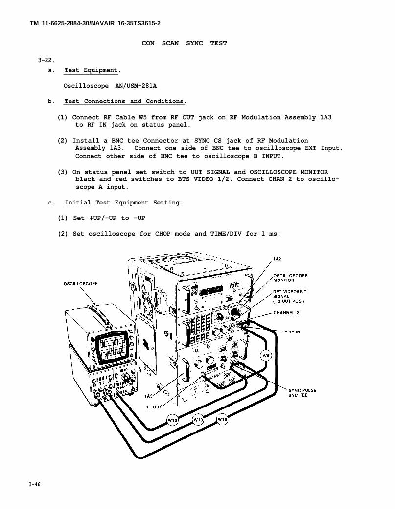
TM 11-6625-2884-30/NAVAIR 16-35TS3615-2
CON SCAN SYNC TEST
3-22.a. Test Equipment.
Oscilloscope AN/USM-281A
b. Test Connections and Conditions.
(1) Connect RF Cable W5 from RF OUT jack on RF Modulation Assembly 1A3to RF IN jack on status panel.
(2) Install a BNC tee Connector at SYNC CS jack of RF ModulationAssembly 1A3. Connect one side of BNC tee to oscilloscope EXT Input.Connect other side of BNC tee to oscilloscope B INPUT.
(3) On status panel set switch to UUT SIGNAL and OSCILLOSCOPE MONITORblack and red switches to BTS VIDEO 1/2. Connect CHAN 2 to oscillo-scope A input.
c. Initial Test Equipment Setting.
(1) Set +UP/-UP to -UP
(2) Set oscilloscope for CHOP mode and TIME/DIV for 1 ms.
3-46

TM 11-6625-2884-30/NAVAIR 16-35TS3615-2
d. Procedure.
1. Measure the timedifference betweenthe leading edge ofthe CS sync pulseand the negativegoing crossover ofsine wave. It shallbe equal to or lessthan 0.5 ins., dctermination.
SWEEP: 1 ms/DIV
a.
b.
co
BTS VIDEO (A)5 VOLTS/DIV
CS SYNC (B)5 VOLTS/DIV
Check voltages ofBTS Power Supplies1A3 PSI, 1A3 PS2,1A3 PS3 and 1A3PS4.
Replace circuitcards 1A3A1 and1A3A2 . Reinstallcircuit cards ifif there is noimprovement.
Replace RF Modula-tion Assembly 1A3.
3-47

TM 11 -6625-2884-30/NAVAIR 16-35TS3615-2
2. Disconnect RF Cable W5from RF ModulationAssembly 1A3 and connectto RF Modulation Assembly1A4. Disconnect BNC teefrom SYNC CS jack on 1A3and connect to SYNC CSjack on 1A4. ConnectCHAN 1 to oscilloscope Ainput. Repeat step 1 for1A4 Assembly.
END OF TEST
3-48

3-23.
a.
b.
TM 11-6625-2884-30/NAVAIR 16-35TS3615-2
STATUS PANEL INDICATOR CHECK
Test Equipment.
None
Test Connections and Conditions.
(1) Connect Cable W1 to jack J1 on left side of BTS.
(2) Turn on 115 V ac power.
c. Initial Test Equipment Setting. Not applicable.
N O T E
Only one lamp is used inside eachindicator or switch indicator.
3-49

TM 11-6625-2884-30/NAVAIR 16-35TS36152
STATUS PANEL INDICATOR CHECK (Continued)
d. Procedure.
press them once.
Illuminated lampsextinguish.
Replace 1A2.
C A U T I O N
Do not install more than one bulb in lamp holder.Extra bulbs may overload 12 Vdc Power Supply1A2PS1.
2. Press LAMP TESTpushbutton switch.
All STATUS and FORCINGFUNCTION indicatorsilluminate.
Ia. If any lamp failsto illuminate,retract lamp holderand replace lamp.Retest to see iflamp illuminates.
b. Replace 1A2.
3-50

TM 11-6625-2884-30/NAVAlR 16-35TS3615-2
3. Use a jumper wire toconnect the followingWI connector pins tocabinet ground. Thecorrect statusindicator illuminatesas its pin is grounded.
CONNECTOR PIN INDICATORLIGHT
W1-P2 1 CHANNEL 12 CHANNEL 13 CHANNEL 24 CHANNEL 25 CHANNEL 16 CHANNEL 17 CHANNEL 28 CHANNEL 29 CHANNEL 1
10 CHANNEL 111 CHANNEL 212 CHANNEL 213 CHANNEL 114 CHANNEL 115 CHANNEL 216 CHANNEL 217 CHANNEL 118 CHANNEL 119 CHANNEL 220 CHANNEL 2
SORTER LOAD COMMANDSORTER LOADEDSORTER LOAD COMMANDSORTER LOADEDSLO LOAD COMMANDSLO LOADEDSLO LOAD COMMANDSLO LOADEDABABCON SCANTC RANGE JAMCON SCANTC RANGE JAMSLO ACCURSPARESLO ACCURSPARE
a. If any of the sta-tus signal lampsfails to light,check Cable W1.If W1 is good,replace 1A2.
END OF TEST.
3-51

TM 11-6625-2884-30/NAVAlR 16-35TS3615-2
STATUS PANEL FORCING FUNCTION CHECK
3-24.
a. Test Equipment.
Digital Multimeter (DMM) AN/USM-451
b. Test Connections and Conditions. Turn off 115 VAC power.
c. Initial Test Equipment Setting. Set DMM to 200 ohm scale. Setmultimeter switch to ON position.
3-52

TM 11-6625-2884-30/NAVAIR 16-35TS3615-2
1. Connect digital multi-meter between thefollowing pins of W1and ground. Press theindicator forcingfunction switch andobserve.
When switch is closed,a maximum of 3 ohms toground exists. Withthe switch open the DMMreads 10,000 ohms mini-mum for the following:
FORCING FUNCTIONSWITCH W1 PIN NO.
SORTER 1 LOAD 21SORTER 1 OVRD 22SORTER 2 LOAD 23SORTER 2 OVRD 24MOD DRIVE INHIBITNOISE INHIBIT 26SW-3 INHIBIT 27CP 28
3-53

TM 11-6625-2884-30/NAVAlR 16-35TS3615-2
2. Disconnect multimeter.Turn on BTS 115 VACpower. Exercise eachforcing function switchby pressing it twice.
Indicator lamp lightcomes on and off.
If switch lamp doesnot illuminate, itmay be defective.Retract switch lampholder and replacelamp and retest.
b. If lamp does notilluminate, replace1A2.
c. If switch lampilluminates butresistance readingexceeds 3 ohms,connection may bedefective. Lookfor broken wiringat either connectorof cable WI. Repairand retest.
d. Switch lamp couldbe faulty. Replace1A2 - refer -todepot level.
3. Turn off BTS 115 VACpower.
END OF TEST.
3-54

TIM 11-6625-2884-30/NAVAIR 16-35TS3615-2
3-25.
STATUS PANEL OSCILLOSCOPE MONITOR CHECK
a. Test Equipment.
Oscilloscope AN/USM-281A
Digital Multimeter AN/USM-451
b. Test Connections and Conditions.
( 1 ) Connect oscilloscope external sync jack to 1A3 SYNC CS jack.
(2) Connect oscilloscope vertical input jack to 1A2 CHAN 2 jack.
c . Initial Test Equipment Setting.
(1) Set sweep speed to 5 ms/DIV.
(2) Other controls are as in paragraph 3-14a.
3-55

TM 11-6625-2884-30/NAVAIR 16-35TS3615-2
1. Turn on 115 VAC power.Set DET VIDEO/UUT SIGNALswitch to UUT SIGNAL andboth red and blackOSCILLOSCOPE MONITORswitches to BTS VIDEO 1/2.
I Oscilloscope displayis a sine wave, insync with an amplitudeof 10 volts p-p minimum.
5 VOLTS/DIV
SWEEP : 5 ms/DIV
b. Replace the two cir-cuit cards in 1A3.Reinstall cards ifno improvement isnoted.
c. Replace 1A3.
2. Change 1A3 CS FREQtens switch.
Frequency of displayedsine wave also changes.
Same as step 1.
3-56

TM 11-6625-2884-30/NAVAIR 16-35TS3615-2
3. Connect oscilloscopesync to 1A4 Assembly CSsync jack and scopevertical input to CHAN1 on the status panel.
4 Change 1A4 CS FREQtens switch.
Oscilloscope displayis a sine wave, insync with an amplitudeof 10 Vp-p minimum.
5 VOLTS/DIV
SWEEP: 5 ms/DIV
Check 1A4 as in the FIX ofstep 1.
The frequency of thedisplayed sine wavealso changes.
Check 1A4 as in Step 1.
5. Set the BTS 115 VAC60 Hz 10 POWERcircuit breaker toOFF.
3-57

TM 11-6625-2884-30/NAVAIR 16-35TS3615-2
STATUS PANEL OSCILLOSCOPE MONITOR CHECK (Continued)
6. Set DET VIDEO/UUTSIGNAL switch toUUT SIGNAL. Checkfor continuitybetween the follow-ing points using aDMM .
Continuity, 3 ohms max,from designated W1 pinsto the CHAN 1 jack whenthe black knob of theOSCILLOSCOPE MONITORSwitch is in the desig-nated position and to theCHAN 2 jack when the redknob is in the designatedposition.
41 SORTER 1 BLANK39 SORTER 1 TC37 SORTER 1 TG35 SORTER 1 ING45 SORTER 2 ING54 SORTER 2 TG52 SORTER 2 TC50 SORTER 2 BLANK
3-58
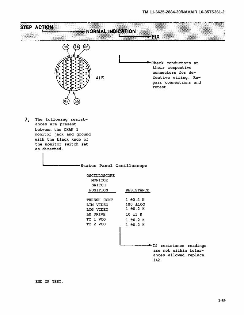
TM 11-6625-2884-30/NAVAIR 16-35TS361-2
Check conductors attheir respectiveconnectors for de-fective wiring. Re-pair connections andretest.
The following resist-ances are presentbetween the CHAN 1monitor jack and groundwith the black knob ofthe monitor switch setas directed.
Status Panel Oscilloscope
END OF TEST.
OSCILLOSCOPEMONITORSWITCH
POSITION RESISTANCE
THRESH CONT 1 ±0.2 KLIM VIDEO 400 ±1OO LOG VIDEO 1 ±0.2 KLM DRIVE 10 ±1 KTC 1 VCO 1 ±0.2 KTC 2 VCO 1 ±0.2 K
If resistance readingsare not within toler-ances allowed replace1A2.
3-59
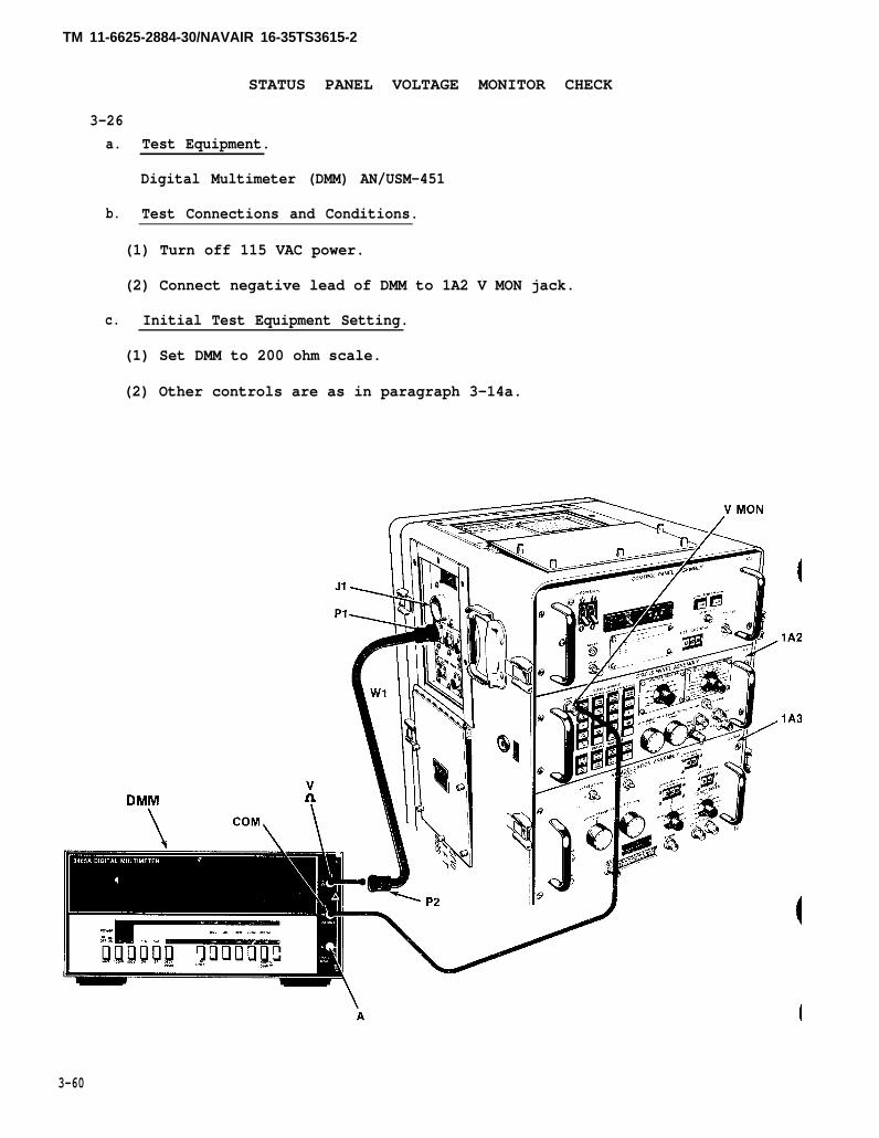
TM 11-6625-2884-30/NAVAIR 16-35TS3615-2
STATUS PANEL VOLTAGE MONITOR CHECK
3-26a. Test Equipment.
Digital Multimeter (DMM) AN/USM-451
b. Test Connections and Conditions.
(1) Turn off 115 VAC power.
(2) Connect negative lead of DMM to 1A2 V MON jack.
c. Initial Test Equipment Setting.
(1) Set DMM to 200 ohm scale.
(2) Other controls are as in paragraph 3-14a.
3-60

TM 11-6625-2884-30/NAVAIR 16-35TS3615-2
1. Connect negative lead ofohmmeter to V MON jackJ6 and the positive leadto the following cableW1P2 pins and check forcontinuity as the statuspanel VOLTAGE MONITORswitch is set to thefollowing positions.
END OF TEST
Each continuity measurement2.2K ±1O% for the following:
VOLTAGEMONITORSWITCH
+5V LOGIC+ 5V-5.2V+1OV-1OV+15V-15V+28V-65V
W1P2PIN NO
777879808687888389
If measurement is not2.2 K +10% it probablyis indicated by aninfinite reading, whichmeans an open R2 or anopen in one of the twoconnectors or in the J1female receptacle onthe connector panel atthe left side of thebench test set. Care-fully probe and repairany defect at the BTSjack, or at eitherconnector of Cable W1.
3-61

TM 1l-6625-2884-30/NAVAIR 16-35TS3615-2
3-27YIG FILTER CHECK
a. Test Equipment.
RF Power Meter HP 435A
RF Power Sensor HP 8481A
28 Vdc Power Supply PP-1104( )/G
b. Test Connections and Conditions.
(1) Connect RF Cable W5 from RF Modulation Assembly 1A3 RF OUT jackto RF IN jack on status panel.
(2) Connect RF power meter sensor to VAR RF OUT jack on status panel.
(3) Connect W7 to 28 Vdc power supply.
c. Initial Test Equipment Setting.
(1) Set RF power meter to +10 dBm scale.
(2) Other equipment settings are as paragraph 3-14.
3-62

TM 11-6625-2884-30/NAVAIR 16-35TS3615-2
d. Procedure .
1. On RF Modulation Assembly1A3, set FREQ SEL to F1,OUT SEL to CW, PRI switchto VAR PRI, TRANSMITATTENUATOR 0-60 DB and0-9 DB to 0.
2. On Status Panel 1A2, setINPUT RF ATTENUATOR0-60 DB and 0-9 DB to O.
3. On Control Panel Assem-bly 1A1, set YIG FILTERswitch to IN and YIGFILTER CONTROL to 330.
3-63
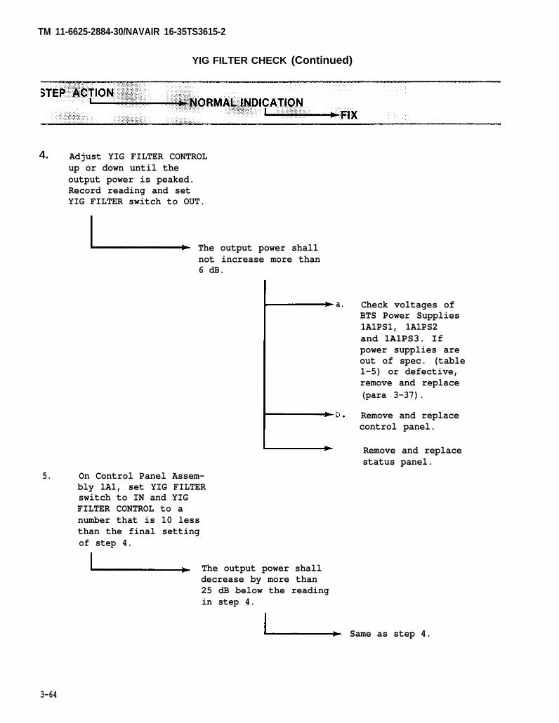
TM 11-6625-2884-30/NAVAIR 16-35TS3615-2
YIG FILTER CHECK (Continued)
4. Adjust YIG FILTER CONTROLup or down until theoutput power is peaked.Record reading and setYIG FILTER switch to OUT.
The output power shallnot increase more than6 dB.
a.
5. On Control Panel Assem-bly 1A1, set YIG FILTERswitch to IN and YIGFILTER CONTROL to anumber that is 10 lessthan the final settingof step 4.
The output power shalldecrease by more than25 dB below the readingin step 4.
Check voltages ofBTS Power Supplies1A1PS1, 1A1PS2and 1A1PS3. Ifpower supplies areout of spec. (table1-5) or defective,remove and replace(para 3-37).
Remove and replacecontrol panel.
Remove and replacestatus panel.
Same as step 4.
3-64

TM 11-6625-2884-301NAVAIR 16-35TS3615-2
On Control Panel Assem-bly 1A1, set YIG FILTERCONTROL to a numberthat is 10 more thanthe final setting ofstep 4.
The output power shalldecrease by more than25 dB below the readingin step 4.
Same as Step 4.
7. On RF Modulation Assembly1A1, set FREQ SEL to F2.
3-65

TM 11-6625-2884-30/NAVAIR 16-35TS3615-2
8. On control panel , setYIG FILTER switch to INand YIG FILTER CONTROLto 509.
9.
10.
Adjust YIG FILTER CONTROLup or down until the outputpower is peaked. Recordreading and set YIG FILTERswitch-to OUT.
On control panel, set
The output power shallnot increase more than6 dB.
Same as step 4.
YIG FILTER switchto IN and YIG FILTERCONTROL to a numberthat is 10 less thanthe final setting ofstep 9.
The output power shalldecrease by 25 dB belowin step 9.
more thanthe reading
Same as step 4.
3-66

TM 11-6625-2884-30/NAVAIR 16-35TS3615-2
11. On control panel, setYIG FILTER CONTROL to anumber that is 10 morethan the final settingof step 9.
The output power shalldecrease by more than25 dB below the readingin step 9.
Same as step 4.
12. On RF Modulation Assembly1A3, set FREQ SEL to F3.
13. On control panel , setYIG FILTER switchto IN and YIG FILTERCONTROL to 688.
3-67

TM 11-6625-2884-30/NAVAIR 16-35TS3615-2
YIG FILTER CHECK (Continued)
14. Adjust YIG FILTER CONTROLup or down until theoutput power is peaked.Record reading and setYIG FILTER switch to OUT.
The output power shallnot increase more than6 dB.
Same as step 4.
15. On Control Panel Assembly1A1, set YIG FILTER switchto IN and YIG FILTER CONTROLto a number that is 10 lessthan the final setting ofstep 14.
The output power shalldecrease by more than25 dB below the readingin step 14.
Same as step 4.
3-68
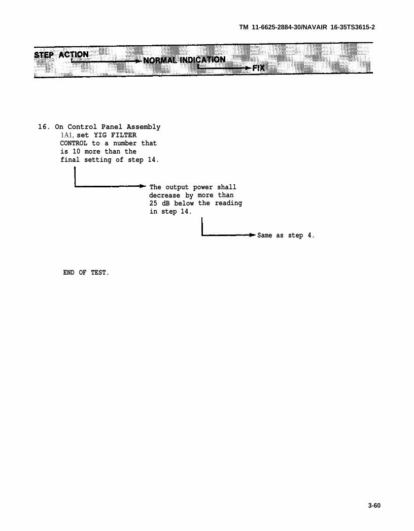
TM 11-6625-2884-30/NAVAIR 16-35TS3615-2
16. On Control Panel Assembly1A1, set YIG FILTERCONTROL to a number thatis 10 more than thefinal setting of step 14.
The output power shalldecrease by25 dB belowin step 14.
more thanthe reading
Same as step 4.
END OF TEST.
3-60

TM 11-6625-2884-30/NAVAIR 16-35TS3615-2
CONTROL PANEL CHECK
3-28a. Test Equipment. Digital Multi meter AN/USM-451
b. Test Connections and Conditions. Turn on 28 VDC circuit breaker (CB1) oncontrol panel.
c. Initial Test Equipment Setting. Set digital multimeter as follows:
(1) OFF/ON pushbutton to ON
(2) = V to ON
(3) 200V to ON
3-70

TM 11-6625-2884-30/NAVAIR 16-35TS3615-2
1. On control panel,press the LAMP TESTpushbutton switch.
JAM/TEST/GO/NO-GO andINOP indicators light.
END OF TEST.
b.
c.
d.
If JAM TEST, GO,or NO-G0 lamp failsto light, twist andremove lens. Replacefailed lamp and re-install lens.
If INOP lamp failsto light, extractINOP lamp holder.Replace failed lampand re-install lampholder.
Using digital multi-meter check thecircuit breaker CB1for +28 V.
If the above checksfail to correct themalfunction, replacecontrol panel.
3-71

TM 11-6625-2884-30/NAVAIR 16-35TS3615-2
S E C T I O N I V
M A I N T E N A N C E P R O C E D U R E S
CONTENTS
GENERAL . . . . . . . . . . . ..................... . . . . . . . . . . ... . .......CORRECTIVE ACTION . . . .. . . . . . . . . . . . .... . . . . . . . . ............LAMP REPLACEMENT . . . . . ............................................ASSEMBLY REMOVAL AND REPLACEMENT . . . . ..............................ADJUSTMENT OF +5V POWER SUPPLY 1A3/1A4 PSI . . . . . . . . . . . . . . . . . . . . . . .ADJUSTMENT OF +15V POWER SUPPLY 1A3/1A4 PS2 . . . . . . . . . . . . . . . . . . . . . . .ADJUSTMENT OF -65V POWER SUPPLY 1A3/1A4 PS3 . . . . . . . . . . . . . . . . . . . . . . .ADJUSTMENT OF +12V POWER SUPPLY 1A2 PS1 . . . . . .............................. .REPLACEMENT OF POWER SUPPLIES . . . . .. . . . . . ...............................REPLACEMENT OF PRINTED CIRCUIT BOARDS . . . . ................................ . . . . .REPLACEMENT OF CONTROL INDICATOR 1A1A1 . . . . . . . . . . . . . . . . . . . . . . . . . . . .CABLE REPAIRS. . . . . . ........................................... .
PAGE
3-723-733-733- 743-813-823-843-853-863-1013-1033-108
GENERAL
3-29. This section gives instructions for performing the alignment, repair,removal, and replacement actions listed in section III and in the MaintenanceAllocation Chart. These instructions include illustrations showing partslocations. The section describes how to remove Control Panel Assembly 1A1.Status Panel Assembly 1A2 and the two RF Modulation Assemblies 1A3 and 1A4 fromthe BTS case. In addition, the section discusses replacement of the two printedcircuit cards of the BTS which are located in an enclosure on RF ModulationAssemblies 1A3/1A4.
Instructions are provided for removal, replacement and adjustment of theinternal power supplies in the BTS.
Three of the power supplies are located in Control Panel Assembly 1A1.
+5V Power Supply PS1.
+15V Power Supply PS2.
+1OV Power Supply PS3.
3-72

TM 11-6625-2664-30/NAVAIR 16-35TS3615-2
One power supply is located in Status Panel Assembly 1A2:
+12V Power Supply PS1.
Four of the power supplies are located in RF Modulation Assembly 1A3/1A4.
+5V Power Supply PS1. -65V Power Supply PS3.
+15V Power Supply PS2. -15V Power Supply PS4.
3-30. The two-fold purpose of troubleshooting procedures in Section III is todetect trouble in the system and to isolate the malfunction to a particularassembly or subassembly. If the trouble is traced to the single power supplyon the status panel, replace the power supply. Similarly, four power supplieson RF Modulation Assembly units 1A3 or 1A4 may be replaced if necessary. If amalfunction is traced to the three power supplies in the control panel, replacethe defective power supply. If the control indicator on Control Panel Assembly1A1 is defective, another control indicator may be substituted. One RFmodulation assembly may be substituted for the other.
LAMP REPLACEMENT
3-31. Lamp replacement is accomplished from the panel front without the use ofany tools.
C A U T I O N
In lamp assemblies with dual sockets, install onlya single lamp. Sockets are wired in parallel and asecond lamp would overload the lamp power supply.
The dual-lamp light capsule which holds the lamps and front lens is held to theunit housing by spring clips which allow it to be removed from the front panelfor quick and easy lamp replacement. To obtain access to the lens, diffuser,or color filter, slide the holder vertically upward and off the light capsule.In the BITE 4-lamp assembly, pull lens forward and rotate 90 degrees: pull andhinge lamp assembly downward: remove colored filters from suspected defectivelamp; press lamp to rear and remove. Press replacement lamp in socket, replacefilter and reinstall lamp assembly. After replacement of a lamp, the indicatorshould be retested by depressing the LAMP TEST switch on the front of thecontrol panel assembly to check that the new lamp lights. For power indicators,unscrew lens (CCW), pull lamp from lens, press in replacement lamp and screwlens (CW) back into socket.
3-73

TM 11-6625-2884-30/NAVAIR 16-35TS3615-2
ASSEMBLY REMOVAL AND REPLACEMENT
3-32. The procedure for removal of Status Panel Assembly 1A2, or the two RFModulation Assemblies 1A3 or 1A4 is the same. To remove any one of the threeassemblies or all of them, perform the following:
a. Removal of 1A2, 1A3 or 1A4 Panel Assemblies.
W A R N I N G
Exercise the utmost care duringassembly removal as the RF Modula-tion Assembly weighs 44 pounds.
C A U T I O N
When connecting or disconnecting jackscrew connectors:
Turn one screw one turn.Turn other screw one turn.Repeat alternate turning of screws.Do not use excessive torque.
Turning one screw too far or using excessive torque maycrack connector body or strip screw thread!
Be sure to disconnect semi-rigid coax cables from rear ofassembly before removing it. Pulling assembly with cableattached may damage cable.
Retain nuts and washers when removing grounding straps.Do not let loose nuts or washers fall into BTS. Loosehardware can cause a short circuit.
3-74

Tm 11-6625-2884-30/NAVAIR 16-35TS3615-2
(1) Remove the front and rear covers of the case.
(2) Remove 115 V ac and 28 V dc power from the BTS.
(3) Disconnect all cables, grounding straps and semi-rigid coax cablesfrom the front and rear panels of the assembly to be removed.
(4) Loosen the four captive screws securing the assembly to the case.
(5) Firmly grasp the two handles of the assembly to be removed and gentlypull the assemblv out. Continue pulling SlOWly until the assembly isalmost out of its closure at which time-carefully and slowly pull-itfree of the case and gently lower the assembly to the test bench.
NOTETwo guides on the back of the case framemate with two holes at the rear of theassembly for the purposes of assemblyalinement and stability.
3-76

TM 11-6625-2884-30/NAVAlR 16-35TS3615-2
ASSEMBLY REMOVAL AND REPLACEMENT (Continued)
b. Replacement of 1A2, 1A3 or 1A4 Panel Assemblies. The procedure forreplacement of Status Panel Assembly 1A2 , or the two RF ModulationAssemblies 1A3 or 1A4 is the same. To replace any of the threeassemblies, perform the following:
W A R N I N GExercise the utmost care during assemblyreplacement as the RF modulation assem-bly weighs 44 pounds.
C A U T I O NPulling assemblies forward withoutdisconnecting cables may damagecables.
N O T ETwo guides on the back of the case framemate with two holes at the rear of theassembly for the purposes of assemblyalinement and stability.
( 1 ) Firmly grasp the two handles of the assembly to be replaced and gentlypush the assembly into the case. Continue slowly until the assemblyis almost in its closure at which time carefully and slowly push itfully in, engaging the guide pins at the rear of the assembly.
(2) Secure panel assembly to BTS case frame with four captive screws.
(3) Connect all cables and grounding straps to front and rear panels ofassembly being replaced.
3-76

TM 11-6625-2884-30/NAVAIR 16-35TS3815-2
CAUTIONWhen connecting or disconnectingconnectors:
Turn one screw one turn.
Turn other screw one turn.
Repeat alternate turning of
Do not use excessive torque.
jack screw
screws.
Turning one screw too far or using excessivetorque may crack connector body or stripscrew thread!
c. Removal of Control Panel Assembly lA1. For removal of the control panel,perform the followlng procedure:
(2) Remove 115 Vac and 28 Vdc input power to the BTS Connector PanelJacks J5 and J6.
(3) From the rear of the BTS, disconnect cable P4 from 1A2 J10 on StatusPanel 1A2 and Cable P2 from lAIJ1 on the control panel.
3-77
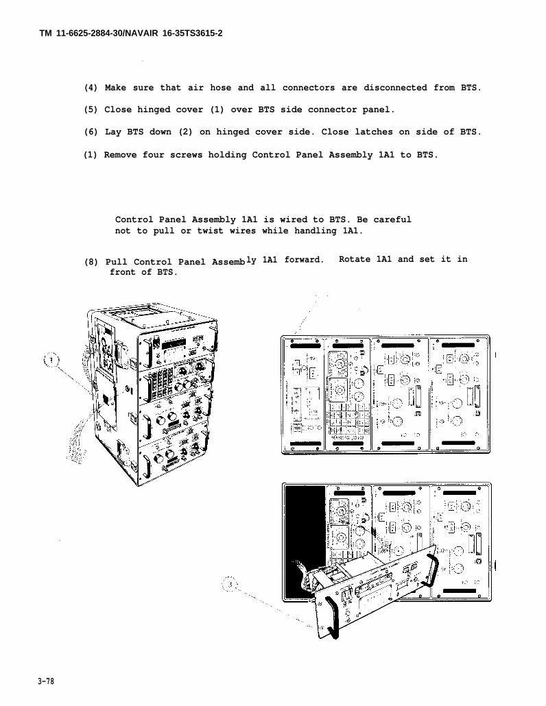
TM 11-6625-2884-30/NAVAIR 16-35TS3615-2
.
(4) Make sure that air hose and all connectors are disconnected from BTS.
(5) Close hinged cover (1) over BTS side connector panel.
(6) Lay BTS down (2) on hinged cover side. Close latches on side of BTS.
(1) Remove four screws holding Control Panel Assembly 1A1 to BTS.
Control Panel Assembly 1A1 is wired to BTS. Be carefulnot to pull or twist wires while handling 1A1.
(8) Pull Control Panel Assembfront of BTS.
ly 1A1 forward. Rotate 1A1 and set it in
3-78

TM 11-6625-2884-30/NAVAIR 16-35TS3615-2
(9) Tag and disconnect the following wires from the rear of the controlpanel:
115 VAC from TB1-3
NEUT from TB1-2
GND from TB1-1
+28 VDC from TB2-4, TB2-2 and TB2-1
+28 VDC RTN from Switch S2-2
Four wires from TB4
3-79
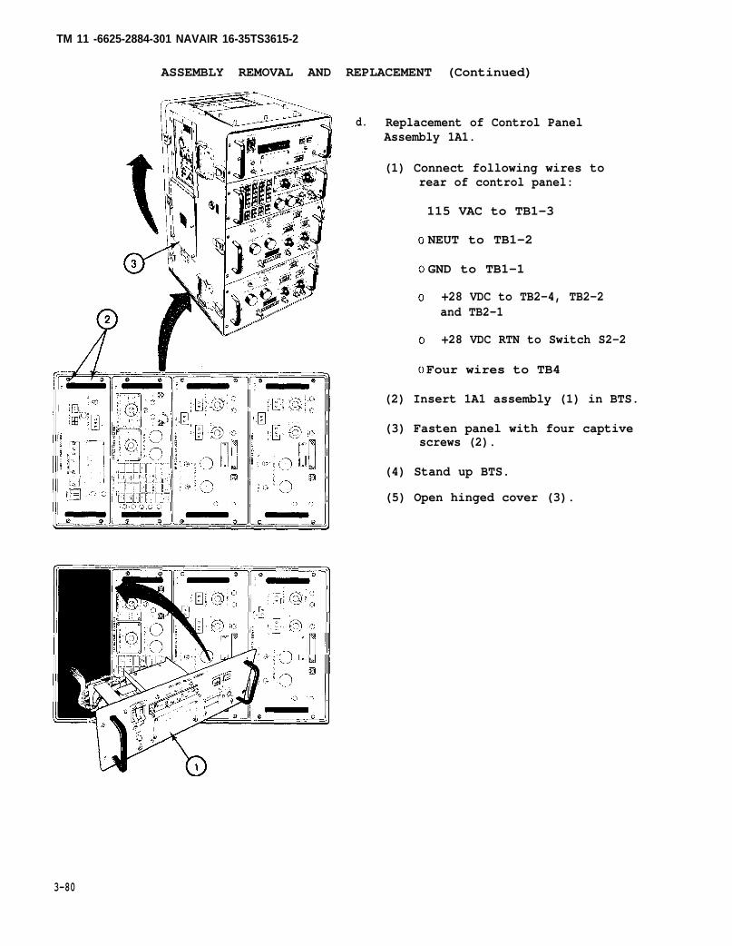
TM 11 -6625-2884-301 NAVAIR 16-35TS3615-2
ASSEMBLY REMOVAL AND REPLACEMENT (Continued)
d. Replacement of Control PanelAssembly 1A1.
(1) Connect following wires torear of control panel:
115 VAC to TB1-3
NEUT to TB1-2
GND to TB1-1
+28 VDC to TB2-4, TB2-2and TB2-1
+28 VDC RTN to Switch S2-2
Four wires to TB4
(2) Insert 1A1 assembly (1) in BTS.
(3) Fasten panel with four captivescrews (2).
(4) Stand up BTS.
(5) Open hinged cover (3).
3-80

TM 11-6625-2884-30/NAVAIR 16-35TS3615-2
ADJUSTMENT OF +5 V POWER SUPPLY 1A3/1 A4 PS1
3-33. To adjust +5 V Power Supply 1A3/1A4 PS1, perform the following:
a. Remove RF modulation assembly from bench test set in accordance withparagraph 3-32a. Set the RF modulation assembly upside down on the testbench. Connect power cord to an energized 115 V ac 60 Hz source.
b. Check that front pane? POWER lamp illuminates.
If lamp does not light, check that frontpanel circuit breaker on the RF modulationassembly has not been tripped.
c. Connect the V lead of the DMM to the +5 V test point (1) and the COMlead to chassis ground.
d. Adjust CR1 (2) control fully clockwise.
e. Using screwdriver, rotate the PS1 +5 V ADJ control (3) until DMM indicates+5.0 v.
f. Adjust CR1 control (2) counterclockwise while observing DMM. When DMMreading drops to less than 2 volts, stop adjustment.
9. Adjust CR1 control (2) 1/2 turn clockwise.
3-81
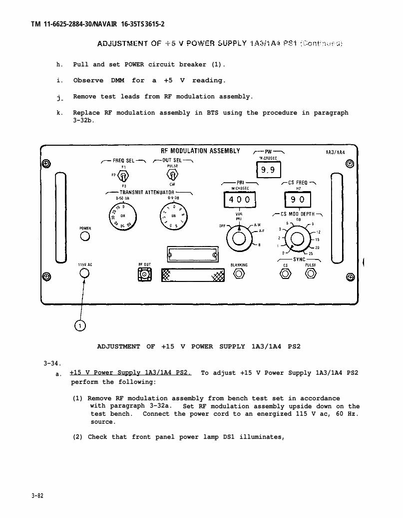
TM 11-6625-2884-30/NAVAIR 16-35TS3615-2
h. Pull and set POWER circuit breaker (1).
i. Observe DMM for a +5 V reading.
j =Remove test leads from RF modulation assembly.
k. Replace RF modulation assembly in BTS using the procedure in paragraph3-32b.
ADJUSTMENT OF +15 V POWER SUPPLY 1A3/1A4 PS2
3-34.a. +15 V Power Supply 1A3/1A4 PS2. To adjust +15 V Power Supply 1A3/1A4 PS2
perform the following:
(1) Remove RF modulation assembly from bench test set in accordancewith paragraph 3-32a. Set RF modulation assembly upside down on thetest bench. Connect the power cord to an energized 115 V ac, 60 Hz.source.
(2) Check that front panel power lamp DS1 illuminates,
3-82
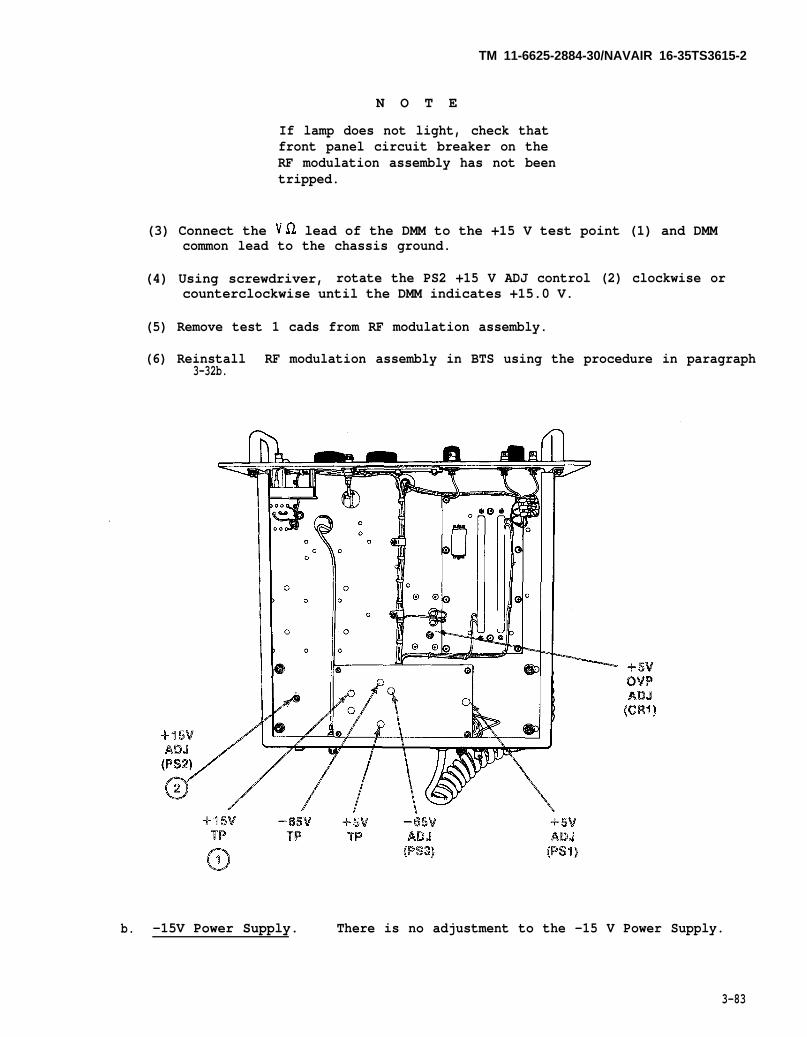
TM 11-6625-2884-30/NAVAIR 16-35TS3615-2
N O T E
If lamp does not light, check thatfront panel circuit breaker on theRF modulation assembly has not beentripped.
(3) Connect the VfL lead of the DMM to the +15 V test point (1) and DMMcommon lead to the chassis ground.
(4) Using screwdriver, rotate the PS2 +15 V ADJ control (2) clockwise orcounterclockwise until the DMM indicates +15.0 V.
(5) Remove test 1 cads from RF modulation assembly.
(6) Reinstall RF modulation assembly in BTS using the procedure in paragraph3-32b.
b. -15V Power Supply. There is no adjustment to the -15 V Power Supply.
3-83

TM 11-6625-2884-30/NAVAIR 16-35TS3615-2
ADJUSTMENT OF –65 V POWER SUPPLY 1A3/1A4 PS3
3-35. To adjust -65 V Power Supply 1A3/1A4 PS3 perform the following:
a. Remove RF modulation assembly from bench test set in accordance withparagraph 3-32a. Set the RF modulation assembly upside down on the testbench. Connect the power cord to an energized 115 V ac, 60 Hz source.
b. Check that front panel power lamp DS1 illuminates.
c. Connect the common lead of the DMM to ground and the DMM Vi2 lead to the-65 V test point (1).
d. Using screwdriver, rotate the PS3 -65 V ADJ control clockwise or counter-clockwise until the DMM meter indicates -65.0 V (2).
e. Remove test leads from RF modulation assembly.
f. Reinstall RF modulation assembly in BTS using the procedure in paragraph3-32b.
3-84
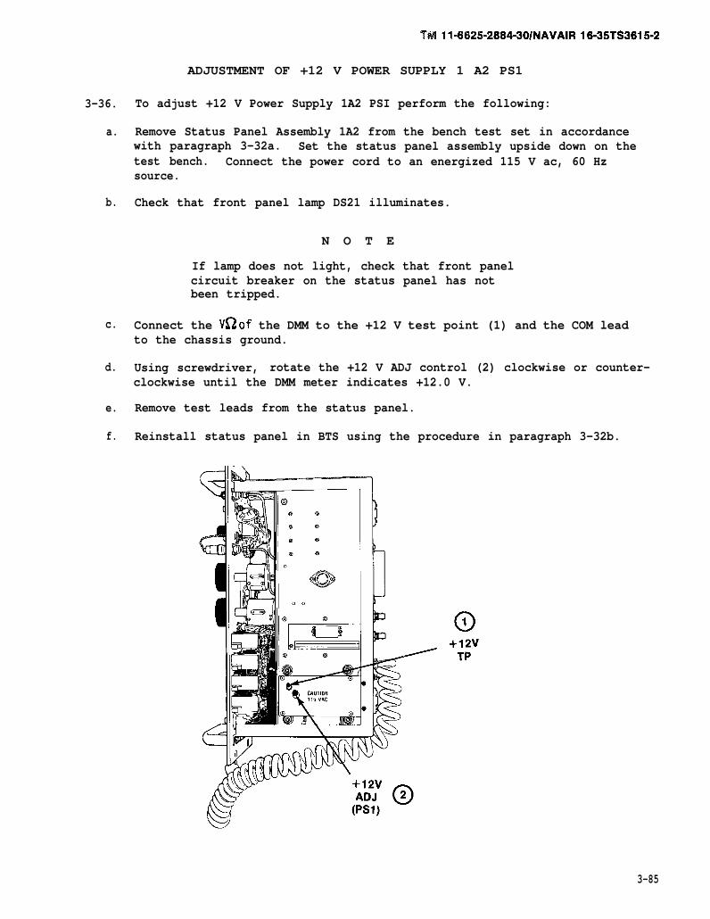
TM 11-6625-2884-30/NAVAIR 16-35TS3615-2
ADJUSTMENT OF +12 V POWER SUPPLY 1 A2 PS1
3-36. To adjust +12 V Power Supply 1A2 PSI perform the following:
a. Remove Status Panel Assembly 1A2 from the bench test set in accordancewith paragraph 3-32a. Set the status panel assembly upside down on thetest bench. Connect the power cord to an energized 115 V ac, 60 Hzsource.
b. Check that front panel lamp DS21 illuminates.
N O T E
If lamp does not light, check that front panelcircuit breaker on the status panel has notbeen tripped.
c. Connect the V~of the DMM to the +12 V test point (1) and the COM leadto the chassis ground.
d. Using screwdriver, rotate the +12 V ADJ control (2) clockwise or counter-clockwise until the DMM meter indicates +12.0 V.
e. Remove test leads from the status panel.
f. Reinstall status panel in BTS using the procedure in paragraph 3-32b.
3-85

TM 11-6625-2884-30/NAVAIR 16-35TS3615-2
3-37.accomp
a.
REPLACEMENT OF POWER SUPPLIES
Replacement of the eight internal power supplies of the BTS isished by performing one of the following respective procedures.
Control Panel Assembly Power Supply 1A1PS1 (-15 Vdc). Remove ControlPanel Assembly 1A1 from them in accordance with paragraph 3-32c andperform the following:
(1) Place the control panel in an upside down position on the testbench.
(2) Remove caution plate (1) - four pan head screws,flat washers.
(3) Tag and unsolder the 115 Vac input wires (2) andwires (3) from Power Supply PSI.
lockwashers and
the two output
(4) Remove pan head screw and lockwasher (4) securing PS1 to powersupply bracket.
(5) Remove pan head screw, lockwasher and flat washer (5), securingthe hold down bracket, between PS1 and PS3 (6).
(5) Lower and remove PS1 (7) with the hold down bracket and post (6).
(1) Posa n d
REPLACEMENT
tion replacement -15 Vdc Powerpost (6) on control panel.
Suppl y 1A1PS1 (7) and bracket
(2) Fasten 1A1PS1 to power supply bracket, using pan head screw andlockwashers (4).
(3) Fasten hold down bracket and post (6) to power supply bracket,using pan head screws, lockwasher and flat, washer (5).
(4) Solder 115 Vac input wires (2) and two output wires (3) to PowerSupply PS1, observing dc polarity.
(5) Install caution plate (1) with four pan head screws, lockwashersand flat washers.
(6) Replace control panel in BTS according to paragraph 3-32d.
3-86
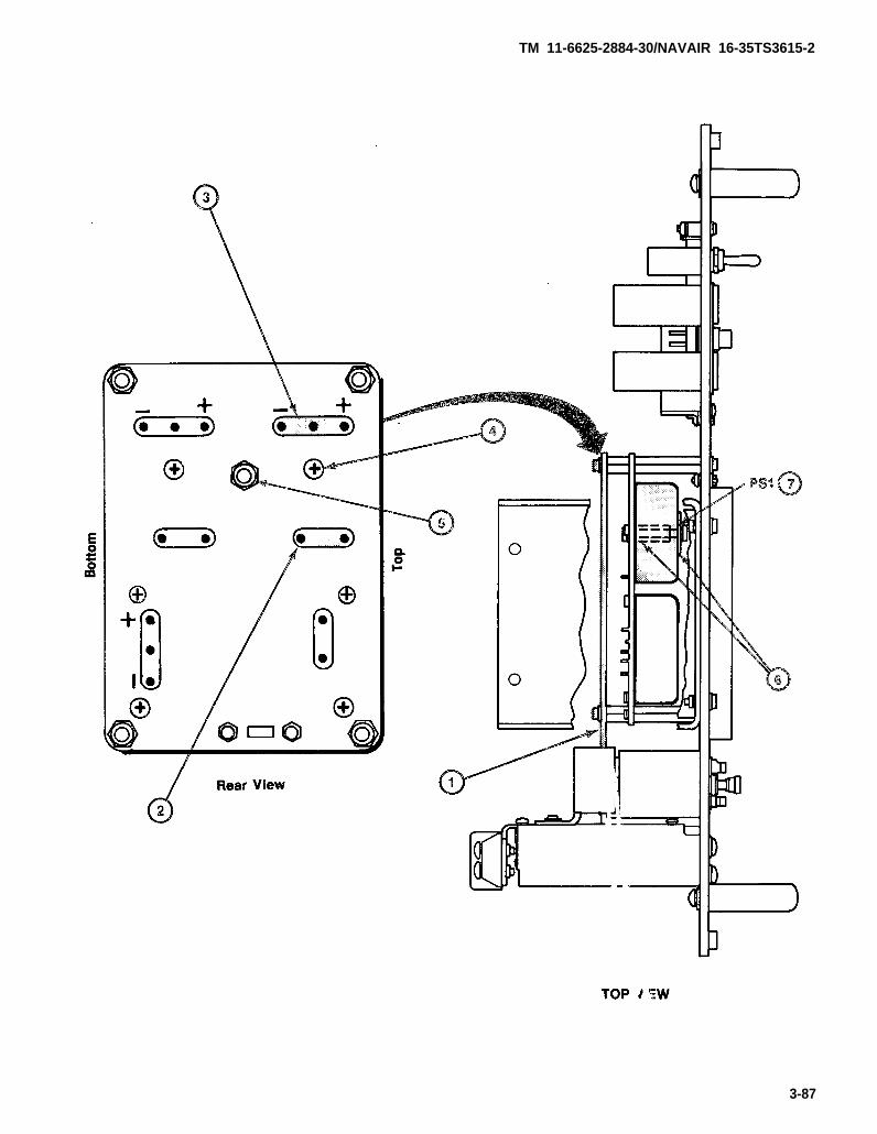
TM 11-6625-2884-30/NAVAIR 16-35TS3615-2
3-87

TM 11-6625-2884-30/NAVAIR 16-35TS3615-2
REPLACEMENT OF POWER SUPPLIES (Continued)
b. Control Panel Assembly Power Supply 1A1PS2 (+15 Vdc). Remove ControlPanel Assembly 1A1 from the BTS in accordance with paragraph 3-32c andperform the following:
REMOVAL
(1) Place the control panel in an upside down position on the testbench.
(2) Remove caution Plate (1) - four pan head screws, lockwashers andflat washers.
(3) Tag and unsolder the 115 Vac input wires (2) and the two outputwires (3) from Power Supply PS2.
(4) Remove four pan head screws and lockwashers (4) securing PS2 topower supply bracket.
(5) Lower and remove PS2
(1) Position replacementpanel.
(5) from the control panel.
REPLACEMENT
+15 Vdc Power Supply PS2 (5) on control
(2) Fasten PS2 to power supply bracket, using four pan head screwsand lockwashers (4).
(3) Solder 115 Vac input wires (2) and two output wires (3) to PowerSupply PS2, observing dc polarity.
(4) Install caution plate (1) with four pan head screws, lockwashersand flat washers.
(5) Replace control panel in BTS according to paragraph 3-32d.
3-88
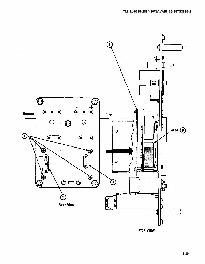
TM 11-6625-2884-30/NAVAIR 16-35TS3815-2
3-89

TM 11-6625-2884-30/NAVAIR 16-35TS3615-2
c. Control Panel Assembly Power Supply 1A1PS3 (+1O Vdc). Remove ControlPanel Assemblv 1A1 from the BTS in accordance with paragraph 3-32B andperform the following:
(1)
(2)
(3)
(4)
(5)
(6)
Place the control panel in an upside down position on the testbench.
Remove caution plate (1) - four pan head screws, lockwashers andflat washers.
Tag and unsolder the 115 Vac input wires (2) and the two outputwires (3) from Power Supply PS3.
Remove pan head screw and lockwasher (4) securing PS3 to powersupply bracket.
Remove pan head screw, lockwasher and flat washer (5) securing thehold down bracket between PS1 and PS3.
Lower and remove PS3 (7) with the hold down bracket and post (6).
(1) Posand
(2) Fas
tion replacement +10 Vdc Power Supply 1A1PS3 (7) and bracketpost (6) on control panel.
en PS3 to power supply bracket, using pan head screw andlockwasher (4).
(3) Fasten hold down bracket and post (6) to power supply bracket,using pan head screw, lockwasher and flat washer (5).
(4) Solder 115 Vac input wires (2) and two output wires (3) to PowerSupply PS3, observing dc polarity.
(5) Install caution plate (1) with four pan head screws, lockwashersand flat washers.
(6) Replace control panel in BTS according to paragraph 3-32d.
3-90

TM 11-6625-2884-30/NAVAIR 16-35TS3615-2
3-91
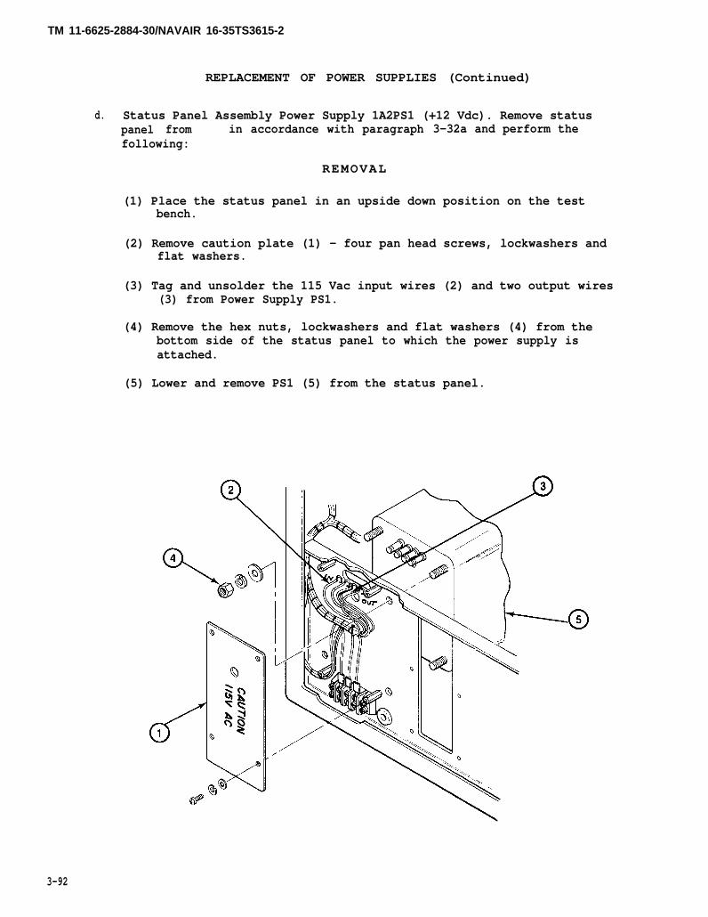
TM 11-6625-2884-30/NAVAIR 16-35TS3615-2
REPLACEMENT OF POWER SUPPLIES (Continued)
d. Status Panel Assembly Power Supply 1A2PS1 (+12 Vdc). Remove statuspanel from in accordance with paragraph 3-32a and perform thefollowing:
REMOVAL
(1) Place the status panel in an upside down position on the testbench.
(2) Remove caution plate (1) - four pan head screws, lockwashers andflat washers.
(3) Tag and unsolder the 115 Vac input wires (2) and two output wires(3) from Power Supply PS1.
(4) Remove the hex nuts, lockwashers and flat washers (4) from thebottom side of the status panel to which the power supply isattached.
(5) Lower and remove PS1 (5) from the status panel.
3-92
TM 11-6625-2884-30/NAVAIR 16-35TS3515-2
R E P L A C E M E N T
(1) Position replacement Power Supply (5) in status panel.
(2) Fasten power supply (5) to status panel, using four hex nuts,Iockwashers and flat washers (4).
(3) Solder 115 Vac input wires (2) and two output wires (3) to Powersupply PSI.
(4) Adjust +12 Vdc power supply as in paragraph 3-36.
(5) Install caution plate (1), using four pan head screws, lock-washers, and flat washers.
(6) Replace status panel in BTS as in paragraph 3-32b.
3-93

TM 11-6625-2884-30/NAVAIR 16-35TS3615-2
REPLACEMENT OF POWER SUPPLIES (Continued)
e. RF Modulation Assembly Power Supply 1A3/1A4PS1 (+5 Vdc). Remove RFmodulation assembly from in accordance with paragraph 3-32a.
(1)
(2)
(3)
(4)
(5)
REMOVAL
Place the RF modulation assembly in an upside down position on thetest bench.
Remove caution plate (1) - five pan head screws, lockwashers andflat washers.
Tag and unsolder the 115 Vac input wires (2) and the two outputwires (3) from power supply PS1.
Remove the hex nuts, lockwashers and flat washers (4) from thebottom side of the RF modulation assembly to which the powersupply is attached.
Lower and remove PS1 (5) from the RF modulation assembly.
3-94

(3)
Position replacement Powerassembly.
REPLACEMENT
supply PS1 (5)
TM 11-6625-2884-30/NAVAIR 16-35TS3615-2
in RF modulation
Fasten Power Supply PS1 (5) to chassis, using four hex nuts,lockwashers and flat washers (4).
Solder 115 Vac input wires (2) and two output wires (3) to +5 Vdcpower supply.
Adjust Power Supply PS1 as in paragraph 3-33.
Reinstall caution plate (1), using five pan head screws, lock-washers and flat washers.
Install RF modulation assembly in BTS as in paragraph 3-32b.
3-95

TM 11-6625-2884-30/NAVAlR 16-35TS3615-2
REPLACEMENT OF POWER SUPPLIES (Continued)
f. RF Modulation Assembly 1A3/1A4PS2 (+15 Vdc). Remove RF modulationassembly from BTS in accordance with paragraph 3-32a.
(1) Place the RF modutest bench.
REMOVAL
ation assembly in an upside down position on the
(2) Remove caution plate (1) - five pan head screws, lockwashers andflat washers.
(3) Tag and unsolder the 115 Vac input wires (2) and the two outputwires (3) from Power Supply PS2.
(4) Remove the hex nuts, lockwashers and flat washers (4) from thebottom side of the RF modulation assembly to which the power supplyis attached.
(5) Lower and remove PS2 (5) from the RF modulation assembly.
3-96

TM 11-6625-2884-30/NAVAIR 16-35TS3615-2
REPLACEMENT
(1) Position replacement +15 Vdc Powerassembly.
Supply PS2 (5) in RF modulation
(2) Fasten power supply PS2 (5) to chassis, using four hex nuts,lockwashers and flat washers (4).
(3) Solder 115 Vac input wires (2) and two output wires (3) to powersupply PS2.
(4) Adjust +15 Vdc power supply as in paragraph 3-34.
(5) Reinstall caution plate (1), using five pan head screws, lock-washers and flat washers.
(6) Install RF modulation assembly in BTS as in paragraph 3-32b.
3-97
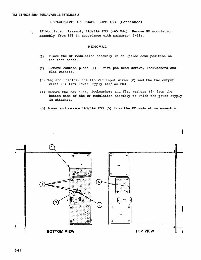
TM 11-6625-2884-30/NAVAIR 16-35TS3615-2
REPLACEMENT OF POWER SUPPLIES (Continued)
g. RF Modulation Assembly 1A3/1A4 PS3 (-65 Vdc). Remove RF modulationassembly from BTS in accordance with paragraph 3-32a.
(1)
(2)
REMOVAL
Place the RF modulation assembly in an upside down position onthe test bench.
Remove caution plate (1) - five pan head screws, lockwashers andflat washers.
(3) Tag and unsolder the 115 Vac input wires (2) and the two outputwires (3) from Power Supply 1A3/1A4 PS3.
(4) Remove the hex nuts, lockwashers and flat washers (4) from thebottom side of the RF modulation assembly to which the power supplyis attached.
(5) Lower and remove 1A3/1A4 PS3 (5) from the RF modulation assembly.
3-98
(1) Position replacementassembly.
(2) Fasten -65 Vdc powerlockwashers and flat
(3) Solder 115 Vac inputpower supply.
(4) Adjust -65 Vdc power
TM 11-6625-2884-30/NAVAIR 16-35TS3615-2
REPLACEMENT
-65 Vdc Power Supply PS3 (5) in RF modulation
supply (5) to chassis, using four hex nuts,washers (4).
wires (2) and two output wires (3) to -65 Vdc
supply as in paragraph 3-35.
(5) Reinstall caution Plate (1), using five pan head screws, lock-washers and flat washers.
(6) Install RF modulation assembly in BTS as in paragraph 3-32b.
3-99

TM 11-6625-2884-30/NAVAlR 16-35TS3615-2
REPLACEMENT OF
h. RF Modulation Assemblv 1A3/1A4
POWER SUPPLIES (Continued)
PS4 (-15 Vdc). Remove RF modulationassembly from BTS in accordance with paragraph 3-32a.
(1)
(2)
(3)
(4)
(5)
(6)
REMOVAL
Place the RF modulation assembly in an upside down position on thetest bench.
Remove caution plate (1) - five pan head screws, lockwashers andflat washers.
Tag and unsolder the 115 Vac input wires (2) and the two outputwires (3) from Power Supply PS4.
Remove pan head screw and lockwasher (4) securing PS4 to the RFmodulation assembly chassis.
Remove the pan head screws, lockwashers and flat washers (5)securing the hold down bracket (6) to the RF modulation assembly.
Lower and remove PS4 (7) with the hold down bracket and two standoffposts.
3-100

TM 11-6625-2884-30/NAVAIR 16-35TS3615-2
REPLACEMENT
(1) Position replacement -15 V dc Power Supply PS4 (7) and bracket (6)on RF modulation assembly.
(2) Fasten PS4 to power supply bracket, using pan head screw and lock-washers (4).
(3) Fasten hold down bracket (6) to RF modulation assembly, using panhead screw and lockwasher (4).
(4) Solder 115 Vac input wires (2) and two output wires (3) to PowerSupply PS4, observing dc polarity.
(5) Reinstall caution plate (1), with five pan head screws, lock-washers and flat washers.
(6) Replace RF modulation assembly in BTS as in paragraph 3-32b.
REPLACEMENT OF PRINTED CIRCUIT BOARDS
3-38. Replace either or both printed circuit boards in 1A3 or 1A4,
CCA, Pulse Generator 1A3/1A4-A1
CCA, CS and Pulse Control 1A3/1A4-A2
as follows.
R E M O V A L
a. Perform the following steps.
C A U T I O N
Disconnect all cables from rear of unit beforeretracting it from case.
(1) Disconnect cables from rear of 1A3/1A4 as follows:
3-101

TM 11-6625-2884-30/NAVAIR 16-35TS3615-2
3-102
REPLACEMENT OF PRINTED CIRCUIT BOARDS (Continued)
REMOVAL (Continued)
(2) Loosen four captive screws (1) on the front of RF Modulation Assembly1A3/1A4 and retract from the BTS cabinet.
(3) Using a screwdriver, rotate the captive screw (2) counterclockwiseuntil free and rotate lid of enclosure to the rear. Both circuitcards are now ready for removal.
(4) Grasp circuit card 1A3/1A4-A1 (3) or 1A3/1A4-A2 (4) and pull cir-cuit card directly out of jack.
TOP VIEW

TM 11-6625-2884-30/NAVAIR 16-35TS3615-2
REPLACEMENT
b. Perform the following steps.
2.
3.
4.
5.
6.
Loosen captive screw (2) and lift enclosure lid for access.
Identify circuit card by part number, and locate its chassisconnector.
Orient cicuit card so its connector polarizing pins match holes atends of chassis connector.
Slide circuit card into card guides and push to chassis connector.
Be sure polarizing pins enter matching holes, then seat circuit cardfully in chassis connector.
Pull enclosure lid forward over circuit cards, and fasten withcaptive screw (2).
REPLACEMENT OF CONTROL INDICATOR 1A1A1
3-39. To replace Control Indicator 1A1A1, remove the front and rear coversof the BTS and perform the following steps.
C A U T I O N
Turning one screw too far or using excessive torquemay crack connector body or strip screw thread.
3-103

TM 11-6625-2884-30/NAVAIR 16-35TS3615-2
REPLACEMENT OF CONTROL INDICATOR 1A1A1 (Continued)
REMOVAL
a. Disconnect air hose and all connectors from BTS:
CABLE DESIGNATION
W1W2W3W5W6W7
Air Duct
JACK NOMENCLATURE AND NUMBER
Monitor J1Control J228V Power J3CMBD RF J4115V 60 Hz J528 VDC J6
Not designated (locatednear top of panel)
b. Close hinged cover (1) over BTS side connector panel.
C. Lay BTS down (2) on hinged cover side.
d. Loosen four screws holding Control Panel Assembly 1A1 to BTS.
C A U T I O N
Control Panel Assembly 1A1 is wired to the BTS. Becareful not to pull or twist wires while handling1A1.
e. Pull Control Panel Assembly 1A1 forward. Rotate 1A1 and set it infront of BTS (3).
f. Remove four Phillips head screws and washers (4) from controlindicator gusset (5).
g. Remove connector (6) from rear of Control Indicator 1A1A1.
h. On front of 1A1A1 turn two fasteners (7) to left.
i. Pull 1A1A1 forward and out of control panel assembly.
3-104
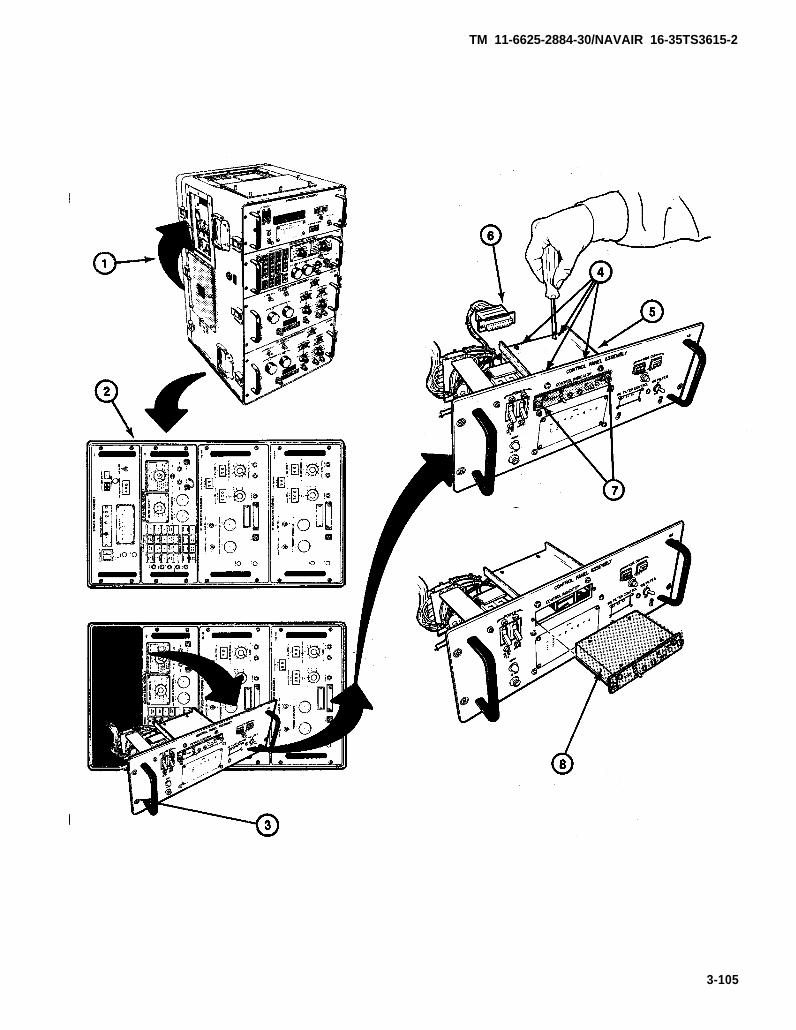
TM 11-6625-2884-30/NAVAIR 16-35TS3615-2
3-105

TM 11-6625-2884-30/NAVAIR 16-35TS3615-2
REPLACEMENT OF CONTROL INDICATOR 1A1A1 (Continued)
REPLACEMENT
a. Push replacement Control Indicator 1A1A1 (1) into opening incontrol panel assembly.
b. Fasten control indicator to panel by turning fasteners (2) clock-wise.
c. Connect plug (3) to rear of control indicator.
C A U T I O N
When connecting or disconnecting jackscrewconnectors:
Turn one screw one turn. Turn other screw one turn. Repeat alternate turning of screws. Do not use excessive torque.
Turning one screw too far or using excessive torquemay crack connector body or strip screw thread.
d. Fasten control indicator to gusset (4) with four Phillips headscrews and washers (5).
e. Replace Control Panel Assembly 1A1 in BTS. Fasten with fourcaptive screws (6).
f. Set BTS (7) erect, and open hinged cover (8).
3-106

TM 11-6625-2884-30/NAVAIR 16-35TS3615-2
3-107

TM 11-6625-2884-30/NAVAIR 16-35TS3615-2
CABLE REPAIRS
3-40. Minor cable repair (broken wires at connectors or connector replacement)may be performed as directed in TM 55-1500-323-25. It is more cost effectiveto replace a cable which requires major repairs. The following illustrationsand text will assist You in checking out and performing minor cable repairs.The cables that will be covered are:
W1 - CM Set Control and W6 - Input Power 115V, 60 HzStatus W7 - Input Power 28 Vdc
W2 -Control W8 - Blanking W3 - Power W9 - Voltage Monitor W4 -RF Coax W10 - Oscilloscope Monitor W5 - RF Coax Wll - FLTS Control Status and Power
a. BTS Cable W1 - Interconnects BTS monitor jack J1 with LRU-1 testjack 1J7.
3-108

TM 11-6625-2884-30/NAVAIR 16-TS3615-2
BTS CABLE W1 WIRE LIST
WIRE
AWG
22
22
22
22
22
22
22
22
22
22
22
22
22
22
22
22
22
22
22
22
22
22
COLOR
WHITE
WHITE
WHITE
WHITE
WHITE
WHITE
WHITE
WHITE
WHITE
WHITE
WHITE
WHITE
WHITE
WHITE
WHITE
WHITE
WHITE
WHITE
WHITE
WHITE
WHITE
WHITE
FROM
P1-1
P1-2
P1-3
P1-4
P 1 - 5
P1-6
P1-7
P1-8
P1-9
P1-10
P1-11
P1-12
P1-13
P1-14
P1-15
P1-16
P1-17
P1-18
P1-19
P1-20
P1-21
P1-22
TO
P2-1
P2-2
P2-3
P2-4
P2-5
P2-6
P2-7
P2-8
P2-9
P2-10
P2-11
P2-12
P2-13
P2-14
P2-15
P2-16
P2-17
P2-18
P2-19
P2-20
P2-21
P2-22
CIRCUITFUNCTION
OGLC1M
OSCLK1M
0GLCM2M
0DSLK2M
OGSLL1M
OLSLQ1M
0GSLL2M
0LSLQ2M
OCSGC1M
OS18M
0DSGC2M
0S28M
OECSR1M
OG1RJM
0CESR2M
0G2RJM
OLSL1AM
(Spare 1)
0LSL2AM
(Spare 2)
OMFS1LC
OMFS1LO
3-109

3-110
TM 11-6625-2884-30/NAVAIR 16-35TS3615-2
CABLE REPAIRS (Continued)
BTS CABLE W1 WIRE LIST (Continued)
WIRE
AWG
22
22
22
22
22
22
22
24TP
24
I
24TP
24
24TP
24
24TP
24
24TP
24
24TP
24
24TP
24
24TP
24
COLOR
WHITE
WHITE
WHITE
WHITE
WHITE
WHITE
WHITE
WHITE
BLACK
WHITE
BLACK
WHITE
BLACK
WHITE
BLACK
WHITE
BLACK
WHITE
BLACK
WHITE
BLANK
WHITE
BLACK
FROM
P1-23
P1-24
P1-25
P1-26
P1-27
P1-28
P1-29
P1-35
P1-36
P1-37
P1-38
P1-39
P1-40
P1-41
P1-42
P1-43
P1-44
P1-46
P1-47
P1-48
P1-49
P1-50
P1-51
TO
P2-23
P2-24
P2-25
P2-26
P2-27
P2-28
P2-29
P2-35
P2-36
P2-37
P2-38
P2-39
P2-40
P2-41
P2-42
P2-43
P2-44
P2-46
P2-47
P2-48
P2-49
P2-50
P2-51
CIRCUITFUNCTION
0MFS2LC
0MFS2L0
OMFOD
OMFAVN
0MFSM3
OMFVCP
OMSYSRS
OES11GM
OCST1M
OCTGC1M
0GS3K1M
OGPULVM
0ESY2M
OESY1M
0GSBK2M

TM 11-6625-2884-30/NAVAIR 16-35TS3615-2
AWG
24TP
24
24TP
24
24TP
24
24TPSH
24
22
COLOR
WHITE
BLACK
WHITE
BLACK
WHITE
BLACK
RG-179 B/U
SHIELD
RG-179B/U
SHIELD
RG-179 B/U
SHIELD
RG-179 B/U
SHIELD
RG-179 B/U
SHIELD
WHITE
BLACK
SHIELD
BLACK
FROM
P1-52
P1-53
P1-54
P1-55
P1-45
P1-34
P1-56
P1-67
P1-57
P1-68
P1-58
P1-69
P1-59
P1-70
P1-60
P1-71
P1-61
P1-62
P1-72
P1-64
P1-65
P1-66
TO
P2-52
P2-53
P2-54
P2-55
P2-45
P2-34
P2-56
P2-67
P2-57
P2-68
P2-58
P2-69
P2-59
P2-70
P2-60
P2-71
P2-61
P2-62
P2-72
P2-64
CIRCUITFUNCTION
ODTGC2M
ODSTP2M
OES21GM
AGLMDRM
AALVM
AGTHLEVM
ALVC02M
ALVCO1M
OALMTVM
GND
SPARE
SPARE
3-111

TM 11-6625-2884-30/NAVAIR 16-35TS3615-2
CABLE REPAIRS (Continued)
BTS CABLE W1 WIRE LIST (Continued)
WIRECIRCUIT
AWG COLOR FROM TO FUNCTION
P1-75 SPARE
P1-75 P2-75 SPARE
P1-76 P2-76 SPARE
22 ORANGE P1-83 P2-83 +28v
P1-84 SPARE
P1-85 SPARE
P1-91 SPARE
P1-92 SPARE
P1-93 SPARE
22 WHITE P1-77 P2-77 +5V Logic
22 WHITE P1-78 P2-78 +5V
22 WHITE P1-79 P2-79 -5.2V
22 WHITE P1-80 P2-80 +1OV
22 WHITE P1-86 P2-86 -1OV
22 WHITE P1-87 P2-87 +15V
22 WHITE P1-88 P2-88 -15V
22 WHITE P1-89 P2-89 -65V
3-112
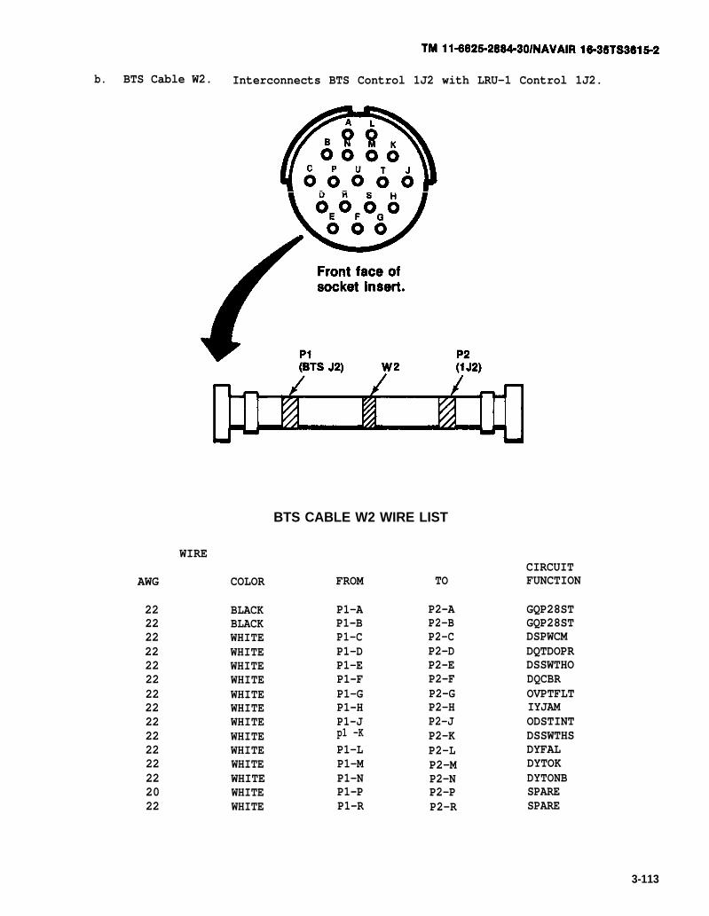
TM625-2884-30/NAVAIR 16-35TS3615-2
b. BTS Cable W2. Interconnects BTS Control 1J2 with LRU-1 Control 1J2.
BTS CABLE W2 WIRE LIST
WIRECIRCUIT
AWG COLOR FROM TO FUNCTION
22 BLACK P1-A P2-A GQP28ST22 BLACK P1-B P2-B GQP28ST22 WHITE P1-C P2-C DSPWCM22 WHITE P1-D P2-D DQTDOPR22 WHITE P1-E P2-E DSSWTHO22 WHITE P1-F P2-F DQCBR22 WHITE P1-G P2-G OVPTFLT22 WHITE P1-H P2-H IYJAM22 WHITE P1-J P2-J ODSTINT22 WHITE p1 -K P2-K DSSWTHS22 WHITE P1-L P2-L DYFAL22 WHITE P1-M P2-M DYTOK22 WHITE P1-N P2-N DYTONB20 WHITE P1-P P2-P SPARE22 WHITE P1-R P2-R SPARE
3-113

TM 11-6625-2884-30/NAVAIR 16-35TS3615-2
CABLE REPAIRS (Continued)
c. BTS Cable W3. Interconnects BTS +28 Vdc Power 1J3 to LRU-1 Power 1J1.
BTS CABLE W3 WIRE LIST
WIRECIRCUIT
AWG COLOR FROM TO FUNCTION
12 ORANGE P1-A P2-A +28V
12 RED P1-B P2-B +28V
12 BLACK P1-D P2-D 28V RET
12 WHITE P1-E P2-E 28V RET
12 GREEN Pi-F P2-F GND
d. BTS Cable W4. Interconnects BTS Status Panel RF IN jack 1A2J2 toLRU-1 RF OUT jack 1A1J4 (via a 30 dB attenuator). Used to samplethe RF output of LRU-1 under test.
3-114
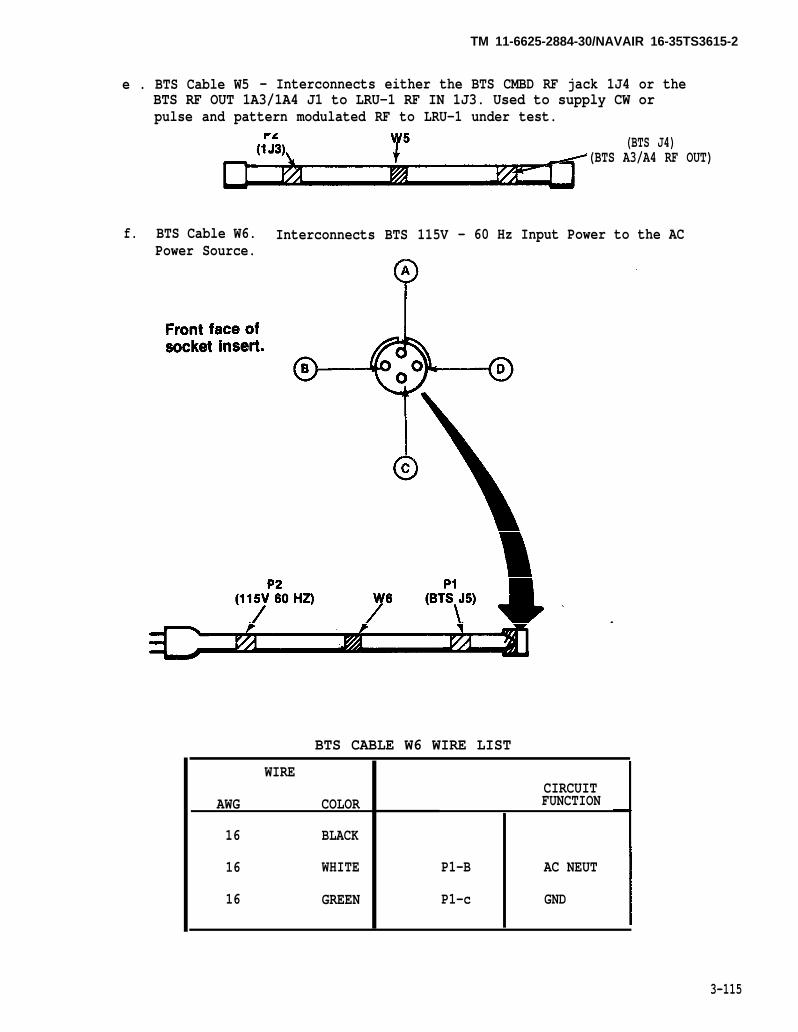
TM 11-6625-2884-30/NAVAIR 16-35TS3615-2
e . BTS Cable W5 - Interconnects either the BTS CMBD RF jack 1J4 or theBTS RF OUT 1A3/1A4 J1 to LRU-1 RF IN 1J3. Used to supply CW orpulse and pattern modulated RF to LRU-1 under test.
(BTS J4)(BTS A3/A4 RF OUT)
f. BTS Cable W6. Interconnects BTS 115V - 60 Hz Input Power to the ACPower Source.
BTS CABLE W6 WIRE LIST
WIRE
AWG COLOR
16 BLACK
16 WHITE
16 GREEN
CIRCUITFUNCTION
P1-B AC NEUT
P1-c GND
3-115

TM 11-6625-2884-30/NAVAIR 16-35TS8615-2
CABLE REPAIRS (Continued)
g. BTS Cable W7 - Interconnects BTS 28 VDC input power to the 28power supply.
BTS CABLE W7 WIRE LIST
WIRE
AWG
12
12
12
12
12
COLOR
ORANGE
RED
BLACK
WHITE
GREEN
CIRCUITFROM FUNCTION
P1-A +28V
P1-B +28V
P1-D 28V RET
P1-E 28V RET
P1-F GND
Volt
3-116
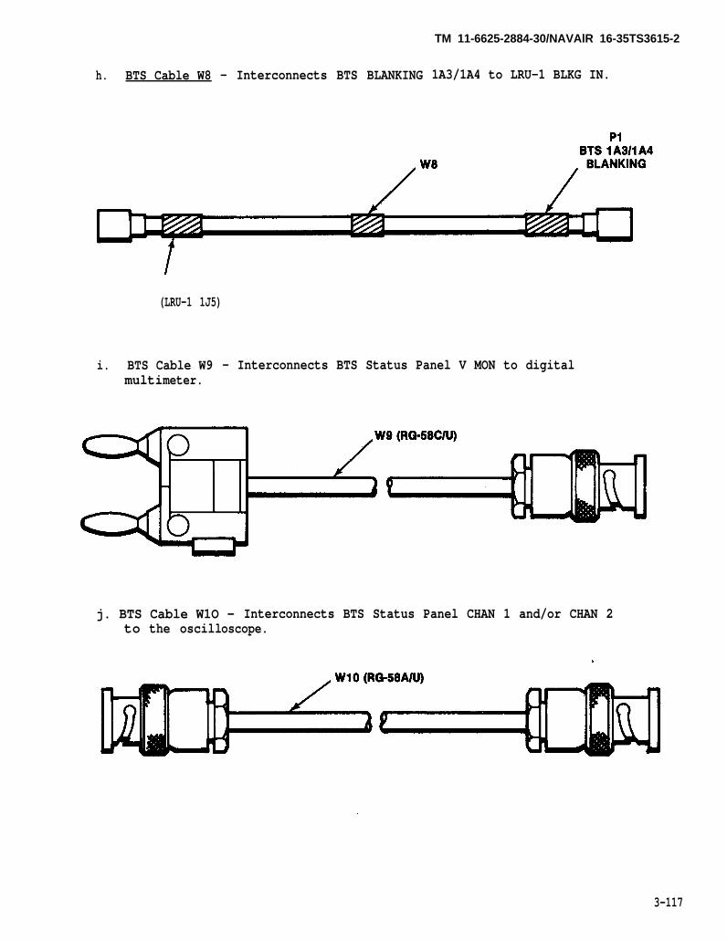
h. BTS Cable W8 - Interconnects BTS BLANKING
TM 11-6625-2884-30/NAVAlR 16-35TS3615-2
1A3/1A4 to LRU-1 BLKG IN.
(LRU-1 1J5)
i. BTS Cable W9 - Interconnects BTS Status Panel V MON to digitalmultimeter.
j. BTS Cable W1O - Interconnects BTS Status Panel CHAN 1 and/or CHAN 2to the oscilloscope.
3-117
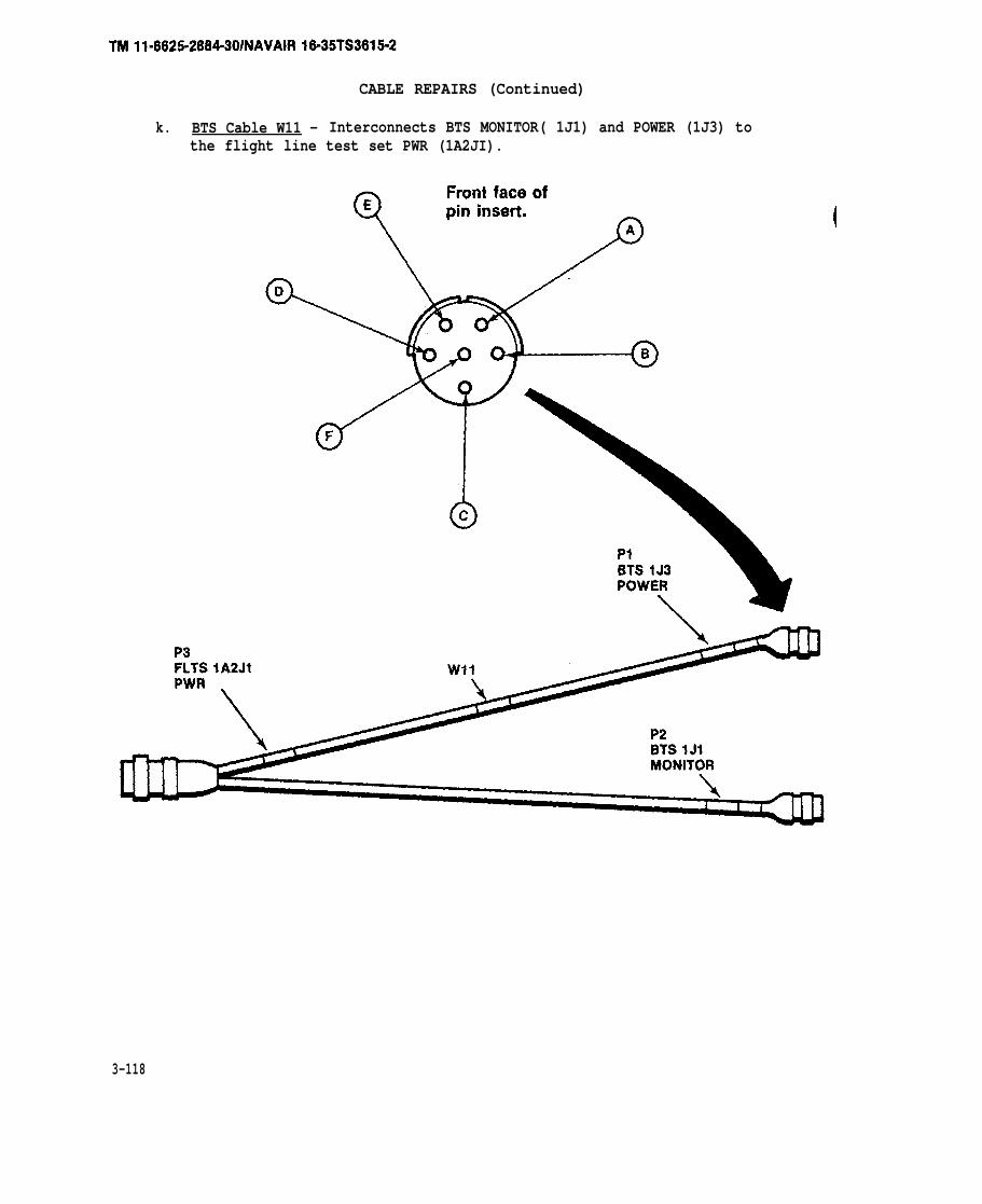
TM 11-6625-2884-30/NAVAIR 16-35TS3615-2
CABLE REPAIRS (Continued)
k. BTS Cable W11 - Interconnects BTS MONITOR( 1J1) and POWER (1J3) tothe flight line test set PWR (1A2JI).
3-118

TM 11-6625-2884-30/NAVAIR 16-35TS3615-2
3-119

TM 11-6625-2884-30/NAVAIR 16-35TS3615-2
3-120

CABLE W11 WIRE LIST
REFNo.
1
2
3
4
5
6
7
8
9
10
11
12
13
14
15
16
17
18
19
20
AWG
WIRE
22
22
22
22
22
22
22
22
22
22
22
22
22
*
*
*
*
*
COLOR
BLACK
BLACK
WHITE
WHITE
GREEN
GREEN
WHITE
WHITE
WHITE
WHITE
WHITE
WHITE
WHITE
RG-179 B/U
SHIELD
RG-179 B/U
SHIELD
BROWN
RED
YELLOW
ORANGE
BLUE
FROM
P3-1
P3-2
P3-4
P3-5
P3-7
P3-8
P3-13
P3-14
P3-15
P3-17
P3-18
P3-19
P3-49
P3-47
P3-48
P3-45
P3-46
P3-39
P3-40
P3-41
P3-42
P3-43
TOCIRCUITFUNCTION
P1-A
P1-D
P1-F
P2-21
P2-22
P2-23
P2-24
P2-25
P2-26
P2-27
P2-48
P2-49
P2-46
P2-47
P2-77
P2-87
P2-88
P2-83
P2-89
+28 Vdc
28V RET
GND
+5V
+15V
-15V
+28V
-65V
3-121
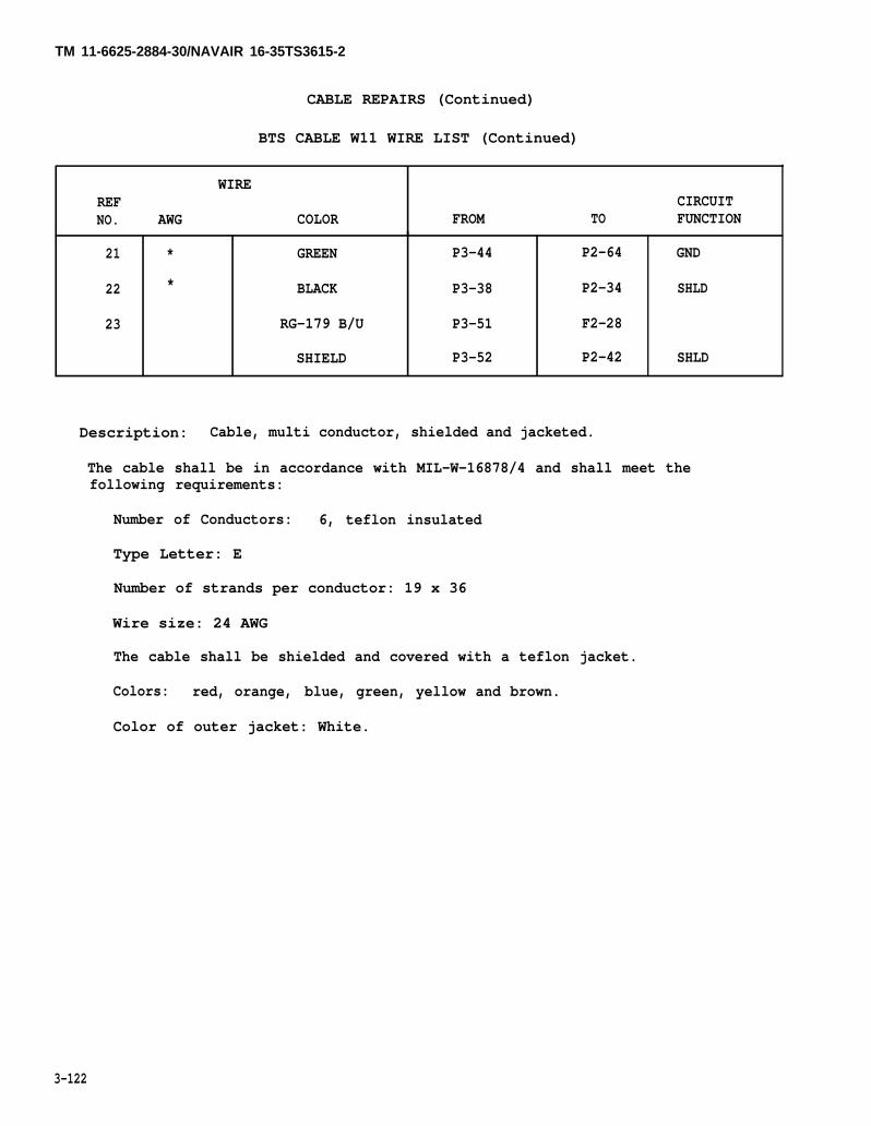
TM 11-6625-2884-30/NAVAIR 16-35TS3615-2
CABLE REPAIRS (Continued)
BTS CABLE W11 WIRE LIST (Continued)
WIREREF CIRCUITNO. AWG COLOR FROM TO FUNCTION
21 * GREEN P3-44 P2-64 GND
22 * BLACK P3-38 P2-34 SHLD
23 RG-179 B/U P3-51 F2-28
SHIELD P3-52 P2-42 SHLD
Description: Cable, multi conductor, shielded and jacketed.
The cable shall be in accordance with MIL-W-16878/4 and shall meet thefollowing requirements:
Number of Conductors: 6, teflon insulated
Type Letter: E
Number of strands per conductor: 19 x 36
Wire size: 24 AWG
The cable shall be shielded and covered with a teflon jacket.
Colors: red, orange, blue, green, yellow and brown.
Color of outer jacket: White.
3-122

3-123/3-124(Blank)
SECTION VAVIM TESTING PROCEDURES
SECTION CONTENTS PAGE
GENERAL ................................................ 3-123POST REPAIR REQUIREMENTS ................................... 3-123
GENERAL
3-41. Testing of support equipment circuits is accomplished by following thetroubleshooting procedures in Section III. Step-by-step conformance to thenormal indication columns of the troubleshooting procedures ensures that thebench test set meets performance standards.
POST REPAIR REQUIREMENTS
3-42. If any repairs or adjustments have been made to the bench test set, per-form column 1 (ACTION) and verify with column 2 (NORMAL INDICATION) of theappropriate troubleshooting procedure as given in section 111. If any addi-tional troubles are encountered while following the procedure, perform column 3(FIX), and retest.


TM 11-6625-2884-30/NAVAIR 16-35TS3615-2
AR 55-38
AR 735-11-2
DA PAM 310-1
TM 38-750
TM 11-5865-202-12
(S) TM 11-5865-202-30
TM 11-6625-2884-12
TM 11-6625-2885-12
TM 11-6625-2885-30
APPENDIX AREFERENCES
A-1 . GENERAL INFORMATION
Reporting of Transportation Discrepancies in Shipments.
Reporting of Item Discrepancies Attributable to Shippers.
Consolidated Index of Army Publications and Blank Forms.
The Army Maintenance Management Systems (TAMMS).
A-2. TECHNICAL MANUALS
Operator’s and Aviation Unit Maintenance ManualCountermeasures Set AN/ALQ-136(V)1 (NSN5805-01-127-6880).
Aviation Intermediate Maintenance Manual Counter-measures Set AN/ALQ-136(V)1 (NSN 5805-01-127-6880)(u).
Operator’s and Aviation Unit Maintenance ManualTest Set, Countermeasures Set TS-3615/ALQ-136(V)(NSN 6625-01-121-8984).
Operator’s and Aviation Unit Maintenance ManualTest Set, Countermeasures Set TS-3614/ALQ-136(V)(NSN 6625-01-121-8983).
Aviation Intermediate Maintenance Manual Test Set,Countermeasures Set TS-3614/ALQ-136(V) (NSN 6625--
01-121-8983).
A-3. REPAIR PARTS AND SPECIAL TOOLS LIST
TM 11-6625-2884-30P
TM 11-6625-2885-30P
Aviation Intermediate Maintenance Repair Parts andSpecial Tools List (Including Depot MaintenanceRepair Parts and Special Tools) for Test Set,Countermeasures Set TS-3615/ALQ-136(V) (NSN6625-01-121-8984).
Aviation Intermediate Maintenance Repair Parts and SpecialTools List (Including Depot Maintenance Repair Parts andSpecial Tools) for Test Set, Countermeasures SetTS-3614/ALQ-136(V) NSN 6625-01-121-8983.
A-1
TM 11-6625-2884-30/NAVAIR 16-35TS3615-2
REFERENCES (Continued)
A-4. GENERAL REPAIR INSTRUCTIONS
TM 43-0139 Painting Instructions for Field Use.
TM 55-1500-323-25 Organizational, Direct Support, and DepotMaintenance Manual, Installation Practicesfor Aircraft Electric and Electronic Wiring.
A-5. GENERAL TYPE EQUIPMENT PUBLICATIONS
SC 5180-91-CL-R07 Tool Kit, Electronic Equipment TK-105/G
SC 5180-91-CL-R13 Tool Kit, Electronic Equipment TK-100/G
TM 11-6625-1703-15 Operators Manual for OscilloscopeAN/USM-281A
A-2
TM 11-6625-2884-30/NAVAIR 16-35TS3615-2
APPENDIX BEXPENDABLE SUPPLIESAND MATERIALS LIST
SECTION IINTRODUCTION
B-1 . SCOPE
This appendix lists expendable supplies and materials you will need tooperate and maintain the BTS. These items are authorized to you by CTA 50-970,Expendable Items (Except Medical, Class V, Repair Parts, and Heraldic Items).
B-2. EXPLANATION OF COLUMNS
The columns in this list are explained below.
a. Column (1) - Item Number. This number is assigned to the entry in thelisting and i s referenced in the narrative instructions to identify thematerial (e.g., “Use cl caning compound, item 5, App. D“ ).
b. Column (2) - Level. This column identifies the lowest level of mainten-ance that requires the listed item.
(enter as applicable)
O - Aviation Unit MaintenanceF - Direct Support Maintenance
c. Column (3) - National Stock Number. This is the national stock numberassigned to the item; use it to request or requisition the item.
d. Column (4) - Description. Indicates the Federal item name and, ifrequired, a description to identify the item. The last line for each itemindicates the part number followed by the Federal Supply Code for Manufacturer(FSCM) in parenthesiss followed by the part number.
Column (5) - Unit of Measure (U/M). Indicates the measure used in per-forming the actual maintenance function. This measure is expressed by a two-character alphabetic abbreviation (e.g., ea, in, pr). If the unit of measurediffers from the unit of issue, requisition the lowest unit to issue that willsatisfy your requirements.
B-1

TM 11-6625-2884-30/NAVAIR 16-35TS3615-2
SECTION IIEXPENDABLE SUPPLIES AND MATERIALS
(1) (2) (3) (J) (5)NATIONAL
ITEM STOCKNUMBER LEVEL NUMBER DESCRIPTION U/M
1 0, F Cloths, lint-free cleaning A/R
2 O, F Trichlorotrifluoroethane A/R
3 F Paint, light gray, QTFED-STD-595 color no. 26307
4 F Sandpaper A/R
5 F Brush, wire EA
6 F Brush, paint EA
B-2

TM 11-6625-2884-30/NAVAIR 16-35TS3615-2
INDEXSUBJECT
AAbbreviations, Comon . . . . . . . . . . . . . . . . . . . . . . . . . . . .AC Power Distribution, Cooling and YIG Filter Control . . . . . . . . . . .Adjustment of Power Supply,
+5V Power Supply 1A3/1A4 PS1 .................................+15V Power Supply 1A3/1A4 PS2 ✎ ✎ ✎ ✎ ✎ ✎ ✎ ✎ ✎ ✎ ✎ ✎ ✎ ✎ ✎ ✎ ✎ ✎ ✎ ✎ ✎ ✎ ✎ ✎ ✎ ✎ ✎ ✎ ✎ ✎ ✎ ✎ ✎ ✎
-65V Power Supply 1A3/1A4 PS3 . . ...................................+12V Power Supply 1A2 PS1 ..................................
Aviation Intermediate Maintenance (AVIM) Testing Procedures . . . . .
BBlanking Output Test . . . . ...................................... . . . . . .Block Diagram Description,
Control Panel Assembly . ....................................RF Modulation Assemblies . . . . . . . . . . . . . . . . . . . .Status Panel Assembly ...................................... . . . . . .
BTS Illustration . . . . . . . . . . . . . . . . . . . . . . .BTS, Rear View Illustration . . . . . . . . . . . . . . . . . . . . . . . . .
c
Cabling/Hose Attachment to BTS Connector-Panel . . . . . . . . . . . . . . . . . .Cable,
Information (table 1-8) .............................Repairs . . . . . . . . . . . . . . . . . . . . . . . ..................W1 Control and Status .....................................W2 Control . ........................ . . . ......................W3 Power . ................... . ............................W4 RF Coax . . . . . . . . . . . . . . . . . . . . . .......................... .W5 RF Coax . . . ..................... . ...............W6 Input Power 115V, 60 Hz . . . . . ................................W7 Input Power 28 VDC ........................................ . .W8 Blanking . . . . . . ..........................................W9 Voltage Monitor .......................... .......................W 1O Oscilloscope Monitor . . . . . . . . . . . . . . . . . . . . . . . .W11 BTS to FLTS . ...........................................
Common Names . . . . . . . . ............. . . . . . . . . . . . . .Components,
Front Panel . . ..............................................Location and Description,
Control Panel Assembly . . . . ...............................RF Modulation Assembly ................................Status Panel Assembly . ...................................
Connections, Installation . . . . . . . . .. . . . . . . . . . . . . . . . . .Connector Panel Illustration . . . . . . . . . . . . . . . . . . . . . . . . . . . .Con Scan Modulation Check . . . . . . .................................Con Scan Sync Test ...............................................
PAGE
1-42-4
3-813-823-843-853-123
3-40
2-22-102-51-81-51
3-4
1-423-1083-1083-1133-1143-1143-1153-1153-1163-1173-1173-1173-1181-7
1-10
1-201-271-223-33-53-293-46
Index-1

TM 11-6625-2884-30/NAVAlR 16-35TS3615-2
INDEX (Continued)
C (Continued)
Consolidated Index of Army Publications and BlankControl and Power Distribution,
Forms . . .
Introduction .15V Power . . . . ............ . . . . . . . . . . . .YIG Filter . . . . . . . . . . . . . . . .+28 Vdc PowerControl Signals to LRU-1Status Signals from LRU-1
Control Panel Assembly,Block Diagram DescriptionCheckComponents, Description and LocationControl IndicatorDrawer Removal and ReplacementPower Supplies
Control, Countermeasures Set C-9576/ALQ . . . . . . . . . . . . . . . . . . .Control Indicator, Replacement ofControl Signals to LRU-1Control, Status PanelControls and Indicators,
Control Panel (table 1-1)RF Modulation Assembly (table 1-3)Status Panel Assembly (table 1-2)
Corrective Action
DDA PAM 310-1Data, EquipmentDefinitions . . . . . . . . . . . . . . . . . . . . . . . . . . . .Description, EquipmentDestruction of Army Electronic Materiel . . . . . . . . . . . . . . . . . .Digital/Analog Circuits . . . . . . . . . . . . . . . . . . . . .Drawer Removal and Replacement,
Control PanelRF ModulationStatus Panel
EEquipment,
Cable Information (table 1-8)Characteristics, Capabilities and Features . . . . . . . . . . . . . . . . . . . .ConfigurationDataDescription and DataIndicator Information (table 1-6)Leading Particulars (table 1-4)
PAGE
1-3
2-152-162-182-202-212-22
2-23-70
1-10,1-11,1-201-113-77
1-32,3-861-13-1042-212-5
1-111-191-153-73
1-31-7,1-33
3-91-71-32-25
3-773-743-74
1-421-71-451-331-71-371-33
I n d e x - 2

1-10
1-7
1-9
2-15
TM 11-6625-2884-30/NAVAIR 16-35TS3815-2
SUBJECT PAGE
E (Continued)Equipment (Continued),
Power Supply Information (table 1-5)Required but not Supplied (table 1-10) . . . . . . . . . . . . . . . . . . . . . . . .Supplied (table 1-9)Switch Information (table 1-7)
Expendable Supplies and Materials List
FFirst AidFront Panel ComponentsFunctions (Purpose and Use)Functions of BTS, MajorFunctional Block Diagram Description
HHow to Use This Manual
IIndicator Information (table 1-6)Installation Instructions
Cabling/Hose Attachment . . . . . . . . . . . . . . . . . . . . . . .CheckoutConnections . . . . . . . . . . . . . . . . . . . . . . . . . . . . .GeneralPower Requirements
LLamp ReplacementLinear Modulation (CON SCAN)Location and Description of Components,
Control Indicator (table 1-1)Control Panel AssemblyRF Modulation AssemblyStatus Panel Assembly
Location and Description of Major Components,Control Panel AssemblyRF Modulation AssemblyStatus Panel Assembly
MMaintenance Forms, Records and ReportsMaintenance Procedures,
Adjustment of Power SupplyAlignment of power SupplyAssembly Removal and ReplacementCable RepairsCorrective Action . . . . . . . . . . . . . . . . . . . . . . . .
1-341-451-451-39
Appendix B
iii
1-37
3-43-63-33-31-33
3-732-12,2-34
1-111-101-181-12
1-201-251-22
1-3
3-813-82,3-83,3-84
3-743-1083-73
Index-3

TM 11-6625-2884-30/NAVAIR 16-35TS3615-2
INDEX (Continued)
M (Continued)
Maintenance Procedures (Continued),Replacement of,
Control Indicators 1A1A1 . . . . . . . . . . . . . . . . . . . . . . . . . . . . . . . . . . . .Power Supplies . . . . . . . . . . . . . . . . . . . . . . . . . . . . . . . . . . . . . . . . . . . . . .Printed Circuit Boards . . . . . . . . . . . . . . . . . . . . . . . . . . . . . . . . . . . . . .
Materiel, Destruction of Electronic . . . . . . . . . . . . . . . . . . . . . . . . . . . . .
NNomenclature, Official . . . . . . . . . . . . . . . . . . . . . . . . . . . . . . . . . . . . . . . .
0Operation, Principles of . . . . . . . . . . . . . . . . . . . . . . . . . . . . . . . . . . . . . . . .Oscilloscope Monitor Switches . . . . . . . . . . . . . . . . . . . . . . . . . . . . . . . . . . .
PPost Repair Requirement . . . . . . . . . . . . . . . . . . . . . . . . . . . . . . . . . . . . .Power Supplies, Removal and Replacement of,
Control Panel Power Supply 1A1PS1Control Panel Power Supply 1A1PS2Control Panel Power Supply 1A1PS3RF Modulation Power Supply 1A3/1A4RF Modulation Power Supply 1A3/1A4RF Modulation Power Supply 1A3/1A4RF Modulation Power Supply 1A3/1A4Status Panel Power Supply 1A2PS1
-15 Vdc) . . . . . . . . . . (+15 Vdc) . . . . . . . . . .(+10 Vdc) . . . . . . . . . . . . . . . . . . .PS1 (+5 Vdc) . . . . . . . . . . . . . . .PS2 (+15 Vdc) . . . . . . . . . . . . . .PS3 (-65Vdc) . . . . . . . .PS4 (-15Vdc) . . . . . . . . .(+12Vdc) . . . . .
Power Supply Information(table 1-5) . . . . . . . . . . . . . . . . . . . . . . . . . .Preparation for Storage or Shipment . . . . . . . . . . . . . . . . . . . . . . . . . . . . .Preliminary Test Setup . . . . . . . . . . . . . . . . . . . . . . . . . . . . . . . . . . . . . . . . . .PRI Check . . . . . . . . . . . . . . . . . . . . . . . . . . . . . . . . . . . . . . . . . . . . . . . . . . . . . . .Printed Circuit Boards, Replacement of . . . . . . . . . . . . . . . . . . . . . . . . . .Pulse Modulation . . . . . . . . . . . . . . . . . . . . . . . . . . . . . . . . . . . . . . . . . . . . . . . .Pulse Modulation (AW/AF/B/VAR PRI) . . . . . . . . . . . . . . . . . . . . . . . . . . . . . .Pulse Sync Test . . . . . . . . . . . . . . . . . . . . . . . . . . . . . . . . . . . . . . . .Purpose and Use (Functions) . . . . . . . . . . . . . . . . . . . . . . . . . . . . . . . . .
RReceiver/Transmitter RT 1149(V) . . . . . . . . . . . . . . . . . . . . . . . . . . . . . . . . .
3-1043-863-1821-3
1-4
2-l2-8
3-123
3-863-883-903-943-963-993-1003-921-341-33-113-363-1022-302-133-431-7
1-2References, General . . . . . . . . . . . . . . . . . . . . . . . . . . . . . . . . . . . . . . . . . . . . . Appendix ARepair Parts, Special Tools, Test Measurement and Diagnostic Equipment and Support Equipment . . . . . . . . . . . . . . . . . . . . . . . . . . . . . . . . . 3-1Repair Parts, Tools and . . . . . . . . . . . . . . . . . . . . . . . . . . . . . . . . . . . . . . . . . 3-2Replacement of,
Control Indicator 1A1A1 . . . . . . . . . . . . . . . . . . . . . . . . . . . . . . . . . . . . . . . 3-104Power Supplies . . . . . . . . . . . . . . . . . . . . . . . . . . . . . . . . . . . . . . . . . . . . . , , . 3-86Printed Circuit Boards . . . . . . . . . . . . . . . . . . . . . . . . . . . . . . . . . . . . . . . . 3-102
Reporting Equipment Improvement Recommendations . . . . . . . . . . . . . . . . . 1-5
Index-4

TM 11-6625-2884-30 /NAVAIR 16-35TS3615-2
SUBJECT
R (Continued)Reports,
Discrepancy in ShipmentMaintenance . .. . . . . . . . . . . . . . . . . . . . . . . . . .Packaging and Handling DeficienciesUnsatisfactory Equipment
RF Modulation Assembly,Block Diagram DescriptionComponents, Description and Location . . . . . . . . . . . . . . . . . . . . . .Controls and Indicators . . . . . . . . . . . . . . . . . . . . . . . .Drawer Removal and ReplacementFunctions . . . . . . .. . . . . . . . . . . . . . . . . . . . . . . . . . . . .Maintenance - see Maintenance ProceduresPower Supplies
Preliminary Test SetupRF Path
RF Output Frequency CheckRF Output Level CheckRF Path (CW),
RF Modulation Assemblies 1A3/1A4RF Modulation . . . . . . . . . . . . . . . . . . . . . . .Status Panel Assembly 1A2
sSafety, Care and HandlingScope of BookSchematic Diagrams . . . . . . . . . . . . . . . . . . . . . . . . . . . . .
Shipment, Preparation for . . . . . .. . . . . . . . . . . . . .Special ToolsStatus and Monitoring,
Block Diagram DescriptionFunctional Block Diagram Description
Status Panel Assembly,Block Diagram Description . . . . . . . . . . . . . . . . . . . . . . . . . . . . .Components, Location and Description . . . . . . . . . . . . . . . . . . . . . .Controls and Indicators . . . . . . . . . . . . . . . . . . .. . .Drawer Removal and ReplacementForcing Function CheckIndicator CheckMaintenance - see Maintenance ProceduresOscilloscope Monitor CheckPower suppliesRF Path Status and MonitoringVoltage Monitor Check
1-31-31-31-3
2-101-18,1-20,1-27
1-193-741-3
1-34,3-94,3-96,3-98,
3-1003-11
2-10,2-233-193-14
2-102-232-9
1-471-1
3-2,F.O.-1thru
F.O.-131-33-1,3-2
2-62-36
1-12,1-221-153-743-523-49
3-551-34,3-92
2-92-363-60
TM 11-6625-2884-30/NAVAIR 16-35TS3615-2
INDEX
SUBJECT
S (Continued)Status Signals from LRU-1Storage, Preparation for . . . . . . . . . . . . . . . . . . . . . . . . . . . . . . . . . . . . . . . .Sympton Index . . . . . . . . . . . . .. . . . . . . . . . . . . . . . . . . .Switch Information (table 1-7)
TTechnical Manuals, ReferencesTest,
ConditionsEquipmentEquipment UseSetup, Prelilninary . . . . . . ... . . . . . . . . . . . . . . . . . . . .Test Set, Countermeasures Set
Threat PRI CheckTools and Repair PartsTroubleshooting
VVariable PRI CheckVoltage Monitor Switch
wMarnings
YYIG Filter,
CheckControl
PAGE
1-6,2-221-33-81-39
Appendix A
3-93-23-93-111-23-363-23-7
3-232-7
Inside FrontCover, a
3-622-18
Index-6
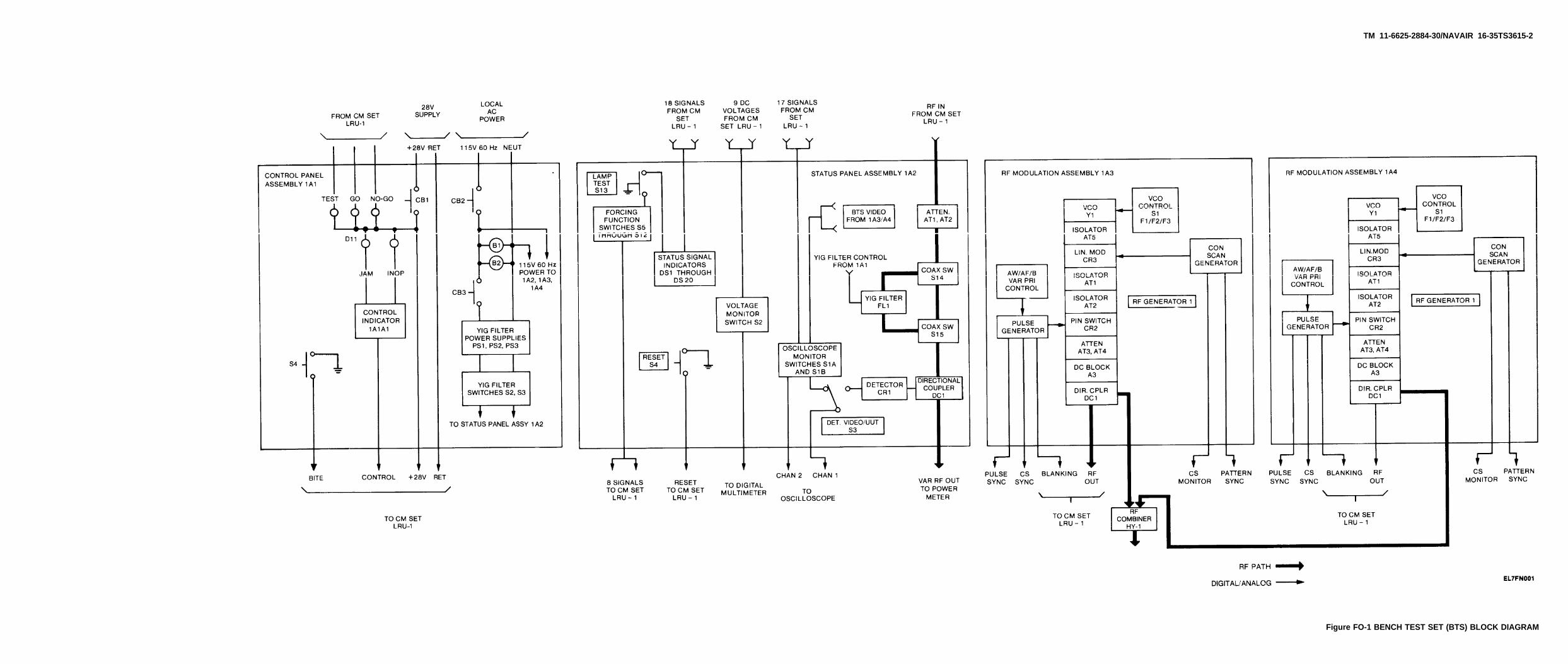
TM 11-6625-2884-30/NAVAIR 16-35TS3615-2
Figure FO-1 BENCH TEST SET (BTS) BLOCK DIAGRAM
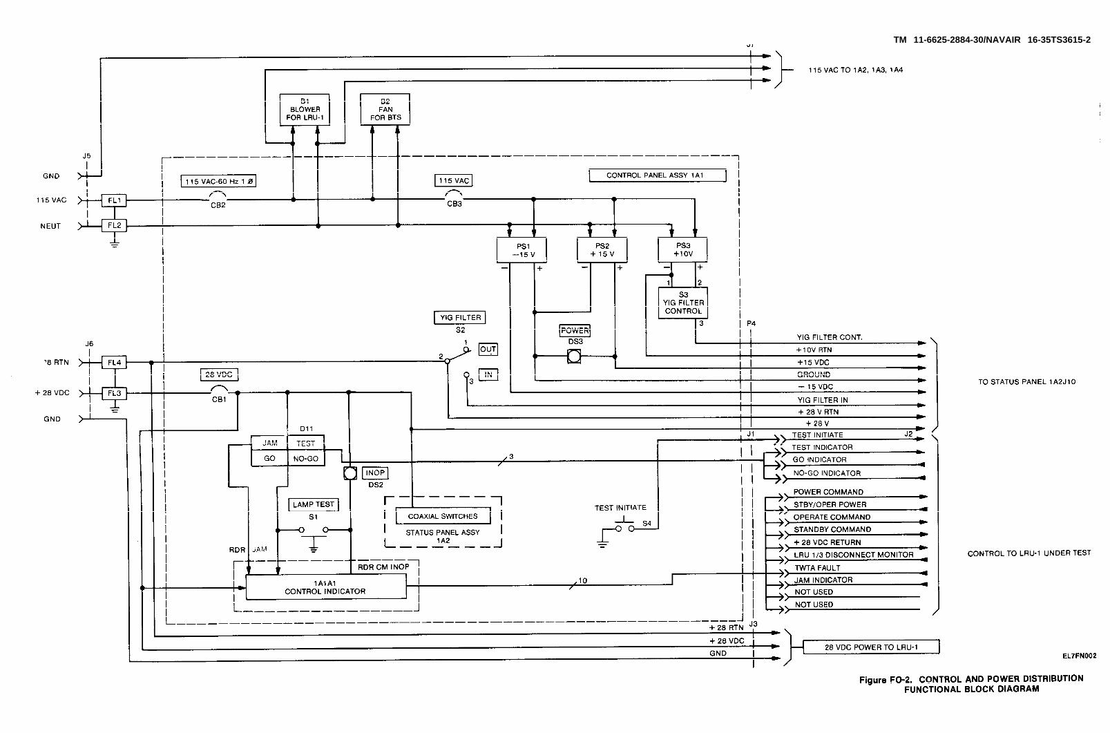
TM 11-6625-2884-30/NAVAIR 16-35TS3615-2

TM 11-6625-2884-30/NAVAIR 16-35TS3615-2

TM 11-6625-2884-30/NAVAIR 16-35TS3615-2
Figure FO-4 RF PULSE MODULATIONFUNCTIONAL BLOCK DIAGRAM

TM 11-6625-2884-30/NAVAIR 16-35TS3615-2
Figure FO-5 RF LINEAR MODULATION FUNCTIONAL
BLOCK DIAGRAM
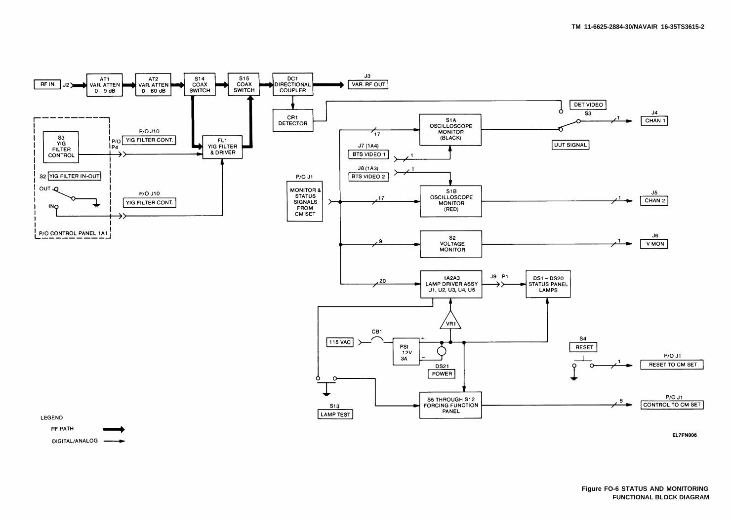
TM 11-6625-2884-30/NAVAIR 16-35TS3615-2
Figure FO-6 STATUS AND MONITORINGFUNCTIONAL BLOCK DIAGRAM
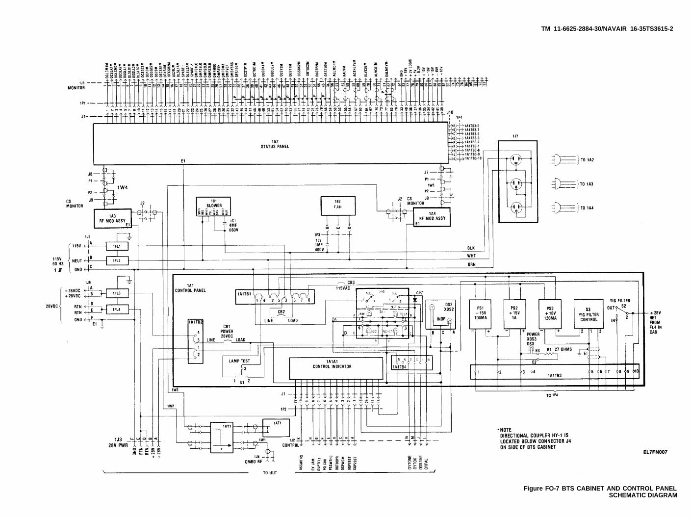
TM 11-6625-2884-30/NAVAIR 16-35TS3615-2
Figure FO-7 BTS CABINET AND CONTROL PANELSCHEMATIC DIAGRAM

TM 11s-6625-2884-30/NAVAIR 16-35TS3615-2
Figure FO-8 STATUS PANEL ASSEMBLY 1A2SCHEMATIC DIAGRAM

TM 11-6625-2884-30/NAVAIR 16-35TS3615-2
Figure FO-9 RF MODULATION ASSEMBLY 1A3/1A4
SCHEMATIC DIAGRAM (Sheet 1 of 2)
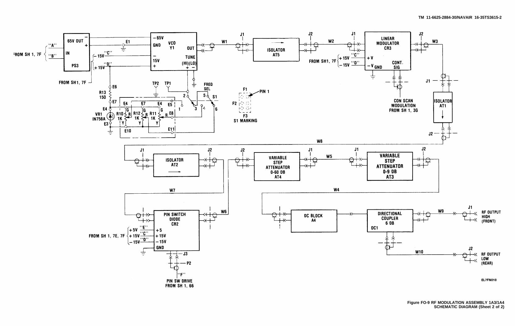
TM 11-6625-2884-30/NAVAIR 16-35TS3615-2
Figure FO-9 RF MODULATION ASSEMBLY 1A3/1A4SCHEMATIC DIAGRAM (Sheet 2 of 2)
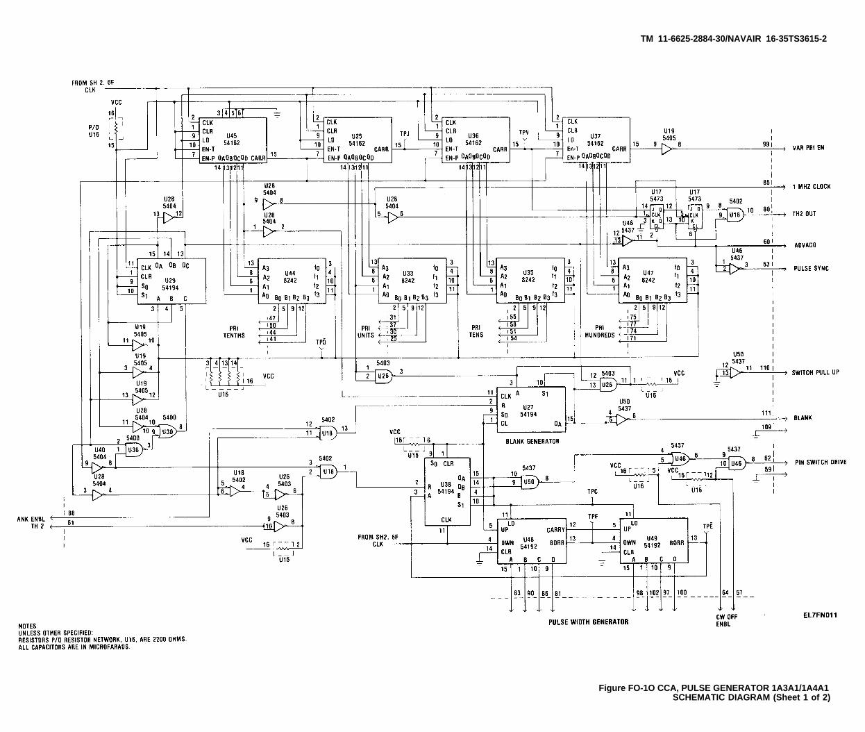
TM 11-6625-2884-30/NAVAIR 16-35TS3615-2
Figure FO-1O CCA, PULSE GENERATOR 1A3A1/1A4A1SCHEMATIC DIAGRAM (Sheet 1 of 2)
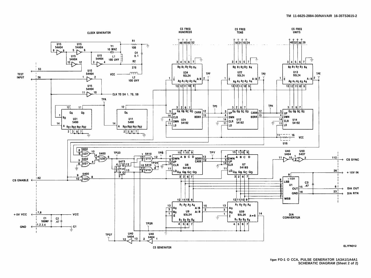
TM 11-6625-2884-30/NAVAIR 16-35TS3615-2
Figure FO-1 O CCA, PULSE GENERATOR 1A3A1/1A4A1SCHEMATIC DIAGRAM (Sheet 2 of 2)
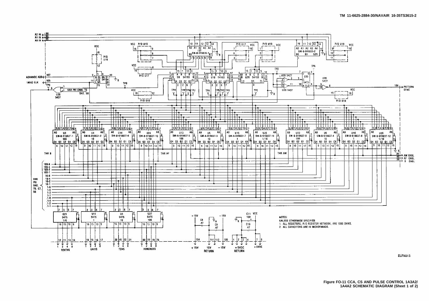
TM 11-6625-2884-30/NAVAIR 16-35TS3615-2
Figure FO-11 CCA, CS AND PULSE CONTROL 1A3A2/1A4A2 SCHEMATIC DIAGRAM (Sheet 1 of 2)

TM 11-6625-2884-30/NAVAIR 16-35TS3615-2
Figure FO-11 CCA, CS AND PULSE CONTROL 1A3A2/1A4A2 SCHEMATIC DIAGRAM (Sheet 2 of 2)
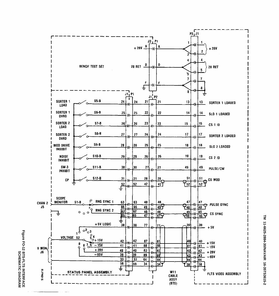
TM 11-6625-2884-30/N
AV
AIR
16-35TS3615-2
Figure FO-12 B
TS-FLTS
INTE
RFA
CE
SC
HE
MA
TIC D
IAG
RA
M

TM 11-6625-2884-30/NAVAIR 16-35TS3615-2
Figure FO-13 CONTROL INDICATOR 1A1A1SCHEMATIC DIAGRAM


DowningEB
055033-000

This fine document...
Was brought to you by me:
Liberated Manuals -- free army and government manuals
Why do I do it? I am tired of sleazy CD-ROM sellers, who take publicly available information, slap “watermarks” and other junk on it, and sell it. Those masters of search engine manipulation make sure that their sites that sell free information, come up first in search engines. They did not create it... They did not even scan it... Why should they get your money? Why are not letting you give those free manuals to your friends?
I am setting this document FREE. This document was made by the US Government and is NOT protected by Copyright. Feel free to share, republish, sell and so on.
I am not asking you for donations, fees or handouts. If you can, please provide a link to liberatedmanuals.com, so that free manuals come up first in search engines:
<A HREF=http://www.liberatedmanuals.com/>Free Military and Government Manuals</A>
– SincerelyIgor Chudovhttp://igor.chudov.com/
– Chicago Machinery Movers