TLE75008-ESD Datasheet 2020-09-02
63
Datasheet 1 Rev. 1.10 www.infineon.com 2020-09-02 TLE75008-ESD 1 Overview Applications • Low-side switches for 12 V in automotive or industrial applications such as lighting, heating, motor driving, energy and power distribution • Especially designed for driving relays, LEDs and motors. Figure 1 TLE75008-ESD Application Diagram SPIDER+ 12V SPI Driver for Enhanced Relay Control Package PG-TSDSO-24 Marking TLE75008ESD VBA TT ZVS IDLE IN1 SO GND VDD CVDD IN0_LH IN1_LH LI MP HO ME RIN GP O VDD RIN RIDLE RCSN RSCLK RSI RSO SI CSN VDD SCLK IN0 VS GP O GP O GP O GP O GP O GPI GND OUT7_LS C OUT C OUT C OUT C OUT C OUT C OUT C OUT C OUT OUT6_LS OUT5_LS OUT4_LS OUT3_LS OUT2_LS OUT1_LS Application_8LS.emf Z OUT3 Z OUT4 Z OUT5 Z OUT6 Z OUT7 Z OUT2 CVS OUT0_LS RVDD RLH R OUT1
Transcript of TLE75008-ESD Datasheet 2020-09-02

Datasheet 1 Rev. 1.10www.infineon.com 2020-09-02
TLE75008-ESD
1 Overview
Applications• Low-side switches for 12 V in automotive or industrial applications such
as lighting, heating, motor driving, energy and power distribution• Especially designed for driving relays, LEDs and motors.
Figure 1 TLE75008-ESD Application Diagram
SPIDER+ 12VSPI Driver for Enhanced Relay Control
Package PG-TSDSO-24
Marking TLE75008ESD
VBATT
ZVS
IDLE
IN1
SO
GND
VDD
CVDD
IN0_LHIN1_LH
LIMPHOME
RIN
GPO
VDD
RIN
RIDLE
RCSN
RSCLK
RSI
RSO
SI
CSN
VDD
SCLK
IN0VS
GPO
GPO
GPO
GPO
GPO
GPI
GND
OUT7_LS
CO
UT
CO
UT
CO
UT
CO
UT
CO
UT
CO
UT
CO
UT
CO
UT
OUT6_LS
OUT5_LS
OUT4_LS
OUT3_LS
OUT2_LS
OUT1_LS
Application_8LS.emf
Z OUT
3
Z OUT
4
Z OUT
5
Z OUT
6
Z OUT
7
Z OUT
2
CVS
OUT0_LS
RVDD
RLH
R OUT
1

Datasheet 2 Rev. 1.10 2020-09-02
TLE75008-ESDSPIDER+ 12V
Overview
Basic Features• 16-bit serial peripheral interface for control and diagnosis• Daisy Chain capability SPI also compatible with 8-bit SPI devices• 2 CMOS compatible parallel input pins with Input Mapping functionality• Cranking capability down to VS = 3.0 V (supports LV124)• Digital supply voltage range compatible with 3.3 V and 5 V microcontrollers• Very low quiescent current (with usage of IDLE pin)• Limp Home mode (with usage of IDLE and IN pins)• Green Product (RoHS compliant)• AEC Qualified
Protection Features• Reverse battery protection on VS without external components• Short circuit to ground and battery protection• Stable behavior at under voltage conditions (“Lower Supply Voltage Range for Extended Operation”)• Over Current latch OFF• Thermal shutdown latch OFF• Overvoltage protection• Loss of ground protection• Loss of battery protection• Electrostatic discharge (ESD) protection
Diagnostic Features• Latched diagnostic information via SPI register• Over Load detection at ON state• Open Load detection at OFF state using Output Status Monitor function• Output Status Monitor• Input Status Monitor
Application Specific Features
• Fail-safe activation via Input pins in Limp-Home Mode• SPI with Daisy Chain capability• Safe operation at low battery voltage (cranking)
DescriptionThe TLE75008-ESD is an eight channel low-side power switch in PG-TSDSO-24 package providing embeddedprotective functions. It is specially designed to control relays and LEDs in automotive and industrialapplications.A serial peripheral interface (SPI) is utilized for control and diagnosis of the loads as well as of the device. Fordirect control and PWM there are two input pins available connected to two outputs by default. Additional ordifferent outputs can be controlled by the same input pins (programmable via SPI).

Datasheet 3 Rev. 1.10 2020-09-02
TLE75008-ESDSPIDER+ 12V
Overview
Detailed DescriptionThe TLE75008-ESD is an eight channel low-side switch providing embedded protective functions. The outputstages incorporate eight low-side switches (typical RDS(ON) at TJ = 25°C is 1 Ω).The 16-bit serial peripheral interface (SPI) is utilized to control and diagnose the device and the loads. The SPIinterface provides daisy chain capability in order to assemble multiple devices (also devices with 8 bit SPI) inone SPI chain by using the same number of microcontroller pins.This device is designed for low supply voltage operation, therefore being able to keep its state at low batteryvoltage (VS ≥ 3.0 V). The SPI functionality, including the possibility to program the device, is available onlywhen the digital power supply is present (see Chapter 6 for more details).The TLE75008-ESD is equipped with two input pins that are connected to two outputs, making themcontrollable even when the digital supply voltage is not available. With the Input Mapping functionality it ispossible to connect the input pins to different outputs, or assign more outputs to the same input pin. In thiscase more channels can be controlled with one signal applied to one input pin.In Limp Home mode (Fail-Safe mode) the input pins are directly routed to channels 2 and 3. When IDLE pin is“low”, it is possible to activate the two channels using the input pins independently from the presence of thedigital supply voltage.The device provides diagnosis of the load via Open Load at OFF state (with DIAG_OSM.OUTn bits) and shortcircuit detection. For Open Load at OFF state detection, a internal current source IOL can be activated via SPI.Each output stage is protected against short circuit. In case of Overload, the affected channel switches OFFwhen the Overload Detection Current IL(OVLn) is reached and can be reactivated via SPI. In Limp Home modeoperation, the channels connected to an input pin set to “high” restart automatically after Output Restart timetRETRY(LH) is elapsed. Temperature sensors are available for each channel to protect the device against OverTemperature.The power transistors are built by N-channel power MOSFET . The inputs are ground referenced TTLcompatible. The device is monolithically integrated in Smart Power Technology.
Table 1 Product SummaryParameter Symbol ValuesAnalog supply voltage VS 3.0 V … 28 V
Digital supply voltage VDD 3.0 V … 5.5 V
Minimum overvoltage protection VS(AZ) 42 V (see Chapter 8.5 for details)
Maximum on-state resistance at TJ = 150 °C RDS(ON) 2.2 Ω
Nominal load current (TA = 85 °C, all channels) IL(NOM) 330 mA
Maximum Energy dissipation - repetitive EAR 10 mJ @ IL(EAR) = 220 mA
Minimum Drain to Source clamping voltage VDS(CL) 42 V
Maximum overload switch OFF threshold IL(OVL0) 2.3 A
Maximum total quiescent current at TJ ≤ 85 °C ISLEEP 5 µA
Maximum SPI clock frequency fSCLK 5 MHz

Datasheet 4 Rev. 1.10 2020-09-02
TLE75008-ESDSPIDER+ 12V
Block Diagram and Terms
2 Block Diagram and Terms
2.1 Block Diagram
Figure 2 Block Diagram of TLE75008-ESD
BlockDiagram _8LS.emf
control, diagnostic
and protective functions
Limp HomeIN1
IDLE
IN0
power supply
OUT1_LSOUT2_LS
CSN
SISCLK
SOdiagnosis register
input register
SPI
Power mode control
OUT0_LS
OUT7_LSOUT6_LSOUT5_LSOUT4_LSOUT3_LS
GND
Output Status Monitor
temperature sensor
Over Loaddetection
low-sidegate control
VS
VDD

Datasheet 5 Rev. 1.10 2020-09-02
TLE75008-ESDSPIDER+ 12V
Block Diagram and Terms
2.2 TermsFigure 3 shows all terms used in this data sheet, with associated convention for positive values.
Figure 3 Voltage and Current definition
In all tables of electrical characteristics the channel related symbols without channel numbers are valid foreach channel separately (e.g. VDS specification is valid for VDS0 ... VDS7).Furthermore, parameters relative to output current can be indicated without specifying whether the currentis going into the Drain pin or going out of the Source pin, unless otherwise specified. For instance, nominaloutput current can be indicated in the following ways: IL(NOM) IL_LS(NOM) IL_D(NOM) All SPI registers bits are marked as follows: ADDR.PARAMETER (e.g. HWCR.RST) with the exception of thebits in the Diagnosis frames which are marked only with PARAMETER (e.g. UVRVS).
Terms_8LS.emf
V IN1
VS
VSO
IVDD
ISI
ICSN
IVS
VDD
IDLE
SI
CSN
VS
I IN1
IN1
ISCLK
SCLK
I IN0
IN0
OUT1_LS
OUT3_LS
IIDLE
OUT2_LSIL_D2
IL_D1
SOISO
IL_D3
GND
IGND
OUT4_LSIL_D4
OUT5_LSIL_D5
OUT6_LSIL_D6
OUT7_LSIL_D7
VDS1
VSCLK
VCSN
VIN0
V IDLE
VDD
VSI
VDS7
VDS6
VDS4
VDS5
VDS3
VDS2
OUT0_LSIL_D0
VDS0

Datasheet 6 Rev. 1.10 2020-09-02
TLE75008-ESDSPIDER+ 12V
Pin Configuration
3 Pin Configuration
3.1 Pin Assignment
Figure 4 Pin Configuration TLE75008-ESD in PG-TSDSO-24
(top view)
PinOut _8LS.emf
VDDIN0IN1IDLEVSOUT1_LSOUT3_LSOUT2_LS
GNDOUT4_LS
OUT6_LSn.c.
CSNSCLK
SISO
GNDOUT0_LS
GNDOUT5_LS
OUT7_LS
n.c.
181716151413
242322212019
123456789101112
25SUB
expo
sed
pad
(bot
tom
)
n.c.n.c.
Datasheet 7 Rev. 1.10 2020-09-02
TLE75008-ESDSPIDER+ 12V
Pin Configuration
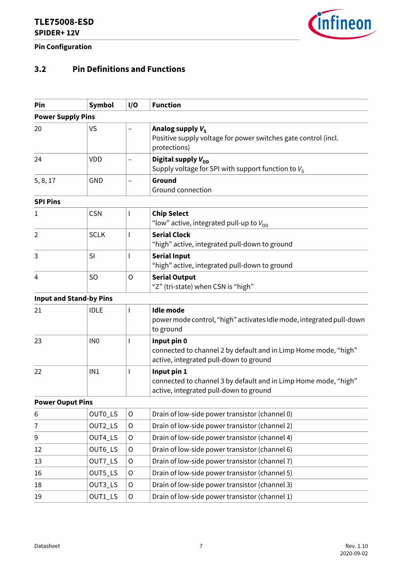
3.2 Pin Definitions and Functions
Pin Symbol I/O FunctionPower Supply Pins20 VS – Analog supply VS
Positive supply voltage for power switches gate control (incl. protections)
24 VDD – Digital supply VDDSupply voltage for SPI with support function to VS
5, 8, 17 GND – GroundGround connection
SPI Pins1 CSN I Chip Select
“low” active, integrated pull-up to VDD
2 SCLK I Serial Clock“high” active, integrated pull-down to ground
3 SI I Serial Input“high” active, integrated pull-down to ground
4 SO O Serial Output“Z” (tri-state) when CSN is “high”
Input and Stand-by Pins21 IDLE I Idle mode
power mode control, “high” activates Idle mode, integrated pull-down to ground
23 IN0 I Input pin 0connected to channel 2 by default and in Limp Home mode, “high” active, integrated pull-down to ground
22 IN1 I Input pin 1connected to channel 3 by default and in Limp Home mode, “high” active, integrated pull-down to ground
Power Ouput Pins6 OUT0_LS O Drain of low-side power transistor (channel 0)
7 OUT2_LS O Drain of low-side power transistor (channel 2)
9 OUT4_LS O Drain of low-side power transistor (channel 4)
12 OUT6_LS O Drain of low-side power transistor (channel 6)
13 OUT7_LS O Drain of low-side power transistor (channel 7)
16 OUT5_LS O Drain of low-side power transistor (channel 5)
18 OUT3_LS O Drain of low-side power transistor (channel 3)
19 OUT1_LS O Drain of low-side power transistor (channel 1)

Datasheet 8 Rev. 1.10 2020-09-02
TLE75008-ESDSPIDER+ 12V
Pin Configuration
Not Connected pins / Cooling Tab10, 11, 14, 15 n.c. – Not Connected, internally not bonded
25 GND – Exposed padIt is recommended to connect it to PCB ground for cooling and EMC - not usable as electrical GND pin. Electrical ground must be provided by pins 5, 8 and 17.
Pin Symbol I/O Function

Datasheet 9 Rev. 1.10 2020-09-02
TLE75008-ESDSPIDER+ 12V
General Product Characteristics
4 General Product Characteristics
4.1 Absolute Maximum Ratings
Table 2 Absolute Maximum Ratings 1)
TJ = -40 °C to +150 °Call voltages with respect to ground, positive current flowing into pin (unless otherwise specified)
Parameter Symbol Values Unit Note or Test Condition
NumberMin. Typ. Max.
Supply VoltagesAnalog Supply voltage VS -0.3 – 28 V – P_4.1.1
Digital Supply voltage VDD -0.3 – 5.5 V – P_4.1.2
Supply voltage for load dump protection
VS(LD) – – 42 V 2) P_4.1.3
Supply voltage for short circuit protection (single pulse)
VS(SC) 0 – 28 V – P_4.1.4
Reverse polarity voltage -VS(REV) – – 16 V 3)
TJ(0) = 25 °Ct ≤ 2 minSee Chapter 11 for general setup. RL = 70 Ω on all channels
P_4.1.5
Current through VS pin IVS -10 – 10 mA t ≤ 2 min P_4.1.7
Current through VDD pin IVDD -50 – 10 mA t ≤ 2 min P_4.1.8
Power StagesLoad current |IL| – – IL(OVL0) A single channel P_4.1.9
Voltage at power transistor VDS -0.3 – 42 V – P_4.1.10
Maximum energy dissipation single pulse
EAS – – 50 mJ 4)
TJ(0) = 25 °CIL(0) = 2*IL(EAR)
P_4.1.13
Maximum energy dissipation single pulse
EAS – – 25 mJ 4)
TJ(0) = 150 °CIL(0) = 400 mA
P_4.1.14
Maximum energy dissipation repetitive pulses - IL(EAR)
EAR – – 10 mJ 4)
TJ(0) = 85 °CIL(0) = IL(EAR)2*106 cycles
P_4.1.15
IDLE pinVoltage at IDLE pin VIDLE -0.3 5.5 V – P_4.1.23
Current through IDLE pin IIDLE -0.75 0.75 mA – P_4.1.25

Datasheet 10 Rev. 1.10 2020-09-02
TLE75008-ESDSPIDER+ 12V
General Product Characteristics
Current through IDLE pin IIDLE -10.0 2.0 mA t ≤ 2 min. P_4.1.26
Input PinsVoltage at input pins VIN -0.3 5.5 V – P_4.1.28
Current through input pins IIN -0.75 0.75 mA – P_4.1.30
Current through input pins IIN -10.0 2.0 mA t ≤ 2 min. P_4.1.31
SPI PinsVoltage at chip select pin VCSN -0.3 5.5 V – P_4.1.33
Current through chip select pin ICSN -0.75 0.75 mA – P_4.1.34
Current through chip select pin ICSN -10.0 2.0 mA t ≤ 2 min. P_4.1.35
Voltage at serial clock pin VSCLK -0.3 5.5 V P_4.1.37
Current through serial clock pin ISCLK -0.75 0.75 mA – P_4.1.38
Current through serial clock pin ISCLK -10.0 2.0 mA t ≤ 2 min. P_4.1.39
Voltage at serial input pin VSI -0.3 5.5 V P_4.1.41
Current through serial input pin ISI -0.75 0.75 mA – P_4.1.42
Current through serial input pin ISI -10.0 2.0 mA t ≤ 2 min. P_4.1.43
Voltage at serial output pin SO VSO -0.3 VDD+0.3 V P_4.1.58
Current through serial output pin SO
ISO -0.75 0.75 mA P_4.1.45
Current through serial output pin SO
ISO -2.0 10.0 mA t ≤ 2 min. P_4.1.46
TemperaturesJunction Temperature TJ -40 – 150 °C – P_4.1.48
Storage Temperature Tstg -55 – 150 °C – P_4.1.49
ESD SusceptibilityESD Susceptibility HBMOUT pins vs. VS or GND
VESD -4 – 4 kV 5)
HBMP_4.1.50
ESD Susceptibility HBMother pins
VESD -2 – 2 kV 5)
HBMP_4.1.51
ESD Susceptibility CDMPin 1, 12, 13, 24 (corner pins)
VESD -750 – 750 V 6)
CDMP_4.1.52
ESD Susceptibility CDM VESD -500 – 500 V 6)
CDMP_4.1.54
1) Not subject to production test, specified by design.2) For a duration of ton = 400 ms; ton/toff = 10%; limited to 100 pulses3) Device is mounted on a FR4 2s2p board according to Jedec JESD51-2,-5,-7 at natural convection; the Product
(Chip+Package) was simulated on a 76.2 *114.3 *1.5 mm board with 2 inner copper layers (2 * 70 µm Cu, 2 * 35 µm Cu). Where applicable a thermal via array under the exposed pad contacted the first inner copper layer.
Table 2 Absolute Maximum Ratings (cont’d)1)
TJ = -40 °C to +150 °Call voltages with respect to ground, positive current flowing into pin (unless otherwise specified)
Parameter Symbol Values Unit Note or Test Condition
NumberMin. Typ. Max.

Datasheet 11 Rev. 1.10 2020-09-02
TLE75008-ESDSPIDER+ 12V
General Product Characteristics
Notes1. Stresses above the ones listed here may cause permanent damage to the device. Exposure to absolute
maximum rating conditions for extended periods may affect device reliability.2. Integrated protection functions are designed to prevent IC destruction under fault conditions described in the
data sheet. Fault conditions are considered as “outside” normal operating range. Protection functions are not designed for continuous repetitive operation.
4.2 Functional Range
Note: Within the functional or operating range, the IC operates as described in the circuit description. The electrical characteristics are specified within the conditions given in the Electrical Characteristics table.
4) Pulse shape represents inductive switch off: IL(t) = IL(0) x (1 - t / tpulse); 0 < t < tpulse
5) ESD susceptibility, Human Body Model “HBM” according to AEC Q100-0026) ESD susceptibility, Charged Device Mode “CDM” according to AECQ100-011 Rev D
Table 3 Functional rangeParameter Symbol Values Unit Note or
Test ConditionNumber
Min. Typ. Max.Supply Voltage Range for Normal Operation
VS(NOR) 7 – 18 V – P_4.2.1
Upper Supply Voltage Range for Extended Operation
VS(EXT,UP) 18 – 28 V Parameter deviation possible
P_4.2.2
Lower Supply Voltage Range for Extended Operation
VS(EXT,LOW) 3 – 7 V Parameter deviation possible
P_4.2.3
Junction Temperature TJ -40 – 150 °C – P_4.2.4
Logic supply voltage VDD 3 – 5.5 V – P_4.2.5
Datasheet 12 Rev. 1.10 2020-09-02
TLE75008-ESDSPIDER+ 12V
General Product Characteristics
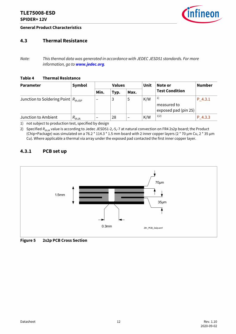
4.3 Thermal Resistance
Note: This thermal data was generated in accordance with JEDEC JESD51 standards. For more information, go to www.jedec.org.
4.3.1 PCB set up
Figure 5 2s2p PCB Cross Section
Table 4 Thermal ResistanceParameter Symbol Values Unit Note or
Test ConditionNumber
Min. Typ. Max.Junction to Soldering Point RthJSP – 3 5 K/W 1)
measured to exposed pad (pin 25)
1) not subject to production test, specified by design
P_4.3.1
Junction to Ambient RthJA – 28 – K/W 1)2)
2) Specified RthJA value is according to Jedec JESD51-2,-5,-7 at natural convection on FR4 2s2p board; the Product (Chip+Package) was simulated on a 76.2 * 114.3 * 1.5 mm board with 2 inner copper layers (2 * 70 µm Cu, 2 * 35 µm Cu). Where applicable a thermal via array under the exposed pad contacted the first inner copper layer.
P_4.3.3
1.5mm
70µm
35µm
0.3mm Zth_PCB_2s2p.emf

Datasheet 13 Rev. 1.10 2020-09-02
TLE75008-ESDSPIDER+ 12V
General Product Characteristics
Figure 6 PC Board for Thermal Simulation with 600 mm2 Cooling Area
Figure 7 PC Board for Thermal Simulation with 2s2p Cooling Area

Datasheet 14 Rev. 1.10 2020-09-02
TLE75008-ESDSPIDER+ 12V
General Product Characteristics
4.3.2 Thermal Impedance
Figure 8 Typical Thermal Impedance. PCB setup according Chapter 4.3.1
Figure 9 Typical Thermal Resistance. PCB setup 1s0p
0.1
1
10
100
0.0001 0.001 0.01 0.1 1 10 100 1000
Zth-
JA [K
/W]
Tam
b =
105°
C
Time [s]
8 Channels Low-side
2s2p1s0p - 600 mm²1s0p - 300 mm²1s0p - footprint
30.00
40.00
50.00
60.00
70.00
80.00
90.00
100.00
0 100 200 300 400 500 600 700
Rth
-JA
[K/W
]
Area [mm²]
8 Channels Low-side
1s0p - Tamb = 105°C

Datasheet 15 Rev. 1.10 2020-09-02
TLE75008-ESDSPIDER+ 12V
Control Pins
5 Control PinsThe device has three pins (IN0, IN1 and IDLE) to control directly the device without using SPI.
5.1 Input pinsTLE75008-ESD has two input pins available. Each input pin is connected by default to one channel (IN0 tochannel 2, IN1 to channel 3). Input Mapping Registers MAPIN0 and MAPIN1 can be programmed to connectadditional or different channels to each input pin, as shown in Figure 10. The signals driving the channels arean OR combination between OUT register status, IN0 and IN1 (according to Input Mapping registers status).
Figure 10 Input Mapping
The logic level of the input pins can be monitored via the Input Status Monitor Register (INST). The InputStatus Monitor is operative also when TLE75008-ESD is in Limp Home mode. If one of the Input pins is set to“high” and the IDLE pin is set to “low”, the device switches into Limp Home mode and activates the channelmapped by default to the input pins. See Chapter 6.1.5 for further details.
5.2 IDLE pin
The IDLE pin is used to bring the device into Sleep mode operation when is set to “low” and all input pins areset to “low”.When IDLE pin is set to “low” while one of the input pins is set to “high” the device enters LimpHome mode.To ensure a proper mode transition, IDLE pin must be set for at least tIDLE2SLEEP (P_6.3.54, transition from “high”to “low”) or tSLEEP2IDLE (P_6.3.53, transition from “low” to “high”).Setting the IDLE pin to “low” has the following consequences:• All registers in the SPI are reset to default values• VDD and VS Undervoltage detection circuits are disabled to decrease current consumption (if both inputs
are set to “low”)
InputMapping_8ch.emf
Channel 7Channel 6
Channel 5Channel 4
Channel 3Channel 2
Channel 1Channel 0
OR
&
IN1
IIN1
IN0
IIN0
&
MAPIN1
MAPIN0
OUT
OR
8
8
8
8
8
8
8
Limp Home mode(default )
Limp Home mode(default )

Datasheet 16 Rev. 1.10 2020-09-02
TLE75008-ESDSPIDER+ 12V
Control Pins
• No SPI communication is allowed (SO pin remains in high impedance state also when CSN pin is set to “low”) if both input pins are set to “low”

Datasheet 17 Rev. 1.10 2020-09-02
TLE75008-ESDSPIDER+ 12V
Control Pins
5.3 Electrical Characteristics Control Pins
Table 5 Electrical Characteristics: Control PinsVDD = 3 V to 5.5 V, VS = 7 V to 18 V, TJ = -40 °C to +150 °C (unless otherwise specified)Typical values: VDD = 5 V, VS = 13.5 V, TJ = 25 °C
Parameter Symbol Values Unit Note or Test Condition
NumberMin. Typ. Max.
IDLE pinL-input level VIDLE(L) 0 0.8 V – P_5.3.1
H-input level VIDLE(H) 2.0 5.5 V – P_5.3.2
L-input current IIDLE(L) 5 12 20 μA VIDLE = 0.8 V P_5.3.3
H-input current IIDLE(H) 14 28 45 μA VIDLE = 2.0 V P_5.3.4
Input PinsL-input level VIN(L) 0 0.8 V – P_5.3.5
H-input level VIN(H) 2.0 5.5 V – P_5.3.6
L-input current IIN(L) 5 12 20 μA VIN = 0.8 V P_5.3.7
H-input current IIN(H) 14 28 45 μA VIN = 2.0 V P_5.3.8

Datasheet 18 Rev. 1.10 2020-09-02
TLE75008-ESDSPIDER+ 12V
Power Supply
6 Power SupplyThe TLE75008-ESD is supplied by two supply voltages:• VS (analog supply voltage used also for the logic)• VDD (digital supply voltage)The VS supply line is connected to a battery feed and used, in combination with VDD supply, for the drivingcircuitry of the power stages. In situations where VS voltage drops below VDD voltage (for instance duringcranking events down to 3.0 V), an increased current consumption may be observed at VDD pin.VS and VDD supply voltages have an undervoltage detection circuit, which prevents the activation of theassociated function in case the measured voltage is below the undervoltage threshold. More in detail:• An undervoltage on both VS and VDD supply voltages prevents the activation of the power stages and any
SPI communication (the SPI registers are reset)• An undervoltage on VDD supply prevents any SPI communication. SPI read/write registers are reset to
default values.• An undervoltage on VS supply forces the TLE75008-ESD to drain all needed current for the low-side
switches and for the logic from VDD supply.Figure 11 shows a basic concept drawing of the interaction between supply pins VS and VDD, the output stagedrivers and SO supply line.
Figure 11 TLE75008-ESD Internal Power Supply concept
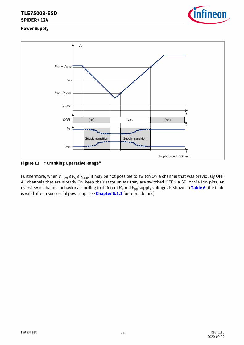
When 3.0 V ≤ VS ≤ VDD - VSDIFF TLE75008-ESD operates in “Cranking Operative Range” (COR). In this condition thecurrent consumption from VDD pin increases while it decreases from VS pin where the total currentconsumption remains within the specified limits. Figure 12 shows the voltage levels at VS pin where thedevice goes in and out of COR. During the transition to and from COR operative region, IVS and IVDD changebetween values defined for normal operation and for COR operation. The sum of both current remains withinlimits specified in “Overall current consumption” section (see Table 8).
VS
VDD
IVS
IVDD
VREG
SPISO
UVRVDD
UVRVS
GD
GND
LS
SupplyConcept_xLS.emf
Datasheet 19 Rev. 1.10 2020-09-02
TLE75008-ESDSPIDER+ 12V
Power Supply
Figure 12 “Cranking Operative Range”
Furthermore, when VS(UV) ≤ VS ≤ VS(OP) it may be not possible to switch ON a channel that was previously OFF.All channels that are already ON keep their state unless they are switched OFF via SPI or via INn pins. Anoverview of channel behavior according to different VS and VDD supply voltages is shown in Table 6 (the tableis valid after a successful power-up, see Chapter 6.1.1 for more details).
Supply transitionSupply transition
SupplyConcept_COR.emf
t
VS
VDD + VSDIFF
VDD - VSDIFF
3.0 V
(no)COR yes (no)
tIVS
VDD
IVDD
t

Datasheet 20 Rev. 1.10 2020-09-02
TLE75008-ESDSPIDER+ 12V
Power Supply
Table 6 Device capability as function of VS and VDD
VDD ≤ VDD(UV)(VDD(UV) = P_6.3.25)
VDD = VDD(LOP)(VDD(LOP) = P_6.3.24)
VDD > VDD(LOP)
VS ≤ 3.0 V
3.0 V = VS(UV),max(P_6.3.1)
channels cannot be controlled
channels can be switched ON and OFF (SPI control)(RDS(ON) deviations possible)
channels can be switched ON and OFF (SPI control)(RDS(ON) deviations possible)
SPI registers reset SPI registers available SPI registers available
SPI communication not available (fSCLK = 0 MHz)
SPI communication possible (fSCLK = 1 MHz) (P_10.4.34)
SPI communication possible (fSCLK = 5 MHz) (P_10.4.22)
Limp Home mode not available
Limp Home mode available (RDS(ON) deviations possible)
Limp Home mode available (RDS(ON) deviations possible)
3.0 V < VS ≤ VS(OP)(VS(OP) = P_6.3.2)
channels cannot be controlled by SPI
channels can be switched ON and OFF (SPI control)1)
(RDS(ON) deviations possible)
channels can be switched ON and OFF (SPI control)1)
(RDS(ON) deviations possible)
SPI registers reset SPI registers available SPI registers available
SPI communication not available (fSCLK = 0 MHz)
SPI communication possible (fSCLK = 1 MHz) (P_10.4.34)
SPI communication possible (fSCLK = 5 MHz) (P_10.4.22)
Limp Home mode available1) (RDS(ON) deviations possible)
1) undervoltage condition on VS must be considered - see Chapter 6.2.1 for more details
Limp Home mode available1) (RDS(ON) deviations possible)
Limp Home mode available (RDS(ON) deviations possible)
VS > VS(OP) channels cannot be controlled by SPI
channels can be switched ON and OFF(small RDS(ON) dev. possible when VS = VS(EXT,LOW))
channels can be switched ON and OFF(small RDS(ON) dev. possible when VS = VS(EXT,LOW))
SPI registers reset SPI registers available SPI registers available
SPI communication not available (fSCLK = 0 MHz)
SPI communication possible (fSCLK = 5 MHz) (P_10.4.22)
SPI communication possible (fSCLK = 5 MHz) (P_10.4.22)
Limp Home mode available(RDS(ON) dev. possible when VS = VS(EXT,LOW))
Limp Home mode available(RDS(ON) dev. possible when VS = VS(EXT,LOW))
Limp Home mode available(RDS(ON) dev. possible when VS = VS(EXT,LOW))

Datasheet 21 Rev. 1.10 2020-09-02
TLE75008-ESDSPIDER+ 12V
Power Supply
6.1 Operation ModesTLE75008-ESD has the following operation modes:• Sleep mode• Idle mode• Active mode• Limp Home modeThe transition between operation modes is determined according to following levels and states:• logic level at IDLE pin• logic level at INn pins• OUT.OUTn bits state• HWCR.ACT bit stateThe state diagram including the possible transitions is shown in Figure 13. The behaviour of TLE75008-ESD aswell as some parameters may change in dependence from the operation mode of the device. Furthermore,due to the undervoltage detection circuitry which monitors VS and VDD supply voltages, some changes withinthe same operation mode can be seen accordingly.The operation mode of the TLE75008-ESD can be observed by:• status of output channels• status of SPI registers• current consumption at VDD pin (IVDD)• current consumption at VS pin (IVS)The default operation mode to switch ON the loads is Active mode. If the device is not in Active mode and arequest to switch ON one or more outputs comes (via SPI or via Input pins), it will switch into Active or LimpHome mode, according to IDLE pin status. Due to the time needed for such transitions, output turn-on timetON will be extended due to the mode transition latency.
Figure 13 Operation Mode state diagramOpModes.emf
Sleep
Idle
IDLE = „high“
IDLE = „low“
Active
INn = „high“& IDLE = „low“
IDLE = „high“
Limp Home
HWCR.ACT = 1or OUT.OUTn = 1or INn = „high“
HWCR.ACT = 0& OUT.OUTn = 0& INn = „low“
IDLE = „low“& INn = „high“
INn = „low“
init
IDLE = „low“& INn = „low“
INn = „low“& VDD < VDD(UV)
Datasheet 22 Rev. 1.10 2020-09-02
TLE75008-ESDSPIDER+ 12V
Power Supply
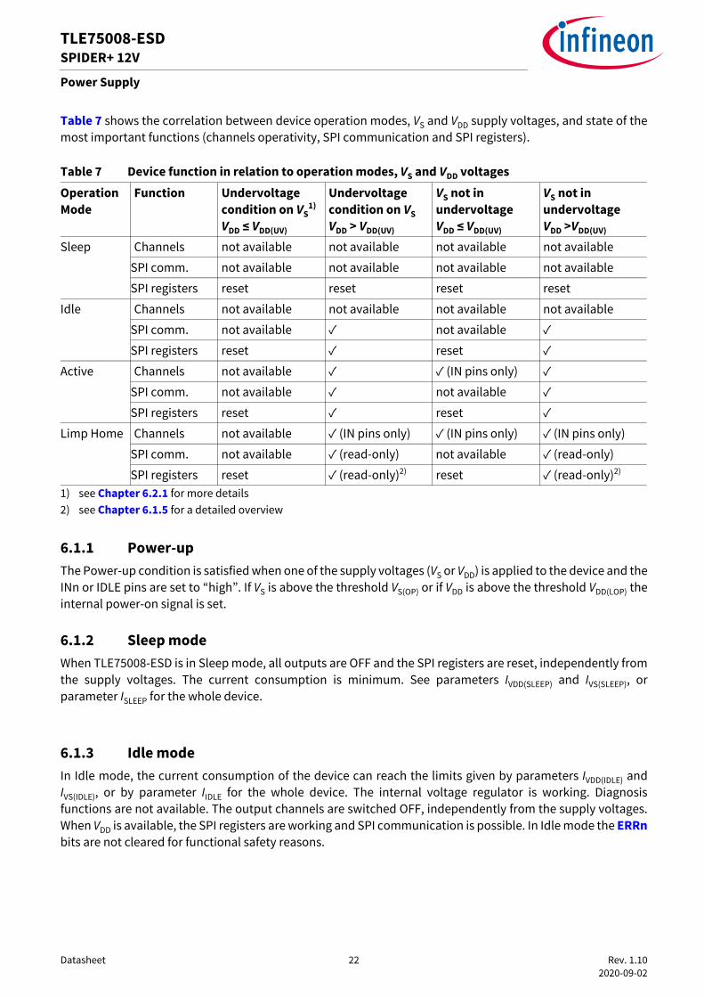
Table 7 shows the correlation between device operation modes, VS and VDD supply voltages, and state of themost important functions (channels operativity, SPI communication and SPI registers).
6.1.1 Power-upThe Power-up condition is satisfied when one of the supply voltages (VS or VDD) is applied to the device and theINn or IDLE pins are set to “high”. If VS is above the threshold VS(OP) or if VDD is above the threshold VDD(LOP) theinternal power-on signal is set.
6.1.2 Sleep modeWhen TLE75008-ESD is in Sleep mode, all outputs are OFF and the SPI registers are reset, independently fromthe supply voltages. The current consumption is minimum. See parameters IVDD(SLEEP) and IVS(SLEEP), orparameter ISLEEP for the whole device.
6.1.3 Idle modeIn Idle mode, the current consumption of the device can reach the limits given by parameters IVDD(IDLE) andIVS(IDLE), or by parameter IIDLE for the whole device. The internal voltage regulator is working. Diagnosisfunctions are not available. The output channels are switched OFF, independently from the supply voltages.When VDD is available, the SPI registers are working and SPI communication is possible. In Idle mode the ERRnbits are not cleared for functional safety reasons.
Table 7 Device function in relation to operation modes, VS and VDD voltagesOperation Mode
Function Undervoltage condition on VS
1)
VDD ≤ VDD(UV)
1) see Chapter 6.2.1 for more details
Undervoltage condition on VSVDD > VDD(UV)
VS not in undervoltageVDD ≤ VDD(UV)
VS not in undervoltageVDD >VDD(UV)
Sleep Channels not available not available not available not available
SPI comm. not available not available not available not available
SPI registers reset reset reset reset
Idle Channels not available not available not available not available
SPI comm. not available not available
SPI registers reset reset
Active Channels not available (IN pins only)
SPI comm. not available not available
SPI registers reset reset
Limp Home Channels not available (IN pins only) (IN pins only) (IN pins only)
SPI comm. not available (read-only) not available (read-only)
SPI registers reset (read-only)2)
2) see Chapter 6.1.5 for a detailed overview
reset (read-only)2)

Datasheet 23 Rev. 1.10 2020-09-02
TLE75008-ESDSPIDER+ 12V
Power Supply
6.1.4 Active modeActive mode is the normal operation mode of TLE75008-ESD when no Limp Home condition is set and it isnecessary to drive some or all loads. Voltage levels of VDD and VS influence the behavior as described at thebeginning of Chapter 6. Device current consumption is specified with IVDD(ACTIVE) and IVS(ACTIVE) (IACTIVE for thewhole device). The device enters Active mode when IDLE pin is set to “high” and one of the input pins is set to“high” or one OUT.OUTn bit is set to “1”. If HWCR.ACT is set to “0”, the device returns to Idle mode as soon asall inputs pins are set to “low” and OUT.OUTn bits are set to “0”. If HWCR.ACT is set to “1”, the device remainsin Active mode independently of the status of input pins and OUT.OUTn bits. An undervoltage condition onVDD supply brings the device into Idle mode, if all input pins are set to “low”. Even if the registers MAPIN0 andMAPIN1 are both set to “00H” but one of the input pins INn is set to “high”, the device goes into Active mode.
6.1.5 Limp Home modeTLE75008-ESD enters Limp Home mode when IDLE pin is “low” and one of the input pins is set to “high”,switching ON the channel connected to it. SPI communication is possible but only in read-only mode (SPIregisters can be read but cannot be written). More in detail:• UVRVS and LOPVDD are set to “1”• MODE bits are set to “01B” (Limp Home mode)• TER bit is set to “1” on the first SPI command after entering Limp Home mode. Afterwards it works
normally• OLOFF bits is set to “0”• ERRn bits work normally• DIAG_OSM.OUTn bits can be read and work normally• All other registers are set to their default value and cannot be programmed as long as the device is in Limp
Home modeSee Table 6 for a detailed overview of supply voltage conditions required to switch ON channels 2 and 3 duringLimp Home. All other channels are OFF.A transmission of SPI commands during transition from Active to Limp Home mode or Limp Home to Activemode may result in undefined SPI responses.
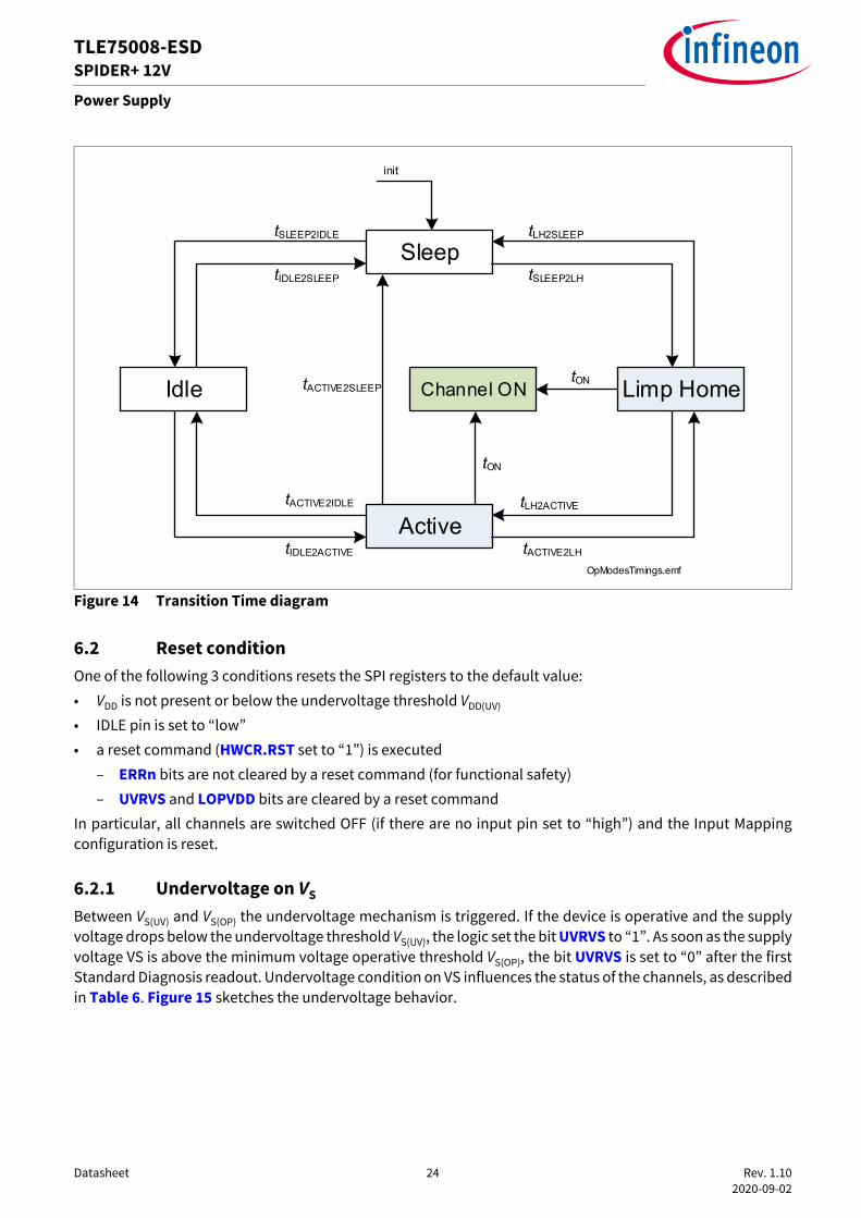
6.1.6 Definition of Power Supply modes transition timesThe channel turn-ON time is as defined by parameter tON when TLE75008-ESD is in Active mode or in LimpHome mode. In all other cases, it is necessary to add the transition time required to reach one of the twoaforementioned Power Supply modes (as shown in Figure 14).
Datasheet 24 Rev. 1.10 2020-09-02
TLE75008-ESDSPIDER+ 12V
Power Supply
Figure 14 Transition Time diagram
6.2 Reset conditionOne of the following 3 conditions resets the SPI registers to the default value:• VDD is not present or below the undervoltage threshold VDD(UV)
• IDLE pin is set to “low”• a reset command (HWCR.RST set to “1”) is executed
– ERRn bits are not cleared by a reset command (for functional safety)– UVRVS and LOPVDD bits are cleared by a reset command
In particular, all channels are switched OFF (if there are no input pin set to “high”) and the Input Mappingconfiguration is reset.
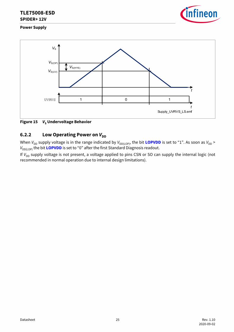
6.2.1 Undervoltage on VS
Between VS(UV) and VS(OP) the undervoltage mechanism is triggered. If the device is operative and the supplyvoltage drops below the undervoltage threshold VS(UV), the logic set the bit UVRVS to “1”. As soon as the supplyvoltage VS is above the minimum voltage operative threshold VS(OP), the bit UVRVS is set to “0” after the firstStandard Diagnosis readout. Undervoltage condition on VS influences the status of the channels, as describedin Table 6. Figure 15 sketches the undervoltage behavior.
OpModesTimings.emf
Sleep
Idle
tSLEEP2IDLE
Active
Limp Home
init
tIDLE2SLEEP
tACTIVE2IDLE
tIDLE2ACTIVE
tON
tACTIVE2LH
tLH2ACTIVE
tLH2SLEEP
tSLEEP2LH
tONChannel ONtACTIVE2SLEEP
Datasheet 25 Rev. 1.10 2020-09-02
TLE75008-ESDSPIDER+ 12V
Power Supply
Figure 15 VS Undervoltage Behavior
6.2.2 Low Operating Power on VDD
When VDD supply voltage is in the range indicated by VDD(LOP), the bit LOPVDD is set to “1”. As soon as VDD >VDD(LOP) the bit LOPVDD is set to “0” after the first Standard Diagnosis readout.If VDD supply voltage is not present, a voltage applied to pins CSN or SO can supply the internal logic (notrecommended in normal operation due to internal design limitations).
Supply_UVRVS_LS.emf
VS(OP)
VS(UV)
1UVRVS 0 1
t
VS(HYS)
t
VS

Datasheet 26 Rev. 1.10 2020-09-02
TLE75008-ESDSPIDER+ 12V
Power Supply
6.3 Electrical Characteristics Power Supply
Table 8 Electrical Characteristics Power SupplyVDD = 3 V to 5.5 V, VS = 7 V to 18 V, TJ = -40 °C to +150 °C, all voltages with respect to ground, positive currentsflowing as described in Figure 3 (unless otherwise specified)Typical values: VDD = 5 V, VS = 13.5 V, TJ = 25 °C
Parameter Symbol Values Unit Note or Test Condition
NumberMin. Typ. Max.
VS pinAnalog supply undervoltage shutdown
VS(UV) 1.5 – 3.0 V OUTn = ONfrom VDS ≤ 1 V to UVRVS = 1BRL = 50 Ω
P_6.3.1
Analog supply minimum operative voltage
VS(OP) – – 4.0 V OUT.OUTn = 1Bfrom UVRVS = 1Bto VDS ≤ 1 VRL = 50 Ω
P_6.3.2
Undervoltage shutdown hysteresis
VS(HYS) – 1 – V 1) P_6.3.3
Analog supply current consumption in Sleep mode with loads
IVS(SLEEP) – 0.1 3 µA 1)
VIDLE floatingVINn floatingVCSN = VDDTJ ≤ 85 °C
P_6.3.4
Analog supply current consumption in Sleep mode with loads
IVS(SLEEP) – 0.1 – µA 1)
VIDLE floatingVINn floatingVCSN = VDDTJ ≤ 85 °CVS = 13.5 V
P_6.3.63
Analog supply current consumption in Sleep mode with loads
IVS(SLEEP) – 0.1 20 µA VIDLE floatingVINn floatingVCSN = VDDTJ = 150 °C
P_6.3.5
Analog supply current consumption in Idle mode with loads
IVS(IDLE) – – 2.2 mA IDLE = “high”VINn floatingfSCLK = 0 MHzHWCR.ACT = 0BOUT.OUTn = 0BDIAG_IOL.OUTn = 0BVCSN = VDD
P_6.3.6

Datasheet 27 Rev. 1.10 2020-09-02
TLE75008-ESDSPIDER+ 12V
Power Supply
Analog supply current consumption in Idle mode with loads (COR)
IVS(IDLE) – – 0.3 mA IDLE = “high”VINn floatingfSCLK = 0 MHzHWCR.ACT = 0BOUT.OUTn = 0BDIAG_IOL.OUTn = 0BVCSN = VDDVS ≤ VDD - 1 V
P_6.3.7
Analog supply current consumption in Active mode with loads - channels OFF
IVS(ACTIVE) – – 4.2 mA IDLE = “high”VINn floatingfSCLK = 0 MHzHWCR.ACT = 1BOUT.OUTn = 0BDIAG_IOL.OUTn = 0BVCSN = VDD
P_6.3.8
Analog supply current consumption in Active mode with loads - channels OFF (COR)
IVS(ACTIVE) – 0.1 0.3 mA IDLE = “high”VINn floatingfSCLK = 0 MHzHWCR.ACT = 1BOUT.OUTn = 0BDIAG_IOL.OUTn = 0BVCSN = VDDVS ≤ VDD - 1 V
P_6.3.12
Analog supply current consumption in Active mode with loads - channels ON
IVS(ACTIVE) – – 4.2 mA IDLE = “high”VINn floatingfSCLK = 0 MHzHWCR.ACT = 1BOUT.OUTn = 1BDIAG_IOL.OUTn = 0BVCSN = VDD
P_6.3.15
Table 8 Electrical Characteristics Power Supply (cont’d)VDD = 3 V to 5.5 V, VS = 7 V to 18 V, TJ = -40 °C to +150 °C, all voltages with respect to ground, positive currentsflowing as described in Figure 3 (unless otherwise specified)Typical values: VDD = 5 V, VS = 13.5 V, TJ = 25 °C
Parameter Symbol Values Unit Note or Test Condition
NumberMin. Typ. Max.
Datasheet 28 Rev. 1.10 2020-09-02
TLE75008-ESDSPIDER+ 12V
Power Supply
Analog supply current consumption in Active mode with loads - channels ON (COR)
IVS(ACTIVE) – 0.1 0.3 mA IDLE = “high”VINn floatingfSCLK = 0 MHzHWCR.ACT = 1BOUT.OUTn = 1BDIAG_IOL.OUTn = 0BVCSN = VDDVS ≤ VDD - 1 V
P_6.3.20
VDD pinLogic Supply Operating voltage
VDD(OP) 3.0 – 5.5 V fSCLK = 5 MHz P_6.3.23
Logic Supply Lower Operating Voltage
VDD(LOP) 3.0 – 4.5 V – P_6.3.24
Undervoltage shutdown VDD(UV) 1 – 3.0 V VSI = 0 VVSCLK = 0 VVCSN = 0 VSO from “low” to high impedance
P_6.3.25
Logic supply current in Sleep mode
IVDD(SLEEP) – 0.1 2.5 µA 1)
VIDLE floatingVINn floatingVCSN = VDDTJ ≤ 85 °C
P_6.3.26
Logic supply current in Sleep mode
IVDD(SLEEP) – – 10 µA VIDLE floatingVINn floatingVCSN = VDDTJ = 150 °C
P_6.3.27
Logic supply current in Idle mode
IVDD(IDLE) – – 0.3 mA IDLE = “high”VINn floatingfSCLK = 0 MHzHWCR.ACT = 0BOUT.OUTn = 0BVCSN = VDD
P_6.3.28
Logic supply current in Idle mode (COR)
IVDD(IDLE) – – 2.2 mA IDLE = “high”VINn floatingfSCLK = 0 MHzHWCR.ACT = 0BOUT.OUTn = 0BVCSN = VDDVS ≤ VDD - 1 V
P_6.3.29
Table 8 Electrical Characteristics Power Supply (cont’d)VDD = 3 V to 5.5 V, VS = 7 V to 18 V, TJ = -40 °C to +150 °C, all voltages with respect to ground, positive currentsflowing as described in Figure 3 (unless otherwise specified)Typical values: VDD = 5 V, VS = 13.5 V, TJ = 25 °C
Parameter Symbol Values Unit Note or Test Condition
NumberMin. Typ. Max.

Datasheet 29 Rev. 1.10 2020-09-02
TLE75008-ESDSPIDER+ 12V
Power Supply
Logic supply current in Active mode - channels OFF
IVDD(ACTIVE) – – 0.3 mA IDLE = “high”VINn floatingfSCLK = 0 MHzHWCR.ACT = 1BOUT.OUTn = 0BVCSN = VDD
P_6.3.30
Logic supply current in Active mode - channels OFF (COR)
IVDD(ACTIVE) – – 4.2 mA IDLE = “high”VINn floatingfSCLK = 0 MHzHWCR.ACT = 1BOUT.OUTn = 0BVCSN = VDDVS ≤ VDD - 1 V
P_6.3.31
Logic supply current in Active mode - channels ON
IVDD(ACTIVE) – – 0.3 mA IDLE = “high”VINn floatingfSCLK = 0 MHzHWCR.ACT = 1BOUT.OUTn = 1VCSN = VDD
P_6.3.35
Logic supply current in Active mode - channels ON (COR)
IVDD(ACTIVE) – – 4.2 mA IDLE = “high”VINn floatingfSCLK = 0 MHzHWCR.ACT = 1BOUT.OUTn = 1BVCSN = VDDVS ≤ VDD - 1 V
P_6.3.36
Overall current consumptionOverall current consumption in Sleep modeIVS(SLEEP) + IVDD(SLEEP)
ISLEEP – – 5 µA 1)
VIDLE floatingVINn floatingVCSN = VDDTJ ≤ 85 °C
P_6.3.40
Overall current consumption in Sleep modeIVS(SLEEP) + IVDD(SLEEP)
ISLEEP – – 5 µA 1)
VIDLE floatingVINn floatingVCSN = VDDTJ ≤ 85 °CVS = 13.5 V
P_6.3.64
Table 8 Electrical Characteristics Power Supply (cont’d)VDD = 3 V to 5.5 V, VS = 7 V to 18 V, TJ = -40 °C to +150 °C, all voltages with respect to ground, positive currentsflowing as described in Figure 3 (unless otherwise specified)Typical values: VDD = 5 V, VS = 13.5 V, TJ = 25 °C
Parameter Symbol Values Unit Note or Test Condition
NumberMin. Typ. Max.

Datasheet 30 Rev. 1.10 2020-09-02
TLE75008-ESDSPIDER+ 12V
Power Supply
Overall current consumption in Sleep modeIVS(SLEEP) + IVDD(SLEEP)
ISLEEP – – 30 µA VIDLE floatingVINn floatingVCSN = VDDTJ = 150 °C
P_6.3.41
Overall current consumption in Idle modeIVS(IDLE) + IVDD(IDLE)
IIDLE – – 2.5 mA IDLE = “high”VINn floatingfSCLK = 0 MHzHWCR.ACT = 0BOUT.OUTn = 0BDIAG_IOL.OUTn = 0BVCSN = VDD
P_6.3.42
Overall current consumption in Active mode - channels OFFIVS(ACTIVE) + IVDD(ACTIVE)
IACTIVE – – 4.5 mA IDLE = “high”VINn floatingfSCLK = 0 MHzHWCR.ACT = 1BOUT.OUTn = 0BDIAG_IOL.OUTn = 0BVCSN = VDD
P_6.3.43
Overall current consumption in Active mode - channels ONIVS(ACTIVE) + IVDD(ACTIVE)
IACTIVE – – 4.5 mA IDLE = “high”VINn floatingfSCLK = 0 MHzHWCR.ACT = 1BOUT.OUTn = 1BDIAG_IOL.OUTn = 0BVCSN = VDD
P_6.3.47
Voltage difference between VS and VDD supply lines
VSDIFF – 200 – mV 1) P_6.3.52
TimingsSleep to Idle delay tSLEEP2IDLE – 200 400 µs 1)
from IDLE pin to TER + INST register = 8680H (see Chapter 10.6.1 for details)
P_6.3.53
Table 8 Electrical Characteristics Power Supply (cont’d)VDD = 3 V to 5.5 V, VS = 7 V to 18 V, TJ = -40 °C to +150 °C, all voltages with respect to ground, positive currentsflowing as described in Figure 3 (unless otherwise specified)Typical values: VDD = 5 V, VS = 13.5 V, TJ = 25 °C
Parameter Symbol Values Unit Note or Test Condition
NumberMin. Typ. Max.
Datasheet 31 Rev. 1.10 2020-09-02
TLE75008-ESDSPIDER+ 12V
Power Supply
Idle to Sleep delay tIDLE2SLEEP – 100 200 µs 1)
from IDLE pin to Standard Diagnosis = 0000H (see Chapter 10.5 for details)external pull-down SO to GND required
P_6.3.54
Idle to Active delay tIDLE2ACTIVE – 100 200 µs 1)
from INn or CSN pins to MODE = 10B
P_6.3.55
Active to Idle delay tACTIVE2IDLE – 100 200 µs 1)
from INn or CSN pins to MODE = 11B
P_6.3.56
Sleep to Limp Home delay tSLEEP2LH – 300+tON
600+tON
µs 1)
from INn pins to VDS = 10% VS
P_6.3.57
Limp Home to Sleep delay tLH2SLEEP – 200+tOFF
400+tOFF
µs 1)
from INn pins to Standard Diagnosis = 0000H (see Chapter 10.6.1 for details). External pull-down SO to GND required
P_6.3.58
Limp Home to Active delay tLH2ACTIVE – 50 100 µs 1)
from IDLE pin to MODE = 10B
P_6.3.59
Table 8 Electrical Characteristics Power Supply (cont’d)VDD = 3 V to 5.5 V, VS = 7 V to 18 V, TJ = -40 °C to +150 °C, all voltages with respect to ground, positive currentsflowing as described in Figure 3 (unless otherwise specified)Typical values: VDD = 5 V, VS = 13.5 V, TJ = 25 °C
Parameter Symbol Values Unit Note or Test Condition
NumberMin. Typ. Max.

Datasheet 32 Rev. 1.10 2020-09-02
TLE75008-ESDSPIDER+ 12V
Power Supply
Active to Limp Home delay tACTIVE2LH – 50 100 µs 1)
from IDLE pin to TER + INST register = 8683H (IN0 = IN1 = “high”) or 8682H(IN1 = “high”, IN0 = “low”) or 8681H (IN1 = “low”, IN0 = “high”) (see Chapter 10.5 for details)
P_6.3.60
Active to Sleep delay tACTIVE2SLEEP – 50 100 µs 1)
from IDLE pin to Standard Diagnosis = 0000H (see Chapter 10.6.1 for details). External pull-down SO to GND required.
P_6.3.61
1) Not subject to production test - specified by design
Table 8 Electrical Characteristics Power Supply (cont’d)VDD = 3 V to 5.5 V, VS = 7 V to 18 V, TJ = -40 °C to +150 °C, all voltages with respect to ground, positive currentsflowing as described in Figure 3 (unless otherwise specified)Typical values: VDD = 5 V, VS = 13.5 V, TJ = 25 °C
Parameter Symbol Values Unit Note or Test Condition
NumberMin. Typ. Max.

Datasheet 33 Rev. 1.10 2020-09-02
TLE75008-ESDSPIDER+ 12V
Power Stages
7 Power StagesThe TLE75008-ESD is an eight channels low-side relay switch. The power stages are built by N-channel lateralpower MOSFET transistors.
7.1 Output ON-state resistanceThe ON-state resistance RDS(ON) depends on the supply voltage as well as the junction temperature TJ.
7.1.1 Switching Resistive LoadsWhen switching resistive loads the following switching times and slew rates can be considered.
Figure 16 Switching a Resistive Load
7.1.2 Inductive Output ClampWhen switching off inductive loads, the voltage across the power switch rises to VDS(CL) potential, because theinductance intends to continue driving the current. The voltage clamping is necessary to prevent devicedestruction.Figure 17 shows a concept drawing of the implementation. Nevertheless, the maximum allowed loadinductance is limited. The clamping structure protects the device in all operative modes (Sleep, Idle, Active,Limp Home).
VDS
t
SwitchON.emf
tON tOFF
t
90% of VS
dV /dtON
70%
dV /dtOFF
30%
tDELAY (ON) tDELAY (OFF)
INn /OUT.OUTn
70% of VS
30% of VS
10% of VS
Datasheet 34 Rev. 1.10 2020-09-02
TLE75008-ESDSPIDER+ 12V
Power Stages
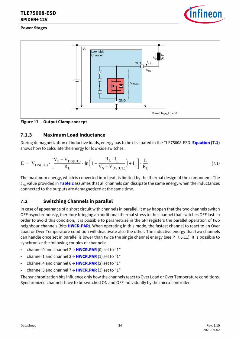
Figure 17 Output Clamp concept
7.1.3 Maximum Load InductanceDuring demagnetization of inductive loads, energy has to be dissipated in the TLE75008-ESD. Equation (7.1)shows how to calculate the energy for low-side switches:
(7.1)
The maximum energy, which is converted into heat, is limited by the thermal design of the component. TheEAR value provided in Table 2 assumes that all channels can dissipate the same energy when the inductancesconnected to the outputs are demagnetized at the same time.
7.2 Switching Channels in parallelIn case of appearance of a short circuit with channels in parallel, it may happen that the two channels switchOFF asynchronously, therefore bringing an additional thermal stress to the channel that switches OFF last. Inorder to avoid this condition, it is possible to parametrize in the SPI registers the parallel operation of twoneighbour channels (bits HWCR.PAR). When operating in this mode, the fastest channel to react to an OverLoad or Over Temperature condition will deactivate also the other. The inductive energy that two channelscan handle once set in parallel is lower than twice the single channel energy (see P_7.6.11). It is possible tosynchronize the following couples of channels:• channel 0 and channel 2 → HWCR.PAR (0) set to “1”• channel 1 and channel 3 → HWCR.PAR (1) set to “1”• channel 4 and channel 6 → HWCR.PAR (2) set to “1”• channel 5 and channel 7 → HWCR.PAR (3) set to “1”The synchronization bits influence only how the channels react to Over Load or Over Temperature conditions.Synchronized channels have to be switched ON and OFF individually by the micro-controller.
PowerStage_LS.emf
VSLow -sideChannel L,
RLIL_DOUT
VDS
VDS(CL)
GND
IL
E VDS CL( )VS VDS CL( )–
RL--------------------------------- 1
RL I⋅ LVS VDS CL( )–---------------------------------–è ø
æ ö IL+ln⋅ LRL------⋅ ⋅=

Datasheet 35 Rev. 1.10 2020-09-02
TLE75008-ESDSPIDER+ 12V
Power Stages
7.3 Electrical Characteristics Power Stages
Table 9 Electrical Characteristics: Power StageVDD = 3 V to 5.5 V, VS = 7 V to 18 V, TJ = -40 °C to +150 °C (unless otherwise specified)Typical values: VDD = 5 V, VS = 13.5 V, TJ = 25 °C
Parameter Symbol Values Unit Note or Test Condition
NumberMin. Typ. Max.
Output CharacteristicsOn-State Resistance RDS(ON) – 1.0 – Ω 1)
TJ = 25 °CP_7.6.1
On-State Resistance RDS(ON) – 1.8 2.2 Ω TJ = 150 °CIL = IL(EAR) = 220 mA
P_7.6.2
Nominal load current(all channels active)
IL(NOM) – 330 5002)3) mA 1)
TA = 85 °CTJ ≤ 150 °C
P_7.6.3
Nominal load current(all channels active)
IL(NOM) – 260 5002)3) mA 1)
TA = 105 °CTJ ≤ 150 °C
P_7.6.4
Nominal load current(half of channels active)
IL(NOM) – 470 5002)3) mA 1)
TA = 85 °CTJ ≤ 150 °C
P_7.6.5
Load current for maximum energy dissipation - repetitive(all channels active)
IL(EAR) – 220 – mA 1)
TA = 85 °CTJ ≤ 150 °C
P_7.6.8
Maximum energy dissipation repetitive pulses - 2*IL(EAR)(two channels in parallel)
EAR – – 15 mJ 1)
TJ(0) = 85 °CIL(0) = 2*IL(EAR)2*106 cyclesHWCR.PAR = “1” for affected channels
P_7.6.11
Power stage voltage drop at low battery
VDS(OP) – – 1 V RL = 50 Ω supplied by VS = 4 VVS = VS(OP),max orVDD = 4.5 V, VS pin openrefer to Figure 17
P_7.6.12
Drain to Source Output clamping voltage
VDS(CL) 42 46 55 V IL = 20 mA P_7.6.16
Output leakage current(each channel)TJ ≤ 85 °C
IL(OFF) – 0.01 0.5 µA 1)
VIN = 0 V or floatingVDS = 28 VOUT.OUTn = 0TJ ≤ 85 °C
P_7.6.19
Datasheet 36 Rev. 1.10 2020-09-02
TLE75008-ESDSPIDER+ 12V
Power Stages
Output leakage current(each channel)TJ = 150 °C(Low-Side channels)
IL(OFF) – 0.1 5 µA 1)
VIN = 0 V or floatingVDS = 28 VOUT.OUTn = 0TJ = 150 °C
P_7.6.20
TimingsTurn-ON delay(from INn pin or bit to VOUT = 90% VS)
tDELAY(ON) 1 4 8 µs RL = 50 ΩVS = 13.5 VActive mode or Limp Home mode
P_7.6.21
Turn-OFF delay(from INn pin or bit to VOUT = 10% VS)
tDELAY(OFF) 1 6 12 µs RL = 50 ΩVS = 13.5 VActive mode or Limp Home mode
P_7.6.22
Turn-ON time(from INn pin or bit to VOUT = 10% VS)
tON 6 15 35 µs RL = 50 ΩVS = 13.5 VActive mode or Limp Home mode
P_7.6.23
Turn-OFF time(from INn pin or bit to VOUT = 90% VS)
tOFF 6 15 35 µs RL = 50 ΩVS = 13.5 VActive mode or Limp Home mode
P_7.6.24
Turn-ON/OFF matching tON - tOFF -10 0 10 µs RL = 50 ΩVS = 13.5 VActive mode or Limp Home mode
P_7.6.25
Turn-ON slew rateVDS = 70% to 30% VS
dV/dtON 0.7 1.3 1.9 V/µs RL = 50 ΩVS = 13.5 VActive mode or Limp Home mode
P_7.6.26
Turn-OFF slew rateVDS = 30% to 70% VS
-dV/dtOFF 0.7 1.3 1.9 V/µs RL = 50 ΩVS = 13.5 VActive mode or Limp Home mode
P_7.6.27
Internal reference frequencysynchronization time
tSYNC – 5 10 µs 1) P_7.6.45
1) Not subject to production test - specified by design2) If one channel has IL(NOM),max applied, the remaining channels must be underloaded accordingly so that TJ < 150°C3) IL(NOM),max can reach IL(OVL1),min
Table 9 Electrical Characteristics: Power Stage (cont’d)VDD = 3 V to 5.5 V, VS = 7 V to 18 V, TJ = -40 °C to +150 °C (unless otherwise specified)Typical values: VDD = 5 V, VS = 13.5 V, TJ = 25 °C
Parameter Symbol Values Unit Note or Test Condition
NumberMin. Typ. Max.

Datasheet 37 Rev. 1.10 2020-09-02
TLE75008-ESDSPIDER+ 12V
Protection Functions
8 Protection Functions
8.1 Over Load ProtectionThe TLE75008-ESD is protected in case of over load or short circuit of the load. There are two over load currentthresholds (see Figure 18):• IL(OVL0) between channel switch ON and tOVLIN
• IL(OVL1) after tOVLIN
Every time the channel is switched OFF for a time longer than 2 * tSYNC the over load current threshold is setback to IL(OVL0).
Figure 18 Over Load current thresholds
In case the load current is higher than IL(OVL0) or IL(OVL1), after time tOFF(OVL) the over loaded channel is switchedOFF and the according diagnosis bit ERRn is set. The channel can be switched ON after clearing the protectionlatch by setting the corresponding HWCR_OCL.OUTn bit to “1”. This bit is set back to “0” internally after de-latching the channel. Please refer to Figure 19 for details.
Figure 19 Latch OFF at Over Load
8.2 Over Temperature ProtectionA temperature sensor is integrated for each channel, causing an overheated channel to switch OFF to preventdestruction. The according diagnosis bit ERRn is set (combined with Over Load protection). The channel can
INn
IL(OVL)
t
t
OverLoadStep.emf
tOVLIN
OUT.OUTn
IL(OVL0)
IL(OVL 1)
INn
ILn
t
t
OverLoad.emf
tOFF(OVL)
IL(OVLn)
OUT.OUTn
SPI command to set HWCR_OCL.OUTn = 1b
t
tERRn 1 00
t1 00HWCR_OCL.OUTn

Datasheet 38 Rev. 1.10 2020-09-02
TLE75008-ESDSPIDER+ 12V
Protection Functions
be switched ON after clearing the protection latch by setting the corresponding HWCR_OCL.OUTn bit to “1”.This bit is set back to “0” internally after de-latching the channel.
8.3 Over Temperature and Over Load Protection in Limp Home modeWhen TLE75008-ESD is in Limp Home mode, channels 2 and 3 can be switched ON using the input pins. In caseof Over Load, Short Circuit or Over Temperature the channels switch OFF. If the input pins remain “high”, thechannels restart with the following timings:• 10 ms (first 8 retries)• 20 ms (following 8 retries)• 40 ms (following 8 retries)• 80 ms (as long as the input pin remains “high” and the error is still present)If at any time the input pin is set to “low” for longer than 2*tSYNC, the restart timer is reset. At the next channelactivation while in Limp Home mode the timer starts from 10 ms again. See Figure 20 for details. Over Loadcurrent thresholds behave as described in Chapter 8.1.
Figure 20 Restart timer in Limp Home mode
8.4 Reverse Polarity ProtectionIn Reverse Polarity (also known as Reverse Battery) condition, power dissipation is caused by the intrinsicbody diode of each DMOS channel. Each ESD diode of the logic and supply pins contributes to total powerdissipation. The reverse current through the channels has to be limited by the connected loads. The currentthrough digital power supply VDD and input pins has to be limited as well (please refer to the AbsoluteMaximum Ratings listed on Chapter 4.1).
Note: No protection mechanism like temperature protection or current limitation is active during reverse polarity.
8.5 Over Voltage ProtectionIn the case of supply voltages between VS(SC) and VS(LD) the output transistors are still operational and followthe input pins or the OUT register.In addition to the output clamp for inductive loads as described in Chapter 7.1.2, there is a clamp mechanismavailable for over voltage protection for the logic and all channels, monitoring the voltage between VS andGND pins (VS(AZ)).
IN0IN1
IL2IL3
t
t
LHrestart.emf
tRETRY0(LH)
10 ms
0 1 8
tRETRY1(LH)
20 ms
1 8
tRETRY2(LH)
40 ms
1 8
tRETRY3(LH)
80 ms
tRETRY0(LH)
10 ms
0 1

Datasheet 39 Rev. 1.10 2020-09-02
TLE75008-ESDSPIDER+ 12V
Protection Functions
8.6 Electrical Characteristics Protection
Table 10 Electrical Characteristics ProtectionVDD = 3 V to 5.5 V, VS = 7 V to 18 V, TJ = -40 °C to +150 °C (unless otherwise specified)Typical values: VDD = 5 V, VS = 13.5 V, TJ = 25 °C
Parameter Symbol Values Unit Note or Test Condition
NumberMin. Typ. Max.
Over LoadOver Load detection current IL(OVL0) 1.3 1.7 2.3 A TJ = -40 °C P_8.8.19
Over Load detection current IL(OVL0) 1.25 1.55 2.3 A 1)
TJ = 25 °CP_8.8.20
Over Load detection current IL(OVL0) 1 1.45 2 A TJ = 150 °C P_8.8.21
Over Load detection current IL(OVL1) 0.7 0.95 1.3 A TJ = -40 °C P_8.8.22
Over Load detection current IL(OVL1) 0.65 0.85 1.3 A 1)
TJ = 25 °CP_8.8.23
Over Load detection current IL(OVL1) 0.5 0.8 1.25 A TJ = 150 °C P_8.8.24
Over Load threshold switch delay time
tOVLIN 110 170 260 µs 1) P_8.8.5
Over Load shut-down delay time
tOFF(OVL) 4 7 11 µs 1) P_8.8.26
Over Temperature and Over VoltageThermal shut-down temperature
TJ(SC) 150 1751)
1) Not subject to production test - specified by design
2201) °C P_8.8.7
Over voltage protection VS(AZ) 42 50 60 V IVS = 10 mASleep mode
P_8.8.8
Reverse PolarityDrain Source diode during reverse polarity
VDS(REV) – 800 – mV 1)
IL = -10 mATJ = 25 °CSleep mode
P_8.8.9
Drain Source diode during reverse polarity
VDS(REV) – 650 – mV IL = -10 mATJ = 150 °CSleep mode
P_8.8.10
TimingsRestart time in Limp Home mode
tRETRY0(LH) 7 10 13 ms 1) P_8.8.13
Restart time in Limp Home mode
tRETRY1(LH) 14 20 26 ms 1) P_8.8.14
Restart time in Limp Home mode
tRETRY2(LH) 28 40 52 ms 1) P_8.8.15
Restart time in Limp Home mode
tRETRY3(LH) 56 80 104 ms 1) P_8.8.16

Datasheet 40 Rev. 1.10 2020-09-02
TLE75008-ESDSPIDER+ 12V
Diagnosis
9 DiagnosisThe SPI of TLE75008-ESD provides diagnosis information about the device and the load status. Each channeldiagnosis information is independent from other channels. An error condition on one channel has noinfluence on the diagnostic of other channels in the device (unless configured to work in parallel, seeChapter 7.2 for more details).
9.1 Over Load and Over TemperatureWhen either an Over Load or an Over Temperature occurs on one channel, the diagnosis bit ERRn is setaccordingly. As described in Chapter 8.1 and Chapter 8.2, the channel latches OFF and must be reactivatedsetting corresponding HWCR_OCL.OUTn bit to “1”.
9.2 Output Status MonitorThe device compares each channel VDS with VDS(OL) and sets the corresponding DIAG_OSM.OUTn bitsaccordingly. The bits are updated every time DIAG_OSM register is read.• VDS < VDS(OL) → DIAG_OSM.OUTn = “1” A diagnosis current IOL in parallel to the power switch can be enabled by programming the DIAG_IOL.OUTnbit, which can be used for Open Load at OFF detection. Each channel has its dedicated diagnosis currentsource. If the diagnosis current IOL is enabled or if the channel changes state (ON → OFF or OFF → ON) it isnecessary to wait a time tOSM for a reliable diagnosis. Enabling IOL current sources increases the currentconsumption of the device. Even if an Open Load is detected, the channel is not latched OFF.See Figure 21 for a timing overview (the values of DIAG_IOL.OUTn refer to a channel in normal operationproperly connected to the load).
Figure 21 Output Status Monitor timing
Output Status Monitor diagnostic is available when VS = VS(NOR) and VDD ≥ VDD(UV).Due to the fact that Output Status Monitor checks the voltage level at the outputs in real time, for Open Loadin OFF diagnostic it is necessary to synchronize the reading of DIAG_OSM register with the OFF state of thechannels.
INn
t
OutStatMon_timings.emf
OUT.OUTn
1ttON + tOSM
DIAG_OSM.OUTn
0
t
x
t
SPI readout of DIAG_OSM.OUTn
1 00
Output voltage comparator
tOFF + tOSM
x 0
x x

Datasheet 41 Rev. 1.10 2020-09-02
TLE75008-ESDSPIDER+ 12V
Diagnosis
Figure 22 shows how Output Status Monitor is implemented at concept level.
Figure 22 Output Status Monitor - concept
In Standard Diagnosis the bit OLOFF represents the OR combination of all DIAG_OSM.OUTn bits for allchannels in OFF state which have the corresponding current source IOL activated.
OutStatMon_LS.emf
VSLow-sideChannel ROL
OUT
VDS
GND
IOL
IOLVDS(OL)
DIAG_OSM.OUTn
VDS < VDS(OL) à DIAG_OSM.OUTn = „1"

Datasheet 42 Rev. 1.10 2020-09-02
TLE75008-ESDSPIDER+ 12V
Diagnosis
9.3 Electrical Characteristics Diagnosis
Table 11 Electrical Characteristics DiagnosisVDD = 3 V to 5.5 V, VS = 7 V to 18 V, TJ = -40 °C to +150 °C (unless otherwise specified)Typical values: VDD = 5 V, VS = 13.5 V, TJ = 25 °C
Parameter Symbol Values Unit Note or Test Condition
NumberMin. Typ. Max.
Output Status MonitorOutput Status Monitor comparator settling time
tOSM – – 20 µs 1)
1) Not subject to production test - specified by design
P_9.5.1
Output Status Monitor threshold voltage
VDS(OL) 3 3.3 3.6 V P_9.5.2
Output diagnosis current IOL 70 85 100 µA VDS = 3.3 V
P_9.5.5
Open Load equivalent resistance
ROL 30 – 300 kΩ 1) P_9.5.6

Datasheet 43 Rev. 1.10 2020-09-02
TLE75008-ESDSPIDER+ 12V
Serial Peripheral Interface (SPI)
10 Serial Peripheral Interface (SPI)The serial peripheral interface (SPI) is a full duplex synchronous serial slave interface, which uses four lines:SO, SI, SCLK and CSN. Data is transferred by the lines SI and SO at the rate given by SCLK. The falling edge ofCSN indicates the beginning of an access. Data is sampled in on line SI at the falling edge of SCLK and shiftedout on line SO at the rising edge of SCLK. Each access must be terminated by a rising edge of CSN. A modulo8/16 counter ensures that data is taken only when a multiple of 8 bit has been transferred after the first 16 bits.Otherwise a TER bit is asserted. In this way the interface provides daisy chain capability with 16 bit as well aswith 8 bit SPI devices.
Figure 23 Serial Peripheral Interface
10.1 SPI Signal Description
CSN - Chip SelectThe system microcontroller selects the TLE75008-ESD by means of the CSN pin. Whenever the pin is in “low”state, data transfer can take place. When CSN is in "high" state, any signals at the SCLK and SI pins are ignoredand SO is forced into a high impedance state.
CSN “high” to “low” Transition• The requested information is transferred into the shift register.• SO changes from high impedance state to "high" or “low” state depending on the logic OR combination
between the transmission error flag (TER) and the signal level at pin SI. This allows to detect a faulty transmission even in daisy chain configuration.
• If the device is in Sleep mode, SO pin remains in high impedance state and no SPI transmission occurs.
Figure 24 Combinatorial Logic for TER bit
14 13 12 11
14 13 12 11MSB
MSB
SPI _16bit.emf
LSB6 5 4 3 2 1
LSB6 5 4 3 2 1
10 9 8
10 9 8
7
7SO
SI
CSN
SCLKtime
SPI _TER.emf
SI
SPI
OR
TER
0
1 SO
CSNSCLK
S
SOS
SI
Datasheet 44 Rev. 1.10 2020-09-02
TLE75008-ESDSPIDER+ 12V
Serial Peripheral Interface (SPI)
CSN “low” to "high" Transition• Command decoding is only done, when after the falling edge of CSN exactly a multiple (1, 2, 3, …) of eight
SCLK signals have been detected after the first 16 SCLK pulses. In case of faulty transmission, the transmission error bit (TER) is set and the command is ignored.
• Data from shift register is transferred into the addressed register.
SCLK - Serial ClockThis input pin clocks the internal shift register. The serial input (SI) transfers data into the shift register on thefalling edge of SCLK while the serial output (SO) shifts diagnostic information out on the rising edge of theserial clock. It is essential that the SCLK pin is in “low” state whenever chip select CSN makes any transition,otherwise the command may be not accepted.
SI - Serial InputSerial input data bits are shift-in at this pin, the most significant bit first. SI information is read on the fallingedge of SCLK. The input data consists of two parts, control bits followed by data bits. Please refer toChapter 10.5 for further information.
SO Serial OutputData is shifted out serially at this pin, the most significant bit first. SO is in high impedance state until the CSNpin goes to “low” state. New data appears at the SO pin following the rising edge of SCLK.Please refer to Chapter 10.5 for further information.
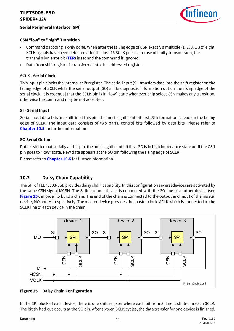
10.2 Daisy Chain CapabilityThe SPI of TLE75008-ESD provides daisy chain capability. In this configuration several devices are activated bythe same CSN signal MCSN. The SI line of one device is connected with the SO line of another device (seeFigure 25), in order to build a chain. The end of the chain is connected to the output and input of the masterdevice, MO and MI respectively. The master device provides the master clock MCLK which is connected to theSCLK line of each device in the chain.
Figure 25 Daisy Chain Configuration
In the SPI block of each device, there is one shift register where each bit from SI line is shifted in each SCLK.The bit shifted out occurs at the SO pin. After sixteen SCLK cycles, the data transfer for one device is finished.
SI
device 1
SPI
SCLK
SO
CSN
SI
device 2
SPI
SCLK
SO
CSN
SI
device 3
SPI
SCLK
SO
CSN
MO
MIMCSNMCLK
SPI_DaisyChain_1.emf

Datasheet 45 Rev. 1.10 2020-09-02
TLE75008-ESDSPIDER+ 12V
Serial Peripheral Interface (SPI)
In single chip configuration, the CSN line must turn “high” to make the device acknowledge the transferreddata. In daisy chain configuration, the data shifted out at device 1 has been shifted in to device 2. When usingthree devices in daisy chain, several multiples of 8 bits have to be shifted through the devices (depending onhow many devices with 8 bit SPI and how many with 16 bit SPI). After that, the MCSN line must turn “high” (seeFigure 26).
Figure 26 Data Transfer in Daisy Chain Configuration
10.3 Timing Diagrams
Figure 27 Timing Diagram SPI Access
MI
MOMCSN
MCLK
SI device 3 SI device 2 SI device 1
SO device 3 SO device 2 SO device 1
SPI_DaisyChain_2.emf
CSN
SCLK
SI
tCSN(lead) tCSN(td)tCSN(lag)
tSCLK(H) tSCLK(L)
tSCLK(P )
tSI(su) tSI(h)
SO
tSO(v)tSO(en) tSO (dis)
VCSN(H)
SPI _Timings.emf
VCSN(L)
VSCLK(H)
VSCLK(L)
VSI(H)
VSI(L)
VSO(H)
VSO(L)

Datasheet 46 Rev. 1.10 2020-09-02
TLE75008-ESDSPIDER+ 12V
Serial Peripheral Interface (SPI)
10.4 Electrical CharacteristicsVDD = 3 V to 5.5 V, VS = 7 V to 18 V, TJ = -40 °C to +150 °C (unless otherwise specified)Typical values: VDD = 5 V, VS = 13.5 V, TJ = 25 °C
Table 12 Electrical Characteristics Serial Peripheral Interface (SPI)Parameter Symbol Values Unit Note or
Test ConditionNumber
Min. Typ. Max.Input Characteristics (CSN, SCLK, SI) - “low” level of pinCSN VCSN(L) 0 – 0.8 V – P_10.4.1
SCLK VSCLK(L) 0 – 0.8 V – P_10.4.2
SI VSI(L) 0 – 0.8 V – P_10.4.3
Input Characteristics (CSN, SCLK, SI) - “high” level of pinCSN VCSN(H) 2 – VDD V – P_10.4.4
SCLK VSCLK(H) 2 – VDD V – P_10.4.5
SI VSI(H) 2 – VDD V – P_10.4.6
Input Pull-Up Current at Pin CSNL-input pull-up current at CSN pin -ICSN(L) 30 60 90 μA VDD = 5 V
VCSN = 0.8 VP_10.4.7
H-input pull-up current at CSN pin -ICSN(H) 20 40 65 μA VDD = 5 VVCSN = 2 V
P_10.4.8
L-Input Pull-Down Current at PinSCLK ISCLK(L) 5 12 20 μA VSCLK = 0.8 V P_10.4.9
SI ISI(L) 5 12 20 μA VSI = 0.8 V P_10.4.10
H-Input Pull-Down Current at PinSCLK ISCLK(H) 14 28 45 μA VSCLK = 2 V P_10.4.11
SI ISI(H) 14 28 45 μA VSI = 2 V P_10.4.12
Output Characteristics (SO)L level output voltage VSO(L) 0 – 0.4 V ISO = -1.5 mA P_10.4.13
H level output voltage VSO(H) VDD - 0.4 – VDD V ISO = 1.5 mA P_10.4.14
Output tristate leakage current ISO(OFF) -1 – 1 μA VCSN =VDDVSO = 0 V
P_10.4.15
Output tristate leakage current ISO(OFF) -1 – 1 μA VCSN =VDDVSO = VDD
P_10.4.16
TimingsEnable lead time (falling CSN to rising SCLK)
tCSN(lead) 200 – – ns 1)
VDD = 4.5 V or VS > 7 V
P_10.4.17
Enable lag time (falling SCLK to rising CSN)
tCSN(lag) 200 – – ns 1)
VDD = 4.5 V or VS > 7 V
P_10.4.18
Datasheet 47 Rev. 1.10 2020-09-02
TLE75008-ESDSPIDER+ 12V
Serial Peripheral Interface (SPI)
Transfer delay time (rising CSN to falling CSN)
tCSN(td) 250 – – ns 1)
VDD = 4.5 V or VS > 7 V
P_10.4.19
Output enable time (falling CSN to SO valid)
tSO(en) – – 200 ns 1)
VDD = 4.5 V or VS > 7 VCL = 20 pF at SO pin
P_10.4.20
Output disable time (rising CSN to SO tristate)
tSO(dis) – – 200 ns 1)
VDD = 4.5 V or VS > 7 VCL = 20 pF at SO pin
P_10.4.21
Serial clock frequency fSCLK – – 5 MHz 1)
VDD = 4.5 V or VS > 7 V
P_10.4.22
Serial clock period tSCLK(P) 200 – – ns 1)
VDD = 4.5 V or VS > 7 V
P_10.4.23
Serial clock “high” time tSCLK(H) 75 – – ns 1)
VDD = 4.5 V or VS > 7 V
P_10.4.24
Serial clock “low” time tSCLK(L) 75 – – ns 1)
VDD = 4.5 V or VS > 7 V
P_10.4.25
Data setup time (required time SI to falling SCLK)
tSI(su) 20 – – ns 1)
VDD = 4.5 V or VS > 7 V
P_10.4.26
Data hold time (falling SCLK to SI) tSI(h) 20 – – ns 1)
VDD = 4.5 V or VS > 7 V
P_10.4.27
Output data valid time with capacitive load
tSO(v) – – 100 ns 1)
VDD = 4.5 V or VS > 7 VCL = 20 pF at SO pin
P_10.4.28
Enable lead time (falling CSN to rising SCLK)
tCSN(lead) 1 – – μs 1)
VDD = VS = 3.0 VP_10.4.29
Enable lag time (falling SCLK to rising CSN)
tCSN(lag) 1 – – μs 1)
VDD = VS = 3.0 VP_10.4.30
Transfer delay time (rising CSN to falling CSN)
tCSN(td) 1.25 – – μs 1)
VDD = VS = 3.0 VP_10.4.31
Table 12 Electrical Characteristics Serial Peripheral Interface (SPI) (cont’d)
Parameter Symbol Values Unit Note or Test Condition
NumberMin. Typ. Max.

Datasheet 48 Rev. 1.10 2020-09-02
TLE75008-ESDSPIDER+ 12V
Serial Peripheral Interface (SPI)
Output enable time (falling CSN to SO valid)
tSO(en) – – 1 μs 1)
VDD = VS = 3.0 VCL = 20 pF at SO pin
P_10.4.32
Output disable time (rising CSN to SO tristate)
tSO(dis) – – 1 μs 1)
VDD = VS = 3.0 VCL = 20 pF at SO pin
P_10.4.33
Serial clock frequency fSCLK – – 1 MHz 1)
VDD = VS = 3.0 VP_10.4.34
Serial clock period tSCLK(P) 1 – – μs 1)
VDD = VS = 3.0 VP_10.4.35
Serial clock “high” time tSCLK(H) 375 – – ns 1)
VDD = VS = 3.0 VP_10.4.36
Serial clock “low” time tSCLK(L) 375 – – ns 1)
VDD = VS = 3.0 VP_10.4.37
Data setup time (required time SI to falling SCLK)
tSI(su) 100 – – ns 1)
VDD = VS = 3.0 VP_10.4.38
Data hold time (falling SCLK to SI) tSI(h) 100 – – ns 1)
VDD = VS = 3.0 VP_10.4.39
Output data valid time with capacitive load
tSO(v) – – 500 ns 1)
VDD = VS = 3.0 VCL = 20 pF at SO pin
P_10.4.40
1) Not subject to production test, specified by design
Table 12 Electrical Characteristics Serial Peripheral Interface (SPI) (cont’d)
Parameter Symbol Values Unit Note or Test Condition
NumberMin. Typ. Max.
Datasheet 49 Rev. 1.10 2020-09-02
TLE75008-ESDSPIDER+ 12V
Serial Peripheral Interface (SPI)
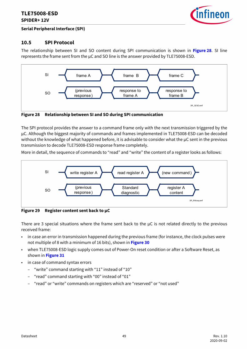
10.5 SPI ProtocolThe relationship between SI and SO content during SPI communication is shown in Figure 28. SI linerepresents the frame sent from the µC and SO line is the answer provided by TLE75008-ESD.
Figure 28 Relationship between SI and SO during SPI communication
The SPI protocol provides the answer to a command frame only with the next transmission triggered by theµC. Although the biggest majority of commands and frames implemented in TLE75008-ESD can be decodedwithout the knowledge of what happened before, it is advisable to consider what the µC sent in the previoustransmission to decode TLE75008-ESD response frame completely.More in detail, the sequence of commands to “read” and “write” the content of a register looks as follows:
Figure 29 Register content sent back to µC
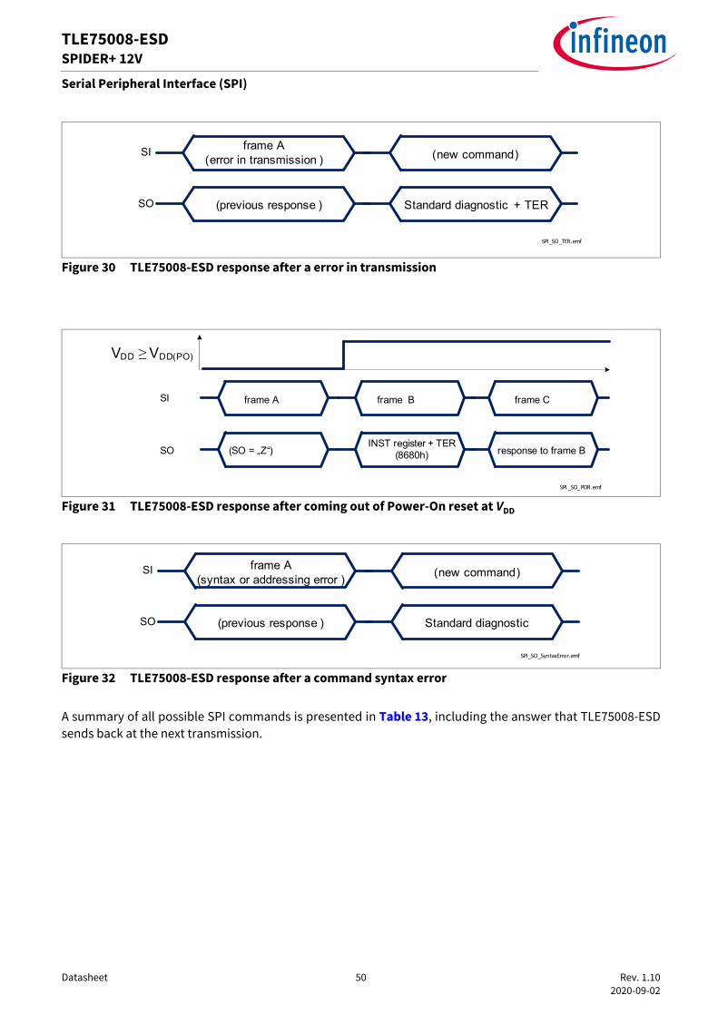
There are 3 special situations where the frame sent back to the µC is not related directly to the previousreceived frame:• in case an error in transmission happened during the previous frame (for instance, the clock pulses were
not multiple of 8 with a minimum of 16 bits), shown in Figure 30• when TLE75008-ESD logic supply comes out of Power-On reset condition or after a Software Reset, as
shown in Figure 31• in case of command syntax errors
– “write” command starting with “11” instead of “10”– “read” command starting with “00” instead of “01”– “read” or “write” commands on registers which are “reserved” or “not used”
SI
SO
frame A frame B
(previous response )
response to frame A
frame C
response to frame B
SPI_SI2SO.emf
SI
SO
write register A read register A
Standard diagnostic
register A content
(new command )
SPI_RWseq.emf
(previous response )
Datasheet 50 Rev. 1.10 2020-09-02
TLE75008-ESDSPIDER+ 12V
Serial Peripheral Interface (SPI)
Figure 30 TLE75008-ESD response after a error in transmission
Figure 31 TLE75008-ESD response after coming out of Power-On reset at VDD
Figure 32 TLE75008-ESD response after a command syntax error
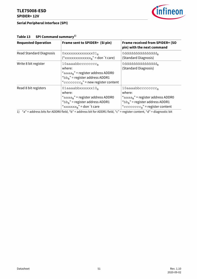
A summary of all possible SPI commands is presented in Table 13, including the answer that TLE75008-ESDsends back at the next transmission.
frame A(error in transmission )
SPI_SO_TER.emf
SI
SO
(new command)
Standard diagnostic + TER(previous response )
SI
SO
frame A frame B
(SO = „Z“)
frame C
response to frame BINST register + TER
(8680h)
VDD ≥ VDD(PO)
SPI _SO_POR.emf
SI
SO
frame A(syntax or addressing error ) (new command)
Standard diagnostic(previous response )
SPI_SO_SyntaxError.emf
Datasheet 51 Rev. 1.10 2020-09-02
TLE75008-ESDSPIDER+ 12V
Serial Peripheral Interface (SPI)
Table 13 SPI Command summary1)
1) “a” = address bits for ADDR0 field, “b” = address bit for ADDR1 field, “c” = register content, “d” = diagnostic bit
Requested Operation Frame sent to SPIDER+ (SI pin) Frame received from SPIDER+ (SO pin) with the next command
Read Standard Diagnosis 0xxxxxxxxxxxxx01B(“xxxxxxxxxxxxB” = don´t care)
0dddddddddddddddB(Standard Diagnosis)
Write 8 bit register 10aaaabbccccccccBwhere:“aaaaB” = register address ADDR0“bbB” = register address ADDR1“ccccccccB” = new register content
0dddddddddddddddB(Standard Diagnosis)
Read 8 bit registers 01aaaabbxxxxxx10Bwhere:“aaaaB” = register address ADDR0“bbB” = register address ADDR1“xxxxxxB” = don´t care
10aaaabbccccccccBwhere:“aaaaB” = register address ADDR0“bbB” = register address ADDR1“ccccccccB” = register content

Datasheet 52 Rev. 1.10 2020-09-02
TLE75008-ESDSPIDER+ 12V
Serial Peripheral Interface (SPI)
10.6 SPI Registers Overview
10.6.1 Standard Diagnosis
Table 14 Standard Diagnosis15 14 13 12 11 10 9 8 7 6 5 4 3 2 1 0 Default
0 UVRVS
LOPVDD
MODE TER 0 OLOFF
ERR 7800H
Field Bits Type DescriptionUVRVS 14 r VS Undervoltage Monitor
0B No undervoltage condition on VS detected (see Chapter 6.2.1 for more details)
1B (default) There was at least one VS Undervoltage condition since last Standard Diagnosis readout
LOPVDD 13 r VDD Lower Operating Range Monitor0B VDD is above VDD(LOP)1B (default) There was at least one “VDD = VDD(LOP)” condition since
last Standard Diagnosis readout
MODE 12:11 r Operative Mode Monitor00B (reserved)01B Limp Home Mode10B Active Mode11B (default) Idle Mode
TER 10 r Transmission Error0B Previous transmission was successful
(modulo 16 + n*8 clocks received, where n = 0, 1, 2...)1B (default) Previous transmission failedThe first frame after a reset is TER set to “high” and the INST register. The second frame is the Standard Diagnosis with TER set to “low” (if there was no fail in the previous transmission).
OLOFF 8 r Open Load in OFF Diagnosis0B (default) All channels in OFF state (which have
DIAG_IOL.OUTn bit set to “1”) have VDS > VDS(OL)1B At least one channel in OFF state (with DIAG_IOL.OUTn bit set
to “1”) has VDS < VDS(OL)Channels in ON state are not considered
ERRnn = 7 to 0
n:0 r Over Load / Over Temperature Diagnosis of channel n0B (default) No failure detected1B Over Temperature or Over Load
Datasheet 53 Rev. 1.10 2020-09-02
TLE75008-ESDSPIDER+ 12V
Serial Peripheral Interface (SPI)
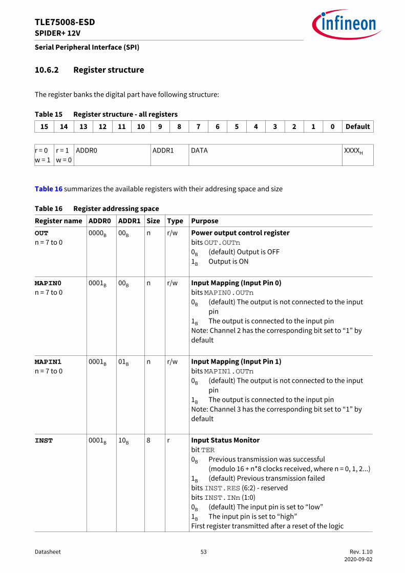
10.6.2 Register structure
The register banks the digital part have following structure:
Table 16 summarizes the available registers with their addresing space and size
Table 15 Register structure - all registers 15 14 13 12 11 10 9 8 7 6 5 4 3 2 1 0 Default
r = 0w = 1
r = 1w = 0
ADDR0 ADDR1 DATA XXXXH
Table 16 Register addressing spaceRegister name ADDR0 ADDR1 Size Type PurposeOUTn = 7 to 0
0000B 00B n r/w Power output control registerbits OUT.OUTn0B (default) Output is OFF1B Output is ON
MAPIN0n = 7 to 0
0001B 00B n r/w Input Mapping (Input Pin 0)bits MAPIN0.OUTn0B (default) The output is not connected to the input
pin1B The output is connected to the input pinNote: Channel 2 has the corresponding bit set to “1” by default
MAPIN1n = 7 to 0
0001B 01B n r/w Input Mapping (Input Pin 1)bits MAPIN1.OUTn0B (default) The output is not connected to the input
pin1B The output is connected to the input pinNote: Channel 3 has the corresponding bit set to “1” by default
INST 0001B 10B 8 r Input Status Monitorbit TER0B Previous transmission was successful
(modulo 16 + n*8 clocks received, where n = 0, 1, 2...)1B (default) Previous transmission failedbits INST.RES (6:2) - reservedbits INST.INn (1:0)0B (default) The input pin is set to “low” 1B The input pin is set to “high”First register transmitted after a reset of the logic

Datasheet 54 Rev. 1.10 2020-09-02
TLE75008-ESDSPIDER+ 12V
Serial Peripheral Interface (SPI)
10.6.3 Register summaryAll registers with addresses not mentioned in Table 17 have to be considered as “reserved”. “Read”operations performed on those registers return the Standard Diagnosis. The column “Default” indicates thecontent of the register (8 bits) after a reset.
DIAG_IOLn = 7 to 0
0010B 00B n r/w Open Load diagnostic current controlbits DIAG_IOL.OUTn0B (default) Diagnosis current not enabled1B Diagnosis current enabled
DIAG_OSMn = 7 to 0
0010B 01B n r Output Status Monitorbits DIAG_OSM.OUTn0B (default) VDS > VDS(OL)1B VDS < VDS(OL)
HWCR 0011B 00B 8 r/w Hardware Configuration Registerbit HWCR.ACT (7) (Active Mode) 0B (default) Normal operation or device leaves Active
Mode1B Device enters Active Mode(see Chapter 6.1 for a description of the possible operative mode transitions)bit HWCR.RST (6) (Reset)0B (default) Normal operation1B Execute Reset command (self clearing)bits HWCR.PAR (3:0) (channels operating in parallel)0B (default) Normal operation1B two neighbour channels have Over Load and Over
Temperature synchronized (see Chapter 7.2 for more details)
bits 5:4 - reserved (default: 0B)
HWCR_OCLn = 7 to 0
0011B 01B n w Output Clear Latchbits HWCR_OCL.OUTn0B (default) Normal operation1B Clear the error latch for the selected output
Table 17 Addressable registers15 14 13-10 9 8 7 6 5 4 3 2 1 0 Default
r = 0w = 1
r = 1w = 0
0000 00 OUT.OUTn 00H
r = 0w = 1
r = 1w = 0
0001 00 MAPIN0.OUTn 04H
Table 16 Register addressing space (cont’d)
Register name ADDR0 ADDR1 Size Type Purpose
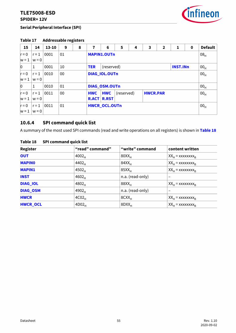
Datasheet 55 Rev. 1.10 2020-09-02
TLE75008-ESDSPIDER+ 12V
Serial Peripheral Interface (SPI)
10.6.4 SPI command quick listA summary of the most used SPI commands (read and write operations on all registers) is shown in Table 18
r = 0w = 1
r = 1w = 0
0001 01 MAPIN1.OUTn 08H
0 1 0001 10 TER (reserved) INST.INn 00H
r = 0w = 1
r = 1w = 0
0010 00 DIAG_IOL.OUTn 00H
0 1 0010 01 DIAG_OSM.OUTn 00H
r = 0w = 1
r = 1w = 0
0011 00 HWCR.ACT
HWCR.RST
(reserved) HWCR.PAR 00H
r = 0w = 1
r = 1w = 0
0011 01 HWCR_OCL.OUTn 00H
Table 18 SPI command quick listRegister “read” command” “write” command content writtenOUT 4002H 80XXH XXH = xxxxxxxxB
MAPIN0 4402H 84XXH XXH = xxxxxxxxB
MAPIN1 4502H 85XXH XXH = xxxxxxxxB
INST 4602H n.a. (read-only) –
DIAG_IOL 4802H 88XXH XXH = xxxxxxxxB
DIAG_OSM 4902H n.a. (read-only) –
HWCR 4C02H 8CXXH XXH = xxxxxxxxB
HWCR_OCL 4D02H 8DXXH XXH = xxxxxxxxB
Table 17 Addressable registers15 14 13-10 9 8 7 6 5 4 3 2 1 0 Default

Datasheet 56 Rev. 1.10 2020-09-02
TLE75008-ESDSPIDER+ 12V
Application Information
11 Application Information
Note: The following information is given as a hint for the implementation of the device only and shall not be regarded as a description or warranty of a certain functionality, condition or quality of the device.
Figure 33 TLE75008-ESD Application Diagram
Note: This is a very simplified example of an application circuit. The function must be verified in the real application.
Table 19 Suggested Component valuesReference Value PurposeRIN 4.7 kΩ Protection of the micro-controller during Over Voltage and Reverse Polarity
Guarantee TLE75008-ESD channels OFF during Loss of Ground
RIDLE 4.7 kΩ Protection of the micro-controller during Over Voltage and Reverse PolarityGuarantee TLE75008-ESD channels OFF during Loss of Ground
RCSN 500 Ω Protection of the micro-controller during Over Voltage and Reverse Polarity
RSCLK 500 Ω Protection of the micro-controller during Over Voltage and Reverse Polarity
RSI 500 Ω Protection of the micro-controller during Over Voltage and Reverse Polarity
RSO 500 Ω Protection of the micro-controller during Over Voltage and Reverse Polarity
RVDD 100 Ω Logic supply voltage spikes filtering
VBATT
ZVS
IDLE
IN1
SO
GND
VDD
CVDD
IN0_LHIN1_LH
LIMPHOME
RIN
GPO
VDD
RIN
RIDLE
RCSN
RSCLK
RSI
RSO
SI
CSN
VDD
SCLK
IN0VS
GPO
GPO
GPO
GPO
GPO
GPI
GND
OUT7_LS
C OU
T
C OU
T
C OU
T
C OU
T
C OU
T
C OU
T
C OU
T
C OU
T
OUT6_LS
OUT5_LS
OUT4_LS
OUT3_LS
OUT2_LS
OUT1_LS
Application_8LS.emf
Z OUT
3
Z OUT
4
Z OUT
5
Z OUT
6
Z OUT
7
Z OUT
2
CVS
OUT0_LS
RVDD
RLH
R OUT
1

Datasheet 57 Rev. 1.10 2020-09-02
TLE75008-ESDSPIDER+ 12V
Application Information
11.1 Further Application Information
• Please contact us for information regarding the Pin FMEA• For further information you may contact http://www.infineon.com/
CVDD 100 nF Logic supply voltage spikes filtering
CVS 68 nF Analog supply voltage spikes filtering
ZVS P6SMB30 Protection of device during Over Voltage. Zener diode
COUT 10 nF Protection of TLE75008-ESD against ESD and BCI
Table 19 Suggested Component values (cont’d)
Reference Value Purpose

Datasheet 58 Rev. 1.10 2020-09-02
TLE75008-ESDSPIDER+ 12V
Package Outlines
12 Package Outlines
Figure 34 PG-TSDSO-24 Package drawing
Figure 35 TLE75008-ESD Package pads and stencil

Datasheet 59 Rev. 1.10 2020-09-02
TLE75008-ESDSPIDER+ 12V
Package Outlines
Green Product (RoHS compliant)To meet the world-wide customer requirements for environmentally friendly products and to be compliantwith government regulations the device is available as a green product. Green products are RoHS-Compliant(i.e Pb-free finish on leads and suitable for Pb-free soldering according to IPC/JEDEC J-STD-020).
For further information on alternative packages, please visit our website:http://www.infineon.com/packages. Dimensions in mm

Datasheet 60 Rev. 1.10 2020-09-02
TLE75008-ESDSPIDER+ 12V
Revision History
13 Revision History
Page or Item Changes since previous revisionRev. 1.10, 2020-09-02All Package name updated
Table 2 Updated ESD susceptibility footnotes for HBM and CDM
Updated backcover
Rev.1.00, 2017-11-23All Datasheet released
TLE75008-ESD

Datasheet 61 Rev. 1.10 2020-09-02
TLE75008-ESDSPIDER+ 12V
Table of Contents1 Overview . . . . . . . . . . . . . . . . . . . . . . . . . . . . . . . . . . . . . . . . . . . . . . . . . . . . . . . . . . . . . . . . . . . . . . . . 1
2 Block Diagram and Terms . . . . . . . . . . . . . . . . . . . . . . . . . . . . . . . . . . . . . . . . . . . . . . . . . . . . . . . . . . 42.1 Block Diagram . . . . . . . . . . . . . . . . . . . . . . . . . . . . . . . . . . . . . . . . . . . . . . . . . . . . . . . . . . . . . . . . . . . . . . . . . . . . 42.2 Terms . . . . . . . . . . . . . . . . . . . . . . . . . . . . . . . . . . . . . . . . . . . . . . . . . . . . . . . . . . . . . . . . . . . . . . . . . . . . . . . . . . . 5
3 Pin Configuration . . . . . . . . . . . . . . . . . . . . . . . . . . . . . . . . . . . . . . . . . . . . . . . . . . . . . . . . . . . . . . . . . 63.1 Pin Assignment . . . . . . . . . . . . . . . . . . . . . . . . . . . . . . . . . . . . . . . . . . . . . . . . . . . . . . . . . . . . . . . . . . . . . . . . . . . 63.2 Pin Definitions and Functions . . . . . . . . . . . . . . . . . . . . . . . . . . . . . . . . . . . . . . . . . . . . . . . . . . . . . . . . . . . . . . 7
4 General Product Characteristics . . . . . . . . . . . . . . . . . . . . . . . . . . . . . . . . . . . . . . . . . . . . . . . . . . . . 94.1 Absolute Maximum Ratings . . . . . . . . . . . . . . . . . . . . . . . . . . . . . . . . . . . . . . . . . . . . . . . . . . . . . . . . . . . . . . . . 94.2 Functional Range . . . . . . . . . . . . . . . . . . . . . . . . . . . . . . . . . . . . . . . . . . . . . . . . . . . . . . . . . . . . . . . . . . . . . . . . 114.3 Thermal Resistance . . . . . . . . . . . . . . . . . . . . . . . . . . . . . . . . . . . . . . . . . . . . . . . . . . . . . . . . . . . . . . . . . . . . . . 124.3.1 PCB set up . . . . . . . . . . . . . . . . . . . . . . . . . . . . . . . . . . . . . . . . . . . . . . . . . . . . . . . . . . . . . . . . . . . . . . . . . . . . . 124.3.2 Thermal Impedance . . . . . . . . . . . . . . . . . . . . . . . . . . . . . . . . . . . . . . . . . . . . . . . . . . . . . . . . . . . . . . . . . . . . 14
5 Control Pins . . . . . . . . . . . . . . . . . . . . . . . . . . . . . . . . . . . . . . . . . . . . . . . . . . . . . . . . . . . . . . . . . . . . 155.1 Input pins . . . . . . . . . . . . . . . . . . . . . . . . . . . . . . . . . . . . . . . . . . . . . . . . . . . . . . . . . . . . . . . . . . . . . . . . . . . . . . . 155.2 IDLE pin . . . . . . . . . . . . . . . . . . . . . . . . . . . . . . . . . . . . . . . . . . . . . . . . . . . . . . . . . . . . . . . . . . . . . . . . . . . . . . . . 155.3 Electrical Characteristics Control Pins . . . . . . . . . . . . . . . . . . . . . . . . . . . . . . . . . . . . . . . . . . . . . . . . . . . . . 17
6 Power Supply . . . . . . . . . . . . . . . . . . . . . . . . . . . . . . . . . . . . . . . . . . . . . . . . . . . . . . . . . . . . . . . . . . . 186.1 Operation Modes . . . . . . . . . . . . . . . . . . . . . . . . . . . . . . . . . . . . . . . . . . . . . . . . . . . . . . . . . . . . . . . . . . . . . . . . 216.1.1 Power-up . . . . . . . . . . . . . . . . . . . . . . . . . . . . . . . . . . . . . . . . . . . . . . . . . . . . . . . . . . . . . . . . . . . . . . . . . . . . . . 226.1.2 Sleep mode . . . . . . . . . . . . . . . . . . . . . . . . . . . . . . . . . . . . . . . . . . . . . . . . . . . . . . . . . . . . . . . . . . . . . . . . . . . . 226.1.3 Idle mode . . . . . . . . . . . . . . . . . . . . . . . . . . . . . . . . . . . . . . . . . . . . . . . . . . . . . . . . . . . . . . . . . . . . . . . . . . . . . 226.1.4 Active mode . . . . . . . . . . . . . . . . . . . . . . . . . . . . . . . . . . . . . . . . . . . . . . . . . . . . . . . . . . . . . . . . . . . . . . . . . . . 236.1.5 Limp Home mode . . . . . . . . . . . . . . . . . . . . . . . . . . . . . . . . . . . . . . . . . . . . . . . . . . . . . . . . . . . . . . . . . . . . . . 236.1.6 Definition of Power Supply modes transition times . . . . . . . . . . . . . . . . . . . . . . . . . . . . . . . . . . . . . . . . 236.2 Reset condition . . . . . . . . . . . . . . . . . . . . . . . . . . . . . . . . . . . . . . . . . . . . . . . . . . . . . . . . . . . . . . . . . . . . . . . . . . 246.2.1 Undervoltage on VS . . . . . . . . . . . . . . . . . . . . . . . . . . . . . . . . . . . . . . . . . . . . . . . . . . . . . . . . . . . . . . . . . . . . . 246.2.2 Low Operating Power on VDD . . . . . . . . . . . . . . . . . . . . . . . . . . . . . . . . . . . . . . . . . . . . . . . . . . . . . . . . . . . . 256.3 Electrical Characteristics Power Supply . . . . . . . . . . . . . . . . . . . . . . . . . . . . . . . . . . . . . . . . . . . . . . . . . . . . 26
7 Power Stages . . . . . . . . . . . . . . . . . . . . . . . . . . . . . . . . . . . . . . . . . . . . . . . . . . . . . . . . . . . . . . . . . . . 337.1 Output ON-state resistance . . . . . . . . . . . . . . . . . . . . . . . . . . . . . . . . . . . . . . . . . . . . . . . . . . . . . . . . . . . . . . . 337.1.1 Switching Resistive Loads . . . . . . . . . . . . . . . . . . . . . . . . . . . . . . . . . . . . . . . . . . . . . . . . . . . . . . . . . . . . . . . 337.1.2 Inductive Output Clamp. . . . . . . . . . . . . . . . . . . . . . . . . . . . . . . . . . . . . . . . . . . . . . . . . . . . . . . . . . . . . . . . . 337.1.3 Maximum Load Inductance. . . . . . . . . . . . . . . . . . . . . . . . . . . . . . . . . . . . . . . . . . . . . . . . . . . . . . . . . . . . . . 347.2 Switching Channels in parallel . . . . . . . . . . . . . . . . . . . . . . . . . . . . . . . . . . . . . . . . . . . . . . . . . . . . . . . . . . . . 347.3 Electrical Characteristics Power Stages . . . . . . . . . . . . . . . . . . . . . . . . . . . . . . . . . . . . . . . . . . . . . . . . . . . . 35
8 Protection Functions . . . . . . . . . . . . . . . . . . . . . . . . . . . . . . . . . . . . . . . . . . . . . . . . . . . . . . . . . . . . . 378.1 Over Load Protection . . . . . . . . . . . . . . . . . . . . . . . . . . . . . . . . . . . . . . . . . . . . . . . . . . . . . . . . . . . . . . . . . . . . 378.2 Over Temperature Protection . . . . . . . . . . . . . . . . . . . . . . . . . . . . . . . . . . . . . . . . . . . . . . . . . . . . . . . . . . . . . 378.3 Over Temperature and Over Load Protection in Limp Home mode . . . . . . . . . . . . . . . . . . . . . . . . . . . . 388.4 Reverse Polarity Protection . . . . . . . . . . . . . . . . . . . . . . . . . . . . . . . . . . . . . . . . . . . . . . . . . . . . . . . . . . . . . . . 388.5 Over Voltage Protection . . . . . . . . . . . . . . . . . . . . . . . . . . . . . . . . . . . . . . . . . . . . . . . . . . . . . . . . . . . . . . . . . . 388.6 Electrical Characteristics Protection . . . . . . . . . . . . . . . . . . . . . . . . . . . . . . . . . . . . . . . . . . . . . . . . . . . . . . . 39
9 Diagnosis . . . . . . . . . . . . . . . . . . . . . . . . . . . . . . . . . . . . . . . . . . . . . . . . . . . . . . . . . . . . . . . . . . . . . . . 409.1 Over Load and Over Temperature . . . . . . . . . . . . . . . . . . . . . . . . . . . . . . . . . . . . . . . . . . . . . . . . . . . . . . . . . 40

Datasheet 62 Rev. 1.10 2020-09-02
TLE75008-ESDSPIDER+ 12V
9.2 Output Status Monitor . . . . . . . . . . . . . . . . . . . . . . . . . . . . . . . . . . . . . . . . . . . . . . . . . . . . . . . . . . . . . . . . . . . 409.3 Electrical Characteristics Diagnosis . . . . . . . . . . . . . . . . . . . . . . . . . . . . . . . . . . . . . . . . . . . . . . . . . . . . . . . . 42
10 Serial Peripheral Interface (SPI) . . . . . . . . . . . . . . . . . . . . . . . . . . . . . . . . . . . . . . . . . . . . . . . . . . . 4310.1 SPI Signal Description . . . . . . . . . . . . . . . . . . . . . . . . . . . . . . . . . . . . . . . . . . . . . . . . . . . . . . . . . . . . . . . . . . . . 4310.2 Daisy Chain Capability . . . . . . . . . . . . . . . . . . . . . . . . . . . . . . . . . . . . . . . . . . . . . . . . . . . . . . . . . . . . . . . . . . . 4410.3 Timing Diagrams . . . . . . . . . . . . . . . . . . . . . . . . . . . . . . . . . . . . . . . . . . . . . . . . . . . . . . . . . . . . . . . . . . . . . . . . 4510.4 Electrical Characteristics . . . . . . . . . . . . . . . . . . . . . . . . . . . . . . . . . . . . . . . . . . . . . . . . . . . . . . . . . . . . . . . . . 4610.5 SPI Protocol . . . . . . . . . . . . . . . . . . . . . . . . . . . . . . . . . . . . . . . . . . . . . . . . . . . . . . . . . . . . . . . . . . . . . . . . . . . . . 4910.6 SPI Registers Overview . . . . . . . . . . . . . . . . . . . . . . . . . . . . . . . . . . . . . . . . . . . . . . . . . . . . . . . . . . . . . . . . . . . 5210.6.1 Standard Diagnosis . . . . . . . . . . . . . . . . . . . . . . . . . . . . . . . . . . . . . . . . . . . . . . . . . . . . . . . . . . . . . . . . . . . . . 5210.6.2 Register structure . . . . . . . . . . . . . . . . . . . . . . . . . . . . . . . . . . . . . . . . . . . . . . . . . . . . . . . . . . . . . . . . . . . . . . 5310.6.3 Register summary . . . . . . . . . . . . . . . . . . . . . . . . . . . . . . . . . . . . . . . . . . . . . . . . . . . . . . . . . . . . . . . . . . . . . . 5410.6.4 SPI command quick list . . . . . . . . . . . . . . . . . . . . . . . . . . . . . . . . . . . . . . . . . . . . . . . . . . . . . . . . . . . . . . . . . 55
11 Application Information . . . . . . . . . . . . . . . . . . . . . . . . . . . . . . . . . . . . . . . . . . . . . . . . . . . . . . . . . . 5611.1 Further Application Information . . . . . . . . . . . . . . . . . . . . . . . . . . . . . . . . . . . . . . . . . . . . . . . . . . . . . . . . . . 57
12 Package Outlines . . . . . . . . . . . . . . . . . . . . . . . . . . . . . . . . . . . . . . . . . . . . . . . . . . . . . . . . . . . . . . . . 58
13 Revision History . . . . . . . . . . . . . . . . . . . . . . . . . . . . . . . . . . . . . . . . . . . . . . . . . . . . . . . . . . . . . . . . . 60

Trademarks of Infineon Technologies AGAll referenced product or service names and trademarks are the property of their respective owners.
Edition 2020-09-02Published by Infineon Technologies AG81726 Munich, Germany
© 2020 Infineon Technologies AG.All Rights Reserved.
Do you have a question about any aspect of this document?Email: [email protected]
IMPORTANT NOTICEThe information given in this document shall in noevent be regarded as a guarantee of conditions orcharacteristics ("Beschaffenheitsgarantie"). With respect to any examples, hints or any typicalvalues stated herein and/or any information regardingthe application of the product, Infineon Technologieshereby disclaims any and all warranties and liabilitiesof any kind, including without limitation warranties ofnon-infringement of intellectual property rights of anythird party. In addition, any information given in this document issubject to customer's compliance with its obligationsstated in this document and any applicable legalrequirements, norms and standards concerningcustomer's products and any use of the product ofInfineon Technologies in customer's applications. The data contained in this document is exclusivelyintended for technically trained staff. It is theresponsibility of customer's technical departments toevaluate the suitability of the product for the intendedapplication and the completeness of the productinformation given in this document with respect tosuch application.
For further information on technology, delivery termsand conditions and prices, please contact the nearestInfineon Technologies Office (www.infineon.com).
WARNINGSDue to technical requirements products may containdangerous substances. For information on the typesin question please contact your nearest InfineonTechnologies office.
Except as otherwise explicitly approved by InfineonTechnologies in a written document signed byauthorized representatives of Infineon Technologies,Infineon Technologies’ products may not be used inany applications where a failure of the product or anyconsequences of the use thereof can reasonably beexpected to result in personal injury.
Please read the Important Notice and Warnings at the end of this document