TL1L4-NW0,L4A5B Datasheet en 20150612
16
TL1L4-NW0,L4A5B 1 LED Lamps InGaN and Phosphor TL1L4-NW0,L4A5B TL1L4-NW0,L4A5B TL1L4-NW0,L4A5B TL1L4-NW0,L4A5B Start of commercial production 2015-02 1. 1. 1. 1. Applications Applications Applications Applications • General Lighting 2. 2. 2. 2. Features Features Features Features (1) Size: 3.5 (L) mm × 3.5 (W) mm × 2.05 (H) mm (2) High luminous flux LED: 165 lm (typ.) @I F = 350 mA, T a = 25 (3) Hot Binning: Tested at operating temperature similar to actual set condition. (4) I F Absolute Maximum Ratings: 1.5 A (max) @T a = 25 (5) Operating temperature range: T opr = -40 to 125 (6) Color: White (color temperature: 5000 K (typ.)) (7) Color Rendering Index: Ra = 70 (min) 3. 3. 3. 3. Packaging and Pin Assignment Packaging and Pin Assignment Packaging and Pin Assignment Packaging and Pin Assignment 4-4P1A 1: Anode 2: Cathode 2015-06-12 Rev.1.0
-
Upload
john-mcclain -
Category
Documents
-
view
7 -
download
0
description
LED datasheet or something
Transcript of TL1L4-NW0,L4A5B Datasheet en 20150612

TL1L4-NW0,L4A5B
1
LED Lamps InGaN and Phosphor
TL1L4-NW0,L4A5BTL1L4-NW0,L4A5BTL1L4-NW0,L4A5BTL1L4-NW0,L4A5B
Start of commercial production2015-02
1. 1. 1. 1. ApplicationsApplicationsApplicationsApplications• General Lighting
2. 2. 2. 2. FeaturesFeaturesFeaturesFeatures(1) Size: 3.5 (L) mm × 3.5 (W) mm × 2.05 (H) mm(2) High luminous flux LED: 165 lm (typ.) @IF = 350 mA, Ta = 25 (3) Hot Binning: Tested at operating temperature similar to actual set condition.(4) IF Absolute Maximum Ratings: 1.5 A (max) @Ta = 25 (5) Operating temperature range: Topr = -40 to 125 (6) Color: White (color temperature: 5000 K (typ.))(7) Color Rendering Index: Ra = 70 (min)
3. 3. 3. 3. Packaging and Pin AssignmentPackaging and Pin AssignmentPackaging and Pin AssignmentPackaging and Pin Assignment
4-4P1A
1: Anode2: Cathode
2015-06-12Rev.1.0
TL1L4-NW0,L4A5B
2
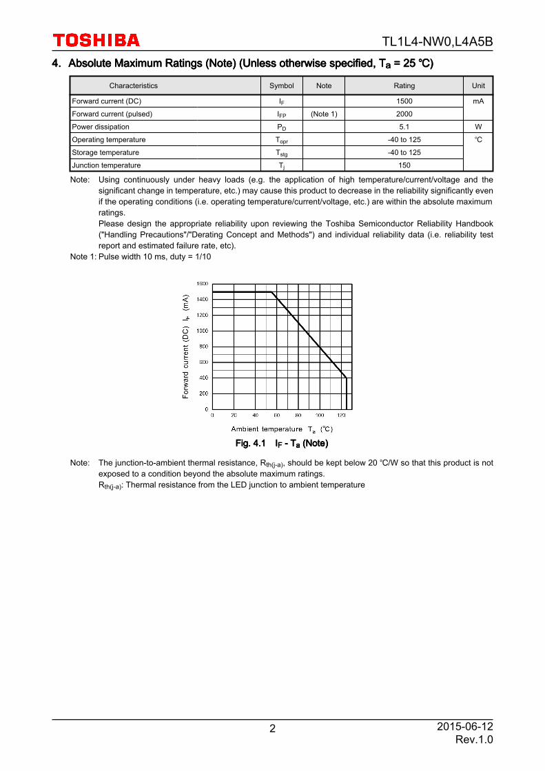
4. 4. 4. 4. Absolute Maximum Ratings (Note) (Unless otherwise specified, TAbsolute Maximum Ratings (Note) (Unless otherwise specified, TAbsolute Maximum Ratings (Note) (Unless otherwise specified, TAbsolute Maximum Ratings (Note) (Unless otherwise specified, Taaaa = 25 = 25 = 25 = 25 ))))
Characteristics
Forward current (DC)
Forward current (pulsed)
Power dissipation
Operating temperature
Storage temperature
Junction temperature
Symbol
IFIFP
PD
Topr
Tstg
Tj
Note
(Note 1)
Rating
1500
2000
5.1
-40 to 125
-40 to 125
150
Unit
mA
W
Note: Using continuously under heavy loads (e.g. the application of high temperature/current/voltage and thesignificant change in temperature, etc.) may cause this product to decrease in the reliability significantly evenif the operating conditions (i.e. operating temperature/current/voltage, etc.) are within the absolute maximumratings.Please design the appropriate reliability upon reviewing the Toshiba Semiconductor Reliability Handbook("Handling Precautions"/"Derating Concept and Methods") and individual reliability data (i.e. reliability testreport and estimated failure rate, etc).
Note 1: Pulse width 10 ms, duty = 1/10
Fig. Fig. Fig. Fig. 4.14.14.14.1 IIIIFFFF - T - T - T - Taaaa (Note) (Note) (Note) (Note)
Note: The junction-to-ambient thermal resistance, Rth(j-a), should be kept below 20 /W so that this product is notexposed to a condition beyond the absolute maximum ratings. Rth(j-a): Thermal resistance from the LED junction to ambient temperature
2015-06-12Rev.1.0
TL1L4-NW0,L4A5B
3
5. 5. 5. 5. Handling PrecautionsHandling PrecautionsHandling PrecautionsHandling Precautions• This product is sensitive to electrostatic and care must be fully taken when handling products. Particularly
in the case that an overvoltage shall be applied, the overflowed energy may cause damage to or possiblyresult in destruction of the product. Users shall take absolutely secure countermeasures againstelectrostatic and surge when handling the product.
• A damage to the device might create a tiny leakage path, which causes the LED lamp not to light up in thelow-current region or causes a drop in the VF rise voltage.Failure criterion: IF ≥ 0.5 mA @ VF = 2 V
• If multiple LEDs are connected in parallel, they will experience variations in the forward current due tothe characteristics differences in forward voltage. Ensure that the forward current of all the LEDs fallwithin the intended range of the system design, for example, by inserting current-limiting resistors to eachLED string.
• Since this product is intended to be used for display lighting, the measurement standard is based on thespectral sensitivity of the human eye. It is not intended to be used for any applications other than displaylighting (e.g., sensors and light communications systems.)
• Generally, GaN-based LEDs exhibit instability or significant device-to-device variations in the relativeluminous flux in the low-current region. To avoid these problems, an application system should bedesigned in such a manner that the GaN-based LEDs are driven with a forward current of 10 mA orhigher.
• This device should not be reverse-biased.• When the device is used in places that are likely to be exposed to condensation, salt or corrosive gas, the
effect on its performance and reliability must be thoroughly verified. Gases produced from the materials ofluminaires might affect the LED characteristics. To avoid any problem, appropriate materials should beselected and verified empirically that they do not have any adverse effect.
• Volatile organic compounds (VOCs) can be generated from adhesives, hardeners, packing, solder flux andetc. used in luminaires (fixtures). The LED encapsulant may be permeable to those chemicals. if VOCs areexposed to heat or light in hermetically sealed conditions, the inside or the surface of the LED packagemay be discolored over time, causing a loss of light output from the luminaires. When the LED is used inhermetically sealed conditions, it should be verified empirically that the LED will not be affected adverselyby any VOCs.Also the LED may be subject to discoloration when it is even temporarily placed in an environment inwhich VOCs are absorbed into its encapsulant. So it is advisable to rinse the PC board before attaching itonto the luminaires.
• Please note the handling of products during evaluation.(1) Please do not apply pressure to the upper surface of the product with finger, tweezers, and others. Failure of product to light up may occur due to package deformation, wire deformation and/or disconnection. (2) Should tweezers be used in product handling, one with flat surfaces is recommended. (3) Please handle the product widthwise. (4) Please do not drop the product. There is a possibility for package transformation etc. to occur when the product is dropped. (5) Please do not stack the printed circuit boards on which the product is mounted to prevent damages to product surface. Also, please note not to damage the surface of the product with cushioning material etc. Surface damage to the product may influence their optical characteristics.(6) Solder, flux, paper or heat-sensitive materials that might be deformed or discolored at high temperatures should not be left on the surface of an LED lamp.
• Extreme care should be exercised when using this device for high-power applications:(1) Do not directly touch this device during active operation because it becomes hot, depending on the operating power.(2) Take a possible rise in ambient temperature around this device and the heat-resistant temperature of the system components into consideration.
2015-06-12Rev.1.0
TL1L4-NW0,L4A5B
4
6. 6. 6. 6. Electrical Characteristics Electrical Characteristics Electrical Characteristics Electrical Characteristics
Characteristics
Forward voltage(Hot Binning)
Thermal resistance(junction-to-soldering point)
See Table 6.1.
Symbol
VF(HB)
Rth(j-s)
Note
(Note 1 )
Test Condition
IF = 350 mA, Tj = 85
IF = 350 mA, Ta = 25
Min
2.6
Typ.
2.8
5
Max
3.2
Unit
V
/W
Note 1 :Rth(j-s): Thermal resistance from the LED junction to solder point.
Table Table Table Table 6.16.16.16.1 Forward Voltage (Hot Binning) Rank (Note)Forward Voltage (Hot Binning) Rank (Note)Forward Voltage (Hot Binning) Rank (Note)Forward Voltage (Hot Binning) Rank (Note)
Rank
1
2
3
Test Condition
IF = 350 mA, Tj = 85 , Tolerance ±0.1 V
Forward Voltage(Min)
2.6
2.8
3.0
Forward Voltage(Max)
2.8
3.0
3.2
Unit
V
Note: This LED lamp is sorted into forward voltage (VF) ranks shown above. Each reel includes the same rank LEDs.Let the delivery ratio of each rank be unquestioned.
7. 7. 7. 7. Optical Characteristics Optical Characteristics Optical Characteristics Optical Characteristics
Characteristics
Luminous flux
Luminous flux(Hot Binning)
Chromaticity(Hot Binning)
Chromaticity(Hot Binning)
Color temperature(Hot Binning)
Color rendering index(Hot Binning)
Half-intensity angle
Symbol
φV
φV(HB)
Cx(HB)
Cy(HB)
CCT(HB)
Ra(HB)
2θ1/2
Note
(Note 1)
(Note 2)
(Note 3)
Test Condition
IF = 350 mA, Ta = 25
IF = 350 mA, Tj = 85
IF = 350 mA, Ta = 25
Min
140
See Fig.
70
Typ.
165
7.1, Table
5000
120
Max
160
7.1.
Unit
lm
K
°
Note 1: Luminous flux value(IF = 350 mA, Ta = 25 ) is presented for reference only.Note 2: See Table 7.2 for luminous flux rank.Note 3: Tolerance: ±2
2015-06-12Rev.1.0

TL1L4-NW0,L4A5B
5
Fig. Fig. Fig. Fig. 7.17.17.17.1 Chromaticity (Hot Binning) Rank (Note)Chromaticity (Hot Binning) Rank (Note)Chromaticity (Hot Binning) Rank (Note)Chromaticity (Hot Binning) Rank (Note)
Note: Test conditions: IF = 350 mA, Tj = 85 , Tolerance: ±0.01
2015-06-12Rev.1.0

TL1L4-NW0,L4A5B
6
Table Table Table Table 7.17.17.17.1 Chromaticity (Hot Binning) Rank (Note)Chromaticity (Hot Binning) Rank (Note)Chromaticity (Hot Binning) Rank (Note)Chromaticity (Hot Binning) Rank (Note)
Rank
3A1
3A2
3A3
3A4
3B1
3B2
3B3
3B4
Cx
0.3366
0.3369
0.3407
0.3403
0.3369
0.3371
0.3411
0.3407
0.3407
0.3411
0.3451
0.3446
0.3403
0.3407
0.3446
0.3440
0.3371
0.3374
0.3415
0.3411
0.3374
0.3376
0.3419
0.3415
0.3415
0.3419
0.3463
0.3457
0.3411
0.3415
0.3457
0.3451
Cy
0.3369
0.3430
0.3460
0.3398
0.3430
0.3490
0.3522
0.3460
0.3460
0.3522
0.3554
0.3491
0.3398
0.3460
0.3491
0.3427
0.3490
0.3553
0.3587
0.3522
0.3553
0.3616
0.3651
0.3587
0.3587
0.3651
0.3687
0.3621
0.3522
0.3587
0.3621
0.3554
Rank
3C1
3C2
3C3
3C4
3D1
3D2
3D3
3D4
Cx
0.3451
0.3457
0.3500
0.3492
0.3457
0.3463
0.3507
0.3500
0.3500
0.3507
0.3551
0.3542
0.3492
0.3500
0.3542
0.3533
0.3440
0.3446
0.3485
0.3477
0.3446
0.3451
0.3492
0.3485
0.3485
0.3492
0.3533
0.3524
0.3477
0.3485
0.3524
0.3515
Cy
0.3554
0.3621
0.3656
0.3589
0.3621
0.3687
0.3724
0.3656
0.3656
0.3724
0.3760
0.3690
0.3588
0.3656
0.3690
0.3620
0.3427
0.3491
0.3522
0.3455
0.3491
0.3554
0.3588
0.3522
0.3522
0.3588
0.3620
0.3554
0.3455
0.3522
0.3554
0.3487
Note: This LED lamp is sorted into chromaticity coordinate groups shown above. Each reel includes the same rankLEDs. Let the delivery ratio of each rank be unquestioned.
2015-06-12Rev.1.0

TL1L4-NW0,L4A5B
7
Table Table Table Table 7.27.27.27.2 Luminous Flux (Hot Binning) Rank (Note)Luminous Flux (Hot Binning) Rank (Note)Luminous Flux (Hot Binning) Rank (Note)Luminous Flux (Hot Binning) Rank (Note)
Rank
B14A
B14B
B15A
B15B
Test Condition
IF = 350 mA, Tj = 85 , Tolerance ±10 %
Luminous Flux (Min)
140
145
150
155
Luminous Flux (Max)
145
150
155
160
Unit
lm
Note: This LED lamp is sorted into luminous flux ranks shown above. Each reel includes the same rank LEDs. Letthe delivery ratio of each rank be unquestioned.
Rank notations: The luminous flux, chromaticity and VF ranks are printed on labels as shown below:
Example: 3A1 B14A 23A1: Chromaticity rankB14A: Luminous flux rank2: VF rank
2015-06-12Rev.1.0

TL1L4-NW0,L4A5B
8
8. 8. 8. 8. Characteristics Curves (Note)Characteristics Curves (Note)Characteristics Curves (Note)Characteristics Curves (Note)
Fig. Fig. Fig. Fig. 8.18.18.18.1 IIIIFFFF - V - V - V - VFFFF Fig. Fig. Fig. Fig. 8.28.28.28.2 Relative Luminous Flux - IRelative Luminous Flux - IRelative Luminous Flux - IRelative Luminous Flux - IFFFF
Fig. Fig. Fig. Fig. 8.38.38.38.3 Relative Luminous Flux - TRelative Luminous Flux - TRelative Luminous Flux - TRelative Luminous Flux - Tjjjj Fig. Fig. Fig. Fig. 8.48.48.48.4 VVVVFFFF - T - T - T - Tjjjj
Fig. Fig. Fig. Fig. 8.58.58.58.5 Chromaticity - IChromaticity - IChromaticity - IChromaticity - IFFFF Fig. Fig. Fig. Fig. 8.68.68.68.6 Chromaticity - TChromaticity - TChromaticity - TChromaticity - Tjjjj
2015-06-12Rev.1.0

TL1L4-NW0,L4A5B
9
Fig. Fig. Fig. Fig. 8.78.78.78.7 Wavelength CharacteristicWavelength CharacteristicWavelength CharacteristicWavelength Characteristic Fig. Fig. Fig. Fig. 8.88.88.88.8 Radiation PatternRadiation PatternRadiation PatternRadiation Pattern
Note: The above characteristics curves are presented for reference only and not guaranteed by production test,unless otherwise noted.
2015-06-12Rev.1.0

TL1L4-NW0,L4A5B
10
9. 9. 9. 9. PackingPackingPackingPacking
9.1. 9.1. 9.1. 9.1. Moisture-Proof PackingMoisture-Proof PackingMoisture-Proof PackingMoisture-Proof PackingThese LED devices are packed in an aluminum envelope with a silica gel and a moisture indicator to avoidmoisture absorption. The optical characteristics of the device may be affected by exposure to moisture in the airbefore soldering and the device should therefore be stored under the following conditions:• This moisture proof bag may be stored unopened within 12 months at the following conditions.
Temperature: 5 to 30 Humidity: 90 % (max)
• After opening the moisture proof bag, the device should be assembled within 4 weeks in an environment of5 to 30 /60 % RH or below.
• If upon opening, the moisture indicator card shows humidity 30 % or above (Color of indication changes topink) or the expiration date has passed, the device should be baked in taping with reel.After baking, use the baked device within 72 hours, but perform baking only once.Baking conditions: 60 ± 5 , for 12 to 24 hours.Expiration date: 12 months from sealing date, which is imprinted on the label affixed.
• Repeated baking can cause the peeling strength of the taping to change, then leads to trouble in mounting.Furthermore, prevent the devices from being destructed against static electricity for baking of it.
• If the packing material of laminate would be broken, the hermeticity would deteriorate. Therefore, do notthrow or drop the packed devices.
10. 10. 10. 10. MountingMountingMountingMounting
10.1. 10.1. 10.1. 10.1. Mounting PrecautionsMounting PrecautionsMounting PrecautionsMounting Precautions• Do not apply mechanical stress to the resin body at high temperature.
The time taken for a device to return to the room temperature after reflow soldering depends on themounting board and environmental conditions.
• The resin body is easily scratched. Avoid friction against hard materials.• When installing an assembled board into equipment, ensure that the devices on the board do not contact
with other components.
2015-06-12Rev.1.0

TL1L4-NW0,L4A5B
11
10.2. 10.2. 10.2. 10.2. SolderingSolderingSolderingSolderingFollowing show examples of reflow soldering.• Temperature Profile (see following figures.)
Fig. Fig. Fig. Fig. 10.2.110.2.110.2.110.2.1 Temperature Profile forTemperature Profile forTemperature Profile forTemperature Profile for Lead(Pb)-free Soldering (example) Lead(Pb)-free Soldering (example) Lead(Pb)-free Soldering (example) Lead(Pb)-free Soldering (example)
Table 10.2.1 Temperature Profile forTable 10.2.1 Temperature Profile forTable 10.2.1 Temperature Profile forTable 10.2.1 Temperature Profile for Lead(Pb)-free Soldering (example) Lead(Pb)-free Soldering (example) Lead(Pb)-free Soldering (example) Lead(Pb)-free Soldering (example)
• The product is evaluated using above reflow soldering conditions. No additional test is performed exceedthe condition as a evaluation. Please perform reflow soldering under the above conditions.
• Please perform the first reflow soldering with reference to the above temperature profile and within 4weeks of opening the package.
• If a second reflow process is necessary, reflow soldering should be performed within 168 h of the firstreflow under the above conditions. Storage conditions before the second reflow soldering: 30 , 60 % RH(max)
• Do not perform wave soldering.• When any soldering corrections are made manually, a hot-plate should be used.
(only once at each soldering point)
10.3. 10.3. 10.3. 10.3. Land Pattern Dimensions (for reference only)Land Pattern Dimensions (for reference only)Land Pattern Dimensions (for reference only)Land Pattern Dimensions (for reference only)Heatsink pin of this product is the same electric potential as anode electrode. Please do not connect to otherelectrical potentials or GND.
(Unit: mm)(Unit: mm)(Unit: mm)(Unit: mm)
2015-06-12Rev.1.0

TL1L4-NW0,L4A5B
12
11. 11. 11. 11. CleaningCleaningCleaningCleaning Flux cleaning should be completed free of residual reactive ion such as Na, Cl, etc. Organic solvent acts upon water and generates corrosive gas such as hydrogen chloride. There are some cases where the device is degraded. Effective solvent seriously affects package and resin, and may cause inferior device. In actually using it, please sufficiently check whether there is nothing inferior on the device. Ultrasonic cleaning that provides effective cleaning for short time much affects on the device. so coherence between resin and lead metal is degraded by cleaning solvent during long ultrasonic cleaning. We recommend to take ultrasonic cleaning for the device at a minimum range. The influences on a device is occurred by the output of an ultrasonic wave and set board, please sufficiently check whether there is nothing inferior on the device.
12. 12. 12. 12. Tape SpecificationsTape SpecificationsTape SpecificationsTape Specifications
12.1. 12.1. 12.1. 12.1. Product Naming ConventionsProduct Naming ConventionsProduct Naming ConventionsProduct Naming ConventionsThe type of package used for shipment is denoted by a symbol suffix after the part number. The method ofclassification is as below. (this method, however does not apply to products whose electrical characteristics differfrom standard Toshiba specifications)
Example: TL1L4-NW0,L Toshiba part number: TL1L4-NW0 Packing type: L (Taping)
12.2. 12.2. 12.2. 12.2. Handling PrecautionsHandling PrecautionsHandling PrecautionsHandling Precautions(1) The tape is antistatic-coated. However, if the tape is charged with excess static electricity, devices might
cling to the tape or waggle in the tape when the cover tape peeled off. Be aware of the following to avoidthis: Use an ionizer to neutralize the ions when utilizing an automatic mounter. For transport and temporary storage of devices, use containers (boxes, jigs, bags) that are made with antistatic materials or materials that dissipate static electricity.
12.3. 12.3. 12.3. 12.3. Tape DimensionsTape DimensionsTape DimensionsTape DimensionsTable Table Table Table 12.3.112.3.112.3.112.3.1 Tape Dimensions (Unit: mm)Tape Dimensions (Unit: mm)Tape Dimensions (Unit: mm)Tape Dimensions (Unit: mm)
Dimensions
Tolerance
D
1.5
+0.1/-0
E
1.75
±0.1
P0
4.0
±0.1
t
0.3
±0.05
F
5.5
±0.05
D1
1.7
±0.1
P2
2.0
±0.05
W
12.0
±0.2
P
8.0
±0.1
A0
3.8
±0.1
B0
3.8
±0.1
K0
2.15
±0.1
2015-06-12Rev.1.0

TL1L4-NW0,L4A5B
13
12.4. 12.4. 12.4. 12.4. Reel SpecificationReel SpecificationReel SpecificationReel Specification
12.4.1. 12.4.1. 12.4.1. 12.4.1. Reel DimensionsReel DimensionsReel DimensionsReel Dimensions
12.4.2. 12.4.2. 12.4.2. 12.4.2. Tape Leader and TrailerTape Leader and TrailerTape Leader and TrailerTape Leader and Trailer
2015-06-12Rev.1.0

TL1L4-NW0,L4A5B
14
12.5. 12.5. 12.5. 12.5. Packing FormPacking FormPacking FormPacking FormEach reel is sealed in an aluminum pack with silica gel. Packing quantity is as shown below.• Reel: 1,000 pcs• Carton: 4,000 pcs (max)• Sealed aluminum pack with silica gel
12.6. 12.6. 12.6. 12.6. Label FormatLabel FormatLabel FormatLabel FormatLabel example for TL1L4-NW0,L4A5B and label location are as shown below.
12.6.1. 12.6.1. 12.6.1. 12.6.1. Label ExampleLabel ExampleLabel ExampleLabel Example
12.6.2. 12.6.2. 12.6.2. 12.6.2. Label DetailsLabel DetailsLabel DetailsLabel Details
No. (# refer to the abovelabel example)
(1)
(2)
(3)
(4)
(5)
(6)
(7)
(8)
Information for Toshiba Use
Part No.
ADD code (Note)
Lot code
Rank symbol
Storage condition after opening
Packing quantity
Key code
Country of origin
Remarks
TL1L4-NW0,L4A5B
Example: (O
Example: 270xxxxx
Example: 3A1B14A2
Use under 5 - 30 /60 %RH within 4 weeks
Example: 1,000 pcs
Example: 12345
Example: JAPAN
Note: ADD code Naming Conventions(O : Assembled in Japan, Sales for domestic and overseas customers(J : Assembled in overseas factory, Sales for domestic customers(T : Assembled in overseas factory, Sales for overseas customers
12.6.3. 12.6.3. 12.6.3. 12.6.3. Label LocationLabel LocationLabel LocationLabel Location
Fig. Fig. Fig. Fig. 12.6.3.112.6.3.112.6.3.112.6.3.1 Label Position on the ReelLabel Position on the ReelLabel Position on the ReelLabel Position on the Reel Fig. Fig. Fig. Fig. 12.6.3.212.6.3.212.6.3.212.6.3.2 Label Position on the CartonLabel Position on the CartonLabel Position on the CartonLabel Position on the Carton
Aluminum pack : The aluminum pack in which the reel is supplied also has the label attached to center of one side.
2015-06-12Rev.1.0

TL1L4-NW0,L4A5B
15
13. 13. 13. 13. Internal CircuitInternal CircuitInternal CircuitInternal Circuit
1: Anode2: Cathode
Package DimensionsPackage DimensionsPackage DimensionsPackage DimensionsUnit: mm
Weight: 0.04 g (typ.)
Package Name(s)
TOSHIBA: 4-4P1A
2015-06-12Rev.1.0

TL1L4-NW0,L4A5B
16
RESTRICTIONS ON PRODUCT USERESTRICTIONS ON PRODUCT USERESTRICTIONS ON PRODUCT USERESTRICTIONS ON PRODUCT USE• Toshiba Corporation, and its subsidiaries and affiliates (collectively "TOSHIBA"), reserve the right to make changes to the information
in this document, and related hardware, software and systems (collectively "Product") without notice.
• This document and any information herein may not be reproduced without prior written permission from TOSHIBA. Even with TOSHIBA'swritten permission, reproduction is permissible only if reproduction is without alteration/omission.
• Though TOSHIBA works continually to improve Product's quality and reliability, Product can malfunction or fail. Customers are responsiblefor complying with safety standards and for providing adequate designs and safeguards for their hardware, software and systems whichminimize risk and avoid situations in which a malfunction or failure of Product could cause loss of human life, bodily injury or damageto property, including data loss or corruption. Before customers use the Product, create designs including the Product, or incorporatethe Product into their own applications, customers must also refer to and comply with (a) the latest versions of all relevant TOSHIBAinformation, including without limitation, this document, the specifications, the data sheets and application notes for Product and theprecautions and conditions set forth in the "TOSHIBA Semiconductor Reliability Handbook" and (b) the instructions for the applicationwith which the Product will be used with or for. Customers are solely responsible for all aspects of their own product design or applications,including but not limited to (a) determining the appropriateness of the use of this Product in such design or applications; (b) evaluatingand determining the applicability of any information contained in this document, or in charts, diagrams, programs, algorithms, sampleapplication circuits, or any other referenced documents; and (c) validating all operating parameters for such designs and applications. TOSHIBA ASSUMES NO LIABILITY FOR CUSTOMERS' PRODUCT DESIGN OR APPLICATIONS.TOSHIBA ASSUMES NO LIABILITY FOR CUSTOMERS' PRODUCT DESIGN OR APPLICATIONS.TOSHIBA ASSUMES NO LIABILITY FOR CUSTOMERS' PRODUCT DESIGN OR APPLICATIONS.TOSHIBA ASSUMES NO LIABILITY FOR CUSTOMERS' PRODUCT DESIGN OR APPLICATIONS.
• PRODUCT IS NEITHER INTENDED NOR WARRANTED FOR USE IN EQUIPMENTS OR SYSTEMS THAT REQUIREPRODUCT IS NEITHER INTENDED NOR WARRANTED FOR USE IN EQUIPMENTS OR SYSTEMS THAT REQUIREPRODUCT IS NEITHER INTENDED NOR WARRANTED FOR USE IN EQUIPMENTS OR SYSTEMS THAT REQUIREPRODUCT IS NEITHER INTENDED NOR WARRANTED FOR USE IN EQUIPMENTS OR SYSTEMS THAT REQUIREEXTRAORDINARILY HIGH LEVELS OF QUALITY AND/OR RELIABILITY, AND/OR A MALFUNCTION OR FAILURE OF WHICH MAYEXTRAORDINARILY HIGH LEVELS OF QUALITY AND/OR RELIABILITY, AND/OR A MALFUNCTION OR FAILURE OF WHICH MAYEXTRAORDINARILY HIGH LEVELS OF QUALITY AND/OR RELIABILITY, AND/OR A MALFUNCTION OR FAILURE OF WHICH MAYEXTRAORDINARILY HIGH LEVELS OF QUALITY AND/OR RELIABILITY, AND/OR A MALFUNCTION OR FAILURE OF WHICH MAYCAUSE LOSS OF HUMAN LIFE, BODILY INJURY, SERIOUS PROPERTY DAMAGE AND/OR SERIOUS PUBLIC IMPACTCAUSE LOSS OF HUMAN LIFE, BODILY INJURY, SERIOUS PROPERTY DAMAGE AND/OR SERIOUS PUBLIC IMPACTCAUSE LOSS OF HUMAN LIFE, BODILY INJURY, SERIOUS PROPERTY DAMAGE AND/OR SERIOUS PUBLIC IMPACTCAUSE LOSS OF HUMAN LIFE, BODILY INJURY, SERIOUS PROPERTY DAMAGE AND/OR SERIOUS PUBLIC IMPACT("UNINTENDED USE").("UNINTENDED USE").("UNINTENDED USE").("UNINTENDED USE"). Except for specific applications as expressly stated in this document, Unintended Use includes, without limitation,equipment used in nuclear facilities, equipment used in the aerospace industry, medical equipment, equipment used for automobiles,trains, ships and other transportation, traffic signaling equipment, equipment used to control combustions or explosions, safety devices,elevators and escalators, devices related to electric power, and equipment used in finance-related fields. IF YOU USE PRODUCT FORIF YOU USE PRODUCT FORIF YOU USE PRODUCT FORIF YOU USE PRODUCT FORUNINTENDED USE, TOSHIBA ASSUMES NO LIABILITY FOR PRODUCT.UNINTENDED USE, TOSHIBA ASSUMES NO LIABILITY FOR PRODUCT.UNINTENDED USE, TOSHIBA ASSUMES NO LIABILITY FOR PRODUCT.UNINTENDED USE, TOSHIBA ASSUMES NO LIABILITY FOR PRODUCT. For details, please contact your TOSHIBA salesrepresentative.
• Do not disassemble, analyze, reverse-engineer, alter, modify, translate or copy Product, whether in whole or in part.
• Product shall not be used for or incorporated into any products or systems whose manufacture, use, or sale is prohibited under anyapplicable laws or regulations.
• The information contained herein is presented only as guidance for Product use. No responsibility is assumed by TOSHIBA for anyinfringement of patents or any other intellectual property rights of third parties that may result from the use of Product. No license to anyintellectual property right is granted by this document, whether express or implied, by estoppel or otherwise.
• ABSENT A WRITTEN SIGNED AGREEMENT, EXCEPT AS PROVIDED IN THE RELEVANT TERMS AND CONDITIONS OF SALEABSENT A WRITTEN SIGNED AGREEMENT, EXCEPT AS PROVIDED IN THE RELEVANT TERMS AND CONDITIONS OF SALEABSENT A WRITTEN SIGNED AGREEMENT, EXCEPT AS PROVIDED IN THE RELEVANT TERMS AND CONDITIONS OF SALEABSENT A WRITTEN SIGNED AGREEMENT, EXCEPT AS PROVIDED IN THE RELEVANT TERMS AND CONDITIONS OF SALEFOR PRODUCT, AND TO THE MAXIMUM EXTENT ALLOWABLE BY LAW, TOSHIBA (1) ASSUMES NO LIABILITY WHATSOEVER,FOR PRODUCT, AND TO THE MAXIMUM EXTENT ALLOWABLE BY LAW, TOSHIBA (1) ASSUMES NO LIABILITY WHATSOEVER,FOR PRODUCT, AND TO THE MAXIMUM EXTENT ALLOWABLE BY LAW, TOSHIBA (1) ASSUMES NO LIABILITY WHATSOEVER,FOR PRODUCT, AND TO THE MAXIMUM EXTENT ALLOWABLE BY LAW, TOSHIBA (1) ASSUMES NO LIABILITY WHATSOEVER,INCLUDING WITHOUT LIMITATION, INDIRECT, CONSEQUENTIAL, SPECIAL, OR INCIDENTAL DAMAGES OR LOSS, INCLUDINGINCLUDING WITHOUT LIMITATION, INDIRECT, CONSEQUENTIAL, SPECIAL, OR INCIDENTAL DAMAGES OR LOSS, INCLUDINGINCLUDING WITHOUT LIMITATION, INDIRECT, CONSEQUENTIAL, SPECIAL, OR INCIDENTAL DAMAGES OR LOSS, INCLUDINGINCLUDING WITHOUT LIMITATION, INDIRECT, CONSEQUENTIAL, SPECIAL, OR INCIDENTAL DAMAGES OR LOSS, INCLUDINGWITHOUT LIMITATION, LOSS OF PROFITS, LOSS OF OPPORTUNITIES, BUSINESS INTERRUPTION AND LOSS OF DATA, ANDWITHOUT LIMITATION, LOSS OF PROFITS, LOSS OF OPPORTUNITIES, BUSINESS INTERRUPTION AND LOSS OF DATA, ANDWITHOUT LIMITATION, LOSS OF PROFITS, LOSS OF OPPORTUNITIES, BUSINESS INTERRUPTION AND LOSS OF DATA, ANDWITHOUT LIMITATION, LOSS OF PROFITS, LOSS OF OPPORTUNITIES, BUSINESS INTERRUPTION AND LOSS OF DATA, AND(2) DISCLAIMS ANY AND ALL EXPRESS OR IMPLIED WARRANTIES AND CONDITIONS RELATED TO SALE, USE OF PRODUCT,(2) DISCLAIMS ANY AND ALL EXPRESS OR IMPLIED WARRANTIES AND CONDITIONS RELATED TO SALE, USE OF PRODUCT,(2) DISCLAIMS ANY AND ALL EXPRESS OR IMPLIED WARRANTIES AND CONDITIONS RELATED TO SALE, USE OF PRODUCT,(2) DISCLAIMS ANY AND ALL EXPRESS OR IMPLIED WARRANTIES AND CONDITIONS RELATED TO SALE, USE OF PRODUCT,OR INFORMATION, INCLUDING WARRANTIES OR CONDITIONS OF MERCHANTABILITY, FITNESS FOR A PARTICULAROR INFORMATION, INCLUDING WARRANTIES OR CONDITIONS OF MERCHANTABILITY, FITNESS FOR A PARTICULAROR INFORMATION, INCLUDING WARRANTIES OR CONDITIONS OF MERCHANTABILITY, FITNESS FOR A PARTICULAROR INFORMATION, INCLUDING WARRANTIES OR CONDITIONS OF MERCHANTABILITY, FITNESS FOR A PARTICULARPURPOSE, ACCURACY OF INFORMATION, OR NONINFRINGEMENT.PURPOSE, ACCURACY OF INFORMATION, OR NONINFRINGEMENT.PURPOSE, ACCURACY OF INFORMATION, OR NONINFRINGEMENT.PURPOSE, ACCURACY OF INFORMATION, OR NONINFRINGEMENT.
• Do not use or otherwise make available Product or related software or technology for any military purposes, including without limitation,for the design, development, use, stockpiling or manufacturing of nuclear, chemical, or biological weapons or missile technology products(mass destruction weapons). Product and related software and technology may be controlled under the applicable export laws andregulations including, without limitation, the Japanese Foreign Exchange and Foreign Trade Law and the U.S. Export AdministrationRegulations. Export and re-export of Product or related software or technology are strictly prohibited except in compliance with allapplicable export laws and regulations.
• Please contact your TOSHIBA sales representative for details as to environmental matters such as the RoHS compatibility of Product.Please use Product in compliance with all applicable laws and regulations that regulate the inclusion or use of controlled substances,including without limitation, the EU RoHS Directive. TOSHIBA ASSUMES NO LIABILITY FOR DAMAGES OR LOSSES OCCURRING TOSHIBA ASSUMES NO LIABILITY FOR DAMAGES OR LOSSES OCCURRING TOSHIBA ASSUMES NO LIABILITY FOR DAMAGES OR LOSSES OCCURRING TOSHIBA ASSUMES NO LIABILITY FOR DAMAGES OR LOSSES OCCURRINGAS A RESULT OF NONCOMPLIANCE WITH APPLICABLE LAWS AND REGULATIONS.AS A RESULT OF NONCOMPLIANCE WITH APPLICABLE LAWS AND REGULATIONS.AS A RESULT OF NONCOMPLIANCE WITH APPLICABLE LAWS AND REGULATIONS.AS A RESULT OF NONCOMPLIANCE WITH APPLICABLE LAWS AND REGULATIONS.
2015-06-12Rev.1.0