
Title Scalability of Quasi-hysteretic FSM-based Digitally Controlled ...
29
Title Scalability of Quasi-hysteretic FSM-based Digitally Controlled Single-inductor Dual-string Buck LED Driver To Multiple Strings Author(s) Lee, ATL; Sin, JKO; Chan, PCH Citation IEEE Transactions on Power Electronics, 2014, v. 29 n. 1, p. 501- 513 Issued Date 2014 URL http://hdl.handle.net/10722/215297 Rights IEEE Transactions on Power Electronics. Copyright © Institute of Electrical and Electronics Engineers.; ©2014 IEEE. Personal use of this material is permitted. Permission from IEEE must be obtained for all other uses, in any current or future media, including reprinting/republishing this material for advertising or promotional purposes, creating new collective works, for resale or redistribution to servers or lists, or reuse of any copyrighted component of this work in other works.; This work is licensed under a Creative Commons Attribution-NonCommercial- NoDerivatives 4.0 International License.
Transcript of Title Scalability of Quasi-hysteretic FSM-based Digitally Controlled ...

Title Scalability of Quasi-hysteretic FSM-based Digitally ControlledSingle-inductor Dual-string Buck LED Driver To Multiple Strings
Author(s) Lee, ATL; Sin, JKO; Chan, PCH
Citation IEEE Transactions on Power Electronics, 2014, v. 29 n. 1, p. 501-513
Issued Date 2014
URL http://hdl.handle.net/10722/215297
Rights
IEEE Transactions on Power Electronics. Copyright © Instituteof Electrical and Electronics Engineers.; ©2014 IEEE. Personaluse of this material is permitted. Permission from IEEE must beobtained for all other uses, in any current or future media,including reprinting/republishing this material for advertising orpromotional purposes, creating new collective works, for resaleor redistribution to servers or lists, or reuse of any copyrightedcomponent of this work in other works.; This work is licensedunder a Creative Commons Attribution-NonCommercial-NoDerivatives 4.0 International License.
IEEE
Proo
f
IEEE TRANSACTIONS ON POWER ELECTRONICS 1
Scalability of Quasi-Hysteretic FSM-Based DigitallyControlled Single-Inductor Dual-String Buck LED
Driver to Multiple Strings
1
2
3
Albert T. L. Lee, Johnny K. O. Sin, Fellow, IEEE, and Philip C. H. Chan, Fellow, IEEE4
Abstract—There has been growing interest in single-inductor5multiple-output (SIMO) dc–dc converters due to its reduced cost6and smaller form factor in comparison with using multiple single-7output converters. An application for such a SIMO-based switch-8ing converter is to drive multiple LED strings in a multichannel9LED display. This paper proposes a quasi-hysteretic finite-state-10machine-based digitally controlled single-inductor dual-output11buck switching LED driver operating in discontinuous conduction12mode (DCM) and extends it to drive multiple outputs. Based on13the time-multiplexing control scheme in DCM, a theoretical upper14limit of the total number of outputs in a SIMO buck switching LED15driver for various backlight LED current values can be derived16analytically. The advantages of the proposed SIMO LED driver17include reducing the controller design complexity by eliminating18loop compensation, driving more LED strings without limited by19the maximum LED current rating, performing digital dimming20with no additional switches required, and optimization of local bus21voltage to compensate for variability of LED forward voltage VF22in each individual LED string with smaller power loss. Loosely23binned LEDs with larger VF variation can, therefore, be used for24reduced LED costs.25
Index Terms—Boundary conduction mode (BCM), discontinu-26ous conduction mode (DCM), finite-state machine (FSM), single-27inductor dual-output (SIDO), single-inductor multiple-output28(SIMO).29
I. INTRODUCTION30
AN LED driver is essentially a current source (or sink)31
which maintains a constant current required for achieving32
the desired color and luminous flux from an array of LEDs. A33
number of highly efficient switching LED drivers have been re-34
ported in the literature and their primary objective is to achieve35
high power conversion efficiency [1]–[11]. Besides efficiency,36
another important consideration is the scalability of the exist-37
ing single-inductor dual-output (SIDO) switching converter to38
drive multiple independent LED strings in a single-inductor39
multiple-output (SIMO) topology for reduced cost and smaller40
Manuscript received November 7, 2012; revised January 22, 2013; acceptedMarch 11, 2013. Recommended for publication by Associate Prof. J. M. Alonso.
A. T. L. Lee and J. K. O. Sin are with the Department of Electronic andComputer Engineering, The Hong Kong University of Science and Technology,Kowloon, Hong Kong (e-mail: [email protected]; [email protected]).
P. C. H. Chan is with Hong Kong Polytechnic University, Hong Kong (e-mail:[email protected]).
Color versions of one or more of the figures in this paper are available onlineat http://ieeexplore.ieee.org.
Digital Object Identifier 10.1109/TPEL.2013.2253804
form factor [12]. However, in practice, only a finite number of 41
outputs can be served by each LED driver. 42
The prior arts of SIMO switching converter use either one of 43
two ways to distribute energy from a single power supply to mul- 44
tiple outputs with a single inductor, namely multiple energizing 45
phases [13]–[20] and single energizing phase per switching cy- 46
cle [21]. The former with time-multiplexing control leads to 47
much better suppression of cross regulation because the out- 48
puts are decoupled in time. In this paper, a quasi-hysteretic 49
finite-state machine (FSM)-based digital control scheme is em- 50
ployed in a SIDO buck LED driver consisting of two inde- 51
pendent parallel strings operating in discontinuous conduction 52
mode (DCM). The extension of this SIDO architecture to SIMO 53
is formally investigated. The proposed SIMO-based switching 54
buck LED driver enables separate control of the three primary 55
colors (red, green, and blue), thereby offering more flexibility 56
for color mixing. The rest of this paper is organized as follows. 57
Section II introduces the proposed quasi-hysteretic FSM-based 58
digital controller for a SIDO switching buck LED driver oper- 59
ating in DCM. Section III provides a theoretical analysis on the 60
scalability of the proposed digital control scheme from SIDO 61
to SIMO and suggests a general formula for determining the 62
theoretical upper bound in the total number of outputs in SIMO. 63
Section IV shows Cadence Spectre simulation results that are 64
used to verify the theoretical model. Section V contains the ex- 65
perimental results for the proposed digitally controlled SIDO 66
buck LED driver. Section VI concludes our research effort. 67
II. QUASI-HYSTERETIC FSM-BASED DIGITAL CONTROL 68
FOR SIDO LED DRIVER 69
A SIDO switching converter with time-multiplexing control 70
scheme operating in DCM was first reported in [13]–[16]. With 71
such kind of time-multiplexing control scheme, a SIDO con- 72
verter can easily be extended to drive multiple outputs and it 73
exhibits negligible cross regulation in DCM. A SIMO parallel- 74
string LED driver operating in DCM has recently been re- 75
ported [12]. It uses an analog-based controller with dominant 76
pole compensation for stability, and time-multiplexing control in 77
DCM is employed to suppress cross regulation among the LED 78
strings. Unlike conventional pulse width modulation (PWM)- 79
based analog controllers, the proposed digital controller uti- 80
lizing quasi-hysteretic control does not require any compensa- 81
tion circuits because of its inherent stability [22]–[24], hence 82
simplifying the control loop design and reducing the com- 83
ponent count and cost. Quasi-hysteretic control offers a good 84
0885-8993/$31.00 © 2013 IEEE

IEEE
Proo
f
2 IEEE TRANSACTIONS ON POWER ELECTRONICS
Fig. 1. System architecture of the quasi-hysteretic FSM-based digitally con-trolled SIDO buck LED driver.
compromise between traditional fixed-frequency PWM control85
and pure hysteretic control with variable switching frequency.86
In the proposed design, an external clock is used to synchro-87
nize the buck LED driver which switches at a fixed frequency.88
Fast comparators are used to control the on-time of the high-89
side and low-side power switches by monitoring the inductor90
current. This is particularly suitable for lighting applications91
where variable switching frequencies are not desirable. The re-92
configurability and scalability of a digital controller makes it93
especially attractive for SIMO.94
A major drawback of the previously proposed SIMO LED95
driver operating in DCM [12] is that since the LED current is96
discontinuous, the LED endures a higher maximum peak current97
for the same average current required. In other words, the LED98
could potentially be operating close to its absolute maximum99
current rating, thereby increasing the current stress and possibly100
shortening the operating lifetime of the LED. In their approach,101
the LED current scales with the number of LED strings in SIMO.102
Hence, the maximum current rating of the LED unnecessarily103
restricts the maximum achievable number of LED strings which104
can be implemented in SIMO. In the proposed design, the LED105
current is always continuous and the LED can be regulated very106
close to the target average current value which is much lower107
than its maximum current rating. During the time interval when108
the output switch is OFF, the output capacitor, acting as a con-109
stant current source, continues to discharge its current to the110
corresponding LED string. When the output switch is ON, the111
power stage is reconnected to the LED string and the induc-112
tor current is transferred to the output capacitor and the LED113
string simultaneously. The current-sense feedback control en-114
sures that the LED current is maintained at the desired dc level.115
Hence, a time-continuous current is supplied to the LED string.116
Consequently, the LED current does not scale with the number117
of LED strings in the proposed SIMO architecture, making it118
possible to drive more LED strings without inducing too much119
stress on the LEDs. Fig. 1 shows the system architecture of the120
proposed quasi-hysteretic FSM-based digitally controlled SIDO121
buck switching LED driver which takes into account the para-122
sitic effects including the dc resistance (DCR) of the inductor L123
and equivalent series resistance (ESR) of the output capacitors 124
(Coa , Cob). The two independently driven LED strings share 125
the same inductor L and the two main power switches (S1 , S2) 126
of the buck converter. The output switches (Sa, Sb) enable the 127
charge stored in the inductor to be distributed between the two 128
outputs in a time-multiplexed fashion. Dead-time generators 129
are used to eliminate shoot-through current by ensuring that 130
S1 and S2 are not turned ON simultaneously. Dead-times are 131
also introduced between Sa and Sb to prevent inadvertent cross 132
conduction between the two LED strings. 133
Since an LED is essentially a current driven device, an LED 134
driver typically regulates the LED current rather than its forward 135
voltage. A straightforward way is to insert a small high-precision 136
current sensing resistor (Rcsa , Rcsb) in series with the corre- 137
sponding LED string to sense the LED current by converting it 138
to the current-sense voltage (Vcsa , Vcsb). The current-sense volt- 139
age is then compared with the reference voltage (Vrefa , Vrefb) to 140
generate the corresponding logic signals (outa_req, outb_req) 141
which determine the opening or closing of the two output 142
switches in a SIDO buck converter. Since the LED’s I–V curve 143
is usually provided by the LED manufacturer, the target dc cur- 144
rent value for a particular LED string can be set by choosing 145
an appropriate reference voltage. On the other hand, a two-limit 146
hysteretic control determines the on-time of the high-side and 147
low-side power switches (S1 , S2) of the buck converter. The 148
upper and lower limits of the inductor current, namely the peak 149
current limit and the valley current limit, define the average 150
value of the inductor current which is the total LED current for 151
a SIDO buck LED driver. In DCM, the valley current limit is 152
set to zero to prevent the inductor current from going negative 153
which degrades the power conversion efficiency [12], [16], [25]. 154
As illustrated in Fig. 1, Rf Cf is connected in parallel to the 155
inductor so that the slopes of VRC are proportional to the in- 156
ductor current ramp-up and ramp-down slopes [26]. A small 157
resistor ladder is connected between VRC and ground in order 158
to generate a lower voltage signal ViLsense which falls within 159
the input voltage range of the comparator (CMP). V0iLsense is 160
fed forward to the corresponding comparators to determine the 161
peak-crossing and zero-crossing of the inductor current. Fig. 2 162
is a simplified flowchart showing the system-level operation of 163
the proposed SIDO buck driver. Suppose identical current flows 164
through each of the two LED strings, also referred to as the 165
balanced load condition, the inductor current IL is assigned to 166
each string in alternate switching cycles. The working principle 167
of the proposed SIDO buck LED driver is represented by the 168
timing diagram shown in Fig. 3. During D1aTs or D1bTs, IL 169
ramps up with a slope of m1 = (Vg – Vo)/L and the inductor 170
is charged with a voltage of VL = Vg − Vo , where Vg and Vo 171
represent the input voltage and the output voltage, respectively. 172
During D2aTs or D2bTs, IL ramps down with a slope of m2 = 173
−Vo /L and the inductor discharges its current to the correspond- 174
ing output capacitor and the LED string until IL returns to zero. 175
During D3aTs or D3bTs, IL stays at zero with both S1 and S2 176
OFF. In the proposed SIDO LED driver, the system clock de- 177
fines the switching frequency. The rising edge of the system 178
clock triggers the ON duty cycle (D1aTs, D1bTs ) by charging 179
up the inductor during which S1 is ON and S2 is OFF. The 180

IEEE
Proo
f
LEE et al.: SCALABILITY OF QUASI-HYSTERETIC FSM-BASED DIGITALLY CONTROLLED SINGLE-INDUCTOR DUAL-STRING 3
Fig. 2. Simplified flowchart representing the system-level operation of theproposed SIDO buck LED driver.
Fig. 3. Timing diagram of the proposed SIDO buck LED driver with balancedload operating in DCM.
inductor current continues to increase until it hits the peak181
current limit at which point the buck converter enters182
(D2aTs,D2bTs) where S1 is OFF and S2 is ON. The induc-183
tor discharges its current to the corresponding output until the184
zero-crossing of the inductor current is detected. The converter185
then enters the idle phase (D3aTs , D3bTs ) during which both186
S1and S2 are OFF. The inductor current remains at zero until the187
next rising edge of the system clock arrives and the switching188
sequence repeats itself. The two output switches (Sa , Sb ) are189
controlled by the FSM as shown in Fig. 4.190
The state machine is triggered by the rising edge of the sys-191
tem clock (sysclk) so that the transitions of the output switches192
(Sa, Sb) are in sync with the system clock. The input signals193
of the state machine are the output enable signals (outa_en,194
outb_en) and the output request signals (outa_req, outb_req)195
which determine the switching sequence of the two outputs. The196
first LED string is always given a higher priority over the second197
one. For instance, if both strings request service simultaneously,198
i.e., outa_req = 1 and outb_req = 1, Sa is turned ON first and199
Sb remains OFF. Sb is turned ON only when outa_req = 0200
Fig. 4. State diagram of the proposed FSM for controlling the two outputswitches in SIDO buck LED driver.
Fig. 5. Simulated steady-state waveforms for the proposed SIDO buck LEDdriver operating in DCM.
and outb_req = 1. Sa and Sb must be nonoverlapping to avoid 201
undesirable cross conduction between the two LED strings. In 202
addition, an enable signal (out1en, out2en) is associated with 203
either of the two LED strings. It provides the option of shut- 204
ting down any or all of the LED strings, for example, in re- 205
sponse to an overcurrent fault condition. An overriding signal 206
can also be sent from the FSM to the hysteretic controller to 207
disable the high-side and low-side power switches accordingly. 208
The FSM-based controller can be modified quickly and conve- 209
niently to drive multiple LED strings in a SIMO configuration 210
by simply adding more states in the VHDL or Verilog code. 211
A mixed-signal macromodel of the proposed FSM-based digi- 212
tally controlled SIDO buck switching LED operating in DCM 213
is simulated in the time domain using Cadence Spectre [27]. 214
The FSM is modeled in Verilog RTL and the rest are modeled 215
as ideal circuit elements. The simulation model also incorpo- 216
rates parasitics such as DCR of the inductor L and ESR of the 217
output capacitors (Coa , Cob). For balanced load condition, the 218
current between the two LED strings is identical and each string 219
consists of two LEDs connected in series. First, the steady- 220
state performance is investigated. Fig. 5 contains the simulated 221
steady-state waveforms for the inductor current (IL ), the LED 222
current (ILEDa , ILEDb), and the four switches (S1 , S2 , Sa , Sb) 223
of the proposed SIDO buck LED driver operating in DCM. The 224
switching frequency is 156.25 kHz and the input voltage Vg is 225
15 V. The simulation results show that the LED current in either 226
IEEE
Proo
f
4 IEEE TRANSACTIONS ON POWER ELECTRONICS
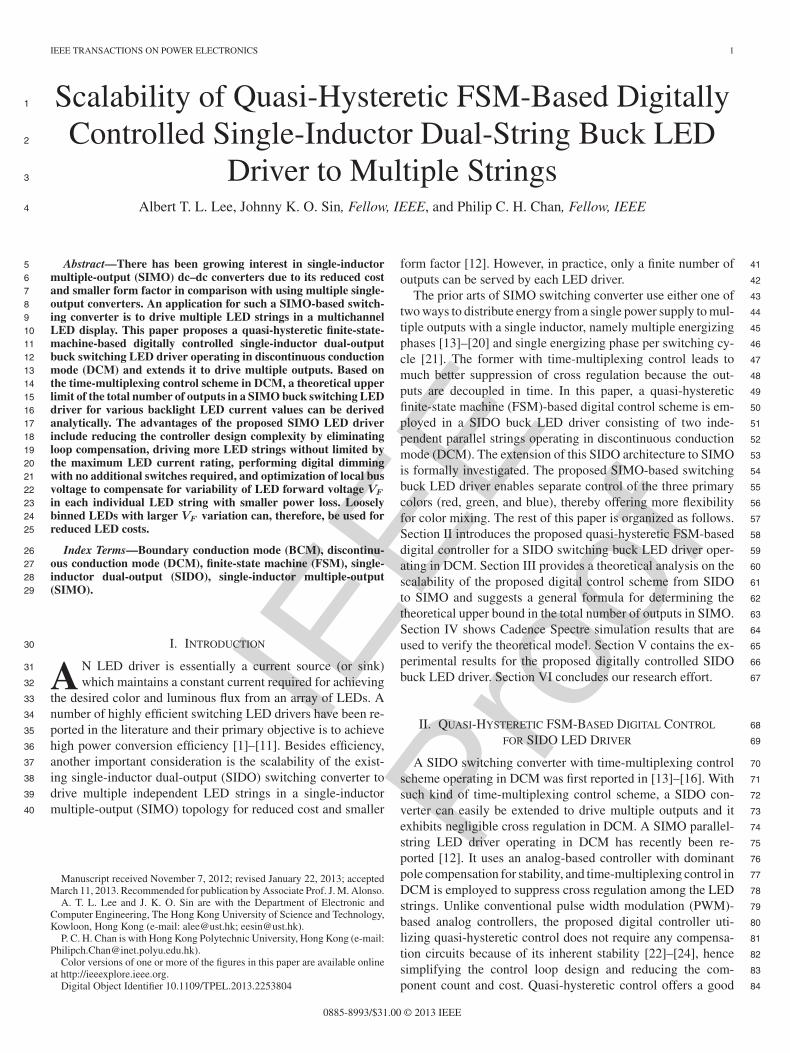
Fig. 6. First LED string remains under regulation without cross regulationwhen the second LED string is shut down completely.
Fig. 7. First LED string remains under regulation without cross regulationdespite a reference step in the second LED string from 100 to 50 mA in 20 ns.
of the two strings is regulated successfully to the target steady-227
state dc value of 100 mA with a current ripple of 23\%P-P .228
The steady-state output voltage for the first and second LED229
string is approximately 6.48 V with a voltage ripple of 2.6%P-P .230
Second, the stability of the closed-loop system is verified by231
examining its dynamic performance. In the first scenario, the232
second LED string needs to be shut down instantly in response233
to an over-current condition. Fig. 6 shows that despite the im-234
mediate shutdown of the second LED string, the LED current235
ILEDa in the first LED string continues to be regulated success-236
fully at its target nominal value of 100 mA with minimal cross237
regulation. In the second scenario, the second LED string expe-238
riences a reference step of 50 mA, i.e., ILEDb transitions from239
100 to 50 mA in 20 ns. Fig. 7 shows that the current in the first240
LED string continues to be regulated at around 100 mA, virtu-241
ally unaffected by the sudden reference step in the other string.242
The second LED string settles to the new nominal current value243
of 50 mA. It demonstrates that the closed-loop system remains244
stable in response to the reference transient in the second string.245
Unlike conventional backlight LED drivers that use PWM246
dimming transistor connected in series with the LED string [3],247
[8], [28]–[31], the proposed SIDO LED driver takes advantage248
of the existing four switches to perform dimming without re-249
quiring additional switches. When the dimming control signal250
for a particular LED string goes high, certain phases of the in-251
ductor current are skipped so that the average inductor current252
(also the average load current) going into that string is reduced253
accordingly. The digital dimming control signals (dim_ctrl1,254
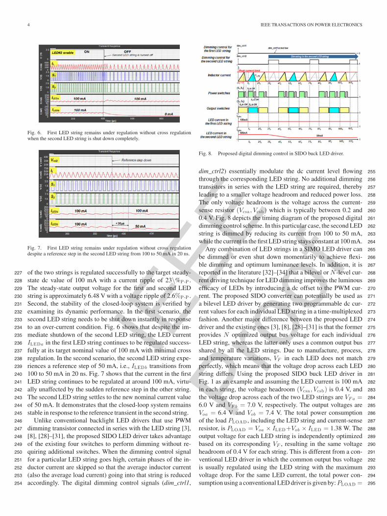
Fig. 8. Proposed digital dimming control in SIDO buck LED driver.
dim_ctrl2) essentially modulate the dc current level flowing 255
through the corresponding LED string. No additional dimming 256
transistors in series with the LED string are required, thereby 257
leading to a smaller voltage headroom and reduced power loss. 258
The only voltage headroom is the voltage across the current- 259
sense resistor (Vcsa , Vcsb) which is typically between 0.2 and 260
0.4 V. Fig. 8 depicts the timing diagram of the proposed digital 261
dimming control scheme. In this particular case, the second LED 262
string is dimmed by reducing its current from 100 to 50 mA, 263
while the current in the first LED string stays constant at 100 mA. 264
Any combination of LED strings in a SIMO LED driver can 265
be dimmed or even shut down momentarily to achieve flexi- 266
ble dimming and optimum luminance levels. In addition, it is 267
reported in the literature [32]–[34] that a bilevel or N -level cur- 268
rent driving technique for LED dimming improves the luminous 269
efficacy of LEDs by introducing a dc offset to the PWM cur- 270
rent. The proposed SIDO converter can potentially be used as 271
a bilevel LED driver by generating two programmable dc cur- 272
rent values for each individual LED string in a time-multiplexed 273
fashion. Another major difference between the proposed LED 274
driver and the existing ones [3], [8], [28]–[31] is that the former 275
provides N optimized output bus voltage for each individual 276
LED string, whereas the latter only uses a common output bus 277
shared by all the LED strings. Due to manufacture, process, 278
and temperature variations, VF in each LED does not match 279
perfectly, which means that the voltage drop across each LED 280
string differs. Using the proposed SIDO buck LED driver in 281
Fig. 1 as an example and assuming the LED current is 100 mA 282
in each string, the voltage headroom (Vcsa , Vcsb) is 0.4 V, and 283
the voltage drop across each of the two LED strings are VF a = 284
6.0 V and VF b = 7.0 V, respectively. The output voltages are 285
Voa = 6.4 V and Vob = 7.4 V. The total power consumption 286
of the load PLOAD , including the LED string and current-sense 287
resistor, is PLOAD = Voa × ILED+Vob × ILED = 1.38 W. The 288
output voltage for each LED string is independently optimized 289
based on its corresponding VF , resulting in the same voltage 290
headroom of 0.4 V for each string. This is different from a con- 291
ventional LED driver in which the common output bus voltage 292
is usually regulated using the LED string with the maximum 293
voltage drop. For the same LED current, the total power con- 294
sumption using a conventional LED driver is given by: PLOAD = 295

IEEE
Proo
f
LEE et al.: SCALABILITY OF QUASI-HYSTERETIC FSM-BASED DIGITALLY CONTROLLED SINGLE-INDUCTOR DUAL-STRING 5
Fig. 9. Timing diagram of the proposed SIMO buck LED driver.
2 × max (Voa ,Vob ) × ILED = 1.48 W, which is more than 7%296
higher than that of the proposed driver. The voltage headroom297
for the first LED string increases from 0.4 to 1.4 V, resulting in298
450 mW more power loss or additional 30% efficiency degra-299
dation. Since the output voltage is self-optimized to match the300
total VF in each individual LED string in the proposed driver,301
same-colored LEDs from neighboring bins (not only from a302
single bin) with larger VF variance can be used which helps303
reduce the LED costs. In the event that a particular application304
demands a total LED current greater than the average inductor305
current, the same time-multiplexing control scheme operating306
in DCM can still be employed either by lowering the switch-307
ing frequency with a higher inductor peak current limit or by308
operating the buck LED driver in pseudocontinuous conduction309
mode (PCCM) [17], [35], [36]. In PCCM, the average inductor310
current is increased by simply adding a nonzero dc offset of IDC311
to that of DCM.312
III. EXTENSION FROM SIDO TO SIMO BUCK LED DRIVER313
Having demonstrated the feasibility of the proposed SIDO314
buck LED driver, it is natural for us to extend it to SIMO with315
N independently driven LED strings. In particular, the theo-316
retical maximum number of LED strings Nmax is determined317
for this SIMO architecture. Fig. 9 shows a timing diagram of318
the inductor current, the two power switches (S1 , S2), and the319
first four output switches (Sa, Sb , Sc , Sd) in a SIMO buck LED320
driver. To simplify the analysis, the balanced load condition is321
assumed. Based on the time-multiplexing control scheme, en-322
ergy is being transferred from the dc supply to each individual323
output exactly once within a total of N switching phases. For a324
particular output, the corresponding output switch is OFF dur-325
ing D3 , while the output capacitor discharges to the LED string.326
During the subsequent (N – 1) × Ts phases, the output switch327
remains OFF and the output capacitor continues to discharge328
to the corresponding LED string. Hence, the total discharging329
time for the output capacitor tdch can be expressed as330
tdch = D3Ts + (N − 1)Ts = (D3 + N − 1)Ts. (1)
For D3 = 0, tdch = (N − 1)Ts. (2)
The proposed SIMO buck LED driver is essentially a331
constant-current regulator which maintains a constant dc cur-332
rent ILED flowing through the LED string via a closed-loop333
current-sense feedback control. For very small variation of for- 334
ward voltage around the quiescent point (also known as bias 335
point) on the LED’s exponential I–V curve, the dc forward cur- 336
rent is assumed to be constant. During tdch when the output 337
switch is OFF, the output capacitor is connected to the LED 338
string which acts as a constant-current sink (CCS). Assuming 339
ideal capacitor with no ESR (the effect of the ESR will be ex- 340
plained later), the voltage across the output capacitor vc (t) is the 341
same as the output voltage which is expressed as the charge q(t) 342
divided by the capacitance value Co , i.e., 343
vc(t) =q(t)Co
=1Co
∫ td ch
0ic(τ)dτ + vc(0). (3)
For CCS, ic(τ) = ILED . (4)
Combining (3) and (4) and rearranging, we have 344
Δvo = Δvc = vc(t) − vc(0) =1Co
(ILED tdch). (5)
Hence, the total discharging time tdch can be expressed as 345
tdch =CoΔvo
ILED(6)
where Δvo is the output voltage drop due to the discharging 346
of the output capacitor. In general, Δvo is assumed to be rea- 347
sonably small relative to the output voltage. The LED ripple 348
current ΔiLED usually ranges from 10%P-P to 40%P-P of the 349
dc forward current as recommended by the LED manufactur- 350
ers [37], [38]. For a particular ΔiLED , the corresponding voltage 351
ripple ΔvLED at the chosen bias point can be readily obtained 352
from the exponential I–V curve. Suppose each LED string con- 353
tains a total of n LEDs connected in series. The output voltage 354
ripple Δvo is, therefore, the sum of the voltage ripple across 355
the LED string and the voltage ripple across the current-sense 356
resistor, i.e., Δvo = n×ΔvLED + Δvcs . Suppose Δvomax rep- 357
resents the maximum output voltage ripple allowed. Equation (6) 358
can, therefore, be rewritten as 359
tdch ≤ CoΔvo max
ILED. (7)
Substituting (1) into (7), we have 360
(D3 + N − 1)Ts ≤ CoΔvo max
ILED⇒ N
≤ CoΔvo max
ILEDTs+ 1 − D3 . (8)
Hence, the theoretical maximum possible number of LED 361
strings in SIMO, Nmax , is given by 362
Nmax =CoΔvo max
ILEDTs+ 1 − D3 =
CoΔvo max
ILEDTs+ D1 + D2 .
(9a)Since Nmax is an integer value, the floor(·) function is used to 363
round the result down to the closest integer. Hence, (9a) becomes 364
Nmax = floor
(CoΔvo max + ILEDTs(1 − D3)
ILEDTs
). (9b)
Equation (9b) represents a general formula for determining the 365
scalability limit of a SIMO buck LED driver operating in DCM 366
IEEE
Proo
f
6 IEEE TRANSACTIONS ON POWER ELECTRONICS
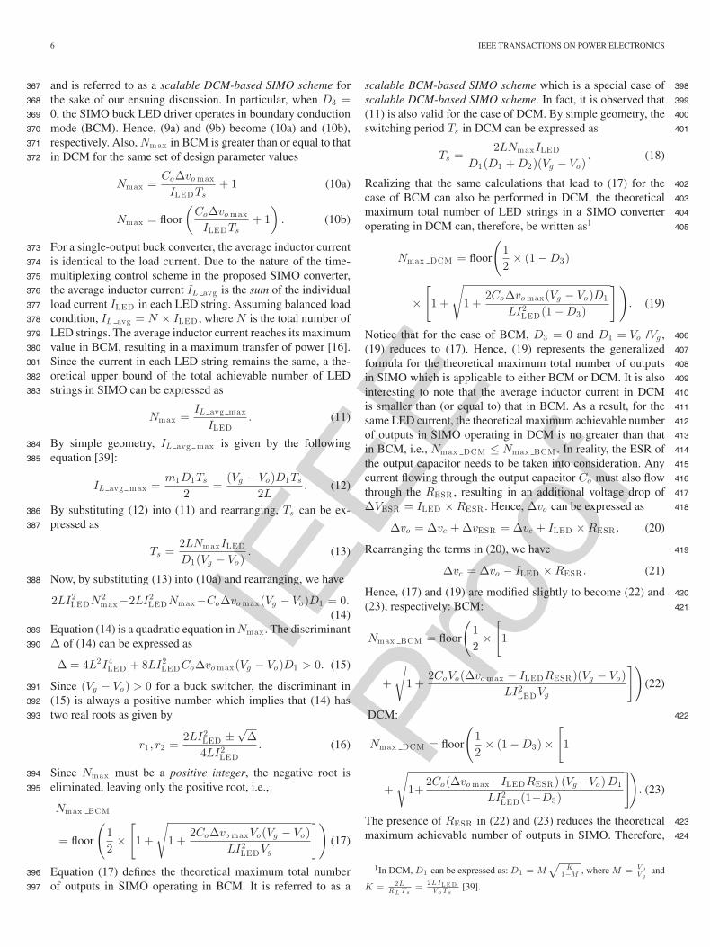
and is referred to as a scalable DCM-based SIMO scheme for367
the sake of our ensuing discussion. In particular, when D3 =368
0, the SIMO buck LED driver operates in boundary conduction369
mode (BCM). Hence, (9a) and (9b) become (10a) and (10b),370
respectively. Also, Nmax in BCM is greater than or equal to that371
in DCM for the same set of design parameter values372
Nmax =CoΔvo max
ILEDTs+ 1 (10a)
Nmax = floor
(CoΔvo max
ILEDTs+ 1
). (10b)
For a single-output buck converter, the average inductor current373
is identical to the load current. Due to the nature of the time-374
multiplexing control scheme in the proposed SIMO converter,375
the average inductor current IL avg is the sum of the individual376
load current ILED in each LED string. Assuming balanced load377
condition, IL avg = N × ILED , where N is the total number of378
LED strings. The average inductor current reaches its maximum379
value in BCM, resulting in a maximum transfer of power [16].380
Since the current in each LED string remains the same, a the-381
oretical upper bound of the total achievable number of LED382
strings in SIMO can be expressed as383
Nmax =IL avg max
ILED. (11)
By simple geometry, IL avg max is given by the following384
equation [39]:385
IL avg max =m1D1Ts
2=
(Vg − Vo)D1Ts
2L. (12)
By substituting (12) into (11) and rearranging, Ts can be ex-386
pressed as387
Ts =2LNmaxILED
D1(Vg − Vo). (13)
Now, by substituting (13) into (10a) and rearranging, we have388
2LI2LEDN 2
max−2LI2LEDNmax−CoΔvo max(Vg − Vo)D1 = 0.
(14)Equation (14) is a quadratic equation in Nmax . The discriminant389
Δ of (14) can be expressed as390
Δ = 4L2I4LED + 8LI2
LEDCoΔvo max(Vg − Vo)D1 > 0. (15)
Since (Vg − Vo) > 0 for a buck switcher, the discriminant in391
(15) is always a positive number which implies that (14) has392
two real roots as given by393
r1 , r2 =2LI2
LED ±√
Δ4LI2
LED. (16)
Since Nmax must be a positive integer, the negative root is394
eliminated, leaving only the positive root, i.e.,395
Nmax BCM
= floor
(12×
[1 +
√1 +
2CoΔvo maxVo(Vg − Vo)LI2
LEDVg
]).(17)
Equation (17) defines the theoretical maximum total number396
of outputs in SIMO operating in BCM. It is referred to as a397
scalable BCM-based SIMO scheme which is a special case of 398
scalable DCM-based SIMO scheme. In fact, it is observed that 399
(11) is also valid for the case of DCM. By simple geometry, the 400
switching period Ts in DCM can be expressed as 401
Ts =2LNmaxILED
D1(D1 + D2)(Vg − Vo). (18)
Realizing that the same calculations that lead to (17) for the 402
case of BCM can also be performed in DCM, the theoretical 403
maximum total number of LED strings in a SIMO converter 404
operating in DCM can, therefore, be written as1 405
Nmax DCM = floor
(12× (1 − D3)
×[1 +
√1 +
2CoΔvo max(Vg − Vo)D1
LI2LED(1 − D3)
]). (19)
Notice that for the case of BCM, D3 = 0 and D1 = Vo /Vg , 406
(19) reduces to (17). Hence, (19) represents the generalized 407
formula for the theoretical maximum total number of outputs 408
in SIMO which is applicable to either BCM or DCM. It is also 409
interesting to note that the average inductor current in DCM 410
is smaller than (or equal to) that in BCM. As a result, for the 411
same LED current, the theoretical maximum achievable number 412
of outputs in SIMO operating in DCM is no greater than that 413
in BCM, i.e., Nmax DCM ≤ Nmax BCM . In reality, the ESR of 414
the output capacitor needs to be taken into consideration. Any 415
current flowing through the output capacitor Co must also flow 416
through the RESR , resulting in an additional voltage drop of 417
ΔVESR = ILED × RESR . Hence, Δvo can be expressed as 418
Δvo = Δvc + ΔvESR = Δvc + ILED × RESR . (20)
Rearranging the terms in (20), we have 419
Δvc = Δvo − ILED × RESR . (21)
Hence, (17) and (19) are modified slightly to become (22) and 420
(23), respectively: BCM: 421
Nmax BCM = floor
(12×
[1
+
√1 +
2CoVo(Δvo max − ILEDRESR)(Vg − Vo)LI2
LEDVg
])(22)
DCM: 422
Nmax DCM = floor
(12× (1 − D3) ×
[1
+
√1+
2Co(Δvo max−ILEDRESR) (Vg −Vo) D1
LI2LED(1−D3)
]). (23)
The presence of RESR in (22) and (23) reduces the theoretical 423
maximum achievable number of outputs in SIMO. Therefore, 424
1In DCM, D1 can be expressed as: D1 = M√
K1−M , where M = Vo
V gand
K = 2LR L Ts
= 2LIL E DVo T s
[39].

IEEE
Proo
f
LEE et al.: SCALABILITY OF QUASI-HYSTERETIC FSM-BASED DIGITALLY CONTROLLED SINGLE-INDUCTOR DUAL-STRING 7
Fig. 10. Theoretical maximum achievable number of LED strings (Nm ax )versus the output capacitance (Co ) and the capacitor ESR (RESR ) for thescalable BCM-based SIMO scheme.
it is always recommended to choose an output capacitor with a425
smaller ESR, whenever possible. Fig. 10 shows the theoretical426
maximum total number of LED strings versus the output ca-427
pacitance and capacitor ESR for the scalable BCM-based SIMO428
scheme, given an LED current of 80 mA and a maximum ripple429
current requirement of 40%P-P .430
Intuitively, for a particular LED current, an increasing number431
of outputs can be achieved by using a larger output capacitor432
with the same ESR value. For instance, if the output capacitance433
is increased from 4.7 to 22 μF (the ESR remains at 100 mΩ),434
the theoretical model based on (22) suggests that the maximum435
total number of LED strings can be increased from three to six.436
It is also interesting to note that the maximum number of outputs437
in SIMO has a stronger dependence on the output capacitance438
than the capacitor ESR, as shown in Fig. 10.439
On the other hand, it is useful to study how the LED current440
affects the maximum achievable number of outputs in SIMO.441
As an example, assuming balanced load and two LEDs con-442
nected in series per string, a scalable BCM-based SIMO scheme443
is investigated with these parameter values: L = 47 μH, Co =444
4.7 μF, RESR = 100 mΩ, Vg = 15 V, and Vo = 6.4 V. The445
relationship between Nmax and ILED can be obtained by us-446
ing (22) for different values of output voltage ripple Δvo max .447
Based upon the I–V curve and/or SPICE model of the particular448
LED used, the corresponding output voltage ripple Δvo max can449
be determined from the LED current ripple requirement ΔiLED .450
The proposed design uses white LED [40] which is the target for451
LCD backlighting applications. For instance, a 20%P-P current452
ripple corresponds to around 2%P-P voltage ripple and a 40%P-P453
current ripple corresponds to around 4%P-P voltage ripple.454
Fig. 11 shows a plot of Nmax versus ILED for ΔiLED rang-455
ing from 5%P-P to 40%P-P . This plot is beneficial to a practical456
SIMO design in two ways. First, for a given LED current and457
current ripple requirement, the theoretical maximum number458
of LED strings viable under the scalable BCM-based SIMO459
scheme can be extracted directly from the plot. Second, the460
Fig. 11. Plot of theoretical maximum number of LED strings in SIMO(Nm ax ) versus the LED current (ILED ) in the scalable BCM-based SIMOscheme.
maximum LED current allowed in order for a SIMO to remain 461
at the same scaling level can also be obtained from the plot. For 462
instance, given a 20% current ripple requirement (i.e., ΔiLED = 463
20%P-P ), a SIDO (dual-string) configuration is possible as long 464
as the LED current in each string is no more than 110 mA. In 465
the event that an application demands an LED current greater 466
than 110 mA, two options can be considered: 1) Relax the cur- 467
rent ripple requirement whenever possible. A wider tolerance 468
in ΔiLED is generally acceptable since the ripple frequency is 469
too high for the human eye to detect. 2) Operate the SIMO buck 470
LED driver in PCCM [17], [35], [36]. In PCCM, the floor of 471
the inductor current is raised by a nonzero dc offset IDC which 472
distinguishes it from DCM. The proposed theoretical model can 473
be extended to PCCM by adding a dc component to the aver- 474
age inductor current. By going through similar calculations as 475
in DCM, the theoretical maximum number of outputs in SIMO 476
operating in PCCM is given by (24), as shown at the bottom of 477
the page. It is interesting to note that (24) continues to apply to 478
the cases of DCM and BCM. For instance, in DCM, IDC = 0 479
and (24), therefore, reduces to (23). 480
In the event of unbalanced load with unequal current among 481
the LED strings, the scalable DCM- or BCM-based SIMO 482
scheme continues to hold. The only change is to replace ILED 483
in (22) and (23) by max(ILED ), where max(ILED ) denotes the 484
largest LED current among all the LED strings. In other words, 485
the maximum number of LED strings that can be realized in 486
a SIMO buck LED driver is constrained by the largest LED 487
current. Generally speaking, the input voltage Vg , output volt- 488
age Vo , and the current ripple requirement are typically fixed 489
parameters defined in the design specification. Without making 490
any hardware changes (i.e., L and Co values are fixed), the pri- 491
mary design variable in (22) and (23) is the LED current ILED . 492
In fact, the LED current is the dominant factor for determining 493
the maximum possible number of outputs under the scalable 494
DCM-/BCM-based SIMO scheme. By knowing the maximum 495
LED current required for a particular application, the theoretical 496
Nmax PCCM =floor
(1
2ILED×[(IDC +(1−D3) ILED ]×
[1+
√1 +
2Co(Δvo max − ILEDRESR) (Vg − Vo) D1(1 − D3)L [IDC − (1 − D3)ILED ]2
]).
(24)

IEEE
Proo
f
8 IEEE TRANSACTIONS ON POWER ELECTRONICS
TABLE IDESIGN SPECIFICATION OF A SISO BUCK LED DRIVER IN DCM
Fig. 12. Simulated steady-state waveforms for the SISO buck LED driverbased on the design specification in Table I.
maximum achievable number of independently driven LED497
strings can be estimated in advance.498
IV. SIMULATION RESULTS499
Ideal macromodels based on the scalable DCM-based SIMO500
scheme were constructed and simulated in Cadence Spectre [27]501
in order to compare with the theoretical results in Section III. The502
design specification of a single-inductor single-output (SISO)503
buck converter is shown in Table I. The theoretical model based504
on (23) suggests that Nmax DCM = 1, meaning only one LED505
string is viable. Fig. 12 shows the simulated steady-state wave-506
forms of the inductor current IL , the LED currents ILED , and507
the output voltages Vo of a SISO buck LED driver. The simu-508
lated steady-state LED current ILED is approximately 80 mA509
which meets the design target. The simulated LED current rip-510
ple ΔiLED is 18%P-P (also, the output voltage ripple Δvo is511
1.7%P-P ), which satisfies the maximum ripple requirement.512
Now, the SISO buck LED driver is transformed into SIDO513
by adding a second LED string. Fig. 13 shows the simulated514
steady-state waveforms from the resulting SIDO LED driver.515
Despite the fact that the steady-state LED current in either516
string remains at 80 mA, the LED current ripple is more than517
40%P-P which violates the maximum ripple current require-518
ment. Hence, the simulation results show that SIDO is not viable519
based on the design requirement which is consistent with the520
theoretical result. By increasing the switching frequency from521
Fig. 13. Simulated steady-state waveforms showing SIDO is not viable sincethe 30%p -p maximum current ripple requirement is violated.
Fig. 14. Simulated steady-state waveforms showing SIDO is possible by in-creasing the switching frequency from 100 to 156.25 kHz.
100 to 156.25 kHz and keeping other parameters unchanged, 522
Nmax DCM = 2 from (23). Fig. 14 shows the simulated wave- 523
forms for the corresponding signals in a SIDO buck LED driver. 524
The simulated LED current ripple ΔiLED is 24%P-P and the cor- 525
responding output voltage ripple Δvo is 2.3%P-P , both of which 526
satisfy their corresponding maximum ripple requirement. Con- 527
sequently, both the theoretical and simulation results show that 528
by increasing the switching frequency, a SIDO buck LED driver 529
in DCM is feasible. 530
A third LED string is added to the SIDO buck LED driver to 531
transform it into SIMO consisting of three independently driven 532
LED strings. The LED current in each string remains unchanged 533
at 80 mA as in the SISO or SIDO case. According to Fig. 11, 534
the theoretical model suggests that for ILED = 80 mA, a scal- 535
able BCM-based SIMO scheme with a maximum of three LED 536
strings is feasible under the 40%P-P current ripple constraint. 537
The switching period Ts is chosen to be 6 μs using (13) which 538
corresponds to a switching frequency of 166.67 kHz. Fig. 15 539
shows the simulated waveforms from the resulting SIMO buck 540
LED driver. The simulated LED current ripple ΔiLED is around 541
35%P-P and the output voltage ripple Δvo is 3.5%P-P , both of 542
which satisfy their respective maximum ripple constraint. As a 543
sanity check, the theoretical model based on (22) indeed sug- 544
gests that a maximum possible number of three independently 545
driven LED strings can be achieved in the scalable BCM-based 546
SIMO scheme. Hence, it is shown that the simulation result 547
agrees with the corresponding theoretical result. On the other 548
hand, it is important to examine the transient performance of the 549

IEEE
Proo
f
LEE et al.: SCALABILITY OF QUASI-HYSTERETIC FSM-BASED DIGITALLY CONTROLLED SINGLE-INDUCTOR DUAL-STRING 9
Fig. 15. Simulated steady-state waveforms of a three-string SIMO buck LEDdriver operating in BCM.
Fig. 16. Simulated transient waveforms for (a) peak reference step-up and(b) peak reference step-down response.
proposed SIDO buck LED driver. The LED current is changed550
by adjusting the peak limit of the inductor current. By stepping551
up the peak voltage reference (Vpeak in Fig. 1) from 1.660 to552
1.945 V in 400 ns, the peak inductor current limit is increased553
by approximately 200 mA, leading to an increase in the nom-554
inal LED current from 20 to 80 mA. The reference voltages555
(Vrefa , Vrefb) are also stepped up from 100 to 340 mV in order556
to maintain the same load current between the two LED strings.557
Conversely, by stepping down Vpeak from 1.945 to 1.660 V,558
the LED current is reduced from 80 to 20 mA. Fig. 16 shows559
the simulated transient behavior for the peak voltage reference560
step-up and step-down response.561
In the case of step-up reference response, the LED current in562
either string settles to the steady-state nominal value of 80 mA563
within 63 μs. The output voltage reaches its target steady-state564
Fig. 17. Simulated steady-state waveforms of a SIDO buck LED driver withunbalanced load.
value of 6.34 V. In the case of step-down reference response, 565
the LED current in either string settles to the steady-state nom- 566
inal value of 20 mA in less than 112 μs. The output voltage 567
settles to its new steady-state value of 5.82 V without oscilla- 568
tions. Hence, the simulation results show that the closed-loop 569
system remains in stable condition in response to a peak voltage 570
reference transient. 571
The effectiveness of the proposed SIDO converter to drive 572
unbalanced load is also investigated. As an example, the first 573
and second LED strings require an average current value of 80 574
and 30 mA, respectively. Unlike the balanced load case with 575
a constant peak inductor current limit, two distinct peak cur- 576
rent limits are employed for unbalanced load such that two 577
different average inductor (or load) current values can be gen- 578
erated in alternate clock cycles. Fig. 17 depicts the simulated 579
steady-state waveforms from the SIDO buck LED driver with 580
unbalanced load. The simulation results show that the first and 581
second LED strings are regulated with an average current value 582
of 80 and 30 mA, respectively. For the first string, the simu- 583
lated current ripple is 24.38%P-P and the output voltage ripple 584
is 2.3%P-P . Also, for the second string, the simulated current 585
ripple is 21.1%P-P and the output voltage ripple is 1.1%P-P . 586
Either string meets the maximum ripple requirements. The sim- 587
ulation results demonstrate that the proposed SIDO converter is 588
capable of delivering unequal currents to the two LED strings 589
simultaneously. 590
V. EXPERIMENTAL RESULTS 591
The proposed SIDO buck LED driver was implemented on 592
a field-programmable gate array (FPGA)-based hardware pro- 593
totype in accordance with the design specification provided in 594
Table I. The switching frequency is increased to 156.25 kHz in 595
order to satisfy the LED current ripple requirement. A photo of 596
the experimental setup is shown in Fig. 18. The power stage of 597
the buck converter consists of discrete ICs from International 598
Rectifier such as power MOSFETs (IRF7828), dual-channel 599
gate driver (IR2110), and output switches (IRF9388), as well as 600
surface-mount inductor and low-ESR capacitors. In actual im- 601
plementation, the top level of the proposed digital controller is 602
partitioned into two major functional blocks. The functionality 603
of the first block is to control the switching action of the power 604

IEEE
Proo
f
10 IEEE TRANSACTIONS ON POWER ELECTRONICS
Fig. 18. Experimental setup for the proposed SIDO buck LED driver.
Fig. 19. Measured waveforms for inductor current and current sense feedbackvoltage.
stage by detecting the peak-crossing and zero-crossing events605
of the inductor current. It was implemented in hierarchical gate-606
level schematics using primitives and macros available from607
the Xilinx Spartan-3 Generation library. Dead-time logic is in-608
cluded to prevent shoot-through current of the power switches.609
The second logical block is used to control the switching se-610
quence of the two output switches by continuously monitoring611
the current-sense feedback signals. It was modeled as an FSM612
in Verilog RTL. Only one of the two output switches can be ON613
and the other must be OFF per switching cycle. Dead-time logic614
is also added to prevent cross conduction between outputs. The615
two logical blocks are synchronized by the system clock to en-616
sure that the high-side power switch and the output switches are617
triggered from the same clock edge. The entire digital controller618
was implemented with Xilinx Spartan-3E (XC3S250E) FPGA.619
The quasi-hysteretic control logic was realized using 4-ns fast620
comparators (AD8611 from Analog Devices) and semicustom621
synchronous logic.622
Using a current sensing resistor of 4 Ω and reference voltage623
of 320 mV, the target current in each of the two LED strings624
is 80 mA. Fig. 19 shows the current sensing feedback voltage625
(Vcsa , Vcsb) from which the corresponding average load current626
can be obtained, i.e., ILED = Vcs /Rcs . The average inductor627
current is measured to be 162 mA, which is the sum of the628
load currents in both LED strings. The average current values629
in the first and second LED string are measured to be around630
80.6 and 82 mA, respectively. The measured LED current ripple631
ΔiLED in either string is around 26%P-P , which is reasonably632
close to the simulated current ripple of 24%P-P . In addition,633
the nominal output voltages in the first and second string are634
Fig. 20. Measured waveforms for inductor current and output voltage in eitherLED string.
measured to be 6.204 and 6.249 V, respectively, as shown in 635
Fig. 20. Under this balanced load condition, the measured cur- 636
rent and voltage values are in close agreement between the 637
two LED strings. The output voltage ripple is also measured 638
to be around 2.57%P-P , compared to 2.3%P-P from simulation. 639
Therefore, the experimental results are shown to be consistent 640
with the corresponding simulation ones. On the other hand, the 641
measured power conversion efficiency of the proposed SIDO 642
converter is 80% which is comparable to conventional driving 643
topologies [41]. The efficiency can be further increased by em- 644
ploying a current-sensing resistor with a smaller value. 645
The transient response of the proposed SIDO buck LED driver 646
is verified experimentally by measuring its peak voltage refer- 647
ence step response. An 8-bit digital-to-analog converter (AD558 648
from Analog Devices) is used to enable programming of the peak 649
voltage reference Vpeak and the current-sense voltage references 650
(Vrefa , Vref b) by the Xilinx FPGA. The measured waveforms 651
of the inductor current and the voltage at the current sensing 652
nodes in response to a peak voltage reference step are shown in 653
Fig. 21. The settling time of the transient response is also mea- 654
sured and compared with the simulated settling time. For the 655
step-up response, it is observed that the current-sensing voltage 656
Vcsa in the first LED string steps up from 81.8 to 325.4 mV, 657
which corresponds to an increase in the average load current 658
from 20.5 to 81.3 mA. Similarly, the current-sensing voltage 659
Vcsb in the second LED string steps up from 94.1 to 327.6 mV, 660
which corresponds to an increase in the average load current 661
from 23.5 to 81.9 mA. The settling time for the step-up response 662
is measured to be 67 μs, compared to 63 μs from simulation. 663
The measured results for the step-down response are the reverse 664
of those from the step-up response. The only difference is that 665
it takes longer for the step-down transient to settle. The set- 666
tling time for the step-down response is measured to be 115 μs, 667
compared to 112 μs from simulation. The measured settling 668
times are shown to be very close to the simulated ones. The 669
experimental results confirm that the system remains in stable 670
condition when it is perturbed by the peak voltage reference 671
transient. 672
The unbalanced load scenario in the proposed SIDO buck 673
LED driver is also verified experimentally. The measured aver- 674
age load current values in the first and second LED string are 675

IEEE
Proo
f
LEE et al.: SCALABILITY OF QUASI-HYSTERETIC FSM-BASED DIGITALLY CONTROLLED SINGLE-INDUCTOR DUAL-STRING 11
Fig. 21. Measured transient waveforms in response to (a) peak reference step-up and (b) peak reference step-down.
Fig. 22. Measured waveforms for inductor current and current sense voltages.
around 81.9 and 30.1 mA, respectively. Fig. 22 shows the mea-676
sured waveforms for the inductor current and the current-sensing677
voltage per string. The inductor current waveform indicates that678
the proposed driver operates in DCM with two distinct peak679
current limits. Fig. 23 shows the measured inductor current and680
the output voltage in either string. The measured output voltage681
values in the first and second LED string are 6.22 and 5.70 V,682
respectively. The experimental results demonstrate that the pro-683
posed driver is capable of driving two independent LED strings684
concurrently with different load current.685
Fig. 23. Measured waveforms for inductor current and output voltages.
VI. CONCLUSION 686
The proposed SIDO buck LED driver was implemented in 687
FPGA-based hardware. The experimental results correlate well 688
with simulation ones. The scalability of the proposed SIDO buck 689
LED driver to SIMO is closely examined. A general formula 690
for determining the theoretical maximum achievable number of 691
LED strings in SIMO is derived. The simulation results were 692
shown to be consistent with those obtained from the theoret- 693
ical model for the same design parameter values. The quasi- 694
hysteretic digital control scheme does not require loop com- 695
pensation which simplifies the control loop design and reduces 696
component count. In addition, the proposed SIMO architecture 697
offers the advantage of driving a larger number of parallel LED 698
strings without being limited by the maximum current rating of 699
the LED. It also enables dimming for the LED strings without 700
additional dimming transistors. Local bus voltage and current 701
optimization in each individual LED string compensates for the 702
variability of the LED’s forward voltage, which reduces power 703
loss and enables mixing of white LEDs from different bins to 704
lower LED costs. 705
REFERENCES 706
[1] C.-Y Hsieh, C.-Y. Yang, and K.-H. Chen, “A charge-recycling buck-store 707and boost-restore (BSBR) technique with dual outputs for RGB LED 708backlight and flashlight module,” IEEE Trans. Power Electron., vol. 24, 709no. 8, pp. 1914–1925, Aug. 2009. 710
[2] S.-Y. Lee, J.-W. Kwon, H.-S. Kim, M.-S. Choi, and K.-S. Byun, “New 711design and application of high efficiency LED driving system for RGB- 712LED backlight in LCD display,” in Proc. 37th IEEE Power Electron. Spec. 713Conf.,, 2006, pp. 1–5. 714
[3] H.-J. Chiu, Y.-K. Lo, J.-T. Chen, S.-J. Cheng, C.-Y. Lin, and S.-C. Mou, “A 715high-efficiency dimmable led driver for low-power lighting applications,” 716IEEE Trans. Ind. Electron., vol. 57, no. 2, pp. 735–743, Feb. 2010. 717
[4] C.-H. Liu, C.-Y. Hsieh, Y.-C. Hsieh, T.-J. Tai, and K.-H. Chen, “SAR- 718Controlled adaptive off-time technique without sensing resistor for achiev- 719ing high efficiency and accuracy led lighting system,” IEEE Trans. Circuits 720Syst. I, Reg. Papers, vol. 57, no. 6, pp. 1384–1394, Jun. 2010. 721
[5] C.-H. Wu and C.-L. Chen, “High-efficiency current-regulated charge pump 722for a white LED driver,” IEEE Trans. Circuits Syst. II, Exp. Briefs, vol. 56, 723no. 10, pp. 614–618, Oct. 2009. 724
[6] P. Malcovati, M. Belloni, F. Gozzini, C. Bazzani, and A. Baschirotto, “A 7250.18μm CMOS 91%-efficiency 0.1-to-2 A scalable buck-boost DC-DC 726converter for LED drivers,” in Proc. ISSCC Dig. Tech. Papers, Feb. 2012, 727pp. 280–281. 728
[7] S. Rao, Q. Khan, S. Bang, D. Swank, A. Rao, W. Mclntyre, and 729P. K. Hanumolu, “A 1.2 A buck-boost LED driver with 13% efficiency 730

IEEE
Proo
f
12 IEEE TRANSACTIONS ON POWER ELECTRONICS
improvement using error-averaged SenseFET-Based current sensing,” in731Proc. ISSCC Dig. Tech. Papers, Feb. 2011, pp. 238–239.732
[8] S.-I. Hong, J.-W Han, D.-H. Kim, and O.-K. Kwon, “A double-loop733control LED backlight driver IC for medium-sized LEDs,” in Proc. ISSCC734Dig. Tech. Papers, Feb. 2010, pp. 116–117.735
[9] M.-H. Huang and K.-H. Chen, “Single-inductor multi-output (SIMO)736DC-DC converters with high light-load efficiency and minimized cross-737regulation for portable devices,” IEEE J. Solid-State Circuits, vol. 44,738no. 4, pp. 1099–1111, Apr. 2009.739
[10] E. Bonizzoni, F. Borghetti, P. Malcovati, F. Maloberti, and B. Niessen, “A740200 mA 93% peak efficiency single-inductor dual-output DC-DC buck741converter,” in Proc. IEEE ISSCC Dig. Tech. Papers, Feb. 2007, pp. 526–742619.743
[11] C.-Y. Hsieh and K.-H. Chen, “Boost DC-DC converter with fast reference744tracking (FRT) and charge-recycling (CR) techniques for high-efficiency745and low-cost LED driver,” IEEE J. Solid- State Circuits, vol. 44, no. 9,746pp. 2568–2580, Sep. 2009.747
[12] H. Chen, Y. Zhang, and D. Ma, “A SIMO parallel-string driver IC for748dimmable LED backlighting with local bus voltage optimization and single749time-shared regulation loop,” IEEE Trans. Power Electron., vol. 27, no. 1,750pp. 452–462, Jan. 2012.751
[13] D. Ma, W.-H. Ki, P. K. T. Mok, and C.-Y. Tsui, “Single-inductor multiple-752output switching converters with bipolar outputs,” in Proc. IEEE Int.753Symp. Circuits Syst., May 2001, vol. 3, pp. 301–304.754
[14] D. Ma, W.-H. Ki, C.-Y. Tsui, and P. K. T. Mok, “A 1.8 V single-inductor755dual-output switching converter for power reduction techniques,” in Proc.756IEEE Symp. VLSI Circuits, Jun. 2001, pp. 137–140.757
[15] W.-H. Ki and D. Ma, “Single-inductor multiple-output switching convert-758ers,” in Proc. 32nd IEEE Power Electron. Spec. Conf., Jun. 2001, vol. 1,759pp. 226–231.760
[16] D. Ma, W.-H. Ki, C.-Y. Tsui, and P. K. T. Mok, “Single-inductor multiple-761output switching converters with time-multiplexing control in discon-762tinuous conduction mode,” IEEE J. Solid-State Circuits, vol. 38, no. 1,763pp. 89–100, Jan. 2003.764
[17] D. Ma, W.-H. Ki, and C.-Y. Tsui, “A pseudo-CCM/DCM SIMO switching765converter with freewheel switching,” IEEE J. Solid-State Circuits, vol. 38,766no. 6, pp. 1007–1014, Jun. 2003.767
[18] D. Kwon and G. A. Rincon-Mora, “Single-inductor multiple-output768switching DC–DC converters,” IEEE Trans. Circuits Syst. II, Exp. Briefs,769vol. 56, no. 8, pp. 614–618, Aug. 2009.770
[19] K.-S. Seol, Y.-J. Woo, G.-H. Cho, G.-H. Gho, and J.-W. Lee, “A syn-771chronous multioutput step-up/down DC–DC converter with return current772control,” IEEE Trans. Circuits Syst. II, Exp. Briefs, vol. 56, no. 3, pp. 210–773214, Mar. 2009.774
[20] C.-W. Leng, C.-H. Yang, and C.-H. Tsai, “Digital PWM controller for775SIDO switching converter with time-multiplexing scheme,” in Proc. Int.776Symp. VLSI Design Autom. Test, Apr. 2009, pp. 52–55.777
[21] Y.-J. Moon, Y.-S. Roh, J.-C. Gong, and C. Yoo, “Load-independent current778control technique of a single-inductor multiple-output switching DC–DC779converter,” IEEE Trans. Circuits Syst. II, Exp. Briefs, vol. 59, no. 1, pp. 50–78054, Jan. 2012.781
[22] F. Su, W.-H. Ki, and C.-Y. Tsui, “Ultra fast fixed-frequency hysteretic buck782converter with maximum charging current control and adaptive for DVS783applications,” IEEE J. Solid- State Circuits, vol. 43, no. 4, pp. 815–822,784Apr. 2008.785
[23] W.-H. Ki, K.-M. Lai, and C. Zhan, “Charge balance analysis and state786transition analysis of hysteretic voltage mode switching converters,” IEEE787Trans. Circuits Syst. I, Reg. Papers, vol. 58, no. 5, pp. 1142–1153, May7882011.789
[24] K. K.-S. Leung and H. S.-H. Chung, “Dynamic hysteresis band control790of the buck converter with fast transient response,” IEEE Trans. Circuits791Syst. II, Exp. Briefs, vol. 52, no. 7, pp. 398–402, Jul. 2005.792
[25] H. Eachempatti, S. Ganta, J. Silva-Martinez, and H. Martınez-Garcia,793“SIDO buck converter with independent outputs,” in Proc. 53rd IEEE Int.794Midwest Symp. Circuits Syst., Aug. 2010, pp. 37–40.795
[26] F. Su and W.-H. Ki, “Digitally assisted quasi-V2 hysteretic buck converter796with fixed frequency and without using Large-ESR capacitor,” in Proc.797ISSCC Dig. Tech. Papers, Feb. 2009, pp. 446–447.798
[27] Cadence Spectre Circuit Simulator Datasheet [Online]. Available:799http://www.cadence.com/products/cic/spectre_circuit/pages/default.aspxQ1 800
[28] M. Doshi and R. Zane, “Digital architecture for driving large LED arrays801with dynamic bus voltage regulation and phase shifted PWM,” in Proc.802Appl. Power Electron. Conf., Feb. 2007, pp. 287–293.803
[29] W.-S. Oh, D. Cho, K.-M. Cho, G.-W. Moon, B. Yang, and T. Jang, “A novel804two-dimensional adaptive dimming technique of X-Y channel drivers for805
LED backlight system in LCD TVs,” J. Display Technol., vol. 5, no. 1, 806pp. 20–26, Jan. 2009. 807
[30] Datasheet: LP8545, “LP8545 High-efficiency LED backlight driver 808for notebooks,” Texas Instruments Incorporated, [Online] Available: 809http://www.ti.com/general/docs/lit/getliterature.tsp?genericPartNumber= 810lp8545&fileType=pdf 811
[31] Datasheet: MAX16814, “Integrated, 4-channel, high-brightness LED 812driver with high-voltage DC-DC controller,” Maxim Integrated Prod- 813ucts, Inc., [Online], Available: http://datasheets.maximintegrated.com/ 814en/ds/MAX16814.pdf 815
[32] K. H. Loo, W. K. Lun, S. C. Tan, Y. M. Lai, and C. K. Tse, “On driving 816techniques for LEDs: Toward a generalized methodology,” IEEE Trans. 817Power Electron., vol. 24, no. 12, pp. 2967–2976, Dec. 2009. 818
[33] W. K. Lun, K. H. Loo, S. C. Tan, Y. M. Lai, and C. K. Tse, “Bilevel current 819driving technique for LEDs,” IEEE Trans. Power Electron., vol. 24, no. 12, 820pp. 2920–2932, Dec. 2009. 821
[34] S. C. Tan, “General n-level driving approach for improving electrical-to- 822optical energy-conversion efficiency of fast-response saturable lighting 823devices,” IEEE Trans. Ind. Electron., vol. 57, no. 4, pp. 1342–1353, Apr. 8242010. 825
[35] D. Ma and W.-H. Ki, “Fast transient PCCM switching converter with 826freewheel switching control,” IEEE Trans. Circuits Syst. II, Exp. Briefs, 827vol. 54, no. 9, pp. 825–829, Sep. 2007. 828
[36] D. Ma, W.-H. Ki, and C.-Y. Tsui, “Single-inductor multiple-output switch- 829ing converters in PCCM with freewheel switching,” U.S. Patent 7 432 614, 830Oct. 7, 2008. 831
[37] Application Note: AN-1656, “Design challenges of switching LED 832drivers,” Texas Instruments Incorporated, [Online] Available: http:// 833www.ti.com/general/docs/lit/getliterature.tsp?literatureNumber=snva253 834&fileType=pdf 835
[38] Solutions Guide, “LED drivers for high-brightness lighting,” Texas 836Instruments Incorporated, [Online], Available: http://www.ti.com/ 837general/docs/lit/getliterature.tsp?baseLiteratureNumber=snvy001 838
[39] R. W. Erickson and D. Maksimovic, Fundamentals of Power Electronics, 8392nd ed. New York, NY, USA: Springer, 2001. 840
[40] Datasheet: SMD5730, “SMD 5730 White LED Datasheet,” APT Electron- 841ics Ltd., [Online], Available: http://www.apt-hk.com/en/product/?95.html 842
[41] Z. Ye, F. Greenfeld, and Z. Liang, “Design considerations of a high power 843factor SEPIC converter for high brightness white LED lighting applica- 844tions,” in Proc. IEEE Power Electron. Spec. Conf., 2008, pp. 2657–2663. 845
Albert T. L. Lee received the Bachelor of Science de- 846gree in electrical engineering from the University of 847Wisconsin, Madison, USA, in 1994, and the Master 848of Science degree from the University of Michigan, 849Ann Arbor, USA, in 1996. He is currently working 850toward the Doctor of Philosophy degree in electronic 851and computer engineering at the Hong Kong Uni- 852versity of Science and Technology, Kowloon, Hong 853Kong. 854
He joined Intel Corporation, Hillsboro, OR, USA, 855in 1996 as a Senior Component Design Engineer and 856
was involved in the development of Intel’s P6 family microprocessors. In 2001, 857he served as a Senior Corporate Application Engineer in the System-Level De- 858sign Group at Synopsys Inc., Mountain View, CA, USA. In 2003, he joined 859the Hong Kong Applied Science and Technology Research Institute Company 860Ltd. and served as EDA Manager in the Wireline Communications Group. In 8612006, he joined the Giant Electronics Limited as Hardware Design Manager 862and became Associate General Manager in 2008. His research interests include 863mixed-signal system-level design, LED driver, power management system, and 864very large scale integration circuits. 865
866

IEEE
Proo
f
LEE et al.: SCALABILITY OF QUASI-HYSTERETIC FSM-BASED DIGITALLY CONTROLLED SINGLE-INDUCTOR DUAL-STRING 13
Johnny K. O. Sin (S’79–M’88–SM’96–F’12) re-867ceived the B.A.Sc., M.A.Sc., and Ph.D. degrees in868electrical engineering from the University of Toronto,869Toronto, ON, Canada, in 1981, 1983, and 1988,870respectively.871
From 1988 to 1991, he was a Senior Member of872the research staff of Philips Laboratories, Briarcliff873Manor, NY, USA. In August 1991, he joined the De-874partment of Electronic and Computer Engineering,875The Hong Kong University of Science and Technol-876ogy, Kowloon, Hong Kong, where he has been a Full877
Professor since 2001. He is the holder of 13 patents, and the author of more878than 270 papers in technical journals and refereed conference proceedings. His879research interests include microelectronic and nanoelectronic devices and fabri-880cation technology, particularly novel power semiconductor devices and ICs, and881system-on-a-chip applications using CMOS and power transistors and silicon-882embedded magnetic and capacitive devices.883
Dr. Sin was an Editor for the IEEE ELECTRON DEVICES LETTERS from 1998884to 2010. He is a member of the Power Devices and IC’s Technical Committee of885the IEEE Electron Devices Society. He is also a Technical Committee member886of the International Symposium on Power Semiconductor Devices and IC’s. He887is a Fellow of the IEEE for contributions to the design and commercialization888of power semiconductor devices.889
890
Philip C. H. Chan (SM’97–F’07) received the Bach- 891elor of Science degree in electrical engineering from 892the University of California at Davis, Davis, USA, in 8931973, and the Master of Science and Doctor of Phi- 894losophy degrees in electrical engineering from the 895University of Illinois at Urbana-Champaign, Urbana, 896USA, in 1975 and 1978, respectively. 897
He later joined Intel Corporation, Santa Clara, 898CA, USA, in 1981 and became a Senior Project 899Manager in Technology Development. He joined the 900Hong Kong University of Science and Technology 901
(HKUST) in 1991 as a founding member. He served at HKUST as the Associate 902Dean of Engineering and Head of the Department of Electronic and Com- 903puter Engineering. He became the Dean of Engineering in September 2003. 904He joined the Hong Kong Polytechnic University, Hong Kong, in 2010 as the 905Deputy President and Provost. His research interests include very large scale 906integration devices, circuits, electronic packaging, and integrated sensors. 907
Dr. Chan received the ECE Distinguished Alumni Award from the University 908of Illinois, Urbana-Champaign in 2010. 909
910

IEEE
Proo
f
QUERIES911
Q1. Author: Please provide year information in Refs. [27], [30], [31], [37], [38], and [40].912

IEEE
Proo
f
IEEE TRANSACTIONS ON POWER ELECTRONICS 1
Scalability of Quasi-Hysteretic FSM-Based DigitallyControlled Single-Inductor Dual-String Buck LED
Driver to Multiple Strings
1
2
3
Albert T. L. Lee, Johnny K. O. Sin, Fellow, IEEE, and Philip C. H. Chan, Fellow, IEEE4
Abstract—There has been growing interest in single-inductor5multiple-output (SIMO) dc–dc converters due to its reduced cost6and smaller form factor in comparison with using multiple single-7output converters. An application for such a SIMO-based switch-8ing converter is to drive multiple LED strings in a multichannel9LED display. This paper proposes a quasi-hysteretic finite-state-10machine-based digitally controlled single-inductor dual-output11buck switching LED driver operating in discontinuous conduction12mode (DCM) and extends it to drive multiple outputs. Based on13the time-multiplexing control scheme in DCM, a theoretical upper14limit of the total number of outputs in a SIMO buck switching LED15driver for various backlight LED current values can be derived16analytically. The advantages of the proposed SIMO LED driver17include reducing the controller design complexity by eliminating18loop compensation, driving more LED strings without limited by19the maximum LED current rating, performing digital dimming20with no additional switches required, and optimization of local bus21voltage to compensate for variability of LED forward voltage VF22in each individual LED string with smaller power loss. Loosely23binned LEDs with larger VF variation can, therefore, be used for24reduced LED costs.25
Index Terms—Boundary conduction mode (BCM), discontinu-26ous conduction mode (DCM), finite-state machine (FSM), single-27inductor dual-output (SIDO), single-inductor multiple-output28(SIMO).29
I. INTRODUCTION30
AN LED driver is essentially a current source (or sink)31
which maintains a constant current required for achieving32
the desired color and luminous flux from an array of LEDs. A33
number of highly efficient switching LED drivers have been re-34
ported in the literature and their primary objective is to achieve35
high power conversion efficiency [1]–[11]. Besides efficiency,36
another important consideration is the scalability of the exist-37
ing single-inductor dual-output (SIDO) switching converter to38
drive multiple independent LED strings in a single-inductor39
multiple-output (SIMO) topology for reduced cost and smaller40
Manuscript received November 7, 2012; revised January 22, 2013; acceptedMarch 11, 2013. Recommended for publication by Associate Prof. J. M. Alonso.
A. T. L. Lee and J. K. O. Sin are with the Department of Electronic andComputer Engineering, The Hong Kong University of Science and Technology,Kowloon, Hong Kong (e-mail: [email protected]; [email protected]).
P. C. H. Chan is with Hong Kong Polytechnic University, Hong Kong (e-mail:[email protected]).
Color versions of one or more of the figures in this paper are available onlineat http://ieeexplore.ieee.org.
Digital Object Identifier 10.1109/TPEL.2013.2253804
form factor [12]. However, in practice, only a finite number of 41
outputs can be served by each LED driver. 42
The prior arts of SIMO switching converter use either one of 43
two ways to distribute energy from a single power supply to mul- 44
tiple outputs with a single inductor, namely multiple energizing 45
phases [13]–[20] and single energizing phase per switching cy- 46
cle [21]. The former with time-multiplexing control leads to 47
much better suppression of cross regulation because the out- 48
puts are decoupled in time. In this paper, a quasi-hysteretic 49
finite-state machine (FSM)-based digital control scheme is em- 50
ployed in a SIDO buck LED driver consisting of two inde- 51
pendent parallel strings operating in discontinuous conduction 52
mode (DCM). The extension of this SIDO architecture to SIMO 53
is formally investigated. The proposed SIMO-based switching 54
buck LED driver enables separate control of the three primary 55
colors (red, green, and blue), thereby offering more flexibility 56
for color mixing. The rest of this paper is organized as follows. 57
Section II introduces the proposed quasi-hysteretic FSM-based 58
digital controller for a SIDO switching buck LED driver oper- 59
ating in DCM. Section III provides a theoretical analysis on the 60
scalability of the proposed digital control scheme from SIDO 61
to SIMO and suggests a general formula for determining the 62
theoretical upper bound in the total number of outputs in SIMO. 63
Section IV shows Cadence Spectre simulation results that are 64
used to verify the theoretical model. Section V contains the ex- 65
perimental results for the proposed digitally controlled SIDO 66
buck LED driver. Section VI concludes our research effort. 67
II. QUASI-HYSTERETIC FSM-BASED DIGITAL CONTROL 68
FOR SIDO LED DRIVER 69
A SIDO switching converter with time-multiplexing control 70
scheme operating in DCM was first reported in [13]–[16]. With 71
such kind of time-multiplexing control scheme, a SIDO con- 72
verter can easily be extended to drive multiple outputs and it 73
exhibits negligible cross regulation in DCM. A SIMO parallel- 74
string LED driver operating in DCM has recently been re- 75
ported [12]. It uses an analog-based controller with dominant 76
pole compensation for stability, and time-multiplexing control in 77
DCM is employed to suppress cross regulation among the LED 78
strings. Unlike conventional pulse width modulation (PWM)- 79
based analog controllers, the proposed digital controller uti- 80
lizing quasi-hysteretic control does not require any compensa- 81
tion circuits because of its inherent stability [22]–[24], hence 82
simplifying the control loop design and reducing the com- 83
ponent count and cost. Quasi-hysteretic control offers a good 84
0885-8993/$31.00 © 2013 IEEE

IEEE
Proo
f
2 IEEE TRANSACTIONS ON POWER ELECTRONICS
Fig. 1. System architecture of the quasi-hysteretic FSM-based digitally con-trolled SIDO buck LED driver.
compromise between traditional fixed-frequency PWM control85
and pure hysteretic control with variable switching frequency.86
In the proposed design, an external clock is used to synchro-87
nize the buck LED driver which switches at a fixed frequency.88
Fast comparators are used to control the on-time of the high-89
side and low-side power switches by monitoring the inductor90
current. This is particularly suitable for lighting applications91
where variable switching frequencies are not desirable. The re-92
configurability and scalability of a digital controller makes it93
especially attractive for SIMO.94
A major drawback of the previously proposed SIMO LED95
driver operating in DCM [12] is that since the LED current is96
discontinuous, the LED endures a higher maximum peak current97
for the same average current required. In other words, the LED98
could potentially be operating close to its absolute maximum99
current rating, thereby increasing the current stress and possibly100
shortening the operating lifetime of the LED. In their approach,101
the LED current scales with the number of LED strings in SIMO.102
Hence, the maximum current rating of the LED unnecessarily103
restricts the maximum achievable number of LED strings which104
can be implemented in SIMO. In the proposed design, the LED105
current is always continuous and the LED can be regulated very106
close to the target average current value which is much lower107
than its maximum current rating. During the time interval when108
the output switch is OFF, the output capacitor, acting as a con-109
stant current source, continues to discharge its current to the110
corresponding LED string. When the output switch is ON, the111
power stage is reconnected to the LED string and the induc-112
tor current is transferred to the output capacitor and the LED113
string simultaneously. The current-sense feedback control en-114
sures that the LED current is maintained at the desired dc level.115
Hence, a time-continuous current is supplied to the LED string.116
Consequently, the LED current does not scale with the number117
of LED strings in the proposed SIMO architecture, making it118
possible to drive more LED strings without inducing too much119
stress on the LEDs. Fig. 1 shows the system architecture of the120
proposed quasi-hysteretic FSM-based digitally controlled SIDO121
buck switching LED driver which takes into account the para-122
sitic effects including the dc resistance (DCR) of the inductor L123
and equivalent series resistance (ESR) of the output capacitors 124
(Coa , Cob). The two independently driven LED strings share 125
the same inductor L and the two main power switches (S1 , S2) 126
of the buck converter. The output switches (Sa, Sb) enable the 127
charge stored in the inductor to be distributed between the two 128
outputs in a time-multiplexed fashion. Dead-time generators 129
are used to eliminate shoot-through current by ensuring that 130
S1 and S2 are not turned ON simultaneously. Dead-times are 131
also introduced between Sa and Sb to prevent inadvertent cross 132
conduction between the two LED strings. 133
Since an LED is essentially a current driven device, an LED 134
driver typically regulates the LED current rather than its forward 135
voltage. A straightforward way is to insert a small high-precision 136
current sensing resistor (Rcsa , Rcsb) in series with the corre- 137
sponding LED string to sense the LED current by converting it 138
to the current-sense voltage (Vcsa , Vcsb). The current-sense volt- 139
age is then compared with the reference voltage (Vrefa , Vrefb) to 140
generate the corresponding logic signals (outa_req, outb_req) 141
which determine the opening or closing of the two output 142
switches in a SIDO buck converter. Since the LED’s I–V curve 143
is usually provided by the LED manufacturer, the target dc cur- 144
rent value for a particular LED string can be set by choosing 145
an appropriate reference voltage. On the other hand, a two-limit 146
hysteretic control determines the on-time of the high-side and 147
low-side power switches (S1 , S2) of the buck converter. The 148
upper and lower limits of the inductor current, namely the peak 149
current limit and the valley current limit, define the average 150
value of the inductor current which is the total LED current for 151
a SIDO buck LED driver. In DCM, the valley current limit is 152
set to zero to prevent the inductor current from going negative 153
which degrades the power conversion efficiency [12], [16], [25]. 154
As illustrated in Fig. 1, Rf Cf is connected in parallel to the 155
inductor so that the slopes of VRC are proportional to the in- 156
ductor current ramp-up and ramp-down slopes [26]. A small 157
resistor ladder is connected between VRC and ground in order 158
to generate a lower voltage signal ViLsense which falls within 159
the input voltage range of the comparator (CMP). V0iLsense is 160
fed forward to the corresponding comparators to determine the 161
peak-crossing and zero-crossing of the inductor current. Fig. 2 162
is a simplified flowchart showing the system-level operation of 163
the proposed SIDO buck driver. Suppose identical current flows 164
through each of the two LED strings, also referred to as the 165
balanced load condition, the inductor current IL is assigned to 166
each string in alternate switching cycles. The working principle 167
of the proposed SIDO buck LED driver is represented by the 168
timing diagram shown in Fig. 3. During D1aTs or D1bTs, IL 169
ramps up with a slope of m1 = (Vg – Vo)/L and the inductor 170
is charged with a voltage of VL = Vg − Vo , where Vg and Vo 171
represent the input voltage and the output voltage, respectively. 172
During D2aTs or D2bTs, IL ramps down with a slope of m2 = 173
−Vo /L and the inductor discharges its current to the correspond- 174
ing output capacitor and the LED string until IL returns to zero. 175
During D3aTs or D3bTs, IL stays at zero with both S1 and S2 176
OFF. In the proposed SIDO LED driver, the system clock de- 177
fines the switching frequency. The rising edge of the system 178
clock triggers the ON duty cycle (D1aTs, D1bTs ) by charging 179
up the inductor during which S1 is ON and S2 is OFF. The 180

IEEE
Proo
f
LEE et al.: SCALABILITY OF QUASI-HYSTERETIC FSM-BASED DIGITALLY CONTROLLED SINGLE-INDUCTOR DUAL-STRING 3
Fig. 2. Simplified flowchart representing the system-level operation of theproposed SIDO buck LED driver.
Fig. 3. Timing diagram of the proposed SIDO buck LED driver with balancedload operating in DCM.
inductor current continues to increase until it hits the peak181
current limit at which point the buck converter enters182
(D2aTs,D2bTs) where S1 is OFF and S2 is ON. The induc-183
tor discharges its current to the corresponding output until the184
zero-crossing of the inductor current is detected. The converter185
then enters the idle phase (D3aTs , D3bTs ) during which both186
S1and S2 are OFF. The inductor current remains at zero until the187
next rising edge of the system clock arrives and the switching188
sequence repeats itself. The two output switches (Sa , Sb ) are189
controlled by the FSM as shown in Fig. 4.190
The state machine is triggered by the rising edge of the sys-191
tem clock (sysclk) so that the transitions of the output switches192
(Sa, Sb) are in sync with the system clock. The input signals193
of the state machine are the output enable signals (outa_en,194
outb_en) and the output request signals (outa_req, outb_req)195
which determine the switching sequence of the two outputs. The196
first LED string is always given a higher priority over the second197
one. For instance, if both strings request service simultaneously,198
i.e., outa_req = 1 and outb_req = 1, Sa is turned ON first and199
Sb remains OFF. Sb is turned ON only when outa_req = 0200
Fig. 4. State diagram of the proposed FSM for controlling the two outputswitches in SIDO buck LED driver.
Fig. 5. Simulated steady-state waveforms for the proposed SIDO buck LEDdriver operating in DCM.
and outb_req = 1. Sa and Sb must be nonoverlapping to avoid 201
undesirable cross conduction between the two LED strings. In 202
addition, an enable signal (out1en, out2en) is associated with 203
either of the two LED strings. It provides the option of shut- 204
ting down any or all of the LED strings, for example, in re- 205
sponse to an overcurrent fault condition. An overriding signal 206
can also be sent from the FSM to the hysteretic controller to 207
disable the high-side and low-side power switches accordingly. 208
The FSM-based controller can be modified quickly and conve- 209
niently to drive multiple LED strings in a SIMO configuration 210
by simply adding more states in the VHDL or Verilog code. 211
A mixed-signal macromodel of the proposed FSM-based digi- 212
tally controlled SIDO buck switching LED operating in DCM 213
is simulated in the time domain using Cadence Spectre [27]. 214
The FSM is modeled in Verilog RTL and the rest are modeled 215
as ideal circuit elements. The simulation model also incorpo- 216
rates parasitics such as DCR of the inductor L and ESR of the 217
output capacitors (Coa , Cob). For balanced load condition, the 218
current between the two LED strings is identical and each string 219
consists of two LEDs connected in series. First, the steady- 220
state performance is investigated. Fig. 5 contains the simulated 221
steady-state waveforms for the inductor current (IL ), the LED 222
current (ILEDa , ILEDb), and the four switches (S1 , S2 , Sa , Sb) 223
of the proposed SIDO buck LED driver operating in DCM. The 224
switching frequency is 156.25 kHz and the input voltage Vg is 225
15 V. The simulation results show that the LED current in either 226
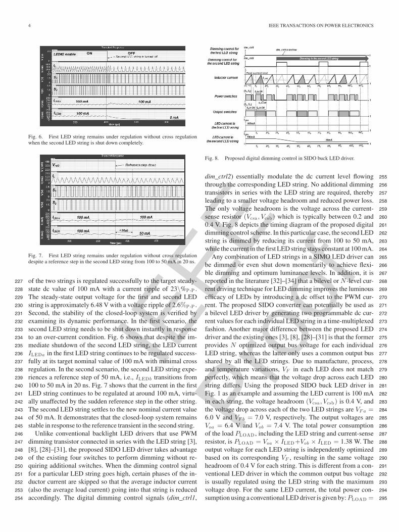
IEEE
Proo
f
4 IEEE TRANSACTIONS ON POWER ELECTRONICS
Fig. 6. First LED string remains under regulation without cross regulationwhen the second LED string is shut down completely.
Fig. 7. First LED string remains under regulation without cross regulationdespite a reference step in the second LED string from 100 to 50 mA in 20 ns.
of the two strings is regulated successfully to the target steady-227
state dc value of 100 mA with a current ripple of 23\%P-P .228
The steady-state output voltage for the first and second LED229
string is approximately 6.48 V with a voltage ripple of 2.6%P-P .230
Second, the stability of the closed-loop system is verified by231
examining its dynamic performance. In the first scenario, the232
second LED string needs to be shut down instantly in response233
to an over-current condition. Fig. 6 shows that despite the im-234
mediate shutdown of the second LED string, the LED current235
ILEDa in the first LED string continues to be regulated success-236
fully at its target nominal value of 100 mA with minimal cross237
regulation. In the second scenario, the second LED string expe-238
riences a reference step of 50 mA, i.e., ILEDb transitions from239
100 to 50 mA in 20 ns. Fig. 7 shows that the current in the first240
LED string continues to be regulated at around 100 mA, virtu-241
ally unaffected by the sudden reference step in the other string.242
The second LED string settles to the new nominal current value243
of 50 mA. It demonstrates that the closed-loop system remains244
stable in response to the reference transient in the second string.245
Unlike conventional backlight LED drivers that use PWM246
dimming transistor connected in series with the LED string [3],247
[8], [28]–[31], the proposed SIDO LED driver takes advantage248
of the existing four switches to perform dimming without re-249
quiring additional switches. When the dimming control signal250
for a particular LED string goes high, certain phases of the in-251
ductor current are skipped so that the average inductor current252
(also the average load current) going into that string is reduced253
accordingly. The digital dimming control signals (dim_ctrl1,254
Fig. 8. Proposed digital dimming control in SIDO buck LED driver.
dim_ctrl2) essentially modulate the dc current level flowing 255
through the corresponding LED string. No additional dimming 256
transistors in series with the LED string are required, thereby 257
leading to a smaller voltage headroom and reduced power loss. 258
The only voltage headroom is the voltage across the current- 259
sense resistor (Vcsa , Vcsb) which is typically between 0.2 and 260
0.4 V. Fig. 8 depicts the timing diagram of the proposed digital 261
dimming control scheme. In this particular case, the second LED 262
string is dimmed by reducing its current from 100 to 50 mA, 263
while the current in the first LED string stays constant at 100 mA. 264
Any combination of LED strings in a SIMO LED driver can 265
be dimmed or even shut down momentarily to achieve flexi- 266
ble dimming and optimum luminance levels. In addition, it is 267
reported in the literature [32]–[34] that a bilevel or N -level cur- 268
rent driving technique for LED dimming improves the luminous 269
efficacy of LEDs by introducing a dc offset to the PWM cur- 270
rent. The proposed SIDO converter can potentially be used as 271
a bilevel LED driver by generating two programmable dc cur- 272
rent values for each individual LED string in a time-multiplexed 273
fashion. Another major difference between the proposed LED 274
driver and the existing ones [3], [8], [28]–[31] is that the former 275
provides N optimized output bus voltage for each individual 276
LED string, whereas the latter only uses a common output bus 277
shared by all the LED strings. Due to manufacture, process, 278
and temperature variations, VF in each LED does not match 279
perfectly, which means that the voltage drop across each LED 280
string differs. Using the proposed SIDO buck LED driver in 281
Fig. 1 as an example and assuming the LED current is 100 mA 282
in each string, the voltage headroom (Vcsa , Vcsb) is 0.4 V, and 283
the voltage drop across each of the two LED strings are VF a = 284
6.0 V and VF b = 7.0 V, respectively. The output voltages are 285
Voa = 6.4 V and Vob = 7.4 V. The total power consumption 286
of the load PLOAD , including the LED string and current-sense 287
resistor, is PLOAD = Voa × ILED+Vob × ILED = 1.38 W. The 288
output voltage for each LED string is independently optimized 289
based on its corresponding VF , resulting in the same voltage 290
headroom of 0.4 V for each string. This is different from a con- 291
ventional LED driver in which the common output bus voltage 292
is usually regulated using the LED string with the maximum 293
voltage drop. For the same LED current, the total power con- 294
sumption using a conventional LED driver is given by: PLOAD = 295

IEEE
Proo
f
LEE et al.: SCALABILITY OF QUASI-HYSTERETIC FSM-BASED DIGITALLY CONTROLLED SINGLE-INDUCTOR DUAL-STRING 5
Fig. 9. Timing diagram of the proposed SIMO buck LED driver.
2 × max (Voa ,Vob ) × ILED = 1.48 W, which is more than 7%296
higher than that of the proposed driver. The voltage headroom297
for the first LED string increases from 0.4 to 1.4 V, resulting in298
450 mW more power loss or additional 30% efficiency degra-299
dation. Since the output voltage is self-optimized to match the300
total VF in each individual LED string in the proposed driver,301
same-colored LEDs from neighboring bins (not only from a302
single bin) with larger VF variance can be used which helps303
reduce the LED costs. In the event that a particular application304
demands a total LED current greater than the average inductor305
current, the same time-multiplexing control scheme operating306
in DCM can still be employed either by lowering the switch-307
ing frequency with a higher inductor peak current limit or by308
operating the buck LED driver in pseudocontinuous conduction309
mode (PCCM) [17], [35], [36]. In PCCM, the average inductor310
current is increased by simply adding a nonzero dc offset of IDC311
to that of DCM.312
III. EXTENSION FROM SIDO TO SIMO BUCK LED DRIVER313
Having demonstrated the feasibility of the proposed SIDO314
buck LED driver, it is natural for us to extend it to SIMO with315
N independently driven LED strings. In particular, the theo-316
retical maximum number of LED strings Nmax is determined317
for this SIMO architecture. Fig. 9 shows a timing diagram of318
the inductor current, the two power switches (S1 , S2), and the319
first four output switches (Sa, Sb , Sc , Sd) in a SIMO buck LED320
driver. To simplify the analysis, the balanced load condition is321
assumed. Based on the time-multiplexing control scheme, en-322
ergy is being transferred from the dc supply to each individual323
output exactly once within a total of N switching phases. For a324
particular output, the corresponding output switch is OFF dur-325
ing D3 , while the output capacitor discharges to the LED string.326
During the subsequent (N – 1) × Ts phases, the output switch327
remains OFF and the output capacitor continues to discharge328
to the corresponding LED string. Hence, the total discharging329
time for the output capacitor tdch can be expressed as330
tdch = D3Ts + (N − 1)Ts = (D3 + N − 1)Ts. (1)
For D3 = 0, tdch = (N − 1)Ts. (2)
The proposed SIMO buck LED driver is essentially a331
constant-current regulator which maintains a constant dc cur-332
rent ILED flowing through the LED string via a closed-loop333
current-sense feedback control. For very small variation of for- 334
ward voltage around the quiescent point (also known as bias 335
point) on the LED’s exponential I–V curve, the dc forward cur- 336
rent is assumed to be constant. During tdch when the output 337
switch is OFF, the output capacitor is connected to the LED 338
string which acts as a constant-current sink (CCS). Assuming 339
ideal capacitor with no ESR (the effect of the ESR will be ex- 340
plained later), the voltage across the output capacitor vc (t) is the 341
same as the output voltage which is expressed as the charge q(t) 342
divided by the capacitance value Co , i.e., 343
vc(t) =q(t)Co
=1Co
∫ td ch
0ic(τ)dτ + vc(0). (3)
For CCS, ic(τ) = ILED . (4)
Combining (3) and (4) and rearranging, we have 344
Δvo = Δvc = vc(t) − vc(0) =1Co
(ILED tdch). (5)
Hence, the total discharging time tdch can be expressed as 345
tdch =CoΔvo
ILED(6)
where Δvo is the output voltage drop due to the discharging 346
of the output capacitor. In general, Δvo is assumed to be rea- 347
sonably small relative to the output voltage. The LED ripple 348
current ΔiLED usually ranges from 10%P-P to 40%P-P of the 349
dc forward current as recommended by the LED manufactur- 350
ers [37], [38]. For a particular ΔiLED , the corresponding voltage 351
ripple ΔvLED at the chosen bias point can be readily obtained 352
from the exponential I–V curve. Suppose each LED string con- 353
tains a total of n LEDs connected in series. The output voltage 354
ripple Δvo is, therefore, the sum of the voltage ripple across 355
the LED string and the voltage ripple across the current-sense 356
resistor, i.e., Δvo = n×ΔvLED + Δvcs . Suppose Δvomax rep- 357
resents the maximum output voltage ripple allowed. Equation (6) 358
can, therefore, be rewritten as 359
tdch ≤ CoΔvo max
ILED. (7)
Substituting (1) into (7), we have 360
(D3 + N − 1)Ts ≤ CoΔvo max
ILED⇒ N
≤ CoΔvo max
ILEDTs+ 1 − D3 . (8)
Hence, the theoretical maximum possible number of LED 361
strings in SIMO, Nmax , is given by 362
Nmax =CoΔvo max
ILEDTs+ 1 − D3 =
CoΔvo max
ILEDTs+ D1 + D2 .
(9a)Since Nmax is an integer value, the floor(·) function is used to 363
round the result down to the closest integer. Hence, (9a) becomes 364
Nmax = floor
(CoΔvo max + ILEDTs(1 − D3)
ILEDTs
). (9b)
Equation (9b) represents a general formula for determining the 365
scalability limit of a SIMO buck LED driver operating in DCM 366

IEEE
Proo
f
6 IEEE TRANSACTIONS ON POWER ELECTRONICS
and is referred to as a scalable DCM-based SIMO scheme for367
the sake of our ensuing discussion. In particular, when D3 =368
0, the SIMO buck LED driver operates in boundary conduction369
mode (BCM). Hence, (9a) and (9b) become (10a) and (10b),370
respectively. Also, Nmax in BCM is greater than or equal to that371
in DCM for the same set of design parameter values372
Nmax =CoΔvo max
ILEDTs+ 1 (10a)
Nmax = floor
(CoΔvo max
ILEDTs+ 1
). (10b)
For a single-output buck converter, the average inductor current373
is identical to the load current. Due to the nature of the time-374
multiplexing control scheme in the proposed SIMO converter,375
the average inductor current IL avg is the sum of the individual376
load current ILED in each LED string. Assuming balanced load377
condition, IL avg = N × ILED , where N is the total number of378
LED strings. The average inductor current reaches its maximum379
value in BCM, resulting in a maximum transfer of power [16].380
Since the current in each LED string remains the same, a the-381
oretical upper bound of the total achievable number of LED382
strings in SIMO can be expressed as383
Nmax =IL avg max
ILED. (11)
By simple geometry, IL avg max is given by the following384
equation [39]:385
IL avg max =m1D1Ts
2=
(Vg − Vo)D1Ts
2L. (12)
By substituting (12) into (11) and rearranging, Ts can be ex-386
pressed as387
Ts =2LNmaxILED
D1(Vg − Vo). (13)
Now, by substituting (13) into (10a) and rearranging, we have388
2LI2LEDN 2
max−2LI2LEDNmax−CoΔvo max(Vg − Vo)D1 = 0.
(14)Equation (14) is a quadratic equation in Nmax . The discriminant389
Δ of (14) can be expressed as390
Δ = 4L2I4LED + 8LI2
LEDCoΔvo max(Vg − Vo)D1 > 0. (15)
Since (Vg − Vo) > 0 for a buck switcher, the discriminant in391
(15) is always a positive number which implies that (14) has392
two real roots as given by393
r1 , r2 =2LI2
LED ±√
Δ4LI2
LED. (16)
Since Nmax must be a positive integer, the negative root is394
eliminated, leaving only the positive root, i.e.,395
Nmax BCM
= floor
(12×
[1 +
√1 +
2CoΔvo maxVo(Vg − Vo)LI2
LEDVg
]).(17)
Equation (17) defines the theoretical maximum total number396
of outputs in SIMO operating in BCM. It is referred to as a397
scalable BCM-based SIMO scheme which is a special case of 398
scalable DCM-based SIMO scheme. In fact, it is observed that 399
(11) is also valid for the case of DCM. By simple geometry, the 400
switching period Ts in DCM can be expressed as 401
Ts =2LNmaxILED
D1(D1 + D2)(Vg − Vo). (18)
Realizing that the same calculations that lead to (17) for the 402
case of BCM can also be performed in DCM, the theoretical 403
maximum total number of LED strings in a SIMO converter 404
operating in DCM can, therefore, be written as1 405
Nmax DCM = floor
(12× (1 − D3)
×[1 +
√1 +
2CoΔvo max(Vg − Vo)D1
LI2LED(1 − D3)
]). (19)
Notice that for the case of BCM, D3 = 0 and D1 = Vo /Vg , 406
(19) reduces to (17). Hence, (19) represents the generalized 407
formula for the theoretical maximum total number of outputs 408
in SIMO which is applicable to either BCM or DCM. It is also 409
interesting to note that the average inductor current in DCM 410
is smaller than (or equal to) that in BCM. As a result, for the 411
same LED current, the theoretical maximum achievable number 412
of outputs in SIMO operating in DCM is no greater than that 413
in BCM, i.e., Nmax DCM ≤ Nmax BCM . In reality, the ESR of 414
the output capacitor needs to be taken into consideration. Any 415
current flowing through the output capacitor Co must also flow 416
through the RESR , resulting in an additional voltage drop of 417
ΔVESR = ILED × RESR . Hence, Δvo can be expressed as 418
Δvo = Δvc + ΔvESR = Δvc + ILED × RESR . (20)
Rearranging the terms in (20), we have 419
Δvc = Δvo − ILED × RESR . (21)
Hence, (17) and (19) are modified slightly to become (22) and 420
(23), respectively: BCM: 421
Nmax BCM = floor
(12×
[1
+
√1 +
2CoVo(Δvo max − ILEDRESR)(Vg − Vo)LI2
LEDVg
])(22)
DCM: 422
Nmax DCM = floor
(12× (1 − D3) ×
[1
+
√1+
2Co(Δvo max−ILEDRESR) (Vg −Vo) D1
LI2LED(1−D3)
]). (23)
The presence of RESR in (22) and (23) reduces the theoretical 423
maximum achievable number of outputs in SIMO. Therefore, 424
1In DCM, D1 can be expressed as: D1 = M√
K1−M , where M = Vo
V gand
K = 2LR L Ts
= 2LIL E DVo T s
[39].

IEEE
Proo
f
LEE et al.: SCALABILITY OF QUASI-HYSTERETIC FSM-BASED DIGITALLY CONTROLLED SINGLE-INDUCTOR DUAL-STRING 7
Fig. 10. Theoretical maximum achievable number of LED strings (Nm ax )versus the output capacitance (Co ) and the capacitor ESR (RESR ) for thescalable BCM-based SIMO scheme.
it is always recommended to choose an output capacitor with a425
smaller ESR, whenever possible. Fig. 10 shows the theoretical426
maximum total number of LED strings versus the output ca-427
pacitance and capacitor ESR for the scalable BCM-based SIMO428
scheme, given an LED current of 80 mA and a maximum ripple429
current requirement of 40%P-P .430
Intuitively, for a particular LED current, an increasing number431
of outputs can be achieved by using a larger output capacitor432
with the same ESR value. For instance, if the output capacitance433
is increased from 4.7 to 22 μF (the ESR remains at 100 mΩ),434
the theoretical model based on (22) suggests that the maximum435
total number of LED strings can be increased from three to six.436
It is also interesting to note that the maximum number of outputs437
in SIMO has a stronger dependence on the output capacitance438
than the capacitor ESR, as shown in Fig. 10.439
On the other hand, it is useful to study how the LED current440
affects the maximum achievable number of outputs in SIMO.441
As an example, assuming balanced load and two LEDs con-442
nected in series per string, a scalable BCM-based SIMO scheme443
is investigated with these parameter values: L = 47 μH, Co =444
4.7 μF, RESR = 100 mΩ, Vg = 15 V, and Vo = 6.4 V. The445
relationship between Nmax and ILED can be obtained by us-446
ing (22) for different values of output voltage ripple Δvo max .447
Based upon the I–V curve and/or SPICE model of the particular448
LED used, the corresponding output voltage ripple Δvo max can449
be determined from the LED current ripple requirement ΔiLED .450
The proposed design uses white LED [40] which is the target for451
LCD backlighting applications. For instance, a 20%P-P current452
ripple corresponds to around 2%P-P voltage ripple and a 40%P-P453
current ripple corresponds to around 4%P-P voltage ripple.454
Fig. 11 shows a plot of Nmax versus ILED for ΔiLED rang-455
ing from 5%P-P to 40%P-P . This plot is beneficial to a practical456
SIMO design in two ways. First, for a given LED current and457
current ripple requirement, the theoretical maximum number458
of LED strings viable under the scalable BCM-based SIMO459
scheme can be extracted directly from the plot. Second, the460
Fig. 11. Plot of theoretical maximum number of LED strings in SIMO(Nm ax ) versus the LED current (ILED ) in the scalable BCM-based SIMOscheme.
maximum LED current allowed in order for a SIMO to remain 461
at the same scaling level can also be obtained from the plot. For 462
instance, given a 20% current ripple requirement (i.e., ΔiLED = 463
20%P-P ), a SIDO (dual-string) configuration is possible as long 464
as the LED current in each string is no more than 110 mA. In 465
the event that an application demands an LED current greater 466
than 110 mA, two options can be considered: 1) Relax the cur- 467
rent ripple requirement whenever possible. A wider tolerance 468
in ΔiLED is generally acceptable since the ripple frequency is 469
too high for the human eye to detect. 2) Operate the SIMO buck 470
LED driver in PCCM [17], [35], [36]. In PCCM, the floor of 471
the inductor current is raised by a nonzero dc offset IDC which 472
distinguishes it from DCM. The proposed theoretical model can 473
be extended to PCCM by adding a dc component to the aver- 474
age inductor current. By going through similar calculations as 475
in DCM, the theoretical maximum number of outputs in SIMO 476
operating in PCCM is given by (24), as shown at the bottom of 477
the page. It is interesting to note that (24) continues to apply to 478
the cases of DCM and BCM. For instance, in DCM, IDC = 0 479
and (24), therefore, reduces to (23). 480
In the event of unbalanced load with unequal current among 481
the LED strings, the scalable DCM- or BCM-based SIMO 482
scheme continues to hold. The only change is to replace ILED 483
in (22) and (23) by max(ILED ), where max(ILED ) denotes the 484
largest LED current among all the LED strings. In other words, 485
the maximum number of LED strings that can be realized in 486
a SIMO buck LED driver is constrained by the largest LED 487
current. Generally speaking, the input voltage Vg , output volt- 488
age Vo , and the current ripple requirement are typically fixed 489
parameters defined in the design specification. Without making 490
any hardware changes (i.e., L and Co values are fixed), the pri- 491
mary design variable in (22) and (23) is the LED current ILED . 492
In fact, the LED current is the dominant factor for determining 493
the maximum possible number of outputs under the scalable 494
DCM-/BCM-based SIMO scheme. By knowing the maximum 495
LED current required for a particular application, the theoretical 496
Nmax PCCM =floor
(1
2ILED×[(IDC +(1−D3) ILED ]×
[1+
√1 +
2Co(Δvo max − ILEDRESR) (Vg − Vo) D1(1 − D3)L [IDC − (1 − D3)ILED ]2
]).
(24)
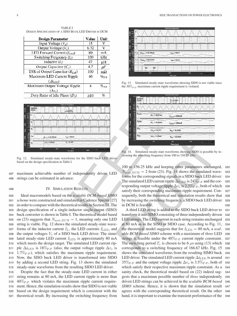
IEEE
Proo
f
8 IEEE TRANSACTIONS ON POWER ELECTRONICS
TABLE IDESIGN SPECIFICATION OF A SISO BUCK LED DRIVER IN DCM
Fig. 12. Simulated steady-state waveforms for the SISO buck LED driverbased on the design specification in Table I.
maximum achievable number of independently driven LED497
strings can be estimated in advance.498
IV. SIMULATION RESULTS499
Ideal macromodels based on the scalable DCM-based SIMO500
scheme were constructed and simulated in Cadence Spectre [27]501
in order to compare with the theoretical results in Section III. The502
design specification of a single-inductor single-output (SISO)503
buck converter is shown in Table I. The theoretical model based504
on (23) suggests that Nmax DCM = 1, meaning only one LED505
string is viable. Fig. 12 shows the simulated steady-state wave-506
forms of the inductor current IL , the LED currents ILED , and507
the output voltages Vo of a SISO buck LED driver. The simu-508
lated steady-state LED current ILED is approximately 80 mA509
which meets the design target. The simulated LED current rip-510
ple ΔiLED is 18%P-P (also, the output voltage ripple Δvo is511
1.7%P-P ), which satisfies the maximum ripple requirement.512
Now, the SISO buck LED driver is transformed into SIDO513
by adding a second LED string. Fig. 13 shows the simulated514
steady-state waveforms from the resulting SIDO LED driver.515
Despite the fact that the steady-state LED current in either516
string remains at 80 mA, the LED current ripple is more than517
40%P-P which violates the maximum ripple current require-518
ment. Hence, the simulation results show that SIDO is not viable519
based on the design requirement which is consistent with the520
theoretical result. By increasing the switching frequency from521
Fig. 13. Simulated steady-state waveforms showing SIDO is not viable sincethe 30%p -p maximum current ripple requirement is violated.
Fig. 14. Simulated steady-state waveforms showing SIDO is possible by in-creasing the switching frequency from 100 to 156.25 kHz.
100 to 156.25 kHz and keeping other parameters unchanged, 522
Nmax DCM = 2 from (23). Fig. 14 shows the simulated wave- 523
forms for the corresponding signals in a SIDO buck LED driver. 524
The simulated LED current ripple ΔiLED is 24%P-P and the cor- 525
responding output voltage ripple Δvo is 2.3%P-P , both of which 526
satisfy their corresponding maximum ripple requirement. Con- 527
sequently, both the theoretical and simulation results show that 528
by increasing the switching frequency, a SIDO buck LED driver 529
in DCM is feasible. 530
A third LED string is added to the SIDO buck LED driver to 531
transform it into SIMO consisting of three independently driven 532
LED strings. The LED current in each string remains unchanged 533
at 80 mA as in the SISO or SIDO case. According to Fig. 11, 534
the theoretical model suggests that for ILED = 80 mA, a scal- 535
able BCM-based SIMO scheme with a maximum of three LED 536
strings is feasible under the 40%P-P current ripple constraint. 537
The switching period Ts is chosen to be 6 μs using (13) which 538
corresponds to a switching frequency of 166.67 kHz. Fig. 15 539
shows the simulated waveforms from the resulting SIMO buck 540
LED driver. The simulated LED current ripple ΔiLED is around 541
35%P-P and the output voltage ripple Δvo is 3.5%P-P , both of 542
which satisfy their respective maximum ripple constraint. As a 543
sanity check, the theoretical model based on (22) indeed sug- 544
gests that a maximum possible number of three independently 545
driven LED strings can be achieved in the scalable BCM-based 546
SIMO scheme. Hence, it is shown that the simulation result 547
agrees with the corresponding theoretical result. On the other 548
hand, it is important to examine the transient performance of the 549

IEEE
Proo
f
LEE et al.: SCALABILITY OF QUASI-HYSTERETIC FSM-BASED DIGITALLY CONTROLLED SINGLE-INDUCTOR DUAL-STRING 9
Fig. 15. Simulated steady-state waveforms of a three-string SIMO buck LEDdriver operating in BCM.
Fig. 16. Simulated transient waveforms for (a) peak reference step-up and(b) peak reference step-down response.
proposed SIDO buck LED driver. The LED current is changed550
by adjusting the peak limit of the inductor current. By stepping551
up the peak voltage reference (Vpeak in Fig. 1) from 1.660 to552
1.945 V in 400 ns, the peak inductor current limit is increased553
by approximately 200 mA, leading to an increase in the nom-554
inal LED current from 20 to 80 mA. The reference voltages555
(Vrefa , Vrefb) are also stepped up from 100 to 340 mV in order556
to maintain the same load current between the two LED strings.557
Conversely, by stepping down Vpeak from 1.945 to 1.660 V,558
the LED current is reduced from 80 to 20 mA. Fig. 16 shows559
the simulated transient behavior for the peak voltage reference560
step-up and step-down response.561
In the case of step-up reference response, the LED current in562
either string settles to the steady-state nominal value of 80 mA563
within 63 μs. The output voltage reaches its target steady-state564
Fig. 17. Simulated steady-state waveforms of a SIDO buck LED driver withunbalanced load.
value of 6.34 V. In the case of step-down reference response, 565
the LED current in either string settles to the steady-state nom- 566
inal value of 20 mA in less than 112 μs. The output voltage 567
settles to its new steady-state value of 5.82 V without oscilla- 568
tions. Hence, the simulation results show that the closed-loop 569
system remains in stable condition in response to a peak voltage 570
reference transient. 571
The effectiveness of the proposed SIDO converter to drive 572
unbalanced load is also investigated. As an example, the first 573
and second LED strings require an average current value of 80 574
and 30 mA, respectively. Unlike the balanced load case with 575
a constant peak inductor current limit, two distinct peak cur- 576
rent limits are employed for unbalanced load such that two 577
different average inductor (or load) current values can be gen- 578
erated in alternate clock cycles. Fig. 17 depicts the simulated 579
steady-state waveforms from the SIDO buck LED driver with 580
unbalanced load. The simulation results show that the first and 581
second LED strings are regulated with an average current value 582
of 80 and 30 mA, respectively. For the first string, the simu- 583
lated current ripple is 24.38%P-P and the output voltage ripple 584
is 2.3%P-P . Also, for the second string, the simulated current 585
ripple is 21.1%P-P and the output voltage ripple is 1.1%P-P . 586
Either string meets the maximum ripple requirements. The sim- 587
ulation results demonstrate that the proposed SIDO converter is 588
capable of delivering unequal currents to the two LED strings 589
simultaneously. 590
V. EXPERIMENTAL RESULTS 591
The proposed SIDO buck LED driver was implemented on 592
a field-programmable gate array (FPGA)-based hardware pro- 593
totype in accordance with the design specification provided in 594
Table I. The switching frequency is increased to 156.25 kHz in 595
order to satisfy the LED current ripple requirement. A photo of 596
the experimental setup is shown in Fig. 18. The power stage of 597
the buck converter consists of discrete ICs from International 598
Rectifier such as power MOSFETs (IRF7828), dual-channel 599
gate driver (IR2110), and output switches (IRF9388), as well as 600
surface-mount inductor and low-ESR capacitors. In actual im- 601
plementation, the top level of the proposed digital controller is 602
partitioned into two major functional blocks. The functionality 603
of the first block is to control the switching action of the power 604

IEEE
Proo
f
10 IEEE TRANSACTIONS ON POWER ELECTRONICS
Fig. 18. Experimental setup for the proposed SIDO buck LED driver.
Fig. 19. Measured waveforms for inductor current and current sense feedbackvoltage.
stage by detecting the peak-crossing and zero-crossing events605
of the inductor current. It was implemented in hierarchical gate-606
level schematics using primitives and macros available from607
the Xilinx Spartan-3 Generation library. Dead-time logic is in-608
cluded to prevent shoot-through current of the power switches.609
The second logical block is used to control the switching se-610
quence of the two output switches by continuously monitoring611
the current-sense feedback signals. It was modeled as an FSM612
in Verilog RTL. Only one of the two output switches can be ON613
and the other must be OFF per switching cycle. Dead-time logic614
is also added to prevent cross conduction between outputs. The615
two logical blocks are synchronized by the system clock to en-616
sure that the high-side power switch and the output switches are617
triggered from the same clock edge. The entire digital controller618
was implemented with Xilinx Spartan-3E (XC3S250E) FPGA.619
The quasi-hysteretic control logic was realized using 4-ns fast620
comparators (AD8611 from Analog Devices) and semicustom621
synchronous logic.622
Using a current sensing resistor of 4 Ω and reference voltage623
of 320 mV, the target current in each of the two LED strings624
is 80 mA. Fig. 19 shows the current sensing feedback voltage625
(Vcsa , Vcsb) from which the corresponding average load current626
can be obtained, i.e., ILED = Vcs /Rcs . The average inductor627
current is measured to be 162 mA, which is the sum of the628
load currents in both LED strings. The average current values629
in the first and second LED string are measured to be around630
80.6 and 82 mA, respectively. The measured LED current ripple631
ΔiLED in either string is around 26%P-P , which is reasonably632
close to the simulated current ripple of 24%P-P . In addition,633
the nominal output voltages in the first and second string are634
Fig. 20. Measured waveforms for inductor current and output voltage in eitherLED string.
measured to be 6.204 and 6.249 V, respectively, as shown in 635
Fig. 20. Under this balanced load condition, the measured cur- 636
rent and voltage values are in close agreement between the 637
two LED strings. The output voltage ripple is also measured 638
to be around 2.57%P-P , compared to 2.3%P-P from simulation. 639
Therefore, the experimental results are shown to be consistent 640
with the corresponding simulation ones. On the other hand, the 641
measured power conversion efficiency of the proposed SIDO 642
converter is 80% which is comparable to conventional driving 643
topologies [41]. The efficiency can be further increased by em- 644
ploying a current-sensing resistor with a smaller value. 645
The transient response of the proposed SIDO buck LED driver 646
is verified experimentally by measuring its peak voltage refer- 647
ence step response. An 8-bit digital-to-analog converter (AD558 648
from Analog Devices) is used to enable programming of the peak 649
voltage reference Vpeak and the current-sense voltage references 650
(Vrefa , Vref b) by the Xilinx FPGA. The measured waveforms 651
of the inductor current and the voltage at the current sensing 652
nodes in response to a peak voltage reference step are shown in 653
Fig. 21. The settling time of the transient response is also mea- 654
sured and compared with the simulated settling time. For the 655
step-up response, it is observed that the current-sensing voltage 656
Vcsa in the first LED string steps up from 81.8 to 325.4 mV, 657
which corresponds to an increase in the average load current 658
from 20.5 to 81.3 mA. Similarly, the current-sensing voltage 659
Vcsb in the second LED string steps up from 94.1 to 327.6 mV, 660
which corresponds to an increase in the average load current 661
from 23.5 to 81.9 mA. The settling time for the step-up response 662
is measured to be 67 μs, compared to 63 μs from simulation. 663
The measured results for the step-down response are the reverse 664
of those from the step-up response. The only difference is that 665
it takes longer for the step-down transient to settle. The set- 666
tling time for the step-down response is measured to be 115 μs, 667
compared to 112 μs from simulation. The measured settling 668
times are shown to be very close to the simulated ones. The 669
experimental results confirm that the system remains in stable 670
condition when it is perturbed by the peak voltage reference 671
transient. 672
The unbalanced load scenario in the proposed SIDO buck 673
LED driver is also verified experimentally. The measured aver- 674
age load current values in the first and second LED string are 675

IEEE
Proo
f
LEE et al.: SCALABILITY OF QUASI-HYSTERETIC FSM-BASED DIGITALLY CONTROLLED SINGLE-INDUCTOR DUAL-STRING 11
Fig. 21. Measured transient waveforms in response to (a) peak reference step-up and (b) peak reference step-down.
Fig. 22. Measured waveforms for inductor current and current sense voltages.
around 81.9 and 30.1 mA, respectively. Fig. 22 shows the mea-676
sured waveforms for the inductor current and the current-sensing677
voltage per string. The inductor current waveform indicates that678
the proposed driver operates in DCM with two distinct peak679
current limits. Fig. 23 shows the measured inductor current and680
the output voltage in either string. The measured output voltage681
values in the first and second LED string are 6.22 and 5.70 V,682
respectively. The experimental results demonstrate that the pro-683
posed driver is capable of driving two independent LED strings684
concurrently with different load current.685
Fig. 23. Measured waveforms for inductor current and output voltages.
VI. CONCLUSION 686
The proposed SIDO buck LED driver was implemented in 687
FPGA-based hardware. The experimental results correlate well 688
with simulation ones. The scalability of the proposed SIDO buck 689
LED driver to SIMO is closely examined. A general formula 690
for determining the theoretical maximum achievable number of 691
LED strings in SIMO is derived. The simulation results were 692
shown to be consistent with those obtained from the theoret- 693
ical model for the same design parameter values. The quasi- 694
hysteretic digital control scheme does not require loop com- 695
pensation which simplifies the control loop design and reduces 696
component count. In addition, the proposed SIMO architecture 697
offers the advantage of driving a larger number of parallel LED 698
strings without being limited by the maximum current rating of 699
the LED. It also enables dimming for the LED strings without 700
additional dimming transistors. Local bus voltage and current 701
optimization in each individual LED string compensates for the 702
variability of the LED’s forward voltage, which reduces power 703
loss and enables mixing of white LEDs from different bins to 704
lower LED costs. 705
REFERENCES 706
[1] C.-Y Hsieh, C.-Y. Yang, and K.-H. Chen, “A charge-recycling buck-store 707and boost-restore (BSBR) technique with dual outputs for RGB LED 708backlight and flashlight module,” IEEE Trans. Power Electron., vol. 24, 709no. 8, pp. 1914–1925, Aug. 2009. 710
[2] S.-Y. Lee, J.-W. Kwon, H.-S. Kim, M.-S. Choi, and K.-S. Byun, “New 711design and application of high efficiency LED driving system for RGB- 712LED backlight in LCD display,” in Proc. 37th IEEE Power Electron. Spec. 713Conf.,, 2006, pp. 1–5. 714
[3] H.-J. Chiu, Y.-K. Lo, J.-T. Chen, S.-J. Cheng, C.-Y. Lin, and S.-C. Mou, “A 715high-efficiency dimmable led driver for low-power lighting applications,” 716IEEE Trans. Ind. Electron., vol. 57, no. 2, pp. 735–743, Feb. 2010. 717
[4] C.-H. Liu, C.-Y. Hsieh, Y.-C. Hsieh, T.-J. Tai, and K.-H. Chen, “SAR- 718Controlled adaptive off-time technique without sensing resistor for achiev- 719ing high efficiency and accuracy led lighting system,” IEEE Trans. Circuits 720Syst. I, Reg. Papers, vol. 57, no. 6, pp. 1384–1394, Jun. 2010. 721
[5] C.-H. Wu and C.-L. Chen, “High-efficiency current-regulated charge pump 722for a white LED driver,” IEEE Trans. Circuits Syst. II, Exp. Briefs, vol. 56, 723no. 10, pp. 614–618, Oct. 2009. 724
[6] P. Malcovati, M. Belloni, F. Gozzini, C. Bazzani, and A. Baschirotto, “A 7250.18μm CMOS 91%-efficiency 0.1-to-2 A scalable buck-boost DC-DC 726converter for LED drivers,” in Proc. ISSCC Dig. Tech. Papers, Feb. 2012, 727pp. 280–281. 728
[7] S. Rao, Q. Khan, S. Bang, D. Swank, A. Rao, W. Mclntyre, and 729P. K. Hanumolu, “A 1.2 A buck-boost LED driver with 13% efficiency 730
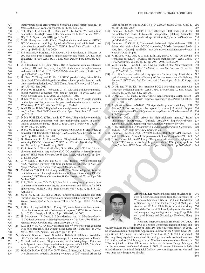
IEEE
Proo
f
12 IEEE TRANSACTIONS ON POWER ELECTRONICS
improvement using error-averaged SenseFET-Based current sensing,” in731Proc. ISSCC Dig. Tech. Papers, Feb. 2011, pp. 238–239.732
[8] S.-I. Hong, J.-W Han, D.-H. Kim, and O.-K. Kwon, “A double-loop733control LED backlight driver IC for medium-sized LEDs,” in Proc. ISSCC734Dig. Tech. Papers, Feb. 2010, pp. 116–117.735
[9] M.-H. Huang and K.-H. Chen, “Single-inductor multi-output (SIMO)736DC-DC converters with high light-load efficiency and minimized cross-737regulation for portable devices,” IEEE J. Solid-State Circuits, vol. 44,738no. 4, pp. 1099–1111, Apr. 2009.739
[10] E. Bonizzoni, F. Borghetti, P. Malcovati, F. Maloberti, and B. Niessen, “A740200 mA 93% peak efficiency single-inductor dual-output DC-DC buck741converter,” in Proc. IEEE ISSCC Dig. Tech. Papers, Feb. 2007, pp. 526–742619.743
[11] C.-Y. Hsieh and K.-H. Chen, “Boost DC-DC converter with fast reference744tracking (FRT) and charge-recycling (CR) techniques for high-efficiency745and low-cost LED driver,” IEEE J. Solid- State Circuits, vol. 44, no. 9,746pp. 2568–2580, Sep. 2009.747
[12] H. Chen, Y. Zhang, and D. Ma, “A SIMO parallel-string driver IC for748dimmable LED backlighting with local bus voltage optimization and single749time-shared regulation loop,” IEEE Trans. Power Electron., vol. 27, no. 1,750pp. 452–462, Jan. 2012.751
[13] D. Ma, W.-H. Ki, P. K. T. Mok, and C.-Y. Tsui, “Single-inductor multiple-752output switching converters with bipolar outputs,” in Proc. IEEE Int.753Symp. Circuits Syst., May 2001, vol. 3, pp. 301–304.754
[14] D. Ma, W.-H. Ki, C.-Y. Tsui, and P. K. T. Mok, “A 1.8 V single-inductor755dual-output switching converter for power reduction techniques,” in Proc.756IEEE Symp. VLSI Circuits, Jun. 2001, pp. 137–140.757
[15] W.-H. Ki and D. Ma, “Single-inductor multiple-output switching convert-758ers,” in Proc. 32nd IEEE Power Electron. Spec. Conf., Jun. 2001, vol. 1,759pp. 226–231.760
[16] D. Ma, W.-H. Ki, C.-Y. Tsui, and P. K. T. Mok, “Single-inductor multiple-761output switching converters with time-multiplexing control in discon-762tinuous conduction mode,” IEEE J. Solid-State Circuits, vol. 38, no. 1,763pp. 89–100, Jan. 2003.764
[17] D. Ma, W.-H. Ki, and C.-Y. Tsui, “A pseudo-CCM/DCM SIMO switching765converter with freewheel switching,” IEEE J. Solid-State Circuits, vol. 38,766no. 6, pp. 1007–1014, Jun. 2003.767
[18] D. Kwon and G. A. Rincon-Mora, “Single-inductor multiple-output768switching DC–DC converters,” IEEE Trans. Circuits Syst. II, Exp. Briefs,769vol. 56, no. 8, pp. 614–618, Aug. 2009.770
[19] K.-S. Seol, Y.-J. Woo, G.-H. Cho, G.-H. Gho, and J.-W. Lee, “A syn-771chronous multioutput step-up/down DC–DC converter with return current772control,” IEEE Trans. Circuits Syst. II, Exp. Briefs, vol. 56, no. 3, pp. 210–773214, Mar. 2009.774
[20] C.-W. Leng, C.-H. Yang, and C.-H. Tsai, “Digital PWM controller for775SIDO switching converter with time-multiplexing scheme,” in Proc. Int.776Symp. VLSI Design Autom. Test, Apr. 2009, pp. 52–55.777
[21] Y.-J. Moon, Y.-S. Roh, J.-C. Gong, and C. Yoo, “Load-independent current778control technique of a single-inductor multiple-output switching DC–DC779converter,” IEEE Trans. Circuits Syst. II, Exp. Briefs, vol. 59, no. 1, pp. 50–78054, Jan. 2012.781
[22] F. Su, W.-H. Ki, and C.-Y. Tsui, “Ultra fast fixed-frequency hysteretic buck782converter with maximum charging current control and adaptive for DVS783applications,” IEEE J. Solid- State Circuits, vol. 43, no. 4, pp. 815–822,784Apr. 2008.785
[23] W.-H. Ki, K.-M. Lai, and C. Zhan, “Charge balance analysis and state786transition analysis of hysteretic voltage mode switching converters,” IEEE787Trans. Circuits Syst. I, Reg. Papers, vol. 58, no. 5, pp. 1142–1153, May7882011.789
[24] K. K.-S. Leung and H. S.-H. Chung, “Dynamic hysteresis band control790of the buck converter with fast transient response,” IEEE Trans. Circuits791Syst. II, Exp. Briefs, vol. 52, no. 7, pp. 398–402, Jul. 2005.792
[25] H. Eachempatti, S. Ganta, J. Silva-Martinez, and H. Martınez-Garcia,793“SIDO buck converter with independent outputs,” in Proc. 53rd IEEE Int.794Midwest Symp. Circuits Syst., Aug. 2010, pp. 37–40.795
[26] F. Su and W.-H. Ki, “Digitally assisted quasi-V2 hysteretic buck converter796with fixed frequency and without using Large-ESR capacitor,” in Proc.797ISSCC Dig. Tech. Papers, Feb. 2009, pp. 446–447.798
[27] Cadence Spectre Circuit Simulator Datasheet [Online]. Available:799http://www.cadence.com/products/cic/spectre_circuit/pages/default.aspxQ1 800
[28] M. Doshi and R. Zane, “Digital architecture for driving large LED arrays801with dynamic bus voltage regulation and phase shifted PWM,” in Proc.802Appl. Power Electron. Conf., Feb. 2007, pp. 287–293.803
[29] W.-S. Oh, D. Cho, K.-M. Cho, G.-W. Moon, B. Yang, and T. Jang, “A novel804two-dimensional adaptive dimming technique of X-Y channel drivers for805
LED backlight system in LCD TVs,” J. Display Technol., vol. 5, no. 1, 806pp. 20–26, Jan. 2009. 807
[30] Datasheet: LP8545, “LP8545 High-efficiency LED backlight driver 808for notebooks,” Texas Instruments Incorporated, [Online] Available: 809http://www.ti.com/general/docs/lit/getliterature.tsp?genericPartNumber= 810lp8545&fileType=pdf 811
[31] Datasheet: MAX16814, “Integrated, 4-channel, high-brightness LED 812driver with high-voltage DC-DC controller,” Maxim Integrated Prod- 813ucts, Inc., [Online], Available: http://datasheets.maximintegrated.com/ 814en/ds/MAX16814.pdf 815
[32] K. H. Loo, W. K. Lun, S. C. Tan, Y. M. Lai, and C. K. Tse, “On driving 816techniques for LEDs: Toward a generalized methodology,” IEEE Trans. 817Power Electron., vol. 24, no. 12, pp. 2967–2976, Dec. 2009. 818
[33] W. K. Lun, K. H. Loo, S. C. Tan, Y. M. Lai, and C. K. Tse, “Bilevel current 819driving technique for LEDs,” IEEE Trans. Power Electron., vol. 24, no. 12, 820pp. 2920–2932, Dec. 2009. 821
[34] S. C. Tan, “General n-level driving approach for improving electrical-to- 822optical energy-conversion efficiency of fast-response saturable lighting 823devices,” IEEE Trans. Ind. Electron., vol. 57, no. 4, pp. 1342–1353, Apr. 8242010. 825
[35] D. Ma and W.-H. Ki, “Fast transient PCCM switching converter with 826freewheel switching control,” IEEE Trans. Circuits Syst. II, Exp. Briefs, 827vol. 54, no. 9, pp. 825–829, Sep. 2007. 828
[36] D. Ma, W.-H. Ki, and C.-Y. Tsui, “Single-inductor multiple-output switch- 829ing converters in PCCM with freewheel switching,” U.S. Patent 7 432 614, 830Oct. 7, 2008. 831
[37] Application Note: AN-1656, “Design challenges of switching LED 832drivers,” Texas Instruments Incorporated, [Online] Available: http:// 833www.ti.com/general/docs/lit/getliterature.tsp?literatureNumber=snva253 834&fileType=pdf 835
[38] Solutions Guide, “LED drivers for high-brightness lighting,” Texas 836Instruments Incorporated, [Online], Available: http://www.ti.com/ 837general/docs/lit/getliterature.tsp?baseLiteratureNumber=snvy001 838
[39] R. W. Erickson and D. Maksimovic, Fundamentals of Power Electronics, 8392nd ed. New York, NY, USA: Springer, 2001. 840
[40] Datasheet: SMD5730, “SMD 5730 White LED Datasheet,” APT Electron- 841ics Ltd., [Online], Available: http://www.apt-hk.com/en/product/?95.html 842
[41] Z. Ye, F. Greenfeld, and Z. Liang, “Design considerations of a high power 843factor SEPIC converter for high brightness white LED lighting applica- 844tions,” in Proc. IEEE Power Electron. Spec. Conf., 2008, pp. 2657–2663. 845
Albert T. L. Lee received the Bachelor of Science de- 846gree in electrical engineering from the University of 847Wisconsin, Madison, USA, in 1994, and the Master 848of Science degree from the University of Michigan, 849Ann Arbor, USA, in 1996. He is currently working 850toward the Doctor of Philosophy degree in electronic 851and computer engineering at the Hong Kong Uni- 852versity of Science and Technology, Kowloon, Hong 853Kong. 854
He joined Intel Corporation, Hillsboro, OR, USA, 855in 1996 as a Senior Component Design Engineer and 856
was involved in the development of Intel’s P6 family microprocessors. In 2001, 857he served as a Senior Corporate Application Engineer in the System-Level De- 858sign Group at Synopsys Inc., Mountain View, CA, USA. In 2003, he joined 859the Hong Kong Applied Science and Technology Research Institute Company 860Ltd. and served as EDA Manager in the Wireline Communications Group. In 8612006, he joined the Giant Electronics Limited as Hardware Design Manager 862and became Associate General Manager in 2008. His research interests include 863mixed-signal system-level design, LED driver, power management system, and 864very large scale integration circuits. 865
866

IEEE
Proo
f
LEE et al.: SCALABILITY OF QUASI-HYSTERETIC FSM-BASED DIGITALLY CONTROLLED SINGLE-INDUCTOR DUAL-STRING 13
Johnny K. O. Sin (S’79–M’88–SM’96–F’12) re-867ceived the B.A.Sc., M.A.Sc., and Ph.D. degrees in868electrical engineering from the University of Toronto,869Toronto, ON, Canada, in 1981, 1983, and 1988,870respectively.871
From 1988 to 1991, he was a Senior Member of872the research staff of Philips Laboratories, Briarcliff873Manor, NY, USA. In August 1991, he joined the De-874partment of Electronic and Computer Engineering,875The Hong Kong University of Science and Technol-876ogy, Kowloon, Hong Kong, where he has been a Full877
Professor since 2001. He is the holder of 13 patents, and the author of more878than 270 papers in technical journals and refereed conference proceedings. His879research interests include microelectronic and nanoelectronic devices and fabri-880cation technology, particularly novel power semiconductor devices and ICs, and881system-on-a-chip applications using CMOS and power transistors and silicon-882embedded magnetic and capacitive devices.883
Dr. Sin was an Editor for the IEEE ELECTRON DEVICES LETTERS from 1998884to 2010. He is a member of the Power Devices and IC’s Technical Committee of885the IEEE Electron Devices Society. He is also a Technical Committee member886of the International Symposium on Power Semiconductor Devices and IC’s. He887is a Fellow of the IEEE for contributions to the design and commercialization888of power semiconductor devices.889
890
Philip C. H. Chan (SM’97–F’07) received the Bach- 891elor of Science degree in electrical engineering from 892the University of California at Davis, Davis, USA, in 8931973, and the Master of Science and Doctor of Phi- 894losophy degrees in electrical engineering from the 895University of Illinois at Urbana-Champaign, Urbana, 896USA, in 1975 and 1978, respectively. 897
He later joined Intel Corporation, Santa Clara, 898CA, USA, in 1981 and became a Senior Project 899Manager in Technology Development. He joined the 900Hong Kong University of Science and Technology 901
(HKUST) in 1991 as a founding member. He served at HKUST as the Associate 902Dean of Engineering and Head of the Department of Electronic and Com- 903puter Engineering. He became the Dean of Engineering in September 2003. 904He joined the Hong Kong Polytechnic University, Hong Kong, in 2010 as the 905Deputy President and Provost. His research interests include very large scale 906integration devices, circuits, electronic packaging, and integrated sensors. 907
Dr. Chan received the ECE Distinguished Alumni Award from the University 908of Illinois, Urbana-Champaign in 2010. 909
910

IEEE
Proo
f
QUERIES911
Q1. Author: Please provide year information in Refs. [27], [30], [31], [37], [38], and [40].912